3048A Phase Noise Measurement System Calibration Manual ...
254
Errata Title & Document Type: 3048A Phase Noise Measurement System Calibration Manual Manual Part Number: 03048-90015 Revision Date: June 1990 HP References in this Manual This manual may contain references to HP or Hewlett-Packard. Please note that Hewlett- Packard's former test and measurement, semiconductor products and chemical analysis businesses are now part of Agilent Technologies. We have made no changes to this manual copy. The HP XXXX referred to in this document is now the Agilent XXXX. For example, model number HP8648A is now model number Agilent 8648A. About this Manual We’ve added this manual to the Agilent website in an effort to help you support your product. This manual provides the best information we could find. It may be incomplete or contain dated information, and the scan quality may not be ideal. If we find a better copy in the future, we will add it to the Agilent website. Support for Your Product Agilent no longer sells or supports this product. You will find any other available product information on the Agilent Test & Measurement website: www.tm.agilent.com Search for the model number of this product, and the resulting product page will guide you to any available information. Our service centers may be able to perform calibration if no repair parts are needed, but no other support from Agilent is available.
-
Upload
khangminh22 -
Category
Documents
-
view
1 -
download
0
Transcript of 3048A Phase Noise Measurement System Calibration Manual ...
Errata
Title & Document Type: 3048A Phase Noise Measurement System Calibration Manual
Manual Part Number: 03048-90015
Revision Date: June 1990
HP References in this Manual
This manual may contain references to HP or Hewlett-Packard. Please note that Hewlett-Packard's former test and measurement, semiconductor products and chemical analysis businesses are now part of Agilent Technologies. We have made no changes to this manual copy. The HP XXXX referred to in this document is now the Agilent XXXX. For example, model number HP8648A is now model number Agilent 8648A.
About this Manual
We’ve added this manual to the Agilent website in an effort to help you support your product. This manual provides the best information we could find. It may be incomplete or contain dated information, and the scan quality may not be ideal. If we find a better copy in the future, we will add it to the Agilent website.
Support for Your Product
Agilent no longer sells or supports this product. You will find any other available product information on the Agilent Test & Measurement website:
www.tm.agilent.com
Search for the model number of this product, and the resulting product page will guide you to any available information. Our service centers may be able to perform calibration if no repair parts are needed, but no other support from Agilent is available.
S Y S T E M C A L I B R A T I O N M A N U A L
HP 3048A PHASE NOISE
MEASUREMENT SYSTEM
June 1990 WL"~^ HEWLETT 03048-90015 " * ■ * ■ « ■ i ^ w w ^ ^ i ■ m PACKARD
HP3048A PHASE NOISE MEASUREMENT SYSTEM (Including Options 001, 002, 003, 004, 005, and 006)
Calibration Manual SERIAL NUMBERS
This manual applies directly to software version number:
HP 3048A Software Version: REV: A.02.00 rev.25MAY90
Third Edition
"This material may be reproduced by or for the U.S. Government pursuant to the Copyright License under the clause at DFARS 52.227-7013 (APR 1988)"
Copyright© HEWLETT-PACKARD COMPANY 1987 EAST 24001 MISSION AVENUE, TAF C-34, SPOKANE, WASHINGTON, U.S.A. 99220
Calibration Manual HP Part 03048-90015
Other Documents Availiable: Microfiche Calibration Manual HP Part 03048-90016 Operation Manual HP Part 03048-90001 Microfiche Operation Manual HP Part 03048-90014 Reference Manual HP Part 03048-90002 Microfiche Reference Manual HP Part 03048-90017 HP 11848A Service Manual HP Part 11848-90004 Microfiche HP 11848A Service Manual HP Part 11848-90012 HP 3048A System Software Discs,HP Part 03048-90018 HP 3048A Quick Reference Guide 03048-90019 Printed in U.S.A. : June 1990
m HEWLETT PACKARD
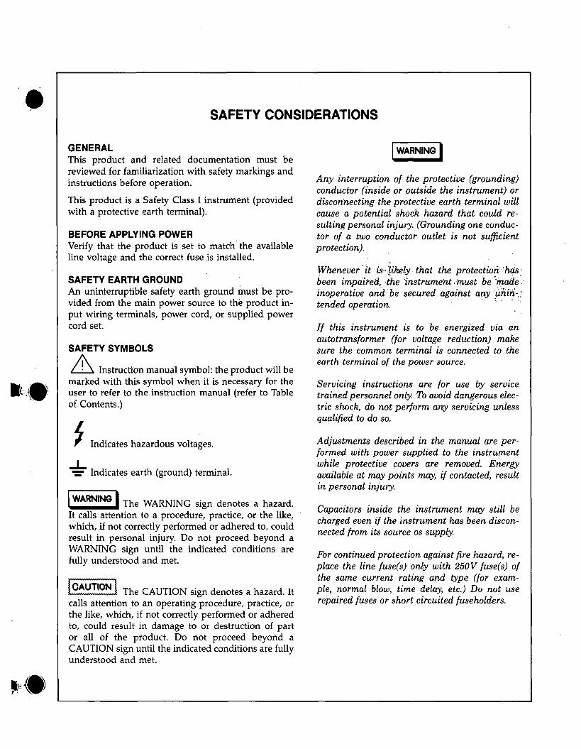
SAFETY CONSIDERATIONS
GENERAL This product and related documentation must be reviewed for familiarization with safety markings and instructions before operation.
This product is a Safety Class I instrument (provided with a protective earth terminal).
BEFORE APPLYING POWER Verify that the product is set to match the available line voltage and the correct fuse is installed.
SAFETY EARTH GROUND An uninterruptible safety earth ground must be provided from the main power source to the product input wiring terminals, power cord, or supplied power cord set.
SAFETY SYMBOLS
WARNING
A Instruction manual symbol: the product will be marked with this symbol when it is necessary for the user to refer to the instruction manual (refer to Table of Contents.)
J Indicates hazardous voltages.
— Indicates earth (ground) terminal.
WARNING The WARNING sign denotes a hazard. It calls attention to a procedure, practice, or the like, which, if not correctly performed or adhered to, could result in personal injury. Do not proceed beyond a WARNING sign until the indicated conditions are fully understood and met.
CAUTION T h e C A U T I O N sign denotes a hazard. It calls attention to an operating procedure, practice, or the like, which, if not correctly performed or adhered to, could result in damage to or destruction of part or all of the product. Do not proceed beyond a CAUTION sign until the indicated conditions are fully understood and met.
Any interruption of the protective (grounding) conductor (inside or outside the instrument) or disconnecting the protective earth terminal will cause a potential shock hazard that could resulting personal injury. (Grounding one conductor of a two conductor outlet is not sufficient protection).
Whenever it is likely ■ that the protection has; been impaired, the instrument must be made. inoperative and be secured against any uhin-; tended operation.
If this instrument is to be energized via an autotransformer (for voltage reduction) make sure the common terminal is connected to the earth terminal of the power source.
Servicing instructions are for use by service trained personnel only. To avoid dangerous electric shock, do not perform any servicing unless qualified to do so.
Adjustments described in the manual are performed with power supplied to the instrument while protective covers are removed. Energy available at may points may, if contacted, result in personal injury.
Capacitors inside the instrument may still be charged even if the instrument has been disconnected from its source os supply.
For continued protection against fire hazard, replace the line fuse(s) only with 250V fuse(s) of the same current rating and type (for example, normal blow, time delay, etc.) Do not use repaired fuses or short circuited fuseholders.
ATTENTION Static Sensitive
Devices
This instrument was constructed in an ESD (electro-static discharge) protected environment. This is because most of the semi-conductor devices used in this instrument are susceptible to damage by static discharge.
Depending on the magnitude of the charge, device substrates can be punctured or destroyed by contact or mere proximity of a static charge. The results can cause degradation of device performance, early failure, or immediate destruction.
These charges are generated in numerous ways such as simple contact, separation of materials, and normal motions of persons working with static sensitive devices.
When handling or servicing equipment containing static sensitive devices, adequate precautions must be taken to prevent device damage or destruction.
Only those who are thoroughly familiar with industry accepted techniques for handling static sensitive devices should attempt to service circuitry with these devices.
In all instances, measures must be taken to prevent static charge build-up on work surfaces and persons handling the devices.
Model 3048A Table of Contents
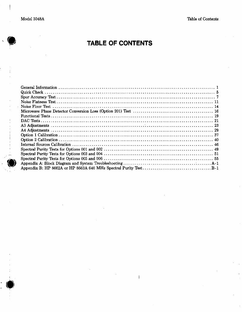
TABLE OF CONTENTS
General Information 1 Quick Check 5 Spur Accuracy Test 7 Noise Flatness Test 11 Noise Floor Test 14 Microwave Phase Detector Conversion Loss (Option 201) Test 16 Functional Tests 19 DAC Tests 21 A3 Adjustments 23 A4 Adjustments 29 Option 1 Calibration 37 Option 2 Calibration 40 Internal Sources Calibration 46 Spectral Purity Tests for Options 001 and 002 49 Spectral Purity Tests for Options 003 and 004 51 Spectral Purity Tests for Options 005 and 006 55 Appendix A: Block Diagram and System Troubleshooting : A-l Appendix B: HP 8662A or HP 8663A 640 MHz Spectral Purity Test B-l
Model 3048A Calibration
General Information
INTRODUCTION This manual documents the procedures which calibrate the HP 3048A Phase Noise Measurement System. System calibration assures that the System meets its published specifications. The procedures consist of system checks, adjustments, performance tests, and signal path characterization. Calibration of the HP 11848A Phase Noise Measurement Interface results from calibration of the System.
NOTE
"Calibration" as referred to in this manual should not be confused with the measurement calibration referred to in the normal course of making a phase noise measurement. Measurement calibration (especially, a measurement with phase lock) refers to the characterization of such parameters as the detector constant, tuning sensitivity of the signal source's FM input, and determination of the phase lock loop bandwidth.
iter The need for calibration is governed by the situation. It is usually not necessary nor even desirable to recalibrate the System frequently. Testing guidelines are summarized below. ^ Most tests are automatic. Operator intervention is documented in the System's test software. It is recommended, however, that the user follow along in this manual as the tests are running.
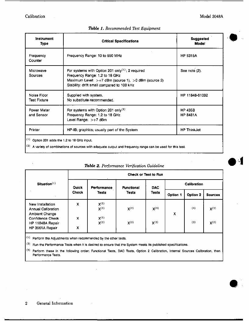
EQUIPMENT REQUIRED Equipment required, but not part of the System, is minimal. A feature of the System is the four sources built into the Interface which substitute for external sources in many cases. Extensive use is made of the HP 3561A Dynamic Signal Analyzer both as a signal source (using its built-in noise source) and as a signal analyzer. Any calibrated HP 3561A can be used in calibrating the System; it does not need to be the specific HP 3561A in the System. The external test equipment requirements are given in Table 1.
PERFORMANCE TEST RECORD Most test results can be hardcopied on the System's printer. This practice is recommended. It is also recommended that the serial number of the Interface under test be recorded in the System Configuration Table so that it will appear on the printouts.
rev. 29MA Y90 General Information
Calibration Model 3048A
Table 1. Recommended Test Equipment
Instrument Type
Frequency Counter
Microwave Sources
Noise Floor Test Fixture
Power Meter and Sensor
Printer
Critical Specifications
Frequency Range: 10 to 550 MHz
For systems with Option 201 only(1); 2 required Frequency Range: 1.2 to 18 GHz Maximum Level: >+7 dBm (source 1), >0 dBm (source 2) Stability: drift small compared to 100 kHz
Supplied with system. No substitute recommended.
For systems with Option 201 only(2)
Frequency Range: 1.2 to 18 GHz Level Range: >+7 dBm
HP-IB; graphics; usually part of the System
Suggested Model
HP5315A
See note (2).
HP 11848-61032
HP 435B HP 8481A
HP ThinkJet
(1) Option 201 adds the 1.2 to 18 GHz input.
^2' A variety of combinations of sources with adequate output and frequency range can be used for this test.
Table 2. Performance Verification Guideline
Situation'1)
New Installation Annual Calibration Ambient Change Confidence Check HP 11848A Repair HP 3561A Repair
Check or Test to Run
Quick Check
X
X
X
Performance Tests
xro X<3)
x<a> X (3)
Functional tests
X (3)
X (3)
DAC Tests
X (3)
X (3)
Calibration
Option 1
X
Option 2
(3)
(3)
Sources
X (3)
X (3)
W Perform the Adjustments when recommended by the other tests. (2) Run the Performance Tests when it is desired to ensure that the System meets its published specifications.
(3) Perform these in the following order: Functional Tests, DAC Tests, Option 2 Calibration, Internal Sources Calibration, then Performance Tests.
2 General Information
Model 3048A Calibration
WHEN AND WHAT TO TEST
Use Table 2 as a guideline for verifying the performance of the System.
The checks and tests are summarized below. The procedures are listed in the order in which they are described except for the Source Options Spectral Purity Tests which follow the Adjustments.
Quick Check is a confidence check which performs a complete phase-locked measurement of the phase noise of the 10 MHz A vs. B internal sources.
Performance Tests verify that the System meets its published specifications. The tests are as follows:
Spur Accuracy Test verifies the accuracy of noise measurements by measuring the level of phase modulation on a carrier with a known discrete sideband level. (In the context of phase noise measurements, discrete sidebands are often referred to as spurious signals or "spurs".)
Noise Flatness Test measures the unflatness of noise signals at offsets greater than 500 kHz. This test needs to be performed only when an RF spectrum analyzer is in the System's Configuration Table.
Noise Floor Test verifies the measurement sensitivity.
Microwave Phase Detector Conversion Loss (Option 201) Test measures the conversion loss of the 1.2 to 18 GHz phase detector. If the detector is not within specification, the noise floor will be degraded when the detector is used. (Option 201 adds the 1.2 to 18 GHz input to the Interface.)
Source Options Spectral Purity Tests verify the contribution of optional sources to the noise floor. (The procedures for these tests follow the Adjustments.)
Functional Tests verify the functionality of the HP 11848A Phase Noise Interface. The tests measure the paths for proper switching, DC offsets, amplifier gains, filter responses, etc. (Adjustments to the HP 11848A can be made when Functional Tests show a problem.)
DAC Tests verify the accuracy of the three DACs in the HP 11848A Phase Noise Interface. (Adjustments to the DACs should be made if a DAC is out of limits.) The DAC Tests require accessing the interior of the Interface.
Option 1 Calibration totally characterizes the HP 11848A measurement paths and generates new calibration data. The data collected replaces the data generated during the previous calibration. The new data may be stored in mass storage. (However, it does not replace the extra data obtained from the Option 2 Calibration.)
Option 2 Calibration is the same as Option 1 Calibration but includes the characterization of two additional reference paths.
Internal Sources Calibration determines and records as data the nominal DAC 2 and DAC 3 voltages (VNOMs) required to set the three tuneable, internal sources (VCOs) to their center frequencies.
Adjustments are made when other tests or checks indicate the need. Adjustments require accessing the interior of the Interface.
A3 Adjustments are made to the A3 Analyzer Interface Assembly.
A4 Adjustments are made to the A4 Phase Detector Assembly.
General Information 3
Calibration Model 3048A
THE IMPORTANCE OF SYSTEM CALIBRATION DATA Phase noise measurements are ultimately made by the HP 3561A Dynamic Signal Analyzer after the ( demodulated "noise signal" has passed through the HP 11848A Phase Noise Interface. Phase lock loop control signals also pass through the Interface. The Interface conditions the signals for best measurement sensitivity and accuracy. It is therefore important to know the characteristics of the circuits in the Interface.
The Interface's characteristics are acquired during the Option 1, Option 2, and Internal Sources Calibrations that are described above. The acquired data is stored on the mass-storage media (hard or floppy disc). During the normal course of operation, the System loads the data into the computer's memory (RAM) where it is accessed by the program as needed to correct the raw measurement data. Therefore, the stored data must match the specific Interface being used. It is a good practice to keep the Interface's serial number in the System's Configuration Table which will then appear on data printouts.
The calibration data is stored in two data files: "CALDATALO" and "CALDATAHI". CALDATALO is used for signal-path circuits through 100 kHz. CALDATAHI is used for signal paths above 100 kHz plus the VNOMs (the nominal tuning voltage of the tuneable, internal sources) and noise-flatness data for flatness variations greater than 2 dB.
General Information
Model 3048A Calibration
Quick Check
DESCRIPTION The Quick Check is a straight-forward, phase-lock-loop measurement of the phase noise of the two internal 10 MHz sources (A vs. B). Though the check is easy to run, a large portion of the circuitry in the HP 11848A Phase Noise Interface is exercised. A completed measurement with good results verifies that the System is operating correctly but does not verify its accuracy.
The check uses only equipment that is part of the System. Measurement definition parameters for this test are retrieved from a Test File named "DEFAULT".
NOTE
This check duplicates some of the guided tour in the Getting Started section of the Operating Manual.
PROCEDURE 1. Press the System Preset softkey. This softkey appears at the Main Software Level menu.
2. Press the New Msrmnt softkey to initiate the measurement.
3. Press the |Yes, Proceedj softkey to indicate that new measurement data is desired. The System now addresses each instrument listed in the System's Configuration Table. If an instrument does not respond to the HP-IB address listed for it, the System will inform you with a display message. (For details on adding an instrument to the System's Configuration Table or verifying an HP-IB address, refer to Setting Up the HP-IB Addresses in the installation section of the HP 3048A Operating Manual.)
4. Connect the HP 3561A input and the two 10 MHz source outputs to the HP 11848A as shown in the connect diagram on the computer display and in Figure 1. Note especially the rear-panel connections.
NOTE
The Interface's SPECTRUM ANALYZER output should either be terminated in 50Q or an RF spectrum analyzer should be connected to it.
5. Press the Proceed softkey to run the test. The measurement should proceed without error messages, and the measured noise results should be within 10 dB of that in Figure 2. (The plot in Figure 2 is typical for a System without an RF spectrum analyzer. The measurement takes about 10 minutes depending on the controller and the presence of the RF spectrum analyzer.)
Quick Check 5
Calibration Model 3048A
HP 3561A DYNAMIC SIGNAL ANALYZER
NOISE INPUT FROM HP 3561A SOURCE OUTPUT
(REAR PANEL)
HP 11848A PHASE NOISE INTERFACE
TO HP 3 5 6 1 A INPUT
(CONNECT RF SPECTRUM ANALYZER OR 5 0 - O H M LOAD HEREO
SPECTRUM ANALYZER
Figure 1. Quick Check Setup
m
0 - 1 0 - 2 0 - 3 0 - 4 0 - 5 0 -G0 - 7 0 - 8 0 - 9 0
-100 -1 10 -120 -130 -140 -150 -160 -170
H P 3 0 4 8 H Qhp: 3048H C a r r i e r
i i i i
---------
^Y/u ^Hu
"""fc^ j i ^ml ' i
-i I I I
DEMO: 1 0 MHz ■: 10.E+6 Hz
i I I I
1 1 il .
JU. ifl Jtdi vvl^ilL 1 1 1 1
" R " v s . 1 0 Mr 28 Dec 1987 1 6 ;
i I I I
- _ i I I I
Hz " B " 3 7 : 2 7 - 1 6 : 4 0 : 3 3
i I I I
---------------
i I I I
s
10 100 IK 10K
I t f ) C d B c / H z : v s f C H z : 100K
Figure 2. Typical Noise Plot for the System Quick Check
6 Quick Check
Model 3048A Calibration
Spur Accuracy Test
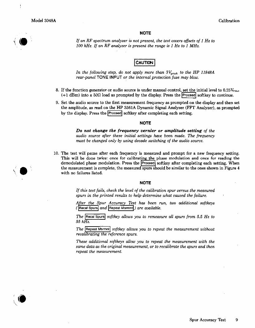
DESCRIPTION
In this test an external audio tone is input to the phase modulator of the internal 10 MHz B Oscillator to generate a 10 MHz carrier with discrete, phase-modulation sidebands. The sideband level (relative to the carrier) is calibrated with the HP 3561A Dynamic Signal Analyzer then measured as a normal phase noise measurement (with the 10 MHz A Oscillator phase locked to 10 MHz B Oscillator). The measurements are made with audio tones of 5.5, 55, 550, 5500, 55 000, and (if an RF spectrum analyzer is present) 550 000 Hz.
To calibrate the sideband level (relative to the carrier), the two 10 MHz Oscillators (A and B) are set 785 Hz apart and fed into the RF Phase Detector. The amplitude of the 785 Hz beatnote is measured by the HP 3561A. This level is the carrier reference level. Then the phase modulation sidebands for each modulation rate are measured with the HP 3561A and the relative sideband level is computed as the ratio of the two measurements.
The RF signal simulates the spurious discrete phase modulation (often called "spurs") frequently appearing in phase noise measurements. Although testing is done on discrete tone sidebands, the general accuracy of the noise sideband measurement is verified.
If an RF spectrum analyzer is not present, the test covers offsets of 1 Hz to 100 kHz. If an RF analyzer is present the range is 1 Hz to 1 MHz.
^EQUIPMENT
Printer. The test requires the presence of a printer in the System's Configuration Table.
Audio Source. The Spur Accuracy Test will run automatically if an HP 3325A Function Generator is in the System's Configuration Table. If this function generator is not available, any manually controlled function generator or audio source having exact decade frequency switching covering 5 Hz to 55 kHz can be used. (The range must be 5 Hz to 550 kHz if an RF spectrum analyzer is configured in the System.) The HP 3312A Function Generator is a typical manual audio source which can be used in this test. If no function generator is found in the system instrument configuration table, the software assumes you have only a manual audio source and you will be prompted for the proper settings.
NOTE
The flatness of the audio source must be better than ±0.3 dB when switching from 55 kHz to 550 kHz. The 550 kHz span is only used when an RF spectrum analyzer is present.
PROCEDURE
1. Press the Spci. Funct'n softkey. This softkey appears at the Main Software Level menu.
Spur Accuracy Test 7
Calibration Model 3048A
Test Mode
NOTE
If troubleshoot mode has been selected (by pressing the you will be prompted for the setup diagram two times. Press the softkey after the second setup diagram is displayed.
softkey), Proceed|
2. Press the |3048A Sys Chk| softkey.
3. Press the Perf. Tests softkey.
4. Press the |Spur Accy.j softkey. The System will then load the Spur Accuracy Test File.
5. Press the New Msrmnt softkey. 6. Connect the instruments as shown in the on-screen connection diagram and in Figure 3.
NOTE
If a function generator is to be under automatic control, the System's Configuration Table must have the literal name "FUNCT GEN" and model "3325A". The Interface's SPECTRUM ANALYZER output should either be terminated in 500 or an RF spectrum analyzer should be connected to it.
7. Press the Proceed softkey. If the function generator is under automatic control, the measurement should proceed without error messages, and the measured spurs should be similar to the ones shown in Figure 4 with no failures listed. (The measurement takes about 10 minutes depending on controller and the presence of the RF spectrum analyzer.) If the function generator or audio source is under manual control, proceed with step 8.
AUDIO SOURCE
NOISE INPUT FROM HP 3581A SOURCE OUTPUT
(REAR PANEL)
TONE INPUT (REAR PANEL)
HP 3561A DYNAMIC SIGNAL ANALYZER
[o] 5rM>_
HP 11648A PHASE NOISE INTERFACE
TO HP 3S61A INPUT
(CONNECT RF SPECTRUM ANALYZER
SPECTRUM ANALYZER
Figure 3. Spur Accuracy Test Setup
8 Spur Accuracy Test
Calibration
NOTE
/ / an RF spectrum analyzer is not present, the test covers offsets of 1 Hz to 100 kHz. If an RF analyzer is present the range is 1 Hz to 1 MHz.
■IVWVVVVVIlMl lVMlMVW
CAUTION
In the following step, do not apply more than 3Vpeak to the HP 11848A rear-panel TONE INPUT or the internal protection fuse may blow.
If the function generator or audio source is under manual control, set the initial level to 0.25Vn (+1 dBm) into a 50O load as prompted by the display. Press the Proceed softkey to continue.
Set the audio source to the first measurement frequency as prompted on the display and then set the amplitude, as read on the HP 3561A Dynamic Signal Analyzer (FFT Analyzer), as prompted by the display. Press the Proceed softkey after completing each setting.
NOTE
Do not change the frequency vernier or amplitude setting of the audio source after these initial settings have been made. The frequency must be changed only by using decade switching of the audio source.
The test will pause after each frequency is measured and prompt for a new frequency setting. This will be done twice: once for calibrating the phase modulation and once for reading the demodulated phase modulation. Press the Proceed softkey after completing each setting. When the measurement is complete, the measured spurs should be similar to the ones shown in Figure 4 with no failures listed.
NOTE
/ / this test fails, check the level of the calibration spur versus the measured spurs in the printed results to help determine what caused the failure. After the Spur Accuracy Test has been run, two additional softkeys ( Recal Spurs and Repeat Msrmnt ) are available.
The 55 kHz.
Recal Spurs softkey allows you to remeasure all spurs from 5.5 Hz to
The Repeat Msrmnt| softkey allows you to repeat the measurement without recalibrating the reference spurs. These additional softkeys allow you to repeat the measurement with the same data as the original measurement, or to recalibrate the spurs and then repeat the measurement.
Spur Accuracy Test 9
Calibration Model 3048A
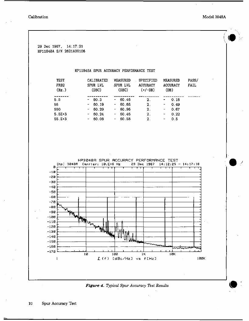
29 Dec 1987, 14:17:21 HP11848A S/N 2621A00106
HP11848A SPUR ACCURACY PERFORMANCE TEST
TEST FREG) (Hz.)
5.5 55 550 5.5E+3 55.E+3
CALIBRATED SPUR LVL
(DBC)
- 60.3 - 60.19 - 60.29 - 60.24 - 60.08
MEASURED SPUR LVL
(DBC)
- 60.46 - 60.68 - 60.96 - 60.46 - 60.58
SPECIFIED ACCURACY (+/-DB)
2. 2. 2. 2. 2.
MEASURED ACCURACY (DB)
- 0.16 - 0.49 - 0.67 - 0.22 - 0.5
PASS/ FAIL
H P 3 0 4 8 R SPUR RCCURRCY PERFORMRNCE T E S T Lhp] 3048R C a r r i e r : 10.E+G Hz 29 Dec 1987 1 4 : 1 2 : 2 5 - 1 4 : 1 7 : 1 8
— i 1—i—r-i 1 1—i—i—i 1 1—i—I—I 1 1—i—i—i 1 1—i—r
100 IK I ( f ) cdBc/Hz: vs f m z :
10K 100K
Figure 4. Typical Spur Accuracy Test Results
10 Spur Accuracy Test
Model 3048A Calibration
Noise Flatness Test
DESCRIPTION This test verifies that the calibration data used for phase noise measurements above 500 kHz offsets is accurate. It also provides an opportunity to update the calibration data should the flatness be marginal.
The test requires an RF spectrum analyzer in the System's Configuration Table and needs to be run only when an RF analyzer is used while making measurements. (An HP 3585A Spectrum Analyzer is supplied with Systems having Option 101.) The test is a standard phase-lock-loop measurement of the phase noise of the internal 400 MHz and 350-500 MHz Oscillators. The frequency offset range of the measurement is 500 kHz to 40 MHz. The 400 MHz Oscillator has a flat or white phase noise distribution from 500 kHz to 40 MHz.
This test measures the maximum unflatness above 500 kHz relative to the measured noise value at a 500 kHz offset. If the unflatness is equal to or greater than 2 dB, the "CALDATAHI" data file will have supplementary data appended to it to adjust for the unflatness.
EQUIPMENT Printer. The test requires the presence of a printer in the System's Configuration Table.
PROCEDURE 1. Press the Spcl. Funct'n softkey available at the Main Software Level menu.
Test Mode
NOTE
/ / troubleshoot mode has been selected (by pressing the hey)you will be prompted for the setup diagram two times. Press the softkey after the second setup diagram is displayed.
soft-Proceed
2. Press the |3048A Sys Chk| softkey.
3. Press the Pert. Tests
4. Press the
5. Press the
Noise Flat.
New Msrmnt
softkey.
softkey. The System will then load the Noise Flatness Test File.
softkey.
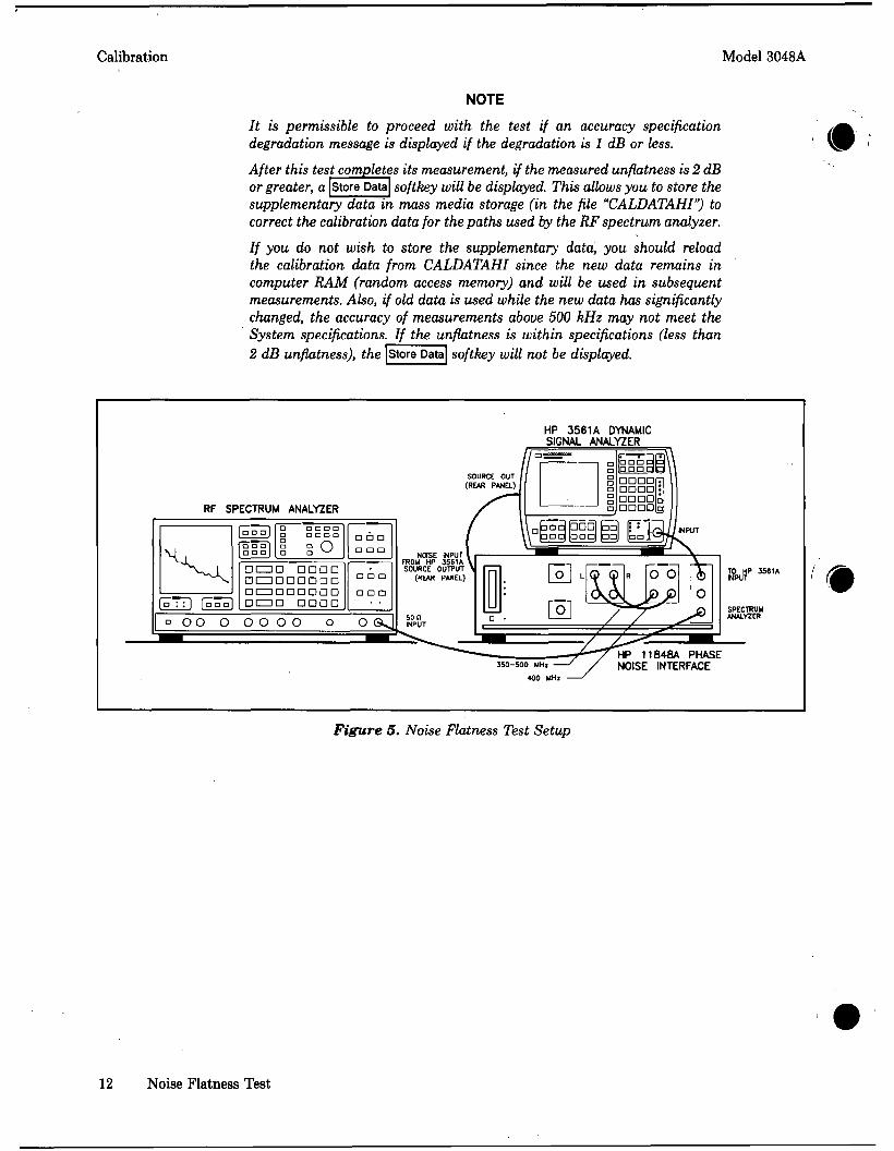
6. Connect the instruments as shown on the on-screen connection diagram and in Figure 5
7. Press the Proceed softkey. The measurement should proceed automatically without error messages (but see the following note) and the measured noise should be similar to that shown in Figure 6. (The measurement takes about 5 minutes depending on the controller.)
Noise Flatness Test 11
Calibration Model 3048A
NOTE
It is permissible to proceed with the test if an accuracy specification degradation message is displayed if the degradation is 1 dB or less. After this test completes its measurement, if the measured unflatness is 2 dB or greater, a Store Data softkey will be displayed. This allows you to store the supplementary data in mass media storage (in the file "CALDATAHI") to correct the calibration data for the paths used by the RF spectrum analyzer. If you do not wish to store the supplementary data, you should reload the calibration data from CALDATAHI since the new data remains in computer RAM (random access memory) and will be used in subsequent measurements. Also, if old data is used while the new data has significantly changed, the accuracy of measurements above 500 kHz may not meet the System specifications. If the unflatness is within specifications (less than 2 dB unflatness), the Store Data softkey will not be displayed.
#
HP 3561A DYNAMIC SIGNAL ANALYZER
RF SPECTRUM ANALYZER
[a a a
s O ac^n D D D D D n D D D D O D D C D D D a D D D D C D a D D D D
° o o o o o o o
TO HP 3561A INPUT
350-500 MHi
400 MHz
HP 11848A PHASE NOISE INTERFACE
Figure 5. Noise Flatness Test Setup
12 Noise Flatness Test
Model 3048A
30 Dec 1987, 15:45:23 HP11848A S/N 2621A00106
HP11848A NOISE FLATNESS PERFORMANCE TEST
OFFSET MAX UNFLATNESS FREQ RELATIVE TO 500 KHz. (Hz.) (+/- dB.)
6.2E+6 0.83
120
130
HP3048H NOISE FLRTNESS PERFORMRNCE TEST Chp] 304BH C a r r i e r : 400.E+G Hz 30 Dec 1987 15:41:54 - 15:43:59
i i
i >
i i i i
J.I 1 .,...1 ... „ L ^ „ L ,
1 I I I
1
,,
-
i
1M 10M 500K X. C-F 5 C d B c / H z ] v s fCHzD 40M
Figure 6. Typical Noise Flatness Test Results
Noise Flatness Test 13
Calibration Model 3048A
Noise Floor Test
DESCRIPTION This test measures the noise of the System apart from the phase noise contribution of the external reference sources. Thus this test measures the absolute sensitivity (the noise floor) of the System.
The output of the internal 350-500 MHz Oscillator is split and applied to both inputs of the 5 MHz to 1.6 GHz Phase Detector. However, one path to the phase detector is delayed one-quarter wavelength to establish phase quadrature of the split signals. Fine adjustment of quadrature is made by tuning the oscillator until the dc output of the detector is 0V. The phase noise of the oscillator cancels itself out because the phase fluctuations of the split signals are correlated.
EQUIPMENT Printer. The test requires the presence of a printer in the System's Configuration Table.
Noise Floor Test Fixture. A power splitter with delay line is required for this test. This device is supplied with the System (HP 11848-61032).
PROCEDURE 1. Press the Spcl. Funct'n softkey available at the Main Software Level menu.
NOTE Test Mode / / troubleshoot mode has been selected (by pressing the
you will be prompted for the setup diagram two times. Press the softkey after the second setup diagram is displayed.
softkey), Proceed
2. Press the |3048A Sys Chk| softkey.
3. Press the Perf. Tests
Noise Floor
New Msrmnt
softkey.
softkey. The System will then load the Noise Floor Test File.
softkey.
4. Press the
5. Press the 6. Connect the instruments as shown on the on-screen connection diagram and also Figure 7.
NOTE The Interface's SPECTRUM ANALYZER output should either be terminated in 50Q or an RF spectrum analyzer should be connected to it. Connect the Noise Floor Test Fixture directly to the L and R ports of the PHASE DETECTOR INPUTS. Line length is critical; do not connect intervening cables. Tighten all connections securely as the Noise Floor test results may be affected by loose connections. Also, do not mechanically disturb the System while the test is running.
7. Press the Proceed softkey. The measurement should proceed automatically without error messages and the measured noise should be similar to that shown in Figure 8. (The measurement takes about 30 minutes depending on the controller and the presence of the RF spectrum analyzer.)
14 Noise Floor Test
Model 3048A Calibration
NOTE
/ / no RF spectrum analyzer is present, the test covers offsets of 0.01 Hz to 100 kHz. If an RF analyzer is present the range is 0.01 Hz to 40 MHz.
The phase detector constant is not measured for this test. A phase detector constant of 0.6 V/radian is used for the Noise Floor Test because at the specified R-port power level, the phase detector constant is typically 0.6 V/radian.
HP 3561A DYNAMIC SIGNAL ANALYZER
NOISE FLOOR FROMNOHP iseu TEST FIXTURE SOURCE OUTPUT
(REAR PANEL)
SPECTRUM ANALYZER
HP 11848A PHASE NOISE INTERFACE
Figure 7. Noise Floor Test Setup
- 3 0 - 4 0 - 5 0 -G0 - 7 0 -B0 - 9 0
- 1 0 0 - 1 1 0 - 1 3 0 - 1 3 0 - 1 4 0 - 1 5 0 -1G0 - 1 7 0 - 1 8 0 - 1 9 0
HP304GR NOISE FLOOR PERFORMANCE TEST [hp] 304BA C a r r i e r : 400.E+6 Hz 31 Dec 1987 10 :43 :47 - 1 1 : 0 9 : 2 5 - T 1—n
---
N^ - > ^
\
^-= ; -~N~ W
--
■ i i i
■ I I I
> y
\x ""N V H* I f
I I I I
1 I I I
' ^ ^
1 I I I
1 I I I
^wyLi
i I I I
■ I I I - ' I ™ 1 I ! 1 T T T
-----
SPURIOUS SPEC -----
NOISE FLOOR SPEC -
i I I I ■ I I I
---
1 I I I
.01 JC C -F 3 CdBc^HzD v s fCHzD
Figure 8. Typical Noise Floor Test Results
100K
Noise Floor Test 15
Calibration Model 3048A
Microwave Phase Detector Conversion Loss (Opt. 201) Test
DESCRIPTION Two microwave sources are set 50 kHz apart. One is connected to the R port of the Interface's 1.2 GHz to 18 GHz (microwave) phase detector; the other is connected to the L port. The phase detector generates a 50 kHz IF beatnote at its output which is measured by the HP 3561 A. The conversion loss of the phase detector is the ratio of the level of the beatnote to the level of the signal at the R port. This procedure is repeated for several carrier frequencies. Because of the high frequencies involved, the power of the two sources is measured by a power meter for each frequency. The signal path within the Interface is controlled manually using the 11848A Control feature. The microwave sources are operated manually. Conversion loss is not an explicitly specified parameter but must be within the limits given in this procedure to assure specified sensitivity (that is, noise floor) for the stated carrier frequency. Excessive conversion loss is usually caused by a defective phase detector (mixer) itself or by interconnecting cables or relays.
EQUIPMENT Microwave Sources. Two microwave sources are required. If the full range of the microwave phase detector is to be tested, both sources must cover 1.2 to 18 GHz. The drift and short-term instability of both sources must be small compared to 100 kHz. One source must output at least +7 dBm, the other at least 0 dBm. If the required stability is unobtainable, the test can be run with an RF spectrum analyzer (such as the HP 3585A) used in place of the HP 3561A; the source instability must be small compared to 1 MHz. If any other RF spectrum analyzer is used, the output power of the generators should be measured with the power meter. Power Meter and Sensor. A power meter with sensor is required for this test to check the power into the L and R ports of the microwave phase detector. The power meter must be able to measure up to +10 dBm from 1.2 to 18 GHz. Spectrum Analyzer. The HP 3561A Dynamic Signal Analyzer or the HP 3585A Spectrum Analyzer is recommended but other RF spectrum analyzers can be used. If any other spectrum analyzer is used, the output power of the generators should be made with a power meter.
PROCEDURE
CAUTION
The microwave phase detector is more susceptible to burnout than the RF phase detector. Levels greater than +10 dBm may cause damage. Measure the power levels with a power meter before connecting the sources to the phase detector. Also, disconnect the sources from the phase detector before changing frequency.
1. Two signal sources and the spectrum analyzer are connected to the Interface as follows. (Refer to Figure 9.)
a. Set one microwave source to 1.2 GHz. Measure the power with a power meter and set the level to 0 dBm. Connect it to the front-panel R input of the 1.2 GHz TO 18 GHz phase detector.
b. Set the other microwave source 50 kHz above or below 1.2 GHz. Measure the power with a power meter and set the level to +7 dBm. Connect it to the front-panel L input of the phase detector. (If an RF spectrum analyzer is to be used, a 1 MHz beatnote is suggested.)
16 Microwave Phase Detector Conversion Loss (Opt. 201) Test
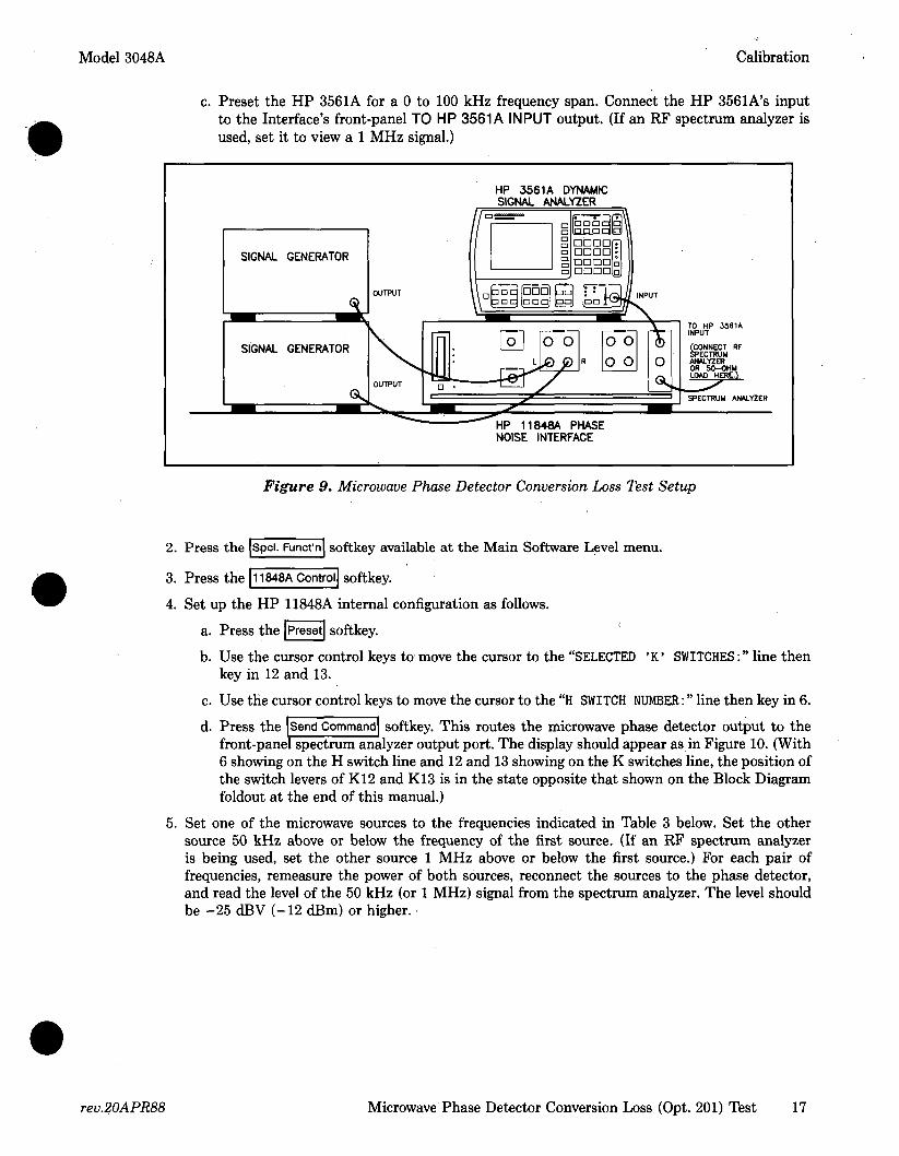
Model 3048A Calibration
Preset the HP 3561A for a 0 to 100 kHz frequency span. Connect the HP 3561A's input to the Interface's front-panel TO HP 3561A INPUT output. (If an RF spectrum analyzer is used, set it to view a 1 MHz signal.)
HP 3561A DYNAMIC SIGNAL ANALYZER
TO HP 3561A INPUT
(CONNECT RF SPECTRUM ANALYZER OR 50-OHM LOAD HERE.)
SPECTRUM ANALYZER
HP 11848A PHASE NOISE INTERFACE
Figure 9. Microwave Phase Detector Conversion Loss Test Setup
2. Press the Spci. Funct'n softkey available at the Main Software Level menu.
3. Press the 11848A Control softkey. 4. Set up the HP 11848A internal configuration as follows.
a. Press the Preset softkey. b. Use the cursor control keys to move the cursor to the "SELECTED 'K' SWITCHES:" line then
key in 12 and 13. c. Use the cursor control keys to move the cursor to the "H SWITCH NUMBER:" line then key in 6.
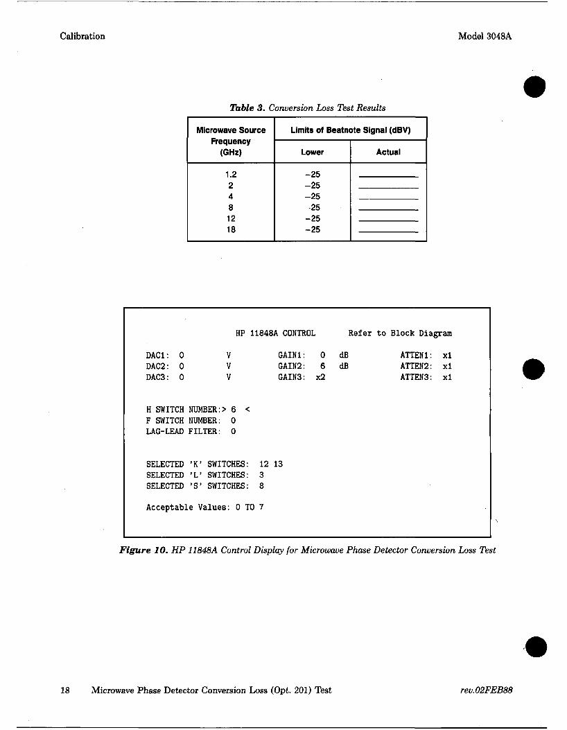
d. Press the |Send Command softkey. This routes the microwave phase detector output to the front-panel spectrum analyzer output port. The display should appear as in Figure 10. (With 6 showing on the H switch line and 12 and 13 showing on the K switches line, the position of the switch levers of K12 and K13 is in the state opposite that shown on the Block Diagram foldout at the end of this manual.)
Set one of the microwave sources to the frequencies indicated in Table 3 below. Set the other source 50 kHz above or below the frequency of the first source. (If an RF spectrum analyzer is being used, set the other source 1 MHz above or below the first source.) For each pair of frequencies, remeasure the power of both sources, reconnect the sources to the phase detector, and read the level of the 50 kHz (or 1 MHz) signal from the spectrum analyzer. The level should be -25 dBV (-12 dBm) or higher.
rev.20APR88 Microwave Phase Detector Conversion Loss (Opt. 201) Test 17
Calibration Model 3048A
Table 3. Conversion Loss Test Results
Microwave Source Frequency
(GHz)
1.2 2 4 8 12 18
Limits of Beatnote Signal (dBV)
Lower
-25 -25 -25 -25 -25 -25
Actual
HP 11848A CONTROL Refer to Block Diagram
DAC1: DAC2: DAC3:
0 0 0
V V V
GAIN1: GAIN2: GAIN3:
0 6
x2
dB dB
ATTEN1: ATTEN2: ATTEN3:
xl xl xl
H SWITCH NUMBER:> 6 < F SWITCH NUMBER: 0 LAG-LEAD FILTER: 0
SELECTED 'K' SWITCHES SELECTED 'L' SWITCHES SELECTED 'S' SWITCHES
12 13 3 8
Acceptable Values: 0 TO 7
Figure 10. HP 11848A Control Display for Microwave Phase Detector Conversion Loss Test
18 Microwave Phase Detector Conversion Loss (Opt. 201) Test rev.02FEB88
Model 3048A Calibration
Functional Tests
DESCRIPTION The Functional Tests exercise the hardware in the Interface and check for proper functioning. Examples of the hardware checked are switches, amplifiers, attenuators, DACs, filters, etc. The program permits a run-through of all checks or in some cases a single function can be individually tested.
In a typical test such as the testing of a filter, the program routes the noise source of the HP 3561A Dynamic Signal Analyzer through a reference path to the input of the HP 3561A and measures the signal level at several frequencies. The program then inserts the filter in the path and remeasures the levels.
Except for checks of dc offset and VCO control path, test limits are loose because only the general functioning of the filter is checked. (Measurement path filters are tightly characterized by the Option 1 or Option 2 Calibration program.)
These tests are similar to the tests on the Diagnostic disc. The diagnostic program also includes failure analysis information and thus may be more useful in tracking down a fault than the Functional Tests. (Refer to the HP 11848A Service Manual.)
EQUIPMENT Printer. These tests will run without the presence of a printer in the System's Configuration Table. However, the test results in some instances will not remain on the display long enough to be observed; therefore, it is recommended that the tests be run with a printer.
PROCEDURE 1. Press the Spcl. Funct'n softkey available at the Main Software Level menu.
2. Press the |3048A Sys Chk| softkey.
3. Press the Fnctl. Chk. softkey.
NOTE
The tests may be run as an entire sequence or tests may be run individually as outlined in the following steps. Before proceeding with the tests, you should read the Comments section below.
4. To perform all tests sequentially, press the Test All. softkey and follow the displayed instructions. To perform a specific test, perform the following steps.
Press the a.
b.
Select Test softkey.
Move the cursor to the desired test.
With the cursor at Test 01, Test 02, or Test 03, press the Select Path softkey then move the cursor to the desired path of the selected test. Press the Sngl Path softkey to test a single path of the selected test or press the for a description of the test paths.)
Test all softkey to test all paths. (Refer to Comments
d. If Test 04 through Test 10 is selected, press the Run Test softkey.
Functional Tests 19
Calibration Model 3048A
Comments Runtime. With the printer on the full functional test takes about 25 minutes to run. Some manual reconnection of cables is required. Connections. Signal connect diagrams or instructions appear on the display as the test or tests proceed. However, two connections are assumed that are not shown. (1) The rear-panel SOURCE OUT connector of the HP 3561A must be connected to the rear-panel NOISE INPUT FROM HP 3561A SOURCE OUTPUT connector of the Interface. (2) The Interface's SPECTRUM ANALYZER output should either be terminated in 50f2 or an RF spectrum analyzer should be connected to it. In either case the spectrum analyzer port must be terminated in 50fi. Printer On/Off. If a printer is on HP-IB and in the System's Configuration Table, the printout can be inhibited by pressing the | Printer Off softkey. To re-enable the printer, press the | Printer On| softkey. It is recommended that tests be run with the printer, otherwise the test results in some instances will not remain on the display long enough to be observed. If it is desired to have the Interface's serial number appear on the printout, the serial number must appear in the appropriate column of the System's Configuration Table. This practice is recommended. Tests. A brief description of the ten Functional Tests follows. Referring to the Block Diagram foldout at the end of this manual will help in understanding the descriptions.
Test 01. DC Offsets Test. The HP 3561A is used as a dc voltmeter to measure the dc level at the front-panel TO HP 3561A INPUT connector. The voltage is measured with many different circuits in the measurement path. The circuits are labeled for each result. If the voltage is slightly out of limits, in most cases they can be adjusted. (Refer to the Adjustments further on in this manual.)
Test 02. A3/A4 Signal Paths Transfer Functions Test. A3 is the Analyzer Interface Assembly; A4 is the Phase Detector Assembly. The circuit paths checked are between the rear-panel NOISE INPUT FROM HP 3561A SOURCE OUTPUT connector (J14) to the front-panel TO HP 3561A INPUT connector (Jll). The print out path descriptions give some idea of the signal flow. A measurement of the simplest path is made first; this becomes a reference for the tests. Measurements are made at several frequencies.
Test 03. Phase-Lock Loop Paths Transfer Functions Test. This check is similar to Test 02 except that the paths are through the circuits labeled GAIN 1, GAIN 2, and ATTEN 2 on the Block Diagram.
Test 04. Lag-Lead Transfer Functions Test. Lag-Lead Network 1 is measured at 8 different settings.
Test 05. 100 kHz Calibrator, Search Oscillator, and Out-of-Lock Flip-Flop Test. The absolute level and frequency of the 100 kHz Calibration Oscillator and the Search Oscillator are measured. The Out-of-Lock and Overload Flip-Flops are tested when set and cleared.
Test 06. RF Phase Detector Beatnote Test. The (A6) 10 MHz VCXO A and (A7) 10 MHz VCXO B are fed into the RF Phase Detector. A beatnote of 500 Hz is generated and the amplitude measured. This test checks the functioning of both oscillators and the RF Phase Detector.
Test 07. DAC 1, 2, and 3 Beatnote Pull Test. This is similar to Test 06, but the oscillators are individually tuned by each of the three DACs to test their tuning sensitivity.
Test 08. Peak Detector and Switched High-Pass Filter Test. An 800 Hz beatnote is generated by the method described in Test 06. The beatnote is fed into the Peak Detector following the 10 Hz/50 kHz High-Pass Filter. The dc output from the Peak Detector is measured with the 10 Hz then the 50 kHz filter switched in.
Test 09. Rear-Panel Tune Voltage Output Test. The transfer function of ATTEN 1 is measured by a method similar to Test 02.
Test 10. Front-Panel Tune Voltage Output Test. The transfer function of ATTEN 3 is measured by a method similar to Test 02.
20 Functional Tests
Model 3048A Calibration
DAC Tests
DESCRIPTION The output of the three Digital-to-Analog Converters (DACs) is measured with each input bit individually set high. DAC 1 can be tested via a front-panel output. DACs 2 and 3 can only be tested at internal test points. This requires removal of the top cover of the HP 11848A Phase Noise Interface. The HP 3561A Dynamic Signal Analyzer is used as a dc voltmeter in this test.
Since this test requires accessing the interior of the Interface, precautions should be taken to prevent electrical shock. Care should also be taken to minimize electro-static discharge that could damage sensitive electrical devices.
EQUIPMENT Printer. These tests will run without the presence of a printer in the System's Configuration Table. However, the test results in some instances will not remain on the display long enough to be observed; therefore, it is recommended that the tests be run with a printer.
PROCEDURE 1. The testing of DACs 2 and 3 requires removal of the top cover of the Interface. To do this:
a. Switch LINE to OFF.
b. Remove the line cord.
c. If the rear panel of the Interface has two feet in the upper corners, remove them.
d. Unscrew the screw in the middle of the rear edge of the top cover. This is a captive screw and will cause the top cover to push away from the frame. (A slight tapping on the top cover will aid in removal.) Slide the cover back about 6.5 mm (0.25 inch) and lift it off.
e. Reinsert the line cord and switch LINE back to ON.
2. Press the Spcl. Funct'n softkey available at the Main Software Level menu.
3. Press the 3048A Sys Chk softkey.
NOTE Before proceeding with the tests, you should read the Comments section below.
4. Press the Dae Tests softkey and follow the displayed instructions.
Comments Printer On/Off. If a printer is on HP-IB and in the System's Configuration Table, the printout can be inhibited by pressing the Printer Off softkey. To re-enable the printer, press the Printer On softkey. This softkey function is not present at all times during the execution of the tests. It is recommended that tests be run with the printer, otherwise the test results in some instances will not remain on the display long enough to be observed.
If it is desired to have the Interface's serial number appear on the printout, the serial number must appear in the appropriate column of the System's Configuration Table. This practice is recommended.
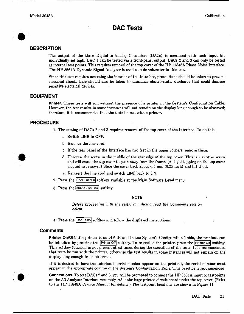
Connections. To test DACs 2 and 3, you will be prompted to connect the HP 3561A input to testpoints on the A3 Analyzer Interface Assembly. A3 is the large printed circuit board under the top cover. (Refer to the HP 11848A Service Manual for details.) The testpoint locations are shown in Figure 11.
DAC Tests 21
Calibration Model 3048A
The specific connections are: DAC 2: Connect the positive (+) lead (the inner conductor) to A3 TP202. Connect the negative (-) '
lead (the outer conductor) to A3 TP207 (ground). v
DAC 3: Connect the positive (+) lead (the inner conductor) to A3 TP201. Connect the negative (-) lead (the outer conductor) to A3 TP207 (ground).
TP202
TP201
FRONT
TP207- TP203 A3
Analyzer Interface Assembly
Figure 11. A3 Testpoint Locations
22 DAC Tests
Model 3048A Calibration
A3 Adjustments
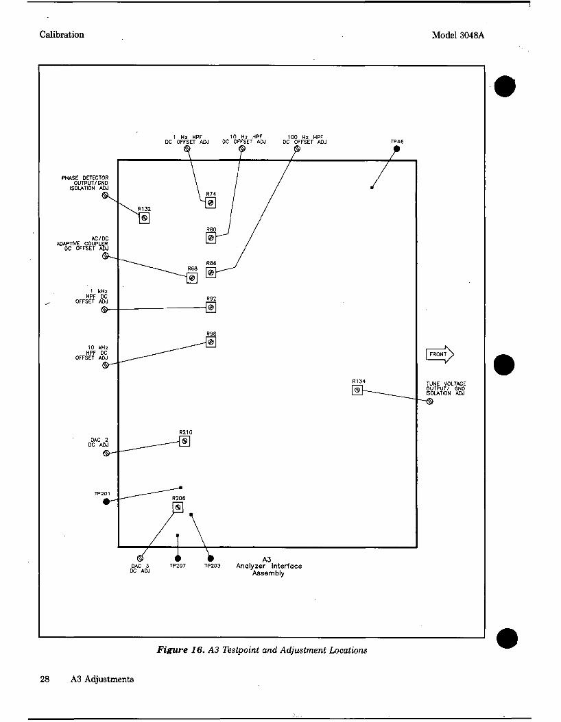
DESCRIPTION The A3 Analyzer Interface Assembly in the HP 11848A has ten adjustments. The adjustments are guided by the system software but the software neither displays the actual measurement values nor indicates whether the adjustment is within the proper limits; rather, the operator simply reads the value from the HP 3561A and adjusts the specified component until the reading is within limits. The following adjustments are made:
Component
A3R68 A3R74 A3R80 A3R86 A3R92 A3R98
A3R132 A3R134
A3R210 A3R206
Circuit
AC/DC Adaptive Coupler 1 Hz High-Pass Filter 10 Hz High-Pass Filter 100 Hz High-Pass Filter 1 kHz High-Pass Filter 10 kHz High-Pass Filter
Floating Amplifier 2 Floating Amplifier 1
DAC2 DAC3
Purpose
Minimize dc offset Minimize dc offset Minimize dc offset Minimize dc offset Minimize dc offset Minimize dc offset
Maximize ground isolation Maximize ground isolation
Set reference level Set reference level
Since these procedures require accessing the interior of the Interface, precautions should be taken to prevent electrical shock. Care should also be taken to minimize electrostatic discharge that could damage sensitive electrical devices.
PROCEDURE
Initial Setup 1. The adjustments to the A3 Analyzer Interface Assembly require removal of the top cover of the
Interface. To do this: a. Switch LINE to OFF. b. Remove the line cord. c. If the rear panel of the Interface has two feet in the upper corners, remove them. d. Unscrew the screw in the middle of the rear edge of the top cover. This is a captive screw
and will cause the top cover to push away from the frame. Slide the cover back about 6.5 mm (0.25 inch) and lift it off.
e. Reinsert the power cord and switch LINE back to ON. 2. Set the HP 3561A input switch to the FLOAT position.
Press the Spcl. Funcf n softkey available at the Main Software Level menu.
4. Press the 3048A Sys Chk softkey.
5. Press the Int. Adj'mnt softkey.
6. Press the Adjust A3 softkey.
A3 Adjustments 23
Calibration Model 3048A
NOTE
The physical location of testpoints and adjustable components is shown in Figure 16.
DC Offset Adjustments
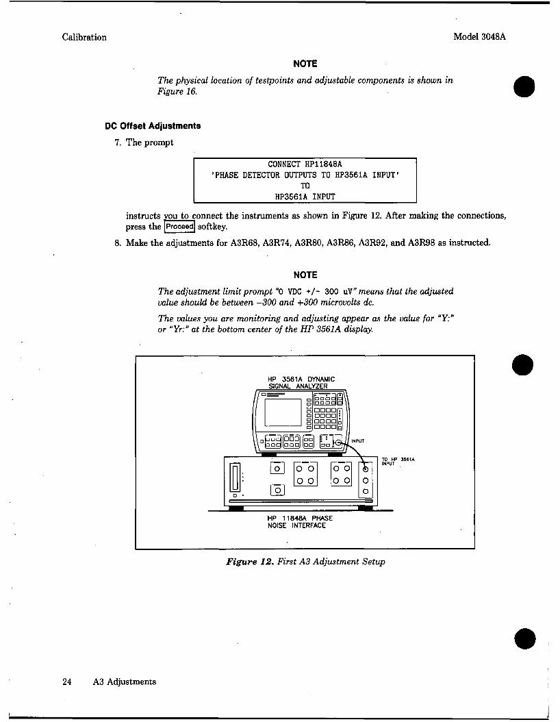
7. The prompt
CONNECT HP11848A 'PHASE DETECTOR OUTPUTS TO HP3561A INPUT'
TO HP3561A INPUT
instructs you to connect the instruments as shown in Figure 12. After making the connections, press the Proceed softkey.
8. Make the adjustments for A3R68, A3R74, A3R80, A3R86, A3R92, and A3R98 as instructed.
NOTE
The adjustment limit prompt "0 VDC +/- 300 uV" means that the adjusted value should be between -300 and +300 microvolts dc. The values you are monitoring and adjusting appear as the value for "Y:" or "Yr:" at the bottom center of the HP 3561A display.
HP 3561A DYNAMIC SIGNAL ANALYZER
(-1
D
. E o o O 0
o o 0 0
. [o] 0 o
TO HP 3561A INPUT
HP 1184dA PHASE NOISE INTERFACE
Figure 12. First A3 Adjustment Setup
24 A3 Adjustments
3048A Calibration
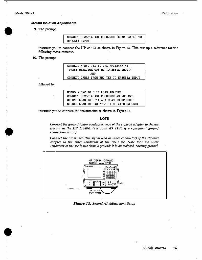
Ground Isolation Adjustments
9. The prompt
CONNECT HP3561A NOISE SOURCE (REAR PANEL) TO HP3561A INPUT.
instructs you to connect the HP 3561A as shown in Figure 13. This sets up a reference for the following measurements.
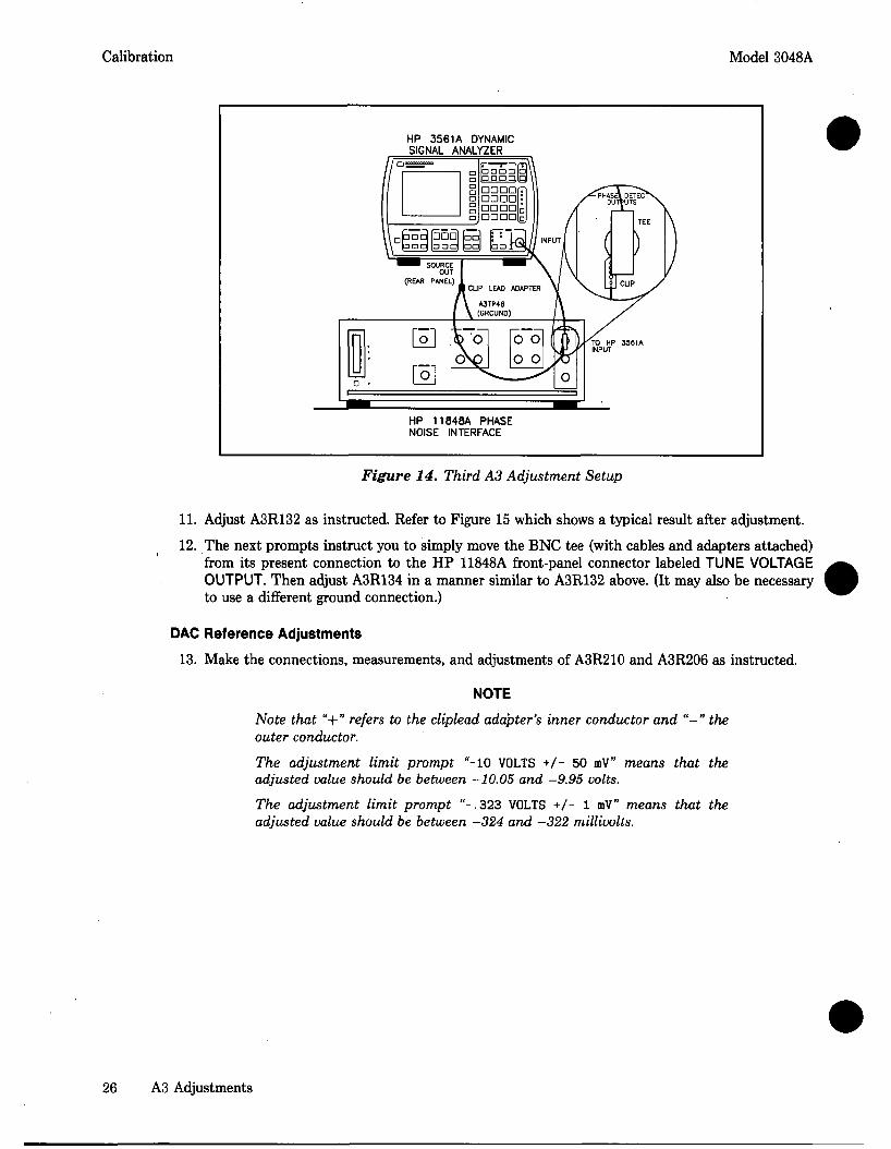
10. The prompt
CONNECT 'PHASE ]
CONNECT
A BNC TEE TO THE HP11848A AT 3ETECT0R OUTPUT
CABLE AND FROM BNC
TO 3561A INPUT
TEE TO HP3561A INPUT
followed by
USING A CONNECT GROUND SIGNAL
BNC TO CLIP LEAD ADAPTER HP3561A NOISE SOURCE AS FOLLOWS: LEAD LEAD
TO TO
HP11848A BNC 'TEE'
CHASSIS GROUND (ISOLATED GROUND)
instructs you to connect the instruments as shown in Figure 14.
NOTE Connect the ground (outer conductor) lead of the cliplead adapter to chassis ground in the HP 11848A. (Testpoint A3 TP46 is a convenient ground connection point.) Connect the other lead (the signal lead or inner conductor) of the cliplead adapter to the outer conductor of the BNC tee. Note that the outer conductor of the tee is not chassis ground; it is an isolated, floating ground.
HP 3561A DYNAMIC SIGNAL ANALYZER m % DDDD DDDD DDDD DDDD
SOURCE OUT (REAR PANEL)
Figure 13. Second A3 Adjustment Setup
A3 Adjustments 25
Calibration Model 3048A
HP 3561A DYNAMIC SIGNAL ANALYZER
3DC QDU □ □ : a c O D D n o [an
SOURCE OUT
(REAR PANEL)
[o]
HP 11848A PHASE NOISE INTERFACE
Figure 14. Third A3 Adjustment Setup
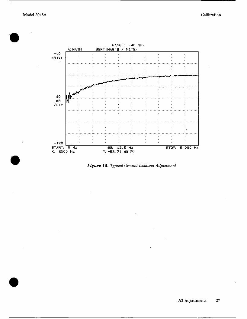
11. Adjust A3R132 as instructed. Refer to Figure 15 which shows a typical result after adjustment. 12. The next prompts instruct you to simply move the BNC tee (with cables arid adapters attached)
from its present connection to the HP 11848A front-panel connector labeled TUNE VOLTAGE OUTPUT. Then adjust A3R134 in a manner similar to A3R132 above. (It may also be necessary to use a different ground connection.)
DAC Reference Adjustments
13. Make the connections, measurements, and adjustments of A3R210 and A3R206 as instructed.
NOTE
Note that "+" refers to the cliplead adapter's inner conductor and "-" the outer conductor. The adjustment limit prompt "-10 VOLTS +/- 50 mV" means that the adjusted value should be between —10.05 and —9.95 volts. The adjustment limit prompt "-.323 VOLTS +/- 1 mV" means that the adjusted value should be between —324 and —322 millivolts.
26 A3 Adjustments
Model 3048A Calibration
-40 B(V)
10 dB
/DIV
-120
A: MATH RANGE: -40 dBV
SQRT (MAG~2 / Ml~2)
i irru-^*~ ■ » • « — ■
START: 0 Hz X: 2500 Hz
BW: 1 2 . 5 Hz Y: - 6 2 . 7 1 dB (V)
STOP: 5 000 Hz
Figure 15. Typical Ground Isolation Adjustment
A3 Adjustments 27
Calibration Model 3048A
PHASE DETECTOR OUTPUT/GND
ISOLATION ADJ ^
AC/DC ADAPTIVE COUPLER
DC OFFSET ADJ
1 kHz HPF DC
_^ OFFSET ADJ / t \ ©
10 kHz HPF DC
OFFSET ADJ
DAC 2 DC ADJ
TP201
^ \ R 1 3 2
« / DAC 3
DC ADJ
1 Hz HPF 10 Hz HPF 100 Hz HPF DC OFFSET ADJ DC OFFSET ADJ DC OFFSET ADJ
\ / / \ I / \ I / \ R74 / /
Ml / / R80 / /
[®r / /
R86 /
-~^ R68 nz\^-^ ^ L ® J —
R92
fel 1^1
R98
_^-^@\
R210
—■ [®]
R206
l
< \
► V A3 TP207 TP203 Anolyzer Interface
Assembly
TP46
/ / 4
R134
[®] _____^
N FRONT \
TUNE VOLTAGE OUTPUT/ GND ISOLATION ADJ
Figure 16. A3 Testpoint and Adjustment Locations
28 A3 Adjustments
Model 3048A Calibration
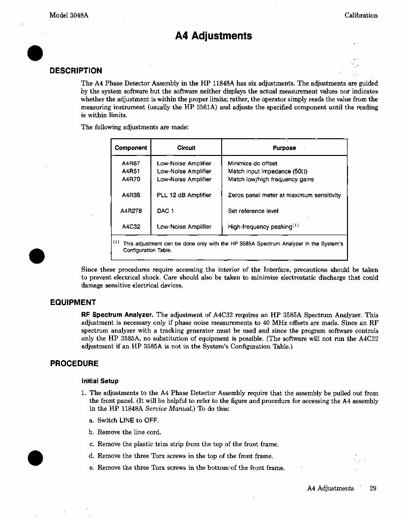
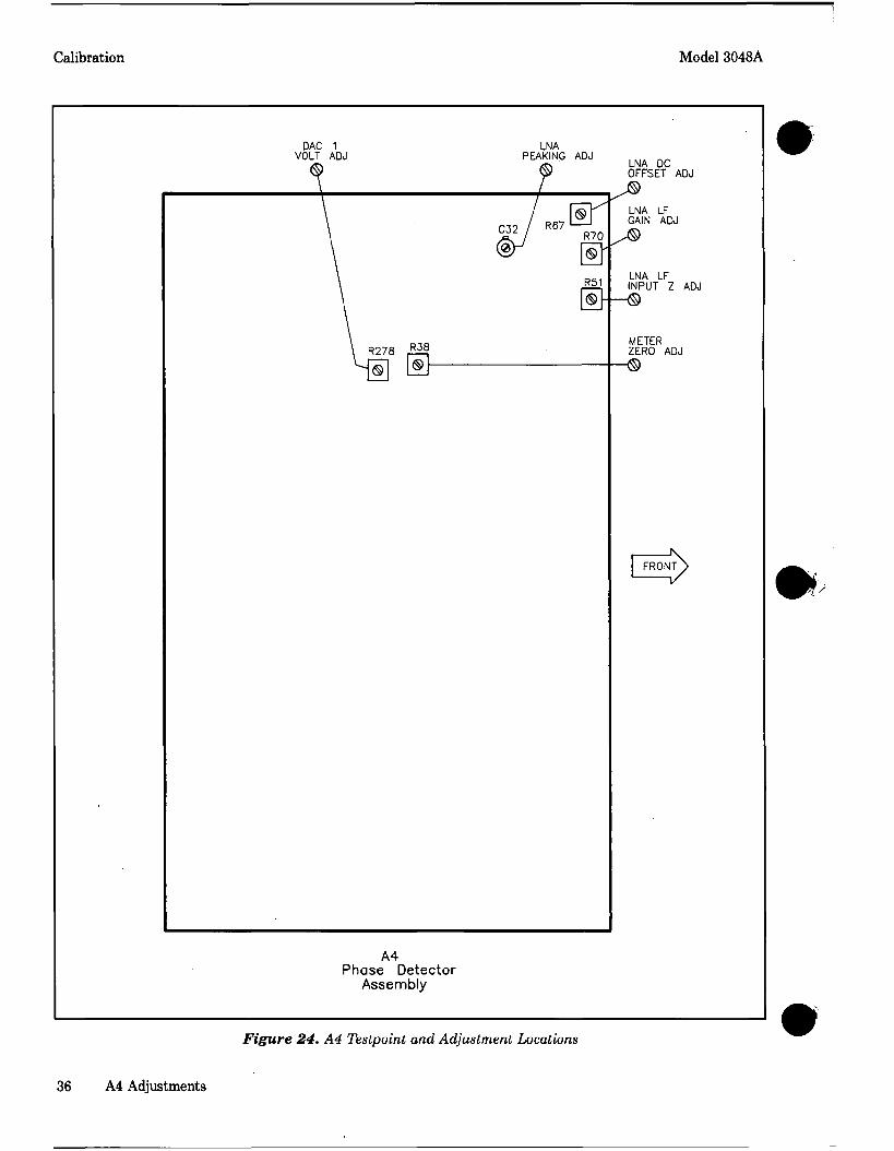
A4 Adjustments
DESCRIPTION The A4 Phase Detector Assembly in the HP 11848A has six adjustments. The adjustments are guided by the system software but the software neither displays the actual measurement values nor indicates whether the adjustment is within the proper limits; rather, the operator simply reads the value from the measuring instrument (usually the HP 3561A) and adjusts the specified component until the reading is within limits.
The following adjustments are made:
Component
A4R67 A4R51 A4R70
A4R38
A4R278
A4C32
Circuit
Low-Noise Amplifier Low-Noise Amplifier Low-Noise Amplifier
PLL 12 dB Amplifier
DAC1
Low-Noise Amplifier
Purpose
Minimize dc offset Match input impedance (50fi) Match low/high frequency gains
Zeros panel meter at maximum sensitivity
Set reference level
High-frequency peaking(1)
(1) This adjustment can be done only with the HP 3585A Spectrum Analyzer in the System's Configuration Table.
Since these procedures require accessing the interior of the Interface, precautions should be taken to prevent electrical shock. Care should also be taken to minimize electrostatic discharge that could damage sensitive electrical devices.
EQUIPMENT RF Spectrum Analyzer. The adjustment of A4C32 requires an HP 3585A Spectrum Analyzer. This adjustment is necessary only if phase noise measurements to 40 MHz offsets are made. Since an RF spectrum analyzer with a tracking generator must be used and since the program software controls only the HP 3585A, no substitution of equipment is possible. (The software will not run the A4C32 adjustment if an HP 3585A is not in the System's Configuration Table.)
PROCEDURE
Initial Setup
1. The adjustments to the A4 Phase Detector Assembly require that the assembly be pulled out from the front panel. (It will be helpful to refer to the figure and procedure for accessing the A4 assembly in the HP 11848A Service Manual.) To do this: a. Switch LINE to OFF. b. Remove the line cord.
c. Remove the plastic trim strip from the top of the front frame. d. Remove the three Torx screws in the top of the front frame. e. Remove the three Torx screws in the bottom'of the front frame.
A4 Adjustments 29
Calibration Model 3048A
f. Carefully pull the front panel out far enough to access the six adjustment holes in the shield covering the A4 assembly. Note that it is not necessary to remove the shield from the A4 assembly to make the adjustments.
g. Reinsert the line cord and switch LINE back to ON.
2. Set the HP 3561A input switch to the FLOAT position.
3. Press the Spcl. Funct'n softkey available at the Main Software Level menu.
4. Press the 3048A Sys Chk softkey.
5. Press the Int. Adj'mnt softkey.
6. Press the Adjust A4 softkey.
NOTE
7/ no RF spectrum analyzer is in the System's Configuration Table, you will be informed at this time. Press the Proceed softkey to continue the A4 adjustments minus the A4C32 adjustment.
The physical location of testpoints and adjustable components is shown in Figure 24.
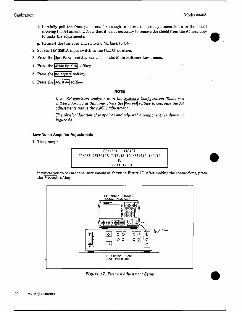
Low-Noise Amplifier Adjustments
7. The prompt
CONNECT HP11848A 'PHASE DETECTOR OUTPUTS TO HP3561A INPUT'
TO HP3561A INPUT
instructs you to connect the instruments as shown in Figure 17. After making the connections, press the Proceed softkey.
HP 3561A DYNAMIC SIGNAL ANALYZER
if
DDC □ □ □ CO •
c
T. [o] O O o o
o o o o
1. [°] —' o o
HP 11848A PHASE NOISE INTERFACE
TO HP 3581A INPUT
Figure 17. First A4 Adjustment Setup
30 A4 Adjustments
Model 3048A Calibration
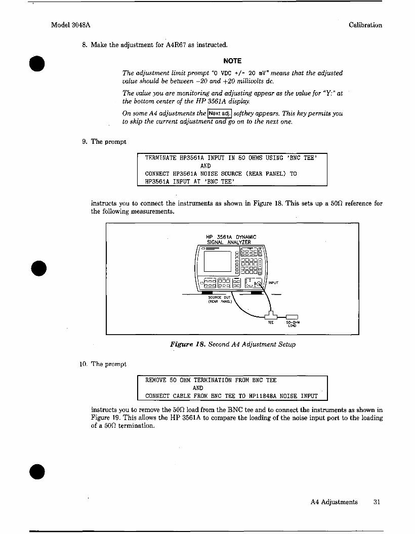
8. Make the adjustment for A4R67 as instructed.
NOTE
The adjustment limit prompt "0 VDC +/- 20 mV" means that the adjusted value should be between -20 and +20 millivolts dc. The value you are monitoring and adjusting appear as the value for "Y:" at the bottom center of the HP 3561A display.
On some A4 adjustments the \ Next adj. | softkey appears. This key permits you to skip the current adjustment and go on to the next one.
9. The prompt
TERMINATE HP3561A INPUT IN
CONNECT HP3561A
AND HP3561A NOISE INPUT AT 'BNC
50
SOURCE TEE'
OHMS USING
(REAR PANEL)
'BNC
TO
TEE'
instructs you to connect the instruments as shown in Figure 18. This sets up a 50(7 reference for the following measurements.
HP 3561A DYNAMIC SIGNAL ANALYZER
Figure 18. Second A4 Adjustment Setup
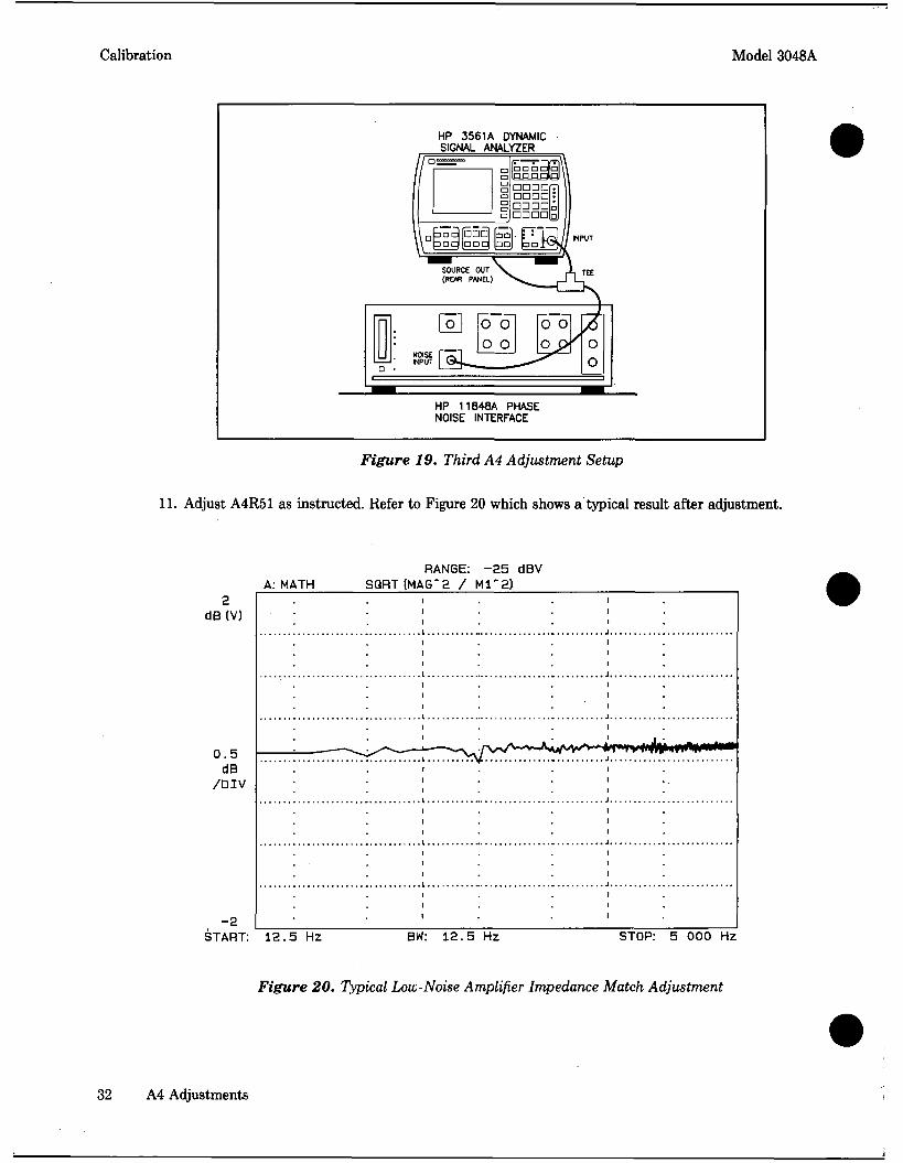
10. The prompt
REMOVE
CONNECT
50 OHM
CABLE
TERMINATION AND FROM BNC TEE
FROM
TO
BNC TEE
HP11848A NOISE INPUT
instructs you to remove the 50(7 load from the BNC tee and to connect the instruments as shown in Figure 19. This allows the HP 3561A to compare the loading of the noise input port to the loading of a 50fi termination.
A4 Adjustments 31
Calibration Model 3048A
HP 3561A DYNAMIC SIGNAL ANALYZER
essi DDDD DQDD DDDD DDDD
D D C G D G D O o n
SOURCE OUT (REAR PANEL)
-
D
NOISE INPUT
LI] [ — |
o o o o
0 O op o
o
HP 11B48A PHASE NOISE INTERFACE
Figure 19. Third A4 Adjustment Setup
11. Adjust A4R51 as instructed. Refer to Figure 20 which shows a typical result after adjustment.
2 dB(V)
0.5 dB
/DIV
A: MATH RANGE: -25 dBV
SQRT (MAG*2 / Ml* 2)
START: 12.5 Hz BW: 12.5 Hz STOP: 5 000 Hz
Figure 20. Typical Low-Noise Amplifier Impedance Match Adjustment
32 A4 Adjustments
Model 3048A
v. 12. The prompt
Calibration
CONNECT HP11848A 'PHASE DETECTOR OUTPUTS TO HP3561A INPUT'
TO HP3561A INPUT
instructs you to connect the instruments as shown in Figure 17 (the same as in step 7).
13. The prompt
CONNECT HP3561A NOISE SOURCE TO HP11848A AT 'NOISE INPUT FROM HP3561A SOURCE OUTPUT' (REAR PANEL)
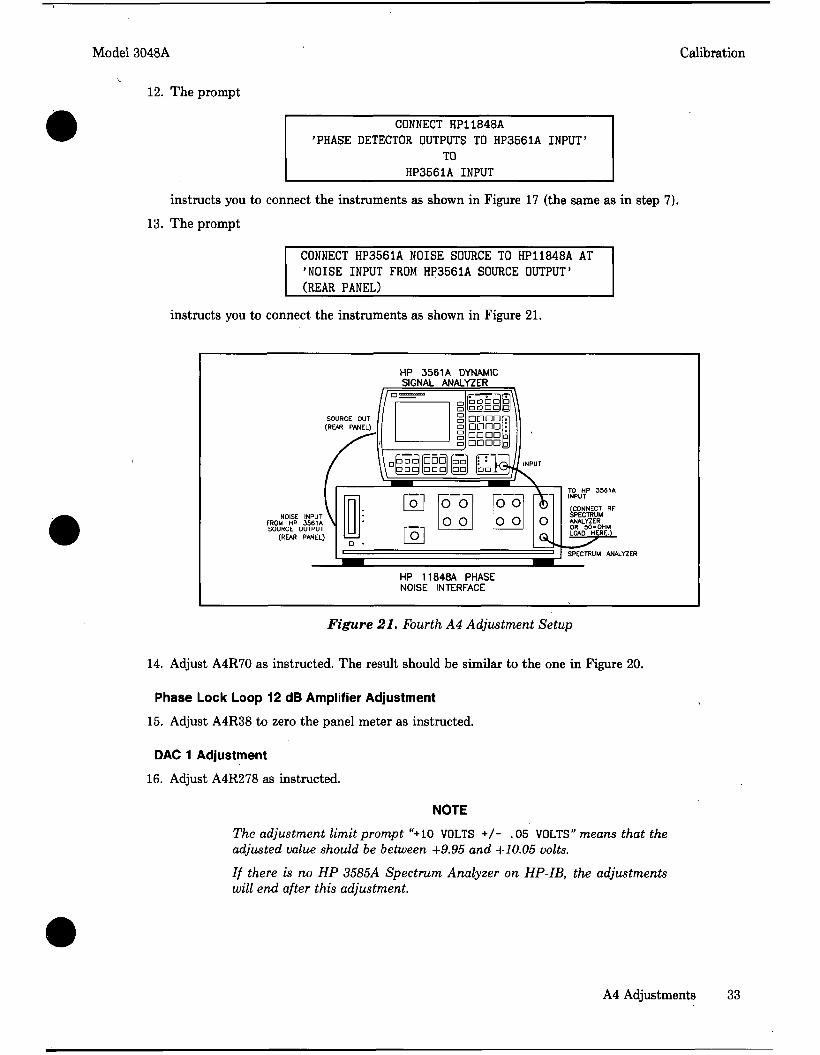
instructs you to connect the instruments as shown in Figure 21.
HP 3561A DYNAMIC SIGNAL ANALYZER
SOURCE OUT (REAR PANEL)
NOISE INPUT FROM HP 3561A SOURCE OUTPUT
(REAR PANEL)
CONNECT RF jPECTRUM ANALYZER OR 50-OHM LOAD HERE.)
SPECTRUM ANALYZER
HP 11848A PHASE NOISE INTERFACE
Figure 21. Fourth A4 Adjustment Setup
14. Adjust A4R70 as instructed. The result should be similar to the one in Figure 20.
Phase Lock Loop 12 dB Amplifier Adjustment
15. Adjust A4R38 to zero the panel meter as instructed.
DAC 1 Adjustment
16. Adjust A4R278 as instructed.
NOTE
The adjustment limit prompt "+10 VOLTS +/- .05 VOLTS" means that the adjusted value should be between +9.95 and +10.05 volts.
If there is no HP 3585A Spectrum Analyzer on HP-IB, the adjustments will end after this adjustment.
A4 Adjustments 33
Calibration Model 3048A
Low-Noise Amplifier Peaking Adjustment
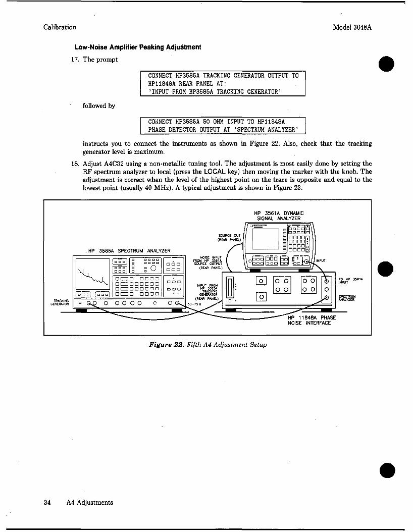
17. The prompt
CONNECT HP3585A TRACKING HP11848A REAR PANEL 'INPUT FROM HP3585A
AT: GENERATOR
TRACKING
OUTPUT
GENERATOR'
TO
followed by
CONNECT HP3585A 50 OHM INPUT TO HP11848A PHASE DETECTOR OUTPUT AT 'SPECTRUM ANALYZER'
instructs you to connect the instruments as shown in Figure 22. Also, check that the tracking generator level is maximum.
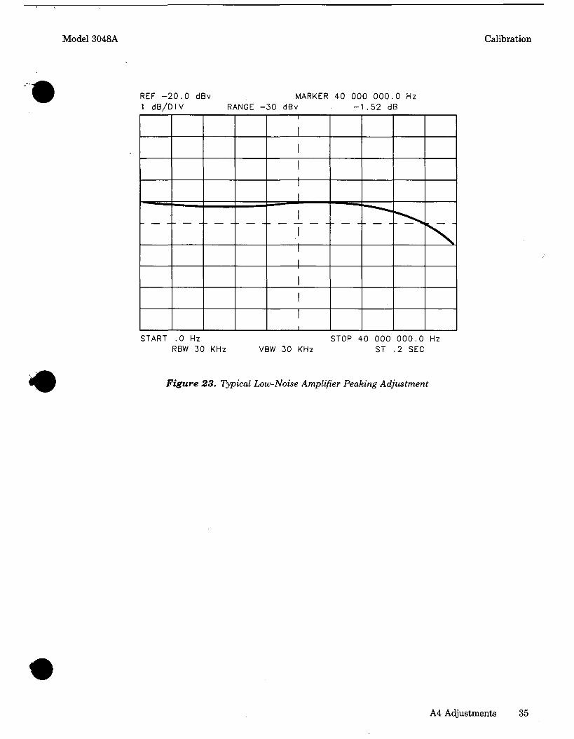
18. Adjust A4C32 using a non-metallic tuning tool. The adjustment is most easily done by setting the RF spectrum analyzer to local (press the LOCAL key) then moving the marker with the knob. The adjustment is correct when the level of the highest point on the trace is opposite and equal to the lowest point (usually 40 MHz). A typical adjustment is shown in Figure 23.
Figure 22. Fifth A4 Adjustment Setup
34 A4 Adjustments
Model 3048A Calibration
REF -20.0 dBv 1 dB/DIV RANGE -
_ _ _
MARKER 30 dBv
i
i
40 000 000.0 Hz -1.52 dB
t — -
START .0 Hz RBW 30 KHz
STOP 40 000 000.0 Hz VBW 30 KHz ST .2 SEC
m Figure 23. Typical Low-Noise Amplifier Peaking Adjustment
A4 Adjustments 35
Calibration Model 3048A
DAC 1 VOLT ADJ
LNA PEAKING ADJ
LNA DC OFFSET ADJ
^
R67 ®
R70 ^ / ®
R51
R278 R38 ®
LNA LF GAIN ADJ
LNA LF INPUT 2 ADJ
METER ZERO ADJ
FRONT
^^F?- -
A4 Phase Detector
Assembly
Figure 24. A4 Testpoint and Adjustment Locations
36 A4 Adjustments
Model 3048A Calibration
Option 1 Calibration
DESCRIPTION The Option 1 Calibration program characterizes the gain and flatness of signal paths internal to the HP 11848A Phase Noise Interface. These unique characteristics are calibration factors which scale the measurement results for best noise measurement accuracy.
NOTE
Option 1 Calibration is similar to Option 2 Calibration. However, Option 2 Calibration collects data to characterize two additional reference paths. Perform Option 2 Calibration annually. Perform Option 1 Calibration when significant ambient changes occur.
For frequencies of 100 kHz and below, the calibration program sets up the HP 3561A as a scalar network analyzer. The internal noise source of the HP 3561A is the input signal to the network under test and the spectrum analyzer function measures the magnitude of the output from the network. For frequencies of 100 kHz through 40 MHz, the HP 3585A (which is required for this frequency range) is used with its internal tracking generator used as the stimulus.
The collected data is stored in two files in mass media storage titled "CALDATALO" and "CAL-DATAHI". Since the data is unique to each individual HP 11848A, it is important that the two files be transferred along with the Interface should the Interface be moved to another System. The data should be tagged to the serial number of the Interface it represents. (The Interface's serial number is logged in the System's Configuration Table.) Note, however, that the data is not unique to the HP 3561A (or HP 3585A) spectrum analyzer.
EQUIPMENT RF Spectrum Analyzer. The System collects data through offsets of 100 kHz with the HP 3561A. Data through 40 MHz offsets requires, in addition, an HP 3585A Spectrum Analyzer. Since an RF spectrum analyzer with a tracking generator must be used and since the program software controls only the HP 3585A, no substitution of equipment is possible.
PROCEDURE
Initial Setup
1. Set the HP 3561A input switch to the FLOAT position.
2. Press the Spcl. Funct'n softkey available at the Main Software Level menu.
3. Press the 3048A Sys Chk softkey.
NOTE
Before proceeding with the measurements, you should read the Comments section below.
4. Press the Cal System softkey.
Option 1 Calibration 37
Calibration Model 3048A
Calibration to 100 kHz Offsets 5. Press the CaltolOOkHz softkey.
6. Press the Option 1 softkey.
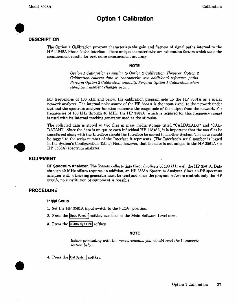
7. Connect the cables as prompted on the display and as shown in Figure 25.
HP 3561A DYNAMIC SIGNAL ANALYZER
SOURCE OUT (REAR PANEL)
NOISE INPUT FROM HP 3561A SOURCE OUTPUT
(REAR PANEL)
TO HP 3561A INPUT
(CONNECT RF SPECTRUM ANALYZER OR 50-OHM LOAD HERE.)
SPECTRUM ANALVZER
HP 11848A PHASE NOISE INTERFACE
Figure 25. First Option 1 Calibration Setup
8. When the prompt appears asking if you want to store the data taken, you have the following choices.
• If you do not want to store the data, press the Abort softkey. This will cause the old data from the mass storage media to be re-loaded in computer RAM (random access memory) and thus destroy the data just collected. If you want simply to replace the old data with the new data on the current mass media storage device, press the | Store Caldata softkey and overwrite the data in the file. (If you abort at this point, the new data still remains in computer RAM.)
• If you want to store the new data on a new disc or mass media file location while keeping the old data, place a new disc in place of the old one then press the this point, the new data still remains in computer RAM.)
Store Caldata softkey. (If you abort at
NOTE Difficulties encountered in storing calibration data in mass storage generate prompts to assist in clearing the problem. A common example of a problem is a write-protected floppy disc. This is the end of Option 1 Calibration if no HP 3585A Spectrum Analyzer is present.
Calibration 100 kHz through 40 MHz Offsets 9. Press the Cal System] softkey.
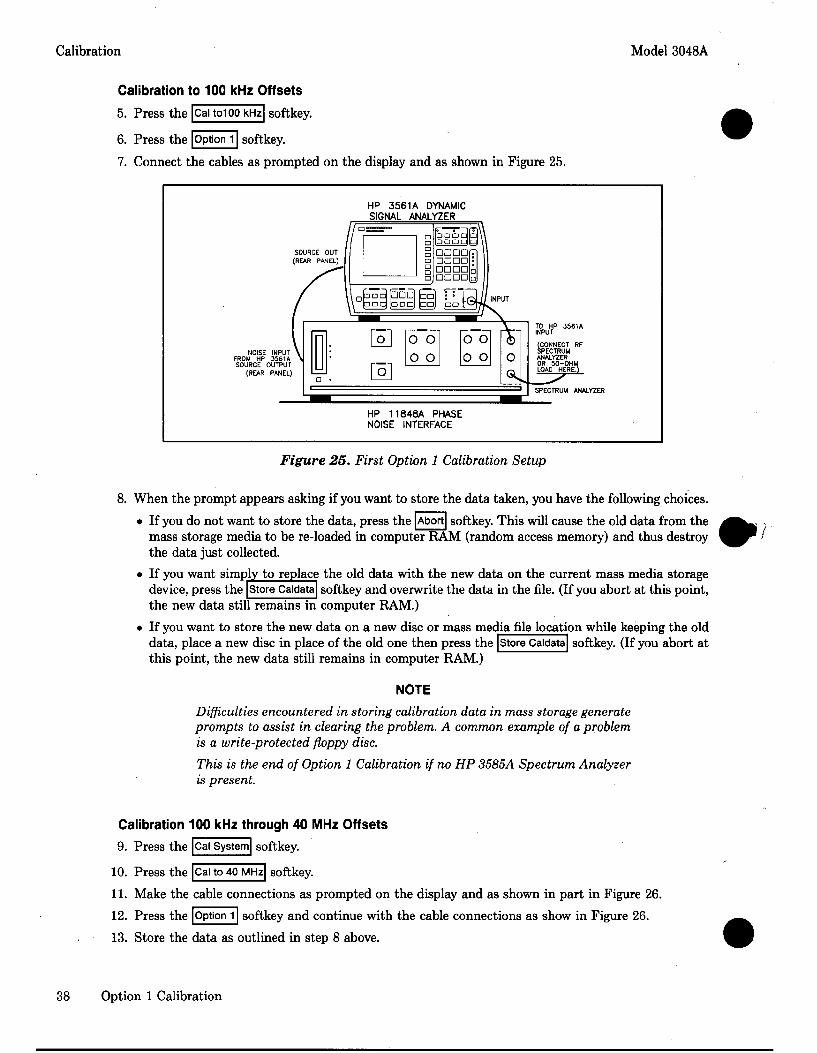
10. Press the Cal to 40 MHz softkey. 11. Make the cable connections as prompted on the display and as shown in part in Figure 26.
12. Press the Option 1 softkey and continue with the cable connections as show in Figure 26. 13. Store the data as outlined in step 8 above.
38 Option 1 Calibration
Model 3048A Calibration
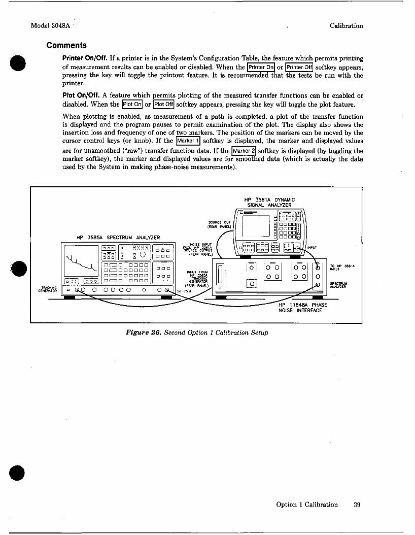
Comments Printer On/Off. If a printer is in the System's Configuration Table, the feature which permits printing of measurement results can be enabled or disabled. When the Printer On or Printer Off softkey appears, pressing the key will toggle the printout feature. It is recommended that the tests be run with the printer. Plot On/Off. A feature which permits plotting of the measured transfer functions can be enabled or disabled. When the Plot On or Plot Off softkey appears, pressing the key will toggle the plot feature. When plotting is enabled, as measurement of a path is completed, a plot of the transfer function is displayed and the program pauses to permit examination of the plot. The display also shows the insertion loss and frequency of one of two markers. The position of the markers can be moved by the cursor control keys (or knob). If the Marker 1 softkey is displayed, the marker and displayed values are for unsmoothed ("raw") transfer function data. If the | Marker 2| softkey is displayed (by toggling the marker softkey), the marker and displayed values are for smoothed data (which is actually the data used by the System in making phase-noise measurements).
TRACKING GENERATOR
HP 3585A SPECTRUM ANALYZER
[a a z
| D D D |
I □ "□ I [ a p p)
DCDD D D O D D a D D D D D D □ czmooQnn a n o D D D O
J^U o o o o o
HP 3561A DYNAMIC SIGNAL ANALYZER
TO HP 3561A INPUT
HP 11848A PHASE NOISE INTERFACE
Figure 26. Second Option 1 Calibration Setup
Option 1 Calibration 39
Calibration Model 3048A
Option 2 Calibration
DESCRIPTION The Option 2 Calibration program characterizes the gain and flatness of signal paths internal to the HP 11848A Phase Noise Interface. These unique characteristics are calibration factors which scale the measurement results for best noise measurement accuracy.
NOTE
Option 2 Calibration is similar to Option 1 Calibration. However, Option 2 Calibration collects data to characterize two additional reference paths. Perform Option 2 Calibration annually.
For frequencies of 100 kHz and below, the calibration program sets up the HP 3561A as a scalar network analyzer. The internal noise source of the HP 3561A is the input signal to the network under test and the spectrum analyzer function measures the magnitude of the output from the network. For frequencies of 100 kHz through 40 MHz, the HP 3585A (which is required for this frequency range) is used with its internal tracking generator used as the stimulus.
The collected data is stored in two files in mass media storage titled "CALDATALO" and "CAL-DATAHF. Since the data is unique to each individual HP 11848A, it is important that the two files be transferred along with the Interface should the Interface be moved to another System. The data should be tagged to the serial number of the Interface it represents. (The Interface's serial number is logged in the System's Configuration Table.) Note, however, that the data is not unique to the HP 3561A (or HP 3585A) spectrum analyzer.
EQUIPMENT RF Spectrum Analyzer. The System collects data through offsets of 100 kHz with the HP 3561A. Data through 40 MHz offsets requires, in addition, an HP 3585A Spectrum Analyzer. Since an RF spectrum analyzer with a tracking generator must be used and since the program software controls only the HP 3585A, no substitution of equipment is possible.
PROCEDURE
Initial Setup
1. Set the HP 3561A input switch to the FLOAT position.
2. Press the Spcl. Funct'n softkey available at the Main Software Level menu.
3. Press the |3048A Sys Chk| softkey.
NOTE
Before proceeding with the measurements, you should read the Comments section below.
4. Press the Cai System softkey.
40 Option 2 Calibration
Model 3048A Calibration
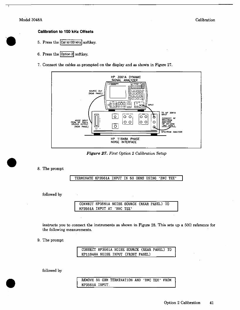
Calibration to 100 kHz Offsets
5. Press the CaltolOOkHz softkey.
6. Press the Option 2 softkey.
7. Connect the cables as prompted on the display and as shown in Figure 27.
HP 3561A DYNAMIC SIGNAL ANALYZER
NOISE INPUT FROM HP 3561A SOURCE OUTPUT
(REAR PANEL)
HP 11848A PHASE NOISE INTERFACE
TO HP 3561A INPUT
(CONNECT RF SPECTRUM ANALYZER OR 50-OHU LOAD HERE.)
SPECTRUM ANALYZER
Figure 27. First Option 2 Calibration Setup
8. The prompt
TERMINATE HP3561A INPUT IN 50 OHMS USING 'BNC TEE'
followed by
CONNECT HP3561A NOISE SOURCE (REAR PANEL) TO HP3561A INPUT AT 'BNC TEE"
instructs you to connect the instruments as shown in Figure 28. This sets up a 50fi reference for the following measurements.
9. The prompt
CONNECT HP3561A NOISE SOURCE (REAR PANEL) TO HP11848A NOISE INPUT (FRONT PANEL)
followed by
REMOVE 50 OHM TERMINATION AND 'BNC TEE' FROM HP3561A INPUT.
Option 2 Calibrat ion 41
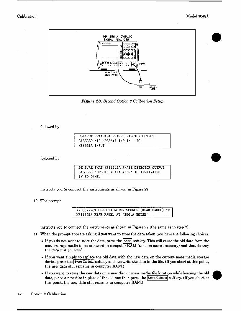
Calibration Model 3048A
HP 3561A DYNAMIC SIGNAL ANALYZER
Figure 28. Second Option 2 Calibration Setup
followed by
CONNECT HP11848A PHASE DETECTOR OUTPUT LABELED 'TO HP3561A INPUT' TO HP3561A INPUT.
followed by
BE SURE THAT HP11848A PHASE DETECTOR OUTPUT LABELED "SPECTRUM ANALYZER' IS TERMINATED IN 50 OHMS.
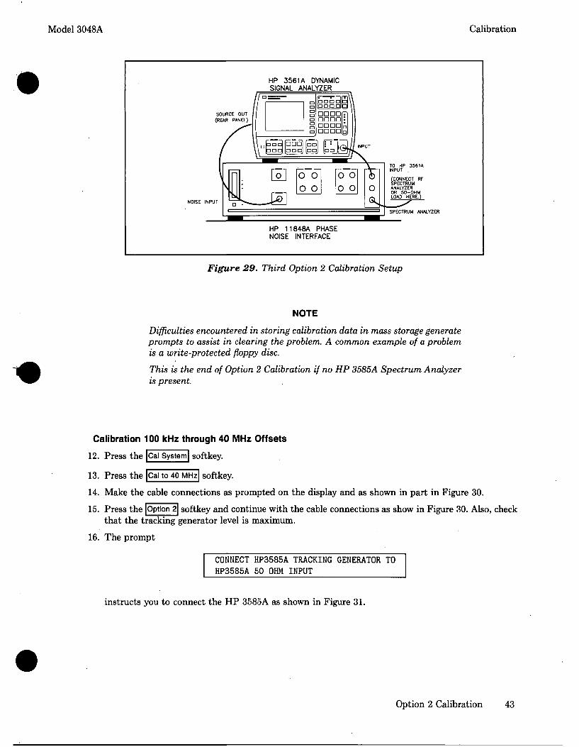
instructs you to connect the instruments as shown in Figure 29.
10. The prompt
RE-CONNECT HP3561A NOISE SOURCE (REAR PANEL) TO HP11848A REAR PANEL AT '3561A NOISE*
instructs you to connect the instruments as shown in Figure 27 (the same as in step 7).
11. When the prompt appears asking if you want to store the data taken, you have the following choices.
• If you do not want to store the data, press the Abort softkey. This will cause the old data from the mass storage media to be re-loaded in computer RAM (random access memory) and thus destroy the data just collected.
• If you want simply to replace the old data with the new data on the current mass media storage device, press the | Store Caldata softkey and overwrite the data in the file. (If you abort at this point, the new data still remains in computer RAM.)
• If you want to store the new data on a new disc or mass media file location while keeping the old data, place a new disc in place of the old one then press the this point, the new data still remains in computer RAM.)
Store Caldata softkey. (If you abort at
42 Option 2 Calibration
Model 3048A Calibration
HP 3561A DYNAMIC SIGNAL ANALYZER
NOISE INPUT
DDDD DDDD DDDD DDDD
f l : ^ O O O O
0 O 0 O O
HP 11848A PHASE NOISE INTERFACE
TO HP 3561* INPUT .
(CONNECT RF SPECTRUM ANALYZER OR 50-OHM LOAD HERE.)
SPECTRUM ANALYZER
Figure 29. Third Option 2 Calibration Setup
NOTE
Difficulties encountered in storing calibration data in mass storage generate prompts to assist in clearing the problem. A common example of a problem is a write-protected floppy disc.
This is the end of Option 2 Calibration if no HP 3585A Spectrum Analyzer is present.
Calibration 100 kHz through 40 MHz Offsets
12. Press the |Cal System| softkey.
13. Press the Cal to 40 MHz softkey.
14. Make the cable connections as prompted on the display and as shown in part in Figure 30.
15. Press the Option 2 softkey and continue with the cable connections as show in Figure 30. Also, check that the tracking generator level is maximum.
16. The prompt
CONNECT HP3585A TRACKING GENERATOR TO HP3585A 50 OHM INPUT
instructs you to connect the HP 3585A as shown in Figure 31.
Option 2 Calibration 43
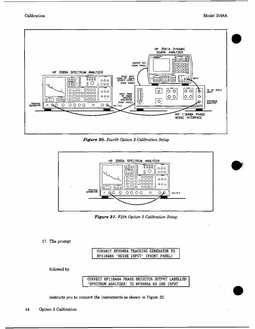
Calibration Model 3048A
HP 3561A DYNAMIC SIGNAL ANALYZER
HP 3585A SPECTRUM ANALYZER
TRACKING GENERATOR
□ :: I ["□"oa
Qczm D O D O D n D D D D D D D Q D D D D D D QCZID D D D D
□ □ a □ □ D
ae o o o o o
TO HP 3561A INPUT
HP 11848A PHASE NOISE INTERFACE
Figure 30. Fourth Option 2 Calibration Setup
HP 3585A SPECTRUM ANALYZER
[a a □
o aaa □ a n
a C D D D D D D D C D D D D D D D O n D D D D D D D Q D D D D D
D a n □ a a
Figure 31. Fifth Option 2 Calibration Setup
17. The prompt
CONNECT HP3585A TRACKING GENERATOR TO HP11848A 'NOISE INPUT' (FRONT PANEL)
followed by
CONNECT HP11848A PHASE DETECTOR OUTPUT LABELLED 'SPECTRUM ANALYZER' TO HP3585A 50 OHM INPUT
instructs you to connect the instruments as shown in Figure 32.
44 Option 2 Calibration
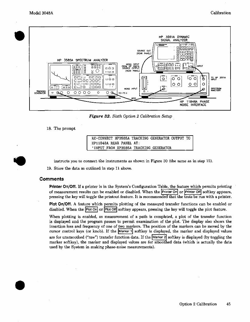
Model 3048A Calibration
HP 3561A DYNAMIC SIGNAL ANALYZER
HP 3585A SPECTRUM ANALYZER
[ D O C
I □ ™r. [ □ □ c O n n D
o □ n
p : : ] [ □ D a ]
D O D D D D D D a a a a o c D D a D D D D D D D I T I D D D D D
□ D n o o n
NOISE INPUT FROM HP 3561A SOURCE OUTPUT
(REAR PANEL)
NOISE INPUT
5 0 - 7 5 n
TO HP 3561A INPUT
HP 11848A PHASE NOISE INTERFACE
Figure 32. Sixth Option 2 Calibration Setup
18. The prompt
RE-CONNECT HP3585A TRACKING GENERATOR OUTPUT TO HP11848A REAR PANEL AT: •INPUT FROM HP3585A TRACKING GENERATOR
instructs you to connect the instruments as shown in Figure 30 (the same as in step 15).
19. Store the data as outlined in step 11 above.
Comments Printer On/Off. If a printer is in the System's Configuration Table, the feature which permits printing
softkey appears, Printer On or Printer Off of measurement results can be enabled or disabled. When the pressing the key will toggle the printout feature. It is recommended that the tests be run with a printer. Plot On/Off. A feature which permits plotting of the measured transfer functions can be enabled or disabled. When the Plot On or Plot Off softkey appears, pressing the key will toggle the plot feature. When plotting is enabled, as measurement of a path is completed, a plot of the transfer function is displayed and the program pauses to permit examination of the plot. The display also shows the insertion loss and frequency of one of two markers. The position of the markers can be moved by the cursor control keys (or knob). If the Marker 1 softkey is displayed, the marker and displayed values
softkey is displayed (by toggling the Marker 2 are for unsmoothed ("raw") transfer function data. If the marker softkey), the marker and displayed values are for smoothed data (which is actually the data used by the System in making phase-noise measurements).
Option 2 Calibration 45
Calibration
Internal Sources Calibration
Model 3048A
DESCRIPTION The Internal Sources Calibration program determines the settings of DACs 2 and 3 which tune three of the four internal Oscillators to their nominal frequencies. This is a software controlled adjustment. (The three oscillators are 10 MHz A, 10 MHz B, and 350-500 MHz.) The tuning (or frequency set) data is then recorded on the System's mass storage medium as VNOMs in the CALDATAHI file. As with the Option 1 and Option 2 Calibration, this data must be used only with the HP 11848A for which the data was taken.
EQUIPMENT Frequency Counter. A general purpose 550 MHz counter is required. It does not need to be programmable.
PROCEDURE
Initial Setup 1. Press the Spcl. Funct'n softkey available at the Main Software Level menu.
2. Press the 3048A Sys Chk softkey.
3. Press the |Cal System| softkey.
4. Press the Cal Int Srcs
5. Press the Cal All Srcs
softkey.
softkey.
NOTE Step 5 sets up the tests for all three oscillators. The other softkeys allow selection of the individual tests.
Calibration of the 10 MHz A Oscillator 6. Connect the cable from the HP 11848A front-panel 10 MHz A source output to the counter's input
as prompted. 8. The prompt
Press 'Proceed' TO ACCESS HP11848A FRONT PANEL Then adjust DAC2 and DAC3 for a frequency reading of 10 MHz +/- 10 Hz. You may re turn from 'Front Panel ' by pressing 'DONE'
readies you for the HP 11848A CONTROL display. To adjust the DACs: a. Use the vertical cursor control keys or knob to move the cursor field (" > <") to DAC2. b. Note the frequency on the counter. If it is within ±10 Hz of 10 MHz, press the DONE softkey
and continue on to step 10. c. If the frequency is out of limits, change the voltage of DAC2 by keying in a new voltage within,
the cursor field then press the Send Command softkey. If the voltage does not bring the frequency within limits, key in another voltage. If the voltage settings are too coarse to reach the frequency limits, cursor down to DAC3 and set it in a similar manner.
46 Internal Sources Calibration
3048A Calibration
NOTE
For all oscillators increasing the voltage decreases the frequency.
The 10 MHz A Oscillator has a tuning sensitivity of approximately 20 Hz/V.
DAC2 can be set only in 50 mV increments; DAC3 in 1 mV increments. The acceptable range of voltages are listed below the last entry of the display.
If an unacceptable value is entered, the DAC voltage, after giving the send command, will either be unchanged, rounded off, or a prompt will indicate that the entry needs modification.
Calibration of the 10 MHz B Oscillator
10. Connect the cable from the HP 11848A front-panel 10 MHz B source output to the counter's input as prompted.
11. The prompt
Press 'Proceed' TO ACCESS HP11848A FRONT PANEL Then adjust DAC2 and DAC3 for a frequency reading of 10 MHz +/- 50 Hz. You may return from 'Front Panel' by pressing 'DONE'
readies you for the HP 11848A CONTROL display.
12. To adjust the DACs, proceed as in step 9 to bring the frequency within ±50 Hz of 10 MHz, then press the DONE softkey and continue on to step 13. (The tuning sensitivity is about 200 Hz/V.)
Calibration of the 350-500 MHz Oscillator
13. Connect the cable from the HP 11848A front-panel 350-500 MHz source output to the counter's input as prompted.
14. The prompt
Press 'Proceed' TO ACCESS HP11848A FRONT PANEL Then adjust DAC2 and DAC3 for a frequency reading of 400 MHz +/- 1 MHz. You may return from 'Front Panel' by pressing 'DONE'
readies you for the HP 11848A CONTROL display.
15. To adjust the DACs, proceed as in step 9 to bring the frequency between 399 and 401 MHz, then press the DONE softkey. (The tuning sensitivity is about 20 MHz/V.)
Storing the Data
16. As you are prompted for the 10 MHz A oscillator, press either the you want to store the new VNOM in mass storage or the the old VNOM. Actual storing of data is in step 19.
Proceed Abort
softkey to indicate that softkey to indicate you want to retain
17. As you are prompted for the 10 MHz B oscillator, press either the you want to store the new VNOM in mass storage or the the old VNOM. Actual storing of data is in step 19.
Proceed
Abort
softkey to indicate that softkey to indicate you want to retain
18. As you are prompted for the 350-500 MHz oscillator, press either the that you want to store the new VNOM in mass storage or the retain the old VNOM. Actual storing of data is in step 19.
Proceed Abort
softkey to indicate softkey to indicate you want to
Internal Sources Calibration 47
Calibration Model 3048A
19. As you are prompted, press either the Store Caldata softkey to permanently store the specified new VNOMs in mass storage or the |Abort| softkey to leave the current VNOMs unchanged. Stored new VNOMs will overwrite the old VNOMs
20. If you have requested permanent storage of the new VNOMs, the display will prompt you for confirmation of this decision. Press the |Yes, Proceed softkey to store the new VNOMs.
NOTE
Difficulties encountered in storing the VNOMs in mass storage generate prompts to assist in clearing the problem. A common example of a problem is a write-protected floppy disc.
Press the View Vnoms softkey to confirm the values of the stored VNOMs.
48 Internal Sources Calibration
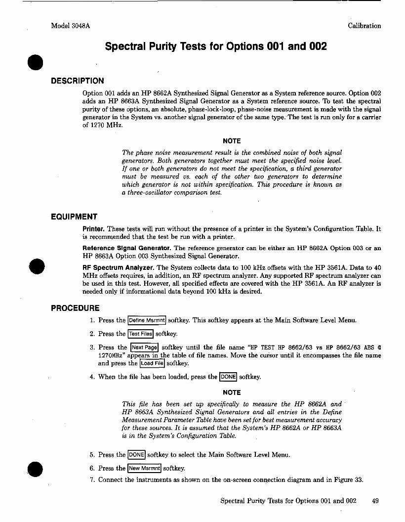
Model 3048A Calibration
Spectral Purity Tests for Options 001 and 002
DESCRIPTION Option 001 adds an HP 8662A Synthesized Signal Generator as a System reference source. Option 002 adds an HP 8663A Synthesized Signal Generator as a System reference source. To test the spectral purity of these options, an absolute, phase-lock-loop, phase-noise measurement is made with the signal generator in the System vs. another signal generator of the same type. The test is run only for a carrier of 1270 MHz.
NOTE
The phase noise measurement result is the combined noise of both signal generators. Both generators together must meet the specified noise level. If one or both generators do not meet the specification, a third generator must be measured vs. each of the other two generators to determine which generator is not within specification. This procedure is known as a three-oscillator comparison test.
EQUIPMENT Printer. These tests will run without the presence of a printer in the System's Configuration Table. It is recommended that the test be run with a printer. Reference Signal Generator. The reference generator can be either an HP 8662A Option 003 or an HP 8663A Option 003 Synthesized Signal Generator. RF Spectrum Analyzer. The System collects data to 100 kHz offsets with the HP 3561A. Data to 40 MHz offsets requires, in addition, an RF spectrum analyzer. Any supported RF spectrum analyzer can be used in this test. However, all specified effects are covered with the HP 3561A. An RF analyzer is needed only if informational data beyond 100 kHz is desired.
PROCEDURE 1. Press the Define Msrmnt softkey. This softkey appears at the Main Software Level Menu.
2. Press the Test Files softkey.
3. Press the Next Page softkey until the file name "HP TEST HP 8662/63 vs HP 8662/63 ABS Q 1270MHz" appears in the table of file names. Move the cursor until it encompasses the file name and press the Load File softkey.
4. When the file has been loaded, press the DONE softkey.
NOTE
This file has been set up specifically to measure the HP 8662A and HP 8663A Synthesized Signal Generators and all entries in the Define Measurement Parameter Table have been set for best measurement accuracy for these sources. It is assumed that the System's HP 8662A or HP 8663A is in the System's Configuration Table.
5. Press the DONE softkey to select the Main Software Level Menu.
6. Press the New Msrmnt softkey. 7. Connect the instruments as shown on the on-screen connection diagram and in Figure 33.
Spectral Purity Tests for Options 001 and 002 49
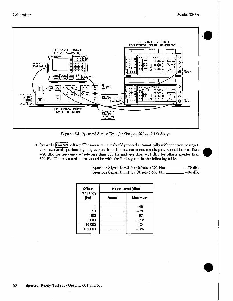
Calibration Model 3048A
HP 8662A OR 8663A SYNTHESIZED SIGNAL GENERATOR
HP 3561A DYNAMIC SIGNAL ANALYZER
NOISE INPUT FROM
HP 3561A SOURCE OUTPUT
(REAR PANEL)
RF OUTPUT
HP 11B48A PHASE NOISE INTERFACE »(CONNECT RF
SPECTRUM ANALYZER
Figure 33. Spectral Purity Tests for Options 001 and 002 Setup
8. Press the Proceed softkey. The measurement should proceed automatically without error messages. The measured spurious signals, as read from the measurement results plot, should be less than -70 dBc for frequency offsets less than 300 Hz and less than - 8 4 dBc for offsets greater than 300 Hz. The measured noise should be with the limits given in the following table.
Spurious Signal Limit for Offsets <300 Hz:, Spurious Signal Limit for Offsets >300 Hz:
- 7 0 dBc - 8 4 dBc
Offset Frequency
(Hz)
1 10
100 1 000
10 000 100 000
Noise Level (dBc)
Actual Maximum
-48 -78 -97 -112 -124 -126
50 Spectral Purity Tests for Options 001 and 002
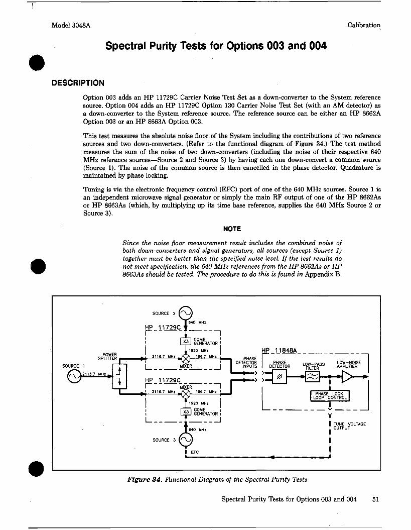
Model 3048A Calibration
Spectral Purity Tests for Options 003 and 004
DESCRIPTION
Option 003 adds an HP 11729C Carrier Noise Test Set as a down-converter to the System reference source. Option 004 adds an HP 11729C Option 130 Carrier Noise Test Set (with an AM detector) as a down-converter to the System reference source. The reference source can be either an HP 8662A Option 003 or an HP 8663A Option 003.
This test measures the absolute noise floor of the System including the contributions of two reference sources and two down-converters. (Refer to the functional diagram of Figure 34.) The test method measures the sum of the noise of two down-converters (including the noise of their respective 640 MHz reference sources—Source 2 and Source 3) by having each one down-convert a common source (Source 1). The noise of the common source is then cancelled in the phase detector. Quadrature is maintained by phase locking.
Tuning is via the electronic frequency control (EFC) port of one of the 640 MHz sources. Source 1 is an independent microwave signal generator or simply the main RF output of one of the HP 8662As or HP 8663As (which, by multiplying up its time base reference, supplies the 640 MHz Source 2 or Source 3).
NOTE
Since the noise floor measurement result includes the combined noise of both down-converters and signal generators, all sources (except Source 1) together must be better than the specified noise level. If the test results do not meet specification, the 640 MHz references from the HP 8662As or HP 8663As should be tested. The procedure to do this is found in Appendix B.
SOURCE 2 V\s,
1*640 MHz
SOURCE 1
Figure 34. Functional Diagram of the Spectral Purity Tests
Spectral Purity Tests for Options 003 and 004 51
Calibration Model 3048A
EQUIPMENT Carrier Noise Test Set. A second HP 11729C is required in addition to the one in the System. Reference Signal Generator. A second HP 8662A Option 003 or HP 8663A Option 003 Synthesized Signal Generator is required in addition to the one in the System. Frequency Doubler. If two HP 8662As are used, a frequency doubler is required. The recommended model is HP 11721A. Power Splitter. The generally recommended model is HP 11667A; it has a very wide frequency range but 6 dB loss. Other splitters such as Minicircuits ZAPD-4 have typically 3 dB loss but the frequency range is restricted. Printer. These tests will run without the presence of a printer in the System's Configuration Table. However, it is recommended that the test be run with a printer. RF Spectrum Analyzer. The System collects data to 100 kHz offsets with the HP 3561A. Data to 40 MHz offsets requires, in addition, an RF spectrum analyzer. Any supported RF spectrum analyzer can be used in this test. However, all specified effects are covered with the HP 3561A. An RF analyzer is needed only if informational data beyond 100 kHz is desired.
PROCEDURE 1. The HP 3048A Noise Floor Test should be run before running this test.
2. Press the Define Msrmnt softkey. This softkey appears at the Main Software Level menu.
3. Press the Test Files softkey.
4. Press the Next Page softkey until the file name "HP TEST HP 11729C/8662/63 vs HP 11729C/ 8662/63" appears in the table of file names. Move the cursor until it encompasses the file name and press the Load File softkey.
NOTE
This file has been set up specifically to measure the HP 8662A and HP 8663A Synthesized Signal Generators and the HP 11729C Carrier Noise Test Sets. All entries in the Define Measurement Parameter Table have been set for best measurement accuracy for these sources. However, only the first HP 11729C actually needs to be entered in System's Configuration Table (which allows the System to select its center band).
5. When the file has been loaded, press the DONE softkey.
6. Press the DONE softkey again to select the Main Software Level menu.
7. Press the New Msrmnt softkey. 8. Connect the instruments as shown in Figure 35 and set the non-controlled instruments as
instructed in the following steps a and b. However, before connecting and setting the instruments, read the following notes.
a. Normally, you will set the level of the second source (driving the power splitter) to +13 dBm, and set its frequency to 2116.7 MHz (into the splitter). (But see the following notes.)
b. Set the second HP 11729C FILTER RANGE CENTER BAND to 1.92 GHz. (Or, in general, set the center band to frequency that matches the RF or microwave input frequency.)
52 Spectral Purity Tests for Options 003 and 004
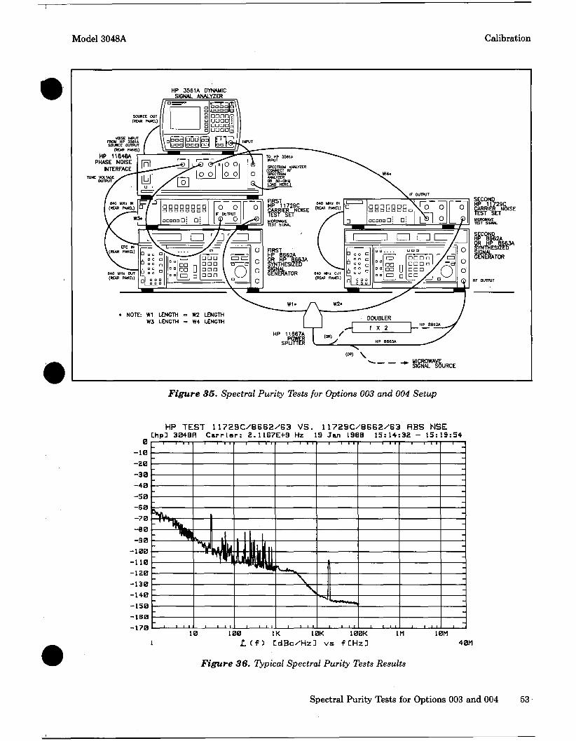
Model 3048A Calibration
HP 3561A DYNAMIC SIGNAL ANALYZER
HP 1184BA PHASE NOISE
INTERFACE
W1 LENGTH W3 LENGTH
v _ » . MICROWAVE SIGNAL SOURCE
Figure 35. Spectral Purity Tests for Options 003 and 004 Setup
0 -10 -20 -30 -40 -50 -60 -70 -80 -90
-100 -110 -120 -130 -140 -150 -160 -170
HP TEST 1 1 7 2 9 C / B 6 6 2 / 6 3 V S . 1 1 7 2 9 C / 8 S 6 2 / 6 3 LhpD 3048R C a r r i e r : 2.1167E+9 Hz 19 Jan 1988 15:14
-----
Nw, - X. - ^s ------
■ 1 1 1
< ^ Nyl
,1 .ilUu
A. tt
i 1, lli On
■hlLi' l IMim
i i i i
- ~ - - "n *
i I I I
VJU-U
\ \
■ I I I
■•si
■ I I I ■ I I I
HBS NSE 32 - 15:19:54
i I I I
---------------
■
1 10 100 IK 10K 100K 1M
£ C f ) C d B c / H z ] v s fCHz3 10M
40M
Figure 36. Typical Spectral Purity Tests Results
Spectral Purity Tests for Options 003 and 004 53
Calibration Model 3048A
NOTE
1. The on-screen connection diagram, while showing the general measurement technique, is incomplete. Also note that neither of the HP 8662As or HP 8663As nor the second HP 11729C in Figure 35 are under HP-IB control. 2. Either the first source, the second source, or an independent third source can be used to drive the power splitter. 3. The recommended input drive level to each of the two HP 11729Cs is +7 dBm; although, for the 1.28 and 3.20 GHz frequency band, 0 dBm is adequate. Thus, if an HP 11667A Power Splitter (with a nominal 6 dB loss) is used, the source driving the power splitter optimally should be set to 2116.7 MHz at +13 dBm, but a level as low as +6 dBm is adequate. 4. If the source driving the power splitter (such as the HP 8662A) requires a doubler, set the source's frequency to 1058.35 MHz and set its level as high as possible (+16 to +20 dBm) to generate at least 0 dBm at the output of the doubler. 5. The frequency of 2116.7 MHz was chosen to minimize the number of significant spurious signals.
/ 6. Other sources can be used to perform this test at higher frequencies. It is important to observe the power requirements stated above and to set the center bands of the HP 11729Cs to match the carrier frequency. For the spectral purity specifications at other frequencies, refer to the Specifications section of the Reference Manual.
Press the Proceed softkey. The measurement should proceed automatically. The measured noise should be similar to that shown in Figure 36 and should be within the limits given in the following table.
NOTE
// the beatndte frequency is too high, the System cannot tune the (EFC) source close enough to acquire phase lock. Various error messages on the display warn of this condition. You must then manually adjust either 640 MHz source (in the HP 8662As or HP 8663As) to bring the difference frequency of the sources within the loop's capture range. (For the HP 8662A and*HP 8663A, the adjustment is located on the rear panel and is labeled ?FINE FREQUENCY ADJUST".;
7/ this test fails, perform the HP 8662A or HP 8663A 640 MHz Spectral • Purity Test in Appendix B.
• • v ^ / '
^ J <
Offset Frequency
(Hz)
1 10
100 1 000
10 000 100 000
Noise Level (dBc)
Actual Maximum
-44 -74 -94
-110 -130 -140
s
54 Spectral Purity Tests for Options 003 and 004
Model 3048A Calibration
Spectral Purity Tests for Options 005 and 006
DESCRIPTION Option 005 adds an HP 8642A Signal Generator Option 001 as a System reference source. Option 006 adds an HP 8642B Signal Generator Option 001 as a System reference source. (Option 001 in the HP 8642A or HP 8642B adds a high-stability timebase reference.) To test the spectral purity of these options, an absolute, phase-lock-loop, phase-noise measurement is made with the signal generator in the System vs. another signal generator of the same performance or better. The test is run only for a carrier of 640 MHz.
NOTE
The phase noise measurement result is the combined noise of both signal generators. If a second HP 8642A or HP 8642B Signal Generator is used, the specified noise level should be raised 3 dB. Then, if one or both generators do not meet the specification, a third generator must be measured vs. each of the other two generators to determine which generator is not within specification. This procedure is known as a three-oscillator comparison test.
EQUIPMENT Printer. These tests will run without the presence of a printer in the System's Configuration Table. It is recommended that the test be run with a printer.
Reference Signal Generator. The reference signal generator must have phase noise performance that equals or exceeds the specifications for the HP 8642A or HP 8642B under test. Possible reference sources include the 640 MHz reference from an HP 8662A Option 003 or HP 8663A Option 003 Synthesized Signal Generator or a second HP 8642A or HP 8642B Signal Generator (which need not have Option 001). None of the sources need to be in the System's Configuration Table, but one may be. Having the System's HP 8642A or HP 8642B in the table will put it under automatic control.
RF Spectrum Analyzer. The System collects data to 100 kHz offsets with the HP 3561A. Although the System has a specification at 200 kHz offsets, data taken at 100 kHz offsets is adequate and thus eliminates the need for an RF spectrum analyzer. However, any supported RF spectrum analyzer, such as the HP 3585A Spectrum Analyzer, can be used in this test. With an RF spectrum analyzer connected, data to 40 MHz offsets will be displayed.
PROCEDURE .V 1. Press the Define Msrmnt softkey. This softkey appears at the Main Software Level menu
2. Press the Test Files softkey.
3. Press the Next Page softkey until the file name "HP TEST HP 8642A/B vs HP 8662/63 640 MHZ REF" appears in the table of file names. Move the cursor until it encompasses the file name and press the Load File softkey. (This test file allows a reference HP 8642A or HP 8642B even though "HP 8662/63" is in the title.)
4. When the file has been loaded, press the DONE softkey.
Spectral Purity Tests for Options 005 and 006 55
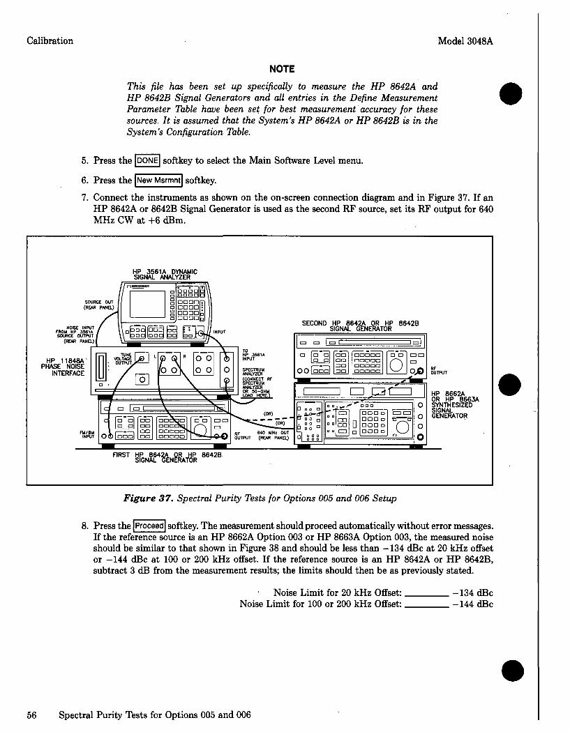
Calibration Model 3048A
NOTE
This file has been set up specifically to measure the HP 8642A and HP 8642B Signal Generators and all entries in the Define Measurement Parameter Table have been set for best measurement accuracy for these sources. It is assumed that the System's HP 8642A or HP 8642B is in the System's Configuration Table.
5. Press the DONE| softkey to select the Main Software Level menu.
6. Press the New Msrmnt softkey. 7. Connect the instruments as shown on the on-screen connection diagram and in Figure 37. If an
HP 8642A or 8642B Signal Generator is used as the second RF source, set its RF output for 640 MHz CW at +6 dBm.
HP 3561A DYNAMIC SIGNAL ANALYZER
NOISE INPUT FROM HP JS61A , SOURCE OUTPUT I
(REAR PANEL)!
SECOND HP 8642A OR HP 8642B SIGNAL GENERATOR
HP 11848A' PHASE NOISE
INTERFACE
FIRST HP 8642A OR HP 8642B SIGNAL GENERATOR
HP 8662A OR HP 8663A SYNTHESIZED SIGNAL GENERATOR
Figure 37. Spectral Purity Tests for Options 005 and 006 Setup
Press the | Proceed softkey. The measurement should proceed automatically without error messages. If the reference source is an HP 8662A Option 003 or HP 8663A Option 003, the measured noise should be similar to that shown in Figure 38 and should be less than -134 dBc at 20 kHz offset or -144 dBc at 100 or 200 kHz offset. If the reference source is an HP 8642A or HP 8642B, subtract 3 dB from the measurement results; the limits should then be as previously stated.
Noise Limit for 20 kHz Offset: Noise Limit for 100 or 200 kHz Offset:
-134 dBc -144 dBc
56 Spectral Purity Tests for Options 005 and 006
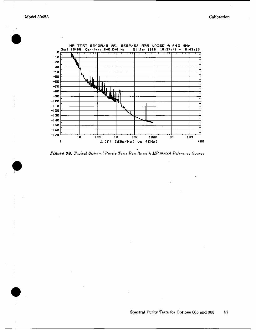
Model 3048A Calibration
e -10 -20 -30 -40 -50 -G0 - 7 0 -80 -90
-100 -1 10 -120 -130 -140 -150 -160 -170
HP TEST B G 4 2 R / B V S . ChpJ 304BH C a r r i e r : 640.E+6
\ . \
-------------— _ J 1 l—L. ■ 1 1-1- 1 1 1..J-
8 6 6 3 / 6 3 RBS NOISE ® Hz 21 Jan 1S8B 16:37 1 I I I
^" X, X, ^
1 1 1-1-
1 I I I
^ , *•*.
i i i i i_. . i i t
6 4 0 MHz 4G - 16:
1 I I I
1 1 1 1 ,
43: 10 i
---------------
« 10 100 IK 10K 100K
I t C-f) CdBc/Hz] vs i [Hz] 1M 10M
40M
Figure 38. Typical Spectral Purity Tests Results with HP 8662A Reference Source
Spectral Purity Tests for Options 005 and 006 57
Model 3048A Calibration
Appendix A: Block Diagram and System Troubleshooting
BLOCK DIAGRAM The foldout at the back of this manual is a block diagram of the HP 11848A Phase Noise Interface. When calibrating the System, the diagram helps to visualize what circuit functions are being tested. It is also very useful when running the HP 11848A Control feature which is required in several of the tests. The HP 11848A Control feature permits arbitrary control over all programmable circuits; the Block Diagram documents those circuits. For more information about the Block Diagram (such as theory of operation), refer to the HP 11848A Service Manual.
SYSTEM TROUBLESHOOTING The tests described in this manual can often assist in isolating System faults down to a System device. Some aspects of the main software tests as they apply to isolating faulty System devices are described in the following list.
NOTE
A Diagnostic program for troubleshooting specifically the HP 11848A Phase Noise Interface is supplied on a separate mass media disc. The Diagnostic program is independent of the main software, and it is usually more efficient to use the main software programs until they point to the Interface as the faulty System device. The Diagnostic program can then be loaded to troubleshoot the Interface itself. Refer to the HP 11848A Service Manual.
Calibrate System. A series of transfer function measurements are made on various signal paths in the Interface. The measurement data is stored as calibration factors which the controller uses (either directly or in more involved calculations) to correct the measured phase noise data whenever that signal path is used. Normally the Calibrate System program is invoked only for the annual System calibration or when the Interface has been repaired. Any difficulties encountered when the calibration program is being run may point to the Interface. For example, a catastrophic failure of a high-pass filter in the Interface will generate data that is too far out of limits to be accepted as a legitimate transfer function; the program will then abort the measurement. Performance Tests. To verify that the system meets its published specifications, a series of Performance Tests can be run. The failure of a test may contain enough clues to point to a failure in the Interface. Internal Adjustments. Often small out-of-specification results of the Performance Tests or Functional Checks can be corrected by means of adjustments, particularly if the condition is due to a dc offset voltage that is out of limits. Functional Checks. These tests are an extension of the Performance Tests that test the general operational integrity of the Interface itself. The test limits are generally loose. (The tests in the Diagnostic program are similar to the Functional Checks, but they attempt to diagnose the failure in addition to simply indicating out-of-limits data.)
HP 11848A Control. Arbitrary and complete control of the programmable functions of the Interface from the controller keyboard is provided by the HP 11848A Control program. A single display contains all the Interface state information. Because of the compactness of the state information, you should consult the HP 3048A Reference Manual when running the program. (The keyboard control feature of the Diagnostic program is similar to this program.)
Troubleshoot Mode. When the Troubleshoot Mode (a subset of Test Mode) is enabled, information beyond simple error messages can be invoked. For example, tests can be aborted to the HP 11848A Control mode which shows the Interface state when the abort occurred.
Appendix A: Block Diagram and System Troubleshooting A-l
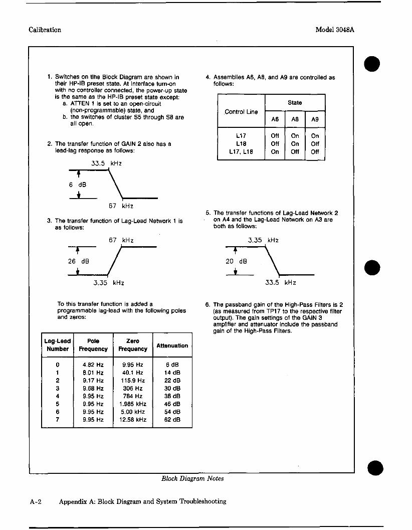
Calibration Model 3048A
1. Switches on tlhe Block Diagram are shown in their HP-IB preset state. At Interface turn-on with no controller connected, the power-up state is the same as the HP-IB preset state except:
a. ATTEN 1 is set to an open-circuit (non-programmable) state, and
b. the switches of cluster S5 through S8 are all open.
2. The transfer function of GAIN 2 also has a lead-lag response as follows:
33.5 kHz
6 dB
67 kHz
3. The transfer function of Lag-Lead Network 1 is as follows:
67 kHz
26 dB
3.35 kHz
To this transfer function is added a programmable lag-lead with the following poles and zeros:
Lag-Lead Number
0 1 2 3 4 5 6 7
Pole Frequency
4.82 Hz 8.01 Hz 9.17 Hz 9.68 Hz 9.95 Hz 9.95 Hz 9.95 Hz 9.95 Hz
Zero Frequency
9.95 Hz 40.1 Hz 115.9 Hz 306 Hz 784 Hz
1.985 kHz 5.00 kHz 12.58 kHz
Attenuation
6dB 14 dB 22 dB 30 dB 38 dB 46 dB 54 dB 62 dB
4. Assemblies A6, A8, and A9 are controlled as follows:
Control Line
L17 L18
L17, L18
State
A6
Off Off On
A8
On On Off
A9
On Off Off
5. The transfer functions of Lag-Lead Network 2 on A4 and the Lag-Lead Network on A3 are both as follows:
3.35 kHz
~7 20 dB
_ 4 33.5 kHz
The passband gain of the High-Pass Filters is 2 (as measured from TP17 to the respective filter output). The gain settings of the GAIN 3 amplifier and attenuator include the passband gain of the High-Pass Filters.
Block Diagram Notes
A-2 Appendix A: Block Diagram and System Troubleshooting
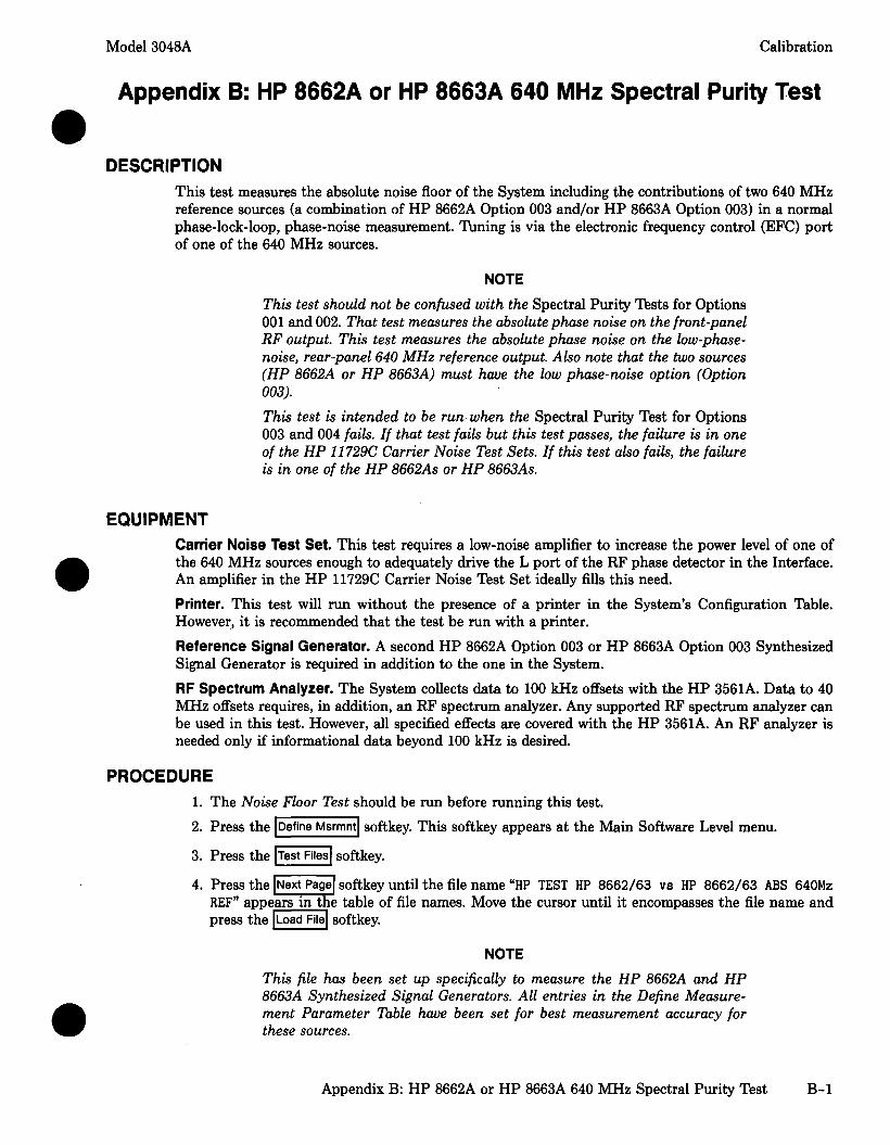
Model 3048A Calibration
Appendix B: HP 8662A or HP 8663A 640 MHz Spectral Purity Test
DESCRIPTION This test measures the absolute noise floor of the System including the contributions of two 640 MHz reference sources (a combination of HP 8662A Option 003 and/or HP 8663A Option 003) in a normal phase-lock-loop, phase-noise measurement. Tuning is via the electronic frequency control (EFC) port of one of the 640 MHz sources.
NOTE
This test should not be confused with the Spectral Purity Tests for Options 001 and 002. That test measures the absolute phase noise on the front-panel RF output. This test measures the absolute phase noise on the low-phase-noise, rear-panel 640 MHz reference output. Also note that the two sources (HP 8662A or HP 8663A) must have the low phase-noise option (Option 003). This test is intended to be run when the Spectral Purity Test for Options 003 and 004 fails. If that test fails but this test passes, the failure is in one of the HP 11729C Carrier Noise Test Sets. If this test also fails, the failure is in one of the HP 8662As or HP 8663As.
EQUIPMENT Carrier Noise Test Set. This test requires a low-noise amplifier to increase the power level of one of the 640 MHz sources enough to adequately drive the L port of the RF phase detector in the Interface. An amplifier in the HP 11729C Carrier Noise Test Set ideally fills this need. Printer. This test will run without the presence of a printer in the System's Configuration Table. However, it is recommended that the test be run with a printer. Reference Signal Generator. A second HP 8662A Option 003 or HP 8663A Option 003 Synthesized Signal Generator is required in addition to the one in the System. RF Spectrum Analyzer. The System collects data to 100 kHz offsets with the HP 3561A. Data to 40 MHz offsets requires, in addition, an RF spectrum analyzer. Any supported RF spectrum analyzer can be used in this test. However, all specified effects are covered with the HP 3561 A. An RF analyzer is needed only if informational data beyond 100 kHz is desired.
PROCEDURE 1. The Noise Floor Test should be run before running this test. 2. Press the Define Msrmnt softkey. This softkey appears at the Main Software Level menu.
3. Press the Test Files softkey.
4. Press the |Next Page| softkey until the file name "HP TEST HP 8662/63 vs HP 8662/63 ABS 640Mz REF" appears in the table of file names. Move the cursor until it encompasses the file name and press the Load File| softkey.
NOTE This file has been set up specifically to measure the HP 8662A and HP 8663A Synthesized Signal Generators. All entries in the Define Measurement Parameter Table have been set for best measurement accuracy for these sources.
Appendix B: HP 8662A or HP 8663A 640 MHz Spectral Purity Test B-l
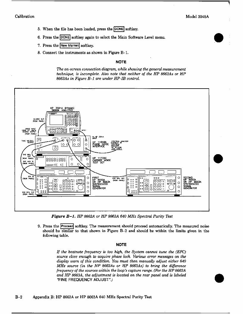
Calibration Model 3048A
5. When the file has been loaded, press the DONE softkey.
6. Press the DONE softkey again to select the Main Software Level menu.
softkey. 7. Press the New Msrmnt
8. Connect the instruments as shown in Figure B-l.
NOTE
The on-screen connection diagram, while showing the general measurement technique, is incomplete. Also note that neither of the HP 8662As or HP 8663As in Figure B-l are under HP-IB control.
HP 3561A DYNAMIC SIGNAL ANALYZER
SOURCE OUT (REAR PANEL)
NOISE INPUT FROM HP 3S61A SOURCE OUTPUT
(REAR PANEL)
SPECTRUM ANALYZER
FIRST 640 MHi OUT
OR H P 6 $ 6 M ° " ^ SYNTHESIZED SIGNAL GENERATOR
1 □ D 0 O . □ 0 Q D DO n
[a D a a □1 2 2 D u | o a a
: □ □ 1 a D
□ □ □ a a a
an DO D
D
o a o D'CID a 1
D D D a O D D a D D D □
b d
a
o o o o
SECOND HP 8662A OR HP 8663A SYNTHESIZED SIGNAL GENERATOR
Figure B-l. HP 8662A or HP 8663A 640 MHz Spectral Purity Test
9. Press the Proceed softkey. The measurement should proceed automatically. The measured noise should be similar to that shown in Figure B-2 and should be within the limits given in the following table.
NOTE
// the beatnote frequency is too high, the System cannot tune the (EFC) source close enough to acquire phase lock. Various error messages on the display warn of this condition. You must then manually adjust either 640 MHz source (in the HP 8662As or HP 8663As) to bring the difference frequency of the sources within the loop's capture range. (For the HP 8662A and HP 8663A, the adjustment is located on the rear panel and is labeled "FINE FREQUENCY ADJUST".)
B-2 Appendix B: HP 8662A or HP 8663A 640 MHz Spectral Purity Test
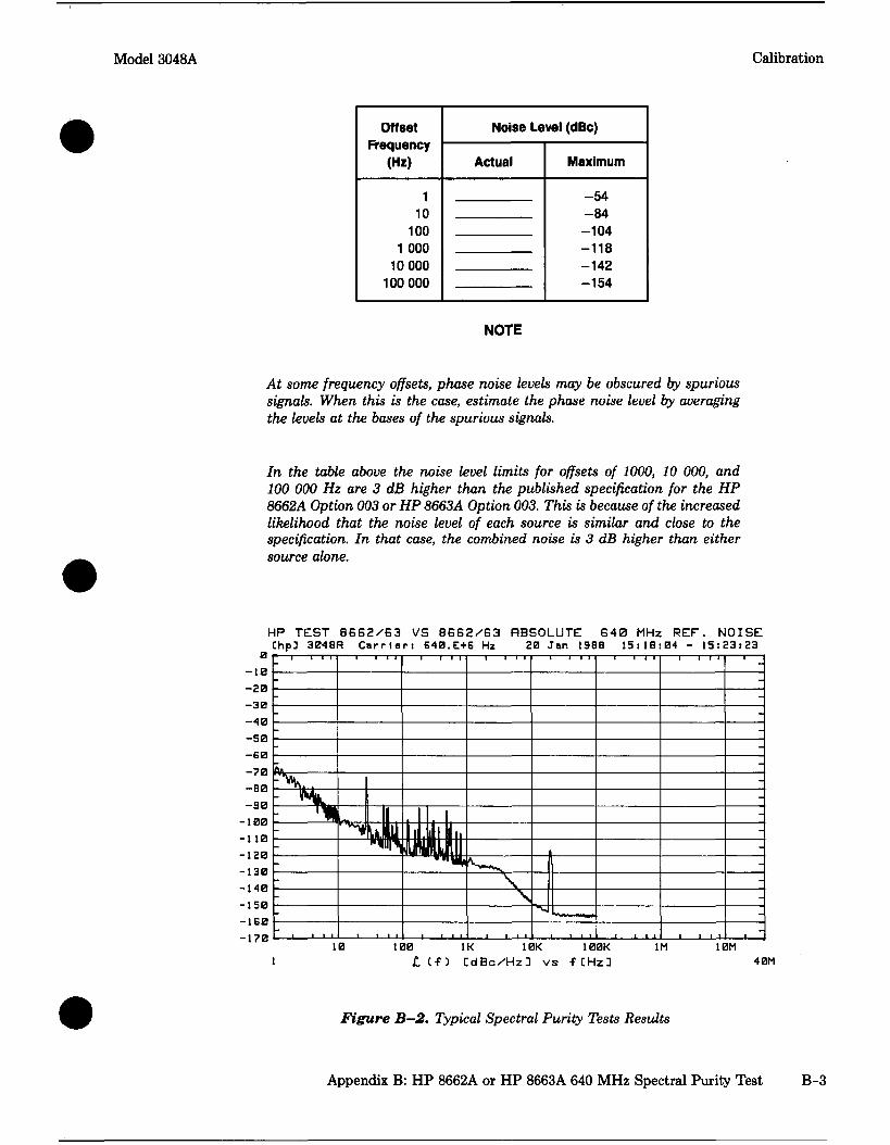
Model 3048A Calibration
Offset Frequency
(Hz)
1 10
100 1 000
10 000 100 000
Noise Level (dBc)
Actual Maximum
-54 -84 -104 -118 -142 -154
NOTE
At some frequency offsets, phase noise levels may be obscured by spurious signals. When this is the case, estimate the phase noise level by averaging the levels at the bases of the spurious signals.
In the table above the noise level limits for offsets of 1000, 10 000, and 100 000 Hz are 3 dB higher than the published specification for the HP 8662A Option 003 or HP 8663A Option 003. This is because of the increased likelihood that the noise level of each source is similar and close to the specification. In that case, the combined noise is 3 dB higher than either source alone.
HP TEST 8 6 6 2 / 6 3 VS 8 6 6 2 / 6 3 RBSOLUTE 6 4 0 MHz R E F . N O I S E Chp3 3048H C a r r i e r : E40.E+6 Hz 20 Jan 138B 15:1B:04 - 15:23:23
100 IK 10K 100K £ C-f) CdBo /HzD v s f lHz.1
1M 40M
Figure B-2. Typical Spectral Purity Tests Results
Appendix B: HP 8662A or HP 8663A 640 MHz Spectral Purity Test B-3
REGIONAL SALES AND SERVICE OFFICES
ASIA
Hewlett-Packard Asia Ltd. 47/F 26 Harbour Rd. Wanchai, HONG KONG G.P.O. Box 863 Hong Kong Tel: 5-8330833 Telex: 76793 HPA HX Cable: HPASIAL TD
CANADA
Hewlett-Packard (Canada) Ltd. 6877 Goreway Drive MISSISSAUGA, Ontario L4V 1M8 Tel: (416) 678-9430 Telex: 069-8644
EASTERN EUROPE
Hewlett Packard Ges. m.b.h. Liebigasse 1 P.O. Box 72 A-1222 VIENNA, Austria Tel: (222) 2500-0 Telex: 1 3 4425 HEPA A
NORTHERN EUROPE
Hewlett-Packard S.A. V.D. Hooplaan 241 P.O. Box 999 NL-118 LN 15 AMSTELVEEN The Netherlands Tel: 20 5479999 Telex: 18919 hpser
SOUTH EAST EUROPE
Hewlett-Packard S.A. World Trade Center 110 Avenue Louis-Casai 1215 Cointrin, GENEVA, Switzerland Tel: (022) 98 96 51 Telex: 27225 hpner Mail Address: P.O. Box CH-1217 Meyrin 1 GENEVA Switzerland
MIDDLE EAST AND CENTRAL AFRICA
Hewlett-Packard S.A. Middle East/Central Africa Sales H.Q. 7, rue du Bois-du-Lan P.O. Box 364 CH-1217 Meyrin 1 GENEVA Switzerland Tel: (022)83 12 12 Telex: 27835 hmea ch Telefax: (022)83 15 35
UNITED KINGDOM
Hewlett Packard Ltd. Nine Mile Ride WOKINGHAM Berkshire, RG113LL Tel: 0344 773100 Telex: 848805/848814/848912
UNITED STATES OF AMERICA
Customer Information Center Tel: (800) 752-0900 6:00 AM to 5:00 PM Pacific Time
EASTERN USA
Hewlett-Packard Co. 4 Choke Cherry Road ROCKVILLE, MD 20850 Tel: (301) 948-6370
MIDWESTERN USA
Hewlett-Packard Co. 5201 Tollview Drive ROLLING MEADOWS, IL 60008 Tel: (312)255-9800
SOUTHERN USA
Hewlett-Packard Co. 2000 South Park Place ATLANTA, GA 30339 Tel: (404) 955-1500
WESTERN USA
Hewlett-Packard Co. 5161 Lankershim Blvd. NORTH HOLLYWOOD, CA 91601 Tel: (818) 505-5600
OTHER INTERNATIONAL AREAS
Hewlett-Packard Co. Intercontinental Headquarters 3495 Deer Creek Road PALO ALTO, CA 94304 Tel: (415) 857-1501 Telex: 034-8300 Cable: HEWPACK
Residual Phase Noise and AM Noise
Measurement Techniques
11 HEWLETT® PACKARD
Printed in USA
© Copyright; '1990 Hewlett-Packard Company. All rights reserved
Residual Phase Noise and AM Noise
Measurement Techniques
E l HEWLETT "um PACKARD
HP Part No. 03048-90059 Printed in USA November 1994
Edition A.0.0
Notice
The information contained in this document is subject to change without notice. Hewlett-Packard makes no warranty of any kind with regard to this material, including but not limited to, the implied warranties of merchantability and fitness for a particular purpose. Hewlett-Packard shall not be liable for errors contained herein or for incidental or consequential damages in connection with the furnishing, performance, or use of this material.
©Copyright Hewlett-Packard Company 1994
All Rights Reserved. Reproduction, adaptation, or translation without prior written permission is prohibited, except as allowed under the copyright laws. 1400 Fountaingrove Parkway, Santa Rosa, CA 95403-1799, USA
Certification Hewlett-Packard Company certifies that this product met its published specifications at the time of shipment from the factory. Hewlett-Packard further certifies that its calibration measurements are traceable to the United States National Institute of Standards and Technology, to the extent allowed by the Institute's calibration facility, and to the calibration facilities of other International Standards Organization members.
Warranty This Hewlett-Packard instrument product is warranted against defects in material and workmanship for a period of one year from date of shipment. During the warranty period, Hewlett-Packard Company will, at its option, either repair or replace products which prove to be defective. For warranty service or repair, this product must be returned to a service facility designated by Hewlett-Packard. Buyer shall prepay shipping charges to Hewlett-Packard and Hewlett-Packard shall pay shipping charges to return the product to Buyer. However, Buyer shall pay all shipping charges, duties, and taxes for products returned to Hewlett-Packard from another country. y
Hewlett-Packard warrants that its software and firmware designated by Hewlett-Packard for use with an instrument will execute its programming instructions when properly installed on that instrument. Hewlett-Packard does not warrant that the operation of the instrument, or software, or firmware will be uninterrupted or error-free. LIMITATION OF W A R R A N T Y
The foregoing warranty shall not apply to defects resulting from improper or inadequate maintenance by Buyer, Buyer-supplied software or interfacing, unauthorized modification or misuse, operation outside of the environmental specifications for the product, or improper site preparation or maintenance. NO OTHER WARRANTY IS EXPRESSED OR IMPLIED. HEWLETT-PACKARD SPECIFICALLY DISCLAIMS THE IMPLIED WARRANTIES OF MERCHANTABILITY AND FITNESS FOR A PARTICULAR PURPOSE.
EXCLUSIVE REMEDIES
THE REMEDIES PROVIDED HEREIN ARE BUYER'S SOLE AND EXCLUSIVE REMEDIES. HEWLETT-PACKARD SHALL NOT BE LIABLE FOR ANY DIRECT, INDIRECT, SPECIAL, INCIDENTAL, OR CONSEQUENTIAL DAMAGES, WHETHER BASED ON CONTRACT, TORT, OR ANY OTHER LEGAL THEORY.
Assistance Product maintenance agreements and. other customer assistance agreements are available for Hewlett-Packard products. For any assistance, contact your nearest Hewlett-Packard. Sales and Service Office.
Safety Symbols The following safety symbols are used throughout this manual. Familiarize yourself with each of the symbols and its meaning before operating this instrument.
CAUTION The CAUTION sign denotes a hazard. It, calls attention to a procedure which, if not, correctly performed or adhered to, could result in damage to or destruction of the product or the user's work. Do not proceed beyond a CAUTION sign until the indicated conditions are fully understood and met.
WARNING The WARNING sign denotes a hazard. It calls attention to a procedure which, if not correctly performed or adhered to, could result in injury to the user. Do not proceed beyond a WARNING sign until the indicated conditions are fully understood and met.
DANGER The DANGER sign denotes an imminent hazard to people. It warns the reader of a procedure which, if not correctly performed or adhered to, could result in injury or loss of life. Do not proceed beyond a, DANGER sign until the indicated conditions are fully understood and met.
iv
General Safety Considerations WARNING ■ These servicing instructions are for use by qualified personnel only. To
avoid electrical shock, do not perform any servicing unless you are qualified to do so.
■ The opening of covers or removal of parts is likely to expose dangerous voltages. Disconnect the instrument from all voltage sources while it is being opened.
■ The power cord is connected to internal capacitors that may remain live for five seconds after disconnecting the plug from its power supply.
■ This is a Safety Class 1 Product (provided with a protective earthing ground incorporated in the power cord). The mains plug shall only be inserted in a socket outlet provided with a protective earth contact. Any interruption of the protective conductor inside or outside of the instrument is likely to make the instrument dangerous. Intentional interruption is prohibited.
■ For continued protection against fire hazard, replace fuse only with same type and ratings, (type nA/nV). The use of other fuses or materials is prohibited.
WARNING ■ Before this instrument is switched on, make sure it has been properly grounded through the protective conductor of the ac power cable to a socket outlet provided with protective earth contact. Any interruption of the protective (grounding) conductor, inside or outside the instrument, or disconnection of the protective earth terminal can result in personal injury.
■ Before this instrument is switched on, make sure its primary power circuitry has been adapted to the voltage of the ac power source. Failure to set the ac power input to the correct voltage could cause damage to the instrument when the ac power cable is plugged in.
Acknowledgements This manual is based on the technical paper "Residual Phase Noise and AM Noise Measurement Techniques" by Thomas R. Faulkner and Robert E. Temple.
VI
Contents
1. General Information What is residual two-port noise? 1-1 Why are residual and AM noise measurements important? 1-2 HP 3048A Description 1-3
2. Residual Phase Noise Measurement Basic Phase Noise Measurement Theory 2-1
Region of Validity of £(f) = S^(f)/2 2-2 Conversion Between S^(f) and S(y(f) 2-3
Residual Phase Noise Measurement: Basic Assumptions 2-5 Steps for Making Residual Phase Noise Measurements 2-6 Choosing a Calibration Method 2-7
Method 1: User entry of phase detector constant 2-7 Method 2: Measured + / - d c peak voltage 2-8 Method 3: Measured Beatnote 2-9 Method 4: Double-Sided Spur 2-10 Method 5: Single-Sided Spur 2-11
Calibration and Measurement General Guidelines 2-12 Calibration and Measurement Procedures 2-14
Method 1: User entry of phase detector constant 2-14 Method 2: Measured +/- DC Peak Voltage 2-17 Method 3: Measured Beatnote Method > 2-18 Method 4: Double-sided Spur 2-21 Method 5: Single-Sided Spur Method 2-24
Residual Phase Noise Measurement Examples 2-27 System Noise Floor Measurement 2-27
Initial Setup 2-27 Conditions 2-28 Results ; 2-28
Amplifier Noise and Dynamic Noise Figure Measurement 2-30 Initial Setup 2-30 Conditions 2-31 Results 2-31
Measurement of a Device with Large Time Delay (r) 2-33 Initial Setup 2-33 Conditions 2-34 Results 2-35
Measurement of a Crystal Resonator 2-37 Initial Setup 2-37 Conditions 2-37
Measuring the Noise Floor of the Test Setup 2-38 Measuring the Crystal Resonator 2-38
Results of the Setup Noise Floor Measurement 2-39 Results of the Crystal Resonator Measurement 2-39
Measurement of a Low-Noise Phase Modulator ; 2-42
Contents 1
Initial Setup 2-42 Conditions 2-42 Results 2-43
Residual Noise of a Frequency Synthesizer 2-44 Initial Setup 2-45 Conditions 2-46 Results 2-46
Residual Noise of a Comb Generator Multiplier 2-48 Initial Setup 2-48 Conditions 2-49 Results 2-49
Measurement of a Device Using an External Phase Detector 2-51 Initial Setup 2-51 Conditions 2-51 Results 2-52
3. AM-Source Noise Measurement AM-Noise Measurement Theory of Operation 3-1
Basic Noise Measurement 3-1 Phase Noise Measurement 3-1 Amplitude Noise Measurement 3-2
AM Noise Measurement System Block Diagram 3-2 AM Detector 3-3
AM Detector Specifications 3-3 AM Detector Considerations 3-3
Steps for Making AM Noise Measurements ■ 3-4 Choosing a Calibration Method 3-6
Method 1: User entry of phase detector constant 3-6 Method 1, Example 1 3-6
Method 1, Example 2 3-6 Method 2: Double Sided Spur 3-7
Method 2, Example 1 3-7 Method 2, Example 2 3-7
Method 3: Single-Sided-Spur Method 3-7 Calibration and Measurement General Guidelines 3-8 Calibration and Measurement Procedures 3-9
Method 1: User Entry of Phase Detector Constant 3-9 Method 1, example 1 3-9
Method 1, Example 2 3-11 Method 2: Double-Sided Spur Method 3-12
Method 2, Example 1 3-12 Method 2, Example 2 3-13
Method 3: Single-Sided-Spur Method 3-15 Examples of AM Noise Measurements 3-17
Measurement of a Source with AM 3-17 Initial Setup 3-17 Conditions 3-18 Results . 3-18
Measurement Of A Source Without, AM 3-20 Initial Setup 3-20 Conditions 3-20 Results 3-21
Measurement of a Microwave Source without AM Modulation 3-23 Initial Setup ., 3-23 Conditions 3-24
Contents-2
Results 3-24
4. Baseband Noise Measurements Measurement Considerations 4-1 Steps for Making Baseband Noise Measurements 4-1
A. Calculation of Source Noise Attenuation
Source Noise Attenuation versus Carrier Offset and Time Delay A-l
B. Noise Figure Versus Dynamic Noise Figure
C. Single-Sided Spur
D. Carrier-to-Sideband Modulation Equations AM Carrier-to-Modulation Sideband Ratio D :l
Example D-l M Carrier-to-Modulation Sideband Ratio D-l
Example D-l FM Carrier-to-Modulation Sideband Ratio D-2
Example D-2 E. Common Equipment Used in RF Noise Measurements
Sources E-l Spectrum Analyzers E-J Modulation Analyzers E-2 Power Meters E-2 Diode Detectors E-2 AM Detector E-2 DC Block E-2 Attenuators E-3 Amplifiers E-3 Phase Shifters E-3 0° Power Splitters E-4 Couplers E-4 Instrument Suppliers E-4
F. Components of the Phase Noise Accessory Kits Components for Residual Measurements F-l Miscellaneous Components F-3 Cables F-3 Adapters F-4 Case Layout F-5
G. HP 3048A Options KOl, K02, K21, K22, and K23 Specifications HP 70428A Option KOl Tune Volt Supply G-l HP 70427A Option K02 Balun G-l HP 3048A Option K21 AM Detector Filter G-2 HP 3048A Option K22 AM Dual RF Amplifier G-3 HP 3048A Option K23 AM DC Blocking Filter G-4
Contents-3
Figures 1-1. Additive Noise Components 1-1 1-2. Multiplicative Noise Components 1-2 1-3. HP 3048A Block Diagram 1-4 2-1. Double-Balanced Mixer Used as a Phase Detector 2-1 2-2. Region of Validity of £(f) = S^(f)/2 2-3 2-3. S?i(f)/2: 1/2 Spectral Density of Phase Fluctuation 2-4 2-4. S„(f): Spectral Density of Phase Fluctuation 2-4 2-5 2-5 2-6 2-5 2-7. Measuring Power at Phase Detector R Port 2-14 2-8. Phase Detector Sensitivity 2-15 2-9. Measuring Power at Phase Detector L Port 2-16
2-10. Connection to Optional Oscilloscope for Determining Voltage Peaks 2-17 2-11. Measuring Power from Splitter 2-18 2-12. Calibration Source Beatnote Injection 2-20 2-13. Double-Sided Spur Calibration Setup 2-21 2-14. Measuring Carrier-to-sideband Ratio of the Modulated Port 2:22 2-15. Measuring Carrier-to-sideband Ratio of the Non-modulated Port 2-23 2-16. Single-Sided Spur Calibration Setup 2-24 2-17. Carrier-to-sideband Ratio of the Modulated Signal 2-25 2-18. Carrier-to-spur Ratio of the Non-modulated Signal 2-25 2-19. User Entry of Phase Detector Constant Calibration Setup 2-27 2-20. User Entry of Phase Detector Constant Measurement Setup 2-27 2-21. System Noise Floor Results Graph 2-29 2-22. Dynamic Noise Figure Measurement, Setup 2-30 2-23. Dynamic Noise Figure Results Graph 2-32 2-24. Time Delay Measurement Setup 2-33 2-25. Graph of Source Decorrelation 2-34 2-26. Time Delay Results Graph 2-36 2-27. Crystal Measurement Setup 2-37 2-28. Noise-Floor Measurement, Test, Setup 2-38 2-29. Noise Floor Measurement Results 2-40 2-30. Noise Floor Measurement Results 2-41 2-31. Low Noise Phase Modulator Measurement, Setup 2-42 2-32. Phase Modulator Noise HP 8640B Source 2-44 2-33. Frequency Synthesizer Measurement Setup 2-45 2-34. Residua] Noise: Two HP 8663A Synthesizers 2-47 2-35. Residual Noise of Step-Recovery Diode Setup 2-48 2-36. Residual Noise: Step Recovery Diode 2-50 2-37. External Phase Detector Setup 2-51 2-38. HP 3325A Fractional Divider/Phase Detector Measurement Results 2-53
3-1. System Block Diagram 3-2 3-2. AM Detector Schematic 3-3 3-3. AM Noise Measurement Setup 3-9 3-4. AM Noise Calibration Setup 3-9 3-5. AM Detector Sensitivity Graph 3-10
Contents-4
3-6. AM Noise Measurement Setup 3-11 3-7. Modulation Sideband Calibration Setup . 3-11 3-8. AM Noise Measurement Setup 3-12 3-9. Measuring the Carrier-to-Sideband Ratio 3-12
3-10. Measuring the Calibration Constant 3-13 3-11. AM Noise Measurement Setup 3-13 3-12. Measuring Power at the AM Detector 3-13 3-13. Measuring Carrier-to-Sideband Ratio 3-14 3-14. Measuring the Calibration Constant 3-14 3-15. AM Noise Measurement Setup Using Single-Sided-Spur 3-15 3-16. Measuring Relative Spur Level 3-15 3-17. Measuring Detector Sensitivity 3-15 3-18. AM Noise Measurement Setup for a Source with AM 3-17 3-19. AM Modulation Measurement Results 3-19 3-20. Source Without AM Measurement Setup 3-20 3-21. Source Without AM Modulation Measurement Results 3-22 3-22. Microwave Source Without AM Setup 3-23 3-23. Microwave Source Without AM Measurement Results 3-25
4-1. Baseband Noise Measurement Block Diagram 4-1 4-2. S,,(dBv/Hz) versus f (Hz) 4-2 F-1. Single-Sided Spur Calibration Setup for Residual Measurement F-1 F-2. Single-sided Spur Calibration Setup for AM Noise Measurement F-2 F-3. HP 11826A/B/C Small Case Layout F-5 F-4. HP 11826A/B/C Large Case Layout F-6
Contents-5
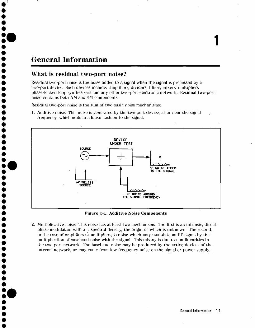
1 General Information
What is residual two-port noise? Residual two-port noise is the noise added to a signal when the signal is processed by a two-port device. Such devices include: amplifiers, dividers, filters, mixers, multipliers, phase-locked loop synthesizers and any other two-port electronic network. Residual two-port noise contains both AM and $M components.
Residual two-port noise is the sum of two basic noise mechanisms: 1. Additive noise: This noise is generated by the two-port device, at or near the signal
frequency, which adds in a linear fashion to the signal.
DEVICE UNDER TEST
SOURCE: <s> + NOISELESS
SOURCE L, RF NOISE ADDED TO THE SIGNAL
RF NOISE AROUND THE SIGNAL FREQUENCY
Figure 1-1. Additive Noise Components
Multiplicative noise: This noise has at least two mechanisms. The first is an intrinsic, direct, phase modulation with a j spectral density, the origin of which is unknown. The second, in the case of amplifiers or multipliers, is noise which may modulate an RF signal by the multiplication of baseband noise with the signal. This mixing is due to non-linearities in the two-port network. The baseband noise may be produced by the active devices of the internal network, or may come from low-frequency noise on the signal or power supply.
General Information 1-1
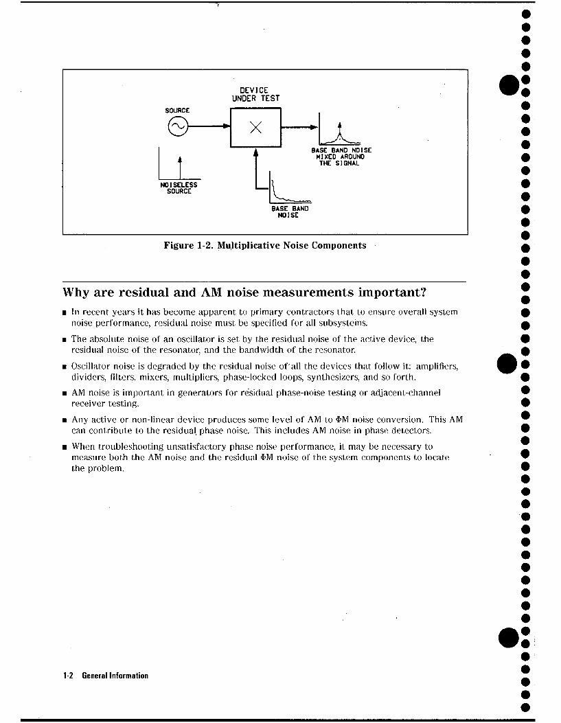
SOUF
(5 i
ICE
y
i
NOISELESS SOURCE
DEVICE UNDER TEST
X
1, V BASE BAND NOISE
-JK— BASE BAND NOISE MIXED AROUND THE SIGNAL
Figure 1-2. Multiplicative Noise Components
Why are residual and AM noise measurements important? ■ In recent years it has become apparent to primary contractors that to ensure overall system
noise performance, residual noise must be specified for all subsystems. ■ The absolute noise of an oscillator is set by the residual noise of the active device, the
residual noise of the resonator, and the bandwidth of the resonator. ■ Oscillator noise is degraded by the residual noise of all the devices that follow it: amplifiers,
dividers, filters, mixers, multipliers, phase-locked loops, synthesizers, and so forth. ■ AM noise is important in generators for residual phase-noise testing or adjacent-channel
receiver testing. ■ Any active or non-linear device produces some level of AM to $M noise conversion. This AM
can contribute to the residual phase noise. This includes AM noise in phase detectors. ■ When troubleshooting unsatisfactory phase noise performance, it, may be necessary to
measure both the AM noise and the residual 4>M noise of the system components to locate the problem.
1-2 General Information
HP 3048A Description The HP 3048A provides you standard process for measuring phase noise. It allows you to measure sources of many types with a flexible system configuration.
The HP 3048A Phase Noise Measurement System includes the following instruments and accessories.
■ The HP 11848A Phase Noise Interface, an interface box specifically designed for high performance phase noise measurements. The HP 11848A supports several measurement techniques for phase noise and AM noise measurement. Built into the interface are phase detectors, amplifiers, filters, and switches necessary to measure phase noise over a frequency range of 5 MHz to 18 GHz. An input for an external phase detector outside the above mentioned frequency range is also provided. Internal sources are provided to allow the system to functionally check all of its signal handling circuits ensuring proper operation prior to making a measurement.
■ The HP 3561A Dynamic Signal Analyzer, a Fast Fourier Transform analyzer of a wide frequency range (125 /<Hz to 100 kHz). The HP 3561A has built-in data averaging capabilities, large dynamic range, and fast measurement speed which make it ideal for quantifying demodulated phase noise (noise voltages).
■ Measurement software, a program that includes all drivers necessary to run both standard and optional instruments of the HP 3048A system.
■ Operator's Training, a training course that explains all of the operating modes and measurement techniques of the HP 3048A, when each technique is appropriate, and how to analyze the measured data.
General Information 1-3
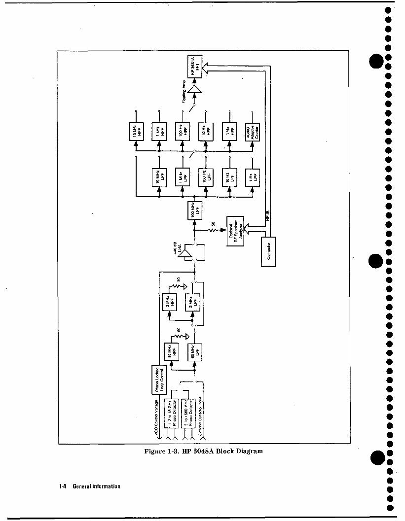
Figure 1-3. HP 3048A Block Diagram
1-4 General Information
2 Residual Phase Noise Measurement Basic Phase Noise Measurement Theory Phase noise can be measured by demodulating the RF signal and analyzing it at baseband.
Doubly balanced mixer used as phase detector
V, Sin [27rfot+0(t)] >-
V. Sin [2xf t+90°] >■
Low Pass Filter
M x 0(t)=V„(t) If [0(t)]<.2 rad
s -M>
jt(U=^l=Ml b e c a u s e 10(t) I < .2rad 2 2K20
1. Demodulate RF signal and analyze at baseband 2. Measure spectral density of noise fluctuation 3. Calculate phase noise
Figure 2-1. Double-Balanced Mixer Used as a Phase Detector
Residual Phase Noise Measurement 2-1
A double-balanced mixer is used as a phase detector to demodulate the RF signal for baseband analysis. When operated as a phase detector, two signals are input to the double-balanced mixer at the same frequency. The phase difference between the signals is adjusted to 90° (quadrature) to minimize the detector's sensitivity to AM fluctuations, and to maximize its sensitivity to phase fluctuations. Any phase fluctuations not common to both signals (for example, <p(t)) result in a voltage fluctuation proportional to the phase difference, provided the phase fluctuations are less than approximately 0.2 radians. This voltage output ;;„(t) is equal to the difference in phase fluctuations multiplied by the phase detector gain of the mixer, KJ,, in volts per radian. The spectral density of the phase fluctuations, S^Cf), is calculated by measuring the spectral density of voltage fluctuations, S„(f) with a baseband spectrum analyzer. S„(f) is then divided by the square of the phase detector constant (squared because of the power relationship of spectral density) which results in S^(f).
The single-sided phase noise £(f), can then be calculated from the spectral density of phase fluctuation SJ,(I"), (or frequency fluctuation, S;,(f) = f-xS^(f)) provided that, the mean square phase fluctuations, <j>-(t), are small relative to 1 radian.
Region of Validity of £(f) = S^(f)/2
Because of the small-angle criterion, caution must be exercised when £(f") is calculated from the spectral density of the phase fluctuations. This plot (figure 2-2) of £(f) resulting from the phase noise of a free-running VCO illustrates the erroneous results that, can occur if the instantaneous phase modulation exceeds a small angle. Approaching the carrier, £(f) is obviously increasingly in error as it reaches a relative level of +45 dBc/Hz at a I Hz offset (45 dB more power at a 1 Hz offset, in a 1 Hz bandwidth, than the total power in the signal). The -10 dB/decade line is drawn on the plot for an instantaneous phase deviation of 0.2 radians integrated over one decade of offset frequency. At approximately 0.2 radians the power in the higher-order sidebands of the phase modulation is still insignificant compared to the power in the first-order sideband, thus ensuring the validity of the calculation of £(f). Below the line, the plot of £(f) is correct; above the line, £(f) becomes increasingly invalid and S^(f) must be used to represent the phase noise of the signal.
2-2 Residual Phase Noise Measurement
866-4B, EXT FM OFF, 864 QB .4 aVERt*SE5 CRRRIER FRE->t? rgBE^Hz
7 REF, 3dO KHZ PK DEV Fll t r i p ] RPR 4 1 3 . 4 f l / 14:8?
1Hz L i f t CdBc H z ] v i i C H z ] 4 0MH
Figure 2-2. Region of Validity of £(f) = S^(f)/2
Conversion Between S^f) and S;/(f) Other than S^(f), the instability of a signal may also be represented with a plot of the spectral density of frequency fluctuations, Sj/(f). As illustrated below S„(f) is equal to fxS.y/f) because ;/(t) is the derivative of <?i(t). These two graphs are from the same data with figure 2-3 a square root of S„(f). The graph of the square root of S/,(f) indicates the power spectral density of the frequency modulation (FM) noise on the signal. Such a measurement of the spectral density of the FM noise versus the offset from the carrier is be very useful in the design of an FM system.
Residual Phase Noise Measurement 2-3
CONVERSION BETWEEN S»(f) AND Sv( f )
- 1 5 0
-l"50
• ro StipL'ir'3t»"t>UT">
i ' ■ ■' 1—1 i l l i i ■ 11 i i_
l O H l t i n CdBc'Hrj vs fCH:}
' " I L. ion
4QNHz
Figure 2-3. S j,(f)/2: 1/2 Spectral Density of Phase Fluctuation
36~^ VS 8350. 83525H
c-oe
c*oe
t-Ji
^ V > i
c»ee
t-«3
' i ■ i i i
P0T31RE NOJSC n.OC*» L t n l T 18 TO 4a : M ;
' ' I ■ i i t i i i i I.I i
I O H I
lee ik ie< IPOK IM SOPT CSv(f) (Hz-2 H i ] ) VS <CHr]
I I I I L. 10M
«OMHx
Figure 2-4. S;,(f): Spectral Density of Phase Fluctuation
2-4 Residual Phase Noise Measurement
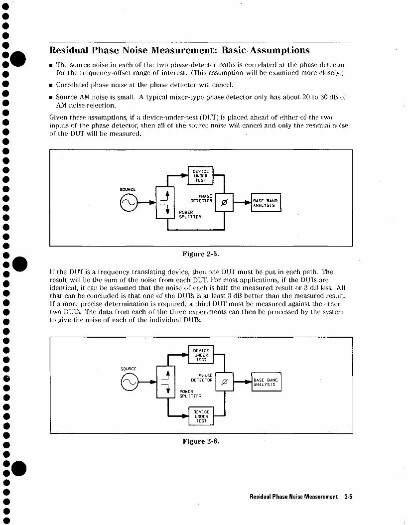
Residual Phase Noise Measurement: Basic Assumptions ■ The source noise in each of the two phase-detector paths is correlated at the phase detector
for the frequency-offset range of interest. (This assumption will be examined more closely.)
■ Correlated phase noise at the phase detector will cancel.
■ Source AM noise is small. A typical mixer-type phase detector only has about 20 to 30 dB of AM noise rejection.
Given these assumptions, if a device-under-test (DUT) is placed ahead of either of the two inputs of the phase detector, then all of the source noise will cancel and only the residual noise of the DUT will be measured.
SOURCE r
j
i
— * ■ DEVICE UNDER TEST
PHASE DETECTOR
POWER SPLITTER
"1 1 0 BASE BAND
ANALYSIS
Figure 2-5.
If the DUT is a frequency translating device, then one DUT must be put in each path. The result will be the sum of the noise from each DUT. For most applications, if the DUTs are identical, it can be assumed that the noise of each is half the measured result or 3 dB less. All that can be concluded is that one of the DUTs is at least 3 dB better than the measured result. If a more precise determination is required, a third DUT must be measured against the other two DUTs. The data from each of the three experiments can then be processed by the system to give the noise of each of the individual DUTs.
SOURCE r* ■
j
DEVICE UNDER TEST
PHASE DETECTOR
POWER SPLITTER
DEVICE UNDER TEST
0 BASE BAND ANALYSIS
Figure 2-6.
Residual Phase Noise Measurement 2-5
Steps for Making Residual Phase Noise Measurements ■ Connect the system hardware and load/run the software. ■ Measure the system calibration data. The system calibration data is the correction data for
all the signal paths in the interface box.
■ Main Menu—Select the type of measurement to be made. All residual phase noise measurements will be "PHASE NOISE MEASUREMENT WITHOUT VOLTAGE CONTROL."
■ Establish parameters.
1. Source parameters '
a. Enter phase detector input frequency
b. Enter carrier frequency c. Select internal or external phase detector (mixer)
d. Select calibration option
2. Measurement parameters
a. Enter start and stop frequencies for the measurement data □ HP 3048A without RF analyzer: 0.01 Hz to 100 kHz
D HP 3048A with RF analyzer: 0.01 Hz to 40 MHz
b. Enter number of sweeps averaged on FFT analyzer 3. Plot parameters
a. Select graph type (usually "SINGLE SIDEBAND PHASE NOISE") b. Select plotter type (if any) c. Enter minimum and maximum Y-axis values (dBc) d. Enter minimum and maximum X-axis values (Hz) e. Enter a title
■ Make measurement. 1. Connect the DUT and external hardware 2. Measure calibration data by selected option 3. Measure noise data
■ Interpret, the measurement results.
2-6 Residual Phase Noise Measurement
Choosing a Calibration Method
Method 1: User entry of phase detector constant This calibration option requires that you know the phase detector constant for the specific measurement to be made. The phase detector constant can be estimated from the source power levels or it can be determined using one of the other calibration methods.
Once determined, the phase detector constant can be entered directly into the system software without going through a calibration sequence. Remember, however, that the phase detector constant is unique to a particular set of sources, the RF level into the phase detector, and the test configuration. s
Advantages Easy method of calibrating the measurement system. Requires little additional equipment, only an RF power meter to manually measure the drive levels into the phase detector. Fastest method of calibration. If the same power levels are always at the phase detector (as in the case of leveled outputs) the phase detector sensitivity will always be essentially the same (within 1 or 2 dB). If this accuracy is adequate, it is not necessary to recalibrate. Only one RF source is required. Quick method of estimating the phase detector constant and noise floor to verify other calibration methods and check available dynamic range.
Disadvantages Least accurate of the calibration methods. Does not take into account, the amount, of power at harmonics of the signal. Does not take into account the power which may be generated by spurious oscillations, causing the power meter to measure more power than is at the distinct phase-detector frequency.
Residual Phase Noise Measurement 2-7
Method 2: Measured + / - dc peak voltage This technique requires you to adjust off of quadrature to both the positive and the negative peak output of the Phase Detector. This is done by either adjusting the phase shifter or the frequency of the source. An oscilloscope or voltmeter is optional for setting the positive and negative peaks.
Advantages Easy method of calibrating the measurement system.
This calibration technique can be performed using the HP 3561A.
Fastest method of calibration. If, for example, the same power levels are always at the phase detector, as in the case of leveled or limited outputs, the phase detector sensitivity will always be essentially equivalent (within 1 or 2 dB). Recalibration becomes unnecessary if this accuracy is adequate.
Only one RF source is required. Measures the phase detector gain in the actual measurement configuration.
Disadvantages Has only moderate accuracy compared to the other calibration methods. Does not take into account the amount, of phase detector harmonic distortion relative to the measured phase detector gain, therefore, the phase detector must operate in its linear region.
Requires manual adjustments to the source and/or phase shifter to find the phase detector's positive and negative output peaks. The system will read the value of the positive and negative peak and automatically calculate the mean of the peak voltages which is the the phase detector constant used by the system.
2-8 Residual Phase Noise Measurement
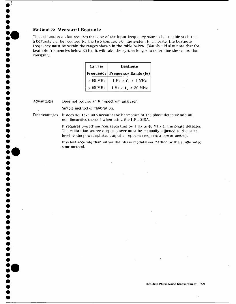
Method 3: Measured Beatnote This calibration option requires that one of the input frequency sources be tunable such that a beatnote can be acquired for the two sources. For the system to calibrate, the beatnote frequency must be within the ranges shown in the table below. (You should also note that for beatnote frequencies below 20 Hz, it will take the system longer to determine the calibration constant.)
Carrier
Frequency Beatnote
Frequency Range (fe)
< 95 MHz
> 95 MHz
1 Hz < fB < 1 MHz
1 Hz < fB < 20 MHz
Advantages Does not require an RF spectrum analyzer. Simple method of calibration.
Disadvantages It does not take into account the harmonics of the phase detector and all non-linearities thereof when using the HP 3048A. It requires two RF sources separated by 1 Hz to 40 MHz at the phase detector. The calibration source output power must be manually adjusted to the same level as the power splitter output it replaces (requires a power meter). It is less accurate than either the phase modulation method or the single sided spur method.
Residual Phase Noise Measurement 2-9
Method 4: Double-Sided Spur This calibration option has the following requirements:
■ One of the input frequency sources must be capable of being frequency or phase modulated. ■ The resultant sideband spurs from the FM or $M modulation must have amplitudes that are
> — 100 dB and <-20 dB relative to the carrier amplitude. ■ The offset frequency or modulation frequency must be between 20 Hz and 100 kHz if only
the HP 3561A analyzer is configured in the system, or between 20 Hz and 20 MHz if an RF spectrum analyzer is also configured in the system.
Advantages Requires only one RF source.
Calibration is done under actual measurement conditions so all non-linearities are calibrated out. Because the calibration is performed under actual measurement conditions, the Double-sided Spur Method and the Single-sided Spur Method are the two most accurate calibration methods.
Disadvantages Requires an RF spectrum analyzer for manual measurement of <i>M sidebands. Requires audio calibration source. Requires a phase modulator which operates at the desired carrier frequency. (Most phase modulators are narrow-band devices, therefore a wide range of test frequencies will require multiple phase modulators.)
2-10 Residual Phase Noise Measurement
I
Method 5: Single-Sided Spur This calibration option has the following requirements: ■ A third source to generate a single-sided spur. ■ An external power combiner (or adder) to add the calibration spur to the frequency carrier
under test. The calibration spur must have an amplitude >-100 dB and <-20 dB relative to the carrier amplitude. The offset frequency of the spur must be >20 Hz and <20 MHz.
■ A spectrum analyzer or other means to measure the single-sided spur relative to the carrier signal.
You will find that the equipment setup for this calibration option is similar to the others except that an additional source and a power splitter have been added so that the spur can be summed with the input carrier frequency.
Advantages Calibration is done under actual measurement conditions so all non-linearities and harmonics of the phase detector are calibrated out.
The Double-sided Spur Method and the Single-Sided Spur Method are the two most accurate methods. Broadband couplers with good directivity are available, at reasonable cost, to couple-in the calibration spur.
Disadvantages Requires two RF sources that must be between 20 Hz and 100 kHz if only an HP 3561A analyzer is configured in the system, or between 20 Hz and 20 MHz if an RF spectrum analyzer is configured in the system. Requires an RF spectrum analyzer for manual measurement of the signal-to-spur ratio and the spur offset frequency.
Residual Phase Noise Measurement 2-11
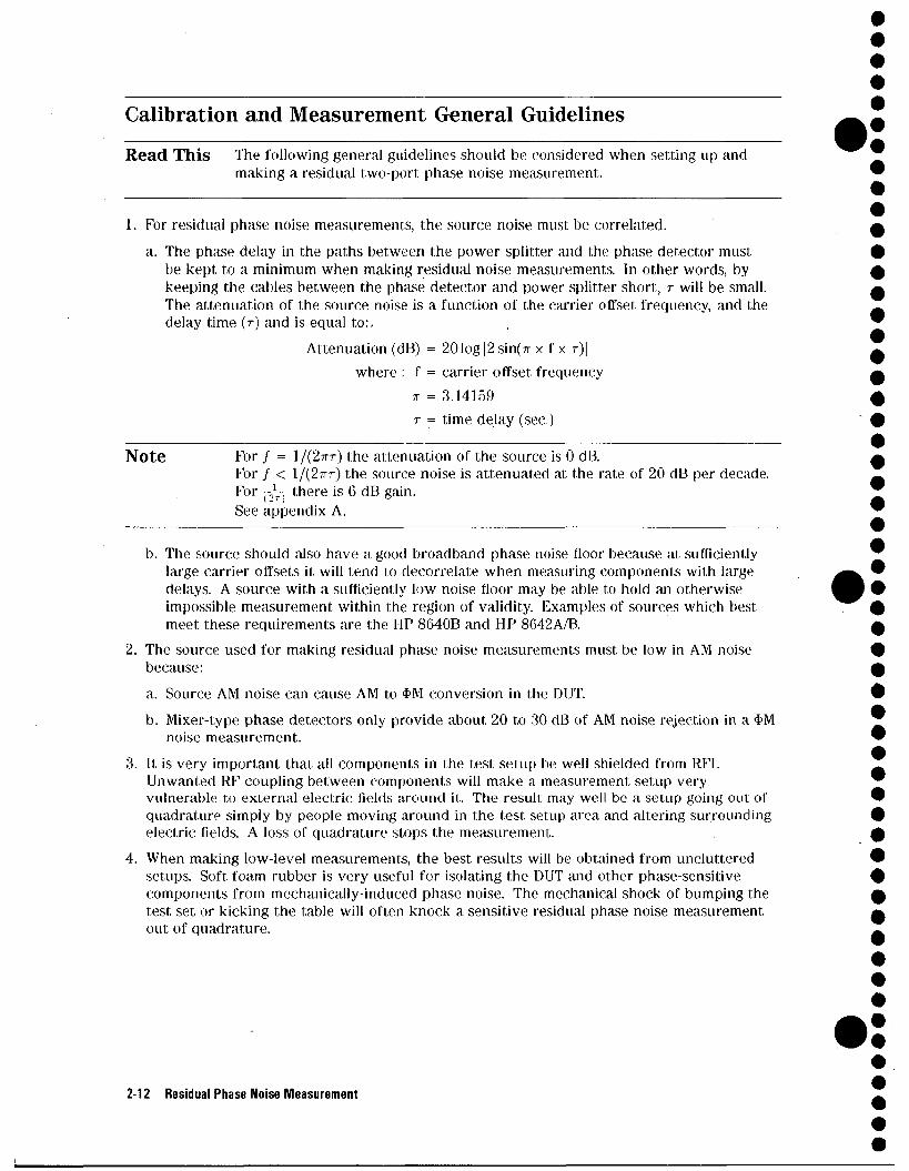
Calibration and Measurement General Guidelines Read This The following general guidelines should be considered when setting up and
making a residual two-port phase noise measurement.
1. For residual phase noise measurements, the source noise must, be correlated. a. The phase delay in the paths between the power splitter and the phase detector must
be kept to a minimum when making residual noise measurements. In other words, by keeping the cables between the phase detector and power splitter short, r will be small. The attenuation of the source noise is a function of the carrier offset frequency, and the delay time (r) and is equal to:,
Attenuation (dB) = 20 log |2sin(;r x f x r)\ where : f = carrier offset frequency
7r = 3.14159 r = time delay (sec.)
Note For / = l/(27rr) the attenuation of the source is 0 dB. For / < l/(27rr) the source noise is attenuated at the rate of 20 dB per decade. For piq there is 6 dB gain. See appendix A.
b. The source should also have a good broadband phase noise floor because at sufficiently large carrier offsets it will tend to decorrelate when measuring components with large delays. A source with a sufficiently low noise floor may be able to hold an otherwise impossible measurement within the region of validity. Examples of sources which best meet these requirements are the HP 8640B and HP 8642A/B.
2. The source used for making residual phase noise measurements must be low in AM noise because: a. Source AM noise can cause AM to 4>M conversion in the DUT. b. Mixer-type phase detectors only provide about 20 to 30 dB of AM noise rejection in a $M
noise measurement. 3. It is very important that all components in the test setup be well shielded from RFI.
Unwanted RF coupling between components will make a measurement setup very vulnerable to external electric fields around it. The result may well be a setup going out of quadrature simply by people moving around in the test setup area and altering surrounding electric fields. A loss of quadrature stops the measurement.
4. When making low-level measurements, the best results will be obtained from uncluttered setups. Soft, foam rubber is very useful for isolating the DUT and other phase-sensitive components from mechanically-induced phase noise. The mechanical shock of bumping the test set or kicking the table will often knock a sensitive residual phase noise measurement out of quadrature.
2-12 Residual Phase Noise Measurement
5. When making an extremely sensitive measurement it is essential to use semi-rigid cable between the components. The bending of a flexible cable from vibrations and temperature variations in the room can cause enough phase noise in flexible connecting cables to destroy the accuracy of a sensitive measurement. The connectors also must be tight; a wrench is the best tool.
6. When measuring a low-noise device, it is important that the source and any amplification, required to achieve the proper power at the phase detector, be placed before the splitter so it will be correlated out of the measurement. In cases where this is not possible; remember that any noise source, such as an amplifier, placed after the splitter in either phase detector path, will contribute to the measured noise.
7. An amplifier must be used in cases where the signal level out of the DUT is too small to drive the phase detector, or the drive level is inadequate to provide a low enough system noise floor. In this case the amplifier should have the following characteristics:
a. It should have the lowest possible noise figure, and the greatest possible dynamic range. b. The signal level must be kept as high as possible at all points in the setup to minimize
degradation from the thermal noise floor. c. It should have only enough gain to provide the required signal levels. Excess gain
leads to amplifiers operating in gain compression, making them very vulnerable to multiplicative noise problems. The non-linearity of the active device produces mixing which multiplies the baseband noise of the active device and power supply noise around the carrier.
d. The amplifier's sensitivity to power supply noise and the power supply noise itself must both be minimized.
Residual Phase Noise Measurement 2-13
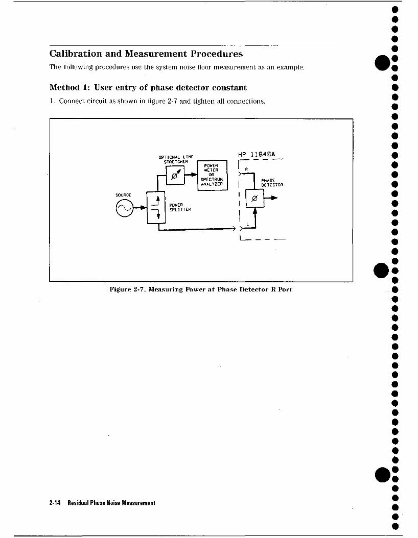
Calibration and Measurement Procedures The following procedures use the system noise floor measurement as an example.
Method 1: User entry of phase detector constant 1. Connect circuit as shown in figure 2-7 and tighten all connections.
OPTIONAL LINE STRETCHER
SOURCE
& ~
P s J 1
POWER METER OR
SPECTRUM ANALYZER
HP 11848A
n PHASE OCTECTOR
POWER SPLITTER
0
U h
Figure 2-7. Measuring Power at Phase Detector R Port
2-14 Residual Phase Noise Measurement
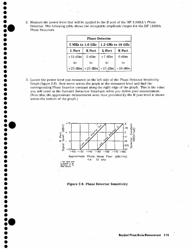
2. Measure the power level that will be applied to the R port of the HP 11848A's Phase Detector. The following table shows the acceptable amplitude ranges for the HP 11848A Phase Detectors.
Phase Detector
5 MHz to 1.6 GHz
L Port
+15 dBm
to
+ 23 dBm
R Port
OdBm
to
+ 23 dBm
1.2 GHz to 18 GHz
L Port
+ 7 dBm
to
+10 dBm
R Port
OdBm
to
+10 dBm
3. Locate the power level you measured on the left side of the Phase Detector Sensitivity Graph (figure 2-8). Now move across the graph at the measured level and find the corresponding Phase Detector constant along the right edge of the graph. This is the value you will enter as the Current Detector Constant when you define your measurement. (Note that the approximate measurement noise floor provided by the R port level is shown across the bottom of the graph.)
+ 15
E m ■o
r V
c e - 1 • "5
' c
+ 5
•15
' ^
/
4 op/
.NO
^Z
<*2
7
.6 ~
.35
.2
.11
.06
.035
.02
C o O i-°> o ^
r;
- 1 2 0 - 1 3 0 -140 -150 -160 - 1 7 0 - 1 8 0
A p p r o x i m a t e Phase Noise Floor ( d B c / H z ) f £ 10 kHz
I Port S V * l * * * ■■ Aa*um«0 to b«
Figure 2-8. Phase Detector Sensitivity
Residual Phase Noise Measurement 2
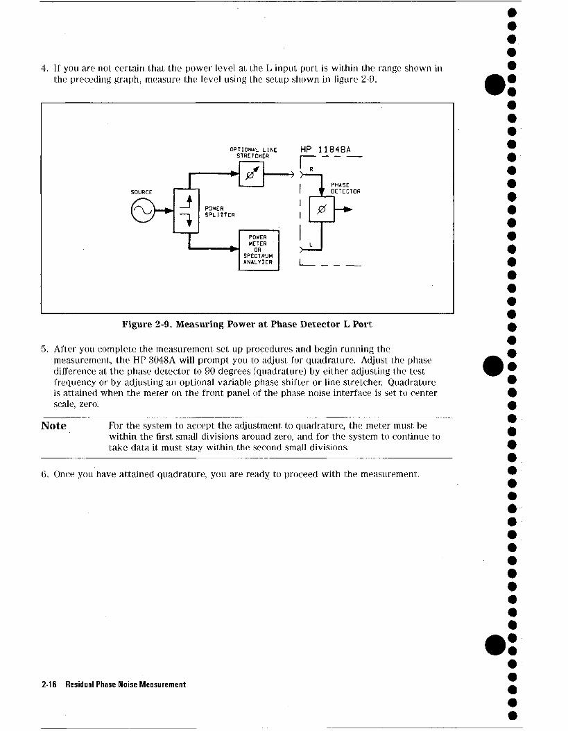
4. If you are not certain that the power level at the L input port is within the range shown in the preceding graph, measure the level using the setup shown in figure 2-9.
SOURCE
OPTIONAL LINE HP 1 1 8 4 8 A STRETCHER | —
-J " sf J
I POWER SPLITTER
POWER METER OR
SPECTRUM ANALYZER
PHASE DETECTOR
Figure 2-9. Measuring Power at Phase Detector L Port
5. After you complete the measurement set up procedures and begin running the measurement, the HP 3048A will prompt you to adjust for quadrature. Adjust the phase difference at the phase detector to 90 degrees (quadrature) by either adjusting the test frequency or by adjusting an optional variable phase shifter or line stretcher. Quadrature is attained when the meter on the front panel of the phase noise interface is set to center scale, zero.
Note For the system to accept the adjustment to quadrature, the meter must be within the first small divisions around zero, and for the system to continue to take data it must stay within, the second small divisions.
6. Once you have attained quadrature, you are ready to proceed with the measurement.
2-16 Residual Phase Noise Measurement
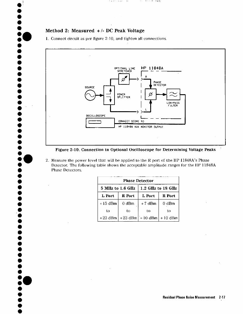
Method 2: Measured +/- DC Peak Voltage 1. Connect circuit as per figure 2-10, and tighten all connections.
OPTIONAL LINE H P 1 1 8 4 8 A STRETCHER | — — —
I D
SOURCE £1 tf
J 1,
n PHASE DETECTOR
POWER SPLITTER 0 ur LOW-PASS
FILTER
OSCILLOSCOPE CONNECT SCOPE TO HP 11848A AUX MONITOR OUTPUT
Figure 2-10. Connection to Optional Oscilloscope for Determining Voltage Peaks
2. Measure the power level that will be applied to the R port of the HP 11848A's Phase Detector. The following table shows the acceptable amplitude ranges for the HP 11848A Phase Detectors.
Phase Detector
5 MHz to 1.6 GHz
L Port
+15 dBm
to + 23 dBm
R Port
0 dBm
to
+23dBm
1.2 GHz to 18 GHz
L Port
+ 7 dBm
to
+ 10 dBm
R Port
OdBm
to
+10 dBm
Residual Phase Noise Measurement 2-17
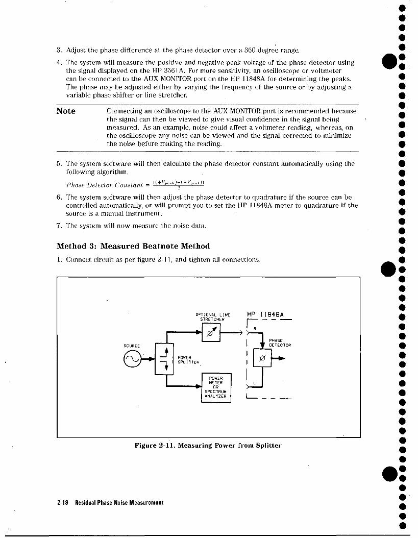
3. Adjust the phase difference at the phase detector over a 360 degree range.
4. The system will measure the positive and negative peak voltage of the phase detector using the signal displayed on the HP 3561 A. For more sensitivity, an oscilloscope or voltmeter can be connected to the AUX MONITOR port on the HP 11848A for determining the peaks. The phase may be adjusted either by varying the frequency of the source or by adjusting a variable phase shifter or line stretcher.
Note Connecting an oscilloscope to the AUX MONITOR port is recommended because the signal can then be viewed to give visual confidence in the signal being measured. As an example, noise could affect a voltmeter reading, whereas, on the oscilloscope any noise can be viewed and the signal corrected to minimize the noise before making the reading.
5. The system software will then calculate the phase detector constant automatically using the following algorithm. Phase Detector Constant = <<-+'W>-(-'v^>>
6. The system software will then adjust the phase detector to quadrature if the source can be controlled automatically, or will prompt you to set the IIP 11848A meter to quadrature if the source is a manual instrument.
7. The system will now measure the noise data.
Method 3: Measured Beatnote Method
1. Connect circuit as per figure 2-11, and tighten all connections.
OPTIONAL LINE HP 1 1848A STRETCHER | — —
' R
SOURCE
j POWER SPLITTER
*
POWER METER OR
SPECTRUM ANALYZER
| I PHASE I y DETECTOR
0
Figure 2-11. Measuring Power from Splitter
2-18 Residual Phase Noise Measurement
2. Measure the power level that will be applied to the R port of the HP 11848A's Phase Detector. The following table shows the acceptable amplitude ranges for the HP 11848A Phase Detectors.
Phase Detector
5 MHz to 1.6 GHz
L Port
+15 dBm
to
+ 23 dBm
R Port
OdBm
to
+ 23 dBm
1.2 GHz to 18 GHz
L Port
+ 7 dBm
to
+10 dBm
R Port
OdBm
to
+10 dBm
3. Measure the output power at one side of the power splitter, then terminate in 50 ohms. 4. Adjust the calibration source to the same output power as the measured output power of the
power splitter. 5. Adjust the output frequency such that the beatnote frequency is between 1 Hz and 100 kHz,
or to between 1 Hz and 20 MHz if an RF spectrum analyzer is included in the system. (Note that the beatnote frequency may be measured on the system spectrum analyzers.)
6. The system can now measure the calibration constant.
7. Disconnect the calibration source and reconnect the power splitter. 8. Adjust the phase difference at the phase detector to 90 degrees (quadrature) either by
adjusting the test frequency or by adjusting an optional variable phase shifter or line stretcher. Quadrature is achieved when the meter on the front panel of the phase noise interface is set to zero.
Note For the system to accept the adjustment, the meter needle must be between the first two small divisions around center scale (zero). For the system to continue to take data, the needle must stay within the second two small divisions around center scale.
9. Reset quadrature and measure phase noise data.
Residual Phase Noise Measurement 2-19
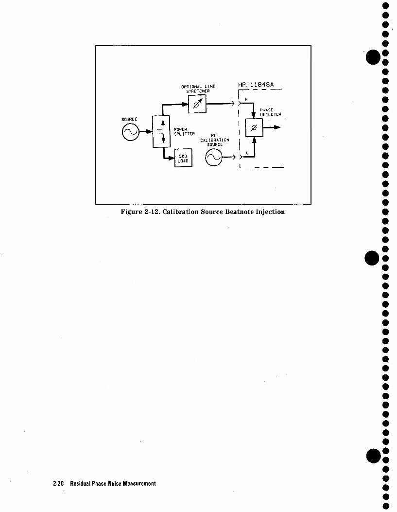
OPTIONAL LINE STRETCHER
SOURCE
G^ if
HP 11848A
I I a
J 1
i is PHASE OETECTOR
POWER SPLITTER 0
RF CALIBRATION
SOURCE
U{ ] (^H u Figure 2-12. Calibration Source Beatnote Injection
2-20 Residual Phase Noise Measurement
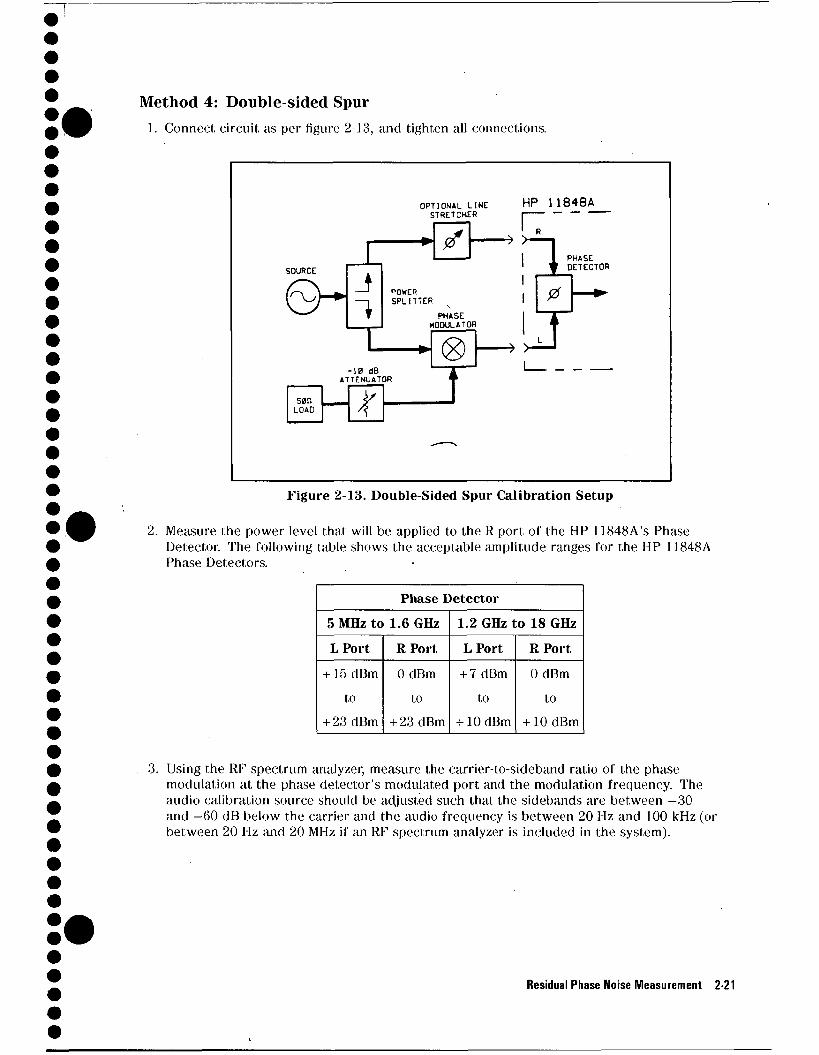
!
Method 4: Double-sided Spur 1. Connect circuit as per figure 2-13, and tighten all connections.
OPTIONAL LINE HP 11848A STRETCHER
SOURCE
& ~
I < /
J 1 T
17" PHASE DETECTOR
POWER SPLITTER
PHASE MODULATOR
0
- 1 0 dB ATTENUATOR
son LOAD X
IX
Figure 2-13. Double-Sided Spur Calibration Setup
2. Measure the power level that will be applied to the R port of the HP 11848A's Phase Detector. The following table shows the acceptable amplitude ranges for the HP 11848A Phase Detectors.
Phase Detector
5 MHz to 1.6 GHz
L Port
+ 15 dBm
to + 23 dBm
R Port
OdBm
to + 23 dBm
1.2 GHz to 18 GHz
L Port
+ 7 dBm
to +10 dBm
R Port
OdBm
to +10 dBm
3. Using the RF spectrum analyzer, measure the carrier-to-sideband ratio of the phase modulation at the phase detector's modulated port and the modulation frequency. The audio calibration source should be adjusted such that the sidebands are between -30 and -60 dB below the carrier and the audio frequency is between 20 Hz and 100 kHz (or between 20 Hz and 20 MHz if an RF spectrum analyzer is included in the system).
Residual Phase Noise Measurement 2-21
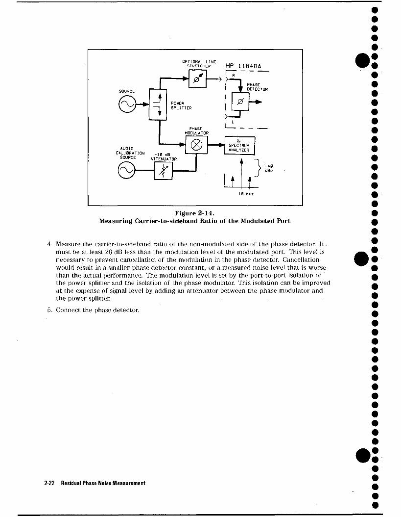
OPTIONAL LINE STRETCHER HP 11848A
SOURCE
J 1
AUDIO CALIBRATION -10 dB SOURCE ATTENUATOR
r\, t - 4 0 dBc
10 KHz
Figure 2-14. Measuring Carrier-to-sideband Ratio of the Modulated Port
4. Measure the carrier-to-sideband ratio of the non-modulated side of the phase detector. It must be at least 20 dB less than the modulation level of the modulated port. This level is necessary to prevent cancellation of the modulation in the phase detector. Cancellation would result in a smaller phase detector constant, or a measured noise level that is worse than the actual performance. The modulation level is set by the port-to-port isolation of the power splitter and the isolation of the phase modulator. This isolation can be improved at the expense of signal level by adding an attenuator between the phase modulator and the power splitter.
Connect the phase detector.
2-22 Residual Phase Noise Measurement
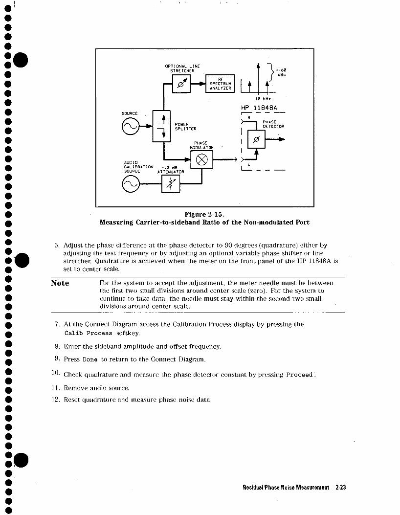
OPTIONAL LINE STRETCHER
SOURCE t
AUDIO CALIBRATION SOURCE AT
\ ^ ~ ~
f \
* RF
» SPECTRUM ANALYZER
POWER SPLITTER
PHASE MODULATOR
TENUAT 3R <8>
'
<-60 dBc
HP 11848A
PHASE DETECTOR
0
Figure 2-15. Measuring Carrier-to-sideband Ratio of the Non-modulated Port
6. Adjust the phase difference at the phase detector to 90 degrees (quadrature) either by adjusting the test frequency or by adjusting an optional variable phase shifter or line stretcher. Quadrature is achieved when the meter on the front panel of the HP 11848A is set to center scale.
Note For the system to accept the adjustment, the meter needle must be between the first two small divisions around center scale (zero). For the system to continue to take data, the needle must stay within the second two small divisions around center scale.
7. At the Connect Diagram access the Calibration Process display by pressing the Calib Process softkey.
8. Enter the sideband amplitude and offset frequency.
9. Press Done to return to the Connect Diagram.
10- Check quadrature and measure the phase detector constant by pressing Proceed.
11. Remove audio source. 12. Reset quadrature and measure phase noise data.
Residual Phase Noise Measurement 2-23
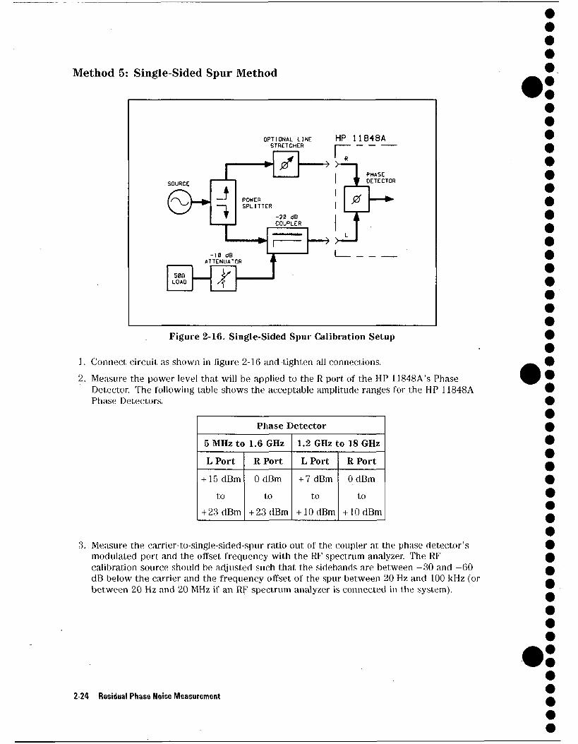
Method 5: Single-Sided Spur Method
OPTIONAL LINE STRETCHER
SOURCE
j
i - 1 0 dB
ATTENUATOR
500 LOAD t
Figure 2-16. Single-Sided Spur Calibration Setup
1. Connect circuit as shown in figure 2-16 and tighten all connections. 2. Measure the power level that will be applied to the R port of the HP 11848A's Phase
Detector. The following table shows the acceptable amplitude ranges for the HP 11848A Phase Detectors.
Phase Detector
5 MHz to 1.6 GHz
L Port
+ 15 dBm
to
+ 23 dBm
R Port
OdBm
to
+ 23 dBm
1.2 GHz to 18 GHz
L Port
+ 7 dBm
to
+ 10 dBm
R Por t
OdBm
to
+10 dBm
3. Measure the carrier-to-single-sided-spur ratio out of the coupler at the phase detector's modulated port and the offset frequency with the RF spectrum analyzer. The RF calibration source should be adjusted such that the sidebands are between -30 and -60 dB below the carrier and the frequency offset of the spur between 20 Hz and 100 kHz (or between 20 Hz and 20 MHz if an RF spectrum analyzer is connected in the system).
2-24 Residual Phase Noise Measurement
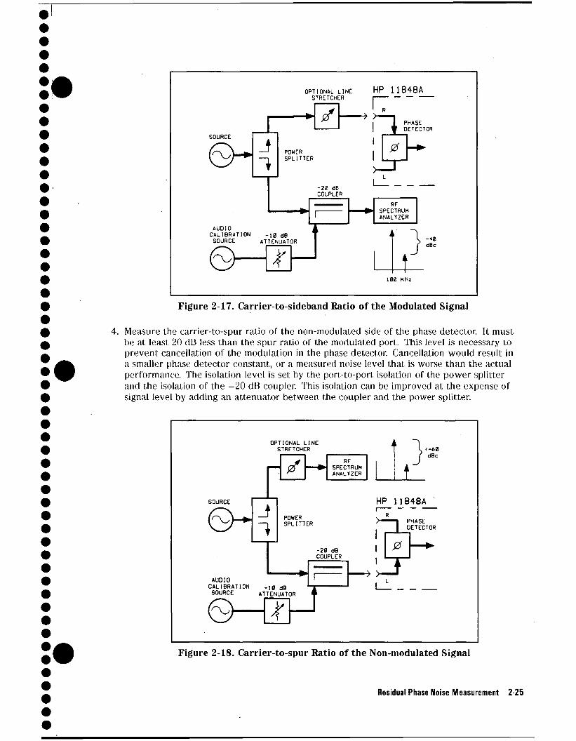
OPTIONAL LINE STRETCHER
SOURCE
AUDIO CALIBRATION -)0 dB SOURCE ATTENUATOR
100 KHz
Figure 2-17. Carrier-to-sideband Ratio of the Modulated Signal
4. Measure the carrier-to-spur ratio of the non-modulated side of the phase detector. It must be at least 20 dB less than the spur ratio of the modulated port. This level is necessary to prevent cancellation of the modulation in the phase detector. Cancellation would result in a smaller phase detector constant, or a measured noise level that is worse than the actual performance. The isolation level is set by the port-to-port isolation of the power splitter and the isolation of the -20 dB coupler. This isolation can be improved at the expense of signal level by adding an attenuator between the coupler and the power splitter.
OPTIONAL LINE STRETCHER
SOURCE
& ~
S? Rr
SPECTRUM ANALYZER
<-60 dSc
J 1 HP 11848A
POWER SPLITTER rtL PHASE DETECTOR
-20 dB COUPLER
AUDIO CALIBRATION -i0 d B SOURCE ATTENUATOR ' ^
0—2
0
Figure 2-18. Carrier-to-spur Ratio of the Non-modulated Signal
Residual Phase Noise Measurement 2-25
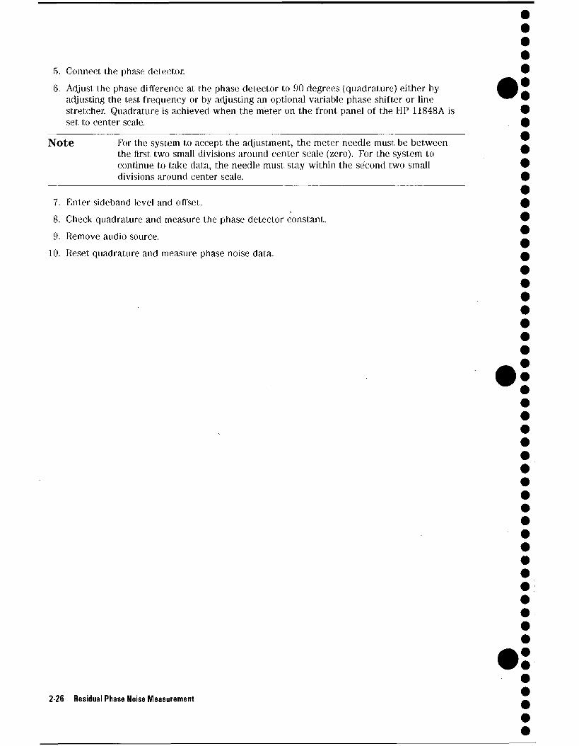
5. Connect the phase detector. 6. Adjust the phase difference at the phase detector to 90 degrees (quadrature) either by
adjusting the test frequency or by adjusting an optional variable phase shifter or line stretcher. Quadrature is achieved when the meter on the front panel of the HP 11848A is set to center scale.
Note For the system to accept the adjustment, the meter needle must be between the first two small divisions around center scale (zero). For the system to continue to take data, the needle must stay within the second two small divisions around center scale.
7. Enter sideband level and offset. 8. Check quadrature and measure the phase detector constant. 9. Remove audio source.
10. Reset quadrature and measure phase noise data.
2-26 Residual Phase Noise Measurement
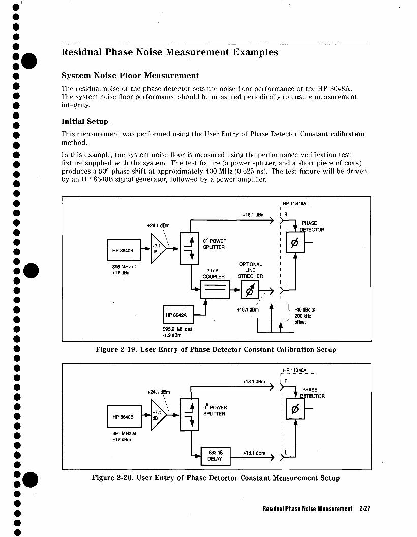
Residual Phase Noise Measurement Examples
System Noise Floor Measurement The residual noise of the phase detector sets the noise floor performance of the HP 3048A. The system noise floor performance should be measured periodically to ensure measurement integrity.
Initial Setup
This measurement was performed using the User Entry of Phase Detector Constant calibration method.
In this example, the system noise floor is measured using the performance verification test fixture supplied with the system. The test fixture (a power splitter, and a short piece of coax) produces a 90° phase shift at approximately 400 MHz (0.625 ns). The test fixture will be driven by an HP 8640B signal generator, followed by a power amplifier.
HP11848A r
+24.1 dBm
HP8640B
395 MHz at +17 dBm
+18.1 dBm I R
' / 1, PHASE .DETECTOR
0 POWER SPUTTER 0
OPTIONAL -20 dB LINE
COUPLER STRECHER
4 HP8642A
i +18.1 dBm
/ i
395.2 MHz at -1.9 dBm
i \ -40dBcat [' 200 kHz
offset
Figure 2-19. User Entry of Phase Detector Constant Calibration Setup
+24.1 dBm
HP8640B
395 MHz at +17 dBm
_f 0° POWER SPUTTER
.633 nS DELAY
HP11848A r
+18.1 dBm i R S S~~\ PHASE
1 ▼ DETECTOR
0 i
+18.1 dBm v v l
) /"
L
Figure 2-20. User Entry of Phase Detector Constant Measurement Setup
Residual Phase Noise Measurement 2-27
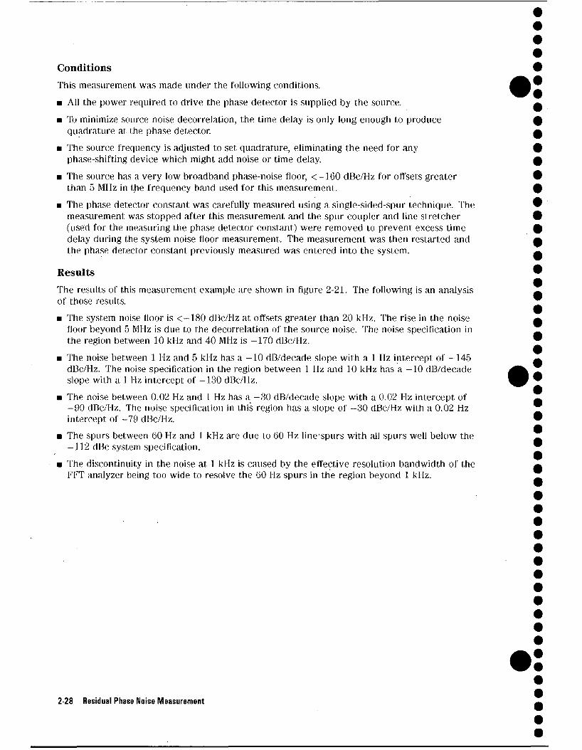
Conditions This measurement was made under the following conditions. ■ All the power required to drive the phase detector is supplied by the source. ■ To minimize source noise decorrelation, the time delay is only long enough to produce
quadrature at the phase detector. ■ The source frequency is adjusted to set quadrature, eliminating the need for any
phase-shifting device which might add noise or time delay. ■ The source has a very low broadband phase-noise floor, <-160 dBc/Hz for offsets greater
than 5 MHz in the frequency band used for this measurement.
■ The phase detector constant was carefully measured using a single-sided-spur technique. The measurement, was stopped after this measurement and the spur coupler and line stretcher (used for the measuring the phase detector constant) were removed to prevent excess time delay during the system noise floor measurement. The measurement was then restarted and the phase detector constant previously measured was entered into the system.
Results The results of this measurement example are shown in figure 2-21. The following is an analysis of those results. ■ The system noise floor is <-180 dBc/Hz at offsets greater than 20 kHz. The rise in the noise
floor beyond 5 MHz is due to the decorrelation of the source noise. The noise specification in the region between 10 kHz and 40 MHz is -170 dBc/Hz.
■ The noise between 1 Hz and 5 kHz has a -10 dB/decade slope with a 1 Hz intercept of -145 dBc/Hz. The noise specification in the region between 1 Hz and 10 kHz has a -10 dB/decade slope with a 1 Hz intercept of -130 dBc/Hz.
■ The noise between 0.02 Hz and 1 Hz has a -30 dB/decade slope with a 0.02 Hz intercept,-of -90 dBc/Hz. The noise specification in this region has a slope of -30 dBc/Hz with a 0.02 Hz intercept of -79 dBc/Hz.
■ The spurs between 60 Hz and 1 kHz are due to 60 Hz linespurs with all spurs well below the -112 dBc system specification.
■ The discontinuity in the noise at 1 kHz is caused by the effective resolution bandwidth of the FFT analyzer being too wide to resolve the 60 Hz spurs in the region beyond 1 kHz.
2-28 Residual Phase Noise Measurement
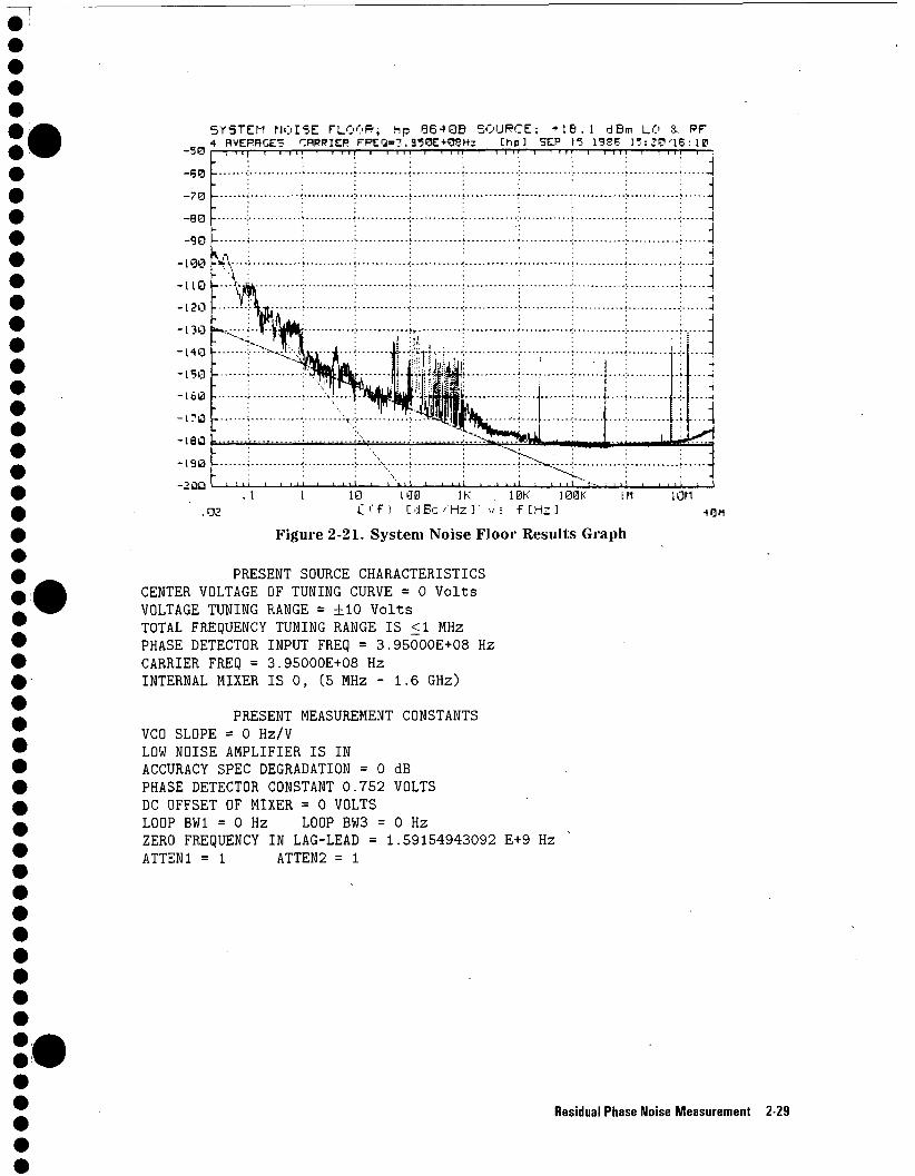
-50
-50 -?e>
- 8 0
- 9 0
- 1 0 0
- 1 1 0
- 1 2 0
- 1 3 0
- H O
- 1 5 0
- i b a
- 1 7 0
- i a i 3
- 1 9 a
SYSTEM MOISE FLOOR; hp 86498 SOURCE; + I B . 1 d Bin LO 8, PF 4 RVERRGE? CRRRIER FREG=?.950E+0SHz Chp] SEP ]Z 133S 1 7 : 2 0 ' 1 6 : 10
V'<-
-rrr
■ * :
2i3Q I—J_U
i i i i i i i 11 i I I I II I I I I ! I l l T I I I I
.1 :u
ilr Js-♦'•jii<?»a*i i ■--•.■ ■:
i i 11 i i i 11 i—i 11 I i i i 11 -i_i_U_ 10 130 1K
Cff) Cc iEc 'H r ] '
■ ' " r - - ' ' ■ ! * ' ' ■ ' '
1BK 103K IM f C H z ]
ion ■»GM
Figure 2-21. System Noise Floor Results Graph
PRESENT SOURCE CHARACTERISTICS CENTER VOLTAGE OF TUNING CURVE = 0 Volts VOLTAGE TUNING RANGE = ±10 Volts TOTAL FREQUENCY TUNING RANGE IS <1 MHz PHASE DETECTOR INPUT FREQ = 3.95000E+08 Hz CARRIER FREQ = 3.95000E+08 Hz INTERNAL MIXER IS 0, (5 MHz - 1.6 GHz)
PRESENT MEASUREMENT CONSTANTS VCO SLOPE = 0 Hz/V LOW NOISE AMPLIFIER IS IN ACCURACY SPEC DEGRADATION = 0 dB PHASE DETECTOR CONSTANT 0.752 VOLTS DC OFFSET OF MIXER = 0 VOLTS LOOP BW1 = 0 Hz LOOP BW3 = 0 Hz ZERO FREQUENCY IN LAG-LEAD = 1.59154943092 E+9 Hz ATTEN1 = 1 ATTEN2 = 1
Residual Phase Noise Measurement 2-29
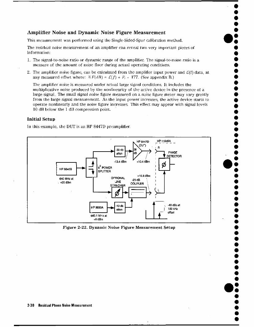
Amplifier Noise and Dynamic Noise Figure Measurement This measurement; was performed using the Single-Sided-Spur calibration method. The residual noise measurement of an amplifier can reveal two very important pieces of information: 1. The signal-to-noise ratio or dynamic range of the amplifier. The signal-to-noise ratio is a
measure of the amount of noise floor during actual operating conditions. 2. The amplifier noise figure, can be calculated from the amplifier input power and £(f) data, at
any measured offset where: NF(dB) = £(/) + P{ + 177. (See appendix B.)
The amplifier noise is measured under actual large signal conditions. It includes the multiplicative noise produced by the nonlinearify of the active device in the presence of a large signal. The small signal noise figure measured on a noise figure meter may vary greatly from the large signal measurement. As the input power increases, the active device starts to operate nonlinearly and the noise figure increases. This effect may appear with signal levels 10 dB below the 1 dB compression point.
Initial Setup In this example, the DUT is an HP 8447D preamplifier.
HP 8640B
640 MHz at . +20 dBm
J -30 db atten
-13.4 dBm
HP 8447D .(DUT)
0 POWER SPLnTER
OPTIONAL LINE
STRECHER
+10.4 dBm
+15.8 dBm -20 dB \
COUPLER \
4 HP8663A -10 db |
->
HP11848A
i n
? 1 PHASE DETECTOR
atten
640.1 MHz t +6 dBm
0
£ \ -40dBcat ]' 100 kHz
offset
Figure 2-22. Dynamic Noise Figure Measurement Setup
2-30 Residual Phase Noise Measurement
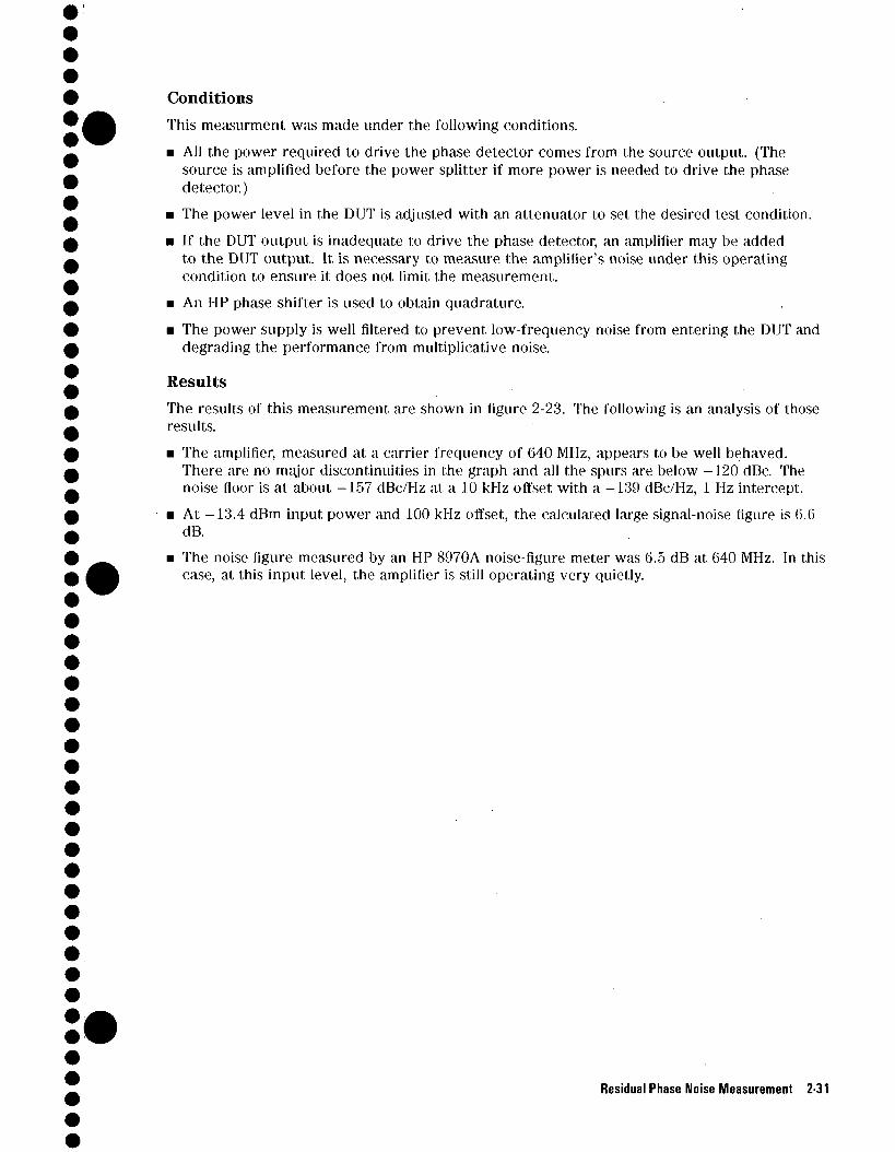
Conditions This measurment was made under the following conditions.
■ All the power required to drive the phase detector comes from the source output. (The source is amplified before the power splitter if more power is needed to drive the phase detector.)
■ The power level in the DUT is adjusted with an attenuator to set the desired test condition.
■ If the DUT output is inadequate to drive the phase detector, an amplifier may be added to the DUT output. It is necessary to measure the amplifier's noise under this operating condition to ensure it does not limit the measurement.
■ An HP phase shifter is used to obtain quadrature.
■ The power supply is well filtered to prevent low-frequency noise from entering the DUT and degrading the performance from multiplicative noise.
Results The results of this measurement are shown in figure 2-23. The following is an analysis of those results.
■ The amplifier, measured at a carrier frequency of 640 MHz, appears to be well behaved. There are no major discontinuities in the graph and all the spurs are below -120 dBc. The noise floor is at about -157 dBc/Hz at a 10 kHz offset with a -139 dBc/Hz, 1 Hz intercept.
■ At -13.4 dBm input power and 100 kHz offset, the calculated large signal-noise figure is 6.6 dB.
■ The noise figure measured by an HP 8970A noise-figure meter was 6.5 dB at 640 MHz. In this case, at this input level, the amplifier is still operating very quietly.
Residual Phase Noise Measurement 2-31
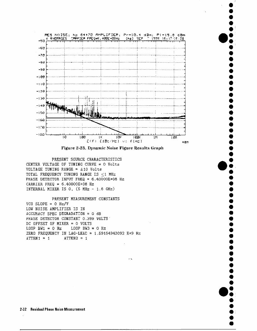
RES N O I S E ; hp 9 4 4 7 D A M P L I F I E R ; P r - 1 0 . 4 dBm; P l - 1 5 . 9 d Bm 4 HVERHGE5 CHPFIER PREPS. 400E+g3Hz Chp] 5EP 7 193S 1B: ] 7 ■'! P : 23
-50
-70
-89
-98
-109
-1 10
-120
-13©
-140
-150
- Ibt t
-170
-ISO
I I I I I r T T T 1 1—m 1 1—m 1 1 i i i i i 11
vr-MHw^ain^mj'f ii—«t—
- I i l l I i i—LI i i uxJ 1 i i i I ' ' ■ I 100 IK 10K I30K
C ' f i C ci Be ■'■ Hz ] •./ ■ f [ Hz ]
i - ' i
1M 19H 40M
Figure 2-23. Dynamic Noise Figure Results Graph
PRESENT SOURCE CHARACTERISTICS CENTER VOLTAGE OF TUNING CURVE = 0 Volts VOLTAGE TUNING RANGE = ±10 Volts TOTAL FREQUENCY TUNING RANGE IS <1 MHz PHASE DETECTOR INPUT FREQ = 6.40000E+08 Hz CARRIER FREQ = 6.40000E+08 Hz INTERNAL MIXER IS 0, (5 MHz - 1.6 GHz)
PRESENT MEASUREMENT CONSTANTS VCO SLOPE = 0 Hz/V LOW NOISE AMPLIFIER IS IN ACCURACY SPEC DEGRADATION = 0 dB PHASE DETECTOR CONSTANT 0.399 VOLTS DC OFFSET OF MIXER = 0 VOLTS LOOP BW1 = 0 Hz LOOP BW3 = 0 Hz ZERO FREQUENCY IN LAG-LEAD = 1.59154943092 E+9 Hz ATTEN1 = 1 ATTEN2 = 1
2-32 Residual Phase Noise Measurement
Measurement of a Device with Large Time Delay (r) This measurement was made using the Single-Sided-Spur calibration method.
The measurement of a device with long delay usually has two special considerations: 1. Delays exceeding 1 //.s tend to have a large amount of signal path loss. This loss makes
it necessary to follow the DUT with an amplifier having the properties discussed in "Calibration and Measurement General Guidelines."
2. The long delay will decorrelate the source noise. The attenuation of the source noise is equal to:
Attenuation(dB) = 201og|2 sin(?rf r)| where TT = 3.14159
( f = frequency offset (Hz) T = time delay (seconds)
N o t e At ^ the source noise will be completely decorrelated and at 4p there is an actual enhancement of 6 dB to the source noise. The source noise will be periodic in the region beyond ^ . The noise peaks are the sum of the source and DUT noise. The bottom of the nulls is residual noise.
Initial Setup In this example, the DUT is a 236 ns SAW delay line, followed by the amplifier used in the Amplifier Noise and Dynamic Noise Figure measurement.
HP8640B
640 MHz at +20dBm
236.2 nS SAW DELAY LINE
D -6db atten
J +10.6 dBm -13.7 dBm
HP8447D .(DUT)
+10.4 dBm
0 POWER SPLITTER
OPTIONAL LINE
STRECHER
+15.8 dBm -20 dB
COUPLER
4 HP8663A ■10 db
atten
- »
HP11848A r
^1 PHASE DETECTOR
0 ~
640.1 MHz at +6 dBm 1
'N -40dBcat \ 100 kHz
offset
Figure 2-24. Time Delay Measurement Setup
Residual Phase Noise Measurement 2-33
Conditions This measurement was made under the following conditions.
■ All the power required to drive the phase detector comes from the source output. ■ The power level into the DUT is adjusted with an attenuator to set the desired test condition. ■ The DUT output, is inadequate to drive the phase detector, thus an amplifier has been added
to the DUT output. It is necessary to measure the amplifier's noise under this operating condition to ensure it does not limit the measurement.
■ An HP phase shifter is used to obtain and maintain quadrature. The phase shift through this SAW delay line is very sensitive to temperature change and therefore, it drifts with time. It was necessary to adjust the phase shifter very slowly during the measurement, to maintain quadrature. A sudden movement in the phase correction will look like phase noise close to the carrier, and invalidate the close-in data.
■ The source decorrelation is plotted for this example to provide an idea of what, the noise to be measured should look like.
, „ m -o Q> <r> o 7? 0) n i _ 3 o CO o c o (0 D C CD e <
+10 dB
OdB
-10 dB
-20 dB
-30 dB
-40 dB
-50 dB
-60 dB
-70 dB
-80 dB
-90 dB
20 Log 2 Sin N fm t t = 236.2 nSec
10 Hz 100 Hz 1kHz 10 kHz 100 kHz 1MHz 10 MHz 100 MHz
fm (Hz) Figure 2-25. Graph of Source Decorrelation
The attenuation of the DUT must either be known or it must, be measured. The test-setup noise floor is measured, substituting an attenuator for the DUT. This is necessary to sort the DUT noise from the test-setup noise.
2-34 Residual Phase Noise Measurement
Results The results of this measurement are found in figure 2-26. The following is an analysis of those results.
■ The SAW delay line, measured at the frequency of 640 MHz, appears to be very well behaved. There are no discontinuities in the graph and all the spurs are <10 dB out of the noise. The noise floor is at about -155 dBc/Hz at a 10 kHz offset with a -118 dBc/Hz, 1 Hz intercept.
■ The j noise region out to about 4 kHz offset is very typical of this DUT.
■ The floor region between 4 and 200 kHz approaches the test system noise floor. Data in this region is being degraded by insufficient dynamic range of the test setup. This problem may be remedied either by operating the DUT at a higher output level to increase its output signal-to-noise ratio, or by using an amplifier with a lower noise figure. The test-setup noise floor must be 10 dB below the measured noise to ensure less than a 1 dB measurement error.
■ The region beyond 200 kHz is a very good example of the periodic nature of source decorrelation. At i , noise is almost exactly 6 dB higher than the phase noise of a typical HP 8642A at that offset and carrier frequency. The noise nulls are at the measured test-system noise floor.
Residual Phase Noise Measurement 2-35
- 3 0
- 6 0 h
- 7 0
- 98
- 9 3
- 1 8 8
- I 19 -
- 1 2 9
-ne - 1 4 8
- 1 3 0
- 1 6 0
- l ? Q
- 1 3 0
KE5 N015E; 2 3 6 . 2 nSEC SRW DELAY; P r - 1 0 . 4 dBm, P I - 1 5 . 8 dBm 4 HVERBGES CHRR1EH FPEQ-6.400E+08Hz Chp] SEP 7 1985 1 5 : 0 9 / 1 5 : 2 1
: ; : : :
: : 1 1 !
; ^ f = 6 7 3 " S 1 k H z
i ^ — *
" ^ M * ^ h d 0 ^ ^ ^
; *" s ^ 1 L l l i 1 i l l ! 1 1—I_LJ 1 1—I_JJ i 1—i_iJ j i_i
T 1
.......
.i 1™3
■
* = 2 » *-^ ;
:
:
;
%ii :
feu i l l i 10 100 IK 10K
1. r f i C d Be / Mz ] 130K 1M
f [ H z ]
Figure 2-26. Time Delay Results Graph
PRESENT SOURCE CHARACTERISTICS CENTER VOLTAGE OF TUNING CURVE = 0 Volts VOLTAGE TUNING RANGE = ±10 Volts TOTAL FREQUENCY TUNING RANGE IS <1 MHz PHASE DETECTOR INPUT FREQ = 6.40000E+08 Hz CARRIER FREQ = 6.40000E+08 Hz INTERNAL MIXER IS 0, (5 MHz - 1.6 GHz)
H3M •tan
PRESENT MEASUREMENT CONSTANTS VCO SLOPE = 0 Hz/V LOW NOISE AMPLIFIER IS IN ACCURACY SPEC DEGRADATION = 0 dB PHASE DETECTOR CONSTANT 0.413 VOLTS DC OFFSET OF MIXER = 0 VOLTS LOOP BW1 = 0 Hz LOOP BW3 = 0 Hz ZERO FREQUENCY IN LAG-LEAD = 1.59154943092 E+9 Hz ATTEN1 = 1 ATTEN2 = 1
2-36 Residual Phase Noise Measurement
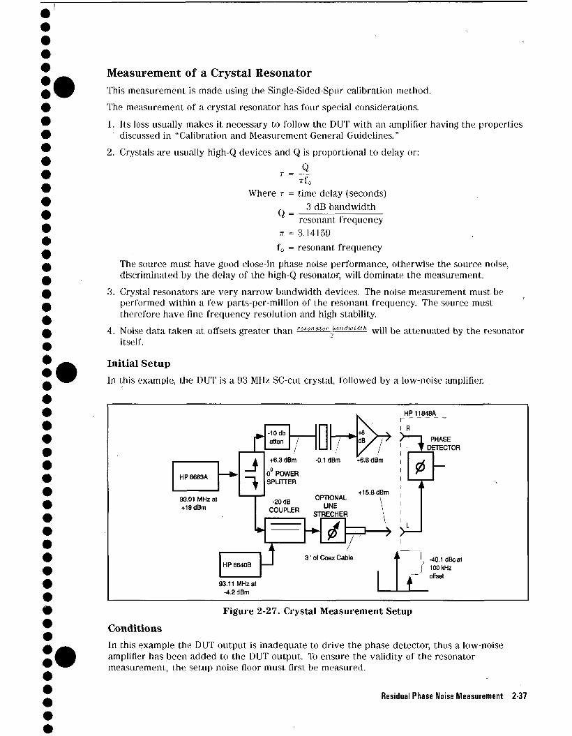
I
Measurement of a Crystal Resonator This measurement is made using the Single-Sided-Spur calibration method. The measurement of a crystal resonator has four special considerations. 1. Its loss usually makes it necessary to follow the DUT with an amplifier having the properties
discussed in "Calibration and Measurement General Guidelines."
2. Crystals are usually high-Q devices and Q is proportional to delay or:
r = 3-7Tf0
Where r = time delay (seconds) 3 dB bandwidth
resonant frequency jr.= 3.14159
l'o = resonant frequency The source must have good close-in phase noise performance, otherwise the source noise, discriminated by the delay of the high-Q resonator, will dominate the measurement.
3. Crystal resonators are very narrow bandwidth devices. The noise measurement must be performed within a few parts-per-million of the resonant frequency. The source must therefore have fine frequency resolution and high stability.
4. Noise data taken at offsets greater than resonator bandwidth w^ ^ e attenuated by the resonator itself.
Initial Setup In this example, the DUT is a 93 MHz SC-ci.it crystal, followed by a low-noise amplifier.
HP8663A
93.01 MHz at +19 dBm
Jj J
-10 db atten
+6.3 dBm
0° POWER SPLnTER
-20 dB COUPLER
HP6640B J
-0.1 dBm
OPTIONAL UNE
STRECHER
HP11848A I
J R PHASE
DETECTOR
+6.8 dBm
+15.8 dBm
0
4 3' of Coax Cable
93.11 MHz at -4.2 dBm i
\ -40.1dBcat |" 100 kHz
offset
Figure 2-27. Crystal Measurement Setup
Conditions In this example the DUT output is inadequate to drive the phase detector, thus a low-noise amplifier has been added to the DUT output. To ensure the validity of the resonator measurement, the setup noise floor must first be measured.
Residual Phase Noise Measurement 2-37
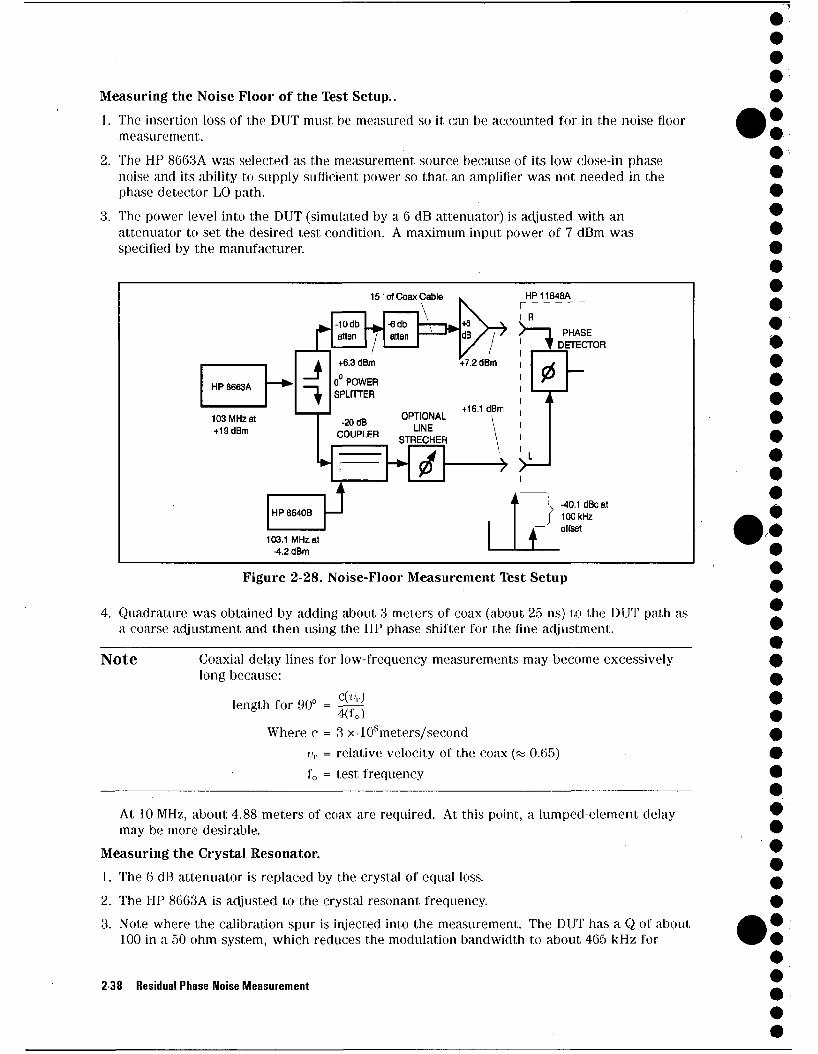
Measuring the Noise Floor of the Test Setup.. 1. The insertion loss of the DUT must be measured so it can be accounted for in the noise floor
measurement.
2. The HP 8663A was selected as the measurement source because, of its low close-in phase noise and its ability to supply sufficient power so that an amplifier was not needed in the phase detector LO path.
3. The power level into the DUT (simulated by a 6 dB attenuator) is adjusted with an attenuator to set the desired test condition. A maximum input power of 7 dDm was specified by the manufacturer.
15'of Coax Cable
HP 8663A
103 MHz at +19dBm
n j
-iodb atten
+6.3 dBm
0° POWER SPLITTER
-20 dB COUPLER
HP8640B
103.1 MHz at -4.2 dBm 1
-40.1 dBcat 100 kHz offset
Figure 2-28. Noise-Floor Measurement Test Setup
4. Quadrature was obtained by adding about 3 meters of coax (about 25 ns) to the DUT path as a coarse adjustment and then using the HP phase shifter for the fine adjustment.
Note Coaxial delay lines for low-frequency measurements may become excessively long because:
length for 90° = C(vr) 4(fo)
Where c = 3 xl0smeters/second •iv = relative velocity of the coax (« 0.65) f0 = test frequency
At 10 MHz, about 4.88 meters of coax are required. At this point, a lumped-element delay may be more desirable.
Measuring the Crystal Resonator. 1. The 6 dB attenuator is replaced by the crystal of equal loss. 2. The HP 8663A is adjusted to the crystal resonant frequency. 3. Note where the calibration spur is injected into the measurement. The DUT has a Q of about
100 in a 50 ohm system, which reduces the modulation bandwidth to about 465 kHz for
2 38 Residual Phase Noise Measurement
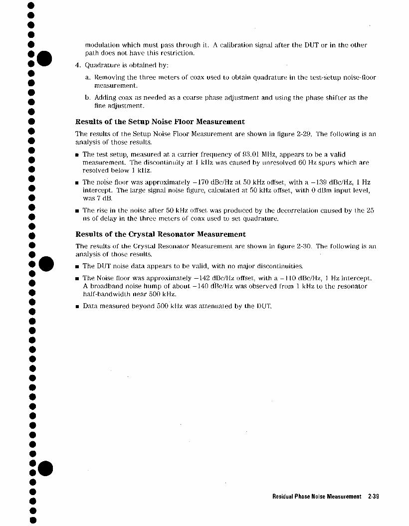
modulation which must pass through it. A calibration signal after the DUT or in the other path does not have this restriction.
4. Quadrature is obtained by:
a. Removing the three meters of coax used to obtain quadrature in the test-setup noise-floor measurement.
b. Adding coax as needed as a coarse phase adjustment and using the phase shifter as the fine adjustment.
Results of the Setup Noise Floor Measurement The results of the Setup Noise Floor Measurement are shown in figure 2-29. The following is an analysis of those results.
■ The test setup, measured at a carrier frequency of 93.01 MHz, appears to be a valid measurement. The discontinuity at 1 kHz was caused by unresolved 60 Hz spurs which are resolved below 1 kHz.
■ The noise floor was approximately -170 dBc/Hz at 50 kHz offset, with a -139 dBc/Hz, 1 Hz intercept. The large signal noise figure, calculated at 50 kHz offset, with 0 dBm input level, was 7 dB.
■ The rise in the noise after 50 kHz offset was produced by the decorrelation caused by the 25 ns of delay in the three meters of coax used to set quadrature.
Results of the Crystal Resonator Measurement The results of the Crystal Resonator Measurement are shown in figure 2-30. The following is an analysis of those results. ■ The DUT noise data appears to be valid, with no major discontinuities. ■ The Noise floor was approximately -142 dBc/Hz offset, with a -110 dBc/Hz, 1 Hz intercept.
A broadband noise hump of about -140 dBc/Hz was observed from 1 kHz to the resonator half-bandwidth near 500 kHz.
■ Data measured beyond 500 kHz was attenuated by the DUT.
Residual Phase Noise Measurement 2-39
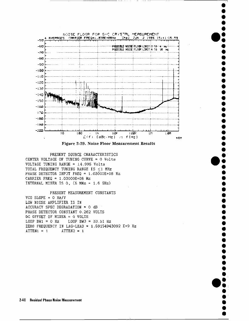
NOISE FLOOR FOP 5 - 0 CRYSTAL MEASUREMENT 4 RVEPHGE5 CHPRIER FFEO-t.030E*08Hr Chp3 TUN 2 1955 13:4 1 -13:53
180 • IK 10K 130K £ ' ' f J CdBc / 'Hz ] vs f CHz]
Figure 2-29. Noise Floor Measurement Results 40M
PRESENT SOURCE CHARACTERISTICS CENTER VOLTAGE OF TUNING CURVE = 0 Volts VOLTAGE TUNING RANGE = ±4.995 Volts TOTAL FREQUENCY TUNING RANGE IS <1 MHz PHASE DETECTOR INPUT FREQ = 1.03000E+08 Hz CARRIER FREQ = 1.03000E+08 Hz INTERNAL MIXER IS 0, (5 MHz - 1.6 GHz)
PRESENT MEASUREMENT CONSTANTS VCO SLOPE = 0 Hz/V LOW NOISE AMPLIFIER IS IN ACCURACY SPEC DEGRADATION = 0 dB PHASE DETECTOR CONSTANT 0.262 VOLTS DC OFFSET OF MIXER = 0 VOLTS LOOP BW1 = 0 Hz LOOP BW3 = 33.51 Hz ZERO FREQUENCY IN LAG-LEAD = 1.59154943092 E+9 Hz ATTEN1 = 1 ATTEN2 = 1
2-40 Residual Phase Noise Measurement
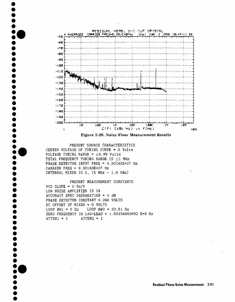
-30
-60
-70
-SB
-90
-100
RESIDURL MEflS; S - C CUT CRYSTAL 4 HVERHGE5 CRBRICR FPEO-9.3BIE+B7HZ ChpJ JUN g 1386 IB: 45/11:33
i i i 11 i 1 i 1 1 — i > I I I — i — i i n
-150 --160 --170 P-- i a o
- i s a
-2Qia
i
fUiyLjji^*vawJw
I I I I I I LxJ I I I I I I l l 10 100 IK 10K 100K
£Cf) CdBc-'HzJ v; f[Hz]
■ ■ ■ i i i l in i an
40M Figure 2-30. Noise Floor Measurement Results
PRESENT SOURCE CHARACTERISTICS CENTER VOLTAGE OF TUNING CURVE = 0 Volts VOLTAGE TUNING RANGE = ±9.99 Volts TOTAL FREQUENCY TUNING RANGE IS <1 MHz PHASE DETECTOR INPUT FREQ = 9.30140E+07 Hz CARRIER FREQ = 9.30140E+07 Hz INTERNAL MIXER IS 0, (5 MHz - 1.6 GHz)
PRESENT MEASUREMENT CONSTANTS VCO SLOPE = 0 Hz/V LOW NOISE AMPLIFIER IS IN ACCURACY SPEC DEGRADATION = 0 dB PHASE DETECTOR CONSTANT 0.246 VOLTS DC OFFSET OF MIXER = 0 VOLTS LOOP BW1 = 0 Hz LOOP BW3 = 33.51 Hz ZERO FREQUENCY IN LAG-LEAD = 1.59154943092 E+9 Hz ATTEN1 = 1 ATTEN2 = 1
Residual Phase Noise Measurement 2
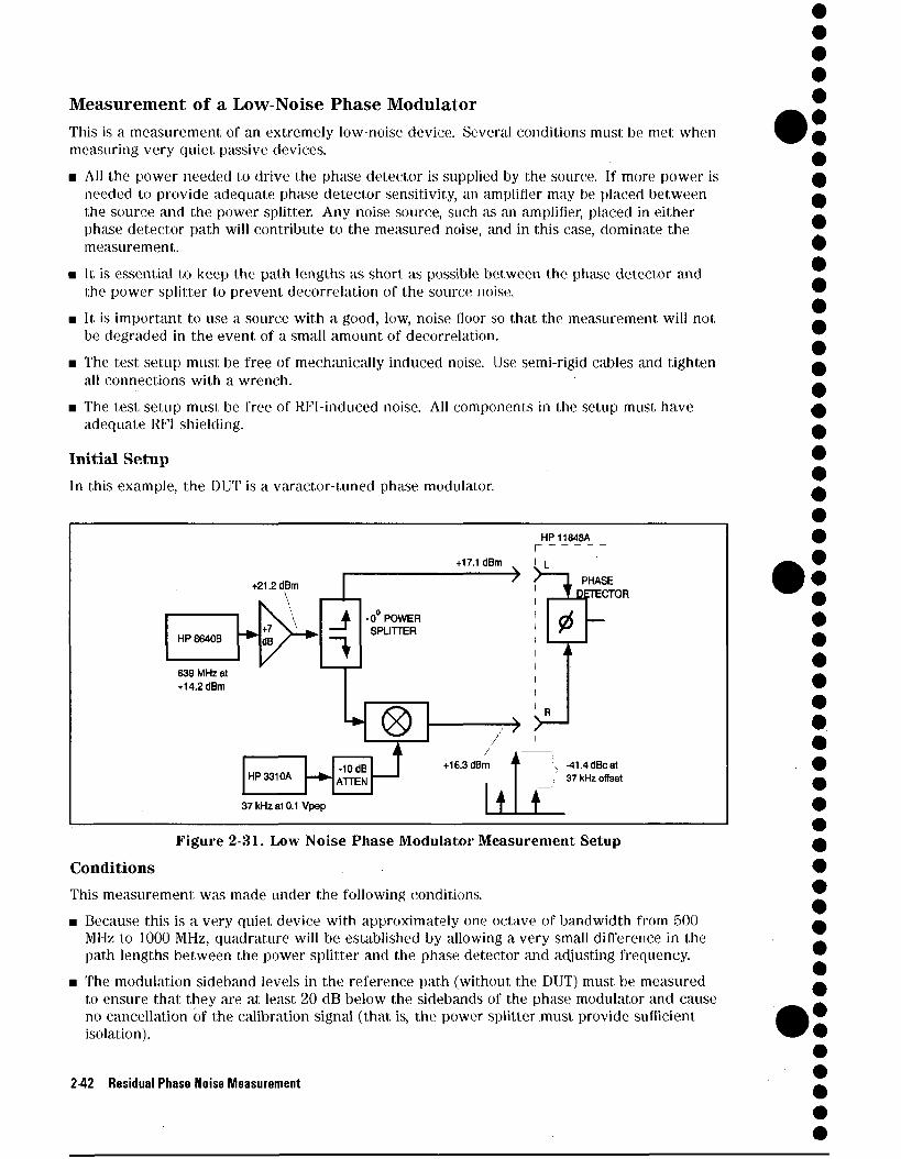
Measurement of a Low-Noise Phase Modulator This is a measurement of an extremely low-noise device. Several conditions must be met when measuring very quiet passive devices.
■ All the power needed to drive the phase detector is supplied by the source. If more power is needed to provide adequate phase detector sensitivity, an amplifier may be placed between the source and the power splitter. Any noise source, such as an amplifier, placed in either phase detector path will contribute to the measured noise, and in this case, dominate the measurement.
■ It is essential to keep the path lengths as short as possible between the phase detector and the power splitter to prevent decorrelation of the source noise.
■ It is important to use a source with a good, low, noise floor so that the measurement will not be degraded in the event of a small amount of decorrelation.
■ The test setup must be free of mechanically induced noise. Use semi-rigid cables and tighten all connections with a wrench.
■ The test setup must be free of RFI-induced noise. All components in the setup must have adequate RFI shielding.
Initial Setup In this example, the DUT is a varactor-tuned phase modulator.
+17.1 dBm
HP8640B
639 MHz at +14.2 dBm
">
HP 1J848A^
L n ■0 POWER SPUTTER
PHASE flETECTOR
0
HP3310A -10 dB ATTEN
i +16.3 dBm
/ I
A
37 kHz at 0.1 Vpep 1 -41.4dBcal 37 kHz offeet
1 Figure 2-31. Low Noise Phase Modulator Measurement Setup
Conditions This measurement was made under the following conditions. ■ Because this is a very quiet device with approximately one octave of bandwidth from 500
MHz to 1000 MHz, quadrature will be established by allowing a very small difference in the path lengths between the power splitter and the phase detector and adjusting frequency.
■ The modulation sideband levels in the reference path (without the DUT) must be measured to ensure that they are at least 20 dB below the sidebands of the phase modulator and cause no cancellation of the calibration signal (that is, the power splitter must provide sufficient isolation).
2-42 Residual Phase Noise Measurement
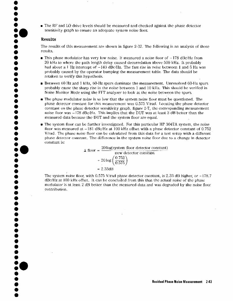
■ The RF and LO drive levels should be measured and checked against the phase detector sensitivity graph to ensure an adequate system noise floor.
Results The results of this measurement are shown in figure 2-32. The following is an analysis of those results. ■ This phase modulator has very low noise. It measured a noise floor of -178 dBc/Hz from
20 kHz to where the path length delay caused decorrelation above 500 kHz. It probably had about a 1 Hz intercept of -143 dBc/Hz. The fast rise in noise between 1 and 5 Hz was probably caused by the operator bumping the measurement table. The data should be retaken to verify this hypothesis.
■ Between 60 Hz and 1 kHz, 60-Hz spurs dominate the measurement. Unresolved 60-Hz spurs probably cause the sharp rise in the noise between 1 and 10 kHz. This should be verified in Noise Monitor Mode using the FFT analyzer to look at the noise between the spurs.
■ The phase modulator noise is so low that the system noise floor must be questioned. The phase detector constant for this measurement was 0.575 V/rad. Locating the phase detector constant on the phase detector sensitivity graph, figure 2-7, the corresponding measurement noise floor was -178 dBc/Hz. This implies that the DUT was at least 3 dB better than the measured data because the DUT and the system floor are equal.
■ The system floor, can be further investigated. For this particular HP 3047A system, the noise floor was measured at -181 dBc/Hz at 100 kHz offset with a phase detector constant of 0.752 V/rad. The phase noise floor can be calculated from this data for a test setup with a different phase detector constant. The difference in the system noise floor due to a change in detector constant is:
A „ 20 logfsystem floor detector constant) A floor =
new detector constant „_. / 0.752 \ = 2 0 1 O gCo575j
= 2.33dB The system noise floor, with 0.575 V/rad phase detector constant, is 2.33 dB higher, or -178.7 dBc/Hz at 100 kHz offset. It can be conclucled from this that the actual noise of the phase modulator is at least 2 dB better than the measured data and was degraded by the noise floor contribution.
Residual Phase Noise Measurement 2-43
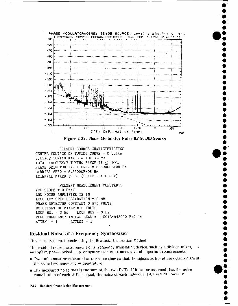
PHRSE MODULflTORNOISE; 6 6 4 0 B SOURCE; L c + l ? . l riBm.RFt-iS.3dBr , „ 4_nVERBCE_5_cnRRiEB FREQ=G.39OE+0SH= Chp]_SEP 15 1935 17:41 17:55
-GO
-?e
-30 -90
-100 -110 -150 -130 -HO -150 -16Q -17G
-IBia F
•I3i2
-2QQ
I i i I 1 1 i 11
Wf-\ i i-v-4'-. i
s ^
-J 1 I 11 1_ in
i i 11 100 IK 10K
C''f i CdBc .■"Hz ) 100K
f CH-i 111 ign
10M
Figure 2-32. Phase Modulator Noise HP 8640B Source
PRESENT SOURCE CHARACTERISTICS CENTER VOLTAGE OF TUNING CURVE = 0 Volts VOLTAGE TUNING RANGE = ±10 Volts TOTAL FREQUENCY TUNING RANGE IS <1 MHz PHASE DETECTOR INPUT FREQ = 6.39000E+08 Hz CARRIER FREQ = 6.39000E+08 Hz INTERNAL MIXER IS 0, (5 MHz - 1.6 GHz)
PRESENT MEASUREMENT CONSTANTS VCO SLOPE = 0 Hz/V LOW NOISE AMPLIFIER IS IN ACCURACY SPEC DEGRADATION = 0 dB PHASE DETECTOR CONSTANT 0.575 VOLTS DC OFFSET OF MIXER = 0 VOLTS LOOP BW1 = 0 Hz LOOP BW3 = 0 Hz ZERO FREQUENCY IN LAG-LEAD = 1.59154943092 E+9 Hz ATTEN1 = 1 ATTEN2 = 1
Residual Noise of a Frequency Synthesizer This measurement is made using the Beatnote Calibration Method. The residual noise measurement of a frequency translating device, such as a divider, mixer, multiplier, phase-locked loop, or synthesizer, must meet several important requirements. ■ Two units must be measured at the same time so that the signals at the phase detector are at
the same frequency and in quadrature. ■ The measured noise data is the sum of the two DUTs. If it can be assumed that the noise
contribution of each DUT is equal, the noise of each individual DUT is 3 dB lower. If
2-44 Residual Phase Noise Measurement
it cannot be assumed that the noise contributions are equal, then a third DUT must be measured against each of the first two DUTs. The data is then processed through a three source comparison program. The output will be the noise of each individual DUT.
Initial Setup In this example, the DUTs were two HP 8663A synthesizers at 639 MHz and +19 dBm output level.
10 MHz OUTPUT
EXTERNAL
INPUT
HP8663A
639 MHz at +19 dBm
HP8663A
639 MHz at +19 dBm
+19 dBm x
/
OPTIONAL UNE
STRECHER
4 +19 dBm
/
HP11848A r I R S~~1 PHASE 1 T DETECTOR
0 i l
^L
l
Figure 2-33. Frequency Synthesizer Measurement Setup
Residual Phase Noise Measurement 2-45
Conditions This measurement was made under the following conditions.
■ The two synthesizers are connected to the same high-stability time base, in this case, located inside one of the DUTs. The second DUT is connected through the time base output of the first DUT. It is critical that the phase shift from the semi-rigid cable and connectors between the two sources be minimized, as it will be multiplied by the DUT multiplication factor at the phase detector in this case, 35.11 dB.
■ The beatnote was generated by setting one of the DUTs to 639.1 MHz during the calibration step, instead of adding a second calibration generator as in the beatnote calibration procedure.
■ The DUTs must be allowed several hours to warm up. This helps to remove phase drift produced by the thermal effects of warm-up.
■ An HP phase shifter was used to obtain and maintain quadrature.
After a 30-minute warm-up period, there was still a significant amount of phase drift between the two instruments. (One DUT had been on all day and was stable.) It was necessary to adjust the phase shifter very slowly during the measurement to maintain quadrature. A sudden movement in the phase correction will look like phase noise close to the carrier and invalidate that data.
Results The results of this measurement are shown in figure 2-34. The following is an analysis of those results. ■ It is important to notice the "amplifier out" indicator in the lower left corner of the phase
noise plot. This indicates that the low-noise amplifier (LN A) in the interface box, after the phase detector, was not used in this measurement. Without the LNA, with phase slope of 0.742 V/rad, the system noise floor is about -160 dBc/Hz.
■ The measured data is for two DUTs. The correction for a single DUT is - 3 dB at all frequency offsets. With that in mind, the broadband noise floor (offsets >2 MHz) is about -154 dBc/Hz. The noise pedestal at 10 kHz offset is -138 dBc/Hz, with 1 Hz intercept of -90 dBc/Hz.
■ There are also some 60 Hz spurs mixed with some unknown noise or spurs. This region should be investigated using the Real-Time Measurement mode. This mode allows the use to manually adjust the spectrum analyzer bandwidth and frequency in the region of interest. The system can then be instructed to make calibrated, single-point measurements of both noise and spurs.
■ The spurs beyond 10 kHz are probably generated inside the HP 8663s. They are all within the - dBc customer specification.
2-46 Residual Phase Noise Measurement
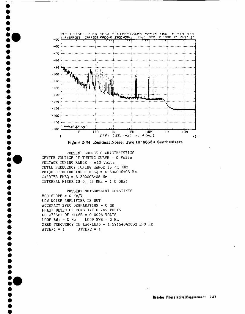
PE5 N O I S E ; 3 hp 6 6 6 3 S Y N T H E S I Z E R S P r - 1 9 d B m ; P I - I S ciBm 4 P.VEPRGES CRPP1ER FFEQ=E. 333£+Q5Hz Chp] 5EP 7 195S 17: 15/17 : 27
i i i 11 I 1—rrr - i—rn r
-7FI
-89
- 3 8
- 1 0 8
- I IS
- i 2 e
-1 3 *
- 1 4 8 -
-ISO
-IbQ 1-
-17Q
■130
;<te^^*^ *!' I ' F '
HMPLIFrEP OUT I I I I I • I I . I I J I l_ -L i - Li. io 1BQ IK IOK 10BK in ian
i C''fi EdBcH-] ■.--: fCHz] +QM
Figure 2-34. Residual Noise: Two HP 8663A Synthesizers
PRESENT SOURCE CHARACTERISTICS CENTER VOLTAGE OF TUNING CURVE = 0 Volts VOLTAGE TUNING RANGE = ±10 Volts TOTAL FREQUENCY TUNING RANGE IS <1 MHz PHASE DETECTOR INPUT FREQ = 6.39000E+08 Hz CARRIER FREQ = 6.39000E+08 Hz INTERNAL MIXER IS 0, (5 MHz - 1.6 GHz)
PRESENT MEASUREMENT CONSTANTS VCO SLOPE = 0 Hz/V LOW NOISE AMPLIFIER IS OUT ACCURACY SPEC DEGRADATION = 0 dB PHASE DETECTOR CONSTANT 0.742 VOLTS DC OFFSET OF MIXER = 0.0026 VOLTS LOOP BW1 = 0 Hz LOOP BW3 = 0 Hz ZERO FREQUENCY IN LAG-LEAD = 1.59154943092 E+9 Hz ATTEN1 = 1 ATTEN2 = 1
Residual Phase Noise Measurement 247
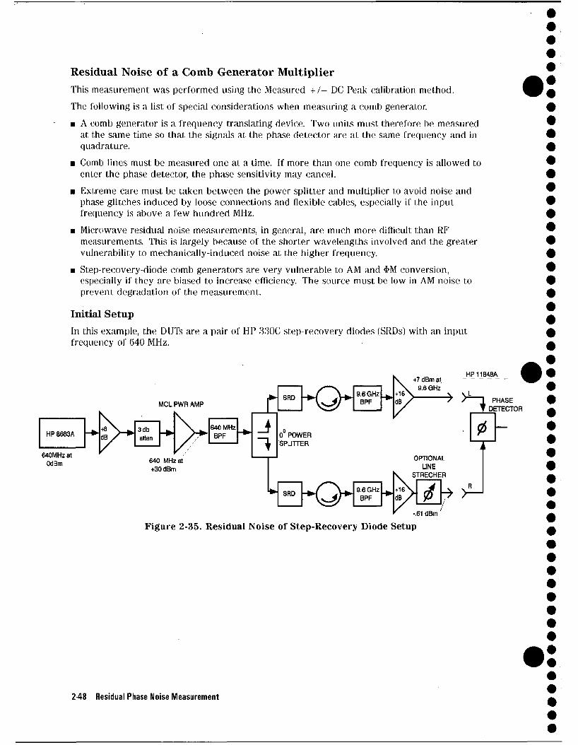
Residual Noise of a Comb Generator Multiplier This measurement was performed using the Measured + / - DC Peak calibration method. The following is a list, of special considerations when measuring a comb generator. ■ A comb generator is a frequency translating device. Two units must therefore be measured
at the same time so that the signals at the phase detector are at the same frequency and in quadrature.
■ Comb lines must be measured one at a time. If more than one comb frequency is allowed to enter the phase detector, the phase sensitivity may cancel.
■ Extreme care must be taken between the power splitter and multiplier to avoid noise and phase glitches induced by loose connections and flexible cables, especially if the input frequency is above a few hundred MHz.
■ Microwave residual noise measurements, in general, are much more difficult than RF measurements. This is largely because of the shorter wavelengths involved and the greater vulnerability to mechanically-induced noise at the higher frequency.
■ Step-recovery-diode comb generators are very vulnerable to AM and <i>M conversion, especially if they are biased to increase efficiency. The source must be low in AM noise to prevent degradation of the measurement.
Initial Setup In this example, the DUTs are a pair of HP 330C step-recovery diodes (SRDs) with an input frequency of 640 MHz.
HP11848A
MCLPWRAMP
HP8663A
640MHz at OdBm
Jj J
SRD 9.6 GHz BPF
0 POWER SPUTTER
SRD ^J 9.6 GHz
BPF
-.61 dBm
Figure 2-35. Residual Noise of Step-Recovery Diode Setup
248 Residual Phase Noise Measurement
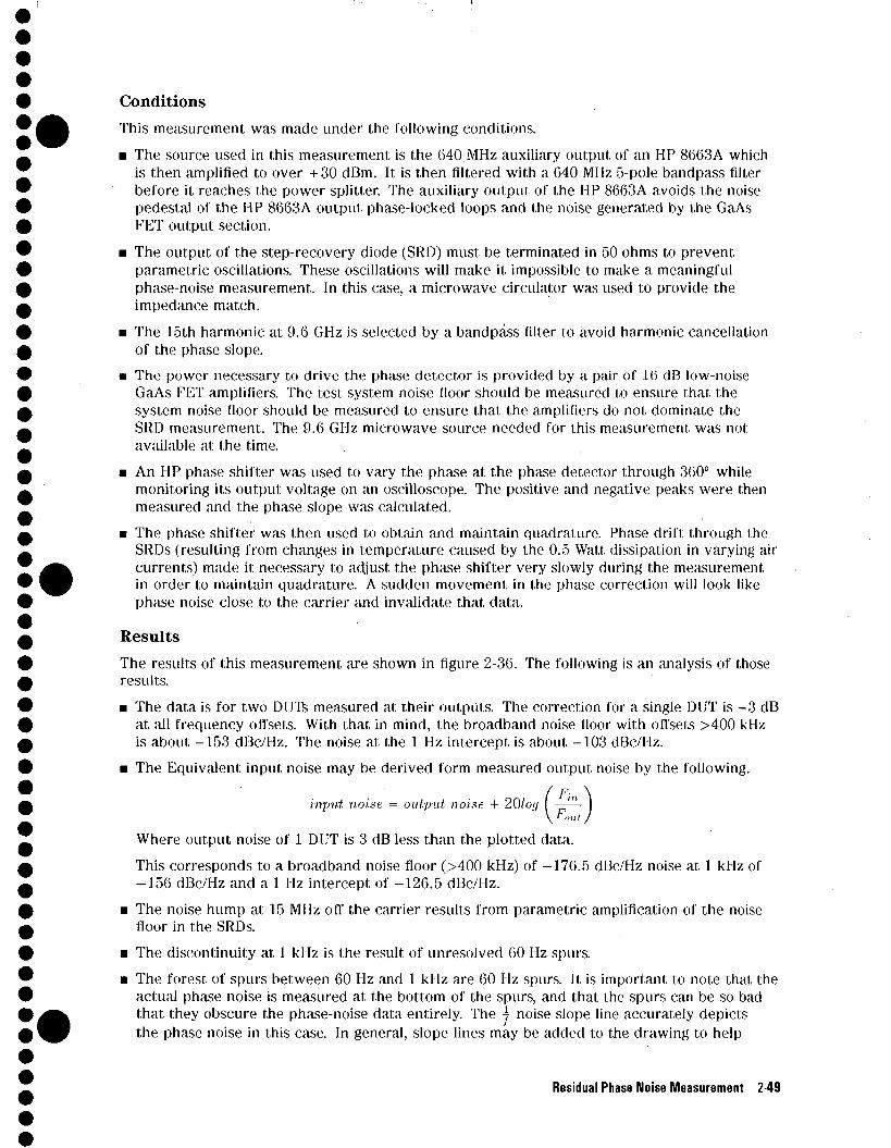
Conditions This measurement was made under the following conditions.
■ The source used in this measurement is the 640 MHz auxiliary output of an HP 8663A which is then amplified to over +30 dBm. It is then filtered with a 640 MHz 5-pole bandpass filter before it reaches the power splitter. The auxiliary output of the HP 8663A avoids the noise pedestal of the HP 8663A output phase-locked loops and the noise generated by the GaAs FET output section.
■ The output of the step-recovery diode (SRD) must be terminated in 50 ohms to prevent parametric oscillations. These oscillations will make it impossible to make a meaningful phase-noise measurement. In this case, a microwave circulator was used to provide the impedance match.
■ The 15th harmonic at 9.6 GHz is selected by a bandpass filter to avoid harmonic cancellation of the phase slope.
■ The power necessary to drive the phase detector is provided by a pair of 16 dB low-noise GaAs FET amplifiers. The test system noise floor should be measured to ensure that the system noise floor should be measured to ensure that the amplifiers do not dominate the SRD measurement. The 9.6 GHz microwave source needed for this measurement was not available at the time.
■ An HP phase shifter was used to vary the phase at the phase detector through 360° while monitoring its output voltage on an oscilloscope. The positive and negative peaks were then measured and the phase slope was calculated.
■ The phase shifter was then used to obtain and maintain quadrature. Phase drift through the SRDs (resulting from changes in temperature caused by the 0.5 Watt dissipation in varying air currents) made it necessary to adjust the phase shifter very slowly during the measurement in order to maintain quadrature. A sudden movement in the phase correction will look like phase noise close to the carrier and invalidate that data.
Results The results of this measurement are shown in figure 2-36. The following is an analysis of those results.
■ The data is for two DUTs measured at their outputs. The correction for a single DUT is - 3 dB at all frequency offsets. With that in mind, the broadband noise floor with offsets >400 kHz is about -153 dBc/Hz. The noise at the 1 Hz intercept is about -103 dBc/Hz.
■ The Equivalent input noise may be derived form measured output noise by the following.
input noise = output noise + 20loq I —— I \FoulJ
Where output noise of 1 DUT is 3 dB less than the plotted data.
This corresponds to a broadband noise floor (>400 kHz) of -176.5 dBc/Hz noise at 1 kHz of -156 dBc/Hz and a 1 Hz intercept of -126.5 dBc/Hz.
■ The noise hump at 15 MHz off the carrier results from parametric amplification of the noise floor in the SRDs.
■ The discontinuity at 1 kHz is the result of unresolved 60 Hz spurs. ■ The forest of spurs between 60 Hz and 1 kHz are 60 Hz spurs. It is important to note that the
actual phase noise is measured at the bottom of the spurs, and that the spurs can be so bad that they obscure the phase-noise data entirely. The j noise slope line accurately depicts the phase noise in this case. In general, slope lines may be added to the drawing to help
Residual Phase Noise Measurement 249
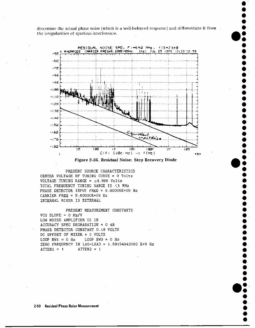
determine the actual phase noise (which is a well-behaved response) and differentiate it from the irregularities of spurious interference.
PE5IDUAL NOISE 5PD; F i - 6 4 0 HHz ; :<15-J3riB 4 RVEPHCES CRRR:ER FREQ=9.SOe!E+09Hr Chp] riJL 27 1355 )2s29'12:?B
43H
Figure 2-36. Residual Noise: Step Recovery Diode
PRESENT SOURCE CHARACTERISTICS CENTER VOLTAGE OF TUNING CURVE = 0 Volts VOLTAGE TUNING RANGE = ±4.995 Volts TOTAL FREQUENCY TUNING RANGE IS <1 MHz PHASE DETECTOR INPUT FREQ = 9.60000E+09 Hz CARRIER FREQ = 9.60000E+09 Hz INTERNAL MIXER IS EXTERNAL
PRESENT MEASUREMENT CONSTANTS VCO SLOPE = 0 Hz/V LOW NOISE AMPLIFIER IS IN ACCURACY SPEC DEGRADATION = 0 dB PHASE DETECTOR CONSTANT 0.19 VOLTS DC OFFSET OF MIXER = 0 VOLTS LOOP BW1 = 0 Hz LOOP BW3 = 0 Hz ZERO FREQUENCY IN LAG-LEAD = 1.59154943092 E+9 Hz ATTEN1 = 1 ATTEN2 = 1
2-50 Residual Phase Noise Measurement
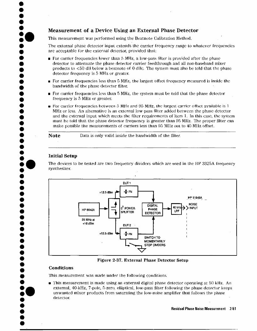
Measurement of a Device Using an External Phase Detector This measurement was performed using the Beatnote Calibration Method. The external phase detector input extends the carrier frequency range to whatever frequencies are acceptable for the external detector, provided that:
■ For carrier frequencies lower than 5 MHz, a low-pass filter is provided after the phase detector to attenuate the phase detector carrier feedthrough and all non-baseband mixer products to <50 dB below a beatnote of 0 dBc. The system must also be told that the phase detector frequency is 5 MHz or greater.
■ For carrier frequencies less than 5 MHz, the largest offset frequency measured is inside the bandwidth of the phase detector filter.
■ For carrier frequencies less than 5 MHz, the system must be told that the phase detector frequency is 5 MHz or greater.
■ For carrier frequencies between 5 MHz and 95 MHz, the largest, carrier offset available is 1 MHz or less. An alternative is an external low-pass filter added between the phase detector and the external input which meets the filter requirements of item 1. In this case, the system must be told that the phase detector frequency is greater than 95 MHz. The proper filter can make possible the measurements of carriers less than 95 MHz out to 40 MHz offset.
Note Data is only valid inside the bandwidth of the filter.
Initial Setup The devices to be tested are two frequency dividers which are used in the HP 3325A frequency synthesizer.
HP8642A
25 MHz at +16dBm
+12.5 dBm i^-
—*- J
+12 5 dBm fe.
DUT1
-J-FN
0° POWER SPLITTER
DUT2
-J-FN
L-
i ' DIGITAL PHASE
DETECTOR
i
swrrc
^
MOME STOP
— * ■
[
HTO NTARIl DIVDEF
.Y IS
r NOISb
40 kHz \ |NpuT LPF
Figure 2-37. External Phase Detector Setup
Conditions This measurement was made under the following conditions. ■ This measurement is made using an external digital phase detector operating at 50 kHz. An
external, 40-kHz, 7-pole, 5-zero, elliptical, low-pass filter following the phase detector keeps unwanted mixer products from saturating the low-noise amplifier that follows the phase detector.
Residual Phase Noise Measurement 2-51
■ Care must be taken to minimize ground loops and sources of 66 Hz noise when using the external input. This prevents 60 Hz spurs from masking the noise data.
■ The calibration beatnote was generated by changing the divide number of one of the two dividers which produced a frequency difference at the phase detector.
■ Quadrature is achieved by starting dividers in the correct phase. This is accomplished by letting one divider operate continuously, while momentarily pausing the other. It may take several tries to get the second divider to start in the right phase.
Results The results of this measurement are shown in figure 2-38. The following is an analysis of those results. ■ The data is for two DUTs measured at their outputs. The correction for a single DUT is - 3 dB
at all frequency offsets. With that in mind, the broadband noise floor with offsets less than 100 Hz is about, -172.5 dBc/Hz. The noise at the 1 Hz intercept is about -153 dBc/Hz. The ability of the system to draw slope lines at any offset and slope often simplifies interpretation of the data.
■ The graph looks very well-behaved. The spurs in the region between 60 Hz and 1 kHz are 60 Hz spurs which are all below -120 dBc.
■ The spurs at 50 kHz and its multipliers are phase-detector feedthrough and undesired mixer products which are all below -.100 dBc.
■ The data beyond 40 kHz is attenuated by the feedthrough filter.
2-52 Residual Phase Noise Measurement
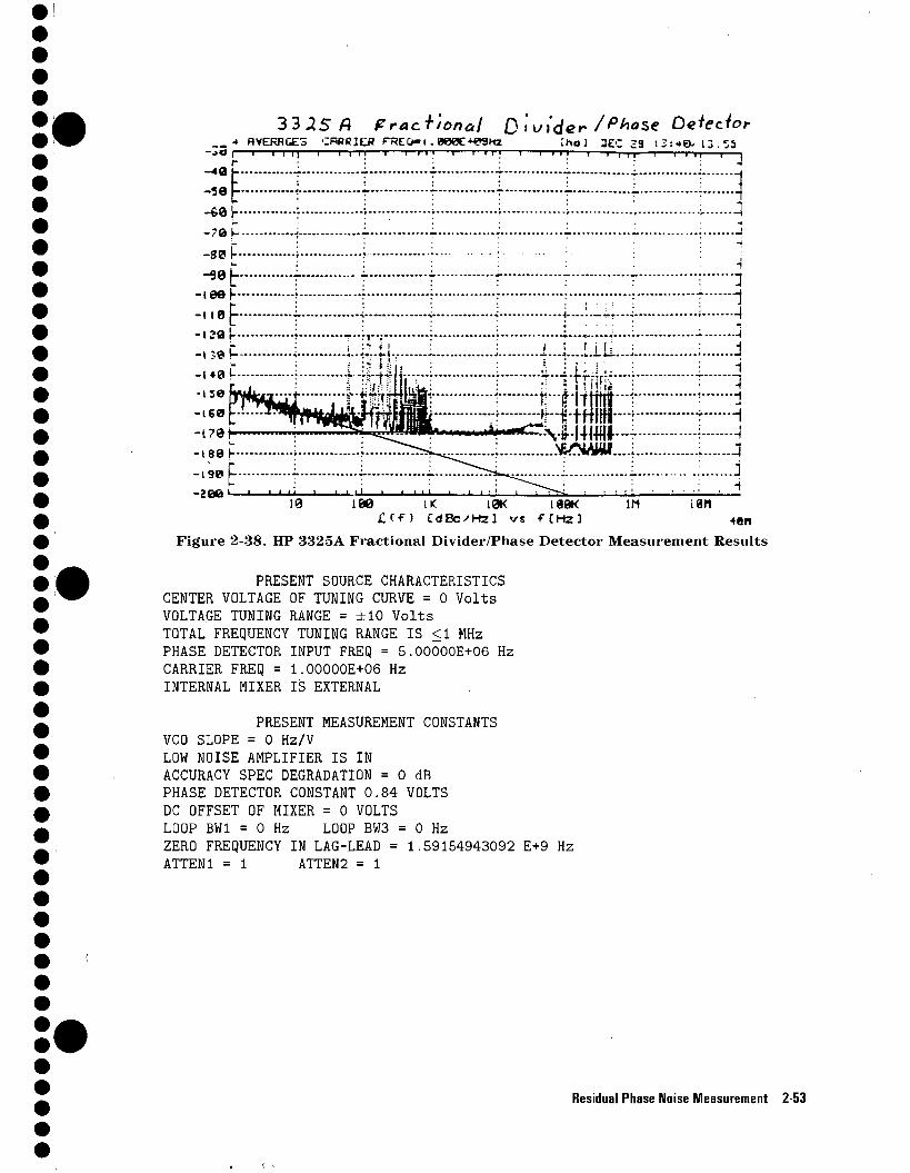
33 25 ft Prac + 'tonat 0 i'i/i'der /Phase Detector ._ 4 RVEKHCE3 CRHRltR FREO-i.aeee^egMz Choi 3EC 29 l3:-»€^ 13:55
1 W IK 10K 198K £ C f > C d B c / H z ] vs f [ H z ] ■♦an
Figure 2-38. HP 3325A Fractional Divider/Phase Detector Measurement Results
PRESENT SOURCE CHARACTERISTICS CENTER VOLTAGE OF TUNING CURVE = 0 Volts VOLTAGE TUNING RANGE = ±10 Volts TOTAL FREQUENCY TUNING RANGE IS <1 MHz PHASE DETECTOR INPUT FREQ = 5.00000E+06 Hz CARRIER FREQ = 1.00000E+06 Hz INTERNAL MIXER IS EXTERNAL
PRESENT MEASUREMENT CONSTANTS VCO SLOPE = 0 Hz/V LOW NOISE AMPLIFIER IS IN ACCURACY SPEC DEGRADATION = 0 dB PHASE DETECTOR CONSTANT 0.84 VOLTS DC OFFSET OF MIXER = 0 VOLTS LOOP BW1 = 0 Hz LOOP BW3 = 0 Hz ZERO FREQUENCY IN LAG-LEAD = 1.59154943092 E+9 Hz ATTEN1 = 1 ATTEN2 = 1
Residual Phase Noise Measurement 2-53
3 AM-Source Noise Measurement
AM-Noise Measurement Theory of Operation
Basic Noise Measurement The HP 3048A phase noise measurement system measures noise by: ■ Calibrating of the noise detector sensitivity. ■ Measuring the recovered baseband noise out to the detector. ■ Calculating the noise around the signal by multiplying the measured data by the detector
sensitivity. ■ Displaying the measured noise data in the required format.
Once the detector is calibrated, the system looks at the signal out of the detector as just a noise voltage which must be measured over a band of frequencies regardless of the signal's origin. The detector calibration is accomplished by applying a known signal to the detector. The known signal is then measured at baseband. Finally, the transfer function between the known signal and the measurement baseband signal is calculated.
Phase Noise Measurement In the case of small angle phase modulation (<0.1 rad), the modulation sidebands' amplitude is constant with increasing modulation frequency. The phase detector gain can thus be measured at a single offset frequency, and the same constant will apply at all offset frequencies.
■ In the case of calibrating with phase modulation sidebands, the system requires the carrier-to-sideband ratio and the frequency offset of the sidebands. The offset frequency is equal to the baseband frequency where the signal can be found. The ratio of the baseband signal voltage to the carrier-to-sideband ratio is the sensitivity of the detector.
■ In the case of calibrating with a single-sided spur, it can be shown (see appendix C) that a single-sided spur is equal to a <i>M signal plus an AM signal. The modulation sidebands for both are 6 dB below the original single-sided spur. Since the phase detector attenuates the AM by more than 30 dB, the calibration constant can be measured as in the previous case, but with an additional 6 dB correction factor.
AM-Source Noise Measurement 3-1
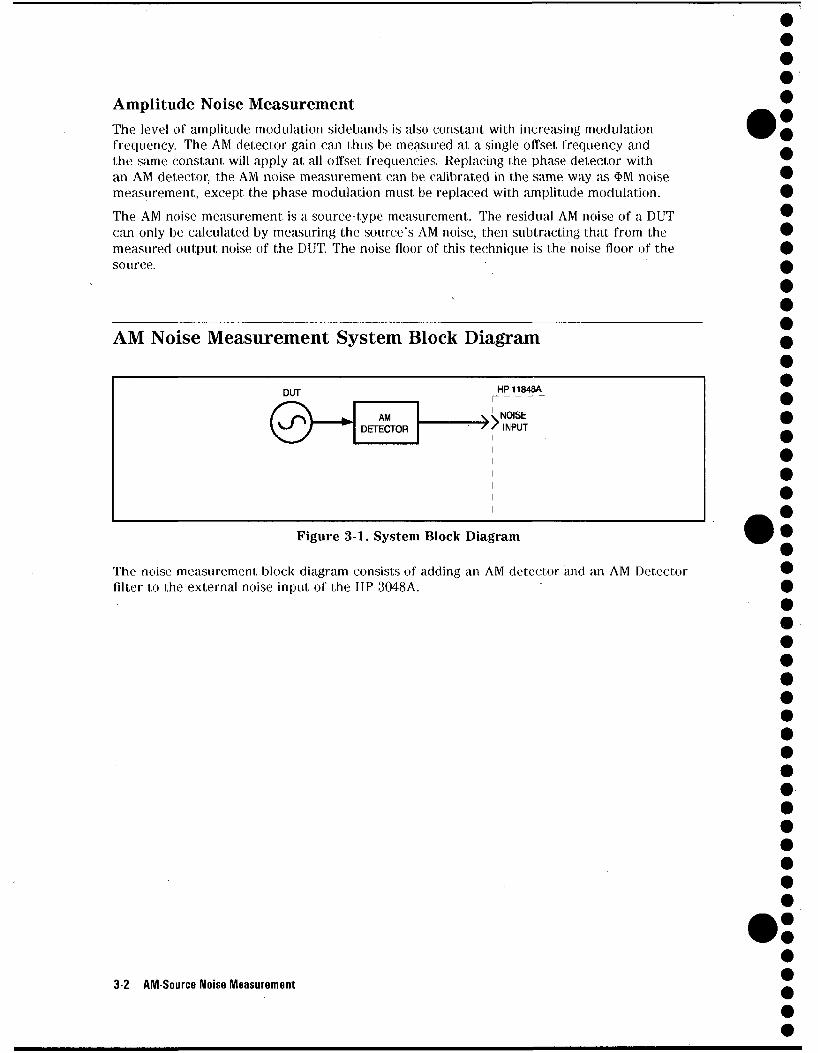
Amplitude Noise Measurement The level of amplitude modulation sidebands is also constant with increasing modulation frequency. The AM detector gain can thus be measured at a single offset frequency and the same constant will apply at all offset, frequencies. Replacing the phase detector with an AM detector, the AM noise measurement can be calibrated in the same way as <i>M noise measurement, except the phase modulation must be replaced with amplitude modulation. The AM noise measurement is a source-type measurement. The residual AM noise of a DUT can only be calculated by measuring the source's AM noise, then subtracting that from the measured output noise of the DUT. The noise floor of this technique is the noise floor of the source.
AM Noise Measurement System Block Diagram
DUT
<2H —► AM DETECTOR
\ /
HP11848A
v NOISE r INPUT
Figure 3-1. System Block Diagram
The noise measurement block diagram consists of adding an AM detector and an AM Detector filter to the external noise input of the HP 3048A.
3-2 AM-Source Noise Measurement
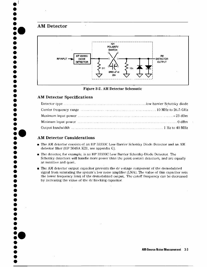
AM Detector
RF INPUT-HP33330C
DIODE DETECTOR
AM ■ DETECTOR
OUTPUT
Figure 3-2. AM Detector Schematic
AM Detec tor Spec i f i ca t ions
Detector type low barrier Schottky diode Carrier frequency range 10 MHz to 26.5 GHz Maximum input power - +23 dBm Minimum input power 0 dBm Output bandwidth 1 Hz to 40 MHz
AM Detector Considerations ■ The AM detector consists of an HP 33330C Low-Barrier Schottky Diode Detector and an AM
detector filter (HP 3048A K21, see appendix G). ■ The detector, for example, is an HP 33330C Low-Barrier Schottky-Diode Detector. The
Schottky detectors will handle more power than the point contact detectors, and are equally as sensitive and quiet.
■ The AM detector output capacitor prevents the dc voltage component of the demodulated signal from saturating the system's low noise amplifier (LNA). The value of this capacitor sets the lower frequency limit of the demodulated output. The cutoff frequency can be decreased by increasing the value of the dc blocking capacitor.
AM-Source Noise Measurement 3-3
■ Carrier feedthrough in the detector may be excessive for frequencies below a few hundred megahertz. The LNA is protected from saturation by the internal filters used to absorb phase detector feedthrough and unwanted mixer products. This limits the maximum carrier offset frequency to 1 MHz for input frequencies of less than 95 MHz and 40 MHz for carriers above 95 MHz. "
■ The 511 ohm resistor in the AM detector sets the dc bias-current in the diode detector. The ac load is 50 ohms, set by the input impedance of the test system. The 50 ohm load increases the detector bandwidth to greater than 40 MHz.
■ A high impedance monitor port is provided on the AM detector for measuring calibration constants. This port must be bypassed with a feedthrough capacitor to prevent noise from entering the main signal path. It must not be connected during the actual noise measurement.
■ The HP 11848A Phase Noise Interface must be dc blocked when using its NOISE INPUT. The interface will not tolerate more than ± 2 mV DC Input without overloading the LNA. A DC block must be connected in series after the AM Detector to remove the dc component. The HP 3048A Option K21 is designed specifically for this purpose.
Steps for Making AM Noise Measurements 1. Connect the system hardware and load/run the software. 2. Measure the system calibration data. (System calibration data is the correction data for all
signal paths in the interface box.) 3. Main menu - Select the type of measurement to be made. 4. Establish parameters
a. Source parameters ■ Phase detector input frequency ■ Carrier frequency ■ Select external detector ■ Select calibration option
b. Measurement parameters ■ Start, and stop frequency of measurement data
□ Without RF analyzer 0.01 Hz to 100 kHz □ With RF analyzer 0.01 Hz to 40 MHz
■ Number of sweeps averaged on FFT analyzer
3-4 AM-Source Noise Measurement
c. Plot parameters ■ Graph type (usually Single-Sideband Phase Noise) ■ Plotter type (if any) ■ Minimum and maximum Y-axis (dBc) ■ Minimum and maximum X-axis (Hz) ■ Title
d. Measure ■ Connect-up the device-under-test (DUT) and external hardware ■ Measure calibration data by selected option
■ Measure noise data e. Interpret the measurement, result
AM-Source Noise Measurement 3-5
Choosing a Calibration Method
Method 1: User entry of phase detector constant
Method 1, Example 1 Advantages Easy method of calibrating the measurement system
Will measure DUT without modulation capability. Requires only an RF power meter to measure drive levels into the AM detector. Fastest method of calibration. If the same power levels are always at the AM detector, as in the case of leveled outputs, the AM detector sensitivity will always be essentially the same. Super-quick method of estimating the equivalent phase detector constant.
Disadvantages It is the least accurate of the calibration methods. It does not, take into account the amount, of power at harmonics of the signal. It, does not take into account the power which may be generated by spurious oscillations, causing the power meter to measure much more power than is at the AM detector.
Method 1, Example 2 Advantages Easy method of calibrating the measurement system.
Will measure DUT without modulation capability. Requires little additional equipment: only a voltmeter or an oscilloscope. Fastest method of calibration. If the same power levels are always at the AM ■detector, as in the case of leveled outputs, the AM detector sensitivity will always be essentially the same. Measures the AM detector gain in the actual measurement configuration. Super-quick method of estimating the equivalent, phase detector constant.
Disadvantages Has only moderate accuracy compared to the other calibration methods.
3-6 AM-Source Noise Measurement
Method 2: Double Sided Spur
Method 2, Example 1 Advantages Requires only one RF source (DUT)
Calibration is done under actual measurement conditions so all non-linearities and harmonics of the AM detector are calibrated out. The double-sided spur method and the single-sided-spur method are the two most accurate methods for this reason.
Disadvantages Required that the DUT have adjustable AM which may also be turned off.
Requires the AM of the DUT to be extremely accurate; otherwise an RF spectrum analyzer, or modulation analyzer, for manual measurement of AM sidebands is required.
Method 2, Example 2
Advantages Will measure source without modulation capability
Calibration is done under actual measurement conditions so all non-linearities and harmonics of the AM detector are calibrated out. The double-sided spur method and the single-sided-spur method are the two most accurate methods for this reason.
Disadvantages Requires a second RF source with very accurate AM modulation and output power sufficient to match the DUT. If the AM modulation is not very accurate, a spectrum analyzer or modulation analyzer must be used to make manual measurement of the AM sidebands.
Method 3: Single-Sided-Spur Method Advantages Will measure source without modulation capability.
Calibration is done under actual measurement conditions so all non-linearities and harmonics of the AM detector are calibrated out. The double-sided spur method and the single-sided-spur method are the two most accurate methods for this reason.
Disadvantages Requires 2 RF sources, which must be between 1 Hz and 40 MHz apart in frequency. Requires an RF spectrum analyzer for manual measurement of the signal-to-spur ratio and spur offset.
AM-Source Noise Measurement 3
Calibration and Measurement General Guidelines Read This The following general guidelines should be considered when setting up and
making an AM-noise measurement.
■ The AM detector must be well shielded from external noise especially 60 Hz noise. The components between the diode detector and the test system should be packaged in a metal box to prevent RFI interference. Also, the AM detector should be connected directly to the test system if possible, to minimize ground loops. If the AM detector and test system must be separated, semi-rigid cable should be used to keep the shield resistance to a minimum.
■ Although AM noise measurements are less vulnerable than residual phase-noise measurements to noise induced by vibration and temperature fluctuation, care should be taken to ensure that all connections are tight and that all cables are electrically sound.
■ The output voltage monitor on the AM detector must be disconnected from digital voltmeters or other noisy monitoring equipment before noise measurement data is taken.
■ The j noise floor of the detector may degrade as power increases above +15 dBm. Noise in the j region of the detector is best measured with about + 10 dBm of drive level. The noise floor is best measured with about +20 dBm of drive level.
■ An amplifier must be used in cases where the signal level out of the DUT is too small to drive the AM detector or is inadequate to produce a low enough measurement noise floor. In this case the amplifier should have the following characteristics. D It should have the lowest possible noise figure, and the greatest possible dynamic range. D The signal level must be kept as high as possible at all points in the test setup to avoid
noise floor degradation. a It should have only enough gain to get the required signal levels. Excess gain leads to
amplifiers operating in gain compression, increasing their likelihood of suppressing the AM noise to be measured.
D The amplifier's sensitivity to power supply noise and the supply noise itself must both be minimized.
3-8 AM-Source Noise Measurement
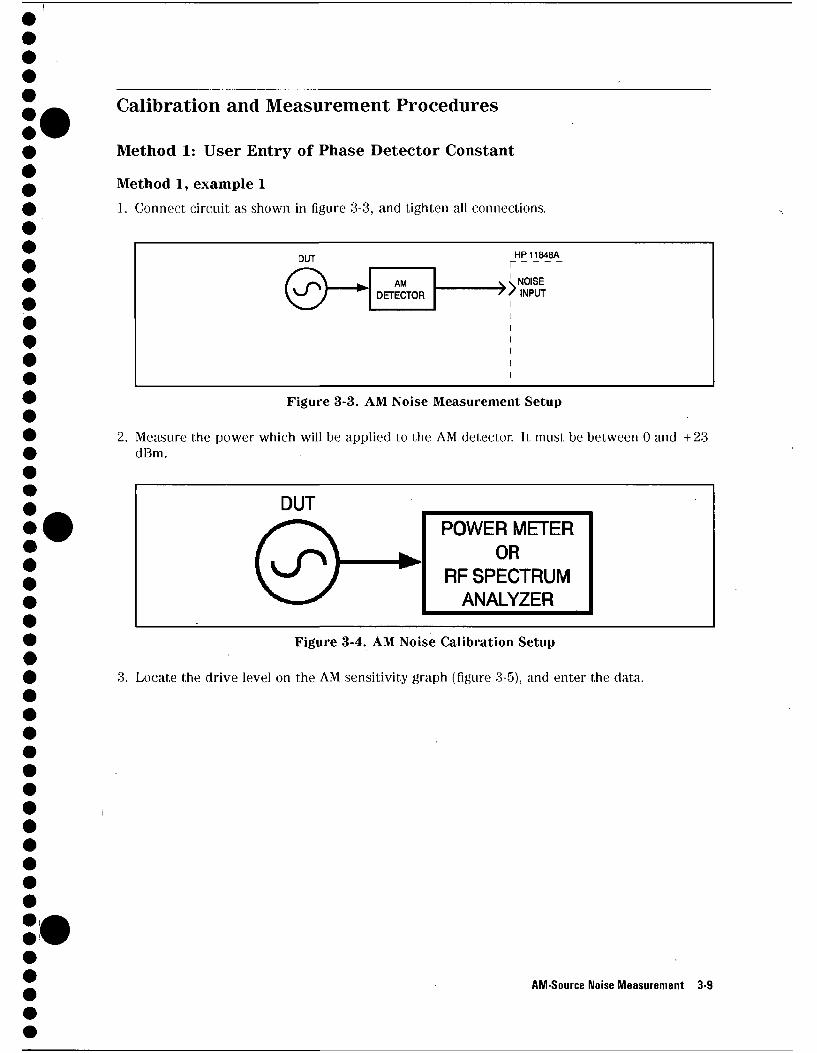
Calibration and Measurement Procedures
Method 1: User Entry of Phase Detector Constant
Method 1, example 1 1. Connect circuit as shown in figure 3-3, and tighten all connections.
DUT
0-—► AM DETECTOR
^
HP11848A I
v NOISE 7 / INPUT
Figure 3-3. AM Noise Measurement Setup
2. Measure the power which will be applied to the AM detector. It must be between 0 and +23 dBm.
DUT
(oy-POWER METER
OR RF SPECTRUM
ANALYZER
Figure 3-4. AM Noise Calibration Setup
3. Locate the drive level on the AM sensitivity graph (figure 3-5), and enter the data.
AM-Source Noise Measurement 3-9
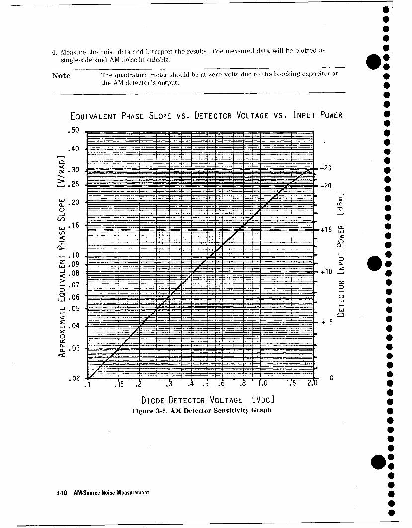
4. Measure the noise data and interpret the results. The measured data will be plotted as single-sideband AM noise in dBc/Hz.
Note The quadrature meter should be at zero volts due to the blocking capacitor at the AM detector's output.
DIODE DETECTOR VOLTAGE [VDC] Figure 3-5. AM Detector Sensitivity Graph
3-10 AM-Source Noise Measurement
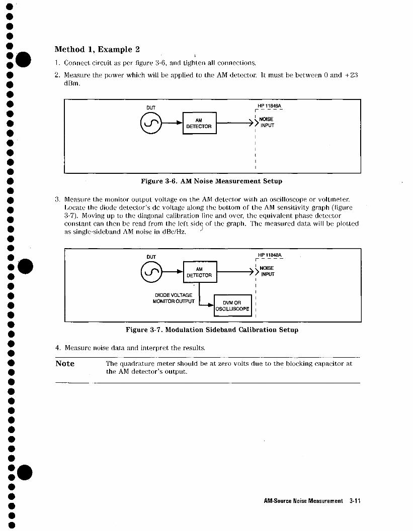
Method 1, Example 2 1. Connect circuit as per figure 3-6, and tighten all connections.
2. Measure the power which will be applied to the AM detector. It must be between 0 and +23 dBm.
DUT
f?) . KO AM
DETECTOR
HPVI848A_
\ Jy NOISE 7 ' INPUT
Figure 3-6. AM Noise Measurement Setup
3. Measure the monitor output voltage on the AM detector with an oscilloscope or voltmeter. Locate the diode detector's dc voltage along the bottom of the AM sensitivity graph (figure 3-7). Moving up to the diagonal calibration line and over, the equivalent phase detector constant can then be read from the left side of the graph. The measured data will be plotted as single-sideband AM noise in dBc/Hz.
DUT
C?\ r K£) AM
DETECTOR
MONITOR OUTPUT
\
HP11848A I
J . NOISE / / INPUT
DVMOR OSCILUSCOPE
Figure 3-7. Modulation Sideband Calibration Setup
4. Measure noise data and interpret the results.
Note The quadrature meter should be at zero volts due to the blocking capacitor at the AM detector's output.
AM-Source Noise Measurement 3-11
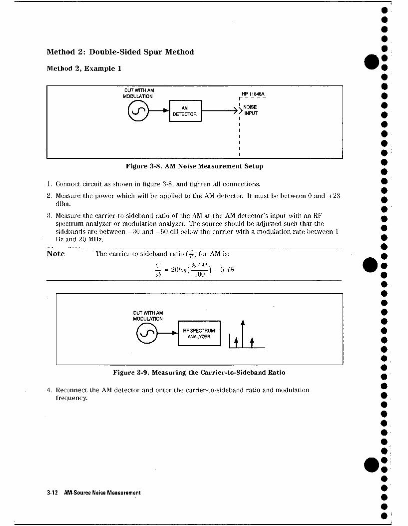
Method 2: Double-Sided Spur Method
Method 2, Example 1
DUTWITHAM MODULATION
f?\ . \£) AM DETECTOR
HPrj84SA_
v l NOISE 7 / INPUT
Figure 3-8. AM Noise Measurement Setup
1. Connect circuit as shown in figure 3-8, and tighten all connections. 2. Measure the power which will be applied to the AM detector. It must be between 0 and +23
dBm.
3. Measure the carrier-to-sideband ratio of the AM at the AM detector's input with an RF spectrum analyzer or modulation analyzer. The source should be adjusted such that the sidebands are between -30 and -60 dB below the carrier with a modulation rate between 1 Hz and 20 MHz.
Note The carrier-to-sideband ratio (^) for AM is:
C.MM*^)-^
DUTWITHAM MODULATION
<2> RF SPECTRUM ANALYZER
A 1
Figure 3-9. Measuring the Carrier-to-Sideband Ratio
4. Reconnect the AM detector and enter the carrier-to-sideband ratio and modulation frequency.
3-12 AM-Source Noise Measurement
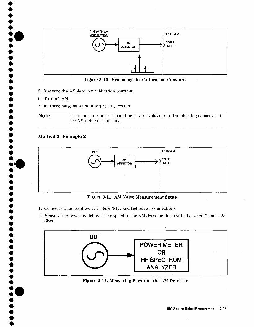
D m WITH AM MODULATION
AM DETECTOR
HPV1848A_
■ »
NOISE INPUT
Li i Figure 3-10. Measuring the Calibration Constant
5. Measure the AM detector calibration constant. 6. Turn off AM. 7. Measure noise data and interpret the results.
Note The quadrature meter should be at zero volts due to the blocking capacitor at the AM detector's output.
Method 2, Example 2
DUT
(?) -y£) AM
DETECTOR
HP11848A
v i. NOISE 7? INPUT
Figure 3-11. AM Noise Measurement Setup
1. Connect circuit as shown in figure 3-11, and tighten all connections.
2. Measure the power which will be applied to the AM detector. It must be between 0 and +23 dBm.
DUT
fr) » \£) POWER METER
OR RF SPECTRUM
ANALYZER
•
Figure 3-12. Measuring Power at the AM Detector
AM-Source Noise Measurement 3-13
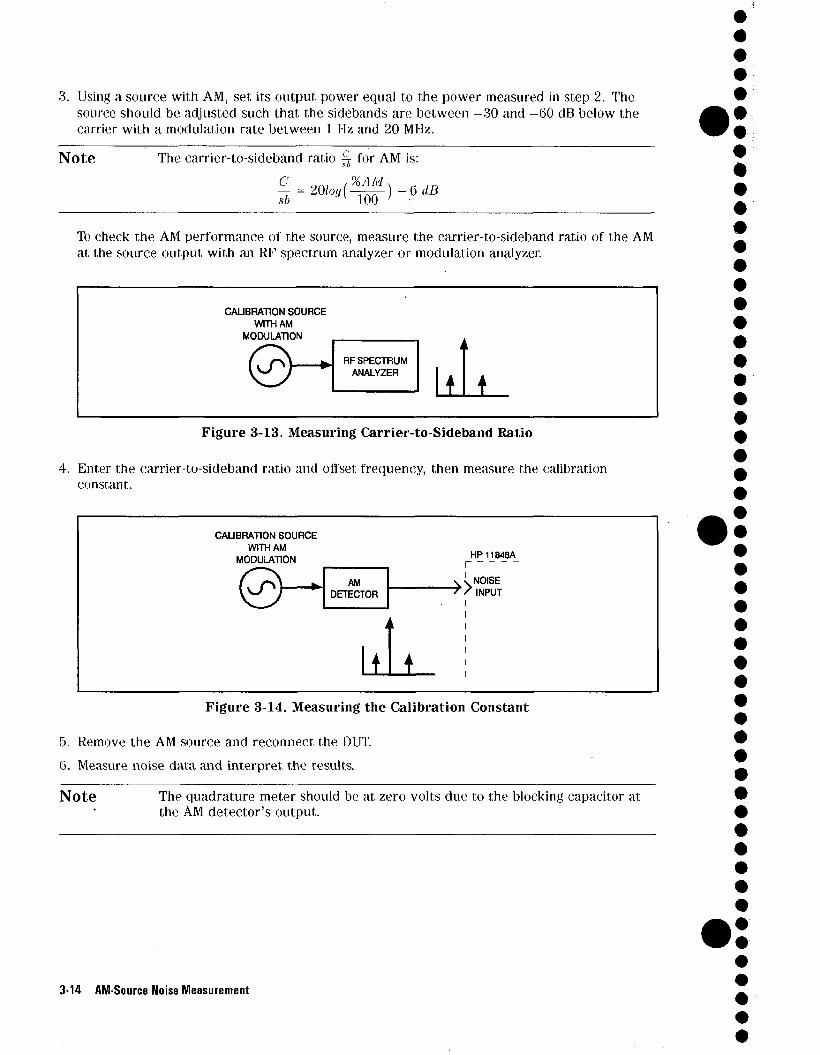
3. Using a source with AM, set, its output power equal to the power measured in step 2. The source should be adjusted such that, the sidebands are between -30 and -60 dB below the carrier with a modulation rate between 1 Hz and 20 MHz.
Note The carrier-to-sideband ratio ^ for AM is:
To check the AM performance of the source, measure the carrier-to-sideband ratio of the AM at the source output, with an RF spectrum analyzer or modulation analyzer.
CALIBRATION SOURCE WITH AM
MODULATION
& RFSPECTRUM
ANALYZER 1 ± Figure 3-13. Measuring Carrier-to-Sideband Ratio
4. Enter the carrier-to-sideband ratio and offset frequency, then measure the calibration constant.
CALIBRATION SOURCE WITH AM
MODULATION HP11848A
& AM
DETECTOR
r _v ^ NOISE ' S INPUT
1 ± Figure 3-14. Measuring the Calibration Constant
5. Remove the AM source and reconnect the DUT. 6. Measure noise data and interpret the results.
Note The quadrature meter should be at zero volts due to the blocking capacitor at the AM detector's output.
3-14 AMSource Noise Measurement
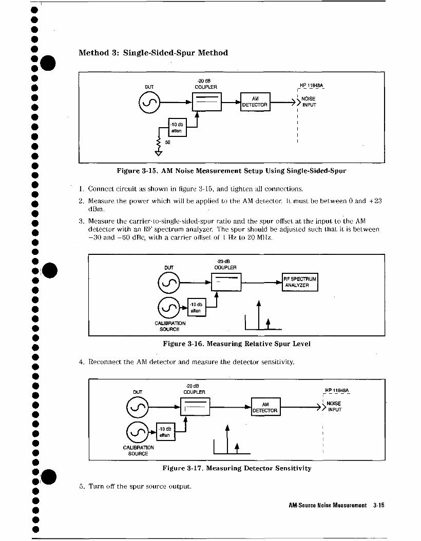
Method 3: Single-Sided-Spur Method
DUT 0 1
-■10 db atten
: 50
-20 dB COUPLER
i t
AM DETECTOR
HP11848A
v v NOISE y ? INPUT
Figure 3-15. AM Noise Measurement Setup Using Single-Sided-Spur
1. Connect circuit as shown in figure 3-15, and tighten all connections. 2. Measure the power which will be applied to the AM detector. It must be between 0 and +23
dBm. 3. Measure the carrier-to-single-sided-spur ratio and the spur offset at the input to the AM
detector with an KF spectrum analyzer. The spur should be adjusted such that it is between -30 and -60 dBc, with a carrier offset of I Hz to 20 MHz.
DUT
(r\ K£)
CALIBRATION
-10db atten
-20 dB COUPLER
I
Jk
i k
RFSPECTRUM ANALYZER
Figure 3-16. Measuring Relative Spur Level
4. Reconnect the AM detector and measure the detector sensitivity.
DUT -20 dB
COUPLER HP11848A
0-0H
CALIBRATION SOURCE
-10 db atten
AM DETECTOR ■ »
NOISE INPUT
1 Figure 3-17. Measuring Detector Sensitivity
5. Turn off the spur source output.
AM-Source Noise Measurement 3-15
6. Measure noise data and interpret the results.
Note The quadrature meter should be at zero volts due to the blocking capacitor at the AM detector's output.
3-16 AM Source Noise Measurement
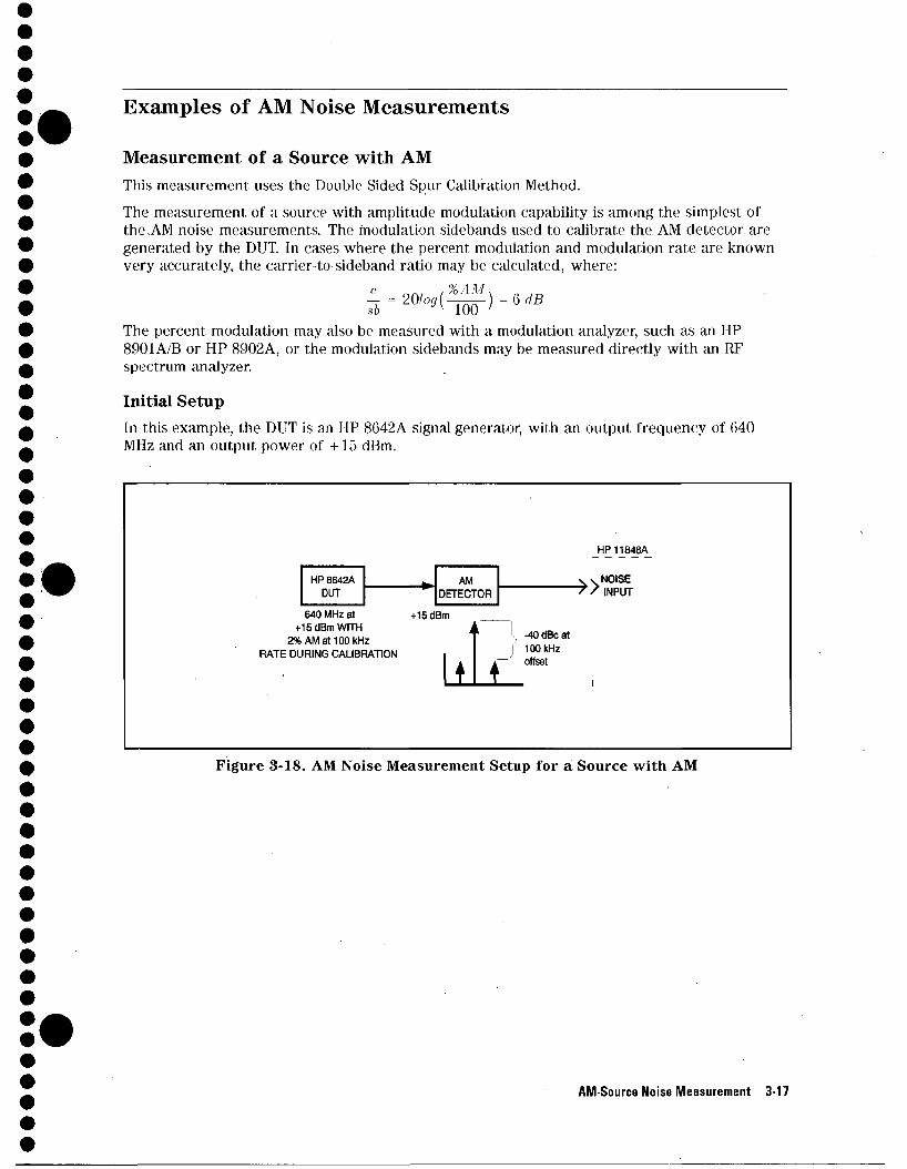
Examples of AM Noise Measurements
Measurement of a Source with AM This measurement uses the Double Sided Spur Calibration Method.
The measurement of a source with amplitude modulation capability is among the simplest of the,AM noise measurements. The modulation sidebands used to calibrate the AM detector are generated by the DUT. In cases where the percent modulation and modulation rate are known very accurately, the carrier-to-sideband ratio may be calculated, where:
c
lb 2 0 / o , ( ^ ) - 6 f / 5
The percent modulation may also be measured with a modulation analyzer, such as an HP 8901A/B or HP 8902A, or the modulation sidebands may be measured directly with an RF spectrum analyzer.
Initial Setup In this example, the DUT is an HP 8642A signal generator, with an output frequency of 640 MHz and an output power of +15 dBm.
HP8642A DUT
640 MHz at +15dBmWITH
2% AM at 100 kHz RATE DURING CALIBRATION
+15 d
AM DETECTOR
Bm i
It
HP11848A I
N v NOISE ' ' INPUT
'., -40dBoat ' |' 100 kHz '
~ offset
Figure 3-18. AM Noise Measurement Setup for a Source with AM
AM-Source Noise Measurement 3-17
Conditions This measurement was performed under the following conditions. ■ All the power required to drive the AM detector is provided by the DUT. ■ The AM detector is calibrated by setting the DUT to 2% AM at a 100 kHz modulation rate.
This produces -40 dBc amplitude modulation sidebands with an offset of 100 kHz. ■ The modulation sideband amplitude was verified with an HP 8568A RF spectrum analyzer.
■ The signal power must not significantly change when the calibration modulation is removed.
■ The quadrature meter should be at zero volts due to the blocking capacitor in the AM detector.
Results The results of this measurement are shown in figure 3-19. The following is an analysis of those results. ■ The signal generator, measured at 640 MHz, has an AM noise floor of -160 dBc/Hz at carrier
offsets greater than 50 kHz, with a 1 Hz intercept of -123 dBc/Hz. It is important to note that the HP 8642A signal generator has one of the lowest AM noise floors available, which makes it an excellent signal source for residual 2-port phase noise measurements.
■ The spurs between 60 Hz and 1 kHz are due to 60 Hz line spurs, possibly induced by a ground loop between the DUT and the test system.
■ The discontinuity at 1 kHz is caused by unresolved 60 Hz spurs. ■ All the remaining spurs above 10 kHz are less than the DUT's -100 dBc spur specification.
3-18 AMSource Noise Measurement
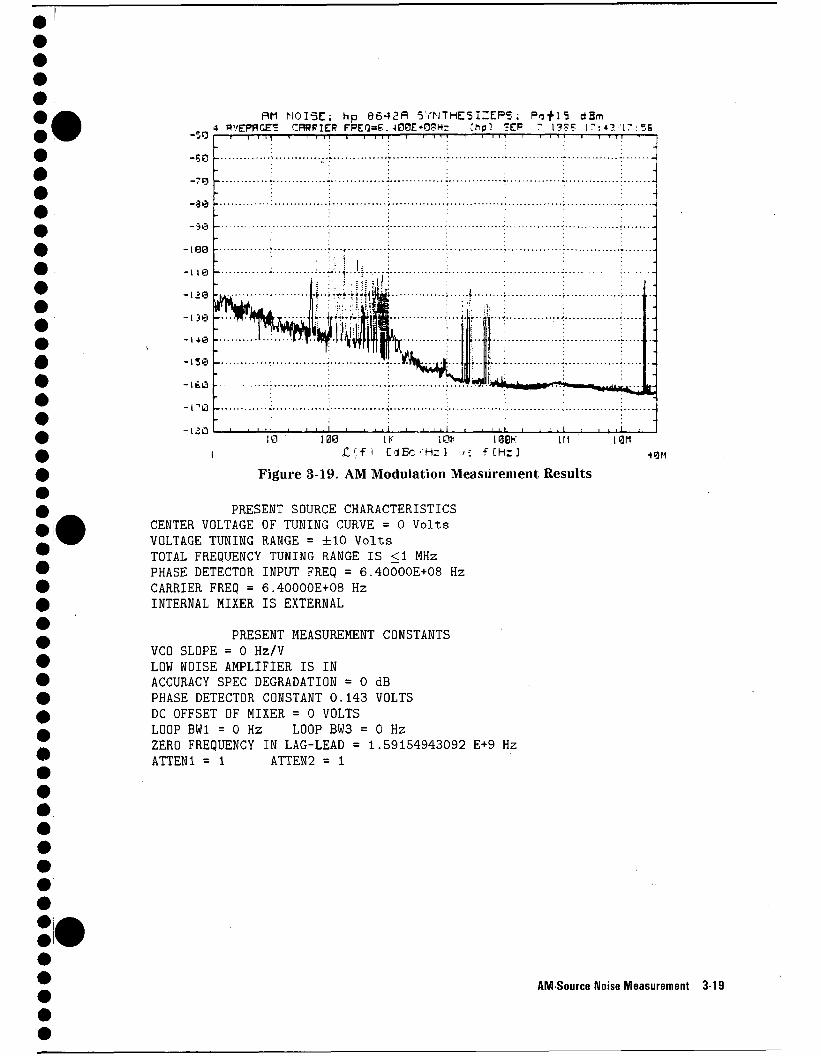
I
flfl N O I S E ; hp 66421=1 SYNTHESIZEPS; P n f l 5 dBm 4 BVEPHCES CRRFIER FPEQ=S. -tCIOE+gSH- Chp] "EP 7 1356 17:*3' '17:3B
10 ' 100 IK lOh ,C'fi CdBCHz]
100K f CHs]
in ian ■»gn
Figure 3-19. A M Modulation Measurement Results
PRESENT SOURCE CHARACTERISTICS CENTER VOLTAGE OF TUNING CURVE = 0 Volts VOLTAGE TUNING RANGE = ±10 Volts TOTAL FREQUENCY TUNING RANGE IS <1 MHz PHASE DETECTOR INPUT FREQ = 6.40000E+08 Hz CARRIER FREQ = 6.40000E+08 Hz INTERNAL MIXER IS EXTERNAL
PRESENT MEASUREMENT CONSTANTS VCO SLOPE = 0 Hz/V LOW NOISE AMPLIFIER IS IN ACCURACY SPEC DEGRADATION = 0 dB PHASE DETECTOR CONSTANT 0.143 VOLTS DC OFFSET OF MIXER = 0 VOLTS LOOP BW1 = 0 Hz LOOP BW3 = 0 Hz ZERO FREQUENCY IN LAG-LEAD = 1.59154943092 E+9 Hz ATTEN1 = 1 ATTEN2 = 1
AM Source Noise Measurement 3-19
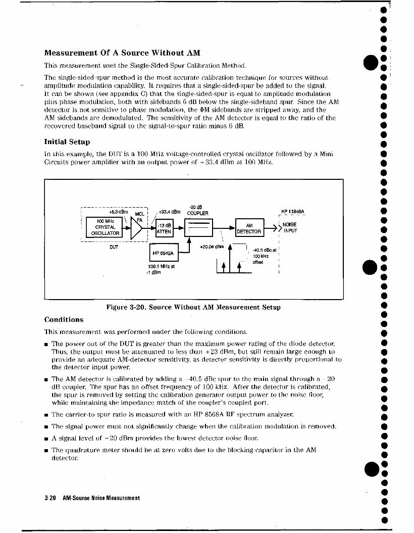
Measurement Of A Source Without AM This measurement uses the Single-Sided-Spur Calibration Method. The single-sided-spur method is the most accurate calibration technique for sources without amplitude modulation capability. It requires that a single-sided-spur be added to the signal. It can be shown (see appendix C) that the single-sided-spur is equal to amplitude modulation plus phase modulation, both with sidebands 6 dB below the single-sideband spur. Since the AM detector is not sensitive to phase modulation, the $M sidebands are stripped away, and the AM sidebands are demodulated. The sensitivity of the AM detector is equal to the ratio of the recovered baseband signal to the signal-to-spur ratio minus 6 dB.
Initial Setup In this example, the DUT is a 100 MHz voltage-controlled crystal oscillator followed by a Mini Circuits power amplifier with an output power of +33.4 dBm at 100 MHz.
+8.3 dBm
\ 100 MH2 CRYSTAL
OSCILLATOR
MCL -20 dB
, +33.4 dBm COUPLER HP11848A
13 dB ATTEN
DUT HP8642A
AM DETECTOR - »
NOISE INPUT
100.1 MHz at -1dBm
+20.04 dBm i i
1 £ -40.5 dBc at 100 kHz offset
Figure 3-20. Source Without AM Measurement Setup
Conditions This measurement was performed under the following conditions. ■ The power out of the DUT is greater than the maximum power rating of the diode detector.
Thus, the output must be attenuated to less than +23 dBm, but still remain large enough to provide an adequate AM-detector sensitivity, as detector sensitivity is directly proportional to the detector input power.
■ The AM detector is calibrated by adding a -40.5 dBc spur to the main signal through a -20 dB coupler. The spur has an offset frequency of 100 kHz. After the detector is calibrated, the spur is removed by setting the calibration generator output power to the noise floor, while maintaining the impedance match of the coupler's coupled port.
■ The carrier-to-spur ratio is measured with an HP 8568A RF spectrum analyzer. ■ The signal power must not significantly change when the calibration modulation is removed. ■ A signal level of + 20 dBm provides the lowest detector noise floor. ■ The quadrature meter should be at zero volts due to the blocking capacitor in the AM
detector.
3-20 AM-Source Noise Measurement
I
Results The results of this measurement are shown in figure 3-21. The following is an analysis of the results.
■ The crystal-oscillator/power-amplifier combination measured at 100 MHz has a noise floor of at least -170 dBc/Hz at offsets greater than 1 MHz. The system noise floor can be estimated by comparing the equivalent phase slope to the Phase Detector Sensitivity Graph (figure 2-8).
■ The 1 Hz intercept noise is at least -116 dBc/Hz. The large j noise region is probably due to one of two mechanisms: □ The noise of the power amplifier. This should be investigated by removing the power
amplifier, and remeasuring the oscillator's AM noise. n The diode detector in the AM detector is operating at a very high power level to measure
the noise floor performance. The high power may be degrading the j performance of the detector. The j region of the noise data should be remeasured with an additional 10 dB of attenuation placed before the AM detector, which will lower the input level to +10 dBm.
■ The spurs between 60.Hz and 1 kHz are due to 60 Hz line spurs, possibly induced by a ground loop between the DUT and the test system.
■ The discontinuity at, 1 kHz is caused by unresolved 60 Hz spurs. ■ Spurs in the 1 to 2 MHz region are produced by the Shared Resource Management System
multiplexer with the new HP 50961A SRM coax adapter.
AM-Source Noise Measurement 3-21
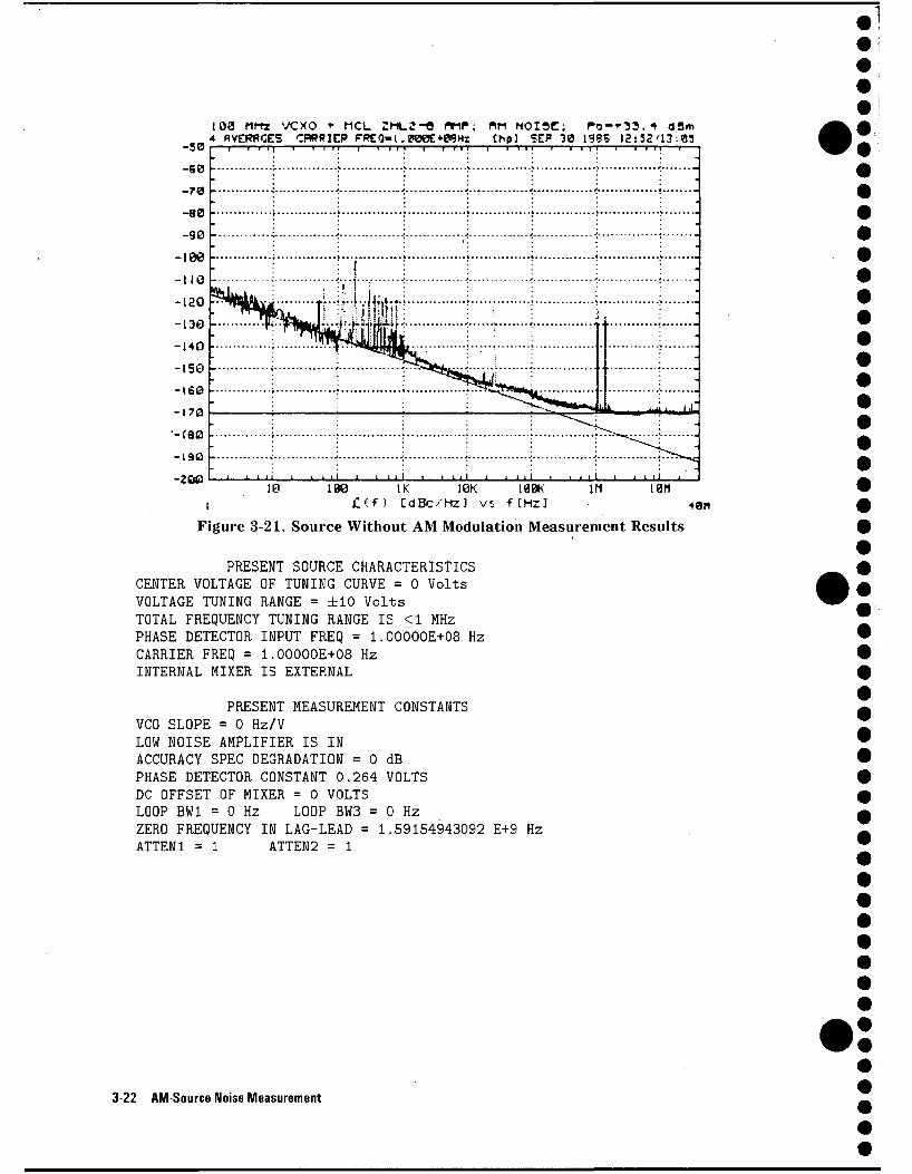
-50 -SB -79
-B0
-90 -100 -110 -120 -130 -140 -150 - i s a -4 70
'-rafl -190 h
100 MHz VCXO *■ MCL Z M L 2 - 0 Hf-ir; f in N 0 I 3 C ; P o - 0 3 . * dSffl 4 RVERRGES CRRR1ER FREO-l. STOE+OTHr Chp] SEP 30 1935 )2:32'13:05
-200
' ' M
■ ■ ■' i i i I _L_1_1_L ' ■ ■ ' i iL. ■ ■ ■'
10 100 IK 10K 18*: in i an i £(f) CdBc/'HzJ vi fCMz] tan
Figure 3-21. Source Without A M Modulation Measurement Results
PRESENT SOURCE CHARACTERISTICS CENTER VOLTAGE OF TUNING CURVE = 0 Volts VOLTAGE TUNING RANGE = ±10 Volts TOTAL FREQUENCY TUNING RANGE IS <1 MHz PHASE DETECTOR INPUT FREQ = 1.00000E+08 Hz CARRIER FREQ = 1.00000E+08 Hz INTERNAL MIXER IS EXTERNAL
PRESENT MEASUREMENT CONSTANTS VCO SLOPE = 0 Hz/V LOW NOISE AMPLIFIER IS IN ACCURACY SPEC DEGRADATION = 0 dB PHASE DETECTOR CONSTANT 0.264 VOLTS DC OFFSET OF MIXER = 0 VOLTS LOOP BW1 = 0 Hz LOOP BW3 = 0 Hz ZERO FREQUENCY IN LAG-LEAD = 1.59154943092 E+9 Hz ATTEN1 = 1 ATTEN2 = 1
3-22 AM Source Noise Measurement
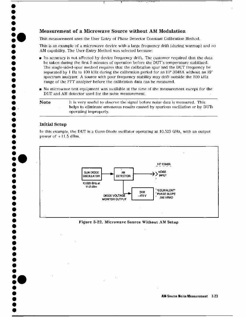
Measurement of a Microwave Source without AM Modulation This measurement uses the User Entry of Phase Detector Constant Calibration Method. This is an example of a microwave device with a large frequency drift (during warmup) and no AM capability. The User-Entry Method was selected because: ■ Its accuracy is not affected by device frequency drift. The customer required that the data
be taken during the first 5 minutes of operation before the DUT's temperature stabilized. The single-sided-spur method requires that the calibration spur and the DUT frequency be separated by 1 Hz to 100 kHz during the calibration period for an HP 3048A without an RF spectrum analyzer. A source with poor frequency stability may drift outside the 100 kHz range of the FFT analyzer before the calibration data can be measured.
■ No microwave test equipment was available at the time of the measurement except for the DUT and AM detector used for the noise measurement.
N o t e It is very useful to observe the signal before noise data is measured. This helps to eliminate erroneous results caused by spurious oscillation or by DUTs operating improperly.
Initial Setup In this example, the DUT is a Gunn-Diode oscillator operating at 10.525 GHz, with an output power of +11.5 dBm.
GUN DIODE OSCILLATOR
10.525 GHz at 11.5 dBm
AM DETECTOR
DIODE VOLTAG MONITOR OUTP
E " JT
\ /
DVM -.472 V
HP11848A I •L NOISE / INPUT
■EQUIVALENT1
'PHASE SLOPE .092V/RAD
Figure 3-22. Microwave Source Without AM Setup
AMSource Noise Measurement 3-23
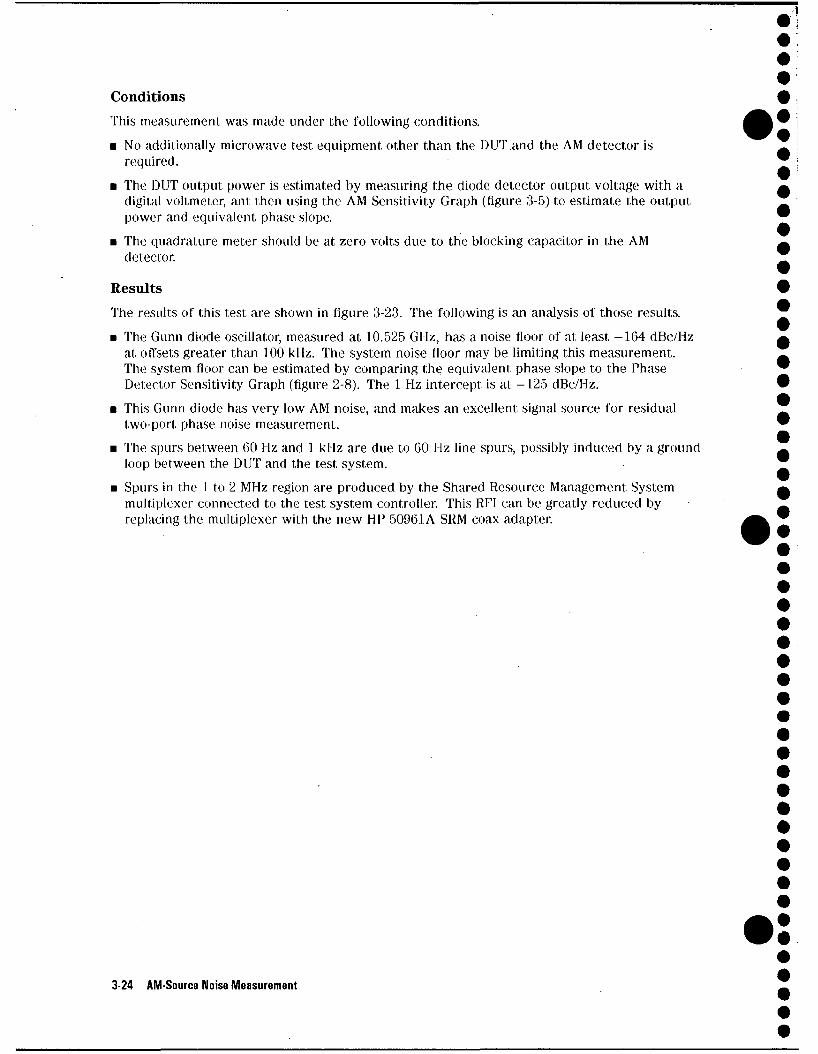
Conditions This measurement was made under the following conditions. ■ No additionally microwave test equipment other than the DUT and the AM detector is
required. ■ The DUT output power is estimated by measuring the diode detector output voltage with a
digital voltmeter, ant then using the AM Sensitivity Graph (figure 3-5) to estimate the output, power and equivalent phase slope.
■ The quadrature meter should be at zero volts due to the blocking capacitor in the AM detector.
Results The results of this test are shown in figure 3-23. The following is an analysis of those results. ■ The Gunn diode oscillator, measured at 10.525 GHz, has a noise floor of at least -164 dBc/Hz
at offsets greater than 100 kHz. The system noise floor may be limiting this measurement. The system floor can be estimated by comparing the equivalent phase slope to the Phase Detector Sensitivity Graph (figure 2-8). The 1 Hz intercept is at -125 dBc/Hz.
■ This Gunn diode has very low AM noise, and makes an excellent signal source for residual two-port phase noise measurement.
■ The spurs between 60 Hz and 1 kHz are due to 60 Hz line spurs, possibly induced by a ground loop between the DUT and the test system.
■ Spurs in the 1 to 2 MHz region are produced by the Shared Resource Management System multiplexer connected to the test system controller. This RFI can be greatly reduced by replacing the multiplexer with the new HP 50961A SRM coax adapter.
3-24 AMSource Noise Measurement
NO WflRMUP; GIJNN DIODE RM N O I S E ; Prr + 1 1 . 5 dBm; Vd - , 4 7 2 V 4 RVERHGES CR9R1EP FPEQ-l ,052E*lBHz Chp] SEPTS 1335 1 1 : 2 3 / 1 1 : 3 6
-50
-65
-?0
11 i — i — r r r - i i 1 1 — r -
-80
- 9 0 -
-100
-110
-150
-130
-140
-150
-160
-170
-180
-19(3
-£ld0
- i—i i M — r
-J 1 i_U ' I ' I ' I ' ■ ' ' t i l l . I I I I J _ I I l l , 10 100 IK IQK 100K 111 ISM
l £ f f i L it Be / H z 1 v ■; ■ -F C Hz ] ^gM
Figure 3-23. Microwave Source Without A M Measurement Results
PRESENT SOURCE CHARACTERISTICS CENTER VOLTAGE OF TUNING CURVE = 0 Volts VOLTAGE TUNING RANGE = ±10 Volts TOTAL FREQUENCY TUNING RANGE IS <1 MHz PHASE DETECTOR INPUT FREQ = 1.05250E+10 Hz CARRIER FREQ = 1.05250E+10 Hz MIXER IS EXTERNAL
PRESENT MEASUREMENT CONSTANTS VCO SLOPE = 0 Hz/V LOW NOISE AMPLIFIER IS IN ACCURACY SPEC DEGRADATION = 0 dB PHASE DETECTOR CONSTANT 0.092 VOLTS DC OFFSET OF MIXER = 0 VOLTS LOOP BW1 = 0 Hz LOOP BW3 = 0 Hz ZERO FREQUENCY IN LAG-LEAD = 1.59154943092 E+9 Hz ATTEN1 = 1 ATTEN2 = 1
AM-Source Noise Measurement 3-25
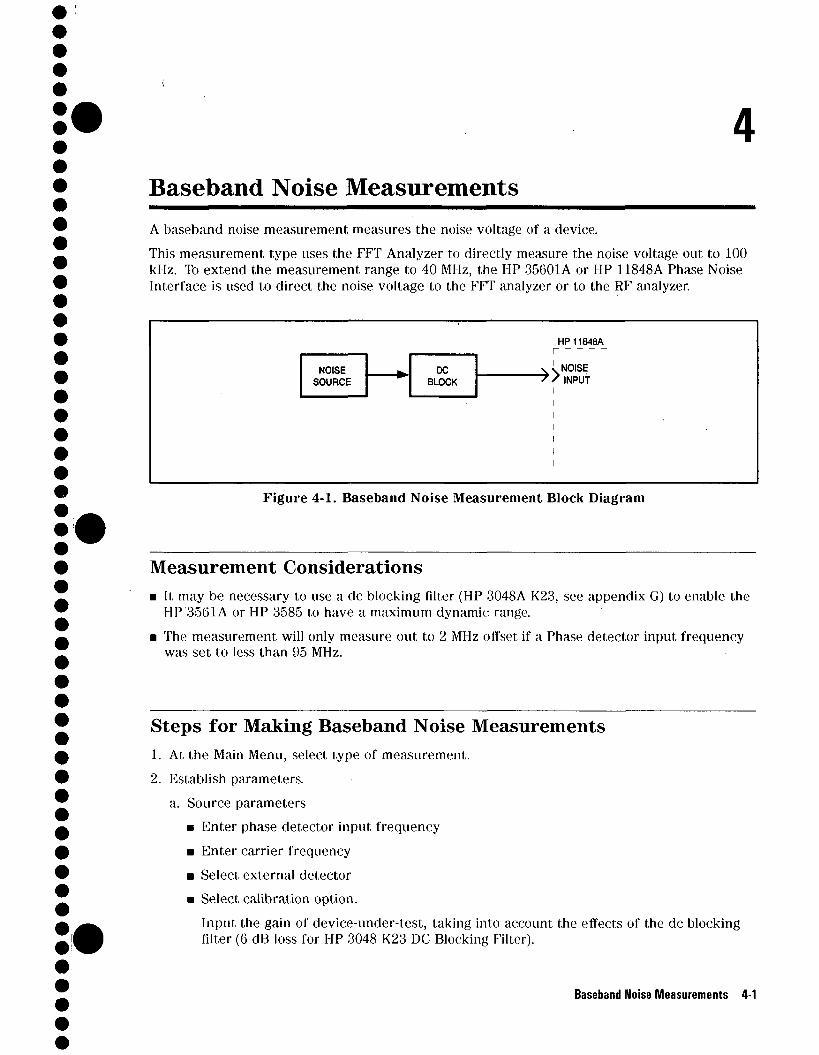
4 Baseband Noise Measurements A baseband noise measurement measures the noise voltage of a device. This measurement type uses the FFT Analyzer to directly measure the noise voltage out to 100 kHz. To extend the measurement range to 40 MHz, the HP 35601A or HP 11848A Phase Noise Interface is used to direct the noise voltage to the FFT analyzer or to the RF analyzer.
NOISE SOURCE
DC BLOCK
HP11848A
v v NOISE 7 ? INPUT
Figure 4-1. Baseband Noise Measurement Block Diagram
Measurement Considerations ■ It may be necessary to use a dc blocking filter (HP 3048A K23, see appendix G) to enable the
HP 3561A or HP 3585 to have a maximum dynamic range.
■ The measurement will only measure out to 2 MHz offset if a Phase detector input frequency was set to less than 95 MHz.
Steps for Making Baseband Noise Measurements 1. At the Main Menu, select type of measurement.
2. Establish parameters.
a. Source parameters ■ Enter phase detector input frequency ■ Enter carrier frequency ■ Select external detector ■ Select calibration option.
Input the gain of device-under-test, taking into account the effects of the dc blocking filter (6 dB loss for HP 3048 K23 DC Blocking Filter).
Baseband Noise Measurements 4-1
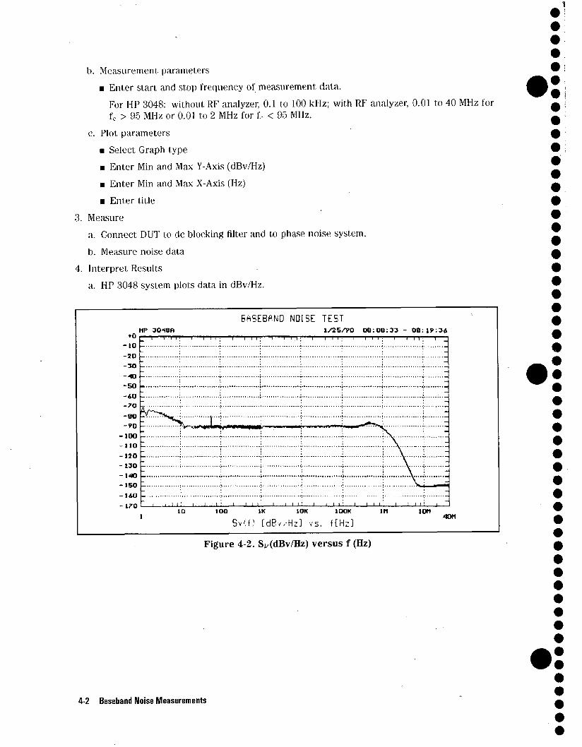
b. Measurement parameters ■ Enter start and stop frequency of measurement data.
For HP 3048: without RF analyzer, 0.1 to 100 kHz; with RF analyzer, 0.01 to 40 MHz for f,: > 95 MHz or 0.01 to 2 MHz for f,: < 95 MHz.
c. Plot parameters ■ Select Graph type ■ Enter Min and Max Y-Axis (dBv/Hz) ■ Enter Min and Max X-Axis (Hz)
■ Enter title
3. Measure a. Connect DUT to dc blocking filter and to phase noise system. b. Measure noise data
4. Interpret Results a. HP 3048 system plots data in dBv/Hz.
HP 3048ft BASEBAND NOISE TEST
1 /25 /70 0 8 : 0 8 : 3 3 - 06: l?:3t f
- 1 0
- 1 7 0
-I—r—rr I I I ; I I I I - I I I I ; I I I I - I I I I -
to too IK IOK IOOK SvCO [dBv /Hz ] vs. f [Hz ]
in
Figure 4-2. S„ (dBv/Hz) versus f (Hz)
ion ton
4-2 Baseband Noise Measurements
A Calculation of Source Noise Attenuation
Source Noise Attenuation versus Carrier Offset and Time Delay
Oi
1 J ~k
1
0° POWER SPUTTER .
Delay l e w
f V. ' \ ©out - 0i ■ 6d
The input signal is expressed as a function of phase:
6, = wct +• A#sinc<;nit carrier phase modulation
The delay path phase is:
0d= ujc(t-r) + Af l s ina ' m ( t - T)^ carrier delayed in time phase modulation delayed in time
Therefore, the oiiput phase expression is:
9out = Oi - 6j = U)CT + Ad[smumi. - sino;.m(/ - r)] From trigometric identities:
sin Q — sin p = I sin I —-— I cos sin n — sin 8 = 9, sin I — ■7 J "" \ 2
Which allows us to break the output signal into its component parts where:
Ooui — wcr + A 0 static phase error modulation amplitude
2 sin —-—cosic'nitJ
sensitivity to modulation rate
Calculation of Source Noise Attenuation A-1
Because the measurement is made with the phase detector in quadrature, the static phase error is zero. Also, for small values of wmr, for example, wm < it, the output phase expression can be reduced to:
8out - A6 [2 sin —— cosu;nit] modulation amplitude s *
sensitivity to modulation, rate
Therefore the sensitivity to the input phase modulation, or the phase noise of a source is: _, . . . . ^'niT bensitii'iiy = 2 sin
2 or expressed in terms of carrier offset frequency:
Sensitivity = 2 sin 7rf,nr Where : fni = offset frequency
T — time delay Finally, expressing the detector's sensitivity to source phase modulation in dB, the source's phase noise is attenuated by:
Att(dB) = 201og|2sin7r/wr | It is important to note that the attenuation of the source's phase moise is a periodic function. For offset frequencies of f^, when n = 1,3,5...., the input signal modulation and the delayed signal modulation add in phase. This results in the source's phase contribution having 6 dB of gain at the detector output. For offset frequencies of ^ , when u. = 0, 2,4,6,..., the input signal modulation and the delayed signal modulation are out-of-phase, which results in the total cancellation of the source's phase noise contribution at the dete'ctor output. Finally, at approximately ~ offset frequency, there is 0 dB of attenuation to the source noise contribution. From frequency discriminator theory, this corresponds to the offset frequency where the phase detector gain and the discriminator gain are equal. A practical example of the determination of source noise attenuation can be found in figure 2-25.
A-2 Calculation of Source Noise Attenuation
B Noise Figure Versus Dynamic Noise Figure Noise figure is the ratio of the output noise of an amplifier referred back to the input divided by the thermal noise floor.
The noise figure of a linearly operating amplifier is defined by the expression:
N F = P o u t
KTBG Where : Pout = Noise power at amplifier output with the input terminated
T. ,., , , A . 3 7 4 x 1(T23 joules \ K = Boltzman s constant :
v ° K ; T = Absolute temperature of amplifier (°K) B = Measurement bandwidth G = Amplifier gain
Expressed in dB:
J V F ^ l O k * ^
A noiseless amplifier would have a noise figure of 0 dB, that is, all the noise appearing at the output would be due to the noise generated by the input, termination. The noise power (Pn) of the termination is equal to:
P„ = KTB
T- T, , i A.374 x 1(T23 joules \ Where : K = Boltzman s constant V °K /
T = Room temperature of 290°K B = Bandwidth of 1 Hz
Substituting in:
1.374 x 10 --'3 joules n T . P n = — x 290°K x 1Hz
°K = 3.985 x 10"21 watts
P u = -174 dBm
The termination noise power consists of two equal contributors: AM noise and $M noise. This results in a termination noise floor of -177 dBc/Hz for both, or a dynamic rang of -177 dBc/Hz referred to 0 dBm.
Noise Figure Versus Dynamic Noise Figure B-1
We shall now calculate: £(f) = $M noise floor (dBc/Hz)
+ noise figure fdB)
+ amplifier gain (dB)
— amplifier output power(clBm)
But:
amplifier output power {dBm) = input power (dBm) -{-gain {dB) Therefore:
C{i) — $M noise floor (dBc/Hz) + noise figure (dB) — amplifier input power (dBm
That is : £(i") = -177 (dBc/Hz) + NF (dB) - P; (dBm)
Or the equation can be used to calculate noise figure,
NF {dB) = £ ( / ) {dBc/Hz) + P{ {dBm) + 177 {dBc/Hz) This dynamic noise figure is measured under actual large signal conditions and may differ from the small signal noise figure. It includes the multiplicative noise produced by the non-linearities of the active device, in the presence of a large signal. This noise is negligible for very low input levels.
B-2 Noise Figure Versus Dynamic Noise Figure
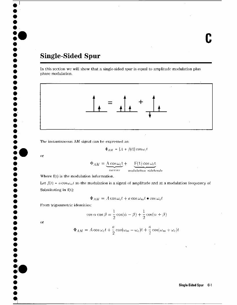
c Single-Sided Spur In this section we will show that a single-sided spur is equal to amplitude modulation plus phase modulation.
i i
I i L i
+
\
The instantaneous AM signal can be expressed as:
<f>,lAy = [-4 + /'(/)] COSu/c*
or
$AM = A cos<vct + F( t) cos o.'ct
currier modulation sidebands
Where f(t) is the modulation information. Let /(/) = ocosw,,,/ so the modulation is a signal of amplitude and at a modulation frequency of Substituting in f(t):
$AM = A COS lVct + (I COS LVmt • COS LVct
From trigonmetric identities:
cos a cos ft = - COS(Q' — ft) + — cos{a + ft)
or
®AM = Acosuct + - cos (a;,,, - ujc)t + - cos(a;m + ivc)t
Single-Sided Spur C-1
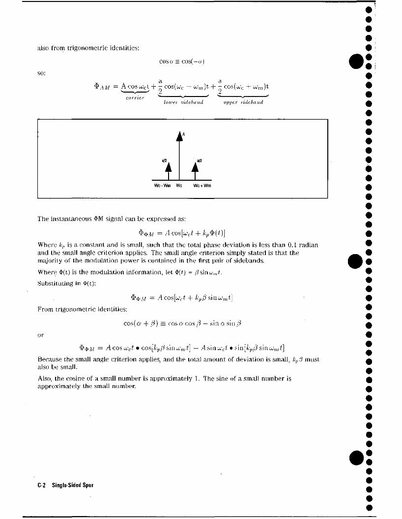
also lrom trigonometric identities:
so:
COS a = C O S ( - a )
a. a ®AM = A cos uct + - cos(u.'c - to'm )t + - cos(tc'c + u;m )t
lower sideband upper sideband
1 I Wc-Wm Wc Wc + Wm
The instantaneous *M signal can be expressed as:
$$JW = Acos[uct + k:p$(t)] Where kp is a constant and is small, such that the total phase deviation is less than 0.1 radian and the small angle criterion applies. The small angle criterion simply stated is that the majority of the modulation power is contained in the first pair of sidebands. Where <t>(t) is the modulation information, let *(/.) = /?sinw„,/. Substituting in 4>(t):
$$M = A cos[u!ct + kp/3 s'm ujmt] From trigonometric identities:
cos (a + fi) = cos a cos /3 — sin a sin (3 or
$$jVy — Acosu;ci • cos[A:y)/3sii]u.'mt] — As\i\ujct • s'm[kpf3since,nt] Because the small angle criterion applies, and the total amount of deviation is small, kP/3 must also be small. Also, the cosine of a small number is approximately J. The sine of a small number is approximately the small number.
C-2 Single-Sided Spur
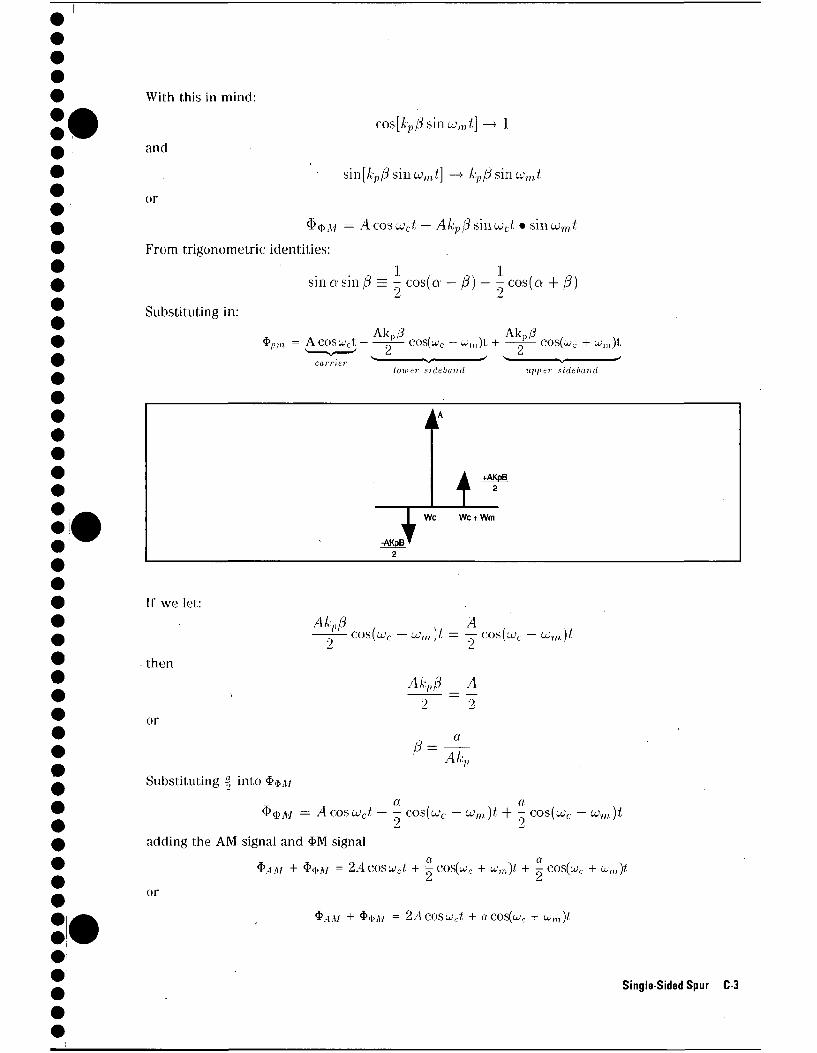
With this in mind:
and
or
cos [kpfi since',,,/,] —> 1
sin [kvj3 sin umt] —► kpft sin ujmt
^$M — Acosu!ct — Akj, ft sinojci • sinujmt From trigonometric identities:
sin a sin /? = - cos(cv — /?) — - cos(o' + ft)
Substituting in:
$,,,„ = ACOSWct ^— COS(u>c - w m ) t + " " ^ COS(wc + W m ) t A M 2
lower sideband upper sideband
-AKpB*
1 tAKpB
Wc Wc + Wm
If we let:
then
or
/U:;)/? A -~ cos(o.'c - c;m )i = — cos(co'c - CJ,,,)/
.4^/3 _ A 9 _ ¥
/* Afc, Substituting % into $<I>A/
$$;!/ = -4 costly/ - - cos(u,'c - um)t + - cos(o,'c - um)t
adding the AM signal and 4>M signal
$AM + $<F>M = 2.4coswcr. + -cos(wc + w„»)/ + ~ cos(wc + w,„)f.
or $.4,y + * , ] , j V / = 2.4COSwcf. + f/.COS(wc-+ W,„)f.
Single-Sided Spur C-3
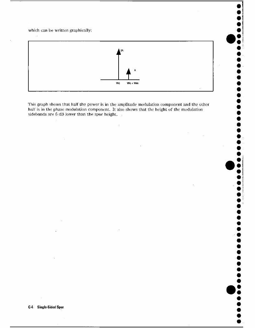
which can be written graphically:
A*
ill Wc Wc + Wm
This graph shows that half the power is in the amplitude modulation component and the other half is in the phase modulation component. It also shows that the height of the modulation sidebands are 6 dB lower than the spur height.
C4 Single-Sided Spur
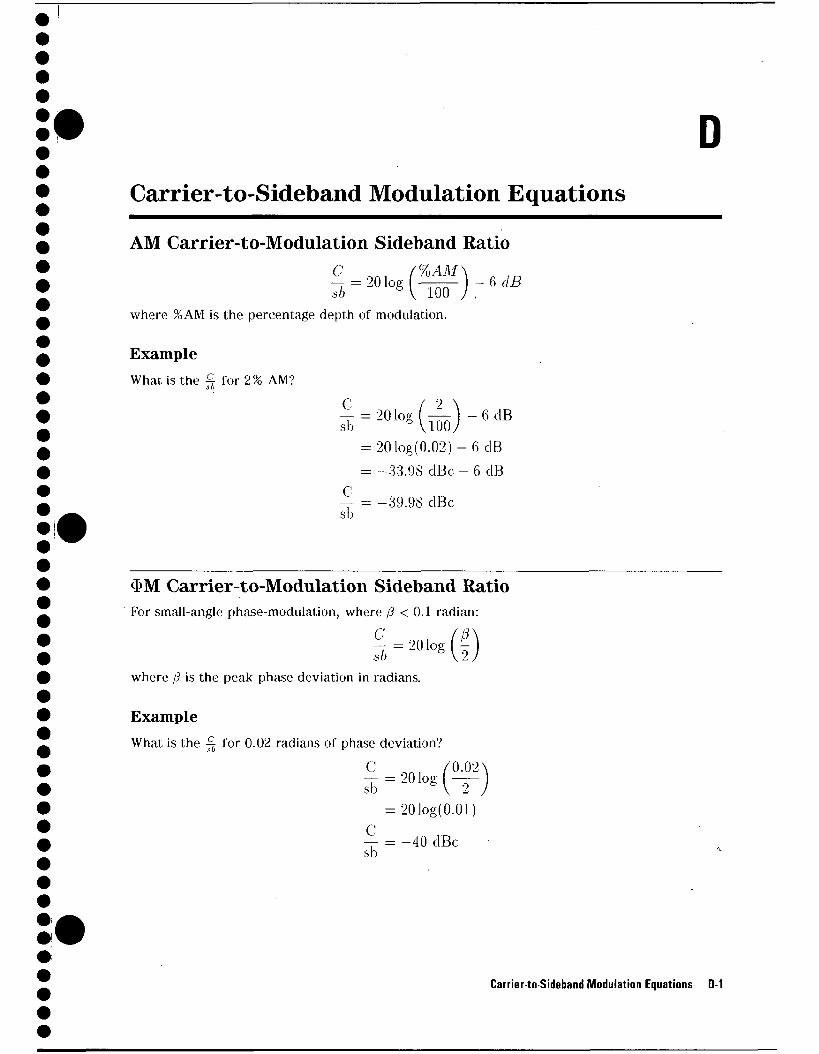
D Carrier-to-Sideband Modulation Equations
AM Carrier-to-Modulation Sideband Ratio
where %AM is the percentage depth of modulation.
Example What is the 4 for 2% AM?
= 201og(0 .02) -6dB = -33.98 dBc - 6 dB
~ = -39.98 dBc sb
$M Carrier-to-Modulation Sideband Ratio For small-angle phase-modulation, where /? < 0.1 radian:
where /? is the peak phase deviation in radians.
Example What is the ^ for 0.02 radians of phase deviation?
C _ , /0.02\ s = 2 0 , o g ( — )
= 201og(0.01) C — = - 4 0 dBc sb
S = 201°s(ls)-6tlB
Carrier-to-Sideband Modulation Equations D-1
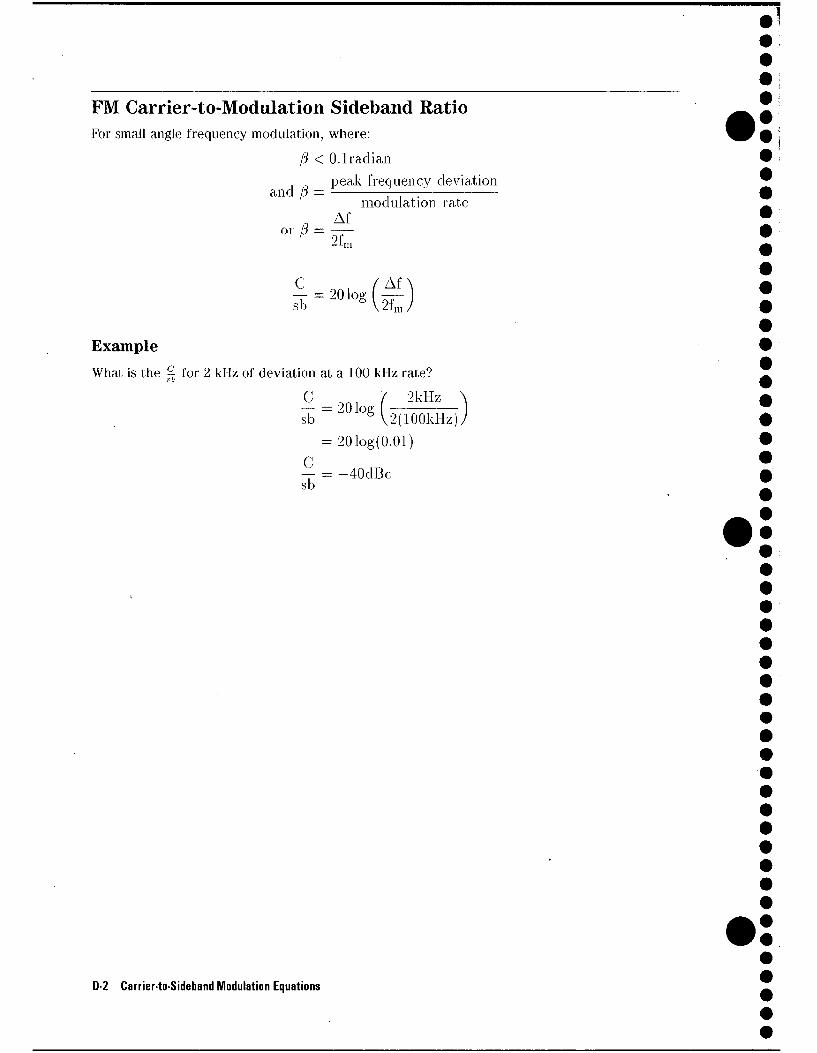
FM Carrier-to-Modulation Sideband Ratio For small angle frequency modulation, where:
fi < 0.1 radian peak frequency deviation
and p = ——r modulation rate
-, M or 15 = - r -
—Mil
C , / Af - = 2 0 log — sb V2fni
Example What is the 4 for 2 kHz of deviation at a 100 kHz rate?
c ib
_ , / 2kHz = 20 be; 6 V2(100kHz) = 201og(0.01)
= -40dBc
D 2 Carrier-to-Sideband Modulation Equations
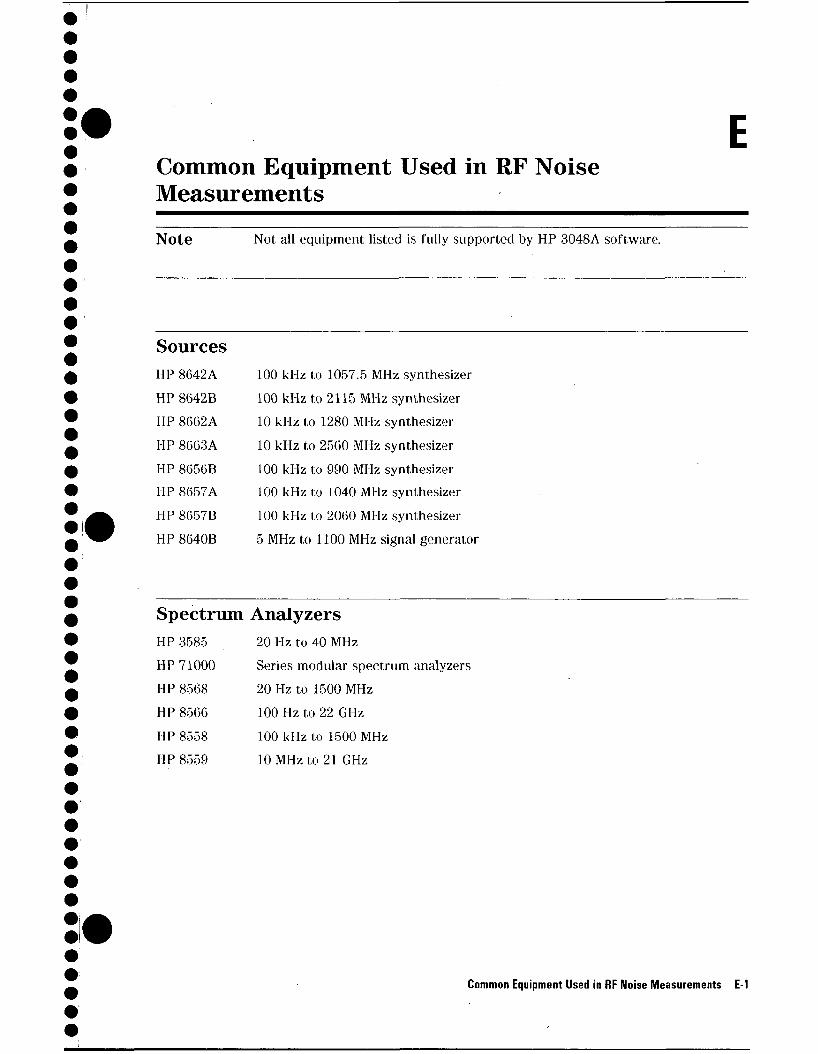
I
E Common Equipment Used in RF Noise Measurements
Note Not all equipment listed is fully supported by HP 3048A software.
Sources HP 8642A 100 kHz to 1057.5 MHz synthesizer HP 8642B 100 kHz to 2115 MHz synthesizer HP 8662A 10 kHz to 1280 MHz synthesizer HP 8663A 10 kHz to 2560 MHz synthesizer HP 8656B 100 kHz to 990 MHz synthesizer HP 8657A 100 kHz to 1040 MHz synthesizer HP 865713 100 kHz to 2060 MHz synthesizer HP 8640B 5 MHz to 1100 MHz signal generator
Spectrum Analyzers HP 3585 20 Hz to 40 MHz HP 71000 Series modular spectrum analyzers HP 8568 20 Hz to 1500 MHz HP 8566 100 Hz to 22 GHz HP 8558 100 kHz to 1500 MHz HP 8559 10 MHz to 21 GHz
Common Equipment Used in RF Noise Measurements E-1
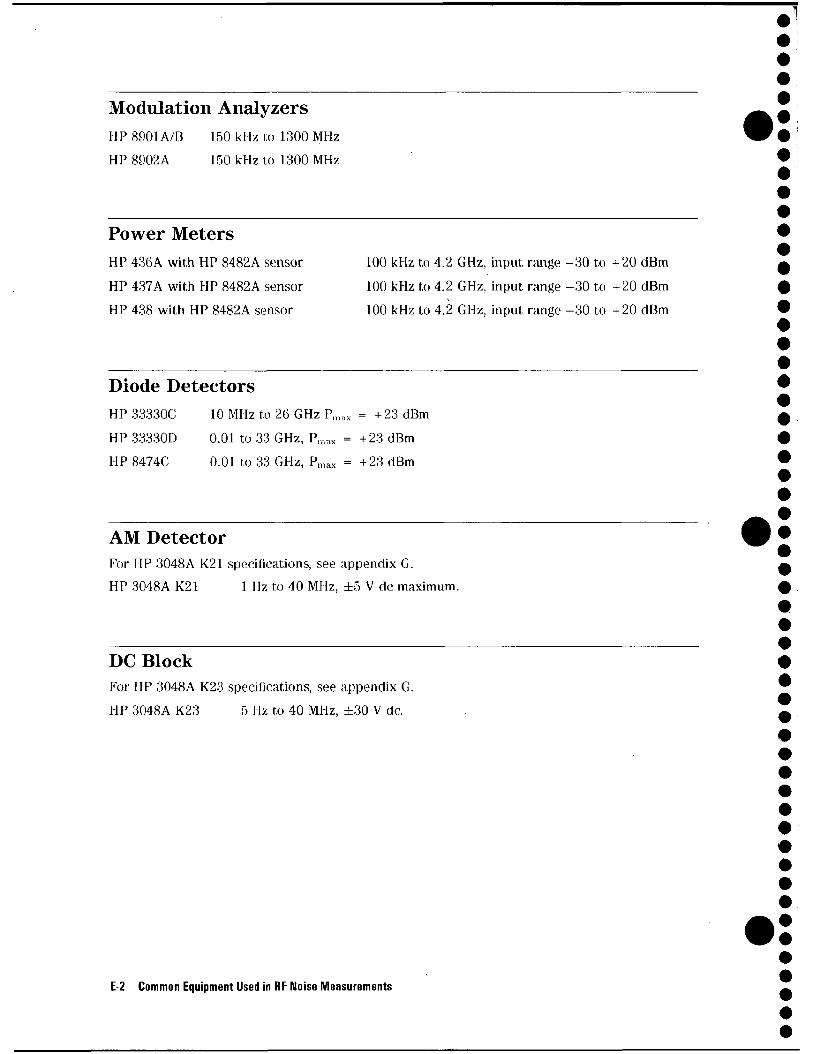
Modulation Analyzers HP 8901A/B 150 kHz to 1300 MHz HP 8902A 150 kHz to 1300 MHz
Power Meters HP 436A with HP 8482A sensor 100 kHz to 4.2 GHz, input range -30 to +20 dBm HP 437A with HP 8482A sensor 100 kHz to 4.2 GHz, input range -30 to +20 dBm HP 438 with HP 8482A sensor 100 kHz to 4.2 GHz, input range -30 to +20 dBm
Diode Detectors HP 33330C 10 MHz to 26 GHz Pmax = +23 dBm HP 33330D 0.01 to 33 GHz, Pniox = +23 dBm HP 8474C 0.01 to 33 GHz, Pmax = +23 dBm
AM Detector For HP 3048A K21 specifications, see appendix G. HP 3048A K21 1 Hz to 40 MHz, ±5 V dc maximum.
DC Block For HP 3048A K23 specifications, see appendix G. HP 3048A K23 5 Hz to 40 MHz, ±30 V dc.
E-2 Common Equipment Used in RF Noise Measurements
Attenuators HP 8491 Series of fixed attenuators HP 8493 Series of fixed attenuators HP 8494 1 dB step attenator HP 8495 10 dB step attenuator
Amplifiers Specifications for the HP 3048A K22 can be found in appendix G. HP 3048A K22 dual amplifier
HP 8447A preamp
HP 8447D preamp
HP 8447E preamp
MCL ZHL-2-8 power amplifier
ANZAC AMC-123
9 dB gain each, 5 MHz to 1500 MHz, NF < 7.5 dB, output power > +15 dBm 26 dB gain, 0.1 MHz to 400 MHz, NF < 5 dB, output power > 6 dBm 26 dB gain, 0.1 MHz to 1300 MHz, NF < 8.5 dB, output power > 7 dBm 22 dB gain, 0.1 MHz to 1300 MHz, NF < 11 dB, output power > 15 dBm 27 dB gain, 10 MHz to 10 MHz, NF < 10 dB, output power > +29 dBm 10 dB gain, 5 MHz to 500 MHz, NF < 3.5 dB, output power > +16 dBm
Phase Shifters 2 GHz Phase Shifter 4 GHz Phase Shifter 18 GHz Phase Shifter
1 nanosecond delay. 1 nanosecond delay. 1 nanosecond delay.
Common Equipment Used in RF Noise Measurements E-3
0° Power Splitters MCL ZFSC-2-2500 10 MHz to 2.5 GHz, Pmax 1 watt, MCL ZFSC-2-5 10 MHz to 1500 MHz, Pmax 1 watt, MCL ZAPD-21 500 MHz to 2 GHz, Pmax 10 watts NARDA 4456-2 2 GHz to 18 GHz
Couplers MCL ZFDC-20-5 MCL ZFDC-10-2 NARDA 4227-16
0.1 to 2000 MHz 20 dB coupler, Pmax 2 watts
10 MHz to 1000 MHz coupler, Pmax 1.5 watts
1.7 to 26.5 GHz coupler
Instrument Suppliers Anzac Division of Adams/Russel 80 Cambridge Street Burlington, MA 01803-0964 (617)273-3333
ARRA 15 Harold Court Bayshore, Long Island, NY 11706 (516) 231-8400 MCL (Mini-Circuits) P.O. Box 166 Brooklyn, NY 11235 (212) 934-4500
E-4 Common Equipment Used in RF Noise Measurements
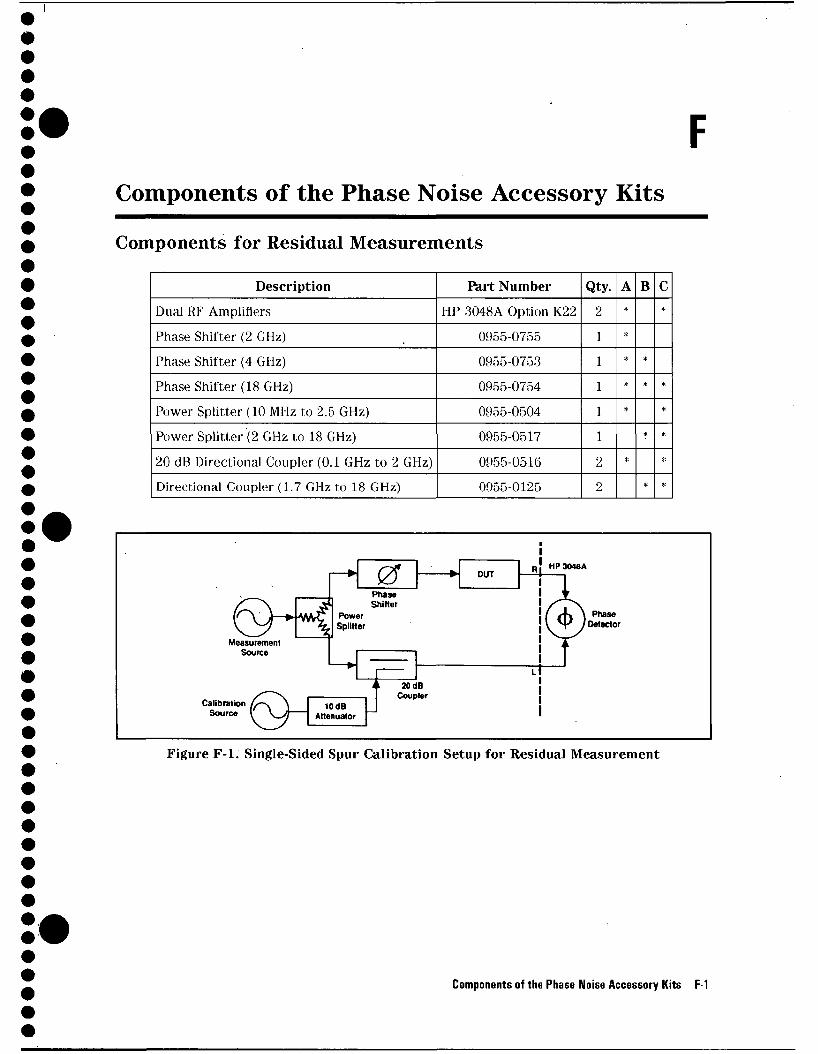
F Components of the Phase Noise Accessory Kits
Components for Residual Measurements
Description
Dual RF Amplifiers
Phase Shifter (2 GHz)
Phase Shifter (4 GHz)
Phase Shifter (18 GHz)
Power Splitter (10 MHz to 2.5 GHz)
Power Splitter (2 GHz to 18 GHz)
20 dB Directional Coupler (0.1 GHz to 2 GHz)
Directional Coupler (1.7 GHz to 18 GHz)
Part Number
HP 3048A Option K22
0955-0755
0955-0753
0955-0754
0955-0504
0955-0517
0955-0516
0955-0125
Qty.
2
2
2
A *
*
*
*
*
*
B
*
*
*
*
C *
*
*
*
*
*
®~ Measurement
«J Source
s—>v Calibration ts~\ \
Source V \_J
^ *
fe 0 Phase Shifter
Power Splitter
10 dB Attenuator
i i 20 d B
OUT RJ HP3048A
|(i)= LI
i Figure F-1. Single-Sided Spur Calibration Setup for Residual Measurement
Components of the Phase Noise Accessory Kits F-1
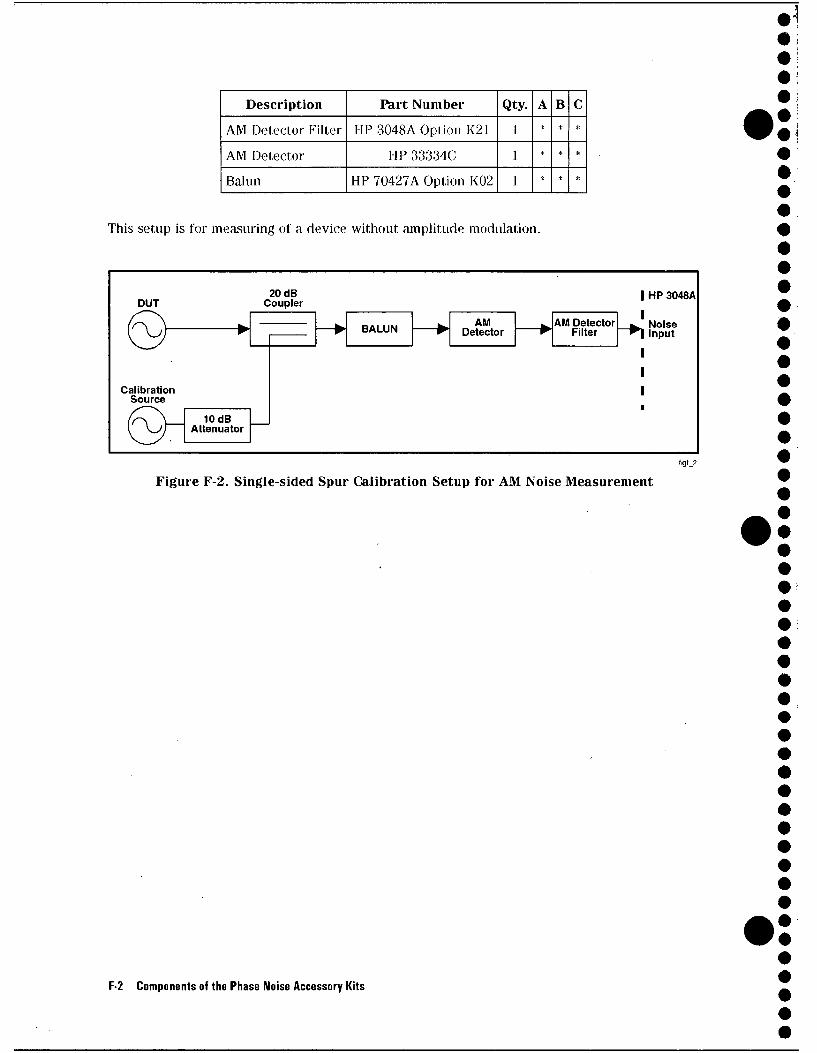
Description
AM Detector Filter
AM Detector
Balun
Part Number
HP 3048A Option K21
HP 33334C
HP 70427A Option K02
Qty. l
l
l
A =!= *
*
B %
*
*
C #
*
*
This setup is for measuring of a device without amplitude modulation.
DUT
Calibration Source
tor
^ W
10 dB Attenuator
20 dB Coupler
BALUN ► AM Detector ^
w AM Detector
Filter
I HP 3048A
1 ^ Noise
~~^1 Input 1 1 1
«gf-2
Figure F-2. Single-sided Spur Calibration Setup for AM Noise Measurement
F-2 Components of the Phase Noise Accessory Kits
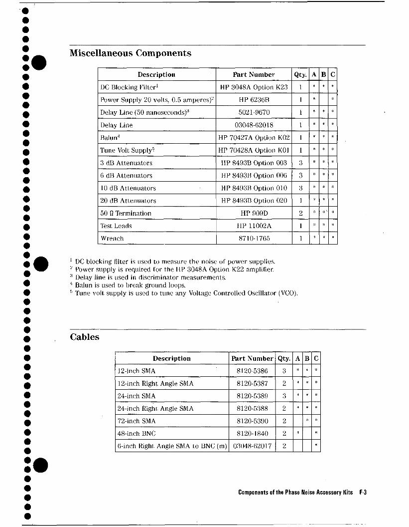
Miscellaneous Components
Description
DC Blocking Filter1
Power Supply 20 volts, 0.5 amperes)'-'
Delay Line (50 nanoseconds)3
Delay Line
Balun4
Tune Volt Supply5
3 dB Attenuators
6 dB Attenuators
10 dB Attenuators
20 dB Attenuators
50 0 Termination
Test Leads
Wrench
Part Number
HP 3048A Option K23
HP 6236B
5021-9670
03048-62018
HP 70427A Option K02
HP 70428A Option K01
HP 8493B Option 003
HP 8493B Option 006
HP 8493B Option 010
HP 8493B Option 020
HP 909D
HP 11002A
8710-1765
Qty.
1
1
1
1
1
1
3
3
3
1
2
1
1
A *
*
*
*
*
*
*
*
*
*
*
*
*
B *
*
*
*
*
if
*
*
* * ■ ■
*
*
C *
#
*
*
*
#
*
*
*
*
*
*
*
1 DC blocking filter is used to measure the noise of power supplies. - Power supply is required for the HP 3048A Option K22 amplifier. 3 Delay line is used in discriminator measurements. 4 Balun is used to break ground loops. 5 Tune volt supply is used to tune any Voltage Controlled Oscillator (VCO).
Cables
Description
12-inch SMA
12-inch Right Angle SMA
24-inch SMA
24-inch Right Angle SMA
72-inch SMA
48-inch BNC
6-inch Right Angle SMA to BNC (m)
Part Number
8120-5386
8120-5387
8120-5389
8120-5388
8120-5390
8120-1840
03048-62017
Qty.
3
2
3
2
2
2
2
A *
*
*
*
*
B *
*
*
*
*
C *
*
*
*
*
*
*
Components of the Phase Noise Accessory Kits F-3
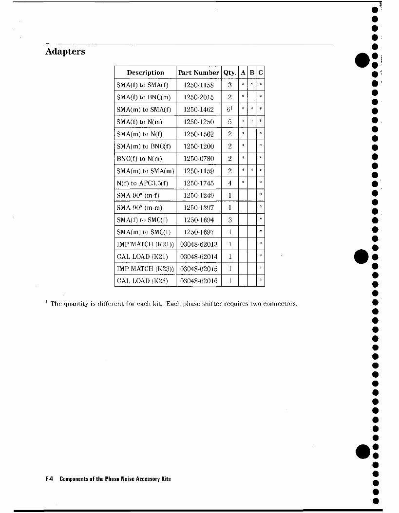
Adapters
Description
SMA(f) to SMA(f)
SMA(f) to BNC(m)
SMA(m) to SMA(f)
SMA(f) to N(m)
SMA(m) to N(f)
SMA(m) to BNC(f)
BNC(f) to N(m)
SMA(m) to SMA(m)
N(t') to APC3.5(f)
SMA 90° (m-f)
SMA 90° (m-m)
SMA(f) to SMC(f)
SMA(m) to SMC(f)
IMP'MATCH (K21))
CAL LOAD (K21)
IMP MATCH (K23))
CAL LOAD (K23)
Part Number
1250-1158
1250-2015
1250-1462
1250-1250
1250-1562
1250-1200
1250-0780
1250-1159
1250-1745
1250-1249
1250-1397
1250-1694
1250-1697
03048-62013
03048-62014
03048-62015
03048-62016
Qty.
3
2
61
5
2
2
2
2
4
1
1
3 1
1
1
1
1
A *
*
*
*
*
*
*
*
*
B *
*
*
*
C *
*
*
*
*
* ■
*
*
*
*
*
*
*
*
*
*
*
1 The quantity is different for each kit. Each phase shifter requires two connectors.
F-4 Components of the Phase Noise Accessorv Kits
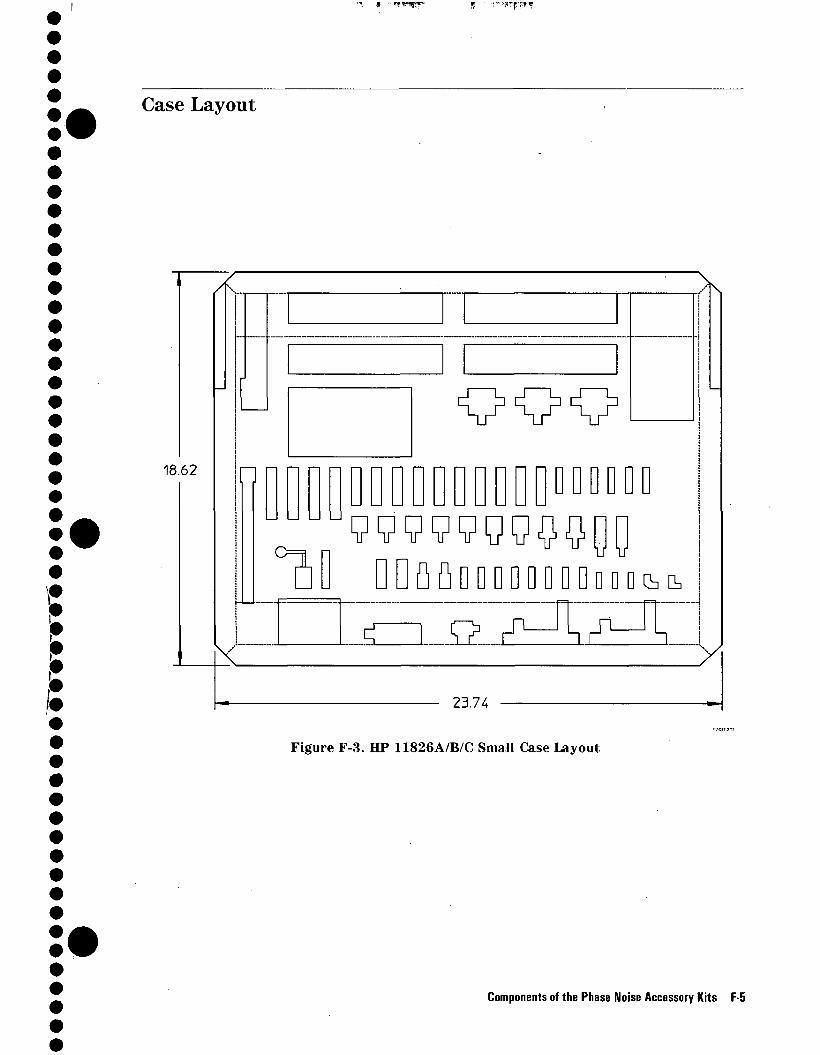
* " "T«nqr«* S :-'s-'fT»«
Case Layout
18.62
<?<?<? j l p D Q D D Q
1 . Q O O O O O D O D D O O D D D C Q ,
^ — ^ ^ ^ ^ ^
23.74
Figure F-3. HP 11826A/B/C Small Case Layout
Components of the Phase Noise Accessory Kits F-5
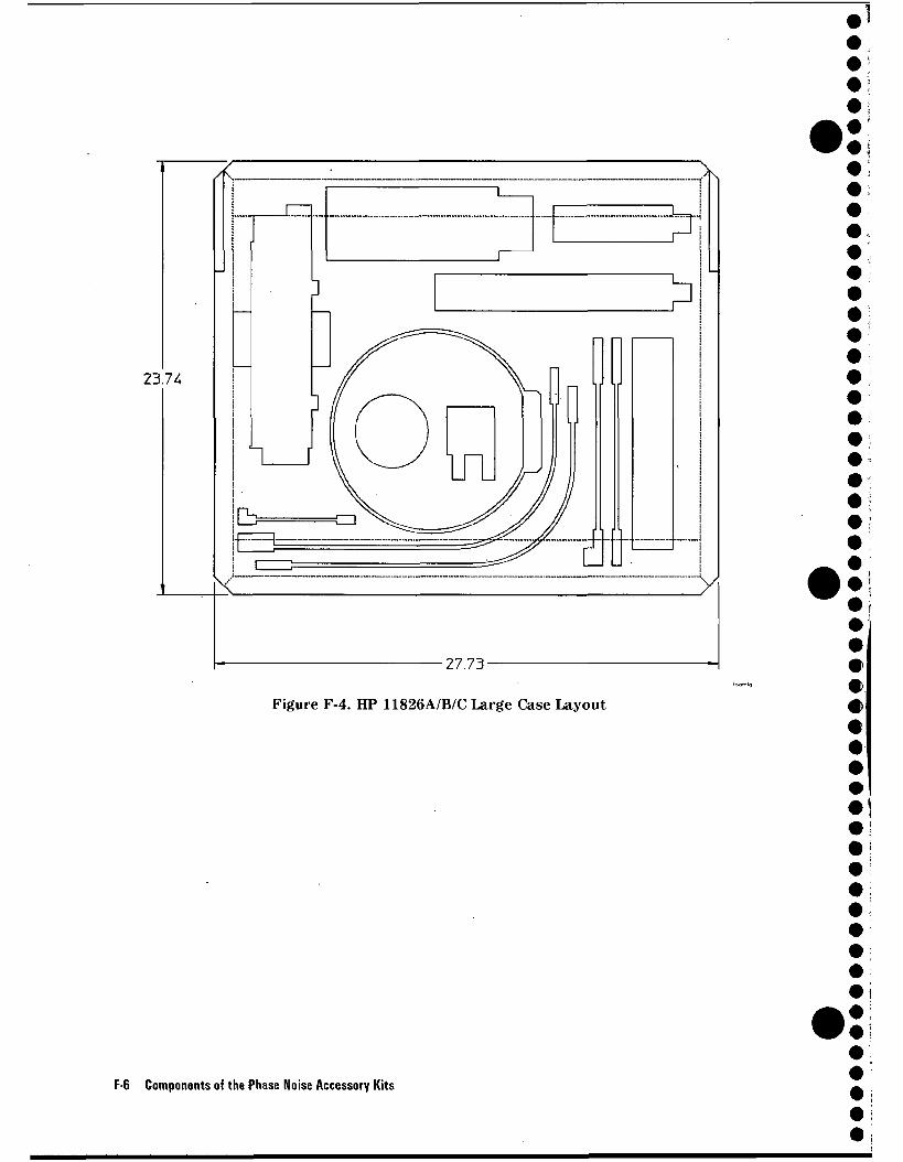
23.74
27.73-
Figure F-4. HP 11826A/B/C Large Case Layout
F-6 Components of the Phase Noise Accessory Kits
I
G HP 3048A Options KOl, K02, K21, K22, and K23 Specifications
HP 70428A Option KOl Tune Volt Supply The tune volt supply can be used to tune any Voltage Controlled Oscillator (VCO) instead of changing the HP 11848A phase noise interface center voltage. Changing the center voltage on the HP 11848A to tune a VCO can induce noise into the measurement.
DC Input Impedance: &> 25k ohms
HP 70427A Option K02 Balun The balun should be used on the noise input of the HP 11848A for external detector and baseband noise measurements to minimize spurs due to ground loops. Frequency Range: DC to 40 MHz Insertion Loss: < 0.4 dB
HP 3048A Options K01. K02, K21, K22. and K23 Specifications G 1
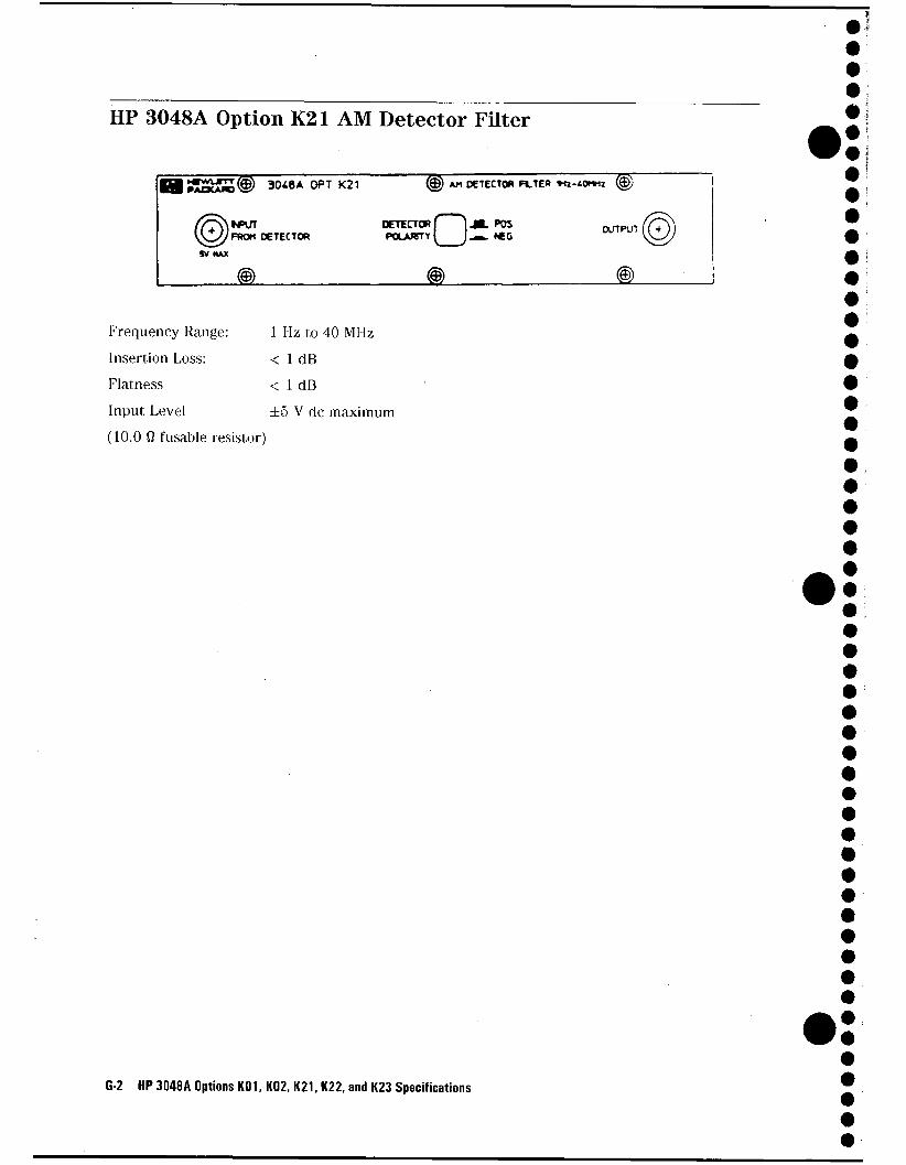
1 I
HP 3048A Option K21 AM Detector FUter
w E&SZW 3046A OPT K21
\M>UT
AM OETECTO* FUTER VR-iOMMi
'FROM CCTECTOR DETECTwf \M. POS OUTPLTI I +
® M.
Frequency Range: Insertion Loss: Flatness Input Level
1 Hz to 40 MHz < 1 clB < 1 clB ±5 V dc maximum
(10.0 fl disable resistor)
G-2 HP 3048A Options K01, K02, K21, K22, and K23 Specifications
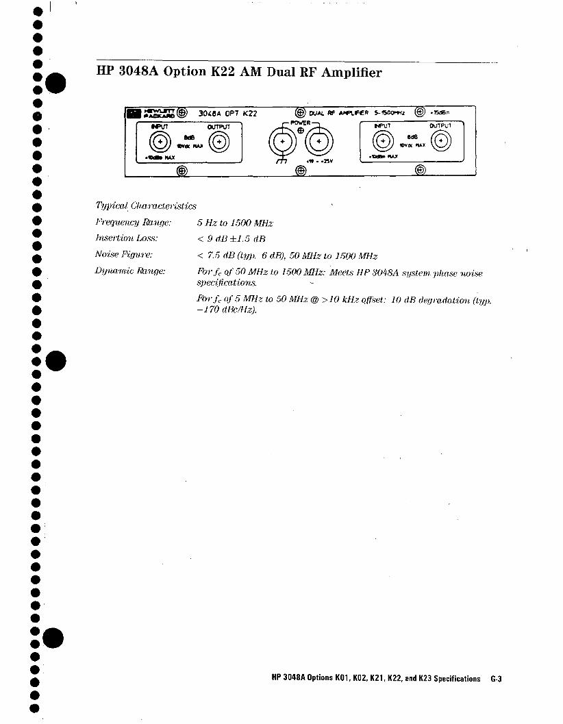
HP 3048A Option K22 AM Dual RF Amplifier
f 2 £ £ f S ; " M ) 3048A OPT K22 ® DUAL RF AWPLFCR S-1500MHZ (g) .15d6m
[ t*>UT OUTPUT
• « * MAX
f) © ©
Typical. Characteristics Frequency Range: 5 Hz to 1500 MHz Insertion Loss: < 9 dB ±1.5 d.B
Noise Figure: < 7.5 dB (tup. 6 d.B), 50 MHz to 1500 MHz
Dynamic Range: Forfc of 50 MHz to 1500 MHz: Meets IIP 3048A system, phase noise specifications. Forfc of 5 MHz to 50 MHz @ >10 kHz offset: 10 dB degradation (typ. ~170d.Bc/Hz).
-runcn
HP 3048A Options K01, K02, K21, K22, and K23 Specifications G
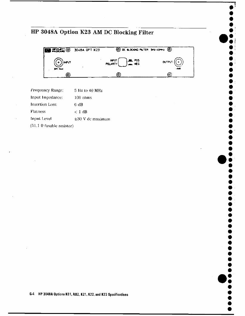
HP 3048A Option K23 AM DC Blocking Filter
© DC BtOCKWG PITER SMl-*Omj @ |>«Wt»TT( 3CU8A OPT K23
JOV tVkX
»*vr POLARITY
POS OUTPUT +
M.
Frequency Range: Input Impedance: Insertion Loss: Flatness Input Level (51.1 Q fusable resistor)
5 Hz to 40 MHz 100 ohms 6dB < 1 dB ±30 V do maximum
G4 HP 3048A Options K01, K02, K21, K22, and K23 Specifications
HP Part Number 03048-90059 Rev. A.O.O. /Nov. 1994
t
CHOOSING A PHASE NOISE MEASUREMENT TECHNIQUE
Concepts and Implementation TERRY DECKER ♦ BOB TEMPLE
RF & Microwave Measurement Symposium and Exhibition
tfl HEWLETT PACKARD
Terry Decker, received her BA in Physics from Carleton College in Northfield, Minnesota in 1980 and a BSEE from the University of Arizona in 1981. She worked as a microwave engineer for Hughes Aircraft Company on the Phoenix and AMRAAM programs for 4 years. She is currently a product marketing engineer responsible for phase-noise measurement systems at the Spokane Division of Hewlett-Packard Company.
Bob Temple, received his BA in Physics from Harvard University in 1961, and his MSEE in 1965 and PhD EE in 1971 from the University of Colorado in Boulder. Thesis topic was The Operation and Frequency Stability Measurement of a Hydrogen Cyanide Beam Type Maser at 88.6 GHz. His career with Hewlett-Packard began in December 1969 at the Loveland Division designing the frequency synthesis loops for the HP 3320 and 3330 Frequency Synthesizers. He was co-project manager for the HP 3585A Spectrum Analyzer and the inventor and project manager for the HP 3047A Spectrum Analyzer System for making comprehensive phase noise and spectral purity measurements. He transferred to the Spokane Division in 1981 and supported phase noise measurements using the HP 3047A/11740A Phase Noise Measurement Systems working both within the Company and with HP customers. He is currently the Project Manager for the HP 3048A Phase Noise System.
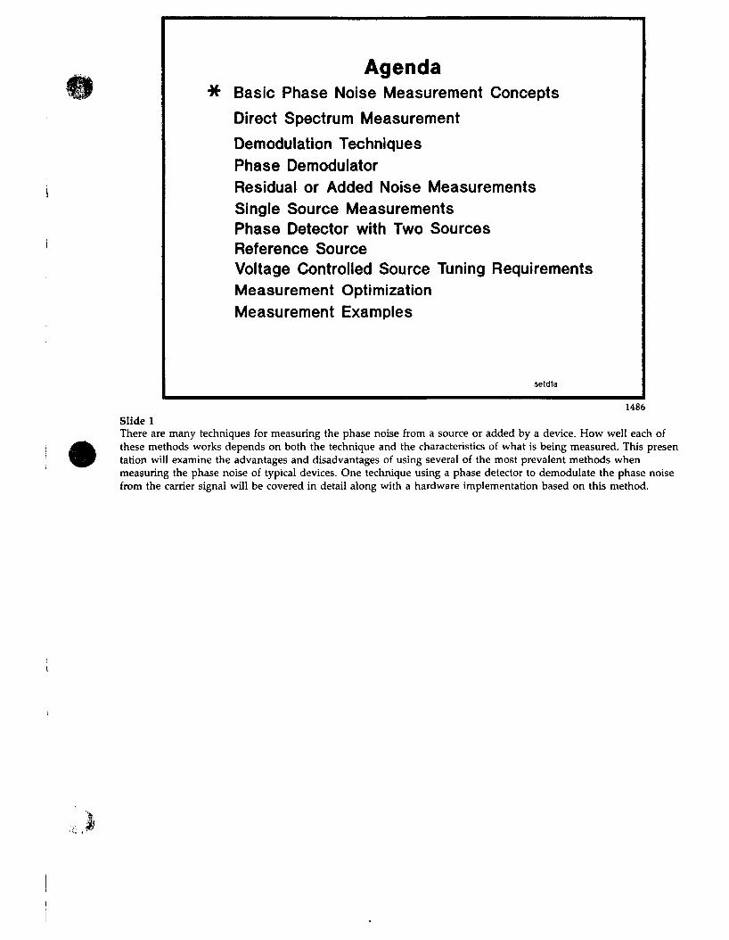
Agenda Basic Phase Noise Measurement Concepts Direct Spectrum Measurement Demodulation Techniques Phase Demodulator Residual or Added Noise Measurements Single Source Measurements Phase Detector with Two Sources Reference Source Voltage Controlled Source Tuning Requirements Measurement Optimization Measurement Examples
setdla
1486 Slide 1 There are many techniques for measuring the phase noise from a source or added by a device. How well each of these methods works depends on both the technique and the characteristics of what is being measured. This presen ration will examine the advantages and disadvantages of using several of the most prevalent methods when measuring the phase noise of typical devices. One technique using a phase detector to demodulate the phase noise from the carrier signal will be covered in detail along with a hardware implementation based on this method.
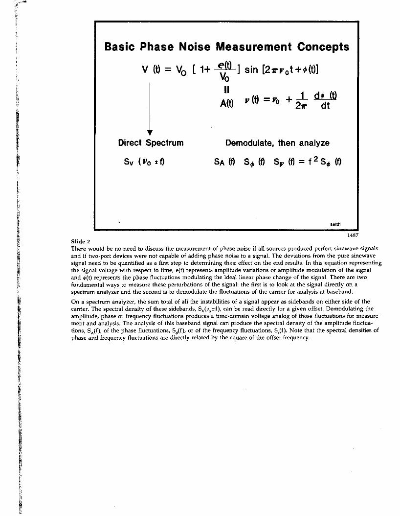
Basic Phase Noise Measurement Concepts
V (t) = V0
Direct Spectrum
S v (Po ±f)
[1+ - f f6 - ] sin [2irr0t + *(t)] Vo
AW '®="°+lV
Demodulate, then analyze
SA(A S*(f) S„ (f) = f 2 S * (f)
setdl
1487 Slide 2 There would be no need to discuss the measurement of phase noise if all sources produced perfect sinewave signals and if two-port devices were not capable of adding phase noise to a signal. The deviations from the pure sinewave signal need to be quantified as a first step to determining their effect on the end results. In this equation representing the signal voltage with respect to time, e(t) represents amplitude variations or amplitude modulation of the signal and <t>(t) represents the phase fluctuations modulating the ideal linear phase change of the signal. There are two fundamental ways to measure these perturbations of the signal: the first is to look at the signal directly on a spectrum analyzer and the second is to demodulate the fluctuations of the carrier for analysis at baseband.
On a spectrum analyzer, the sum total of all the instabilities of a signal appear as sidebands on either side of the carrier. The spectral density of these sidebands, Sv(u0±f), can be read directly for a given offset. Demodulating the amplitude, phase or frequency fluctuations produces a time-domain voltage analog of these fluctuations for measurement and analysis. The analysis of this baseband signal can produce the spectral density of the amplitude fluctuations, SA(f), of the phase fluctuations, S^f), or of the frequency fluctuations, S^f). Note that the spectral densities of phase and frequency fluctuations are directly related by the square of the offset frequency.
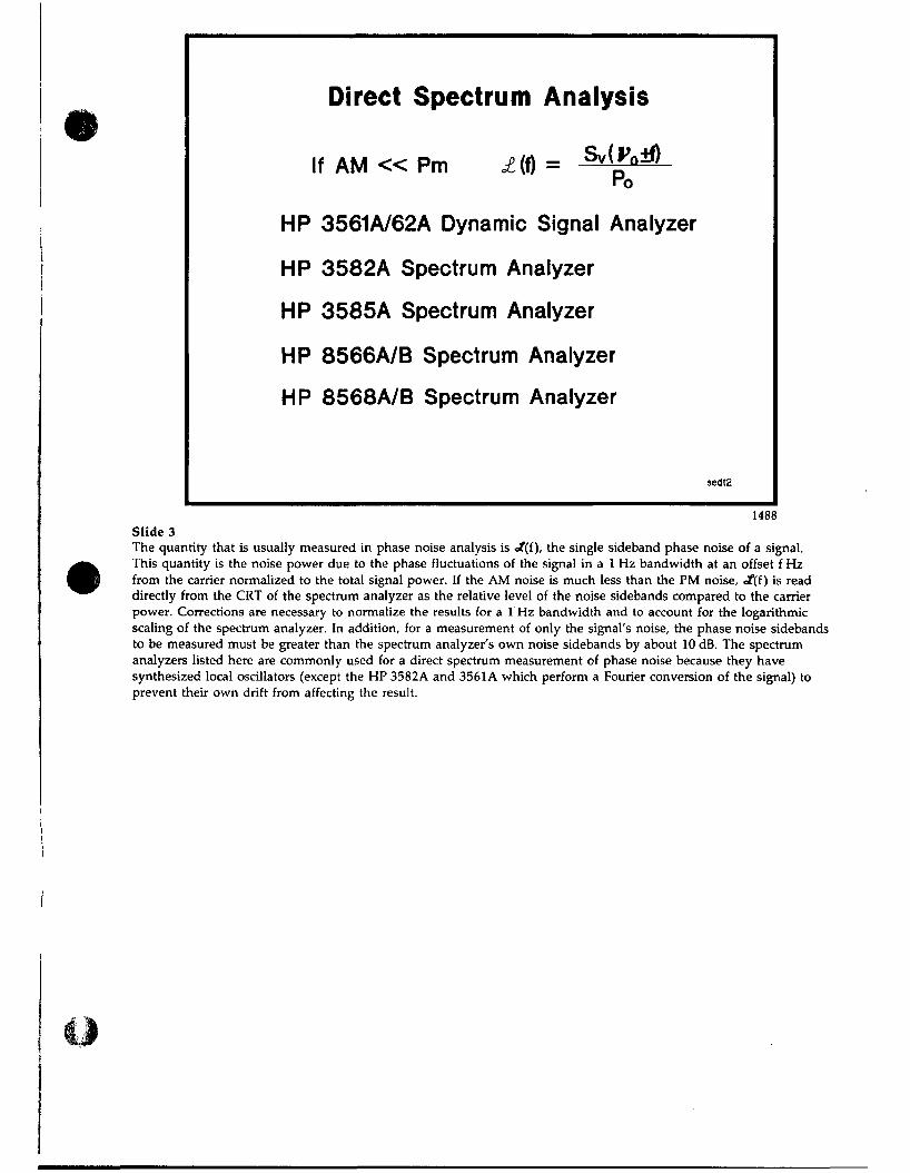
Direct Spectrum Analysis
If AM « Pm m = Svff i^
HP 3561A/62A Dynamic Signal Analyzer
HP 3582A Spectrum Analyzer
HP 3585A Spectrum Analyzer
HP 8566A/B Spectrum Analyzer
HP 8568A/B Spectrum Analyzer
sedt2
1488 Slide 3 The quantity that is usually measured in phase noise analysis is «f(f), the single sideband phase noise of a signal. This quantity is the noise power due to the phase fluctuations of the signal in a 1 Hz bandwidth at an offset f Hz from the carrier normalized to the total signal power. If the AM noise is much less than the PM noise, <Jf(f) is read directly from the CRT of the spectrum analyzer as the relative level of the noise sidebands compared to the carrier power. Corrections are necessary to normalize the results for a 1 Hz bandwidth and to account for the logarithmic scaling of the spectrum analyzer. In addition, for a measurement of only the signal's noise, the phase noise sidebands to be measured must be greater than the spectrum analyzer's own noise sidebands by about 10 dB. The spectrum analyzers listed here are commonly used for a direct spectrum measurement of phase noise because they have synthesized local oscillators (except the HP 3582A and 3561A which perform a Fourier conversion of the signal) to prevent their own drift from affecting the result.
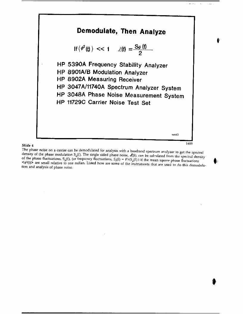
Demodulate, Then Analyze
if(^(t)) « 1 m =- |®—
HP 5390A Frequency Stability Analyzer HP 8901A/B Modulation Analyzer HP 8902A Measuring Receiver HP 3047A/11740A Spectrum Analyzer System HP 3048A Phase Noise Measurement System HP 11729C Carrier Noise Test Set
setd3
1489 Slide 4 The phase noise on a carrier can be demodulated for analysis with a baseband spectrum analyzer to get the spectral density of the phase modulation S,(f). The single sided phase noise, Jftf), can be calculated from the spectral density ° J ^ Actuations, S,(f), (or frequency fluctuations, S,(f) = PxS,(f)) if the mean square phase fluctuations <<t> (t)> are small relative to one radian. Listed here are some of the instruments that are used to do this demodula tion and analysis of phase noise.
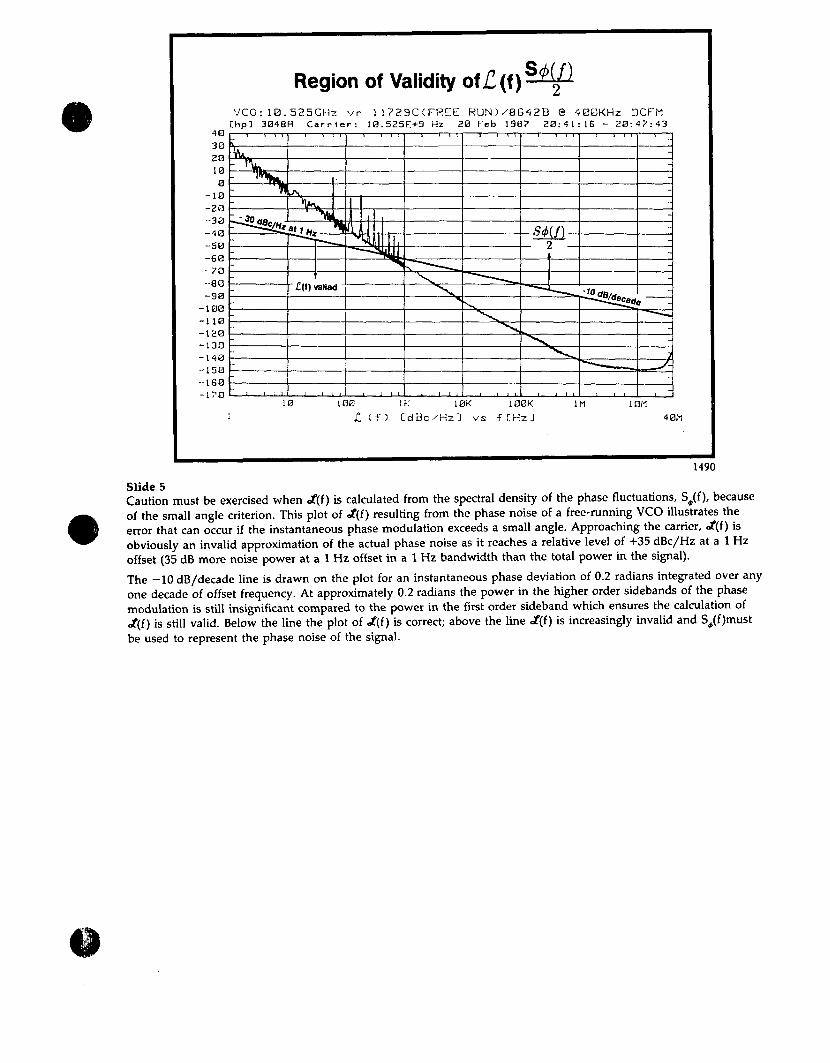
1490 Slide 5 Caution must be exercised when Jf(f) is calculated from the spectral density of the phase fluctuations, S^(f), because of the small angle criterion. This plot of «f(f) resulting from the phase noise of a free-running VCO illustrates the error that can occur if the instantaneous phase modulation exceeds a small angle. Approaching the carrier, </(f) is obviously an invalid approximation of the actual phase noise as it reaches a relative level of +35 dBc/Hz at a 1 Hz offset (35 dB more noise power at a 1 Hz offset in a 1 Hz bandwidth than the total power in the signal). The - 1 0 dB/decade line is drawn on the plot for an instantaneous phase deviation of 0.2 radians integrated over any one decade of offset frequency. At approximately 0.2 radians the power in the higher order sidebands of the phase modulation is still insignificant compared to the power in the first order sideband which ensures the calculation of <Jf(f) is still valid. Below the line the plot of </(f) is correct; above the line J(f) is increasingly invalid and S^(f)must be used to represent the phase noise of the signal.
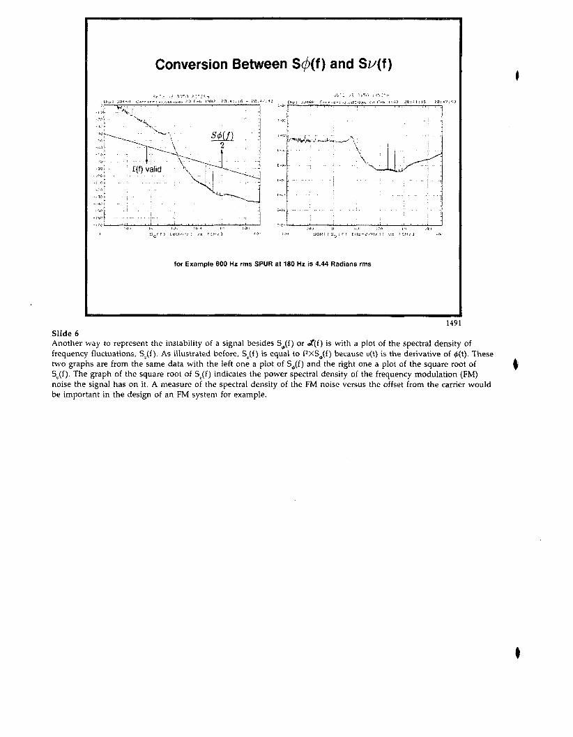
1491 Slide 6 Another way to represent the instability of a signal besides S,(f) or </(f) is with a plot of the spectral density of frequency fluctuations, Su(f). As illustrated before, Su(f) is equal to f2XS^(f) because u(t) is the derivative of <£(t). These two graphs are from the same data with the left one a plot of S^(f) and the right one a plot of the square root of S^f). The graph of the square root of Su(f) indicates the power spectral density of the frequency modulation (FM) noise the signal has on it. A measure of the spectral density of the FM noise versus the offset from the carrier would be important in the design of an FM system for example.
I
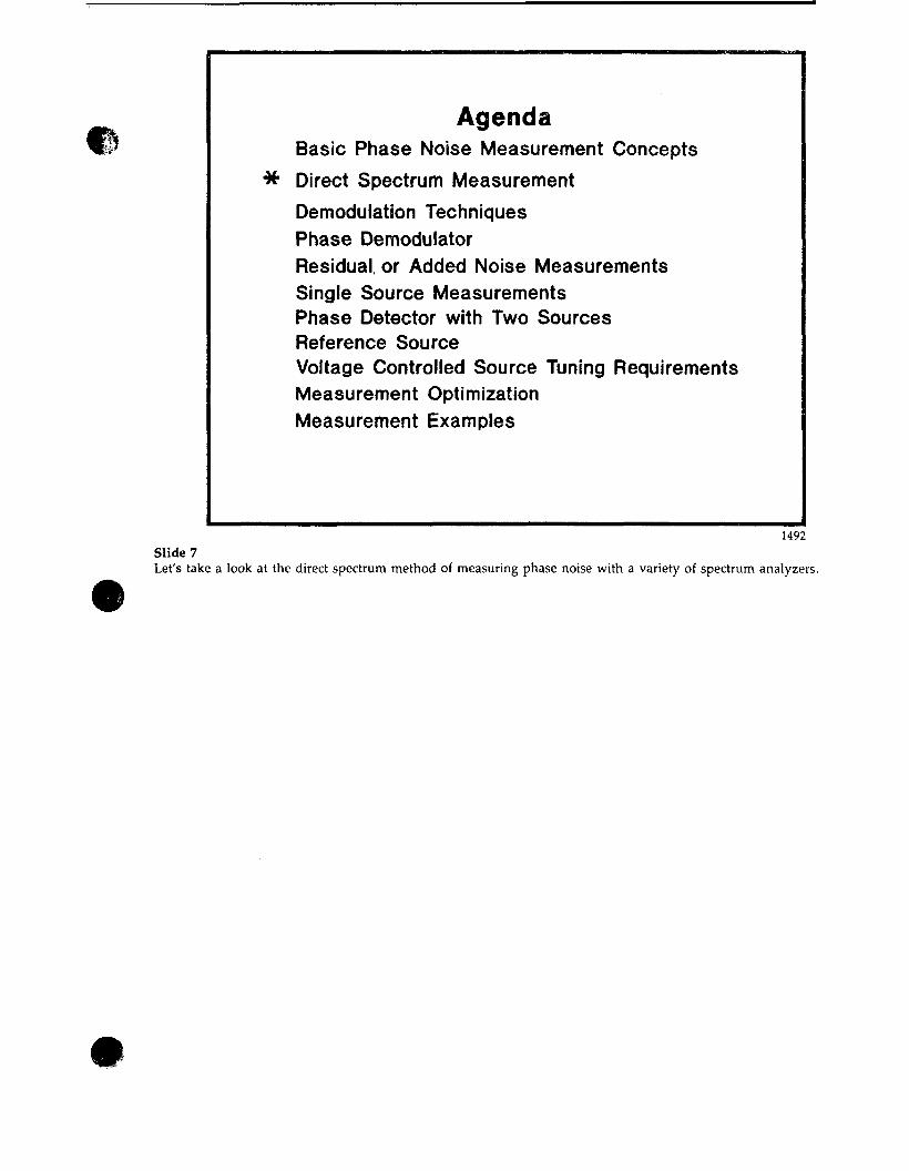
Agenda Basic Phase Noise Measurement Concepts
** Direct Spectrum Measurement Demodulation Techniques Phase Demodulator Residual or Added Noise Measurements Single Source Measurements Phase Detector with Two Sources Reference Source Voltage Controlled Source Tuning Requirements Measurement Optimization Measurement Examples
1492 Slide 7 Let's take a look at the direct spectrum method of measuring phase noise with a variety of spectrum analyzers.
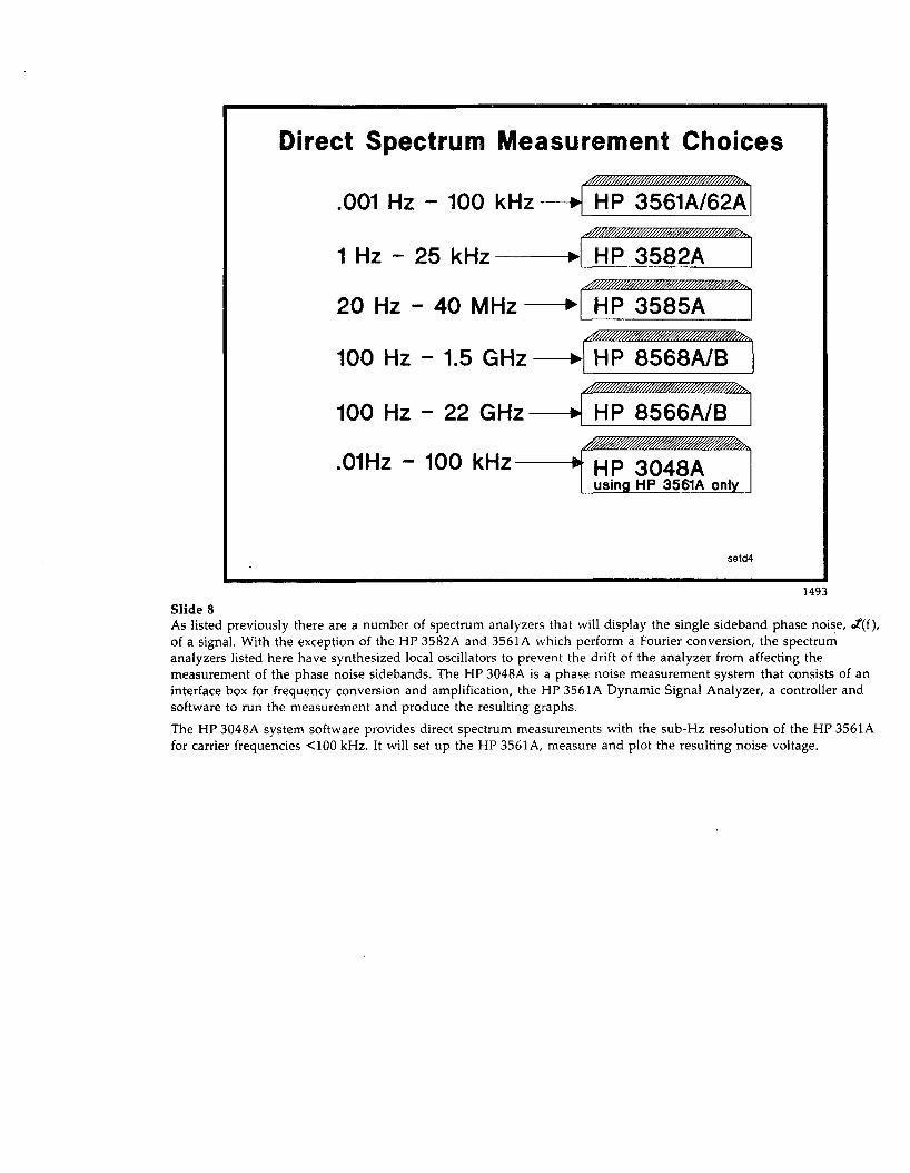
Direct Spectrum Mea
.001 Hz - 100 kHz -
i n z CJO Knz
20 Hz - 40 MHz —
100 Hz - 1.5 G H z -
100 Hz - 22 GHz — H1MI7 - 1flfi kH?
.uinz. luu i\nz
SU
—►
h» w
—►
—►
—►
Ik w
rement Choices / j i i a i i i B i k HP 3561A/62A
^^M5mm^^m5%^%^^ HP 3582A
- ^ ^ ^ ^ ^ M ^ ^ M M ^ HP 3585A
J W # J I « « I « ^ HP 8568A/B
X ^ M ^ M ^ ^ M ^ M ^ ^ ^
HP 8566A/B . ^ ^ ^ ^ ^ ^ ^ ^ ^ ^ ^ ^ ^ ^ ^ ^ s .
HP 3048A using HP 3561A only
setd^
1493 Slide 8 As listed previously there are a number of spectrum analyzers that will display the single sideband phase noise, </(f), of a signal. With the exception of the HP 3582A and 3561A which perform a Fourier conversion, the spectrum analyzers listed here have synthesized local oscillators to prevent the drift of the analyzer from affecting the measurement of the phase noise sidebands. The HP 3048A is a phase noise measurement system that consists of an interface box for frequency conversion and amplification, the HP 3561A Dynamic Signal Analyzer, a controller and software to run the measurement and produce the resulting graphs. The HP 3048A system software provides direct spectrum measurements with the sub-Hz resolution of the HP 3561A for carrier frequencies <100 kHz. It will set up the HP 3561 A, measure and plot the resulting noise voltage.
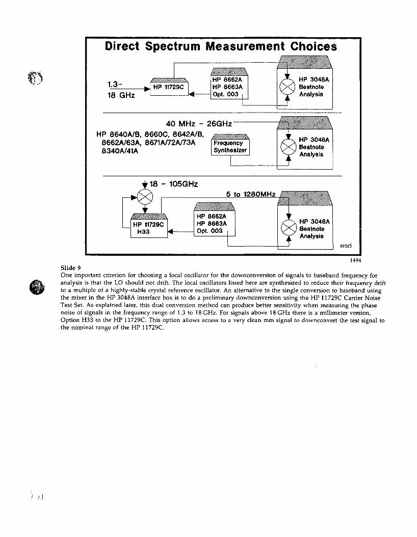
1494 Slide 9 One important criterion for choosing a local oscillator for the downconversion of signals to baseband frequency for analysis is that the LO should not drift. The local oscillators listed here are synthesized to reduce their frequency drift to a multiple of a highly-stable crystal reference oscillator. An alternative to the single conversion to baseband using the mixer in the HP 3048A interface box is to do a preliminary downconversion using the HP 11729C Carrier Noise Test Set. As explained later, this dual conversion method can produce better sensitivity when measuring the phase noise of signals in the frequency range of 1.3 to 18 GHz. For signals above 18 GHz there is a millimeter version, Option H33 to the HP 11729C. This option allows access to a very clean mm signal to downconvert the test signal to the nominal range of the HP 11729C.
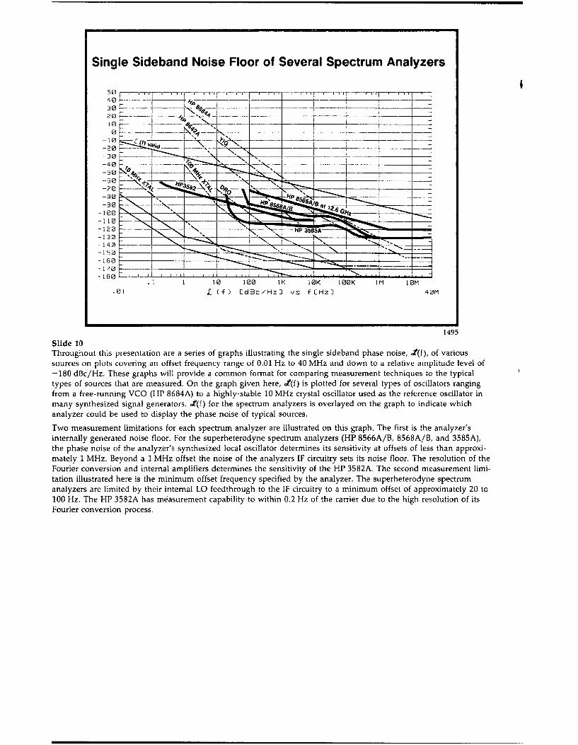
1495 Slide 10 Throughout this presentation are a series of graphs illustrating the single sideband phase noise, Jf(f), of various sources on plots covering an offset frequency range of 0.01 Hz to 40 MHz and down to a relative amplitude level of —180 dBc/Hz. These graphs will provide a common format for comparing measurement techniques to the typical types of sources that are measured. On the graph given here, Jf(f) is plotted for several types of oscillators ranging from a free-running VCO (HP 8684A) to a highly-stable 10 MHz crystal oscillator used as the reference oscillator in many synthesized signal generators. Jt(f) for the spectrum analyzers is overlayed on the graph to indicate which analyzer could be used to display the phase noise of typical sources. Two measurement limitations for each spectrum analyzer are illustrated on this graph. The first is the analyzer's internally generated noise floor. For the superheterodyne spectrum analyzers (HP 8566A/B, 8568A/B, and 3585A), the phase noise of the analyzer's synthesized local oscillator determines its sensitivity at offsets of less than approximately 1 MHz. Beyond a 1 MHz offset the noise of the analyzers IF circuitry sets its noise floor. The resolution of the Fourier conversion and internal amplifiers determines the sensitivity of the HP 3582A. The second measurement limitation illustrated here is the minimum offset frequency specified by the analyzer. The superheterodyne spectrum analyzers are limited by their internal LO feedthrough to the IF circuitry to a minimum offset of approximately 20 to 100 Hz. The HP 3582A has measurement capability to within 0.2 Hz of the carrier due to the high resolution of its Fourier conversion process.
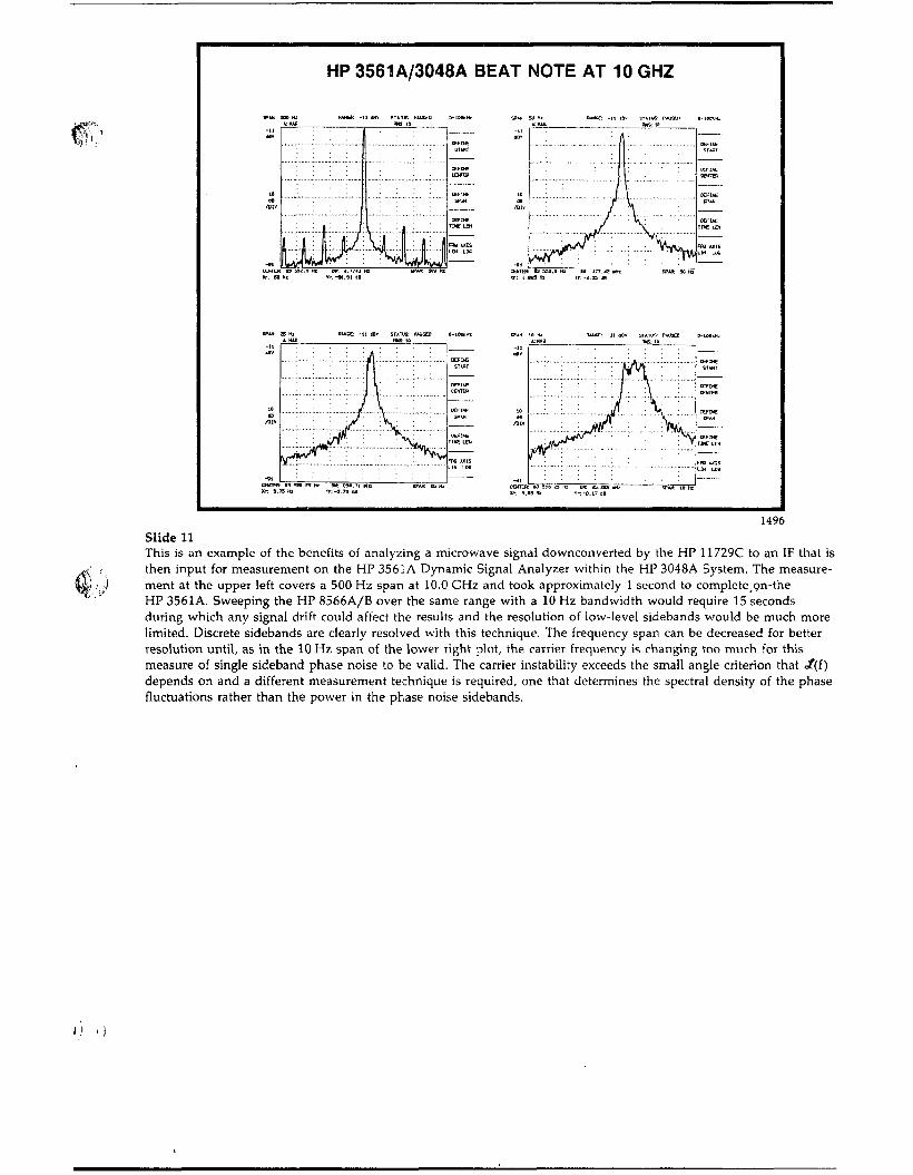
&
HP 3561A/3048A BEAT NOTE AT 10 GHZ
- i l SBV ST4TU& PAUSKI
: : : : :
SPAK 5 0 Ha
SPAM
dSV
10
Anv
ZS Hz A: KM
(UNSE: - i t nav STATUS; PAUSES RMS: 10
O-lOaXH*
DEFI>E START
OGFWC COTTER
(DEFINE SPAH
OEF:IC TIKEUEH
mo AXIS L I N L O B
1496 Slide 11 This is an example of the benefits of analyzing a microwave signal downconverted by the HP 11729C to an IF that is then input for measurement on the HP 3561A Dynamic Signal Analyzer within the HP 3048A System. The measurement at the upper left covers a 500 Hz span at 10.0 GHz and took approximately 1 second to complete.on-the HP 3561A. Sweeping the HP 8566A/B over the same range with a 10 Hz bandwidth would require 15 seconds during which any signal drift could affect the results and the resolution of low-level sidebands would be much more limited. Discrete sidebands are clearly resolved with this technique. The frequency span can be decreased for better resolution until, as in the 10 Hz span of the lower right plot, the carrier frequency is changing too much for this measure of single sideband phase noise to be valid. The carrier instability exceeds the small angle criterion that ./(f) depends on and a different measurement technique is required, one that determines the spectral density of the phase fluctuations rather than the power in the phase noise sidebands.
n ■)
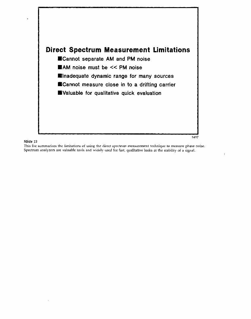
Direct Spectrum Measurement Limitations ■Cannot separate AM and PM noise ■AM noise must be « PM noise ■Inadequate dynamic range for many sources ■Cannot measure close in to a drifting carrier ■Valuable for qualitative quick evaluation
1497 Slide 12 This list summarizes the limitations of using the direct spectrum measurement technique to measure phase noise. Spectrum analyzers are valuable tools and widely used for fast, qualitative looks at the stability of a signal.
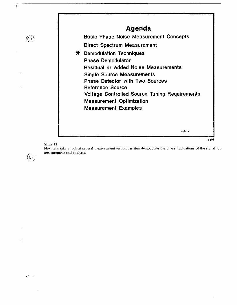
Agenda Basic Phase Noise Measurement Concepts Direct Spectrum Measurement
#■ Demodulation Techniques Phase Demodulator Residual or Added Noise Measurements Single Source Measurements Phase Detector with Two Sources Reference Source Voltage Controlled Source Tuning Requirements Measurement Optimization Measurement Examples
setdla
1498 Slide 13 Next let's take a look at several measurement techniques that demodulate the phase fluctuations of the signal for measurement and analysis.
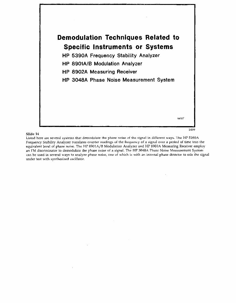
Demodulation Techniques Related to Specific Instruments or Systems HP 5390A Frequency Stability Analyzer HP 8901A/B Modulation Analyzer HP 8902A Measuring Receiver HP 3048A Phase Noise Measurement System
setd7
1499 Slide 14 Listed here are several systems that demodulate the phase noise of the signal in different ways. The HP 5390A Frequency Stability Analyzer translates counter readings of the frequency of a signal over a period of time into the equivalent level of phase noise. The HP 8901A/B Modulation Analyzer and HP 8902A Measuring Receiver employ an FM discriminator to demodulate the phase noise of a signal. The HP 3048A Phase Noise Measurement System can be used in several ways to analyze phase noise, one of which is with an internal phase detector to mix the signal under test with synthesized oscillator.
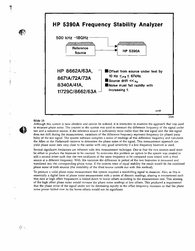
HP 5390A Frequency Stability Analyzer
5 0 0 kHz -18GHz
Reference Source HP 5390A
HP 8662A/63A, 8671A/72A/73A 8340A/41A, 11729C/8662/63A
I Offset from source under test by 10 Hz < r B < 67kHz.
I Source drift « Vst
I Noise must fall rapidly with increasing f.
setd8
1500 Slide 15 Although this system is now obsolete and cannot be ordered, it is instructive to examine the approach that was used to measure phase noise. The counter in the system was used to measure the difference frequency of the signal under test and a reference source. If the reference source is sufficiently more stable than the test signal and the test signal does not drift during the measurement, variations of the difference frequency represent frequency (or phase) instability of the test signal. The system software compiles a series of readings of this difference frequency and calculates the Allen or the Hadamard variance to determine the phase noise of the signal. This measurement approach can yield phase noise data very close to the carrier with very good sensitivity if a low frequency beatnote is used. Several significant limitations are inherent with this measurement technique. One is that the two sources used must be offset to produce the beatnote to be counted. To overcome this problem an option to the system was created to add a second mixer such that the two oscillators of the same frequency to be compared were mixed with a third source at a different frequency. With this variation the difference in period of the two beatnotes is measured and translated into the corresponding phase noise. If the sources were of equal stability the result would be the combined phase noise of both sources (the instability of the third source cancels out with this method).
To produce a valid phase noise measurement this system required a nondrifting signal to measure. Also, as this is essentially a digital form of phase noise measurement with a series of discrete readings, aliasing is encountered such that.data at high offset frequencies is folded down to lower offsets according to the measurement rate. This aliasing of the high offset phase noise would increase the phase noise readings at low offsets. This produced a requirement that the phase noise of the signal under test be decreasing rapidly as the offset frequency increases so that the phase noise power folded over to the lower offsets would not be significant.
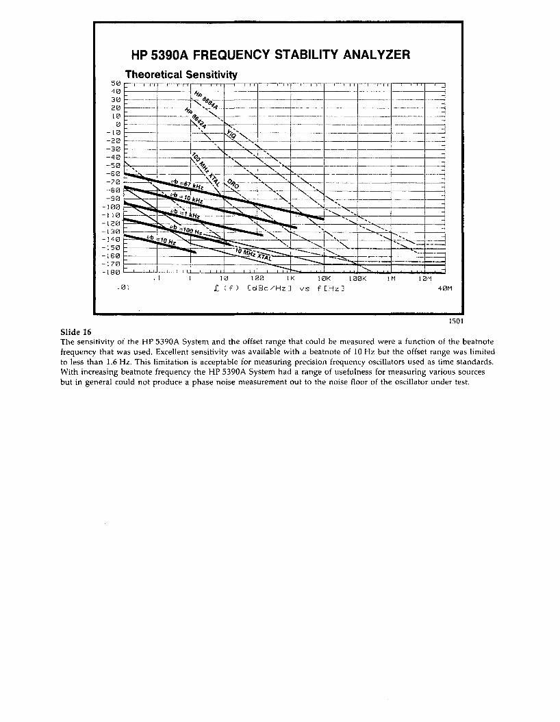
HP 5390A FREQUENCY STABILITY ANALYZER Theoretical Sensitivity
r 1 F T ^ I TT 1 J.-.J.-J j J—J.. I 1—i—r~i 1 1—r~rl i 1 rr
. 0 1 10 100 IK 10K 100K
£ ( f ) C d B c / H z ] v s f CHz] !M 10M
40M
1501 Slide 16 The sensitivity of the HP 5390A System and the offset range that could be measured were a function of the beatnote frequency that was used. Excellent sensitivity was available with a beatnote of 10 Hz but the offset range was limited to less than 1.6 Hz. This limitation is acceptable for measuring precision frequency oscillators used as time standards. With increasing beatnote frequency the HP 5390A System had a range of usefulness for measuring various sources but in general could not produce a phase noise measurement out to the noise floor of the oscillator under test.
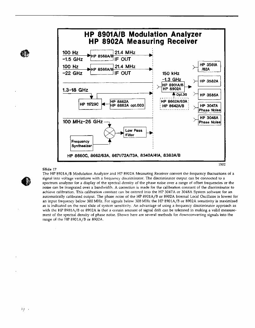
HP 8901A/B Modulation Analyzer HP 8902A Measuring Receiver
100 Hz -1.5 GHz 100 Hz
HP 8568A/B 21.4 MHz
-22 GHz » H P 8566A/B
IF OUT 21.4 MHz IF OUT 150 kHz
-1.3 GHz
HP 3561A /62A
1.3-18 GHz > - HP 8901A/B HP 8902A
HP 11729C HP 8662A HP 8663A opt.003
J
y- HP 3582A
Opt.30
IHP 8662A/63A; ; HP 8642A/B '
HP 3585A
>- HP 3047A Phase Noise
100 MHz-26 GHz
Frequency Synthesizer
> HP 3048A Phase Noise
Low Pass Filter
HP 8660C, 8662/63A, 8671/72A/73A, 8340A/41A, 8383A/B
1502 Slide 17 The HP 8901A/B Modulation Analyzer and HP 8902A Measuring Receiver convert the frequency fluctuations of a signal into voltage variations with a frequency discriminator. The discriminator output can be connected to a spectrum analyzer for a display of the spectral density of the phase noise over a range of offset frequencies or the noise can be integrated over a bandwidth. A correction is made for the calibration constant of the discriminator to achieve calibration. This calibration constant can be entered into the HP 3047A or 3048A System software for an automatically calibrated output. The phase noise of the HP 8901 A/B or 8902A Internal Local Oscillator is lowest for an input frequency below 300 MHz. For signals below 300 MHz the HP 8901A/B or 8902A sensitivity is maximized as is indicated on the next slide of system sensitivity. An advantage of using a frequency discriminator approach as with the HP 8901A/B or 8902A is that a certain amount of signal drift can be tolerated in making a valid measurement of the spectral density of phase noise. Shown here are several methods for downconverting signals into the range of the HP 8901A/B or 8902A.
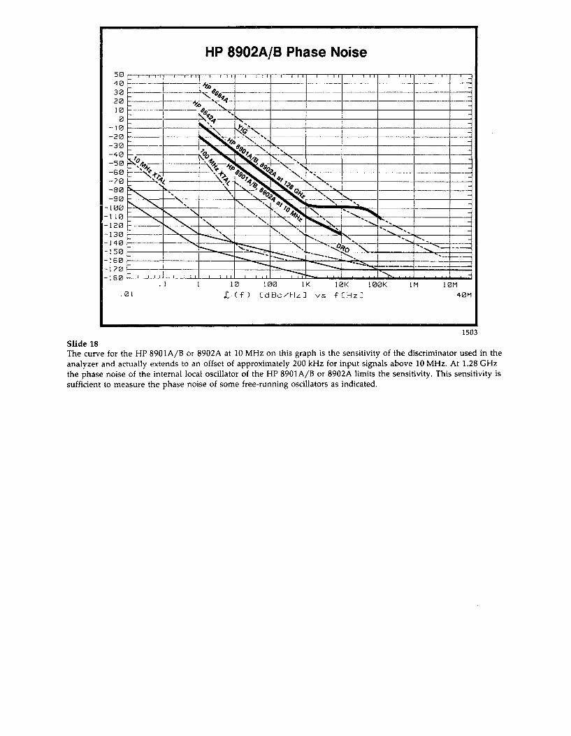
50 40 30 20 10 0
- 1 0 - 2 0 - 3 0 - 4 0 - 5 0 - 6 0 - 7 0 - 8 0 - 9 0
-100 -1 10 -120 -130 -140 -150 -160 -170
HP 8902A/B Phase Noise i i M
---
---
^°u - N %
r ^
L
-
i i M
^ ^s. * . " \
K
\ v
\ N
"if -
ws
X N v p \ SX^- \. x / f l \ l v* X - > & . « ~ ~ \ ^
\
"v
^ ^ - ^ - w
ssrx *•>• >fe.x- ^ \ N & . \ V
& ' ^ X N&_ v v ^^3STN& \ \
\ \
x T ^ > ^ -. ~~"~
LT*'>0 v ,JX \ >
^> 1 _ X .
V \ *» \ X
"^t~—~u
--
X s
^ X ""^ | \
^*v
"->4*h \
* " ^ ^ * - „
k"*"i4a f c^
N.. . ..
"'v^""-*—
------------1 - 1
----
1
-\ .1 1 10 100 IK 10K 100K 1M 10M
•01 £ ( f ) C d B c / H z ] v s f C H z 3 40M
1503 Slide 18 The curve for the HP 8901A/B or 8902A at 10 MHz on this graph is the sensitivity of the discriminator used in the analyzer and actually extends to an offset of approximately 200 kHz for input signals above 10 MHz. At 1.28 GHz the phase noise of the internal local oscillator of the HP 8901A/B or 8902A limits the sensitivity. This sensitivity is sufficient to measure the phase noise of some free-running oscillators as indicated.
Agenda Basic Phase Noise Measurement Concepts Direct Spectrum Measurement Demodulation Techniques Phase Demodulator Residual or Added Noise Measurements Single Source Measurements Phase Detector with Two Sources Reference Source Voltage Controlled Source Tuning Requirements Measurement Optimization Measurement Examples
1504 Slide 19 Now we'll take a look at the phase demodulator technique used by the HP 3048A Phase Noise Measurement System. Whereas the previous phase noise measurement techniques were useful within certain limits of signal stability, offset ranges, and sensitivity levels, the phase demodulation technique used by the HP 3048A System has the broadest range of applications of any system available today.
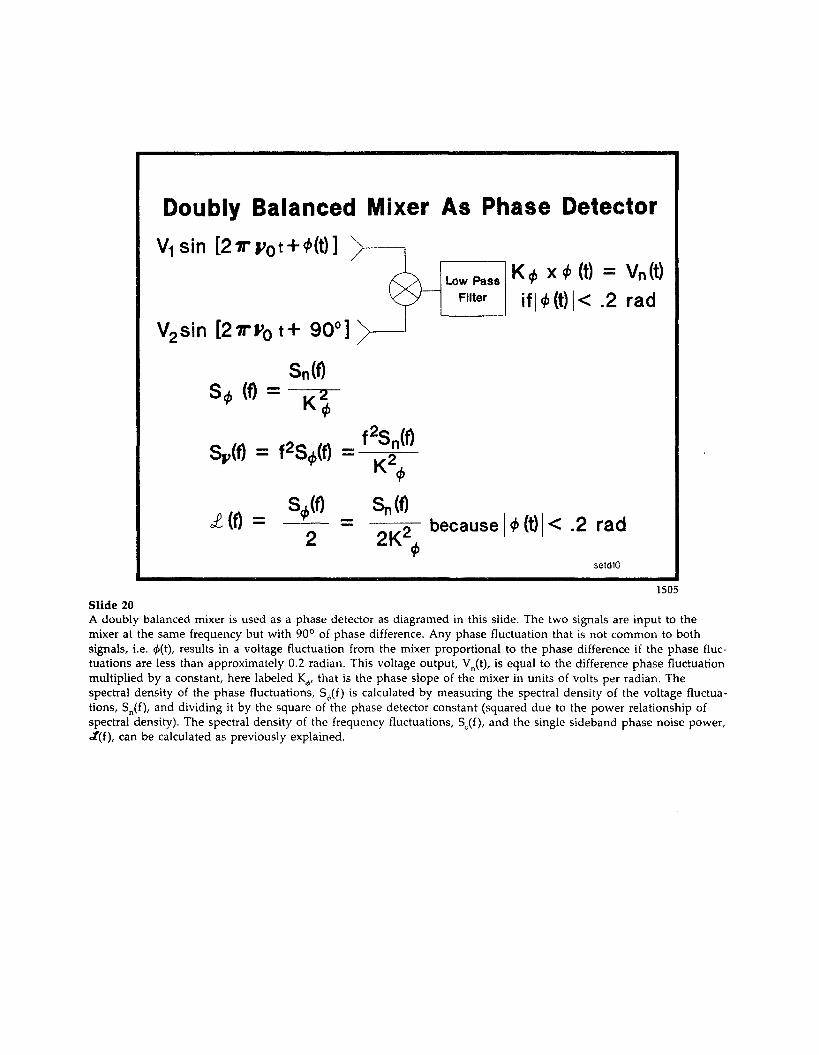
Doubly Balanced Mixer As Phase Detector ViSin l2Tp0t+H\)]
V2sin [2TV0 t+ 90°]
Low Pass Filter
K* x<Mt) = Vn(t) if|4>(t)|< .2 rad
S 0 (I) Sn(f)
K <f>
SF(f) = f%(f)
/(f) = s^(f)
f2Sn(0
2K' because 4>(t) < .2 rad
* setdIO
1505 Slide 20 A doubly balanced mixer is used as a phase detector as diagramed in this slide. The two signals are input to the mixer at the same frequency but with 90° of phase difference. Any phase fluctuation that is not common to both signals, i.e. 0(t), results in a voltage fluctuation from the mixer proportional to the phase difference if the phase fluctuations are less than approximately 0.2 radian. This voltage output, Vn(t), is equal to the difference phase fluctuation multiplied by a constant, here labeled K , that is the phase slope of the mixer in units of volts per radian. The spectral density of the phase fluctuations, S^(f) is calculated by measuring the spectral density of the voltage fluctuations, Sn(f), and dividing it by the square of the phase detector constant (squared due to the power relationship of spectral density). The spectral density of the frequency fluctuations, Sv((), and the single sideband phase noise power, of(f), can be calculated as previously explained.
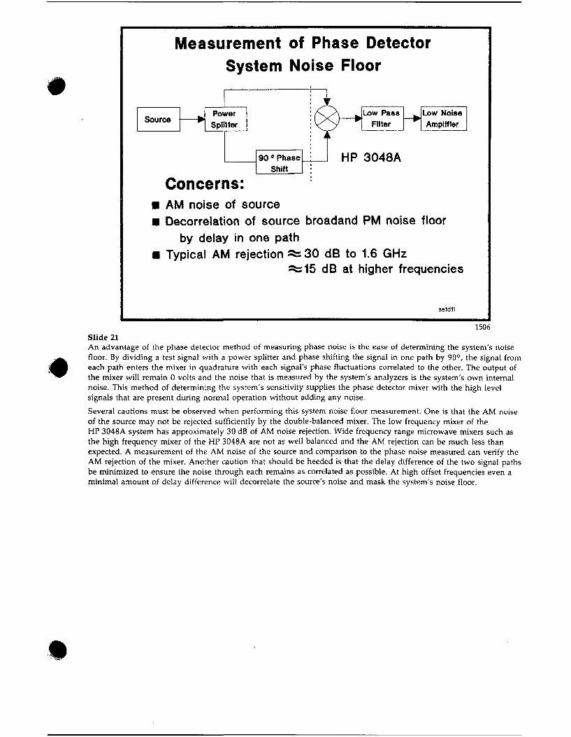
Measurement of Phase Detector System Noise Floor
Source Power Splitter
Low Pass Filter
Low Noise Amplifier
90 ° Phase Shift
HP 3048A
Concerns: AM noise of source Decorrelation of source broadand PM noise floor
by delay in one path Typical AM rejection fts 30 dB to 1.6 GHz
^s15 dB at higher frequencies
setdH
1506 Slide 21 An advantage of the phase detector method of measuring phase noise is the ease of determining the system's noise floor. By dividing a test signal with a power splitter and phase shifting the signal in one path by 90°, the signal from each path enters the mixer in quadrature with each signal's phase fluctuations correlated to the other. The output of the mixer will remain 0 volts and the noise that is measured by the system's analyzers is the system's own internal noise. This method of determining the system's sensitivity supplies the phase detector mixer with the high level signals that are present during normal operation without adding any noise. Several cautions must be observed when performing this system noise floor measurement. One is that the AM noise of the source may not be rejected sufficiently by the double-balanced mixer. The low frequency mixer of the HP 3048A system has approximately 30 dB of AM noise rejection. Wide frequency range microwave mixers such as the high frequency mixer of the HP 3048A are not as well balanced and the AM rejection can be much less than expected. A measurement of the AM noise of the source and comparison to the phase noise measured can verify the AM rejection of the mixer. Another caution that should be heeded is that the delay difference of the two signal paths be minimized to ensure the noise through each remains as correlated as possible. At high offset frequencies even a minimal amount of delay difference will decorrelate the source's noise and mask the system's noise floor.
HP 3048A Phase Noise Measurement Noise Floor 5 MHz-1.6 GHz,+15 dBm Sources
n n—m i r~rr-\ 1 — r r r ~ i — t ~ n
. 0 1 10 1 0 0 IK
I ( f ) CdBc/Hz] 10K 100K
s f C H z J 10M
4 0M
1507 Slide 22 This graph of the resulting noise floor of the phase detector method of the HP 3048A System demonstrates why this method has the most usefulness for measuring the widest range of sources. The system's typical sensitivity allows measurement of even the cleanest of reference oscillators.
Agenda Basic Phase Noise Measurement Concepts Direct Spectrum Measurement Demodulation Techniques Phase Demodulator
■*■ Residual or Added Noise Measurements Single Source Measurements Phase Detector with Two Sources Reference Source Voltage Controlled Source Tuning Requirements Measurement Optimization Measurement Examples
setdla
1508 Slide 23 One application of the phase detector method of phase noise measurement is to quantify the amount of noise added to a signal as it passes through a device. This added noise is referred to as residual noise.
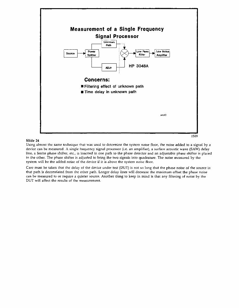
Measurement of a Single Frequency Signal Processor
Source Power Splitter
Unknown Path
ADJ*
1 T
f-y u
Low Pasa Filter
Low Noise Amplifier
HP 3048A
Concerns: i Filtering effect of unknown path I Time delay in unknown path
1509 Slide 24 Using almost the same technique that was used to determine the system noise floor, the noise added to a signal by a device can be measured. A single frequency signal processor (i.e. an amplifier), a surface acoustic wave (SAW) delay line, a ferrite phase shifter, etc., is inserted in one path to the phase detector and an adjustable phase shifter is placed in the other. The phase shifter is adjusted to bring the two signals into quadrature. The noise measured by the system will be the added noise of the device if it is above the system noise floor. Care must be taken that the delay of the device under test (DUT) is not so long that the phase noise of the source in that path is decorrelated from the other path. Longer delay lines will decrease the maximum offset the phase noise can be measured to or require a quieter source. Another thing to keep in mind is that any filtering of noise by the DUT will affect the results of the measurement.
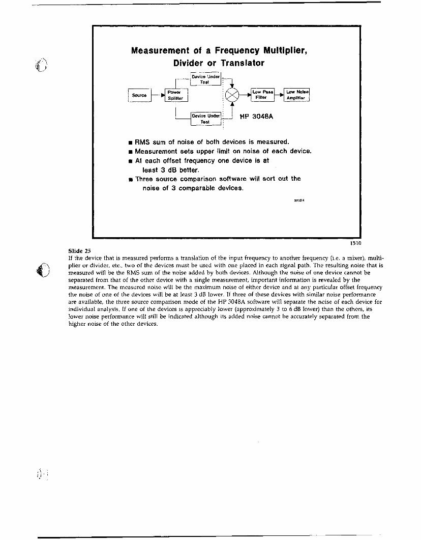
Measurement of a Frequency Multiplier, Divider or Translator
Source
Device Under Test
Power Splitter
Device Under Test
n !(Xh» : i
Low Pass Filter
HP 3048A
-► Low Noise Amplifier
■ RMS sum of noise of both devices is measured. ■ Measurement sets upper limit on noise of each device. ■ At each offset frequency one device is at
least 3 dB better. ■ Three source comparison software will sort out the
noise of 3 comparable devices.
1510 Slide 25 If the device that is measured performs a translation of the input frequency to another frequency (i.e. a mixer), multiplier or divider, etc., two of the devices must be used with one placed in each signal path. The resulting noise that is measured will be the RMS sum of the noise added by both devices. Although the noise of one device cannot be separated from that of the other device with a single measurement, important information is revealed by the measurement. The measured noise will be the maximum noise of either device and at any particular offset frequency the noise of one of the devices will be at least 3 dB lower. If three of these devices with similar noise performance are available, the three source comparison mode of the HP 3048A software will separate the noise of each device for individual analysis. If one of the devices is appreciably lower (approximately 3 to 6 dB lower) than the others, its lower noise performance will still be indicated although its added noise cannot be accurately separated from the higher noise of the other devices.
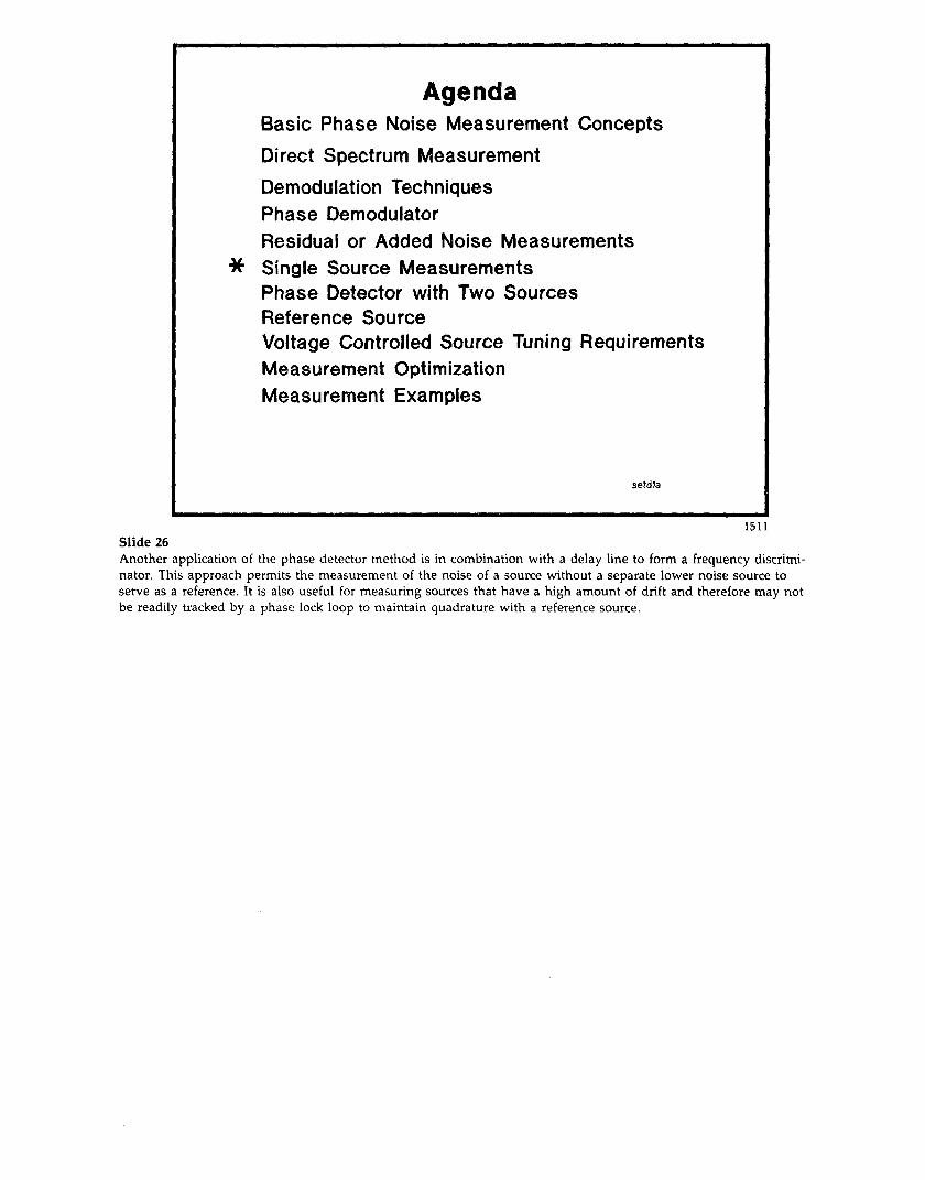
Agenda Basic Phase Noise Measurement Concepts Direct Spectrum Measurement Demodulation Techniques Phase Demodulator Residual or Added Noise Measurements
* Single Source Measurements Phase Detector with Two Sources Reference Source Voltage Controlled Source Tuning Requirements Measurement Optimization Measurement Examples
setdla
1511 Slide 26 Another application of the phase detector method is in combination with a delay line to form a frequency discriminator. This approach permits the measurement of the noise of a source without a separate lower noise source to serve as a reference. It is also useful for measuring sources that have a high amount of drift and therefore may not be readily tracked by a phase lock loop to maintain quadrature with a reference source.
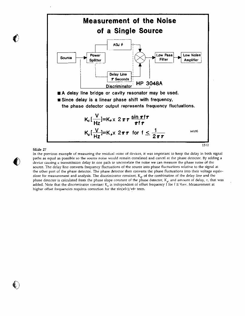
Measurement of the Noise off a Single Source
Source
ADJ ^
Power Splitter
Delay Line T Seconds
Low Pass Filter
Low Noise Amplifier
Discriminator HP 3048A i A delay line bridge or cavity resonator may be used. I Since delay is a linear phase shift with frequency, the phase detector output represents frequency fluctuations.
Hz t\r K, [-j^=K,x 2rr for f <. ± ^
1512 Slide 27 In the previous example of measuring the residual noise of devices, it was important to keep the delay in both signal paths as equal as possible so the source noise would remain correlated and cancel at the phase detector. By adding a device causing a transmission delay in one path to uncorrelate the noise we can measure the phase noise of the source. The delay line converts frequency fluctuations of the source into phase fluctuations relative to the signal at the other port of the phase detector. The phase detector then converts the phase fluctuations into their voltage equivalent for measurement and analysis. The discriminator constant, Kd, of the combination of the delay line and the phase detector is calculated from the phase slope constant of the phase detector, K , and amount of delay, r, that was added. Note that the discriminator constant Kd is independent of offset frequency f for f < VITTT. Measurement at higher offset frequencies requires correction for the sin(7rf"r)/7rfT term.
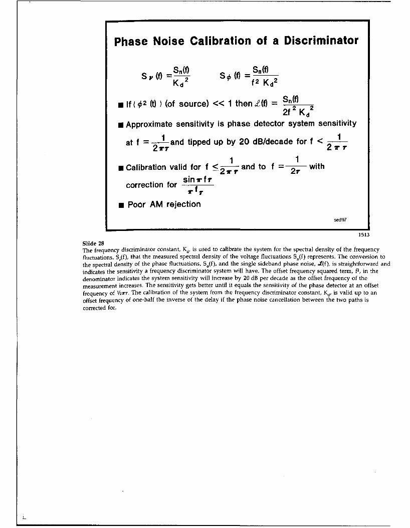
Phase Noise Calibration of a Discriminator
S*(f) = Snfl) f2 K H 2
If<^2 (t) ) (of source) « 1 then 1(f) = ^$—= 2 f 2 K d
2
Approximate sensitivity is phase detector system sensitivity
at f = ^ - a n d tipped up by 20 dB/decade for f < 2rr
Calibration valid for f <
2TT
correction for s in i r f r 2*T
and to f = 1
2r with
Poor AM rejection sedt17
1513 Slide 28 The frequency discriminator constant, Kd, is used to calibrate the system for the spectral density of the frequency fluctuations, S (f), that the measured spectral density of the voltage fluctuations Sn(f) represents. The conversion to the spectral density of the phase fluctuations, S^(f), and the single sideband phase noise, Jf(f), is straightforward and indicates the sensitivity a frequency discriminator system will have. The offset frequency squared term, P, in the denominator indicates the system sensitivity will increase by 20 dB per decade as the offset frequency of the measurement increases. The sensitivity gets better until it equals the sensitivity of the phase detector at an offset frequency of VIVT. The calibration of the system from the frequency discriminator constant, Kd, is valid up to an offset frequency of one-half the inverse of the delay if the phase noise cancellation between the two paths is corrected for.
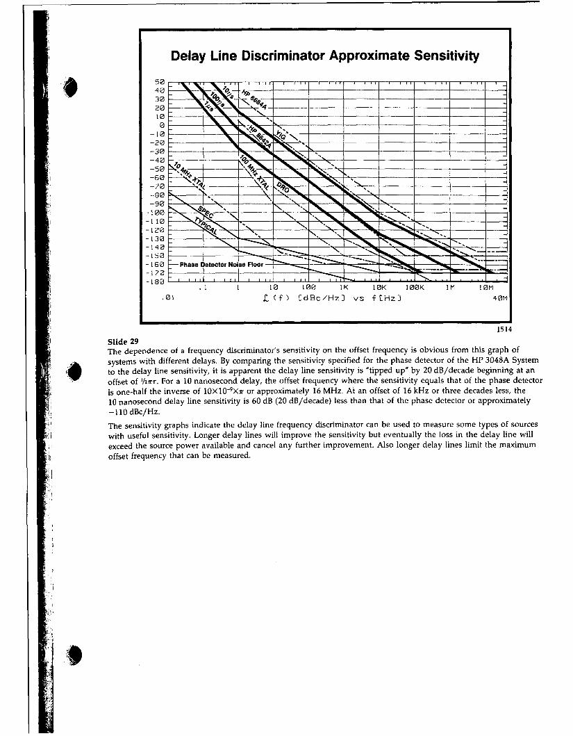
1514 Slide 29 The dependence of a frequency discriminator's sensitivity on the offset frequency is obvious from this graph of systems with different delays. By comparing the sensitivity specified for the phase detector of the HP 3048A System to the delay line sensitivity, it is apparent the delay line sensitivity is "tipped up" by 20 dB/decade beginning at an offset of VITTT. For a 10 nanosecond delay, the offset frequency where the sensitivity equals that of the phase detector is one-half the inverse of 10X10"9X7r or approximately 16 MHz. At an offset of 16 kHz or three decades less, the 10 nanosecond delay line sensitivity is 60 dB (20 dB/decade) less than that of the phase detector or approximately -HOdBc/Hz. The sensitivity graphs indicate the delay line frequency discriminator can be used to measure some types of sources with useful sensitivity. Longer delay lines will improve the sensitivity but eventually the loss in the delay line will exceed the source power available and cancel any further improvement. Also longer delay lines limit the maximum offset frequency that can be measured.
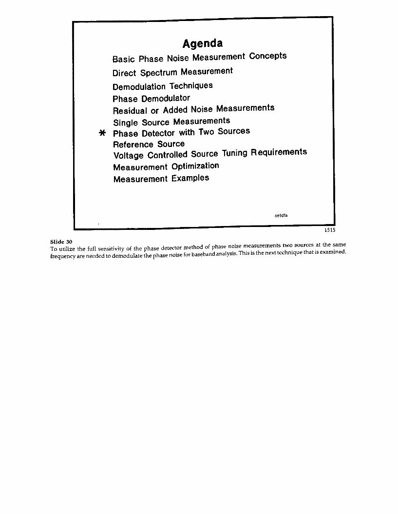
Agenda Basic Phase Noise Measurement Concepts Direct Spectrum Measurement Demodulation Techniques Phase Demodulator Residual or Added Noise Measurements Single Source Measurements Phase Detector with Two Sources Reference Source Voltage Controlled Source Tuning Requirements Measurement Optimization Measurement Examples
setdla
1515
Totalize the full sensitivity of the phase detector method of phase noise measurements two sources at the same frequency are needed to demodulate the phase noise for baseband analysis. This is the next technique that is examined.
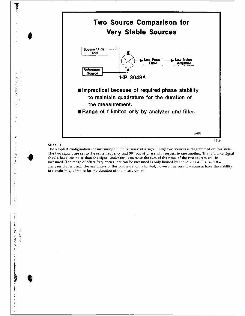
Two Source Comparison for Very Stable Sources
Source Under Test
Reference Source
Low Pass Filter
Low Noise Amplifier
HP 3048A
Impractical because of required phase stability to maintain quadrature for the duration of the measurement.
i Range of f limited only by analyzer and filter.
sedt19
1516 Slide 31 The simplest configuration for measuring the phase noise of a signal using two sources is diagrammed on this slide. The two signals are set to the same frequency and 90° out of phase with respect to one another. The reference signal should have less noise than the signal under test, otherwise the sum of the noise of the two sources will be measured. The range of offset frequencies that can be measured is only limited by the low-pass filter and the analyzer that is used. The usefulness of this configuration is limited, however, as very few sources have the stability to remain in quadrature for the duration of the measurement.
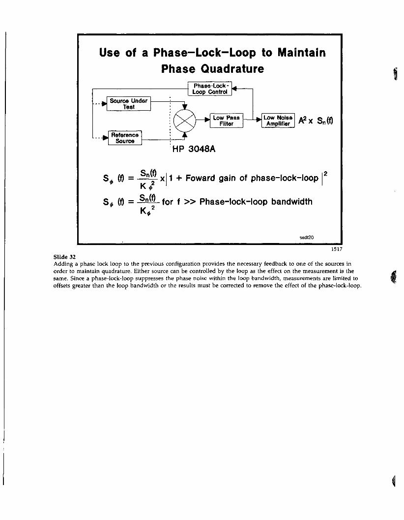
Use of a Phase-Lock-Loop to Maintain Phase Quadrature
Phase-Lock-Loop Control
Source Under Test
Reference Source
Low Pass Filter
Low Noise Amplifier A2X Sn(f)
HP 3048A
S (A S. (f) = — ^ x 1 + Foward gain of phase-lock-loop
S, (f) =
K <£
Sn(f) for f » Phase-lock-loop bandwidth
sedt20
1517 Slide 32 Adding a phase lock loop to the previous configuration provides the necessary feedback to one of the sources in order to maintain quadrature. Either source can be controlled by the loop as the effect on the measurement is the same. Since a phase-lock-loop suppresses the phase noise within the loop bandwidth, measurements are limited to offsets greater than the loop bandwidth or the results must be corrected to remove the effect of the phase-lock-loop.
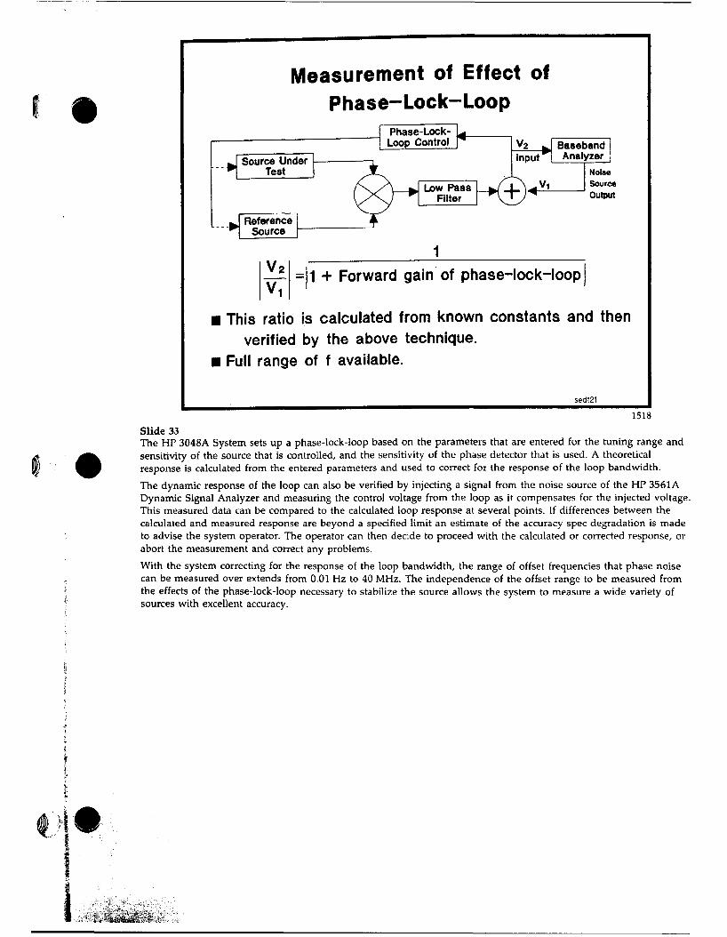
*
i
Measurement of Effect of Phase-Lock-Loop
Phase-Lock-Loop Control
Source Under Test
Reference Source
V2
input Baseband Analyzer
Low Paaa Filter +> V i
Noise Source Output
1 1 + Forward gain of phase-lock-loop
This ratio is calculated from known constants and then verified by the above technique.
Full range of f available.
sedt21
1518 Slide 33 The HP 3048A System sets up a phase-lock-loop based on the parameters that are entered for the tuning range and sensitivity of the source that is controlled, and the sensitivity of the phase detector that is used. A theoretical response is calculated from the entered parameters and used to correct for the response of the loop bandwidth. The dynamic response of the loop can also be verified by injecting a signal from the noise source of the HP 3561A Dynamic Signal Analyzer and measuring the control voltage from the loop as it compensates for the injected voltage. This measured data can be compared to the calculated loop response at several points. If differences between the calculated and measured response are beyond a specified limit an estimate of the accuracy spec degradation is made to advise the system operator. The operator can then decide to proceed with the calculated or corrected response, or abort the measurement and correct any problems.
With the system correcting for the response of the loop bandwidth, the range of offset frequencies that phase noise can be measured over extends from 0.01 Hz to 40 MHz. The independence of the offset range to be measured from the effects of the phase-lock-loop necessary to stabilize the source allows the system to measure a wide variety of sources with excellent accuracy.
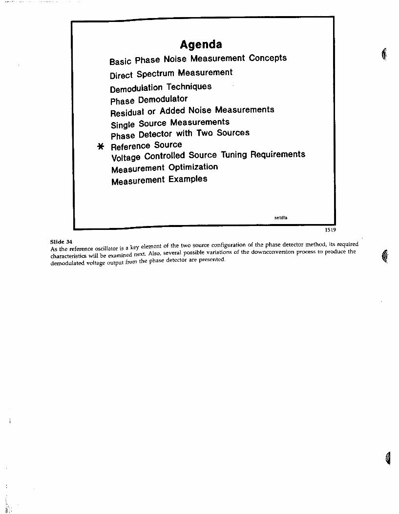
Agenda Basic Phase Noise Measurement Concepts Direct Spectrum Measurement Demodulation Techniques Phase Demodulator Residual or Added Noise Measurements Single Source Measurements Phase Detector with Two Sources Reference Source Voltage Controlled Source Tuning Requirements Measurement Optimization Measurement Examples
setdla
1 1519
Asthe^eference oscillator is a key element of the two source configuration of the phase detector method, its required , I c i c I C " . A , s e veral possible variations of the downconversion process to produce the
characteristics will be examined next. «»=", t-demodulated voltage output from the phase detector are presented.
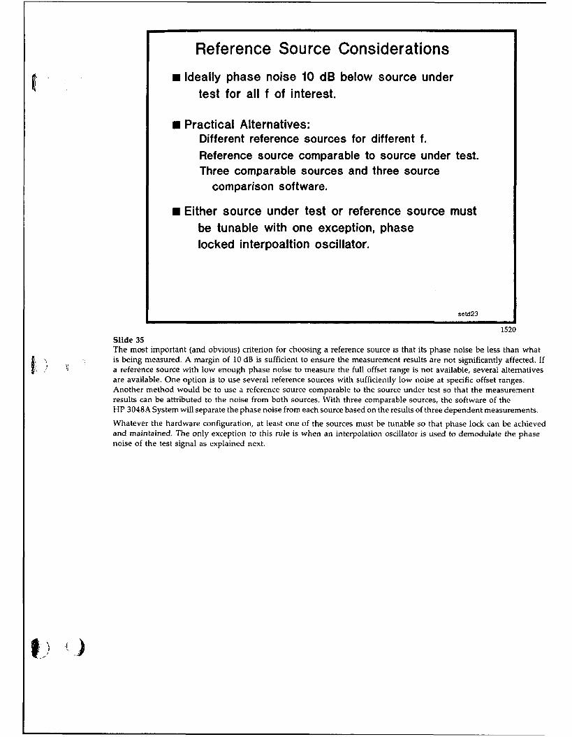
Reference Source Considerations ■ Ideally phase noise 10 dB below source under
test for all f of interest.
■ Practical Alternatives: Different reference sources for different f. Reference source comparable to source under test. Three comparable sources and three source
comparison software.
■ Either source under test or reference source must be tunable with one exception, phase locked interpoaltion oscillator.
setd23
1520 Slide 35 The most important (and obvious) criterion for choosing a reference source is that its phase noise be less than what is being measured. A margin of 10 dB is sufficient to ensure the measurement results are not significantly affected. If a reference source with low enough phase noise to measure the full offset range is not available, several alternatives are available. One option is to use several reference sources with sufficiently low noise at specific offset ranges. Another method would be to use a reference source comparable to the source under test so that the measurement results can be attributed to the noise from both sources. With three comparable sources, the software of the HP 3048A System will separate the phase noise from each source based on the results of three dependent measurements.
Whatever the hardware configuration, at least one of the sources must be tunable so that phase lock can be achieved and maintained. The only exception to this rule is when an interpolation oscillator is used to demodulate the phase noise of the test signal as explained next.
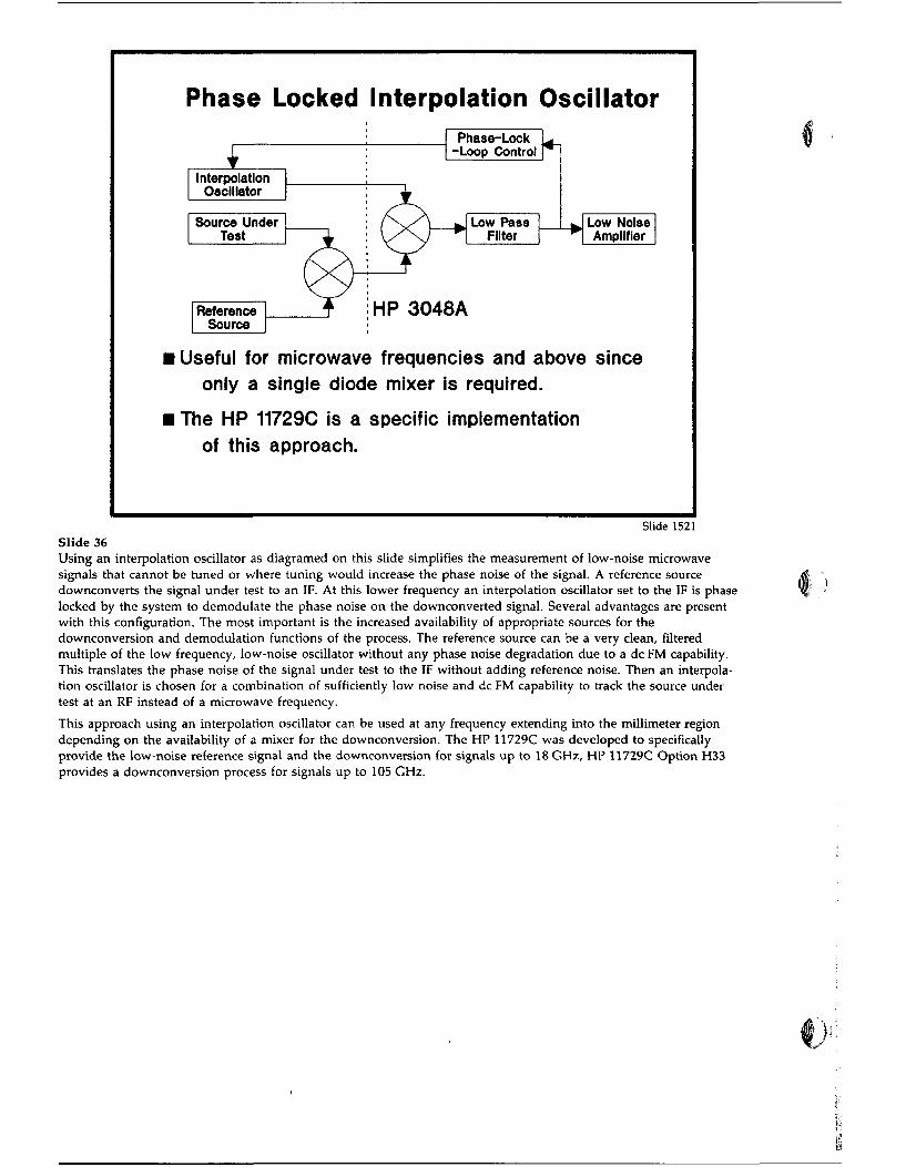
1 Phase Locked Interpolation Oscillatoi
1 T Interpolation
Oscillator
Source Under Test
Reference Source
«
Phase-Lock -Loop Control
*
^_ *^
<T~\ ®-V Low Pass
Filter L> Low Noise Amplifier
HP 3048A
■ Useful for microwave frequencies and above only a single diode mixer is required.
■ The HP 11729C is a specific implementation of this approach.
) since
Slide 1521 Slide 36 Using an interpolation oscillator as diagramed on this slide simplifies the measurement of low-noise microwave signals that cannot be tuned or where tuning would increase the phase noise of the signal. A reference source downconverts the signal under test to an IF. At this lower frequency an interpolation oscillator set to the IF is phase locked by the system to demodulate the phase noise on the downconverted signal. Several advantages are present with this configuration. The most important is the increased availability of appropriate sources for the downconversion and demodulation functions of the process. The reference source can be a very clean, filtered multiple of the low frequency, low-noise oscillator without any phase noise degradation due to a dc FM capability. This translates the phase noise of the signal under test to the IF without adding reference noise. Then an interpolation oscillator is chosen for a combination of sufficiently low noise and dc FM capability to track the source under test at an RF instead of a microwave frequency. This approach using an interpolation oscillator can be used at any frequency extending into the millimeter region depending on the availability of a mixer for the downconversion. The HP 11729C was developed to specifically provide the low-noise reference signal and the downconversion for signals up to 18 GHz, HP 11729C Option H33 provides a downconversion process for signals up to 105 GHz.
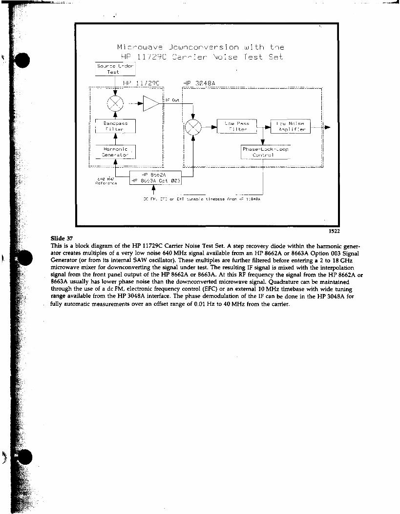
Microwave Downconversion with the HP 11729C Carrier Noise Test Set
Source Under Test
HP 11729C HP 3048A
640 MHZ Reference
HP 8662A HP 8663A Opt 003
\ DC FM, EFC or EXT tunable timebase from HP 11848A
1522 Slide 37 This is a block diagram of the HP 11729C Carrier Noise Test Set. A step recovery diode within the harmonic generator creates multiples of a very low noise 640 MHz signal available from an HP 8662A or 8663A Option 003 Signal Generator (or from its internal SAW oscillator). These multiples are further filtered before entering a 2 to 18 GHz microwave mixer for downconverting the signal under test. The resulting IF signal is mixed with the interpolation signal from the front panel output of the HP 8662A or 8663A. At this RF frequency the signal from the HP 8662A or 8663A usually has lower phase noise than the downconverted microwave signal. Quadrature can be maintained through the use of a dc FM, electronic frequency control (EFC) or an external 10 MHz timebase with wide tuning range available from the HP 3048A interface. The phase demodulation of the IF can be done in the HP 3048A for fully automatic measurements over an offset range of 0.01 Hz to 40 MHz from the carrier.
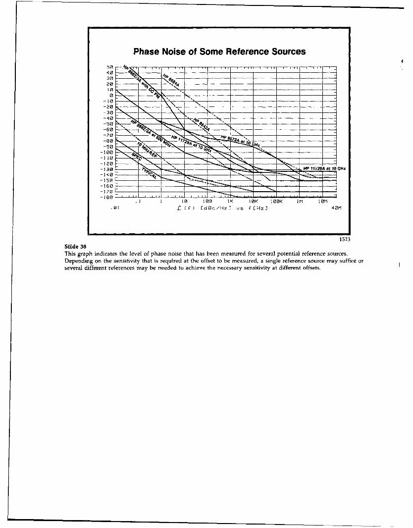
Phase Noise of Some Reference Sources
HP 11V29A at 10 GHz
£ C f ) C d B c / H z D v s f C H z J
1523 Slide 38 This graph indicates the level of phase noise that has been measured for several potential reference sources. Depending on the sensitivity that is required at the offset to be measured, a single reference source may suffice or several different references may be needed to achieve the necessary sensitivity at different offsets.
Agenda Basic Phase Noise Measurement Concepts Direct Spectrum Measurement Demodulation Techniques Phase Demodulator Residual or Added Noise Measurements Single Source Measurements Phase Detector with Two Sources Reference Source
* Voltage Controlled Source Tuning Requirements Measurement Optimization Measurement Examples
setdla
1524 Slide 39 There are several considerations that need to be made concerning phase locking of various sources. The next section covers the drift limits, phase lock loop bandwidths, and the tuning range required of the source by the HP 3048A System.
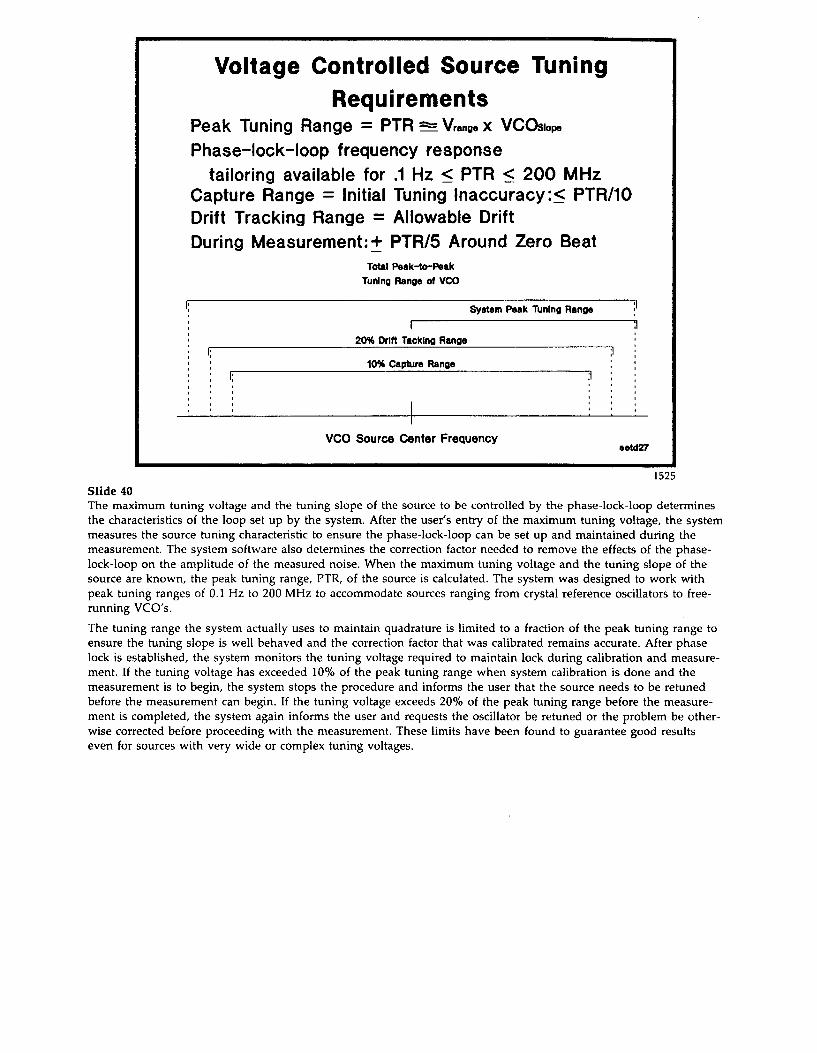
Voltage Controlled Source Tuning Requirements
Peak Tuning Range = PTR *=. Vrange X VCOsiope Phase-lock-loop frequency response
tailoring available for .1 Hz < PTR < 200 MHz Capture Range = Initial Tuning Inaccuracy :< PTR/10 Drift Tracking Range = Allowable Drift During Measurement: + PTR/5 Around Zero Beat
Total Peak-to-Peak Tuning Range of VCO
System Paak Tuning Range
20% Drift Tacking Range
10% Capture Range
VCO Source Center Frequency setd27
1525 Slide 40 The maximum tuning voltage and the tuning slope of the source to be controlled by the phase-lock-loop determines the characteristics of the loop set up by the system. After the user's entry of the maximum tuning voltage, the system measures the source tuning characteristic to ensure the phase-lock-loop can be set up and maintained during the measurement. The system software also determines the correction factor needed to remove the effects of the phase-lock-loop on the amplitude of the measured noise. When the maximum tuning voltage and the tuning slope of the source are known, the peak tuning range, PTR, of the source is calculated. The system was designed to work with peak tuning ranges of 0.1 Hz to 200 MHz to accommodate sources ranging from crystal reference oscillators to free-running VCO's. The tuning range the system actually uses to maintain quadrature is limited to a fraction of the peak tuning range to ensure the tuning slope is well behaved and the correction factor that was calibrated remains accurate. After phase lock is established, the system monitors the tuning voltage required to maintain lock during calibration and measurement. [f the tuning voltage has exceeded 10% of the peak tuning range when system calibration is done and the measurement is to begin, the system stops the procedure and informs the user that the source needs to be retuned before the measurement can begin. If the tuning voltage exceeds 20% of the peak tuning range before the measurement is completed, the system again informs the user and requests the oscillator be retuned or the problem be otherwise corrected before proceeding with the measurement. These limits have been found to guarantee good results even for sources with very wide or complex tuning voltages.
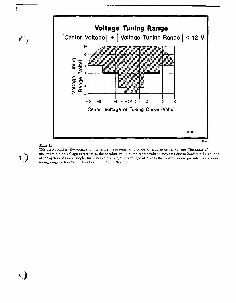
Voltage Tuning Range Center Voltage I + I Voltage Tuning Range < 12 V
-10 -5 -2 -1 -.5 0 .5 1 2 5 10
Center Voltage of Tuning Curve (Volts)
setd28
1526 Slide 41 This graph outlines the voltage tuning range the system can provide for a given center voltage. The range of maximum tuning voltage decreases as the absolute value of the center voltage increases due to hardware limitations of the system. As an example, for a source needing a bias voltage of 2 volts the system cannot provide a maximum tuning range of less than ±1 volt or more than ±10 volts.
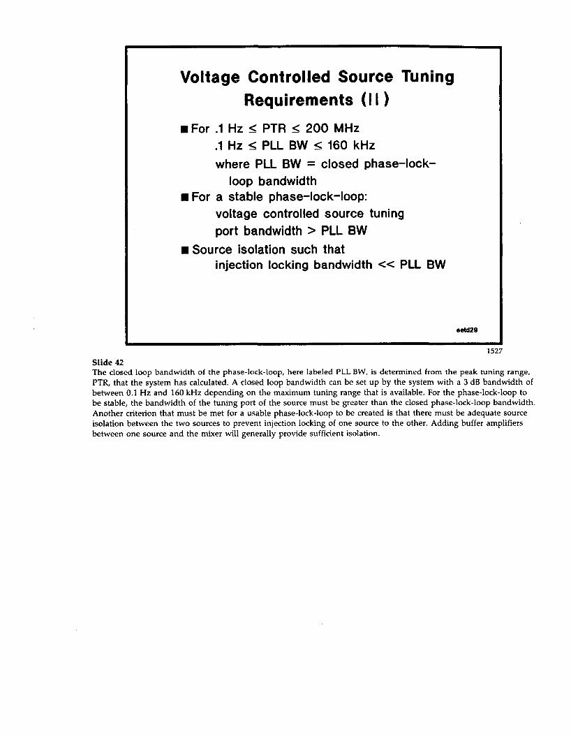
Voltage Controlled Source Tuning Requirements (I I)
■ For .1 Hz < PTR < 200 MHz .1 Hz < PLL BW < 160 kHz where PLL BW = closed phase-lock-
loop bandwidth ■ For a stable phase-lock-loop:
voltage controlled source tuning port bandwidth > PLL BW
■ Source isolation such that injection locking bandwidth « PLL BW
setd29
1527 Slide 42 The closed loop bandwidth of the phase-lock-loop, here labeled PLL BW, is determined from the peak tuning range, PTR, that the system has calculated. A closed loop bandwidth can be set up by the system with a 3 dB bandwidth of between 0.1 Hz and 160 kHz depending on the maximum tuning range that is available. For the phase-lock-loop to be stable, the bandwidth of the tuning port of the source must be greater than the closed phase-lock-loop bandwidth. Another criterion that must be met for a usable phase-lock-loop to be created is that there must be adequate source isolation between the two sources to prevent injection locking of one source to the other. Adding buffer amplifiers between one source and the mixer will generally provide sufficient isolation.
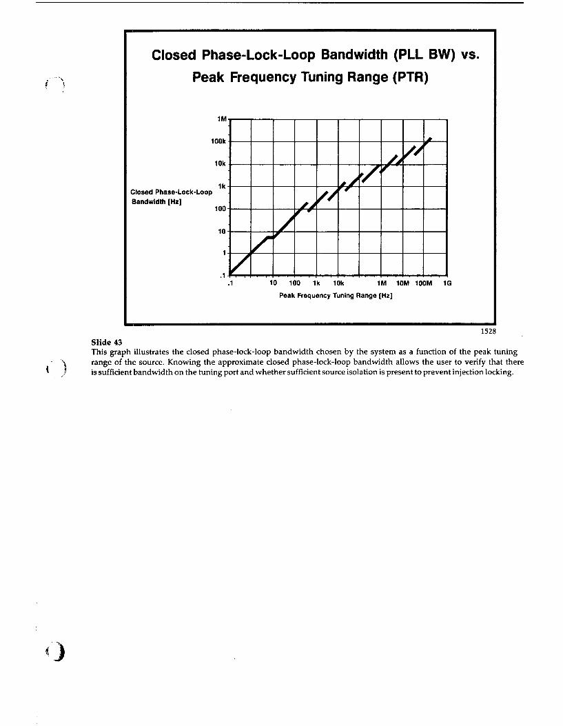
Closed Phase-Lock-Loop Bandwidth (PLL BW) vs. Peak Frequency Tuning Range (PTR)
1M-. 1 , 1 1 , 1 1 1 1 ,
100k
10k
Closed Phase-Lock-Loop Bandwidth [Hz]
100
10
1
.1 .1 10 100 1k 10k 1M 10M 100M 1G
Peak Frequency Tuning Range [Hz]
1528 Slide 43 This graph illustrates the closed phase-lock-loop bandwidth chosen by the system as a function of the peak tuning range of the source. Knowing the approximate closed phase-lock-loop bandwidth allows the user to verify that there is sufficient bandwidth on the tuning port and whether sufficient source isolation is present to prevent injection locking.
/
/ ■ / f
.s / / ' ' r*
,/<■ r*
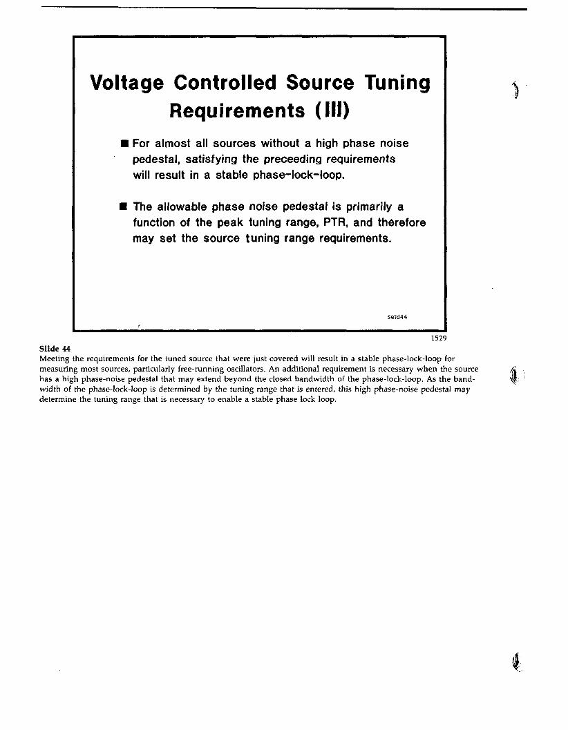
Voltage Controlled Source Tuning Requirements (III)
■ For almost all sources without a high phase noise pedestal, satisfying the preceeding requirements will result in a stable phase-lock-loop.
■ The allowable phase noise pedestal is primarily a function of the peak tuning range, PTR, and therefore may set the source tuning range requirements.
setd44
1529 Slide 44 Meeting the requirements for the tuned source that were just covered will result in a stable phase-lock-loop for measuring most sources, particularly free-running oscillators. An additional requirement is necessary when the source has a high phase-noise pedestal that may extend beyond the closed bandwidth of the phase-lock-loop. As the bandwidth of the phase-lock-loop is determined by the tuning range that is entered, this high phase-noise pedestal may determine the tuning range that is necessary to enable a stable phase lock loop.
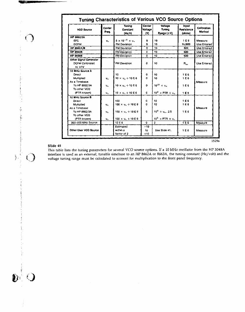
Tuning Characteristics of Various VCO Source Options
VCO Source
HP 8862/3A EFC DCFM
HP 8642A/B HP 8840B HP 86S6B Other Signal Generator
DCFM Calibrated to±1V
10 MHz Source A Direct Multiplied
As a Timebase; To HP 8662/3A To other VCO
(PTR known)
10 MHz Source B Direct Multiplied
As a Timebase; To HP 8662/3A To other VCO
(PTR known) 350-500 MHz Source
Other User VCO Source
Carrier Freq.
V„
Tuning Constant
(Hz/V)
5 x 10 _ o x v0
FM Deviation FM Deviation FM Deviation FM Deviation
FM Deviation
10
10 X U „ T 1 0 E 6
10 x v„ - M 0 E 6
10 X V „ T 1 0 E 6
100
100 x v„ 4-10 E 6
100 x v„ -=- 10 E 6
100 x v „ - M 0 E 6 12 E 6 Estimated within a factor of 2
Center Voltage
(V)
0 0 0 0 0
0
0 0
0
0
0 0
0
0 -10 to
+10
Voltage Tuning
Range (±V)
10 10 10 10 10
10
10 10
10'° -=- v„
10° X PTR -r V„
10 10
10° 4 v„ , 2.5
105 X PTR -r v„ 2
See Slide 41.
Input Resistance
(ohms)
1 E6 1k/600
600 600 600
^ i i i
1 E6 1 E6
1 E6
1 E6
1 E6 1 E6
1 E6
1 E6
1 E6
Calibration Method
Measure Use Entered Use Entered Use Entered Use Entered
Use Entered
Measure
Measure
Measure
Measure
1529a Slide 45 This table lists the tuning parameters for several VCO source options. If a 10 MHz oscillator from the HP 3048A interface is used as an external, tunable timebase to an HP 8662A or 8663A, the tuning constant (Hz/volt) and the voltage tuning range must be calculated to account for multiplication to the front panel frequency.
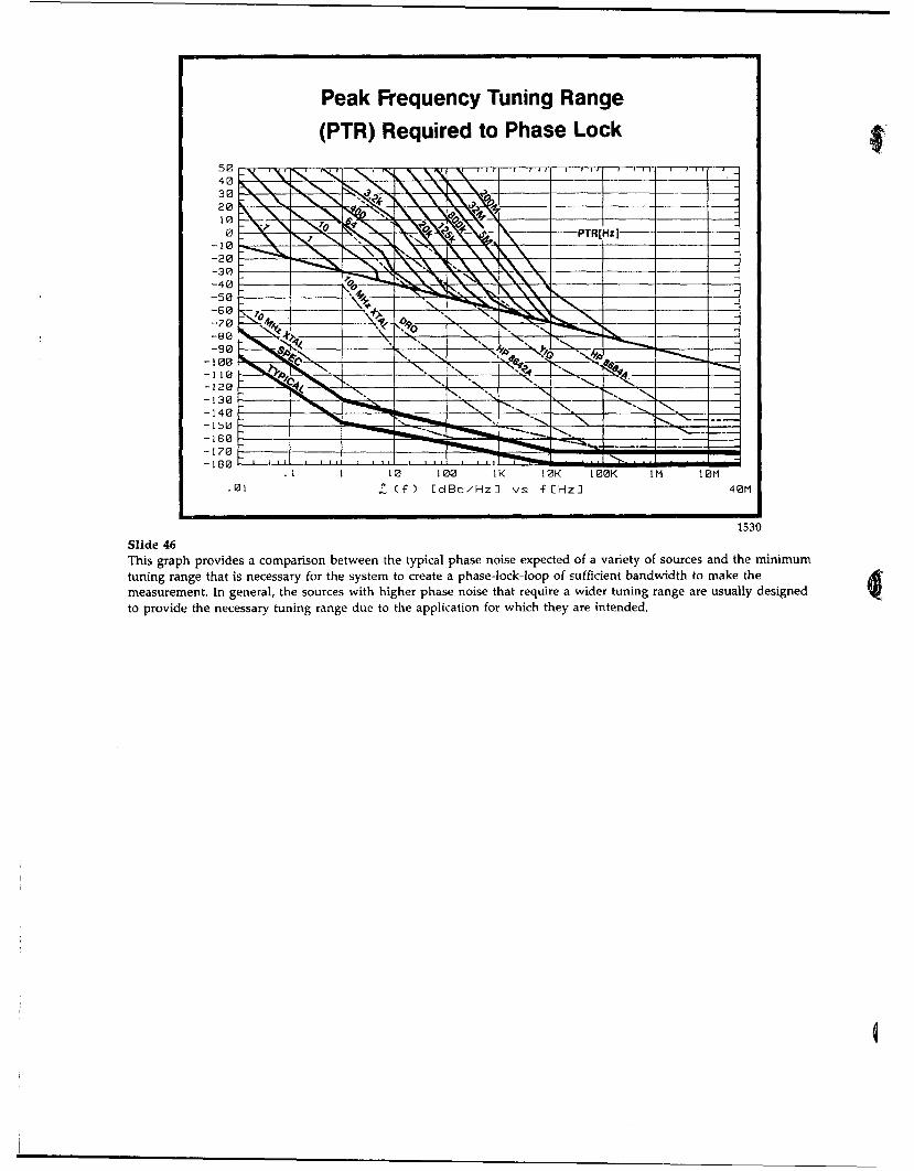
1530 Slide 46 This graph provides a comparison between the typical phase noise expected of a variety of sources and the minimum tuning range that is necessary for the system to create a phase-lock-loop of sufficient bandwidth to make the measurement. In general, the sources with higher phase noise that require a wider tuning range are usually designed to provide the necessary tuning range due to the application for which they are intended.
Agenda Basic Phase Noise Measurement Concepts Direct Spectrum Measurement Demodulation Techniques Phase Demodulator Residual or Added Noise Measurements Single Source Measurements Phase Detector with Two Sources Reference Source Voltage Controlled Source Tuning Requirements
ft Measurement Optimization Measurement Examples
setdla
1531 Slide 47 While the HP 3048A System will make measurements of the phase noise of sources with a wide variety of character istics, there are techniques to optimize the measurements for better results as are explained next.
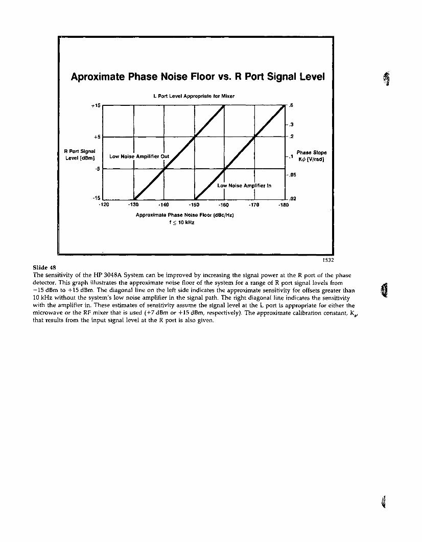
Aproximate Phase Noise Floor vs. R Port Signal Level
L Port Level Appropriate for Mixer
R Port Signal Level [dBm]
-5
-15
Low Noise Ampilifier C ut f
f Low Noise Amplifier In X I I / I I
-.3
2
Phase Slope "•1 K<HV/rad]
-.05
.02 -120 -130 -140 -150 -160 -170 -180
Approximate Phase Noise Floor (dBc/Hz) f < 10 kHz
1532 Slide 48 The sensitivity of the HP 3048A System can be improved by increasing the signal power at the R port of the phase detector. This graph illustrates the approximate noise floor of the system for a range of R port signal levels from —15 dBm to +15 dBm. The diagonal line on the left side indicates the approximate sensitivity for offsets greater than 10 kHz without the system's low noise amplifier in the signal path. The right diagonal line indicates the sensitivity with the amplifier in. These estimates of sensitivity assume the signal level at the L port is appropriate for either the microwave or the RF mixer that is used (+7 dBm or +15 dBm, respectively). The approximate calibration constant, K , that results from the input signal level at the R port is also given.
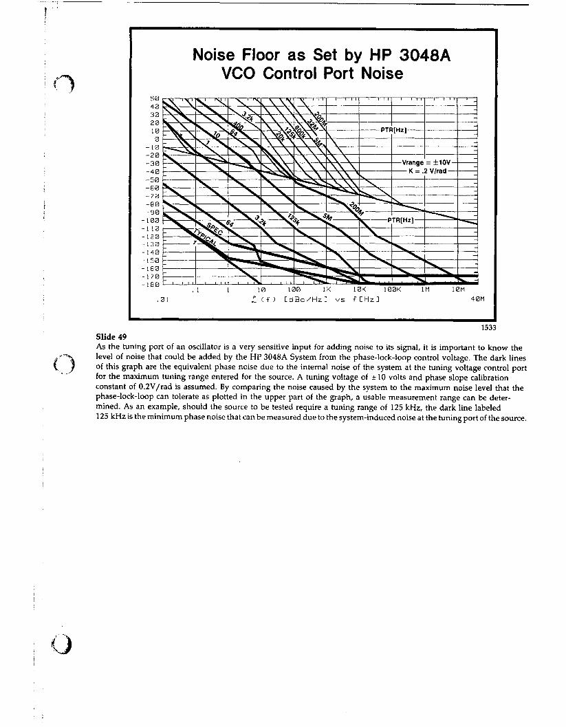
1533 Slide 49 As the tuning port of an oscillator is a very sensitive input for adding noise to its signal, it is important to know the level of noise that could be added by the HP 3048A System from the phase-lock-loop control voltage. The dark lines of this graph are the equivalent phase noise due to the internal noise of the system at the tuning voltage control port for the maximum tuning range entered for the source. A tuning voltage of ±10 volts and phase slope calibration constant of 0.2V/rad is assumed. By comparing the noise caused by the system to the maximum noise level that the phase-lock-loop can tolerate as plotted in the upper part of the graph, a usable measurement range can be determined. As an example, should the source to be tested require a tuning range of 125 kHz, the dark line labeled 125 kHz is the minimum phase noise that can be measured due to the system-induced noise at the tuning port of the source.
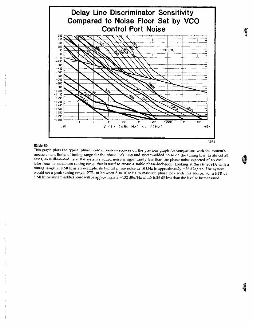
1534 Slide 50 This graph plots the typical phase noise of various sources on the previous graph for comparison with the system's measurement limits of tuning range for the phase-lock-loop and system-added noise on the tuning line. In almost all cases, as is illustrated here, the system's added noise is significantly less than the phase noise expected of an oscillator from its maximum tuning range that is used to create a stable phase-lock-loop. Looking at the HP 8684A with a tuning range ±10 MHz as an example, its typical phase noise at 10 kHz is approximately - 7 6 dBc/Hz. The system would set a peak tuning range, PTR, of between 5 to 10 MHz to maintain phase lock with this source. For a PTR of 5 MHz the system-added noise will be approximately -132 dBc/Hz which is 56 dB less than the level to be measured.
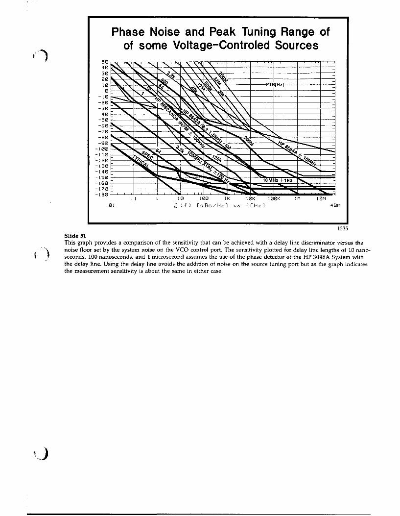
1535 Slide 51 This graph provides a comparison of the sensitivity that can be achieved with a delay line discriminator versus the noise floor set by the system noise on the VCO control port. The sensitivity plotted for delay line lengths of 10 nanoseconds, 100 nanoseconds, and 1 microsecond assumes the use of the phase detector of the HP 3048A System with the delay line. Using the delay line avoids the addition of noise on the source tuning port but as the graph indicates the measurement sensitivity is about the same in either case.
Agenda Basic Phase Noise Measurement Concepts Direct Spectrum Measurement Demodulation Techniques Phase Demodulator Residual or Added Noise Measurements Single Source Measurements Phase Detector with Two Sources Reference Source Voltage Controlled Source Tuning Requirements Measurement Optimization
* Measurement Examples
setdla
1536 Slide 52 A few measurement examples that illustrate the various measurement techniques follow.
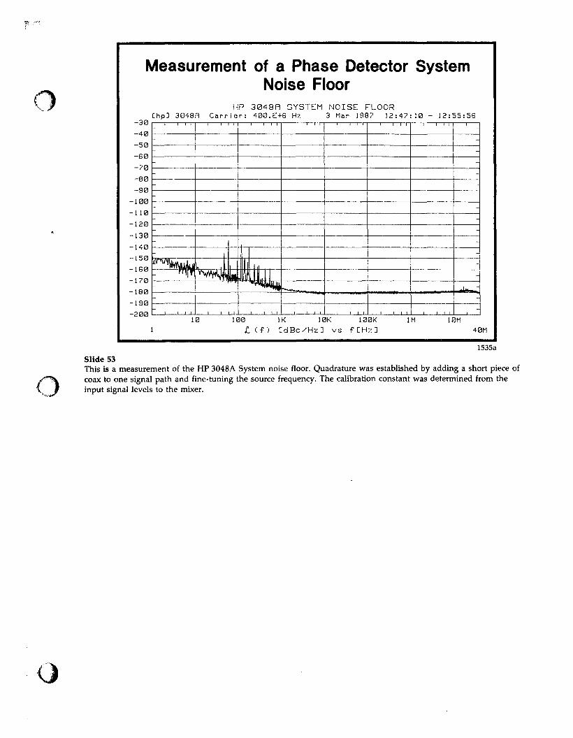
Measurement of a Phase Detector System Noise Floor
HP 3 0 4 8 R SYSTEM N O I S E FLOOR Ibpl 3048R C a r r i e r : 400.E+6 Hz 3 Mar 1987 1 2 : 4 7 : 1 0 - 12 :55 :56
- 4 0 - 5 0 - 6 0 - 7 0 - 8 0 - 9 0
-100 -110 -120 -130 -140 -150 - 1 6 0 -170 - 1 8 0 -190
Z T O feL '~|»l
1
k , ik 1 ^41, Hi in H „ "Mmiwilj l
i i i i
i I I I i I I I
---
--
. J * _ -
10 100 IK 10K 100K 1M 10M Z if) C d B c / H z ] v s f CHz3 40M
1535a Slide 53 This is a measurement of the HP 3048A System noise floor. Quadrature was established by adding a short piece of coax to one signal path and fine-tuning the source frequency. The calibration constant was determined from the input signal levels to the mixer.
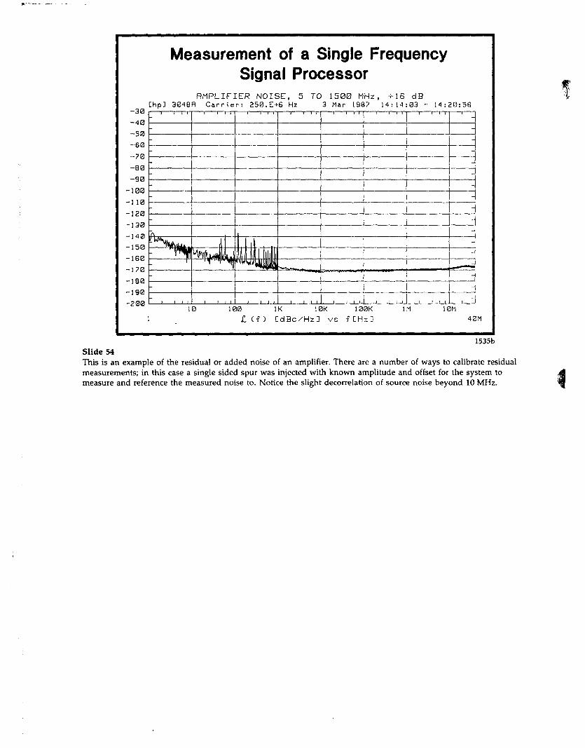
- 4 0 - 5 0 - 6 0 - 7 0 -B0 - 9 0
-100 -1 10 -120 -130 -140 - 1 5 0 -160 -170 -190 -190
Measurement of a Single Frequency Signal Processor
R M P L I F I E R N O I S E , 5 TO 1 5 0 0 M H z , + 1 6 d B Chp] 3048R C a r r i e r : 250 . E>6 Hz 3 Mar 198? 14 :14 :03 - 14 :20 :56
A. ^ V h d l i * - m
r -
| towil . ^Y R " r v ^
\ \ \ ■
Hi ^ w y i / ^ I! 1
_.. I . . J i i l i t
i
-j
1
-
i
10 100 IK 10K 100K 1M 10M £ ( f ) C d B C H z ] v s - fCHz3 40M
1535b Slide 54 This is an example of the residual or added noise of an amplifier. There are a number of ways to calibrate residual measurements; in this case a single sided spur was injected with known amplitude and offset for the system to measure and reference the measured noise to. Notice the slight decorrelation of source noise beyond 10 MHz.
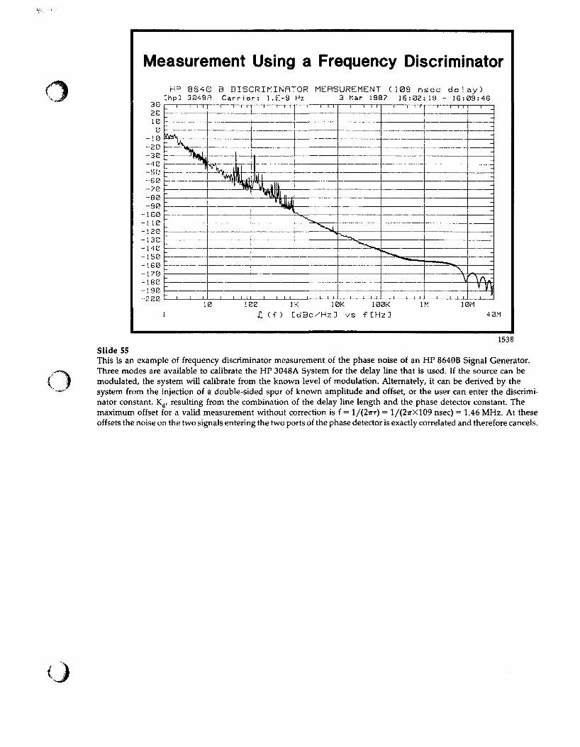
Measurement Using a Frequency Discriminator r\P 8 S 4 G B D I S C R I M I N A T O R MERSUREMENT ( 1 0 9 n s e c d e l a y )
Crip: 3048R C a r r i e r : 1 . E+9 Hz 3 Mar 1987 16 :02 :19 - 16 :09 :46
20 10 0
- 1 0 - 2 0 - 3 0 - 4 0 - 5 0 - 6 0 - 7 0 - 8 0 - 9 0
-100 -1 10 -120 -133 -140 -150 -160 -170 -180 -190
:
- vV
L ^L
-
-
i i i i i i i i
1 1
^ "Hit
. . . --, - -
III Atjii ^ l l l „
.mi
i
I \
i l i t
i I I I
i i i i
i I I I i
----- i
- i
-~j
J
--j
10 !00 IK !0K 100K 1M IBM £ ( f ) C d B c / H z 3 v s f C H z l 40M
1538 Slide 55 This is an example of frequency discriminator measurement of the phase noise of an HP 8640B Signal Generator. Three modes are available to calibrate the HP 3048A System for the delay line that is used. If the source can be modulated, the system will calibrate from the known level of modulation. Alternately, it can be derived by the system from the injection of a double-sided spur of known amplitude and offset, or the user can enter the discriminator constant, Kd, resulting from the combination of the delay line length and the phase detector constant. The maximum offset for a valid measurement without correction is f = 1/(27TT) = 1/(2TTX109 nsec) = 1.46 MHz. At these offsets the noise on the two signals entering the two ports of the phase detector is exactly correlated and therefore cancels.
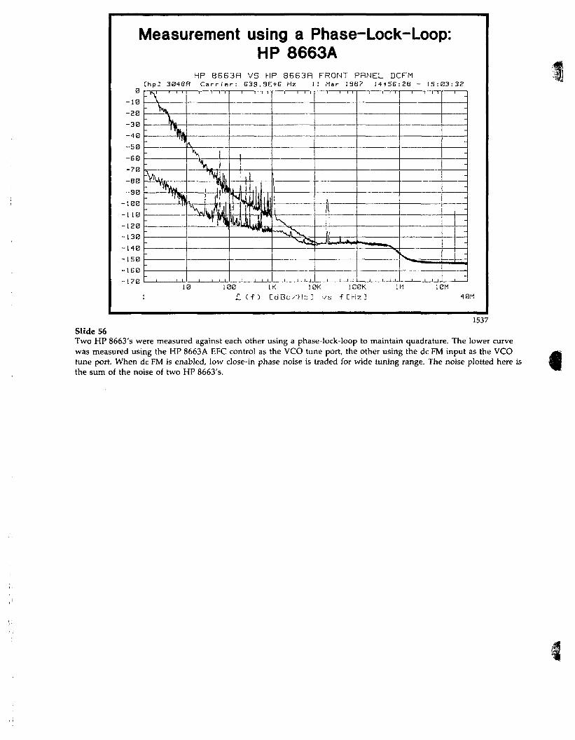
Measurement using a Phase-Lock-Loop: HP 8663A
0 - 1 0 - 2 0 - 3 0 - 4 0 - 5 0 - 6 0 - ? 0 - 8 0 - 9 0
- 1 0 0 -1 10 - 1 2 0 - 1 3 0 - 1 4 0 - 1 5 0 -1G0 - 1 7 0
1
Chp3 HP 8663H VS
3049R C a r r i e r : 6 3 9 . H, 1 i l l
- W - \ - \ T | v |
Xu, - v 1- \ -----
r\
\ 1 \ * %
i
in, (U|l
*\ ' I n
^m-
i i i i
HP 8663R FRONT PHNEL DCFM 9E+6 Hz 11 Mar 198? I 4 > 5 6 : 2 8 -
1 ! i
7^1
i l l m J
i l i t
i
i 1 I I \
■ * * o \ ^
1 1 1 1
1
a ;:
A' . >JLJU-<
I I I I
i I I I
- — - * v >
1 I I I
1 5 :
S s _
i i I I
3 3 : 32
--------------
i
10 100 IK 10K !G0K £ C-f) CdBc/H=3 v s f [ H z ]
!M IBM 40M
1537 Slide 56 Two HP 8663's were measured against each other using a phase-lock-loop to maintain quadrature. The lower curve was measured using the HP 8663A EFC control as the VCO tune port, the other using the dc FM input as the VCO tune port. When dc FM is enabled, low close-in phase noise is traded for wide tuning range. The noise plotted here is the sum of the noise of two HP 8663's.
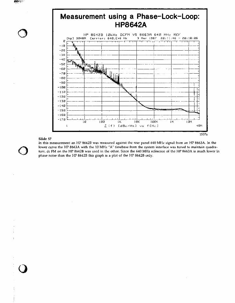
Measurement using a Phase-Lock-Loop: HP8642A
HP 8 G 4 2 B 10kHz DCFM VS 8 6 6 3 H 6 4 0 MHz REF Chp] 3048R C a r r i e r : G40.E+G Hz 3 Mar 1987 20 :11 :46 - 20 :18 :06
- 1 0 - 2 0 - 3 0 -4B - 5 0 - 6 0 - 7 0 -80 - 9 0
-100 -1 10 -120 -130 -140 -150 -160
- v - \ - V - \ =vw ]\
■nJV* i
---
-
Vbu "|f I T * inm
^ v
1 1 t 1
!_
10 100 IK 10K 100K 1M IBM £ ( f ) C d B c / H z 3 v s -fCHzD 40M
1537a Slide 57 In this measurement an HP 8642B was measured against the rear panel 640 MHz signal from an HP 8663A. In the lower curve the HP 8663A with the 10 MHz "A" timebase from the system interface was tuned to maintain quadrature, dc FM on the HP 8642B was used in the other. Since the 640 MHz reference of the HP 8663A is much lower in phase noise than the HP 8642B this graph is a plot of the HP 8642B only.
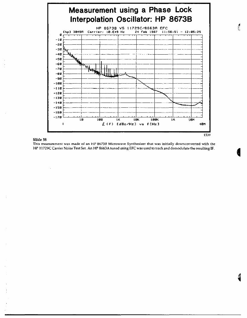
- 1 0 - 2 0 - 3 0 - 4 0 - 5 0 - 6 0 - 7 0 - 8 0 - 9 0
-100 -110 -120 -130 -140 -150 -160
1
Measurement using a Phase Lock Interpolation Oscillator: HP 8673B
HP 8 G 7 3 B VS 1 1 7 2 9 C / 8 G S 3 H EFC Chp] 3048R C a r r i e r : 10.E+9 Hz 24 Fob 1987 11:58:51 - 12:05:25
-
-1
, , , ,
\
----1
-
10 100 IK 10K 100K 1M 10M £ ( f ) C d B c / H z ] v s f C H z 3 40M
1539 Slide 58 This measurement was made of an HP 8673B Microwave Synthesizer that was initially downconverted with the HP 11729C Carrier Noise Test Set. An HP 8663A tuned using EFC was used to track and demodulate the resulting IF.
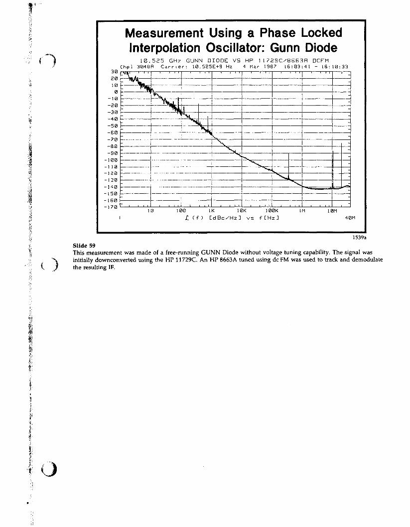
Measurement Using a Phase Locked Interpolation Oscillator: Gunn Diode
30 2 0 10 0
- 1 0 -aa - 3 0 - 4 0 - 5 0 -G0 - 7 0 - 8 0 - 9 0
- 1 0 0 - 1 1 0 - 1 2 0 - 1 3 0 -140 -150 -1G0 - 1 7 0
1 0 . 5 2 5 GHz GUNN D IODE VS Chp3 3048R C a r r i e r : 10.525E+9 Hz
^ ^ f c _ P'WhUn
\*\, , i -----1 ....
:
-i
--
1 i l l
T%^| 1 IHL1 i
i f
^^
i i
Tv *i TV^
i ^N. — ■
i
1
i !
i i i i i i i i .i i i i t
HP 1 1 7 2 9 C / 8 6 G 3 R DCFM 4 Mar 1987 16 :03 :41 - 16:
1 I I I 1 I I I
i i i i i
. ; "***<_ ;
l^s,^
j
i 1
I "X^ 1
1
i i 1 1 1 i i l l i i i i
10: 33 I
-----j -----------
-
1 1 0 0 IK 10K 100K 1M
£ Cf ) C d B c / H z ] v s f CHzD IBM
40M
1539a Slide 59 This measurement was made of a free-running GUNN Diode without voltage tuning capability. The signal was initially downconverted using the HP 11729C. An HP 8663A tuned using dc FM was used to track and demodulate the resulting IF.
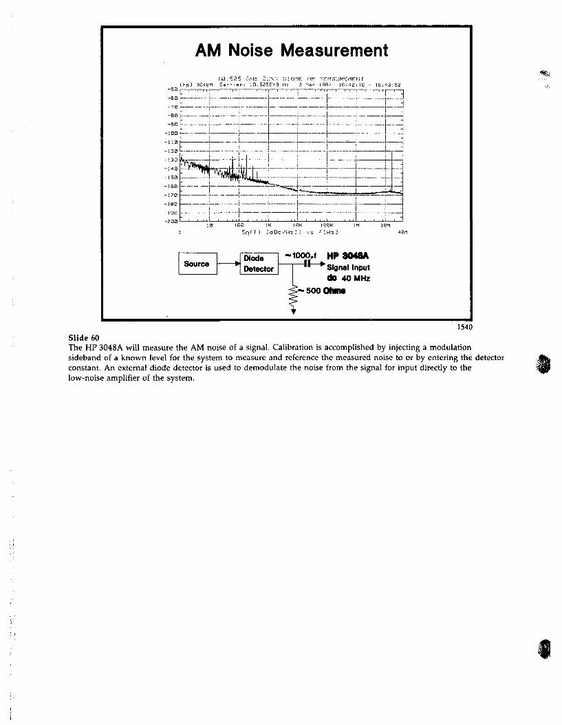
-50 -SO -70 -BO -90
-100 -1 10 -120 -130 -140 -150 - 1 6 0 - 1 7 0 - 1 8 3 - ISO -200
AM Noise Measurement 1 3 . 5 2 5 GHz GJNN i l l ODE flM .'iERSUREMENT
thp j 3046H C a r r i e r : J0.525E+9 Hi 3 Mar 190? 16:42:16 - 16:48:52
— h -
\
L ... T -
W*7 , - ™
!— —
,
,— ..-
i_. J .. J . . _i
!
- • - - 4-i
,
' '
j ^ ^ * * - ^ ,
| i ] i
T7T , ,.T! 7,,',"
. i
i i i i
i
-
i 1 u
-
--
i w
! J , . . .
10 102 IK 10K 100K
Source Diode Detector
~1000„f HP 3048A —I I * Signal Input
do 40 MHz *~ 500 Ohm*
1540 Slide 60 The HP 3048A will measure the AM noise of a signal. Calibration is accomplished by injecting a modulation sideband of a known level for the system to measure and reference the measured noise to or by entering the detector constant. An external diode detector is used to demodulate the noise from the signal for input directly to the low-noise amplifier of the system.
REFERENCES
1) Ashley, R.J., et al, "The Measurement of Noise in Microwave Transmitters," IEEE Transactions on Microwave Theory and Techniques, Vol. MTT-25, No. 4, pp. 294-318 (April 1977)
2) Fischer, M., "An Overview of Modern Techniques for Measuring Spectral Purity," Microwaves, Vol. 18, No. 7, pp. 66-75, July 1979.
3) Hewlett-Packard staff, "Understanding and Measuring Phase Noise in the Frequency Domain," Application Note 207, October 1976.
4) Hewlett-Packard staff, "Measuring Phase Noise with the HP 3585A Spectrum Analyzer," Application Note 246-2, May 1981.
5) Hewlett-Packard staff, "Low Phase Noise Applications of the HP 8662A and 8663A Synthesized Signal Generators," Application Note 283-3, December 1986.
6) Howe, D.A., "Frequency Domain Stability Measurements: A Tutorial Introduction," NBS Technical Note 679, March 1976.
7) Lance, A.L., Seal, W.D., Hudson, N.W., Mendoza, F.G., and Donald Halford, "Phase Noise Measurements Using Cross-Spectrum Analysis," Conference on Precision Electromagnetic Measurements, Ottawa, Canada, June 1978.
8) Ondria F.G., "A Microwave System for Measurements of AM and FM Noise Spectra," IEEE Transactions on Microwave Theory and Techniques, Vol. MTT-16, pp. 767-781, September 1968.
9) Scherer, Dieter, "Design Principles and Test Methods for Low Phase Noise RF and Microwave Sources," Hewlett-Packard RF and Microwave Measurement Symposium, October 1978. (Also edited version in Microwaves, "Today's Lesson—Learn About Low-Noise Design," part 1, pp. 116-122, April 1979, part 2, pp. 72-77, May 1979).
10) Shoaf, J.H., Halford, D., Risley, A.S., "Frequency Stability Specification and Measurement: High Frequency and Microwave Signals," NBS Technical Note 632, January 1973.
11) Hewlett-Packard staff, "Phase Noise Characterization of Microwave Oscillators, Phase Detector Method," Product Note 11729B-1, March 1984.
12) Hewlett-Packard staff, "Phase Noise Characterization of Microwave Oscillators, Frequency Discriminator Method," Product Note 11729C-2, September 1985.
13) Kroupa, V.F., "Frequency Stability: Fundamentals and Measurement," IEEE Press, (Order Number: PC 01644), 1983. 14) Barnes, J.A., et al, "Characterization of Frequency Stability," NBS Technical Note 394, October 1970. 15) Lesson, D.B., Johnson, G.F., "Short-Term Stability for a Doppler Radar. Requirements, Measurements and Tech
niques," Proceedings of the IEEE, Vol. 54, No. 2, pp. 244-248, (February 1966). 16) Gibbs, ]., Prouty B., "Using Phase Noise Measurements to Improve Performance," Microwave Journal, Vol. 24,
No. 12, pp. 47-54, December 1981. 17) Barnes, J.A., Chic, A.R., Cutter, L.S., et al, "Characterization of Frequency Stability," IEEE Transactions on Instru
mentation and Measurement, Vol. IN-20, No. 2, pp. 105-20, May 1971. 18) Keshner, Marvin S., "1/f Noise," Proceedings of the IEEE, Vol. 70, No. 3, pp. 212-218, March 1982. 19) Rutman, J., "Characterization of Phase and Frequency Instabilities in Precision Frequency Sources: Fifteen Years
of Progress," Proceedings of the IEEE, Vol. 66, No. 9, pp. 1048-1075, September 1978. 20) McNamee, M. "Automate for Improved Phase-Noise Measurement," Microwaves, pp. 80-85, May 1979. 21) Fischer, M„ "Frequency Stability Measurement Procedures," Hewlett-Packard Co., presented at the Eight Annual
Precision Time and Time Interval Meeting, December 1976. 22) Burgoon, R., "Conversion Between Time and Frequency Domain of Intersection Points of Slopes of Various
Noise Processes," Thirty-second Annual Frequency Control Symposium, pp. 514-519, May 1978. 23) Scherer, D., "The 'Art' of Phase Noise Measurements," Hewlett-Packard RF and Microwave Symposium, May 1983. 24) Muat, R., Upham, A., "Low Noise Oscillator Design," Hewlett-Packard RF and Microwave Symposium, March 1986. 25) Moulton, G., "Analysis and Prediction of Phase Noise in Resonators and Oscillators," Hewlett-Packard RF and
Microwave Symposium, September 1985.