
230-V, 900-W Mains Powered BLDC Motor Drive for Vacuum Cleaner
73
Surge Protection & EMC Filter UCC27714 UCC27714 UCC27714 Voltage Scaling VACUUM CLEANER BLDC MOTOR 16-BIT MCU Pre-Driver Back-EMF Sensing & Comparators (10-Bit ADC) Differential Current Sense Amplifier + Comparator for OC Protection Buck-Regulator Voltage Regulators & References 10-Bit ADC Hall Sensor Interface DRV92250 VCC (15V) Buck Converter L N PE LMT84 AC-DC Power Supply Input: 230V ±15% 1-Phase AC VDC VDC TI Designs 230-V, 900-W Mains Powered BLDC Motor Drive for Vacuum Cleaner Design Overview Design Features The TIDA-00433 is a discrete IGBT-based three-phase • 900-W, 325-V DC Three-Phase Inverter Board With inverter using trapezoidal control for driving high-speed Discrete IGBT-Based Implementation Capable of brushless DC (BLDC) motors rated up to 900 W in Driving High-Speed BLDC Motors mains powered vacuum cleaners. The design provides • Uses DRV92250 High-Voltage BLDC Motor ready implementation of Hall sensor-based BLDC Controller, Which Integrates 16-Bit MCU, Low-Side motor trapezoidal control and provision for sensorless Pre-Driver Circuits, One Differential Current Sense trapezoidal control using back-EMF (BEMF) sensing. Amplifier, Comparator With a DAC for Overcurrent The inverter stage works with or without an active PFC Protection, Buck Controller and LDOs stage and is tested up to 390-V DC from active PFC. • Ready Implementation of Hall Sensor-Based BLDC Motor Trapezoidal Control and Provision for Design Resources Sensorless Trapezoidal Control Using BEMF Sensing Design Folder TIDA-00433 • Integrated DC-DC Controller and LDOs of DRV92250 Product Folder DRV92250 Enables Generation of Bias Power UCC27714 Product Folder Supplies Directly From the High Voltage LMT84 Product Folder • Uses 600-V High-Side Low-Side Gate Driver With TL431A Product Folder 4A/4A Source/Sink Current Capability, for Driving the Three-Phase Inverter Featured Applications • Cycle-by-Cycle Motor Overcurrent Protection, Over • Vacuum Cleaner Temperature and Line Undervoltage Protections • Air Conditioner • Thermal Design to Enable Operating Ambient up • Blowers to 55°C • AC Mains Input Designed to Pass Surge, EFT, and Conducted Emission as per EN55014 An IMPORTANT NOTICE at the end of this TI reference design addresses authorized use, intellectual property matters and other important disclaimers and information. 1 TIDUA03 – June 2015 230-V, 900-W Mains Powered BLDC Motor Drive for Vacuum Cleaner Submit Documentation Feedback Copyright © 2015, Texas Instruments Incorporated
-
Upload
khangminh22 -
Category
Documents
-
view
0 -
download
0
Transcript of 230-V, 900-W Mains Powered BLDC Motor Drive for Vacuum Cleaner

Surge
Protection
&
EMC Filter
UCC27714 UCC27714 UCC27714Voltage
Scaling
VACUUM
CLEANER
BLDC MOTOR
16-BIT
MCU
Pre-Driver
Back-EMF Sensing
& Comparators
(10-Bit ADC)
Differential Current
Sense Amplifier
+
Comparator for OC
Protection
Buck-Regulator
Voltage Regulators
& References
10-Bit ADC
Hall Sensor
Interface
DRV92250
VCC (15V)
Buck Converter
L
N
PE
LMT84
AC-DC Power Supply
Input: 230V ±15%
1-Phase AC
VDC
VDC
TI Designs230-V, 900-W Mains Powered BLDC Motor Drive forVacuum Cleaner
Design Overview Design FeaturesThe TIDA-00433 is a discrete IGBT-based three-phase • 900-W, 325-V DC Three-Phase Inverter Board Withinverter using trapezoidal control for driving high-speed Discrete IGBT-Based Implementation Capable ofbrushless DC (BLDC) motors rated up to 900 W in Driving High-Speed BLDC Motorsmains powered vacuum cleaners. The design provides • Uses DRV92250 High-Voltage BLDC Motorready implementation of Hall sensor-based BLDC Controller, Which Integrates 16-Bit MCU, Low-Sidemotor trapezoidal control and provision for sensorless Pre-Driver Circuits, One Differential Current Sensetrapezoidal control using back-EMF (BEMF) sensing. Amplifier, Comparator With a DAC for OvercurrentThe inverter stage works with or without an active PFC Protection, Buck Controller and LDOsstage and is tested up to 390-V DC from active PFC.
• Ready Implementation of Hall Sensor-BasedBLDC Motor Trapezoidal Control and Provision forDesign ResourcesSensorless Trapezoidal Control Using BEMFSensingDesign FolderTIDA-00433
• Integrated DC-DC Controller and LDOs ofDRV92250 Product FolderDRV92250 Enables Generation of Bias PowerUCC27714 Product FolderSupplies Directly From the High VoltageLMT84 Product Folder
• Uses 600-V High-Side Low-Side Gate Driver WithTL431A Product Folder4A/4A Source/Sink Current Capability, for Drivingthe Three-Phase InverterFeatured Applications
• Cycle-by-Cycle Motor Overcurrent Protection, Over• Vacuum CleanerTemperature and Line Undervoltage Protections
• Air Conditioner• Thermal Design to Enable Operating Ambient up
• Blowers to 55°C• AC Mains Input Designed to Pass Surge, EFT, and
Conducted Emission as per EN55014
An IMPORTANT NOTICE at the end of this TI reference design addresses authorized use, intellectual property matters and otherimportant disclaimers and information.
1TIDUA03–June 2015 230-V, 900-W Mains Powered BLDC Motor Drive for Vacuum CleanerSubmit Documentation Feedback
Copyright © 2015, Texas Instruments Incorporated

Introduction www.ti.com
1 IntroductionThis reference design is a three-phase inverter using trapezoidal control for driving high-speed BLDCmotors rated up to 900 W in mains powered vacuum cleaners. The inverter stage is preceded by anAC-DC converter that comprises of EMI filter, full-bridge rectifier, and DC bus electrolytic capacitor. Thisstage rectifies the input single phase AC supply of 195- to 265 V, 50 or 60 Hz to generate DC bus voltageof 275- to 375 V. The inverter stage can also optionally operate from a front end active power factorcorrection stage with DC bus voltage of up to 390-V DC. The design uses six discrete IGBTs and threehigh-voltage half-bridge gate driver ICs for the power stage, which enable flexible form-factor and costcompetitive designs as compared to IPM module. The design uses DRV92250 a high-voltage BLDC motorcontroller that integrates a 16-bit RISC microcontroller (MCU), a low-side pre-driver circuit, one differentialcurrent sense amplifier, comparator with programmable DAC for overcurrent protection, DC-DC buckcontroller, LDOs of 5.35 V, 5.0 V, 3.3 V, and 1.9 V, and BEMF detection comparators for sensorlesscontroller. The design uses the UCC27714 gate driver, a 600-V high-side low-side gate driver with4 A/4 A source/sink current capability.
The integrated buck controller of the DRV92250 along with an external MOSFET-based circuit generatesa 15-V bias power supply directly from the high-voltage DC bus of the inverter. This DC-DC buckcontroller works without any intervention of the MCU except few register settings. The design providescycle-by-cycle motor overcurrent protection, over temperature, and line undervoltage protections. Theboard is designed to pass conducted emission, surge, and EFT as per EN55014.
A vacuum cleaner is a common household and industrial appliance that works with a suction motor tocreate suction pressure and airflow for the removal of dust and dirt. Generally, vacuum cleaners comewith variety of motor power levels typically ranging from 500 to 2200 W. There are small handheld vacuumcleaners that operate on a low-voltage battery and have a power rating below 100 W.
One of the main requirements of a vacuum cleaner motor is that, it should be able to spin at very highRPM. Although a universal series motor is commonly used in this application due to its simplicity ofcontrol, it poses challenges for high speed operation due to the commutator and brushes and lowerefficiency. The brushless construction of BLDC enables very high speed operation, and they can be moreefficient as well.
The Directive 2009/125/EC of the European Parliament and of the Council with regard to the eco-designrequirements for vacuum cleaners laid out the limit on the annual energy consumptions and input power ofvacuum cleaners. As per the EU regulation, the rated input power for vacuum cleaners must be less than900 W starting September 2017. This would require the use of high efficiency brushless motors.
This reference design provides a ready platform for the 900-W inverter for BLDC motor-based vacuumcleaners. The design has a three-phase discrete IGBT-based inverter with the necessary protectionsimplemented in hardware and software.
2 230-V, 900-W Mains Powered BLDC Motor Drive for Vacuum Cleaner TIDUA03–June 2015Submit Documentation Feedback
Copyright © 2015, Texas Instruments Incorporated

www.ti.com Key System Specifications
2 Key System Specifications
Table 1. Key System Specifications of Power Stage
PARAMETER SPECIFICATIONAC input voltage 230 V ±15%
Rated output power 900 WInverter switching frequency 10 kHz
Operating ambient temperature –20°C to 55°CInverter efficiency ≥ 97% at rated load
Power supply specification for gate driver 15 V ±5%Feedbacks Three motor winding voltages, input DC voltage, Low side DC bus currentProtections Overcurrent (cycle-by-cycle/latch), over temperature, input under voltage
Conducted emission EN55014
3TIDUA03–June 2015 230-V, 900-W Mains Powered BLDC Motor Drive for Vacuum CleanerSubmit Documentation Feedback
Copyright © 2015, Texas Instruments Incorporated

q
q
q
q
Ic
Ec
I
Eb
Ia
Ea
Phase C
Phase B
Phase A
Torque
System Description www.ti.com
3 System DescriptionPermanent magnet BLDC motors are gaining importance because of their high efficiency, lowmaintenance, high reliability, low rotor inertia and low noise compared to their brushed motor counterpart.A permanent magnet BLDC motor has a wound stator and a permanent magnet rotor assembly. Thesemotors generally use internal or external devices to sense rotor position. The sensing devices providelogic signals for electronically switching the stator windings in the proper sequence to maintain rotation ofthe magnet assembly.
An electronic drive is required to control the stator currents in a brushless permanent magnet motor. Theelectronic drive consists of:• Power stage with three-phase inverter with the required power capability• MCU to implement the motor control algorithm• Motor voltage and current sensing for sensorless control and closed loop speed or torque control• Gate driver for driving the three-phase inverter• Bias power supply to power up the gate driver and MCU
3.1 BLDC Motor — Trapezoidal ControlThe BLDC motor or the trapezoidal BEMF motor has the ampere conductor distribution of the stator thatideally remains constant and fixed in space for a fixed interval known as the commutation interval. For athree-phase winding, the commutation interval is 60° electrical. At the end of each commutation interval,the ampere conductors are commutated to the next position. These motors use a two-phase ON control,where two phases of the motor will be energized at a time and the third winding will be open. The principleof the BLDC motor is to energize the phase pair at all times, which can produce the highest torque. Thecombination of a 120° electrical square wave current in synchronism with the 120° electrical flat top of thetrapezoidal BEMF makes it theoretically possible to produce a constant torque. In practice, the currentcannot be established instantaneously in a motor phase; as a consequence, the torque ripple is present ateach 60° phase commutation. Figure 1 describes the electrical wave forms in the BLDC motor in the twophases ON operation.
Figure 1. Electrical Waveforms in Two-Phase ON Control of BLDC Motor and Torque Ripple
Trapezoidal control has the following advantages:• Only one current at a time needs to be controlled.• Only one current sensor is necessary (or none in case of speed loop only).• The positioning of the current sensor allows the use of low cost sensors as a shunt.
For more details about trapezoidal control, see the application report Sensorless Trapezoidal Control ofBLDC Motors (SPRABQ7).
4 230-V, 900-W Mains Powered BLDC Motor Drive for Vacuum Cleaner TIDUA03–June 2015Submit Documentation Feedback
Copyright © 2015, Texas Instruments Incorporated

www.ti.com System Description
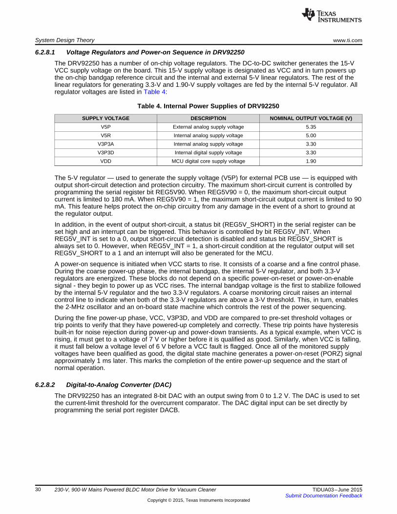
3.2 Power Stage for the BLDC Motor DriveThis reference design provides a 900-W inverter along with the AC-DC power stage working at 230 V±15%, for brushless motor control in vacuum cleaners. The reference design uses Hall sensor-basedtrapezoidal control using the DRV92250 as the controller. The three-phase inverter is designed usingIGBT with the UCC27714 as the gate driver. Figure 2 shows the assembled inverter board and the AC-DCpower supply board.
Figure 2. Assembled Inverter Board and AC-DC Converter
The inverter is designed to operate from the DC voltage obtained by rectifying the input 230-V AC ±15%.The maximum input AC voltage is 265 V and corresponding peak DC bus voltage is 375 V. However, if anactive power factor correction (PFC) is required, the DC voltage will be more than the peak input voltage.With the active PFC, typically the maximum DC bus voltage is 390 V at an input AC voltage of 265 V. Inthe reference design, the three-phase inverter is designed for a maximum DC bus voltage of 390 V.
5TIDUA03–June 2015 230-V, 900-W Mains Powered BLDC Motor Drive for Vacuum CleanerSubmit Documentation Feedback
Copyright © 2015, Texas Instruments Incorporated

Surge
Protection
&
EMC Filter
UCC27714 UCC27714 UCC27714Voltage
Scaling
VACUUM
CLEANER
BLDC MOTOR
16-BIT
MCU
Pre-Driver
Back-EMF Sensing
& Comparators
(10-Bit ADC)
Differential Current
Sense Amplifier
+
Comparator for OC
Protection
Buck-Regulator
Voltage Regulators
& References
10-Bit ADC
Hall Sensor
Interface
DRV92250
VCC (15V)
Buck Converter
L
N
PE
LMT84
AC-DC Power Supply
Input: 230V ±15%
1-Phase AC
VDC
VDC
Block Diagram www.ti.com
4 Block DiagramFigure 3 depicts the block diagram of the inverter system with the power stage. The main parts of thesystem consists of the AC-DC power supply stage, three-phase IGBT Inverter bridge, the gate driverUCC27714, the controller DRV92250, the 15-V buck regulator, the temperature sensor, and the input DCvoltage, motor voltage, and winding current sense feedback circuits.
Figure 3. Block Diagram of 900-W Inverter System
This reference design shows a discrete implementation for the three-phase BLDC inverter. The inverteruses six IGBTs. The UCC27714 is used as the gate driver for the IGBTs. The UCC27714 is a 600-V high-side low-side gate driver with 4 A/4 A source/sink current capability, capable of driving power MOSFETsor IGBTs. The device comprises of one ground-referenced channel (LO) and one floating channel (HO),which is designed for operating with bootstrap supplies. It has the VDD bias supply range of 10 to 20 V,which allows designing the IGBT gate drive with the maximum allowed gate voltage.
The trapezoidal control is implemented using the controller DRV92250. It provides six PWM outputs todrive the three-phase inverter. It can support both sensored and sensorless operation with the internalcomparators. The DRV92250 has an internal buck regulator, which helps in generating the 15-V biaspower supply for the gate driver. The DRV92250 generates 1.9 V, 3.3 V and 5 V internally using internalLDOs for the operation of the internal MCU and the analog peripherals of the controller.
The speed of the motor can be controlled easily using the potentiometer. More features can be added orthe performance can be optimized by programming the DRV92250.
6 230-V, 900-W Mains Powered BLDC Motor Drive for Vacuum Cleaner TIDUA03–June 2015Submit Documentation Feedback
Copyright © 2015, Texas Instruments Incorporated

www.ti.com Highlighted Products
5 Highlighted ProductsThe following are the highlighted products used in the reference design.
5.1 DRV92250DRV92250 is a high-voltage BLDC motor controller which integrates a 16-bit RISC MCU and pre-drivercircuits in a 48-pin LQFP with PowerPAD heat sink. 32KB of single-cycle (40 ns) Flash memory isembedded with the digital MCU sub-system. The 16-bit MCU is instruction set compatible with TI’sMSP430F5438 family. The DRV92250 has low-side pre-driver circuits, one differential current senseamplifier, a comparator with programmable DAC for overcurrent protection, a DC-DC buck controller,LDOs of 5.35 V, 5.0 V, 3.3 V, and 1.9 V, and BEMF detection comparators for sensorless controller.
5.2 UCC27714The UCC27714 is a 600-V high-side low-side gate driver with 4 A/4 A source/sink current capability,targeted to drive power MOSFETs or IGBTs. The device comprises of one ground-referenced channel(LO) and one floating channel (HO), which is designed for operating with bootstrap supplies. The devicefeatures an excellent robustness and noise immunity with the capability to maintain operational logic atnegative voltages of up to –8-V DC on the HS pin (at VDD = 12 V).The device features the industry best-in-class input propagation delays and delay matching between both channels aimed at minimizing pulsedistortion in high-frequency switching applications. Each channel is controlled by its respective input pins(HI and LI), allowing full and independent flexibility to control the on/off state of the output. The UCC27714includes protection features wherein the outputs are held LOW when inputs are floating or when theminimum pulse width specification of the input is not met. The driver inputs are CMOS/TTL compatible foreasy interface to digital power controllers and analog controllers alike. An Enable/Disable function isincluded in the UCC27714 to enable the output gate signals. The device accepts a wide range bias supplyinput from 10 to 20 V and offers UVLO protection for both the VCC and HB bias supply pins. TheUCC27714 is available in SOIC-14 package and rated to operate from –40°C to 125°C.
5.3 LMT84The LMT84 is precision CMOS integrated-circuit temperature sensors with an analog output voltage that islinearly and inversely proportional to temperature. It can operate down to 1.5-V supply with 5.4-μA powerconsumption, making it ideal for battery powered devices. Multiple package options including through-holeTO-92 and TO-126 packages also allow the LMT84 to be mounted on-board, off-board, to a heat sink, oron multiple unique locations in the same application. Class-AB output structures gives the LMT84 strongoutput source and sink current capability that can directly drive up to 1.1-nF capacitive loads. This meansit is well suited to drive an analog-to-digital converter sample-and-hold input with its transient loadrequirements. It has accuracy capability specified in the operating range of −50°C to 150°C.
5.4 TL431AThe TL431 is a three-terminal adjustable shunt regulator with specified thermal stability over applicableautomotive, commercial, and military temperature ranges. The output voltage can be set to any valuebetween VREF (approximately 2.5 V) and 36 V with two external resistors. The TL431 has a typical outputimpedance of 0.2 Ω. Active output circuitry provides a very sharp turn-on characteristic, making thesedevices excellent replacements for Zener diodes in many applications such as onboard regulation,adjustable power supplies, and switching power supplies. The TL431 has a low-output drift versustemperature ensures good stability over the entire temperature range.
7TIDUA03–June 2015 230-V, 900-W Mains Powered BLDC Motor Drive for Vacuum CleanerSubmit Documentation Feedback
Copyright © 2015, Texas Instruments Incorporated

TIDA-00433DB
AC-DC power supply with EMI filters,
bridge rectifier and DC bus capacitors
TIDA-00433MB
Three phase IGBT inverter with gate
driver, controller and 15-V bias supply.
DC busTo motor winding
L
N
PE
230 ±15% V 1-phase AC
50/60 Hz
System Design Theory www.ti.com
6 System Design TheoryThe complete system is designed in two boards, as shown in Figure 4. The boards TIDA-00433DB is thepower supply board with DC bus capacitors, which rectifies the 230-V AC input supply. The other boardTIDA-00433MB consists of the three-phase inverter with the onboard 15-V bias power supply.
Figure 4. Power Supply — Inverter Board Split Up
6.1 AC-DC Power Supply Board (TIDA-00433DB)The AC-DC power supply board schematic is shown in Figure 5. The power supply board is designedusing the diode bridge rectifier and bulk electrolytic capacitor at the DC bus, with provision for necessaryfilters for conducted emission, surge, and EFT protection as per the standard EN55014.
Figure 5. AC-DC Power Supply (TIDA-00433DB)
In the schematic, J2 is the three-pin connector for the single-phase AC input. In the schematic, F1 is theprotection fuse followed by the Metal Oxide Varistor (MOV) for surge protection. A 20-mm diameter MOVwith 275-V AC rating is selected for this application. R1 and R4 forms discharge resistor for the X2capacitor C4 and C5. The filter network consists of C5, C4, L1, L2, L3 C1, C6, C7, and C8 form theconducted emission filter. C5 and C4 are X2 rated capacitors, C1, C6, C7, and C8 are Y2 ratedcapacitors. L1 is a common mode filter and L2 and L3 are differential mode filters. To limit the inrushcurrent of the bulk DC capacitors, an inrush current limiter RT1 is provided. D1 is the full bridge rectifier.
J1 is the connector for connecting external DC choke. The external chock can be connected to meet theharmonic standards.
C2 and C3 are the electrolytic capacitors at the DC bus. The capacitors are designed for 10% voltageripple at a power of 900 W. R2, R3, R5, and R6 forms the bleeder resistor for the bulk capacitors.
8 230-V, 900-W Mains Powered BLDC Motor Drive for Vacuum Cleaner TIDUA03–June 2015Submit Documentation Feedback
Copyright © 2015, Texas Instruments Incorporated

DC
DC
tC I
V
D³ ´
D
www.ti.com System Design Theory
NOTE: The bleeder resistors can be eliminated on integration of the inverter board and AC-DCpower supply into single board. The differential mode inductors L2 and L3 were not used inthe conduction emission test because the test is giving satisfactory performance without L2and L3 and hence can be eliminated.
6.1.1 Design of DC Bus CapacitorThe DC bus capacitor is important while designing the inverter-fed motor drives operating from the ACmains. The DC bus capacitor serves the following purposes.1. Reduces the voltage ripple in the DC link and provide a stable DC link voltage for the inverter. A high
DC voltage ripple may cause motor torque ripple and cause inferior performance of the motor drive.2. In PWM inverter drives, there could be huge current ripple in the DC bus. The DC bus capacitor act as
local storage for handling the ripple current.3. The DC bus capacitor act as a storage for regenerative energy from the motor. If diode bridge rectifiers
are used, the regenerative energy could not be fed back to the source and hence absence of a properDC bus capacitor may cause high voltage build up in the DC link during regeneration and causevoltage breakdown of the semiconductors.
In this reference design, the capacitor is designed to limit the DC bus voltage ripple to less than 10% ofthe peak value at rated DC bus power of 900 W.
If the AC input supply is 230 V, 50 Hz, the discharge time of the capacitor, tdischarge = 10 ms (approximate,to make the calculations simple). If the average DC link current is at 900 W, IDC ≈ 3 A. Therefore, requiredcapacitance value is found with
where• Δt = tdischarge = 10 ms• ΔV = 10% of 325 = 32.5 V (1)
Substituting in Equation 1, C ≥ 924 μF.
The ripple current capacity of the capacitor also needs to be decided. The application is a BLDC motordriven by the three-phase inverter using trapezoidal control. In trapezoidal control, the DC link currentwould have huge current ripple during commutation in motor. The DC bus ripple current could be as highas two times the DC bus average current. The DC bus capacitors should be able to handle this ripplecurrent. A high ESR capacitor will increase the losses in the capacitor, which leads to capacitor heatingand hence reduced capacitor life.
This reference design uses two 560-μF capacitors with a 2-A ripple current capacity, which are connectedin parallel to share the ripple current.
6.1.2 Selection of Bridge RectifierThe diode bridge rectifier should withstand the peak inverse voltage at 265-V AC. If a DC link choke is notused, the peak current drawn by the bulk electrolytic capacitors could be as high as 20 A at rated inputpower of 900 W. This reference design uses a 1000-V, 25-A full bridge rectifier.
Thermal design is done to select the appropriate heat sink for the bridge rectifier by calculating the lossesin the bridge rectifier.
Rated power = 900 WThe DC bus capacitor is designed for 10% voltage ripple.Therefore the average DC bus voltage, VDCavg = 310 V
At 900 W, average DC bus current, IDCavg ≈ 3 ATherefore, the average forward current through the bridge rectifier, IFavg = 3 A
During the charging, the bulk capacitors draws very high peak current from the supply of the order of 20 A.Therefore, the RMS current flowing through the diode will be more compared to the average current.
9TIDUA03–June 2015 230-V, 900-W Mains Powered BLDC Motor Drive for Vacuum CleanerSubmit Documentation Feedback
Copyright © 2015, Texas Instruments Incorporated

( )j amb(max) RECT JC HAT T P R Rq q- = ´ +
( )2RECT F0 Fav g D FrmsP 2 V I r I= ´ +
2DIODE F0 Fav g D FrmsP V I r I= +
( )F F0 D FV V r I= + ´
( )j F
T
DIODE FF T , I0
1P V I dt
T= ò
System Design Theory www.ti.com
The simulation results with the designed capacitor value shows that at 900-W DC bus power, the RMS DCbus current ≈ 7.5 A
For the thermal design calculations, the following values are used:• Diode forward average current, IFavg = 3 A• Diode forward RMS current, IFrms = 7.5 A
Conduction loss in the diode can be calculated using Equation 2:
where• VF(Tj,If) is the forward voltage of the diode at a junction temperature Tj and forward current IF (2)
The user can express the forward voltage VF at a forward current IF as in Equation 3.
(3)
Where VF0 is the zero current forward voltage drop, which is obtained by drawing a tangent to the forwardcharacteristics of diode over the operating current range, extend it to the voltage axis, and take the voltageaxis intercept. rD is the dynamic resistance of the diode, which is the slope of the tangent line.
Using Equation 3, the power dissipation in the diode can be expressed as in Equation 4.
(4)
Normally VF0 and rD are specified in the datasheet. In this reference design, the full-bridge rectifier is usedand at any time two diodes are ON. Therefore, the total loss in the bridge rectifier can be found with
(5)
From the datasheet, approximate values of VF0 and rD are VF0= 0.75 V and rD= 24 mΩ.
Therefore, PRECT = 2 × [(0.75 × 3) + (0.024 × 7.52)] = 7.2 W.
From the rectifier datasheet, the junction to case thermal resistance of the rectifier, RθJC = 0.6°C/W.
The maximum operating ambient temperature, Tamb(max) = 55°C
To limit the junction temperature of the diode rectifier to 115°C (maximum operating temperature of thebridge rectifier is 150°C), connect a heat sink to the rectifier. The heat sink can be directly mounted on thebridge rectifier without any interface material (the rectifier case is isolated).
If RθHA is the thermal resistance of the heat sink to the ambient, the thermal equation can be written as
(6)
Substituting Tj = 115°C in Equation 6 leads to RθHA = 7.7°C/W. Therefore, select a heat sink with a thermalresistance less than 7.7°C/W.
10 230-V, 900-W Mains Powered BLDC Motor Drive for Vacuum Cleaner TIDUA03–June 2015Submit Documentation Feedback
Copyright © 2015, Texas Instruments Incorporated

www.ti.com System Design Theory
6.2 Inverter Board (TIDA-00433MB)
6.2.1 Three-Phase InverterThe three-phase inverter is designed to operate from the rectified 230-V AC mains. However, with anactive power factor correction front end the maximum DC bus voltage could be up to 390 V. Figure 6shows the input connector J1 in the inverter board. A three-terminal connector is used, which interfacesthe DC supply terminals, and the earth connection.
Figure 6. DC Power Supply Connector to Inverter Board
NOTE: The capacitor C58, rated 100 μF, 400 V, is used as a DC capacitor near the inverter bridgeto supply the ripple current locally in the inverter board. However, on integration of the AC-DC power supply and the three-phase inverter in a single board, the DC capacitors used inthe rectifier board (in this reference design 560 μF × 2, in the AC-DC board) is sufficient andthe capacitor C58 can be removed.
Figure 7 shows the schematic of the three-phase inverter . The decoupling capacitors C30, C31, and C32are provided for each leg of the inverter to limit the switching voltage spikes. These capacitors must beplaced very close to each leg of the inverter. The resistor R55 is used to sense the DC bus return current.The filter network consists of C17, R25, and R26 is used as a high frequency differential filter. Theterminal block J7 is used to connect the three-phase motor terminals.
Figure 7. Three-Phase Inverter
11TIDUA03–June 2015 230-V, 900-W Mains Powered BLDC Motor Drive for Vacuum CleanerSubmit Documentation Feedback
Copyright © 2015, Texas Instruments Incorporated

2 2
RMS SENSEPower loss in the resistor I R 5 0.02 0.5 W= ´ = ´ =
AVG
900 WI 3 A
310 V» »
System Design Theory www.ti.com
6.2.2 Selection of Switching DeviceThe three-phase inverter is designed to operate from the rectified 230-V AC main. However, with an activepower factor correction front end the maximum DC bus voltage could be up to 390 V. Considering thesafety factor and switching spikes, the switching device with voltage rating of 1.25 to 1.5 times themaximum input voltage can be selected.
Voltage rating of the switching device, VSW ≥ 1.25 × 390 ≈ 500 V.
The current rating of the switching device depends on the peak winding current. The rated power is900 W. Considering average DC bus voltage of 310-V DC, at 230-V AC input, average currentat the DC bus:
The peak current in the motor winding depends on the motor parameters. Normally in trapezoidal control,the peak winding current could be as high as two times the average DC current. Therefore, the peakcurrent in the switches could be more than 6 A. In the reference design, the peak current limit is kept at7 A. Keeping the current limit to a lower value will limit the torque capability of the drive. Considering afactor of safety, a switching device with current rating 1.5 to 2 times the calculated peak current can beselected. The device should be rated for this current at the maximum operating junction temperature (Tj).Therefore, the current rating of the switching device, ISW ≥ 1.5 × 7 ≈ 11 A, at Tj = 125°C.
Another aspect for selecting the switching device is the switching frequency. This reference design uses aswitching frequency of 10 kHz. IGBTs are selected for the application because of lower switchingfrequency (10 kHz), high voltage (400-V DC) and reasonable high power (≈ 1 kW).
The reference design uses a 600-V, 20-A IGBT.
6.2.3 Selection of Sense ResistorThe sense resistor is used at the DC link return path to measure the inverter or motor current. Intrapezoidal control of BLDC motors, only two phases are ON at a time, thus the DC link current is thesame as the winding current. Therefore, different current or torque control strategies can be implementedby sensing only the DC bus current. The DRV92250 has an internal differential amplifier to sense thebottom DC link current. If the designer is implementing any current control algorithm, consider thedifferential amplifier parameters when selecting the sense resistor.
The power dissipation is another factor to be considered in the selection. A high resistance value thatleads to a high power loss in the resistor and a very low value may cause noise problems in sensing andcontrol.
This reference design uses the sense resistor to implement peak winding current control using the internalcomparator of the DRV92250. The inverting input of the comparator is used as the current thresholdreference and is fed from a digital-to-analog converter (DAC), whose maximum output voltage is 1.2 V. Inthis reference design, the peak current limit is designed to be 7 A. Selecting a 20-mΩ sense resistor, Thesense voltage, VSENSE = ISENSE × RSENSE. At 7 A, VSENSE = 0.14 V.
The nominal RMS current of the motor winding current is less than 5 A for this application. Therefore, thepower loss in the resistor at 5 A(RMS) is given by Equation 7.
(7)
In case of a blocked rotor or any other over current situation, the peak current will be limited to 7 A. Thepower loss in the resistor at a 7-A continuous current = 0.98 W. Therefore, a standard 2-W, 2512-packageresistor can be used.
12 230-V, 900-W Mains Powered BLDC Motor Drive for Vacuum Cleaner TIDUA03–June 2015Submit Documentation Feedback
Copyright © 2015, Texas Instruments Incorporated

Collector-Emitter Voltage, VCE(V)
Co
lle
cto
r C
urr
en
t, I
C(A
)
VCE0
P/C
PsCE
0
Specified
VGE & TCASE
www.ti.com System Design Theory
6.2.4 IGBT Loss CalculationThe trapezoidal BLDC motor control is used in this reference design. In trapezoidal control, any switch willconduct for 120° in an electrical cycle, and in any case two switches are ON, one from the high side andthe other from the low side.
With a stable 230-V AC input system; the diode rectified average DC bus voltage is a constant. Therefore,in order to control the average voltage applied to the motor, a PWM technique can be used. This can beachieved by inserting the PWM to the 120° conduction period of either top side or bottom side switch orboth.
Here, only the top side is switched to control the voltage applied to the motor winding and the bottom sideswitch is continuously ON for the entire 120° period. This leads to saving in switching loss from the bottomswitch.
The inverter losses are calculated at 900-W output power from the inverter. The specifications given inTable 2 are used in calculating the inverter losses.
Table 2. Parameters Used for Inverter Loss Calculation
PARAMETER VALUERated voltage of the motor 300 VNominal motor current (RMS) 4.5 AAverage DC current 3 ARated RPM 18000No of poles of the motor 4Motor electrical frequency at rated RPM 600 Hz
6.2.4.1 Power Loss in Low-Side IGBT
Conduction LossIGBT conduction losses can be calculated using an approximate equivalent circuit consists of a seriesconnection of a voltage source (VCE0) representing the ON state zero current collector-emitter drop and thedynamic collector-emitter ON state resistance (rC).
Figure 8. Modeling of IGBT for Loss Calculation
13TIDUA03–June 2015 230-V, 900-W Mains Powered BLDC Motor Drive for Vacuum CleanerSubmit Documentation Feedback
Copyright © 2015, Texas Instruments Incorporated

LP 1.55 0.13 1.7 W= + »
L CL SWLP P P= +
( )SWL
325 7P 0.41 0.36 600 0.13 W
400 20
´æ ö= + ´ ´ =ç ÷´è ø
( )( ) ( )
NOM PK
SWL ON OFF ele
CC test C test
V IP E E f
V I
æ ö´ç ÷= + ´ ´ç ÷´è ø
( )
ele
SWL ele ON OFF
No of pole pairs RPM 2 18000f 600 Hz
60 60
P f E E
´ ´= = =
= ´ +
( ) ( )( )2CL CE0 C,AVG C C,RMS
1P V I r I
3= ´ ´ + ´
( ) ( )2C CE0 C,AVG C C,RMSP V I r I= ´ + ´
CE CE0 C C,RMSV V r I= + ´
System Design Theory www.ti.com
Figure 8 shows typical output characteristics of an IGBT at a particular gate-to-emitter voltage (VGE) andcase temperature. A linear interpolation is done on the output characteristics to derive the equivalentcircuit equation given in Equation 8.
(8)
Where rC is the equivalent dynamic resistance of the IGBT, which is the slope of the output characteristics.IC,RMS is the RMS value of the switch current and IC,AVG is the average switch current.
Based on the assumption above, the conduction loss (PC) of an IGBT can be expressed as in Equation 9.
(9)
In BLDC trapezoidal control, one switch is conducting for 120°, or one third of the total electrical cycle.
Therefore, the conduction loss in one lower IGBT is
(10)
From the output characteristics of the IGBT at the case temperature of 125°C, the approximate values ofthe loss modeling parameters are VCE0 ≈ 1.2 V and rC ≈ 50 mΩ.
Therefore, the conduction loss in one lower IGBT is PCL = (1/3) × [(1.2 ×3) + (0.005 × 4.52)] ≈ 1.55 W.
Switching LossThere is no PWM switching in low-side switches and is continuously ON for the 120° interval. However,the low-side switch is commutating at the motor electrical frequency.
The motor electrical frequency at rated RPM is
(11)
From the datasheet of the IGBT,Turn ON switching loss, EON = 0.41 mJ, when tested at VCC = 400 V, IC = 20 A, RG = 10 Ω, VGE = 15 VTurn OFF switching loss, EOFF = 0.36 mJ, when tested at VCC = 400 V, IC = 20 A, RG = 10 Ω, VGE = 15 V
In the reference design, VGE = 15 V, and the peak winding current IPK = 7 A.
Low side IGBT switching loss,
(12)
Total loss on a single low-side IGBT,(13)
14 230-V, 900-W Mains Powered BLDC Motor Drive for Vacuum Cleaner TIDUA03–June 2015Submit Documentation Feedback
Copyright © 2015, Texas Instruments Incorporated

HP 1.5 0.73 2.23 W= + =
H CH SWHP P P= +
( )SWH
1 325 7P 0.41 0.36 10 k 0.73 W
3 400 20
´æ ö= ´ + ´ ´ =ç ÷´è ø
( ) NOM PKSWH ON OFF SW
CC(test) C(test)
V I1P E E f
3 V I
æ ö´= ´ + ´ ´ç ÷
ç ÷´è ø
( )2CH
1P (0.968 1.2 3) (0.05 4.5 ) 1.5 W
3= ´ ´ ´ + ´ »
( ) ( )( )2CH CE0 C,AVG C C,RMS
1P D V I r I
3= ´ ´ ´ + ´
www.ti.com System Design Theory
6.2.4.2 High-Side IGBT LossThe PWM is applied to high-side switches; therefore, the only difference in estimating the conduction lossin the high-side IGBT and low-side IGBT is that the user needs to consider the duty cycle of the PWM.• Average DC bus voltage = 310 V• Average motor winding voltage at rated load = 300 V (Rated voltage of the motor)• At rated load, PWM Duty Cycle, D = 300/310 = 0.968
Therefore, the conduction loss in one high-side IGBT,
(14)
In the reference design, the high-side IGBT is switching at 10 kHz. Therefore, the switching loss is
(15)
Total loss on a single high-side IGBT,
15TIDUA03–June 2015 230-V, 900-W Mains Powered BLDC Motor Drive for Vacuum CleanerSubmit Documentation Feedback
Copyright © 2015, Texas Instruments Incorporated

DIODE,COMMP 6 1.5 3.5 100 s 600 Hz 1.89 W» ´ ´ ´ m ´ =
DIODE,COMM F F,avg commutation eleP 6 V I T f» ´ ´ ´ ´
elecf 600 Hz=
( )DIODE,SW
1P 1 0.968 1.7 3 0.0544 W
3= ´ - ´ ´ =
( )DIODE,SW F F,AVG
1P 1 D V I
3= ´ - ´ ´
( ) ( )DIODE,SW F F,AVG SW DIODE
1P 1 D V I f E
3
æ ö= ´ - ´ ´ + ´ç ÷
è ø
System Design Theory www.ti.com
6.2.4.3 Diode Losses
Losses Due to PWM SwitchingWhen the top IGBT is turned off during PWM switching, the motor current gets transferred to theantiparallel diode of the lower IGBT. Therefore, the lower diode losses can be calculated usingEquation 16.
(16)
Where EDIODE is the reverse recovery switching losses in the diode. Excluding the reverse recoveryswitching loss in the diode,
where• VF is the forward loss in the diode• IF,AVG is the average diode forward current (17)
The diode losses calculated above are for the low side. The high-side diodes are conducted during thecommutation period only and hence calculated separately.
Losses Due to Phase CommutationDuring commutation, the motor winding current will freewheel through the antiparallel diode of thecomplimentary IGBT. For example, if the top IGBT is commutating, then the winding current which wasflowing through the top IGBT will get transferred to the antiparallel diode of the lower IGBT. There are sixcommutations in one electrical cycle of the motor current waveform. The commutation period can bedefined as the duration of time in which the winding current of the commutation phase reduces to zero.The commutation period depends on the motor inductance and the peak winding current, hence thecommutation period varies from motor to motor.
The reference design uses a vacuum cleaner motor for testing and the approximate commutation time isobserved as less than 100 μs. The commutation time, Tcommutation = 100 µs.
For a 4-pole motor running at 18000 RPM, the electrical frequency of motor winding current is(18)
Since there are six commutations in one electrical cycle, the total diode loss due to phase commutationcan be calculated as
where• VF,avg is the diode forward voltage drop• IF,avg is the average forward current of the diode during commutation (19)
The multiplication factor of 6 in Equation 19 is because there are six commutations in an electrical cycle.During commutation, the current in the commutating phase reduces from the peak value to zero. In theapplication design, the peak winding current is 7 A. Therefore, IF,avg = 7/2 = 3.5 A.
From the device datasheet, VF,avg ≈ 1.5 V, at diode junction temperature of 125°C at a forward currentof 7 A.
Substituting the values in Equation 19,
Therefore, the total diode loss, PDIODE = (3 × PDIODE,SW) + PDIODE,COMM = 2.1 W.
16 230-V, 900-W Mains Powered BLDC Motor Drive for Vacuum Cleaner TIDUA03–June 2015Submit Documentation Feedback
Copyright © 2015, Texas Instruments Incorporated

( )LOSSP 3 1.7 2.23 2.1 14 W= ´ + + »
( )LOSS L H DIODEP 3 P P P= ´ + +
www.ti.com System Design Theory
Total Loss in Three-Phase InverterThe total losses in the IGBTs of the three-phase inverter are:
(20)
6.2.5 Thermal Design for Three-Phase InverterProper thermal design is crucial for the safe and reliable operation of semiconductors. Operating thesemiconductor at higher operating temperature reduces the safe operating area and may lead to failure orreduce the life of the device.
The whole aim of the thermal design is to limit the junction temperature of the IGBTs with in the safevalues at full load. The datasheet specifies that the IGBT has a maximum junction temperature rating of150°C. The user need to design a heat sink or any cooling method needs to have the junction temperaturewithin safe limits.
However, the user has access to the case of the IGBT and hence should limit the case temperature insuch a way that at that particular case temperature the junction temperature is in safe limit. The differencebetween the case and junction temperature depends on the junction to case thermal resistance.
The datasheet of the IGBT specifies the thermal resistance of the IGBT and antiparallel diode separately.
From the datasheet:• The junction to case thermal resistance of the IGBT, RθJC_IGBT = 0.76°C/W• The junction to case thermal resistance of the Diode, RθJC_DIODE = 2.51°C/W
The case of the IGBT is generally connected to the collector terminal. Therefore, an electrically insulatedand thermally conducting filler or interface material is required between the IGBT case and the heat sink.The thermal interface material has to be selected such that it has sufficient electrical insulation voltagerating compared to the system operating voltage. The material should have a very low thermal resistanceas well.
The thermal equivalent circuit of a single IGBT with the independent heat sink is as shown in Figure 9.
Figure 9. Thermal Equivalent Circuit of Single IGBT to Ambient
NOTE: RθCH = Thermal resistance from IGBT case to heat sink or the thermal resistance of thethermal interface material (°C/W)RθHA = Thermal resistance from heat sink to the ambient (°C/W)
17TIDUA03–June 2015 230-V, 900-W Mains Powered BLDC Motor Drive for Vacuum CleanerSubmit Documentation Feedback
Copyright © 2015, Texas Instruments Incorporated

( ) CHJC IGBT
j a HA LOSS
R RT T R P
6
qqq
+æ öç ÷- = + ´ç ÷è ø
System Design Theory www.ti.com
In the reference design, a single heat sink is used for all six IGBTs of the three-phase inverter. Thethermal equivalent circuit of the system becomes as shown in Figure 10.
Figure 10. Thermal Equivalent Circuit of Inverter With Heat Sink
For analysis simplicity, It is assumed that all the IGBT losses are same. The diode thermal resistance(RθJC_DIODE) is excluded in the mathematical equation.
From the equivalent circuit, the mathematical relation for temperature rise can be written as inEquation 21.
(21)
The maximum operating ambient temperature, Ta = 55°C
Considering a safety margin, let the maximum junction temperature at rated load be 110°C, thetemperature rise, Tj − Ta = 55°C.
A typical thermal interface material has a thermal resistance less than 0.5°C/W. The calculated IGBTpower loss at a rated inverter output power PLOSS ≈ 14 W. Considering a design margin of 2 W, the IGBTlosses can be approximated to 16 W. Substituting these values in Equation 21 gives RθHA = 3.2°C/W.
An extrusion heat sink with thermal resistance less than 3.2°C/W and having length sufficient to mount sixIGBTs is a good choice.
18 230-V, 900-W Mains Powered BLDC Motor Drive for Vacuum Cleaner TIDUA03–June 2015Submit Documentation Feedback
Copyright © 2015, Texas Instruments Incorporated

www.ti.com System Design Theory
6.2.6 Buck Regulator Using DRV92250The bias power supply of 15 V required for DRV92250 and UCC27714 is derived using the external highvoltage P-channel FET and discrete gate drive controlled by the buck regulator inside the DRV92250. Thebuck converter circuit is shown in Figure 11.
The DC/DC buck converter controller on the DRV92250 has special protection features designed in toprevent any damage to external components in case of a floating VCC pin (15-V power supply pin). Inaddition, to protect the off chip switching transistor/FET, duty cycle control is also provided through serialregister bits DCDeGlitch and DcDcWidth[1;0]. Minimum duty cycle is controlled by setting the DCDeGlitchcontrol bit to a 1. This enables pulse extension circuitry on chip which guarantees a minimum switcherpulse width of at least 1 µs. Similarly, maximum switcher duty cycle is controlled by programmingDcDcWidth[1:0] control bits. For duty-cycle greater than what is set by control bits DcDcWidth[1:0], theSWDR output waveform is modulated by a 125-kHz clock signal to protect the switching power transistorand inductor.
Figure 11. Buck Converter Circuit
FDBK is the feedback control input for the DC/DC converter. The output voltage of the buck converter isfed back to the FDBK pin using a feedback resistive network. An on-chip hysteresis comparator closes thecontrol loop by comparing the voltage on pin FDBK against reference voltage derived from the band gap.The nominal value of the band gap voltage is 1.3 V. The comparator switching output drives the externalswitch through pin SWDR. The comparator hysteresis voltage is programmable and provides four optionsof 10 mV, 20 mV, 30 mV, and 40 mV using the control bit HYSDCDC[1:0].
The DRV92250 derives the start-up bias supply through the pin ST_BIAS. The resistive divider networkconnected between ST_BIAS and the high voltage DC bus is used for this purpose.
6.2.6.1 Discrete Gate Drive for High-Side Buck ConverterFigure 11 shows the buck converter using the DRV92250 controller. The external switch for the buckconverter is a P-channel MOSFET Q2. The transistors Q1, Q3, and Q4 form the gate driver circuit. D1 isthe freewheeling diode of the buck converter. R11 and C6 form the snubber for D1. The inductor L2 andcapacitor C5 forms the output filter. The resistors R5 and R12 are the voltage divider to feed back theoutput voltage to the DRV92250 through the FDBK pin. The starting bias for the DC/DC converter isderived from the mains voltage using the resistor network R1, R3, and R8. Three resistors are used toreduce the voltage stress on each resistor.
Working of Gate DriverThe transistors Q1, Q3 and Q4 are operating in the linear region. The leg consist of R2, R14, and Q3forms a voltage regulator (when Q3 is ON), which regulates the voltage across R2, when input voltage VDCvaries over a wide range. This can be explained as follows.
The SWDR is the PWM signal from DRV92250 with PWM high level voltage of 3.3 V and low level of 0 V.
19TIDUA03–June 2015 230-V, 900-W Mains Powered BLDC Motor Drive for Vacuum CleanerSubmit Documentation Feedback
Copyright © 2015, Texas Instruments Incorporated

( )
R2
c Q3
V 12.7 VR2 4.88 k
i 2.6 mA= = = Ω
( )R2 GS Q2V (V 0.7) 12.7 V= - - =
( )GS(Q2) R2V V 0.7 V= - -
( )GS(Q2) R2 BE(Q4)V V V= - +
R2 c (Q3)V i R2= ´
( )e Q3
3.3 0.7 2.6i
R14 R14
-= =
( ) ( )b(Q3) BE(Q3) e(Q3)3.3 i R6 V i R14= ´ + + ´
System Design Theory www.ti.com
When SWDR is high, the KVL equation for the loop consists of SWDR, R6, the base emitter junction ofQ3, and R14 can be written as in Equation 22.
where• ie(Q3) is the emitter current of Q3• ib(Q3) is the base current of Q3 (22)
Typically, VBE(Q3) = 0.7 V. Neglecting the base current, Equation 22 can be re-written as
(23)
The design uses R14 = 1 kΩ. Therefore, ie(Q3) = 2.6 mA.
This means the resistor R14 fixes the emitter current of the transistor Q3. The collector current of Q3 canbe approximated to emitter current (neglecting the base current).ic(Q3) ≈ ie(Q3) = 2.6 mA
Then the voltage drop across R2 is determined by the emitter current. Therefore, the voltage dropacross R2:
(24)
This clearly shows that the voltage across R2 is regulated (when Q3 is ON) independent of the DC busvoltage.
Because of the totem pole network consisting of Q1 and Q4, the voltage at the collector of Q3, will bereflected at the emitters of Q1 and Q4 with a difference of 0.7 V. In short, the voltage across R2 willappear as the gate-to-source voltage (VGS) of the P-channel FET Q2, with a difference of VBE of the totempole transistor Q4.
Therefore,
(25)
Assuming VBE (Q4) = −0.7 V,
This reference design uses the high voltage P-channel FET FQD3P50TM. Typical gate to source voltageof –12 to –15 V is a good choice.
Considering –12 V as the required gate voltage, substituting in Equation 25,
(26)
Therefore, the required resistor,
.
When Q3 is ON, the voltage drop across R2 makes Q4 to turn ON. The gate drive provides the requiredgate charge to Q2 by means of the gate current flowing through the gate-to-source capacitance of Q2,R10, and Q4. Therefore, the negative voltage across the gate-to-source capacitance of Q2 will build upslowly and causes turn ON of Q2. Similarly when Q3 is OFF, Q4 will turn OFF, and Q1 will turn ON. Thisremoves the gate charge from Q2 through Q1 and R4. That means R10 forms the turn on resistance andR4 forms turn off resistance of Q2.
The maximum voltage across Q3 is equal to the maximum DC bus voltage. The maximum DC bus voltagecould be 400 V in this application. Therefore, the transistor Q3 should have a minimum collector to emitterbreakdown voltage of 450 V. The voltage across the transistor Q1 is clamped to less than 15 V by theresistor R2. Therefore, a low-voltage (typically 40-V rated) transistor is good enough.
20 230-V, 900-W Mains Powered BLDC Motor Drive for Vacuum Cleaner TIDUA03–June 2015Submit Documentation Feedback
Copyright © 2015, Texas Instruments Incorporated

www.ti.com System Design Theory
The maximum voltage across the transistor Q4 is equal to the DC bus voltage. The resistor R10 controlsthe gate current of Q2 during its turn ON. A low value of R10 increases the losses in Q4, and a high valueof R10 slows down the turn on of Q2 and hence the turn on losses of Q2. The reference design uses a200-Ω resistor R10, which is selected based on simulation results to limit the power loss in Q4 (thereference design uses a 500-V, 150-mA PNP transistor having a maximum power capacity of 2 W).
6.2.6.2 Design of Power Components in Buck ConverterThe buck converter is designed to generate the bias power supply required in the board. The bias supplyvoltage of 15 V is generated in the reference design, which optimizes the gate drive for the IGBT. Thetotal power required from the bias supply is approximately 3 W.
The bias power supply is required mainly for the gate drivers, the DRV92250, and the PFC board. Thedesign specification of the buck converter is summarized as in Table 3.
Table 3. Specifications for 15-V Bias Power Supply
PARAMETER VALUEInput voltage 90-V to 400-V DC
Output voltage 15 V, 200 mA (approximately 3-W output)Average output current (IOUT) 200 mA
Efficiency > 70%Protections Output overvoltage protection
Isolation Non-isolated (Buck)
The buck regulator of the DRV92250 is operating in hysteresis control with programmable minimum ONtime. At lower input voltages, the buck converter is operating in continuous conduction mode (CCM) todeliver the rated output current. However, as the voltage increases the buck regulator starts operating indiscontinuous conduction mode (DCM). The switching frequency is not constant as this controller is basedon hysteresis control. Therefore, for a constant output load, as the input voltage increases, the switchingfrequency decreases. The switching frequency also depends on the hysteresis band provided. Theminimum on time of the switching pulse is limited to 1 μs. Therefore, for a constant output load, as theinput voltage increases, the on time of the switching pulse reduces and when the pulse width is less than1 μs, the pulse is extended to 1 μs and the switching frequency is reduced.
21TIDUA03–June 2015 230-V, 900-W Mains Powered BLDC Motor Drive for Vacuum CleanerSubmit Documentation Feedback
Copyright © 2015, Texas Instruments Incorporated

MIN ON_MINPK
MIN
385L T
I
385L 2 s 0.77 mH
1
= ´
= ´ m =
PK ON_MIN
PK
400 15T
L
385I 2 s
L
-= ´
= ´ m
IN OUTPK L(ON) ON
V VI I T
L
-= D = ´
L
L
VI t
LD = ´ D
L
L
diV L
dt= ´
System Design Theory www.ti.com
6.2.6.3 Output Inductor SelectionIn DCM, the inductor current increases the peak current (IPK) and reduces to zero before the nextswitching cycle.
The voltage across the output inductor can be expressed as in Equation 27.
(27)
On linearizing Equation 27,
(28)
In DCM, the inductor current increases during the ON state to the peak current (IPK). Therefore,
(29)
The maximum DC input voltage, VDC(MAX) = 400 V
The minimum turn ON period of the switching pulse from the buck regulator in the DRV92250 is 1 μs.Considering the non-linearities in the gate driver and the hysteresis controller, the minimum on period ofTON_MIN = 2 μs is considered in this reference design.
At 400-V DC, using Equation 29,
(30)
The peak value of the current is dependent on the output inductor value. Selecting a lower inductor valueincreases the peak current in the switch and the freewheeling diode. The DC-DC converter switch currentrating should be greater than the peak current rating with a sufficient safety margin. To limit the peakcurrent to less than 1 A, the minimum required value of inductor is
(31)
Selecting a standard 1-mH inductor, the peak current is IPK = 0.77 mA.
The current rating of the selected inductor is 780 mA and the saturation current is 1.2 A.
22 230-V, 900-W Mains Powered BLDC Motor Drive for Vacuum Cleaner TIDUA03–June 2015Submit Documentation Feedback
Copyright © 2015, Texas Instruments Incorporated

R12 1.3
R5 13.7=
bg OUT
R12V V
R12 R5=
+
www.ti.com System Design Theory
6.2.6.4 MOSFET SelectionThe P-channel MOSFET Q2 is selected to handle 0.77-A peak current safely. The voltage rating of theFET should be greater than 1.25 times the maximum input DC bus voltage (considering 25% safetymargin due to voltage spike):• Voltage rating > 1.25 × 400 V = 500 V
The current rating should be greater than 1.5 times the peak current. (50% safety margin):• Current rating > 1.5 × 0.77 = 1.2 A
The selected device FQD3P50TM is rated for a voltage of 500 V and 2.1-A current capability.
6.2.6.5 Freewheeling Diode SelectionIn the reference design, D1 is the freewheeling diode. A fast rectifier diode can be selected with• Peak Inverse Voltage > 1.25 × VIN(max) = 1.25 × 400 = 500 V• Forward current IF > 1.5 × IOUT = 1.5 × 0.2 A = 0.3 A
So 2-A, 600-V diode MURA160T3G is chosen for the application.
6.2.6.6 Selection of Output Voltage Feedback NetworkThe resistors R5 and R12 are used to take the output voltage feedback signal to the DRV92250. An on-chip hysteresis comparator closes the control loop by comparing the voltage on pin FDBK against areference voltage derived from the bandgap.• Required output voltage, VOUT = 15 V• Typical bandgap voltage of the DRV92250, Vbg = 1.3 V
Therefore,
(32)
Substituting VOUT = 15 V and Vbg = 1.3 in Equation 32 gets
The sum of these resistors should be selected to be high to limit the standby power. This reference designuses R5 = 130 kΩ and R12 = 12.4 kΩ, which satisfies Equation 32.
23TIDUA03–June 2015 230-V, 900-W Mains Powered BLDC Motor Drive for Vacuum CleanerSubmit Documentation Feedback
Copyright © 2015, Texas Instruments Incorporated

OUT
PK
V 0.344ESR 0.446
I 0.77
D£ = = W
OUT HYS
R12 R5V V
R12
+D = ´
System Design Theory www.ti.com
6.2.6.7 Output Voltage RippleThe buck regulator of the DRV92250 is operating in hysteresis control. The different hysteresis voltagethresholds are 10 mV, 20 mV, 30 mV, and 40 mV. The reference design uses a 30-mV hysteresis voltagethreshold (VHYS).
Therefore, the minimum output peak-to-peak voltage ripple is
where• VHYS = 30 mV• ΔVOUT = 344 mV (33)
This is approximately 2.5 % of the rated output voltage of 15 V. Operating frequency is not constant anddepends on the input voltage, output voltage, inductor value, VHYS, equivalent series resistance (ESR) ofoutput capacitor, and the delay in the feedback network and hysteresis controller.
6.2.6.8 Output Capacitor SelectionThe ESR of the output capacitor affects the ripple of the regulator. However, the VHYS sets the first ordervalue of this ripple. As ESR is increased with a given inductance, the operating frequency also increases.If ESR is reduced, then the operating frequency reduces. The recommended ESR is
(34)
The reference design uses a 47-μF, 25-V capacitor with an ESR of 0.4 Ω.
6.2.6.9 Overvoltage ProtectionIn the circuit shown in Figure 11, the 18-V Zener D15 and transistor Q11, are provided to protect the biassupply going more than 18 V, by pulling the PWM pulses of the DRV92250 to zero.
NOTE: The filter L1 and C3 is used as the input filter for the buck converter. On integration of theAC-DC power supply and buck converter circuit in a single board, these filters can beeliminated or the filter component value can be reduced depending on the closeness of thebuck converter circuit and the DC bus bulk capacitor. Placing a small value of L1 and C3helps to reduce the voltage ramp rate at the buck converter input.
24 230-V, 900-W Mains Powered BLDC Motor Drive for Vacuum Cleaner TIDUA03–June 2015Submit Documentation Feedback
Copyright © 2015, Texas Instruments Incorporated

www.ti.com System Design Theory
6.2.7 Gate Driver Using UCC27714The features of the gate driver UCC27714 are• High-side low-side configuration with independent Inputs• Fully operational up to 600 V (HS pin)• Floating channel designed for bootstrap operation• Peak output current capability of 4A/4A sink/source at VDD = 15 V• Best-in-class propagation delay (90 ns typ, 125 ns max)• Best-in-class delay matching (20 ns max)• TTL and CMOS compatible logic input thresholds independent of supply voltage with hysteresis• VDD bias supply range of 10 to 20 V• Undervoltage lockout (UVLO) protection feature on the supply circuit blocks between VDD and VSS
pins, as well as between HB and HS pins• Rail-to-rail drive with outputs held low when inputs are floating• Robust operation under negative voltage transients (logic operational up to –8 V on HS pin for
VDD = 12 V). The parasitic inductance in the circuit can cause negative voltage at HS respect to COM,which can makes logic error of HO if the driver cannot handle negative voltage of HS
• Separated grounds for logic (VSS) and driver (COM) with capability to sustain voltage difference• Option enable/disable function, pin internally pulled high to enable outputs by default
The circuit diagram for a half-bridge gate drive using UCC27714 is shown in Figure 12.
Figure 12. Gate Driver Circuit Using UCC27714
25TIDUA03–June 2015 230-V, 900-W Mains Powered BLDC Motor Drive for Vacuum CleanerSubmit Documentation Feedback
Copyright © 2015, Texas Instruments Incorporated

DBOOST g SW DBOOT
1 1P Q f V 63 nC 10 kHz 0.6 V 0.2 mW
2 2= ´ ´ ´ = ´ ´ ´ »
VDD BOOSTC 10 C 1uF³ ´ =
BOOST 38C C 100 nF= =
BOOST gC 10 C 44 nF³ ´ =
gg
GE
Q 63 nCC 4.4 nF
V 14.4= = »
GE DD DBOOTV V V 15 V 0.6 V 14.4 V» - = - =
System Design Theory www.ti.com
6.2.7.1 Selecting HI and LI Low-Pass Filter ComponentsAn RC filter should be added between PWM controller and input pin of the UCC27714 to filter the highfrequency noise. The recommended value of the RC filter is• RHI = RLI = 51 Ω• CHI = CLI = 220 pF
In the reference design, R56 and C37 form RHI and CHI, for the phase U. Similarly, R63 and C39 form RLIand CLI.
6.2.7.2 Selecting Boost Capacitor (CBOOT)The boost capacitor should be sized to have more than enough energy to drive the gate of IGBT high,without depleting the boot capacitor more than 10%. A good rule of thumb is size CBOOT to be at least10 times — as large as the equivalent IGBT gate capacitance (Cg).
Cg will have to be calculated based on the voltage driving the high side IGBT’s gate (VGE) and knowing theIGBT’s gate charge (Qg). VGE is approximately the bias voltage supplied to VDD less the forward voltagedrop of the boost diode D9 (VDBOOT). In this design example, the estimated VGE was approximately 14.4 V.
(35)
The IGBT used in this example had a specified Qg of 63 nC.
(36)
Once Cg is estimated CBOOST should be sized to be at least 10 times larger than Cg.
(37)
For this design example, a 100-nF capacitor was chosen for the boost capacitor.
6.2.7.3 Selecting VDD Bypass and Holdup Capacitor (CBOOT) and Rbias
The VDD capacitor (CVDD) should be chosen to be at least 10 times larger than CBOOST. For this designexample, a 1-μF capacitor was selected. C33 is the VDD capacitor.
(38)
Under the condition when the output of UCC27714 has not any load and VDD/HB-HS ramp up veryfast, the HO/LO has error logic spike even HI/LI is low condition. If the VDD/HB-HS ramp up time from0 to 15 V less than 50 μs, in another word, if the ramp up slew rate of VDD/HB-HS larger than 300 V/ms,there is risk to hit this phenomenon. A 5-Ω resistor Rbias series with bias supply and VDD pin isrecommended to make the VDD ramp up time larger than 50 μs. In Figure 12, the resistor R90 is used asthe Rbias resistor.
6.2.7.4 Estimate Boost Diode Power Dissipation (PDBOOT)Estimate the boost diode power dissipation (PDBOOT) based on the switching frequency, diode forwardvoltage drop, and gate driver switching frequency (fSW). For this example, the switching frequency was setto 10 kHz. The estimated power loss for the boost diode is given in Equation 39:
(39)
26 230-V, 900-W Mains Powered BLDC Motor Drive for Vacuum Cleaner TIDUA03–June 2015Submit Documentation Feedback
Copyright © 2015, Texas Instruments Incorporated

DDLO _ SK
LO _ OFF LOL
V 15 VI 4 A
R R 3 1.45= = »
- W + W
DDLO _DR
LO _ ON LOH
V 15 VI 1.63 A
R R 3 3.75= = »
- W + W
DD DBOOTHO _ SK
HO _ OFF HOL
V V 15 V 0.6 VI 4 A
R R 2 1.45
- -= = »
- W + W
DD DBOOTHO _DR
HO _ ON HOH
V V 15 V 0.6 VI 1.63 A
R R 5.1 3.75
- -= = »
- W + W
PK
DBOOT
DBOOT
BOOT
VDD V 15 V 0.6 VI 4.36 A
R 3.3
- -= = »
W
www.ti.com System Design Theory
6.2.7.5 Selecting Boost Diode Current Limiting Resistor (RBOOT)The resistor RBOOT is selected to limit the current in DBOOT and limit the ramp up slew rate of voltage ofHB-HS. It is recommended when using the UCC27714 that RBOOT is between 2 and 10 Ω. For this design,a current limiting resistor of 3.3 Ω is used. The peak boost diode current (IDBOOTpk) was limited to roughly4.4 A.
RBOOT = R49 = 3.3 Ω
(40)
6.2.7.6 Selection of Bootstrap DiodeThe voltage seen by the bootstrap diode will be same as the full DC bus voltage (in this case, 325-V DC).The bootstrap diode voltage rating must be greater than the DC bus rail voltage. It must be a fast recoverydiode to minimize the recovery charge and hence charge fed from the bootstrap capacitor to the 15-VVDD supply. The diode should be able to carry a pulsed peak current of 4.36 A. However, the averagecurrent is much smaller and is dependent on the switching frequency and the gate charge requirement ofthe high side IGBT. This reference design uses a 1000-V, 1-A, fast recovery diode.
6.2.7.7 Selecting Gate Resistor RHO/RLO
The gate resistors are sized to reduce ringing caused by parasitic inductances and capacitances and alsoto limit the source/sink current of the gate driver.
From the UCC27714 datasheet,• LO, HO output pull-down resistance, RHOL = RLOL = 1.45 Ω• LO, HO output pull-up resistance, RHOH = RLOH = 3.75 Ω
The reference design uses different gate resistors for turn and turn off of the IGBT. The external gateresistors used are• The high side turn ON gate resistance, RHO_ON = R65 = 5.1 Ω
The parallel combination of the resistors R58 and R65 form the turn OFF equivalent resistance.• The high side turn OFF gate resistance, RHO_OFF = 2 Ω (5.1 Ω and 3.3 Ω in parallel)• The low side turn ON gate resistance, RLO_ON = R67 = 5.1 Ω• The low side turn OFF gate resistance, RLO_OFF = 2 Ω (R67 and R68 in parallel)
Maximum HO drive current (IHO_DR):
(41)
Maximum HO sink current (IHO_SK):
(42)
Maximum LO drive current (ILO_DR):
(43)
Maximum LO sink current (ILO_SK):
(44)
27TIDUA03–June 2015 230-V, 900-W Mains Powered BLDC Motor Drive for Vacuum CleanerSubmit Documentation Feedback
Copyright © 2015, Texas Instruments Incorporated

GL G GE eleP Q V f= ´ ´
GH G GE SW
1P Q V f
3= ´ ´ ´
G G GE SWP Q V f= ´ ´
G _ ON G GE SW
1P Q V f
2= ´ ´ ´
G G GEE Q V= ´
DC Q DDP I V= ´
DC SWP P P= +
System Design Theory www.ti.com
6.2.7.8 Estimation of UCC27714 Power Losses (PUCC27714)The power dissipation of the gate driver has two portions as shown in Equation 45:
(45)
The DC portion of the power dissipation is:
where• IQ is the quiescent current for the driver (46)
The quiescent current is the current consumed by the device to bias all internal circuits such as inputstage, reference voltage, logic circuits, protections, and so on, and also any current associated withswitching of internal devices when the driver output changes state (such as charging and discharging ofparasitic capacitances, parasitic shoot-through). The UCC27714 features very low quiescent currents (lessthan 1.1 mA). In practice, this is the power consumed by driver when its output is disconnected from thegate of power switch.
The power dissipated in the gate driver package during switching (PSW) depends on the following factors:• Gate charge required of the power device (usually a function of the drive voltage VGE, which is very
close to input bias supply voltage VDD due to low VOH drop-out)• Switching frequency• Use of external gate resistors
To turn on an IGBT the sufficient gate charge must be provided by the gate driver.
The energy required to supply the gate charge,
where• VGE is the gate voltage supplied by the gate driver across the gate and emitter of the IGBT (47)
If the IGBT is switching at a frequency fSW, then the gate power supplied by the gate driving during the turnON of the IGBT,
(48)
The same energy is dissipated when the IGBT turns off also. Therefore, the total gate power required toturn ON and OFF one IGBT is
(49)
In BLDC trapezoidal control, only upper IGBT is switched using PWM, and lower IGBT is continuously ONfor 120° electrical. Both upper and lower IGBTs are ON only for one third of the electrical cycle.
Therefore, the gate power required for the upper IGBT is
(50)
The gate power required for the lower IGBT can be calculated based on the electrical frequency of theinverter output voltage and current. The lower IGBT is switched ON and OFF once in every electricalfrequency. The electrical frequency of the motor winding voltage at 18000 RPM for a 4-pole motoris 600 Hz.
(51)
28 230-V, 900-W Mains Powered BLDC Motor Drive for Vacuum Cleaner TIDUA03–June 2015Submit Documentation Feedback
Copyright © 2015, Texas Instruments Incorporated
( ) ( )UCC27714
1P 15 V 1.1mA 63 nC 15 V 10000 Hz 63 nC 15 V 600 Hz 20.217 mW
3
æ ö» ´ + ´ ´ ´ + ´ ´ =ç ÷
è ø
( ) ( )UCC27714 DD QDD G GE SW G GE ele
1P V I Q V f Q V f
3
æ ö» ´ + ´ ´ ´ + ´ ´ç ÷
è ø
www.ti.com System Design Theory
The total power loss in a single UCC27714 is:
(52)
There are three gate drivers. Therefore, the total gate drive power loss = 61 mW.
NOTE: In the application example schematic, there are 20-kΩ resistors across the gate and emitterterminals of IGBTs. These resistors are a safety precaution and are placed across thesenodes to ensure the IGBTs are not turned on if the UCC27714 is not in place or not properlysoldered to the circuit board.
The VDD power terminal for the device requires the placement of electrolytic capacitor as energy storagecapacitor, because the UCC27714 is a 4-A peak current driver. And requires the placement of low-ESRnoise decoupling capacitance as directly as possible from the VDD terminal to the VSS terminal, ceramiccapacitors with stable dielectric characteristics over temperature are recommended, such as X7R orbetter. The recommended electrolytic capacitor is a 22-μF/50-V capacitor. The recommended decouplingcapacitors are a 1-μF 0805-sized 50-V X7R capacitor, ideally with (but not essential) a second smallerparallel 100-nF 0603- sized 50-V X7R capacitor. If a shunt resistor used between COM and VSS, thenalso bypass this pin to COM with a 1-uF SMD capacitor. The reference design uses a 47-μF capacitor atthe output of the 15-V bias supply buck converter and this capacitor is placed near the gate driver.
6.2.8 DRV92250 ControllerThe DRV92250 provides all the necessary control features for implementing a three-phase BLDC motorcontroller and driver. It supports both the Hall sensor BLDC motor control scheme and sensorless BLDCcontrol scheme. A full complement of protective features, such as overcurrent protection, thermalprotection and power supply monitoring, makes for a robust system. The CPU has a 16-bit RISCarchitecture that is highly transparent to the application. All operations, other than program-flowinstructions, are performed as register operations in conjunction with seven addressing modes for sourceoperand and four addressing modes for destination operand. The CPU is integrated with 16 registers thatprovide reduced instruction execution time. The register-to-register operation execution time is one cycleof the CPU clock. Four of the registers, R0 to R3, are dedicated as program counter, stack pointer, statusregister, and constant generator, respectively. The remaining registers are general-purpose registers.Peripherals are connected to the CPU using data, address, and control buses, and can be handled withall instructions.
29TIDUA03–June 2015 230-V, 900-W Mains Powered BLDC Motor Drive for Vacuum CleanerSubmit Documentation Feedback
Copyright © 2015, Texas Instruments Incorporated
System Design Theory www.ti.com
6.2.8.1 Voltage Regulators and Power-on Sequence in DRV92250The DRV92250 has a number of on-chip voltage regulators. The DC-to-DC switcher generates the 15-VVCC supply voltage on the board. This 15-V supply voltage is designated as VCC and in turn powers upthe on-chip bandgap reference circuit and the internal and external 5-V linear regulators. The rest of thelinear regulators for generating 3.3-V and 1.90-V supply voltages are fed by the internal 5-V regulator. Allregulator voltages are listed in Table 4:
Table 4. Internal Power Supplies of DRV92250
SUPPLY VOLTAGE DESCRIPTION NOMINAL OUTPUT VOLTAGE (V)V5P External analog supply voltage 5.35V5R Internal analog supply voltage 5.00
V3P3A Internal analog supply voltage 3.30V3P3D Internal digital supply voltage 3.30VDD MCU digital core supply voltage 1.90
The 5-V regulator — used to generate the supply voltage (V5P) for external PCB use — is equipped withoutput short-circuit detection and protection circuitry. The maximum short-circuit current is controlled byprogramming the serial register bit REG5V90. When REG5V90 = 0, the maximum short-circuit outputcurrent is limited to 180 mA. When REG5V90 = 1, the maximum short-circuit output current is limited to 90mA. This feature helps protect the on-chip circuitry from any damage in the event of a short to ground atthe regulator output.
In addition, in the event of output short-circuit, a status bit (REG5V_SHORT) in the serial register can beset high and an interrupt can be triggered. This behavior is controlled by bit REG5V_INT. WhenREG5V_INT is set to a 0, output short-circuit detection is disabled and status bit REG5V_SHORT isalways set to 0. However, when REG5V_INT = 1, a short-circuit condition at the regulator output will setREG5V_SHORT to a 1 and an interrupt will also be generated for the MCU.
A power-on sequence is initiated when VCC starts to rise. It consists of a coarse and a fine control phase.During the coarse power-up phase, the internal bandgap, the internal 5-V regulator, and both 3.3-Vregulators are energized. These blocks do not depend on a specific power-on-reset or power-on-enablesignal - they begin to power up as VCC rises. The internal bandgap voltage is the first to stabilize followedby the internal 5-V regulator and the two 3.3-V regulators. A coarse monitoring circuit raises an internalcontrol line to indicate when both of the 3.3-V regulators are above a 3-V threshold. This, in turn, enablesthe 2-MHz oscillator and an on-board state machine which controls the rest of the power sequencing.
During the fine power-up phase, VCC, V3P3D, and VDD are compared to pre-set threshold voltages ortrip points to verify that they have powered-up completely and correctly. These trip points have hysteresisbuilt-in for noise rejection during power-up and power-down transients. As a typical example, when VCC isrising, it must get to a voltage of 7 V or higher before it is qualified as good. Similarly, when VCC is falling,it must fall below a voltage level of 6 V before a VCC fault is flagged. Once all of the monitored supplyvoltages have been qualified as good, the digital state machine generates a power-on-reset (PORZ) signalapproximately 1 ms later. This marks the completion of the entire power-up sequence and the start ofnormal operation.
6.2.8.2 Digital-to-Analog Converter (DAC)The DRV92250 has an integrated 8-bit DAC with an output swing from 0 to 1.2 V. The DAC is used to setthe current-limit threshold for the overcurrent comparator. The DAC digital input can be set directly byprogramming the serial port register DACB.
30 230-V, 900-W Mains Powered BLDC Motor Drive for Vacuum Cleaner TIDUA03–June 2015Submit Documentation Feedback
Copyright © 2015, Texas Instruments Incorporated

www.ti.com System Design Theory
6.2.8.3 Analog-to-Digital Converter (ADC)The DRV92250 includes an integrated 10-bit ADC with a full scale input range from 0 to 2.4 V. It uses aninternal 2.4-V reference voltage.
Figure 13 shows the schematic of the DRV92250 used in the reference design. J4 is the programmingconnector. The capacitors C10, C11, C12, C13, C21, C25, C26, and C27 are the recommendeddecoupling resistors. The header J2 is used as the provision for external 12-V supply for programmingthe DRV92250.
Figure 13. DRV92250 Schematic
31TIDUA03–June 2015 230-V, 900-W Mains Powered BLDC Motor Drive for Vacuum CleanerSubmit Documentation Feedback
Copyright © 2015, Texas Instruments Incorporated

1
2
3
4
V3P3
TEST/SBWTCK
RSTB/NMI/SBWTDIO
GND
JTAG
from Programmer
(MSP-FET430UIF)
DRV92250
programming
connector, J4
System Design Theory www.ti.com
6.2.9 Programming of DRV92250Programmer kit: MSP-FET430UIF (MSP430 USB debugging interface)Platform: CCStudio™ 5.5
The programmer tool has a 14-pin JTAG connector. The programming of the DRV92250 is done bymeans of 2-wire Spy-Bi-Wire. The four-pin connector between the programmer and the DRV92250 can beformed as shown in Figure 14.
Figure 14. Programming Connector
32 230-V, 900-W Mains Powered BLDC Motor Drive for Vacuum Cleaner TIDUA03–June 2015Submit Documentation Feedback
Copyright © 2015, Texas Instruments Incorporated

www.ti.com System Design Theory
J4 is the programming connector. The header J6 is used as the provision for external 12-V supply forprogramming the DRV92250. By default the external 12 V is connected to the board. If the jumper J2 isclosed, the 15 V generated in the board will be connected to the DRV92250. Figure 15 shows the terminalconnector J6 for external 12-V programming supply. Figure 16 shows the image of board duringprogramming.
Figure 15. External Power Supply for Programming
Figure 16. Programming of DRV92250
Follow these steps to program the DRV92250:1. Switch off the board. Wait for the DC bus voltage to ramp down to zero.2. Remove or open the J2 connection.3. Give an external 12 V to J6 with the correct polarity, and turn on the 12-V supply.4. Connect the 4-pin programming connector.5. Open Code Composer Studio. Build and debug the program to burn the code.
33TIDUA03–June 2015 230-V, 900-W Mains Powered BLDC Motor Drive for Vacuum CleanerSubmit Documentation Feedback
Copyright © 2015, Texas Instruments Incorporated

System Design Theory www.ti.com
6.2.10 External Hall Sensor InterfaceFigure 17 shows the connector J3 used to interface the Hall sensors from the motor to the board. The5.35 V generated by the DRV92250 is used as the power supply for the Hall sensor. Usually, the Hallsensors have an open drain or open collector configuration. R27, R28, and R29 are used as the pull upresistors. R87, R88, and R89 are used as voltage divider so that the voltage to pins HS1, HS2, and HS3can be properly scaled. Here, the scaling is done to make the logic high voltage to 3.3 V. R30, R31, andR35 along with C18, C19, and C20 form noise filtering at the Hall sensor input.
Figure 17. Hall Sensor Connector
NOTE: The Hall sensor connection should match with the winding for proper operation of the BLDCmotor. The winding phases U, V, and W are named as MU, MV, and MW and the Hallsensors as HU, HV, and HW in the inverter board. The Hall sensors inside the motor areplaced such that the connection matches as per Table 5. To change the direction of rotation,two phase winding and the corresponding Hall sensors should be interchanged.
Table 5. Hall Sensor and Motor Winding Connection Matching
HALL SENSOR MATCHING WINDINGHALL SENSOR COMMENTSSIGNAL PHASEHall sensor HU placed at the start of the U phaseHS1 HU MU windingHall sensor HV placed at the start of the V phaseHS2 HV MV windingHall sensor HW placed at the start of the W phaseHS3 HW MW winding
34 230-V, 900-W Mains Powered BLDC Motor Drive for Vacuum Cleaner TIDUA03–June 2015Submit Documentation Feedback
Copyright © 2015, Texas Instruments Incorporated

M
150 150 150 5.9V 5.35 413 V
5.9
+ + += ´ =
M ADC
R32 R33 R34 R47V V
R47
+ + += ´
ADC M
R47V V
R32 R33 R34 R47= ´
+ + +
www.ti.com System Design Theory
6.2.11 Motor Winding Voltage FeedbackThe motor winding voltages are fed back to the controller for sensorless control implementation. Thewinding voltages are switching at a maximum voltage equal to the DC bus voltage. Therefore, properscaling network is required before feeding to the controller as shown in Figure 18.
Figure 18. Motor Winding Voltage Sensing
The maximum voltages that can be fed to the US, VS, and WS terminals of the DRV92250 are 5.35 V.The maximum voltage at the DC bus could be approximately 390 V when fed from an active power factorcorrection front end.
Therefore, considering a one-phase voltage sensing network,
(53)
Therefore, the resistive divider ensure that with the maximum motor winding voltage that can be sensed ismore than the required 390 V with a small margin.
These ADC terminals have internal voltage divider comprising of 100k resistor and 150k resistor to furtherscale it down to the ADC measurable voltage of less than 2.4 V. The terminals US, VS, and WS haveinternal programmable pull-down resistors of 20k and 5k. Therefore, the user can utilize these resistorsalso instead of R45, R46, and R47.
6.2.12 DC Bus Voltage FeedbackFigure 19 shows the DC bus voltage sensing circuit. The resistors R19, R20, R21, and R24 are selectedto a high value to reduce the stand by current of the board. D3 is used as a protection clamp diode.
The resistors R19, R20, and R21 are designed to bring down the voltage across R24 to a maximum of5.35 V when the DC bus voltage is approximately 390 V. The 150k and 100k network further reduce thevoltage to less than 2.4 V, which is the maximum measurable voltage of the ADC.
Figure 19. DC Bus Voltage Sensing
35TIDUA03–June 2015 230-V, 900-W Mains Powered BLDC Motor Drive for Vacuum CleanerSubmit Documentation Feedback
Copyright © 2015, Texas Instruments Incorporated

System Design Theory www.ti.com
6.2.13 Current Sense Amplifier and Overcurrent Protection Using DRV92250The DRV92250 includes robust motor current sensing and overcurrent detection capability. Current tovoltage conversion is achieved on the PCB using a current-sense resistor connected to ground. A fullydifferential current sense amplifier on-chip is directly connected across the current-sense resistor at pinsCSP and CSN. Excellent common-mode and ground bounce rejection is achieved due to the fullydifferential configuration. The amplifier has register programmable voltage gains of 4V/V and 10V/Vcontrolled by register bit ISnsHiGain. In addition to amplifying the incoming signal, the differential current-sense amplifier also converts it to single-ended. This single-ended signal is directly applied to the on-board analog-to-digital converter (ADC) and the digital output is fed to the microcontroller for accuratemotor current control.
Overcurrent detection can be performed using either the internal voltage comparator or an externaldiscrete voltage comparator. This is controlled by register bit OCFromGPIO. When OCFromGPIO=0(default state), an internal overcurrent comparator is used. When OCFromGPIO=1, an externalovercurrent comparator can be used. This reference design uses the internal voltage comparator.
When overcurrent detection is implemented internally (OCFromGPIO=0), the on-chip voltage comparatoris connected directly to the positive terminal of the external current-sense resistor. The referencecomparison threshold voltage for the overcurrent comparator is supplied by the integrated 8-bit DAC.Whenever the comparator threshold is exceeded, an overcurrent event is flagged if the leading edgeblanking interval is exceeded. The leading-edge blanking interval provides protection against falsedetection due to current over-shoot or ringing. It can be programmed using serial register control bitsCURLIM[1:0].
When overcurrent detection is implemented externally, the output of the external signal must be routed tomulti-function pin ADC8/PA1.4 and this pin must be configured as a digital input (G1p4[WR,RD]=01). Theexpected swing out of the external comparator is 0 to 5 V. For external OC detection, the on-chip leadingedge blanking circuitry is bypassed as well.
When an overcurrent event is detected, it sets the hardware overcurrent limit (HOC) bit in the serialregister and asserts an interrupt for the MCU. At the same time, pre-drivers are disabled. The number ofpre-drivers disabled depends on the state of a few serial register control bits. Specifically, when control bitTRKHSPWM=0 (the default state), all six pre-drivers are disabled when an overcurrent is detected.However, if TRKHSPWM=1, only the three high side pre-drivers are disabled if control bit HSDPWM isalso equal to a 1. If TRKHSPWM=1and HSDPWM=0, only the three low-side pre-drivers are disabled inthe event of an overcurrent.
Once disabled, the pre-drivers resume normal operation as soon as the motor current falls below theovercurrent threshold if the control bit PreDrvHLD=0 (a feature known as pulse-skipping). Conversely,when PreDrvHLD=1, the pre-drivers remain powered down until PreDrvHLD is reset to 0. However, ineither case, once the control bit HOC is set, it can only be reset by the MCU reading back the state ofregister Misc1.
The overcurrent comparator provides programmable hysteresis for excellent performance even in noisyenvironments. The amount of hysteresis is controlled by the register bits IcompHys[1:0] bits. Additionalprotection against false comparator trips is provided by the programmable leading edge blanking featurefor the current sense signal.
36 230-V, 900-W Mains Powered BLDC Motor Drive for Vacuum Cleaner TIDUA03–June 2015Submit Documentation Feedback
Copyright © 2015, Texas Instruments Incorporated

dec
7 0.02DACB 255 29.75
1.2
´æ ö= ´ =ç ÷
è ø
OC SENSE
dec
I RDACB 255
1.2
´æ ö= ´ç ÷ç ÷
è ø
www.ti.com System Design Theory
6.2.13.1 Setting Current Limit in SoftwareThe DRV92250 has an integrated 8-bit DAC with an output swing from 0 to 1.2 V. The DAC is used to setthe current-limit threshold for the overcurrent comparator. The DAC digital input can be set directly byprogramming the serial port register DACB:
drv922xxSpiWrite(ASSI_DACB_WRITE, 0x1E);
The calculation is shown as follows:• RSENSE = The sense resistor value• IOC = Required overcurrent limit
For the 8-bit DAC the maximum hex value is 0xFF (255 Decimal) and the corresponding DAC outputvoltage is 1.2 V.
Therefore, the equivalent decimal value to be stored in the DACB registers,
(54)
Approximate DACBdec to the nearest integer value, convert into the equivalent hex, and write in the DACBregister. For example: In the reference design, RSENSE = 20 mΩ
To set the current limit at 7 A, IOC = 7 A, substituting in Equation 54:
(55)
The nearest integer value is 30. The equivalent hex value of 30D is 1EH. Therefore, the value to be storedin DACB register is 0x1E.
6.2.14 Heat Sink Temperature SensorFigure 20 shows the temperature sensor circuit used to measure the heat sink temperature. The LMT84 isan analog output temperature sensor. The temperature sensing element is comprised of a simple baseemitter junction that is forward biased by a current source. The temperature sensing element is thenbuffered by an amplifier and provided to the OUT pin. The amplifier has a simple push-pull output stage,thus providing a low-impedance output source. The average output sensor gain is –5.5 mV/0C.
Although the LMT84 is very linear, its response does have a slight umbrella parabolic shape. The outputvoltages at different temperatures are given in the datasheet of LMT84 in tabular form. For an even lessaccurate linear approximation, a line can easily be calculated over the desired temperature range usingthe two-point equation of a line. Using this method of linear approximation, the transfer function can beapproximated for one or more temperature ranges of interest.
Figure 20. Heat Sink Temperature Sensor
37TIDUA03–June 2015 230-V, 900-W Mains Powered BLDC Motor Drive for Vacuum CleanerSubmit Documentation Feedback
Copyright © 2015, Texas Instruments Incorporated

DC REF
R42 R44 R82 R83V V
R83
+ + +æ ö= ´ ç ÷
è ø
REF DC
R83V V
R42 R44 R82 R83
æ ö= ´ ç ÷+ + +è ø
System Design Theory www.ti.com
6.2.15 Features and Controls Available in Board
6.2.15.1 Safe Turn-Off Circuit for DRV92250To enable the DRV92250 to turn off with the proper power sequence, a safe turn off circuit as shown inFigure 21 is implemented.
The shunt regulator TL431 is used in this reference design, to implement this feature. The referencevoltage, VREF = 2.5 V
When the voltage across R83 reaches 2.5 V, Q12 will turn on and the generated power supply voltage15 V (VCC) will be fed to the DRV92250 (VCC_15V).
From Figure 21,
(56)
The DC bus voltage at which the transistor Q2 will turn ON can be found out using Equation 57:
(57)
Substituting the values, VDC = 60 V
Therefore, when the DC voltage goes down to less than 60 V, this circuit will turn off the 15-V supplygoing to the DRV92250 immediately, which enables proper power down sequence of the DRV92250.
Figure 21. Safe Turn-Off Circuit for DRV92250
38 230-V, 900-W Mains Powered BLDC Motor Drive for Vacuum Cleaner TIDUA03–June 2015Submit Documentation Feedback
Copyright © 2015, Texas Instruments Incorporated

POT,MAX
20V 5.35 2.38 V
24.9 20= ´ =
+
POT,MAX
R17V 5.35
R16 R17= ´
+
www.ti.com System Design Theory
6.2.15.2 Speed Control of MotorThe speed control is done using a potentiometer (POT) and the POT voltage is fed to ADC9 of theDRV92250. The circuit is shown in Figure 22. The POT is supplied from the 5.35 V generated by theDRV92250. A 20k POT is used in the reference design. The resistor R16 is used to limit the maximumvoltage across the POT to 2.4 V, which is the maximum measurable voltage of the ADC.
The maximum POT voltage is
(58)
The resistor R18 is used to ensure that the speed control reference is zero if the POT terminal is open.
Figure 22. Potentiometer Connection for Speed Control
6.2.15.3 Digital InputsThe reference design has the provision for two digital inputs, fed to P1.6 and P1.7, which the user canconfigure based on the application requirement. The user can configure these inputs for different featureslike direction control, maximum speed options, and so on.
Figure 23. Digital Inputs to DRV92250
39TIDUA03–June 2015 230-V, 900-W Mains Powered BLDC Motor Drive for Vacuum CleanerSubmit Documentation Feedback
Copyright © 2015, Texas Instruments Incorporated

System Design Theory www.ti.com
6.2.15.4 Software Start ControlThe reference design uses a software start control feature using the toggle switch S1 as shown inFigure 24. This switch acts as the software trigger and thus starts the inverter operation.
Figure 24. Digital Inputs to Start DRV92250 Execution
6.2.15.5 Control of PFC BoardFigure 25 shows the connector J9 for interfacing the active power factor correction (PFC) front end to theinverter board. The inverter board provides a 15-V supply to the PFC board. PFC_ON is the digital outputfrom the DRV92250 to trigger ON the PFC. The digital output named INRUSH is also fed to the PFCboard.
Figure 25. Interfacing Active PFC Front End to Inverter Board
40 230-V, 900-W Mains Powered BLDC Motor Drive for Vacuum Cleaner TIDUA03–June 2015Submit Documentation Feedback
Copyright © 2015, Texas Instruments Incorporated

BLDC motor winding connector
External 12-V terminal for programming
Potentiometer for speed variation
Programming interface
Hall sensor feedback
15-V DC supply interface to PFC board
Input DC voltage connector
DRV92250
Fuse
Provision for external DC choke
Bridge rectifierDC Voltage Output
230-V AC input connector
www.ti.com Getting Started Firmware
7 Getting Started FirmwareRefer to the document Hall Sensor-Based Trapezoidal Control of 230-V, 900-W Mains Powered BLDCMotor Drive Using DRV92250 (TIDCAI3).
8 Test ResultsFigure 26 and Figure 27 show the top view of the power supply board and the three-phase inverter board.
Figure 26. Assembled AC-DC Power Supply
Figure 27. Assembled Inverter Board
41TIDUA03–June 2015 230-V, 900-W Mains Powered BLDC Motor Drive for Vacuum CleanerSubmit Documentation Feedback
Copyright © 2015, Texas Instruments Incorporated

Test Results www.ti.com
8.1 Functional Tests of Buck Regulator Using DRV92250The operating voltage range of the buck converter depends on the bias resistor connected from thepositive DC bus to the ST_BIAS pin of the DRV92250. With a 524-kΩ resistor, when the input voltage ismore than approximately 75 V, the buck converter will start building up and regulate the output voltage.The buck converter is tested up to 400 V. The buck regulator inside the DRV92250 has a hysteresiscontroller and hence the switching frequency is not constant with the input DC variation or the output loadvariation. The buck regulator performance can be optimized using the configuration registers inside theDRV92250. The reference design uses the configuration as per Table 6 for the testing of buck regulator.Figure 28 shows the buck converter output waveforms when tested at an input DC voltage of 100 V.
Table 6. Buck Controller Register Configuration in DRV92250
REGISTER BIT SET BINARY VALUE REMARKSDcDeGlitch 1 Minimum pulse width = 1 µsHYSDCDC 10 Hysteresis band = 30 mVDcDcWidth 00 Maximum duty cycle = 42%
Figure 28. Test Results of Buck Converter at 100-V DC
From Figure 28:• Time period of the switching pulse (SWDR), T = 117 μs• ON time of SWDR, TON = 5.2 μs• Switching frequency of buck regulator, fSW = 8.5 kHz• Operating duty cycle = 0.044
42 230-V, 900-W Mains Powered BLDC Motor Drive for Vacuum Cleaner TIDUA03–June 2015Submit Documentation Feedback
Copyright © 2015, Texas Instruments Incorporated
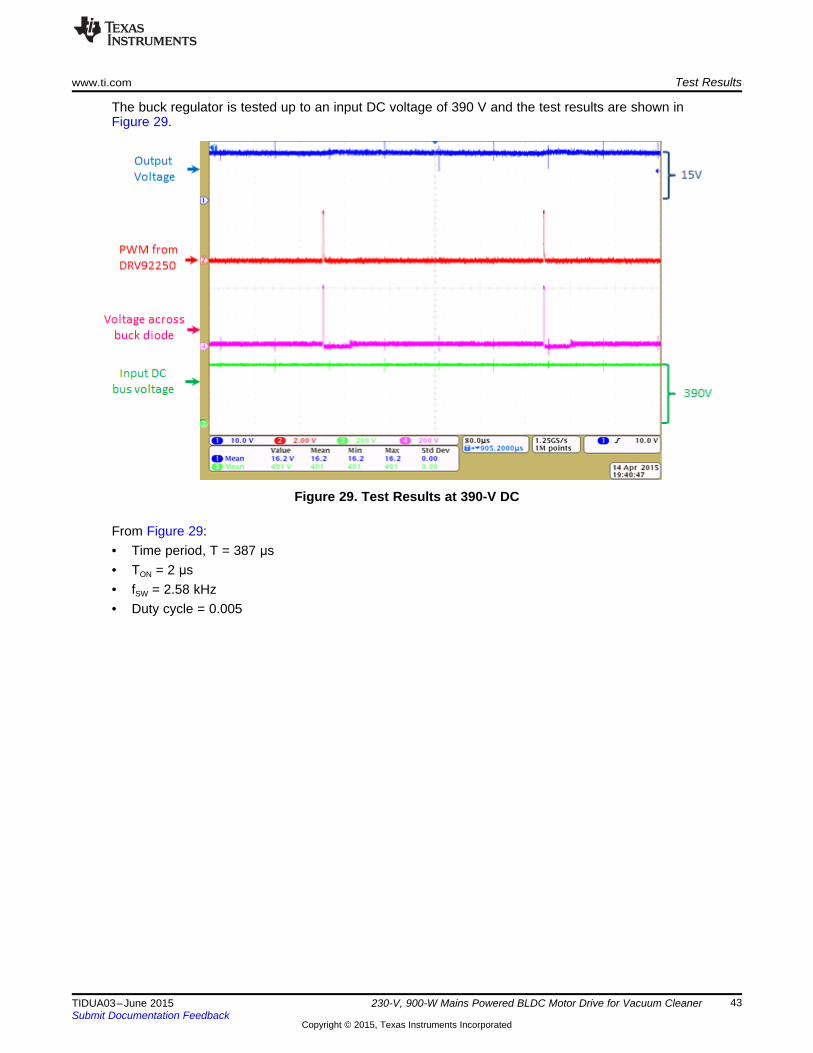
www.ti.com Test Results
The buck regulator is tested up to an input DC voltage of 390 V and the test results are shown inFigure 29.
Figure 29. Test Results at 390-V DC
From Figure 29:• Time period, T = 387 μs• TON = 2 μs• fSW = 2.58 kHz• Duty cycle = 0.005
43TIDUA03–June 2015 230-V, 900-W Mains Powered BLDC Motor Drive for Vacuum CleanerSubmit Documentation Feedback
Copyright © 2015, Texas Instruments Incorporated

Test Results www.ti.com
Figure 30 shows the start-up of the buck regulator. The test result shows that when the input DC voltage(VIN) is more than 75 V (approximately), the DRV92250 starts generating the PWM pulses at SWDR pin.
Figure 30. Start-up of Buck Converter and Voltage Build-up
44 230-V, 900-W Mains Powered BLDC Motor Drive for Vacuum Cleaner TIDUA03–June 2015Submit Documentation Feedback
Copyright © 2015, Texas Instruments Incorporated

www.ti.com Test Results
Figure 31 shows the voltage ripple in the 15-V output at 325-V DC input. The peak-to-peak ripple voltagepresent at the 15-V output is approximately 388 mV (for 30-mV hysteresis control).
Figure 31. Ripple Voltage at 15-V Supply
45TIDUA03–June 2015 230-V, 900-W Mains Powered BLDC Motor Drive for Vacuum CleanerSubmit Documentation Feedback
Copyright © 2015, Texas Instruments Incorporated

Test Results www.ti.com
8.2 Functional Tests of the DRV92250 Internal Voltage RegulatorThe VCC of the DRV92250 in this reference design is 15 V. The on-chip voltage regulators of theDRV92250 generates internal analog supply voltage 5 V, external analog supply voltage 5.35 V from the15 V. The internal linear regulators also generate 3.3 V and 1.9 V.
Figure 32 shows the reference voltage outputs of DRV92250. The regulated 5.35 V and the ripple areshown in Figure 33.
Figure 32. DRV92250 Voltage Regulator Output
Figure 33. Voltage Ripple at Regulated 5.35 V From DRV92250
46 230-V, 900-W Mains Powered BLDC Motor Drive for Vacuum Cleaner TIDUA03–June 2015Submit Documentation Feedback
Copyright © 2015, Texas Instruments Incorporated

www.ti.com Test Results
8.3 Functional Tests of IGBT Gate Driver UCC27714Figure 34 shows the PMM input to the UCC27714, which is fed from the DRV92250. In BLDC unipolartrapezoidal control, only the high-side is modulated at the PWM frequency (10 kHz in this design) in the120° ON period. The low side is continuously ON for 120°.
Figure 34. High-Side and Low-Side 120° Unipolar PWM Input to UCC27714 From DRV92250
47TIDUA03–June 2015 230-V, 900-W Mains Powered BLDC Motor Drive for Vacuum CleanerSubmit Documentation Feedback
Copyright © 2015, Texas Instruments Incorporated

Test Results www.ti.com
Figure 35 shows the low-side signal input and the corresponding low-side output of one UCC27714. Thesupply voltage for the low-side pre-driver of the DRV92250 is VCC, which is 15 V. That means the low-side PWM output from the DRV92250 will swing between ground and 15 V. The low-side gate output fromthe UCC27714 swings between ground and VCC of the UCC27714.
Figure 35. Low-Side PWM Input and Output of UCC27714
48 230-V, 900-W Mains Powered BLDC Motor Drive for Vacuum Cleaner TIDUA03–June 2015Submit Documentation Feedback
Copyright © 2015, Texas Instruments Incorporated

www.ti.com Test Results
Figure 36 shows the high-side signal input to UCC27714, the corresponding high-side output ofUCC27714 measured across the gate to emitter (VGE) of the IGBT and the corresponding phase voltagemeasured with respect to the board ground (DC minus). The supply voltage for the high-side pre-driver ofthe DRV92250 is V5P, which is 5.35 V. That means the high-side PWM output from the DRV92250 willswing between ground and 5.35 V. The gate-to-emitter voltage is equal to VDD of the UCC27714 minusthe voltage drop across the bootstrap diode of the high side driver in the UCC27714. The waveformsreveal that the VGE is approximately 14.4 V
Figure 36. High-Side PWM Input and Output of UCC27714
49TIDUA03–June 2015 230-V, 900-W Mains Powered BLDC Motor Drive for Vacuum CleanerSubmit Documentation Feedback
Copyright © 2015, Texas Instruments Incorporated

Test Results www.ti.com
8.4 Load TestsThe load test evaluates the performance of the three-phase inverter with load variation, load capacity, andthermal characteristics of the board. The inverter board is tested with a vacuum cleaner motor with thespecification as given in Table 7.
Table 7. Specification of Motor Used for Load Test
RATED VOLTAGE (V) RATED SPEED (RPM) RATED POWER (W) NOMINAL CURRENT (A)300-V DC 18000 900 3.75
Figure 37. Load Test Setup
Figure 37 shows the load setup. The winding terminals of the motor are connected to the phaseconnections terminals MU, MV, and MW of the inverter board. The Hall sensor 5-pin connector isconnected to the terminal J3 of the inverter board. Then, the inverter board and the AC-DC power supplyboards are connected using the interface connector J1. The system is tested with DC input supply up to390 V and also with AC supply from 195-V to 265-V AC with and without the PFC front end. The testresults are covered in the subsequent sections.
50 230-V, 900-W Mains Powered BLDC Motor Drive for Vacuum Cleaner TIDUA03–June 2015Submit Documentation Feedback
Copyright © 2015, Texas Instruments Incorporated

www.ti.com Test Results
Figure 38. Assembled Power Stage With Power Connections
The load test is done at the rated power of 900 W. Table 8 list the test results at 900-W power.
Table 8. Load Test Results at 900 W
PEAK-TO-PEAKRMS WINDING MOTOR SPEED DC INPUT POWERDC VOLTAGE (V) DC CURRENT (A) WINDINGCURRENT (A) (RPM) (W)CURRENT (A)324.4 2.76 3.76 15.4 15789 895.34
51TIDUA03–June 2015 230-V, 900-W Mains Powered BLDC Motor Drive for Vacuum CleanerSubmit Documentation Feedback
Copyright © 2015, Texas Instruments Incorporated

Test Results www.ti.com
Figure 39 shows the motor winding current and winding voltage measured with respect to DC minus. Thewinding voltage is switching at 10 kHz. Figure 40 shows the thermal image of the inverter board at 900 Wwhen operated from 325-V DC, with a heat sink having thermal resistance of 3°C/W. The heat sinktemperature at this power level is 72.4°C and the DRV92250 temperature is 53.6°C.
NOTE: All the temperature mentioned in the test results are absolute temperature. All the tests aredone at an ambient temperature of 25°C.
Figure 39. Load Test at 325-V DC, 900-W Input PowerMotor Winding Current and Winding Voltage Measured With Respect to DC Minus
Figure 40. Thermal Image of Load Test at 325-V DC, 900-W Input Power
52 230-V, 900-W Mains Powered BLDC Motor Drive for Vacuum Cleaner TIDUA03–June 2015Submit Documentation Feedback
Copyright © 2015, Texas Instruments Incorporated

www.ti.com Test Results
The load test is done with PFC front end as well. With PFC, the DC bus voltage is kept at 390 V and theload test is done up to 950-W input power. The test results are tabulated in Table 9.
Table 9. Load Test Results at 120% Overload
PEAK-TO-PEAKRMS WINDING MOTOR SPEED DC INPUT POWERDC VOLTAGE (V) DC CURRENT (A) WINDINGCURRENT (A) (RPM) (W)CURRENT (A)390 2.435 3.92 15 16484 950
Figure 41 shows the motor winding current and winding voltage measured with respect to DC minus at theabove test condition. Figure 42 shows the thermal image of the inverter board at 950 W when operatedfrom 390-V DC. The heat sink temperature at this power level is 76.3°C and the DRV92250 temperature is53.9°C.
Figure 41. Load Test at 390-V DC, 950-W Input PowerMotor Winding Current and Winding Voltage Measured With Respect to DC Minus
Figure 42. Thermal Image of Load Test at 390-V DC, 950-W Input Power
53TIDUA03–June 2015 230-V, 900-W Mains Powered BLDC Motor Drive for Vacuum CleanerSubmit Documentation Feedback
Copyright © 2015, Texas Instruments Incorporated
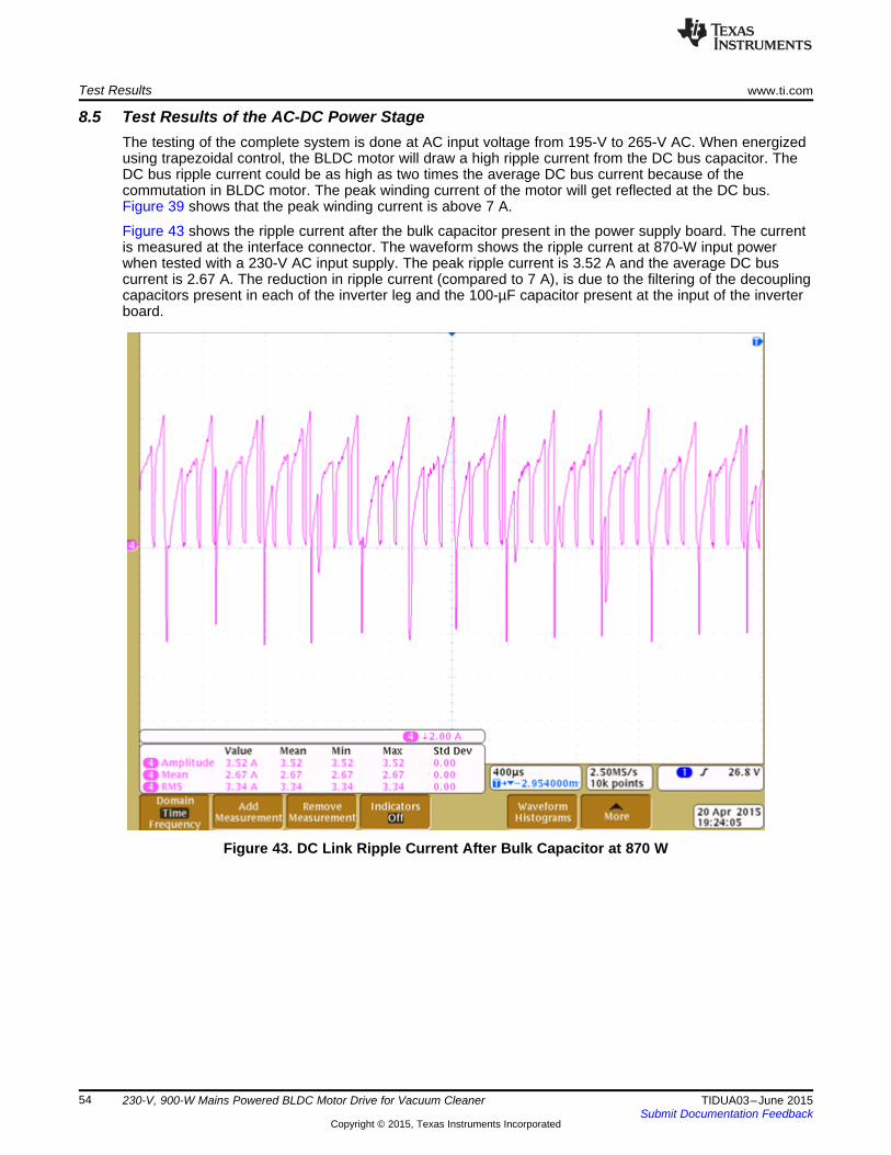
Test Results www.ti.com
8.5 Test Results of the AC-DC Power StageThe testing of the complete system is done at AC input voltage from 195-V to 265-V AC. When energizedusing trapezoidal control, the BLDC motor will draw a high ripple current from the DC bus capacitor. TheDC bus ripple current could be as high as two times the average DC bus current because of thecommutation in BLDC motor. The peak winding current of the motor will get reflected at the DC bus.Figure 39 shows that the peak winding current is above 7 A.
Figure 43 shows the ripple current after the bulk capacitor present in the power supply board. The currentis measured at the interface connector. The waveform shows the ripple current at 870-W input powerwhen tested with a 230-V AC input supply. The peak ripple current is 3.52 A and the average DC buscurrent is 2.67 A. The reduction in ripple current (compared to 7 A), is due to the filtering of the decouplingcapacitors present in each of the inverter leg and the 100-µF capacitor present at the input of the inverterboard.
Figure 43. DC Link Ripple Current After Bulk Capacitor at 870 W
54 230-V, 900-W Mains Powered BLDC Motor Drive for Vacuum Cleaner TIDUA03–June 2015Submit Documentation Feedback
Copyright © 2015, Texas Instruments Incorporated

www.ti.com Test Results
Figure 44 shows the current waveform at the output of the bridge rectifier that is before the DC bus bulkcapacitors. The testing is done at 870-W input power and 230-V AC, without using any DC chokes. Thebulk capacitor draws peak charging current. The peak current is 17 A and the average current is 2.65 A.
Figure 44. DC Link Ripple Current Before Bulk Capacitor at 870 W
Figure 45 shows the ripple voltage present at the DC bus capacitors at 900-W input power. The testing isdone with a 230-V AC input. The peak-to-peak ripple voltage at the DC bus is 21.6 V.
Figure 45. DC Bus Voltage Ripple at 900 W
55TIDUA03–June 2015 230-V, 900-W Mains Powered BLDC Motor Drive for Vacuum CleanerSubmit Documentation Feedback
Copyright © 2015, Texas Instruments Incorporated
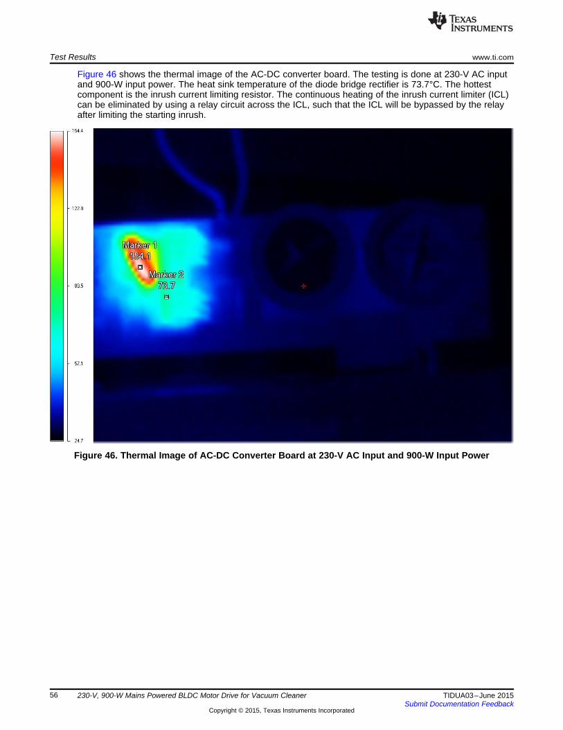
Test Results www.ti.com
Figure 46 shows the thermal image of the AC-DC converter board. The testing is done at 230-V AC inputand 900-W input power. The heat sink temperature of the diode bridge rectifier is 73.7°C. The hottestcomponent is the inrush current limiting resistor. The continuous heating of the inrush current limiter (ICL)can be eliminated by using a relay circuit across the ICL, such that the ICL will be bypassed by the relayafter limiting the starting inrush.
Figure 46. Thermal Image of AC-DC Converter Board at 230-V AC Input and 900-W Input Power
56 230-V, 900-W Mains Powered BLDC Motor Drive for Vacuum Cleaner TIDUA03–June 2015Submit Documentation Feedback
Copyright © 2015, Texas Instruments Incorporated

www.ti.com Test Results
8.6 Overcurrent Protection of DRV92250The overcurrent protection feature of the DRV92250 is tested at different current references. Theparameters as per Table 10 are set for current limit operation setting.
Table 10. Settings of DRV92250 for Current Limit Protection
REGISTER BIT BINARY SETTING REMARKSOCFromGPIO 0 On-chip voltage comparator for OC detectionTRKHSPWM 1 Number of pre-drivers disabled depends on HSDPWM
HSDPWM 1 Only the three high-side pre-drivers are disabledPreDrvHLD 0 Pulse skipping control
CURLIM [1:0] 0 Leading-edge current limit blanking interval = 800 nsIcompHys [1:0] 1 0-mV hysteresis control for OC comparator
DACB [7:0] 0x0D 8-bit reference for the current limit
A 20-mΩ sense resistor is used to detect the DC bus current. Figure 47 and Figure 48 show the currentlimit operation when the overcurrent reference is set at 3 A. Figure 48 shows a zoomed view of theovercurrent protection operation showing the PWM signals shut down when the current peak to the setcurrent reference. The PWM duty cycle was 75% and testing is done at 325 V. The high side PWM isimmediately pulled down whenever the current reaches the reference threshold. It can be seen that theovercurrent protection acts at around 3.5 A.
Figure 47. Overcurrent Protection at 3-A Peak Current
Figure 48. High-Side PWM Shut Down During Overcurrent Protection at 3-A Peak Current
57TIDUA03–June 2015 230-V, 900-W Mains Powered BLDC Motor Drive for Vacuum CleanerSubmit Documentation Feedback
Copyright © 2015, Texas Instruments Incorporated
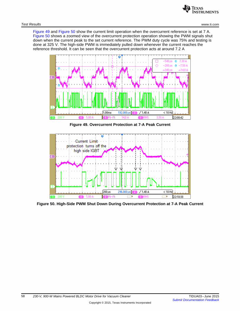
Test Results www.ti.com
Figure 49 and Figure 50 show the current limit operation when the overcurrent reference is set at 7 A.Figure 50 shows a zoomed view of the overcurrent protection operation showing the PWM signals shutdown when the current peak to the set current reference. The PWM duty cycle was 75% and testing isdone at 325 V. The high-side PWM is immediately pulled down whenever the current reaches thereference threshold. It can be seen that the overcurrent protection acts at around 7.2 A
Figure 49. Overcurrent Protection at 7-A Peak Current
Figure 50. High-Side PWM Shut Down During Overcurrent Protection at 7-A Peak Current
58 230-V, 900-W Mains Powered BLDC Motor Drive for Vacuum Cleaner TIDUA03–June 2015Submit Documentation Feedback
Copyright © 2015, Texas Instruments Incorporated

www.ti.com Test Results
8.7 Conducted Emission TestThis reference design has been tested for conducted emission as per EN55022 class B (EN55014) limits.During the test, the common mode choke L1 is replaced by the part 7448041104 from Wurth Electronics,which is a 4-mH, 11-A common mode filter and the gate resistors of the IGBTs are made to 20 Ω. Testresults are shown in Figure 52 and the board passes the result with a 5-dB margin.
Figure 51. Conducted Emission Test Setup
59TIDUA03–June 2015 230-V, 900-W Mains Powered BLDC Motor Drive for Vacuum CleanerSubmit Documentation Feedback
Copyright © 2015, Texas Instruments Incorporated

Test Results www.ti.com
Figure 52. Conducted Emission Results as per EN55022 Class BAverage and Peak Detector Output
60 230-V, 900-W Mains Powered BLDC Motor Drive for Vacuum Cleaner TIDUA03–June 2015Submit Documentation Feedback
Copyright © 2015, Texas Instruments Incorporated

www.ti.com Test Results
8.8 Surge and EFT TestSurge and EFT testing is done on the boards as per EN55014. The test condition and test results aretabulated in Table 11.
Table 11. Surge and EFT Test Result
REQUIREMENTS FOR RESIDENTIAL, PERFORMANCEBASIC STANDARD PORT COMMERCIAL AND LIGHT-INDUSTRIAL TEST RESULTCRITERIONENVIRONMENTSPassedIEC/EN 61000-4-4: AC input ±1 kV, 5 kHz B (Meeting performanceFast transients (burst) criterion A)PassedIEC/EN 61000-4-5: ±2-kV line to earth,AC input B (Meeting performanceSurge ±1-kV line to line criterion A)
Figure 53. Surge and EFT Test Setup
61TIDUA03–June 2015 230-V, 900-W Mains Powered BLDC Motor Drive for Vacuum CleanerSubmit Documentation Feedback
Copyright © 2015, Texas Instruments Incorporated
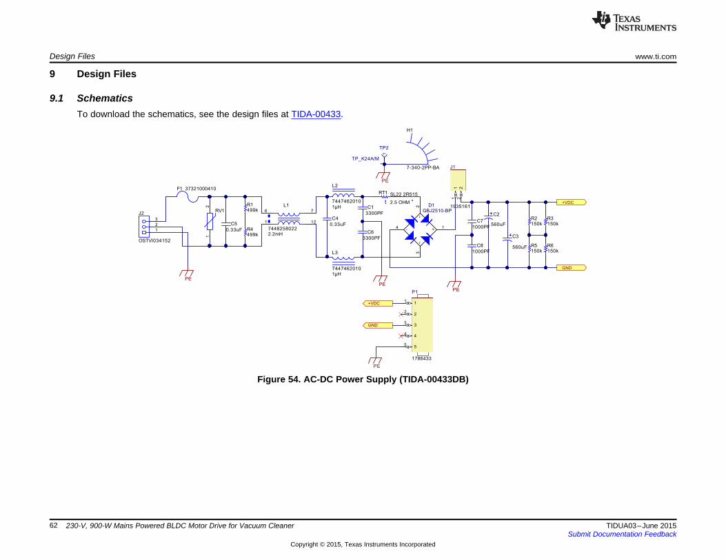
PEPE
+VDC
~3
+1
~2
-4
D1GBJ2510-BP
12
RV1
2.2mH
1 12
76
L1
74482580221
2
3
J2
OSTVI034152
11
22
J1
1935161
560uF
C2
560uF
C3
0.33uF
C5
3300PF
C6
0.33uF
C43300PF
C1
PE
11
TP2
TP_K24A/M
H1
7-340-2PP-BA
499kR1
150kR5
1µH
L2
7447462010
499kR4
150kR6
150kR2
150kR3
1µH
L3
7447462010
1000PF
C7
1000PF
C8
PE
PE
+VDC
GND
GND
11
22
33
44
55
P1
1786433
2.5 OHMt °
RT1 SL22 2R515
F1 37321000410
Design Files www.ti.com
9 Design Files
9.1 SchematicsTo download the schematics, see the design files at TIDA-00433.
Figure 54. AC-DC Power Supply (TIDA-00433DB)
62 230-V, 900-W Mains Powered BLDC Motor Drive for Vacuum Cleaner TIDUA03–June 2015Submit Documentation Feedback
Copyright © 2015, Texas Instruments Incorporated

+VDC
GND
U_TOP
U_BOT
V_TOP
V_BOT
W_TOP
W_BOT
HI1
LI2
VSS3
NC/EN4
COM5
LO6
VDD7
NC8
NC9
NC10
HS11
HO12
HB13
NC14
U2
UCC27714D14
GND
GND
HI1
LI2
VSS3
NC/EN4
COM5
LO6
VDD7
NC8
NC9
NC10
HS11
HO12
HB13
NC14
U3
UCC27714D14
GND
GND
HI1
LI2
VSS3
NC/EN4
COM5
LO6
VDD7
NC8
NC9
NC10
HS11
HO12
HB13
NC14
U4
UCC27714D14
GND
GND
PWM_U_TOP
PWM_U_BOT
PWM_V_TOP
U_TOP
V_TOP
W_TOP
V_BOT
U_BOT
W_BOT
VCC_15V
VCC_15V
VCC_15V
D9
US1M-13-F
D10
US1M-13-F
D11
US1M-13-F
VCC_15V
VCC_15V
1µF
C34
1µFC35
1µF
C33
3.3
R54
3.3
R49
3.3
R62
20.0kR57
20.0kR51
20.0kR53
20.0kR59
20.0kR64
20.0kR66
0.1µFC32
0.1µFC31
0.1µFC30
GNDGNDGND
CS
P
1
2
3
J7
OSTVI034152
PHU
PHV
PHW
PHU PHV PHW
PHU
PHV
PHW
GND
GND
GND
GND
VCC_15V
PWM_V_BOT
GND
GND
PWM_W_TOP
PWM_W_BOT
2200pFC40DNP
2200pFC41DNP
2200pFC45DNP
2200pFC46DNP
2200pFC50DNP
2200pFC51DNP
0.1µFC38
0.1µFC43
0.1µFC48
EMT_U EMT_V EMT_W
EMT_U
EMT_U
EN
EN
EN
EMT_V
EMT_V
EMT_W
EMT_W
D17
1N5819HW-7-F
5.1
R65
5.1
R72
5.1
R78
3.3
R58
D18
1N5819HW-7-F
3.3
R68
5.1
R67
5.1
R74
5.1
R80
D19
1N5819HW-7-F
3.3
R70
D20
1N5819HW-7-F
3.3
R73
D21
1N5819HW-7-F
3.3
R76
D22
1N5819HW-7-F
3.3
R79
2
1
3
Q7
FGP20N60UFDTU
2
1
3
Q10FGP20N60UFDTU
2
1
3
Q5
FGP20N60UFDTU
2
1
3
Q8FGP20N60UFDTU
2
1
3
Q6
FGP20N60UFDTU
2
1
3
Q9FGP20N60UFDTU
CS
N
68pF
C17
100R25
100R26
51.1
R56
51.1
R63
51.1
R69
51.1
R71
51.1
R75
51.1
R77
220pFC37
220pFC39
220pFC42
220pFC44
220pFC47
220pFC49
1µF
C55
1µF
C56
1µF
C57
5.11
R90
5.11
R91
5.11
R92
0.02
R55
www.ti.com Design Files
Figure 55. Gate Driver and Three Phase Inverter (TIDA-00433MB)
63TIDUA03–June 2015 230-V, 900-W Mains Powered BLDC Motor Drive for Vacuum CleanerSubmit Documentation Feedback
Copyright © 2015, Texas Instruments Incorporated

P4.5
1
P4.6
2
VD
D3
P4.7
4
P4.1
/TA
1C
LK
5
P4.0
/TA
0C
LK
6
P2.0
/TB
0.0
7
P1.5
/TA
3.0
8
P1.6
/TA
4.0
9
P3.4
/UC
B0S
TE
/UC
A0C
LK
10
RS
TB
/NM
I/S
BW
TD
IO11
TE
ST
/SB
WT
CK
12
P3.513
P3.614
GND(DV)15
US/ADC1316
VS/ADC1217
WS/ADC1118
COMMON/ADC1019
V3P3A20
CSN21
CSP22
ADC9/PA2.023
TACH/PA2 .124
V5
P2
5
VC
C2
6
UL
DR
27
UH
DR
28
VL
DR
29
VH
DR
30
WL
DR
/PA
2.3
31
WH
DR
/PA
2.2
32
GN
D3
3
SW
DR
34
ST
_B
IAS
35
FD
BK
36
ADC8/PA1.437
ADC7/PA1.538
ADC6/UTX/PA1.639
ADC5/URX/PA1.740
ADC4/PA1.841
HS3/ADC3/PA1.942
HS2/ADC2/PA1.1043
HS1/ADC1/PA1.1144
V3P3D(DVCC)45
P1.2/TA3.246
P1.7/TA4.247
P2.7/TBOCLK48
PWPD49
U1DRV92250PHP
1
2
3
4
5
J3
HEADER_1X5
1
2
3
4
J4
HEADER_1X4
PHU
PHV
PHW
GND
GND
GND
GND GND
+VDC
GND
PW
M_W
_T
OP
PW
M_W
_B
OT
PW
M_V
_T
OP
PW
M_V
_B
OT
PW
M_
U_T
OP
PW
M_
U_B
OT
GND
GND
GND
EXT_12V
GND
GND
V5P
V5P
GND
150k
R22
100k
R23
0.1µFC15
10µFC21
10µFC25
10µFC12
10µFC10
150kR32 150kR33 150kR34
150kR36 150kR37 150kR38
150kR39 150kR40 150kR41
3.3kR27
3.3kR28
3.3kR29
1.00k
R30
1.00k
R31
1.00k
R35
1000pFC18
1000pFC19
1000pFC20
GND
V5P
0.1µFC22DNP
0.1µFC23DNP
0.1µFC24DNP
GND
GND
PA2_0/ADC9
V5P
1.0MegR18
PA2_0/ADC9
V3P3
SPEED CONTROL
ST_BIAS
SWDR
FDBK
VCC_15V
V5
P
GND
GND
V3P
3
P1.7
P1.7
EXTERNAL SUPPLY FOR PROGRAMMING
0.1µFC16
1
2
J6
HEADER_1X2
1 2
J2HEADER_1X2
VDD3
OUT2
GND1
U6
LMT84LP
V3P
3
V5P
0.1µF
C28
GND
TEMP_SENSE
TEMP_SENSE
EX
T_1
2V
20k
R173386P-1-203LF
24.9kR16
GND
GND
V3P
3
P1.2
ON_OFF CONTROL
2
1
3
S1
B12AP
P1.2
GND
0.1µFC36
CSP
CSN
0.01µFC27
V3P3
V5
P
1
2
J5
800-10-002-10-001000
10.0kR85
1.00k
R84DNP
1000pFC53DNP
GND
EN
D5
NS
R0
24
0V
2T
1G
D6
NS
R0
24
0V
2T
1G
D7
NS
R0
24
0V
2T
1G
D3 NSR0240V2T1G
GND
GND
GND
V3P
3
P1.61
2
J8
800-10-002-10-001000
10.0kR86
P1.6
0.1µFC14
0.1µFC13
0.1µFC11
0.1µFC26
47kR48
1.00k
R52
5.90kR45
5.90kR46
5.90kR47
5.11kR87
5.11kR88
5.11kR89
TextTextText
0.01µFC54
0.01µFC52
0.01µFC29
V3P
3
PFC-ON
INRUSH
5K R93
VCC_15V
Green
12
D23
GND
3
1
2
Q13BSS84-7-F
0.1µF
C60
10.0kR96
P3.5
D24
1N5819HW-7-F
499k
R19
499k
R20
499k
R21
19.6kR24
Design Files www.ti.com
Figure 56. DRV92250 Controller and Feedbacks (TIDA-00433MB)
64 230-V, 900-W Mains Powered BLDC Motor Drive for Vacuum Cleaner TIDUA03–June 2015Submit Documentation Feedback
Copyright © 2015, Texas Instruments Incorporated

POWER SUPPLY
GND
GND
3
1
2
Q1MMBT3904
SWDR
GND GND
+VDC
VCC
1.00kR11
DNP
200
R10
0.01µFC2
22pFC6DNP
2200pFC9
100
R9
1000pFC4
0.1µFC7
ST_BIAS
FDBK
174kR1
174kR3
174kR8
0.022µFC8
10µFC3
1.00kR7
DNP
+VDC
GND
GND
VCC_15V
V5P
5.11kR61
Yellow
12
D12
18V
D15
MMSZ5248B-7-F1.00k
R503
12
Q11MMBT3904
GND
VCC_15V
5.1V
D14MMSZ4689T1G
DNP
D1MURA160T3G
L2
TSL1315RA-102JR78-PF
L1
SLF10145T-471MR47-PF
3
1
2
Q3FMMT459TA
2
1
34
Q4FZT560TA
D2
B180-13-F
DNP
3
2 1
U5TL431ACDBZR
+V
DC
GND
2.2kR81
2.2kR43 1
3 2
4
Q12
TR-PZT2907A
VCC VCC_15V
1.00kR13
DNP 1.00kR14
4.87k
R2
15.0
R4
499
R6130kR5
12.4k
R12
0.1µFC1
2.0k
R15DNP
47 µFC5
TextText
Red
12
D13
PE
1
2
3
4
5
J1
175727115 µFC58
4
1
2
3
J9
800-10-004-10-001000
VCC_15V
GND
1µFC59
PFC-ON
INRUSH
10.0kR94
10.0kR95
V3P3
V3P3
4
1
3
Q2FQD3P50TM
GND
3
1
2
Q14BSS84-7-F
10.0kR97
GND
P3
.5V
3P
3
499kR42
499kR44
499kR82
64.9kR83
10.0kR60
www.ti.com Design Files
Figure 57. Bias Power Supply (15-V) (TIDA-00433MB)
65TIDUA03–June 2015 230-V, 900-W Mains Powered BLDC Motor Drive for Vacuum CleanerSubmit Documentation Feedback
Copyright © 2015, Texas Instruments Incorporated

Design Files www.ti.com
9.2 Bill of MaterialsTo download the bill of materials (BOM), see the design files at TIDA-00433.
9.2.1 TIDA-00433DB
Table 12. TIDA-00433DB BOM
MANUFACTURERQTY REFERENCE PART DESCRIPTION MANUFACTURER PCB FOOTPRINT NOTEPARTNUMBER1 !PCB1 Printed Circuit Board Any TIDA-00433DB-E2 Fitted
CAP CER 3300PF 300VAC 20%2 C1, C6 Kemet C947U332MZWDBA7317 FittedRADIALCAP, ALUMINUM, 560 uF, 450V,2 C2, C3 NICHICON LGN2W561MELC50 Fitted20%, THCAP FILM 0.33UF 630VDC2 C4, C5 EPCOS(TDK) B32922C3334M189 FittedRADIALCAP CER 1000PF 300VAC 20%2 C7, C8 Kemet C907U102MZVDBA7317 FittedRADIALRECT BRIDGE GPP 25A 1000V MICRO COMMERCIAL1 D1 GBJ2510-BP FittedGBJ COMPONENTSFUSE BOARD MNT 10A 250VAC1 F1 Littelfuse Inc 37321000410 Radial, Can, Vertical FittedRADIALHEATSINK PWR DUAL BLACK CTS Thermal Management1 H1 7-340-2PP-BA TO-220 Heat Sink FittedTO-220 ProductsMACHINE SCREW PAN4 H2, H3, H4, H5 Keystone Electronics 29344 Screw FittedSLOTTED M3TERM BLOCK PCB, 2POS,1 J1 PHOENIX CONTACT 1935161 Fitted5.0MM, THTERMINAL BLOCK 7.50MM1 J2 On-Shore Technology OSTVI034152 Fitted3POS PCB, THFILTER, WE-CMB COMMON
1 L1 MODE POWER LINE CHOKE, Wurth Elektronics 7448258022 Fitted2.2mH, 8A, VERTICALInductor, Unshielded Drum Core,2 L2, L3 Wurth Elektronik eiSos 7447462010 D6 x 8.5mm FittedFerrite, 1uH, 8A, 0.006 ohm, THTERM BLOCK HDR 5POS R/A1 P1 PHOENIX CONTACT 1786433 Fitted5.08MM
2 R1, R4 RES, 499k ohm, 1%, 0.25W, 1206 Vishay-Dale CRCW1206499KFKEA 1206 Fitted4 R2, R3, R5, R6 RES, 150k ohm, 1%, 0.25W, 1206 Vishay-Dale CRCW1206150KFKEA 1206 Fitted
CURRENT LIMITR INRSH 2.51 RT1 AMETHERM SL22 2R515 FittedOHM 15A
66 230-V, 900-W Mains Powered BLDC Motor Drive for Vacuum Cleaner TIDUA03–June 2015Submit Documentation Feedback
Copyright © 2015, Texas Instruments Incorporated

www.ti.com Design Files
Table 12. TIDA-00433DB BOM (continued)MANUFACTURERQTY REFERENCE PART DESCRIPTION MANUFACTURER PCB FOOTPRINT NOTEPARTNUMBER
VARISTOR, 387V, 8KA, DISC1 RV1 EPCOS Inc B72220S271K151 Fitted20MMPin, Thru Hole, Tin Plate, for1 TP2 Vector K24A/M 0.039 inch Fitted0.062 PCB'sHEX STANDOFF M3 ALUMINUM4 HEX STAND Keystone Electronics 24437 HEX STAND Fitted20MM
1 HEX NUT HEX NUT 0.217" STEEL M3 Keystone Electronics 4708 HEX NUT Fitted
9.2.2 TIDA-00433MB
Table 13. TIDA-00433MB
MANUFACTURERQTY REFERENCE PART DESCRIPTION MANUFACTURER PCB FOOTPRINT NOTEPARTNUMBER1 !PCB1 Printed Circuit Board Any TIDA-00433MB-E2 Fitted
CAP, CERM, 0.1 µF, 630 V, +/-4 C1, C30, C31, C32 MuRata GRM43DR72J104KW01L 1812 Fitted10%, X7R, 1812CAP, CERM, 10uF, 16V, +/-20%,4 C10, C12, C21, C25 TDK Corporation C2012X5R1C106M085AC 0805 FittedX5R, 0805CAP, CERM, 0.1 µF, 25 V, +/- 10%,3 C11, C13, C28 AVX 06033C104KAT2A 0603 FittedX7R, 0603CAP, CERM, 0.1uF, 16V, +/-5%,4 C14, C15, C36, C60 AVX 0603YC104JAT2A 0603 FittedX7R, 0603CAP, CERM, 0.1uF, 25V, +/-10%,1 C16 AVX 08053C104KAT2A 0805 FittedX7R, 0805CAP, CERM, 68pF, 50V, +/-5%,1 C17 AVX 06035A680JAT2A 0603 FittedC0G/NP0, 0603CAP, CERM, 1000 pF, 50 V, +/-3 C18, C19, C20 TDK C1608X7R1H102K080AE 0603 Fitted10%, X7R, 0603CAP, CERM, 0.01uF, 500V, +/-10%,1 C2 Vishay-Vitramon VJ1812Y103KXEAT 1812 FittedX7R, 1812CAP, CERM, 0.1 µF, 25 V, +/- 10%,1 C26 Kemet C0603C104K3RACTU 0603 FittedX7R, 0603CAP, CERM, 0.01uF, 100V, +/-10%,4 C27, C29, C52, C54 AVX 06031C103KAT2A 0603 FittedX7R, 0603
1 C3 CAP, AL, 10 µF, 400 V, +/- 20%, TH Nichicon UCS2G100MPD1TD RCAP, TH, 10 x 20mm FittedC33, C34, C35, C55, C56, CAP, CERM, 1uF, 25V, +/-10%,6 MuRata GRM21BR71E105KA99L 0805 FittedC57 X7R, 0805
67TIDUA03–June 2015 230-V, 900-W Mains Powered BLDC Motor Drive for Vacuum CleanerSubmit Documentation Feedback
Copyright © 2015, Texas Instruments Incorporated

Design Files www.ti.com
Table 13. TIDA-00433MB (continued)MANUFACTURERQTY REFERENCE PART DESCRIPTION MANUFACTURER PCB FOOTPRINT NOTEPARTNUMBER
C37, C39, C42, C44, C47, CAP, CERM, 220 pF, 50 V, +/- 1%,6 TDK C1608C0G1H221J080AA 0603 FittedC49 C0G/NP0, 0603CAP, CERM, 0.1 µF, 25 V, +/- 10%,3 C38, C43, C48 MuRata GRM21BR71E104KA01L 0805 FittedX7R, 0805CAP, CERM, 1000pF, 25V, +/-10%,1 C4 MuRata GRM188R71E102KA01D 0603 FittedX7R, 0603
1 C5 CAP ALUM 47UF 25V 20% RADIAL Kemet ESY476M025AC3EA 5.0x9.0mm FittedCAP ALUM 100UF 400V 20%1 C58 Nichicon UPZ2G101MNY9 12.5x20 FittedRADIALCAP, CERM, 1uF, 50V, +/-10%,1 C59 Taiyo Yuden UMK212F105ZG-T 0805 FittedX7R, 0805CAP, CERM, 0.1uF, 25V, +/-5%,1 C7 AVX 06033C104JAT2A 0603 FittedX7R, 0603CAP, CERM, 0.022 µF, 25 V, +/-1 C8 Kemet C0603C223K3RACTU 0603 Fitted10%, X7R, 0603CAP, CERM, 2200pF, 100V, +/-1 C9 TDK C1608X7R2A222K 0603 Fitted10%, X7R, 0603
1 D1 Diode, Ultrafast, 600V, 1A, SMA ON Semiconductor MURA160T3G SMA Fitted1 D12 LED YELLOW CLEAR 1206 SMD Stanley Electric Co., LTD HAY1105W-TR 1.6x1.85x3.2 Fitted1 D13 LED, Red, SMD Stanley Electric Co., LTD HBR1105W-TR 1.6x1.85x3.2 Fitted
Diode, Zener, 18V, 500 mW, SOD-1 D15 Diodes Inc. MMSZ5248B-7-F SOD-123 Fitted123D17, D18, D19, D20, D21,7 Diode, Schottky, 40V, 1A, SOD-123 Diodes Inc. 1N5819HW-7-F SOD-123 FittedD22, D24
1 D23 LED GREEN CLEAR 1206 SMD Stanley Electric Co., LTD HPG1105W-TR 1.6x1.85x3.2 FittedDIODE SCHOTTKY 40V 250MA4 D3, D5, D6, D7 ON Semiconductor NSR0240V2T1G SOD-523 FittedSOD523
3 D9, D10, D11 Diode, Ultrafast, 1000V, 1A, SMA Diodes Inc. US1M-13-F SMA FittedTERM BLOCK HDR 5POS R/A1 J1 Phoenix Contact 1757271 17.24x8.6x12mm Fitted5.08MM
4 J2,J5,J6, J8 Header, Male 2-pin, 100mil spacing, Wurth Electronics Inc 61300211121 0.100 inch x 2 Fitted1 J3 Header, Male 5-pin, 100mil spacing, Wurth Electronics Inc 61300511121 0.100 inch x 5 Fitted2 J4,J9 Header, Male 4-pin, 100mil spacing, Wurth Electronics Inc 61300411121 0.100 inch x 4 Fitted
TERMINAL BLOCK 7.50MM 3POS1 J7 On-Shore Technology OSTVI034152 FittedPCB, THInductor, Shielded Drum Core,
1 L1 Ferrite, 470uH, 0.47A, 1.03 ohm, TDK SLF10145T-471MR47-PF SLF10145 FittedSMD
68 230-V, 900-W Mains Powered BLDC Motor Drive for Vacuum Cleaner TIDUA03–June 2015Submit Documentation Feedback
Copyright © 2015, Texas Instruments Incorporated

www.ti.com Design Files
Table 13. TIDA-00433MB (continued)MANUFACTURERQTY REFERENCE PART DESCRIPTION MANUFACTURER PCB FOOTPRINT NOTEPARTNUMBER
1 L2 FIXED IND 1MH 780MA 1 OHM TH TDK TSL1315RA-102JR78-PF 14x17mm Fitted2 Q1, Q11 Transistor, NPN, 40V, 0.2A, SOT-23 Fairchild Semiconductor MMBT3904 SOT-23 Fitted
Transistor, PNP, 60-V, 800-mA,1 Q12 Fairchild PZT2907A SOT-223 Fitted1000-mWMOSFET, P-CH, -50V, -0.13A,2 Q13, Q14 Diodes Inc. BSS84-7-F SOT-23 FittedSOT-23
1 Q2 MOSFET P-CH 500V 2.1A DPAK Fairchild Semiconductor FQD3P50TM DPAK FittedTRANSISTOE, NPN, 450V, 0.15A,1 Q3 DIODES INCORPORATED FMMT459TA FittedSOT23-3TRANSISTOR, PNP, 500V, 0.15A,1 Q4 DIODES INCORPORATED FZT560TA FittedSOT223IGBT Transistors 600V, 20A Field6 Q5, Q6, Q7, Q8, Q9, Q10 Fairchild Semiconductor FGP20N60UFDTU FittedStop
3 R1, R3, R8 RES, 174 k, 1%, 0.25 W, 1206 Yageo America RC1206FR-07174KL 1206 Fitted1 R10 RES, 200 ohm, 1%, 0.25W, 1206 Panasonic ERJ-8ENF2000V 1206 Fitted1 R12 RES, 12.4 k, 1%, 0.1 W, 0603 Vishay-Dale CRCW060312K4FKEA 0603 Fitted5 R14, R30, R31, R35, R52 RES, 1.00 k, 1%, 0.1 W, 0603 Vishay-Dale CRCW06031K00FKEA 0603 Fitted1 R16 RES, 24.9k ohm, 1%, 0.1W, 0603 Yageo America RC0603FR-0724K9L 0603 Fitted1 R17 TRIMMER, 20k ohm, 0.5W, TH Bourns 3386P-1-203LF 375x190x375mil Fitted1 R18 RES, 1.0Meg ohm, 5%, 0.1W, 0603 Vishay-Dale CRCW06031M00JNEA 0603 Fitted
R19, R20, R21, R32, R33,12 R34, R36, R37, R38, R39, RES, 150k ohm, 1%, 0.25W, 1206 Vishay-Dale CRCW1206150KFKEA 1206 Fitted
R40, R411 R2 RES, 4.87 k, 1%, 0.1 W, 0603 Vishay-Dale CRCW06034K87FKEA 0603 Fitted1 R22 RES, 150k ohm, 5%, 0.1W, 0603 Vishay-Dale CRCW0603150KJNEA 0603 Fitted1 R23 RES, 100k ohm, 1%, 0.1W, 0603 Vishay-Dale CRCW0603100KFKEA 0603 Fitted4 R24, R45, R46, R47 RES, 5.90 k, 1%, 0.1 W, 0603 Vishay-Dale CRCW06035K90FKEA 0603 Fitted2 R25, R26 RES, 100, 1%, 0.1 W, 0603 Vishay-Dale CRCW0603100RFKEA 0603 Fitted3 R27, R28, R29 RES, 3.3 k, 5%, 0.1 W, 0603 Vishay-Dale CRCW06033K30JNEA 0603 Fitted1 R4 RES, 15.0, 1%, 0.1 W, 0603 Vishay-Dale CRCW060315R0FKEA 0603 Fitted3 R42, R44, R82 RES, 499 k, 1%, 0.25 W, 1206 Panasonic ERJ-8ENF4993V 1206 Fitted2 R43, R81 RES, 2.2 k, 5%, 0.1 W, 0603 Vishay-Dale CRCW06032K20JNEA 0603 Fitted1 R48 RES, 47k ohm, 5%, 0.1W, 0603 Vishay-Dale CRCW060347K0JNEA 0603 Fitted3 R49, R54, R62 RES, 3.3 ohm, 5%, 0.25W, 1206 Vishay-Dale CRCW12063R30JNEA 1206 Fitted1 R5 RES, 130 k, 1%, 0.1 W, 0603 Yageo America AC0603FR-07130KL 0603 Fitted
69TIDUA03–June 2015 230-V, 900-W Mains Powered BLDC Motor Drive for Vacuum CleanerSubmit Documentation Feedback
Copyright © 2015, Texas Instruments Incorporated
Design Files www.ti.com
Table 13. TIDA-00433MB (continued)MANUFACTURERQTY REFERENCE PART DESCRIPTION MANUFACTURER PCB FOOTPRINT NOTEPARTNUMBER
1 R50 RES, 1.00 k, 1%, 0.25 W, 1206 Vishay-Dale CRCW12061K00FKEA 1206 FittedR51, R53, R57, R59, R64,6 RES, 20.0k ohm, 1%, 0.1W, 0603 Vishay-Dale CRCW060320K0FKEA 0603 FittedR66
1 R55 RES, 0.02, 1%, 3 W, 2512 Bourns CRA2512-FZ-R020ELF 2512 FittedR56, R63, R69, R71, R75,6 RES, 51.1, 1%, 0.1 W, 0603 Vishay-Dale CRCW060351R1FKEA 0603 FittedR77R58, R68, R70, R73, R76,6 RES, 3.3 ohm, 5%, 0.125W, 0805 Vishay-Dale CRCW08053R30JNEA 0805 FittedR79
1 R6 RES, 499, 1%, 0.1 W, 0603 Yageo America RC0603FR-07499RL 0603 FittedR60, R85, R86, R93, R94,8 RES, 10.0k ohm, 1%, 0.1W, 0603 Yageo America RC0603FR-0710KL 0603 FittedR95, R96, R97
4 R61, R87, R88, R89 RES, 5.11 k, 0.5%, 0.1 W, 0603 Yageo America RC0603FR-075K11L 0603 FittedR65, R67, R72, R74, R78,6 RES, 5.1 ohm, 5%, 0.125W, 0805 Vishay-Dale CRCW08055R10JNEA 0805 FittedR80
1 R83 RES, 64.9 k, 1%, 0.1 W, 0603 Vishay-Dale CRCW060364K9FKEA 0603 Fitted1 R9 RES, 100 ohm, 1%, 0.1W, 0603 Yageo America RC0603FR-07100RL 0603 Fitted3 R90, R91, R92 RES, 5.11, 1%, 0.1 W, 0603 Yageo America RC0603FR-075R11L 0603 Fitted
SWITCH TOGGLE SPDT 0.4VA1 S1 NKK Switches B12AP 6.8x23.1x8.8mm Fitted28VIC, Voltage Brushless DC (BLDC)1 U1 Texas Instruments DRV92250PHP HTQFP-48 FittedMotor ControllerHigh-Speed Low-side Gate Driver3 U2, U3, U4 Texas Instruments UCC27714D14 D0014A FittedDevice, D0014AAdjustable Precision ShuntRegulator, 34 ppm / degC, 100 mA,1 U5 Texas Instruments TL431ACDBZR DBZ0003A Fitted0 to 70 degC, 3-pin SOT-23 (DBZ),Green (RoHS & no Sb/Br)IC, TEMP SENSOR PREC ANLG,1 U6 Texas Instruments LMT84LP LP FittedTO-92, ROHSCAP, CERM, 0.1 µF, 25 V, +/- 10%,0 C22, C23, C24 AVX 06033C104KAT2A 0603 Not FittedX7R, 0603
C40, C41, C45, C46, C50, CAP, CERM, 2200 pF, 25 V, +/-0 MuRata GRM188R71E222KA01D 0603 Not FittedC51 10%, X7R, 0603CAP, CERM, 1000 pF, 50 V, +/-0 C53 TDK C1608X7R1H102K 0603 Not Fitted10%, X7R, 0603CAP, CERM, 22pF, 100V, +/-5%,0 C6 AVX 12061A220JAT2A 1206 Not FittedC0G/NP0, 1206
70 230-V, 900-W Mains Powered BLDC Motor Drive for Vacuum Cleaner TIDUA03–June 2015Submit Documentation Feedback
Copyright © 2015, Texas Instruments Incorporated

www.ti.com Design Files
Table 13. TIDA-00433MB (continued)MANUFACTURERQTY REFERENCE PART DESCRIPTION MANUFACTURER PCB FOOTPRINT NOTEPARTNUMBER
Diode, Zener, 5.1V, 500 mW, SOD-0 D14 ON Semiconductor MMSZ4689T1G SOD-123 Not Fitted1230 D2 Diode, Schottky, 80V, 1A, SMA Diodes Inc. B180-13-F SMA Not Fitted0 R13, R84 RES, 1.00 k, 1%, 0.1 W, 0603 Vishay-Dale CRCW06031K00FKEA 0603 Not Fitted0 R15 RES, 2.0 k, 5%, 0.1 W, 0603 Vishay-Dale CRCW06032K00JNEA 0603 Not Fitted0 R7, R11 RES, 1.00k ohm, 1%, 0.25W, 1206 Vishay-Dale CRCW12061K00FKEA 1206 Not Fitted
FISCHER ELEKTRONIK SK 81/ 501 HEAT SINK FISCHER ELEKTRONIK SK 81/ 50 SA HEAT SINK FittedSA HEAT SINK, EXTRUDEDMACHINE SCREW PAN SLOTTED4 H4, H5, H6, H7 Keystone Electronics 29316 Screw FittedM3HEX STANDOFF M3 ALUMINUM4 HEX STAND Keystone Electronics 24437 HEX STAND Fitted20MMMAX CLIP TO-220/MAX2206 CLIP-TO220 Aavid Thermalloy MAX07NG CLIP-TO220 FittedSCREW-MNTMACHINE SCREW PAN SLOTTED6 MACHINE SCREW Keystone Electronics 29316 Screw FittedM3
71TIDUA03–June 2015 230-V, 900-W Mains Powered BLDC Motor Drive for Vacuum CleanerSubmit Documentation Feedback
Copyright © 2015, Texas Instruments Incorporated

Design Files www.ti.com
9.3 Layer PlotsTo download the layer plots, see the design files at TIDA-00433.
9.4 Altium ProjectTo download the Altium project files, see the design files at TIDA-00433.
9.5 Gerber FilesTo download the Gerber files, see the design files at TIDA-00433.
9.6 Assembly DrawingsTo download the assembly drawings, see the design files at TIDA-00433.
10 References
1. Texas Instruments, Highly Integrated High Voltage Brushless DC (BLDC) Motor Controller, DRV92250Datasheet
2. Texas Instruments, UCC27714 High-Speed, 600-V High-Side Low-Side Gate Driver with 4A PeakOutput, Datasheet (SLUSBY6)
3. Texas Instruments, Sensorless Trapezoidal Control of BLDC Motors, Application Report (SPRABQ7)
11 Terminology
SPI— Serial Peripheral Interface
PWM— Pulse Width Modulation
BLDC— Brushless DC motor
MCU— Microcontroller unit
FETs, MOSFETs—Metal–oxide–semiconductor field-effect transistor
IGBT— Insulated Gate Bipolar Transistor
ESD— Electrostatic Discharge
RPM— Rotation per Minute
RMS— Root Mean Square
12 About the AuthorMANU BALAKRISHNAN is a systems engineer at Texas Instruments where he is responsible fordeveloping subsystem design solutions for the Industrial Motor Drive segment. Manu brings to this role hisexperience in power electronics, analog and mixed signal designs. He has system level product designexperience in permanent magnet motor drives. Manu earned his bachelor of technology in electrical andelectronics engineering from the University of Kerala and his master of technology in power electronicsfrom National Institute of Technology Calicut, India.
72 230-V, 900-W Mains Powered BLDC Motor Drive for Vacuum Cleaner TIDUA03–June 2015Submit Documentation Feedback
Copyright © 2015, Texas Instruments Incorporated

IMPORTANT NOTICE FOR TI REFERENCE DESIGNS
Texas Instruments Incorporated ("TI") reference designs are solely intended to assist designers (“Buyers”) who are developing systems thatincorporate TI semiconductor products (also referred to herein as “components”). Buyer understands and agrees that Buyer remainsresponsible for using its independent analysis, evaluation and judgment in designing Buyer’s systems and products.TI reference designs have been created using standard laboratory conditions and engineering practices. TI has not conducted anytesting other than that specifically described in the published documentation for a particular reference design. TI may makecorrections, enhancements, improvements and other changes to its reference designs.Buyers are authorized to use TI reference designs with the TI component(s) identified in each particular reference design and to modify thereference design in the development of their end products. HOWEVER, NO OTHER LICENSE, EXPRESS OR IMPLIED, BY ESTOPPELOR OTHERWISE TO ANY OTHER TI INTELLECTUAL PROPERTY RIGHT, AND NO LICENSE TO ANY THIRD PARTY TECHNOLOGYOR INTELLECTUAL PROPERTY RIGHT, IS GRANTED HEREIN, including but not limited to any patent right, copyright, mask work right,or other intellectual property right relating to any combination, machine, or process in which TI components or services are used.Information published by TI regarding third-party products or services does not constitute a license to use such products or services, or awarranty or endorsement thereof. Use of such information may require a license from a third party under the patents or other intellectualproperty of the third party, or a license from TI under the patents or other intellectual property of TI.TI REFERENCE DESIGNS ARE PROVIDED "AS IS". TI MAKES NO WARRANTIES OR REPRESENTATIONS WITH REGARD TO THEREFERENCE DESIGNS OR USE OF THE REFERENCE DESIGNS, EXPRESS, IMPLIED OR STATUTORY, INCLUDING ACCURACY ORCOMPLETENESS. TI DISCLAIMS ANY WARRANTY OF TITLE AND ANY IMPLIED WARRANTIES OF MERCHANTABILITY, FITNESSFOR A PARTICULAR PURPOSE, QUIET ENJOYMENT, QUIET POSSESSION, AND NON-INFRINGEMENT OF ANY THIRD PARTYINTELLECTUAL PROPERTY RIGHTS WITH REGARD TO TI REFERENCE DESIGNS OR USE THEREOF. TI SHALL NOT BE LIABLEFOR AND SHALL NOT DEFEND OR INDEMNIFY BUYERS AGAINST ANY THIRD PARTY INFRINGEMENT CLAIM THAT RELATES TOOR IS BASED ON A COMBINATION OF COMPONENTS PROVIDED IN A TI REFERENCE DESIGN. IN NO EVENT SHALL TI BELIABLE FOR ANY ACTUAL, SPECIAL, INCIDENTAL, CONSEQUENTIAL OR INDIRECT DAMAGES, HOWEVER CAUSED, ON ANYTHEORY OF LIABILITY AND WHETHER OR NOT TI HAS BEEN ADVISED OF THE POSSIBILITY OF SUCH DAMAGES, ARISING INANY WAY OUT OF TI REFERENCE DESIGNS OR BUYER’S USE OF TI REFERENCE DESIGNS.TI reserves the right to make corrections, enhancements, improvements and other changes to its semiconductor products and services perJESD46, latest issue, and to discontinue any product or service per JESD48, latest issue. Buyers should obtain the latest relevantinformation before placing orders and should verify that such information is current and complete. All semiconductor products are soldsubject to TI’s terms and conditions of sale supplied at the time of order acknowledgment.TI warrants performance of its components to the specifications applicable at the time of sale, in accordance with the warranty in TI’s termsand conditions of sale of semiconductor products. Testing and other quality control techniques for TI components are used to the extent TIdeems necessary to support this warranty. Except where mandated by applicable law, testing of all parameters of each component is notnecessarily performed.TI assumes no liability for applications assistance or the design of Buyers’ products. Buyers are responsible for their products andapplications using TI components. To minimize the risks associated with Buyers’ products and applications, Buyers should provideadequate design and operating safeguards.Reproduction of significant portions of TI information in TI data books, data sheets or reference designs is permissible only if reproduction iswithout alteration and is accompanied by all associated warranties, conditions, limitations, and notices. TI is not responsible or liable forsuch altered documentation. Information of third parties may be subject to additional restrictions.Buyer acknowledges and agrees that it is solely responsible for compliance with all legal, regulatory and safety-related requirementsconcerning its products, and any use of TI components in its applications, notwithstanding any applications-related information or supportthat may be provided by TI. Buyer represents and agrees that it has all the necessary expertise to create and implement safeguards thatanticipate dangerous failures, monitor failures and their consequences, lessen the likelihood of dangerous failures and take appropriateremedial actions. Buyer will fully indemnify TI and its representatives against any damages arising out of the use of any TI components inBuyer’s safety-critical applications.In some cases, TI components may be promoted specifically to facilitate safety-related applications. With such components, TI’s goal is tohelp enable customers to design and create their own end-product solutions that meet applicable functional safety standards andrequirements. Nonetheless, such components are subject to these terms.No TI components are authorized for use in FDA Class III (or similar life-critical medical equipment) unless authorized officers of the partieshave executed an agreement specifically governing such use.Only those TI components that TI has specifically designated as military grade or “enhanced plastic” are designed and intended for use inmilitary/aerospace applications or environments. Buyer acknowledges and agrees that any military or aerospace use of TI components thathave not been so designated is solely at Buyer's risk, and Buyer is solely responsible for compliance with all legal and regulatoryrequirements in connection with such use.TI has specifically designated certain components as meeting ISO/TS16949 requirements, mainly for automotive use. In any case of use ofnon-designated products, TI will not be responsible for any failure to meet ISO/TS16949.IMPORTANT NOTICE
Mailing Address: Texas Instruments, Post Office Box 655303, Dallas, Texas 75265Copyright © 2015, Texas Instruments Incorporated