![Tulkintoja olennaisesti kiistellyistä käsitteistä [Final draft]](https://static.fdokumen.com/doc/165x107/632058f518429976e4062a20/tulkintoja-olennaisesti-kiistellyistae-kaesitteistae-final-draft.jpg)
Tulkintoja olennaisesti kiistellyistä käsitteistä [Final draft]
Upload
newintieduCategory
view
1download
0
SummaryAn electronic dice is an unconventional dice that displays random numbers from 1 to 6 and the numbers are displayed on a
7 segment display. The simplified basic diagram is as shown asbelow:
This mini project is divided into two main parts which is the dice rolling and display part and the summing part of the electric dice. The dice has two functional switch buttons. Oneof the button functions as the start and sum button while the other one function as the reset button. When the switch is pressed, 555 timer circuit which in astable mode will generatea square wave clock signal and is used to clock a 4017 decade counter IC. As soon as the button is released the counting stops, the number is then displayed on the LED dice. The 8bit binary output is encoded using a 4532 IC into a 4bit binary for the summation of the two dices. The summation circuit consist of two 4008B 4bit full adder, one OR gate and one AND gate. The final stage is to convert the binary number by usinga 4511 BCD to 7 segment decoder into an output which can be shown on the 7 segment display.
Table of ContentNo.
Content Page
1. Summary 1
1

2. Introduction 23. Hardware Description 2-84. Discussion 85. Conclusion 96. Appendix 9-107. Additional 10
IntroductionThe overall goal of this mini project is to design two
electronic dices with summation feature using 2 seven-segment displays and being able to practically demonstrate its functionality. Practically, this is a modified and modern way of using dice while playing games. These enhancements to the game will make the game easier to set up and play, resulting in a much improved game play experience. Game will flow much smoother with the automatic summing calculation process and isdisplayed with this electronic dice when done.
In achieving this, we decided to first identify and then distribute the workload amongst ourselves in an equitable manner. In the course of this project, we not only learnt the functions of various components used, but also managed to incorporate their theoretical and practical aspects to successfully produce 2 functional electronic dices that meet all the requirements in this project.
Hardware Description
2

The whole electronic dice circuit configuration can be dividedinto several functional parts, the CLOCK system, the LED dice display board, encoder part, the summation circuit of the diceand lastly the 7 segment display board.
CLOCK SYSTEMA NE555 IC timer circuit is designed to operate in an astablemode to produce a continuous CLOCK square wave pulses. The output is continually changing between high and low. The purpose of the 555 timer is to generate a clock signal whenever the switch is pressed.
3

Figure 1-1 : 555 astable circuit
The speed that the signal goes high and low is set by the capacitor C1 and variable resistor R1 and R2. The period (T) is the length of time for one complete square wave cycle, while the frequency (f) is the number of cycles per second. The duty cycle is the percentage of time the output is on.Criteria when choosing value for C1, R1 and R2.The capacitor on the control voltage (CV) pin is present for improved noise immunity. The value of R1 is normally much moresmaller than R2 so that the duty cycle is almost 50%.For our mini project, two 10µF value capacitor is used on the control voltage and also as C1. R1 is 1kΩ while R2 is 10kΩ.
The calculation formulas:
f = 1.4
(R1+2R2)xC1
= 1.4(1k+2(10k))x10µ
= 6.667 Hz //
Duty cycle = R1+R2R1+2R2 x 100%
= 1k+10k1k+2(10k)
x 100%
= 52.38% //
4

LED DICE DISPLAY BOARDA 4017 IC (decade counter) has ten outputs (output 0-9) which go HIGH in sequence when a source of pulses is connected to the CLOCK input produced by the 555 timer and when suitable
logic levels are applied to the RESET and ENABLE inputs.Figure 2-1 : the schematic circuit configuration
In this circuit, only 6 outputs are needed to display a dice of six. Thus, the output Q0 to Q5 is connected while the seventh output Q6 (pin5) is connected to RESET (pin15). Appropriate outputs are combined with diodes to supply the
LEDs. The
arrangement of the 4017 output and LEDs are simplified in the table below.
Figure 2-2: LED Dice display table
Based on the timing graph of 4017 outputs from the datasheet, the ÷10 output is HIGH for counts Q0-Q4 and
5

LOW for counts Q5-Q9. Thus, the ÷10 output which is from pin12is connected to LED B1 & B2 which displays number 2 on the dice arrangement. So throughout Q0 to Q4, LED B1 and B2 is always turned on. It also displays numbers such as 3, 4, 5 and6 respectively when the Q0 counts to Q4 based on the arrangement and configuration of the LEDs and pin legs of 4017.
For number 2, Q0 is not connected to any LEDs since the ÷10 output already turned on LED B1 and B2 which displays number 2 during the first count. While only LED A is needed tobe turned on to display number 1. During the sixth count (Q5),÷10 output is LOW thus the number 2 on the dice arrangement isno longer displayed, so LED A which is connected to Q5 (pin1) is turned on and displays number 1 on the dice arrangement.
ENCODER PARTA 4532B 8-input priority encoder is used to encode the 6 bit binary number from the 4017 decade counter output into a 3 bitbinary number before going in to the summation circuit of the dice. Below is the truth table of the 4532B which is taken from the datasheet:
From the timing graph of 4017B, the output for each count of output from Q0 to Q5is represent by a 6 bit binary number as shown as thetable beside.
6
OutputFrom 4017B
Binary
number
Numberrepresent on
LED
Q0 100000
2
Q1 010000
3
Q2 001000
4
Q3 000100
5
Q4 000010
6
Q5 000001
1

The binary code for the number from 1 to 6 is 001, 010, 011, 100, 101, 110 respectively. In comparison to the truth table of 4532B, these binary code is actually the output of 4532B. For example, in order to get output 001 at Q2, Q1 and Q0, the input D1(pin 3) has to be high. Thus, output Q5(pin1) of 4017B is connected to input D1(pin 3) to get a binary code output of 001 which also represent number 1. The output and inputs pins are summarized in the table below.Output pins from
4017BInput pins from
4532BBinary output
Q0 (pin3) D2 (pin11) 010Q1 (pin2) D3 (pin12) 011Q2 (pin4) D4 (pin13) 100Q3 (pin7) D5 (pin1) 101Q4 (pin10) D6 (pin2) 110Q5 (pin1) D1 (pin3) 001
According to the datasheet, the binary code corresponds to thehighest priority input (D0 to D7). So, D7(pin4) and D0(pin10) have to connected to ground. Ein(pin 5) has to be connected toVcc to make sure everything is in normal operation.
SUMMATION CIRCUIT OF THE DICE
The summation circuit consist of two 4008 4bit full adder, one4071 OR gate and one 4081 AND gate. The 3bit binary code
7
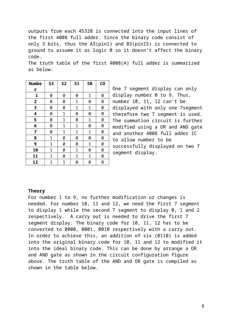
outputs from each 4532B is connected into the input lines of the first 4008 full adder. Since the binary code consist of only 3 bits, thus the A3(pin1) and B3(pin15) is connected to ground to assume it as logic 0 so it doesn’t affect the binarycode.The truth table of the first 4008(A) full adder is summarized as below:
One 7 segment display can only display number 0 to 9. Thus, number 10, 11, 12 can’t be displayed with only one 7segmenttherefore two 7 segment is used.The summation circuit is furthermodified using a OR and AND gateand another 4008 full adder IC to allow number to be successfully displayed on two 7 segment display.
TheoryFor number 1 to 9, no further modification or changes is needed. For number 10, 11 and 12, we need the first 7 segment to display 1 while the second 7 segment to display 0, 1 and 2 respectively. A carry out is needed to drive the first 7 segment display. The binary code for 10, 11, 12 has to be converted to 0000, 0001, 0010 respectively with a carry out. In order to achieve this, an addition of six (0110) is added into the original binary code for 10, 11 and 12 to modified itinto the ideal binary code. This can be done by arrange a OR and AND gate as shown in the circuit configuration figure above. The truth table of the AND and OR gate is compiled as shown in the table below.
8
Number
S3 S2 S1 S0 CO
1 0 0 0 1 02 0 0 1 0 03 0 0 1 1 04 0 1 0 0 05 0 1 0 1 06 0 1 1 0 07 0 1 1 1 08 1 0 0 0 09 1 0 0 1 010 1 0 1 0 011 1 0 1 1 012 1 1 0 0 0

The output at Y (AND gate) is 0 from number 1 to 9 but it has the output 1 when it reaches number 10, 11 and 12. Thus, the output 1 is needed to create a binary input of 0110 into one of the input of the second 4008 full adder. In the circuit configuration figure above, A0 and A3 is connected to ground while A1 and A2 are connected to the output at Y. So when it reaches number 10, 11, 12, the addition of six will occurs while there is no changes for the rest of the number. The addition process is shown in the truth table below:
Number Inputs OutputsA3 A2 A1 A0 B3 B2 B1 B0 CO S3 S2 S1 S0
1 0 0 0 0 0 0 0 1 0 0 0 0 12 0 0 0 0 0 0 1 0 0 0 0 1 03 0 0 0 0 0 0 1 1 0 0 0 1 14 0 0 0 0 0 1 0 0 0 0 1 0 05 0 0 0 0 0 1 0 1 0 0 1 0 16 0 0 0 0 0 1 1 0 0 0 1 1 07 0 0 0 0 0 1 1 1 0 0 1 1 18 0 0 0 0 1 0 0 0 0 1 0 0 09 0 0 0 0 1 0 0 1 0 1 0 0 110 0 1 1 0 1 0 1 0 1 0 0 0 011 0 1 1 0 1 0 1 1 1 0 0 0 112 0 1 1 0 1 1 0 0 1 0 0 1 0
Conclusion, for number 1 to 9, the binary code still remains the same without an carry out (CO) output. But for number 10 to 12, there will be a carry out (CO) which will be directly connected to the appropriate input line of the first 7 segmentto display number 1. While the binary code of 10, 11, 12 is
9
S1 S2 X (ORgate)
0 0 00 1 10 1 11 0 11 0 11 1 11 1 10 0 00 0 00 1 10 1 11 0 1
X S3 Y (ANDgate)
0 0 01 0 01 0 01 0 01 0 01 0 01 0 00 0 00 1 01 1 11 1 11 1 1

converted into 0000, 0001, 0010 which display the number 0, 1 and 2 on the second 7 segment display.
7 Segment Display BoardThe final process is to convert to final summation binary codeinto outputs that can drive a seven segment display. A 4511 ICBCD to 7-segment decoder driver is used to convert the logic states at the outputs of a BCD, or binary coded decimal, counter like the 4510 into signals which will drive a 7-segment display. This part has four input lines in BCD format and 7 output lines to drive the seven segments on the number.
There is a few extra control lines :LT Lamp Test (active low) has to be connected to Vcc to operate in normal operation.BI Blanking (active low) has to be connected to Vcc to displays the required number.LE Latch Enable (active high) has to be connected to ground inorder to be in normal operation.
The final step is to connect the common cathode seven segment display. According to the datasheet, the 7 segment generally consists of one LED. Thus a range of 300Ω to 500Ω current limit resistor is connected to the input lines of 7 segment will give a good brightness.
DiscussionIn the process of carrying out this mini project, several problems have been encountered. One of the main problems is the connectivity of the breadboards. Until a certain point where the whole circuit is tested out parts by parts. Reconstruction of whole circuit is done at least three times but it is still not the wanted results. Thus, a different breadboard is replaced and the circuit was operating as it should. As suspected, it is the problematic connectivity of the breadboard that caused such hassle so a Continuity Breadboard Multimeter Test should be done before constructing the circuit to avoid this problem.
Besides, IC’s are generally sensitive to static electricity. Discharging oneself of any static electricity first before
10

touching them is crucial. It is usually adequate to earth one’s hands by touching a metal water pipe or window frame before handling the IC but for the more sensitive (and expensive) IC’s special equipment is available, including earthed wrist straps and earthed work surfaces. But due to carelessness and hastiness of the members, the process of discharging of static electricity before touching the IC’s wasoverlooked. As a result, after hours of troubleshooting the circuit constructed, only to find out that one of the IC’s is spoiled. As suspected, it is because the discharging part was overlooked before touching them that caused the IC to spoil. Also, there is also an incident where one of the members was too rough in inserting an IC into the breadboard that one of the pins of the IC broke without using the right tool for removing and inserting components.
The polarity of every component is important. If one of the polarities of component is placed in a wrong direction, it maycause the component to burn or the whole circuit would not work. For example: the polarity of LED is connected wrongly which prevent the voltage flow across the LED thus the LED cannot be lighted up.
For the LED dice display, an appropriate value of resistor anddiode is connected series to the LED. The purpose is the limitthe voltage that flows into the LED in order to prevent the LED to be burned. LED can only withstand a very small current which is around the range of 100mA.
For 7 segment, according to the datasheet, each generally consists of one LED. However bigger displays may use more thanone LED per segment, as these are connected in series the voltage drop across the combined LEDs will be higher and a lower value resistor will be required. So, the consideration of the resistor value has to be taken in. If not, all the power will be dissipated in the 7 segment display while the LED dice will be very dim as there is only very small voltage that flows through there.
Neatness of the wire is also a major factor in the construction of circuit. The messier a circuit is constructed,the more problems will appear because the wire may not connect
11

properly. Knowing this, neatness became one of the most important aspects the group took note of and the end product is a circuit with tidily-arranged components and flat wirings.Assuredly, very few glitches can be found in the circuit. Thus, proving the hypothesis stated.
ConclusionThe main objectives of the experiment have been achieved. The operation of the designed circuit and also the functionality of each component in the design (single dice & dual dice) are carried out smoothly. The 555 timer gives out the pulses and clock the 4017 counter which enables the LED dice to display number from 1 to 6 when the switch start button is pressed. The number from each dice is added together with the summationcircuit design which makes up of full adder, OR gate and AND gate. The final number was displayed accurately on the 7segment display. The undertakings of the tasks in this assignment have proven successful.
AppendixBill Of MaterialsComponents No
.Unit price(RM)
Amount (RM)
7 segment (common cathode) 2 2.60 5.804511 IC 2 1.30 2.60NE555 IC 2 0.90 1.804017 IC 2 1.30 2.604 pin switch 3 0.40 1.2010µF capacitor 4 0.20 0.80IN4148 12 0.10 1.205mW LED 14 0.30 4.20Resistor (10kΩ×2, 1kΩ×2, 470Ω×20)
24 0.05 1.25
4008 IC 2 3.50 7.004532 IC 2 3.00 6.00CD4081 1 2.60 2.60CD4071 1 2.30 2.30
Total 39.35
Datasheets
12

NE555 http://pdf1.alldatasheet.com/datasheet-pdf/view/23384/STMICROELECTRONICS/NE555.htmlCD4017Bhttp://pdf1.alldatasheet.com/datasheet-pdf/view/50846/FAIRCHILD/CD4017.htmlCD4532Bhttp://www.ti.com/lit/ds/symlink/cd4532b-mil.pdfCD4008Bhttp://pdf1.alldatasheet.com/datasheet-pdf/view/66388/INTERSIL/CD4008.htmlCD4511Bhttp://pdf1.alldatasheet.com/datasheet-pdf/view/26905/TI/CD4511.htmlCD4081B and CD4071Bhttp://pdf1.alldatasheet.com/datasheet-pdf/view/50864/FAIRCHILD/CD4081.html Schematic diagram of the whole circuit
Picture
13

14

AdditionalSuggestion: Add some sound effect like buzzing to make it moreinteresting when the dice roll. When the button is pressed, ittoggles to buzzer and it is turned on and off according to pulses of the 555 timer. Thus, a buzzer is connected series with the start switch button.
15
Copyright © 2022 FDOKUMEN