2017.03.ieee_micro.top_picks.cover.pdf - People
136
The magazine for chip and silicon systems designers Reflections from Uri Weiser p. 126 www.computer.org/micro May/June 2017 Volume 37, Number 3
-
Upload
khangminh22 -
Category
Documents
-
view
4 -
download
0
Transcript of 2017.03.ieee_micro.top_picks.cover.pdf - People

The magazine for chip and silicon systems designers
Reflections from Uri Weiserp. 126
www.computer.org/micro
Top
Picks fro
m the 2016 C
om
puter A
rchitecture Co
nferencesIE
EE
MIC
RO
m
Ay
/jun
e 2017
VO
Lum
e 37
nu
mB
eR
3
May/June 2017 Volume 37, Number 3


IEEE Micro (ISSN 0272-1732) is published bimonthly by the IEEE Computer Society.IEEE Headquarters, Three Park Ave., 17th Floor, New York, NY 10016-5997; IEEEComputer Society Headquarters, 2001 L St., Ste. 700, Washington, DC 20036; IEEEComputer Society Publications Office, 10662 Los Vaqueros Circle, PO Box 3014,Los Alamitos, CA 90720.Subscribe to IEEE Micro by visiting www.computer.org/micro.Postmaster: Send address changes and undelivered copies to IEEE, MembershipProcessing Dept., 445 Hoes Ln., Piscataway, NJ 08855. Periodicals postage is paidat New York, NY, and at additional mailing offices. Canadian GST #125634188.Canada Post Corp. (Canadian distribution) Publications Mail Agreement #40013885.Return undeliverable Canadian addresses to 4960-2 Walker Road; Windsor, ON N9A6J3. Printed in USA.Reuse rights and reprint permissions: Educational or personal use of this material ispermitted without fee, provided such use: 1) is not made for profit; 2) includes this noticeand a full citation to the original work on the first page of the copy; and 3) does not implyIEEE endorsement of any third-party products or services. Authors and their companiesare permitted to post the accepted version of IEEE-copyrighted material on their ownwebservers without permission, provided that the IEEE copyright notice and a fullcitation to the original work appear on the first screen of the posted copy. An acceptedmanuscript is a version which has been revised by the author to incorporate reviewsuggestions, but not the published version with copy-editing, proofreading, and for-matting added by IEEE. For more information, please go to www.ieee.org/publications_standards/publications/rights/paperversionpolicy.html.Permission to reprint/republish this material for commercial, advertising, or promo-tional purposes or for creating new collective works for resale or redistribution must beobtained from IEEE by writing to the IEEE Intellectual Property Rights Office,445 Hoes Lane, Piscataway, NJ 08854-4141 or [email protected] 2017 by IEEE. All rights reserved.Abstracting and library use: Abstracting is permitted with credit to the source.Libraries are permitted to photocopy for private use of patrons, provided theper-copy fee indicated in the code at the bottom of the first page is paid throughthe Copyright Clearance Center, 222 Rosewood Drive, Danvers, MA 01923.Editorial: Unless otherwise stated, bylined articles, as well as product and service descrip-tions, reflect the author’s or firm’s opinion. Inclusion in IEEE Micro does not necessarilyconstitute an endorsement by IEEE or the Computer Society. All submissions are subject toediting for style, clarity, and space. IEEE prohibits discrimination, harassment, and bullying.For more information, visit www.ieee.org/web/aboutus/whatis/policies/p9-26.html.
May/June 2017 Volume 37 Number 3
Features
6 Guest Editors’ Introduction: Top Picks from the 2016 ComputerArchitecture ConferencesAamer Jaleel and Moinuddin Qureshi
12 Using Dataflow to Optimize Energy Efficiency of Deep Neural NetworkAcceleratorsYu-Hsin Chen, Joel Emer, and Vivienne Sze
22 The Memristive Boltzmann Machines
Mahdi Nazm Bojnordi and Engin Ipek
30 Analog Computing in a Modern Context: A Linear Algebra AcceleratorCase StudyYipeng Huang, Ning Guo, Mingoo Seok, Yannis Tsividis, and SimhaSethumadhavan
40 Domain Specialization Is Generally Unnecessary for Accelerators
Tony Nowatzki, Vinay Gangadhar, Karthikeyan Sankaralingam, and Greg Wright
52 Configurable Clouds
Adrian M. Caulfield, Eric S. Chung, Andrew Putnam, Hari Angepat, Daniel Firestone,Jeremy Fowers, Michael Haselman, Stephen Heil, Matt Humphrey, Puneet Kaur,Joo-Young Kim, Daniel Lo, Todd Massengill, Kalin Ovtcharov, Michael Papamichael,Lisa Woods, Sitaram Lanka, Derek Chiou, and Doug Burger
62 Specializing a Planet’s Computation: ASIC Clouds
Moein Khazraee, Luis Vega Gutierrez, Ikuo Magaki, and Michael Bedford Taylor
70 DRAF: A Low-Power DRAM-Based Reconfigurable Acceleration Fabric
Mingyu Gao, Christina Delimitrou, Dimin Niu, Krishna T. Malladi, HongzhongZheng, Bob Brennan, and Christos Kozyrakis
80 Agile Paging for Efficient Memory Virtualization
Jayneel Gandhi, Mark D. Hill, and Michael M. Swift
88 Transistency Models: Memory Ordering at the Hardware–OS Interface
Daniel Lustig, Geet Sethi, Abhishek Bhattacharjee, and Margaret Martonosi
98 Toward a DNA-Based Archival Storage System
James Bornholt, Randolph Lopez, Douglas M. Carmean, Luis Ceze, Georg Seelig, andKarin Strauss
106 Ti-states: Power Management in Active Timing Margin Processors
Yazhou Zu, Wei Huang, Indrani Paul, and Vijay Janapa Reddi
116 An Energy-Aware Debugger for Intermittently Powered Systems
Alexei Colin, Graham Harvey, Alanson P. Sample, and Brandon Lucia
Departments
4 From the Editor in ChiefThoughts on the Top Picks SelectionsLieven Eeckhout
126 AwardsInsights from the 2016 Eckert-Mauchly Award RecipientUri Weiser
130 Micro EconomicsTwo Sides to ScaleShane Greenstein
Computer Society Information, p. 3Advertising/Product Index, p. 61
Oliver BurstonDebut Art
...............................
2

.............................................................
MAY/JUNE 2017 3
........................................................................................................................................ ..................................................................................................................................................................................................................................................................
................
...........
........................................................................................................................................EDITOR IN CHIEF
Lieven EeckhoutGhent [email protected]
. . . . . . . . . . . . . . . . . . . . . . . . . . . . . . . . . . . . . . .
ADVISORY BOARD
David H. Albonesi, Erik R. Altman, Pradip Bose,Kemal Ebcioglu, Michael Flynn, Ruby B. Lee,Yale Patt, James E. Smith, and Marc Tremblay
. . . . . . . . . . . . . . . . . . . . . . . . . . . . . . . . . . . . . . .
EDITORIAL BOARD
David BrooksHarvard University
Alper BuyuktosunogluIBM
Bronis de SupinskiLawrence Livermore National Laboratory
Natalie Enright JergerUniversity of Toronto
Babak FalsafiEPFL
Shane GreensteinNorthwestern University
Lizy Kurian JohnUniversity of Texas at Austin
Hyesoon KimGeorgia Tech
John KimKAIST
Hsien-Hsin (Sean) LeeTaiwan Semiconductor Manufacturing Company
Richard MateosianTrevor Mudge
University of Michigan, Ann ArborShubu Mukherjee
Cavium NetworksOnur Mutlu
ETH ZurichToshio Nakatani
IBM ResearchVojin G. Oklobdzija
University of California, DavisRonny Ronen
IntelKevin W. Rudd
Laboratory for Physical SciencesAndre Seznec
INRIAPer Stenstrom
Chalmers University of TechnologyRichard H. Stern
George Washington University Law SchoolLixin Zhang
Chinese Academy of Sciences. . . . . . . . . . . . . . . . . . . . . . . . . . . . . . . . . . . . . . .
EDITORIAL STAFFEditorial Product Lead
Cathy Martin
[email protected] Management
Molly Gamborg
Publications Coordinator
[email protected]. . . . . . . . . . . . . . . . . . . . . . . . . . . . . . . . . . . . . . .Director, Products & Services
Evan Butterfield
Senior Manager, Editorial Services
Robin Baldwin
Manager, Editorial Services
Brian Brannon
Manager, Peer Review & PeriodicalAdministration
Hilda Carman
Digital Library Marketing Manager
Georgann Carter
Senior Business Development Manager
Sandra Brown
Director of Membership
Eric Berkowitz
Digital Marketing Manager
Marian Anderson
[email protected]. . . . . . . . . . . . . . . . . . . . . . . . . . . . . . . . . . . . . . .
EDITORIAL OFFICE
PO Box 3014, Los Alamitos, CA 90720;
(714) 821-8380; [email protected]. . . . . . . . . . . . . . . . . . . . . . . . . . . . . . . . . . . . . . .
Submissions:
https://mc.manuscriptcentral.com/micro-cs
Author guidelines:
http://www.computer.org/micro. . . . . . . . . . . . . . . . . . . . . . . . . . . . . . . . . . . . . . .
IEEE CS PUBLICATIONS BOARD
Greg Byrd (VP for Publications), Alfredo Benso, Irena
Bojanova, Robert Dupuis, David S. Ebert, Davide
Falessi, Vladimir Getov, Jose Martinez, Forrest
Shull, and George K. Thiruvathukal. . . . . . . . . . . . . . . . . . . . . . . . . . . . . . . . . . . . . . .
IEEE CS MAGAZINE OPERATIONS
COMMITTEE
George K. Thiruvathukal (Chair), Gul Agha, M. Brian
Blake, Jim X. Chen, Maria Ebling, Lieven Eeckhout,
Miguel Encarnacao, Nathan Ensmenger, Sumi Helal,
San Murugesan, Yong Rui, Ahmad-Reza Sadeghi,
Diomidis Spinellis, VS Subrahmanian, and Mazin
Yousif
..................................................................................................................................................................................................................................................................

................................................................................................................................................................
Thoughts on the Top PicksSelections
LIEVEN EECKHOUTGhent University
......The May/June issue of IEEE
Micro traditionally features a selection of
articles called Top Picks that have the
potential to influence the work of com-
puter architects for the near future. A
selection committee of experts selects
these articles from the previous year’s
computer architecture conferences; the
selection criteria are novelty and potential
for long-term impact. Any paper published
in the top computer architecture confer-
ences of 2016 was eligible, which makes
the job of the selection committee both a
challenge and a pleasure. Selections are
based on the original conference paper
and a three-page write-up that summa-
rizes the paper’s key contributions and
potential impact. We received a record
number of 113 submissions this year.
Aamer Jaleel and Moinuddin Qureshi
chaired the selection committee, which
comprised 33 experts. I wholeheartedly
thank them and their committee for
having done such a great job. As they
note in the Guest Editors’ Introduction,
Aamer and Moin introduced a novel two-
phase review procedure. Four commit-
tee members reviewed each paper
during the first round. A subset of the
papers was selected to move to the
second round based on the reviewers’
scores and online discussion of the first
round. Six more committee members
reviewed each paper during the second
round; second-round papers thus received
a total of 10 reviews! This formed the
basic input for the in-person selection
committee meeting.
The selection committee reached a
consensus on 12 Top Picks and 12 Hono-
rable Mentions. Top Pick selections
were invited to prepare an article to be
included in this special issue. Because
these magazine articles are much shorter
than the original conference papers, they
tend to be more high-level and more
qualitative than the original conference
publications, providing an excellent intro-
duction to these highly innovative contri-
butions. The Honorable Mentions are top
papers that the selection committee
unfortunately could not recognize as Top
Picks because of magazine space con-
straints; these are acknowledged in the
Guest Editors’ Introduction. I encourage
you to read these important contribu-
tions to our field and share your thoughts
with students and colleagues.
Having participated in the selection
committee myself, I was deeply im-
pressed by the effectiveness of the
new review process. In particular, I
found it interesting to observe that the
committee reached a consensus that
very closely aligned with the ranking
obtained by the 10 reviews for each of
the second-round papers. This makes
me wonder whether we still need an in-
person selection committee meeting.
Of course, the meeting itself has great
value in terms of generating interesting
discussions and providing the opportu-
nity to meet colleagues from our com-
munity, but it undeniably also imposes
a big cost in terms of time, effort,
money, and carbon footprint (with
many committee members flying in and
out from all over the world).
Glancing over the set of papers
selected for Top Picks and Honorable
Mentions, one important trend has
emerged just recently—namely, the
focus on accelerators and hardware
specialization. A good number of papers
are related to hardware acceleration in
the broad sense. This does not come as
a surprise given current application
trends, along with the end of Dennard
scaling, which pushes architects to
improve system performance within
stringent power and cost envelopes
through hardware acceleration. We
observe this trend throughout the entire
computing landscape, from mobile devi-
ces to large-scale datacenters. There is a
lot of exciting research and advanced
development going on in this area by
many research groups in industry and aca-
demia, and I expect many more important
advances in the near future. Next to this
emerging trend, there is (still) a good frac-
tion of outstanding papers in more tradi-
tional areas, including microarchitecture,
memory hierarchy, memory consistency,
multicore, power management, security,
and simulation methodology.
I want to share a couple more
thoughts with you regarding the Top Picks
procedure that arose from conversations
I’ve had with various people in our com-
munity. I’d love to get the broader com-
munity’s feedback on this, so please
don’t hesitate to contact me and share
your thoughts.
.......................................................
4 Published by the IEEE Computer Society 0272-1732/17/$33.00�c 2017 IEEE
From the Editor in Chief
One thought relates to the number of
selected Top Picks being too restrictive.
There is a hard cap of only 12 Top Picks.
On one hand, we want the process to be
selective and Top Picks recognition to be
prestigious. On the other hand, our com-
munity is growing. Our top-tier conferen-
ces, such as ISCA, MICRO, HPCA, and
ASPLOS, receive an ever-increasing
number of papers to review, and the
number of accepted papers is increasing
as well. One could argue that in response
we need to recognize more papers as
Top Picks. The hard constraint that we
are hitting here is the page limit we have
for the magazine, because the number
of pages is related to the production
cost. One solution may be to have more
Top Picks selections but fewer pages
allocated per selected article—but this
may compromise the comprehensive-
ness of the articles. Another solution
may be to recognize more Honorable
Mentions, because they don’t affect the
page count. Or, we may want to elec-
tronically publish the three-page Top
Picks submissions (paper summary and
potential impact, as mentioned earlier) as
they are, if the authors agree. This would
not incur any production cost at all, yet
the community would benefit from read-
ing them. Yet another solution may be to
select more than 12 Top Picks and pub-
lish them in different issues of the maga-
zine. The counterargument here is that
we have only six issues per year, which
makes it difficult to argue for more than
one issue devoted to Top Picks.
Another issue relates to the timing of
the Top Picks selection. Our community
has relatively few awards, and Top Picks
is an important vehicle in our community
to recognize top-quality research. How-
ever, one may argue whether selecting
Top Picks one year after publication is
too soon—it might make sense to wait a
couple more years before recognizing
the best research contributions of the
year. We may not want to wait as long
as the ISCA’s Influential Paper Award (15
years after publication) and MICRO’s
Test of Time Award (18 to 22 years after
publication), but still, one could argue for
waiting a few more years before under-
standing the true value of a novel
research contribution and how it impacts
our field. An important argument in this
discussion is that awards are generally
more important to young researchers
than they are for senior researchers.
Young researchers looking for a faculty or
research position in a leading academic
institute or industry lab need recognition
fairly soon in their careers as they get in
competition with other researchers from
other fields that have more awards.
Senior researchers, on the other hand, do
not need the recognition as much—or at
least their time scale is (much) longer.
Please let me know your thoughts on
these ideas or any other concerns you
may have. I’m open to any suggestions.
My only concern is to make sure Top
Picks continues to recognize the best
research in our field while serving the
best interests of both the community
and IEEE Micro.
Before wrapping up, I want to high-
light that this issue also includes an
award testimonial. Uri Weiser received
the 2016 Eckert-Mauchly Award for his
seminal contributions to the field of com-
puter architecture over the course of his
40-year career in industry and academia.
Uri Weiser single-handedly convinced
Intel executives to continue designing
CISC-based x86 processors by showing
that through adding new features such
as superscalar execution, branch predica-
tion, split instruction, and data cache, the
x86 processors could be made competi-
tive against the RISC family of process-
ors initiated by IBM and Berkeley. This
laid the foundation for the Intel Pentium
processor. Uri Weiser made several
other seminal contributions, including
the design of instruction-set extensions
(that is, Intel’s MMX) for supporting mul-
timedia applications. The Eckert-Mauchly
Award is considered the computer archi-
tecture community’s most prestigious
award. I wholeheartedly congratulate Uri
Weiser on the award and thank him for
his insightful testimonial.
With that, I wish you happy reading,
as always!
Lieven Eeckhout
Editor in Chief
IEEE Micro
Lieven Eeckhout is a professor in the
Department of Electronics and Informa-
tion Systems at Ghent University. Con-
tact him at [email protected].
.............................................................
MAY/JUNE 2017 5
Guest Editors’ Introduction........................................................................................................................................................................................................................
TOP PICKS FROM THE 2016COMPUTER ARCHITECTURE
CONFERENCES......It is our pleasure to introduce thisyear’s Top Picks in Computer Architecture.This issue is the culmination of the hardwork of the selection committee, which chosefrom 113 submissions that were published incomputer architecture conferences in 2016.We followed the precedent set by last year’sco-chairs and encouraged the selection com-mittee members to consider characteristicsthat make a paper worthy of being a “toppick.” Specifically, we asked them to considerwhether a paper challenges conventionalwisdom, establishes a new area of research, isthe definitive “last word” in an establishedresearch area, has a high potential for indus-try impact, and/or is one they would recom-mend to others to read.
Since the number of papers that could beselected for this Top Picks special issue waslimited to 12, we continued the precedent setover the past two years of having the selectioncommittee recognize 12 additional high-quality papers for Honorable Mention. Westrongly encourage you to read these papers(see the “Honorable Mentions” sidebar).Before we present the list of articles appearingin this special issue, we will first describe thenew review process that we implemented toimprove the paper selection process.
Review ProcessA selection committee comprising 31 mem-bers reviewed all the 113 papers (see the“Selection Committee” sidebar). This year,we tried a different selection process com-
pared to previous years’ Top Picks, keepingin mind the constraints and objectives thatare unique to Top Picks. The conventionalapproach to Top Picks selection has largelyremained similar to that used in our confer-ences (for example, four to five reviews perpaper and a four-to-six-point grading scale).For Top Picks, the number of papers that canbe accepted is fixed (11 to 12), and the selec-tion committee’s primary job is to identifythe top 12 papers out of all the submittedpapers, instead of providing a detailed cri-tique of the technical work and how thepaper can be improved. The papers submit-ted to Top Picks tend to be of much higher(average) quality than the typical paper sub-mitted at our conferences, and in many casesthe reviewers are already aware of the work(through prior reviewing, reading the papers,or attending the presentations). Therefore,the time and effort spent reviewing Top Pickspapers tends to be less than that spent review-ing the typical conference submissions.
We identified two key areas in which theTop Picks selection process could beimproved. First, a small number of reviewers(approximately five) made the decisions forTop Picks. The confidence in selection couldbe improved significantly by having a largernumber of reviews (approximately 10) perpaper, especially for the papers that are likelyto be discussed at the selection committeemeeting. This also ensures that reviewers aremore engaged at the meeting and makeinformed decisions. Second, the selection ofTop Picks gets overly influenced by excessively
Aamer Jaleel
Nvidia
Moinuddin Qureshi
Georgia Tech
............................................................
6 Published by the IEEE Computer Society 0272-1732/17/$33.00�c 2017 IEEE
....................................................................................................................................................................................
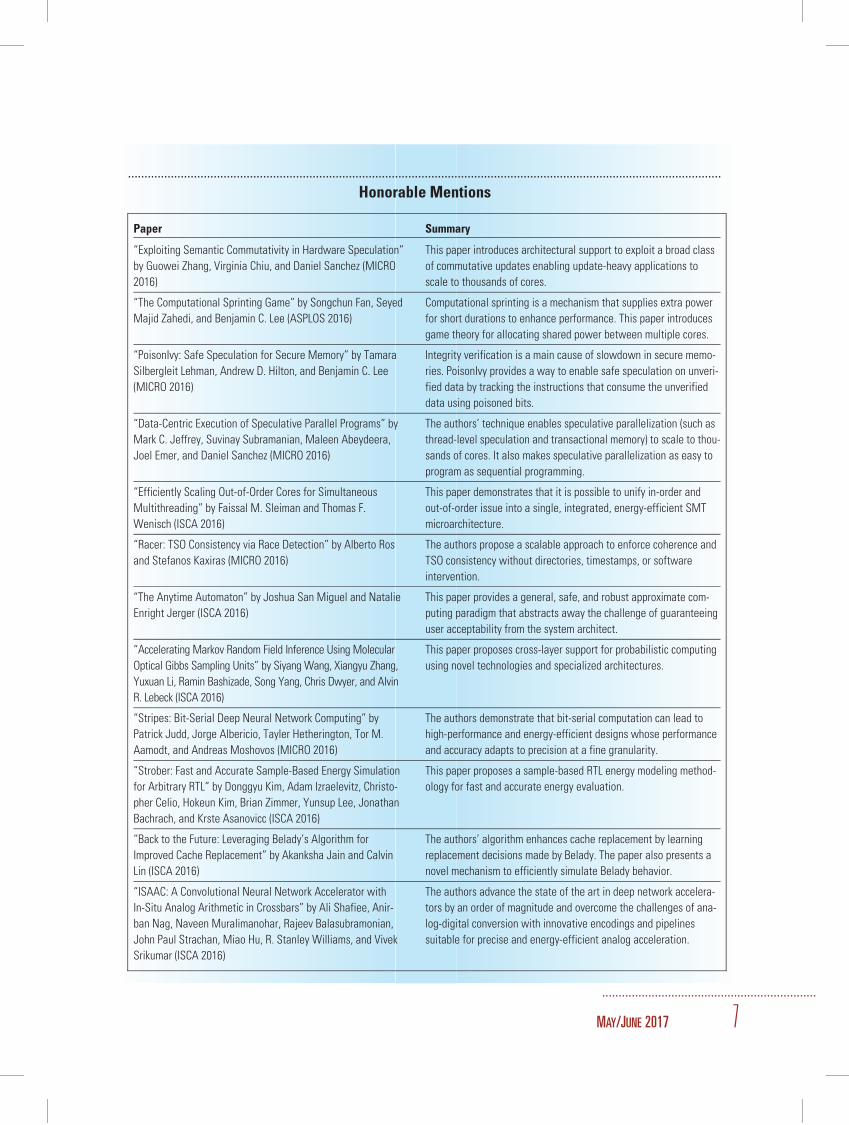
Honorable Mentions
Paper Summary
“Exploiting Semantic Commutativity in Hardware Speculation”
by Guowei Zhang, Virginia Chiu, and Daniel Sanchez (MICRO
2016)
This paper introduces architectural support to exploit a broad class
of commutative updates enabling update-heavy applications to
scale to thousands of cores.
“The Computational Sprinting Game” by Songchun Fan, Seyed
Majid Zahedi, and Benjamin C. Lee (ASPLOS 2016)
Computational sprinting is a mechanism that supplies extra power
for short durations to enhance performance. This paper introduces
game theory for allocating shared power between multiple cores.
“PoisonIvy: Safe Speculation for Secure Memory” by Tamara
Silbergleit Lehman, Andrew D. Hilton, and Benjamin C. Lee
(MICRO 2016)
Integrity verification is a main cause of slowdown in secure memo-
ries. PoisonIvy provides a way to enable safe speculation on unveri-
fied data by tracking the instructions that consume the unverified
data using poisoned bits.
“Data-Centric Execution of Speculative Parallel Programs” by
Mark C. Jeffrey, Suvinay Subramanian, Maleen Abeydeera,
Joel Emer, and Daniel Sanchez (MICRO 2016)
The authors’ technique enables speculative parallelization (such as
thread-level speculation and transactional memory) to scale to thou-
sands of cores. It also makes speculative parallelization as easy to
program as sequential programming.
“Efficiently Scaling Out-of-Order Cores for Simultaneous
Multithreading” by Faissal M. Sleiman and Thomas F.
Wenisch (ISCA 2016)
This paper demonstrates that it is possible to unify in-order and
out-of-order issue into a single, integrated, energy-efficient SMT
microarchitecture.
“Racer: TSO Consistency via Race Detection” by Alberto Ros
and Stefanos Kaxiras (MICRO 2016)
The authors propose a scalable approach to enforce coherence and
TSO consistency without directories, timestamps, or software
intervention.
“The Anytime Automaton” by Joshua San Miguel and Natalie
Enright Jerger (ISCA 2016)
This paper provides a general, safe, and robust approximate com-
puting paradigm that abstracts away the challenge of guaranteeing
user acceptability from the system architect.
“Accelerating Markov Random Field Inference Using Molecular
Optical Gibbs Sampling Units” by Siyang Wang, Xiangyu Zhang,
Yuxuan Li, Ramin Bashizade, Song Yang, Chris Dwyer, and Alvin
R. Lebeck (ISCA 2016)
This paper proposes cross-layer support for probabilistic computing
using novel technologies and specialized architectures.
“Stripes: Bit-Serial Deep Neural Network Computing” by
Patrick Judd, Jorge Albericio, Tayler Hetherington, Tor M.
Aamodt, and Andreas Moshovos (MICRO 2016)
The authors demonstrate that bit-serial computation can lead to
high-performance and energy-efficient designs whose performance
and accuracy adapts to precision at a fine granularity.
“Strober: Fast and Accurate Sample-Based Energy Simulation
for Arbitrary RTL” by Donggyu Kim, Adam Izraelevitz, Christo-
pher Celio, Hokeun Kim, Brian Zimmer, Yunsup Lee, Jonathan
Bachrach, and Krste Asanovicc (ISCA 2016)
This paper proposes a sample-based RTL energy modeling method-
ology for fast and accurate energy evaluation.
“Back to the Future: Leveraging Belady’s Algorithm for
Improved Cache Replacement” by Akanksha Jain and Calvin
Lin (ISCA 2016)
The authors’ algorithm enhances cache replacement by learning
replacement decisions made by Belady. The paper also presents a
novel mechanism to efficiently simulate Belady behavior.
“ISAAC: A Convolutional Neural Network Accelerator with
In-Situ Analog Arithmetic in Crossbars” by Ali Shafiee, Anir-
ban Nag, Naveen Muralimanohar, Rajeev Balasubramonian,
John Paul Strachan, Miao Hu, R. Stanley Williams, and Vivek
Srikumar (ISCA 2016)
The authors advance the state of the art in deep network accelera-
tors by an order of magnitude and overcome the challenges of ana-
log-digital conversion with innovative encodings and pipelines
suitable for precise and energy-efficient analog acceleration.
.................................................................
MAY/JUNE 2017 7
harsh or generous reviewers, who either givescores at extreme ends or advocate for toofew or too many papers from their stack. Wewanted to ensure that all reviewers play anequal role in the selection, regardless of theirharshness or generosity. For example, wecould give all reviewers an equal voice byrequiring them to advocate for a fixed num-ber of papers from their stack. We used thedata from the past three years’ Top Picksmeetings to analyze the process for Top Picksand used this data to drive the design of ourprocess. For example, the typical acceptancerate of Top Picks is approximately 10 per-cent; therefore, if we assign 15 papers to eachreviewer, then each reviewer can be expectedto have only 1.5 Top Picks papers on averagein their stack, and the likelihood of having 5or more Top Picks papers in the stack wouldbe extremely small.
Based on the data and constraints of TopPicks, we formulated a ranking-based two-phase process. The objective of the first phasewas to filter about 35 to 40 papers that wouldbe discussed at the selection committee meet-ing. The objective of the second phase was toincrease the number of reviews per paper toabout 10 and ask each reviewer to provide aconcrete decision for the assigned paper:whether it should be selected as a Top Picks
or Honorable Mention, or neither. In the firstphase, each reviewer was assigned exactly 14papers and was asked to recommend exactlyfive papers (Top 5) to the second phase. Eachpaper received four ratings in this phase. If apaper got three or more ratings of Top 5, itautomatically advanced to the second phase.If the paper had two ratings of Top 5, thenboth positive reviewers had to champion thepaper for it to advance to the second phase.Papers with less than two ratings of Top 5 didnot advance to the second phase. A total of38 papers advanced to the second phase, andeach such paper got a total of 9 to 10 reviews.In the second phase, each reviewer wasassigned an additional seven to eight papersin addition to the four to five papers that sur-vived the first phase. Each reviewer had 12papers and was asked to place exactly 4 ofthem into each category: Top Picks, Honora-ble Mention, and neither.
The selection committee meeting washeld in person in Atlanta, Georgia, on17 December 2016. At the selection com-mittee meeting, the 38 papers were rank-ordered on the basis of the number of TopPicks votes and the average rating the paperreceived in the second phase. If, after the in-person discussion, 60 percent or morereviewers rated a paper as a Top Pick, then
....................................................................................................................................................................................
Selection Committee� Tor Aamodt, University of British Columbia
� Alaa Alameldeen, Intel
� Murali Annavaram, University of Southern California
� Todd Austin, University of Michigan
� Chris Batten, Cornell University
� Luis Ceze, University of Washington
� Sandhya Dwarkadas, University of Rochester
� Lieven Eeckhout, Ghent University
� Joel Emer, Nvidia and MIT
� Babak Falsafi, EPFL
� Hyesoon Kim, Georgia Tech
� Nam Sung Kim, University of Illinois at Urbana–Champaign
� Benjamin Lee, Duke University
� Hsien-Hsin Lee, Taiwan Semiconductor Manufacturing
Company
� Gabriel Loh, AMD
� Debbie Marr, Intel
� Andreas Moshovos, University of Toronto
� Onur Mutlu, ETH Zurich
� Ravi Nair, IBM
� Milos Prvulovic, Georgia Tech
� Scott Rixner, Rice University
� Eric Rotenberg, North Carolina State University
� Karu Sankaralingam, University of Wisconsin
� Yanos Sazeidas, University of Cyprus
� Simha Sethumadhavan, Columbia University
� Andre Seznec, INRIA
� Dan Sorin, Duke University
� Viji Srinivasan, IBM
� Karin Strauss, Microsoft
� Tom Wenisch, University of Michigan
� Antonia Zhai, University of Minnesota
..............................................................................................................................................................................................
GUEST EDITORS’ INTRODUCTION
.................................................................
8 IEEE MICRO
the paper was selected as a Top Pick. Other-wise, the decision to select the paper as a TopPick (or Honorable Mention or neither) wasmade by a committee-wide vote using a sim-ple majority. We observed that the top eightranked papers all got accepted as Top Picks,and four more papers were selected as TopPicks from the next nine papers. Overall, outof the top 25 papers, all but one was selectedas either a Top Pick or an Honorable Men-tion. Thus, having a large number of reviewsper paper reduced the dependency on the in-person discussion. Coincidentally, the daybefore the selection committee meeting therewas a hurricane, which caused many flightsto be canceled, and 4 of the 31 selection com-mittee members were unable to attend themeeting. However, having 9 to 10 reviewersper paper still ensured that there were at leasteight reviewers present for each paper dis-cussed at the selection committee meeting,resulting in a robust and high-confidenceprocess, even with a relatively high rate ofabsentees. Given the unique constraints andobjectives of Top Picks, we hope that such aprocess with a larger number of reviews perpaper and a process that is robust to variationin generosity levels of reviewers (for example,ranking papers into fixed-sized bins) will beuseful for future Top Picks selection commit-tees as well.
Selected PapersWith the slowing down of conventionalmeans for improving performance, the archi-tecture community has been investigatingaccelerators to improve performance andenergy efficiency. This was evident in theemergence of a large number of papers onaccelerators appearing throughout the archi-tecture conferences in 2016. Given theemphasis on accelerators, it is no surprise thatmore than half of the articles in this issuefocus on architecting accelerators. Memorysystem and energy considerations are twoother areas from which the Top Picks paperswere selected.
AcceleratorsData movement is a primary factor thatdetermines the energy efficiency and effec-tiveness of accelerators. “Using Dataflow to
Optimize Energy Efficiency of Deep NeuralNetwork Accelerators” by Yu-Hsin Chen andhis colleagues describes a spatial architecturethat optimizes the dataflow for energy effi-ciency. This article also has an insightfulframework for classifying different accelera-tors based on access patterns.
“The Memristive Boltzmann Machines”by Mahdi Nazm Bojnordi and Engin Ipekproposes a memory-centric hardware acceler-ator for combinatorial optimization and deeplearning that leverages in-situ computing ofbit-line computation in memristive arraysto eliminate the need for exchanging dataamong the memory arrays and the computa-tional units.
The concept of using analog computingfor efficient computation is also explored byYipeng Huang and colleagues in “AnalogComputing in a Modern Context: A LinearAlgebra Accelerator Case Study.” The authorstry to address the typical challenges faced byanalog computing, such as limited problemsize, limited dynamic range, and precision.
In contrast to the first three articles, whichuse domain-specific acceleration, “DomainSpecialization Is Generally Unnecessary ForAccelerators” by Tony Nowatzki and his col-leagues focuses on retaining the programm-ability of accelerators while maintaining theirenergy efficiency. The authors use an architec-ture that has a large number of tiny cores withkey building blocks typically required foraccelerators and configure these cores intelli-gently based on the domain requirement.
Large-Scale AcceleratorsThe next three articles look at enhancing thescalability of accelerators so that they canhandle larger problem sizes and cater to vary-ing problem domains. The article“Configurable Clouds” by Adrian Caulfieldand his colleagues describes a cloud-scaleacceleration architecture that can connect dif-ferent accelerator nodes within a datacenterusing a high-speed FPGA fabric that lets thesystem accelerate a wide variety of applica-tions and has been deployed in Microsoftdatacenters.
In “Specializing a Planet’s Computation:ASIC Clouds,” Moein Khazraee and his col-leagues target scale-out workloads comprisingmany independent but similar jobs, often on
.................................................................
MAY/JUNE 2017 9

behalf of many users. This architecture showsa way to make ASIC usage more economical,because different users can potentially sharethe cost of fabricating a given ASIC, ratherthan each design team incurring the cost offabricating the ASIC.
“DRAF: A Low-Power DRAM-BasedReconfigurable Acceleration Fabric” by Min-gyu Gao and his colleagues describes a way toincrease the size of FPGA fabrics at low costby using DRAM instead of SRAM for thestorage inside the FPGA, thereby enabling ahigh-density and low-power reconfigurablefabric.
Memory and Storage SystemsMemory systems continue to be important indetermining the performance and efficiencyof computer systems. This issue features threearticles that focus on improving memory andstorage systems. “Agile Paging for EfficientMemory Virtualization” by Jayneel Gandhiand his colleagues addresses the performanceoverhead of virtual memory in virtualizedenvironments by getting the best of bothworlds: nested paging and shadow paging.
Virtual address translation can some-times affect the correctness of memory con-sistency models. Daniel Lustig and hiscolleagues address this problem in their article,“Transistency Models: Memory Ordering atthe Hardware–OS Interface.” The authorspropose to rigorously integrate memory con-sistency models and address translation at themicroarchitecture and operating system levels.
Moving on to the storage domain, in“Toward a DNA-Based Archival Storage Sys-tem,” James Bornholt and his colleaguesdemonstrate DNA-based storage architectedas a key-value store. Their design enables ran-dom access and is equipped with error correc-tion capability to handle the imperfections ofthe read and write process. As the demandfor cheap storage continues to increase, suchalternative technologies have the potential toprovide a major breakthrough in storagecapability.
Energy ConsiderationsThe final two articles are related to optimiz-ing energy or operating under low energybudgets. Modern processors are provisionedwith a timing margin to protect against tem-
perature inversion. In the article “Ti-states:Power Management in Active Timing Mar-gin Processors,” Yazhou Zu and his col-leagues show how actively monitoring thetemperature on the chip and dynamicallyreducing this timing margin can result in sig-nificant power savings.
Energy harvesting systems represent anextreme end of energy-constrained comput-ing in which the system performs computingonly when the harvested energy is present.One challenge in such systems is to providedebugging functionality for software, becausesystem failure could happen due to eitherlack of energy or incorrect code. “An Energy-Aware Debugger for Intermittently PoweredSystems” by Alexei Colin and his colleaguesdescribes a hardware–software debugger foran intermittent energy-harvesting system thatcan allow software verification to proceedwithout getting interference from the energy-harvesting circuit.
W e hope you enjoy reading these articlesand that you will explore both the
original conference versions and the Honora-ble Mention papers. We welcome your feed-back on this special issue and any suggestionsfor next year’s Top Picks issue. MICRO
AcknowledgmentsWe thank Lieven Eeckhout for providingsupport and direction as we tried out thenew paper selection process. Lieven alsohandled the papers that were conflicted withboth co-chairs. We also thank the selectioncommittee co-chairs for the past three TopPicks issues (Gabe Loh, Babak Falsafi, LuisCeze, Karin Strauss, Milo Martin, and DanSorin) for providing the review statistics fromtheir editions of Top Picks and for answeringour questions. We thank Vinson Young forhandling the submission website and Pra-shant Nair and Jian Huang for facilitating theprocess at the selection committee meeting.We owe a huge thanks to our fantastic selec-tion committee, which not only diligentlyreviewed all the papers but also were suppor-tive of the new review process. Furthermore,the selection committee members spent a dayattending the in-person meeting in Atlanta,fairly close to the holiday season. Finally, we
..............................................................................................................................................................................................
GUEST EDITORS’ INTRODUCTION
.................................................................
10 IEEE MICRO

thank all the authors who submitted theirwork for consideration to this Top Picks issueand the authors of the selected papers for pro-ducing the final versions of their papers forthis issue.
Aamer Jaleel is a principal research scientistat Nvidia. Contact him at [email protected].
Moinuddin Qureshi is an associate profes-sor in the School of Electrical and Com-puter Engineering at Georgia Tech. Contacthim at [email protected].
Read your subscriptions through the myCS publications portal at http://mycs.computer.org.
.................................................................
MAY/JUNE 2017 11
.................................................................................................................................................................................................................
USING DATAFLOW TO OPTIMIZEENERGY EFFICIENCY OF DEEP NEURAL
NETWORK ACCELERATORS.................................................................................................................................................................................................................
THE AUTHORS DEMONSTRATE THE KEY ROLE DATAFLOWS PLAY IN OPTIMIZING ENERGY
EFFICIENCY FOR DEEP NEURAL NETWORK (DNN) ACCELERATORS. THEY INTRODUCE BOTH A
SYSTEMATIC APPROACH TO ANALYZE THE PROBLEM AND A NEW DATAFLOW, CALLED
ROW-STATIONARY, THAT IS UP TO 2.5 TIMES MORE ENERGY EFFICIENT THAN EXISTING
DATAFLOWS IN PROCESSING A STATE-OF-THE-ART DNN. THIS ARTICLE PROVIDES
GUIDELINES FOR FUTURE DNN ACCELERATOR DESIGNS.
......Recent breakthroughs in deepneural networks (DNNs) are leading to anindustrial revolution based on AI. The super-ior accuracy of DNNs, however, comes atthe cost of high computational complexity.General-purpose processors no longer deliversufficient processing throughput and energyefficiency for DNNs. As a result, demandsfor dedicated DNN accelerators are increas-ing in order to support the rapidly growinguse of AI.
The processing of a DNN mainly com-prises multiply-and-accumulate (MAC) oper-ations (see Figure 1). Most of these MACs areperformed in the DNN’s convolutionallayers, in which multichannel filters are con-volved with multichannel input feature maps(ifmaps, such as images). This generates par-tial sums (psums) that are further accumu-lated into multichannel output feature maps(ofmaps). Because the MAC operations havefew data dependencies, DNN accelerators can
use high parallelism to achieve high process-ing throughput. However, this processingalso requires a significant amount of datamovement: each MAC performs three readsand one write of data access. Because movingdata can consume more energy than thecomputation itself,1 optimizing data move-ment becomes key to achieving high energyefficiency.
Data movement can be optimized byexploiting data reuse in a multilevel storagehierarchy. By maximizing the reuse of data inthe lower-energy-cost storage levels (such aslocal scratchpads), thus reducing data accessesto the higher-energy-cost levels (such asDRAM), the overall data movement energyconsumption is minimized.
In fact, DNNs present many data reuseopportunities. First, there are three typesof input data reuse: filter reuse, whereineach filter weight is reused across multipleifmaps; ifmap reuse, wherein each ifmap
Yu-Hsin Chen
Massachusetts Institute of
Technology
Joel Emer
Nvidia and Massachusetts
Institute of Technology
Vivienne Sze
Massachusetts Institute of
Technology
.......................................................
12 Published by the IEEE Computer Society 0272-1732/17/$33.00�c 2017 IEEE

pixel is reused across multiple filters; andconvolutional reuse, wherein both ifmap pix-els and filter weights are reused due to thesliding-window processing in convolutions.Second, the intermediate psums are reusedthrough the accumulation of ofmaps. If notaccumulated and reduced as soon as possi-ble, the psums can pose additional storagepressure.
A design can exploit these data reuseopportunities by finding the optimal MACoperation mapping, which determines boththe temporal and spatial scheduling of theMACs on a highly parallel architecture.Ideally, data in the lower-cost storage levels isreused by as many MACs as possible beforereplacement. However, due to the limitedamount of local storage, input data reuse(ifmaps and filters) and psum reuse cannotbe fully exploited simultaneously. For exam-ple, reusing the same input data for multipleMACs generates psums that cannot be accu-mulated together and, as a result, consumeextra storage space. Therefore, the systemenergy efficiency is maximized only when themapping balances all types of data reuse in amultilevel storage hierarchy.
The search for the mapping that maxi-mizes system energy efficiency thus becomesan optimization process. This optimizationmust consider the following factors: the datareuse opportunities available for a givenDNN shape and size (for example, the num-ber of filters, number of channels, size of fil-ters, and feature map size), the energy cost ofdata access at each level of the storage hier-archy, and the available processing parallelismand storage capacity. The first factor is a func-tion of workload, whereas the second andthird factors are a function of the specificaccelerator implementation.
Because of implementation tradeoffs, pre-vious proposals for DNN accelerators havemade choices on the subset of mappings thatcan be supported. Therefore, for a specificDNN accelerator design, the optimal map-ping can be selected only from the subset ofsupported mappings instead of the entiremapping space. The subset of supportedmappings is usually determined by a set ofmapping rules, which also characterizes thehardware implementation. Such a set of map-ping rules defines a dataflow.
Because state-of-the-art DNNs come in awide range of shapes and sizes, the corre-sponding optimal mappings also vary. Thequestion is, can we find a dataflow that accom-modates the mappings that optimize datamovement for various DNN shapes and sizes?
In this article, we explore different DNNdataflows to answer this question in the con-text of a spatial architecture.2 In particular, wewill present the following key contributions:3
� An analogy between DNN accelera-tors and general-purpose processorsthat clearly identifies the distinctaspects of operation of a DNN accel-erator, which provides insights intoopportunities for innovation.
� A framework that quantitatively eval-uates the energy consumption of dif-ferent mappings for different DNNshapes and sizes, which is an essentialtool for finding the optimal mapping.
� A taxonomy that classifies existingdataflows from previous DNN accel-erator projects, which helps to under-stand a large body of work despitedifferences in the lower-level details.
� A new dataflow, called Row-Stationary(RS), which is the first dataflow to
Filters
Input feature maps(ifmaps)
Partialsums
(psums)
C
RH
E
M
M
E
E
N
1
E
Output feature maps(ofmaps)
1
H
C
R
C
H
R
R
1
M
N
H
......
...
C
Figure 1. In the processing of a deep neural network (DNN), multichannel
filters are convolved with the multichannel input feature maps, which then
generate the output feature maps. The processing of a DNN comprises
many multiply-and-accumulate (MAC) operations.
.............................................................
MAY/JUNE 2017 13

optimize data movement for superiorsystem energy efficiency. It has alsobeen verified in a fabricated DNNaccelerator chip, Eyeriss.4
We evaluate the energy efficiency of theRS dataflow and compare it to other data-flows from the taxonomy. The comparisonuses a popular state-of-the-art DNN model,AlexNet,5 with a fixed amount of hardwareresources. Simulation results show that theRS dataflow is 1.4 to 2.5 times more energyefficient than other dataflows in the convolu-tional layers. It is also at least 1.3 times moreenergy efficient in the fully connected layersfor batch sizes of at least 16. These resultswill provide guidance for future DNN accel-erator designs.
An Analogy to General-Purpose ProcessorsFigure 2 shows an analogy between the oper-ation of DNN accelerators and general-purpose processors. In conventional computersystems, the compiler translates a programinto machine-readable binary codes for exe-cution; in the processing of DNNs, the map-per translates the DNN shape and size into ahardware-compatible mapping for execu-tion. While the compiler usually optimizesfor performance, the mapper especially opti-mizes for energy efficiency.
The dataflow is a key attribute of a DNNaccelerator and is analogous to one of theparts of a general-purpose processor’s archi-
tecture. Similar to the role of an ISA ormemory consistency model, the dataflowdefines the mapping rules that the mappermust follow in order to generate hardware-compatible mappings. Later in this article,we will introduce several previously pro-posed dataflows.
Other attributes of a DNN accelerator,such as the storage organization, also areanalogous to parts of the general-purposeprocessor architecture, such as scratchpads orvirtual memory. We consider these attributespart of the architecture, instead of microarch-itecture, because they may largely remaininvariant across implementations. Although,similar to GPUs, the distinction betweenarchitecture and microarchitecture is likely toblur for DNN accelerators.
Implementation details, such as those thatdetermine access energy cost at each level ofthe storage hierarchy and latency betweenprocessing elements (PEs), are analogous tothe microarchitecture of processors, because amapping will be valid despite changes inthese characteristics. However, they play avital part in determining a mapping’s energyefficiency.
The mapper’s goal is to search in the map-ping space for the mapping that best opti-mizes data movement. The size of the entiremapping space is determined by the totalnumber of MACs, which can be calculatedfrom the DNN shape and size. However,only a subset of the space is valid given themapping rules defined by a dataflow. Forexample, the dataflow can enforce the follow-ing mapping rule: all MACs that use thesame filter weight must be mapped on thesame PE in the accelerator. Then, it is themapper’s job to find out the exact ordering ofthese MACs on each PE by evaluating andcomparing the energy efficiency of differentvalid ordering options.
As in conventional compilers, performingevaluation is an integral part of the mapper.The evaluation process takes a certain map-ping as input and gives an energy consump-tion estimation based on the availablehardware resources (microarchitecture) anddata reuse opportunities extracted from theDNN shape and size (program). In the nextsection, we will introduce a framework thatcan perform this evaluation.
Compilation
DNN shape and size(Program)
Dataflow, ...(Architecture)
Mapping(Binary)
Inputdata
Implementationdetails(μArch)
Execution
Processeddata
DNN accelerator(Processor)
Mapper(Compiler)
Figure 2. An analogy between the operation of DNN accelerators (roman
text) and that of general-purpose processors (italicized text).
..............................................................................................................................................................................................
TOP PICKS
............................................................
14 IEEE MICRO

Evaluating Energy ConsumptionFinding the optimal mapping requires evalu-ation of the energy consumption for variousmapping options. In this article, we evaluateenergy consumption based on a spatial archi-tecture,2 because many of the previousdesigns can be thought of as instances of suchan architecture. The spatial architecture (seeFigure 3) consists of an array of PEs and amultilevel storage hierarchy. The PE arrayprovides high parallelism for high through-put, whereas the storage hierarchy can beused to exploit data reuse in a four-level setup(in decreasing energy-cost order): DRAM,global buffer, network-on-chip (NoC, forinter-PE communication), and register file(RF) in the PE as local scratchpads.
In this architecture, we assume all datatypes can be stored and accessed at any levelof the storage hierarchy. Input data for theMAC operations—that is, filter weights andifmap pixels—are moved from the mostexpensive level (DRAM) to the lower-costlevels. Ultimately, they are usually deliveredfrom the least expensive level (RF) to thearithmetic logic unit (ALU) for computation.The results from the ALU—that is, psums—generally move in the opposite direction.The orchestration of this movement is deter-mined by the mappings for a specific DNNshape and size under the mapping rule con-straints of a specific dataflow architecture.
Given a specific mapping, the systemenergy consumption is estimated by account-ing for the number of times each data valuefrom all data types (ifmaps, filters, psums) isreused at each level of the four-level memoryhierarchy, and weighing it with the energycost of accessing that specific storage level.Figure 4 shows the normalized energy con-sumption of accessing data from each storagelevel relative to the computation of a MAC atthe ALU. We extracted these numbers from acommercial 65-nm process and used them inour final experiments.
Figure 5 uses a toy example to show how amapping determines the data reuse at eachstorage level, and thus the energy consump-tion, in a three-PE setup. In this example, wehave the following assumptions: each ifmappixel is used by 24 MACs, all ifmap pixelscan fit into the global buffer, and the RF of
each PE can hold only one ifmap pixel at atime. The mapping first reads an ifmap pixelfrom DRAM to the global buffer, then fromthe global buffer to the RF of each PEthrough the NoC, and reuses it from the RFfor four MACs consecutively in each PE. Themapping then switches to MACs that useother ifmap pixels, so the original one in theRF is replaced by new ones, due to limitedcapacity. Therefore, the original ifmap pixelmust be fetched from the global buffer again
PE array
(zoom in)
pF
IFO
RFRF
pF
IFO
RF
pF
IFO
iFIFO/oFIFO
Global
buffer
PE arrayiFIFO/oFIFO
Off-chip
DRAM
Ac
ce
lera
tor c
hip
CPU
GPU
Figure 3. Spatial array architecture comprises an array of processing
elements (PEs) and a multilevel storage hierarchy, including the off-chip
DRAM, global buffer, network-on-chip (NoC), and register file (RF) in the PE.
The off-chip DRAM, global buffer, and PEs in the array can communicate
with each other directly through the input and output FIFOs (the iFIFO and
oFIFO). Within each PE, the PE FIFO (pFIFO) controls the traffic going in and
out of the arithmetic logic unit (ALU), including from the RF or other storage
levels.
Normalized energy cost
200×
6×
2×
1×
1× (Reference)
RF (0.5 to 1.0 Kbytes)
1 MAC at ALUComputation
Data accessNoC (1 to 2 mm)
Global buffer(>100 Kbytes)
DRAM
Figure 4. Normalized energy cost relative to the computation of one MAC
operation at ALU. Numbers are extracted from a commercial 65-nm
process.
.............................................................
MAY/JUNE 2017 15

when the mapping switches back to theMACs that use it. In this case, the sameifmap pixel is reused at the DRAM, globalbuffer, NoC, and RF for 1, 2, 6, and 24times, respectively. The corresponding nor-malized energy consumption of moving thisifmap pixel is obtained by weighing thesenumbers with the normalized energy num-bers in Figure 4 and then adding themtogether (that is, 1 � 200 þ 2 � 6 þ 6 � 2þ 24 � 1 ¼ 248). For other data types, thesame approach can be applied.
This analysis framework can be used notonly to find the optimal mapping for a spe-cific dataflow, but also to evaluate and com-pare the energy consumption of differentdataflows. In the next section, we willdescribe various existing dataflows.
A Taxonomy of Existing DNN DataflowsNumerous previous efforts have proposedsolutions for DNN acceleration. Thesedesigns reflect a variety of trade-offs betweenperformance and implementation complex-ity. Despite their differences in low-levelimplementation details, we find that many ofthem can be described as embodying a set ofrules—that is, a dataflow—that defines the
valid mapping space based on how they han-dle data. As a result, we can classify them intoa taxonomy.
� The Weight-Stationary (WS) data-flow keeps filter weights stationary ineach PE’s RF by enforcing the follow-ing mapping rule: all MACs that usethe same filter weight must bemapped on the same PE for process-ing serially. This maximizes the con-volutional and filter reuse of weightsin the RF, thus minimizing theenergy consumption of accessingweights (for example, work by SrimatChakradhar and colleagues6 andVinayak Gokhale and colleagues7).Figure 6a shows the data movementof a common WS dataflow imple-mentation. While each weight staysin the RF of each PE, the ifmap pixelsare broadcast to all PEs, and the gen-erated psums are then accumulatedspatially across PEs.
� The Output-Stationary (OS) data-flow keeps psums stationary by accu-mulating them locally in the RF. Themapping rule is that all MACs thatgenerate psums for the same ofmappixel must be mapped on the samePE serially. This maximizes psumreuse in the RF, thus minimizingenergy consumption of psum move-ment (for example, work by ZidongDu and colleagues,8 Suyog Guptaand colleagues,9 and Maurice Pee-men and colleagues10). The datamovement of a common OS dataflowimplementation is to broadcast filterweights while passing ifmap pixelsspatially across the PE array (seeFigure 6b).
� Unlike the previous two dataflows,which keep a certain data type sta-tionary, the No-Local-Reuse (NLR)dataflow keeps no data stationarylocally so it can trade the RF off for alarger global buffer. This is to mini-mize DRAM access energy consump-tion by storing more data on-chip(for example, work by Tianshi Chenand colleagues11 and Chen Zhangand colleagues12). The corresponding
PE arrayiFIFO/oFIFO
pF
IFO
DR
AM
Global
buffer
RF RF RF
pF
IFO
pF
IFO
NoC levelBuffer level
time
Memory level
RF levelIfmap pixeldata movement Processing other data . . .
Figure 5. Example of how a mapping determines data reuse at each storage
level. This example shows the data movement of one ifmap pixel going
through the storage hierarchy. Each arrow means moving data between
specific levels (or to an ALU for computation).
..............................................................................................................................................................................................
TOP PICKS
............................................................
16 IEEE MICRO

mapping rule is that at each process-ing cycle, all parallel MACs mustcome from a unique pair of filter andchannel. The data movement of theNLR dataflow is to single-cast weights,multicast ifmap pixels, and spatiallyaccumulate psums across the PE array(see Figure 6c).
The three dataflows show distinct datamovement patterns, which imply differenttradeoffs. First, as Figures 6a and 6b show,the cost for keeping a specific data type sta-tionary is to move the other types of datamore. Second, the timing of data accessesalso matters. For example, in the WS data-flow, each ifmap pixel read from the globalbuffer is broadcast to all PEs with properlymapped MACs on the PE array. This is moreefficient than reading the same value multipletimes from the global buffer and single-cast-ing it to the PEs, which is the case for filterweights in the NLR dataflow (see Figure 6c).Other dataflows can make other tradeoffs. Inthe next section, we present a new dataflowthat takes these factors into account for opti-mizing energy efficiency.
An Energy-Efficient DataflowAlthough the dataflows in the taxonomydescribe the design of many DNN accelera-tors, they optimize data movement only for aspecific data type (for example, WS forweights) or storage level (NLR for DRAM).In this section, we introduce a new dataflow,called Row-Stationary (RS), which aims tooptimize data movement for all data types inall levels of the storage hierarchy of a spatialarchitecture.
The RS dataflow divides the MACs intomapping primitives, each of which comprisesa subset of MACs that run on the same PE ina fixed order. Specifically, each mappingprimitive performs a 1D row convolution, sowe call it a row primitive, and intrinsicallyoptimizes data reuse per MAC for all datatypes combined. Each row primitive isformed with the following rules:
� The MACs for applying a row of fil-ter weights on a row of ifmap pixels,which generate a row of psums, mustbe mapped on the same PE.
� The ordering of these MACs enablesthe use of a sliding window for ifmaps,as shown in Figure 7.
Convolutional and psum reuse opportu-nities within a row primitive are fullyexploited in the RF, given sufficient RF stor-age capacity.
Even with the RS dataflow, as defined bythe row primitives, there are still a large num-ber of valid mapping choices. These mappingchoices arise both in the spatial and temporalassignment of primitives to PEs:
1. One spatial mapping option is toassign primitives with data rowsfrom the same 2D plane on the PEarray, to lay out a 2D convolution(see Figure 8). This mapping fullyexploits convolutional and psumreuse opportunities across primitivesin the NoC: the same rows of filterweights and ifmap pixels are reusedacross PEs horizontally and diago-nally, respectively; psum rows are
Ifmap pixel (l)
Weight-Stationary (WS) dataflow
(a)
(b)
(c)
Output-Stationary (OS) dataflow
No-Local-Reuse (NLR) dataflow
Filter weight (W) Psum (P)
Global buffer
W0 W1 W2 W3 W4 W5 W6 W7
I8
PE
P0
P1P2P3P4P5P6P7
P8
P0 P1 P2 P3 P4 P5 P6 P7
W7
PEI0I1I2I3I4I5I6
I7
PE
W0 W1 W2 W3 W4 W5 W6 W7P1P0P9P8
P6
P7
P4
P5
P2
P3
I0 I1 I2 I3
Global buffer
Global buffer
Figure 6. Dataflow taxonomy. (a) Weight Stationary. (b) Output Stationary.
(c) No Local Reuse.
.............................................................
MAY/JUNE 2017 17

further accumulated across PEsvertically.
2. Another spatial mapping optionarises when the size of the PE array islarge, and the pattern shown inFigure 8 can be spatially duplicatedacross the PE array for various 2Dconvolutions. This not only increasesutilization of PEs, but also furtherexploits filter, ifmap, and psum reuseopportunities in the NoC.
3. One temporal mapping option ariseswhen row primitives from different2D planes can be concatenated orinterleaved on the same PE. As Figure9 shows, primitives with differentifmaps, filters, and channels have filterreuse, ifmap reuse, and psum reuseopportunities, respectively. By concat-enating or interleaving their computa-tion together in a PE, it virtually
becomes a larger 1D row convolution,which exploits these cross-primitivedata reuse opportunities in the RF.
4. Another temporal mapping choicearises when the PE array size is toosmall, and the originally spatiallymapped row primitives must be tem-porally folded into multiple process-ing passes (that is, the computation isserialized). In this case, the data reuseopportunities that are originally spa-tially exploited in the NoC can betemporally exploited by the globalbuffer to avoid DRAM accesses,given sufficient storage capacity.
As evident from the preceding list, the RSdataflow provides a high degree of mappingflexibility, such as using concatenation, inter-leaving, duplicating, and folding of the rowprimitives. The mapper searches for the exactamount to apply each technique in the opti-mal mapping—for example, how many fil-ters are interleaved on the same PE to exploitifmap reuse—to minimize overall systemenergy consumption.
Dataflow ComparisonIn this section, we quantitatively compare theenergy efficiency of different DNN dataflowsin a spatial architecture, including those fromthe taxonomy and the proposed RS dataflow.We use AlexNet5 as the benchmarking DNNbecause it is one of the most popular DNNsavailable, and it comprises five convolutional(CONV) layers and three fully connected(FC) layers with a wide variety of shapes andsizes, which can more thoroughly evaluatethe optimal mappings from each dataflow.
In order to have a fair comparison, weapply the following two constraints for alldataflows. First, the size of the PE array isfixed at 256 for constant processing through-put across dataflows. Second, the total hard-ware area is also fixed. For example, becausethe NLR dataflow does not use an RF, it canallocate more area for the global buffer. Thecorresponding hardware resource parametersare based on the RS dataflow implementationin Eyeriss, a DNN accelerator chip fabricatedin 65-nm CMOS.4 By applying these con-straints, we fix the total cost to implementthe microarchitecture of each dataflow.
Filter row Ifmap row Psum row
A
A B C
a b c
x y z
a b c a b c
A B C A B C
B C a b c d e x y z∗ =
Time
MAC1 MAC2 MAC3 MAC4 MAC5 MAC6 MAC7 MAC8 MAC9
Filter weight:
Ifmap pixel:
Psum:II II II
x + + + + + +x x x x x x x x
Figure 7. Each row primitive in the Row-Stationary (RS) dataflow runs a 1D
row convolution on the same PE in a sliding-window processing order.
Row 1
Row 1 Row 1 Row 1 Row 2 Row 1 Row 3
Row 2 Row 2 Row 2 Row 3 Row 2 Row 4
Row 3 Row 3 Row 3 Row 4 Row 3 Row 5
Row 2 Row 3
PE1
PE2
PE3
PE4
PE5
PE6
PE7
PE8
PE9
∗
∗
∗
∗ = = =∗ ∗
∗
∗
∗
∗
∗
∗
Figure 8. Patterns of how row primitives from the same 2D plane are
mapped onto the PE array in the RS dataflow.
..............................................................................................................................................................................................
TOP PICKS
............................................................
18 IEEE MICRO
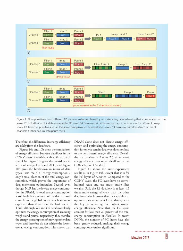
Therefore, the differences in energy efficiencyare solely from the dataflows.
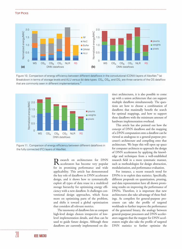
Figures 10a and 10b show the comparisonof energy efficiency between dataflows in theCONV layers of AlexNet with an ifmap batchsize of 16. Figure 10a gives the breakdown interms of storage levels and ALU, and Figure10b gives the breakdown in terms of datatypes. First, the ALU energy consumption isonly a small fraction of the total energy con-sumption, which proves the importance ofdata movement optimization. Second, eventhough NLR has the lowest energy consump-tion in DRAM, its total energy consumptionis still high, because most of the data accessescome from the global buffer, which are moreexpensive than those from the NoC or RF.Third, although WS and OS dataflows clearlyoptimize the energy consumption of accessingweights and psums, respectively, they sacrificethe energy consumption of moving other datatypes, and therefore do not achieve the lowestoverall energy consumption. This shows that
DRAM alone does not dictate energy effi-ciency, and optimizing the energy consump-tion for only a certain data type does not leadto the best system energy efficiency. Overall,the RS dataflow is 1.4 to 2.5 times moreenergy efficient than other dataflows in theCONV layers of AlexNet.
Figure 11 shows the same experimentresults as in Figure 10b, except that it is forthe FC layers of AlexNet. Compared to theCONV layers, the FC layers have no convo-lutional reuse and use much more filterweights. Still, the RS dataflow is at least 1.3times more energy efficient than the otherdataflows, which proves that the capability tooptimize data movement for all data types isthe key to achieving the highest overallenergy efficiency. Note that the FC layersaccount for less than 20 percent of the totalenergy consumption in AlexNet. In recentDNNs, the number of FC layers have alsobeen greatly reduced, making their energyconsumption even less significant.
Filter 1
Filter 1Channel 1 =
=
=
=
=
Channel 1
Row 1
Row 1
Row 1
Row 1
Row 1
Row 1
Row 1
Row 1 Row 1 Row 1 Row 1Filter 1
Ifmap 1
Ifmap 2
Ifmap 1 and 2 Psum 1 and 2Psum 1
Psum 2
filter reuse
Ifmap reuse
psum reuse (can be further accumulated)
∗
Filter 1
Channel 1
Channel 1
Row 1
Row 1
Row 1 Row 1
Row 1 Row 1
Filter 2
Ifmap 1
Ifmap 1
Psum 1
Psum 2
∗
∗
=
=
=
=
Filter 1
Filter 1
Filter 1 and 2
Ifmap 1
Ifmap 1 Psum 1 and 2
PsumChannel 1
Channel 2 Row 1
Row 1Row 1 Row 1
Row 1
Row 1 Row 1
Filter 1
Ifmap 1
Ifmap 1
Psum 1
Psum 1
∗
∗
∗
∗
∗
∗
(a)
(b)
(c)
Figure 9. Row primitives from different 2D planes can be combined by concatenating or interleaving their computation on the
same PE to further exploit data reuse at the RF level. (a) Two-row primitives reuse the same filter row for different ifmap
rows. (b) Two-row primitives reuse the same ifmap row for different filter rows. (c) Two-row primitives from different
channels further accumulate psum rows.
.............................................................
MAY/JUNE 2017 19
R esearch on architectures for DNNaccelerators has become very popular
for its promising performance and wideapplicability. This article has demonstratedthe key role of dataflows in DNN acceleratordesign, and it shows how to systematicallyexploit all types of data reuse in a multilevelstorage hierarchy for optimizing energy effi-ciency with a new dataflow. It challenges con-ventional design approaches, which focusmore on optimizing parts of the problem,and shifts it toward a global optimizationthat considers all relevant metrics.
The taxonomy of dataflows lets us comparehigh-level design choices irrespective of low-level implementation details, and thus can beused to guide future designs. Although thesedataflows are currently implemented on dis-
tinct architectures, it is also possible to comeup with a union architecture that can supportmultiple dataflows simultaneously. The ques-tions are how to choose a combination ofdataflows that maximally benefit the searchfor optimal mappings, and how to supportthese dataflows with the minimum amount ofhardware implementation overhead.
This article has also pointed out how theconcept of DNN dataflows and the mappingof a DNN computation onto a dataflow can beviewed as analogous to a general-purpose pro-cessor’s architecture and compiling onto thatarchitecture. We hope this will open up spacefor computer architects to approach the designof DNN accelerators by applying the knowl-edge and techniques from a well-establishedresearch field in a more systematic manner,such as methodologies for design abstraction,modularization, and performance evaluation.
For instance, a recent research trend forDNNs is to exploit data statistics. Specifically,different proposals on quantization, pruning,and data representation have all shown prom-ising results on improving the performance ofDNNs. Therefore, it is important that newarchitectures also take advantage of these find-ings. As compilers for general-purpose pro-cessors can take the profile of targetedworkloads to further improve the performanceof the generated binary, the analogy betweengeneral-purpose processors and DNN acceler-ators suggests that the mapper for DNN accel-erators might also take the profile of targetedDNN statistics to further optimize the
2.0
1.5
1.0
0.5
0
Norm
aliz
ed
energ
y/M
AC
2.0
1.5
1.0
0.5
0
Norm
aliz
ed
energ
y/M
AC
WS NLR
RF
psums
weights
pixels
NoC
Buffer
DRAM
ALU
RSOSA OSB OSC
DNN dataflows
WS NLR RSOSA OSB OSC
DNN dataflows(a) (b)
Figure 10. Comparison of energy efficiency between different dataflows in the convolutional (CONV) layers of AlexNet.5 (a)
Breakdown in terms of storage levels and ALU versus (b) data types. OSA, OSB, and OSC are three variants of the OS dataflow
that are commonly seen in different implementations.3
2.0
1.5
1.0
0.5
0
Norm
aliz
ed
energ
y/M
AC
psums
weights
pixels
WS NLR RSOSA OSB OSC
DNN dataflows
Figure 11. Comparison of energy efficiency between different dataflows in
the fully connected (FC) layers of AlexNet.
..............................................................................................................................................................................................
TOP PICKS
............................................................
20 IEEE MICRO

generated mappings. This is an endeavor wewill leave for future work. MICRO
....................................................................References1. M. Horowitz, “Computing’s Energy Prob-
lem (And What We Can Do About It),” Proc.
IEEE Int’l Solid-State Circuits Conf. (ISSCC
14), 2014, pp. 10–14.
2. A. Parashar et al., “Triggered Instructions: A
Control Paradigm for Spatially-Programmed
Architectures,” Proc. 40th Ann. Int’l Symp.
Computer Architecture (ISCA 13), 2013, pp.
142–153.
3. Y.-H. Chen, J. Emer, and V. Sze, “Eyeriss: A
Spatial Architecture for Energy-Efficient Data-
flow for Convolutional Neural Networks,” Proc.
ACM/IEEE 43rd Ann. Int’l Symp. Computer
Architecture (ISCA 16), 2016, pp. 367–379.
4. Y.-H. Chen et al., “Eyeriss: An Energy-
Efficient Reconfigurable Accelerator for
Deep Convolutional Neural Networks,”
Proc. IEEE Int’l Solid-States Circuits Conf.
(ISSCC 16), 2016, pp. 262–263.
5. A. Krizhevsky, I. Sutskever, and G.E. Hinton,
“ImageNet Classification with Deep Convo-
lutional Neural Networks,” Proc. 25th Int’l
Conf. Neural Information Processing Sys-
tems (NIPS 12), 2012, pp. 1097–1105.
6. S. Chakradhar et al., “A Dynamically Config-
urable Coprocessor for Convolutional Neural
Networks,” Proc. 37th Ann. Int’l Symp.
Computer Architecture (ISCA 10), 2010, pp.
247–257.
7. V. Gokhale et al., “A 240 G-ops/s Mobile
Coprocessor for Deep Neural Networks,”
Proc. IEEE Conf. Computer Vision and Pat-
tern Recognition Workshops (CVPRW 14),
2014, pp. 696–701.
8. Z. Du et al., “ShiDianNao: Shifting Vision
Processing Closer to the Sensor,” Proc.
ACM/IEEE 42nd Ann. Int’l Symp. Computer
Architecture (ISCA 15), 2015, pp. 92–104.
9. S. Gupta et al., “Deep Learning with Limited
Numerical Precision,” Proc. 32nd Int’l Conf.
Machine Learning, vol. 37, 2015, pp.
1737–1746.
10. M. Peemen et al., “Memory-Centric Accelera-
tor Design for Convolutional Neural Networks,”
Proc. IEEE 31st Int’l Conf. Computer Design
(ICCD 13), 2013, pp. 13–19.
11. T. Chen et al., “DianNao: A Small-Footprint
High-Throughput Accelerator for Ubiquitous
Machine-Learning,” Proc. 19th Int’l Conf.
Architectural Support for Programming Lan-
guages and Operating Systems (ASPLOS
14), 2014, pp. 269–284.
12. C. Zhang et al., “Optimizing FPGA-based
Accelerator Design for Deep Convolutional
Neural Networks,” Proc. ACM/SIGDA Int’l
Symp. Field-Programmable Gate Arrays
(FPGA 15), 2015, pp. 161–170.
Yu-Hsin Chen is a PhD student in theDepartment of Electrical Engineering andComputer Science at the MassachusettsInstitute of Technology. His research inter-ests include energy-efficient multimedia sys-tems, deep learning architectures, and com-puter vision. Chen received an MS inelectrical engineering and computer sciencefrom the Massachusetts Institute of Tech-nology. He is a student member of IEEE.Contact him at [email protected].
Joel Emer is a senior distinguished researchscientist at Nvidia and a professor of electricalengineering and computer science at the Mas-sachusetts Institute of Technology. His researchinterests include spatial and parallel architec-tures, performance modeling, reliability analy-sis, and memory hierarchies. Emer received aPhD in electrical engineering from the Uni-versity of Illinois. He is a Fellow of IEEE.Contact him at [email protected].
Vivienne Sze is an assistant professor in theDepartment of Electrical Engineering andComputer Science at the MassachusettsInstitute of Technology. Her research inter-ests include energy-aware signal processingalgorithms and low-power architecture andsystem design for multimedia applications,such as machine learning, computer vision,and video coding. Sze received a PhD in elec-trical engineering from the MassachusettsInstitute of Technology. She is a senior mem-ber of IEEE. Contact her at [email protected].
Read your subscriptions through the myCS publications portal at http://mycs.computer.org.
.............................................................
MAY/JUNE 2017 21

.................................................................................................................................................................................................................
THE MEMRISTIVE BOLTZMANNMACHINES
.................................................................................................................................................................................................................
THE PROPOSED MEMRISTIVE BOLTZMANN MACHINE IS A MASSIVELY PARALLEL,
MEMORY-CENTRIC HARDWARE ACCELERATOR BASED ON RECENTLY DEVELOPED RESISTIVE
RAM (RRAM) TECHNOLOGY. THE PROPOSED ACCELERATOR EXPLOITS THE ELECTRICAL
PROPERTIES OF RRAM TO REALIZE IN SITU, FINE-GRAINED PARALLEL COMPUTATION
WITHIN MEMORY ARRAYS, THEREBY ELIMINATING THE NEED FOR EXCHANGING DATA
BETWEEN THE MEMORY CELLS AND COMPUTATIONAL UNITS.
......Combinatorial optimization is abranch of discrete mathematics that is con-cerned with finding the optimum element of afinite or countably infinite set. An enormousnumber of critical problems in science andengineering can be cast within the combinato-rial optimization framework, including classi-cal problems such as traveling salesman, integerlinear programming, knapsack, bin packing,and scheduling problems, as well as numerousoptimization problems in machine learningand data mining. Because many of these prob-lems are NP-hard, heuristic algorithms arecommonly used to find approximate solutionsfor even moderately sized problem instances.
Simulated annealing is one of the mostcommonly used optimization algorithms. Onmany types of NP-hard problems, simulatedannealing achieves better results than otherheuristics; however, its convergence may beslow. This problem was first addressed byreformulating simulated annealing within thecontext of a massively parallel computationalmodel called the Boltzmann machine.1 TheBoltzmann machine is amenable to a massivelyparallel implementation in either software or
hardware.2 With the growing interest in deeplearning models that rely on Boltzmannmachines for training (such as deep belief net-works), the importance of high-performanceBoltzmann machine implementations isincreasing. Regrettably, the required all-to-allcommunication among the processing unitslimits these recent efforts’ performance.
The memristive Boltzmann machine is amassively parallel, memory-centric hardwareaccelerator for the Boltzmann machine basedon recently developed resistive RAM(RRAM) technology. RRAM is a memristive,nonvolatile memory technology that providesFlash-like density and DRAM-like readspeed. The accelerator exploits the electricalproperties of the bitlines and wordlines in aconventional single-level cell (SLC) RRAMarray to realize in situ, fine-grained parallelcomputation, which eliminates the need forexchanging data among the memory arraysand computational units. The proposedhardware platform connects to a general-purpose system via the DDRx interface andcan be selectively integrated with systems thatrun optimization workloads.
Mahdi Nazm Bojnordi
University of Utah
Engin Ipek
University of Rochester
.......................................................
22 Published by the IEEE Computer Society 0272-1732/17/$33.00�c 2017 IEEE

Computation within Memristive ArraysThe key idea behind the proposed memory-centric accelerator is to exploit the electricalproperties of the storage cells and the intercon-nections among those cells to compute the dotproduct—the fundamental building blockof the Boltzmann machine—in situ withinthe memory arrays. This novel capability ofthe proposed memristive arrays eliminatesunnecessary latency, bandwidth, and energyoverheads associated with streaming the dataout of the memory arrays during computation.
The Boltzmann MachineThe Boltzmann machine, proposed by Geof-frey Hinton and colleagues in 1983,2 is awell-known example of a stochastic neuralnetwork that can learn internal representa-tions and solve combinatorial optimizationproblems. The Boltzmann machine is a fullyconnected network comprising two-stateunits. It employs simulated annealing fortransitioning between the possible networkstates. The units flip their states on the basisof the current state of their neighbors and thecorresponding edge weights to maximize aglobal consensus function, which is equiva-lent to minimizing the network energy.
Many combinatorial optimization prob-lems, as well as machine learning tasks, can bemapped directly onto a Boltzmann machineby choosing the appropriate edge weights andthe initial state of the units within the net-work. As a result of this mapping, each possi-ble state of the network represents a candidatesolution to the optimization problem, andminimizing the network energy becomesequivalent to solving the optimization prob-lem. The energy minimization process is typi-cally performed either by adjusting the edgeweights (learning) or recomputing the unitstates (searching and classifying). This processis repeated until convergence is reached.The solution to an optimization problemcan be found by reading—and appropri-ately interpreting—the network’s final state.For example, Figure 1 depicts the mappingfrom an example graph with five vertices to aBoltzmann machine with five nodes. TheBoltzmann machine is used to solve a Max-Cut problem. Given an undirected graphG with N nodes whose connection weights
(dij) are represented by a symmetric weightmatrix, the maximum cut problem is to find asubset S � {1, …, N} of the nodes that maxi-mizes
Xi;j
dij, in which i � S and j 62 S. Tosolve the problem on a Boltzmann machine, aone-to-one mapping is established betweenthe graph G and a Boltzmann machine withN processing units. The Boltzmann machineis configured as wjj ¼
Xidji and wji¼ –2dji.
When the machine reaches its lowest energy,(E(x)¼ �19), the state variables represent theoptimum solution, in which a value of 1 atunit i indicates that the corresponding graphi-cal node belongs to S.
In Situ ComputationThe critical computation that the Boltzmannmachine performs consists of multiplying aweight matrix W by a state vector x. Everyentry of the symmetric matrix W (wji) recordsthe weight between two units (j and i); everyentry of the vector x(xi) stores the state of asingle unit (i). Figure 2 depicts the funda-mental concept behind the design of the
Cost = 19 Energy = –19
4
5
11
73
S
Mapping
9
–8–2
–2
–10
–14–6
9
51 1 0
109
1
Figure 1. Mapping a Max-Cut problem to the Boltzmann machine model. An
example five-vertex undirected graph is mapped and partitioned using a five-
node Boltzmann machine.
xj
wji
Ijixi
liVsupply
x0
Wordlines
+–
Bitl
ine
Ij = xjxixjiIji = i = 0 i = 0
Figure 2. The key concept of in situ
computation within memristive arrays.
Current summation within every bitline is
used to compute the result of a dot product.
.............................................................
MAY/JUNE 2017 23
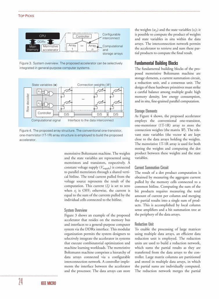
memristive Boltzmann machine. The weightsand the state variables are represented usingmemristors and transistors, respectively. Aconstant voltage supply (Vsupply) is connectedto parallel memristors through a shared verti-cal bitline. The total current pulled from thevoltage source represents the result of thecomputation. This current (Ij) is set to zerowhen xj is OFF; otherwise, the current isequal to the sum of the currents pulled by theindividual cells connected to the bitline.
System OverviewFigure 3 shows an example of the proposedaccelerator that resides on the memory busand interfaces to a general-purpose computersystem via the DDRx interface. This modularorganization permits the system designers toselectively integrate the accelerator in systemsthat execute combinatorial optimization andmachine learning workloads. The memristiveBoltzmann machine comprises a hierarchy ofdata arrays connected via a configurableinterconnection network. A controller imple-ments the interface between the acceleratorand the processor. The data arrays can store
the weights (wji) and the state variables (xi); itis possible to compute the product of weightsand state variables in situ within the dataarrays. The interconnection network permitsthe accelerator to retrieve and sum these par-tial products to compute the final result.
Fundamental Building BlocksThe fundamental building blocks of the pro-posed memristive Boltzmann machine arestorage elements, a current summation circuit,a reduction unit, and a consensus unit. Thedesign of these hardware primitives must strikea careful balance among multiple goals: highmemory density, low energy consumption,and in situ, fine-grained parallel computation.
Storage ElementsAs Figure 4 shows, the proposed acceleratoremploys the conventional one-transistor,one-memristor (1T-1R) array to store theconnection weights (the matrix W). The rele-vant state variables (the vector x) are keptclose to the data arrays holding the weights.The memristive 1T-1R array is used for bothstoring the weights and computing the dotproduct between these weights and the statevariables.
Current Summation CircuitThe result of a dot product computation isobtained by measuring the aggregate currentpulled by the memory cells connected to acommon bitline. Computing the sum of thebit products requires measuring the totalamount of current per column and mergingthe partial results into a single sum of prod-ucts. This is accomplished by local columnsense amplifiers and a bit summation tree atthe periphery of the data arrays.
Reduction UnitTo enable the processing of large matricesusing multiple data arrays, an efficient datareduction unit is employed. The reductionunits are used to build a reduction network,which sums the partial results as they aretransferred from the data arrays to the con-troller. Large matrix columns are partitionedand stored in multiple data arrays, in whichthe partial sums are individually computed.The reduction network merges the partial
CPU
DDRx
Mainmemory
Memristiveaccelerator
Controller
Array1
Arrayn
Configurableinterconnect
Computationalandstorage arrays
Figure 3. System overview. The proposed accelerator can be selectively
integrated in general-purpose computer systems.
State variables (x) Connection weights (W )
Row
dec
oder
Controller
Computational signal Interface to the data interconnect
D/S D/S D/S
x1
xn
Figure 4. The proposed array structure. The conventional one-transistor,
one-memristor (1T-1R) array structure is employed to build the proposed
accelerator.
..............................................................................................................................................................................................
TOP PICKS
............................................................
24 IEEE MICRO

results into a single sum. Multiple such net-works are used to process the weight columnsin parallel. The reduction tree comprises ahierarchy of bit-serial adders to strike a bal-ance between throughput and area efficiency.
Figure 5 shows the proposed reductionmechanism. The column is partitioned intofour segments, each of which is processedseparately to produce a total of four partialresults. The partial results are collected by areduction network comprising three bimodalreduction elements. Each element is config-ured using a local latch that operates in oneof two modes: forwarding or reduction. Eachreduction unit employs a full adder to com-pute the sum of the two inputs when operat-ing in the reduction mode. In the forwardingmode, the unit is used for transferring thecontent of one input upstream to the root.
Consensus UnitThe Boltzmann machine relies on a sigmoi-dal activation function, which plays a keyrole in both the model’s optimization andmachine learning applications. A preciseimplementation of the sigmoid function,however, would introduce unnecessaryenergy and performance overheads. The pro-posed memristive accelerator employs anapproximation unit using logic gates andlookup tables to implement the consensusfunction. As Figure 6 shows, the table con-tains 64 precomputed sample points of thesigmoid function f ðxÞ ¼ 1
1þe�x , in which xvaries between –4 and 4. The samples areevenly distributed on the x-axis. Six bits of agiven fixed-point value are used to index thelookup table and retrieve a sample value. Themost significant bits of the input data areANDed and NORed to decide whether theinput value is outside the domain [–4, 4]; ifso, the sign bit is extended to implement f(x)¼ 0 or f(x)¼ 1; otherwise, the retrieved sam-ple is chosen as the outcome.
System ArchitectureThe proposed architecture for the memristiveBoltzmann machine comprises multiple banksand a controller (see Figure 7). The banksoperate independently and serve memory andcomputation requests in parallel. For example,column 0 can be multiplied by the vector x at
bank 0 while any location of bank 1 is beingread. Within each bank, a set of sub-banks isconnected to a shared interconnection tree.The bank interconnect is equipped withreduction units to contribute to the dot prod-uct computation. In the reduction mode, allsub-banks actively produce the partial results,while the reduction tree selectively merges theresults from a subset of the sub-banks. Thiscapability is useful for computing the largematrix columns partitioned across multiplesub-banks. Each sub-bank comprises multiplemats, each of which is composed of a control-ler and multiple data arrays. The sub-banktree transfers the data bits between the mats
A largematrix
column
A
B
Mode
F.A. OutputMode Output
Forwarding
Reduction
A
A+B
Figure 5. The proposed reduction element. The reduction element can
operate in forwarding or reduction mode.
Decimal pointB
it ex
tens
ion
Accept/Reject
64 × 16lookuptable
In
Out
Pseudorandom generator
In (energy difference)43210–1–2–3–4O
ut (
pro
bab
ility
) 1.00.80.60.40.2
0
64 evenly sampled points from sigmoid
Figure 6. The proposed unit for the activation function. A 64-entry lookup
table is used for approximating the sigmoid function.
Chip
Controller
Bank Subbank
Reductiontree
Subbanktree
Mat
F/R
F/R
F/R Dataarray
Figure 7. Hierarchical organization of a chip. A chip controller is employed to
manage the multiple independent banks.
.............................................................
MAY/JUNE 2017 25
and the bank tree in a bit-parallel fashion,thereby increasing the parallelism.
Data OrganizationTo amortize the peripheral circuitry’s cost, thedata array’s columns and rows are time shared.Each sense amplifier is shared by four bitlines.The array is vertically partitioned along thebitlines into 16 stripes, multiples of which canbe enabled per array computation. This allowsthe software to keep a balance between theaccuracy of the computation and the perform-ance for a given application by quantizingmore bit products into a fixed number of bits.
On-Chip ControlThe proposed hardware can accelerate opti-mization and deep learning tasks by appro-priately configuring the on-chip controller.The controller configures the reduction trees,maps the data to the internal resources,orchestrates the data movement among thebanks, performs annealing or training tasks,and interfaces to the external bus.
DIMM OrganizationTo solve large-scale optimization andmachine learning problems whose statespaces do not fit within a single chip, we caninterconnect multiple accelerators on aDIMM. Each DIMM is equipped with con-trol registers, data buffers, and a controller.This controller receives DDRx commands,data, and address bits from the external inter-face and orchestrates computation among allof the chips on the DIMM.
Software SupportTo make the proposed accelerator visible tosoftware, we memory map its address rangeto a portion of the physical address space. Asmall fraction of the address space withinevery chip is mapped to an internal RAMarray and is used to implement the data buf-fers and configuration parameters. Softwareconfigures the on-chip data layout and ini-tiates the optimization by writing to a mem-ory mapped control register.
Evaluation HighlightsWe modify the SESC simulator3 to model abaseline eight-core out-of-order processor.
The memristive Boltzmann machine is inter-faced to a single-core system via a singleDDR3-1600 channel. We develop anRRAM-based processing-in-memory (PIM)baseline. The weights are stored within dataarrays that are equipped with integer andbinary multipliers to perform the dot prod-ucts. The proposed consensus units, optimi-zation and training controllers, and mappingalgorithms are employed to accelerate theannealing and training processes. When com-pared to existing computer systems andGPU-based accelerators, the PIM baselinecan achieve significantly higher performanceand energy efficiency because it eliminatesthe unnecessary data movement on the mem-ory bus, exploits data parallelism throughoutthe chip, and transfers the data across thechip using energy-efficient reduction trees.The PIM baseline is optimized so that itoccupies the same area as that of the memris-tive accelerator.
Area, Delay, and Power BreakdownWe model the data array, sensing circuits,drivers, local array controller, and interconnectelements using Spice predictive technologymodels4 of n-channel and p-channel metal-oxide semiconductor transistors at 22 nm.The full adders, latches, and control logic aresynthesized using FreePDK5 at 45 nm. Wefirst scale the results to 22 nm using scalingparameters reported in prior work,6 and thenscale them using the fan-out of 4 (FO4)parameters for International Technology Road-map for Semiconductors low-standby-power(LSTP) devices to model the impact of usinga memory process on peripheral and globalcircuitry.7,8 We use McPAT9 to estimate theprocessor power.
Figure 8 shows a breakdown of the compu-tational energy, leakage power, computationallatency, and die area among different hard-ware components. The sense amplifiers andinterconnects are the major contributors tothe dynamic energy (41 and 36 percent,respectively). The leakage is caused mainly bythe current summation circuits (40 percent)and other logic (59 percent), which includesthe charge pumps, write drivers, and control-lers. The computation latency, however, isdue mainly to the interconnects (49 percent),the wordlines, and the bitlines (32 percent).
..............................................................................................................................................................................................
TOP PICKS
............................................................
26 IEEE MICRO

Notably, only a fraction of the memory arraysmust be active during a computational opera-tion. A subset of the mats within each bankperforms current sensing of the bitlines; thepartial results are then serially streamed to thecontroller on the interconnect wires. Theexperiments indicate that a fully utilized accel-erator integrated circuit (IC) consumes 1.3 W,which is below the peak power rating of astandard DDR3 chip (1.4 W).
PerformanceFigure 9 shows the performance on theproposed accelerator, the PIM architecture,the multicore system running the multi-threaded kernel, and the single-core systemrunning the semidefinite programing (SDP)and MaxWalkSAT kernels. The results are nor-malized to the single-threaded kernel runningon a single core. The results indicate that thesingle-threaded kernel (Boltzmann machine) isfaster than the baselines (SDP and MaxWalk-SAT heuristics) by an average of 38 percent.The average performance gain for the mul-tithreaded kernel is limited to 6 percent,owing to significant state update overheads.PIM outperforms the single-threaded ker-nel by 9.31 times. The memristive accelera-tor outperforms all of the baselines (57.75times speedup over the single-threaded ker-nel and 6.19 times over PIM). Moreover,the proposed accelerator performs the deeplearning tasks 68.79 times faster than thesingle-threaded kernel and 6.89 times fasterthan PIM.
EnergyFigure 10 shows the energy savings as com-pared to PIM, the multithreaded kernel,SDP, and MaxWalkSAT. On average, energyis reduced by 25 times as compared to thesingle-threaded kernel implementation, whichis 5.2 times better than PIM. For the deeplearning tasks, the system energy is improvedby 63 times, which is 5.3 times better than theenergy consumption of PIM.
Sensitivity to Process VariationsMemristor parameters can deviate from theirnominal values, owing to process variationscaused by line edge roughness, oxide thick-ness fluctuation, and random discrete dop-ing. These parameter deviations result in
cycle-to-cycle and device-to-device variabil-ities. We evaluate the impact of cycle-to-cyclevariation on the computation’s outcome byconsidering a bit error rate of 10�5 in all ofthe simulations, along the lines of the analy-sis provided in prior work.10 The proposedaccelerator successfully tolerates such errors,with less than a 1-percent change in the out-come as compared to a perfect softwareimplementation.
The resistance of RRAM cells can fluctu-ate because of the device-to-device variation,which can impact the outcome of a columnsummation—that is, a partial dot product.
Peak energy (8.6 nJ)Leakage power (405 mW)
Computational latency (6.59 ns)Die area (25.67 mm2)
Others Interconnects Sense amplifiers Data arrays
0% 10% 20% 30% 40% 50% 60% 70% 80% 90% 100%
Figure 8. Area, delay, and power breakdown. Peak energy, leakage
power, computational latency, and die area are estimated at the 22-nm
technology node.
Sp
eed
up o
ver
the
sing
le-t
hrea
ded
ker
nel 100
10
0.1
1
Baseline Multithreaded kernel PIM Memristive accelerator
MC
-1
MC
-2
MC
-3
MC
-4
MC
-5
MC
-6
MC
-7
MC
-8
MC
-9
Geo
mea
n
MC
-10
MS
-1
MS
-2
MS
-3
MS
-4
MS
-5
MS
-6
MS
-7
MS
-8
MS
-9
MS
-10
Figure 9. Performance on optimization. Speedup of various system
configurations over the single-threaded kernel.
Ene
rgy
savi
ngs
over
the
sing
le-t
hrea
ded
ker
nel
100
10
0.1
1
Baseline Multithreaded kernel PIM Memristive accelerator
MC
-1
MC
-2
MC
-3
MC
-4
MC
-5
MC
-6
MC
-7
MC
-8
MC
-9
Geo
mea
n
MC
-10
MS
-1
MS
-2
MS
-3
MS
-4
MS
-5
MS
-6
MS
-7
MS
-8
MS
-9
MS
-10
Figure 10. Energy savings on optimization. Energy savings of various
system configurations over the single-threaded kernel.
.............................................................
MAY/JUNE 2017 27
We use the geometric model of memri-stance variation proposed by Miao Hu andcolleagues11 to conduct Monte Carlo simu-lations for 1 million columns, each com-prising 32 cells. The experiment yields twodistributions for low resistance (RLO) andhigh resistance (RHI) samples that are thenapproximated by normal distributions withrespective standard deviations of 2.16 and2.94 percent (similar to the prior work byHu and colleagues). We then find a bit pat-tern that results in the largest summationerror for each column. We observe up to2.6 � 10�6 deviation in the column con-ductance, which can result in up to 1 biterror per summation. Subsequent simula-tion results indicate that the accelerator cantolerate this error, with less than a 2 percentchange in the outcome quality.
Finite Switching EnduranceRRAM cells exhibit finite switching endur-ance ranging from 1e6 to 1e12 writes. Weevaluate the impact of finite endurance on anaccelerator module’s lifetime. Because wear isinduced only by the updating of the weightsstored in memristors, we track the number oftimes that each weight is written. The edgeweights are written once in optimizationproblems and multiple times in deep learningworkloads. (Updating the state variables,stored in static CMOS latches, does notinduce wear on RRAM.) We track the totalnumber of updates per second to estimatethe lifetime of an eight-chip DIMM. Assum-ing endurance parameters of 1e6 and 1e8writes, the respective module lifetimes are 3.7and 376 years for optimization and 1.5 and151 years for deep learning.
D ata movement between memory cellsand processor cores is the primary con-
tributor to power dissipation in computersystems. A recent report by the US Depart-ment of Energy identifies the power con-sumed in moving data between the memoryand the processor as one of the 10 most sig-nificant challenges in the exascale computingera.12 The same report indicates that by2020, the energy cost of moving data acrossthe memory hierarchy will be orders of mag-nitude higher than the cost of performing adouble-precision floating-point operation.
Emerging large-scale applications such ascombinatorial optimization and deep learn-ing tasks are even more influenced by mem-ory bandwidth and power problems. In theseapplications, massive datasets have to be iter-atively accessed by the processor cores toachieve a desirable output quality, whichconsumes excessive memory bandwidth andsystem energy. To address this problem,numerous software and hardware optimiza-tions using GPUs, clusters based on messagepassing interface (MPI), field-programmablegate arrays, and application-specific inte-grated circuits have been proposed in theliterature. These proposals focus on energy-efficient computing with reduced data move-ment among the processor cores and memoryarrays. These proposals’ performance andenergy efficiency are limited by read accessesthat are necessary to move the operands fromthe memory arrays to the processing units. Amemory subsystem that allows for in situcomputation within its data arrays couldaddress these limitations by eliminating theneed to move raw data between the memoryarrays and the processor cores.
Designing a platform capable of perform-ing in situ computation is a significant chal-lenge. In addition to storage cells, extracircuits are required to perform analog com-putation within the memory cells, whichdecreases memory density and area efficiency.Moreover, power dissipation and area con-sumption of the required components forsignal conversion between analog and digitaldomains could become serious limiting fac-tors. Hence, it is critical to strike a careful bal-ance between the accelerator’s performanceand complexity.
The memristive Boltzmann machine isthe first memory-centric accelerator thataddresses these challenges. It provides a newframework for designing memory-centricaccelerators. Large scale combinatorial opti-mization problems and deep learning tasksare mapped onto a memory-centric, non-Von Neumann computing substrate andsolved in situ within the memory cells, withorders of magnitude greater performance andenergy efficiency than contemporary super-computers. Unlike PIM-based accelerators,the proposed accelerator enables computationwithin conventional data arrays to achieve the
..............................................................................................................................................................................................
TOP PICKS
............................................................
28 IEEE MICRO

energy-efficient and massively parallel proc-essing required for the Boltzmann machinemodel.
We expect the proposed memory-centricaccelerator to set off a new line of research onin situ approaches to accelerate large-scaleproblems such as combinatorial optimizationand deep learning tasks and to significantlyincrease the performance and energy effi-ciency of future computer systems. MICRO
AcknowledgmentsThis work was supported in part by NSFgrant CCF-1533762.
....................................................................References1. E. Aarts and J. Korst, Simulated Annealing
and Boltzmann Machines: A Stochastic
Approach to Combinatorial Optimization and
Neural Computing, John Wiley & Sons,
1989.
2. S.E. Fahlman, G.E. Hinton, and T.J. Sejnow-
ski, “Massively Parallel Architectures for AI:
NETL, Thistle, and Boltzmann Machines,”
Proc. Assoc. Advancement of AI (AAAI),
1983, pp. 109–113.
3. J. Renau et al., “SESC Simulator,” Jan.
2005; http://sesc.sourceforge.net.
4. W. Zhao and Y. Cao, “New Generation of
Predictive Technology Model for Sub-45nm
Design Exploration,” Proc. Int’l Symp. Qual-
ity Electronic Design, 2006, pp. 585–590.
5. “FreePDK 45nm Open-Access Based PDK
for the 45nm Technology Node,” 29 May
2014; www.eda.ncsu.edu/wiki/FreePDK.
6. M.N. Bojnordi and E. Ipek, “Pardis: A Pro-
grammable Memory Controller for the
DDRX Interfacing Standards,” Proc. 39th
Ann. Int’l Symp. Computer Architecture
(ISCA), 2012 pp. 13–24.
7. N.K. Choudhary et al., “Fabscalar: Compos-
ing Synthesizable RTL Designs of Arbitrary
Cores Within a Canonical Superscalar
Template,” Proc. 38th Ann. Int’l Symp. Com-
puter Architecture, 2011, pp. 11–22.
8. S. Thoziyoor et al., “A Comprehensive Mem-
ory Modeling Tool and Its Application to the
Design and Analysis of Future Memory Hier-
archies,” Proc. 35th Int’l Symp. Computer
Architecture (ISCA), 2008, pp. 51–62.
9. S. Li et al., “McPAT: An Integrated Power,
Area, and Timing Modeling Framework for
Multicore and Manycore Architectures,”
Proc. 36th Int’l Symp. Computer Architec-
ture (ISCA), 2009, pp. 468–480.
10. D. Niu et al., “Impact of Process Variations
on Emerging Memristor,” Proc. 47th ACM/
IEEE Design Automation Conf. (DAC), 2010,
pp. 877–882.
11. M. Hu et al., “Geometry Variations Analysis
of Tio 2 Thin-Film and Spintronic Mem-
ristors,” Proc. 16th Asia and South Pacific
Design Automation Conf., 2011, pp. 25–30.
12. The Top Ten Exascale Research Challenges,
tech. report, Advanced Scientific Comput-
ing Advisory Committee Subcommittee,
Dept. of Energy, 2014.
Mahdi Nazm Bojnordi is an assistant pro-fessor in the School of Computing at theUniversity of Utah. His research focuses oncomputer architecture, with an emphasis onenergy-efficient computing. Nazm Bojnordireceived a PhD in electrical engineeringfrom the University of Rochester. Contacthim at [email protected].
Engin Ipek is an associate professor in theDepartment of Electrical and ComputerEngineering and the Department of Com-puter Science at the University of Rochester.His research interests include energy-efficientarchitectures, high-performance memory sys-tems, and the application of emerging tech-nologies to computer systems. Ipek receiveda PhD in electrical and computer engineer-ing from Cornell University. He has receivedthe 2014 IEEE Computer Society TCCAYoung Computer Architect Award, twoIEEE Micro Top Picks awards, and an NSFCAREER award. Contact him at [email protected].
Read your subscriptions through the myCS publications portal at http://mycs.computer.org.
.............................................................
MAY/JUNE 2017 29

.................................................................................................................................................................................................................
ANALOG COMPUTING IN A MODERNCONTEXT: A LINEAR ALGEBRA
ACCELERATOR CASE STUDY.................................................................................................................................................................................................................
THIS ARTICLE PRESENTS A PROGRAMMABLE ANALOG ACCELERATOR FOR SOLVING
SYSTEMS OF LINEAR EQUATIONS. THE AUTHORS COMPENSATE FOR COMMONLY PERCEIVED
DOWNSIDES OF ANALOG COMPUTING. THEY COMPARE THE ANALOG SOLVER’S
PERFORMANCE AND ENERGY CONSUMPTION AGAINST AN EFFICIENT DIGITAL ALGORITHM
RUNNING ON A GENERAL-PURPOSE PROCESSOR. FINALLY, THEY CONCLUDE THAT PROBLEM
CLASSES OUTSIDE OF SYSTEMS OF LINEAR EQUATIONS COULD HOLD MORE PROMISE FOR
ANALOG ACCELERATION.
......As we approach the limits of sili-con scaling, it behooves us to reexamine fun-damental assumptions of modern computing,even well-served ones, to see if they are hin-dering performance and efficiency. An analogaccelerator discussed in this article breakstwo fundamental assumptions in moderncomputing: in contrast to using digital binarynumbers, an analog accelerator encodes num-bers using the full range of circuit voltage andcurrent. Furthermore, in contrast to operatingstep by step on clocked hardware, an analogaccelerator updates its values continuously.These different hardware assumptions canprovide substantial gains but would needdifferent abstractions and cross-layer optimi-zations to support various modern workloads.We draw inspiration from an immenseamount of prior work in analog electronic
computing (see the sidebar, “Related Work inAnalog Computing”).
To support modern workloads in the digitalera, we observed that modern scientific com-puting and big data problems are converted tolinear algebra problems. To maximize analogacceleration’s usefulness, we explored whetheranalog accelerators are effective at solvingsystems of linear equations, the single mostimportant numerical primitive in continuousmathematics.
For readers not familiar with linear alge-bra, systems of linear equations are oftensolved using iterative numerical linear algebramethods, which start with an initial guess forthe entire solution vector and update the sol-ution vector over iterations of the algorithm,each step further minimizing the differencebetween the guess and the correct solution.1
Yipeng Huang
Ning Guo
Mingoo Seok
Yannis Tsividis
Simha Sethumadhavan
Columbia University
.......................................................
30 Published by the IEEE Computer Society 0272-1732/17/$33.00�c 2017 IEEE
Efficient iterative methods such as the conju-gate gradient method are increasingly impor-tant because intermediate guess vectors are agood approximation of the correct solution.
In discrete-time-iterative linear algebraalgorithms, the solution vector changes insteps, and each step is characterized by a stepsize. The step size affects the algorithm’s effi-ciency and requires many processor cycles tocalculate. In the conjugate gradient method,for example, the step size is calculated fromprevious step sizes and the gradient magni-tude, and this calculation takes up half of themultiplication operations in each conjugategradient step.
In an analog accelerator, systems of linearequations can also be thought of as solvedvia an iterative algorithm, with an importantdistinction that the guess vector is updatedusing infinitesimally small steps, over infin-
itely many iterations. This continuous trajec-tory from the original guess vector to thecorrect solution is an ordinary differentialequation (ODE), which states that the changein a set of variables is a function of the varia-bles’ present value. We can naturally solveODEs using an analog accelerator.
We give an example of an analog accelera-tor solving an ODE that in turn solves asystem of linear equations. At the analogaccelerator’s heart are integrators, which con-tain the present guess of the solution vectorrepresented as an analog signal evolving as afunction of time (see Figure 1). We performoperations on this solution vector by feedingthe vector through multiplier and summationunits. Digital-to-analog converters (DACs)provide constant coefficients and biases.Using these function units, we create a lin-ear function of the solution vector, which is
Related Work in Analog ComputingAnalog computers of the mid-20th century were widely used to
solve scientific computing problems, described as ordinary differ-
ential equations (ODEs). Analog computers would solve those
ODEs by setting up analog electronic circuits, whose time-depend-
ent voltage and current were described by corresponding ODEs.
The analog computers therefore were computational analogies of
physical models.
Our group revisited this model of analog computing for solving
nonlinear ODEs, which frequently appear in cyber-physical sys-
tems workloads, with higher performance and efficiency com-
pared to digital systems.1,2 The analog, continuous-time output of
analog computing is especially suited for embedded systems
applications in which sensor inputs are analog and actuators can
use such results directly. The question for this article is whether
analog acceleration can help conventional workloads in which
inputs and outputs are digital.
Modern scientific computation and big data workloads are
phrased as linear algebra problems. In this article, our analog
accelerator solves an ODE that does steepest descent, in turn
solving a linear algebra problem. Such a solving method belongs
to a broad class of ODEs that can solve other numerical problems,
including nonlinear systems of equations.3,4 These ODEs point to
other ways analog accelerators can support modern workloads.
We draw a distinction between our approach to analog accel-
eration and that of using analog circuits to build neural net-
works.5,6 Most importantly, we do not use training to get a
network topology and weights that solve a given problem. No
prior knowledge of the solution or training set of solutions is
required. The analog acceleration technique presented in this
article is a procedural approach to solving problems: there is a
predefined way to convert a system of linear equations under
study into an analog accelerator configuration.
References1. G. Cowan, R. Melville, and Y. Tsividis, “A VLSI Analog
Computer/Digital Computer Accelerator,” IEEE J. Solid-
State Circuits, vol. 41, no. 1, 2006, pp. 42–53.
2. N. Guo et al., “Energy-Efficient Hybrid Analog/Digital
Approximate Computation in Continuous Time,” IEEE J.
Solid-State Circuits, vol. 51, no. 7, 2016, pp. 1514–1524.
3. M.T. Chu, “On the Continuous Realization of Iterative
Processes,” SIAM Rev., vol. 30, no. 3, 1988, pp.
375–387.
4. O. Bournez and M.L. Campagnolo, A Survey on Continu-
ous Time Computations, Springer, 2008, pp. 383–423.
5. R. LiKamWa et al., “RedEye: Analog ConvNet Image Sen-
sor Architecture for Continuous Mobile Vision,”
SIGARCH Computer Architecture News, vol. 44, no. 3,
2016, pp. 255–266.
6. A. Shafiee et al., “ISAAC: A Convolutional Neural Net-
work Accelerator with In-Situ Analog Arithmetic in Cross-
bars,” SIGARCH Computer Architecture News, vol. 44,
no. 3, 2016, pp. 14–26.
.............................................................
MAY/JUNE 2017 31
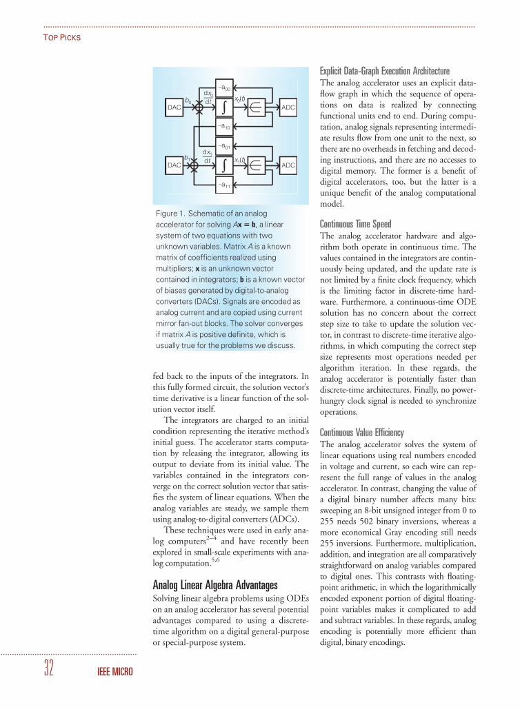
fed back to the inputs of the integrators. Inthis fully formed circuit, the solution vector’stime derivative is a linear function of the sol-ution vector itself.
The integrators are charged to an initialcondition representing the iterative method’sinitial guess. The accelerator starts computa-tion by releasing the integrator, allowing itsoutput to deviate from its initial value. Thevariables contained in the integrators con-verge on the correct solution vector that satis-fies the system of linear equations. When theanalog variables are steady, we sample themusing analog-to-digital converters (ADCs).
These techniques were used in early ana-log computers2–4 and have recently beenexplored in small-scale experiments with ana-log computation.5,6
Analog Linear Algebra AdvantagesSolving linear algebra problems using ODEson an analog accelerator has several potentialadvantages compared to using a discrete-time algorithm on a digital general-purposeor special-purpose system.
Explicit Data-Graph Execution ArchitectureThe analog accelerator uses an explicit data-flow graph in which the sequence of opera-tions on data is realized by connectingfunctional units end to end. During compu-tation, analog signals representing intermedi-ate results flow from one unit to the next, sothere are no overheads in fetching and decod-ing instructions, and there are no accesses todigital memory. The former is a benefit ofdigital accelerators, too, but the latter is aunique benefit of the analog computationalmodel.
Continuous Time SpeedThe analog accelerator hardware and algo-rithm both operate in continuous time. Thevalues contained in the integrators are contin-uously being updated, and the update rate isnot limited by a finite clock frequency, whichis the limiting factor in discrete-time hard-ware. Furthermore, a continuous-time ODEsolution has no concern about the correctstep size to take to update the solution vec-tor, in contrast to discrete-time iterative algo-rithms, in which computing the correct stepsize represents most operations needed peralgorithm iteration. In these regards, theanalog accelerator is potentially faster thandiscrete-time architectures. Finally, no power-hungry clock signal is needed to synchronizeoperations.
Continuous Value EfficiencyThe analog accelerator solves the system oflinear equations using real numbers encodedin voltage and current, so each wire can rep-resent the full range of values in the analogaccelerator. In contrast, changing the value ofa digital binary number affects many bits:sweeping an 8-bit unsigned integer from 0 to255 needs 502 binary inversions, whereas amore economical Gray encoding still needs255 inversions. Furthermore, multiplication,addition, and integration are all comparativelystraightforward on analog variables comparedto digital ones. This contrasts with floating-point arithmetic, in which the logarithmicallyencoded exponent portion of digital floating-point variables makes it complicated to addand subtract variables. In these regards, analogencoding is potentially more efficient thandigital, binary encodings.
–a00
–a10
–a01
–a11
b1
b0x0(t)
x1(t)
DAC
DAC
ADC
ADC
dx1
dt
dx0
dt
Figure 1. Schematic of an analog
accelerator for solving Ax 5 b, a linear
system of two equations with two
unknown variables. Matrix A is a known
matrix of coefficients realized using
multipliers; x is an unknown vector
contained in integrators; b is a known vector
of biases generated by digital-to-analog
converters (DACs). Signals are encoded as
analog current and are copied using current
mirror fan-out blocks. The solver converges
if matrix A is positive definite, which is
usually true for the problems we discuss.
..............................................................................................................................................................................................
TOP PICKS
............................................................
32 IEEE MICRO

Analog Accelerator ArchitectureThe analog accelerator acts as a peripheral toa digital host processor. The analog accelera-tor interface accepts an accelerator configura-tion, which entails the connectivity betweenfunction units, multiplier gains, DAC con-stants, and integrator initial conditions.Additionally, the interface allows calibration,computation control, and reading of outputvalues, and reporting exceptions. Table 1summarizes the analog accelerator’s essentialsystem calls and corresponding instructions.
Analog Accelerator Physical PrototypeWe tested analog acceleration for linear alge-bra using a prototype reconfigurable analogaccelerator silicon chip implemented in65-nm CMOS technology (see Figures 2and 3). The accelerator comprises four inte-grators, plus accompanying DACs, multi-pliers, and ADCs connected using crossbarswitches. In our analog accelerator, electrical
currents represent variables. Fan-out cur-rent mirrors allow the analog circuit to copyvariables by replicating values onto differentbranches. To sum variables, currents are addedtogether by joining branches. Eight multi-pliers allow variable-variable and constant-variable multiplication.
The physical prototype validates the ana-log circuits’ functionality and allows physicalmeasurement of component area and energy.Additionally, the chip allows rapid prototyp-ing of accelerator algorithms.
Using physical timing, power, and areameasurements recorded by Ning Guo andcolleagues7 and summarized in Table 2, webuilt a model that predicts the properties oflarger-scale analog accelerators. In Table 2,“analog core power” and “analog core area”show the power and area of each block thatforms the analog signal path. The noncoretransistors and nets not involved in analogcomputation include calibration and testingcircuits and registers. The core area and power
Table 1. Analog accelerator instruction set architecture.
Instruction type Instruction Parameters Instruction effect
Control Initialize — Find input and output offset and gain calibration
settings for all function units.
Configuration Set connection Source, destination Set a crossbar switch to create an analog current
connection between two analog interfaces.
Configuration Set initial condition Pointer to an integrator, initial
condition value
Charge integrator capacitors to have ODE initial
condition value.
Configuration Set multiplier gain Pointer to a multiplier, gain value Amplify values by constant coefficient gain.
Configuration Set constant offset Pointer to a DAC, offset value Add a constant bias to values.
Configuration Set timeout time Number of digital controller
clock cycles
Stop analog computation after specified time
once started.
Configuration Configuration commit — Finish configuration and write any new changes
to chip registers.
Control Execution start — Start analog computation by letting integrators
deviate from initial conditions.
Control Execution stop — Stop analog computation by holding integrators
at their present value.
Data input Enable analog input Pointer to chip analog input
channel
Open chip analog input channel, allowing multi-
ple chips to participate in computation.
Data output Read analog value Pointer to an ADC, memory
location to store result
Read analog computation results from ADCs and
store values.
Exception Read exceptions Memory location to store result Read the exception vector indicating whether
analog units exceeded their valid range....................................................................................................................................
*ADC: analog-to-digital converter; DAC: digital-to-analog converter; ODE: ordinary differential equation.
.............................................................
MAY/JUNE 2017 33

scale up and down for different analog band-width designs. We explore how differentbandwidth choices influence analog accel-erator performance and efficiency.
Mitigation of Analog Linear AlgebraDisadvantagesWe encountered several drawbacks of analogcomputing, including limited accuracy, pre-cision, and scalability. We tackled each ofthese problems in the context of solvinglinear algebra, although the techniques we dis-cuss apply to other styles of analog computerarchitecture.
Improve Accuracy Using Calibration and AnalogExceptionsAnalog circuits provide limited accuracycompared to binary ones, in which values areunambiguously interpreted as 0 or 1. Analoghardware uses the full range of values. Subtlevariations in analog hardware due to processand temperature variation lead to undesirablevariations in the computation result.
We identify three main sources of inaccur-acy in analog hardware: gain error, offseterror, and nonlinearity. Gain and offset errorsrefer to inaccurate results in multiplicationand summation, which can be calibratedaway using additional DACs that adjust cir-cuit parameters to shift signals and adjustgains. These DACs are controlled by registers,whose contents are set using binary searchduring calibration by the digital host. The set-tings vary across different copies of functionalunits and accelerator chips, but remain con-stant during accelerator operation.
Nonlinearity errors occur when changesin inputs result in disproportionate changesin outputs, and when analog values exceedthe range in which the circuit’s behavior ismostly linear, resulting in clipping of theoutput, akin to overflow of digital numberrepresentations. At the same time, the hostobserves if the dynamic range is not fullyused, which could result in low precision.When either exception type occurs, the origi-nal problem is rescaled to fit in the dynamicrange of the analog accelerator, and computa-tion is reattempted.
The combination of widespread calibra-tion and exception checking ensures that the
8 fan-out blocks 4 integrators 8 multiplier/VGAs 4 analoginputs
4 an
alog
outp
uts
Dig
ital
inp
ut
Digitaloutput
CT
AD
C
CT
AD
C
CT
DA
C
CT
DA
C
8 8
8 8 8
8
8
8
88
4
SPI SRAM SRAM
SPI controller
Figure 2. Analog accelerator architecture diagram, showing rows of analog,
mixed-signal, and digital components, along with crossbar interconnect.7
“CT” refers to continuous time. Static RAMs (SRAMs) are used as lookup
tables for nonlinear functions (not used for the purposes of this article).
8×fan-out
8×multiplier/
VGA
4×integrator
2 × CT ADC 2 × CT DAC
2 × SRAMSPI controller
Figure 3. Die photo of an analog accelerator
chip fabricated in 65-nm CMOS technology,
showing major components.7 “VGAs” are
variable-gain amplifiers. The die area is
3.8 mm2.
..............................................................................................................................................................................................
TOP PICKS
............................................................
34 IEEE MICRO

analog solution’s accuracy is within the sam-pling resolution of ADCs.
Improve Sampling Precision by Focusing onAnalog Steady StateHigh-frequency and high-precision analog-to-digital conversion is costly. So, instead oftrying to capture the time-dependent analogwaveform, we use the analog accelerator as alinear algebra solver by solving a convergentODE. When the analog accelerator outputsare steady, we can sample the solutions oncewith higher-precision ADCs.
Even then, high-precision ADCs still fallshort of the precision in floating-point num-bers. Even though the analog variables arethemselves highly precise, sampling the varia-bles using ADCs can result in only 8 to 12bits of precision. We get higher-precisionresults by running the analog accelerator mul-tiple times. We use the digital host computerto find the residual error in the solution, andwe set up the analog accelerator to solve a newproblem, focusing on the residual. Each prob-lem has smaller-magnitude variables than pre-vious runs, which lets us scale up the variablesto fit the dynamic range of the analog hard-ware. We can iterate between analog and digi-tal hardware a few times to get a more preciseresult than using the analog hardware alone.
Tackle Larger Problems by Accelerating SparseLinear Algebra SubproblemsModern workloads routinely need thousandsof variables, corresponding to as many analogintegrators in the accelerator, exceeding thearea constraints of realistic analog accelerators.Furthermore, the analog datapath is fixedduring continuous time operation, so there isno way to dynamically load variables fromand store variables to main memory.
Analog accelerators can solve large-scalesparse linear algebra problems by acceleratingthe solving of smaller subproblems. This letsanalog accelerators solve problems containingmore variables than the number of integra-tors in the analog accelerator.
In such a scheme, the analog acceleratorfinds the correct solution for a subproblem.To get overall convergence across the entireproblem, the set of subproblems would besolved several times, using an outer loop iter-ating across the subproblems. Typically, thelarger iteration is an iterative method operat-ing on vectors, which do not have as strongconvergence properties as iterative methodsdo on individual numbers. Therefore, it is stilldesirable to ensure the block matrices cap-tured in the analog accelerator are large, sothat more of the problem is solved using theefficient lower-level solver.
EvaluationWe compare the analog accelerator and digi-tal approaches in terms of performance, hard-ware area, and energy consumption, whilevarying the number of problem variables andthe choice of analog accelerator componentbandwidth, a measure of how quickly theanalog circuit responds to changes.
Analog Bandwidth ModelThe prototype chip has a relatively low analogbandwidth of 20 KHz, a design that ensuresthat the prototype chip accurately solves fortime-dependent solutions in ODEs. How-ever, the prototype’s small bandwidth makesit unrepresentative of an analog acceleratordesigned to solve time-independent algebraicequations, in which accuracy degradation intime-dependent behavior has no impact onthe final steady state output. We scale up the
Table 2. Summary of analog accelerator components.
Unit type Analog core
power
Total unit
power
Analog core
area
Total unit
area
Integrator 22 lW 28 lW 0.016 mm2 0.040 mm2
Fan-out 30 lW 37 lW 0.005 mm2 0.015 mm2
Multiplier 39 lW 49 lW 0.024 mm2 0.050 mm2
ADC 27 lW 54 lW 0.049 mm2 0.054 mm2
DAC 4.6 lW 4.6 lW 0.013 mm2 0.022 mm2
.............................................................
MAY/JUNE 2017 35

model’s bandwidth, within reason, up to1.3 MHz.
Increasing the bandwidth of the analogcircuit design proportionally decreases the
solution time, but also increases area andenergy consumption. As Figures 4 and 5show, we assume an analog accelerator withbandwidth multiplied by a factor of a hashigher power and area consumption in thecore analog circuits, by a factor of a.
The projected analog power figures aresignificantly below the thermal design powerof clocked digital designs of equal area. Evenin the designs that fill a 600 mm2 die size, theanalog accelerator uses about 0.7 W in thebase prototype design and about 1.0 W inthe design with 320 KHz of bandwidth.
Sparse Linear Algebra Case StudyWe use as our test case a sparse system oflinear equations derived from a multigridelliptic partial differential equation (PDE)solver. In multigrid PDE solvers, the overallPDE is converted to several linear algebraproblems with varying spatial resolution.Lower-resolution subproblems are quicklysolved and fed to high-resolution subpro-blems, aiding the high-resolution problem toconverge faster. The linear algebra subpro-blems can be solved approximately. Overallaccuracy of the solution is guaranteed by iter-ating the multigrid algorithm. Because perfectconvergence is not required, less stable, inac-curate, and low-precision techniques, such asanalog acceleration, can support multigrid.
In our case, we compare the analog accel-erator designs to a conjugate gradient algo-rithm running on a CPU, solving to equal(relatively low) solution precision, equivalentto the precision obtained from one run ofthe analog accelerator equipped with high-resolution ADCs. On the digital side, thenumerical iteration stops short of the machineprecision provided by high-precision digitalfloating-point numbers.
The conjugate gradient algorithm uses asustained 20 clock cycles per numerical itera-tion per row element. The comparisonassumes identical transfer cost of data frommain memory to the accelerator versus theCPU: the energy needed to transfer data toand from memory is not modeled, due to therelatively small problem sizes, allowing theprogram data to be entirely cache resident.
As Figure 6 shows, we found that an opti-mal analog accelerator design that balancesperformance and the number of integrators
1.2
1.0
0.8
0.6
0.4
0.2
0.00 500 1,000 1,500 2,000
Max
imum
act
ivity
pow
er (
W)
Total grid points
20 KHz 80 KHz 320 KHz 1.3 MHz
Figure 4. Power versus analog accelerator
size for various bandwidth choices. We
observe that analog circuits operate faster
when the internal node voltages
representing variables change more quickly.
We hold the capacitance fixed to the
capacitance of the prototype’s design, and
use larger currents that draw more power
to charge and discharge the node
capacitances in the signal paths carrying
variables.
0 500 1,000 1,500 2,000
Are
a (m
m2 )
Total grid points
20 KHz 80 KHz 320 KHz 1.3 MHz
6.00E+02
4.00E+02
2.00E+02
0.00E+00
Figure 5. Area versus analog accelerator
size for various bandwidth choices. We
observe that the transistor aspect ratio W/L
must increase to increase the current, and
therefore bandwidth, of the design. L is
kept at a minimum dictated by the
technology node, leaving bandwidth to be
linearly dependent on W. Thus, we
estimate area increasing linearly with
bandwidth.
..............................................................................................................................................................................................
TOP PICKS
............................................................
36 IEEE MICRO

should have components with an analogbandwidth of approximately 320 KHz. Withour bandwidth model, high-bandwidth ana-log computers come with high area cost,quickly reaching the area of the largest CPUor GPU dies. On performance and energymetrics, we find that, with 400 integratorsoperating at 320 KHz of analog bandwidth,analog acceleration can potentially have a 10-times faster solution time; using our analogbandwidth model for power, this designcorresponds to 33 percent lower energy con-sumption compared to a digital general-purpose processor.
W e recognize that the performance in-creases and energy savings are not as
drastic as one expects when using a domain-specific accelerator built on a fundamentallydifferent computing model than digital, syn-chronous computing. The reason for thisshortfall is twofold.
First, the high area cost of high-bandwidthanalog components limits the problem sizesthat can fit in the accelerator, and thereforelimits the analog performance advantage.
Second, the extreme importance of linearalgebra problems has also led to intenseresearch in optimal algorithms and hardwaresupport. Although discrete-time operation hasdrawbacks, it permits algorithms to intelli-gently select a step size, which has advantagesin solving systems of linear equations. Boththe analog and digital solvers perform iterativenumerical algorithms, but the digital programruns the conjugate gradient method, the mostefficient and sophisticated of the classicaliterative algorithms. In the conjugate gradientmethod, each step size is chosen, consideringthe gradient magnitude of the present point,along with the history of step sizes. With theseadditional calculations, the conjugate gradientmethod avoids taking redundant steps, accel-erating toward the answer when the error islarge and slowing when close to convergence.
In contrast, the analog accelerator hasfewer iterative algorithms it can carry out. Inusing the analog accelerator for linear alge-bra, the design’s bandwidth limits the con-vergence rate, so the convergence rate withina time interval cannot be arbitrarily large.Therefore, the numerical iteration in theanalog accelerator is akin to fixed-step size
relaxation or steepest descent. Although wecan consider the analog accelerator as doingcontinuous-time steepest descent, taking manyinfinitesimal steps in continuous time, doingmany iterations of a poor algorithm is in thiscase no match for a better algorithm.
Efficient discrete-time algorithms such asconjugate gradient and multigrid have beenknown to researchers since the 1950s. Analogcomputers remained in use in the 1960s tosolve steepest descent due to their betterimmediate performance relative to early digi-tal computers.
Changing the basic abstractions in com-puter architecture could change what typesof problems are solvable. Interesting physi-cal phenomena are usually continuous-time,
0 200 400 600
Con
verg
ence
tim
e (µ
s)Total grid points
200
150
100
50
0
Digital conjugate gradientsAnalog 20 KHz Linear (analog 20 KHz)Linear (analog 80 KHz projection)
Linear (analog 320 KHz projection)Linear (analog 1.3 MHz projection)
Figure 6. Comparison of time taken to
converge to equivalent precision, for high-
bandwidth analog accelerators and a digital
CPU. The time needed to converge is
plotted against the linear algebra problem
vector size. We give the projected solution
time for 80-KHz, 320-KHz, and 1.3-MHz
analog accelerator designs. The high-
bandwidth designs have increasing area
cost. In this plot, the 320-KHz and 1.3-MHz
designs hit the size of 600 mm2, the size of
the largest GPUs, so the projections are cut
short. The convergence time for digital is
the software runtime on a single CPU core.
.............................................................
MAY/JUNE 2017 37

analog, nonlinear, and often stochastic, so thecomputer architectures and mathematicalabstractions for simulating these processesshould also be continuous-time and analog.Although analog acceleration has limited ben-efits for solving linear algebra, analog accelera-tion holds promise in problem classes such asnonlinear systems, in which digital algorithmsand hardware architectures have been less suc-cessful. In this regard, this article could be thefirst in a line of work redefining what prob-lems are tractable and should be pursued foranalog computing. MICR O
AcknowledgmentsThis work is supported by NSF award CNS-1239134 and a fellowship from the Alfred P.Sloan Foundation. This article is based onour ISCA 2016 paper.8
....................................................................References1. W.H. Press et al., Numerical Recipes: The
Art of Scientific Computing, 3rd ed., Cam-
bridge Univ. Press, 2007.
2. W. Chen and L.P. McNamee, “Iterative Sol-
ution of Large-Scale Systems by Hybrid
Techniques,” IEEE Trans. Computers, vol.
C-19, no. 10, 1970, pp. 879–889.
3. W.J. Karplus and R. Russell, “Increasing
Digital Computer Efficiency with the Aid of
Error-Correcting Analog Subroutines,” IEEE
Trans. Computers, vol. C-20, no. 8, 1971,
pp. 831– 837.
4. G. Korn and T. Korn, Electronic Analog and
Hybrid Computers, McGraw-Hill, 1972.
5. C.C. Douglas, J. Mandel, and W.L. Miranker,
“Fast Hybrid Solution of Algebraic Systems,”
SIAM J. Scientific and Statistical Computing,
vol. 11, no. 6, 1990, pp. 1073–1086.
6. Y. Zhang and S.S. Ge, “Design and Analysis
of a General Recurrent Neural Network
Model for Time-Varying Matrix Inversion,”
IEEE Trans. Neural Networks, vol. 16, no. 6,
2005, pp. 1477–1490.
7. N. Guo et al., “Energy-Efficient Hybrid Ana-
log/Digital Approximate Computation in
Continuous Time,” IEEE J. Solid-State Cir-
cuits, vol. 51, no. 7, 2016, pp. 1514–1524.
8. Y. Huang et al., “Evaluation of an Analog
Accelerator for Linear Algebra,” Proc. ACM/
IEEE 43rd Ann. Int’l Symp. Computer Archi-
tecture (ISCA), 2016, pp. 570–582.
Yipeng Huang is a PhD candidate in theComputer Architecture and Security Tech-nologies Lab at Columbia University. Hisresearch interests include applications ofanalog computing and benchmarking ofrobotic systems. Huang has an MPhil incomputer science from Columbia Univer-sity. He is a member of the IEEE ComputerSociety and ACM SIGARCH. Contact himat [email protected].
Ning Guo is a hardware engineer at Cog-nescent. His research interests include con-tinuous-time analog/hybrid computing andenergy-efficient approximate computing.Guo received a PhD in electrical engineer-ing from Columbia University, where heperformed the work for this article. Contacthim at [email protected].
Mingoo Seok is an assistant professor in theDepartment of Electrical Engineering atColumbia University. His research interestsinclude low-power, adaptive, and cognitiveVLSI systems design. Seok received a PhDin electrical engineering from the Univer-sity of Michigan, Ann Arbor. He hasreceived an NSF CAREER award and is amember of IEEE. Contact him at [email protected].
Yannis Tsividis is the Edwin Howard Arm-strong Professor of Electrical Engineering atColumbia University. His research interestsinclude analog and hybrid analog/digitalintegrated circuit design for computationand signal processing. Tsividis received aPhD in electrical engineering from the Uni-versity of California, Berkeley. He is a LifeFellow of IEEE. Contact him at [email protected].
Simha Sethumadhavan is an associate pro-fessor in the Department of Computer Scienceat Columbia University. His research interestsinclude computer architecture and computersecurity. Sethumadhavan received a PhD incomputer science from the University of Texasat Austin. He has received an Alfred P. Sloanfellowship and an NSF CAREER award. Con-tact him at [email protected].
..............................................................................................................................................................................................
TOP PICKS
............................................................
38 IEEE MICRO


.................................................................................................................................................................................................................
DOMAIN SPECIALIZATION IS GENERALLYUNNECESSARY FOR ACCELERATORS
.................................................................................................................................................................................................................
DOMAIN-SPECIFIC ACCELERATORS (DSAS), WHICH SACRIFICE PROGRAMMABILITY FOR
EFFICIENCY, ARE A REACTION TO THE WANING BENEFITS OF DEVICE SCALING. THIS ARTICLE
DEMONSTRATES THAT THERE ARE COMMONALITIES BETWEEN DSAS THAT CAN BE
EXPLOITED WITH PROGRAMMABLE MECHANISMS. THE GOALS ARE TO CREATE A
PROGRAMMABLE ARCHITECTURE THAT CAN MATCH THE BENEFITS OF A DSA AND TO
CREATE A PLATFORM FOR FUTURE ACCELERATOR INVESTIGATIONS.
......Performance improvements fromgeneral-purpose processors have proved elusivein recent years, leading to a surge of interest inmore narrowly applicable architectures in thehope of continuing system improvements in atleast some significant application domains. Apopular approach so far has been buildingdomain-specific accelerators (DSAs): hardwareengines capable of performing computationsin a particular domain with high performanceand energy efficiency. DSAs have been devel-oped for many domains, including machinelearning, cryptography, regular expressionmatching and parsing, video decoding, anddatabases. DSAs have been shown to achieve10 to 1,000 times performance and energybenefits over high-performance, power-hungrygeneral-purpose processors.
For all of their efficiency benefits, DSAssacrifice programmability, which makes themprone to obsoletion—the domains we needto specialize, as well as the best algorithms touse, are constantly evolving with scientificprogress and changing user needs. Moreover,the relevant domains change between device
types (server, mobile, wearable), and creatingfundamentally new designs for each costsboth design and validation time. More sub-tly, most devices run several different impor-tant workloads (such as mobile systems onchip), and therefore multiple DSAs will berequired; this could mean that althougheach DSA is area-efficient, a combination ofDSAs might not be.
Critically, the alternative to domain spe-cialization is not necessarily standard general-purpose processors, but rather programmableand configurable architectures that employsimilar microarchitectural mechanisms forspecialization. The promises of such anarchitecture are high efficiency and the abil-ity to be flexible across workloads. Figure 1adepicts the two specialization paradigms at ahigh level, leading to the central question ofthis article: How far can the efficiency ofprogrammable architectures be pushed, andcan they be competitive with domain-specificdesigns?
To this end, this article first observes thatalthough DSAs differ greatly in their design
Tony Nowatzki
University of California,
Los Angeles
Vinay Gangadhar
Karthikeyan
Sankaralingam
University of
Wisconsin–Madison
Greg Wright
Qualcomm Research
.......................................................
40 Published by the IEEE Computer Society 0272-1732/17/$33.00�c 2017 IEEE

choices, they all employ a similar set of spe-cialization principles:
� Matching of the hardware concurrencyto the enormous parallelism typicallypresent in accelerated algorithms.
� Problem-specific functional units(FUs) for computation.
� Explicit communication of data asopposed to implicit transfer throughshared (register and memory) addressspaces in a general-purpose instruc-tion set architecture (ISA).
� Customized structures for caching.� Coordination of the control of the
other hardware units using simple,low-power hardware.
Our primary insight is that these sharedprinciples can be exploited by composingknown programmable and configurablemicroarchitectural mechanisms. In this article,we describe one such architecture, our pro-posed design, LSSD (see Figure 1b). (LSSDstands for low-power core, spatial architecture,scratchpad, and DMA.)
To exploit the concurrency present inspecializable algorithms while retaining pro-grammability, we employ many tiny, low-power cores. To improve the cores forhandling the commonly high degree ofcomputation, we add a spatial fabric to eachcore; the spatial fabric’s network specializesthe operand communication, and its FUscan be specialized for algorithm-specificcomputation. Adding scratchpad memoriesenables the specialization of caching, and aDMA engine specializes the memory com-munication. The low-power core makes itpossible to specialize the coordination.
This article has two primary goals. First,we aim to show that by generalizing com-mon specialization principles, we can createa programmable architecture that is compet-itive with DSAs. Our evaluation of LSSDmatches DSA performance with two to fourtimes the power and area overhead. Second,our broader goal is to inspire the use of pro-grammable fabrics like LSSD as vehicles forfuture accelerator research. These types ofarchitectures are far better baselines thanout-of-order (OoO) cores for distilling thebenefits of specialization, and they can serveas a platform for generalizing domain-specific
research, broadening and strengthening theirimpact.
The Five C’s of SpecializationDSAs achieve efficiency through the employ-ment of five common specialization princi-ples, which we describe here in detail. Wealso discuss how four recent acceleratordesigns apply these principles.
Defining the Specialization PrinciplesBefore we define the specialization principles,let’s clarify that we are discussing specializa-tion principles only for workloads that aremost commonly targeted with accelerators.
CommunicationComputation CachingConcurrency
Specialization of:
Memory
Coordination
DM
A
Output interface
Input interface Input interface
Output interface
D$
Spatial fabric Spatial fabric
ScratchpadScratchpad
DM
A
Low-powercore
Low-powercore
D$
...
Competitive?
Lower?
Future proof?
Programmable specializationDomain-specific acceleration
Graphtraversal
Neuralapproxi-mation
Deepneural
Linearalgebra
Stencil
RegExp AI
Sort
Scan
10 to 1,000 times
High overall
Obsoletion prone
Deep neural,neural
approximation
Graph, AI,RegExp
Stencil, Scan,Linear, Sort
Cache
Traditionalmulticore
Cache
Cor
e
Cor
e
Cor
e
Cor
e
Cor
e
Cor
e
Cor
e
Cache
Cor
e
Cor
e
Cor
e
Performance, energy benefits:
Area footprint cost:
Generality/flexibility:
(Specializationalternatives)
(b)
(a)
Figure 1. Specialization paradigms and tradeoffs. (a) Alternate specialization
paradigms. (b) Our LSSD architecture for programmable specialization.
.............................................................
MAY/JUNE 2017 41

In particular, these workloads have significantparallelism, either at the data or thread level;perform some computational work; havecoarse-grained units of work; and havemainly regular memory access.
Here, we define the five principles ofarchitectural specialization and discuss thepotential area, power, and performancetradeoffs of targeting each.
Concurrency specialization. A workload’sconcurrency is the degree to which its opera-tions can be performed simultaneously. Spe-cializing for a high degree of concurrencymeans organizing the hardware to performwork in parallel by favoring lower overheadstructures. Examples of specialization strat-egies include employing many independentprocessing elements with their own control-lers or using a wide vector model with a singlecontroller. Applying hardware concurrencyincreases the performance and efficiency ofparallel workloads while increasing area andpower.
Computation specialization. Computationsare individual units of work in an algorithmperformed by FUs. Specializing computationmeans creating problem-specific FUs (forinstance, a FU that computes sine). Specializ-ing computation improves performance andpower by reducing the total work. Althoughcomputation specialization can be problem-specific, some commonality between domainsat this level is expected.
Communication specialization. Communica-tion is the means of transmission of valuesbetween and among storage and FUs. Speci-alized communication is simply the instantia-tion of communication channels and buffersbetween hardware units to facilitate fasteroperand throughput to the FUs. This reducespower by lessening access to intermediatestorage, and potentially to area if the alterna-tive is a general communication network.One example is a broadcast network for effi-ciently sending immediately consumabledata to many computational units.
Caching specialization. Specialization forcaching exploits the inherent data reuse, whichis an algorithmic property wherein intermedi-
ate values are consumed multiple times. Thespecialization of caching means using customstorage structures for these temporaries.
In the context of accelerators, access pat-terns are often known a priori, often meaningthat low-ported, wide scratchpads (or smallregisters) are more effective than classic caches.
Coordination specialization. Hardware coor-dination is the management of hardwareunits and their timing to perform work.Instruction sequencing, control flow, signaldecoding, and address generation are allexamples of coordination tasks. Specializingit usually involves the creation of small statemachines to perform each task, rather thanreliance on a general-purpose processor and(for example) OoO instruction scheduling.Performing more coordination specializationtypically means less area and power com-pared to something more programmable, atthe price of generality.
Relating Specialization Principles to AcceleratorMechanismsFigure 2 depicts the block diagrams of thefour DSAs that we study; shading indicatesthe types of specialization of each compo-nent. We relate the specialization mecha-nisms to algorithmic properties below.
Neural Processing Unit (NPU) is a DSAfor approximate computing using neural net-works.1 It exploits the concurrency of eachnetwork level, using parallel processing enti-ties (PEs) to pipeline the computations ofeight neurons simultaneously. NPU special-izes reuse with accumulation registers andper-PE weight buffers. For communication,NPU employs a broadcast network specializ-ing the large network fan-outs and specializescomputation with sigmoid FUs. A bus sched-uler and PE controller specialize the hardwarecoordination.
Convolution Engine accelerates stencil-like computations.2 The host core coordi-nates control through custom instructions. Itexploits concurrency through both vectorand pipeline parallelism and uses customscratchpads for caching pixels and coeffi-cients. In addition, column and row interfa-ces provide shifted versions of intermediatevalues. These, along with other wide buses,provide communication specialization. It
..............................................................................................................................................................................................
TOP PICKS
............................................................
42 IEEE MICRO

also uses a specialized graph-fusion compu-tation unit.
Q100 is a DSA for streaming databasequeries, which exploits the pipeline concur-rency of database operators and intermediateoutputs.3 To support a streaming model, ituses stream buffers to prefetch database col-umns. Q100 specializes the communicationby providing dynamically routed channelsbetween FUs to prevent memory spills. Ituses custom database FUs, such as Join, Sort,and Partition. It specializes data caching bystoring constants and reused intermediateswithin these operators’ implementations.The communication network configurationand stream buffers are coordinated using aninstruction sequencer.
DianNao is a DSA for deep neural net-works.4 It achieves concurrency by applying avery wide vector computation model anduses wide memory structures (4,096-bit widestatic RAMs) for reuse specialization ofneurons, accumulated values, and synapses.DianNao also relies on specialized sigmoidFUs. Point-to-point links between FUs,with little bypassing, specialize the commu-nication. A specialized control processor isused for coordination.
An Architecture for ProgrammableSpecializationOur primary insight is that well-understoodmechanisms can be composed to target thesame specialization principles that DSAs use,
but in a programmable fashion. In this sec-tion, we explain the architecture of LSSD,highlighting how it performs specializationusing the principles while remaining pro-grammable and parameterizable for differentdomains. This is not the only possible set ofmechanisms, but it is a simple and effectiveset. The sidebar, “Related ProgrammableSpecialization Architectures,” discusses alter-native designs.
LSSD DesignThe most critical principle is exploiting con-currency, of which there is typically an abun-dant amount when considering specializableworkloads. Requiring high concurrencypushes the design toward simplicity, andrequiring programmability implies the use ofsome sort of programmable core. The naturalway to satisfy these is to use an array of tinylow-power cores that communicate throughmemory. This is a sensible tradeoff becausecommonly specialized workloads exhibit littlecommunication between the coarse-grainedparallel units. The remainder of the design isa straightforward application of the remainingspecialization principles.
Achieving communication specializationof intermediate values requires an efficientdistribution mechanism for operands thatavoids expensive intermediate storage suchas multiported register files. Arguably, thebest-known approach is an explicit routingnetwork that is exposed to the ISA to
CommunicationComputation CachingConcurrencySpecialization of:
Memory Memory
Streambuffers
DMA
Sort
Mult-Add
Weight bufferFIFO
Out buffer
Accumulationregister
Sigmoid
Coordination
PEPE
PE PE
PE PE
PE PE
1D shiftregister
Cont-roller
OutIn Synapse buffer...
Con
trol p
roce
dure
Temp. instructionsequencer
DMA
Outregister Config.
2D shiftregister
2D coefficientregister
DatashuffleFusion
General-purpose processor General-purpose processorIn
FIF
O
Out
FIF
O Bus sched.
Mapunits x64...
ALU
Con
st
Router
Join
Con
st
Router
Filter
Con
st
RouterRouter
Per-neuronlanes
Mult.
Nonlinearfunction
Add,Avg, Max
Reducttree
...Mult/SubAbs/Shft
Add/And/Shift
bypa
ss
SIMD
Pro
cess
ing
un
its
Q100 Database Processing UnitConvolution Engine DianNao Machine LearningNPU (Neural Processing Unit)
Control interface
Hig
h-l
evel
org
aniz
atio
n
Pro
cess
ing
eng
ine
(PE
)
Figure 2. Application of specialization principles in four domain-specific accelerators (DSAs). The elements of each DSA’s
high-level organization and low-level processing unit structure are labeled according to their primary role in performing
specialization.
.............................................................
MAY/JUNE 2017 43

eliminate the hardware burden of dynamicrouting. This property is what defines spatialarchitectures, and we add a spatial architec-ture as our first mechanism. This serves as anappropriate place to instantiate customFUs—that is, computation specialization. Italso enables specialization of caching constantvalues associated with specific computations.
To achieve communication specializationwith the global memory, a natural solution isto add a DMA engine and configurablescratchpad, with a vector interface to the spa-tial architecture. The scratchpad, configuredas a DMA buffer, enables the efficient stream-ing of memory by decoupling memory accessfrom the spatial architecture. When config-ured differently, the scratchpad can act as aprogrammable cache. A single-ported scratch-pad is enough, because access patterns areusually simple and known ahead of time.
Finally, to coordinate the hardware units(for example, synchronizing DMA with thecomputation), we use the simple core, whichis programmable and general. The overhead islow, provided the core is low-power enough,and the spatial architecture is large enough.
Thus, each unit of our proposed fabriccontains a low-power core, a spatial architec-ture, scratchpad, and DMA (LSSD), as
shown in Figure 1b. It is programmable,has high efficiency through the applicationof specialization principles, and has simpleparameterizability.
Use of LSSD in PracticePreparing the LSSD fabric for use occursin two phases—design synthesis andprogramming.
For specialized architectures, design syn-thesis is the process of provisioning for givenperformance, area, and power goals. Itinvolves examining one or more workloaddomains and choosing the appropriate FUs,the datapath size, the scratchpad sizes andwidths, and the degree of concurrencyexploited through multiple core units.Although many optimization strategies arepossible, in this work, we consider the pri-mary constraint to be performance—that is,there exists some throughput target that mustbe met, and power and area should be mini-mized, while still retaining some degree ofgenerality and programmability.
Programming an LSSD has two majorcomponents: creation of the coordinationcode for the low-power core and generationof the configuration data for the spatialdatapath to match available resources.
Related Programmable Specialization ArchitecturesOne related architecture is Smart Memories,1 which when config-
ured acts like either a streaming engine or a speculative multi-
processor. Its primary innovations include mechanisms that let
static RAMs (SRAMs) act as either scratchpads or caches for
reuse. Smart Memories is both more complex and more general
than LSSD, although it’s likely less efficient on the regular work-
loads we target.
Another example is Charm,2 the composable heterogeneous
accelerator-rich microprocessor, which integrates coarse-grained
configurable functional unit blocks and scratchpads for reuse spe-
cialization. A fundamental difference is in the decoupling of the
computation units, reuse structures, and host cores, which allows
concurrent programs to share blocks in complex ways.
The Vector-Thread architecture supports unified vector-and-
multithreading execution, providing flexibility across data-parallel
and irregularly parallel workloads.3 The most similar design in
terms of microarchitecture is MorphoSys.4 It also embeds a low-
power TinyRisc core, integrated with a coarse-grained reconfigur-
able architecture (CGRA), direct memory access engine, and frame
buffer. Here, the frame buffer is not used for data reuse, and the
CGRA is more loosely coupled with the host core.
References1. K. Mai et al., “Smart Memories: A Modular Reconfigura-
ble Architecture,” Proc. 27th Int’l Symp. Computer Archi-
tecture, 2000, pp. 161–171.
2. J. Cong et al., “Charm: A Composable Heterogeneous Accel-
erator-Rich Microprocessor,” Proc. ACM/IEEE Int’l Symp.
Low Power Electronics and Design, 2012, pp. 379–384.
3. R. Krashinsky et al., “The Vector-Thread Architecture,”
Proc. 31st Ann. Int’l Symp. Computer Architecture, 2004,
pp. 52–63.
4. H. Singh et al., “MorphoSys: An Integrated Reconfigura-
ble System for Data-Parallel and Computation-Intensive
Applications,” IEEE Trans. Computers, vol. 49, no. 5,
2000, pp. 465–481.
..............................................................................................................................................................................................
TOP PICKS
............................................................
44 IEEE MICRO

Programming for LSSD in assembly mightbe reasonable because of the simplicity ofboth the control and data portions. In prac-tice, using either standard languages with#pragma annotations or languages likeOpenCL would likely be effective.
Design Provisioning and MethodologyIn this section, we describe the design pointsthat we study in this work, along with theprovisioning and evaluation methodology.More details are in our original paper for the2016 Symposium on High PerformanceComputer Architecture.5
Implementation Building BlocksWe use several existing components, bothfrom the literature and from availabledesigns, as building blocks for the LSSDarchitecture. The spatial architecture we lev-erage is the DySER coarse-grained reconfig-urable architecture (CGRA),6 which is alightweight, statically routed mesh of FUs.Note that we will use CGRA and “spatialarchitecture” interchangeably henceforth.
The processor we leverage is a TensilicaLX3, which is a simple, very long instructionword design featuring a low-frequency (1GHz) seven-stage pipeline. We chose thisbecause of its low area and power footprintand because it can run irregular code.
LSSD ProvisioningTo instantiate LSSD, we provision its param-eters to meet each domain’s performancerequirements by modifying FU composition,scratchpad size, and the number of cores (fordetails, see our original paper). By provision-ing for each domain separately, we createLSSDN, LSSDC, LSSDQ, and LSSDD, for
neural network approximation, convolution,databases, and deep neural networks work-loads, respectively. We also consider a bal-anced design (LSSDB), which contains asuperset of the capabilities of each of theabove and can execute all workloads withrequired performance.
Evaluation MethodologyAt a high level, our methodology attempts tofairly assess LSSD tradeoffs across workloadsfrom four accelerators through pulling datafrom past works and the original authors,applying performance modeling techniques,using sanity checking against real systems,and using standard area/power models.Where assumptions were necessary, we madethose that favored the benefits of the DSA.
LSSD performance estimation. Our strategyuses a combined trace-simulator and applica-tion-specific modeling framework to capturethe role of the compiler and the LSSD pro-gram. This framework is parameterizable fordifferent FU types, concurrency parameters(single-instruction, multiple-data [SIMD]width and LSSD unit counts), and reuse andcommunication structures.
LSSD power and area estimation. Integer FUestimates come from DianNao4 and floating-point FUs are from DySER.6 CGRA-net-work estimates come from synthesis, andstatic RAMs use CACTI estimates.
DSA and baseline characteristics. We obtaineach DSA’s performance, area, and power asshown in Table 1.
Comparison to OoO baseline. We estimatethe properties of the OoO baseline (Intel’s
Table 1. Methodology for obtaining DSA baseline characteristics.
DSA Execution time Power/Area
Neural Processing Unit (NPU) Authors provided MCPAT-based estimation
Convolution Engine Authors provided MCPAT-based estimation
Q100 Optimistic model In original paper3
DianNao Optimistic model In original paper4..............................................................................................
*All area and power estimates are scaled to 28 nm.
.............................................................
MAY/JUNE 2017 45
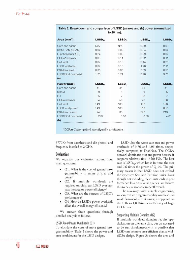
3770K) from datasheets and die photos, andfrequency is scaled to 2 GHz.
EvaluationWe organize our evaluation around fourmain questions:
� Q1. What is the cost of general pro-grammability in terms of area andpower?
� Q2. If multiple workloads arerequired on-chip, can LSSD ever sur-pass the area or power efficiency?
� Q3. What are the sources of LSSD’sperformance?
� Q4. How do LSSD’s power overheadsaffect the overall energy efficiency?
We answer these questions throughdetailed analysis as follows.
LSSD Area/Power Overheads (Q1)To elucidate the costs of more general pro-grammability, Table 2 shows the power andarea breakdowns for the LSSD designs.
LSSDD has the worst-case area and poweroverheads of 3.76 and 4.06 times, respec-tively, compared to DianNao. The CGRAnetwork dominates area and power because itsupports relatively tiny 16-bit FUs. The bestcase is LSSDQ, which has 0.48 times the areaand 0.6 times the power of Q100. The pri-mary reason is that LSSD does not embedthe expensive Sort and Partition units. Eventhough not including these units leads to per-formance loss on several queries, we believethis to be a reasonable tradeoff overall.
The takeaway: with suitable engineering,we can reduce programmability overheads tosmall factors of 2 to 4 times, as opposed tothe 100- to 1,000-times inefficiency of largeOoO cores.
Supporting Multiple Domains (Q2)If multiple workload domains require spe-cialization on the same chip, but do not needto be run simultaneously, it is possible thatLSSD can be more area-efficient than a Mul-tiDSA design. Figure 3a shows the area and
Table 2. Breakdown and comparison of LSSD (a) area and (b) power (normalized
to 28 nm).
Area (mm2) LSSDN LSSDC LSSDQ LSSDD
Core and cache N/A N/A 0.09 0.09
Static RAM (SRAM) 0.04 0.02 0.04 0.04
Functional unit (FU) 0.24 0.02 0.09 0.02
CGRA* network 0.09 0.11 0.22 0.11
Unit total 0.37 0.15 0.44 0.26
LSSD total area 0.37 0.15 1.78 2.11
DSA total area 0.30 0.08 3.69 0.56
LSSD/DSA overhead 1.23 1.74 0.48 3.76
(a)
Power (mW) LSSDN LSSDC LSSDQ LSSDD
Core and cache 41 41 41 41
SRAM 9 5 9 5
FU 65 7 33 7
CGRA network 34 56 46 56
Unit total 149 108 130 108
LSSD total power 149 108 519 867
DSA total power 74 30 870 213
LSSD/DSA overhead 2.02 3.57 0.60 4.06
(b) ..............................................................................................
*CGRA: Coarse-grained reconfigurable architecture.
..............................................................................................................................................................................................
TOP PICKS
............................................................
46 IEEE MICRO
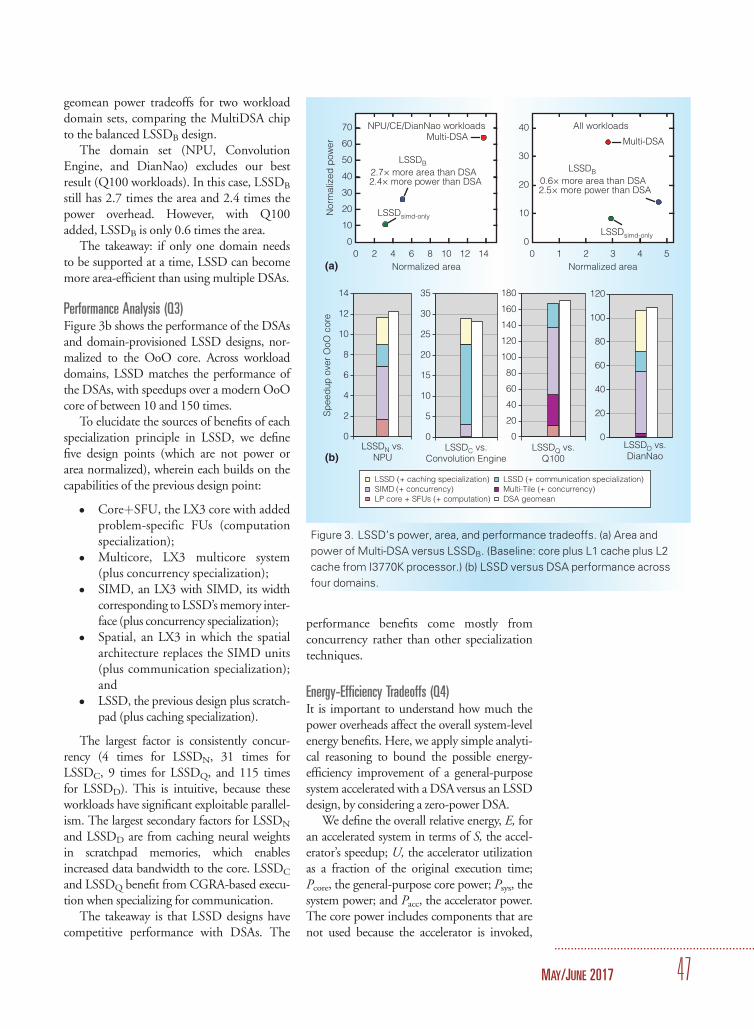
geomean power tradeoffs for two workloaddomain sets, comparing the MultiDSA chipto the balanced LSSDB design.
The domain set (NPU, ConvolutionEngine, and DianNao) excludes our bestresult (Q100 workloads). In this case, LSSDB
still has 2.7 times the area and 2.4 times thepower overhead. However, with Q100added, LSSDB is only 0.6 times the area.
The takeaway: if only one domain needsto be supported at a time, LSSD can becomemore area-efficient than using multiple DSAs.
Performance Analysis (Q3)Figure 3b shows the performance of the DSAsand domain-provisioned LSSD designs, nor-malized to the OoO core. Across workloaddomains, LSSD matches the performance ofthe DSAs, with speedups over a modern OoOcore of between 10 and 150 times.
To elucidate the sources of benefits of eachspecialization principle in LSSD, we definefive design points (which are not power orarea normalized), wherein each builds on thecapabilities of the previous design point:
� CoreþSFU, the LX3 core with addedproblem-specific FUs (computationspecialization);
� Multicore, LX3 multicore system(plus concurrency specialization);
� SIMD, an LX3 with SIMD, its widthcorresponding to LSSD’s memory inter-face (plus concurrency specialization);
� Spatial, an LX3 in which the spatialarchitecture replaces the SIMD units(plus communication specialization);and
� LSSD, the previous design plus scratch-pad (plus caching specialization).
The largest factor is consistently concur-rency (4 times for LSSDN, 31 times forLSSDC, 9 times for LSSDQ, and 115 timesfor LSSDD). This is intuitive, because theseworkloads have significant exploitable parallel-ism. The largest secondary factors for LSSDN
and LSSDD are from caching neural weightsin scratchpad memories, which enablesincreased data bandwidth to the core. LSSDC
and LSSDQ benefit from CGRA-based execu-tion when specializing for communication.
The takeaway is that LSSD designs havecompetitive performance with DSAs. The
performance benefits come mostly fromconcurrency rather than other specializationtechniques.
Energy-Efficiency Tradeoffs (Q4)It is important to understand how much thepower overheads affect the overall system-levelenergy benefits. Here, we apply simple analyti-cal reasoning to bound the possible energy-efficiency improvement of a general-purposesystem accelerated with a DSA versus an LSSDdesign, by considering a zero-power DSA.
We define the overall relative energy, E, foran accelerated system in terms of S, the accel-erator’s speedup; U, the accelerator utilizationas a fraction of the original execution time;Pcore, the general-purpose core power; Psys, thesystem power; and Pacc, the accelerator power.The core power includes components that arenot used because the accelerator is invoked,
0 2 4 6 8 10 12 14Normalized area
0
10
20
30
40
50
60
70
Nor
mal
ized
pow
er
LSSDB2.7× more area than DSA2.4× more power than DSA
LSSDsimd-only
Multi-DSANPU/CE/DianNao workloads
0 1 2 3 4 5Normalized area
0
10
20
30
40
Multi-DSA
All workloads
LSSDB0.6× more area than DSA2.5× more power than DSA
LSSDsimd-only
0
2
4
6
8
10
12
14
LSSDN vs.NPU
LSSDC vs.Convolution Engine
LSSDQ vs.Q100
LSSDD vs.DianNao
Sp
eed
up o
ver
OoO
cor
e
0
5
10
15
20
25
30
35
0
20
40
60
80
100
120
0
20
40
60
80
100
120
140
160
180
LSSD (+ caching specialization)SIMD (+ concurrency) Multi-Tile (+ concurrency)LP core + SFUs (+ computation) DSA geomean
LSSD (+ communication specialization)
(a)
(b)
Figure 3. LSSD’s power, area, and performance tradeoffs. (a) Area and
power of Multi-DSA versus LSSDB. (Baseline: core plus L1 cache plus L2
cache from I3770K processor.) (b) LSSD versus DSA performance across
four domains.
.............................................................
MAY/JUNE 2017 47

whereas the system power components areactive while accelerating (such as higher-levelcaches and DRAM). The total energy thenbecomes
E ¼ PaccðU=SÞ þ Psysð1� U þ U=SÞþ Pcoreð1� U Þ
We characterize system-level energy tradeoffsacross accelerator utilizations and speedupsin Figure 4. Figure 4a shows that the maxi-mum benefits from a DSA are reduced bothas the utilization goes down (stressing corepower) and when accelerator speedupincreases (stressing both core and systempower). For a reasonable utilization of U ¼0.5 and speedup of S ¼ 10, the maximumenergy efficiency gain from a DSA is less than0.5 percent. Figure 4b shows a similar graph,in which LSSD’s power is varied, whereas uti-lization is fixed at U ¼ 0.5. Even consideringan LSSD with power equivalent to the core,when LSSD has a speedup of 10 times, thereis only 5 percent potential energy savings
remaining for a DSA to optimize. The take-away is that when an LSSD can match theperformance of a DSA, the further poten-tial energy benefits of a DSA are usuallysmall, making LSSD’s overheads largelyinconsequential.
T he broad intellectual thrust of thisarticle is to propose an accelerator
architecture that could be used to drive futureinvestigations. As an analogy, the canonicalfive-stage pipelined processor was simple andeffective enough to serve as a framework foralmost three decades of big ideas, policies,and microarchitecture mechanisms thatdrove the general-purpose processor era. Upto now, architects have not focused on anequivalent framework for accelerators.
Most accelerator proposals are presentedas a novel design with a unique compositionof mechanisms for a particular domain, mak-ing comparisons meaningless. However,from an intellectual standpoint, our workshows that these accelerators are more similarthan dissimilar; they exploit the same essen-tial principles with differences in their imple-mentation. This is why we believe anarchitecture designed around these principlescan serve as a standard framework. Of course,the development of DSAs will continue tobe critical for architecture research, both toenable the exploration of the limits of acceler-ation, and as a means to extract new accelera-tion principles.
In the literature today, DSAs are pro-posed and compared to conventional high-performance processors, and typically yieldseveral orders of magnitude better measure-ments on various metrics of interest. For thefour DSAs we looked at, the benefit of spe-cialization is only two to four times forLSSD in area and power when performance-normalized. Therefore, we argue that theoverheads of OoO processors and GPUsmake them poor targets to distill the truebenefit of specialization.
Using LSSD as a baseline will revealmore and deeper insights on what techni-ques are truly needed for a particular prob-lem or domain, as opposed to merelyremoving the inefficiency of a general-pur-pose OoO processor using already-known
0 10 20 30 40 50Accelerator speedup
1.00
1.02
1.04
1.06
1.08
1.10
1.12
Max
imum
DS
A e
nerg
y-ef
ficie
ntim
pro
vem
ent
Max
imum
DS
A e
nerg
y-ef
ficie
ntim
pro
vem
ent
U = 1.00U = 0.95U = 0.90U = 0.75U = 0.50U = 0.25
0 10 20 30 40 50
Accelerator speedup
1.00
1.05
1.10
1.15
1.20
1.25
1.30
1.35
Plssd = 5.0
Plssd = 2.5
Plssd = 1.0
Plssd = 0.5
Plssd = 0.25
(a)
(b)
Figure 4. Energy benefits of zero-power DSA (Pcore¼ 5 W, Psys¼ 5 W). (a)
Varying utilization, Plssd¼ 0.5 W. (b) Varying LSSD power, U¼ 0.5 W.
..............................................................................................................................................................................................
TOP PICKS
............................................................
48 IEEE MICRO
techniques applied in a straightforward man-ner to a new domain.
Orthogonally, LSSD can serve as a guide-line for discovering big ideas for specialization.Undoubtedly, there are additions necessary tothe five principles, alternative formulations,and microarchitecture extensions. Theseinclude ideas that have been demonstrated inan accelerator’s specific context, as well as prin-ciples not discovered or defined yet.
To see how LSSD can serve as a frame-work for generalizing accelerator-specificmechanisms, consider the recent Proteus7
and Cnvlutin8 works, which proposed mech-anisms for extending the DianNao accelera-tor. The idea of bit-serial multiplication(Proteus) and eliminating zero-computing(Cnvlutin) can apply to the database- andimage-processing domains we considered,and evaluating with LSSD enables the studyof these mechanisms’s generalizability.
Our formulation of principles makes clearwhat workload behaviors are currentlyuncovered and need discovery of new princi-ples to match existing accelerators. Thisdirection leads to the more open questions ofwhether the number of principles are eventu-ally too numerous to be practical to put in asingle substrate, whether efficient mecha-nisms can be discovered to target many prin-ciples with a single substrate, or whether theyare sufficiently few in number such that onecan build a single universal framework.
Overall, the specialization principles andLSSD-style architectures can be used todecouple accelerator research from workloaddomains, which we believe can help fostermore shared innovation in this space. MICRO
....................................................................References1. H. Esmaeilzadeh et al., “Neural Acceleration
for General-Purpose Approximate Programs,”
Proc. 45th Ann. IEEE/ACM Int’l Symp. Micro-
architecture, 2012, pp. 449–460.
2. W. Qadeer et al., “Convolution Engine: Bal-
ancing Efficiency and Flexibility in Specialized
Computing,” Proc. 40th Ann. Int’l Symp.
Computer Architecture, 2013, pp. 24–35.
3. L. Wu et al., “Q100: The Architecture and
Design of a Database Processing Unit,”
Proc. 19th Int’l Conf. Architectural Support
for Programming Language and Operating
Systems, 2014, pp. 255–268.
4. T. Chen et al., “DianNao: A Small-Footprint
High-Throughput Accelerator for Ubiquitous
Machine-Learning,” Proc. 19th Int’l Conf.
Architectural Support for Programming Lan-
guage and Operating Systems, 2014, pp.
269–284.
5. T. Nowatzki et al., “Pushing the Limits of
Accelerator Efficiency While Retaining Pro-
grammability,” Proc. IEEE Int’l Symp. High
Performance Computer Architecture, 2016,
pp. 27–39.
6. V. Govindaraju et al., “DySER: Unifying
Functionality and Parallelism Specialization
for Energy Efficient Computing,” IEEE
Micro, vol. 32, no. 5, 2012, pp. 38–51.
7. P. Judd et al., “Proteus: Exploiting Numeri-
cal Precision Variability in Deep Neural
Networks,” Proc. Int’l Conf. Supercomput-
ing, 2016, article 23.
8. J. Albericio et al., “Cnvlutin: Ineffectual-
Neuron-Free Deep Neural Network
Computing,” Proc. ACM/IEEE 43rd Ann.
Int’l Symp. Computer Architecture, 2016,
pp. 1–13.
Tony Nowatzki is an assistant professor inthe Department of Computer Science at theUniversity of California, Los Angeles. Hisresearch interests include architecture andcompiler codesign and mathematical mod-eling. Nowatzki received a PhD in computerscience from the University of Wisconsin–Madison. He is a member of IEEE. Contacthim at [email protected].
Vinay Gangadhar is a PhD student in theDepartment of Electrical and ComputerEngineering at the University of Wiscon-sin–Madison. His research interests includehardware/software codesign of program-mable accelerators, microarchitecture, andGPU computing. Gangadhar received anMS in electrical and computer engineeringfrom the University of Wisconsin–Madison.He is a student member of IEEE. Contacthim at [email protected].
Karthikeyan Sankaralingam is an associateprofessor in the Department of Computer
.............................................................
MAY/JUNE 2017 49

Sciences and the Department of Electricaland Computer Engineering at the Univer-sity of Wisconsin–Madison, where he alsoleads the Vertical Research Group. Hisresearch interests include microarchitecture,architecture, and very large-scale integra-tion. Sankaralingam received a PhD in com-puter science from the University of Texas atAustin. He is a senior member of IEEE.Contact him at [email protected].
Greg Wright is the director of engineeringat Qualcomm Research. His research inter-ests include processor architecture, virtualmachines, compilers, parallel algorithms,and memory models. Wright received aPhD in computer science from the Univer-sity of Manchester. Contact him [email protected].
Read your subscriptions through the myCS publications portal at http://mycs.computer.org.
..............................................................................................................................................................................................
TOP PICKS
............................................................
50 IEEE MICRO


.................................................................................................................................................................................................................
CONFIGURABLE CLOUDS.................................................................................................................................................................................................................
THE CONFIGURABLE CLOUD DATACENTER ARCHITECTURE INTRODUCES A LAYER OF
RECONFIGURABLE LOGIC BETWEEN THE NETWORK SWITCHES AND SERVERS. THE AUTHORS
DEPLOY THE ARCHITECTURE OVER A PRODUCTION SERVER BED AND SHOW HOW IT CAN
ACCELERATE APPLICATIONS THAT WERE EXPLICITLY PORTED TO FIELD-PROGRAMMABLE
GATE ARRAYS, SUPPORT HARDWARE-FIRST SERVICES, AND ACCELERATE APPLICATIONS
WITHOUT ANY APPLICATION-SPECIFIC FPGA CODE BEING WRITTEN.
......Hyperscale clouds (hundreds ofthousands to millions of servers) are anattractive option to run a vast and increasingnumber of applications and workloads span-ning web services, data processing, AI, andthe Internet of Things. Modern hyperscaledatacenters have made huge strides withimprovements in networking, virtualization,energy efficiency, and infrastructure manage-ment, but they still have the same basic struc-ture they’ve had for years: individual serverswith multicore CPUs, DRAM, and localstorage, connected by the network interfacecard (NIC) through Ethernet switches toother servers. However, the slowdown inboth CPU scaling and the end of Moore’slaw has resulted in a growing need for hard-ware specialization to increase performanceand efficiency.
There are two basic ways to introducehardware specialization into the datacenter:one is to form centralized pools of specializedmachines, which we call “bolt-on” accelera-tors, and the other is to distribute the special-ized hardware to each server. Introducingbolt-on accelerators into a hyperscale infra-structure reduces the highly desirable homo-geneity and limits the scalability of thespecialized hardware, but minimizes disrup-
tion to the core server infrastructure. Distrib-uting the accelerators to each server in thedatacenter retains homogeneity, allows moreefficient scaling, allows services to run on allthe servers, and simplifies management byreducing costs and configuration errors. Thequestion of which method is best is mostlyone of economics: is it more cost effective todeploy an accelerator in every new server, tospecialize a subset of an infrastructure’s newservers and maintain an ever-growing num-ber of configurations, or to do neither?
Any specialized accelerator must be com-patible with the target workloads through itsdeployment lifetime (for example, six years—two years to design and deploy the acceleratorand four years of server deployment lifetime).This requirement is a challenge given boththe diversity of cloud workloads and the rapidrate at which they change (weekly ormonthly). It is thus highly desirable thataccelerators incorporated into hyperscale serv-ers be programmable. The two most commonexamples are field-programmable gate arrays(FPGAs) and GPUs, which (in this regard)are preferable over ASICs.
Both GPUs and FPGAs have beendeployed in datacenter infrastructure at reason-able scale, but with limited direct connectivity
Adrian M. Caulfield
Eric S. Chung
Andrew Putnam
Hari Angepat
Daniel Firestone
Jeremy Fowers
Michael Haselman
Stephen Heil
Matt Humphrey
Puneet Kaur
Joo-Young Kim
Daniel Lo
Todd Massengill
Kalin Ovtcharov
Michael Papamichael
Lisa Woods
Sitaram Lanka
Derek Chiou
Doug Burger
Microsoft
.......................................................
52 Published by the IEEE Computer Society 0272-1732/17/$33.00�c 2017 IEEE

between accelerators, such as intraserver con-nectivity or small-scale ring and torus net-works. Our first deployment in a productionhyperscale datacenter was 1,632 servers,each with an FPGA, to accelerate Bing websearch ranking. The FPGAs were connectedto each other in a 6-�-8 torus network in ahalf rack. Although effective at acceleratingsearch ranking, our first architecture1 andsimilar small-scale connectivity architectures(see the sidebar, “Projects Related to theConfigurable Cloud Architecture”) have sev-eral significant limitations:
� The number of FPGAs that couldcommunicate directly, without goingthrough software, is limited to a sin-gle server or single rack (that is, 48nodes).
� The secondary network requiresexpensive and complex cabling and
requires awareness of the machines’physical location.
� Failure handling requires complexrerouting of traffic to neighboringnodes, causing both performance lossand isolation of nodes under certainfailure patterns.
� These fabrics are limited-scale bolt-on accelerators, which can accelerateapplications but offer few enhance-ments for the datacenter infrastruc-ture, such as networking and storageflows.
� Programs must be aware of wheretheir applications are running andhow many specialized machines areavailable, not just the best way to accel-erate a given application.
We propose the Configurable Cloud, anew FPGA-accelerated hyperscale datacenter
Projects Related to the Configurable Cloud ArchitectureFor a complete analysis of related work and a taxonomy of various
system design options, see our original paper.1 In this sidebar, we
focus on projects with related system architectures.
Hyperscale accelerators commonly comprise three types of
accelerators: custom ASICs, application-specific processors and
GPUs, and field-programmable gate arrays (FPGAs). Custom ASICs
solutions, such as DianNao,2 provide excellent performance and
efficiency for their target workload. However, ASICs are inflexible,
so they restrict the rapidly evolving applications from evolving
while still being able to use the accelerator.
Google’s Tensor Processing Unit (TPU)3 is an application-
specific processor that has been highly tuned to execute Tensor-
Flow. GPUs have been commonly used in datacenters as bolt-on
accelerators, even with small-scale interconnection networks
such as NVLink.4 However, the size and power requirements for
GPUs is still much higher than for FPGAs.
FPGA deployments, including Amazon’s EC2 F1,5 Baidu’s SDA,6
IBM’s FPGA fabric,7 Novo-G,8 and our first-generation architecture,1 all
cluster FPGAs into a small subset of the architecture—bolt-on acceler-
ators. None of these have the scalability or ability to benefit the base-
line datacenter server as the Configurable Cloud architecture does.
References1. A. Putnam et al., “A Reconfigurable Fabric for Accelerat-
ing Large-Scale Datacenter Services,” Proc. 41st Ann.
Int’l Symp Computer Architecture, 2014, pp. 13–24.
2. T. Chen et al., “DianNao: A Small-Footprint High-Through-
put Accelerator for Ubiquitous Machine-Learning,” ACM
SIGPLAN Notices, vol. 49, no. 4, 2014, pp. 269–284.
3. M. Abadi et al., “TensorFlow: A System for Large-Scale
Machine Learning,” Proc. 12th USENIX Symp. Operat-
ing Systems Design and Implementation, 2016, pp.
265–283.
4. Nvidia NVLink High-Speed Interconnect: Application Per-
formance, white paper, Nvidia, Nov. 2014.
5. “Amazon EC2 F1 Instances (Preview),” 2017; http://aws
.amazon.com/ec2/instance-types/f1.
6. J. Ouyang et al., “SDA: Software-Defined Accelerator for
Large-Scale DNN Systems,” Proc. Hot Chips 26 Symp.,
2014; doi:10.1109/HOTCHIPS.2014.7478821.
7. J. Weerasinghe et al., “Enabling FPGAs in Hyperscale
Data Centers,” Proc. IEEE 12th Int’l Conf. Ubiquitous
Intelligence and Computing, 12th Int’l Conf. Autonomic
and Trusted Computing, and 15th Int’l Conf. Scalable
Computing and Communications (UIC-ATC-ScalCom),
2015; doi:10.1109/UIC-ATC-ScalCom-CBDCom-IoP
.2015.199.
8. A.G. Lawande, A.D. George, and H. Lam, “Novo-G#: A
Multidimensional Torus-Based Reconfigurable Cluster for
Molecular Dynamics,” Concurrency and Computation:
Practice and Experience, vol. 28, no. 8, 2016, pp.
2374–2393.
.............................................................
MAY/JUNE 2017 53
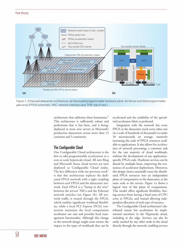
architecture that addresses these limitations.2
This architecture is sufficiently robust andperformant that it has been, and is being,deployed in most new servers in Microsoft’sproduction datacenters across more than 15countries and 5 continents.
The Configurable CloudOur Configurable Cloud architecture is thefirst to add programmable acceleration to acore at-scale hyperscale cloud. All new Bingand Microsoft Azure cloud servers are nowdeployed as Configurable Cloud nodes.The key difference with our previous work1
is that this architecture replaces the dedi-cated FPGA network with a tight couplingbetween each FPGA and the datacenter net-work. Each FPGA is a “bump in the wire”between the servers’ NICs and the Ethernetnetwork switches (see Figure 1b). All net-work traffic is routed through the FPGA,which enables significant workload flexibil-ity, while a local PCI Express (PCIe) con-nection maintains the local computationaccelerator use case and provides local man-agement functionality. Although this changeto the network design might seem minor, theimpact to the types of workloads that can be
accelerated and the scalability of the special-ized accelerator fabric is profound.
Integration with the network lets everyFPGA in the datacenter reach every other one(at a scale of hundreds of thousands) in under10 microseconds on average, massivelyincreasing the scale of FPGA resources avail-able to applications. It also allows for accelera-tion of network processing, a common taskfor the vast majority of cloud workloads,without the development of any application-specific FPGA code. Hardware services can beshared by multiple hosts, improving the eco-nomics of accelerator deployment. Moreover,this design choice essentially turns the distrib-uted FPGA resources into an independentplane of computation in the datacenter, at thesame scale as the servers. Figure 1a shows alogical view of this plane of computation.This model offers significant flexibility, free-ing services from having a fixed ratio of CPUcores to FPGAs, and instead allowing inde-pendent allocation of each type of resource.
The Configurable Cloud architecture’s dis-tributed nature lets accelerators be imple-mented anywhere in the Hyperscale cloud,including at the edge. Services can also beeasily reached by any other node in the clouddirectly through the network, enabling services
TOR
TOR TOR
TOR
L1 L1
Expensivecompression
Deep neuralnetworks
Web searchranking Bioinformatics
L2
TOR
(a) (b)Traditional SW (CPU) server plane
Datacenter HW acceleration plane
Network switch (top of rack, cluster)
FPGA-switch link
FPGA acceleration board
NIC-FPGA link
Two-socket CPU server Two-socket server blade
DRAM DRAM
CPUCPU QPI
Gen3 x8 Gen3 2x8
NIC FPGA
DR
AM
Acc
eler
ator
car
d
40 Gbps 40 GbpsQSFPQSFP QSFPWeb search
ranking
Figure 1. Enhanced datacenter architecture. (a) Decoupled programmable hardware plane. (b) Server and field-programmable
gate array (FPGA) schematic. (NIC: network interface card; TOR: top of rack.)
..............................................................................................................................................................................................
TOP PICKS
............................................................
54 IEEE MICRO

to be implemented at any location in theworldwide datacenter network.
Microsoft has deployed this new architec-ture to most of its new datacenter servers.Although the actual production scale of thisdeployment is orders of magnitude larger, forthis article we evaluate the ConfigurableCloud architecture using a bed of 5,760 serv-ers deployed in a production datacenter.
Usage ModelsThe Configurable Cloud is sufficiently flexibleto cover three scenarios: local acceleration(through PCIe), network acceleration, andglobal application acceleration through poolsof remotely accessible FPGAs. Local accelera-tion handles high-value scenarios such as websearch ranking acceleration, in which everyserver can benefit from having its own FPGA.Network acceleration supports services such assoftware-defined networking, intrusion detec-tion, deep packet inspection, and networkencryption, which are critical to infrastructureas a service (for example, “rental” of cloudservers), and which have such a huge diversityof customers that it makes it difficult to justifylocal acceleration alone economically. Globalacceleration permits acceleration hardwareunused by its host servers to be made availablefor other hardware services—for example,large-scale applications such as machine learn-ing. This decoupling of a 1:1 ratio of servers toFPGAs is essential for breaking the chicken-and-egg problem in which accelerators cannotbe added until enough applications needthem, but applications will not rely on theaccelerators until they are present in the infra-structure. By decoupling the servers andFPGAs, software services that demand moreFPGA capacity can harness spare FPGAs fromother services that are slower to adopt (or donot require) the accelerator fabric.
We measure the system’s performancecharacteristics using web search to representlocal acceleration, network flow encryptionand network flow offload to represent net-work acceleration, and machine learning torepresent global acceleration.
Local AccelerationWe brought up a production Bing web searchranking service on the servers, with 3,081 of
these machines using the FPGA for localacceleration, and the rest used for other func-tions associated with web search. Unlike inour previous work, we implemented only themost expensive feature calculations and omit-ted less-expensive feature calculations, thepost-processed synthetic features, and themachine-learning calculations.
Figure 2 shows the performance of searchranking running in production over a five-day period, with and without FPGA accelera-tion. The top two lines show the normalizedtail query latencies at the 99.9th percentile(aggregated across all servers over a rollingtime window), and the bottom two linesshow the corresponding query loads receivedat each datacenter.
Because load varies throughout the day,the queries executed without FPGAs experi-enced a higher latency with more frequentlatency spikes, whereas the FPGA-acceleratedqueries had much lower, tighter-bound laten-cies. This is particularly impressive given themuch higher query loads experienced by theFPGA-accelerated machines. The higherquery load, which was initially unexpected,was due to the top-level load balancers select-ing FPGA-accelerated machines over thosewithout FPGAs due to the lower and less-
99.9% software latency
99.9% FPGA latency
Average FPGA query load
Averagesoftware load
Day 1 Day 2 Day 3 Day 4 Day 5
1.0
2.0
3.0
4.0
5.0
6.0
7.0
Nor
mal
ized
load
and
late
ncy
Figure 2. Five-day query throughput and latency of ranking service queries
running in production, with and without FPGAs enabled.
.............................................................
MAY/JUNE 2017 55

variable latency. The FPGA-acceleratedmachines were better at serving query trafficeven at higher load, and hence were assignedadditional queries, nearly twice the load thatsoftware alone could handle.
Infrastructure AccelerationAlthough local acceleration such as Bingsearch was the primary motivation fordeploying FPGAs into Microsoft’s datacen-ters at hyperscale, the level of effort requiredto port the Bing software stack to FPGAsis not sustainable for the more than 200first-party workloads currently deployed inMicrosoft datacenters, not to mention thethousands of third-party applications run-ning on Microsoft Azure. The architectureneeds to provide benefit to workloads thathave no specialized code for running onFPGAs by accelerating components commonacross many different workloads. We call thiswidely applicable acceleration infrastructureacceleration. Our first example is accelerationof network services.
Nearly all hyperscale workloads rely on afast, reliable, and secure network betweenmany machines. By accelerating networkprocessing in ways such as protocol offloadand host-to-host network crypto, the FPGAscan accelerate workloads that have no specifictuning for FPGA offload. This is increasinglyimportant as growing network speeds putgreater pressure on CPU cores trying to keepup with protocol processing and line-ratecrypto.
In the case of network crypto, each packetis examined and encrypted or decrypted atline rate as necessary while passing from theNIC through the FPGA to the networkswitch. Thus, once an encrypted flow is setup, no CPU usage is required to encrypt ordecrypt the packets. Encryption occurstransparently from the perspective of thesoftware, which sees unencrypted packets atthe endpoints. Network encryption/decryp-tion offload yields significant CPU savings.Our AES-128 implementations support afull 40 Gbits per second (GBps) of encryp-tion/decryption with no load on the CPUbeyond setup and teardown. Achieving thesame performance in software requiresmore than four CPU cores running at fullutilization.
The same Configurable Cloud architec-ture has also been used to accelerate software-defined networking,3 in which bulk packetoperations are offloaded to the FPGA underthe software’s policy control. The initialimplementation gave Microsoft Azure thefastest public cloud network, with 25 lslatency and 25 Gbps of bandwidth. Thisservice was offered free to third-party users,who can benefit from FPGA accelerationwithout writing any code for the FPGA.
Hardware as a Service: Shared, RemoteAcceleratorsMost workloads can benefit from local accel-eration, infrastructure acceleration, or both.There are two key motivations behind ena-bling remote hardware services: hardwareaccelerators should be placed flexibly any-where in the hyperscale datacenter network,and the resource requirements for the hard-ware fabric (FPGAs) should scale commen-surately with software demand (CPU), notjust one server to one FPGA.
To address the first requirement, remoteaccelerators are never more than a few net-work hops away from any other server acrosshundreds of thousands to millions of servers.Since each server has acceleration capabilities,any accelerator can be mapped to anylocation.
Similarly, some software services haveunderutilized FPGA resources, while othersneed more than one. This architecture lets allaccelerators in the datacenter communicatedirectly, enabling harvesting of FPGAs fromthe deployment for services with greaterneeds. This also allows the allocation of thou-sands of FPGAs for a single job or service,independent of their CPU hosts and withoutimpacting the CPU’s performance, in effectcreating a new kind of computer embeddedin the datacenter. A demonstration of thispooled FPGA capability at Microsoft’s Igniteconference in 2016 showed that four har-vested FPGAs translated 5.2 million Wikipe-dia articles from English to Spanish fiveorders of magnitude faster than a 24-coreserver running highly tuned vectorized code.4
We developed a custom FPGA-to-FPGAnetwork protocol called the LightweightTransport Layer (LTL), which uses the UserDatagram Protocol for frame encapsulation
..............................................................................................................................................................................................
TOP PICKS
............................................................
56 IEEE MICRO

and Internet Protocol for routing packetsacross the datacenter network. Low-latencycommunication demands infrequent packetdrops and infrequent packet reorders. By usinglossless traffic classes provided in datacenterswitches and provisioned for traffic (such asRemote Direct Memory Access and FiberChannel over Ethernet), we avoid most packetdrops and reorders. Separating out such trafficto its own classes also protects the datacenter’sbaseline TCP traffic. Because the FPGAs areso tightly coupled to the network, they canreact quickly and efficiently to congestionnotification and back off when needed toreduce packets dropped from in-cast patterns.
At the endpoints, the LTL protocol engineuses an ordered, reliable connection-basedinterface with statically allocated, persistentconnections, realized using send and receiveconnection tables. The static allocation andpersistence (until they are deallocated) reducelatency for inter-FPGA and inter-service mes-saging, because once established, they cancommunicate with low latency. Reliable mes-saging also reduces protocol latency. Althoughdatacenter networks are already fairly reliable,LTL provides a strong reliability guaranteevia an ACK/NACK-based retransmissionscheme. When packet reordering is detected,NACKs are used to request timely retrans-mission of particular packets without waitingfor a time-out.
To evaluate LTL and resource sharing,we implemented and deployed a latency-optimized Deep Neural Network (DNN)accelerator developed for natural languageprocessing, and we used a synthetic stresstest to simulate DNN request traffic atvarying levels of oversubscription. By increas-ing the ratio of clients to accelerators (byremoving FPGAs from the pool), we measurethe impact on latency due to oversubscrip-tion. The synthetic stress test generated by asingle software client is calibrated to generateat least twice the worst-case traffic expected inproduction (thus, even with 1:1 oversubscrip-tion, the offered load and latencies are highlyconservative).
Figure 3 shows request latencies as over-subscription increases. In the 1:1 case (nooversubscription), remote access adds lessthan 4.7 percent additional latency to eachrequest up to the 95th percentile, and 32
percent at the 99th percentile. As expected,contention and queuing delay increase asoversubscription increases. Eventually, theFPGA reaches its peak throughput and satu-rates. In this case study, each individual FPGAhas sufficient throughput to comfortably sup-port roughly two clients even at artificiallyhigh traffic levels, demonstrating the feasibil-ity of sharing accelerators and freeing resour-ces for other functions.
Managing remote accelerators requiressignificant hardware and software support. Acomplete overview of the management of ourhardware fabric, called Hardware as a Service(HaaS), is beyond the scope of this article,but we provide a short overview of the plat-form here. HaaS manages FPGAs in a man-ner similar to Yarn5 and other job schedulers.A logically centralized resource manager(RM) tracks FPGA resources throughout thedatacenter. The RM provides simple APIs forhigher-level service managers (SMs) to easilymanage FPGA-based hardware componentsthrough a lease-based model. Each compo-nent is an instance of a hardware servicemade up of one or more FPGAs and a set ofconstraints (for example, locality or band-width). SMs manage service-level tasks, suchas load balancing, intercomponent connec-tivity, and failure handling, by requesting andreleasing component leases through the RM.An SM provides pointers to the hardwareservice to one or more users to take advantageof the hardware acceleration. An FPGA
0.0
1.0
2.0
3.0
4.0
5.0
0.5 1.0 1.5 2.0 2.5 3.0
Late
ncy
norm
aliz
ed to
loca
l FP
GA
Oversubscription: No. of remote clients/No. of FPGAs
Avg95%99%
Figure 3. Average, 95th, and 99th percentile latencies to a remote Deep
Neural Network (DNN) accelerator (normalized to locally attached
performance in each latency category).
.............................................................
MAY/JUNE 2017 57

manager (FM) runs on each node to provideconfiguration support and status monitoringfor the system.
Hardware DetailsIn addition to the architectural requirementto provide sufficient flexibility to justify scaleproduction deployment, there are also physi-cal restrictions in current infrastructures thatmust be overcome. These restrictions includestrict power limits, a small physical space inwhich to fit, resilience to hardware failures,and tolerance to high temperatures. For exam-ple, the accelerator architecture we describe isthe widely used OpenCompute server, whichconstrained power to 35 W, the physical sizeto roughly a half-height, half-length PCIeexpansion card, and tolerance to an inlet airtemperature of 70�C at low airflow.
We designed the accelerator board as astand-alone FPGA board that is added to thePCIe expansion slot in a production serverconfiguration. Figure 4 shows a photographof the board with major components labeled.The FPGA is an Altera Stratix V D5, with172,600 adaptive logic modules of program-mable logic, 4 Gbytes of DDR3-1600DRAM, two independent PCIe Gen 3 x8connections, and two independent 40 Giga-bit Ethernet interfaces. The realistic powerdraw of the card under worst-case environ-mental conditions is 35 W.
The dual 40 Gigabit Ethernet interfaceson the board could allow for a private FPGA
network, as was done in previous work, butthis configuration also lets us wire the FPGAas a “bump in the wire,” sitting between theNIC and the top-of-rack (ToR) switch.Rather than cabling the standard NICdirectly to the ToR, the NIC is cabled to oneport of the FPGA, and the other FPGA portis cabled to the ToR (see Figure 1b).
Maintaining the discrete NIC in the sys-tem lets us leverage all the existing networkoffload and packet transport functionalityhardened into the NIC. This minimizes thecode required to deploy FPGAs to simplebypass logic. In addition, both FPGA resour-ces and PCIe bandwidth are preserved foracceleration functionality, rather than beingspent on implementing the NIC in soft logic.
One potential drawback to the bump-in-the-wire architecture is that an FPGA failure,such as loading a buggy application, couldcut off network traffic to the server, renderingthe server unreachable. However, unlike in aring or torus network, failures in the bump-in-the-wire architecture do not degrade anyneighboring FPGAs, making the overall sys-tem more resilient to failures. In addition,most datacenter servers (including ours) havea side-channel management path that existsto power servers on and off. By policy, theknown-good golden image that loads onpower up is rarely (if ever) overwritten, so themanagement network can always recover theFPGA with a known-good configuration,making the server reachable via the networkonce again.
In addition, FPGAs have proven to bereliable and resilient at hyperscale, with only0.03 percent of boards failing across ourdeployment after one month of processingfull-production traffic, and with all failureshappening at the beginning of production.Bit flips in the configuration layer were meas-ured at an average rate of one per 1,025machine days. We used configuration layermonitoring and correcting circuitry to mini-mize the impact of these single-event upsets.Given aggregate datacenter failure rates, wedeemed the FPGA-related hardware failuresto be acceptably low for production.
T he Configurable Cloud architecture is amajor advance in the way datacenters
are being designed and utilized. The impact
Stratix V
D5 FPGA
40G QSFP ports
(NIC and TOR)
4-Gbyte DDR3
Figure 4. Photograph of the manufactured board. The DDR channel is
implemented using discrete components. PCI Express connectivity goes
through a mezzanine connector on the bottom side of the board (not
shown).
..............................................................................................................................................................................................
TOP PICKS
............................................................
58 IEEE MICRO

of this design goes far beyond just an improvednetwork design.
The collective architecture and softwareprotocols described in this article can be seenas a fundamental shift in the role of CPUs inthe datacenter. Rather than the CPU control-ling every task, the FPGA is now the gate-keeper between the server and the network,determining how incoming and outgoingdata will be processed and handling commoncases quickly and efficiently. In such a model,the FPGA calls the CPU to handle infrequentand/or complex work that the FPGA cannothandle itself. Such an architecture addsanother mode of operation to a traditionalcomputing platform, potentially removingthe CPU as the machine’s master. Such anorganization can be viewed as relegating theCPU to be a complexity offload engine forthe FPGA.
Of course, there will be many applicationsin which the CPUs handle the bulk of thecomputation. In that case, the FPGAsattached to those CPUs can be used over thenetwork by other applications running ondifferent servers that need more FPGAresources in a few tens of microseconds acrossthe datacenter.
Such a Configurable Cloud provides enor-mous flexibility in how computation is doneand in the placement of computational tasks,enabling the right computational unit to beassigned a particular task at the right time.Thus, additional efficiency can be extractedfrom the hardware, allowing accelerators to beshared and underutilized resources to bereclaimed and repurposed independently ofthe other resources. In addition, by distribut-ing heterogeneous accelerators throughout thenetwork, this architecture avoids the networkbottlenecks, cost, and complexities of bolt-onclusters of specialized accelerator nodes.
As a result, Configurable Clouds enablethe performant implementation of wildly dif-ferent functions on exactly the same hard-ware. In addition, specialized hardware is farmore efficient than CPUs, making Configu-rable Clouds better for the environment.
This work has already had significantimpact. Microsoft is building the vast major-ity of its next-generation datacenters across 15countries and 5 continents using this architec-ture. Microsoft has publicly described how
that architecture is being used to improveBing search quality and performance andAzure networking capabilities and perform-ance. Those deployments and the results ofaccelerating applications on them provide fur-ther confirmation of programmable accelera-tors’ value for datacenter services.
FPGA architectures are being heavilyinfluenced by this work. Investment intodatacenter FPGA technology and ecosystemsby Microsoft and other major companies isincreasing, not least being Intel’s acquisitionof Altera for $16.7 billion, as well as therecent introduction of FPGAs at a limitedscale by the majority of the other major cloudproviders. MICRO
....................................................................References1. A. Putnam et al., “A Reconfigurable Fabric
for Accelerating Large-Scale Datacenter
Services,” Proc. 41st Ann. Int’l Symp Com-
puter Architecture, 2014, pp. 13–24.
2. A.M. Caulfield et al., “A Cloud-Scale Accel-
eration Architecture,” Proc. 49th Ann. IEEE/
ACM Int’l Symp. Microarchitecture, 2016;
doi:10.1109/MICRO.2016.7783710.
3. Y. Khalidi et al., “Microsoft Azure Network-
ing: New Network Services, Features and
Scenarios,” Microsoft Ignite, 2016; http://
channel9.msdn.com/Events/Ignite/2016
/BRK3237-TS.
4. S. Nadella, “Innovation Keynote,” Microsoft
Ignite, 2016; http://channel9.msdn.com
/Events/Ignite/2016/KEY02.
5. V.K. Vavilapalli et al., “Apache Hadoop Yarn:
Yet Another Resource Negotiator,” Proc.
4th Ann. Symp. Cloud Computing, 2013, pp.
5:1–5:16.
Adrian M. Caulfield is a principal researchhardware development engineer at Micro-soft Research. His research interests includecomputer architecture and reconfigurablecomputing. Caulfield received a PhD incomputer engineering from the Universityof California, San Diego. Contact him [email protected].
Eric S. Chung is a researcher at MicrosoftResearch NExT, where he leads an effort toaccelerate large-scale machine learning using
.............................................................
MAY/JUNE 2017 59

FPGAs. Chung received a PhD in electricaland computer engineering from CarnegieMellon University. Contact him at [email protected].
Andrew Putnam is a principal researchhardware development engineer at MicrosoftResearch NExT. His research interests includereconfigurable computing, future datacenterdesign, and computer architecture. Putnamreceived a PhD in computer science and engi-neering from the University of Washington.Contact him at [email protected].
Hari Angepat is a senior software engineer atMicrosoft and a PhD candidate at the Univer-sity of Texas at Austin. His research interestsinclude novel FPGA accelerator architectures,hardware/software codesign techniques, andapproaches for flexible hardware design. Ange-pat received an MS in computer engineeringfrom the University of Texas at Austin. Con-tact him at [email protected].
Daniel Firestone is the tech lead and man-ager for the Azure Networking Host SDNteam at Microsoft. His team builds theAzure virtual switch and SmartNIC. Con-tact him at [email protected].
Jeremy Fowers is a senior research hardwaredesign engineer in the Catapult team atMicrosoft Research NeXT. He specializes inthe design and implementation of FPGAaccelerators across a variety of applicationdomains, and is currently focused on machinelearning. Fowers received a PhD in electricalengineering from the University of Florida.Contact him at [email protected].
Michael Haselman is a senior software engi-neer at Microsoft ASG (Bing). His researchinterests include FPGAs, computer architec-ture, and distributed computing. Haselmanreceived a PhD in electrical engineering fromthe University of Washington. Contact himat [email protected].
Stephen Heil is a principal program man-ager at Microsoft Research. His research inter-ests include field-programmable gate arrays,application accelerators, and rack-scale systemdesign. Heil received a BS in electrical engi-neering technology and computer science
from the College of New Jersey (formerlyTrenton State College). Contact him [email protected].
Matt Humphrey is a principal engineer atMicrosoft, where he works on Azure. Hisresearch interests include analog and digitalelectronics and the architecture of high-scaledistributed software systems. Humphreyreceived an MS in electrical engineeringfrom the Georgia Institute of Technology.Contact him at [email protected].
Puneet Kaur is a principal software engineerat Microsoft. Her research interests includedistributed systems and scalability. Kaurreceived a MTech in computer science fromthe Indian Institute of Technology, Kanpur.Contact her at [email protected].
Joo-Young Kim is a senior research hard-ware development engineer at MicrosoftResearch. His research interests includehigh-performance, energy-efficient computerarchitectures for various datacenter work-loads, such as data compression, video trans-coding, and machine learning. Kim received aPhD in electrical engineering from KoreaAdvanced Institute of Science and Technol-ogy (KAIST). Contact him at [email protected].
Daniel Lo is a research hardware develop-ment engineer at Microsoft Research. Hisresearch interests include designing high-performance accelerators on FPGAs. Loreceived a PhD in electrical and computerengineering from Cornell University. Con-tact him at [email protected].
Todd Massengill is a senior hardware designengineer at Microsoft Research. His researchinterests include hardware acceleration of arti-ficial intelligence applications, biologicallyinspired computing, and tools to improvehardware engineering design, collaboration,and efficiency. Massengill received an MS inelectrical engineering from the University ofWashington. Contact him at [email protected].
Kalin Ovtcharov is a research hardwaredevelopment engineer at Microsoft ResearchNeXT. His research interests include
..............................................................................................................................................................................................
TOP PICKS
............................................................
60 IEEE MICRO

accelerating computationally intensive taskson FPGAs in areas such as machine learn-ing, image processing, and video compres-sion. Ovtcharov received a BS in computerengineering from McMaster University.Contact him at [email protected].
Michael Papamichael is a researcher atMicrosoft Research, where he’s working onthe Catapult project. His research interestsinclude hardware acceleration, reconfigurablecomputing, on-chip interconnects, and meth-odologies to facilitate hardware specialization.Papamichael received a PhD in computer sci-ence from Carnegie Mellon University. Con-tact him at [email protected].
Lisa Woods is a principal program managerfor the Catapult project at MicrosoftResearch, where she focuses on driving strate-gic alignment between the Catapult team andits many internal and external partners as wellas scalability and execution for the project.Woods received an MS in computer science.Contact her at [email protected].
Sitaram Lanka is a partner group engineer-ing manager in Search Platform at Micro-soft Bing. His research interests include weband enterprise search, large-scale distributed
systems, machine learning, and reconfigura-ble hardware in datacenters. Lanka receiveda PhD in computer science from the Uni-versity of Pennsylvania. Contact him [email protected].
Derek Chiou is a partner hardware groupengineering manager at Microsoft and aresearch scientist at the University of Texasat Austin. His research interests include accel-erating datacenter applications and infrastruc-ture, rapid system design, and fast, accuratesimulation. Chiou received a PhD in electri-cal engineering and computer science fromthe Massachusetts Institute of Technology.Contact him at [email protected].
Doug Burger is a distinguished engineer atMicrosoft, where he leads a Disruptive Sys-tems team at Microsoft Research NExT andcofounded Project Catapult. Burger received aPhD in computer science from the Universityof Wisconsin. He is an IEEE and ACM Fel-low. Contact him at [email protected].
Read your subscriptions through the myCS publications portal at http://mycs.computer.org.
.............................................................
MAY/JUNE 2017 61

.................................................................................................................................................................................................................
SPECIALIZING A PLANET’SCOMPUTATION: ASIC CLOUDS
.................................................................................................................................................................................................................
ASIC CLOUDS, A NATURAL EVOLUTION TO CPU- AND GPU-BASED CLOUDS, ARE
PURPOSE-BUILT DATACENTERS FILLED WITH ASIC ACCELERATORS. ASIC CLOUDS MAY
SEEM IMPROBABLE DUE TO HIGH NON-RECURRING ENGINEERING (NRE) COSTS AND ASIC
INFLEXIBILITY, BUT LARGE-SCALE BITCOIN ASIC CLOUDS ALREADY EXIST. THIS ARTICLE
DISTILLS LESSONS FROM THESE PRIMORDIAL ASIC CLOUDS AND PROPOSES NEW
PLANET-SCALE YOUTUBE-STYLE VIDEO-TRANSCODING AND DEEP LEARNING ASIC CLOUDS,
SHOWING SUPERIOR TOTAL COST OF OWNERSHIP. ASIC CLOUD NRE AND ECONOMICS
ARE ALSO EXAMINED.
......In the past 10 years, two parallelphase changes in the computational landscapehave emerged. The first change is the bifurca-tion of computation into two sectors—cloudand mobile. The second change is the rise ofdark silicon and dark-silicon-aware designtechniques, such as specialization and near-threshold computation.1 Recently, researchersand industry have started to examine the con-junction of these two phase changes. Baiduhas developed GPU-based clouds for distrib-uted neural network accelerators, and Micro-soft has deployed clouds based on field-programmable gate arrays (FPGAs) for Bing.
At a single-node level, we know that appli-cation-specific integrated circuits (ASICs) canoffer order-of-magnitude improvements inenergy efficiency and cost performance overCPU, GPU, and FPGA by specializing siliconfor a particular computation. Our researchproposes ASIC Clouds,2 which are purpose-
built datacenters comprising large arrays ofASIC accelerators. ASIC Clouds are notASIC supercomputers that scale up problemsizes for a single tightly coupled computation;rather, they target workloads comprisingmany independent but similar jobs.
As more and more services are builtaround the Cloud model, we see the emer-gence of planet-scale workloads in whichdatacenters are performing the same compu-tation across many users. For example, con-sider Facebook’s face recognition of uploadedpictures, or Apple’s Siri voice recognition, orthe Internal Revenue Service performing taxaudits with neural nets. Such scale-out work-loads can easily leverage racks of ASIC serverscontaining arrays of chips that in turn con-nect arrays of replicated compute accelera-tors (RCAs) on an on-chip network. Thelarge scale of these workloads creates the eco-nomic justification to pay the non-recurring
Moein Khazraee
Luis Vega Gutierrez
Ikuo Magaki
Michael Bedford Taylor
University of California,
San Diego
.......................................................
62 Published by the IEEE Computer Society 0272-1732/17/$33.00�c 2017 IEEE

engineering (NRE) costs of ASIC develop-ment and deployment. As a workload grows,the ASIC Cloud can be scaled in the datacen-ter by adding more ASIC servers, unlike accel-erators in, say, a mobile phone population,3 inwhich the accelerator/processor mix is fixed attape out.
Our research examines ASIC Clouds inthe context of four key applications thatshow great potential for ASIC Clouds,including YouTube-style video transcoding,Bitcoin and Litecoin mining, and deep learn-ing. ASICs achieve large reductions in siliconarea and energy consumption versus CPUs,GPUs, and FPGAs. We specialize the ASICserver to maximize efficiency, employingoptimized ASICs, a customized printed cir-cuit board (PCB), custom-designed coolingsystems and specialized power delivery sys-tems, and tailored DRAM and I/O subsys-tems. ASIC voltages are customized to tweakenergy efficiency and minimize total cost ofownership (TCO). The datacenter itself canalso be specialized, optimizing rack-level anddatacenter-level thermals and power deliveryto exploit the knowledge of the computation.We developed tools that consider all aspectsof ASIC Cloud design in a bottom-up way,and methodologies that reveal how thedesigners of these novel systems can optimizeTCO in real-world ASIC Clouds. Finally, we
propose a new rule that explains when itmakes sense to design and deploy an ASICCloud, considering NRE.
ASIC Cloud ArchitectureAt the heart of any ASIC Cloud is an energy-efficient, high-performance, specialized RCAthat is multiplied up by having multiple cop-ies per ASIC, multiple ASICs per server,multiple servers per rack, and multiple racksper datacenter (see Figure 1). Work requestsfrom outside the datacenter will be distrib-uted across these RCAs in a scale-out fashion.All system components can be customizedfor the application to minimize TCO.
Each ASIC interconnects its RCAs using acustomized on-chip network. The ASIC’s con-trol plane unit also connects to this networkand schedules incoming work from the ASIC’soff-chip router onto the RCAs. Next, the pack-aged ASICs are arranged in lanes on a custom-ized PCB and connected to a controller thatbridges to the off-PCB interface (1 to 100 Gig-abit Ethernet, Remote Direct Memory Access,and PCI Express). In some cases, DRAMs canconnect directly to the ASICs. The controllercan be implemented by an FPGA, a microcon-troller, or a Xeon processor. It schedulesremote procedure calls (RPCs) that comefrom the off-PCB interface on to the ASICs.
On-PCBrouter
Machine room
1 U
42U-rack
1 U
1 U
Server ASIC
Fans
PS
U
DC/DCconverters
PCI-Express1/10/100 Gigabit Ethernet
Controller
Replicatedcompute
unitsDRAM
controller
1 U
1 U
Controlplane
ASICs
RCA
Figure 1. High-level abstract architecture of an ASIC Cloud. Specialized replicated compute accelerators (RCAs) are multiplied
up by having multiple copies per application-specific integrated circuit (ASIC), multiple ASICs per server, multiple servers per
rack, and multiple racks per datacenter. Server controller can be a field-programmable gate array (FPGA), microcontroller, or a
Xeon processor. The power delivery and cooling system are customized based on ASIC needs. If required, there would be
DRAMs on the printed circuit board (PCB) as well. (PSU: power supply unit.)
.............................................................
MAY/JUNE 2017 63

Depending on the application, it can imple-ment the non-acceleratable part of the work-load or perform UDP/TCP-IP offload.
Each lane is enclosed by a duct and has adedicated fan blowing air through it acrossthe ASIC heatsinks. Our simulations indicate
using ducts results in better cooling perform-ance compared to conventional or staggeredlayout. The PCB, fans, and power supplyare enclosed in a 1U server, which is thenassembled into racks in a datacenter. Basedon ASIC needs, the power supply unit (PSU)and DC/DC converters are customized foreach server.
The “Evaluating an ASIC Server Config-uration” sidebar shows our automated meth-odology for designing a complete ASIC Cloudsystem.
Application Case StudyTo explore ASIC Clouds across a range ofaccelerator properties, we examined fourapplications that span a diverse range ofproperties—namely, Bitcoin mining, Lite-coin mining, video transcoding, and deeplearning (see Figure 2).
Perhaps the most critical of these applica-tions is Bitcoin mining. Our inspiration forASIC Clouds came from our intensive studyof Bitcoin mining clouds,4 which are one ofthe first known instances of a real-life ASICCloud. Figure 3 shows the massive scale outof the Bitcoin-mining workload, which isnow operating at the performance of 3.2 bil-lion GPUs. Bitcoin clouds have undergone arapid ramp from CPU to GPU to FPGA tothe most advanced ASIC technology avail-able today. Bitcoin is a logic-intensive designthat has high power density and no need forstatic RAM (SRAM) or external DRAM.
Litecoin is another popular cryptocur-rency mining system that has been deployedinto clouds. Unlike Bitcoin, it is an SRAM-intensive application with low power density.
Video transcoding, which converts fromone video format to another, currently takesalmost 30 high-end Xeon servers to do inreal time. Because every cell phone andInternet of Things device can easily be avideo source, it has the potential to be anunimaginably large planet-scale computation.Video transcoding is an external memory-intensive application that needs DRAMsnext to each ASIC. It also requires high off-PCB bandwidth.
Finally, deep learning is extremely com-putationally intensive and is likely to beused by every human on the planet. It is oftenlatency sensitive, so our Deep Learning neural
On-chipRAMintensity
On-chiplogicintensity
Latencysensitivity
DRAMor I/Ointensity
Litecoin
VideoXcode
Bitcoin
Deep learning
Figure 2. Accelerator properties. We explore applications with diverse
requirements.
1’09 ’10 ’11 ’12 ’13 ’14 ’15 ’16
130110
6555
28
22
2016
GPU
CPU
FPGA
125
102050
100200500
1,0002,0005,000
10,00020,00050,000
100,000200,000500,000
1,000,0002,000,0005,000,000
10,000,00020,000,00050,000,000
100,000,000200,000,000500,000,000
1,000,000,0002,000,000,0005,000,000,000
10,000,000,00020,000,000,00050,000,000,000
100,000,000,000
Difficulty
Figure 3. Evolution of specialization: Bitcoin cryptocurrency mining clouds.
Numbers are ASIC nodes, in nanometers, which annotate the first date of
release of a miner on that technology. Difficulty is the ratio of the total Bitcoin
hash throughput of the world, relative to the initial mining network throughput,
which was 7.15 MH per second. In the six-year period preceding November
2015, the throughput increased by a factor of 50 billion times, corresponding to a
world hash rate of approximately 575 million GH per second.
..............................................................................................................................................................................................
TOP PICKS
............................................................
64 IEEE MICRO

net accelerator has a tight low-latency service-level agreement.
For our Bitcoin and Litecoin studies, wedeveloped the RCA and got the requiredparameters such as gate count from placed-
and-routed designs in UMC 28 nm usingSynopsys IC compiler and analysis tools(such as PrimeTime). For deep learning andvideo transcoding, we extracted propertiesfrom accelerators in the research literature.
Evaluating an ASIC Server ConfigurationOur ASIC Cloud server configuration evaluator, shown in Figure
A1, starts with a Verilog implementation of an accelerator, or a
detailed evaluation of the accelerator’s properties from the
research literature. In the design of an ASIC server, we must
decide how many chips should be placed on the printed circuit
board (PCB) and how large, in mm2 of silicon, each chip should be.
The size of each chip determines how many replicated compute
accelerators (RCAs) will be on each chip. In each duct-enclosed
lane of ASIC chips, each chip receives around the same amount of
airflow from the intake fans, but the most downstream chip
receives the hottest air, which includes the waste heat from the
other chips. Therefore, the thermally bottlenecking ASIC is the
one in the back, shown in our detailed computational fluid
dynamics (CFD) simulations in Figure A2. Our simulations show
that breaking a fixed heat source into smaller ones with the same
total heat output improves the mixing of warm and cold areas,
resulting in lower temperatures. Using thermal optimization tech-
niques, we established a fundamental connection between an
RCA’s properties, the number of RCAs placed in an ASIC, and how
many ASICs go on a PCB in a server. Given these properties, our
heat sink solver determines the optimal heat sink configuration.
Results are validated with the CFD simulator. In the “Design
Space Evaluation” sidebar, we show how we apply this evaluation
flow across the design space to determine TCO and Pareto-
optimal points that trade off cost per operation per second (ops/s)
and watts per ops/s.
Core voltage Design specification
Voltage scaling
W/mm2 GHash/s/mm2
Die sizeVoltage
FrequencyNo. of ASICs
GHash/s/serverW/server$/serverMHash/J
Choose an optimal heatsink
Die-size optimization
ASIC power budgeting
ASICarrangement
Maximum powerinput
Powerbudgeting policy
Temperature (°C)
87.8606
80.6280
73.3954
66.1628
58.9302
51.6976
44.4650
37.2324
29.9998
(1) (2)
Figure A. ASIC server evaluation flow. (1) The server cost, per server hash rate, and the energy efficiency are evaluated
using replicated compute accelerator (RCA) properties and a flow that optimizes server heatsinks, die size, voltage, and
power density. (2) Thermal verification of an ASIC Cloud server using Computational Fluid Dynamics tools to validate
the flow results. The farthest ASIC from the fan has the highest temperature and is the bottleneck for power per ASIC
at a fixed voltage and energy efficiency.
.............................................................
MAY/JUNE 2017 65

ResultsTable 1 gives details of optimal server config-urations for energy-, TCO-, and cost-optimaldesigns for each application. The “DesignSpace Exploration” sidebar explains how theseoptimal configurations are determined.
For example, for video transcoding, thecost-optimal server packs the maximumnumber of DRAMs per lane, 36, which max-imizes performance. However, increasing thenumber of DRAMs per ASIC requires higherlogic voltage (1.34 V) and corresponding fre-quencies to attain performance within themaximum die area constraint, resulting inless-energy-efficient designs. Hence, theenergy-optimal design has fewer DRAMs perASIC and per lane (24), but it gains backsome performance by increasing ASICs perlane, which is possible due to lower powerdensity at 0.54 V. The TCO-optimal design
increases DRAMs per lane, 30, to improveperformance, but is still close to the optimalenergy efficiency at 0.75 V, resulting in a diesize and frequency between the other twooptimal points.
Figure 4 compares the performance ofCPU Clouds, GPU Clouds, and ASIC Cloudsfor the four applications that we presented.ASIC Clouds outperform CPU Clouds’ TCOper operations per second (ops/s) by 6,270,704, and 8,695 times for Bitcoin, Litecoin,and video transcoding, respectively. ASICClouds outperform GPU Clouds’ TCO perops/s by 1,057, 155, and 199 times for Bit-coin, Litecoin, and deep learning, respectively.
ASIC Cloud Feasibility: The Two-for-TwoRuleWhen does it make sense to design anddeploy an ASIC Cloud? The key barrier is
Design Space ExplorationAfter all thermal constraints were in place, we optimized ASIC
server design targeting two conventional key metrics—namely,
cost per ops/s and power per ops/s—and then applied TCO analy-
sis. TCO analysis incorporates the datacenter-level constraints,
including the cost of power delivery inside the datacenter, land,
depreciation, interest, and the cost of energy itself. With these
tools, we can correctly weight these two metrics and find the over-
all optimal point (TCO-optimal) for the ASIC Cloud.
Design-space exploration is application dependent, and there are
frequently additional constraints. For example, for the video trans-
coding application, we model the PCB real estate occupied by these
DRAMs, which are placed on either side of the ASIC they connect to,
perpendicular to airflow. As the number of DRAMs increases, the
number of ASICs placed in a lane decreases for space reasons. We
model the more expensive PCBs required by DRAM, with more layers
and better signal/power integrity. We employ two 10-Gigabit Ether-
net ports as the off-PCB interface for network-intensive clouds, and
we model the area and power of the memory controllers.
Our ASIC Cloud infrastructure explores a comprehensive
design space, including DRAMs per ASIC, logic voltage, area per
ASIC, and number of chips. DRAM cost and power overhead are
significant, and so the Pareto-optimal video transcoding designs
ensure DRAM bandwidth is saturated, and link chip performance
to DRAM count. As voltage and frequency are lowered, area
increases to meet the performance requirement. Figure B shows
the video transcoding Pareto curve for five ASICs per lane and dif-
ferent numbers of DRAMs per ASIC. The tool comprises two tiers.
The top tier uses brute force to explore all possible configurations
to find the energy-optimal, cost-optimal, and TCO-optimal points
based on the Pareto results. The leaf tier comprises various expert
solvers that compute the optimal properties of the server compo-
nents—for example, CFD simulations for heat sinks, DC-DC con-
verter allocation, circuit area/delay/voltage/energy estimators,
and DRAM property simulation. In many cases, these solvers
export their data as large tables of memoized numbers for every
component.
15141312W/OP/s
$/O
P/s
11109
70
60
50
40
30
No. of DRAMsper ASIC
1 DRAM2 DRAMs3 DRAMs4 DRAMs5 DRAMs6 DRAMs
Figure B. Pareto curve example for video transcoding.
Exploring different numbers of DRAMs per ASIC and
logic voltage for optimal TCO per performance point.
Voltage increases from left to right. Diagonal lines show
equal TCO per performance values; the closer to the
origin, the lower the TCO per performance. This plot is
for five ASICs per lane.
..............................................................................................................................................................................................
TOP PICKS
............................................................
66 IEEE MICRO

Table 1. ASIC Cloud optimization results for four applications: (a) Bitcoin, (b) Litecoin, (c) video transcoding,
and (d) deep learning.
Property Energy optimal server TCO optimal server Cost optimal server
ASICs per server 120 72 24
Logic voltage (V) 0.400 0.459 0.594
Clock frequency (MHz) 71 149 435
Die area (mm2) 599 540 240
GH per second (GH/s) per server 7,292 8,223 3,451
W per server 2,645 3,736 2,513
Cost ($) per server 12,454 8,176 2,458
W per GH/s 0.363 0.454 0.728
Cost ($) per GH/s 1.708 0.994 0.712
Total cost of ownership (TCO) per GH/s 3.344 2.912 3.686
(a)
ASICs per server 120 120 72
Logic voltage (V) 0.459 0.656 0.866
Clock frequency (MHz) 152 576 823
Die area (mm2) 600 540 420
MH/s per server 405 1,384 916
W per server 783 3,662 3,766
$ per server 10,971 11,156 6,050
W per MH/s 1.934 2.645 4.113
$ per MH/s 27.09 8.059 6.607
TCO per MH/s 37.87 19.49 23.70
(b)
DRAMs per ASIC 3 6 9
ASICs per server 64 40 32
Logic voltage (V) 0.538 0.754 1.339
Clock frequency (MHz) 183 429 600
Die area (mm2) 564 498 543
Kilo frames per second (Kfps) per server 126 158 189
W per server 1,146 1,633 3,101
$ per server 7,289 5,300 5,591
W per Kfps 9.073 10.34 16.37
$ per Kfps 57.68 33.56 29.52
TCO per Kfps 100.3 78.46 97.91
(c)
Chip type 4� 2 2� 2 2� 1
ASICs per server 32 64 96
Logic voltage (V) 0.900 0.900 0.900
Clock frequency (MHz) 606 606 606
Tera-operations per second (Tops/s) per server 470 470 353
W per server 3,278 3,493 2,971
$ per server 7,809 6,228 4,146
W per Tops/s per server 6.975 7.431 8.416
$ per Tops/s per server 16.62 13.25 11.74
TCO per Tops/s per server 46.22 44.28 46.51
(d) ...................................................................................................................................
*Energy-optimal server uses lower voltage to increase the energy efficiency. Cost-optimal server uses higher voltage toincrease silicon efficiency. TCO-optimal server has a voltage between these two and balances energy versus silicon cost.
.............................................................
MAY/JUNE 2017 67

the cost of developing the ASIC server,which includes both the mask costs (about$1.5 million for the 28-nm node we con-sider here), and the ASIC design costs, whichcollectively comprise the NRE expense. Tounderstand this tradeoff, we proposed thetwo-for-two rule. If the cost per year (that is,the TCO) for running the computation onan existing cloud exceeds the NRE by twotimes, and you can get at least a two-timesTCO improvement per ops/s, then buildingan ASIC Cloud is likely to save money.
Figure 5 shows a wider range of break-evenpoints. Essentially, as the TCO exceeds the
NRE by more and more, the required speedupto break even declines. As a result, almost anyaccelerator proposed in the literature, no mat-ter how modest the speedup, is a candidate forASIC Cloud, depending on the scale of thecomputation. Our research makes the keycontribution of noting that, in the deploy-ment of ASIC Clouds, NRE and scale can bemore determinative than the absolute speedupof the accelerator. The main barrier for ASICClouds is to reign in NRE costs so they areappropriate for the scale of the computation.In many research accelerators, TCO improve-ments are extreme (such as in Figure 5), butauthors often unnecessarily target expensive,latest-generation process nodes because theyare more cutting-edge. This tendency raisesthe NRE exponentially, reducing economicfeasibility. A better strategy is to target theolder nodes that still attain sufficient TCOimprovements. Our most recent work sug-gests that a better strategy is to lower NREcost by targeting older nodes that still havesufficient TCO per ops/s benefit.5
O ur research generalizes primordial Bit-coin ASIC Clouds into an architec-
tural template that can apply across a rangeof planet-scale applications. Joint knowledgeand control over datacenter and hardwaredesign allows for ASIC Cloud designers toselect the optimal design that optimizes energyand cost proportionally to optimize TCO.Looking to the future, our work suggests thatboth Cloud providers and silicon foundrieswould benefit by investing in technologiesthat reduce the NRE of ASIC design, includ-ing open source IP such as RISC-V, in newlabor-saving development methodologies forhardware and in open source back-end CADtools. With time, mask costs fall by them-selves, but older nodes such as 65 nm and40 nm may provide suitable TCO per ops/sreduction, with one-third to half the maskcost and only a small difference in perform-ance and energy efficiency from 28 nm.This is a major shift from the conventionalwisdom in architecture research, whichoften chooses the best process even thoughit exponentially increases NRE. Foundriesalso should take interest in ASIC Cloud’s low-voltage scale-out design patterns because theylead to greater silicon wafer consumption
TCO
imp
rove
men
t ove
r b
asel
ine
104
103
102
101
100
10–1
CPU Cloud GPU Cloud ASIC Cloud
BitcoinLitecoin
Video transcoding
Deeplearning
Figure 4. CPU Cloud versus GPU Cloud versus ASIC Cloud death match.
ASIC servers greatly outperform the best non-ASIC alternative in terms of
TCO per operations per second (ops/s).
1 2 3 4 5 6 7 8 9 10
TCO/NRE ratio
Min
imum
req
uire
d T
CO
imp
rove
men
t
11109876543210
Knee of curve (two-for-two rule)
Figure 5. The two-for-two rule. Moderate speedup with low non-recurring
engineering (NRE) beats high speedup at high NRE. The points are break-
even points for ASIC Clouds.
..............................................................................................................................................................................................
TOP PICKS
............................................................
68 IEEE MICRO

than CPUs within fixed environmentalenergy limits.
With the coming explosive growth ofplanet-scale computation, we must work tocontain the exponentially growing environ-mental impact of datacenters across theworld. ASIC Clouds promise to help addressthis problem. By specializing the datacenter,they can do greater amounts of computationunder environmentally determined energylimits. The future is planet-scale, and special-ized ASICs will be everywhere. MICRO
AcknowledgmentsThis work was partially supported by NSFawards 1228992, 1563767, and 1565446,and by STARnet’s Center for Future Archi-tectures Research, a SRC program sponsoredby MARCO and DARPA.
....................................................................References1. M.B. Taylor, “A Landscape of the Dark Sili-
con Design Regime,” IEEE Micro, vol. 33,
no. 5, 2013, pp. 8–19.
2. I. Magaki et al., “ASIC Clouds: Specializing
the Datacenter,” Proc. 43rd Int’l Symp.
Computer Architecture, 2016, pp. 178–190.
3. N. Goulding-Hotta et al., “The GreenDroid
Mobile Application Processor: An Architecture
for Silicon’s Dark Future,” IEEE Micro, vol. 31,
no. 2, 2011, pp. 86–95.
4. M.B. Taylor, “Bitcoin and the Age of
Bespoke Silicon,” Proc. Int’l Conf. Com-
pilers, Architectures and Synthesis for
Embedded Systems, 2013, article 16.
5. M. Khazraee et al., “Moonwalk: NRE Optimi-
zation in ASIC Clouds,” Proc. 22nd Int’l
Conf. Architectural Support for Programming
Languages and Operating Systems, 2017,
pp. 511–526.
Moein Khazraee is a PhD candidate in theDepartment of Computer Science and Engi-neering at the University of California, SanDiego. His research interests include ASICClouds, NRE, and specialization. Khazraeereceived an MS in computer science from theUniversity of California, San Diego. Contacthim at [email protected].
Luis Vega Gutierrez is a staff research asso-ciate in the Department of Computer Sci-
ence and Engineering at the University ofCalifornia, San Diego. His research interestsinclude ASIC Clouds, low-cost ASIC design,and systems. Vega received an MSc in electri-cal and computer engineering from the Uni-versity of Kaiserslautern, Germany. Contacthim at [email protected].
Ikuo Magaki is an engineer at Apple. Heperformed the work for this article as aToshiba visiting scholar in the Departmentof Computer Science and Engineering atthe University of California, San Diego. Hisresearch interests include ASIC design andASIC Clouds. Magaki received an MSc incomputer science from Keio University, Japan.Contact him at [email protected].
Michael Bedford Taylor advises his PhDstudents at various well-known west coastuniversities. He performed the work for thisarticle while at the University of California,San Diego. His research interests includetiled multicore architecture, dark silicon,HLS accelerators for mobile, Bitcoin min-ing hardware, and ASIC Clouds. Taylorreceived a PhD in electrical engineering andcomputer science from the MassachusettsInstitute of Technology. Contact him [email protected].
Read your subscriptions through the myCS publications portal at http://mycs.computer.org.
.............................................................
MAY/JUNE 2017 69

.................................................................................................................................................................................................................
DRAF: A LOW-POWERDRAM-BASED RECONFIGURABLE
ACCELERATION FABRIC.................................................................................................................................................................................................................
THE DRAM-BASED RECONFIGURABLE ACCELERATION FABRIC (DRAF) USES COMMODITY
DRAM TECHNOLOGY TO IMPLEMENT A BIT-LEVEL, RECONFIGURABLE FABRIC THAT
IMPROVES AREA DENSITY BY 10 TIMES AND POWER CONSUMPTION BY MORE THAN
3 TIMES OVER CONVENTIONAL FIELD-PROGRAMMABLE GATE ARRAYS. LATENCY
OVERLAPPING AND MULTICONTEXT SUPPORT ALLOW DRAF TO MEET THE PERFORMANCE
AND DENSITY REQUIREMENTS OF DEMANDING APPLICATIONS IN DATACENTER AND
MOBILE ENVIRONMENTS.
......The end of Dennard scaling hasmade it imperative to turn toward applica-tion- and domain-specific acceleration as anenergy-efficient way to improve performance.1
Field-programmable gate arrays (FPGAs)have become a prominent acceleration plat-form as they achieve a good balance betweenflexibility and efficiency.2 FPGAs have enabledaccelerator designs for numerous domains,including datacenter computing,3 in whichapplications are much more complex andchange frequently, and multitenancy sharing isa principal way to achieve resource efficiency.
For FPGA-based accelerators to becomewidely adopted, their cost must remain low.This is an issue both for large-scale datacentersthat are optimized for total cost of ownershipand for small mobile devices that have strictbudgets for power and chip area. Unfortu-nately, conventional FPGAs realize arbitrary
bit-level logic functions using static RAM(SRAM) based lookup tables and configurableinterconnects, both of which incur significantarea and power overheads. The poor logicdensity and high power consumption limitthe functionality that one can implementwithin an FPGA. Previous research has usednetworks of medium-sized FPGAs3 or devel-oped multicontext FPGAs4 to circumventthese limitations, but these approaches comewith their own overheads. For details, see thesidebar, “FPGAs in Datacenters and Multi-context Reconfigurable Fabrics.”
We developed the DRAM-Based Recon-figurable Acceleration Fabric (DRAF), areconfigurable fabric that improves logic den-sity and reduces power consumption throughthe use of dense, commodity DRAM arrays.DRAF is bit-level reconfigurable and has sim-ilar flexibility as conventional FPGAs. DRAF
Mingyu Gao
Stanford University
Christina Delimitrou
Cornell University
Dimin Niu
Krishna T. Malladi
Hongzhong Zheng
Bob Brennan
Samsung Semiconductor
Christos Kozyrakis
Stanford University
.......................................................
70 Published by the IEEE Computer Society 0272-1732/17/$33.00�c 2017 IEEE

includes architectural optimizations, such aslatency overlapping and multicontext sup-port with fast context switching, that allow itto transform slow DRAM into a performantreconfigurable fabric suitable for both data-centers and mobile platforms.
Challenges for DRAM-Based FPGAsDense DRAM technology provides a newapproach to realize high-density, low-powerreconfigurable fabrics necessary in constrainedenvironments such as datacenters and mobiledevices. However, simply replacing theSRAM-based lookup tables in FPGAs withDRAM-based cell arrays would lead to crit-ical challenges in logic utilization, perform-ance, and even operation correctness. First,DRAM arrays are heavily optimized for
area and cost efficiency by using very wideinputs (address) and outputs (data). Suchwide granularity does not match the rela-tively fine-grained logic functions in mostreal-world accelerator designs, resulting inunderutilization of the DRAM-based lookuptables. Simply reducing the I/O width ofDRAM arrays would forfeit the density ben-efit, because the peripheral logic would nowdominate the lookup table area. Second,DRAM access speed is 30 times slower thanthat of SRAM arrays (2 to 10 ns versus 0.1to 0.5 ns). Without careful optimization, a30 times slower FPGA would hardly provideany acceleration over programmable process-ors. Third, implementing large and complexlogic functions often requires multiple lookuptables to be chained together, which is prob-lematic with DRAM lookup tables, because
FPGAs in Datacenters and Multicontext Reconfigurable FabricsThe advantages of spatial programmability and post-fabrication
reconfigurability have made field-programmable gate arrays (FPGAs)
the most successful and widely used reconfigurable fabric for accel-
erator designs in various domains. FPGAs provide bit-level reconfi-
gurability through lookup tables, which can implement arbitrary
combinational logic functions by storing the function outputs in small
static RAM arrays. The typical lookup table granularity at the
moment is 6-bit input and 1-bit output. FPGAs also have flip-flops for
data retiming and temporary storage. The lookup tables and flip-flops
are grouped into configurable logic blocks, which are organized into
a 2D grid layout with other dedicated DSP and block RAM blocks. A
bit-level, statically configurable interconnect supports communica-
tion between these blocks.
FPGAs have recently been used in datacenters as an accelera-
tion fabric for cloud applications.1–3 Datacenter servers often host
multiple complex applications. Hence, multiple large FPGA devices
are often necessary to provide sufficient resources for multiple
large accelerators. Unfortunately, the tight power budget and the
focus on total cost of ownership make it impractical to introduce
expensive, power-hungry devices. To counteract these issues,
Microsoft proposed the Catapult design, using medium-sized
FPGAs with custom-designed interconnects linked between
them.1 Although it improves performance, this approach increases
the system complexity and design integration cost, while still sup-
porting only a single application on the acceleration fabric.
Multicontext reconfigurable fabrics4 can support multitenancy
sharing by allowing rapid runtime switch between multiple designs
(contexts) that are all mapped onto a single fabric, similar to hard-
ware-supported thread switching in multithreaded processors. Such
fabrics store all context configurations on chip, either in specialized
lookup tables5 or in separate global backup memories.6 Both
approaches consume significant on-chip area for the additional stor-
age, greatly reducing the single-context logic capacity. In addition,
loading the configuration from the backup memories can result in
long context switch latency. Because of their large overheads, multi-
context FPGAs have not been widely adopted by industry.
References1. A. Putnam et al., “A Reconfigurable Fabric for Accelerat-
ing Large-Scale Datacenter Services,” Proc. 41st Ann.
Int’l Symp. Computer Architecture (ISCA), 2014, pp.
13–24.
2. J. Hauswald et al., “Sirius: An Open End-to-End Voice
and Vision Personal Assistant and Its Implications for
Future Warehouse Scale Computers,” Proc. 20th Int’l
Conf. Architectural Support for Programing Languages
and Operating Systems (ASPLOS), 2015, pp. 223–238.
3. R. Polig et al., “Giving Text Analytics a Boost,” IEEE
Micro, vol. 34, no. 4, 2014, pp. 6–14.
4. T.R. Halfhill, “Tabula’s Time Machine,” Microprocessor
Report, vol. 131, 2010.
5. E. Tau et al., “A First Generation DPGA Implementation,”
Proc. 3rd Canadian Workshop Field-Programmable Devi-
ces (FPD), 1995, pp. 138–143.
6. S. Trimberger et al., “A Time-Multiplexed FPGA,” Proc.
5th IEEE Symp. FPGA-Based Custom Computing
Machines (FCCM), 1997, p. 22.
.............................................................
MAY/JUNE 2017 71

the destructive nature of DRAM accessesrequires explicit activation and prechargeoperations with precise timing. Without care-ful management and coordination betweenlookup tables, the lookup table contentswould be destroyed if accessed with an unsta-ble input. Finally, DRAM requires periodicrefresh operations, which could negativelyimpact system power consumption and appli-cation performance.
DRAF ArchitectureDRAF leverages DRAM technology to imple-ment a reconfigurable fabric with higher logiccapacity and lower power consumption thanconventional FPGAs. Table 1 summarizes thekey features of DRAF as compared to a con-ventional FPGA.
DRAF implements several key architec-tural optimizations to overcome the challengesdiscussed in the previous section. First, it usesa specialized DRAM lookup table design thatachieves both high density and high utiliza-tion by using a narrower output width andflexible column logic. Second, it uses a simplephase-based solution to specify the correcttiming for each lookup table, and a three-waydelay overlapping technique to significantlyreduce the impact of DRAM operationlatencies. Third, DRAF coordinates DRAMrefresh in the device driver to reduce its powerand latency impact. Finally, DRAF providesefficient multicontext support, which opensup the opportunity for sharing the accelera-tion fabric between multiple applications,greatly decreasing the overall system cost.
OverviewSimilar to an FPGA, DRAF uses three typesof logic blocks. The configurable logic block
(CLB) contains lookup tables made withDRAM cell arrays and conventional flip-flops. The lookup table supports multipleon-chip configurations, each stored in one ofthe contexts. The digital signal processing(DSP) block is used for complex arithmeticoperations, and the block RAM (BRAM) isfor on-chip data storage. They are similar tothose in FPGAs, but implemented in DRAMtechnology, which makes their latency andarea worse than the corresponding imple-mentation in a logic process. However, aswe will show, the DRAM-based lookuptable will also have much higher latencythan an SRAM-based lookup table; there-fore, the increased latencies of DSP andBRAM are not critical and do not dominatethe overall design critical path. In addition,the combinational DSP logic does notneed to be replicated across contexts, thusoffsetting its area overhead. The DRAMarray in the BRAM block is similar to thelookup tables, but with larger capacity, andis used for data storage rather than designconfigurations.
The blocks in DRAF are organized in a2D grid layout similar to that of conventionalFPGAs (see Figure 1a). The DRAF intercon-nect uses a simple and static time-multiplexingscheme to support multiple contexts.5
Configurable Logic BlockFigure 1b shows the structure of the CLB inDRAF. The density advantage of DRAMtechnology allows a DRAF CLB to provide10 times the logic capacity over an FPGACLB within the same area. The CLB con-tains a few DRAM-based lookup tables andthe associated flip-flops and auxiliary multi-plexers. The inputs of the lookup table are
Table 1. Comparison of the DRAM-Based Reconfigurable Acceleration Fabric
(DRAF) and a conventional field-programmable gate array (FPGA).
Features Conventional FPGA DRAF
Lookup table technology Static RAM (SRAM) DRAM
Lookup table delay Short (0.1 to 1 ns) Long (1 to 10 ns)
Lookup table output width Single bit Multiple bits
Logic capacity Moderate Very high
No. of configurations Single Multiple (4 to 8)
Power consumption Moderate Low
..............................................................................................................................................................................................
TOP PICKS
............................................................
72 IEEE MICRO

split into two parts and connected to the rowand column address ports of the DRAMarray, respectively. To support multicontext,each lookup table is divided into four to eightcontexts, leveraging the hierarchical structurein modern DRAM chips, in which the arrayis divided into DRAM MATs. Each contextin DRAF is a modified DRAM MAT (seeFigure 1c). The decoded row address will acti-vate a single local wordline, which connectsthe cells in that row to the bitlines. The dataare then transferred to the sense-amplifiersand augmented to full-swing signals.
The typical MAT width and height incommodity DRAM devices are 512 to 1,024cells. This implies a 9-bit-input, 512-bit-output lookup table, whereas a typical FPGAlookup table has a 6-bit input and 1-bitoutput. To bring the DRAF lookup tablegranularity close to the needs of real-worldapplications to increase the logic utilization,we make each MAT narrower, reducing itswidth to 8 to 16 bits. This offers a goodtradeoff between utilization and density.The aggregated row size of all contexts is stillin the order of hundreds of bits, sufficiently
amortizing the area overheads of the sharedperipheral logic (such as the row decoder).
To further increase the logic utilizationand flexibility, we apply a specialized columnlogic to allow for each output bit to be inde-pendently selected from the corresponding setof bitlines. As Figure 1c shows, rather thansharing the same column address for all bits asin conventional DRAM, we organize the 16bitlines into four groups, and provide eachgroup a separate set of 2 bits to select one out-put from the 4 bits. This additional level ofmultiplexing further reduces the output widthto 4 bits, while allowing each bit to have parti-ally different input bits, increasing the flexibil-ity of the lookup table functionality.
Multicontext SupportDRAF seamlessly supports multicontextoperations by storing each design configura-tion in one MAT and allowing for single-MAT access. Effectively, each MAT formsone context across all lookup tables. Themultiple contexts in one device can be usedfor different independent logic designs, eachof which accelerates one application running
CLB CLB CLB CLB
CLB CLB CLB CLB
CLB CLB CLB CLB
CLB CLB CLB CLB
DSP
BRAM BRAM
DSP DSP
DSP DSP DSP
INP
UT
_0
[13
:0]
OU
TP
UT
_0
[3:0
]O
UTP
UT
_1
[3:0
]
INP
UT_1
[13
:0]
CT
X_S
EL
6
144×2
4×2
2
4
OUT
IN_col
(col addr)
MAT
Local wordline
Sense-amps
Bitlin
e
Ro
w d
ec
6
3
144×2
Ro
w d
ec
IN_c
ol
IN_W
L
EN
OUT
CTX
[0]
IN_c
ol
IN_W
L
EN
OUT
CTX
[1]
FFs FFs
IN_c
ol
IN_W
L
EN
EN
IN_WL[i]
(master
wordline)
OUT
CTX
[7]
FFs
IN_c
ol
IN_W
L
EN
OUT
CTX
[0]
IN_c
ol
IN_W
L
EN
OUT
CTX
[1]
FFs FFs
IN_c
ol
IN_W
L
EN
OUT
CTX
[7]
FFs
Context ouput MUX
Context ouput MUX
4
4
(a) (b) (c)
Figure 1. The DRAM-Based Reconfigurable Acceleration Fabric (DRAF) architecture. (a) The block layout of DRAF, similar to
an FPGA. Block sizes and numbers can vary across devices. (b) The configurable logic block (CLB) in DRAF. As a typical
example, a CLB contains two DRAM-based lookup tables and associated flip-flops (FFs) organized into eight contexts. Each
lookup table has an 8-bit (6 bits for row and 2 bits for column) input and a 4-bit output. (c) Detailed view of one context in a
DRAF lookup table with the context enable gate and specialized column logic.
.............................................................
MAY/JUNE 2017 73

on the shared system. Alternatively, we cansplit a single large and complicated design,such as websearch in Microsoft Catapult,3
and map each part to one context in order tofit the entire design on a single device insteadof using a multi-FPGA network.
We leverage the hierarchical wordlinestructure in DRAM to decouple the accessesto each MAT by adding an enable AND gateto each local wordline driver,6 as shown inFigure 1c. This lets us access only a singleMAT corresponding to the current selectedcontext, while disabling the other MATs. Acontext output multiplexer selects the enabledcontext for the lookup table output port.
The multicontext support in DRAF is par-ticularly efficient. First, the area overhead isnegligible, because the peripheral logic (forexample, the row decoder) is shared betweencontexts. Second, the idle contexts (MATs) arenot accessed, introducing little dynamic poweroverhead, and they can be further power-gatedto reduce static power. Third, because thedesign configurations are stored in-place in
each lookup table, the context switch is instantby simply updating a context index counter(CTX SEL in Figure 1b) and the new contextis ready to use in the next cycle.
Timing Management and OptimizationDRAM access is destructive. Therefore,modern DRAM array organization introdu-ces a two-step access protocol. First, an entireDRAM row is activated and copied into thesense-amplifiers according to the row address(activation); next, a subset of the sense-amplifiers are read or written on the basis ofthe column address. Because the originalcharge of the cells in the DRAM row isdestroyed after the activation, the cells mustbe recharged or discharged to restore to theoriginal values (restoration).7 Finally, we mustprecharge the bitlines and sense-amplifiers toprepare for the next activation (precharging).The explicit activation, restoration, and pre-charging create two major challenges for usingDRAM in a reconfigurable fabric.
First, when multiple DRAM-based lookuptables are chained together for a large logicfunction, we must enforce a specific order foreach lookup table access and the correspond-ing timing constraints, to avoid loss of con-figuration data. DRAF uses a phase-basedtiming solution. We divide the acceleratordesign (user) cycle into multiple phases andassign a specific phase for each lookup tablein the design (see Figure 2). By requiring thephase of a lookup table to be greater than thephases of all lookup tables producing itsinput signals, we can guarantee the correctaccess order. We also delay the prechargeoperation into the next user cycle, ensuringthat the lookup table output is valid acrossdifferent phases (for example, from LUT-2and LUT-3 to LUT-4 in Figure 2). Thephase assignment can be implemented by aCAD tool using techniques similar to criticalpath finding. The phase information isstored in a small local controller per lookuptable. There is no need for global coordina-tion at runtime.
Second, the restoration and precharging ofDRAM arrays introduce high latency over-heads7 that limit the design frequency to nomore than 20 MHz. To hide these overheads,DRAF applies a three-way latency overlappingwithout violating the timing constraints. As
Physical
path
User
clock
LUT-1
LUT-2
LUT-3
LUT-4
Phase 0 Phase 1 Phase 2
PRE ACT RST
PRE ACT RST
PRE ACT RST
PRE ACT RST
Δ = max(tPRE, tRST, troute)
LUT-3
LUT-1 LUT-2
LUT-4 RegReg
Figure 2. The timing diagram and critical path for a chain of four DRAF
lookup tables. Each clock cycle is decomposed into three phases. LUT-1 and
LUT-3 are in phase 0, LUT-2 is in phase 1, and LUT-4 is in phase 2. D
represents the three-way overlapping of restoration, precharging, and
routing delays.
..............................................................................................................................................................................................
TOP PICKS
............................................................
74 IEEE MICRO
Figure 2 shows, we overlap the charge restora-tion of the source lookup table that producesa signal, with the time for precharging the des-tination lookup table of this signal and thetime for routing this signal between the twolookup tables. Because routing delay is typi-cally the dominant latency component inFPGAs,8 this critical optimization lets DRAFbe only two to three times slower than anFPGA and provides reasonable performancespeedup over programmable cores.
DRAM RefreshDRAM requires periodic refresh due to cellleakage. We refresh all lookup tables in aDRAF chip concurrently using a shared rowaddress counter in each CLB and BRAMblock. This is easier for DRAF than for com-modity DRAM chips in terms of powerconsumption, because the arrays are muchsmaller in DRAF. All utilized contexts arerefreshed simultaneously, and unused contextsare skipped. The DRAF device driver coordi-nates the refresh by holding on to newrequests, ignoring output data, and pausingongoing operations similar to processor pipe-line stalls. The internal states in the DRAFdesign are held in the flip-flops and are notaffected. The pause period is less than 1 ls per64 ms, which is negligible even for latency-critical applications in datacenters that requiremillisecond-level tail latency.
Design FlowThe success of a reconfigurable fabric reliesheavily on the CAD toolchain support.Because DRAF uses the same primitives(lookup tables, flip-flops, DSPs, and BRAMs)as modern FPGAs, its design flow is similarto that of FPGAs with some mild tuning.First, the tool now needs to pack more logicper lookup table to utilize the larger lookuptables. Second, the primary optimizationgoal should be latency, because area is not ascarce resource anymore. Third, the toolmust enforce all timing requirements, includ-ing the phases and DRAM timing constraints.Finally, the tool should take advantage of themulticontext support.
Use of DRAF for Datacenter AcceleratorsDRAF trades off some of the potential per-formance of FPGAs to achieve high logic
density, multiple contexts, and low powerconsumption. These features make DRAFdevices appropriate for both mobile and serverapplications in which one wants to introducean FPGA device for acceleration without sig-nificantly impacting existing systems’ powerbudget, airflow, and cooling constraints.
In datacenters that host public and privateclouds, servers are routinely shared by multi-ple diverse applications to increase utiliza-tion. Different applications and differentportions of each application (for example,RPC communication versus security versusmain algorithm) require different accelera-tors. The long reconfiguration latency ofconventional FPGAs leads to nonnegligibleapplication downtime,3 decreasing the sys-tem availability and making it expensive toshare the acceleration fabrics.
In contrast, DRAF provides a shared fabricthat supports multiple accelerators by usingdifferent contexts, which can be viewed asmultiple independent FPGA instances thatneed to be used in a time-multiplexed fashion.The high logic density ensures that each indi-vidual context has sufficient capacity for thedifferent accelerator designs. The instantane-ous context switch ensures that the desiredaccelerator becomes immediately available touse when needed, with negligible overhead inenergy and no application downtime. Beingable to share the acceleration fabric cangreatly reduce the overall system cost whilestill enjoying the benefits of special-purposeacceleration.
EvaluationWe evaluate DRAF as a reconfigurable fabricfor datacenter applications using a wide set ofaccelerator designs for representative compu-tation kernels commonly used in large-scaleproduction services, including both latency-critical online services and batch data analytics.We use seven-input, two-output, eight-contextlookup tables in DRAF, because they achievea good tradeoff between efficiency and logicutilization and flexibility. We compare DRAFto an FPGA similar to a Xilinx Virtex-6 deviceand a programmable processor (Intel XeonE5-2630 at 2.3 GHz). For a fair comparison,the accelerator designs are synthesized usingthe same open-source CAD tools for both theconventional FPGA and DRAF. The DRAF
.............................................................
MAY/JUNE 2017 75

results are conservative compared to theprogrammable core baselines, because highlyoptimized commercial tools are likely to gen-erate more efficient mappings of acceleratordesigns on the DRAF fabric. Our full papercontains a complete description of ourmethodology.9
Area and PowerFigures 3a and 3b compare the area and peakpower consumption of DRAF and FPGAdevices with different logic capacities meas-ured in 6-bit-input lookup table equivalentsfor 45-nm technology. For a fixed logiccapacity, an eight-context DRAF providesmore than 10 times area improvement androughly 50 times power consumption reduc-tion. If we target a cost-effective device sizeof 75 mm2, an FPGA can pack roughly200,000 lookup tables, whereas DRAF canhave more than 1.5 million lookup tables,a logic capacity comparable to that of the
state-of-the-art Virtex-UltraScaleþ FPGAsthat use a much more recent 16-nm tech-nology. The power consumption advantage isalso remarkable. Although the FPGA powercan easily exceed 10 W, DRAF consumesonly about 1 to 2 W.
Figures 3c and 3d further compare DRAFto FPGA using real accelerator designs. Wemap each accelerator to one of the eight avail-able contexts in DRAF. The other unusedcontexts still contribute to the area, consumeleakage power, and introduce a slight accesslatency penalty in the DRAF lookup tables.On average, each accelerator design occupies19 percent less area on DRAF than on theFPGA, roughly matching the 10-times areaadvantage if we consider the seven additionalcontexts available within the area occupiedin DRAF. DRAF’s area advantage stems pri-marily from using lookup tables with widerinputs and outputs; these lookup tablescan realize larger functions and also reduce
Logic capacity
(in million 6-LUT equivalents)
103
102
101
100
10–1
10–2
1.2
1.0
0.8
0.6
0.4
0.2
0.0
1.2
1.0
0.8
0.6
0.4
0.2
0.0
0.0 0.5 1.0 1.5C
hip
are
a (
mm
2)
Logic capacity
(in million 6-LUT equivalents)
103
102
101
100
10–1
10–2
0.0 0.5 1.0 1.5
Pe
ak c
hip
po
we
r (W
)
FPGA DRAF FPGA DRAF
aes
back
prop
gemm gmm
harr
is
stem
mer
sten
cil
vite
rbi
aes
back
prop
gemm gmm
harr
is
stem
mer
sten
cil
vite
rbi
Norm
aliz
ed
min
imum
bound
ing
are
a
FPGA logic
FPGA routing
DRAF logic
DRAF routing
FPGA logic
FPGA routing
DRAF logic
DRAF routing
Norm
aliz
ed
pow
er
(a) (b)
(c) (d)
Figure 3. Area and power comparison between DRAF and a conventional FPGA. (a, b)
Device-level comparison. (c, d) Comparison after real application mapping.
..............................................................................................................................................................................................
TOP PICKS
............................................................
76 IEEE MICRO

pressure on the configurable interconnect.The gmm design uses more area in DRAFthan the FPGA, because it requires exponen-tial and logarithmic functions that are notcurrently supported in our DSP blocks.
Regarding power, the FPGA power con-sumption is dominated by the routing fabric,especially for larger designs. DRAF providesa 3.2 times power improvement on average,resulting from both the more efficientDRAM-based lookup tables and the savingson routing due to denser packing.
PerformanceFinally, we compare the performance ofaccelerator designs mapped onto DRAF andFPGA devices to that of optimized softwarerunning on general-purpose programmablecores. For the programmable cores, we opti-mistically assume ideal linear scaling to fourcores, owing to the abundant request-levelparallelism in datacenter services. The chipsize for FPGA and DRAF is fixed at 75 mm2.
Figure 4 shows that both FPGA andDRAF outperform the single-core baseline,on average by 37 and 13 times, respectively.When compared to four cores with idealspeedup, DRAF still exhibits significantspeedup of 3.4 times while consuming just0.63 W, compared to 7 to 10 W of a singlecore in Xeon-class processors. Overall, theseresults establish DRAF as an attractive andflexible acceleration fabric for cost (area) andpower constrained environments.
D RAF is the first complete design to usedense, commodity DRAM technology
to implement a reconfigurable fabric withsignificant logic density and power improve-ments over conventional FPGAs. DRAFprovides a low-cost solution for multicontextacceleration fabrics, which are expected tobecome widely used in future multitenantcloud and mobile systems. Looking forward,it is important to tune CAD tools and run-time management systems to efficiently mapaccelerator designs on DRAF, taking fulladvantage of its high-density and multicon-text features.
The techniques that allow DRAF to turndense storage technology to cost-effectivereconfigurable fabrics are also applicable tomemory technologies beyond DRAM. The
upcoming dense nonvolatile memory tech-nologies, such as spin-transfer torque RAM,exhibit good density scaling and have betterstatic power characteristics compared toDRAM. An exciting research direction is toextend DRAF to exploit the advantages andaddress the shortcomings of new memorytechnologies in order to produce accelerationfabrics with low area and power cost. MICRO
....................................................................References1. M. Horowitz, “Computing’s Energy Prob-
lem (and What We Can Do About it),” Proc.
IEEE Int’l Solid-State Circuits Conf. (ISSCC),
2014, pp. 10–14.
2. R. Tessier, K. Pocek, and A. DeHon,
“Reconfigurable Computing Architectures,”
Proc. IEEE, vol. 103, no. 3, 2015, pp. 332–354.
3. A. Putnam et al., “A Reconfigurable Fabric
for Accelerating Large-Scale Datacenter
Services,” Proc. 41st Ann. Int’l Symp.
Computer Architecture (ISCA), 2014, pp.
13–24.
4. S. Trimberger et al., “A Time-Multiplexed
FPGA,” Proc. 5th IEEE Symp. FPGA-Based
Custom Computing Machines (FCCM),
1997, p. 22.
5. B. Van Essen et al., “Static versus Sched-
uled Interconnect in Coarse-Grained Recon-
figurable Arrays,” Proc. Int’l Conf. Field
Programmable Logic and Applications (FPL),
2009, pp. 268–275.
Nor
mal
ized
thro
ughp
ut
CPU 4 CPUs FPGA DRAF
103
102
101
100
10–1
aes
back
prop
gemm gmm
harr
is
stem
mer
sten
cil
vite
rbi
Figure 4. Performance comparison between single-core, multicore, FPGA,
and DRAF using representative datacenter application kernels. Assume
ideal scaling from single-core to multicore platform.
.............................................................
MAY/JUNE 2017 77

6. A.N. Udipi et al., “Rethinking DRAM Design
and Organization for Energy-Constrained
Multi-cores,” Proc. 37th Ann. Int’l Symp. Com-
puter Architecture (ISCA), 2010, pp. 175–186.
7. Y.H. Son et al., “Reducing Memory Access
Latency with Asymmetric DRAM Bank
Organizations,” Proc. 40th Ann. Int’l Symp.
Computer Architecture (ISCA), 2013, pp.
380–391.
8. V. Betz et al., Architecture and CAD for
Deep-Submicron FPGAs, Kluwer Academic
Publishers, 1999.
9. M. Gao et al., “DRAF: A Low-Power DRAM-
based Reconfigurable Acceleration Fabric,”
Proc. ACM/IEEE 43rd Ann. Int’l Symp. Com-
puter Architecture (ISCA), 2016, pp. 506–518.
Mingyu Gao is a PhD student in the Depart-ment of Electrical Engineering at StanfordUniversity. His research interests includeenergy-efficient computing and memorysystems, specifically on practical and effi-cient near-data processing for data-intensiveanalytics applications, high-density and low-power reconfigurable architectures for data-center services, and scalable accelerators forlarge-scale neural networks. Gao received anMS in electrical engineering from StanfordUniversity. He is a student member of IEEE.Contact him at [email protected].
Christina Delimitrou is an assistant profes-sor in the Departments of Electrical andComputer Engineering and Computer Sci-ence at Cornell University, where she workson computer architecture and distributed sys-tems. Her research interests include resource-efficient datacenters, scheduling and resourcemanagement with quality-of-service guaran-tees, disaggregated cloud architectures, andcloud security. Delimitrou received a PhD inelectrical engineering from Stanford Univer-sity. She is a member of IEEE and ACM.Contact her at [email protected].
Dimin Niu is a senior memory architect inthe Memory Solutions Lab in the US R&Dcenter at Samsung Semiconductor. Hisresearch interests include computer archi-tecture, emerging nonvolatile memory tech-nologies, and processing near-/in-memoryarchitecture. Niu received a PhD in com-
puter science and engineering from Penn-sylvania State University. Contact him [email protected].
Krishna T. Malladi is a staff architect in theMemory Solutions Lab in the US R&D cen-ter at Samsung Semiconductor. His researchinterests include next-generation memoryand storage systems for datacenter platforms.Malladi received a PhD in electrical engi-neering from Stanford University. Contacthim at [email protected].
Hongzhong Zheng is a senior manager inthe Memory Solutions Lab in the US R&Dcenter at Samsung Semiconductor. Hisresearch interests include novel memory sys-tem architecture with DRAM and emergingmemory technologies, processing in-memoryarchitecture for machine learning applica-tions, computer architecture and systemperformance modeling, and energy-efficientcomputing system designs. Zheng received aPhD in electrical and computer engineeringfrom the University of Illinois at Chicago.He is a member of IEEE and ACM. Contacthim at [email protected].
Bob Brennan is the senior vice president ofthe Memory Solutions Lab in the US R&Dcenter at Samsung Semiconductor. He has lednumerous research projects on memorysystem architecture, SoC architecture, CPUvalidation, and low-power system design.Brennan received an MS in electrical engi-neering from the University of Virginia. Con-tact him at [email protected].
Christos Kozyrakis is an associate professorin the Departments of Electrical Engineeringand Computer Science at Stanford Univer-sity, where he investigates hardware architec-tures, system software, and programmingmodels for systems ranging from cell phonesto warehouse-scale datacenters. His researchinterests include resource-efficient cloudcomputing, energy-efficient computing andmemory systems for emerging workloads,and scalable operating systems. Kozyrakishas a PhD in computer science from theUniversity of California, Berkeley. He is afellow of IEEE and ACM. Contact him [email protected].
..............................................................................................................................................................................................
TOP PICKS
............................................................
78 IEEE MICRO


.................................................................................................................................................................................................................
AGILE PAGING FOR EFFICIENT MEMORYVIRTUALIZATION
.................................................................................................................................................................................................................
VIRTUALIZATION PROVIDES BENEFITS FOR MANY WORKLOADS, BUT THE ASSOCIATED
OVERHEAD IS STILL HIGH. THE COST COMES FROM MANAGING TWO LEVELS OF ADDRESS
TRANSLATION WITH EITHER NESTED OR SHADOW PAGING. THIS ARTICLE INTRODUCES
AGILE PAGING, WHICH COMBINES THE BEST OF BOTH NESTED AND SHADOW PAGING
WITHIN A PAGE WALK TO EXCEED THE PERFORMANCE OF BOTH TECHNIQUES.
......Two important trends in comput-ing are evident. First, computing is becomingmore data-centric, wherein low-latency accessto a very large amount of data is critical. Sec-ond, virtual machines are playing an increas-ingly critical role in server consolidation,security, and fault tolerance as substantialamounts of computing migrate to sharedresources in cloud services. Because softwareaccesses data using virtual addresses, fastaddress translation is a prerequisite for effi-cient data-centric computation and for pro-viding the benefits of virtualization to a widerange of applications. Unfortunately, thegrowth in physical memory sizes is exceedingthe capabilities of the most widely usedvirtual memory abstraction—paging—whichhas worked for decades.
Translation look-aside buffer (TLB) sizeshave not grown in proportion to growth inmemory sizes, causing a problem of limitedTLB reach: the fraction of physical memorythat TLBs can map reduces with each hardwaregeneration. There are two key factors causinglimited TLB reach: first, TLBs are on the crit-ical path of accessing the L1 cache and thushave remained small in size, and second, mem-ory sizes and the workload’s memory demandshave increased exponentially. This has intro-
duced significant performance overhead dueto TLB misses causing hardware page walks.Even the TLBs in the recent Intel Skylake pro-cessor architecture cover only 9 percent of a256-Gbyte memory. This mismatch betweenTLB reach and memory size will keep growingwith time.
In addition, our experiments show virtu-alization increases page-walk latency by twoto three times compared to unvirtualized exe-cution. The overheads are due to two levelsof page tables: one in the guest virtualmachine (VM) and the other in the host vir-tual machine monitor (VMM). There aretwo techniques to manage these two levels ofpage tables: nested paging and shadow pag-ing. In this article, we explain the tradeoffsbetween the two techniques that intrinsicallylead to high overheads of virtualizing mem-ory. With current hardware and software, theoverheads of virtualizing memory are hard tominimize, because a VM exclusively uses onetechnique or the other. This effect, com-bined with limited TLB reach, is detrimentalfor many virtualized applications and makesvirtualization unattractive for big-memoryapplications.1
This article addresses the challenge ofhigh overheads of virtualizing memory in a
Jayneel Gandhi
Mark D. Hill
Michael M. Swift
University of
Wisconsin–Madison
.......................................................
80 Published by the IEEE Computer Society 0272-1732/17/$33.00�c 2017 IEEE

comprehensive manner. It proposes a hard-ware/software codesign called agile pagingfor fast virtualized address translation toaddress the needs of many different big-memory workloads. Our goal, originally setforth in our paper for the 43rd Interna-tional Symposium on Computer Architec-ture,2 is to minimize memory virtualizationoverheads by combining the hardware (nestedpaging) and software (shadow paging) techni-ques, while exceeding the best performance ofboth individual techniques.
Techniques for Virtualizing MemoryA key component enabling virtualization isits support for virtualizing memory with twolevels of page tables:
� gVA!gPA: guest virtual address(gVA) to guest physical address trans-lation (gPA) via a per-process guestOS page table.
� gPA!hPA: guest physical address tohost physical address (hPA) transla-tion via a per-VM host page table.
Table 1 shows the tradeoffs between nestedpaging and shadow paging, the two techniquescommonly used to virtualize memory, andcompares them to our agile paging proposal.
Nested PagingNested paging is a widely used hardware tech-nique to virtualize memory. The processor hastwo hardware page-table pointers to perform
a complete translation: one points to the guestpage table (gcr3 in x86-64), and the otherpoints to the host page table (ncr3).
In the best case, the virtualized addresstranslation has a hit in the TLB to directlytranslate from gVA to hPA with no overheads.In the worst case, a TLB miss needs to per-form a nested page walk that multiplies over-heads vis-�a-vis native (that is, unvirtualized 4-Kbyte pages), because accesses to the guestpage table also require translation by the hostpage table. Note that extra hardware isrequired for nested page walk beyond the basenative page walk. Figure 1a depicts virtualizedaddress translation for x86-64. It showshow page table memory references growfrom a native 4 to a virtualized 24 references.Although page-walk caches can elide some ofthese references,3 TLB misses remain sub-stantially more expensive with virtualization.
Despite the expense, nested paging allowsfast, direct updates to both page tables withoutany VMM intervention.
Shadow PagingShadow paging is a lesser-used software tech-nique to virtualize memory. With shadowpaging, the VMM creates on demand ashadow page table that holds complete trans-lations from gVA!hPA by merging entriesfrom the guest and host tables.
In the best case, as in nested paging, thevirtualized address translation has a hit in theTLB to directly translate from gVA to hPA
Table 1. Tradeoffs provided by memory virtualization techniques as compared to base native. Agile paging
exceeds the best of both worlds.
Properties Base native Nested paging Shadow paging Agile paging
Translation look-aside
buffer (TLB) hit
Fast (gVA!hPA) Fast (gVA!hPA) Fast (gVA!hPA) Fast (gVA!hPA)
Memory accesses per
TLB miss
4 24 4 Approximately 4 to 5
on average
Page table updates Fast: direct Fast: direct Slow: mediated by the virtual
machine monitor (VMM)
Fast: direct
Hardware support Native page
walk
Nestedþ native
page walk
Native page walk Nestedþ native page
walk with switching...................................................................................................................................
*gVA!hPA: guest virtual address to host physical address.
.............................................................
MAY/JUNE 2017 81

with no overheads. On a TLB miss, the hard-ware performs a native page walk on theshadow page table. The native page tablepointer points to the shadow page table(scr3). Thus, the memory referencesrequired for shadow page table walk are the
same as a base native walk. For example, x86-64 requires up to four memory references on aTLB miss for shadow paging (see Figure 1b).In addition, as a software technique, there isno need for any extra hardware support forpage walks beyond base native page walk.
Even though TLB misses cost the same asnative execution, this technique does not allowdirect updates to the page tables, because theshadow page table needs to be kept consistentwith guest and host page tables.4 These updatesoccur because of various optimizations, such aspage sharing, page migrations, setting accessedand dirty bits, and copy-on-write. Every pagetable update requires a costly VMM interven-tion to fix the shadow page table by invalidat-ing or updating its entries, which causessignificant overheads in many applications.
OpportunityShadow paging reduces overheads of virtual-izing memory to that of native execution ifthe address space does not change. Our keyobservation is that empirically page tables arenot modified uniformly: some regions of anaddress space see far more changes thanothers, and some levels of the page table,such as the leaves, are updated far more oftenthan the upper-level nodes. For example,code regions might see little change over thelife of a process, whereas regions that mem-ory-map files might change frequently. Ourexperiments showed that generally less than1 percent and up to 5 percent of the addressspace changes in a 2-second interval of guestapplication execution (see Figure 2).
Proposed Agile Paging DesignWe propose agile paging as a lightweight sol-ution to reduce the cost of virtualized addresstranslation. We use the opportunity we justdescribed to combine the best of shadow andnested paging by using
� shadow paging with fast TLB missesfor the parts of the guest page tablethat remain static, and
� nested paging for fast in-placeupdates for the parts of the guestpage tables that dynamically change.
In the following subsections, we describethe mechanisms that enable us to use both
hPA
gVA
gPA
Guest page table
Host page table
gCR3
gVA
Memory accessesnc
r3+ 5
ncr3
+ 5
ncr3gPAgPAgPAgPA ncr3
+ 5
ncr3
+ 4
hPA
= 245
(a)
(b)
hPA
Guest pagetable (read only)
Host page table
gVA
Shadow pagetable sCR3
Memory accesses = 4
gVA
hPA
gPA
Figure 1. Nested paging has a longer page walk as compared to shadow
paging, but nested paging allows fast, in-place updates whereas shadow
paging requires slow, mediated updates (guest page tables are read-only).
(a) Nested paging. (b) Shadow paging.
Fully static address spaceShadow paging preferred
Fully dynamic address spaceNested paging preferred
Only a small fraction ofaddress space is dynamicOpportunity for agile paging
Guest virtual address space
Figure 2. Opportunity that agile paging uses to improve performance.
Portions in white denote static portions, stripes denote dynamic portions,
and solid gray denotes unallocated portions of the guest virtual address
space.
..............................................................................................................................................................................................
TOP PICKS
............................................................
82 IEEE MICRO

constituent techniques at the same timefor a guest process, and we discuss policiesused by the VMM to select shadow ornested mode.
Mechanism: Hardware SupportAgile paging allows both techniques for thesame guest process—even on a single addresstranslation—using modest hardware supportto switch between the two. Agile paging hasthree hardware architectural page tablepointers: one each for shadow, guest, andhost page tables. If agile paging is enabled,virtualized page walks start in shadow pagingand then switch, in the same page walk, tonested paging if required.
To allow fine-grained switching fromshadow paging to nested paging on anyaddress translation at any level of the guestpage table, the shadow page table needs tologically support a new switching bit perpage table entry. This notifies the hardwarepage table walker to switch from shadow tonested mode. When the switching bit is setin a shadow page table entry, the shadowpage table holds the hPA (pointer) of thenext guest page table level. Figure 3a depictsthe use of the switching bit in the shadowpage table for agile paging. Figure 3b showsa page walk that is possible with agile paging.The switching is allowed at any level of thepage table.
Mechanism: VMM SupportLike shadow paging, the VMM for agile pag-ing manages three page tables: guest, shadow,and host. Agile paging’s page table manage-ment is closely related to that of shadow pag-ing, but there are subtle differences.
Guest page table (gVA!gPA). With allapproaches, the guest page table is created andmodified by the guest OS for every guest pro-cess. The VMM in shadow paging, though,controls access to the guest page table bymarking its pages read-only. With agile pag-ing, we leverage the support for marking guestpage tables read-only with one subtle change.The VMM marks as read-only just the partsof the guest page table covered by the partialshadow page table. The rest of the guest pagetable (handled by nested mode) has full read-write access.
Shadow page table (gVA!hPA). For all guestprocesses with agile paging enabled, the VMMcreates and maintains a shadow page table.However, with agile paging, the shadow pagetable is partial and cannot translate all gVAsfully. The shadow page table entry at eachswitching point holds the hPA of the nextlevel of the guest page table with the switch-ing bit set. This enables hardware to performthe page walk correctly with agile pagingusing both techniques.
Host page table (gPA!hPA). The VMMmanages the host page table to map fromgPA to hPA for each VM. As with shadowpaging, the VMM merges this page tablewith the guest page table to create a shadowpage table. The VMM must update theshadow page table on any changes to the hostpage table. The host page table is updatedonly by the VMM, and during that update,
sCR3
hPA
gVA
gPA
Guestpage table
Hostpage table
Shadowpage table
ncr3gPA
+ 5
hPA
= 8
sCR3
gVA
gCR3
gVA
Memory accesses 1 + 1 + 1
Switch modes at level 4 of guest page table
(b)
(a)
11
Figure 3. Agile paging support. (a) Mechanism for agile paging: when the
switching bit is set, the shadow page table points to the next level of the
guest page table. (b) Example page walk possible with agile paging, wherein
it switches to nested mode at level four of the guest page table.
.............................................................
MAY/JUNE 2017 83

the shadow page table is kept consistent byinvalidating affected entries.
Policy: What Level to Switch?Agile paging provides a mechanism for vir-tualized address translation that starts inshadow mode and switches at some level ofthe guest page table to nested mode. Thepurpose of a policy is to determine whetherto switch from shadow to nested mode for asingle virtualized address translation and atwhich level of the guest page table the switchshould be performed.
The ideal policy would determine thatpage table entries are changing rapidlyenough and the cost of correspondingupdates to the shadow page table outweighsthe benefit of faster TLB misses in shadowmode, and so translation should use nestedmode. The policy would quickly detect thedynamically changing parts of the guestpage table and switch them to nested modewhile keeping the rest of the static parts ofthe guest page table under shadow mode.
To achieve this goal, a policy will movesome parts of the guest page table fromshadow to nested mode and vice versa. Weassume that the guest process starts in fullshadow mode, and we propose a simple algo-rithm for when to change modes.
Shadow!Nested mode. We start a guestprocess in the shadow mode to allow theVMM to track all updates to the guest pagetable (the guest page table is marked read only
in shadow mode, requiring VMM interven-tions for updates). Our experiments showedthat the updates to a single page of a guestpage table are bimodal in a 2-second timeinterval: only one update or many updates(for example, 10, 50, 100). Thus, we use atwo-update policy to move a page of theguest page table from shadow mode to nestedmode: two successive updates to a page trig-ger a mode change. This allows all subse-quent updates to frequently changing parts ofthe guest page table to proceed withoutVMM interventions.
Nested!Shadow mode. Once we move partsof the guest page table to the nested mode, allupdates to those parts happen without anyVMM intervention. Thus, the VMM cannottrack if the parts under the nested mode havestopped changing and thus can be movedback to the shadow mode. So, we use dirtybits on the pages containing the guest pagetable as a proxy to find these static parts ofthe guest page table after every time interval,and we switch those parts back to the shadowmode. Figure 4 depicts the policy used byagile paging.
To summarize, the changes to the hard-ware and VMM to support agile paging areincremental, but they result in a powerful,efficient, and robust mechanism. This mech-anism, when combined with our proposedpolicies, helps the VMM detect changesto the page tables and intelligently make adecision to switch modes and thus reduceoverheads.
Our original paper has more details onthe agile paging design to integrate page walkcaches, perform guest context switches, setaccessed/dirty bits, and handle small orshort-lived processes. It also describes possi-ble hardware optimizations.2
MethodologyTo evaluate our proposal, we emulate ourproposed hardware with Linux and proto-type our software in Linux KVM.5 Weselected workloads with poor TLB perform-ance from SPEC 2006,6 BioBench,7 Parsec,8
and big-memory workloads.9 We reportoverheads using a combination of hardwareperformance counters from native and vir-tualized application executions, along with
Shadow(1 write)Shadow
Nested
Subsequent writes(no VMM traps)
Use dirty bits to trackwrites to guest page table
Write to page table
(VMM trap)
(VM
M tr
aps)
Writ
e to
pag
eta
ble
Start
Timeout
Move non-dirty
Figure 4. Policy to move a page between nested mode and shadow mode in
agile paging.
..............................................................................................................................................................................................
TOP PICKS
............................................................
84 IEEE MICRO
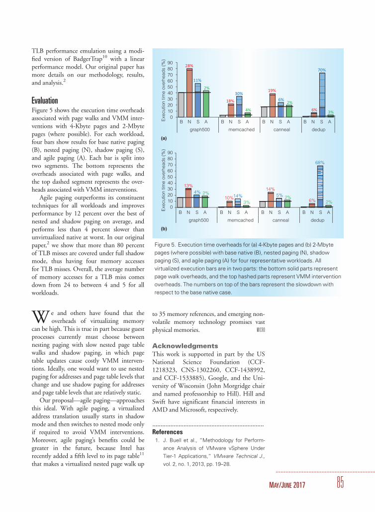
TLB performance emulation using a modi-fied version of BadgerTrap10 with a linearperformance model. Our original paper hasmore details on our methodology, results,and analysis.2
EvaluationFigure 5 shows the execution time overheadsassociated with page walks and VMM inter-ventions with 4-Kbyte pages and 2-Mbytepages (where possible). For each workload,four bars show results for base native paging(B), nested paging (N), shadow paging (S),and agile paging (A). Each bar is split intotwo segments. The bottom represents theoverheads associated with page walks, andthe top dashed segment represents the over-heads associated with VMM interventions.
Agile paging outperforms its constituenttechniques for all workloads and improvesperformance by 12 percent over the best ofnested and shadow paging on average, andperforms less than 4 percent slower thanunvirtualized native at worst. In our originalpaper,2 we show that more than 80 percentof TLB misses are covered under full shadowmode, thus having four memory accessesfor TLB misses. Overall, the average numberof memory accesses for a TLB miss comesdown from 24 to between 4 and 5 for allworkloads.
W e and others have found that theoverheads of virtualizing memory
can be high. This is true in part because guestprocesses currently must choose betweennesting paging with slow nested page tablewalks and shadow paging, in which pagetable updates cause costly VMM interven-tions. Ideally, one would want to use nestedpaging for addresses and page table levels thatchange and use shadow paging for addressesand page table levels that are relatively static.
Our proposal—agile paging—approachesthis ideal. With agile paging, a virtualizedaddress translation usually starts in shadowmode and then switches to nested mode onlyif required to avoid VMM interventions.Moreover, agile paging’s benefits could begreater in the future, because Intel hasrecently added a fifth level to its page table11
that makes a virtualized nested page walk up
to 35 memory references, and emerging non-volatile memory technology promises vastphysical memories. MICRO
AcknowledgmentsThis work is supported in part by the USNational Science Foundation (CCF-1218323, CNS-1302260, CCF-1438992,and CCF-1533885), Google, and the Uni-versity of Wisconsin (John Morgridge chairand named professorship to Hill). Hill andSwift have significant financial interests inAMD and Microsoft, respectively.
....................................................................References1. J. Buell et al., “Methodology for Perform-
ance Analysis of VMware vSphere Under
Tier-1 Applications,” VMware Technical J.,
vol. 2, no. 1, 2013, pp. 19–28.
0102030405060708090
B N S A B N S A B N S A B N S A
graph500 memcached canneal dedup
Exe
cutio
n tim
e ov
erhe
ads
(%)
0102030405060708090
Exe
cutio
n tim
e ov
erhe
ads
(%)
13%4%
10%14%14%
5%6%
68%
2%
3%2%
2%
B N S A B N S A B N S A B N S A
graph500 memcached canneal dedup
(b)
(a)
28%
11%
18%
30%19%
6%
6%
70%
2%
4%
2%
3%
Figure 5. Execution time overheads for (a) 4-Kbyte pages and (b) 2-Mbyte
pages (where possible) with base native (B), nested paging (N), shadow
paging (S), and agile paging (A) for four representative workloads. All
virtualized execution bars are in two parts: the bottom solid parts represent
page walk overheads, and the top hashed parts represent VMM intervention
overheads. The numbers on top of the bars represent the slowdown with
respect to the base native case.
.............................................................
MAY/JUNE 2017 85
2. J. Gandhi, M.D. Hill, and M.M. Swift,
“Agile Paging: Exceeding the Best of
Nested and Shadow Paging,” Proc. 43rd
Int’l Symp. Computer Architecture, 2016,
pp. 707–718.
3. R. Bhargava et al., “Accelerating Two-
Dimensional Page Walks for Virtualized
Systems,” in Proceedings of the 13th Inter-
national Conference on Architectural Sup-
port for Programming Languages and
Operating Systems, 2008, pp. 26–35.
4. K. Adams and O. Agesen, “A Comparison
of Software and Hardware Techniques for
x86 Virtualization,” Proc. 12th Int’l Conf.
Architectural Support for Programming Lan-
guages and Operating Systems, 2006, pp.
2–13.
5. A. Kivity et al., “KVM: The Linux Virtual
Machine Monitor,” Proc. Linux Symp., vol.
1, 2007, pp. 225–230.
6. J.L. Henning, “SPEC CPU2006 Benchmark
Descriptions,” SIGARCH Computer Archi-
tecture News, vol. 34, no. 4, 2006, pp.
1–17.
7. K. Albayraktaroglu et al., “BioBench: A
Benchmark Suite of Bioinformatics
Applications,” Proc. IEEE Int’l Symp. Per-
formance Analysis of Systems and Soft-
ware, 2005, pp. 2–9.
8. C. Bienia et al., “The Parsec Benchmark
Suite: Characterization and Architectural
Implications,” Proc. 17th Int’l Conf. Parallel
Architectures and Compilation Techniques,
2008, pp. 72–81.
9. A. Basu et al., “Efficient Virtual Memory for
Big Memory Servers,” Proc. 40th Ann. Int’l
Symp. Computer Architecture, 2013, pp.
237–248.
10. J. Gandhi et al., “BadgerTrap: A Tool to
Instrument x86-64 TLB Misses,” SIGARCH
Computer Architecture News, vol. 42, no. 2,
2014, pp. 20–23.
11. 5-Level Paging and 5-Level EPT, white
paper, Intel, Dec. 2016.
Jayneel Gandhi is a research scientist atVMware Research. His research interestsinclude computer architecture, operatingsystems, memory system design, virtualmemory, and virtualization. Gandhi has a
PhD in computer sciences from the Univer-sity of Wisconsin–Madison, where he com-pleted the work for this article. He is a mem-ber of ACM. Contact him at [email protected].
Mark D. Hill is the John P. MorgridgeProfessor, Gene M. Amdahl Professor ofComputer Sciences, and Computer SciencesDepartment Chair at the University of Wis-consin–Madison, where he also has a cour-tesy appointment in the Department ofElectrical and Computer Engineering. Hisresearch interests include parallel computersystem design, memory system design, andcomputer simulation. Hill has a PhD incomputer science from the University ofCalifornia, Berkeley. He is a fellow of IEEEand ACM. He serves as vice chair of theComputer Community Consortium. Con-tact him at [email protected].
Michael M. Swift is an associate professorin the Computer Sciences Department atthe University of Wisconsin–Madison. Hisresearch interests include operating systemreliability, the interaction of architectureand operating systems, and device driverarchitecture. Swift has a PhD in computerscience from the University of Washington.He is a member of ACM. Contact him [email protected].
Read your subscriptions through the myCS publications portal at http://mycs.computer.org.
..............................................................................................................................................................................................
TOP PICKS
............................................................
86 IEEE MICRO


.................................................................................................................................................................................................................
TRANSISTENCY MODELS: MEMORYORDERING AT THE HARDWARE–OS
INTERFACE.................................................................................................................................................................................................................
THIS ARTICLE INTRODUCES THE TRANSISTENCY MODEL, A SET OF MEMORY ORDERING
RULES AT THE INTERSECTION OF VIRTUAL-TO-PHYSICAL ADDRESS TRANSLATION AND
MEMORY CONSISTENCY MODELS. USING THEIR COATCHECK TOOL, THE AUTHORS SHOW
HOW TO RIGOROUSLY MODEL, ANALYZE, AND VERIFY THE CORRECTNESS OF A GIVEN
SYSTEM’S MICROARCHITECTURE AND SOFTWARE STACK WITH RESPECT TO ITS
TRANSISTENCY MODEL SPECIFICATION.
......Modern computer systems con-sist of heterogeneous processing elements(CPUs, GPUs, accelerators) running multi-ple distinct layers of software (user code,libraries, operating systems, hypervisors) ontop of many distributed caches and memo-ries. Fortunately, most of this complexity ishidden away underneath the virtual memory(VM) abstraction presented to the user code.However, one aspect of that complexity doespierce through: a typical memory subsystemwill buffer, reorder, or coalesce memoryrequests in often unintuitive ways for thesake of performance. This results in essen-tially all real-world hardware today exposinga weak memory consistency model (MCM)to concurrent code that communicatesthrough shared VM.
The responsibilities for maintaining theVM abstraction and for enforcing the mem-ory consistency model are shared between
the hardware and the operating system(OS) and require careful coordinationbetween the two. Although MCMs at theinstruction set architecture (ISA) and pro-gramming language levels are becomingincreasingly well understood,1–5 a key veri-fication challenge is that events within sys-tem layers can behave differently than the“normal” accesses described by the ISA orprogramming language MCM. For exam-ple, on the x86-64 architecture, whichimplements the relatively strong total storeordering (TSO) memory model,5 page tablewalks are automatically issued by hardware,can happen at any time, and often are notordered even with respect to fences. Evenworse is that while an ISA by design tends toremain stable across processor generations,microarchitectural phenomena often changedramatically from one generation to the next.For example, CPUs today are experimenting
Daniel Lustig
Princeton University
Geet Sethi
Abhishek Bhattacharjee
Rutgers University
Margaret Martonosi
Princeton University
.......................................................
88 Published by the IEEE Computer Society 0272-1732/17/$33.00�c 2017 IEEE
with features such as concurrent page tablewalkers and translation lookaside buffer(TLB) coalescing that improve performanceat the cost of adding significant complexity.6
Consequently, VM and MCM specificationsand implementations tend to be bug-proneand are only becoming more complex as sys-tems become increasingly heterogeneous anddistributed.
Bogdan Romanescu and colleagues werethe first to distinguish between MCMsmeant for virtual addresses (VAMC) andthose for physical addresses (PAMC).7 Theyconsidered hardware to be responsible for thelatter, and a combination of hardware andOS for the former. However, as we show inthis article, not even VAMC and PAMC cap-ture the full intersection of address transla-tion and memory ordering. Even machinesthat implemented the strictest model theyconsidered—virtual address sequential con-sistency (SC-for-VAMC)—may be prone tosurprising ordering bugs related to the check-ing of metadata at a different virtual andphysical address from the data being accessed.We therefore coin the term memory transis-tency model to refer to any set of memoryordering rules that explicitly account for thesebroader virtual-to-physical address transla-tion issues.
To enable rigorous analysis of transistencymodels and their implementations, we devel-oped a tool called COATCheck for verifyingmemory ordering enforcement in the contextof virtual-to-physical address translation.(COAT stands for consistency ordering andaddress translation.) COATCheck lets usersreason about the ordering implications of sys-tem calls, interrupts, microcode, and so on atthe microarchitecture, architecture, and OSlevels. System models are built in COAT-Check using a domain-specific language(DSL) called lspec (pronounced “mu-spec”),within which each component in a system(for example, each pipeline stage, each cache,and each TLB) can independently specify itsown contribution to memory ordering usingthe languages of first-order logic and micro-architecture-level happens-before (lhb)graphs.8,9 This allows COATCheck verifica-tion to be modular and flexible enough toadapt to the fast-changing world of modernheterogeneous systems.
Our contributions are as follows. First, wedeveloped a comprehensive methodology forspecifying and statically verifying memoryordering enforcement at the hardware–OSinterface. Second, we built a fast and general-purpose constraint solver that automates theanalysis of lspec microarchitecture specifica-tions. Third, as a case study, we built asophisticated model of an Intel Sandy-Bridge-like processor running a Linux-likeOS, and using that model we analyzed vari-ous translation-related memory ordering sce-narios of interest. Finally, we identified casesin which transistency goes beyond the tradi-tional scope of consistency: where even SC-for-VAMC7 is insufficient. Overall, our workoffers a rigorous yet practical framework formemory ordering verification, and it broad-ens the very scope of memory ordering as afield. The full toolset is open source.10
Enhanced Litmus TestsLitmus tests are small stylized programs test-ing some aspect of a memory model. Eachtest proposes an outcome: the value returnedby each load plus the final value at eachmemory location, or some relevant subsetthereof. The rules of a memory model deter-mine whether an outcome is permitted orforbidden. Consider Figure 1a: as written, xand y appear to be distinct addresses. Underthat assumption, the proposed outcome isobservable even under a model as strict assequential consistency (SC),11 because theevent interleaving shown in Figure 1b produ-ces that outcome. If instead x and y areactually synonyms (both map to the samephysical address), as in Figure 1c, the test isforbidden by SC, because then no interleav-ing of the threads produces the proposed out-come. While simple, this example highlightshow memory ordering verification is funda-mentally incomplete unless it explicitlyaccounts for address translation.
The basic unit of testing in COATCheckis the enhanced litmus test (ELT). ELTsextend traditional litmus tests by addingaddress translation, memory (re)mappings,interrupts, and other system-level operationsrelevant to memory ordering. In addition,just as a traditional litmus test outcome speci-fies the values returned by loads, ELTs also
.............................................................
MAY/JUNE 2017 89

consider the physical addresses used by eachVM access to be part of the outcome.Finally, ELTs include “ghost instructions”that model lower-than-ISA operations(such as microcode and page table walks)executed by hardware, even if these instruc-tions are not fetched, decoded, or issued aspart of the normal ISA-level instructionstream. These features give ELTs sufficientexpressive power to test all aspects of mem-ory ordering enforcement as it relates toaddress translation.
The COATCheck toolflow provides auto-mated methods to create ELTs from user-provided litmus tests plus other system-levelannotation guidance. We describe this con-version process below.
OS SynopsesOS activities such as TLB shootdowns andmemory (re)mappings are captured withinELTs as sequences of loads, stores, systemcalls, and/or interrupts. An OS synopsisspecifies a mapping from each system callinto a sequence of micro-ops that capture theeffects of that system call on ordering andaddress translation. When the system callcontains an interprocessor interrupt (IPI),the OS synopsis also instantiates predefinedinterrupt handler threads on interrupt-receiving cores.
For example, an OS synopsis mightexpand the mprotect call of Figure 2a intothe shaded instructions of Figure 2b. The callitself expands into four instructions: oneupdates the page table entry, one invalidatesthe local TLB, one sends an IPI, and onewaits for the IPI to be acknowledged. TheOS synopsis also produces the interrupt han-
dler (Thread 1b), which performs its ownlocal TLB invalidation before responding tothe initiating thread.
Microarchitecture SynopsesAs with the OS synopses, microarchitecturesynopses map each instruction onto a micro-code sequence that includes ghost instruc-tions such as page table walks. Not everyinstruction actually triggers a page table walk,so these ghost instructions are instantiatedonly as needed during the analysis.
For example, Figure 2b is transformedinto the ELT of Figure 2c by the addition ofthe gray-shaded ghost instructions. In thisexample, Thread 0’s store to [x] requires apage table walk, because the TLB entry forthat virtual address would have been invali-dated by the preceding invlpg instruction.Furthermore, because the page was originallyclean, ghost instructions also model howhardware marks the page dirty at that point.Finally, the microarchitecture synopsis addsto Thread 1b a microcode preamble contain-ing ghost instructions to receive the interrupt,save state, and disable nested interrupts. Inthis example, hardware is responsible for sav-ing state, but software is responsible forrestoring it. This again highlights the degreeof collective responsibility between hardwareand OS for ensuring ordering correctness.
lspec: A DSL for Specifying MemoryOrderingslspec is a domain-specific language for speci-fying memory ordering enforcement in theform of lhb graphs8,9 (see Figure 3). Nodesin a lhb graph represent events corresponding
Initially: [x] = 0, [y] = 0
Thread 0 Thread 1
Initially: [x] = 0, [y] = 0
Thread 0 Thread 1
St [x] 1
Ld [y] r1
St PA1 1
Ld PA1 r1
St PA1 2
Ld PA1 r2
St [y] 2
Ld [x] r2
Proposed outcome: r1 = 2, r2 = 1 Outcome r1 = 2, r2 = 1 forbidden
(a) (b)
Initially: [x] = 0, [y] = 0
Thread 0 Thread 1
(c)
St PA1 1
Ld PA2 r1
St PA2 2
Ld PA1 r2
Outcome: r1 = 2, r2 = 1 permitted
Figure 1. A litmus test showing how virtual memory interacts with memory ordering. (a)
Litmus test code. (b) A possible execution showing how the proposed outcome is observable
if x and y point to different physical addresses. (c) The outcome is forbidden if x and y point
to the same physical address (only one possible interleaving among many is shown).
..............................................................................................................................................................................................
TOP PICKS
............................................................
90 IEEE MICRO

to a particular instruction (column) andsome particular microarchitectural event(row). Edges represent happens-before order-ings guaranteed by some property of themicroarchitecture: an instruction flowingthrough a pipeline, a structure maintainingfirst-in, first-out (FIFO) ordering, the pas-sage of a message, and so on. Although pre-vious work derived lhb graphs using hard-coded notions of pipelines8 and caches,9
lspec models provide a completely general-purpose language for drawing lhb graphstailored to any arbitrary system design. Weprovide a detailed example of the lspec syn-tax in the next section.
Hardware memory models today tend tobe either axiomatic, where an outcome ispermitted if and only if it simultaneously sat-isfies all of the axioms of the model, or opera-tional, where an outcome is permitted onlyif it matches the outcome of some series ofexecution steps on an abstract “golden hard-ware model.” lspec models are axiomatic: alhb graph represents a legal test execution ifand only if it is acyclic and satisfies all of theconstraints in the model. Each hardware orsoftware component designer provides anindependent set of lhb graph axioms whichthat component guarantees to maintain. Theconjunction of these axioms forms the overalllspec model. This modularity means thatcomponents can be added, changed, orremoved as necessary without affecting anyof the other components.
Although they are inherently axiomatic,lspec models capture the best of the opera-tional approach as well. A total ordering ofthe nodes in an acyclic lhb graph is also anal-ogous to the sequence of execution steps inan operational model. This analogy lets lhbgraphs retain much of the intuitiveness ofoperational models while simultaneouslyretaining the scalability of axiomatic models.As such, lhb graphs are useful not only fortransistency models but also more generallyfor software and hardware memory models.
The COATCheck constraint solver isinspired by SAT and SMT solvers. It searchesto find any lhb graph that satisfies all of theconstraints of a given lspec model applied tosome ELT. If one can be found, the proposedELT outcome is observable. If not, the pro-posed outcome is forbidden. This result is
then checked against the architecture-levelspecification1 to ensure correctness.
System Model Case StudyIn this section, we present an in-depth casestudy of how hardware and software design-ers can use COATCheck and lspec to modela high-performance out-of-order processorand OS. Our case study has three parts. Thefirst is a lspec model called SandyBridge thatdescribes an out-of-order processor based onpublic documentation of and patents relatingto Intel’s Sandy Bridge microarchitecture.
Core 0/Thread 0 Core 1/Thread 1a
Core 0/Thread 0 Core 1/Thread 1a Core 1/Thread 1b
Core 1/Thread 1b
St [y] ← 1
Ld [x] → 0
Ld PML4E (x)
Ld PDPTE (x)
Ld PDE (x)
Ld PTE (x)
St [z/PTE (x)] ← R/W
invlpg [x]
Send IPI
Wait for Acks
Ld PML4E (x)
Ld PDPTE (x)
Ld PDE (x)
LdAtomic PTE (x) → clean
StAtomic PTE (x) ← dirty
St [x] ← 1
Ld [y] → 0
invlpg [x]
Send Ack
iret
St [z/PTE (x)] ← R/W
invlpg [x]
Send IPI
Wait for Acks
St [x] ← 1
Ld [y] → 0
St [y] ← 1
Ld [x] → 0
Depicted outcome permitted
Depicted outcome permitted
IPI Receive
Save state
disable ints
invlpg [x]
Send ACK
iret
Initially: [x] = 0, [y] = 0
Initially: [x] = 0, [y] = 0
Initially: [x] = 0, [y] = 0
Core 0/Thread 0 Core 1/Thread 1a
mprotect [x], r/w
St [x] ← 1
Ld [y] → 0
St [y] ← 1
Ld [x] → 0
Depicted outcome permitted
(a)
(b)
(c)
Figure 2. Traditional litmus tests are expanded into enhanced litmus tests
(ELTs). (a) A traditional litmus test with an mprotect system call added.
(b) The userþkernel version of the litmus test. On core 1, threads 1a and 1b
will be interleaved dynamically. “R/W” indicates that the page table entry
(PTE) R/W bit will be set. (c) The ELT. Page table accesses for [y],
accessed bit updates, and so forth are not depicted but will be included in
the analysis.
.............................................................
MAY/JUNE 2017 91

The second is the microarchitecture synopsis,which specifies how ghost instructions suchas page table walks behave on SandyBridge.The third is an OS synopsis inspired byLinux’s implementations of system calls andinterrupt handlers. We offer in-depth modelhighlights in this article; see our full paper foradditional detail.12
Memory Dependency Prediction andDisambiguationSandyBridge uses a sophisticated, high-performance virtually and physically addressedstore buffer (SB). This decision was inten-tional: a virtual-only SB would be unable todetect virtual address synonyms, whereas aphysical-only SB would place the TLB ontothe critical path for SB forwarding. The Sandy-Bridge SB instead splits the forwarding processinto two parts: a prediction stage tries to pre-emptively anticipate physical address matches,and a disambiguation stage later ensures thatall predictions were correct. This pairing keepsthe TLB off the critical path without giving upthe ability to detect synonyms.
The mechanism works as follows. Allstores write their virtual address and data intothe SB in parallel with accessing the TLB.
Once the TLB provides it, the physicaladdress is written into the SB as well. Eachload, in parallel with accessing the TLB,writes the lower 12 bits (the “index bits”) ofits virtual address into a CAM-based loadbuffer storing uncommitted loads. The loadthen compares its index bits against those ofall older stores in the SB. If an index match isfound, the load then compares its virtual tag,and potentially its physical tag, against thestores. If there is a tag match, the youngestmatching store forwards its data to the load.If no match is found, the load proceeds tothe cache. If there is an empty slot becausethe load executed out of order before an ear-lier store, then the load predicts that there isno dependency. This prediction is laterchecked during disambiguation: before eachstore commits, it checks the load buffer to seeif any younger loads matching the same phys-ical address have speculatively executedbefore it. If so, it squashes and replays thosemispredicted loads.
The following lspec snippet shows a por-tion of the SandyBridge lspec model captur-ing a case in which a load has an indexmatch, a virtual tag miss, and a physical tagmatch with a previous store.
DefineMacro “StoreBufferForwardPTag”:
exists microop “w”, (
SameCore w i /\IsAnyWrite w /\ProgramOrder w i /\
SameIndex w i /\~(SameVirtualTag w i) /\
SamePhysicalTag w i /\SameData w i/\
EdgesExist [
((w, SB-VTag/Index/Data), (i, LB-SB-IndexCompare),
“SBEntryIndexPresent”);
((w, SB-PTag), (i, LB-SB-PTagCompare), “SBEntryPTagPresent”);
((i, SB-LB-DataForward), (w, (0, MemoryHierarchy)),
“BeforeSBEntryLeaves”);
((i, LB-SB-IndexCompare), (i, LB-SB-VTagCompare), “path”);
((i, LB-SB-VTagCompare), (i, LB-SB-PTagCompare), “path”);
((i, LB-PTag), (i, LB-SB-PTagCompare), “path”);
((i, LB-SB-PTagCompare), (i, SB-LB-DataForward), “path”);
((i, SB-LB-DataForward), (i, WriteBack), “path”)
] /\
ExpandMacro STBNoOtherMatchesBetweenSrcAndRead
).
..............................................................................................................................................................................................
TOP PICKS
............................................................
92 IEEE MICRO

The first set of predicates narrows the axiomdown to apply to the scenario we described ear-lier. The edges listed in the EdgesExistpredicate then describe the associated memoryordering constraints. The first three ensurethat write w is still in the SB when load isearches for it, and the rest describe the paththat i itself takes through the microarchitec-ture. Finally, the axiom also checks (using amacro defined elsewhere) that the store is infact the youngest matching store in the SB.
Other Model DetailsA second component of our SandyBridgemodel reflects the functionality of system callsand interrupts as they relate to memory map-ping and remapping functions. Although x86TLB lookups and page table walks are per-formed by the hardware, x86 TLB coher-ence is OS-managed. To support this, x86provides the privileged invlpg instruc-tion, which invalidates the local TLB entryat a given address, along with support forinterprocessor interrupts (IPIs). As a serial-izing instruction, invlpg forces all pre-vious instructions to commit and drains theSB before fetching the following instruc-tion. invlpg also ensures that the nextaccess to the virtual page invalidated will bea TLB miss, thus forcing the latest versionof the corresponding page table entry to bebrought into the TLB.
To capture IPIs and invlpg instructions,our Linux OS synopsis expands the systemcall mprotect into code snippets thatupdate the page table, invalidate the now-stale TLB entry on the current core, and sendTLB shootdowns to other cores via IPIs andinterrupt handlers that execute invlpgoperations on the remote cores. The Sandy-Bridge microarchitecture synopsis capturesinterrupts by adding ghost instructions thatrepresent the reception of the interrupt andthe hardware disabling of nested interruptsbefore each interrupt handler. All possibleinterleavings of the interrupt handlers andthe threads’ code are considered. Figures 2band 2c depict the effects of both of thesesynopses.
To model TLB occupancy, the Sandy-Bridge lspec model adds two nodes to thelhb graph to represent TLB entry creationand invalidation, respectively. These are then
constrained following the value-in-cache-line(ViCL) mechanism.9 All loads and stores(including ghost instructions) are constrainedby the model to access the TLB within thelifetime of some matching TLB entry.
Page table walks are also instantiated bythe microarchitecture synopsis as a set ofghost instruction loads of the page tableentry. Because these are generated by dedi-cated hardware, the SandyBridge lspecmodel does not draw nodes such as Fetchand Dispatch for these instructions, becausethey do not pass through the pipeline. Fur-thermore, because the page table walk loadsare not TSO-ordered, they do not search theload buffer. They are, however, ordered withrespect to invlpg.
Our SandyBridge model also captures theaccessed and dirty bits present in the pagetable and TLB. When an accessed or dirty bitneeds to be updated, the pipeline waits untilthe triggering instruction reaches the head ofthe reorder buffer. At that point, the pro-cessor injects microcode (modeled via ghostLOCKed read-modify-write [RMW]instructions) implementing the update. Theghost instructions in a status bit update dotraverse the Dispatch, Issue, and Commitstages, unlike the ghost page table walks,because the status bit updates do propagatethrough most of the pipeline and affect archi-tectural state. The model also uses lhb edgesto ensure that the update is ordered againstall other instructions.
fr
fr
Fetch
Decode
Execute
Memory
Writeback
LeaveStoreBuffer
MemoryHierarchy
St[x]←1 Ld[y]→0 St[y]←1 Ld[x]→0
Core 0/Thread 0 Core 0/Thread 1a
Figure 3. A lhb graph for the litmus test in Figure 1 (minus the
mprotect), executing on a simple five-stage out-of-order pipeline.
Because the graph is acyclic, the execution is observable.
.............................................................
MAY/JUNE 2017 93

Analysis and Verification ExamplesIn this section, we present three test cases forour SandyBridge model.
Store Buffer ForwardingTest n5 (see Figure 4) checks the SB’s abilityto detect synonyms. If a synonym is misde-tected, one of the loads (i1.0 or i3.0)might be allowed to bypass the store (i0.0or i2.0) before it, leading to an illegal out-come. Also pictured are the TLB access ghostinstructions associated with each ISA-levelinstruction. Figure 4a shows one of the lhbgraphs COATCheck uses to rule out such a
situation on SandyBridge. Figure 4b showsthe code itself. If load (i3.0) executes outof order, it finds that the SB contains noprevious entries with the same index; this iscaptured by a lhb edge between (i3.0,LB-SB-IndexCompare) and (i2.0,SB-VTag/Index/Data). However, whenthe store (i2.0) does eventually execute, itwill squash (i3.0) unless the load buffer hasno index matches—that is, if (i3.0) has notyet entered the load buffer. The lhb edgefrom (i2.0, LBSearch) back to (i3.0,LB-Index) completes the cycle, which rulesout the execution.
Page RemappingsFigure 5 reproduces and extends the keyexample studied by Bogdan Romanescu andcolleagues:7 thread 0 changes the mappingfor x (i0.0), triggers a TLB shootdown(i2.0), and sends a message to thread 1(i4.0). Thread 1 receives the message(i7.0) and is hypothesized to write to x(i8.0) using the old, stale mapping (a situa-tion COATCheck should be expected to ruleout). Thread 1 (i9.0) sends a message backto thread 0 (i5.0), which checks (i6.0)that the value at x (according to the new map-ping) was not overwritten by the thread 1store (i8.0), which used the old mapping.The lhb graph generated for this scenario(Figure 5a) is also cyclic, showing how COAT-Check does in fact rule out the execution ofFigure 5b. The graph also simultaneouslydemonstrates many COATCheck features,such as IPIs, handlers, microcode, and fences,and it shows COATCheck’s ability to scale upto large and highly nontrivial problems.
Transistency versus ConsistencyOur third example focuses on status bits andsynonyms. Status bits are tracked per virtual-to-physical mapping rather than per physicalpage, and so the OS is responsible for track-ing the status of synonyms. In this example,suppose the OS intends to swap out to disk aclean page that is a synonym of some dirtypage. If it fails to check the status bits for thatsynonym, it might think that the page isclean and hence that it can be safely swappedout without being first written back.
Notably, in this example, the bug may beobservable even when there is no reordering
i0.0 i2.1i2.0i0.1 i3.0 i3.1i1.0 i1.1
Fetch
Dispatch
Issue
AGU
AccessTLB
TLBEntryCreate
TLBEntryInvalidate
SB-VTag/Index/Data
LB-Index
LB-SB-IndexCompare
LB-SB-VTagCompare
SB-PTag
LB-PTag
LB-SB-PTagCompare
SB-LB-DataForward
AccessCache
CacheLineInvalidated
WriteBack
LBSearch
Commit
LeaveStoreBuffer
MemoryHierarchy
Initially: [x] = 0, [y] = 0VA x → PA a (R/W, accessed, dirty)
VA y → PA a (R/W, accessed, dirty)
Core 0/Thread 0 Core 1/Thread 1
(i0.0) St [x/a] ← 1 (i2.0) St [y/a] ← 2
(i0.1) Ld PTE [x] (i2.1) Ld PTE (y)
(i1.0) Ld [y/a] → r1 (i3.0) Ld [x/a] → r2
(i3.1) Ld PTE [x](i1.1) Ld PTE (y)
Outcome r1 = 2, r2 = 1 forbidden
(a)
(b)
Figure 4. Analyzing litmus test n5 with COATCheck. (a) The lhb graph, with
the cycle shown with thicker edges. (b) The ELT code.
..............................................................................................................................................................................................
TOP PICKS
............................................................
94 IEEE MICRO

of any kind taking place, even under virtual-and/or physical-address sequential consis-tency.7 Because the checks of the two syno-nym page mappings are to different virtualand physical addresses, the necessary orderingcannot even be described by VAMC. Thisexample highlights a key way in which tran-sistency models are inherently broader inscope than consistency models.
We tested COATCheck on 118 litmustests, many of which come from Intel andAMD manuals and from prior work,1 andothers that are handwritten to stress the
SandyBridge model (including the case stud-ies discussed earlier). On an Intel Xeon E5-2667-v3 CPU, all 118 tests completed infewer than 100 seconds, and many were evenfaster. Although these lhb graphs are oftenan order of magnitude larger than thosestudied by prior tools analyzing lhbgraphs,8,9 the runtimes are similar. This dem-onstrates the benefits of combining the lspecDSL with an efficient dedicated solver. It alsopoints to the feasibility of providing transis-tency verification fast enough to supportinteractive design and debugging.
i11.0 i12.0i9.0 i10.0 i15.0i3.0i1.0i0.1 i6.1i5.0i0.0 i14.0i4.0i2.0 i6.0 i8.0i7.0i2.1 i8.1 i13.0
Fetch
Dispatch
Issue
AGU
AccessTLB
TLBEntryCreate
TLBEntryInvlidate
SB-VTag/Index/Data
LB-Index
LB-SB-IndexCompare
LB-SB-VTagCompare
SB-PTag
LB-PTag
LB-SB-PTagCompare
SB-LB-DataForward
AccessCache
CacheLineInvalidated
WriteBack
LBSearch
Commit
LeaveStoreBuffer
MemoryHierarchy
(a)
(b)
Initially: [x] = 0, VA x → PA a (R/W, accessed, dirty)(other initial mapping not shown)
Thread 0
Core 0
Thread 1a
Core 1
(i0.0) St [z/PTE (x)] ←(VA x → PA b)
(i10.0) Ld [w/APIC] → mrf(i11.0) Ld EFLAGS → (IF)(i12.0) St EFLAGS ← (!IF)(i13.0) invlpg [x](i14.0) St [v/d] ← ack(i15.0) iret
(i7.0) Ld [y/c] → 2(i8.0) St [x/a] ← 3(i8.1) Ld PTE [x] → TLB(i9.0) St [y/c] ← 4
Depicted outcome forbidden
(i0.1) Ld PTE [x](i1.0) invlpg [x](i2.0) St [w/APIC] ← mrf(i2.1) Ld PTE(w) → TLB(i3.0) Ld [v/d] → ack(i4.0) St [y/c] ← 2(i5.0) Ld [y/c] → 4(i6.0) Ld [x/b] → 1(i6.1) Ld PTE [x] → TLB
Thread 1b
Figure 5. Litmus test ipi8.7 (a) Because the graph is cyclic (thick edges), the outcome is forbidden. In this case, the cycle
was found before the PTEs for y were even enumerated. (b) The ELT code.
.............................................................
MAY/JUNE 2017 95

W ith COATCheck, we were able tosuccessfully identify, model, and ver-
ify a number of interesting scenarios at theintersection of memory consistency modelsand address translation. However, manyimportant challenges remain; COATCheckonly scratches the surface of the complete setof phenomena that can arise at the OS andmicroarchitecture layers. For example, a nat-ural next step might be to extend COAT-Check to model virtual machines andhypervisors of arbitrary depth. Generally, wehope and expect that future work in the areawill build on top of COATCheck to createmore complete and more rigorous transistencymodels that can capture an ever-growing setof system-level behaviors and bugs.
We also envision COATCheck becomingmore integrated with top-to-bottom memoryordering verification tools. We hope that oneday verification tools will cohesively span thefull computing stack, from programminglanguages all the way down to register trans-fer level, thereby giving programmers andarchitects much more confidence in the cor-rectness of their code and systems. Thesegoals will only become more challenging assystems grow more heterogeneous and morecomplex over time. However, COATCheckprovides a rigorous and scalable roadmap forunderstanding how such systems can beunderstood rigorously, and as such we hopethat future work finds COATCheck and itslspec modeling language to be useful build-ing blocks for continued research into thearea. MICR O
....................................................................References1. J. Alglave, L. Maranget, and M. Tautschnig,
“Herding Cats: Modelling, Simulation, Test-
ing, and Data Mining for Weak Memory,”
ACM Trans. Programming Languages and
Systems, vol. 36, no. 2, 2014; doi:10.1145
/2627752.
2. M. Batty et al., “Clarifying and Compiling C/
Cþþ Concurrency: From Cþþ 11 to
POWER,” Proc. 39th Ann. ACM SIGPLAN-
SIGACT Symp. Principles of Programming
Languages, 2012, pp. 509–520.
3. H.-J. Boehm and S.V. Adve, “Foundations
of the Cþþ Concurrency Memory Model,”
Proc. 29th ACM SIGPLAN Conf. Program-
ming Language Design and Implementa-
tion, 2008, pp. 68–78.
4. S. Sarkar et al., “Understanding POWER
Multiprocessors,” Proc. 32nd ACM SIG-
PLAN Conf. Programming Language Design
and Implementation, 2011, pp. 175–186.
5. P. Sewell et al., “x86-TSO: A Rigorous and
Usable Programmer’s Model for x86 Multi-
processors,” Comm. ACM, vol. 53, no. 7,
2010, pp. 89–97.
6. M. Clark, “A New, High Performance x86
Core Design from AMD,” Hot Chips 28
Symp., 2016; www.hotchips.org/archives
/2010s/hc28.
7. B. Romanescu, A. Lebeck, and D.J. Sorin,
“Address Translation Aware Memory Con-
sistency,” IEEE Micro, vol. 31, no. 1, 2011,
pp. 109–118.
8. D. Lustig, M. Pellauer, and M. Martonosi,
“Verifying Correct Microarchitectural Enforce-
ment of Memory Consistency Models,” IEEE
Micro, vol. 35, no. 3, 2015, pp. 72–82.
9. Y. Manerkar et al., “CCICheck: Using lhb
Graphs to Verify the Coherence-Consis-
tency Interface,” Proc. 48th Int’l Symp.
Microarchitecture, 2015, pp. 26–37.
10. Check Verification Tool Suite; http://check
.cs.princeton.edu.
11. L. Lamport, “How to Make a Multiprocessor
Computer That Correctly Executes Multiproc-
ess Programs,” IEEE Trans. Computers, vol.
28, no. 9, 1979, pp. 690–691.
12. D. Lustig et al., “COATCheck: Verifying
Memory Ordering at the Hardware-OS
Interface,” Proc. 21st Int’l Conf. Architec-
tural Support for Programming Languages
and Operating Systems, 2016, pp. 233–247.
Daniel Lustig is a research scientist at Nvi-dia. His research interests include computerarchitecture and memory consistency mod-els. Lustig received a PhD in electrical engi-neering from Princeton University, where heperformed the work for this article. He is amember of IEEE and ACM. Contact him [email protected].
Geet Sethi is a PhD student in the Depart-ment of Computer Science at Stanford
..............................................................................................................................................................................................
TOP PICKS
............................................................
96 IEEE MICRO

University. His research interests includeserverless computing, machine learning, andcomputer architecture. Sethi received a BSin computer science and mathematics fromRutgers University, where he performed thework for this article. He is a student memberof IEEE and ACM. Contact him at [email protected].
Abhishek Bhattacharjee is an associate pro-fessor in the Department of Computer Sci-ence at Rutgers University. His researchinterests span the hardware–software inter-face. Bhattacharjee received a PhD in electri-cal engineering from Princeton University.He is a member of IEEE and ACM. Contacthim at [email protected].
Margaret Martonosi is the Hugh TrumbullAdams ’35 Professor of Computer Scienceat Princeton University. Her research inter-ests include computer architecture and
mobile computing, with an emphasis onpower-efficient heterogeneous systems.Martonosi has a PhD in electrical engineer-ing from Stanford University. She is a Fellowof IEEE and ACM. Contact her at [email protected].
Read your subscriptions through the myCS publications portal at http://mycs.computer.org.
.............................................................
MAY/JUNE 2017 97

.................................................................................................................................................................................................................
TOWARD A DNA-BASED ARCHIVALSTORAGE SYSTEM
.................................................................................................................................................................................................................
STORING DATA IN DNA MOLECULES OFFERS EXTREME DENSITY AND DURABILITY
ADVANTAGES THAT CAN MITIGATE EXPONENTIAL GROWTH IN DATA STORAGE NEEDS. THIS
ARTICLE PRESENTS A DNA-BASED ARCHIVAL STORAGE SYSTEM, PERFORMS WET LAB
EXPERIMENTS TO SHOW ITS FEASIBILITY, AND IDENTIFIES TECHNOLOGY TRENDS THAT
POINT TO INCREASING PRACTICALITY.
......The “digital universe” (all digitaldata worldwide) is forecast to grow to morethan 16 zettabytes in 2017.1 Alarmingly, thisexponential growth rate easily exceeds ourability to store it, even when accounting forforecast improvements in storage technolo-gies such as tape (185 terabytes2) and opticalmedia (1 petabyte3). Although not all datarequires long-term storage, a significant frac-tion does: Facebook recently built a datacen-ter dedicated to 1 exabyte of cold storage.4
Synthetic (manufactured) DNA sequen-ces have long been considered a potentialmedium for digital data storage because oftheir density and durability.5–7 DNA mole-cules offer a theoretical density of 1 exabyteper cubic millimeter (eight orders of magni-tude denser than tape) and half-life durabilityof more than 500 years.8 DNA-based storagealso has the benefit of eternal relevance: aslong as there is DNA-based life, there will bestrong reasons to read and manipulate DNA.
Our paper for the 2016 Conference onArchitectural Support for Programming Lan-guages and Operating Systems (ASPLOS)proposed an architecture for a DNA-basedarchival storage system.9 Both reading andwriting a synthetic DNA storage medium
involve established biotechnology practices.The write process encodes digital data intoDNA nucleotide sequences (a nucleotide isthe basic building block of DNA), synthe-sizes (manufactures) the corresponding DNAmolecules, and stores them away. Readingthe data involves sequencing (reading) theDNA molecules and decoding the informa-tion back to the original digital data (seeFigure 1).
Progress in DNA storage has been rapid:in our ASPLOS paper, we successfully storedand recovered 42 Kbytes of data; since publi-cation, our team has scaled our process tostore and recover more than 200 Mbytes ofdata.10,11 Constant improvement in the scaleof DNA storage—at least two times peryear—is fueled by exponential reduction insynthesis and sequencing cost and latency;growth in sequencing productivity eclipseseven Moore’s law.12 Further growth in thebiotechnology industry portends orders ofmagnitude cost reductions and efficiencyimprovements.
We think the time is ripe to seriously con-sider DNA-based storage and explore systemdesigns and architectural implications. OurASPLOS paper was the first to address two
James Bornholt
Randolph Lopez
University of Washington
Douglas M. Carmean
Microsoft
Luis Ceze
Georg Seelig
University of Washington
Karin Strauss
Microsoft Research
.......................................................
98 Published by the IEEE Computer Society 0272-1732/17/$33.00�c 2017 IEEE

fundamental challenges in building a viableDNA-based storage system. First, how shouldsuch a storage medium be organized? Wedemonstrate the tradeoffs between density,reliability, and performance by envisioningDNA storage as a key-value store. Multiplekey-value pairs are stored in the same pool,and multiple such pools are physicallyarranged into a library. Second, how can databe recovered efficiently from a DNA storagesystem? We show for the first time that ran-dom access to DNA-based storage pools isfeasible by using a polymerase chain reaction(PCR) to amplify selected molecules forsequencing. Our wet lab experiments validateour approach and point to the long-term via-bility of DNA as an archival storage medium.
System DesignA DNA storage system (see Figure 2) takesdata as input, synthesizes DNA molecules torepresent that data, and stores them in alibrary of pools. To read data back, the sys-tem selects molecules from the pool, ampli-fies them with PCR (a standard process frombiotechnology), and sequences them back todigital data. We model the DNA storage sys-tem as a key-value store, in which input datais associated with a key, and read operationsidentify the key they wish to recover.
Writing to DNA storage involves encod-ing binary data as DNA nucleotides and syn-thesizing the corresponding molecules. Thisprocess involves two non-trivial steps. First,although there are four DNA nucleotides(A, C, G, T) and so a conversion from binaryappears trivial, we instead convert binarydata to base 3 and employ a rotating encod-ing from ternary digits to nucleotides.7 Thisencoding avoids homopolymers—repetitionsof the same nucleotide—that significantlyincrease the chance of errors.
Second, DNA synthesis technology effec-tively manufactures molecules one nucleotideat a time, and cannot synthesize molecules ofarbitrary length without error. A reasonablyefficient strand length for DNA synthesis is120 to 150 nucleotides, which gives a maxi-mum of 237 bits of data in a single moleculeusing this ternary encoding. The write proc-ess therefore fragments input data into smallblocks that correspond to separate DNA
molecules. This blocking approach also ena-bles added redundancy. Previous work over-lapped multiple small blocks,7 but ourexperimental and simulation results showthis approach to sacrifice too much densityfor little gain. Our ASPLOS experimentsinstead used an XOR encoding, in whicheach consecutive pair of blocks is XORedtogether to form a third redundancy block.Although this encoding is simple, we showedthat it achieves similar redundancy propertiesto existing approaches with much less densityoverhead. Since publishing this paper, ourteam has been exploring more sophisticatedencodings, such as Reed-Solomon codes.
Random AccessReading from DNA storage involves sequenc-ing molecules and decoding their data back tobinary (using the inverse of the encoding dis-cussed earlier). In existing work on DNA stor-age, recovering data meant sequencing all
Write path
AGTCACT AGTCACT01010111 01010111
Read path
Encoding Synthesis Sequencing Decoding
Figure 1. Using DNA for digital data storage. Writes to DNA first encode
digital data as nucleotide sequences and then synthesize (manufacture)
molecules. Reads from DNA first sequence (read) the molecules and then
decode back to digital data.
Datain
DNA synthesizer
PCRthermocycler
DNA sequencer
DNA storage library
Dataout
DNApool
Figure 2. Overview of a DNA storage system. Stored molecules are
arranged in a library of pools.
.............................................................
MAY/JUNE 2017 99
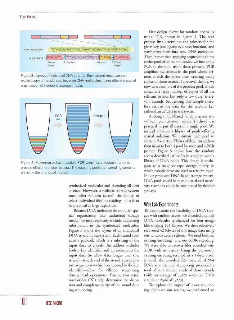
synthesized molecules and decoding all dataat once. However, a realistic storage systemmust offer random access—the ability toselect individual files for reading—if it is tobe practical at large capacities.
Because DNA molecules do not offer spa-tial organization like traditional storagemedia, we must explicitly include addressinginformation in the synthesized molecules.Figure 3 shows the layout of an individualDNA strand in our system. Each strand con-tains a payload, which is a substring of theinput data to encode. An address includesboth a key identifier and an index into theinput data (to allow data longer than onestrand). At each end of the strand, special pri-mer sequences—which correspond to the keyidentifier—allow for efficient sequencingduring read operations. Finally, two sensenucleotides (“S”) help determine the direc-tion and complementarity of the strand dur-ing sequencing.
Our design allows for random access byusing PCR, shown in Figure 4. The readprocess first determines the primers for thegiven key (analogous to a hash function) andsynthesizes them into new DNA molecules.Then, rather than applying sequencing to theentire pool of stored molecules, we first applyPCR to the pool using these primers. PCRamplifies the strands in the pool whose pri-mers match the given ones, creating manycopies of those strands. To recover the file, wenow take a sample of the product pool, whichcontains a large number of copies of all therelevant strands but only a few other irrele-vant strands. Sequencing this sample there-fore returns the data for the relevant keyrather than all data in the system.
Although PCR-based random access is aviable implementation, we don’t believe it ispractical to put all data in a single pool. Weinstead envision a library of pools offeringspatial isolation. We estimate each pool tocontain about 100 Tbytes of data. An addressthen maps to both a pool location and a PCRprimer. Figure 5 shows how the randomaccess described earlier fits in a system with alibrary of DNA pools. This design is analo-gous to a magnetic-tape storage library, inwhich robotic arms are used to retrieve tapes.In our proposed DNA-based storage system,DNA pools could be manipulated and neces-sary reactions could be automated by fluidicssystems.
Wet Lab ExperimentsTo demonstrate the feasibility of DNA stor-age with random access, we encoded and hadDNA molecules synthesized for four imagefiles totaling 151 Kbytes. We then selectivelyrecovered 42 Kbytes of this image data usingour random access scheme. We used both anexisting encoding7 and our XOR encoding.We were able to recover files encoded withXOR with no errors. Using the previouslyexisting encoding resulted in a 1-byte error.In total, the encoded files required 16,994DNA strands, and sequencing produced atotal of 20.8 million reads of those strands(with an average of 1,223 reads per DNAstrand, or depth of 1,223).
To explore the impact of lower sequenc-ing depth on our results, we performed an
Input nucleotides
Output strand 5’ 3’
Primertarget
S S Primertarget
Payload Address
TCTACGATC A TCTACGCTCGAGTGATACGA
TCTACGCTCGAGTGATACGAATGCGTCGTACTACGTCGTGTACGTA...
TCTACG A CCAGTATCA
Figure 3. Layout of individual DNA strands. Each strand must carry an
explicit copy of its address, because DNA molecules do not offer the spatial
organization of traditional storage media.
PCR Sample
Figure 4. Polymerase chain reaction (PCR) amplifies selected strands to
provide efficient random access. The resulting pool after sampling contains
primarily the strands of interest.
..............................................................................................................................................................................................
TOP PICKS
............................................................
100 IEEE MICRO

experiment in which we discarded much ofthe sequencing data (see Figure 6). Lowerdepth per DNA sequence frees up additionalsequencing bandwidth for other DNAsequences, but could omit some strandsentirely if they are not sequenced at all.Despite such omissions, the results show thatwe can successfully recover all data using asfew as 1 percent of the sequencing results,indicating we could have recovered 100times more data with the same sequencingtechnology. Future sequencing technology islikely to continue increasing this amount.
To inform our coding-scheme design,we assessed errors in DNA synthesis andsequencing by comparing the sequencingoutput of two sets of DNA sequences withthe original reference data. The first setincludes the sequences we used to encodedata, which were synthesized for our storageexperiments by a supplier using an arraymethod. Errors in these sequencing resultscould be caused either by sequencing or syn-thesis (or both). The second set includesDNA that was synthesized by a different sup-plier using a process that’s much more accu-rate (virtually no errors), but also muchcostlier. Errors in these sequencing results areessentially caused only by the sequencingprocess. By comparing the two sets of results,we can determine the error rate of bothsequencing (results from the second set) and
array synthesis (the difference between thetwo sets). Our results indicate that overallerrors per base are a little more than 1 percentand that sequencing accounts for most of theerror (see Figure 7).
Technology TrendsWith demand for storage growing fasterthan even optimistic projections of currenttechnologies, it is important to develop newsustainable storage solutions. A significant
0
25
50
75
100
0.01 0.1 1 10Reads used (%)
Per
−b
ase
accu
racy
(%
)
EncodingGoldmanXOR
Figure 6. Decoding accuracy as a function of sequencing depth. We
successfully recover all data using as little as 1 percent of the sequencing
results, suggesting current sequencing technology can recover up to 100
times more data.
A T G T T G G A T G C A A A A A C A T C CC
A T G T T G C C A G T T A A A G C A T C CC
A T G T T T G C T T A C A A A C C A T C CC
A T G T T G G A T G C A A A A A C A T C CC
A T G T T G C C A G T T A A A G C A T C CC
A T G T T T G C T T A C A A A C C A T C CC
Sequencing
PCR amplification
Manufacture DNA
Write process
Read process
Decode
Select primers for key
Encode data
DNA storage(physical) library
01010111...
01010111...
foo.jpg
Look up anddetermine primer
foo.jpg
Figure 5. Putting it all together: random access with a pool library for physical isolation. The key data (here, foo.jpg) is used
with a hash function to identify the relevant pool within the library.
.............................................................
MAY/JUNE 2017 101
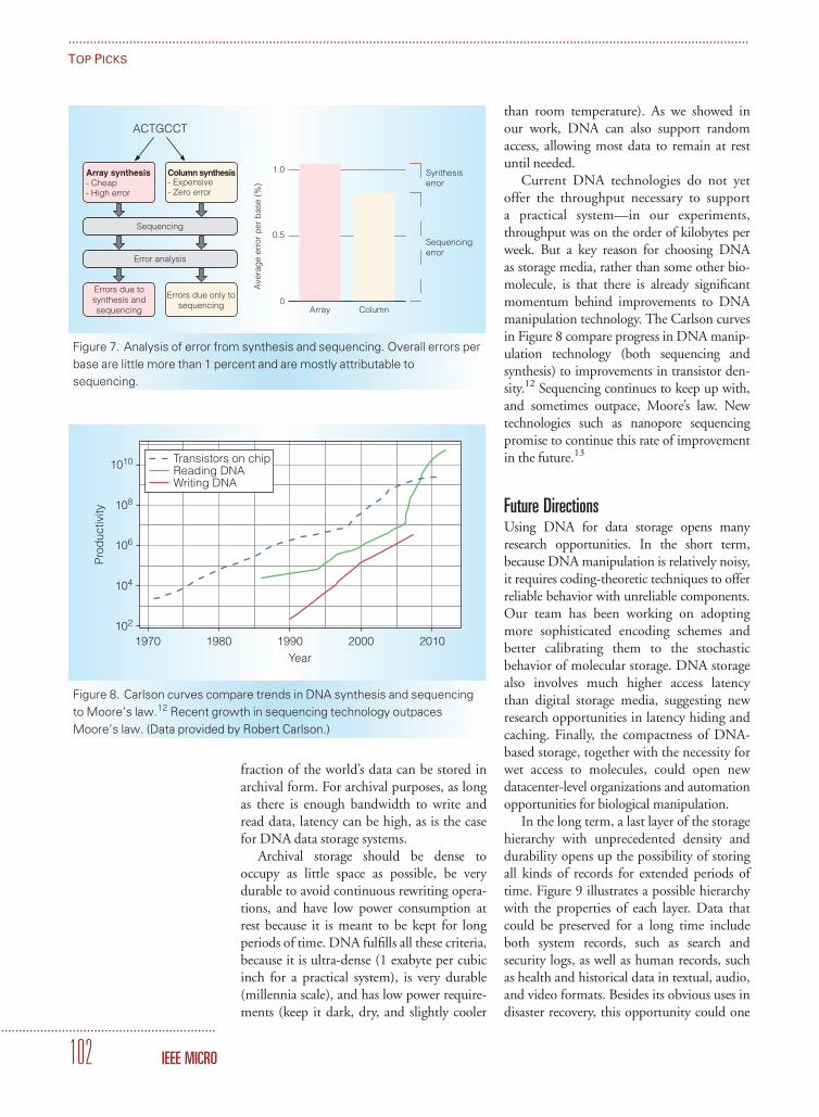
fraction of the world’s data can be stored inarchival form. For archival purposes, as longas there is enough bandwidth to write andread data, latency can be high, as is the casefor DNA data storage systems.
Archival storage should be dense tooccupy as little space as possible, be verydurable to avoid continuous rewriting opera-tions, and have low power consumption atrest because it is meant to be kept for longperiods of time. DNA fulfills all these criteria,because it is ultra-dense (1 exabyte per cubicinch for a practical system), is very durable(millennia scale), and has low power require-ments (keep it dark, dry, and slightly cooler
than room temperature). As we showed inour work, DNA can also support randomaccess, allowing most data to remain at restuntil needed.
Current DNA technologies do not yetoffer the throughput necessary to supporta practical system—in our experiments,throughput was on the order of kilobytes perweek. But a key reason for choosing DNAas storage media, rather than some other bio-molecule, is that there is already significantmomentum behind improvements to DNAmanipulation technology. The Carlson curvesin Figure 8 compare progress in DNA manip-ulation technology (both sequencing andsynthesis) to improvements in transistor den-sity.12 Sequencing continues to keep up with,and sometimes outpace, Moore’s law. Newtechnologies such as nanopore sequencingpromise to continue this rate of improvementin the future.13
Future DirectionsUsing DNA for data storage opens manyresearch opportunities. In the short term,because DNA manipulation is relatively noisy,it requires coding-theoretic techniques to offerreliable behavior with unreliable components.Our team has been working on adoptingmore sophisticated encoding schemes andbetter calibrating them to the stochasticbehavior of molecular storage. DNA storagealso involves much higher access latencythan digital storage media, suggesting newresearch opportunities in latency hiding andcaching. Finally, the compactness of DNA-based storage, together with the necessity forwet access to molecules, could open newdatacenter-level organizations and automationopportunities for biological manipulation.
In the long term, a last layer of the storagehierarchy with unprecedented density anddurability opens up the possibility of storingall kinds of records for extended periods oftime. Figure 9 illustrates a possible hierarchywith the properties of each layer. Data thatcould be preserved for a long time includeboth system records, such as search andsecurity logs, as well as human records, suchas health and historical data in textual, audio,and video formats. Besides its obvious uses indisaster recovery, this opportunity could one
102
104
106
108
1010
1970 1980 1990 2000 2010Year
Pro
duc
tivity
Transistors on chipReading DNAWriting DNA
Figure 8. Carlson curves compare trends in DNA synthesis and sequencing
to Moore’s law.12 Recent growth in sequencing technology outpaces
Moore’s law. (Data provided by Robert Carlson.)
ACTGCCT
Array synthesis Column synthesis- Cheap- High error
- Expensive- Zero error
Sequencing
Error analysis
Errors due tosynthesis andsequencing
Errors due only tosequencing
Ave
rag
e er
ror
per
bas
e (%
)
1.0
0.5
0
Synthesiserror
Sequencingerror
Array Column
Figure 7. Analysis of error from synthesis and sequencing. Overall errors per
base are little more than 1 percent and are mostly attributable to
sequencing.
..............................................................................................................................................................................................
TOP PICKS
............................................................
102 IEEE MICRO

day be a great contributor to the field of digi-tal archeology, the study of human historythrough “ancient” digital data.
T he success of the initial project, pub-lished in our ASPLOS paper, motivated
us to significantly expand our efforts toexplore DNA-based data storage. We formedthe Molecular Information Systems Lab(MISL), with members from the Universityof Washington and Microsoft Research.MISL has worked with Twist Bioscience tosynthesize a 200-Mbyte DNA pool,11 morethan three orders of magnitude larger thanour ASPLOS results, and an order of magni-tude larger than the prior state of the art.14
Some of its more recent efforts include newcoding schemes, sequencing with nanopore-based techniques, and fluidics automation.
Given the impending limits of silicontechnology, we believe that hybrid siliconand biochemical systems are worth seriousconsideration. Now is the time for architectsto consider incorporating biomolecules as anintegral part of computer design. DNA-basedstorage is one clear, practical example of thisdirection. Biotechnology has benefited tre-mendously from progress in silicon technol-ogy developed by the computer industry;perhaps now is the time for the computerindustry to borrow back from the biotechnol-ogy industry to advance the state of the art incomputer systems. MICRO
AcknowledgmentsWe thank the members of the MolecularInformation Systems Laboratory for their con-tinuing support of this work. We thank Bran-don Holt, Emina Torlak, Xi Wang, the Sampagroup at the University of Washington, andthe anonymous reviewers for feedback on
this work. This material is based on worksupported by the National Science Founda-tion under grant numbers 1064497 and1409831, by gifts from Microsoft Research,and by the David Notkin Endowed Gradu-ate Fellowship.
....................................................................References1. “Where in the World Is Storage: Byte
Density Across the Globe,” IDC, 2013;
www.idc.com/downloads/where is storage
infographic 243338.pdf.
2. “Sony Develops Magnetic Tape Technology
with the World’s Highest Recording Density,”
press release, Sony, 30 Apr. 2014; www.sony
.net/SonyInfo/News/Press/201404/14-044E.
3. J. Plafke, “New Optical Laser Can Increase
DVD Storage Up to One Petabyte,” blog,
20 June 2013; www.extremetech.com
/computing/159245-new-optical-laser-can
-increase-dvd-storage-up-to-one-petabyte.
4. R. Miller, “Facebook Builds Exabyte Data
Centers for Cold Storage,” blog, 18 Jan. 2013;
www.datacenterknowledge.com/archives
/2013/01/18/facebook-builds-new-data-centers
-for-cold-storage.
5. G.M. Church, Y. Gao, and S. Kosuri, “Next-
Generation Digital Information Storage in
DNA,” Science, vol. 337, no. 6102, 2012,
pp. 1628–1629.
6. C.T. Clelland, V. Risca, and C. Bancroft,
“Hiding Messages in DNA Microdots,”
Nature, vol. 399, 1999, pp. 533–534.
7. N. Goldman et al., “Towards Practical, High-
Capacity, Low-Maintenance Information
Storage in Synthesized DNA,” Nature,
vol. 494, 2013, pp. 77–80.
8. M.E. Allentoft et al., “The Half-Life of DNA
in Bone: Measuring Decay Kinetics in 158
Flash
HDD
Tape
DNA storage
Access time Durability Capacity
µs–ms
10s of ms
Minutes
Hours
~5 yrs
~5 yrs
~15–30 yrs
Centuries
Tbytes
100s of Tbytes
Pbytes
Zbytes
Figure 9. A possible storage system hierarchy. DNA storage is a promising new bottom layer,
offering higher density and durability at the cost of latency.
.............................................................
MAY/JUNE 2017 103

Dated Fossils,” Proc. Royal Society of
London B: Biological Sciences, vol. 279, no.
1748, 2012, pp. 4724–4733.
9. J. Bornholt et al., “A DNA-Based Archival
Storage System,” Proc. 21st Int’l Conf.
Architectural Support for Programming
Languages and Operating Systems
(ASPLOS), 2016, pp. 637–649.
10. M. Brunker, “Microsoft and University of
Washington Researchers Set Record for
DNA Storage,” blog, 7 July 2016; http://
blogs.microsoft.com/next/2016/07/07
/microsoft-university-washington
-researchers-set-record-dna-storage.
11. L Organick et al., “Scaling Up DNA Data
Storage and Random Access Retrieval,”
bioRxiv, 2017; doi:10.1101/114553.
12. R. Carlson, “Time for New DNA Synthesis
and Sequencing Cost Curves,” blog, 12
Feb. 2014; www.synthesis.cc/2014/02
/time-for-new-cost-curves-2014.html.
13. “Oxford Nanopore Technologies,” http://
nanoporetech.com.
14. M. Blawata et al., “Forward Error Correction
for DNA Data Storage,” Procedia Computer
Science, vol. 80, 2016, pp. 1011–1022.
James Bornholt is a PhD student in thePaul G. Allen School of Computer Scienceand Engineering at the University of Wash-ington. His research interests include pro-gramming languages and formal methods,focusing on program synthesis. Bornholtreceived an MS in computer science fromthe University of Washington. Contact himat [email protected].
Randolph Lopez is a graduate student inbioengineering at the University of Wash-ington. His research interests include theintersection of synthetic biology, DNAnanotechnology, and molecular diagnostics.Lopez received a BS in bioengineering fromthe University of California, San Diego.Contact him at [email protected].
Douglas M. Carmean is a partner architectat Microsoft. His research interests includenew architectures on future device technol-ogy. Carmean received a BS in electrical andelectronics engineering from Oregon State
University. Contact him at [email protected].
Luis Ceze is the Torode Family AssociateProfessor in the Paul G. Allen School ofComputer Science and Engineering at theUniversity of Washington. His researchinterests include the intersection betweencomputer architecture, programming lan-guages, and biology. Ceze received a PhD incomputer science from the University of Illi-nois at Urbana–Champaign. Contact him [email protected].
Georg Seelig is an associate professor in theDepartment of Electrical Engineering andthe Paul G. Allen School of Computer Sci-ence and Engineering at the University ofWashington. His research interests includeunderstanding how biological organismsprocess information using complex biochemi-cal networks and how such networks can beengineered to program cellular behavior. See-lig received a PhD in physics from the Uni-versity of Geneva. Contact him at [email protected].
Karin Strauss is a senior researcher atMicrosoft Research and an affiliate faculty atthe University of Washington. Her researchinterests include studying the application ofbiological mechanisms and other emergingtechnologies to storage and computation,and building systems that are efficient andreliable with them. Strauss received a PhDin computer science from the University ofIllinois at Urbana–Champaign. Contact herat [email protected].
Read your subscriptions through the myCS publications portal at http://mycs.computer.org.
..............................................................................................................................................................................................
TOP PICKS
............................................................
104 IEEE MICRO


.................................................................................................................................................................................................................
TI-STATES: POWER MANAGEMENT INACTIVE TIMING MARGIN PROCESSORS
.................................................................................................................................................................................................................
TEMPERATURE INVERSION IS A TRANSISTOR-LEVEL EFFECT THAT IMPROVES PERFORMANCE
WHEN TEMPERATURE INCREASES. THIS ARTICLE PRESENTS A COMPREHENSIVE
MEASUREMENT-BASED ANALYSIS OF ITS IMPLICATIONS FOR ARCHITECTURE DESIGN AND
POWER MANAGEMENT USING THE AMD A10-8700P PROCESSOR. THE AUTHORS
PROPOSE TEMPERATURE-INVERSION STATES (TI-STATES) TO HARNESS THE OPPORTUNITIES
PROMISED BY TEMPERATURE INVERSION. THEY EXPECT TI-STATES TO BE ABLE TO IMPROVE
THE POWER EFFICIENCY OF MANY PROCESSORS MANUFACTURED IN FUTURE CMOS
TECHNOLOGIES.
......Temperature inversion refers tothe phenomenon that transistors switch fasterat a higher temperature when operating undercertain regions. To harness temperature inver-sion’s performance benefits, we introduceTi-states, or temperature-inversion states, foractive timing-margin management in emerg-ing processors. Ti-states are frequency, temper-ature, and voltage triples that enable processortiming-margin adjustments through runtimesupply voltage changes. Similar to P-states’frequency-voltage table lookup mechanism,Ti-states operate by indexing into a temper-ature-voltage table that resembles a seriesof power states determined by transistors’temperature-inversion effect. Ti-states pushgreater efficiency out of the underlyingprocessor, specifically in active timing-margin-based processors.
Ti-states are the desired evolution of clas-sical power-management mechanisms, such
as P-states and C-states. This evolution isenabled by the growing manifestation of thetransistor’s temperature-inversion effect asdevice feature size scales down.
When temperature increases, transistorperformance is affected by two factors: adecrease in both carrier mobility and thresh-old voltage. Reduced carrier mobility causesdevices to slow down, whereas reducedthreshold voltage causes devices to speed up.When supply voltage is low enough, transistorspeed is sensitive to minute threshold voltagechanges, which makes the second factor(threshold voltage reduction) dominate. Inthis situation, temperature inversion occurs.1
In the past, designers have safely dis-counted temperature inversion because itdoes not occur under a processor’s normaloperation. However, as transistor feature sizescales down, today’s processors are operatingclose to the temperature inversion’s voltage
Yazhou Zu
University of Texas at Austin
Wei Huang
Indrani Paul
Advanced Micro Devices
Vijay Janapa Reddi
University of Texas at Austin
.......................................................
106 Published by the IEEE Computer Society 0272-1732/17/$33.00�c 2017 IEEE

region. Therefore, the speedup benefit oftemperature inversion deserves more atten-tion from architects and system operators.
Figure 1a provides a device simulationanalysis based on predictive technology mod-els.2,3 We use inflection voltage to denote thecrossover point for temperature inversion tooccur. Below the inflection voltage is thetemperature-inversion region, in which cir-cuits speed up at high temperature. Abovethe inflection voltage is the noninversionregion, in which circuits slow down at hightemperature. From 90 nm to 22 nm, theinflection voltage keeps increasing andapproaches the processor’s nominal voltage.This means temperature inversion is becom-ing more likely to occur in recent smallertechnologies.
Our silicon measurement corroboratesand strengthens this projection. The meas-ured 28-nm AMD A10-8700P processor’sinflection voltage falls within the range of theprocessor’s different P-states. Figure 1b fur-ther illustrates temperature inversion by con-trasting circuit performance in the inversionand noninversion regions. At 1.1 V, the cir-cuit is slightly slower at a higher temperaturewhile safely meeting the specified frequency,as expected from conventional wisdom. At0.7 V, however, this circuit becomes faster bymore than 15 percent at 80�C as a result oftemperature inversion.
Ti-states harness temperature inversion’sspeedup effect by actively undervolting tosave power. Ti-states exploit the fact that thefaster circuits offered by temperature inver-sion add extra margin to the processor’s clockcycle. It then calculates the precise amount ofvoltage that can be safely reduced to reclaimthe extra margin. The undervolting decisionfor each temperature is stored in a table forruntime lookup.
Ti-states are instrumental because theycan apply to almost all processors manufac-tured with today’s technologies that manifesta strong temperature-inversion effect, includ-ing bulk CMOS, fin field-effect transistor(FinFET), and fully depleted silicon on insu-lator (FD-SOI). The comprehensive charac-terization we present in this article is basedon rigorous hardware measurement, and itcan spawn future work that exploits the tem-perature-inversion effect.
Measuring Temperature InversionWe measure temperature inversion on a 28-nm AMD A10-8700P accelerated processingunit (APU).4 The APU integrates two CPUcore pairs, eight GPU cores, and other systemcomponents. We conduct our study on boththe CPU and GPU and present measure-ments at the GPU’s lowest P-state of 0.7 Vand 300 MHz, because it has strong tempera-ture inversion. The temperature-inversioneffect we study depends on supply voltagebut not on the architecture. Thus, we expectthe analysis on the AMD-integrated GPU tonaturally extend to the CPU and other archi-tectures as well for all processor vendors.
We leverage the APU’s power supply mon-itors (PSMs) to accurately measure circuitspeed changes under different conditions.5
1.4
1.2
1.0
0.8
0.6
0.4
Vo
lta
ge
(V
)
90 n
m
65
nm
45
nm
32 n
m
22 n
m
Measurement
at 28 nm
pstates
20
15
10
5
0
–5
Circuit s
pe
ed
up
(%
)
80604020
Temperature (C)
0.7 V, speed up
1.1 V, slow down
0.9 V, unchanged
Nominal Inflection
(a)
(b)
Figure 1. Temperature inversion is having
more impact on processor performance as
technology scales. (a) Temperature
inversion was projected to be more
common in smaller technologies as its
inflection voltage keeps increasing and
approaches nominal supply. (b) High
temperature increases performance under
low voltage due to temperature inversion,
compared to conventional wisdom under
high voltage.
.............................................................
MAY/JUNE 2017 107

Figure 2 illustrates a PSM’s structure. A PSMis a time-to-digital converter that reflectscircuit time delay in numeric form. Its corecomponent is a ring oscillator that counts thenumber of inverters an “edge” has traveledthrough in each clock cycle. When the circuitis faster, an edge can pass more inverters, anda PSM will produce a higher count output.We use a PSM as a means to characterize cir-cuit performance under temperature varia-tion. We normalize the PSM reading to areference value measured under 0.7 V, 300MHz, 0�C, and idle chip condition.
To characterize the effect of temperatureinversion on performance and power underdifferent operating conditions, we carefullyregulate the processor’s on-die temperatureusing a temperature feedback control system(see Figure 3). The feedback control checksdie temperature measured via an on-chipthermal diode and adjusts the thermal headtemperature every 10 ms to set the chip tem-perature to a user-specified value. Physically,the thermal head’s temperature is controlledvia a water pipe and a heater to control itssurface temperature.
The Temperature-Inversion EffectTemperature inversion primarily affects circuitperformance. We first explain temperatureinversion’s performance impact with respectto supply voltage and temperature. We thenextrapolate the power optimization potentialoffered by temperature inversion. Throughour measurement, we make two observa-tions: temperature inversion’s speedup effectsbecome stronger with lower voltage, and thespeedup can be turned into more than 5 per-cent undervolting benefits.
Inversion versus NoninversionWe contrast temperature inversion and non-inversion effects by sweeping across a wideoperating voltage range. Figure 4 shows thecircuit speed change under different supplyvoltages and die temperatures. Speed isreflected by the PSM’s normalized output—ahigher value implies a faster circuit. We keepthe chip idle to avoid any workload disturb-ance, such as the di/dt effect.
Figure 4 illustrates the insight that thetemperature’s impact on circuit performancedepends on the supply voltage. In the highsupply-voltage region around 1.1 V, thePSM’s reading becomes progressively smalleras the temperature rises from 0�C to 100�C.The circuit operates slower at a higher tem-perature, which aligns with conventionalbelief. The reason for this circuit perform-ance degradation is that the transistor’s carriermobility decreases at a higher temperature,leading to smaller switch-on current (Ion) andlonger switch time.
Under a lower supply voltage, the PSM’sreading increases with higher temperature,which means the circuit switches faster (thatis, the temperature-inversion phenomenon).The reason is because the transistor’s thresh-old voltage (Vth) decreases linearly as tempera-ture increases. For the same supply voltage, alower Vth provides more drive current (Ion),which makes the circuit switch faster. Thespeedup effect is more dominant when supplyvoltage is low, because then the supply voltageis closer to Vth, and any minute change of Vth
can affect transistor performance.An “inflection voltage” exists that balan-
ces high temperature’s speedup and slow-down effects. On the processor we tested,
Edge
propagation
Figure 2. A power supply monitor (PSM) is a
ring of inverters inserted between two
pipeline latches. It counts the number of
inverters an “edge” travels through in one
cycle to measure circuit speed.
..............................................................................................................................................................................................
TOP PICKS
............................................................
108 IEEE MICRO
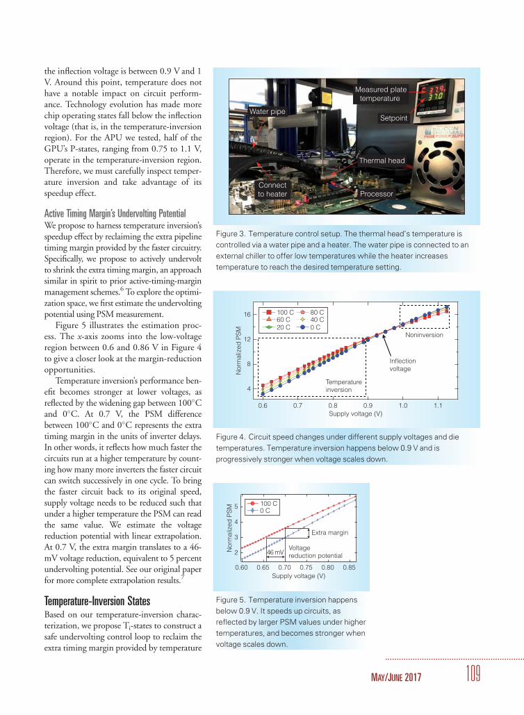
the inflection voltage is between 0.9 V and 1V. Around this point, temperature does nothave a notable impact on circuit perform-ance. Technology evolution has made morechip operating states fall below the inflectionvoltage (that is, in the temperature-inversionregion). For the APU we tested, half of theGPU’s P-states, ranging from 0.75 to 1.1 V,operate in the temperature-inversion region.Therefore, we must carefully inspect temper-ature inversion and take advantage of itsspeedup effect.
Active Timing Margin’s Undervolting PotentialWe propose to harness temperature inversion’sspeedup effect by reclaiming the extra pipelinetiming margin provided by the faster circuitry.Specifically, we propose to actively undervoltto shrink the extra timing margin, an approachsimilar in spirit to prior active-timing-marginmanagement schemes.6 To explore the optimi-zation space, we first estimate the undervoltingpotential using PSM measurement.
Figure 5 illustrates the estimation proc-ess. The x-axis zooms into the low-voltageregion between 0.6 and 0.86 V in Figure 4to give a closer look at the margin-reductionopportunities.
Temperature inversion’s performance ben-efit becomes stronger at lower voltages, asreflected by the widening gap between 100�Cand 0�C. At 0.7 V, the PSM differencebetween 100�C and 0�C represents the extratiming margin in the units of inverter delays.In other words, it reflects how much faster thecircuits run at a higher temperature by count-ing how many more inverters the faster circuitcan switch successively in one cycle. To bringthe faster circuit back to its original speed,supply voltage needs to be reduced such thatunder a higher temperature the PSM can readthe same value. We estimate the voltagereduction potential with linear extrapolation.At 0.7 V, the extra margin translates to a 46-mV voltage reduction, equivalent to 5 percentundervolting potential. See our original paperfor more complete extrapolation results.7
Temperature-Inversion StatesBased on our temperature-inversion charac-terization, we propose Ti-states to construct asafe undervolting control loop to reclaim theextra timing margin provided by temperature
16
12
8
4
Norm
aliz
ed
PS
M
1.11.00.90.80.70.6
Supply voltage (V)
Temperature
inversion
Noninversion
Inflection
voltage
100 C 80 C60 C 40 C20 C 0 C
Figure 4. Circuit speed changes under different supply voltages and die
temperatures. Temperature inversion happens below 0.9 V and is
progressively stronger when voltage scales down.
Measured plate
temperature
Setpoint
Thermal head
ProcessorConnect
to heater
Water pipe
Figure 3. Temperature control setup. The thermal head’s temperature is
controlled via a water pipe and a heater. The water pipe is connected to an
external chiller to offer low temperatures while the heater increases
temperature to reach the desired temperature setting.
5
4
3
2Norm
aliz
ed
PS
M
0.850.800.750.700.650.60
Supply voltage (V)
Extra margin
Voltage
reduction potential46 mV
100 C0 C
Figure 5. Temperature inversion happens
below 0.9 V. It speeds up circuits, as
reflected by larger PSM values under higher
temperatures, and becomes stronger when
voltage scales down.
.............................................................
MAY/JUNE 2017 109

inversion. In doing this, we must not intro-duce additional pipeline timing threats forreliability purposes, such as overly reducingtiming margins or enlarging voltage droopscaused by workload di/dt effects.
To guarantee timing safety, we use the tim-ing margin measured at 0�C as the “golden”reference. We choose 0�C as the referencebecause it represents the worst-case operatingcondition under temperature inversion. Work-loads that run safely at 0�C are guaranteed topass under higher temperatures, because tem-perature inversion can make circuits run faster.Although 0�C rarely occurs in desktop,mobile, and datacenter applications, duringthe early design stage, timing margins shouldbe set to tolerate these worst-case conditions.In industry, 0�C or below is used as a standardcircuit design guideline.8 In critical scenarios,an even more conservative reference of –25�Cis adopted.
Ti-states’ undervolting goal is to maintainthe same timing margin as 0�C when a chipis operating at a higher temperature. In otherwords, the voltage Ti-state sets should alwaysmake the timing margins measured by thePSM match 0�C. Under this constraint,Ti-states undervolt to maximize power saving.
Algorithm 1 summarizes the methodol-ogy to construct Ti- states:
The algorithm repeatedly stress tests theprocessor under different temperature-voltageenvironments with a set of workloads, andproduces a temperature-voltage table thatcan be stored in system firmware.9 At run-time, the system can index into this table toactively set the supply voltage according toruntime temperature measurement.
Algorithm 1 uses a set of workloads as thetraining sets to first get a tentative tempera-ture-voltage mapping. We then validate thismapping with another set of test workloads.
During the training stage, Algorithm 1first measures each workload’s golden refer-ence timing margin at 0�C using PSMs. Thetiming margin is recorded as the worst-casemargin during the entire program run. Then,at each target temperature, Algorithm 1selects four candidate voltages around theextrapolated voltage value as in Figure 5. Thefour candidate voltages are stepped through,and each workload’s timing margin is recordedusing PSMs. Finally, the timing margins at dif-ferent candidate voltages are compared againstthe 0�C reference, and the voltage with theminimum PSM difference is taken as thetarget temperature’s Ti-state voltage.
Table 1 shows the PSM difference com-pared with the 0�C reference across differentcandidate voltages for 20�C, 40�C, 60�C,and 80�C. The selected Ti-state voltages withthe smallest difference are shown in bold inthe table. For instance, at 80�C, 0.6625 V isthe Ti-state, which provides around 5% volt-age reduction benefits.
We observed from executing Algorithm 1that a Ti-state’s undervolting decision is inde-pendent of the workloads. It achieves thesame margin reduction effects across all pro-grams. This makes sense, because tempera-ture inversion is a transistor-level effect anddoes not depend on other architecture or pro-gram behavior. This observation is good forTi-states, because it justifies the applicabilityof the undervolting decision made from asmall set of test programs to a wide range offuture unknown workloads.
Figure 6 illustrates our observation. Goingfrom 0�C to 80�C, temperature inversionoffers more than 15 percent extra timingmargin. Ti-states safely reclaim the extramargin by reducing voltage to 0.66 V. Aftervoltage reduction, workload timing margins
1:procedure GET REFERENCE MARGIN2: set voltage and temperature to reference3: for each training workload do4: workloadMargin ← PSM measurement5: push RefMarginArr, workloadMargin
returnRefMarginArr
returnexploreVDD
6:procedure EXPLORE UNDERVOLT7: initVDD ← idle PSM extrapolation8: candidateVDDArr ← voltage around initVDD9: minErr ← MaxInt10: set exploration temperature11: for each VDD in candidateVDDArrdo12: set voltage to VDD13: for each training workload do14: workloadMargin ← PSM measurement15: push TrainMarginArr, workloadMargin16: err ← diff(RefMarginArr,TrainMarginArr) 17: if err<minErr then18: minErr ← err19: exploreVDD ← VDD
..............................................................................................................................................................................................
TOP PICKS
............................................................
110 IEEE MICRO
closely track the baseline for all workloads.Overall, Ti-states can achieve 6 to 12 percentpower savings on our measured chip acrossdifferent temperatures.
Long-Term ImpactAs CMOS technology scales to its end, itis important to extract as much efficiencyimprovement opportunity as possible fromthe underlying transistors. Ti-state achievesthis goal with active timing-margin man-agement. Exploiting slack in timing mar-gins to improve processor efficiency will beubiquitous, just as P-states and C-stateshave helped reduce redundant power in thepast. We believe the simplicity of Ti-statesand the insights behind them render a widerange of applicability. Our work bringstemperature inversion’s value from devicelevel to architects and system managers, andopens doors for other ideas to improve pro-cessor efficiency.
Wide Range of ApplicabilityTi-state is purely based on transistor’s temper-ature-inversion effect and is independent ofother factors. Temperature inversion is anopportunity offered by technology scaling,which makes it a free meal for computerarchitects. Therefore, Ti-state is applicable tochips made with today’s advanced technolo-gies, including bulk CMOS, FD-SOI, andFinFET (as we show in our original paper7).Many, if not all, processor architectures canbenefit from it, whether they’re CPUs, GPUs,FPGAs, or other accelerators.
Ti-state’s design is succinct. Its main com-ponents are on-chip timing margin sensors,temperature sensors, and system firmwarethat stores Ti-state tables. A Ti-state’s runtimeoverhead is a table lookup and a voltage regu-lator module’s set command, which are mini-mal. Because chip temperature changes overthe course of several seconds, a Ti-state’s feed-back loop has no strict latency requirement,which makes it easy to design, implement,and test.
Implications at Circuit, Architecture, andSystem LevelOur study conducted on an AMD A10-8700P processor focuses on a single chipmade in planar CMOS technology. Goingbeyond current technology and across systemscale, Ti-states will have a bigger impact inthe future.
Table 1. PSM error compared to the reference setting for different <temperature, voltage> configurations.
Candidate voltages (mV) 208C 408C 608C 808C 1008C
693.75 3.7% — — — —
687.50 2.2% — — — —
681.25 8.4% 2.3% — — —
675.00 13.9% 5.3% 4.9% — —
668.75 — 9.5% 2.5% — —
662.50 — 13.5% 6.5% 1.9% —
656.25 — — 12.2% 5.6% 9.9%
650.00 — — — 9.3% 5.1%...................................................................................................................................
*Bold type indicates the voltages with the smallest PSM difference.
1.0
0.9
0.8
Norm
aliz
ed
PS
M
Benchmark
0.7 V, 0 C
0.7 V, 80 C0.6625 V, 80 C
Temperature
inversion offers
more margin
Undervolt safely
reclaims margin
Figure 6. Temperature inversion’s speedup effect offers extra timing margin
at 80�C, as reflected by the elevated workload worst-case PSM. Ti-state
precisely reduces voltage to have the same timing margin as under 0�C and
nominal voltage, which achieves better efficiency and guarantees reliability.
.............................................................
MAY/JUNE 2017 111

Significance for FinFETand FD-SOI. FinFETand FD-SOI are projected to have strongerand more common temperature-inversioneffects.10,11 In these technologies, Ti-stateshave broader applicability and more bene-fits. Furthermore, the low-leakage charac-teristics of these technologies promise otheropportunities for a tradeoff between tem-perature and power.
In our original paper, we provide a detailedFinFET and FD-SOI projection analysisbased on measurements taken at 28-nm bulkCMOS. We find the 10-times leakage reduc-tion capabilities make these technologiesenjoy a higher operating temperature, becauseTi-states reduce more VDD under higher tem-peratures. The optimal temperature for poweris usually between 40�C to 60�C, dependingon workloads and device type. Thus, Ti-statesnot only reduce chip power itself for FinFETand FD-SOI but also relieve the burden ofthe cooling system.
System-level thermal management. Datacen-ters and supercomputers strive to make roomtemperature low at the cost of very highpower consumption and cost. A tradeoffbetween cooling power and chip leakagepower exists in this setting.12 Ti-states addnew perspective to this problem. First, wefind that high temperature does not worsentiming margins, but actually preserves pro-cessor timing reliability because of tempera-ture inversion. Second, Ti-states reducepower under higher temperatures, mitigating
processor power cost. For FinFET andFD-SOI, the processor might prefer hightemperatures around 60�C to save power,which further provides room for coolingpower reduction.
Figure 7 shows a control mechanism thatwe conceived to synergistically reduce chipand cooling power. The test-time procedureand loop 1 is what the Ti-state achieves. Inaddition, loop 2 takes cooling system powerinto consideration and jointly optimizes fanand chip power together. Overall, tempera-ture inversion and Ti-states enable an optimi-zation space involving cooling power, chippower, and chip reliability.
Opportunity for near-threshold computing.Our measurement on a real chip shows thattemperature inversion is stronger at lower vol-tages, reaching up to 10 percent VDD reduc-tion potential for a Ti-state at 0.6 V for our28-nm chip. In near-threshold conditions aslow as 0.4 V, temperature inversion will havea much stronger effect and will offer muchlarger benefits. In addition to power reduc-tion, a Ti-state can be employed to boost theperformance of near-threshold chips by over-clocking directly to exploit extra margin.Extrapolation similar to Figure 4 shows over-clocking potential is between 20 and 50 per-cent with the help of techniques that mitigatedi/dt effects.5
Temperature inversion offers a new ave-nue for improving processor efficiency.
VRM On-die temp
sensor data
Find desired VDD
Set VDD
Workload
activity factorFan control
Technology model
Set temperature
Find optimaltemp
1. Per-part PSM characterization
at different (V, T ) points
Test time
2. Undervolt validation at
different temperature
3. Fuse (V, F, T ) table into
firmware/OS
Runtime1 2
(V, F, T ) table
Processor
Dynamic/leakage
power analysis
Figure 7. Ti-state temperature and voltage control: two loops work in synergy to minimize
power. Loop 1 is a fast control loop that uses a Ti-state table to keep adjusting voltage in
response to silicon temperature variation. Loop 2 is a slow control loop that sets the optimal
temperature based on workload steady-state dynamic power profile.
..............................................................................................................................................................................................
TOP PICKS
............................................................
112 IEEE MICRO
On the basis of detailed measurements, ourarticle presents a comprehensive analysis ofhow temperature inversion can alter the waywe do power management today. Throughthe introduction of Ti-states, we show thatactive timing margin management can besuccessfully applied to exploit temperatureinversion. Applying such optimizations inthe future will likely become even moreimportant as technology scaling continues.We envision future work that draws on Ti-states to enhance computing systems acrossthe stack and at a larger scale. MICRO
....................................................................References1. C. Park et al., “Reversal of Temperature
Dependence of Integrated Circuits Operat-
ing at Very Low Voltages,” Proc. Int’l
Electron Devices Meeting (IEDM), 1995,
pp. 71–74.
2. D. Wolpert and P. Ampadu, “Temperature
Effects in Semiconductors,” Managing
Temperature Effects in Nanoscale Adaptive
Systems, Springer, 2012, pp. 15–33.
3. W. Zhao and Y. Cao, “New Generation of
Predictive Technology Model for Sub-45 nm
Early Design Exploration,” IEEE Trans. Elec-
tron Devices, vol. 53, no. 11, 2006, pp.
2816–2823.
4. B. Munger et al., “Carrizo: A High Perform-
ance, Energy Efficient 28 nm APU,”
J. Solid-State Circuits (JSSC), vol. 51, no. 1,
2016, pp. 1–12.
5. A. Grenat et al., “Adaptive Clocking System
for Improved Power Efficiency in a 28nm
x86–64 Microprocessor,” Proc. IEEE Int’l
Solid-State Circuits Conf. (ISSCC), 2014,
pp. 106–107.
6. C.R. Lefurgy et al., “Active Management of
Timing Guardband to Save Energy in
POWER7,” Proc. 44th IEEE/ACM Int’l Symp.
Microarchitecture (MICRO), 2011, pp. 1–11.
7. Y. Zu, “Ti-states: Processor Power Manage-
ment in the Temperature Inversion Region,”
Proc. 49th Ann. IEEE/ACM Int’l Symp. Micro-
architecture (MICRO), 2016; doi:10.1109
/MICRO.2016.7783758.
8. Guaranteeing Silicon Performance with
FPGA Timing Models, white paper WP-
01139-1.0, Altera, Aug. 2010.
9. S. Sundaram et al., “Adaptive Voltage Fre-
quency Scaling Using Critical Path Accumu-
lator Implemented in 28nm CPU,” Proc.
29th Int’l Conf. VLSI Design and 15th Int’l
Conf. Embedded Systems (VLSID), 2016,
pp. 565–566.
10. W. Lee et al., “Dynamic Thermal Manage-
ment for FinFET-Based Circuits Exploiting
the Temperature Effect Inversion Phenom-
enon,” Proc. Int’l Symp. Low Power Elec-
tronics and Design (ISLPED), 2014, pp.
105–110.
11. E. Cai and D. Marculescu, “TEI-Turbo: Tem-
perature Effect Inversion-Aware Turbo
Boost for FinFET-Based Multi-core Sys-
tems,” Proc. IEEE/ACM Int’l Conf. Com-
puter-Aided Design (ICCAD), 2015, pp.
500–507.
12. W. Huang et al., “TAPO: Thermal-Aware
Power Optimization Techniques for Servers
and Data Centers,” Proc. Int’l Green Com-
puting Conf. and Workshops (IGCC), 2011;
doi:10.1109/IGCC.2011.6008610.
Yazhou Zu is a PhD student in the Depart-ment of Electrical and Computer Engineer-ing at the University of Texas at Austin.His research interests include resilient andenergy-efficient processor design and man-agement. Zu received a BS in microelec-tronics from Shanghai Jiao Tong Universityof China. Contact him at [email protected].
Wei Huang is a staff researcher at AdvancedMicro Devices Research, where he works onenergy-efficient processors and systems.Huang received a PhD in electrical andcomputer engineering from the Universityof Virginia. He is a member of IEEE. Con-tact him at [email protected].
Indrani Paul is a principal member of thetechnical staff at Advanced Micro Devices,where she leads the Advanced Power Man-agement group, which focuses on innovat-ing future power and thermal managementapproaches, system-level power modeling,and APIs. Paul received a PhD in electricaland computer engineering from the GeorgiaInstitute of Technology. Contact her [email protected].
.............................................................
MAY/JUNE 2017 113

Vijay Janapa Reddi is an assistant professorin the Department of Electrical and Com-puter Engineering at the University ofTexas at Austin. His research interests spanthe definition of computer architecture,including software design and optimiza-
tion, to enhance mobile quality of experi-ence and improve the energy efficiency ofhigh-performance computing systems. JanapaReddi received a PhD in computer sciencefrom Harvard University. Contact him [email protected].
..............................................................................................................................................................................................
TOP PICKS
............................................................
114 IEEE MICRO

.................................................................................................................................................................................................................
AN ENERGY-AWARE DEBUGGER FORINTERMITTENTLY POWERED SYSTEMS
.................................................................................................................................................................................................................
DEVELOPMENT AND DEBUGGING SUPPORT IS A PREREQUISITE FOR THE ADOPTION OF
INTERMITTENTLY OPERATING ENERGY-HARVESTING COMPUTERS. THIS WORK IDENTIFIES
AND CHARACTERIZES INTERMITTENCE-SPECIFIC DEBUGGING CHALLENGES THAT ARE
UNADDRESSED BY EXISTING DEBUGGING SOLUTIONS. THIS WORK ADDRESSES THESE
CHALLENGES WITH THE ENERGY-INTERFERENCE-FREE DEBUGGER (EDB), THE FIRST
DEBUGGING SOLUTION FOR INTERMITTENT SYSTEMS. THIS ARTICLE DESCRIBES EDB’S CO-
DESIGNED HARDWARE AND SOFTWARE IMPLEMENTATION AND SHOWS ITS VALUE IN
SEVERAL DEBUGGING TASKS ON A REAL RF-POWERED ENERGY-HARVESTING DEVICE.
......Energy-harvesting devices areembedded computing systems that eschewtethered power and batteries by harvestingenergy from radio waves,1,2 motion,3 temper-ature gradients, or light in the environment.Small form factors, resilience to harsh envi-ronments, and low-maintenance operationmake energy-harvesting computers well-suited for next-generation medical, indus-trial, and scientific sensing and computingapplications.4
The power system of an energy-harvestingcomputer collects energy into a storage ele-ment (that is, a capacitor) until the bufferedenergy is sufficient to power the device.Once powered, the device can operate untilenergy is depleted and power fails. After thefailure, the cycle of charging begins again.These charge–discharge cycles power the sys-tem intermittently, and consequently, soft-ware that runs on an energy-harvesting deviceexecutes intermittently.5 In the intermittent
execution model, programs are frequently,repeatedly interrupted by power failures, incontrast to the traditional continuously pow-ered execution model, in which programs areassumed to run to completion. Every rebootinduced by a power failure clears volatile state(such as registers and memory), retains non-volatile state (such as ferroelectric RAM), andtransfers control to some earlier point in theprogram.
Intermittence makes software difficult towrite and understand. Unlike traditional sys-tems, the power supply of an energy-harvestingcomputer changes high-level software behav-ior, such as control-flow and memory con-sistency.5,6 Reboots complicate a program’spossible behavior, because they are implicitdiscontinuities in the program’s control flowthat are not expressed anywhere in the code.A reboot can happen at any point in a pro-gram and cause control to flow unintuitivelyback to a previous point in the execution.
Alexei Colin
Carnegie Mellon University
Graham Harvey
Alanson P. Sample
Disney Research Pittsburgh
Brandon Lucia
Carnegie Mellon University
.......................................................
116 Published by the IEEE Computer Society 0272-1732/17/$33.00�c 2017 IEEE
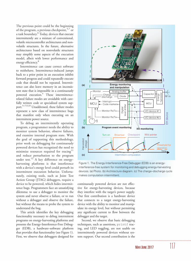
The previous point could be the beginningof the program, a previous checkpoint,5,7 ora task boundary.6 Today, devices that executeintermittently are a mixture of conventional,volatile microcontroller architectures and non-volatile structures. In the future, alternativearchitectures based on nonvolatile structuresmay simplify some aspects of the executionmodel, albeit with lower performance andenergy efficiency.8
Intermittence can cause correct softwareto misbehave. Intermittence-induced jumpsback to a prior point in an execution inhibitforward progress and could repeatedly executecode that should not be repeated. Intermit-tence can also leave memory in an inconsis-tent state that is impossible in a continuouslypowered execution.5 These intermittence-related failure modes are avoidable with care-fully written code or specialized system sup-port.5–7,9,10 Unaddressed, these failure modesrepresent a new class of intermittence bugsthat manifest only when executing on anintermittent power source.
To debug an intermittently operatingprogram, a programmer needs the ability tomonitor system behavior, observe failures,and examine internal program state. Withthe goal of supporting this methodology,prior work on debugging for continuouslypowered devices has recognized the need tominimize resources required for tracing11
and reduce perturbation to the programunder test.12 A key difference on energy-harvesting platforms is that interferencewith a device’s energy level could perturb itsintermittent execution behavior. Unfortu-nately, existing tools, such as Joint TestAction Group (JTAG) debuggers, require adevice to be powered, which hides intermit-tence bugs. Programmers face an unsatisfyingdilemma: to use a debugger to monitor thesystem and never observe a failure, or to runwithout a debugger and observe the failure,but without the means to probe the system tounderstand the bug.
This article identifies the key debuggingfunctionality necessary to debug intermittentprograms on energy-harvesting platforms andpresents the Energy-Interference-Free Debug-ger (EDB), a hardware–software platformthat provides that functionality (see Figure 1).First, we observe that debuggers designed for
continuously powered devices are not effec-tive for energy-harvesting devices, becausethey interfere with the target’s power supply.Our first contribution is a hardware devicethat connects to a target energy-harvestingdevice with the ability to monitor and manip-ulate its energy level, but without permittingany significant current to flow between thedebugger and the target.
Second, we observe that basic debuggingtechniques, such as assertions, printf trac-ing, and LED toggling, are not usable onintermittently powered devices without sys-tem support. Our second contribution is the
MCU MCU\Code markers
Monitor
n
Interrupt
I/O device #1…
I/O device #d
Monitor Rx/Tx …
Monitor Rx/Tx
RF In
DC+ –
Energy monitoringand manipulation
Har
vest
edvo
ltag
e
Brownout Checkpoint Wild pointerTurn on
Threshold foroperation
Time
ED
B
Intermittent computation
I/O monitoringProgram event monitoring
Chargedischarge
Analog buffer
Dig
ital
leve
l shi
fter
Diode
Ene
rgy
harv
este
r
Capacitor
EH
dev
ice
(c)
(b)
(a)
Figure 1. The Energy-Interference-Free Debugger (EDB) is an energy-
interference-free system for monitoring and debugging energy-harvesting
devices. (a) Photo. (b) Architecture diagram. (c) The charge–discharge cycle
makes computation intermittent.
.............................................................
MAY/JUNE 2017 117

EDB software system, which was codesignedwith EDB’s hardware to make debuggingprimitives that are useful for intermittentlypowered devices, including energy breakpointsand keep-alive assertions. EDB addressesdebugging needs unique to energy-harvestingdevices, with novel primitives for selectivelypowering spans of code and for tracing thedevice’s energy level, code events, and fullydecoded I/O events. The whole of EDB’scapabilities is greater than the sum of capabil-ities of existing tools, such as a JTAG debuggerand an oscilloscope. Moreover, EDB is sim-pler to use and far less expensive. We applyEDB’s capabilities to diagnose problems onreal energy-harvesting hardware in a series ofcase studies in our evaluation.
Intermittence Bugs and Energy InterferenceAn intermittent power source complicatesunderstanding and debugging of a system,
because the behavior of software on an inter-mittent system is closely linked to its powersupply. Figure 2 illustrates the undesirableconsequences of disregarding this linkbetween the software and the power system.The code has an intermittence bug that leadsto memory corruption only when the deviceruns on harvested energy.
Debugging intermittence bugs using exist-ing tools is virtually impossible due to energyinterference from these tools. JTAG debug-gers supply power to the device under test(DUT), which precludes observation of arealistically intermittent execution, such asthe execution on the left in Figure 2. EvenJTAG, with a power rail isolator completelymasks intermittent behavior, because theprotocol requires the target to be poweredthroughout the debugging session. An oscillo-scope can directly observe and trace a DUT’spower system and lines, but a scope cannot
Source__NV list_t listmain(){ init_list(list) while(true){ __NV elem e select(e) remove(list,e) update(e) append(list,e) }}
append(list,e){ e->next = NULL e->prev = list->tail list->tail->next = e list->tail = e}
remove(list,e){ e->prev->next = e->next if(e==list->tail){ tail = e->prev }else{ e->next->prev = e->prev }}
Tim
e
Continuousexecution
while(true){[true]
select(e)
remove(list,e) e->prev->next=e->next if(e==list->tail)[false] e->next->prev=e->prev
update(e)
append(list,e) e->next=NULL e->prev=list->tail list->tail->next=e list->tail=e
Always executescompletely w/continuous power
The example program on the left illustrates how intermittence
perturbs a program’s execution. The code manipulates a
linked-list in nonvolatile memory using append and remove
functions. The continuous execution completes the code
sequentially. The intermittent execution, however, is not
sequential. Instead, the code captures a checkpoint at the
top of the while loop, then proceeds until power fails at the
indicated point. After the reboot, execution resumes from
the checkpoint. In some cases, an execution resumed from
the checkpoint mimics a continuously powered execution.
However, intermittence can also cause misbehavior
stemming from an intermittence bug in the code.
while(true){[true]
select(e)
remove(list,e) e->prev->next=e->next if(e==list->tail) [false] e->next->prev=e->prev
update(e)
append(list,e) e->next=NULL e->prev=list->tail list->tail->next=e
select(e)
remove(list,e) e->prev->next=e->next if(e==list->tail)[false] e->next->prev=e->prev
Checkpoint
Reboot! Back to checkpoint
Bug! Writing a wild pointerbecause e->next = NULL
Intermittentexecution
Power fails beforelist->tail=e
Should be true, butappend rebooted
Tim
e
The illustrated intermittent execution of the example code
exhibits incorrect behavior that is impossible in a continuous
execution. The execution violates the precondition assumed
by remove that only the tail’s next should be NULL.
The reboot interrupts append before it can make node e the
list’s new tail, but after its next pointer is set to NULL.
When execution resumes at the checkpoint, it attempts to
remove node e again. The conditional in remove confirms
that e is not the tail, then dereferences its next pointer
(which is NULL). The NULL next pointer makes e ->next->prev
a wild pointer that, when written, leads to undefined behavior.
Figure 2. An intermittence bug. The software executes correctly with continuous power, but
incorrectly in an intermittent execution.
..............................................................................................................................................................................................
TOP PICKS
............................................................
118 IEEE MICRO

observe internal software state, which limitsits value for debugging.
Debugging code added to trace and reactto certain program events—such as togglingLEDs, streaming events to a universal asyn-chronous receiver/transmitter (UART), or in-memory logging—has a high energy cost, andsuch instrumentation can change programbehavior. For example, activating an LED toindicate when the Wireless Identification andSensing Platform (WISP)2 is actively executingincreases its total current draw by five times,from around 1 mA to more than 5 mA. Fur-thermore, in-code instrumentation is limitedby scarcity of resources, such as nonvolatilememory to store the log, and an analog-to-digital converter (ADC) channel for measure-ments of the device’s energy level.
Energy interference and the lack of visibil-ity into intermittent executions make priorapproaches to debugging inadequate forintermittently powered devices.
Energy-Interference-Free DebuggingEDB is an energy-interference-free debug-ging platform for intermittent devices thataddresses the shortcomings of existing debug-
ging approaches. In this section, we describeEDB’s functionality and its implementationin codesigned hardware and software.
Figure 3 provides an overview of EDB.The capabilities of EDB’s hardware andsoftware (Figure 3a) support EDB’s debug-ging primitives (Figure 3b). The hardwareelectrically isolates the debugger from thetarget. EDB has two modes of operation:passive mode and active mode. In passivemode, the target’s energy level, programevents, and I/O can be monitored unobtru-sively. In active mode, the target’s energy leveland internal program state (such as memory)can be manipulated. We combine passive- andactive-mode operation to implement energy-interference-free debugging primitives, includ-ing energy and event tracing, intermittence-aware breakpoints, energy guards for instru-mentation, and interactive debugging.
Passive-Mode OperationEDB’s passive mode of operation lets devel-opers stream debugging information to ahost workstation continuously in real time,relying on the three rightmost components inFigure 3a. Important debugging streams that
Measureenergy level
for(…){
sense(&s)
ok=check(s)
if(ok){
i++
data[i]=s
Trace programevents
Trace I/Oevents
Event logging
Code breakpointsEnergy breakpoints
Manipulateenergy level
Assertions
Energy guards/instrumentation
Interactivedebugging
Deb
ug
gin
gp
rim
itiv
es
Code/energy breakpoints
Cap
abili
ties
Active mode Passive mode
Energy logging I/O logging
(a)
(b)
(c)
libEDB API
assert (expr)
break|watch_point (id)
energy_guard (begin|end)
printf (fmt, ...)
Debug console commands
charge|discharge energy_level
break|watch en|dis id [energy_level]
trace {energy, iobus, rfid, watch_points}
read|write address [value]
Figure 3. EDB’s features support debugging tasks and developer interfaces. (a) Hardware
and software capabilities. (b) Debugging primitives. (c) API and debug console commands.
.............................................................
MAY/JUNE 2017 119

are available through EDB are the device’senergy level, I/O events on wired buses,decoded messages sent via RFID, and programevents marked in application code. A majoradvantage of EDB is its ability to gather manydebugging streams concurrently, allowing thedeveloper to correlate streams (for example,relating changes in I/O or program behaviorwith energy changes). Correlating debuggingstreams is essential, but doing so is difficult orimpossible using existing techniques. Anotherkey advantage of EDB is that data is collectedexternally without burdening the target or per-turbing its intermittent behavior.
Monitoring signals in the target’s circuitrequires electrical connections between thedebugger and the target, and EDB ensuresthat these connections do not allow signifi-cant current exchange, which could interferewith the target’s behavior. To measure the tar-get energy level, EDB samples the analogvoltage from the target’s capacitor through anoperational amplifier buffer. To monitor digi-tal communication and program events with-out energy interference, EDB connects towired buses—including Inter-Integrated Cir-cuit (I2C), Serial Peripheral Interface (SPI),RF front-end general-purpose I/Os (GPIOs),and watch point GPIOs—through a digitallevel-shifter. As an external monitor, EDBcan collect and decode raw I/O events, evenif the target violates the I/O protocol due toan intermittence bug.
Active-Mode OperationEDB’s active mode frees debugging tasksfrom the constraint of the target device’s smallenergy store by compensating for energy con-sumed during debugging. In active mode, theprogrammer can perform debugging tasksthat require more energy than a target couldever harvest and store—for example, complexinvariant checks or user interactions. EDBhas an energy compensation mechanism thatmeasures and records the energy level on thetarget device before entering active mode.While the debugging task executes, EDB sup-plies power to the target. After performingthe task, EDB restores the energy level to thelevel recorded earlier. Energy compensationpermits costly, arbitrary instrumentation,while ensuring that the target has the behav-ior of an unaltered, intermittent execution.
EDB’s energy compensation mechanismis implemented using two GPIO pins con-nected to the target capacitor, an ADC, anda software control loop. To prevent energyinterference by these components during pas-sive mode, the circuit includes a low-leakagekeeper diode and sets the GPIO pins to high-impedance mode. To charge the target to adesired voltage level, EDB keeps the sourcepin high until EDB’s ADC indicates that thetarget’s capacitor voltage is at the desiredlevel. To discharge, the drain pin is kept lowto open a path to ground through a resistor,until the target’s capacitor voltage reaches thedesired level. Several of the debugging primi-tives presented in the next section are builtusing this energy-compensation mechanism.
EDB PrimitivesUsing the capabilities described so far, EDBcreates a toolbox of energy-interference-freedebugging primitives. EDB brings to intermit-tent platforms familiar debugging techniquesthat are currently confined to continuouslypowered platforms, such as assertions andprintf tracing. New intermittence-awareprimitives, such as energy guards, energybreakpoints, and watch points, are introducedto handle debugging tasks that arise only onintermittently powered platforms. Each prim-itive is accessible to the end user through twocomplimentary interfaces: the API linked intothe application and the console commands ona workstation computer (see Figure 3c).
Code and energy breakpoints. EDB imple-ments three types of breakpoints. A codebreakpoint is a conventional breakpoint thattriggers at a certain code point. An energybreakpoint triggers when the target’s energylevel is at or below a specified threshold. Acombined breakpoint triggers when a certaincode point executes and the target device’senergy level is at or below a specified thresh-old. Breakpoints conditioned on energy levelcan initiate an interactive debugging sessionprecisely when code is likely to misbehavedue to energy conditions—for example, justas the device is about to brownout.
Keep-alive assertions. EDB provides supportfor assertions on intermittent platforms.When an assertion fails, EDB immediately
..............................................................................................................................................................................................
TOP PICKS
............................................................
120 IEEE MICRO

tethers the target to a continuous power sup-ply to prevent it from losing state by exhaust-ing its energy supply. This keep-alive featureturns what would have to be a post-mortemreconstruction of events into an investigationon a live device. The ensuing interactivedebugging session for a failed assert includesthe entire live target address space and I/Obuses to peripherals. In contrast to EDB’skeep-alive assertions, traditional assertions areineffective in intermittent executions. After atraditional assertion fails, the device wouldpause briefly, until energy was exhausted, thenrestart, losing the valuable debugging infor-mation in the live device’s state.
Energy guards. Using its energy compensa-tion mechanism, EDB can hide the energycost of arbitrary code enclosed within anenergy guard. Code within an energy guardexecutes on tethered power. Code before andafter an energy-guarded region executes asthough no energy was consumed by theenergy-guarded region. Without energy cost,instrumentation code becomes nondisruptiveand therefore useful on intermittent plat-forms. Two especially valuable forms of instru-mentation that are impossible without EDBare complex data structure invariant checksand event tracing. EDB’s energy guards allowcode to check data invariants or report appli-cation events via I/O (such as printf), thehigh energy cost of which would normallydeplete the target’s energy supply and preventforward progress.
Interactive debugging. An interactive debug-ging session with EDB can be initiated by abreakpoint, an assertion, or a user interrupt,and allows observation and manipulation ofthe target’s memory state and energy level.Using charge–discharge commands, the devel-oper can intermittently execute any part of aprogram starting from any energy level, assess-ing the behavior of each charge–dischargecycle. During passive-mode debugging, theEDB console delivers traces of energy state,watch points, I/O events, and printf output.
EvaluationWe built a prototype of EDB, including thecircuit board in Figure 1 and software thatimplements EDB’s functionality. A release of
our prototype is available (http://intermittent.systems). The purpose of our evaluation istwofold. First, we characterize potential sour-ces of energy interference and show that EDBis free of energy interference. Second, we use aseries of case studies conducted on a realenergy-harvesting system to show that EDBsupports monitoring and debugging tasks thatare difficult or impossible without EDB.
Our target device is a WISP2 powered byradio waves from an RFID reader. The WISPhas a 47 lF energy-storage capacitor and anactive current of approximately 0.5 mA at 4MHz. We evaluated EDB using several testapplications, including the official WISP 5RFID tag firmware and a machine-learning-based activity-recognition application used inprior work.5,6
Energy InterferenceEDB’s edge over existing debugging tools isits ability to remain isolated from an inter-mittently operating target in passive modeand its ability to create an illusion of anuntouched target energy reservoir in activemode. Our first experiment concretely dem-onstrates the energy interference of a tradi-tional debugging technique, when applied toan intermittently operating system. Themeasurements in Table 1 demonstrate theimpact on program behavior of executiontracing using printf over UART withoutEDB. Without EDB, the energy cost of theprint statement significantly changes the iter-ation success rate—that is, the fraction ofiterations that complete without a power fail-ure. Next, we show with data that EDB iseffectively free of energy interference both inpassive- and active-mode operation.
In passive mode, current flow betweenEDB and the target through the connectionsin Figure 1 can inadvertently charge or dis-charge the target’s capacitor. We measured themaximum possible current flow over eachconnection by driving it with a source meterand found that the aggregate current cannotexceed 0.85 lA in the worst case, representingjust 0.2 percent of the target microcontroller’stypical active-mode current.
In active mode, energy compensationrequires EDB to save and restore the voltage ofthe target’s storage capacitor, and any discrep-ancy between the saved and restored voltage
.............................................................
MAY/JUNE 2017 121

represents energy interference. Using an oscil-loscope, we measured the discrepancy betweenthe target capacitor voltage saved and restoredby EDB. Over 50 trials, the average voltagediscrepancy was just 4 percent of the target’senergy-storage capacity, with most error stem-ming from our limited-precision softwarecontrol loop.
Debugging CapabilitiesWe now illustrate the new capabilities thatEDB brings to the development of intermit-tent software by applying EDB in case studiesto debugging tasks that are difficult to resolvewithout EDB.
Detecting memory corruption early. We eval-uated how well EDB’s keep-alive assertionshelp diagnose memory corruption that is notreproducible in a conventional debugger.
� Application. The code in Figure 4amaintains a doubly linked list in non-volatile memory. On each iteration ofthe main loop, a node is appended tothe list if the list is empty; otherwise,a node is removed from the list. Thenode is initialized with a pointer to abuffer in volatile memory that is lateroverwritten.
� Symptoms. After running on harvestedenergy for some time, the GPIO pinindicating main loop progress stopstoggling. After the main loop stops,normal behavior never resumes, evenafter a reboot; thus, the device mustbe decommissioned, reprogrammed,and redeployed.
� Diagnosis. To debug the list, we assertthat the list’s tail pointer must pointto the list’s last element, as shown in
Figure 4a. A conventional assertion isunhelpful: after the assertion fails, thetarget drains its energy supply andthe program restarts, losing the con-text of the failure. In contrast, EDB’sintermittence-aware, keep-alive asserthalts the program immediately whenthe list invariant is violated, powersthe target, and opens an interactivedebugging session.
Interactive inspection of target memoryusing EDB’s commands reveals that the tailpointer points to the penultimate element,not the actual tail. The inconsistency arosewhen a power failure interrupted append.In the absence of the keep-alive assert, theprogram would proceed to read this inconsis-tent state, dereference a null pointer, andwrite to a wild pointer.
Instrumenting code with consistency checks.On intermittently powered platforms, theenergy overhead of instrumentation code canrender an application nonfunctional by pre-venting it from making any forward progress.In this case study, we demonstrate how anapplication can be instrumented with aninvariant check of arbitrary energy cost usingEDB’s energy guards.
� Application. The code in Figure 4bgenerates the Fibonacci sequencenumbers and appends each to a non-volatile, doubly linked list. Each iter-ation of the main loop toggles aGPIO pin to track progress. The pro-gram begins with a consistency checkthat traverses the list and asserts thatthe pointers and the Fibonacci valuein each node are consistent.
Table 1. Cost of debug output and its impact on the activity-recognition
application’s behavior
Instrumentation
method
Iteration success
rate (%)
Iteration cost
Energy (%*) Time (ms)
No print 87 3.0 1.1
UARTprintf 74 5.3 2.1
EDBprintf 82 3.4 4.7..............................................................................................
*Energy cost as percentage of 47 lF storage capacity.
..............................................................................................................................................................................................
TOP PICKS
............................................................
122 IEEE MICRO
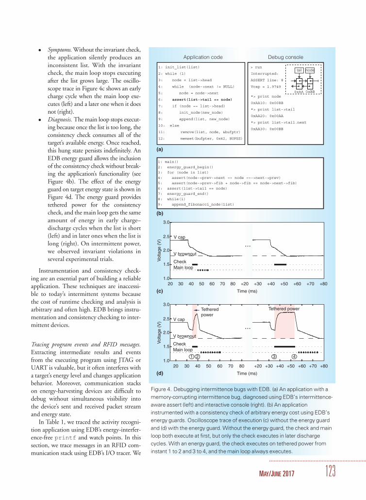
� Symptoms. Without the invariant check,the application silently produces aninconsistent list. With the invariantcheck, the main loop stops executingafter the list grows large. The oscillo-scope trace in Figure 4c shows an earlycharge cycle when the main loop exe-cutes (left) and a later one when it doesnot (right).
� Diagnosis. The main loop stops execut-ing because once the list is too long, theconsistency check consumes all of thetarget’s available energy. Once reached,this hung state persists indefinitely. AnEDB energy guard allows the inclusionof the consistency check without break-ing the application’s functionality (seeFigure 4b). The effect of the energyguard on target energy state is shown inFigure 4d. The energy guard providestethered power for the consistencycheck, and the main loop gets the sameamount of energy in early charge–discharge cycles when the list is short(left) and in later ones when the list islong (right). On intermittent power,we observed invariant violations inseveral experimental trials.
Instrumentation and consistency check-ing are an essential part of building a reliableapplication. These techniques are inaccessi-ble to today’s intermittent systems becausethe cost of runtime checking and analysis isarbitrary and often high. EDB brings instru-mentation and consistency checking to inter-mittent devices.
Tracing program events and RFID messages.Extracting intermediate results and eventsfrom the executing program using JTAG orUART is valuable, but it often interferes witha target’s energy level and changes applicationbehavior. Moreover, communication stackson energy-harvesting devices are difficult todebug without simultaneous visibility intothe device’s sent and received packet streamand energy state.
In Table 1, we traced the activity recogni-tion application using EDB’s energy-interfer-ence-free printf and watch points. In thissection, we trace messages in an RFID com-munication stack using EDB’s I/O tracer. We
Application code
1: init_list(list)
2: while (1)
3: node = list->head
4: while (node->next != NULL)
5: node = node->next
8: init_node(new_node)
9: append(list, new_node)
11: remove(list, node, &bufptr)
12: memset(bufpter, 0x42, BUFSZ)
6: assert(list->tail == node)
7: if (node == list->head)
10: else
Debug console
> run
Interrupted:
ASSERT line: 8
Vcap = 1.9749
*> print node
0xAA10: 0x00BB
0xAA20: 0x00AA
*> print list->tail
*> print list->tail.next
0xAA30: 0x00BB
0xAA 0xBB
tail node
1: main()2: energy_guard_begin()3: for (node in list)
6: assert(list->tail == node)7: energy_guard_end()8: while(1)
4: assert(node->prev->next == node ==->next->prev)5: assert(node->prev->fib + node->fib == node->next->fib)
9: append_fibonacci_node(list)
(a)
(b)
3.0
2.5
2.0
1.5
1.0
Vol
tage
(V
)
20 30 40 50 60 70 80 +20 +30 +40 +50 +60 +70 +80
Time (ms)
V cap
V brownout
CheckMain loop
(c)
3.0
2.5
2.0
1.5
1.0
Vol
tage
(V
)
20 30 40 50 60 70 80 +20 +30 +40 +50 +60 +70 +80
Time (ms)
V cap
V brownout
CheckMain loop
Tetheredpower
Tethered power
1 2 3 4
(d)
Figure 4. Debugging intermittence bugs with EDB. (a) An application with a
memory-corrupting intermittence bug, diagnosed using EDB’s intermittence-
aware assert (left) and interactive console (right). (b) An application
instrumented with a consistency check of arbitrary energy cost using EDB’s
energy guards. Oscilloscope trace of execution (c) without the energy guard
and (d) with the energy guard. Without the energy guard, the check and main
loop both execute at first, but only the check executes in later discharge
cycles. With an energy guard, the check executes on tethered power from
instant 1 to 2 and 3 to 4, and the main loop always executes.
.............................................................
MAY/JUNE 2017 123
used EDB to collect RFID message identifiersfrom the WISP RFID tag firmware, alongwith target energy readings. From the collectedtrace, we found that in our lab setup the appli-cation responded 86 percent of the time for anaverage of 13 replies per second. To producesuch a mixed trace of I/O and energy usingexisting equipment, the target would have tobe burdened with logging duties that exceedthe computational resources, given the alreadyhigh cost of message decoding and response.
E nergy-harvesting technology extends thereach of embedded devices beyond tra-
ditional sensor network nodes by eliminatingthe constraints imposed by batteries and wires.However, developing software for energy-harvesting devices is more difficult than tra-ditional embedded development, because ofsurprising behavior that arises when softwareexecutes intermittently. Debugging intermit-tently executing software is particularlychallenging because of a new class of inter-mittence bugs that are immune to existingdebugging approaches. Without effectivedebugging tools, energy-harvesting devicesare accessible only to a small community ofsystems experts instead of a wide communityof application-domain experts.
We identified energy interference as thefundamental shortcoming of available de-bugging tools. We designed EDB, the firstenergy-interference-free debugging systemthat supports debugging primitives for energy-harvesting devices, such as energy guards, keep-alive assertions, energy watch points, and energybreakpoints. Students in our lab and at a grow-ing list of other academic institutions havesuccessfully used EDB to debug and profileapplications in scenarios similar to the casestudies we evaluated.
EDB’s low-cost, compact hardware designmakes it suitable for incorporation into next-generation debugging tools and for fielddeployment with a target device. In the field, afuture automatic diagnostic system could lev-erage EDB to catch rare bugs and automati-cally log memory states from the target device.In the lab, EDB can serve research projectsthat require data on energy consumption andprogram execution on an energy-harvestingplatform, such as an intermittence-aware com-piler analysis.
We created EDB because we foundenergy-harvesting devices to be among theleast accessible platforms for research, requir-ing each researcher to reinvent ad hoc techni-ques for troubleshooting each device. EDBmakes intermittently powered platformsaccessible to a wider research audience andhelps establish a new research area surround-ing intermittent computing. MICRO
....................................................................References1. S. Gollakota et al., “The Emergence of RF-
Powered Computing,” Computer, vol. 47,
no. 1, 2014, pp. 32–39.
2. A.P. Sample et al., “Design of an RFID-
Based Battery-Free Programmable Sensing
Platform,” IEEE Trans. Instrumentation and
Measurement, vol. 57, no. 11, 2008, pp.
2608–2615.
3. P. Mitcheson et al., “Energy Harvesting
From Human and Machine Motion for Wire-
less Electronic Devices,” Proc. IEEE, vol.
96, no. 9, 2008, pp. 1457–1486.
4. J.A. Paradiso and T. Starner, “Energy Scav-
enging for Mobile and Wireless Electro-
nics,” IEEE Pervasive Computing, vol. 4, no.
1, 2005 pp. 18–27.
5. B. Lucia and B. Ransford, “A Simpler, Safer
Programming and Execution Model for
Intermittent Systems,” Proc. 36th ACM
SIGPLAN Conf. Programming Language
Design and Implementation (PLDI), 2015,
pp. 575–585.
6. A. Colin and B. Lucia, “Chain: Tasks and
Channels for Reliable Intermittent Pro-
grams,” Proc. ACM SIGPLAN Int’l Conf.
Object-Oriented Programming, Systems, Lan-
guages, and Applications, 2016, pp. 514–530.
7. B. Ransford, J. Sorber, and K. Fu, “Mementos:
System Support for Long-Running Computa-
tion on RFID-Scale Devices,” Proc. 16th Int’l
Conf. Architectural Support for Programming
Languages and Operating Systems, 2011, pp.
159–170.
8. K. Ma et al., “Architecture Exploration for
Ambient Energy Harvesting Nonvolatile Pro-
cessors,” Proc. IEEE 21st Int’l Symp. High
Performance Computer Architecture (HPCA),
2015, pp. 526–537.
..............................................................................................................................................................................................
TOP PICKS
............................................................
124 IEEE MICRO

9. D. Balsamo et al., “Hibernus: Sustaining
Computation During Intermittent Supply for
Energy-Harvesting Systems,” IEEE Embedded
Systems Letters, vol. 7, no. 1, 2015, pp.
15–18.
10. M. Buettner, B. Greenstein, and D. Wetherall,
“Dewdrop: An Energy-Aware Task Sched-
uler for Computational RFID,” Proc. 8th
USENIX Conf. Networked Systems Design
and Implementation (NSDI), 2011, pp.
197–210.
11. V. Sundaram et al., “Diagnostic Tracing for
Wireless Sensor Networks,” ACM Trans.
Sensor Networks, vol. 9, no. 4, 2013, pp.
38:1–38:41.
12. J. Yang et al., “Clairvoyant: A Comprehen-
sive Source-Level Debugger for Wireless
Sensor Networks,” Proc. 5th Int’l Conf.
Embedded Networked Sensor Systems
(SenSys 07), 2007, pp. 189–203.
Alexei Colin is a graduate student in theDepartment of Electrical and ComputerEngineering at Carnegie Mellon University.His research interests include reliability, pro-grammability, and efficiency of software onenergy-harvesting devices. Colin received anMSc in electrical and computer engineeringfrom Carnegie Mellon University. He is astudent member of ACM. Contact him [email protected].
Graham Harvey is an associate show elec-tronic engineer at Walt Disney Imagineering.His research interests include real-world appli-cations of wireless technologies to enhanceguest experiences in themed environments.Harvey received a BS in electrical and com-puter engineering from Carnegie Mellon Uni-versity. He completed the work for this articlewhile interning at Disney Research Pitts-burgh. Contact him at [email protected].
Alanson P. Sample is an associate lab direc-tor and principal research scientist at DisneyResearch Pittsburgh, where he leads theWireless Systems group. His research inter-ests include enabling new guest experiencesand sensing and computing devices by apply-ing novel approaches to electromagnetics, RFand analog circuits, and embedded systems.
Sample received a PhD in electrical engineer-ing from the University of Washington. He isa member of IEEE and ACM. Contact himat [email protected].
Brandon Lucia is an assistant professor inthe Department of Electrical and ComputerEngineering at Carnegie Mellon University.His research interests include the boundariesbetween computer architecture, compilers,system software, and programming lan-guages, applied to emerging, intermittentlypowered systems and efficient parallel sys-tems. Lucia received a PhD in computer sci-ence and engineering from the University ofWashington. He is a member of IEEE andACM. Contact him at [email protected] http://brandonlucia.com.
Read your subscriptions through the myCS publications portal at http://mycs.computer.org.
.............................................................
MAY/JUNE 2017 125
................................................................................................................................................................
Insights from the 2016 Eckert-Mauchly Award Recipient
URI WEISERTechnion–Israel Institute of Technology
......I appreciate the opportunity to
share with you the insights I presented in
my Eckert-Mauchly Award acceptance
speech at the 43rd International Sympo-
sium on Computer Architecture (ISCA)
held in Seoul, South Korea, in June 2016.
I would like to thank the Editor in Chief of
IEEE Micro, Lieven Eeckhout, for this
opportunity.
I am humbled and honored to have
received the ACM-IEEE Computer Soci-
ety Eckert-Mauchly Award. During my
nearly 40 years in the field of computer
architecture, I have had the privilege of
working with many architects, profes-
sors, and students at the University of
Utah, National Semiconductor, Intel, and
the Technion–Israel Institute of Technol-
ogy and to collaborate with many col-
leagues in industry and academia around
the world. I see this award as recognition
of the computer architecture researchers
I have worked with in Israel and abroad.
I was fortunate to work on several
state-of-the-art concepts in research and
development that impacted the industry
and academia alike. Computerization is
one of the most rapidly developing trends
in human history, influencing almost every
aspect of our lives, as it will continue to do
for a long time to come. Thus, in this field,
it will always be the right time to innovate.
In these exciting times, I was lucky to
be involved in developing new computer
architecture concepts and products that
have changed the way we use com-
puters in our daily lives. To be at just the
right time and place may not be pure luck.
If it happens again and again, it means
that you keep trying to make a difference.
The Passion PathI was born in Tel Aviv, Israel. My parents
were German Jews who fled Germany
before the Holocaust in 1933. The culture
I was exposed to during my childhood
was heavily influenced by the necessity
of constantly being in survival mode. The
main theme was to do your utmost to
excel, move forward, and survive.
The values I was nourished on were
to take the road less traveled by, to look
for new directions, and to challenge the
status quo even when the target seems
unobtainable: the obligation to innovate
in order to find new paths, to debate con-
structively on any solution, to crystallize
the proposed solution, and to be passion-
ate about whatever you do.
EducationSoon after graduating with a BSc in electri-
cal engineering from the Technion and
completing my MSc degree while working
at the Israeli DoD, I made an audacious
decision to pursue my PhD studies in com-
puter science abroad. I had a few options
and ultimately chose the University of
Utah. At Utah, with Professor Al Davis as
my advisor (and I may also say my friend), I
was exposed to computer architecture
and helped pave the way (together with
others) toward new systolic array graphics
and analytical approaches. This exposure
to the industry and academia outside of
Israel set me on my technical path.
IndustryThereafter, at National Semiconductor (in
the mid-1980s), I was lucky to lead the
design of the CISC NS32532 processor,
the best microprocessor at that time. I
learned there how a small team of excited
professionals could achieve the impossi-
ble (OS run on first silicon). The product
was a huge technical success, but
unfortunately, the market had already
shifted to the “other” CISC processors
(68000, MIPS, PowerPC, and X86).
NS32532 insight: Technology is important;
having the market behind you is a must.
With this strong insight, I moved to
Intel in the late 1980s. Intel’s market for
the X86 was huge compared to the market
for any other microprocessor. As Nick Tre-
dennick said in his 1988 talk, “More 386s
are produced at Intel between coffee
break and lunch than the number of RISC
chips produced all year by RISC vendors.”
However, Intel management’s belief in the
X86 product path was not strong enough.
Intel’s processors (the X86 family)
were based on the “old” complex-
instruction-set computer (CISC) architec-
ture, while a few years before IBM (with
its 801 processor) and Berkeley initiated a
.......................................................
126 Published by the IEEE Computer Society 0272-1732/17/$33.00�c 2017 IEEE
Awards

new direction—the reduced-instruction-
set computer (RISC) processor. A debate
emerged within the computing commun-
ity as to whether the RISC design would
eclipse the old CISC design. Intel was
contemplating whether to design a new
X86 processor using the CISC concept or
abandon the program and shift from the
company’s central product toward a new
RISC architecture–based microprocessor
(the i860 family). Moving to a new archi-
tecture meant losing SW computability—
that is, writing new software for the entire
application base.
At that time, together with a few other
architects, I passionately tried to convince
Intel executives to continue developing a
new generation of CISC-based X86 pro-
cessors. We did this by showing how,
with the addition of new microarchitecture
features such as superscalar execution,
branch predication, split instructions, and
data caches, the X86 processors could be
made to perform competitively against
the RISC-based processors. Part of this
process included a superb one-page tech-
nical document titled “Do Not Kill the
Golden Goose,” which was sent to Intel’s
then-CEO, Dr. Andy Grove, and his staff.
The debate within Intel took several
months, and finally the decision was
made to design the next-generation micro-
processor based on the old X86 CISC fam-
ily. The architecture enhancements we
proposed laid the foundation for Intel’s
first Pentium processor.
Pentium insight: Understand the environ-
ment; do not follow the trend; be innova-
tive, passionate, and involved. Do not give
up; prove that your way is the right way.
Thereafter, I was lucky to be invited
to lead Intel’s Platform Architecture Cen-
ter in Santa Clara, California. There, I led
a group of researchers and strategists
who formulated the first PCI definition,
defined Intel’s CPU Roadmap, and pro-
posed a systems solution for the Pen-
tium processor. This group formed the
foundation of the Intel Research Labora-
tories, established a few years later.
Shortly after enhancing Intel’s line of
CISC-based processors in the early 1990s,
I co-invented and led the development of
the MMX architecture. This was the first
time (after i386) that Intel added a full set
of instructions to its X86 architecture. The
set of 57 instructions was based on a 64-
bit single-instruction, multiple-data (SIMD)
instruction set that improved performance
of digital signal processing, media and
graphics processing, speech recognition,
and video encoding/decoding. The new
MMX-based processor (P55C designed in
Israel) was a huge success in the market.
....................................................................................................................................................................................
Reading List� U. Weiser and A.L. Davis, “Wavefront Notation Tool for VLSI Array Design,” VLSI System and Computation, H.T. Kung, R.F. Sproull,
and G.T. Steele, eds., Computer Science Press, 1981, pp. 226–234.
� L. Johnson et al., “Towards a Formal Treatment of VLSI Arrays,” Proc. Caltech Conf. VLSI, 1981; http://authors.library.caltech.edu
/27041/1/4191 TR 81.pdf.
� U. Weiser et al., “Design of the NS32532 MicroProcessor,” Proc. IEEE Int’l Conf. Computer Design: VLSI in Computers and Processors,
1987, pp. 177–180.
� A. Peleg and U. Weiser, Dynamic Flow Instruction Cache Memory Organized Around Trace Segments Independent of Virtual Address
Line, US patent 5,381,533, to Intel, Patent and Trademark Office, 1995.
� A. Peleg, S. Wilkie, and U. Weiser, “Intel MMX for Multimedia PCs,” Comm. ACM, vol. 40, no. 1, 1997, pp. 25–38.
� A. Peleg et al., The Complete Guide to MMX, McGraw-Hill, 1997.
� T.Y. Morad, U.C. Weiser, and A. Kolodny, ACCMP—Asymmetric Cluster Chip Multiprocessing, tech. report 488, Dept. Electrical Eng.,
Technion, 2004.
� T. Morad et al., “Performance, Power Efficiency and Scalability of Asymmetric Cluster Chip MultiProcessors,” IEEE Computer Archi-
tecture Letters, vol. 5, no. 1, 2006, pp. 14–17.
� T. Morad, A. Kolodny, and U.C. Weiser, Multiple Multithreaded Applications on Asymmetric and Symmetric Chip MultiProcessors,
tech. report 701, Dept. Electrical Eng., Technion, 2008.
� Z. Guz et al., “Utilizing Shared Data in Chip Multiprocessors with the Nahalal Architecture,” Proc. 20th Ann. Symp. Parallelism in
Algorithms and Architectures Conf., 2008; doi:10.1145/1378533.1378535.
� Z. Guz et al., “Multi-core vs. Multi-thread Machines: Stay Away from the Valley,” IEEE Computer Architecture Letters, vol. 8, no. 1,
2009, pp. 25–28.
� T. Zidenberg, I. Keslassy, and U. Weiser, “Optimal Resource Allocation with MultiAmdahl,” Computer, vol. 46, no. 7, 2013, pp. 70–77.
� L. Peled et al., “Semantic Locality and Context-Based Prefetching Using Reinforcement Learning,” Proc. ACM/IEEE 42nd Ann. Int’l
Symp. Computer Architecture (ISCA), 2015; doi:10.1145/2749469.2749473.
� T. Morad et al., “Optimizing Read-Once Data Flow in Big-Data Applications,” IEEE Computer Architecture Letters, 2016; doi:10.1109
/LCA.2016.2520927.
.............................................................
MAY/JUNE 2017 127
MMX insight: Marketing has a tremen-
dous impact on your success.
Later, Intel invited me to co-lead the
foundations of a new design center in
Austin, Texas, the Texas Development
Center (TDC). At Intel, management usu-
ally provides the vision, whereas the
strategy is defined bottom up. We had to
define our product path and convince
Intel to adopt our strategy. Establishing a
new Intel design center is a challenging
task: hiring and building a team, defining a
local culture, defining a new product path,
and striving for recognition inside Intel.
Establishing a new design center insight:
This challenging task required me to cover
the varied domains of architecture, estab-
lishing a local culture, hiring, and building
a leading team.
After returning to Israel, I realized that
processors were reaching the perform-
ance wall when operating under a limited
power envelope environment. By nar-
rowing the application range, accelera-
tors can achieve better performance and
better performance/power than general-
purpose processors. I realized that an
on-die accelerator can provide a better,
more comprehensive solution. I formu-
lated a new concept called a Streaming
Processor (StP). We defined the concept
(an X86-based media processor), archi-
tecture, SW model, and application range.
The main purpose was an on-die X86-
based media (streaming) coprocessor.
Intel had to choose between two
options: an X86 graphics processor or
an X86 media processor. Intel manage-
ment chose the graphic path (Larrabee).
Streaming Processor insight: When you
dare, sometimes you fail.
AcademiaAlong with my industrial work, I kept my
ties with the academic world. I continued
publishing papers, taught and advised
graduate students, and participated in pro-
fessional conferences. In 1990, together
with one of my students at the Technion,
Alex Peleg, I invented the Trace Cache, a
microarchitecture concept that increases
performance and reduces power con-
sumption by storing in-cache the dynamic
trace-flow of instructions that have
already been fetched and decoded. This
innovation brought about a fundamental
change in the design principles of high-
performance microprocessors. A trace
cache concept was incorporated into
more than 500 million Intel Pentium 4 pro-
cessors that Intel sold. Digital’s EV8 used
this architecture enhancement, too.
Trace Cache insight: Always continue to
look for new research avenues. Not all
will be successful, but some may be.
The limitation of general-purpose pro-
cessor performance under a limited power
envelope became a major performance
hurdle. This drove me to strive for better
performance/power architecture and led
me to pursue the concept of heterogene-
ous computing in general and asymmetric
computing in particular. Initially conceived
(as mentioned) for speeding up high-
throughput media applications, the con-
cept of heterogeneous computing later
served as a means to improve perform-
ance and efficiency by using “big cores”
for serial code and “small cores” for paral-
lel code and low-energy consumption.
Together with a colleague and a stu-
dent, I investigated the fundamentals of
heterogeneous computing. This research
led to new insights such as the Multi-
Amdahl concept, an analytical based
optimal resource division in heteroge-
neous systems, and the Multi-Core vs.
Multithread concept, which avoids the
performance valley in multiple core envi-
ronments. Additional research activities
included new architecture paradigms
such as Nahalal, a specialized cache
architecture for multicore systems, and
Continuous Flow Multithreading, which
uses memristors to allow fine-grained
switch-on-event multithreading.
Heterogeneous insight: Technology
changes over time. Be ready to take
advantage of the changes that may lead
to new avenues.
The introduction of the new Big Data
environment calls for re-evaluation of our
existing solutions. We started to direct
our research toward a more effective sol-
ution for the new environment and came
up with two new concepts: the Funnel, a
computing element whose input band-
width is much wider than its output band-
width, and the Non-Temporal Locality
Memory Access, exhibited by some Big
Data applications.
Big Data insight: Watch for a change in
the environment and the validity of cur-
rent computing solutions. We often
need to tune, change, and/or adapt our
computing structure to accept the new
requirements.
My professional path from the indus-
try to academia was, in a way, a
calculated decision. Its purpose was to pro-
long my technical career. Academia pro-
vides a limitless professional trail (as long
as you are productive) not always available
in the industry. In addition, academia keeps
you in young, vibrant surroundings in which
the research targets are to look forward,
innovate, and open new technological ave-
nues for the industry to follow.
I believe that the current slowdown in
the process technology trend, combined
with technological limitations on energy
and power, will place the burden of revital-
izing computing technology on research-
ers in the computer architecture field.
Thus, I believe that we are on the verge of
new architectural findings. The perform-
ance/application/capability baton is being
handed to you, the architects. Take it, and
go do wonderful things!
I have enjoyed being part of a group
of architects that made big changes in
computer architecture, and I continue to
enjoy the interactions, the passion, and
the unforgettable ride. MICRO
Uri Weiser is an emeritus professor in
the Electrical Engineering Department at
the Technion–Israel Institute of Technol-
ogy (IIT). Contact him at uri.weiser@ee
.technion.ac.il.
..............................................................................................................................................................................................
AWARDS
............................................................
128 IEEE MICRO


................................................................................................................................................................
Two Sides to Scale
SHANE GREENSTEINHarvard Business School
......It used to be that only AT&T, oil
companies, and Soviet enterprises could
aspire to monstrous size. Technology
firms entered that club only in rare cir-
cumstances, and when IBM, Intel, and
Microsoft did so, they each found their
own path to headlines.
We live in a different era today. The
largest organizations on the planet are
leading technology firms. These firms
aspire to sell tens of billions of dollars of
products and services, employ hundreds
of thousands of workers, and lure invest-
ors to value their organizations at hun-
dreds of billions of dollars. They deploy
worldwide distribution, complemented
by worldwide supply of inputs, growing
brand names recognized in Canada, the
Kalahari Desert, and the Caribbean.
Each of the big four—Alphabet, Ama-
zon, Apple, and Facebook—have achieved
this unprecedented scale. Large and val-
uable? Check. Hundreds of thousands of
employees? At last count. Global in aspira-
tions and operations? You bet. Endless
opportunities in front of them? So it
seems. A few others—such as Microsoft,
Intel, IBM, SAP, and Oracle—could round
out a top 10 list. A few more young firms—
such as Uber, Airbnb, and Alibaba—aspire
to be the tenth tomorrow.
Mainstream economics regards this
scale with either praise or alarm. One
view marvels at the spread of such star-
tling efficiency, low prices, and wide vari-
ety. A contrasting view worries about
the distortions from concentrating deci-
sion making in a single large firm.
Let’s compare and contrast those
views.
Scale Is a Moving TargetScale cannot be achieved without opera-
tions that produce and deliver many serv-
ices or products whose price exceeds
their cost. Accordingly, one advantage of
scale is replication of operations. Take
Alphabet’s search engine, Google. Their
engineers learned to parse the web in
one language and extended the approach
to other languages. Software algorithms
that worked in one language can work in
others. User-oriented processes that
helped build loyalty in one language build
it in another—for example, “Did you
mean to misspell that word, or would
you prefer an alternative?”
That does not happen by itself. Proc-
esses must be well documented, and
the knowledge about them must pass
between employees. Replication then
yields gains the second and third and
eighteenth time. To say it another way,
Google faces a lower cost supporting
search in another language than anyone
supporting just one.
At one level, this is not new. Others
have benefited from the economics of
replication in the past. Technology firms
brought it to new heights owing to the rise
of the worldwide Internet and the ease of
moving software to new locations.
Consider Amazon, which started its
life as an electronic retailer and never let
up on relentless expansion. It started in
books, and now has expanded to every
conceivable product category. In the
process, it developed an operation to
support the worldwide sale and distribu-
tion of its products, achieving a scale
never before seen in any retailer other
than Walmart.
Here is the remarkable part. Walmart
does not rent out its warehouses and
trucks and computing and order fulfill-
ment staff to anyone else. It does not rent
its staff’s insights about how to secure
its IT, nor its management’s insights
about how to fulfill customer demand.
It regards these as foundational trade
secrets.
Amazon’s management, in contrast,
took these services and developed,
refined, and standardized their use for
others. In their retail operations, they both
resell for others and perform order fulfill-
ment for others. They also developed a
range of back-end services to sell to
others, layered on top of additional options
for software applications and a range of
needs. It is called Amazon Web Services
(AWS). Both of these are available to other
firms, even some of Amazon’s ostensible
competitors in retail services.
I cannot think of any other compara-
ble historical example where a large firm
has developed such scale, and also
grown by making its processes available
to others. (If you can think of one, feel
free to suggest it. I would love to hear
from you.)
To be sure, there is more than eco-
nomics behind this achievement. After all,
the malleability and mobility of software
.......................................................
130 Published by the IEEE Computer Society 0272-1732/17/$33.00�c 2017 IEEE
Micro Economics

also contributes to the scale seen in these
two examples. So too does the legal sys-
tem, as writers such as Tom Friedman
have noted. This worldwide scale takes
advantage of all the efforts to coordinate
global markets over the last half century.
Diplomats went to great effort decades
ago to standardize processes for imports
and exports and remove frictions in the
settlement of accounts across interna-
tional boundaries.
It is still funny when you think about it.
These frictions were reduced to benefit
the prior generation’s global companies,
such as McDonald’s and IBM, not to
mention Coca-Cola, Boeing, Caterpillar,
and Goldman Sachs. Today these same
rules benefit several firms selling services
that Ray Kroc and Thomas Watson Jr.
never could have imagined.
Decision MakingA less appealing attribute accompanies
scale: concentration of decision making.
To begin, let’s recognize that popular
discussion often gets this one wrong.
Hollywood likes dystopian conspiracy
theories in which quasi-evil executives
manipulate society for selfish reasons.
However, the problems are usually less
sinister than that. Even with the best-
intentioned executives, the biggest firms
make decisions that can have enormous
consequences, many unintended.
Facebook’s recent travails are a good
illustration of one type of problem. Recall
that, despite multiple complaints about
the manipulation of its algorithm and
advertising program during the election,
Facebook refused to intervene in policing
fake news stories, many of which were
invented out of whole cloth for the pur-
poses of making some ad revenue from a
hyped electorate. After the election, Mark
Zuckerberg cloaked his firm’s behavior in
the language of free speech and user
choice.
What a tin ear from Zuck. Irrespective
of your short-term political outlook,
invented news is plainly not good for
democratic societies. And, more nar-
rowly, Facebook’s long-term fortunes
depended on the credibility of the mat-
erial being shared. A platform polluted
with lies does not attract participation.
The point is this: all firms mess up.
When large firms mess up, more of soci-
ety pays the cost.
More to the point, scale makes com-
petitive discipline more difficult to apply
when firms mess up. For example, many
years ago Apple had a series of policies
for its new smartphone that prevented
developers from spreading porn and
gambling apps, and that made a lot of
sense. But Apple kept expanding its
requirements, eventually angering many
programmers with rules about owning
data. That gave an opening to an alterna-
tive platform with less restrictive rules,
and Android took advantage of that
opportunity. In short, that is competitive
discipline incarnate: when a big firm mes-
ses up, competitors gain.
Ah, therein lies the problem. Scale
can sometimes provide almost impene-
trable insulation from competitive disci-
pline. As noted earlier, for example, in
many languages nobody can challenge
Google, so, effectively, nobody can disci-
pline them when they mess up. And in
the earlier example, who stepped in
when Facebook messed up? What were
the alternatives? In other words, the
absence of competitive discipline arises
occasionally, almost by definition, when-
ever large-scale firms are involved.
Perhaps more awkwardly, today’s plat-
forms support large ecosystems, in which
the leading firms coordinate many actions
in that ecosystem. Occasionally, a leading
firm bullies a smaller one in the ecosys-
tem, but the more common issue might
be called “uncomfortable dependence.”
Let’s pick on Apple again for an illus-
tration of dependence. Years ago, and for
a number of reasons, Steve Jobs refused
to let Flash deploy on Apple products.
Whether you think those motives were
justified or selfish (which typically gets
the attention in a conversation about this
topic), let’s focus on the more mundane
fact that nobody questions: one person
held enough authority to kill a part of the
ecosystem, which until then had been a
thriving software language. It does not
matter why he did it. Jobs’ decision
devalued a set of skills held by many
programmers, reducing the return on
investments those programmers made
in refining and developing those skills.
That is not the only form dependence
takes. Once again, Alphabet provides a
good illustration in its Google News serv-
ice. Whether you like it or not, Google
News has consistently interpreted copy-
right law online in a way that permits
them to show parts of another party’s
content. For understandable reasons, and
like almost all news organizations world-
wide, Spanish newspapers were among
the complainers. But they took one more
step, and had their country’s legislature
pass a law requiring Google to pay for the
content, even small slices. Long story
short, Google refused to pay, and it shut
down Google News in Spain. In no time,
those newspapers saw their traffic drop,
and they were begging to get it back.
Now that is dependence for you.
I am not going to argue about who
was right or wrong. Rather, my point is
this: such dependence tends to arise in
virtually every setting in which scale
concentrates authority. And so the self-
interested strategic decisions of one set
of executives has consequences for so
many others. We have already seen that
when firms mess up, many pay a cost.
Even when leading firms don’t mess up,
their intended decisions can impose
worry on others.
T he spread of efficiency is breathtak-
ing. The potential dangers from con-
centrating managerial decision making
are worrying.
After looking more closely, these do
not seem like two different perspec-
tives. These are more like yin and yang:
it is not possible to have one without
the other—and they are an unavoidable
feature of our times. MICR O
Shane Greenstein is a professor at the
Harvard Business School. Contact him
.............................................................
MAY/JUNE 2017 131