2 3 Analog Integrated Circuits and Signal Processing An International Journal A CMOS current-mode...
8
1 23 Analog Integrated Circuits and Signal Processing An International Journal ISSN 0925-1030 Analog Integr Circ Sig Process DOI 10.1007/s10470-014-0319-8 A CMOS current-mode squaring circuit free of error resulting from carrier mobility reduction Munir A. AL-Absi & Ibrahim A. As- Sabban
Transcript of 2 3 Analog Integrated Circuits and Signal Processing An International Journal A CMOS current-mode...

1 23
Analog Integrated Circuits and SignalProcessingAn International Journal ISSN 0925-1030 Analog Integr Circ Sig ProcessDOI 10.1007/s10470-014-0319-8
A CMOS current-mode squaring circuitfree of error resulting from carrier mobilityreduction
Munir A. AL-Absi & Ibrahim A. As-Sabban

1 23
Your article is protected by copyright and all
rights are held exclusively by Springer Science
+Business Media New York. This e-offprint is
for personal use only and shall not be self-
archived in electronic repositories. If you wish
to self-archive your article, please use the
accepted manuscript version for posting on
your own website. You may further deposit
the accepted manuscript version in any
repository, provided it is only made publicly
available 12 months after official publication
or later and provided acknowledgement is
given to the original source of publication
and a link is inserted to the published article
on Springer's website. The link must be
accompanied by the following text: "The final
publication is available at link.springer.com”.

A CMOS current-mode squaring circuit free of error resultingfrom carrier mobility reduction
Munir A. AL-Absi • Ibrahim A. As-Sabban
Received: 10 February 2014 / Revised: 10 April 2014 / Accepted: 23 April 2014
� Springer Science+Business Media New York 2014
Abstract This paper presents a new current-mode
squaring circuit. The design is based on MOSFETs trans-
linear principle in strong inversion. A new compensation
technique to minimize the second order effects caused by
carrier mobility reduction in short channel MOSFETs is
proposed. Tanner T-spice simulation tool is used to confirm
the functionality of the proposed design in 0.18 lm CMOS
process technology. Simulation results indicate that the
maximum linearity error is 1.2 %; power consumption is
326 lW and bandwidth of 340 MHz.
Keywords Short channel MOSFET � Carried mobility
reduction � Squaring circuit � Current mode
1 Introduction
The squaring circuit is a very important building block in
analog signal processing applications. This includes but not
limited to RMS-DC converters, pseudo-exponential cells,
CMOS companding filters, fuzzy control, multipliers, etc.
[1–8]. A number of squaring circuits have been published
in the literatures [8–13]. They can be categorized into three
modes: voltage-mode [8, 9], current-mode [10–12] and
voltage/current-mode [13].
It is well known that the current-mode circuits are better
than its voltage-mode counterpart circuits because they
offer high bandwidth, larger dynamic range, simple cir-
cuitry, and lower power consumption. Squaring circuits
designed using MOSFET in saturation can be classified in
two categories. The first one is the direct approach using
MOS translinear loop [1, 14]. The second approach uses
the analog multiplier to obtain the squaring output. This
multiplier can be designed with a MOS transistor operated
in saturation region [15] or both a saturation and triode
region [16].
Nowadays, due to the scaling down in the dimensions of
the MOSFET transistor, a transistor model that accounts
for second order effects has to be used in the analysis and
simulation of circuits under consideration. In Ref. [17] a
current-mode squaring circuit that reduces short-channel
effects caused by carrier mobility reduction was proposed.
A small transistor is used as an active resistor to com-
pensate for the carrier mobility reduction. The drawback of
this approach is it requires a controllable voltage to work
properly. Also, changes in the drain-to-source voltage of
this transistor causes variations in the resistance value
which degrades the accuracy of the circuit. In [18] a
MOSFETs Translinear Loop (MTL) based squarer/divider
circuit free from mobility reduction is proposed. A resistor
is used in the MTL to compensate for the error due to
carrier mobility reduction. The drawbacks of this design is
the increase in silicon area and the power consumption of
the circuit. Other designs are given in [19, 20].
In this paper, a new squaring circuit with compensation
for the error due to carrier mobility reduction employing
MTL is proposed. The paper is organized as follows. In
Sect. 2, the proposed circuit is presented. Simulation results
are presented in Sect. 3. Mismatch analysis is presented in
Sect. 4. Section 5 concludes the paper.
2 Proposed squaring circuit
The proposed squaring circuit is based on the design in [21]
and is shown in Fig. 1. The design is based on translinear
M. A. AL-Absi (&) � I. A. As-Sabban
KFUPM, Dhahran, Saudi Arabia
e-mail: [email protected]
123
Analog Integr Circ Sig Process
DOI 10.1007/s10470-014-0319-8
Author's personal copy
loop formed by transistors (M1–M4). The current IB is the
bias current and IX is the input current. It will be shown that
the output current is given by:
Iout ¼I2x
8IB
With reference to Fig. 1, writing MTL around transis-
tors M1–M4 to get:
VSG1 þ VSG2 ¼ VSG3 þ VSG4 ð1Þ
If the carrier mobility reduction is taken into consider-
ation, the drain current for short channel MOSFET is given
by:
ID ¼b2
VGS � VTHð Þ2
1þ h VGS � VTHð Þ ð2Þ
where h is a fitting parameter and b = l Cox W/L is the
transconductanc of the transistor. Using equation (2), the
gate-to source potential can be written as:
VGS �IDhbþ
ffiffiffiffiffiffiffi
2ID
b
s
þ VTH ð3Þ
Combining Eqs. (1) and (3) to get:
ID1h1
b1
þffiffiffiffiffiffiffiffiffi
2ID1
b1
s
þ ID2h2
b2
þffiffiffiffiffiffiffiffiffi
2ID2
b2
s
¼ ID3h3
b3
þffiffiffiffiffiffiffiffiffi
2ID3
b3
s
þ ID4h4
b4
þffiffiffiffiffiffiffiffiffi
2ID4
b4
s
ð4Þ
Assuming the aspect ratios of the transistors in MTL
satisfy the condition b1 = b2 = 2b, b3 = b4 = b and
h1 = h2 = h3 = h4 = h, and h is 0.25 V-1 for 0.18 lm
CMOS process technology.
Equation 4 can be rewritten as:
ID1h2bþ
ffiffiffiffiffiffiffiffiffi
2ID1
2b
s
þ ID2h2bþ
ffiffiffiffiffiffiffiffiffi
2ID2
2b
s
¼ ID3hbþ
ffiffiffiffiffiffiffiffiffi
2ID3
b
s
þ ID4hbþ
ffiffiffiffiffiffiffiffiffi
2ID4
b
s
ð5Þ
With reference to Fig. 1, the drain current of transistors
M1 and M2 are the same, Eq. (5) can be expressed by:
hb
IB þ1ffiffiffi
bp 2
ffiffiffiffi
IB
p� �
¼ hb
ID3 þ ID4½ �
þ 1ffiffiffi
bp
ffiffiffiffiffiffiffiffiffi
2ID3
p
þffiffiffiffiffiffiffiffiffi
2ID4
p
h i
ð6Þ
If we force the following condition hb IB ¼ h
b ID3 þ ID4½ �,then
IB ¼ ID3 þ ID4 ð7Þ
Using Eq. (7) and (6) then;
1ffiffiffi
bp 2
ffiffiffiffi
IB
p� �
¼ 1ffiffiffi
bp
ffiffiffiffiffiffiffiffiffi
2ID3
p
þffiffiffiffiffiffiffiffiffi
2ID4
p
h i
ð8Þ
Equation (8) rewritten as:
ffiffiffiffiffiffiffiffiffi
2ID4
p
¼ 2ffiffiffiffi
IB
p�
ffiffiffiffiffiffiffiffiffi
2ID3
p
ð9Þ
From the circuit schematic shown in Fig. 1, with current
IX mirrored in transistor M13 and ID3 mirrored in M5 and
M6.
ID3 ¼ IX þ ID4 ð10Þ
Fig. 1 Proposed current-mode squaring circuit
Analog Integr Circ Sig Process
123
Author's personal copy
Combining Eqs. (9) and (10), the drain current for M4 is
given by:
ID4 ¼IB
2� Ix
2þ I2
x
8IB
ð11Þ
Combining Eqs. (10) and (11) to get:
ID3 ¼ IX þIB
2� Ix
2þ I2
x
8IB
¼ Ix
2þ IB
2þ I2
x
8IB
ð12Þ
The first two terms to the right are subtracted using
transistors M12 and M13 and the output is mirrored via
M14 and M15 respectively to get:
Iout ¼I2x
8IB
ð13Þ
Equation 13 can be written as:
Iout ¼ kI2x ð14Þ
where k ¼ 18IB
It is clear that Eq. (14) implements squaring circuit with
compensation for error due to carrier mobility reduction.
3 Simulation results
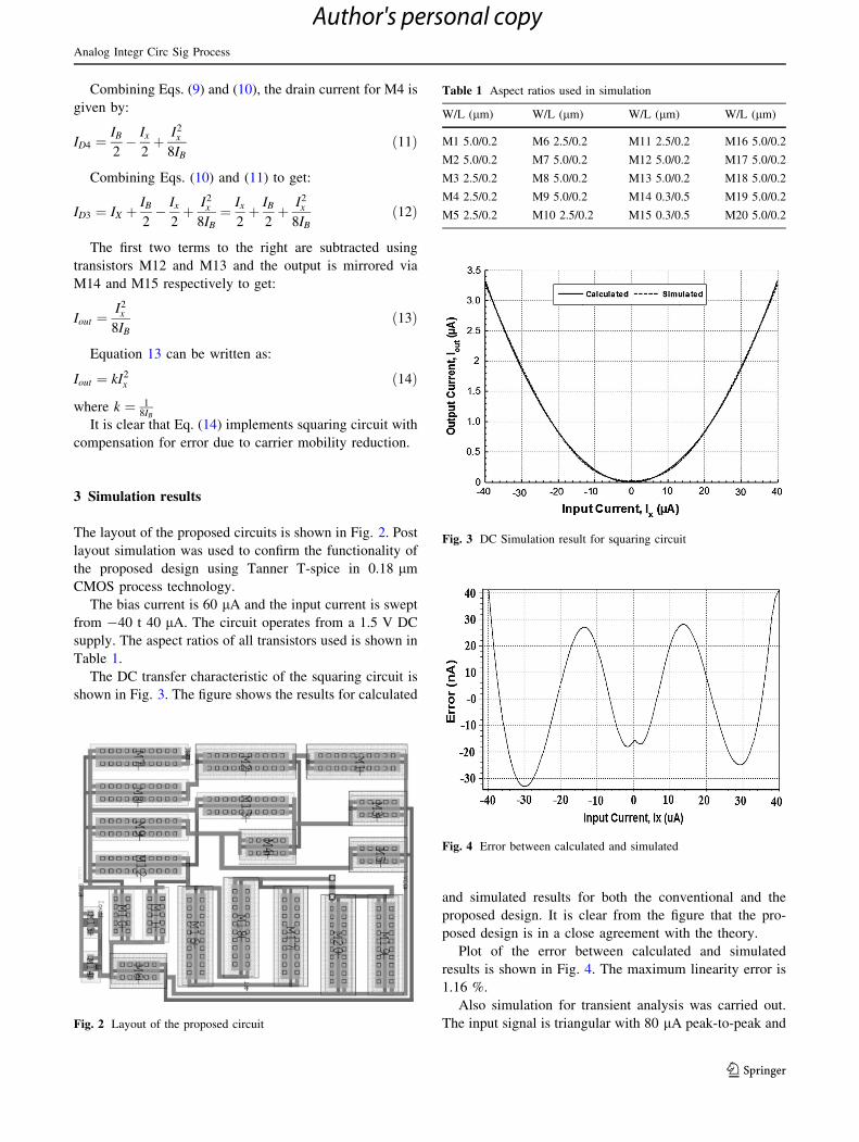
The layout of the proposed circuits is shown in Fig. 2. Post
layout simulation was used to confirm the functionality of
the proposed design using Tanner T-spice in 0.18 lm
CMOS process technology.
The bias current is 60 lA and the input current is swept
from -40 t 40 lA. The circuit operates from a 1.5 V DC
supply. The aspect ratios of all transistors used is shown in
Table 1.
The DC transfer characteristic of the squaring circuit is
shown in Fig. 3. The figure shows the results for calculated
and simulated results for both the conventional and the
proposed design. It is clear from the figure that the pro-
posed design is in a close agreement with the theory.
Plot of the error between calculated and simulated
results is shown in Fig. 4. The maximum linearity error is
1.16 %.
Also simulation for transient analysis was carried out.
The input signal is triangular with 80 lA peak-to-peak andFig. 2 Layout of the proposed circuit
Table 1 Aspect ratios used in simulation
W/L (lm) W/L (lm) W/L (lm) W/L (lm)
M1 5.0/0.2 M6 2.5/0.2 M11 2.5/0.2 M16 5.0/0.2
M2 5.0/0.2 M7 5.0/0.2 M12 5.0/0.2 M17 5.0/0.2
M3 2.5/0.2 M8 5.0/0.2 M13 5.0/0.2 M18 5.0/0.2
M4 2.5/0.2 M9 5.0/0.2 M14 0.3/0.5 M19 5.0/0.2
M5 2.5/0.2 M10 2.5/0.2 M15 0.3/0.5 M20 5.0/0.2
Fig. 3 DC Simulation result for squaring circuit
Fig. 4 Error between calculated and simulated
Analog Integr Circ Sig Process
123
Author's personal copy
1 MHz frequency. Figure 5 shows the simulation results
for the input current, the output current and the error
between calculated and simulated result.
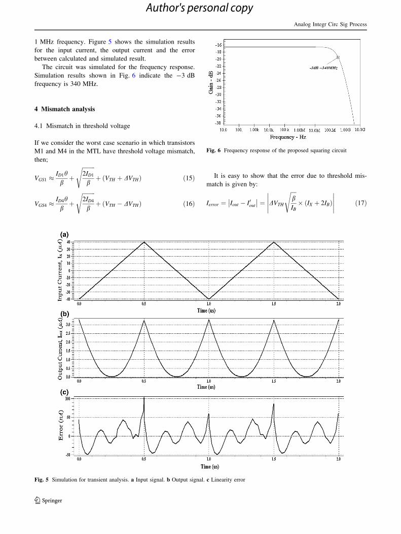
The circuit was simulated for the frequency response.
Simulation results shown in Fig. 6 indicate the -3 dB
frequency is 340 MHz.
4 Mismatch analysis
4.1 Mismatch in threshold voltage
If we consider the worst case scenario in which transistors
M1 and M4 in the MTL have threshold voltage mismatch,
then;
VGS1 �ID1hbþ
ffiffiffiffiffiffiffiffiffi
2ID1
b
s
þ VTH þ DVTHð Þ ð15Þ
VGS4 �ID4hbþ
ffiffiffiffiffiffiffiffiffi
2ID4
b
s
þ VTH � DVTHð Þ ð16Þ
It is easy to show that the error due to threshold mis-
match is given by:
Ierror ¼ Iout � I0out
�
�
�
� ¼ DVTH
ffiffiffiffi
bIB
s
� IX þ 2IBð Þ�
�
�
�
�
�
�
�
�
�
ð17Þ
Fig. 5 Simulation for transient analysis. a Input signal. b Output signal. c Linearity error
Fig. 6 Frequency response of the proposed squaring circuit
Analog Integr Circ Sig Process
123
Author's personal copy

To evaluate the error due to threshold mismatch con-
sidering a worst case of all parameters in Eq. (17) is, for
example, Ix = 40 lA, IB = 60 lA, b = 86 lA/V2,
L = 0.2 lm, and
DVTH ¼ 0:1�4:1�10�9ffiffiffiffiffiffiffiffi
W�Lp ¼ 0:1�4:1�10�9
ffiffiffiffiffiffiffiffiffiffiffiffiffiffiffiffiffiffiffiffiffiffiffiffiffiffiffiffi
5�10�6�0:2�10�6p ¼ 0:41 mV the
maximum error is 78.5 nA which is equivalent to 2.3 %.
4.2 Mismatch in channel length
The same two transistors were used to study the effect of
mismatch in the channel length of transistors M1 and M4.
The gate to source voltages are given by:
VGS1 �ID1h1
LþDLL
� �
b1
þ
ffiffiffiffiffiffiffiffiffiffiffiffiffiffiffiffiffiffiffiffiffiffi
2ID1LþDL
L
� �
b1
s
þ VTH ð18Þ
VGS4 �ID4h4
L�DLL
� �
b4
þ
ffiffiffiffiffiffiffiffiffiffiffiffiffiffiffiffiffiffiffiffiffiffi
2ID4L�DL
L
� �
b4
s
þ VTH ð19Þ
It is easy to show that the error due to channel length
mismatch is given by:
Ierror ¼ Iout � I0out
�
�
�
� ¼ hDL
2Lffiffiffiffiffiffiffiffiffiffiffiffiffi
b� IB
p I2x
�
�
�
�
�
�
�
�
ð20Þ
To evaluate the error due to channel length mismatch
considering the worst case of all parameters in Eq. (20) is,
for example, IB = 60 lA, h = 0.25 V-1, b = 86 lA/V2,
L = 0.2 lm and DL = 0.004 lm, The maximum error is
0.25 lA which is equivalent to 7.5 %.
Monte Carlo analysis was carried out with sigma vari-
ation of .004 lm (0.02lm channel length variation). Sim-
ulation results shown in Fig. 7 indicate that the circuit is
almost insensitive to channel length mismatch.
Comparison of the performance between the proposed
work and previous art available in the open literature is
given in Table 2. It is clear from the table the proposed
design has a superior performance. It is worth mentioning
that the comparison is not fair but these are the only ref-
erences we got in the open literature.
5 Conclusion
A new CMOS current-mode squaring circuit using short
channel MOSFET is achieved. The circuit is free of errors
due to carrier mobility reduction. The maximum linearity
error is 1.2 %; and bandwidth of 340 MHz. The circuit is a
core block in multiplier design using MOSFETS in strong
inversion and in signal processing applications.
Acknowledgments The authors would like to thank KFUPM and
KACST for supporting this research.
References
1. Chen, C.-Y., Huang, C.-Y., & Liu, B.-D. (1997). Current-mode
defuzzifier circuit to realise the centroid strategy. IEE Proceed-
ings-Circuits, Devices and Systems, 144(5), 265–271.
2. Filanovsky, I. M., & Baltes, H. P. (1992). Simple CMOS analog
square-rooting and squaring circuits. IEEE Transaction on Cir-
cuits and Systems-I, 39(4), 312–315.
3. Gai, W., Chen, H., & Seevinck, E. (1997). Quadratic-translinear
CMOS multiplier/divider circuit. IEE Electronics Letter, 33(10),
860–861.
4. Tanno, K., Ishizuka, O., & Tang, Z. (2000). Four-quadrant
CMOS current mode multiplier in dependent of device parame-
ters. IEEE Transaction on Circuits System II, 47, 473.
5. Naderi, A., Mojarrad, H., Ghasemzadeh, H., Khoei, A., & Hadidi,
K. (2009). Four-quadrant CMOS analog multiplier based on new
current squarer circuit with high-speed. In EUROCON 2009,
EUROCON’09. IEEE, (pp. 282–287).
6. De La Cruz-Blas, C. A., Lopez-Martı́n, A., & Carlosena, A.
(2003). 1.5-V MOS translinear loops with improved dynamic
range and their applications to current-mode signal processing.
IEEE Transaction on Circuits and Systems II: Analog and Digital
Signal Processing, 50(12), 918–927.
7. De La Blas, C.A., Lopez, A. (Sept, 2008). A novel two quadrant
MOS trans-linear Squarer-divider cell. In ICECS 2008. 15th
IEEE International Conference on Electronics, Circuits and
Systems, 2008 (pp. 5–8).
8. Mulder, J., Serdijn, W. A., Van Der Woerd, A. C., & Van
Roermund, A. H. M. (1998). 3.3 V current-controlled Square-
domain oscillator. Analog Integrated Circuits and Signal Pro-
cessing, 16, 17–28.Fig. 7 Simulation results for channel length mismatch
Table 2 Performance comparison
References Year Process Input
range
Error Bandwidth Area/
lm
[17] 2007 0.35 lm 7 lA – 50 MHz 1,500
[18] 2011 0.35 lm 40 lA – – –
[19] 2012 0.25 lm ±40 lA 1.9 % 0.03 MHz –
[20] 2008 0.25 lm ±1.0 V 3 % 200 MHz 340
This work 2013 0.18 lm ±40 lA 1.2 % 340 MHz 76.5
Analog Integr Circ Sig Process
123
Author's personal copy

9. Wisetphanichkij, S., Singkrajom, N., Kumngern M., & Dejhan,
K. (Oct, 2005). A low-voltage CMOS current squarer circuit. In
IEEE International Symposium on Communications and Infor-
mation Technology, 2005 (Vol. 1, pp. 271–274).
10. Menekay, S., Tarcan, R. C., Kuntman H. (2008). Novel high-
precision current-mode circuits based on the MOS-translinear
principle. International Journal of Electronic Communication
(AEU). doi:10.1016/j.aeue.2008.08.010.
11. Chaisayun, I., Dejhan, K., & Piangprantong, S. (2012). Versatile
analog squarer and multiplier free from body effect. Analog
Integrated Circuits and Signal Processing, 71(3), 539–547.
12. Ibaragi, E., Hyogo, A., & Seikine, K. (1998), A novel CMOS
OTA free from mobility degradation effect. In IEEE Asia Pacific
Conference of Circuit and Systems, 1998 (pp. 241–244).
13. Yang, S. H., et al. (2005). A novel CMOS operational trans-
conductance amplifier based on a mobility compensation tech-
nique. IEEE Transaction on Circuits Systems II: Express Briefs,
52(1), 37–42.
14. Tanno, K., Ide, D., Nishimura, K., Tanaka, H., & Tamura, H.
(2008). Highly-linear CMOS OTA with compensation of
mobility reduction. In IEEE Asia Pacific Conference on Circuits
and Systems, 2008 (pp. 810–813).
15. Sengupta, S. (2005). Adaptively biased linear transconductor.
IEEE Transaction on Circuits and Systems–I: Regular Papers,
52(11), 2369–2375.
16. Menekay, S., Tarcan, R. C., Kuntman H. (2007). Novel high
precision current-mode multiplier/divider. In International Con-
ference on Electrical and Electronics Engineering, (ELECO-
2007) (pp. 5–9).
17. Tarcan R. C., & Kuntman, H. (2007). CMOS high precision
current-mode squarer/divider circuit. In IEEE 15th Signal Pro-
cessing and Communications Applications, 2007. SIU 2007 (pp.
1–4).
18. Tavassoli, M., Khoei, A., Hadidi, Kh. (2011). High-precision
MOS-trans-linear loop-based squarer/divider circuit free from
mobility reduction. In 19th Conference on Electrical Engineer-
ing, Iran.
19. Chaisayun, I., Piangprantong, S., & Dejhan, K. (2012). Versatile
analog squarer and multiplier free from body effect. Analog
Integrated Circuits and Signal Processing, 71(3), 539–547.
20. Seon, J.-K. (2008). Design and application of precise analog
computational circuits. Analog Integrated Circuits and Signal
Processing, 54(1), 55–66.
21. AL-Absi, M. A., Assaban, I. (2013). A new current-mode
squaring circuit with compensation for error resulting from car-
rier mobility reduction. In Eleco Dec, 2013 (pp. 358–361).
Munir A. AL-Absi obtained his
B.Sc. and M.Sc. from KFUPM,
Dhahran Saudi Arabia in 1984
and 1987 respectively. Obtained
his Ph.D. form UMIST, UK in
2001. Currently he is an Asso-
ciate Professor at KFUPM EE
department teaching electronics
and instrumentation courses. His
research interests include analog
computational circuits, circuits
for biomedical applications.
Ibrahim A. As-Sabban obtained
his B.Sc. from Hadramout Uni-
versity. Currently he is a gradu-
ate student at KFUPM. His
research interest is analog compu-
tational circuits using MOSFET.
Analog Integr Circ Sig Process
123
Author's personal copy