Evolution of porous network in GaSb under normally incident 60 keVAr+-ion irradiation
Upload
independentCategory
view
0download
0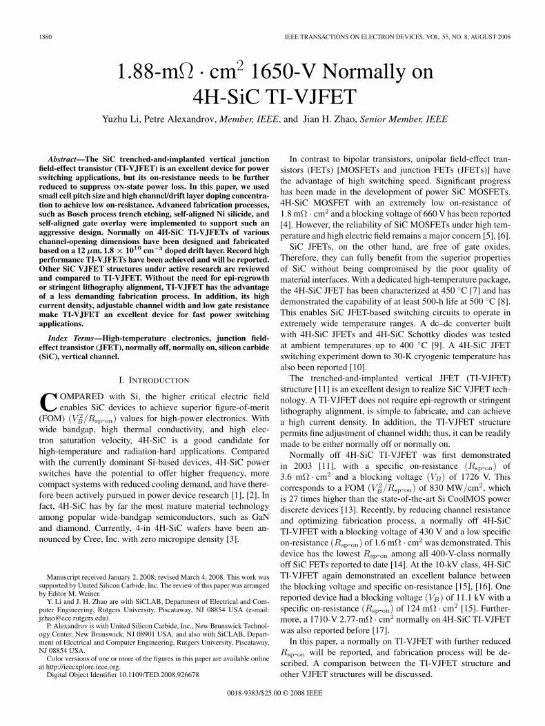
1880 IEEE TRANSACTIONS ON ELECTRON DEVICES, VOL. 55, NO. 8, AUGUST 2008
1.88-mΩ · cm2 1650-V Normally on4H-SiC TI-VJFET
Yuzhu Li, Petre Alexandrov, Member, IEEE, and Jian H. Zhao, Senior Member, IEEE
Abstract—The SiC trenched-and-implanted vertical junctionfield-effect transistor (TI-VJFET) is an excellent device for powerswitching applications, but its on-resistance needs to be furtherreduced to suppress ON-state power loss. In this paper, we usedsmall cell pitch size and high channel/drift layer doping concentra-tion to achieve low on-resistance. Advanced fabrication processes,such as Bosch process trench etching, self-aligned Ni silicide, andself-aligned gate overlay were implemented to support such anaggressive design. Normally on 4H-SiC TI-VJFETs of variouschannel-opening dimensions have been designed and fabricatedbased on a 12 µm, 1.8 × 1016 cm−3 doped drift layer. Record highperformance TI-VJFETs have been achieved and will be reported.Other SiC VJFET structures under active research are reviewedand compared to TI-VJFET. Without the need for epi-regrowthor stringent lithography alignment, TI-VJFET has the advantageof a less demanding fabrication process. In addition, its highcurrent density, adjustable channel width and low gate resistancemake TI-VJFET an excellent device for fast power switchingapplications.
Index Terms—High-temperature electronics, junction field-effect transistor (JFET), normally off, normally on, silicon carbide(SiC), vertical channel.
I. INTRODUCTION
COMPARED with Si, the higher critical electric fieldenables SiC devices to achieve superior figure-of-merit
(FOM) (V 2B/Rsp-on) values for high-power electronics. With
wide bandgap, high thermal conductivity, and high elec-tron saturation velocity, 4H-SiC is a good candidate forhigh-temperature and radiation-hard applications. Comparedwith the currently dominant Si-based devices, 4H-SiC powerswitches have the potential to offer higher frequency, morecompact systems with reduced cooling demand, and have there-fore been actively pursued in power device research [1], [2]. Infact, 4H-SiC has by far the most mature material technologyamong popular wide-bandgap semiconductors, such as GaNand diamond. Currently, 4-in 4H-SiC wafers have been an-nounced by Cree, Inc. with zero micropipe density [3].
Manuscript received January 2, 2008; revised March 4, 2008. This work wassupported by United Silicon Carbide, Inc. The review of this paper was arrangedby Editor M. Weiner.
Y. Li and J. H. Zhao are with SiCLAB, Department of Electrical and Com-puter Engineering, Rutgers University, Piscataway, NJ 08854 USA (e-mail:[email protected]).
P. Alexandrov is with United Silicon Carbide, Inc., New Brunswick Technol-ogy Center, New Brunswick, NJ 08901 USA, and also with SiCLAB, Depart-ment of Electrical and Computer Engineering, Rutgers University, Piscataway,NJ 08854 USA.
Color versions of one or more of the figures in this paper are available onlineat http://ieeexplore.ieee.org.
Digital Object Identifier 10.1109/TED.2008.926678
In contrast to bipolar transistors, unipolar field-effect tran-sistors (FETs) [MOSFETs and junction FETs (JFETs)] havethe advantage of high switching speed. Significant progresshas been made in the development of power SiC MOSFETs.4H-SiC MOSFET with an extremely low on-resistance of1.8 mΩ · cm2 and a blocking voltage of 660 V has been reported[4]. However, the reliability of SiC MOSFETs under high tem-perature and high electric field remains a major concern [5], [6].
SiC JFETs, on the other hand, are free of gate oxides.Therefore, they can fully benefit from the superior propertiesof SiC without being compromised by the poor quality ofmaterial interfaces. With a dedicated high-temperature package,the 4H-SiC JFET has been characterized at 450 C [7] and hasdemonstrated the capability of at least 500-h life at 500 C [8].This enables SiC JFET-based switching circuits to operate inextremely wide temperature ranges. A dc–dc converter builtwith 4H-SiC JFETs and 4H-SiC Schottky diodes was testedat ambient temperatures up to 400 C [9]. A 4H-SiC JFETswitching experiment down to 30-K cryogenic temperature hasalso been reported [10].
The trenched-and-implanted vertical JFET (TI-VJFET)structure [11] is an excellent design to realize SiC VJFET tech-nology. A TI-VJFET does not require epi-regrowth or stringentlithography alignment, is simple to fabricate, and can achievea high current density. In addition, the TI-VJFET structurepermits fine adjustment of channel width; thus, it can be readilymade to be either normally off or normally on.
Normally off 4H-SiC TI-VJFET was first demonstratedin 2003 [11], with a specific on-resistance (Rsp-on) of3.6 mΩ · cm2 and a blocking voltage (VB) of 1726 V. Thiscorresponds to a FOM (V 2
B/Rsp-on) of 830 MW/cm2, whichis 27 times higher than the state-of-the-art Si CoolMOS powerdiscrete devices [13]. Recently, by reducing channel resistanceand optimizing fabrication process, a normally off 4H-SiCTI-VJFET with a blocking voltage of 430 V and a low specificon-resistance (Rsp-on) of 1.6 mΩ · cm2 was demonstrated. Thisdevice has the lowest Rsp-on among all 400-V-class normallyoff SiC FETs reported to date [14]. At the 10-kV class, 4H-SiCTI-VJFET again demonstrated an excellent balance betweenthe blocking voltage and specific on-resistance [15], [16]. Onereported device had a blocking voltage (VB) of 11.1 kV with aspecific on-resistance (Rsp-on) of 124 mΩ · cm2 [15]. Further-more, a 1710-V 2.77-mΩ · cm2 normally on 4H-SiC TI-VJFETwas also reported before [17].
In this paper, a normally on TI-VJFET with further reducedRsp-on will be reported, and fabrication process will be de-scribed. A comparison between the TI-VJFET structure andother VJFET structures will be discussed.
0018-9383/$25.00 © 2008 IEEE
LI et al.: 1.88-mΩ · cm2 1650-V NORMALLY ON 4H-SiC TI-VJFET 1881
Fig. 1. Schematic cross-sectional view of the TI-VJFET unit cell.
II. DESIGN AND FABRICATION
The 4H-SiC epiwafer was purchased from a commercial sup-plier. The wafer structure and a cross-sectional view of the unitcell are shown in Fig. 1. The lightly doped n-type layer beneaththe n+ cap was specified to be 1.8 × 1016 cm−3 and 15 µmin thickness. Part of the 15 µm was used to form the verticalJFET channel. The remaining 12 µm then became the drift layerto support the blocking voltage. To confirm the doping concen-tration of the structure, a SIMS measurement was done, and theresult is shown in Fig. 2. It is seen that the doping concentrationis ∼1.8 × 1016 cm−3. The commercial wafer was specifiedto have a doping concentration variation of ±10% across thewafer, although higher concentration variation may exist.
A 280-nm AlTi (3.5 wt% of Ti) layer was first defined toserve as the dry etching mask. Deep trench etching was doneby CF4/O2- and C4F8-based Bosch process in an inductivelycoupled plasma etcher, resulting in a smooth and highly verticalsidewall [18]. The etched mesa line widths were intentionallyvaried from 1.3 to 1.7 µm across the wafer. A SEM photographof the resulting mesa and trench structure is shown in Fig. 3.
Molybdenum (Mo) was then deposited and patterned bystandard lithography to serve as the implantation mask. Asshown in Fig. 4, tilted Al ion implantation [11] was done tocreate highly vertical and uniform channels with the channelopening Wvc ranging from 0.5 to 0.9 µm. The wafer was thenannealed at 1550 C in Ar ambient for 30 min to activate theimplanted Al atoms.
Multiple junction termination extension (MJTE) [11] wasused to achieve a near-theoretical blocking voltage determinedby the drift layer. The MJTE structure was first formed andoptimized on a separate test sample. The optimal depths of theJTE step etching were determined by the maximum breakdownvoltage found on a p-n diode test sample (Fig. 5). As shownin the figure, the sample could block 1100, 1250, 1800, 1800,1800, and 1400 V, respectively, when the etching depths were1500, 2100, 2200, 2600, 2900, and 3200 Å, respectively. Thus,the blocking voltage first increased to a maximum and thendecreased as the etching depth increased [11]. An optimumetching depth range of 2200–2900 Å was found to give an
optimum blocking voltage of 1800 V. After the optimum MJTEstructure had been confirmed, it was reproduced on the waferwith TI-VJFET devices.
The achieved blocking voltage of 1800 V has approachedthe theoretical limit. It needs to be pointed out that results oftheoretical blocking voltages depend strongly on the modelchosen for the critical electric field. The breakdown voltagedependences on doping concentration and layer thickness basedon two different models for the critical electric field are shownin Figs. 6 and 7. As seen from the two figures, Konstantinov’smodel [19] predicts that an epilayer of 1.8 × 1016 cm−3 with athickness of 12 µm can block not more than 1200 V, whereasBaliga’s model [20] predicts that the same epilayer blocksabout 1800 V. Keeping in mind that both SIMS data anddoping uniformity may have an error or variation up to 20%,the achieved breakdown voltage can be explained and can bereasonably stated to be near-theoretical limit of the structure.
The surface passivation was accomplished by a 2-h wetoxidation at 1100 C, followed by a 200-nm-thick PECVDsilicon nitride. Then, source–gate ohmic contacts were formedby a self-aligned nickel (Ni) silicide process [16], [18]. Then,nickel was also deposited on the drain, and the sample wasannealed at 1000 C in Ar forming gas to form ohmic contacts.Fig. 8 shows the schematic cross-sectional view of the deviceafter ohmic contact formation.
For switching applications, gate resistance should be reducedto increase switching speed. Thick gate-overlay metal wasadded by using a self-aligned process with the help of pho-toresist planarization and etch back [18]. The schematic cross-sectional view of the device with gate overlay is shown in Fig. 9.
PECVD SiO2 layer was deposited and etched back to fill thetrenches. This process utilizes the unique surface topographyof the TI-VJFET and is self-aligned with the assistance of pho-toresist planarization [18]. Contact windows were subsequentlyopened, and thick source-overlay metal was deposited. The finaldevice with overlay is shown schematically in Fig. 10.
III. DEVICE CHARACTERIZATION
A. Gate–Source Junction Characterization
To evaluate the effectiveness of gate-overlay process, the gateeffective resistance of the fabricated device was extracted fromthe forward current–voltage (I–V ) curve of the gate–sourcejunction (Fig. 11). As can be seen, the specific gate effectiveresistance is as small as 8.4 mΩ · cm2.
For normally on JFETs, a negative gate bias is needed toachieve maximum blocking voltage, and a reliable gate–sourcejunction is needed to sustain this negative gate bias. Fig. 12shows the reverse gate–source junction I–V curve of a fabri-cated TI-VJFET. It can be seen that the gate–source junctionleakage current is still small up to 30 V reverse bias, which isenough to pinch off the vertical channel (Fig. 13).
B. JFET Forward Conduction and Reverse BlockingCharacterization
The fabricated devices were characterized by using aTektronix 371-A High Power Curve Tracer and a probing

1882 IEEE TRANSACTIONS ON ELECTRON DEVICES, VOL. 55, NO. 8, AUGUST 2008
Fig. 2. SIMS data showing nitrogen atom concentration in the epilayer.
Fig. 3. Etched mesa–trench structure.
Fig. 4. Highly vertical and uniform channel created by tilted Al implantation.
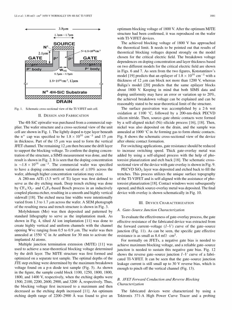
station. The forward I–V was measured in both voltage andcurrent drive modes. Fig. 13(a)–(c) shows the I–V curves ofthe fabricated TI-VJFETs of different channel widths. Note that
Fig. 5. I–V curves showing dependence of breakdown voltage on the etchingdepth in the MJTE optimization.
Fig. 6. 4H-SiC blocking voltage dependence on blocking layer doping con-centration and thickness using Konstantinov’s model [19].

LI et al.: 1.88-mΩ · cm2 1650-V NORMALLY ON 4H-SiC TI-VJFET 1883
Fig. 7. 4H-SiC blocking voltage dependence on blocking layer doping con-centration and thickness using Baliga’s model [20].
Fig. 8. Schematic cross-sectional view of TI-VJFET after ohmic contactformation.
Fig. 9. Schematic cross-sectional view of TI-VJFET after gate-overlayformation.
the leakage current has been multiplied by a factor of 10 000 toshow the detailed dependence.
For the device in Fig. 13(a), the blocking voltage VB wasmeasured to be 1650 V at VG = −5 V. With VGS of 3 V andVDS of 0.47 V, the forward current is 0.225 A (250 A/cm2), cor-responding to an on-resistance of 2.09 Ω. Considering that thedevice active area is 9.0 × 10⁻⁴ cm2, its specific on-resistance(Rsp-on) is 1.88 mΩ · cm2 which is the lowest reported to date
Fig. 10. Schematic cross-sectional view of TI-VJFET after source-overlayformation.
Fig. 11. Gate effective resistance as small as 8.4 mΩ · cm2.
Fig. 12. Gate–source junction reverse I–V curve.
for 1.6-kV SiC JFETs. With VGS of 2.5 V and VDS of 0.51 V,the forward current is 0.195 A, giving it a specific on-resistanceof 2.35 mΩ · cm2 at VGS = 2.5 V. It is seen that the currentgains (ID/IG) are over 100 and 8000 at VGS of 3 and 2.5 V,respectively.
It is interesting to compare Fig. 13(a) with the TI-VJFETreported in [17]. Both devices require a small negative gatebias to close the channel completely, and they had similar
1884 IEEE TRANSACTIONS ON ELECTRON DEVICES, VOL. 55, NO. 8, AUGUST 2008
Fig.13. (a) Forward I–V curve of the small TI-VJFET with a channel widthof 0.5 µm. (b) Forward I–V curve of the small TI-VJFET with a channelwidth of 0.7 µm. (c) Forward I–V curve of the small TI-VJFET with a channelwidth of 0.9 µm.
blocking voltages. The device in [17] had an Rsp-on (measuredat current gain of 40) of 2.77 mΩ · cm2, while the device inFig. 13(a) had an Rsp-on (measured at current gain of 100)of 1.88 mΩ · cm2, leading to a 32% reduction. The reductionof on-resistance may be attributed to a higher device packingdensity, a higher channel/drift layer doping density, and alsoan optimized processing technology. For the TI-VJFET in [17],the channel/drift layer doping concentration and unit cell pitchwere 7 × 1015 cm−3 and 5.75 µm, respectively, whereas this
device had a channel/drift layer doping concentration and a unitcell pitch of 1.8 × 1016 cm−3 and 3.8 µm, respectively.
For the device in Fig. 13(c), the blocking voltage VB has beenmeasured to be 1568 V at VG = −26 V. With VGS of 3 V andVDS of 0.33 V, the forward current is 0.17 A, corresponding toa specific on-resistance of 1.75 mΩ · cm2. With VGS of 2.5 Vand VDS of 0.47 V, the forward current is 0.21 A, correspondingto the specific on-resistance of 2.0 mΩ · cm2, with a very highFOM V 2
B/Rsp-on of 1230 MW/cm2. The current gains arefound to be over 12 000 and 120 when VGS is 2.5 and 3 V,respectively. The Rsp-on values of 1.75 mΩ · cm2 at VGS = 3 Vand 2.0 mΩ · cm2 at VGS = 2.5 V are the lowest among all1500-V-class normally on SiC FETs reported to date. The totalRsp-on of 2.0 mΩ · cm2 has the following three contributions:wafer intrinsic resistance, device channel resistance, and ad-ditional resistance caused by processing. The wafer substrate(400 µm thick and 0.02 Ω · cm) and the drift layer (12 µmand 1.8 × 1016 cm−3 doped, assuming an electron mobility of750 cm2/V · s) have intrinsic specific resistances of 0.8 and0.56 mΩ · cm2, respectively, so the total wafer intrinsic resis-tance is 1.36 mΩ · cm2. The theoretical channel resistance is0.49 mΩ · cm2, which is calculated by using a channel lengthof 2.5 µm, a channel doping concentration of 1.8 × 1016 cm−3,and a channel width/cell pitch ratio of 0.9 µm/3.8 µm.Thus, the additional resistance caused by processing is0.15 mΩ · cm2. This low additional resistance indicated a suc-cessful improvement of the fabrication technology.
IV. DISCUSSION
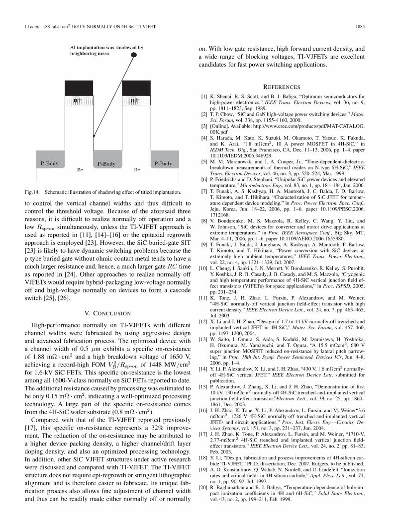
A research team at Northrop–Grumman has been conductingresearch on SiC static induction transistors (SITs) based one-beam lithography [21], [22]. While SITs are excellent devicesfor RF power amplifier applications, they do not have thehighly uniform and vertical-channel-opening dimension that isthe key to the success of TI-VJFETs for high-power switch-ing applications. By using e-beam lithography, SITs can packhigher density channels and avoid shadowing effect causedby neighboring mesas (Fig. 14). For TI-VJFETs, the sidewallimplantation needs to increase its tilt angle when cell pitchis reduced. However, grazing-angle implantation may not beoptimum because ions may be bounced away from the sidewall.Thus, TI-VJFET may not achieve a cell packing density ashigh as that of e-beam-lithography-fabricated SITs. However,SIT structures have the following disadvantages compared withTI-VJFET. First, the vertical channel does not have a highlyuniform channel width. As shown in the SEM photograph of[21], because of the implantation scattering effect, the verticalchannel does not have a uniform channel width. Second, thechannel length is not easily controlled because it is determinedby the implantation depth, which, in turn, is limited by theion energy provided by the implanter. Typical commercialimplanters provide several hundred kiloelectron-volt ion im-plantations, and megaelectron-volt ion implantations requirespecial masking and are only available in research institutions.Third, tilted implantation provides a freedom to fine-tune thechannel width, even after the mesas have been defined bydry etching. Without tilted sidewall implantation, it is difficult
LI et al.: 1.88-mΩ · cm2 1650-V NORMALLY ON 4H-SiC TI-VJFET 1885
Fig.14. Schematic illustration of shadowing effect of titled implantation.
to control the vertical channel widths and thus difficult tocontrol the threshold voltage. Because of the aforesaid threereasons, it is difficult to realize normally off operation and alow Rsp-on simultaneously, unless the TI-VJFET approach isused as reported in [11], [14]–[16] or the epitaxial regrowthapproach is employed [23]. However, the SiC buried-gate SIT[23] is likely to have dynamic switching problems because thep-type buried gate without ohmic contact metal tends to have amuch larger resistance and, hence, a much larger gate RC timeas reported in [24]. Other approaches to realize normally offVJFETs would require hybrid-packaging low-voltage normallyoff and high-voltage normally on devices to form a cascodeswitch [25], [26].
V. CONCLUSION
High-performance normally on TI-VJFETs with differentchannel widths were fabricated by using aggressive designand advanced fabrication process. The optimized device witha channel width of 0.5 µm exhibits a specific on-resistanceof 1.88 mΩ · cm2 and a high breakdown voltage of 1650 V,achieving a record-high FOM V 2
B/Rsp-on of 1448 MW/cm2
for 1.6-kV SiC FETs. This specific on-resistance is the lowestamong all 1600-V-class normally on SiC FETs reported to date.The additional resistance caused by processing was estimated tobe only 0.15 mΩ · cm2, indicating a well-optimized processingtechnology. A large part of the specific on-resistance comesfrom the 4H-SiC wafer substrate (0.8 mΩ · cm2).
Compared with that of the TI-VJFET reported previously[17], this specific on-resistance represents a 32% improve-ment. The reduction of the on-resistance may be attributed toa higher device packing density, a higher channel/drift layerdoping density, and also an optimized processing technology.In addition, other SiC VJFET structures under active researchwere discussed and compared with TI-VJFET. The TI-VJFETstructure does not require epi-regrowth or stringent lithographicalignment and is therefore easier to fabricate. Its unique fab-rication process also allows fine adjustment of channel widthand thus can be readily made either normally off or normally
on. With low gate resistance, high forward current density, anda wide range of blocking voltages, TI-VJFETs are excellentcandidates for fast power switching applications.
REFERENCES
[1] K. Shenai, R. S. Scott, and B. J. Baliga, “Optimum semiconductors forhigh-power electronics,” IEEE Trans. Electron Devices, vol. 36, no. 9,pp. 1811–1823, Sep. 1989.
[2] T. P. Chow, “SiC and GaN high-voltage power switching devices,” Mater.Sci. Forum, vol. 338, pp. 1155–1160, 2000.
[3] [Online]. Available: http://www.cree.com/products/pdf/MAT-CATALOG.00K.pdf
[4] S. Harada, M. Kato, K. Suzuki, M. Okamoto, T. Yatsuo, K. Fukuda,and K. Arai, “1.8 mΩcm2, 10 A power MOSFET in 4H-SiC,” inIEDM Tech. Dig., San Francisco, CA, Dec. 11–13, 2006, pp. 1–4. paper10.1109/IEDM.2006.346929.
[5] M. M. Maranowski and J. A. Cooper, Jr., “Time-dependent-dielectric-breakdown measurements of thermal oxides on N-type 6H-SiC,” IEEETrans. Electron Devices, vol. 46, no. 3, pp. 520–524, Mar. 1999.
[6] P. Friedrichs and D. Stephani, “Unipolar SiC power devices and elevatedtemperature,” Microelectron. Eng., vol. 83, no. 1, pp. 181–184, Jan. 2006.
[7] T. Funaki, A. S. Kashyap, H. A. Mantooth, J. C. Balda, F. D. Barlow,T. Kimoto, and T. Hikihara, “Characterization of SiC JFET for temper-ature dependent device modeling,” in Proc. Power Electron. Spec. Conf.,Jeju, Korea, Jun. 18–22, 2006, pp. 1–6. paper 10.1109/PESC.2006.1712168.
[8] V. Bondarenko, M. S. Mazzola, R. Kelley, C. Wang, Y. Liu, andW. Johnson, “SiC devices for converter and motor drive applications atextreme temperatures,” in Proc. IEEE Aerospace Conf., Big Sky, MT,Mar. 4–11, 2006, pp. 1–6. paper 10.1109/AERO.2006.1655980.
[9] T. Funaki, J. Balda, J. Junghans, A. Kashyap, A. Mantooth, F. Barlow,T. Kimoto, and T. Hikihara, “Power conversion with SiC devices atextremely high ambient temperatures,” IEEE Trans. Power Electron.,vol. 22, no. 4, pp. 1321–1329, Jul. 2007.
[10] L. Cheng, I. Sankin, J. N. Merrett, V. Bondarenko, R. Kelley, S. Purohit,Y. Koshka, J. R. B. Casady, J. B. Casady, and M. S. Mazzola, “Cryogenicand high temperature performance of 4H-SiC vertical junction field ef-fect transistors (VJFETs) for space applications,” in Proc. ISPSD, 2005,pp. 231–234.
[11] K. Tone, J. H. Zhao, L. Fursin, P. Alexandrov, and M. Weiner,“4H-SiC normally-off vertical junction field-effect transistor with highcurrent density,” IEEE Electron Device Lett., vol. 24, no. 7, pp. 463–465,Jul. 2003.
[12] X. Li and J. H. Zhao, “Design of 1.7 to 14 kV normally-off trenched andimplanted vertical JFET in 4H-SiC,” Mater. Sci. Forum, vol. 457–460,pp. 1197–1200, 2004.
[13] W. Saito, I. Omura, S. Aida, S. Koduki, M. Izumisawa, H. Yoshioka,H. Okumura, M. Yamaguchi, and T. Ogura, “A 15.5 mΩcm2, 680 Vsuper junction MOSFET reduced on-resistance by lateral pitch narrow-ing,” in Proc. 18th Int. Symp. Power Semicond. Devices ICs, Jun. 4–8,2006, pp. 1–4.
[14] Y. Li, P. Alexandrov, X. Li, and J. H. Zhao, “430 V, 1.6 mΩcm2 normally-off 4H-SiC vertical JFET,” IEEE Electron Device Lett. submitted forpublication.
[15] P. Alexandrov, J. Zhang, X. Li, and J. H. Zhao, “Demonstration of first10 kV, 130 mΩcm2 normally-off 4H-SiC trenched-and-implanted verticaljunction field-effect transistor,”Electron. Lett., vol. 39, no. 25, pp. 1860–1861, Dec. 2003.
[16] J. H. Zhao, K. Tone, X. Li, P. Alexandrov, L. Fursin, and M. Weiner“3.6mΩcm2, 1726 V 4H-SiC normally-off trenched-and-implanted verticalJFETs and circuit applications,” Proc. Inst. Electr. Eng.—Circuits, De-vices Systems, vol. 151, no. 3, pp. 231–237, Jun. 2004.
[17] J. H. Zhao, K. Tone, P. Alexandrov, L. Fursin, and M. Weiner, “1710-V,2.77-mΩcm2 4H-SiC trenched and implanted vertical junction field-effect transistors,” IEEE Electron Device Lett., vol. 24, no. 2, pp. 81–83,Feb. 2003.
[18] Y. Li, “Design, fabrication and process improvements of 4H-silicon car-bide TI-VJFET,” Ph.D. dissertation, Dec. 2007. Rutgers. to be published.
[19] A. O. Konstantinov, Q. Wahab, N. Nordell, and U. Lindefelt, “Ionizationrates and critical fields in 4H silicon carbide,” Appl. Phys. Lett., vol. 71,no. 1, pp. 90–92, Jul. 1997.
[20] R. Raghunathan and B. J. Baliga, “Temperature dependence of hole im-pact ionization coefficients in 4H and 6H-SiC,” Solid State Electron.,vol. 43, no. 2, pp. 199–211, Feb. 1999.

1886 IEEE TRANSACTIONS ON ELECTRON DEVICES, VOL. 55, NO. 8, AUGUST 2008
[21] T. J. Knight, R. C. Clarke, R. R. Barron, J. A. Ostop, B. A. Morick,J. R. Gigante, W. J. Malkowski, A. W. Morse, G. C. DeSalvo,K. J. Petrosky, and W. R. Curtice, “A silicon carbide self-aligned andion implanted static induction transistor (SAI-SIT) for 150 watt S-bandoperation,” in Proc. 60th Annu. Device Res. Conf., Santa Barbara, CA,Jun. 24–26, 2002, pp. 179–180. paper 10.1109/DRC.2002.1029586.
[22] G. C. DeSalvo, P. M. Esker, T. A. Flint, J. A. Ostop, E. J. Stewart,T. J. Knight, K. J. Petrosky, S. D. VanCampen, R. C. Clarke, andG. M. Bates, “Ion implanted SiC static induction transistor with 107 Woutput power and 59% power added efficiency under CW operation at750 MHz,” Int. J. High Speed Electron. Syst., vol. 14, no. 3, pp. 906–908,2004.
[23] Y. Tanaka, M. Okamoto, A. Takatsuka, K. Arai, T. Yatsuo, K. Yano, andM. Kasuga, “700-V 1.0-mΩ · cm2 buried gate SiC-SIT (SiC-BGSIT),”IEEE Electron Device Lett., vol. 27, no. 11, pp. 908–910, Nov. 2006.
[24] Y. Tanaka, K. Yano, M. Okamoto, A. Takatsuka, K. Arai, andT. Yatsuo, “1270 V, 1.21 mΩcm2 SiC buried gate static induction tran-sistors (SiC-BGSIT),” presented at the Int. Conf. Silicon Carbide andRelated Materials, Otsu, Japan, Oct. 14–19, 2007, Paper Th-3B-3.
[25] J. Hornberger, E. Cilio, B. McPherson, R. Schupbach, A. Lostetter, andH. Mantooth, “A fully integrated 300 C, 4 kW, 3-phase, SiC motor drivemodule,” in Proc. Power Electron. Spec. Conf., Orlando, FL, Jun. 17–21,2007, pp. 1048–1053. paper 10.1109/PESC.2007.4342136.
[26] E. J. Stewart, M. J. McCoy, T. R. McNutt, H. C. Hearne, A. P. Walker,S. D. Van Campen, G. M. Bates, S. Leslie, G. C. DeSalvo, andR. C. Clarke, “8 kV normally-off all-SiC cascode power switchusing VJFETs,” in Proc. 19th ISPSD, Jeju, Korea, May 27–30, 2007,pp. 85–87. paper 10.1109/ISPSD.2007.4294938.
Yuzhu Li received the B.S. degree in electrical en-gineering from Tsinghua University, Beijing, China,in 1999, and the M.S. and Ph.D. degrees in elec-trical engineering from Rutgers University, NewBrunswick, NJ, in 2001 and 2008, respectively.
He is currently with SiCLAB, Department of Elec-trical and Computer Engineering, Rutgers Univer-sity, Piscataway, NJ. His research interests includedesign and fabrication of 4H-SiC VJFET and circuitmodeling of power electronics.
Petre Alexandrov (M’00) received the M.Sc. degreein engineering physics from Sofia University, Sofia,Bulgaria, in 1986, and the M.S. degree in electricalengineering from Rutgers University, Piscataway,NJ, in 2001.
In 1988, he was with the Institute of Microelec-tronics, Sofia, where he worked on MOS device andprocess technology control and development. From1993 to 1998, he was a Research Associate with theInstitute of Solid State Physics, Bulgarian Academyof Sciences, Sofia, where he worked on new thin-film
materials for microelectronic applications. He is currently a Senior ResearchEngineer with United Silicon Carbide, Inc., New Brunswick Technical Center,New Brunswick, NJ. He is also with SiCLAB, Department of Electrical andComputer Engineering, Rutgers University. He is the author or coauthor ofmore than 40 papers on 4H-SiC devices, which are published in technical jour-nals and conference proceedings. His responsibilities include design, processdevelopment, fabrication, and characterization of high-performance SiC-basedpower devices. His research activities in projects funded by DARPA, U.S. ArmyTACOM, U.S. Air Force, and NASA led to development of novel 4H-SiC powerdiodes and switches.
Jian H. Zhao (SM’94) received the B.S. degree inphysics from Xiamen (Amoy) University, Xiamen,China, in 1982, the M.S. degree in physics from theUniversity of Toledo, Toledo, OH, in 1985, and thePh.D. degree in electrical and computer engineeringfrom Carnegie Mellon University, Pittsburgh, PA,in 1988.
He has been with the Department of Electri-cal and Computer Engineering, Rutgers University,Piscataway, NJ, since 1988, where he is currentlythe Director of SiCLAB and a Professor of electrical
and computer engineering. His current research interests include wide-bandgapsemiconductor electronic and optoelectronic devices, circuits, and system ap-plications, with a major emphasis on energy-efficient power devices, powerICs, and various detectors, including single-photon counters. Together with hisstudents and others, he has published over 200 refereed journal and proceedingpapers, six book chapters, and two books entitled Silicon Carbide Materials,Processing, and Devices (Taylor & Francis, 2003) and Optical Filter Designand Analysis: A Signal Processing Approach (Wiley, 1999) which was a top tenbest seller in Amazon.com in 2000 under Corning Fiber Optics Series. He is aholder of one pending and six awarded U.S. patents, of which two have beenlicensed to industry.
Copyright © 2022 FDOKUMEN


![Ethyl 2-(6-amino-5-cyano-3,4-dimethyl-2H,4H-pyrano[2,3-c]pyrazol-4-yl)acetate](https://static.fdokumen.com/doc/165x107/630bead9dffd3305850820dd/ethyl-2-6-amino-5-cyano-34-dimethyl-2h4h-pyrano23-cpyrazol-4-ylacetate.jpg)