A study on knowledge transfer between in and out-of-school language learning
Upload
khangminh22Category
view
0download
0
1
UNIT-1
Register Transfer Language. Definition: The symbolic notation used to describe the microoperation transfers among
registers is called a register transfer language.
The term "register transfer" implies the availability of hardware logic circuits that can perform a stated microoperation and transfer the result of the operation to the same or another register.
The word "language" is borrowed from programmers, who apply this term to programming languages.
A register transfer language is a system for expressing in symbolic form the microoperation sequences among the registers of a digital module.
It is a convenient tool for describing the internal organization of digital computers in concise and precise manner.
It can also be used to facilitate the design process of digital systems. Information transfer from one register to another is designated in symbolic form by
means of a replacement operator.
The statement below denotes a transfer of the content of register R1 into register R2. R2 ← R1
A statement that specifies a register transfer implies that circuits are available from the outputs of the destination register has a parallel load capability.
Every statement written in a register transfer notation implies a hardware construction for implementing the transfer.block diagram and timing diagram.
Definition: Information transfer from one register to another is designated in symbolic form by means of a replacement operator is known as Register Transfer.
R2 ← R1
Denotes a transfer of the content of register R1 into register R2. Computer registers are designated by capital letters (sometimes followed by numerals)
to denote the function of the register. For example:
MAR Holds address of memory unit
PC Program Counter
IR Instruction Register R1 Processor Register
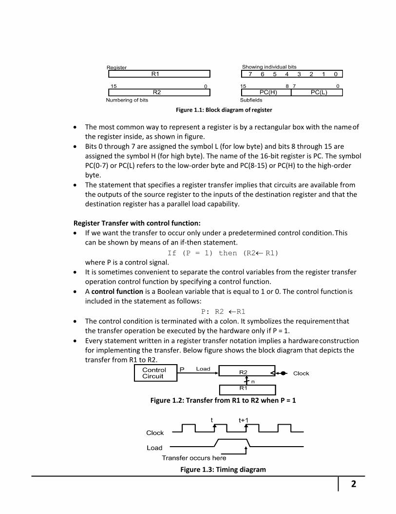
Below figure1.1 shows the representation of registers in block diagram form.
2
Figure 1.1: Block diagram of register
The most common way to represent a register is by a rectangular box with the name of the register inside, as shown in figure.
Bits 0 through 7 are assigned the symbol L (for low byte) and bits 8 through 15 are assigned the symbol H (for high byte). The name of the 16-bit register is PC. The symbol PC(0-7) or PC(L) refers to the low-order byte and PC(8-15) or PC(H) to the high-order byte.
The statement that specifies a register transfer implies that circuits are available from the outputs of the source register to the inputs of the destination register and that the destination register has a parallel load capability.
Register Transfer with control function: If we want the transfer to occur only under a predetermined control condition. This
can be shown by means of an if-then statement.
If (P = 1) then (R2 R1)
where P is a control signal. It is sometimes convenient to separate the control variables from the register transfer
operation control function by specifying a control function.
A control function is a Boolean variable that is equal to 1 or 0. The control function is included in the statement as follows:
P: R2 R1
The control condition is terminated with a colon. It symbolizes the requirement that the transfer operation be executed by the hardware only if P = 1.
Every statement written in a register transfer notation implies a hardware construction for implementing the transfer. Below figure shows the block diagram that depicts the transfer from R1 to R2.
Figure 1.2: Transfer from R1 to R2 when P = 1
Figure 1.3: Timing diagram
3
The n outputs of register R1 are connected to the n inputs of register R2. The letter n will be used to indicate any number of bits for the register.
In the timing diagram, P is activated in the control section by the rising edge of a clock pulse at time t.
The next positive transition of the clock at time t + 1 finds the load input active and the data inputs of R2 are then loaded into the register in parallel.
P may go back to 0 at time t + 1; otherwise, the transfer will occur with every clock pulse transition while P remains active.
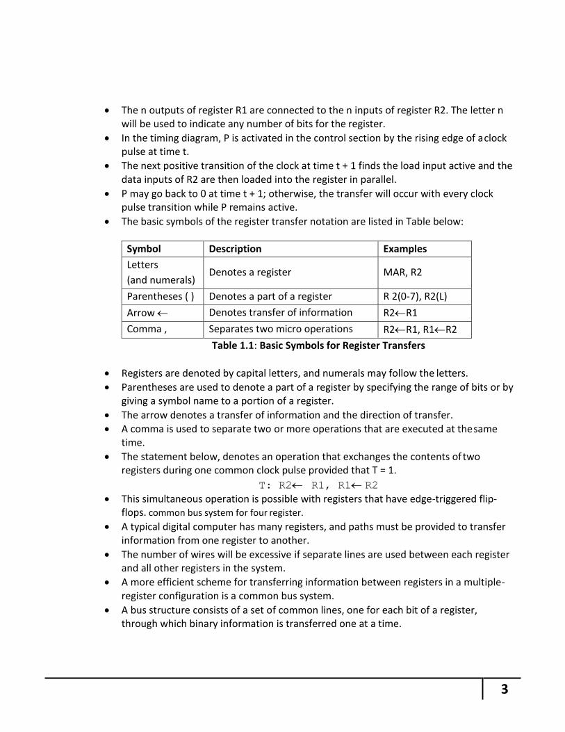
The basic symbols of the register transfer notation are listed in Table below:
Symbol Description Examples
Letters
(and numerals) Denotes a register MAR, R2
Parentheses ( ) Denotes a part of a register R 2(0-7), R2(L)
Arrow Denotes transfer of information R2R1
Comma , Separates two micro operations R2R1, R1R2
Table 1.1: Basic Symbols for Register Transfers
Registers are denoted by capital letters, and numerals may follow the letters.
Parentheses are used to denote a part of a register by specifying the range of bits or by giving a symbol name to a portion of a register.
The arrow denotes a transfer of information and the direction of transfer. A comma is used to separate two or more operations that are executed at the same
time.
The statement below, denotes an operation that exchanges the contents of two registers during one common clock pulse provided that T = 1.
T: R2 R1, R1 R2
This simultaneous operation is possible with registers that have edge-triggered flip- flops. common bus system for four register.
A typical digital computer has many registers, and paths must be provided to transfer information from one register to another.
The number of wires will be excessive if separate lines are used between each register and all other registers in the system.
A more efficient scheme for transferring information between registers in a multiple- register configuration is a common bus system.
A bus structure consists of a set of common lines, one for each bit of a register, through which binary information is transferred one at a time.
4
D2 C2 B2 A2
D2
3 2
4 x 1
MUX 2
4 x 1
MUX 3
S1
S0
4 x 1
MUX 0
4 x 1
MUX 1
Control signals determine which register is selected by the bus during each particular register transfer.
One way of constructing a common bus system is with multiplexers. The multiplexers select the source register whose binary information is then placed on
the bus.
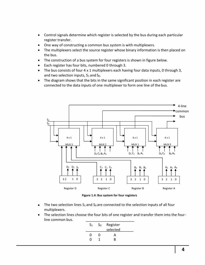
The construction of a bus system for four registers is shown in figure below.
Each register has four bits, numbered 0 through 3. The bus consists of four 4 x 1 multiplexers each having four data inputs, 0 through 3,
and two selection inputs, S1 and S0. The diagram shows that the bits in the same significant position in each register are
connected to the data inputs of one multiplexer to form one line of the bus.
4-line
common
bus
D1 C1 B1 A1 D0 C0 B0 A0
D0
C2
C1
C0
B2
B1
B0
A2
A1
A0
0 3 2 1 0 3 2 1 0 3 2 1 0
Register D Register C Register B Register A
Figure 1.4: Bus system for four registers
The two selection lines S1 and S0 are connected to the selection inputs of all four multiplexers.
The selection lines choose the four bits of one register and transfer them into the four- line common bus.
S1 S0 Register selected
0 0 A 0 1 B
D1
1
5
1 0 C 1 1 D Table 1.2: Function Table for Bus
When S1S0 = 00, the 0 data inputs of all four multiplexers are selected and applied to the outputs that form the bus.
This causes the bus lines to receive the content of register A since the outputs of this register are connected to the 0 data inputs of the multiplexers.
Similarly, register B is selected if S1S0 = 01, and so on.
Table shows the register that is selected by the bus for each of the four possible binary values of the selection lines.
In general, a bus system will multiplex k registers of n bits each to produce an n-line common bus.
The number of multiplexers needed to construct the bus is equal to n, the number of bits in each register.
The size of each multiplexer must be K x 1 since it multiplexes K data lines. For example, a common bus for eight registers of 16 bits each requires 16 multiplexers, one for each line in the bus. Each multiplexer must have eight data input lines and three selection lines to multiplex one significant bit in the eight registers.
A digital computer has a common bus system for 16 registers of 32 bits each. (i) How many selection input are there in each multiplexer? (ii) What size of multiplexers is needed? (iii) How many multiplexers are there in a bus? (i) How many selection input are there in each multiplexer?
2n=No. of Registers; n=selection input of multiplexer 2n=16; here n=4 Therefore 4 selection input lines should be there in each multiplexer.
(ii) What size of multiplexers is needed? size of multiplexers= Total number of register X 1
= 16 X 1 Multiplexer of 16 x 1 size is needed to design the above defined common bus.
(iii) How many multiplexers are there in a bus? No. of multiplexers = bits of register
= 32 32 multiplexers are needed in a bus.
6
Three-state bus buffer. A bus system can be constructed with three-state gates instead of multiplexers.
A three-state gate is a digital circuit that exhibits three states. State 1: Signal equivalent to Logic 1 State 2: Signal equivalent to Logic 0 State 3: High Impedance State (behaves as open circuit)
The high-impedance state behaves like an open circuit, which means that the output is disconnected and does not have logic significance.
The most commonly used design of a bus system is the buffer gate.
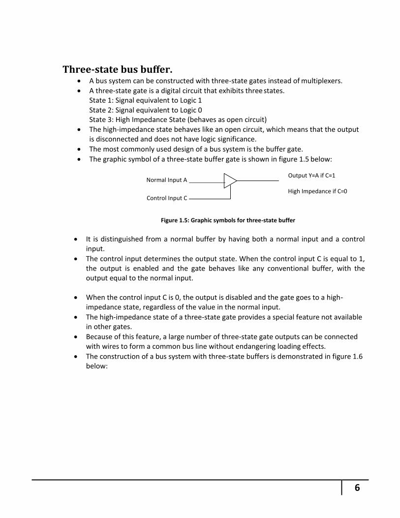
The graphic symbol of a three-state buffer gate is shown in figure 1.5 below:
Normal Input A
Control Input C
Output Y=A if C=1
High Impedance if C=0
Figure 1.5: Graphic symbols for three-state buffer
It is distinguished from a normal buffer by having both a normal input and a control input.
The control input determines the output state. When the control input C is equal to 1, the output is enabled and the gate behaves like any conventional buffer, with the output equal to the normal input.
When the control input C is 0, the output is disabled and the gate goes to a high- impedance state, regardless of the value in the normal input.
The high-impedance state of a three-state gate provides a special feature not available in other gates.
Because of this feature, a large number of three-state gate outputs can be connected with wires to form a common bus line without endangering loading effects.
The construction of a bus system with three-state buffers is demonstrated in figure 1.6 below:
7
Bus line for bit 0 A0
B0
C0
D0
Select
Enable
Figure 1.6: Bus line with three state-buffers
The outputs of four buffers are connected together to form a single bus line. The control inputs to the buffers determine which of the four normal inputs will
communicate with the bus line.
No more than one buffer may be in the active state at any given time.
The connected buffers must be controlled so that only one three-state buffer has access to the bus line while all other buffers are maintained in a high impedance state.
One way to ensure that no more than one control input is active at any given time is to use a decoder, as shown in the figure: Bus line with three state-buffers.
When the enable input of the decoder is 0, all of its four outputs are 0, and the bus line is in a high-impedance state because all four buffers are disabled.
When the enable input is active, one of the three-state buffers will be active, depending on the binary value in the select inputs of the decoder.
To construct a common bus for four registers of n bits each using three- state buffers, we need n circuits with four buffers in each as shown in figure: Bus line with three state-buffers,
Each group of four buffers receives one significant bit from the four registers.
Each common output produces one of the lines for the common bus for a total of n lines.
Only one decoder is necessary to select between the four registers.
0
1
2
3 Decoder
2x4
S1
S0
8
Memory Transfer Read Operation: The transfer of information from a memory word to the outside
environment is called a read operation.
Write Operation: The transfer of new information to be stored into the memory is called a write operation.
A memory word will be symbolized by the letter M.
It is necessary to specify the address of M when writing memory transfer operations.
This will be done by enclosing the address in square brackets following the letter M.
Consider a memory unit that receives the address from a register, called the address register, symbolized by AR.
The data are transferred to another register, called the data register, symbolized by DR. The read operation can be stated as follows:
Read: DR M[AR] This causes a transfer of information into DR from the memory word M selected by the
address in AR.
The write operation transfers the content of a data register to a memory word M selected by the address. Assume that the input data are in register R1 and the address is in AR.
Write operation can be stated symbolically as follows:
Write: M[AR] R1
This causes a transfer of information from R1 into memory word M selected by address AR.
9
Arithmetic Micro-operation. The basic arithmetic micro-operations are:
1. Addition 2. Subtraction 3. Increment 4. Decrement 5. Shift
The additional arithmetic micro operations are: 1. Add with carry 2. Subtract with borrow 3. Transfer/Load , etc.
Summary of Typical Arithmetic Micro-Operations:
R3 R1 + R2 Contents of R1 plus R2 transferred to R3
R3 R1 - R2 Contents of R1 minus R2 transferred to R3
R2 R2’ Complement the contents of R2
R2 R2’+ 1 2's complement the contents of R2 (negate)
R3 R1 + R2’+ 1
subtraction
R1 R1 + 1 Increment
R1 R1 – 1 Decrement
Binary Adder To implement the add micro operation with hardware, we need :
1. Registers : that hold the data 2. Digital component: that performs the arithmetic addition.
Full-adder The digital circuit that forms the arithmetic sum of two bits and a previous carry is called a full-adder.
Binary adder The digital circuit that generates the arithmetic sum of two binary numbers of any lengths is called a binary adder.
The binary adder is constructed with full-adder circuits connected in cascade, with the output carry from one full-adder connected to the input carry of the next full-adder.
10
FA FA FA FA
B3 A3 B2 A2 B1 A1 B0 A0
C3 C2 C1 C0
C4 S3 S2 S1 S0
Figure 1.7: 4-bit binary adder
Above figure 1.7 shows the interconnections of four full-adders (FA) to provide a 4-bit binary adder.
The augends bits of A and the addend bits of B are designated by subscript numbers from right to left, with subscript 0 denoting the low-order bit.
The carries are connected in a chain through the full-adders.
The input carry to the binary adder is C0 and the output carry is C4.
The S outputs of the full-adders generate the required sum bits.
An n-bit binary adder requires n full-adders. The output carry from each full-adder is connected to the input carry of the next-high-
order full-adder.
The n data bits for the A inputs come from one register (such as R1), and the n data bits for the B inputs come from another register (such as R2). The sum can be transferred to a third register or to one of the source registers (R1 or R2), replacing its previous content.
Binary Adder-Subtractor The subtraction of binary numbers can be done most conveniently by means of
complements.
Remember that the subtraction A - B can be done by taking the 2's complement of B and adding it to A.
The 2's complement can be obtained by taking the l's complement and adding one to the least significant pair of bits. The l's complement can be implemented with inverters and a one can be added to the sum through the input carry.
The addition and subtraction operations can be combined into one common circuit by including an exclusive-OR gate with each full-adder.
The mode input M controls the operation. When M = 0 the circuit is an Adder When M = 1 the circuit becomes a Subtractor
Each exclusive-OR gate receives input M and one of the inputs of B. When M = 0,
We have C0=0
B ⊕ 0 = B
The full-adders receive the value of B, the input carry is 0, and the circuit performs A
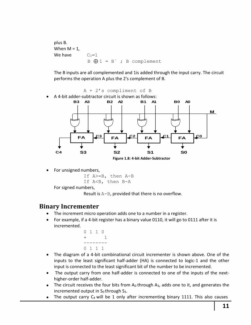
11
FA
plus B. When M = 1,
We have C0=1
B ⊕ 1 = B` ; B complement
The B inputs are all complemented and 1is added through the input carry. The circuit performs the operation A plus the 2's complement of B.
A + 2’s compliment of B
A 4-bit adder-subtractor circuit is shown as follows: B3 A3 B2 A2 B1 A1 B0 A0
C4 S3 S2 S1 S0
For unsigned numbers,
Figure 1.8: 4-bit Adder-Subtractor
If A>=B, then A-B
If A<B, then B-A
For signed numbers,
Result is A-B, provided that there is no overflow.
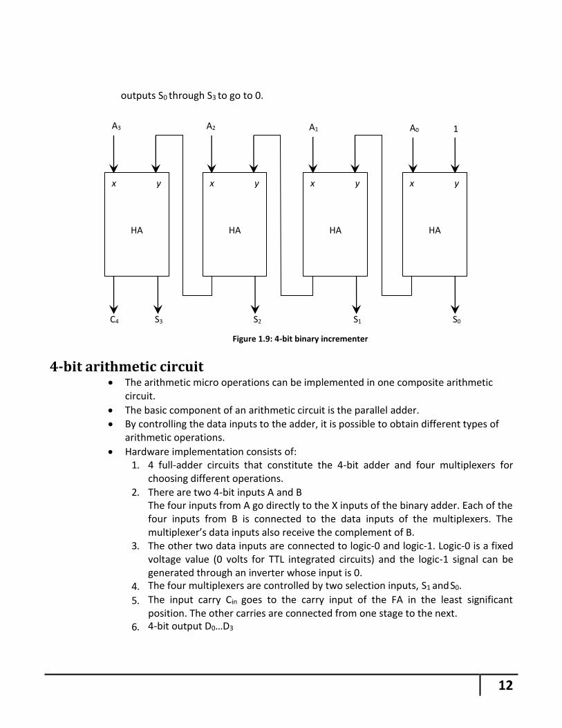
Binary Incrementer The increment micro operation adds one to a number in a register.
For example, if a 4-bit register has a binary value 0110, it will go to 0111 after it is incremented.
0 1 1 0
+ 1
--------
0 1 1 1
The diagram of a 4-bit combinational circuit incrementer is shown above. One of the inputs to the least significant half-adder (HA) is connected to logic-1 and the other input is connected to the least significant bit of the number to be incremented.
The output carry from one half-adder is connected to one of the inputs of the next- higher-order half-adder.
The circuit receives the four bits from A0 through A3, adds one to it, and generates the incremented output in S0 through S3.
The output carry C4 will be 1 only after incrementing binary 1111. This also causes
M
C3 C2 C1 C0 FA FA FA
12
A3 A2 A1 A0 1
HA
y x
HA
y x
HA
y x
HA
y x
outputs S0 through S3 to go to 0.
C4 S3 S2 S1 S0
Figure 1.9: 4-bit binary incrementer
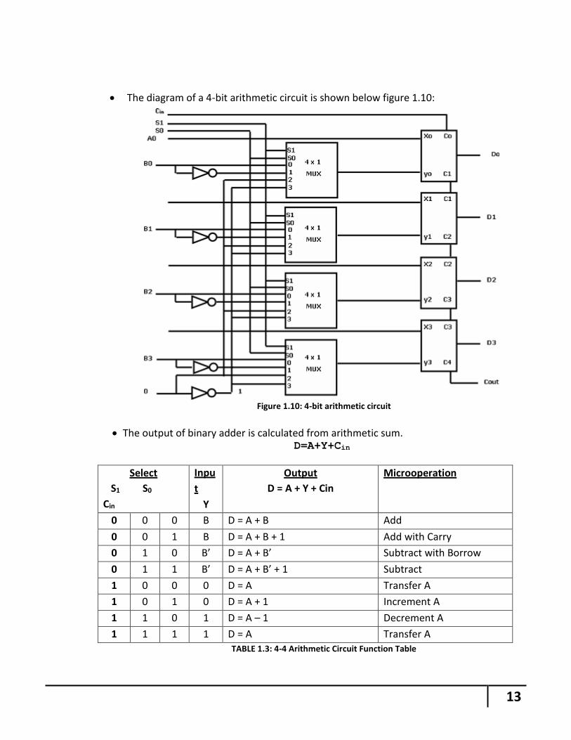
4-bit arithmetic circuit The arithmetic micro operations can be implemented in one composite arithmetic
circuit.
The basic component of an arithmetic circuit is the parallel adder. By controlling the data inputs to the adder, it is possible to obtain different types of
arithmetic operations.
Hardware implementation consists of: 1. 4 full-adder circuits that constitute the 4-bit adder and four multiplexers for
choosing different operations. 2. There are two 4-bit inputs A and B
The four inputs from A go directly to the X inputs of the binary adder. Each of the four inputs from B is connected to the data inputs of the multiplexers. The multiplexer’s data inputs also receive the complement of B.
3. The other two data inputs are connected to logic-0 and logic-1. Logic-0 is a fixed voltage value (0 volts for TTL integrated circuits) and the logic-1 signal can be generated through an inverter whose input is 0.
4. The four multiplexers are controlled by two selection inputs, S1 and S0.
5. The input carry Cin goes to the carry input of the FA in the least significant position. The other carries are connected from one stage to the next.
6. 4-bit output D0…D3
13
The diagram of a 4-bit arithmetic circuit is shown below figure 1.10:
Figure 1.10: 4-bit arithmetic circuit
The output of binary adder is calculated from arithmetic sum. D=A+Y+Cin
Select
S1 S0
Cin
Inpu
t
Y
Output
D = A + Y + Cin
Microoperation
0 0 0 B D = A + B Add
0 0 1 B D = A + B + 1 Add with Carry
0 1 0 B’ D = A + B’ Subtract with Borrow
0 1 1 B’ D = A + B’ + 1 Subtract
1 0 0 0 D = A Transfer A
1 0 1 0 D = A + 1 Increment A
1 1 0 1 D = A – 1 Decrement A
1 1 1 1 D = A Transfer A
TABLE 1.3: 4-4 Arithmetic Circuit Function Table
14
When S1 S0= 0 0
If Cin=0, D=A+B; Add
If Cin=1, D=A+B+1;Add with carry
When S1 S0= 0 1
If Cin=0, D=A+B ; Subtract with borrow
If Cin=1, D=A+B +1;A+2’s compliment of B i.e. A-B
When S1 S0= 1 0
Input B is neglected and Y=> logic ‘0’
D=A+0+ Cin
If Cin=0, D=A; Transfer A
If Cin=1, D=A+1;Increment A
When S1 S0= 1 1
Input B is neglected and Y=> logic ‘1’
D=A-1+ Cin
If Cin=0, D=A-1; 2’s compliment
If Cin=1, D=A; Transfer A
Note that the micro-operation D = A is generated twice, so there are only seven distinct micro-operations in the arithmetic circuit.
Logic Micro-operations Logic micro operations specify binary operations for strings of bits stored in registers.
These operations consider each bit of the register separately and treat them as binary variables. For example, the exclusive-OR micro-operation with the contents of two registers R1 and R2 is symbolized by the statement:
P: R1 R1 ⊕ R2
1 0 1 0 Content of R1
⊕ 1 1 0 0 Content of R2
-----------------------------------
0 1 1 0 Content of R1 after P = 1
The logic micro-operations are seldom used in scientific computations, but they are very useful for bit manipulation of binary data and for making logical decisions.
Notation: The symbol ∨ will be used to denote an OR microoperation and the symbol ∧ to denote an AND microoperation. The complement microoperation is the same as the 1's complement and uses a bar on top of the symbol that denotes the register name.
Although the + symbol has two meanings, it will be possible to distinguish between them by noting where the symbol occurs. When the symbol + occurs in a microoperation, it will denote an arithmetic plus. When it occurs in a control (or Boolean) function, it will denote an OR operation.
P + Q: R1 R2 + R3, R4 R5 V R6
15
The + between P and Q is an OR operation between two binary variables of a control function. The + between R2 and R3 specifies an add microoperation. The OR microoperation is designated by the symbol V between registers R5and R6.
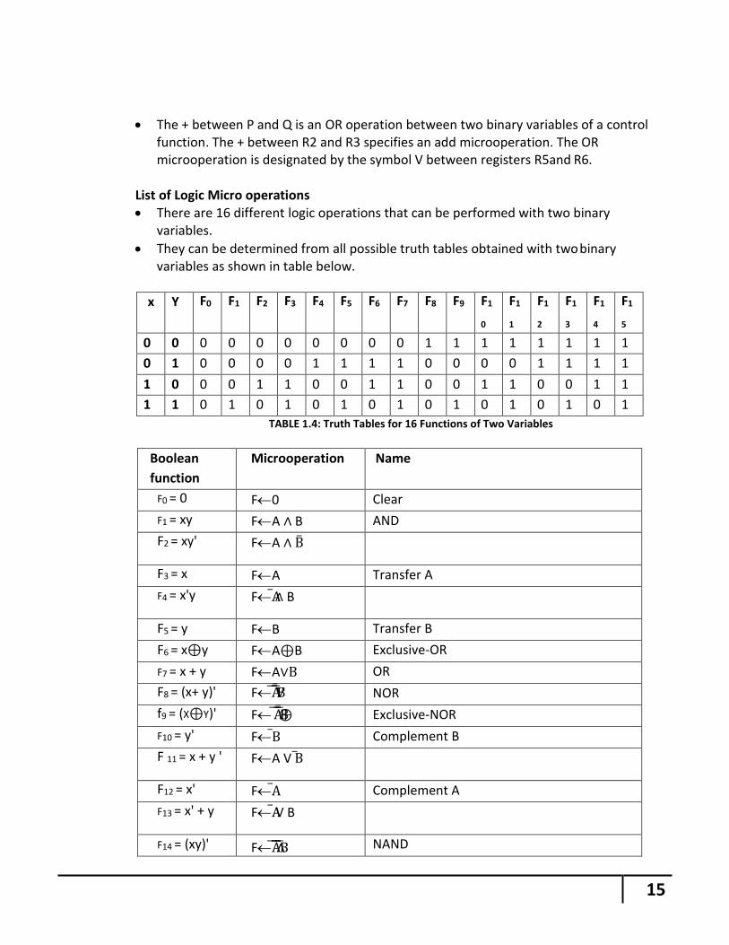
List of Logic Micro operations There are 16 different logic operations that can be performed with two binary
variables.
They can be determined from all possible truth tables obtained with two binary variables as shown in table below.
x Y F0 F1 F2 F3 F4 F5 F6 F7 F8 F9 F1
0
F1
1
F1
2
F1
3
F1
4
F1
5
0 0 0 0 0 0 0 0 0 0 1 1 1 1 1 1 1 1
0 1 0 0 0 0 1 1 1 1 0 0 0 0 1 1 1 1
1 0 0 0 1 1 0 0 1 1 0 0 1 1 0 0 1 1
1 1 0 1 0 1 0 1 0 1 0 1 0 1 0 1 0 1
TABLE 1.4: Truth Tables for 16 Functions of Two Variables
Boolean
function
Microoperation Name
F0 = 0 F0 Clear
F1 = xy FA ∧ B AND
F2 = xy' FA ∧
F3 = x FA Transfer A
F4 = x'y FA ∧ B
F5 = y FB Transfer B
F6 = x⊕y FA⊕B Exclusive-OR
F7 = x + y FA∨ OR
F8 = (x+ y)' F A V B NOR
f9 = (X⊕Y)' F A ⊕ B Exclusive-NOR
F10 = y' FB Complement B
F 11 = x + y ' FA V
F12 = x' FA Complement A
F13 = x' + y FA V B
F14 = (xy)' F A ∧ B NAND
16
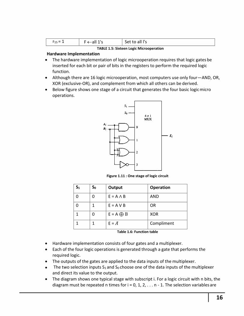
F15 = 1 F all 1's Set to all l's
TABLE 1.5: Sixteen Logic Microoperation
Hardware Implementation The hardware implementation of logic microoperation requires that logic gates be
inserted for each bit or pair of bits in the registers to perform the required logic function.
Although there are 16 logic microoperation, most computers use only four—AND, OR, XOR (exclusive-OR), and complement from which all others can be derived.
Below figure shows one stage of a circuit that generates the four basic logic micro operations.
Figure 1.11 : One stage of logic circuit
S1 S0 Output Operation
0 0 E = A ∧ B AND
0 1 E = A V B OR
1 0 E = A ⊕ XOR
1 1 E = Compliment
Table 1.6: Function table
Hardware implementation consists of four gates and a multiplexer. Each of the four logic operations is generated through a gate that performs the
required logic.
The outputs of the gates are applied to the data inputs of the multiplexer.
The two selection inputs S1 and S0 choose one of the data inputs of the multiplexer and direct its value to the output.
The diagram shows one typical stage with subscript i. For a logic circuit with n bits, the diagram must be repeated n times for i = 0, 1, 2, . . . n - 1. The selection variables are
17
applied to all stages.
selective set, selective complement and selective clear. Selective-Set operation:
The selective-set operation sets to 1 the bits in register A where there are corresponding 1's in register B. It does not affect bit positions that have 0's in B. The following numerical example clarifies this operation:
1010 A before 1100 B (logical operand) 1110 A after
The two leftmost bits of B are 1's, so the corresponding bits of A are set to 1.
One of these two bits was already set and the other has been changed from 0 to 1.
The two bits of A with corresponding 0's in B remain unchanged. The example above serves as a truth table since it has all four possible combinations of two binary variables.
The OR microoperation can be used to selectively set bits of a register.
Selective-Complement operation: The selective-complement operation complements bits in A where there are
corresponding 1's in B. It does not affect bit positions that have O's in B. For example:
1010 A before 1100 B (logical operand) 0110 A after
Again the two leftmost bits of B are 1's, so the corresponding bits of A are complemented.
The exclusive-OR microoperation can be used to selectively complement bits of a register.
Selective-Clear operation: The selective-clear operation clears to 0 the bits in A only where there are
corresponding 1's in B. For example:
1010 A before 1100 B (logical operand) 0010 A after
Again the two leftmost bits of B are 1's, so the corresponding bits of A are cleared to 0.
One can deduce that the Boolean operation performed on the individual bits is AB'. The corresponding logic microoperation is A ← A ∧ B’.
18
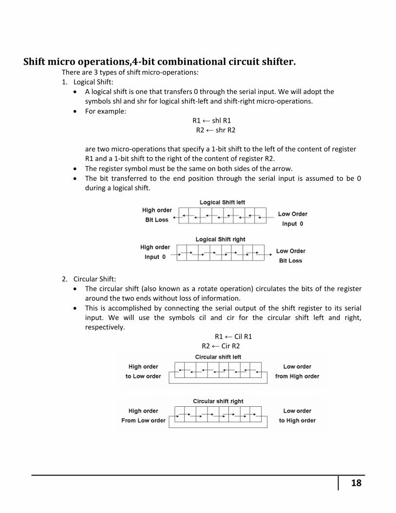
Shift micro operations,4-bit combinational circuit shifter. There are 3 types of shift micro-operations: 1. Logical Shift:
A logical shift is one that transfers 0 through the serial input. We will adopt the symbols shl and shr for logical shift-left and shift-right micro-operations.
For example: R1 ← shl R1
R2 ← shr R2
are two micro-operations that specify a 1-bit shift to the left of the content of register R1 and a 1-bit shift to the right of the content of register R2.
The register symbol must be the same on both sides of the arrow.
The bit transferred to the end position through the serial input is assumed to be 0 during a logical shift.
2. Circular Shift:
The circular shift (also known as a rotate operation) circulates the bits of the register around the two ends without loss of information.
This is accomplished by connecting the serial output of the shift register to its serial input. We will use the symbols cil and cir for the circular shift left and right, respectively.
R1 ← Cil R1 R2 ← Cir R2
19
3. Arithmetic Shift: An arithmetic shift is a micro-operation that shifts a signed binary number to the
left or right.
An arithmetic shift-left multiplies a signed binary number by 2.
An arithmetic shift-right divides the number by 2. Arithmetic shifts must leave the sign bit unchanged because the sign of the
number remains the same when it is multiplied or divided by 2.
The leftmost bit in a register holds the sign bit, and the remaining bits hold the number. The sign bit is 0 for positive and 1 for negative.
Negative numbers are in 2's complement form.
Figure shows a typical register of n bits. Bit Rn-1 in the leftmost position holds the sign bit.
Rn-2 is the most significant bit of the number and R0 is the least significant bit. The arithmetic shift-right leaves the sign bit unchanged and shifts the number
(including the sign bit) to the right.
Thus Rn-1 remains the same; Rn-2 receives the bit from Rn-1, and so on for the other bits in the register.
The bit in R0 is lost.
The arithmetic shift-left inserts a 0 into R0, and shifts all other bits to the left.
The initial bit of Rn-1 is lost and replaced by the bit from Rn-2. A sign reversal occurs if the bit in Rn-1 changes in value after the shift. This
happens if the multiplication by 2 causes an overflow.
4- bit combinational circuit shifter A combinational circuit shifter can be constructed with multiplexers as shown in Figure
below.

20
Figure 1.12: 4-bit combinational circuit shifter
The 4-bit shifter has four data inputs, A0 through A3 and four data outputs, H0 through H3.
There are two serial inputs, one for shift left (IL) and the other for shift right (IL).
When the selection input S = 0, the input data are shifted right (down in the diagram).
When S = 1, the input data are shifted left (up in the diagram).
The function table in Figure shows which input goes to each output after the shift.
A shifter with n data inputs and outputs requires n multiplexers. The two serial inputs can be controlled by another multiplexer to provide the three
possible types of shifts
21
One stage of arithmetic logic shift unit. Instead of having individual registers performing the micro operations directly,
computer systems employ a number of storage registers connected to a common operational unit called an arithmetic logic unit, abbreviated ALU.
To perform a microoperation, the contents of specified registers are placed in the inputs of the common ALU.
The ALU performs an operation and the result of the operation is then transferred to a destination register.
The ALU is a combinational circuit so that the entire register transfer operation from the source registers through the ALU and into the destination register can be performed during one dock pulse period.
The arithmetic, logic, and shift circuits introduced in previous sections can be combined into one ALU with common selection variables.
One stage of an arithmetic logic shift unit is shown in figure below:
Figure 1.13: One stage of arithmetic logic shift unit
The subscript i designates a typical stage. Inputs Ai and Bi are applied to both the arithmetic and logic units.
A particular microoperation is selected with inputs S1 and S0.
A 4 x 1 multiplexer at the output chooses between an arithmetic output in Di and a logic
output in Ei . The data in the multiplexer are selected with inputs S3 and S2.
The other two data inputs to the multiplexer receive inputs Ai-1 for the shift-right operation and Ai+1 for the shift-left operation.
Note that the diagram shows just one typical stage. The circuit shown in figure must be repeated n times for an n-bit ALU.
The outputs carry Ci+1 of a given arithmetic stage must be connected to the input carry Cin of the next stage in sequence.
The input carry to the first stage is the input carry On, which provides a selection
22
variable for
the arithmetic operations.
The circuit whose one stage is specified in figure provides
8 arithmetic operation
4 logic operations
2 shift operations
Each operation is selected with the five variables S3, S2, Si, S0, and Cin. The input carry Cin is used for selecting an arithmetic operation only.
Table below lists the 14 operations of the ALU.
Operation Select
Operation
Function S3 S2 S1 S0 Cin
0 0 0 0 0 F = A Transfer A
0 0 0 0 1 F = A + 1 Increment A
0 0 0 1 0 F = A + B Addition
0 0 0 1 1 F = A + B + 1 Add with carry
0 0 1 0 0 F = A + Subtract with borrow
0 0 1 0 1 F = A + +1 Subtraction
0 0 1 1 0 F = A - 1 Decrement A
0 0 1 1 1 F = A Transfer A
0 1 0 0 X F = A ∧ B AND
0 1 0 1 X F = A ∨ B OR
0 1 1 0 X F = A ⊕ B XOR
0 1 1 1 X F = Complement A
1 0 X X X F = shr A Shift right A into F
1 1 X X X F = shl A Shift left A into F
Table 1.7: Function Table for Arithmetic Logic Shift Unit
The first eight are arithmetic operations and are selected with S3S2 = 00.
The next four are logic operations are selected with S3S2 = 01. The input carry has no effect during the logic operations and is marked with don't-care X's.
The last two operations are shift operations and are selected with S3S2 = 10 and 11.
The other three selection inputs have no effect on the shift.
1
[Type text]
Instruction Code An instruction code is a group of bits that instruct the computer to perform a specific operation.
Operation Code The operation code of an instruction is a group of bits that define such operations as add, subtract, multiply, shift, and complement. The number of bits required for the operation code of an instruction depends on the total number of operations available in the computer. The operation code must consist of at least n bits for a given 2n (or less) distinct operations.
Accumulator (AC) Computers that have a single-processor register usually assign to it the name accumulator (AC) accumulator and label it AC. The operation is performed with the memory operand and the content of AC.
Stored Program Organization The simplest way to organize a computer is to have one processor register and an
instruction code format with two parts.
The first part specifies the operation to be performed and the second specifies an address.
The memory address tells the control where to find an operand in memory.
This operand is read from memory and used as the data to be operated on together with the data stored in the processor register.
The following figure 2.1 shows this type of organization.
Figure 2.1: Stored Program Organization
Instructions are stored in one section of memory and data in another. For a memory unit with 4096 words, we need 12 bits to specify an address since 212 =
4096.
2
[Type text]
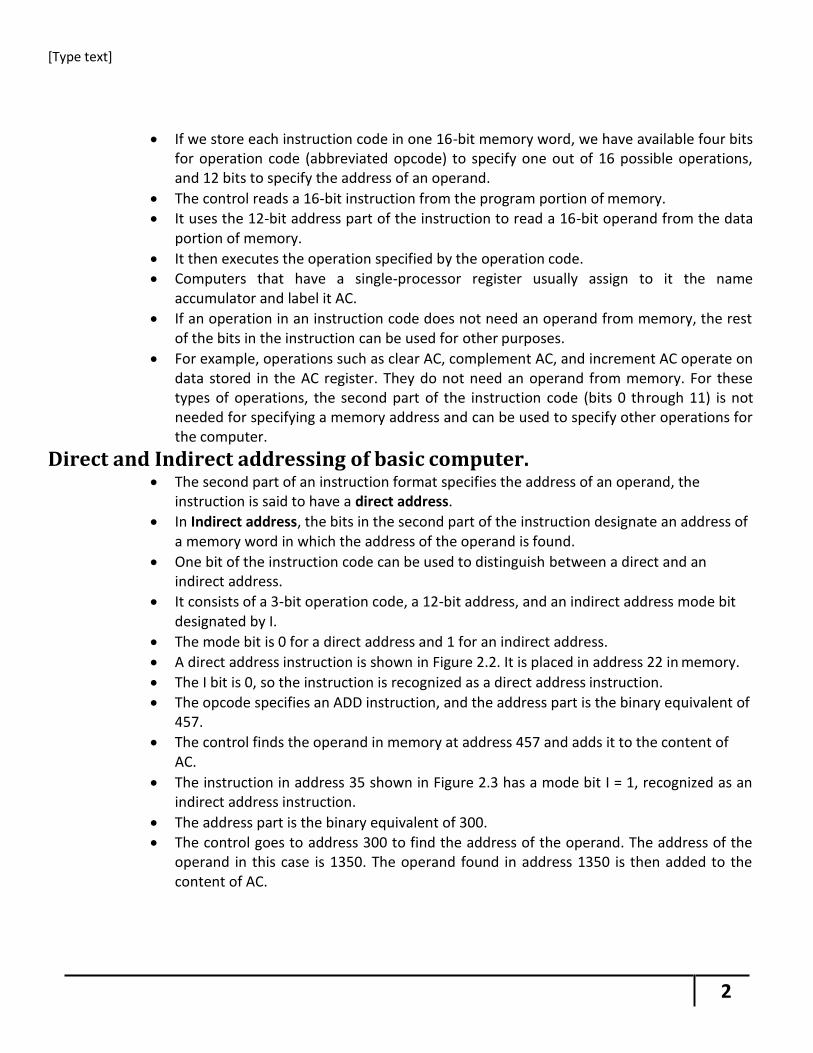
If we store each instruction code in one 16-bit memory word, we have available four bits for operation code (abbreviated opcode) to specify one out of 16 possible operations, and 12 bits to specify the address of an operand.
The control reads a 16-bit instruction from the program portion of memory. It uses the 12-bit address part of the instruction to read a 16-bit operand from the data
portion of memory.
It then executes the operation specified by the operation code. Computers that have a single-processor register usually assign to it the name
accumulator and label it AC.
If an operation in an instruction code does not need an operand from memory, the rest of the bits in the instruction can be used for other purposes.
For example, operations such as clear AC, complement AC, and increment AC operate on data stored in the AC register. They do not need an operand from memory. For these types of operations, the second part of the instruction code (bits 0 through 11) is not needed for specifying a memory address and can be used to specify other operations for the computer.
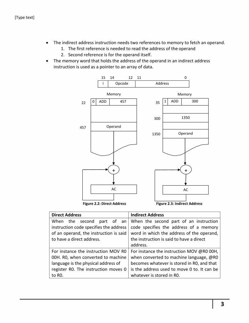
Direct and Indirect addressing of basic computer. The second part of an instruction format specifies the address of an operand, the
instruction is said to have a direct address.
In Indirect address, the bits in the second part of the instruction designate an address of a memory word in which the address of the operand is found.
One bit of the instruction code can be used to distinguish between a direct and an indirect address.
It consists of a 3-bit operation code, a 12-bit address, and an indirect address mode bit designated by I.
The mode bit is 0 for a direct address and 1 for an indirect address.
A direct address instruction is shown in Figure 2.2. It is placed in address 22 in memory.
The I bit is 0, so the instruction is recognized as a direct address instruction.
The opcode specifies an ADD instruction, and the address part is the binary equivalent of 457.
The control finds the operand in memory at address 457 and adds it to the content of AC.
The instruction in address 35 shown in Figure 2.3 has a mode bit I = 1, recognized as an indirect address instruction.
The address part is the binary equivalent of 300. The control goes to address 300 to find the address of the operand. The address of the
operand in this case is 1350. The operand found in address 1350 is then added to the content of AC.
3
[Type text]
22
457
+
AC
457 ADD 0
Operand
35
300
1350
+
AC
300 ADD 1
Operand
1350
The indirect address instruction needs two references to memory to fetch an operand. 1. The first reference is needed to read the address of the operand 2. Second reference is for the operand itself.
The memory word that holds the address of the operand in an indirect address instruction is used as a pointer to an array of data.
15 14 12 11 0
I Opcode Address
Memory Memory
Figure 2.2: Direct Address Figure 2.3: Indirect Address
Direct Address Indirect Address
When the second part of an instruction code specifies the address of an operand, the instruction is said to have a direct address.
When the second part of an instruction code specifies the address of a memory word in which the address of the operand, the instruction is said to have a direct address.
For instance the instruction MOV R0 00H. R0, when converted to machine language is the physical address of register R0. The instruction moves 0 to R0.
For instance the instruction MOV @R0 00H, when converted to machine language, @R0 becomes whatever is stored in R0, and that is the address used to move 0 to. It can be whatever is stored in R0.
4
[Type text]
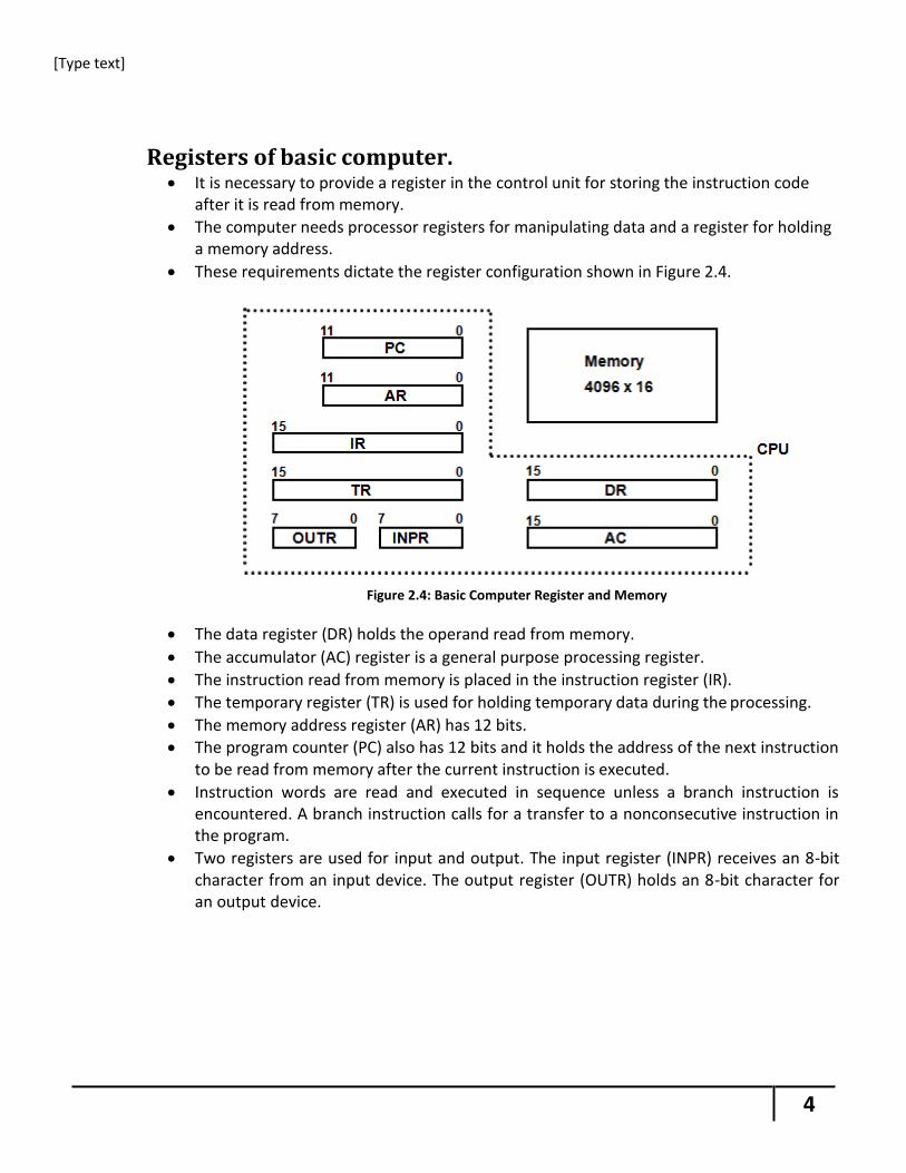
Registers of basic computer. It is necessary to provide a register in the control unit for storing the instruction code
after it is read from memory.
The computer needs processor registers for manipulating data and a register for holding a memory address.
These requirements dictate the register configuration shown in Figure 2.4.
Figure 2.4: Basic Computer Register and Memory
The data register (DR) holds the operand read from memory.
The accumulator (AC) register is a general purpose processing register.
The instruction read from memory is placed in the instruction register (IR).
The temporary register (TR) is used for holding temporary data during the processing.
The memory address register (AR) has 12 bits. The program counter (PC) also has 12 bits and it holds the address of the next instruction
to be read from memory after the current instruction is executed.
Instruction words are read and executed in sequence unless a branch instruction is encountered. A branch instruction calls for a transfer to a nonconsecutive instruction in the program.
Two registers are used for input and output. The input register (INPR) receives an 8-bit character from an input device. The output register (OUTR) holds an 8-bit character for an output device.
5
[Type text]
Register Symbol
Bits Register Name Function
DR 16 Data register Holds memory operand AR 12 Address register Holds address for memory
AC 16 Accumulator Processor register
IR 16 Instruction register Holds instruction code
PC 12 Program counter Holds address of instruction
TR 16 Temporary register Holds temporary data INPR 8 Input register Holds input character
OUTR 8 Output register Holds output character Table 2.1: List of Registers for Basic Computer
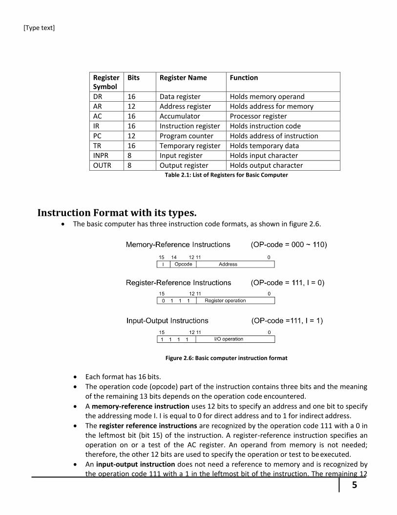
Instruction Format with its types. The basic computer has three instruction code formats, as shown in figure 2.6.
Each format has 16 bits.
Figure 2.6: Basic computer instruction format
The operation code (opcode) part of the instruction contains three bits and the meaning of the remaining 13 bits depends on the operation code encountered.
A memory-reference instruction uses 12 bits to specify an address and one bit to specify the addressing mode I. I is equal to 0 for direct address and to 1 for indirect address.
The register reference instructions are recognized by the operation code 111 with a 0 in the leftmost bit (bit 15) of the instruction. A register-reference instruction specifies an operation on or a test of the AC register. An operand from memory is not needed; therefore, the other 12 bits are used to specify the operation or test to be executed.
An input-output instruction does not need a reference to memory and is recognized by the operation code 111 with a 1 in the leftmost bit of the instruction. The remaining 12
6
[Type text]
bits are used to specify the type of input-output operation or test performed.
Basic working principle of the Control Unit with timing diagram.
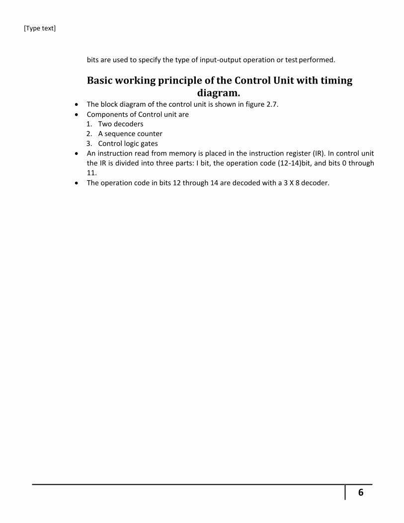
The block diagram of the control unit is shown in figure 2.7.
Components of Control unit are 1. Two decoders 2. A sequence counter 3. Control logic gates
An instruction read from memory is placed in the instruction register (IR). In control unit the IR is divided into three parts: I bit, the operation code (12-14)bit, and bits 0 through 11.
The operation code in bits 12 through 14 are decoded with a 3 X 8 decoder.
7
[Type text]
Figure 2.7: Control unit of basic computer
Bit-15 of the instruction is transferred to a flip-flop designated by the symbol I. The eight outputs of the decoder are designated by the symbols D0 through D7. Bits 0
through 11 are applied to the control logic gates. The 4‐bit sequence counter can count in binary from 0 through 15.The outputs of counter are decoded into 16 timing signals T0
through T15. The sequence counter SC can be incremented or cleared synchronously. Most of the
time, the counter is incremented to provide the sequence of timing signals out of 4 X 16 decoder. Once in awhile, the counter is cleared to 0, causing the next timing signal to be T0.
As an example, consider the case where SC is incremented to provide timing signals T0,
T1, T2, T3 and T4 in sequence. At time T4, SC is cleared to 0 if decoder output D3 is active. This is expressed symbolically by the statement
D3T4: SC ← 0 Timing Diagram:
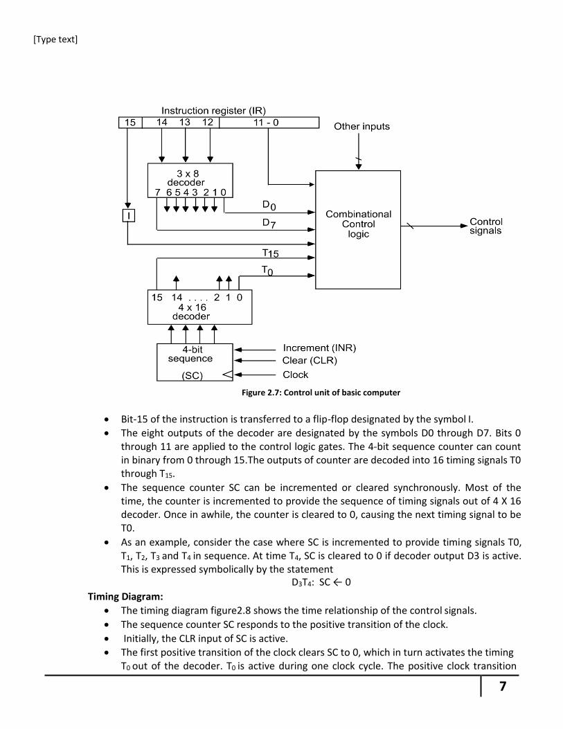
The timing diagram figure2.8 shows the time relationship of the control signals.
The sequence counter SC responds to the positive transition of the clock.
Initially, the CLR input of SC is active. The first positive transition of the clock clears SC to 0, which in turn activates the timing
T0 out of the decoder. T0 is active during one clock cycle. The positive clock transition
8
[Type text]
Clock
0
1
2
3
4
3
SC
labeled T0 in the diagram will trigger only those registers whose control inputs are connected to timing signal T0.
SC is incremented with every positive clock transition, unless its CLR input is active.
This procedures the sequence of timing signals T0, T1, T2, T3 and T4, and so on. If SC is not cleared, the timing signals will continue with T5, T6, up to T15 and back to T0.
T0 T1 T2 T3 T4 T0
T
T
T
T
T
D
CLR
Figure 2.8: Example of control timing signals
The last three waveforms shows how SC is cleared when D3T4 = 1. Output D3 from the
operation decoder becomes active at the end of timing signal T2. When timing signal T4
becomes active, the output of the AND gate that implements the control function D3T4
becomes active.
This signal is applied to the CLR input of SC. On the next positive clock transition the
counter is cleared to 0. This causes the timing signal T0 to become active instead of T5
that would have been active if SC were incremented instead of cleared.
9
[Type text]
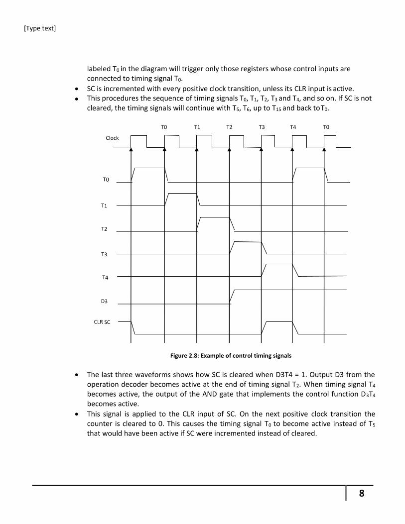
Instruction cycle. A program residing in the memory unit of the computer consists of a sequence of
instructions. In the basic computer each instruction cycle consists of the following phases: 4. Fetch an instruction from memory. 5. Decode the instruction. 6. Read the effective address from memory if the instruction has an indirect address. 7. Execute the instruction.
After step 4, the control goes back to step 1 to fetch, decode and execute the nex instruction.
This process continues unless a HALT instruction is encountered.
Figure 2.9: Flowchart for instruction cycle (initial configuration)
The flowchart presents an initial configuration for the instruction cycle and shows how the control determines the instruction type after the decoding.
If D7 = 1, the instruction must be register-reference or input-output type. If D7 = 0, the operation code must be one of the other seven values 110, specifying a memory- reference instruction. Control then inspects the value of the first bit of the instruction, which now available in flip-flop I.
If D7 = 0 and I = 1, we have a memory-reference instruction with an indirect address. It is then necessary to read the effective address from memory.
The three instruction types are subdivided into four separate paths. The selected
10
[Type text]
operation is activated with the clock transition associated with timing signal T3.This can be symbolized as follows:
D’7 I T3: AR M [AR] D’7 I’ T3: Nothing D7 I’ T3: Execute a register-reference instruction D7 I T3: Execute an input-output instruction
When a memory-reference instruction with I = 0 is encountered, it is not necessary to do anything since the effective address is already in AR.
However, the sequence counter SC must be incremented when D’7 I T3 = 1, so that the execution of the memory-reference instruction can be continued with timing variable T4.
A register-reference or input-output instruction can be executed with the click associated with timing signal T3. After the instruction is executed, SC is cleared to 0 and control returns to the fetch phase with T0 =1. SC is either incremented or cleared to 0 with every positive clock transition.
Register reference instruction. When the register-reference instruction is decoded, D7 bit is set to 1.
Each control function needs the Boolean relation D7 I' T3
15 12 11 0
0 1 1 1 Register Operation
There are 12 register-reference instructions listed below: r: SC0 Clear SC
CLA rB11: AC 0 Clear AC
CLE rB10: E 0 Clear E
CMA rB9: AC AC’ Complement AC
CME rB8: E E’ Complement E
CIR rB7: AC shr AC, AC(15) E, E AC(0) Circular Right
CIL rB6: AC shl AC, AC(0) E, E AC(15) Circular Left
INC rB5: AC AC + 1 Increment AC
SPA rB4: if (AC(15) = 0) then (PC PC+1) Skip if positive
SNA rB3: if (AC(15) = 1) then (PC PC+1 Skip if negative
SZA rB2: if (AC = 0) then (PC PC+1) Skip if AC is zero
SZE rB1: if (E = 0) then (PC PC+1) Skip if E is zero
HLT rB0: S 0 (S is a start-stop flip-flop) Halt computer
These 12 bits are available in IR (0-11). They were also transferred to AR during time T2.
These instructions are executed at timing cycle T3.
The first seven register-reference instructions perform clear, complement, circular shift, and increment microoperations on the AC or E registers.
The next four instructions cause a skip of the next instruction in sequence when

11
[Type text]
condition is satisfied. The skipping of the instruction is achieved by incrementing PC. The condition control statements must be recognized as part of the control conditions.
The AC is positive when the sign bit in AC(15) = 0; it is negative when AC(15) = 1. The content of AC is zero (AC = 0) if all the flip-flops of the register are zero.
The HLT instruction clears a start-stop flip-flop S and stops the sequence counter from counting. To restore the operation of the computer, the start-stop flip-flop must be set manually.
Memory reference instructions. When the memory-reference instruction is decoded, D7 bit is set to 0.
15 14 12 11 0
I 000~110 Address
The following table lists seven memory-reference instructions.
Symbol Operation Decoder
Symbolic Description
AND D0 AC AC M[AR]
ADD D1 AC AC + M[AR], E Cout
LDA D2 AC M[AR]
STA D3 M[AR] AC
BUN D4 PC AR
BSA D5 M[AR] PC, PC AR + 1
ISZ D6 M[AR] M[AR] + 1, if M[AR] + 1 = 0 then PC PC+1
The effective address of the instruction is in the address register AR and was placed
there during timing signal T2 when I = 0, or during timing signal T3 when I = 1. The execution of the memory-reference instructions starts with timing signal T4.
AND to AC
This is an instruction that performs the AND logic operation on pairs of bits in AC and the memory word specified by the effective address. The result of the operation is transferred to AC.
D0T4: DRM[AR] D0T5: AC AC DR, SC 0
ADD to AC
This instruction adds the content of the memory word specified by the effective address to the value of AC. The sum is transferred into AC and the output carry Cout is transferred to the E (extended accumulator) flip-flop.
D1T4: DR M[AR] D1T5: AC AC + DR, E Cout, SC 0
12
[Type text]
LDA: Load to AC This instruction transfers the memory word specified by the effective address to AC.
D2T4: DR M[AR] D2T5: AC DR, SC 0
STA: Store AC This instruction stores the content of AC into the memory word specified by the effective address.
D3T4: M[AR] AC, SC 0 BUN: Branch Unconditionally
This instruction transfers the program to instruction specified by the effective address. The BUN instruction allows the programmer to specify an instruction out of sequence and the program branches (or jumps) unconditionally.
D4T4: PC AR, SC 0 BSA: Branch and Save Return Address
This instruction is useful for branching to a portion of the program called a subroutine or procedure. When executed, the BSA instruction stores the address of the next instruction in sequence (which is available in PC) into a memory location specified by the effective address.
M[AR] PC, PC AR + 1
M[135] 21, PC 135 + 1 = 136
Figure2.10: Example of BSA instruction execution
It is not possible to perform the operation of the BSA instruction in one clock cycle when we use the bus system of the basic computer. To use the memory and the bus properly, the BSA instruction must be executed with a sequence of two microoperations:
D5T4: M[AR] PC, AR AR + 1
D5T5: PC AR, SC 0 ISZ: Increment and Skip if Zero
These instruction increments the word specified by the effective address, and if the incremented value is equal to 0, PC is incremented by 1. Since it is not possible to
13
[Type text]
increment a word inside the memory, it is necessary to read the word into DR, increment DR, and store the word back into memory.
D6T4: DR M[AR]
D6T5: DR DR + 1 D6T4: M[AR] DR, if (DR = 0) then (PC PC + 1), SC 0
Control Flowchart
Figure 2.11: Flowchart for memory-reference instructions
14
[Type text]
Input-output configuration of basic computer. A computer can serve no useful purpose unless it communicates with the external
environment.
To exhibit the most basic requirements for input and output communication, we will use a terminal unit with a keyboard and printer.
Figure 2.12: Input-output configuration
The terminal sends and receives serial information and each quantity of information has eight bits of an alphanumeric code.
The serial information from the keyboard is shifted into the input register INPR.
The serial information for the printer is stored in the output register OUTR. These two registers communicate with a communication interface serially and with the
AC in parallel.
The transmitter interface receives serial information from the keyboard and transmits it to INPR. The receiver interface receives information from OUTR and sends it to the printer serially.
The 1-bit input flag FGI is a control flip-flop. It is set to 1 when new information is available in the input device and is cleared to 0 when the information is accepted by the computer.
The flag is needed to synchronize the timing rate difference between the input device and the computer.
The process of information transfer is as follows:
The process of input information transfer: Initially, the input flag FGI is cleared to 0. When a key is struck in the keyboard, an 8-bit
alphanumeric code is shifted into INPR and the input flag FGI is set to 1.
As long as the flag is set, the information in INPR cannot be changed by striking another key. The computer checks the flag bit; if it is 1, the information from INPR is transferred in parallel into AC and FGI is cleared to 0.
15
[Type text]
Once the flag is cleared, new information can be shifted into INPR by striking another key.
The process of outputting information: The output register OUTR works similarly but the direction of information flow is
reversed.
Initially, the output flag FGO is set to 1. The computer checks the flag bit; if it is 1, the information from AC is transferred in parallel to OUTR and FGO is cleared to 0. The output device accepts the coded information, prints the corresponding character, and when the operation is completed, it sets FGO to 1.
The computer does not load a new character into OUTR when FGO is 0 because this condition indicates that the output device is in the process of printing the character.
Input-Output instructions. Input and output instructions are needed for transferring information to and from AC
register, for checking the flag bits, and for controlling the interrupt facility.
Input-output instructions have an operation code 1111 and are recognized by the control when D7 = 1 and I = 1.
The remaining bits of the instruction specify the particular operation. The control functions and microoperations for the input-output instructions are listed
below.
INP AC(0-7) INPR, FGI 0 Input char. to AC
OUT OUTR AC(0-7), FGO 0 Output char. from AC
SKI if(FGI = 1) then (PC PC + 1) Skip on input flag
SKO if(FGO = 1) then (PC PC + 1) Skip on output flag
ION IEN 1 Interrupt enable on
IOF IEN 0 Interrupt enable off Table 2.2: Input Output Instructions
The INP instruction transfers the input information from INPR into the eight low-order bits of AC and also clears the input flag to 0.
The OUT instruction transfers the eight least significant bits of AC into the output register OUTR and clears the output flag to 0.
The next two instructions in Table 2.2 check the status of the flags and cause a skip of the next instruction if the flag is 1.
The instruction that is skipped will normally be a branch instruction to return and check the flag again.
The branch instruction is not skipped if the flag is 0. If the flag is 1, the branch instruction is skipped and an input or output instruction is executed.
The last two instructions set and clear an interrupt enable flip-flop IEN. The purpose of IEN is explained in conjunction with the interrupt operation.
16
[Type text]
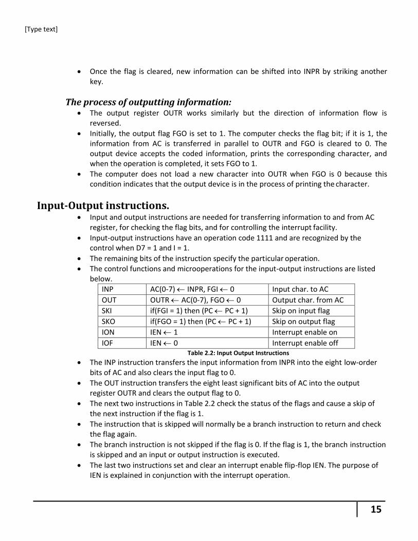
Interrupt Cycle The way that the interrupt is handled by the computer can be explained by means of the
flowchart shown in figure 2.13.
An interrupt flip-flop R is included in the computer.
When R = 0, the computer goes through an instruction cycle.
During the execute phase of the instruction cycle IEN is checked by the control. If it is 0, it indicates that the programmer does not want to use the interrupt, so control
continues with the next instruction cycle.
If IEN is 1, control checks the flag bits. If both flags are 0, it indicates that neither the input nor the output registers are ready
for transfer of information.
In this case, control continues with the next instruction cycle. If either flag is set to 1 while IEN = 1, flip-flop R is set to 1.
At the end of the execute phase, control checks the value of R, and if it is equal to 1, it goes to an interrupt cycle instead of an instruction cycle.
Interrupt Cycle Figure 2.13: Flowchart for interrupt cycle
The interrupt cycle is a hardware implementation of a branch and save return address operation.
The return address available in PC is stored in a specific location where it can be found later when the program returns to the instruction at which it was interrupted. This location may be a processor register, a memory stack, or a specific memory location.
Here we choose the memory location at address 0 as the place for storing the return
17
[Type text]
address. Control then inserts address 1 into PC and clears IEN and R so that no more interruptions
can occur until the interrupt request from the flag has been serviced.
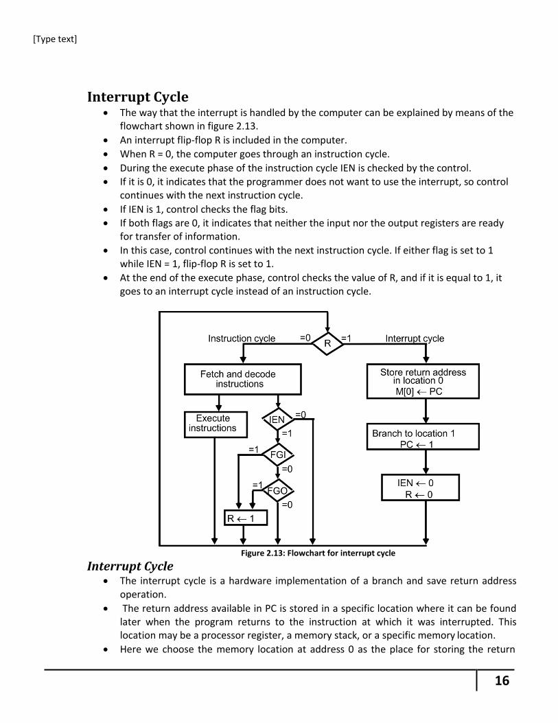
An example that shows what happens during the interrupt cycle is shown in Figure 2.14:
Figure 2.14: Demonstration of the interrupt cycle
Suppose that an interrupt occurs and R = 1, while the control is executing the instruction at address 255. At this time, the return address 256 is in PC.
The programmer has previously placed an input-output service program in memory starting from address 1120 and a BUN 1120 instruction at address 1.
The content of PC (256) is stored in memory location 0, PC is set to 1, and R is cleared to 0.
At the beginning of the next instruction cycle, the instruction that is read from memory is in address 1 since this is the content of PC. The branch instruction at address 1 causes the program to transfer to the input-output service program at address 1120.
This program checks the flags, determines which flag is set, and then transfers the required input or output information. Once this is done, the instruction ION is executed to set IEN to 1 (to enable further interrupts), and the program returns to the location where it was interrupted.
The instruction that returns the computer to the original place in the main program is a branch indirect instruction with an address part of 0. This instruction is placed at the end of the I/O service program.
The execution of the indirect BUN instruction results in placing into PC the return address from location 0.
18
[Type text]
Register transfer statements for the interrupt cycle The flip-flop is set to 1 if IEN = 1 and either FGI or FGO are equal to 1. This can happen
with any clock transition except when timing signals T0, T1 or T2 are active. The condition for setting flip-flop R= 1 can be expressed with the following register
transfer statement: T0T1T2 (IEN) (FGI + FGO): R 1
The symbol + between FGI and FGO in the control function designates a logic OR
operation. This is AND with IEN and T0T1 T2 . The fetch and decode phases of the instruction cycle must be modified and Replace T0,
T1, T2 with R'T0, R'T1, R'T2
Therefore the interrupt cycle statements are :
RT0: AR 0, TR PC RT1: M[AR] TR, PC 0 RT2: PC PC + 1, IEN 0, R 0, SC 0
During the first timing signal AR is cleared to 0, and the content of PC is transferred to the temporary register TR.
With the second timing signal, the return address is stored in memory at location 0 and PC is cleared to 0.
The third timing signal increments PC to 1, clears IEN and R, and control goes back to T0
by clearing SC to 0.
The beginning of the next instruction cycle has the condition RT0 and the content of PC is equal to 1. The control then goes through an instruction cycle that fetches and executes the BUN instruction in location 1.
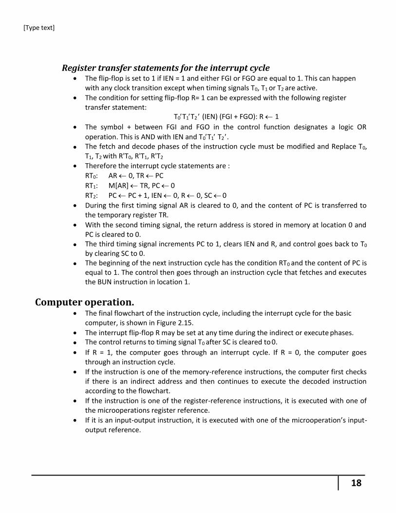
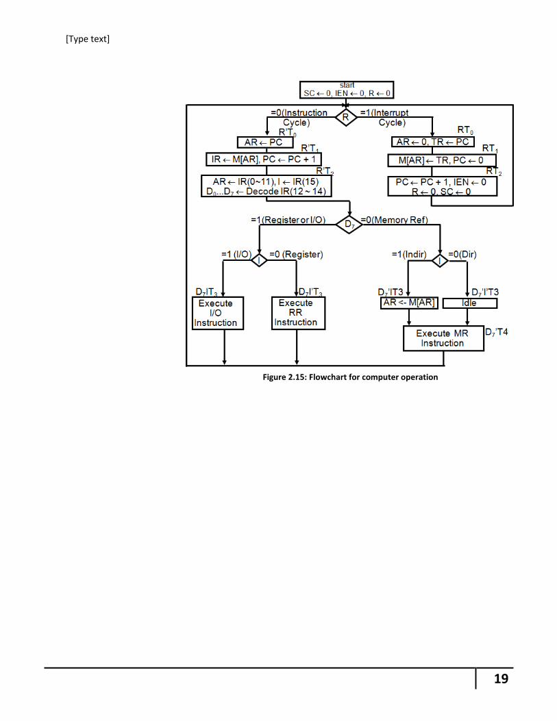
Computer operation. The final flowchart of the instruction cycle, including the interrupt cycle for the basic
computer, is shown in Figure 2.15.
The interrupt flip-flop R may be set at any time during the indirect or execute phases.
The control returns to timing signal T0 after SC is cleared to 0.
If R = 1, the computer goes through an interrupt cycle. If R = 0, the computer goes through an instruction cycle.
If the instruction is one of the memory-reference instructions, the computer first checks if there is an indirect address and then continues to execute the decoded instruction according to the flowchart.
If the instruction is one of the register-reference instructions, it is executed with one of the microoperations register reference.
If it is an input-output instruction, it is executed with one of the microoperation’s input- output reference.
19
[Type text]
Figure 2.15: Flowchart for computer operation
Copyright © 2022 FDOKUMEN