Chapter 2: Register Transfer and Microoperations - Genuine ...
39
Nipun Thapa / Computer Organization Chapter 2: Register Transfer and Microoperations https://genuinenotes.com
-
Upload
khangminh22 -
Category
Documents
-
view
0 -
download
0
Transcript of Chapter 2: Register Transfer and Microoperations - Genuine ...

Nipun Thapa / Computer Organization
Chapter 2:
Register Transfer and Microoperations
https://genuinenotes.com
Register and Register Transfer
Language (RTL)
Resister
A processor register (CPU register) is one of a small set of
data holding places that are part of the computer processor.
A register may hold an instruction, a storage address, or any
kind of data (such as a bit sequence or individual characters).
Some instructions specify registers as part of the instruction.
For example, an instruction may specify that the contents of
two defined registers be added together and then placed in a
specified register.
2 Nipun Thapa / Computer Organization, Unit 2
https://genuinenotes.com
Register and Register Transfer
Language (RTL)
Resister..
A register must be large enough to hold an instruction - for
example, in a 64-bit computer, a register must be 64 bits in
length. In some computer designs, there are smaller registers
- for example, half-registers - for shorter instructions.
Depending on the processor design and language rules,
registers may be numbered or have arbitrary names.
Register is the storage device, inside CPU, of data on which
microoperations are performed.
3 Nipun Thapa / Computer Organization, Unit 2
https://genuinenotes.com
Register and Register Transfer
Language (RTL) Resister..
The operations executed on data stored in registers are calledmicrooperations.
A microoperation is an elementary operation performed on theinformation stored in one or more registers.
The result of the operation may replace the previous binary informationof a register or may be transferred to another register.
Examples of microoperations are shift, count, clear and load.
The internal hardware organization of a digital computer is best definedby specifying:- The set of registers it contains and their function.
- The sequence of microoperations performed on the binary information storedin the registers.
- The control that initiates the sequence of microoperations.
4 Nipun Thapa / Computer Organization, Unit 2
https://genuinenotes.com

Register and Register Transfer
Language (RTL)
Resister..
The language, which is basically used to express the transfer
of data among the registers, is called Register Transfer
Language (RTL).
It is the symbolic notation used to describe the
microoperation transfers among registers.
In such transfer, one of the source or destination should
be register (not necessarily both).
5 Nipun Thapa / Computer Organization, Unit 2
https://genuinenotes.com

Register and Register Transfer
Language (RTL)
Nipun Thapa / Computer Organization, Unit 2 6
Register Transfer Language, RTL, (sometimes called register
transfer notation) is a powerful high level method of
describing the architecture of a circuit.
VHDL code and schematics are often created from RTL.
RTL describes the transfer of data from register to register,
known as microinstructions or microoperations.
Transfers may be conditional.
https://genuinenotes.com
Register Transfer
Nipun Thapa / Computer Organization, Unit 2 7
Computer registers are designated by capital letters.
For example, the register that holds an address for the
memory unit is usually called a memory address register
and is designated by the name MAR.
Other designations for registers are PC (for program
counter), IR (for instruction register, and R1 (for processor
register).
https://genuinenotes.com

Register Transfer
Nipun Thapa / Computer Organization, Unit 2 8
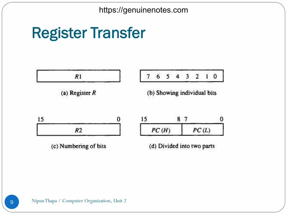
The most common way to represent a register is by a rectangular box with the name of the register inside. Fig (a).
The individual flip-flops in an n-bit register are numbered in sequence from 0 through n-1, starting from 0 in the rightmost position and increasing the numbers toward the left. For e.g. 8-bit register numbered: Fig (b).
The numbering of bits in a 8-bit register can be marked on top of the box. Fig (c).
A 16-bit register is partitioned into two parts in (d). Bits 0 through 7 are assigned the symbol L (for low byte) and bits 8 through 15 are assigned the symbol H (for high byte).
The name of the 16 bit register is PC.
The symbol PC(0—7) or PC(L) refers to the low order byte and PC(8—15) or PC(H) to the high order byte.
https://genuinenotes.com
Register Transfer
Nipun Thapa / Computer Organization, Unit 2 9
https://genuinenotes.com
Register Transfer
Nipun Thapa / Computer Organization, Unit 2 10
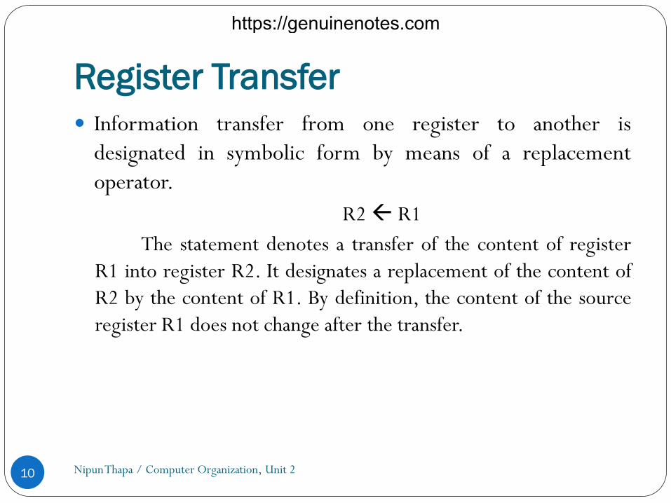
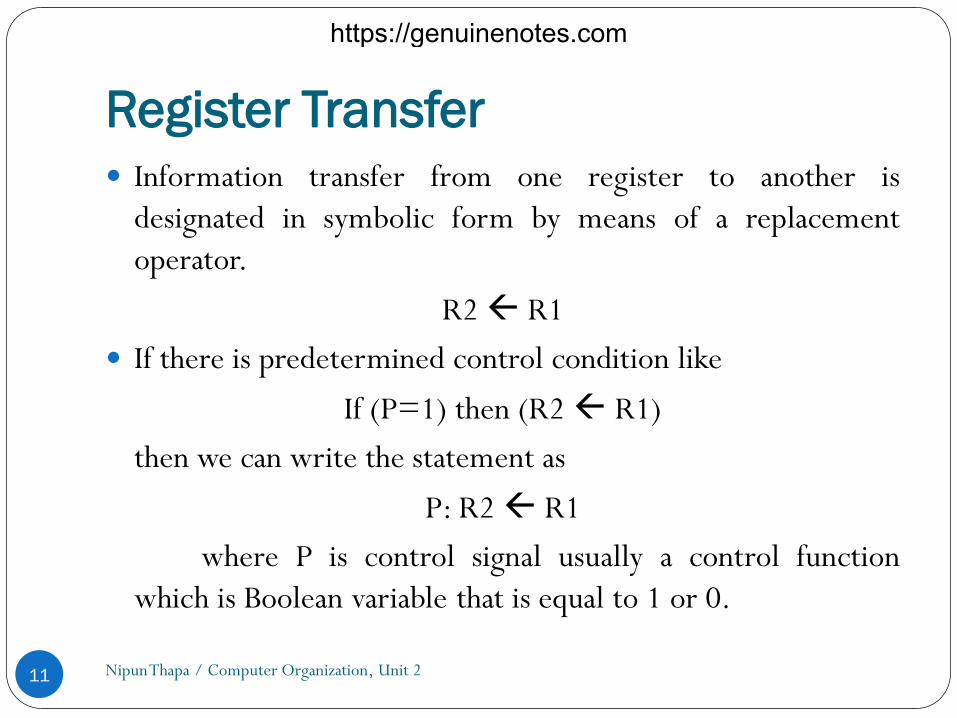
Information transfer from one register to another is
designated in symbolic form by means of a replacement
operator.
R2 R1
The statement denotes a transfer of the content of register
R1 into register R2. It designates a replacement of the content of
R2 by the content of R1. By definition, the content of the source
register R1 does not change after the transfer.
https://genuinenotes.com
Register Transfer
Nipun Thapa / Computer Organization, Unit 2 11
Information transfer from one register to another is
designated in symbolic form by means of a replacement
operator.
R2 R1
If there is predetermined control condition like
If (P=1) then (R2 R1)
then we can write the statement as
P: R2 R1
where P is control signal usually a control function
which is Boolean variable that is equal to 1 or 0.
https://genuinenotes.com
Register Transfer
Nipun Thapa / Computer Organization, Unit 2 12
https://genuinenotes.com
Register Transfer
Nipun Thapa / Computer Organization, Unit 2 13
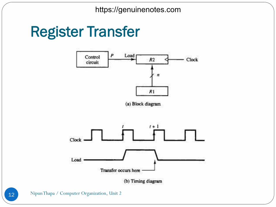
The n outputs of register R1 are connected to the n inputs ofregister R2. The letter n will be used to indicate any number ofbits for the register.
It is assumed that all transfers occur during a clock edgetransition. Even though the control condition such as P becomesactive just after time t, the actual transfer does not occur until theregister is triggered by the next positive transition of the clock attime t + 1.
A comma is used to separate two or more operations that areexecuted at the same time. The statement
T: R2 R1, R1 R2
denotes an operation that exchanges the contents of two registers during one common clock pulse provided that T = 1.
https://genuinenotes.com
Register Transfer
Nipun Thapa / Computer Organization, Unit 2 14
• For example, RTL of fetch cycle can be written as:
T1: MARPC
T2: MBR[MAR]
T3: IRMBR
T4: unspecified; PCPC+1 The notation (T1, T2, T3, T4) represents successive time units. All three units are
of equal duration. A time unit is defined by regularly spaced clock pulses. The operations
performed within this single unit of time are called microoperations. A single time unit can
contain one or more microoperations. Since each microoperation can specifies the transfer
of data into or out of a register, such type is called RTL.
https://genuinenotes.com
Bus and Memory Transfer
Nipun Thapa / Computer Organization, Unit 2 15
Bus
A typical digital computer has many registers, and paths must be provided to transfer information from one register to another.
The number of wires will be excessive if separate lines are used between each register and all other registers in the system.
A more efficient scheme for transferring information between registers in a multiple register configuration is a common bus system.
A bus structure consists of a set of common lines, one for each bit of a register, through which binary information is transferred one at a time.
Control signals determine which register is selected by the bus during each particular register transfer.
https://genuinenotes.com
Bus and Memory Transfer
Nipun Thapa / Computer Organization, Unit 2 16
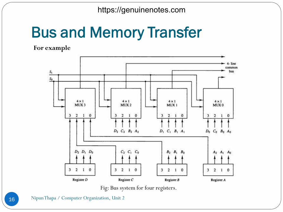
For example
Fig: Bus system for four registers.
https://genuinenotes.com

Bus and Memory Transfer
Nipun Thapa / Computer Organization, Unit 2 17
Here, the bus contain 4 X 1 MUX and each have four data
inputs, 0 through 3, and two selection inputs S1 and S0 .
for example, output 1 of register A is connected to input 0 of
MUX 1 because this input is labeled A1 .
The two selection lines S1 and S0 are connected to the
selection inputs of all four multiplexers.
The selection lines choose the four bits of one register and
transfer them into the four-line common bus.
https://genuinenotes.com
Bus and Memory Transfer
Nipun Thapa / Computer Organization, Unit 2 18
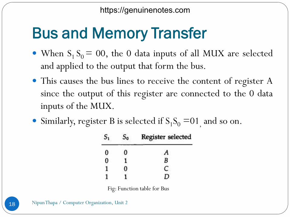
When S1 S0 = 00, the 0 data inputs of all MUX are selected
and applied to the output that form the bus.
This causes the bus lines to receive the content of register A
since the output of this register are connected to the 0 data
inputs of the MUX.
Similarly, register B is selected if S1S0 =01, and so on.
Fig: Function table for Bus
https://genuinenotes.com
Bus and Memory Transfer
Nipun Thapa / Computer Organization, Unit 2 19
In general, a bus system will multiplex k registers of n bits each toproduce an n line common bus.
The number of multiplexers needed to construct the bus is equal to n,the number of bits in each register.
The size of each multiplexer must be k X 1 since it multiplexes k datalines.
For example, a common bus for eight registers of 16 bits each requires16 multiplexers, one for each line in the bus.
Each multiplexer must have eight data input lines and three selectionlines to multiplex one significant bit in the eight registers.
The transfer of information from a bus into one of many destinationregisters can be accomplished by connecting the bus lines to the inputsof all destination registers and activating the load control of theparticular destination register selected.
https://genuinenotes.com
Bus and Memory Transfer
Nipun Thapa / Computer Organization, Unit 2 20
Memory Transfer
The transfer of information from a memory word to the outside environment is called a read operation.
The transfer of new information to be stored into the memory is called a write operation.
A memory word will be symbolized by the letter M. The particular memory word among the many available is selected by the memory address during the transfer.
Consider a memory unit that receives the address from a register, called the address register, symbolized by AR. The data are transferred to another register, called the data register, symbolized by DR. The read operation can be stated as follows:
Read: DR M[AR]
This causes a transfer of information into DR from the memory word M selected by the address in AR.
https://genuinenotes.com

Bus and Memory Transfer
Nipun Thapa / Computer Organization, Unit 2 21
Memory Transfer
The write operation transfer the content of a data register to
a memory word M selected by the address.
Assume that the input data are in register R1 and the address
is in AR.
The write operation can be started symbolically as follows :
Write : M[AR] R1
The cause a transfer of information from R1 into the
memory word M selected by the address in AR.
https://genuinenotes.com
Microoperations
Nipun Thapa / Computer Organization, Unit 2 22
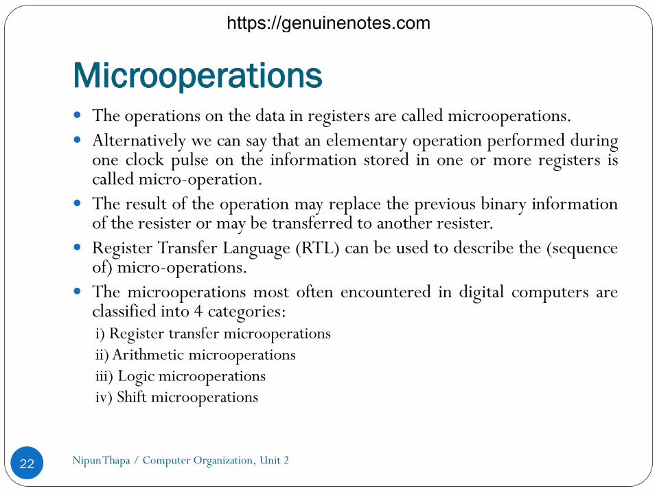
The operations on the data in registers are called microoperations.
Alternatively we can say that an elementary operation performed duringone clock pulse on the information stored in one or more registers iscalled micro-operation.
The result of the operation may replace the previous binary informationof the resister or may be transferred to another resister.
Register Transfer Language (RTL) can be used to describe the (sequenceof) micro-operations.
The microoperations most often encountered in digital computers areclassified into 4 categories:i) Register transfer microoperations
ii) Arithmetic microoperations
iii) Logic microoperationsiv) Shift microoperations
https://genuinenotes.com
Register transfer microoperations
Nipun Thapa / Computer Organization, Unit 2 23
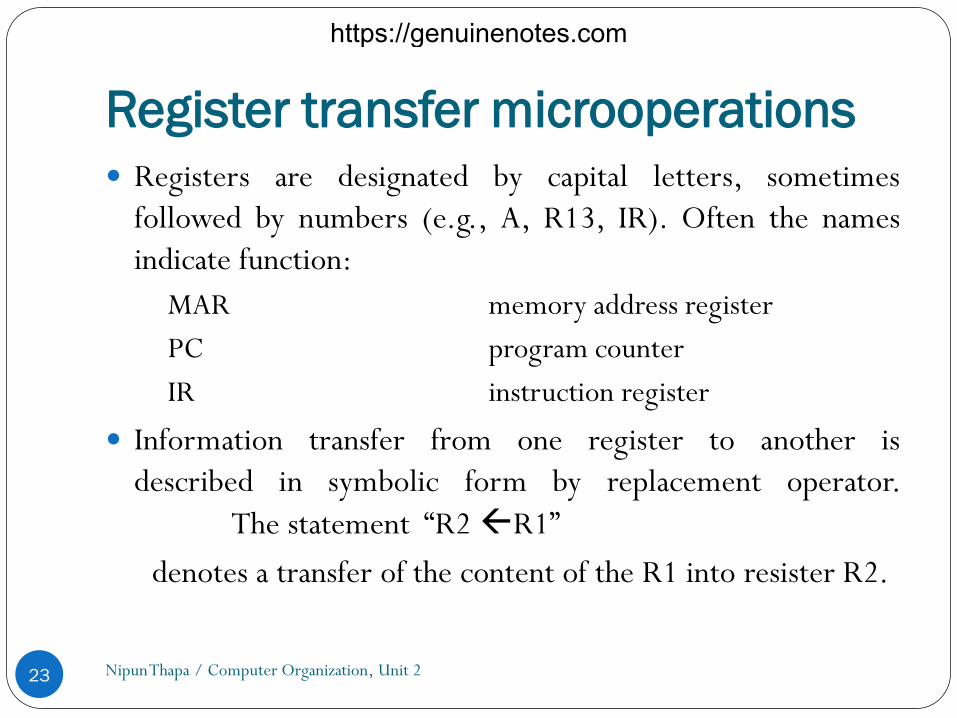
Registers are designated by capital letters, sometimes
followed by numbers (e.g., A, R13, IR). Often the names
indicate function:
MAR memory address register
PC program counter
IR instruction register
Information transfer from one register to another is
described in symbolic form by replacement operator.
The statement “R2 R1”
denotes a transfer of the content of the R1 into resister R2.
https://genuinenotes.com
Control Function
Nipun Thapa / Computer Organization, Unit 2 24
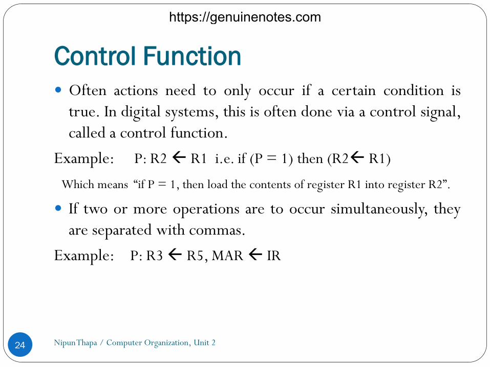
Often actions need to only occur if a certain condition is
true. In digital systems, this is often done via a control signal,
called a control function.
Example: P: R2 R1 i.e. if (P = 1) then (R2 R1)
Which means “if P = 1, then load the contents of register R1 into register R2”.
If two or more operations are to occur simultaneously, they
are separated with commas.
Example: P: R3 R5, MAR IR
https://genuinenotes.com

Arithmetic microoperations
Nipun Thapa / Computer Organization, Unit 2 25
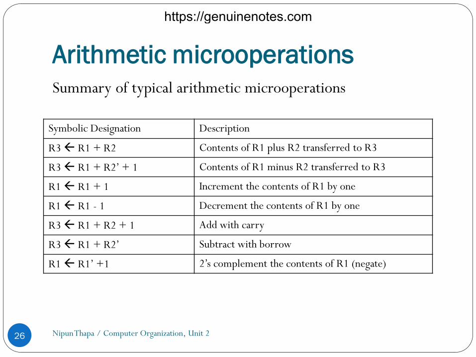
The basic arithmetic microoperations are
Addition
Subtraction
Increment
Decrement
The additional arithmetic microoperations are
Add with carry
Subtract with borrow
Transfer/Load
https://genuinenotes.com
Arithmetic microoperations
Nipun Thapa / Computer Organization, Unit 2 26
Summary of typical arithmetic microoperations
Symbolic Designation Description
R3 R1 + R2 Contents of R1 plus R2 transferred to R3
R3 R1 + R2’ + 1 Contents of R1 minus R2 transferred to R3
R1 R1 + 1 Increment the contents of R1 by one
R1 R1 - 1 Decrement the contents of R1 by one
R3 R1 + R2 + 1 Add with carry
R3 R1 + R2’ Subtract with borrow
R1 R1’ +1 2’s complement the contents of R1 (negate)
https://genuinenotes.com
Logic microoperations
Nipun Thapa / Computer Organization, Unit 2 27
Logic microoperations are bit-wise operations, i.e., they work on
the individual bits of data.
Useful for bit manipulations on binary data and for making logical
decisions based on the bit value.
There are, in principle, 16 different logic functions that can be
defined over two binary input variables.
However, most systems only implement four of these
– AND (/\), OR (\/), XOR (⊕), Complement/NOT
https://genuinenotes.com
Logic microoperations
Nipun Thapa / Computer Organization, Unit 2 28
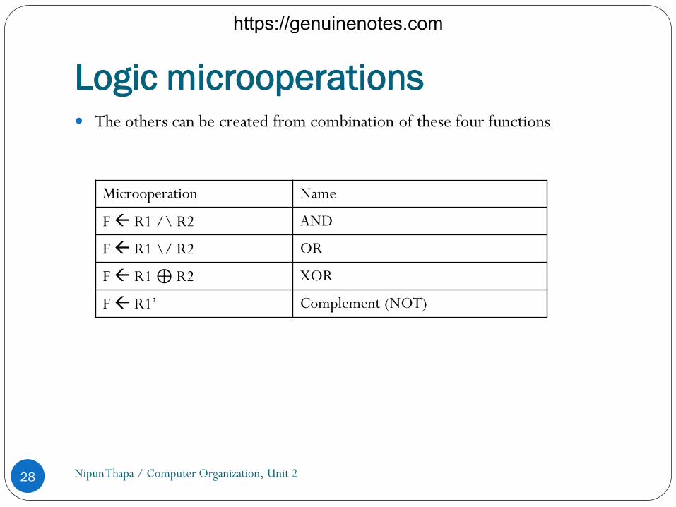
The others can be created from combination of these four functions
Microoperation Name
F R1 /\ R2 AND
F R1 \/ R2 OR
F R1 ⊕ R2 XOR
F R1’ Complement (NOT)
https://genuinenotes.com
Logic microoperations
Nipun Thapa / Computer Organization, Unit 2 29
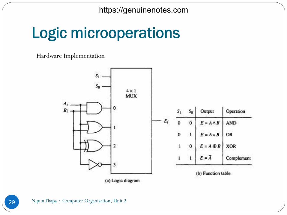
Hardware Implementation
https://genuinenotes.com
Shift microoperations
Nipun Thapa / Computer Organization, Unit 2 30
The operation that changes the adjacent bit position of the
binary values stored in the register is known as shift
microoperation.
They are used for serial transfer of data.
The shift microoperations are classified into 3 types:
i) Logical shift
ii) Circular shift
iii) Arithmetic shift
https://genuinenotes.com

Shift microoperations
Nipun Thapa / Computer Organization, Unit 2 31
i) Logical shift: A logical shift transfer 0 through the
serial input. It can be defined in RTL by:
R←shl R shift-left register R
R←shr R shift-right register R
https://genuinenotes.com
Shift microoperations
Nipun Thapa / Computer Organization, Unit 2 32
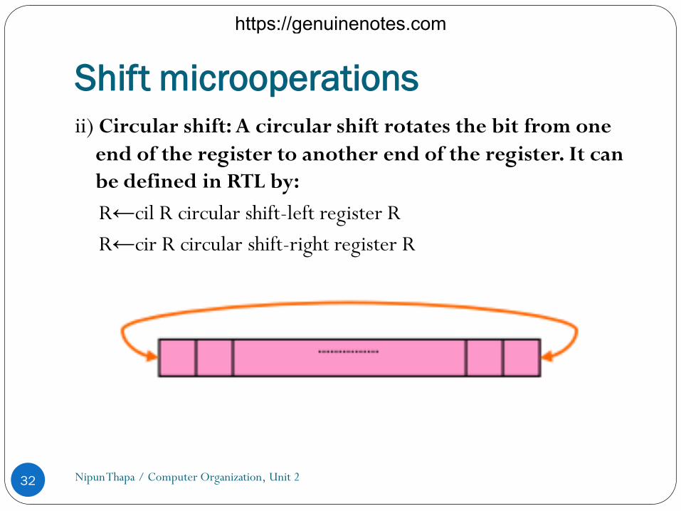
ii) Circular shift: A circular shift rotates the bit from one
end of the register to another end of the register. It can
be defined in RTL by:
R←cil R circular shift-left register R
R←cir R circular shift-right register R
https://genuinenotes.com
Shift microoperations
Nipun Thapa / Computer Organization, Unit 2 33
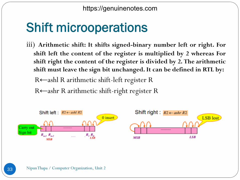
iii) Arithmetic shift: It shifts signed-binary number left or right. For
shift left the content of the register is multiplied by 2 whereas For
shift right the content of the register is divided by 2. The arithmetic
shift must leave the sign bit unchanged. It can be defined in RTL by:
R←ashl R arithmetic shift-left register R
R←ashr R arithmetic shift-right register R
https://genuinenotes.com

Overflow case during arithmetic shift-
left:
Nipun Thapa / Computer Organization, Unit 2 34
If a bit in Rn-1 changes in value after the shift, sign reversal
occurs in the result. This happens if the multiplication by 2
causes an overflow.
Thus, left arithmetic shift operation must be checked for the
overflow: an overflow occurs after an arithmetic shift-left if
before shift Rn-1≠Rn-2.
https://genuinenotes.com
2.4 Arithmetic Logic Shift Unit
Nipun Thapa / Computer Organization, Unit 2 35
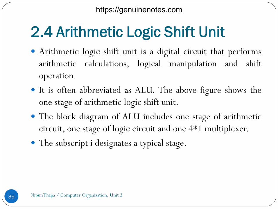
Arithmetic logic shift unit is a digital circuit that performs
arithmetic calculations, logical manipulation and shift
operation.
It is often abbreviated as ALU. The above figure shows the
one stage of arithmetic logic shift unit.
The block diagram of ALU includes one stage of arithmetic
circuit, one stage of logic circuit and one 4*1 multiplexer.
The subscript i designates a typical stage.
https://genuinenotes.com
2.4 Arithmetic Logic Shift Unit
Nipun Thapa / Computer Organization, Unit 2 36
https://genuinenotes.com
2.4 Arithmetic Logic Shift Unit
Nipun Thapa / Computer Organization, Unit 2 37
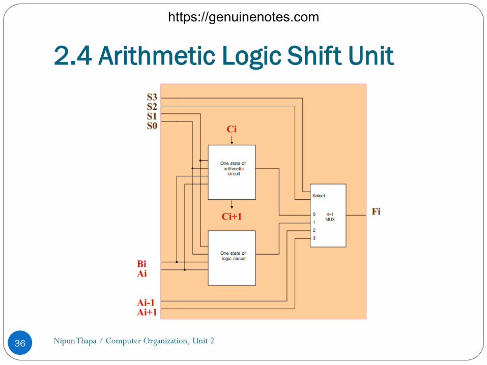
Inputs Ai and Bi are applied to both the arithmetic and logic units. A particular microoperation is selected with inputs S1 and S0.
A 4 x 1 MUX selects the final output.
The two inputs of the MUX are received from the output of the arithmetic circuit and logic circuit.
The other two is Ai-1 for the shift-right operation and Ai+1 for the shift left operation.
The circuit is repeated n times for n-bit ALU.
The output carry Ci+1 is connected to the input carry Cin.
In every stage the circuit specifies 8 arithmetic operations, 4 logical operations and 2 shift operations, where each operation is selected by the five variables S3, S2, S1, S0 and Cin.
https://genuinenotes.com
2.4 Arithmetic Logic Shift Unit
Nipun Thapa / Computer Organization, Unit 2 38
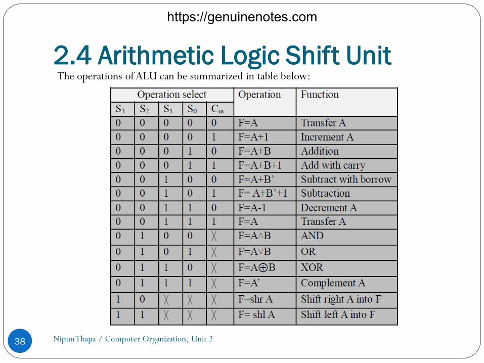
The operations of ALU can be summarized in table below:
https://genuinenotes.com
Finished Unit 2 !!!
Nipun Thapa / Computer Organization, Unit 2 39
https://genuinenotes.com