
1 Fundamentals of Computer Organization and Architecture
175
CHAPTER -1 Fundamentals of Computer Organization and Architecture Objectives are: Basic Structure of Computers Functional Units Basic Operational Concepts Bus Structures Software Memory Locations and Addresses Memory Operations Instructions and Instruction Sequencing Addressing Modes ARM Example Basic I/O Operations Stack Subroutine Calls
-
Upload
khangminh22 -
Category
Documents
-
view
2 -
download
0
Transcript of 1 Fundamentals of Computer Organization and Architecture

CHAPTER -1
Fundamentals of Computer Organization and Architecture
Objectives are: Basic Structure of Computers Functional Units Basic Operational Concepts Bus Structures Software
Memory Locations and Addresses Memory Operations Instructions and Instruction Sequencing Addressing Modes ARM Example Basic I/O Operations Stack Subroutine Calls
Fundamentals of Computer Organization and Architecture
2
1.1 Basic Structure of Computers A Computer is a fast electronic machine that accepts input information in digital form, process the input according to a set of stored instructions (called programs) and outputs the resulting information. Computer Types Based on size, cost, computational power and intended use computers can be classified as below: Personal computer
The most common form of desktop computers is personal computers. It has processing and storage units, visual display, audio output units and a keyboard that can be placed easily on office/home desk. Storage media include hard disk, CD ROM and diskettes.
Notebook Computers These are compact version of personal computer. All components are packaged into a single unit, with the size of thin briefcase.
Workstations Dimensions of workstations are same as that of desktop computers. They have high resolution graphics input/output capability and have more computational power than personal computers.
Mainframes(Enterprise systems) These types of systems are used for business data processing. These have more computing power and storage capacity than workstations.
Servers Contain sizable database storage units and are capable of handling large volumes of requests to access the data. These are widely accessible to the education, business and personal user communities. Requests and responses are usually transported over internet communication facilities.
Supercomputers Super computers are high end powerful computer systems. Used for large scale numerical calculations required in applications such as weather forecasting. India’s first Supercomputer is PARAM 8000 developed by CDAC (Centre for Development of Advanced Computing).
1.1.1 Functional Units A computer consist of mainly five independent functional parts
Input Unit This unit accepts information from human operators with the help of electomechanical devices such as keyboard. Whenever a key is pressed the corresponding letter or digit is automatically translated into its corresponding binary code and transmitted over a cable to either the memory or processor. The received information can be stored in computers memory for later references otherwise it can be immediately used by the ALU circuitry to perform the desired operations.
Memory Unit It is the storage unit of the computer system. The input information is processed based on the stored instructions called programs; these programs are stored in memory unit. The

Fundamentals of Computer Organization and Architecture
3
memory contains a large number of semiconductor storage cells where each cell can store one bit of information. The cells are processed in groups of fixed sizes called words, with a distinct address for each word. Addresses are simply numbers that can identify successive locations. The number of bits in each word determines word length of the computer (16 to 64 bits). Memory units are mainly classified into two types: Primary Memory
It is a fast memory operating at electronic speeds. Programs are stored in this memory during their execution period. Primary memory is divided into two types: o RAM(Random Access Memory)
It is a volatile memory that means the contents will lost when the power is switched off. RAM can again be divided into two types. Static Memory(SRAM)
Memories that consist of circuits that are capable of retaining their states as long as the power is applied are known as static memories. These memories are designed by using transistors and inverters.
Dynamic Memory(DRAM) These are less expensive RAMs. The cost of static RAMs are high because of the usage of the several transistors. Dynamic RAMs are implemented with the help of a capacitor and a single transistor. Such cells don’t retain their state indefinitely hence they are called dynamic RAMs.
o ROM(Read Only Memory) This is one of the major types of memory using personnel computers. ROM is a type of memory that normally can only be read as opposed to RAM which can be both read and written. It is a non- volatile memory that is contents will retain even when the power is switched off. ROM can again be divided into three types: Programmable ROM(PROM)
This is a type of ROM that can be programmed using special equipment; it can be written to, but only once. This is useful for companies that make their own ROMs from software they write, because when they change their code they can create new PROMs without requiring expensive equipment. This is similar to the way a CD-ROM recorder works by letting you "burn" programs onto blanks once and then letting you read from them many times. In fact, programming a PROM is also called burning, just like burning a CD-R, and it is comparable in terms of its flexibility.
Erasable Programmable ROM(EPROM) An EPROM is a ROM that can be erased and reprogrammed. A little glass window is installed in the top of the ROM package, through which you can actually see the chip that holds the memory. Ultraviolet light of a specific frequency can be shined through this window for a specified period of time, which will erase the EPROM and allow it to be reprogrammed again. Obviously this is much more useful than a regular PROM, but it does require the erasing light. Continuing the "CD" analogy, this technology is analogous to a reusable CD-RW.

Fundamentals of Computer Organization and Architecture
4
Electrically Erasable Programmable ROM(EEPROM)
The next level of erasability is the EEPROM, which can be erased under software control. This is the most flexible type of ROM, and is now commonly used for holding BIOS programs. When you hear reference to a "flash BIOS" or doing a BIOS upgrade by "flashing", this refers to reprogramming the BIOS EEPROM with a special software program. Here we are blurring the line a bit between what "read-only" really means, but remember that this rewriting is done maybe once a year or so, compared to real read-write memory (RAM) where rewriting is done often many times per second.
Secondary Memory This memory is used when large amount of data and programs have to be stored. Compared to the primary memory these are cheaper but performs at low speed. Examples are CD ROMS, Magnetic disk, USB drives etc.
Fig 1.1: Classification of Memories Arithmetic and Logic unit
This is the main part of the processing unit of a computer. The desired operations are performed by this unit. Arithmetic and logic operations can be separated with the help of a mode selector. When the mode selector bit is zero it performs arithmetic operations and performs logical operations when the bit is one. To perform the operation the required operands have to be bringing into the processor, where they are stored in registers.
Control unit This is one of another core part of a processing unit of a computer. It is known as the nerve centre of a computer system. It coordinates the operation of all other units in computer system. It sends the control signals to other units and senses their states. Example of control signals are read, write etc.
Output unit The processed results are sending to the outside world through output device. Example: Printer.
Computer Memory
Primary Memory
Secondary Memory
RAM ROM
SRAM DRAM EEPROM EPROM PROM

Fundamentals of Computer Organization and Architecture
5
Fig 1.2: Basic Functional units of a computer 1.1.2 Basic Operational Concepts
In order to execute an operation in a processor the required instructions have to be brought out from the memory to the processor. Transfers between memory and processor are started by sending the address of the memory location to be accessed to the memory unit and issuing the appropriate control signals. Then the data are transferred to or from the memory. The following figure shows the connection between the memory and the processor.
Fig 1.3: Connection between the processor and main memory
Memory
Output Control
I/O Processor
Arithmetic Input and
logic Interconnection
network
n general purpose registers
MDR Control
ALU
MAR
PC
IR
Main Memory
R0
R1 . . . .
Rn-1
Processor

Fundamentals of Computer Organization and Architecture
6
Memory Address Register (MAR) and Memory Data Register (MDR) are the two registers which are facilitating the communication between the processor and memory. In order to read an information from memory the address of the memory location in which the information is residing have to be put in MAR and a Read control signal will be sent to memory unit. When the memory unit sees the address in address line of the bus and read signal in control line of the bus memory will start the read operation from the concerned address and the result will be sent to the MDR. From there the information can be transferred to any other registers inside the processor through internal processor bus. Similarly for Write operation initially the data to be written into the memory has to be placed in MDR and the address in which the desired information have to be kept in memory will be placed in MAR and a Write control signal will be sent to the memory unit. When the memory unit sees the address, data and write signal in the external memory bus it will start the corresponding write operation. Other than MAR and MDR few registers like PC(Program Counter), IR(Instruction Register) and some general purpose registers R0, R1,....Rn-1 are there within the processor unit. PC is a register which holds the address of the next instruction to be fetched. Initially PC will be assigned by the starting program address and after fetching of each instruction it will be incremented by a size of word byte. IR is a register which holds the decoded instruction to be executed. Normal execution of programs may be pre-empted if some device requires urgent servicing. In order to deal with the situation immediately the normal execution of the current program must be interrupted. To do this the device raises an interrupt signal. An interrupt is nothing but it is a request from an I/O device for service by the processor. The processor executes an interrupt service routine (ISR) to service the same. Before servicing an interrupt the current state of the processor must be saved in memory locations. After ISR is completed the state of the processor is restored so that the interrupted program may continue.
1.1.3 Bus Structures Different functional units of a computer can be connected using a structure called bus system structure. There are external bus structures and internal bus structures. Bus interface between memory and processor is called external memory bus and bus structure inside the processor is called internal bus structures. Bus consists of three lines of carries, one for holding address, one for holding data and one for carrying control information.
Fig 1.4: Bus Structure
Control Bus (Read, Write etc)
Data Bus
Address Bus

Fundamentals of Computer Organization and Architecture
7
Fig 1.5: External processor bus Fig 1.6: Internal processor bus
Bus Structures can be classified into two: Single bus structure
Only two units can actively participate at a time, that is only one transfer takes place at a time. Advantages Low cost Flexibility for attaching peripheral devices Disadvantages Only one transfer at a time
Multiple bus structure It contains multiple buses, so that more than one transfer can takes place. Advantages More concurrency in operations. Better performance Disadvantages Increased cost
The different units connected to the processor are having different speeds. These timing differences can be smoothened by including buffer registers with the devices to hold information during transfers. Once the buffer is full, the device can start the operation without further intervention by the bus and the processor.
Fig 1.7: Single bus structure
PC
IR R0
R1
Rn
.
.
Input
Output
Memory
Processor
Memory
Processor
Control Bus (Read, Write etc)
Data Bus
Address Bus

Fundamentals of Computer Organization and Architecture
8
1.1.4 Software A sequence of program instructions is known by the term software. Software can be classified into two types: Application Software
Application software is a computer program designed to perform a group of coordinated functions, tasks, or activities for the benefit of the user. Example: MS-office packages, MP3 media player etc.
System Software These are responsible for the coordination of all activities in a computing system. Most of the applications may run only with the help of installed system software programs. Example: Compiler, Assembler, Text editor.
Operating system is one of the important system software. OS is actually the interface between hardware and the user. An application program is usually written in a high level programming language. It will be translated into machine language program (languages which consist of only zeros and ones) by using system software known as compiler. It will be stored on disk. In order to execute this program, it has to be transferred to memory. While execution, if it needs any data file, the program requests the OS to transfer the data file from the disk into memory. OS perform this task and passes execution control back to the application program. Execution control passes back and forth between the application program and the OS routines.
Fig 1.8: User program and OS routine sharing of the processor 1.2 Memory Locations and Addresses
Operands and instructions are stored in computers memory. Memory is organized as a set of storage cells; each cell can store a value of 0 or 1. Single bit can represent a very small amount of information; they are operated in terms of groups of fixed size bits. These groups are termed as words. The size of the group (n bit sized block – size is n) is termed as word length. Usually, the word length of the computer can range from 16 to 64 bits. Group of 8bits is known as byte. Each word is assigned with distinct addresses, as shown in below figure.
Printer
Disk
OS routines
Program
t 0 t 1 t 2 t 3 t 4 t 5 Time

Fundamentals of Computer Organization and Architecture
9
Fig 1.9: Memory Address Note 16 bit address: - Creates an address space of 216 addresses 32 bit address: - Creates an address space of 232 addresses Byte Addressability Basic information quantities are, bit, byte and word. Byte is of size 8 bit (always this is constant).Word length may from 16 to 64 bits. So normally distinct addresses will be assigned to each byte location. This is known as byte addressability. For example, if word length is 16 bits, successive words are located at addresses 0 and 4. If 32 bits, successive words will be located at addresses 0, 4, 8 ..., with each word consisting of four bytes. Big-Endian and Little-Endian Assignments Byte addresses can be assigned across words in two ways: Big – Endian
Lower byte addresses are used for most significant bytes of the word. Little – Endian
Lower byte addresses are used for least significant bytes of the word.
Fig 1.10(a): Big- Endian Assignment Fig 1.10(b): Little- Endian Assignment
0 1 2 3
4 5 6 7
.
.
.
.
. 2K-4 2K-3 2K-2 2K-1
0 4 2K-4
Word Byte Address Address
3 2 1 0
7 6 5 4
.
.
.
.
. 2K-1 2K-2 2K-3 2K-4
0 4 2K-4
Word Byte Address Address
n bits First word Second word Usually address ranges from 0 to 2k-1 Last word
. . . .

Fundamentals of Computer Organization and Architecture
10
Word Alignment The words are said to be aligned in memory if they begin at a byte address that is a multiple of number of bytes in a word. The number of bytes in a word is power of 2. Example If word length is 16 bits, aligned words begin at byte addresses 0, 4, 8.... If word length is 64 bits, aligned words begin at byte addresses 0,8,16.... Words are said to have unaligned addresses if the words begin at arbitrary byte address. Accessing Numbers, Characters and Character Strings A number can be accessed in the memory by specifying its word address. Individual characters can be accessed by their byte address. Character Strings can be of variable length. The beginning of the string is indicated by giving the address of the byte containing the first character. A successive byte location contains successive characters of the string. End of string (a special control character) can be used as the last character in the string.
1.3 Memory Operations
To execute an instruction, the words containing the instruction have to be brought out to the processor from memory. Operands and results also have to be moved in between of main memory and processor. Main operations are: Load(Read or Fetch)
Transfer copy of the contents of a specific memory location to the processor. The memory contents remain unchanged.
Store(Write) It transfers information from processor to memory. It will destroy the earlier content of the memory location. Information can be transferred between processor and memory in terms of bytes or words. One byte or one word can be transferred in a single operation.
1.4 Instructions and Instruction Sequencing
A computer must have instructions capable of performing four type of operations: Data transfer between processor and memory registers Arithmetic and logic operations on data Program sequencing and control I/O transfers
Register- Transfer Notation
Information can be transferred to and fro between memory locations, processor registers and registers with I/O. We can identify a location by a symbolic name. Example
LOC, PLACE, A (Address of memory locations) R0, R1, R5 (Processor register names)
DATA IN, OUT STATUS (I/O Registers) Register- Transfer Examples
R1 [LOC]
1

Fundamentals of Computer Organization and Architecture
11
The contents of the memory location are transferred to processor register R1. Square bracket indicates the contents of the location.
R3 [R1] + [R2] Adds the contents of registers R1 and R2 and places the sum in register R3.The type of notations and are known as register transfer notation. Assembly Language Notation The register transfer notation R1 [LOC] can be notated in assembly language as:
Move LOC, R1 Here the content of LOC is unchanged, R1 will be over written. Similarly,
R3[R1] + [R2] This can be notated in assembly language as
Add R1, R2, R3 Basic Instruction Types
Consider the statement C=A+B. To execute this statement, the operands A and B have to be fetched from memory to the processor. ALU computes the operation and the result will be sent back to memory and stored in location C.
Three Address Instructions Syntax Operation source1, source2, destination Example
Add A, B, C Where, A and B are source operands and C is destination operand. Add is the operation to be performed on operands. Suppose that K bits are needed to specify the memory address of each operand, and then totally 3K bits are needed totally to specify the memory address of all operands in the above sample case. In addition, some bits are needed to denote Add instruction also. Three address instruction is too large to fit in one word for most cases. An alternative approach is to use two address instructions.
Two Address Instructions Syntax Operation source, destination Example
Add A, B Which performs the operation B [A] + [B]. Square bracket indicates the contents of the location specified. That is, it adds the contents of A and B and the result is stored back to B. Here the value of location B will be overwritten. To preserve the value of B, we can go for another instruction Move B, C. It moves the content of B to C, leaving the
2
1 2
Fundamentals of Computer Organization and Architecture
12
contents of location B unchanged. We couldn’t find an alternative approach by using a single two address instruction.
Add A, B Move B, C Add A, C
(Single two (Leave B unchanged) address instruction)
Here, in all instructions we are adopting a scheme such that source operand is specified first then destination operand. This may not be the case with all architectures. In some of the machine instructions, it will follow a scheme of destination first, and then source. There is no uniform scheme for specifying operands. Even two address instructions also, may not be fit into one word for usual word length. Another possibility is to have machine instructions with single operand. These are called One Address Instructions.
One Address Instructions Here one of the register called Accumulator is implicit in all cases. Example
Add A Add the content of memory location A to the content of the accumulator register and places the sum back to accumulator. Question
Represent C[A] + [B] in terms of one address instruction Ans
Load A Add B
Store C Load instruction copies the contents of memory location A into accumulator. Add B, adds the content of B to Accumulator and Store C, and stores the content of accumulator to memory location C. Early computers have designed with only a single accumulator .But now, modern computers are coming with so many general purpose registers (R1, R2,……..Ri,….Rn). To perform an operation, normally the data can store in registers rather than taking from memory, so that faster processing may occur. Instructions size can also be shorten, because register addressing can be done with fewer bits. Means,
32 bit computer 232 memory locations as possible
That is one word location can be identified by a 32 bit address. But for register addressing, consider 32 general purpose registers only 5 bits are needed to identify a register(2n=32, n=5). reduced to
32 bit 5 bits (If register is holding operand in an instruction) Example
Add Ri, Rj Add Ri, Rj,Rk
These types of instructions may normally fit into one word.

Fundamentals of Computer Organization and Architecture
13
Data transfer between different locations Instructions used for data transfer between different locations are Move. Syntax
Move Source, Destination Example Move A, Risame as Load A, Ri
Move Ri, Asame as Store Ri, A Question Write the instruction sequence for C=A+B (suppose that arithmetic operations are allowed only on register operands) Answer
Move A, Ri Move B, Rj
Add Ri , Rj Move Rj, C
Question Write the instruction sequence for C=A+B(suppose that one operand in memory, other in register) Answer
Move A, Ri Add B, Ri
Move Ri, C Zero Address Instructions
Instructions can be used with zero operands in which the locations of all operands are specified implicitly. (It is possible by storing the operands in a structure called pushdown stack).
Instruction Execution and Straight line sequencing This section deals with the flow of execution of a program .Consider a sample memory space for the program C[A] + [B]
Fig 1.11: Program execution
Move A, R0 Add B, R0 Move R0, C
.
.
. . .
. .
i i+4 i+8
A
B
C
Address Contents
3- Instruction program segment
Data for the program
Execution Begins here

Fundamentals of Computer Organization and Architecture
14
Initially PC (Program Counter) contains the address of the next instruction to be executed. In this example initially address i is placed in PC. The processor control circuitry use the information in PC to fetch and execute instructions, one at a time, in the order of increasing addresses. This is called straight line sequencing .While the instruction is being executed, the value of PC will be updated by incrementing 4 bytes, (because here length of instruction is 4 bytes). Instruction execution consists of 2 phases: Instruction Fetch
Instruction is fetched from memory location whose address is in PC. This instruction is placed in IR (Instruction Register).
Instruction Execute Instruction in IR (Instruction Register) is analyzed to see which operation have to be performed by the processor. This may include several operations like fetching of operands from memory (or from processor registers), performing an ALU operation, storing of result into memory etc.
After the execution phase, PC will contain the address of the next instruction to be executed. Then a new instruction fetch phase will begin.
Branching Consider a program of adding a list of n numbers (num1, num2….num n) and stores the result in memory location sum. By straight line sequencing approach, it can be done as follows:
Fig 1.12: Straight Line Sequencing Program for adding ‘n’ numbers Initially the value of first number (Num1) is moved to R0. Then it will be added with Num2 and result is stored in R0.Num3 will be read next and added with R0 (R0 now contains num1+num2+num3).The process will be continued with n numbers. After this, R0 contains a value (Num1+Num2+……Num n).We have to store the result into location Sum. So, we are in need of an instruction,
Move R0, Sum
Move Num1, R0 Add Num2, R0 Add Num 3, R0
.
.
. Add Num n, R0 Move R0, Sum
.
.
. . .
. .
i i+4 i+8
i+4n-4 i+4n
Sum
Num 1
Num 2
Num n

Fundamentals of Computer Organization and Architecture
15
Here, a long list of add instruction is there. To remove this, we are going for a looping concept. The loop is a straight line sequence of instructions executed as many times as needed. It starts at the location Loop and ends at the instruction Branch>0.
Fig 1.13: Using loop to add ‘n’ numbers No of entries in the list (n) is stored at memory location N. After each addition operation this value is decremented by one. This value is a number greater than zero that means again there are numbers to be added to the list. Branch Instruction loads a new value into the program counter .The processor fetches and executes the instructions from these addresses (known as branch target) instead of loading the instruction from address of PC. A conditional branch instruction causes a branch only if the specified condition is not satisfied, PC is incremented in the normal way and the next instruction in sequential address order is fetched and executed.
Condition Codes Whenever a conditional branch instruction is executed, it may require the results of various operations (to check the condition).Processors keeping this information in individual bits called condition code flags. These flags are grouped together in a special processor register called condition code Register or Status register. Four commonly used flags are: N (Negative) Set to 1 if result is negative, otherwise zero. Z (Zero) Set to 1 if result is zero, otherwise cleared to zero. V (Overflow) Set to 1 if arithmetic overflow occur, otherwise cleared to zero. C (Carry) Set to 1 if a carry after the operation, otherwise cleared to zero.
In the above example ,Branch>0 tests the condition code flags N and Z .That is ,the branch is taken only if register R either contain a negative or zero value.
Move N, R1 Clear R0 Determine address of “Next” number and add “Next” number to R0
Decrement R1 Branch>0 Loop Move R0, Sum
. .
n . . . .
Loop
Sum N
Num 1
Num n
Program Loop
Fundamentals of Computer Organization and Architecture
16
1.5 Addressing Modes The different ways in which the location of an operand is specified in an instruction is called as Addressing mode. Generic Addressing Modes Immediate mode Register mode Absolute mode Indirect mode Index mode Base with index Base with index and offset Relative mode Auto-increment mode Auto-decrement mode
Implementation of Variables and Constants Variables
The value can be changed as needed using the appropriate instructions. There are 2 accessing modes to access the variables. They are Register Mode
The operand is the contents of the processor register. The name (address) of the register is given in the instruction.
Absolute Mode (Direct Mode) The operand is in new location. The address of this location is given explicitly in the instruction.
Example MOVE LOC, R2
The above instruction uses the register and absolute mode. The processor register is the temporary storage where the data in the register are accessed using register mode. The absolute mode can represent global variables in the program.
Mode Assembler Syntax Addressing Function Register mode Ri EA=Ri Absolute mode LOC EA=LOC
Where, EA is Effective Address Constants
Address and data constants can be represented in assembly language using Immediate Mode.
Immediate mode The operand is given explicitly in the instruction. Example
Move 200 immediate, R0

Fundamentals of Computer Organization and Architecture
17
It places the value 200 in the register R0.The immediate mode used to specify the value of source operand. In assembly language, the immediate subscript is not appropriate so # symbol is used. It can be re-written as:
Move #200, R0 Assembly Syntax Addressing Function Immediate #value Operand =value Indirection and Pointers
Instruction does not give the operand or its address explicitly. Instead it provides information from which the new address of the operand can be determined. This address is called effective Address (EA) of the operand.
Indirect Mode The effective address of the operand is the contents of a register. We denote the indirection by the name of the register or new address given in the instruction.
Fig 1.14: Indirect mode Address of an operand (B) is stored into R1 register. If we want this operand, we can get it through register R1 (indirection). The register or new location that contains the address of an operand is called the pointer.
Mode Assembler Syntax Addressing Function Indirect Ri, LOC EA=[Ri] or EA=[LOC]
Indexing and Arrays Index Mode
The effective address of an operand is generated by adding a constant value to the contents of a register. The constant value uses either special purpose or general purpose register. We indicate the index mode symbolically as,
X(Ri) Where,
X – denotes the constant value contained in the instruction Ri – It is the name of the register involved
The Effective Address of the operand is, EA=X + [Ri]
The index register R1 contains the address of a new location and the value of X defines an offset (also called a displacement).
Add (R1), R0
. . .
Operand
Add (A), R0 B
Operand

Fundamentals of Computer Organization and Architecture
18
To find operand, 1. First go to Reg R1 (using address)-read the content from R1-1000 2. Add the content 1000 with offset 20 get the result.
1000+20=1020 3. Here the constant X refers to the new address and the contents of index register define
the offset to the operand. 4. The sum of two values is given explicitly in the instruction and the other is stored in
register. Example
Add 20(R1) , R2 (or) EA=>1000+20=1020
Index Mode Assembler Syntax Addressing Function Index X(Ri) EA=[Ri]+X Base with Index (Ri,Rj) EA=[Ri]+[Rj] Base with Index and offset X(Ri,Rj) EA=[Ri]+[Rj] +X
Relative Addressing It is same as index mode. The difference is, instead of general purpose register, here we can use program counter (PC). Relative Mode
The Effective Address is determined by the Index mode using the PC in place of the general purpose register (gpr). This mode can be used to access the data operand. But its most common use is to specify the target address in branch instruction. Example
Branch>0 Loop It causes the program execution to goto the branch target location. It is identified by the name loop if the branch condition is satisfied.
Mode Assembler Syntax Addressing Function Relative X(PC) EA=[PC]+X
Additional Modes There are two additional modes. They are Auto-increment mode
The Effective Address of the operand is the contents of a register in the instruction. After accessing the operand, the contents of this register is automatically incremented to point to the next item in the list.
Mode Assembler Syntax Addressing Function Auto-increment (Ri)+ EA=[Ri];
Increment Ri Auto-decrement mode
The Effective Address of the operand is the contents of a register in the instruction. After accessing the operand, the contents of this register is automatically decremented to point to the next item in the list.

Fundamentals of Computer Organization and Architecture
19
Mode Assembler Syntax Addressing Function Auto-decrement -(Ri) EA=[Ri];
Decrement Ri
1.6 ARM Advanced Risc Machine (ARM) Limited has designed a family of microprocessors. All ARM processors share the same machine instruction set.
Registers, Memory access and Data transfer In ARM architectures, memory is byte addressable using 32 bit addresses. Processor registers are also 32 bits long. In moving of data between processor registers and memory, operand length may be 8 bit (byte) or words (32 bit).Both little Endian and big Endian addressing schemes are supported. Memory is accessed only by Load and Store instructions. All arithmetic and logic instructions operate only on data in processor registers. This arrangement is a basic feature of RISC Architectures. Register Structure There are sixteen 32 bit registers labelled R0 to R15. R0 to R14 are general purpose registers and one is dedicated as a program counter (PC). General purpose registers can hold either memory operands or data operands. The Current Program Status Register (CPSR) or simply status register holds the condition code flags, interrupt disable flags and processor mode bits. as described in the following figure.
Fig 1.15: ARM Register Structure There are 15 additional general purpose registers called the banked registers. They are duplicates of some of the R0 to R14 registers. They are used when the processor switches into supervisor mode.
··
31 R0 R1
0
R14
15General purpose registers
31 0
···
R15 (PC) Program counter
· · ·
31 30 29 28 7 6 4 CPSR
N–Negative Z–Zero C–Carry
V–Overflow Condition code flags
0 Status register Processor mode bits Interrupt disable bits

Fundamentals of Computer Organization and Architecture
20
Memory Access Instructions and addressing modes In ARM, access to memory is provided with only Load and Store instructions. The basic encoding format is shown as in the following figure:
Fig 1.16: ARM instruction format Conditional execution of instructions
Unlike others, in ARM processors all instructions are conditionally executed, depending on the condition specified in the instruction. Instruction is executed only when the condition flag is true. Otherwise the processor proceeds to the next instruction. One of the conditions is used to indicate that the instruction is always executed.
Memory addressing modes For addressing memory operands one of the basic method is generate an EA(Effective Address) of the operand by adding a signed offset to the contents of the base register Rn(which is specified in the instruction).The magnitude of offset may be either an immediate value or the contents of the register Rm. Examples
LDR Rd, [Rn, #offset] It performs the operation Rd [[Rn] +offset] LDR Rd, [Rn, Rm] It performs the operation Rd [[Rn] + [Rm]] If a negative offset is used, Rm must be preceded by a minus sign. An offset of zero doesn’t have to specify explicitly. That is, LDR Rd, [Rn] It performs the operation Rd [[Rn]] A byte operand can be moved by using the Opcode LDRB. Similarly Store has the mnemonics STR and STRB. Example STR Rd, [Rn] It performs the operation [Rn] [Rd] Generally we can define three addressing modes in ARM processors. Pre-indexed mode:
Effective address of the operand is the sum of contents of base register Rn and an offset value.
Pre-indexed with write back mode: It is working in the same way as pre-indexed mode except that effective address is written back to Rn.
Post-indexed mode: The effective address of the operand is the contents of Rn. The offset is then added to this address and the result is written back into Rn.
Condition OP code Rn Rd Other info Rm 31 28 27 20 19 16 15 12 11 4 3 0

Fundamentals of Computer Organization and Architecture
21
Register Move Instructions To copy the contents of register Rm into register Rd, ARM uses the following instruction
MOV Rd, Rm To load an immediate value in the register Rd, the instruction will be
MOV Rd, #immediate value Example
MOV R0, #70 Places the value 70 in register R0.
Arithmetic and Logic Instructions ARM instruction set has a number of arithmetic and logic operations. The operands may be in general purpose registers or may give as an immediate operand. Memory operands are not allowed in these instructions. Arithmetic Instructions
The general format for arithmetic instruction is, OP code Rd, Rn, Rm
Operation specified by the OP code is performed on operands in general purpose registers Rn and Rm. The result is placed in register Rd. Example
ADD R0, R2, R4 Adds the content of R2 and R4 and places the sum in register R0. It performs the operation, R0[R2] + [R4]
ADD R0, R3, #17 Adds the content of R3 and 17 and stores the sum in R0. It performs the operation, R0[R3] +17 The immediate value is contained in the 8 bit field on bits b7-0 of the instruction. The second operand can be shifted or rotated before being used in the instruction. When a shift or rotation is required, it is specified last in the assembly language expression for the instruction. Example
ADD R0, R1, R5, LSL #4 The second operand contained in register R5 is shifted left 4 bit positions and it is then added to the contents of register R1 and sum is placed in Register R0. Two versions of multiply instructions are there. 1. Multiplies the contents of two registers and places the low order 32 bits of the
product in a third register. Higher order bits of the product, if any, are discarded. MUL R0, R1, R2
It performs the operation, R0 [R1] * [R2] 2. Second version called Multiply Accumulate specifies a fourth register whose
contents are added to the product before storing the result in the destination register. MLA R0, R1, R2, R3
It performs the operation, R0 [R1] * [R2] + [R3] This method is often used in numerical algorithms for digital signal processing.

Fundamentals of Computer Organization and Architecture
22
Logic Instructions Logic operations AND, OR, XOR and Bit-Clear are implemented by instructions with the OP codes AND, ORR, EOR, BIC. The instructions have the following format: AND Rd, Rn, Rm AND operation is doing bitwise logical AND between the operands in registers Rn and Rm. It performs the operation, Rd [Rn] ^ [Rm] Bit Clear Instruction is closely related to AND instruction. It complements each bit in operand Rm before ANDing them with the bits in register Rn. Example Perform the operations AND R0, R0, R1 and BIC R0, R0, R1 on the following operands. R0 contains 02FA62CA R1 contains 0000FFFF AND operation will results the value 000062CA and placed in register R0. BIC operation results in 02FA0000 and placed in register R0. Move Negative Instruction (OP code is MVN) complements the bits of source operand and places the result in Rd. Example MVN R0, R3 will results in the value F0F0F0F0 and placed in register R0. (Assume that R3 contains the hexadecimal pattern 0F0F0F0F)
Branch Instructions The instruction format of branch instruction in ARM processors is as shown below.
Fig 1.17: Instruction format The high order 4 bits represent the condition to be tested to determine whether a branching is required or not. The next higher order 4 bits represents the operation to be performed and the lower order bits represents the offset that have to be added to the value of PC to get the branch address. Setting condition codes
An instruction such as CMP (compare) is used for setting the condition code flags. CMP Rn, Rm It performs the operation, [Rn] – [Rm] Condition code flags are set based on the result of the subtraction operation. Arithmetic and logic operations can also used for setting of condition code flags by explicitly specifying a bit in the OP code. Example
ADDS R0, R1, R2 Sets the condition code flags, but ADD R0, R1, R2 doesn’t.
Condition OP code Offset
31 28 27 24 23 0

Fundamentals of Computer Organization and Architecture
23
1.7 Basic I/O Operations Input (I)/Output (O) operations are essential in a computer system, because data have to be transferred from memory of a computer to the outside world. The way in which I/O is performed has a significant role in the performance of a computer system.
Consider a task that reads a character from the keyboard and produces character output on a display screen. A simple way of performing such I/O task is to use a method known as program controlled I/O. Whenever a key is pressed on the keyboard, that character code has to be moved to the processor. Similarly, for display the same, that character code have to be moved from processor to display device. But when this transfer takes place, processor is very fast compared to the I/O device (keyboard and display). So, some sort of synchronization mechanism we are in need off. A solution to this problem is as follows: The processor waits for a signal from the keyboard indicating that a character key has been struck and that its code is available in some buffer register associated with the keyboard. This register is known as DATAIN (8 bit buffer register).A status flag SIN is used to signal the processor. A program monitors SIN value, and when SIN is set to 1, the processor reads the contents of DATAIN. When the character is transferred to the processor, SIN is automatically cleared to 0. Similarly, with the output device, processor sends the first character and then waits for a signal from the display to know that character has been received. A buffer register DATAOUT and a status control flag SOUT is used for this transfer. When SOUT is 1, the display is ready to receive the character. A program monitors the value of SOUT and when this is equal to 1, processor transfers a character code to DATAOUT. Transfer of a character to DATAOUT clears SOUT to 0. When the display device is ready to receive a second character, SOUT is again set to 1. The above specified I/O transfers are accomplished with the help of machine instructions. A processor can monitor SIN flag and transfer character from DATAIN to register R1 with the following sequence of operations.
READWAIT Branch to READWAIT if SIN=0
Input from DATAIN to R1
Analogous sequence of operations for transferring output to the display is WRITEWAIT Branch to WRITEWAIT if SOUT=0 Output from R1 to DATAOUT
Branch operation is normally implemented by two machine instructions. The first instruction checks the status flag and the second instruction performs branch. Status flags are monitored by executing a short wait loop. We assume that initial state of SIN is 0 and SOUT is 1. This will be done by the device control circuits.

Fundamentals of Computer Organization and Architecture
24
If the scheme used is memory mapped I/O instead of program control I/O, it is possible to use the same instruction set used for memory access. In such cases the contents of DATAIN and DATAOUT can be moved to R1 by using the instruction Move. (Load, store etc can also be used) as in the following instruction.
Movebyte DATAIN, R1
Similarly contents of DATAOUT can be moved to R1 as,
Movebyte R1, DATAOUT Status flag SIN and SOUT are automatically cleared when the buffer registers are referenced. (Note: Difference between Move and Movebyte is in Move operand is word operands and for Movebyte operand size is byte.) Status flags also can addressed as part of memory address space by assigning distinct addresses. But the common practice is including SIN and SOUT in device status registers. Bit b3 in registers INSTATUS and OUTSTATUS is used for this purpose.
Read operation can now be implemented with the machine instruction sequence as shown below:
READWAIT Testbit #3, INSTATUS Branch=0 READWAIT Movebyte DATAIN, R1 Write operation may implemented as,
WRITEWAIT Testbit #3, OUTSTATUS Branch=0 WRITEWAIT Movebyte R1, DATAOUT
Testbit instruction checks the value of status flags. If the value of test bit is 0, then the condition of the branch instruction is true, and a branch is made to the beginning of the wait loop. When the device is ready (at that time bit tested will be equal to 1) the data are read from the input or written into the output buffer.
Move #LOC, R0
Initialize pointer register R0 to point to the address of the first location in memory Where the characters are to be stored.
READ TestBit Branch=0 MoveByte
#3,INSTATUS READ DATAIN, (R0)
Wait for a character to be entered in the keyboard buffer DATAIN. Transfer the character from DATAIN into the memory (this clears SIN to 0).
ECHO TestBit Branch=0 MoveByte
#3, OUTSTATUS ECHO (R0), DATAOUT
Wait for the display to become ready.
Move the character just read to the output buffer register (this clears SOUT to 0).
Compare Branch≠0
#CR, (R0)+ READ
Check if the character just read is CR (carriage return). If it is not CR, then branch back and read another character. Also, increment the pointer to store the next character.
Table 1.1: A program that reads a line of characters and displays it

Fundamentals of Computer Organization and Architecture
25
1.8 Stack Subroutine Calls In this section we are dealing with the concepts of subroutines, stacks and how a subroutine call can be performed with the help of stack data structure.
Stacks Stack is a data structure which contains a list of data elements usually words or bytes, with the accessing restriction that elements can be added or removed at one end of the list only. This end is called top of the stack, and the other end is called the bottom. The structure is also refereed as push down stack or LIFO (Last In First Out) stack. The operations on stack are push (inserting an item into the stack) and pop (remove an item from the stack). Data stored in the memory of a computer can be organized as a stack, with successive elements occupying successive memory locations. First element is placed in location BOTTOM and when new data are added they are placed in successively lower address locations. Here we are considering a stack which grows in the direction of decreasing memory addresses.
Fig 1.18: A stack of words in the memory
A processor register is used to keep track of the address of the element of the stack that is at top at any given time. This register is called stack pointer (SP). Push and Pop operations can be implemented as follows (Assume that 32 bit word length that is 4 bytes word length)
Push: Subtract #4, SP Move NEWITEM, (SP)
Pop: Move (SP), ITEM Add #4, SP If the processor has auto increment and auto decrement addressing modes, the above operations can be replaced with a single instruction as follows:
Stack pointer register
739 17
0
Current top element
Bottom element BOTTOM 43
Stack
SP –28
2k – 1
Fundamentals of Computer Organization and Architecture
26
Push: Move NEWITEM, - (SP) Pop: Move (SP) +, ITEM
Fig 1.19: Effect of stack operations on the stack in fig 1.18 When a stack is used in a program, it is usually allocated a fixed amount of space in the memory. In this case, we have to avoid pushing a data item when the stack has reached its maximum size. Similarly always have to avoid a pop operation from an empty stack (otherwise it will lead to program error). Subroutines A computer program often needs to perform a particular subtask many times with different data values. This subtask is known as subroutines. Subroutine may consist of a block of instructions. At every place of the program where this subroutine is needed we can place these entire block of instructions. But this will waste more space. So, to save space only one copy of the instructions that constitute the subroutine is placed in the memory. Any program that requires the use of this subroutine simply branches to the starting location of subroutine. When a program branches to a subroutine it is known as calling a subroutine. The instruction that performs this branch operation is known as CALL instruction. After a subroutine has been executed, the calling program has to resume the execution continuing immediately after the instruction that called the subroutine. At the end of the subroutine a RETURN instruction will be there, which transfer the flow of control to the appropriate location. In order to do so, these location addresses have to store somewhere. Normally this will be the address of the location pointed to by the updated PC (Program Counter) while the CALL instruction is being executed. Hence, the contents of the PC must be saved by the CALL instruction to enable correct return to the calling program. Subroutine Linkage
The way in which computers make it possible to call and return from a subroutine is referred as subroutine linkage. Here, a register named as link register is used to store the
(a) After push from NEWITEM (b) After pop into ITEM
Stack
SP 19 17 SP 17
739 739
43 43 NEWITEM 19 ITEM –28
–28 –28
Fundamentals of Computer Organization and Architecture
27
return address. When a subroutine completes its task, return instruction return to the calling program by branching indirectly through link register. CALL instruction: 1. Store the contents of PC to link register 2. Branch to the target address specified by the instruction RETURN instruction: 1. Branch to the address contained in the link register.
Sub Routine Nesting and Processor Stack One subroutine call in another subroutine is known as subroutine nesting. In this case the return address of the second call is also stored in the link register, destroying its previous contents. Hence, it is essential to save the contents of link register in some other location before calling another subroutine. Otherwise, the return address of the first subroutine will be lost. Subroutine nesting can be happen at any depth. The return address are generated and used in a last in first out order. So, a stack may be the best option to store the return address associated with subroutine calls. Stack pointer register is used for this purpose. Stack pointer points to a stack called processor stack. The call instruction pushes the contents of PC onto the processor stack and loads the subroutine address into PC. The Return instruction pops the return address from processor stack into the PC. Parameter Passing While calling a subroutine, calling program has to pass the necessary operands or address to subroutine for processing the information. Similarly subroutines may return the results of computation to the calling program. This exchange of information between calling program and subroutine is termed as parameter passing. Parameter passing can be done in several ways. 1. Parameters may place in registers. 2. Parameters may place in memory locations 3. Parameters may place on processor stack.
Parameters may pass with two mechanisms: 1. Passed by value: actual data is passed to the subroutine 2. Passed by reference: address of actual data is passed to the subroutine.
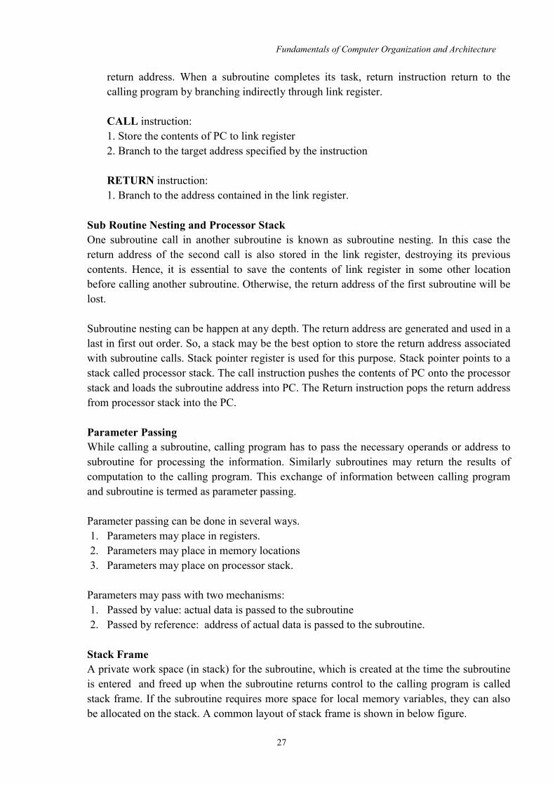
Stack Frame A private work space (in stack) for the subroutine, which is created at the time the subroutine is entered and freed up when the subroutine returns control to the calling program is called stack frame. If the subroutine requires more space for local memory variables, they can also be allocated on the stack. A common layout of stack frame is shown in below figure.
Fundamentals of Computer Organization and Architecture
28
Fig 1.20: A subroutine stack frame example In addition to stack pointer SP, it is useful to have another pointer FP (Frame Pointer). FP is useful for the accessing of parameters passed to the subroutine and the local memory variables used by the subroutine. The contents of FP remain fixed throughout the execution of the subroutine. But stack pointer SP always point to the current top element of the stack which may vary. As FP is fixed we can use the indexed addressing mode to access the parameters and local variables. (For example, -4(FP), 8(FP)) Initially SP is pointed to the old TOS. Before the subroutine is called the calling program pushes the four parameters onto the stack. Then the CALL instruction is executed. Then return address is pushed onto the stack. Now SP points to this return address, and the first instruction of the subroutine is about to be executed. At this point FP is set to contain the proper memory address. Since FP is a general purpose register, it may contain information of use to the calling program; its contents are saved by pushing them on to the stack. Since SP now points to this position, its contents are copied into FP. Thus, the first two instruction executed in the subroutine are, Move FP, - (SP) Move SP, FP After these instructions are executed, both SP and FP point to the saved FP contents. Space for three local variables are allocated by executing the instruction Subtract #12, SP
SP (stack pointer)
FP (frame pointer)
saved [R1] saved [R0]
Stack frame for called subroutine
localvar3 localvar2 localvar1
saved [FP]
Old TOS
param1 Return Address
param2 param3 param4

Fundamentals of Computer Organization and Architecture
29
Finally the contents of registers R0 and R1 are saved by pushing into the stack. The above stack frame has been set up at this point. The subroutine now executes the task. When the task is completed it pops the saved value of R0 and R1 back to those registers, removes the local variables from the stack frame by executing the instruction,
Add #12, SP And pops the saved old value of FP back into FP. Now SP points to the return address, so the return instruction can be executed, transferring control back to the calling program. Stack Frames for Nested Subroutines
For nested subroutines also stack frames can be created. Whenever a subroutine calls other subroutines its local variables and register values are also saved into the stack in a similar fashion as we discussed earlier. The following program and the corresponding stack frame will give more clarification.
Table 1.2: Nested subroutines
Memory location Instructions Comments Main program
: Place parameters on stack.
Store result. Restore stack level.
2000 Move PARAM2,-(SP) 2004 Move PARAM1,-(SP) 2008 Call SUB1 2012 Move (SP), RESULT 2016 Add #8, SP 2020 next instruction : First subroutine 2100 SUB1: 2104 2108 2112 21602164
FP,-(SP) SP, FP R0-R3,-(SP) 8(FP), R0 12(FP), R1 PARAM3, -(SP) SUB2 (SP)+, R2 R3,8(FP) (SP)+, R0-R3 (SP)+,FP, 8(FP)
Save frame pointer register. Load the frame pointer. Save registers. Get first parameter. Get second parameter. Place a parameter on stack. Pop SUB2 result into R2. Place answer on stack. Restore registers. Restore frame pointer register. Return to Main program.
Move Move MoveMultiple Move Move : Move Call Move : Move Move MoveMultiple Return
Second subroutine 3000 SUB2: FP,-(SP)
SP, FP R0-R1,-(SP) 8(FP),R0 R1, 8(FP) (SP)+, R0-R1 (SP) +,FP
Save frame pointer register. Load the frame pointer. Save registers R0 and R1. Get the parameter. Place SUB2 result on stack. Restore registers R0 and R1. Restore frame pointer register. Return to Subroutine 1.
Move Move MoveMultiple Move : Move Move MoveMultiple Return

Fundamentals of Computer Organization and Architecture
30
Fig 1.21: Stack frames for Table 1.2
Main program calls a subroutine SUB1. The parameters to SUB1 (param1 and param2) are saved by pushing into the stack. Then return address 2012 is saved. Then FP is created. Register values R0 to R3 are saved by pushing the register values in the stack. From that point a call has been made by SUB1 to the second subroutine SUB2. The parameter (param3) is saved into the stack and also the return address 2164.Again FP is set up and needed register values R0 and R1 from SUB1 moved to the stack. After the execution of SUB2, returned result is stored in register R2 by SUB1.Then SUB1 continuous its execution and eventually passes the required answer back to the main program on the stack. When SUB1 executes its return, the main program stores this answer in the memory location RESULT. From the return address main program resumes its execution. Note: Calling routines are also responsible for removing parameters from the stack.
2164
[R0] from Main
param3 [R3] from Main [R2] from Main [R1] from Main
Old TOS
2012 FP [FP] from Main
param1 param2
[FP] from SUB1 [R0] from SUB1 Stack frame for second subroutine
[R1] from SUB1
Stack frame for first subroutine
FP


CHAPTER -2
Basic Processing Unit and Computer Arithmetic
Objectives are: Basic processing unit
Fundamental Concepts Instruction Cycle Execution of a Complete Instruction Multiple-Bus Organization Sequencing of Control Signals
Arithmetic Algorithms Multiplication Algorithms for Binary Numbers Booth’s Multiplication Algorithm Array Multiplier Division of Binary Numbers Representation of BCD Numbers Addition and Subtraction of BCD Numbers Multiplication of BCD Numbers Division of BCD Numbers Floating Point Arithmetic


Basic Processing Unit and Computer Arithmetic
32
2.1 Basic Processing Unit The information’s accepted from the users are processed with the help of processing unit. The instruction set of a processor may vary depends on the architecture. In this section we are dealing with how the instructions are processed within the processing unit.
2.1.1 Fundamental Concepts To execute a program, the processor fetches one instruction at a time and performs the specified operations. Program Counter (PC) and Instruction Register (IR) are the main CPU registers who is participating in this task. PC contains the address of the instruction which is going to be executed next. The decoded instruction which is going to be currently executed is stored in register IR. The following are the general steps used to execute an instruction: Fetch the contents of memory location pointed by PC. This is actually referred as the
instruction to be executed. Then they are loaded into IR. This can be symbolically represented as:
IR [[PC]]
Update the value of PC. Suppose that every instruction has 4 bytes. Then PC will be updated by 4. Symbolically it can be represented as;
PC [PC] + 4
(The content of PC will be incremented by 4) Carry out the action specified in IR.
The fig 2.1 shows the single bus organization of data path inside the CPU. The ALU registers and the internal processor bus together known as “data path”. The internal processor bus is used for communication between the various units inside the CPU. A separate external memory bus will be there to communicate between processor and memory. Normally in the instruction execution following operations may be happen in different sequences: Register transfer Performing an arithmetic and logic operation Fetching a word from memory Storing a word in memory The order of these operations may be different in separate sequences. In some of the operations, some steps may not be necessary too. Here, we are discussing each of these operations in detail.

Basic Processing Unit and Computer Arithmetic
33
Fig 2.1: Single-bus organization of the datapath inside a processor
a) Register transfer Associating with each registers there are two signals in and out. The input and output of the register Ri are connected to the bus via switches controlled by Riin and Riout . When Riin is set to 1 the data on the bus are loaded in Ri. If Riout is set to 1 the contents registers Ri are placed on bus.
Internal processor bus
Control signals . . .
Address
lines
Memory bus
Data lines
Constant 4
Select
Add
Sub .
.
.
XOR Carry-in
PC
MAR
MDR
Y
Instruction Decoder and Control logic
IR
R0
R (n-1)
TEMP Z
MUX
A B
ALU ALU
Control lines
.
.
.

Basic Processing Unit and Computer Arithmetic
34
Fig 2.2: Input and output gating for the registers in Fig 2.1 Example Transfer the contents of register R1 to R4.
Set R1out to 1. This places the contents of R1 to the bus.
Internal processor bus
Riin
Riout
Yin
Constant 4
Select
Zin Zout
X
Ri
Y
Z
MUX
A B
ALU
X
X
X
X

Basic Processing Unit and Computer Arithmetic
35
Set R4in to 1. This loads data from the processor bus to register R4. b) Performing an arithmetic and logic operation
ALU is a combinational circuit and has no internal storage. It performs arithmetic and logic operations on the two operands applied to its A and B inputs. In the above figure we can see that, one of the operand is the output of the MUX and the other operand is obtained directly from the bus. The result produced by ALU is temporarily stored in register ‘Z’. Therefore a sequence of operations to add the contents of register R1 to those of register R2 and store the result in register R3 is: R1out , Yin R2out ,Select Y ,add, Zin Zout , R3in Example
Subtract the contents of R4 from R5 and store the result in R6. R4out , Yin R5out ,Select Y ,sub, Zin Zout , R6in
c) Fetching a word from memory To fetch a word of information from the memory the processor has to specify the memory location, where this information is stored and requests a read operation. This applies whether the information to be fetched represents an instruction in a program or an operand specified by an instruction. The processor transfers the required address to MAR whose output is connected to address lines of external memory bus. At the same time the processor uses the control lines of the memory bus to indicate that a read operation is needed. When the requested data is received from the memory they are stored in the register MDR. From there they can be transferred to other registers in the processor. The following figure shows the connection and control signals for register MDR.
Fig 2.3: Connection and control signals for register MDR
Memory-bus Internal processor data lines bus
MDRoutE MDRout
MDRinE MDRin
X
MDR
X
X
X
Basic Processing Unit and Computer Arithmetic
36
Example MOVE (R1) , R2 R1out, MARin, READ MDRinE, WMFC MDRout, R2in MFC (Memory Function Complete) signal is used for indicating that the requested read or write operation has been completed.
d) Storing a word in memory Writing a word into a memory location follows a similar procedure. The desired address will be loaded in MAR, the data to be written are loaded in MDR, and then a write command is issued. Example MOVE R2, (R1)
R1out, MAR in R2out, MDR in, WRITE MDRoutE, WMFC
The action specified in one step can be completed in one clock cycle. Exemption may come for some steps like MFC depending on the speed of the addressed device.
2.1.2 Instruction Cycle
An instruction cycle (sometimes called a fetch–decode–execute cycle) is the basic operational process of a computer. It is the process by which a computer retrieves a program instruction from its memory, determines what actions the instruction dictates, and carries out those actions. In simpler CPUs the instruction cycle is executed sequentially, each instruction being processed before the next one is started. In most modern CPUs the instruction cycles are executed concurrently, and often in parallel, through an instruction pipeline: the next instruction starts being processed before the previous instruction has finished, which is possible because the cycle is broken up into separate steps. The main steps in the instruction cycle are Fetch and Execution. Initially an instruction is fetched from the memory unit based on the address contained in PC. The PC value is updated by a value of size of the instruction so that PC can point to the next instruction to be executed. Then the decoded instruction is placed in IR, which is ready to be executed. (Execution phase: Refer2.1.3)
2.1.3 Execution of a Complete Instruction
A sequence of elementary operations we have discussed so far which are required to execute an instruction. They can put together to execute one instruction. Consider the instruction,
ADD (R3), R1 Which adds the contents of the memory location pointed by R3 to register R1.The execution of this instruction requires the following actions: 1. Fetch the instruction.

Basic Processing Unit and Computer Arithmetic
37
2. Fetch the first operand (contents of the memory location pointed by R3) 3. Perform addition. 4. Load the result into R1. The following figure shows the sequence of control steps to perform these operations for the single bus architecture.
Table 2.1: Control sequence for execution of the instruction Add (R3), R1 Explanation: The first three steps are common to every instruction. Instruction fetch operation is initiated by loading the contents of PC into MAR (Memory Address Register) and sending a read request to the memory. The select signal is set to 4 so that the multiplexer select the input as constant 4. This value is added to the operand at B (this is the value of PC) and the result is storing in register Z. Then this updated value is moved to PC from register Z. This is specified in control sequence step 2. In step 3, word fetched from the memory is loaded into IR. From step 4 onwards the sequence (execution sequences) will be different for every instruction. Here, in the example instruction, contents of register R3 are transferred to MAR in step 4, and a read operation is specified. Then the contents of register R1 are transferred to register Y in step 5. When the read operation is completed, memory operand is available in MDR and the addition operation can be performed. The contents of MDR are gated to the bus, and are taken as input B of ALU circuit. Register Y is selected as the second input to the ALU by choosing select Y. The sum will be getting in register Z and will transfer to register R1 in step 7. The End signal causes a new instruction fetch cycle to begin by returning to step 1. In the above execution of add instruction there is no need of Yin signal in step 2.But in the case of branch instruction ,the updated value of PC is needed to compute the branch target address. For this purpose only we are transferring the value of PC into register Y. This is the reason for adding Yin in step 2. The fetch phase is common for all instructions.
Step Action 1 PCout, MARin , READ, SELECT 4, ADD, Zin
2 Zout, PCin, Yin, WMFC 3 MDRout, IRin 4 R3out, MARin, READ 5 R1out, Yin, WMFC 6 MDRout, SELECT Y, ADD, Zin 7 Zout, R1in, END

Basic Processing Unit and Computer Arithmetic
38
Branch Instructions Usually the address of the next instruction to be executed will be obtained from PC register. When branching takes place, the address is obtained by adding an offset X (which is given in the branch instruction) to the updated value of PC. The following figure shows the control sequence that implements an unconditional branch instruction. Fetch phase is same as the above instruction. In step4, offset value is extracted from IR by the instruction decoding circuit. Updated PC value is already available in register Y. Offset X is gated onto the bus in step 4 and an addition operation is performed. The result, which is branch target address, is loaded into the PC.
Table 2.2: Control sequence for an unconditional Branch instruction
Now a conditional branch can consider. Here we need to check the status of condition codes before loading a new value into the PC. This can be done by the control sequence
Offset-field –of-IRout, Add, Zin, If N=0 then End in step 4 of above table 2.2. In this case if N=0 the processor returns to step1 immediately after step4. If N=1, step 5 is performed to load a new value into the PC, thus performing the branch operation.
2.1.4 Multiple-Bus Organization In the case of single bus organization, only one data item can be transferred over the bus in a clock cycle. The resulting control sequence will be lengthy in such cases. To reduce the number of steps needed, most of the processors are providing multiple internal paths so that several transfers are possible during a clock cycle. The following figure shows a three bus structure. Registers and the ALU are connected to this bus. All general purpose registers are combined into a single block called register file. The register files have 3 ports. There are two output ports and one input port. Contents of two different registers can be accessed simultaneously and have their contents placed on buses A and B by using two output ports. The third port allows the data on bus C to be loaded into a third register during the same clock cycle.
Step Action 1 PCout, MARin , READ, SELECT 4, ADD, Zin
2 Zout, PCin, Yin, WMFC 3 MDRout, IRin 4 Offset-field –of-IRout, Add, Zin
5 Zout, PCin, END

Basic Processing Unit and Computer Arithmetic
39
Fig 2.4: Three-bus organization of the datapath
The need of temporary registers Y and Z are not there with three bus arrangement. Buses A and B are used to transfer the source operands to the A and B inputs of the ALU.ALU performs the operation and the result is transferred to the destination over bus C. Another feature of multiple buses is the introduction of incrementer unit. The purpose of this unit to increment the value of PC by 4. (We are assuming the word size as 4 bytes). This eliminates the need to add 4 to the PC using the main ALU. The constant4 in the ALU input multiplexer is still useful because it can be used to increment other memory addresses in LoadMultiple and StoreMultiple instructions.
Bus A Bus B Bus C Constant 4
Memory bus Address data lines lines
PC
IR
MAR
Register
file
Instruction decoder
MUX A
ALU R B
Incrementer
MDR
Basic Processing Unit and Computer Arithmetic
40
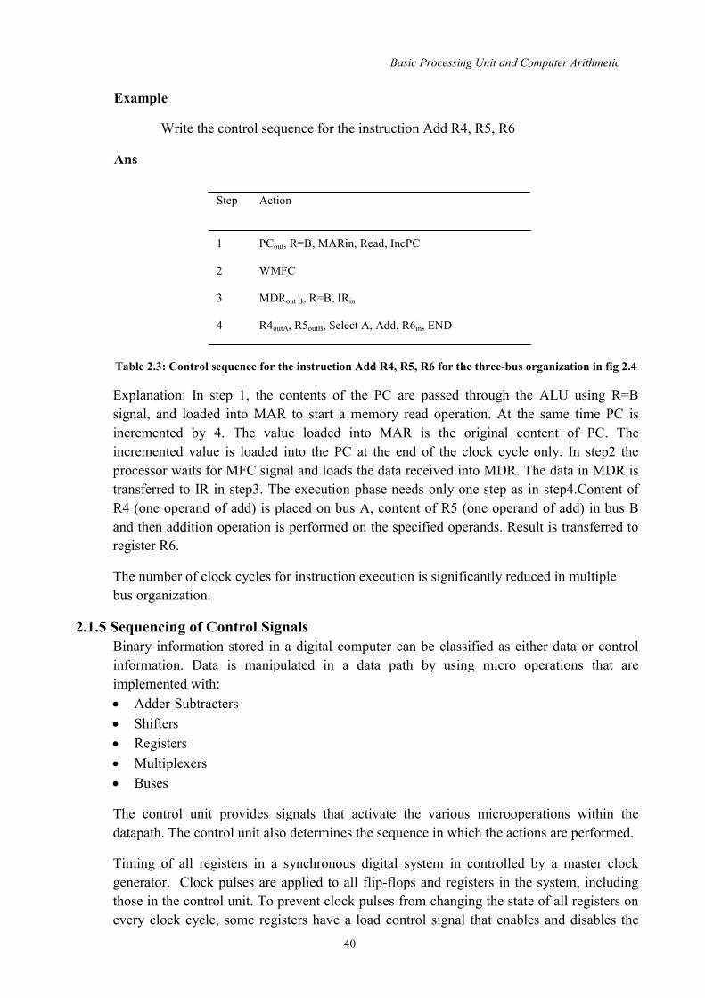
Example Write the control sequence for the instruction Add R4, R5, R6
Ans
Table 2.3: Control sequence for the instruction Add R4, R5, R6 for the three-bus organization in fig 2.4 Explanation: In step 1, the contents of the PC are passed through the ALU using R=B signal, and loaded into MAR to start a memory read operation. At the same time PC is incremented by 4. The value loaded into MAR is the original content of PC. The incremented value is loaded into the PC at the end of the clock cycle only. In step2 the processor waits for MFC signal and loads the data received into MDR. The data in MDR is transferred to IR in step3. The execution phase needs only one step as in step4.Content of R4 (one operand of add) is placed on bus A, content of R5 (one operand of add) in bus B and then addition operation is performed on the specified operands. Result is transferred to register R6. The number of clock cycles for instruction execution is significantly reduced in multiple bus organization.
2.1.5 Sequencing of Control Signals Binary information stored in a digital computer can be classified as either data or control information. Data is manipulated in a data path by using micro operations that are implemented with: Adder-Subtracters Shifters Registers Multiplexers Buses The control unit provides signals that activate the various microoperations within the datapath. The control unit also determines the sequence in which the actions are performed. Timing of all registers in a synchronous digital system in controlled by a master clock generator. Clock pulses are applied to all flip-flops and registers in the system, including those in the control unit. To prevent clock pulses from changing the state of all registers on every clock cycle, some registers have a load control signal that enables and disables the
Step Action 1 PCout, R=B, MARin, Read, IncPC
2 WMFC 3 MDRout B, R=B, IRin 4 R4outA, R5outB, Select A, Add, R6in, END

Basic Processing Unit and Computer Arithmetic
41
loading of new data into the register. The binary variables that control the selection inputs of the components are generated by the control unit. The control unit that generates the signals for sequencing the microoperations is a sequential circuit that dictates the control signals for the system. Using status conditions and control inputs the sequential control unit determines the next state. In a programmable system, a portion of the input to the processor consists of a sequence of instructions. Each instruction specifies the operation that the system is to perform, which operands to use, where to place the results of the operation. Instructions are stored in memory. The address of the next instruction is the PC. There is a parallel transfer from memory to the instruction register. The control unit contains decision logic to interpret the instruction. Executing an instruction means activating the necessary sequence of micro operations in the datapath required to perform the operation specified by the instruction. In nonprogrammable systems, the control unit is not responsible for obtaining instructions from memory, nor is it responsible for sequencing execution of those instructions. There is no PC in nonprogrammable systems. Instead, the control determines the operations to be performed and the sequence of those operations, based on its inputs and status bits from the data path. Mainly there are four sequences of control signals as we described in section 2.1.3. (a) Fetch the instruction from memory location pointed by PC (b) Read the operand from memory address pointed by the source register. (c) Perform Arithmetic operations on the operands. (d) Write back the result to the memory address pointed by destination register. Refer the example in 2.1.3 for more details.
2.2 Arithmetic Algorithms In this section we are describing the different methods to perform multiplication and division of binary numbers, BCD numbers and floating point numbers.
2.2.1 Multiplication Algorithms for Binary Numbers Multiplication of two fixed point binary number in signed magnitude representation is done with paper and pencil by a process of successive shift and add operation as shown below. The process consists of looking at successive bits of multiplier in LSB first fashion. If the multiplier bit is 1, the multiplicand is copied down otherwise 0’s are copied down. The numbers copied down in successive lines are shifted one position to the left from the previous number. Finally the numbers are added and their sum forms the product. The sign of the product determined from the signs of multiplicand and multiplier. If they are same, sign of product is +ve. If the sign are not same, sign will be –ve.
Basic Processing Unit and Computer Arithmetic
42
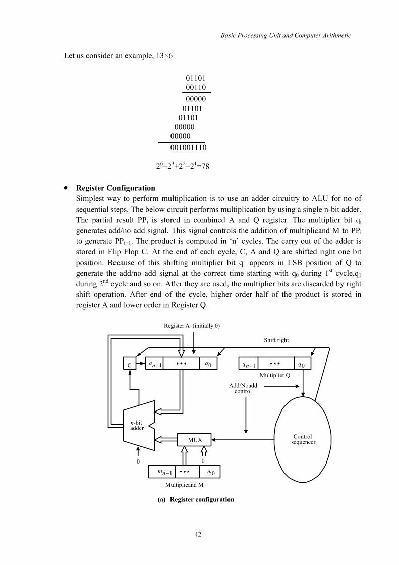
Let us consider an example, 13×6
Register Configuration Simplest way to perform multiplication is to use an adder circuitry to ALU for no of sequential steps. The below circuit performs multiplication by using a single n-bit adder. The partial result PPi is stored in combined A and Q register. The multiplier bit qi generates add/no add signal. This signal controls the addition of multiplicand M to PPi to generate PPi+1. The product is computed in ‘n’ cycles. The carry out of the adder is stored in Flip Flop C. At the end of each cycle, C, A and Q are shifted right one bit position. Because of this shifting multiplier bit qi appears in LSB position of Q to generate the add/no add signal at the correct time starting with q0 during 1st cycle,q1 during 2nd cycle and so on. After they are used, the multiplier bits are discarded by right shift operation. After end of the cycle, higher order half of the product is stored in register A and lower order in Register Q.
(a) Register configuration
01101 00110
00000 01101 01101 00000 00000 001001110
26+23+22+21=78
n-bit
Multiplicand M
Control
Multiplier Q
Shift right Register A (initially 0)
adder
Add/Noadd control
C an–1 a0 qn–1 q0
MUX sequencer
0 0 mn–1 m0

Basic Processing Unit and Computer Arithmetic
43
Perform the multiplication of the following numbers by sequential multiplication approach. Multiplicand = 1101 Multiplier = 1011
No add Shift Add Shift
(b) Multiplication example
Fig 2.5: Sequential circuit binary multiplier 2.2.2 Booth’s Multiplication Algorithm
By sequential network structure a multiplying instruction takes much more time to execute than an ADD instruction. Several techniques have been developed to speed up multiplication. One of them is Booth Multiplication. This is a technique which works well for both +ve and –ve multipliers. The booth algorithm generates a 2n bit product and treat both -ve and +ve 2’s complement n bit operands uniformly.
M Initial Configuration C A Q 0 1101 1011 0 0110 1101 1 0011 1101 0 1001 1110 0 1001 1110 0 0100 1111 1 0001 1111 0 1000 1111
1101 0 0000 1011
Add Shift
Add Shift
No add Shift
Add Shift
First cycle
Second cycle
Third cycle
Fourth cycle
Product

Basic Processing Unit and Computer Arithmetic
44
In booth scheme ‘-1’ times the shifted multiplicand is selected when moving from 0 to 1 and ‘+1’ times shifted multiplicand is selected when moving from 1 to 0. As the multiplicand is scanned from right to left booth multiplier can be found out by following table.
Table 2.4: Booth multiplier recording table Eg: 00101111001 The booth recording of multiplier can be in the form as follows. Always assume that there is a right most zero if the right most bit is’1’.
0 +1 -1 +1 0 0 0 -1 0 +1 -1 The above transformation is called skipping over 1’s. Here only few versions of the shifted multiplicand have to be added to generate the product. Thus speeding up the multiplication operation. In some situations, booth algorithm will work as worse (when alternate 0’s and 1’s), in some cases such as ordinary multiplier. (consecutive combinations of 0’s and 1’s and some cases larger block of 1’s).Let us consider an example,
Fig 2.6: Booth recorded multiplier
Multiplier bit i, bit i-1
Version of multiplier
selected by bit i
0 0
0 x M
0 1
+1 x M
1 0
-1 x M
1 1
0 xM
0 0 0 0 1 1 1 1 1 0 0 0 0 1 1 1
0 0 0 +1 0 0 0 0 –1 0 0 0 +1 0 0 – 1
0 1 0 1 0 1 0 1 0 1 0 1 0 1 0 1 Worst-case multiplier
+1 –1 +1 –1 +1 –1 +1 –1 +1 –1 +1 –1 +1 –1 +1 –1
1 1 0 0 0 1 0 1 1 0 1 1 1 1 0 0 Ordinary multiplier
0 –1 0 0 + 1 –1 +1 0 –1 +1 0 0 0 –1 0 0
Good multiplier

Basic Processing Unit and Computer Arithmetic
45
Advantages of Booth Algorithm It handles both +ve and –ve multipliers uniformly. It achieves some efficiency in the no of additions required when the multiplier has few large block of 1’s. The speed gained by skipping over once depends on the data.
Fig 2.7: Flow chart of Booth Algorithm
Multiply
=10 =01 = 00 = 11
≠0 = 0
AC 0
Qn+1 0
SC N
Qn Qn+1
AC AC + BR +1
AC AC + BR
Arithmetic right Shift (AC & QR)
SCSC-1
SC
Multiplicand in BR
Multiplier in QR
End
AC – Accumulator Register SC – Sequence Counter (it is initialized with number of bits in multiplier

Basic Processing Unit and Computer Arithmetic
46
Example
BR = 10111 QR = 10011
Result is 0001110101 = 117
The above example show as the multiplication of (-9)*(13) = +117. Note that multiplier in QR is negative and multiplicand in BR is also negative. Then 10 bit product appears in AC and QR and it is positive. The final value of Qn+1 is the original sign bit of the multiplier and shouldn’t be taken as part of the product.
Qn
Qn+1
BR=10111 BR+1=01001 AC QR Qn+1 SC
1 1 0 0 1
0 1 1 0 0
Initial sub BR ashr ashr add BR ashr ashr sub BR ashr
00000
01001 01001
00100
00010
10111 11001
11100
11110
01001 00111
00011
10011
10011
11001
01100
01100
10110
01011
01011
10101
0
0
1
1
1
0
0
0
1
101
101
100
011
011
010
001
001
000

Basic Processing Unit and Computer Arithmetic
47
Example BR = 00111(+7) QR = 10101(-11)
Qn Qn+1 BR+1 AC QR Qn+1 SC
1 0 1 0 1
0 1 0 1 0
Initial sub BR ashr add BR ashr sub BR ashr add BR ashr sub BR ashr
00000
11001 11001
11100
00111 00011
00001
11001 11010
11101
00111 00100
00010
11001 11011
11101
10101
10101
11010
11010
11101
11101
01110
01110
00111
00111
10011
0 0 1 1 0 0 1 1 0 0 1
101
101
100
100
011
011
010
010
001
001
000
Result is 1110110011 = -77 2.2.3 Array Multiplier
Checking the bits of the multiplier one at a time and forming the partial product is a sequential operation, that requires a sequence of add and shift micro operation. The multiplication of two binary no’s can be done with one micro operation by means of a combinational circuit that forms the product bits all at once. This is the fast way of multiplying two no’s since all it takes is the time for the signal to propagate trough the gates
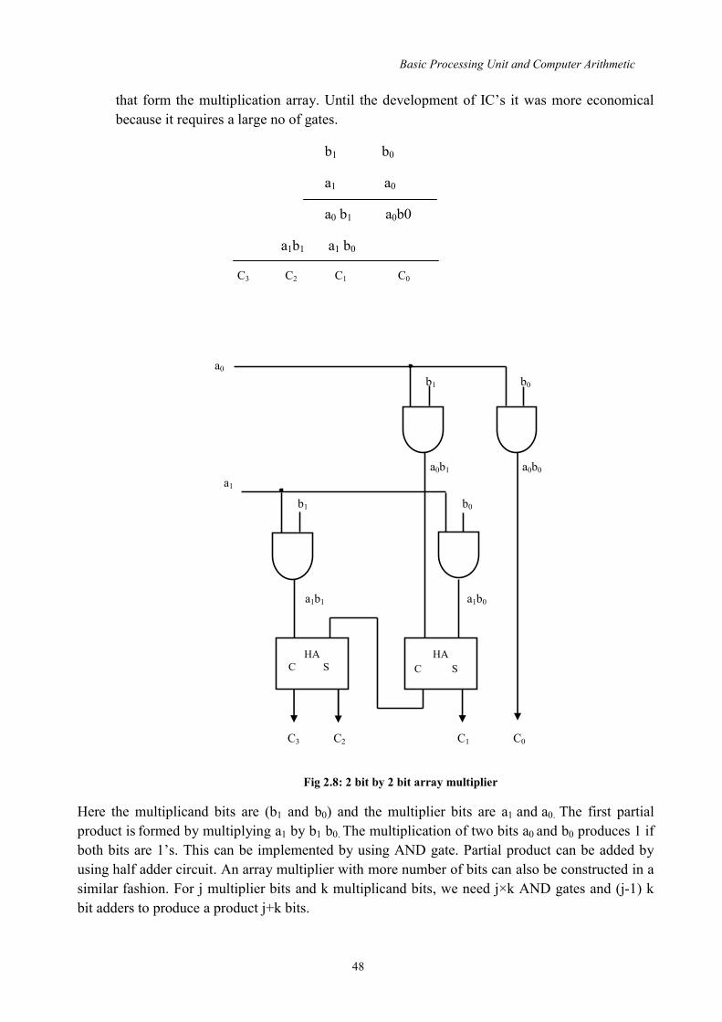
Basic Processing Unit and Computer Arithmetic
48
that form the multiplication array. Until the development of IC’s it was more economical because it requires a large no of gates.
Fig 2.8: 2 bit by 2 bit array multiplier Here the multiplicand bits are (b1 and b0) and the multiplier bits are a1 and a0. The first partial product is formed by multiplying a1 by b1 b0. The multiplication of two bits a0 and b0 produces 1 if both bits are 1’s. This can be implemented by using AND gate. Partial product can be added by using half adder circuit. An array multiplier with more number of bits can also be constructed in a similar fashion. For j multiplier bits and k multiplicand bits, we need j×k AND gates and (j-1) k bit adders to produce a product j+k bits.
a0 b1 b0
a0b1 a0b0 a1 b1 b0
a1b1 a1b0
C3 C2 C1 C0
HA C S
HA
C S
b1 b0
a1 a0
a0 b1 a0b0 a1b1 a1 b0
C3 C2 C1 C0

Basic Processing Unit and Computer Arithmetic
49
Example Design a 4 bit by 3 bit array multiplier
Fig 2.9: 4 bit by 3 bit array multiplier 2.2.4 Division of Binary Numbers
Circuit arrangement of binary division is very similar with the circuit arrangement of multiplication. The following figure will illustrate this:
b3 b2 b1 b0 x a2 a1 a0
a0b3 a0b2 a0b1 a0b0 a1b3 a1b2 a1b1 a1 b0
a2b3 a2b2 a2b1 a2b0 a2b3 a1b3+a2b2 a0b3+a1b2+a2b1 a0b2+a1b1+a2b0 a0b1+a1b0 a0b0
a0
b3 b2 b1 b0
a1
b3 b2 b1 b0
0
a2
b3 b2 b1 b0
C6 C5 C4 C3 C2 C1 C0
Addend Augend 4 bit adder
Sum and output carry
Addend Augend 4 bit adder
Sum and output carry

Basic Processing Unit and Computer Arithmetic
50
Fig 2.10: Circuit arrangement for binary division
An n-bit positive divisor is loaded in register M and n-bit positive dividend is loaded in register Q. Register A is set to 0. After the division is complete, n bit quotient is in register Q and the remainder is in register A. The required subtractions are facilitated by using 2’s complement arithmetic. The extra bit position at the left end of both A and M accommodates the sign bit during subtractions. Division Algorithms are of 2 types:- 1. Restoring Division
Algorithm
Do the following n times: 1. Shift A and Q left one binary position. 2. Subtract M from A and place the answer back in A. 3. If the sign of A is 1, set q0 to 0 and add M back to A (i.e. restore A), Otherwise
set q0 to 1.
The following example will perform the division on numbers 8 and 3. After the operation you can see quotient 2 is in register Q and reminder 2 will be in register A.
n+1 bit
Divisor M
Control sequencer
Dividend Q Quotient setting
Shift left
adder Add/Subtract
an an–1 a0 qn–1 q0
0 mn–1 m0
A
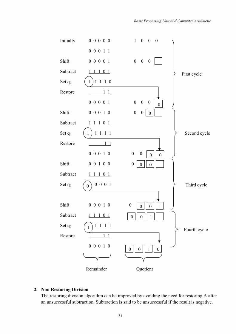
Basic Processing Unit and Computer Arithmetic
51
2. Non Restoring Division The restoring division algorithm can be improved by avoiding the need for restoring A after an unsuccessful subtraction. Subtraction is said to be unsuccessful if the result is negative.
Initially 0 0 0 0 0 1 0 0 0 0 0 0 1 1 Shift 0 0 0 0 1 0 0 0 Subtract 1 1 1 0 1 Set q0 1 1 1 0 Restore 1 1 0 0 0 0 1 0 0 0 Shift 0 0 0 1 0 0 0 Subtract 1 1 1 0 1 Set q0 1 1 1 1 Restore 1 1 0 0 0 1 0 0 0 Shift 0 0 1 0 0 0 Subtract 1 1 1 0 1 Set q0 0 0 0 1 Shift 0 0 0 1 0 0 Subtract 1 1 1 0 1 Set q0 1 1 1 1 Restore 1 1 0 0 0 1 0
First cycle
Second cycle
Third cycle
Fourth cycle
Quotient Remainder
0
0 0
0 0 1 0 0 1
1
1
0
1
0
0 0
0 0 1 0

Basic Processing Unit and Computer Arithmetic
52
Algorithm Step 1: Do the following n times:
1. If the sign of A is zero, shift A and Q left one bit position and subtract M from A ; otherwise Shift A and Q left and add M to A.
2. Now, if the sign of A is 0, set q0 to 1; otherwise set q0 to 0. Step 2: If the sign of A is 1, add M to A.
Example: Perform division on numbers 8 and 3 using non restoring technique.
Initially 0 0 0 0 0 1 0 0 0 0 0 0 1 1 Shift 0 0 0 0 1 0 0 0 Subtract 1 1 1 0 1 Set q0 1 1 1 0 0 0 0 Shift 1 1 1 0 0 0 0 Add 0 0 0 1 1 Set q0 1 1 1 1 0 0 Shift 1 1 1 1 0 0 Add 0 0 0 1 1 Set q0 0 0 0 1 0 Shift 0 0 0 1 0 Subtract 1 1 1 0 1 Set q0 1 1 1 1 Add 1 1 1 1 1 0 0 0 1 1 0 0 0 1 0
First cycle
Second cycle
Third cycle
Fourth cycle
Quotient
0
0 0
0 0 1 0
1
1
Reminder
0
0 0
0 0 1
Restore remainder
1
0
0 0 1

Basic Processing Unit and Computer Arithmetic
53
2.2.5 Representation of BCD Numbers BCD means that Binary Coded Decimal. It represents each of the digits of an unsigned decimal as the 4-bit binary equivalents. BCD numbers can be represented in two formats. They are packed BCD numbers and unpacked BCD numbers. Unpacked BCD
Unpacked BCD representation contains only one decimal digit per byte. The digit is stored in the least significant 4 bits; the most significant 4 bits are not relevant to the value of the represented number.
Packed BCD Packed BCD representation packs two decimal digits into a single byte.
Following figure will give more clarification.
Decimal Binary BCD Packed Unpacked
0 0000 0000 0000 0000 0000 0000 1 0000 0001 0000 0001 0000 0001 2 0000 0010 0000 0010 0000 0010 3 0000 0011 0000 0011 0000 0011 4 0000 0100 0000 0100 0000 0100 5 0000 0101 0000 0101 0000 0101 6 0000 0110 0000 0110 0000 0110 7 0000 0111 0000 0111 0000 0111 8 0000 1000 0000 1000 0000 1000 9 0000 1001 0000 1001 0000 1001 10 0000 1010 0000 0001 0000 0000 0001 0000 11 0000 1011 0000 0001 0000 0001 0001 0001 12 0000 1100 0000 0001 0000 0010 0001 0010 13 0000 1101 0000 0001 0000 0011 0001 0011 14 0000 1110 0000 0001 0000 0100 0001 0100 15 0000 1111 0000 0001 0000 0101 0001 0101 16 0001 0000 0000 0001 0000 0110 0001 0110 17 0001 0001 0000 0001 0000 0111 0001 0111 18 0001 0010 0000 0001 0000 1000 0001 1000 19 0001 0011 0000 0001 0000 1001 0001 1001 20 0001 0100 0000 0010 0000 0000 0010 0000
Table 2.5: Representation of BCD numbers

Basic Processing Unit and Computer Arithmetic
54
Packing a Two-Byte BCD To pack a two-byte unpacked BCD number into a single byte creating a packed BCD number, shift the upper byte left four times, then OR the results with the lower byte. Example
0000 0111 0000 1001(unpacked BCD) 0111 1001(packed BCD)
0000 0111 << 4 0111 0000 (SHIFT LEFT 4) 0111 0000 + 0000 1001 0111 1001 (OR)
In BCD, digits from 0 to 9 only are allowed. The binary numbers 1010, 1011, 1100, 1101, 1110, 1111are not allowed in BCD system. So they are called invalid BCD numbers.
2.2.6 Addition and Subtraction of BCD Numbers BCD Addition Either packed or unpacked BCD numbers can be summed. BCD addition follows the same rules as binary addition. However, if the addition produces a carry and/or creates an invalid BCD number, an adjustment is required to correct the sum. The correction method is to add 6 to the sum in any digit position that has caused an error.
Example
BCD Subtraction Either packed or unpacked BCD numbers can be subtracted. BCD subtraction follows the same rules as binary subtraction. However, if the subtraction causes a borrow and or creates an invalid BCD number, an adjustment is required to correct the answer. The correction method is to subtract 6 from the difference in any digit position that has caused an error.
24 + 13 = 37 15 + 9 = 24 19 + 28 = 47 0010 0100 = 24 0001 0101 = 15 0001 1001 = 19 +0001 0011 = 13 +0000 1001 = 9 -0010 1000 = 28
0011 0111 = 37 0001 1110 = 1?(invalid) 0100 0001 = 41(error) 0001 1100 = 1?(invalid) 0100 0001 = 41(error) + 0000 0110 = 6 (adjustment)
+0000 0110 = 6 (adjustment)
0010 0100 = 24 0100 0011 = 47

Basic Processing Unit and Computer Arithmetic
55
Example 2.2.7 Multiplication of BCD Numbers
This algorithm implements BCD multiplication using a shift-add philosophy. Here we are using the notation QL as the least significant digit and Ae as carry digit. Finally, k is the number of digits and thus the number of iterations of the shift-add loop. Step 1 sets the sign, initializes the running total and sets the loop counter. Step 2 performs the add portion of the shift-add. Note that it loops back to itself in order to perform the multiple adds required by digits greater than one. Step 3 performs the shift, a decimal shift this time, and decrements the loop counter. Finally, step 4 loops back if not done. Algorithm 1. As Bs Qs, A 0, Ae 0, SC k
2. IF (QL 0) THEN (Ae A A+B, QL QL-1, GOTO 2) 3. dshr (Ae AQ), SC SC - 1 4. IF (SC 0) THEN GOTO 2
Example B = 57 * Q = 12
37 - 12 = 25 65 - 19 = 46 41 - 18 = 23 0011 0111 = 37 0110 0101= 65 0100 0001= 41 -0001 0010 = 12 -0001 1001 = 19 -0001 1000 = 18
0010 0101 = 25 0100 1100 = 4?(invalid) 0010 100 = 29(error) 0100 1100 = 4?(invalid) 0010 100 = 29(error) - 0000 0110 = 6 (adjustment)
- 0000 0110 = 6 (adjustment)
0100 0110 = 46 0010 0011 = 23
STEP AeA Q SC
1 000 12 2 2 057 11 2 114 10
3,4 011 41 1 2 068 40
3,4 006 84 0

Basic Processing Unit and Computer Arithmetic
56
Consider this example. We begin by clearing Ae and A and by setting the loop counter to 2. The first loop performs step 2 twice because the least significant digit of Q is 2. Steps 3 and 4 perform the shift and loop counter maintenance. During the second iteration, we perform step 2 only once, since the least significant digit of Q is now 1. Notice that the running product is underlined. Just as before, we shift the extra bit of the product into Q just as the least significant digit of the multiplier is processed and no longer needed.
2.2.8 Division of BCD Numbers BCD division is an extension of binary signed-magnitude division. Again we use a decimal shift instead of a linear shift and, just as in the multiplication algorithm; more than one subtraction may be required. Instead of performing subtraction using 2’s complement, we perform it using 10’s complement. The 10’s complement of a number is equal to its 9’s complement + 1. For example, a 3-digit number XYZ has a 10’s complement of (999-XYZ) + 1.
Algorithm
Q A&Q div B, A remainder
1. IF (OVERFLOW) THEN {ERROR} 2. Qs As Bs, Be 0, SC k 3. dshl(AQ) 4. EAA+B+1 5. IF (E=1) THEN (QL QL+1, EAA+B+1, GOTO 5) 6. AA+B, SC SC - 1 7. IF (SC0) THEN GOTO 3
This algorithm implements BCD division. As before, we check for overflow and exit if it present. Otherwise we proceed to step 2, where we set the sign, initialize the running quotient and set the loop counter. Steps 3 to 7 comprise the loop. In step 3 we perform the shift and in step 4 we form A-B using 10’s complement. Step 5 checks to see if the subtraction was valid. If so, it increments the quotient, performs another subtraction and loops back to itself. This step implements the multiple subtractions in this algorithm. When we have subtracted one too many times, we proceed to step 6, where we restore the extra subtraction and decrement the loop counter. Step 7 either branches back, if we are not done, or exits the algorithm.
Example AQ = 0769 B = 036; B+1 = 964

Basic Processing Unit and Computer Arithmetic
57
STEP A Q SC
1,2 007 69 2 3 076 90 4 040 90 5 004 91 5 968 92
6,7 004 92 1
In this example, step 1 finds no overflow, so step 2 initializes the necessary values. The first iteration of the loop begins by shifting the value one position to the left and subtracting via 10’s complement. Step 5 checks and sees that the first subtraction was valid, so it performs a second subtraction and loops back to itself. During the second iteration of step 5, we find that this subtraction is also valid, so we update Q and perform a third subtraction. The next iteration of step 5 finds that this is invalid, so step 6 restores the last subtraction. This step and step 7 finish the first iteration of the loop. The second and final iteration performs similarly to the first iteration, except that step 5 is only executed once in this iteration. This is shown below in the continuing example above. The final result is 769/36 = 21 with a remainder of 13.
STEP A Q SC
3 049 20 4 013 20 5 977 21 6 013 21 0
2.2.9 Floating Point Arithmetic
A floating point number in a computer register consists of two parts: 1. Mantissa ( m ) 2. Exponent ( e )
The two parts represents a number obtained from multiplying m times a radix r raised to the value of e, i.e., m × re. The mantissa may be a fraction or an integer. A floating point number is normalized if the most significant digit of the mantissa is nonzero. Register Configuration for floating point arithmetic The same registers and adders used for the integer arithmetic can also be used in processing the mantissa part. The only difference lies in the way the exponents are

Basic Processing Unit and Computer Arithmetic
58
handled. There are three registers BR, AC and QR. Each register is subdivided into two parts: One for mantissa (rep by uppercase) and one for exponent (rep by lowercase).
Each floating point number has a mantissa in signed magnitude representation and a biased exponent. Thus AC has a mantissa part whose sign is in As, and magnitude in A. The exponent is in the part of the register and represents by lower symbol a. A1 is the most significant digit and parallel for other registers. A parallel Adder adds the two mantissas and transfers the sum into A and carry into E. A separate parallel adder is used for exponents. The exponents are biased. (So don’t have a distinct sign bit) In this representation, the sign bit is removed from being a separate entity. The bias is a positive number that is added to each exponent as the floating point number is formed, so that internally all exponents are positive. Consider an exponent that ranges from -50 to 49. Internally it is represented by 2 digits (without a sign) by adding it to a bias of 50.Then the exponent will become e+50, into the range of 00 to 99. The advantage of bias exponent is that, they contain only positive numbers. It is then simpler to compare their relative magnitude without being concerned with their signs.
Fig 2.11: Registers for floating point arithmetic operations Floating Point Addition and Subtraction In addition and subtraction, operands are stored in AC and BR. The sum or difference is formed in AC. The algorithm can be divided into four parts: 1. Check for zeros 2. Align the mantissa 3. Add or subtract the mantissa 4. Normalize the result The flow chart can be drawn as follows:
BR
AC
QR
Bs B
As A1 A
Qs Q
Parallel-adder
b
Parallel-adder And comparator
a
q
E

Basic Processing Unit and Computer Arithmetic
59
Fig 2.12: Flowchart for floating point addition and subtraction
Check
for zer
os
BR AC
ACBR
op
As As
a:b
Shr A a a+1
Shr B
b b+1
op
As Bs As Bs
EA A+B+1 EA A+B
E
A
AA + 1 As As
AIA
AC0
Shl A a a-1
E
Shr A A1E
a a+1
END
=0 ≠0 ≠0
a<b a>b =0
a=b
Sub Add
=0 =1 =1 =0
=0
≠ 0 =1
=0
=0 =1
=0
=1
Add
Sub
Add/subtract
align mantissa
Mantissa Addition
Or Subtraction
Normalization
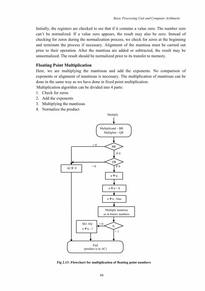
Basic Processing Unit and Computer Arithmetic
60
Initially, the registers are checked to see that if it contains a value zero. The number zero can’t be normalized. If a value zero appears, the result may also be zero. Instead of checking for zeros during the normalization process, we check for zeros at the beginning and terminate the process if necessary. Alignment of the mantissa must be carried out prior to their operation. After the mantissa are added or subtracted, the result may be unnormalized. The result should be normalized prior to its transfer to memory. Floating Point Multiplication Here, we are multiplying the mantissas and add the exponents. No comparison of exponents or alignment of mantissas is necessary. The multiplication of mantissas can be done in the same way as we have done in fixed point multiplication.
Multiplication algorithm can be divided into 4 parts: 1. Check for zeros 2. Add the exponents 3. Multiplying the mantissas 4. Normalize the product
Fig 2.13: Flowchart for multiplication of floating point numbers
Multiply
= 0
≠ 0
= 0 ≠ 0
\
= 0
= 1
a q
Multiply mantissa as in binary numbers
A1
BR
QR
Sh1 AQ a a - 1
AC 0
Multiplicand – BR Multiplier - QR
End (product is in AC)
a a - bias
a a + b
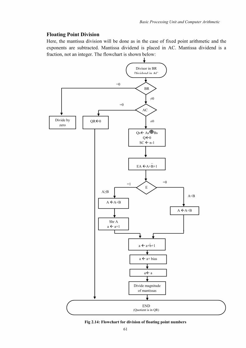
Basic Processing Unit and Computer Arithmetic
61
Floating Point Division Here, the mantissa division will be done as in the case of fixed point arithmetic and the exponents are subtracted. Mantissa dividend is placed in AC. Mantissa dividend is a fraction, not an integer. The flowchart is shown below:
Fig 2.14: Flowchart for division of floating point numbers
BR
AC
Qs As Bs Q0
SC n-1
_ EA A+B+1
E
A A+B
Shr A a a+1
A A+B
a a+ bias
q a
END (Quotient is in QR)
QR0 Divide by
zero
A≥B
=1 =0
A<B
=0
=0 ≠0
≠0
Divisor in BR Dividend in AC
Divide magnitude of mantissas
_ a a+b+1

Basic Processing Unit and Computer Arithmetic
62
Divide overflow check will be done as in fixed point. If the dividend is greater than or equal to the divisor, the dividend fraction is shifted to the right and its exponent incremented by 1. This operation is known as dividend alignment.
The division of two normalized floating point numbers will always results in a normalized quotient provided that a dividend alignment is carried out before the division. So, as in other cases, the quotient obtained after the division doesn’t require normalization. The division algorithm can be subdivided into five parts: 1. Check for zeros 2. Initialize registers and evaluate the sign 3. Align dividend 4. Subtract exponent 5. Divide the mantissas
Initially divisor and dividend are checked to see that if they are zero’s. If the divisor is zero, it is an exception, divide by zero, which is not possible. Similarly if dividend is zero and if divisor is not zero the result will be zero. After checking for zero’s, the registers are initialized and signs are evaluated. Then dividend alignment is performed so that resulting quotient will be in normalized form. Exponents are treated as separate case and subtraction of exponents have done in fourth step (For division exponents have to be subtracted opposite to addition of exponents in multiplication). Finally, the mantissa part division is performed as in the case of integer divisions. We can go for either restoring division or non restoring division as discussed on section 2.2.4.


CHAPTER -3
Input Output Organization
Objectives are: I/O organization Accessing of I/O Devices Interrupts Direct Memory Access Buses Interface Circuits Standard I/O Interfaces (PCI, SCSI, USB)


Input Output Organization
64
3. 1 I/O Organization One of the basic features of a computer is the ability to exchange the data with other devices. Now a day, in almost all environments computer is an integral part. So that I/O organization has an important role in computer organization.
3.1.1 Accessing of I/O Devices A simple arrangement to connect I/O devices to a computer is to use a single bus structure. It consists of three sets of lines to carry Address Data Control Signals. When the processor places a particular address on address lines, the devices that recognize this address responds to the command issued on the control lines. The processor request either a read or write operation and the requested data are transferred over the data lines.
Fig 3.1: A single-bus structure Based on the address space used by the I/O devices, there are two schemes for I/O.
Memory Mapped I/O When I/O devices & memory share the same address space, the arrangement is called memory mapped I/O. Here same instructions are using for controlling memory and I/O. Example
I/O Mapped I/O In this scheme, there are separate address spaces for I/O devices. CPU instructions are designed specifically to perform I/O. This doesn’t means that I/O address lines are physically separate from memory address lines. A special signal on the bus indicates that the requested read/ write transfer is an I/O operation. Then memory ignores this one .The different I/O devices connected to the bus will examine the address lines to see that whether they have to respond to this or not.
Move DATAIN, Ro Move Ro, DATAOUT DATAIN DATAOUT
Reads the data from DATAIN then into processor register Ro.
Send the contents of register Ro to location DATAOUT. Input buffer associated with keyboard Output data buffer of a display unit / printer.
Bus Processor Memory
I/O device 1 … I/O device n

Input Output Organization
65
I/O Interface This includes the hardware required to connect an I/O Device to the bus. Interface circuit consists of address decoder, data registers, status registers and control circuitry. Address decoder enables the device to recognize its address when this address appears on address lines. The data register holds the data being transferred to or from the processor. Status register contains the information relevant to the operation of the I/O device. For an input device, SIN status flag in used. For example, when SIN = 1 a character is entered at the keyboard. When SIN=0, the character is read by the processor. For an output device, SOUT status flag is used in a similar fashion. Status and data registers are connected to the data bus.
Fig 3.2: I/O Interface for an Input Device Example The following example illustrates I/O operations involving a keyboard and display device. Four registers are used in the data transfer operations as shown below.
Fig 3.3: Registers in keyboard and display interfaces
Address lines Data lines Control lines
I/O Address decoder Control circuits
Data and status registers
Input device
Bus
DATAOUT
DATAIN
STATUS
CONTROL
DIRQ KIRQ SOUT SIN
7 6 5 4 3 2 1 0
DEN KEN

Input Output Organization
66
The data from the keyboard are made available in the DATAIN register & the data sent to the display are stored in DATAOUT register. Program
This program reads a line of characters from the keyboard & stores it in a memory buffer starting at locations LINE. Then it calls the subroutine “PROCESS” to process the input line. As each character is read, it is echoed back to the display. Register R0 is used as a pointer to the memory buffer area. Contents of R0 are updated using autoincrement mode so that successive characters are stored in successive memory location. Each character is checked to see if there is carriage return (CR) character, char, which has the ASCII code 0D (hex). If it is a Line Feed character (ASCII code-0A) is sent to move the cursor one line down on the display & subroutine PROCESS is called. Otherwise, the program loops back to wait for another character from the keyboard.
Program Controlled I/O Here the processor repeatedly checks a status flag to achieve the required synchronization between Processor & I/O device that is, the processor polls the device. There are 2 mechanisms to handle I/O operations. They are, Interrupt
Synchronization is achieved by having I/O device send special signal over the bus whenever it is ready for data transfer operation
DMA Here the device interface transfers the data directly to or from the memory, without continuous involvement of the processor. It is a technique used for high speed I/O device.
DIRQ KIRQ KEN DEN SIN, SOUT
Interrupt Request for display Interrupt Request for keyboard Keyboard enables Display Enable Status flags
WAIT K Move Test Bit
Branch = 0 Move
WAIT D Test Bit Branch = 0 Move Move Compare Branch≠0 Move Call
# LINE, R0 #0, STATUS WAIT K DATAIN, R1 #1, STATUS WAIT D R1, DATAOUT R1, (R0) + #$0D, R1 WAIT K #$0A, DATAOUT PROCESS

Input Output Organization
67
3.1.2 Interrupts When a program enters a wait loop, it will repeatedly check the device status. During this period, the processor will not perform any function. This waiting period can be used for performing any other function actually. To allow this to happen, we can arrange the I/O device to alert the processor when it becomes ready. It can do so by sending a hardware signal called an interrupt to the processor, so that the processor doesn’t have to continuously check the device status. One of the bus control lines named as interrupt request line is dedicated for this purpose. The routine executed in response to an interrupt request is called Interrupt Service Routine (ISR). The interrupt resembles the subroutine calls.
Fig 3.4: Transfer of control through the use of interrupts The processor first completes the execution of instruction i .Then it loads the PC (Program Counter) with the address of the first instruction of the ISR (Interrupt Service Routine). After the execution of ISR, the processor has to come back to instruction i + 1. Therefore, when an interrupt occurs the current contents of PC which is pointing to i +1 is put in a temporary storage of known location. A return from interrupt instruction at the end of ISR reloads the PC from that temporary storage location, causing the execution to resume at instruction i+1. When the processor is handling the interrupts, it must inform the device that its request has been recognized so that it removes its interrupt requests signal. This may be accomplished by a special control signal called the interrupt acknowledge signal. The task of saving and restoring the information can be done automatically by the processor. The processor saves only the contents of program counter & status register .That is, it saves only the minimal amount of information to maintain the integrity of the program execution. Saving registers also increases the delay between the time an interrupt request is received and the start of the execution of the ISR. This delay is called the Interrupt Latency. Generally, the long interrupt latency is unacceptable. The concept of interrupts is used in Operating System and in Control Applications, where processing of certain routines must be accurately timed relative to external events. This application is also called as real-time processing. Interrupt Hardware All the devices are connected to the Interrupt Request Line via switches to ground. A single
Program 1 COMPUTE routine
Program 2 PRINT routine
1
2
i
i+1 M
.
.
.
.
.
.
.
.
.
Interrupt occurs here

Input Output Organization
68
Interrupt request line is there to serve all the n devices. To request an interrupt, a device closes its associated switch. Then the voltage on INTR line drops to 0(zero). If all the interrupt request signals (INTR1 to INTRn) are inactive, all switches are open and the voltage on INTR line is equal to Vdd. When a device requests an interrupts, the value of INTR is the logical OR of the requests from individual devices. That is,
INTR = INTR1+…………+INTRn
Fig 3.5: An equivalent circuit for an open-drain bus used to implement a common
Interrupt-request line Enabling and Disabling Interrupts We have to ensure that active interrupt request signal does not lead to successive interruptions:- First Method
Processor hardware ignores the IRQ (Interrupt request) line until the execution of first instruction of ISR has been completed. DI (Disable interrupts) instruction will be used as first instruction in ISR (Interrupt Service Routine) so that no further interruptions will occur until an Interrupt Enable instruction is executed. Last instruction in ISR is EI, before RET instruction. Processor guarantees that execution of RET from interrupt instruction is completed before further interruption.
Second Method In this method, Processor automatically disable interrupts before starting the execution of ISR.For this,one bit in Processor Status Register called Interrupt Enable is used to indicate whether interrupts are enabled or not. The interrupt request will be received only when this bit is one. When bit is 1, saves the contents of processor status register on the stack, then clears the bit to 0 so that further interrupts will be disabled. When RET from interrupt instruction is executed, the contents of PS are restored from stack, so setting the bit again to 1.
Third Method Here, Processor has a special IRQ line for which the interrupt-handling circuit responds only to the leading edge of the signal. Such a line is said to be edge-triggered. In this case, the processor will receive only one request, regardless of how long the line is activated. There is no chance for multiple interruptions and hence no need for explicit disable interrupts.
INTR1 INTR2 INTRn
Processor
INTR R
Vdd
INTR

Input Output Organization
69
Following are the Sequence of events involved in handling an IRQ from a single device. 1. Device raises an IRQ 2. The processor interrupts the program currently being executed 3. Interrupts are disabled by changing the control bits in the PS. 4. Device is informed that its request has been recognized, and in response it
deactivates the IRQ signal. 5. The action requested by the interrupt is performed by the ISR 6. Interrupts are enabled and execution of the interrupted program is resumed.
Handling Multiple Devices When more than one device is connected to a single interrupt Request line, additional information is needed to identify the device that activates the IRQ line. If two devices are activated the line at the same time, some method is needed to break this tie. Whoever will be selected first is also a problem. Polling With the help of one bit in status register, it is able to identify the device who initiates the interrupt request. The simplest way to identify the interrupting device is poll all the I/O devices connected to the bus. The first device encountered with IRQ bit set is the device that should be serviced. Appropriate ISR is called to service the same. Advantage
It is easy to implement. Disadvantage
So much time is wasted by interrogating the IRQ bit of all devices that may not be requesting any service.
Vectored Interrupts To reduce the time involved in the polling process, a device requesting an interrupt can identify itself directly by sending a special code to the processor over the bus. It enables the processor to identify the device that generated the interrupt. Code supplied by device may represent the starting address of ISR for that device / or it represents an area in memory where the addresses for ISR are located. ISR for a device must always start at same location. Processor reads this address called interrupt vector & loads in to PC. Processor can immediately start the execution of the corresponding Interrupt Service Routine (ISR).All interrupt handling schemes based on this approach is called vectored interrupts. Interrupt Nesting I/O devices should be organized in a priority structure. That is an interrupt request from a higher priority device should be accepted while the processor is servicing another request from a lower priority device. A long delay in responding to an interrupt request may lead to erroneous situation for some devices. That type of interrupt request has to be handled in top priority fashion. In Multiple-level priority organization, during execution of an ISR, interrupt requests will be

Input Output Organization
70
accepted from some devices, depending upon the devices priority. To implement this scheme we can assign a priority level to processor that can be changed under program control. Priority level of the processor is the priority of the program currently being executed. Processor accepts interrupts only from devices that have priorities higher than its own. During the execution of an ISR for some device, the priority of the processor is raised to that of the device. It disables interrupts from devices at same level of priority or lower. But, interrupt requests from higher priority devices will continue to be accepted. Processor’s priority is encoded in a few bits of PS (processor status register). It can be changed by program instructions that write in to the PS. These are Privileged instructions which can be executed only while the system is running in supervisor mode. Processor is in supervised mode only when executing OS routines. It switches to user mode before executing application programs. An attempt to execute a privileged instruction while in the user mode leads to a special type of interrupt called Privileged Exception. A multiple priority scheme can be implemented easily by using separate interrupt request and interrupt acknowledge lines for each device. This is shown in the following figure.
Fig 3.6: Implementation of interrupt priority using individual interrupt-request and
acknowledge lines
Each of the interrupt request line is assigned a different priority level. Interrupt requests received over these lines are sent to a priority arbitration circuit in the processor. A request is accepted only if it has higher priority level than that currently assigned to the processor. Simultaneous Requests If simultaneous request arrives from 2 or more devices, then processor must have some means of deciding which request to service first. By using the Priority scheme highest priority one will be accepted to service first. With polling mechanism as we discussed earlier, priority is determined by the order in which the devices are polled. When vectored interrupts are used we must ensure that only one device is selected to send its interrupt vector code. A widely used scheme is to connect the devices to form a daisy chain, as in below figure.
Proces
sor
Device 1 Device 2 Device p
Priority arbitration circuit
INTA 1 INTA p
INTR 1 INTR p . . .
INTR 2
INTA 2

Input Output Organization
71
Fig 3.7: Daisy chain Here all interrupt devices are serially connected. Higher priority device places first closed to the processor. Second device along the chain have second priority, third device along the chain have third priority and so on. Interrupt request line (INTR) is common to all devices. CPU responds to the interrupt via Interrupt Acknowledge line (INTA).INTA signal propagates serially through the devices. When several devices raise INTR, processor responds by setting INTA line to 1. It is received by device 1. It passes to device 2 only if device1 does not require any service. If device1 has a pending request for interrupt, it blocks INTA signal & put its identifying code on the data line. Here the Device that is electrically closest to the processor has the highest priority. Advantage of priority scheme is, it allows the processor to accept interrupt requests from some devices but not from others, depending upon priorities. We can combine Priority and daisy chain methods. Here devices are organized in groups. Each group is connected at a different priority level within a group; devices are connected in a daisy chain. This organization is used in many computer systems.
Fig 3.8: Arrangement of priority groups 3.1.3 Direct Memory Access
An important aspect governing the Computer System performance is the transfer of data between memory and I/O devices. Polling and Interrupt driven I/O concentrates on data transfer between the processor and I/O devices. An instruction to transfer (eg: Move
Proces
sor Device 1 Device 2
Priority arbitration circuit
INTR p
INTA1 . .
Device 1 Device 2 INTA p
INTR 1
.
.
Proces
sor
Device 1 Device 2 Device p INTA 1
. . .
INTR

Input Output Organization
72
DATAIN,R0) only occurs after the processor determines that the I/O device is ready either by polling a status flag in the device interface or waits for the device to send an interrupt request. Considerable overhead is incurred in this case, because several program instructions must be executed for each data word transferred. Instructions are needed to increment memory address and keeping track of work count. With interrupts, additional overhead associated with saving and restoring the program counter and other state information. To transfer large blocks of data at high speed, an alternative approach is used. A special control unit may be provided to allow transfer of a block of data directly between an external device and the main memory, without continuous intervention by the processor. This is known as Direct Memory Access (DMA). DMA transfers are performed by a control circuit known as DMA Controller that is part of the I/O interface. DMA controller performs the functions that would normally be carried out by the processor when accessing the main memory. For each word transferred, it provides the memory address and all the bus signals that control data transfer. DMA controller increments the memory address after each transfer of word and also keeps the number of transfers. Although DMA Controller can transfer data without intervention by the processor, its operation must be under the control of a program executed by the processor. To initiate the transfer of a block of data, the processor sends the starting address, the number of words in the block, and direction of the transfer. Once information is received, the DMA Controller proceeds to perform the requested operation. When the entire block has been transferred, the controller informs the processor by raising an interrupt signal.
Fig 3.9: Use of DMA controllers in a computer system
Processor
Main memory
Disk/DMA controller
DMA controller
Printer
Keyboard
Disk
Disk Network
Interface
System bus
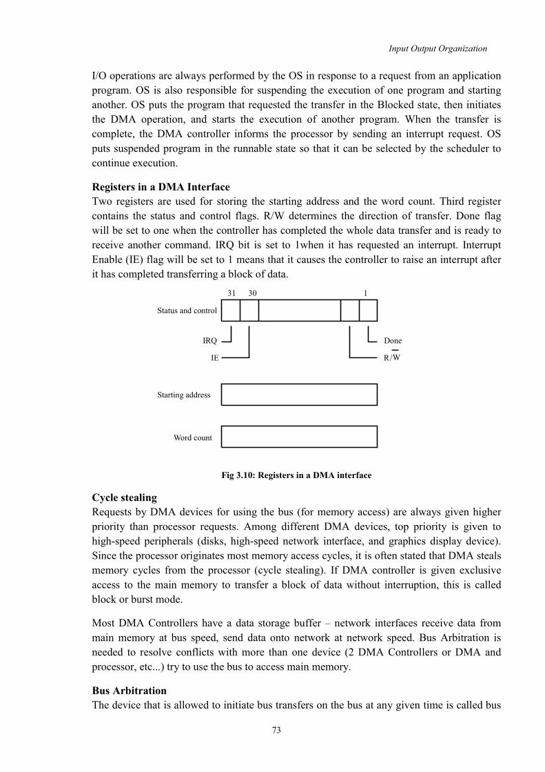
Input Output Organization
73
I/O operations are always performed by the OS in response to a request from an application program. OS is also responsible for suspending the execution of one program and starting another. OS puts the program that requested the transfer in the Blocked state, then initiates the DMA operation, and starts the execution of another program. When the transfer is complete, the DMA controller informs the processor by sending an interrupt request. OS puts suspended program in the runnable state so that it can be selected by the scheduler to continue execution. Registers in a DMA Interface Two registers are used for storing the starting address and the word count. Third register contains the status and control flags. R/W determines the direction of transfer. Done flag will be set to one when the controller has completed the whole data transfer and is ready to receive another command. IRQ bit is set to 1when it has requested an interrupt. Interrupt Enable (IE) flag will be set to 1 means that it causes the controller to raise an interrupt after it has completed transferring a block of data.
Fig 3.10: Registers in a DMA interface Cycle stealing Requests by DMA devices for using the bus (for memory access) are always given higher priority than processor requests. Among different DMA devices, top priority is given to high-speed peripherals (disks, high-speed network interface, and graphics display device). Since the processor originates most memory access cycles, it is often stated that DMA steals memory cycles from the processor (cycle stealing). If DMA controller is given exclusive access to the main memory to transfer a block of data without interruption, this is called block or burst mode. Most DMA Controllers have a data storage buffer – network interfaces receive data from main memory at bus speed, send data onto network at network speed. Bus Arbitration is needed to resolve conflicts with more than one device (2 DMA Controllers or DMA and processor, etc...) try to use the bus to access main memory. Bus Arbitration The device that is allowed to initiate bus transfers on the bus at any given time is called bus
IRQ Done Status and control
Starting address
Word count
IE R/W
31 30 1

Input Output Organization
74
master. When the current master relinquishes control, another device can acquire this status. The process by which the selection of next device to become bus master and bus mastership is transferred to it is known as bus arbitration. There are two approaches to bus arbitration. 1. Centralized Arbitration
Here, a single arbiter performs the arbitration. Bus arbiter may be a processor or a separate unit connected to the bus.
Fig 3.11: A Simple arrangement for bus arbitration using a daisy chain 2. Distributed Arbitration
Here all devices participate in the selection of the next bus master. No central arbiter is used. Each device on bus is assigned a 4-bit identification number. When one or more devices request the bus, they assert the Start-Arbitration signal and place their 4-bit ID number on ARB [3...0]. The request that has the highest ID number ends up having the highest priority. Advantage is that it offers higher reliability (operation of the bus is not dependent on any one device). SCSI bus is an example of distributed (decentralized) arbitration. The drivers specified here are open collector types. Hence, if the i/p to one driver is equal to one and input to another driver connected to the same bus line is equal to 0, the bus will be in low voltage state.
Fig 3.12: A distributed arbitration scheme
Proces
sor
DMA Controller
1 BG1
DMA Controller
2
BR BBSY
BG2
ARB3 ARB2 ARB1 ARB0
Start-Arbitration
O.C.
Interface circuit for device A
0 1 0 1 -0 -1 -1 -1
Vcc

Input Output Organization
75
3.1.4 Buses A bus protocol is the set of rules that govern the behaviour of various devices connected to the bus as to when to place information on the bus, assert control signals, and so on. Bus lines may be grouped into three types: Address, data and control lines. The control signals specify whether a read or write operation is to be performed. The bus control signal also carries timing information. They specify the times at which the processor and I/O devices may place on the bus or receive data from the bus. Many schemes have been there for the timing of data transfers over the bus. They can broadly be classified into two types: 1. Synchronous Bus
In a synchronous bus, all devices derive timing information from a common clock line. Equal spaced pulses on this line define equal time intervals. In the simplest form of a synchronous bus, each of these intervals constitutes a bus cycle during which one data transfer can take place.
2. Asynchronous Bus An alternative scheme for controlling data transfers on the bus is based on the use of a handshake between the master and slave. The common clock is replaced by two timing control lines, Master-ready and Slave-Ready. The first is asserted by the master to indicate that it is ready for a transaction, and the second is a response from the slave.
In this scheme data transfer is controlled by a handshake protocol. The master places the address and command information on the bus. Then it indicates to all devices that it has done so by activating the Master-ready line. This causes all devices on the bus to decode the address. The selected slave performs the required operation and informs the processor it has done so by activating the Slave-ready line. The master waits for Slave-ready to become asserted before it removes its signals from the bus. The handshake process eliminates the need for synchronization of the sender and receiver clock, thus simplifying timing design.
3.1.5 Interface Circuits An I/O interface consists of a circuitry required to connect an I/O device to a computer bus. One side of the interface consists of bus signals and the other side consists of the data path with its associated control (to transfer the data between the interface and I/O Device).This side is called a port. Ports can be classified into two types: serial and parallel port. A parallel port transfer’s data in the form of bits (may be 8 or 16).But in serial port only one bit can transmit at a time. Parallel Port In the case of parallel port, the connections between the device and the computer uses a multiple pin connector and a cable with as many wires, typically arranged in a flat configuration. The circuits at either end are relatively simple, as there is no need to convert

Input Output Organization
76
between parallel and serial formats. This arrangement is suitable for devices that are physically close to the computer. Interface design-Example Firstly circuits for an 8 bit input port and an 8 bit output port are designed. Then we can combine the two circuits to show how the interface for a general purpose 8 bit parallel port can be designed. We assume that interface circuit is connected to a 32 bit processor that uses memory mapped I/O and the asynchronous bus protocol. The following figure shows the hardware components needed for connecting a keyboard to a processor.
Fig 3.13: Keyboard to Processor connection The output of the encoder consists of the bits that represent the encoded character and one signal called valid, which indicates the key is pressed. The information is sent to the interface circuits, which contains a data register, DATAIN and a status flag SIN. When a key is pressed, the valid signal changes from 0 to1, causing the ASCII code to be loaded into DATAIN and SIN set to 1. The status flag SIN set to 0 when the processor reads the contents of the DATAIN register. The interface circuit is connected to the asynchronous bus on which transfers are controlled using the Handshake signals Master ready and Slave-ready. The following figure (3.14) shows a general purpose parallel interface circuit that can be configured in a variety of ways. Datalines P7 through P0 can be used for either input or output purposes. For increased flexibility, the circuit makes it possible for some lines to serve as inputs and some lines to serve as outputs, under program control. The DATAOUT register is connected to these lines via three state drivers that are controlled by a Data Direction Register DDR. The processor can write any 8 bit pattern into DDR. For a given bit if the DDR value is 1, the corresponding dataline acts as an output line otherwise it acts as an input line.
Keyboard switches
DATA IN
Input Interface
SIN
Data
Data
Address
R / W
Master-ready
Slave-ready
Valid
.
.
.
Encoder and debouncing
circuit
Processor

Input Output Organization
77
Fig 3.14: A General 8-Bit Parallel Interface Two lines C1 and C2 are provided to control the interaction between the circuit and the I/O device it serves. These lines are also programmable. Line C2 is bidirectional to provide several different modes of signalling. The Ready and Accept lines are the handshake control lines on the processor bus side. The input signal My-address should be connected to the output of an address decoder that recognizes the address assigned to the interface. Three register select lines (RS0-RS2), allowing upto 8registers in the interface, input and output data, data direction and control and status registers for various modes of operation. An interrupt request output INTR is also provided. It should be connected to the interrupt request line on the computer bus.
Register select
Status and
control
. . .
DATAIN
DATAOUT
Data Direction Register
D7 D0
.
.
.
. . .
P7 P0
C1 C2
My-address RS2 RS1 RS0 R/W Ready
Accept INTR
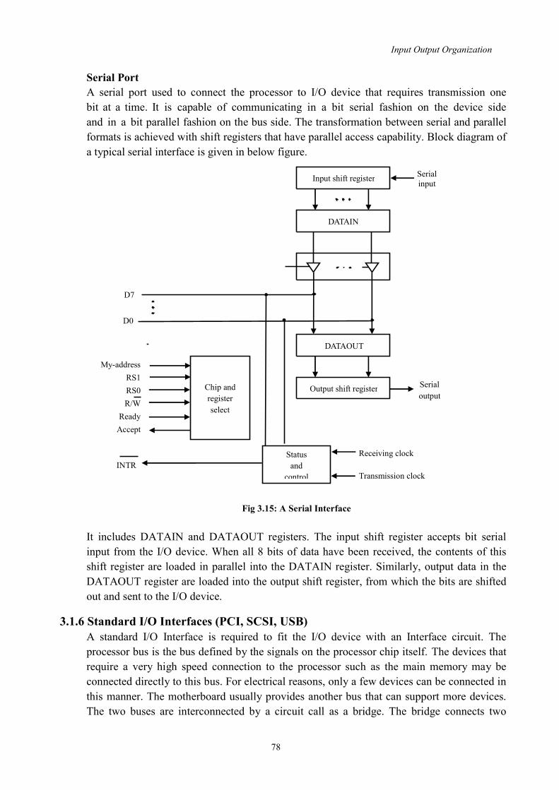
Input Output Organization
78
Serial Port A serial port used to connect the processor to I/O device that requires transmission one bit at a time. It is capable of communicating in a bit serial fashion on the device side and in a bit parallel fashion on the bus side. The transformation between serial and parallel formats is achieved with shift registers that have parallel access capability. Block diagram of a typical serial interface is given in below figure.
Fig 3.15: A Serial Interface It includes DATAIN and DATAOUT registers. The input shift register accepts bit serial input from the I/O device. When all 8 bits of data have been received, the contents of this shift register are loaded in parallel into the DATAIN register. Similarly, output data in the DATAOUT register are loaded into the output shift register, from which the bits are shifted out and sent to the I/O device.
3.1.6 Standard I/O Interfaces (PCI, SCSI, USB) A standard I/O Interface is required to fit the I/O device with an Interface circuit. The processor bus is the bus defined by the signals on the processor chip itself. The devices that require a very high speed connection to the processor such as the main memory may be connected directly to this bus. For electrical reasons, only a few devices can be connected in this manner. The motherboard usually provides another bus that can support more devices. The two buses are interconnected by a circuit call as a bridge. The bridge connects two
D7
D0
Output shift register
DATAIN
Input shift register
Serial output
Serial input
Chip and register select
Status and
control Receiving clock Transmission clock
My-address RS1 RS0 R/W Ready Accept
INTR
DATAOUT

Input Output Organization
79
buses, which translates the signals and protocols of one bus into another. The bridge circuit introduces a small delay in data transfer between processor and the devices.
Fig 3.16: An example of a computer system using different interface standards
Widely used bus standards are: 1. PCI (Peripheral Component Inter Connect) 2. SCSI (Small Computer System Interface) 3. USB (Universal Serial Bus)
1. Peripheral Component Interconnect Bus (PCI)
PCI is developed as a low cost bus that is truly processor independent. It supports high speed disk, graphics and video devices. PCI has plug and play capability for connecting I/O devices. To connect new devices, the user simply connects the device interface board to the bus.
Data Transfer The data are transferred between cache and main memory in bursts of several words each and they are stored in successive memory locations. When the processor specifies an address and request a ‘read’ operation from memory, the memory responds by sending a sequence of data words starting at that address. During write operation, the processor sends the address followed by sequence of data words to be
Bridge
Processor
Main memory
Additional memory
SCSI controller
Ethernet interface
USB controller
ISA interface
Disk controller
CD-ROM controller
Disk 1
Disk 2
Keyboard
CD-ROM
IDE disk
Video
Game
Processor bus
PCI bus
SCSI bus

Input Output Organization
80
written in successive memory locations. PCI supports this mode of read and write operation. A read / write operation involving a single word is treated as a burst of length one. PCI has three address spaces. They are: Memory address space I/O address space Configuration address space
I/O address space is intended for use with processors, which have separate I/O address space. Configuration space is intended to give the PCI its plug and play capability. PCI Bridge provides a separate physical connection to main memory. The master maintains the address information on the bus until data transfer is completed. At any time, only one device acts as bus master. A master is called ‘initiator’ in PCI which is either processor or DMA controller. The addressed device that responds to read and write commands is called a target. A complete transfer operation on the bus, involving an address and a burst of data is called a transaction. Individual word transfers within the transaction are called phases.
Fig 3.17: Use of a PCI bus in a computer system Data Transfer signals on PCI bus
Name Function CLK 33 MHZ / 66 MHZ clock FRAME# Sent by the indicator to indicate the duration of transaction AD 32 address / data line C/BE# 4 command / byte Enable Lines IRDY#, TRDY# Initiator Ready, Target Ready Signals DEVSEL # A response from the device indicating that it has recognized its address and is ready for data transfer transaction. IDSEL # Initialization Device Select
Host
PCI Bridge
Main
memory
Disk
Printer
Ethernet
interface
PCI bus

Input Output Organization
81
Fig 3.18: A read operation on the PCI bus
The sequence events on the bus are shown in fig 3.17. In Clock cycle1, the processor asserts FRAME # to indicate the beginning of a transaction; it sends the address on AD lines and command on C/BE # Lines. Clock cycle2 is used to turn the AD Bus lines around. The processor removes the address and disconnects its drives from AD lines. The selected target enables its drivers on AD lines and fetches the requested data to be placed on the bus during clock cycle 3. It asserts DEVSEL# and maintains it in asserted state until the end of the transaction. C/BE# is used to send a bus command in clock cycle 1 and it is used for different purpose during the rest of the transaction. During clock cycle 3, the initiator asserts IRDY#, to indicate that it is ready to receive data. If the target has data ready to send then it asserts TRDY#. In our eg, the target sends 3 more words of data in clock cycle 4 to 6. The initiator uses FRAME# signal to indicate the duration of the burst. Since it wishes to read 4 words, the initiator negates FRAME # during clock cycle 5. After sending the 4th word in clock cycle 6, the target disconnects its drivers and negates DEVSEL# at the beginning of during clock cycle 7.
1 2 3 4 5 6 7
CLK
FRAME#
IRDY#
TRDY#
DEVSEL#
C/BE# Cmnd Byte enable
AD Address #1 #2 #3 #4

Input Output Organization
82
Fig 3.19: A read operation showing the role of IRDY# / TRDY#
Fig 3.18 shows an example of a more general input transaction. It shows how the IRDY# and TRDY# signals can be used by the initiator and target respectively to indicate a pause in the middle of the transaction. The first two words are transferred and the target sends the 3rd word in cycle 5. But the initiator is not able to receive it. Hence it negates IRDY#. In response the target maintains 3rd data on AD line until IRDY is asserted again. In cycle 6, the initiator asserts IRDY and loads the data in its i/p buffer. But the target is not ready to transfer the fourth word immediately; hence it negates TRDY in cycle 7.It sends the 4th word and asserts TRDY# at cycle 8.
2. SCSI (Small Computer System Interface)
The acronym SCSI stands for Small Computer System Interface. It refers to a standard bus defined by the American National Standards Institute (ANSI). The SCSI bus may be used to connect a variety of devices to a computer. It is particularly well-suited for use with disk drives. It is often found in installations such as institutional databases or email systems where many disks drives are used. SCSI bus had undergone many revisions. Data transfer capability has been increased very rapidly. So many versions including SCSI-2, SCSI-3 (also known as Ultra SCSI or
1 2 3 4 5 6 7 8 9
CLK
FRAME#
IRDY#
TRDY#
DEVSEL#
C/BE# Cmnd Byte enable
AD Address #1 #2 #3 #4

Input Output Organization
83
fast 20 SCSI), and different Ultra versions are there. The recent standard is Ultra 640 (Also known as Fast 320). A SCSI may be narrow or wide. In narrow it may have 8 datalines, so that one byte of data can be transfer at a time. In a wide SCSI, it has 16 data lines and transfer 16 bit of data at a time. The bus may use a single ended transmission (SE) where each signal uses one wire, with a common ground return for all signals or it may use different signalling scheme where a separate return wire is provided for each signal. Two voltage levels are possible in different signalling scheme. Earlier versions use 5v (known as High Voltage Differential) and 3.3v (Low Voltage Differential). Because of these various options SCSI connector may have 50, 68, or 80 pins. Data transfer rate may vary from 5 megabytes/sec in SCSI-1 to 640 megabytes/s in Ultra 640. The higher data rate can be achieved with shorter cable length and fewer devices. So, to achieve top transfer rate the bus length is typically limited to 1.2 m for SE signals and 12m for LVD signalling. The maximum capacity of the bus is 8 devices for a narrow bus and 16 devices for a wide bus. Data Transfer Devices connected to the SCSI bus are not part of the address space of the processor in the same way as devices connected to the processor bus or to the PCI bus. A SCSI bus may be connected directly to the processor bus, or more likely to another standard I/O bus such as PCI, through a SCSI controller. Data and commands are transferred in the form of multi-byte messages called packets. To send commands or data to a device, the processor assembles the information in the memory then instructs the SCSI controller to transfer it to the device. Similarly, when data are read from a device, the controller transfers the data to the memory and then informs the processor by raising an interrupt. There are two types of SCSI controllers. 1. Initiator:
It has the ability to select a particular target and to send commands specifying the operations to be performed. Controller on the processor side must be an initiator type.
2. Target Disk controller operates as a target. It carries out the commands received from the initiator.
Data transfer on SCSI bus is always controlled by the target controller. To send a command to the target, an initiator requests control of the bus and after winning arbitration, selects the controller it wants to communicate with and hands over the control of the bus over to it. Then the controller starts a data transfer operation to receive a command from the initiator. Let us examine a complete Read operation as an example. Assume that the processor wishes to read a block of data from a disk drive and that these data are stored in two
Input Output Organization
84
disk sectors that are not contiguous. The processor sends a command to the SCSI controller, which causes the following sequence of events to take place: 1. The SCSI controller contends for control of the SCSI bus. 2. When it wins the arbitration process, the SCSI controller sends a command to the
disk controller, specifying the required Read operation. 3. The disk controller cannot start to transfer data immediately. It must first move the
read head of the disk to the required sector. Hence, it sends a message to the SCSI controller indicating that it will temporarily suspend the connection between them. The SCSI bus is now free to be used by other devices.
4. The disk controller sends a command to the disk drive to move the read head to the first sector involved in the requested Read operation. It reads the data stored in that sector and stores them in a data buffer. When it is ready to begin transferring data, it requests control of the bus. After it wins arbitration, it re-establishes the connection with the SCSI controller, sends the contents of the data buffer, and then suspends the connection again.
5. The process is repeated to read and transfer the contents of the second disk sector. 6. The SCSI controller transfers the requested data to the main memory and sends an
interrupt to the processor indicating that the data are now available. The messages exchanged over SCSI bus are at a higher level than those exchanged over the processor bus. Higher level means that the messages refer to operations that may require several steps to complete, depending on the device. The SCSI standard defines a wide range of control messages that can be exchanged between the controllers to handle different type of I/O devices. Also some messages are devised to deal with error or failure conditions during device operation or data transfer.
3. Universal Serial Bus (USB) The Universal Serial Bus (USB) is the most widely used interconnection standard. A large variety of devices are available with a USB connector, including mice, memory keys, disk drives, printers, cameras, and many more. The commercial success of the USB is due to its simplicity and low cost. The original USB specification supports two speeds of operation, called low-speed (1.5 Megabits/s) and full-speed (12 Megabits/s). Later, USB 2, called High-Speed USB, was introduced. It enables data transfers at speeds up to 480 Megabits/s. As I/O devices continued to evolve with even higher speed requirements, USB 3 (called Superspeed) was developed. It supports data transfer rates up to 5 Gigabits/s. The USB has been designed to meet several key objectives: Provide a simple, low-cost, and easy to use interconnection system. Accommodate a wide range of I/O devices and bit rates, including Internet
connections, and audio and video applications. Enhance user convenience through a “plug-and-play” mode of operation.

Input Output Organization
85
USB Architecture The USB uses point-to-point connections and a serial transmission format. When multiple devices are connected, they are arranged in a tree structure as shown in below figure.
Fig 3.20: Universal Serial Bus tree structure
Each node of the tree has a device called a hub, which acts as an intermediate transfer point between the host computer and the I/O devices. At the root of the tree, a root hub connects the entire tree to the host computer. The leaves of the tree are the I/O devices: a mouse, a keyboard, a printer, an Internet connection, a camera, or a speaker. The tree structure makes it possible to connect many devices using simple point-to-point serial links. If I/O devices are allowed to send messages at any time, two messages may reach the hub at the same time and interfere with each other. For this reason, the USB operates strictly on the basis of polling. A device may send a message only in response to a poll message from the host processor. Hence, no two devices can send messages at the same time. This restriction allows hubs to be simple, low-cost devices. The above specified mode of operation is same for all devices operating at either high speed or low speed. But one exception is there in USB 2.0 with high speed operation. Consider the following situation in the below figure.
I/O I/O device device
Root hub
Host Computer
Hub Hub
Hub I/O I/O I/O I/O device device device device
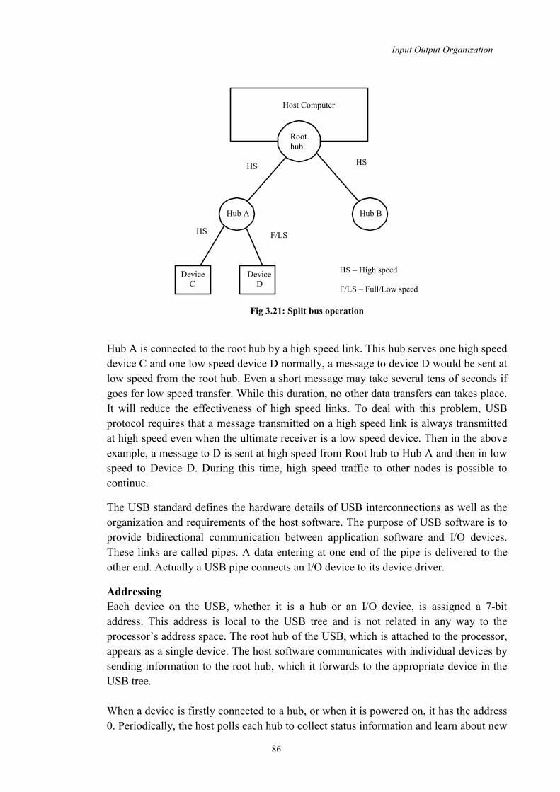
Input Output Organization
86
Fig 3.21: Split bus operation
Hub A is connected to the root hub by a high speed link. This hub serves one high speed device C and one low speed device D normally, a message to device D would be sent at low speed from the root hub. Even a short message may take several tens of seconds if goes for low speed transfer. While this duration, no other data transfers can takes place. It will reduce the effectiveness of high speed links. To deal with this problem, USB protocol requires that a message transmitted on a high speed link is always transmitted at high speed even when the ultimate receiver is a low speed device. Then in the above example, a message to D is sent at high speed from Root hub to Hub A and then in low speed to Device D. During this time, high speed traffic to other nodes is possible to continue. The USB standard defines the hardware details of USB interconnections as well as the organization and requirements of the host software. The purpose of USB software is to provide bidirectional communication between application software and I/O devices. These links are called pipes. A data entering at one end of the pipe is delivered to the other end. Actually a USB pipe connects an I/O device to its device driver. Addressing Each device on the USB, whether it is a hub or an I/O device, is assigned a 7-bit address. This address is local to the USB tree and is not related in any way to the processor’s address space. The root hub of the USB, which is attached to the processor, appears as a single device. The host software communicates with individual devices by sending information to the root hub, which it forwards to the appropriate device in the USB tree. When a device is firstly connected to a hub, or when it is powered on, it has the address 0. Periodically, the host polls each hub to collect status information and learn about new
Root hub
Host Computer
Hub A Hub B
Device Device C D
HS HS
HS F/LS
HS – High speed F/LS – Full/Low speed

Input Output Organization
87
devices that may have been added or disconnected. When the host is informed that a new device has been connected, it reads the information in a special memory in the device’s USB interface to learn about the device’s capabilities. It then assigns the device a unique USB address and writes that address in one of the device’s interface registers. It is this initial connection procedure that gives the USB its plug-and-play capability. USB Protocols All information transferred over the USB is organized into packets, where a packet consists of one or more bytes of information. The information transferred on the USB can be divided into two broad categories: control and data. A packet consists of one or more fields containing different kinds of information. The first field of any packet is packet identifier PID, which identifies the type of packet. There are four bits of information in this field, but they are transmitted twice. The first time they are sent with their true values, and the second time with each bit complemented. This enables the receiving device to verify that the PID byte has been received correctly. Format is given in the following figure.
(a) Packet identifier field
(b) Token packet, IN or OUT
(c) Data packet
Fig 3.22: USB packet formats
Control packets used for controlling data transfer operations are called token packets. A token packet starts with a PID field (using to identify IN or OUT packet).It is followed by 7 bit address of the device and the 4 bit endpoint number within that device. The
PID0 PID1 PID2 PID3 PID0 PID1 PID2 PID3
PID0 ADDR ENDP CRC16
8 7 4 5
Bits
PID DATA CRC16
8 0 to 8192 16
Bits

Input Output Organization
88
packet ends with 5 bit error checking field, using the method called Cyclic Redundancy Check (CRC). Data packets also start with PID field. Three different PID patterns are used to identify data packets, so that data packets may be numbered 0,1 or 2. Data packets don’t carry a device address or an endpoint number. Isochronous Traffic on USB An important feature of the USB is its ability to support the transfer of isochronous data (transmission of real time information such as audio or video data at a constant rate) in a simple manner. As mentioned earlier, isochronous data need to be transferred at precisely timed regular intervals. To accommodate this type of traffic, the root hub transmits a uniquely recognizable sequence of bits over the USB tree every millisecond. This sequence of bits, called a Start of Frame character, acts as a marker indicating the beginning of isochronous data, which are transmitted after this character. Thus, digitized audio and video signals can be transferred in a regular and precisely timed manner. Electrical Characteristic USB connections consist of four wires, of which two carry power, +5 V and Ground, and two wires carry data. Thus, I/O devices that do not have large power requirements can be powered directly from the USB. This obviates the need for a separate power supply for simple devices such as a memory key or a mouse. Two methods are used to send data over a USB cable. When sending data at low speed, a high voltage relative to Ground is transmitted on one of the two data wires to represent a 0 and on the other to represent a 1. The Ground wire carries the return current in both cases. Such a scheme in which a signal is injected on a wire relative to ground is referred to as single-ended transmission.


CHAPTER -4
Memory Systems
Objectives are: Memory System
Basic Concepts Semiconductor RAMs Memory System Considerations Semiconductor ROMs Flash Memory Cache Memory and Mapping Functions


Memory Systems
90
4.1 Memory System Programs and the data are stored in a storage unit called memory. The execution speed of the program is dependent on how fast the transfer of data and instructions in between memory and processor. Anyway faster memory is preferred to increase the throughput of the system. Similarly, the memory should be large to deal with large amount of data and to facilitate the execution of larger programs. So, ideally the memory should be fast, large and inexpensive. But meeting these three requirements is difficult in most of the cases. When the speed and size increases, cost will also increase. In this unit, we are dealing with basic concepts and different implementations of memory.
4.1.1 Basic Concepts Memory is organized as a collection of cells. Each cell can store 1 bit of information ‘0’ or ‘1’. The maximum size of the memory that can be used in any computer can be determined by the addressing scheme. Consider a 16 bit computer, which generates 16 bit address. This computer has a capacity of 216 memory locations. That is 216 memory locations can be addressed in this computer system. Word length is the number of bits that can be transferred to or from the memory. It can be determined from the width of data bus. If the data bus has a width of n bits, it means word length of that computer system is n bits. The following figure shows the connection of memory to the processor.
Fig 4.1: Connection of the memory to the processor Processor and memory are connected through the bus interconnection structure. The bus has three lines to carry address, data and control. Here the address bus has a capacity of k bits, so that memory can store upto 2k memory locations. Similarly, data bus capacity is n bit, so that word length is n bits.MAR and MDR are the two registers inside the processor to facilitate the communication between memory and processor. The main measures to determine the speed of the memory is memory access time and memory cycle time. The time that elapses between the initiation of an operation and the completion of an operation is called memory access time. (Eg: time between read and MFC signal). The minimum time delay required between the initiation of two successive memory operations is called memory cycle time. (Eg: time between successive read operations).
Control lines (R/W, MFC etc.)
Memory k-bit address bus
n-bit data bus Up to 2k addressable locations
Word length = n bits
MAR
MDR
Processor

Memory Systems
91
Based on this speed of measure especially memory access time, a memory hierarchy is designed as follows:
Fig 4.2: Memory hierarchy The fastest unit of the computer system is the processor. Compared to processor, the main memory unit is very slow. So in order to transfer something between memory and processor takes a long time. The processor has to wait a lot. To avoid this speed gap between memory and processor a new memory called cache memory is placed in between main memory and processor. The speed of cache memory is approximately similar to that of processing unit. The lowest level is the secondary memory like disk storage. In this hierarchy, speed will decrease and size will increase from top to bottom level.
4.1.2 Semiconductor RAMs Semiconductor memories are available in a wide range of speed. Their cycle times range from 100 ns to less than 10 ns. When first introduced in late 1990s, they were much more expansive than the magnetic-core memories they replaced. Because of rapid advances in VLSI (Very Large Scale Integration) technology, the cost of semiconductor memories has dropped dramatically. As a result, they are now used almost exclusively in implementing memories. Internal Organisation of Memory Chips Memory cells are usually organized in the form of array, in which each cell is capable of storing one bit of information. A possible organization is illustrated in the following figure. Each row of cells consists of memory word, and all cells of a row are connected to a common line referred to as the word line, which is driven by the address decoder on a chip. The cells in each column are connected to a Sense/Write circuit by two bit lines. The Sense/Write circuits are connected to the data input/output lines of the chip. During a Read operation, these circuits’ sense, or read, the information stored in the cells selected by a
Processor Registers
Primary cache L1
Secondary cache L2
Main Memory
Magnetic Disk Secondary Memory
Increasing Speed Increasing
Cost per bit Increasing Size

Memory Systems
92
word line and transmit this information to the output data lines. During a Write operation, the Sense/Write circuits receive input information and store it in the cells of the selected word. Figure below shows an example of a very small memory chip consisting of 16 words of 8 bits each. This is referred to as a 16 x 8 organization. The data input and the data output of each Sense/Write circuit are connected to the data bus of computer. Two control lines, R/W and CS, are provided in addition to address and data lines. The Read/Write input specifics the required operation, and the CS input select a given chip in multichip memory system.
Fig 4.3: Organization of bit cells in a memory chip The memory circuit in figure stores 128 bits and requires 14 external connections for address, data, and control lines. Of course, it also needs two lines for power supply and ground connections. Consider now a slightly larger memory circuit, one that has 1k (1024) memory cells. The circuit can be organized as a 128 x 8 memory, requiring a total of 19 external connections. Alternatively, the same number of cells can be organized into a 1k x 1 format. In this case, a 10 bit address is needed, but there is only one data line, resulting in 15 external connections. Static Memories Memories that consists of circuits that are capable of retaining their state as long as the the power is applied are known as static memories. The following figure shows how a static RAM cell may be implemented.
circuit circuit circuit
Memory Cells
A3
W0
A0 W1
W15
Sense/Write Sense/Write Sense/Write R/W CS
7 1b7 b b1 b b0 b0
Data input /output lines: b7 b1 b0
Address decoder
A1
A2
FF FF

Memory Systems
93
Fig 4.4: A static RAM cell Two inverters are cross connected to form a latch. Latch is connected to two bit lines by transistors T1 and T2.These transistors act as switches that can be opened or closed under the control of a word line. When the word line is at the ground level, transistors are turned off and the latch retains its state. Read operation Word line is activated to close T1 and T2 Cell is in state '1' => b=1 and b'=0 Cell is in state '0' => b=0 and b'=1 Sense/Write circuit transmit the state of b & b' to output line
Write operation Set the value of b & b' Activate word line, which close the T1 and T2 and Cell acquire the state of b & b'
CMOS Cell CMOS realization of a memory cell is shown below:
Fig 4.5: An example of a CMOS memory cell
Word line Bit lines
T1 X Y T2
b b
Word lineBit lines
T5 T6
T3 T4T1 T2
X Y
b Vsupply b

Memory Systems
94
The transistor pairs (T3, T5) and (T4, T6) form the inverters in the latch. Cell is in state ‘1’, when transistors T3 and T6 are ‘on’ and T4 and T5 are ‘off’. T1 and T2 work as switches to propagate the Cell state into bit lines b and b’. Constant Vsupply of 5V or 3V is required to maintain the state of Cell. Hence cell is volatile. Major advantage of CMOS cell, is their very low power consumption because current flows in the cell only when cell is being accessed. CMOS SRAMs have high speed data access, but more expensive. DRAM (Dynamic Random Access Memory) Static RAMs are fast, but the cost is too high because their cells require several transistors. Less expensive RAMs can be implemented if simpler cells are used. Such cells don’t retain their state indefinitely; hence they are called dynamic RAMs. Dynamic memory cell consists of a capacitor C, and a transistor T. In order to store information in this cell, transistor t is turned on and an appropriate voltage is applied to the bit line. This causes a known amount of charge to be stored in the capacitor.
Fig 4.6: A single transistor dynamic memory cell
Information is stored in a dynamic memory cell in the form of a charge on a capacitor, and this charge can be maintained for only tens of milliseconds. Since the cell is required to store information for a much longer time, its contents must be periodically refreshed by restoring the capacitor charge to its full value. Read Operation Transistor turned on, Sensor check voltage of capacitor If voltage is less than Threshold value, Capacitor discharged and it represents logical ‘0’.If voltage is above Threshold value, Capacitor charged to full voltage and it represents Logical ‘1’. Write Operation Transistor is turned on and a voltage is applied to the bit line Asynchronous Dynamic RAM In Asynchronous dynamic RAM, the timing of the memory device is controlled asynchronously. A specialized memory controller circuit provides the necessary control signals, RAS and CAS, which govern the timing. The processor must take into account the delay in the response of the memory.
TC
Word line
Bit line
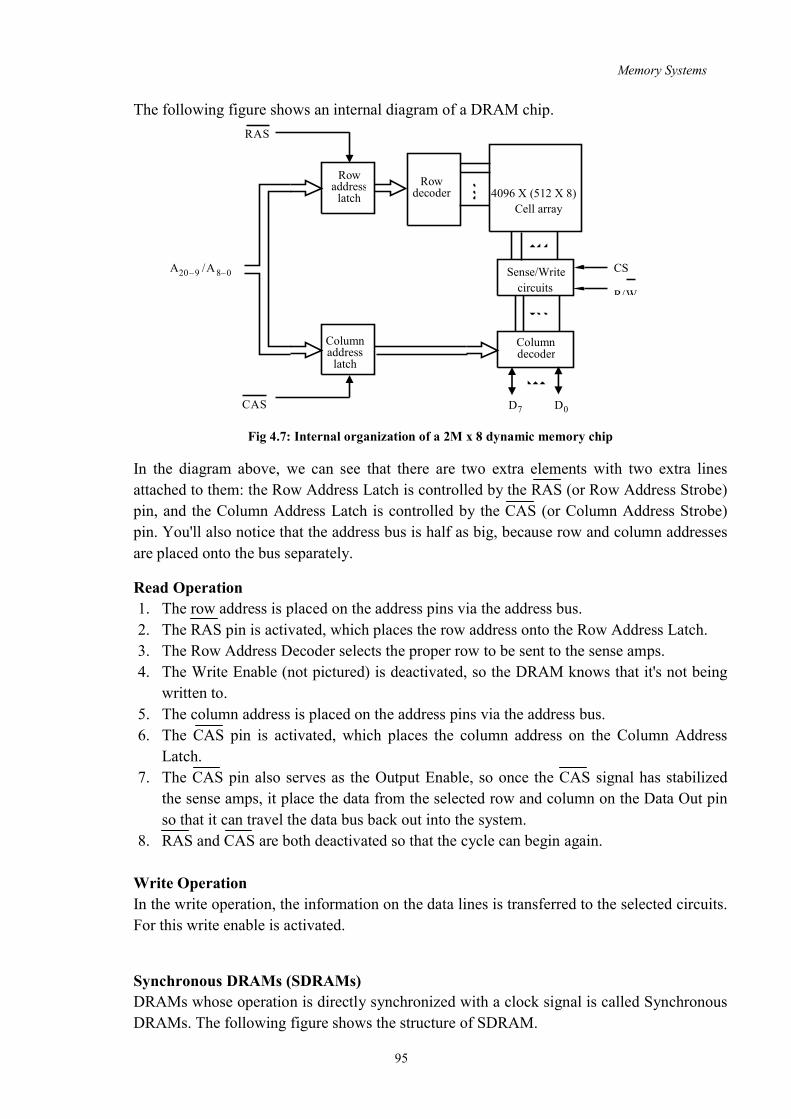
Memory Systems
95
The following figure shows an internal diagram of a DRAM chip.
Fig 4.7: Internal organization of a 2M x 8 dynamic memory chip In the diagram above, we can see that there are two extra elements with two extra lines attached to them: the Row Address Latch is controlled by the RAS (or Row Address Strobe) pin, and the Column Address Latch is controlled by the CAS (or Column Address Strobe) pin. You'll also notice that the address bus is half as big, because row and column addresses are placed onto the bus separately. Read Operation 1. The row address is placed on the address pins via the address bus. 2. The RAS pin is activated, which places the row address onto the Row Address Latch. 3. The Row Address Decoder selects the proper row to be sent to the sense amps. 4. The Write Enable (not pictured) is deactivated, so the DRAM knows that it's not being
written to. 5. The column address is placed on the address pins via the address bus. 6. The CAS pin is activated, which places the column address on the Column Address
Latch. 7. The CAS pin also serves as the Output Enable, so once the CAS signal has stabilized
the sense amps, it place the data from the selected row and column on the Data Out pin so that it can travel the data bus back out into the system.
8. RAS and CAS are both deactivated so that the cycle can begin again.
Write Operation In the write operation, the information on the data lines is transferred to the selected circuits. For this write enable is activated. Synchronous DRAMs (SDRAMs) DRAMs whose operation is directly synchronized with a clock signal is called Synchronous DRAMs. The following figure shows the structure of SDRAM.
Row address latch Row decoder
Column decoderColumn address latch
A20–9 /A 8–0 Sense/Write CS circuits R/W
RAS
CAS D7 D0
4096 X (512 X 8)
Cell array

Memory Systems
96
Fig 4.8: Synchronous DRAM The cell array is the same as in Asynchronous DRAMs. The address and data connections are buffered by means of registers. The output of each sense amplifier is connected to a latch. During a read operation the selected row cells are loaded in these latches. From there it is transferred to data output register. SDRAMs have several different modes of operation which can be selected by writing control information into a mode register. Double Data Rate SDRAM (DDR-SDRAM) DDR-SDRAM is a faster version of SDRAM. The standard SDRAM perform all actions on the rising edge of the clock signal.DDR SDRAM is also access the cell array in the same way but transfers data on both edges of the clock. So bandwidth is essentially doubled for long burst transfers. To make it possible to access the data at a high enough rate, the cell array is organized in two banks. Each bank can access separately. Consecutive words of a given block are stored in different banks. Such interleaving of words allows simultaneous access to two words that are transferred on successive edges of the clock.
4.1.3 Memory System Considerations The choice of memory for a given application mainly depends on the factors cost, speed, power dissipation and size of the chip. If speed is the primary requirement static RAMs are the most appropriate one. Static RAMs are mostly used in cache memories. If cost is the prioritized factor then we are going for dynamic RAMs. Dynamic RAMs are used for implementing computer main memories. Memory Controller Dynamic memory chips use multiplexed address inputs so that we can reduce the number of pins. The address is divided into two parts and they are the High order address bits and Low order address bits. The high order selects a row in the cell array and the low order address bits selects a column in the cell array. The address selection is done under the control of RAS and CAS signal respectively for high order and low order address bits.
CS
Clock
Cell array Row address latch Row decoder
Column decoder Read/Write circuits & latches Column address counter
Row/Column address
Data input register Data output register
Data
Refresh counter
RAS Mode register CAS and R/ W timing control

Memory Systems
97
A processor issues all bits of an address at the same time. Multiplexing of address bits is performed by a memory-controller circuit, placed between processor and dynamic memory. Controller accepts a complete address and the R/W (Read/Write) signal from the processor, under control of a request signal. Whenever a memory access operation is needed, processor issues a request signal. Then, the controller forwards the row and column portions of the address to the memory, and generates RAS and CAS signals. It also sends the R/W and CS signals to the memory. Data lines are connected directly between processor and memory. Dynamic memories have to be refreshed. But they don’t have self refreshing capability. Memory controller has to provide the information’s needed to control the refreshing process.
Fig 4.9: Use of a memory controller 4.1.4 Semiconductor ROMs
One major type of memory that is used in PCs is called read - only memory or ROM for short. ROM is a type of memory that normally can only be read, as opposed to RAM which can be both read and written. It is a non volatile memory. That is the contents will retain even when the power is switched off. There are two main reasons that read-only memory is used for certain functions within the PC: Permanence: The values stored in ROM are always there, whether the power is on or
not. A ROM can be removed from the PC, stored for an indefinite period of time, and then replaced, and the data it contains will still be there. For this reason, it is called non-volatile storage. A hard disk is also non-volatile, for the same reason, but regular RAM is not.
Security: The fact that ROM cannot easily be modified provides a measure of security against accidental (or malicious) changes to its contents. You are not going to find viruses infecting true ROMs, for example; it's just not possible. (It's technically possible with erasable EPROMs, though in practice never seen.)
Row/Column
Address
Processor
Memory
Memory
controller
Data
Address
R/W
Request
Clock
RAS CAS R/W CS
Clock

Memory Systems
98
While the whole point of a ROM is supposed to be that the contents cannot be changed, there are times when being able to change the contents of a ROM can be very useful. There are several ROM variants that can be changed under certain circumstances; these can be thought of as "mostly read-only memory". The following are the different types of ROMs with a description of their relative modifiability: ROM: A regular ROM is constructed from hard-wired logic, encoded in the silicon itself, much the way that a processor is. It is designed to perform a specific function and cannot be changed. This is inflexible and so regular ROMs are only used generally for programs that are static (not changing often) and mass-produced. This product is analogous to a commercial software CD-ROM that you purchase in a store. Programmable ROM (PROM): This is a type of ROM that can be programmed using
special equipment; it can be written to, but only once. This is useful for companies that make their own ROMs from software they write, because when they change their code they can create new PROMs without requiring expensive equipment. This is similar to the way a CD-ROM recorder works by letting you "burn" programs onto blanks once and then letting you read from them many times. In fact, programming a PROM is also called burning, just like burning a CD-R, and it is comparable in terms of its flexibility.
Erasable Programmable ROM (EPROM): An EPROM is a ROM that can be erased and reprogrammed. A little glass window is installed in the top of the ROM package, through which you can actually see the chip that holds the memory. Ultraviolet light of a specific frequency can be shined through this window for a specified period of time, which will erase the EPROM and allow it to be reprogrammed again. Obviously this is much more useful than a regular PROM, but it does require the erasing light. Continuing the "CD" analogy, this technology is analogous to a reusable CD-RW.
Electrically Erasable Programmable ROM (EEPROM): The next level of erasability is the EEPROM, which can be erased under software control. This is the most flexible type of ROM, and is now commonly used for holding BIOS programs. When you hear reference to a "flash BIOS" or doing a BIOS upgrade by "flashing", this refers to reprogramming the BIOS EEPROM with a special software program. Here we are blurring the line a bit between what "read-only" really means, but remember that this rewriting is done maybe once a year or so, compared to real read-write memory (RAM) where rewriting is done often many times per second.
4.1.5 Flash Memory In EEPROM, it is possible to read & write the contents of a single cell. In Flash device, it is possible to read the contents of a single cell but it is only possible to write the entire contents of a block. Prior to writing, the previous contents of the block are erased. Eg. In MP3 player, the flash memory stores the data that represents sound. Single flash chips cannot provide sufficient storage capacity for embedded system application. There are 2 methods for implementing larger memory modules consisting of number of chips. They are,

Memory Systems
99
Flash Cards One way of constructing larger module is to mount flash chips on a small card. Such flash card have standard interface. Flash cards come in variety of memory sizes (8, 32, 64 Mbits).
Flash Drives These are developed to replace hard disk drives. But the storage capacity of flash drives is significantly lower. These are solid state electronic devices which have no movable parts. The main advantages of flash drives are shorter seek and access times and low power consumption. The main disadvantage is their smaller capacity and higher cost per bit.
4.1.6 Cache Memory and Mapping Functions Cache Memory Cache memory is extremely fast memory that is built into a computer’s central processing unit (CPU), or located next to it on a separate chip. The CPU uses cache memory to store instructions that are repeatedly required to run programs, improving overall system speed. The advantage of cache memory is that the CPU does not have to use the motherboard’s system bus for data transfer. Whenever data must be passed through the system bus, the data transfer speed slows to the motherboard’s capability. The CPU can process data much faster by avoiding the bottleneck created by the system bus. If there is no concept of cache, CPU has to fetch everything from the main memory itself. Main memory is very slow compared to processor. So CPU has to wait for a long time in the case of transfer. As it happens, once most programs are open and running, they use very few resources. When these resources are kept in cache, programs can operate more quickly and efficiently. All else being equal, cache is so effective in system performance that a computer running a fast CPU with little cache can have lower benchmarks than a system running a somewhat slower CPU with more cache. Cache built into the CPU itself is referred to as Level 1 (L1) cache. Cache that resides on a separate chip next to the CPU is called Level 2 (L2) cache. Some CPUs have both L1 and L2 cache built-in and designate the separate cache chip as Level 3 (L3) cache. The effectiveness of the cache mechanism is based on a property of called locality of reference. Locality of reference can be defined as follows: Many instructions in localized areas of the program are executed repeatedly during some period & remainder of the program is accessed relatively infrequently. Two types of locality of reference are there. Temporal
Recently executed instruction is likely to be executed again very soon. The temporal aspect of the locality of reference suggests that whenever an information item is first needed, this item should be brought into the cache where it will hopefully remain until it is needed again.
Spatial Instructions in close proximity to a recently executed instruction are also likely to be executed soon. Spatial aspects suggest that instead of fetching just one item from the

Memory Systems
100
main memory to the cache, it is useful to fetch several items that reside at adjacent addresses as well (That is read a block).
Working of cache Cache is placed in between main memory and processor. When a read request is received from the processor, the contents of a block of memory words containing the location specified are transferred into the cache one word at a time. Subsequently when the program references any of the locations in this block, the desired contents are read directly from the cache.
Fig 4.10: Use of a cache memory
Read operation The following things can happen: 1. Cache hit: cache block is valid and contains proper address, so read desired word 2. Cache miss: desired word is not present in cache, so fetch the word from main memory 3. Cache miss, block replacement: required data not in cache; some other data in the space;
fetch desired data from memory and replace The processor doesn’t need to know explicitly about the existence of cache. They simply issue read and write request using addresses that refer to locations in the memory. The cache control circuitry determines whether the requested word currently exists in cache. If it does, the read or write operation is performed on the appropriate cache location. This is called a read or write hit. If the referenced word is not in cache, it is called cache miss. In that case, the block of words that contain the requested word is copied from the main memory into cache. The requested word may be sent to the processor as soon as it is read from the main memory or after the entire block is loaded into the cache. If the word is sent to the processor as soon as it is read from the main memory, it is called load-through or early restart. Load through approach reduces processor’s waiting time but more expensive. Suppose that the cache is full when a miss occurs. In that case, one of the blocks has to be replaced from the cache to make the room for the newly fetched word. The block which has to be replaced is determined by some replacement algorithms. In a read operation main memory is not involved. Write operation For a write operation system can proceed in two ways: 1. Write Through: the cache and the main memory locations are updated simultaneously.
Cache Main memory Processor

Memory Systems
101
2. Write Back: cache location updated during a write operation is marked with a dirty or modified bit. The main memory location is updated later when the block is to be removed from the cache.The dirty bit is helping to identify the modified block.
Write through protocol is simpler, but it results in unnecessary write operations in the main memory when a given cache word is updated several times during its cache residency. Write back protocol also results in unnecessary write operations because when a cache block is written back to the memory all words of the block are written back even if only a single word has been changed while the block was in the cache. During a write operation, if the addressed word is not in the cache, a write miss occurs. Then, if the write through protocol is used, the information is written directly into the main memory. In the case of write back, the block containing the addressed word is first brought into the cache, and then desired word in the cache is overwritten with the new information. The correspondence between the main memory blocks and those in the cache is specified by a mapping function. Mainly three types of mapping functions are there. Directive mapping Associative mapping Set Associative mapping
To explain the mapping procedures, we consider a 2K cache consisting of 128 blocks of 16 words each, and a 64K main memory addressable by a 16-bit address, 4096 blocks of 16 words each. Mapping functions Directive Mapping
According to this mapping function block j of the main memory is mapped to block j modulo 128 of cache. That is block 0 is mapped to block 0 modulo 128 of cache that is block 0 is mapped to block 0 of cache.Block1 to block 1 of cache and so on. When the block 128 comes it will map to block 0.Again when the block 255 comes, it will also map to block 0.This is the disadvantage of this mapping technique. A contention will arise for the same block even if there are free blocks in cache. Placement of a block in the cache is determined from the memory address. The memory address can be divided into three fields. The low-order 4 bits select one of 16 words in a block. When a new block enters the cache, the 7 bit cache block field determines the cache position in which this block must be stored. The high order 5 bits of the memory address of the block are stored in 5 tag bits associated with its location in the cache. As execution proceeds, the 7 bit cache block field of each address generated by the processor points to a particular block location in the cache. The high order 5 bits of the address are compared with the tag bits associated with that cache location. If they match, then the desired word is in that block of cache. If there is no match, then the block containing the required word must first be read from the main memory and located into the cache. Direct mapping technique is very easy to implement.

Memory Systems
102
Fig 4.11: Direct mapped cache Associative Mapping
According to this, main memory block can be placed into any cache block position. So, the space in the cache can be used more efficiently.
Fig 4.12: Associative mapped cache Here, The 12 tag bits identify a memory block residing in the cache and the lower-order 4 bits select one of 16 words in a block. The tag bits of an address received from the
Main memory
4 Main memory address Tag Block Word 5 7
Block 0 Block 1
Block 127 Block 128 Block 129
Block 255 Block 256 Block 257
Block 4095
Cache
Block 0
Block 1
tag Block 127
tag tag
Main memory
12 4 Main memory address Tag Word
Cache tag Block 0 tag Block 1
tag Block 127
Block 4095
Block i
Block 1 Block 0

Memory Systems
103
processor are compared to the tag bits of each block of the cache to see if the desired block is present. The cost of an associative cache is higher than the cost of a direct mapped cache because of the need to search all 128 tag patterns to determine whether given cache block is in the cache. A search of this kind is called an associative search.
Set Associative Mapping It is combination of direct mapping and associative mapping techniques. Blocks of the cache are grouped into sets, and the mapping allows a block of the main memory to reside in any block of a specific set. Hence the contention problem of direct mapping is eased by having a few choices for block placement. At the same time, the hardware cost can be reduced by decreasing the size of the associative search. The following figure shows an example a set associative technique for a cache with two blocks per set. In this case, memory blocks 0, 64,128….4032 are map into cache set 0, and they can occupy either of the two block positions within this set.
Fig 4.13: Set-associative-mapped cache with two blocks per set
Cache
Main memory
6 6 4 Main memory address Tag Set Word
Block 4095
Block 129 Block 128 Block 127
Block 65 Block 64 Block 63
Block 1 Block 0
Block 127 Block 126
Block 3 Block 2 Block 1 Block 0 tag Set 0
tag tag Set 1 tag
tag Set 63
tag

Memory Systems
104
The 6-bit set field determines which set of the cache might contain the desired block. The tag field is associatively compared to the tags of the two blocks of the set to check if the desired block is present. This is called two way set associative search.
CHAPTER -5
ALU Design
Objectives are: Processor Logic Design
Register Transfer Logic Inter Register Transfer Arithmetic, Logic and Shift Microoperations Conditional Control Statements.
Processor organization Design of Arithmetic and Logic unit Design of Combinational Logic Shifter Status Registers Processor Unit Design of Accumulator.

ALU Design
106
5.1 Processor Logic Design This section of processor logic design goes through the basic logic concepts design such as register transfer, arithmetic, logic, shift microoperations etc.
5.1.1 Register Transfer Logic A digital system is a sequential logic system constructed with flip flops and gates. Sequential circuit can be specified by means of a state table. To specify a large digital system with a state table would be very difficult, since the number of states would be very large. To overcome this difficulty, digital systems are designed using a modular approach, where each modular subsystem performs some functional task. The modules are constructed from such digital functions as registers, counters, decoders, multiplexers, arithmetic elements and control logic. Various modules are interconnected with data and control paths. The interconnection of digital functions cannot be described by means of combinational or sequential logic techniques. To describe a digital system in terms of functions such as adders, decoders and registers, it is necessary to employ a higher level mathematical notation. The register transfer logic method fulfils this requirement. The information flow and the processing task among the data stored in the registers can be described by means of register transfer logic. It provides the necessary tool for specifying the interconnection between various digital functions. Components of register transfer logic The set of registers in the system and their functions. The binary-coded information stored in the registers. The operations performed on the information stored in the registers. The control functions that initiate the sequence of operations.
A register also encompasses all type of registers including shift registers, counters and memory units. Counter is considering as a register whose function is to increment by 1 the information stored within it. A memory unit is considered to be a set of storage registers where information can be stored. A flip flop standing alone can be considered as 1 bit register. The binary information stored in registers may be binary numbers, binary coded decimal numbers, alphanumeric characters, control information or any other binary coded information. The operations performed on data stored in registers are called micro operations. Examples are shift, count, add, clear and load. The control functions that initiate the sequence of operations consists of timing signals that sequence the operations one at a time. A control function is a binary variable, so that it performs the operation when the bit is 1 and inhibits the operation when bit is 0. The type of micro operations in digital systems can be classified into four categories: 1. Inter register transfer.
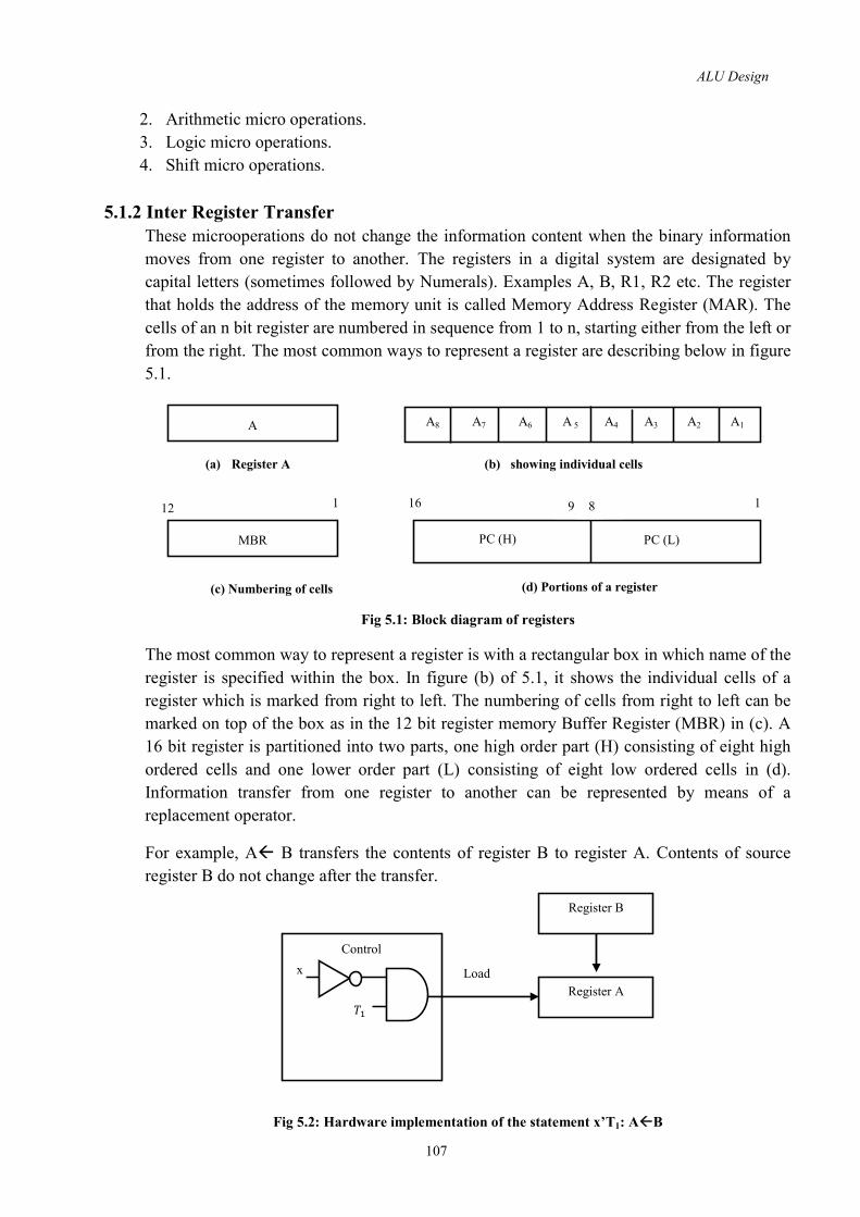
ALU Design
107
2. Arithmetic micro operations. 3. Logic micro operations. 4. Shift micro operations.
5.1.2 Inter Register Transfer
These microoperations do not change the information content when the binary information moves from one register to another. The registers in a digital system are designated by capital letters (sometimes followed by Numerals). Examples A, B, R1, R2 etc. The register that holds the address of the memory unit is called Memory Address Register (MAR). The cells of an n bit register are numbered in sequence from 1 to n, starting either from the left or from the right. The most common ways to represent a register are describing below in figure 5.1.
Fig 5.1: Block diagram of registers The most common way to represent a register is with a rectangular box in which name of the register is specified within the box. In figure (b) of 5.1, it shows the individual cells of a register which is marked from right to left. The numbering of cells from right to left can be marked on top of the box as in the 12 bit register memory Buffer Register (MBR) in (c). A 16 bit register is partitioned into two parts, one high order part (H) consisting of eight high ordered cells and one lower order part (L) consisting of eight low ordered cells in (d). Information transfer from one register to another can be represented by means of a replacement operator. For example, A B transfers the contents of register B to register A. Contents of source register B do not change after the transfer.
Fig 5.2: Hardware implementation of the statement x’T1: AB
(a) Register A
12
(c) Numbering of cells
A
MBR PC (L) PC (H) 1 16 9 8 1
(b) showing individual cells
(d) Portions of a register
A8 A7 A6 A 5 A4 A3 A2 A1
Register A
Register B
x Control
Load

ALU Design
108
We do not wish this transfer to occur with every clock pulse, but only under a predetermined condition. The condition that determines when the transfer is to occur is called a control function. A control function is a Boolean function that can be equal to 0 or 1. The control function can be specified with the following statement:
x’T1: AB It means that the transfer operation be executed by the hardware only when the Boolean function x’T1=1.That is, variable x=0 and timing variable T1=1. The implementation of this statement is shown in fig 5.2. The basic symbols of the register transfer logic are listed in the following table.
Symbol
Description
Examples
Letters(and numerals) Denotes a register A,MBR,R2
Subscript Denotes a bit of register A2,B6
Parenthesis ( ) Denotes a portion of a register PC(H),MBR(OP)
Arrow Denotes transfer of information AB
Colon : Terminates a control function x’T1:
Comma , Separates two micro operations AB,BA
Square brackets [ ] Specifies an address for memory transfer MBRM[MAR]
Table 5.1: Basic symbols of register transfer logic Registers are denoted by capital letters, and numerals may follow letters. Subscripts are used to distinguish individual cells of a register. Parenthesis is used to define a portion of a register. The arrow denotes the transfer operation and direction of transfer. A colon terminates a control function and the comma is used to separate two or more operations that are executed at the same time. Simultaneous operation is possible in registers with master slave or edge triggered flip flops. For example, the contents of two registers can be swapped during one common clock pulse as below.
T3: AB, BA In some cases, there may be situations in which destination register may be same for different source registers at different clock cycles. In such cases, a multiplexer circuit is used to select between two possible paths.
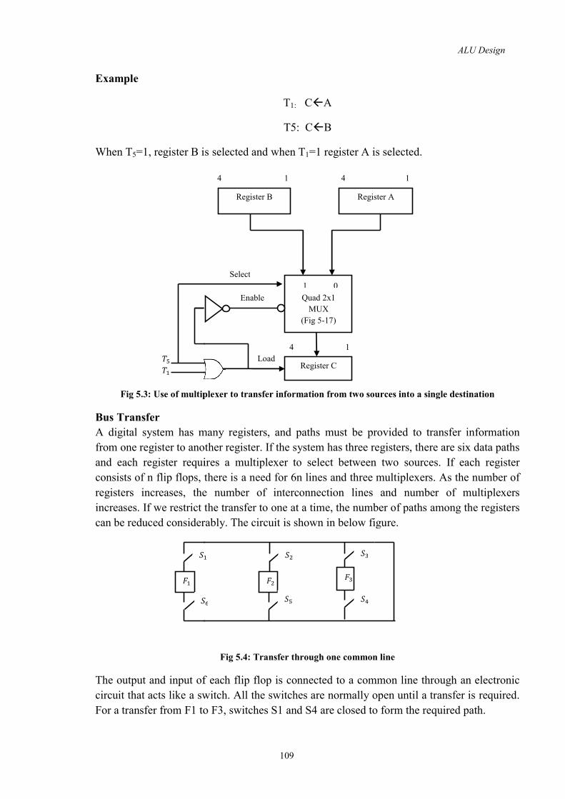
Example
When T5=1, register B is selected and when T
Fig 5.3: Use of multiplexer to transfer Bus Transfer A digital system has many registers, and paths must be provided to transfer information from one register to another register. If the system has three registers, there are six data paths and each register requires a multiplexer to select between two sources. If each register consists of n flip flops, there is a need for 6n lines and three multiplexers. As the number of registers increases, the number of interconnection lines and number of increases. If we restrict the transfer to one at a time, the number of paths among the registers can be reduced considerably. The circuit is shown in below figure.
The output and input of each flip flop is connected to a common line through an electronic circuit that acts like a switch. All the switches are normally open until a transfer is required. For a transfer from F1 to F3, switches S1 and S4 are closed to form
109
T1: CA T5: CB
=1, register B is selected and when T1=1 register A is selected.
Fig 5.3: Use of multiplexer to transfer information from two sources into a single destination
A digital system has many registers, and paths must be provided to transfer information from one register to another register. If the system has three registers, there are six data paths and each register requires a multiplexer to select between two sources. If each register consists of n flip flops, there is a need for 6n lines and three multiplexers. As the number of registers increases, the number of interconnection lines and number of increases. If we restrict the transfer to one at a time, the number of paths among the registers can be reduced considerably. The circuit is shown in below figure.
Fig 5.4: Transfer through one common line
The output and input of each flip flop is connected to a common line through an electronic circuit that acts like a switch. All the switches are normally open until a transfer is required. For a transfer from F1 to F3, switches S1 and S4 are closed to form the required path.
Register B Register A
Quad 2x1 MUX
(Fig 5-17)
Register C
4 1 4 1
1 0
4 1
Select Enable
Load
ALU Design
is selected.
information from two sources into a single destination
A digital system has many registers, and paths must be provided to transfer information from one register to another register. If the system has three registers, there are six data paths and each register requires a multiplexer to select between two sources. If each register consists of n flip flops, there is a need for 6n lines and three multiplexers. As the number of registers increases, the number of interconnection lines and number of multiplexers increases. If we restrict the transfer to one at a time, the number of paths among the registers
The output and input of each flip flop is connected to a common line through an electronic circuit that acts like a switch. All the switches are normally open until a transfer is required.
the required path.
1

ALU Design
110
A group of wires through which binary information is transferred one at a time among registers is called a bus. A common bus system can be constructed with multiplexers and a destination register for the bus transfer can be selected by means of a decoder. The multiplexers select one source register for the bus and the decoder selects one destination register to transfer the information from the bus. Memory Transfer The transfer of information from memory register to the outside environment is called a read operation. The transfer of new information into memory register is called write operation. In both operations, the memory register selected is specified by an address. The read operation is a transfer from the selected memory register M into MBR (memory Buffer register).This can be represented by the following statement:
R: MBR M R is the control function that initiates the read operation. Write operation is the transfer from MBR to the selected memory register M. This can be represented by the following statement:
W: MMBR
Fig 5.5: Memory unit that communicates with two external registers The access time of a memory unit must be synchronized with the master clock pulses in the system that triggers the processor registers. In fast memories, the access time may be slower than or equal to a clock pulse period. In slow memories, it may be necessary to wait for a number of clock pulses for the transfer to be completed. In some systems, the memory unit receives addresses and data from many registers connected to common buses.
5.1.3 Arithmetic, Logic and Shift Microoperations The inter register transfer micro operations do not change the information content when the binary information moves from the source register to the destination register. All other micro operations change the information content during the transfer. A set of basic micro operations are described in this section. Arithmetic Micro operations The basic arithmetic micro operations are add, subtract, complement, and shift.
MAR Memory Unit
MBR
Read Write

ALU Design
111
Add operation It can be specified by the statement:
FA+ B That is, the contents of register A is added to the contents of register B and the sum is transferred to register F. Here we require 3 registers and one digital function that perform the addition operation such as parallel adder. The other basic arithmetic operations are listed in the following table.
Symbolic designation Description
FA+B Contents of A plus B transferred to F
FA-B Contents of A minus B transferred to F
BB Complement register B(1’s complement)
BB +1 Form the 2’s complement of contents of register B
FA+ B +1 A plus 2’s complement of B transferred to F
AA+1 Increment the contents of A by 1(count up)
AA-1 Decrement the contents of A by 1(count down)
Table 5.2: Table showing other basic arithmetic microoperations Arithmetic subtraction is most often implemented through complementation and addition. That is, Adding 1 to the 1’s complement of B gives the 2’s complement of B. When adding 2’s complement of B to A it will results in minus operation (A-B). Increment and decrement micro operations are implemented with an up counter and down counter. There must be a direct relationship between the statements written in a register transfer language and the registers and digital functions which are required for their implementation. For example consider the following two statements:
T2: AA+B T5: AA+1
Implementation for these add and increment operations is given in the following figure.
FA+B+1

ALU Design
112
Fig 5.6: Implementation for add and increment micro operations Timing variable T2 initiates an operation to add the contents of A and B. Timing variable T5 increments register A. The register be a counter with parallel load capability inorder to perform increment operation and to transfer the sum to A from parallel adder. Parallel adder receives input data from A and B and sum bits are applied to register A. Timing variable T2 loads the sum to A. Timing variable T5 increments the register by enabling the increment input. Arithmetic operations multiply and divide can be represented by the symbol * and / respectively. In most computers multiplication is implemented with a sequence of add and shift operations and division is implemented with a sequence of subtract and shift operations. Logic Micro Operations Logic micro operations specify binary operations for a string of bits stored in registers. These operations consider each bit in the registers separately and treat it as a binary variable. For example consider the AND operation of A and B. Content of A is 1101 and content of B is 1010. Then, 1101(A) 1010(B) A AND B will be 1000 (it will contain in the register F) There are 16 different logic operations can be performed with two binary variables, as described in the below table.
Register B
Parallel Adder
Register A
Sum Load
Increment T2
T5

ALU Design
113
Boolean Functions
Operator symbol
Name Comments
F0=0 Null Binary constant 0 F1=xy x.y AND x and y F2=xy’ x/y Inhibition x but not y F3=x Transfer X F4=x’y y/x Inhibition y but not x F5=y Transfer Y F6=xy’+x’y x ⊕ y Exclusive-OR x or y but not both F7= x + y x + y OR x or y F8= (x + y)’ x↓y NOR Not-OR F9= xy +x’y’ x ʘy Equivalence x equals y F10=y’ y’ Complement Not y F11 = x + y’ x⊂y Implication If y then x F12= x’ x’ Complement Not x F13 = x’ + y x⊃y Implication If x then y F14 = (xy)’ x↑y NAND Not-AND F15 = 1 Identity Binary constant 1
Table 5.3: Boolean expressions for the 16 function of two variables All 16 logic operations can be expressed in terms of the AND, OR and complement operations. Special symbols are adopted for these three micro operations. ∧ used for representing AND operation V used for representing OR operation A bar on the top of the letter as in the case of 1’s complement is used for representing complement operation. By using these symbols, it is possible to differentiate between a logic micro operation and a control function. The logic micro operations can be easily implemented with a group of gates. The complement of a register of n bits is obtained from n inverter gates. Similarly AND and OR micro operations can obtained from a group of AND gates and OR gates respectively, each of which receives pair of bits from the two source registers. Shift Micro Operations Shift micro operations transfer binary information between registers in serial computers. They are also used in parallel computers for arithmetic, logic and control operations.

ALU Design
114
Registers can be shifted to the left or right. There are no conventional symbols for shift. Here we are adopting the symbols shl and shr for shift left and shift right operations respectively.
Ashl A (1 bit shift to the left of register A) Bshr B (1 bit shift to the right of register B) Examples
Here when we are shifting to left the bit at position A0 is vacant. This gap can be filled by transferring the bit of position An in the original register A. In the above example the bit at position A8(here n=8)is transferred to A0.(That is bit 1 in this example.).This can be considered as a circular shift.
Ashl A, A1An
Here also when we are shifting the register content to the right, the bit at position An is vacant. This gap can be filled by receiving the value of the 1 bit register E. In the above example, A8 is filled by receiving the value of register E.(the value is 0 in this example.)
Ashr A, AnE So, a shift micro operation statement must be accomplished with another micro operation that specifies the value of the serial input for the bit transfer into the extreme flip flop.
5.1.4 Conditional Control Statements Conditional control statements can be symbolized by an if-then-else statement.
P: If (condition) then [microoperation(S)] else [microoperation(S)] It means that if the control condition is true then the microoperation specified within the parenthesis after the word ‘then’ is executed. If the condition is not true, then the microoperation listed after the word ‘else’ is executed. If the else part is missing, then nothing is executed if the condition is not true. It can also be written in a conventional statement. For example consider the conditional control statement:
T2: If (C=0) then (F1) else (F0) F is assumed to be a 1 bit register that can be set or cleared. If register C is a 1 bit register, the statement is equivalent to the following two statements:
A 1 0 1 0 1 1 1 0 0 1 0 1 1 1 0 1 Shl A
A 1 0 1 0 1 1 1 0 0 1 0 1 0 1 1 1 Shr A
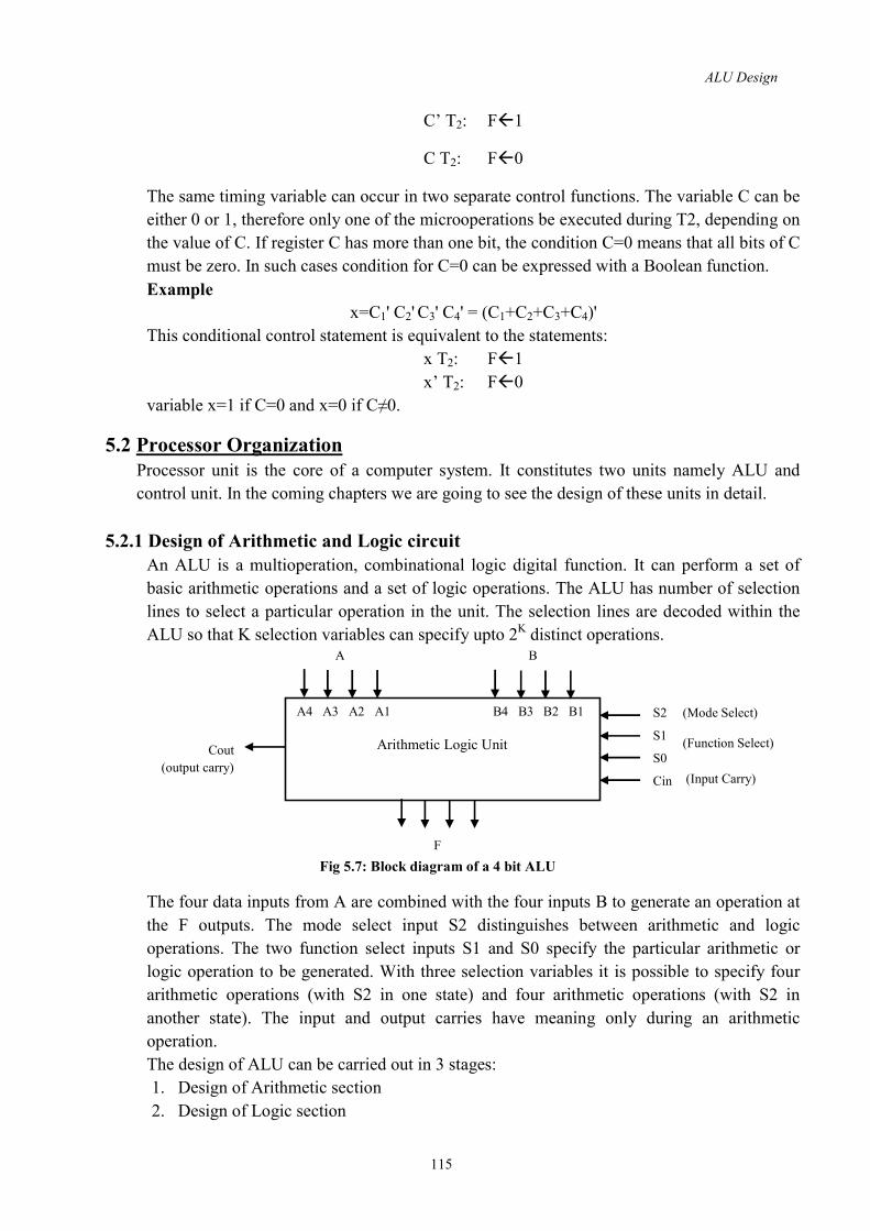
ALU Design
115
C’ T2: F1 C T2: F0
The same timing variable can occur in two separate control functions. The variable C can be either 0 or 1, therefore only one of the microoperations be executed during T2, depending on the value of C. If register C has more than one bit, the condition C=0 means that all bits of C must be zero. In such cases condition for C=0 can be expressed with a Boolean function. Example
x=C1' C2' C3' C4' = (C1+C2+C3+C4)' This conditional control statement is equivalent to the statements:
x T2: F1 x’ T2: F0
variable x=1 if C=0 and x=0 if C≠0. 5.2 Processor Organization
Processor unit is the core of a computer system. It constitutes two units namely ALU and control unit. In the coming chapters we are going to see the design of these units in detail.
5.2.1 Design of Arithmetic and Logic circuit An ALU is a multioperation, combinational logic digital function. It can perform a set of basic arithmetic operations and a set of logic operations. The ALU has number of selection lines to select a particular operation in the unit. The selection lines are decoded within the ALU so that K selection variables can specify upto 2K distinct operations.
Fig 5.7: Block diagram of a 4 bit ALU
The four data inputs from A are combined with the four inputs B to generate an operation at the F outputs. The mode select input S2 distinguishes between arithmetic and logic operations. The two function select inputs S1 and S0 specify the particular arithmetic or logic operation to be generated. With three selection variables it is possible to specify four arithmetic operations (with S2 in one state) and four arithmetic operations (with S2 in another state). The input and output carries have meaning only during an arithmetic operation. The design of ALU can be carried out in 3 stages: 1. Design of Arithmetic section 2. Design of Logic section
A4 A3 A2 A1 B4 B3 B2 B1 Arithmetic Logic Unit
S2 S1 S0 Cin
Cout (output carry)
A B
F
(Mode Select) (Function Select) (Input Carry)

ALU Design
116
3. Modification of arithmetic section so that it can perform both arithmetic and logic operations.
Design of Arithmetic Unit The basic component of arithmetic section of an ALU is a parallel adder. Parallel adder is constructed with a number of full adder circuits connected in cascade. By combining the data inputs to the parallel adder, it is possible to obtain different types of arithmetic operations. The following figure demonstrates the arithmetic operations obtained when one set of inputs to the parallel adder is controlled externally. The no of bits in the parallel adder may be of any value. The input carry Cin goes to the full adder circuit in the LSB position and output carry Cout comes from the full adder circuits in the MSB position.
Fig 5.8: Operations trained by controlling one set of inputs to a parallel adder
A B
Cout Cin=0
F=A+B (a)Addition
Parallel Adder
A B
Cout Cin=1
F=A+B+1 (b)Addition with carry
Parallel Adder
A B
Cout Cin=0
F=A+B (c)A plus 1’s complement of B
Parallel Adder
A B
Cout Cin=1
F=A+B+1 (d)Subtraction
Parallel Adder
A 0
Cout Cin=0
F=A (e)Transfer A
Parallel Adder
A 0
Cout Cin=1
F=A+1 (f)Increment A
Parallel Adder
A All 1’s
Cout Cin=1
F=A (h)Transfer A
Parallel Adder
A All 1’s
Cout Cin=0
F=A-1 (g)Decrement
Parallel Adder

ALU Design
117
The circuit that controls input B to provide the function illustrated in above figure is called a true/complement, one/zero element. This circuit can be shown as follows.
Fig 5.9: True/complement, one/zero circuit
Fig 5.10: Logic diagram of 4 bit arithmetic circuit
S1 S0 Yi 0 0 0 0 1 Bi 1 0 Bi 1 1 1
Yi
S0
S1
Bi
Cin S1 S0 C1
A1 B1
F1
C2
A2 B2
F2
C3
A3 B3
F3
C4
A4 B4
F4
X1 FA
Y1
X2 FA
Y2
X3 FA
Y3
X4 FA
Y4
C out
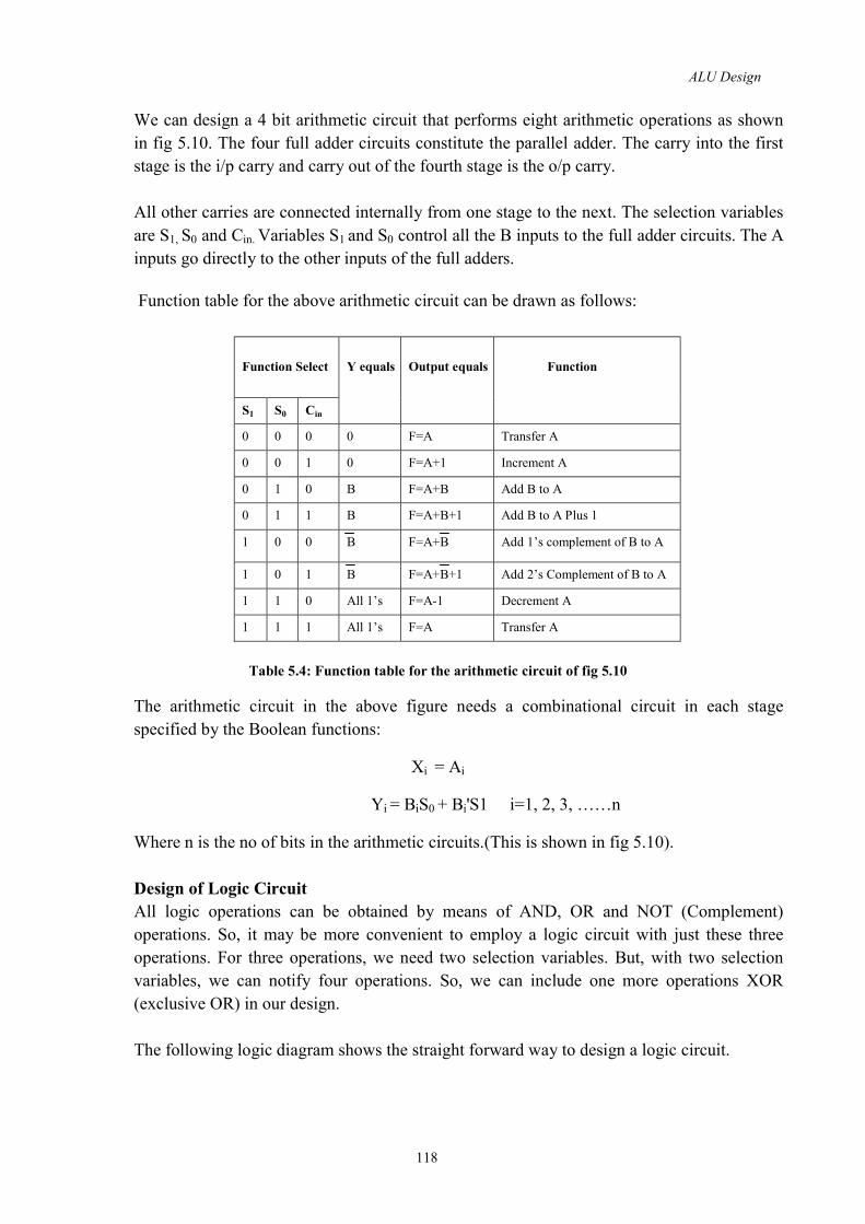
ALU Design
118
We can design a 4 bit arithmetic circuit that performs eight arithmetic operations as shown in fig 5.10. The four full adder circuits constitute the parallel adder. The carry into the first stage is the i/p carry and carry out of the fourth stage is the o/p carry. All other carries are connected internally from one stage to the next. The selection variables are S1, S0 and Cin. Variables S1 and S0 control all the B inputs to the full adder circuits. The A inputs go directly to the other inputs of the full adders. Function table for the above arithmetic circuit can be drawn as follows:
Function Select
Y equals
Output equals
Function
S1 S0 Cin 0 0 0 0 F=A Transfer A 0 0 1 0 F=A+1 Increment A 0 1 0 B F=A+B Add B to A 0 1 1 B F=A+B+1 Add B to A Plus 1 1 0 0 B F=A+B Add 1’s complement of B to A 1 0 1 B F=A+B+1 Add 2’s Complement of B to A 1 1 0 All 1’s F=A-1 Decrement A 1 1 1 All 1’s F=A Transfer A
Table 5.4: Function table for the arithmetic circuit of fig 5.10 The arithmetic circuit in the above figure needs a combinational circuit in each stage specified by the Boolean functions:
Xi = Ai Yi = BiS0 + Bi'S1 i=1, 2, 3, ……n
Where n is the no of bits in the arithmetic circuits.(This is shown in fig 5.10). Design of Logic Circuit All logic operations can be obtained by means of AND, OR and NOT (Complement) operations. So, it may be more convenient to employ a logic circuit with just these three operations. For three operations, we need two selection variables. But, with two selection variables, we can notify four operations. So, we can include one more operations XOR (exclusive OR) in our design. The following logic diagram shows the straight forward way to design a logic circuit.
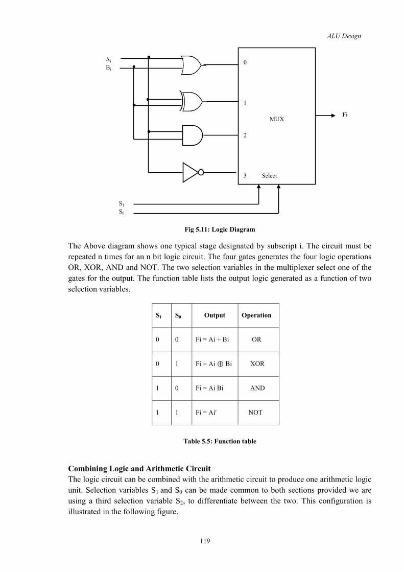
ALU Design
119
Fig 5.11: Logic Diagram The Above diagram shows one typical stage designated by subscript i. The circuit must be repeated n times for an n bit logic circuit. The four gates generates the four logic operations OR, XOR, AND and NOT. The two selection variables in the multiplexer select one of the gates for the output. The function table lists the output logic generated as a function of two selection variables.
Table 5.5: Function table Combining Logic and Arithmetic Circuit The logic circuit can be combined with the arithmetic circuit to produce one arithmetic logic unit. Selection variables S1 and S0 can be made common to both sections provided we are using a third selection variable S2, to differentiate between the two. This configuration is illustrated in the following figure.
S1 S0 Output Operation
0 0 Fi = Ai + Bi OR
0 1 Fi = Ai ⊕ Bi XOR
1 0 Fi = Ai Bi AND
1 1 Fi = Ai' NOT
0 1
MUX 2 3 Select
Ai Bi
S1 S0
Fi

ALU Design
120
Fig 5.12: Combining logic and arithmetic circuit The outputs of the logic and arithmetic circuits in each stage go through a multiplexer with selection variable S2. When S2=0, the arithmetic output is selected, but when S2=1, the logic output is selected. Although the two circuits can be combined in this manner, this is not the best way to design an ALU. A more efficient ALU can be obtained if we investigate the possibility of generating logic operations in an already available arithmetic circuit. Design of Arithmetic Logic Unit The design of an ALU is a combinational logic problem. Because the unit has a regular pattern, it can be broken into identical stages connected in cascade through the carries. We can design one stage of the ALU and then duplicate it for the no of stages required. There are six inputs (Ai, Bi, Ci, S2, S1, S0,) to each stage. Two o/p’s in each stage Fi and the carry out Ci+1. The steps involved in the design of ALU are as follows: Design the arithmetic section independent of the logic section. Determine the logic operations obtained from the arithmetic circuit in Step 1, assuming
the input carries to all stages are 0. Modify the arithmetic circuit to obtain the required logic operations.
5.2.2 Design of Combinational Logic Shifter
The shift unit attached to the processor transfers the output of the ALU onto the output bus. Shifter may function in four different ways.
One stage of Arithmetic
circuit
One stage of
Logic circuit
0
MUX 1 Select
Ai
Bi S1 S0 S2
C1 Ci+1
F1

ALU Design
121
1. The shifter may transfer the information directly without a shift. 2. The shifter may shift the information to the right. 3. The shifter may shift the information to the left. 4. In some cases no transfer is made from ALU to the output bus.
A shifter is a bi directional shift-register with parallel load. The information from ALU can be transferred to the register in parallel and then shifted to the right or left. In this configuration, a clock pulse is needed for the transfer to the shift register, and another pulse is needed for the shift. Another clock pulse may also in need of when information is passed from shift register to destination register. The number of clock pulses may reduce if the shifter is implemented with a combinational circuit. In such cases, only one clock pulse is required to transfer from source register to destination register. In a combinational logic shifter, the signals from the ALU to the output bus propagate through gates without the need for clock pulse. A combinational–logic shifter can be constructed with multiplexers. The following figure will show the same.
Fig 5.13: 4-bit combinational-logic shifter Shifter operation can be selected by two variables H1H0. If H1H0=00, no shift is executed and the signals from F go directly to the S lines. If H1H0=01, shift right is executed. If H1H0=10, shift left is executed. If H1H0=11, no operation.(The multiplexers select the inputs attached to 0 and as a
consequence the S outputs are also equal to 0, blocking the transfer of information from the ALU to the output bus.)
0 1 2 3 MUX
0 1 2 3 MUX
0 1 2 3 MUX
0 1 2 3 MUX
Serial Output
F4 F3 F2 F1
IR
H1 H0
S4 S3 S2 S1
Serial Output
IL
0
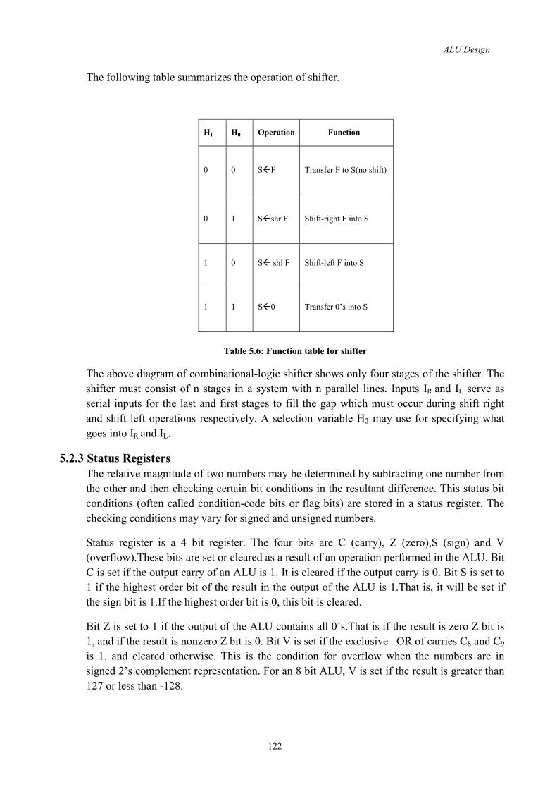
ALU Design
122
The following table summarizes the operation of shifter.
H1 H0 Operation Function
0 0 SF Transfer F to S(no shift)
0 1 Sshr F Shift-right F into S
1 0 S shl F
Shift-left F into S
1 1 S0 Transfer 0’s into S
Table 5.6: Function table for shifter The above diagram of combinational-logic shifter shows only four stages of the shifter. The shifter must consist of n stages in a system with n parallel lines. Inputs IR and IL serve as serial inputs for the last and first stages to fill the gap which must occur during shift right and shift left operations respectively. A selection variable H2 may use for specifying what goes into IR and IL.
5.2.3 Status Registers The relative magnitude of two numbers may be determined by subtracting one number from the other and then checking certain bit conditions in the resultant difference. This status bit conditions (often called condition-code bits or flag bits) are stored in a status register. The checking conditions may vary for signed and unsigned numbers. Status register is a 4 bit register. The four bits are C (carry), Z (zero),S (sign) and V (overflow).These bits are set or cleared as a result of an operation performed in the ALU. Bit C is set if the output carry of an ALU is 1. It is cleared if the output carry is 0. Bit S is set to 1 if the highest order bit of the result in the output of the ALU is 1.That is, it will be set if the sign bit is 1.If the highest order bit is 0, this bit is cleared. Bit Z is set to 1 if the output of the ALU contains all 0’s.That is if the result is zero Z bit is 1, and if the result is nonzero Z bit is 0. Bit V is set if the exclusive –OR of carries C8 and C9 is 1, and cleared otherwise. This is the condition for overflow when the numbers are in signed 2’s complement representation. For an 8 bit ALU, V is set if the result is greater than 127 or less than -128.
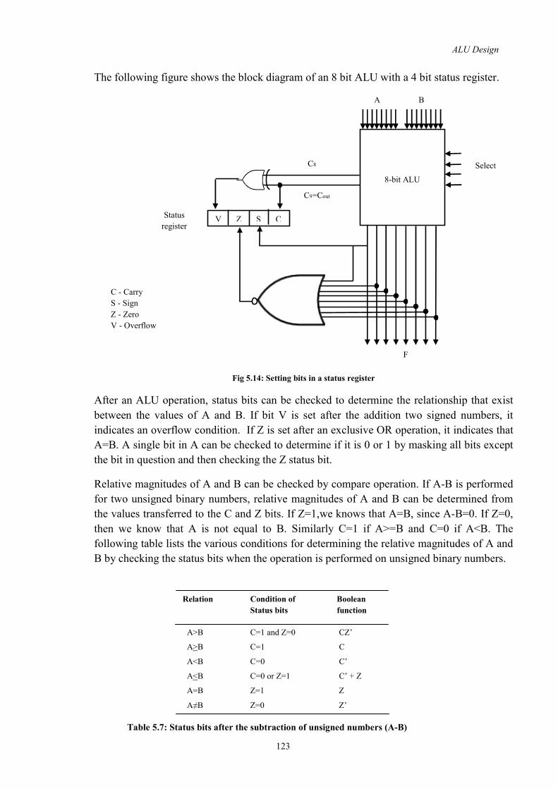
ALU Design
123
The following figure shows the block diagram of an 8 bit ALU with a 4 bit status register.
Fig 5.14: Setting bits in a status register
After an ALU operation, status bits can be checked to determine the relationship that exist between the values of A and B. If bit V is set after the addition two signed numbers, it indicates an overflow condition. If Z is set after an exclusive OR operation, it indicates that A=B. A single bit in A can be checked to determine if it is 0 or 1 by masking all bits except the bit in question and then checking the Z status bit. Relative magnitudes of A and B can be checked by compare operation. If A-B is performed for two unsigned binary numbers, relative magnitudes of A and B can be determined from the values transferred to the C and Z bits. If Z=1,we knows that A=B, since A-B=0. If Z=0, then we know that A is not equal to B. Similarly C=1 if A>=B and C=0 if A<B. The following table lists the various conditions for determining the relative magnitudes of A and B by checking the status bits when the operation is performed on unsigned binary numbers. Table 5.7: Status bits after the subtraction of unsigned numbers (A-B)
Relation Condition of Boolean Status bits function
A>B C=1 and Z=0 CZ’ A>B C=1 C A<B C=0 C’ A<B C=0 or Z=1 C’ + Z A=B Z=1 Z A≠B Z=0 Z’
8-bit ALU V Z S C
C9=Cout
A B
C8
Status register
Select
F
C - Carry S - Sign Z - Zero V - Overflow

ALU Design
124
These conditions may differ for signed binary numbers. Here the relative magnitudes of A and B can determine from the values transferred to Z, S and V status bits. If S=0, it means that sign of the result is positive, again it means A>B. This is true if there is no overflow and V=0. The following table lists the various conditions for determining the relative magnitudes of A and B by checking the status bits when the operation is performed on signed binary numbers.
Table 5.8: Status bit after the subtraction of sign-2’s complement numbers (A-B) 5.2.4 Processor Unit
The microoperations within the processor during a given clock cycle can be determined by the selection variables. The selection variables control the buses, the ALU, the shifter, and the destination register. A block diagram for the processing unit is shown in the below figure.
Relation Condition of status bits Boolean function
A>B Z=0 and (S=0, V=0 or S=1, V=1) Z’(S V) A>B S=0, V=0 or S=1, V=1 S V A<B S=1, V=0 or S=0, V=1 S V A<B S=1, V=0 or S=0, V=1or Z=1 (S V)+Z A=B Z=1 Z A≠B Z=0 Z’
Register file
R1 to R7
Destination
Select
Bus A Select
Bus B Select
ALU
Shifter
V Z S C
4 5 6
10 11 12 13
14 15 16
1 2 3
7 8 9
D A B
F
H
Output
Status register
Input data
(a) Block diagram

ALU Design
125
Fig 5.15: Processor unit with control variables It consists of seven registers (R1 to R7) and a status register. The output of the seven registers goes through two multiplexers to select the inputs to the ALU. If the input is giving from any external source it can also accepting by the same multiplexers. The output from the ALU goes through a shifter and then to a set of external output terminals. It is also possible to transfer the content from shifter to any one of the registers. There are 16 selection variables in the unit. It can be specified by a control word. The 16 bit control word is shown in fig 5.15(b). The control word is partitioned into six fields, with each field is designated by a letter name. All the fields, except Cin have a code of 3 bits.
A selects the input register for the left side of ALU. B selects the input register for the right side of ALU. D selects the destination register. F3 bits In F and Cin together selects the function for ALU (add, sub etc) H selects the type of shift in shifter unit.
When the A or B field is 000, corresponding multiplexer selects the input data. When D=000, no destination register is selected. 12 operations can be specified by the ALU and it can be selected by using the three bits in F and one bit in Cin. With Cin=0 and Cin=1 two possibilities are there for F=A. For the selection of ALU operations refer table 5.8. The table given below will gives you the functions of control variables for the processor.
Table 5.8 Function of control variable for the processor of Fig 5.15
A B D F Cin H 1 2 3 4 5 6 7 8 9 10 11 1213 14
(b) Control
Binary code Function of selection variable A B D F with
Cin=0 F with Cin=1
H 0 0 0 0 0 1 0 1 0 0 1 1 1 0 0 1 0 1 1 1 0 1 1 1
Input data R1 R2 R3 R4 R5 R6 R7
Input data R1 R2 R3 R4 R5 R6 R7
None R1 R2 R3 R4 R5 R6 R7
A,C0 A+B
A-B-1 A-1
AVB A B
A B A
A+1 A+B+1
A-B A,C1
No shift Shift-right, IR = 0 Shift-left, IL = 0 0’s to output bus
Circulate-right with C
Circulate-left with C

ALU Design
126
Shift operations can be specified with the help of H field. The first four entries in the table for H field specifying the same (as we discussed in design of shifter). Here a third selection variable is also used to specify either a 0 for the serial inputs IR and IL or a circular shift with the carry bit C. The denotation for circular right shift with carry is crc and circular left shift carry is clc. That is, R crc R is doing the operations,
Rshr R, RnC, CR1 (R is shifted to right, least significant bit of R goes to C, and the value of C is moving to the most significant bit of R). Control words of 16 bits are necessary to specify a particular micro operation for the processor unit. For example, consider the below control word.
0010100010101000 We can group them in terms of 3 bits as specified above.
A B D F Cin H 001 010 001 010 1 000
3 bits of A selects Register R1, 3 bits of B selects register R2, 3 bits of D selects the destination register as R1, 3 bits of F together with Cin selects the operation sub, and 3 bits of H selects no shift operation. So, the operation can be written as,
R1R1-R2 Compare operation is also very similar to subtract except that we are selecting no destination register for compare operation by setting the D bits as 000. Only the status bits are affected in this case. Readers are recommended to do the exercises as specified in Appendix. The clock pulse that triggers the destination register transfers the status bits from ALU to status register. The status bits are affected after an arithmetic operation. But for a logical operation, C and V status bits are left unchanged. These bits have no meaning in logic operations. For doing shift left and shift right operation, initially the register contents have to be placed into the shifter. This can be do by performing an OR logic operation with the same register selected for the operation. For example, to perform the operation, R3shl R3, initially the contents of R3 can be placed into the shifter by performing the OR operation as follows.
R3R3 v R3 The shifted information returns to R3 if R3 specified as destination register. Control word can be written as follows for the shl operation.
0110110111000010

ALU Design
127
A B D F Cin H 011 011 011 100 0 010
Since we are selecting register R3 both A and B and destination D can select the bit pattern as 011. ALU will select OR operation by setting the code as 1000. Shift left operation can be specified by selecting H pattern as 010. The control word for each microoperation is derived from the function table of the processor. The sequences of control words are stored in control memory. Based on the selection variables system will perform the sequence of micro operations. The scheme of producing control signals based on the control word is known as micro programmed control.
5.2.5 Design of Accumulator Some processors distinguish one register from others and it is known as accumulator register. It is a multipurpose register capable of performing not only the add microoperation but many other microoperations as well. The organization of a processor unit with an accumulator register is shown below.
Fig 5.16: Processor with an accumulator register
The ALU associated with the register may be constructed as a combinational circuit. In this configuration, the accumulator register is essentially a bidirectional shift register with parallel load which is connected to the ALU. There is also a feedback connection from the output of accumulator register to one of the inputs in ALU. Because of this feedback connection, the accumulator register and its associated logic, when taken as one unit,
Input Data
Processor registers Or
Memory unit
ALU
Accumulator Register (A)
Output data
B A
Select B source

ALU Design
128
constitute a sequential circuit. The block diagram of the accumulator that forms as sequential circuit is shown below:
Fig 5.17: Block diagram of accumulator The A register and associated combinational circuit constitute a sequential circuit. Here the combinational circuit replaces ALU, but it cannot be separated from the register. The accumulator register is denoted by A or AC (A register and associated combinational circuit).The external inputs to the accumulator are data inputs from B and the control variables (which will specify the microoperation to be executed). Accumulator can also perform data processing operations .Total of nine operations are considered here for the design of accumulator circuit. These operations are described below.
Table 5.9: List of microoperation for an accumulator In all listed microoperations A is the source register. B register is used as the second source register. The destination register is also accumulator register itself. The nine control variables are considered as inputs to the sequential circuit. These variables are mutually exclusive. That means, only one variable must be enabled when a clock pulse occurs. The last entry in the table is a conditional control statement. It produces a binary 1 in the output variable Z when the content of register A is 0.
Register A
Combinational
circuit
B Data inputs
Control variables
Control variable
F with Cin=0
F with Cin=1
P1 P2 P3 P4 P5 P6 P7 P8 P9
Z bit
AA+B A0 AA
AA B AAVB AA B Ashr A Ashl A AA+1
If(A=0)then(Z=1)
Add Clear Complement AND OR Exclusive-OR Shift-right Shift-left Increment Check for zero

ALU Design
129
Design Procedure Accumulator consists of n stages and n flip flops, numbered as A1, A2, A3….An from right to left. It is convenient to partition the accumulator into n similar stages, with each stage consisting of one flip flop denoted by Ai, and one data input denoted by Bi, and the combinational logic associated with the flip flop. Each stage Ai is interconnected with neighbouring stage Ai-1 on its right and Ai+1 on its left. The register will be designed using JK type flip flops. Each control variable Pj initiates a microoperation. Here nine microoperations are there by selecting control variables from P1 to P9. Accumulator is partitioned into n stages and each stage is again partitioned into those circuits that are needed for each microoperation. In the design procedure, we are designing various pieces separately and combine to form a one stage accumulator and then combine the stages to form a complete accumulator. Add B to A (P1)
Add microoperation is initiated when control variable P1 is 1. To perform addition operation, accumulator can use a parallel adder composed of full adders. The full adder in each stage I will accept the input and (present state of Ai and data input Bi) and a previous carry bit Ci. Sum bit is transferred to flip flop Ai and output carries Ci+1 is transferred to the next stage as input carry of that stage. The state table of a full adder, when considered as a sequential circuit is shown below.
Table 5.10: Excitation table for add microoperation Columns of the table can be described as follows: Present state- the value of flip flop Ai before the clock pulse Next state- the value of flip flop Ai after the clock pulse (here, it will be determined
by sum produced with inputs Ai, Bi and Ci) Ci - input carry Ci+1 - output carry Flip flop inputs - shows the excitation input for the JK flip flop.
Present State Input Next
State Flip-flop inputs Output
Ai Bi Ci Ai JAi KAi Ci+1 0 0 0 0 0 X 0 0 0 1 1 1 X 0 0 1 0 1 1 X 0 0 1 1 0 0 X 1 1 0 0 1 X 0 0 1 0 1 0 X 1 1 1 1 0 0 X 1 1 1 1 1 1 X 0 1
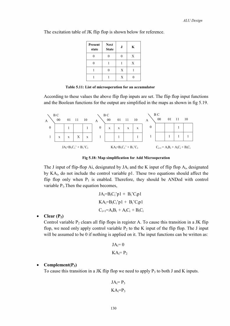
ALU Design
130
The excitation table of JK flip flop is shown below for reference.
Table 5.11: List of microoperation for an accumulator According to these values the above flip flop inputs are set. The flip flop input functions and the Boolean functions for the output are simplified in the maps as shown in fig 5.19.
Fig 5.18: Map simplification for Add Microoperation The J input of flip-flop Ai, designated by JAi and the K input of flip flop Ai, designated by KAi, do not include the control variable p1. These two equations should affect the flip flop only when P1 is enabled. Therefore, they should be ANDed with control variable P1.Then the equation becomes,
Clear (P2) Control variable P2 clears all flip flops in register A. To cause this transition in a JK flip flop, we need only apply control variable P2 to the K input of the flip flop. The J input will be assumed to be 0 if nothing is applied on it. The input functions can be written as:
Complement(P3) To cause this transition in a JK flip flop we need to apply P3 to both J and K inputs.
Present state
Next State J K
0 0 0 X 0 1 1 X 1 0 X 1 1 1 X 0
1 1 x x X x
x x x x 1 1
1 1 1 1
JAi=BiCi’p1 + Bi’Cip1 KAi=BiCi’p1 + Bi’Cip1 Ci+1=AiBi + AiCi + BiCi
JAi= 0 KAi= P2
JAi= P3 KAi=P3
JAi=B1C1’ + B1’C1 KAi=B1C1’ + B1’C1 Ci+1 = AiBi + AiCi + BiCi
A
0
1
B C 00 01 11 10 A
0
1
B C 00 01 11 10 A
0
1
B C 00 01 11 10

ALU Design
131
AND (P4) This microoperation is initiated with control variable P4.This operation performs the logic AND operation between Ai and Bi and transfers the result to Ai. The excitation table for this operation is as shown below.
Fig 5.19: Excitation table for AND microoperations The next state of Ai will be 1 only when the present state of Ai and data input Bi is 1s. The flip flop input functions can be simplified with the maps and the equations can be written as:
By including the control variable p4, the equation can be rewritten as:
OR (P5) Control variable P5 initiates the logic OR operation between Ai and Bi. The result is transferred to Ai. The excitation table for this operation is as shown below.
Fig 5.20: Excitation table for OR microoperations
Present State Input Next
State Flip-flop Inputs
Ai Bi Ai JAi KAi 0 0 0 0 X 0 1 0 0 X 1 0 0 X 1 1 1 1 X 0
X X
X X
1
Present State Input Next
State Flip-flop
inputs
Ai Bi Ai JAi KAi 0 0 0 0 X 0 1 1 1 X 1 0 1 X 0 1 1 1 X 0
1
X X
X X
JAi= 0 KAi=Bi’
JAi= 0 KAi=Bi’P4
Ai
Bi
JAi = Bi
Bi
Ai
KAi = 0
Bi
JAi = 0
Bi
Ai
KAi = 0
Ai

ALU Design
132
The simplified equations in the maps dictate that the J input be enabled when Bi=1. When Bi=0, the present state and next state of Ai are the same. When Bi=1, the J input is enabled and the next state of Ai becomes 1. Input functions for the OR microoperation are:
Exclusive-OR (P6) Control variable P6 initiates the logic Exclusive-OR operation between Ai and Bi. The result is transferred to Ai. The excitation table and map simplification is as shown below.
Fig 5.21: Excitation table for Exclusive-OR microoperations The flip flop input functions are written as:
Shift-right (P7) Control variable P7 initiates the shift operation of Ai register one bit to the right. That is, the value of flip flop Ai+1 is transferred to flip flop Ai. The flip flop input functions can be written as:
Shift-left (P8) Control variable P8 initiates the shift operation of Ai register one bit to the left. That is, the value of flip flop Ai-1 is transferred to flip flop Ai. The flip flop input functions can be written as:
Present State Input Next
State Flip-flop Inputs
Ai Bi Ai JAi KAi 0 0 0 0 X 0 1 1 1 X 1 0 1 X 0 1 1 0 X 1
1
X X
X X
1
JAi= Bi’p5 KAi=0
JAi= BiP6 KAi= BiP6
JAi= Ai+1P7 KAi= A’i+1P7
JAi= Ai-1P8 KAi= A’i-1P8
Bi
Ai
JAi = Bi
Bi
Ai
KAi = Bi

ALU Design
133
Increment (P9) These operations increment the content of A register by one. The register behaves likes a synchronous binary counter with P9 enabling the count. A 3 bit synchronous counter is shown in the following figure.
Fig 5.22: 3-bit synchronous binary counter From the figure it can see that each stage is complemented when an input carry Ei=1. Each stage is generating an output carry Ei+1 that is fed to the next stage on its left. The first stage is an exception, since it is complemented with the count-enable P9. The Boolean function for a typical stage can be written as: Input carry to the first stage of counter is E1. It must be equal to the control variable p9 which enables the count. The input carry Ei is used to complement flip flop Ai. The input carry is ANDed with Ai to generate a carry for the next stage.
Check for Zero (Z) Variable Z is an output from the accumulator. This variable can be used to indicate a zero content in the A register. All the flip flops in the accumulator is cleared Z variable will be set to 1. When a flip flop is cleared, its complement output Q’ is equal to 1. The following figure shows the first three stages of the accumulator that checks for zero content. Each stage generates a variable Zi+1 by ANDing the complement output of Ai to an input variable Zi. In this way, a chain of AND gates through all stages will indicate if all flips are cleared.
JAi= Ei KAi= Ei Ei+1=EiAi i=1,2,….,n Ei=P9
A2 A1
CP
E4
E3 E2 E1=P9
A3
Stage 3
Q
K J Q
K J Q
K J
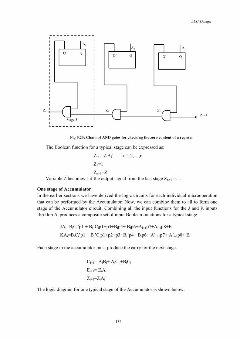
ALU Design
134
Fig 5.23: Chain of AND gates for checking the zero content of a register The Boolean function for a typical stage can be expressed as: Variable Z becomes 1 if the output signal from the last stage Zn+1 is 1.
One stage of Accumulator In the earlier sections we have derived the logic circuits for each individual microoperation that can be performed by the Accumulator. Now, we can combine them to all to form one stage of the Accumulator circuit. Combining all the input functions for the J and K inputs flip flop Ai produces a composite set of input Boolean functions for a typical stage.
Each stage in the accumulator must produce the carry for the next stage.
The logic diagram for one typical stage of the Accumulator is shown below:
Zi+1=ZiAi’ i=1,2,…,n Z1=1 Zn+1=Z
Ci+1= AiBi+ AiCi +BiCi Ei+1= EiAi Zi+1=ZiAi’
JAi=BiCi’p1 + Bi’Cip1+p3+Bip5+ Bip6+Ai+1p7+Ai-1p8+Ei KAi=BiCi’p1 + Bi’Cip1+p2+p3+Bi’p4+ Bip6+ A’i+1p7+ A’i-1p8+ Ei
A2 A1
Z4 Z3 Z2
Z1=1
A3
Stage 3
Q’ Q Q’ Q Q’ Q

ALU Design
135
Fig 5.24: One typical stage of the accumulator Each accumulator stage has eight control inputs from p1 to p8 that initiates one of eight possible microoperations. Control variable p9 is applied only to the first stage to enable the increment operation through input Ei.
Zi+1
Ci+1 Ai Ei+1
Zi Ci Bi Pi Add CP P2 Clear
P3 Complement P4 AND P5 OR P6 Exclusive Or Ai+1 P7 Shift-right Ai-1 P8 Shift-left Ei Increment
Q, Q K J

ALU Design
136
There are six other inputs in the circuit. Data input Bi, input carry Ci,Ai-1 comes from the flip flop one position to the right,Ai+1 comes from the flip flop one position to the left, Ei(carry input for the increment operation),and Zi(used to form chain of zero detection). There are four outputs to this circuit.
Ai - output of the flip flop Ci+1 - carry for the next stage Ei+1 - increment carry for the next stage Zi+1 - carry for the next stage for zero detection.
Complete Accumulator We have covered the design of one stage of Accumulator. For a complete accumulator there will be n stages like this. The inputs and outputs of each stage can be connected in cascade to form a complete accumulator. Here we are discussing the design of a 4 bit accumulator. The following diagram shows the design.
Fig 5.25: 4-bit accumulator constructed with four stages The number on top of each block represents the bit position. All blocks receive 8 control variables p1 to p8 and the clock pulses from CP. The other six inputs and four outputs are same as with the typical stage. The zero detect chain is obtained by connecting the z variables in cascade, with the first block receiving a binary constant 1. The last stage produces the zero detect variable Z.
4 B4 Z5 Z4 C5 C4 A A3 E E4 A5
1 B1 Z2 Z1 C2 C1 A1 A0 E2 E1 A2
2 B2 Z3 Z2 C3 C2 A2 A1 E3 E2 A3
3 B3 Z Z3 C4 C3 A3 A2 E4 E3 A4
Z
Output carry
Increment carry
Serial Input
1 Input carry Serial
input P9
B4 B3 B2 B1
P1 to P8
CP

ALU Design
137
Total number of terminals in the 4 bit accumulator is 25, including terminals for the A outputs. Incorporating two more terminals for power supply, the circuit can be enclosed within one IC package having 27 or 28 pins. The number of terminals for the control variable can be reduced from 9 to 4 if a decoder is inserted in the IC. In such cases, IC pin count is also reduced to 22 and the accumulator can be extended to 16 microoperations without adding external pins (That is, with 4 bits we can identify 16 operations).


CHAPTER -6
Control Unit Design
Objectives are: Control Logic Design
Control Organization Design of Hardwired Control Control of Processor Unit PLA Control
Micro-Programmed Control Microinstructions Horizontal and Vertical Microinstructions Micro-Program Sequencer Micro Programmed CPU Organization

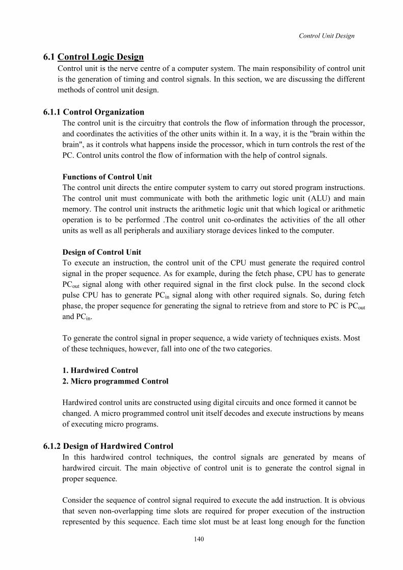
Control Unit Design
140
6.1 Control Logic Design Control unit is the nerve centre of a computer system. The main responsibility of control unit is the generation of timing and control signals. In this section, we are discussing the different methods of control unit design.
6.1.1 Control Organization The control unit is the circuitry that controls the flow of information through the processor, and coordinates the activities of the other units within it. In a way, it is the "brain within the brain", as it controls what happens inside the processor, which in turn controls the rest of the PC. Control units control the flow of information with the help of control signals. Functions of Control Unit The control unit directs the entire computer system to carry out stored program instructions. The control unit must communicate with both the arithmetic logic unit (ALU) and main memory. The control unit instructs the arithmetic logic unit that which logical or arithmetic operation is to be performed .The control unit co-ordinates the activities of the all other units as well as all peripherals and auxiliary storage devices linked to the computer. Design of Control Unit To execute an instruction, the control unit of the CPU must generate the required control signal in the proper sequence. As for example, during the fetch phase, CPU has to generate PCout signal along with other required signal in the first clock pulse. In the second clock pulse CPU has to generate PCin signal along with other required signals. So, during fetch phase, the proper sequence for generating the signal to retrieve from and store to PC is PCout and PCin. To generate the control signal in proper sequence, a wide variety of techniques exists. Most of these techniques, however, fall into one of the two categories. 1. Hardwired Control 2. Micro programmed Control Hardwired control units are constructed using digital circuits and once formed it cannot be changed. A micro programmed control unit itself decodes and execute instructions by means of executing micro programs.
6.1.2 Design of Hardwired Control In this hardwired control techniques, the control signals are generated by means of hardwired circuit. The main objective of control unit is to generate the control signal in proper sequence. Consider the sequence of control signal required to execute the add instruction. It is obvious that seven non-overlapping time slots are required for proper execution of the instruction represented by this sequence. Each time slot must be at least long enough for the function

Control Unit Design
141
specified in the corresponding step to be completed. Since , the control unit is implemented by hardwire device and every device is having a propagation delay , due to which it requires some time to get the stable output signal at the output port after giving the input signal. So, to find out the time slot is a complicated task. For the moment, for simplicity, let us assume that all slots are equal in diameter. Therefore the required controller may be implemented based upon the use of a counter driven by clock. Each state, or count, of this counter corresponds to one of the steps of the control sequence of the instructions of the CPU. In the previous discussion (Refer chapter 2, section 2.1.3), we have mentioned control sequence for execution of two instructions only (one is for add and other one is for branching). Like that we need to design the control sequence of all the instructions. By looking into the design of the CPU, we may say that there are various instruction for add operation. As for example, Add (R3), R1 Add the contents of memory location specified by R3 to the contents of register R1.
R1 R1 + [R3] Add R2, R1 Add the contents of register R2 to the contents of register R1 R1 R1 + R2 The control sequence for execution of these two adds instructions are different of course, the fetch phase of all the instruction remain same. It is clear that control signals depend on the instruction, i.e. the contents of the instruction register. It is also observed that execution of some of the instructions depend on the contents of condition code or status flag register, where the control sequence depends in conditional branch instruction. Hence, the required control signals are uniquely determined by the following information: Contents of the control counter. Contents of the instruction register. Contents of the condition code and other status flags.
The status flags represent the various state of the CPU and various control lines connected to it, such as MFC status signal. The structure of control unit can be represented in a simplified view by putting it in block diagram. The detailed hardware involved may be explored step by step. The simplified view of the control unit is given in the figure 6.1.
Fig 6.1: Control Unit Organization
.
.
Decoder/ Encoder
Control step counter Clock
IR
Control signals
... External inputs
... Condition codes

Control Unit Design
142
The decoder/encoder block is simply a combinational circuit that generates the required control outputs depending on the state of all its input. The decoder part of decoder/encoder part provides a separate signal line for each control step, or time slot in the control sequence. Similarly, the output of the instruction decoder consists of a separate line for each machine instruction loaded in the IR, one of the output lines INS1 to INSn be set to 1 and all other lines are set to 0.
. . . . . .
. . . . . .
Fig 6.2: Control Unit Organization All input signals to the encoder block should be combined to generate the individual control signals. Control step counter keeps tracks of the count of control steps. Each state or count of this control step corresponds to one control step. The step decoder provides a separate signal line for each step or time slot in the control sequence. The output of the instruction decoder consists of a separate signal line for each instruction. For any instruction loaded in the IR, one of the output lines INS1 through INSn is set to 1 and all other lines are set to zero. The encoder circuit combines all of these inputs and generates the control signals Yin, Zout etc. It is required to generate many control signals by the control unit. These are basically coming out from the encoder circuit of the control signal generator. The control signals are lie PCin , PCout , Zin , Zout , MARin , add , End etc. In the previous discussions (chapter 2), we have mentioned the control sequence of the instruction, “Add (R3), R1”, and “Control sequence for an unconditional branch instruction (BR)”. Consider those CPU instructions. By looking into the above instructions, we can write the logic function for Zin as:
Zin = T1 +T6.ADD + T4.BR +…………… This means, control signal Zin have to be generated for time cycles T1for all instructions, in time cycle T6 for add instruction and in time cycle T4 of BR instruction and so on.
.
.
Control step counter Clock
IR
Step Decoder
INS2
INSn
External inputs
Condition codes
INS1
Decoder/ Encoder
Run End
Instruction Decoder
.
.
.
.
.
.
T1 T2 . . . . . . . Tn
Control signals
CLK Reset

Similarly, the Boolean logic function for add signal isadd = T
These logic functions can be implemented by a two level combinational circuit of AND and OR gates. Similarly, the End control signal is generated by the logic
End = T7
This End signal indicates the End of the execution of an instruction, so this End signal can be used to start a new instruction fetch cycle by starting value. The circuit diagram (Partial) for generating Zdiagram.
The signal ADD, BR, BRN etc are coming from instruction decoder circuits which depends on the contents of IR. The signalcontrol step counter. The signal N (Negative) is coming from condition code register. When wait for MFC (WMFC) signal is generated, then CPU does not do any works and it waits for
T7
143
Similarly, the Boolean logic function for add signal is add = T1+ T6.ADD+ T4.BR + ………………..
These logic functions can be implemented by a two level combinational circuit of AND and Similarly, the End control signal is generated by the logic
7. ADD + T5.BR + (T5.N +T4.N ).BRN + …………….This End signal indicates the End of the execution of an instruction, so this End signal can be used to start a new instruction fetch cycle by resetting the control step counter to its
ing value. The circuit diagram (Partial) for generating Zin and End signal is shown in the
Fig 6.3: Generation of Zin signal for the processor
Fig 6.4: Generation of the End control signal The signal ADD, BR, BRN etc are coming from instruction decoder circuits which depends on the contents of IR. The signal 1T , 2T , 3T etc are coming out from step decoder depends on control step counter. The signal N (Negative) is coming from condition code register. When wait for MFC (WMFC) signal is generated, then CPU does not do any works and it waits for
Branch Add
T1
T4 T6
Zin
… …
Branch Add
T4 T5
End
… …
Branch<0
T5
N N
Control Unit Design
.BR + ……………….. These logic functions can be implemented by a two level combinational circuit of AND and
function: ).BRN + …………….
This End signal indicates the End of the execution of an instruction, so this End signal can the control step counter to its
and End signal is shown in the
The signal ADD, BR, BRN etc are coming from instruction decoder circuits which depends t from step decoder depends on
control step counter. The signal N (Negative) is coming from condition code register. When wait for MFC (WMFC) signal is generated, then CPU does not do any works and it waits for
5

Control Unit Design
144
an MFC signal from memory unit. In this case, the desired effect is to delay the initiation of the next control step until the MFC signal is received from the main memory. This can be incorporated by inhibiting the advancement of the control step counter for the required period. Let us assume that the control step counter is controlled by a signal called RUN. When set to 1, RUN causes the counter to be incremented by one at the end of every clock cycle. When RUN equal to zero, the counter stops counting. This is needed whenever the WMFC signal is issued, to cause the processor to wait for the reply from the memory. End signal starts a new instruction fetch cycle by resetting the control step counter to its starting value. The control hardwire we have discussed now can be viewed as a state machine that changes from one state to another in every clock cycle, depending on the contents of the instruction register, condition codes and external inputs. The output of the state machines are the control signals. The sequence of operations carried out by this machine is determined by the wiring of the logic elements; hence it is named as “Hardwired unit”. Advantages 1. They Operates at high speed.
Disadvantages 1. Have little flexibility. 2. Complexity of the instruction set it can implement is limited.
A complete Processor A complete processor can be designed using the following structure as shown in figure 6.5.This structure has an instruction unit that fetches instruction from an instruction cache or from the main memory. To deal with integer and floating point data it has separate processing units. A data cache is inserted between the main memory and integer and floating point units. The processor is connected to the system bus and hence to the rest of the computer by means of a bus interface. A processor may include several units of integer and floating point units so that the rate of instruction execution will be increased.
Fig 6.5: Block diagram of a complete Processor
Main Memory
Input/ Output
Processor
Instruction Unit
Integer Unit
Floating-point Unit
Instruction cache
Data Cache
Bus interface
System bus

Control Unit Design
145
6.1.3 Control of Processor Unit In this section we are discussing the hardwire configuration of micro program organization to include the control of entire processing unit. Processor unit consists of ALU, Shifter, status register, general purpose registers etc. A micro operation is selected with a control word of 16 bits. A micro program organization for controlling the processor unit is shown in the following figure 6.6. It has a control memory of 64 words, with 26 bits per word. For selecting 64 words, we need 6 bits address. To select 8 status bits, we need 3 selection lines for the multiplexer. One bit of the microinstruction selects between an external address and the address field of the microinstruction.16 bits is in need for selecting the microoperation in the processor. The diagram shows the connection of processor unit to micro program control unit. The first 16 bits of the microinstruction selects the microoperation for the processor. The other 10 bits selects the next address for the Control Address Register (CAR). So, total 26 bits for each microinstruction. The status bits from the processor are applied to the inputs of a multiplexer. Both the normal and complement values are used (except status bit V). Input 0 of MUX2 is always a binary 1. The load input to CAR is enabled when this input is selected by bits 18, 19 and 20 in the microinstruction. This causes a transfer of information from the output of MUX 1 into CAR. The input into CAR is a function of bit 17 in the microinstruction. If bit 17 is 1, CAR receives the address field of the microinstruction. If bit 17 is 0, an external address is loaded into CAR (this is needed for initiating a new sequence of microinstructions). The status bits selected by bits 18, 19 and 20 of the microinstruction may be equal to 1 or 0. If the selected bit is 1, the input address is loaded into CAR. If the selected bit is 0, CAR is incremented. To construct correct micro programs, it is necessary to specify exactly how the status bits are affected by each microoperation in the processor. The sign (S) and Zero (Z) flags are affected by all operations. The C (carry) and V (overflow) bits do not change after the following ALU operations. 1. The four logic operations OR, AND, XOR and complement. 2. The increment and decrement operations.
For all other operations, the output carry from the ALU goes into the C bit of the status register. The C bit is also affected after a circular shift with carry operation.
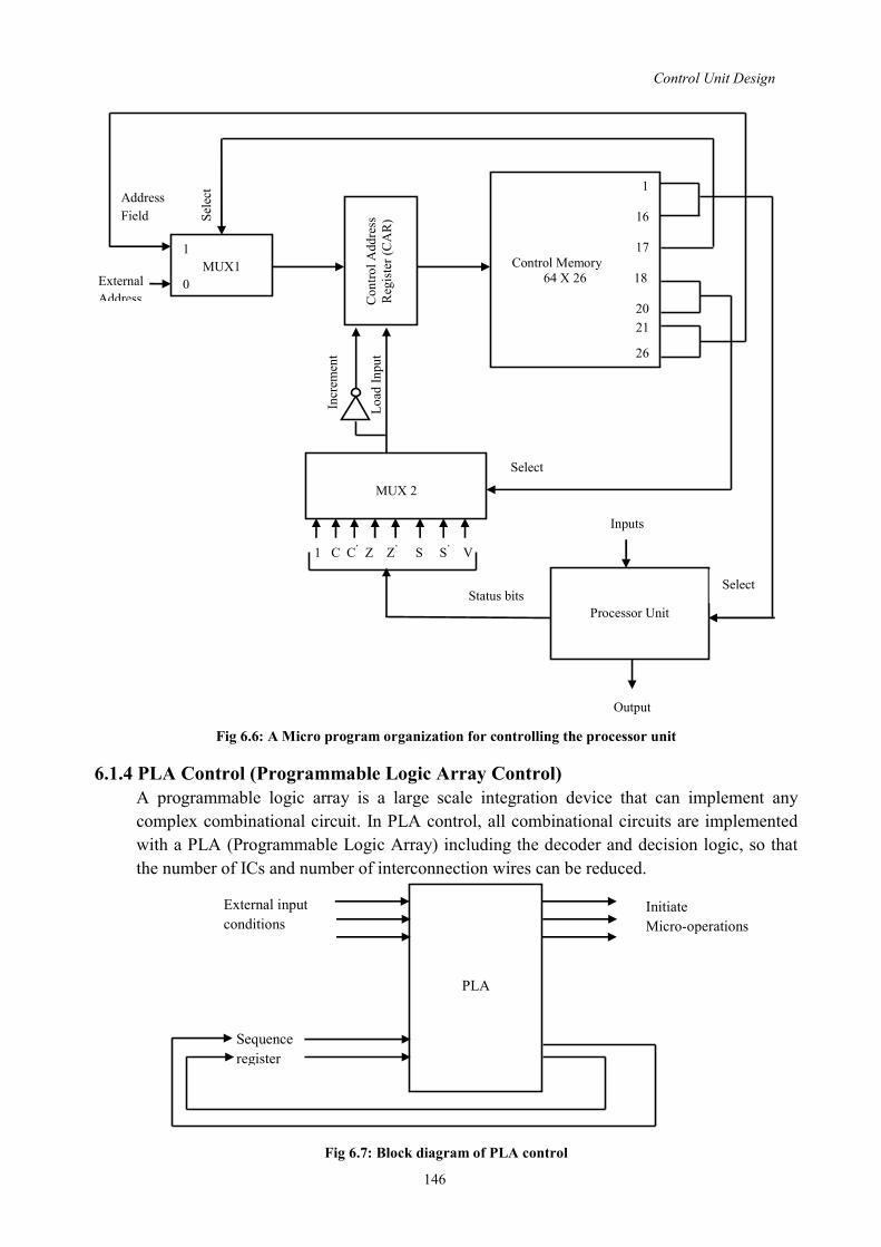
Control Unit Design
146
Fig 6.6: A Micro program organization for controlling the processor unit 6.1.4 PLA Control (Programmable Logic Array Control)
A programmable logic array is a large scale integration device that can implement any complex combinational circuit. In PLA control, all combinational circuits are implemented with a PLA (Programmable Logic Array) including the decoder and decision logic, so that the number of ICs and number of interconnection wires can be reduced.
Fig 6.7: Block diagram of PLA control
PLA
External input conditions
Initiate Micro-operations
Sequence register
1
16
17 Control Memory 64 X 26 18
20
21
26
MUX 2
1 C C’ Z Z’ S S’ V
External Address
Select
Status bits
Processor Unit
Inputs
Output
Select
Select
Address Field
1 MUX1
0
Increm
ent
Load In
put
Contro
l Addr
ess
Registe
r (CAR
)

Control Unit Design
147
Here, sequence register establishes the present state of the control circuit. Depending on the present state of the control circuit and external input conditions, PLA will determine the micro operations which have to be initiated. At the same time, other PLA outputs determine the next state of sequence register. The sequence register is external to the PLA if the unit implements only combinational circuits.
6.2 Micro-Programmed Control Here the control signals are generated by a program similar to machine language programs instead of using a decoder/encoder circuit.
6.2.1 Microinstructions Micro instruction is normally structured as assign one bit position to each control signal. Consider the following control sequence:
1. PCout, MARin, Read, Select4, Add 2. Zout, PCin, Yin ,WMFC 3. MDRout, IRin 4. R3out, MARin, Read 5. R1out,Yin,WMFC 6. MDRout, Select4,Add, Zin 7. Zout,R1in,End
Here so many control signals are there like PCin, PCout, MARin, Zin, Zout etc. The following table shows the micro instructions corresponding to the given control sequence.
Table 6.1: An example of micro instruction for the above control sequence
Micro
instru
ctions
….
PCin
PCout
MA
R in
Read
Add
Z in
Z out
MDR ou
t IR i
n R3
out
R1out
Y in
R1in
WMFC
En
d
1 0 1 1 1 1 1 0 0 0 0 0 0 0 0 0 2 1 0 0 0 0 0 1 0 0 0 0 1 0 1 0 3 0 0 0 0 0 0 0 1 1 0 0 0 0 0 0 4 0 0 1 1 0 0 0 0 0 1 0 0 0 0 0 5 0 0 0 0 0 0 0 0 0 0 1 1 0 1 0 6 0 0 0 0 1 1 0 1 0 0 0 0 0 0 0 7 0 0 0 0 0 0 1 0 0 0 0 0 1 0 1

Control Unit Design
148
Each row in this table is referred as a control word. Individual bits in the control word represent various control signals. Each control word is a combination of sequence of 0’s and 1’s. A sequence of control words corresponding to the control sequence of a machine instruction is referred as micro routine. Individual control words in the micro routine are called micro instructions.
6.2.2 Horizontal and Vertical Microinstructions Microinstructions can be organized in two different ways named as Horizontal and Vertical microinstructions Horizontal Microinstructions The above represented scheme of micro instruction by assigning one bit position to each control signal is known as horizontal microinstruction. Example
011100010110010 Drawback of this scheme Assigning individual bits to each control signal results in long micro instructions because the number of required signals is usually large. For any given micro instruction, only few bits are set to 1, which means available bit space is purely used. In the earlier discussion of the processor organization we had discussed, it needs total of 42 control signals. (Assuming that here four general purpose registers R0 to R3.)If we are using the simple encoding scheme now we have discussed, total of 42 bits would be needed for each micro instruction. Vertical Microinstructions We can reduce the length of the horizontal micro instructions so easily by implementing another method known as vertical micro instructions. In all cases, most signals are not needed simultaneously, and many signals are mutually exclusive. For example, only one function of the ALU can be activated at a time. The source for a data transfer must be unique because it is not possible to gate the contents of two different registers on to the bus at the same time. Read and write signals to the memory cannot be active simultaneously. All of these cases suggest that signals can be grouped so that all mutually exclusive signals are placed in the same group. A binary coding scheme can be used to represent the signals within a group. The following example will illustrate this.

Control Unit Design
149
Micro Instruction
Here most of the fields must include one inactive code for the case in which no action is required. For example, all zero patterns in F1 indicate that none of the registers that may be specified in this field should have its contents placed on the bus. An inactive code is not needed in all fields. For example, F4 contains 4 bits that specify one of the 16 operations performed in the ALU. Since no spare code is included, the ALU is active during the execution of every micro instruction. This type of highly encoded scheme which uses compact codes to specify control functions in each micro instruction is referred as vertical micro instruction. Comparison of Horizontal and vertical micro instructions The horizontal approach is useful when a higher operating speed is desired and when the machine structure allows parallel use of resources. But in vertical micro instruction, grouping control signals into fields requires a little more hardware because decoding circuits must be used to decode the bit patterns of each field into individual control signals.
F1 F2 F3 F4 F5
F1 (4 bits) F2 (3 bits) F3 (3 bits) F4 (4 bits) F5 (2bits) 0000: No Transfer 000: No Transfer 000: No Transfer 0000: Add 00: No Action 0001: PCout 001: PCin 001: MARin 0001: Sub 01: Read 0010: MDRout 010: IRin 010: MDRin . 10: Write
0011: Zout 011: Zin 011: TEMPin . 0100:R0out 100:R0in 100: Yin 1111: XOR 0101: R1out 101:R1in 16 ALU functions
0110:R2out 110:R2in
0111:R3out 111:R3in
1010: TEMPout
1011: Offsetout F6 (1 bit) F7 (1 Bit) F8 (1 bit) 0: Select Y 0: No Action 0: Continue 1: Select 4 1: WMFC 1: End
F6 F7 F8 ........

Control Unit Design
150
The cost of this additional hardware is more. The vertical approach results in considerably slower operating speeds because more micro instructions are needed to perform the desired control functions. To handle the execution of micro instructions only less hardware is needed. Design of Micro Programmed Control The micro routines for all instructions in the instruction set of a computer are stored in a s special memory called control store. Control unit will generate the control signals by sequentially reading the control words of the corresponding micro routine from the control store. For this sequential reading micro programmed control uses a Micro program Counter. The following figure illustrates the working of micro programmed organization.
Fig 6.8: Basic organization of a micro programmed control unit Every time a new instruction is loaded into IR, the output of the starting address generator is loaded into the micro program counter. This counter is automatically incremented by the clock. So that successive micro instructions can be read from the control store. These control signals are delivered to various parts of the processor in correct sequence. By using this design, it is not possible to implement the complete function of the control unit. That is, when the control unit have to check the status of condition codes or external inputs, this organization will not work. In order to implement it, the above design can be little bit modified as follows:
Fig 6.9: Organization of the control unit to allow the conditional branching in the micro program.
IR
Starting address
generator
µPC
Control Store CW
Clock
IR
Starting and branch
address generator
µPC
Control Store CW
Clock
External Inputs
Condition Codes

Control Unit Design
151
Here, starting address generator becomes the starting and branch address generator. This block loads a new address into the micro program counter when the micro instruction instructs it to do so. Condition codes and external inputs are also taken into consideration. Micro program counter is incremented every time a new micro instruction is fetched from the micro program memory, except in the following situations: When a new instruction is loaded into IR, micro program counter is loaded with the
starting address of the micro routine for that instruction. When branch micro instruction is encountered and the branch condition is satisfied,
counter is loaded with the branch address. When an End micro instruction is encountered, counter is loaded with the address of
the first control word in the micro routine for the instruction fetch cycle. 6.2.3 Micro Program Sequencer
A micro program control unit consisting of two parts: control memory that stores the microinstructions and the associated circuits that control the generation of the next address. The address generation part is called micro program sequencer, since it sequences the microinstructions in control memory. Microprogram sequencer is attached to the control memory. It inspects certain bits in the microinstruction to determine the next address for control memory. A typical sequencer has the following address sequencing capabilities. 1. Increments the present address of control memory 2. Branches to an address which will be specified in the bits of microinstruction 3. Branches to a given address if a specified status bit is equal to 1. 4. Transfers control to a new address as specified by an external source 5. Has a facility for subroutines calls and returns.
In majority cases successive microinstructions are read from the control memory. This type of sequencing is easy by incrementing the address register of the control memory. But in some cases, address may also be a part of microinstructions. In such cases, even the incrementer also may not be needed. In some cases, control must be transferred to a non sequential microinstruction. To handle such situations sequencer must have branching capability. This is usually performed by the sequencer by looking up a special status bit. If it is 1, sequencer will transfer to the branch address which will be specified in the microinstruction. If it is 0, go to the next address in sequence. To start a new microoperation, a new address has to be loaded. In such cases, sequencer will load new address in address register of control memory. This will be done by receiving the new address from an external input source. Many microprograms may contain identical sections of code. Space may be wasted if the common sections are repeated in each microprogram. Instead of that such portions may shared by employing subroutines, so that we can save the control memory space. Microprograms that use subroutines must have a provision for storing the return address during a subroutine call and restoring the address during a subroutine return. This can be

accomplished by placing the return address in a sbeginning of the subroutine. The best way to organize the register file is in LIFO (Last In First Out fashion.). The block diagram of microprogram sequencer is shown in the below figure:
Fig 6.10It consists of a multiplexer that selects an address from four sources and control address register. The O/Pcontents of CAR are incremented and applied to the multiplexer and to the stack register file. The register selected in the stack is determined by staoperation for the sequencer and input T is the test point for a status bit. Initially the address register is cleared to zero and clock
I1
I0
T (test)
Clear CP
I2
152
accomplished by placing the return address in a special register and then branching to the beginning of the subroutine. The best way to organize the register file is in LIFO (Last In
The block diagram of microprogram sequencer is shown in the below figure:
Fig 6.10: Block diagram of Microprogram sequencer It consists of a multiplexer that selects an address from four sources and control address register. The O/P from CAR provides the address for control memory. The contents of CAR are incremented and applied to the multiplexer and to the stack register file. The register selected in the stack is determined by stack pointer. Inputsoperation for the sequencer and input T is the test point for a status bit. Initially the address register is cleared to zero and clock pulse synchronizes the loading into registers.
0 1 2 3 S1
MUX S0
Control address register (CAR) Incrementer
External address
Branch address (BRA)
Read
Push
Pop
Output address
Control Unit Design
pecial register and then branching to the beginning of the subroutine. The best way to organize the register file is in LIFO (Last In
The block diagram of microprogram sequencer is shown in the below figure:
icroprogram sequencer It consists of a multiplexer that selects an address from four sources and routes it into a
from CAR provides the address for control memory. The contents of CAR are incremented and applied to the multiplexer and to the stack register file.
ck pointer. Inputs (I0-I2) specify the operation for the sequencer and input T is the test point for a status bit. Initially the address
the loading into registers.
Stack Register
(SR)
Stack pointer register (SP)
Write Read
Inc Dec

Control Unit Design
153
The following function diagram illustrates the operation of a sequencer.
I2 I1 I0 T
S1 S0
Operations Comments X 0 0 X X 0 1 X X 1 0 X 0 1 1 0 0 1 1 1 1 1 1 0 1 1 1 1
0 0 0 1 1 0 1 0 1 1 1 0 1 1
CAR EXA CAR SR CAR CAR+1 CAR CAR+1 CAR BAR CAR CAR+1 CAR BRA, SR CAR+1
Transfer external address Transfer from register stack Increment address Increment address Transfer branch address Increment address Branch to subroutine
Table 6.2: Function table for microprogram sequencer
6.2.4 Microprogrammed CPU Organization A digital computer consists of a Central Processor Unit (CPU), a memory unit, and input-output devices. CPU can be classified into processing section and control section. Here we are designing a computer CPU with micro programmed control. Microprogram sequencer is a basic element of micro programmed control for a CPU. The block diagram of the microprogrammed computer is shown below figure 6.11. It consists of a memory unit, two processor units (one for address and one for data), a microprogram sequencer, a control memory and few other digital functions. The memory unit stores the instructions and data supplied by the user through an input device. The data processor manipulates the data and address processor manipulates the address information received from memory. Provision is also there to combine these two units into one. The instruction extracted from the memory during fetch cycle goes into the instruction register. The instruction-code bits in the instruction register specify a macrooperation for control memory. A coded transformation is needed sometimes to convert the operation code bits of an instruction into a starting address for the control memory. This code transformation consists of a mapping function and can be implemented with a ROM or PLA. Mapping function is giving the flexibility for adding instructions or macrooperations for control memory as in need. The address generated from the PLA is applied to the External Address (EXA) input of the sequencer. The micro program control unit consists of a control memory (for storing the microinstructions), a multiplexer and a pipeline register. The multiplexer selects the status bits and applies it to the test input of the sequencer. One input of the multiplexer is always 1 to trigger an unconditional branch instruction. The outputs from the control memory can go directly to the control inputs of the various part of the CPU. Pipeline register is an optional one. But it may speed up the control operation. A possible micro instruction format is shown within the pipeline register. I field consists of 3 bits and supplies the input information to the sequencer.SL bits are status bits for the multiplexer. BRA field is supplies a branch address to the sequencer. Using these 3 fields microprogram sequencer is determining the next address for control memory. The other

Control Unit Design
154
fields are for controlling the microoperations within the CPU and memory. The MC (Memory Control) bits control the address processor and the read and write operations in the memory. PS (Processor Select) bits control the operation in data processor. The DF (Data Field) bits are used to introduce constants into the processor. Data field can be used as a sequence counter to count the number of times a microprogram loop is traversed. Data field outputs can be used to setup control registers and to introduce data in processor registers. For example, a constant in the data field may be added to a processor register to increment its contents by a specified value. Once the hardwire configuration of microprogrammed CPU is completed, the designer can select one of the computer configuration. Initially the instructions set have to be formulated and corresponding microinstructions will be set up and stored in control memory. No hardware changes are required for a different computer configuration. Only the ROM has to be changed. This can be possible by replacing the ROM with different microprograms.
Fig 6.11: Microprogrammed computer organization
Address processor Program Counter
Memory address register
Instruction Register
Code transformation (PLA)
I SL BRA MC PS DF
MUX
Memory unit
MUX
Data processor
Address Read/Write
EXA BRA T
I0 - I2
Pipeline Register
1 Status
Bit
I Sequence selector SL MUX selector BRA Branch address MC Memory control PS Processor selector DF Data field
Control Memory (ROM)
Microprogram sequencer (Fig 6.10)


Appendix


Appendix
156
Chapter 1 1. List out the different functional parts of a computer system.
2. Write the machine instruction for the following statements:
(a) “Add the contents of register R1 and register R2 and store the result in register R1.” (b) “Add the contents of register R1 and register R2 and store the result in register R3.” (c) “A+B*C+D”
3. Illustrate the different addressing modes possible for the instructions.
4. Give examples for system software and application software.
5. Differentiate between Little Endian and Big Endian addressing schemes.
6. Consider a computer that has a byte addressable memory organized in 32 bit words according to the Big Endian scheme. A program reads ASCII characters entered at a keyboard and stores them in successive byte locations, starting at location 5000. Show the contents of the two memory words at locations 5000 and 5004 after the name “Ilahia” has been entered.(To solve this refer ASCII code of Alphabets. sample is given here).
Letter ASCII Code Binary A 065 01000001 B 066 01000010 C 067 01000011 D 068 01000100
7. Repeat exercise no 6 with Little Endian schemes.
8. Registers R1 and R2 of a computer contain the decimal values 1000 and 2000.Calculate
the effective address of the memory operand in the following instructions:
Load 20(R1),R5 Move #2000,R5 Store R5,30(R1,R2) Add -(R2),R5 Subtract(R1)+,R5
9. How will you determine the word length of a computer system.
10. Calculate the no of bits in the following measures: 1 byte, 1K (1 Kilobyte), 1M (1
Megabyte), 1G (1 Gigabyte), 1T (1 Terabyte).

Appendix
157
11. What do you mean by byte addressable memory.
12. What is aligned address?
13. Explain the basic operational concepts in detail.
14. What is the function of control unit.
15. What are the different parts of a processor.
16. Illustrate the method of straight line sequencing.
17. What is the need of branching? Give one scenario in which branching is required.
18. Define condition code. What is its use.
19. Explain the two addressing modes which are useful for accessing data items in successive locations in the memory.
20. Differentiate between program controlled I/O and memory mapped I/O.
21. What is the purpose of status flags SIN and SOUT in I/O devices.
22. What is a subroutine.
23. What is a stack frame? Give the layout of the same.
24. Consider the following possibilities for saving the return address of a subroutine.
a. In a processor register b. In a memory location associated with the call, so that a different location is used when
the subroutine is called from different places. c. On a stack
Out of these possibilities, which one supports subroutine nesting and which one supports subroutine recursion.
25. Register R1 is used in a program to point to the top of the stack. Write a sequence of instructions using the index, auto increment, and auto decrement addressing modes to perform each of the following tasks:
(a) Pop the top two items off the stack, add them, and then push the results onto the stack. (b) Copy the third item from the top into register R2. (c) Remove the top five items from the stack.

Appendix
158
26. Draw the register structure for ARM processors. Explain the components.
27. Write the Arithmetic and logic instruction format for ARM processors.
28. Which of the following ARM instructions would cause the assembler to issue a syntax error message? Why.
(a) ADD R1,R2,R3 (b) ADD R1,R1,R1 (c) MOV R1,# 300 (d) MOV R1,#110011 (e) ADD R1,R2,R3,LSL #4
Chapter 2 1. List out the different steps required to execute an instruction.
2. Write the control sequence for the following instructions.
(a) Add (R3),R4,R5 (b) Add #3000, R1 (c) MUL R1,R2 (d) Move R1, (R2)
3. Show the control sequence for branch on negative condition.
4. What is the function of WMFC signal.
5. How the single bus and multiple bus organization affects the sequencing of control
signal.
6. Design an array multiplier with two 3 bit numbers.
7. Perform the multiplication on the following numbers. (a) 1100 and 1001 (b) 13 and -6 (c) 11 and -7 (d) 010111 and 110110 Use sequential binary multiplier and Booth method.

Appendix
159
8. What is the difference between restoring and non restoring division.
9. Explain the multiplication algorithms used in CPU Arithmetic.
10. What is Booth recording of a multiplier? Perform Booth recording on the following numbers: (a) 1100110010101101010 (b) 1111110000011110000 (c) 10101010101010101010
Also analyse the effect of booth recording in each case. 11. Explain the concept of Booth Multiplication with algorithm and flow chart.
12. What is the advantage of using an array multiplier. Explain in detail.
13. Explain the algorithm for BCD multiplication and Division.
14. Classify the division algorithms in CPU arithmetic.
15. Perform the division (both restoring and non restoring) on the following numbers: (a) 1101,1000 (b) 011110,1001
16. Draw the flowchart of floating point multiplication.
17. Explain the different steps in floating point division with a neat flowchart.
18. What do you mean by divide alignment. Why it is needed.
19. Illustrate the concept of instruction cycle with an example.
20. What is the purpose of sequencing of control signals.
Chapter 3 1. What is an interrupt. Give an example for a situation in which interrupt arise.
2. What is an ISR.

Appendix
160
3. Explain the term interrupt latency.
4. What is vectored interrupt.
5. What is daisy chain method.
6. Explain DMA.
7. What is the difference between a subroutine & an ISR.
8. Consider a computer with several devices connected to a common interrupt request line. Inorder to accept the request from device j first before ISR of a device i has to be completed, how it would be arranged. Explain.
9. Explain the H/W required for implementing interrupt.
10. What do you mean by bus arbitrary. What are different bus arbitration schemes. Explain.
11. What is the need of an interface circuits in I/O organization.
12. Name any three standard interfaces in I/O.
13. Differentiate between serial port and parallel port. Give an example for each.
14. Design an I/P interface for keyboard and explain each component.
15. Design an output interface circuit that can connect an O/P device printer to the processor.
16. Design a general 8 bit parallel interface.
17. Explain the PCI structure in detail.
18. What is SCSI? Explain the sequence of events that will takes place in SCSI controller by receiving a command from the processor.
19. What are the design objectives of USB. How it will met.
20. What is the advantage of tree structure in USBs. Explain with figure.

Appendix
161
Chapter 4 1. What is the size of the address space of a computer in which address lines are 20 bits
length.
2. Differentiate between RAM and ROM.
3. What are the classification of ROM. Compare each.
4. Differentiate between SRAM and DRAM.
5. Why the refreshing circuitry is needed in DRAMs.
6. What is a memory controller.
7. What are the different ways of organizing a memory circuit have a capacity of 1K(1024) bits. Also specify the number of external connections in each case.
8. Design a memory module 2M X 32 by using 512K X 8 static memory chips.
9. What is Double Data rate SDRAMs.
10. How the synchronous DRAMs differ from asynchronous DRAMs.
11. What are the choice criteria for selecting a RAM chip.
12. What is the need of memory hierarchy.
13. Explain Flash Memories.
14. What is the need of cache memory.
15. What is cache hit and cache miss.
16. What are the different writing mechanisms in cache memories. Compare and analyse both techniques.
17. What do you mean by load through (or early restart) approach.
18. Explain the different mapping functions in cache memories.

Appendix
162
19. A block set associative cache consists of a total of 64 blocks divided into 4 block sets. The main memory contains 4096 blocks, each consisting of 128 words.
a. How many bits are there in a main memory address b. How many bits are there in each of the TAG,SET, and WORD fields.
20. Compare the different mapping techniques in cache.
Chapter 5 1. Show the block diagram that executes the statements:
xT3: AB,BA or Swaps the contents of two registers. (Ans same)
2. What is the meaning of the following statements: W: M [A1]B2 R: BM [A3]
3. Perform shift left, shift right, shift left circular, right shift circular on the input:
0010110010111011 1010111101011101
4. Expand the meaning of the following statements: (a) C’T1: R1 CT1 : R0 (Assume that R is one bit register that can be set or cleared)
(b) A4’C: AA+1 A4 C: A0
(Assume A is a 4 bit register with A4 as the MSB)
5. A digital system has 3 registers A, B, C and three flipflops F, R & D for controlling the system operation. F&R for sequencing micro operation. D is set when the operation is completed. The system function is described with the following register transfer operations.
S: C0, S0, D0, F1 F: F0, if (A=0) then (D1) else (R1) R: CC+B, AA-1, R0, F1

Appendix
163
Identify the system function. Draw a block diagram showing the hardware implementation of the above function. Include start input to set flip flop S and a done output from flip flop D.
6. Design an arithmetic circuit with one selection variable s and two data inputs A and B. When S=0, the circuit performs the addition operation F=A+B. When S=1, the circuit performs the increment operation F=A+1.
7. Design an arithmetic circuit with 2 selection variables s1 and s0,that generates the following arithmetic operations. Draw the logic diagram of one typical stage.
8. Design an arithmetic circuit with 2 selection variables s1 and s0,that generates the following arithmetic operations. Draw the logic diagram of one typical stage.
9. The operation performed in an ALU is F=A+B (A plus 1’s complement of B). (a) Determine the output value of F when A=B. Let this condition set a status bit E. (b) Determine the condition for Cout=1. Let this condition set a status bit C. (c ) derive a table for the six relationships (A>B,A>=B,A<B, A<=B, A=B, A=B)in terms of the status bit conditions E and C
10. The following sequence of micro operations is performed in the accumulator. Determine the content of A after each micro operation if initially A=1011 and B=1001
S1 S0 Cin=0 Cin=1 0 0 F=A+B F=A+B+1 0 1 F=A F=A+1 1 0 F= B F= B +1 1 1 F=A+ B F= A+B+1
S1 S0 Cin=0 Cin=1 0 0 F=A F=A+1 0 1 F=A-B-1 F=A-B 1 0 F= B-A-1 F= B-A 1 1 F=A+ B F= A+B+1
P3: AA P1: A + B P5: A V B P9: A + 1

Appendix
164
11. Explain the different classification of microoperations in digital systems. 12. Explain the arithmetic, logic and Shift microoperations with examples. 13. Differentiate between inter register transfer and other microoperations. 14. How is it possible to represent a conditional control statement in digital logic. 15. What is the difference between a macro operation and micro operation. 16. What is the function of Arithmetic and Logic unit? How these two categories of
operations are differentiated. 17. List out the operations obtained by controlling one set of inputs toa parallel Adder. 18. Explain in detail the design of Arithmetic unit. 19. Explain in detail the design of logic unit. 20. Illustrate the technique of combining Arithmetic and Logic unit. 21. What is a status register. Explain each field with the concerned circuit diagram. 22. Design a 4 bit combinational-logic shifter. 23. With neat diagram, explain the processor unit organization with control variables. 24. Control word at a particular time period is given as: 100 000 101 000 0 000. Which
microoperations will perform for this control word? 25. What are the different stages in Accumulator Design. Explain each stages.
Chapter 6
1. What are the different methods of control logic design.
2. Differentiate between hardwired and microprogrammed control.
3. What is the advantage of using PLA control.
4. Explain in detail the circuit diagram of a hardwired control.
5. What are microinstructions. Give an example.
6. What is microroutines. How it is stored.
7. What do you mean by control word.

Appendix
165
8. What is the use of control memory.
9. Explain in detail the working of microprogrammed control unit.
10. Design a binary multiplier by using any of the control logic design.
11. What is a micro program sequencer.
12. What address sequencing capabilities a microprogram sequencer has.
13. What is Bit-ORing technique.
14. Describe a typical microprogram sequencer organization with neat picture.
15. Explain detail the microprogrammed CPU organization.
16. The microprogrammed computer organization has a Control Address Register (CAR)
inside the sequencer and a pipeline Register (PLR) in the output of control memory. The speed of operation can be improved if only one register is used. Compare the speed of operation by comparing the propagation delays encountered when the system uses:
a. a CAR without a PLR b. a PLR without a CAR
17. Analyze the different design methods for Hardwired design. 18. Write a microprogram for the following operations:
a. Count the number of 1’s in register R1. b. Compare the numbers in register R1 and R2, and then clear the registers if both
register contents are same. c. MOV X (R1),R2
19. Differentiate between Horizontal and vertical micro instructions. 20. Write a control sequence for the instruction ADD R1, R2 and represent the routine in
horizontal and vertical manner.