019 1983 Jphysc
22
J. Phys. C: Solid State Phys., 16 (1983) 6241-6262. Printed in Great Britain Properties of microcrystalline silicon: IV. ?Electrical conductivity, electron spin resonance and the effect of gas adsorption S Vepiek, Z Iqbal, R 0 Kuhne, P Capezzuto, F-A Sarott and J K Gimzewski Institute of Inorganic Chemistry, University of Zurich, 8057 Zurich, Switzerland Received 11 September 1981, in final form 28 April 1983 Abstract. Measured values of the electrical conductivity, U, and electron spin density (g = 2.0057) of microcrystalline silicon can be essentially determined by the extent of the contam- ination of the samples by oxygen unless special precautions are taken as regards the sample preparation and/or handling. For samples deposited at a floating potential, two kinds of oxygen incorporation are identified: irreversible formation of Si-0 bonds on the grain boundaries (and on the sample surface) and a reversible adsorption which is probably associated with a non-dissociative 0:- (ads) state. The latter results in a decrease of ~RT by up to five orders of magnitude, an increase of the activation energy, E~, and of the pre- exponential factor, @, as well as in an increase of the electron spin density. A reversible desorption of oxygen leads to an increase of ~RT up to not less than about R-' cm-' and a decrease of the EPR signal below the detection limit of less than 1016 (31-r~~. In order to avoid such effects a negative bias has to be applied to the substrate during deposition. Samples of undoped yc-Si deposited in this way show neither the incorporation of oxygen into the bulk nor significant changes in the dark conductivity even after long-term exposure to air. 1. Introduction The application of polycrystalline silicon in the fabrication of electronic devices is well known. Such a material is usually prepared by the thermal decomposition of silane at temperatures above about 620 "C and its crystallite size varies from several hundred angstroms to the micron range, depending on the deposition temperature. The depo- sition temperature can be significantly lowered if an intense glow discharge is used. The resulting material with crystallite sizes ranging between about 20 and less than about 200 A is referred to as 'microcrystalline silicon', p s i . The most convenient method of preparation of pc-Si thin films which provides optimum control of the deposition is chemical transport in a hydrogen plasma at a pressure between 0.1-1 Torr and substrate temperature of between about 65 and 500 "C. Plasma-activated decomposition of silane diluted with hydrogen or 'sputtering' can also yield pc-Si provided the discharge parameters are properly chosen so that the deposition takes place close to chemical equilibrium. The chemistry of the heterogeneous system Si(s) + H2 under plasma conditions and the discharge parameters controlling the depo- sition of amorphous and microcrystalline silicon (a-Si and pc-Si) have been discussed in + Parts I, I1 and 111: Vepfek et a1 (1981c), Iqbal and Veptek (1982), Iqbal era1 (1983), respectively. @ 1983 The Institute of Physics 6241
-
Upload
independent -
Category
Documents
-
view
3 -
download
0
Transcript of 019 1983 Jphysc

J. Phys. C: Solid State Phys., 16 (1983) 6241-6262. Printed in Great Britain
Properties of microcrystalline silicon: IV. ?Electrical conductivity, electron spin resonance and the effect of gas adsorption
S Vepiek, Z Iqbal, R 0 Kuhne, P Capezzuto, F-A Sarott and J K Gimze ws ki Institute of Inorganic Chemistry, University of Zurich, 8057 Zurich, Switzerland
Received 11 September 1981, in final form 28 April 1983
Abstract. Measured values of the electrical conductivity, U, and electron spin density (g = 2.0057) of microcrystalline silicon can be essentially determined by the extent of the contam- ination of the samples by oxygen unless special precautions are taken as regards the sample preparation and/or handling. For samples deposited at a floating potential, two kinds of oxygen incorporation are identified: irreversible formation of Si-0 bonds on the grain boundaries (and on the sample surface) and a reversible adsorption which is probably associated with a non-dissociative 0:- (ads) state. The latter results in a decrease of ~ R T by up to five orders of magnitude, an increase of the activation energy, E ~ , and of the pre- exponential factor, @, as well as in an increase of the electron spin density. A reversible desorption of oxygen leads to an increase of ~ R T up to not less than about R-' cm-' and a decrease of the EPR signal below the detection limit of less than 1016 (31-r~~. In order to avoid such effects a negative bias has to be applied to the substrate during deposition. Samples of undoped yc-Si deposited in this way show neither the incorporation of oxygen into the bulk nor significant changes in the dark conductivity even after long-term exposure to air.
1. Introduction
The application of polycrystalline silicon in the fabrication of electronic devices is well known. Such a material is usually prepared by the thermal decomposition of silane at temperatures above about 620 "C and its crystallite size varies from several hundred angstroms to the micron range, depending on the deposition temperature. The depo- sition temperature can be significantly lowered if an intense glow discharge is used. The resulting material with crystallite sizes ranging between about 20 and less than about 200 A is referred to as 'microcrystalline silicon', p s i .
The most convenient method of preparation of pc-Si thin films which provides optimum control of the deposition is chemical transport in a hydrogen plasma at a pressure between 0.1-1 Torr and substrate temperature of between about 65 and 500 "C. Plasma-activated decomposition of silane diluted with hydrogen or 'sputtering' can also yield pc-Si provided the discharge parameters are properly chosen so that the deposition takes place close to chemical equilibrium. The chemistry of the heterogeneous system Si(s) + H2 under plasma conditions and the discharge parameters controlling the depo- sition of amorphous and microcrystalline silicon (a-Si and pc-Si) have been discussed in
+ Parts I, I1 and 111: Vepfek et a1 (1981c), Iqbal and Veptek (1982), Iqbal era1 (1983), respectively.
@ 1983 The Institute of Physics 6241
6242 S VepJek et a1
several papers (Webb and Vepiek 1979, Vepiek 1980, Vepiek er a1 1981a, Wagner and Vepiek 1982, 1983) and summarised in recent reviews (Vepiek 1982, 1983), where references to the publications of other workers can also be found. The optical absorption, hydrogen content and thermal evolution, purity, Raman spectra, x-ray and electron diffraction, and preliminary data on electrical conductivity of pc-Si films have been reported by Vepiek et a1 (1981~). In more recent papers we have studied in some detail the Raman scattering (Iqbal et a1 1981a, Iqbal and Vepiek 1982), the crystalline-to amorphous transition (Vepiek er a1 1982), the effect of the substrate bias (Sarott er a1 1982) and the optical absorption (Iqbal et a1 1983). The electronic properties of pc-Si have been studied by Spear and his collaborators (Spear er a1 1981, Willeke er a1 1982) who concluded that the large increase of conductivity over a-Si is almost entirely caused by the increased carrier density resulting from delocalised tail states. They also found that the si n of the Hall constant remains normal down to a ‘critical’ crystallite size of
interest since this ‘critical’ size compares well with the lower limit of the stability of pc- Si for samples deposited under negative bias (Vepiek er a1 1982).
In the present paper we shall restrict ourselves to a discussion of the effect of the constituents of air on the measured value of the electrical conductivity and electron spin density of undoped pc-Si. It will be shown that, unless special precautions are taken, the measured data can be significantly influenced by incorporated oxygen. Two kinds of oxygen adsorption in the samples, a reversible and an irreversible one, are identified and studied in some detail.
The organisation of the paper is as follows: first, we shall give some additional information on the preparation of the samples and their properties in order to update earlier data. Next, electrical conductivity measurements will be reported vis-a-uis a study of oxygen incorporation using infrared absorption and EPR spectroscopy and supplemented by x-ray photoelectron spectroscopy (XPS).
about 20 R and extrapolates to the opposite sign for a-Si. This result is of considerable
2. Preparation of samples and some additional data on their structural properties
Thin films of pc-Si were deposited on various substrates by means of chemical transport in a hydrogen discharge as described elsewhere (Vepiek and MareEek 1968, Webb and Vepiek 1979, Vepiek er a1 1981~) and summarised recently (Vepiek 1982). The appar- atus used in the present work is shown schematically in figure 1. An oil-free, base vacuum of about 2 X lo-’ Torr was provided by a 301s-’ ion pump. During deposition the chosen pressure and gas flow were controlled by a rotary pump with a zeolite trap and appropriate valves. The bent shape of the discharge tube and polycrystalline silicon powder (Alfa Products 99.99,50 mesh) covering the anode ensured that no impurities from the electrodes could contaminate the deposit. A DC discharge was maintained between the anode and the metallic valve, K. The temperature of the substrate was controlled to within less than 2 2 “C by means of a temperature controller which was carefully insulated from the ground. Thus, the surface of the substrate was at a floating potential. Whenever desirable, the potential of the substrate could be varied, in a controlled way, between that of the cathode and anode using an auxiliary power supply. Unless specified otherwise all samples to be reported on here were deposited at a floating potential. The effect of the bias on the deposition has been briefly described elsewhere (Vepiek er a1 1981a, b, Vepiek 1982, Sarott et a1 1982). The deposition rate was typically 60 to 300 min-’ depending on the deposition conditions.

Properties of microcrystalline silicon 6243
I - 9 control H 2 O I
1
- 600 mm __ To temperature
1
Figure 1. Schematic view of the apparatus used for the deposition of samples: 1, discharge tube q = 5 cm (silica glass); 2, substrate holder; 3, silica glass tube protecting the substrate holder from plasma; 4, extension of the discharge tube (silica glass); 5, silica-to-pyrex-to- metal seal; K, all-metal valve (cathode); 6 , metallic flange with a differentially pumped double O-ring seal; A, anode; TC, thermocouple; H, substrate heater; S , substrate; CH, charge zone.
2.1. Crystallite size and preferential orientation
As mentioned earlier (Vepiek et a1 1981c, Iqbal et a1 1981b) the crystallite size and the extent of the preferential orientation were essentially independent of the nature of the substrate (silica glass, metallic glasses, polycrystalline Al, MO and stainless steel, single-crystal sapphire and silicon). For samples deposited at a floating potential the crystallite size, D, depends essentially only on the deposition temperature and it varies between about 30 and 200 8, for Td = 65 "C and Td - 450 "C respectively, as shown by both x-ray diffraction and transmission electron microscopic data. The application of a negative bias to the substrate during deposition results in a large decrease of D (for example from - 100 A to -30 8, at Td = 260 "C and Vb = 0 and - 200 V, respectively; Sarott e t a f 1982). Under a strong negative bias, v b IS -50 V, a compressive stress is built up in the films that reaches a value of about 40 kbar for v b - - 650 V (Iqbal and Vepfek 1983b).
The crystallite size is independent of thickness between a few hundred angstroms and more than about 40 pm. The films deposited at v b - 0 show a preferential orientation with (111)-planes parallel to the substrate surface at Td IS 100 "C which changes to a (110)-orientation at Td = 450 "C. At Td = 200 "C the crystallites are randomly oriented.
2.2. Nature of grain boundaries
The films of undoped yc-Si to be discussed here are essentially free of any extended amorphous interconnecting tissue (Iqbal and Vepi-ek 1982). The interconnection between the individual crystallites seems to be more appropriately described in terms of low-angle grain boundaries. In the case of extended boundaries of this kind there are atoms belonging to both grains which form a coincidence-site-lattice with an array of

6244 S Vephk et a1
dislocations in between. The bond lengths are somewhat elongated in the vicinity of the grain boundaries. Theoretical calculations and experimental studies show that such distortions of the periodic crystalline lattice extend over a distance of 3-4 lattice planes, i.e. typically about 10-15 8, around the boundary (Pond et a1 1974, Pond and Vitek 1977, Pond 1979).
Figure 2, which is a high-resolution transmission electron photomicrograph of a
Figure 2. (a) Transmission electron photomicrograph of p s i showing a direct image of the (1 11) lattice planes (distance 3.15 A). The dark region in the middle of the figure corresponds to two overlapping crystallites. The remarkable orientation of the film is obvious from the well-resolved (111) planes in relatively large regions over the whole area of the figure of about 600 x lo00 A' and, in particular in the region of the overlapping crystallites. The samples were deposited at T - 300 "C on a polycrystalline molybdenum substrate. (b) Part of (a) in greater detail, showing part of the grain boundary.
100-200 8, thick pc-Si film representative of the material discussed in the present paper, shows that this concept of polycrystalline material applies also to pc-Si prepared by chemical transport in a plasma. Two points have to be emphasised.
(a) In order to obtain their direct image all the lattice planes have to be perfectly aligned with respect to the electron beam since a small distortion of the alignment (more than a few tenths of a degree) and/or the periodicity (such as that to be expected at the grain boundaries) already leads to an apparent loss of the image contrast.
(b ) The typical width of the contrastless boundaries between two well-resolved grains amounts to about 8-13 8, as expected for the low-angle boundaries. Several examples are seen in figure 2 and we have also obtained such data from a series of photomicro- graphs taken on different samples.

Properties of microcrystalline silicon 6245
It has been shown previously (Vepiek et a1 1981c, Iqbal and Vepiek 1982) that the hydrogen incorporated into the films during deposition is located at the grain boundaries occupying sites with a well-defined surrounding. It is natural to expect that this saturates dangling bonds at the dislocations. In addition, there must be some weak Si-Si bonds into which oxygen can be incorporated during long-term exposure of the film to air since no significant interaction between the oxygen and hydrogen is seen in the infrared absorption spectra (see § 3).
These data substantiate the view that pc-Si prepared by chemical transport and discussed in the present paper is essentially free of amorphous tissue. This of course does not exclude the possibility that such tissue might be present in material prepared by another method which does not enable sufficient control of the deposition.
3. Infrared absorption study of oxygen incorporation into the films
It will be shown later in the paper that both the measured electrical conductivity and electron spin density of pc-Si can be strongly influenced by irreversibly absorbed and reversibly adsorbed oxygen. Therefore, in this section we shall present data on the optical and infrared absorption studies of these phenomena.
Unless specified otherwise all the results to be presented were obtained with samples deposited at a floating potential. For optical absorption measurements in the range from 185 nm to about 3 pm fused silica substrates were used. The infrared absorption studies were performed between 200 and 4000 cm-' with pc-Si films of thickness ranging from about 10 to 40 pm deposited on ( I l l )& chips which were polished on both sides (the intrinsic IR absorption of the substrate was balanced with another chip in the reference beam of the spectrometer).
3.1. Irreversible oxygen incorporation
As a typical example, three relevant regions of the infrared spectra of a 23.7 pm thick pc-Si film are shown in figure3. First, one notices the absorption bands due to the stretching, bending and wagging modes of SiH, groups which were already reported in our earlier paper (Vepiek et a1 1981~). In addition, a weak absorption between about 1020 and 1050 cm-' is observed after a few minutes of exposure of the samples to air which, upon prolonged exposure, increases in intensity, broadens and its centre of gravity shifts towards about 1060 cm-'. After an exposure time of about 7 days a second component centred at about 1120 cm-' appears and it grows somewhat faster than that at about 1060 cm-' (see figure 3, showing spectra taken at various times). According to the literature, the feature at about 1060 cm-' is assigned to a Si-0 valence vibration, and that at about 1120 cm-' to a stretching-bending mode of bridging oxygen between two Si atoms, Si-0-Si (Simon and McMahon 1953 and references therein). Similar absorption bands due to Si-0 vibrations were also observed by Freeman and Paul (1978) and Yacobi et a1 (1981) in RF sputtered films of a-SiH which was exposed to air for about five months.
Figure 4(a ) , curve A, shows the time dependence of the absorption coefficient corresponding to the band maximum and the integrated intensity of the absorption band associated with chemically bonded oxygen. The relative amount of oxygen, as evaluated from the absorption using calibration from thermally grown S O z films of known thick- ness, is shown in figure 4(b).

6246 S Vepfek et a1
The oxygen content given in figure 4(b) should be considered as an upper limit because of a possible, but as yet unknown, difference in the oscillator strengths of the Si-0 and Si-0-Si bonds in thermally grown Si02 and at the grain boundaries in our films. Using a calibration reported for a-Si : H (Yacobi et a1 1981) and for crystalline Si (Sari eta1 1978) the oxygen content at saturation (-5.8 at .% in figure 4(b)) should be about 1.1 and 0.26 at. %, respectively. Thus, additional data on the oscillator strengths of the Si-0 and Si-0-Si bonds in pc-Si are necessary in order to evaluate the exact absolute value of the oxygen content.
Si-H, s t re tch
t=304 h <
220 h -cif t I
0 L
5 2 h
SI-H,
wag i\
26 min - L , l u I a l t 2400 2000 1200 1000 800 700 500
Frequency (cm-')
Figure3. Three relevant regions of absorption in the infrared (see text). Sample parameters: Td = 180 "C, thickness 23.7 pm, (111)-Si substrate. The numbers indicate the time of expo- sure of the samples to air.
One notices that, for films deposited at a floating potential, the oxygen incorporation, as detected by infrared absorption, terminates only after a period of greater than about 15 days. Annealing at about 220 "C under vacuum as well as subsequent exposure to air do not result in any observable change of the spectra. Even annealing up to about 900 "C under UHV, where all the hydrogen was desorbed from the sample, did not lead to any significant change in the saturation value of the oxygen content. Only annealing at not less than 1050 "C for at least 4 h under UHV resulted in recrystallisation of the film and the disappearance of the silicon-oxygen absorption bands.
Table 1 summarises the pertinent data on samples deposited at various temperatures. One sees that the 'equivalent thickness of the oxide layer' is much larger than that of the actually observed surface oxide which was typically less than about 15 A for samples exposed to air for several months (x-ray photoelectron spectroscopy). Thus we conclude

Properties of microcrystalline silicon 6247
B I--
-4.- 0 20 40 60 100 200 300 400 600 4 6 (min) (hl (months]
Time
" k L ' , ' I " 1 ' ( I
Figure 4. (a ) Plot of the absorption coefficient and integrated in :nsity of the silicon-oxygen band against time for the sample with Td = 180 "C, thickness 23.7 pm deposited at a floating potential (curve A), and for the sample Td = 260 "C, thickness 5.0 pm deposited at a bias of -100 V (curve B). ( b ) Plot of at.% 0-uptake against time for samples as in 4(a). (For the absolute value of the 0-content see text.)
that the irreversibly incorporated oxygen is chemically bonded within the film, most probably at the grain boundaries.
Rather unexpected is the fact, obvious from figure 3, that the incorporation of oxygen into the film does not significantly change the SiH, absorption bands. This is quite
Table 1. Deposition conditions and oxygen content of pc-Si films.
Equivalent Sample Tdep Thickness [O] Si02 thickness code ("C) (CLm) (at .%) (w-4
27/2/81 180 23.7 5.5 1.3 27/3/81 350 21.2 9.18 2.17 31/5/81 400 36.6 6.4 1.52 30/4/81 450 22.1 5.7 1.35
6248 S Veptek et a1
different from the results found by John et af (1981) for a-Si. Evidently, oxygen is bonded at sites other than hydrogen. It is remarkable that only after annealing the samples saturated with oxygen at not less than 250 "C can an absorption band at 2270 cm-' due to the Si-H - 0 vibration be observed in the infrared spectrum.
The effect of bias. The curves B in figures 4(a), 4(b) illustrate that films deposited under a negative bias do not show any observable amount of oxygen incorporation. This is an important result which merits attention since, for example, the electrical conduc- tivity of such films is almost unaffected by the reversible adsorbed oxygen on the film surface (see below), In most of the published papers on the properties of a-Si and pc-Si films, the substrate bias during deposition is unknown and hence unreported. Such unknown differences in the bias that result in different resistance of the films to bulk oxidation may be responsible for the observed discrepancies regarding, for example, the effect of gas adsorption on the electrical conductivity.
The absence of the irreversible oxygen incorporation for films deposited at a negative substrate bias can be explained in terms of compressive stress induced by ion bombard- ment (Vepiek et aZ1982c, Sarott et al1982, Iqbal and Vepiek 1983). This point will not be discussed further here because of space limitations. The reader can find further information in our above mentioned papers and in a recent review (Harper et a1 1982) which, however, discusses other materials and higher ion energies than those encoun- tered during silicon deposition.
3.2. Effect of reuersible oxygen adsorption
As will be shown below, oxygen can be reversibly adsorbed on yc-Si films saturated with irreversibly incorporated oxygen and covered with an oxide surface layer about 15 A thick. The adsorbtion results in a strong decrease of the electrical conductivity and the appearance of an EPR signal. In order to obtain information on the nature of the reversibly adsorbed oxygen species we performed comparative measurements on samples after exposure to oxygen at about 100 Torr at room temperature and those annealed under high vacuum at about 230°C. (Under these conditions large reversible changes of electrical conductivity and spin density are observed; see below). The measurements in the range of 185-3000 nm were done on samples sealed under a high vacuum in a silica ampoule with optical windows, and those in the infrared region under pure nitrogen gas flow. However, no reuersible changes in the absorption spectra due to oxygen adsorption and annealing could be detected throughout the entire spectral range investigated. Therefore we conclude that the adsorbed oxygen species is either vibrationally infrared inactive (e.g. Of-) and/or its surface concentration is low. In fact, for ionosorption on a highly resistive solid one would expect a saturation density of less than about 10'2-10'3 cm-' (Morrison 1977, Heiland 1982) which would require a surface roughness factor (SRF) of more than lo6 in order to provide a sufficient total number of the active species for detection. In spite of a relatively high surface roughness found for pc-Si deposited at a floating potential, an SRF of about lo6 seems unlikely (Iqbal and Vepfek 1983a).
4. Electrical conductivity effect of gas adsorption
In a previous paper (Vepiek et af 1981c) we have reported that the dark conductivity of the undoped pc-Si films at room temperature amounts to about and S2-'

Properties of microcrystalline silicon 6249
cm-' for samples deposited at about 110 and 260 "C, respectively, and that an approxi- mately exponential temperature dependence U = q exp( - E&T) with 00 3 100 Q-' cm-' and E, = 0.52-0.87 eV follows. In some cases, however, a significant scattering of the data, as well as changes of q and E, upon annealing were found. Therefore we have undertaken a rather extended study of the effect of adsorption of air constituents on the electrical conductivity, results of which will be reported here.
The measurements were performed with an apparatus consisting of a vacuum appar- atus made of stainless steel with a base vacuum of about 3 x Torr and less than 7 x 10-'Torr without and with the sample, respectively. Samples of a thickness between around 0.3 and 30 pm were deposited on pure silica substrates. A gap arrangement with a gap size of either 0.2 or 2 mm and various electrode materials, such as Al, Au and MO were used. The entire measurement including the programmable temperature scan was controlled by a computer (Hewlett-Packard 9825 A / S ) and digital data acquisition system. Such automation was necessary because of the long-term nature of the experiments.
In the following discussion we shall summarise data obtained from more than 50 samples, for most of which the whole measurement including annealing and gas adsorp- tion were repeated several times.
The changes in electrical conductivity upon such treatment resemble those reported by the Chicago group (Tanelian et a1 1978,1980, Solomon 1981) for a-Si and are believed to be of the same origin. They are, most probably, of the same nature as the well known changes of electrical conductivity of metallic oxides (e.g. ZnO, Sn02, Ti02, WO3) due to redox reactions taking place at the surface upon gas adsorption. Such effects represent the physical base of modern gas sensors (for recent reviews see Morrison 1982, Heiland 1982, Fonash et a1 1982); from this point of view the present paper is of fundamental interest since it shows how pc-Si films can be made highly sensitive to gas adsorption. In this paper we shall report only the effect of oxygen but should like to emphasise that we have also measured similar effects with other gases (e.g. the increase of U due to adsorption of NH3 and H20). Therefore, pc-Si films deposited at a floating potential and saturated with incorporated oxygen can be a new candidate material for selective gas sensors.
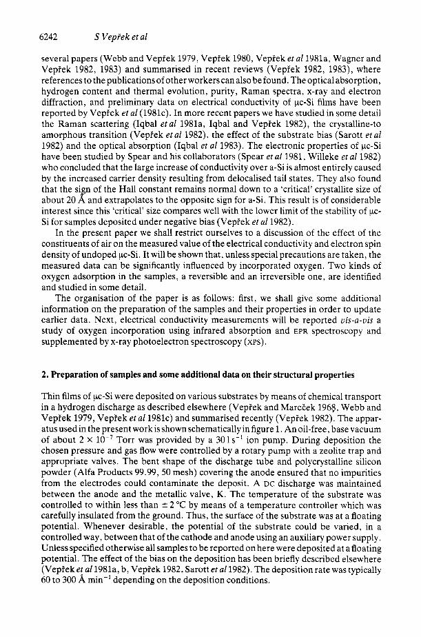
Figure 5 shows the typical behaviour of a pc-Si film which was, prior to the measure- ment, exposed to air for more than about three weeks in order to reach saturation with incorporated oxygen (see figure 4). Qualitatively similar and fairly reproducible behav- iour was found for all films studied which were of different thicknesses ranging between around 1 and 3 pm and deposited at various temperatures between about 100 and 450 "C. The effect of exposure of the samples to air was essentially the same as that of dry oxygen at about 100 Torr; no changes in URT of the annealed sample due to exposure to dry N2 took place. It should be emphasised that the changes of ~ R T due to annealing under vacuum and subsequent oxygen adsorption were, for a given sample saturated with the irreversibly absorbed oxygen, fairly reproducible even after several tens of cycles,
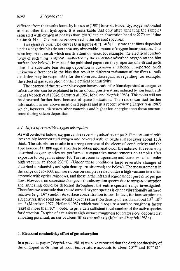
A representative example of the time dependence of the dark conductivity at room temperature as a function of the exposure of the annealed sample to pure oxygen at various pressures is shown in figure 6 for the same samples as in figure 5 . The value of mT at time zero, i.e. before oxygen was introduced, was the same for all three curves. Although the initial change of ~ R T was fast (e.g. a factor of greater than 10 in less than 1 min), in some cases it took around 10 days for ~ R T to reach the final, constant value. The complicated dependence of the mT decrease with pressure indicates a complex mechanism of the adsorption, but we shall not discuss this point here.
C32 - I
6250
-3.; - 7
S Veptek et a1
.. 02 1 *.. 1 Torr 'i *.
-1 h
-4 E
-2
I
9 -3
k - D
B -4 -
-5
&
Figure 5. Dependence of the logarithm of dark conductivity, log U, on the inverse temper- ature, 103/T, illustrating the effect of contamination by air and by oxygen: curve A, first heating up under vacuum better than 8 x Torr after long-term exposure of the sample to air; curves B to E, repeated cycling between 20 and 150 "C with annealing for about 15 min at 150 "C, followed by annealing for about 2 h at not less than 220 "C (curve E) and cooling down to 20 "C (curve F); curve F, repeated cycling between 20 and 220 "C under a vacuum better than 1 x Torr; curve G, sample stored under vacuum for around 24 h, followed by heating up to 220 "C (curve H) and cooling down (again along curve F). Curve I, exposure to oxygen at a pressure chosen between 1 and 100 Torr; curve J, heating up to more than 220 "C under vacuum; after annealing at this temperature curve F is measured upon cooling again. Sample parameters: Td = 265 "C, thickness 1.8 pm, AI electrodes in a gap geometry, gap vaned between 0.2 and 2 mm; applied voltage 10-30 V.
+ ' . ' ++ \'-
++ 100 Tors.s
-2 i
on exposure to

Properties of microcrystalline silicon 625 1
4.1. Temperature dependence of the conductivity changes during adsorption and desorp-
Fritzsche and co-workers (Fritzsche 1980, Tanielian et a1 1978, 1980), who described similar effects in a-Si as those reported in this section, have pointed out that the gas adsorption is not thermally activated. We have found that both the decrease and recovery of the electrical conductivity due to oxygen exposure and annealing are thermally activated but, because of the rather high activation energy, their temperature depend- ence is measurable only above around 100°C. This dependence was, in particular, established for annealing under vacuum which was more accessible to quantitative measurements by following the rate of increase of electrical conductivity, Su/at, during isothermal annealing at various temperatures. In order to ensure that no transient effect might falsify the results we restricted the measurements to a temperature range of 20- 125 "C in which the particular value of ( S ~ / S ~ ) T = ~ ~ ~ ~ ~ remained constant for at least 1 h. Figure 7 shows an Arrhenius plot of the rate of the recovery of the electrical conductivity,
tion of oxygen
L% kcal mol- ' I
1 o"0 2 0 2 5 3 0 3 5
103/r (K-" i
Figure 7. An Arrhenius plot of the rate of annealing of ~ c - S I under high vacuum after exposure of the sample to oxygen.
( Scq/St)T=,,n,,, for this temperature range. The approximate values of the activation energy at low temperatures are given as well indicating a rather complicated mechanism for the process. Regarding the annealing rate above about 125 "C we give only the following semiquantitative data: in order to recover the original conductivity completely, annealing times (under high vacuum) of more than 4 h, about 1 h and 10 min at temper- atures of about 170,200 and 220 "C are required.
4.2. Dependence of a ( T ) on oxygen pressure
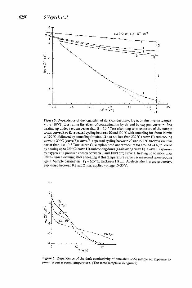
Figure 8 and table 2 show that oxygen at low pressure can significantly change the values
6252 S Vep f ek et a1
2 3 2 1 3 1 3 5 10 3 / T I K-' 1
Figure 8. Effect of oxygen on the measured dependence of log aon the inverse temperature in the steady state, i.e. after the oxygen adsorption reached equilibrium as in figure 5. Curve A, & = 0.12 eV, @ = 1 Q-lcm-', Pm < 10-6Torr; curve B, ea = 0.37 eV, @ = 47 Q-' cm-', Pm = 1 Torr.
Table 2. Effect of oxygen on the activation energy and pre-exponential factor of dark conductivity. Sample parameters are the same as in figure 5 .
Po2 (Torr) (ev) 4, (Q-l cm-I)
<10-6 0.12 1 1 0.37 47
100 0.89 4 x 10⁸
of aT, and G. One notices that the dependence of log U against 1/T remains fairly linear. It should be emphasised that this effect was reproducible upon repetitive anneal- ing under vacuum and exposure to oxygen, and fairly similar behaviour was found with several samples. The high sensitivity of a~ even to oxygen at low pressure is of interest with respect to the potential use of such films in gas sensors. This also shows that residual oxygen can completely falsify the measured electrical properties of undoped silicon films unless they are annealed at temperatures not less than 200 "C under a vacuum of less than about Torr.
4.3. Effect of sample thickness
As an example we show in figures 9 and 10 the effect of the sample thickness on the dark conductivity and its activation energy, for a series of pc-Si samples deposited at 400 "C. Figure 10 illustrates that for a thickness of more than about 1 pm, the aT of annealed samples remains nearly constant and close to around 0.013 SZ-' cm-', and the difference of aT of annealed and contaminated samples decreases with increasing thickness. The activation energy of annealed and contaminated samples increases and decreases, respectively, approaching a common value of about 0.3 eV.
An apparent anomaly is seen for samples less than 1 pm thick which display a high conductivity, very low activation energy and only small changes of both upon contami- nation by oxygen (and air) and annealing. Evidently, the dominant charge transport in these samples is by hopping in states within the gap associated with defects; its insensi- tivity to gas adsorption implies a high density of the gap states in these films. Similar effects were also found for a-Si (Ast and Brodsky 1980).
For the series of samples reported in figures 9 and 10 we also measured the time

Properties of microcrystalline silicon 6253
Figure 9. Effect of the sample thickness on the dark conductivity for annealed samples (0) and samples contaminated by oxygen (0). Td = 400 "C.
t o
I., , . , , ;, ; . * , , , ;, , , . ' g
0 10 20 30 Thickness (pm)
Figure 10. An example of the effect of sample thickness on the activation energy of dark conductivity for annealed (0) and contaminated (0) samples. Td = 400 "C.
-5 1 3 50 100
Time imin)
Figure 11. A 'universal' curve showing the time dependence of log %Tof an annealed sample (t = 0 min) on the exposure time to 0 2 at 100 Torr for a series of samples deposited at 400 "C with thickness varying between 1.04 and 25 pm, normalised to the initial, ~ R T (t = 0), and final, &RT (c+ m) values of the 1.04 Fm thick sample. The error bars indicate the range within which all the curves fall. One notices that this curve also follows closely the curve in figure 6 (0, at 100 Torr) for a sample of a similar thickness, but deposited at Td = 260 "C.

6254 S Vep f e k et a1
dependence of mT during their exposure to pure oxygen as a function of sample thick- ness, As indicated in figure 9, the difference between the loguRT values of annealed and contaminated samples decreases with increasing sample thickness, evidently because of the increasing contribution of the bulk conductivity of pc-Si as compared with that of the surface regions. The values of the annealed samples are nearly independent of the thickness in the range greater than around 1 to 25 pm see figure 9). If one normalises all the measured curves for exactly the same mT values at t = 0 (i.e. annealed samples) and as t+ CQ (i.e. contaminated), all the samples follow the same universal curve shown in figure 11. This curve is also similar to that given in figure 6 (see figure captions for details) and it shows that the changes of mTare due to oxygen adsorption at the surface.
5. Electron paramagnetic resonance (EPR) study
5.1. Experimental details of the apparatus and sample presentation
The measurements were performed with a ‘Varian Century Line Spectrometer’ equipped with a X-band bridge (E 101), a 12 inch electromagnet (V 7300), a resonance cavity (E 231), operating in the TE 102 mode, a Gaussmeter (E 500) and a frequency counter (EIP 548). A microwave power of 0.1 mW was chosen in order to compromise between the signal-to-noise ratio and the signal saturation. The spectra reported here were measured at room temperature. In a few cases spectra were also taken at 4 K but no significant changes were found.
For absolute measurements of the spin concentration 2,2-diphenyl-l-picryl-hydra- zyle (DPPH, Fluka purum) ground with either KCl or KBr was used as a standard. The shape of the EPR signal from DPPH corresponded to a lorentzian line with a peak-to- peak width of its first derivative of 1.5 G and ag-factor of 2.0036 (modulation amplitude of 0.25 G, field width of 4 G).
The yc-Si films were deposited on either Al, MO or Si02 substrates. For most of the measurements reported here the films were either scratched off the substrate or, because of very good adherence, the A1 substrate was dissolved, using asaturated Hg2C12 aqueous solution, and the yc-Si was filled into Heralux quartz tubes (internal diameter 4 mm). Such a sample handling also corresponds to that being currently used by other workers. In one case, the film was deposited on a Spectrosil substrate and inserted directly into the microwave cavity in order to check whether the above-described handling of the samples does not introduce a spurious EPR signal.
In order to minimise further the possible contamination of the samples during such handling we have also performed measurements on freshly deposited samples which were exposed to air for not more than 5 min prior to the EPR measurements. The samples were scratched from the substrate and filled into the Heralux quartz tubes under ultra- clean nitrogen (total oxygen and moisture content less than 0.1 ppm). It was shown in our previous paper that such a short exposure does not cause any oxidation of the sample which could be detected by XPS (Gimzewski and Vepfek 1983).
First, the EPR spectra were measured on samples which were contaminated due to exposure to air. Afterwards, the samples were annealed at 200-220 “C under an oil-free vacuum of better than lo-’ Torr, sealed under high vacuum and the measurements were repeated. Finally, the quartz tubes were opened and the changes of the EPR signals were measured as a function of time. All the spectra from pc-Si were taken with a modulation amplitude of 2.5 G and a field width of 40 G.
Properties of microcrystalline silicon 6255
The absolute spin concentration, N , , was calculated from the relation
where c is a calibration constant determined from the measurements on the DPPH standard (neglecting the dependence on the g-factor), Y,,, and AH,, are the peak-to- peak heights and widths of the EPR signal (first derivative), respectively, ma is the modulation amplitude andA the electronic amplification factor. The constant k = 0.517 is for gaussian and 1.81 for lorentzian lineshapes. In order to verify our measurements several samples were kindly remeasured by Professor Stuke and his co-workers (Uni- versity of Marburg) who found the same signal intensities.
5.2. Results
Essentially one EPR signal with a g-factor of 2.0057 t 0.0002 was found in all pc-Si samples examined, the peak-to-peak width varying between about 9 and 11 G. With most samples the lineshape could be approximated by a gaussian, but in some cases it corresponded neither to a gaussian nor to a lorentzian function and appeared to be possibly a superposition of two or more signals.
For samples deposited at temperatures between about 180 and 350 "C, and exposed to air for more than two weeks prior to the measurements (see figure 4), the total spin concentration varied between about 5 X lo" and 2 x 1OI8 ~ m - ~ , but no clear dependence of N , on the deposition conditions was found.
Similar results were also obtained with a sample about 15 ym thick measured directly with the substrate (Spectrosil). In this case we also verified that no additional EPR signal arose during long-term irradiation of the sample by white light (100 W tungsten lamp, light focused on the sample by means of fibre optics). However, samples which were scratched from the substrate and inserted in the Heralux quartz tubes under ultrapure nitrogen/(oxygen and a moisture content of less than 0.1 ppm) have shown a very low spin density of less than 1OI6 cm-3 (see figure 15).
The most interesting results came from the annealing experiments which parallel those described in § 4 on the conductivity measurements. The results, which were repeated with several samples in order to verify their reproducibility, are illustrated in figure 12. One notices that the relatively strong EPR signal from the 'as-deposited' (i.e. contaminated by air) sample vanishes upon annealing (detection limit better than 1 x 1OI6 spins ~ m - ~ ) and recovers again during exposure of the sample to air. We have verified that these changes of the EPR signal are reproducible for a given sample as are the changes of the electrical conductivity (0 4).
Figure 13 shows the time dependence of the electron spin density for a sample which was, after annealing, stored in an open quartz tube. In several cases we have verified that the recovery of the original value of the spin density can be accelerated by annealing overnight in air at about 80 "C. Annealing of the samples to greater than about 600 "C, where the hydrogen is evolved, results in an irreversible increase of the spin concentra- tion by a factor of three to nine as compared with those of 'as-deposited' samples. It is likely that these spins are of a similar origin to those found on the Si/SiOz interfaces and attributed to dangling bonds (Poindexter er al 1981, Poindexter and Caplan 1981). However, it cannot be considered as proven yet that the reversibly occurring and disappearing spins are of the same origin.

6256 S Vepr’ek et a1
6.3
6.3
6.3
6 . 3
6.3
A l 1 O 4 1 A i r
4
10 G
Figure 12. The EPR signal (g = 2.0057) of a Fc-Si sample which was, after deposition, exposed to air (lower curve), after annealing at 220 “C under a vacuum of better than lo-’ Torr for the indicated period of time. A is the amplification factor.
-A f te r annealing
0 20 50 100 200 300 670 4800 ExDosure time to air Ih)
Figure 13. Electron spin density of a sample which was annealed under vacuum and exposed afterwards to air.
Properties of microcrystalline silicon 6257
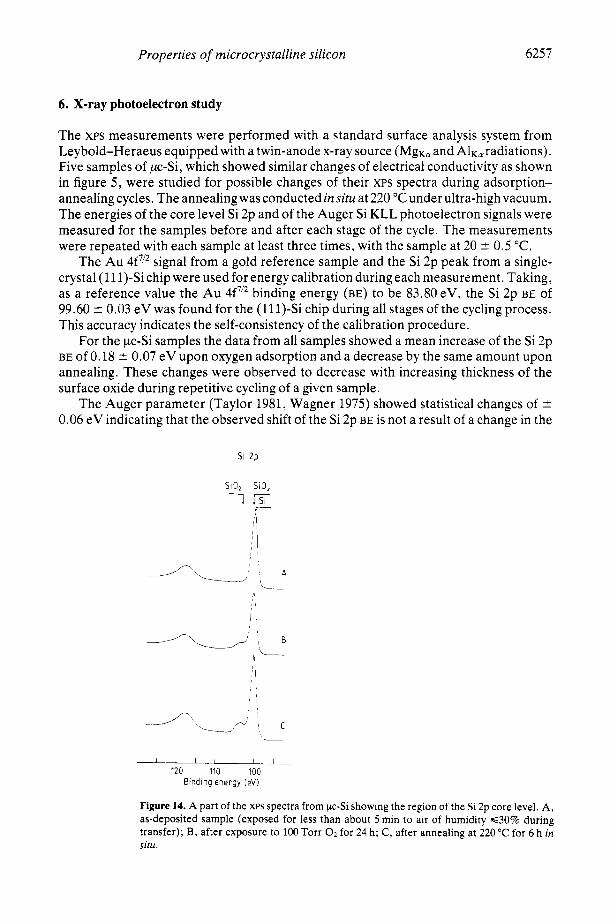
6. X-ray photoelectron study
The XPS measurements were performed with a standard surface analysis system from Leybold-Heraeus equipped with a twin-anode x-ray source (MgK, and AlK,radiations). Five samples of ps i , which showed similar changes of electrical conductivity as shown in figure 5, were studied for possible changes of their XPS spectra during adsorption- annealing cycles, The annealing was conducted in situ at 220 "C under ultra-high vacuum. The energies of the core level Si 2p and of the Auger Si KLL photoelectron signals were measured for the samples before and after each stage of the cycle. The measurements were repeated with each sample at least three times, with the sample at 20 k 0.5 "C.
The Au 4f''' signal from a gold reference sample and the Si 2p peak from a single- crystal (1 11)-Si chip were used for energy calibration during each measurement. Taking, as a reference value the Au 4f7'* binding energy (BE) to be 83.80 eV, the Si 2p BE of 99.60 ? 0.03 eV was found for the (111)-Si chip during all stages of the cycling process. This accuracy indicates the self-consistency of the calibration procedure.
For the p s i samples the data from all samples showed a mean increase of the Si 2p BE of 0.18 5 0.07 eV upon oxygen adsorption and a decrease by the same amount upon annealing. These changes were observed to decrease with increasing thickness of the surface oxide during repetitive cycling of a given sample.
The Auger parameter (Taylor 1981, Wagner 1975) showed statistical changes of k 0.06 eV indicating that the observed shift of the Si 2p BE is not a result of a change in the
SI 2 p
SIO, sio, 1 E
I ' 4-
1 1 I I l I I
120 110 100 Binding energy lev)
Figure 14. A part of the XPS spectra from p s i showing the region of the Si 2p core level. A, as-deposited sample (exposed for less than about 5 min to air of humidity 630% during transfer); B , after exposure to 100 Torr 0 2 for 24 h; C , after annealing at 220 "C for 6 h in situ.

6258 S Vepfek et a1
relaxation process occurring in the elemental sub-surface silicon. Thus, the observed changes of the Si 2p BE are due to a relative shift of the position of the Fermi level with respect to the conduction and valence bands.
The qualitative changes of the XPS spectra in the range of the Si 2p core level observed during the repetitive cyling are illustrated by figure 14. Spectrum A was taken on an as-deposited sample which was exposed for less than 5 min to air during transport from the deposition apparatus into the xps analysis chamber. After exposure to O2 at about 100 Torr for 24 h an oxide overlayer with a thickness of less than about 5 A was formed (spectrum B). The shape of the shoulder due to the oxide suggests the presence of an intermediate SiO, state with a chemical shift between that of Si02 and of elemental Si. This is further substantiated by spectrum C, taken after annealing of the oxidised sample at 220 “C in situ under UHV, where the intermediate state apparently vanishes, and the oxide peak, shifted by about 3.4 eV from the elemental one, becomes clearly distin- guishable. Repetitive exposure to oxygen and vacuum annealing resulted in spectra B and C, respectively. There is a certain ambiguity regarding the interpretation of the nature of the oxygen adsorption state referred to here as ‘SiO,’ (e.g. Hollinger et af 1977, Muiioz and Sacedon 1981, Kazmerski et a1 1981 and references therein) but, regardless of its microscopic nature, this state appears to be an intermediate formed during the oxidation of Si and is associated with a partial transfer of electronic charge to the adsorbed oxygen, Ot-. Further details on the initial stages of the oxidation of pc-Si can be found in our recent paper (Gimzewski and Vepiek 1983).
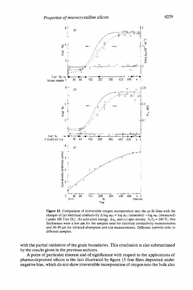
7. Comparison of oxygen incorporation with the changes of electrical conductivity and electron spin density
The results given in 09 3 to 6 refer to pc-Si samples in which the irreversibly incorporated oxygen had reached saturation. In this section we shall show how the changes of electrical conductivity and spin density evolve during the oxygen incorporation up to the point of saturation.
In our previous study we have shown that our samples can be exposed to air for about 7 min without undergoing any oxidation or even any appreciable oxygen adsorption detectable by XPS (Gimzewski and Vepiek 1983). Therefore, we performed a series of conductivity, EPR and infrared absorption measurements on freshly prepared samples which were exposed for less than 5-7 min to air before the first measurement was made.
Figure 15 illustrates the results: the electrical conductivity initially shows only very small changes upon exposure of the samples to 0 2 at 100 Torr and subsequent annealing under high vacuum. The measured value of the electron spin density of the (almost) uncontaminated samples is also very low (around 1 x 10l6 cm-3 on an absolute scale). Only after more than 60min exposure of the samples to air, when the amount of irreversibly incorporated oxygen noticeably increases, AURT, A E ~ and N , increase as well closely following the relative increase of the oxygen concentration in the films up to saturation (see figure 15). The N , data show somewhat larger scattering since, in the course of the study which took over six months, it was not always possible to match all the necessary adjustments and calibrations of the EPR spectrometer, which was being used by other research groups.
It is evident from figure 15 that the changes of the electrical conductivity as well as of the electron spin density due to reversibly adsorbed oxygen on the sample surface are correlated with the amount of irreversibly incorporated oxygen, i.e. (most probably)
Properties of microcrystalline silicon 6259
6 2
- 4 8 c 0 0 I
2
O b i %) - biased sample 0
I a, E.,.,,, ' I M C L .
30 60 100 200 300 400 600 4 t
,-d 0 30 60 100 200 300 400 600 4 6
Imin) Ih) (months) Time
Figure 15. Comparison of irreversible oxygen incorporation into the Fc-Si films with the changes of ( a ) electrical conductivity A log *T = log %T (annealed) -log hT (measured) (under 100 Torr Oz), ( b ) activation energy, Aea, and (c) spin density, N,Td -- 260 "C; film thicknesses were a few pm for the samples used for electrical conductivity measurements and 30-50 pm for infrared absorption and ESR measurements. Different symbols refer to different samples.
with the partial oxidation of the grain boundaries. This conclusion is also substantiated by the results given in the previous sections.
A point of particular interest and of significance with respect to the applications of plasma-deposited silicon is the fact illustrated by figure 15 that films deposited under negative bias, which do not show irreversible incorporation of oxygen into the bulk also
6260 S Vepfek et a1
do not show any changes of electrical conductivity comparable with those of films deposited at a floating potential.
Moreover, we have verified on several samples that, in order to avoid the oxygen incorporation and resulting conductivity changes it is sufficient to deposit, on top of a sample prepared at a floating potential, a few thousand angstroms thick overlayer under negative bias. Such samples did not display any significant changes of their properties even after long-term exposure to air.
8. Discussion and conclusion
The main goal of this paper is to show which deposition parameters determine the stability or, on the other hand, the sensitivity of Si films to absorbed and adsorbed gases. An explanation of the effects of gas adsorption on the electrical properties of the film can be given in terms of well-accepted models of polycrystalline gas sensors (Heiland 1982, Fonash et a1 1982, Morrison 1982) and of the recent review of the electrical properties of polycrystalline semiconductors (Orton and Powell 1980).
For further discussion it is essential to realise that undoped yc-Si of crystallite sizes typical of plasma deposited material, i.e. not greater than 200 A with incorporated oxygen at several at. % must be strongly depleted of free charge carriers which are trapped at the oxidised grain boundaries. This is illustrated by the following comparison: Spear et a1 (1981) reported a carrier density of not less than 3 X 1017 cm-3 for their undoped films which compares with the density of 7 X 1017 cm-3 for our typical sample, as kindly measured by the Dundee group. A simple estimate shows that for any reason- ably expected density of trapping sites at the grain boundary, their total number on the grain surface is much larger than the number of free carriers in the grain (see also figure 10 in Veptek (1982)). Consequently, charge transport in undoped pc-Si films cannot be described by a grain barrier model which has been developed for poly-Si with a relatively large grain size (Seto 1975, Kamins 1971, Baccarini et a1 1978). The barrier model can apply to doped yc-Si provided that there is a sufficiently low density of trapping sites (Spear et a1 1981, Willeke et a1 1982).
We should, therefore, like to suggest that an appropriate model which can explain the remarkable sensitivity of yc-Si with incorporated oxygen to the reversible adsorption of oxygen (and other gases) at their surface, is that of depleted films. In this case, adsorption of about 10l2 cm-* of electron acceptors (e.g. 0 2 ) or donors (e.g. H, NH3) on the surface will strongly change the conductivity of a film not less than 50 ym thick (for a numerical estimate see, e.g., Morrison 1982, p 335). Such films appear to be promising candidates for gas sensors.
The experimental finding that samples deposited under a negative bias do not show such changes of electrical conductivity upon gas adsorption can be explained in terms of a Debye screening length short compared with the film thickness. The same conclusion applies to phosphorus-doped samples which also show only inappreciable conductivity changes on exposure to 0 2 (unpublished results).
Further work is necessary in order to explain the origin and behaviour of the EPR signal upon repeated oxygen adsorption and annealing (§ 5). In addition to the well- accepted interpretation of such a signal as due to dangling bonds there are further alternative possibilities, such as 0; in a strongly anisotropic environment, localised electrons and various radicals which cannot be excluded on the basis of the available data.

Properties of microcrystalline silicon 6261
The XPS (§ 6 and Gimzewski and Vepiek 1983) and infrared adsorption studies have shown that the irreversibly incorporated oxygen in films deposited at a floating potential is chemically bonded at the grain boundaries which, however, do not contain any noticeable amorphous tissue (§ 2.2). Such a diffusion of oxygen into the films can be avoided by application of a negative bias to the substrate during deposition (§§ 3 and 7 ) which leads to a build-up of compressive stress in the film (Iqbal and Vepfek 1983b). It must be emphasised that the density of films deposited at a temperature of not less than 200 "C corresponds to that of bulk silicon even for those deposited at a floating potential (Vepiek eta1 1981~). Therefore, they do not show any porosity typical of silicon films deposited at lower temperatures.
In conclusion, we have shown that pc-Si films deposited at a floating potential and saturated with chemically bonded oxygen at the grain boundaries display a high sensi- tivity of their electrical conductivity to gases adsorbed at their surface. Such films may find an application as selective gas sensors.
In order to avoid such effects and prepare undoped films which show only inappre- ciable changes of electrical conductivity due to gas adsorption it is necessary to apply a negative bias to the substrate during the deposition.
Acknowledgments
We should like to thank Professor J Stuke (University of Marburg) and Professor W E Spear for some measurements on our samples and for valuable discussions. This work has been supported in part by the Nationaler-Energie-Forschungs-Fonds (NEFF) and by the Schweizerischer Fonds zur Forderung der Wissenschaftlichen Forschung.
References
Ast D G and Brodsky M H 1980 Phil. Mag. B 41 273 Baccarini G , Riccb B and Spadini G 1978 J. Appl. Phys. 49 5565 Fonash S J , Huston H and Ashok S 1982 Sensors and Actuators 2 363 Freeman E C and Paul W 1978 Phys. Rev. B 18 4288 Fritzsche H 1980 Solar Energy Materials 3 447 Gimzewski J K and Vepiek S 1983 Solid State Commun. 47 747 Harper J M E, Cuomo J J and Kaufman H R 1982 J. Vac. Sci. Technol. 21 737 Heiland 1982 Sensors and Actuators 2 343 Hollinger G, Jugnet Y , Pertosa P, Portel and Duc T M 1977 Proc. 7th Int. Vac. Congr. and3rd Int. Conf. Solid
Iqbal Z, Sarott F A and Vepiek S 1983 J. Phys. C: Solid State Phys. 16 2005 Iqbal Z and Vepiek S 1982 J. Phys. C: Solid State Phys. 15 377 - 1983 (to be published) Iqbal Z, Vepiek S, Webb A P and Capezzuto P 1981a Solid State Commun. 37 933 Iqbal 2, Webb A P and Vepfek S 1981bAppl. Phys. Lett. 36 163 John P, Odeh I M, Thomas M J K and Wilson J I B 1981 Proc. 9th Int. Conf. on Amorphous and Liquid
Semiconductors ed. D Kaplan (1981 J. Physique C 4 651) Kamins T I 1971 J. Appl. Phys. 42 4357 Kazmerski L L, Jamjoum 0, Ireland P J and Whitney R L 1981 J. Vac. Sci. Technol. 18 960 Morrison S R 1977 The Chemical Physics of Surfaces (New York: Plenum) - Mufioz M C and Saced6n J L 1981 J. Chem. Phys. 74 4693 Orton J W and Powell M J 1980 Rep. Prog. Phys. 43 81
Surfaces (Vienna) I977 p 2229
1982 Sensors and Actuators 2 329
6262 S VeprTek et a1
Pond R C 1979 J . Microsc. 116 105 Pond R C, Smith D A and Clark W A T 1974 J . Microsc. 102 309 Pond R C and Vitek V 1977 Proc. R. Soc. 357 453 Poindexter E H and Caplan P J 1981 Proc. Int. Conf. o n Insulating F i l m on Semiconductors (Erlangen) 1981
Poindexter E H , Caplan P J, Deal B E and Razouk R R 1981 J . Appl . Phys. 52 879 Sari S 0, Hollingsworth Smith P and Oona H 1978 J . Phys. Chem. Solids 39 957 Sarott F-A 1981 Diplomarbeit University of Zurich Sarott F-A, Iqbal Z and Vepiek S 1982 Solid State Commun. 42 465 Set0 J Y W 1975 J . Appl . Phys. 46 5247 Simon I and McMahon H 0 1953 J . Chem. Phys. 21 23 Solomon I 1981 in Fundamental Physics o fAmorphous Semiconductors ed. F Yonezawa (Berlin: Springer) p
Spear W E , Willeke G, Le Comber P G and Fitzgerald A G 1981 Proc. 9th Int. Conf. on A m o r p h o w and
Tanielian M, Chatani M, Fritzsche H , Smid V and Persans P D 1980 J . Non-Cryst. Solids 35/36 575 Tanielian M, Fritzsche H H, Tsai C C and Symbalisty E 1978 Appl . Phys. Lett. 33 353 Taylor J A 1981 Appl . Surf. Sci. 7 168 Vepiek S 1980 Chimia 34 489 - 1982 Pure and Appl . Chem. 54 1197 - 1983 Proc. Technical Symp., Semiconductors (Europe) Vepiek S , Iqbal Z, Oswald H R, Sarott F-A and Wagner J J 1981a Proc. 9th Int. Conf. o n Amorphous and
Vepiek S , Iqbal Z, Oswald H R, Sarott F-A, Wagner J J and Webb A P 1981b Solid State Commun. 39 509 Vepiek S , Iqbal Z, Oswald H R and Webb A P 1981c J . Phys. C: Solid State Phys. 14 295 Vepfek S, Iqbal Z and Sarott F-A 1982 Phil. Mag. B 45 137 Vepiek S and MareCek V 1968 Solid-state Electron. 11 683 Wagner C D 1975 Farad. Disc.: Chem. Soc. 60 291 Wagner J J and Vepiek S 1982 Plasma Chem. and Plasma Processing 2 9 - 1983 Plasma Chem. and Plasma Processing 3 219 Webb A P and Vepfek S 1979 Chem. Phys. Lett. 62 173 Willeke G, Spear W E , Jones D I and Le Comber P G 1982 Phil. Mag. B 46 177 Yacobi B G, Collins R W, Moddel G, Viktorovitch P and Paul W 1981 Phys. Reu. B 24 5907
(Berlin: Springer) p 150
33
Liquid Semiconductors ed D Kaplan (1982 J . Physique C4 2577)
Liquid Semiconductors ed. D Kaplan (1982 J . Physique C4 251)