
光電工程研究所 - 碩 士 論 文 - 國立交通大學機構典藏
65
國 立 交 通 大 學 光電工程研究所 碩 士 論 文 氧化鋅量子點中不受激發功率影響之激子態研究 Invariable exciton states upon increasing pumping in ZnO quantum dots 研 究 生:廖婉君 指導教授:謝文峰 教授 張振雄 教授 中 華 民 國 九 十 九 年 六 月
-
Upload
khangminh22 -
Category
Documents
-
view
2 -
download
0
Transcript of 光電工程研究所 - 碩 士 論 文 - 國立交通大學機構典藏

國 立 交 通 大 學
光電工程研究所
碩 士 論 文
氧化鋅量子點中不受激發功率影響之激子態研究
Invariable exciton states upon increasing
pumping in ZnO quantum dots
研 究 生廖婉君
指導教授謝文峰 教授
張振雄 教授
中 華 民 國 九 十 九 年 六 月
氧化鋅量子點中不受激發功率影響之激子態研究
Invariable exciton states upon increasing
pumping in ZnO quantum dots
研 究 生廖婉君 Student Wan-Jiun Liao
指導老師謝文峰 教授 Advisors Dr Wen-Feng Hsieh
張振雄 教授 Dr Chen-Shiung Chang
國立交通大學
光電工程研究所
碩士論文
A Thesis
Submitted to Institute of Electro-Optical Engineering College of Electrical Engineering and Computer Science
National Chiao Tung University In partial Fulfillment of the Requirements
for the Degree of Master
in Electro-Optical Engineering
June 2010 Hsinchu Taiwan Republic of China
中 華 民 國 九 十 九 年 六 月
I
Invariable exciton states upon increasing pumping
in ZnO quantum dots
Student Wan-Jiun Liao Advisor Dr Wen-Feng Hsieh
Dr Chen-Shiung Chang
Department of Photonics amp Institute of Electro-Optical Engineering
National Chiao Tung University
Abstract
ZnO QDs are synthesized by a simple sol-gel method and the average size of
QDs can be tailored under solution concentration Size-dependent blue shifts of
photoluminescence give the evidence of the quantum confinement effect
Furthermore the unchanged spectral profiles of near-bandedge emission (NBE) for a
fixed size of ZnO quantum dots (QDs) reveal no signature of biexciton formation and
exciton-exciton scattering under excitation density covering three orders of magnitude
These results quite differ from that of the micrometer-sized powder The intensities
of NBE peaks attributed to free exciton and surface bound exciton states exhibit linear
dependence on the excitation power density that confirms the invariable exciton states
with no effect of two-exciton interaction in ZnO QDs upon increasing the pump
intensity
II
氧化鋅量子點中不受激發功率影響之激子態研究
研究生廖婉君 指導老師謝文峰 教授
張振雄 教授
國立交通大學光電工程研究所
摘要
利用溶膠-凝膠法藉由改變溶液濃度來合成不同晶粒大小的氧化鋅量子點
並量測其光學特性從低溫螢光光譜隨氧化鋅量子點尺寸變小而藍移的現象可觀
察到在氧化鋅量子點中存在量子侷限效應然而量測變功率螢光光譜發現當
激發光強度改變了1000倍除了光譜強度會隨激發強度增加而變大外NBE的光
譜形狀幾乎都不變且觀察不到雙激子的形成與激子與激子的散射現象此情形
與氧化鋅塊材的特性相當不一樣另外自由激子與表面束縛激子的發光能量幾
乎不隨激發光強度改變及線性的發光強度與激發能量關係表示當激發功率增
加仍沒有激子間的交互作用因此在氧化鋅量子點中存在穩定的激子態
III
誌謝
時間過得真快一轉眼我的碩士生生活就要結束了在這兩年的日子裡
我學習與成長了很多也讓我的想法與處事態度變得更成熟了
研究所這段期間我要謝謝我的指導教授謝文峰老師謝謝老師在課業
研究與待人處事上對我的指導與教誨以及對我在生活上的關心從老師的身上
我學習到很多也要謝謝另外一位指導教授張振雄老師提供我專業意見以及
生活上的幫助接下來要謝謝小豪帶我入門做實驗雖然我常做出讓你啞口無言
的事不過真的很謝謝你教了我很多事還要謝謝小郭當我研究上有問題時
常常向你請教謝謝你提供我很多想法與協助也要謝謝楊松幫我打XRD與教我
SEM以及謝謝鄭信民學長對我研究的關心與協助還有歐博濟雖然在碩二之
後才跟你比較有交集常向你請教TRPL的問題你也常會關心我的近況論文或
找工作的進展如何謝謝你另外智章學長維仁學長碧軒學長以及黃董偶
爾我有問題要請教你們你們也都很熱心的幫我解答謝謝你們還有要謝謝黃
至賢很多生活上的瑣碎事情常會去煩你謝謝你啦實驗室有了你讓我很不無
聊了XD
另外謝謝蔡智雅學姐課業上或是找工作等常找你幫忙或詢問你意見
謝謝你還要謝謝陳厚仁總是很大方的借我筆記與考古題祝你跟學姐永遠甜蜜
幸福喔XD 還有黃冠智常常會以你的經驗告訴我很多事情以及提供我建議以
及林建輝你真是一個奇妙的人你的很多事情與想法常讓我們驚奇也讓實驗
室更有趣了還有黃棕儂雖然你比較少來實驗室但也很謝謝你在我還沒進實
驗室前對我的照顧另外還有黎延垠你竟然拋棄我們提前畢業去了剛進實驗室
時什麼都不懂多虧你在告訴與提醒我要做什麼以及問你光電系的八卦ㄎ
IV
ㄎ謝謝你們雖然跟你們只相處了一年但碩一的那一年裡因為有你們讓我
覺得實驗室很溫馨也讓我能更快熟悉實驗室當然也要謝謝和我當了兩年同學的
李柏毅謝謝你對我生活上的關心還有許家瑋謝謝你很熱心想教我程式語言
但我還是沒學會= = 另外還有實驗室的學弟們雖然跟你們還沒有很熟不過
也祝你們在實驗室的生活都能很愉快
最後當然要謝謝一位特別的人謝謝你的陪伴與鼓勵讓我在心情不好沮
喪的時候得以抒發與得到安慰未來還有很多挑戰等著我們我們要一起加油
小布丁 于 九十九年六月
V
Contents
Abstract (in English)helliphelliphelliphelliphelliphelliphelliphelliphelliphelliphelliphelliphelliphelliphelliphelliphelliphelliphelliphelliphelliphelliphelliphelliphellipI
Abstract (in Chinese)helliphelliphelliphelliphelliphelliphelliphelliphelliphelliphelliphelliphelliphelliphelliphelliphelliphelliphelliphelliphelliphelliphelliphelliphellipII
AcknowledgementhelliphelliphelliphelliphelliphelliphelliphelliphelliphelliphelliphelliphelliphelliphelliphelliphelliphelliphelliphelliphelliphelliphelliphelliphellipIII
ContentshelliphelliphelliphelliphelliphelliphelliphelliphelliphelliphelliphelliphelliphelliphelliphelliphelliphelliphelliphelliphelliphelliphelliphelliphelliphelliphelliphellipV
List of FigureshelliphelliphelliphelliphelliphelliphelliphelliphelliphelliphelliphelliphelliphelliphelliphelliphelliphelliphelliphelliphelliphelliphelliphelliphelliphellipVII
List of TableshelliphelliphelliphelliphelliphelliphelliphelliphelliphelliphelliphelliphelliphelliphelliphelliphelliphelliphelliphelliphelliphellipVIII
Chapter 1 Introductionhelliphelliphelliphelliphelliphelliphelliphelliphelliphelliphelliphelliphelliphelliphelliphelliphelliphelliphelliphelliphelliphelliphellip1
11 Basic properties of ZnO and significance of ZnO related photonic deviceshelliphellip1
12 General review of ZnO nanostructureshelliphelliphelliphelliphelliphelliphelliphelliphelliphelliphelliphelliphelliphelliphelliphellip4
13 Motivationshelliphelliphelliphelliphelliphelliphelliphelliphelliphelliphelliphelliphelliphelliphelliphelliphelliphelliphelliphelliphelliphelliphelliphelliphelliphelliphellip6
14 Organization of the thesishelliphelliphelliphelliphelliphelliphelliphelliphelliphelliphelliphelliphelliphelliphelliphelliphelliphelliphelliphelliphelliphellip8
Chapter 2 Theoretical backgroundhelliphelliphelliphelliphelliphelliphelliphelliphelliphelliphelliphelliphelliphelliphelliphelliphelliphellip9
21 Sol-gel methodhelliphelliphelliphelliphelliphelliphelliphelliphelliphelliphelliphelliphelliphelliphelliphelliphelliphelliphelliphelliphelliphelliphelliphellip9
22 Quantum effecthelliphelliphelliphelliphelliphelliphelliphelliphelliphelliphelliphelliphelliphelliphelliphelliphelliphelliphelliphelliphelliphelliphelliphellip12
221 Quantum confinement effecthelliphelliphelliphelliphelliphelliphelliphelliphelliphelliphelliphelliphelliphelliphelliphelliphellip13
222 Density of stateshelliphelliphelliphelliphelliphelliphelliphelliphelliphelliphelliphelliphelliphelliphelliphelliphelliphelliphelliphelliphellip16
23 X-ray diffractionhelliphelliphelliphelliphelliphelliphelliphelliphelliphelliphelliphelliphelliphelliphelliphelliphelliphelliphelliphelliphelliphelliphelliphellip19
231 Lattice parametershelliphelliphelliphelliphelliphelliphelliphelliphelliphelliphelliphelliphelliphelliphelliphelliphelliphelliphelliphelliphellip19
232 Debye-Scherer formulahelliphelliphelliphelliphelliphelliphelliphelliphelliphelliphelliphelliphelliphelliphelliphelliphelliphelliphellip21
24 Photoluminescence characterizationhelliphelliphelliphelliphelliphelliphelliphelliphelliphelliphelliphelliphelliphelliphelliphelliphellip24
241 Fundamental transitionshelliphelliphelliphelliphelliphelliphelliphelliphelliphelliphelliphelliphelliphelliphelliphelliphelliphellip25
VI
242 Influence of high excited light intensityhelliphelliphelliphelliphelliphelliphelliphelliphelliphelliphelliphelliphellip31
Chapter 3 Experiment detail and analysis techniqueshelliphelliphelliphelliphelliphelliphelliphelliphelliphellip34
31 Sample preparationhelliphelliphelliphelliphelliphelliphelliphelliphelliphelliphelliphelliphelliphelliphelliphelliphelliphelliphelliphelliphelliphelliphelliphellip34
32 Microstructure and optical properties analysishelliphelliphelliphelliphelliphelliphelliphelliphelliphelliphelliphellip37
321 X-ray diffractionhelliphelliphelliphelliphelliphelliphelliphelliphelliphelliphelliphelliphelliphelliphelliphelliphelliphelliphelliphelliphelliphellip37
322 Photoluminescence systemhelliphelliphelliphelliphelliphelliphelliphelliphelliphelliphelliphelliphelliphelliphelliphelliphelliphellip38
Chapter 4 Results and Discussionhelliphelliphelliphelliphelliphelliphelliphelliphelliphelliphelliphelliphelliphelliphelliphelliphelliphelliphellip40
41 Morphology and crystal structureshelliphelliphelliphelliphelliphelliphelliphelliphelliphelliphelliphelliphelliphelliphelliphellip40
411 Morphologyhelliphelliphelliphelliphelliphelliphelliphelliphelliphelliphelliphelliphelliphelliphelliphelliphelliphelliphelliphelliphelliphelliphelliphellip40
412 X-ray diffraction measurementhelliphelliphelliphelliphelliphelliphelliphelliphelliphelliphelliphelliphelliphelliphelliphellip41
42 Photoluminescence spectrahelliphelliphelliphelliphelliphelliphelliphelliphelliphelliphelliphelliphelliphelliphelliphelliphelliphelliphelliphellip42
421 Photoluminescence spectra for different sizes of ZnO particleshelliphelliphelliphellip42
422 Temperature-dependent PL for different sizes of ZnO particleshelliphelliphelliphellip44
423 Power-dependent PL for different sizes of ZnO particleshelliphelliphelliphelliphelliphelliphellip45
424 PL peak positions as a function of excitation powerhelliphelliphelliphelliphelliphelliphelliphelliphellip48
425 Integrated intensity as a function of excitation powerhelliphelliphelliphelliphelliphelliphelliphellip49
Chapter 5 Conclusions and Prospective helliphelliphelliphelliphelliphelliphelliphelliphelliphelliphelliphelliphelliphelliphelliphellip51
51 Conclusionshelliphelliphelliphelliphelliphelliphelliphelliphelliphelliphelliphelliphelliphelliphelliphelliphelliphelliphelliphelliphelliphelliphelliphelliphellip51
52 Prospectivehelliphelliphelliphelliphelliphelliphelliphelliphelliphelliphelliphelliphelliphelliphelliphelliphelliphelliphelliphelliphelliphelliphelliphelliphelliphellip52
Referenceshelliphelliphelliphelliphelliphelliphelliphelliphelliphelliphelliphelliphelliphelliphelliphelliphelliphelliphelliphelliphelliphelliphelliphelliphelliphelliphelliphellip53
VII
List of Figures
Fig 1-1 The wurtzite structure model of ZnOhelliphelliphelliphelliphelliphelliphelliphelliphelliphelliphelliphelliphelliphelliphellip3
Fig 12 Representative scanning electron microscopy images of various ZnO
nanostructure morphologieshelliphelliphelliphelliphelliphelliphelliphelliphelliphelliphelliphelliphelliphelliphelliphelliphelliphellip6
Fig 2-1 Schematic of the rotes that one could follow within the scope of sol-gel
processinghelliphelliphelliphelliphelliphelliphelliphelliphelliphelliphelliphelliphelliphelliphelliphelliphelliphelliphelliphelliphelliphelliphelliphelliphellip12
Fig 2-2 Geometry used to calculate density of states in three two and one
dimensionshelliphelliphelliphelliphelliphelliphelliphelliphelliphelliphelliphelliphelliphelliphelliphelliphelliphelliphelliphelliphelliphelliphelliphelliphellip17
Fig 2-3 Variation in the energy dependence of the density of stateshelliphelliphelliphelliphelliphellip18
Fig 2-4 X-ray scattering from a 2-dimendion periodic crystalhelliphelliphelliphelliphelliphelliphelliphelliphellip20
Fig 2-5 The hexagonal unit cellhelliphelliphelliphelliphelliphelliphelliphelliphelliphelliphelliphelliphelliphelliphelliphelliphelliphelliphelliphellip21
Fig 2-6 Grating treatment of line broadening by crystallite helliphelliphelliphelliphelliphelliphelliphelliphellip21
Fig 2-7 A pair excitation in the scheme of valence and conduction bandshelliphelliphellip27
Fig 2-8 Visualization of bound excitonshelliphelliphelliphelliphelliphelliphellip28
Fig 2-9 Radiative transition between a band and an impurity statehelliphelliphelliphelliphelliphelliphellip31
Fig 2-10 The general scenario for many-particle effects in semiconductorshelliphellip32
Fig 2-11 Schematic representation of the inelastic exciton-exciton scattering
processeshelliphelliphelliphelliphelliphelliphelliphelliphelliphelliphelliphelliphelliphelliphelliphelliphelliphelliphelliphelliphelliphelliphelliphelliphelliphellip33
Fig 3-1 Experiment equipment used for fabricating ZnO QDshelliphelliphelliphelliphelliphelliphelliphellip36
Fig 3-2 A flow chart of fabricates ZnO QDs by sol-gel methodhelliphelliphelliphelliphelliphelliphelliphellip36
Fig 3-3 The x-ray spectrometerhelliphelliphelliphelliphelliphelliphelliphelliphelliphelliphelliphelliphelliphelliphelliphelliphelliphelliphelliphellip37
Fig 3-4 PL detection systemshelliphelliphelliphelliphelliphelliphelliphelliphelliphelliphelliphelliphelliphelliphelliphelliphelliphelliphelliphelliphellip39
Fig 4-1 HRTEM image of the ZnO QDs fabricated using 004M Zn(OAc)2helliphelliphellip40
Fig 4-2 XRD profiles of the ZnO QDs prepared with various concentration of
Zn(OAc)2helliphelliphelliphelliphelliphelliphelliphelliphelliphelliphelliphelliphelliphelliphelliphelliphelliphelliphelliphelliphelliphelliphelliphelliphellip41
VIII
Fig 4-3 The PL spectra of the ZnO QDs measured at low temperaturehelliphelliphelliphelliphellip43
Fig 4-4 PL spectra of different sizes of ZnO QD at low temperaturehelliphelliphelliphelliphellip44
Fig 4-5 Temperature-dependent PL spectrahelliphelliphelliphelliphelliphelliphelliphelliphelliphelliphelliphelliphelliphelliphellip45
Fig 4-6 Power-dependent PL spectrahelliphelliphelliphelliphelliphelliphelliphelliphelliphelliphelliphelliphelliphelliphelliphelliphellip47
Fig 4-7 Theoretical fit to a PL spectrum of 6 nm ZnO QDs measured at 80Khellip48
Fig 4-8 The PL peak positions as a function of excitation power measured at 80K49
Fig 4-9 The integrated intensity of two decomposed peaks as a function of excitation
power measured at 80Khelliphelliphelliphelliphelliphelliphelliphelliphelliphelliphelliphelliphelliphelliphelliphelliphelliphelliphelliphellip50
List of Tables
Table 1-1 Comparison of properties of ZnO with those of other wide band gap
semiconductorshelliphelliphelliphelliphelliphelliphelliphelliphelliphelliphellip1
Table 1-2 Properties of wurtzite ZnO helliphelliphelliphelliphelliphelliphelliphelliphelliphelliphelliphelliphelliphelliphelliphelliphelliphelliphellip2
Table 31 Shows that chemical reagent was used with sol-gel experiment process hellip35
1
Chapter 1 Introduction
11 Basic property of ZnO and significance of ZnO related photonic devices
Zinc oxide (ZnO) is a promising material for a variety of practical applications [1]
such as piezoelectric transducers optical waveguides surface acoustic wave devices
varistors phosphors solar cells chemical and gas sensors transparent electrodes spin
functional devices UV-light emitters [2] and ultraviolet laser diodes The basic
properties of ZnO can be obtained by examining Table 1-1 which compares the
material properties of other relevant semiconductors [3]
Table 1-1 Comparison of properties of ZnO with those of other wide band gap semiconductors [3]
ZnO has attracted significant scientific and technological attention due to its
wide direct band gap (337 eV) that is suitable for photonic applications in the
ultraviolet (UV) or blue spectrum range [4] In this regard a large exciton binding
energy of ZnO is 60 meV which is significantly larger than that of GaN (25 meV) and
2
ZnS (39 meV) and other wide-gap semiconductors The large exciton binding
energy allows stable existence of excitons and efficient excitonic emission at room
temperature (thermal energy 26 meV) The basic material parameters of ZnO are
also shown in Table 1-2 To realize any type of device technology these parameters
are important to have control over the concentration of intentionally introduced
impurities (dopants) which are responsible for the electrical properties of ZnO The
dopants determine whether the current (and ultimately the information processed by
the device) is carried by electrons or holes
Table 1-2 Properties of wurtzite ZnO
3
The structure of ZnO crystal is shown in Fig 1-1 which has a hexagonal wurtzite
structure (space group C6mc) with lattice parameters a = 03249 nm and c = 05207
nm The structure of ZnO can be simply described as a number of alternating planes
composed of tetrahedrally coordinated O2- and Zn2+ ions stacked alternately along the
c-axis in which a1 a2 and c are the unit vectors in a unit cell the large and small
circles denote the anion and cation atoms respectively The tetrahedral coordination
in ZnO results in non-central symmetric structure and consequently the development
of piezoelectricity and pyroelectricity
Fig 1-1 The wurtzite structure model of ZnO
4
12 General review of ZnO nanostructures
ZnO nanocrystals have recently attracted broad attention in fundamental studies
and technical applications [5] because of their distinguished performance in
electronics optics and photonics Therefore in the last few decades a variety of
ZnO nanostructure morphologies such as nanowires [6] nanorods [7 8] tetrapods
[9] nanoribbonsbelts [9] and nanoparticles [10 11] have been reported Recently
novel morphologies such as hierarchical nanostructures [12] bridge-nail-like
nanostructures [13] tubular nanostructures [14] nanosheets [15] nanopropeller
arrays [16] nanohelixes [17] and nanorings [17] have amongst others been
demonstrated These diverse ZnO nanostructures have been fabricated by various
methods such as thermal evaporation [9] metalndashorganic vapor phase epitaxy
(MOVPE) [8] laser ablation hydrothermal synthesis [7] sol-gel method [10 11] and
template-based synthesis [6] Several recent review articles have summarized
progress in the growth and applications of ZnO nanostructures [4 18] Some of the
possible ZnO nanostructure morphologies are shown in Fig 12
Additionally when the dimension of semiconductors are reduced from three
(bulk material) to the quasi-zero dimensional semiconductor structures such as
quantum dots (QDs) the optical properties of QDs are much different from the bulk
materials There are two physical mechanisms in modifying the energy band
5
structure of nanostructures ie the quantum confinement effect (QCE) [19] and
surface states [20] These two mechanisms compete with each other to influence PL
spectra For nanodots or nanostructures in ZnO system with diameters less than 10
nm the QCE plays a dominant role as has been much reported [21] On the other
hand the surface-to-volume ratio also brings much influence on the systemrsquos
Hamiltonian when the material size is reduced to the nanometer scale [22] The
predominance of surface states is responsible for many novel physical features of
nanomaterials In the past decade various groups have devoted to produce ZnO
QDs and study the properties For instance Guo et al [23] exhibited significantly
enhanced UV luminescence diminished visible luminescence and excellent
third-order nonlinear optical response with poly vinyl pyrrolidone (PVP) modified
surface of ZnO nanoparticles Pan et al [24] predicted a significant increase in the
intensity ratio of the deep level to the near band edge emission is observed with
ever-increasing nanorod surface-aspect ratio Fonoberov et al [25] have
theoretically investigated that depending on the fabrication technique and ZnO QD
surface quality the origin of UV photoluminescence (PL) in ZnO QDs is either
recombination of confined exciton or surface-bound ionized acceptor-exciton
complexs Although there were many experiments to describe the behavior of ZnO
nanostructure more and more unique behaviors are still continuously being explored
6
Fig 12 Representative scanning electron microscopy images of various ZnO nanostructure
morphologies [4]
13 Motivations
Recently the power-dependent photoluminescence (PL) of ZnO bulk associated
with biexciton recombination has been investigated by several research groups
[26-29] Zhang et al [26] who grew ZnO rods by metalorganic chemical vapor
deposition indicated that the biexciton intensity is proportional to the 17th power of
the excitation density Besides we have observed the intensity of biexciton emission
in ZnO powder is proportional to the 186th power of the excitation power at T = 80
K but it is close to unity exponent or even sub-linear when it is measured at the lower
temperature [30] Acoustic and optical phonon scatterings playing key roles in
efficient exciton relaxation are responsible for bounding two cooled excitons to form
7
biexciton at various temperatures At low temperature the acoustic phonon
scattering is the dominant mechanism for exciton thermalization while the optical
phonon scattering will participate in when the exciton kinetic energy approaches to
the energy of the lowest optical phonon about T = 80 K The efficient cooling of
exciton with the assistance of optical phonon scattering allows effectively bounding
exciton pairs to form biexcitons
However Kim et al [31] have reported the spectra of power-dependent PL in
ZnO nanorods synthesized by standard Schlenk techniques remain nearly unchanged
spectral profile as increasing the excitation intensity as compared with 40 meV red
shift for bulk crystal with their maximum excitation intensity They attributed this
finding to the quantum confinement effects that can alter the properties of exciton
states and claimed in this study the exciton states of the nanorods are stable even
when the excitation intensity reaches the Mott density of the bulk crystal due to a
smaller exciton size and an enhanced exciton binding energy [32] On the other
hand Bagnall et al [33] have observed the red-shifted PL peak of ~50 meV in ZnO
powder that may be attributed to the exciton-exciton scattering (or P band) rather than
electron-hole plasma (EHP or N band) with gt 100 meV red shift
The characterizations of ZnO QDs are complicated problems to be investigated
And it is imperative to understand the optical properties of ZnO QDs since they play
8
important roles in stimulated emission and gain process in real photonic device
structures
14 Organization of the thesis
This thesis is organized as follows Chapter 2 covers the theoretical
background of experiments such as sol-gel method X-ray diffraction (XRD)
photoluminescence (PL) characterization and a general concept of quantum effect
fundamental optical transitions and ZnO excitons-related emissions In Chapter 3
we describe the experimental details including the measurement apparatus and
processes By means of the XRD and PL spectroscopy the crystal structures and the
optical emission properties of ZnO QDs grown by the sol-gel method will be
investigated and discussed in Chapter 4 Finally in Chapter 5 we conclude the
studies on the ZnO QDs and propose several topics of the future works
9
Chapter 2 Theoretical background
21 Sol-gel method
An aerosol is a colloidal suspension of particles in a gas (the suspension may be
called a fog if the particles are liquid and a smoke if they are solid) and an emulsion is
a suspension of liquid droplets in anther liquid A sol is a colloidal suspension of
solid particles in a liquid in which the dispersed phase is so small (~1-1000 nm) that
gravitational force is negligible and interactions are dominated by the short-range
forces such as Van der Waals attraction and surface charge All of these types of
colloids can be used to generate polymers or particles from which ceramic materials
can be made A polymer is a huge molecule (also called a macromolecule) formed
from hundreds or thousands of units called monomers If one molecule reaches
macroscopic dimensions so that it extends throughout the solution the substance is
said to be gel
Sol-gel synthesis has two ways to prepare solution One way is the
metal-organic route with metal alkoxides in organic solvent the other way is the
inorganic route with metal salts in aqueous solution It is much cheaper and easier to
handle than metal alkoxides but their reactions are more difficult to control The
inorganic route is a step of polymerization reactions through hydrolysis and
10
condensation of metal alkoxides M(OR)Z where M = Si Ti Zr Al Sn Ce and OR is
an alkoxy group and Z is the valence or the oxidation state of the metal First
hydroxylation upon the hydrolysis of alkoxy groups
ROHOHMOHORM +minusrarr+minus 2 (2-1)
The second step polycondensation process leads to the formation of branched
oligomers and polymers with a metal oxygenation based skeleton and reactive
residual hydroxyl and alkoxy groups There are 2 competitive mechanisms
(1) Oxolation-- formation of oxygen bridges
XOHMOMMXOOHM +minusminusrarrminus+minus (2-2)
The hydrolysis ratio (h = H2OM) decides X=H (h gtgt 2) or X = R (h lt 2)
(2) Olation-- formation of hydroxyl bridges when the coordination of the metallic
center is not fully satisfied (N - Z gt 0)
MOHMMHOOHM minusminusrarrminus+minus 2)( (2-3)
where X = H or R The kinetics of olation is usually faster than those of oxolation
Figure 2-1 presents a schematic of the routes that one could follow within the
scope of sol-gel processing [34] In the sol-gel process the precursors (starting
compounds) for preparation of a colloid consist of a metal or metalloid element
surrounded by various ligands The precursors were mixed together and heated at
high temperature This procedure has to be repeated several times until a
11
homogeneous product is obtained Then the materials have to be transformed into
the desired shape For example an alkyl is a ligand formed by removing one
hydrogen (proton) from an alkane molecule to produce for example methyl (CH3)
or ethyl (C2H5) An alcohol is a molecule formed by adding a hydroxyl (OH) group
to an alkyl (or other) molecule as in methanol (CH3OH) or ethanol (C2H5OH)
Metal alkoxides are members of the family of metalorganic compounds which
have an organic ligand attracted to a metal or metalloid atom Metal alkoxides are
popular precursors because they react readily with water The reaction is called
hydrolysis because a hydroxy ion becomes attached to the metal atom This type of
reaction can continue to build larger and larger molecules by the process of
polymerization The gel point is the time (or degree of reaction) when the last bound
is formed that completes this giant molecule It is generally found that the process
begins with the formation of fractal aggregates that begin to impinge on one another
then those clusters link together as described by the theory of percolation The gel
point corresponds to the percolation threshold when a single cluster (call the
spanning cluster) appears that extends throughout the sol the spanning cluster
coexists with a sol phase containing many smaller clusters which gradually become
attached to the network Gelation can occur after a sol is cast into a mold in which
it is possible to make objects of a desired shape
12
Fig 2-1 Schematic of the rotes that one could follow within the scope of sol-gel processing [8]
22 Quantum effect
During the last decade the growth of low-dimensional semiconductor structures
has made it possible to reduce the dimension from three (bulk material) to the
quasi-zero dimensional semiconductor structures usually called QDs In these
nanostructures the quantum confinement effects become predominant and give rise to
many interesting electronic and optical properties The electron energy will be
quantized and varies with dot sizes that cause the variation of band gap energy
binding energy and Bohr radius The band gap and the density of states (DOS)
associated with a quantum-structure differ from that associated with bulk material
determined from the magnitude of the three-dimension wave vector
13
221 Quantum confinement effect
Models explaining the confinement of charged particles in a three-dimensional
potential well typically involve the solution of Schroumldingerrsquos wave equation using the
Hamiltonian [35]
UVmm
Hhe
++nablaminusnablaminus= 02
22
2
22hh
(2-4)
Variation between treatments generally originates from differences in expressions
assigned to V0 for the confining potential well which normally is accompanied by the
Coulombic interaction term U Boundary conditions are imposed forcing the wave
functions describing the carriers to zero at the walls of the potential well
Two regimes of quantization are usually distinguished in which the crystallite
radius R is compared with the Bohr radius of the excitons Ba or the related
quantities
(1) Weak confinement regime for BaR ge and
(2) Strong confinement regime for BaR lt
In the weak confinement regime the motion of center of exciton mass is
quantized while the relative motion of electron and hole given by the envelope
function )( he rr minusφ is hardly affected In the strong confinement regime however
the Coulomb energy increases roughly with R-1 and the quantization energy with R-2
so that for sufficiently small values of R one should reach a situation where the
14
Coulomb term can be neglected
2211 Weak confinement [36]
Coulomb-related correlation between the charged particles handled through the
use of variational approach involving higher-order wave function of the confined
particles and we cannot neglect the electron hole Coulomb potential The
Schroumldinger equation may be written as
Ψ=Ψminus++Ψnablaminusminus thehe
ErrUVmm
)]([)22
( 02
22 hh (2-5)
Taking he rrr minus= and he
hhee
mmrmrmR
++
= then the equation becomes
Ψ=Ψ++nablaminusnablaminus trR ErURVM
)]()(2
22
[ 222
μhh
with he mmM += he
he
mmmm+
=μ and tE as the total energy of the system If we
take )()( rR ϕφ=Ψ and consider Coulomb interaction first then we get
)()()](2
[ 22
RERRVM cR φφ =+nablaminush
)()()()()](2
[ 22
rErEErrU exctr ϕϕϕμ
=minus=+nablaminush
Here exE results from the inclusion of Coulomb interaction Then we consider the
confinement potential
B
B
aRRVaRRV
gtinfin=le=
)(0)(
Thus the energy is
3212 2
222
== nMa
nEcnπh
(2-6)
and the absorption energy of a photon is
15
exgexct EMa
EEEE ++=+== 2
22
0 2πω h
h (2-7)
with he mmM += as the total mass of the electron and hole
2212 Strong confinement
The size quantization band states of the electron and hole dominate for the
kinetic energies of electron and hole are larger than the electron-hole Coulomb
potential and the effect of the Coulomb attraction between the electron and hole can
be treated as a perturbation Then the Schroumldinger equation becomes
Ψ=Ψ+Ψnablaminusminus EVmm ee
02
22
)22
( hh
The potential is defined as
B
B
arrVarrV
gtinfin=le=
)(0)(
and the energy of an electron or a hole is
3212 2
222
== namnE
hecn
πh
The absorption energy of a photon is
μππω 2
22
2
22
0 2)11(
2 aE
mmaE g
heg
hhh +=++= (2-8)
with he
he
mmmm+
=μ as the reduced mass of electron and hole
16
222 Density of states (DOS)
The concept of density of states (DOS) is extremely powerful and important
physical properties such as optical absorption transport etc are intimately dependent
upon this concept The density of states is the number of available electronic states
per unit volume per unit energy around an energy E If we denote the density of
states by N(E) the number of states in an energy interval dE around an energy E is
N(E)dE To calculate the density of states we need to know the dimensionality of
the system and the energy vs wave vector relation or the dispersion relation that the
electrons obey [37]
2221 Density of states for a three-dimensional system
In a three dimension system the k-space volume between vector k and k + dk is
4πk2dk (see Figure 2-2) We had shown above that the k-space volume per electron
state is 3)2( Lπ Therefore the number of states of electron in the region between k
and k+ dk are
VdkkVdkk2
2
3
2
284
πππ
=
Denoting the energy and energy interval corresponding to k and dk as E and dE we
see that the number of electron states between E and E+ dE per unit volume are
2
2
2)(
πdkkdEEN =
17
and since mkE
2
22h= then the equation becomes
3
21
23
2 2h
dEEmdkk =
which gives
2
)(32
21
23
dEEmdEENhπ
=
We must remember that the electron can have two states for a given k-value
since it can have a spin state of s = 12 or -12 Accounting for spin the density of
states is
2)( 32
21
23
hπEmEN =
Fig 2-2 Geometry used to calculate density of states in three two and one dimensions
2222 Density of states for lower-dimensional systems
If we consider a 2-D system a concept that has become a reality with use of
quantum wells similar arguments tell us that the density of states for a parabolic band
is
18
2)(hπmEN =
Finally in a 1-D system or ldquoquantum wirerdquo the density of states is
hπ
21
21
2)(minus
=EmEN
We notice that as the dimensionality of the system changes the energy
dependence of the density of states also changes In three-dimensional systems we
have E12-dependence as shown in Figure 2-3a while in two-dimensional systems
there is no energy dependence (Figure 2-3b) In one-dimensional systems the
density of states has E-12-dependence and a peak at E = 0 (Figure 2-3c) and the
density of states in zero-dimensional systems is shown in Figure 2-3d The
variations related to dimensionality are extremely important and is a key driving force
to lower dimensional systems
Fig 2-3 Variation in the energy dependence of the density of states in a) three-dimensional b)
two-dimensional c) one-dimensional d) zero-dimensional systems
19
23 X-ray diffraction
231 Lattice parameters [38]
A crystal consists of orderly array of atoms each of which can scatter
electromagnetic waves A monochromatic beam of X-rays that falls upon a crystal
will be scattered in all directions inside it However owing to the regular
arrangement of the atoms in certain directions the scattered waves will constructively
interfere with one another while in others they will destructively interfere The peaks
of an x-ray diffraction pattern are made up of photons constructively interfere with
planes this analysis was suggested in 1913 by W L Bragg Consider an incident
monochromatic x-ray beam interacting with the atoms arranged in a periodic manner
as shown in 2-dimendion in Fig 2-4 The atoms represented as circles in the graph
form different sets of plane in the crystal To give a set of lattice planes with an
inter-plane distance of d the condition for diffraction (peak) constructively interfere
to occur can be simply written as
λθ nd =sin2 321=n (29)
which is known as the Braggrsquos law In this equation λ is the wavelength of the
x-ray θ is the diffraction angle and n is an integer representing the order of the
diffraction peak
20
Fig 2-4 x-ray scattering from a 2-dimendion periodic crystal
The lattice constant can be found by means of the diffraction pattern For
hexagonal unit cell (Figure 2-5) which is characterized by lattice parameters a and c
the plane spacing equation for hexagonal structure is
2
2
2
22
2 341
cl
akhkh
d+⎟⎟
⎠
⎞⎜⎜⎝
⎛ ++= (210)
where h k and l are the Millrsquos indices
Combining the Braggrsquos law (λ= θsin2d ) with (2-2) we can get
sin4341
2
2
2
2
2
22
2 λθ
=+⎟⎟⎠
⎞⎜⎜⎝
⎛ ++=
cl
akhkh
d (2-11)
Rearranging (2-3) gives
34
4sin 2
2
2
2222
cl
akhkh
+⎟⎟⎠
⎞⎜⎜⎝
⎛ ++=λθ (2-12)
thus the lattice parameters can be estimated from Eq (2-12)
21
Fig 2-5 The hexagonal unit cell
232 Deby-Scherer formula [39]
Considering the path difference between the successive planes when the incident
beam remains fixed at the Bragg angle θ but with the diffracted ray leaving at an
angle θ+Δθ corresponding to intensity I in the spectrum line an distance Δθ away
from the peak as Figure 2-6
Fig 2-6 Grating treatment of line broadening by crystallite
The path difference between waves from successive planes is now
BC + CE = d sinθ+ d sin(θ+Δθ)
22
= d sinθ+ d sinθcosΔθ+d cosθsinΔθ (213)
where BC and CE is the path difference between incident ray of the successive planes
and d is the interplanar distance If Δθ is very small we can write cosΔθasymp1 and
sinΔθasympΔθ in which case
BC + CE = 2dsinθ+ d cosθΔθ (214)
Combining Braggrsquos law Eq (21)
BC + CE = 2dsinθ+ d cosθΔθ= nλ + d cosθΔθ (215)
where λ is the wavelength of the incident x-ray Therefore the phase difference δ
per interplanar distance or ldquoaperturerdquo is
δ = θθλπ
λπλ Δbull+ cos22 dn
= 2 πn + θθλπ
Δbullcos2 d (216)
Since a phase difference of 2π n produces the same effect as a zero phase we
can write the effective phase difference per aperture as
δ = θθλπ
Δbullcos2 d (217)
We obtain the result that the distribution of intensity of I in a spectrum line a
distance R from the grating is effectively
δ
δ
21sin
21sin
)(2
2
2N
RI Φ= (218)
and maximum intensity is
23
22max )( N
RI Φ
= (219)
where Φ is the amplitude at unit distance from the graying and N is the total number
of grating aperture
Diving Eq (210) by Eq (211) we obtain
2
2
2
max
)1(
21sin
21sin
N
N
II
δ
δ= (220)
Since 21 Nδ will change much faster than
21 δ the function will reach its first
minimum before 21 δ is very large We can therefore replace δ
21sin by
21 δ and
we will get
2
max
)
21
21sin
(δ
δ
N
N
II
= (221)
The ratio maxII will fall to
21 when
δ
δ
N
N
21
21sin
=2
1 (222)
The solution to the equation (214) yields the required phase difference
corresponding to the half maximum It may be obtained
δN21 = 139 (223)
Since according to equation (29) δ = θθλπ
Δbullcos2 d and D = Nd we obtain
θθλ
Δ= 2cos890
D (224)
24
Let B be taken as the full width at half maximum from Δθ to ndashΔθ hence
B = 2Δθ= θλ
cos890
D (radians) (225)
where λ is the wavelength of x-ray and D is the average size of the particles
24 Photoluminescence characterization [35 40]
Photoluminescence (PL) is a powerful and noninvasive optical analysis
technology for the semiconductor industry It has high sensitivity to reveal the band
structure and the carrier transportation behaviors in a material From PL spectrum
the defect or impurity can also be found in the compound semiconductors which
affect material quality and device performance A given impurity produces a set of
characteristic spectral features The fingerprint identifies the impurity type and
often several different impurities can be seen in a single PL spectrum In addition
the full width at half maximum of the PL peak is an indication of samplersquos quality
[41] So the PL could be a judgment of the material quality and be a key technology
of the development of nano-technology
PL is the optical radiation emitted by a physical system (in excess the thermal
equilibrium blackbody radiation) resulting from excitation to a nonequilibrium state
by illuminating with light Three processes can be distinguished (i) creation of
electron-hole pairs by absorption of the excited light (ii) radiative recombination of
25
electron-hole pairs and (iii) escape of the recombination radiation from the sample
241 Fundamental Transitions
An electron is excited from the valence band to the conduction band by
absorption of a photon In this sense an optical excitation is a two-particle transition
The same is true for the recombination process An electron in the conduction band
can return radiatively or nonradiatively to the valance band only if there is a free
space ie a hole available Two quasi-particles annihilate in the recombination
process What we need for the understanding of the optical properties of the
electronic system of a semiconductor is therefore a description of the excited states of
the N-particle problem We will consider the fundamental transitions those
occurring at or near the band edges
1 Free excitons (Wannier-Mott excitons)
An electron in the conduction band and a hole in the valence band are created at
the same point in space and can attract each other through their Coulomb interaction
Using the effective mass approximation the Coulomb interaction between electron
and hole leads to a hydrogen-like problem with a Coulomb potential term
he rreminus
minusεπε0
2
4
26
Here we will consider the so-called Wannier-Mott excitons more specifically
This type of excitons has a large Bohr radius (ie the mean distance between electron
and hole) that encompasses many atoms and they are delocalized states that can move
freely throughout the crystal hence the alternative name of free excitons
Indeed excitons in semiconductors form to a good approximation a hydrogen-
or positronium-like series of states below the gap For a simple parabolic band in a
direct-gap semiconductor one can separate the relative motion of electron and hole
and the motion of the center of mass This leads to the dispersion relation of exciton
as shown in Fig 2-7
MK
nRyEKnE
BgBph 2
1)(22
2 h
+minus= (226)
where Bn =123 is the principal number )1(613 20
εμm
Ry = eV is exciton binding
energy he mmM += and he kkK += are translational mass and wave vector of
the exciton respectively The series of exciton states in (226) has an effective
Rydberg energy Ry modified by the reduced mass of electron and hole and the
dielectric constant of the medium in which these particles move The radius of the
exciton equals the Bohr radius of H atom again modified by ε and μ Using the
material parameters for typical semiconductors one finds that the orbits of electron
and hole around their common center of mass average over many unit cells and this in
turn justifies the effective mass approximation in a self-consistent way These
27
excitons are called Wannier-Mott excitons
Fig 2-7 A pair excitation in the scheme of valence and conduction bands (a) in the exciton picture for a
direct gap semiconductor (b)
2 Biexcitons
It is well known that two hydrogen atoms with opposite electron spins can bind
to form a hydrogen molecule In the same sense it has been calculated that two
positronium-like atoms can form a positronium-like molecule as a bound state So
the idea is not far away that two excitons could bind to form a new quasiparticle the
so-called biexciton or excitonic molecule It has been found theoretically that the
biexciton should form a bound state for all ratios of effective electron and hole masses
and dimensionalities of the sample
The dispersion relation is given in the simplest case by
ex
bbiex
bexgbiex M
kEEEkE4
)(2)(22h
+minusminus= (2-27)
assuming that the effective mass of the biexciton is just twice that of the exciton
28
3 Bound excitons
Similar to the way that free carriers can be bound to defects it is found that
excitons can also be bound to defects Some of these defects can bind an exciton
resulting in a bound exciton complex (BEC) In Figure 2-8 we visualize exciton
bound to an ionized donor (D+X) a neutral donor (D0X) and a netural axxeptor (A0X)
An ionized acceptor does not usually bind an exciton since a neutral acceptor and a
free electron are energetically more favorable The binding energy of an exciton (X)
is the highest for a neutral acceptor (A0X complex) the lower for a neutral donor
(D0X) and the lower still for an ionized donor (D+X) The binding energy bE of
exciton to the complex usually increases according to bXA
bXD
bXD EEE 00 ltlt+ The
binding energy is defined as the energetic distance from the lowest free exciton state
at k = 0 to the energy of the complex There is a rule of thumb known as Haynersquos
rule which relates the binding energy of the exciton to the neutral complex with the
binding of the additional carrier to the point defect
Fig 2-8 Visualization of an exciton bound to an ionized donor (a) a neutral donor (b) and a neutral
acceptor (c)
29
4 Surface-bound exciton
The surface-to-volume ratio brings much influence on the systemrsquos Hamiltonian
when the material size is reduced to the nanometer scale [22] From the calculation
of exciton states at the QD surface we can know the exciton is bound to the
surface-located acceptor [25] Unlike the acceptor the donor does not bind the
exciton Because the hole is much heavier than the electron which makes the
surface donor a shallow impurity while the surface acceptor a deep impurity
Therefore excitons can be effectively bound only to surface acceptors
5 Two-Electron Satellites (TES) [42]
Two-electron satellite (TES) transitions involve radiative recombination of an
exciton bound to a neutral donor leaving the donor in the excited state In the
effective mass approximation the energy difference between the ground-state neutral
donor bound excitons and their excited states (TES) can be used to determine the
donor binding energies [43] (the donor excitation energy from the ground state to the
first excited state equals to 34 of the donor binding energy DE ) and catalog the
different species present in the material
30
6 Donor-Acceptor Pairs (DAP)
Donors and acceptors can form pairs and act as stationary molecules imbedded in
the host crystal The coulomb interaction between a donor and an acceptor results in
a lowering of their binding energies In the donor-acceptor pair case it is convenient
to consider only the separation between the donor and the acceptor level
rqEEEE ADgpair ε
2
)( ++minus= (2-28)
where r is the donor-acceptor pair separation DE and AE are the respective ionization
energies of the donor and the acceptor as isolated impurities
7 Deep transitions
By deep transition we shall mean either the transition of an electron from the
conduction band to an acceptor state or a transition from a donor to the valence band
in Fig 2-9 Such transition emits a photon ig EEh minus=ν for direct transition and
pig EEEh minusminus=ν if the transition is indirect and involves a phonon of energy pE
Hence the deep transitions can be distinguished as ( ) conductionⅠ -band-to-acceptor
transition which produces an emission peak at Ag EEh minus=ν and ( ) Ⅱ
donor-to-valence-band transition which produces emission peak at the higher photon
energy Dg EEh minus=ν
31
C
V
D
A
Fig 2-9 Radiative transition between a band and an impurity state
242 Influence of high excited light intensity
The PL conditions as mentioned above are excited by low excitation light
intensity At low excitation light intensity (low density regime in Fig 2-10) the PL
properties are determined by single electron-hole pairs either in the exciton states or
in the continuum Higher excitation intensity (intermediate density regime in Fig
2-10) makes more excitons such condition would lead to the exciton inelastic
scattering processes and form the biexciton The scattering processes may lead to a
collision-broadening of the exciton resonances and to the appearance of new
luminescence bands to an excitation-induced increase of absorption to bleaching or
to optical amplification ie to gain or negative absorption depending on the
excitation conditions If we pump the sample even harder we leave the intermediate
and arrive at the high density regime in Fig 2-10 where the excitons lose their
identity as individual quasiparticles and where a new collective phase is formed which
32
is known as the electron-hole plasma (EHP)
Fig 2-10 The general scenario for many-particle effects in semiconductors [35]
1 Electron-Hole Plasma
In this high density regime the density of electron-hole pairs np is at least in
parts of the excited volume so high that their average distance is comparable to or
smaller than their Bohr radius ie we reach a ldquocritical densityrdquo cpn in an EHP given
to a first approximation by 13 asympcpBna We can no longer say that a certain electron is
bound to a certain hole instead we have the new collective EHP phase The
transition to an EHP is connected with very strong changes of the electronic
excitations and the optical properties of semiconductors
33
2 Scattering Processes
In the inelastic scattering processes an exciton is scattered into a higher excited
state while another is scattered on the photon-like part of the polariton dispersion and
leaves the sample with high probability as a luminescence photon when this
photon-like particle hits the surface of the sample This process is shown
schematically in Fig 2-11 and the photons emit in such a process having energies En
given by Ref [44]
kTn
EEE exbexn 2
311 2 minus⎟⎠⎞
⎜⎝⎛ minusminus= (2-29)
where n = 2 3 4hellip exbE = 60 meV is the binding energy of the free exciton of ZnO
and kT is the thermal energy The resulting emission bands are usually called
P-bands with an index given by n
energy
Wave vector
Eg
Eexciton
P2
Pinfin
1
2
infin
nB=continuum
Fig2-11 Schematic representation of the inelastic exciton-exciton scattering processes [35]
34
Chapter 3 Experiment details and analysis techniques
31 Sample preparation
We fabricate ZnO QDs by sol-gel method Sol-gel method was chosen due to
its simple handling low cost and narrow size distribution In particular it has the
potential to produce samples with large areas and complicated forms on various
substrates
The ZnO colloidal spheres were produced by one-stage reaction process and
reactions were described as the following equations
COOHxCHCOOCHOHZnOxHCOOCHZn xx 323223 )()()( +⎯rarr⎯+ minusminusminusΔ (3-1)
COOHCHxOHxZnOCOOCHOHZn xx 3223 )2()1()()( minus+minus+⎯rarr⎯Δminus
minusminus (3-2)
Equation (3-1) is the hydrolysis reaction for Zn(OAc)2 to form metal complexes We
increased the temperature of reflux from RT to 160oC and maintained for aging The
zinc complexes will dehydrate and remove acetic acid to form pure ZnO as Eq (3-2)
during the aging time Actually the two reactions described above proceed
simultaneously while the temperature is over 110oC
All chemicals used in this study were reagent grade and employed without
further purification A typical reaction was listed in Table 3-1 stoichiometric zinc
acetate dihydrate [995 Zn(OAc)2middot2H2O Riedel-deHaen] was dissolved into
35
diethylene glycol [995 DEG ethylenediamine-tetra-acetic acid (EDTA)] to make
01 M 005 M 001 M solutions The first thing we notice is that we can control the
QDs size with domination concentration of zinc acetate in the solvent (DEG) Then
the temperature of reaction solution was increased to 160 and white colloidal ZnO
was formed in the solution that was employed as the primary solution The primary
solutions were put separately in a centrifuge operating at 3000 rpm for 30 minutes
The supernatant was decanted off and saved and the polydisperse powder was
discarded Finally the supernatant was then dropped onto Si (100) substrates and
dried at 150 for further characterization The experiment equipment and a flow
chart of fabricate ZnO QDs by sol-gel method was shown in Figure 3-1amp3-2
Chemical reagent Molecular formula Degree of
purity
Source
Zinc acetate dehydrate Zn(CH3COOH)22H2O 995 Riedel-deHaen
Diethylene glycol C4H10O3 995 EDTA
Table 3-1 Shows that chemical reagent was used with sol-gel experiment process
36
Fig 3-1 Experiment equipment used for fabricating ZnO QDs
Fig 3-2 A flow chart of fabricate ZnO QDs by sol-gel method
Zn(CH3COOH)22H2O
Diethylene-glycol (DEG)
Counter flow apparatus
White colloidal formed
Centrifuge
Clear solution
drop or spin coating onSiO2Si(001)
varying solution concentration
heating up to 160
separating solution
37
32 Microstructure and optical properties analysis
321 X-ray diffraction
The crystal structures of the as-grown powder were inspected by using XRD
(model MAC Sience MXP18) at room temperature equipped with CuK X-ray source
(λ=15405Aring) in National Synchrotron Radiation Research Center (NSRRC) Taiwan
Data were recorded between the angle range of 20deg lt 2θ lt 80deg with steps of 002degand
rate of scanning is 40degmin The operation voltage of the system is 50 kV and the
operation current is 200 mA The essential features of x-ray spectrometer are shown
in Figure 3-3 X-rays from the tube T are incident on a crystal C which may be set at
any desired angle to the incident beam by rotation about an axis through O the center
of the spectrometer circle D is a detector which measures the intensity of the
diffraction x-rays
Fig 3-3 The x-ray spectrometer
38
The sizes of the nanocrystallites can be determined by X-ray diffraction using the
measurement of the full width at half maximum (FWHM) of the X-ray diffraction
lines The average diameter is obtained byθλ
cos890
BD = where D is the average
diameter of the nanocrystallite λ is the wavelength of the X-ray source and B is the
FWHM of X-ray diffraction peak at the diffraction angle θ
322 Photoluminescence system
PL provides a non-destructive technique for the determination of certain
impurities in semiconductors The shallow-level and the deep-level of impurity
states were detected by PL system It was provided radiative recombination events
dominate nonradiative recombination
In the PL measurements we used a He-Cd cw laser (325 nm) [Kimmon
IK5552R-F] as the excitation light Light emission from the samples was collected
into the TRIAX 320 spectrometer and detected by a photomultiplier tube (PMT) As
shown in Fig 3-4 the diagram of PL detection system includes mirror focusing and
collecting lens the sample holder and the cooling system The excitation laser beam
was directed normally and focused onto the sample surface with power being varied
with an optical attenuator The spot size on the sample is about 100 μm
Spontaneous and stimulated emissions were collected by a fiber bundle and coupled
39
into a 032 cm focal-length monochromator (TRIAX 320) with a 1200 linesmm
grating then detected by either an electrically cooled CCD (CCD-3000) or a
photomultiplier tube (PMT-HVPS) detector The temperature-dependent PL
measurements were carried out using a closed cycle cryogenic system A closed
cycle refrigerator was used to set the temperature anywhere between 15 K and 300 K
And the power-dependent PL spectra were used for monitoring the characteristic of
excitons and thermalization effect at the different excitation density
Fig 3-4 The PL system
40
Chapter 4 Results and Discussion
41 Morphology and crystal structures
411 Morphology
Shown in Fig 4-1 is a typical high-resolution transmission electron microscope
(HRTEM) image of the ZnO nanoparticles Nanoparticles aged at 160 degC for 1 hr
and solution concentration of 004 M was selected for particle size determination by
HRTEM The shape of particles is predominantly spherical and the nanoparticles
are clearly well separated and essentially have some aggregation The average
diameter of the number-weighted particles obtained from a colloid aged at 160 degC for
1 hr (004 M) was determined to be 618plusmn 03 nm
Fig 4-1 HRTEM image of the ZnO QDs fabricated using 004M Zn(OAc)2
41
412 X-ray diffraction measurement
The XRD profiles of the ZnO QDs with various concentrations of Zn(OAc)2 are
shown in Fig 4-2 The diffraction pattern and interplanar spacings match nicely
with the standard diffraction pattern of wurtzite ZnO demonstrating the formation of
wurtzite ZnO nanocrystals All of the samples present similar XRD peaks that can
be indexed as the wurtzite ZnO crystal structure with lattice constants a = 3253 Aring and
c = 5213 Aring which are consistent with the value in the standard card (JCPDS
89-1397)
Fig 4-2 XRD profiles of the ZnO QDs prepared with various concentration of Zn(OAc)2 The
crystalline size can be approximately estimated to be 16 and 7 nm respectively (top to bottom) for
concentrations of 016 and 006 M
No diffraction peaks of other species could be detected that indicates all the
precursors have been completely decomposed and no other crystal products were
42
formed The full width at half maximum (FWHM) of the diffraction peaks increases
that is the average crystalline size decreases as the concentration of zinc precursor
reduces The average size is calculated from the width of diffraction peak using the
Debye-Scherer formula [45 46] )cos(890 θλ wD = where D is the average
crystalline diameter of the particles λ is the wavelength of the x-ray source w is the
linewidth at half maximum in excess of the instrumental broadening and θ is the
diffraction angle The crystalline size can be estimated to be 16 nm and 7 nm for
concentrations of 016 M and 006 M respectively
42 Photoluminescence spectra
421 Photoluminescence spectra for different sizes of ZnO particles
The PL spectra of ZnO QDs with average crystalline sizes of 16 and 7 nm at 13
K are shown in Fig 4-3 For the 16-nm ZnO QDs a strong UV emission peak at
3388 eV with FWHM of ~ 96 meV was observed accompanied with very broad weak
visible emission with the slightly strong blue emission and rather weak yellow
emission bands And only a strong UV emission peak at 3411 eV with FWHM of ~
174 meV was observed unaccompanied with visible emission for the 7 nm ZnO QDs
The sharp UV emission peak is attributed to the near band edge emission (NBE) [27
47] The broad visible emission is the deep-level emission which is attributed to the
43
oxygen vacancy (green emission) or oxygen interstitial (red emission) The intensity
of the UV and visible peak ratio increases with decreasing the QD size The strong
UV emission and weak visible emission in PL spectra indicates that the ZnO QDs
have a good crystal quality
Fig 4-3 The PL spectra of the ZnO QDs measured at low temperature
Figure 4-4 demonstrates the PL spectra of ZnO QDs with different average
crystalline sizes measured at T = 13 K The near band edge UV emission is
attributed to the free exciton (FX) emission [32] which shifts (solid line) to the higher
energy (from 3386 eV to 342 eV) as the QD size decreases (16 nm ndash 6 nm) due to
the quantum confinement effect (QCE) Besides the FWHM increases as the
average QDs size decreases that may be caused by the contribution of surface-optical
phonon [48] surface-bound acceptor exciton complexes [25] and size distribution
44
Since the Bohr radius of the exciton in bulk ZnO is about 234 nm [49] we must
consider the electron hole Coulomb interaction in our samples and the particles are in
the moderate to weak confinement regime
Fig 4-4 PL spectra of different sizes of ZnO QD at low temperature The line indicates the shifts of FX
peak energy
422 Temperature-dependent PL for different sizes of ZnO particles
Figure 4-5 displays the temperature-dependent PL of different sizes of ZnO it
reveals only single one band for T = 8 ~ 300 K in QDs system Due to small binding
energy of D0X it will be ionized as T gt 100 K so we can easily attribute the single
band to the FX emission We also find that the peak energy difference of FX in QDs
system between 8 K and 300 K decrease with the particle size decreasing It is
known that the main contribution to the energy shift is the Froumlhlich interaction [50] a
45
result of Coulomb interaction
Fig 4-5 Temperature-dependent PL spectra of (a) 16 nm (b) 7 nm (c) 6 nm
423 Power-dependent PL for different sizes of ZnO particles
The power-dependent PL spectra of different sizes of ZnO QDs are shown in Fig
4-6 These spectral shapes are almost the same except that the spectral intensity
increases with increasing excitation power from 003 mW to 34 mW (432 Wcm2 to
46
49 kWcm2) covering a range of three orders of magnitude which show the exciton
states remain invariable
The character in ZnO QDs gives a sharp contrast to the ZnO powder (~ 1 μm)
in which the relative peak intensities of biexciton (BX) and P-band (exciton-exciton
scattering) emissions increase as the excitation power increasing [30] For
quantitative analysis the spectral shape of NBE emission measured in 6-nm ZnO QDs
at 80 K is decomposed into two peaks and theoretical fitting results are shown in Fig
4-7 For comparison the inset of Fig 4-7 shows the fit of the PL spectrum in ZnO
powder at 80 K The dashed curves denote the various emissions and the solid curve
corresponds to the sum of the theoretical fit which shows good agreement with the
experimental data marked as the open dots The PL spectra of QDs and that of
powder are very diverse The BX emission can be observed in ZnO powder
nevertheless in ZnO QDs only the emission of surface bound exciton (SX) [51] rather
than BX can be recognized
47
Fig 4-6 Power-dependent PL spectra of (a) 16 nm at 15 K (b) 16 nm at 80 K (c) 7 nm at 15 K (d) 7
nm at 80 K (e) 6 nm at 8 K (f) 6 nm at 80 K
48
Fig 4-7 Gaussian fit to a PL spectrum of 6 nm ZnO QDs (004M) measured at 80K The inset shows
the spectral fitting for ZnO powder The fitted line shapes are shown separately in dash lines Solid
lines correspond to the fit and dots represent the data
424 PL peak positions as a function of excitation power
The peak positions of these emissions with increasing the excitation power in
6-nm ZnO QDs at 80 K are plotted in Fig 4-8 The FX is observed at 3418 eV and
the PL emission peak at 3325 eV may be attributed to the emission of SX The peak
positions of FX emission and SX emission are hardly shifted as the excitation power
increases from 003 to 34 mW
49
Fig 4-8 The PL peak positions as a function of excitation power measured at 80K
425 Integrated intensity as a function of excitation power
In order to further understand the characteristic of these two peaks the integrated
PL intensities of these peaks as a function of excitation power in 6-nm ZnO QDs at
80K are depicted in Fig 4-9 Both of the integrated intensities exhibit nearly linear
dependence on the excitation power with both exponents close to 096 However
the exponent of BX (with binding energy of ~15 meV) on the excitation power in
ZnO powder comes near the theoretical value of 2 having 186 at 80K It is due to
efficient cooling via participation of optical phonons when the exciton kinetic energy
approaches to the energy of the lowest optical phonon [30] However reducing the
exciton-LO phonon coupling in ZnO QDs [32] causes the lack of the efficient cooling
of exciton with assistance of optical phonon scattering or the so-called phonon
bottleneck Therefore it is hardly to allow effectively bounding exciton pairs to
form biexcitons in ZnO QDs
50
In addition the P-band emission is hardly found in Fig 4-6 This finding
means that the probability of exciton-exciton scattering is also very low For that
reason we suspect the other reason might be that there is only one exciton existing in
a QD within the exciton lifetime even with the achievable high power CW excitation
so that neither exciton-exciton scattering nor BX can be observed in ZnO QDs
Therefore the increase of excitation intensity provides the larger chance of a single
exciton being excited or the larger excitation rate of single exciton Thus the peak is
hardly shifted and the PL intensity is linear dependence with excitation intensity
corroborating the invariable exciton states upon increasing pumping in ZnO QDs
Fig 4-9 The integrated intensity of two decomposed TES and FX peaks as a function of excitation
power measured at 80K The inset shows the excitation power dependent emission intensity of
biexciton in ZnO powder measured at 80 K The power factor is 186
51
Chapter 5 Conclusions and Prospective
51 Conclusions
In summary we have measured XRD to inspect the crystal structures and the
average size of ZnO QDs synthesized by a simple sol-gel method The average sizes
of ZnO QDs were verfied by TEM The diffraction pattern and interplanar spacings
indicate the formation of wurtzite ZnO nanocrystals and no diffraction peaks of other
species could be detected that indicates all the precursors have been completely
decomposed and no other crystal products were formed We have measured
temperature-dependent and power-dependent PL spectra of ZnO QDs with different
sizes to investigate the optical properties From Size-dependence of efficient UV
photoluminescence from low temperature PL gives evidence for quantum
confinement effect The ZnO QDs exhibit strong UV emission and weak visible
emission indicating very good crystal quality Moreover the biexciton and P-band
emissions in ZnO QDs are hardly observed and unchanged shapes of
power-dependent PL spectra show the exciton states remain invariable in ZnO QDs
The intensities of emission peaks associated with these invariable free exciton and
surface bound exciton states exhibit linear dependence on the excitation density
52
52 Prospective
In order to further investigate the optical properties of ZnO QDs we will
measure the time resolved photoluminescence (TRPL) to inspect the lifetime of ZnO
QDs Through measuring the lifetime of ZnO QDs we can identify the different PL
origins of physical mechanisms and the process of exciton recombination Besides
we will do single-photon measurement to study the optical characterizations in a
single ZnO QD
53
References
[1] R Triboulet and J Perriere Prog Cryst Growth Charact Mater 47 65 (2003)
[2] U Ozgur Y I Alivov C Liu A Teke M A Reshchikov S Dogan V Avrutin
S J Cho and H Morkoc J Appl Phys 98 041301 (2005)
[3] T Yatsui J Lim M Ohtsu S J An and G C Yi Appl Phys Lett 85 727
(2004)
[4] A B Djurisic and Y H Leung Small 2 944 (2006)
[5] A P Alivisatos Science 271 933 (1996)
[6] C H Liu J A Zapien Y Yao X M Meng C S Lee S S Fan Y Lifshitz
and S T Lee Adv Mater 15 838 (2003)
[7] B Liu and H C Zeng J Am Chem Soc 125 4430 (2003)
[8] W I Park Y H Jun S W Jung and G C Yi Appl Phys Lett 82 964 (2003)
[9] H Q Yan R R He J Pham and P D Yang Adv Mater 15 402 (2003)
[10] K F Lin H M Cheng H C Hsu L J Lin and W F Hsieh Chem Phys Lett
409 208 (2005)
[11] C J Pan K-F Lin W-T Hsu and W-F Hsieh J Appl Phys 102 123504
(2007)
[12] J Y Lao J G Wen and Z F Ren Nano Letters 2 1287 (2002)
[13] J Y Lao J Y Huang D Z Wang and Z F Ren Nano Letters 3 235 (2003)
[14] Y J Xing Z H Xi X D Zhang J H Song R M Wang J Xu Z Q Xue and
D P Yu Solid State Commun 129 671 (2004)
[15] J H Park H J Choi Y J Choi S H Sohn and J G Park J Mater Chem 14
35 (2004)
[16] P X Gao and Z L Wang Appl Phys Lett 84 2883 (2004)
[17] X Y Kong and Z L Wang Nano Letters 3 1625 (2003)
[18]G C Yi C R Wang and W I Park Semiconductor Science and Technology 20
54
S22 (2005)
[19] L E Brus J Chem Phys 80 4403 (1984)
[20] L T Canham Appl Phys Lett 57 1046 (1990)
[21] Y Kayanuma Phys Rev B 38 9797 (1988)
[22] J B Xia and K W Cheah Phys Rev B 59 14876 (1999)
[23] L Guo S H Yang C L Yang P Yu J N Wang W K Ge and G K L
Wong Appl Phys Lett 76 2901 (2000)
[24] N Pan X P Wang M Li F Q Li and J G Hou J Phys Chem C 111 17265
(2007)
[25] V A Fonoberov and A A Balandin Appl Phys Lett 85 5971 (2004)
[26] B P Zhang N T Binh Y Segawa K Wakatsuki and N Usami Appl Phys
Lett 83 1635 (2003)
[27] B P Zhang N T Binh Y Segawa Y Kashiwaba and K Haga Appl Phys
Lett 84 586 (2004)
[28] S W Kim and S Fujita Appl Phys Lett 86 153119 (2005)
[29]X Q Zhang Z G Yao S H Huang I Suemune and H Kumano J Appl Phys
99 063709 (2006)
[30] C J Pan K F Lin and W F Hsieh Appl Phys Lett 91 111907 (2007)
[31] S Y Kim Y S Yeon S M Park J H Kim and J K Song Chem Phys Lett
462 100 (2008)
[32] W T Hsu K F Lin and W F Hsieh Appl Phys Lett 91 181913 (2007)
[33] D M Bagnall Y F Chen Z Zhu T Yao M Y Shen and T Goto Appl Phys
Lett 73 1038 (1998)
[34] C J Brinker and G W Scherer Sol-Gel Sience (Academic Press 1990) p 303
[35] C F Klingshirn Semiconductor Optics (Springer 1997)
[36] S-B Yin in National Chiao Tung University Department of Photonics (National
55
Chiao Tung University 1999)
[37] J Singh Physics of Semiconductors and Their Heterostructures (McGraw-Hill
Singapore 1993) p 17amp316
[38] B D Cullity Element of X-ray diffraction (Addison Wesley Canada 1978)
[39] A Taylor X-ray Metallography (John Wiley and Sons New York 1961) p 676
[40] F Mark Optical Properties of Solids (Oxfrd university press 2001)
[41] S Perlpwotz Optical characterization of semiconductors infaraed Raman and
Photoluminescence spectroscopy (Academic Press London 1993)
[42] A Teke U Ozgur S Dogan X Gu H Morkoc B Nemeth J Nause and H O
Everitt Phys Rev B 70 195207 (2004)
[43] H Alves D Pfisterer A Zeuner T Riemann J Christen D M Hofmann and
B K Meyer Optical Materials 23 33 (2003)
[44] J B Baxter and E S Aydil Appl Phys Lett 86 053114 (2005)
[45] E F Kaelble Handbook of X-rays (McGraw-Hill New York 1967)
[46] J C Bailar A F Trotman-Dickenson H J Emeleus and S R Nyholm
Comprehensive Inorganic Chemistry (Pergamon Oxford 1973) Vol 3
[47] H C Hsu Y K Tseng H M Cheng J H Kuo and W F Hsieh J Crystal
Growth 261 520 (2004)
[48] Z D Fu Y S Cui S Y Zhang J Chen D P Yu S L Zhang L Niu and J Z
Jiang Appl Phys Lett 90 263113 (2007)
[49] R T Senger and K K Bajaj Phys Rev B 68 045313 (2003)
[50] S J Sheih K T Tsen D K Ferry A Botchkarev B Sverdlov A Salvador
and H Morkoc Appl Phys Lett 67 1757 (1995)
[51]V A Fonoberov K A Alim A A Balandin F X Xiu and J L Liu Phys Rev
B 73 (2006)

氧化鋅量子點中不受激發功率影響之激子態研究
Invariable exciton states upon increasing
pumping in ZnO quantum dots
研 究 生廖婉君 Student Wan-Jiun Liao
指導老師謝文峰 教授 Advisors Dr Wen-Feng Hsieh
張振雄 教授 Dr Chen-Shiung Chang
國立交通大學
光電工程研究所
碩士論文
A Thesis
Submitted to Institute of Electro-Optical Engineering College of Electrical Engineering and Computer Science
National Chiao Tung University In partial Fulfillment of the Requirements
for the Degree of Master
in Electro-Optical Engineering
June 2010 Hsinchu Taiwan Republic of China
中 華 民 國 九 十 九 年 六 月
I
Invariable exciton states upon increasing pumping
in ZnO quantum dots
Student Wan-Jiun Liao Advisor Dr Wen-Feng Hsieh
Dr Chen-Shiung Chang
Department of Photonics amp Institute of Electro-Optical Engineering
National Chiao Tung University
Abstract
ZnO QDs are synthesized by a simple sol-gel method and the average size of
QDs can be tailored under solution concentration Size-dependent blue shifts of
photoluminescence give the evidence of the quantum confinement effect
Furthermore the unchanged spectral profiles of near-bandedge emission (NBE) for a
fixed size of ZnO quantum dots (QDs) reveal no signature of biexciton formation and
exciton-exciton scattering under excitation density covering three orders of magnitude
These results quite differ from that of the micrometer-sized powder The intensities
of NBE peaks attributed to free exciton and surface bound exciton states exhibit linear
dependence on the excitation power density that confirms the invariable exciton states
with no effect of two-exciton interaction in ZnO QDs upon increasing the pump
intensity
II
氧化鋅量子點中不受激發功率影響之激子態研究
研究生廖婉君 指導老師謝文峰 教授
張振雄 教授
國立交通大學光電工程研究所
摘要
利用溶膠-凝膠法藉由改變溶液濃度來合成不同晶粒大小的氧化鋅量子點
並量測其光學特性從低溫螢光光譜隨氧化鋅量子點尺寸變小而藍移的現象可觀
察到在氧化鋅量子點中存在量子侷限效應然而量測變功率螢光光譜發現當
激發光強度改變了1000倍除了光譜強度會隨激發強度增加而變大外NBE的光
譜形狀幾乎都不變且觀察不到雙激子的形成與激子與激子的散射現象此情形
與氧化鋅塊材的特性相當不一樣另外自由激子與表面束縛激子的發光能量幾
乎不隨激發光強度改變及線性的發光強度與激發能量關係表示當激發功率增
加仍沒有激子間的交互作用因此在氧化鋅量子點中存在穩定的激子態
III
誌謝
時間過得真快一轉眼我的碩士生生活就要結束了在這兩年的日子裡
我學習與成長了很多也讓我的想法與處事態度變得更成熟了
研究所這段期間我要謝謝我的指導教授謝文峰老師謝謝老師在課業
研究與待人處事上對我的指導與教誨以及對我在生活上的關心從老師的身上
我學習到很多也要謝謝另外一位指導教授張振雄老師提供我專業意見以及
生活上的幫助接下來要謝謝小豪帶我入門做實驗雖然我常做出讓你啞口無言
的事不過真的很謝謝你教了我很多事還要謝謝小郭當我研究上有問題時
常常向你請教謝謝你提供我很多想法與協助也要謝謝楊松幫我打XRD與教我
SEM以及謝謝鄭信民學長對我研究的關心與協助還有歐博濟雖然在碩二之
後才跟你比較有交集常向你請教TRPL的問題你也常會關心我的近況論文或
找工作的進展如何謝謝你另外智章學長維仁學長碧軒學長以及黃董偶
爾我有問題要請教你們你們也都很熱心的幫我解答謝謝你們還有要謝謝黃
至賢很多生活上的瑣碎事情常會去煩你謝謝你啦實驗室有了你讓我很不無
聊了XD
另外謝謝蔡智雅學姐課業上或是找工作等常找你幫忙或詢問你意見
謝謝你還要謝謝陳厚仁總是很大方的借我筆記與考古題祝你跟學姐永遠甜蜜
幸福喔XD 還有黃冠智常常會以你的經驗告訴我很多事情以及提供我建議以
及林建輝你真是一個奇妙的人你的很多事情與想法常讓我們驚奇也讓實驗
室更有趣了還有黃棕儂雖然你比較少來實驗室但也很謝謝你在我還沒進實
驗室前對我的照顧另外還有黎延垠你竟然拋棄我們提前畢業去了剛進實驗室
時什麼都不懂多虧你在告訴與提醒我要做什麼以及問你光電系的八卦ㄎ
IV
ㄎ謝謝你們雖然跟你們只相處了一年但碩一的那一年裡因為有你們讓我
覺得實驗室很溫馨也讓我能更快熟悉實驗室當然也要謝謝和我當了兩年同學的
李柏毅謝謝你對我生活上的關心還有許家瑋謝謝你很熱心想教我程式語言
但我還是沒學會= = 另外還有實驗室的學弟們雖然跟你們還沒有很熟不過
也祝你們在實驗室的生活都能很愉快
最後當然要謝謝一位特別的人謝謝你的陪伴與鼓勵讓我在心情不好沮
喪的時候得以抒發與得到安慰未來還有很多挑戰等著我們我們要一起加油
小布丁 于 九十九年六月
V
Contents
Abstract (in English)helliphelliphelliphelliphelliphelliphelliphelliphelliphelliphelliphelliphelliphelliphelliphelliphelliphelliphelliphelliphelliphelliphelliphelliphellipI
Abstract (in Chinese)helliphelliphelliphelliphelliphelliphelliphelliphelliphelliphelliphelliphelliphelliphelliphelliphelliphelliphelliphelliphelliphelliphelliphelliphellipII
AcknowledgementhelliphelliphelliphelliphelliphelliphelliphelliphelliphelliphelliphelliphelliphelliphelliphelliphelliphelliphelliphelliphelliphelliphelliphelliphellipIII
ContentshelliphelliphelliphelliphelliphelliphelliphelliphelliphelliphelliphelliphelliphelliphelliphelliphelliphelliphelliphelliphelliphelliphelliphelliphelliphelliphelliphellipV
List of FigureshelliphelliphelliphelliphelliphelliphelliphelliphelliphelliphelliphelliphelliphelliphelliphelliphelliphelliphelliphelliphelliphelliphelliphelliphelliphellipVII
List of TableshelliphelliphelliphelliphelliphelliphelliphelliphelliphelliphelliphelliphelliphelliphelliphelliphelliphelliphelliphelliphelliphellipVIII
Chapter 1 Introductionhelliphelliphelliphelliphelliphelliphelliphelliphelliphelliphelliphelliphelliphelliphelliphelliphelliphelliphelliphelliphelliphelliphellip1
11 Basic properties of ZnO and significance of ZnO related photonic deviceshelliphellip1
12 General review of ZnO nanostructureshelliphelliphelliphelliphelliphelliphelliphelliphelliphelliphelliphelliphelliphelliphelliphellip4
13 Motivationshelliphelliphelliphelliphelliphelliphelliphelliphelliphelliphelliphelliphelliphelliphelliphelliphelliphelliphelliphelliphelliphelliphelliphelliphelliphelliphellip6
14 Organization of the thesishelliphelliphelliphelliphelliphelliphelliphelliphelliphelliphelliphelliphelliphelliphelliphelliphelliphelliphelliphelliphelliphellip8
Chapter 2 Theoretical backgroundhelliphelliphelliphelliphelliphelliphelliphelliphelliphelliphelliphelliphelliphelliphelliphelliphelliphellip9
21 Sol-gel methodhelliphelliphelliphelliphelliphelliphelliphelliphelliphelliphelliphelliphelliphelliphelliphelliphelliphelliphelliphelliphelliphelliphelliphellip9
22 Quantum effecthelliphelliphelliphelliphelliphelliphelliphelliphelliphelliphelliphelliphelliphelliphelliphelliphelliphelliphelliphelliphelliphelliphelliphellip12
221 Quantum confinement effecthelliphelliphelliphelliphelliphelliphelliphelliphelliphelliphelliphelliphelliphelliphelliphelliphellip13
222 Density of stateshelliphelliphelliphelliphelliphelliphelliphelliphelliphelliphelliphelliphelliphelliphelliphelliphelliphelliphelliphelliphellip16
23 X-ray diffractionhelliphelliphelliphelliphelliphelliphelliphelliphelliphelliphelliphelliphelliphelliphelliphelliphelliphelliphelliphelliphelliphelliphelliphellip19
231 Lattice parametershelliphelliphelliphelliphelliphelliphelliphelliphelliphelliphelliphelliphelliphelliphelliphelliphelliphelliphelliphelliphellip19
232 Debye-Scherer formulahelliphelliphelliphelliphelliphelliphelliphelliphelliphelliphelliphelliphelliphelliphelliphelliphelliphelliphellip21
24 Photoluminescence characterizationhelliphelliphelliphelliphelliphelliphelliphelliphelliphelliphelliphelliphelliphelliphelliphelliphellip24
241 Fundamental transitionshelliphelliphelliphelliphelliphelliphelliphelliphelliphelliphelliphelliphelliphelliphelliphelliphelliphellip25
VI
242 Influence of high excited light intensityhelliphelliphelliphelliphelliphelliphelliphelliphelliphelliphelliphelliphellip31
Chapter 3 Experiment detail and analysis techniqueshelliphelliphelliphelliphelliphelliphelliphelliphelliphellip34
31 Sample preparationhelliphelliphelliphelliphelliphelliphelliphelliphelliphelliphelliphelliphelliphelliphelliphelliphelliphelliphelliphelliphelliphelliphelliphellip34
32 Microstructure and optical properties analysishelliphelliphelliphelliphelliphelliphelliphelliphelliphelliphelliphellip37
321 X-ray diffractionhelliphelliphelliphelliphelliphelliphelliphelliphelliphelliphelliphelliphelliphelliphelliphelliphelliphelliphelliphelliphelliphellip37
322 Photoluminescence systemhelliphelliphelliphelliphelliphelliphelliphelliphelliphelliphelliphelliphelliphelliphelliphelliphelliphellip38
Chapter 4 Results and Discussionhelliphelliphelliphelliphelliphelliphelliphelliphelliphelliphelliphelliphelliphelliphelliphelliphelliphelliphellip40
41 Morphology and crystal structureshelliphelliphelliphelliphelliphelliphelliphelliphelliphelliphelliphelliphelliphelliphelliphellip40
411 Morphologyhelliphelliphelliphelliphelliphelliphelliphelliphelliphelliphelliphelliphelliphelliphelliphelliphelliphelliphelliphelliphelliphelliphelliphellip40
412 X-ray diffraction measurementhelliphelliphelliphelliphelliphelliphelliphelliphelliphelliphelliphelliphelliphelliphelliphellip41
42 Photoluminescence spectrahelliphelliphelliphelliphelliphelliphelliphelliphelliphelliphelliphelliphelliphelliphelliphelliphelliphelliphelliphellip42
421 Photoluminescence spectra for different sizes of ZnO particleshelliphelliphelliphellip42
422 Temperature-dependent PL for different sizes of ZnO particleshelliphelliphelliphellip44
423 Power-dependent PL for different sizes of ZnO particleshelliphelliphelliphelliphelliphelliphellip45
424 PL peak positions as a function of excitation powerhelliphelliphelliphelliphelliphelliphelliphelliphellip48
425 Integrated intensity as a function of excitation powerhelliphelliphelliphelliphelliphelliphelliphellip49
Chapter 5 Conclusions and Prospective helliphelliphelliphelliphelliphelliphelliphelliphelliphelliphelliphelliphelliphelliphelliphellip51
51 Conclusionshelliphelliphelliphelliphelliphelliphelliphelliphelliphelliphelliphelliphelliphelliphelliphelliphelliphelliphelliphelliphelliphelliphelliphelliphellip51
52 Prospectivehelliphelliphelliphelliphelliphelliphelliphelliphelliphelliphelliphelliphelliphelliphelliphelliphelliphelliphelliphelliphelliphelliphelliphelliphelliphellip52
Referenceshelliphelliphelliphelliphelliphelliphelliphelliphelliphelliphelliphelliphelliphelliphelliphelliphelliphelliphelliphelliphelliphelliphelliphelliphelliphelliphelliphellip53
VII
List of Figures
Fig 1-1 The wurtzite structure model of ZnOhelliphelliphelliphelliphelliphelliphelliphelliphelliphelliphelliphelliphelliphelliphellip3
Fig 12 Representative scanning electron microscopy images of various ZnO
nanostructure morphologieshelliphelliphelliphelliphelliphelliphelliphelliphelliphelliphelliphelliphelliphelliphelliphelliphelliphellip6
Fig 2-1 Schematic of the rotes that one could follow within the scope of sol-gel
processinghelliphelliphelliphelliphelliphelliphelliphelliphelliphelliphelliphelliphelliphelliphelliphelliphelliphelliphelliphelliphelliphelliphelliphelliphellip12
Fig 2-2 Geometry used to calculate density of states in three two and one
dimensionshelliphelliphelliphelliphelliphelliphelliphelliphelliphelliphelliphelliphelliphelliphelliphelliphelliphelliphelliphelliphelliphelliphelliphelliphellip17
Fig 2-3 Variation in the energy dependence of the density of stateshelliphelliphelliphelliphelliphellip18
Fig 2-4 X-ray scattering from a 2-dimendion periodic crystalhelliphelliphelliphelliphelliphelliphelliphelliphellip20
Fig 2-5 The hexagonal unit cellhelliphelliphelliphelliphelliphelliphelliphelliphelliphelliphelliphelliphelliphelliphelliphelliphelliphelliphelliphellip21
Fig 2-6 Grating treatment of line broadening by crystallite helliphelliphelliphelliphelliphelliphelliphelliphellip21
Fig 2-7 A pair excitation in the scheme of valence and conduction bandshelliphelliphellip27
Fig 2-8 Visualization of bound excitonshelliphelliphelliphelliphelliphelliphellip28
Fig 2-9 Radiative transition between a band and an impurity statehelliphelliphelliphelliphelliphelliphellip31
Fig 2-10 The general scenario for many-particle effects in semiconductorshelliphellip32
Fig 2-11 Schematic representation of the inelastic exciton-exciton scattering
processeshelliphelliphelliphelliphelliphelliphelliphelliphelliphelliphelliphelliphelliphelliphelliphelliphelliphelliphelliphelliphelliphelliphelliphelliphelliphellip33
Fig 3-1 Experiment equipment used for fabricating ZnO QDshelliphelliphelliphelliphelliphelliphelliphellip36
Fig 3-2 A flow chart of fabricates ZnO QDs by sol-gel methodhelliphelliphelliphelliphelliphelliphelliphellip36
Fig 3-3 The x-ray spectrometerhelliphelliphelliphelliphelliphelliphelliphelliphelliphelliphelliphelliphelliphelliphelliphelliphelliphelliphelliphellip37
Fig 3-4 PL detection systemshelliphelliphelliphelliphelliphelliphelliphelliphelliphelliphelliphelliphelliphelliphelliphelliphelliphelliphelliphelliphellip39
Fig 4-1 HRTEM image of the ZnO QDs fabricated using 004M Zn(OAc)2helliphelliphellip40
Fig 4-2 XRD profiles of the ZnO QDs prepared with various concentration of
Zn(OAc)2helliphelliphelliphelliphelliphelliphelliphelliphelliphelliphelliphelliphelliphelliphelliphelliphelliphelliphelliphelliphelliphelliphelliphelliphellip41
VIII
Fig 4-3 The PL spectra of the ZnO QDs measured at low temperaturehelliphelliphelliphelliphellip43
Fig 4-4 PL spectra of different sizes of ZnO QD at low temperaturehelliphelliphelliphelliphellip44
Fig 4-5 Temperature-dependent PL spectrahelliphelliphelliphelliphelliphelliphelliphelliphelliphelliphelliphelliphelliphelliphellip45
Fig 4-6 Power-dependent PL spectrahelliphelliphelliphelliphelliphelliphelliphelliphelliphelliphelliphelliphelliphelliphelliphelliphellip47
Fig 4-7 Theoretical fit to a PL spectrum of 6 nm ZnO QDs measured at 80Khellip48
Fig 4-8 The PL peak positions as a function of excitation power measured at 80K49
Fig 4-9 The integrated intensity of two decomposed peaks as a function of excitation
power measured at 80Khelliphelliphelliphelliphelliphelliphelliphelliphelliphelliphelliphelliphelliphelliphelliphelliphelliphelliphelliphellip50
List of Tables
Table 1-1 Comparison of properties of ZnO with those of other wide band gap
semiconductorshelliphelliphelliphelliphelliphelliphelliphelliphelliphelliphellip1
Table 1-2 Properties of wurtzite ZnO helliphelliphelliphelliphelliphelliphelliphelliphelliphelliphelliphelliphelliphelliphelliphelliphelliphelliphellip2
Table 31 Shows that chemical reagent was used with sol-gel experiment process hellip35
1
Chapter 1 Introduction
11 Basic property of ZnO and significance of ZnO related photonic devices
Zinc oxide (ZnO) is a promising material for a variety of practical applications [1]
such as piezoelectric transducers optical waveguides surface acoustic wave devices
varistors phosphors solar cells chemical and gas sensors transparent electrodes spin
functional devices UV-light emitters [2] and ultraviolet laser diodes The basic
properties of ZnO can be obtained by examining Table 1-1 which compares the
material properties of other relevant semiconductors [3]
Table 1-1 Comparison of properties of ZnO with those of other wide band gap semiconductors [3]
ZnO has attracted significant scientific and technological attention due to its
wide direct band gap (337 eV) that is suitable for photonic applications in the
ultraviolet (UV) or blue spectrum range [4] In this regard a large exciton binding
energy of ZnO is 60 meV which is significantly larger than that of GaN (25 meV) and
2
ZnS (39 meV) and other wide-gap semiconductors The large exciton binding
energy allows stable existence of excitons and efficient excitonic emission at room
temperature (thermal energy 26 meV) The basic material parameters of ZnO are
also shown in Table 1-2 To realize any type of device technology these parameters
are important to have control over the concentration of intentionally introduced
impurities (dopants) which are responsible for the electrical properties of ZnO The
dopants determine whether the current (and ultimately the information processed by
the device) is carried by electrons or holes
Table 1-2 Properties of wurtzite ZnO
3
The structure of ZnO crystal is shown in Fig 1-1 which has a hexagonal wurtzite
structure (space group C6mc) with lattice parameters a = 03249 nm and c = 05207
nm The structure of ZnO can be simply described as a number of alternating planes
composed of tetrahedrally coordinated O2- and Zn2+ ions stacked alternately along the
c-axis in which a1 a2 and c are the unit vectors in a unit cell the large and small
circles denote the anion and cation atoms respectively The tetrahedral coordination
in ZnO results in non-central symmetric structure and consequently the development
of piezoelectricity and pyroelectricity
Fig 1-1 The wurtzite structure model of ZnO
4
12 General review of ZnO nanostructures
ZnO nanocrystals have recently attracted broad attention in fundamental studies
and technical applications [5] because of their distinguished performance in
electronics optics and photonics Therefore in the last few decades a variety of
ZnO nanostructure morphologies such as nanowires [6] nanorods [7 8] tetrapods
[9] nanoribbonsbelts [9] and nanoparticles [10 11] have been reported Recently
novel morphologies such as hierarchical nanostructures [12] bridge-nail-like
nanostructures [13] tubular nanostructures [14] nanosheets [15] nanopropeller
arrays [16] nanohelixes [17] and nanorings [17] have amongst others been
demonstrated These diverse ZnO nanostructures have been fabricated by various
methods such as thermal evaporation [9] metalndashorganic vapor phase epitaxy
(MOVPE) [8] laser ablation hydrothermal synthesis [7] sol-gel method [10 11] and
template-based synthesis [6] Several recent review articles have summarized
progress in the growth and applications of ZnO nanostructures [4 18] Some of the
possible ZnO nanostructure morphologies are shown in Fig 12
Additionally when the dimension of semiconductors are reduced from three
(bulk material) to the quasi-zero dimensional semiconductor structures such as
quantum dots (QDs) the optical properties of QDs are much different from the bulk
materials There are two physical mechanisms in modifying the energy band
5
structure of nanostructures ie the quantum confinement effect (QCE) [19] and
surface states [20] These two mechanisms compete with each other to influence PL
spectra For nanodots or nanostructures in ZnO system with diameters less than 10
nm the QCE plays a dominant role as has been much reported [21] On the other
hand the surface-to-volume ratio also brings much influence on the systemrsquos
Hamiltonian when the material size is reduced to the nanometer scale [22] The
predominance of surface states is responsible for many novel physical features of
nanomaterials In the past decade various groups have devoted to produce ZnO
QDs and study the properties For instance Guo et al [23] exhibited significantly
enhanced UV luminescence diminished visible luminescence and excellent
third-order nonlinear optical response with poly vinyl pyrrolidone (PVP) modified
surface of ZnO nanoparticles Pan et al [24] predicted a significant increase in the
intensity ratio of the deep level to the near band edge emission is observed with
ever-increasing nanorod surface-aspect ratio Fonoberov et al [25] have
theoretically investigated that depending on the fabrication technique and ZnO QD
surface quality the origin of UV photoluminescence (PL) in ZnO QDs is either
recombination of confined exciton or surface-bound ionized acceptor-exciton
complexs Although there were many experiments to describe the behavior of ZnO
nanostructure more and more unique behaviors are still continuously being explored
6
Fig 12 Representative scanning electron microscopy images of various ZnO nanostructure
morphologies [4]
13 Motivations
Recently the power-dependent photoluminescence (PL) of ZnO bulk associated
with biexciton recombination has been investigated by several research groups
[26-29] Zhang et al [26] who grew ZnO rods by metalorganic chemical vapor
deposition indicated that the biexciton intensity is proportional to the 17th power of
the excitation density Besides we have observed the intensity of biexciton emission
in ZnO powder is proportional to the 186th power of the excitation power at T = 80
K but it is close to unity exponent or even sub-linear when it is measured at the lower
temperature [30] Acoustic and optical phonon scatterings playing key roles in
efficient exciton relaxation are responsible for bounding two cooled excitons to form
7
biexciton at various temperatures At low temperature the acoustic phonon
scattering is the dominant mechanism for exciton thermalization while the optical
phonon scattering will participate in when the exciton kinetic energy approaches to
the energy of the lowest optical phonon about T = 80 K The efficient cooling of
exciton with the assistance of optical phonon scattering allows effectively bounding
exciton pairs to form biexcitons
However Kim et al [31] have reported the spectra of power-dependent PL in
ZnO nanorods synthesized by standard Schlenk techniques remain nearly unchanged
spectral profile as increasing the excitation intensity as compared with 40 meV red
shift for bulk crystal with their maximum excitation intensity They attributed this
finding to the quantum confinement effects that can alter the properties of exciton
states and claimed in this study the exciton states of the nanorods are stable even
when the excitation intensity reaches the Mott density of the bulk crystal due to a
smaller exciton size and an enhanced exciton binding energy [32] On the other
hand Bagnall et al [33] have observed the red-shifted PL peak of ~50 meV in ZnO
powder that may be attributed to the exciton-exciton scattering (or P band) rather than
electron-hole plasma (EHP or N band) with gt 100 meV red shift
The characterizations of ZnO QDs are complicated problems to be investigated
And it is imperative to understand the optical properties of ZnO QDs since they play
8
important roles in stimulated emission and gain process in real photonic device
structures
14 Organization of the thesis
This thesis is organized as follows Chapter 2 covers the theoretical
background of experiments such as sol-gel method X-ray diffraction (XRD)
photoluminescence (PL) characterization and a general concept of quantum effect
fundamental optical transitions and ZnO excitons-related emissions In Chapter 3
we describe the experimental details including the measurement apparatus and
processes By means of the XRD and PL spectroscopy the crystal structures and the
optical emission properties of ZnO QDs grown by the sol-gel method will be
investigated and discussed in Chapter 4 Finally in Chapter 5 we conclude the
studies on the ZnO QDs and propose several topics of the future works
9
Chapter 2 Theoretical background
21 Sol-gel method
An aerosol is a colloidal suspension of particles in a gas (the suspension may be
called a fog if the particles are liquid and a smoke if they are solid) and an emulsion is
a suspension of liquid droplets in anther liquid A sol is a colloidal suspension of
solid particles in a liquid in which the dispersed phase is so small (~1-1000 nm) that
gravitational force is negligible and interactions are dominated by the short-range
forces such as Van der Waals attraction and surface charge All of these types of
colloids can be used to generate polymers or particles from which ceramic materials
can be made A polymer is a huge molecule (also called a macromolecule) formed
from hundreds or thousands of units called monomers If one molecule reaches
macroscopic dimensions so that it extends throughout the solution the substance is
said to be gel
Sol-gel synthesis has two ways to prepare solution One way is the
metal-organic route with metal alkoxides in organic solvent the other way is the
inorganic route with metal salts in aqueous solution It is much cheaper and easier to
handle than metal alkoxides but their reactions are more difficult to control The
inorganic route is a step of polymerization reactions through hydrolysis and
10
condensation of metal alkoxides M(OR)Z where M = Si Ti Zr Al Sn Ce and OR is
an alkoxy group and Z is the valence or the oxidation state of the metal First
hydroxylation upon the hydrolysis of alkoxy groups
ROHOHMOHORM +minusrarr+minus 2 (2-1)
The second step polycondensation process leads to the formation of branched
oligomers and polymers with a metal oxygenation based skeleton and reactive
residual hydroxyl and alkoxy groups There are 2 competitive mechanisms
(1) Oxolation-- formation of oxygen bridges
XOHMOMMXOOHM +minusminusrarrminus+minus (2-2)
The hydrolysis ratio (h = H2OM) decides X=H (h gtgt 2) or X = R (h lt 2)
(2) Olation-- formation of hydroxyl bridges when the coordination of the metallic
center is not fully satisfied (N - Z gt 0)
MOHMMHOOHM minusminusrarrminus+minus 2)( (2-3)
where X = H or R The kinetics of olation is usually faster than those of oxolation
Figure 2-1 presents a schematic of the routes that one could follow within the
scope of sol-gel processing [34] In the sol-gel process the precursors (starting
compounds) for preparation of a colloid consist of a metal or metalloid element
surrounded by various ligands The precursors were mixed together and heated at
high temperature This procedure has to be repeated several times until a
11
homogeneous product is obtained Then the materials have to be transformed into
the desired shape For example an alkyl is a ligand formed by removing one
hydrogen (proton) from an alkane molecule to produce for example methyl (CH3)
or ethyl (C2H5) An alcohol is a molecule formed by adding a hydroxyl (OH) group
to an alkyl (or other) molecule as in methanol (CH3OH) or ethanol (C2H5OH)
Metal alkoxides are members of the family of metalorganic compounds which
have an organic ligand attracted to a metal or metalloid atom Metal alkoxides are
popular precursors because they react readily with water The reaction is called
hydrolysis because a hydroxy ion becomes attached to the metal atom This type of
reaction can continue to build larger and larger molecules by the process of
polymerization The gel point is the time (or degree of reaction) when the last bound
is formed that completes this giant molecule It is generally found that the process
begins with the formation of fractal aggregates that begin to impinge on one another
then those clusters link together as described by the theory of percolation The gel
point corresponds to the percolation threshold when a single cluster (call the
spanning cluster) appears that extends throughout the sol the spanning cluster
coexists with a sol phase containing many smaller clusters which gradually become
attached to the network Gelation can occur after a sol is cast into a mold in which
it is possible to make objects of a desired shape
12
Fig 2-1 Schematic of the rotes that one could follow within the scope of sol-gel processing [8]
22 Quantum effect
During the last decade the growth of low-dimensional semiconductor structures
has made it possible to reduce the dimension from three (bulk material) to the
quasi-zero dimensional semiconductor structures usually called QDs In these
nanostructures the quantum confinement effects become predominant and give rise to
many interesting electronic and optical properties The electron energy will be
quantized and varies with dot sizes that cause the variation of band gap energy
binding energy and Bohr radius The band gap and the density of states (DOS)
associated with a quantum-structure differ from that associated with bulk material
determined from the magnitude of the three-dimension wave vector
13
221 Quantum confinement effect
Models explaining the confinement of charged particles in a three-dimensional
potential well typically involve the solution of Schroumldingerrsquos wave equation using the
Hamiltonian [35]
UVmm
Hhe
++nablaminusnablaminus= 02
22
2
22hh
(2-4)
Variation between treatments generally originates from differences in expressions
assigned to V0 for the confining potential well which normally is accompanied by the
Coulombic interaction term U Boundary conditions are imposed forcing the wave
functions describing the carriers to zero at the walls of the potential well
Two regimes of quantization are usually distinguished in which the crystallite
radius R is compared with the Bohr radius of the excitons Ba or the related
quantities
(1) Weak confinement regime for BaR ge and
(2) Strong confinement regime for BaR lt
In the weak confinement regime the motion of center of exciton mass is
quantized while the relative motion of electron and hole given by the envelope
function )( he rr minusφ is hardly affected In the strong confinement regime however
the Coulomb energy increases roughly with R-1 and the quantization energy with R-2
so that for sufficiently small values of R one should reach a situation where the
14
Coulomb term can be neglected
2211 Weak confinement [36]
Coulomb-related correlation between the charged particles handled through the
use of variational approach involving higher-order wave function of the confined
particles and we cannot neglect the electron hole Coulomb potential The
Schroumldinger equation may be written as
Ψ=Ψminus++Ψnablaminusminus thehe
ErrUVmm
)]([)22
( 02
22 hh (2-5)
Taking he rrr minus= and he
hhee
mmrmrmR
++
= then the equation becomes
Ψ=Ψ++nablaminusnablaminus trR ErURVM
)]()(2
22
[ 222
μhh
with he mmM += he
he
mmmm+
=μ and tE as the total energy of the system If we
take )()( rR ϕφ=Ψ and consider Coulomb interaction first then we get
)()()](2
[ 22
RERRVM cR φφ =+nablaminush
)()()()()](2
[ 22
rErEErrU exctr ϕϕϕμ
=minus=+nablaminush
Here exE results from the inclusion of Coulomb interaction Then we consider the
confinement potential
B
B
aRRVaRRV
gtinfin=le=
)(0)(
Thus the energy is
3212 2
222
== nMa
nEcnπh
(2-6)
and the absorption energy of a photon is
15
exgexct EMa
EEEE ++=+== 2
22
0 2πω h
h (2-7)
with he mmM += as the total mass of the electron and hole
2212 Strong confinement
The size quantization band states of the electron and hole dominate for the
kinetic energies of electron and hole are larger than the electron-hole Coulomb
potential and the effect of the Coulomb attraction between the electron and hole can
be treated as a perturbation Then the Schroumldinger equation becomes
Ψ=Ψ+Ψnablaminusminus EVmm ee
02
22
)22
( hh
The potential is defined as
B
B
arrVarrV
gtinfin=le=
)(0)(
and the energy of an electron or a hole is
3212 2
222
== namnE
hecn
πh
The absorption energy of a photon is
μππω 2
22
2
22
0 2)11(
2 aE
mmaE g
heg
hhh +=++= (2-8)
with he
he
mmmm+
=μ as the reduced mass of electron and hole
16
222 Density of states (DOS)
The concept of density of states (DOS) is extremely powerful and important
physical properties such as optical absorption transport etc are intimately dependent
upon this concept The density of states is the number of available electronic states
per unit volume per unit energy around an energy E If we denote the density of
states by N(E) the number of states in an energy interval dE around an energy E is
N(E)dE To calculate the density of states we need to know the dimensionality of
the system and the energy vs wave vector relation or the dispersion relation that the
electrons obey [37]
2221 Density of states for a three-dimensional system
In a three dimension system the k-space volume between vector k and k + dk is
4πk2dk (see Figure 2-2) We had shown above that the k-space volume per electron
state is 3)2( Lπ Therefore the number of states of electron in the region between k
and k+ dk are
VdkkVdkk2
2
3
2
284
πππ
=
Denoting the energy and energy interval corresponding to k and dk as E and dE we
see that the number of electron states between E and E+ dE per unit volume are
2
2
2)(
πdkkdEEN =
17
and since mkE
2
22h= then the equation becomes
3
21
23
2 2h
dEEmdkk =
which gives
2
)(32
21
23
dEEmdEENhπ
=
We must remember that the electron can have two states for a given k-value
since it can have a spin state of s = 12 or -12 Accounting for spin the density of
states is
2)( 32
21
23
hπEmEN =
Fig 2-2 Geometry used to calculate density of states in three two and one dimensions
2222 Density of states for lower-dimensional systems
If we consider a 2-D system a concept that has become a reality with use of
quantum wells similar arguments tell us that the density of states for a parabolic band
is
18
2)(hπmEN =
Finally in a 1-D system or ldquoquantum wirerdquo the density of states is
hπ
21
21
2)(minus
=EmEN
We notice that as the dimensionality of the system changes the energy
dependence of the density of states also changes In three-dimensional systems we
have E12-dependence as shown in Figure 2-3a while in two-dimensional systems
there is no energy dependence (Figure 2-3b) In one-dimensional systems the
density of states has E-12-dependence and a peak at E = 0 (Figure 2-3c) and the
density of states in zero-dimensional systems is shown in Figure 2-3d The
variations related to dimensionality are extremely important and is a key driving force
to lower dimensional systems
Fig 2-3 Variation in the energy dependence of the density of states in a) three-dimensional b)
two-dimensional c) one-dimensional d) zero-dimensional systems
19
23 X-ray diffraction
231 Lattice parameters [38]
A crystal consists of orderly array of atoms each of which can scatter
electromagnetic waves A monochromatic beam of X-rays that falls upon a crystal
will be scattered in all directions inside it However owing to the regular
arrangement of the atoms in certain directions the scattered waves will constructively
interfere with one another while in others they will destructively interfere The peaks
of an x-ray diffraction pattern are made up of photons constructively interfere with
planes this analysis was suggested in 1913 by W L Bragg Consider an incident
monochromatic x-ray beam interacting with the atoms arranged in a periodic manner
as shown in 2-dimendion in Fig 2-4 The atoms represented as circles in the graph
form different sets of plane in the crystal To give a set of lattice planes with an
inter-plane distance of d the condition for diffraction (peak) constructively interfere
to occur can be simply written as
λθ nd =sin2 321=n (29)
which is known as the Braggrsquos law In this equation λ is the wavelength of the
x-ray θ is the diffraction angle and n is an integer representing the order of the
diffraction peak
20
Fig 2-4 x-ray scattering from a 2-dimendion periodic crystal
The lattice constant can be found by means of the diffraction pattern For
hexagonal unit cell (Figure 2-5) which is characterized by lattice parameters a and c
the plane spacing equation for hexagonal structure is
2
2
2
22
2 341
cl
akhkh
d+⎟⎟
⎠
⎞⎜⎜⎝
⎛ ++= (210)
where h k and l are the Millrsquos indices
Combining the Braggrsquos law (λ= θsin2d ) with (2-2) we can get
sin4341
2
2
2
2
2
22
2 λθ
=+⎟⎟⎠
⎞⎜⎜⎝
⎛ ++=
cl
akhkh
d (2-11)
Rearranging (2-3) gives
34
4sin 2
2
2
2222
cl
akhkh
+⎟⎟⎠
⎞⎜⎜⎝
⎛ ++=λθ (2-12)
thus the lattice parameters can be estimated from Eq (2-12)
21
Fig 2-5 The hexagonal unit cell
232 Deby-Scherer formula [39]
Considering the path difference between the successive planes when the incident
beam remains fixed at the Bragg angle θ but with the diffracted ray leaving at an
angle θ+Δθ corresponding to intensity I in the spectrum line an distance Δθ away
from the peak as Figure 2-6
Fig 2-6 Grating treatment of line broadening by crystallite
The path difference between waves from successive planes is now
BC + CE = d sinθ+ d sin(θ+Δθ)
22
= d sinθ+ d sinθcosΔθ+d cosθsinΔθ (213)
where BC and CE is the path difference between incident ray of the successive planes
and d is the interplanar distance If Δθ is very small we can write cosΔθasymp1 and
sinΔθasympΔθ in which case
BC + CE = 2dsinθ+ d cosθΔθ (214)
Combining Braggrsquos law Eq (21)
BC + CE = 2dsinθ+ d cosθΔθ= nλ + d cosθΔθ (215)
where λ is the wavelength of the incident x-ray Therefore the phase difference δ
per interplanar distance or ldquoaperturerdquo is
δ = θθλπ
λπλ Δbull+ cos22 dn
= 2 πn + θθλπ
Δbullcos2 d (216)
Since a phase difference of 2π n produces the same effect as a zero phase we
can write the effective phase difference per aperture as
δ = θθλπ
Δbullcos2 d (217)
We obtain the result that the distribution of intensity of I in a spectrum line a
distance R from the grating is effectively
δ
δ
21sin
21sin
)(2
2
2N
RI Φ= (218)
and maximum intensity is
23
22max )( N
RI Φ
= (219)
where Φ is the amplitude at unit distance from the graying and N is the total number
of grating aperture
Diving Eq (210) by Eq (211) we obtain
2
2
2
max
)1(
21sin
21sin
N
N
II
δ
δ= (220)
Since 21 Nδ will change much faster than
21 δ the function will reach its first
minimum before 21 δ is very large We can therefore replace δ
21sin by
21 δ and
we will get
2
max
)
21
21sin
(δ
δ
N
N
II
= (221)
The ratio maxII will fall to
21 when
δ
δ
N
N
21
21sin
=2
1 (222)
The solution to the equation (214) yields the required phase difference
corresponding to the half maximum It may be obtained
δN21 = 139 (223)
Since according to equation (29) δ = θθλπ
Δbullcos2 d and D = Nd we obtain
θθλ
Δ= 2cos890
D (224)
24
Let B be taken as the full width at half maximum from Δθ to ndashΔθ hence
B = 2Δθ= θλ
cos890
D (radians) (225)
where λ is the wavelength of x-ray and D is the average size of the particles
24 Photoluminescence characterization [35 40]
Photoluminescence (PL) is a powerful and noninvasive optical analysis
technology for the semiconductor industry It has high sensitivity to reveal the band
structure and the carrier transportation behaviors in a material From PL spectrum
the defect or impurity can also be found in the compound semiconductors which
affect material quality and device performance A given impurity produces a set of
characteristic spectral features The fingerprint identifies the impurity type and
often several different impurities can be seen in a single PL spectrum In addition
the full width at half maximum of the PL peak is an indication of samplersquos quality
[41] So the PL could be a judgment of the material quality and be a key technology
of the development of nano-technology
PL is the optical radiation emitted by a physical system (in excess the thermal
equilibrium blackbody radiation) resulting from excitation to a nonequilibrium state
by illuminating with light Three processes can be distinguished (i) creation of
electron-hole pairs by absorption of the excited light (ii) radiative recombination of
25
electron-hole pairs and (iii) escape of the recombination radiation from the sample
241 Fundamental Transitions
An electron is excited from the valence band to the conduction band by
absorption of a photon In this sense an optical excitation is a two-particle transition
The same is true for the recombination process An electron in the conduction band
can return radiatively or nonradiatively to the valance band only if there is a free
space ie a hole available Two quasi-particles annihilate in the recombination
process What we need for the understanding of the optical properties of the
electronic system of a semiconductor is therefore a description of the excited states of
the N-particle problem We will consider the fundamental transitions those
occurring at or near the band edges
1 Free excitons (Wannier-Mott excitons)
An electron in the conduction band and a hole in the valence band are created at
the same point in space and can attract each other through their Coulomb interaction
Using the effective mass approximation the Coulomb interaction between electron
and hole leads to a hydrogen-like problem with a Coulomb potential term
he rreminus
minusεπε0
2
4
26
Here we will consider the so-called Wannier-Mott excitons more specifically
This type of excitons has a large Bohr radius (ie the mean distance between electron
and hole) that encompasses many atoms and they are delocalized states that can move
freely throughout the crystal hence the alternative name of free excitons
Indeed excitons in semiconductors form to a good approximation a hydrogen-
or positronium-like series of states below the gap For a simple parabolic band in a
direct-gap semiconductor one can separate the relative motion of electron and hole
and the motion of the center of mass This leads to the dispersion relation of exciton
as shown in Fig 2-7
MK
nRyEKnE
BgBph 2
1)(22
2 h
+minus= (226)
where Bn =123 is the principal number )1(613 20
εμm
Ry = eV is exciton binding
energy he mmM += and he kkK += are translational mass and wave vector of
the exciton respectively The series of exciton states in (226) has an effective
Rydberg energy Ry modified by the reduced mass of electron and hole and the
dielectric constant of the medium in which these particles move The radius of the
exciton equals the Bohr radius of H atom again modified by ε and μ Using the
material parameters for typical semiconductors one finds that the orbits of electron
and hole around their common center of mass average over many unit cells and this in
turn justifies the effective mass approximation in a self-consistent way These
27
excitons are called Wannier-Mott excitons
Fig 2-7 A pair excitation in the scheme of valence and conduction bands (a) in the exciton picture for a
direct gap semiconductor (b)
2 Biexcitons
It is well known that two hydrogen atoms with opposite electron spins can bind
to form a hydrogen molecule In the same sense it has been calculated that two
positronium-like atoms can form a positronium-like molecule as a bound state So
the idea is not far away that two excitons could bind to form a new quasiparticle the
so-called biexciton or excitonic molecule It has been found theoretically that the
biexciton should form a bound state for all ratios of effective electron and hole masses
and dimensionalities of the sample
The dispersion relation is given in the simplest case by
ex
bbiex
bexgbiex M
kEEEkE4
)(2)(22h
+minusminus= (2-27)
assuming that the effective mass of the biexciton is just twice that of the exciton
28
3 Bound excitons
Similar to the way that free carriers can be bound to defects it is found that
excitons can also be bound to defects Some of these defects can bind an exciton
resulting in a bound exciton complex (BEC) In Figure 2-8 we visualize exciton
bound to an ionized donor (D+X) a neutral donor (D0X) and a netural axxeptor (A0X)
An ionized acceptor does not usually bind an exciton since a neutral acceptor and a
free electron are energetically more favorable The binding energy of an exciton (X)
is the highest for a neutral acceptor (A0X complex) the lower for a neutral donor
(D0X) and the lower still for an ionized donor (D+X) The binding energy bE of
exciton to the complex usually increases according to bXA
bXD
bXD EEE 00 ltlt+ The
binding energy is defined as the energetic distance from the lowest free exciton state
at k = 0 to the energy of the complex There is a rule of thumb known as Haynersquos
rule which relates the binding energy of the exciton to the neutral complex with the
binding of the additional carrier to the point defect
Fig 2-8 Visualization of an exciton bound to an ionized donor (a) a neutral donor (b) and a neutral
acceptor (c)
29
4 Surface-bound exciton
The surface-to-volume ratio brings much influence on the systemrsquos Hamiltonian
when the material size is reduced to the nanometer scale [22] From the calculation
of exciton states at the QD surface we can know the exciton is bound to the
surface-located acceptor [25] Unlike the acceptor the donor does not bind the
exciton Because the hole is much heavier than the electron which makes the
surface donor a shallow impurity while the surface acceptor a deep impurity
Therefore excitons can be effectively bound only to surface acceptors
5 Two-Electron Satellites (TES) [42]
Two-electron satellite (TES) transitions involve radiative recombination of an
exciton bound to a neutral donor leaving the donor in the excited state In the
effective mass approximation the energy difference between the ground-state neutral
donor bound excitons and their excited states (TES) can be used to determine the
donor binding energies [43] (the donor excitation energy from the ground state to the
first excited state equals to 34 of the donor binding energy DE ) and catalog the
different species present in the material
30
6 Donor-Acceptor Pairs (DAP)
Donors and acceptors can form pairs and act as stationary molecules imbedded in
the host crystal The coulomb interaction between a donor and an acceptor results in
a lowering of their binding energies In the donor-acceptor pair case it is convenient
to consider only the separation between the donor and the acceptor level
rqEEEE ADgpair ε
2
)( ++minus= (2-28)
where r is the donor-acceptor pair separation DE and AE are the respective ionization
energies of the donor and the acceptor as isolated impurities
7 Deep transitions
By deep transition we shall mean either the transition of an electron from the
conduction band to an acceptor state or a transition from a donor to the valence band
in Fig 2-9 Such transition emits a photon ig EEh minus=ν for direct transition and
pig EEEh minusminus=ν if the transition is indirect and involves a phonon of energy pE
Hence the deep transitions can be distinguished as ( ) conductionⅠ -band-to-acceptor
transition which produces an emission peak at Ag EEh minus=ν and ( ) Ⅱ
donor-to-valence-band transition which produces emission peak at the higher photon
energy Dg EEh minus=ν
31
C
V
D
A
Fig 2-9 Radiative transition between a band and an impurity state
242 Influence of high excited light intensity
The PL conditions as mentioned above are excited by low excitation light
intensity At low excitation light intensity (low density regime in Fig 2-10) the PL
properties are determined by single electron-hole pairs either in the exciton states or
in the continuum Higher excitation intensity (intermediate density regime in Fig
2-10) makes more excitons such condition would lead to the exciton inelastic
scattering processes and form the biexciton The scattering processes may lead to a
collision-broadening of the exciton resonances and to the appearance of new
luminescence bands to an excitation-induced increase of absorption to bleaching or
to optical amplification ie to gain or negative absorption depending on the
excitation conditions If we pump the sample even harder we leave the intermediate
and arrive at the high density regime in Fig 2-10 where the excitons lose their
identity as individual quasiparticles and where a new collective phase is formed which
32
is known as the electron-hole plasma (EHP)
Fig 2-10 The general scenario for many-particle effects in semiconductors [35]
1 Electron-Hole Plasma
In this high density regime the density of electron-hole pairs np is at least in
parts of the excited volume so high that their average distance is comparable to or
smaller than their Bohr radius ie we reach a ldquocritical densityrdquo cpn in an EHP given
to a first approximation by 13 asympcpBna We can no longer say that a certain electron is
bound to a certain hole instead we have the new collective EHP phase The
transition to an EHP is connected with very strong changes of the electronic
excitations and the optical properties of semiconductors
33
2 Scattering Processes
In the inelastic scattering processes an exciton is scattered into a higher excited
state while another is scattered on the photon-like part of the polariton dispersion and
leaves the sample with high probability as a luminescence photon when this
photon-like particle hits the surface of the sample This process is shown
schematically in Fig 2-11 and the photons emit in such a process having energies En
given by Ref [44]
kTn
EEE exbexn 2
311 2 minus⎟⎠⎞
⎜⎝⎛ minusminus= (2-29)
where n = 2 3 4hellip exbE = 60 meV is the binding energy of the free exciton of ZnO
and kT is the thermal energy The resulting emission bands are usually called
P-bands with an index given by n
energy
Wave vector
Eg
Eexciton
P2
Pinfin
1
2
infin
nB=continuum
Fig2-11 Schematic representation of the inelastic exciton-exciton scattering processes [35]
34
Chapter 3 Experiment details and analysis techniques
31 Sample preparation
We fabricate ZnO QDs by sol-gel method Sol-gel method was chosen due to
its simple handling low cost and narrow size distribution In particular it has the
potential to produce samples with large areas and complicated forms on various
substrates
The ZnO colloidal spheres were produced by one-stage reaction process and
reactions were described as the following equations
COOHxCHCOOCHOHZnOxHCOOCHZn xx 323223 )()()( +⎯rarr⎯+ minusminusminusΔ (3-1)
COOHCHxOHxZnOCOOCHOHZn xx 3223 )2()1()()( minus+minus+⎯rarr⎯Δminus
minusminus (3-2)
Equation (3-1) is the hydrolysis reaction for Zn(OAc)2 to form metal complexes We
increased the temperature of reflux from RT to 160oC and maintained for aging The
zinc complexes will dehydrate and remove acetic acid to form pure ZnO as Eq (3-2)
during the aging time Actually the two reactions described above proceed
simultaneously while the temperature is over 110oC
All chemicals used in this study were reagent grade and employed without
further purification A typical reaction was listed in Table 3-1 stoichiometric zinc
acetate dihydrate [995 Zn(OAc)2middot2H2O Riedel-deHaen] was dissolved into
35
diethylene glycol [995 DEG ethylenediamine-tetra-acetic acid (EDTA)] to make
01 M 005 M 001 M solutions The first thing we notice is that we can control the
QDs size with domination concentration of zinc acetate in the solvent (DEG) Then
the temperature of reaction solution was increased to 160 and white colloidal ZnO
was formed in the solution that was employed as the primary solution The primary
solutions were put separately in a centrifuge operating at 3000 rpm for 30 minutes
The supernatant was decanted off and saved and the polydisperse powder was
discarded Finally the supernatant was then dropped onto Si (100) substrates and
dried at 150 for further characterization The experiment equipment and a flow
chart of fabricate ZnO QDs by sol-gel method was shown in Figure 3-1amp3-2
Chemical reagent Molecular formula Degree of
purity
Source
Zinc acetate dehydrate Zn(CH3COOH)22H2O 995 Riedel-deHaen
Diethylene glycol C4H10O3 995 EDTA
Table 3-1 Shows that chemical reagent was used with sol-gel experiment process
36
Fig 3-1 Experiment equipment used for fabricating ZnO QDs
Fig 3-2 A flow chart of fabricate ZnO QDs by sol-gel method
Zn(CH3COOH)22H2O
Diethylene-glycol (DEG)
Counter flow apparatus
White colloidal formed
Centrifuge
Clear solution
drop or spin coating onSiO2Si(001)
varying solution concentration
heating up to 160
separating solution
37
32 Microstructure and optical properties analysis
321 X-ray diffraction
The crystal structures of the as-grown powder were inspected by using XRD
(model MAC Sience MXP18) at room temperature equipped with CuK X-ray source
(λ=15405Aring) in National Synchrotron Radiation Research Center (NSRRC) Taiwan
Data were recorded between the angle range of 20deg lt 2θ lt 80deg with steps of 002degand
rate of scanning is 40degmin The operation voltage of the system is 50 kV and the
operation current is 200 mA The essential features of x-ray spectrometer are shown
in Figure 3-3 X-rays from the tube T are incident on a crystal C which may be set at
any desired angle to the incident beam by rotation about an axis through O the center
of the spectrometer circle D is a detector which measures the intensity of the
diffraction x-rays
Fig 3-3 The x-ray spectrometer
38
The sizes of the nanocrystallites can be determined by X-ray diffraction using the
measurement of the full width at half maximum (FWHM) of the X-ray diffraction
lines The average diameter is obtained byθλ
cos890
BD = where D is the average
diameter of the nanocrystallite λ is the wavelength of the X-ray source and B is the
FWHM of X-ray diffraction peak at the diffraction angle θ
322 Photoluminescence system
PL provides a non-destructive technique for the determination of certain
impurities in semiconductors The shallow-level and the deep-level of impurity
states were detected by PL system It was provided radiative recombination events
dominate nonradiative recombination
In the PL measurements we used a He-Cd cw laser (325 nm) [Kimmon
IK5552R-F] as the excitation light Light emission from the samples was collected
into the TRIAX 320 spectrometer and detected by a photomultiplier tube (PMT) As
shown in Fig 3-4 the diagram of PL detection system includes mirror focusing and
collecting lens the sample holder and the cooling system The excitation laser beam
was directed normally and focused onto the sample surface with power being varied
with an optical attenuator The spot size on the sample is about 100 μm
Spontaneous and stimulated emissions were collected by a fiber bundle and coupled
39
into a 032 cm focal-length monochromator (TRIAX 320) with a 1200 linesmm
grating then detected by either an electrically cooled CCD (CCD-3000) or a
photomultiplier tube (PMT-HVPS) detector The temperature-dependent PL
measurements were carried out using a closed cycle cryogenic system A closed
cycle refrigerator was used to set the temperature anywhere between 15 K and 300 K
And the power-dependent PL spectra were used for monitoring the characteristic of
excitons and thermalization effect at the different excitation density
Fig 3-4 The PL system
40
Chapter 4 Results and Discussion
41 Morphology and crystal structures
411 Morphology
Shown in Fig 4-1 is a typical high-resolution transmission electron microscope
(HRTEM) image of the ZnO nanoparticles Nanoparticles aged at 160 degC for 1 hr
and solution concentration of 004 M was selected for particle size determination by
HRTEM The shape of particles is predominantly spherical and the nanoparticles
are clearly well separated and essentially have some aggregation The average
diameter of the number-weighted particles obtained from a colloid aged at 160 degC for
1 hr (004 M) was determined to be 618plusmn 03 nm
Fig 4-1 HRTEM image of the ZnO QDs fabricated using 004M Zn(OAc)2
41
412 X-ray diffraction measurement
The XRD profiles of the ZnO QDs with various concentrations of Zn(OAc)2 are
shown in Fig 4-2 The diffraction pattern and interplanar spacings match nicely
with the standard diffraction pattern of wurtzite ZnO demonstrating the formation of
wurtzite ZnO nanocrystals All of the samples present similar XRD peaks that can
be indexed as the wurtzite ZnO crystal structure with lattice constants a = 3253 Aring and
c = 5213 Aring which are consistent with the value in the standard card (JCPDS
89-1397)
Fig 4-2 XRD profiles of the ZnO QDs prepared with various concentration of Zn(OAc)2 The
crystalline size can be approximately estimated to be 16 and 7 nm respectively (top to bottom) for
concentrations of 016 and 006 M
No diffraction peaks of other species could be detected that indicates all the
precursors have been completely decomposed and no other crystal products were
42
formed The full width at half maximum (FWHM) of the diffraction peaks increases
that is the average crystalline size decreases as the concentration of zinc precursor
reduces The average size is calculated from the width of diffraction peak using the
Debye-Scherer formula [45 46] )cos(890 θλ wD = where D is the average
crystalline diameter of the particles λ is the wavelength of the x-ray source w is the
linewidth at half maximum in excess of the instrumental broadening and θ is the
diffraction angle The crystalline size can be estimated to be 16 nm and 7 nm for
concentrations of 016 M and 006 M respectively
42 Photoluminescence spectra
421 Photoluminescence spectra for different sizes of ZnO particles
The PL spectra of ZnO QDs with average crystalline sizes of 16 and 7 nm at 13
K are shown in Fig 4-3 For the 16-nm ZnO QDs a strong UV emission peak at
3388 eV with FWHM of ~ 96 meV was observed accompanied with very broad weak
visible emission with the slightly strong blue emission and rather weak yellow
emission bands And only a strong UV emission peak at 3411 eV with FWHM of ~
174 meV was observed unaccompanied with visible emission for the 7 nm ZnO QDs
The sharp UV emission peak is attributed to the near band edge emission (NBE) [27
47] The broad visible emission is the deep-level emission which is attributed to the
43
oxygen vacancy (green emission) or oxygen interstitial (red emission) The intensity
of the UV and visible peak ratio increases with decreasing the QD size The strong
UV emission and weak visible emission in PL spectra indicates that the ZnO QDs
have a good crystal quality
Fig 4-3 The PL spectra of the ZnO QDs measured at low temperature
Figure 4-4 demonstrates the PL spectra of ZnO QDs with different average
crystalline sizes measured at T = 13 K The near band edge UV emission is
attributed to the free exciton (FX) emission [32] which shifts (solid line) to the higher
energy (from 3386 eV to 342 eV) as the QD size decreases (16 nm ndash 6 nm) due to
the quantum confinement effect (QCE) Besides the FWHM increases as the
average QDs size decreases that may be caused by the contribution of surface-optical
phonon [48] surface-bound acceptor exciton complexes [25] and size distribution
44
Since the Bohr radius of the exciton in bulk ZnO is about 234 nm [49] we must
consider the electron hole Coulomb interaction in our samples and the particles are in
the moderate to weak confinement regime
Fig 4-4 PL spectra of different sizes of ZnO QD at low temperature The line indicates the shifts of FX
peak energy
422 Temperature-dependent PL for different sizes of ZnO particles
Figure 4-5 displays the temperature-dependent PL of different sizes of ZnO it
reveals only single one band for T = 8 ~ 300 K in QDs system Due to small binding
energy of D0X it will be ionized as T gt 100 K so we can easily attribute the single
band to the FX emission We also find that the peak energy difference of FX in QDs
system between 8 K and 300 K decrease with the particle size decreasing It is
known that the main contribution to the energy shift is the Froumlhlich interaction [50] a
45
result of Coulomb interaction
Fig 4-5 Temperature-dependent PL spectra of (a) 16 nm (b) 7 nm (c) 6 nm
423 Power-dependent PL for different sizes of ZnO particles
The power-dependent PL spectra of different sizes of ZnO QDs are shown in Fig
4-6 These spectral shapes are almost the same except that the spectral intensity
increases with increasing excitation power from 003 mW to 34 mW (432 Wcm2 to
46
49 kWcm2) covering a range of three orders of magnitude which show the exciton
states remain invariable
The character in ZnO QDs gives a sharp contrast to the ZnO powder (~ 1 μm)
in which the relative peak intensities of biexciton (BX) and P-band (exciton-exciton
scattering) emissions increase as the excitation power increasing [30] For
quantitative analysis the spectral shape of NBE emission measured in 6-nm ZnO QDs
at 80 K is decomposed into two peaks and theoretical fitting results are shown in Fig
4-7 For comparison the inset of Fig 4-7 shows the fit of the PL spectrum in ZnO
powder at 80 K The dashed curves denote the various emissions and the solid curve
corresponds to the sum of the theoretical fit which shows good agreement with the
experimental data marked as the open dots The PL spectra of QDs and that of
powder are very diverse The BX emission can be observed in ZnO powder
nevertheless in ZnO QDs only the emission of surface bound exciton (SX) [51] rather
than BX can be recognized
47
Fig 4-6 Power-dependent PL spectra of (a) 16 nm at 15 K (b) 16 nm at 80 K (c) 7 nm at 15 K (d) 7
nm at 80 K (e) 6 nm at 8 K (f) 6 nm at 80 K
48
Fig 4-7 Gaussian fit to a PL spectrum of 6 nm ZnO QDs (004M) measured at 80K The inset shows
the spectral fitting for ZnO powder The fitted line shapes are shown separately in dash lines Solid
lines correspond to the fit and dots represent the data
424 PL peak positions as a function of excitation power
The peak positions of these emissions with increasing the excitation power in
6-nm ZnO QDs at 80 K are plotted in Fig 4-8 The FX is observed at 3418 eV and
the PL emission peak at 3325 eV may be attributed to the emission of SX The peak
positions of FX emission and SX emission are hardly shifted as the excitation power
increases from 003 to 34 mW
49
Fig 4-8 The PL peak positions as a function of excitation power measured at 80K
425 Integrated intensity as a function of excitation power
In order to further understand the characteristic of these two peaks the integrated
PL intensities of these peaks as a function of excitation power in 6-nm ZnO QDs at
80K are depicted in Fig 4-9 Both of the integrated intensities exhibit nearly linear
dependence on the excitation power with both exponents close to 096 However
the exponent of BX (with binding energy of ~15 meV) on the excitation power in
ZnO powder comes near the theoretical value of 2 having 186 at 80K It is due to
efficient cooling via participation of optical phonons when the exciton kinetic energy
approaches to the energy of the lowest optical phonon [30] However reducing the
exciton-LO phonon coupling in ZnO QDs [32] causes the lack of the efficient cooling
of exciton with assistance of optical phonon scattering or the so-called phonon
bottleneck Therefore it is hardly to allow effectively bounding exciton pairs to
form biexcitons in ZnO QDs
50
In addition the P-band emission is hardly found in Fig 4-6 This finding
means that the probability of exciton-exciton scattering is also very low For that
reason we suspect the other reason might be that there is only one exciton existing in
a QD within the exciton lifetime even with the achievable high power CW excitation
so that neither exciton-exciton scattering nor BX can be observed in ZnO QDs
Therefore the increase of excitation intensity provides the larger chance of a single
exciton being excited or the larger excitation rate of single exciton Thus the peak is
hardly shifted and the PL intensity is linear dependence with excitation intensity
corroborating the invariable exciton states upon increasing pumping in ZnO QDs
Fig 4-9 The integrated intensity of two decomposed TES and FX peaks as a function of excitation
power measured at 80K The inset shows the excitation power dependent emission intensity of
biexciton in ZnO powder measured at 80 K The power factor is 186
51
Chapter 5 Conclusions and Prospective
51 Conclusions
In summary we have measured XRD to inspect the crystal structures and the
average size of ZnO QDs synthesized by a simple sol-gel method The average sizes
of ZnO QDs were verfied by TEM The diffraction pattern and interplanar spacings
indicate the formation of wurtzite ZnO nanocrystals and no diffraction peaks of other
species could be detected that indicates all the precursors have been completely
decomposed and no other crystal products were formed We have measured
temperature-dependent and power-dependent PL spectra of ZnO QDs with different
sizes to investigate the optical properties From Size-dependence of efficient UV
photoluminescence from low temperature PL gives evidence for quantum
confinement effect The ZnO QDs exhibit strong UV emission and weak visible
emission indicating very good crystal quality Moreover the biexciton and P-band
emissions in ZnO QDs are hardly observed and unchanged shapes of
power-dependent PL spectra show the exciton states remain invariable in ZnO QDs
The intensities of emission peaks associated with these invariable free exciton and
surface bound exciton states exhibit linear dependence on the excitation density
52
52 Prospective
In order to further investigate the optical properties of ZnO QDs we will
measure the time resolved photoluminescence (TRPL) to inspect the lifetime of ZnO
QDs Through measuring the lifetime of ZnO QDs we can identify the different PL
origins of physical mechanisms and the process of exciton recombination Besides
we will do single-photon measurement to study the optical characterizations in a
single ZnO QD
53
References
[1] R Triboulet and J Perriere Prog Cryst Growth Charact Mater 47 65 (2003)
[2] U Ozgur Y I Alivov C Liu A Teke M A Reshchikov S Dogan V Avrutin
S J Cho and H Morkoc J Appl Phys 98 041301 (2005)
[3] T Yatsui J Lim M Ohtsu S J An and G C Yi Appl Phys Lett 85 727
(2004)
[4] A B Djurisic and Y H Leung Small 2 944 (2006)
[5] A P Alivisatos Science 271 933 (1996)
[6] C H Liu J A Zapien Y Yao X M Meng C S Lee S S Fan Y Lifshitz
and S T Lee Adv Mater 15 838 (2003)
[7] B Liu and H C Zeng J Am Chem Soc 125 4430 (2003)
[8] W I Park Y H Jun S W Jung and G C Yi Appl Phys Lett 82 964 (2003)
[9] H Q Yan R R He J Pham and P D Yang Adv Mater 15 402 (2003)
[10] K F Lin H M Cheng H C Hsu L J Lin and W F Hsieh Chem Phys Lett
409 208 (2005)
[11] C J Pan K-F Lin W-T Hsu and W-F Hsieh J Appl Phys 102 123504
(2007)
[12] J Y Lao J G Wen and Z F Ren Nano Letters 2 1287 (2002)
[13] J Y Lao J Y Huang D Z Wang and Z F Ren Nano Letters 3 235 (2003)
[14] Y J Xing Z H Xi X D Zhang J H Song R M Wang J Xu Z Q Xue and
D P Yu Solid State Commun 129 671 (2004)
[15] J H Park H J Choi Y J Choi S H Sohn and J G Park J Mater Chem 14
35 (2004)
[16] P X Gao and Z L Wang Appl Phys Lett 84 2883 (2004)
[17] X Y Kong and Z L Wang Nano Letters 3 1625 (2003)
[18]G C Yi C R Wang and W I Park Semiconductor Science and Technology 20
54
S22 (2005)
[19] L E Brus J Chem Phys 80 4403 (1984)
[20] L T Canham Appl Phys Lett 57 1046 (1990)
[21] Y Kayanuma Phys Rev B 38 9797 (1988)
[22] J B Xia and K W Cheah Phys Rev B 59 14876 (1999)
[23] L Guo S H Yang C L Yang P Yu J N Wang W K Ge and G K L
Wong Appl Phys Lett 76 2901 (2000)
[24] N Pan X P Wang M Li F Q Li and J G Hou J Phys Chem C 111 17265
(2007)
[25] V A Fonoberov and A A Balandin Appl Phys Lett 85 5971 (2004)
[26] B P Zhang N T Binh Y Segawa K Wakatsuki and N Usami Appl Phys
Lett 83 1635 (2003)
[27] B P Zhang N T Binh Y Segawa Y Kashiwaba and K Haga Appl Phys
Lett 84 586 (2004)
[28] S W Kim and S Fujita Appl Phys Lett 86 153119 (2005)
[29]X Q Zhang Z G Yao S H Huang I Suemune and H Kumano J Appl Phys
99 063709 (2006)
[30] C J Pan K F Lin and W F Hsieh Appl Phys Lett 91 111907 (2007)
[31] S Y Kim Y S Yeon S M Park J H Kim and J K Song Chem Phys Lett
462 100 (2008)
[32] W T Hsu K F Lin and W F Hsieh Appl Phys Lett 91 181913 (2007)
[33] D M Bagnall Y F Chen Z Zhu T Yao M Y Shen and T Goto Appl Phys
Lett 73 1038 (1998)
[34] C J Brinker and G W Scherer Sol-Gel Sience (Academic Press 1990) p 303
[35] C F Klingshirn Semiconductor Optics (Springer 1997)
[36] S-B Yin in National Chiao Tung University Department of Photonics (National
55
Chiao Tung University 1999)
[37] J Singh Physics of Semiconductors and Their Heterostructures (McGraw-Hill
Singapore 1993) p 17amp316
[38] B D Cullity Element of X-ray diffraction (Addison Wesley Canada 1978)
[39] A Taylor X-ray Metallography (John Wiley and Sons New York 1961) p 676
[40] F Mark Optical Properties of Solids (Oxfrd university press 2001)
[41] S Perlpwotz Optical characterization of semiconductors infaraed Raman and
Photoluminescence spectroscopy (Academic Press London 1993)
[42] A Teke U Ozgur S Dogan X Gu H Morkoc B Nemeth J Nause and H O
Everitt Phys Rev B 70 195207 (2004)
[43] H Alves D Pfisterer A Zeuner T Riemann J Christen D M Hofmann and
B K Meyer Optical Materials 23 33 (2003)
[44] J B Baxter and E S Aydil Appl Phys Lett 86 053114 (2005)
[45] E F Kaelble Handbook of X-rays (McGraw-Hill New York 1967)
[46] J C Bailar A F Trotman-Dickenson H J Emeleus and S R Nyholm
Comprehensive Inorganic Chemistry (Pergamon Oxford 1973) Vol 3
[47] H C Hsu Y K Tseng H M Cheng J H Kuo and W F Hsieh J Crystal
Growth 261 520 (2004)
[48] Z D Fu Y S Cui S Y Zhang J Chen D P Yu S L Zhang L Niu and J Z
Jiang Appl Phys Lett 90 263113 (2007)
[49] R T Senger and K K Bajaj Phys Rev B 68 045313 (2003)
[50] S J Sheih K T Tsen D K Ferry A Botchkarev B Sverdlov A Salvador
and H Morkoc Appl Phys Lett 67 1757 (1995)
[51]V A Fonoberov K A Alim A A Balandin F X Xiu and J L Liu Phys Rev
B 73 (2006)

II
氧化鋅量子點中不受激發功率影響之激子態研究
研究生廖婉君 指導老師謝文峰 教授
張振雄 教授
國立交通大學光電工程研究所
摘要
利用溶膠-凝膠法藉由改變溶液濃度來合成不同晶粒大小的氧化鋅量子點
並量測其光學特性從低溫螢光光譜隨氧化鋅量子點尺寸變小而藍移的現象可觀
察到在氧化鋅量子點中存在量子侷限效應然而量測變功率螢光光譜發現當
激發光強度改變了1000倍除了光譜強度會隨激發強度增加而變大外NBE的光
譜形狀幾乎都不變且觀察不到雙激子的形成與激子與激子的散射現象此情形
與氧化鋅塊材的特性相當不一樣另外自由激子與表面束縛激子的發光能量幾
乎不隨激發光強度改變及線性的發光強度與激發能量關係表示當激發功率增
加仍沒有激子間的交互作用因此在氧化鋅量子點中存在穩定的激子態
III
誌謝
時間過得真快一轉眼我的碩士生生活就要結束了在這兩年的日子裡
我學習與成長了很多也讓我的想法與處事態度變得更成熟了
研究所這段期間我要謝謝我的指導教授謝文峰老師謝謝老師在課業
研究與待人處事上對我的指導與教誨以及對我在生活上的關心從老師的身上
我學習到很多也要謝謝另外一位指導教授張振雄老師提供我專業意見以及
生活上的幫助接下來要謝謝小豪帶我入門做實驗雖然我常做出讓你啞口無言
的事不過真的很謝謝你教了我很多事還要謝謝小郭當我研究上有問題時
常常向你請教謝謝你提供我很多想法與協助也要謝謝楊松幫我打XRD與教我
SEM以及謝謝鄭信民學長對我研究的關心與協助還有歐博濟雖然在碩二之
後才跟你比較有交集常向你請教TRPL的問題你也常會關心我的近況論文或
找工作的進展如何謝謝你另外智章學長維仁學長碧軒學長以及黃董偶
爾我有問題要請教你們你們也都很熱心的幫我解答謝謝你們還有要謝謝黃
至賢很多生活上的瑣碎事情常會去煩你謝謝你啦實驗室有了你讓我很不無
聊了XD
另外謝謝蔡智雅學姐課業上或是找工作等常找你幫忙或詢問你意見
謝謝你還要謝謝陳厚仁總是很大方的借我筆記與考古題祝你跟學姐永遠甜蜜
幸福喔XD 還有黃冠智常常會以你的經驗告訴我很多事情以及提供我建議以
及林建輝你真是一個奇妙的人你的很多事情與想法常讓我們驚奇也讓實驗
室更有趣了還有黃棕儂雖然你比較少來實驗室但也很謝謝你在我還沒進實
驗室前對我的照顧另外還有黎延垠你竟然拋棄我們提前畢業去了剛進實驗室
時什麼都不懂多虧你在告訴與提醒我要做什麼以及問你光電系的八卦ㄎ
IV
ㄎ謝謝你們雖然跟你們只相處了一年但碩一的那一年裡因為有你們讓我
覺得實驗室很溫馨也讓我能更快熟悉實驗室當然也要謝謝和我當了兩年同學的
李柏毅謝謝你對我生活上的關心還有許家瑋謝謝你很熱心想教我程式語言
但我還是沒學會= = 另外還有實驗室的學弟們雖然跟你們還沒有很熟不過
也祝你們在實驗室的生活都能很愉快
最後當然要謝謝一位特別的人謝謝你的陪伴與鼓勵讓我在心情不好沮
喪的時候得以抒發與得到安慰未來還有很多挑戰等著我們我們要一起加油
小布丁 于 九十九年六月
V
Contents
Abstract (in English)helliphelliphelliphelliphelliphelliphelliphelliphelliphelliphelliphelliphelliphelliphelliphelliphelliphelliphelliphelliphelliphelliphelliphelliphellipI
Abstract (in Chinese)helliphelliphelliphelliphelliphelliphelliphelliphelliphelliphelliphelliphelliphelliphelliphelliphelliphelliphelliphelliphelliphelliphelliphelliphellipII
AcknowledgementhelliphelliphelliphelliphelliphelliphelliphelliphelliphelliphelliphelliphelliphelliphelliphelliphelliphelliphelliphelliphelliphelliphelliphelliphellipIII
ContentshelliphelliphelliphelliphelliphelliphelliphelliphelliphelliphelliphelliphelliphelliphelliphelliphelliphelliphelliphelliphelliphelliphelliphelliphelliphelliphelliphellipV
List of FigureshelliphelliphelliphelliphelliphelliphelliphelliphelliphelliphelliphelliphelliphelliphelliphelliphelliphelliphelliphelliphelliphelliphelliphelliphelliphellipVII
List of TableshelliphelliphelliphelliphelliphelliphelliphelliphelliphelliphelliphelliphelliphelliphelliphelliphelliphelliphelliphelliphelliphellipVIII
Chapter 1 Introductionhelliphelliphelliphelliphelliphelliphelliphelliphelliphelliphelliphelliphelliphelliphelliphelliphelliphelliphelliphelliphelliphelliphellip1
11 Basic properties of ZnO and significance of ZnO related photonic deviceshelliphellip1
12 General review of ZnO nanostructureshelliphelliphelliphelliphelliphelliphelliphelliphelliphelliphelliphelliphelliphelliphelliphellip4
13 Motivationshelliphelliphelliphelliphelliphelliphelliphelliphelliphelliphelliphelliphelliphelliphelliphelliphelliphelliphelliphelliphelliphelliphelliphelliphelliphelliphellip6
14 Organization of the thesishelliphelliphelliphelliphelliphelliphelliphelliphelliphelliphelliphelliphelliphelliphelliphelliphelliphelliphelliphelliphelliphellip8
Chapter 2 Theoretical backgroundhelliphelliphelliphelliphelliphelliphelliphelliphelliphelliphelliphelliphelliphelliphelliphelliphelliphellip9
21 Sol-gel methodhelliphelliphelliphelliphelliphelliphelliphelliphelliphelliphelliphelliphelliphelliphelliphelliphelliphelliphelliphelliphelliphelliphelliphellip9
22 Quantum effecthelliphelliphelliphelliphelliphelliphelliphelliphelliphelliphelliphelliphelliphelliphelliphelliphelliphelliphelliphelliphelliphelliphelliphellip12
221 Quantum confinement effecthelliphelliphelliphelliphelliphelliphelliphelliphelliphelliphelliphelliphelliphelliphelliphelliphellip13
222 Density of stateshelliphelliphelliphelliphelliphelliphelliphelliphelliphelliphelliphelliphelliphelliphelliphelliphelliphelliphelliphelliphellip16
23 X-ray diffractionhelliphelliphelliphelliphelliphelliphelliphelliphelliphelliphelliphelliphelliphelliphelliphelliphelliphelliphelliphelliphelliphelliphelliphellip19
231 Lattice parametershelliphelliphelliphelliphelliphelliphelliphelliphelliphelliphelliphelliphelliphelliphelliphelliphelliphelliphelliphelliphellip19
232 Debye-Scherer formulahelliphelliphelliphelliphelliphelliphelliphelliphelliphelliphelliphelliphelliphelliphelliphelliphelliphelliphellip21
24 Photoluminescence characterizationhelliphelliphelliphelliphelliphelliphelliphelliphelliphelliphelliphelliphelliphelliphelliphelliphellip24
241 Fundamental transitionshelliphelliphelliphelliphelliphelliphelliphelliphelliphelliphelliphelliphelliphelliphelliphelliphelliphellip25
VI
242 Influence of high excited light intensityhelliphelliphelliphelliphelliphelliphelliphelliphelliphelliphelliphelliphellip31
Chapter 3 Experiment detail and analysis techniqueshelliphelliphelliphelliphelliphelliphelliphelliphelliphellip34
31 Sample preparationhelliphelliphelliphelliphelliphelliphelliphelliphelliphelliphelliphelliphelliphelliphelliphelliphelliphelliphelliphelliphelliphelliphelliphellip34
32 Microstructure and optical properties analysishelliphelliphelliphelliphelliphelliphelliphelliphelliphelliphelliphellip37
321 X-ray diffractionhelliphelliphelliphelliphelliphelliphelliphelliphelliphelliphelliphelliphelliphelliphelliphelliphelliphelliphelliphelliphelliphellip37
322 Photoluminescence systemhelliphelliphelliphelliphelliphelliphelliphelliphelliphelliphelliphelliphelliphelliphelliphelliphelliphellip38
Chapter 4 Results and Discussionhelliphelliphelliphelliphelliphelliphelliphelliphelliphelliphelliphelliphelliphelliphelliphelliphelliphelliphellip40
41 Morphology and crystal structureshelliphelliphelliphelliphelliphelliphelliphelliphelliphelliphelliphelliphelliphelliphelliphellip40
411 Morphologyhelliphelliphelliphelliphelliphelliphelliphelliphelliphelliphelliphelliphelliphelliphelliphelliphelliphelliphelliphelliphelliphelliphelliphellip40
412 X-ray diffraction measurementhelliphelliphelliphelliphelliphelliphelliphelliphelliphelliphelliphelliphelliphelliphelliphellip41
42 Photoluminescence spectrahelliphelliphelliphelliphelliphelliphelliphelliphelliphelliphelliphelliphelliphelliphelliphelliphelliphelliphelliphellip42
421 Photoluminescence spectra for different sizes of ZnO particleshelliphelliphelliphellip42
422 Temperature-dependent PL for different sizes of ZnO particleshelliphelliphelliphellip44
423 Power-dependent PL for different sizes of ZnO particleshelliphelliphelliphelliphelliphelliphellip45
424 PL peak positions as a function of excitation powerhelliphelliphelliphelliphelliphelliphelliphelliphellip48
425 Integrated intensity as a function of excitation powerhelliphelliphelliphelliphelliphelliphelliphellip49
Chapter 5 Conclusions and Prospective helliphelliphelliphelliphelliphelliphelliphelliphelliphelliphelliphelliphelliphelliphelliphellip51
51 Conclusionshelliphelliphelliphelliphelliphelliphelliphelliphelliphelliphelliphelliphelliphelliphelliphelliphelliphelliphelliphelliphelliphelliphelliphelliphellip51
52 Prospectivehelliphelliphelliphelliphelliphelliphelliphelliphelliphelliphelliphelliphelliphelliphelliphelliphelliphelliphelliphelliphelliphelliphelliphelliphelliphellip52
Referenceshelliphelliphelliphelliphelliphelliphelliphelliphelliphelliphelliphelliphelliphelliphelliphelliphelliphelliphelliphelliphelliphelliphelliphelliphelliphelliphelliphellip53
VII
List of Figures
Fig 1-1 The wurtzite structure model of ZnOhelliphelliphelliphelliphelliphelliphelliphelliphelliphelliphelliphelliphelliphelliphellip3
Fig 12 Representative scanning electron microscopy images of various ZnO
nanostructure morphologieshelliphelliphelliphelliphelliphelliphelliphelliphelliphelliphelliphelliphelliphelliphelliphelliphelliphellip6
Fig 2-1 Schematic of the rotes that one could follow within the scope of sol-gel
processinghelliphelliphelliphelliphelliphelliphelliphelliphelliphelliphelliphelliphelliphelliphelliphelliphelliphelliphelliphelliphelliphelliphelliphelliphellip12
Fig 2-2 Geometry used to calculate density of states in three two and one
dimensionshelliphelliphelliphelliphelliphelliphelliphelliphelliphelliphelliphelliphelliphelliphelliphelliphelliphelliphelliphelliphelliphelliphelliphelliphellip17
Fig 2-3 Variation in the energy dependence of the density of stateshelliphelliphelliphelliphelliphellip18
Fig 2-4 X-ray scattering from a 2-dimendion periodic crystalhelliphelliphelliphelliphelliphelliphelliphelliphellip20
Fig 2-5 The hexagonal unit cellhelliphelliphelliphelliphelliphelliphelliphelliphelliphelliphelliphelliphelliphelliphelliphelliphelliphelliphelliphellip21
Fig 2-6 Grating treatment of line broadening by crystallite helliphelliphelliphelliphelliphelliphelliphelliphellip21
Fig 2-7 A pair excitation in the scheme of valence and conduction bandshelliphelliphellip27
Fig 2-8 Visualization of bound excitonshelliphelliphelliphelliphelliphelliphellip28
Fig 2-9 Radiative transition between a band and an impurity statehelliphelliphelliphelliphelliphelliphellip31
Fig 2-10 The general scenario for many-particle effects in semiconductorshelliphellip32
Fig 2-11 Schematic representation of the inelastic exciton-exciton scattering
processeshelliphelliphelliphelliphelliphelliphelliphelliphelliphelliphelliphelliphelliphelliphelliphelliphelliphelliphelliphelliphelliphelliphelliphelliphelliphellip33
Fig 3-1 Experiment equipment used for fabricating ZnO QDshelliphelliphelliphelliphelliphelliphelliphellip36
Fig 3-2 A flow chart of fabricates ZnO QDs by sol-gel methodhelliphelliphelliphelliphelliphelliphelliphellip36
Fig 3-3 The x-ray spectrometerhelliphelliphelliphelliphelliphelliphelliphelliphelliphelliphelliphelliphelliphelliphelliphelliphelliphelliphelliphellip37
Fig 3-4 PL detection systemshelliphelliphelliphelliphelliphelliphelliphelliphelliphelliphelliphelliphelliphelliphelliphelliphelliphelliphelliphelliphellip39
Fig 4-1 HRTEM image of the ZnO QDs fabricated using 004M Zn(OAc)2helliphelliphellip40
Fig 4-2 XRD profiles of the ZnO QDs prepared with various concentration of
Zn(OAc)2helliphelliphelliphelliphelliphelliphelliphelliphelliphelliphelliphelliphelliphelliphelliphelliphelliphelliphelliphelliphelliphelliphelliphelliphellip41
VIII
Fig 4-3 The PL spectra of the ZnO QDs measured at low temperaturehelliphelliphelliphelliphellip43
Fig 4-4 PL spectra of different sizes of ZnO QD at low temperaturehelliphelliphelliphelliphellip44
Fig 4-5 Temperature-dependent PL spectrahelliphelliphelliphelliphelliphelliphelliphelliphelliphelliphelliphelliphelliphelliphellip45
Fig 4-6 Power-dependent PL spectrahelliphelliphelliphelliphelliphelliphelliphelliphelliphelliphelliphelliphelliphelliphelliphelliphellip47
Fig 4-7 Theoretical fit to a PL spectrum of 6 nm ZnO QDs measured at 80Khellip48
Fig 4-8 The PL peak positions as a function of excitation power measured at 80K49
Fig 4-9 The integrated intensity of two decomposed peaks as a function of excitation
power measured at 80Khelliphelliphelliphelliphelliphelliphelliphelliphelliphelliphelliphelliphelliphelliphelliphelliphelliphelliphelliphellip50
List of Tables
Table 1-1 Comparison of properties of ZnO with those of other wide band gap
semiconductorshelliphelliphelliphelliphelliphelliphelliphelliphelliphelliphellip1
Table 1-2 Properties of wurtzite ZnO helliphelliphelliphelliphelliphelliphelliphelliphelliphelliphelliphelliphelliphelliphelliphelliphelliphelliphellip2
Table 31 Shows that chemical reagent was used with sol-gel experiment process hellip35
1
Chapter 1 Introduction
11 Basic property of ZnO and significance of ZnO related photonic devices
Zinc oxide (ZnO) is a promising material for a variety of practical applications [1]
such as piezoelectric transducers optical waveguides surface acoustic wave devices
varistors phosphors solar cells chemical and gas sensors transparent electrodes spin
functional devices UV-light emitters [2] and ultraviolet laser diodes The basic
properties of ZnO can be obtained by examining Table 1-1 which compares the
material properties of other relevant semiconductors [3]
Table 1-1 Comparison of properties of ZnO with those of other wide band gap semiconductors [3]
ZnO has attracted significant scientific and technological attention due to its
wide direct band gap (337 eV) that is suitable for photonic applications in the
ultraviolet (UV) or blue spectrum range [4] In this regard a large exciton binding
energy of ZnO is 60 meV which is significantly larger than that of GaN (25 meV) and
2
ZnS (39 meV) and other wide-gap semiconductors The large exciton binding
energy allows stable existence of excitons and efficient excitonic emission at room
temperature (thermal energy 26 meV) The basic material parameters of ZnO are
also shown in Table 1-2 To realize any type of device technology these parameters
are important to have control over the concentration of intentionally introduced
impurities (dopants) which are responsible for the electrical properties of ZnO The
dopants determine whether the current (and ultimately the information processed by
the device) is carried by electrons or holes
Table 1-2 Properties of wurtzite ZnO
3
The structure of ZnO crystal is shown in Fig 1-1 which has a hexagonal wurtzite
structure (space group C6mc) with lattice parameters a = 03249 nm and c = 05207
nm The structure of ZnO can be simply described as a number of alternating planes
composed of tetrahedrally coordinated O2- and Zn2+ ions stacked alternately along the
c-axis in which a1 a2 and c are the unit vectors in a unit cell the large and small
circles denote the anion and cation atoms respectively The tetrahedral coordination
in ZnO results in non-central symmetric structure and consequently the development
of piezoelectricity and pyroelectricity
Fig 1-1 The wurtzite structure model of ZnO
4
12 General review of ZnO nanostructures
ZnO nanocrystals have recently attracted broad attention in fundamental studies
and technical applications [5] because of their distinguished performance in
electronics optics and photonics Therefore in the last few decades a variety of
ZnO nanostructure morphologies such as nanowires [6] nanorods [7 8] tetrapods
[9] nanoribbonsbelts [9] and nanoparticles [10 11] have been reported Recently
novel morphologies such as hierarchical nanostructures [12] bridge-nail-like
nanostructures [13] tubular nanostructures [14] nanosheets [15] nanopropeller
arrays [16] nanohelixes [17] and nanorings [17] have amongst others been
demonstrated These diverse ZnO nanostructures have been fabricated by various
methods such as thermal evaporation [9] metalndashorganic vapor phase epitaxy
(MOVPE) [8] laser ablation hydrothermal synthesis [7] sol-gel method [10 11] and
template-based synthesis [6] Several recent review articles have summarized
progress in the growth and applications of ZnO nanostructures [4 18] Some of the
possible ZnO nanostructure morphologies are shown in Fig 12
Additionally when the dimension of semiconductors are reduced from three
(bulk material) to the quasi-zero dimensional semiconductor structures such as
quantum dots (QDs) the optical properties of QDs are much different from the bulk
materials There are two physical mechanisms in modifying the energy band
5
structure of nanostructures ie the quantum confinement effect (QCE) [19] and
surface states [20] These two mechanisms compete with each other to influence PL
spectra For nanodots or nanostructures in ZnO system with diameters less than 10
nm the QCE plays a dominant role as has been much reported [21] On the other
hand the surface-to-volume ratio also brings much influence on the systemrsquos
Hamiltonian when the material size is reduced to the nanometer scale [22] The
predominance of surface states is responsible for many novel physical features of
nanomaterials In the past decade various groups have devoted to produce ZnO
QDs and study the properties For instance Guo et al [23] exhibited significantly
enhanced UV luminescence diminished visible luminescence and excellent
third-order nonlinear optical response with poly vinyl pyrrolidone (PVP) modified
surface of ZnO nanoparticles Pan et al [24] predicted a significant increase in the
intensity ratio of the deep level to the near band edge emission is observed with
ever-increasing nanorod surface-aspect ratio Fonoberov et al [25] have
theoretically investigated that depending on the fabrication technique and ZnO QD
surface quality the origin of UV photoluminescence (PL) in ZnO QDs is either
recombination of confined exciton or surface-bound ionized acceptor-exciton
complexs Although there were many experiments to describe the behavior of ZnO
nanostructure more and more unique behaviors are still continuously being explored
6
Fig 12 Representative scanning electron microscopy images of various ZnO nanostructure
morphologies [4]
13 Motivations
Recently the power-dependent photoluminescence (PL) of ZnO bulk associated
with biexciton recombination has been investigated by several research groups
[26-29] Zhang et al [26] who grew ZnO rods by metalorganic chemical vapor
deposition indicated that the biexciton intensity is proportional to the 17th power of
the excitation density Besides we have observed the intensity of biexciton emission
in ZnO powder is proportional to the 186th power of the excitation power at T = 80
K but it is close to unity exponent or even sub-linear when it is measured at the lower
temperature [30] Acoustic and optical phonon scatterings playing key roles in
efficient exciton relaxation are responsible for bounding two cooled excitons to form
7
biexciton at various temperatures At low temperature the acoustic phonon
scattering is the dominant mechanism for exciton thermalization while the optical
phonon scattering will participate in when the exciton kinetic energy approaches to
the energy of the lowest optical phonon about T = 80 K The efficient cooling of
exciton with the assistance of optical phonon scattering allows effectively bounding
exciton pairs to form biexcitons
However Kim et al [31] have reported the spectra of power-dependent PL in
ZnO nanorods synthesized by standard Schlenk techniques remain nearly unchanged
spectral profile as increasing the excitation intensity as compared with 40 meV red
shift for bulk crystal with their maximum excitation intensity They attributed this
finding to the quantum confinement effects that can alter the properties of exciton
states and claimed in this study the exciton states of the nanorods are stable even
when the excitation intensity reaches the Mott density of the bulk crystal due to a
smaller exciton size and an enhanced exciton binding energy [32] On the other
hand Bagnall et al [33] have observed the red-shifted PL peak of ~50 meV in ZnO
powder that may be attributed to the exciton-exciton scattering (or P band) rather than
electron-hole plasma (EHP or N band) with gt 100 meV red shift
The characterizations of ZnO QDs are complicated problems to be investigated
And it is imperative to understand the optical properties of ZnO QDs since they play
8
important roles in stimulated emission and gain process in real photonic device
structures
14 Organization of the thesis
This thesis is organized as follows Chapter 2 covers the theoretical
background of experiments such as sol-gel method X-ray diffraction (XRD)
photoluminescence (PL) characterization and a general concept of quantum effect
fundamental optical transitions and ZnO excitons-related emissions In Chapter 3
we describe the experimental details including the measurement apparatus and
processes By means of the XRD and PL spectroscopy the crystal structures and the
optical emission properties of ZnO QDs grown by the sol-gel method will be
investigated and discussed in Chapter 4 Finally in Chapter 5 we conclude the
studies on the ZnO QDs and propose several topics of the future works
9
Chapter 2 Theoretical background
21 Sol-gel method
An aerosol is a colloidal suspension of particles in a gas (the suspension may be
called a fog if the particles are liquid and a smoke if they are solid) and an emulsion is
a suspension of liquid droplets in anther liquid A sol is a colloidal suspension of
solid particles in a liquid in which the dispersed phase is so small (~1-1000 nm) that
gravitational force is negligible and interactions are dominated by the short-range
forces such as Van der Waals attraction and surface charge All of these types of
colloids can be used to generate polymers or particles from which ceramic materials
can be made A polymer is a huge molecule (also called a macromolecule) formed
from hundreds or thousands of units called monomers If one molecule reaches
macroscopic dimensions so that it extends throughout the solution the substance is
said to be gel
Sol-gel synthesis has two ways to prepare solution One way is the
metal-organic route with metal alkoxides in organic solvent the other way is the
inorganic route with metal salts in aqueous solution It is much cheaper and easier to
handle than metal alkoxides but their reactions are more difficult to control The
inorganic route is a step of polymerization reactions through hydrolysis and
10
condensation of metal alkoxides M(OR)Z where M = Si Ti Zr Al Sn Ce and OR is
an alkoxy group and Z is the valence or the oxidation state of the metal First
hydroxylation upon the hydrolysis of alkoxy groups
ROHOHMOHORM +minusrarr+minus 2 (2-1)
The second step polycondensation process leads to the formation of branched
oligomers and polymers with a metal oxygenation based skeleton and reactive
residual hydroxyl and alkoxy groups There are 2 competitive mechanisms
(1) Oxolation-- formation of oxygen bridges
XOHMOMMXOOHM +minusminusrarrminus+minus (2-2)
The hydrolysis ratio (h = H2OM) decides X=H (h gtgt 2) or X = R (h lt 2)
(2) Olation-- formation of hydroxyl bridges when the coordination of the metallic
center is not fully satisfied (N - Z gt 0)
MOHMMHOOHM minusminusrarrminus+minus 2)( (2-3)
where X = H or R The kinetics of olation is usually faster than those of oxolation
Figure 2-1 presents a schematic of the routes that one could follow within the
scope of sol-gel processing [34] In the sol-gel process the precursors (starting
compounds) for preparation of a colloid consist of a metal or metalloid element
surrounded by various ligands The precursors were mixed together and heated at
high temperature This procedure has to be repeated several times until a
11
homogeneous product is obtained Then the materials have to be transformed into
the desired shape For example an alkyl is a ligand formed by removing one
hydrogen (proton) from an alkane molecule to produce for example methyl (CH3)
or ethyl (C2H5) An alcohol is a molecule formed by adding a hydroxyl (OH) group
to an alkyl (or other) molecule as in methanol (CH3OH) or ethanol (C2H5OH)
Metal alkoxides are members of the family of metalorganic compounds which
have an organic ligand attracted to a metal or metalloid atom Metal alkoxides are
popular precursors because they react readily with water The reaction is called
hydrolysis because a hydroxy ion becomes attached to the metal atom This type of
reaction can continue to build larger and larger molecules by the process of
polymerization The gel point is the time (or degree of reaction) when the last bound
is formed that completes this giant molecule It is generally found that the process
begins with the formation of fractal aggregates that begin to impinge on one another
then those clusters link together as described by the theory of percolation The gel
point corresponds to the percolation threshold when a single cluster (call the
spanning cluster) appears that extends throughout the sol the spanning cluster
coexists with a sol phase containing many smaller clusters which gradually become
attached to the network Gelation can occur after a sol is cast into a mold in which
it is possible to make objects of a desired shape
12
Fig 2-1 Schematic of the rotes that one could follow within the scope of sol-gel processing [8]
22 Quantum effect
During the last decade the growth of low-dimensional semiconductor structures
has made it possible to reduce the dimension from three (bulk material) to the
quasi-zero dimensional semiconductor structures usually called QDs In these
nanostructures the quantum confinement effects become predominant and give rise to
many interesting electronic and optical properties The electron energy will be
quantized and varies with dot sizes that cause the variation of band gap energy
binding energy and Bohr radius The band gap and the density of states (DOS)
associated with a quantum-structure differ from that associated with bulk material
determined from the magnitude of the three-dimension wave vector
13
221 Quantum confinement effect
Models explaining the confinement of charged particles in a three-dimensional
potential well typically involve the solution of Schroumldingerrsquos wave equation using the
Hamiltonian [35]
UVmm
Hhe
++nablaminusnablaminus= 02
22
2
22hh
(2-4)
Variation between treatments generally originates from differences in expressions
assigned to V0 for the confining potential well which normally is accompanied by the
Coulombic interaction term U Boundary conditions are imposed forcing the wave
functions describing the carriers to zero at the walls of the potential well
Two regimes of quantization are usually distinguished in which the crystallite
radius R is compared with the Bohr radius of the excitons Ba or the related
quantities
(1) Weak confinement regime for BaR ge and
(2) Strong confinement regime for BaR lt
In the weak confinement regime the motion of center of exciton mass is
quantized while the relative motion of electron and hole given by the envelope
function )( he rr minusφ is hardly affected In the strong confinement regime however
the Coulomb energy increases roughly with R-1 and the quantization energy with R-2
so that for sufficiently small values of R one should reach a situation where the
14
Coulomb term can be neglected
2211 Weak confinement [36]
Coulomb-related correlation between the charged particles handled through the
use of variational approach involving higher-order wave function of the confined
particles and we cannot neglect the electron hole Coulomb potential The
Schroumldinger equation may be written as
Ψ=Ψminus++Ψnablaminusminus thehe
ErrUVmm
)]([)22
( 02
22 hh (2-5)
Taking he rrr minus= and he
hhee
mmrmrmR
++
= then the equation becomes
Ψ=Ψ++nablaminusnablaminus trR ErURVM
)]()(2
22
[ 222
μhh
with he mmM += he
he
mmmm+
=μ and tE as the total energy of the system If we
take )()( rR ϕφ=Ψ and consider Coulomb interaction first then we get
)()()](2
[ 22
RERRVM cR φφ =+nablaminush
)()()()()](2
[ 22
rErEErrU exctr ϕϕϕμ
=minus=+nablaminush
Here exE results from the inclusion of Coulomb interaction Then we consider the
confinement potential
B
B
aRRVaRRV
gtinfin=le=
)(0)(
Thus the energy is
3212 2
222
== nMa
nEcnπh
(2-6)
and the absorption energy of a photon is
15
exgexct EMa
EEEE ++=+== 2
22
0 2πω h
h (2-7)
with he mmM += as the total mass of the electron and hole
2212 Strong confinement
The size quantization band states of the electron and hole dominate for the
kinetic energies of electron and hole are larger than the electron-hole Coulomb
potential and the effect of the Coulomb attraction between the electron and hole can
be treated as a perturbation Then the Schroumldinger equation becomes
Ψ=Ψ+Ψnablaminusminus EVmm ee
02
22
)22
( hh
The potential is defined as
B
B
arrVarrV
gtinfin=le=
)(0)(
and the energy of an electron or a hole is
3212 2
222
== namnE
hecn
πh
The absorption energy of a photon is
μππω 2
22
2
22
0 2)11(
2 aE
mmaE g
heg
hhh +=++= (2-8)
with he
he
mmmm+
=μ as the reduced mass of electron and hole
16
222 Density of states (DOS)
The concept of density of states (DOS) is extremely powerful and important
physical properties such as optical absorption transport etc are intimately dependent
upon this concept The density of states is the number of available electronic states
per unit volume per unit energy around an energy E If we denote the density of
states by N(E) the number of states in an energy interval dE around an energy E is
N(E)dE To calculate the density of states we need to know the dimensionality of
the system and the energy vs wave vector relation or the dispersion relation that the
electrons obey [37]
2221 Density of states for a three-dimensional system
In a three dimension system the k-space volume between vector k and k + dk is
4πk2dk (see Figure 2-2) We had shown above that the k-space volume per electron
state is 3)2( Lπ Therefore the number of states of electron in the region between k
and k+ dk are
VdkkVdkk2
2
3
2
284
πππ
=
Denoting the energy and energy interval corresponding to k and dk as E and dE we
see that the number of electron states between E and E+ dE per unit volume are
2
2
2)(
πdkkdEEN =
17
and since mkE
2
22h= then the equation becomes
3
21
23
2 2h
dEEmdkk =
which gives
2
)(32
21
23
dEEmdEENhπ
=
We must remember that the electron can have two states for a given k-value
since it can have a spin state of s = 12 or -12 Accounting for spin the density of
states is
2)( 32
21
23
hπEmEN =
Fig 2-2 Geometry used to calculate density of states in three two and one dimensions
2222 Density of states for lower-dimensional systems
If we consider a 2-D system a concept that has become a reality with use of
quantum wells similar arguments tell us that the density of states for a parabolic band
is
18
2)(hπmEN =
Finally in a 1-D system or ldquoquantum wirerdquo the density of states is
hπ
21
21
2)(minus
=EmEN
We notice that as the dimensionality of the system changes the energy
dependence of the density of states also changes In three-dimensional systems we
have E12-dependence as shown in Figure 2-3a while in two-dimensional systems
there is no energy dependence (Figure 2-3b) In one-dimensional systems the
density of states has E-12-dependence and a peak at E = 0 (Figure 2-3c) and the
density of states in zero-dimensional systems is shown in Figure 2-3d The
variations related to dimensionality are extremely important and is a key driving force
to lower dimensional systems
Fig 2-3 Variation in the energy dependence of the density of states in a) three-dimensional b)
two-dimensional c) one-dimensional d) zero-dimensional systems
19
23 X-ray diffraction
231 Lattice parameters [38]
A crystal consists of orderly array of atoms each of which can scatter
electromagnetic waves A monochromatic beam of X-rays that falls upon a crystal
will be scattered in all directions inside it However owing to the regular
arrangement of the atoms in certain directions the scattered waves will constructively
interfere with one another while in others they will destructively interfere The peaks
of an x-ray diffraction pattern are made up of photons constructively interfere with
planes this analysis was suggested in 1913 by W L Bragg Consider an incident
monochromatic x-ray beam interacting with the atoms arranged in a periodic manner
as shown in 2-dimendion in Fig 2-4 The atoms represented as circles in the graph
form different sets of plane in the crystal To give a set of lattice planes with an
inter-plane distance of d the condition for diffraction (peak) constructively interfere
to occur can be simply written as
λθ nd =sin2 321=n (29)
which is known as the Braggrsquos law In this equation λ is the wavelength of the
x-ray θ is the diffraction angle and n is an integer representing the order of the
diffraction peak
20
Fig 2-4 x-ray scattering from a 2-dimendion periodic crystal
The lattice constant can be found by means of the diffraction pattern For
hexagonal unit cell (Figure 2-5) which is characterized by lattice parameters a and c
the plane spacing equation for hexagonal structure is
2
2
2
22
2 341
cl
akhkh
d+⎟⎟
⎠
⎞⎜⎜⎝
⎛ ++= (210)
where h k and l are the Millrsquos indices
Combining the Braggrsquos law (λ= θsin2d ) with (2-2) we can get
sin4341
2
2
2
2
2
22
2 λθ
=+⎟⎟⎠
⎞⎜⎜⎝
⎛ ++=
cl
akhkh
d (2-11)
Rearranging (2-3) gives
34
4sin 2
2
2
2222
cl
akhkh
+⎟⎟⎠
⎞⎜⎜⎝
⎛ ++=λθ (2-12)
thus the lattice parameters can be estimated from Eq (2-12)
21
Fig 2-5 The hexagonal unit cell
232 Deby-Scherer formula [39]
Considering the path difference between the successive planes when the incident
beam remains fixed at the Bragg angle θ but with the diffracted ray leaving at an
angle θ+Δθ corresponding to intensity I in the spectrum line an distance Δθ away
from the peak as Figure 2-6
Fig 2-6 Grating treatment of line broadening by crystallite
The path difference between waves from successive planes is now
BC + CE = d sinθ+ d sin(θ+Δθ)
22
= d sinθ+ d sinθcosΔθ+d cosθsinΔθ (213)
where BC and CE is the path difference between incident ray of the successive planes
and d is the interplanar distance If Δθ is very small we can write cosΔθasymp1 and
sinΔθasympΔθ in which case
BC + CE = 2dsinθ+ d cosθΔθ (214)
Combining Braggrsquos law Eq (21)
BC + CE = 2dsinθ+ d cosθΔθ= nλ + d cosθΔθ (215)
where λ is the wavelength of the incident x-ray Therefore the phase difference δ
per interplanar distance or ldquoaperturerdquo is
δ = θθλπ
λπλ Δbull+ cos22 dn
= 2 πn + θθλπ
Δbullcos2 d (216)
Since a phase difference of 2π n produces the same effect as a zero phase we
can write the effective phase difference per aperture as
δ = θθλπ
Δbullcos2 d (217)
We obtain the result that the distribution of intensity of I in a spectrum line a
distance R from the grating is effectively
δ
δ
21sin
21sin
)(2
2
2N
RI Φ= (218)
and maximum intensity is
23
22max )( N
RI Φ
= (219)
where Φ is the amplitude at unit distance from the graying and N is the total number
of grating aperture
Diving Eq (210) by Eq (211) we obtain
2
2
2
max
)1(
21sin
21sin
N
N
II
δ
δ= (220)
Since 21 Nδ will change much faster than
21 δ the function will reach its first
minimum before 21 δ is very large We can therefore replace δ
21sin by
21 δ and
we will get
2
max
)
21
21sin
(δ
δ
N
N
II
= (221)
The ratio maxII will fall to
21 when
δ
δ
N
N
21
21sin
=2
1 (222)
The solution to the equation (214) yields the required phase difference
corresponding to the half maximum It may be obtained
δN21 = 139 (223)
Since according to equation (29) δ = θθλπ
Δbullcos2 d and D = Nd we obtain
θθλ
Δ= 2cos890
D (224)
24
Let B be taken as the full width at half maximum from Δθ to ndashΔθ hence
B = 2Δθ= θλ
cos890
D (radians) (225)
where λ is the wavelength of x-ray and D is the average size of the particles
24 Photoluminescence characterization [35 40]
Photoluminescence (PL) is a powerful and noninvasive optical analysis
technology for the semiconductor industry It has high sensitivity to reveal the band
structure and the carrier transportation behaviors in a material From PL spectrum
the defect or impurity can also be found in the compound semiconductors which
affect material quality and device performance A given impurity produces a set of
characteristic spectral features The fingerprint identifies the impurity type and
often several different impurities can be seen in a single PL spectrum In addition
the full width at half maximum of the PL peak is an indication of samplersquos quality
[41] So the PL could be a judgment of the material quality and be a key technology
of the development of nano-technology
PL is the optical radiation emitted by a physical system (in excess the thermal
equilibrium blackbody radiation) resulting from excitation to a nonequilibrium state
by illuminating with light Three processes can be distinguished (i) creation of
electron-hole pairs by absorption of the excited light (ii) radiative recombination of
25
electron-hole pairs and (iii) escape of the recombination radiation from the sample
241 Fundamental Transitions
An electron is excited from the valence band to the conduction band by
absorption of a photon In this sense an optical excitation is a two-particle transition
The same is true for the recombination process An electron in the conduction band
can return radiatively or nonradiatively to the valance band only if there is a free
space ie a hole available Two quasi-particles annihilate in the recombination
process What we need for the understanding of the optical properties of the
electronic system of a semiconductor is therefore a description of the excited states of
the N-particle problem We will consider the fundamental transitions those
occurring at or near the band edges
1 Free excitons (Wannier-Mott excitons)
An electron in the conduction band and a hole in the valence band are created at
the same point in space and can attract each other through their Coulomb interaction
Using the effective mass approximation the Coulomb interaction between electron
and hole leads to a hydrogen-like problem with a Coulomb potential term
he rreminus
minusεπε0
2
4
26
Here we will consider the so-called Wannier-Mott excitons more specifically
This type of excitons has a large Bohr radius (ie the mean distance between electron
and hole) that encompasses many atoms and they are delocalized states that can move
freely throughout the crystal hence the alternative name of free excitons
Indeed excitons in semiconductors form to a good approximation a hydrogen-
or positronium-like series of states below the gap For a simple parabolic band in a
direct-gap semiconductor one can separate the relative motion of electron and hole
and the motion of the center of mass This leads to the dispersion relation of exciton
as shown in Fig 2-7
MK
nRyEKnE
BgBph 2
1)(22
2 h
+minus= (226)
where Bn =123 is the principal number )1(613 20
εμm
Ry = eV is exciton binding
energy he mmM += and he kkK += are translational mass and wave vector of
the exciton respectively The series of exciton states in (226) has an effective
Rydberg energy Ry modified by the reduced mass of electron and hole and the
dielectric constant of the medium in which these particles move The radius of the
exciton equals the Bohr radius of H atom again modified by ε and μ Using the
material parameters for typical semiconductors one finds that the orbits of electron
and hole around their common center of mass average over many unit cells and this in
turn justifies the effective mass approximation in a self-consistent way These
27
excitons are called Wannier-Mott excitons
Fig 2-7 A pair excitation in the scheme of valence and conduction bands (a) in the exciton picture for a
direct gap semiconductor (b)
2 Biexcitons
It is well known that two hydrogen atoms with opposite electron spins can bind
to form a hydrogen molecule In the same sense it has been calculated that two
positronium-like atoms can form a positronium-like molecule as a bound state So
the idea is not far away that two excitons could bind to form a new quasiparticle the
so-called biexciton or excitonic molecule It has been found theoretically that the
biexciton should form a bound state for all ratios of effective electron and hole masses
and dimensionalities of the sample
The dispersion relation is given in the simplest case by
ex
bbiex
bexgbiex M
kEEEkE4
)(2)(22h
+minusminus= (2-27)
assuming that the effective mass of the biexciton is just twice that of the exciton
28
3 Bound excitons
Similar to the way that free carriers can be bound to defects it is found that
excitons can also be bound to defects Some of these defects can bind an exciton
resulting in a bound exciton complex (BEC) In Figure 2-8 we visualize exciton
bound to an ionized donor (D+X) a neutral donor (D0X) and a netural axxeptor (A0X)
An ionized acceptor does not usually bind an exciton since a neutral acceptor and a
free electron are energetically more favorable The binding energy of an exciton (X)
is the highest for a neutral acceptor (A0X complex) the lower for a neutral donor
(D0X) and the lower still for an ionized donor (D+X) The binding energy bE of
exciton to the complex usually increases according to bXA
bXD
bXD EEE 00 ltlt+ The
binding energy is defined as the energetic distance from the lowest free exciton state
at k = 0 to the energy of the complex There is a rule of thumb known as Haynersquos
rule which relates the binding energy of the exciton to the neutral complex with the
binding of the additional carrier to the point defect
Fig 2-8 Visualization of an exciton bound to an ionized donor (a) a neutral donor (b) and a neutral
acceptor (c)
29
4 Surface-bound exciton
The surface-to-volume ratio brings much influence on the systemrsquos Hamiltonian
when the material size is reduced to the nanometer scale [22] From the calculation
of exciton states at the QD surface we can know the exciton is bound to the
surface-located acceptor [25] Unlike the acceptor the donor does not bind the
exciton Because the hole is much heavier than the electron which makes the
surface donor a shallow impurity while the surface acceptor a deep impurity
Therefore excitons can be effectively bound only to surface acceptors
5 Two-Electron Satellites (TES) [42]
Two-electron satellite (TES) transitions involve radiative recombination of an
exciton bound to a neutral donor leaving the donor in the excited state In the
effective mass approximation the energy difference between the ground-state neutral
donor bound excitons and their excited states (TES) can be used to determine the
donor binding energies [43] (the donor excitation energy from the ground state to the
first excited state equals to 34 of the donor binding energy DE ) and catalog the
different species present in the material
30
6 Donor-Acceptor Pairs (DAP)
Donors and acceptors can form pairs and act as stationary molecules imbedded in
the host crystal The coulomb interaction between a donor and an acceptor results in
a lowering of their binding energies In the donor-acceptor pair case it is convenient
to consider only the separation between the donor and the acceptor level
rqEEEE ADgpair ε
2
)( ++minus= (2-28)
where r is the donor-acceptor pair separation DE and AE are the respective ionization
energies of the donor and the acceptor as isolated impurities
7 Deep transitions
By deep transition we shall mean either the transition of an electron from the
conduction band to an acceptor state or a transition from a donor to the valence band
in Fig 2-9 Such transition emits a photon ig EEh minus=ν for direct transition and
pig EEEh minusminus=ν if the transition is indirect and involves a phonon of energy pE
Hence the deep transitions can be distinguished as ( ) conductionⅠ -band-to-acceptor
transition which produces an emission peak at Ag EEh minus=ν and ( ) Ⅱ
donor-to-valence-band transition which produces emission peak at the higher photon
energy Dg EEh minus=ν
31
C
V
D
A
Fig 2-9 Radiative transition between a band and an impurity state
242 Influence of high excited light intensity
The PL conditions as mentioned above are excited by low excitation light
intensity At low excitation light intensity (low density regime in Fig 2-10) the PL
properties are determined by single electron-hole pairs either in the exciton states or
in the continuum Higher excitation intensity (intermediate density regime in Fig
2-10) makes more excitons such condition would lead to the exciton inelastic
scattering processes and form the biexciton The scattering processes may lead to a
collision-broadening of the exciton resonances and to the appearance of new
luminescence bands to an excitation-induced increase of absorption to bleaching or
to optical amplification ie to gain or negative absorption depending on the
excitation conditions If we pump the sample even harder we leave the intermediate
and arrive at the high density regime in Fig 2-10 where the excitons lose their
identity as individual quasiparticles and where a new collective phase is formed which
32
is known as the electron-hole plasma (EHP)
Fig 2-10 The general scenario for many-particle effects in semiconductors [35]
1 Electron-Hole Plasma
In this high density regime the density of electron-hole pairs np is at least in
parts of the excited volume so high that their average distance is comparable to or
smaller than their Bohr radius ie we reach a ldquocritical densityrdquo cpn in an EHP given
to a first approximation by 13 asympcpBna We can no longer say that a certain electron is
bound to a certain hole instead we have the new collective EHP phase The
transition to an EHP is connected with very strong changes of the electronic
excitations and the optical properties of semiconductors
33
2 Scattering Processes
In the inelastic scattering processes an exciton is scattered into a higher excited
state while another is scattered on the photon-like part of the polariton dispersion and
leaves the sample with high probability as a luminescence photon when this
photon-like particle hits the surface of the sample This process is shown
schematically in Fig 2-11 and the photons emit in such a process having energies En
given by Ref [44]
kTn
EEE exbexn 2
311 2 minus⎟⎠⎞
⎜⎝⎛ minusminus= (2-29)
where n = 2 3 4hellip exbE = 60 meV is the binding energy of the free exciton of ZnO
and kT is the thermal energy The resulting emission bands are usually called
P-bands with an index given by n
energy
Wave vector
Eg
Eexciton
P2
Pinfin
1
2
infin
nB=continuum
Fig2-11 Schematic representation of the inelastic exciton-exciton scattering processes [35]
34
Chapter 3 Experiment details and analysis techniques
31 Sample preparation
We fabricate ZnO QDs by sol-gel method Sol-gel method was chosen due to
its simple handling low cost and narrow size distribution In particular it has the
potential to produce samples with large areas and complicated forms on various
substrates
The ZnO colloidal spheres were produced by one-stage reaction process and
reactions were described as the following equations
COOHxCHCOOCHOHZnOxHCOOCHZn xx 323223 )()()( +⎯rarr⎯+ minusminusminusΔ (3-1)
COOHCHxOHxZnOCOOCHOHZn xx 3223 )2()1()()( minus+minus+⎯rarr⎯Δminus
minusminus (3-2)
Equation (3-1) is the hydrolysis reaction for Zn(OAc)2 to form metal complexes We
increased the temperature of reflux from RT to 160oC and maintained for aging The
zinc complexes will dehydrate and remove acetic acid to form pure ZnO as Eq (3-2)
during the aging time Actually the two reactions described above proceed
simultaneously while the temperature is over 110oC
All chemicals used in this study were reagent grade and employed without
further purification A typical reaction was listed in Table 3-1 stoichiometric zinc
acetate dihydrate [995 Zn(OAc)2middot2H2O Riedel-deHaen] was dissolved into
35
diethylene glycol [995 DEG ethylenediamine-tetra-acetic acid (EDTA)] to make
01 M 005 M 001 M solutions The first thing we notice is that we can control the
QDs size with domination concentration of zinc acetate in the solvent (DEG) Then
the temperature of reaction solution was increased to 160 and white colloidal ZnO
was formed in the solution that was employed as the primary solution The primary
solutions were put separately in a centrifuge operating at 3000 rpm for 30 minutes
The supernatant was decanted off and saved and the polydisperse powder was
discarded Finally the supernatant was then dropped onto Si (100) substrates and
dried at 150 for further characterization The experiment equipment and a flow
chart of fabricate ZnO QDs by sol-gel method was shown in Figure 3-1amp3-2
Chemical reagent Molecular formula Degree of
purity
Source
Zinc acetate dehydrate Zn(CH3COOH)22H2O 995 Riedel-deHaen
Diethylene glycol C4H10O3 995 EDTA
Table 3-1 Shows that chemical reagent was used with sol-gel experiment process
36
Fig 3-1 Experiment equipment used for fabricating ZnO QDs
Fig 3-2 A flow chart of fabricate ZnO QDs by sol-gel method
Zn(CH3COOH)22H2O
Diethylene-glycol (DEG)
Counter flow apparatus
White colloidal formed
Centrifuge
Clear solution
drop or spin coating onSiO2Si(001)
varying solution concentration
heating up to 160
separating solution
37
32 Microstructure and optical properties analysis
321 X-ray diffraction
The crystal structures of the as-grown powder were inspected by using XRD
(model MAC Sience MXP18) at room temperature equipped with CuK X-ray source
(λ=15405Aring) in National Synchrotron Radiation Research Center (NSRRC) Taiwan
Data were recorded between the angle range of 20deg lt 2θ lt 80deg with steps of 002degand
rate of scanning is 40degmin The operation voltage of the system is 50 kV and the
operation current is 200 mA The essential features of x-ray spectrometer are shown
in Figure 3-3 X-rays from the tube T are incident on a crystal C which may be set at
any desired angle to the incident beam by rotation about an axis through O the center
of the spectrometer circle D is a detector which measures the intensity of the
diffraction x-rays
Fig 3-3 The x-ray spectrometer
38
The sizes of the nanocrystallites can be determined by X-ray diffraction using the
measurement of the full width at half maximum (FWHM) of the X-ray diffraction
lines The average diameter is obtained byθλ
cos890
BD = where D is the average
diameter of the nanocrystallite λ is the wavelength of the X-ray source and B is the
FWHM of X-ray diffraction peak at the diffraction angle θ
322 Photoluminescence system
PL provides a non-destructive technique for the determination of certain
impurities in semiconductors The shallow-level and the deep-level of impurity
states were detected by PL system It was provided radiative recombination events
dominate nonradiative recombination
In the PL measurements we used a He-Cd cw laser (325 nm) [Kimmon
IK5552R-F] as the excitation light Light emission from the samples was collected
into the TRIAX 320 spectrometer and detected by a photomultiplier tube (PMT) As
shown in Fig 3-4 the diagram of PL detection system includes mirror focusing and
collecting lens the sample holder and the cooling system The excitation laser beam
was directed normally and focused onto the sample surface with power being varied
with an optical attenuator The spot size on the sample is about 100 μm
Spontaneous and stimulated emissions were collected by a fiber bundle and coupled
39
into a 032 cm focal-length monochromator (TRIAX 320) with a 1200 linesmm
grating then detected by either an electrically cooled CCD (CCD-3000) or a
photomultiplier tube (PMT-HVPS) detector The temperature-dependent PL
measurements were carried out using a closed cycle cryogenic system A closed
cycle refrigerator was used to set the temperature anywhere between 15 K and 300 K
And the power-dependent PL spectra were used for monitoring the characteristic of
excitons and thermalization effect at the different excitation density
Fig 3-4 The PL system
40
Chapter 4 Results and Discussion
41 Morphology and crystal structures
411 Morphology
Shown in Fig 4-1 is a typical high-resolution transmission electron microscope
(HRTEM) image of the ZnO nanoparticles Nanoparticles aged at 160 degC for 1 hr
and solution concentration of 004 M was selected for particle size determination by
HRTEM The shape of particles is predominantly spherical and the nanoparticles
are clearly well separated and essentially have some aggregation The average
diameter of the number-weighted particles obtained from a colloid aged at 160 degC for
1 hr (004 M) was determined to be 618plusmn 03 nm
Fig 4-1 HRTEM image of the ZnO QDs fabricated using 004M Zn(OAc)2
41
412 X-ray diffraction measurement
The XRD profiles of the ZnO QDs with various concentrations of Zn(OAc)2 are
shown in Fig 4-2 The diffraction pattern and interplanar spacings match nicely
with the standard diffraction pattern of wurtzite ZnO demonstrating the formation of
wurtzite ZnO nanocrystals All of the samples present similar XRD peaks that can
be indexed as the wurtzite ZnO crystal structure with lattice constants a = 3253 Aring and
c = 5213 Aring which are consistent with the value in the standard card (JCPDS
89-1397)
Fig 4-2 XRD profiles of the ZnO QDs prepared with various concentration of Zn(OAc)2 The
crystalline size can be approximately estimated to be 16 and 7 nm respectively (top to bottom) for
concentrations of 016 and 006 M
No diffraction peaks of other species could be detected that indicates all the
precursors have been completely decomposed and no other crystal products were
42
formed The full width at half maximum (FWHM) of the diffraction peaks increases
that is the average crystalline size decreases as the concentration of zinc precursor
reduces The average size is calculated from the width of diffraction peak using the
Debye-Scherer formula [45 46] )cos(890 θλ wD = where D is the average
crystalline diameter of the particles λ is the wavelength of the x-ray source w is the
linewidth at half maximum in excess of the instrumental broadening and θ is the
diffraction angle The crystalline size can be estimated to be 16 nm and 7 nm for
concentrations of 016 M and 006 M respectively
42 Photoluminescence spectra
421 Photoluminescence spectra for different sizes of ZnO particles
The PL spectra of ZnO QDs with average crystalline sizes of 16 and 7 nm at 13
K are shown in Fig 4-3 For the 16-nm ZnO QDs a strong UV emission peak at
3388 eV with FWHM of ~ 96 meV was observed accompanied with very broad weak
visible emission with the slightly strong blue emission and rather weak yellow
emission bands And only a strong UV emission peak at 3411 eV with FWHM of ~
174 meV was observed unaccompanied with visible emission for the 7 nm ZnO QDs
The sharp UV emission peak is attributed to the near band edge emission (NBE) [27
47] The broad visible emission is the deep-level emission which is attributed to the
43
oxygen vacancy (green emission) or oxygen interstitial (red emission) The intensity
of the UV and visible peak ratio increases with decreasing the QD size The strong
UV emission and weak visible emission in PL spectra indicates that the ZnO QDs
have a good crystal quality
Fig 4-3 The PL spectra of the ZnO QDs measured at low temperature
Figure 4-4 demonstrates the PL spectra of ZnO QDs with different average
crystalline sizes measured at T = 13 K The near band edge UV emission is
attributed to the free exciton (FX) emission [32] which shifts (solid line) to the higher
energy (from 3386 eV to 342 eV) as the QD size decreases (16 nm ndash 6 nm) due to
the quantum confinement effect (QCE) Besides the FWHM increases as the
average QDs size decreases that may be caused by the contribution of surface-optical
phonon [48] surface-bound acceptor exciton complexes [25] and size distribution
44
Since the Bohr radius of the exciton in bulk ZnO is about 234 nm [49] we must
consider the electron hole Coulomb interaction in our samples and the particles are in
the moderate to weak confinement regime
Fig 4-4 PL spectra of different sizes of ZnO QD at low temperature The line indicates the shifts of FX
peak energy
422 Temperature-dependent PL for different sizes of ZnO particles
Figure 4-5 displays the temperature-dependent PL of different sizes of ZnO it
reveals only single one band for T = 8 ~ 300 K in QDs system Due to small binding
energy of D0X it will be ionized as T gt 100 K so we can easily attribute the single
band to the FX emission We also find that the peak energy difference of FX in QDs
system between 8 K and 300 K decrease with the particle size decreasing It is
known that the main contribution to the energy shift is the Froumlhlich interaction [50] a
45
result of Coulomb interaction
Fig 4-5 Temperature-dependent PL spectra of (a) 16 nm (b) 7 nm (c) 6 nm
423 Power-dependent PL for different sizes of ZnO particles
The power-dependent PL spectra of different sizes of ZnO QDs are shown in Fig
4-6 These spectral shapes are almost the same except that the spectral intensity
increases with increasing excitation power from 003 mW to 34 mW (432 Wcm2 to
46
49 kWcm2) covering a range of three orders of magnitude which show the exciton
states remain invariable
The character in ZnO QDs gives a sharp contrast to the ZnO powder (~ 1 μm)
in which the relative peak intensities of biexciton (BX) and P-band (exciton-exciton
scattering) emissions increase as the excitation power increasing [30] For
quantitative analysis the spectral shape of NBE emission measured in 6-nm ZnO QDs
at 80 K is decomposed into two peaks and theoretical fitting results are shown in Fig
4-7 For comparison the inset of Fig 4-7 shows the fit of the PL spectrum in ZnO
powder at 80 K The dashed curves denote the various emissions and the solid curve
corresponds to the sum of the theoretical fit which shows good agreement with the
experimental data marked as the open dots The PL spectra of QDs and that of
powder are very diverse The BX emission can be observed in ZnO powder
nevertheless in ZnO QDs only the emission of surface bound exciton (SX) [51] rather
than BX can be recognized
47
Fig 4-6 Power-dependent PL spectra of (a) 16 nm at 15 K (b) 16 nm at 80 K (c) 7 nm at 15 K (d) 7
nm at 80 K (e) 6 nm at 8 K (f) 6 nm at 80 K
48
Fig 4-7 Gaussian fit to a PL spectrum of 6 nm ZnO QDs (004M) measured at 80K The inset shows
the spectral fitting for ZnO powder The fitted line shapes are shown separately in dash lines Solid
lines correspond to the fit and dots represent the data
424 PL peak positions as a function of excitation power
The peak positions of these emissions with increasing the excitation power in
6-nm ZnO QDs at 80 K are plotted in Fig 4-8 The FX is observed at 3418 eV and
the PL emission peak at 3325 eV may be attributed to the emission of SX The peak
positions of FX emission and SX emission are hardly shifted as the excitation power
increases from 003 to 34 mW
49
Fig 4-8 The PL peak positions as a function of excitation power measured at 80K
425 Integrated intensity as a function of excitation power
In order to further understand the characteristic of these two peaks the integrated
PL intensities of these peaks as a function of excitation power in 6-nm ZnO QDs at
80K are depicted in Fig 4-9 Both of the integrated intensities exhibit nearly linear
dependence on the excitation power with both exponents close to 096 However
the exponent of BX (with binding energy of ~15 meV) on the excitation power in
ZnO powder comes near the theoretical value of 2 having 186 at 80K It is due to
efficient cooling via participation of optical phonons when the exciton kinetic energy
approaches to the energy of the lowest optical phonon [30] However reducing the
exciton-LO phonon coupling in ZnO QDs [32] causes the lack of the efficient cooling
of exciton with assistance of optical phonon scattering or the so-called phonon
bottleneck Therefore it is hardly to allow effectively bounding exciton pairs to
form biexcitons in ZnO QDs
50
In addition the P-band emission is hardly found in Fig 4-6 This finding
means that the probability of exciton-exciton scattering is also very low For that
reason we suspect the other reason might be that there is only one exciton existing in
a QD within the exciton lifetime even with the achievable high power CW excitation
so that neither exciton-exciton scattering nor BX can be observed in ZnO QDs
Therefore the increase of excitation intensity provides the larger chance of a single
exciton being excited or the larger excitation rate of single exciton Thus the peak is
hardly shifted and the PL intensity is linear dependence with excitation intensity
corroborating the invariable exciton states upon increasing pumping in ZnO QDs
Fig 4-9 The integrated intensity of two decomposed TES and FX peaks as a function of excitation
power measured at 80K The inset shows the excitation power dependent emission intensity of
biexciton in ZnO powder measured at 80 K The power factor is 186
51
Chapter 5 Conclusions and Prospective
51 Conclusions
In summary we have measured XRD to inspect the crystal structures and the
average size of ZnO QDs synthesized by a simple sol-gel method The average sizes
of ZnO QDs were verfied by TEM The diffraction pattern and interplanar spacings
indicate the formation of wurtzite ZnO nanocrystals and no diffraction peaks of other
species could be detected that indicates all the precursors have been completely
decomposed and no other crystal products were formed We have measured
temperature-dependent and power-dependent PL spectra of ZnO QDs with different
sizes to investigate the optical properties From Size-dependence of efficient UV
photoluminescence from low temperature PL gives evidence for quantum
confinement effect The ZnO QDs exhibit strong UV emission and weak visible
emission indicating very good crystal quality Moreover the biexciton and P-band
emissions in ZnO QDs are hardly observed and unchanged shapes of
power-dependent PL spectra show the exciton states remain invariable in ZnO QDs
The intensities of emission peaks associated with these invariable free exciton and
surface bound exciton states exhibit linear dependence on the excitation density
52
52 Prospective
In order to further investigate the optical properties of ZnO QDs we will
measure the time resolved photoluminescence (TRPL) to inspect the lifetime of ZnO
QDs Through measuring the lifetime of ZnO QDs we can identify the different PL
origins of physical mechanisms and the process of exciton recombination Besides
we will do single-photon measurement to study the optical characterizations in a
single ZnO QD
53
References
[1] R Triboulet and J Perriere Prog Cryst Growth Charact Mater 47 65 (2003)
[2] U Ozgur Y I Alivov C Liu A Teke M A Reshchikov S Dogan V Avrutin
S J Cho and H Morkoc J Appl Phys 98 041301 (2005)
[3] T Yatsui J Lim M Ohtsu S J An and G C Yi Appl Phys Lett 85 727
(2004)
[4] A B Djurisic and Y H Leung Small 2 944 (2006)
[5] A P Alivisatos Science 271 933 (1996)
[6] C H Liu J A Zapien Y Yao X M Meng C S Lee S S Fan Y Lifshitz
and S T Lee Adv Mater 15 838 (2003)
[7] B Liu and H C Zeng J Am Chem Soc 125 4430 (2003)
[8] W I Park Y H Jun S W Jung and G C Yi Appl Phys Lett 82 964 (2003)
[9] H Q Yan R R He J Pham and P D Yang Adv Mater 15 402 (2003)
[10] K F Lin H M Cheng H C Hsu L J Lin and W F Hsieh Chem Phys Lett
409 208 (2005)
[11] C J Pan K-F Lin W-T Hsu and W-F Hsieh J Appl Phys 102 123504
(2007)
[12] J Y Lao J G Wen and Z F Ren Nano Letters 2 1287 (2002)
[13] J Y Lao J Y Huang D Z Wang and Z F Ren Nano Letters 3 235 (2003)
[14] Y J Xing Z H Xi X D Zhang J H Song R M Wang J Xu Z Q Xue and
D P Yu Solid State Commun 129 671 (2004)
[15] J H Park H J Choi Y J Choi S H Sohn and J G Park J Mater Chem 14
35 (2004)
[16] P X Gao and Z L Wang Appl Phys Lett 84 2883 (2004)
[17] X Y Kong and Z L Wang Nano Letters 3 1625 (2003)
[18]G C Yi C R Wang and W I Park Semiconductor Science and Technology 20
54
S22 (2005)
[19] L E Brus J Chem Phys 80 4403 (1984)
[20] L T Canham Appl Phys Lett 57 1046 (1990)
[21] Y Kayanuma Phys Rev B 38 9797 (1988)
[22] J B Xia and K W Cheah Phys Rev B 59 14876 (1999)
[23] L Guo S H Yang C L Yang P Yu J N Wang W K Ge and G K L
Wong Appl Phys Lett 76 2901 (2000)
[24] N Pan X P Wang M Li F Q Li and J G Hou J Phys Chem C 111 17265
(2007)
[25] V A Fonoberov and A A Balandin Appl Phys Lett 85 5971 (2004)
[26] B P Zhang N T Binh Y Segawa K Wakatsuki and N Usami Appl Phys
Lett 83 1635 (2003)
[27] B P Zhang N T Binh Y Segawa Y Kashiwaba and K Haga Appl Phys
Lett 84 586 (2004)
[28] S W Kim and S Fujita Appl Phys Lett 86 153119 (2005)
[29]X Q Zhang Z G Yao S H Huang I Suemune and H Kumano J Appl Phys
99 063709 (2006)
[30] C J Pan K F Lin and W F Hsieh Appl Phys Lett 91 111907 (2007)
[31] S Y Kim Y S Yeon S M Park J H Kim and J K Song Chem Phys Lett
462 100 (2008)
[32] W T Hsu K F Lin and W F Hsieh Appl Phys Lett 91 181913 (2007)
[33] D M Bagnall Y F Chen Z Zhu T Yao M Y Shen and T Goto Appl Phys
Lett 73 1038 (1998)
[34] C J Brinker and G W Scherer Sol-Gel Sience (Academic Press 1990) p 303
[35] C F Klingshirn Semiconductor Optics (Springer 1997)
[36] S-B Yin in National Chiao Tung University Department of Photonics (National
55
Chiao Tung University 1999)
[37] J Singh Physics of Semiconductors and Their Heterostructures (McGraw-Hill
Singapore 1993) p 17amp316
[38] B D Cullity Element of X-ray diffraction (Addison Wesley Canada 1978)
[39] A Taylor X-ray Metallography (John Wiley and Sons New York 1961) p 676
[40] F Mark Optical Properties of Solids (Oxfrd university press 2001)
[41] S Perlpwotz Optical characterization of semiconductors infaraed Raman and
Photoluminescence spectroscopy (Academic Press London 1993)
[42] A Teke U Ozgur S Dogan X Gu H Morkoc B Nemeth J Nause and H O
Everitt Phys Rev B 70 195207 (2004)
[43] H Alves D Pfisterer A Zeuner T Riemann J Christen D M Hofmann and
B K Meyer Optical Materials 23 33 (2003)
[44] J B Baxter and E S Aydil Appl Phys Lett 86 053114 (2005)
[45] E F Kaelble Handbook of X-rays (McGraw-Hill New York 1967)
[46] J C Bailar A F Trotman-Dickenson H J Emeleus and S R Nyholm
Comprehensive Inorganic Chemistry (Pergamon Oxford 1973) Vol 3
[47] H C Hsu Y K Tseng H M Cheng J H Kuo and W F Hsieh J Crystal
Growth 261 520 (2004)
[48] Z D Fu Y S Cui S Y Zhang J Chen D P Yu S L Zhang L Niu and J Z
Jiang Appl Phys Lett 90 263113 (2007)
[49] R T Senger and K K Bajaj Phys Rev B 68 045313 (2003)
[50] S J Sheih K T Tsen D K Ferry A Botchkarev B Sverdlov A Salvador
and H Morkoc Appl Phys Lett 67 1757 (1995)
[51]V A Fonoberov K A Alim A A Balandin F X Xiu and J L Liu Phys Rev
B 73 (2006)

V
Contents
Abstract (in English)helliphelliphelliphelliphelliphelliphelliphelliphelliphelliphelliphelliphelliphelliphelliphelliphelliphelliphelliphelliphelliphelliphelliphelliphellipI
Abstract (in Chinese)helliphelliphelliphelliphelliphelliphelliphelliphelliphelliphelliphelliphelliphelliphelliphelliphelliphelliphelliphelliphelliphelliphelliphelliphellipII
AcknowledgementhelliphelliphelliphelliphelliphelliphelliphelliphelliphelliphelliphelliphelliphelliphelliphelliphelliphelliphelliphelliphelliphelliphelliphelliphellipIII
ContentshelliphelliphelliphelliphelliphelliphelliphelliphelliphelliphelliphelliphelliphelliphelliphelliphelliphelliphelliphelliphelliphelliphelliphelliphelliphelliphelliphellipV
List of FigureshelliphelliphelliphelliphelliphelliphelliphelliphelliphelliphelliphelliphelliphelliphelliphelliphelliphelliphelliphelliphelliphelliphelliphelliphelliphellipVII
List of TableshelliphelliphelliphelliphelliphelliphelliphelliphelliphelliphelliphelliphelliphelliphelliphelliphelliphelliphelliphelliphelliphellipVIII
Chapter 1 Introductionhelliphelliphelliphelliphelliphelliphelliphelliphelliphelliphelliphelliphelliphelliphelliphelliphelliphelliphelliphelliphelliphelliphellip1
11 Basic properties of ZnO and significance of ZnO related photonic deviceshelliphellip1
12 General review of ZnO nanostructureshelliphelliphelliphelliphelliphelliphelliphelliphelliphelliphelliphelliphelliphelliphelliphellip4
13 Motivationshelliphelliphelliphelliphelliphelliphelliphelliphelliphelliphelliphelliphelliphelliphelliphelliphelliphelliphelliphelliphelliphelliphelliphelliphelliphelliphellip6
14 Organization of the thesishelliphelliphelliphelliphelliphelliphelliphelliphelliphelliphelliphelliphelliphelliphelliphelliphelliphelliphelliphelliphelliphellip8
Chapter 2 Theoretical backgroundhelliphelliphelliphelliphelliphelliphelliphelliphelliphelliphelliphelliphelliphelliphelliphelliphelliphellip9
21 Sol-gel methodhelliphelliphelliphelliphelliphelliphelliphelliphelliphelliphelliphelliphelliphelliphelliphelliphelliphelliphelliphelliphelliphelliphelliphellip9
22 Quantum effecthelliphelliphelliphelliphelliphelliphelliphelliphelliphelliphelliphelliphelliphelliphelliphelliphelliphelliphelliphelliphelliphelliphelliphellip12
221 Quantum confinement effecthelliphelliphelliphelliphelliphelliphelliphelliphelliphelliphelliphelliphelliphelliphelliphelliphellip13
222 Density of stateshelliphelliphelliphelliphelliphelliphelliphelliphelliphelliphelliphelliphelliphelliphelliphelliphelliphelliphelliphelliphellip16
23 X-ray diffractionhelliphelliphelliphelliphelliphelliphelliphelliphelliphelliphelliphelliphelliphelliphelliphelliphelliphelliphelliphelliphelliphelliphelliphellip19
231 Lattice parametershelliphelliphelliphelliphelliphelliphelliphelliphelliphelliphelliphelliphelliphelliphelliphelliphelliphelliphelliphelliphellip19
232 Debye-Scherer formulahelliphelliphelliphelliphelliphelliphelliphelliphelliphelliphelliphelliphelliphelliphelliphelliphelliphelliphellip21
24 Photoluminescence characterizationhelliphelliphelliphelliphelliphelliphelliphelliphelliphelliphelliphelliphelliphelliphelliphelliphellip24
241 Fundamental transitionshelliphelliphelliphelliphelliphelliphelliphelliphelliphelliphelliphelliphelliphelliphelliphelliphelliphellip25
VI
242 Influence of high excited light intensityhelliphelliphelliphelliphelliphelliphelliphelliphelliphelliphelliphelliphellip31
Chapter 3 Experiment detail and analysis techniqueshelliphelliphelliphelliphelliphelliphelliphelliphelliphellip34
31 Sample preparationhelliphelliphelliphelliphelliphelliphelliphelliphelliphelliphelliphelliphelliphelliphelliphelliphelliphelliphelliphelliphelliphelliphelliphellip34
32 Microstructure and optical properties analysishelliphelliphelliphelliphelliphelliphelliphelliphelliphelliphelliphellip37
321 X-ray diffractionhelliphelliphelliphelliphelliphelliphelliphelliphelliphelliphelliphelliphelliphelliphelliphelliphelliphelliphelliphelliphelliphellip37
322 Photoluminescence systemhelliphelliphelliphelliphelliphelliphelliphelliphelliphelliphelliphelliphelliphelliphelliphelliphelliphellip38
Chapter 4 Results and Discussionhelliphelliphelliphelliphelliphelliphelliphelliphelliphelliphelliphelliphelliphelliphelliphelliphelliphelliphellip40
41 Morphology and crystal structureshelliphelliphelliphelliphelliphelliphelliphelliphelliphelliphelliphelliphelliphelliphelliphellip40
411 Morphologyhelliphelliphelliphelliphelliphelliphelliphelliphelliphelliphelliphelliphelliphelliphelliphelliphelliphelliphelliphelliphelliphelliphelliphellip40
412 X-ray diffraction measurementhelliphelliphelliphelliphelliphelliphelliphelliphelliphelliphelliphelliphelliphelliphelliphellip41
42 Photoluminescence spectrahelliphelliphelliphelliphelliphelliphelliphelliphelliphelliphelliphelliphelliphelliphelliphelliphelliphelliphelliphellip42
421 Photoluminescence spectra for different sizes of ZnO particleshelliphelliphelliphellip42
422 Temperature-dependent PL for different sizes of ZnO particleshelliphelliphelliphellip44
423 Power-dependent PL for different sizes of ZnO particleshelliphelliphelliphelliphelliphelliphellip45
424 PL peak positions as a function of excitation powerhelliphelliphelliphelliphelliphelliphelliphelliphellip48
425 Integrated intensity as a function of excitation powerhelliphelliphelliphelliphelliphelliphelliphellip49
Chapter 5 Conclusions and Prospective helliphelliphelliphelliphelliphelliphelliphelliphelliphelliphelliphelliphelliphelliphelliphellip51
51 Conclusionshelliphelliphelliphelliphelliphelliphelliphelliphelliphelliphelliphelliphelliphelliphelliphelliphelliphelliphelliphelliphelliphelliphelliphelliphellip51
52 Prospectivehelliphelliphelliphelliphelliphelliphelliphelliphelliphelliphelliphelliphelliphelliphelliphelliphelliphelliphelliphelliphelliphelliphelliphelliphelliphellip52
Referenceshelliphelliphelliphelliphelliphelliphelliphelliphelliphelliphelliphelliphelliphelliphelliphelliphelliphelliphelliphelliphelliphelliphelliphelliphelliphelliphelliphellip53
VII
List of Figures
Fig 1-1 The wurtzite structure model of ZnOhelliphelliphelliphelliphelliphelliphelliphelliphelliphelliphelliphelliphelliphelliphellip3
Fig 12 Representative scanning electron microscopy images of various ZnO
nanostructure morphologieshelliphelliphelliphelliphelliphelliphelliphelliphelliphelliphelliphelliphelliphelliphelliphelliphelliphellip6
Fig 2-1 Schematic of the rotes that one could follow within the scope of sol-gel
processinghelliphelliphelliphelliphelliphelliphelliphelliphelliphelliphelliphelliphelliphelliphelliphelliphelliphelliphelliphelliphelliphelliphelliphelliphellip12
Fig 2-2 Geometry used to calculate density of states in three two and one
dimensionshelliphelliphelliphelliphelliphelliphelliphelliphelliphelliphelliphelliphelliphelliphelliphelliphelliphelliphelliphelliphelliphelliphelliphelliphellip17
Fig 2-3 Variation in the energy dependence of the density of stateshelliphelliphelliphelliphelliphellip18
Fig 2-4 X-ray scattering from a 2-dimendion periodic crystalhelliphelliphelliphelliphelliphelliphelliphelliphellip20
Fig 2-5 The hexagonal unit cellhelliphelliphelliphelliphelliphelliphelliphelliphelliphelliphelliphelliphelliphelliphelliphelliphelliphelliphelliphellip21
Fig 2-6 Grating treatment of line broadening by crystallite helliphelliphelliphelliphelliphelliphelliphelliphellip21
Fig 2-7 A pair excitation in the scheme of valence and conduction bandshelliphelliphellip27
Fig 2-8 Visualization of bound excitonshelliphelliphelliphelliphelliphelliphellip28
Fig 2-9 Radiative transition between a band and an impurity statehelliphelliphelliphelliphelliphelliphellip31
Fig 2-10 The general scenario for many-particle effects in semiconductorshelliphellip32
Fig 2-11 Schematic representation of the inelastic exciton-exciton scattering
processeshelliphelliphelliphelliphelliphelliphelliphelliphelliphelliphelliphelliphelliphelliphelliphelliphelliphelliphelliphelliphelliphelliphelliphelliphelliphellip33
Fig 3-1 Experiment equipment used for fabricating ZnO QDshelliphelliphelliphelliphelliphelliphelliphellip36
Fig 3-2 A flow chart of fabricates ZnO QDs by sol-gel methodhelliphelliphelliphelliphelliphelliphelliphellip36
Fig 3-3 The x-ray spectrometerhelliphelliphelliphelliphelliphelliphelliphelliphelliphelliphelliphelliphelliphelliphelliphelliphelliphelliphelliphellip37
Fig 3-4 PL detection systemshelliphelliphelliphelliphelliphelliphelliphelliphelliphelliphelliphelliphelliphelliphelliphelliphelliphelliphelliphelliphellip39
Fig 4-1 HRTEM image of the ZnO QDs fabricated using 004M Zn(OAc)2helliphelliphellip40
Fig 4-2 XRD profiles of the ZnO QDs prepared with various concentration of
Zn(OAc)2helliphelliphelliphelliphelliphelliphelliphelliphelliphelliphelliphelliphelliphelliphelliphelliphelliphelliphelliphelliphelliphelliphelliphelliphellip41
VIII
Fig 4-3 The PL spectra of the ZnO QDs measured at low temperaturehelliphelliphelliphelliphellip43
Fig 4-4 PL spectra of different sizes of ZnO QD at low temperaturehelliphelliphelliphelliphellip44
Fig 4-5 Temperature-dependent PL spectrahelliphelliphelliphelliphelliphelliphelliphelliphelliphelliphelliphelliphelliphelliphellip45
Fig 4-6 Power-dependent PL spectrahelliphelliphelliphelliphelliphelliphelliphelliphelliphelliphelliphelliphelliphelliphelliphelliphellip47
Fig 4-7 Theoretical fit to a PL spectrum of 6 nm ZnO QDs measured at 80Khellip48
Fig 4-8 The PL peak positions as a function of excitation power measured at 80K49
Fig 4-9 The integrated intensity of two decomposed peaks as a function of excitation
power measured at 80Khelliphelliphelliphelliphelliphelliphelliphelliphelliphelliphelliphelliphelliphelliphelliphelliphelliphelliphelliphellip50
List of Tables
Table 1-1 Comparison of properties of ZnO with those of other wide band gap
semiconductorshelliphelliphelliphelliphelliphelliphelliphelliphelliphelliphellip1
Table 1-2 Properties of wurtzite ZnO helliphelliphelliphelliphelliphelliphelliphelliphelliphelliphelliphelliphelliphelliphelliphelliphelliphelliphellip2
Table 31 Shows that chemical reagent was used with sol-gel experiment process hellip35
1
Chapter 1 Introduction
11 Basic property of ZnO and significance of ZnO related photonic devices
Zinc oxide (ZnO) is a promising material for a variety of practical applications [1]
such as piezoelectric transducers optical waveguides surface acoustic wave devices
varistors phosphors solar cells chemical and gas sensors transparent electrodes spin
functional devices UV-light emitters [2] and ultraviolet laser diodes The basic
properties of ZnO can be obtained by examining Table 1-1 which compares the
material properties of other relevant semiconductors [3]
Table 1-1 Comparison of properties of ZnO with those of other wide band gap semiconductors [3]
ZnO has attracted significant scientific and technological attention due to its
wide direct band gap (337 eV) that is suitable for photonic applications in the
ultraviolet (UV) or blue spectrum range [4] In this regard a large exciton binding
energy of ZnO is 60 meV which is significantly larger than that of GaN (25 meV) and
2
ZnS (39 meV) and other wide-gap semiconductors The large exciton binding
energy allows stable existence of excitons and efficient excitonic emission at room
temperature (thermal energy 26 meV) The basic material parameters of ZnO are
also shown in Table 1-2 To realize any type of device technology these parameters
are important to have control over the concentration of intentionally introduced
impurities (dopants) which are responsible for the electrical properties of ZnO The
dopants determine whether the current (and ultimately the information processed by
the device) is carried by electrons or holes
Table 1-2 Properties of wurtzite ZnO
3
The structure of ZnO crystal is shown in Fig 1-1 which has a hexagonal wurtzite
structure (space group C6mc) with lattice parameters a = 03249 nm and c = 05207
nm The structure of ZnO can be simply described as a number of alternating planes
composed of tetrahedrally coordinated O2- and Zn2+ ions stacked alternately along the
c-axis in which a1 a2 and c are the unit vectors in a unit cell the large and small
circles denote the anion and cation atoms respectively The tetrahedral coordination
in ZnO results in non-central symmetric structure and consequently the development
of piezoelectricity and pyroelectricity
Fig 1-1 The wurtzite structure model of ZnO
4
12 General review of ZnO nanostructures
ZnO nanocrystals have recently attracted broad attention in fundamental studies
and technical applications [5] because of their distinguished performance in
electronics optics and photonics Therefore in the last few decades a variety of
ZnO nanostructure morphologies such as nanowires [6] nanorods [7 8] tetrapods
[9] nanoribbonsbelts [9] and nanoparticles [10 11] have been reported Recently
novel morphologies such as hierarchical nanostructures [12] bridge-nail-like
nanostructures [13] tubular nanostructures [14] nanosheets [15] nanopropeller
arrays [16] nanohelixes [17] and nanorings [17] have amongst others been
demonstrated These diverse ZnO nanostructures have been fabricated by various
methods such as thermal evaporation [9] metalndashorganic vapor phase epitaxy
(MOVPE) [8] laser ablation hydrothermal synthesis [7] sol-gel method [10 11] and
template-based synthesis [6] Several recent review articles have summarized
progress in the growth and applications of ZnO nanostructures [4 18] Some of the
possible ZnO nanostructure morphologies are shown in Fig 12
Additionally when the dimension of semiconductors are reduced from three
(bulk material) to the quasi-zero dimensional semiconductor structures such as
quantum dots (QDs) the optical properties of QDs are much different from the bulk
materials There are two physical mechanisms in modifying the energy band
5
structure of nanostructures ie the quantum confinement effect (QCE) [19] and
surface states [20] These two mechanisms compete with each other to influence PL
spectra For nanodots or nanostructures in ZnO system with diameters less than 10
nm the QCE plays a dominant role as has been much reported [21] On the other
hand the surface-to-volume ratio also brings much influence on the systemrsquos
Hamiltonian when the material size is reduced to the nanometer scale [22] The
predominance of surface states is responsible for many novel physical features of
nanomaterials In the past decade various groups have devoted to produce ZnO
QDs and study the properties For instance Guo et al [23] exhibited significantly
enhanced UV luminescence diminished visible luminescence and excellent
third-order nonlinear optical response with poly vinyl pyrrolidone (PVP) modified
surface of ZnO nanoparticles Pan et al [24] predicted a significant increase in the
intensity ratio of the deep level to the near band edge emission is observed with
ever-increasing nanorod surface-aspect ratio Fonoberov et al [25] have
theoretically investigated that depending on the fabrication technique and ZnO QD
surface quality the origin of UV photoluminescence (PL) in ZnO QDs is either
recombination of confined exciton or surface-bound ionized acceptor-exciton
complexs Although there were many experiments to describe the behavior of ZnO
nanostructure more and more unique behaviors are still continuously being explored
6
Fig 12 Representative scanning electron microscopy images of various ZnO nanostructure
morphologies [4]
13 Motivations
Recently the power-dependent photoluminescence (PL) of ZnO bulk associated
with biexciton recombination has been investigated by several research groups
[26-29] Zhang et al [26] who grew ZnO rods by metalorganic chemical vapor
deposition indicated that the biexciton intensity is proportional to the 17th power of
the excitation density Besides we have observed the intensity of biexciton emission
in ZnO powder is proportional to the 186th power of the excitation power at T = 80
K but it is close to unity exponent or even sub-linear when it is measured at the lower
temperature [30] Acoustic and optical phonon scatterings playing key roles in
efficient exciton relaxation are responsible for bounding two cooled excitons to form
7
biexciton at various temperatures At low temperature the acoustic phonon
scattering is the dominant mechanism for exciton thermalization while the optical
phonon scattering will participate in when the exciton kinetic energy approaches to
the energy of the lowest optical phonon about T = 80 K The efficient cooling of
exciton with the assistance of optical phonon scattering allows effectively bounding
exciton pairs to form biexcitons
However Kim et al [31] have reported the spectra of power-dependent PL in
ZnO nanorods synthesized by standard Schlenk techniques remain nearly unchanged
spectral profile as increasing the excitation intensity as compared with 40 meV red
shift for bulk crystal with their maximum excitation intensity They attributed this
finding to the quantum confinement effects that can alter the properties of exciton
states and claimed in this study the exciton states of the nanorods are stable even
when the excitation intensity reaches the Mott density of the bulk crystal due to a
smaller exciton size and an enhanced exciton binding energy [32] On the other
hand Bagnall et al [33] have observed the red-shifted PL peak of ~50 meV in ZnO
powder that may be attributed to the exciton-exciton scattering (or P band) rather than
electron-hole plasma (EHP or N band) with gt 100 meV red shift
The characterizations of ZnO QDs are complicated problems to be investigated
And it is imperative to understand the optical properties of ZnO QDs since they play
8
important roles in stimulated emission and gain process in real photonic device
structures
14 Organization of the thesis
This thesis is organized as follows Chapter 2 covers the theoretical
background of experiments such as sol-gel method X-ray diffraction (XRD)
photoluminescence (PL) characterization and a general concept of quantum effect
fundamental optical transitions and ZnO excitons-related emissions In Chapter 3
we describe the experimental details including the measurement apparatus and
processes By means of the XRD and PL spectroscopy the crystal structures and the
optical emission properties of ZnO QDs grown by the sol-gel method will be
investigated and discussed in Chapter 4 Finally in Chapter 5 we conclude the
studies on the ZnO QDs and propose several topics of the future works
9
Chapter 2 Theoretical background
21 Sol-gel method
An aerosol is a colloidal suspension of particles in a gas (the suspension may be
called a fog if the particles are liquid and a smoke if they are solid) and an emulsion is
a suspension of liquid droplets in anther liquid A sol is a colloidal suspension of
solid particles in a liquid in which the dispersed phase is so small (~1-1000 nm) that
gravitational force is negligible and interactions are dominated by the short-range
forces such as Van der Waals attraction and surface charge All of these types of
colloids can be used to generate polymers or particles from which ceramic materials
can be made A polymer is a huge molecule (also called a macromolecule) formed
from hundreds or thousands of units called monomers If one molecule reaches
macroscopic dimensions so that it extends throughout the solution the substance is
said to be gel
Sol-gel synthesis has two ways to prepare solution One way is the
metal-organic route with metal alkoxides in organic solvent the other way is the
inorganic route with metal salts in aqueous solution It is much cheaper and easier to
handle than metal alkoxides but their reactions are more difficult to control The
inorganic route is a step of polymerization reactions through hydrolysis and
10
condensation of metal alkoxides M(OR)Z where M = Si Ti Zr Al Sn Ce and OR is
an alkoxy group and Z is the valence or the oxidation state of the metal First
hydroxylation upon the hydrolysis of alkoxy groups
ROHOHMOHORM +minusrarr+minus 2 (2-1)
The second step polycondensation process leads to the formation of branched
oligomers and polymers with a metal oxygenation based skeleton and reactive
residual hydroxyl and alkoxy groups There are 2 competitive mechanisms
(1) Oxolation-- formation of oxygen bridges
XOHMOMMXOOHM +minusminusrarrminus+minus (2-2)
The hydrolysis ratio (h = H2OM) decides X=H (h gtgt 2) or X = R (h lt 2)
(2) Olation-- formation of hydroxyl bridges when the coordination of the metallic
center is not fully satisfied (N - Z gt 0)
MOHMMHOOHM minusminusrarrminus+minus 2)( (2-3)
where X = H or R The kinetics of olation is usually faster than those of oxolation
Figure 2-1 presents a schematic of the routes that one could follow within the
scope of sol-gel processing [34] In the sol-gel process the precursors (starting
compounds) for preparation of a colloid consist of a metal or metalloid element
surrounded by various ligands The precursors were mixed together and heated at
high temperature This procedure has to be repeated several times until a
11
homogeneous product is obtained Then the materials have to be transformed into
the desired shape For example an alkyl is a ligand formed by removing one
hydrogen (proton) from an alkane molecule to produce for example methyl (CH3)
or ethyl (C2H5) An alcohol is a molecule formed by adding a hydroxyl (OH) group
to an alkyl (or other) molecule as in methanol (CH3OH) or ethanol (C2H5OH)
Metal alkoxides are members of the family of metalorganic compounds which
have an organic ligand attracted to a metal or metalloid atom Metal alkoxides are
popular precursors because they react readily with water The reaction is called
hydrolysis because a hydroxy ion becomes attached to the metal atom This type of
reaction can continue to build larger and larger molecules by the process of
polymerization The gel point is the time (or degree of reaction) when the last bound
is formed that completes this giant molecule It is generally found that the process
begins with the formation of fractal aggregates that begin to impinge on one another
then those clusters link together as described by the theory of percolation The gel
point corresponds to the percolation threshold when a single cluster (call the
spanning cluster) appears that extends throughout the sol the spanning cluster
coexists with a sol phase containing many smaller clusters which gradually become
attached to the network Gelation can occur after a sol is cast into a mold in which
it is possible to make objects of a desired shape
12
Fig 2-1 Schematic of the rotes that one could follow within the scope of sol-gel processing [8]
22 Quantum effect
During the last decade the growth of low-dimensional semiconductor structures
has made it possible to reduce the dimension from three (bulk material) to the
quasi-zero dimensional semiconductor structures usually called QDs In these
nanostructures the quantum confinement effects become predominant and give rise to
many interesting electronic and optical properties The electron energy will be
quantized and varies with dot sizes that cause the variation of band gap energy
binding energy and Bohr radius The band gap and the density of states (DOS)
associated with a quantum-structure differ from that associated with bulk material
determined from the magnitude of the three-dimension wave vector
13
221 Quantum confinement effect
Models explaining the confinement of charged particles in a three-dimensional
potential well typically involve the solution of Schroumldingerrsquos wave equation using the
Hamiltonian [35]
UVmm
Hhe
++nablaminusnablaminus= 02
22
2
22hh
(2-4)
Variation between treatments generally originates from differences in expressions
assigned to V0 for the confining potential well which normally is accompanied by the
Coulombic interaction term U Boundary conditions are imposed forcing the wave
functions describing the carriers to zero at the walls of the potential well
Two regimes of quantization are usually distinguished in which the crystallite
radius R is compared with the Bohr radius of the excitons Ba or the related
quantities
(1) Weak confinement regime for BaR ge and
(2) Strong confinement regime for BaR lt
In the weak confinement regime the motion of center of exciton mass is
quantized while the relative motion of electron and hole given by the envelope
function )( he rr minusφ is hardly affected In the strong confinement regime however
the Coulomb energy increases roughly with R-1 and the quantization energy with R-2
so that for sufficiently small values of R one should reach a situation where the
14
Coulomb term can be neglected
2211 Weak confinement [36]
Coulomb-related correlation between the charged particles handled through the
use of variational approach involving higher-order wave function of the confined
particles and we cannot neglect the electron hole Coulomb potential The
Schroumldinger equation may be written as
Ψ=Ψminus++Ψnablaminusminus thehe
ErrUVmm
)]([)22
( 02
22 hh (2-5)
Taking he rrr minus= and he
hhee
mmrmrmR
++
= then the equation becomes
Ψ=Ψ++nablaminusnablaminus trR ErURVM
)]()(2
22
[ 222
μhh
with he mmM += he
he
mmmm+
=μ and tE as the total energy of the system If we
take )()( rR ϕφ=Ψ and consider Coulomb interaction first then we get
)()()](2
[ 22
RERRVM cR φφ =+nablaminush
)()()()()](2
[ 22
rErEErrU exctr ϕϕϕμ
=minus=+nablaminush
Here exE results from the inclusion of Coulomb interaction Then we consider the
confinement potential
B
B
aRRVaRRV
gtinfin=le=
)(0)(
Thus the energy is
3212 2
222
== nMa
nEcnπh
(2-6)
and the absorption energy of a photon is
15
exgexct EMa
EEEE ++=+== 2
22
0 2πω h
h (2-7)
with he mmM += as the total mass of the electron and hole
2212 Strong confinement
The size quantization band states of the electron and hole dominate for the
kinetic energies of electron and hole are larger than the electron-hole Coulomb
potential and the effect of the Coulomb attraction between the electron and hole can
be treated as a perturbation Then the Schroumldinger equation becomes
Ψ=Ψ+Ψnablaminusminus EVmm ee
02
22
)22
( hh
The potential is defined as
B
B
arrVarrV
gtinfin=le=
)(0)(
and the energy of an electron or a hole is
3212 2
222
== namnE
hecn
πh
The absorption energy of a photon is
μππω 2
22
2
22
0 2)11(
2 aE
mmaE g
heg
hhh +=++= (2-8)
with he
he
mmmm+
=μ as the reduced mass of electron and hole
16
222 Density of states (DOS)
The concept of density of states (DOS) is extremely powerful and important
physical properties such as optical absorption transport etc are intimately dependent
upon this concept The density of states is the number of available electronic states
per unit volume per unit energy around an energy E If we denote the density of
states by N(E) the number of states in an energy interval dE around an energy E is
N(E)dE To calculate the density of states we need to know the dimensionality of
the system and the energy vs wave vector relation or the dispersion relation that the
electrons obey [37]
2221 Density of states for a three-dimensional system
In a three dimension system the k-space volume between vector k and k + dk is
4πk2dk (see Figure 2-2) We had shown above that the k-space volume per electron
state is 3)2( Lπ Therefore the number of states of electron in the region between k
and k+ dk are
VdkkVdkk2
2
3
2
284
πππ
=
Denoting the energy and energy interval corresponding to k and dk as E and dE we
see that the number of electron states between E and E+ dE per unit volume are
2
2
2)(
πdkkdEEN =
17
and since mkE
2
22h= then the equation becomes
3
21
23
2 2h
dEEmdkk =
which gives
2
)(32
21
23
dEEmdEENhπ
=
We must remember that the electron can have two states for a given k-value
since it can have a spin state of s = 12 or -12 Accounting for spin the density of
states is
2)( 32
21
23
hπEmEN =
Fig 2-2 Geometry used to calculate density of states in three two and one dimensions
2222 Density of states for lower-dimensional systems
If we consider a 2-D system a concept that has become a reality with use of
quantum wells similar arguments tell us that the density of states for a parabolic band
is
18
2)(hπmEN =
Finally in a 1-D system or ldquoquantum wirerdquo the density of states is
hπ
21
21
2)(minus
=EmEN
We notice that as the dimensionality of the system changes the energy
dependence of the density of states also changes In three-dimensional systems we
have E12-dependence as shown in Figure 2-3a while in two-dimensional systems
there is no energy dependence (Figure 2-3b) In one-dimensional systems the
density of states has E-12-dependence and a peak at E = 0 (Figure 2-3c) and the
density of states in zero-dimensional systems is shown in Figure 2-3d The
variations related to dimensionality are extremely important and is a key driving force
to lower dimensional systems
Fig 2-3 Variation in the energy dependence of the density of states in a) three-dimensional b)
two-dimensional c) one-dimensional d) zero-dimensional systems
19
23 X-ray diffraction
231 Lattice parameters [38]
A crystal consists of orderly array of atoms each of which can scatter
electromagnetic waves A monochromatic beam of X-rays that falls upon a crystal
will be scattered in all directions inside it However owing to the regular
arrangement of the atoms in certain directions the scattered waves will constructively
interfere with one another while in others they will destructively interfere The peaks
of an x-ray diffraction pattern are made up of photons constructively interfere with
planes this analysis was suggested in 1913 by W L Bragg Consider an incident
monochromatic x-ray beam interacting with the atoms arranged in a periodic manner
as shown in 2-dimendion in Fig 2-4 The atoms represented as circles in the graph
form different sets of plane in the crystal To give a set of lattice planes with an
inter-plane distance of d the condition for diffraction (peak) constructively interfere
to occur can be simply written as
λθ nd =sin2 321=n (29)
which is known as the Braggrsquos law In this equation λ is the wavelength of the
x-ray θ is the diffraction angle and n is an integer representing the order of the
diffraction peak
20
Fig 2-4 x-ray scattering from a 2-dimendion periodic crystal
The lattice constant can be found by means of the diffraction pattern For
hexagonal unit cell (Figure 2-5) which is characterized by lattice parameters a and c
the plane spacing equation for hexagonal structure is
2
2
2
22
2 341
cl
akhkh
d+⎟⎟
⎠
⎞⎜⎜⎝
⎛ ++= (210)
where h k and l are the Millrsquos indices
Combining the Braggrsquos law (λ= θsin2d ) with (2-2) we can get
sin4341
2
2
2
2
2
22
2 λθ
=+⎟⎟⎠
⎞⎜⎜⎝
⎛ ++=
cl
akhkh
d (2-11)
Rearranging (2-3) gives
34
4sin 2
2
2
2222
cl
akhkh
+⎟⎟⎠
⎞⎜⎜⎝
⎛ ++=λθ (2-12)
thus the lattice parameters can be estimated from Eq (2-12)
21
Fig 2-5 The hexagonal unit cell
232 Deby-Scherer formula [39]
Considering the path difference between the successive planes when the incident
beam remains fixed at the Bragg angle θ but with the diffracted ray leaving at an
angle θ+Δθ corresponding to intensity I in the spectrum line an distance Δθ away
from the peak as Figure 2-6
Fig 2-6 Grating treatment of line broadening by crystallite
The path difference between waves from successive planes is now
BC + CE = d sinθ+ d sin(θ+Δθ)
22
= d sinθ+ d sinθcosΔθ+d cosθsinΔθ (213)
where BC and CE is the path difference between incident ray of the successive planes
and d is the interplanar distance If Δθ is very small we can write cosΔθasymp1 and
sinΔθasympΔθ in which case
BC + CE = 2dsinθ+ d cosθΔθ (214)
Combining Braggrsquos law Eq (21)
BC + CE = 2dsinθ+ d cosθΔθ= nλ + d cosθΔθ (215)
where λ is the wavelength of the incident x-ray Therefore the phase difference δ
per interplanar distance or ldquoaperturerdquo is
δ = θθλπ
λπλ Δbull+ cos22 dn
= 2 πn + θθλπ
Δbullcos2 d (216)
Since a phase difference of 2π n produces the same effect as a zero phase we
can write the effective phase difference per aperture as
δ = θθλπ
Δbullcos2 d (217)
We obtain the result that the distribution of intensity of I in a spectrum line a
distance R from the grating is effectively
δ
δ
21sin
21sin
)(2
2
2N
RI Φ= (218)
and maximum intensity is
23
22max )( N
RI Φ
= (219)
where Φ is the amplitude at unit distance from the graying and N is the total number
of grating aperture
Diving Eq (210) by Eq (211) we obtain
2
2
2
max
)1(
21sin
21sin
N
N
II
δ
δ= (220)
Since 21 Nδ will change much faster than
21 δ the function will reach its first
minimum before 21 δ is very large We can therefore replace δ
21sin by
21 δ and
we will get
2
max
)
21
21sin
(δ
δ
N
N
II
= (221)
The ratio maxII will fall to
21 when
δ
δ
N
N
21
21sin
=2
1 (222)
The solution to the equation (214) yields the required phase difference
corresponding to the half maximum It may be obtained
δN21 = 139 (223)
Since according to equation (29) δ = θθλπ
Δbullcos2 d and D = Nd we obtain
θθλ
Δ= 2cos890
D (224)
24
Let B be taken as the full width at half maximum from Δθ to ndashΔθ hence
B = 2Δθ= θλ
cos890
D (radians) (225)
where λ is the wavelength of x-ray and D is the average size of the particles
24 Photoluminescence characterization [35 40]
Photoluminescence (PL) is a powerful and noninvasive optical analysis
technology for the semiconductor industry It has high sensitivity to reveal the band
structure and the carrier transportation behaviors in a material From PL spectrum
the defect or impurity can also be found in the compound semiconductors which
affect material quality and device performance A given impurity produces a set of
characteristic spectral features The fingerprint identifies the impurity type and
often several different impurities can be seen in a single PL spectrum In addition
the full width at half maximum of the PL peak is an indication of samplersquos quality
[41] So the PL could be a judgment of the material quality and be a key technology
of the development of nano-technology
PL is the optical radiation emitted by a physical system (in excess the thermal
equilibrium blackbody radiation) resulting from excitation to a nonequilibrium state
by illuminating with light Three processes can be distinguished (i) creation of
electron-hole pairs by absorption of the excited light (ii) radiative recombination of
25
electron-hole pairs and (iii) escape of the recombination radiation from the sample
241 Fundamental Transitions
An electron is excited from the valence band to the conduction band by
absorption of a photon In this sense an optical excitation is a two-particle transition
The same is true for the recombination process An electron in the conduction band
can return radiatively or nonradiatively to the valance band only if there is a free
space ie a hole available Two quasi-particles annihilate in the recombination
process What we need for the understanding of the optical properties of the
electronic system of a semiconductor is therefore a description of the excited states of
the N-particle problem We will consider the fundamental transitions those
occurring at or near the band edges
1 Free excitons (Wannier-Mott excitons)
An electron in the conduction band and a hole in the valence band are created at
the same point in space and can attract each other through their Coulomb interaction
Using the effective mass approximation the Coulomb interaction between electron
and hole leads to a hydrogen-like problem with a Coulomb potential term
he rreminus
minusεπε0
2
4
26
Here we will consider the so-called Wannier-Mott excitons more specifically
This type of excitons has a large Bohr radius (ie the mean distance between electron
and hole) that encompasses many atoms and they are delocalized states that can move
freely throughout the crystal hence the alternative name of free excitons
Indeed excitons in semiconductors form to a good approximation a hydrogen-
or positronium-like series of states below the gap For a simple parabolic band in a
direct-gap semiconductor one can separate the relative motion of electron and hole
and the motion of the center of mass This leads to the dispersion relation of exciton
as shown in Fig 2-7
MK
nRyEKnE
BgBph 2
1)(22
2 h
+minus= (226)
where Bn =123 is the principal number )1(613 20
εμm
Ry = eV is exciton binding
energy he mmM += and he kkK += are translational mass and wave vector of
the exciton respectively The series of exciton states in (226) has an effective
Rydberg energy Ry modified by the reduced mass of electron and hole and the
dielectric constant of the medium in which these particles move The radius of the
exciton equals the Bohr radius of H atom again modified by ε and μ Using the
material parameters for typical semiconductors one finds that the orbits of electron
and hole around their common center of mass average over many unit cells and this in
turn justifies the effective mass approximation in a self-consistent way These
27
excitons are called Wannier-Mott excitons
Fig 2-7 A pair excitation in the scheme of valence and conduction bands (a) in the exciton picture for a
direct gap semiconductor (b)
2 Biexcitons
It is well known that two hydrogen atoms with opposite electron spins can bind
to form a hydrogen molecule In the same sense it has been calculated that two
positronium-like atoms can form a positronium-like molecule as a bound state So
the idea is not far away that two excitons could bind to form a new quasiparticle the
so-called biexciton or excitonic molecule It has been found theoretically that the
biexciton should form a bound state for all ratios of effective electron and hole masses
and dimensionalities of the sample
The dispersion relation is given in the simplest case by
ex
bbiex
bexgbiex M
kEEEkE4
)(2)(22h
+minusminus= (2-27)
assuming that the effective mass of the biexciton is just twice that of the exciton
28
3 Bound excitons
Similar to the way that free carriers can be bound to defects it is found that
excitons can also be bound to defects Some of these defects can bind an exciton
resulting in a bound exciton complex (BEC) In Figure 2-8 we visualize exciton
bound to an ionized donor (D+X) a neutral donor (D0X) and a netural axxeptor (A0X)
An ionized acceptor does not usually bind an exciton since a neutral acceptor and a
free electron are energetically more favorable The binding energy of an exciton (X)
is the highest for a neutral acceptor (A0X complex) the lower for a neutral donor
(D0X) and the lower still for an ionized donor (D+X) The binding energy bE of
exciton to the complex usually increases according to bXA
bXD
bXD EEE 00 ltlt+ The
binding energy is defined as the energetic distance from the lowest free exciton state
at k = 0 to the energy of the complex There is a rule of thumb known as Haynersquos
rule which relates the binding energy of the exciton to the neutral complex with the
binding of the additional carrier to the point defect
Fig 2-8 Visualization of an exciton bound to an ionized donor (a) a neutral donor (b) and a neutral
acceptor (c)
29
4 Surface-bound exciton
The surface-to-volume ratio brings much influence on the systemrsquos Hamiltonian
when the material size is reduced to the nanometer scale [22] From the calculation
of exciton states at the QD surface we can know the exciton is bound to the
surface-located acceptor [25] Unlike the acceptor the donor does not bind the
exciton Because the hole is much heavier than the electron which makes the
surface donor a shallow impurity while the surface acceptor a deep impurity
Therefore excitons can be effectively bound only to surface acceptors
5 Two-Electron Satellites (TES) [42]
Two-electron satellite (TES) transitions involve radiative recombination of an
exciton bound to a neutral donor leaving the donor in the excited state In the
effective mass approximation the energy difference between the ground-state neutral
donor bound excitons and their excited states (TES) can be used to determine the
donor binding energies [43] (the donor excitation energy from the ground state to the
first excited state equals to 34 of the donor binding energy DE ) and catalog the
different species present in the material
30
6 Donor-Acceptor Pairs (DAP)
Donors and acceptors can form pairs and act as stationary molecules imbedded in
the host crystal The coulomb interaction between a donor and an acceptor results in
a lowering of their binding energies In the donor-acceptor pair case it is convenient
to consider only the separation between the donor and the acceptor level
rqEEEE ADgpair ε
2
)( ++minus= (2-28)
where r is the donor-acceptor pair separation DE and AE are the respective ionization
energies of the donor and the acceptor as isolated impurities
7 Deep transitions
By deep transition we shall mean either the transition of an electron from the
conduction band to an acceptor state or a transition from a donor to the valence band
in Fig 2-9 Such transition emits a photon ig EEh minus=ν for direct transition and
pig EEEh minusminus=ν if the transition is indirect and involves a phonon of energy pE
Hence the deep transitions can be distinguished as ( ) conductionⅠ -band-to-acceptor
transition which produces an emission peak at Ag EEh minus=ν and ( ) Ⅱ
donor-to-valence-band transition which produces emission peak at the higher photon
energy Dg EEh minus=ν
31
C
V
D
A
Fig 2-9 Radiative transition between a band and an impurity state
242 Influence of high excited light intensity
The PL conditions as mentioned above are excited by low excitation light
intensity At low excitation light intensity (low density regime in Fig 2-10) the PL
properties are determined by single electron-hole pairs either in the exciton states or
in the continuum Higher excitation intensity (intermediate density regime in Fig
2-10) makes more excitons such condition would lead to the exciton inelastic
scattering processes and form the biexciton The scattering processes may lead to a
collision-broadening of the exciton resonances and to the appearance of new
luminescence bands to an excitation-induced increase of absorption to bleaching or
to optical amplification ie to gain or negative absorption depending on the
excitation conditions If we pump the sample even harder we leave the intermediate
and arrive at the high density regime in Fig 2-10 where the excitons lose their
identity as individual quasiparticles and where a new collective phase is formed which
32
is known as the electron-hole plasma (EHP)
Fig 2-10 The general scenario for many-particle effects in semiconductors [35]
1 Electron-Hole Plasma
In this high density regime the density of electron-hole pairs np is at least in
parts of the excited volume so high that their average distance is comparable to or
smaller than their Bohr radius ie we reach a ldquocritical densityrdquo cpn in an EHP given
to a first approximation by 13 asympcpBna We can no longer say that a certain electron is
bound to a certain hole instead we have the new collective EHP phase The
transition to an EHP is connected with very strong changes of the electronic
excitations and the optical properties of semiconductors
33
2 Scattering Processes
In the inelastic scattering processes an exciton is scattered into a higher excited
state while another is scattered on the photon-like part of the polariton dispersion and
leaves the sample with high probability as a luminescence photon when this
photon-like particle hits the surface of the sample This process is shown
schematically in Fig 2-11 and the photons emit in such a process having energies En
given by Ref [44]
kTn
EEE exbexn 2
311 2 minus⎟⎠⎞
⎜⎝⎛ minusminus= (2-29)
where n = 2 3 4hellip exbE = 60 meV is the binding energy of the free exciton of ZnO
and kT is the thermal energy The resulting emission bands are usually called
P-bands with an index given by n
energy
Wave vector
Eg
Eexciton
P2
Pinfin
1
2
infin
nB=continuum
Fig2-11 Schematic representation of the inelastic exciton-exciton scattering processes [35]
34
Chapter 3 Experiment details and analysis techniques
31 Sample preparation
We fabricate ZnO QDs by sol-gel method Sol-gel method was chosen due to
its simple handling low cost and narrow size distribution In particular it has the
potential to produce samples with large areas and complicated forms on various
substrates
The ZnO colloidal spheres were produced by one-stage reaction process and
reactions were described as the following equations
COOHxCHCOOCHOHZnOxHCOOCHZn xx 323223 )()()( +⎯rarr⎯+ minusminusminusΔ (3-1)
COOHCHxOHxZnOCOOCHOHZn xx 3223 )2()1()()( minus+minus+⎯rarr⎯Δminus
minusminus (3-2)
Equation (3-1) is the hydrolysis reaction for Zn(OAc)2 to form metal complexes We
increased the temperature of reflux from RT to 160oC and maintained for aging The
zinc complexes will dehydrate and remove acetic acid to form pure ZnO as Eq (3-2)
during the aging time Actually the two reactions described above proceed
simultaneously while the temperature is over 110oC
All chemicals used in this study were reagent grade and employed without
further purification A typical reaction was listed in Table 3-1 stoichiometric zinc
acetate dihydrate [995 Zn(OAc)2middot2H2O Riedel-deHaen] was dissolved into
35
diethylene glycol [995 DEG ethylenediamine-tetra-acetic acid (EDTA)] to make
01 M 005 M 001 M solutions The first thing we notice is that we can control the
QDs size with domination concentration of zinc acetate in the solvent (DEG) Then
the temperature of reaction solution was increased to 160 and white colloidal ZnO
was formed in the solution that was employed as the primary solution The primary
solutions were put separately in a centrifuge operating at 3000 rpm for 30 minutes
The supernatant was decanted off and saved and the polydisperse powder was
discarded Finally the supernatant was then dropped onto Si (100) substrates and
dried at 150 for further characterization The experiment equipment and a flow
chart of fabricate ZnO QDs by sol-gel method was shown in Figure 3-1amp3-2
Chemical reagent Molecular formula Degree of
purity
Source
Zinc acetate dehydrate Zn(CH3COOH)22H2O 995 Riedel-deHaen
Diethylene glycol C4H10O3 995 EDTA
Table 3-1 Shows that chemical reagent was used with sol-gel experiment process
36
Fig 3-1 Experiment equipment used for fabricating ZnO QDs
Fig 3-2 A flow chart of fabricate ZnO QDs by sol-gel method
Zn(CH3COOH)22H2O
Diethylene-glycol (DEG)
Counter flow apparatus
White colloidal formed
Centrifuge
Clear solution
drop or spin coating onSiO2Si(001)
varying solution concentration
heating up to 160
separating solution
37
32 Microstructure and optical properties analysis
321 X-ray diffraction
The crystal structures of the as-grown powder were inspected by using XRD
(model MAC Sience MXP18) at room temperature equipped with CuK X-ray source
(λ=15405Aring) in National Synchrotron Radiation Research Center (NSRRC) Taiwan
Data were recorded between the angle range of 20deg lt 2θ lt 80deg with steps of 002degand
rate of scanning is 40degmin The operation voltage of the system is 50 kV and the
operation current is 200 mA The essential features of x-ray spectrometer are shown
in Figure 3-3 X-rays from the tube T are incident on a crystal C which may be set at
any desired angle to the incident beam by rotation about an axis through O the center
of the spectrometer circle D is a detector which measures the intensity of the
diffraction x-rays
Fig 3-3 The x-ray spectrometer
38
The sizes of the nanocrystallites can be determined by X-ray diffraction using the
measurement of the full width at half maximum (FWHM) of the X-ray diffraction
lines The average diameter is obtained byθλ
cos890
BD = where D is the average
diameter of the nanocrystallite λ is the wavelength of the X-ray source and B is the
FWHM of X-ray diffraction peak at the diffraction angle θ
322 Photoluminescence system
PL provides a non-destructive technique for the determination of certain
impurities in semiconductors The shallow-level and the deep-level of impurity
states were detected by PL system It was provided radiative recombination events
dominate nonradiative recombination
In the PL measurements we used a He-Cd cw laser (325 nm) [Kimmon
IK5552R-F] as the excitation light Light emission from the samples was collected
into the TRIAX 320 spectrometer and detected by a photomultiplier tube (PMT) As
shown in Fig 3-4 the diagram of PL detection system includes mirror focusing and
collecting lens the sample holder and the cooling system The excitation laser beam
was directed normally and focused onto the sample surface with power being varied
with an optical attenuator The spot size on the sample is about 100 μm
Spontaneous and stimulated emissions were collected by a fiber bundle and coupled
39
into a 032 cm focal-length monochromator (TRIAX 320) with a 1200 linesmm
grating then detected by either an electrically cooled CCD (CCD-3000) or a
photomultiplier tube (PMT-HVPS) detector The temperature-dependent PL
measurements were carried out using a closed cycle cryogenic system A closed
cycle refrigerator was used to set the temperature anywhere between 15 K and 300 K
And the power-dependent PL spectra were used for monitoring the characteristic of
excitons and thermalization effect at the different excitation density
Fig 3-4 The PL system
40
Chapter 4 Results and Discussion
41 Morphology and crystal structures
411 Morphology
Shown in Fig 4-1 is a typical high-resolution transmission electron microscope
(HRTEM) image of the ZnO nanoparticles Nanoparticles aged at 160 degC for 1 hr
and solution concentration of 004 M was selected for particle size determination by
HRTEM The shape of particles is predominantly spherical and the nanoparticles
are clearly well separated and essentially have some aggregation The average
diameter of the number-weighted particles obtained from a colloid aged at 160 degC for
1 hr (004 M) was determined to be 618plusmn 03 nm
Fig 4-1 HRTEM image of the ZnO QDs fabricated using 004M Zn(OAc)2
41
412 X-ray diffraction measurement
The XRD profiles of the ZnO QDs with various concentrations of Zn(OAc)2 are
shown in Fig 4-2 The diffraction pattern and interplanar spacings match nicely
with the standard diffraction pattern of wurtzite ZnO demonstrating the formation of
wurtzite ZnO nanocrystals All of the samples present similar XRD peaks that can
be indexed as the wurtzite ZnO crystal structure with lattice constants a = 3253 Aring and
c = 5213 Aring which are consistent with the value in the standard card (JCPDS
89-1397)
Fig 4-2 XRD profiles of the ZnO QDs prepared with various concentration of Zn(OAc)2 The
crystalline size can be approximately estimated to be 16 and 7 nm respectively (top to bottom) for
concentrations of 016 and 006 M
No diffraction peaks of other species could be detected that indicates all the
precursors have been completely decomposed and no other crystal products were
42
formed The full width at half maximum (FWHM) of the diffraction peaks increases
that is the average crystalline size decreases as the concentration of zinc precursor
reduces The average size is calculated from the width of diffraction peak using the
Debye-Scherer formula [45 46] )cos(890 θλ wD = where D is the average
crystalline diameter of the particles λ is the wavelength of the x-ray source w is the
linewidth at half maximum in excess of the instrumental broadening and θ is the
diffraction angle The crystalline size can be estimated to be 16 nm and 7 nm for
concentrations of 016 M and 006 M respectively
42 Photoluminescence spectra
421 Photoluminescence spectra for different sizes of ZnO particles
The PL spectra of ZnO QDs with average crystalline sizes of 16 and 7 nm at 13
K are shown in Fig 4-3 For the 16-nm ZnO QDs a strong UV emission peak at
3388 eV with FWHM of ~ 96 meV was observed accompanied with very broad weak
visible emission with the slightly strong blue emission and rather weak yellow
emission bands And only a strong UV emission peak at 3411 eV with FWHM of ~
174 meV was observed unaccompanied with visible emission for the 7 nm ZnO QDs
The sharp UV emission peak is attributed to the near band edge emission (NBE) [27
47] The broad visible emission is the deep-level emission which is attributed to the
43
oxygen vacancy (green emission) or oxygen interstitial (red emission) The intensity
of the UV and visible peak ratio increases with decreasing the QD size The strong
UV emission and weak visible emission in PL spectra indicates that the ZnO QDs
have a good crystal quality
Fig 4-3 The PL spectra of the ZnO QDs measured at low temperature
Figure 4-4 demonstrates the PL spectra of ZnO QDs with different average
crystalline sizes measured at T = 13 K The near band edge UV emission is
attributed to the free exciton (FX) emission [32] which shifts (solid line) to the higher
energy (from 3386 eV to 342 eV) as the QD size decreases (16 nm ndash 6 nm) due to
the quantum confinement effect (QCE) Besides the FWHM increases as the
average QDs size decreases that may be caused by the contribution of surface-optical
phonon [48] surface-bound acceptor exciton complexes [25] and size distribution
44
Since the Bohr radius of the exciton in bulk ZnO is about 234 nm [49] we must
consider the electron hole Coulomb interaction in our samples and the particles are in
the moderate to weak confinement regime
Fig 4-4 PL spectra of different sizes of ZnO QD at low temperature The line indicates the shifts of FX
peak energy
422 Temperature-dependent PL for different sizes of ZnO particles
Figure 4-5 displays the temperature-dependent PL of different sizes of ZnO it
reveals only single one band for T = 8 ~ 300 K in QDs system Due to small binding
energy of D0X it will be ionized as T gt 100 K so we can easily attribute the single
band to the FX emission We also find that the peak energy difference of FX in QDs
system between 8 K and 300 K decrease with the particle size decreasing It is
known that the main contribution to the energy shift is the Froumlhlich interaction [50] a
45
result of Coulomb interaction
Fig 4-5 Temperature-dependent PL spectra of (a) 16 nm (b) 7 nm (c) 6 nm
423 Power-dependent PL for different sizes of ZnO particles
The power-dependent PL spectra of different sizes of ZnO QDs are shown in Fig
4-6 These spectral shapes are almost the same except that the spectral intensity
increases with increasing excitation power from 003 mW to 34 mW (432 Wcm2 to
46
49 kWcm2) covering a range of three orders of magnitude which show the exciton
states remain invariable
The character in ZnO QDs gives a sharp contrast to the ZnO powder (~ 1 μm)
in which the relative peak intensities of biexciton (BX) and P-band (exciton-exciton
scattering) emissions increase as the excitation power increasing [30] For
quantitative analysis the spectral shape of NBE emission measured in 6-nm ZnO QDs
at 80 K is decomposed into two peaks and theoretical fitting results are shown in Fig
4-7 For comparison the inset of Fig 4-7 shows the fit of the PL spectrum in ZnO
powder at 80 K The dashed curves denote the various emissions and the solid curve
corresponds to the sum of the theoretical fit which shows good agreement with the
experimental data marked as the open dots The PL spectra of QDs and that of
powder are very diverse The BX emission can be observed in ZnO powder
nevertheless in ZnO QDs only the emission of surface bound exciton (SX) [51] rather
than BX can be recognized
47
Fig 4-6 Power-dependent PL spectra of (a) 16 nm at 15 K (b) 16 nm at 80 K (c) 7 nm at 15 K (d) 7
nm at 80 K (e) 6 nm at 8 K (f) 6 nm at 80 K
48
Fig 4-7 Gaussian fit to a PL spectrum of 6 nm ZnO QDs (004M) measured at 80K The inset shows
the spectral fitting for ZnO powder The fitted line shapes are shown separately in dash lines Solid
lines correspond to the fit and dots represent the data
424 PL peak positions as a function of excitation power
The peak positions of these emissions with increasing the excitation power in
6-nm ZnO QDs at 80 K are plotted in Fig 4-8 The FX is observed at 3418 eV and
the PL emission peak at 3325 eV may be attributed to the emission of SX The peak
positions of FX emission and SX emission are hardly shifted as the excitation power
increases from 003 to 34 mW
49
Fig 4-8 The PL peak positions as a function of excitation power measured at 80K
425 Integrated intensity as a function of excitation power
In order to further understand the characteristic of these two peaks the integrated
PL intensities of these peaks as a function of excitation power in 6-nm ZnO QDs at
80K are depicted in Fig 4-9 Both of the integrated intensities exhibit nearly linear
dependence on the excitation power with both exponents close to 096 However
the exponent of BX (with binding energy of ~15 meV) on the excitation power in
ZnO powder comes near the theoretical value of 2 having 186 at 80K It is due to
efficient cooling via participation of optical phonons when the exciton kinetic energy
approaches to the energy of the lowest optical phonon [30] However reducing the
exciton-LO phonon coupling in ZnO QDs [32] causes the lack of the efficient cooling
of exciton with assistance of optical phonon scattering or the so-called phonon
bottleneck Therefore it is hardly to allow effectively bounding exciton pairs to
form biexcitons in ZnO QDs
50
In addition the P-band emission is hardly found in Fig 4-6 This finding
means that the probability of exciton-exciton scattering is also very low For that
reason we suspect the other reason might be that there is only one exciton existing in
a QD within the exciton lifetime even with the achievable high power CW excitation
so that neither exciton-exciton scattering nor BX can be observed in ZnO QDs
Therefore the increase of excitation intensity provides the larger chance of a single
exciton being excited or the larger excitation rate of single exciton Thus the peak is
hardly shifted and the PL intensity is linear dependence with excitation intensity
corroborating the invariable exciton states upon increasing pumping in ZnO QDs
Fig 4-9 The integrated intensity of two decomposed TES and FX peaks as a function of excitation
power measured at 80K The inset shows the excitation power dependent emission intensity of
biexciton in ZnO powder measured at 80 K The power factor is 186
51
Chapter 5 Conclusions and Prospective
51 Conclusions
In summary we have measured XRD to inspect the crystal structures and the
average size of ZnO QDs synthesized by a simple sol-gel method The average sizes
of ZnO QDs were verfied by TEM The diffraction pattern and interplanar spacings
indicate the formation of wurtzite ZnO nanocrystals and no diffraction peaks of other
species could be detected that indicates all the precursors have been completely
decomposed and no other crystal products were formed We have measured
temperature-dependent and power-dependent PL spectra of ZnO QDs with different
sizes to investigate the optical properties From Size-dependence of efficient UV
photoluminescence from low temperature PL gives evidence for quantum
confinement effect The ZnO QDs exhibit strong UV emission and weak visible
emission indicating very good crystal quality Moreover the biexciton and P-band
emissions in ZnO QDs are hardly observed and unchanged shapes of
power-dependent PL spectra show the exciton states remain invariable in ZnO QDs
The intensities of emission peaks associated with these invariable free exciton and
surface bound exciton states exhibit linear dependence on the excitation density
52
52 Prospective
In order to further investigate the optical properties of ZnO QDs we will
measure the time resolved photoluminescence (TRPL) to inspect the lifetime of ZnO
QDs Through measuring the lifetime of ZnO QDs we can identify the different PL
origins of physical mechanisms and the process of exciton recombination Besides
we will do single-photon measurement to study the optical characterizations in a
single ZnO QD
53
References
[1] R Triboulet and J Perriere Prog Cryst Growth Charact Mater 47 65 (2003)
[2] U Ozgur Y I Alivov C Liu A Teke M A Reshchikov S Dogan V Avrutin
S J Cho and H Morkoc J Appl Phys 98 041301 (2005)
[3] T Yatsui J Lim M Ohtsu S J An and G C Yi Appl Phys Lett 85 727
(2004)
[4] A B Djurisic and Y H Leung Small 2 944 (2006)
[5] A P Alivisatos Science 271 933 (1996)
[6] C H Liu J A Zapien Y Yao X M Meng C S Lee S S Fan Y Lifshitz
and S T Lee Adv Mater 15 838 (2003)
[7] B Liu and H C Zeng J Am Chem Soc 125 4430 (2003)
[8] W I Park Y H Jun S W Jung and G C Yi Appl Phys Lett 82 964 (2003)
[9] H Q Yan R R He J Pham and P D Yang Adv Mater 15 402 (2003)
[10] K F Lin H M Cheng H C Hsu L J Lin and W F Hsieh Chem Phys Lett
409 208 (2005)
[11] C J Pan K-F Lin W-T Hsu and W-F Hsieh J Appl Phys 102 123504
(2007)
[12] J Y Lao J G Wen and Z F Ren Nano Letters 2 1287 (2002)
[13] J Y Lao J Y Huang D Z Wang and Z F Ren Nano Letters 3 235 (2003)
[14] Y J Xing Z H Xi X D Zhang J H Song R M Wang J Xu Z Q Xue and
D P Yu Solid State Commun 129 671 (2004)
[15] J H Park H J Choi Y J Choi S H Sohn and J G Park J Mater Chem 14
35 (2004)
[16] P X Gao and Z L Wang Appl Phys Lett 84 2883 (2004)
[17] X Y Kong and Z L Wang Nano Letters 3 1625 (2003)
[18]G C Yi C R Wang and W I Park Semiconductor Science and Technology 20
54
S22 (2005)
[19] L E Brus J Chem Phys 80 4403 (1984)
[20] L T Canham Appl Phys Lett 57 1046 (1990)
[21] Y Kayanuma Phys Rev B 38 9797 (1988)
[22] J B Xia and K W Cheah Phys Rev B 59 14876 (1999)
[23] L Guo S H Yang C L Yang P Yu J N Wang W K Ge and G K L
Wong Appl Phys Lett 76 2901 (2000)
[24] N Pan X P Wang M Li F Q Li and J G Hou J Phys Chem C 111 17265
(2007)
[25] V A Fonoberov and A A Balandin Appl Phys Lett 85 5971 (2004)
[26] B P Zhang N T Binh Y Segawa K Wakatsuki and N Usami Appl Phys
Lett 83 1635 (2003)
[27] B P Zhang N T Binh Y Segawa Y Kashiwaba and K Haga Appl Phys
Lett 84 586 (2004)
[28] S W Kim and S Fujita Appl Phys Lett 86 153119 (2005)
[29]X Q Zhang Z G Yao S H Huang I Suemune and H Kumano J Appl Phys
99 063709 (2006)
[30] C J Pan K F Lin and W F Hsieh Appl Phys Lett 91 111907 (2007)
[31] S Y Kim Y S Yeon S M Park J H Kim and J K Song Chem Phys Lett
462 100 (2008)
[32] W T Hsu K F Lin and W F Hsieh Appl Phys Lett 91 181913 (2007)
[33] D M Bagnall Y F Chen Z Zhu T Yao M Y Shen and T Goto Appl Phys
Lett 73 1038 (1998)
[34] C J Brinker and G W Scherer Sol-Gel Sience (Academic Press 1990) p 303
[35] C F Klingshirn Semiconductor Optics (Springer 1997)
[36] S-B Yin in National Chiao Tung University Department of Photonics (National
55
Chiao Tung University 1999)
[37] J Singh Physics of Semiconductors and Their Heterostructures (McGraw-Hill
Singapore 1993) p 17amp316
[38] B D Cullity Element of X-ray diffraction (Addison Wesley Canada 1978)
[39] A Taylor X-ray Metallography (John Wiley and Sons New York 1961) p 676
[40] F Mark Optical Properties of Solids (Oxfrd university press 2001)
[41] S Perlpwotz Optical characterization of semiconductors infaraed Raman and
Photoluminescence spectroscopy (Academic Press London 1993)
[42] A Teke U Ozgur S Dogan X Gu H Morkoc B Nemeth J Nause and H O
Everitt Phys Rev B 70 195207 (2004)
[43] H Alves D Pfisterer A Zeuner T Riemann J Christen D M Hofmann and
B K Meyer Optical Materials 23 33 (2003)
[44] J B Baxter and E S Aydil Appl Phys Lett 86 053114 (2005)
[45] E F Kaelble Handbook of X-rays (McGraw-Hill New York 1967)
[46] J C Bailar A F Trotman-Dickenson H J Emeleus and S R Nyholm
Comprehensive Inorganic Chemistry (Pergamon Oxford 1973) Vol 3
[47] H C Hsu Y K Tseng H M Cheng J H Kuo and W F Hsieh J Crystal
Growth 261 520 (2004)
[48] Z D Fu Y S Cui S Y Zhang J Chen D P Yu S L Zhang L Niu and J Z
Jiang Appl Phys Lett 90 263113 (2007)
[49] R T Senger and K K Bajaj Phys Rev B 68 045313 (2003)
[50] S J Sheih K T Tsen D K Ferry A Botchkarev B Sverdlov A Salvador
and H Morkoc Appl Phys Lett 67 1757 (1995)
[51]V A Fonoberov K A Alim A A Balandin F X Xiu and J L Liu Phys Rev
B 73 (2006)

1
Chapter 1 Introduction
11 Basic property of ZnO and significance of ZnO related photonic devices
Zinc oxide (ZnO) is a promising material for a variety of practical applications [1]
such as piezoelectric transducers optical waveguides surface acoustic wave devices
varistors phosphors solar cells chemical and gas sensors transparent electrodes spin
functional devices UV-light emitters [2] and ultraviolet laser diodes The basic
properties of ZnO can be obtained by examining Table 1-1 which compares the
material properties of other relevant semiconductors [3]
Table 1-1 Comparison of properties of ZnO with those of other wide band gap semiconductors [3]
ZnO has attracted significant scientific and technological attention due to its
wide direct band gap (337 eV) that is suitable for photonic applications in the
ultraviolet (UV) or blue spectrum range [4] In this regard a large exciton binding
energy of ZnO is 60 meV which is significantly larger than that of GaN (25 meV) and
2
ZnS (39 meV) and other wide-gap semiconductors The large exciton binding
energy allows stable existence of excitons and efficient excitonic emission at room
temperature (thermal energy 26 meV) The basic material parameters of ZnO are
also shown in Table 1-2 To realize any type of device technology these parameters
are important to have control over the concentration of intentionally introduced
impurities (dopants) which are responsible for the electrical properties of ZnO The
dopants determine whether the current (and ultimately the information processed by
the device) is carried by electrons or holes
Table 1-2 Properties of wurtzite ZnO
3
The structure of ZnO crystal is shown in Fig 1-1 which has a hexagonal wurtzite
structure (space group C6mc) with lattice parameters a = 03249 nm and c = 05207
nm The structure of ZnO can be simply described as a number of alternating planes
composed of tetrahedrally coordinated O2- and Zn2+ ions stacked alternately along the
c-axis in which a1 a2 and c are the unit vectors in a unit cell the large and small
circles denote the anion and cation atoms respectively The tetrahedral coordination
in ZnO results in non-central symmetric structure and consequently the development
of piezoelectricity and pyroelectricity
Fig 1-1 The wurtzite structure model of ZnO
4
12 General review of ZnO nanostructures
ZnO nanocrystals have recently attracted broad attention in fundamental studies
and technical applications [5] because of their distinguished performance in
electronics optics and photonics Therefore in the last few decades a variety of
ZnO nanostructure morphologies such as nanowires [6] nanorods [7 8] tetrapods
[9] nanoribbonsbelts [9] and nanoparticles [10 11] have been reported Recently
novel morphologies such as hierarchical nanostructures [12] bridge-nail-like
nanostructures [13] tubular nanostructures [14] nanosheets [15] nanopropeller
arrays [16] nanohelixes [17] and nanorings [17] have amongst others been
demonstrated These diverse ZnO nanostructures have been fabricated by various
methods such as thermal evaporation [9] metalndashorganic vapor phase epitaxy
(MOVPE) [8] laser ablation hydrothermal synthesis [7] sol-gel method [10 11] and
template-based synthesis [6] Several recent review articles have summarized
progress in the growth and applications of ZnO nanostructures [4 18] Some of the
possible ZnO nanostructure morphologies are shown in Fig 12
Additionally when the dimension of semiconductors are reduced from three
(bulk material) to the quasi-zero dimensional semiconductor structures such as
quantum dots (QDs) the optical properties of QDs are much different from the bulk
materials There are two physical mechanisms in modifying the energy band
5
structure of nanostructures ie the quantum confinement effect (QCE) [19] and
surface states [20] These two mechanisms compete with each other to influence PL
spectra For nanodots or nanostructures in ZnO system with diameters less than 10
nm the QCE plays a dominant role as has been much reported [21] On the other
hand the surface-to-volume ratio also brings much influence on the systemrsquos
Hamiltonian when the material size is reduced to the nanometer scale [22] The
predominance of surface states is responsible for many novel physical features of
nanomaterials In the past decade various groups have devoted to produce ZnO
QDs and study the properties For instance Guo et al [23] exhibited significantly
enhanced UV luminescence diminished visible luminescence and excellent
third-order nonlinear optical response with poly vinyl pyrrolidone (PVP) modified
surface of ZnO nanoparticles Pan et al [24] predicted a significant increase in the
intensity ratio of the deep level to the near band edge emission is observed with
ever-increasing nanorod surface-aspect ratio Fonoberov et al [25] have
theoretically investigated that depending on the fabrication technique and ZnO QD
surface quality the origin of UV photoluminescence (PL) in ZnO QDs is either
recombination of confined exciton or surface-bound ionized acceptor-exciton
complexs Although there were many experiments to describe the behavior of ZnO
nanostructure more and more unique behaviors are still continuously being explored
6
Fig 12 Representative scanning electron microscopy images of various ZnO nanostructure
morphologies [4]
13 Motivations
Recently the power-dependent photoluminescence (PL) of ZnO bulk associated
with biexciton recombination has been investigated by several research groups
[26-29] Zhang et al [26] who grew ZnO rods by metalorganic chemical vapor
deposition indicated that the biexciton intensity is proportional to the 17th power of
the excitation density Besides we have observed the intensity of biexciton emission
in ZnO powder is proportional to the 186th power of the excitation power at T = 80
K but it is close to unity exponent or even sub-linear when it is measured at the lower
temperature [30] Acoustic and optical phonon scatterings playing key roles in
efficient exciton relaxation are responsible for bounding two cooled excitons to form
7
biexciton at various temperatures At low temperature the acoustic phonon
scattering is the dominant mechanism for exciton thermalization while the optical
phonon scattering will participate in when the exciton kinetic energy approaches to
the energy of the lowest optical phonon about T = 80 K The efficient cooling of
exciton with the assistance of optical phonon scattering allows effectively bounding
exciton pairs to form biexcitons
However Kim et al [31] have reported the spectra of power-dependent PL in
ZnO nanorods synthesized by standard Schlenk techniques remain nearly unchanged
spectral profile as increasing the excitation intensity as compared with 40 meV red
shift for bulk crystal with their maximum excitation intensity They attributed this
finding to the quantum confinement effects that can alter the properties of exciton
states and claimed in this study the exciton states of the nanorods are stable even
when the excitation intensity reaches the Mott density of the bulk crystal due to a
smaller exciton size and an enhanced exciton binding energy [32] On the other
hand Bagnall et al [33] have observed the red-shifted PL peak of ~50 meV in ZnO
powder that may be attributed to the exciton-exciton scattering (or P band) rather than
electron-hole plasma (EHP or N band) with gt 100 meV red shift
The characterizations of ZnO QDs are complicated problems to be investigated
And it is imperative to understand the optical properties of ZnO QDs since they play
8
important roles in stimulated emission and gain process in real photonic device
structures
14 Organization of the thesis
This thesis is organized as follows Chapter 2 covers the theoretical
background of experiments such as sol-gel method X-ray diffraction (XRD)
photoluminescence (PL) characterization and a general concept of quantum effect
fundamental optical transitions and ZnO excitons-related emissions In Chapter 3
we describe the experimental details including the measurement apparatus and
processes By means of the XRD and PL spectroscopy the crystal structures and the
optical emission properties of ZnO QDs grown by the sol-gel method will be
investigated and discussed in Chapter 4 Finally in Chapter 5 we conclude the
studies on the ZnO QDs and propose several topics of the future works
9
Chapter 2 Theoretical background
21 Sol-gel method
An aerosol is a colloidal suspension of particles in a gas (the suspension may be
called a fog if the particles are liquid and a smoke if they are solid) and an emulsion is
a suspension of liquid droplets in anther liquid A sol is a colloidal suspension of
solid particles in a liquid in which the dispersed phase is so small (~1-1000 nm) that
gravitational force is negligible and interactions are dominated by the short-range
forces such as Van der Waals attraction and surface charge All of these types of
colloids can be used to generate polymers or particles from which ceramic materials
can be made A polymer is a huge molecule (also called a macromolecule) formed
from hundreds or thousands of units called monomers If one molecule reaches
macroscopic dimensions so that it extends throughout the solution the substance is
said to be gel
Sol-gel synthesis has two ways to prepare solution One way is the
metal-organic route with metal alkoxides in organic solvent the other way is the
inorganic route with metal salts in aqueous solution It is much cheaper and easier to
handle than metal alkoxides but their reactions are more difficult to control The
inorganic route is a step of polymerization reactions through hydrolysis and
10
condensation of metal alkoxides M(OR)Z where M = Si Ti Zr Al Sn Ce and OR is
an alkoxy group and Z is the valence or the oxidation state of the metal First
hydroxylation upon the hydrolysis of alkoxy groups
ROHOHMOHORM +minusrarr+minus 2 (2-1)
The second step polycondensation process leads to the formation of branched
oligomers and polymers with a metal oxygenation based skeleton and reactive
residual hydroxyl and alkoxy groups There are 2 competitive mechanisms
(1) Oxolation-- formation of oxygen bridges
XOHMOMMXOOHM +minusminusrarrminus+minus (2-2)
The hydrolysis ratio (h = H2OM) decides X=H (h gtgt 2) or X = R (h lt 2)
(2) Olation-- formation of hydroxyl bridges when the coordination of the metallic
center is not fully satisfied (N - Z gt 0)
MOHMMHOOHM minusminusrarrminus+minus 2)( (2-3)
where X = H or R The kinetics of olation is usually faster than those of oxolation
Figure 2-1 presents a schematic of the routes that one could follow within the
scope of sol-gel processing [34] In the sol-gel process the precursors (starting
compounds) for preparation of a colloid consist of a metal or metalloid element
surrounded by various ligands The precursors were mixed together and heated at
high temperature This procedure has to be repeated several times until a
11
homogeneous product is obtained Then the materials have to be transformed into
the desired shape For example an alkyl is a ligand formed by removing one
hydrogen (proton) from an alkane molecule to produce for example methyl (CH3)
or ethyl (C2H5) An alcohol is a molecule formed by adding a hydroxyl (OH) group
to an alkyl (or other) molecule as in methanol (CH3OH) or ethanol (C2H5OH)
Metal alkoxides are members of the family of metalorganic compounds which
have an organic ligand attracted to a metal or metalloid atom Metal alkoxides are
popular precursors because they react readily with water The reaction is called
hydrolysis because a hydroxy ion becomes attached to the metal atom This type of
reaction can continue to build larger and larger molecules by the process of
polymerization The gel point is the time (or degree of reaction) when the last bound
is formed that completes this giant molecule It is generally found that the process
begins with the formation of fractal aggregates that begin to impinge on one another
then those clusters link together as described by the theory of percolation The gel
point corresponds to the percolation threshold when a single cluster (call the
spanning cluster) appears that extends throughout the sol the spanning cluster
coexists with a sol phase containing many smaller clusters which gradually become
attached to the network Gelation can occur after a sol is cast into a mold in which
it is possible to make objects of a desired shape
12
Fig 2-1 Schematic of the rotes that one could follow within the scope of sol-gel processing [8]
22 Quantum effect
During the last decade the growth of low-dimensional semiconductor structures
has made it possible to reduce the dimension from three (bulk material) to the
quasi-zero dimensional semiconductor structures usually called QDs In these
nanostructures the quantum confinement effects become predominant and give rise to
many interesting electronic and optical properties The electron energy will be
quantized and varies with dot sizes that cause the variation of band gap energy
binding energy and Bohr radius The band gap and the density of states (DOS)
associated with a quantum-structure differ from that associated with bulk material
determined from the magnitude of the three-dimension wave vector
13
221 Quantum confinement effect
Models explaining the confinement of charged particles in a three-dimensional
potential well typically involve the solution of Schroumldingerrsquos wave equation using the
Hamiltonian [35]
UVmm
Hhe
++nablaminusnablaminus= 02
22
2
22hh
(2-4)
Variation between treatments generally originates from differences in expressions
assigned to V0 for the confining potential well which normally is accompanied by the
Coulombic interaction term U Boundary conditions are imposed forcing the wave
functions describing the carriers to zero at the walls of the potential well
Two regimes of quantization are usually distinguished in which the crystallite
radius R is compared with the Bohr radius of the excitons Ba or the related
quantities
(1) Weak confinement regime for BaR ge and
(2) Strong confinement regime for BaR lt
In the weak confinement regime the motion of center of exciton mass is
quantized while the relative motion of electron and hole given by the envelope
function )( he rr minusφ is hardly affected In the strong confinement regime however
the Coulomb energy increases roughly with R-1 and the quantization energy with R-2
so that for sufficiently small values of R one should reach a situation where the
14
Coulomb term can be neglected
2211 Weak confinement [36]
Coulomb-related correlation between the charged particles handled through the
use of variational approach involving higher-order wave function of the confined
particles and we cannot neglect the electron hole Coulomb potential The
Schroumldinger equation may be written as
Ψ=Ψminus++Ψnablaminusminus thehe
ErrUVmm
)]([)22
( 02
22 hh (2-5)
Taking he rrr minus= and he
hhee
mmrmrmR
++
= then the equation becomes
Ψ=Ψ++nablaminusnablaminus trR ErURVM
)]()(2
22
[ 222
μhh
with he mmM += he
he
mmmm+
=μ and tE as the total energy of the system If we
take )()( rR ϕφ=Ψ and consider Coulomb interaction first then we get
)()()](2
[ 22
RERRVM cR φφ =+nablaminush
)()()()()](2
[ 22
rErEErrU exctr ϕϕϕμ
=minus=+nablaminush
Here exE results from the inclusion of Coulomb interaction Then we consider the
confinement potential
B
B
aRRVaRRV
gtinfin=le=
)(0)(
Thus the energy is
3212 2
222
== nMa
nEcnπh
(2-6)
and the absorption energy of a photon is
15
exgexct EMa
EEEE ++=+== 2
22
0 2πω h
h (2-7)
with he mmM += as the total mass of the electron and hole
2212 Strong confinement
The size quantization band states of the electron and hole dominate for the
kinetic energies of electron and hole are larger than the electron-hole Coulomb
potential and the effect of the Coulomb attraction between the electron and hole can
be treated as a perturbation Then the Schroumldinger equation becomes
Ψ=Ψ+Ψnablaminusminus EVmm ee
02
22
)22
( hh
The potential is defined as
B
B
arrVarrV
gtinfin=le=
)(0)(
and the energy of an electron or a hole is
3212 2
222
== namnE
hecn
πh
The absorption energy of a photon is
μππω 2
22
2
22
0 2)11(
2 aE
mmaE g
heg
hhh +=++= (2-8)
with he
he
mmmm+
=μ as the reduced mass of electron and hole
16
222 Density of states (DOS)
The concept of density of states (DOS) is extremely powerful and important
physical properties such as optical absorption transport etc are intimately dependent
upon this concept The density of states is the number of available electronic states
per unit volume per unit energy around an energy E If we denote the density of
states by N(E) the number of states in an energy interval dE around an energy E is
N(E)dE To calculate the density of states we need to know the dimensionality of
the system and the energy vs wave vector relation or the dispersion relation that the
electrons obey [37]
2221 Density of states for a three-dimensional system
In a three dimension system the k-space volume between vector k and k + dk is
4πk2dk (see Figure 2-2) We had shown above that the k-space volume per electron
state is 3)2( Lπ Therefore the number of states of electron in the region between k
and k+ dk are
VdkkVdkk2
2
3
2
284
πππ
=
Denoting the energy and energy interval corresponding to k and dk as E and dE we
see that the number of electron states between E and E+ dE per unit volume are
2
2
2)(
πdkkdEEN =
17
and since mkE
2
22h= then the equation becomes
3
21
23
2 2h
dEEmdkk =
which gives
2
)(32
21
23
dEEmdEENhπ
=
We must remember that the electron can have two states for a given k-value
since it can have a spin state of s = 12 or -12 Accounting for spin the density of
states is
2)( 32
21
23
hπEmEN =
Fig 2-2 Geometry used to calculate density of states in three two and one dimensions
2222 Density of states for lower-dimensional systems
If we consider a 2-D system a concept that has become a reality with use of
quantum wells similar arguments tell us that the density of states for a parabolic band
is
18
2)(hπmEN =
Finally in a 1-D system or ldquoquantum wirerdquo the density of states is
hπ
21
21
2)(minus
=EmEN
We notice that as the dimensionality of the system changes the energy
dependence of the density of states also changes In three-dimensional systems we
have E12-dependence as shown in Figure 2-3a while in two-dimensional systems
there is no energy dependence (Figure 2-3b) In one-dimensional systems the
density of states has E-12-dependence and a peak at E = 0 (Figure 2-3c) and the
density of states in zero-dimensional systems is shown in Figure 2-3d The
variations related to dimensionality are extremely important and is a key driving force
to lower dimensional systems
Fig 2-3 Variation in the energy dependence of the density of states in a) three-dimensional b)
two-dimensional c) one-dimensional d) zero-dimensional systems
19
23 X-ray diffraction
231 Lattice parameters [38]
A crystal consists of orderly array of atoms each of which can scatter
electromagnetic waves A monochromatic beam of X-rays that falls upon a crystal
will be scattered in all directions inside it However owing to the regular
arrangement of the atoms in certain directions the scattered waves will constructively
interfere with one another while in others they will destructively interfere The peaks
of an x-ray diffraction pattern are made up of photons constructively interfere with
planes this analysis was suggested in 1913 by W L Bragg Consider an incident
monochromatic x-ray beam interacting with the atoms arranged in a periodic manner
as shown in 2-dimendion in Fig 2-4 The atoms represented as circles in the graph
form different sets of plane in the crystal To give a set of lattice planes with an
inter-plane distance of d the condition for diffraction (peak) constructively interfere
to occur can be simply written as
λθ nd =sin2 321=n (29)
which is known as the Braggrsquos law In this equation λ is the wavelength of the
x-ray θ is the diffraction angle and n is an integer representing the order of the
diffraction peak
20
Fig 2-4 x-ray scattering from a 2-dimendion periodic crystal
The lattice constant can be found by means of the diffraction pattern For
hexagonal unit cell (Figure 2-5) which is characterized by lattice parameters a and c
the plane spacing equation for hexagonal structure is
2
2
2
22
2 341
cl
akhkh
d+⎟⎟
⎠
⎞⎜⎜⎝
⎛ ++= (210)
where h k and l are the Millrsquos indices
Combining the Braggrsquos law (λ= θsin2d ) with (2-2) we can get
sin4341
2
2
2
2
2
22
2 λθ
=+⎟⎟⎠
⎞⎜⎜⎝
⎛ ++=
cl
akhkh
d (2-11)
Rearranging (2-3) gives
34
4sin 2
2
2
2222
cl
akhkh
+⎟⎟⎠
⎞⎜⎜⎝
⎛ ++=λθ (2-12)
thus the lattice parameters can be estimated from Eq (2-12)
21
Fig 2-5 The hexagonal unit cell
232 Deby-Scherer formula [39]
Considering the path difference between the successive planes when the incident
beam remains fixed at the Bragg angle θ but with the diffracted ray leaving at an
angle θ+Δθ corresponding to intensity I in the spectrum line an distance Δθ away
from the peak as Figure 2-6
Fig 2-6 Grating treatment of line broadening by crystallite
The path difference between waves from successive planes is now
BC + CE = d sinθ+ d sin(θ+Δθ)
22
= d sinθ+ d sinθcosΔθ+d cosθsinΔθ (213)
where BC and CE is the path difference between incident ray of the successive planes
and d is the interplanar distance If Δθ is very small we can write cosΔθasymp1 and
sinΔθasympΔθ in which case
BC + CE = 2dsinθ+ d cosθΔθ (214)
Combining Braggrsquos law Eq (21)
BC + CE = 2dsinθ+ d cosθΔθ= nλ + d cosθΔθ (215)
where λ is the wavelength of the incident x-ray Therefore the phase difference δ
per interplanar distance or ldquoaperturerdquo is
δ = θθλπ
λπλ Δbull+ cos22 dn
= 2 πn + θθλπ
Δbullcos2 d (216)
Since a phase difference of 2π n produces the same effect as a zero phase we
can write the effective phase difference per aperture as
δ = θθλπ
Δbullcos2 d (217)
We obtain the result that the distribution of intensity of I in a spectrum line a
distance R from the grating is effectively
δ
δ
21sin
21sin
)(2
2
2N
RI Φ= (218)
and maximum intensity is
23
22max )( N
RI Φ
= (219)
where Φ is the amplitude at unit distance from the graying and N is the total number
of grating aperture
Diving Eq (210) by Eq (211) we obtain
2
2
2
max
)1(
21sin
21sin
N
N
II
δ
δ= (220)
Since 21 Nδ will change much faster than
21 δ the function will reach its first
minimum before 21 δ is very large We can therefore replace δ
21sin by
21 δ and
we will get
2
max
)
21
21sin
(δ
δ
N
N
II
= (221)
The ratio maxII will fall to
21 when
δ
δ
N
N
21
21sin
=2
1 (222)
The solution to the equation (214) yields the required phase difference
corresponding to the half maximum It may be obtained
δN21 = 139 (223)
Since according to equation (29) δ = θθλπ
Δbullcos2 d and D = Nd we obtain
θθλ
Δ= 2cos890
D (224)
24
Let B be taken as the full width at half maximum from Δθ to ndashΔθ hence
B = 2Δθ= θλ
cos890
D (radians) (225)
where λ is the wavelength of x-ray and D is the average size of the particles
24 Photoluminescence characterization [35 40]
Photoluminescence (PL) is a powerful and noninvasive optical analysis
technology for the semiconductor industry It has high sensitivity to reveal the band
structure and the carrier transportation behaviors in a material From PL spectrum
the defect or impurity can also be found in the compound semiconductors which
affect material quality and device performance A given impurity produces a set of
characteristic spectral features The fingerprint identifies the impurity type and
often several different impurities can be seen in a single PL spectrum In addition
the full width at half maximum of the PL peak is an indication of samplersquos quality
[41] So the PL could be a judgment of the material quality and be a key technology
of the development of nano-technology
PL is the optical radiation emitted by a physical system (in excess the thermal
equilibrium blackbody radiation) resulting from excitation to a nonequilibrium state
by illuminating with light Three processes can be distinguished (i) creation of
electron-hole pairs by absorption of the excited light (ii) radiative recombination of
25
electron-hole pairs and (iii) escape of the recombination radiation from the sample
241 Fundamental Transitions
An electron is excited from the valence band to the conduction band by
absorption of a photon In this sense an optical excitation is a two-particle transition
The same is true for the recombination process An electron in the conduction band
can return radiatively or nonradiatively to the valance band only if there is a free
space ie a hole available Two quasi-particles annihilate in the recombination
process What we need for the understanding of the optical properties of the
electronic system of a semiconductor is therefore a description of the excited states of
the N-particle problem We will consider the fundamental transitions those
occurring at or near the band edges
1 Free excitons (Wannier-Mott excitons)
An electron in the conduction band and a hole in the valence band are created at
the same point in space and can attract each other through their Coulomb interaction
Using the effective mass approximation the Coulomb interaction between electron
and hole leads to a hydrogen-like problem with a Coulomb potential term
he rreminus
minusεπε0
2
4
26
Here we will consider the so-called Wannier-Mott excitons more specifically
This type of excitons has a large Bohr radius (ie the mean distance between electron
and hole) that encompasses many atoms and they are delocalized states that can move
freely throughout the crystal hence the alternative name of free excitons
Indeed excitons in semiconductors form to a good approximation a hydrogen-
or positronium-like series of states below the gap For a simple parabolic band in a
direct-gap semiconductor one can separate the relative motion of electron and hole
and the motion of the center of mass This leads to the dispersion relation of exciton
as shown in Fig 2-7
MK
nRyEKnE
BgBph 2
1)(22
2 h
+minus= (226)
where Bn =123 is the principal number )1(613 20
εμm
Ry = eV is exciton binding
energy he mmM += and he kkK += are translational mass and wave vector of
the exciton respectively The series of exciton states in (226) has an effective
Rydberg energy Ry modified by the reduced mass of electron and hole and the
dielectric constant of the medium in which these particles move The radius of the
exciton equals the Bohr radius of H atom again modified by ε and μ Using the
material parameters for typical semiconductors one finds that the orbits of electron
and hole around their common center of mass average over many unit cells and this in
turn justifies the effective mass approximation in a self-consistent way These
27
excitons are called Wannier-Mott excitons
Fig 2-7 A pair excitation in the scheme of valence and conduction bands (a) in the exciton picture for a
direct gap semiconductor (b)
2 Biexcitons
It is well known that two hydrogen atoms with opposite electron spins can bind
to form a hydrogen molecule In the same sense it has been calculated that two
positronium-like atoms can form a positronium-like molecule as a bound state So
the idea is not far away that two excitons could bind to form a new quasiparticle the
so-called biexciton or excitonic molecule It has been found theoretically that the
biexciton should form a bound state for all ratios of effective electron and hole masses
and dimensionalities of the sample
The dispersion relation is given in the simplest case by
ex
bbiex
bexgbiex M
kEEEkE4
)(2)(22h
+minusminus= (2-27)
assuming that the effective mass of the biexciton is just twice that of the exciton
28
3 Bound excitons
Similar to the way that free carriers can be bound to defects it is found that
excitons can also be bound to defects Some of these defects can bind an exciton
resulting in a bound exciton complex (BEC) In Figure 2-8 we visualize exciton
bound to an ionized donor (D+X) a neutral donor (D0X) and a netural axxeptor (A0X)
An ionized acceptor does not usually bind an exciton since a neutral acceptor and a
free electron are energetically more favorable The binding energy of an exciton (X)
is the highest for a neutral acceptor (A0X complex) the lower for a neutral donor
(D0X) and the lower still for an ionized donor (D+X) The binding energy bE of
exciton to the complex usually increases according to bXA
bXD
bXD EEE 00 ltlt+ The
binding energy is defined as the energetic distance from the lowest free exciton state
at k = 0 to the energy of the complex There is a rule of thumb known as Haynersquos
rule which relates the binding energy of the exciton to the neutral complex with the
binding of the additional carrier to the point defect
Fig 2-8 Visualization of an exciton bound to an ionized donor (a) a neutral donor (b) and a neutral
acceptor (c)
29
4 Surface-bound exciton
The surface-to-volume ratio brings much influence on the systemrsquos Hamiltonian
when the material size is reduced to the nanometer scale [22] From the calculation
of exciton states at the QD surface we can know the exciton is bound to the
surface-located acceptor [25] Unlike the acceptor the donor does not bind the
exciton Because the hole is much heavier than the electron which makes the
surface donor a shallow impurity while the surface acceptor a deep impurity
Therefore excitons can be effectively bound only to surface acceptors
5 Two-Electron Satellites (TES) [42]
Two-electron satellite (TES) transitions involve radiative recombination of an
exciton bound to a neutral donor leaving the donor in the excited state In the
effective mass approximation the energy difference between the ground-state neutral
donor bound excitons and their excited states (TES) can be used to determine the
donor binding energies [43] (the donor excitation energy from the ground state to the
first excited state equals to 34 of the donor binding energy DE ) and catalog the
different species present in the material
30
6 Donor-Acceptor Pairs (DAP)
Donors and acceptors can form pairs and act as stationary molecules imbedded in
the host crystal The coulomb interaction between a donor and an acceptor results in
a lowering of their binding energies In the donor-acceptor pair case it is convenient
to consider only the separation between the donor and the acceptor level
rqEEEE ADgpair ε
2
)( ++minus= (2-28)
where r is the donor-acceptor pair separation DE and AE are the respective ionization
energies of the donor and the acceptor as isolated impurities
7 Deep transitions
By deep transition we shall mean either the transition of an electron from the
conduction band to an acceptor state or a transition from a donor to the valence band
in Fig 2-9 Such transition emits a photon ig EEh minus=ν for direct transition and
pig EEEh minusminus=ν if the transition is indirect and involves a phonon of energy pE
Hence the deep transitions can be distinguished as ( ) conductionⅠ -band-to-acceptor
transition which produces an emission peak at Ag EEh minus=ν and ( ) Ⅱ
donor-to-valence-band transition which produces emission peak at the higher photon
energy Dg EEh minus=ν
31
C
V
D
A
Fig 2-9 Radiative transition between a band and an impurity state
242 Influence of high excited light intensity
The PL conditions as mentioned above are excited by low excitation light
intensity At low excitation light intensity (low density regime in Fig 2-10) the PL
properties are determined by single electron-hole pairs either in the exciton states or
in the continuum Higher excitation intensity (intermediate density regime in Fig
2-10) makes more excitons such condition would lead to the exciton inelastic
scattering processes and form the biexciton The scattering processes may lead to a
collision-broadening of the exciton resonances and to the appearance of new
luminescence bands to an excitation-induced increase of absorption to bleaching or
to optical amplification ie to gain or negative absorption depending on the
excitation conditions If we pump the sample even harder we leave the intermediate
and arrive at the high density regime in Fig 2-10 where the excitons lose their
identity as individual quasiparticles and where a new collective phase is formed which
32
is known as the electron-hole plasma (EHP)
Fig 2-10 The general scenario for many-particle effects in semiconductors [35]
1 Electron-Hole Plasma
In this high density regime the density of electron-hole pairs np is at least in
parts of the excited volume so high that their average distance is comparable to or
smaller than their Bohr radius ie we reach a ldquocritical densityrdquo cpn in an EHP given
to a first approximation by 13 asympcpBna We can no longer say that a certain electron is
bound to a certain hole instead we have the new collective EHP phase The
transition to an EHP is connected with very strong changes of the electronic
excitations and the optical properties of semiconductors
33
2 Scattering Processes
In the inelastic scattering processes an exciton is scattered into a higher excited
state while another is scattered on the photon-like part of the polariton dispersion and
leaves the sample with high probability as a luminescence photon when this
photon-like particle hits the surface of the sample This process is shown
schematically in Fig 2-11 and the photons emit in such a process having energies En
given by Ref [44]
kTn
EEE exbexn 2
311 2 minus⎟⎠⎞
⎜⎝⎛ minusminus= (2-29)
where n = 2 3 4hellip exbE = 60 meV is the binding energy of the free exciton of ZnO
and kT is the thermal energy The resulting emission bands are usually called
P-bands with an index given by n
energy
Wave vector
Eg
Eexciton
P2
Pinfin
1
2
infin
nB=continuum
Fig2-11 Schematic representation of the inelastic exciton-exciton scattering processes [35]
34
Chapter 3 Experiment details and analysis techniques
31 Sample preparation
We fabricate ZnO QDs by sol-gel method Sol-gel method was chosen due to
its simple handling low cost and narrow size distribution In particular it has the
potential to produce samples with large areas and complicated forms on various
substrates
The ZnO colloidal spheres were produced by one-stage reaction process and
reactions were described as the following equations
COOHxCHCOOCHOHZnOxHCOOCHZn xx 323223 )()()( +⎯rarr⎯+ minusminusminusΔ (3-1)
COOHCHxOHxZnOCOOCHOHZn xx 3223 )2()1()()( minus+minus+⎯rarr⎯Δminus
minusminus (3-2)
Equation (3-1) is the hydrolysis reaction for Zn(OAc)2 to form metal complexes We
increased the temperature of reflux from RT to 160oC and maintained for aging The
zinc complexes will dehydrate and remove acetic acid to form pure ZnO as Eq (3-2)
during the aging time Actually the two reactions described above proceed
simultaneously while the temperature is over 110oC
All chemicals used in this study were reagent grade and employed without
further purification A typical reaction was listed in Table 3-1 stoichiometric zinc
acetate dihydrate [995 Zn(OAc)2middot2H2O Riedel-deHaen] was dissolved into
35
diethylene glycol [995 DEG ethylenediamine-tetra-acetic acid (EDTA)] to make
01 M 005 M 001 M solutions The first thing we notice is that we can control the
QDs size with domination concentration of zinc acetate in the solvent (DEG) Then
the temperature of reaction solution was increased to 160 and white colloidal ZnO
was formed in the solution that was employed as the primary solution The primary
solutions were put separately in a centrifuge operating at 3000 rpm for 30 minutes
The supernatant was decanted off and saved and the polydisperse powder was
discarded Finally the supernatant was then dropped onto Si (100) substrates and
dried at 150 for further characterization The experiment equipment and a flow
chart of fabricate ZnO QDs by sol-gel method was shown in Figure 3-1amp3-2
Chemical reagent Molecular formula Degree of
purity
Source
Zinc acetate dehydrate Zn(CH3COOH)22H2O 995 Riedel-deHaen
Diethylene glycol C4H10O3 995 EDTA
Table 3-1 Shows that chemical reagent was used with sol-gel experiment process
36
Fig 3-1 Experiment equipment used for fabricating ZnO QDs
Fig 3-2 A flow chart of fabricate ZnO QDs by sol-gel method
Zn(CH3COOH)22H2O
Diethylene-glycol (DEG)
Counter flow apparatus
White colloidal formed
Centrifuge
Clear solution
drop or spin coating onSiO2Si(001)
varying solution concentration
heating up to 160
separating solution
37
32 Microstructure and optical properties analysis
321 X-ray diffraction
The crystal structures of the as-grown powder were inspected by using XRD
(model MAC Sience MXP18) at room temperature equipped with CuK X-ray source
(λ=15405Aring) in National Synchrotron Radiation Research Center (NSRRC) Taiwan
Data were recorded between the angle range of 20deg lt 2θ lt 80deg with steps of 002degand
rate of scanning is 40degmin The operation voltage of the system is 50 kV and the
operation current is 200 mA The essential features of x-ray spectrometer are shown
in Figure 3-3 X-rays from the tube T are incident on a crystal C which may be set at
any desired angle to the incident beam by rotation about an axis through O the center
of the spectrometer circle D is a detector which measures the intensity of the
diffraction x-rays
Fig 3-3 The x-ray spectrometer
38
The sizes of the nanocrystallites can be determined by X-ray diffraction using the
measurement of the full width at half maximum (FWHM) of the X-ray diffraction
lines The average diameter is obtained byθλ
cos890
BD = where D is the average
diameter of the nanocrystallite λ is the wavelength of the X-ray source and B is the
FWHM of X-ray diffraction peak at the diffraction angle θ
322 Photoluminescence system
PL provides a non-destructive technique for the determination of certain
impurities in semiconductors The shallow-level and the deep-level of impurity
states were detected by PL system It was provided radiative recombination events
dominate nonradiative recombination
In the PL measurements we used a He-Cd cw laser (325 nm) [Kimmon
IK5552R-F] as the excitation light Light emission from the samples was collected
into the TRIAX 320 spectrometer and detected by a photomultiplier tube (PMT) As
shown in Fig 3-4 the diagram of PL detection system includes mirror focusing and
collecting lens the sample holder and the cooling system The excitation laser beam
was directed normally and focused onto the sample surface with power being varied
with an optical attenuator The spot size on the sample is about 100 μm
Spontaneous and stimulated emissions were collected by a fiber bundle and coupled
39
into a 032 cm focal-length monochromator (TRIAX 320) with a 1200 linesmm
grating then detected by either an electrically cooled CCD (CCD-3000) or a
photomultiplier tube (PMT-HVPS) detector The temperature-dependent PL
measurements were carried out using a closed cycle cryogenic system A closed
cycle refrigerator was used to set the temperature anywhere between 15 K and 300 K
And the power-dependent PL spectra were used for monitoring the characteristic of
excitons and thermalization effect at the different excitation density
Fig 3-4 The PL system
40
Chapter 4 Results and Discussion
41 Morphology and crystal structures
411 Morphology
Shown in Fig 4-1 is a typical high-resolution transmission electron microscope
(HRTEM) image of the ZnO nanoparticles Nanoparticles aged at 160 degC for 1 hr
and solution concentration of 004 M was selected for particle size determination by
HRTEM The shape of particles is predominantly spherical and the nanoparticles
are clearly well separated and essentially have some aggregation The average
diameter of the number-weighted particles obtained from a colloid aged at 160 degC for
1 hr (004 M) was determined to be 618plusmn 03 nm
Fig 4-1 HRTEM image of the ZnO QDs fabricated using 004M Zn(OAc)2
41
412 X-ray diffraction measurement
The XRD profiles of the ZnO QDs with various concentrations of Zn(OAc)2 are
shown in Fig 4-2 The diffraction pattern and interplanar spacings match nicely
with the standard diffraction pattern of wurtzite ZnO demonstrating the formation of
wurtzite ZnO nanocrystals All of the samples present similar XRD peaks that can
be indexed as the wurtzite ZnO crystal structure with lattice constants a = 3253 Aring and
c = 5213 Aring which are consistent with the value in the standard card (JCPDS
89-1397)
Fig 4-2 XRD profiles of the ZnO QDs prepared with various concentration of Zn(OAc)2 The
crystalline size can be approximately estimated to be 16 and 7 nm respectively (top to bottom) for
concentrations of 016 and 006 M
No diffraction peaks of other species could be detected that indicates all the
precursors have been completely decomposed and no other crystal products were
42
formed The full width at half maximum (FWHM) of the diffraction peaks increases
that is the average crystalline size decreases as the concentration of zinc precursor
reduces The average size is calculated from the width of diffraction peak using the
Debye-Scherer formula [45 46] )cos(890 θλ wD = where D is the average
crystalline diameter of the particles λ is the wavelength of the x-ray source w is the
linewidth at half maximum in excess of the instrumental broadening and θ is the
diffraction angle The crystalline size can be estimated to be 16 nm and 7 nm for
concentrations of 016 M and 006 M respectively
42 Photoluminescence spectra
421 Photoluminescence spectra for different sizes of ZnO particles
The PL spectra of ZnO QDs with average crystalline sizes of 16 and 7 nm at 13
K are shown in Fig 4-3 For the 16-nm ZnO QDs a strong UV emission peak at
3388 eV with FWHM of ~ 96 meV was observed accompanied with very broad weak
visible emission with the slightly strong blue emission and rather weak yellow
emission bands And only a strong UV emission peak at 3411 eV with FWHM of ~
174 meV was observed unaccompanied with visible emission for the 7 nm ZnO QDs
The sharp UV emission peak is attributed to the near band edge emission (NBE) [27
47] The broad visible emission is the deep-level emission which is attributed to the
43
oxygen vacancy (green emission) or oxygen interstitial (red emission) The intensity
of the UV and visible peak ratio increases with decreasing the QD size The strong
UV emission and weak visible emission in PL spectra indicates that the ZnO QDs
have a good crystal quality
Fig 4-3 The PL spectra of the ZnO QDs measured at low temperature
Figure 4-4 demonstrates the PL spectra of ZnO QDs with different average
crystalline sizes measured at T = 13 K The near band edge UV emission is
attributed to the free exciton (FX) emission [32] which shifts (solid line) to the higher
energy (from 3386 eV to 342 eV) as the QD size decreases (16 nm ndash 6 nm) due to
the quantum confinement effect (QCE) Besides the FWHM increases as the
average QDs size decreases that may be caused by the contribution of surface-optical
phonon [48] surface-bound acceptor exciton complexes [25] and size distribution
44
Since the Bohr radius of the exciton in bulk ZnO is about 234 nm [49] we must
consider the electron hole Coulomb interaction in our samples and the particles are in
the moderate to weak confinement regime
Fig 4-4 PL spectra of different sizes of ZnO QD at low temperature The line indicates the shifts of FX
peak energy
422 Temperature-dependent PL for different sizes of ZnO particles
Figure 4-5 displays the temperature-dependent PL of different sizes of ZnO it
reveals only single one band for T = 8 ~ 300 K in QDs system Due to small binding
energy of D0X it will be ionized as T gt 100 K so we can easily attribute the single
band to the FX emission We also find that the peak energy difference of FX in QDs
system between 8 K and 300 K decrease with the particle size decreasing It is
known that the main contribution to the energy shift is the Froumlhlich interaction [50] a
45
result of Coulomb interaction
Fig 4-5 Temperature-dependent PL spectra of (a) 16 nm (b) 7 nm (c) 6 nm
423 Power-dependent PL for different sizes of ZnO particles
The power-dependent PL spectra of different sizes of ZnO QDs are shown in Fig
4-6 These spectral shapes are almost the same except that the spectral intensity
increases with increasing excitation power from 003 mW to 34 mW (432 Wcm2 to
46
49 kWcm2) covering a range of three orders of magnitude which show the exciton
states remain invariable
The character in ZnO QDs gives a sharp contrast to the ZnO powder (~ 1 μm)
in which the relative peak intensities of biexciton (BX) and P-band (exciton-exciton
scattering) emissions increase as the excitation power increasing [30] For
quantitative analysis the spectral shape of NBE emission measured in 6-nm ZnO QDs
at 80 K is decomposed into two peaks and theoretical fitting results are shown in Fig
4-7 For comparison the inset of Fig 4-7 shows the fit of the PL spectrum in ZnO
powder at 80 K The dashed curves denote the various emissions and the solid curve
corresponds to the sum of the theoretical fit which shows good agreement with the
experimental data marked as the open dots The PL spectra of QDs and that of
powder are very diverse The BX emission can be observed in ZnO powder
nevertheless in ZnO QDs only the emission of surface bound exciton (SX) [51] rather
than BX can be recognized
47
Fig 4-6 Power-dependent PL spectra of (a) 16 nm at 15 K (b) 16 nm at 80 K (c) 7 nm at 15 K (d) 7
nm at 80 K (e) 6 nm at 8 K (f) 6 nm at 80 K
48
Fig 4-7 Gaussian fit to a PL spectrum of 6 nm ZnO QDs (004M) measured at 80K The inset shows
the spectral fitting for ZnO powder The fitted line shapes are shown separately in dash lines Solid
lines correspond to the fit and dots represent the data
424 PL peak positions as a function of excitation power
The peak positions of these emissions with increasing the excitation power in
6-nm ZnO QDs at 80 K are plotted in Fig 4-8 The FX is observed at 3418 eV and
the PL emission peak at 3325 eV may be attributed to the emission of SX The peak
positions of FX emission and SX emission are hardly shifted as the excitation power
increases from 003 to 34 mW
49
Fig 4-8 The PL peak positions as a function of excitation power measured at 80K
425 Integrated intensity as a function of excitation power
In order to further understand the characteristic of these two peaks the integrated
PL intensities of these peaks as a function of excitation power in 6-nm ZnO QDs at
80K are depicted in Fig 4-9 Both of the integrated intensities exhibit nearly linear
dependence on the excitation power with both exponents close to 096 However
the exponent of BX (with binding energy of ~15 meV) on the excitation power in
ZnO powder comes near the theoretical value of 2 having 186 at 80K It is due to
efficient cooling via participation of optical phonons when the exciton kinetic energy
approaches to the energy of the lowest optical phonon [30] However reducing the
exciton-LO phonon coupling in ZnO QDs [32] causes the lack of the efficient cooling
of exciton with assistance of optical phonon scattering or the so-called phonon
bottleneck Therefore it is hardly to allow effectively bounding exciton pairs to
form biexcitons in ZnO QDs
50
In addition the P-band emission is hardly found in Fig 4-6 This finding
means that the probability of exciton-exciton scattering is also very low For that
reason we suspect the other reason might be that there is only one exciton existing in
a QD within the exciton lifetime even with the achievable high power CW excitation
so that neither exciton-exciton scattering nor BX can be observed in ZnO QDs
Therefore the increase of excitation intensity provides the larger chance of a single
exciton being excited or the larger excitation rate of single exciton Thus the peak is
hardly shifted and the PL intensity is linear dependence with excitation intensity
corroborating the invariable exciton states upon increasing pumping in ZnO QDs
Fig 4-9 The integrated intensity of two decomposed TES and FX peaks as a function of excitation
power measured at 80K The inset shows the excitation power dependent emission intensity of
biexciton in ZnO powder measured at 80 K The power factor is 186
51
Chapter 5 Conclusions and Prospective
51 Conclusions
In summary we have measured XRD to inspect the crystal structures and the
average size of ZnO QDs synthesized by a simple sol-gel method The average sizes
of ZnO QDs were verfied by TEM The diffraction pattern and interplanar spacings
indicate the formation of wurtzite ZnO nanocrystals and no diffraction peaks of other
species could be detected that indicates all the precursors have been completely
decomposed and no other crystal products were formed We have measured
temperature-dependent and power-dependent PL spectra of ZnO QDs with different
sizes to investigate the optical properties From Size-dependence of efficient UV
photoluminescence from low temperature PL gives evidence for quantum
confinement effect The ZnO QDs exhibit strong UV emission and weak visible
emission indicating very good crystal quality Moreover the biexciton and P-band
emissions in ZnO QDs are hardly observed and unchanged shapes of
power-dependent PL spectra show the exciton states remain invariable in ZnO QDs
The intensities of emission peaks associated with these invariable free exciton and
surface bound exciton states exhibit linear dependence on the excitation density
52
52 Prospective
In order to further investigate the optical properties of ZnO QDs we will
measure the time resolved photoluminescence (TRPL) to inspect the lifetime of ZnO
QDs Through measuring the lifetime of ZnO QDs we can identify the different PL
origins of physical mechanisms and the process of exciton recombination Besides
we will do single-photon measurement to study the optical characterizations in a
single ZnO QD
53
References
[1] R Triboulet and J Perriere Prog Cryst Growth Charact Mater 47 65 (2003)
[2] U Ozgur Y I Alivov C Liu A Teke M A Reshchikov S Dogan V Avrutin
S J Cho and H Morkoc J Appl Phys 98 041301 (2005)
[3] T Yatsui J Lim M Ohtsu S J An and G C Yi Appl Phys Lett 85 727
(2004)
[4] A B Djurisic and Y H Leung Small 2 944 (2006)
[5] A P Alivisatos Science 271 933 (1996)
[6] C H Liu J A Zapien Y Yao X M Meng C S Lee S S Fan Y Lifshitz
and S T Lee Adv Mater 15 838 (2003)
[7] B Liu and H C Zeng J Am Chem Soc 125 4430 (2003)
[8] W I Park Y H Jun S W Jung and G C Yi Appl Phys Lett 82 964 (2003)
[9] H Q Yan R R He J Pham and P D Yang Adv Mater 15 402 (2003)
[10] K F Lin H M Cheng H C Hsu L J Lin and W F Hsieh Chem Phys Lett
409 208 (2005)
[11] C J Pan K-F Lin W-T Hsu and W-F Hsieh J Appl Phys 102 123504
(2007)
[12] J Y Lao J G Wen and Z F Ren Nano Letters 2 1287 (2002)
[13] J Y Lao J Y Huang D Z Wang and Z F Ren Nano Letters 3 235 (2003)
[14] Y J Xing Z H Xi X D Zhang J H Song R M Wang J Xu Z Q Xue and
D P Yu Solid State Commun 129 671 (2004)
[15] J H Park H J Choi Y J Choi S H Sohn and J G Park J Mater Chem 14
35 (2004)
[16] P X Gao and Z L Wang Appl Phys Lett 84 2883 (2004)
[17] X Y Kong and Z L Wang Nano Letters 3 1625 (2003)
[18]G C Yi C R Wang and W I Park Semiconductor Science and Technology 20
54
S22 (2005)
[19] L E Brus J Chem Phys 80 4403 (1984)
[20] L T Canham Appl Phys Lett 57 1046 (1990)
[21] Y Kayanuma Phys Rev B 38 9797 (1988)
[22] J B Xia and K W Cheah Phys Rev B 59 14876 (1999)
[23] L Guo S H Yang C L Yang P Yu J N Wang W K Ge and G K L
Wong Appl Phys Lett 76 2901 (2000)
[24] N Pan X P Wang M Li F Q Li and J G Hou J Phys Chem C 111 17265
(2007)
[25] V A Fonoberov and A A Balandin Appl Phys Lett 85 5971 (2004)
[26] B P Zhang N T Binh Y Segawa K Wakatsuki and N Usami Appl Phys
Lett 83 1635 (2003)
[27] B P Zhang N T Binh Y Segawa Y Kashiwaba and K Haga Appl Phys
Lett 84 586 (2004)
[28] S W Kim and S Fujita Appl Phys Lett 86 153119 (2005)
[29]X Q Zhang Z G Yao S H Huang I Suemune and H Kumano J Appl Phys
99 063709 (2006)
[30] C J Pan K F Lin and W F Hsieh Appl Phys Lett 91 111907 (2007)
[31] S Y Kim Y S Yeon S M Park J H Kim and J K Song Chem Phys Lett
462 100 (2008)
[32] W T Hsu K F Lin and W F Hsieh Appl Phys Lett 91 181913 (2007)
[33] D M Bagnall Y F Chen Z Zhu T Yao M Y Shen and T Goto Appl Phys
Lett 73 1038 (1998)
[34] C J Brinker and G W Scherer Sol-Gel Sience (Academic Press 1990) p 303
[35] C F Klingshirn Semiconductor Optics (Springer 1997)
[36] S-B Yin in National Chiao Tung University Department of Photonics (National
55
Chiao Tung University 1999)
[37] J Singh Physics of Semiconductors and Their Heterostructures (McGraw-Hill
Singapore 1993) p 17amp316
[38] B D Cullity Element of X-ray diffraction (Addison Wesley Canada 1978)
[39] A Taylor X-ray Metallography (John Wiley and Sons New York 1961) p 676
[40] F Mark Optical Properties of Solids (Oxfrd university press 2001)
[41] S Perlpwotz Optical characterization of semiconductors infaraed Raman and
Photoluminescence spectroscopy (Academic Press London 1993)
[42] A Teke U Ozgur S Dogan X Gu H Morkoc B Nemeth J Nause and H O
Everitt Phys Rev B 70 195207 (2004)
[43] H Alves D Pfisterer A Zeuner T Riemann J Christen D M Hofmann and
B K Meyer Optical Materials 23 33 (2003)
[44] J B Baxter and E S Aydil Appl Phys Lett 86 053114 (2005)
[45] E F Kaelble Handbook of X-rays (McGraw-Hill New York 1967)
[46] J C Bailar A F Trotman-Dickenson H J Emeleus and S R Nyholm
Comprehensive Inorganic Chemistry (Pergamon Oxford 1973) Vol 3
[47] H C Hsu Y K Tseng H M Cheng J H Kuo and W F Hsieh J Crystal
Growth 261 520 (2004)
[48] Z D Fu Y S Cui S Y Zhang J Chen D P Yu S L Zhang L Niu and J Z
Jiang Appl Phys Lett 90 263113 (2007)
[49] R T Senger and K K Bajaj Phys Rev B 68 045313 (2003)
[50] S J Sheih K T Tsen D K Ferry A Botchkarev B Sverdlov A Salvador
and H Morkoc Appl Phys Lett 67 1757 (1995)
[51]V A Fonoberov K A Alim A A Balandin F X Xiu and J L Liu Phys Rev
B 73 (2006)
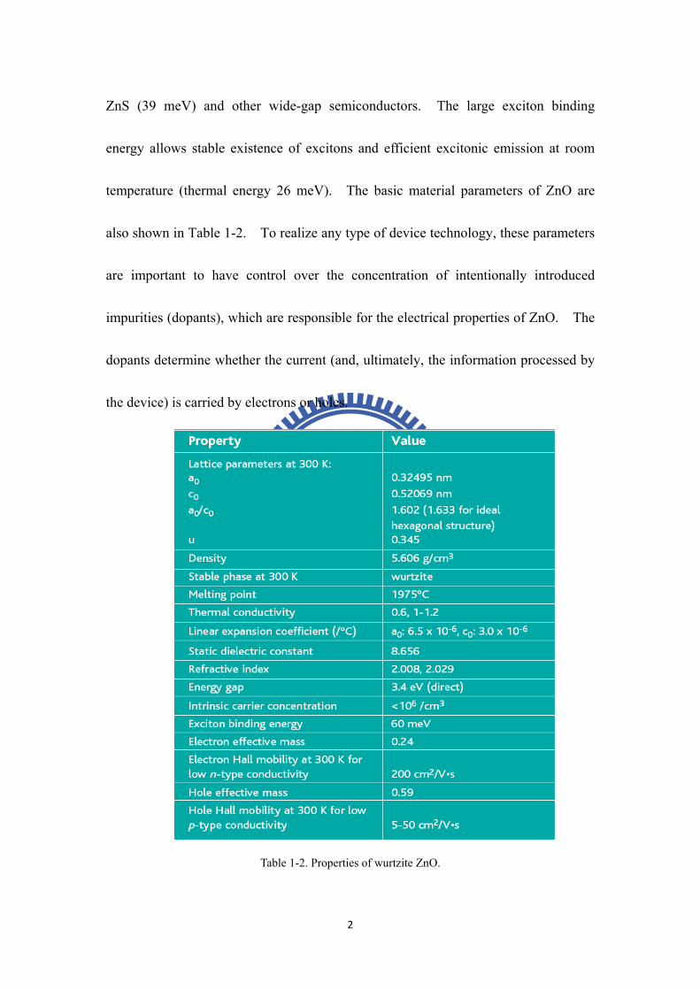
2
ZnS (39 meV) and other wide-gap semiconductors The large exciton binding
energy allows stable existence of excitons and efficient excitonic emission at room
temperature (thermal energy 26 meV) The basic material parameters of ZnO are
also shown in Table 1-2 To realize any type of device technology these parameters
are important to have control over the concentration of intentionally introduced
impurities (dopants) which are responsible for the electrical properties of ZnO The
dopants determine whether the current (and ultimately the information processed by
the device) is carried by electrons or holes
Table 1-2 Properties of wurtzite ZnO
3
The structure of ZnO crystal is shown in Fig 1-1 which has a hexagonal wurtzite
structure (space group C6mc) with lattice parameters a = 03249 nm and c = 05207
nm The structure of ZnO can be simply described as a number of alternating planes
composed of tetrahedrally coordinated O2- and Zn2+ ions stacked alternately along the
c-axis in which a1 a2 and c are the unit vectors in a unit cell the large and small
circles denote the anion and cation atoms respectively The tetrahedral coordination
in ZnO results in non-central symmetric structure and consequently the development
of piezoelectricity and pyroelectricity
Fig 1-1 The wurtzite structure model of ZnO
4
12 General review of ZnO nanostructures
ZnO nanocrystals have recently attracted broad attention in fundamental studies
and technical applications [5] because of their distinguished performance in
electronics optics and photonics Therefore in the last few decades a variety of
ZnO nanostructure morphologies such as nanowires [6] nanorods [7 8] tetrapods
[9] nanoribbonsbelts [9] and nanoparticles [10 11] have been reported Recently
novel morphologies such as hierarchical nanostructures [12] bridge-nail-like
nanostructures [13] tubular nanostructures [14] nanosheets [15] nanopropeller
arrays [16] nanohelixes [17] and nanorings [17] have amongst others been
demonstrated These diverse ZnO nanostructures have been fabricated by various
methods such as thermal evaporation [9] metalndashorganic vapor phase epitaxy
(MOVPE) [8] laser ablation hydrothermal synthesis [7] sol-gel method [10 11] and
template-based synthesis [6] Several recent review articles have summarized
progress in the growth and applications of ZnO nanostructures [4 18] Some of the
possible ZnO nanostructure morphologies are shown in Fig 12
Additionally when the dimension of semiconductors are reduced from three
(bulk material) to the quasi-zero dimensional semiconductor structures such as
quantum dots (QDs) the optical properties of QDs are much different from the bulk
materials There are two physical mechanisms in modifying the energy band
5
structure of nanostructures ie the quantum confinement effect (QCE) [19] and
surface states [20] These two mechanisms compete with each other to influence PL
spectra For nanodots or nanostructures in ZnO system with diameters less than 10
nm the QCE plays a dominant role as has been much reported [21] On the other
hand the surface-to-volume ratio also brings much influence on the systemrsquos
Hamiltonian when the material size is reduced to the nanometer scale [22] The
predominance of surface states is responsible for many novel physical features of
nanomaterials In the past decade various groups have devoted to produce ZnO
QDs and study the properties For instance Guo et al [23] exhibited significantly
enhanced UV luminescence diminished visible luminescence and excellent
third-order nonlinear optical response with poly vinyl pyrrolidone (PVP) modified
surface of ZnO nanoparticles Pan et al [24] predicted a significant increase in the
intensity ratio of the deep level to the near band edge emission is observed with
ever-increasing nanorod surface-aspect ratio Fonoberov et al [25] have
theoretically investigated that depending on the fabrication technique and ZnO QD
surface quality the origin of UV photoluminescence (PL) in ZnO QDs is either
recombination of confined exciton or surface-bound ionized acceptor-exciton
complexs Although there were many experiments to describe the behavior of ZnO
nanostructure more and more unique behaviors are still continuously being explored
6
Fig 12 Representative scanning electron microscopy images of various ZnO nanostructure
morphologies [4]
13 Motivations
Recently the power-dependent photoluminescence (PL) of ZnO bulk associated
with biexciton recombination has been investigated by several research groups
[26-29] Zhang et al [26] who grew ZnO rods by metalorganic chemical vapor
deposition indicated that the biexciton intensity is proportional to the 17th power of
the excitation density Besides we have observed the intensity of biexciton emission
in ZnO powder is proportional to the 186th power of the excitation power at T = 80
K but it is close to unity exponent or even sub-linear when it is measured at the lower
temperature [30] Acoustic and optical phonon scatterings playing key roles in
efficient exciton relaxation are responsible for bounding two cooled excitons to form
7
biexciton at various temperatures At low temperature the acoustic phonon
scattering is the dominant mechanism for exciton thermalization while the optical
phonon scattering will participate in when the exciton kinetic energy approaches to
the energy of the lowest optical phonon about T = 80 K The efficient cooling of
exciton with the assistance of optical phonon scattering allows effectively bounding
exciton pairs to form biexcitons
However Kim et al [31] have reported the spectra of power-dependent PL in
ZnO nanorods synthesized by standard Schlenk techniques remain nearly unchanged
spectral profile as increasing the excitation intensity as compared with 40 meV red
shift for bulk crystal with their maximum excitation intensity They attributed this
finding to the quantum confinement effects that can alter the properties of exciton
states and claimed in this study the exciton states of the nanorods are stable even
when the excitation intensity reaches the Mott density of the bulk crystal due to a
smaller exciton size and an enhanced exciton binding energy [32] On the other
hand Bagnall et al [33] have observed the red-shifted PL peak of ~50 meV in ZnO
powder that may be attributed to the exciton-exciton scattering (or P band) rather than
electron-hole plasma (EHP or N band) with gt 100 meV red shift
The characterizations of ZnO QDs are complicated problems to be investigated
And it is imperative to understand the optical properties of ZnO QDs since they play
8
important roles in stimulated emission and gain process in real photonic device
structures
14 Organization of the thesis
This thesis is organized as follows Chapter 2 covers the theoretical
background of experiments such as sol-gel method X-ray diffraction (XRD)
photoluminescence (PL) characterization and a general concept of quantum effect
fundamental optical transitions and ZnO excitons-related emissions In Chapter 3
we describe the experimental details including the measurement apparatus and
processes By means of the XRD and PL spectroscopy the crystal structures and the
optical emission properties of ZnO QDs grown by the sol-gel method will be
investigated and discussed in Chapter 4 Finally in Chapter 5 we conclude the
studies on the ZnO QDs and propose several topics of the future works
9
Chapter 2 Theoretical background
21 Sol-gel method
An aerosol is a colloidal suspension of particles in a gas (the suspension may be
called a fog if the particles are liquid and a smoke if they are solid) and an emulsion is
a suspension of liquid droplets in anther liquid A sol is a colloidal suspension of
solid particles in a liquid in which the dispersed phase is so small (~1-1000 nm) that
gravitational force is negligible and interactions are dominated by the short-range
forces such as Van der Waals attraction and surface charge All of these types of
colloids can be used to generate polymers or particles from which ceramic materials
can be made A polymer is a huge molecule (also called a macromolecule) formed
from hundreds or thousands of units called monomers If one molecule reaches
macroscopic dimensions so that it extends throughout the solution the substance is
said to be gel
Sol-gel synthesis has two ways to prepare solution One way is the
metal-organic route with metal alkoxides in organic solvent the other way is the
inorganic route with metal salts in aqueous solution It is much cheaper and easier to
handle than metal alkoxides but their reactions are more difficult to control The
inorganic route is a step of polymerization reactions through hydrolysis and
10
condensation of metal alkoxides M(OR)Z where M = Si Ti Zr Al Sn Ce and OR is
an alkoxy group and Z is the valence or the oxidation state of the metal First
hydroxylation upon the hydrolysis of alkoxy groups
ROHOHMOHORM +minusrarr+minus 2 (2-1)
The second step polycondensation process leads to the formation of branched
oligomers and polymers with a metal oxygenation based skeleton and reactive
residual hydroxyl and alkoxy groups There are 2 competitive mechanisms
(1) Oxolation-- formation of oxygen bridges
XOHMOMMXOOHM +minusminusrarrminus+minus (2-2)
The hydrolysis ratio (h = H2OM) decides X=H (h gtgt 2) or X = R (h lt 2)
(2) Olation-- formation of hydroxyl bridges when the coordination of the metallic
center is not fully satisfied (N - Z gt 0)
MOHMMHOOHM minusminusrarrminus+minus 2)( (2-3)
where X = H or R The kinetics of olation is usually faster than those of oxolation
Figure 2-1 presents a schematic of the routes that one could follow within the
scope of sol-gel processing [34] In the sol-gel process the precursors (starting
compounds) for preparation of a colloid consist of a metal or metalloid element
surrounded by various ligands The precursors were mixed together and heated at
high temperature This procedure has to be repeated several times until a
11
homogeneous product is obtained Then the materials have to be transformed into
the desired shape For example an alkyl is a ligand formed by removing one
hydrogen (proton) from an alkane molecule to produce for example methyl (CH3)
or ethyl (C2H5) An alcohol is a molecule formed by adding a hydroxyl (OH) group
to an alkyl (or other) molecule as in methanol (CH3OH) or ethanol (C2H5OH)
Metal alkoxides are members of the family of metalorganic compounds which
have an organic ligand attracted to a metal or metalloid atom Metal alkoxides are
popular precursors because they react readily with water The reaction is called
hydrolysis because a hydroxy ion becomes attached to the metal atom This type of
reaction can continue to build larger and larger molecules by the process of
polymerization The gel point is the time (or degree of reaction) when the last bound
is formed that completes this giant molecule It is generally found that the process
begins with the formation of fractal aggregates that begin to impinge on one another
then those clusters link together as described by the theory of percolation The gel
point corresponds to the percolation threshold when a single cluster (call the
spanning cluster) appears that extends throughout the sol the spanning cluster
coexists with a sol phase containing many smaller clusters which gradually become
attached to the network Gelation can occur after a sol is cast into a mold in which
it is possible to make objects of a desired shape
12
Fig 2-1 Schematic of the rotes that one could follow within the scope of sol-gel processing [8]
22 Quantum effect
During the last decade the growth of low-dimensional semiconductor structures
has made it possible to reduce the dimension from three (bulk material) to the
quasi-zero dimensional semiconductor structures usually called QDs In these
nanostructures the quantum confinement effects become predominant and give rise to
many interesting electronic and optical properties The electron energy will be
quantized and varies with dot sizes that cause the variation of band gap energy
binding energy and Bohr radius The band gap and the density of states (DOS)
associated with a quantum-structure differ from that associated with bulk material
determined from the magnitude of the three-dimension wave vector
13
221 Quantum confinement effect
Models explaining the confinement of charged particles in a three-dimensional
potential well typically involve the solution of Schroumldingerrsquos wave equation using the
Hamiltonian [35]
UVmm
Hhe
++nablaminusnablaminus= 02
22
2
22hh
(2-4)
Variation between treatments generally originates from differences in expressions
assigned to V0 for the confining potential well which normally is accompanied by the
Coulombic interaction term U Boundary conditions are imposed forcing the wave
functions describing the carriers to zero at the walls of the potential well
Two regimes of quantization are usually distinguished in which the crystallite
radius R is compared with the Bohr radius of the excitons Ba or the related
quantities
(1) Weak confinement regime for BaR ge and
(2) Strong confinement regime for BaR lt
In the weak confinement regime the motion of center of exciton mass is
quantized while the relative motion of electron and hole given by the envelope
function )( he rr minusφ is hardly affected In the strong confinement regime however
the Coulomb energy increases roughly with R-1 and the quantization energy with R-2
so that for sufficiently small values of R one should reach a situation where the
14
Coulomb term can be neglected
2211 Weak confinement [36]
Coulomb-related correlation between the charged particles handled through the
use of variational approach involving higher-order wave function of the confined
particles and we cannot neglect the electron hole Coulomb potential The
Schroumldinger equation may be written as
Ψ=Ψminus++Ψnablaminusminus thehe
ErrUVmm
)]([)22
( 02
22 hh (2-5)
Taking he rrr minus= and he
hhee
mmrmrmR
++
= then the equation becomes
Ψ=Ψ++nablaminusnablaminus trR ErURVM
)]()(2
22
[ 222
μhh
with he mmM += he
he
mmmm+
=μ and tE as the total energy of the system If we
take )()( rR ϕφ=Ψ and consider Coulomb interaction first then we get
)()()](2
[ 22
RERRVM cR φφ =+nablaminush
)()()()()](2
[ 22
rErEErrU exctr ϕϕϕμ
=minus=+nablaminush
Here exE results from the inclusion of Coulomb interaction Then we consider the
confinement potential
B
B
aRRVaRRV
gtinfin=le=
)(0)(
Thus the energy is
3212 2
222
== nMa
nEcnπh
(2-6)
and the absorption energy of a photon is
15
exgexct EMa
EEEE ++=+== 2
22
0 2πω h
h (2-7)
with he mmM += as the total mass of the electron and hole
2212 Strong confinement
The size quantization band states of the electron and hole dominate for the
kinetic energies of electron and hole are larger than the electron-hole Coulomb
potential and the effect of the Coulomb attraction between the electron and hole can
be treated as a perturbation Then the Schroumldinger equation becomes
Ψ=Ψ+Ψnablaminusminus EVmm ee
02
22
)22
( hh
The potential is defined as
B
B
arrVarrV
gtinfin=le=
)(0)(
and the energy of an electron or a hole is
3212 2
222
== namnE
hecn
πh
The absorption energy of a photon is
μππω 2
22
2
22
0 2)11(
2 aE
mmaE g
heg
hhh +=++= (2-8)
with he
he
mmmm+
=μ as the reduced mass of electron and hole
16
222 Density of states (DOS)
The concept of density of states (DOS) is extremely powerful and important
physical properties such as optical absorption transport etc are intimately dependent
upon this concept The density of states is the number of available electronic states
per unit volume per unit energy around an energy E If we denote the density of
states by N(E) the number of states in an energy interval dE around an energy E is
N(E)dE To calculate the density of states we need to know the dimensionality of
the system and the energy vs wave vector relation or the dispersion relation that the
electrons obey [37]
2221 Density of states for a three-dimensional system
In a three dimension system the k-space volume between vector k and k + dk is
4πk2dk (see Figure 2-2) We had shown above that the k-space volume per electron
state is 3)2( Lπ Therefore the number of states of electron in the region between k
and k+ dk are
VdkkVdkk2
2
3
2
284
πππ
=
Denoting the energy and energy interval corresponding to k and dk as E and dE we
see that the number of electron states between E and E+ dE per unit volume are
2
2
2)(
πdkkdEEN =
17
and since mkE
2
22h= then the equation becomes
3
21
23
2 2h
dEEmdkk =
which gives
2
)(32
21
23
dEEmdEENhπ
=
We must remember that the electron can have two states for a given k-value
since it can have a spin state of s = 12 or -12 Accounting for spin the density of
states is
2)( 32
21
23
hπEmEN =
Fig 2-2 Geometry used to calculate density of states in three two and one dimensions
2222 Density of states for lower-dimensional systems
If we consider a 2-D system a concept that has become a reality with use of
quantum wells similar arguments tell us that the density of states for a parabolic band
is
18
2)(hπmEN =
Finally in a 1-D system or ldquoquantum wirerdquo the density of states is
hπ
21
21
2)(minus
=EmEN
We notice that as the dimensionality of the system changes the energy
dependence of the density of states also changes In three-dimensional systems we
have E12-dependence as shown in Figure 2-3a while in two-dimensional systems
there is no energy dependence (Figure 2-3b) In one-dimensional systems the
density of states has E-12-dependence and a peak at E = 0 (Figure 2-3c) and the
density of states in zero-dimensional systems is shown in Figure 2-3d The
variations related to dimensionality are extremely important and is a key driving force
to lower dimensional systems
Fig 2-3 Variation in the energy dependence of the density of states in a) three-dimensional b)
two-dimensional c) one-dimensional d) zero-dimensional systems
19
23 X-ray diffraction
231 Lattice parameters [38]
A crystal consists of orderly array of atoms each of which can scatter
electromagnetic waves A monochromatic beam of X-rays that falls upon a crystal
will be scattered in all directions inside it However owing to the regular
arrangement of the atoms in certain directions the scattered waves will constructively
interfere with one another while in others they will destructively interfere The peaks
of an x-ray diffraction pattern are made up of photons constructively interfere with
planes this analysis was suggested in 1913 by W L Bragg Consider an incident
monochromatic x-ray beam interacting with the atoms arranged in a periodic manner
as shown in 2-dimendion in Fig 2-4 The atoms represented as circles in the graph
form different sets of plane in the crystal To give a set of lattice planes with an
inter-plane distance of d the condition for diffraction (peak) constructively interfere
to occur can be simply written as
λθ nd =sin2 321=n (29)
which is known as the Braggrsquos law In this equation λ is the wavelength of the
x-ray θ is the diffraction angle and n is an integer representing the order of the
diffraction peak
20
Fig 2-4 x-ray scattering from a 2-dimendion periodic crystal
The lattice constant can be found by means of the diffraction pattern For
hexagonal unit cell (Figure 2-5) which is characterized by lattice parameters a and c
the plane spacing equation for hexagonal structure is
2
2
2
22
2 341
cl
akhkh
d+⎟⎟
⎠
⎞⎜⎜⎝
⎛ ++= (210)
where h k and l are the Millrsquos indices
Combining the Braggrsquos law (λ= θsin2d ) with (2-2) we can get
sin4341
2
2
2
2
2
22
2 λθ
=+⎟⎟⎠
⎞⎜⎜⎝
⎛ ++=
cl
akhkh
d (2-11)
Rearranging (2-3) gives
34
4sin 2
2
2
2222
cl
akhkh
+⎟⎟⎠
⎞⎜⎜⎝
⎛ ++=λθ (2-12)
thus the lattice parameters can be estimated from Eq (2-12)
21
Fig 2-5 The hexagonal unit cell
232 Deby-Scherer formula [39]
Considering the path difference between the successive planes when the incident
beam remains fixed at the Bragg angle θ but with the diffracted ray leaving at an
angle θ+Δθ corresponding to intensity I in the spectrum line an distance Δθ away
from the peak as Figure 2-6
Fig 2-6 Grating treatment of line broadening by crystallite
The path difference between waves from successive planes is now
BC + CE = d sinθ+ d sin(θ+Δθ)
22
= d sinθ+ d sinθcosΔθ+d cosθsinΔθ (213)
where BC and CE is the path difference between incident ray of the successive planes
and d is the interplanar distance If Δθ is very small we can write cosΔθasymp1 and
sinΔθasympΔθ in which case
BC + CE = 2dsinθ+ d cosθΔθ (214)
Combining Braggrsquos law Eq (21)
BC + CE = 2dsinθ+ d cosθΔθ= nλ + d cosθΔθ (215)
where λ is the wavelength of the incident x-ray Therefore the phase difference δ
per interplanar distance or ldquoaperturerdquo is
δ = θθλπ
λπλ Δbull+ cos22 dn
= 2 πn + θθλπ
Δbullcos2 d (216)
Since a phase difference of 2π n produces the same effect as a zero phase we
can write the effective phase difference per aperture as
δ = θθλπ
Δbullcos2 d (217)
We obtain the result that the distribution of intensity of I in a spectrum line a
distance R from the grating is effectively
δ
δ
21sin
21sin
)(2
2
2N
RI Φ= (218)
and maximum intensity is
23
22max )( N
RI Φ
= (219)
where Φ is the amplitude at unit distance from the graying and N is the total number
of grating aperture
Diving Eq (210) by Eq (211) we obtain
2
2
2
max
)1(
21sin
21sin
N
N
II
δ
δ= (220)
Since 21 Nδ will change much faster than
21 δ the function will reach its first
minimum before 21 δ is very large We can therefore replace δ
21sin by
21 δ and
we will get
2
max
)
21
21sin
(δ
δ
N
N
II
= (221)
The ratio maxII will fall to
21 when
δ
δ
N
N
21
21sin
=2
1 (222)
The solution to the equation (214) yields the required phase difference
corresponding to the half maximum It may be obtained
δN21 = 139 (223)
Since according to equation (29) δ = θθλπ
Δbullcos2 d and D = Nd we obtain
θθλ
Δ= 2cos890
D (224)
24
Let B be taken as the full width at half maximum from Δθ to ndashΔθ hence
B = 2Δθ= θλ
cos890
D (radians) (225)
where λ is the wavelength of x-ray and D is the average size of the particles
24 Photoluminescence characterization [35 40]
Photoluminescence (PL) is a powerful and noninvasive optical analysis
technology for the semiconductor industry It has high sensitivity to reveal the band
structure and the carrier transportation behaviors in a material From PL spectrum
the defect or impurity can also be found in the compound semiconductors which
affect material quality and device performance A given impurity produces a set of
characteristic spectral features The fingerprint identifies the impurity type and
often several different impurities can be seen in a single PL spectrum In addition
the full width at half maximum of the PL peak is an indication of samplersquos quality
[41] So the PL could be a judgment of the material quality and be a key technology
of the development of nano-technology
PL is the optical radiation emitted by a physical system (in excess the thermal
equilibrium blackbody radiation) resulting from excitation to a nonequilibrium state
by illuminating with light Three processes can be distinguished (i) creation of
electron-hole pairs by absorption of the excited light (ii) radiative recombination of
25
electron-hole pairs and (iii) escape of the recombination radiation from the sample
241 Fundamental Transitions
An electron is excited from the valence band to the conduction band by
absorption of a photon In this sense an optical excitation is a two-particle transition
The same is true for the recombination process An electron in the conduction band
can return radiatively or nonradiatively to the valance band only if there is a free
space ie a hole available Two quasi-particles annihilate in the recombination
process What we need for the understanding of the optical properties of the
electronic system of a semiconductor is therefore a description of the excited states of
the N-particle problem We will consider the fundamental transitions those
occurring at or near the band edges
1 Free excitons (Wannier-Mott excitons)
An electron in the conduction band and a hole in the valence band are created at
the same point in space and can attract each other through their Coulomb interaction
Using the effective mass approximation the Coulomb interaction between electron
and hole leads to a hydrogen-like problem with a Coulomb potential term
he rreminus
minusεπε0
2
4
26
Here we will consider the so-called Wannier-Mott excitons more specifically
This type of excitons has a large Bohr radius (ie the mean distance between electron
and hole) that encompasses many atoms and they are delocalized states that can move
freely throughout the crystal hence the alternative name of free excitons
Indeed excitons in semiconductors form to a good approximation a hydrogen-
or positronium-like series of states below the gap For a simple parabolic band in a
direct-gap semiconductor one can separate the relative motion of electron and hole
and the motion of the center of mass This leads to the dispersion relation of exciton
as shown in Fig 2-7
MK
nRyEKnE
BgBph 2
1)(22
2 h
+minus= (226)
where Bn =123 is the principal number )1(613 20
εμm
Ry = eV is exciton binding
energy he mmM += and he kkK += are translational mass and wave vector of
the exciton respectively The series of exciton states in (226) has an effective
Rydberg energy Ry modified by the reduced mass of electron and hole and the
dielectric constant of the medium in which these particles move The radius of the
exciton equals the Bohr radius of H atom again modified by ε and μ Using the
material parameters for typical semiconductors one finds that the orbits of electron
and hole around their common center of mass average over many unit cells and this in
turn justifies the effective mass approximation in a self-consistent way These
27
excitons are called Wannier-Mott excitons
Fig 2-7 A pair excitation in the scheme of valence and conduction bands (a) in the exciton picture for a
direct gap semiconductor (b)
2 Biexcitons
It is well known that two hydrogen atoms with opposite electron spins can bind
to form a hydrogen molecule In the same sense it has been calculated that two
positronium-like atoms can form a positronium-like molecule as a bound state So
the idea is not far away that two excitons could bind to form a new quasiparticle the
so-called biexciton or excitonic molecule It has been found theoretically that the
biexciton should form a bound state for all ratios of effective electron and hole masses
and dimensionalities of the sample
The dispersion relation is given in the simplest case by
ex
bbiex
bexgbiex M
kEEEkE4
)(2)(22h
+minusminus= (2-27)
assuming that the effective mass of the biexciton is just twice that of the exciton
28
3 Bound excitons
Similar to the way that free carriers can be bound to defects it is found that
excitons can also be bound to defects Some of these defects can bind an exciton
resulting in a bound exciton complex (BEC) In Figure 2-8 we visualize exciton
bound to an ionized donor (D+X) a neutral donor (D0X) and a netural axxeptor (A0X)
An ionized acceptor does not usually bind an exciton since a neutral acceptor and a
free electron are energetically more favorable The binding energy of an exciton (X)
is the highest for a neutral acceptor (A0X complex) the lower for a neutral donor
(D0X) and the lower still for an ionized donor (D+X) The binding energy bE of
exciton to the complex usually increases according to bXA
bXD
bXD EEE 00 ltlt+ The
binding energy is defined as the energetic distance from the lowest free exciton state
at k = 0 to the energy of the complex There is a rule of thumb known as Haynersquos
rule which relates the binding energy of the exciton to the neutral complex with the
binding of the additional carrier to the point defect
Fig 2-8 Visualization of an exciton bound to an ionized donor (a) a neutral donor (b) and a neutral
acceptor (c)
29
4 Surface-bound exciton
The surface-to-volume ratio brings much influence on the systemrsquos Hamiltonian
when the material size is reduced to the nanometer scale [22] From the calculation
of exciton states at the QD surface we can know the exciton is bound to the
surface-located acceptor [25] Unlike the acceptor the donor does not bind the
exciton Because the hole is much heavier than the electron which makes the
surface donor a shallow impurity while the surface acceptor a deep impurity
Therefore excitons can be effectively bound only to surface acceptors
5 Two-Electron Satellites (TES) [42]
Two-electron satellite (TES) transitions involve radiative recombination of an
exciton bound to a neutral donor leaving the donor in the excited state In the
effective mass approximation the energy difference between the ground-state neutral
donor bound excitons and their excited states (TES) can be used to determine the
donor binding energies [43] (the donor excitation energy from the ground state to the
first excited state equals to 34 of the donor binding energy DE ) and catalog the
different species present in the material
30
6 Donor-Acceptor Pairs (DAP)
Donors and acceptors can form pairs and act as stationary molecules imbedded in
the host crystal The coulomb interaction between a donor and an acceptor results in
a lowering of their binding energies In the donor-acceptor pair case it is convenient
to consider only the separation between the donor and the acceptor level
rqEEEE ADgpair ε
2
)( ++minus= (2-28)
where r is the donor-acceptor pair separation DE and AE are the respective ionization
energies of the donor and the acceptor as isolated impurities
7 Deep transitions
By deep transition we shall mean either the transition of an electron from the
conduction band to an acceptor state or a transition from a donor to the valence band
in Fig 2-9 Such transition emits a photon ig EEh minus=ν for direct transition and
pig EEEh minusminus=ν if the transition is indirect and involves a phonon of energy pE
Hence the deep transitions can be distinguished as ( ) conductionⅠ -band-to-acceptor
transition which produces an emission peak at Ag EEh minus=ν and ( ) Ⅱ
donor-to-valence-band transition which produces emission peak at the higher photon
energy Dg EEh minus=ν
31
C
V
D
A
Fig 2-9 Radiative transition between a band and an impurity state
242 Influence of high excited light intensity
The PL conditions as mentioned above are excited by low excitation light
intensity At low excitation light intensity (low density regime in Fig 2-10) the PL
properties are determined by single electron-hole pairs either in the exciton states or
in the continuum Higher excitation intensity (intermediate density regime in Fig
2-10) makes more excitons such condition would lead to the exciton inelastic
scattering processes and form the biexciton The scattering processes may lead to a
collision-broadening of the exciton resonances and to the appearance of new
luminescence bands to an excitation-induced increase of absorption to bleaching or
to optical amplification ie to gain or negative absorption depending on the
excitation conditions If we pump the sample even harder we leave the intermediate
and arrive at the high density regime in Fig 2-10 where the excitons lose their
identity as individual quasiparticles and where a new collective phase is formed which
32
is known as the electron-hole plasma (EHP)
Fig 2-10 The general scenario for many-particle effects in semiconductors [35]
1 Electron-Hole Plasma
In this high density regime the density of electron-hole pairs np is at least in
parts of the excited volume so high that their average distance is comparable to or
smaller than their Bohr radius ie we reach a ldquocritical densityrdquo cpn in an EHP given
to a first approximation by 13 asympcpBna We can no longer say that a certain electron is
bound to a certain hole instead we have the new collective EHP phase The
transition to an EHP is connected with very strong changes of the electronic
excitations and the optical properties of semiconductors
33
2 Scattering Processes
In the inelastic scattering processes an exciton is scattered into a higher excited
state while another is scattered on the photon-like part of the polariton dispersion and
leaves the sample with high probability as a luminescence photon when this
photon-like particle hits the surface of the sample This process is shown
schematically in Fig 2-11 and the photons emit in such a process having energies En
given by Ref [44]
kTn
EEE exbexn 2
311 2 minus⎟⎠⎞
⎜⎝⎛ minusminus= (2-29)
where n = 2 3 4hellip exbE = 60 meV is the binding energy of the free exciton of ZnO
and kT is the thermal energy The resulting emission bands are usually called
P-bands with an index given by n
energy
Wave vector
Eg
Eexciton
P2
Pinfin
1
2
infin
nB=continuum
Fig2-11 Schematic representation of the inelastic exciton-exciton scattering processes [35]
34
Chapter 3 Experiment details and analysis techniques
31 Sample preparation
We fabricate ZnO QDs by sol-gel method Sol-gel method was chosen due to
its simple handling low cost and narrow size distribution In particular it has the
potential to produce samples with large areas and complicated forms on various
substrates
The ZnO colloidal spheres were produced by one-stage reaction process and
reactions were described as the following equations
COOHxCHCOOCHOHZnOxHCOOCHZn xx 323223 )()()( +⎯rarr⎯+ minusminusminusΔ (3-1)
COOHCHxOHxZnOCOOCHOHZn xx 3223 )2()1()()( minus+minus+⎯rarr⎯Δminus
minusminus (3-2)
Equation (3-1) is the hydrolysis reaction for Zn(OAc)2 to form metal complexes We
increased the temperature of reflux from RT to 160oC and maintained for aging The
zinc complexes will dehydrate and remove acetic acid to form pure ZnO as Eq (3-2)
during the aging time Actually the two reactions described above proceed
simultaneously while the temperature is over 110oC
All chemicals used in this study were reagent grade and employed without
further purification A typical reaction was listed in Table 3-1 stoichiometric zinc
acetate dihydrate [995 Zn(OAc)2middot2H2O Riedel-deHaen] was dissolved into
35
diethylene glycol [995 DEG ethylenediamine-tetra-acetic acid (EDTA)] to make
01 M 005 M 001 M solutions The first thing we notice is that we can control the
QDs size with domination concentration of zinc acetate in the solvent (DEG) Then
the temperature of reaction solution was increased to 160 and white colloidal ZnO
was formed in the solution that was employed as the primary solution The primary
solutions were put separately in a centrifuge operating at 3000 rpm for 30 minutes
The supernatant was decanted off and saved and the polydisperse powder was
discarded Finally the supernatant was then dropped onto Si (100) substrates and
dried at 150 for further characterization The experiment equipment and a flow
chart of fabricate ZnO QDs by sol-gel method was shown in Figure 3-1amp3-2
Chemical reagent Molecular formula Degree of
purity
Source
Zinc acetate dehydrate Zn(CH3COOH)22H2O 995 Riedel-deHaen
Diethylene glycol C4H10O3 995 EDTA
Table 3-1 Shows that chemical reagent was used with sol-gel experiment process
36
Fig 3-1 Experiment equipment used for fabricating ZnO QDs
Fig 3-2 A flow chart of fabricate ZnO QDs by sol-gel method
Zn(CH3COOH)22H2O
Diethylene-glycol (DEG)
Counter flow apparatus
White colloidal formed
Centrifuge
Clear solution
drop or spin coating onSiO2Si(001)
varying solution concentration
heating up to 160
separating solution
37
32 Microstructure and optical properties analysis
321 X-ray diffraction
The crystal structures of the as-grown powder were inspected by using XRD
(model MAC Sience MXP18) at room temperature equipped with CuK X-ray source
(λ=15405Aring) in National Synchrotron Radiation Research Center (NSRRC) Taiwan
Data were recorded between the angle range of 20deg lt 2θ lt 80deg with steps of 002degand
rate of scanning is 40degmin The operation voltage of the system is 50 kV and the
operation current is 200 mA The essential features of x-ray spectrometer are shown
in Figure 3-3 X-rays from the tube T are incident on a crystal C which may be set at
any desired angle to the incident beam by rotation about an axis through O the center
of the spectrometer circle D is a detector which measures the intensity of the
diffraction x-rays
Fig 3-3 The x-ray spectrometer
38
The sizes of the nanocrystallites can be determined by X-ray diffraction using the
measurement of the full width at half maximum (FWHM) of the X-ray diffraction
lines The average diameter is obtained byθλ
cos890
BD = where D is the average
diameter of the nanocrystallite λ is the wavelength of the X-ray source and B is the
FWHM of X-ray diffraction peak at the diffraction angle θ
322 Photoluminescence system
PL provides a non-destructive technique for the determination of certain
impurities in semiconductors The shallow-level and the deep-level of impurity
states were detected by PL system It was provided radiative recombination events
dominate nonradiative recombination
In the PL measurements we used a He-Cd cw laser (325 nm) [Kimmon
IK5552R-F] as the excitation light Light emission from the samples was collected
into the TRIAX 320 spectrometer and detected by a photomultiplier tube (PMT) As
shown in Fig 3-4 the diagram of PL detection system includes mirror focusing and
collecting lens the sample holder and the cooling system The excitation laser beam
was directed normally and focused onto the sample surface with power being varied
with an optical attenuator The spot size on the sample is about 100 μm
Spontaneous and stimulated emissions were collected by a fiber bundle and coupled
39
into a 032 cm focal-length monochromator (TRIAX 320) with a 1200 linesmm
grating then detected by either an electrically cooled CCD (CCD-3000) or a
photomultiplier tube (PMT-HVPS) detector The temperature-dependent PL
measurements were carried out using a closed cycle cryogenic system A closed
cycle refrigerator was used to set the temperature anywhere between 15 K and 300 K
And the power-dependent PL spectra were used for monitoring the characteristic of
excitons and thermalization effect at the different excitation density
Fig 3-4 The PL system
40
Chapter 4 Results and Discussion
41 Morphology and crystal structures
411 Morphology
Shown in Fig 4-1 is a typical high-resolution transmission electron microscope
(HRTEM) image of the ZnO nanoparticles Nanoparticles aged at 160 degC for 1 hr
and solution concentration of 004 M was selected for particle size determination by
HRTEM The shape of particles is predominantly spherical and the nanoparticles
are clearly well separated and essentially have some aggregation The average
diameter of the number-weighted particles obtained from a colloid aged at 160 degC for
1 hr (004 M) was determined to be 618plusmn 03 nm
Fig 4-1 HRTEM image of the ZnO QDs fabricated using 004M Zn(OAc)2
41
412 X-ray diffraction measurement
The XRD profiles of the ZnO QDs with various concentrations of Zn(OAc)2 are
shown in Fig 4-2 The diffraction pattern and interplanar spacings match nicely
with the standard diffraction pattern of wurtzite ZnO demonstrating the formation of
wurtzite ZnO nanocrystals All of the samples present similar XRD peaks that can
be indexed as the wurtzite ZnO crystal structure with lattice constants a = 3253 Aring and
c = 5213 Aring which are consistent with the value in the standard card (JCPDS
89-1397)
Fig 4-2 XRD profiles of the ZnO QDs prepared with various concentration of Zn(OAc)2 The
crystalline size can be approximately estimated to be 16 and 7 nm respectively (top to bottom) for
concentrations of 016 and 006 M
No diffraction peaks of other species could be detected that indicates all the
precursors have been completely decomposed and no other crystal products were
42
formed The full width at half maximum (FWHM) of the diffraction peaks increases
that is the average crystalline size decreases as the concentration of zinc precursor
reduces The average size is calculated from the width of diffraction peak using the
Debye-Scherer formula [45 46] )cos(890 θλ wD = where D is the average
crystalline diameter of the particles λ is the wavelength of the x-ray source w is the
linewidth at half maximum in excess of the instrumental broadening and θ is the
diffraction angle The crystalline size can be estimated to be 16 nm and 7 nm for
concentrations of 016 M and 006 M respectively
42 Photoluminescence spectra
421 Photoluminescence spectra for different sizes of ZnO particles
The PL spectra of ZnO QDs with average crystalline sizes of 16 and 7 nm at 13
K are shown in Fig 4-3 For the 16-nm ZnO QDs a strong UV emission peak at
3388 eV with FWHM of ~ 96 meV was observed accompanied with very broad weak
visible emission with the slightly strong blue emission and rather weak yellow
emission bands And only a strong UV emission peak at 3411 eV with FWHM of ~
174 meV was observed unaccompanied with visible emission for the 7 nm ZnO QDs
The sharp UV emission peak is attributed to the near band edge emission (NBE) [27
47] The broad visible emission is the deep-level emission which is attributed to the
43
oxygen vacancy (green emission) or oxygen interstitial (red emission) The intensity
of the UV and visible peak ratio increases with decreasing the QD size The strong
UV emission and weak visible emission in PL spectra indicates that the ZnO QDs
have a good crystal quality
Fig 4-3 The PL spectra of the ZnO QDs measured at low temperature
Figure 4-4 demonstrates the PL spectra of ZnO QDs with different average
crystalline sizes measured at T = 13 K The near band edge UV emission is
attributed to the free exciton (FX) emission [32] which shifts (solid line) to the higher
energy (from 3386 eV to 342 eV) as the QD size decreases (16 nm ndash 6 nm) due to
the quantum confinement effect (QCE) Besides the FWHM increases as the
average QDs size decreases that may be caused by the contribution of surface-optical
phonon [48] surface-bound acceptor exciton complexes [25] and size distribution
44
Since the Bohr radius of the exciton in bulk ZnO is about 234 nm [49] we must
consider the electron hole Coulomb interaction in our samples and the particles are in
the moderate to weak confinement regime
Fig 4-4 PL spectra of different sizes of ZnO QD at low temperature The line indicates the shifts of FX
peak energy
422 Temperature-dependent PL for different sizes of ZnO particles
Figure 4-5 displays the temperature-dependent PL of different sizes of ZnO it
reveals only single one band for T = 8 ~ 300 K in QDs system Due to small binding
energy of D0X it will be ionized as T gt 100 K so we can easily attribute the single
band to the FX emission We also find that the peak energy difference of FX in QDs
system between 8 K and 300 K decrease with the particle size decreasing It is
known that the main contribution to the energy shift is the Froumlhlich interaction [50] a
45
result of Coulomb interaction
Fig 4-5 Temperature-dependent PL spectra of (a) 16 nm (b) 7 nm (c) 6 nm
423 Power-dependent PL for different sizes of ZnO particles
The power-dependent PL spectra of different sizes of ZnO QDs are shown in Fig
4-6 These spectral shapes are almost the same except that the spectral intensity
increases with increasing excitation power from 003 mW to 34 mW (432 Wcm2 to
46
49 kWcm2) covering a range of three orders of magnitude which show the exciton
states remain invariable
The character in ZnO QDs gives a sharp contrast to the ZnO powder (~ 1 μm)
in which the relative peak intensities of biexciton (BX) and P-band (exciton-exciton
scattering) emissions increase as the excitation power increasing [30] For
quantitative analysis the spectral shape of NBE emission measured in 6-nm ZnO QDs
at 80 K is decomposed into two peaks and theoretical fitting results are shown in Fig
4-7 For comparison the inset of Fig 4-7 shows the fit of the PL spectrum in ZnO
powder at 80 K The dashed curves denote the various emissions and the solid curve
corresponds to the sum of the theoretical fit which shows good agreement with the
experimental data marked as the open dots The PL spectra of QDs and that of
powder are very diverse The BX emission can be observed in ZnO powder
nevertheless in ZnO QDs only the emission of surface bound exciton (SX) [51] rather
than BX can be recognized
47
Fig 4-6 Power-dependent PL spectra of (a) 16 nm at 15 K (b) 16 nm at 80 K (c) 7 nm at 15 K (d) 7
nm at 80 K (e) 6 nm at 8 K (f) 6 nm at 80 K
48
Fig 4-7 Gaussian fit to a PL spectrum of 6 nm ZnO QDs (004M) measured at 80K The inset shows
the spectral fitting for ZnO powder The fitted line shapes are shown separately in dash lines Solid
lines correspond to the fit and dots represent the data
424 PL peak positions as a function of excitation power
The peak positions of these emissions with increasing the excitation power in
6-nm ZnO QDs at 80 K are plotted in Fig 4-8 The FX is observed at 3418 eV and
the PL emission peak at 3325 eV may be attributed to the emission of SX The peak
positions of FX emission and SX emission are hardly shifted as the excitation power
increases from 003 to 34 mW
49
Fig 4-8 The PL peak positions as a function of excitation power measured at 80K
425 Integrated intensity as a function of excitation power
In order to further understand the characteristic of these two peaks the integrated
PL intensities of these peaks as a function of excitation power in 6-nm ZnO QDs at
80K are depicted in Fig 4-9 Both of the integrated intensities exhibit nearly linear
dependence on the excitation power with both exponents close to 096 However
the exponent of BX (with binding energy of ~15 meV) on the excitation power in
ZnO powder comes near the theoretical value of 2 having 186 at 80K It is due to
efficient cooling via participation of optical phonons when the exciton kinetic energy
approaches to the energy of the lowest optical phonon [30] However reducing the
exciton-LO phonon coupling in ZnO QDs [32] causes the lack of the efficient cooling
of exciton with assistance of optical phonon scattering or the so-called phonon
bottleneck Therefore it is hardly to allow effectively bounding exciton pairs to
form biexcitons in ZnO QDs
50
In addition the P-band emission is hardly found in Fig 4-6 This finding
means that the probability of exciton-exciton scattering is also very low For that
reason we suspect the other reason might be that there is only one exciton existing in
a QD within the exciton lifetime even with the achievable high power CW excitation
so that neither exciton-exciton scattering nor BX can be observed in ZnO QDs
Therefore the increase of excitation intensity provides the larger chance of a single
exciton being excited or the larger excitation rate of single exciton Thus the peak is
hardly shifted and the PL intensity is linear dependence with excitation intensity
corroborating the invariable exciton states upon increasing pumping in ZnO QDs
Fig 4-9 The integrated intensity of two decomposed TES and FX peaks as a function of excitation
power measured at 80K The inset shows the excitation power dependent emission intensity of
biexciton in ZnO powder measured at 80 K The power factor is 186
51
Chapter 5 Conclusions and Prospective
51 Conclusions
In summary we have measured XRD to inspect the crystal structures and the
average size of ZnO QDs synthesized by a simple sol-gel method The average sizes
of ZnO QDs were verfied by TEM The diffraction pattern and interplanar spacings
indicate the formation of wurtzite ZnO nanocrystals and no diffraction peaks of other
species could be detected that indicates all the precursors have been completely
decomposed and no other crystal products were formed We have measured
temperature-dependent and power-dependent PL spectra of ZnO QDs with different
sizes to investigate the optical properties From Size-dependence of efficient UV
photoluminescence from low temperature PL gives evidence for quantum
confinement effect The ZnO QDs exhibit strong UV emission and weak visible
emission indicating very good crystal quality Moreover the biexciton and P-band
emissions in ZnO QDs are hardly observed and unchanged shapes of
power-dependent PL spectra show the exciton states remain invariable in ZnO QDs
The intensities of emission peaks associated with these invariable free exciton and
surface bound exciton states exhibit linear dependence on the excitation density
52
52 Prospective
In order to further investigate the optical properties of ZnO QDs we will
measure the time resolved photoluminescence (TRPL) to inspect the lifetime of ZnO
QDs Through measuring the lifetime of ZnO QDs we can identify the different PL
origins of physical mechanisms and the process of exciton recombination Besides
we will do single-photon measurement to study the optical characterizations in a
single ZnO QD
53
References
[1] R Triboulet and J Perriere Prog Cryst Growth Charact Mater 47 65 (2003)
[2] U Ozgur Y I Alivov C Liu A Teke M A Reshchikov S Dogan V Avrutin
S J Cho and H Morkoc J Appl Phys 98 041301 (2005)
[3] T Yatsui J Lim M Ohtsu S J An and G C Yi Appl Phys Lett 85 727
(2004)
[4] A B Djurisic and Y H Leung Small 2 944 (2006)
[5] A P Alivisatos Science 271 933 (1996)
[6] C H Liu J A Zapien Y Yao X M Meng C S Lee S S Fan Y Lifshitz
and S T Lee Adv Mater 15 838 (2003)
[7] B Liu and H C Zeng J Am Chem Soc 125 4430 (2003)
[8] W I Park Y H Jun S W Jung and G C Yi Appl Phys Lett 82 964 (2003)
[9] H Q Yan R R He J Pham and P D Yang Adv Mater 15 402 (2003)
[10] K F Lin H M Cheng H C Hsu L J Lin and W F Hsieh Chem Phys Lett
409 208 (2005)
[11] C J Pan K-F Lin W-T Hsu and W-F Hsieh J Appl Phys 102 123504
(2007)
[12] J Y Lao J G Wen and Z F Ren Nano Letters 2 1287 (2002)
[13] J Y Lao J Y Huang D Z Wang and Z F Ren Nano Letters 3 235 (2003)
[14] Y J Xing Z H Xi X D Zhang J H Song R M Wang J Xu Z Q Xue and
D P Yu Solid State Commun 129 671 (2004)
[15] J H Park H J Choi Y J Choi S H Sohn and J G Park J Mater Chem 14
35 (2004)
[16] P X Gao and Z L Wang Appl Phys Lett 84 2883 (2004)
[17] X Y Kong and Z L Wang Nano Letters 3 1625 (2003)
[18]G C Yi C R Wang and W I Park Semiconductor Science and Technology 20
54
S22 (2005)
[19] L E Brus J Chem Phys 80 4403 (1984)
[20] L T Canham Appl Phys Lett 57 1046 (1990)
[21] Y Kayanuma Phys Rev B 38 9797 (1988)
[22] J B Xia and K W Cheah Phys Rev B 59 14876 (1999)
[23] L Guo S H Yang C L Yang P Yu J N Wang W K Ge and G K L
Wong Appl Phys Lett 76 2901 (2000)
[24] N Pan X P Wang M Li F Q Li and J G Hou J Phys Chem C 111 17265
(2007)
[25] V A Fonoberov and A A Balandin Appl Phys Lett 85 5971 (2004)
[26] B P Zhang N T Binh Y Segawa K Wakatsuki and N Usami Appl Phys
Lett 83 1635 (2003)
[27] B P Zhang N T Binh Y Segawa Y Kashiwaba and K Haga Appl Phys
Lett 84 586 (2004)
[28] S W Kim and S Fujita Appl Phys Lett 86 153119 (2005)
[29]X Q Zhang Z G Yao S H Huang I Suemune and H Kumano J Appl Phys
99 063709 (2006)
[30] C J Pan K F Lin and W F Hsieh Appl Phys Lett 91 111907 (2007)
[31] S Y Kim Y S Yeon S M Park J H Kim and J K Song Chem Phys Lett
462 100 (2008)
[32] W T Hsu K F Lin and W F Hsieh Appl Phys Lett 91 181913 (2007)
[33] D M Bagnall Y F Chen Z Zhu T Yao M Y Shen and T Goto Appl Phys
Lett 73 1038 (1998)
[34] C J Brinker and G W Scherer Sol-Gel Sience (Academic Press 1990) p 303
[35] C F Klingshirn Semiconductor Optics (Springer 1997)
[36] S-B Yin in National Chiao Tung University Department of Photonics (National
55
Chiao Tung University 1999)
[37] J Singh Physics of Semiconductors and Their Heterostructures (McGraw-Hill
Singapore 1993) p 17amp316
[38] B D Cullity Element of X-ray diffraction (Addison Wesley Canada 1978)
[39] A Taylor X-ray Metallography (John Wiley and Sons New York 1961) p 676
[40] F Mark Optical Properties of Solids (Oxfrd university press 2001)
[41] S Perlpwotz Optical characterization of semiconductors infaraed Raman and
Photoluminescence spectroscopy (Academic Press London 1993)
[42] A Teke U Ozgur S Dogan X Gu H Morkoc B Nemeth J Nause and H O
Everitt Phys Rev B 70 195207 (2004)
[43] H Alves D Pfisterer A Zeuner T Riemann J Christen D M Hofmann and
B K Meyer Optical Materials 23 33 (2003)
[44] J B Baxter and E S Aydil Appl Phys Lett 86 053114 (2005)
[45] E F Kaelble Handbook of X-rays (McGraw-Hill New York 1967)
[46] J C Bailar A F Trotman-Dickenson H J Emeleus and S R Nyholm
Comprehensive Inorganic Chemistry (Pergamon Oxford 1973) Vol 3
[47] H C Hsu Y K Tseng H M Cheng J H Kuo and W F Hsieh J Crystal
Growth 261 520 (2004)
[48] Z D Fu Y S Cui S Y Zhang J Chen D P Yu S L Zhang L Niu and J Z
Jiang Appl Phys Lett 90 263113 (2007)
[49] R T Senger and K K Bajaj Phys Rev B 68 045313 (2003)
[50] S J Sheih K T Tsen D K Ferry A Botchkarev B Sverdlov A Salvador
and H Morkoc Appl Phys Lett 67 1757 (1995)
[51]V A Fonoberov K A Alim A A Balandin F X Xiu and J L Liu Phys Rev
B 73 (2006)

3
The structure of ZnO crystal is shown in Fig 1-1 which has a hexagonal wurtzite
structure (space group C6mc) with lattice parameters a = 03249 nm and c = 05207
nm The structure of ZnO can be simply described as a number of alternating planes
composed of tetrahedrally coordinated O2- and Zn2+ ions stacked alternately along the
c-axis in which a1 a2 and c are the unit vectors in a unit cell the large and small
circles denote the anion and cation atoms respectively The tetrahedral coordination
in ZnO results in non-central symmetric structure and consequently the development
of piezoelectricity and pyroelectricity
Fig 1-1 The wurtzite structure model of ZnO
4
12 General review of ZnO nanostructures
ZnO nanocrystals have recently attracted broad attention in fundamental studies
and technical applications [5] because of their distinguished performance in
electronics optics and photonics Therefore in the last few decades a variety of
ZnO nanostructure morphologies such as nanowires [6] nanorods [7 8] tetrapods
[9] nanoribbonsbelts [9] and nanoparticles [10 11] have been reported Recently
novel morphologies such as hierarchical nanostructures [12] bridge-nail-like
nanostructures [13] tubular nanostructures [14] nanosheets [15] nanopropeller
arrays [16] nanohelixes [17] and nanorings [17] have amongst others been
demonstrated These diverse ZnO nanostructures have been fabricated by various
methods such as thermal evaporation [9] metalndashorganic vapor phase epitaxy
(MOVPE) [8] laser ablation hydrothermal synthesis [7] sol-gel method [10 11] and
template-based synthesis [6] Several recent review articles have summarized
progress in the growth and applications of ZnO nanostructures [4 18] Some of the
possible ZnO nanostructure morphologies are shown in Fig 12
Additionally when the dimension of semiconductors are reduced from three
(bulk material) to the quasi-zero dimensional semiconductor structures such as
quantum dots (QDs) the optical properties of QDs are much different from the bulk
materials There are two physical mechanisms in modifying the energy band
5
structure of nanostructures ie the quantum confinement effect (QCE) [19] and
surface states [20] These two mechanisms compete with each other to influence PL
spectra For nanodots or nanostructures in ZnO system with diameters less than 10
nm the QCE plays a dominant role as has been much reported [21] On the other
hand the surface-to-volume ratio also brings much influence on the systemrsquos
Hamiltonian when the material size is reduced to the nanometer scale [22] The
predominance of surface states is responsible for many novel physical features of
nanomaterials In the past decade various groups have devoted to produce ZnO
QDs and study the properties For instance Guo et al [23] exhibited significantly
enhanced UV luminescence diminished visible luminescence and excellent
third-order nonlinear optical response with poly vinyl pyrrolidone (PVP) modified
surface of ZnO nanoparticles Pan et al [24] predicted a significant increase in the
intensity ratio of the deep level to the near band edge emission is observed with
ever-increasing nanorod surface-aspect ratio Fonoberov et al [25] have
theoretically investigated that depending on the fabrication technique and ZnO QD
surface quality the origin of UV photoluminescence (PL) in ZnO QDs is either
recombination of confined exciton or surface-bound ionized acceptor-exciton
complexs Although there were many experiments to describe the behavior of ZnO
nanostructure more and more unique behaviors are still continuously being explored
6
Fig 12 Representative scanning electron microscopy images of various ZnO nanostructure
morphologies [4]
13 Motivations
Recently the power-dependent photoluminescence (PL) of ZnO bulk associated
with biexciton recombination has been investigated by several research groups
[26-29] Zhang et al [26] who grew ZnO rods by metalorganic chemical vapor
deposition indicated that the biexciton intensity is proportional to the 17th power of
the excitation density Besides we have observed the intensity of biexciton emission
in ZnO powder is proportional to the 186th power of the excitation power at T = 80
K but it is close to unity exponent or even sub-linear when it is measured at the lower
temperature [30] Acoustic and optical phonon scatterings playing key roles in
efficient exciton relaxation are responsible for bounding two cooled excitons to form
7
biexciton at various temperatures At low temperature the acoustic phonon
scattering is the dominant mechanism for exciton thermalization while the optical
phonon scattering will participate in when the exciton kinetic energy approaches to
the energy of the lowest optical phonon about T = 80 K The efficient cooling of
exciton with the assistance of optical phonon scattering allows effectively bounding
exciton pairs to form biexcitons
However Kim et al [31] have reported the spectra of power-dependent PL in
ZnO nanorods synthesized by standard Schlenk techniques remain nearly unchanged
spectral profile as increasing the excitation intensity as compared with 40 meV red
shift for bulk crystal with their maximum excitation intensity They attributed this
finding to the quantum confinement effects that can alter the properties of exciton
states and claimed in this study the exciton states of the nanorods are stable even
when the excitation intensity reaches the Mott density of the bulk crystal due to a
smaller exciton size and an enhanced exciton binding energy [32] On the other
hand Bagnall et al [33] have observed the red-shifted PL peak of ~50 meV in ZnO
powder that may be attributed to the exciton-exciton scattering (or P band) rather than
electron-hole plasma (EHP or N band) with gt 100 meV red shift
The characterizations of ZnO QDs are complicated problems to be investigated
And it is imperative to understand the optical properties of ZnO QDs since they play
8
important roles in stimulated emission and gain process in real photonic device
structures
14 Organization of the thesis
This thesis is organized as follows Chapter 2 covers the theoretical
background of experiments such as sol-gel method X-ray diffraction (XRD)
photoluminescence (PL) characterization and a general concept of quantum effect
fundamental optical transitions and ZnO excitons-related emissions In Chapter 3
we describe the experimental details including the measurement apparatus and
processes By means of the XRD and PL spectroscopy the crystal structures and the
optical emission properties of ZnO QDs grown by the sol-gel method will be
investigated and discussed in Chapter 4 Finally in Chapter 5 we conclude the
studies on the ZnO QDs and propose several topics of the future works
9
Chapter 2 Theoretical background
21 Sol-gel method
An aerosol is a colloidal suspension of particles in a gas (the suspension may be
called a fog if the particles are liquid and a smoke if they are solid) and an emulsion is
a suspension of liquid droplets in anther liquid A sol is a colloidal suspension of
solid particles in a liquid in which the dispersed phase is so small (~1-1000 nm) that
gravitational force is negligible and interactions are dominated by the short-range
forces such as Van der Waals attraction and surface charge All of these types of
colloids can be used to generate polymers or particles from which ceramic materials
can be made A polymer is a huge molecule (also called a macromolecule) formed
from hundreds or thousands of units called monomers If one molecule reaches
macroscopic dimensions so that it extends throughout the solution the substance is
said to be gel
Sol-gel synthesis has two ways to prepare solution One way is the
metal-organic route with metal alkoxides in organic solvent the other way is the
inorganic route with metal salts in aqueous solution It is much cheaper and easier to
handle than metal alkoxides but their reactions are more difficult to control The
inorganic route is a step of polymerization reactions through hydrolysis and
10
condensation of metal alkoxides M(OR)Z where M = Si Ti Zr Al Sn Ce and OR is
an alkoxy group and Z is the valence or the oxidation state of the metal First
hydroxylation upon the hydrolysis of alkoxy groups
ROHOHMOHORM +minusrarr+minus 2 (2-1)
The second step polycondensation process leads to the formation of branched
oligomers and polymers with a metal oxygenation based skeleton and reactive
residual hydroxyl and alkoxy groups There are 2 competitive mechanisms
(1) Oxolation-- formation of oxygen bridges
XOHMOMMXOOHM +minusminusrarrminus+minus (2-2)
The hydrolysis ratio (h = H2OM) decides X=H (h gtgt 2) or X = R (h lt 2)
(2) Olation-- formation of hydroxyl bridges when the coordination of the metallic
center is not fully satisfied (N - Z gt 0)
MOHMMHOOHM minusminusrarrminus+minus 2)( (2-3)
where X = H or R The kinetics of olation is usually faster than those of oxolation
Figure 2-1 presents a schematic of the routes that one could follow within the
scope of sol-gel processing [34] In the sol-gel process the precursors (starting
compounds) for preparation of a colloid consist of a metal or metalloid element
surrounded by various ligands The precursors were mixed together and heated at
high temperature This procedure has to be repeated several times until a
11
homogeneous product is obtained Then the materials have to be transformed into
the desired shape For example an alkyl is a ligand formed by removing one
hydrogen (proton) from an alkane molecule to produce for example methyl (CH3)
or ethyl (C2H5) An alcohol is a molecule formed by adding a hydroxyl (OH) group
to an alkyl (or other) molecule as in methanol (CH3OH) or ethanol (C2H5OH)
Metal alkoxides are members of the family of metalorganic compounds which
have an organic ligand attracted to a metal or metalloid atom Metal alkoxides are
popular precursors because they react readily with water The reaction is called
hydrolysis because a hydroxy ion becomes attached to the metal atom This type of
reaction can continue to build larger and larger molecules by the process of
polymerization The gel point is the time (or degree of reaction) when the last bound
is formed that completes this giant molecule It is generally found that the process
begins with the formation of fractal aggregates that begin to impinge on one another
then those clusters link together as described by the theory of percolation The gel
point corresponds to the percolation threshold when a single cluster (call the
spanning cluster) appears that extends throughout the sol the spanning cluster
coexists with a sol phase containing many smaller clusters which gradually become
attached to the network Gelation can occur after a sol is cast into a mold in which
it is possible to make objects of a desired shape
12
Fig 2-1 Schematic of the rotes that one could follow within the scope of sol-gel processing [8]
22 Quantum effect
During the last decade the growth of low-dimensional semiconductor structures
has made it possible to reduce the dimension from three (bulk material) to the
quasi-zero dimensional semiconductor structures usually called QDs In these
nanostructures the quantum confinement effects become predominant and give rise to
many interesting electronic and optical properties The electron energy will be
quantized and varies with dot sizes that cause the variation of band gap energy
binding energy and Bohr radius The band gap and the density of states (DOS)
associated with a quantum-structure differ from that associated with bulk material
determined from the magnitude of the three-dimension wave vector
13
221 Quantum confinement effect
Models explaining the confinement of charged particles in a three-dimensional
potential well typically involve the solution of Schroumldingerrsquos wave equation using the
Hamiltonian [35]
UVmm
Hhe
++nablaminusnablaminus= 02
22
2
22hh
(2-4)
Variation between treatments generally originates from differences in expressions
assigned to V0 for the confining potential well which normally is accompanied by the
Coulombic interaction term U Boundary conditions are imposed forcing the wave
functions describing the carriers to zero at the walls of the potential well
Two regimes of quantization are usually distinguished in which the crystallite
radius R is compared with the Bohr radius of the excitons Ba or the related
quantities
(1) Weak confinement regime for BaR ge and
(2) Strong confinement regime for BaR lt
In the weak confinement regime the motion of center of exciton mass is
quantized while the relative motion of electron and hole given by the envelope
function )( he rr minusφ is hardly affected In the strong confinement regime however
the Coulomb energy increases roughly with R-1 and the quantization energy with R-2
so that for sufficiently small values of R one should reach a situation where the
14
Coulomb term can be neglected
2211 Weak confinement [36]
Coulomb-related correlation between the charged particles handled through the
use of variational approach involving higher-order wave function of the confined
particles and we cannot neglect the electron hole Coulomb potential The
Schroumldinger equation may be written as
Ψ=Ψminus++Ψnablaminusminus thehe
ErrUVmm
)]([)22
( 02
22 hh (2-5)
Taking he rrr minus= and he
hhee
mmrmrmR
++
= then the equation becomes
Ψ=Ψ++nablaminusnablaminus trR ErURVM
)]()(2
22
[ 222
μhh
with he mmM += he
he
mmmm+
=μ and tE as the total energy of the system If we
take )()( rR ϕφ=Ψ and consider Coulomb interaction first then we get
)()()](2
[ 22
RERRVM cR φφ =+nablaminush
)()()()()](2
[ 22
rErEErrU exctr ϕϕϕμ
=minus=+nablaminush
Here exE results from the inclusion of Coulomb interaction Then we consider the
confinement potential
B
B
aRRVaRRV
gtinfin=le=
)(0)(
Thus the energy is
3212 2
222
== nMa
nEcnπh
(2-6)
and the absorption energy of a photon is
15
exgexct EMa
EEEE ++=+== 2
22
0 2πω h
h (2-7)
with he mmM += as the total mass of the electron and hole
2212 Strong confinement
The size quantization band states of the electron and hole dominate for the
kinetic energies of electron and hole are larger than the electron-hole Coulomb
potential and the effect of the Coulomb attraction between the electron and hole can
be treated as a perturbation Then the Schroumldinger equation becomes
Ψ=Ψ+Ψnablaminusminus EVmm ee
02
22
)22
( hh
The potential is defined as
B
B
arrVarrV
gtinfin=le=
)(0)(
and the energy of an electron or a hole is
3212 2
222
== namnE
hecn
πh
The absorption energy of a photon is
μππω 2
22
2
22
0 2)11(
2 aE
mmaE g
heg
hhh +=++= (2-8)
with he
he
mmmm+
=μ as the reduced mass of electron and hole
16
222 Density of states (DOS)
The concept of density of states (DOS) is extremely powerful and important
physical properties such as optical absorption transport etc are intimately dependent
upon this concept The density of states is the number of available electronic states
per unit volume per unit energy around an energy E If we denote the density of
states by N(E) the number of states in an energy interval dE around an energy E is
N(E)dE To calculate the density of states we need to know the dimensionality of
the system and the energy vs wave vector relation or the dispersion relation that the
electrons obey [37]
2221 Density of states for a three-dimensional system
In a three dimension system the k-space volume between vector k and k + dk is
4πk2dk (see Figure 2-2) We had shown above that the k-space volume per electron
state is 3)2( Lπ Therefore the number of states of electron in the region between k
and k+ dk are
VdkkVdkk2
2
3
2
284
πππ
=
Denoting the energy and energy interval corresponding to k and dk as E and dE we
see that the number of electron states between E and E+ dE per unit volume are
2
2
2)(
πdkkdEEN =
17
and since mkE
2
22h= then the equation becomes
3
21
23
2 2h
dEEmdkk =
which gives
2
)(32
21
23
dEEmdEENhπ
=
We must remember that the electron can have two states for a given k-value
since it can have a spin state of s = 12 or -12 Accounting for spin the density of
states is
2)( 32
21
23
hπEmEN =
Fig 2-2 Geometry used to calculate density of states in three two and one dimensions
2222 Density of states for lower-dimensional systems
If we consider a 2-D system a concept that has become a reality with use of
quantum wells similar arguments tell us that the density of states for a parabolic band
is
18
2)(hπmEN =
Finally in a 1-D system or ldquoquantum wirerdquo the density of states is
hπ
21
21
2)(minus
=EmEN
We notice that as the dimensionality of the system changes the energy
dependence of the density of states also changes In three-dimensional systems we
have E12-dependence as shown in Figure 2-3a while in two-dimensional systems
there is no energy dependence (Figure 2-3b) In one-dimensional systems the
density of states has E-12-dependence and a peak at E = 0 (Figure 2-3c) and the
density of states in zero-dimensional systems is shown in Figure 2-3d The
variations related to dimensionality are extremely important and is a key driving force
to lower dimensional systems
Fig 2-3 Variation in the energy dependence of the density of states in a) three-dimensional b)
two-dimensional c) one-dimensional d) zero-dimensional systems
19
23 X-ray diffraction
231 Lattice parameters [38]
A crystal consists of orderly array of atoms each of which can scatter
electromagnetic waves A monochromatic beam of X-rays that falls upon a crystal
will be scattered in all directions inside it However owing to the regular
arrangement of the atoms in certain directions the scattered waves will constructively
interfere with one another while in others they will destructively interfere The peaks
of an x-ray diffraction pattern are made up of photons constructively interfere with
planes this analysis was suggested in 1913 by W L Bragg Consider an incident
monochromatic x-ray beam interacting with the atoms arranged in a periodic manner
as shown in 2-dimendion in Fig 2-4 The atoms represented as circles in the graph
form different sets of plane in the crystal To give a set of lattice planes with an
inter-plane distance of d the condition for diffraction (peak) constructively interfere
to occur can be simply written as
λθ nd =sin2 321=n (29)
which is known as the Braggrsquos law In this equation λ is the wavelength of the
x-ray θ is the diffraction angle and n is an integer representing the order of the
diffraction peak
20
Fig 2-4 x-ray scattering from a 2-dimendion periodic crystal
The lattice constant can be found by means of the diffraction pattern For
hexagonal unit cell (Figure 2-5) which is characterized by lattice parameters a and c
the plane spacing equation for hexagonal structure is
2
2
2
22
2 341
cl
akhkh
d+⎟⎟
⎠
⎞⎜⎜⎝
⎛ ++= (210)
where h k and l are the Millrsquos indices
Combining the Braggrsquos law (λ= θsin2d ) with (2-2) we can get
sin4341
2
2
2
2
2
22
2 λθ
=+⎟⎟⎠
⎞⎜⎜⎝
⎛ ++=
cl
akhkh
d (2-11)
Rearranging (2-3) gives
34
4sin 2
2
2
2222
cl
akhkh
+⎟⎟⎠
⎞⎜⎜⎝
⎛ ++=λθ (2-12)
thus the lattice parameters can be estimated from Eq (2-12)
21
Fig 2-5 The hexagonal unit cell
232 Deby-Scherer formula [39]
Considering the path difference between the successive planes when the incident
beam remains fixed at the Bragg angle θ but with the diffracted ray leaving at an
angle θ+Δθ corresponding to intensity I in the spectrum line an distance Δθ away
from the peak as Figure 2-6
Fig 2-6 Grating treatment of line broadening by crystallite
The path difference between waves from successive planes is now
BC + CE = d sinθ+ d sin(θ+Δθ)
22
= d sinθ+ d sinθcosΔθ+d cosθsinΔθ (213)
where BC and CE is the path difference between incident ray of the successive planes
and d is the interplanar distance If Δθ is very small we can write cosΔθasymp1 and
sinΔθasympΔθ in which case
BC + CE = 2dsinθ+ d cosθΔθ (214)
Combining Braggrsquos law Eq (21)
BC + CE = 2dsinθ+ d cosθΔθ= nλ + d cosθΔθ (215)
where λ is the wavelength of the incident x-ray Therefore the phase difference δ
per interplanar distance or ldquoaperturerdquo is
δ = θθλπ
λπλ Δbull+ cos22 dn
= 2 πn + θθλπ
Δbullcos2 d (216)
Since a phase difference of 2π n produces the same effect as a zero phase we
can write the effective phase difference per aperture as
δ = θθλπ
Δbullcos2 d (217)
We obtain the result that the distribution of intensity of I in a spectrum line a
distance R from the grating is effectively
δ
δ
21sin
21sin
)(2
2
2N
RI Φ= (218)
and maximum intensity is
23
22max )( N
RI Φ
= (219)
where Φ is the amplitude at unit distance from the graying and N is the total number
of grating aperture
Diving Eq (210) by Eq (211) we obtain
2
2
2
max
)1(
21sin
21sin
N
N
II
δ
δ= (220)
Since 21 Nδ will change much faster than
21 δ the function will reach its first
minimum before 21 δ is very large We can therefore replace δ
21sin by
21 δ and
we will get
2
max
)
21
21sin
(δ
δ
N
N
II
= (221)
The ratio maxII will fall to
21 when
δ
δ
N
N
21
21sin
=2
1 (222)
The solution to the equation (214) yields the required phase difference
corresponding to the half maximum It may be obtained
δN21 = 139 (223)
Since according to equation (29) δ = θθλπ
Δbullcos2 d and D = Nd we obtain
θθλ
Δ= 2cos890
D (224)
24
Let B be taken as the full width at half maximum from Δθ to ndashΔθ hence
B = 2Δθ= θλ
cos890
D (radians) (225)
where λ is the wavelength of x-ray and D is the average size of the particles
24 Photoluminescence characterization [35 40]
Photoluminescence (PL) is a powerful and noninvasive optical analysis
technology for the semiconductor industry It has high sensitivity to reveal the band
structure and the carrier transportation behaviors in a material From PL spectrum
the defect or impurity can also be found in the compound semiconductors which
affect material quality and device performance A given impurity produces a set of
characteristic spectral features The fingerprint identifies the impurity type and
often several different impurities can be seen in a single PL spectrum In addition
the full width at half maximum of the PL peak is an indication of samplersquos quality
[41] So the PL could be a judgment of the material quality and be a key technology
of the development of nano-technology
PL is the optical radiation emitted by a physical system (in excess the thermal
equilibrium blackbody radiation) resulting from excitation to a nonequilibrium state
by illuminating with light Three processes can be distinguished (i) creation of
electron-hole pairs by absorption of the excited light (ii) radiative recombination of
25
electron-hole pairs and (iii) escape of the recombination radiation from the sample
241 Fundamental Transitions
An electron is excited from the valence band to the conduction band by
absorption of a photon In this sense an optical excitation is a two-particle transition
The same is true for the recombination process An electron in the conduction band
can return radiatively or nonradiatively to the valance band only if there is a free
space ie a hole available Two quasi-particles annihilate in the recombination
process What we need for the understanding of the optical properties of the
electronic system of a semiconductor is therefore a description of the excited states of
the N-particle problem We will consider the fundamental transitions those
occurring at or near the band edges
1 Free excitons (Wannier-Mott excitons)
An electron in the conduction band and a hole in the valence band are created at
the same point in space and can attract each other through their Coulomb interaction
Using the effective mass approximation the Coulomb interaction between electron
and hole leads to a hydrogen-like problem with a Coulomb potential term
he rreminus
minusεπε0
2
4
26
Here we will consider the so-called Wannier-Mott excitons more specifically
This type of excitons has a large Bohr radius (ie the mean distance between electron
and hole) that encompasses many atoms and they are delocalized states that can move
freely throughout the crystal hence the alternative name of free excitons
Indeed excitons in semiconductors form to a good approximation a hydrogen-
or positronium-like series of states below the gap For a simple parabolic band in a
direct-gap semiconductor one can separate the relative motion of electron and hole
and the motion of the center of mass This leads to the dispersion relation of exciton
as shown in Fig 2-7
MK
nRyEKnE
BgBph 2
1)(22
2 h
+minus= (226)
where Bn =123 is the principal number )1(613 20
εμm
Ry = eV is exciton binding
energy he mmM += and he kkK += are translational mass and wave vector of
the exciton respectively The series of exciton states in (226) has an effective
Rydberg energy Ry modified by the reduced mass of electron and hole and the
dielectric constant of the medium in which these particles move The radius of the
exciton equals the Bohr radius of H atom again modified by ε and μ Using the
material parameters for typical semiconductors one finds that the orbits of electron
and hole around their common center of mass average over many unit cells and this in
turn justifies the effective mass approximation in a self-consistent way These
27
excitons are called Wannier-Mott excitons
Fig 2-7 A pair excitation in the scheme of valence and conduction bands (a) in the exciton picture for a
direct gap semiconductor (b)
2 Biexcitons
It is well known that two hydrogen atoms with opposite electron spins can bind
to form a hydrogen molecule In the same sense it has been calculated that two
positronium-like atoms can form a positronium-like molecule as a bound state So
the idea is not far away that two excitons could bind to form a new quasiparticle the
so-called biexciton or excitonic molecule It has been found theoretically that the
biexciton should form a bound state for all ratios of effective electron and hole masses
and dimensionalities of the sample
The dispersion relation is given in the simplest case by
ex
bbiex
bexgbiex M
kEEEkE4
)(2)(22h
+minusminus= (2-27)
assuming that the effective mass of the biexciton is just twice that of the exciton
28
3 Bound excitons
Similar to the way that free carriers can be bound to defects it is found that
excitons can also be bound to defects Some of these defects can bind an exciton
resulting in a bound exciton complex (BEC) In Figure 2-8 we visualize exciton
bound to an ionized donor (D+X) a neutral donor (D0X) and a netural axxeptor (A0X)
An ionized acceptor does not usually bind an exciton since a neutral acceptor and a
free electron are energetically more favorable The binding energy of an exciton (X)
is the highest for a neutral acceptor (A0X complex) the lower for a neutral donor
(D0X) and the lower still for an ionized donor (D+X) The binding energy bE of
exciton to the complex usually increases according to bXA
bXD
bXD EEE 00 ltlt+ The
binding energy is defined as the energetic distance from the lowest free exciton state
at k = 0 to the energy of the complex There is a rule of thumb known as Haynersquos
rule which relates the binding energy of the exciton to the neutral complex with the
binding of the additional carrier to the point defect
Fig 2-8 Visualization of an exciton bound to an ionized donor (a) a neutral donor (b) and a neutral
acceptor (c)
29
4 Surface-bound exciton
The surface-to-volume ratio brings much influence on the systemrsquos Hamiltonian
when the material size is reduced to the nanometer scale [22] From the calculation
of exciton states at the QD surface we can know the exciton is bound to the
surface-located acceptor [25] Unlike the acceptor the donor does not bind the
exciton Because the hole is much heavier than the electron which makes the
surface donor a shallow impurity while the surface acceptor a deep impurity
Therefore excitons can be effectively bound only to surface acceptors
5 Two-Electron Satellites (TES) [42]
Two-electron satellite (TES) transitions involve radiative recombination of an
exciton bound to a neutral donor leaving the donor in the excited state In the
effective mass approximation the energy difference between the ground-state neutral
donor bound excitons and their excited states (TES) can be used to determine the
donor binding energies [43] (the donor excitation energy from the ground state to the
first excited state equals to 34 of the donor binding energy DE ) and catalog the
different species present in the material
30
6 Donor-Acceptor Pairs (DAP)
Donors and acceptors can form pairs and act as stationary molecules imbedded in
the host crystal The coulomb interaction between a donor and an acceptor results in
a lowering of their binding energies In the donor-acceptor pair case it is convenient
to consider only the separation between the donor and the acceptor level
rqEEEE ADgpair ε
2
)( ++minus= (2-28)
where r is the donor-acceptor pair separation DE and AE are the respective ionization
energies of the donor and the acceptor as isolated impurities
7 Deep transitions
By deep transition we shall mean either the transition of an electron from the
conduction band to an acceptor state or a transition from a donor to the valence band
in Fig 2-9 Such transition emits a photon ig EEh minus=ν for direct transition and
pig EEEh minusminus=ν if the transition is indirect and involves a phonon of energy pE
Hence the deep transitions can be distinguished as ( ) conductionⅠ -band-to-acceptor
transition which produces an emission peak at Ag EEh minus=ν and ( ) Ⅱ
donor-to-valence-band transition which produces emission peak at the higher photon
energy Dg EEh minus=ν
31
C
V
D
A
Fig 2-9 Radiative transition between a band and an impurity state
242 Influence of high excited light intensity
The PL conditions as mentioned above are excited by low excitation light
intensity At low excitation light intensity (low density regime in Fig 2-10) the PL
properties are determined by single electron-hole pairs either in the exciton states or
in the continuum Higher excitation intensity (intermediate density regime in Fig
2-10) makes more excitons such condition would lead to the exciton inelastic
scattering processes and form the biexciton The scattering processes may lead to a
collision-broadening of the exciton resonances and to the appearance of new
luminescence bands to an excitation-induced increase of absorption to bleaching or
to optical amplification ie to gain or negative absorption depending on the
excitation conditions If we pump the sample even harder we leave the intermediate
and arrive at the high density regime in Fig 2-10 where the excitons lose their
identity as individual quasiparticles and where a new collective phase is formed which
32
is known as the electron-hole plasma (EHP)
Fig 2-10 The general scenario for many-particle effects in semiconductors [35]
1 Electron-Hole Plasma
In this high density regime the density of electron-hole pairs np is at least in
parts of the excited volume so high that their average distance is comparable to or
smaller than their Bohr radius ie we reach a ldquocritical densityrdquo cpn in an EHP given
to a first approximation by 13 asympcpBna We can no longer say that a certain electron is
bound to a certain hole instead we have the new collective EHP phase The
transition to an EHP is connected with very strong changes of the electronic
excitations and the optical properties of semiconductors
33
2 Scattering Processes
In the inelastic scattering processes an exciton is scattered into a higher excited
state while another is scattered on the photon-like part of the polariton dispersion and
leaves the sample with high probability as a luminescence photon when this
photon-like particle hits the surface of the sample This process is shown
schematically in Fig 2-11 and the photons emit in such a process having energies En
given by Ref [44]
kTn
EEE exbexn 2
311 2 minus⎟⎠⎞
⎜⎝⎛ minusminus= (2-29)
where n = 2 3 4hellip exbE = 60 meV is the binding energy of the free exciton of ZnO
and kT is the thermal energy The resulting emission bands are usually called
P-bands with an index given by n
energy
Wave vector
Eg
Eexciton
P2
Pinfin
1
2
infin
nB=continuum
Fig2-11 Schematic representation of the inelastic exciton-exciton scattering processes [35]
34
Chapter 3 Experiment details and analysis techniques
31 Sample preparation
We fabricate ZnO QDs by sol-gel method Sol-gel method was chosen due to
its simple handling low cost and narrow size distribution In particular it has the
potential to produce samples with large areas and complicated forms on various
substrates
The ZnO colloidal spheres were produced by one-stage reaction process and
reactions were described as the following equations
COOHxCHCOOCHOHZnOxHCOOCHZn xx 323223 )()()( +⎯rarr⎯+ minusminusminusΔ (3-1)
COOHCHxOHxZnOCOOCHOHZn xx 3223 )2()1()()( minus+minus+⎯rarr⎯Δminus
minusminus (3-2)
Equation (3-1) is the hydrolysis reaction for Zn(OAc)2 to form metal complexes We
increased the temperature of reflux from RT to 160oC and maintained for aging The
zinc complexes will dehydrate and remove acetic acid to form pure ZnO as Eq (3-2)
during the aging time Actually the two reactions described above proceed
simultaneously while the temperature is over 110oC
All chemicals used in this study were reagent grade and employed without
further purification A typical reaction was listed in Table 3-1 stoichiometric zinc
acetate dihydrate [995 Zn(OAc)2middot2H2O Riedel-deHaen] was dissolved into
35
diethylene glycol [995 DEG ethylenediamine-tetra-acetic acid (EDTA)] to make
01 M 005 M 001 M solutions The first thing we notice is that we can control the
QDs size with domination concentration of zinc acetate in the solvent (DEG) Then
the temperature of reaction solution was increased to 160 and white colloidal ZnO
was formed in the solution that was employed as the primary solution The primary
solutions were put separately in a centrifuge operating at 3000 rpm for 30 minutes
The supernatant was decanted off and saved and the polydisperse powder was
discarded Finally the supernatant was then dropped onto Si (100) substrates and
dried at 150 for further characterization The experiment equipment and a flow
chart of fabricate ZnO QDs by sol-gel method was shown in Figure 3-1amp3-2
Chemical reagent Molecular formula Degree of
purity
Source
Zinc acetate dehydrate Zn(CH3COOH)22H2O 995 Riedel-deHaen
Diethylene glycol C4H10O3 995 EDTA
Table 3-1 Shows that chemical reagent was used with sol-gel experiment process
36
Fig 3-1 Experiment equipment used for fabricating ZnO QDs
Fig 3-2 A flow chart of fabricate ZnO QDs by sol-gel method
Zn(CH3COOH)22H2O
Diethylene-glycol (DEG)
Counter flow apparatus
White colloidal formed
Centrifuge
Clear solution
drop or spin coating onSiO2Si(001)
varying solution concentration
heating up to 160
separating solution
37
32 Microstructure and optical properties analysis
321 X-ray diffraction
The crystal structures of the as-grown powder were inspected by using XRD
(model MAC Sience MXP18) at room temperature equipped with CuK X-ray source
(λ=15405Aring) in National Synchrotron Radiation Research Center (NSRRC) Taiwan
Data were recorded between the angle range of 20deg lt 2θ lt 80deg with steps of 002degand
rate of scanning is 40degmin The operation voltage of the system is 50 kV and the
operation current is 200 mA The essential features of x-ray spectrometer are shown
in Figure 3-3 X-rays from the tube T are incident on a crystal C which may be set at
any desired angle to the incident beam by rotation about an axis through O the center
of the spectrometer circle D is a detector which measures the intensity of the
diffraction x-rays
Fig 3-3 The x-ray spectrometer
38
The sizes of the nanocrystallites can be determined by X-ray diffraction using the
measurement of the full width at half maximum (FWHM) of the X-ray diffraction
lines The average diameter is obtained byθλ
cos890
BD = where D is the average
diameter of the nanocrystallite λ is the wavelength of the X-ray source and B is the
FWHM of X-ray diffraction peak at the diffraction angle θ
322 Photoluminescence system
PL provides a non-destructive technique for the determination of certain
impurities in semiconductors The shallow-level and the deep-level of impurity
states were detected by PL system It was provided radiative recombination events
dominate nonradiative recombination
In the PL measurements we used a He-Cd cw laser (325 nm) [Kimmon
IK5552R-F] as the excitation light Light emission from the samples was collected
into the TRIAX 320 spectrometer and detected by a photomultiplier tube (PMT) As
shown in Fig 3-4 the diagram of PL detection system includes mirror focusing and
collecting lens the sample holder and the cooling system The excitation laser beam
was directed normally and focused onto the sample surface with power being varied
with an optical attenuator The spot size on the sample is about 100 μm
Spontaneous and stimulated emissions were collected by a fiber bundle and coupled
39
into a 032 cm focal-length monochromator (TRIAX 320) with a 1200 linesmm
grating then detected by either an electrically cooled CCD (CCD-3000) or a
photomultiplier tube (PMT-HVPS) detector The temperature-dependent PL
measurements were carried out using a closed cycle cryogenic system A closed
cycle refrigerator was used to set the temperature anywhere between 15 K and 300 K
And the power-dependent PL spectra were used for monitoring the characteristic of
excitons and thermalization effect at the different excitation density
Fig 3-4 The PL system
40
Chapter 4 Results and Discussion
41 Morphology and crystal structures
411 Morphology
Shown in Fig 4-1 is a typical high-resolution transmission electron microscope
(HRTEM) image of the ZnO nanoparticles Nanoparticles aged at 160 degC for 1 hr
and solution concentration of 004 M was selected for particle size determination by
HRTEM The shape of particles is predominantly spherical and the nanoparticles
are clearly well separated and essentially have some aggregation The average
diameter of the number-weighted particles obtained from a colloid aged at 160 degC for
1 hr (004 M) was determined to be 618plusmn 03 nm
Fig 4-1 HRTEM image of the ZnO QDs fabricated using 004M Zn(OAc)2
41
412 X-ray diffraction measurement
The XRD profiles of the ZnO QDs with various concentrations of Zn(OAc)2 are
shown in Fig 4-2 The diffraction pattern and interplanar spacings match nicely
with the standard diffraction pattern of wurtzite ZnO demonstrating the formation of
wurtzite ZnO nanocrystals All of the samples present similar XRD peaks that can
be indexed as the wurtzite ZnO crystal structure with lattice constants a = 3253 Aring and
c = 5213 Aring which are consistent with the value in the standard card (JCPDS
89-1397)
Fig 4-2 XRD profiles of the ZnO QDs prepared with various concentration of Zn(OAc)2 The
crystalline size can be approximately estimated to be 16 and 7 nm respectively (top to bottom) for
concentrations of 016 and 006 M
No diffraction peaks of other species could be detected that indicates all the
precursors have been completely decomposed and no other crystal products were
42
formed The full width at half maximum (FWHM) of the diffraction peaks increases
that is the average crystalline size decreases as the concentration of zinc precursor
reduces The average size is calculated from the width of diffraction peak using the
Debye-Scherer formula [45 46] )cos(890 θλ wD = where D is the average
crystalline diameter of the particles λ is the wavelength of the x-ray source w is the
linewidth at half maximum in excess of the instrumental broadening and θ is the
diffraction angle The crystalline size can be estimated to be 16 nm and 7 nm for
concentrations of 016 M and 006 M respectively
42 Photoluminescence spectra
421 Photoluminescence spectra for different sizes of ZnO particles
The PL spectra of ZnO QDs with average crystalline sizes of 16 and 7 nm at 13
K are shown in Fig 4-3 For the 16-nm ZnO QDs a strong UV emission peak at
3388 eV with FWHM of ~ 96 meV was observed accompanied with very broad weak
visible emission with the slightly strong blue emission and rather weak yellow
emission bands And only a strong UV emission peak at 3411 eV with FWHM of ~
174 meV was observed unaccompanied with visible emission for the 7 nm ZnO QDs
The sharp UV emission peak is attributed to the near band edge emission (NBE) [27
47] The broad visible emission is the deep-level emission which is attributed to the
43
oxygen vacancy (green emission) or oxygen interstitial (red emission) The intensity
of the UV and visible peak ratio increases with decreasing the QD size The strong
UV emission and weak visible emission in PL spectra indicates that the ZnO QDs
have a good crystal quality
Fig 4-3 The PL spectra of the ZnO QDs measured at low temperature
Figure 4-4 demonstrates the PL spectra of ZnO QDs with different average
crystalline sizes measured at T = 13 K The near band edge UV emission is
attributed to the free exciton (FX) emission [32] which shifts (solid line) to the higher
energy (from 3386 eV to 342 eV) as the QD size decreases (16 nm ndash 6 nm) due to
the quantum confinement effect (QCE) Besides the FWHM increases as the
average QDs size decreases that may be caused by the contribution of surface-optical
phonon [48] surface-bound acceptor exciton complexes [25] and size distribution
44
Since the Bohr radius of the exciton in bulk ZnO is about 234 nm [49] we must
consider the electron hole Coulomb interaction in our samples and the particles are in
the moderate to weak confinement regime
Fig 4-4 PL spectra of different sizes of ZnO QD at low temperature The line indicates the shifts of FX
peak energy
422 Temperature-dependent PL for different sizes of ZnO particles
Figure 4-5 displays the temperature-dependent PL of different sizes of ZnO it
reveals only single one band for T = 8 ~ 300 K in QDs system Due to small binding
energy of D0X it will be ionized as T gt 100 K so we can easily attribute the single
band to the FX emission We also find that the peak energy difference of FX in QDs
system between 8 K and 300 K decrease with the particle size decreasing It is
known that the main contribution to the energy shift is the Froumlhlich interaction [50] a
45
result of Coulomb interaction
Fig 4-5 Temperature-dependent PL spectra of (a) 16 nm (b) 7 nm (c) 6 nm
423 Power-dependent PL for different sizes of ZnO particles
The power-dependent PL spectra of different sizes of ZnO QDs are shown in Fig
4-6 These spectral shapes are almost the same except that the spectral intensity
increases with increasing excitation power from 003 mW to 34 mW (432 Wcm2 to
46
49 kWcm2) covering a range of three orders of magnitude which show the exciton
states remain invariable
The character in ZnO QDs gives a sharp contrast to the ZnO powder (~ 1 μm)
in which the relative peak intensities of biexciton (BX) and P-band (exciton-exciton
scattering) emissions increase as the excitation power increasing [30] For
quantitative analysis the spectral shape of NBE emission measured in 6-nm ZnO QDs
at 80 K is decomposed into two peaks and theoretical fitting results are shown in Fig
4-7 For comparison the inset of Fig 4-7 shows the fit of the PL spectrum in ZnO
powder at 80 K The dashed curves denote the various emissions and the solid curve
corresponds to the sum of the theoretical fit which shows good agreement with the
experimental data marked as the open dots The PL spectra of QDs and that of
powder are very diverse The BX emission can be observed in ZnO powder
nevertheless in ZnO QDs only the emission of surface bound exciton (SX) [51] rather
than BX can be recognized
47
Fig 4-6 Power-dependent PL spectra of (a) 16 nm at 15 K (b) 16 nm at 80 K (c) 7 nm at 15 K (d) 7
nm at 80 K (e) 6 nm at 8 K (f) 6 nm at 80 K
48
Fig 4-7 Gaussian fit to a PL spectrum of 6 nm ZnO QDs (004M) measured at 80K The inset shows
the spectral fitting for ZnO powder The fitted line shapes are shown separately in dash lines Solid
lines correspond to the fit and dots represent the data
424 PL peak positions as a function of excitation power
The peak positions of these emissions with increasing the excitation power in
6-nm ZnO QDs at 80 K are plotted in Fig 4-8 The FX is observed at 3418 eV and
the PL emission peak at 3325 eV may be attributed to the emission of SX The peak
positions of FX emission and SX emission are hardly shifted as the excitation power
increases from 003 to 34 mW
49
Fig 4-8 The PL peak positions as a function of excitation power measured at 80K
425 Integrated intensity as a function of excitation power
In order to further understand the characteristic of these two peaks the integrated
PL intensities of these peaks as a function of excitation power in 6-nm ZnO QDs at
80K are depicted in Fig 4-9 Both of the integrated intensities exhibit nearly linear
dependence on the excitation power with both exponents close to 096 However
the exponent of BX (with binding energy of ~15 meV) on the excitation power in
ZnO powder comes near the theoretical value of 2 having 186 at 80K It is due to
efficient cooling via participation of optical phonons when the exciton kinetic energy
approaches to the energy of the lowest optical phonon [30] However reducing the
exciton-LO phonon coupling in ZnO QDs [32] causes the lack of the efficient cooling
of exciton with assistance of optical phonon scattering or the so-called phonon
bottleneck Therefore it is hardly to allow effectively bounding exciton pairs to
form biexcitons in ZnO QDs
50
In addition the P-band emission is hardly found in Fig 4-6 This finding
means that the probability of exciton-exciton scattering is also very low For that
reason we suspect the other reason might be that there is only one exciton existing in
a QD within the exciton lifetime even with the achievable high power CW excitation
so that neither exciton-exciton scattering nor BX can be observed in ZnO QDs
Therefore the increase of excitation intensity provides the larger chance of a single
exciton being excited or the larger excitation rate of single exciton Thus the peak is
hardly shifted and the PL intensity is linear dependence with excitation intensity
corroborating the invariable exciton states upon increasing pumping in ZnO QDs
Fig 4-9 The integrated intensity of two decomposed TES and FX peaks as a function of excitation
power measured at 80K The inset shows the excitation power dependent emission intensity of
biexciton in ZnO powder measured at 80 K The power factor is 186
51
Chapter 5 Conclusions and Prospective
51 Conclusions
In summary we have measured XRD to inspect the crystal structures and the
average size of ZnO QDs synthesized by a simple sol-gel method The average sizes
of ZnO QDs were verfied by TEM The diffraction pattern and interplanar spacings
indicate the formation of wurtzite ZnO nanocrystals and no diffraction peaks of other
species could be detected that indicates all the precursors have been completely
decomposed and no other crystal products were formed We have measured
temperature-dependent and power-dependent PL spectra of ZnO QDs with different
sizes to investigate the optical properties From Size-dependence of efficient UV
photoluminescence from low temperature PL gives evidence for quantum
confinement effect The ZnO QDs exhibit strong UV emission and weak visible
emission indicating very good crystal quality Moreover the biexciton and P-band
emissions in ZnO QDs are hardly observed and unchanged shapes of
power-dependent PL spectra show the exciton states remain invariable in ZnO QDs
The intensities of emission peaks associated with these invariable free exciton and
surface bound exciton states exhibit linear dependence on the excitation density
52
52 Prospective
In order to further investigate the optical properties of ZnO QDs we will
measure the time resolved photoluminescence (TRPL) to inspect the lifetime of ZnO
QDs Through measuring the lifetime of ZnO QDs we can identify the different PL
origins of physical mechanisms and the process of exciton recombination Besides
we will do single-photon measurement to study the optical characterizations in a
single ZnO QD
53
References
[1] R Triboulet and J Perriere Prog Cryst Growth Charact Mater 47 65 (2003)
[2] U Ozgur Y I Alivov C Liu A Teke M A Reshchikov S Dogan V Avrutin
S J Cho and H Morkoc J Appl Phys 98 041301 (2005)
[3] T Yatsui J Lim M Ohtsu S J An and G C Yi Appl Phys Lett 85 727
(2004)
[4] A B Djurisic and Y H Leung Small 2 944 (2006)
[5] A P Alivisatos Science 271 933 (1996)
[6] C H Liu J A Zapien Y Yao X M Meng C S Lee S S Fan Y Lifshitz
and S T Lee Adv Mater 15 838 (2003)
[7] B Liu and H C Zeng J Am Chem Soc 125 4430 (2003)
[8] W I Park Y H Jun S W Jung and G C Yi Appl Phys Lett 82 964 (2003)
[9] H Q Yan R R He J Pham and P D Yang Adv Mater 15 402 (2003)
[10] K F Lin H M Cheng H C Hsu L J Lin and W F Hsieh Chem Phys Lett
409 208 (2005)
[11] C J Pan K-F Lin W-T Hsu and W-F Hsieh J Appl Phys 102 123504
(2007)
[12] J Y Lao J G Wen and Z F Ren Nano Letters 2 1287 (2002)
[13] J Y Lao J Y Huang D Z Wang and Z F Ren Nano Letters 3 235 (2003)
[14] Y J Xing Z H Xi X D Zhang J H Song R M Wang J Xu Z Q Xue and
D P Yu Solid State Commun 129 671 (2004)
[15] J H Park H J Choi Y J Choi S H Sohn and J G Park J Mater Chem 14
35 (2004)
[16] P X Gao and Z L Wang Appl Phys Lett 84 2883 (2004)
[17] X Y Kong and Z L Wang Nano Letters 3 1625 (2003)
[18]G C Yi C R Wang and W I Park Semiconductor Science and Technology 20
54
S22 (2005)
[19] L E Brus J Chem Phys 80 4403 (1984)
[20] L T Canham Appl Phys Lett 57 1046 (1990)
[21] Y Kayanuma Phys Rev B 38 9797 (1988)
[22] J B Xia and K W Cheah Phys Rev B 59 14876 (1999)
[23] L Guo S H Yang C L Yang P Yu J N Wang W K Ge and G K L
Wong Appl Phys Lett 76 2901 (2000)
[24] N Pan X P Wang M Li F Q Li and J G Hou J Phys Chem C 111 17265
(2007)
[25] V A Fonoberov and A A Balandin Appl Phys Lett 85 5971 (2004)
[26] B P Zhang N T Binh Y Segawa K Wakatsuki and N Usami Appl Phys
Lett 83 1635 (2003)
[27] B P Zhang N T Binh Y Segawa Y Kashiwaba and K Haga Appl Phys
Lett 84 586 (2004)
[28] S W Kim and S Fujita Appl Phys Lett 86 153119 (2005)
[29]X Q Zhang Z G Yao S H Huang I Suemune and H Kumano J Appl Phys
99 063709 (2006)
[30] C J Pan K F Lin and W F Hsieh Appl Phys Lett 91 111907 (2007)
[31] S Y Kim Y S Yeon S M Park J H Kim and J K Song Chem Phys Lett
462 100 (2008)
[32] W T Hsu K F Lin and W F Hsieh Appl Phys Lett 91 181913 (2007)
[33] D M Bagnall Y F Chen Z Zhu T Yao M Y Shen and T Goto Appl Phys
Lett 73 1038 (1998)
[34] C J Brinker and G W Scherer Sol-Gel Sience (Academic Press 1990) p 303
[35] C F Klingshirn Semiconductor Optics (Springer 1997)
[36] S-B Yin in National Chiao Tung University Department of Photonics (National
55
Chiao Tung University 1999)
[37] J Singh Physics of Semiconductors and Their Heterostructures (McGraw-Hill
Singapore 1993) p 17amp316
[38] B D Cullity Element of X-ray diffraction (Addison Wesley Canada 1978)
[39] A Taylor X-ray Metallography (John Wiley and Sons New York 1961) p 676
[40] F Mark Optical Properties of Solids (Oxfrd university press 2001)
[41] S Perlpwotz Optical characterization of semiconductors infaraed Raman and
Photoluminescence spectroscopy (Academic Press London 1993)
[42] A Teke U Ozgur S Dogan X Gu H Morkoc B Nemeth J Nause and H O
Everitt Phys Rev B 70 195207 (2004)
[43] H Alves D Pfisterer A Zeuner T Riemann J Christen D M Hofmann and
B K Meyer Optical Materials 23 33 (2003)
[44] J B Baxter and E S Aydil Appl Phys Lett 86 053114 (2005)
[45] E F Kaelble Handbook of X-rays (McGraw-Hill New York 1967)
[46] J C Bailar A F Trotman-Dickenson H J Emeleus and S R Nyholm
Comprehensive Inorganic Chemistry (Pergamon Oxford 1973) Vol 3
[47] H C Hsu Y K Tseng H M Cheng J H Kuo and W F Hsieh J Crystal
Growth 261 520 (2004)
[48] Z D Fu Y S Cui S Y Zhang J Chen D P Yu S L Zhang L Niu and J Z
Jiang Appl Phys Lett 90 263113 (2007)
[49] R T Senger and K K Bajaj Phys Rev B 68 045313 (2003)
[50] S J Sheih K T Tsen D K Ferry A Botchkarev B Sverdlov A Salvador
and H Morkoc Appl Phys Lett 67 1757 (1995)
[51]V A Fonoberov K A Alim A A Balandin F X Xiu and J L Liu Phys Rev
B 73 (2006)

4
12 General review of ZnO nanostructures
ZnO nanocrystals have recently attracted broad attention in fundamental studies
and technical applications [5] because of their distinguished performance in
electronics optics and photonics Therefore in the last few decades a variety of
ZnO nanostructure morphologies such as nanowires [6] nanorods [7 8] tetrapods
[9] nanoribbonsbelts [9] and nanoparticles [10 11] have been reported Recently
novel morphologies such as hierarchical nanostructures [12] bridge-nail-like
nanostructures [13] tubular nanostructures [14] nanosheets [15] nanopropeller
arrays [16] nanohelixes [17] and nanorings [17] have amongst others been
demonstrated These diverse ZnO nanostructures have been fabricated by various
methods such as thermal evaporation [9] metalndashorganic vapor phase epitaxy
(MOVPE) [8] laser ablation hydrothermal synthesis [7] sol-gel method [10 11] and
template-based synthesis [6] Several recent review articles have summarized
progress in the growth and applications of ZnO nanostructures [4 18] Some of the
possible ZnO nanostructure morphologies are shown in Fig 12
Additionally when the dimension of semiconductors are reduced from three
(bulk material) to the quasi-zero dimensional semiconductor structures such as
quantum dots (QDs) the optical properties of QDs are much different from the bulk
materials There are two physical mechanisms in modifying the energy band
5
structure of nanostructures ie the quantum confinement effect (QCE) [19] and
surface states [20] These two mechanisms compete with each other to influence PL
spectra For nanodots or nanostructures in ZnO system with diameters less than 10
nm the QCE plays a dominant role as has been much reported [21] On the other
hand the surface-to-volume ratio also brings much influence on the systemrsquos
Hamiltonian when the material size is reduced to the nanometer scale [22] The
predominance of surface states is responsible for many novel physical features of
nanomaterials In the past decade various groups have devoted to produce ZnO
QDs and study the properties For instance Guo et al [23] exhibited significantly
enhanced UV luminescence diminished visible luminescence and excellent
third-order nonlinear optical response with poly vinyl pyrrolidone (PVP) modified
surface of ZnO nanoparticles Pan et al [24] predicted a significant increase in the
intensity ratio of the deep level to the near band edge emission is observed with
ever-increasing nanorod surface-aspect ratio Fonoberov et al [25] have
theoretically investigated that depending on the fabrication technique and ZnO QD
surface quality the origin of UV photoluminescence (PL) in ZnO QDs is either
recombination of confined exciton or surface-bound ionized acceptor-exciton
complexs Although there were many experiments to describe the behavior of ZnO
nanostructure more and more unique behaviors are still continuously being explored
6
Fig 12 Representative scanning electron microscopy images of various ZnO nanostructure
morphologies [4]
13 Motivations
Recently the power-dependent photoluminescence (PL) of ZnO bulk associated
with biexciton recombination has been investigated by several research groups
[26-29] Zhang et al [26] who grew ZnO rods by metalorganic chemical vapor
deposition indicated that the biexciton intensity is proportional to the 17th power of
the excitation density Besides we have observed the intensity of biexciton emission
in ZnO powder is proportional to the 186th power of the excitation power at T = 80
K but it is close to unity exponent or even sub-linear when it is measured at the lower
temperature [30] Acoustic and optical phonon scatterings playing key roles in
efficient exciton relaxation are responsible for bounding two cooled excitons to form
7
biexciton at various temperatures At low temperature the acoustic phonon
scattering is the dominant mechanism for exciton thermalization while the optical
phonon scattering will participate in when the exciton kinetic energy approaches to
the energy of the lowest optical phonon about T = 80 K The efficient cooling of
exciton with the assistance of optical phonon scattering allows effectively bounding
exciton pairs to form biexcitons
However Kim et al [31] have reported the spectra of power-dependent PL in
ZnO nanorods synthesized by standard Schlenk techniques remain nearly unchanged
spectral profile as increasing the excitation intensity as compared with 40 meV red
shift for bulk crystal with their maximum excitation intensity They attributed this
finding to the quantum confinement effects that can alter the properties of exciton
states and claimed in this study the exciton states of the nanorods are stable even
when the excitation intensity reaches the Mott density of the bulk crystal due to a
smaller exciton size and an enhanced exciton binding energy [32] On the other
hand Bagnall et al [33] have observed the red-shifted PL peak of ~50 meV in ZnO
powder that may be attributed to the exciton-exciton scattering (or P band) rather than
electron-hole plasma (EHP or N band) with gt 100 meV red shift
The characterizations of ZnO QDs are complicated problems to be investigated
And it is imperative to understand the optical properties of ZnO QDs since they play
8
important roles in stimulated emission and gain process in real photonic device
structures
14 Organization of the thesis
This thesis is organized as follows Chapter 2 covers the theoretical
background of experiments such as sol-gel method X-ray diffraction (XRD)
photoluminescence (PL) characterization and a general concept of quantum effect
fundamental optical transitions and ZnO excitons-related emissions In Chapter 3
we describe the experimental details including the measurement apparatus and
processes By means of the XRD and PL spectroscopy the crystal structures and the
optical emission properties of ZnO QDs grown by the sol-gel method will be
investigated and discussed in Chapter 4 Finally in Chapter 5 we conclude the
studies on the ZnO QDs and propose several topics of the future works
9
Chapter 2 Theoretical background
21 Sol-gel method
An aerosol is a colloidal suspension of particles in a gas (the suspension may be
called a fog if the particles are liquid and a smoke if they are solid) and an emulsion is
a suspension of liquid droplets in anther liquid A sol is a colloidal suspension of
solid particles in a liquid in which the dispersed phase is so small (~1-1000 nm) that
gravitational force is negligible and interactions are dominated by the short-range
forces such as Van der Waals attraction and surface charge All of these types of
colloids can be used to generate polymers or particles from which ceramic materials
can be made A polymer is a huge molecule (also called a macromolecule) formed
from hundreds or thousands of units called monomers If one molecule reaches
macroscopic dimensions so that it extends throughout the solution the substance is
said to be gel
Sol-gel synthesis has two ways to prepare solution One way is the
metal-organic route with metal alkoxides in organic solvent the other way is the
inorganic route with metal salts in aqueous solution It is much cheaper and easier to
handle than metal alkoxides but their reactions are more difficult to control The
inorganic route is a step of polymerization reactions through hydrolysis and
10
condensation of metal alkoxides M(OR)Z where M = Si Ti Zr Al Sn Ce and OR is
an alkoxy group and Z is the valence or the oxidation state of the metal First
hydroxylation upon the hydrolysis of alkoxy groups
ROHOHMOHORM +minusrarr+minus 2 (2-1)
The second step polycondensation process leads to the formation of branched
oligomers and polymers with a metal oxygenation based skeleton and reactive
residual hydroxyl and alkoxy groups There are 2 competitive mechanisms
(1) Oxolation-- formation of oxygen bridges
XOHMOMMXOOHM +minusminusrarrminus+minus (2-2)
The hydrolysis ratio (h = H2OM) decides X=H (h gtgt 2) or X = R (h lt 2)
(2) Olation-- formation of hydroxyl bridges when the coordination of the metallic
center is not fully satisfied (N - Z gt 0)
MOHMMHOOHM minusminusrarrminus+minus 2)( (2-3)
where X = H or R The kinetics of olation is usually faster than those of oxolation
Figure 2-1 presents a schematic of the routes that one could follow within the
scope of sol-gel processing [34] In the sol-gel process the precursors (starting
compounds) for preparation of a colloid consist of a metal or metalloid element
surrounded by various ligands The precursors were mixed together and heated at
high temperature This procedure has to be repeated several times until a
11
homogeneous product is obtained Then the materials have to be transformed into
the desired shape For example an alkyl is a ligand formed by removing one
hydrogen (proton) from an alkane molecule to produce for example methyl (CH3)
or ethyl (C2H5) An alcohol is a molecule formed by adding a hydroxyl (OH) group
to an alkyl (or other) molecule as in methanol (CH3OH) or ethanol (C2H5OH)
Metal alkoxides are members of the family of metalorganic compounds which
have an organic ligand attracted to a metal or metalloid atom Metal alkoxides are
popular precursors because they react readily with water The reaction is called
hydrolysis because a hydroxy ion becomes attached to the metal atom This type of
reaction can continue to build larger and larger molecules by the process of
polymerization The gel point is the time (or degree of reaction) when the last bound
is formed that completes this giant molecule It is generally found that the process
begins with the formation of fractal aggregates that begin to impinge on one another
then those clusters link together as described by the theory of percolation The gel
point corresponds to the percolation threshold when a single cluster (call the
spanning cluster) appears that extends throughout the sol the spanning cluster
coexists with a sol phase containing many smaller clusters which gradually become
attached to the network Gelation can occur after a sol is cast into a mold in which
it is possible to make objects of a desired shape
12
Fig 2-1 Schematic of the rotes that one could follow within the scope of sol-gel processing [8]
22 Quantum effect
During the last decade the growth of low-dimensional semiconductor structures
has made it possible to reduce the dimension from three (bulk material) to the
quasi-zero dimensional semiconductor structures usually called QDs In these
nanostructures the quantum confinement effects become predominant and give rise to
many interesting electronic and optical properties The electron energy will be
quantized and varies with dot sizes that cause the variation of band gap energy
binding energy and Bohr radius The band gap and the density of states (DOS)
associated with a quantum-structure differ from that associated with bulk material
determined from the magnitude of the three-dimension wave vector
13
221 Quantum confinement effect
Models explaining the confinement of charged particles in a three-dimensional
potential well typically involve the solution of Schroumldingerrsquos wave equation using the
Hamiltonian [35]
UVmm
Hhe
++nablaminusnablaminus= 02
22
2
22hh
(2-4)
Variation between treatments generally originates from differences in expressions
assigned to V0 for the confining potential well which normally is accompanied by the
Coulombic interaction term U Boundary conditions are imposed forcing the wave
functions describing the carriers to zero at the walls of the potential well
Two regimes of quantization are usually distinguished in which the crystallite
radius R is compared with the Bohr radius of the excitons Ba or the related
quantities
(1) Weak confinement regime for BaR ge and
(2) Strong confinement regime for BaR lt
In the weak confinement regime the motion of center of exciton mass is
quantized while the relative motion of electron and hole given by the envelope
function )( he rr minusφ is hardly affected In the strong confinement regime however
the Coulomb energy increases roughly with R-1 and the quantization energy with R-2
so that for sufficiently small values of R one should reach a situation where the
14
Coulomb term can be neglected
2211 Weak confinement [36]
Coulomb-related correlation between the charged particles handled through the
use of variational approach involving higher-order wave function of the confined
particles and we cannot neglect the electron hole Coulomb potential The
Schroumldinger equation may be written as
Ψ=Ψminus++Ψnablaminusminus thehe
ErrUVmm
)]([)22
( 02
22 hh (2-5)
Taking he rrr minus= and he
hhee
mmrmrmR
++
= then the equation becomes
Ψ=Ψ++nablaminusnablaminus trR ErURVM
)]()(2
22
[ 222
μhh
with he mmM += he
he
mmmm+
=μ and tE as the total energy of the system If we
take )()( rR ϕφ=Ψ and consider Coulomb interaction first then we get
)()()](2
[ 22
RERRVM cR φφ =+nablaminush
)()()()()](2
[ 22
rErEErrU exctr ϕϕϕμ
=minus=+nablaminush
Here exE results from the inclusion of Coulomb interaction Then we consider the
confinement potential
B
B
aRRVaRRV
gtinfin=le=
)(0)(
Thus the energy is
3212 2
222
== nMa
nEcnπh
(2-6)
and the absorption energy of a photon is
15
exgexct EMa
EEEE ++=+== 2
22
0 2πω h
h (2-7)
with he mmM += as the total mass of the electron and hole
2212 Strong confinement
The size quantization band states of the electron and hole dominate for the
kinetic energies of electron and hole are larger than the electron-hole Coulomb
potential and the effect of the Coulomb attraction between the electron and hole can
be treated as a perturbation Then the Schroumldinger equation becomes
Ψ=Ψ+Ψnablaminusminus EVmm ee
02
22
)22
( hh
The potential is defined as
B
B
arrVarrV
gtinfin=le=
)(0)(
and the energy of an electron or a hole is
3212 2
222
== namnE
hecn
πh
The absorption energy of a photon is
μππω 2
22
2
22
0 2)11(
2 aE
mmaE g
heg
hhh +=++= (2-8)
with he
he
mmmm+
=μ as the reduced mass of electron and hole
16
222 Density of states (DOS)
The concept of density of states (DOS) is extremely powerful and important
physical properties such as optical absorption transport etc are intimately dependent
upon this concept The density of states is the number of available electronic states
per unit volume per unit energy around an energy E If we denote the density of
states by N(E) the number of states in an energy interval dE around an energy E is
N(E)dE To calculate the density of states we need to know the dimensionality of
the system and the energy vs wave vector relation or the dispersion relation that the
electrons obey [37]
2221 Density of states for a three-dimensional system
In a three dimension system the k-space volume between vector k and k + dk is
4πk2dk (see Figure 2-2) We had shown above that the k-space volume per electron
state is 3)2( Lπ Therefore the number of states of electron in the region between k
and k+ dk are
VdkkVdkk2
2
3
2
284
πππ
=
Denoting the energy and energy interval corresponding to k and dk as E and dE we
see that the number of electron states between E and E+ dE per unit volume are
2
2
2)(
πdkkdEEN =
17
and since mkE
2
22h= then the equation becomes
3
21
23
2 2h
dEEmdkk =
which gives
2
)(32
21
23
dEEmdEENhπ
=
We must remember that the electron can have two states for a given k-value
since it can have a spin state of s = 12 or -12 Accounting for spin the density of
states is
2)( 32
21
23
hπEmEN =
Fig 2-2 Geometry used to calculate density of states in three two and one dimensions
2222 Density of states for lower-dimensional systems
If we consider a 2-D system a concept that has become a reality with use of
quantum wells similar arguments tell us that the density of states for a parabolic band
is
18
2)(hπmEN =
Finally in a 1-D system or ldquoquantum wirerdquo the density of states is
hπ
21
21
2)(minus
=EmEN
We notice that as the dimensionality of the system changes the energy
dependence of the density of states also changes In three-dimensional systems we
have E12-dependence as shown in Figure 2-3a while in two-dimensional systems
there is no energy dependence (Figure 2-3b) In one-dimensional systems the
density of states has E-12-dependence and a peak at E = 0 (Figure 2-3c) and the
density of states in zero-dimensional systems is shown in Figure 2-3d The
variations related to dimensionality are extremely important and is a key driving force
to lower dimensional systems
Fig 2-3 Variation in the energy dependence of the density of states in a) three-dimensional b)
two-dimensional c) one-dimensional d) zero-dimensional systems
19
23 X-ray diffraction
231 Lattice parameters [38]
A crystal consists of orderly array of atoms each of which can scatter
electromagnetic waves A monochromatic beam of X-rays that falls upon a crystal
will be scattered in all directions inside it However owing to the regular
arrangement of the atoms in certain directions the scattered waves will constructively
interfere with one another while in others they will destructively interfere The peaks
of an x-ray diffraction pattern are made up of photons constructively interfere with
planes this analysis was suggested in 1913 by W L Bragg Consider an incident
monochromatic x-ray beam interacting with the atoms arranged in a periodic manner
as shown in 2-dimendion in Fig 2-4 The atoms represented as circles in the graph
form different sets of plane in the crystal To give a set of lattice planes with an
inter-plane distance of d the condition for diffraction (peak) constructively interfere
to occur can be simply written as
λθ nd =sin2 321=n (29)
which is known as the Braggrsquos law In this equation λ is the wavelength of the
x-ray θ is the diffraction angle and n is an integer representing the order of the
diffraction peak
20
Fig 2-4 x-ray scattering from a 2-dimendion periodic crystal
The lattice constant can be found by means of the diffraction pattern For
hexagonal unit cell (Figure 2-5) which is characterized by lattice parameters a and c
the plane spacing equation for hexagonal structure is
2
2
2
22
2 341
cl
akhkh
d+⎟⎟
⎠
⎞⎜⎜⎝
⎛ ++= (210)
where h k and l are the Millrsquos indices
Combining the Braggrsquos law (λ= θsin2d ) with (2-2) we can get
sin4341
2
2
2
2
2
22
2 λθ
=+⎟⎟⎠
⎞⎜⎜⎝
⎛ ++=
cl
akhkh
d (2-11)
Rearranging (2-3) gives
34
4sin 2
2
2
2222
cl
akhkh
+⎟⎟⎠
⎞⎜⎜⎝
⎛ ++=λθ (2-12)
thus the lattice parameters can be estimated from Eq (2-12)
21
Fig 2-5 The hexagonal unit cell
232 Deby-Scherer formula [39]
Considering the path difference between the successive planes when the incident
beam remains fixed at the Bragg angle θ but with the diffracted ray leaving at an
angle θ+Δθ corresponding to intensity I in the spectrum line an distance Δθ away
from the peak as Figure 2-6
Fig 2-6 Grating treatment of line broadening by crystallite
The path difference between waves from successive planes is now
BC + CE = d sinθ+ d sin(θ+Δθ)
22
= d sinθ+ d sinθcosΔθ+d cosθsinΔθ (213)
where BC and CE is the path difference between incident ray of the successive planes
and d is the interplanar distance If Δθ is very small we can write cosΔθasymp1 and
sinΔθasympΔθ in which case
BC + CE = 2dsinθ+ d cosθΔθ (214)
Combining Braggrsquos law Eq (21)
BC + CE = 2dsinθ+ d cosθΔθ= nλ + d cosθΔθ (215)
where λ is the wavelength of the incident x-ray Therefore the phase difference δ
per interplanar distance or ldquoaperturerdquo is
δ = θθλπ
λπλ Δbull+ cos22 dn
= 2 πn + θθλπ
Δbullcos2 d (216)
Since a phase difference of 2π n produces the same effect as a zero phase we
can write the effective phase difference per aperture as
δ = θθλπ
Δbullcos2 d (217)
We obtain the result that the distribution of intensity of I in a spectrum line a
distance R from the grating is effectively
δ
δ
21sin
21sin
)(2
2
2N
RI Φ= (218)
and maximum intensity is
23
22max )( N
RI Φ
= (219)
where Φ is the amplitude at unit distance from the graying and N is the total number
of grating aperture
Diving Eq (210) by Eq (211) we obtain
2
2
2
max
)1(
21sin
21sin
N
N
II
δ
δ= (220)
Since 21 Nδ will change much faster than
21 δ the function will reach its first
minimum before 21 δ is very large We can therefore replace δ
21sin by
21 δ and
we will get
2
max
)
21
21sin
(δ
δ
N
N
II
= (221)
The ratio maxII will fall to
21 when
δ
δ
N
N
21
21sin
=2
1 (222)
The solution to the equation (214) yields the required phase difference
corresponding to the half maximum It may be obtained
δN21 = 139 (223)
Since according to equation (29) δ = θθλπ
Δbullcos2 d and D = Nd we obtain
θθλ
Δ= 2cos890
D (224)
24
Let B be taken as the full width at half maximum from Δθ to ndashΔθ hence
B = 2Δθ= θλ
cos890
D (radians) (225)
where λ is the wavelength of x-ray and D is the average size of the particles
24 Photoluminescence characterization [35 40]
Photoluminescence (PL) is a powerful and noninvasive optical analysis
technology for the semiconductor industry It has high sensitivity to reveal the band
structure and the carrier transportation behaviors in a material From PL spectrum
the defect or impurity can also be found in the compound semiconductors which
affect material quality and device performance A given impurity produces a set of
characteristic spectral features The fingerprint identifies the impurity type and
often several different impurities can be seen in a single PL spectrum In addition
the full width at half maximum of the PL peak is an indication of samplersquos quality
[41] So the PL could be a judgment of the material quality and be a key technology
of the development of nano-technology
PL is the optical radiation emitted by a physical system (in excess the thermal
equilibrium blackbody radiation) resulting from excitation to a nonequilibrium state
by illuminating with light Three processes can be distinguished (i) creation of
electron-hole pairs by absorption of the excited light (ii) radiative recombination of
25
electron-hole pairs and (iii) escape of the recombination radiation from the sample
241 Fundamental Transitions
An electron is excited from the valence band to the conduction band by
absorption of a photon In this sense an optical excitation is a two-particle transition
The same is true for the recombination process An electron in the conduction band
can return radiatively or nonradiatively to the valance band only if there is a free
space ie a hole available Two quasi-particles annihilate in the recombination
process What we need for the understanding of the optical properties of the
electronic system of a semiconductor is therefore a description of the excited states of
the N-particle problem We will consider the fundamental transitions those
occurring at or near the band edges
1 Free excitons (Wannier-Mott excitons)
An electron in the conduction band and a hole in the valence band are created at
the same point in space and can attract each other through their Coulomb interaction
Using the effective mass approximation the Coulomb interaction between electron
and hole leads to a hydrogen-like problem with a Coulomb potential term
he rreminus
minusεπε0
2
4
26
Here we will consider the so-called Wannier-Mott excitons more specifically
This type of excitons has a large Bohr radius (ie the mean distance between electron
and hole) that encompasses many atoms and they are delocalized states that can move
freely throughout the crystal hence the alternative name of free excitons
Indeed excitons in semiconductors form to a good approximation a hydrogen-
or positronium-like series of states below the gap For a simple parabolic band in a
direct-gap semiconductor one can separate the relative motion of electron and hole
and the motion of the center of mass This leads to the dispersion relation of exciton
as shown in Fig 2-7
MK
nRyEKnE
BgBph 2
1)(22
2 h
+minus= (226)
where Bn =123 is the principal number )1(613 20
εμm
Ry = eV is exciton binding
energy he mmM += and he kkK += are translational mass and wave vector of
the exciton respectively The series of exciton states in (226) has an effective
Rydberg energy Ry modified by the reduced mass of electron and hole and the
dielectric constant of the medium in which these particles move The radius of the
exciton equals the Bohr radius of H atom again modified by ε and μ Using the
material parameters for typical semiconductors one finds that the orbits of electron
and hole around their common center of mass average over many unit cells and this in
turn justifies the effective mass approximation in a self-consistent way These
27
excitons are called Wannier-Mott excitons
Fig 2-7 A pair excitation in the scheme of valence and conduction bands (a) in the exciton picture for a
direct gap semiconductor (b)
2 Biexcitons
It is well known that two hydrogen atoms with opposite electron spins can bind
to form a hydrogen molecule In the same sense it has been calculated that two
positronium-like atoms can form a positronium-like molecule as a bound state So
the idea is not far away that two excitons could bind to form a new quasiparticle the
so-called biexciton or excitonic molecule It has been found theoretically that the
biexciton should form a bound state for all ratios of effective electron and hole masses
and dimensionalities of the sample
The dispersion relation is given in the simplest case by
ex
bbiex
bexgbiex M
kEEEkE4
)(2)(22h
+minusminus= (2-27)
assuming that the effective mass of the biexciton is just twice that of the exciton
28
3 Bound excitons
Similar to the way that free carriers can be bound to defects it is found that
excitons can also be bound to defects Some of these defects can bind an exciton
resulting in a bound exciton complex (BEC) In Figure 2-8 we visualize exciton
bound to an ionized donor (D+X) a neutral donor (D0X) and a netural axxeptor (A0X)
An ionized acceptor does not usually bind an exciton since a neutral acceptor and a
free electron are energetically more favorable The binding energy of an exciton (X)
is the highest for a neutral acceptor (A0X complex) the lower for a neutral donor
(D0X) and the lower still for an ionized donor (D+X) The binding energy bE of
exciton to the complex usually increases according to bXA
bXD
bXD EEE 00 ltlt+ The
binding energy is defined as the energetic distance from the lowest free exciton state
at k = 0 to the energy of the complex There is a rule of thumb known as Haynersquos
rule which relates the binding energy of the exciton to the neutral complex with the
binding of the additional carrier to the point defect
Fig 2-8 Visualization of an exciton bound to an ionized donor (a) a neutral donor (b) and a neutral
acceptor (c)
29
4 Surface-bound exciton
The surface-to-volume ratio brings much influence on the systemrsquos Hamiltonian
when the material size is reduced to the nanometer scale [22] From the calculation
of exciton states at the QD surface we can know the exciton is bound to the
surface-located acceptor [25] Unlike the acceptor the donor does not bind the
exciton Because the hole is much heavier than the electron which makes the
surface donor a shallow impurity while the surface acceptor a deep impurity
Therefore excitons can be effectively bound only to surface acceptors
5 Two-Electron Satellites (TES) [42]
Two-electron satellite (TES) transitions involve radiative recombination of an
exciton bound to a neutral donor leaving the donor in the excited state In the
effective mass approximation the energy difference between the ground-state neutral
donor bound excitons and their excited states (TES) can be used to determine the
donor binding energies [43] (the donor excitation energy from the ground state to the
first excited state equals to 34 of the donor binding energy DE ) and catalog the
different species present in the material
30
6 Donor-Acceptor Pairs (DAP)
Donors and acceptors can form pairs and act as stationary molecules imbedded in
the host crystal The coulomb interaction between a donor and an acceptor results in
a lowering of their binding energies In the donor-acceptor pair case it is convenient
to consider only the separation between the donor and the acceptor level
rqEEEE ADgpair ε
2
)( ++minus= (2-28)
where r is the donor-acceptor pair separation DE and AE are the respective ionization
energies of the donor and the acceptor as isolated impurities
7 Deep transitions
By deep transition we shall mean either the transition of an electron from the
conduction band to an acceptor state or a transition from a donor to the valence band
in Fig 2-9 Such transition emits a photon ig EEh minus=ν for direct transition and
pig EEEh minusminus=ν if the transition is indirect and involves a phonon of energy pE
Hence the deep transitions can be distinguished as ( ) conductionⅠ -band-to-acceptor
transition which produces an emission peak at Ag EEh minus=ν and ( ) Ⅱ
donor-to-valence-band transition which produces emission peak at the higher photon
energy Dg EEh minus=ν
31
C
V
D
A
Fig 2-9 Radiative transition between a band and an impurity state
242 Influence of high excited light intensity
The PL conditions as mentioned above are excited by low excitation light
intensity At low excitation light intensity (low density regime in Fig 2-10) the PL
properties are determined by single electron-hole pairs either in the exciton states or
in the continuum Higher excitation intensity (intermediate density regime in Fig
2-10) makes more excitons such condition would lead to the exciton inelastic
scattering processes and form the biexciton The scattering processes may lead to a
collision-broadening of the exciton resonances and to the appearance of new
luminescence bands to an excitation-induced increase of absorption to bleaching or
to optical amplification ie to gain or negative absorption depending on the
excitation conditions If we pump the sample even harder we leave the intermediate
and arrive at the high density regime in Fig 2-10 where the excitons lose their
identity as individual quasiparticles and where a new collective phase is formed which
32
is known as the electron-hole plasma (EHP)
Fig 2-10 The general scenario for many-particle effects in semiconductors [35]
1 Electron-Hole Plasma
In this high density regime the density of electron-hole pairs np is at least in
parts of the excited volume so high that their average distance is comparable to or
smaller than their Bohr radius ie we reach a ldquocritical densityrdquo cpn in an EHP given
to a first approximation by 13 asympcpBna We can no longer say that a certain electron is
bound to a certain hole instead we have the new collective EHP phase The
transition to an EHP is connected with very strong changes of the electronic
excitations and the optical properties of semiconductors
33
2 Scattering Processes
In the inelastic scattering processes an exciton is scattered into a higher excited
state while another is scattered on the photon-like part of the polariton dispersion and
leaves the sample with high probability as a luminescence photon when this
photon-like particle hits the surface of the sample This process is shown
schematically in Fig 2-11 and the photons emit in such a process having energies En
given by Ref [44]
kTn
EEE exbexn 2
311 2 minus⎟⎠⎞
⎜⎝⎛ minusminus= (2-29)
where n = 2 3 4hellip exbE = 60 meV is the binding energy of the free exciton of ZnO
and kT is the thermal energy The resulting emission bands are usually called
P-bands with an index given by n
energy
Wave vector
Eg
Eexciton
P2
Pinfin
1
2
infin
nB=continuum
Fig2-11 Schematic representation of the inelastic exciton-exciton scattering processes [35]
34
Chapter 3 Experiment details and analysis techniques
31 Sample preparation
We fabricate ZnO QDs by sol-gel method Sol-gel method was chosen due to
its simple handling low cost and narrow size distribution In particular it has the
potential to produce samples with large areas and complicated forms on various
substrates
The ZnO colloidal spheres were produced by one-stage reaction process and
reactions were described as the following equations
COOHxCHCOOCHOHZnOxHCOOCHZn xx 323223 )()()( +⎯rarr⎯+ minusminusminusΔ (3-1)
COOHCHxOHxZnOCOOCHOHZn xx 3223 )2()1()()( minus+minus+⎯rarr⎯Δminus
minusminus (3-2)
Equation (3-1) is the hydrolysis reaction for Zn(OAc)2 to form metal complexes We
increased the temperature of reflux from RT to 160oC and maintained for aging The
zinc complexes will dehydrate and remove acetic acid to form pure ZnO as Eq (3-2)
during the aging time Actually the two reactions described above proceed
simultaneously while the temperature is over 110oC
All chemicals used in this study were reagent grade and employed without
further purification A typical reaction was listed in Table 3-1 stoichiometric zinc
acetate dihydrate [995 Zn(OAc)2middot2H2O Riedel-deHaen] was dissolved into
35
diethylene glycol [995 DEG ethylenediamine-tetra-acetic acid (EDTA)] to make
01 M 005 M 001 M solutions The first thing we notice is that we can control the
QDs size with domination concentration of zinc acetate in the solvent (DEG) Then
the temperature of reaction solution was increased to 160 and white colloidal ZnO
was formed in the solution that was employed as the primary solution The primary
solutions were put separately in a centrifuge operating at 3000 rpm for 30 minutes
The supernatant was decanted off and saved and the polydisperse powder was
discarded Finally the supernatant was then dropped onto Si (100) substrates and
dried at 150 for further characterization The experiment equipment and a flow
chart of fabricate ZnO QDs by sol-gel method was shown in Figure 3-1amp3-2
Chemical reagent Molecular formula Degree of
purity
Source
Zinc acetate dehydrate Zn(CH3COOH)22H2O 995 Riedel-deHaen
Diethylene glycol C4H10O3 995 EDTA
Table 3-1 Shows that chemical reagent was used with sol-gel experiment process
36
Fig 3-1 Experiment equipment used for fabricating ZnO QDs
Fig 3-2 A flow chart of fabricate ZnO QDs by sol-gel method
Zn(CH3COOH)22H2O
Diethylene-glycol (DEG)
Counter flow apparatus
White colloidal formed
Centrifuge
Clear solution
drop or spin coating onSiO2Si(001)
varying solution concentration
heating up to 160
separating solution
37
32 Microstructure and optical properties analysis
321 X-ray diffraction
The crystal structures of the as-grown powder were inspected by using XRD
(model MAC Sience MXP18) at room temperature equipped with CuK X-ray source
(λ=15405Aring) in National Synchrotron Radiation Research Center (NSRRC) Taiwan
Data were recorded between the angle range of 20deg lt 2θ lt 80deg with steps of 002degand
rate of scanning is 40degmin The operation voltage of the system is 50 kV and the
operation current is 200 mA The essential features of x-ray spectrometer are shown
in Figure 3-3 X-rays from the tube T are incident on a crystal C which may be set at
any desired angle to the incident beam by rotation about an axis through O the center
of the spectrometer circle D is a detector which measures the intensity of the
diffraction x-rays
Fig 3-3 The x-ray spectrometer
38
The sizes of the nanocrystallites can be determined by X-ray diffraction using the
measurement of the full width at half maximum (FWHM) of the X-ray diffraction
lines The average diameter is obtained byθλ
cos890
BD = where D is the average
diameter of the nanocrystallite λ is the wavelength of the X-ray source and B is the
FWHM of X-ray diffraction peak at the diffraction angle θ
322 Photoluminescence system
PL provides a non-destructive technique for the determination of certain
impurities in semiconductors The shallow-level and the deep-level of impurity
states were detected by PL system It was provided radiative recombination events
dominate nonradiative recombination
In the PL measurements we used a He-Cd cw laser (325 nm) [Kimmon
IK5552R-F] as the excitation light Light emission from the samples was collected
into the TRIAX 320 spectrometer and detected by a photomultiplier tube (PMT) As
shown in Fig 3-4 the diagram of PL detection system includes mirror focusing and
collecting lens the sample holder and the cooling system The excitation laser beam
was directed normally and focused onto the sample surface with power being varied
with an optical attenuator The spot size on the sample is about 100 μm
Spontaneous and stimulated emissions were collected by a fiber bundle and coupled
39
into a 032 cm focal-length monochromator (TRIAX 320) with a 1200 linesmm
grating then detected by either an electrically cooled CCD (CCD-3000) or a
photomultiplier tube (PMT-HVPS) detector The temperature-dependent PL
measurements were carried out using a closed cycle cryogenic system A closed
cycle refrigerator was used to set the temperature anywhere between 15 K and 300 K
And the power-dependent PL spectra were used for monitoring the characteristic of
excitons and thermalization effect at the different excitation density
Fig 3-4 The PL system
40
Chapter 4 Results and Discussion
41 Morphology and crystal structures
411 Morphology
Shown in Fig 4-1 is a typical high-resolution transmission electron microscope
(HRTEM) image of the ZnO nanoparticles Nanoparticles aged at 160 degC for 1 hr
and solution concentration of 004 M was selected for particle size determination by
HRTEM The shape of particles is predominantly spherical and the nanoparticles
are clearly well separated and essentially have some aggregation The average
diameter of the number-weighted particles obtained from a colloid aged at 160 degC for
1 hr (004 M) was determined to be 618plusmn 03 nm
Fig 4-1 HRTEM image of the ZnO QDs fabricated using 004M Zn(OAc)2
41
412 X-ray diffraction measurement
The XRD profiles of the ZnO QDs with various concentrations of Zn(OAc)2 are
shown in Fig 4-2 The diffraction pattern and interplanar spacings match nicely
with the standard diffraction pattern of wurtzite ZnO demonstrating the formation of
wurtzite ZnO nanocrystals All of the samples present similar XRD peaks that can
be indexed as the wurtzite ZnO crystal structure with lattice constants a = 3253 Aring and
c = 5213 Aring which are consistent with the value in the standard card (JCPDS
89-1397)
Fig 4-2 XRD profiles of the ZnO QDs prepared with various concentration of Zn(OAc)2 The
crystalline size can be approximately estimated to be 16 and 7 nm respectively (top to bottom) for
concentrations of 016 and 006 M
No diffraction peaks of other species could be detected that indicates all the
precursors have been completely decomposed and no other crystal products were
42
formed The full width at half maximum (FWHM) of the diffraction peaks increases
that is the average crystalline size decreases as the concentration of zinc precursor
reduces The average size is calculated from the width of diffraction peak using the
Debye-Scherer formula [45 46] )cos(890 θλ wD = where D is the average
crystalline diameter of the particles λ is the wavelength of the x-ray source w is the
linewidth at half maximum in excess of the instrumental broadening and θ is the
diffraction angle The crystalline size can be estimated to be 16 nm and 7 nm for
concentrations of 016 M and 006 M respectively
42 Photoluminescence spectra
421 Photoluminescence spectra for different sizes of ZnO particles
The PL spectra of ZnO QDs with average crystalline sizes of 16 and 7 nm at 13
K are shown in Fig 4-3 For the 16-nm ZnO QDs a strong UV emission peak at
3388 eV with FWHM of ~ 96 meV was observed accompanied with very broad weak
visible emission with the slightly strong blue emission and rather weak yellow
emission bands And only a strong UV emission peak at 3411 eV with FWHM of ~
174 meV was observed unaccompanied with visible emission for the 7 nm ZnO QDs
The sharp UV emission peak is attributed to the near band edge emission (NBE) [27
47] The broad visible emission is the deep-level emission which is attributed to the
43
oxygen vacancy (green emission) or oxygen interstitial (red emission) The intensity
of the UV and visible peak ratio increases with decreasing the QD size The strong
UV emission and weak visible emission in PL spectra indicates that the ZnO QDs
have a good crystal quality
Fig 4-3 The PL spectra of the ZnO QDs measured at low temperature
Figure 4-4 demonstrates the PL spectra of ZnO QDs with different average
crystalline sizes measured at T = 13 K The near band edge UV emission is
attributed to the free exciton (FX) emission [32] which shifts (solid line) to the higher
energy (from 3386 eV to 342 eV) as the QD size decreases (16 nm ndash 6 nm) due to
the quantum confinement effect (QCE) Besides the FWHM increases as the
average QDs size decreases that may be caused by the contribution of surface-optical
phonon [48] surface-bound acceptor exciton complexes [25] and size distribution
44
Since the Bohr radius of the exciton in bulk ZnO is about 234 nm [49] we must
consider the electron hole Coulomb interaction in our samples and the particles are in
the moderate to weak confinement regime
Fig 4-4 PL spectra of different sizes of ZnO QD at low temperature The line indicates the shifts of FX
peak energy
422 Temperature-dependent PL for different sizes of ZnO particles
Figure 4-5 displays the temperature-dependent PL of different sizes of ZnO it
reveals only single one band for T = 8 ~ 300 K in QDs system Due to small binding
energy of D0X it will be ionized as T gt 100 K so we can easily attribute the single
band to the FX emission We also find that the peak energy difference of FX in QDs
system between 8 K and 300 K decrease with the particle size decreasing It is
known that the main contribution to the energy shift is the Froumlhlich interaction [50] a
45
result of Coulomb interaction
Fig 4-5 Temperature-dependent PL spectra of (a) 16 nm (b) 7 nm (c) 6 nm
423 Power-dependent PL for different sizes of ZnO particles
The power-dependent PL spectra of different sizes of ZnO QDs are shown in Fig
4-6 These spectral shapes are almost the same except that the spectral intensity
increases with increasing excitation power from 003 mW to 34 mW (432 Wcm2 to
46
49 kWcm2) covering a range of three orders of magnitude which show the exciton
states remain invariable
The character in ZnO QDs gives a sharp contrast to the ZnO powder (~ 1 μm)
in which the relative peak intensities of biexciton (BX) and P-band (exciton-exciton
scattering) emissions increase as the excitation power increasing [30] For
quantitative analysis the spectral shape of NBE emission measured in 6-nm ZnO QDs
at 80 K is decomposed into two peaks and theoretical fitting results are shown in Fig
4-7 For comparison the inset of Fig 4-7 shows the fit of the PL spectrum in ZnO
powder at 80 K The dashed curves denote the various emissions and the solid curve
corresponds to the sum of the theoretical fit which shows good agreement with the
experimental data marked as the open dots The PL spectra of QDs and that of
powder are very diverse The BX emission can be observed in ZnO powder
nevertheless in ZnO QDs only the emission of surface bound exciton (SX) [51] rather
than BX can be recognized
47
Fig 4-6 Power-dependent PL spectra of (a) 16 nm at 15 K (b) 16 nm at 80 K (c) 7 nm at 15 K (d) 7
nm at 80 K (e) 6 nm at 8 K (f) 6 nm at 80 K
48
Fig 4-7 Gaussian fit to a PL spectrum of 6 nm ZnO QDs (004M) measured at 80K The inset shows
the spectral fitting for ZnO powder The fitted line shapes are shown separately in dash lines Solid
lines correspond to the fit and dots represent the data
424 PL peak positions as a function of excitation power
The peak positions of these emissions with increasing the excitation power in
6-nm ZnO QDs at 80 K are plotted in Fig 4-8 The FX is observed at 3418 eV and
the PL emission peak at 3325 eV may be attributed to the emission of SX The peak
positions of FX emission and SX emission are hardly shifted as the excitation power
increases from 003 to 34 mW
49
Fig 4-8 The PL peak positions as a function of excitation power measured at 80K
425 Integrated intensity as a function of excitation power
In order to further understand the characteristic of these two peaks the integrated
PL intensities of these peaks as a function of excitation power in 6-nm ZnO QDs at
80K are depicted in Fig 4-9 Both of the integrated intensities exhibit nearly linear
dependence on the excitation power with both exponents close to 096 However
the exponent of BX (with binding energy of ~15 meV) on the excitation power in
ZnO powder comes near the theoretical value of 2 having 186 at 80K It is due to
efficient cooling via participation of optical phonons when the exciton kinetic energy
approaches to the energy of the lowest optical phonon [30] However reducing the
exciton-LO phonon coupling in ZnO QDs [32] causes the lack of the efficient cooling
of exciton with assistance of optical phonon scattering or the so-called phonon
bottleneck Therefore it is hardly to allow effectively bounding exciton pairs to
form biexcitons in ZnO QDs
50
In addition the P-band emission is hardly found in Fig 4-6 This finding
means that the probability of exciton-exciton scattering is also very low For that
reason we suspect the other reason might be that there is only one exciton existing in
a QD within the exciton lifetime even with the achievable high power CW excitation
so that neither exciton-exciton scattering nor BX can be observed in ZnO QDs
Therefore the increase of excitation intensity provides the larger chance of a single
exciton being excited or the larger excitation rate of single exciton Thus the peak is
hardly shifted and the PL intensity is linear dependence with excitation intensity
corroborating the invariable exciton states upon increasing pumping in ZnO QDs
Fig 4-9 The integrated intensity of two decomposed TES and FX peaks as a function of excitation
power measured at 80K The inset shows the excitation power dependent emission intensity of
biexciton in ZnO powder measured at 80 K The power factor is 186
51
Chapter 5 Conclusions and Prospective
51 Conclusions
In summary we have measured XRD to inspect the crystal structures and the
average size of ZnO QDs synthesized by a simple sol-gel method The average sizes
of ZnO QDs were verfied by TEM The diffraction pattern and interplanar spacings
indicate the formation of wurtzite ZnO nanocrystals and no diffraction peaks of other
species could be detected that indicates all the precursors have been completely
decomposed and no other crystal products were formed We have measured
temperature-dependent and power-dependent PL spectra of ZnO QDs with different
sizes to investigate the optical properties From Size-dependence of efficient UV
photoluminescence from low temperature PL gives evidence for quantum
confinement effect The ZnO QDs exhibit strong UV emission and weak visible
emission indicating very good crystal quality Moreover the biexciton and P-band
emissions in ZnO QDs are hardly observed and unchanged shapes of
power-dependent PL spectra show the exciton states remain invariable in ZnO QDs
The intensities of emission peaks associated with these invariable free exciton and
surface bound exciton states exhibit linear dependence on the excitation density
52
52 Prospective
In order to further investigate the optical properties of ZnO QDs we will
measure the time resolved photoluminescence (TRPL) to inspect the lifetime of ZnO
QDs Through measuring the lifetime of ZnO QDs we can identify the different PL
origins of physical mechanisms and the process of exciton recombination Besides
we will do single-photon measurement to study the optical characterizations in a
single ZnO QD
53
References
[1] R Triboulet and J Perriere Prog Cryst Growth Charact Mater 47 65 (2003)
[2] U Ozgur Y I Alivov C Liu A Teke M A Reshchikov S Dogan V Avrutin
S J Cho and H Morkoc J Appl Phys 98 041301 (2005)
[3] T Yatsui J Lim M Ohtsu S J An and G C Yi Appl Phys Lett 85 727
(2004)
[4] A B Djurisic and Y H Leung Small 2 944 (2006)
[5] A P Alivisatos Science 271 933 (1996)
[6] C H Liu J A Zapien Y Yao X M Meng C S Lee S S Fan Y Lifshitz
and S T Lee Adv Mater 15 838 (2003)
[7] B Liu and H C Zeng J Am Chem Soc 125 4430 (2003)
[8] W I Park Y H Jun S W Jung and G C Yi Appl Phys Lett 82 964 (2003)
[9] H Q Yan R R He J Pham and P D Yang Adv Mater 15 402 (2003)
[10] K F Lin H M Cheng H C Hsu L J Lin and W F Hsieh Chem Phys Lett
409 208 (2005)
[11] C J Pan K-F Lin W-T Hsu and W-F Hsieh J Appl Phys 102 123504
(2007)
[12] J Y Lao J G Wen and Z F Ren Nano Letters 2 1287 (2002)
[13] J Y Lao J Y Huang D Z Wang and Z F Ren Nano Letters 3 235 (2003)
[14] Y J Xing Z H Xi X D Zhang J H Song R M Wang J Xu Z Q Xue and
D P Yu Solid State Commun 129 671 (2004)
[15] J H Park H J Choi Y J Choi S H Sohn and J G Park J Mater Chem 14
35 (2004)
[16] P X Gao and Z L Wang Appl Phys Lett 84 2883 (2004)
[17] X Y Kong and Z L Wang Nano Letters 3 1625 (2003)
[18]G C Yi C R Wang and W I Park Semiconductor Science and Technology 20
54
S22 (2005)
[19] L E Brus J Chem Phys 80 4403 (1984)
[20] L T Canham Appl Phys Lett 57 1046 (1990)
[21] Y Kayanuma Phys Rev B 38 9797 (1988)
[22] J B Xia and K W Cheah Phys Rev B 59 14876 (1999)
[23] L Guo S H Yang C L Yang P Yu J N Wang W K Ge and G K L
Wong Appl Phys Lett 76 2901 (2000)
[24] N Pan X P Wang M Li F Q Li and J G Hou J Phys Chem C 111 17265
(2007)
[25] V A Fonoberov and A A Balandin Appl Phys Lett 85 5971 (2004)
[26] B P Zhang N T Binh Y Segawa K Wakatsuki and N Usami Appl Phys
Lett 83 1635 (2003)
[27] B P Zhang N T Binh Y Segawa Y Kashiwaba and K Haga Appl Phys
Lett 84 586 (2004)
[28] S W Kim and S Fujita Appl Phys Lett 86 153119 (2005)
[29]X Q Zhang Z G Yao S H Huang I Suemune and H Kumano J Appl Phys
99 063709 (2006)
[30] C J Pan K F Lin and W F Hsieh Appl Phys Lett 91 111907 (2007)
[31] S Y Kim Y S Yeon S M Park J H Kim and J K Song Chem Phys Lett
462 100 (2008)
[32] W T Hsu K F Lin and W F Hsieh Appl Phys Lett 91 181913 (2007)
[33] D M Bagnall Y F Chen Z Zhu T Yao M Y Shen and T Goto Appl Phys
Lett 73 1038 (1998)
[34] C J Brinker and G W Scherer Sol-Gel Sience (Academic Press 1990) p 303
[35] C F Klingshirn Semiconductor Optics (Springer 1997)
[36] S-B Yin in National Chiao Tung University Department of Photonics (National
55
Chiao Tung University 1999)
[37] J Singh Physics of Semiconductors and Their Heterostructures (McGraw-Hill
Singapore 1993) p 17amp316
[38] B D Cullity Element of X-ray diffraction (Addison Wesley Canada 1978)
[39] A Taylor X-ray Metallography (John Wiley and Sons New York 1961) p 676
[40] F Mark Optical Properties of Solids (Oxfrd university press 2001)
[41] S Perlpwotz Optical characterization of semiconductors infaraed Raman and
Photoluminescence spectroscopy (Academic Press London 1993)
[42] A Teke U Ozgur S Dogan X Gu H Morkoc B Nemeth J Nause and H O
Everitt Phys Rev B 70 195207 (2004)
[43] H Alves D Pfisterer A Zeuner T Riemann J Christen D M Hofmann and
B K Meyer Optical Materials 23 33 (2003)
[44] J B Baxter and E S Aydil Appl Phys Lett 86 053114 (2005)
[45] E F Kaelble Handbook of X-rays (McGraw-Hill New York 1967)
[46] J C Bailar A F Trotman-Dickenson H J Emeleus and S R Nyholm
Comprehensive Inorganic Chemistry (Pergamon Oxford 1973) Vol 3
[47] H C Hsu Y K Tseng H M Cheng J H Kuo and W F Hsieh J Crystal
Growth 261 520 (2004)
[48] Z D Fu Y S Cui S Y Zhang J Chen D P Yu S L Zhang L Niu and J Z
Jiang Appl Phys Lett 90 263113 (2007)
[49] R T Senger and K K Bajaj Phys Rev B 68 045313 (2003)
[50] S J Sheih K T Tsen D K Ferry A Botchkarev B Sverdlov A Salvador
and H Morkoc Appl Phys Lett 67 1757 (1995)
[51]V A Fonoberov K A Alim A A Balandin F X Xiu and J L Liu Phys Rev
B 73 (2006)
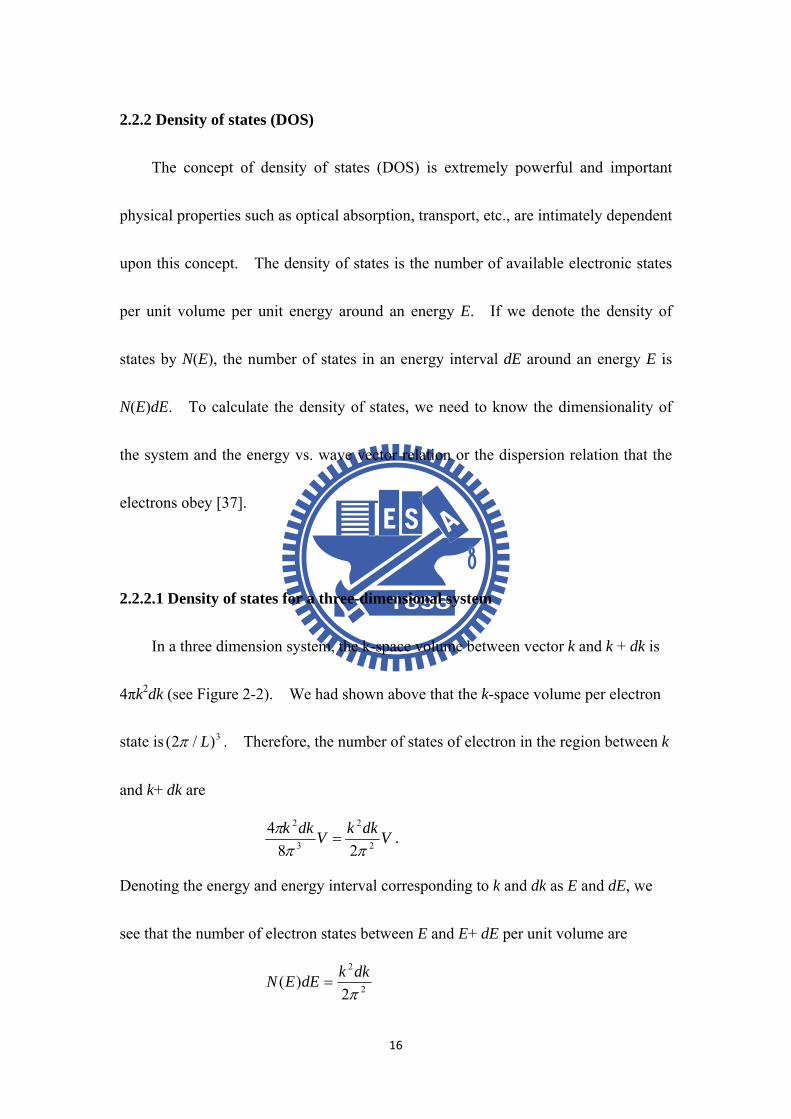
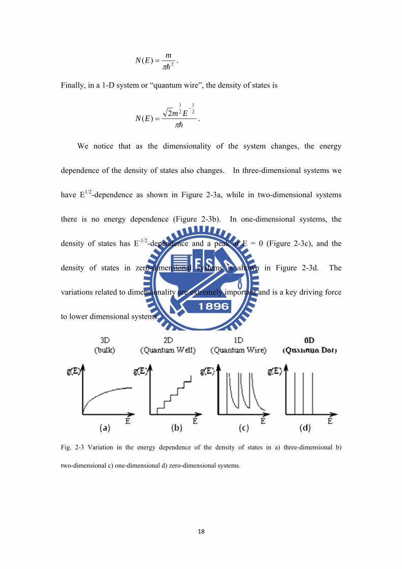

21
Fig 2-5 The hexagonal unit cell
232 Deby-Scherer formula [39]
Considering the path difference between the successive planes when the incident
beam remains fixed at the Bragg angle θ but with the diffracted ray leaving at an
angle θ+Δθ corresponding to intensity I in the spectrum line an distance Δθ away
from the peak as Figure 2-6
Fig 2-6 Grating treatment of line broadening by crystallite
The path difference between waves from successive planes is now
BC + CE = d sinθ+ d sin(θ+Δθ)
22
= d sinθ+ d sinθcosΔθ+d cosθsinΔθ (213)
where BC and CE is the path difference between incident ray of the successive planes
and d is the interplanar distance If Δθ is very small we can write cosΔθasymp1 and
sinΔθasympΔθ in which case
BC + CE = 2dsinθ+ d cosθΔθ (214)
Combining Braggrsquos law Eq (21)
BC + CE = 2dsinθ+ d cosθΔθ= nλ + d cosθΔθ (215)
where λ is the wavelength of the incident x-ray Therefore the phase difference δ
per interplanar distance or ldquoaperturerdquo is
δ = θθλπ
λπλ Δbull+ cos22 dn
= 2 πn + θθλπ
Δbullcos2 d (216)
Since a phase difference of 2π n produces the same effect as a zero phase we
can write the effective phase difference per aperture as
δ = θθλπ
Δbullcos2 d (217)
We obtain the result that the distribution of intensity of I in a spectrum line a
distance R from the grating is effectively
δ
δ
21sin
21sin
)(2
2
2N
RI Φ= (218)
and maximum intensity is
23
22max )( N
RI Φ
= (219)
where Φ is the amplitude at unit distance from the graying and N is the total number
of grating aperture
Diving Eq (210) by Eq (211) we obtain
2
2
2
max
)1(
21sin
21sin
N
N
II
δ
δ= (220)
Since 21 Nδ will change much faster than
21 δ the function will reach its first
minimum before 21 δ is very large We can therefore replace δ
21sin by
21 δ and
we will get
2
max
)
21
21sin
(δ
δ
N
N
II
= (221)
The ratio maxII will fall to
21 when
δ
δ
N
N
21
21sin
=2
1 (222)
The solution to the equation (214) yields the required phase difference
corresponding to the half maximum It may be obtained
δN21 = 139 (223)
Since according to equation (29) δ = θθλπ
Δbullcos2 d and D = Nd we obtain
θθλ
Δ= 2cos890
D (224)
24
Let B be taken as the full width at half maximum from Δθ to ndashΔθ hence
B = 2Δθ= θλ
cos890
D (radians) (225)
where λ is the wavelength of x-ray and D is the average size of the particles
24 Photoluminescence characterization [35 40]
Photoluminescence (PL) is a powerful and noninvasive optical analysis
technology for the semiconductor industry It has high sensitivity to reveal the band
structure and the carrier transportation behaviors in a material From PL spectrum
the defect or impurity can also be found in the compound semiconductors which
affect material quality and device performance A given impurity produces a set of
characteristic spectral features The fingerprint identifies the impurity type and
often several different impurities can be seen in a single PL spectrum In addition
the full width at half maximum of the PL peak is an indication of samplersquos quality
[41] So the PL could be a judgment of the material quality and be a key technology
of the development of nano-technology
PL is the optical radiation emitted by a physical system (in excess the thermal
equilibrium blackbody radiation) resulting from excitation to a nonequilibrium state
by illuminating with light Three processes can be distinguished (i) creation of
electron-hole pairs by absorption of the excited light (ii) radiative recombination of
25
electron-hole pairs and (iii) escape of the recombination radiation from the sample
241 Fundamental Transitions
An electron is excited from the valence band to the conduction band by
absorption of a photon In this sense an optical excitation is a two-particle transition
The same is true for the recombination process An electron in the conduction band
can return radiatively or nonradiatively to the valance band only if there is a free
space ie a hole available Two quasi-particles annihilate in the recombination
process What we need for the understanding of the optical properties of the
electronic system of a semiconductor is therefore a description of the excited states of
the N-particle problem We will consider the fundamental transitions those
occurring at or near the band edges
1 Free excitons (Wannier-Mott excitons)
An electron in the conduction band and a hole in the valence band are created at
the same point in space and can attract each other through their Coulomb interaction
Using the effective mass approximation the Coulomb interaction between electron
and hole leads to a hydrogen-like problem with a Coulomb potential term
he rreminus
minusεπε0
2
4
26
Here we will consider the so-called Wannier-Mott excitons more specifically
This type of excitons has a large Bohr radius (ie the mean distance between electron
and hole) that encompasses many atoms and they are delocalized states that can move
freely throughout the crystal hence the alternative name of free excitons
Indeed excitons in semiconductors form to a good approximation a hydrogen-
or positronium-like series of states below the gap For a simple parabolic band in a
direct-gap semiconductor one can separate the relative motion of electron and hole
and the motion of the center of mass This leads to the dispersion relation of exciton
as shown in Fig 2-7
MK
nRyEKnE
BgBph 2
1)(22
2 h
+minus= (226)
where Bn =123 is the principal number )1(613 20
εμm
Ry = eV is exciton binding
energy he mmM += and he kkK += are translational mass and wave vector of
the exciton respectively The series of exciton states in (226) has an effective
Rydberg energy Ry modified by the reduced mass of electron and hole and the
dielectric constant of the medium in which these particles move The radius of the
exciton equals the Bohr radius of H atom again modified by ε and μ Using the
material parameters for typical semiconductors one finds that the orbits of electron
and hole around their common center of mass average over many unit cells and this in
turn justifies the effective mass approximation in a self-consistent way These
27
excitons are called Wannier-Mott excitons
Fig 2-7 A pair excitation in the scheme of valence and conduction bands (a) in the exciton picture for a
direct gap semiconductor (b)
2 Biexcitons
It is well known that two hydrogen atoms with opposite electron spins can bind
to form a hydrogen molecule In the same sense it has been calculated that two
positronium-like atoms can form a positronium-like molecule as a bound state So
the idea is not far away that two excitons could bind to form a new quasiparticle the
so-called biexciton or excitonic molecule It has been found theoretically that the
biexciton should form a bound state for all ratios of effective electron and hole masses
and dimensionalities of the sample
The dispersion relation is given in the simplest case by
ex
bbiex
bexgbiex M
kEEEkE4
)(2)(22h
+minusminus= (2-27)
assuming that the effective mass of the biexciton is just twice that of the exciton
28
3 Bound excitons
Similar to the way that free carriers can be bound to defects it is found that
excitons can also be bound to defects Some of these defects can bind an exciton
resulting in a bound exciton complex (BEC) In Figure 2-8 we visualize exciton
bound to an ionized donor (D+X) a neutral donor (D0X) and a netural axxeptor (A0X)
An ionized acceptor does not usually bind an exciton since a neutral acceptor and a
free electron are energetically more favorable The binding energy of an exciton (X)
is the highest for a neutral acceptor (A0X complex) the lower for a neutral donor
(D0X) and the lower still for an ionized donor (D+X) The binding energy bE of
exciton to the complex usually increases according to bXA
bXD
bXD EEE 00 ltlt+ The
binding energy is defined as the energetic distance from the lowest free exciton state
at k = 0 to the energy of the complex There is a rule of thumb known as Haynersquos
rule which relates the binding energy of the exciton to the neutral complex with the
binding of the additional carrier to the point defect
Fig 2-8 Visualization of an exciton bound to an ionized donor (a) a neutral donor (b) and a neutral
acceptor (c)
29
4 Surface-bound exciton
The surface-to-volume ratio brings much influence on the systemrsquos Hamiltonian
when the material size is reduced to the nanometer scale [22] From the calculation
of exciton states at the QD surface we can know the exciton is bound to the
surface-located acceptor [25] Unlike the acceptor the donor does not bind the
exciton Because the hole is much heavier than the electron which makes the
surface donor a shallow impurity while the surface acceptor a deep impurity
Therefore excitons can be effectively bound only to surface acceptors
5 Two-Electron Satellites (TES) [42]
Two-electron satellite (TES) transitions involve radiative recombination of an
exciton bound to a neutral donor leaving the donor in the excited state In the
effective mass approximation the energy difference between the ground-state neutral
donor bound excitons and their excited states (TES) can be used to determine the
donor binding energies [43] (the donor excitation energy from the ground state to the
first excited state equals to 34 of the donor binding energy DE ) and catalog the
different species present in the material
30
6 Donor-Acceptor Pairs (DAP)
Donors and acceptors can form pairs and act as stationary molecules imbedded in
the host crystal The coulomb interaction between a donor and an acceptor results in
a lowering of their binding energies In the donor-acceptor pair case it is convenient
to consider only the separation between the donor and the acceptor level
rqEEEE ADgpair ε
2
)( ++minus= (2-28)
where r is the donor-acceptor pair separation DE and AE are the respective ionization
energies of the donor and the acceptor as isolated impurities
7 Deep transitions
By deep transition we shall mean either the transition of an electron from the
conduction band to an acceptor state or a transition from a donor to the valence band
in Fig 2-9 Such transition emits a photon ig EEh minus=ν for direct transition and
pig EEEh minusminus=ν if the transition is indirect and involves a phonon of energy pE
Hence the deep transitions can be distinguished as ( ) conductionⅠ -band-to-acceptor
transition which produces an emission peak at Ag EEh minus=ν and ( ) Ⅱ
donor-to-valence-band transition which produces emission peak at the higher photon
energy Dg EEh minus=ν
31
C
V
D
A
Fig 2-9 Radiative transition between a band and an impurity state
242 Influence of high excited light intensity
The PL conditions as mentioned above are excited by low excitation light
intensity At low excitation light intensity (low density regime in Fig 2-10) the PL
properties are determined by single electron-hole pairs either in the exciton states or
in the continuum Higher excitation intensity (intermediate density regime in Fig
2-10) makes more excitons such condition would lead to the exciton inelastic
scattering processes and form the biexciton The scattering processes may lead to a
collision-broadening of the exciton resonances and to the appearance of new
luminescence bands to an excitation-induced increase of absorption to bleaching or
to optical amplification ie to gain or negative absorption depending on the
excitation conditions If we pump the sample even harder we leave the intermediate
and arrive at the high density regime in Fig 2-10 where the excitons lose their
identity as individual quasiparticles and where a new collective phase is formed which
32
is known as the electron-hole plasma (EHP)
Fig 2-10 The general scenario for many-particle effects in semiconductors [35]
1 Electron-Hole Plasma
In this high density regime the density of electron-hole pairs np is at least in
parts of the excited volume so high that their average distance is comparable to or
smaller than their Bohr radius ie we reach a ldquocritical densityrdquo cpn in an EHP given
to a first approximation by 13 asympcpBna We can no longer say that a certain electron is
bound to a certain hole instead we have the new collective EHP phase The
transition to an EHP is connected with very strong changes of the electronic
excitations and the optical properties of semiconductors
33
2 Scattering Processes
In the inelastic scattering processes an exciton is scattered into a higher excited
state while another is scattered on the photon-like part of the polariton dispersion and
leaves the sample with high probability as a luminescence photon when this
photon-like particle hits the surface of the sample This process is shown
schematically in Fig 2-11 and the photons emit in such a process having energies En
given by Ref [44]
kTn
EEE exbexn 2
311 2 minus⎟⎠⎞
⎜⎝⎛ minusminus= (2-29)
where n = 2 3 4hellip exbE = 60 meV is the binding energy of the free exciton of ZnO
and kT is the thermal energy The resulting emission bands are usually called
P-bands with an index given by n
energy
Wave vector
Eg
Eexciton
P2
Pinfin
1
2
infin
nB=continuum
Fig2-11 Schematic representation of the inelastic exciton-exciton scattering processes [35]
34
Chapter 3 Experiment details and analysis techniques
31 Sample preparation
We fabricate ZnO QDs by sol-gel method Sol-gel method was chosen due to
its simple handling low cost and narrow size distribution In particular it has the
potential to produce samples with large areas and complicated forms on various
substrates
The ZnO colloidal spheres were produced by one-stage reaction process and
reactions were described as the following equations
COOHxCHCOOCHOHZnOxHCOOCHZn xx 323223 )()()( +⎯rarr⎯+ minusminusminusΔ (3-1)
COOHCHxOHxZnOCOOCHOHZn xx 3223 )2()1()()( minus+minus+⎯rarr⎯Δminus
minusminus (3-2)
Equation (3-1) is the hydrolysis reaction for Zn(OAc)2 to form metal complexes We
increased the temperature of reflux from RT to 160oC and maintained for aging The
zinc complexes will dehydrate and remove acetic acid to form pure ZnO as Eq (3-2)
during the aging time Actually the two reactions described above proceed
simultaneously while the temperature is over 110oC
All chemicals used in this study were reagent grade and employed without
further purification A typical reaction was listed in Table 3-1 stoichiometric zinc
acetate dihydrate [995 Zn(OAc)2middot2H2O Riedel-deHaen] was dissolved into
35
diethylene glycol [995 DEG ethylenediamine-tetra-acetic acid (EDTA)] to make
01 M 005 M 001 M solutions The first thing we notice is that we can control the
QDs size with domination concentration of zinc acetate in the solvent (DEG) Then
the temperature of reaction solution was increased to 160 and white colloidal ZnO
was formed in the solution that was employed as the primary solution The primary
solutions were put separately in a centrifuge operating at 3000 rpm for 30 minutes
The supernatant was decanted off and saved and the polydisperse powder was
discarded Finally the supernatant was then dropped onto Si (100) substrates and
dried at 150 for further characterization The experiment equipment and a flow
chart of fabricate ZnO QDs by sol-gel method was shown in Figure 3-1amp3-2
Chemical reagent Molecular formula Degree of
purity
Source
Zinc acetate dehydrate Zn(CH3COOH)22H2O 995 Riedel-deHaen
Diethylene glycol C4H10O3 995 EDTA
Table 3-1 Shows that chemical reagent was used with sol-gel experiment process
36
Fig 3-1 Experiment equipment used for fabricating ZnO QDs
Fig 3-2 A flow chart of fabricate ZnO QDs by sol-gel method
Zn(CH3COOH)22H2O
Diethylene-glycol (DEG)
Counter flow apparatus
White colloidal formed
Centrifuge
Clear solution
drop or spin coating onSiO2Si(001)
varying solution concentration
heating up to 160
separating solution
37
32 Microstructure and optical properties analysis
321 X-ray diffraction
The crystal structures of the as-grown powder were inspected by using XRD
(model MAC Sience MXP18) at room temperature equipped with CuK X-ray source
(λ=15405Aring) in National Synchrotron Radiation Research Center (NSRRC) Taiwan
Data were recorded between the angle range of 20deg lt 2θ lt 80deg with steps of 002degand
rate of scanning is 40degmin The operation voltage of the system is 50 kV and the
operation current is 200 mA The essential features of x-ray spectrometer are shown
in Figure 3-3 X-rays from the tube T are incident on a crystal C which may be set at
any desired angle to the incident beam by rotation about an axis through O the center
of the spectrometer circle D is a detector which measures the intensity of the
diffraction x-rays
Fig 3-3 The x-ray spectrometer
38
The sizes of the nanocrystallites can be determined by X-ray diffraction using the
measurement of the full width at half maximum (FWHM) of the X-ray diffraction
lines The average diameter is obtained byθλ
cos890
BD = where D is the average
diameter of the nanocrystallite λ is the wavelength of the X-ray source and B is the
FWHM of X-ray diffraction peak at the diffraction angle θ
322 Photoluminescence system
PL provides a non-destructive technique for the determination of certain
impurities in semiconductors The shallow-level and the deep-level of impurity
states were detected by PL system It was provided radiative recombination events
dominate nonradiative recombination
In the PL measurements we used a He-Cd cw laser (325 nm) [Kimmon
IK5552R-F] as the excitation light Light emission from the samples was collected
into the TRIAX 320 spectrometer and detected by a photomultiplier tube (PMT) As
shown in Fig 3-4 the diagram of PL detection system includes mirror focusing and
collecting lens the sample holder and the cooling system The excitation laser beam
was directed normally and focused onto the sample surface with power being varied
with an optical attenuator The spot size on the sample is about 100 μm
Spontaneous and stimulated emissions were collected by a fiber bundle and coupled
39
into a 032 cm focal-length monochromator (TRIAX 320) with a 1200 linesmm
grating then detected by either an electrically cooled CCD (CCD-3000) or a
photomultiplier tube (PMT-HVPS) detector The temperature-dependent PL
measurements were carried out using a closed cycle cryogenic system A closed
cycle refrigerator was used to set the temperature anywhere between 15 K and 300 K
And the power-dependent PL spectra were used for monitoring the characteristic of
excitons and thermalization effect at the different excitation density
Fig 3-4 The PL system
40
Chapter 4 Results and Discussion
41 Morphology and crystal structures
411 Morphology
Shown in Fig 4-1 is a typical high-resolution transmission electron microscope
(HRTEM) image of the ZnO nanoparticles Nanoparticles aged at 160 degC for 1 hr
and solution concentration of 004 M was selected for particle size determination by
HRTEM The shape of particles is predominantly spherical and the nanoparticles
are clearly well separated and essentially have some aggregation The average
diameter of the number-weighted particles obtained from a colloid aged at 160 degC for
1 hr (004 M) was determined to be 618plusmn 03 nm
Fig 4-1 HRTEM image of the ZnO QDs fabricated using 004M Zn(OAc)2
41
412 X-ray diffraction measurement
The XRD profiles of the ZnO QDs with various concentrations of Zn(OAc)2 are
shown in Fig 4-2 The diffraction pattern and interplanar spacings match nicely
with the standard diffraction pattern of wurtzite ZnO demonstrating the formation of
wurtzite ZnO nanocrystals All of the samples present similar XRD peaks that can
be indexed as the wurtzite ZnO crystal structure with lattice constants a = 3253 Aring and
c = 5213 Aring which are consistent with the value in the standard card (JCPDS
89-1397)
Fig 4-2 XRD profiles of the ZnO QDs prepared with various concentration of Zn(OAc)2 The
crystalline size can be approximately estimated to be 16 and 7 nm respectively (top to bottom) for
concentrations of 016 and 006 M
No diffraction peaks of other species could be detected that indicates all the
precursors have been completely decomposed and no other crystal products were
42
formed The full width at half maximum (FWHM) of the diffraction peaks increases
that is the average crystalline size decreases as the concentration of zinc precursor
reduces The average size is calculated from the width of diffraction peak using the
Debye-Scherer formula [45 46] )cos(890 θλ wD = where D is the average
crystalline diameter of the particles λ is the wavelength of the x-ray source w is the
linewidth at half maximum in excess of the instrumental broadening and θ is the
diffraction angle The crystalline size can be estimated to be 16 nm and 7 nm for
concentrations of 016 M and 006 M respectively
42 Photoluminescence spectra
421 Photoluminescence spectra for different sizes of ZnO particles
The PL spectra of ZnO QDs with average crystalline sizes of 16 and 7 nm at 13
K are shown in Fig 4-3 For the 16-nm ZnO QDs a strong UV emission peak at
3388 eV with FWHM of ~ 96 meV was observed accompanied with very broad weak
visible emission with the slightly strong blue emission and rather weak yellow
emission bands And only a strong UV emission peak at 3411 eV with FWHM of ~
174 meV was observed unaccompanied with visible emission for the 7 nm ZnO QDs
The sharp UV emission peak is attributed to the near band edge emission (NBE) [27
47] The broad visible emission is the deep-level emission which is attributed to the
43
oxygen vacancy (green emission) or oxygen interstitial (red emission) The intensity
of the UV and visible peak ratio increases with decreasing the QD size The strong
UV emission and weak visible emission in PL spectra indicates that the ZnO QDs
have a good crystal quality
Fig 4-3 The PL spectra of the ZnO QDs measured at low temperature
Figure 4-4 demonstrates the PL spectra of ZnO QDs with different average
crystalline sizes measured at T = 13 K The near band edge UV emission is
attributed to the free exciton (FX) emission [32] which shifts (solid line) to the higher
energy (from 3386 eV to 342 eV) as the QD size decreases (16 nm ndash 6 nm) due to
the quantum confinement effect (QCE) Besides the FWHM increases as the
average QDs size decreases that may be caused by the contribution of surface-optical
phonon [48] surface-bound acceptor exciton complexes [25] and size distribution
44
Since the Bohr radius of the exciton in bulk ZnO is about 234 nm [49] we must
consider the electron hole Coulomb interaction in our samples and the particles are in
the moderate to weak confinement regime
Fig 4-4 PL spectra of different sizes of ZnO QD at low temperature The line indicates the shifts of FX
peak energy
422 Temperature-dependent PL for different sizes of ZnO particles
Figure 4-5 displays the temperature-dependent PL of different sizes of ZnO it
reveals only single one band for T = 8 ~ 300 K in QDs system Due to small binding
energy of D0X it will be ionized as T gt 100 K so we can easily attribute the single
band to the FX emission We also find that the peak energy difference of FX in QDs
system between 8 K and 300 K decrease with the particle size decreasing It is
known that the main contribution to the energy shift is the Froumlhlich interaction [50] a
45
result of Coulomb interaction
Fig 4-5 Temperature-dependent PL spectra of (a) 16 nm (b) 7 nm (c) 6 nm
423 Power-dependent PL for different sizes of ZnO particles
The power-dependent PL spectra of different sizes of ZnO QDs are shown in Fig
4-6 These spectral shapes are almost the same except that the spectral intensity
increases with increasing excitation power from 003 mW to 34 mW (432 Wcm2 to
46
49 kWcm2) covering a range of three orders of magnitude which show the exciton
states remain invariable
The character in ZnO QDs gives a sharp contrast to the ZnO powder (~ 1 μm)
in which the relative peak intensities of biexciton (BX) and P-band (exciton-exciton
scattering) emissions increase as the excitation power increasing [30] For
quantitative analysis the spectral shape of NBE emission measured in 6-nm ZnO QDs
at 80 K is decomposed into two peaks and theoretical fitting results are shown in Fig
4-7 For comparison the inset of Fig 4-7 shows the fit of the PL spectrum in ZnO
powder at 80 K The dashed curves denote the various emissions and the solid curve
corresponds to the sum of the theoretical fit which shows good agreement with the
experimental data marked as the open dots The PL spectra of QDs and that of
powder are very diverse The BX emission can be observed in ZnO powder
nevertheless in ZnO QDs only the emission of surface bound exciton (SX) [51] rather
than BX can be recognized
47
Fig 4-6 Power-dependent PL spectra of (a) 16 nm at 15 K (b) 16 nm at 80 K (c) 7 nm at 15 K (d) 7
nm at 80 K (e) 6 nm at 8 K (f) 6 nm at 80 K
48
Fig 4-7 Gaussian fit to a PL spectrum of 6 nm ZnO QDs (004M) measured at 80K The inset shows
the spectral fitting for ZnO powder The fitted line shapes are shown separately in dash lines Solid
lines correspond to the fit and dots represent the data
424 PL peak positions as a function of excitation power
The peak positions of these emissions with increasing the excitation power in
6-nm ZnO QDs at 80 K are plotted in Fig 4-8 The FX is observed at 3418 eV and
the PL emission peak at 3325 eV may be attributed to the emission of SX The peak
positions of FX emission and SX emission are hardly shifted as the excitation power
increases from 003 to 34 mW
49
Fig 4-8 The PL peak positions as a function of excitation power measured at 80K
425 Integrated intensity as a function of excitation power
In order to further understand the characteristic of these two peaks the integrated
PL intensities of these peaks as a function of excitation power in 6-nm ZnO QDs at
80K are depicted in Fig 4-9 Both of the integrated intensities exhibit nearly linear
dependence on the excitation power with both exponents close to 096 However
the exponent of BX (with binding energy of ~15 meV) on the excitation power in
ZnO powder comes near the theoretical value of 2 having 186 at 80K It is due to
efficient cooling via participation of optical phonons when the exciton kinetic energy
approaches to the energy of the lowest optical phonon [30] However reducing the
exciton-LO phonon coupling in ZnO QDs [32] causes the lack of the efficient cooling
of exciton with assistance of optical phonon scattering or the so-called phonon
bottleneck Therefore it is hardly to allow effectively bounding exciton pairs to
form biexcitons in ZnO QDs
50
In addition the P-band emission is hardly found in Fig 4-6 This finding
means that the probability of exciton-exciton scattering is also very low For that
reason we suspect the other reason might be that there is only one exciton existing in
a QD within the exciton lifetime even with the achievable high power CW excitation
so that neither exciton-exciton scattering nor BX can be observed in ZnO QDs
Therefore the increase of excitation intensity provides the larger chance of a single
exciton being excited or the larger excitation rate of single exciton Thus the peak is
hardly shifted and the PL intensity is linear dependence with excitation intensity
corroborating the invariable exciton states upon increasing pumping in ZnO QDs
Fig 4-9 The integrated intensity of two decomposed TES and FX peaks as a function of excitation
power measured at 80K The inset shows the excitation power dependent emission intensity of
biexciton in ZnO powder measured at 80 K The power factor is 186
51
Chapter 5 Conclusions and Prospective
51 Conclusions
In summary we have measured XRD to inspect the crystal structures and the
average size of ZnO QDs synthesized by a simple sol-gel method The average sizes
of ZnO QDs were verfied by TEM The diffraction pattern and interplanar spacings
indicate the formation of wurtzite ZnO nanocrystals and no diffraction peaks of other
species could be detected that indicates all the precursors have been completely
decomposed and no other crystal products were formed We have measured
temperature-dependent and power-dependent PL spectra of ZnO QDs with different
sizes to investigate the optical properties From Size-dependence of efficient UV
photoluminescence from low temperature PL gives evidence for quantum
confinement effect The ZnO QDs exhibit strong UV emission and weak visible
emission indicating very good crystal quality Moreover the biexciton and P-band
emissions in ZnO QDs are hardly observed and unchanged shapes of
power-dependent PL spectra show the exciton states remain invariable in ZnO QDs
The intensities of emission peaks associated with these invariable free exciton and
surface bound exciton states exhibit linear dependence on the excitation density
52
52 Prospective
In order to further investigate the optical properties of ZnO QDs we will
measure the time resolved photoluminescence (TRPL) to inspect the lifetime of ZnO
QDs Through measuring the lifetime of ZnO QDs we can identify the different PL
origins of physical mechanisms and the process of exciton recombination Besides
we will do single-photon measurement to study the optical characterizations in a
single ZnO QD
53
References
[1] R Triboulet and J Perriere Prog Cryst Growth Charact Mater 47 65 (2003)
[2] U Ozgur Y I Alivov C Liu A Teke M A Reshchikov S Dogan V Avrutin
S J Cho and H Morkoc J Appl Phys 98 041301 (2005)
[3] T Yatsui J Lim M Ohtsu S J An and G C Yi Appl Phys Lett 85 727
(2004)
[4] A B Djurisic and Y H Leung Small 2 944 (2006)
[5] A P Alivisatos Science 271 933 (1996)
[6] C H Liu J A Zapien Y Yao X M Meng C S Lee S S Fan Y Lifshitz
and S T Lee Adv Mater 15 838 (2003)
[7] B Liu and H C Zeng J Am Chem Soc 125 4430 (2003)
[8] W I Park Y H Jun S W Jung and G C Yi Appl Phys Lett 82 964 (2003)
[9] H Q Yan R R He J Pham and P D Yang Adv Mater 15 402 (2003)
[10] K F Lin H M Cheng H C Hsu L J Lin and W F Hsieh Chem Phys Lett
409 208 (2005)
[11] C J Pan K-F Lin W-T Hsu and W-F Hsieh J Appl Phys 102 123504
(2007)
[12] J Y Lao J G Wen and Z F Ren Nano Letters 2 1287 (2002)
[13] J Y Lao J Y Huang D Z Wang and Z F Ren Nano Letters 3 235 (2003)
[14] Y J Xing Z H Xi X D Zhang J H Song R M Wang J Xu Z Q Xue and
D P Yu Solid State Commun 129 671 (2004)
[15] J H Park H J Choi Y J Choi S H Sohn and J G Park J Mater Chem 14
35 (2004)
[16] P X Gao and Z L Wang Appl Phys Lett 84 2883 (2004)
[17] X Y Kong and Z L Wang Nano Letters 3 1625 (2003)
[18]G C Yi C R Wang and W I Park Semiconductor Science and Technology 20
54
S22 (2005)
[19] L E Brus J Chem Phys 80 4403 (1984)
[20] L T Canham Appl Phys Lett 57 1046 (1990)
[21] Y Kayanuma Phys Rev B 38 9797 (1988)
[22] J B Xia and K W Cheah Phys Rev B 59 14876 (1999)
[23] L Guo S H Yang C L Yang P Yu J N Wang W K Ge and G K L
Wong Appl Phys Lett 76 2901 (2000)
[24] N Pan X P Wang M Li F Q Li and J G Hou J Phys Chem C 111 17265
(2007)
[25] V A Fonoberov and A A Balandin Appl Phys Lett 85 5971 (2004)
[26] B P Zhang N T Binh Y Segawa K Wakatsuki and N Usami Appl Phys
Lett 83 1635 (2003)
[27] B P Zhang N T Binh Y Segawa Y Kashiwaba and K Haga Appl Phys
Lett 84 586 (2004)
[28] S W Kim and S Fujita Appl Phys Lett 86 153119 (2005)
[29]X Q Zhang Z G Yao S H Huang I Suemune and H Kumano J Appl Phys
99 063709 (2006)
[30] C J Pan K F Lin and W F Hsieh Appl Phys Lett 91 111907 (2007)
[31] S Y Kim Y S Yeon S M Park J H Kim and J K Song Chem Phys Lett
462 100 (2008)
[32] W T Hsu K F Lin and W F Hsieh Appl Phys Lett 91 181913 (2007)
[33] D M Bagnall Y F Chen Z Zhu T Yao M Y Shen and T Goto Appl Phys
Lett 73 1038 (1998)
[34] C J Brinker and G W Scherer Sol-Gel Sience (Academic Press 1990) p 303
[35] C F Klingshirn Semiconductor Optics (Springer 1997)
[36] S-B Yin in National Chiao Tung University Department of Photonics (National
55
Chiao Tung University 1999)
[37] J Singh Physics of Semiconductors and Their Heterostructures (McGraw-Hill
Singapore 1993) p 17amp316
[38] B D Cullity Element of X-ray diffraction (Addison Wesley Canada 1978)
[39] A Taylor X-ray Metallography (John Wiley and Sons New York 1961) p 676
[40] F Mark Optical Properties of Solids (Oxfrd university press 2001)
[41] S Perlpwotz Optical characterization of semiconductors infaraed Raman and
Photoluminescence spectroscopy (Academic Press London 1993)
[42] A Teke U Ozgur S Dogan X Gu H Morkoc B Nemeth J Nause and H O
Everitt Phys Rev B 70 195207 (2004)
[43] H Alves D Pfisterer A Zeuner T Riemann J Christen D M Hofmann and
B K Meyer Optical Materials 23 33 (2003)
[44] J B Baxter and E S Aydil Appl Phys Lett 86 053114 (2005)
[45] E F Kaelble Handbook of X-rays (McGraw-Hill New York 1967)
[46] J C Bailar A F Trotman-Dickenson H J Emeleus and S R Nyholm
Comprehensive Inorganic Chemistry (Pergamon Oxford 1973) Vol 3
[47] H C Hsu Y K Tseng H M Cheng J H Kuo and W F Hsieh J Crystal
Growth 261 520 (2004)
[48] Z D Fu Y S Cui S Y Zhang J Chen D P Yu S L Zhang L Niu and J Z
Jiang Appl Phys Lett 90 263113 (2007)
[49] R T Senger and K K Bajaj Phys Rev B 68 045313 (2003)
[50] S J Sheih K T Tsen D K Ferry A Botchkarev B Sverdlov A Salvador
and H Morkoc Appl Phys Lett 67 1757 (1995)
[51]V A Fonoberov K A Alim A A Balandin F X Xiu and J L Liu Phys Rev
B 73 (2006)
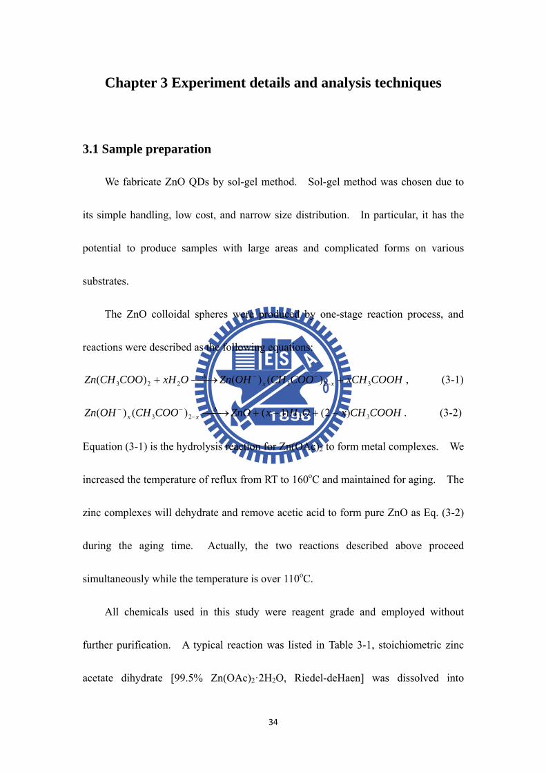
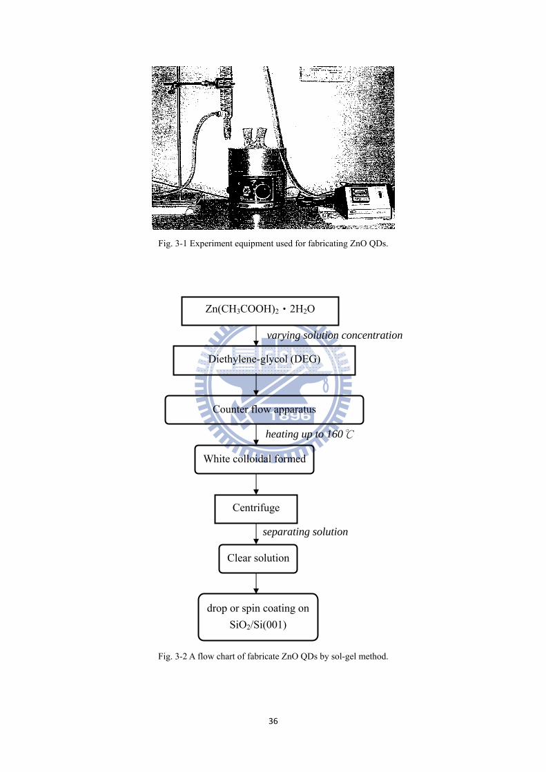
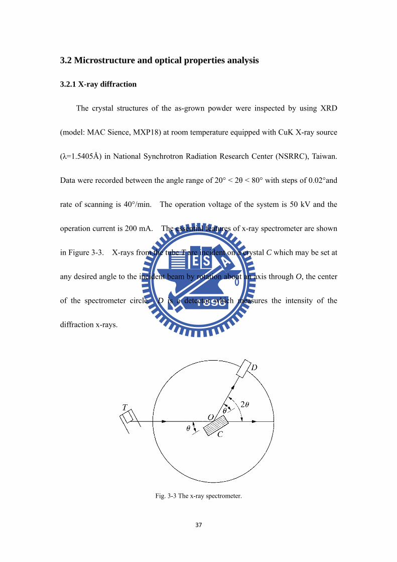
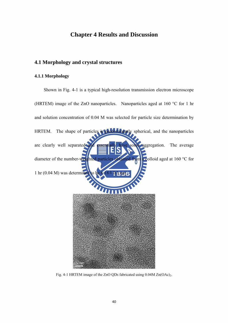
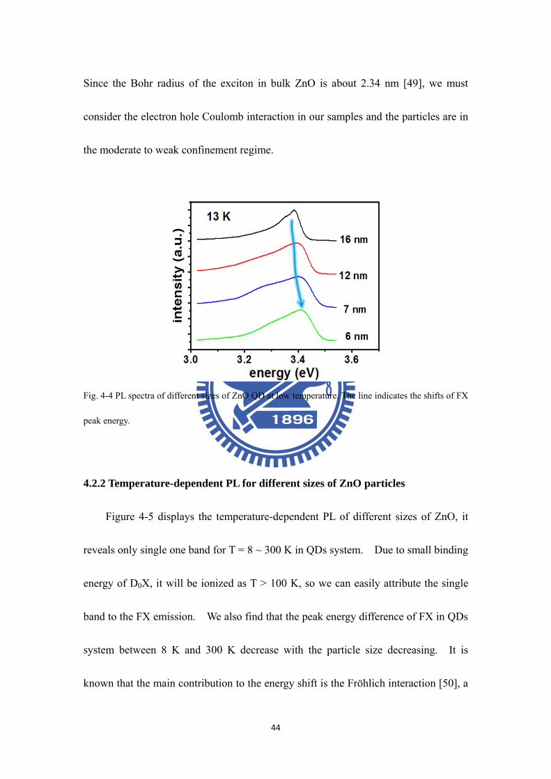
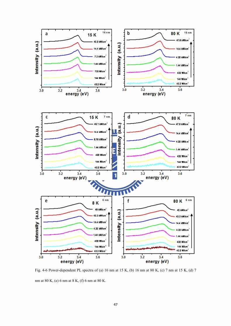


![CAlEnDAR - EdUHK Collection [教大特藏]](https://static.fdokumen.com/doc/165x107/6320cf82117b4414ec0b2e88/calendar-eduhk-collection-.jpg)


