國立交通大學 電子工程學系電子研究所碩士班 碩 士 論 文
97
國 立 交 通 大 學 電 子 工 程 學 系 電 子 研 究 所 碩 士 班 碩 士 論 文 應用於兆級序列傳輸系統之等化器技術 Multi-Gbps Equalizer Technology for Serial Link System 研 究 生 : 黃喻暄 指 導 教 授 : 周世傑 博士 中 華 民 國 九 十 七 年 十 月
-
Upload
khangminh22 -
Category
Documents
-
view
0 -
download
0
Transcript of 國立交通大學 電子工程學系電子研究所碩士班 碩 士 論 文

國立交通大學
電子工程學系 電子研究所碩士班
碩 士 論 文
應應應用用用於於於兆兆兆級級級序序序列列列傳傳傳輸輸輸系系系統統統之之之等等等化化化器器器技技技術術術
Multi-Gbps Equalizer Technology for Serial
Link System
研 究 生: 黃喻暄指導教授: 周世傑 博士
中 華 民 國 九 十 七 年 十 月

應用於兆級序列傳輸系統之等化器技術
Multi-Gbps Equalizer Technology for Serial Link System
研 究 生 : 黃喻暄 Student: Yu-Sam, Huang
指 導 教 授 : 周世傑 博士 Advisor: Dr. Shyh-Jye Jou
國 立 交 通 大 學
電子工程學系電子研究所碩士班
碩 士 論 文
A Thesis
Submitted to Department of Electronics Engineering & Institute
of Electronics
College of Electrical and Computer Engineering
National Chiao Tung University
in Partial Fulfillment of the Requirements
for the Degree of Master of Science
in
Department of Electronics Engineering
October 2008
HsinChu, Taiwan, Republic of China
中 華 民 國 九 十 七 年 十 月

應用於兆級序列傳輸系統之等化器技術
學生: 黃喻暄 指 導 教 授 : 周世傑 博士
國立交通大學
電子工程學系 電子研究所碩士班
摘 要
在多媒體時代的今天,各種高速串列傳輸技術廣泛的使用在許多高效能的電子產品
中。為了讓訊號經過各種傳輸通道破壞後可以保持一定的品質,等化器在高速串列傳
輸的系統中扮演了重要的角色。根據信號處理的方式我們可以將等化器分成連續時間
領域等化器跟離散時間領域等化器。
在本論文中,首先我們提出了一個操作在 6 Gbps 的連續時間領域等化器。在等
化電路的輸入端我們使用了一個準位平移電路來減少通道輸出端直流電壓準位漂移對
等化器造成的影響。準位平移電路同時也提供低頻訊號的放大功能。為了減少在增加
高頻放大率的同時對低頻訊號的抑制量,我們將等化電路設計成兩級串接的模式。我
們提出的連續時間領域等化器在時脈訊號頻率 3 GHz 可以提供 13.87 dB 的補償。
實做晶片使用聯電標準臨界電壓 90 耐米互補式金氧半導體製程來製造。佈局之後的
模擬結果,位於等化器輸出端的信號眼圖可以開至正負 250 mV,而緩衝器的輸出端
可以將信號眼圖張開到規格所定的正負 300mV。電路總面積為0.49 × 0.49 mm2。在
1.0 V 的操作電壓下,電路總功率為 78.83 mW。
接著,我們對一個半速率的決策回授等化器電路架構 [8]提出跳躍式係數更新
方案以及乒乓係數更新方案。該電路結構擁有5筆過去的資料消除符號間干擾並且
使用一個位元的猜測方法來紓解時間上得限制。係數更新的演算法是使用sign-sign
LMS演算法。在跳躍式係數更新方案中,係數計算電路的操作頻率將會降低而且功率
ii

消耗也會減少。乒乓係數更新方案則是在每個資料路徑上省下一個用來計算錯誤量正
負號的比較器。針對這兩個係數更新方案,我們執行許多不同條件的模擬並且整理決
策回授等化器係數收斂時間的表現。希望能夠藉此得到設計電路時在規格的規範下選
擇相關參數的方針,尤其是決策回授等化器係數收練的速度。
iii

Multi-Gbps Equalizer Technology for Serial Link System
Student: Yu-Sam, Huang Advisor: Dr. Shyh-Jye Jou
Department of Electronics Engineering & Institute of ElectronicsCollege of Electrical and Computer Engineering
National Chiao Tung University
ABSTRACT
In the multi-media era, many high-speed serial link trarnsmission technologies are
developed and are widely used for high performance modern electronic product.
In order to maintain the data quality that will be attenuated by communication
channel, the equalizer becomes an important component in the high-speed serial
link system. Based on the type of data processing, the equalizer can be categoried
into continuous-time equalizer and discrete-time equalizer.
In this thesis, we first propose a continuous-time equalizer that operates at
6 Gbps. We take a level-shifter stage in the front of our proposed equalizer for
minimizing the DC voltage level variation in the equalizer input and for providing
the low-frequency gain in the proposed circuit. In the equalization block, we use
two serial cascade stages to minimize the gain suppression at low frequency while
to boost the gain in high frequency. The proposed equalizer can compensate
13.87 dB channel loss at clock frequency of 3 GHz. The test chip is fabricated
in UMC 90 nm CMOS regular-Vt process. The post-layout simulation results
show that the data eye in the output of equazlier stage is about ±250 mV, and
the data eye in the output of buffer stage can reach ±300 mV that meets our
specification. Total area of our proposed equalizer including pads is 0.49 × 0.49
mm2 and power consumption is 78.83 mW under 1.0 V supply voltage.
Secondly, we propose a hopping coefficients update and ping-pong coeffi-
cients update schemes for a discrete-time half-rate DFE (Decision-feedback equal-
izer)architecture [8]. The architecture uses five taps to cancel the ISI (intersymbol-
iv

interference) effects and uses the speculation method to relax the timing con-
strain. The algorithm used for coefficients update is the sign-sign LMS (least-
mean-square) algorithm. For the hopping update scheme, the operation frequency
of coefficients update block can be reduced and the power can be saved. For ping-
pong update scheme, we calculate the sign of error under different conditions in
these two data paths. The ping-pong update scheme saves one comparator for
calculating the sign of error in each data path. For these two update schemes, we
run different conditions and summary the convergent performance. We get the
guideline of choosing parameters in the proposed equalizer under some system
specifications especially the speed of convergence.
v

誌誌誌 謝謝謝
首先我要感謝指導教授周世傑老師在我兩年又1個半月的碩士生涯中細心的指
導。不論是在研究內容上的指導以及每次meeting報告時所給予的糾正以及建議,都
讓我在這短段時間獲益良多,同時也要謝謝老師這段時間對我犯錯時的包容,耐心並
且孜孜不倦的叮嚀我們要努力從事研究。在此祝福老師家庭和樂融融,老師與師母身
體健康笑口常開,老師的三位小朋友們在未來求學的路上一路順風。另外,也要感謝
蘇朝琴教授、陳巍仁教授與蔡嘉明教授撥冗參加口試,給予珍貴的經驗讓我的論文能
更加完整。
接著,我要特別謝謝林志憲博士在整個研究的過程中不厭其煩的解答我各式各樣
的問題。整本論文能夠完成,他的幫忙一直是很關鍵的一個因素。謝謝他提供我許多
研究的方向以及許多小細節上得幫忙。祝福他接下來的從軍生活一切順利,家庭生活
圓滿。
這一路上,還要謝謝許多朋友陪伴我走過一段又一段的難關。除了常常聽我滿滿
的抱怨還有我接納陷入低潮時負面的情緒,每當想到大家對我這段時間的支持與鼓
勵,再多的謝謝也無法道盡我心中的感恩之情,很高興這段時間能有你們這群朋友的
陪伴。祝福大家在各自的跑道上一切順利,不論是找工作或者出國深造都能有佳音。
最後,要謝謝我的父母的照顧與支持。在我走入低潮的時候幫我鼓勵打氣,甚至
還要每天聽我發牢騷,真的辛苦你們了。
vi

Content
摘要 . . . . . . . . . . . . . . . . . . . . . . . . . . . . . . . . . . . . . . . ii
Abstract . . . . . . . . . . . . . . . . . . . . . . . . . . . . . . . . . . . . . iv
誌謝 . . . . . . . . . . . . . . . . . . . . . . . . . . . . . . . . . . . . . . . vi
Content . . . . . . . . . . . . . . . . . . . . . . . . . . . . . . . . . . . . . vii
List of Tables . . . . . . . . . . . . . . . . . . . . . . . . . . . . . . . . . . x
List of Figures . . . . . . . . . . . . . . . . . . . . . . . . . . . . . . . . . xi
1 Introduction . . . . . . . . . . . . . . . . . . . . . . . . . . . . . . . . . 1
1.1 Challenges in High-Speed Applications . . . . . . . . . . . . . . . 1
1.2 Motivation . . . . . . . . . . . . . . . . . . . . . . . . . . . . . . . 3
1.3 Thesis Organization . . . . . . . . . . . . . . . . . . . . . . . . . . 3
2 Theory of Equalizer . . . . . . . . . . . . . . . . . . . . . . . . . . . . . 5
2.1 Equalizers in High-Speed Application . . . . . . . . . . . . . . . . 5
2.1.1 Physical Limitation of High-Speed Transmission . . . . . . 5
2.1.2 Equalizer and Compensation . . . . . . . . . . . . . . . . . 8
2.2 Concepts of Equalizers . . . . . . . . . . . . . . . . . . . . . . . . 10
2.2.1 Continuous-Time Equalizers . . . . . . . . . . . . . . . . . 10
2.2.2 Discrete-Time Equalizers . . . . . . . . . . . . . . . . . . . 12
2.3 Traditional algorithm of discrete-time Equalizer . . . . . . . . . . 15
2.3.1 Zero Forcing Algorithm . . . . . . . . . . . . . . . . . . . . 16
vii

2.3.2 Mean-Square Error Algorithm . . . . . . . . . . . . . . . . 17
2.4 General Topology of Equalization . . . . . . . . . . . . . . . . . . 18
2.4.1 Linear Equalization . . . . . . . . . . . . . . . . . . . . . . 18
2.4.2 Decision Feedback Equalization . . . . . . . . . . . . . . . 19
3 Continuous-Time Equalizer . . . . . . . . . . . . . . . . . . . . . . . . . 21
3.1 Overview . . . . . . . . . . . . . . . . . . . . . . . . . . . . . . . . 21
3.2 Motivation and the proposed architecture . . . . . . . . . . . . . . 22
3.3 Circuit design and simulation results . . . . . . . . . . . . . . . . 24
3.3.1 Level-Shifter . . . . . . . . . . . . . . . . . . . . . . . . . . 24
3.3.2 Equalizer stage . . . . . . . . . . . . . . . . . . . . . . . . 27
3.4 Implementation and layout . . . . . . . . . . . . . . . . . . . . . . 39
3.5 Measurement environment setup . . . . . . . . . . . . . . . . . . . 47
4 Discrete-Time equalizer . . . . . . . . . . . . . . . . . . . . . . . . . . . 48
4.1 Overview . . . . . . . . . . . . . . . . . . . . . . . . . . . . . . . . 48
4.2 Techniques and architectures for discrete-time DFE . . . . . . . . 49
4.3 Sign-sign least-mean-square algorithm . . . . . . . . . . . . . . . . 52
4.3.1 Method of steepest descent . . . . . . . . . . . . . . . . . . 52
4.3.2 Sign-sign LMS algorithm . . . . . . . . . . . . . . . . . . . 54
4.4 Design parameters selection based on power and area consideration 55
4.4.1 Architecture in our model . . . . . . . . . . . . . . . . . . 56
4.4.2 Hopping coefficients update scheme . . . . . . . . . . . . . 58
viii

4.4.3 Ping-pong coefficients update scheme . . . . . . . . . . . . 63
5 Conclusions and Future Works . . . . . . . . . . . . . . . . . . . . . . . 77
5.1 Conclusions . . . . . . . . . . . . . . . . . . . . . . . . . . . . . . 77
5.2 Future Works . . . . . . . . . . . . . . . . . . . . . . . . . . . . . 78
References . . . . . . . . . . . . . . . . . . . . . . . . . . . . . . . . . . . . 79
ix

List of Tables
1.1 Industrial standards of high-speed serial link . . . . . . . . . . . . 1
2.1 Skin depth of several material at various frequencies . . . . . . . . 7
2.2 Characteristics of CT-EQ, DT-EQ and Digital-EQ . . . . . . . . . 15
3.1 Specification of proposed equalizer . . . . . . . . . . . . . . . . . . 23
3.2 Pad assignment . . . . . . . . . . . . . . . . . . . . . . . . . . . . 44
3.3 Summary of proposed test chip . . . . . . . . . . . . . . . . . . . 46
3.4 Comparison with other works . . . . . . . . . . . . . . . . . . . . 46
4.1 Eave and Tcon for hopping update scheme under three different
data rate . . . . . . . . . . . . . . . . . . . . . . . . . . . . . . . . 62
4.2 Eave and Tcon for hopping update scheme with/without ping-pong
update scheme under five different data rate . . . . . . . . . . . . 72
4.3 Eave and Tcon for hopping update scheme under three different
data rate with ping-pong update scheme. . . . . . . . . . . . . . . 74
4.4 Eave and Tcon for hopping update scheme under three different
data rate with ping-pong update scheme and 8b/10b input data. . 76
x

List of Figures
1.1 An ISI phenomenon and error introduced by wire. (a) An impulse
and its response. (b) A series of impulse and their response. . . . 2
2.1 Channel response and equalizer response . . . . . . . . . . . . . . 9
2.2 Typical system view with equalizer . . . . . . . . . . . . . . . . . 10
2.3 Frequency Response of continuous-time equalizers . . . . . . . . . 11
2.4 Two types of discrete-time equalizers, z−1 is the register. (a)
Discrete-time digital equalizer. (b) Discrete-time analog equalizer. 14
2.5 Noise enhancement in zero forcing equalizer . . . . . . . . . . . . 16
2.6 Noise enhancement is reduced by MSE . . . . . . . . . . . . . . . 18
2.7 (a) Basic block diagram of a linear equalizer. (b) Equivalent block
diagram of linear equalizer [16]. . . . . . . . . . . . . . . . . . . . 19
2.8 (a) Equivalent block diagram of DFE. (b) Basic block diagram of
a DFE [16]. . . . . . . . . . . . . . . . . . . . . . . . . . . . . . . 20
3.1 Equivalent model of continuous-time equalizer . . . . . . . . . . . 21
3.2 Equalizer model of our proposed equalizer . . . . . . . . . . . . . 22
3.3 Block diagram of our proposed equalizer . . . . . . . . . . . . . . 23
3.4 Circuit diagram of level-shifter . . . . . . . . . . . . . . . . . . . . 25
3.5 Relationship between output and input DC voltage of the level-
shifter. . . . . . . . . . . . . . . . . . . . . . . . . . . . . . . . . . 26
3.6 Channel response and response after level-shifter . . . . . . . . . . 27
xi

3.7 Circuit diagram of one equalizer stage . . . . . . . . . . . . . . . . 28
3.8 Small signal circuit of equalizer. (a) Simplified equivalent small-
signal model. (b) Further simplified equivalent small-signal model.
(c) Virtual ground in equivalent small-signal model. . . . . . . . . 30
3.9 Half circuit of equalizers. . . . . . . . . . . . . . . . . . . . . . . . 31
3.10 Final circuit of equalization stage . . . . . . . . . . . . . . . . . . 31
3.11 Frequency dependence of gain in each equalization stage and total
response. . . . . . . . . . . . . . . . . . . . . . . . . . . . . . . . . 32
3.12 Response of equalizer stage and combination of level-shifter and
equalizer. . . . . . . . . . . . . . . . . . . . . . . . . . . . . . . . 33
3.13 Frequency response of channel output and equalizer output. . . . 34
3.14 Group delay in the equalizer output . . . . . . . . . . . . . . . . . 35
3.15 Eye diagram of pre-layout simulation: (a) channel output. (b)
equalizer output. (c) buffer output . . . . . . . . . . . . . . . . . 37
3.16 Jitter histogram of pre-layout simulation: (a) equalizer output. (b)
buffer output . . . . . . . . . . . . . . . . . . . . . . . . . . . . . 38
3.17 Eye diagram of post-layout simulation under TT corner condition:
(a) channel output. (b) equalizer output. (c) buffer output . . . . 40
3.18 Jitter histogram of post-layout simulation under TT corner condi-
tion: (a) equalizer output. (b) buffer output . . . . . . . . . . . . 41
3.19 Eye diagram of post-layout simulation under FF corner condition:
(a) channel output. (b) equalizer output. (c) buffer output . . . . 42
3.20 Eye diagram of post-layout simulation under SS corner condition:
(a) channel output. (b) equalizer output. (c) buffer output . . . . 43
xii
3.21 Layout view of the proposed equalizer. (a) Total view. (b) zoom-in
on level-shifer and equlizer block. . . . . . . . . . . . . . . . . . . 45
3.22 Test environment setup . . . . . . . . . . . . . . . . . . . . . . . . 47
4.1 Typical block diagram of DFE with one tap . . . . . . . . . . . . 50
4.2 Block diagram of speculation for one bit . . . . . . . . . . . . . . 51
4.3 Half-rate DFE block diagram with speculation . . . . . . . . . . . 51
4.4 N-tap FIR Wiener filter . . . . . . . . . . . . . . . . . . . . . . . 53
4.5 The architecture of analog discrete-time DFE in our model . . . . 56
4.6 Data arrangement of (a)half-rate architecture, (b)quarter-rate ar-
chitecture . . . . . . . . . . . . . . . . . . . . . . . . . . . . . . . 59
4.7 Hopping update scheme under data-rate. (a) DFE Coefficients,
(b) error. . . . . . . . . . . . . . . . . . . . . . . . . . . . . . . . . 61
4.8 Hopping update scheme under 1/4 data-rate. (a) DFE Coefficients,
(b) error. . . . . . . . . . . . . . . . . . . . . . . . . . . . . . . . . 61
4.9 Hopping update scheme under 1/16 data-rate. (a) DFE Coeffi-
cients, (b) error. . . . . . . . . . . . . . . . . . . . . . . . . . . . . 62
4.10 Illustration of calculating sign of error speculatively. . . . . . . . . 64
4.11 Hopping update scheme under data rate without ping-pong update
scheme. (a) DFE coefficients. (b) error . . . . . . . . . . . . . . . 67
4.12 Hopping update scheme under data rate with ping-pong update
scheme. (a) DFE coefficients. (b) error . . . . . . . . . . . . . . . 67
4.13 Hopping update scheme under 1/2 data rate without ping-pong
update scheme. (a) DFE coefficients. (b) error . . . . . . . . . . . 68
xiii

4.14 Hopping update scheme under 1/2 data rate with ping-pong up-
date scheme. (a) DFE coefficients. (b) error . . . . . . . . . . . . 68
4.15 Hopping update scheme under 1/4 data rate without ping-pong
update scheme. (a) DFE coefficients. (b) error . . . . . . . . . . . 69
4.16 Hopping update scheme under 1/4 data rate with ping-pong up-
date scheme. (a) DFE coefficients. (b) error . . . . . . . . . . . . 69
4.17 Hopping update scheme under 1/8 data rate without ping-pong
update scheme. (a) DFE coefficients. (b) error . . . . . . . . . . . 70
4.18 Hopping update scheme under 1/8 data rate with ping-pong up-
date scheme. (a) DFE coefficients. (b) error . . . . . . . . . . . . 70
4.19 Hopping update scheme under 1/16 data rate without ping-pong
update scheme. (a) DFE coefficients. (b) error . . . . . . . . . . . 71
4.20 Hopping update scheme under 1/16 data rate with ping-pong up-
date scheme. (a) DFE coefficients. (b) error . . . . . . . . . . . . 71
4.21 Hopping update scheme under data rate with ping-pong update
scheme. (a) DFE coefficients. (b) error . . . . . . . . . . . . . . . 73
4.22 Hopping update scheme under 1/4 data rate with ping-pong up-
date scheme. (a) DFE coefficients. (b) error . . . . . . . . . . . . 73
4.23 Hopping update scheme under 1/16 data rate with ping-pong up-
date scheme. (a) DFE coefficients. (b) error . . . . . . . . . . . . 74
4.24 Hopping update scheme under data rate with ping-pong update
scheme and 8b/10b input. (a) DFE coefficients. (b) error . . . . . 75
4.25 Hopping update scheme under 1/4 data rate with ping-pong up-
date scheme and 8b/10b input. (a) DFE coefficients. (b) error . . 75
xiv

4.26 Hopping update scheme under 1/16 data rate with ping-pong up-
date scheme and 8b/10b input data. (a) DFE coefficients. (b)
error . . . . . . . . . . . . . . . . . . . . . . . . . . . . . . . . . . 76
xv

Chapter 1
Introduction
1.1 Challenges in High-Speed Applications
Following the trend of serial link transmission applications, we can observe
that data-rate is increasing dramatically in the resent years as shown in Ta-
ble 1.11. In these high data-rate communications, transmitted data will suffer
severe frequency-dependent loss. Skin effect, for example, will attenuate the high
frequency signal in wire transmission. The loss limits the transmission speed and
length of cable. The negative effect gives an upper bound when systems demand
higher speed and wider range in the area of transmission technology.
Table 1.1: Industrial standards of high-speed serial link
USB 2.0 (High Speed) 400 Mb/s
PCI-Express 2.5 Gb/s
Serial ATA 1.5/3/6 Gb/s
IEEE 802.3ae 10 Gb/s
Moreover, the transmitted data will be distorted when it passes the low
pass frequency response channel and the distorted date will cause intersymbol-
interference (ISI). Fig. 1.1(a) illustrates phenomenon of ISI. When a nice short
pulse is fed into a low pass frequency response channel the input pulse gets spread
out. If we change the input wave to two consecutive nice short pulses as in
1Reference: ”Universal Serial Bus Specification Revision 2.0, Mar. 2000.”, ”PCI Express
Base Specification Revision 10.a, 15 April 2003.”, ”Serial ATA II Electrical Specification Revi-
sion 1.0, 26 May 2004.”, ”IEEE Std. 802.3ae: IEEE standard for 10Gbps Ethernet.”
1

Fig. 1.1(b), the final output wave is summation of the two spread out waveforms
as in Fig. 1.1(a). The waveform is not the same as input anymore and an error
may occur.
(a)
(b)
Figure 1.1: An ISI phenomenon and error introduced by ISIa.(a) An impulse
and its response. (b) A series of impulse and their response.
aThis figure is imaged from the tutorial “Lecture #4 Communication Techniques: Equal-
ization & Modulation in Advanced Topics in Circiut Design: High-Speed Electrical Interface,”
2004 by Jared Zerbe.
2

1.2 Motivation
To compensate for the signal loss, some methods have been proposed in high
speed serial link. Either pre-emphasis in a transmitter [1], equalization in the
receiver [2–7], or a combination of the two [8–10] is employed. The pre-emphasis
method solve the problem in transmitter side, the method has no information
about the channel in the unidirectional system. Doing equalization in the receiver
side becomes the main solution to guarantee the correctness of the data in whole
system.
In this thesis, the proposed equalizer based on continuous-time domain signal
process can compensate severe channel loss at data rate of 6-Gb/s. The proposed
equalizer has a level-shifter in front of the equalization stage that is composed of
two cascade stages. In time domain, the target of the proposed equalizer is to
open the amplitude of the data eye to ±300 mV. The test chip was fabricated in
UMC 1P9M 90nm 1.0V CMOS technology.
An analysis of equalizer based on discrete-time domain signal process is
also carried out. Based on proposed architectures [8], impact of several design
parameters is analyzed and simulated by MATLAB.
1.3 Thesis Organization
The thesis is organized as follows:
Chapter 2 introduces the operation of equalizer in high-speed serial link ap-
plication. After giving a brief overview, two categories of equalizer depending
on the domain of signal process will be introduced. The concepts of equaliza-
tion operation, advantages, challenge in design, and some previous arts for both
categories will be covered.
Chapter 3 describes the proposed continuous-time domain equalizer. Circuit
3

implementation details and simulation results are presented. Measurement and
equipment consideration for test chip are also discussed.
Chapter 4 shows the discrete-time domain equalizer. Algorithm and some
previous arts will be introduced. Based on an existing architecture, analysis and
comparison about design scheme and parameters will be carried out in MATLAB
simulations.
Finally, a brief conclusion and future work is given in chapter 5.
4

Chapter 2
Theory of Equalizer
2.1 Equalizers in High-Speed Application
In the multimedia era, size of source data is increasing dramatically to get
high definition video or better audio quality. At the same time, high-speed trans-
mission for related application becomes more and more important to provide
sufficient hardware ability. However, the physics characteristics of channels such
as wire between TV and DVD player, wire of earphone, introduce several negative
impacts on the correctness of data. Therefore, we will give a brief introduction
about the factors that cause these negative impacts from physics point of view.
2.1.1 Physical Limitation of High-Speed Transmission
There are two main phenomena that will alter the characteristic of current
or voltage on conductors when we take frequency of current or voltage into con-
sideration. One of the phenomena is skin effect that is mentioned in chapter 1,
the other phenomenon is dielectric loss. We will give a short introduction and
explanation about these two roles and will get a whole picture of the relationship
between signal frequency and characteristics of channel.
The skin effect is the tendency of alternating electric current (AC current) to
distribute itself within a conductor so that the current density near the surface of
the conductor is greater than that at its core. That is, the electric current tends
to flow at the skin of the conductor. The way to measure the depth current flows
at the skin of the conductor is skin depth. By definition, the skin depth is the
5

measure of the distance over which the current density falls to 1/e of its original
value.
Skin depth is a property of the material that varies with the frequency.
Skin depth is affected by the material relative permittivity, conductivity of the
material and frequency of the wave. First, we let the complex permittivity εc of
an material is
εc = ε(1 − jσ
ωε) (2.1)
where:
ε: permittivity of the material of propagation
σ: electrical conductivity of the material of propagation
ω: angular frequency of the wave
j: the imaginary unit
Thus, the propagation constant kc of the signal propagating on the conductor
will also be a complex number
kc = ω√
µεc = ω
√µε(1 − jσ
ωε) (2.2)
where:
µ: permeability of the material
Before we get the final equation of skin depth, there is one more simplifica-
tion. For a good conductor, we can say that 1 ¿ σεω
. Therefore, the propagation
constant in equation (2.2) can be simplified as
kc =√
jµωσ =1 + j√
2
√2πfµσ = (1 + j)
√πfµσ (2.3)
then the above equation can be separated into real part, α, and imaginary part,
β,
kc = α + jβ =√
πfµσ + j√
πfµσ (2.4)
6

Now, assume a uniform wave, that can be voltage or current, propagating in
the +z-direction,
Ez = E0ejkcz = E0e
jαze−βz (2.5)
then β gives an exponential decay as z increases. For this reason β is also called
attenuation constant of a propagating wave. By the definition of skin depth, it
is the distance over which the current density decays to 1/e of its original value,
that is βz = 1. Therefore, the skin depth δ is
δ =1
β=
1√πfµσ
(2.6)
From equation (2.6) we can find that the skin depth decreases while the
signal frequency increases. That means the high frequency signal has less effective
cross area than the low frequency signal. Moreover, the effective resistance is
inverse proportion to effective area. So that high frequency signal will suffer more
effective resistance and will get more loss than low frequency signal will. Table
2.1 lists the skin depths of several types of materials at various frequencies [11]
Table 2.1: Skin depth of several material at various frequencies
Material f=60(Hz) 1(MHz) 1(GHz)
Silver 8.27(mm) 0.064(mm) 0.0020(mm)
Copper 8.53 0.066 0.0021
Gold 10.14 0.079 0.0025
Aluminum 10.92 0.084 0.0027
The dielectric loss is the signal power will loss due the dielectric materials in
7

the wire. When an time-varying electric field passes to a material, the particles
in the material will be polarized. The polarization vector will change with the
varying of electric field. With the input field frequency increases, the internal
polarized charge cannot follow the varying of field in time and the polarized charge
becomes out of phase. This phenomenon leads to a frictional damping mechanism
that causes power loss and generates heat. We can model the phenomenon in the
imaginary part in a complex permittivity εc
εc = ε′ − jε
′′(F/m) (2.7)
where both ε′
and ε′′
can be functions of frequency. Here, we also define an
equivalent conductivity σ representing all loss
σ = ωε′′
(S/m) (2.8)
The ratio ε′′/ε
′is called a loss tangent because it is a measure of the power loss
in the medium:
tan δc =ε′′
ε′∼=
σ
ωε(2.9)
The quantity δc in equation (2.9) is called the loss angle. We know that a medium
is say to be a good conductor if σ À ωε, and a good insulator if ωε À σ. For an fix
medium, ω and σ are almost constants. When the frequency of signal increases,
the medium tends to be like an insulator. That means the signal suffers more
resistant force to pass the medium.
2.1.2 Equalizer and Compensation
An ideal channel should have uniform gain for any band of frequency. How-
ever, from the previous introduction of physical characteristics of a channel we
can find that high frequency signal owns a unfair treatment at amount of gain.
8

The behavior of having much loss at high frequency than at low frequency is just
like a low pass filter. Therefore, we often model the channel frequency response
as a low pass filter.
Equalization is a process to compensate or to make equal the frequency
response of the channel. This technique was first used by the Bell Labs for
correcting audio transmission losses on the telephone system [12]. The block to
complete the equalization process is called equalizer.
An equalizer can be understood as an high pass filter. This filter has a trend
of increasing gain in high frequency to compensate gain decreasing of the channel.
After adding equalizer between the channel and receiver, we hope the high pass
response can just compensate the losses of channel at high frequency to flat or to
equal the total effective response. If we can not flat the response, at least we can
make the band nearly flatten. Fig. 2.1 roughly illustrates the goal of equalizer.
Figure 2.1: Channel response and equalizer response
Fig. 2.2 shows the location of equalizers in a system. As mentioned in chap-
ter 1, we can put the compensation block in the transmitter side also called
pre-emphasis or do the mechanism in the receiver side. No matter in transmitter
side or in receiver side, the goal is that the channel response plus the responses
of the two compensation blocks can be almost flat at the target frequency.
9

Figure 2.2: Typical system view with equalizer
2.2 Concepts of Equalizers
Equalization is a kind of signal processing. The equalizer deals with the
data received from the channel output and then transfers the equalized data to
the circuit after it. A common classification of equalizer are continuous-time
equalizers [2,3] and discrete-time equalizers [8,13]. The basis of the classification
is the method of handling the received data. They do the equalization from
different point of view. In this section, we will give a brief introduction of these
two categories.
2.2.1 Continuous-Time Equalizers
The continuous-time equalizers (CT-EQ) do equalization without the timing
information. The signal dealt with by continuous-time equalizer is not digitized.
Therefore, the circuit belongs to analog domain. Due to the input data is con-
tinuous, we can understand the continuous-time equalizer from compensation in
frequency domain just like the explanation in the previous section.
However, any circuit has poles and zeros itself. That means to reach infinite
high gain at the infinite high frequency is impossible. The frequency response
of equalizer is never like what we plot in Fig. 2.1. Gain amount of frequency
response will fall after an limited frequency range.
The principle of continuous-time equalizer is to produce an band-pass like
10

frequency response to reach the equalization function. Fig. 2.3 illustrates the idea
of band-pass like frequency response. In this figure, we use piece-wise to sketch
a roughly Bode plot.
Figure 2.3: Frequency Response of continuous-time equalizers
First, we assume that there is a zero at a relative low frequency in the
equalizer circuit. By the rule of plotting Bode plot, we know that the frequency
response will increase in 20dB/dec when there is a zero. The value of gain starts
to rise with the frequency increases until reaching frequency of the first pole.
Because a pole will let frequency response decrease in 20dB/dec, the effect of
zero is canceled by the lowest frequency pole. As the frequency keep increasing,
the frequency will decrease dramatically due to dominate pole which is introduced
by the circuit itself.
By such arrangement of poles and zeros, we can get a gain pulse in frequency
response. Therefore, to allocate the first pole and first zero at proper frequency
can move the gain pulse to the band we focus on. Although the effective response
is not flat through the whole frequency, but the equalizer extends the flat part
toward system data transmission frequency. In any data transmission system, the
specification defines the transmission frequency used in the system. Therefore,
11

we do not need to compensate the response at the frequency that exceeds the
frequency defined in the specification.
If the channel loss is severe, the response of equalizer will need a high gain
pulse. One way is to suppress the low frequency gain while keeping the peak gain
value. This strategy do not make sense because the low frequency signal suffers
too many attenuation. The other way is to push up the peak gain value while
keeping the low frequency gain. From Fig. 2.3 we can know that slope of rising
response is a constant, +20dB/dec, if there is only one zero. Assume that the
numbers of pole and zero do not change. If we push the first pole toward high
frequency, the rising trend will stop later. And the response of equalizer will get
a high gain pulse.
In summary, the advantage of continuous-time equalizers is having relative
simple architecture. Therefore, they have small area and own a good equalization
ability. For a well-known and time-invariant channel, the architecture of fixed fre-
quency of poles and zeros can provide a stable performance. On the contrary,
because continuous-time equalizers handle the equalization function in frequency
domain, the adaptive solution is more difficult than discrete-time equalizer. More-
over, a little change in the location of poles and zeros due to process variation
will affect total response dramatically.
2.2.2 Discrete-Time Equalizers
Discrete-time signal processing is for signals that are defined only at discrete
points in time. The processing includes concept of timing index and the order
of data becomes a key parameter in operation. Discrete-time equalizer has the
same idea of equalizing signal in discrete data points. This category of equalizers
handle their operation from the view of cancelling intersymbol-interference (ISI).
Assume that the impulse response of channel is h(t) and the transmitted
12

signal sequence is x(t), and the signal in the channel output, y(t), is y(t) =
x(t) ∗ h(t). The data received at timing index n can be written as
y(n) = x(n)h(n) +∞∑
m=−∞m6=0
x(m)h(n − m) = x(n)h(n) + ISI (2.10)
the ISI term is the sum of all the ISI contributed by past and future bits. Although
an ideal pulse will be spread out causing ISI to the neighbor bits, the value of
spread out ISI data is not obvious for the timing index far from it. The equalizer
just needs to cancel the ISI terms that are close to the current timing index.
A finite impulse response (FIR) filter can accomplish this operation. To cover
the finite length of past data and future data, the dominate effect of ISI can be
removed. The equalizer output can get the data that is near equal to the original
data in the transmitter side.
The discrete-time equalizer has a sampler to get discrete time data per sam-
ple period. After the sampler samples the data from the channel output, the
discrete data will be passed to the later stage of circuit. Due to the data is
discrete, the implementation of the later stage of circuit can be implemented in
digital or in analog. Fig. 2.4 shows the circuit architecture of two types of circuit.
The discrete-time digital equalizer (Digital-EQ) shown in Fig. 2.4(a) is also
called the digital equalizer. It owns a analog-to-digital converter (ADC) to digitize
the analog signal. But when a transmission system needs high resolution and
operates at high frequency, the design of ADC will face a huge challenge. On
the other hands, the discrete-time analog equalizer [13,14] (DT-EQ) shown in
Fig. 2.4(b) will be a proper solution in the high speed application.
To make the sampler work properly, discrete-time equalizer needs an accurate
clock to provide correct sampling. The clock source will need the cooperation
of clock and data recovery (CDR) circuit. In the total system consideration,
the CDR circuit must operate on the raw data first. Another issue about the
clock is jitter. In a system that the jitter problem is severe, the effectiveness
13

(a)
(b)
Figure 2.4: Two types of discrete-time equalizers, z−1 is the register. (a)
Discrete-time digital equalizer. (b) Discrete-time analog equalizer.
of equalization will be reduced. Because discrete-time signal processing is for
signals that are defined only at discrete points in time, we can arrange these data
to separated data paths without losing any information. By paralleling several
data path, the circuit can slow down its operation frequency. With the increase
of data rate, this is really a good news for equalizer design.
Finally, we give a short conclusion about each type of equalizer in Table 2.2.
14

Table 2.2: Characteristics of CT-EQ, DT-EQ and Digital-EQ
Type of Equalizer Characteristics
CT-EQ
• Simple architecture
• Adaptive method is quite difficult
• Fixed pole and zero location
DT-EQ
• Clock recovery is necessary
• Easy for adaptation
Digital-EQ
• Circuit is all digital
• Easy for adaptation
• High resolution and speed ADC is required
• Large area and power
2.3 Traditional algorithm of discrete-time Equal-
izer
In this section, we introduce two traditional equalization algorithms, zero
forcing algorithm and minimum mean-square error (MMSE) algorithm. The zero
forcing algorithm is a straight forward method. However there is usually some
drawback for straight forward strategy. We will give a precise introduction about
a solution that can improve the equalization performance.
15

2.3.1 Zero Forcing Algorithm
The zero forcing algorithm is to remove ISI completely, that is to force the
ISI to zero. In the frequency domain, the meaning is to allocate an equalizer that
has the response that is the reciprocal of channel response. We can write the
equation as
E(z) =1
H(z)(2.11)
where E(z) is the frequency of equalizer, H(z) is the frequency response of chan-
nel.
The zero forcing equalizer inverse the channel response to remove all ISI,
and is ideal when the channel is noiseless. However, when the channel is noisy,
the zero forcing equalizer may amplify the noise greatly. Fig. 2.51 illustrates the
idea of amplifying the noise.
Figure 2.5: Noise enhancement in zero forcing equalizer
The figure shows a situation that channel response has a deep notch at a
frequency. By the zero forcing algorithm, the equalizer response is reciprocal of
the channel response. Therefore, the deep notch in the channel response becomes
a sharp pulse in the equalizer response. The noise in the channel is usually model
as a noise source introduced in the output of channel and as white response. The
noise which is not filtered by the channel will be amplified greatly by the pulse of
1This figure is copied from ”Lecture 8: Equalization, Radio system by Ove Edfors, 2007”
16

the equalizer response, and is not white anymore. The noise is colored, and we
call this phenomenon as noise enhancement.
The main reason of noise enhancement is we only inverse the channel response
without considering the situation that the channel has large gain difference in the
response. If we want to improve the drawback of noise enhancement, we need to
get the other criterion to measure the performance of equalization.
2.3.2 Mean-Square Error Algorithm
The purpose of equalizer in a transmission system is to minimize the differ-
ence between the received data and the original data. The minimum mean-square
error equalizer does not usually eliminate ISI completely but instead minimizes
the following criterion
E(|ck − ck|) (2.12)
where ck is the data in front of the decision, ck is the data in the output of decision
block, E() means expectation. This idea is from statistics. If we treat the data
in the equalizer output, ck, as an estimator of original data, ck, the mean square
error (MSE) of the estimator is a way to quantify the amount of differs from
original data and estimator as defined in equation (2.12).
By the criterion, we can derive the equalizer response as [15]
E(z) =H∗(z−1)
H(z)H∗(z−1) + N0(2.13)
where E(z) is the equalizer response, H(z) is the channel response, H∗(z−1) is
conjugate of channel response, and N0 is the channel noise. Fig. 2.62 gives a simple
example of MSE equalizer. When channel also has a deep notch in response, the
MSE equalizer gives up removing the loss completely. It responds to the deep
2This figure is copied from ”Lecture 8: Equalization, Radio system by Ove Edfors, 2007”
17

notch and takes the effect of noise at the same time. In sum, the MSE equalizer
tries to the balance between noise enhancement and ISI cancellation.
Figure 2.6: Noise enhancement is reduced by MSE
2.4 General Topology of Equalization
In this section, we will introduce two common topologies of equalization, lin-
ear equalization (LE) and decision feedback equalization (DFE). The first topol-
ogy equalizes the data in the channel output and feeds the equalized data to later
stage directly. The second topology, however, will feedback the equalized data as
an information for equalization of later data.
2.4.1 Linear Equalization
In Fig. 2.7(a) the basic structure of a linear equalizer is shown. The received
data sequence rk is the original data sequence ck filtered by the channel H(z)
and adding noise nk. Then the received data sequence is applied to the equalizer
input. The amount of error ek is defined as the difference between the output
of the equalizer and output of the decision block. If the equalizer can recover
the distorted data, the data in the decision block output should equal with the
original data sequence ck. The definition of error is the same as what mentioned
in the previous section.
18

(a)
(b)
Figure 2.7: (a) Basic block diagram of a linear equalizer. (b) Equivalent block
diagram of linear equalizer [16].
The structure in Fig. 2.7(a) is equivalent to the structure in Fig. 2.7(b) under
the assumption that the equalizer recover the data completely and the data in
the decision block output is equal to the original data sequence. The equivalent
relationship can be derived as follows:
ek = E(z)[ckH(z) + nk] − ck = ckH(z)E(z) − ck + nkE(z) (2.14)
Assume, the decision is correct ck = ck, then we will get
ek = ck[H(Z)E(Z) − 1] + nkE(z) (2.15)
The structure in Fig. 2.7(b) emphasis the contribution to the error signal. One
is the ISI contributed by other bits and the filtered noise.
2.4.2 Decision Feedback Equalization
The decision feedback equalization (DFE) [17] makes use of the regenerative
effect of the non-linear decision device, slicer. The DFE is an improvement over
19

the LE basically, and we use Fig. 2.8(a) to explain the scheme. If we add an
additional linear prediction block after the output of Fig. 2.7(b) to filter the
correlated error ek. We get a new error ek that has always a lower variance
compared to ek due to the properties of a linear predictor [16]. In other words,
the linear predictor remove all predictable information resulting in white output
noise.
(a)
(b)
Figure 2.8: (a) Equivalent block diagram of DFE. (b) Basic block diagram of a
DFE [16].
An equivalent structure is shown in Fig. 2.8(b), we can also prove the two
structures are equivalent. From Fig. 2.8(a), we can write the new error ek as
ek = ekC(z) = E(z)C(z)[ckH(z) + nk] − ckC(z) (2.16)
if we add ck − ck in the right side of the above equation, we will get ek as
ek = E(z)C(z)[ckH(z) + nk] − ck[C(z) − 1] − ck (2.17)
The block diagram in Fig. 2.8(b) equals to what equation (2.17) describes. There-
fore, we can say that the DFE is an enhancement of LE under the assumption of
the equalizer can recover the data completely.
20

Chapter 3
Continuous-Time Equalizer
In this chapter, we will put emphasis on the linear continuous-time analog
equalizer. In Section 3.1 we will give an overview of several previous works of
continuous-time equalizer [2,3,10]. The proposed architecture is shown in Section
3.2. The detail of circuit implementation and simulation results are given in Sec-
tion 3.3. Finally, Section 3.5 will show the plan of measurement and verification
of our test chip.
3.1 Overview
We can model the equalizer stage as shown in Fig. 3.1 [2,10]. The equiv-
alent model has two signal paths: one is the unity-gain path with gain, α, and
high-frequency-boosting path with gain, β. The high-frequency loss of the chan-
nels compensated by the high-frequency-boosting path, while the unity-gain path
guarantees the low-frequency gain. So that the overall loss becomes the same for
all frequencies.
Figure 3.1: Equivalent model of continuous-time equalizer
However, when we design the gain for unity-gain path, the gain value will
also affect the characteristic of the other path. Therefore, how to minimize the
21
dependence of the two paths to relax the design consideration or to provide more
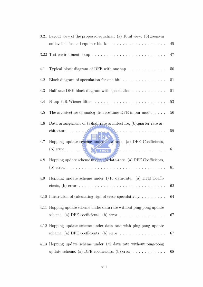
flexibility for adaptation design is an issue that we shall deal with.
With the data rate increases, the operation frequency of equalizer also needs
to push up. In this chapter, we will try to propose an equalizer system that can
compensate severe channel loss.
3.2 Motivation and the proposed architecture
In the model shown in Fig. 3.1, there is a high pass filter in the high-pass-
boosting path while the unity-gain path has gain block only. The gain block in
the unity-gain path will also affect the high-frequency gain. In an analog design,
all the design factors in one block will affect each other. That means there are at
least two parameters that can decide the high-frequency gain at the same time.
In other words, the low-frequency gain controlled by unity-gain path will affect
with high-frequency gain.
A way to minimize the dependence is to move the gain block of unity-gain
path out of the equalizer as shown in Fig. 3.2. The moved out block is series
connection with the equalizer. In this way, the two kinds of gain are covered by
two different blocks. The gain block in front of the equalizer determines the low-
frequency gain, and the equalization stage boosts high-frequency gain. Although
the response of any gain stage may cover a wide frequency range, a gain stage
only owns good performance at a particular frequency band. By using two gain
blocks, we can take the amplification consideration separately.
Figure 3.2: Equalizer model of our proposed equalizer
22

On the other hands, the characteristics of equalizer such as frequencies of
poles and zeros will be influenced by DC voltage level variation at the channel
output if the equalizer stage is connected to the channel directly. By allocating a
level-adjusting block between the equalizer stage and channel output, the effect
may be eased, even be released.
Fig. 3.3 shows the block diagram of our proposed equalizer. The differential
incoming signals attenuated through the wire are terminated using 50-Ω on-chip
resisters. The received signal is amplified and shifted to a DC signal level by the
level-shifter. Two cascade equalization stages are in the same common-source
like topology. Then the buffer amplifies the equalized signal amplitude to the
standard defined in the specification. All the blocks are fully-differential to reject
common-mode noise.
Figure 3.3: Block diagram of our proposed equalizer
Finally, the specification of the proposed equalizer is listed in Table 3.1
Table 3.1: Specification of proposed equalizer
Data Rate 6 GHz
Amplitude of transmitted
signal
±300 mV
Amplitude of output signal ±300 mV
23

3.3 Circuit design and simulation results
This section includes the details of circuit implementation and shows the
simulation results of each block and total system. The test chip is fabricated
with UMC 90 nm 1P9M 1V regular-Vt technology.
3.3.1 Level-Shifter
As mentioned in Section 3.2, the equalizer stage will suffer a great effect when
the DC voltage level in the equalizer input is not stable. Therefore, the proposed
design adds a level-shifter between the equalization stage and channel output.
Moreover, the supply voltage of our used technology is 1 V, and the margin for
signal swing is limited. Therefore, we need a circiut confine the DC voltage level
at equalizer input to a proper region. And the signal can have enough room to
swing.
Fig. 3.4 shows the circuit diagram of level-shifter. In order to guarantee the
level-shifter can ease the DC voltage level variation in equalizer input, we use poly
resister that has more stable impedance characteristics than active load. If we do
not add this level-shifter stage in front of equalizer stage, the ratio of DC voltage
level variation in the equalizer stage input to the one in the channel output is
one. The design goal of level-shifter is to reduce the ratio as small as possible.
The ideal value is zero, of course, because that means the DC level variation in
the channel output has no effect on the DC voltage level anymore.
The level-shifter circuit use fully-differentail architecture to reject the common-
mode noise. M3 and M4 work as the current source. The widths of these two
current source MOS are designed large enough to decrease the effective resis-
tance and increase the stability of the current. The bias voltage Vbn is supplied
by off-chip voltage source, and we choose the bias voltage as 0.3 mV. By the
specification of our proposed design, the amplitude of the transmitted signal is
24

±300 mV in differential. That is ±150 mV swing in single end signal. Therefore,
we will bias the output higher than 0.5 V to provide larger swing margin. The
resistance of two load resisters are chosen by biasing the DC output voltage of
level-shifter at 0.6 V. This level can provide some voltage margin for the later
two equalization stage.
Typically, the DC voltage level for a signal that has ±150 mV is chosen
at 0.85 V. So that the voltage range of the signal is from 0.7 V to 1 V. After
attenuation of channel, the DC voltage level in the channel output will be different
with the DC voltage level in the channel input. Therefore, the level-shifter needs
to have a flat curve for the relationship of output DC voltage level and input DC
voltage level when the input DC voltage is greater than 0.5 V or 0.6 V. In this
way, the level-shifter can work properly for a certain range of DC voltage level of
channel output.
Figure 3.4: Circuit diagram of level-shifter
Now, we sweep the DC voltage level in the level-shifter input, plot the curve
of DC voltage level in level-shifter output versus DC voltage level in level-shifter
output as shown in Fig. 3.5. In the figure we can observe that when the in-
25

put DC voltage is greater than about 500mV, the slope the curve is decreasing
dramatically. To estimate the slope of the segment:
slope ∼=583.3(mV ) − 650.8(mV )
1(V ) − 500(mV )= −0.135
We reduce the output variation to ten percent of the input variation. From the
results, the uncertain variable of DC voltage level variation in the channel output
is almost removed by the block of level-shifter.
Output Voltage (V)
600m
650m
700m
750m
800m
850m
900m
950m
1
Input Voltage (V)
0 200m 400m 600m 800m 1
Figure 3.5: Relationship between output and input DC voltage of the level-
shifter.
Beside easing the DC voltage variation, the level-shifter also has the function
to guarantee a basic low-frequency gain in total system. In the introduction of
the proposed architecture in Section 3.2, we move the function of low-frequency
amplification to the front of equalizer stage. We merge the amplification function
into the level-shifter. Fig. 3.6 shows the frequency reponse in the channel output
and in the level-shifter output. After the amplification of level-shifter, the low-
frequency gain at level-sifter output is about 10 dB. The channel bandwidth
(the -3 dB frequency) is at about 300 MHz. In the output of level-shifter, the
bandwidth is extended to about 1.3 GHz.
26

Ga
in (
dB
)
-60
-40
-20
0
10M 100M 1G 10G
Frequency (log) (HERTZ)
Response after level-shifter
Channel Response
Figure 3.6: Channel response and response after level-shifter
The level-shifter does not extends the bandwidth to the clock frequency
3GHz, but the level-shifter also provides some gain at 3GHz. The level-shifter
almost lifts all the response up under about 7GHz. That means the level-shifter
somehow provides some gain to help the equalizer minimizing the gain loss in the
response.
3.3.2 Equalizer stage
Analog equalizers as introduction in 2.2.1, they do equalization operation by
allocating a zero in the low frequency to produce a gain pulse in the frequency
response. The equalization filter in our equalizer stage use the topology that
introduces a zero in the source terminal of common-source amplifier as shown in
Fig. 3.7 [3].
M1 and M2 are as the active load in the circuit. M3 and M4 play the main
roles for the function of amplification. M5 and M6 are the current source part.
The resister Rm and capacitor C are the key elements to introduce the zero.
27

Figure 3.7: Circuit diagram of one equalizer stage
We will derive the transfer function of this equalizer stage by using the half
circuit scheme. The first part is to find the effective ground point in the circuit.
We assume the characteristics of M1, M3, and M5 are the same with M2, M4, and
M6. We model the current source as two resistors with ro of the two transistors,
and model the active load, M1 and M2 as two simple resistor load, Rp. The
circuit diagram is shown in Fig. 3.8(a).
Under the assumption of previous paragraph, the resistance of ro5 and ro6
should be the same. This means the source voltage of M3 and M4 are the same,
too. Then, the circuit can be further simplified as shown Fig. 3.8(b). We let the
current in the differential small-signal equivalent circuit is i, the following can be
derived
i = (vin − vs3)· gm3 = −(vin# − vs4)· gm4
⇒ (vin + vin#) = (vs3 + vs4) ∵ gm3 = gm4
∵ vin = vin# ∴ vs3 = −vs4
28

The equation vs3 = −vs4 says that the voltage in the two sides of the resistor and
capacitor is sysmetric to zero as shown in Fig. 3.8(b). If we split the resister into
two serial segments which have the same resistance, the voltage in the middle
point, G, of the two segments is equivalent ground point. The same manner can
also be applied to the capacitor as shown in Fig. 3.8(c).
Finally, we can get the half circuit of the equalizer stage as shown in Fig. 3.9.
Based on the half circuit, the transfer function is derived as follow:
vout#
vin= −gm3·
Rp
Rm
2 // 1s·2C
= −gm3·2Rp
Rm· (1 + sCRm) (3.1)
where Rp is the effective resistance of M1. From the tranfer equation, we can find
there is a zero that is used to produce the gain pulse in the frequency response.
The final version of the equalization stage is shown in Fig. 3.10. We replace
the resistor, Rm, with a NMOS which gate is connected to VDD. Moreover, in
order to improve the PMOS ability of pulling the output voltage up, each PMOS
for active load is shunt with another PMOS which gate is connected to the input
respectively as a negative resistor. The bias voltage of current source part uses
the same source as the level-shifter uses.
The equalizer block is composed of two cascade stages. The margin of in-
creasing frequency between the first zero and the first pole is limited. So, we
usually surpress a little low-frequency gain to get a sharp gain pulse in the fre-
quency response. If there is only one stage, the low-frequency gain will be surpress
too low while pushing the gain pulse. If we use two cascade stages, we can get a
sharp gain pulse in the final output while surpressing the low-frequency gain as
less as possible.
Fig. 3.11 shows the frequency response of the two equalization stages and
the total frequency response. Because the two stages suffer different input and
output loading, the two stage will have different zeros and poles frequency. In
the first equalization stage, the frequency of first zero is at about 755 MHz, and
29

(a) (b)
(c)
Figure 3.8: Small signal circuit of equalizer. (a) Simplified equivalent small-
signal model. (b) Further simplified equivalent small-signal model. (c) Virtual
ground in equivalent small-signal model.
the stage has a real zero at about 1.95 GHz and a pair of complex zero at about
2.6 GHz. On the other hand, the first stage has two pair of complex poles at
about 1.41 GHz and 2.96 GHz. There is also a real pole at 2.39 GHz. Therefore,
we can observe that the frequency response of first equalization stage decreases
dramatically after the gain peak frequency.
In the second equalization stage, the frequencies of first two zeros are at
about 790 MHz and 3.89 GHz. While the frequencies of first two poles are at
about 2 GHz and 3.9 GHz. The second stage owns the first pole and the first
30

Figure 3.9: Half circuit of equalizers.
Figure 3.10: Final circuit of equalization stage
zero at the frequency higher than the first stage owns. We push the gain pulse
of the second stage to higher frequency than the gain pulse of the first stage.
Moreover, by minimizing the gate capacitance of the first buffer stage, loading
in the output of the second equalization stage is dominated by the stage itself.
We can push the frequency of poles to higher frequency. So that the trend of
decreasing in the second stage response will not be so dramatically as the first
31

Ga
in (
dB
)
-6
-4
-2
0
2
4
6
8
Frequency (log) (HERTZ)
10M 100M 1G 10G
Second stage
Total response
First stage
Figure 3.11: Frequency dependence of gain in each equalization stage and total
response.
stage. These two methods let the second stage provide more compensation ability
at high frequency than the first stage provides as shown in Fig. 3.11.
In Fig. 3.11 we can also find that the equalizer contributes nagative gain value
under the frequency about 400 MHz. As our architecture decribed in Section 3.2,
the low-frequency gain is dominated by the level-shifter stage. The equalizer
introduces the gain boosting in high frequency, and the low-frequency gain will
be provided by the level-shifter. Fig. 3.12 shows the response of the equalizer
stage and the total response of level-shifter and equalizer stage. The level-shifter
amplifies the low-frequency gain about 9.5 dB, and the effect of amplification also
extend to the frequency of gain pulse. On the other words, the level-shifter not
only provides the gain in low frequency but also contributes amplification in high
frequency. However, the difference between equalizers and amplifiers is that the
equalizers can cancel the ISI components in signal while amlifiers just amplify the
32

signal without any correction mechanism. The level-shifter just lifts the response
up through a limited frequency, it can not extend the flatten response towards
high frequency. The gain pulse used to flat the response is still provieded by the
equalizer stage.
Ga
in (
dB
)
-6
-4
-2
0
2
4
6
8
10
12
14
16
Frequency (log) (HERTZ)
10M 100M 1G 10G
Response of level-shifter & EQ
Response of EQ
Figure 3.12: Response of equalizer stage and combination of level-shifter and
equalizer.
The final frequency response in the equalizer output is shown in Fig. 3.13.
Our proposed equalizer is under the 6GHz system. The clock rate is 3GHz. In
Fig. 3.13, the channel response is -25.35dB at 3GHz. After compensation by
our equalizer, the response at 3GHz is -11.48dB. The proposed equalizer recovers
13.87dB channel loss.
In Fig. 3.14, we show the group delay in the equalizer output. We know
that the group delay is the differential of the phase response. Therefore, for a
linear phase response system, the group delay should be a constant. In Fig. 3.14
we can observe that when the frequency is small than xxGHz, the group delay
33

Ga
in (
dB
)
-80
-70
-60
-50
-40
-30
-20
-10
0
10
Frequency (log) (HERTZ)
10M 100M 1G 10G
Response at EQ output
Channel response
Figure 3.13: Frequency response of channel output and equalizer output.
is almost a constant. That means the proposed equalizer does not introduce too
much phase distortion.
However, the signal is used in time domain for system application. The effect
of equalization can not be measured just in the frequency domain. Therefore,
the performance in the time domain is most important because the meaning of
equalizer is to corrent the signal distorted in the channel. The goal of our equalizer
in time domain is to open the data amplitude to ±300mV. The specification of the
proposed system is to transmit data with ±300mV, so that we need to recover the
received data amplitude amplitude as much as possible. If the signal amplitude
can not reach ±300mV, the buffer stage will amplify the signal to the goal.The
signal in the output of equalizer stage is been equalized, even if the amplitude do
not reach the specification. The buffer stage just amplifies the equalized signal
amplitude to meet the requirment in specification.
We use the RLGC element in HSPICE to fit the reponse of a HDMI cable.
34

Gro
up
Del
ay
(S
ec)
-100n
-80n
-60n
-40n
-20n
0
20n
40n
Frequency (log) (HERTZ)10x
100x 1g10g
Figure 3.14: Group delay in the equalizer output
We change the length of the channel model to get about the -25dB channel loss
at the clock frequency 3GHz under 6GHz data rate. Base on this channel model,
we apply psuedorandom bit sequence (PRBS) pattern to the channel input and
observe the eye diagram of three points: channel output, equalizer output, and
buffer output. The PRBS pattern is set to have ±300 mV swing with 6 Gbps
and the length of the PRBS pattern is 1000 bits. Fig. 3.15 shows the eye diagram
of pre-layout simulation. Fig. 3.15(a) shows the diagram of channel output. Due
to the channel loss, the signal is hard to be distinguished. Fig. 3.15(b) shows
that the equalizer opens the data eye to about ±280 mV. The peak-to-peak
jitter of the eye at the equalizer output is 22.85 ps and the RMS jitter is 7.47
ps, and the jitter histogram is shown in Fig. 3.16(a). The equalized signal is
further amplified by buffer stage to ±300 mV swing, as shown in Fig. 3.15(c). At
buffer output, the data eye has peak-to-peak jitter of 22.96 ps and RMS jitter
is 7.51 ps, and the jitter histogram is shown in Fig. 3.16(b). The buffer stage
introduces about 0.1 ps peak-to-peak jitter to the data eye. The design goal of
35

buffer is also to push the loadings including bounding line and connectors in the
measurement environment. If we just need to amplify and shape the output eye
to the specification, we do not need to design such a buffer stage that with large
driving ability.
36

Am
pli
tud
e (V
)
-400m
-200m
0
200m
400m
Time (sec)0
200p
(a)
Am
pli
tud
e (V
)
-400m
-200m
0
400m
Time (sec)
0200p
200m
(b)
Am
pli
tud
e (V
)
-300m
-200m
-100m
0
100m
200m
300m
Time (sec)0
200p
(c)
Figure 3.15: Eye diagram of pre-layout simulation: (a) channel output. (b)
equalizer output. (c) buffer output
37

(a)
(b)
Figure 3.16: Jitter histogram of pre-layout simulation: (a) equalizer output.
(b) buffer output
38

3.4 Implementation and layout
The layout of proposed design is based on UMC 90 nm 1P9M 1 V techonol-
ogy. In order to minimize the the parasitical effect, we try to reduce the distance
betweeen level-shifter block and equalizer block. Therefore, the interconnection
between these two blocks can be minimized. On the other hands, the routing
of differential signal line takes the length of line into consideration. We try to
minimize the difference between two line length in a pair of differential signal line.
So that the time of differential signal traveling on the line can be almost the same
to minimize the time skew issue. In each block, the circuit is fully differential.
We also use parallel MOS to minimize the effect of process variation.
Fig. 3.17 shows the eye diagram of the post-layout simulation in three points:
channel output, equalizer output, and buffer output. Comparing with the pre-
layout simulation, the eye diagram in the equalizer output is small in the post
layout simulation. The eye open is about ±250 mV in the post-layout simulation
as shown in Fig. 3.17(b). The peak-to-peak jitter of data eye is 25.53 ps, the
RMS jitter is 8.89 ps and the jitter histogram is shown in Fig. 3.18(a). We can
not avoiding the effect of parasitical elements although we try to minimize these
in the layout. Fig. 3.17(c) shows the post-layout eye diagram of buffer output.
In the buffer output, the data eye can open to ±300 mV with peak-to-peak
jitter of 26.71 ps, the RMS jitter is 8.94 ps, and the jitter histogram is shown in
Fig. 3.18(b).
All the simulation results above is based on the TT corner condition. The
simulation based on FF and SS corn conditions are shown in Fig. 3.19 and
Fig. 3.20. We can find that the eye diagram in the equalizer output still can
open the data eye to at least ±200 mV, but the buffer stage that drives the
output loading perform not well in FF and SS corner conditions.
39

Am
pli
tud
e (V
)
-400m
-200m
0
200m
400m
Time (sec)0
200p
(a)
Am
pli
tud
e (V
)
-400m
-200m
0
200m
400m
Time (sec)
0200p
(b)
Am
pli
tud
e (V
)
-400m
-300m
-200m
-100m
0
100m
200m
300m
400m
Time (sec)
0200p
(c)
Figure 3.17: Eye diagram of post-layout simulation under TT corner condition:
(a) channel output. (b) equalizer output. (c) buffer output
40

(a)
(b)
Figure 3.18: Jitter histogram of post-layout simulation under TT corner con-
dition: (a) equalizer output. (b) buffer output
41

Am
pli
tud
e (V
)
-400m
-200m
0
200m
400m
Time (sec)0
200p
(a)
Am
pli
tud
e (V
)
-300m
-200m
-100m
0
100m
200m
300m
Time (sec)0
200p
(b)
Am
pli
tud
e (V
)
-600m
-400m
-200m
0
200m
400m
Time (sec)0
200p
(c)
Figure 3.19: Eye diagram of post-layout simulation under FF corner condition:
(a) channel output. (b) equalizer output. (c) buffer output
42

Am
pli
tud
e (V
)
-400m
-200m
0
200m
400m
Time (sec)0
200p
(a)
Am
pli
tud
e (V
)
-400m
-200m
0
200m
400m
Time (sec)0
200p
(b)
Am
pli
tud
e (V
)
-250m
-200m
-150m
-100m
-50m
0
50m
100m
150m
200m
250m
Time (sec)0
200p
(c)
Figure 3.20: Eye diagram of post-layout simulation under SS corner condition:
(a) channel output. (b) equalizer output. (c) buffer output
43

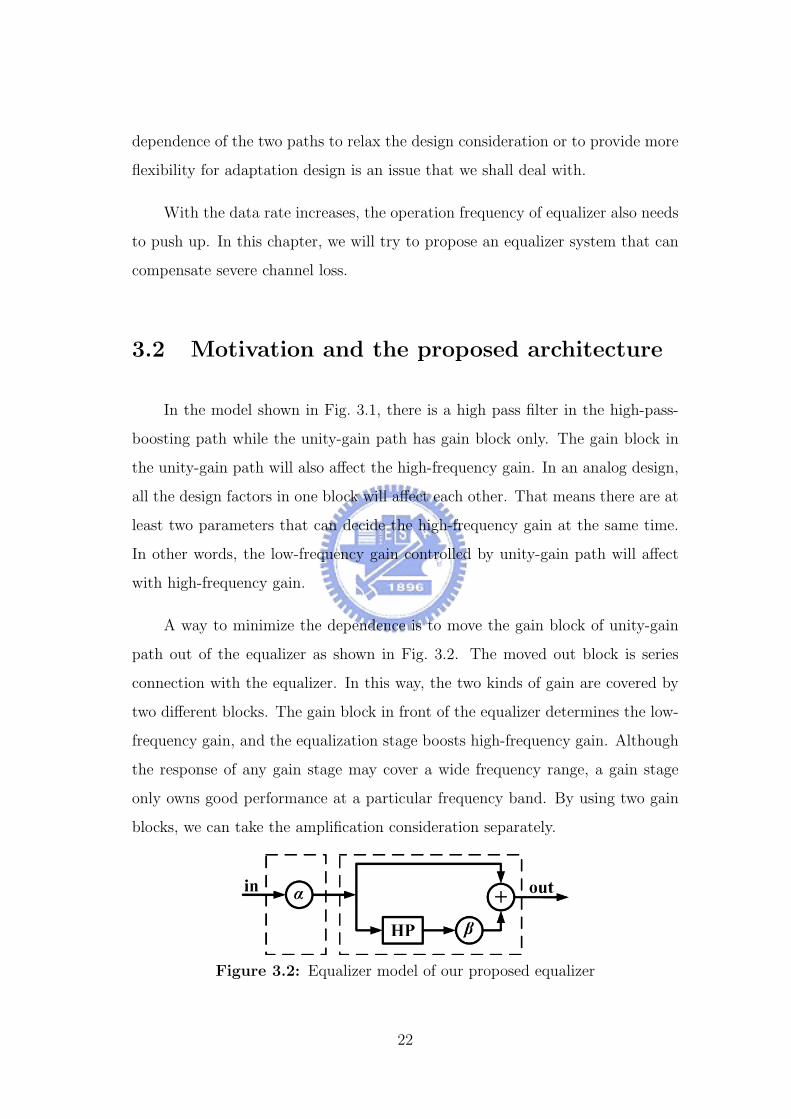
The layout picture and pad assignment are shown in Fig. 3.21(a) and Table
3.3. In order to increase the ability of measurement control, we add a NMOS
parallel with the Mr in each stage to provide a chance of altering the effective
resistance. The gates of these two NMOS are controlled by signal out of chip
through Pad 1 and Pad 12. The core size of level-shifter and two equalizer stage
is 0.058× 0.058 mm2 as shown in Fig. 3.21(b). The total chip area including the
buffer stage and pads is 0.49 × 0.49 mm2. The power consumption is 78.83 mW
when operating at 6 GHz. The summary of the test chip information is list in
Table 3.3 and a comparison is given in Table 3.4.
Table 3.2: Pad assignment
Pad Function Pad Function
1 Gain control of 1st equalizer
stage
7 VDD for circuit
2, 3 signal differential output 8, 9 Signal differential input
4 Ground for circuit 10 Bias voltage for level-shifter
and equalizers
5 Vdd for guard ring 11 Ground for guard ring
6 Bias voltage for buffer stage 12 Gain control of 2nd equalizer
stage
44
(a)
(b)
Figure 3.21: Layout view of the proposed equalizer. (a) Total view. (b) zoom-in
on level-shifer and equlizer block.
45

Table 3.3: Summary of proposed test chip
Supply voltage 1 V
Data Rate 6 GHz
Transmitted signal amplidute ±300 mV
Equalized signal amplitude about ±250 mV
Total power consumption @ 6GHz 78.83 mW
- Level-shifter 1.60 mW
- Equalizer stage 1.39 mW
- Buffer stage 75.84 mW
Total chip area 0.49 × 0.49 mm2
- core area 0.053 × 0.053 mm2
-level-shifter 0.031 × 0.015 mm2
-Equalizer stage 0.060 × 0.039 mm2
- buffer stage 0.026 × 0.026 mm2
Number of pad 12
Table 3.4: Comparison with other works
Our design [2] [3]
Technology UMC 90 nm TSMC 0.18 µm 0.11 µm
Supply Voltage 1.0 V 1.8 V 1.2 V
Data Rate 6 Gb/s 3.5 Gb/s 10 Gb/s
Power consumption 3.79mW(core,
1st buffer)/78.83
mW(total)
80 mW 13 mW
Loss Compensation 13.87 dB N/A 20 dB
Core Area 0.058×0.058 mm2 0.48×0.73 mm2 0.047×0.085 mm2
Transmitted dadta 300 mVp-p N/A 600 mVp-p
Equalized eye diagram 250 mVp-p N/A 80mVp-p
46

3.5 Measurement environment setup
All DC supply sources are given from Keithley 2400 Source Meter. Agilent
N4906B Serial J-BERT provides the 6 GHz transmitted signal to our channel.
The output signal from our test chip is fed back to it to calculate the bit-error rate
(BER). Tektronics TDS6124C Digital Storage Oscilloscope measures the wave-
form and the eye diagram in the test chip output. The overall setup environment
is shown in Fig. 3.22.
Figure 3.22: Test environment setup
47

Chapter 4
Discrete-Time equalizer
In chapter 4, we will focus on the deisgn of discrete-time equalizer for multi-
Gbps applications. In section 4.1, we give an overview of discrete-time equalizer
and outline the topics that we will focus on. A brief introduction and compar-
ison of several previous works are given in section 4.2. Sign-Sign least mean
square (Sign-Sign LMS) algorithm is commonly used for adaptation of equalizer
coefficients. We will give a brief derivation in 4.3. Based on the architectures
introduced in section 4.2, we model the behavior of multi-sampling architecture
with speculation in MATLAB. We will explore the selection of some design pa-
rameters. From these simulation results, we can setup the design guideline for
discrete-time equalizer. The details are shown in section 4.4.
4.1 Overview
Discrete-time equalizers have two different types. One is analog discrete-
time equalizers that process the signal in analog domain, the other is digital
discrete-time equalizers that use the analog-to-digital converter (ADC) to change
the analog signal to digital and process the digitized signal. Analog discrete-
time equalizers have better performance than the digital discrete-time equalizers
in high speed application, because the high speed or high resolution design of
ADC is an challenge. In this chapter, the discussion will focus on the analog
discrete-time equalizers.
Decision feedback equalizer (DFE) will use the past data to compensate the
received signal. The system can also use these past data to adjust the equalizer
48

weighting or equalizer coefficients. Moreover, the DFE has better performance
than linear equalizer based on the derivation in section 2.2.2. We will choose the
DFE topology as the topic in this section.
The discrete-time equalizer also has a property that the discrete-time topol-
ogy can parallel the data paths to slow down the operation frequency. However,
there are some problems when the parallel architecture combines with the DFE
mechanism. Some techniques were proposed to solve the problem, especially the
timing issue. In section 4.2 will give a brief introduction for these previous works.
For the adaption of DFE coefficients, some adaption algorithms were men-
tioned in the field of adaptive filter. One simple and commonly used algorithm is
Sign-Sign LMS algorithm. It is a simplified version of least mean square (LMS)
algorithm. A detail derivation will be given in section 4.3. We will use the
sign-sign LMS algorithm as our algorithm for adaptation of DFE coefficients.
Based on the architecture of analog discrete-time equalizer having parallel
data paths with coefficients adaptation mechanism, we build the mathematical
model with MATLAB. Using this model, we analyze the equalizer performance
by considering of several design parameters under area and power limitation. We
setup a guideline to choose the design parameters based on the analysis.
4.2 Techniques and architectures for discrete-
time DFE
We consider a simple DFE with one tap for cancellation of ISI, its block dia-
gram is shown in Fig. 4.1. The data in the slicer output needs to be ready before
the coming of next sampled data. With the data rate increasing, to complete all
the operation in one bit time is really a challenge. A common solution to deal
with the timing issue is speculation or look-ahead technique [18].
49

Figure 4.1: Typical block diagram of DFE with one tap
Because the DFE is simplified to one tap, the addition operation can be
cancelled by changing the comparator threshold with the feedback data. However,
this replacement does not change the original loop and the timing issue still exists.
Moreover, the data in the slicer output is Boolean, we can split the comparator
into two comparators. One has the threshold voltage that based on guessing the
slicer output is one, the other has the threshold voltage that based on guessing
the slicer output is zero. The block diagram is shown in Fig.4.2 [18]. We see that
the n-th bit is given by
an = Anan−1 + Bnan−1 (4.1)
where An and Bn are outputs of the two comparators at the n-th symbol period,
and a means the complement of a.
In equation 4.1, an is in terms of an−1. We can further replace an−1 with
an−2 by the relation that an−1 = An−1an−2 + Bn−1an−2, and we get
an = An(An−1an−2 + Bn−1an−2) + Bn(An−1an−2 + Bn−1an−2)
= (AnAn−1 + BnAn−1)an−2 + (AnBn−1 + BnBn−1) (4.2)
Equation 4.2 represents an in terms of an−2. If we implement the DFE based
on equation 4.1, we have total one bit time for all the operation. However, if
50

we implement the DFE by equation 4.2, there is total two bit period to do all
the operation. Of course, we can get more time to do operation by expand the
equation by an−3, an−4, . . . . But the hardware area will increase dramatically at
the same time.
Figure 4.2: Block diagram of speculation for one bit
The other method of increasing the operation time is to duplicate the circuit
in Fig. 4.2 and to control the selector of each other [13] as shown in Fig. 4.3. The
method combine the descrete-time equalizer characteristic that arranges data of
different time index to several data path and the speculation techniques. The
method needs no large amount of digital logic blocks, and the speculation bit is
only one bit. However, the time for operation is still two bit time.
Figure 4.3: Half-rate DFE block diagram with speculation
51

4.3 Sign-sign least-mean-square algorithm
The sign-sign least-mean-square algorithm is a simplification of least-mean-
square algorithm. In this section, we will give a short derivation of least-mean-
square algorithm [19]. Then the relationship between LMS algorithm and sign-
sign LMS algorithm will be pointed out.
The DFE is actually a adaptive finite-duration impulse response (FIR) filter.
In adaptive filter theory, the optimum tap-weights, DFE coefficients, of a FIR
filter can be obtained by solving the Wiener-Hopf equation. An alternative way
of finding the optimum tap-weights is to use an interactive search algorithm
that starts at some arbitrary initial point in the tap-weight vector space and
progressively moves toward the optimum point in steps. The LMS algorithm is
an adaptive algorithm, that uses a gradient-based iterative method called method
of steepest descent. The LMS algorithm is derived for minimizing a cost function
with the true statistics replaced by an estimation.
4.3.1 Method of steepest descent
A N-tap FIR Wiener filter is shown in Fig. 4.4, we assume all the data
involved are real-value.
In the figure, d(n) is the desired response or the correct output that we
expect. We can define four parameters as follows:
tap-weight vector: W = [Wo W1 . . . WN−1]T ,
signal input: x(n) = [x(n) x(n − 1) . . . x(n − N + 1)]T ,
filter output: y(n) = wT x(n),
error signal: e(n) = d(n) − y(n).
The cost function is defined as the mean-square error
J = E[e2(n)
]= E
[d2(n)
]− 2W
Tp + W
TRW
52

Figure 4.4: N-tap FIR Wiener filter
where R = E[x(n)xT (n)
]is autocorrelation of the filter input.
The cost function J is a quadratic function of the filter tap-weight vector W.
J has a single global minimum obtained by solving the Wiener-Hopf equation
Rwo = p
if R and p are available, where w0 is the optimal tap-weight vector. However, we
can use iterative method rather than solving the Wiener-Hopf equation directly.
Starting with an initial guess for W0, say W(0), a recursive search method that
may require many iterations to converge to w0 is used.
The method of steepest-descent is a gradient-based method. Using the initial
or present guess, we compute the gradient vector and evaluate the next guess of
the tap-weight vector by making a change in the initial or present guess in a
direction opposite to that of the gradient vector. Here, we define the gradient of
J as
5J = 2RW − 2p (4.3)
53

With an initial guess of W0 at n = 0 the tap-weight vector at the k -th iteration
is denoted as W(k). We can write down the recursive equation that is used to
update W (k)
W(k + 1) = Wk − µ 5k J (4.4)
where µ > 0 is called the step-size, 5kJ denotes the gradient vector 5k ecaluated
at the point W = W(k).
If we substitute equation 4.3 into equation 4.4, we get
W(k + 1) = W(k) − 2µ(RW(k) − p) (4.5)
By equation 4.5, W(k) will converge to the optimum solution w0 and the con-
vergence speed are dependent on the step-size parameter µ.
4.3.2 Sign-sign LMS algorithm
In this subsection, we will derive the LMS algorithm first and the sign-sign
LMS algorithm will be given later.
The conventional LMS algorithm is a stochastic implementation of the steep-
est descent algorithm. It simply replaces the cost function J = E [e2(n)] by its
instantaneous coarse estimate J = e2(n). By substituting the simplified cost
function into equation 4.4, we can obtain
W(n + 1) = W(n) − µ 5 e2(n) (4.6)
where,
w = [Wo(n) W1(n) . . . WN−1(n)]T
5 =[
∂∂W0
∂∂W1
. . . ∂∂WN−1
]T
54

We can expand the i -th element of the gradient vector 5e2(n) as
∂e2(n)
∂Wi= 2e(n)
∂(n)
∂Wi= −2e(n)
∂y(n)
∂Wi= −2e(n)x(n − i)
then, we will get
5e2(n) = −2e(n)x(n) (4.7)
where x(n) = [x(n) x(n − 1) . . . x(n − N + 1)]T .
Finally, we can get the LMS recursion that tells the tap-weight recursion by
substitute equation 4.7 into equation 4.6,
W(n + 1) = W(n) + 2µe(n)x(n) (4.8)
Equation 4.8 describes the relationship between the new tap-weight and the
current tap-weight of LMS algorithm. The sign-sign LMS algorithm is to simplify
the recursion of LMS further. To use the sign of e(n) and x(n) rather than
the actual value of them can further simplify the tap-weight calculation. The
recursion of sign-sign LMS becomes
W(n + 1) = W(n) + 2 · µ · sign(e(n))sign(x(n)) (4.9)
where, the sign() is the function that gets the sign of input.
4.4 Design parameters selection based on power
and area consideration
In this section, we will explore the design parameters selection based on
power and area consideration. On power consideration, the main issue is to
slow down the updating frequency of equalizer coefficients. This method may
loss some information to update the coefficients of equalizer, and the coefficients
55

updating may need a long convergence time. However, the time penalty will not
be too much due to the increasing of data rate. On area consideration, we try to
reduce some circuit blocks so that some information for updating the coefficients
of equalizer will not perform but with little or no performance penalty. The
performance analysis will be given under such reducing. Moreover, an analysis of
combination of the two methods to find the limitation is also given.
4.4.1 Architecture in our model
The architecture we use in our model is shown in Fig. 4.5 [8]. The archi-
tecture has two data paths with each operating at half of data rate. It use the
look-ahead technique for 1 bit to relax the timing issue that is mentioned in sec-
tion 4.2. This example of architecture uses five taps of past data to cancel the
ISI. One of the five taps data (an−1) is canceled in the look-ahead part, the other
four taps data is kept in the registers controled by alternative arranged clock.
Figure 4.5: The architecture of analog discrete-time DFE in our model
Received data an is sampled by sampler and is passed to the two data paths.
The sampled data adds with the past data, an−2-an−5, that is well decided in the
summer S1. Then the summation output goes into two look-ahead paths. One
56

path adds the value based on guessing the bit an−1 is high; the other path add
the value for the opposite assumption. When the clock is high, the output of S2
will go into the MUX and is selected by the previous data an−1 that is decided in
the previous low clock. The selected data is in the MUX output until the clock is
negative. When the negative is coming, the first register L1U in upper path will
save the data waiting in the MUX output and shift the data in second register
L2U to third register L3U. Because the second register L2U will need to save the
data in the first register L1U at the coming high clock. While in the lower path,
the new data is selected and waits in the MUX output. The second register L2D
needs to save the data of the first register L1D in the lower path, because the
first register L1D in the lower path will keep the data in the MUX output in the
coming high clock.
By keeping the data alternatively in these registers, there are four decided
taps of past data an−2-an−5. Adding the look-ahead mechanism, the architecture
covers five taps to cancel the ISI. The equalizer coefficients, or equalizer weights,
in the model are also adapted by sign-sign LMS algorithm. On the other hand,
the value expressed in the circuit should be quantized. The weights must be
quantized to fixed bits. Our model also take this issue into consideration. We
use ten bits to quantize the coefficient in all the simulation. The other important
parameter is the step size for adaption algorithm. We choose the step size µ
as 2−9 that is small enough to make the sign-sign LMS algorithm converge by
simulations.
In the consideration of clock source, the clock source is usually provided
by the phase-lock loop (PLL) in a system. In a PLL, the oscillator is often
implemented by ring oscillator. For each stage of ring oscillator is fully-differetial,
we can get even number phase of clock signal. For the consideration of clock
source and operation frequency of DFE, the quarter-rate architecture is usually
a popular solution.
If we expand the half-rate architecture to quarter-rate architecture by dupli-
57

cating the circuit in Fig. 4.5 to two copies, the mathematical behavior is the same
with the half-rate model. Fig. 4.6(a) shows the data displacement of half-rate ar-
chitecture. The odd index of data passes the upper data path while the even
index of data passes the lower data path. In the case of quarter-rate architecture,
the odd index of data will pass the top path and the one that is duplication of
the top path. The even index of data has the same situation of arrangement as
shown in Fig. 4.6(b). Therefore, we know that with the same architecture, the
mathematical behaviors of half-rate and quarter-rate architecture are the same.
The difference between these two architectures is the operation frequency. The
quarter-rate version has the lower operation frequency (fs/4) for each data path.
When generation of a high-frequency clock is a big issue, we usually need to slow
down the system operation frequency. In summary, our model is not only for
half-rate architecture but also for quarter-rate architecture.
In all the simulations, 10 Gb/s pseudo random bit sequence (PRBS) are
generated and passed through a channel presented in [8]. All the following com-
parisons are made under the same input pattern.
4.4.2 Hopping coefficients update scheme
The power consumes by a circuit can be expressed as the following equation
P = C · V DD2 · f · pt
where,
C: the output loading capacitance,
V DD: the voltage of power supply,
f : the circuit operation frequency.
pt: the probability of switching activity.
In this subsection, we analyze the equalizer performance based on the power
reduction consideration.
58

(a)
(b)
Figure 4.6: Data arrangement of (a)half-rate architecture, (b)quarter-rate ar-
chitecture
Typical adaptive mechanism for adaptive equalizer is to update the weights of
equalizer per bit of data. This method takes every information into consideration
and converges the circuit toward stable state within the shortest time in the
begining of the transmission. However, from the view of hardware operation,
updating the weights of equalizer per bit data means the adaptation circuit in
the equalizer needs operating at data rate. With the increasing of data rate, this
mechanism will introduce a large power consumption for adaptation circuit once
the system is in the stable conditions.
By parallelling data paths, the operation frequency of each data path has
been slowed down. The only part that operates at full speed is the weights adap-
tation block. Obviously, an effective solution of reducing the power consumption
59

is to find some strategy for the weights adaptation block.
In fact, updating the weights of equalizer per bit of data is too greedy. The
transmitted data is often independent between each other and we do not need to
worry about losing the correlation information if we ignore some bits. From the
theory of sign-sign LMS algorithm, we know that the convergence of the sign-
sign LMS algorithm only depend on the step size µ. Therefore, we can choose
some bits from the received sequence as a new received sequence for finding the
characteristics of the channel. On other words, we can use the new received
sequence to update these coefficients of the DFE. From the circuit operation of
view, this method is to update the coefficients of DFE every perticular number
of bits. For example, we choose the bits with time indexes that are equal to a
multiple of eight as a new sequence to update the coefficients of DFE. In circuit
operation, this mechanism is equal to update the coefficients of DFE per eight
bits of reveived data. That means we slow down the operation frequency of
coefficients updating block to eighth of data tranmission frequency.
Although the time of coefficients convergence time will increase in the be-
gining of transmission time if we choose these bits for a long period, we can find
a maximum rate to slow down the coefficients update frequency within the re-
quirement of convergence time. Our simulation will take three coefficients update
frequencies: per bit, per four bits and per sixteen bits. By these three simulations,
we can observe the increase of convergence time while the coefficients update fre-
quency decreases. And we can find the guideline of setup the maximum rate of
slowing down the coeffecients update frequency in a DFE system.
Our simulation takes three conditions into consideration: updating the co-
efficients, or called weights, per bit, per four bits, per sixteen bits. That is
equivalent to divide the operation frequency by 1, by 4, and by 16 respectively.
Fig. 4.7 shows the change of coefficients, and amount of error with time of the
equalizer under data-rate updating. The error is defined as the value difference
between slicer input and slicer output. From the weights change plot we can
60

observe the convergence situation of equalizer weights. And the error plot can
reflect what the adaptation algorithm wants to minimize. Fig. 4.8 shows the
simulation results under quarter of data-rate adaptation. And the result under
sixteenth data-rate adaptation is shown in Fig. 4.9
(a)
(b)
Figure 4.7: Hopping update scheme under data-rate. (a) DFE Coefficients, (b)
error.
(a)
(b)
Figure 4.8: Hopping update scheme under 1/4 data-rate. (a) DFE Coefficients,
(b) error.
61

(a)
(b)
Figure 4.9: Hopping update scheme under 1/16 data-rate. (a) DFE Coefficients,
(b) error.
From Fig. 4.7 to Fig. 4.9, we can find the convergence time increases with
reducing of adaptation frequency. That means slowing down the adaptation fre-
quency indeed delay the convergence duration. We calculate the mean of absolute
error value (Eave) when the coefficients are convergence. From the figure of error
amount, we can measure the coefficients convergence time (Tcon) when the error
reduces into the range of ±0.5. The reason of choosing ±0.5 is that the tranmit-
ted pattern is ±1, and the decision threshold is zero. We list out the Eave and
Tcon of these three simulations as shown in Fig. 4.7 to Fig. 4.9 in Table 4.1.
Table 4.1: Eave and Tcon for hopping update scheme under three different data
rate
adaptation frequency (data-rate) 1 1/4 1/16
mean of absolute error value (Eave) 0.2419 0.2452 0.2441
Convergence time (bit) (Tcon) 2600 4450 17450
62

From Table 4.1, the three cases have roughly the same Eave when the coef-
ficients converge. But in the performance of convergence time, the case of 1/16
data-rate adaptation has Tcon that is triple for the case of data-rate adaptation.
In these simulation results the coefficients are converged, however, the case of
1/16 data-rate adaption has 15000 bit time. And from the error plot we can find
that the Eave is toward the nagetive side when the coefficients are not converged.
The reason is that the update frequency of coefficients decreases. So that the
data are equalized to plus or minus direction for a long time. And the time is
long enough to observation in the plot.
From these simulation results, we can derive a concept of dynamic coef-
ficients update scheme. We can choose the slowest data rate for the hopping
update scheme. Therefore, the power consumption can be minimized during the
coefficients convergence time. Because the characteristic of channel varies slowly
that may be the order of millisecond, the DFE does not need to update the coef-
ficients frequently. On the other words, we can increase the period of coefficient
update after the coefficients are converged to save more power consumption.
4.4.3 Ping-pong coefficients update scheme
The DFE architecture as shown in Fig. 2.8(b), the error can be calculated
until the output of slicer is stable. The error or the sign of error will be passed
to the adaptation block, and the adaptation block needs to calculate the new
weights immediately if updating coefficients every bit. In real implementation,
the clock period is too short to calculate so many operations.
A typical circuit implementation is to calculate the error or sign of error when
the data is sampled in. Like the speculation technique, the circuit calculates two
sign of error based on guessing the sampled data is high or low. When the sampled
data is equalized, the sigh of error can also be chosen. Fig. 4.10 illustrates the
concept of calculating sign of error speculatively.
63

Figure 4.10: Illustration of calculating sign of error speculatively.
In the architecture that we use in our model there are two parallel data
paths. Each path has the same probability of processing high and low data for
PRBS input pattern. That means these two calculated sign of error based on
guessing the sampled data will be selected in equal probability in each data path.
Therefore, we can consider a mechanism that calculates one sign of error in each
path. In the simulation we calculate the sign of error when the processed data is
high in the upper data paths. On the other hand, the lower path calculates the
sign of error when the processed data is low. If the sign of error is not calculated,
the equalizer coefficients keep its current value. We simulate this mechanism
under five different coefficient adaptation frequency. The simulation results are
shown from Fig. 4.11 to Fig. 4.20. The figures that are under the same hopping
update rate uses the same input sequence to make sure the comparison basis is
fair.
In Fig. 4.11 and Fig. 4.12, the equalizer coefficients convergence time and
error is similar in original case and the case with ping-pong update scheme. If we
divide the hopping update rate to half of data rate, the result starts to have differ-
ence. The coefficients convergence time of Fig. 4.13 is shorter than it of Fig. 4.14.
64
That means reducing the calculation of sign of error really loses some information
for coefficients adaptation and extends the convergence duration. The case of 1/4
adaptation frequency as shown in Fig. 4.15 and Fig. 4.15, coefficients convergence
time delay phenomenon is more obvious than the two previous cases. Moreover,
in the cases of 1/8 and 1/16 hopping update rate, the error is bias when the
coefficients do not converge. Following the same principle, we list the Eave and
Tcon in Table 4.2.
In fact, we can consider the mechanism as a modification of slowing down
the coefficients adaptation frequency. Although the mechanism do not really slow
down the coefficients adaptation block operation frequency, the coefficients will
be updated based on the value of input data. We can call the mechanism as data
dependent coefficients update strategy. In a communication system that guaran-
tees the transitions of data sequence, the strategy will be appropriate because the
two data paths will process high and low data in nearly equal probability. From
the simulation results of subsection 4.4.2, we observe that adaptation system can
work properly even if a part of information is lost. The proposed scheme is under
such concept to reduce some hardware blocks. For the data sequence that is often
model as PRBS, the two paths will have the same probability to calculate the
sigh of error for update equalizer coefficients. That means the calculation will
not be halt for a long period.
Because the input data sequences are different in the five situations of dif-
ferent coefficients adaptation frequency, we show a simulation that adopts the
ping-pong coefficients update scheme under three different bits for hopping coef-
ficients update scheme, hopping per bit, per 4 bits, and per 16 bits in Fig 4.21
to Fig. 4.23. The three cases are under the same input data sequence. The Eave
and Tcon of these three simulations are listed in Table 4.3. Moreover, for the
considering of some popular application in serial link, we also run the same simu-
lation that uses the 8b/10b encoding data as the input data sequence as shown in
Fig 4.24 to Fig. 4.26, and the Eave and Tcon of these three simulations are listed
65

in Table 4.4. We can find that the value of Eave and Tcon of 8b/10b input data
sequency have similar performance with that of PRBS input data sequence. The
8b/10b encoding pattern will guarantee the transition per 5 bits. These transi-
tions will increase the probability of error calculation in the ping-pong coefficients
update scheme.
For the hopping coefficients update scheme, we can reduce the power con-
sumption of coefficients update block. The original update frequency is equal
to the data rate fs. Under the hopping coefficients update scheme, the update
frequency can be divided by how many bits the coefficients update once. That
means the power can be save for the same ratio due the power consumption is
proportional to the operation frequency. The ping-pong update scheme can save
one comparator that calculates the sign error in each data path. In the case of
the architecture in our model, the saving is two comparators due to the half-rate
architecture.
66

(a)
(b)
Figure 4.11: Hopping update scheme under data rate without ping-pong update
scheme. (a) DFE coefficients. (b) error
(a)
(b)
Figure 4.12: Hopping update scheme under data rate with ping-pong update
scheme. (a) DFE coefficients. (b) error
67

(a)
(b)
Figure 4.13: Hopping update scheme under 1/2 data rate without ping-pong
update scheme. (a) DFE coefficients. (b) error
(a)
(b)
Figure 4.14: Hopping update scheme under 1/2 data rate with ping-pong up-
date scheme. (a) DFE coefficients. (b) error
68

(a)
(b)
Figure 4.15: Hopping update scheme under 1/4 data rate without ping-pong
update scheme. (a) DFE coefficients. (b) error
(a)
(b)
Figure 4.16: Hopping update scheme under 1/4 data rate with ping-pong up-
date scheme. (a) DFE coefficients. (b) error
69

(a)
(b)
Figure 4.17: Hopping update scheme under 1/8 data rate without ping-pong
update scheme. (a) DFE coefficients. (b) error
(a)
(b)
Figure 4.18: Hopping update scheme under 1/8 data rate with ping-pong up-
date scheme. (a) DFE coefficients. (b) error
70

(a)
(b)
Figure 4.19: Hopping update scheme under 1/16 data rate without ping-pong
update scheme. (a) DFE coefficients. (b) error
(a)
(b)
Figure 4.20: Hopping update scheme under 1/16 data rate with ping-pong
update scheme. (a) DFE coefficients. (b) error
71

Table 4.2: Eave and Tcon for hopping update scheme with/without ping-pong
update scheme under five different data rate
data rate 1 1/2
ping-pong scheme No Yes No Yes
mean of absolute error value (Eave) 0.2426 0.2427 0.2463 0.2473
Convergence time (bit) 2400 2340 2800 4130
data rate 1/4 1/8
ping-pong scheme No Yes No Yes
mean of absolute error value (Eave) 0.2297 0.2343 0.2394 0.2371
Convergence time (bit) 4400 7700 9000 13200
data rate 1/16 –
ping-pong scheme No Yes –
mean of absolute error value (Eave) 0.2411 0.2457 – –
Convergence time (bit) 17440 24470 – –
72

(a)
(b)
Figure 4.21: Hopping update scheme under data rate with ping-pong update
scheme. (a) DFE coefficients. (b) error
(a)
(b)
Figure 4.22: Hopping update scheme under 1/4 data rate with ping-pong up-
date scheme. (a) DFE coefficients. (b) error
73

(a)
(b)
Figure 4.23: Hopping update scheme under 1/16 data rate with ping-pong
update scheme. (a) DFE coefficients. (b) error
Table 4.3: Eave and Tcon for hopping update scheme under three different data
rate with ping-pong update scheme.
update frequency (data-rate) 1 1/4 1/16
mean of absolute error value (Eave) 0.2433 0.2452 0.2431
Convergence time (bit) (Tcon) 2980 5660 24180
74

(a)
(b)
Figure 4.24: Hopping update scheme under data rate with ping-pong update
scheme and 8b/10b input. (a) DFE coefficients. (b) error
(a)
(b)
Figure 4.25: Hopping update scheme under 1/4 data rate with ping-pong up-
date scheme and 8b/10b input. (a) DFE coefficients. (b) error
75

(a)
(b)
Figure 4.26: Hopping update scheme under 1/16 data rate with ping-pong
update scheme and 8b/10b input data. (a) DFE coefficients. (b) error
Table 4.4: Eave and Tcon for hopping update scheme under three different data
rate with ping-pong update scheme and 8b/10b input data.
update frequency (data-rate) 1 1/4 1/16
mean of absolute error value (Eave) 0.2369 0.2375 0.2396
Convergence time (bit) (Tcon) 3010 9100 31880
76

Chapter 5
Conclusions and Future Works
5.1 Conclusions
An implementation of continuous-time equalizer and an analysis of discrete-
time DFE are presented in this thesis. For the continuous-time equalizer, we
propose a 6-Gb/s continuous-time equalizer with level-shifter using 90 nm CMOS
technology. It provide a light weight and stable solution to compensate a severe
channel loss. The area of level-shifter and equalizer stage is 0.053 × 0.053 mm2.
The power consumption of these two blocks and first stage of buffer is 3.79mW.
From the simulation results, the proposed equalizer can compensate the channel
loss of 13.87dB under the 6 GHz data rate. The circuit is implemented in UMC
1P9M 90 nm 1.0 V Regular-Vt CMOS technology. The total chip area including
pads is 0.49 × 0.49 mm2, and power consumption including buffer stage is 78.83
mW.
For the discrete-time DFE, we explore two mechanisms that are based on
power saving and area reducing strategy. The used two parallel data paths for
half-rate operation architecture [8] deals with 10-Gb/s input signal. It has one-bit
speculation and 5 taps to cancel the ISI effects. We build the mathematical model
based on this architecture in MATLAB. The adaptation of DFE coefficients uses
sign-sign LMS algorithm. For the hopping update scheme, the power consump-
tion of coefficients update block can be reduced. The operation frequency of the
update block is equal to the data frequency divides by how many bits the system
updates the coefficients once. And we can save the power for the same ratio.
For ping-pong update scheme, two data paths calculate the sign of error under
different conditions. The ping-pong update scheme saves one comparator that
77

calculates the sign of error in each data path. For these two update schemes,
we observe the coefficients update and error amount with time. We can get the
guideline of setup parameters in design under some system sepcifications espe-
cially the time for DFE coefficients convergence. The simulation of combination
of the two strategies is also presented.
5.2 Future Works
Equalizers becomes more and more important in communication system
while the data rate is increasing. Many new techniques and designs are being
proposed. Both continuous-time equalizer and discrete-time equalizer proposed
in this thesis have many potential improvements. First, we may add the adap-
tion mechanism into our proposed continuous-time equalizer. With adaptation
mechanism, the proposed equalizer will has a little flexibility for time-variation
of channel characteristic. For the discrete-time equalizer, we may consider the
adaptation of coefficients update frequency. By this method, we may find the op-
timal solution for trade-off between power saving and convergence time of DFE
coefficients. Finally, while the data rate keeps increasing, the parallel data paths
may increase. How to take use of the property of data dependent coefficients
update scheme will be a good issue for saving more hardware.
78

References
[1] W. J. Dally and J. Poulton, “Transmitter Equalization for 4-Gbps signaling,”
IEEE Micro, vol. 17, pp. 48–56, Jan./Feb. 1997.
[2] J.-S. Choi, M.-S. Hwang, and D.-K. Jeong, “A 0.18-µm CMOS 3.5-Gb/s
Continuous-Time Adaptive Cable Equalizer Using Enhanced Low-Frequency
Gain Control Method,” IEEE Journal of Solid-State Circiut, vol. 39, pp. 419–
425, Mar. 2004.
[3] Y. Tomita, M. Kibune, J. Ogawa, W. W. Walker, H. Tamura, and T. Kuroda,
“A 10Gb/s Receiver with Equalizer and On-chip ISI monitor in 0.11-µm
CMOS,” IEEE Journal of Solid-State Circiut, vol. 40, pp. 986–993, Apr.
2005.
[4] J. E. C. Brown, P. J. Hurst, and L. Der, “A 35 Mb/s Mixed-Signal Decision-
Feedback Equalizer for Disk Driver in 2-µm CMOS,” IEEE Journal of Solid-
State Circiut, vol. 31, pp. 1258–1266, Sept. 1996.
[5] M. Q. Le, P. J. Hurst, and J. P. Keane, “An Adaptive Analog Noise-
Predictive Decision-Feedback Equalizer,” IEEE Journal of Solid-State Cir-
ciut, vol. 37, pp. 105–113, Feb. 2002.
[6] R. Farjad-Rad, C.-K. K. Yang, M. A. Horowitz, and T. H. Lee, “A 0.3-µm
CMOS 8-Gb/s 4-PAM Serial Link Transceiver,” IEEE Journal of Solid-State
Circiut, vol. 35, pp. 757–764, May 2000.
[7] V. Stojanovic, A. Ho, B. W. Garlepp, F. Chen, J. Wei, G. Tsang, E. Alon,
R. T. Kollipara, C. W. Werner, J. L. Zerbe, and M. A. Horowitz, “Au-
tonomous Dual-Mode (PAM2/4) Serial Link Transceiver With Adaptive
Equalization and Data Recovery,” IEEE Journal of Solid-State Circiut,
vol. 40, pp. 1012–1026, Apr. 2005.
[8] J. F. Bulzacchelli, M. Meghelli, S. V. Rylov, W. Rhee, A. V. Rylyakov,
H. A. Ainspan, B. D. Parker, M. P. Beakes, A. Chung, T. J. Beukema, P. K.
79

Pepeljugoski, L. Shan, Y. H. Kwark, S. Gowda, and D. J. Friedman, “A
10-Gb/s 5-Tap DFE/4-Tap FFE Transceiver in 90-nm CMOS Technology,”
IEEE Journal of Solid-State Circiut, vol. 41, pp. 2885–2900, Dec. 2006.
[9] T. Beukema, M. Sorna, K. Selander, S. Zier, B. L. Ji, P. Murfet, J. Mason,
W. Rhee, H. Ainspan, B. Parker, and M. Beakes, “A 6.4-Gb/s CMOS SerDes
Core With Feed-Forward and Decision-Feedback Equalization,” IEEE Jour-
nal of Solid-State Circiut, vol. 40, pp. 3633–2645, Dec. 2005.
[10] Y. Kudoh, M. Fukaishi, and M. Mizuno, “A 0.13-µm CMOS 5-Gb/s 10-m
28AWG Cable Transceiver With No-Feedback-Loop Continuous-Time Post-
Equalizer,” IEEE Journal of Solid-State Circiut, vol. 38, pp. 741–746, May
2003.
[11] D. K. Cheng, Field and Wave Electromagnetics. Addison Wesley, 1989.
[12] H. M. Tremaine, Audiocyclopedia. Howard W. Sams, 1969.
[13] A. Emami-Neyestanak, A. Vazaghani, J. F. Bulzacchelli, A. Rylyakov, C.-
K. K. Yang, and D. J. Friedman, “A 6.0-mW 10.0-Gb/s Reveiver With
Switched-Capacitor Summation DFE,” IEEE Journal of Solid-State Circiut,
vol. 42, pp. 889–896, Apr. 2007.
[14] K.-L. J. Wong, A. Rylyakov, and C.-K. K. Yang, “A 5-mW 6-Gb/s Quarter-
Rate Sampling Receiver With a 2-Tap DFE Using Soft Decisions,” IEEE
Journal of Solid-State Circiut, vol. 42, pp. 881–888, Apr. 2007.
[15] J. Proakis, Digital Communication. McGrawHill, 2001.
[16] J. R. Barry and G. M. Edward A. Lee, David, Digital Communication.
Springer, 2004.
[17] C. A. Belfiore and J. John H. Park, “Decision Feedback Equalization,” Pro-
ceedings of the IEEE, vol. 67, pp. 1143–1156, Aug. 1979.
80

[18] S. Kasturia and J. H. Winters, “Techniques for high-speed implementatin of
nonlinear cancellation,” IEEE Journal on selected areas in communications,
vol. 9, pp. 711–717, June 1991.
[19] S. Haykin, Adaptive filter theory. Prentice-Hall, 2004.
[20] K. Krishna, D. A. Yokoyama-Martin, A. Caffee, C. Jones, M. Loikkanen,
J. Parker, R. Segelekn, J. L. Sonntag, J. Stonick, S. Titus, D. Weinlader, and
S. Wolfer, “A Multigigabit Backplane Transceiver Core in 0.13-µm CMOS
With a Power-Efficient Equalization Architecture,” IEEE Journal of Solid-
State Circiut, vol. 40, pp. 2658–2666, Dec. 2005.
81