國 立 交 通 大 學 光 電 工 程 研 究 所 碩 士 論 文 - 國立交通大學機構典藏
76
I 國 立 交 通 大 學 光 電 工 程 研 究 所 碩 士 論 文 聚乙烯醇包覆水溶性硒化鎘奈米粒子之非 線性光學及螢光光譜研究 Optical Nonlinearity and Photoluminescence of PVA-capped CdSe Nanoparticles 研 究 生:沈哲佑 指導教授:安惠榮 教授 中 華 民 國 九 十 九 年 八 月
-
Upload
khangminh22 -
Category
Documents
-
view
0 -
download
0
Transcript of 國 立 交 通 大 學 光 電 工 程 研 究 所 碩 士 論 文 - 國立交通大學機構典藏

I
國 立 交 通 大 學
光 電 工 程 研 究 所
碩 士 論 文
聚乙烯醇包覆水溶性硒化鎘奈米粒子之非
線性光學及螢光光譜研究
Optical Nonlinearity and
Photoluminescence of PVA-capped CdSe
Nanoparticles
研 究 生沈哲佑
指導教授安惠榮 教授
中 華 民 國 九 十 九 年 八 月
II
聚乙烯醇包覆水溶性硒化鎘奈米粒子之非線性光學
及螢光光譜研究
Optical Nonlinearity and Photoluminescence of PVA-capped
CdSe Nanoparticles
研 究 生沈哲佑 StudentChe-Yu Shen
指導教授安惠榮 教授 AdvisorProfHyeyoung Ahn
國 立 交 通 大 學
光電工程研究所
碩 士 論 文
A Thesis Submitted to Department of Photonics and
Institute of Electro-Optical Engineering College of Electrical Engineering National Chiao Tung University
In partial Fulfillment of the Requirements for the Degree of Master of Science
in Electro-Optical Engineering
August 2010
Hsinchu Taiwan Republic of China
中華民國九十九年八月
I
Optical Nonlinearity and Photoluminescence of
PVA-capped CdSe Nanoparticles
Student Che-Yu Shen Advisors Prof Hyeyoung Ahn
Department of Photonics and Institute of Electro-Optical Engineering
Abstract
In this thesis we report the photoluminescence and optical nonlinearity of
water-soluble PVA-capped CdSe nanoparticles with high quantum yield (around
68) Luminescence properties of water-soluble CdSe nanoparticles were
studied using time-integrated and time-resolved photoluminescence (TRPL)
measurements at room temperature We observed the photoactivation of CdSe
nanoparticles induced by ultrafast laser pulses By using the Z-scan
measurement technique we measured two photon absorption coefficient β of
water-soluble CdSe nanoparticles
II
Content
Chapter1 Introduction 1
11 Nanoparticles 1
111 Surface Effect 3
112 Quantum Confinement Effect 3
113 Size Quantization Effect 5
12 CdSe 6
121 Chemical Colloidal Method 7
122 CoreShell Structure 8
123 Hydrophilic Ligand 10
124 Applications of CdSe nanoparticle 11
13 Motivation 11
Chapter2 Principles 13
21 Photoluminescence System 13
211 Photoluminescence System 13
212 Time-resolved Photoluminescence System 16
22 Z-scan System 18
221 Basic Principle of Z-scan 18
222 Effects of Nonlinear Absorpton 25
Chapter3 Sample Preparation 27
31 Preparation of the CdSe Nanoparticle 27
III
311 Materials 27
312 Procedure 28
32 List of Samples 30
Chapter4 Experiment amp Result 31
41 Photoluminescence and Time-resolved Photoluminescence System 31
411 Experiment Setup 31
412 Result 33
42 Z-scan System 52
421 Experiment Setup 52
422 Result 55
Chapter5 Conclusion 62
IV
List of figures Fig 1-1 The scale of things 1
Fig 1-2 Fractions of atoms on the nanocrystal surface are plotted against the
total number of atoms 2
Fig 1-3 Molecular orbital model for different particle size 4
Fig 1-4 Characteristics of different colors of CdSe quantum dots 5
Fig 1-5 Important discoveries over the years 7
Fig 1-6 (A) Type-I coreshell structure (B) Type-II coreshell structure 9
Fig 2-1 (1) Excitation (2) Thermal equilibrium (3) Recombination 14
Fig 2-2 Radiative recombination paths (a) band-toband (b) donor to valence
band (c) conduction band to acceptor 15
Fig 2-3 A typical photoluminescence spectrum 15
Fig 2-4 The basic principle of time-resolved photoluminescence 17
Fig 2-5 Basic experimental setup of Z-scan 18
Fig 2-6 If n2 is positive when we move the sample will get different power of
laser beam 20
Fig 2-7 If n2 is negative the laser beam diveges 20
Fig 2-8 The Z-scan data of transmittance change with ZZ0 21
Fig 3-1 (a) Se precursor (b) Se precursor 29
Fig 4-1 Photoluminescence and time-resolved photoluminescence system 31
Fig 4-2 Normalized PL intensity of sample C D J 33
Fig 4-3 PL spectrum of sample C with different excitation times 34
Fig 4-4 PL spectrum of sample J with different excitation times 35
Fig 4-5 Schematic picture of the mechanism of the photoactivation reaction
occurring on water-solube CdSe nanoparticles and changes on PL intensity
V
observed during this pathway 36
Fig 4-6 Total PL intensity change with excitation time of sample E 38
Fig 4-7 Total PL intensity change with excitation time of sample F 38
Fig 4-8 Total PL intensity change with excitation time of sample G 39
Fig 4-9 Total PL intensity change with excitation time of sample H 39
Fig 4-10 Modified photoactivation reaction 41
Fig 4-11 PL spectrum in different excitation times of sample E 43
Fig 4-12 PL spectrum in different excitation times of sample F 43
Fig 4-13 PL spectrum in different excitation times of sample G 44
Fig 4-14 PL spectrum in different excitation times of sample H 45
Fig 4-15 Time-resolved photoluminescence curve of sample GH 47
Fig 4-16 Total PL intensity change with excitation time of sample G at 400
nm 49
Fig 4-17 Total PL intensity change with excitation time of sample H at 400
nm 49
Fig 4-18 Time-resolved photoluminescence curve of sample GH 50
Fig 4-19 Z-scan system setup 52
Fig 4-20 Glass cell 53
Fig 4-21 Normalized transmittance with S=1 of ZnTe 54
Fig 4-22 Normalized transmittance with S=1 of sample A 55
Fig 4-23 Normalized transmittance with S=1 of sample B 55
Fig 4-24 Normalized transmittance with S=1 of sample F 56
Fig 4-25 Normalized transmittance with S=1 of sample I 56
Fig 4-26 Absorption of each samples 58
Fig 4-27 Different electric charges in Tris and PBS 59
VI
Fig 4-28 The CdSe nanoparticlesPVA cluster 60
Fig 4-29 FESEM imaging of sample F 60
Fig 4-30 FESEM imaging of sample I 61
1
Chapter1 Introduction
11 Nanoparticles
In recent years nanotechnology becomes more and more important in
many aspects of science With the quick improvement of the colloidal science
and nanoparticle inspection technology nanoparticles whether in basic
scientific researches or advanced technology applications are subject to
considerable attention and their applications have made great progress
Fig 1-1 The scale of things
[httpcohesionriceeducentersandinstcnstnanocfm]
2
In nanotechnology a nanoparticle is defined as a small object that sizes
between 1 and 100 nanometers (nm=10-9 m)[1] In general the nanoparticles
consist of about ten to one million atoms As the size become small the fraction
of atoms on surface becomes large (see Fig1-2) These nanoparticles bridge the
gap between small molecules and large crystals as well as enable the
exploitation of the useful properties of materials
Recent study on nanoparticles found that material properties of substances
in such a small scale appear different from those of the bulk thus allowing the
material to have many new applications When the size is confined in this small
range three different effects have been found to occur (1) surface effect [1] (2)
quantum confinement effect [1] and (3) size quantization effect [2]
Fig 1-2 Fractions of atoms on the nanocrystal surface are plotted against the
total number of atoms [1]
3
111 Surface Effect[1]
The surface effect means that as the crystal becomes smaller the number of
atoms on the surface increases which can also impact the optical properties
Compare to bulk the ratio of surface area and volume of nanoparticles is large
which allows a high surface energy Because of the increase in the number of
surface atoms incomplete bonds within the crystal lattice and dangling bonds
increase so that the surface atoms become unstable highly reactive and easily
react with other atoms The impact of the surface effect includes the nature of
adsorption catalytic and chemical properties melting point and sintering
temperature and changes in the mechanical properties of materials For these
reasons the surface defects of nanoparticles with high surface-to-volume ratio
strongly affect the optical properties of nanoparticles such as the carrier
relaxation and recombination sites It will directly affect the luminescence
properties of nanoparticles and cause nonlinear optical effects Therefore if the
surface quality of nanoparticles is improved the quantum efficiency would be
effectively improved
112 Quantum Confinement Effect[1]
In the macro view of the semiconductor materials the space of exciton
movement is not confined so that the electron-hole pair separation is easy and
nonradiative relaxation would occur in the lattice defect If the particle size is
less than the Bohr radius (aB) the exciton movement is limited in the small
range and their average free path becomes short In this case the electron-hole
pairs generate recombination emission easily and nanoparticles show some
4
special properties of which their optical and electronic properties are dependent
on the nanoparticle size
En h
8m a Eq 1-1
∆E 1a
a diameter Eq 1-2[3]
According to Eq 1-2 as the particle size decreases the quantum
confinement effect increases and the energy gap moves to a higher energy
resulting the blue shift On the bulk materials since the number of atoms is large
the energy level spacing is very small and density of states is large Therefore it
can be considered as a continuous energy band However for materials with the
particle size in the nanometer scale due to the reduction of the number of atoms
density of states is reduced and energy level spacing increases and then it is no
longer a continuous band but non-continuous energy levels Fig 1-3 shows the
molecular orbital energy level corresponding to different size of particles This is
called quantum confinement effect
Fig 1-3 Molecular orbital model for different particle size[34]
5
113 Size Quantization Effect[2]
By controlling the shape size and structure of nanostructures one can
easily control the band gap exciton binding energy and so on With the decrease
of size of nanostructures the UV-Visible absorption spectrum peak moves to the
short wave length and this blue shift corresponds to the size quantization effect
For example the energy gap of cadmium selenide (CdSe) semiconductor bulk
material is about 174 eV while that of CdSe semiconductor quantum dots with
the average diameter of 44 nm is 240 eV[5]
(C)
(A) (B)
Fig 1-4 Characteristics of different colors of CdSe quantum dots
(A) normalized absorbance spectra (B) normalized PL spectra
(λex=420nm) (C) images under UV irradiation and on visible light[2]
6
12 CdSe
The traditional semiconductor device manufacturing way is top-down
process by using etching techniques for miniaturization of material With the
improvement of technology component size is possible to reach sub-micron but
if it is decreased further to the nanometer range manufacturing process will face
very harsh conditions and cannot be achieved easily by the present technology
And recently bottom-up process based on atoms or molecules have been
gradually raised
In recent years semiconductor nanomaterials researches are already mature
in basic principles preparation or applications and in particular CdSe
semiconductor nanoparticles are well exploited [678]
According to the section described above nanoparticles have a high surface
areavolume ratio so that surface defect strongly influences the optical properties
of nanoparticles By using a larger gap of the organic ligand coating on the
surface of the nanoparticles[8910] or inorganic material attached [111213] we can
form a core-shell structure It can be used to enhance stability against chemical
degradation and thus reduce the electron hole pair non-radiative recombination
with the surface defects as well as reduce the nanoparticles aggregation Most
importantly it can increase the quantum yield In the following we will
introduce the evolution of CdSe nanoparticles and the core-shell structure
synthesis technology
7
121 Chemical Colloidal Method
In 1993 from the Massachusetts Institute of Technology Murrays team
first use of ldquoChemical Colloidal Methodrdquo in the organic phase synthesis of
II-VI semiconductor quantum dots[6] The dimethylcadmiun (CdMe2) as
cadmium precursor produces a single size distribution and high crystallinity of
CdSe quantum dots Compared to earlier ldquoLithography and Etching
Processesrdquo[18] Murray proposed a method which has a good reproducibility and
the ability to prepare quantum dots out of uniform size distribution Since the
particle size can be regulated by the reaction time in this method spectra show a
narrow absorption peak as well as band-edge emission peak Following this
success most of synthesis of nanoparticles is practiced by using chemical
colloidal method However CdMe2 is toxic and explosive Despite the use of a
strong coordination ability of TOP (trioctylphosphine) TOPO (trioctylphosphine
Murray find chemical colloidal
Mews Propose coreshell structure
Hines Propose CdSeZnS structure
Warren find hydrophilic ligand
Fig 1-5 Important discoveries over the years[614151617]
Peng improve chemical colloidal method
8
oxide) protection agents and solvent also have the cost and toxic problems In
addition the reaction temperature up to 250 ~ 300 degrees also limits the further
application
In 2001 an improved method was proposed by Peng et al [17] of which a
relatively low toxicity and stable CdO Cd(AcO)2 and CdCO3 successfully used
to synthesize CdSe CdS CdTe quantum dots with high crystalline quality
quantum dots and low cost
122 CoreShell Structure
In 1994 Mews et al proposed a method to produce core-shell structure
of the quantum dots by chemical colloidal method in which a layer of organic
(or inorganic) compounds (such as zinc sulphide zinc selenide etc) is added to
the surface of quantum dots This method limits the energy of excitation and
then reduces non-radiative energy loss and increase photochemical stability On
the other hand this method can reduce the lattice mismatch and increase the
efficiency of quantum dot emission
In 1996 Hines used CdSe quantum dots as the core with the outer nuclear
layer of ZnS to form a coreshell structure of the quantum dots Compared to
original CdSe quantum dots the quantum efficiency of CdSeZnS quantum dots
was increased by 6 times The red-shift of photoluminescence spectroscopy peak
of CdSeZnS quantum dots confirms the formation of core-shell structure
Core-shell structure can be divided into Type-I[151920] and Type-II[21] quantum
dots according to the energy levels (see Fig 1-6) CdSeCdS CdSeZnS
CdSeZnSe CdSZnS ZnSeZnS belong to Type I For Type I quantum dots the
shell energy gap is larger than the core energy gap The shell conduction band is
9
higher than that of the core but the shell valence band is lower than that of
nuclear On the other hand for type-II including CdTeCdSe CdTeCdSe
CdSeZnTe ZnTeCdSe the conduction band and valence band of the shell is
higher or lower than those of core
Therefore for Type-I quantum dots the electron and hole are confined to
the core and they have higher probability of recombination and reduced
fluorescence lifetime and consequently higher luminous efficiency but the
Type-Ⅱ quantum dots have the completely opposite characteristics
(A)
(B)
Fig 1-6 (A) Type-I coreshell structure (B) Type-II coreshell structure
10
123 Hydrophilic Ligand
Even though the synthesis method of quantum dots in organic solvents has
been developed quite completely the reaction in toxic solvents and risk of
pollution remain the most serious problems So far we have described that
nanoparticlecs or coreshell structure by the traditional method are not soluble in
water indicating hydrophobic Therefore they are incompatible with the
organism and their applications are quite limited The search for the method to
synthesize low toxicity safe and water-soluble CdSe nanoparticle were
gradually merged to change the quantum dot surface for hydrophilic
modification or replacement Goal is to synthesize low toxicity safe and
water-soluble CdSe nanoparticles
In 1998 Nie and Chan proposed a method to modify CdSe ZnS quantum
dot surface by using mercaptoacetic acid and solved the problem of the water
solubility and protein binding[16] Zinc atoms of CdSe ZnS outer layer bonding
with the mercapto group let a polar-COOH coat the most outer layer and make
CdSe ZnS quantum dots soluble in water
While the above method can convert quantum dots from organic phase to
the aqueous phase the process of replacement of functional groups will produce
a lot of defect to cause fluorescence quench and cause nanoparticles to fuse
together which makes the quantum dot fluorescence decay extremely fast and
initiates precipitate formation and lowering of the quantum yield
Therefore it is crucial to directly synthesize high-quantum-yield
water-soluble quantum dots in biomedical or optoelectronic applications
11
124 Applications of CdSe nanoparticle
Compared to the general common fluorescent dyes quantum dots have
strong light stability and different particle size QD can emit different
wavelengths of light with narrow spectral width and high output power These
unique optical properties cause a lot of attention in the quantum dots solar
cells[222324] quantum dots light emitting diodes[2526] quantum dots biomedical
sensors[2728] etc
13 Motivation
Today most of the high-quality CdSe nanoparticles were prepared by the
pyrolysis of unsafe organometallic reagents in high-temperature organic solvents
such as tri-n-octylphosphinetri-n-octylphosphine oxide (TOP TOPO) But this
approach is neither suitable for large-scale synthesis nor environment-friendly
On the other hand these nanoparticles are not water- soluble so that cannot be
directly used in many applications Recently transfering nanoparticles from an
organic solution into an aqueous solution by ligand exchange is a common
method However this process has the defect problem as mentioned earlier
Therefore a good preparation of QD nanocrystals (NCs) must have the
following key
1 the direct synthesis of high-quality QDs in water solution without any harsh
solvent exchange
2 the development of methods for the assembly of individual nanodots into
functional nano-architectures that are constructed from photo-stable
nano-clusters
3 the preparation of highly emissive gel or monoliths to meet specific color
needs
12
Recently Prof Kuan-Jiuh Lin and Dr Fu from National Chung Hsing
University found a less expensive simpler and less toxic method to synthesize
CdSe nanoparticles They have developed a methodology for the directed
self-assembly of anisotropic thiol-capped CdSe NCs from aqueous solutions into
3D solid-state architectures that reveal unique optical properties Water-soluble
CdSe NCs have been successfully synthesized via a green synthetic route using
3-mercaptoproponic acid (MPA) as the capping agent Furthermore the
assembly of thiol-capped CdSe NCs from a solution into functional solid-state
architectures was achieved using water-soluble PVA matrix as the stabilizer this
stabilizer can enhance the PL intensity and control the growth and morphology
of the CdSe NCs during the photoactivation of CdSe QDs
Same as the common CdSe nanopaticles this sample has strong light
stability size-dependent emission peak narrow bandwidth of emission peak etc
Its various applications have been mentioned in the above section in which
light-emitting diodes and solar cells applications and it is necessary to fully
understand the linear and nonlinear optical effect of material itself We used the
photoluminescence (PL) measurement system to measure the linear optical
effect and the Z-scan system to measure its nonlinear optical effect
13
Chapter2 Principles
21 Photoluminescence System
211 Photoluminescence System
Photoluminescence measurement is an indirect optical method to figure out
the band structure and the carrier transportation behaviors in a material The
doping types bandgap energy composition of bulk material and the path of
carrier transportation lifetime of the nano-material can be identified in the
photoluminescence spectrum Therefore the PL spectra of materials can be
served to investigate the material quality and be a key technology of the
development of nano-technology[29]
Luminescence is a phenomenon that physical system resulting
electromagnetic radiation due to excessive radiation or intense heat Typical
light-emitting process for the light-emitting devices includes three steps (1)
Excitation (2) Thermal equilibrium (3) Recombination
(1) ExcitationWhen the light incident if the photon energy of incident light is
equal to or exceed the energy gap it will stimulate the valence band
electrons across the gap to the conduction band and generate electron-hole
pairs
(2) Thermal equilibriumThe electron in higher energy state of conduction band
will come to the lowest energy state of conduction band by nonradiative
relaxation
(3) RecombinationFinally the electron in the conduction band will return to the
14
valence band by radiative relaxation and recombination with the hole
In the bulk of a crystalline material translational symmetry leads to the
formation of electronic energy bands Defects or impurities break the periodicity
of the lattice and make a sub-band structure locally The perturbation usually can
be characterized by a discrete energy level that lies between the conduction and
valence band Depending on the defect or impurity the state acts as a donor or
acceptor of excess electrons in the crystal Electrons or holes are attracted to the
excess or deficiency of local charge due to the impurity nucleus or defect and
Coulomb binding occurs[30]
If the temperature is relatively low carriers will be trapped at these states
When these carriers recombine radiatively the energy of the emitted light can be
analyzed to determine the energy of the defect or impurity level (see Fig 2-2)
Fig 2-1 (1) Excitation (2) Thermal equilibrium (3) Recombination
15
The sub-levels which lie near the conduction or valence band edge are more
likely to participate in radiative recombination
Fig 2-2 Radiative recombination paths (a) band-toband (b) donor to valence
band (c) conduction band to acceptor[30]
Fig 2-3 A typical photoluminescence spectrum
16
In a typical photoluminescence spectrum shown in Fig 2-3 there are two
peaks one for the main emission peak of the sample and the other one caused by
the defect Therefore by analyzing the photoluminescence spectrum the
bandgap energy impurity activation energy and the contribution of defects can
be identified Furthermore we can also get the information of the material
structure composition and quality which are difficult to get by general physical
or electrical measurement method
212 Time-resolved Photoluminescence System
The information of carrier dynamics such as carrier recombination process
and the fluorescence lifetime can be obtained by measuring the time-resolved
photoluminescence[29]
By using time-resolved photoluminescence system we can also identify the
different physical mechanism of fluorescence especially for understanding the
excitation and decay process of light-emitting material or component after the
optical excitation In addition PL spectra from the different fluorescence decay
process can be used to resolve the quantum structure of defects and quantum
efficiency
We used the ultrashort laser pulses to excite sample and the fluorescence
photons were measured by the single-photon detector at a specific wavelength
After several counts in detector the fluorescence photon probability distribution
appears and this distribution curve corresponds to the excitation fluorescence
intensity decay curve I(t) (see Fig2-4)
Due to the response time of the single-photon detectors our temporal
measurement accuracy is limited to be ~20 ps Due to the high sensitivity of
17
single-photon detector we could compare the efficiency and lifetime of different
samples accurately Since the intensity of pump pulses is very low the nonlinear
optical effect which often causes serious artifact in pump-probe measurement
system can be avoided for the time-resolved photoluminescence measurement
system
Fig 2-4 The basic principle of time-resolved photoluminescence
18
22 Zshyscan System[323334]
221 Basic Principle of Z-scan
The nonlinear optical properties of semiconducting materials are being
widely studied as potential components of various optical devices There are
many materials being observed large nonlinearities and used in demonstrating
all-optical switching at incident photon energies nearly resonant with the energy
gap of the material such as InSb[35] GaAs[36] and HgCdTe[37] Large carrier
nonlinearities are also observed in the transparency region where the carrier
excitation mechanism is two-photon absorption
Nonlinear interferometry degenerate four-wave mixing nearly degenerate
three-wave mixing ellipse rotation and beam-distortion measurements are the
typical techniques to measure nonlinear-optical properties of materials But they
need a complex experimental apparatus or precise beam scans followed by
detailed wave-propagation analysis Z-scan is a single-beam technique for
measuring the sign and magnitude of nonlinearities that offers simplicity as well
as high sensitivity The demonstrated sensitivity to nonlinearly induced phase
changes is better than λ100
Fig 2-5 Basic experimental setup of Z-scan
19
The basic experimental setup of Z-scan is shown in Fig2-5 Using a
Gaussian laser beam in a tight focus-limiting geometry the transmittance of a
nonlinear medium through a finite aperture placed in the far field is measured as
a function of the sample position (z) which os measured with respect to the focal
plane For this measurement a thin material with a thickness much less than the
beam depth of focus is placed normal to the incident beam on top of a
translation stage and the changes in transmittance is measured as the sample is
moved from ndashZ to +Z with a fine resolution
Z-scan technique is to use single beam to measure the nonlinear refractive
index and nonlinear absorption When its intensity is strong enough the incident
beam through an optical medium induces a self-focusing or self-defocusing
effects due to the optical kerr effect Under the intense photoexcitation the
dielectric constant ε changes with the electric field square imposed on the media
If we indicate it in term of the refractive index the relation becomes
n nn2
|E| n γI Eq 2-1
where n0 is linear refractive index
E is Electric field strength
I is power of laser beam with sample
γ is nonlinear refractive index and the nonlinear refractive index term is
n
From Eq 2-1 one can learn that if n2 is positive then the center of the
sample has a higher refractive index and outer side has a smaller refractive index
Therefore when the beam transmits through the sample the sample behaves like
a convex lens and then the beam will be focused (see Fig 2-6) On the other
20
hand if n2 is negative the sample works as a concave lens and the beam will be
diverged (see Fig 2-7)
Therefore when the laser beam hits the sample and we move the sample
from + Z to -Z then we will be able to get the data of transmittance change with
the position Z due to the self-focusing or self-defocusing effects
Fig 2-6 If n2 is positive when we move the sample will get different power of
laser beam
Fig 2-7 If n2 is negative the laser beam diveges
21
The solid line in Fig 2-8 is the case of the positive nonlinear refractive
index (self-focusing material) At the ndashZ position self-focusing causes the
focusing of the laser beam before the typical focusing position (Z=0) and then
the light is more divergent than the original at the detector and the signal can be
lower than that at Z=0 At +Z position the power of laser beam is stronger than
the power at Z=0 Meanwhile the dashed line represents the phenomena of the
material with negative nonlinear refractive index (self-defocusing material) The
result is exactly opposite to the self-focusing material
Suppose the laser beam is a TEM00 Gaussian beam and the propagation
direction is + Z then the electric field can be expressed as follows
E z r t E tw
w zexp
rw z
kr2R z
Eq 2-2
Fig 2-8 The Z-scan data of transmittance change with ZZ0[33]
22
where ω0 is the beam waist of TEM00 Gaussian beam
w z w 1 is the beam radius
R z z 1Z
Z is the radius of curvature of the wavefront at z
z is the diffraction length(Rayleigh length) of the beam
is the wave vector
λ is is the laser wavelength and
E t denotes the radiation electric field at the focus and contains the temporal
envelope of the laser pulse Here
term contains all the radially uniform phase variations
If the thickness of the sample is thin enough( LltltZ0 )then the changes in
the beam diameter within the sample due to either diffraction or nonlinear
refraction can be neglected Such an assumption simplifies the problem
considerably and the amplitude radicI and phase of the electric field as a
function of zrsquo are now governed a pair of simple equations
dΔdz
Δn I Eq 2-3
dIdz
α I I Eq 2-4
here zrsquo is the propagation depth in the sample( not be confused with the sample
position z) and
α I includes linear and nonlinear absorption terms
Typically when the nonlinear absorption is small enough nonlinear terms
can be ignored Eq 2-3 and Eq 2-4 are solved to give the phase shift ∆ at the
23
exit surface of the sample which simply follows the radial variation of the
incident irradiance at a given position of the sample z
∆ z r t Δ z t exp2r
w z Eq 2-5
with
Δ z t∆ t
1 zz
Eq 2-6
∆ t ∆n t L is the on-axis phase shift at the focus Eq 2-7
LL
and
L is the sample length
α is the linear absorption coefficient and
∆n γI t with I t being the on-axis irradiance at focus(ie z = 0)
So the complex electric field exiting the sample Ee now contains the
nonlinear phase distortion
E z r t E z r t e Lfrasl e ∆ Eq 2-8
We can decompose the complex electric field at the exit plane of the sample
into a summation of Gaussian beams through a Taylor series expansion of the
nonlinear phase term e ∆ in Eq 2-8
e ∆ ∆ z tm
e frasl Eq 2-9
Now we can derive the resultant electric field E pattern at the aperture as
24
E r t E z r 0 t e Lfrasl ∆ z tm
w
w
expr
wr
2Rθ
Eq 2-10
here d is defined as the propagation distance in free space from the sample to the
aperture plane Assume g 1 d R zfrasl then
w
d
w w g
R d 1frasl
θ tanfrasl
In Z-scan mathematical calculations this method is quite useful because in
Eq 2-10 we only need a sum of several term to get the electric field E And
this method is also easily extended to higher order nonlinearities
Then the transmitted power through the aperture can be got by integrating
Ea ( r t ) with the aperture radius ra
PT cε n π |E | rdr Eq 2-11
n is linear refractive index and
ε is the permittivity of vacuum
Including the pulse temporal variation the normalized Z-scan transmittance
T ( z ) can be calculated as
25
T zPTdt
S P t dt Eq 2-12
P tI
is the instantaneous input power (within the sample)
S 1 exp is the aperture linear transmittance
w denoting the beam radius at the aperture in the linear regime
Next we define an parameter ∆T T T as the difference between the
normalized peak and valley transmittance(see Fig 2-8) According to the
Sheik-Bahaersquos paper
∆T 0406 1 s |∆ | for |∆ | Eq 2-13
Then we can get ∆n and n2 from Eq 2-13 amp Eq 2-7
222 Effects of Nonlinear Absorpton
In a large refractive nonlinearities material commonly we can find single
or two-photon absorption The nonlinear absorption in such materials arising
from either direct multiphoton absorption saturation of the single photon
absorption or dynamic free-carrier absorption have strong effects on the
measurements of nonlinear refraction using the Z-scan technique With S=1 the
nonlinear refraction is insensitive to Z-scan so the coefficients of nonlinear
absorption can be easily calculated from such transmittance curves
The third-order nonlinear susceptibility is now considered to be a complex
quantity
χ χR χI Eq 2-14
26
χI β the imaginary part is related to the 2PA coefficient β
χR 2n ε cγ the real part is related to γ
In Eq 2-32-4 amp Eq 2-5 we ignore the nonlinear absorption because it is
small enough Now we begin to consider it
α I α βI Eq 2-15
After a similar calculation we can get the transmitted power through the
aperture
P z t P t e L ln 1 q z tq z t
Eq 2-16
q z t βI t L 1 z zfraslfrasl
P t was defined in Eq 2-12
For a temporally Gaussian pulse Eq 2-16 can be time integrated to give
the normalized energy transmittance
T z S 11
radicπq z 0 Eq 2-17
For |q | 1 this transmittance can be expressed in terms of the peak
irradiance in a summation form more suitable for numerical evaluation
T z S 1q
m 1 frasl Eq 2-18
Therefore by Eq 2-18 when we get the open aperture (s=1) Z-scan data
we can get the two photon absorption coefficient β from Eq 2-18 with the open
aperture (S=1) Z-scan data
27
Chapter3 Sample Preparation
All CdSe samples were prepared by Dr Fu in Prof Kuan-Jiuh Linrsquo lab in
National Chung Hsing University The sample preparation processes in this
Chapter are from Dr Fursquos recent publication [3839]
31 Preparation of the CdSe Nanoparticle
311 Materials
poly(viny alcohol)MW=89000~98000
( PVA 99 hydrolyzed) Aldrich
Cadmiumchlorid-monohydrate reins (CdCl2middotH2O) Aldrich
Selenium powder (995) Aldrich
Sodium borohydride powder (NaBH4 99) Acros
3-mercaptopropionic acid (MPA 99+) Aldrich
Coumarin-1 (99) Acros
Tris(hydroxymethyl)aminomethane (TRIS) AMRESCOreg
12-ethylene diphosphonic acid(EDPA) Alfa Aesar
28
312 Procedure
1 Se precursorPreparation of sodium hydrogen selenide
Added 132 mg (02 mmol) of sodium borohydride (NaBH4) and 104 mg
(013 mmol) of selenium powder were to a 10-mL of two-necked flask And
then cooled with ice bath air in the system was then pumped-out and
replaced with nitrogen gas
Next 1 mL of ultrapure water was added through a syringe After 3 hours at 4
oC the black selenium powder disappeared and a clear NaHSe solution was
obtained The typical concentration of NaHSe was 01 mM
2Cd precursor
A mixture of CdCl2bullH2O (465 mg 02 mmol) MPA (17 μl 02 mmol) and
EDPA (475 mg 0025 mmol) was dissolved in 20 mL of N2-saturated
ultrapure water The solution was adjusted to pH 12 with 1M NaOH and then
was de-aerated with N2 for 30 min
3 Synthesis of CdSe nanoparticles
CdSe nanoparticles were prepared by refluxing CdCl2bullH2O and NaHSe
precursor in the presence of a mixed ligand system (MPA and EDPA) The
molar ratio of CdMPAEDPANaHSe was fixed at 8811 An oxygen-free
NaHSe solution (025 mL 013 mM) prepared by step 1 was quickly injected
into the mixture prepared by step 2 accompanied by vigorous stirring And
then refluxed the mixture at 90 oC for 240 min
4 Purification
The as-synthesized CdSe nanoparticles were isolated by adding an
ethanolacetone (21 vv) co-solvent After CdSe nanoparticles precipitating
29
centrifugated the solution at 4000 rmin for 10 min Then repeated the above
steps three times the last time replaced by acetone to facilitate drying
Finally added the purified CdSe nanoparticles into 025 M pH = 88 Tris-HCl
buffer
5 Formation of CdSePVA gels
For gelation a mixture of CdSe in 025 M of TRIS-HCl buffer (02 mL) and
06 mL of 5 (wv) PVA in H2O was stirred at room temperature under
ambient fluorescent lighting for 43 h
6 Preparation of CdSEPVA
(1) CdSe 10 ml + PVA 3 ml stirred for 1 hr
(2) in over vacuum at 60 oC for 4 hrs
(3) Then wait for 1 day
(4) Hydrothermal at 60 oC for 6 hrs wait 2 days in air
(5) Then immersed in water for 52 hrs
(6) in over vacuum at 60 oC for 4 hrs
(7) The final production
Fig 3-1 (a) Se precursor (b) Se precursor
30
32 List of Samples
Sample Type CdSe PVA Buffer
A CdSe with buffer tris-HCl
B CdSe with buffer PBS
C Pure CdSe
D Pure CdSe
E CdSePVA gel 1 ml 05 ml tris-HCl
F CdSePVA gel 1 ml 3 ml tris-HCl
G CdSePVA gel 02 ml 2 ml tris-HCl
H CdSePVA gel 02 ml 6 ml tris-HCl
I CdSePVA gel 1 ml 3 ml PBS
J CdSePVA film 1 ml 3 ml
31
Chapter4 Experiment amp Result
41 Photoluminescence and Timeshyresolved
Photoluminescence System
411 Experiment Setup
1 Excitation Laser TiSapphire Laser from Coherent (Chameleon) center
wavelength 700~890nm max power 2 W pulse width 120fs repetition
rate 82MHz For above bandgap energy excitation 350~445 nm laser
pulses were obtained by using the second harmonic generation technique
2 M dichroic mirror
3 L focusing lens
Fig 4-1 Photoluminescence and time-resolved photoluminescence system
setup
32
4 BS beam-splitter
5 Detector1 USB2000 Miniature Fiber Optic Spectrometer Use to measure
the PL spectrum
6 Detector2 measure the TR-PL data
7 Monochromtor MS257 from Newport It is a completely automated
efficient 14 m instrument with enough versatility to satisfy most
spectroscopy applications
8 APD single-photon detector from MPD
The setup of the photoluminescence and time-resolved photoluminescence
system is shown in Fig 4-1 A TiSapphire laser or an amplified TiSapphire
laser is used to drive this system The laser pulses with the center wavelength at
800 nm are frequency-doubled by using a nonlinear crystal BBO to photoexcited
the samples above the bandgap energy Emitted light from the sample is divided
into twopaths one to photoluminescence system and the other one to
time-resolved photoluminescence system Time-resolved PL is measured by
using single-photon counting method while time-integrated PL is measured by a
spectrometer with photodiode array
33
412 Result
Fig 4-2 shows the normalized PL intensity of three different samples The
sample C and D are pure CdSe nanoparticles with water respectively and
prepared with different reaction time in synthesis The peak position of sample C
locates at a longer wavelength that that of sample D Since the reaction time of
sample C is longer than that of sample D the particle size of sample C is
supposed to be larger than that of sample D and the shifted PL peak position of
sample C and D may be due to the different particle sizes Because of Size
Quantization Effect the peak position of sample D is red-shifted Sample J has
the same composition with sample C but adding PVA and in the form of film so
that there is no water in this PVA film Besides the main peak samples C and D
Fig 4-2 Normalized PL intensity of sample C D J
34
have another weak and broad peak at the longer wavelength sides This broad
peaks may be due to the defects existing on the surface of CdSe
nanoparticles [40] Sample J does not have apparent defect-related PL peak
Next we expose the sample C and J to UV light source and compare the PL
spectrums at different excitation times
Fig 4-3 PL spectrum of sample C with different excitation times
35
In Fig 4-3 we can find that the defect-related PL peak of sample C
becomes smaller with the increase excitation time while the main PL peak
intensity first decreases and then increases as the exposure time increases For
sample J however the main peak intensity continuously decreases with the
increase of exposure time and there was no significant defect-related peak We
refer this phenomena to ldquoPhotoactivation theoryrdquo [4041]
Fig 4-4 PL spectrum of sample J with different excitation times
36
The Photoactivation of water-soluble nanoparticles can be broadly divided
into three steps
1 By photo-oxidation the surface thiol groups produce disulfide molecules
which are water-soluble and readily removed from the nanoparticles surface
and dissolved into the aqueous solution And then nanoparticles will stick
together to form aggregates of nanoparticles In this process H2O or
surfactant molecules have probability to be absorbed to the nanoparticles
surface and passivate surface defects As a result PL intensity gradually
increases
Fig 4-5 Schematic picture of the mechanism of the photoactivation reaction
occurring on water-solube CdSe nanoparticles and changes on PL intensity
observed during this pathway
37
2 Photo-oxidation of the nanoparticles surface to form a SeO2 layer as a result
of the transfer of absorbed energy to the surface of nanoparticles and
following oxidation of surface Se
CdSe + O2 Cd2+ + SeO2 Eq 4-1
This oxide layer passivates the surface defects and leads to a large increase
in photoluminescence
3 When the excitation times become very long oxidative dissolution of the
nanoparticles occurs and SeO32- and Cd2+ ion are desorbed from the QD
surface
CdSe + H2O + O2 Cd2+ + SeO32- + 2H+ Eq 4-2
The SeO2 layer gradually disintegrates and exposes to new surface defects
As the nanoparticle surface is destroyed gradually the PL intensity also
decrease gradually
While the similar process is observed for sample C in Fig 4-2 in the case
of sample J the photoactivation process was not obviously observed in sample J
in the form of film without water molecules
Next in order to understand the relation between photoactivation and
CdSePVA ratio we compare the PL spectrums of four samples with different
CdSePVA ratios
hν
38
Fig 4-6 Total PL intensity change with excitation time of sample E
Fig 4-7 Total PL intensity change with excitation time of sample F
39
Fig 4-8 Total PL intensity change with excitation time of sample G
Fig 4-9 Total PL intensity change with excitation time of sample H
40
Fig 4-6~4-9 show the total PL intensity versus excitation time of samples
E F G and H The samples E F G and H have different CdSePVA ratio 21
13 110 130 respectively The PL intensities of samples F G and H increase
by photoactivation while that of sample E monotonically decreases as the
excitation time increases The enhancement of PL intensity in sample F G and
H are times18 times896 times479 after light exposure of 45 min 38 min 5 min
respectively and the highest enhancement was observed for sample G (CdSe
PVA = 110) (see in Fig 4-7)
Meanwhile the high CdSe ratio (sample E and F) will lead to the
quenching effect and reduce the PL intensity In the case of low concentration of
CdSe although the quenching effect is not obvious the particles are too far
away from each other so that the enhancement is still difficulty[42] Our results
show that the sample G has the best ratio of CdSePVA to balance these
problems and enhance the PL intensity For sample G the concentration of PVA
is large enough and after photoactivation PVA can protect CdSe nanoparticles
effectively and prevent disintegration of SeO2 layer Therefore the oxidative
dissolution is less obvious and the PL intensity decays slowly So we propose a
modified process for our case (see Fig 4-10)
41
1 The CdSe nanoparticles are capped by PVA By photo-oxidation the surface
thiol groups produce disulfide molecules which are water-soluble and
readily removed from the nanoparticles surface and dissolved into the
aqueous solution And then nanoparticles will stick together to form
aggregates of nanoparticles In this process H2O PVA or surfactant
molecules have probability to be absorbed to the nanoparticles surface and
passivate surface defects As a result PL intensity gradually increases
2 Photo-oxidation of the nanoparticles surface to form an SeO2 layer as a result
of the transfer of absorbed energy to the surface of nanoparticles and
following oxidation of surface Se
Fig 4-10 Modified photoactivation reaction
42
CdSe + O2 Cd2+ + SeO2 Eq 4-3
This oxide layer passivates the surface defects and leads to a large increase
in photoluminescence
3 When the excitation times become very long oxidative dissolution of the
nanoparticles occurs and SeO32- and Cd2+ ion are desorbed from the QD
surface
CdSe + H2O + O2 Cd2+ + SeO32- + 2H+ Eq 4-4
The SeO2 layer gradually disintegrate and exposes to new surface defects
As the nanoparticles surface is destroyed gradually the PL intensity also
decrease gradually
4 If we expose the CdSe nanoparticles to UV light source in a very long time
The ldquowallrdquo form of PVA between CdSe nanoparticles will be broken by the
laser pulses And then nanoparticles will stick together to form aggregates of
nanoparticles
hν
43
Fig 4-11 PL spectrum in different excitation times of sample E
Fig 4-12 PL spectrum in different excitation times of sample F
44
Fig 4-13 PL spectrum in different excitation times of sample G
45
Fig 4-14 PL spectrum in different excitation times of sample H
46
In order to confirm that photoactivation effect can indeed reduce the
surface defect we compared the PL spectrum at different excitation times of
each samples In Fig 4-12 4-13 and 4-14 the defect-induced PL peak has
decreased with the increase of excitation time
Furthermore we also used time-resolved PL (TR-PL) of sample G and H to
measure the time constant and understand the recombination process of carriers
and plotted in Fig 4-15 The decay time constants of TR-PL signals are obtained
from the fitting to the experimental data with the double exponential functions
47
Fig 4-15 Time-resolved photoluminescence curve of sample GH
48
In Table 4-1 we show the time constant of sample G and H obtained at
two different excitation times corresponding to the time at the highest PL peak
Sample G and H have one thing in common which is when the PL peak is the
highest PL signal has only one time constant This may be due to that after the
completion of the photoactivation the surface defects of CdSe nanoparticles
have been replaced by SeO2 layer and the carriers have only one recombination
channel This can confirm that the photoactivation actually can reduce the
surface defect and enhance the PL intensity
Moreover Ref 40 showed that mention the wavelength of laser and photon
energy plays an important role in photoactivation So we change the wavelength
of laser from 365 nm to 400 nm and repeated the same experiment to
investigate the relation of wavelength and photoactivation
Excitation time
Sample G 0 min 538591 068674
38 min 481212
Sample H 0 min 374298 054484
5 min 353771
Table 4-1 Time constant of sample GH
49
Fig 4-16 Total PL intensity change with excitation time of sample G at 400
nm
Fig 4-17 Total PL intensity change with excitation time of sample H at 400
nm
50
Fig 4-18 Time-resolved photoluminescence curve of sample GH
51
Figure 4-16 and 4-17 show that when the wavelength of laser is changed
from 365 nm to 400 nm the photoactivation still exists and it reduces the
surface defect Compared to the results measured with 365 nm excitation laser
pulses the enhancement of PL intensity of the sample G and H is smaller and it
takes longer time to reach the highest PL peak It may be due to that the photon
energy of 400 nm is smaller so that the absorbed energy transferred to the
surface of nanoparticles becomes smaller Then the production of SeO2 layer
becomes more difficult and results in the reduction of PL intensity enhancement
and longer excitation time to the highest PL peak
Excitation time
Sample G 0 min 543195 080586
60 min 477284
Sample H 0 min 857092 097587
8 min 58104
Table 4-2 Time constant of sample GH
52
43 Zshyscan System
431 Experiment Setup
1 Laser i Tisapphire laser wavelength 800nm max power
400 mW pulse width 120 fs repetition rate 82 MHz
ii amplified Tisapphire laser wavelength 800 nm
max power 15 W pulse width 160 fs repetition rate 1 kHz
2 M silver mirror
3 ND ND Filter ND1 is used to adjust the incident laser power ND2 is used
to prevent the saturation of detector
4 C chopper
5 L focusing lens
6 P pinhole
7 F edgepass filter only let 800nm laser pass block off the 520nm light
emitted by CdSe
Fig 4-19 Z-scan system setup
53
The setup of the Z-scan system is shown in Fig 4-19 A Tisapphire laser or
an amplified Tisapphire laser is used to drive this system A motorized
translation stage is used to move sample from +Z to ndashZ with the spatial
resolution of 10 μm In order to increase the signal to noise ratio an optical
chopper and lock-in amplifier are used In order to keep the thickness proper to
measure Z-scan a glass cell with the gap of 1 mm was prepared to hold the
liquid state of CdSe samples (see Fig 4-20) We chose the glass cell which is
amorphous to prevent the occurrence of optical nonlinear effects by the focused
intense laser pulses
1
Fig 4-20 Glass cell
54
Prior to measure the CdSe sample we measured the nonlinearity of ZnTe
which has a large nonlinear coefficient and its value is already well known
Figure 4-21 shows the typical Z-scan trace of ZnTe and the nonlinear
coefficients measured by our system In our case the two-photon absorption
coefficient β we measured is 247 cmGW which is consistent with that of 16
cmGW in the literature[43]
Fig 4-21 Normalized transmittance with S=1 of ZnTe
55
432 Result
Fig 4-22 Normalized transmittance with S=1 of sample A
Fig 4-23 Normalized transmittance with S=1 of sample B
56
Fig 4-24 Normalized transmittance with S=1 of sample F
Fig 4-25 Normalized transmittance with S=1 of sample I
57
Figures 4-22 and 4-23 show the normalized transmittance signals from
sample A and B Cdse nanoparticles with tris-HCl and PBS as buffer
respectively measured with the open aperture (S=1) Figure 4-24 and 4-25 are
the Z-scan traces of sample F and I CdSe nanoparticles with PVA with tris-HCl
and PBS as buffer respectively Unamplified laser (Tsunami) was used as the
light source for the measurement of sample A and B Meanwhile the
measurement of sample F and I was done with the amplified laser system
(Spitfire) in order to get the measurable signal-to-noise ratio
In these experiments we estimated their two-photon absorption coeffcient
β by Eq 2-18
T z S 1q
m 1 frasl
q z t βI t L 1 z zfraslfrasl
L1 e L
α
First we measure the absorption of sample A and B by UVVis absorption
spectrometer In the Fig 4-26 the absorption of samples with Tris or PBS as
buffer at 800 nm is 0 So the Leff is equal to the thickness of cell 01 cm
58
Tsunami Spitfire amplifier
Power of
Laser Sample A Sample B
Power of
Laser Sample F Sample I
50 mW 159302 12116 400 μW 0049 00328
40 mW 160967 127239 300 μW 0047 00334
30 mW 161667 127293 200 μW 00469 00315
20 mW 158594 123866 100 μW 00488 00357
10 mW 165155 124694 10 μW 00464 00293
Average 161137 12485 004762 003254
Table 4-3 β (cmGW) of each samples
Fig 4-26 Absorption of each samples
59
In Table 4-3 we list β of each sample Sample A and sample B are pure
CdSe nanoparticles in different buffers without PVA On the other hand
samples F and I are CdSe nanoparticles in different buffers with PVA The CdSe
nanoparticles are capped by PVA and form a PVA cluster (see Fig 4-28 4-29 amp
4-30)
In the first part The table shows that β reduce dramatically with the
different buffers respectively and it may be due to the ions of Tris and PBS have
different electric charge The ions of Tris are NH3+ and they have positive charge
Relatively the ions of PBS are PO4- and they have negative charge However
the CdSe nanoparticles with ligand COO- have negative charge so they will
more close in the Tris than in PBS (see Fig 4-27)
So in the unit area the number of CdSe nanoparticles in sample B is less
than that of CdSe nanoparticles in sample A When the laser is focused on
sample fewer CdSe nanoparticles in sample B are hit by the laser pulses than in
Fig 4-27 Different electric charges in Tris and PBS
60
sample A Therefore the probability of two photon absorption becomes smaller
in sample B and results in the smaller two photon absorption coefficient β In
the second part the two photon absorption coefficients β of sample F and
sample I are close Because when we add PVA the CdSe nanoparticles are
capped by PVA to form a PVA cluster They have similar structure so the two
photon absorption coefficients β are close
Fig 4-29 FESEM imaging of sample F
Fig 4-28 The CdSe nanoparticlesPVA cluster
61
Fig 4-30 FESEM imaging of sample I
62
Chapter5 Conclusion
In this thesis we have investigated the photoluminescence and optical
nonlinearity of water-soluble PVA-capped CdSe nanoparticles The experiment
could be summarized to two parts 1 photoactivation 2 two photon absorption
coefficient β
(1) Photoactivation
We found the photoactivation occurs during the exposure by ultrafast laser
Upon irradiation the PL intensity linearly increases with the increase of the
excitation time and the surface defect can be reduced The reaction involving the
PL activation is dependent on the wavelength of the irradiated light Larger
photon energy excitation induces a relatively good photoactivation effect In
addition the CdSePVA ratio also can influence the photoactivation Sample G
with the CdSePVA ratio of 110 shows the highest PL intensity enhancement
and photoactivation effect
(2) Two photon absorption coefficient
We measured the two photon absorption coefficient β of CdSe
nanoparticle with different buffers We found that number of CdSe nanoparticles
in a unit area influence β When the number of nanoparticles in a unit area
becomes small accordingly the probability of light absorption is reduced and
reduces the β
63
Reference [1] Andrew M Smith Shuming Nie ldquoSemiconductor Nanocrystals Structure
Properties and Band Gap Engineeringrdquo Accounts of chemical research
Vol 43 pp190-200 2010
[2] Genoveva Zlateva Zhivko Zhelev Rumiana Bakalova and Iwao Kanno
ldquoPrecise Size Control and Synchronized Synthesis of Six Colors of
CdSeQuantum Dots in a Slow-Increasing Temperature Gradientrdquo Inorg
Chem Vol46 pp6212-6214 2007
[3] Manoj Nirmal Louis Brus ldquoLuminescence Photophysics in
Semiconductor Nanocrystalsrdquo Acc Chem Res Vol 32 pp407-414
1999
[4] Louis Brus ldquoElectronic Wave Functions in Semiconductor Clusters
Experiment and Theoryrdquo J Phys Chem Vol 90 pp2555-2560 1986
[5] Hiroyuki Tetsuka Takeo Ebina and Fujio Mizukami ldquoHighly Luminescent
Flexible Quantum DotndashClay Films rdquo Adv Mater Vol 20 pp3039ndash3043
2008
[6] C B Murray D J Noms and M G Bawendi ldquoSynthesis and
Characterization of Nearly Monodisperse CdE(E = S Se Te)
Semiconductor Nanocrystallitesrdquo J Am Chem Soc Vol115 pp
8706-8715 1993
[7] D J Noms C B Murray and M G Bawendi ldquoMeasurement of the Size
Dependent Hole Spectrum in CdSe Quantum Dotsrdquo Physical Review
Letters Vol 72 pp 2612-2615 1994
[8] Dmitri V Talapin Andrey L Rogach Andreas Kornowski Markus Haase
and Horst Weller ldquoHighly Luminescent Monodisperse CdSe and CdSeZnS
64
Nanocrystals Synthesized in a Hexadecylamine-Trioctylphosphine
Oxide-Trioctylphospine Mixturerdquo Nano Letters Vol 1 No 4
pp207-211 2001
[9] Gregory Kalyuzhny Royce W Murray ldquoLigand Effects on Optical
Properties of CdSe Nanocrystals ldquo J Phys Chem B Vol109
pp7012-7021 2005
[10] Jose Aldana Y Andrew Wang Xiaogang Peng ldquoPhotochemical Instability
of CdSe Nanocrystals Coated by Hydrophilic Thiolsrdquo J Am Chem Soc
Vol123 pp8844-8850 2001
[11] Xiaobo Chen Yongbing Lou Anna C Samia and Clemens Burda
ldquoCoherency Strain Effects on the Optical Response of CoreShell
Heteronanostructuresrdquo NANO LETTERS Vol 3 No 6 pp799-803 2003
[12] J Jack Li Y Andrew Wang Wenzhuo Guo Joel C Keay Tetsuya D
Mishima Matthew B Johnson and Xiaogang Peng ldquoLarge-Scale
Synthesis of Nearly Monodisperse CdSeCdS CoreShell Nanocrystals
Using Air-Stable Reagents via Successive Ion Layer Adsorption and
Reactionrdquo J AM CHEM SOC Vol125 pp12567-12575 2003
[13] P Reiss a S Carayon b J Bleuse b A PronLow rdquopolydispersity
coreshell nanocrystals of CdSeZnSe and CdSeZnSeZnS type preparation
and optical studiesrdquo Synthetic Metals Vol139 pp649ndash652 2003
[14] A Mews A Eychmiiller M Giersig D Schooss H Weller
ldquoPreparation Characterization and Photophysics of the Quantum Dot
Quantum Well System CdSHgSCdSrdquo J Phys Chem Vol98
pp934-941 1994
[15] Margaret A Hines Philippe Guyot-Sionnest ldquoSynthesis and
65
Characterization of Strongly Luminescing ZnS-Capped CdSe
Nanocrystalsrdquo J Phys Chem Vol100 pp468-4711 1996
[16] Warren C W Chan Shuming Nie ldquoQuantum Dot Bioconjugates for
Ultrasensitive Nonisotopic Detectionrdquo Science Vol281 pp2016 1998
[17] Z Adam Peng Xiaogang Peng ldquoMechanisms of the Shape Evolution of
CdSe Nanocrystalsrdquo J Am Chem Soc Vol123 pp1389-13951 2001
[18] Lingjie Guo Peter R Krauss Stephen Y Chou ldquoNanoscale silicon field
effect transistors fabricated using imprint lithographyrdquo Appl Phys Lett
Vol 71 No 13 pp1881-1883 1997
[19] Xiaogang Peng Michael C Schlamp Andreas V Kadavanich A P
Alivisatos ldquoEpitaxial Growth of Highly Luminescent CdSeCdS CoreShell
Nanocrystals with Photostability and Electronic Accessibilityrdquo J Am
Chem Soc Vol119 pp 7019-70291 1997
[20] B O Dabbousi J Rodriguez-Viejo F V Mikulec J R Heine H
Mattoussi R Ober K F Jensen M G Bawendi ldquo(CdSe)ZnS Core-Shell
Quantum Dots Synthesis and Characterization of a Size Series of Highly
Luminescent Nanocrystallitesrdquo J Phys Chem B Vol101
pp9463-94751 1997
[21] Sungjee Kim Brent Fisher Hans-Jurgen Eisler Moungi Bawendi
ldquoType-II Quantum Dots CdTeCdSe(CoreShell) and
CdSeZnTe(CoreShell)rdquo
J AM CHEM SOC Vol125 pp11466-114671 2003
[22] K L Chopra P D Paulson V Dutta ldquoThin-Film Solar Cells An
Overviewrdquo
Res Appl Vol 12 pp69ndash92 2004
66
[23] Chin-Yi Liu Zachary C Holman Uwe R Kortshagen ldquoHybrid Solar
Cells from P3HT and Silicon Nanocrystalsrdquo Nano Lett Vol 9 No 1
pp449-452 20091
[24] Istvaacuten Robel Bruce A Bunker Prashant V Kamat Masaru Kuno
ldquoExciton Recombination Dynamics in CdSe Nanowires Bimolecular to
Three-Carrier Auger Kineticsrdquo Nano Lett Vol 6 No 7 pp1344-1349
2006
[25] C Simbrunner G Hernandez-Sosa E Baumgartner G Hesser J
Roither W Heiss H Sitter ldquoPara-sexiphenyl-CdSeZnS nanocrystal
hybrid light emitting diodesrdquo Appl Phys Lett Vol94 pp073505 2009
[26] Wonkeun Chung Kwanhwi Park Hong Jeong Yu Jihyun Kim
Byung-Hee Chun Sung Hyun Kim ldquoWhite emission using mixtures of
CdSe quantum dots and PMMA as a phosphorrdquo Optical Materials Vol32
pp515ndash521 2010
[27] Weibo Cai Dong-Woon Shin Kai Chen Olivier Gheysens Qizhen Cao
Shan X Wang Sanjiv S Gambhir Xiaoyuan Chen ldquoPeptide-Labeled
Near-Infrared Quantum Dots for Imaging Tumor Vasculature in Living
Subjectsrdquo Nano Lett Vol 6 No 4 pp669-676 2006
[28] Yan Lai Ying Yu Ping Zhong Jianzhong Wu ldquoDevelopment of Novel
Quantum Dots as Fluorescent Sensors for Application in Highly Sensitive
Spectrofluorimetric Determination of Cu2+rdquo Analytical Letters Vol39
pp1201ndash1209 2006
[29] Jia-Min Shieh Yi-Fan Lai Yong-Chang Lin Jr-Yau Fang
ldquoPhotoluminescence Principles Structure and Applicationsrdquo 奈米通訊
第十二卷第二期
67
[30] Timothy H Gfroerer Photoluminescence in Analysis of Surfaces and
Interfaces Encyclopedia of Analytical Chemistry
[31] GD Gilliland Photoluminescence spectroscopy of crystalline
semiconductors Materials Science and Engineering R Reports Vol18
Issues 3-6 pp99-399 1997
[32] M Sheik-Bahae A A Said E W Van Stryland Highsensitivity
single-beam n2 measurement Opt Lett Vol14 955 1989
[33] MANSOOR SHEIK-BAHAE MEMBER IEEE ALI A SAID TAI-HUE1
WEI DAVID J HAGAN MEMBER IEEE AND E w VAN STRYLAND
SENIOR MEMBER IEEE ldquoSensitive Measurement of Optical Nonlinearities
Using a Single Beamzrdquo IEEE VOL 26 NO 4 1990
[34] A A Said M Sheik-Bahae D J Hagan T H Wei J Wang J
Young E W Van Stryland ldquoDetermination of bound-electronic and
free-carrier nonlinearities in ZnSe GaAs CdTe and ZnTerdquo Optical Society
of America Vol 9 No 3 pp405-414 1992
[35] D A B Miller S D Smith A M Johnston ldquoOptical bistability and
signal amplification in a semiconductor crystal applications of new low
power effects in InSbrdquo App Phys Lett Vol35 1979
[36] H M Gibbs S L McCall T N Venkatesan A C Gossard A Passner
W Wiegmann ldquoOptical bistability in semiconductorsrdquo Appl Phys Lett
Vol35 1979
[37] A Miller D Duncan ldquoOptical nonlinearities in narrowgap
semiconductorsrdquo Optical Properties of Narrow-GapLow-Dimensional
Structures
[38] 黃東慶「高亮度硒化鎘聚乙烯醇固態複合式材料之合成與鑑定」國
68
立中興大學碩士論文民國 99 年
[39] Shu-Juan Fu Tung-Ching Huang Ching-Yuan Cheng Hyeyoung Ahn
Sheng-Yueh Changd and Kuan-Jiuh Lin ldquoDirect access to green-emissive
CdSe quantum nanoclusters in sphere-like monoliths and their use as LED
phosphorsrdquo not been published yet
[40] Carolina Carrillo-Carrioacuten Soledad Caacuterdenas Bartolomeacute M Simonet and
Miguel Valcaacute rcel ldquoQuantum dots luminescence enhancement due to
illumination with UVVis lightrdquo Chem Commun pp5214ndash5226 2009
[41] S R Cordero P J Carson R A Estabrook G F Strouse and S K
Buratto ldquoPhoto-Activated Luminescence of CdSe Quantum Dot
Monolayersrdquo J Phys Chem B Vol 104 pp12137-12142 2000
[42] Chaoqing Dong Huifeng Qian Nenghu Fang and Jicun Ren ldquoOn-Line
Investigation of Laser-Induced Aggregation and Photoactivation of CdTe
Quantum Dots by Fluorescence Correlation Spectroscopy rdquo J Phys Chem
C Vol 111 pp7918-7923 2007
[43] 王蒼祺「Z-掃瞄量測碲化鋅之三階非線性效應」國立交通大學碩士
論文民國 90 年
[44] H H Huang F Q Yan Y M Kek C H Chew G Q Xu W Ji P S
Oh and S H Tang ldquoSynthesis Characterization and Nonlinear Optical
Properties of Copper Nanoparticlesrdquo Langmuir Vol 13 pp 172-175
1997

II
聚乙烯醇包覆水溶性硒化鎘奈米粒子之非線性光學
及螢光光譜研究
Optical Nonlinearity and Photoluminescence of PVA-capped
CdSe Nanoparticles
研 究 生沈哲佑 StudentChe-Yu Shen
指導教授安惠榮 教授 AdvisorProfHyeyoung Ahn
國 立 交 通 大 學
光電工程研究所
碩 士 論 文
A Thesis Submitted to Department of Photonics and
Institute of Electro-Optical Engineering College of Electrical Engineering National Chiao Tung University
In partial Fulfillment of the Requirements for the Degree of Master of Science
in Electro-Optical Engineering
August 2010
Hsinchu Taiwan Republic of China
中華民國九十九年八月
I
Optical Nonlinearity and Photoluminescence of
PVA-capped CdSe Nanoparticles
Student Che-Yu Shen Advisors Prof Hyeyoung Ahn
Department of Photonics and Institute of Electro-Optical Engineering
Abstract
In this thesis we report the photoluminescence and optical nonlinearity of
water-soluble PVA-capped CdSe nanoparticles with high quantum yield (around
68) Luminescence properties of water-soluble CdSe nanoparticles were
studied using time-integrated and time-resolved photoluminescence (TRPL)
measurements at room temperature We observed the photoactivation of CdSe
nanoparticles induced by ultrafast laser pulses By using the Z-scan
measurement technique we measured two photon absorption coefficient β of
water-soluble CdSe nanoparticles
II
Content
Chapter1 Introduction 1
11 Nanoparticles 1
111 Surface Effect 3
112 Quantum Confinement Effect 3
113 Size Quantization Effect 5
12 CdSe 6
121 Chemical Colloidal Method 7
122 CoreShell Structure 8
123 Hydrophilic Ligand 10
124 Applications of CdSe nanoparticle 11
13 Motivation 11
Chapter2 Principles 13
21 Photoluminescence System 13
211 Photoluminescence System 13
212 Time-resolved Photoluminescence System 16
22 Z-scan System 18
221 Basic Principle of Z-scan 18
222 Effects of Nonlinear Absorpton 25
Chapter3 Sample Preparation 27
31 Preparation of the CdSe Nanoparticle 27
III
311 Materials 27
312 Procedure 28
32 List of Samples 30
Chapter4 Experiment amp Result 31
41 Photoluminescence and Time-resolved Photoluminescence System 31
411 Experiment Setup 31
412 Result 33
42 Z-scan System 52
421 Experiment Setup 52
422 Result 55
Chapter5 Conclusion 62
IV
List of figures Fig 1-1 The scale of things 1
Fig 1-2 Fractions of atoms on the nanocrystal surface are plotted against the
total number of atoms 2
Fig 1-3 Molecular orbital model for different particle size 4
Fig 1-4 Characteristics of different colors of CdSe quantum dots 5
Fig 1-5 Important discoveries over the years 7
Fig 1-6 (A) Type-I coreshell structure (B) Type-II coreshell structure 9
Fig 2-1 (1) Excitation (2) Thermal equilibrium (3) Recombination 14
Fig 2-2 Radiative recombination paths (a) band-toband (b) donor to valence
band (c) conduction band to acceptor 15
Fig 2-3 A typical photoluminescence spectrum 15
Fig 2-4 The basic principle of time-resolved photoluminescence 17
Fig 2-5 Basic experimental setup of Z-scan 18
Fig 2-6 If n2 is positive when we move the sample will get different power of
laser beam 20
Fig 2-7 If n2 is negative the laser beam diveges 20
Fig 2-8 The Z-scan data of transmittance change with ZZ0 21
Fig 3-1 (a) Se precursor (b) Se precursor 29
Fig 4-1 Photoluminescence and time-resolved photoluminescence system 31
Fig 4-2 Normalized PL intensity of sample C D J 33
Fig 4-3 PL spectrum of sample C with different excitation times 34
Fig 4-4 PL spectrum of sample J with different excitation times 35
Fig 4-5 Schematic picture of the mechanism of the photoactivation reaction
occurring on water-solube CdSe nanoparticles and changes on PL intensity
V
observed during this pathway 36
Fig 4-6 Total PL intensity change with excitation time of sample E 38
Fig 4-7 Total PL intensity change with excitation time of sample F 38
Fig 4-8 Total PL intensity change with excitation time of sample G 39
Fig 4-9 Total PL intensity change with excitation time of sample H 39
Fig 4-10 Modified photoactivation reaction 41
Fig 4-11 PL spectrum in different excitation times of sample E 43
Fig 4-12 PL spectrum in different excitation times of sample F 43
Fig 4-13 PL spectrum in different excitation times of sample G 44
Fig 4-14 PL spectrum in different excitation times of sample H 45
Fig 4-15 Time-resolved photoluminescence curve of sample GH 47
Fig 4-16 Total PL intensity change with excitation time of sample G at 400
nm 49
Fig 4-17 Total PL intensity change with excitation time of sample H at 400
nm 49
Fig 4-18 Time-resolved photoluminescence curve of sample GH 50
Fig 4-19 Z-scan system setup 52
Fig 4-20 Glass cell 53
Fig 4-21 Normalized transmittance with S=1 of ZnTe 54
Fig 4-22 Normalized transmittance with S=1 of sample A 55
Fig 4-23 Normalized transmittance with S=1 of sample B 55
Fig 4-24 Normalized transmittance with S=1 of sample F 56
Fig 4-25 Normalized transmittance with S=1 of sample I 56
Fig 4-26 Absorption of each samples 58
Fig 4-27 Different electric charges in Tris and PBS 59
VI
Fig 4-28 The CdSe nanoparticlesPVA cluster 60
Fig 4-29 FESEM imaging of sample F 60
Fig 4-30 FESEM imaging of sample I 61
1
Chapter1 Introduction
11 Nanoparticles
In recent years nanotechnology becomes more and more important in
many aspects of science With the quick improvement of the colloidal science
and nanoparticle inspection technology nanoparticles whether in basic
scientific researches or advanced technology applications are subject to
considerable attention and their applications have made great progress
Fig 1-1 The scale of things
[httpcohesionriceeducentersandinstcnstnanocfm]
2
In nanotechnology a nanoparticle is defined as a small object that sizes
between 1 and 100 nanometers (nm=10-9 m)[1] In general the nanoparticles
consist of about ten to one million atoms As the size become small the fraction
of atoms on surface becomes large (see Fig1-2) These nanoparticles bridge the
gap between small molecules and large crystals as well as enable the
exploitation of the useful properties of materials
Recent study on nanoparticles found that material properties of substances
in such a small scale appear different from those of the bulk thus allowing the
material to have many new applications When the size is confined in this small
range three different effects have been found to occur (1) surface effect [1] (2)
quantum confinement effect [1] and (3) size quantization effect [2]
Fig 1-2 Fractions of atoms on the nanocrystal surface are plotted against the
total number of atoms [1]
3
111 Surface Effect[1]
The surface effect means that as the crystal becomes smaller the number of
atoms on the surface increases which can also impact the optical properties
Compare to bulk the ratio of surface area and volume of nanoparticles is large
which allows a high surface energy Because of the increase in the number of
surface atoms incomplete bonds within the crystal lattice and dangling bonds
increase so that the surface atoms become unstable highly reactive and easily
react with other atoms The impact of the surface effect includes the nature of
adsorption catalytic and chemical properties melting point and sintering
temperature and changes in the mechanical properties of materials For these
reasons the surface defects of nanoparticles with high surface-to-volume ratio
strongly affect the optical properties of nanoparticles such as the carrier
relaxation and recombination sites It will directly affect the luminescence
properties of nanoparticles and cause nonlinear optical effects Therefore if the
surface quality of nanoparticles is improved the quantum efficiency would be
effectively improved
112 Quantum Confinement Effect[1]
In the macro view of the semiconductor materials the space of exciton
movement is not confined so that the electron-hole pair separation is easy and
nonradiative relaxation would occur in the lattice defect If the particle size is
less than the Bohr radius (aB) the exciton movement is limited in the small
range and their average free path becomes short In this case the electron-hole
pairs generate recombination emission easily and nanoparticles show some
4
special properties of which their optical and electronic properties are dependent
on the nanoparticle size
En h
8m a Eq 1-1
∆E 1a
a diameter Eq 1-2[3]
According to Eq 1-2 as the particle size decreases the quantum
confinement effect increases and the energy gap moves to a higher energy
resulting the blue shift On the bulk materials since the number of atoms is large
the energy level spacing is very small and density of states is large Therefore it
can be considered as a continuous energy band However for materials with the
particle size in the nanometer scale due to the reduction of the number of atoms
density of states is reduced and energy level spacing increases and then it is no
longer a continuous band but non-continuous energy levels Fig 1-3 shows the
molecular orbital energy level corresponding to different size of particles This is
called quantum confinement effect
Fig 1-3 Molecular orbital model for different particle size[34]
5
113 Size Quantization Effect[2]
By controlling the shape size and structure of nanostructures one can
easily control the band gap exciton binding energy and so on With the decrease
of size of nanostructures the UV-Visible absorption spectrum peak moves to the
short wave length and this blue shift corresponds to the size quantization effect
For example the energy gap of cadmium selenide (CdSe) semiconductor bulk
material is about 174 eV while that of CdSe semiconductor quantum dots with
the average diameter of 44 nm is 240 eV[5]
(C)
(A) (B)
Fig 1-4 Characteristics of different colors of CdSe quantum dots
(A) normalized absorbance spectra (B) normalized PL spectra
(λex=420nm) (C) images under UV irradiation and on visible light[2]
6
12 CdSe
The traditional semiconductor device manufacturing way is top-down
process by using etching techniques for miniaturization of material With the
improvement of technology component size is possible to reach sub-micron but
if it is decreased further to the nanometer range manufacturing process will face
very harsh conditions and cannot be achieved easily by the present technology
And recently bottom-up process based on atoms or molecules have been
gradually raised
In recent years semiconductor nanomaterials researches are already mature
in basic principles preparation or applications and in particular CdSe
semiconductor nanoparticles are well exploited [678]
According to the section described above nanoparticles have a high surface
areavolume ratio so that surface defect strongly influences the optical properties
of nanoparticles By using a larger gap of the organic ligand coating on the
surface of the nanoparticles[8910] or inorganic material attached [111213] we can
form a core-shell structure It can be used to enhance stability against chemical
degradation and thus reduce the electron hole pair non-radiative recombination
with the surface defects as well as reduce the nanoparticles aggregation Most
importantly it can increase the quantum yield In the following we will
introduce the evolution of CdSe nanoparticles and the core-shell structure
synthesis technology
7
121 Chemical Colloidal Method
In 1993 from the Massachusetts Institute of Technology Murrays team
first use of ldquoChemical Colloidal Methodrdquo in the organic phase synthesis of
II-VI semiconductor quantum dots[6] The dimethylcadmiun (CdMe2) as
cadmium precursor produces a single size distribution and high crystallinity of
CdSe quantum dots Compared to earlier ldquoLithography and Etching
Processesrdquo[18] Murray proposed a method which has a good reproducibility and
the ability to prepare quantum dots out of uniform size distribution Since the
particle size can be regulated by the reaction time in this method spectra show a
narrow absorption peak as well as band-edge emission peak Following this
success most of synthesis of nanoparticles is practiced by using chemical
colloidal method However CdMe2 is toxic and explosive Despite the use of a
strong coordination ability of TOP (trioctylphosphine) TOPO (trioctylphosphine
Murray find chemical colloidal
Mews Propose coreshell structure
Hines Propose CdSeZnS structure
Warren find hydrophilic ligand
Fig 1-5 Important discoveries over the years[614151617]
Peng improve chemical colloidal method
8
oxide) protection agents and solvent also have the cost and toxic problems In
addition the reaction temperature up to 250 ~ 300 degrees also limits the further
application
In 2001 an improved method was proposed by Peng et al [17] of which a
relatively low toxicity and stable CdO Cd(AcO)2 and CdCO3 successfully used
to synthesize CdSe CdS CdTe quantum dots with high crystalline quality
quantum dots and low cost
122 CoreShell Structure
In 1994 Mews et al proposed a method to produce core-shell structure
of the quantum dots by chemical colloidal method in which a layer of organic
(or inorganic) compounds (such as zinc sulphide zinc selenide etc) is added to
the surface of quantum dots This method limits the energy of excitation and
then reduces non-radiative energy loss and increase photochemical stability On
the other hand this method can reduce the lattice mismatch and increase the
efficiency of quantum dot emission
In 1996 Hines used CdSe quantum dots as the core with the outer nuclear
layer of ZnS to form a coreshell structure of the quantum dots Compared to
original CdSe quantum dots the quantum efficiency of CdSeZnS quantum dots
was increased by 6 times The red-shift of photoluminescence spectroscopy peak
of CdSeZnS quantum dots confirms the formation of core-shell structure
Core-shell structure can be divided into Type-I[151920] and Type-II[21] quantum
dots according to the energy levels (see Fig 1-6) CdSeCdS CdSeZnS
CdSeZnSe CdSZnS ZnSeZnS belong to Type I For Type I quantum dots the
shell energy gap is larger than the core energy gap The shell conduction band is
9
higher than that of the core but the shell valence band is lower than that of
nuclear On the other hand for type-II including CdTeCdSe CdTeCdSe
CdSeZnTe ZnTeCdSe the conduction band and valence band of the shell is
higher or lower than those of core
Therefore for Type-I quantum dots the electron and hole are confined to
the core and they have higher probability of recombination and reduced
fluorescence lifetime and consequently higher luminous efficiency but the
Type-Ⅱ quantum dots have the completely opposite characteristics
(A)
(B)
Fig 1-6 (A) Type-I coreshell structure (B) Type-II coreshell structure
10
123 Hydrophilic Ligand
Even though the synthesis method of quantum dots in organic solvents has
been developed quite completely the reaction in toxic solvents and risk of
pollution remain the most serious problems So far we have described that
nanoparticlecs or coreshell structure by the traditional method are not soluble in
water indicating hydrophobic Therefore they are incompatible with the
organism and their applications are quite limited The search for the method to
synthesize low toxicity safe and water-soluble CdSe nanoparticle were
gradually merged to change the quantum dot surface for hydrophilic
modification or replacement Goal is to synthesize low toxicity safe and
water-soluble CdSe nanoparticles
In 1998 Nie and Chan proposed a method to modify CdSe ZnS quantum
dot surface by using mercaptoacetic acid and solved the problem of the water
solubility and protein binding[16] Zinc atoms of CdSe ZnS outer layer bonding
with the mercapto group let a polar-COOH coat the most outer layer and make
CdSe ZnS quantum dots soluble in water
While the above method can convert quantum dots from organic phase to
the aqueous phase the process of replacement of functional groups will produce
a lot of defect to cause fluorescence quench and cause nanoparticles to fuse
together which makes the quantum dot fluorescence decay extremely fast and
initiates precipitate formation and lowering of the quantum yield
Therefore it is crucial to directly synthesize high-quantum-yield
water-soluble quantum dots in biomedical or optoelectronic applications
11
124 Applications of CdSe nanoparticle
Compared to the general common fluorescent dyes quantum dots have
strong light stability and different particle size QD can emit different
wavelengths of light with narrow spectral width and high output power These
unique optical properties cause a lot of attention in the quantum dots solar
cells[222324] quantum dots light emitting diodes[2526] quantum dots biomedical
sensors[2728] etc
13 Motivation
Today most of the high-quality CdSe nanoparticles were prepared by the
pyrolysis of unsafe organometallic reagents in high-temperature organic solvents
such as tri-n-octylphosphinetri-n-octylphosphine oxide (TOP TOPO) But this
approach is neither suitable for large-scale synthesis nor environment-friendly
On the other hand these nanoparticles are not water- soluble so that cannot be
directly used in many applications Recently transfering nanoparticles from an
organic solution into an aqueous solution by ligand exchange is a common
method However this process has the defect problem as mentioned earlier
Therefore a good preparation of QD nanocrystals (NCs) must have the
following key
1 the direct synthesis of high-quality QDs in water solution without any harsh
solvent exchange
2 the development of methods for the assembly of individual nanodots into
functional nano-architectures that are constructed from photo-stable
nano-clusters
3 the preparation of highly emissive gel or monoliths to meet specific color
needs
12
Recently Prof Kuan-Jiuh Lin and Dr Fu from National Chung Hsing
University found a less expensive simpler and less toxic method to synthesize
CdSe nanoparticles They have developed a methodology for the directed
self-assembly of anisotropic thiol-capped CdSe NCs from aqueous solutions into
3D solid-state architectures that reveal unique optical properties Water-soluble
CdSe NCs have been successfully synthesized via a green synthetic route using
3-mercaptoproponic acid (MPA) as the capping agent Furthermore the
assembly of thiol-capped CdSe NCs from a solution into functional solid-state
architectures was achieved using water-soluble PVA matrix as the stabilizer this
stabilizer can enhance the PL intensity and control the growth and morphology
of the CdSe NCs during the photoactivation of CdSe QDs
Same as the common CdSe nanopaticles this sample has strong light
stability size-dependent emission peak narrow bandwidth of emission peak etc
Its various applications have been mentioned in the above section in which
light-emitting diodes and solar cells applications and it is necessary to fully
understand the linear and nonlinear optical effect of material itself We used the
photoluminescence (PL) measurement system to measure the linear optical
effect and the Z-scan system to measure its nonlinear optical effect
13
Chapter2 Principles
21 Photoluminescence System
211 Photoluminescence System
Photoluminescence measurement is an indirect optical method to figure out
the band structure and the carrier transportation behaviors in a material The
doping types bandgap energy composition of bulk material and the path of
carrier transportation lifetime of the nano-material can be identified in the
photoluminescence spectrum Therefore the PL spectra of materials can be
served to investigate the material quality and be a key technology of the
development of nano-technology[29]
Luminescence is a phenomenon that physical system resulting
electromagnetic radiation due to excessive radiation or intense heat Typical
light-emitting process for the light-emitting devices includes three steps (1)
Excitation (2) Thermal equilibrium (3) Recombination
(1) ExcitationWhen the light incident if the photon energy of incident light is
equal to or exceed the energy gap it will stimulate the valence band
electrons across the gap to the conduction band and generate electron-hole
pairs
(2) Thermal equilibriumThe electron in higher energy state of conduction band
will come to the lowest energy state of conduction band by nonradiative
relaxation
(3) RecombinationFinally the electron in the conduction band will return to the
14
valence band by radiative relaxation and recombination with the hole
In the bulk of a crystalline material translational symmetry leads to the
formation of electronic energy bands Defects or impurities break the periodicity
of the lattice and make a sub-band structure locally The perturbation usually can
be characterized by a discrete energy level that lies between the conduction and
valence band Depending on the defect or impurity the state acts as a donor or
acceptor of excess electrons in the crystal Electrons or holes are attracted to the
excess or deficiency of local charge due to the impurity nucleus or defect and
Coulomb binding occurs[30]
If the temperature is relatively low carriers will be trapped at these states
When these carriers recombine radiatively the energy of the emitted light can be
analyzed to determine the energy of the defect or impurity level (see Fig 2-2)
Fig 2-1 (1) Excitation (2) Thermal equilibrium (3) Recombination
15
The sub-levels which lie near the conduction or valence band edge are more
likely to participate in radiative recombination
Fig 2-2 Radiative recombination paths (a) band-toband (b) donor to valence
band (c) conduction band to acceptor[30]
Fig 2-3 A typical photoluminescence spectrum
16
In a typical photoluminescence spectrum shown in Fig 2-3 there are two
peaks one for the main emission peak of the sample and the other one caused by
the defect Therefore by analyzing the photoluminescence spectrum the
bandgap energy impurity activation energy and the contribution of defects can
be identified Furthermore we can also get the information of the material
structure composition and quality which are difficult to get by general physical
or electrical measurement method
212 Time-resolved Photoluminescence System
The information of carrier dynamics such as carrier recombination process
and the fluorescence lifetime can be obtained by measuring the time-resolved
photoluminescence[29]
By using time-resolved photoluminescence system we can also identify the
different physical mechanism of fluorescence especially for understanding the
excitation and decay process of light-emitting material or component after the
optical excitation In addition PL spectra from the different fluorescence decay
process can be used to resolve the quantum structure of defects and quantum
efficiency
We used the ultrashort laser pulses to excite sample and the fluorescence
photons were measured by the single-photon detector at a specific wavelength
After several counts in detector the fluorescence photon probability distribution
appears and this distribution curve corresponds to the excitation fluorescence
intensity decay curve I(t) (see Fig2-4)
Due to the response time of the single-photon detectors our temporal
measurement accuracy is limited to be ~20 ps Due to the high sensitivity of
17
single-photon detector we could compare the efficiency and lifetime of different
samples accurately Since the intensity of pump pulses is very low the nonlinear
optical effect which often causes serious artifact in pump-probe measurement
system can be avoided for the time-resolved photoluminescence measurement
system
Fig 2-4 The basic principle of time-resolved photoluminescence
18
22 Zshyscan System[323334]
221 Basic Principle of Z-scan
The nonlinear optical properties of semiconducting materials are being
widely studied as potential components of various optical devices There are
many materials being observed large nonlinearities and used in demonstrating
all-optical switching at incident photon energies nearly resonant with the energy
gap of the material such as InSb[35] GaAs[36] and HgCdTe[37] Large carrier
nonlinearities are also observed in the transparency region where the carrier
excitation mechanism is two-photon absorption
Nonlinear interferometry degenerate four-wave mixing nearly degenerate
three-wave mixing ellipse rotation and beam-distortion measurements are the
typical techniques to measure nonlinear-optical properties of materials But they
need a complex experimental apparatus or precise beam scans followed by
detailed wave-propagation analysis Z-scan is a single-beam technique for
measuring the sign and magnitude of nonlinearities that offers simplicity as well
as high sensitivity The demonstrated sensitivity to nonlinearly induced phase
changes is better than λ100
Fig 2-5 Basic experimental setup of Z-scan
19
The basic experimental setup of Z-scan is shown in Fig2-5 Using a
Gaussian laser beam in a tight focus-limiting geometry the transmittance of a
nonlinear medium through a finite aperture placed in the far field is measured as
a function of the sample position (z) which os measured with respect to the focal
plane For this measurement a thin material with a thickness much less than the
beam depth of focus is placed normal to the incident beam on top of a
translation stage and the changes in transmittance is measured as the sample is
moved from ndashZ to +Z with a fine resolution
Z-scan technique is to use single beam to measure the nonlinear refractive
index and nonlinear absorption When its intensity is strong enough the incident
beam through an optical medium induces a self-focusing or self-defocusing
effects due to the optical kerr effect Under the intense photoexcitation the
dielectric constant ε changes with the electric field square imposed on the media
If we indicate it in term of the refractive index the relation becomes
n nn2
|E| n γI Eq 2-1
where n0 is linear refractive index
E is Electric field strength
I is power of laser beam with sample
γ is nonlinear refractive index and the nonlinear refractive index term is
n
From Eq 2-1 one can learn that if n2 is positive then the center of the
sample has a higher refractive index and outer side has a smaller refractive index
Therefore when the beam transmits through the sample the sample behaves like
a convex lens and then the beam will be focused (see Fig 2-6) On the other
20
hand if n2 is negative the sample works as a concave lens and the beam will be
diverged (see Fig 2-7)
Therefore when the laser beam hits the sample and we move the sample
from + Z to -Z then we will be able to get the data of transmittance change with
the position Z due to the self-focusing or self-defocusing effects
Fig 2-6 If n2 is positive when we move the sample will get different power of
laser beam
Fig 2-7 If n2 is negative the laser beam diveges
21
The solid line in Fig 2-8 is the case of the positive nonlinear refractive
index (self-focusing material) At the ndashZ position self-focusing causes the
focusing of the laser beam before the typical focusing position (Z=0) and then
the light is more divergent than the original at the detector and the signal can be
lower than that at Z=0 At +Z position the power of laser beam is stronger than
the power at Z=0 Meanwhile the dashed line represents the phenomena of the
material with negative nonlinear refractive index (self-defocusing material) The
result is exactly opposite to the self-focusing material
Suppose the laser beam is a TEM00 Gaussian beam and the propagation
direction is + Z then the electric field can be expressed as follows
E z r t E tw
w zexp
rw z
kr2R z
Eq 2-2
Fig 2-8 The Z-scan data of transmittance change with ZZ0[33]
22
where ω0 is the beam waist of TEM00 Gaussian beam
w z w 1 is the beam radius
R z z 1Z
Z is the radius of curvature of the wavefront at z
z is the diffraction length(Rayleigh length) of the beam
is the wave vector
λ is is the laser wavelength and
E t denotes the radiation electric field at the focus and contains the temporal
envelope of the laser pulse Here
term contains all the radially uniform phase variations
If the thickness of the sample is thin enough( LltltZ0 )then the changes in
the beam diameter within the sample due to either diffraction or nonlinear
refraction can be neglected Such an assumption simplifies the problem
considerably and the amplitude radicI and phase of the electric field as a
function of zrsquo are now governed a pair of simple equations
dΔdz
Δn I Eq 2-3
dIdz
α I I Eq 2-4
here zrsquo is the propagation depth in the sample( not be confused with the sample
position z) and
α I includes linear and nonlinear absorption terms
Typically when the nonlinear absorption is small enough nonlinear terms
can be ignored Eq 2-3 and Eq 2-4 are solved to give the phase shift ∆ at the
23
exit surface of the sample which simply follows the radial variation of the
incident irradiance at a given position of the sample z
∆ z r t Δ z t exp2r
w z Eq 2-5
with
Δ z t∆ t
1 zz
Eq 2-6
∆ t ∆n t L is the on-axis phase shift at the focus Eq 2-7
LL
and
L is the sample length
α is the linear absorption coefficient and
∆n γI t with I t being the on-axis irradiance at focus(ie z = 0)
So the complex electric field exiting the sample Ee now contains the
nonlinear phase distortion
E z r t E z r t e Lfrasl e ∆ Eq 2-8
We can decompose the complex electric field at the exit plane of the sample
into a summation of Gaussian beams through a Taylor series expansion of the
nonlinear phase term e ∆ in Eq 2-8
e ∆ ∆ z tm
e frasl Eq 2-9
Now we can derive the resultant electric field E pattern at the aperture as
24
E r t E z r 0 t e Lfrasl ∆ z tm
w
w
expr
wr
2Rθ
Eq 2-10
here d is defined as the propagation distance in free space from the sample to the
aperture plane Assume g 1 d R zfrasl then
w
d
w w g
R d 1frasl
θ tanfrasl
In Z-scan mathematical calculations this method is quite useful because in
Eq 2-10 we only need a sum of several term to get the electric field E And
this method is also easily extended to higher order nonlinearities
Then the transmitted power through the aperture can be got by integrating
Ea ( r t ) with the aperture radius ra
PT cε n π |E | rdr Eq 2-11
n is linear refractive index and
ε is the permittivity of vacuum
Including the pulse temporal variation the normalized Z-scan transmittance
T ( z ) can be calculated as
25
T zPTdt
S P t dt Eq 2-12
P tI
is the instantaneous input power (within the sample)
S 1 exp is the aperture linear transmittance
w denoting the beam radius at the aperture in the linear regime
Next we define an parameter ∆T T T as the difference between the
normalized peak and valley transmittance(see Fig 2-8) According to the
Sheik-Bahaersquos paper
∆T 0406 1 s |∆ | for |∆ | Eq 2-13
Then we can get ∆n and n2 from Eq 2-13 amp Eq 2-7
222 Effects of Nonlinear Absorpton
In a large refractive nonlinearities material commonly we can find single
or two-photon absorption The nonlinear absorption in such materials arising
from either direct multiphoton absorption saturation of the single photon
absorption or dynamic free-carrier absorption have strong effects on the
measurements of nonlinear refraction using the Z-scan technique With S=1 the
nonlinear refraction is insensitive to Z-scan so the coefficients of nonlinear
absorption can be easily calculated from such transmittance curves
The third-order nonlinear susceptibility is now considered to be a complex
quantity
χ χR χI Eq 2-14
26
χI β the imaginary part is related to the 2PA coefficient β
χR 2n ε cγ the real part is related to γ
In Eq 2-32-4 amp Eq 2-5 we ignore the nonlinear absorption because it is
small enough Now we begin to consider it
α I α βI Eq 2-15
After a similar calculation we can get the transmitted power through the
aperture
P z t P t e L ln 1 q z tq z t
Eq 2-16
q z t βI t L 1 z zfraslfrasl
P t was defined in Eq 2-12
For a temporally Gaussian pulse Eq 2-16 can be time integrated to give
the normalized energy transmittance
T z S 11
radicπq z 0 Eq 2-17
For |q | 1 this transmittance can be expressed in terms of the peak
irradiance in a summation form more suitable for numerical evaluation
T z S 1q
m 1 frasl Eq 2-18
Therefore by Eq 2-18 when we get the open aperture (s=1) Z-scan data
we can get the two photon absorption coefficient β from Eq 2-18 with the open
aperture (S=1) Z-scan data
27
Chapter3 Sample Preparation
All CdSe samples were prepared by Dr Fu in Prof Kuan-Jiuh Linrsquo lab in
National Chung Hsing University The sample preparation processes in this
Chapter are from Dr Fursquos recent publication [3839]
31 Preparation of the CdSe Nanoparticle
311 Materials
poly(viny alcohol)MW=89000~98000
( PVA 99 hydrolyzed) Aldrich
Cadmiumchlorid-monohydrate reins (CdCl2middotH2O) Aldrich
Selenium powder (995) Aldrich
Sodium borohydride powder (NaBH4 99) Acros
3-mercaptopropionic acid (MPA 99+) Aldrich
Coumarin-1 (99) Acros
Tris(hydroxymethyl)aminomethane (TRIS) AMRESCOreg
12-ethylene diphosphonic acid(EDPA) Alfa Aesar
28
312 Procedure
1 Se precursorPreparation of sodium hydrogen selenide
Added 132 mg (02 mmol) of sodium borohydride (NaBH4) and 104 mg
(013 mmol) of selenium powder were to a 10-mL of two-necked flask And
then cooled with ice bath air in the system was then pumped-out and
replaced with nitrogen gas
Next 1 mL of ultrapure water was added through a syringe After 3 hours at 4
oC the black selenium powder disappeared and a clear NaHSe solution was
obtained The typical concentration of NaHSe was 01 mM
2Cd precursor
A mixture of CdCl2bullH2O (465 mg 02 mmol) MPA (17 μl 02 mmol) and
EDPA (475 mg 0025 mmol) was dissolved in 20 mL of N2-saturated
ultrapure water The solution was adjusted to pH 12 with 1M NaOH and then
was de-aerated with N2 for 30 min
3 Synthesis of CdSe nanoparticles
CdSe nanoparticles were prepared by refluxing CdCl2bullH2O and NaHSe
precursor in the presence of a mixed ligand system (MPA and EDPA) The
molar ratio of CdMPAEDPANaHSe was fixed at 8811 An oxygen-free
NaHSe solution (025 mL 013 mM) prepared by step 1 was quickly injected
into the mixture prepared by step 2 accompanied by vigorous stirring And
then refluxed the mixture at 90 oC for 240 min
4 Purification
The as-synthesized CdSe nanoparticles were isolated by adding an
ethanolacetone (21 vv) co-solvent After CdSe nanoparticles precipitating
29
centrifugated the solution at 4000 rmin for 10 min Then repeated the above
steps three times the last time replaced by acetone to facilitate drying
Finally added the purified CdSe nanoparticles into 025 M pH = 88 Tris-HCl
buffer
5 Formation of CdSePVA gels
For gelation a mixture of CdSe in 025 M of TRIS-HCl buffer (02 mL) and
06 mL of 5 (wv) PVA in H2O was stirred at room temperature under
ambient fluorescent lighting for 43 h
6 Preparation of CdSEPVA
(1) CdSe 10 ml + PVA 3 ml stirred for 1 hr
(2) in over vacuum at 60 oC for 4 hrs
(3) Then wait for 1 day
(4) Hydrothermal at 60 oC for 6 hrs wait 2 days in air
(5) Then immersed in water for 52 hrs
(6) in over vacuum at 60 oC for 4 hrs
(7) The final production
Fig 3-1 (a) Se precursor (b) Se precursor
30
32 List of Samples
Sample Type CdSe PVA Buffer
A CdSe with buffer tris-HCl
B CdSe with buffer PBS
C Pure CdSe
D Pure CdSe
E CdSePVA gel 1 ml 05 ml tris-HCl
F CdSePVA gel 1 ml 3 ml tris-HCl
G CdSePVA gel 02 ml 2 ml tris-HCl
H CdSePVA gel 02 ml 6 ml tris-HCl
I CdSePVA gel 1 ml 3 ml PBS
J CdSePVA film 1 ml 3 ml
31
Chapter4 Experiment amp Result
41 Photoluminescence and Timeshyresolved
Photoluminescence System
411 Experiment Setup
1 Excitation Laser TiSapphire Laser from Coherent (Chameleon) center
wavelength 700~890nm max power 2 W pulse width 120fs repetition
rate 82MHz For above bandgap energy excitation 350~445 nm laser
pulses were obtained by using the second harmonic generation technique
2 M dichroic mirror
3 L focusing lens
Fig 4-1 Photoluminescence and time-resolved photoluminescence system
setup
32
4 BS beam-splitter
5 Detector1 USB2000 Miniature Fiber Optic Spectrometer Use to measure
the PL spectrum
6 Detector2 measure the TR-PL data
7 Monochromtor MS257 from Newport It is a completely automated
efficient 14 m instrument with enough versatility to satisfy most
spectroscopy applications
8 APD single-photon detector from MPD
The setup of the photoluminescence and time-resolved photoluminescence
system is shown in Fig 4-1 A TiSapphire laser or an amplified TiSapphire
laser is used to drive this system The laser pulses with the center wavelength at
800 nm are frequency-doubled by using a nonlinear crystal BBO to photoexcited
the samples above the bandgap energy Emitted light from the sample is divided
into twopaths one to photoluminescence system and the other one to
time-resolved photoluminescence system Time-resolved PL is measured by
using single-photon counting method while time-integrated PL is measured by a
spectrometer with photodiode array
33
412 Result
Fig 4-2 shows the normalized PL intensity of three different samples The
sample C and D are pure CdSe nanoparticles with water respectively and
prepared with different reaction time in synthesis The peak position of sample C
locates at a longer wavelength that that of sample D Since the reaction time of
sample C is longer than that of sample D the particle size of sample C is
supposed to be larger than that of sample D and the shifted PL peak position of
sample C and D may be due to the different particle sizes Because of Size
Quantization Effect the peak position of sample D is red-shifted Sample J has
the same composition with sample C but adding PVA and in the form of film so
that there is no water in this PVA film Besides the main peak samples C and D
Fig 4-2 Normalized PL intensity of sample C D J
34
have another weak and broad peak at the longer wavelength sides This broad
peaks may be due to the defects existing on the surface of CdSe
nanoparticles [40] Sample J does not have apparent defect-related PL peak
Next we expose the sample C and J to UV light source and compare the PL
spectrums at different excitation times
Fig 4-3 PL spectrum of sample C with different excitation times
35
In Fig 4-3 we can find that the defect-related PL peak of sample C
becomes smaller with the increase excitation time while the main PL peak
intensity first decreases and then increases as the exposure time increases For
sample J however the main peak intensity continuously decreases with the
increase of exposure time and there was no significant defect-related peak We
refer this phenomena to ldquoPhotoactivation theoryrdquo [4041]
Fig 4-4 PL spectrum of sample J with different excitation times
36
The Photoactivation of water-soluble nanoparticles can be broadly divided
into three steps
1 By photo-oxidation the surface thiol groups produce disulfide molecules
which are water-soluble and readily removed from the nanoparticles surface
and dissolved into the aqueous solution And then nanoparticles will stick
together to form aggregates of nanoparticles In this process H2O or
surfactant molecules have probability to be absorbed to the nanoparticles
surface and passivate surface defects As a result PL intensity gradually
increases
Fig 4-5 Schematic picture of the mechanism of the photoactivation reaction
occurring on water-solube CdSe nanoparticles and changes on PL intensity
observed during this pathway
37
2 Photo-oxidation of the nanoparticles surface to form a SeO2 layer as a result
of the transfer of absorbed energy to the surface of nanoparticles and
following oxidation of surface Se
CdSe + O2 Cd2+ + SeO2 Eq 4-1
This oxide layer passivates the surface defects and leads to a large increase
in photoluminescence
3 When the excitation times become very long oxidative dissolution of the
nanoparticles occurs and SeO32- and Cd2+ ion are desorbed from the QD
surface
CdSe + H2O + O2 Cd2+ + SeO32- + 2H+ Eq 4-2
The SeO2 layer gradually disintegrates and exposes to new surface defects
As the nanoparticle surface is destroyed gradually the PL intensity also
decrease gradually
While the similar process is observed for sample C in Fig 4-2 in the case
of sample J the photoactivation process was not obviously observed in sample J
in the form of film without water molecules
Next in order to understand the relation between photoactivation and
CdSePVA ratio we compare the PL spectrums of four samples with different
CdSePVA ratios
hν
38
Fig 4-6 Total PL intensity change with excitation time of sample E
Fig 4-7 Total PL intensity change with excitation time of sample F
39
Fig 4-8 Total PL intensity change with excitation time of sample G
Fig 4-9 Total PL intensity change with excitation time of sample H
40
Fig 4-6~4-9 show the total PL intensity versus excitation time of samples
E F G and H The samples E F G and H have different CdSePVA ratio 21
13 110 130 respectively The PL intensities of samples F G and H increase
by photoactivation while that of sample E monotonically decreases as the
excitation time increases The enhancement of PL intensity in sample F G and
H are times18 times896 times479 after light exposure of 45 min 38 min 5 min
respectively and the highest enhancement was observed for sample G (CdSe
PVA = 110) (see in Fig 4-7)
Meanwhile the high CdSe ratio (sample E and F) will lead to the
quenching effect and reduce the PL intensity In the case of low concentration of
CdSe although the quenching effect is not obvious the particles are too far
away from each other so that the enhancement is still difficulty[42] Our results
show that the sample G has the best ratio of CdSePVA to balance these
problems and enhance the PL intensity For sample G the concentration of PVA
is large enough and after photoactivation PVA can protect CdSe nanoparticles
effectively and prevent disintegration of SeO2 layer Therefore the oxidative
dissolution is less obvious and the PL intensity decays slowly So we propose a
modified process for our case (see Fig 4-10)
41
1 The CdSe nanoparticles are capped by PVA By photo-oxidation the surface
thiol groups produce disulfide molecules which are water-soluble and
readily removed from the nanoparticles surface and dissolved into the
aqueous solution And then nanoparticles will stick together to form
aggregates of nanoparticles In this process H2O PVA or surfactant
molecules have probability to be absorbed to the nanoparticles surface and
passivate surface defects As a result PL intensity gradually increases
2 Photo-oxidation of the nanoparticles surface to form an SeO2 layer as a result
of the transfer of absorbed energy to the surface of nanoparticles and
following oxidation of surface Se
Fig 4-10 Modified photoactivation reaction
42
CdSe + O2 Cd2+ + SeO2 Eq 4-3
This oxide layer passivates the surface defects and leads to a large increase
in photoluminescence
3 When the excitation times become very long oxidative dissolution of the
nanoparticles occurs and SeO32- and Cd2+ ion are desorbed from the QD
surface
CdSe + H2O + O2 Cd2+ + SeO32- + 2H+ Eq 4-4
The SeO2 layer gradually disintegrate and exposes to new surface defects
As the nanoparticles surface is destroyed gradually the PL intensity also
decrease gradually
4 If we expose the CdSe nanoparticles to UV light source in a very long time
The ldquowallrdquo form of PVA between CdSe nanoparticles will be broken by the
laser pulses And then nanoparticles will stick together to form aggregates of
nanoparticles
hν
43
Fig 4-11 PL spectrum in different excitation times of sample E
Fig 4-12 PL spectrum in different excitation times of sample F
44
Fig 4-13 PL spectrum in different excitation times of sample G
45
Fig 4-14 PL spectrum in different excitation times of sample H
46
In order to confirm that photoactivation effect can indeed reduce the
surface defect we compared the PL spectrum at different excitation times of
each samples In Fig 4-12 4-13 and 4-14 the defect-induced PL peak has
decreased with the increase of excitation time
Furthermore we also used time-resolved PL (TR-PL) of sample G and H to
measure the time constant and understand the recombination process of carriers
and plotted in Fig 4-15 The decay time constants of TR-PL signals are obtained
from the fitting to the experimental data with the double exponential functions
47
Fig 4-15 Time-resolved photoluminescence curve of sample GH
48
In Table 4-1 we show the time constant of sample G and H obtained at
two different excitation times corresponding to the time at the highest PL peak
Sample G and H have one thing in common which is when the PL peak is the
highest PL signal has only one time constant This may be due to that after the
completion of the photoactivation the surface defects of CdSe nanoparticles
have been replaced by SeO2 layer and the carriers have only one recombination
channel This can confirm that the photoactivation actually can reduce the
surface defect and enhance the PL intensity
Moreover Ref 40 showed that mention the wavelength of laser and photon
energy plays an important role in photoactivation So we change the wavelength
of laser from 365 nm to 400 nm and repeated the same experiment to
investigate the relation of wavelength and photoactivation
Excitation time
Sample G 0 min 538591 068674
38 min 481212
Sample H 0 min 374298 054484
5 min 353771
Table 4-1 Time constant of sample GH
49
Fig 4-16 Total PL intensity change with excitation time of sample G at 400
nm
Fig 4-17 Total PL intensity change with excitation time of sample H at 400
nm
50
Fig 4-18 Time-resolved photoluminescence curve of sample GH
51
Figure 4-16 and 4-17 show that when the wavelength of laser is changed
from 365 nm to 400 nm the photoactivation still exists and it reduces the
surface defect Compared to the results measured with 365 nm excitation laser
pulses the enhancement of PL intensity of the sample G and H is smaller and it
takes longer time to reach the highest PL peak It may be due to that the photon
energy of 400 nm is smaller so that the absorbed energy transferred to the
surface of nanoparticles becomes smaller Then the production of SeO2 layer
becomes more difficult and results in the reduction of PL intensity enhancement
and longer excitation time to the highest PL peak
Excitation time
Sample G 0 min 543195 080586
60 min 477284
Sample H 0 min 857092 097587
8 min 58104
Table 4-2 Time constant of sample GH
52
43 Zshyscan System
431 Experiment Setup
1 Laser i Tisapphire laser wavelength 800nm max power
400 mW pulse width 120 fs repetition rate 82 MHz
ii amplified Tisapphire laser wavelength 800 nm
max power 15 W pulse width 160 fs repetition rate 1 kHz
2 M silver mirror
3 ND ND Filter ND1 is used to adjust the incident laser power ND2 is used
to prevent the saturation of detector
4 C chopper
5 L focusing lens
6 P pinhole
7 F edgepass filter only let 800nm laser pass block off the 520nm light
emitted by CdSe
Fig 4-19 Z-scan system setup
53
The setup of the Z-scan system is shown in Fig 4-19 A Tisapphire laser or
an amplified Tisapphire laser is used to drive this system A motorized
translation stage is used to move sample from +Z to ndashZ with the spatial
resolution of 10 μm In order to increase the signal to noise ratio an optical
chopper and lock-in amplifier are used In order to keep the thickness proper to
measure Z-scan a glass cell with the gap of 1 mm was prepared to hold the
liquid state of CdSe samples (see Fig 4-20) We chose the glass cell which is
amorphous to prevent the occurrence of optical nonlinear effects by the focused
intense laser pulses
1
Fig 4-20 Glass cell
54
Prior to measure the CdSe sample we measured the nonlinearity of ZnTe
which has a large nonlinear coefficient and its value is already well known
Figure 4-21 shows the typical Z-scan trace of ZnTe and the nonlinear
coefficients measured by our system In our case the two-photon absorption
coefficient β we measured is 247 cmGW which is consistent with that of 16
cmGW in the literature[43]
Fig 4-21 Normalized transmittance with S=1 of ZnTe
55
432 Result
Fig 4-22 Normalized transmittance with S=1 of sample A
Fig 4-23 Normalized transmittance with S=1 of sample B
56
Fig 4-24 Normalized transmittance with S=1 of sample F
Fig 4-25 Normalized transmittance with S=1 of sample I
57
Figures 4-22 and 4-23 show the normalized transmittance signals from
sample A and B Cdse nanoparticles with tris-HCl and PBS as buffer
respectively measured with the open aperture (S=1) Figure 4-24 and 4-25 are
the Z-scan traces of sample F and I CdSe nanoparticles with PVA with tris-HCl
and PBS as buffer respectively Unamplified laser (Tsunami) was used as the
light source for the measurement of sample A and B Meanwhile the
measurement of sample F and I was done with the amplified laser system
(Spitfire) in order to get the measurable signal-to-noise ratio
In these experiments we estimated their two-photon absorption coeffcient
β by Eq 2-18
T z S 1q
m 1 frasl
q z t βI t L 1 z zfraslfrasl
L1 e L
α
First we measure the absorption of sample A and B by UVVis absorption
spectrometer In the Fig 4-26 the absorption of samples with Tris or PBS as
buffer at 800 nm is 0 So the Leff is equal to the thickness of cell 01 cm
58
Tsunami Spitfire amplifier
Power of
Laser Sample A Sample B
Power of
Laser Sample F Sample I
50 mW 159302 12116 400 μW 0049 00328
40 mW 160967 127239 300 μW 0047 00334
30 mW 161667 127293 200 μW 00469 00315
20 mW 158594 123866 100 μW 00488 00357
10 mW 165155 124694 10 μW 00464 00293
Average 161137 12485 004762 003254
Table 4-3 β (cmGW) of each samples
Fig 4-26 Absorption of each samples
59
In Table 4-3 we list β of each sample Sample A and sample B are pure
CdSe nanoparticles in different buffers without PVA On the other hand
samples F and I are CdSe nanoparticles in different buffers with PVA The CdSe
nanoparticles are capped by PVA and form a PVA cluster (see Fig 4-28 4-29 amp
4-30)
In the first part The table shows that β reduce dramatically with the
different buffers respectively and it may be due to the ions of Tris and PBS have
different electric charge The ions of Tris are NH3+ and they have positive charge
Relatively the ions of PBS are PO4- and they have negative charge However
the CdSe nanoparticles with ligand COO- have negative charge so they will
more close in the Tris than in PBS (see Fig 4-27)
So in the unit area the number of CdSe nanoparticles in sample B is less
than that of CdSe nanoparticles in sample A When the laser is focused on
sample fewer CdSe nanoparticles in sample B are hit by the laser pulses than in
Fig 4-27 Different electric charges in Tris and PBS
60
sample A Therefore the probability of two photon absorption becomes smaller
in sample B and results in the smaller two photon absorption coefficient β In
the second part the two photon absorption coefficients β of sample F and
sample I are close Because when we add PVA the CdSe nanoparticles are
capped by PVA to form a PVA cluster They have similar structure so the two
photon absorption coefficients β are close
Fig 4-29 FESEM imaging of sample F
Fig 4-28 The CdSe nanoparticlesPVA cluster
61
Fig 4-30 FESEM imaging of sample I
62
Chapter5 Conclusion
In this thesis we have investigated the photoluminescence and optical
nonlinearity of water-soluble PVA-capped CdSe nanoparticles The experiment
could be summarized to two parts 1 photoactivation 2 two photon absorption
coefficient β
(1) Photoactivation
We found the photoactivation occurs during the exposure by ultrafast laser
Upon irradiation the PL intensity linearly increases with the increase of the
excitation time and the surface defect can be reduced The reaction involving the
PL activation is dependent on the wavelength of the irradiated light Larger
photon energy excitation induces a relatively good photoactivation effect In
addition the CdSePVA ratio also can influence the photoactivation Sample G
with the CdSePVA ratio of 110 shows the highest PL intensity enhancement
and photoactivation effect
(2) Two photon absorption coefficient
We measured the two photon absorption coefficient β of CdSe
nanoparticle with different buffers We found that number of CdSe nanoparticles
in a unit area influence β When the number of nanoparticles in a unit area
becomes small accordingly the probability of light absorption is reduced and
reduces the β
63
Reference [1] Andrew M Smith Shuming Nie ldquoSemiconductor Nanocrystals Structure
Properties and Band Gap Engineeringrdquo Accounts of chemical research
Vol 43 pp190-200 2010
[2] Genoveva Zlateva Zhivko Zhelev Rumiana Bakalova and Iwao Kanno
ldquoPrecise Size Control and Synchronized Synthesis of Six Colors of
CdSeQuantum Dots in a Slow-Increasing Temperature Gradientrdquo Inorg
Chem Vol46 pp6212-6214 2007
[3] Manoj Nirmal Louis Brus ldquoLuminescence Photophysics in
Semiconductor Nanocrystalsrdquo Acc Chem Res Vol 32 pp407-414
1999
[4] Louis Brus ldquoElectronic Wave Functions in Semiconductor Clusters
Experiment and Theoryrdquo J Phys Chem Vol 90 pp2555-2560 1986
[5] Hiroyuki Tetsuka Takeo Ebina and Fujio Mizukami ldquoHighly Luminescent
Flexible Quantum DotndashClay Films rdquo Adv Mater Vol 20 pp3039ndash3043
2008
[6] C B Murray D J Noms and M G Bawendi ldquoSynthesis and
Characterization of Nearly Monodisperse CdE(E = S Se Te)
Semiconductor Nanocrystallitesrdquo J Am Chem Soc Vol115 pp
8706-8715 1993
[7] D J Noms C B Murray and M G Bawendi ldquoMeasurement of the Size
Dependent Hole Spectrum in CdSe Quantum Dotsrdquo Physical Review
Letters Vol 72 pp 2612-2615 1994
[8] Dmitri V Talapin Andrey L Rogach Andreas Kornowski Markus Haase
and Horst Weller ldquoHighly Luminescent Monodisperse CdSe and CdSeZnS
64
Nanocrystals Synthesized in a Hexadecylamine-Trioctylphosphine
Oxide-Trioctylphospine Mixturerdquo Nano Letters Vol 1 No 4
pp207-211 2001
[9] Gregory Kalyuzhny Royce W Murray ldquoLigand Effects on Optical
Properties of CdSe Nanocrystals ldquo J Phys Chem B Vol109
pp7012-7021 2005
[10] Jose Aldana Y Andrew Wang Xiaogang Peng ldquoPhotochemical Instability
of CdSe Nanocrystals Coated by Hydrophilic Thiolsrdquo J Am Chem Soc
Vol123 pp8844-8850 2001
[11] Xiaobo Chen Yongbing Lou Anna C Samia and Clemens Burda
ldquoCoherency Strain Effects on the Optical Response of CoreShell
Heteronanostructuresrdquo NANO LETTERS Vol 3 No 6 pp799-803 2003
[12] J Jack Li Y Andrew Wang Wenzhuo Guo Joel C Keay Tetsuya D
Mishima Matthew B Johnson and Xiaogang Peng ldquoLarge-Scale
Synthesis of Nearly Monodisperse CdSeCdS CoreShell Nanocrystals
Using Air-Stable Reagents via Successive Ion Layer Adsorption and
Reactionrdquo J AM CHEM SOC Vol125 pp12567-12575 2003
[13] P Reiss a S Carayon b J Bleuse b A PronLow rdquopolydispersity
coreshell nanocrystals of CdSeZnSe and CdSeZnSeZnS type preparation
and optical studiesrdquo Synthetic Metals Vol139 pp649ndash652 2003
[14] A Mews A Eychmiiller M Giersig D Schooss H Weller
ldquoPreparation Characterization and Photophysics of the Quantum Dot
Quantum Well System CdSHgSCdSrdquo J Phys Chem Vol98
pp934-941 1994
[15] Margaret A Hines Philippe Guyot-Sionnest ldquoSynthesis and
65
Characterization of Strongly Luminescing ZnS-Capped CdSe
Nanocrystalsrdquo J Phys Chem Vol100 pp468-4711 1996
[16] Warren C W Chan Shuming Nie ldquoQuantum Dot Bioconjugates for
Ultrasensitive Nonisotopic Detectionrdquo Science Vol281 pp2016 1998
[17] Z Adam Peng Xiaogang Peng ldquoMechanisms of the Shape Evolution of
CdSe Nanocrystalsrdquo J Am Chem Soc Vol123 pp1389-13951 2001
[18] Lingjie Guo Peter R Krauss Stephen Y Chou ldquoNanoscale silicon field
effect transistors fabricated using imprint lithographyrdquo Appl Phys Lett
Vol 71 No 13 pp1881-1883 1997
[19] Xiaogang Peng Michael C Schlamp Andreas V Kadavanich A P
Alivisatos ldquoEpitaxial Growth of Highly Luminescent CdSeCdS CoreShell
Nanocrystals with Photostability and Electronic Accessibilityrdquo J Am
Chem Soc Vol119 pp 7019-70291 1997
[20] B O Dabbousi J Rodriguez-Viejo F V Mikulec J R Heine H
Mattoussi R Ober K F Jensen M G Bawendi ldquo(CdSe)ZnS Core-Shell
Quantum Dots Synthesis and Characterization of a Size Series of Highly
Luminescent Nanocrystallitesrdquo J Phys Chem B Vol101
pp9463-94751 1997
[21] Sungjee Kim Brent Fisher Hans-Jurgen Eisler Moungi Bawendi
ldquoType-II Quantum Dots CdTeCdSe(CoreShell) and
CdSeZnTe(CoreShell)rdquo
J AM CHEM SOC Vol125 pp11466-114671 2003
[22] K L Chopra P D Paulson V Dutta ldquoThin-Film Solar Cells An
Overviewrdquo
Res Appl Vol 12 pp69ndash92 2004
66
[23] Chin-Yi Liu Zachary C Holman Uwe R Kortshagen ldquoHybrid Solar
Cells from P3HT and Silicon Nanocrystalsrdquo Nano Lett Vol 9 No 1
pp449-452 20091
[24] Istvaacuten Robel Bruce A Bunker Prashant V Kamat Masaru Kuno
ldquoExciton Recombination Dynamics in CdSe Nanowires Bimolecular to
Three-Carrier Auger Kineticsrdquo Nano Lett Vol 6 No 7 pp1344-1349
2006
[25] C Simbrunner G Hernandez-Sosa E Baumgartner G Hesser J
Roither W Heiss H Sitter ldquoPara-sexiphenyl-CdSeZnS nanocrystal
hybrid light emitting diodesrdquo Appl Phys Lett Vol94 pp073505 2009
[26] Wonkeun Chung Kwanhwi Park Hong Jeong Yu Jihyun Kim
Byung-Hee Chun Sung Hyun Kim ldquoWhite emission using mixtures of
CdSe quantum dots and PMMA as a phosphorrdquo Optical Materials Vol32
pp515ndash521 2010
[27] Weibo Cai Dong-Woon Shin Kai Chen Olivier Gheysens Qizhen Cao
Shan X Wang Sanjiv S Gambhir Xiaoyuan Chen ldquoPeptide-Labeled
Near-Infrared Quantum Dots for Imaging Tumor Vasculature in Living
Subjectsrdquo Nano Lett Vol 6 No 4 pp669-676 2006
[28] Yan Lai Ying Yu Ping Zhong Jianzhong Wu ldquoDevelopment of Novel
Quantum Dots as Fluorescent Sensors for Application in Highly Sensitive
Spectrofluorimetric Determination of Cu2+rdquo Analytical Letters Vol39
pp1201ndash1209 2006
[29] Jia-Min Shieh Yi-Fan Lai Yong-Chang Lin Jr-Yau Fang
ldquoPhotoluminescence Principles Structure and Applicationsrdquo 奈米通訊
第十二卷第二期
67
[30] Timothy H Gfroerer Photoluminescence in Analysis of Surfaces and
Interfaces Encyclopedia of Analytical Chemistry
[31] GD Gilliland Photoluminescence spectroscopy of crystalline
semiconductors Materials Science and Engineering R Reports Vol18
Issues 3-6 pp99-399 1997
[32] M Sheik-Bahae A A Said E W Van Stryland Highsensitivity
single-beam n2 measurement Opt Lett Vol14 955 1989
[33] MANSOOR SHEIK-BAHAE MEMBER IEEE ALI A SAID TAI-HUE1
WEI DAVID J HAGAN MEMBER IEEE AND E w VAN STRYLAND
SENIOR MEMBER IEEE ldquoSensitive Measurement of Optical Nonlinearities
Using a Single Beamzrdquo IEEE VOL 26 NO 4 1990
[34] A A Said M Sheik-Bahae D J Hagan T H Wei J Wang J
Young E W Van Stryland ldquoDetermination of bound-electronic and
free-carrier nonlinearities in ZnSe GaAs CdTe and ZnTerdquo Optical Society
of America Vol 9 No 3 pp405-414 1992
[35] D A B Miller S D Smith A M Johnston ldquoOptical bistability and
signal amplification in a semiconductor crystal applications of new low
power effects in InSbrdquo App Phys Lett Vol35 1979
[36] H M Gibbs S L McCall T N Venkatesan A C Gossard A Passner
W Wiegmann ldquoOptical bistability in semiconductorsrdquo Appl Phys Lett
Vol35 1979
[37] A Miller D Duncan ldquoOptical nonlinearities in narrowgap
semiconductorsrdquo Optical Properties of Narrow-GapLow-Dimensional
Structures
[38] 黃東慶「高亮度硒化鎘聚乙烯醇固態複合式材料之合成與鑑定」國
68
立中興大學碩士論文民國 99 年
[39] Shu-Juan Fu Tung-Ching Huang Ching-Yuan Cheng Hyeyoung Ahn
Sheng-Yueh Changd and Kuan-Jiuh Lin ldquoDirect access to green-emissive
CdSe quantum nanoclusters in sphere-like monoliths and their use as LED
phosphorsrdquo not been published yet
[40] Carolina Carrillo-Carrioacuten Soledad Caacuterdenas Bartolomeacute M Simonet and
Miguel Valcaacute rcel ldquoQuantum dots luminescence enhancement due to
illumination with UVVis lightrdquo Chem Commun pp5214ndash5226 2009
[41] S R Cordero P J Carson R A Estabrook G F Strouse and S K
Buratto ldquoPhoto-Activated Luminescence of CdSe Quantum Dot
Monolayersrdquo J Phys Chem B Vol 104 pp12137-12142 2000
[42] Chaoqing Dong Huifeng Qian Nenghu Fang and Jicun Ren ldquoOn-Line
Investigation of Laser-Induced Aggregation and Photoactivation of CdTe
Quantum Dots by Fluorescence Correlation Spectroscopy rdquo J Phys Chem
C Vol 111 pp7918-7923 2007
[43] 王蒼祺「Z-掃瞄量測碲化鋅之三階非線性效應」國立交通大學碩士
論文民國 90 年
[44] H H Huang F Q Yan Y M Kek C H Chew G Q Xu W Ji P S
Oh and S H Tang ldquoSynthesis Characterization and Nonlinear Optical
Properties of Copper Nanoparticlesrdquo Langmuir Vol 13 pp 172-175
1997

1
Chapter1 Introduction
11 Nanoparticles
In recent years nanotechnology becomes more and more important in
many aspects of science With the quick improvement of the colloidal science
and nanoparticle inspection technology nanoparticles whether in basic
scientific researches or advanced technology applications are subject to
considerable attention and their applications have made great progress
Fig 1-1 The scale of things
[httpcohesionriceeducentersandinstcnstnanocfm]
2
In nanotechnology a nanoparticle is defined as a small object that sizes
between 1 and 100 nanometers (nm=10-9 m)[1] In general the nanoparticles
consist of about ten to one million atoms As the size become small the fraction
of atoms on surface becomes large (see Fig1-2) These nanoparticles bridge the
gap between small molecules and large crystals as well as enable the
exploitation of the useful properties of materials
Recent study on nanoparticles found that material properties of substances
in such a small scale appear different from those of the bulk thus allowing the
material to have many new applications When the size is confined in this small
range three different effects have been found to occur (1) surface effect [1] (2)
quantum confinement effect [1] and (3) size quantization effect [2]
Fig 1-2 Fractions of atoms on the nanocrystal surface are plotted against the
total number of atoms [1]
3
111 Surface Effect[1]
The surface effect means that as the crystal becomes smaller the number of
atoms on the surface increases which can also impact the optical properties
Compare to bulk the ratio of surface area and volume of nanoparticles is large
which allows a high surface energy Because of the increase in the number of
surface atoms incomplete bonds within the crystal lattice and dangling bonds
increase so that the surface atoms become unstable highly reactive and easily
react with other atoms The impact of the surface effect includes the nature of
adsorption catalytic and chemical properties melting point and sintering
temperature and changes in the mechanical properties of materials For these
reasons the surface defects of nanoparticles with high surface-to-volume ratio
strongly affect the optical properties of nanoparticles such as the carrier
relaxation and recombination sites It will directly affect the luminescence
properties of nanoparticles and cause nonlinear optical effects Therefore if the
surface quality of nanoparticles is improved the quantum efficiency would be
effectively improved
112 Quantum Confinement Effect[1]
In the macro view of the semiconductor materials the space of exciton
movement is not confined so that the electron-hole pair separation is easy and
nonradiative relaxation would occur in the lattice defect If the particle size is
less than the Bohr radius (aB) the exciton movement is limited in the small
range and their average free path becomes short In this case the electron-hole
pairs generate recombination emission easily and nanoparticles show some
4
special properties of which their optical and electronic properties are dependent
on the nanoparticle size
En h
8m a Eq 1-1
∆E 1a
a diameter Eq 1-2[3]
According to Eq 1-2 as the particle size decreases the quantum
confinement effect increases and the energy gap moves to a higher energy
resulting the blue shift On the bulk materials since the number of atoms is large
the energy level spacing is very small and density of states is large Therefore it
can be considered as a continuous energy band However for materials with the
particle size in the nanometer scale due to the reduction of the number of atoms
density of states is reduced and energy level spacing increases and then it is no
longer a continuous band but non-continuous energy levels Fig 1-3 shows the
molecular orbital energy level corresponding to different size of particles This is
called quantum confinement effect
Fig 1-3 Molecular orbital model for different particle size[34]
5
113 Size Quantization Effect[2]
By controlling the shape size and structure of nanostructures one can
easily control the band gap exciton binding energy and so on With the decrease
of size of nanostructures the UV-Visible absorption spectrum peak moves to the
short wave length and this blue shift corresponds to the size quantization effect
For example the energy gap of cadmium selenide (CdSe) semiconductor bulk
material is about 174 eV while that of CdSe semiconductor quantum dots with
the average diameter of 44 nm is 240 eV[5]
(C)
(A) (B)
Fig 1-4 Characteristics of different colors of CdSe quantum dots
(A) normalized absorbance spectra (B) normalized PL spectra
(λex=420nm) (C) images under UV irradiation and on visible light[2]
6
12 CdSe
The traditional semiconductor device manufacturing way is top-down
process by using etching techniques for miniaturization of material With the
improvement of technology component size is possible to reach sub-micron but
if it is decreased further to the nanometer range manufacturing process will face
very harsh conditions and cannot be achieved easily by the present technology
And recently bottom-up process based on atoms or molecules have been
gradually raised
In recent years semiconductor nanomaterials researches are already mature
in basic principles preparation or applications and in particular CdSe
semiconductor nanoparticles are well exploited [678]
According to the section described above nanoparticles have a high surface
areavolume ratio so that surface defect strongly influences the optical properties
of nanoparticles By using a larger gap of the organic ligand coating on the
surface of the nanoparticles[8910] or inorganic material attached [111213] we can
form a core-shell structure It can be used to enhance stability against chemical
degradation and thus reduce the electron hole pair non-radiative recombination
with the surface defects as well as reduce the nanoparticles aggregation Most
importantly it can increase the quantum yield In the following we will
introduce the evolution of CdSe nanoparticles and the core-shell structure
synthesis technology
7
121 Chemical Colloidal Method
In 1993 from the Massachusetts Institute of Technology Murrays team
first use of ldquoChemical Colloidal Methodrdquo in the organic phase synthesis of
II-VI semiconductor quantum dots[6] The dimethylcadmiun (CdMe2) as
cadmium precursor produces a single size distribution and high crystallinity of
CdSe quantum dots Compared to earlier ldquoLithography and Etching
Processesrdquo[18] Murray proposed a method which has a good reproducibility and
the ability to prepare quantum dots out of uniform size distribution Since the
particle size can be regulated by the reaction time in this method spectra show a
narrow absorption peak as well as band-edge emission peak Following this
success most of synthesis of nanoparticles is practiced by using chemical
colloidal method However CdMe2 is toxic and explosive Despite the use of a
strong coordination ability of TOP (trioctylphosphine) TOPO (trioctylphosphine
Murray find chemical colloidal
Mews Propose coreshell structure
Hines Propose CdSeZnS structure
Warren find hydrophilic ligand
Fig 1-5 Important discoveries over the years[614151617]
Peng improve chemical colloidal method
8
oxide) protection agents and solvent also have the cost and toxic problems In
addition the reaction temperature up to 250 ~ 300 degrees also limits the further
application
In 2001 an improved method was proposed by Peng et al [17] of which a
relatively low toxicity and stable CdO Cd(AcO)2 and CdCO3 successfully used
to synthesize CdSe CdS CdTe quantum dots with high crystalline quality
quantum dots and low cost
122 CoreShell Structure
In 1994 Mews et al proposed a method to produce core-shell structure
of the quantum dots by chemical colloidal method in which a layer of organic
(or inorganic) compounds (such as zinc sulphide zinc selenide etc) is added to
the surface of quantum dots This method limits the energy of excitation and
then reduces non-radiative energy loss and increase photochemical stability On
the other hand this method can reduce the lattice mismatch and increase the
efficiency of quantum dot emission
In 1996 Hines used CdSe quantum dots as the core with the outer nuclear
layer of ZnS to form a coreshell structure of the quantum dots Compared to
original CdSe quantum dots the quantum efficiency of CdSeZnS quantum dots
was increased by 6 times The red-shift of photoluminescence spectroscopy peak
of CdSeZnS quantum dots confirms the formation of core-shell structure
Core-shell structure can be divided into Type-I[151920] and Type-II[21] quantum
dots according to the energy levels (see Fig 1-6) CdSeCdS CdSeZnS
CdSeZnSe CdSZnS ZnSeZnS belong to Type I For Type I quantum dots the
shell energy gap is larger than the core energy gap The shell conduction band is
9
higher than that of the core but the shell valence band is lower than that of
nuclear On the other hand for type-II including CdTeCdSe CdTeCdSe
CdSeZnTe ZnTeCdSe the conduction band and valence band of the shell is
higher or lower than those of core
Therefore for Type-I quantum dots the electron and hole are confined to
the core and they have higher probability of recombination and reduced
fluorescence lifetime and consequently higher luminous efficiency but the
Type-Ⅱ quantum dots have the completely opposite characteristics
(A)
(B)
Fig 1-6 (A) Type-I coreshell structure (B) Type-II coreshell structure
10
123 Hydrophilic Ligand
Even though the synthesis method of quantum dots in organic solvents has
been developed quite completely the reaction in toxic solvents and risk of
pollution remain the most serious problems So far we have described that
nanoparticlecs or coreshell structure by the traditional method are not soluble in
water indicating hydrophobic Therefore they are incompatible with the
organism and their applications are quite limited The search for the method to
synthesize low toxicity safe and water-soluble CdSe nanoparticle were
gradually merged to change the quantum dot surface for hydrophilic
modification or replacement Goal is to synthesize low toxicity safe and
water-soluble CdSe nanoparticles
In 1998 Nie and Chan proposed a method to modify CdSe ZnS quantum
dot surface by using mercaptoacetic acid and solved the problem of the water
solubility and protein binding[16] Zinc atoms of CdSe ZnS outer layer bonding
with the mercapto group let a polar-COOH coat the most outer layer and make
CdSe ZnS quantum dots soluble in water
While the above method can convert quantum dots from organic phase to
the aqueous phase the process of replacement of functional groups will produce
a lot of defect to cause fluorescence quench and cause nanoparticles to fuse
together which makes the quantum dot fluorescence decay extremely fast and
initiates precipitate formation and lowering of the quantum yield
Therefore it is crucial to directly synthesize high-quantum-yield
water-soluble quantum dots in biomedical or optoelectronic applications
11
124 Applications of CdSe nanoparticle
Compared to the general common fluorescent dyes quantum dots have
strong light stability and different particle size QD can emit different
wavelengths of light with narrow spectral width and high output power These
unique optical properties cause a lot of attention in the quantum dots solar
cells[222324] quantum dots light emitting diodes[2526] quantum dots biomedical
sensors[2728] etc
13 Motivation
Today most of the high-quality CdSe nanoparticles were prepared by the
pyrolysis of unsafe organometallic reagents in high-temperature organic solvents
such as tri-n-octylphosphinetri-n-octylphosphine oxide (TOP TOPO) But this
approach is neither suitable for large-scale synthesis nor environment-friendly
On the other hand these nanoparticles are not water- soluble so that cannot be
directly used in many applications Recently transfering nanoparticles from an
organic solution into an aqueous solution by ligand exchange is a common
method However this process has the defect problem as mentioned earlier
Therefore a good preparation of QD nanocrystals (NCs) must have the
following key
1 the direct synthesis of high-quality QDs in water solution without any harsh
solvent exchange
2 the development of methods for the assembly of individual nanodots into
functional nano-architectures that are constructed from photo-stable
nano-clusters
3 the preparation of highly emissive gel or monoliths to meet specific color
needs
12
Recently Prof Kuan-Jiuh Lin and Dr Fu from National Chung Hsing
University found a less expensive simpler and less toxic method to synthesize
CdSe nanoparticles They have developed a methodology for the directed
self-assembly of anisotropic thiol-capped CdSe NCs from aqueous solutions into
3D solid-state architectures that reveal unique optical properties Water-soluble
CdSe NCs have been successfully synthesized via a green synthetic route using
3-mercaptoproponic acid (MPA) as the capping agent Furthermore the
assembly of thiol-capped CdSe NCs from a solution into functional solid-state
architectures was achieved using water-soluble PVA matrix as the stabilizer this
stabilizer can enhance the PL intensity and control the growth and morphology
of the CdSe NCs during the photoactivation of CdSe QDs
Same as the common CdSe nanopaticles this sample has strong light
stability size-dependent emission peak narrow bandwidth of emission peak etc
Its various applications have been mentioned in the above section in which
light-emitting diodes and solar cells applications and it is necessary to fully
understand the linear and nonlinear optical effect of material itself We used the
photoluminescence (PL) measurement system to measure the linear optical
effect and the Z-scan system to measure its nonlinear optical effect
13
Chapter2 Principles
21 Photoluminescence System
211 Photoluminescence System
Photoluminescence measurement is an indirect optical method to figure out
the band structure and the carrier transportation behaviors in a material The
doping types bandgap energy composition of bulk material and the path of
carrier transportation lifetime of the nano-material can be identified in the
photoluminescence spectrum Therefore the PL spectra of materials can be
served to investigate the material quality and be a key technology of the
development of nano-technology[29]
Luminescence is a phenomenon that physical system resulting
electromagnetic radiation due to excessive radiation or intense heat Typical
light-emitting process for the light-emitting devices includes three steps (1)
Excitation (2) Thermal equilibrium (3) Recombination
(1) ExcitationWhen the light incident if the photon energy of incident light is
equal to or exceed the energy gap it will stimulate the valence band
electrons across the gap to the conduction band and generate electron-hole
pairs
(2) Thermal equilibriumThe electron in higher energy state of conduction band
will come to the lowest energy state of conduction band by nonradiative
relaxation
(3) RecombinationFinally the electron in the conduction band will return to the
14
valence band by radiative relaxation and recombination with the hole
In the bulk of a crystalline material translational symmetry leads to the
formation of electronic energy bands Defects or impurities break the periodicity
of the lattice and make a sub-band structure locally The perturbation usually can
be characterized by a discrete energy level that lies between the conduction and
valence band Depending on the defect or impurity the state acts as a donor or
acceptor of excess electrons in the crystal Electrons or holes are attracted to the
excess or deficiency of local charge due to the impurity nucleus or defect and
Coulomb binding occurs[30]
If the temperature is relatively low carriers will be trapped at these states
When these carriers recombine radiatively the energy of the emitted light can be
analyzed to determine the energy of the defect or impurity level (see Fig 2-2)
Fig 2-1 (1) Excitation (2) Thermal equilibrium (3) Recombination
15
The sub-levels which lie near the conduction or valence band edge are more
likely to participate in radiative recombination
Fig 2-2 Radiative recombination paths (a) band-toband (b) donor to valence
band (c) conduction band to acceptor[30]
Fig 2-3 A typical photoluminescence spectrum
16
In a typical photoluminescence spectrum shown in Fig 2-3 there are two
peaks one for the main emission peak of the sample and the other one caused by
the defect Therefore by analyzing the photoluminescence spectrum the
bandgap energy impurity activation energy and the contribution of defects can
be identified Furthermore we can also get the information of the material
structure composition and quality which are difficult to get by general physical
or electrical measurement method
212 Time-resolved Photoluminescence System
The information of carrier dynamics such as carrier recombination process
and the fluorescence lifetime can be obtained by measuring the time-resolved
photoluminescence[29]
By using time-resolved photoluminescence system we can also identify the
different physical mechanism of fluorescence especially for understanding the
excitation and decay process of light-emitting material or component after the
optical excitation In addition PL spectra from the different fluorescence decay
process can be used to resolve the quantum structure of defects and quantum
efficiency
We used the ultrashort laser pulses to excite sample and the fluorescence
photons were measured by the single-photon detector at a specific wavelength
After several counts in detector the fluorescence photon probability distribution
appears and this distribution curve corresponds to the excitation fluorescence
intensity decay curve I(t) (see Fig2-4)
Due to the response time of the single-photon detectors our temporal
measurement accuracy is limited to be ~20 ps Due to the high sensitivity of
17
single-photon detector we could compare the efficiency and lifetime of different
samples accurately Since the intensity of pump pulses is very low the nonlinear
optical effect which often causes serious artifact in pump-probe measurement
system can be avoided for the time-resolved photoluminescence measurement
system
Fig 2-4 The basic principle of time-resolved photoluminescence
18
22 Zshyscan System[323334]
221 Basic Principle of Z-scan
The nonlinear optical properties of semiconducting materials are being
widely studied as potential components of various optical devices There are
many materials being observed large nonlinearities and used in demonstrating
all-optical switching at incident photon energies nearly resonant with the energy
gap of the material such as InSb[35] GaAs[36] and HgCdTe[37] Large carrier
nonlinearities are also observed in the transparency region where the carrier
excitation mechanism is two-photon absorption
Nonlinear interferometry degenerate four-wave mixing nearly degenerate
three-wave mixing ellipse rotation and beam-distortion measurements are the
typical techniques to measure nonlinear-optical properties of materials But they
need a complex experimental apparatus or precise beam scans followed by
detailed wave-propagation analysis Z-scan is a single-beam technique for
measuring the sign and magnitude of nonlinearities that offers simplicity as well
as high sensitivity The demonstrated sensitivity to nonlinearly induced phase
changes is better than λ100
Fig 2-5 Basic experimental setup of Z-scan
19
The basic experimental setup of Z-scan is shown in Fig2-5 Using a
Gaussian laser beam in a tight focus-limiting geometry the transmittance of a
nonlinear medium through a finite aperture placed in the far field is measured as
a function of the sample position (z) which os measured with respect to the focal
plane For this measurement a thin material with a thickness much less than the
beam depth of focus is placed normal to the incident beam on top of a
translation stage and the changes in transmittance is measured as the sample is
moved from ndashZ to +Z with a fine resolution
Z-scan technique is to use single beam to measure the nonlinear refractive
index and nonlinear absorption When its intensity is strong enough the incident
beam through an optical medium induces a self-focusing or self-defocusing
effects due to the optical kerr effect Under the intense photoexcitation the
dielectric constant ε changes with the electric field square imposed on the media
If we indicate it in term of the refractive index the relation becomes
n nn2
|E| n γI Eq 2-1
where n0 is linear refractive index
E is Electric field strength
I is power of laser beam with sample
γ is nonlinear refractive index and the nonlinear refractive index term is
n
From Eq 2-1 one can learn that if n2 is positive then the center of the
sample has a higher refractive index and outer side has a smaller refractive index
Therefore when the beam transmits through the sample the sample behaves like
a convex lens and then the beam will be focused (see Fig 2-6) On the other
20
hand if n2 is negative the sample works as a concave lens and the beam will be
diverged (see Fig 2-7)
Therefore when the laser beam hits the sample and we move the sample
from + Z to -Z then we will be able to get the data of transmittance change with
the position Z due to the self-focusing or self-defocusing effects
Fig 2-6 If n2 is positive when we move the sample will get different power of
laser beam
Fig 2-7 If n2 is negative the laser beam diveges
21
The solid line in Fig 2-8 is the case of the positive nonlinear refractive
index (self-focusing material) At the ndashZ position self-focusing causes the
focusing of the laser beam before the typical focusing position (Z=0) and then
the light is more divergent than the original at the detector and the signal can be
lower than that at Z=0 At +Z position the power of laser beam is stronger than
the power at Z=0 Meanwhile the dashed line represents the phenomena of the
material with negative nonlinear refractive index (self-defocusing material) The
result is exactly opposite to the self-focusing material
Suppose the laser beam is a TEM00 Gaussian beam and the propagation
direction is + Z then the electric field can be expressed as follows
E z r t E tw
w zexp
rw z
kr2R z
Eq 2-2
Fig 2-8 The Z-scan data of transmittance change with ZZ0[33]
22
where ω0 is the beam waist of TEM00 Gaussian beam
w z w 1 is the beam radius
R z z 1Z
Z is the radius of curvature of the wavefront at z
z is the diffraction length(Rayleigh length) of the beam
is the wave vector
λ is is the laser wavelength and
E t denotes the radiation electric field at the focus and contains the temporal
envelope of the laser pulse Here
term contains all the radially uniform phase variations
If the thickness of the sample is thin enough( LltltZ0 )then the changes in
the beam diameter within the sample due to either diffraction or nonlinear
refraction can be neglected Such an assumption simplifies the problem
considerably and the amplitude radicI and phase of the electric field as a
function of zrsquo are now governed a pair of simple equations
dΔdz
Δn I Eq 2-3
dIdz
α I I Eq 2-4
here zrsquo is the propagation depth in the sample( not be confused with the sample
position z) and
α I includes linear and nonlinear absorption terms
Typically when the nonlinear absorption is small enough nonlinear terms
can be ignored Eq 2-3 and Eq 2-4 are solved to give the phase shift ∆ at the
23
exit surface of the sample which simply follows the radial variation of the
incident irradiance at a given position of the sample z
∆ z r t Δ z t exp2r
w z Eq 2-5
with
Δ z t∆ t
1 zz
Eq 2-6
∆ t ∆n t L is the on-axis phase shift at the focus Eq 2-7
LL
and
L is the sample length
α is the linear absorption coefficient and
∆n γI t with I t being the on-axis irradiance at focus(ie z = 0)
So the complex electric field exiting the sample Ee now contains the
nonlinear phase distortion
E z r t E z r t e Lfrasl e ∆ Eq 2-8
We can decompose the complex electric field at the exit plane of the sample
into a summation of Gaussian beams through a Taylor series expansion of the
nonlinear phase term e ∆ in Eq 2-8
e ∆ ∆ z tm
e frasl Eq 2-9
Now we can derive the resultant electric field E pattern at the aperture as
24
E r t E z r 0 t e Lfrasl ∆ z tm
w
w
expr
wr
2Rθ
Eq 2-10
here d is defined as the propagation distance in free space from the sample to the
aperture plane Assume g 1 d R zfrasl then
w
d
w w g
R d 1frasl
θ tanfrasl
In Z-scan mathematical calculations this method is quite useful because in
Eq 2-10 we only need a sum of several term to get the electric field E And
this method is also easily extended to higher order nonlinearities
Then the transmitted power through the aperture can be got by integrating
Ea ( r t ) with the aperture radius ra
PT cε n π |E | rdr Eq 2-11
n is linear refractive index and
ε is the permittivity of vacuum
Including the pulse temporal variation the normalized Z-scan transmittance
T ( z ) can be calculated as
25
T zPTdt
S P t dt Eq 2-12
P tI
is the instantaneous input power (within the sample)
S 1 exp is the aperture linear transmittance
w denoting the beam radius at the aperture in the linear regime
Next we define an parameter ∆T T T as the difference between the
normalized peak and valley transmittance(see Fig 2-8) According to the
Sheik-Bahaersquos paper
∆T 0406 1 s |∆ | for |∆ | Eq 2-13
Then we can get ∆n and n2 from Eq 2-13 amp Eq 2-7
222 Effects of Nonlinear Absorpton
In a large refractive nonlinearities material commonly we can find single
or two-photon absorption The nonlinear absorption in such materials arising
from either direct multiphoton absorption saturation of the single photon
absorption or dynamic free-carrier absorption have strong effects on the
measurements of nonlinear refraction using the Z-scan technique With S=1 the
nonlinear refraction is insensitive to Z-scan so the coefficients of nonlinear
absorption can be easily calculated from such transmittance curves
The third-order nonlinear susceptibility is now considered to be a complex
quantity
χ χR χI Eq 2-14
26
χI β the imaginary part is related to the 2PA coefficient β
χR 2n ε cγ the real part is related to γ
In Eq 2-32-4 amp Eq 2-5 we ignore the nonlinear absorption because it is
small enough Now we begin to consider it
α I α βI Eq 2-15
After a similar calculation we can get the transmitted power through the
aperture
P z t P t e L ln 1 q z tq z t
Eq 2-16
q z t βI t L 1 z zfraslfrasl
P t was defined in Eq 2-12
For a temporally Gaussian pulse Eq 2-16 can be time integrated to give
the normalized energy transmittance
T z S 11
radicπq z 0 Eq 2-17
For |q | 1 this transmittance can be expressed in terms of the peak
irradiance in a summation form more suitable for numerical evaluation
T z S 1q
m 1 frasl Eq 2-18
Therefore by Eq 2-18 when we get the open aperture (s=1) Z-scan data
we can get the two photon absorption coefficient β from Eq 2-18 with the open
aperture (S=1) Z-scan data
27
Chapter3 Sample Preparation
All CdSe samples were prepared by Dr Fu in Prof Kuan-Jiuh Linrsquo lab in
National Chung Hsing University The sample preparation processes in this
Chapter are from Dr Fursquos recent publication [3839]
31 Preparation of the CdSe Nanoparticle
311 Materials
poly(viny alcohol)MW=89000~98000
( PVA 99 hydrolyzed) Aldrich
Cadmiumchlorid-monohydrate reins (CdCl2middotH2O) Aldrich
Selenium powder (995) Aldrich
Sodium borohydride powder (NaBH4 99) Acros
3-mercaptopropionic acid (MPA 99+) Aldrich
Coumarin-1 (99) Acros
Tris(hydroxymethyl)aminomethane (TRIS) AMRESCOreg
12-ethylene diphosphonic acid(EDPA) Alfa Aesar
28
312 Procedure
1 Se precursorPreparation of sodium hydrogen selenide
Added 132 mg (02 mmol) of sodium borohydride (NaBH4) and 104 mg
(013 mmol) of selenium powder were to a 10-mL of two-necked flask And
then cooled with ice bath air in the system was then pumped-out and
replaced with nitrogen gas
Next 1 mL of ultrapure water was added through a syringe After 3 hours at 4
oC the black selenium powder disappeared and a clear NaHSe solution was
obtained The typical concentration of NaHSe was 01 mM
2Cd precursor
A mixture of CdCl2bullH2O (465 mg 02 mmol) MPA (17 μl 02 mmol) and
EDPA (475 mg 0025 mmol) was dissolved in 20 mL of N2-saturated
ultrapure water The solution was adjusted to pH 12 with 1M NaOH and then
was de-aerated with N2 for 30 min
3 Synthesis of CdSe nanoparticles
CdSe nanoparticles were prepared by refluxing CdCl2bullH2O and NaHSe
precursor in the presence of a mixed ligand system (MPA and EDPA) The
molar ratio of CdMPAEDPANaHSe was fixed at 8811 An oxygen-free
NaHSe solution (025 mL 013 mM) prepared by step 1 was quickly injected
into the mixture prepared by step 2 accompanied by vigorous stirring And
then refluxed the mixture at 90 oC for 240 min
4 Purification
The as-synthesized CdSe nanoparticles were isolated by adding an
ethanolacetone (21 vv) co-solvent After CdSe nanoparticles precipitating
29
centrifugated the solution at 4000 rmin for 10 min Then repeated the above
steps three times the last time replaced by acetone to facilitate drying
Finally added the purified CdSe nanoparticles into 025 M pH = 88 Tris-HCl
buffer
5 Formation of CdSePVA gels
For gelation a mixture of CdSe in 025 M of TRIS-HCl buffer (02 mL) and
06 mL of 5 (wv) PVA in H2O was stirred at room temperature under
ambient fluorescent lighting for 43 h
6 Preparation of CdSEPVA
(1) CdSe 10 ml + PVA 3 ml stirred for 1 hr
(2) in over vacuum at 60 oC for 4 hrs
(3) Then wait for 1 day
(4) Hydrothermal at 60 oC for 6 hrs wait 2 days in air
(5) Then immersed in water for 52 hrs
(6) in over vacuum at 60 oC for 4 hrs
(7) The final production
Fig 3-1 (a) Se precursor (b) Se precursor
30
32 List of Samples
Sample Type CdSe PVA Buffer
A CdSe with buffer tris-HCl
B CdSe with buffer PBS
C Pure CdSe
D Pure CdSe
E CdSePVA gel 1 ml 05 ml tris-HCl
F CdSePVA gel 1 ml 3 ml tris-HCl
G CdSePVA gel 02 ml 2 ml tris-HCl
H CdSePVA gel 02 ml 6 ml tris-HCl
I CdSePVA gel 1 ml 3 ml PBS
J CdSePVA film 1 ml 3 ml
31
Chapter4 Experiment amp Result
41 Photoluminescence and Timeshyresolved
Photoluminescence System
411 Experiment Setup
1 Excitation Laser TiSapphire Laser from Coherent (Chameleon) center
wavelength 700~890nm max power 2 W pulse width 120fs repetition
rate 82MHz For above bandgap energy excitation 350~445 nm laser
pulses were obtained by using the second harmonic generation technique
2 M dichroic mirror
3 L focusing lens
Fig 4-1 Photoluminescence and time-resolved photoluminescence system
setup
32
4 BS beam-splitter
5 Detector1 USB2000 Miniature Fiber Optic Spectrometer Use to measure
the PL spectrum
6 Detector2 measure the TR-PL data
7 Monochromtor MS257 from Newport It is a completely automated
efficient 14 m instrument with enough versatility to satisfy most
spectroscopy applications
8 APD single-photon detector from MPD
The setup of the photoluminescence and time-resolved photoluminescence
system is shown in Fig 4-1 A TiSapphire laser or an amplified TiSapphire
laser is used to drive this system The laser pulses with the center wavelength at
800 nm are frequency-doubled by using a nonlinear crystal BBO to photoexcited
the samples above the bandgap energy Emitted light from the sample is divided
into twopaths one to photoluminescence system and the other one to
time-resolved photoluminescence system Time-resolved PL is measured by
using single-photon counting method while time-integrated PL is measured by a
spectrometer with photodiode array
33
412 Result
Fig 4-2 shows the normalized PL intensity of three different samples The
sample C and D are pure CdSe nanoparticles with water respectively and
prepared with different reaction time in synthesis The peak position of sample C
locates at a longer wavelength that that of sample D Since the reaction time of
sample C is longer than that of sample D the particle size of sample C is
supposed to be larger than that of sample D and the shifted PL peak position of
sample C and D may be due to the different particle sizes Because of Size
Quantization Effect the peak position of sample D is red-shifted Sample J has
the same composition with sample C but adding PVA and in the form of film so
that there is no water in this PVA film Besides the main peak samples C and D
Fig 4-2 Normalized PL intensity of sample C D J
34
have another weak and broad peak at the longer wavelength sides This broad
peaks may be due to the defects existing on the surface of CdSe
nanoparticles [40] Sample J does not have apparent defect-related PL peak
Next we expose the sample C and J to UV light source and compare the PL
spectrums at different excitation times
Fig 4-3 PL spectrum of sample C with different excitation times
35
In Fig 4-3 we can find that the defect-related PL peak of sample C
becomes smaller with the increase excitation time while the main PL peak
intensity first decreases and then increases as the exposure time increases For
sample J however the main peak intensity continuously decreases with the
increase of exposure time and there was no significant defect-related peak We
refer this phenomena to ldquoPhotoactivation theoryrdquo [4041]
Fig 4-4 PL spectrum of sample J with different excitation times
36
The Photoactivation of water-soluble nanoparticles can be broadly divided
into three steps
1 By photo-oxidation the surface thiol groups produce disulfide molecules
which are water-soluble and readily removed from the nanoparticles surface
and dissolved into the aqueous solution And then nanoparticles will stick
together to form aggregates of nanoparticles In this process H2O or
surfactant molecules have probability to be absorbed to the nanoparticles
surface and passivate surface defects As a result PL intensity gradually
increases
Fig 4-5 Schematic picture of the mechanism of the photoactivation reaction
occurring on water-solube CdSe nanoparticles and changes on PL intensity
observed during this pathway
37
2 Photo-oxidation of the nanoparticles surface to form a SeO2 layer as a result
of the transfer of absorbed energy to the surface of nanoparticles and
following oxidation of surface Se
CdSe + O2 Cd2+ + SeO2 Eq 4-1
This oxide layer passivates the surface defects and leads to a large increase
in photoluminescence
3 When the excitation times become very long oxidative dissolution of the
nanoparticles occurs and SeO32- and Cd2+ ion are desorbed from the QD
surface
CdSe + H2O + O2 Cd2+ + SeO32- + 2H+ Eq 4-2
The SeO2 layer gradually disintegrates and exposes to new surface defects
As the nanoparticle surface is destroyed gradually the PL intensity also
decrease gradually
While the similar process is observed for sample C in Fig 4-2 in the case
of sample J the photoactivation process was not obviously observed in sample J
in the form of film without water molecules
Next in order to understand the relation between photoactivation and
CdSePVA ratio we compare the PL spectrums of four samples with different
CdSePVA ratios
hν
38
Fig 4-6 Total PL intensity change with excitation time of sample E
Fig 4-7 Total PL intensity change with excitation time of sample F
39
Fig 4-8 Total PL intensity change with excitation time of sample G
Fig 4-9 Total PL intensity change with excitation time of sample H
40
Fig 4-6~4-9 show the total PL intensity versus excitation time of samples
E F G and H The samples E F G and H have different CdSePVA ratio 21
13 110 130 respectively The PL intensities of samples F G and H increase
by photoactivation while that of sample E monotonically decreases as the
excitation time increases The enhancement of PL intensity in sample F G and
H are times18 times896 times479 after light exposure of 45 min 38 min 5 min
respectively and the highest enhancement was observed for sample G (CdSe
PVA = 110) (see in Fig 4-7)
Meanwhile the high CdSe ratio (sample E and F) will lead to the
quenching effect and reduce the PL intensity In the case of low concentration of
CdSe although the quenching effect is not obvious the particles are too far
away from each other so that the enhancement is still difficulty[42] Our results
show that the sample G has the best ratio of CdSePVA to balance these
problems and enhance the PL intensity For sample G the concentration of PVA
is large enough and after photoactivation PVA can protect CdSe nanoparticles
effectively and prevent disintegration of SeO2 layer Therefore the oxidative
dissolution is less obvious and the PL intensity decays slowly So we propose a
modified process for our case (see Fig 4-10)
41
1 The CdSe nanoparticles are capped by PVA By photo-oxidation the surface
thiol groups produce disulfide molecules which are water-soluble and
readily removed from the nanoparticles surface and dissolved into the
aqueous solution And then nanoparticles will stick together to form
aggregates of nanoparticles In this process H2O PVA or surfactant
molecules have probability to be absorbed to the nanoparticles surface and
passivate surface defects As a result PL intensity gradually increases
2 Photo-oxidation of the nanoparticles surface to form an SeO2 layer as a result
of the transfer of absorbed energy to the surface of nanoparticles and
following oxidation of surface Se
Fig 4-10 Modified photoactivation reaction
42
CdSe + O2 Cd2+ + SeO2 Eq 4-3
This oxide layer passivates the surface defects and leads to a large increase
in photoluminescence
3 When the excitation times become very long oxidative dissolution of the
nanoparticles occurs and SeO32- and Cd2+ ion are desorbed from the QD
surface
CdSe + H2O + O2 Cd2+ + SeO32- + 2H+ Eq 4-4
The SeO2 layer gradually disintegrate and exposes to new surface defects
As the nanoparticles surface is destroyed gradually the PL intensity also
decrease gradually
4 If we expose the CdSe nanoparticles to UV light source in a very long time
The ldquowallrdquo form of PVA between CdSe nanoparticles will be broken by the
laser pulses And then nanoparticles will stick together to form aggregates of
nanoparticles
hν
43
Fig 4-11 PL spectrum in different excitation times of sample E
Fig 4-12 PL spectrum in different excitation times of sample F
44
Fig 4-13 PL spectrum in different excitation times of sample G
45
Fig 4-14 PL spectrum in different excitation times of sample H
46
In order to confirm that photoactivation effect can indeed reduce the
surface defect we compared the PL spectrum at different excitation times of
each samples In Fig 4-12 4-13 and 4-14 the defect-induced PL peak has
decreased with the increase of excitation time
Furthermore we also used time-resolved PL (TR-PL) of sample G and H to
measure the time constant and understand the recombination process of carriers
and plotted in Fig 4-15 The decay time constants of TR-PL signals are obtained
from the fitting to the experimental data with the double exponential functions
47
Fig 4-15 Time-resolved photoluminescence curve of sample GH
48
In Table 4-1 we show the time constant of sample G and H obtained at
two different excitation times corresponding to the time at the highest PL peak
Sample G and H have one thing in common which is when the PL peak is the
highest PL signal has only one time constant This may be due to that after the
completion of the photoactivation the surface defects of CdSe nanoparticles
have been replaced by SeO2 layer and the carriers have only one recombination
channel This can confirm that the photoactivation actually can reduce the
surface defect and enhance the PL intensity
Moreover Ref 40 showed that mention the wavelength of laser and photon
energy plays an important role in photoactivation So we change the wavelength
of laser from 365 nm to 400 nm and repeated the same experiment to
investigate the relation of wavelength and photoactivation
Excitation time
Sample G 0 min 538591 068674
38 min 481212
Sample H 0 min 374298 054484
5 min 353771
Table 4-1 Time constant of sample GH
49
Fig 4-16 Total PL intensity change with excitation time of sample G at 400
nm
Fig 4-17 Total PL intensity change with excitation time of sample H at 400
nm
50
Fig 4-18 Time-resolved photoluminescence curve of sample GH
51
Figure 4-16 and 4-17 show that when the wavelength of laser is changed
from 365 nm to 400 nm the photoactivation still exists and it reduces the
surface defect Compared to the results measured with 365 nm excitation laser
pulses the enhancement of PL intensity of the sample G and H is smaller and it
takes longer time to reach the highest PL peak It may be due to that the photon
energy of 400 nm is smaller so that the absorbed energy transferred to the
surface of nanoparticles becomes smaller Then the production of SeO2 layer
becomes more difficult and results in the reduction of PL intensity enhancement
and longer excitation time to the highest PL peak
Excitation time
Sample G 0 min 543195 080586
60 min 477284
Sample H 0 min 857092 097587
8 min 58104
Table 4-2 Time constant of sample GH
52
43 Zshyscan System
431 Experiment Setup
1 Laser i Tisapphire laser wavelength 800nm max power
400 mW pulse width 120 fs repetition rate 82 MHz
ii amplified Tisapphire laser wavelength 800 nm
max power 15 W pulse width 160 fs repetition rate 1 kHz
2 M silver mirror
3 ND ND Filter ND1 is used to adjust the incident laser power ND2 is used
to prevent the saturation of detector
4 C chopper
5 L focusing lens
6 P pinhole
7 F edgepass filter only let 800nm laser pass block off the 520nm light
emitted by CdSe
Fig 4-19 Z-scan system setup
53
The setup of the Z-scan system is shown in Fig 4-19 A Tisapphire laser or
an amplified Tisapphire laser is used to drive this system A motorized
translation stage is used to move sample from +Z to ndashZ with the spatial
resolution of 10 μm In order to increase the signal to noise ratio an optical
chopper and lock-in amplifier are used In order to keep the thickness proper to
measure Z-scan a glass cell with the gap of 1 mm was prepared to hold the
liquid state of CdSe samples (see Fig 4-20) We chose the glass cell which is
amorphous to prevent the occurrence of optical nonlinear effects by the focused
intense laser pulses
1
Fig 4-20 Glass cell
54
Prior to measure the CdSe sample we measured the nonlinearity of ZnTe
which has a large nonlinear coefficient and its value is already well known
Figure 4-21 shows the typical Z-scan trace of ZnTe and the nonlinear
coefficients measured by our system In our case the two-photon absorption
coefficient β we measured is 247 cmGW which is consistent with that of 16
cmGW in the literature[43]
Fig 4-21 Normalized transmittance with S=1 of ZnTe
55
432 Result
Fig 4-22 Normalized transmittance with S=1 of sample A
Fig 4-23 Normalized transmittance with S=1 of sample B
56
Fig 4-24 Normalized transmittance with S=1 of sample F
Fig 4-25 Normalized transmittance with S=1 of sample I
57
Figures 4-22 and 4-23 show the normalized transmittance signals from
sample A and B Cdse nanoparticles with tris-HCl and PBS as buffer
respectively measured with the open aperture (S=1) Figure 4-24 and 4-25 are
the Z-scan traces of sample F and I CdSe nanoparticles with PVA with tris-HCl
and PBS as buffer respectively Unamplified laser (Tsunami) was used as the
light source for the measurement of sample A and B Meanwhile the
measurement of sample F and I was done with the amplified laser system
(Spitfire) in order to get the measurable signal-to-noise ratio
In these experiments we estimated their two-photon absorption coeffcient
β by Eq 2-18
T z S 1q
m 1 frasl
q z t βI t L 1 z zfraslfrasl
L1 e L
α
First we measure the absorption of sample A and B by UVVis absorption
spectrometer In the Fig 4-26 the absorption of samples with Tris or PBS as
buffer at 800 nm is 0 So the Leff is equal to the thickness of cell 01 cm
58
Tsunami Spitfire amplifier
Power of
Laser Sample A Sample B
Power of
Laser Sample F Sample I
50 mW 159302 12116 400 μW 0049 00328
40 mW 160967 127239 300 μW 0047 00334
30 mW 161667 127293 200 μW 00469 00315
20 mW 158594 123866 100 μW 00488 00357
10 mW 165155 124694 10 μW 00464 00293
Average 161137 12485 004762 003254
Table 4-3 β (cmGW) of each samples
Fig 4-26 Absorption of each samples
59
In Table 4-3 we list β of each sample Sample A and sample B are pure
CdSe nanoparticles in different buffers without PVA On the other hand
samples F and I are CdSe nanoparticles in different buffers with PVA The CdSe
nanoparticles are capped by PVA and form a PVA cluster (see Fig 4-28 4-29 amp
4-30)
In the first part The table shows that β reduce dramatically with the
different buffers respectively and it may be due to the ions of Tris and PBS have
different electric charge The ions of Tris are NH3+ and they have positive charge
Relatively the ions of PBS are PO4- and they have negative charge However
the CdSe nanoparticles with ligand COO- have negative charge so they will
more close in the Tris than in PBS (see Fig 4-27)
So in the unit area the number of CdSe nanoparticles in sample B is less
than that of CdSe nanoparticles in sample A When the laser is focused on
sample fewer CdSe nanoparticles in sample B are hit by the laser pulses than in
Fig 4-27 Different electric charges in Tris and PBS
60
sample A Therefore the probability of two photon absorption becomes smaller
in sample B and results in the smaller two photon absorption coefficient β In
the second part the two photon absorption coefficients β of sample F and
sample I are close Because when we add PVA the CdSe nanoparticles are
capped by PVA to form a PVA cluster They have similar structure so the two
photon absorption coefficients β are close
Fig 4-29 FESEM imaging of sample F
Fig 4-28 The CdSe nanoparticlesPVA cluster
61
Fig 4-30 FESEM imaging of sample I
62
Chapter5 Conclusion
In this thesis we have investigated the photoluminescence and optical
nonlinearity of water-soluble PVA-capped CdSe nanoparticles The experiment
could be summarized to two parts 1 photoactivation 2 two photon absorption
coefficient β
(1) Photoactivation
We found the photoactivation occurs during the exposure by ultrafast laser
Upon irradiation the PL intensity linearly increases with the increase of the
excitation time and the surface defect can be reduced The reaction involving the
PL activation is dependent on the wavelength of the irradiated light Larger
photon energy excitation induces a relatively good photoactivation effect In
addition the CdSePVA ratio also can influence the photoactivation Sample G
with the CdSePVA ratio of 110 shows the highest PL intensity enhancement
and photoactivation effect
(2) Two photon absorption coefficient
We measured the two photon absorption coefficient β of CdSe
nanoparticle with different buffers We found that number of CdSe nanoparticles
in a unit area influence β When the number of nanoparticles in a unit area
becomes small accordingly the probability of light absorption is reduced and
reduces the β
63
Reference [1] Andrew M Smith Shuming Nie ldquoSemiconductor Nanocrystals Structure
Properties and Band Gap Engineeringrdquo Accounts of chemical research
Vol 43 pp190-200 2010
[2] Genoveva Zlateva Zhivko Zhelev Rumiana Bakalova and Iwao Kanno
ldquoPrecise Size Control and Synchronized Synthesis of Six Colors of
CdSeQuantum Dots in a Slow-Increasing Temperature Gradientrdquo Inorg
Chem Vol46 pp6212-6214 2007
[3] Manoj Nirmal Louis Brus ldquoLuminescence Photophysics in
Semiconductor Nanocrystalsrdquo Acc Chem Res Vol 32 pp407-414
1999
[4] Louis Brus ldquoElectronic Wave Functions in Semiconductor Clusters
Experiment and Theoryrdquo J Phys Chem Vol 90 pp2555-2560 1986
[5] Hiroyuki Tetsuka Takeo Ebina and Fujio Mizukami ldquoHighly Luminescent
Flexible Quantum DotndashClay Films rdquo Adv Mater Vol 20 pp3039ndash3043
2008
[6] C B Murray D J Noms and M G Bawendi ldquoSynthesis and
Characterization of Nearly Monodisperse CdE(E = S Se Te)
Semiconductor Nanocrystallitesrdquo J Am Chem Soc Vol115 pp
8706-8715 1993
[7] D J Noms C B Murray and M G Bawendi ldquoMeasurement of the Size
Dependent Hole Spectrum in CdSe Quantum Dotsrdquo Physical Review
Letters Vol 72 pp 2612-2615 1994
[8] Dmitri V Talapin Andrey L Rogach Andreas Kornowski Markus Haase
and Horst Weller ldquoHighly Luminescent Monodisperse CdSe and CdSeZnS
64
Nanocrystals Synthesized in a Hexadecylamine-Trioctylphosphine
Oxide-Trioctylphospine Mixturerdquo Nano Letters Vol 1 No 4
pp207-211 2001
[9] Gregory Kalyuzhny Royce W Murray ldquoLigand Effects on Optical
Properties of CdSe Nanocrystals ldquo J Phys Chem B Vol109
pp7012-7021 2005
[10] Jose Aldana Y Andrew Wang Xiaogang Peng ldquoPhotochemical Instability
of CdSe Nanocrystals Coated by Hydrophilic Thiolsrdquo J Am Chem Soc
Vol123 pp8844-8850 2001
[11] Xiaobo Chen Yongbing Lou Anna C Samia and Clemens Burda
ldquoCoherency Strain Effects on the Optical Response of CoreShell
Heteronanostructuresrdquo NANO LETTERS Vol 3 No 6 pp799-803 2003
[12] J Jack Li Y Andrew Wang Wenzhuo Guo Joel C Keay Tetsuya D
Mishima Matthew B Johnson and Xiaogang Peng ldquoLarge-Scale
Synthesis of Nearly Monodisperse CdSeCdS CoreShell Nanocrystals
Using Air-Stable Reagents via Successive Ion Layer Adsorption and
Reactionrdquo J AM CHEM SOC Vol125 pp12567-12575 2003
[13] P Reiss a S Carayon b J Bleuse b A PronLow rdquopolydispersity
coreshell nanocrystals of CdSeZnSe and CdSeZnSeZnS type preparation
and optical studiesrdquo Synthetic Metals Vol139 pp649ndash652 2003
[14] A Mews A Eychmiiller M Giersig D Schooss H Weller
ldquoPreparation Characterization and Photophysics of the Quantum Dot
Quantum Well System CdSHgSCdSrdquo J Phys Chem Vol98
pp934-941 1994
[15] Margaret A Hines Philippe Guyot-Sionnest ldquoSynthesis and
65
Characterization of Strongly Luminescing ZnS-Capped CdSe
Nanocrystalsrdquo J Phys Chem Vol100 pp468-4711 1996
[16] Warren C W Chan Shuming Nie ldquoQuantum Dot Bioconjugates for
Ultrasensitive Nonisotopic Detectionrdquo Science Vol281 pp2016 1998
[17] Z Adam Peng Xiaogang Peng ldquoMechanisms of the Shape Evolution of
CdSe Nanocrystalsrdquo J Am Chem Soc Vol123 pp1389-13951 2001
[18] Lingjie Guo Peter R Krauss Stephen Y Chou ldquoNanoscale silicon field
effect transistors fabricated using imprint lithographyrdquo Appl Phys Lett
Vol 71 No 13 pp1881-1883 1997
[19] Xiaogang Peng Michael C Schlamp Andreas V Kadavanich A P
Alivisatos ldquoEpitaxial Growth of Highly Luminescent CdSeCdS CoreShell
Nanocrystals with Photostability and Electronic Accessibilityrdquo J Am
Chem Soc Vol119 pp 7019-70291 1997
[20] B O Dabbousi J Rodriguez-Viejo F V Mikulec J R Heine H
Mattoussi R Ober K F Jensen M G Bawendi ldquo(CdSe)ZnS Core-Shell
Quantum Dots Synthesis and Characterization of a Size Series of Highly
Luminescent Nanocrystallitesrdquo J Phys Chem B Vol101
pp9463-94751 1997
[21] Sungjee Kim Brent Fisher Hans-Jurgen Eisler Moungi Bawendi
ldquoType-II Quantum Dots CdTeCdSe(CoreShell) and
CdSeZnTe(CoreShell)rdquo
J AM CHEM SOC Vol125 pp11466-114671 2003
[22] K L Chopra P D Paulson V Dutta ldquoThin-Film Solar Cells An
Overviewrdquo
Res Appl Vol 12 pp69ndash92 2004
66
[23] Chin-Yi Liu Zachary C Holman Uwe R Kortshagen ldquoHybrid Solar
Cells from P3HT and Silicon Nanocrystalsrdquo Nano Lett Vol 9 No 1
pp449-452 20091
[24] Istvaacuten Robel Bruce A Bunker Prashant V Kamat Masaru Kuno
ldquoExciton Recombination Dynamics in CdSe Nanowires Bimolecular to
Three-Carrier Auger Kineticsrdquo Nano Lett Vol 6 No 7 pp1344-1349
2006
[25] C Simbrunner G Hernandez-Sosa E Baumgartner G Hesser J
Roither W Heiss H Sitter ldquoPara-sexiphenyl-CdSeZnS nanocrystal
hybrid light emitting diodesrdquo Appl Phys Lett Vol94 pp073505 2009
[26] Wonkeun Chung Kwanhwi Park Hong Jeong Yu Jihyun Kim
Byung-Hee Chun Sung Hyun Kim ldquoWhite emission using mixtures of
CdSe quantum dots and PMMA as a phosphorrdquo Optical Materials Vol32
pp515ndash521 2010
[27] Weibo Cai Dong-Woon Shin Kai Chen Olivier Gheysens Qizhen Cao
Shan X Wang Sanjiv S Gambhir Xiaoyuan Chen ldquoPeptide-Labeled
Near-Infrared Quantum Dots for Imaging Tumor Vasculature in Living
Subjectsrdquo Nano Lett Vol 6 No 4 pp669-676 2006
[28] Yan Lai Ying Yu Ping Zhong Jianzhong Wu ldquoDevelopment of Novel
Quantum Dots as Fluorescent Sensors for Application in Highly Sensitive
Spectrofluorimetric Determination of Cu2+rdquo Analytical Letters Vol39
pp1201ndash1209 2006
[29] Jia-Min Shieh Yi-Fan Lai Yong-Chang Lin Jr-Yau Fang
ldquoPhotoluminescence Principles Structure and Applicationsrdquo 奈米通訊
第十二卷第二期
67
[30] Timothy H Gfroerer Photoluminescence in Analysis of Surfaces and
Interfaces Encyclopedia of Analytical Chemistry
[31] GD Gilliland Photoluminescence spectroscopy of crystalline
semiconductors Materials Science and Engineering R Reports Vol18
Issues 3-6 pp99-399 1997
[32] M Sheik-Bahae A A Said E W Van Stryland Highsensitivity
single-beam n2 measurement Opt Lett Vol14 955 1989
[33] MANSOOR SHEIK-BAHAE MEMBER IEEE ALI A SAID TAI-HUE1
WEI DAVID J HAGAN MEMBER IEEE AND E w VAN STRYLAND
SENIOR MEMBER IEEE ldquoSensitive Measurement of Optical Nonlinearities
Using a Single Beamzrdquo IEEE VOL 26 NO 4 1990
[34] A A Said M Sheik-Bahae D J Hagan T H Wei J Wang J
Young E W Van Stryland ldquoDetermination of bound-electronic and
free-carrier nonlinearities in ZnSe GaAs CdTe and ZnTerdquo Optical Society
of America Vol 9 No 3 pp405-414 1992
[35] D A B Miller S D Smith A M Johnston ldquoOptical bistability and
signal amplification in a semiconductor crystal applications of new low
power effects in InSbrdquo App Phys Lett Vol35 1979
[36] H M Gibbs S L McCall T N Venkatesan A C Gossard A Passner
W Wiegmann ldquoOptical bistability in semiconductorsrdquo Appl Phys Lett
Vol35 1979
[37] A Miller D Duncan ldquoOptical nonlinearities in narrowgap
semiconductorsrdquo Optical Properties of Narrow-GapLow-Dimensional
Structures
[38] 黃東慶「高亮度硒化鎘聚乙烯醇固態複合式材料之合成與鑑定」國
68
立中興大學碩士論文民國 99 年
[39] Shu-Juan Fu Tung-Ching Huang Ching-Yuan Cheng Hyeyoung Ahn
Sheng-Yueh Changd and Kuan-Jiuh Lin ldquoDirect access to green-emissive
CdSe quantum nanoclusters in sphere-like monoliths and their use as LED
phosphorsrdquo not been published yet
[40] Carolina Carrillo-Carrioacuten Soledad Caacuterdenas Bartolomeacute M Simonet and
Miguel Valcaacute rcel ldquoQuantum dots luminescence enhancement due to
illumination with UVVis lightrdquo Chem Commun pp5214ndash5226 2009
[41] S R Cordero P J Carson R A Estabrook G F Strouse and S K
Buratto ldquoPhoto-Activated Luminescence of CdSe Quantum Dot
Monolayersrdquo J Phys Chem B Vol 104 pp12137-12142 2000
[42] Chaoqing Dong Huifeng Qian Nenghu Fang and Jicun Ren ldquoOn-Line
Investigation of Laser-Induced Aggregation and Photoactivation of CdTe
Quantum Dots by Fluorescence Correlation Spectroscopy rdquo J Phys Chem
C Vol 111 pp7918-7923 2007
[43] 王蒼祺「Z-掃瞄量測碲化鋅之三階非線性效應」國立交通大學碩士
論文民國 90 年
[44] H H Huang F Q Yan Y M Kek C H Chew G Q Xu W Ji P S
Oh and S H Tang ldquoSynthesis Characterization and Nonlinear Optical
Properties of Copper Nanoparticlesrdquo Langmuir Vol 13 pp 172-175
1997
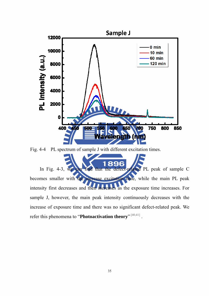
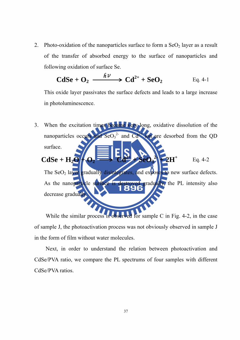
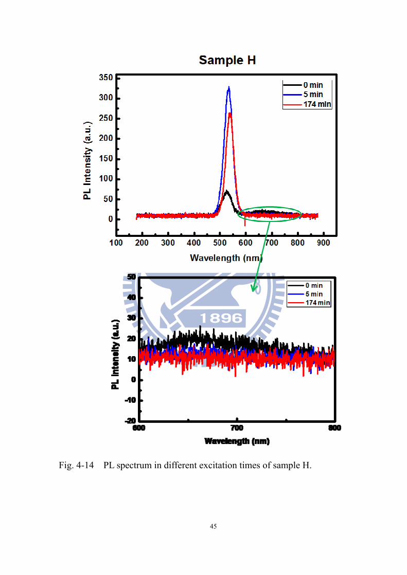


![南宋文言公案故事[通殺夫]類之敘事轉向 - 國立中興大學中國 ...](https://static.fdokumen.com/doc/165x107/63209c8b117b4414ec0b1844/--1677074896.jpg)