


Bahasa
Halaman
Hukum

© Panasonic Corporation 2014. All rights reserved.Unauthorized copying and distribution is a violation oflaw.
PSG1401003CE
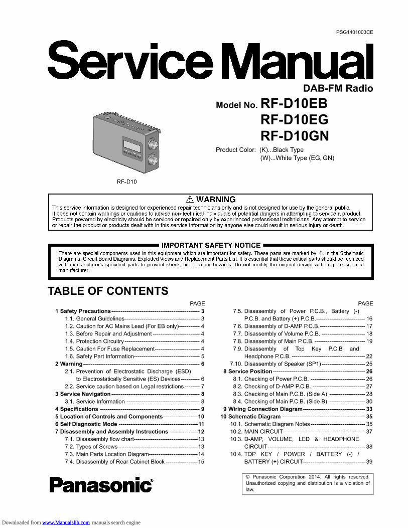
DAB-FM RadioModel No. RF-D10EB
RF-D10EGRF-D10GN
Product Color: (K)...Black Type(W)...White Type (EG, GN)
TABLE OF CONTENTSPAGE PAGE
1 Safety Precautions----------------------------------------------- 31.1. General Guidelines---------------------------------------- 31.2. Caution for AC Mains Lead (For EB only)----------- 41.3. Before Repair and Adjustment ------------------------- 41.4. Protection Circuitry ---------------------------------------- 41.5. Caution For Fuse Replacement------------------------ 41.6. Safety Part Information----------------------------------- 5
2 Warning -------------------------------------------------------------- 62.1. Prevention of Electrostatic Discharge (ESD)
to Electrostatically Sensitive (ES) Devices---------- 62.2. Service caution based on Legal restrictions -------- 7
3 Service Navigation ----------------------------------------------- 83.1. Service Information --------------------------------------- 8
4 Specifications ----------------------------------------------------- 95 Location of Controls and Components ------------------106 Self Diagnostic Mode ------------------------------------------117 Disassembly and Assembly Instructions ---------------12
7.1. Disassembly flow chart----------------------------------137.2. Types of Screws ------------------------------------------137.3. Main Parts Location Diagram--------------------------147.4. Disassembly of Rear Cabinet Block -----------------15
7.5. Disassembly of Power P.C.B., Battery (-)P.C.B. and Battery (+) P.C.B.-------------------------- 16
7.6. Disassembly of D-AMP P.C.B.------------------------ 177.7. Disassembly of Volume P.C.B. ----------------------- 187.8. Disassembly of Main P.C.B. --------------------------- 197.9. Disassembly of Top Key P.C.B and
Headphone P.C.B. --------------------------------------- 227.10. Disassembly of Speaker (SP1) ----------------------- 25
8 Service Position ------------------------------------------------- 268.1. Checking of Power P.C.B. ----------------------------- 268.2. Checking of D-AMP P.C.B. ---------------------------- 278.3. Checking of Main P.C.B. (Side A) ------------------- 288.4. Checking of Main P.C.B. (Side B) ------------------- 30
9 Wiring Connection Diagram--------------------------------- 3310 Schematic Diagram -------------------------------------------- 35
10.1. Schematic Diagram Notes ----------------------------- 3510.2. MAIN CIRCUIT ------------------------------------------- 3710.3. D-AMP, VOLUME, LED & HEADPHONE
CIRCUIT---------------------------------------------------- 3810.4. TOP KEY / POWER / BATTERY (-) /
BATTERY (+) CIRCUIT--------------------------------- 39
Downloaded from www.Manualslib.com manuals search engine Downloaded from www.Manualslib.com manuals search engine
2
11 Printed Circuit Board ------------------------------------------ 4011.1. MAIN P.C.B. ----------------------------------------------- 4011.2. DAMP / VOLUME / LED / HEADPHONE
P.C.B.-------------------------------------------------------- 4111.3. TOP KEY / POWER / BATTERY (-) /
BATTERY (+) P.C.B.------------------------------------- 4212 Appendix Information of Schematic Diagram --------- 43
12.1. Voltage Measurement & Waveform Chart --------- 4313 Exploded View and Replacement Parts List ----------- 47
13.1. Exploded View and Mechanical replacementParts List --------------------------------------------------- 47
13.2. Electrical Replacement Parts List -------------------- 51
Downloaded from www.Manualslib.com manuals search engine Downloaded from www.Manualslib.com manuals search engine
3
1 Safety Precautions1.1. General Guidelines
1. IMPORTANT SAFETY NOTICEThere are special components used in this equipment which are important for safety. These parts are marked by in theSchematic Diagrams, Circuit Board Layout, Exploded Views and Replacement Parts List. It is essential that these critical partsshould be replaced with manufacturer’s specified parts to prevent X-RADIATION, shock, fire, or other hazards. Do not modifythe original design without permission of manufacturer.
2. An Isolation Transformer should always be used during the servicing of AC Adaptor whose chassis is not isolated from the ACpower line. Use a transformer of adequate power rating as this protects the technician from accidents resulting in personalinjury from electrical shocks. It will also protect AC Adaptor from being damaged by accidental shorting that may occur duringservicing.
3. When servicing, observe the original lead dress. If a short circuit is found, replace all parts which have been overheated ordamaged by the short circuit.
4. After servicing, see to it that all the protective devices such as insulation barriers, insulation papers shields are properlyinstalled.
5. After servicing, make the following leakage current checks to prevent the customer from being exposed to shock hazards.
1.1.1. Leakage Current Cold Check1. Unplug the AC cord and connect a jumper between the two prongs on the plug.2. measure the resistance value, with an ohmmeter between the jumpered AC plug and each exposed metallic cabinet part on
the equipment such as screwheads, connectors, control shafts, etc. When the exposed metallic part has a return path to thechassis, the reading should be between 1MΩ and 5.2MΩ. When the exposed metal does not have a return path to the chas-sis, the reading must be
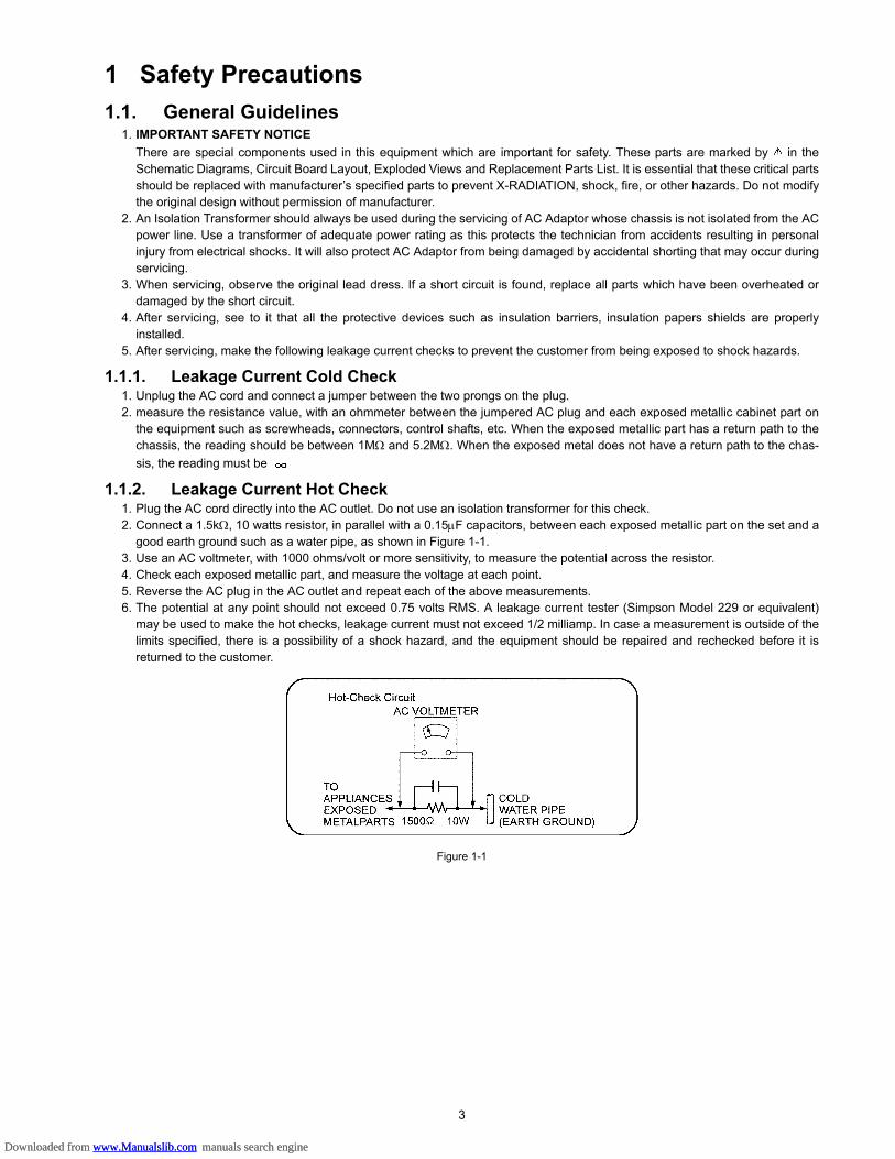
1.1.2. Leakage Current Hot Check1. Plug the AC cord directly into the AC outlet. Do not use an isolation transformer for this check.2. Connect a 1.5kΩ, 10 watts resistor, in parallel with a 0.15μF capacitors, between each exposed metallic part on the set and a
good earth ground such as a water pipe, as shown in Figure 1-1.3. Use an AC voltmeter, with 1000 ohms/volt or more sensitivity, to measure the potential across the resistor.4. Check each exposed metallic part, and measure the voltage at each point.5. Reverse the AC plug in the AC outlet and repeat each of the above measurements.6. The potential at any point should not exceed 0.75 volts RMS. A leakage current tester (Simpson Model 229 or equivalent)
may be used to make the hot checks, leakage current must not exceed 1/2 milliamp. In case a measurement is outside of thelimits specified, there is a possibility of a shock hazard, and the equipment should be repaired and rechecked before it isreturned to the customer.
Figure 1-1
Downloaded from www.Manualslib.com manuals search engine Downloaded from www.Manualslib.com manuals search engine
4
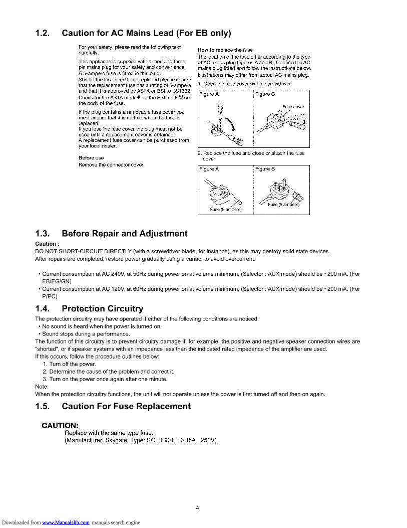
1.2. Caution for AC Mains Lead (For EB only)
1.3. Before Repair and AdjustmentCaution : DO NOT SHORT-CIRCUIT DIRECTLY (with a screwdriver blade, for instance), as this may destroy solid state devices.After repairs are completed, restore power gradually using a variac, to avoid overcurrent.
• Current consumption at AC 240V, at 50Hz during power on at volume minimum, (Selector : AUX mode) should be ~200 mA. (ForEB/EG/GN)
• Current consumption at AC 120V, at 60Hz during power on at volume minimum, (Selector : AUX mode) should be ~200 mA. (ForP/PC)
1.4. Protection CircuitryThe protection circuitry may have operated if either of the following conditions are noticed:
• No sound is heard when the power is turned on.• Sound stops during a performance.
The function of this circuitry is to prevent circuitry damage if, for example, the positive and negative speaker connection wires are"shorted", or if speaker systems with an impedance less than the indicated rated impedance of the amplifier are used.If this occurs, follow the procedure outlines below:
1. Turn off the power.2. Determine the cause of the problem and correct it.3. Turn on the power once again after one minute.
Note:When the protection circuitry functions, the unit will not operate unless the power is first turned off and then on again.
1.5. Caution For Fuse Replacement
Downloaded from www.Manualslib.com manuals search engine Downloaded from www.Manualslib.com manuals search engine
5
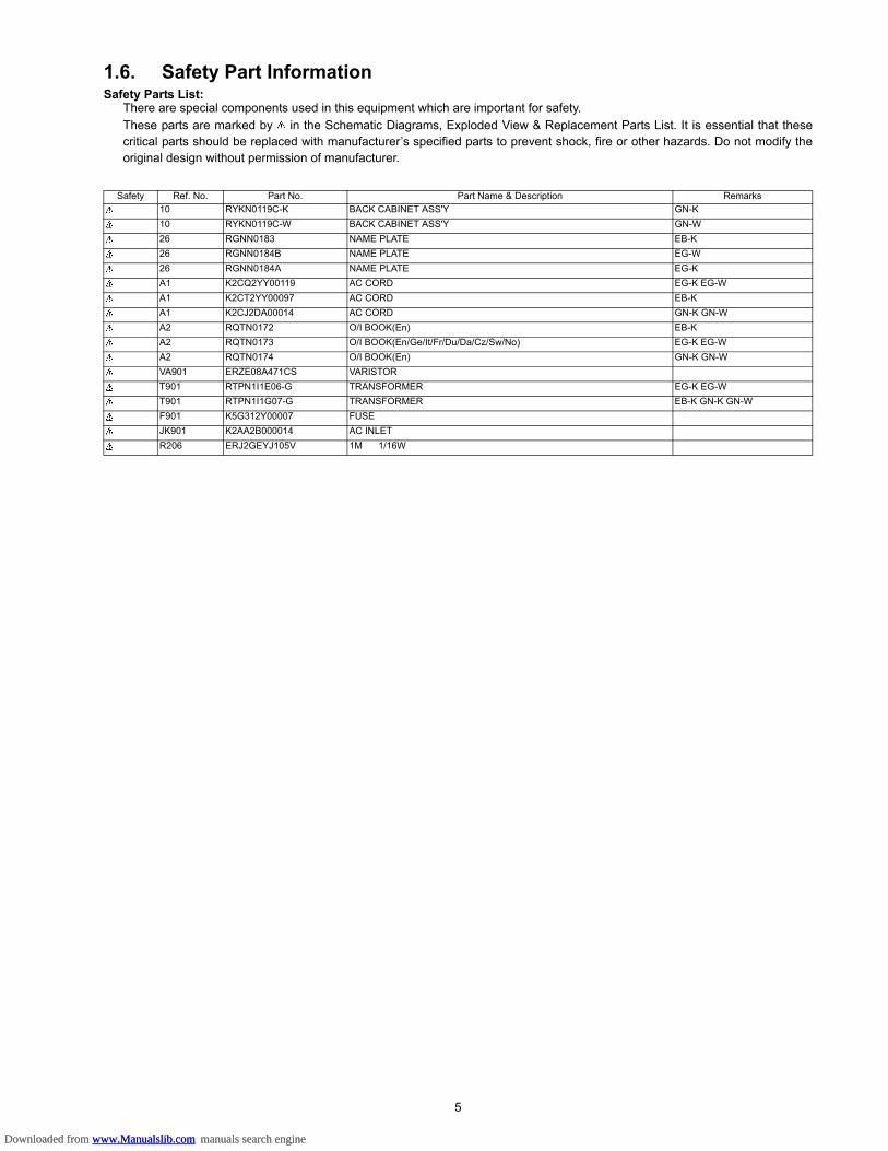
1.6. Safety Part InformationSafety Parts List:
There are special components used in this equipment which are important for safety.These parts are marked by in the Schematic Diagrams, Exploded View & Replacement Parts List. It is essential that thesecritical parts should be replaced with manufacturer’s specified parts to prevent shock, fire or other hazards. Do not modify theoriginal design without permission of manufacturer.
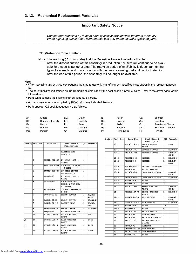
Safety Ref. No. Part No. Part Name & Description Remarks10 RYKN0119C-K BACK CABINET ASS'Y GN-K10 RYKN0119C-W BACK CABINET ASS'Y GN-W26 RGNN0183 NAME PLATE EB-K26 RGNN0184B NAME PLATE EG-W26 RGNN0184A NAME PLATE EG-KA1 K2CQ2YY00119 AC CORD EG-K EG-WA1 K2CT2YY00097 AC CORD EB-KA1 K2CJ2DA00014 AC CORD GN-K GN-WA2 RQTN0172 O/I BOOK(En) EB-KA2 RQTN0173 O/I BOOK(En/Ge/It/Fr/Du/Da/Cz/Sw/No) EG-K EG-WA2 RQTN0174 O/I BOOK(En) GN-K GN-WVA901 ERZE08A471CS VARISTORT901 RTPN1I1E06-G TRANSFORMER EG-K EG-WT901 RTPN1I1G07-G TRANSFORMER EB-K GN-K GN-WF901 K5G312Y00007 FUSEJK901 K2AA2B000014 AC INLETR206 ERJ2GEYJ105V 1M 1/16W
Downloaded from www.Manualslib.com manuals search engine Downloaded from www.Manualslib.com manuals search engine
6
2 Warning2.1. Prevention of Electrostatic Discharge (ESD) to Electrostatically Sensi-
tive (ES) DevicesSome semiconductor (solid state) devices can be damaged easily by static electricity. Such components commonly are called Elec-trostatically Sensitive (ES) Devices.
The following techniques should be used to help reduce the incidence of component damage caused by electrostatic discharge(ESD).
1. Immediately before handling any semiconductor component or semiconductor-equipped assembly, drain off any ESD on yourbody by touching a known earth ground. Alternatively, obtain and wear a commercially available discharging ESD wrist strap,which should be removed for potential shock reasons prior to applying power to the unit under test.
2. After removing an electrical assembly equipped with ES devices, place the assembly on a conductive surface such as alumi-num foil, to prevent electrostatic charge buildup or exposure of the assembly.
3. Use only a grounded-tip soldering iron to solder or unsolder ES devices.4. Use only an anti-static solder removal device. Some solder removal devices not classified as “anti-static (ESD protected)” can
generate electrical charge sufficient to damage ES devices.5. Do not use freon-propelled chemicals. These can generate electrical charges sufficient to damage ES devices.6. Do not remove a replacement ES device from its protective package until immediately before you are ready to install it. (Most
replacement ES devices are packaged with leads electrically shorted together by conductive foam, aluminum foil or compara-ble conductive material).
7. Immediately before removing the protective material from the leads of a replacement ES device, touch the protective materialto the chassis or circuit assembly into which the device will be installed.CAUTION:
Be sure no power is applied to the chassis or circuit, and observe all other safety precautions.8. Minimize bodily motions when handling unpackaged replacement ES devices. (Otherwise harmless motion such as the
brushing together of your clothes fabric or the lifting of your foot from a carpeted floor can generate static electricity (ESD) suf-ficient to damage an ES device).
Downloaded from www.Manualslib.com manuals search engine Downloaded from www.Manualslib.com manuals search engine
7
2.2. Service caution based on Legal restrictions2.2.1. General description about Lead Free Solder (PbF)The lead free solder has been used in the mounting process of all electrical components on the printed circuit boards used for thisequipment in considering the globally environmental conservation.
The normal solder is the alloy of tin (Sn) and lead (Pb). On the other hand, the lead free solder is the alloy mainly consists of tin(Sn), silver (Ag) and Copper (Cu), and the melting point of the lead free solder is higher approx.30 degrees C (86°F) more than thatof the normal solder.
Definition of PCB Lead Free Solder being used
Service caution for repair work using Lead Free Solder (PbF)• The lead free solder has to be used when repairing the equipment for which the lead free solder is used.
(Definition: The letter of “PbF” is printed on the PCB using the lead free solder.)• To put lead free solder, it should be well molten and mixed with the original lead free solder.• Remove the remaining lead free solder on the PCB cleanly for soldering of the new IC.• Since the melting point of the lead free solder is higher than that of the normal lead solder, it takes the longer time to melt the
lead free solder.• Use the soldering iron (more than 70W) equipped with the temperature control after setting the temperature at 350±30 degrees
C (662±86°F).Recommended Lead Free Solder (Service Parts Route.)
• The following 3 types of lead free solder are available through the service parts route.RFKZ03D01K-----------(0.3mm 100g Reel)RFKZ06D01K-----------(0.6mm 100g Reel)RFKZ10D01K-----------(1.0mm 100g Reel)
Note* Ingredient: Tin (Sn), 96.5%, Silver (Ag) 3.0%, Copper (Cu) 0.5%, Cobalt (Co) / Germanium (Ge) 0.1 to 0.3%
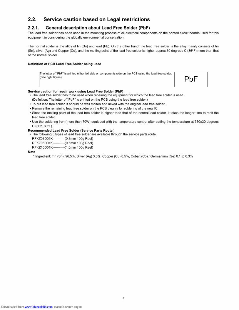
The letter of “PbF” is printed either foil side or components side on the PCB using the lead free solder.(See right figure)
Downloaded from www.Manualslib.com manuals search engine Downloaded from www.Manualslib.com manuals search engine
8
3 Service Navigation3.1. Service InformationThis service manual contains technical information which will allow service personnel’s to understand and service this model.Please place orders using the parts list and not the drawing reference numbers.
If the circuit is changed or modified, this information will be followed by supplement service manual to be filed with original servicemanual.
Downloaded from www.Manualslib.com manuals search engine Downloaded from www.Manualslib.com manuals search engine
9
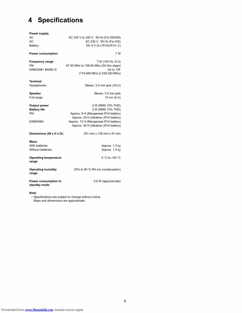
4 Specifications
Power supplyAC AC 230 V to 240 V, 50 Hz (For EB/GN)AC AC 230 V, 50 Hz (For EG)Battery DC 6 V (4 x R14/LR14, C)
Power consumption 7 W
Frequency range 7 W (100 Hz, 6 Ω)FM 87.50 MHz to 108.00 MHz (50 kHz steps)DAB/DAB+ BAND III 5A to 13F
(174.928 MHz to 239.200 MHz)
TerminalHeadphones Stereo, 3.5 mm jack (16 Ω)
Speaker Stereo, 3.5 mm jackFull range 10 cm (4 Ω)
Output power 2 W (RMS 10% THD)Battery life 2 W (RMS 10% THD)FM Approx. 9 H (Manganese R14 battery)
Approx. 30 H (Alkaline LR14 battery)DAB/DAB+ Approx. 12 H (Manganese R14 battery)
Approx. 40 H (Alkaline LR14 battery)
Dimensions (W x H x D): 251 mm x 138 mm x 91 mm
Mass:With batteries Approx. 1.3 kgWithout batteries Approx. 1.0 kg
Operating temperature range
0 °C to +40 °C
Operating humidity range
35% to 80 % RH (no condensation)
Power consumption in standby mode
0.6 W (approximate)
Note:• Specifications are subject to change without notice.
Mass and dimensions are approximate.
Downloaded from www.Manualslib.com manuals search engine Downloaded from www.Manualslib.com manuals search engine
10
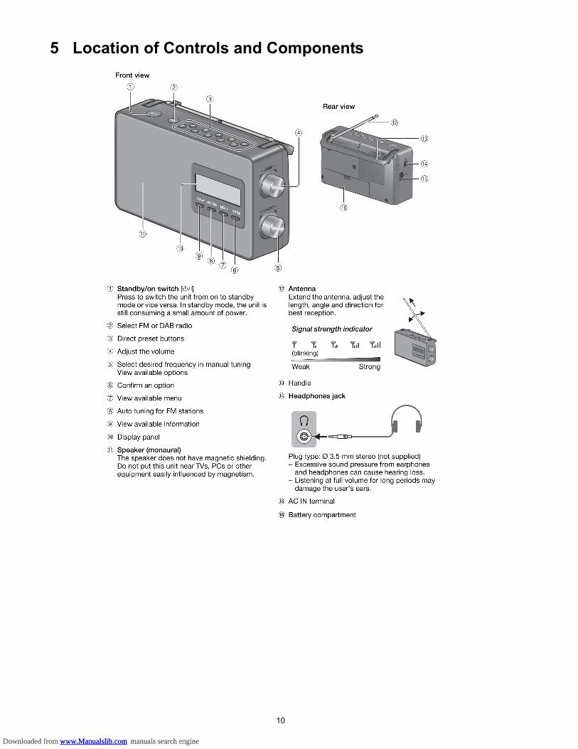
5 Location of Controls and Components
Downloaded from www.Manualslib.com manuals search engine Downloaded from www.Manualslib.com manuals search engine
11
6 Self Diagnostic Mode This unit is equipped with features of service mode & doctor mode setting for checking the functions & reliability.
Here is the procedures to enter into Self Diagnostic Mode.Step 1 : Turn on the unit.Step 2 : Press [MENU] button and turn the jog [TUNER/SELECT] to the left or right.Step 3 : Select [SYSTEM] and press [ENTER] button.Step 4 : Turn the jog [TUNER/SELECT] to select [Factory Reset] and press [ENTER] button.Step 5 : Press and hold [Preset 2], followed by the sequence to press [DISPLAY]→ [AUTOTUNE]→ [MENU] → [ENTER].
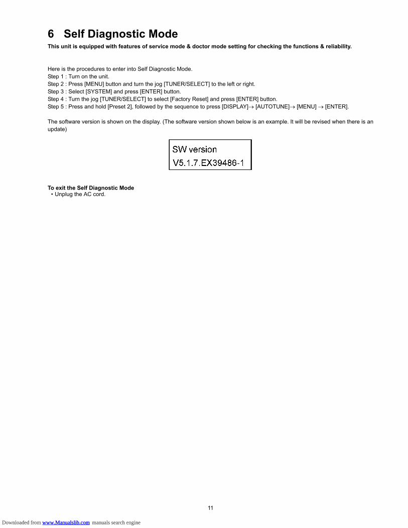
The software version is shown on the display. (The software version shown below is an example. It will be revised when there is anupdate)
To exit the Self Diagnostic Mode• Unplug the AC cord.
Downloaded from www.Manualslib.com manuals search engine Downloaded from www.Manualslib.com manuals search engine
12
7 Disassembly and Assembly Instructions• This section describes the disassembly and/or assembly procedures for all major printed circuit boards & main compo-
nents for the unit. (You may refer to the section of “Main components and P.C.B Locations” as described in this servicemanual)
• Before carrying out the disassembly process, please ensure all the safety precautions & procedures are followed.• During the disassembly and/or assembly process, please handle with care as there may be chassis components with
sharp edges.• Avoid touching heatsinks due to its high temperature after prolong use.• Be sure to use proper service tools , equipments or jigs during repair.• Select items from the following indexes when disassembly or replacement are required.
• Disassembly of Rear Cabinet Block• Disassembly of Power P.C.B., Battery (-) P.C.B. and Battery (+) P.C.B.• Disassembly of D-AMP P.C.B.• Disassembly of Volume P.C.B.• Disassembly of Main P.C.B.• Disassembly of Top Key P.C.B and Headphone P.C.B.• Disassembly of Speaker (SP1)
Downloaded from www.Manualslib.com manuals search engine Downloaded from www.Manualslib.com manuals search engine
13
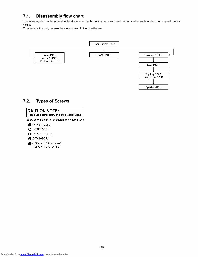
7.1. Disassembly flow chartThe following chart is the procedure for disassembling the casing and inside parts for internal inspection when carrying out the ser-vicing.To assemble the unit, reverse the steps shown in the chart below.
7.2. Types of Screws
Downloaded from www.Manualslib.com manuals search engine Downloaded from www.Manualslib.com manuals search engine
14
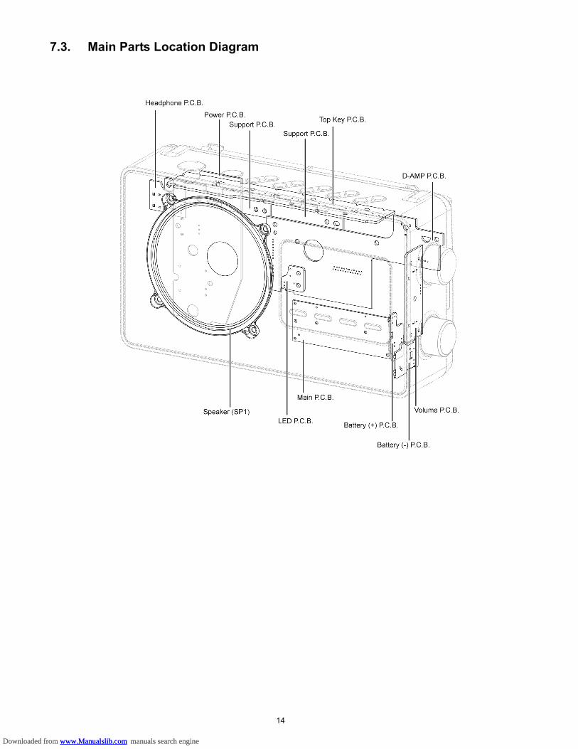
7.3. Main Parts Location Diagram
Downloaded from www.Manualslib.com manuals search engine Downloaded from www.Manualslib.com manuals search engine
15
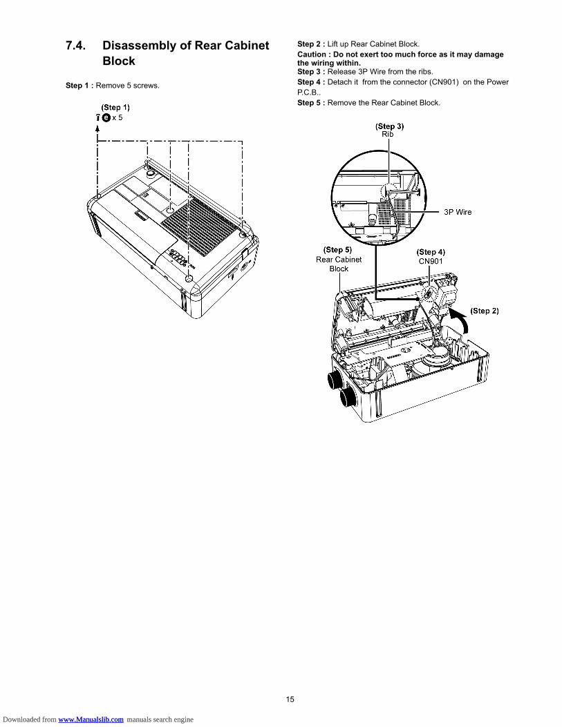
7.4. Disassembly of Rear Cabinet Block
Step 1 : Remove 5 screws.
Step 2 : Lift up Rear Cabinet Block.Caution : Do not exert too much force as it may damage the wiring within.Step 3 : Release 3P Wire from the ribs.Step 4 : Detach it from the connector (CN901) on the Power P.C.B..Step 5 : Remove the Rear Cabinet Block.
Downloaded from www.Manualslib.com manuals search engine Downloaded from www.Manualslib.com manuals search engine
16
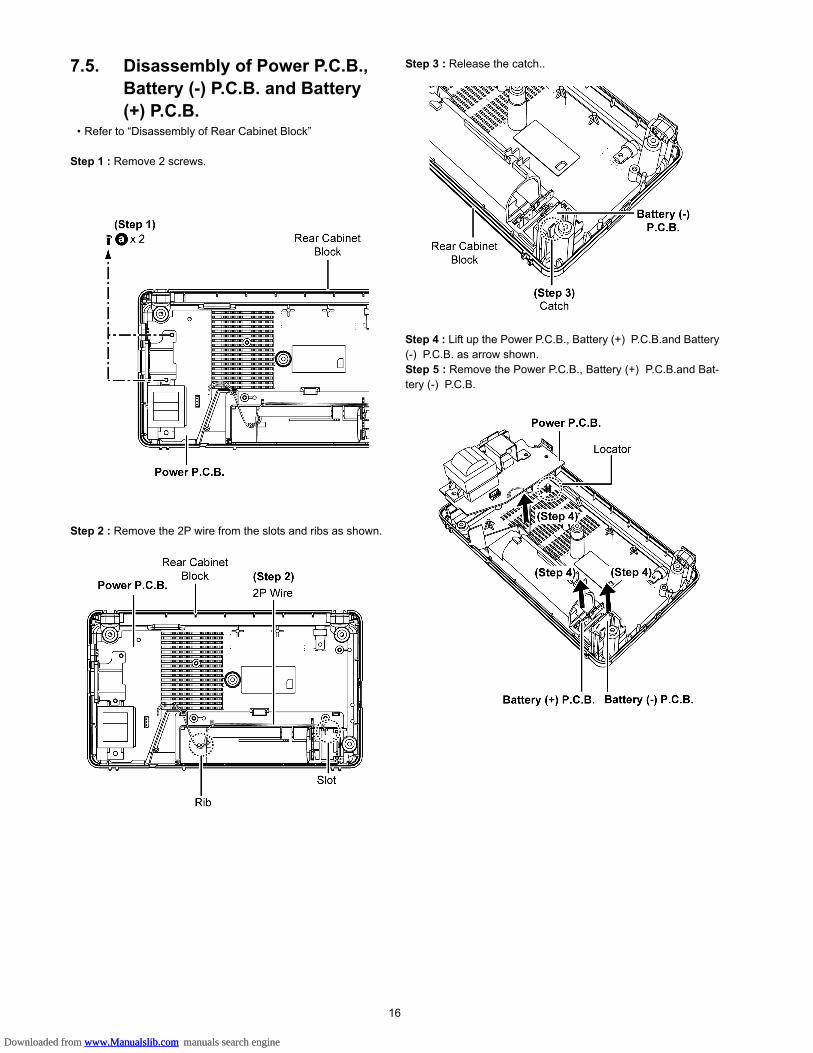
7.5. Disassembly of Power P.C.B., Battery (-) P.C.B. and Battery (+) P.C.B.
• Refer to “Disassembly of Rear Cabinet Block”
Step 1 : Remove 2 screws.
Step 2 : Remove the 2P wire from the slots and ribs as shown.
Step 3 : Release the catch..
Step 4 : Lift up the Power P.C.B., Battery (+) P.C.B.and Battery(-) P.C.B. as arrow shown.Step 5 : Remove the Power P.C.B., Battery (+) P.C.B.and Bat-tery (-) P.C.B.
Downloaded from www.Manualslib.com manuals search engine Downloaded from www.Manualslib.com manuals search engine
17
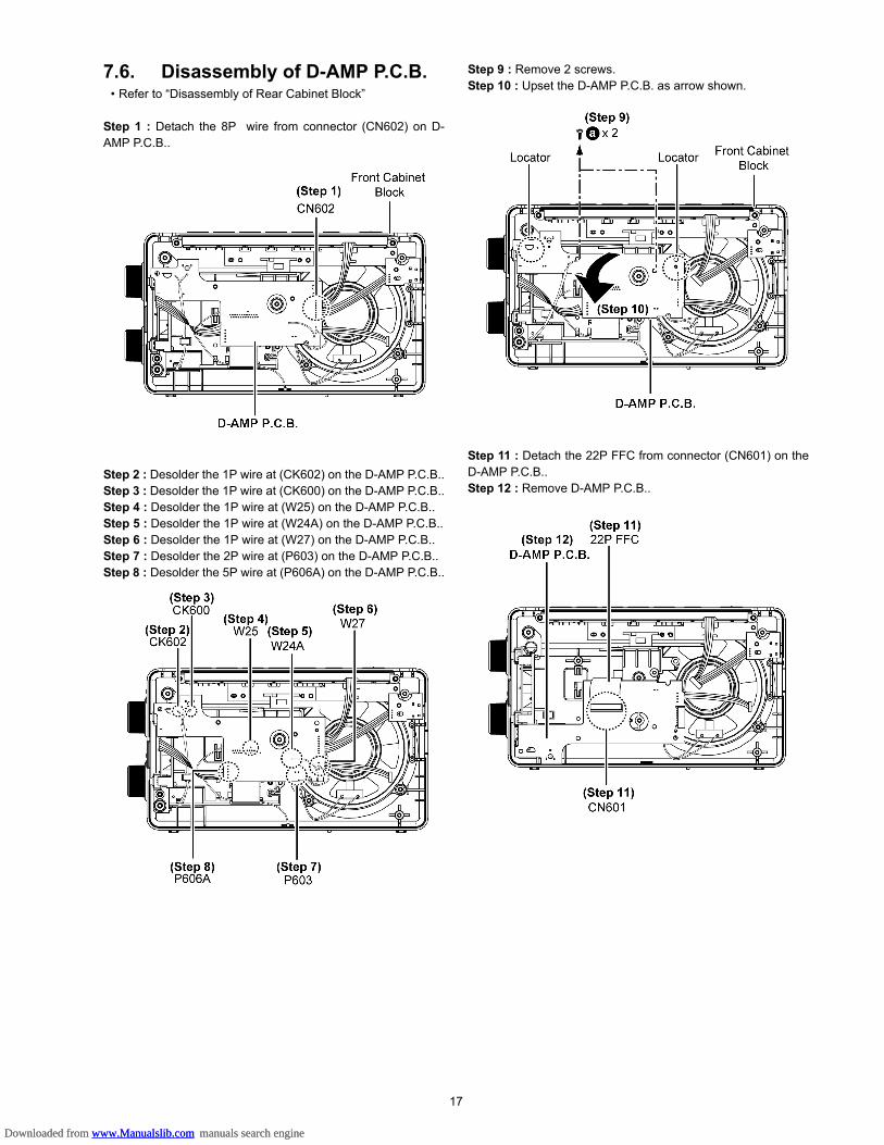
7.6. Disassembly of D-AMP P.C.B.• Refer to “Disassembly of Rear Cabinet Block”
Step 1 : Detach the 8P wire from connector (CN602) on D-AMP P.C.B..
Step 2 : Desolder the 1P wire at (CK602) on the D-AMP P.C.B..Step 3 : Desolder the 1P wire at (CK600) on the D-AMP P.C.B..Step 4 : Desolder the 1P wire at (W25) on the D-AMP P.C.B..Step 5 : Desolder the 1P wire at (W24A) on the D-AMP P.C.B..Step 6 : Desolder the 1P wire at (W27) on the D-AMP P.C.B..Step 7 : Desolder the 2P wire at (P603) on the D-AMP P.C.B..Step 8 : Desolder the 5P wire at (P606A) on the D-AMP P.C.B..
Step 9 : Remove 2 screws.Step 10 : Upset the D-AMP P.C.B. as arrow shown.
Step 11 : Detach the 22P FFC from connector (CN601) on theD-AMP P.C.B..Step 12 : Remove D-AMP P.C.B..
Downloaded from www.Manualslib.com manuals search engine Downloaded from www.Manualslib.com manuals search engine
18
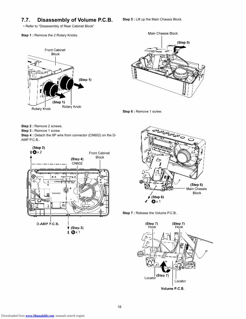
7.7. Disassembly of Volume P.C.B.• Refer to “Disassembly of Rear Cabinet Block”
Step 1 : Remove the 2 Rotary Knobs.
Step 2 : Remove 2 screws.Step 3 : Remove 1 screw.Step 4 : Detach the 8P wire from connector (CN602) on the D-AMP P.C.B..
Step 5 : Lift up the Main Chassis Block.
Step 6 : Remove 1 screw.
Step 7 : Release the Volume P.C.B..
Downloaded from www.Manualslib.com manuals search engine Downloaded from www.Manualslib.com manuals search engine
19
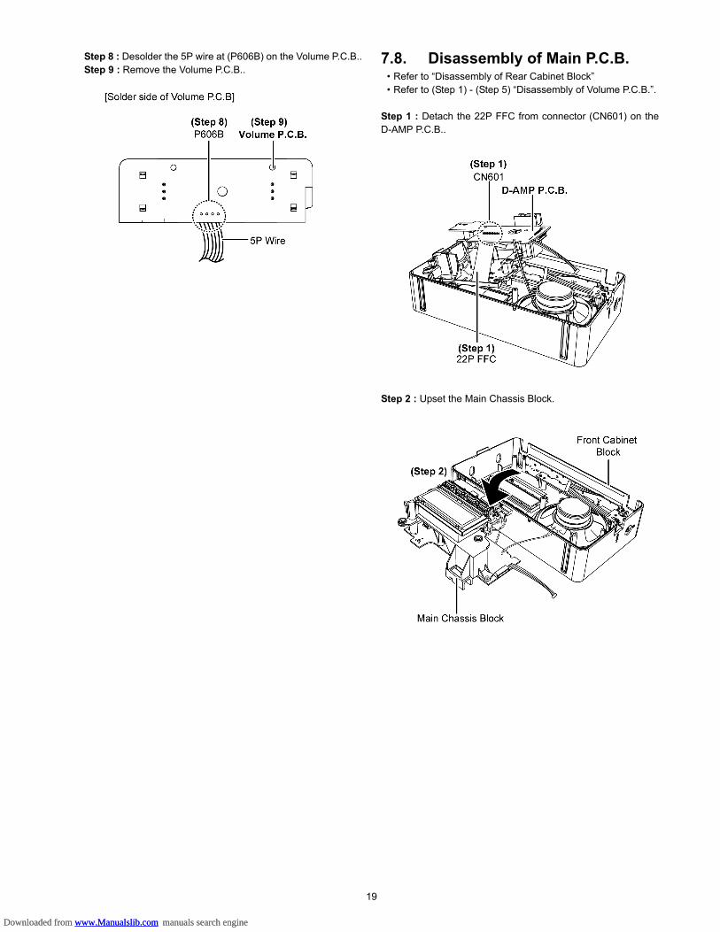
Step 8 : Desolder the 5P wire at (P606B) on the Volume P.C.B..Step 9 : Remove the Volume P.C.B..
7.8. Disassembly of Main P.C.B.• Refer to “Disassembly of Rear Cabinet Block”• Refer to (Step 1) - (Step 5) “Disassembly of Volume P.C.B.”.
Step 1 : Detach the 22P FFC from connector (CN601) on theD-AMP P.C.B..
Step 2 : Upset the Main Chassis Block.
Downloaded from www.Manualslib.com manuals search engine Downloaded from www.Manualslib.com manuals search engine
20
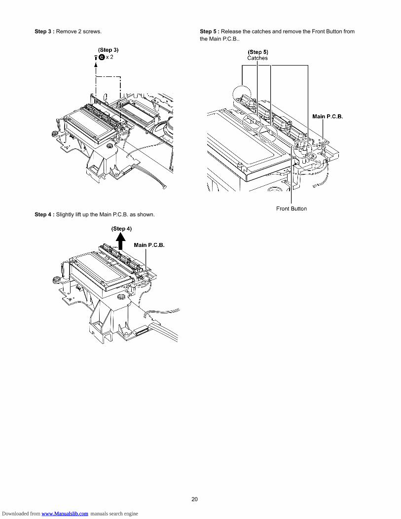
Step 3 : Remove 2 screws.
Step 4 : Slightly lift up the Main P.C.B. as shown.
Step 5 : Release the catches and remove the Front Button fromthe Main P.C.B..
Downloaded from www.Manualslib.com manuals search engine Downloaded from www.Manualslib.com manuals search engine
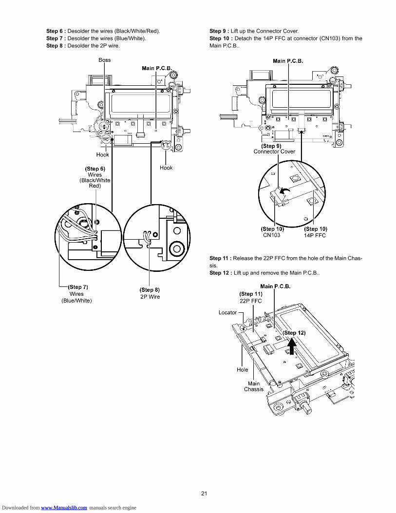
21
Step 6 : Desolder the wires (Black/White/Red).Step 7 : Desolder the wires (Blue/White).Step 8 : Desolder the 2P wire.
Step 9 : Lift up the Connector Cover.Step 10 : Detach the 14P FFC at connector (CN103) from theMain P.C.B..
Step 11 : Release the 22P FFC from the hole of the Main Chas-sis.Step 12 : Lift up and remove the Main P.C.B..
Downloaded from www.Manualslib.com manuals search engine Downloaded from www.Manualslib.com manuals search engine
22
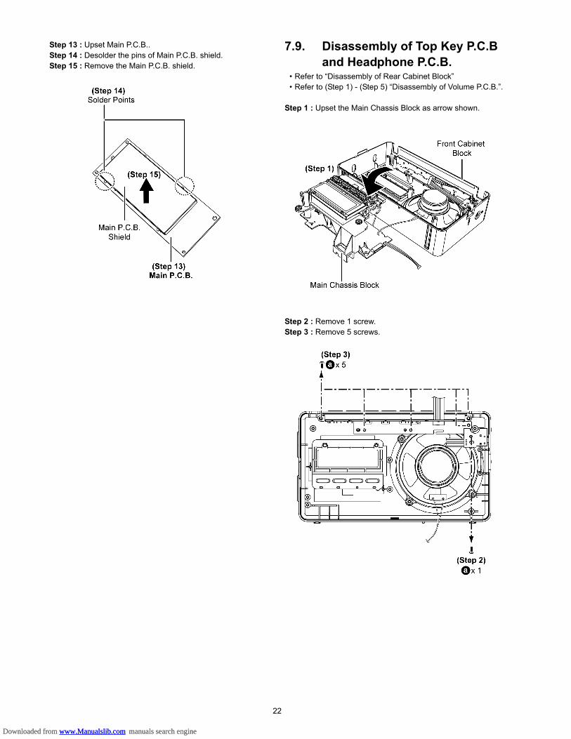
Step 13 : Upset Main P.C.B..Step 14 : Desolder the pins of Main P.C.B. shield.Step 15 : Remove the Main P.C.B. shield.
7.9. Disassembly of Top Key P.C.B and Headphone P.C.B.
• Refer to “Disassembly of Rear Cabinet Block”• Refer to (Step 1) - (Step 5) “Disassembly of Volume P.C.B.”.
Step 1 : Upset the Main Chassis Block as arrow shown.
Step 2 : Remove 1 screw.Step 3 : Remove 5 screws.
Downloaded from www.Manualslib.com manuals search engine Downloaded from www.Manualslib.com manuals search engine
23
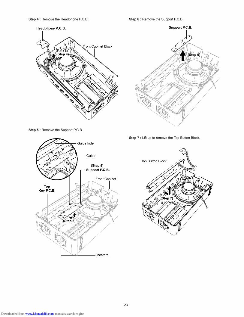
Step 4 : Remove the Headphone P.C.B..
Step 5 : Remove the Support P.C.B..
Step 6 : Remove the Support P.C.B..
Step 7 : Lift up to remove the Top Button Block.
Downloaded from www.Manualslib.com manuals search engine Downloaded from www.Manualslib.com manuals search engine
24
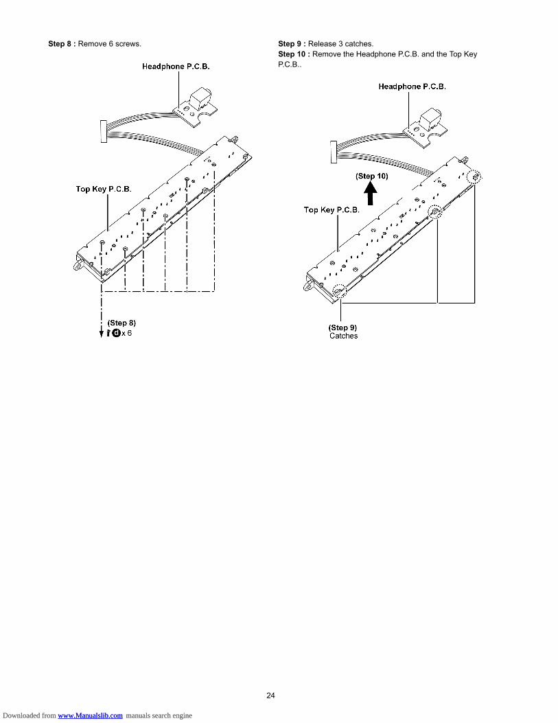
Step 8 : Remove 6 screws. Step 9 : Release 3 catches.Step 10 : Remove the Headphone P.C.B. and the Top Key P.C.B..
Downloaded from www.Manualslib.com manuals search engine Downloaded from www.Manualslib.com manuals search engine
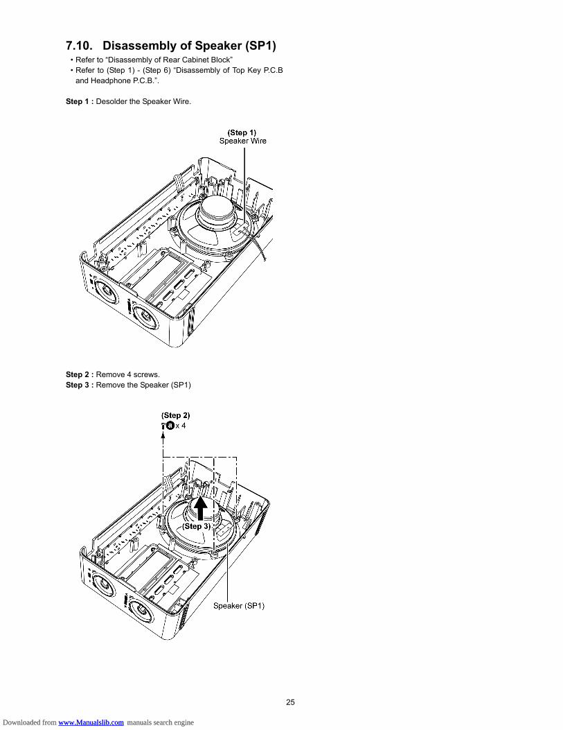
25
7.10. Disassembly of Speaker (SP1)• Refer to “Disassembly of Rear Cabinet Block”• Refer to (Step 1) - (Step 6) “Disassembly of Top Key P.C.B
and Headphone P.C.B.”.
Step 1 : Desolder the Speaker Wire.
Step 2 : Remove 4 screws.Step 3 : Remove the Speaker (SP1)
Downloaded from www.Manualslib.com manuals search engine Downloaded from www.Manualslib.com manuals search engine
26
8 Service PositionNote: For description of the disassembly procedures, see the Section 7
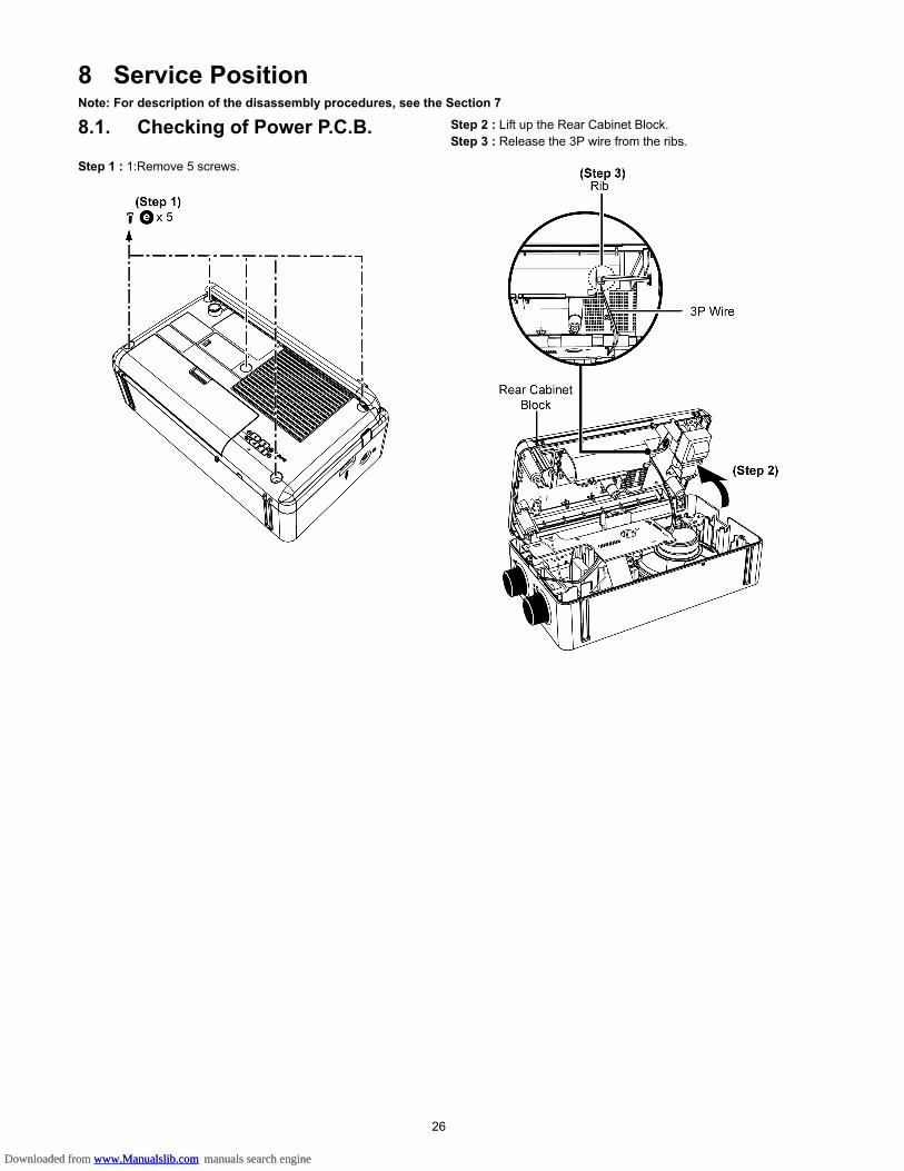
8.1. Checking of Power P.C.B.
Step 1 : 1:Remove 5 screws.
Step 2 : Lift up the Rear Cabinet Block.Step 3 : Release the 3P wire from the ribs.
Downloaded from www.Manualslib.com manuals search engine Downloaded from www.Manualslib.com manuals search engine
27
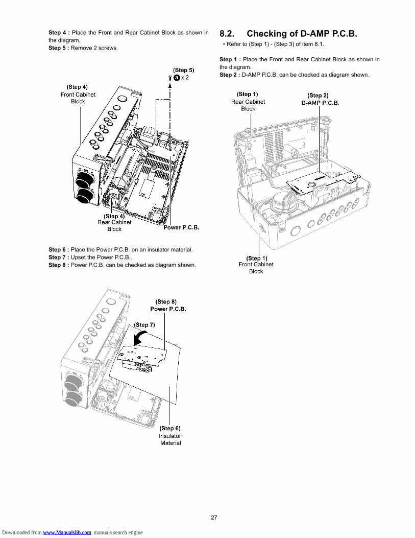
Step 4 : Place the Front and Rear Cabinet Block as shown inthe diagram.Step 5 : Remove 2 screws.
Step 6 : Place the Power P.C.B. on an insulator material.Step 7 : Upset the Power P.C.B..Step 8 : Power P.C.B. can be checked as diagram shown.
8.2. Checking of D-AMP P.C.B.• Refer to (Step 1) - (Step 3) of item 8.1.
Step 1 : Place the Front and Rear Cabinet Block as shown inthe diagram.Step 2 : D-AMP P.C.B. can be checked as diagram shown.
Downloaded from www.Manualslib.com manuals search engine Downloaded from www.Manualslib.com manuals search engine
28
8.3. Checking of Main P.C.B. (SideA)
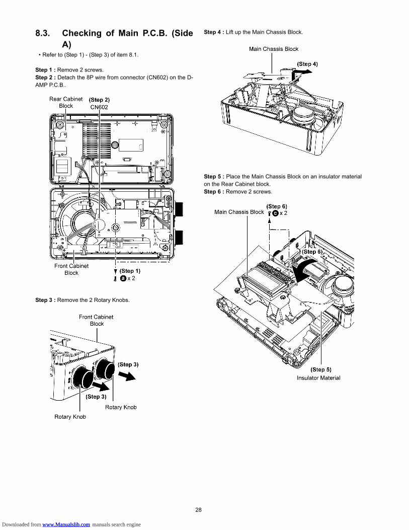
• Refer to (Step 1) - (Step 3) of item 8.1.
Step 1 : Remove 2 screws.Step 2 : Detach the 8P wire from connector (CN602) on the D-AMP P.C.B..
Step 3 : Remove the 2 Rotary Knobs.
Step 4 : Lift up the Main Chassis Block.
Step 5 : Place the Main Chassis Block on an insulator materialon the Rear Cabinet block.Step 6 : Remove 2 screws.
Downloaded from www.Manualslib.com manuals search engine Downloaded from www.Manualslib.com manuals search engine
29
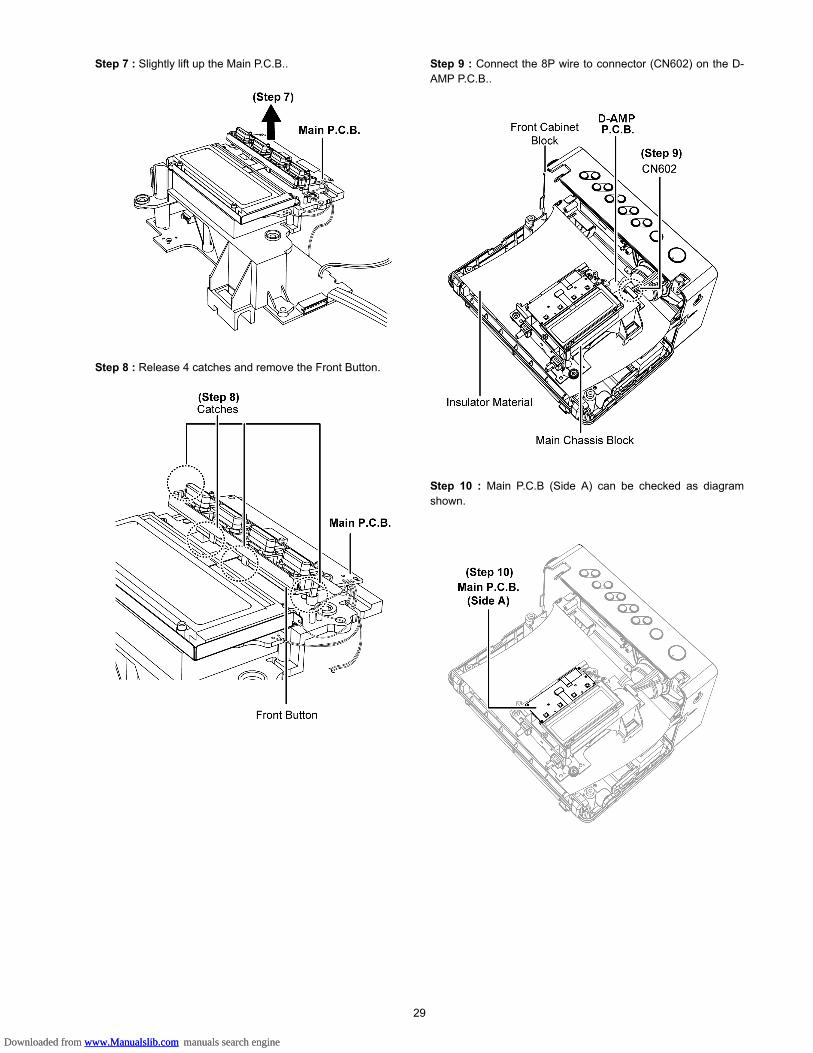
Step 7 : Slightly lift up the Main P.C.B..
Step 8 : Release 4 catches and remove the Front Button.
Step 9 : Connect the 8P wire to connector (CN602) on the D-AMP P.C.B..
Step 10 : Main P.C.B (Side A) can be checked as diagramshown.
Downloaded from www.Manualslib.com manuals search engine Downloaded from www.Manualslib.com manuals search engine
30
8.4. Checking of Main P.C.B. (Side B)
• Refer to item 8.3.
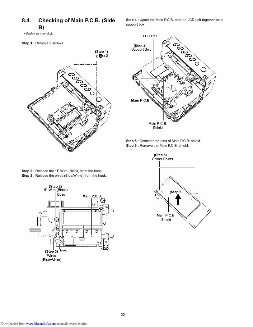
Step 1 : Remove 2 screws.
Step 2 : Release the 1P Wire (Black) from the boss.Step 3 : Release the wires (Blue/White) from the hook.
Step 4 : Upset the Main P.C.B. and the LCD unit together on a support box.
Step 5 : Desolder the pins of Main P.C.B. shield.Step 6 : Remove the Main P.C.B. shield.
Downloaded from www.Manualslib.com manuals search engine Downloaded from www.Manualslib.com manuals search engine
31
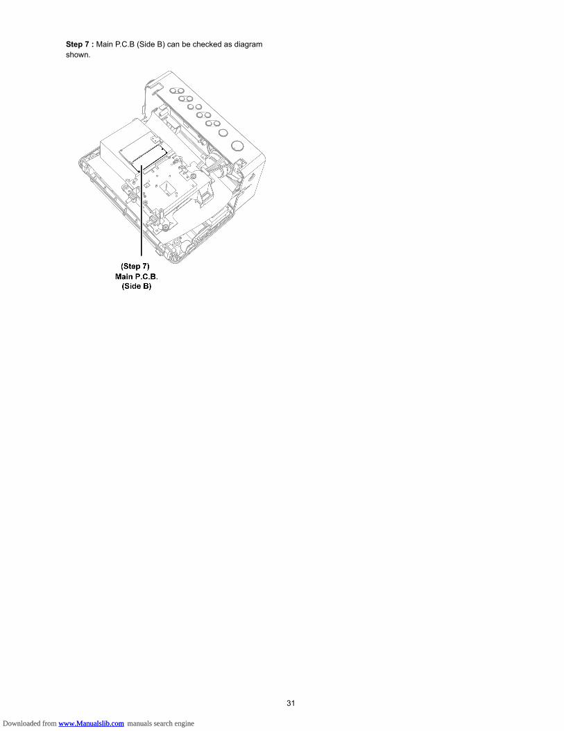
Step 7 : Main P.C.B (Side B) can be checked as diagram shown.
Downloaded from www.Manualslib.com manuals search engine Downloaded from www.Manualslib.com manuals search engine

32
Downloaded from www.Manualslib.com manuals search engine Downloaded from www.Manualslib.com manuals search engine
33
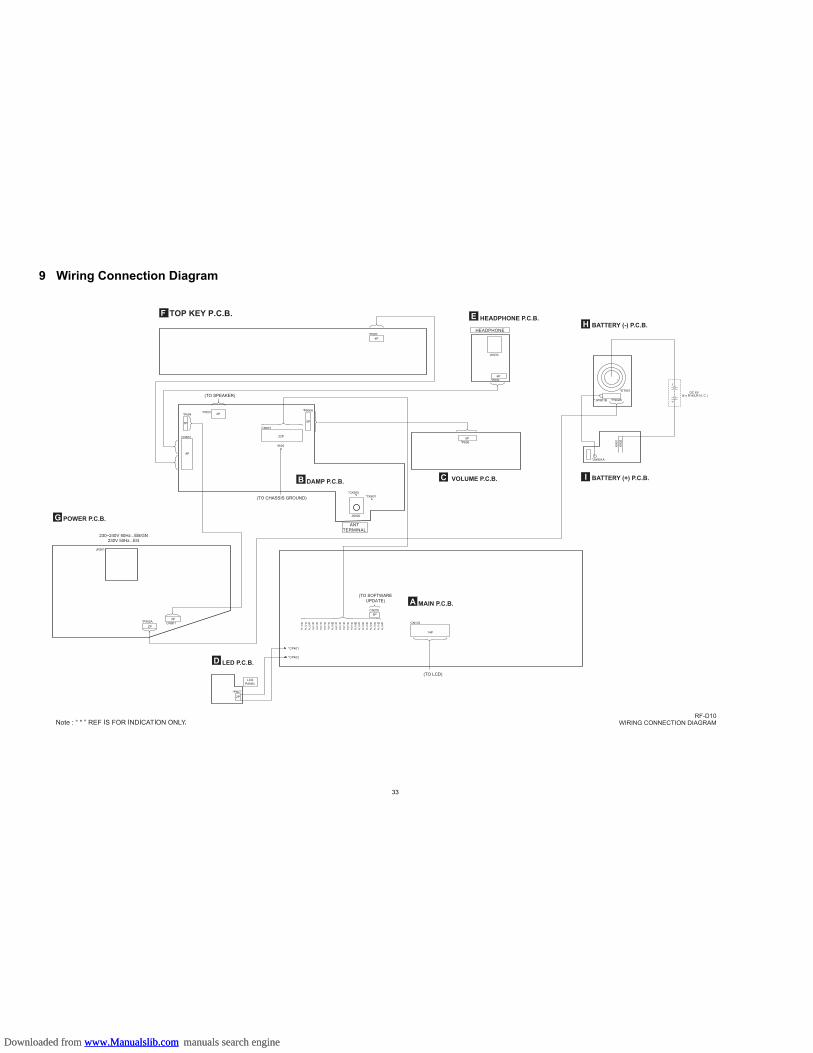
9 Wiring Connection Diagram
(TO SPEAKER)
(TO CHASSIS GROUND)
(TO SOFTWARE UPDATE)
(TO LCD)
B
*P604*P603
CN601
*P606A
CN602
*CK601*CK600
JK600
ANTTERMINAL
HEADPHONE
DAMP P.C.B.
D
*P607
LED P.C.B.
C
*P606
VOLUME P.C.B.
A
*W25
RL1
05
RL1
15
RL1
12
RL1
04
RL1
01
RL1
13
RL1
11
RL1
21
RL1
22
CN103
*CP401
*CP402
CN205
RL1
17
RL1
14
RL1
19
RL1
10
RL1
16
RL1
08
RL1
18
RL1
20
RL1
02
RL1
07
RL1
09
RL1
06
RL1
03
MAIN P.C.B.
F
*P800
TOP KEY P.C.B.
H
I
DC 6V(4 x R14/LR14, C )
*P902B*JW901B
*ET901
*JW901A
K90
1K
902
1
1
2
BATTERY (-) P.C.B.
BATTERY (+) P.C.B.
G
G
230~240V 50Hz...EB/GN230V 50Hz...EG
JK901
*P902A CN901
POWER P.C.B.
E
*P830
JK830
RF-D10WIRING CONNECTION DIAGRAM
4P
22P
2P
8P
3P 5P
3P
5P
4P
2P
2P
14P
8P
LCDPANEL
HEADPHONE P.C.B.
Downloaded from www.Manualslib.com manuals search engine Downloaded from www.Manualslib.com manuals search engine

34
Downloaded from www.Manualslib.com manuals search engine Downloaded from www.Manualslib.com manuals search engine
35
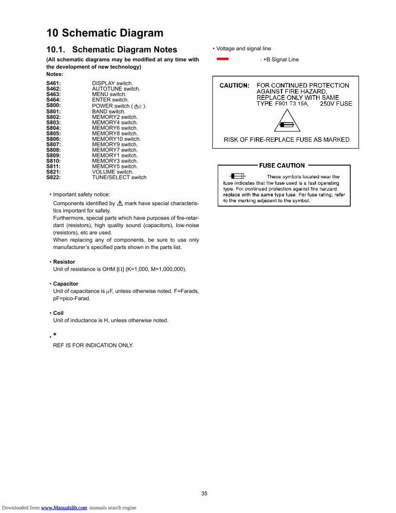
10 Schematic Diagram10.1. Schematic Diagram Notes(All schematic diagrams may be modified at any time withthe development of new technology)Notes:
• Important safety notice:Components identified by mark have special characteris-tics important for safety.Furthermore, special parts which have purposes of fire-retar-dant (resistors), high quality sound (capacitors), low-noise(resistors), etc are used.When replacing any of components, be sure to use onlymanufacturer’s specified parts shown in the parts list.
• ResistorUnit of resistance is OHM [Ω] (K=1,000, M=1,000,000).
• CapacitorUnit of capacitance is μF, unless otherwise noted. F=Farads,pF=pico-Farad.
• CoilUnit of inductance is H, unless otherwise noted.
• *REF IS FOR INDICATION ONLY.
• Voltage and signal line
S461: DISPLAY switch.S462: AUTOTUNE switch.S463: MENU switch.S464: ENTER switch.S800: POWER switch ( ).S801: BAND switch.S802: MEMORY2 switch.S803: MEMORY4 switch.S804: MEMORY6 switch.S805: MEMORY8 switch.S806: MEMORY10 switch.S807: MEMORY9 switch.S808: MEMORY7 switch.S809: MEMORY1 switch.S810: MEMORY3 switch.S811: MEMORY5 switch.S821: VOLUME switch.S822: TUNE/SELECT switch
: +B Signal Line
Downloaded from www.Manualslib.com manuals search engine Downloaded from www.Manualslib.com manuals search engine

36
Downloaded from www.Manualslib.com manuals search engine Downloaded from www.Manualslib.com manuals search engine
37
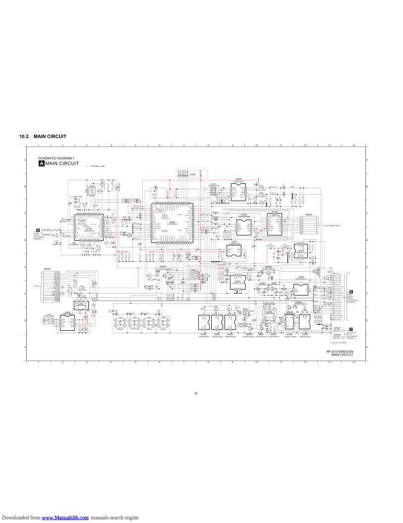
10.2. MAIN CIRCUIT
A
1 2 3 4 5 6 7 8 9 10 11 12 13 14
1 2 3 4 5 6 7 8 9 10 11 12 13 14
C
D
B
E
G
H
F
A
C
D
B
E
G
H
F
RF-D10 EB/EG/GNMAIN CIRCUIT
A MAIN CIRCUITSCHEMATIC DIAGRAM-1
0.1C102
100R120
4.7K
R202 C203
0
LB203
0C201 4.7
R119
33
C12
2
15PC
124
0.1
R206
1M
R243 270
R245 270
C244 0.1
R242 270
0.1C202
C11856P
C1190.1
R1171.5K1.5K
R116
0
R12
7 390
R12
5
C12
747
00P
0.03
9
C12
5
R27
6
J0JC
C00
0040
5
R12
3
J0JC
C00
0040
5
CK
251
CK
238
CK
250
CK
253
CK
254
CK
252
100R121 R201
4.7K
0.1
C25
7
0.1
C25
6
10C
128
LB10
0
J0JC
C00
0040
5
220P
C12
9
6.04k
R260
0.1
C123
3 214
X10
0H
0J24
5500
110
0.1
C26
4
R281
1K
LB281
J0JCC0000405
0.1
C27
1
C27
222
C27
3
10
0.01
C28
5
C28
610
0P
4.7C282
10K
R28
4
10K
R28
3
R282
1K
C28
410
0P
0.01
C28
3
33P
C28
8
C28
733
P
LB282
J0JCC0000405
4.7C281
C24
710
P8
657
421
3
RX203EXB28V221JX
C25
210
P
0.1
C25
0
C24
92210
C25
110
P
C24
8
21
9
4 7
5 6
3 810
IC203C0FBBY000073
33R12
6
0.1C103
1000
P
C10
4
C112 0.1
33R111
R112 33
R10
9
10K
R110 33 56P
C113C111 0.1
100P
C11
0
C24
033
P
C23
6
0.1
R236 100
C20
40.
1
C20
510
C24
233
P
C24
533
P
C24
333
P
B0JCDD000019D531
R20
4
0
0.1C216
R21
1
0
1.2V
0.1
C10
7
220P
C13
0
10C
275
0.1
C13
2
10C
131
0.01
C10
9
C10
80.
22
QR
530
B1G
DC
FNA
0011
R505
47K
R50
7
470K
RL106
B1GDCFNA0011QR505
47KR221
R21
822
0
220
R21
7
R53
1
68K C
530
1
C53
11L530
G1C4R7MA0249
R23
210
0
100
R23
1 R238 4.7K
R239 4.7K 27k
R53
2
0.1
C535
47K
R29
1
10C
534
120P
C53
3
D53
0
B0J
CN
E00
0039
R200
J0JCC0000405
C29
21
C29
110
R533
100k
LB511J0JCC0000405
0.22
C53
2 21
56
3
4
C0DBAYY01511IC53014
23
IC201C0DBFYY00164
3.3V
0.1
C22
0
220
R22
7
220
R22
5
C27
622
C27
822
C27
722
C27
410 0.
1C
219
0.1
C22
8
1000
P
C10
6
C10
5
1000
P
4p
C40
9
23
14
X400H0J327200085
KEY1RL115
AMP_PONRL108
R44
01.
5K R4412.2K
3 12
4 5
C0DBGYY02044
3.3V
IC501
SD
AS
CL
100
C41
2B
0JC
DD
0000
19
D40
0
C502
1
C40
00.
1
100
C41
1
100
R40
2
100
R40
3
R501
100C15
410
C501
1
C15
310
00P
1000
PC
519R405 10K
R41
3
47K
R41
1
47K
100
R55
4
C55
4
0.01
B1ABCF000103Q402
ROT_V_B
1000
PC
517
RL120
RL122
RL121
RL119
1000
PC
516
1000
PC
518
R40
6
18
Q406B1ABCF000103B1GBCFNA0016
QR403
C40
50.
01
Q405
Q405B1ABCF000103
1
4
2
3
IC402C0EBY0002226
1
4
2
3
IC401C0EBY0002221
1
4
2
3
IC403C0EBY0002224
R251 0
R252 0
C40
61
1
C55
9
1
4
2
3
IC504C0EBY0002225
3
1
2
4
5
C0DBGYY02049
3.8V
IC502
2 4
1 3
S461
DISPLAY
2 4
1 3
S462
AUTOTUNE MENU
2 4
1 3
S464
ENTER
2 4
1 3
S463
RL112
RL116
RL117
RL109
RL111C509 1000P
MUTE
ROT_V_A
R55510KB
AC
KLI
GH
T
C407
0.01
C408
1
B1GBCFNA0016QR503
ROT_T_AROT_T_B
C56
10.
1
R51
1
47K
C55
7
10
KEY0RL114
C515 1000P
C508 1000P
RL110100
R55
9
RL113C514 1000PC56
00.
0147K
R22
6
C23
0 1
3 12
4 53.
8V
IC405C0DBGYY02049
R404
100
R41
2
12K
B1ADCF000020Q401
AC
_H
C40
2
0.01
C40
3
0.01 10
C40
4
RL118
QR504B1GDCFNN0032
RO
T_V
_A
KE
Y0
RO
T_T_
B
RO
T_V
_B
R443 3.9KR442 2.7K
R4445.6K
C40
1
0.01
KE
Y1
C152
1
21
78
543 6
IC400C0ZBZ0002094
RO
T_T_
A
R22
9
100
100
R22
4
R22
3
100
R22
2
100
15KR219
15KR220
AM
P_P
ON
MU
TE
AC
_H
C218 1000P
C217
1000P
B1GBCFNA0016QR201
R50
9
33K1000PC146
RL104
RL102C504
1000P RL103
R215 4.7K
R213 4.7K
R214 4.7K
R212 4.7K
R233 100K
RL107AC_H
RL105
10K
R230R510
10K
B1ABCF000103Q506
B1ABCF000103Q230
1 4
2 3
IC503C0EBY0002216
R50
8
270K
1000
PC
511
100K
R50
4
47K
R5062 1
7 85
4 3
6
IC505C0DBEYY00271
1000
PC
555
1C
556
C55
110
00P
RL101
1000PC223 R235 100K
C55
322
C55
222
1000PC222
R234 100KC224 1000P
SD
AS
CL
LCD
_RE
SE
TB
AC
KLI
GH
T
C151
18910
1211
23
1
5
76
4
1413
SC
L
J0JCC0000405
LB151
SD
A10
0R
155
C15
522
0P
220P
C15
6
100
R15
6
LCD
_RE
SE
T
L102
G1C91NGA0040
0.01
C11
5
C11
6
0.1
0.01C2390.1C211 C238 0.156
1
34
2
87
CN205
21
78
543 6
RFKWED10EBMIC204
21
13
54
1011
87
963 12
14
C0JBAS000390
IC205
4.7C209 R240 270C241 0.1
R237 100
643
12
4847
64T1 6162 56 545557 51 5052 495360 585963
56
4
9
78
3940
26 2724 25 30 323128 2920 211817 19 2322
3433
3736
38
3515
1213
1011
14
16
45
4241
ThermalPad
4443
IC200C1AB00004211
0.33
C114
0.33
C117
229
3
67
45
12
24
26
2829
3436 35 32 3133
30
39T1 40 3738
27
25
ThermalPad
328
1211 15 171614 19 201813
2110
IC100C1AB00004210
1000P
C101
100PC100
L101
G1C91NGA0040
B0ZBZ0000230
VA101
VO
R-IN
L-IN
MRB
Lx VIN
GN
D
BS
T
VO
CE
VI
VI
VCC
VCC
KEY1
AC_DET
P_ON
MUTE
HP_DET
KEY0
KEY_POW
LCH
GND
3.3V
GND
GND
VO
UT
RV_N
RESET
GND
TOOL0
RT_N
RT_P
RV_P
RCHV
INE
N/S
SFB
[2] VCC_LDO
PDM0MUX
VCC_LBAND
[3] LDO_BYPASS
PDM1IDC-
IDC+
XTO
[1] VTUNE
GN
D
SC
L
SD
A
GN
D
GN
D
CP
OU
T
REF_OUT
[31] VCC_XTAL
[20] RSSI DELAY
GN
D
XTA
L
VC
C_S
YN
AVDDCOREPLL
[17] RFIVIN1
AVDDIOANA
NCNC
NC
CAP1N
VIN
NC
VSS
SCLRST
SDA
VDD
NCVOUT
CAP1P
VO
VSS
INT
CLKOUT
SDA
SCL
OSCO
VDDOSCI
VI
CE
RFIINI_FHV
RFIQ
NC
QDC-LBAND_IN
BBAGC
+CDQDNG
BBOUT+
BBOUT-
ADDR
RFIQB
GN
DIND1
IND
2
GN
D
VC
C_B
B
AC
_GN
D
VC
C_V
HF
AC
_GN
D
VC
C_M
IX
RFIIBSTBY
RFA
GC
RFI
PW
RD
_n
VD
DC
OR
E_0
VD
DIO
DIG
1_0
RO
TAR
Y1B
AM
P_P
ON
RO
TAR
Y2A
RO
TAR
Y1A
AVDDCOREADC
[18] RFIVIN0
AVSSCOREADC
AV
DD
IOU
SB
VD
DC
OR
E_3
VD
DIO
DIG
1_2
US
BN
[1] LDO3V3
[64] LDO2V5[2] VDDIORF
[49] SDO_0
[32] SDA2
[63] USB_VBUS
AV
SS
IOU
SB
US
BP
SDL0
XTI
SDA0 US
B_R
RE
FEX
T
VCC
GND
SO
WP XC
YD
YC
SCK
RESET
VIN
VOUT
CE
GND
SC GND
BCONT
CCONT
VO
UT
GN
D
VIN
NC
VI
CE
VO
AD
J
VO
CE VI
RO
TAR
Y2B
SC
L2
PO
WE
R_O
FF
MU
TE
DC
_IN
VD
DC
OR
E_1
BACKLIGHT
BAT3
BAT1
BAT2
LCD_RESET
VDDIODIG1_1
POR_N
NC
GN
D
NC
GN
D
VIN
VO
UT
VIN
VO
UT
TDI
TDO
TMS
TCK
PD
M2
SCLK01
RXD1 VCCXA
VDDIODIG2_0
BCLK
JTAG
VQ
LRCK
MCLK
FILT+
GND
AOUTL
VA
VOUTRSDIN
SCLK
WS
DACLK
CS1_n_0 SI
VDDCORE_2
TXD1 ACONT
XD
DCONTYB
YA
XB
CS
1_n_
1
B CP103*
CN103
CP101*
CP401*
CP402*
TO
TO LCD
TO LCD SHIELD
D-AMPCIRCUITIN SCHEMATICDIAGRAM - 2
BTOD-AMPCIRCUIT(CN601)IN SCHEMATICDIAGRAM - 2
: +B SIGNAL LINE
TO SOFTWARE UPDATE
DLCD22
LED CIRCUIT(P607*)IN SCHEMATICDIAGRAM - 2
TO
LCD11
1
22
Downloaded from www.Manualslib.com manuals search engine Downloaded from www.Manualslib.com manuals search engine
38
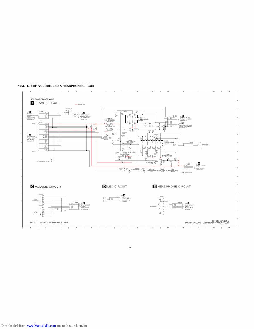
10.3. D-AMP, VOLUME, LED & HEADPHONE CIRCUIT
B
C D E
A
1 2 3 4 5 6 7 8 9 10 11 12 13 14
1 2 3 4 5 6 7 8 9 10 11 12 13 14
C
D
B
E
G
H
F
A
C
D
B
E
G
H
F
A
B
A
E
C
B
G
F
-+1
2
R63
3
22
10v4
70
C63
9
TOMAIN CIRCUIT(CP101*, CP103*)IN SCHEMATICDIAGRAM - 1
AJK600
AMPLIFIER
R64147
100C626C627
C652
0.15
0.1
C633100
100R642
CN602
1000PC613
1000PC612
1000PC614
R6321K
0R631
100C629
R634100
Q607
Q607
B1ABCF000020
JK830
HEADPHONE
R635
SWITCH
SWITCH
Q613
Q613
B1ABCF000020SWITCHSWITCH
47K
P604*
C635220016V
B1GBCFJN0009QR608
QR608
0.15C632
C631470
B1ADMF000017Q606
C6301000P
R606
AMPLIFIER
2.2
47K
R63
9
C643 1
2.2KR602
C609330
0R630
1KR821
LCD
_PA
NE
L
S822
S821
10KR629
2.2C634
0R645
MUTE SWITCH
MUTE SWITCH
SWITCH
R62710K 22K
R626
D601B0BC4R0A0066
1000PC623
C603
1000P
0.1
C60
4
C60
210
00P
Q604B1ABCF000020
C6441
47C606
C610330
C60847
IC601C1BB00000947
1000PC607
R62127K
B1ABCF000176Q609
10KR638
REGULATOR
QR601B1GKCFJN0004
LCH
2.2KR603
RCH
C63647
R62227K
2.2KR625
B1ADCF000063Q605
CN601
1KR628
C647330
IC600C1AA00000829
0.22C624
C625100
R6072.2
C628100
TUNE/SELECT
VOLUME
GNDGND
VCCGND
3.3V
MUTE
RT_N
AC_DETVCC
KEY_POWKEY0
ASP_VDD
RCHRT_P
LCHMUTE
P_ONKEY1
RV_N
TOOL0RESET
GND
RV_P
GND
LCH
GND
RCH
KEY0KEY1
HP_OPEN
POWER KEY
GNDVCC
AC_DET
5
6
1
3
4
2
8
7
17
64
23
5
1
3
2
3
1
2
3
1
2
6 75
24 3
8
1
5
4
2
3
6 1
6
5
8
9
11
12
10
18
15
17
16
20
19
13
14
7
2
1
4
3
22
21
7 56 124 3
10 12 14 16151311
8
9
GN
DG
ND
IN2
SV
R
GN
D
IN1
GN
DS
UB
GN
D
OU
T2O
UT1
+VS
BR
IDG
E
BO
OT2
BO
OT1
BIA
S
IN2
IN1
GN
D
VC
C
OU
T2
OU
T1
MU
TE
FEE
DB
AC
KFE
ED
BA
CK
P606B*
RT_NRT_P
LCD1LCD2
RV_NGND
RV_P
2
3
1
5
4
P606A*
RT_NRT_P
RV_NGND
RV_P2
3
1
5
4
P607*1
2
P603*
P830*
LCHRCH
HP_OPENGND
2
1
4
3
TO LCD SHIELD
TO CHASSIS GND W25
RL106
ROD ANTENNA
RL122
CP103*
CP101*
1PC654
0.1C653 SPEAKER
TOPOWER CIRCUIT(CN901)IN SCHEMATICDIAGRAM - 3
TOTOP KEY CIRCUIT(P800*) IN SCHEMATICDIAGRAM - 3
TOHEADPHONE CIRCUIT(P830*) IN SCHEMATICDIAGRAM - 2
TOD-AMP CIRCUIT(CN602)IN SCHEMATICDIAGRAM - 2
D-AMP CIRCUIT(P606A*)IN SCHEMATICDIAGRAM - 2
TO
MAIN CIRCUIT(CP401*, CP402*)IN SCHEMATICDIAGRAM - 1
TO
MAIN CIRCUIT(RL106*, RL122*)IN SCHEMATICDIAGRAM - 1
TO
VOLUMECONTROL CIRCUIT(P606B*)IN SCHEMATICDIAGRAM - 2
TO
RF-D10 EB/EG/GND-AMP / VOLUME / LED / HEADPHONE CIRCUITNOTE: “ * ” REF IS FOR INDICATION ONLY
D-AMP CIRCUITSCHEMATIC DIAGRAM - 2
: +B SIGNAL LINE
VOLUME CIRCUIT LED CIRCUIT HEADPHONE CIRCUIT
Downloaded from www.Manualslib.com manuals search engine Downloaded from www.Manualslib.com manuals search engine
39
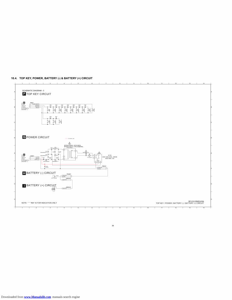
10.4. TOP KEY, POWER, BATTERY (-) & BATTERY (+) CIRCUIT
G
H
A
1 2 3 4 5 6 7 8 9 10 11 12 13 14
1 2 3 4 5 6 7 8 9 10 11 12 13 14
C
D
B
E
G
H
F
A
C
D
B
E
G
H
F
I
F
TOD-AMP
CIRCUIT
(P604)
IN SCHEMATIC
DIAGRAM - 2
B
TOD-AMP
CIRCUIT
(CN602)
IN SCHEMATIC
DIAGRAM - 2
B
D903
D903
D904B0EAKM000117
D904
VCC
TRANSFORMER
C9040.01
K9
02
*
F901
VA901ERZV05Z471CS
T901
JK901
230V~240V 50Hz...EB/GN
230V 50Hz...EGC9030.01
B0EAKM000117
BATT SPRING
ET901*
C901
0.01
B0EAKM000117
D901
C90516V2200
D906
B0ACCK000005
1K
R901
CN901D902
B0EAKM000117
K9
01
*
C9020.01
VCC T3.15A 250V
GND
(RTPN1I1E06-G...RF-D10EG)(RTPN1I1G07-G...RF-D10EB/GN)
ACDET
R8042.7K
R8032.2K
R8065.6K
R80815K
R8078.2K
R8053.9K
S8
11
ME
MO
RY
5
R81115K
ME
MO
RY
4S
80
3
ME
MO
RY
8S
80
5
S8
07
ME
MO
RY
9
S8
00
PO
WE
R
S8
08
ME
MO
RY
7
ME
MO
RY
10
S8
06
ME
MO
RY
6S
80
4
BA
ND
S8
01
ME
MO
RY
2S
80
2
R8021.5K
S8
09
ME
MO
RY
1
R8108.2K
S8
10
ME
MO
RY
3
5
8
1
4
9
2
1
3 45
1
3
2
P800*
KEY0
GND
KEY1
POWER_KEY
2
1
4
3
JW901B*
JW901A*
P902B*
BATT6V
BATT6V
GND
BATT6V
1
1
1
2
P902A*
GND
BATT6V1
2
AC IN
RF-D10 EB/EG/GNTOP KEY / POWER / BATTERY (-) / BATTERY (+) CIRCUITNOTE: “ * ” REF IS FOR INDICATION ONLY
TOP KEY CIRCUIT
SCHEMATIC DIAGRAM - 3
: +B SIGNAL LINEPOWER CIRCUIT
BATTERY (-) CIRCUIT
BATTERY (+) CIRCUIT
Downloaded from www.Manualslib.com manuals search engine Downloaded from www.Manualslib.com manuals search engine
40
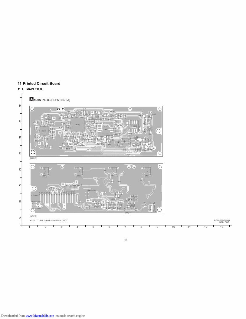
11 Printed Circuit Board11.1. MAIN P.C.B.
1 2 3 4 5 6 7 8 9
A
B
C
D
E
F
G
H
10 11 12 13
A
NOTE: " * " REF IS FOR INDICATION ONLY
3733A3733A
3733A3733A
R12
6 R12
5
C12
5
C12
7
R12
7
C102
C103
C124
IC100
IC200
IC203
X100
X400
R201
R117
R211
R219
R220
C216
C222
R238 R233
R239
C230
R230R413 R411
R504
R505
D531 R531
R532
C203
C533
C205
QR403
QR530
IC530 IC405
Q402 Q401
Q405
Q506
QR505
Q406
Q230
QR503
QR504
IC504
IC503
IC502IC204
IC205 IC505
C228
C218 C224
C400
IC400
QR201
S461
CP401*
CP402*
S462 S463 S464
R213
R214
R402
R403
R444
R443
C264 CK251
R202
R119
R109
R110
VA101
C111
C105 C107
C106
C131
C128
C12
2
C12
3
C11
8C
117
C11
4
C11
2C
110
C10
8
C10
9
L101
L102
LB10
0
C10
1
C10
4
C13
2
C11
3
R11
2
R11
1C
119
C20
1 R26
0
C20
2
C25
7
C25
2
R24
5
R27
6
C24
0
C23
9
C251
C249
C273
R442
C281 R281
C552
C561 R555
C559
R559R511C557
C560
C553
R507
D530
C408
R406
C405
R282C282
LB281
LB282
LB203
R441
C247
C244
RX203
R243
R242 C242 C245 C243
R240
R237
C241
C238
C236R236
R235
C24
8
C27
1
C27
2
C28
7
R28
3
C28
3 R44
0
R51
0
C28
5
R28
4
C28
8
C25
0
C25
6
CK
254
CK
252
CK
250
CK
238
CK
253
R12
1
R12
0
R20
6
C11
6R
116
C11
5
C21
7
R21
7
R21
8 R22
5R
227
R22
9
R21
5
R23
4
R22
6 R50
6R
412
C50
4
LB51
1
L530
C53
4
C53
2
R53
3
C53
5
C51
9
C51
8
C51
7
C51
6C
531
C53
0
C40
6R
405
C40
7
R20
4
C20
4
C55
6
C55
5
R50
8
C55
4
R55
4
R50
9
R23
1C14
6
R23
2
R22
2R
212
R22
3
R22
4
R22
1
C22
3
C40
9
C21
9
C22
0
C21
1
C20
9
R12
3
PbF
PbF
C515
C50
9
C55
1C
511
C40
4 R15
5
R15
6
C27
6C
291
R29
1C
292
R20
0
C50
1
D40
0
C10
0
C13
0
C27
5
C28
4
RL1
22
RL1
21
RL1
20
RL1
19
RL1
18
RL1
17
RL1
16
RL1
11
RL1
09
RL1
12
RL1
13
RL1
14
RL1
10
RL1
15
RL1
08
RL1
07
RL1
05
RL1
04
RL1
03
RL1
02
RL1
01
RL1
06
C28
6
R25
1
C514 C508
R404
C152 C151
LB151
C156
C155C154
C153
C401
C278
C274 R252C129
C277
C411
C412
C502
R501
C402 C403
CN205
CN103
IC401 IC402 IC403
IC501
IC201
CP101*
CP103*
(DISPLAY) (AUTOTUNE) (MENU)
(TO LCD)
(TO P607*)
(TO P607*)
(TO LCD SHIELD)
(TO SOFTWARE UPDATE)
(TO
RO
D A
NT)
(TO
CH
AS
SIS
GN
D)
(ENTER)
1
5
10
11 15 20
40 35 31
30
25
21
48
1
5
10
6
1
2
3
1
2
3
1
2
3
5
4
6
5
4
4
8
88 7 6 5
1 2 31 2
1 2
4 3
3
5 4
4
1014
751
7
6
5
45
40
35
33
1
5
10
16
17
1
23
4
8
76
5
20 25 30 32
64 60 55 49
B
EC
B E
C
B E
C
B B
E
EC
C
BE
C
BE
C
B
EC
B
EC
B
EC
B
EC
B
EC
1 2 3 4 5 6 7 8
4
3
1
2
4
3
1
2
4
3 1 2
1 2
4 3
3
5 4
1
2
MAIN P.C.B. (REPNT0073A)
RF-D10EB/EG/GNMAIN P.C.B.
(SIDE A)
(SIDE B)
Downloaded from www.Manualslib.com manuals search engine Downloaded from www.Manualslib.com manuals search engine
41
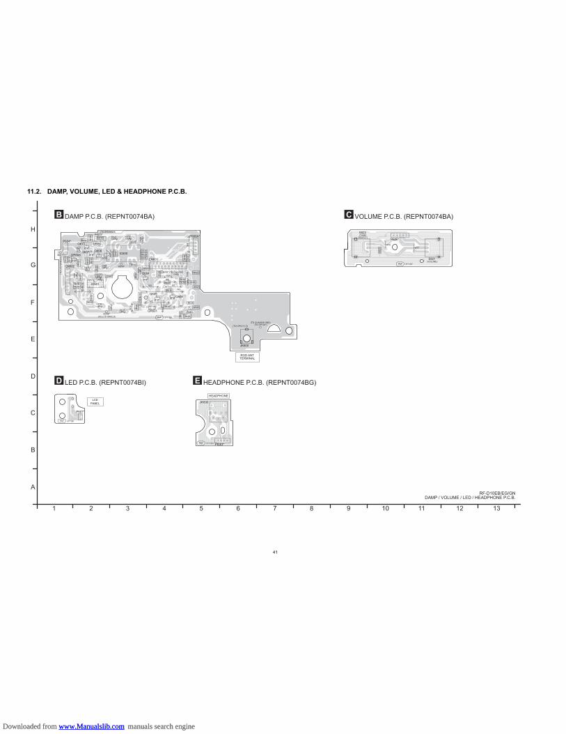
11.2. DAMP, VOLUME, LED & HEADPHONE P.C.B.
1 2 3 4 5 6 7 8 9
A
B
C
D
E
F
G
H
10 11 12 13
B C
D E
3711BF3711BF
3711BI3711BI
3711BG3711BG
3711BA3711BA
PbF
S822
P606*
(TUNE/SELECT)
(TO SPEAKER)
(TO CHASSIS GND)
(TO LCD SHIELD)
(TO
LC
D S
HIE
LD
)
(TO CHASSIS GND)
S821
P607*
P830*
JK830
(VOLUME)
W18
W17
PbF
PbF
R8
21
C652
W508
C613
C614
C623
R628
C624
QR608
W507
R632
C630
R635
C632
Q606
C602
C604
C603
R630
D601R631
QR601
IC601
Q604
R622
R625
R627
R626
Q605
C607
R638
R621
R603
C644
R639
R607
R606
C612
R602
C643
W522
W521
W520
Q609
R634Q613
R642
R629
C634
C647
R641
R645
W503
C627Q607
R633
C654
C653
JK600
C631
C626
C628
C633
C635
C625P603*
P604*
W27*
W24A*
W24B*
(TO CP101*)(TO CP103*)
W25*
IC600
CN601
CN602
C629
W3
W1
W19
C639
C606
C610
W6
C609
P606A*
C608
W9
W5 W7
W2
C636
W4
W26
PbF
3
2
1 3
2
1
3 4 521
2
1
2
26
7
4
3 15
1 43
1
43
6
1
4 5
8
3
2
1
12
1
3
2
9
87654321
16 15 14 13 12 11 10
1
2
3
4
5
6
7 9
8 22
2119
20
17
18
15
16
13
14
11
1210
1
8
5
2
3
4
6
7
1
5
4
3
2
B E
C
B E
C
B E
C
B E
C
B E
C
B E
C
B E
C
HEADPHONE
DAMP P.C.B. (REPNT0074BA) VOLUME P.C.B. (REPNT0074BA)
LED P.C.B. (REPNT0074BI) HEADPHONE P.C.B. (REPNT0074BG)
RF-D10EB/EG/GNDAMP / VOLUME / LED / HEADPHONE P.C.B.
ROD ANT TERMINAL
Downloaded from www.Manualslib.com manuals search engine Downloaded from www.Manualslib.com manuals search engine
42
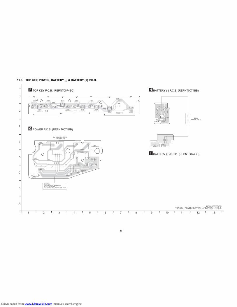
11.3. TOP KEY, POWER, BATTERY (-) & BATTERY (+) P.C.B.
1 2 3 4 5 6 7 8 9
A
B
C
D
E
F
G
H
10 11 12 13
F H
I
G
DC 6V(4 x R14/LR14, C)
230~240V 50Hz...EB/GN230V 50Hz...EG
3711BC3711BC
3711BB3711BB
3711BE3711BE
3711BD3711BD
S806(MEMORY 10)
S807(MEMORY 9)
S805(MEMORY 8)
S808(MEMORY 7)
S804(MEMORY 6)
S803(MEMORY 4)
S802(MEMORY 2)
S810 S809(MEMORY 3) (MEMORY 1) S801
P800*
F901 JK901
P902A*
CN901
T901(TRANSFORMER)
T3.15A 250V
VA901
W16
W1
4
W1
3
W1
2
W1
0
D9
04
SE
CP
RI
C9
04
C9
01
C9
03
C9
02
D9
01
D9
03
D9
02
W11
W15
C905
(BAND)S800
P902B*JW901B*
ET901*
(POWER)
S811(MEMORY 5)
PbF
PbF
PbF
PbFJW901A*
K9
01
K9
02
R807
R806
R808
R805R804
R811
R803
R810 R802
R9
01 D906
3 4 5
1
12
5
14
8 9
3
2
21 4
1
1
2
3
CAUTIONRISK OF ELECTRIC SHOCKAC VOLTAGE LINE.PLEASE DO NOT TOUCH THIS P.C.B
TOP KEY P.C.B. (REPNT0074BC) BATTERY (-) P.C.B. (REPNT0074BB)
BATTERY (+) P.C.B. (REPNT0074BB)
POWER P.C.B. (REPNT0074BB)
RF-D10EB/EG/GNTOP KEY / POWER / BATTERY (-) / BATTERY (+) P.C.B.
Downloaded from www.Manualslib.com manuals search engine Downloaded from www.Manualslib.com manuals search engine
43
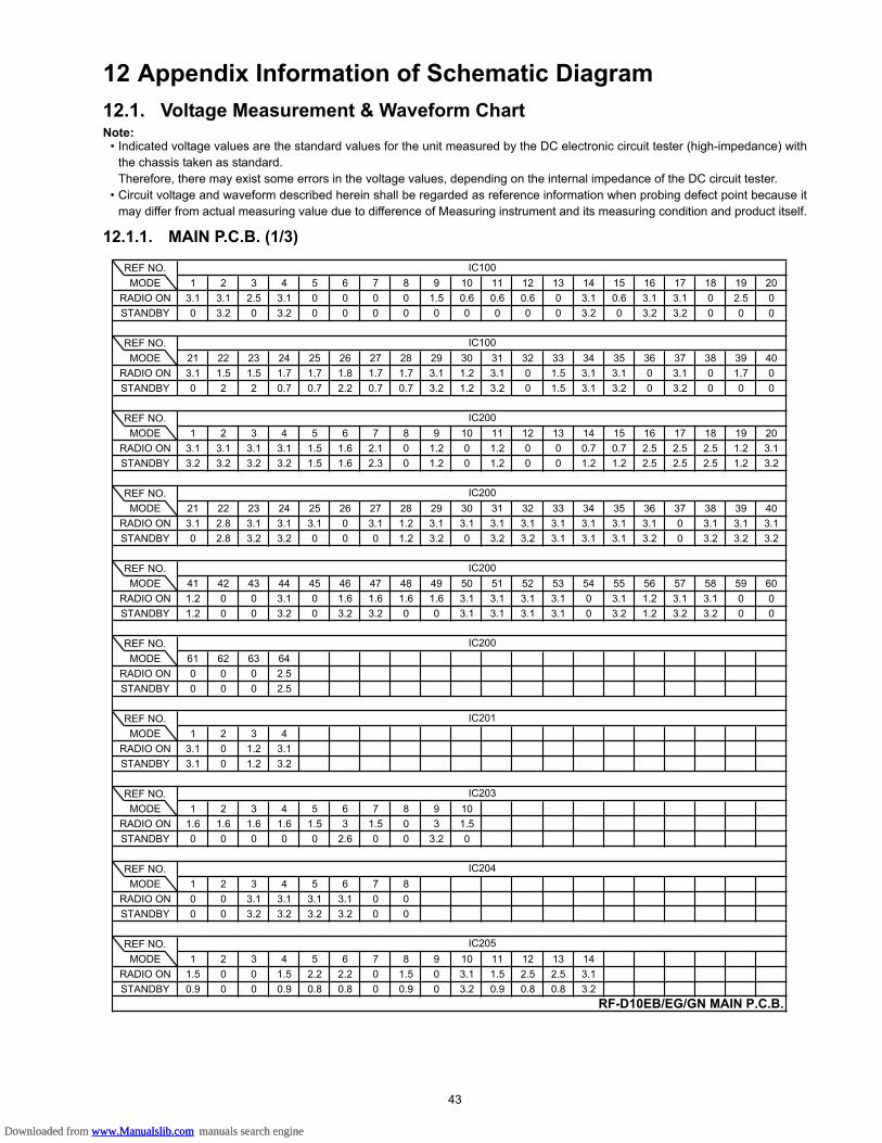
12 Appendix Information of Schematic Diagram12.1. Voltage Measurement & Waveform ChartNote:
• Indicated voltage values are the standard values for the unit measured by the DC electronic circuit tester (high-impedance) withthe chassis taken as standard.Therefore, there may exist some errors in the voltage values, depending on the internal impedance of the DC circuit tester.
• Circuit voltage and waveform described herein shall be regarded as reference information when probing defect point because itmay differ from actual measuring value due to difference of Measuring instrument and its measuring condition and product itself.
12.1.1. MAIN P.C.B. (1/3)
REF NO.
MODE 1 2 3 4 5 6 7 8 9 10 11 12 13 14 15 16 17 18 19 20
RADIO ON 3.1 3.1 2.5 3.1 0 0 0 0 1.5 0.6 0.6 0.6 0 3.1 0.6 3.1 3.1 0 2.5 0
STANDBY 0 3.2 0 3.2 0 0 0 0 0 0 0 0 0 3.2 0 3.2 3.2 0 0 0
REF NO.
MODE 21 22 23 24 25 26 27 28 29 30 31 32 33 34 35 36 37 38 39 40
RADIO ON 3.1 1.5 1.5 1.7 1.7 1.8 1.7 1.7 3.1 1.2 3.1 0 1.5 3.1 3.1 0 3.1 0 1.7 0
STANDBY 0 2 2 0.7 0.7 2.2 0.7 0.7 3.2 1.2 3.2 0 1.5 3.1 3.2 0 3.2 0 0 0
REF NO.
MODE 1 2 3 4 5 6 7 8 9 10 11 12 13 14 15 16 17 18 19 20
RADIO ON 3.1 3.1 3.1 3.1 1.5 1.6 2.1 0 1.2 0 1.2 0 0 0.7 0.7 2.5 2.5 2.5 1.2 3.1
STANDBY 3.2 3.2 3.2 3.2 1.5 1.6 2.3 0 1.2 0 1.2 0 0 1.2 1.2 2.5 2.5 2.5 1.2 3.2
REF NO.
MODE 21 22 23 24 25 26 27 28 29 30 31 32 33 34 35 36 37 38 39 40
RADIO ON 3.1 2.8 3.1 3.1 3.1 0 3.1 1.2 3.1 3.1 3.1 3.1 3.1 3.1 3.1 3.1 0 3.1 3.1 3.1
STANDBY 0 2.8 3.2 3.2 0 0 0 1.2 3.2 0 3.2 3.2 3.1 3.1 3.1 3.2 0 3.2 3.2 3.2
REF NO.
MODE 41 42 43 44 45 46 47 48 49 50 51 52 53 54 55 56 57 58 59 60
RADIO ON 1.2 0 0 3.1 0 1.6 1.6 1.6 1.6 3.1 3.1 3.1 3.1 0 3.1 1.2 3.1 3.1 0 0
STANDBY 1.2 0 0 3.2 0 3.2 3.2 0 0 3.1 3.1 3.1 3.1 0 3.2 1.2 3.2 3.2 0 0
REF NO.
MODE 61 62 63 64
RADIO ON 0 0 0 2.5
STANDBY 0 0 0 2.5
REF NO.
MODE 1 2 3 4
RADIO ON 3.1 0 1.2 3.1
STANDBY 3.1 0 1.2 3.2
REF NO.
MODE 1 2 3 4 5 6 7 8 9 10
RADIO ON 1.6 1.6 1.6 1.6 1.5 3 1.5 0 3 1.5
STANDBY 0 0 0 0 0 2.6 0 0 3.2 0
REF NO.
MODE 1 2 3 4 5 6 7 8
RADIO ON 0 0 3.1 3.1 3.1 3.1 0 0
STANDBY 0 0 3.2 3.2 3.2 3.2 0 0
REF NO.
MODE 1 2 3 4 5 6 7 8 9 10 11 12 13 14
RADIO ON 1.5 0 0 1.5 2.2 2.2 0 1.5 0 3.1 1.5 2.5 2.5 3.1
STANDBY 0.9 0 0 0.9 0.8 0.8 0 0.9 0 3.2 0.9 0.8 0.8 3.2
IC100
IC100
IC200
IC200
IC200
RF-D10EB/EG/GN MAIN P.C.B.
IC200
IC201
IC203
IC204
IC205
Downloaded from www.Manualslib.com manuals search engine Downloaded from www.Manualslib.com manuals search engine
44
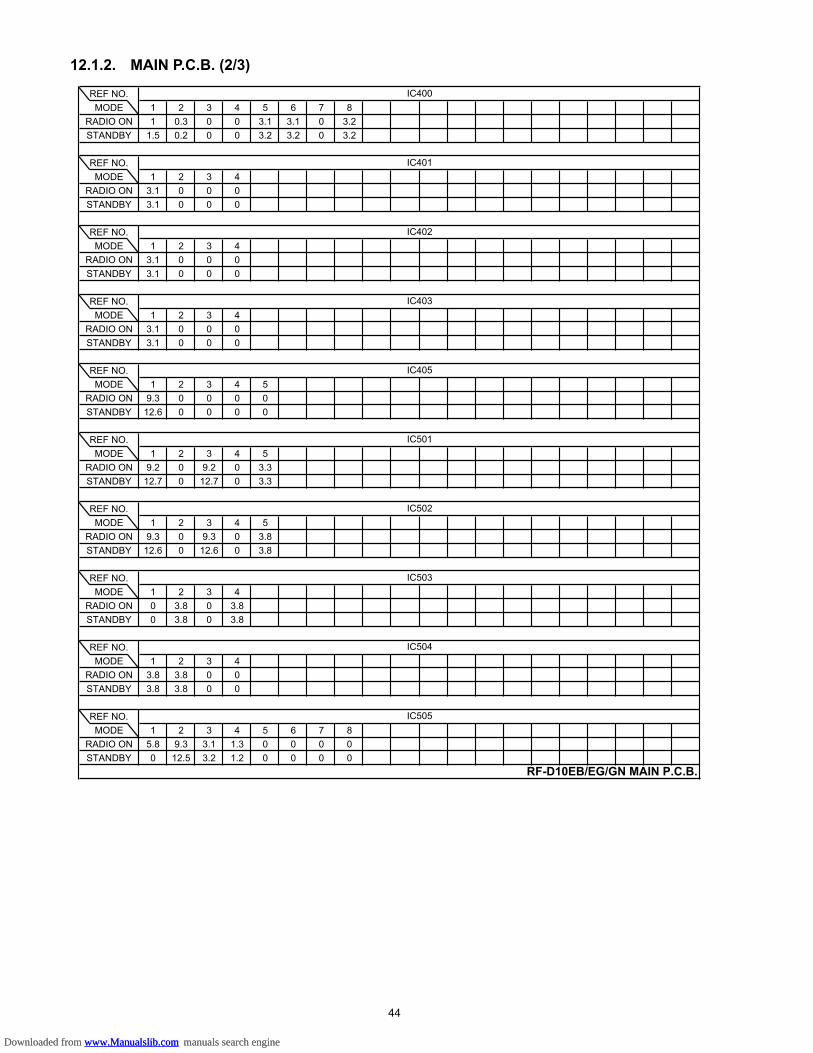
12.1.2. MAIN P.C.B. (2/3)
REF NO.
MODE 1 2 3 4 5 6 7 8
RADIO ON 1 0.3 0 0 3.1 3.1 0 3.2
STANDBY 1.5 0.2 0 0 3.2 3.2 0 3.2
REF NO.
MODE 1 2 3 4
RADIO ON 3.1 0 0 0
STANDBY 3.1 0 0 0
REF NO.
MODE 1 2 3 4
RADIO ON 3.1 0 0 0
STANDBY 3.1 0 0 0
REF NO.
MODE 1 2 3 4
RADIO ON 3.1 0 0 0
STANDBY 3.1 0 0 0
REF NO.
MODE 1 2 3 4 5
RADIO ON 9.3 0 0 0 0
STANDBY 12.6 0 0 0 0
REF NO.
MODE 1 2 3 4 5
RADIO ON 9.2 0 9.2 0 3.3
STANDBY 12.7 0 12.7 0 3.3
REF NO.
MODE 1 2 3 4 5
RADIO ON 9.3 0 9.3 0 3.8
STANDBY 12.6 0 12.6 0 3.8
REF NO.
MODE 1 2 3 4
RADIO ON 0 3.8 0 3.8
STANDBY 0 3.8 0 3.8
REF NO.
MODE 1 2 3 4
RADIO ON 3.8 3.8 0 0
STANDBY 3.8 3.8 0 0
REF NO.
MODE 1 2 3 4 5 6 7 8
RADIO ON 5.8 9.3 3.1 1.3 0 0 0 0
STANDBY 0 12.5 3.2 1.2 0 0 0 0
IC400
IC401
IC402
IC403
IC405
RF-D10EB/EG/GN MAIN P.C.B.
IC501
IC502
IC503
IC504
IC505
Downloaded from www.Manualslib.com manuals search engine Downloaded from www.Manualslib.com manuals search engine
45
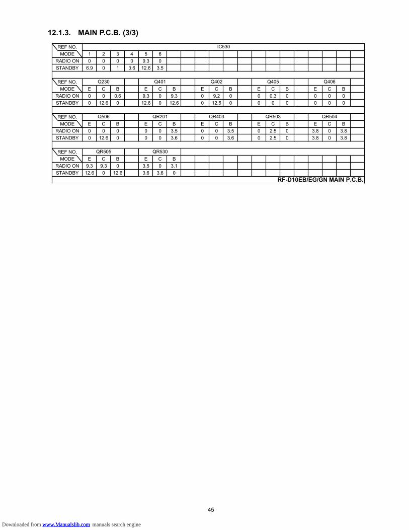
12.1.3. MAIN P.C.B. (3/3)
REF NO.
MODE 1 2 3 4 5 6
RADIO ON 0 0 0 0 9.3 0
STANDBY 6.9 0 1 3.6 12.6 3.5
REF NO.
MODE E C B E C B E C B E C B E C B
RADIO ON 0 0 0.6 9.3 0 9.3 0 9.2 0 0 0.3 0 0 0 0
STANDBY 0 12.6 0 12.6 0 12.6 0 12.5 0 0 0 0 0 0 0
REF NO.
MODE E C B E C B E C B E C B E C B
RADIO ON 0 0 0 0 0 3.5 0 0 3.5 0 2.5 0 3.8 0 3.8
STANDBY 0 12.6 0 0 0 3.6 0 0 3.6 0 2.5 0 3.8 0 3.8
REF NO.
MODE E C B E C B
RADIO ON 9.3 9.3 0 3.5 0 3.1
STANDBY 12.6 0 12.6 3.6 3.6 0
RF-D10EB/EG/GN MAIN P.C.B.
IC530
Q230 Q401 Q402 Q405
QR505 QR530
Q406
Q506 QR201 QR403 QR503 QR504
Downloaded from www.Manualslib.com manuals search engine Downloaded from www.Manualslib.com manuals search engine

46
Downloaded from www.Manualslib.com manuals search engine Downloaded from www.Manualslib.com manuals search engine
47
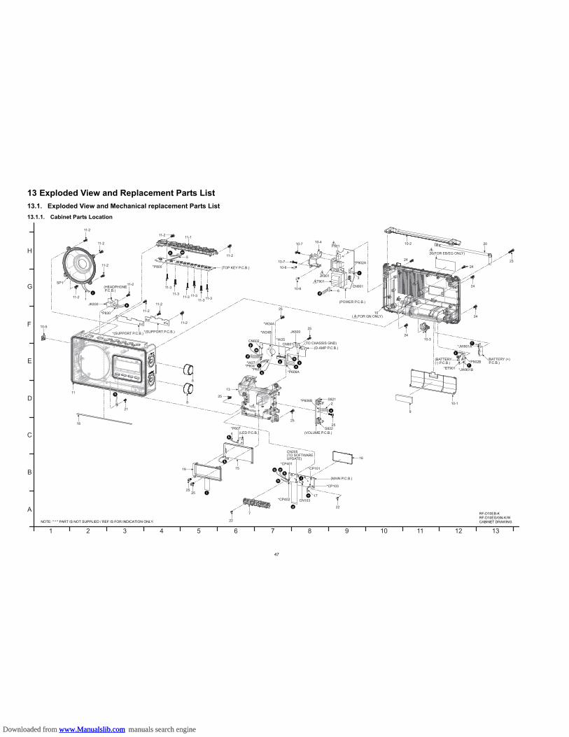
13 Exploded View and Replacement Parts List13.1. Exploded View and Mechanical replacement Parts List13.1.1. Cabinet Parts Location
*P606B
(VOLUME P.C.B.)
*(SUPPORT P.C.B.) *(SUPPORT P.C.B.)
*W27
*W24B
*W25
*W24A
(TO CHASSIS GND)
*P603*P604
(D-AMP P.C.B.)
(POWER P.C.B.)
*CP103
*CP101*CP401
*CP402
(MAIN P.C.B.)
*P607(LED P.C.B.)
(TOP KEY P.C.B.)*P800
*P830
(HEADPHONE P.C.B.)
(BATTERY (+) P.C.B.)
(BATTERY (-) P.C.B.) *P902B
*JW901B
*JW901A
*ET901
JK901
JK830
F901
*P902A
T901
JK600
CN901
CN602CN601
*P606A
CN205(TO SOFTWARE UPDATE)
CN103
S822
S821
SP1
26(FOR EB/EG ONLY)
2525
2525
25
25
25
24
24
24
24
2423
22
22
21
20
19
18
17
16
15
13
11-311-311-311-3
11-3
11-311-2
11-2
11-2
11-2
11-2
11-2
11-2
11-2
11-2
11-2
11-1
11
10-7
10-7
10-6
10-6
10-5
10-4
10-3
10-2
10-1
10( FOR GN ONLY)
9
8
8
7
6
5
4
3
2
1
o
o
n
n
m
m
k
k
i
ih
h
g
g
f
f
e
ed
dc
c
b
b
a
a
p
q
pq
1 2 3 4 5 6 7 8 9
A
B
C
D
E
F
G
H
10 11 12 13CABINET DRAWINGNOTE: " * " PART IS NOT SUPPLIED / REF IS FOR INDICATION ONLY.
RF-D10EB-KRF-D10EG/GN-K/W
Downloaded from www.Manualslib.com manuals search engine Downloaded from www.Manualslib.com manuals search engine
48
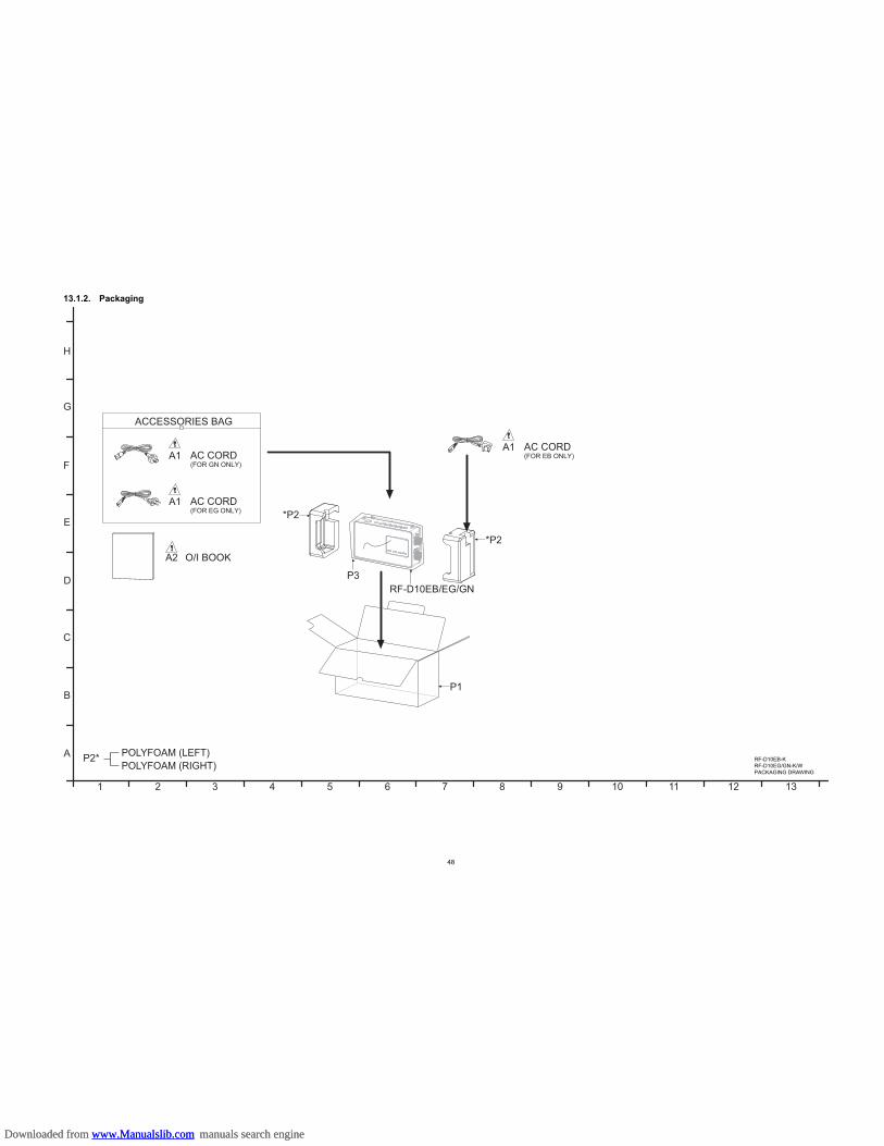
13.1.2. Packaging
RF-D10EB/EG/GN
RF-D10EB-KRF-D10EG/GN-K/WPACKAGING DRAWING
P2* POLYFOAM (LEFT)POLYFOAM (RIGHT)
ACCESSORIES BAG
P3
*P2
*P2
P1
A2 O/I BOOK
AC CORD(FOR GN ONLY)
A1
AC CORD(FOR EG ONLY)
A1
AC CORD(FOR EB ONLY)
A1
1 2 3 4 5 6 7 8 9
A
B
C
D
E
F
G
H
10 11 12 13
Downloaded from www.Manualslib.com manuals search engine Downloaded from www.Manualslib.com manuals search engine
49
13.1.3. Mechanical Replacement Parts List
Safety Ref. No. Part No. Part Name & Description
QTY Remarks
CABINET AND CHASSIS
1 RWJ4202120XG 2P WIRE (SP1 - D-AMP)
1
2 RWJ0205095XX 5P WIRE (VOLUME - D-AMP)
1
3 RWJ4202250XX 2P WIRE (POWER - BATTERY(-))
1
4 REEN0030 2P WIRE (LED - MAIN)
1
5 REXN0092-1 8P WIRE(HEAD-PHONE & TOP KEY - D-AMP)
1
6 REXN0093-1 3P WIRE (POWER - D-AMP)
1
7 RGUN0062-K FRONT BUTTON 1 EB/EG/GN-K
7 RGUN0062-W FRONT BUTTON 1 EG/GN-W8 RGWN0024-1S ROTARY KNOB 2 EB/EG/
GN-K8 RGWN0024-2S ROTARY KNOB 2 EG/GN-W9 RMQN0025 BATTERY CUSHION 110 RYKN0119B-K BACK CABINET
ASS'Y1 EG-K
10 RYKN0119C-K BACK CABINET ASS'Y
1 GN-K
10 RYKN0119C-W BACK CABINET ASS'Y
1 GN-W
10 RYKN0119B-W BACK CABINET ASS'Y
1 EG-W
10 RYKN0119D-K BACK CABINET ASS'Y
1 EB-K
10-1 RKK0084-W1 BATTERY COVER 1 EG/GN-W10-1 RKK0084-1K BATTERY COVER 1 EB/EG/
GN-K10-2 RKH0028-W1 HANDLE 1 EG/GN-W10-2 RKH0028-K HANDLE 1 EB/EG/
GN-K10-3 RJC92002-2 BATTERY TERMINAL 110-4 RMAN0053 AC IN BRACKET 110-5 RMVN0095-K1 JACK HOLE COVER 1 EB/EG/
GN-K10-5 RMVN0095-W1 JACK HOLE COVER 1 EG/GN-W10-6 XTV3+10GFJ SCREW 210-7 XTV3+8FFJ SCREW 211 RYKN0118A-K FRONT CABINET
ASS'Y1 EB/EG/
GN-K11 RYKN0118A-W FRONT CABINET
ASS'Y1 EG/GN-W
11-1 RGUN0061-3S TOP BUTTON 1 EB/EG/GN-K
11-1 RGUN0061-4S TOP BUTTON 1 EG/GN-W11-2 XTV3+10GFJ SCREW 1011-3 XTV3+8GFJ SCREW 613 RMKN0014-1 MAIN CHASSIS 115 RMVN0092 LCD SHIELD 116 RMVN0094 MAIN PCB SHIELD 117 RWK101110 2P WIRE(MAIN -
D-AMP)1
18 RMVN0096 HIMERON 119 L5DYAYY00123 LCD MODULE 120 XEARR150EA-2 ROD ANTENNA 121 XTN2+3FFJ SCREW 1
Safety Ref. No. Part No. Part Name & Description
QTY Remarks
Downloaded from www.Manualslib.com manuals search engine Downloaded from www.Manualslib.com manuals search engine
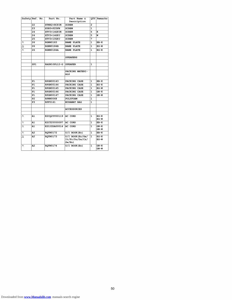
50
22 XTNR2+8CFJK SCREW 223 XYN3+F25FN SCREW 124 XTV3+14GFJK SCREW 5 K24 XTV3+14GFJ SCREW 5 W25 XTV3+10GFJ SCREW 726 RGNN0183 NAME PLATE 1 EB-K
26 RGNN0184B NAME PLATE 1 EG-W
26 RGNN0184A NAME PLATE 1 EG-K
SPEAKERS
SP1 RASN10PL12-G SPEAKER 1
PACKING MATERI-ALS
P1 RPGN00143 PACKING CASE 1 EB-KP1 RPGN00144 PACKING CASE 1 EG-KP1 RPGN00145 PACKING CASE 1 EG-WP1 RPGN00146 PACKING CASE 1 GN-KP1 RPGN00147 PACKING CASE 1 GN-WP2 RPNN0068 POLYFOAM 1P3 RPF0161 MIRAMAT BAG 1
ACCESSORIES
A1 K2CQ2YY00119 AC CORD 1 EG-K EG-W
A1 K2CT2YY00097 AC CORD 1 EB-K
A1 K2CJ2DA00014 AC CORD 1 GN-K GN-W
A2 RQTN0172 O/I BOOK(En) 1 EB-K
A2 RQTN0173 O/I BOOK(En/Ge/It/Fr/Du/Da/Cz/Sw/No)
1 EG-K EG-W
A2 RQTN0174 O/I BOOK(En) 1 GN-K GN-W
Safety Ref. No. Part No. Part Name & Description
QTY Remarks
Downloaded from www.Manualslib.com manuals search engine Downloaded from www.Manualslib.com manuals search engine
51
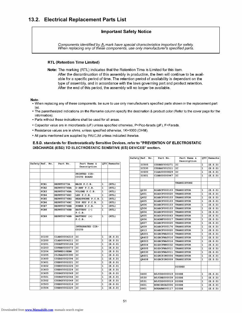
13.2. Electrical Replacement Parts List
Safety Ref. No. Part No. Part Name & Description
QTY Remarks
PRINTED CIR-CUITS BOARD
PCB1 REPNT0073A MAIN P.C.B. 1 (RTL)PCB2 REPNT0074BA D-AMP P.C.B. 1 (RTL)PCB3 REPNT0074BA VOLUME P.C.B. 1 (RTL)PCB4 REPNT0074BI LED P.C.B. 1 (RTL)PCB5 REPNT0074BG HEADPHONE P.C.B. 1 (RTL)PCB6 REPNT0074BC TOP KEY P.C.B. 1 (RTL)PCB7 REPNT0074BB POWER P.C.B. 1 (RTL)PCB8 REPNT0074BB BATTERY (-)
P.C.B.1 (RTL)
PCB9 REPNT0074BB BATTERY (+) P.C.B.
1 (RTL)
INTEGRATED CIR-CUITS
IC100 C1AB00004210 IC 1 (E.S.D)IC200 C1AB00004211 IC 1 (E.S.D)IC201 C0DBFYY00164 IC 1 (E.S.D)IC203 C0FBBY000073 IC 1 (E.S.D)IC204 RFKWED10EBM IC 1 (E.S.D)IC205 C0JBAS000390 IC 1 (E.S.D)IC400 C0ZBZ0002094 IC 1 (E.S.D)IC401 C0EBY0002221 IC 1 (E.S.D)IC402 C0EBY0002226 IC 1 (E.S.D)IC403 C0EBY0002224 IC 1 (E.S.D)IC405 C0DBGYY02049 IC 1 (E.S.D)IC501 C0DBGYY02044 IC 1 (E.S.D)IC502 C0DBGYY02049 IC 1 (E.S.D)IC503 C0EBY0002216 IC 1 (E.S.D)IC504 C0EBY0002225 IC 1 (E.S.D)
IC505 C0DBEYY00271 IC 1 (E.S.D)IC530 C0DBAYY01511 IC 1 (E.S.D)IC600 C1AA00000829 IC 1 (E.S.D)IC601 C1BB00000947 IC 1 (E.S.D)
TRANSISTORS
Q230 B1ABCF000103 TRANSISTOR 1 (E.S.D)Q401 B1ADCF000020 TRANSISTOR 1 (E.S.D)Q402 B1ABCF000103 TRANSISTOR 1 (E.S.D)Q405 B1ABCF000103 TRANSISTOR 1 (E.S.D)Q406 B1ABCF000103 TRANSISTOR 1 (E.S.D)Q506 B1ABCF000103 TRANSISTOR 1 (E.S.D)Q604 B1ABCF000020 TRANSISTOR 1 (E.S.D)Q605 B1ADCF000063 TRANSISTOR 1 (E.S.D)Q606 B1ADMF000017 TRANSISTOR 1 (E.S.D)Q607 B1ABCF000020 TRANSISTOR 1 (E.S.D)Q609 B1ABCF000176 TRANSISTOR 1 (E.S.D)Q613 B1ABCF000020 TRANSISTOR 1 (E.S.D)QR201 B1GBCFNA0016 TRANSISTOR 1 (E.S.D)QR403 B1GBCFNA0016 TRANSISTOR 1 (E.S.D)QR503 B1GBCFNA0016 TRANSISTOR 1 (E.S.D)QR504 B1GDCFNN0032 TRANSISTOR 1 (E.S.D)QR505 B1GDCFNA0011 TRANSISTOR 1 (E.S.D)QR530 B1GDCFNA0011 TRANSISTOR 1 (E.S.D)QR601 B1GKCFJN0004 TRANSISTOR 1 (E.S.D)QR608 B1GBCFJN0009 TRANSISTOR 1 (E.S.D)
DIODES
D400 B0JCDD000019 DIODE 1 (E.S.D)D530 B0JCNE000039 DIODE 1 (E.S.D)D531 B0JCDD000019 DIODE 1 (E.S.D)D601 B0BC4R0A0006 DIODE 1 (E.S.D)D901 B0EAKM000117 DIODE 1 (E.S.D)
Safety Ref. No. Part No. Part Name & Description
QTY Remarks
Downloaded from www.Manualslib.com manuals search engine Downloaded from www.Manualslib.com manuals search engine
52
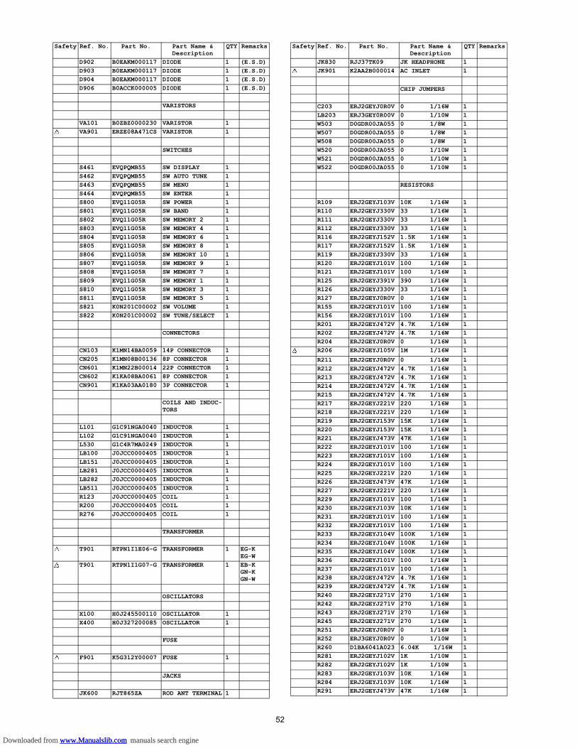
D902 B0EAKM000117 DIODE 1 (E.S.D)D903 B0EAKM000117 DIODE 1 (E.S.D)D904 B0EAKM000117 DIODE 1 (E.S.D)D906 B0ACCK000005 DIODE 1 (E.S.D)
VARISTORS
VA101 B0ZBZ0000230 VARISTOR 1VA901 ERZE08A471CS VARISTOR 1
SWITCHES
S461 EVQPQMB55 SW DISPLAY 1S462 EVQPQMB55 SW AUTO TUNE 1S463 EVQPQMB55 SW MENU 1S464 EVQPQMB55 SW ENTER 1S800 EVQ11G05R SW POWER 1S801 EVQ11G05R SW BAND 1S802 EVQ11G05R SW MEMORY 2 1S803 EVQ11G05R SW MEMORY 4 1S804 EVQ11G05R SW MEMORY 6 1S805 EVQ11G05R SW MEMORY 8 1S806 EVQ11G05R SW MEMORY 10 1S807 EVQ11G05R SW MEMORY 9 1S808 EVQ11G05R SW MEMORY 7 1S809 EVQ11G05R SW MEMORY 1 1S810 EVQ11G05R SW MEMORY 3 1S811 EVQ11G05R SW MEMORY 5 1S821 K0N201C00002 SW VOLUME 1S822 K0N201C00002 SW TUNE/SELECT 1
CONNECTORS
CN103 K1MN14BA0059 14P CONNECTOR 1CN205 K1MN08B00136 8P CONNECTOR 1CN601 K1MN22B00014 22P CONNECTOR 1CN602 K1KA08BA0061 8P CONNECTOR 1CN901 K1KA03AA0180 3P CONNECTOR 1
COILS AND INDUC-TORS
L101 G1C91NGA0040 INDUCTOR 1L102 G1C91NGA0040 INDUCTOR 1L530 G1C4R7MA0249 INDUCTOR 1LB100 J0JCC0000405 INDUCTOR 1LB151 J0JCC0000405 INDUCTOR 1LB281 J0JCC0000405 INDUCTOR 1LB282 J0JCC0000405 INDUCTOR 1LB511 J0JCC0000405 INDUCTOR 1R123 J0JCC0000405 COIL 1R200 J0JCC0000405 COIL 1R276 J0JCC0000405 COIL 1
TRANSFORMER
T901 RTPN1I1E06-G TRANSFORMER 1 EG-K EG-W
T901 RTPN1I1G07-G TRANSFORMER 1 EB-K GN-K GN-W
OSCILLATORS
X100 H0J245500110 OSCILLATOR 1X400 H0J327200085 OSCILLATOR 1
FUSE
F901 K5G312Y00007 FUSE 1
JACKS
JK600 RJT865ZA ROD ANT TERMINAL 1
Safety Ref. No. Part No. Part Name & Description
QTY Remarks
JK830 RJJ37TK09 JK HEADPHONE 1JK901 K2AA2B000014 AC INLET 1
CHIP JUMPERS
C203 ERJ2GEYJ0R0V 0 1/16W 1LB203 ERJ3GEY0R00V 0 1/10W 1W503 D0GDR00JA055 0 1/8W 1W507 D0GDR00JA055 0 1/8W 1W508 D0GDR00JA055 0 1/8W 1W520 D0GDR00JA055 0 1/10W 1W521 D0GDR00JA055 0 1/10W 1W522 D0GDR00JA055 0 1/10W 1
RESISTORS
R109 ERJ2GEYJ103V 10K 1/16W 1R110 ERJ2GEYJ330V 33 1/16W 1R111 ERJ2GEYJ330V 33 1/16W 1R112 ERJ2GEYJ330V 33 1/16W 1R116 ERJ2GEYJ152V 1.5K 1/16W 1R117 ERJ2GEYJ152V 1.5K 1/16W 1R119 ERJ2GEYJ330V 33 1/16W 1R120 ERJ2GEYJ101V 100 1/16W 1R121 ERJ2GEYJ101V 100 1/16W 1R125 ERJ2GEYJ391V 390 1/16W 1R126 ERJ2GEYJ330V 33 1/16W 1R127 ERJ2GEYJ0R0V 0 1/16W 1R155 ERJ2GEYJ101V 100 1/16W 1R156 ERJ2GEYJ101V 100 1/16W 1R201 ERJ2GEYJ472V 4.7K 1/16W 1R202 ERJ2GEYJ472V 4.7K 1/16W 1R204 ERJ2GEYJ0R0V 0 1/16W 1R206 ERJ2GEYJ105V 1M 1/16W 1
R211 ERJ2GEYJ0R0V 0 1/16W 1R212 ERJ2GEYJ472V 4.7K 1/16W 1R213 ERJ2GEYJ472V 4.7K 1/16W 1R214 ERJ2GEYJ472V 4.7K 1/16W 1R215 ERJ2GEYJ472V 4.7K 1/16W 1R217 ERJ2GEYJ221V 220 1/16W 1R218 ERJ2GEYJ221V 220 1/16W 1R219 ERJ2GEYJ153V 15K 1/16W 1R220 ERJ2GEYJ153V 15K 1/16W 1R221 ERJ2GEYJ473V 47K 1/16W 1R222 ERJ2GEYJ101V 100 1/16W 1R223 ERJ2GEYJ101V 100 1/16W 1R224 ERJ2GEYJ101V 100 1/16W 1R225 ERJ2GEYJ221V 220 1/16W 1R226 ERJ2GEYJ473V 47K 1/16W 1R227 ERJ2GEYJ221V 220 1/16W 1R229 ERJ2GEYJ101V 100 1/16W 1R230 ERJ2GEYJ103V 10K 1/16W 1R231 ERJ2GEYJ101V 100 1/16W 1R232 ERJ2GEYJ101V 100 1/16W 1R233 ERJ2GEYJ104V 100K 1/16W 1R234 ERJ2GEYJ104V 100K 1/16W 1R235 ERJ2GEYJ104V 100K 1/16W 1R236 ERJ2GEYJ101V 100 1/16W 1R237 ERJ2GEYJ101V 100 1/16W 1R238 ERJ2GEYJ472V 4.7K 1/16W 1R239 ERJ2GEYJ472V 4.7K 1/16W 1R240 ERJ2GEYJ271V 270 1/16W 1R242 ERJ2GEYJ271V 270 1/16W 1R243 ERJ2GEYJ271V 270 1/16W 1R245 ERJ2GEYJ271V 270 1/16W 1R251 ERJ2GEYJ0R0V 0 1/16W 1R252 ERJ3GEYJ0R0V 0 1/10W 1R260 D1BA6041A023 6.04K 1/16W 1R281 ERJ2GEYJ102V 1K 1/10W 1R282 ERJ2GEYJ102V 1K 1/10W 1R283 ERJ2GEYJ103V 10K 1/16W 1R284 ERJ2GEYJ103V 10K 1/16W 1R291 ERJ2GEYJ473V 47K 1/16W 1
Safety Ref. No. Part No. Part Name & Description
QTY Remarks
Downloaded from www.Manualslib.com manuals search engine Downloaded from www.Manualslib.com manuals search engine
53
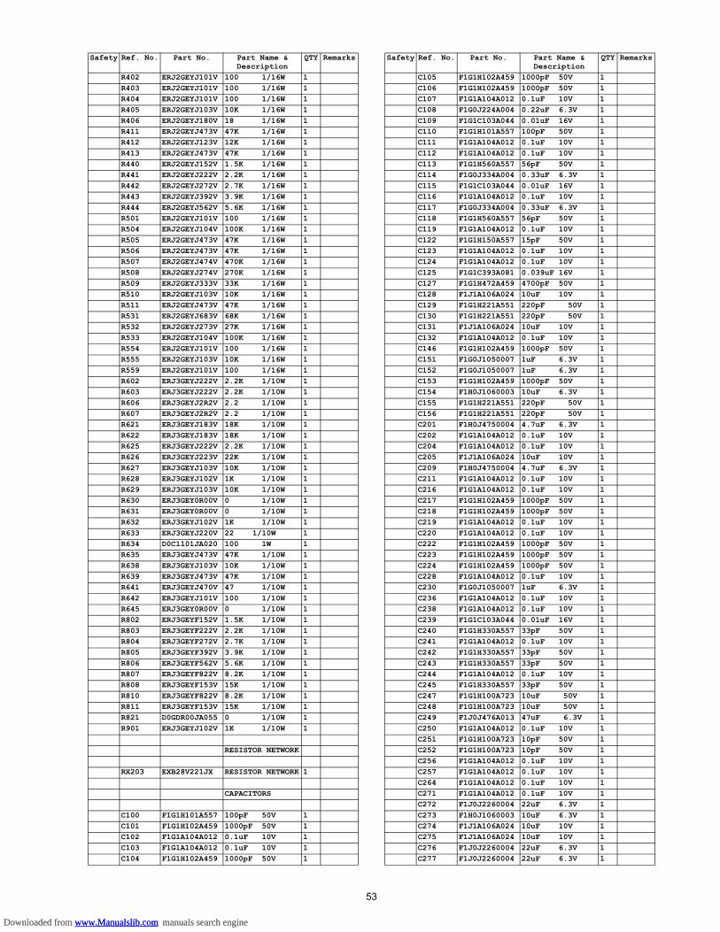
R402 ERJ2GEYJ101V 100 1/16W 1R403 ERJ2GEYJ101V 100 1/16W 1R404 ERJ2GEYJ101V 100 1/16W 1R405 ERJ2GEYJ103V 10K 1/16W 1R406 ERJ2GEYJ180V 18 1/16W 1R411 ERJ2GEYJ473V 47K 1/16W 1R412 ERJ2GEYJ123V 12K 1/16W 1R413 ERJ2GEYJ473V 47K 1/16W 1R440 ERJ2GEYJ152V 1.5K 1/16W 1R441 ERJ2GEYJ222V 2.2K 1/16W 1R442 ERJ2GEYJ272V 2.7K 1/16W 1R443 ERJ2GEYJ392V 3.9K 1/16W 1R444 ERJ2GEYJ562V 5.6K 1/16W 1R501 ERJ2GEYJ101V 100 1/16W 1R504 ERJ2GEYJ104V 100K 1/16W 1R505 ERJ2GEYJ473V 47K 1/16W 1R506 ERJ2GEYJ473V 47K 1/16W 1R507 ERJ2GEYJ474V 470K 1/16W 1R508 ERJ2GEYJ274V 270K 1/16W 1R509 ERJ2GEYJ333V 33K 1/16W 1R510 ERJ2GEYJ103V 10K 1/16W 1R511 ERJ2GEYJ473V 47K 1/16W 1R531 ERJ2GEYJ683V 68K 1/16W 1R532 ERJ2GEYJ273V 27K 1/16W 1R533 ERJ2GEYJ104V 100K 1/16W 1R554 ERJ2GEYJ101V 100 1/16W 1R555 ERJ2GEYJ103V 10K 1/16W 1R559 ERJ2GEYJ101V 100 1/16W 1R602 ERJ3GEYJ222V 2.2K 1/10W 1R603 ERJ3GEYJ222V 2.2K 1/10W 1R606 ERJ3GEYJ2R2V 2.2 1/10W 1R607 ERJ3GEYJ2R2V 2.2 1/10W 1R621 ERJ3GEYJ183V 18K 1/10W 1R622 ERJ3GEYJ183V 18K 1/10W 1R625 ERJ3GEYJ222V 2.2K 1/10W 1R626 ERJ3GEYJ223V 22K 1/10W 1R627 ERJ3GEYJ103V 10K 1/10W 1R628 ERJ3GEYJ102V 1K 1/10W 1R629 ERJ3GEYJ103V 10K 1/10W 1R630 ERJ3GEY0R00V 0 1/10W 1R631 ERJ3GEY0R00V 0 1/10W 1R632 ERJ3GEYJ102V 1K 1/10W 1R633 ERJ3GEYJ220V 22 1/10W 1R634 D0C1101JA020 100 1W 1R635 ERJ3GEYJ473V 47K 1/10W 1R638 ERJ3GEYJ103V 10K 1/10W 1R639 ERJ3GEYJ473V 47K 1/10W 1R641 ERJ3GEYJ470V 47 1/10W 1R642 ERJ3GEYJ101V 100 1/10W 1R645 ERJ3GEY0R00V 0 1/10W 1R802 ERJ3GEYF152V 1.5K 1/10W 1R803 ERJ3GEYF222V 2.2K 1/10W 1R804 ERJ3GEYF272V 2.7K 1/10W 1R805 ERJ3GEYF392V 3.9K 1/10W 1R806 ERJ3GEYF562V 5.6K 1/10W 1R807 ERJ3GEYF822V 8.2K 1/10W 1R808 ERJ3GEYF153V 15K 1/10W 1R810 ERJ3GEYF822V 8.2K 1/10W 1R811 ERJ3GEYF153V 15K 1/10W 1R821 D0GDR00JA055 0 1/10W 1R901 ERJ3GEYJ102V 1K 1/10W 1
RESISTOR NETWORK
RX203 EXB28V221JX RESISTOR NETWORK 1
CAPACITORS
C100 F1G1H101A557 100pF 50V 1C101 F1G1H102A459 1000pF 50V 1C102 F1G1A104A012 0.1uF 10V 1C103 F1G1A104A012 0.1uF 10V 1C104 F1G1H102A459 1000pF 50V 1
Safety Ref. No. Part No. Part Name & Description
QTY Remarks
C105 F1G1H102A459 1000pF 50V 1C106 F1G1H102A459 1000pF 50V 1C107 F1G1A104A012 0.1uF 10V 1C108 F1G0J224A004 0.22uF 6.3V 1C109 F1G1C103A044 0.01uF 16V 1C110 F1G1H101A557 100pF 50V 1C111 F1G1A104A012 0.1uF 10V 1C112 F1G1A104A012 0.1uF 10V 1C113 F1G1H560A557 56pF 50V 1C114 F1G0J334A004 0.33uF 6.3V 1C115 F1G1C103A044 0.01uF 16V 1C116 F1G1A104A012 0.1uF 10V 1C117 F1G0J334A004 0.33uF 6.3V 1C118 F1G1H560A557 56pF 50V 1C119 F1G1A104A012 0.1uF 10V 1C122 F1G1H150A557 15pF 50V 1C123 F1G1A104A012 0.1uF 10V 1C124 F1G1A104A012 0.1uF 10V 1C125 F1G1C393A081 0.039uF 16V 1C127 F1G1H472A459 4700pF 50V 1C128 F1J1A106A024 10uF 10V 1C129 F1G1H221A551 220pF 50V 1C130 F1G1H221A551 220pF 50V 1C131 F1J1A106A024 10uF 10V 1C132 F1G1A104A012 0.1uF 10V 1C146 F1G1H102A459 1000pF 50V 1C151 F1G0J1050007 1uF 6.3V 1C152 F1G0J1050007 1uF 6.3V 1C153 F1G1H102A459 1000pF 50V 1C154 F1H0J1060003 10uF 6.3V 1C155 F1G1H221A551 220pF 50V 1C156 F1G1H221A551 220pF 50V 1C201 F1H0J4750004 4.7uF 6.3V 1C202 F1G1A104A012 0.1uF 10V 1C204 F1G1A104A012 0.1uF 10V 1C205 F1J1A106A024 10uF 10V 1C209 F1H0J4750004 4.7uF 6.3V 1C211 F1G1A104A012 0.1uF 10V 1C216 F1G1A104A012 0.1uF 10V 1C217 F1G1H102A459 1000pF 50V 1C218 F1G1H102A459 1000pF 50V 1C219 F1G1A104A012 0.1uF 10V 1C220 F1G1A104A012 0.1uF 10V 1C222 F1G1H102A459 1000pF 50V 1C223 F1G1H102A459 1000pF 50V 1C224 F1G1H102A459 1000pF 50V 1C228 F1G1A104A012 0.1uF 10V 1C230 F1G0J1050007 1uF 6.3V 1C236 F1G1A104A012 0.1uF 10V 1C238 F1G1A104A012 0.1uF 10V 1C239 F1G1C103A044 0.01uF 16V 1C240 F1G1H330A557 33pF 50V 1C241 F1G1A104A012 0.1uF 10V 1C242 F1G1H330A557 33pF 50V 1C243 F1G1H330A557 33pF 50V 1C244 F1G1A104A012 0.1uF 10V 1C245 F1G1H330A557 33pF 50V 1C247 F1G1H100A723 10uF 50V 1C248 F1G1H100A723 10uF 50V 1C249 F1J0J476A013 47uF 6.3V 1C250 F1G1A104A012 0.1uF 10V 1C251 F1G1H100A723 10pF 50V 1C252 F1G1H100A723 10pF 50V 1C256 F1G1A104A012 0.1uF 10V 1C257 F1G1A104A012 0.1uF 10V 1C264 F1G1A104A012 0.1uF 10V 1C271 F1G1A104A012 0.1uF 10V 1C272 F1J0J2260004 22uF 6.3V 1C273 F1H0J1060003 10uF 6.3V 1C274 F1J1A106A024 10uF 10V 1C275 F1J1A106A024 10uF 10V 1C276 F1J0J2260004 22uF 6.3V 1C277 F1J0J2260004 22uF 6.3V 1
Safety Ref. No. Part No. Part Name & Description
QTY Remarks
Downloaded from www.Manualslib.com manuals search engine Downloaded from www.Manualslib.com manuals search engine
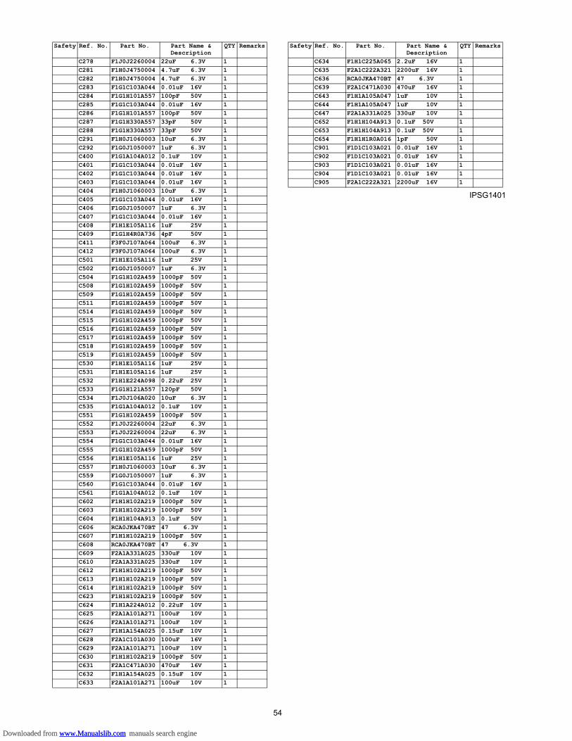
54
IPSG1401
C278 F1J0J2260004 22uF 6.3V 1C281 F1H0J4750004 4.7uF 6.3V 1C282 F1H0J4750004 4.7uF 6.3V 1C283 F1G1C103A044 0.01uF 16V 1C284 F1G1H101A557 100pF 50V 1C285 F1G1C103A044 0.01uF 16V 1C286 F1G1H101A557 100pF 50V 1C287 F1G1H330A557 33pF 50V 1C288 F1G1H330A557 33pF 50V 1C291 F1H0J1060003 10uF 6.3V 1C292 F1G0J1050007 1uF 6.3V 1C400 F1G1A104A012 0.1uF 10V 1C401 F1G1C103A044 0.01uF 16V 1C402 F1G1C103A044 0.01uF 16V 1C403 F1G1C103A044 0.01uF 16V 1C404 F1H0J1060003 10uF 6.3V 1C405 F1G1C103A044 0.01uF 16V 1C406 F1G0J1050007 1uF 6.3V 1C407 F1G1C103A044 0.01uF 16V 1C408 F1H1E105A116 1uF 25V 1C409 F1G1H4R0A736 4pF 50V 1C411 F3F0J107A064 100uF 6.3V 1C412 F3F0J107A064 100uF 6.3V 1C501 F1H1E105A116 1uF 25V 1C502 F1G0J1050007 1uF 6.3V 1C504 F1G1H102A459 1000pF 50V 1C508 F1G1H102A459 1000pF 50V 1C509 F1G1H102A459 1000pF 50V 1C511 F1G1H102A459 1000pF 50V 1C514 F1G1H102A459 1000pF 50V 1C515 F1G1H102A459 1000pF 50V 1C516 F1G1H102A459 1000pF 50V 1C517 F1G1H102A459 1000pF 50V 1C518 F1G1H102A459 1000pF 50V 1C519 F1G1H102A459 1000pF 50V 1C530 F1H1E105A116 1uF 25V 1C531 F1H1E105A116 1uF 25V 1C532 F1H1E224A098 0.22uF 25V 1C533 F1G1H121A557 120pF 50V 1C534 F1J0J106A020 10uF 6.3V 1C535 F1G1A104A012 0.1uF 10V 1C551 F1G1H102A459 1000pF 50V 1C552 F1J0J2260004 22uF 6.3V 1C553 F1J0J2260004 22uF 6.3V 1C554 F1G1C103A044 0.01uF 16V 1C555 F1G1H102A459 1000pF 50V 1C556 F1H1E105A116 1uF 25V 1C557 F1H0J1060003 10uF 6.3V 1C559 F1G0J1050007 1uF 6.3V 1C560 F1G1C103A044 0.01uF 16V 1C561 F1G1A104A012 0.1uF 10V 1C602 F1H1H102A219 1000pF 50V 1C603 F1H1H102A219 1000pF 50V 1C604 F1H1H104A913 0.1uF 50V 1C606 RCA0JKA470BT 47 6.3V 1C607 F1H1H102A219 1000pF 50V 1C608 RCA0JKA470BT 47 6.3V 1C609 F2A1A331A025 330uF 10V 1C610 F2A1A331A025 330uF 10V 1C612 F1H1H102A219 1000pF 50V 1C613 F1H1H102A219 1000pF 50V 1C614 F1H1H102A219 1000pF 50V 1C623 F1H1H102A219 1000pF 50V 1C624 F1H1A224A012 0.22uF 10V 1C625 F2A1A101A271 100uF 10V 1C626 F2A1A101A271 100uF 10V 1C627 F1H1A154A025 0.15uF 10V 1C628 F2A1C101A030 100uF 16V 1C629 F2A1A101A271 100uF 10V 1C630 F1H1H102A219 1000pF 50V 1C631 F2A1C471A030 470uF 16V 1C632 F1H1A154A025 0.15uF 10V 1C633 F2A1A101A271 100uF 10V 1
Safety Ref. No. Part No. Part Name & Description
QTY Remarks
C634 F1H1C225A065 2.2uF 16V 1C635 F2A1C222A321 2200uF 16V 1C636 RCA0JKA470BT 47 6.3V 1C639 F2A1C471A030 470uF 16V 1C643 F1H1A105A047 1uF 10V 1C644 F1H1A105A047 1uF 10V 1C647 F2A1A331A025 330uF 10V 1C652 F1H1H104A913 0.1uF 50V 1C653 F1H1H104A913 0.1uF 50V 1C654 F1H1H1R0A016 1pF 50V 1C901 F1D1C103A021 0.01uF 16V 1C902 F1D1C103A021 0.01uF 16V 1C903 F1D1C103A021 0.01uF 16V 1C904 F1D1C103A021 0.01uF 16V 1C905 F2A1C222A321 2200uF 16V 1
Safety Ref. No. Part No. Part Name & Description
QTY Remarks
Downloaded from www.Manualslib.com manuals search engine Downloaded from www.Manualslib.com manuals search engine
Top Related
Copyright © 2022 FDOKUMEN

