


Bahasa
Halaman
Hukum

Energy &EnvironmentalScience
REVIEW
Ope
n A
cces
s A
rtic
le. P
ublis
hed
on 0
5 M
arch
201
4. D
ownl
oade
d on
18/
08/2
016
07:1
7:28
. T
his
artic
le is
lice
nsed
und
er a
Cre
ativ
e C
omm
ons
Attr
ibut
ion-
Non
Com
mer
cial
3.0
Unp
orte
d L
icen
ce.
View Article OnlineView Journal | View Issue
Towards low-cos
aInstitute of Materials for Electronics and En
Materials Science and Engineerin
Erlangen-Nuremberg, Martensstrasse 7, 91
[email protected] Center for Applied Energy Resea
Erlangen, GermanycErlangen Graduate School in Advanced Op
Str. 6, 91052 Erlangen, Germany
Cite this: Energy Environ. Sci., 2014, 7,1829
Received 27th November 2013Accepted 5th March 2014
DOI: 10.1039/c3ee43865a
www.rsc.org/ees
This journal is © The Royal Society of C
t, environmentally friendly printedchalcopyrite and kesterite solar cells
Hamed Azimi,*a Yi Houac and Christoph J. Brabecab
Solution-processed organic and inorganic semiconductors offer a promising path towards low-cost mass
production of solar cells. Among the various material systems, solution processing of multicomponent
inorganic semiconductors offers considerable promise due to their excellent electronic properties and
superior photo- and thermal stability. This review surveys the recent developments of “all solution-
processed” copper–indium (–gallium)-chalcogenide (CuInS2, CuInSe2 and Cu(In, Ga)(Se, S)2)
chalcopyrites and copper–zinc–tin-chalcogenide (Cu2ZnSnS4 and Cu2ZnSnSe4 (CZTS(e))) kesterite solar
cells. A brief overview further addresses some of the most critical material aspects and associated loss
mechanisms in chalcopyrite and kesterite devices. Today's state-of-the-art performance as well as future
challenges to achieve low-cost and environmentally friendly production is discussed.
Broader context
Photovoltaics as the only truly portable renewable-energy conversion technology available today demonstrate strong commercial growth and hold promise forsignicant market opportunities. Among various solar cell technologies, thin-lm technologies are one of the cost-competitive solar technologies due to reducedmaterial and fabrication costs. However, the production of thin lm solar cells typically relies on capex intense vacuum-based techniques, and/or high-temperature processes, both increasing manufacturing costs. Solution processing of multicomponent inorganic solar cells is considered as a promisingalternative fabrication route to the conventional high cost vacuum techniques.
1. Introduction
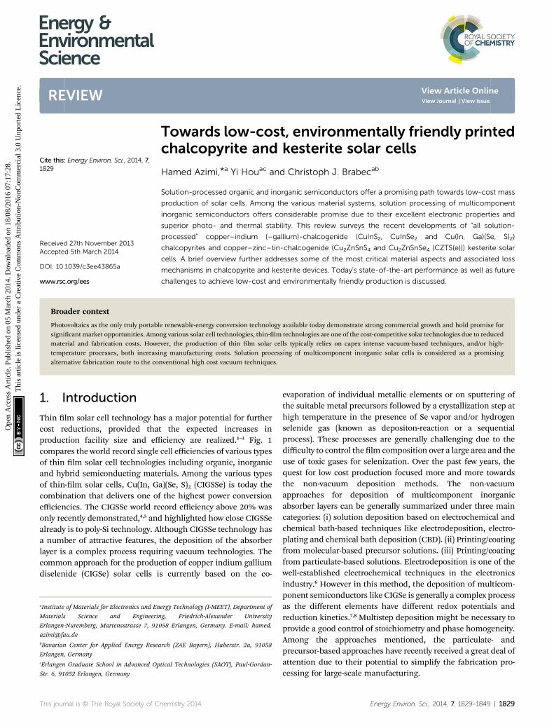
Thin lm solar cell technology has a major potential for furthercost reductions, provided that the expected increases inproduction facility size and efficiency are realized.1–3 Fig. 1compares the world record single cell efficiencies of various typesof thin lm solar cell technologies including organic, inorganicand hybrid semiconducting materials. Among the various typesof thin-lm solar cells, Cu(In, Ga)(Se, S)2 (CIGSSe) is today thecombination that delivers one of the highest power conversionefficiencies. The CIGSSe world record efficiency above 20% wasonly recently demonstrated,4,5 and highlighted how close CIGSSealready is to poly-Si technology. Although CIGSSe technology hasa number of attractive features, the deposition of the absorberlayer is a complex process requiring vacuum technologies. Thecommon approach for the production of copper indium galliumdiselenide (CIGSe) solar cells is currently based on the co-
ergy Technology (I-MEET), Department of
g, Friedrich-Alexander University
058 Erlangen, Germany. E-mail: hamed.
rch (ZAE Bayern), Haberstr. 2a, 91058
tical Technologies (SAOT), Paul-Gordan-
hemistry 2014
evaporation of individual metallic elements or on sputtering ofthe suitable metal precursors followed by a crystallization step athigh temperature in the presence of Se vapor and/or hydrogenselenide gas (known as depositon-reaction or a sequentialprocess). These processes are generally challenging due to thedifficulty to control the lm composition over a large area and theuse of toxic gases for selenization. Over the past few years, thequest for low cost production focused more and more towardsthe non-vacuum deposition methods. The non-vacuumapproaches for deposition of multicomponent inorganicabsorber layers can be generally summarized under three maincategories: (i) solution deposition based on electrochemical andchemical bath-based techniques like electrodeposition, electro-plating and chemical bath deposition (CBD). (ii) Printing/coatingfrom molecular-based precursor solutions. (iii) Printing/coatingfrom particulate-based solutions. Electrodeposition is one of thewell-established electrochemical techniques in the electronicsindustry.6 However in this method, the deposition of multicom-ponent semiconductors like CIGSe is generally a complex processas the different elements have different redox potentials andreduction kinetics.7,8 Multistep deposition might be necessary toprovide a good control of stoichiometry and phase homogeneity.Among the approaches mentioned, the particulate- andprecursor-based approaches have recently received a great deal ofattention due to their potential to simplify the fabrication pro-cessing for large-scale manufacturing.
Energy Environ. Sci., 2014, 7, 1829–1849 | 1829
Energy & Environmental Science Review
Ope
n A
cces
s A
rtic
le. P
ublis
hed
on 0
5 M
arch
201
4. D
ownl
oade
d on
18/
08/2
016
07:1
7:28
. T
his
artic
le is
lice
nsed
und
er a
Cre
ativ
e C
omm
ons
Attr
ibut
ion-
Non
Com
mer
cial
3.0
Unp
orte
d L
icen
ce.
View Article Online
In this article, our main focus is dedicated to the solution-processed fabrication of chalcopyrite CuInS2 (CIS), CuInSe2(CISe) and Cu(In, Ga)(Se, S)2 (CIGSSe) solar cells, addressing allthe various methods like molecular, and particulate-basedsolutions as well as their hybrid combinations. Furthermore, asan important alternative to the CIGSSe technology, we alsoreview the current state-of-the-art fabrication routes for solutionprocessed kesterite Cu2ZnSnS4 (CZTS), Cu2ZnSnSe4 (CZTSe),and Cu2ZnSn(S,Se)4 (CZTSSe) solar cells.
2. Fundamental aspects ofchalcopyrite and kesterite solar cells2.1. Device concept
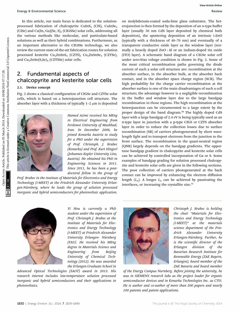
Fig. 2 shows a classical conguration of CIGSe and CZTSe solarcells, which is based on a heterojunction cell structure. Theabsorber layer with a thickness of typically 1–2 mm is deposited
Yi Hou is currently a PhDstudent under the supervision ofProf. Christoph J. Brabec at theinstitute of Materials for Elec-tronics and Energy Technology(i-MEET) at Friedrich AlexanderUniversity Erlangen- Nurnberg(FAU). He received his MEngdegree in Materials Science andEngineering from BeijingUniversity of Chemical Tech-nology (2012). He was awardedthe Erlangen Graduate School in
Advanced Optical Technologies (SAOT) award in 2013. Hisresearch interest includes low-temperature solution processedinorganic and hybrid semiconductors and their applications inphotovoltaics.
Hamed Azimi received his MEngin Electrical Engineering fromFerdowsi University of Mashhad,Iran. In December 2006, hejoined Konarka Austria to studyfor a PhD under the supervisionof Prof. Christoph. J. Brabec(Konarka) and Prof. Kurt Hingerl(Johannes Kepler University Linz,Austria). He obtained his PhD inEngineering Sciences in 2011.Since 2011, he has been a post-doctoral fellow in the group of
Prof. Brabec in the institute of Materials for Electronics and EnergyTechnology (i-MEET) at the Friedrich Alexander University Erlan-gen-Nurnberg, where he leads the group of solution processedinorganic and hybrid semiconductors for photovoltaic application.
1830 | Energy Environ. Sci., 2014, 7, 1829–1849
on molybdenum-coated soda-lime glass substrates. The het-erojunction is then formed by the deposition of an n-type bufferlayer (usually 50 nm CdS layer deposited by chemical bathdeposition), the sputtering deposition of an intrinsic i-ZnO(typically with a thickness of 40–70 nm) and eventually of atransparent conductive oxide layer as the window layer (nor-mally a heavily doped ZnO : Al or an indium-doped tin oxide(ITO) layer). A schematic band diagram of a CIGSe solar cellunder zero-bias voltage condition is shown in Fig. 2. Some ofthe most critical recombination paths governing the diodecurrent of such a solar cell structure are: recombination at theabsorber surface, in the absorber bulk, at the absorber backcontact, and in the absorber space charge region (SCR). Thehigh probability for the charge carrier recombination at theabsorber surface is one of the main disadvantages of such a cellstructure; the advantage however is a negligible recombinationin the buffer and window layer due to the large bandgaprecombination in those regions. The high recombination at theheterojunction can be circumvented to a large extent by theproper design of the band diagram.10 The highly doped CdSlayer with a large bandgap of 2.4 eV is being typically used as ann-type layer in junction with a p-type CIGS or CZTS absorberlayer in order to reduce the collection losses due to surfacerecombination (SR) of carriers photogenerated by short wave-length light and to transport electrons from the junction to thefront surface. The recombination in the quasi-neutral region(QNR) largely depends on the bandgap gradients. The oppor-tune bandgap gradient in chalcopyrite and kesterite solar cellscan be achieved by controlled incorporation of Ga or S. Someexamples of bandgap grading for solution processed chalcopy-rite and kesterite solar cells are given in the following sections.The poor collection of carriers photogenerated at the backcontact can be improved by enhancing the electron diffusionlength (Ln). A longer Ln can be achieved by passivating theinterfaces, or increasing the crystallite size.11
Christoph J. Brabec is holdingthe chair “Materials for Elec-tronics and Energy Technology(i-MEET)” at the materialsscience department of the Frie-drich Alexander UniversityErlangen-Nurnberg. Further, heis the scientic director of theErlangen division of theBavarian Research Institute forRenewable Energy (ZAE Bayern,Erlangen), board member of theZAE Bavaria and board member
of the Energy Campus Nurnberg. Before joining the university, hewas in SIEMENS research labs as the project leader for organicsemiconductor devices and in Konarka Technologies Inc. as CTO.He is author and co-author of more than 200 papers and nearly100 patents and patent applications.
This journal is © The Royal Society of Chemistry 2014
Fig. 1 Comparison between the world record efficiencies reported for various thin film solar cell technologies including for single cell andsubmodule devices. (Data extracted from the solar cell efficiency table reported by Green et al.9) Note: thin film GaAs and polycrystalline solarcells are not included in this comparison.
Fig. 2 Left – a schematic layer structure of a classical CIGSe solar cell. Right – a schematic band profile of a typical CIGSe solar cell under zero-bias voltage condition. The image of the band profile is reprinted with permission from ref. 12, Copyright 2011, Nature Publishing Group.
Review Energy & Environmental Science
Ope
n A
cces
s A
rtic
le. P
ublis
hed
on 0
5 M
arch
201
4. D
ownl
oade
d on
18/
08/2
016
07:1
7:28
. T
his
artic
le is
lice
nsed
und
er a
Cre
ativ
e C
omm
ons
Attr
ibut
ion-
Non
Com
mer
cial
3.0
Unp
orte
d L
icen
ce.
View Article Online
2.2. Grain boundaries and defects
In polycrystalline solar cells, the size of grains and the recom-bination velocity at the grain boundaries (GBs) are the keyparameters to determine the rate of the charge carrier recom-bination. One primary inuence of the GBs is the interruptionof the long-range order in the crystal. A simple relationshipbetween the effective diffusion length (Leff) for a polycrystallinematerial and a monocrystalline material can be dened as
Lpolyeff ¼
�Lmono
eff
� ��2 þ 2Sg
.ðDngÞ
��1=2
; (1)
where Sg stands for the recombination velocity at the grainboundaries of grains with the size g and Dn is the diffusioncoefficient for electrons.13 The GBs play an important role incontrolling the current voltage characteristic of solar cells. TheGBs may adversely inuence the majority carrier mobility,therefore enhancing the series resistance. Also, the lifetime ofthe minority carriers can be reduced by increasing minoritycarrier recombination at GBs.11 The GBs can even exhibit arecombination higher than in the bulk and additionally they
This journal is © The Royal Society of Chemistry 2014
may become charged to induce band bending.10 For examples,in high efficiency record CIGSSe devices, the loss in the opencircuit voltage (Voc) is attributed to the electrostatic potentialvariations at charged extended defects like GBs.14 There ishowever consensus that the GBs in chalcopyrites have morebenign effects compared to other semiconductor materials.15
The less negative inuence of GBs is explained by multiplefactors such as the inherently low GB recombination in CIGS,the benecial effects of O and Na in the passivation of GBs andthe reported downshi of the valence-band energy at GBs thateffectively repels holes from the GB region.13,16–18 The latter caseis well attributed to the formation of a Cu-poor ordered defectcompound (ODC) at the CIGS surface.19,16 The effect of GBs isshown to be similarly benign in kesterites. However, studiesshowed that due to the constituent atoms at the GBs, moredefect levels in the energy gap of CZTS bulk crystals can befound compared to CISe, which, in turn, enhance the proba-bility of recombination of the photogenerated chargecarriers.20
With respect to the different loss mechanisms discussed, itis important to understand the formation of the various defects
Energy Environ. Sci., 2014, 7, 1829–1849 | 1831
Energy & Environmental Science Review
Ope
n A
cces
s A
rtic
le. P
ublis
hed
on 0
5 M
arch
201
4. D
ownl
oade
d on
18/
08/2
016
07:1
7:28
. T
his
artic
le is
lice
nsed
und
er a
Cre
ativ
e C
omm
ons
Attr
ibut
ion-
Non
Com
mer
cial
3.0
Unp
orte
d L
icen
ce.
View Article Online
and secondary phases in chalcopyrites and kesterites. Defectsmay appear as single defect states with well dened energy levelswithin the bandgap or as multiple defect states and defectdistributions with a quasi continuous state density in thebandgap.10 In CIGSSe, the rst-principle investigation showedthat the indium-on-copper-antisites (InCu) and the coppervacancy (VCu) are, respectively, the dominant donor and acceptordefects.21,22 The acceptor defect VCu is found to have a shallowionization energy level and lower formation energy than thedonor defects as InCu (GaCu) and Cui, explaining therefore theintrinsic p-type conductivity and also the difficulty in the controlof n-type doping in this material. Furthermore in ternary chal-copyrites, due to the energetically favorable donor–acceptorcompensation between VCu and InCu, there is a high probabilityof formation of defect clusters like [2VCu + InCu] and even theordered defect compound such as CuIn5Se8.23 In CZTS, VCu hassimilarly a low formation energy and becomes dominant in thecase of Cu-poor and Zn-rich samples. Moreover, the cause offrequently observed non-stoichiometric kesterite samples can beexplained on grounds of a strong tendency towards formation ofself-compensated defect clusters, like [VCu + ZnCu], [ZnSn + 2ZnCu]and [2CuZn + SnZn]23,24 (see Table 1 for a comparison between thedominant defects in chalcopyrites and kesterites).
For solution processed solar cells, the effects of grainboundaries and the defects can be very different from thedevices fabricated based on the conventional vacuum deposi-tion routes. The defect chemistry and the mechanisms of phasetransformation can vary markedly depending on the initialsolution precursors and the temperature used for the lmdeposition and the phase transformation. The losses inducedby the smaller size of grains and the possible impurities fromthe precursors may exert a profound impact on the nal deviceperformance. To date, there have been very limited studies toprovide in-depth insights into the properties and the lossmechanisms of solution processed chalcopyrite and kesteritedevices. Fundamental insights using advanced characterizationmethods are still necessary to overcome the limitations in thesedevices.
2.3. Characterizations
Raman spectroscopy, X-ray diffraction, energy-/wavelengthdispersive X-ray spectroscopy and X-ray uorescence are
Table 1 Comparison of the bandgap, electrical conductivity and defect pfrom ref. 23, Copyright 2013, Wiley VCH
CuInSe2
Bandgap (eV) 1.04Intrinsic conductivity p-typeHole-generating acceptors VCu
�
High-population deepdonorsHigh-population clusters 2VCu + InCu
Electron trapping clusters
1832 | Energy Environ. Sci., 2014, 7, 1829–1849
commonly being used to obtain information on crystallinequality, phase purity and chemical composition. Among thetechniques mentioned above, Raman spectroscopy is anextremely useful technique that provides insight into the latticestrains and the existence and spatial distribution of differentphases. Furthermore, in the preparation of molecular precursorsolutions, Raman measurements can be used to analyze thedegree of intermixing between the precursor components.25 InCISSe samples, Raman spectroscopy can be used to distinguishthe desired stable chalcopyrite (CH) from the metastablecopper–gold CuAu (CA) and the metastable copper rich CuIn5(S,Se)8 structure.26–29 For CZTS samples, while the coexistence ofCZTS, Cu2SnS3 (CTS), and ZnS may not be distinguishable bydiffraction techniques, Raman analysis is able to detect anddistinguish between these phases through their characteristicscattering peaks.30–33 The employment of Raman spectroscopyat resonance conditions is shown to be essential for thedistinction between the secondary phases in kesterites.34 For adetailed overview on assignment of Raman peaks to differentbinary and ternary secondary phases related to the CZTSsystem, see ref. 30 and 34. To monitor the phase formation/transition during the thermal annealing, in situ techniques andthermal analyses like thermogravimetric analysis and differen-tial thermal analysis are being implemented.35–38
To obtain information about the defect physics and theirrelationship to the device performance, characterization toolssuch as photoluminescence (PL),39–41 admittance spectroscopy,deep level transient spectroscopy (DLTS)42–44 and Hallmeasurements45,46 are relevant. A combination of these tech-niques is generally necessary to analyze the shallow, mid-bandgap as well as the deep defects; while admittancemeasurements generally provide information on the deepdefects, information on the density and the energy of shallowdefects can be obtained by Hall and PL measurements.15 In PL,studying the excitation intensity and the temperature depen-dence of the emission peaks sheds light onto the activationenergies of the defects as well as the nature of the associatedtransitions.22,46 At low temperatures and low excitation intensi-ties, the PL spectrum can be dominated by the band–tail (BT)recombination. The BT recombination is the emission bandthat follows the band edge potential uctuations originatingfrom the local deviations in the distribution of donor andacceptor states (see Fig. 3). For instance, comparing the defect
roperties in the chalcopyrites and kesterites. Reprinted with permission
CuGaSe2 Cu2ZnSnSe4 Cu2ZnSnS4
1.68 1.0 1.5p-type p-type p-typeVCu
� CuZn�, VCu
� CuZn�, VCu
�
GaCu2+ SnZn
2+, VS2+
2VCu + GaCu VCu + ZnCu VCu + ZnCu
CuZn + ZnCu CuZn + ZnCu
2CuZn + SnZn 2CuZn + SnZn
ZnSn + 2ZnCu ZnSn + 2ZnCu
2VCu + GaCu 2CuZn + SnZn
This journal is © The Royal Society of Chemistry 2014
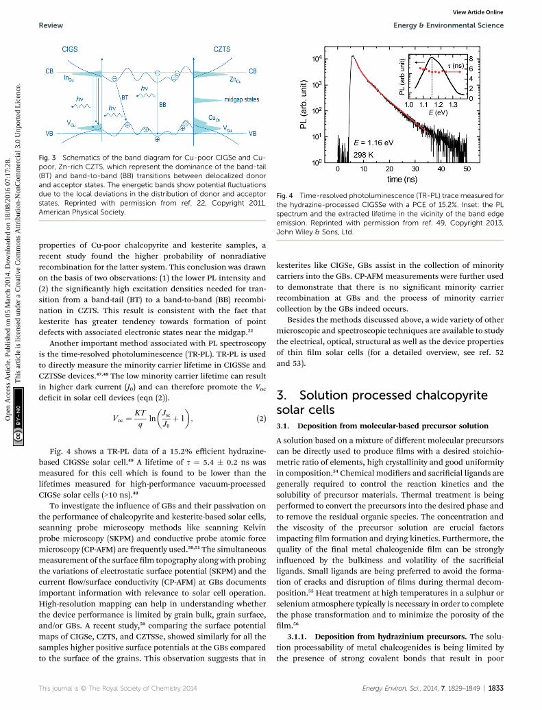
Fig. 3 Schematics of the band diagram for Cu-poor CIGSe and Cu-poor, Zn-rich CZTS, which represent the dominance of the band-tail(BT) and band-to-band (BB) transitions between delocalized donorand acceptor states. The energetic bands show potential fluctuationsdue to the local deviations in the distribution of donor and acceptorstates. Reprinted with permission from ref. 22, Copyright 2011,American Physical Society.
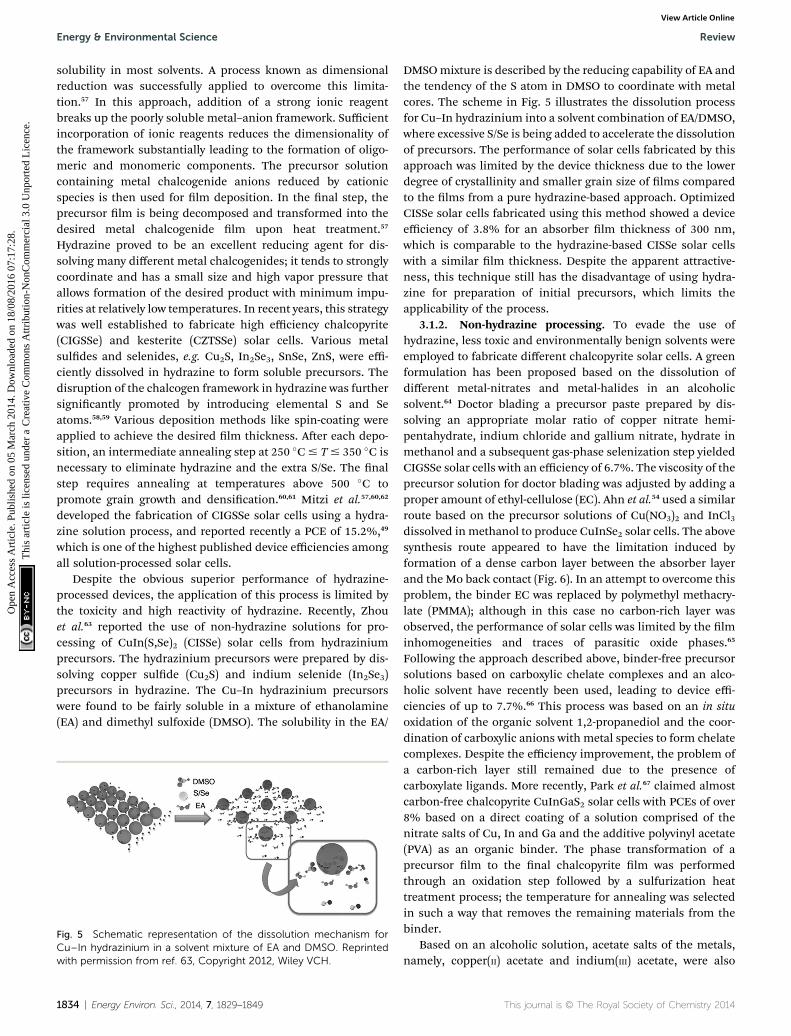
Fig. 4 Time-resolved photoluminescence (TR-PL) trace measured forthe hydrazine-processed CIGSSe with a PCE of 15.2%. Inset: the PLspectrum and the extracted lifetime in the vicinity of the band edgeemission. Reprinted with permission from ref. 49, Copyright 2013,John Wiley & Sons, Ltd.
Review Energy & Environmental Science
Ope
n A
cces
s A
rtic
le. P
ublis
hed
on 0
5 M
arch
201
4. D
ownl
oade
d on
18/
08/2
016
07:1
7:28
. T
his
artic
le is
lice
nsed
und
er a
Cre
ativ
e C
omm
ons
Attr
ibut
ion-
Non
Com
mer
cial
3.0
Unp
orte
d L
icen
ce.
View Article Online
properties of Cu-poor chalcopyrite and kesterite samples, arecent study found the higher probability of nonradiativerecombination for the latter system. This conclusion was drawnon the basis of two observations: (1) the lower PL intensity and(2) the signicantly high excitation densities needed for tran-sition from a band-tail (BT) to a band-to-band (BB) recombi-nation in CZTS. This result is consistent with the fact thatkesterite has greater tendency towards formation of pointdefects with associated electronic states near the midgap.22
Another important method associated with PL spectroscopyis the time-resolved photoluminescence (TR-PL). TR-PL is usedto directly measure the minority carrier lifetime in CIGSSe andCZTSSe devices.47,48 The low minority carrier lifetime can resultin higher dark current (J0) and can therefore promote the Vocdecit in solar cell devices (eqn (2)).
Voc ¼ KT
qln
�Jsc
J0þ 1
�; (2)
Fig. 4 shows a TR-PL data of a 15.2% efficient hydrazine-based CIGSSe solar cell.49 A lifetime of s ¼ 5.4 � 0.2 ns wasmeasured for this cell which is found to be lower than thelifetimes measured for high-performance vacuum-processedCIGSe solar cells (>10 ns).48
To investigate the inuence of GBs and their passivation onthe performance of chalcopyrite and kesterite-based solar cells,scanning probe microscopy methods like scanning Kelvinprobe microscopy (SKPM) and conductive probe atomic forcemicroscopy (CP-AFM) are frequently used.50,51 The simultaneousmeasurement of the surface lm topography along with probingthe variations of electrostatic surface potential (SKPM) and thecurrent ow/surface conductivity (CP-AFM) at GBs documentsimportant information with relevance to solar cell operation.High-resolution mapping can help in understanding whetherthe device performance is limited by grain bulk, grain surface,and/or GBs. A recent study,50 comparing the surface potentialmaps of CIGSe, CZTS, and CZTSSe, showed similarly for all thesamples higher positive surface potentials at the GBs comparedto the surface of the grains. This observation suggests that in
This journal is © The Royal Society of Chemistry 2014
kesterites like CIGSe, GBs assist in the collection of minoritycarriers into the GBs. CP-AFM measurements were further usedto demonstrate that there is no signicant minority carrierrecombination at GBs and the process of minority carriercollection by the GBs indeed occurs.
Besides the methods discussed above, a wide variety of othermicroscopic and spectroscopic techniques are available to studythe electrical, optical, structural as well as the device propertiesof thin lm solar cells (for a detailed overview, see ref. 52and 53).
3. Solution processed chalcopyritesolar cells3.1. Deposition from molecular-based precursor solution
A solution based on a mixture of different molecular precursorscan be directly used to produce lms with a desired stoichio-metric ratio of elements, high crystallinity and good uniformityin composition.54 Chemical modiers and sacricial ligands aregenerally required to control the reaction kinetics and thesolubility of precursor materials. Thermal treatment is beingperformed to convert the precursors into the desired phase andto remove the residual organic species. The concentration andthe viscosity of the precursor solution are crucial factorsimpacting lm formation and drying kinetics. Furthermore, thequality of the nal metal chalcogenide lm can be stronglyinuenced by the bulkiness and volatility of the sacricialligands. Small ligands are being preferred to avoid the forma-tion of cracks and disruption of lms during thermal decom-position.55 Heat treatment at high temperatures in a sulphur orselenium atmosphere typically is necessary in order to completethe phase transformation and to minimize the porosity of thelm.56
3.1.1. Deposition from hydrazinium precursors. The solu-tion processability of metal chalcogenides is being limited bythe presence of strong covalent bonds that result in poor
Energy Environ. Sci., 2014, 7, 1829–1849 | 1833
Energy & Environmental Science Review
Ope
n A
cces
s A
rtic
le. P
ublis
hed
on 0
5 M
arch
201
4. D
ownl
oade
d on
18/
08/2
016
07:1
7:28
. T
his
artic
le is
lice
nsed
und
er a
Cre
ativ
e C
omm
ons
Attr
ibut
ion-
Non
Com
mer
cial
3.0
Unp
orte
d L
icen
ce.
View Article Online
solubility in most solvents. A process known as dimensionalreduction was successfully applied to overcome this limita-tion.57 In this approach, addition of a strong ionic reagentbreaks up the poorly soluble metal–anion framework. Sufficientincorporation of ionic reagents reduces the dimensionality ofthe framework substantially leading to the formation of oligo-meric and monomeric components. The precursor solutioncontaining metal chalcogenide anions reduced by cationicspecies is then used for lm deposition. In the nal step, theprecursor lm is being decomposed and transformed into thedesired metal chalcogenide lm upon heat treatment.57
Hydrazine proved to be an excellent reducing agent for dis-solving many different metal chalcogenides; it tends to stronglycoordinate and has a small size and high vapor pressure thatallows formation of the desired product with minimum impu-rities at relatively low temperatures. In recent years, this strategywas well established to fabricate high efficiency chalcopyrite(CIGSSe) and kesterite (CZTSSe) solar cells. Various metalsuldes and selenides, e.g. Cu2S, In2Se3, SnSe, ZnS, were effi-ciently dissolved in hydrazine to form soluble precursors. Thedisruption of the chalcogen framework in hydrazine was furthersignicantly promoted by introducing elemental S and Seatoms.58,59 Various deposition methods like spin-coating wereapplied to achieve the desired lm thickness. Aer each depo-sition, an intermediate annealing step at 250 �C# T# 350 �C isnecessary to eliminate hydrazine and the extra S/Se. The nalstep requires annealing at temperatures above 500 �C topromote grain growth and densication.60,61 Mitzi et al.57,60,62
developed the fabrication of CIGSSe solar cells using a hydra-zine solution process, and reported recently a PCE of 15.2%,49
which is one of the highest published device efficiencies amongall solution-processed solar cells.
Despite the obvious superior performance of hydrazine-processed devices, the application of this process is limited bythe toxicity and high reactivity of hydrazine. Recently, Zhouet al.63 reported the use of non-hydrazine solutions for pro-cessing of CuIn(S,Se)2 (CISSe) solar cells from hydraziniumprecursors. The hydrazinium precursors were prepared by dis-solving copper sulde (Cu2S) and indium selenide (In2Se3)precursors in hydrazine. The Cu–In hydrazinium precursorswere found to be fairly soluble in a mixture of ethanolamine(EA) and dimethyl sulfoxide (DMSO). The solubility in the EA/
Fig. 5 Schematic representation of the dissolution mechanism forCu–In hydrazinium in a solvent mixture of EA and DMSO. Reprintedwith permission from ref. 63, Copyright 2012, Wiley VCH.
1834 | Energy Environ. Sci., 2014, 7, 1829–1849
DMSOmixture is described by the reducing capability of EA andthe tendency of the S atom in DMSO to coordinate with metalcores. The scheme in Fig. 5 illustrates the dissolution processfor Cu–In hydrazinium into a solvent combination of EA/DMSO,where excessive S/Se is being added to accelerate the dissolutionof precursors. The performance of solar cells fabricated by thisapproach was limited by the device thickness due to the lowerdegree of crystallinity and smaller grain size of lms comparedto the lms from a pure hydrazine-based approach. OptimizedCISSe solar cells fabricated using this method showed a deviceefficiency of 3.8% for an absorber lm thickness of 300 nm,which is comparable to the hydrazine-based CISSe solar cellswith a similar lm thickness. Despite the apparent attractive-ness, this technique still has the disadvantage of using hydra-zine for preparation of initial precursors, which limits theapplicability of the process.
3.1.2. Non-hydrazine processing. To evade the use ofhydrazine, less toxic and environmentally benign solvents wereemployed to fabricate different chalcopyrite solar cells. A greenformulation has been proposed based on the dissolution ofdifferent metal-nitrates and metal-halides in an alcoholicsolvent.64 Doctor blading a precursor paste prepared by dis-solving an appropriate molar ratio of copper nitrate hemi-pentahydrate, indium chloride and gallium nitrate, hydrate inmethanol and a subsequent gas-phase selenization step yieldedCIGSSe solar cells with an efficiency of 6.7%. The viscosity of theprecursor solution for doctor blading was adjusted by adding aproper amount of ethyl-cellulose (EC). Ahn et al.54 used a similarroute based on the precursor solutions of Cu(NO3)2 and InCl3dissolved in methanol to produce CuInSe2 solar cells. The abovesynthesis route appeared to have the limitation induced byformation of a dense carbon layer between the absorber layerand the Mo back contact (Fig. 6). In an attempt to overcome thisproblem, the binder EC was replaced by polymethyl methacry-late (PMMA); although in this case no carbon-rich layer wasobserved, the performance of solar cells was limited by the lminhomogeneities and traces of parasitic oxide phases.65
Following the approach described above, binder-free precursorsolutions based on carboxylic chelate complexes and an alco-holic solvent have recently been used, leading to device effi-ciencies of up to 7.7%.66 This process was based on an in situoxidation of the organic solvent 1,2-propanediol and the coor-dination of carboxylic anions with metal species to form chelatecomplexes. Despite the efficiency improvement, the problem ofa carbon-rich layer still remained due to the presence ofcarboxylate ligands. More recently, Park et al.67 claimed almostcarbon-free chalcopyrite CuInGaS2 solar cells with PCEs of over8% based on a direct coating of a solution comprised of thenitrate salts of Cu, In and Ga and the additive polyvinyl acetate(PVA) as an organic binder. The phase transformation of aprecursor lm to the nal chalcopyrite lm was performedthrough an oxidation step followed by a sulfurization heattreatment process; the temperature for annealing was selectedin such a way that removes the remaining materials from thebinder.
Based on an alcoholic solution, acetate salts of the metals,namely, copper(II) acetate and indium(III) acetate, were also
This journal is © The Royal Society of Chemistry 2014
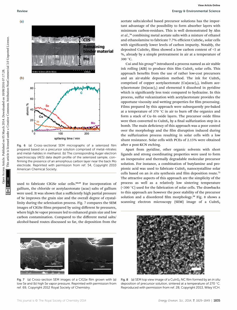
Fig. 6 (a) Cross-sectional SEM micrographs of a selenized filmprepared based on a precursor solution comprised of metal-nitratesand metal-halides in methanol. (b) The corresponding Auger electronspectroscopy (AES) data depth profile of the selenized sample, con-firming the presence of an amorphous carbon layer near the back Moelectrode. Reprinted with permission from ref. 54, Copyright 2010American Chemical Society.
Review Energy & Environmental Science
Ope
n A
cces
s A
rtic
le. P
ublis
hed
on 0
5 M
arch
201
4. D
ownl
oade
d on
18/
08/2
016
07:1
7:28
. T
his
artic
le is
lice
nsed
und
er a
Cre
ativ
e C
omm
ons
Attr
ibut
ion-
Non
Com
mer
cial
3.0
Unp
orte
d L
icen
ce.
View Article Online
used to fabricate CIGSe solar cells.68,69 For incorporation ofgallium, the chloride or acetylacetonate (acac) salts of galliumwere used. It was shown that a sufficiently high partial pressureof Se improves the grain size and the overall degree of crystal-linity during the selenization process. Fig. 7 compares the SEMimages of CIGSe lms prepared by using different Se pressures,where high Se vapor pressure led to enhanced grain size and lowcarbon contamination. Compared to the different metal salts/alcohol-based routes discussed so far, the deposition from the
Fig. 7 (a) Cross-section SEM images of a CIGSe film grown with (a)low Se and (b) high Se vapor pressure. Reprinted with permission fromref. 69, Copyright 2012 Royal Society of Chemistry.
This journal is © The Royal Society of Chemistry 2014
acetate salts/alcohol based precursor solutions has the impor-tant advantage of the possibility to form absorber layers withminimum carbon-residues. This is well demonstrated by Ahnet al.,70 combining metal acetate salts with a mixture of ethanoland ethanolamine to fabricate 7.7% efficient CuInSe2 solar cellswith signicantly lower levels of carbon impurity. Notably, thedeposited CuInSe2 lms showed a low carbon content of <5 at%, already by a simple pretreatment in air at a temperature of300 �C.
Cui and his group71 introduced a process named as air stableink rolling (AIR) to produce thin lm CuInS2 solar cells. Thisapproach benets from the use of rather low-cost precursorsand an air-stable deposition method. The ink for CuInS2comprised of copper acetylacetonate (Cu(acac)2), indium ace-tylacetonate (In(acac)3) and elemental S dissolved in pyridinewhich is signicantly less toxic compared to hydrazine. In thisprocess, sulfur vulcanization with acetylacetonate provides theopportune viscosity and wetting properties for lm processing.Films prepared by this approach were subsequently pre-bakedat a temperature of 370 �C in air to burn off the organics andform a stack of Cu–In oxide layers. The precursor oxide lmswere then converted to CuInS2 by a nal sulfurization step in abomb. The main deciency of this approach was a poor controlover the morphology and the lm disruption induced duringthe sulfurization process resulting in solar cells with a lowshunt resistance. Solar cells with PCEs of 2.15% were obtainedaer a post-KCN etching.
Apart from pyridine, other organic solvents with shortligands and strong coordinating properties were used to forman inexpensive and thermally degradable molecular precursorsolution. For instance, a combination of butylamine and pro-pionic acid was used to fabricate CuInS2 nanocrystalline solarcells based on an in situ synthesis and lm deposition route.72
The attractive aspects of this approach are the simplicity of theprocess as well as a relatively low sintering temperature(<300 �C) used for the fabrication of solar cells. The drawbacksto this approach are however the poor stability of the precursorsolution and a disordered lm morphology.28 Fig. 8 shows ascanning electron microscopy (SEM) image of a CuInS2
Fig. 8 (a) SEM top view image of a CuInS2 NC film formed by an in situdeposition of precursor solution, sintered at a temperature of 270 �C.Reproduced with permission from ref. 28, Copyright 2013, Wiley VCH.
Energy Environ. Sci., 2014, 7, 1829–1849 | 1835
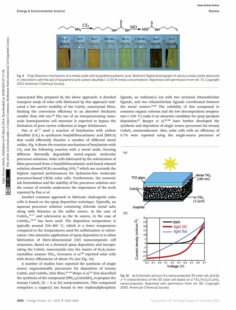
Fig. 10 (a) Schematic picture of a nanocomposite 3D solar cell, and (b)J–V characteristics of the 3D solar cell based on a TiO2/In2S3/CuInS2nanocomposite. Reprinted with permission from ref. 80, Copyright2005, American Chemical Society.
Fig. 9 (Top) Reaction mechanism of a metal oxide with butyldithiocarbamic acid. (Bottom) Digital photograph of various metal oxides dissolvedin chloroform with the aid of butylamine and carbon disulfide (�0.35 M metal concentration). Reprinted with permission from ref. 73, Copyright2012 American Chemical Society.
Energy & Environmental Science Review
Ope
n A
cces
s A
rtic
le. P
ublis
hed
on 0
5 M
arch
201
4. D
ownl
oade
d on
18/
08/2
016
07:1
7:28
. T
his
artic
le is
lice
nsed
und
er a
Cre
ativ
e C
omm
ons
Attr
ibut
ion-
Non
Com
mer
cial
3.0
Unp
orte
d L
icen
ce.
View Article Online
nanocrystal lm prepared by the above approach. A detailedtransport study of solar cells fabricated by this approach indi-cated a low carrier mobility of the CuInS2 nanocrystal lms,limiting the conversion efficiency to an absorber thicknesssmaller than 200 nm.28 The use of an interpenetrating nano-scale heterojunction cell structure is expected to bypass thelimitation of poor carrier collection at larger thicknesses.
Pan et al.73 used a reaction of butylamine with carbondisulde (CS2) to synthesize butyldithiocarbamic acid (BDCA)that could efficiently dissolve a number of different metaloxides. Fig. 9 shows the reactionmechanism of butylamine withCS2 and the following reaction with a metal oxide, formingdifferent thermally degradable metal–organic molecularprecursor solutions. Solar cells fabricated by the selenization oflms processed from a butyldithiocarbamic acid-based ethanolsolution showed PCEs exceeding 10%,74 which are currently thehighest reported performances for hydrazine-free molecularprecursor-based CIGSe solar cells. Furthermore, the nontoxicink formulation and the stability of the precursor solution overthe course of months underscore the importance of the workreported by Pan et al.
Another common approach to fabricate chalcopyrite solarcells is based on the spray deposition technique. Typically, anaqueous precursor solution containing chloride metal saltsalong with thiourea as the sulfur source, in the case ofCuInS2,75–77 and selenourea as the Se source, in the case ofCuInSe2,78,79 has been used. The deposition temperature istypically around 250–400 �C, which is a lower temperaturecompared to the temperatures used for sulfurization or seleni-zation. One attractive application of spray deposition is to allowfabrication of three-dimensional (3D) nanocomposite cellstructures. Based on a chemical spray deposition and incorpo-rating the CuInS2 nanocrystals into the matrix of In2S3/nano-crystalline anatase TiO2, Goossens et al.80 reported solar cellswith device efficiencies of about 5% (see Fig. 10).
A number of studies have reported the synthesis of singlesource organometallic precursors for deposition of ternaryCuInS2 and CuInSe2 thin lms.81–84 Hirpo et al.81 rst describedthe synthesis of the compound (PPh3)2CuIn(SEt)4 to prepare theternary CuInX2 (X ¼ S or Se) semiconductors. This compoundcomprises a copper(I) ion bound to two triphenylphosphine
1836 | Energy Environ. Sci., 2014, 7, 1829–1849
ligands, an indium(III) ion with two terminal ethanethiolateligands, and two ethanethiolate ligands coordinated betweenthe metal centers.81,82 The solubility of this compound incommon organic solvents and the low decomposition tempera-ture (<250 �C) make it an attractive candidate for spray pyrolysisdeposition.81 Banger et al.82–84 have further developed thesynthesis and deposition of single source precursors for ternaryCuInX2 semiconductors. Also, solar cells with an efficiency of6.7% were reported using the single-source precursor of
This journal is © The Royal Society of Chemistry 2014
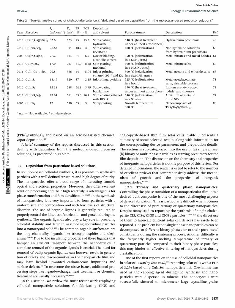
Table 2 Non-exhaustive survey of chalcopyrite solar cells fabricated based on deposition from the molecular-based precursor solutionsa
Year AbsorberJsc(mA cm�2)
Voc(mV)
FF(%)
PCE(%)
Depositionand solvent Post-treatment Description Ref.
2013 Cu(In,Ga)(S,Se)2 32.6 623 75 15.2 Spin-coating,hydrazine
540 �C (heat treatmentunder an inert atmosphere)
Hydrazinium precursors 49
2012 CuIn(S,Se)2 20.63 381 48.7 3.8 Spin-coating,EA/DMSO
400 �C (selenization) Non-hydrazine solutionsfrom hydrazinium precursors
63
2005 Cu(In,Ga)Se2 27.2 404 61 6.7 Doctor-blading,alcoholic solvent
550 �C (selenizationin a Se/N2 atm.)
Metal-nitrates and metal-halides 64
2013 CuInGaS2 17.0 787 61.9 8.28 Spin-coating,methanol
500 �C (sulfurizationin a H2S/N2 atm.)
Metal-nitrate salts 67
2011 CuInxGa1�xSe2 29.8 386 44 5.04 Inkjet-printing,ethanol, EG,* and EA
500 �C (selenizationin a Se/H2/N2 atm.)
Metal-acetate and chloride salts 68
2010 CuInS2 18.49 320 37 2.15 Ink-rolling, pyridine 525 �C (sulfurizationin a bomb)
Metal-acetylacetonatesalts, air-stable process
71
2010 CuInS2 12.38 588 54.8 3.99 Spin-coating,butylamine
250 �C (heat treatmentunder an inert atmosphere)
Indium acetate, copperiodide, and thiourea
72
2013 CuIn(S,Se)2 27.64 561 65.0 10.1 Spin coating ethanolwith BDCA
540 �C (selenizationin a Se atm.)
A mixture of metallicoxide NPs
74
2005 CuInS2 17 530 55 5 Spray-coating Growth temperature300 �C
Nanocomposite ofTiO2/In2S3/CuInS2
80
a n.a. ¼ Not available, * ethylene glycol.
Review Energy & Environmental Science
Ope
n A
cces
s A
rtic
le. P
ublis
hed
on 0
5 M
arch
201
4. D
ownl
oade
d on
18/
08/2
016
07:1
7:28
. T
his
artic
le is
lice
nsed
und
er a
Cre
ativ
e C
omm
ons
Attr
ibut
ion-
Non
Com
mer
cial
3.0
Unp
orte
d L
icen
ce.
View Article Online
(PPh3)2CuIn(SEt)4 and based on an aerosol-assisted chemicalvapor deposition.85
A brief summary of the reports discussed in this section,dealing with deposition from the molecular-based precursorsolutions, is presented in Table 2.
3.2. Deposition from particulate-based solutions
In solution-based colloidal synthesis, it is possible to synthesizeparticles with a well-dened structure and high degree of purity.The nanoparticles offer a broad range of interesting tunableoptical and electrical properties. Moreover, they offer excellentsolution processing and their high reactivity is advantageous forphase transformation and lm densication.86,87 In the synthesisof nanoparticles, it is very important to form particles with auniform size and composition and with low levels of structuraldisorder. The use of organic ligands is generally required toproperly control the kinetics of nucleation and growth during thesynthesis. The organic ligands also play a key role in providingcolloidal stability and later in assembling individual particlesinto a nanocrystal solid.88 The common organic surfactants arethe long chain alkyl ligands like trioctylphosphite and oleyl-amine.89–91 Due to the insulating properties of these ligands thathamper an efficient transport between the nanoparticles, acomplete removal of the organic ligands is crucial. The need forremoval of bulky organic ligands can however result in genera-tion of cracks and discontinuities in the nanoparticle lm andmay leave behind unwanted carbonaceous impurities andsurface defects.55 To overcome the above issues, additional pro-cessing steps like ligand-exchange, heat treatment or chemicaltreatment are usually necessary.90,92–94
In this section, we review the most recent work employingcolloidal nanoparticle solutions for fabricating CIGS and
This journal is © The Royal Society of Chemistry 2014
chalcopyrite-based thin lm solar cells. Table 3 presents asummary of some selected results along with information forthe corresponding device parameters and preparation details.The section is sub-categorized into the use of (a) single phase,(b) binary or multi-phase particles as starting precursors for thelm deposition. The discussion on the chemistry and propertiesof inorganic nanoparticles is not the purpose of this review. Fordetailed information, the reader is urged to refer to the numberof excellent reviews that comprehensively address the mecha-nism of growth and the properties of inorganicnanoparticles.95–97
3.2.1. Ternary and quaternary phase nanoparticles.Controlling the phase transition of a nanoparticular lm into adesired bulk composite is one of the most challenging aspectsof device fabrication. This is particularly difficult when it comesto the direct use of pure ternary or quaternary nanoparticles.Despite many studies reporting the synthesis of single chalco-pyrite CIS, CISe, CIGS and CIGSe particles,55,98–100 the direct useof them to fabricate efficient solar cell devices has rarely beenreported. One problem is that single phase nanoparticles can bedecomposed to different binary phases or to their pure metalconstituents during the sintering process. Another difficulty isthe frequently higher melting temperature of ternary orquaternary particles compared to their binary phase particles;this may hinder an effective sintering of nanoparticles duringcrystallization.
One of the rst reports on the use of colloidal nanoparticlesin solar cells was by Guo et al.,101 reporting solar cells with a PCEof 3.2% based on a CuInSe2 nanoparticle ink. Oleylamine wasused as the capping agent during the synthesis and nano-particles were dispersed in toluene. The nanocrystals weresuccessfully sintered to micrometer large crystalline grains
Energy Environ. Sci., 2014, 7, 1829–1849 | 1837
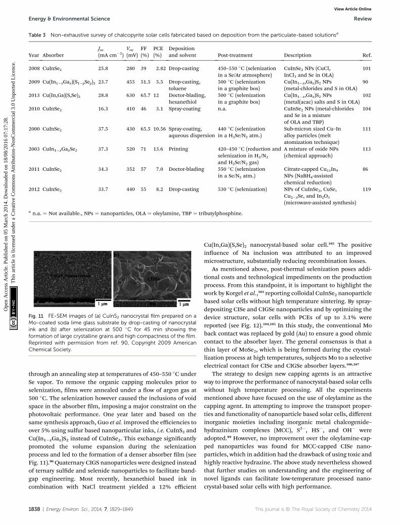
Fig. 11 FE-SEM images of (a) CuInS2 nanocrystal film prepared on aMo-coated soda lime glass substrate by drop-casting of nanocrystalink and (b) after selenization at 500 �C for 45 min showing theformation of large crystalline grains and high compactness of the film.Reprinted with permission from ref. 90, Copyright 2009 AmericanChemical Society.
Table 3 Non-exhaustive survey of chalcopyrite solar cells fabricated based on deposition from the particulate-based solutionsa
Year AbsorberJsc(mA cm�2)
Voc(mV)
FF(%)
PCE(%)
Depositionand solvent Post-treatment Description Ref.
2008 CuInSe2 25.8 280 39 2.82 Drop-casting 450–550 �C (selenizationin a Se/Ar atmosphere)
CuInSe2 NPs (CuCl,InCl3 and Se in OLA)
101
2009 Cu(In1�xGax)(S1�ySey)2 23.7 455 51.5 5.5 Drop-casting,toluene
500 �C (selenizationin a graphite box)
Cu(In1�x,Gax)S2 NPs(metal-chlorides and S in OLA)
90
2013 Cu(In,Ga)(S,Se)2 28.8 630 65.7 12 Doctor-blading,hexanethiol
500 �C (selenizationin a graphite box)
Cu(In1�x,Gax)S2 NPs(metal(acac) salts and S in OLA)
102
2010 CuInSe2 16.3 410 46 3.1 Spray-coating n.a. CuInSe2 NPs (metal-chloridesand Se in a mixtureof OLA and TBP)
104
2000 CuInSe2 37.5 430 65.5 10.56 Spray-coating,aqueous dispersion
440 �C (selenizationin a H2Se/N2 atm.)
Sub-micron sized Cu–Inalloy particles (meltatomization technique)
111
2003 CuIn1�xGaxSe2 37.3 520 71 13.6 Printing 420–450 �C (reduction andselenization in H2/N2
and H2Se/N2 gas)
A mixture of oxide NPs(chemical approach)
113
2011 CuInSe2 34.3 352 57 7.0 Doctor-blading 550 �C (selenizationin a Se/N2 atm.)
Citrate-capped Cu11In9
NPs (NaBH4-assistedchemical reduction)
86
2012 CuInSe2 33.7 440 55 8.2 Drop-casting 530 �C (selenization) NPs of CuInSe2, CuSe,Cu2�xSe, and In2O3
(microwave-assisted synthesis)
119
a n.a. ¼ Not available., NPs ¼ nanoparticles, OLA ¼ oleylamine, TBP ¼ tributylphosphine.
Energy & Environmental Science Review
Ope
n A
cces
s A
rtic
le. P
ublis
hed
on 0
5 M
arch
201
4. D
ownl
oade
d on
18/
08/2
016
07:1
7:28
. T
his
artic
le is
lice
nsed
und
er a
Cre
ativ
e C
omm
ons
Attr
ibut
ion-
Non
Com
mer
cial
3.0
Unp
orte
d L
icen
ce.
View Article Online
through an annealing step at temperatures of 450–550 �C underSe vapor. To remove the organic capping molecules prior toselenization, lms were annealed under a ow of argon gas at500 �C. The selenization however caused the inclusions of voidspace in the absorber lm, imposing a major constraint on thephotovoltaic performance. One year later and based on thesame synthesis approach, Guo et al. improved the efficiencies toover 5% using sulfur based nanoparticular inks, i.e. CuInS2 andCu(In1�xGax)S2 instead of CuInSe2. This exchange signicantlypromoted the volume expansion during the selenizationprocess and led to the formation of a denser absorber lm (seeFig. 11).90 Quaternary CIGS nanoparticles were designed insteadof ternary sulde and selenide nanoparticles to facilitate band-gap engineering. Most recently, hexanethiol based ink incombination with NaCl treatment yielded a 12% efficient
1838 | Energy Environ. Sci., 2014, 7, 1829–1849
Cu(In,Ga)(S,Se)2 nanocrystal-based solar cell.102 The positiveinuence of Na inclusion was attributed to an improvedmicrostructure, substantially reducing recombination losses.
As mentioned above, post-thermal selenization poses addi-tional costs and technological impediments on the productionprocess. From this standpoint, it is important to highlight thework by Korgel et al.,103 reporting colloidal CuInSe2 nanoparticlebased solar cells without high temperature sintering. By spray-depositing CISe and CIGSe nanoparticles and by optimizing thedevice structure, solar cells with PCEs of up to 3.1% werereported (see Fig. 12).104,105 In this study, the conventional Moback contact was replaced by gold (Au) to ensure a good ohmiccontact to the absorber layer. The general consensus is that athin layer of MoSe2, which is being formed during the crystal-lization process at high temperatures, subjects Mo to a selectiveelectrical contact for CISe and CIGSe absorber layers.106,107
The strategy to design new capping agents is an attractiveway to improve the performance of nanocrystal-based solar cellswithout high temperature processing. All the experimentsmentioned above have focused on the use of oleylamine as thecapping agent. In attempting to improve the transport proper-ties and functionality of nanoparticle based solar cells, differentinorganic moieties including inorganic metal chalcogenide–hydrazinium complexes (MCC), S2�, HS�, and OH� wereadopted.89 However, no improvement over the oleylamine-cap-ped nanoparticles was found for MCC-capped CISe nano-particles, which in addition had the drawback of using toxic andhighly reactive hydrazine. The above study nevertheless showedthat further studies on understanding and the engineering ofnovel ligands can facilitate low-temperature processed nano-crystal-based solar cells with high performance.
This journal is © The Royal Society of Chemistry 2014
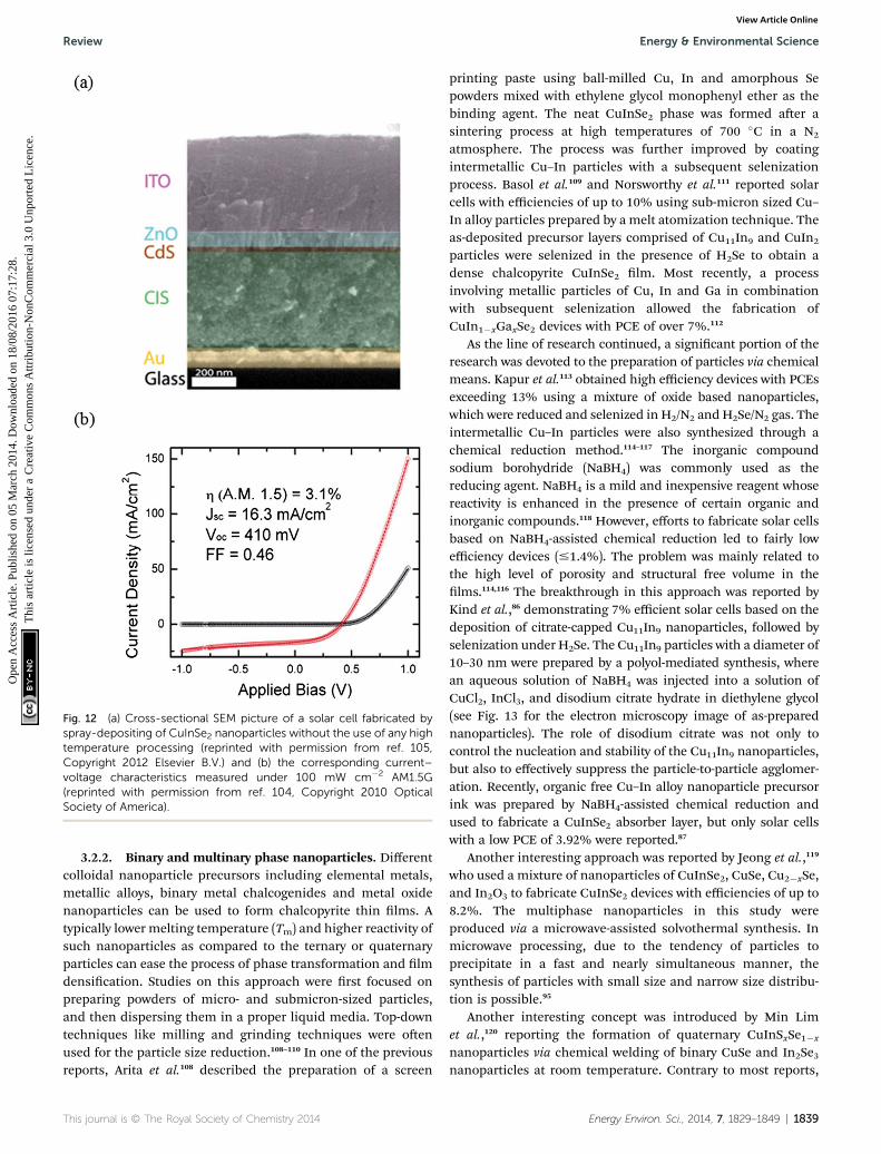
Fig. 12 (a) Cross-sectional SEM picture of a solar cell fabricated byspray-depositing of CuInSe2 nanoparticles without the use of any hightemperature processing (reprinted with permission from ref. 105,Copyright 2012 Elsevier B.V.) and (b) the corresponding current–voltage characteristics measured under 100 mW cm�2 AM1.5G(reprinted with permission from ref. 104, Copyright 2010 OpticalSociety of America).
Review Energy & Environmental Science
Ope
n A
cces
s A
rtic
le. P
ublis
hed
on 0
5 M
arch
201
4. D
ownl
oade
d on
18/
08/2
016
07:1
7:28
. T
his
artic
le is
lice
nsed
und
er a
Cre
ativ
e C
omm
ons
Attr
ibut
ion-
Non
Com
mer
cial
3.0
Unp
orte
d L
icen
ce.
View Article Online
3.2.2. Binary and multinary phase nanoparticles. Differentcolloidal nanoparticle precursors including elemental metals,metallic alloys, binary metal chalcogenides and metal oxidenanoparticles can be used to form chalcopyrite thin lms. Atypically lower melting temperature (Tm) and higher reactivity ofsuch nanoparticles as compared to the ternary or quaternaryparticles can ease the process of phase transformation and lmdensication. Studies on this approach were rst focused onpreparing powders of micro- and submicron-sized particles,and then dispersing them in a proper liquid media. Top-downtechniques like milling and grinding techniques were oenused for the particle size reduction.108–110 In one of the previousreports, Arita et al.108 described the preparation of a screen
This journal is © The Royal Society of Chemistry 2014
printing paste using ball-milled Cu, In and amorphous Sepowders mixed with ethylene glycol monophenyl ether as thebinding agent. The neat CuInSe2 phase was formed aer asintering process at high temperatures of 700 �C in a N2
atmosphere. The process was further improved by coatingintermetallic Cu–In particles with a subsequent selenizationprocess. Basol et al.109 and Norsworthy et al.111 reported solarcells with efficiencies of up to 10% using sub-micron sized Cu–In alloy particles prepared by a melt atomization technique. Theas-deposited precursor layers comprised of Cu11In9 and CuIn2
particles were selenized in the presence of H2Se to obtain adense chalcopyrite CuInSe2 lm. Most recently, a processinvolving metallic particles of Cu, In and Ga in combinationwith subsequent selenization allowed the fabrication ofCuIn1�xGaxSe2 devices with PCE of over 7%.112
As the line of research continued, a signicant portion of theresearch was devoted to the preparation of particles via chemicalmeans. Kapur et al.113 obtained high efficiency devices with PCEsexceeding 13% using a mixture of oxide based nanoparticles,which were reduced and selenized in H2/N2 andH2Se/N2 gas. Theintermetallic Cu–In particles were also synthesized through achemical reduction method.114–117 The inorganic compoundsodium borohydride (NaBH4) was commonly used as thereducing agent. NaBH4 is a mild and inexpensive reagent whosereactivity is enhanced in the presence of certain organic andinorganic compounds.118 However, efforts to fabricate solar cellsbased on NaBH4-assisted chemical reduction led to fairly lowefficiency devices (#1.4%). The problem was mainly related tothe high level of porosity and structural free volume in thelms.114,116 The breakthrough in this approach was reported byKind et al.,86 demonstrating 7% efficient solar cells based on thedeposition of citrate-capped Cu11In9 nanoparticles, followed byselenization under H2Se. The Cu11In9 particles with a diameter of10–30 nm were prepared by a polyol-mediated synthesis, wherean aqueous solution of NaBH4 was injected into a solution ofCuCl2, InCl3, and disodium citrate hydrate in diethylene glycol(see Fig. 13 for the electron microscopy image of as-preparednanoparticles). The role of disodium citrate was not only tocontrol the nucleation and stability of the Cu11In9 nanoparticles,but also to effectively suppress the particle-to-particle agglomer-ation. Recently, organic free Cu–In alloy nanoparticle precursorink was prepared by NaBH4-assisted chemical reduction andused to fabricate a CuInSe2 absorber layer, but only solar cellswith a low PCE of 3.92% were reported.87
Another interesting approach was reported by Jeong et al.,119
who used a mixture of nanoparticles of CuInSe2, CuSe, Cu2�xSe,and In2O3 to fabricate CuInSe2 devices with efficiencies of up to8.2%. The multiphase nanoparticles in this study wereproduced via a microwave-assisted solvothermal synthesis. Inmicrowave processing, due to the tendency of particles toprecipitate in a fast and nearly simultaneous manner, thesynthesis of particles with small size and narrow size distribu-tion is possible.95
Another interesting concept was introduced by Min Limet al.,120 reporting the formation of quaternary CuInSxSe1�x
nanoparticles via chemical welding of binary CuSe and In2Se3nanoparticles at room temperature. Contrary to most reports,
Energy Environ. Sci., 2014, 7, 1829–1849 | 1839

Fig. 13 Electron microscopy of citrate-capped Cu11In9 nanoparticles:(a) SEM overview image, and (b) detailed bright-field STEM image.Reprinted with permission from ref. 86, Copyright 2011 AmericanChemical Society.
Energy & Environmental Science Review
Ope
n A
cces
s A
rtic
le. P
ublis
hed
on 0
5 M
arch
201
4. D
ownl
oade
d on
18/
08/2
016
07:1
7:28
. T
his
artic
le is
lice
nsed
und
er a
Cre
ativ
e C
omm
ons
Attr
ibut
ion-
Non
Com
mer
cial
3.0
Unp
orte
d L
icen
ce.
View Article Online
the coalescence and sintering of particles were performed in theliquid phase, and imposed by oppositely charging the CuS andIn2S3 nanoparticles (schematically outlined in Fig. 14). Toestablish opposite charges on the particle surface, the nano-particles were synthesized in the presence of polyacrylic acid(PAA) and polydiallyldimethylammoniumchloride (PDDA),respectively, for CuS and In2S3 nanoparticles.
Most of the studies discussed so far employed relativelycrystalline nanoparticles. Nevertheless, due to the high meltingtemperature of crystalline particles, theymight not be necessarilythe best choice for device fabrication. Ahn et al.121,122 reported thesynthesis and utilization of amorphous Cu–In–Se nanoparticles,aiming to benet from the lower melting temperatures of suchparticles to assist an effective sintering during a post-thermaltreatment. CuInSe2 lms formed from amorphous Cu–In–Senanoparticles showed dense morphologies for particles modiedby chelate complexation with ethanolamine. Recently, theydemonstrated devices with efficiencies of up to 7.9% frommodied amorphous nanoparticles.123
3.3. Deposition from nanoparticles/precursor solution
Hybrid inks are interesting from the perspective of combiningthe advantages of particulate-based and molecular-based
Fig. 14 A schematic diagram representing the formation ofCuInSxSe1�x nanoparticles through electrostatically induced coales-cence and sintering of binary CuSe and In2Se3 nanoparticles. Reprintedwith permission from ref. 120, Copyright 2013, The Royal Society ofChemistry.
1840 | Energy Environ. Sci., 2014, 7, 1829–1849
precursor solutions. In a hybrid ink of nanoparticles mixed intoa precursor, the precursor solution can be used as a medium toprovide effective binding between nanoparticles. Further, theparticles can act as nucleation sites to promote grain growthand lm densication. Cho et al.124 developed a hybrid inkusing a mixture of colloidal CuS nanoparticles and an indiumprecursor solution to form a dense layer of CuInSe2, demon-strating solar cells with efficiencies of over 6% aer seleniza-tion. Similar device efficiencies were reported by Cai andcoworkers based on spray deposition from a hybrid ink con-taining molecular precursors of CuCl2, InCl3, and thioureamixed with CuS and In2S3 nanoparticles.125 The inclusion of CuSand In2S3 nanoparticles in the precursor solution led to asubstantial improvement in device performance, mainly as aresult of increased Jsc and Voc. The comparison between the J–Vcharacteristics of devices made from a precursor solution and ananoparticle/precursor solution is shown in Fig. 15.
3.4. Hybrid organic/inorganic solar cells
Inorganic semiconductor nanocrystals were investigated incombination with organic molecules or nanostructure metaloxides to combine attractive features of both classes of mate-rials for applications like photodetectors and photovol-taics.126–128 Because of the high carrier mobility and tunableabsorption properties, inorganic NCs are attractive to be used aselectron accepting or donating materials for organic solar cells.These attractive features can be benecial when combined withthe low temperature processing of organic solar cells.129
CuInS2 and CuInSe2 nanoparticles were used as electronacceptors130,131 or electron donors132 in combination withdifferent polymers or organic small molecules to form a bulk-heterojunction solar cell structure. The semiconductingproperties of CuInS2 can be modied, depending on theratio between Cu and In, to a p-type (Cu/In > 1) or an n-type(Cu/In < 1) semiconductor.133
Fig. 15 J–V curve of the device fabricated from a nanoparticleincorporated precursor film (blue) and a precursor film withoutnanoparticles (red). Reprinted with permission from ref. 125, Copyright2013 American Chemical Society.
This journal is © The Royal Society of Chemistry 2014
Review Energy & Environmental Science
Ope
n A
cces
s A
rtic
le. P
ublis
hed
on 0
5 M
arch
201
4. D
ownl
oade
d on
18/
08/2
016
07:1
7:28
. T
his
artic
le is
lice
nsed
und
er a
Cre
ativ
e C
omm
ons
Attr
ibut
ion-
Non
Com
mer
cial
3.0
Unp
orte
d L
icen
ce.
View Article Online
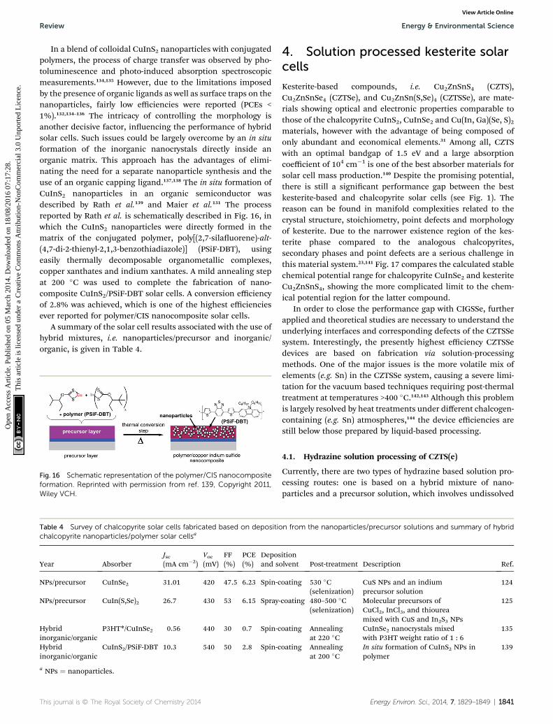
In a blend of colloidal CuInS2 nanoparticles with conjugatedpolymers, the process of charge transfer was observed by pho-toluminescence and photo-induced absorption spectroscopicmeasurements.134,135 However, due to the limitations imposedby the presence of organic ligands as well as surface traps on thenanoparticles, fairly low efficiencies were reported (PCEs <1%).132,134–136 The intricacy of controlling the morphology isanother decisive factor, inuencing the performance of hybridsolar cells. Such issues could be largely overcome by an in situformation of the inorganic nanocrystals directly inside anorganic matrix. This approach has the advantages of elimi-nating the need for a separate nanoparticle synthesis and theuse of an organic capping ligand.137,138 The in situ formation ofCuInS2 nanoparticles in an organic semiconductor wasdescribed by Rath et al.139 and Maier et al.131 The processreported by Rath et al. is schematically described in Fig. 16, inwhich the CuInS2 nanoparticles were directly formed in thematrix of the conjugated polymer, poly[(2,7-silauorene)-alt-(4,7-di-2-thienyl-2,1,3-benzothiadiazole)] (PSiF-DBT), usingeasily thermally decomposable organometallic complexes,copper xanthates and indium xanthates. A mild annealing stepat 200 �C was used to complete the fabrication of nano-composite CuInS2/PSiF-DBT solar cells. A conversion efficiencyof 2.8% was achieved, which is one of the highest efficienciesever reported for polymer/CIS nanocomposite solar cells.
A summary of the solar cell results associated with the use ofhybrid mixtures, i.e. nanoparticles/precursor and inorganic/organic, is given in Table 4.
Fig. 16 Schematic representation of the polymer/CIS nanocompositeformation. Reprinted with permission from ref. 139, Copyright 2011,Wiley VCH.
Table 4 Survey of chalcopyrite solar cells fabricated based on depositiochalcopyrite nanoparticles/polymer solar cellsa
Year AbsorberJsc(mA cm�2)
Voc(mV)
FF(%)
PCE(%)
Deposand so
NPs/precursor CuInSe2 31.01 420 47.5 6.23 Spin-c
NPs/precursor CuIn(S,Se)2 26.7 430 53 6.15 Spray-
Hybridinorganic/organic
P3HT*/CuInSe2 0.56 440 30 0.7 Spin-c
Hybridinorganic/organic
CuInS2/PSiF-DBT 10.3 540 50 2.8 Spin-c
a NPs ¼ nanoparticles.
This journal is © The Royal Society of Chemistry 2014
4. Solution processed kesterite solarcells
Kesterite-based compounds, i.e. Cu2ZnSnS4 (CZTS),Cu2ZnSnSe4 (CZTSe), and Cu2ZnSn(S,Se)4 (CZTSSe), are mate-rials showing optical and electronic properties comparable tothose of the chalcopyrite CuInS2, CuInSe2 and Cu(In, Ga)(Se, S)2materials, however with the advantage of being composed ofonly abundant and economical elements.31 Among all, CZTSwith an optimal bandgap of 1.5 eV and a large absorptioncoefficient of 104 cm�1 is one of the best absorber materials forsolar cell mass production.140 Despite the promising potential,there is still a signicant performance gap between the bestkesterite-based and chalcopyrite solar cells (see Fig. 1). Thereason can be found in manifold complexities related to thecrystal structure, stoichiometry, point defects and morphologyof kesterite. Due to the narrower existence region of the kes-terite phase compared to the analogous chalcopyrites,secondary phases and point defects are a serious challenge inthis material system.23,141 Fig. 17 compares the calculated stablechemical potential range for chalcopyrite CuInSe2 and kesteriteCu2ZnSnS4, showing the more complicated limit to the chem-ical potential region for the latter compound.
In order to close the performance gap with CIGSSe, furtherapplied and theoretical studies are necessary to understand theunderlying interfaces and corresponding defects of the CZTSSesystem. Interestingly, the presently highest efficiency CZTSSedevices are based on fabrication via solution-processingmethods. One of the major issues is the more volatile mix ofelements (e.g. Sn) in the CZTSSe system, causing a severe limi-tation for the vacuum based techniques requiring post-thermaltreatment at temperatures >400 �C.142,143 Although this problemis largely resolved by heat treatments under different chalcogen-containing (e.g. Sn) atmospheres,144 the device efficiencies arestill below those prepared by liquid-based processing.
4.1. Hydrazine solution processing of CZTS(e)
Currently, there are two types of hydrazine based solution pro-cessing routes: one is based on a hybrid mixture of nano-particles and a precursor solution, which involves undissolved
n from the nanoparticles/precursor solutions and summary of hybrid
itionlvent Post-treatment Description Ref.
oating 530 �C(selenization)
CuS NPs and an indiumprecursor solution
124
coating 480–500 �C(selenization)
Molecular precursors ofCuCl2, InCl3, and thioureamixed with CuS and In2S3 NPs
125
oating Annealingat 220 �C
CuInSe2 nanocrystals mixedwith P3HT weight ratio of 1 : 6
135
oating Annealingat 200 �C
In situ formation of CuInS2 NPs inpolymer
139
Energy Environ. Sci., 2014, 7, 1829–1849 | 1841
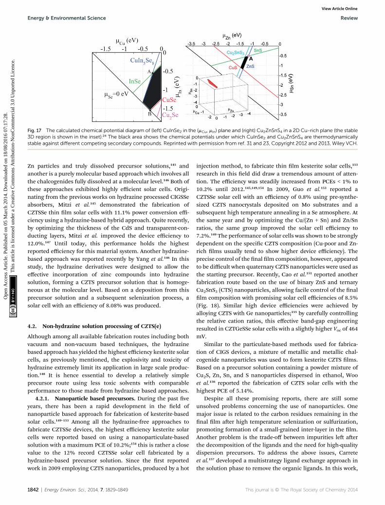
Fig. 17 The calculated chemical potential diagram of (left) CuInSe2 in the (mCu, mIn) plane and (right) Cu2ZnSnS4 in a 2D Cu-rich plane (the stable3D region is shown in the inset).24 The black area shows the chemical potentials under which CuInSe2 and Cu2ZnSnS4 are thermodynamicallystable against different competing secondary compounds. Reprinted with permission from ref. 31 and 23, Copyright 2012 and 2013, Wiley VCH.
Energy & Environmental Science Review
Ope
n A
cces
s A
rtic
le. P
ublis
hed
on 0
5 M
arch
201
4. D
ownl
oade
d on
18/
08/2
016
07:1
7:28
. T
his
artic
le is
lice
nsed
und
er a
Cre
ativ
e C
omm
ons
Attr
ibut
ion-
Non
Com
mer
cial
3.0
Unp
orte
d L
icen
ce.
View Article Online
Zn particles and truly dissolved precursor solutions,145 andanother is a purely molecular based approach which involves allthe chalcogenides fully dissolved at a molecular level.146 Both ofthese approaches exhibited highly efficient solar cells. Origi-nating from the previous works on hydrazine processed CIGSSeabsorbers, Mitzi et al.145 demonstrated the fabrication ofCZTSSe thin lm solar cells with 11.1% power conversion effi-ciency using a hydrazine-based hybrid approach. Quite recently,by optimizing the thickness of the CdS and transparent-con-ducting layers, Mitzi et al. improved the device efficiency to12.0%.147 Until today, this performance holds the highestreported efficiency for this material system. Another hydrazine-based approach was reported recently by Yang et al.146 In thisstudy, the hydrazine derivatives were designed to allow theeffective incorporation of zinc compounds into hydrazinesolution, forming a CZTS precursor solution that is homoge-neous at the molecular level. Based on a deposition from thisprecursor solution and a subsequent selenization process, asolar cell with an efficiency of 8.08% was produced.
4.2. Non-hydrazine solution processing of CZTS(e)
Although among all available fabrication routes including bothvacuum and non-vacuum based techniques, the hydrazinebased approach has yielded the highest efficiency kesterite solarcells, as previously mentioned, the explosivity and toxicity ofhydrazine extremely limit its application in large scale produc-tion.148 It is hence essential to develop a relatively simpleprecursor route using less toxic solvents with comparableperformance to those made from hydrazine based approaches.
4.2.1. Nanoparticle based precursors. During the past veyears, there has been a rapid development in the eld ofnanoparticle based approach for fabrication of kesterite-basedsolar cells.149–153 Among all the hydrazine-free approaches tofabricate CZTSSe devices, the highest efficiency kesterite solarcells were reported based on using a nanoparticulate-basedsolution with a maximum PCE of 10.2%;154 this is rather a closevalue to the 12% record CZTSSe solar cell fabricated by ahydrazine-based precursor solution. Since the rst reportedwork in 2009 employing CZTS nanoparticles, produced by a hot
1842 | Energy Environ. Sci., 2014, 7, 1829–1849
injection method, to fabricate thin lm kesterite solar cells,153
research in this eld did draw a tremendous amount of atten-tion. The efficiency was steadily increased from PCEs < 1% to10.2% until 2012.145,149,154 In 2009, Guo et al.153 reported aCZTSSe solar cell with an efficiency of 0.8% using pre-synthe-sized CZTS nanocrystals deposited on Mo substrates and asubsequent high temperature annealing in a Se atmosphere. Atthe same year and by optimizing the Cu/(Zn + Sn) and Zn/Snratios, the same group improved the solar cell efficiency to7.2%.149 The performance of solar cells was shown to be stronglydependent on the specic CZTS composition (Cu-poor and Zn-rich lms usually tend to show higher device efficiency). Theprecise control of the nal lm composition, however, appearedto be difficult when quaternary CZTS nanoparticles were used asthe starting precursor. Recently, Cao et al.151 reported anotherfabrication route based on the use of binary ZnS and ternaryCu2SnS3 (CTS) nanoparticles, allowing facile control of the nallm composition with promising solar cell efficiencies of 8.5%(Fig. 18). Similar high device efficiencies were achieved byalloying CZTS with Ge nanoparticles;155 by carefully controllingthe relative cation ratios, this effective band-gap engineeringresulted in CZTGeSSe solar cells with a slightly higher Voc of 464mV.
Similar to the particulate-based methods used for fabrica-tion of CIGS devices, a mixture of metallic and metallic chal-cogenide nanoparticles was used to form kesterite CZTS lms.Based on a precursor solution containing a powder mixture ofCu2S, Zn, Sn, and S nanoparticles dispersed in ethanol, Wooet al.156 reported the fabrication of CZTS solar cells with thehighest PCE of 5.14%.
Despite all these promising reports, there are still someunsolved problems concerning the use of nanoparticles. Onemajor issue is related to the carbon residues remaining in thenal lm aer high temperature selenization or sulfurization,promoting formation of a small-grained inter-layer in the lm.Another problem is the trade-off between impurities le aerthe decomposition of the ligands and the need for high-qualitydispersion precursors. To address the above issues, Carreteet al.157 developed a multistrategy ligand exchange approach inthe solution phase to remove the organic ligands. In this work,
This journal is © The Royal Society of Chemistry 2014
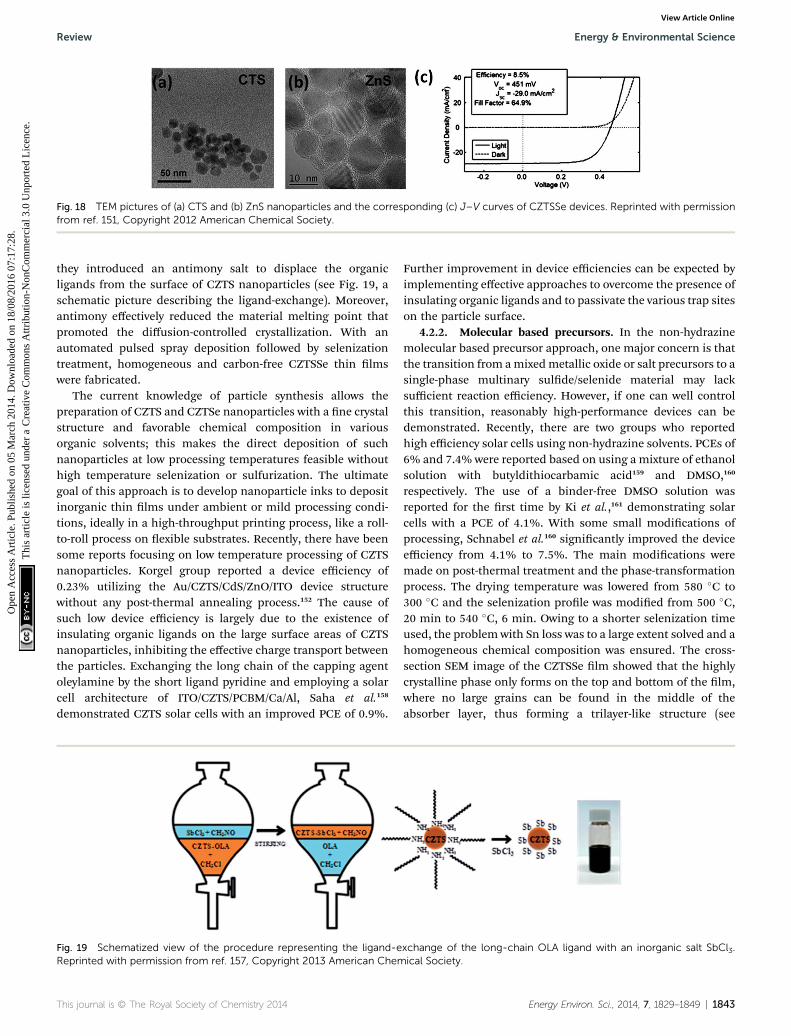
Fig. 18 TEM pictures of (a) CTS and (b) ZnS nanoparticles and the corresponding (c) J–V curves of CZTSSe devices. Reprinted with permissionfrom ref. 151, Copyright 2012 American Chemical Society.
Review Energy & Environmental Science
Ope
n A
cces
s A
rtic
le. P
ublis
hed
on 0
5 M
arch
201
4. D
ownl
oade
d on
18/
08/2
016
07:1
7:28
. T
his
artic
le is
lice
nsed
und
er a
Cre
ativ
e C
omm
ons
Attr
ibut
ion-
Non
Com
mer
cial
3.0
Unp
orte
d L
icen
ce.
View Article Online
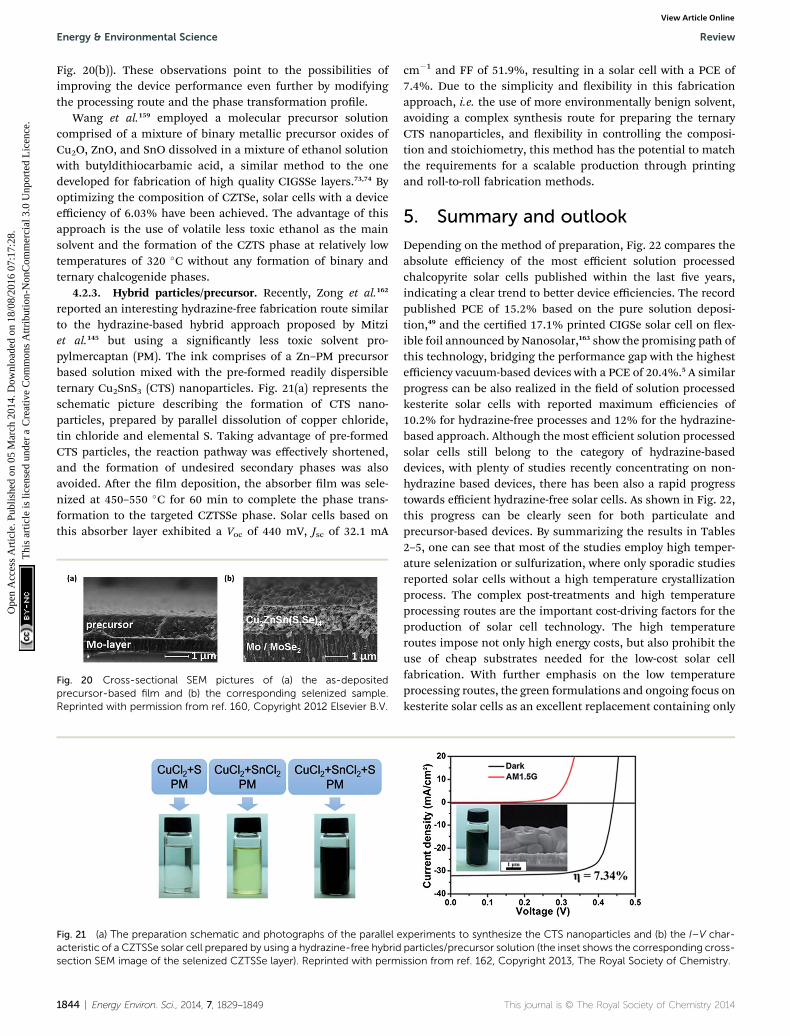
they introduced an antimony salt to displace the organicligands from the surface of CZTS nanoparticles (see Fig. 19, aschematic picture describing the ligand-exchange). Moreover,antimony effectively reduced the material melting point thatpromoted the diffusion-controlled crystallization. With anautomated pulsed spray deposition followed by selenizationtreatment, homogeneous and carbon-free CZTSSe thin lmswere fabricated.
The current knowledge of particle synthesis allows thepreparation of CZTS and CZTSe nanoparticles with a ne crystalstructure and favorable chemical composition in variousorganic solvents; this makes the direct deposition of suchnanoparticles at low processing temperatures feasible withouthigh temperature selenization or sulfurization. The ultimategoal of this approach is to develop nanoparticle inks to depositinorganic thin lms under ambient or mild processing condi-tions, ideally in a high-throughput printing process, like a roll-to-roll process on exible substrates. Recently, there have beensome reports focusing on low temperature processing of CZTSnanoparticles. Korgel group reported a device efficiency of0.23% utilizing the Au/CZTS/CdS/ZnO/ITO device structurewithout any post-thermal annealing process.152 The cause ofsuch low device efficiency is largely due to the existence ofinsulating organic ligands on the large surface areas of CZTSnanoparticles, inhibiting the effective charge transport betweenthe particles. Exchanging the long chain of the capping agentoleylamine by the short ligand pyridine and employing a solarcell architecture of ITO/CZTS/PCBM/Ca/Al, Saha et al.158
demonstrated CZTS solar cells with an improved PCE of 0.9%.
Fig. 19 Schematized view of the procedure representing the ligand-eReprinted with permission from ref. 157, Copyright 2013 American Chem
This journal is © The Royal Society of Chemistry 2014
Further improvement in device efficiencies can be expected byimplementing effective approaches to overcome the presence ofinsulating organic ligands and to passivate the various trap siteson the particle surface.
4.2.2. Molecular based precursors. In the non-hydrazinemolecular based precursor approach, one major concern is thatthe transition from amixedmetallic oxide or salt precursors to asingle-phase multinary sulde/selenide material may lacksufficient reaction efficiency. However, if one can well controlthis transition, reasonably high-performance devices can bedemonstrated. Recently, there are two groups who reportedhigh efficiency solar cells using non-hydrazine solvents. PCEs of6% and 7.4% were reported based on using a mixture of ethanolsolution with butyldithiocarbamic acid159 and DMSO,160
respectively. The use of a binder-free DMSO solution wasreported for the rst time by Ki et al.,161 demonstrating solarcells with a PCE of 4.1%. With some small modications ofprocessing, Schnabel et al.160 signicantly improved the deviceefficiency from 4.1% to 7.5%. The main modications weremade on post-thermal treatment and the phase-transformationprocess. The drying temperature was lowered from 580 �C to300 �C and the selenization prole was modied from 500 �C,20 min to 540 �C, 6 min. Owing to a shorter selenization timeused, the problem with Sn loss was to a large extent solved and ahomogeneous chemical composition was ensured. The cross-section SEM image of the CZTSSe lm showed that the highlycrystalline phase only forms on the top and bottom of the lm,where no large grains can be found in the middle of theabsorber layer, thus forming a trilayer-like structure (see
xchange of the long-chain OLA ligand with an inorganic salt SbCl3.ical Society.
Energy Environ. Sci., 2014, 7, 1829–1849 | 1843
Energy & Environmental Science Review
Ope
n A
cces
s A
rtic
le. P
ublis
hed
on 0
5 M
arch
201
4. D
ownl
oade
d on
18/
08/2
016
07:1
7:28
. T
his
artic
le is
lice
nsed
und
er a
Cre
ativ
e C
omm
ons
Attr
ibut
ion-
Non
Com
mer
cial
3.0
Unp
orte
d L
icen
ce.
View Article Online
Fig. 20(b)). These observations point to the possibilities ofimproving the device performance even further by modifyingthe processing route and the phase transformation prole.
Wang et al.159 employed a molecular precursor solutioncomprised of a mixture of binary metallic precursor oxides ofCu2O, ZnO, and SnO dissolved in a mixture of ethanol solutionwith butyldithiocarbamic acid, a similar method to the onedeveloped for fabrication of high quality CIGSSe layers.73,74 Byoptimizing the composition of CZTSe, solar cells with a deviceefficiency of 6.03% have been achieved. The advantage of thisapproach is the use of volatile less toxic ethanol as the mainsolvent and the formation of the CZTS phase at relatively lowtemperatures of 320 �C without any formation of binary andternary chalcogenide phases.
4.2.3. Hybrid particles/precursor. Recently, Zong et al.162
reported an interesting hydrazine-free fabrication route similarto the hydrazine-based hybrid approach proposed by Mitziet al.145 but using a signicantly less toxic solvent pro-pylmercaptan (PM). The ink comprises of a Zn–PM precursorbased solution mixed with the pre-formed readily dispersibleternary Cu2SnS3 (CTS) nanoparticles. Fig. 21(a) represents theschematic picture describing the formation of CTS nano-particles, prepared by parallel dissolution of copper chloride,tin chloride and elemental S. Taking advantage of pre-formedCTS particles, the reaction pathway was effectively shortened,and the formation of undesired secondary phases was alsoavoided. Aer the lm deposition, the absorber lm was sele-nized at 450–550 �C for 60 min to complete the phase trans-formation to the targeted CZTSSe phase. Solar cells based onthis absorber layer exhibited a Voc of 440 mV, Jsc of 32.1 mA
Fig. 20 Cross-sectional SEM pictures of (a) the as-depositedprecursor-based film and (b) the corresponding selenized sample.Reprinted with permission from ref. 160, Copyright 2012 Elsevier B.V.
Fig. 21 (a) The preparation schematic and photographs of the parallel eacteristic of a CZTSSe solar cell prepared by using a hydrazine-free hybridsection SEM image of the selenized CZTSSe layer). Reprinted with perm
1844 | Energy Environ. Sci., 2014, 7, 1829–1849
cm�1 and FF of 51.9%, resulting in a solar cell with a PCE of7.4%. Due to the simplicity and exibility in this fabricationapproach, i.e. the use of more environmentally benign solvent,avoiding a complex synthesis route for preparing the ternaryCTS nanoparticles, and exibility in controlling the composi-tion and stoichiometry, this method has the potential to matchthe requirements for a scalable production through printingand roll-to-roll fabrication methods.
5. Summary and outlook
Depending on the method of preparation, Fig. 22 compares theabsolute efficiency of the most efficient solution processedchalcopyrite solar cells published within the last ve years,indicating a clear trend to better device efficiencies. The recordpublished PCE of 15.2% based on the pure solution deposi-tion,49 and the certied 17.1% printed CIGSe solar cell on ex-ible foil announced by Nanosolar,163 show the promising path ofthis technology, bridging the performance gap with the highestefficiency vacuum-based devices with a PCE of 20.4%.5 A similarprogress can be also realized in the eld of solution processedkesterite solar cells with reported maximum efficiencies of10.2% for hydrazine-free processes and 12% for the hydrazine-based approach. Although the most efficient solution processedsolar cells still belong to the category of hydrazine-baseddevices, with plenty of studies recently concentrating on non-hydrazine based devices, there has been also a rapid progresstowards efficient hydrazine-free solar cells. As shown in Fig. 22,this progress can be clearly seen for both particulate andprecursor-based devices. By summarizing the results in Tables2–5, one can see that most of the studies employ high temper-ature selenization or sulfurization, where only sporadic studiesreported solar cells without a high temperature crystallizationprocess. The complex post-treatments and high temperatureprocessing routes are the important cost-driving factors for theproduction of solar cell technology. The high temperatureroutes impose not only high energy costs, but also prohibit theuse of cheap substrates needed for the low-cost solar cellfabrication. With further emphasis on the low temperatureprocessing routes, the green formulations and ongoing focus onkesterite solar cells as an excellent replacement containing only
xperiments to synthesize the CTS nanoparticles and (b) the I–V char-particles/precursor solution (the inset shows the corresponding cross-ission from ref. 162, Copyright 2013, The Royal Society of Chemistry.
This journal is © The Royal Society of Chemistry 2014
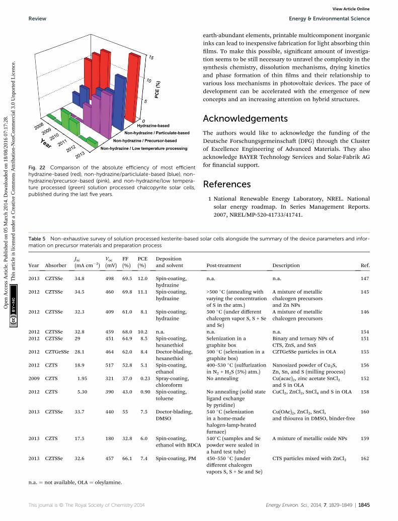
Fig. 22 Comparison of the absolute efficiency of most efficienthydrazine-based (red), non-hydrazine/particlulate-based (blue), non-hydrazine/precursor-based (pink), and non-hydrazine/low tempera-ture processed (green) solution processed chalcopyrite solar cells,published during the last five years.
Table 5 Non-exhaustive survey of solution processed kesterite-based smation on precursor materials and preparation process
Year AbsorberJsc(mA cm�2)
Voc(mV)
FF(%)
PCE(%)
Depositionand solvent
2013 CZTSSe 34.8 498 69.5 12.0 Spin-coating,hydrazine
2012 CZTSSe 34.5 460 69.8 11.1 Spin-coating,hydrazine
2012 CZTSSe 32.3 409 61.0 8.1 Spin-coating,hydrazine
2012 CZTSSe 32.8 459 68.0 10.2 n.a.2012 CZTSSe 29 451 64.9 8.5 Spin-coating,
hexanethiol2012 CZTGeSSe 28.1 464 62.0 8.4 Doctor-blading,
hexanethiol2012 CZTS 18.9 517 52.8 5.1 Spin-coating,
ethanol2009 CZTS 1.95 321 37.0 0.23 Spray-coating,
chloroform2012 CZTS 5.30 390 43.0 0.90 Spin-coating,
toluene
2013 CZTSSe 33.7 440 55 7.5 Doctor-blading,DMSO
2013 CZTS 17.5 180 32.8 6.0 Spin-coating,ethanol with BDCA
2013 CZTSSe 32.6 457 66.1 7.4 Spin-coating, PM
n.a. ¼ not available, OLA ¼ oleylamine.
This journal is © The Royal Society of Chemistry 2014
Review Energy & Environmental Science
Ope
n A
cces
s A
rtic
le. P
ublis
hed
on 0
5 M
arch
201
4. D
ownl
oade
d on
18/
08/2
016
07:1
7:28
. T
his
artic
le is
lice
nsed
und
er a
Cre
ativ
e C
omm
ons
Attr
ibut
ion-
Non
Com
mer
cial
3.0
Unp
orte
d L
icen
ce.
View Article Online
earth-abundant elements, printable multicomponent inorganicinks can lead to inexpensive fabrication for light absorbing thinlms. To make this possible, signicant amount of investiga-tion seems to be still necessary to unravel the complexity in thesynthesis chemistry, dissolution mechanisms, drying kineticsand phase formation of thin lms and their relationship tovarious loss mechanisms in photovoltaic devices. The pace ofdevelopment can be accelerated with the emergence of newconcepts and an increasing attention on hybrid structures.
Acknowledgements
The authors would like to acknowledge the funding of theDeutsche Forschungsgemeinscha (DFG) through the Clusterof Excellence Engineering of Advanced Materials. They alsoacknowledge BAYER Technology Services and Solar-Fabrik AGfor nancial support.
References
1 National Renewable Energy Laboratory, NREL. Nationalsolar energy roadmap. In Series Management Reports.2007, NREL/MP-520-41733/41741.
olar cells alongside the summary of the device parameters and infor-
Post-treatment Description Ref.
n.a. n.a. 147
>500 �C (annealing withvarying the concentrationof S in the atm.)
A mixture of metallicchalcogen precursorsand Zn NPs
145
500 �C (under differentchalcogen vapor S, S + Seand Se)
A mixture of metallicchalcogen precursors
146
n.a. n.a. 154Selenization in agraphite box
Binary and ternary NPs ofCTS, ZnS, and SnS
151
500 �C (selenization in agraphite box)
CZTGeSSe particles in OLA 155
400–530 �C (sulfurizationin N2 + H2S (5%) atm.)
Nanosized powder of Cu2S,Zn, Sn, and S (milling process)
156
No annealing Cu(acac)2, zinc acetate SnCl2and S in OLA
152
No annealing (solid stateligand exchangeby pyridine)
CuCl2, ZnCl2, SnCl4 and S in OLA 158
540 �C (selenizationin a home-madehalogen-lamp-heatedfurnace)
Cu(OAc)2, ZnCl2, SnCl,and thiourea in DMSO, binder-free
160
540�C (samples and Sepowder were sealed ina hard test tube)
A mixture of metallic oxide NPs 159
450–550 �C (underdifferent chalcogenvapors S, S + Se and Se)
CTS particles mixed with ZnCl2 162
Energy Environ. Sci., 2014, 7, 1829–1849 | 1845
Energy & Environmental Science Review
Ope
n A
cces
s A
rtic
le. P
ublis
hed
on 0
5 M
arch
201
4. D
ownl
oade
d on
18/
08/2
016
07:1
7:28
. T
his
artic
le is
lice
nsed
und
er a
Cre
ativ
e C
omm
ons
Attr
ibut
ion-
Non
Com
mer
cial
3.0
Unp
orte
d L
icen
ce.
View Article Online
2 C. Candelise, M. Winskel and R. Gross, Prog. Photovolt: Res.Appl., 2012, 20, 816–831.
3 C. J. Brabec, Sol. Energy Mater. Sol. Cells, 2004, 83, 273.4 P. Jackson, D. Hariskos, E. Lotter, S. Paetel, R. Wuerz,R. Menner, W. Wischmann and M. Powalla, Prog.Photovolt: Res. Appl., 2011, 19, 894–897.
5 A. Chirila, P. Reinhard, F. Pianezzi, P. Bloesch, A. R. Uhl,C. Fella, L. Kranz, D. Keller, C. Gretener, H. Hagendorfer,D. Jaeger, R. Erni, S. Nishiwaki, S. Buecheler andA. N. Tiwari, Nat. Mater., 2013, 12, 1107–1111.
6 C. J. Hibberd, E. Chassaing, W. Liu, D. B. Mitzi, D. Lincotand a. N. Tiwari, Prog. Photovoltaics Res. Appl., 2010, 18,434–452.
7 V. S. Saji, I.-H. Choi and C.-W. Lee, Sol. Energy, 2011, 85,2666–2678.
8 J.-F. Guillemoles, P. Cowache, A. Lusson, K. Fezzaa,F. Boisivon, J. Vedel and D. Lincot, J. Appl. Phys., 1996, 79,7293.
9 M. A. Green, K. Emery, Y. Hishikawa, W. Warta andE. D. Dunlop, Prog. Photovolt: Res. Appl., 2013, 21, 827–837.
10 R. Scheer, H.-W. Schock, Chalcogenide Photovoltaics:Physics, Technologies, and Thin Film Devices, WILEY-VCHVerlag & Co. KGaA 2011.
11 J. Nelson, The Physics of Solar Cells, Imperial College Press,London 2003.
12 A. Chirila, S. Buecheler, F. Pianezzi, P. Bloesch, C. Gretener,A. R. Uhl, C. Fella, L. Kranz, J. Perrenoud, S. Seyrling,R. Verma, S. Nishiwaki, Y. E. Romanyuk, G. Bilger andA. N. Tiwari, Nat. Mater., 2011, 10, 857–861.
13 U. Rau and H. W. Schock, Appl. Phys. A, 1999, 69, 131.14 S. Siebentritt, Sol. Energy Mater. Sol. Cells, 2011, 95, 1471.15 S. Siebentritt, M. Igalson, C. Persson and S. Lany, Prog.
Photovoltaics Res. Appl., 2010, 18, 390.16 U. Rau, K. Taretto and S. Siebentritt, Appl. Phys. A, 2008, 96,
221.17 M. Gloeckler, J. R. Sites and W. K. Metzger, J. Appl. Phys.,
2005, 98, 113704.18 K. Taretto and U. Rau, J. Appl. Phys., 2008, 103, 094523.19 D. Schmid, M. Ruckh and H. W. Schock, Sol. Energy Mater.
Sol. Cells, 1996, 41-42, 281.20 J. Li, D. B. Mitzi, V. B. Shenoy and V. B. Shenoy, ACS Nano,
2011, 5, 8613.21 S.-H. Wei, S. B. Zhang and A. Zunger, Appl. Phys. Lett., 1998,
72, 3199.22 M. J. Romero, H. Du, G. Teeter, Y. Yan and M. M. Al-Jassim,
Phys. Rev. B: Condens. Matter Mater. Phys., 2011, 84, 165324.23 S. Chen, A. Walsh, X.-G. Gong and S.-H. Wei, Adv. Mater.,
2013, 25, 1522.24 S. Chen, X. G. Gong, A. Walsh and S.-H. Wei, Appl. Phys.
Lett., 2010, 96, 021902.25 C.-H. Chung, S.-H. Li, B. Lei, W. Yang, W. W. Hou, B. Bob
and Y. Yang, Chem. Mater., 2011, 23, 964.26 J. Alvarez-Garcıa, E. Rudigier, N. Rega, B. Barcones,
R. Scheer, a. Perez-Rodrıguez, a. Romano-Rodrıguez andJ. R. Morante, Thin Solid Films, 2003, 431–432, 122–125.
27 E. Rudigier, I. Luck and R. Scheer, Appl. Phys. Lett., 2003, 82,4370.
1846 | Energy Environ. Sci., 2014, 7, 1829–1849
28 H. Azimi, T. Heumuller, A. Gerl, G. Matt, P. Kubis,M. Distaso, R. Ahmad, T. Akdas, M. Richter, W. Peukertand C. J. Brabec, Adv. Energy Mater., 2013, 3, 1589.
29 I. Oja, M. Nanu, a. Katerski, M. Krunks, a. Mere, J. Raudojaand a. Goossens, Thin Solid Films, 2005, 480–481, 82–86.
30 A.-J. Cheng, M. Manno, a. Khare, C. Leighton, S. a. Campbelland E. S. Aydil, J. Vac. Sci. Technol., A, 2011, 29, 051203.
31 A. Walsh, S. Chen, S.-H. Wei and X.-G. Gong, Adv. EnergyMater., 2012, 2, 400.
32 P. a. Fernandes, P. M. P. Salome and a. F. da Cunha, ThinSolid Films, 2009, 517, 2519.
33 R. Ahmad, M. Distaso, H. Azimi, C. J. Brabec andW. Peukert, J. Nanopart. Res., 2013, 15, 1886.
34 X. Fontane, L. Calvo-Barrio, V. Izquierdo-Roca, E. Saucedo,a. Perez-Rodriguez, J. R. Morante, D. M. Berg, P. J. Dale andS. Siebentritt, Appl. Phys. Lett., 2011, 98, 181905.
35 F. Hergert, R. Hock, a. Weber, M. Purwins, J. Palm andV. Probst, J. Phys. Chem. Solids, 2005, 66, 1903.
36 C. von Klopmann, J. Djordjevic and R. Scheer, J. Cryst.Growth, 2006, 289, 113.
37 A. Fischereder, T. Rath, W. Haas, H. Amenitsch, D. Schenk,A. Zankel, R. Saf, F. Hofer and G. Trimmel, ACS Appl. Mater.Interfaces, 2012, 4, 382.
38 V. Izquierdo-Roca, A. Shavel, E. Saucedo, S. Jaime-Ferrer,J. Alvarez-Garcıa, A. Cabot, A. Perez-Rodrıguez,V. Bermudez and J. R. Morante, Sol. Energy Mater. Sol.Cells, 2011, 95, S83.
39 K. Topper, J. Bruns, R. Scheer, M. Weber, a. Weidinger andD. Braunig, Appl. Phys. Lett., 1997, 71, 482.
40 F. Luckert, D. I. Hamilton, M. V. Yakushev, N. S. Beattie,G. Zoppi, M. Moynihan, I. Forbes, a. V. Karotki,a. V. Mudryi, M. Grossberg, J. Krustok and R. W. Martin,Appl. Phys. Lett., 2011, 99, 062104.
41 J. Raudoja andM. Altosaar, Sol. Energy Mater., 2003, 79, 401.42 M. Burgelman, F. Engelhardt, J. F. Guillemoles,
R. Herberholz, M. Igalson, R. Klenk, M. Lampert,T. Meyer, V. Nadenau, A. Niemegeers, J. Parisi, U. Rau,H. W. Schock, M. Schmitt, O. Seifert, T. Walter andS. Zott, Prog. Photovolt: Res. Appl., 1997, 5, 121–130.
43 A. Jasenek, U. Rau, V. Nadenau and H. W. Schock, J. Appl.Phys., 2000, 87, 594.
44 R. Knecht, M. S. Hammer, J. Parisi and I. Riedel, Phys.Status Solidi, 2013, 210, 1392–1399.
45 J. P. Leitao, N. M. Santos, P. a. Fernandes, P. M. P. Salome,a. F. da Cunha, J. C. Gonzalez, G. M. Ribeiro andF. M. Matinaga, Phys. Rev. B: Condens. Matter Mater. Phys.,2011, 84, 024120.
46 S. Siebentritt and S. Schuler, J. Phys. Chem. Solids, 2003, 64,1621.
47 O. Gunawan, T. K. Todorov and D. B. Mitzi, Appl. Phys. Lett.,2010, 97, 233506.
48 S. Shirakata and T. Nakada, Thin Solid Films, 2007, 515,6151–6154.
49 T. K. Todorov, O. Gunawan, T. Gokmen and D. B. Mitzi,Prog. Photovolt: Res. Appl., 2013, 21, 82–87.
50 J. B. Li, V. Chawla and B. M. Clemens, Adv. Mater., 2012, 24,720–723.
This journal is © The Royal Society of Chemistry 2014
Review Energy & Environmental Science
Ope
n A
cces
s A
rtic
le. P
ublis
hed
on 0
5 M
arch
201
4. D
ownl
oade
d on
18/
08/2
016
07:1
7:28
. T
his
artic
le is
lice
nsed
und
er a
Cre
ativ
e C
omm
ons
Attr
ibut
ion-
Non
Com
mer
cial
3.0
Unp
orte
d L
icen
ce.
View Article Online
51 Z. Zhang, X. Tang, U. Lemmer, W. Witte, O. Kiowski,M. Powalla andH.Holscher, Appl. Phys. Lett., 2011, 99, 042111.
52 Advanced Characterization Techniques for Thin Film SolarCells, ed. Daniel Abou-Ras, Thomas Kirchartz and UweRau, WILEY-VCH Verlag & Co. KGaA, 2011.
53 K. Durose, S. E. Asher, W. Jaegermann, D. Levi,B. E. McCandless, W. Metzger, H. Moutinho, P. D. Paulson,C. L. Perkins, J. R. Sites, G. Teeter and M. Terheggen, Prog.Photovoltaics Res. Appl., 2004, 12, 177–217.
54 S. Ahn, C. Kim, J. H. Yun, J. Gwak, S. Jeong, B.-H. Ryu andK. Yoon, J. Phys. Chem. C, 2010, 114, 8108–8113.
55 C. Jiang, J. Lee, D. V. Talapin and J. Am, Chem. Soc., 2012,134, 5010–5013.
56 Solution Processing of Inorganic Materials, ed. David B. Mitzi,John Wiley & Sons, Inc, 2009.
57 D. B. Mitzki, Adv. Mater., 2009, 21, 3141.58 T. Todorov and D. B. Mitzi, Eur. J. Inorg. Chem., 2010, 17–28.59 B. Bob, B. Lei, C.-H. Chung, W. Yang, W.-C. Hsu,
H.-S. Duan, W. W.-J. Hou, S.-H. Li and Y. Yang, Adv.Energy Mater., 2012, 2, 504–522.
60 D. B. Mitzi, M. Yuan, W. Liu, A. J. Kellock, S. J. Chey,L. Gignac and A. G. Schrott, Thin Solid Films, 2009, 517,2158–2162.
61 D. B. Mitzi, M. Yuan, W. Liu, A. J. Kellock, S. J. Chey,V. Deline and A. G. Schrott, Adv. Mater., 2008, 20, 3657–3662.
62 W. Liu, D. B. Mitzi, M. Yuan, A. J. Kellock, S. J. Chey andO. Gunawan, Chem. Mater., 2010, 22, 1010.
63 H. Zhou, C.-J. Hsu, W.-C. Hsu, H.-S. Duan, C.-H. Chung,W. Yang and Y. Yang, Adv. Energy Mater., 2012, 3, 328–336.
64 M. Kaelin, D. Rudmann, F. Kurdesau, H. Zogg, T. Meyer anda. N. Tiwari, Thin Solid Films, 2005, 480–481, 486–490.
65 A. R. Uhl, Y. E. Romanyuk and A. N. Tiwari, Thin Solid Films,2011, 519, 7259.
66 A. R. Uhl, C. Fella, A. Chirila, M. R. Kaelin, L. Karvonen,A. Weidenkaff, C. N. Borca, D. Grolimund,Y. E. Romanyuk and A. N. Tiwari, Prog. Photovolt: Res.Appl., 2012, 20, 526–533.
67 S. J. Park, J. W. Cho, J. K. Lee, K. Shin, J. Kim and B. K. Min,Prog. Photovolt.: Res. Appl., 2014, 22, 122–128.
68 W. Wang, Y.-W. Su and C. Chang, Sol. Energy Mater. Sol.Cells, 2011, 95, 2616–2620.
69 W. Wang, S.-Y. Han, S.-J. Sung, D.-H. Kim and C.-H. Chang,Phys. Chem. Chem. Phys., 2012, 14, 11154–11159.
70 S. Ahn, T. H. Son, A. Cho, J. Gwak, J. H. Yun, K. Shin,S. K. Ahn, S. H. Park and K. Yoon, ChemSusChem, 2012, 5,1773–1777.
71 B. D. Weil, S. T. Connor and Y. Cui, J. Am. Chem. Soc., 2010,132, 6642.
72 L. Li, N. Coates and D.Moses, J. Am. Chem. Soc., 2010, 132, 22.73 G. Wang, S. Wang, Y. Cui and D. Pan, Chem. Mater., 2012,
24, 3993–3997.74 W. Zhao, Y. Cui and D. Pan, Energy Technol., 2013, 1, 131.75 A. Goossens and J. Houis, Nanotechnology, 2008, 19,
424018.76 M. Krunks, O. Kijatkina, H. Rebane, I. Oja, V. Mikli and
A. Mere, Thin Solid Films, 2002, 404, 71.
This journal is © The Royal Society of Chemistry 2014
77 T. Theresajohn, M. Mathew, C. Sudhakartha,K. Vijayakumar, T. Abe and Y. Kashiwaba, Sol. EnergyMater. Sol. Cells, 2005, 89, 27.
78 M. S. Tomar and F. J. Garcia, Thin Solid Films, 1982, 90, 419–423.
79 P. R. Ram, R. Thangaraj, A. K. Sharma and O. P. Agnihotri,Solar Cells, 1985, 14, 123.
80 M. Nanu, J. Schoonman and A. Goossens, Nano Lett., 2005,5, 1716.
81 W. Hirpo, S. Dhingra, A. C. Sutorik and M. G. Kanatzidis,J. Am. Chem. Soc., 1993, 115, 1597.
82 K. K. Banger, J. a. Hollingsworth, J. D. Harris, J. Cowen,W. E. Buhro and A. F. Hepp, Appl. Organomet. Chem.,2002, 16, 617.
83 K. K. Banger, J. Cowen and A. F. Hepp, Chem. Mater., 2001,13, 3827–3829.
84 K. K. Banger, M. H.-C. Jin, J. D. Harris, P. E. Fanwick andA. F. Hepp, Inorg. Chem., 2003, 42, 7713.
85 M. H. Jin, K. K. Banger, C. V. Kelly, J. H. Scoeld,J. S. McNatt, J. E. Dickman and A. F. Hepp, Proceedings ofthe 19th European Photovoltaic Solar Energy Conference,4AV.1.71, 2004.
86 C. Kind, C. Feldmann, A. Quintilla and E. Ahlswede, Chem.Mater., 2011, 23, 5269–5274.
87 Y. S. Lim, J. Jeong, J. Y. Kim, M. J. Ko, H. Kim, B. Kim,U. Jeong and D.-K. Lee, J. Phys. Chem. C, 2013, 117,11930.
88 D. V Talapin, J.-S. Lee, M. V Kovalenko and E. VShevchenko, Chem. Rev., 2010, 110, 389–458.
89 C. J. Stolle, M. G. Panthani, T. B. Harvey, V. A. Akhavan andB. A. Korgel, ACS Appl. Mater. Interfaces, 2012, 4, 2757.
90 Q. Guo, G. M. Ford, H. W. Hillhouse and R. Agrawal, NanoLett., 2009, 9, 3060–3065.
91 C. B. Murray, D. J. Norris and M. G. Bawendi, J. Am. Chem.Soc., 1993, 115, 8706–8715.
92 G. Konstantatos, I. Howard, A. Fischer, S. Hoogland,J. Clifford, E. Klem, L. Levina and E. H. Sargent, Nature,2006, 442, 180.
93 J. D. Olson, G. P. Gray and S. a. Carter, Sol. Energy Mater. Sol.Cells, 2009, 93, 519.
94 J.-J. Wang, Y.-Q. Wang, F.-F. Cao, Y.-G. Guo and L.-J. Wan,J. Am. Chem. Soc., 2010, 132, 12218.
95 B. L. Cushing, V. L. Kolesnichenko and C. J. O'Connor,Chem. Rev., 2004, 104, 3893.
96 C. Burda, X. Chen, R. Narayanan and M. A. El-Sayed, Chem.Rev., 2005, 105, 1025–1102.
97 H. Goesmann and C. Feldmann, Angew. Chem., Int. Ed.Engl., 2010, 49, 1362–1395.
98 J. Tang, S. Hinds, S. O. Kelley and E. H. Sargent, Chem.Mater., 2008, 20, 6906–6910.
99 M. Kruszynska, H. Bo rchert, J. Parisi and J. Kolny-Olesiak,J. Am. Chem. Soc., 2010, 132, 15976.
100 M. Chiang, S. Chang, C. Chen, F. Yuan and H. Tuan, J. Phys.Chem. C, 2011, 115, 1592–1599.
101 Q. Guo, S. J. Kim, M. Kar, W. N. Shafarman, R. W. Birkmire,E. a. Stach, R. Agrawal and H. W. Hillhouse, Nano Lett.,2008, 8, 2982.
Energy Environ. Sci., 2014, 7, 1829–1849 | 1847
Energy & Environmental Science Review
Ope
n A
cces
s A
rtic
le. P
ublis
hed
on 0
5 M
arch
201
4. D
ownl
oade
d on
18/
08/2
016
07:1
7:28
. T
his
artic
le is
lice
nsed
und
er a
Cre
ativ
e C
omm
ons
Attr
ibut
ion-
Non
Com
mer
cial
3.0
Unp
orte
d L
icen
ce.
View Article Online
102 Q. Guo, G. M. Ford, R. Agrawal and H. W. Hillhouse, Prog.Photovolt: Res. Appl., 2013, 21, 64–71.
103 M. G. Panthani, V. Akhavan, B. Goodfellow, J. P. Schmidtke,L. Dunn, A. Dodabalapur, P. F. Barbara and B. A. Korgel,J. Am. Chem. Soc., 2008, 130, 16770–16777.
104 V. A. Akhavan, M. G. Panthani, B. W. Goodfellow,D. K. Reid and B. a. Korgel, Energy Express, 2010, 18,A411–A420.
105 V. A. Akhavan, B. W. Goodfellow, M. G. Panthani,C. Steinhagen, T. B. Harvey, C. J. Stolle and B. A. Korgel,J. Solid State Chem., 2012, 189, 2–12.
106 M. Bar, S. Nishiwaki, L. Weinhardt, S. Pookpanratana,W. N. Shafarman and C. Heske, Appl. Phys. Lett., 2008, 93,042110.
107 A. Romeo, M. Terheggen, D. Abou-Ras, D. L. Batzner,F.-J. Haug, M. Kalin, D. Rudmann and A. N. Tiwari, Prog.Photovolt: Res. Appl., 2004, 12, 93–111.
108 T. Arita, N. Suyama, Y. Kita, S. Kitamura, T. Hibino,H. Takada, K. Omura, N. Ueno and M. Murozono,Conference Record of the 20th IEEE Photovoltaic SpecialistsConference, IEEE, New York, 1988, p. 1650.
109 B. M. Basol, V. K. Kapur, G. Norsworthy, A. Halani,C. R. Leidholm and R. Roe, Electrochem. Solid State Lett.,1998, 1, 252.
110 C. Eberspacher, C. Fredric, K. Pauls and J. Serra, Thin SolidFilms, 2001, 387, 18–22.
111 G. Norsworthy, C. R. Leidholm, A. Halani, V. K. Kapur,R. Roe, B. M. Basol and R. Matson, Sol. Energy Mater. Sol.Cells, 2000, 60, 127–134.
112 F. Roux, S. Amtablian, M. Anton, G. Besnard, L. Bilhaut,P. Bommersbach, J. Braillon, C. Cayron, a. Disdier,H. Fournier, J. Garnier, a. Jannaud, J. Jouhannaud,a. Kaminski, N. Karst, S. Noel, S. Perraud, O. Poncelet,O. Raccurt, D. Rapisarda, a. Ricaud, D. Rouchon,M. Roumanie, E. Rouviere, O. Sicardy, F. Sonier,K. Tarasov, F. Tardif, M. Tomassini and J. Villanova, Sol.Energy Mater. Sol. Cells, 2013, 115, 86–92.
113 V. K. Kapur, A. Bansal, P. Le and O. I. Asensio, Thin SolidFilms, 2003, 431–432, 53.
114 G. Chen, L. Wang, X. Sheng, H. Liu, X. Pi and D. Yang,J. Alloys Compd., 2010, 507, 317.
115 J. Chang, J. H. Lee, J.-H. Cha, D.-Y. Jung, G. Choi andG. Kim, Thin Solid Films, 2011, 519, 2176.
116 S.-H. Liu, F.-S. Chen and C.-H. Lu, J. Alloys Compd., 2012,517, 14.
117 S. A. Mockel, A. Holzing, R. Hock and P. J. Wellmann, ThinSolid Films, 2013, 535, 133–137.
118 M. Periasamy and M. Thirumalaikumar, J. Organomet.Chem., 2000, 609, 137.
119 S. Jeong, B.-S. Lee, S. Ahn, K. Yoon, Y.-H. Seo, Y. Choi andB.-H. Ryu, Energy Environ. Sci., 2012, 5, 7539.
120 H. Min Lim, S. K. Batabyal, S. S. Pramana, L. H. Wong,S. Magdassi and S. G. Mhaisalkar, Chem. Commun., 2013,49, 5351.
121 S. Ahn, K. Kim, A. Cho, J. Gwak, J. H. Yun, K. Shin, S. Ahnand K. Yoon, ACS Appl. Mater. Interfaces, 2012, 4, 1530–1536.
1848 | Energy Environ. Sci., 2014, 7, 1829–1849
122 K. Kim, Y.-J. Eo, A. Cho, J. Gwak, J. H. Yun, K. Shin,S. K. Ahn, S. H. Park, K. Yoon and S. Ahn, J. Mater. Chem.,2012, 22, 8444.
123 S. Ahn, Y. J. Choi, K. Kim, Y.-J. Eo, A. Cho, J. Gwak,J. H. Yun, K. Shin, S. K. Ahn and K. Yoon, ChemSusChem,2013, 6, 1282–1287.
124 A. Cho, S. Ahn, J. H. Yun, J. Gwak, H. Song and K. Yoon,J. Mater. Chem., 2012, 22, 17893.
125 Y. Cai, J. C. W. Ho, S. K. Batabyal, W. Liu, Y. Sun,S. G. Mhaisalkar and L. H. Wong, ACS Appl. Mater.Interfaces, 2013, 5, 1533–1537.
126 J.-J. Wang, J.-S. Hu, Y.-G. Guo and L.-J. Wan, NPG AsiaMater., 2012, 4, e2.
127 J.-J. Wang, Y.-Q. Wang, F.-F. Cao, Y.-G. Guo and L.-J. Wan,J. Am. Chem. Soc., 2010, 132, 12218–12221.
128 D. J. Milliron, I. Gur and A. P. Alivisatos,MRS Bull., January2005, 30.
129 H. Borchert, Energy Environ. Sci., 2010, 3, 1682.130 W. Yue, S. Han, R. Peng, W. Shen, H. Geng, F. Wu, S. Tao
and M. Wang, J. Mater. Chem., 2010, 20, 7570.131 E. Maier, T. Rath, W. Haas, O. Werzer, R. Saf, F. Hofer,
D. Meissner, O. Volobujeva, S. Bereznev, E. Mellikov,H. Amenitsch, R. Resel and G. Trimmel, Sol. EnergyMater. Sol. Cells, 2011, 95, 1354.
132 E. Arici, N. S. Saricici and D. Meissner, Adv. Funct. Mater.,2003, 13, 165.
133 F. M. Courtel, R. W. Paynter, B. Marsan and M. Morin,Chem. Mater., 2009, 21, 3752.
134 M. Kruszynska, M. Knipper, J. Kolny-Olesiak, H. Borchertand J. Parisi, Thin Solid Films, 2011, 519, 7374–7377.
135 Y. Yang, H. Zhong, Z. Bai, B. Zou, Y. Li and G. D. Scholes,J. Phys. Chem. C, 2012, 116, 7280–7286.
136 E. Arici, H. Hoppe, F. Schaffler, D. Meissner, M. A. Malikand N. S. Saricici, Thin Solid Films, 2004, 451–452, 612–618.
137 B. P. A. Van Hal, M. M. Wienk, J. M. Kroon, W. J. H. VanGennip, P. Jonkheijm and R. A. J. Janssen, Adv. Mater,2003, 15, 118.
138 S. D. Oosterhout, M. M. Wienk, S. S. van Bavel,R. Thiedmann, L. J. A. Koster, J. Gilot, J. Loos, V. Schmidtand R. a. J. Janssen, Nat. Mater., 2009, 8, 818.
139 T. Rath, M. Edler, W. Haas, A. Fischereder, S. Moscher,A. Schenk, R. Trattnig, M. Sezen, G. Mauthner, A. Pein,D. Meischler, K. Bartl, R. Saf, N. Bansal, S. a. Haque,F. Hofer, E. J. W. List and G. Trimmel, Adv. Energy Mater.,2011, 1, 1046.
140 D. B. Mitzi, O. Gunawan, T. K. Todorov, K. Wang andS. Guha, Sol. Energy Mater. Sol. Cells, 2011, 95, 1421.
141 S. Siebentritt and S. Schorr, Prog. Photovolt: Res. Appl., 2012,20, 512–519.
142 D. B. Mitzi, O. Gunawan, T. K. Todorov andD. A. R. Barkhouse, Philos. Trans. R. Soc., A, 2013, 371,20110432.
143 A. Fairbrother, E. Garcıa-Hemme, V. Izquierdo-Roca,X. Fontane, F. a. Pulgarın-Agudelo, O. Vigil-Galan,A. Perez-Rodrıguez and E. Saucedo, J. Am. Chem. Soc.,2012, 134, 8018.
This journal is © The Royal Society of Chemistry 2014
Review Energy & Environmental Science
Ope
n A
cces
s A
rtic
le. P
ublis
hed
on 0
5 M
arch
201
4. D
ownl
oade
d on
18/
08/2
016
07:1
7:28
. T
his
artic
le is
lice
nsed
und
er a
Cre
ativ
e C
omm
ons
Attr
ibut
ion-
Non
Com
mer
cial
3.0
Unp
orte
d L
icen
ce.
View Article Online
144 A. Redinger, D. M. Berg, P. J. Dale and S. Siebentritt, J. Am.Chem. Soc., 2011, 133, 3320.
145 T. K. Todorov, J. Tang, S. Bag, O. Gunawan, T. Gokmen,Y. Zhu and D. B. Mitzi, Adv. Energy Mater, 2013, 3, 34–38.
146 W. Yang, H.-S. Duan, B. Bob, H. Zhou, B. Lei, C.-H. Chung,S.-H. Li, W. W. Hou and Y. Yang, Adv. Mater., 2012, 24,6323.
147 M. T. Winkler, W. Wang, O. Gunawan, H. J. Hovel,T. Todorov and D. B. Mitzi, Energy Environ. Sci., 2014, 7,1029–1036.
148 Y. E. Romanyuk, C. M. Fella, A. R. Uhl, m. Werner,a. N. Tiwari, T. Schnabel and E. Ahlswede, Sol. EnergyMater. Sol. Cells, 2013, 119, 181–189.
149 Q. Guo, G. M. Ford, W. C. Yang, B. C. Walker, E. A. Stach,H. W. Hillhouse and R. Agrawal, J. Am. Chem. Soc., 2010,132, 17384.
150 G. M. Ford, Q. Guo, R. Agrawal and H. W. Hillhouse, Chem.Mater., 2011, 23, 2626.
151 Y. Cao, M. S. Denny, J. V. Caspar, W. E. Farneth, Q. Guo,A. S. Ionkin, L. K. Johnson, M. Lu, I. Malajovich, D. Radu,H. D. Rosenfeld, K. R. Choudhury and W. Wu, J. Am.Chem. Soc., 2012, 134, 15644.
152 C. Steinhagen, M. G. Panthani, V. Akhavan, B. Goodfellow,B. Koo and B. A. Korgel, J. Am. Chem. Soc., 2009, 131, 12554.
This journal is © The Royal Society of Chemistry 2014
153 Q. Guo, H. W. Hillhouse and R. Agrawal, J. Am. Chem. Soc.,2009, 131, 11672.
154 C. Leidholm, C. Hotz, A. Breeze, C. Sunderland, and W. Ki,NREL Subcontract Report 2012, NREL/SR-5200–56510.
155 Q. Guo, G. M. Ford, W.-C. Yang, C. J. Hages,H. W. Hillhouse and R. Agrawal, Sol. Energy Mater. Sol.Cells, 2012, 105, 132.
156 K. Woo, Y. Kim and J. Moon, Energy Environ. Sci., 2012, 5,5340.
157 A. Carrete, A. Shavel, X. Fontane, J. Montserrat, J. Fan,M. Ibanez, E. Saucedo, A. Perez-Rodrıguez and A. Cabot,J. Am. Chem. Soc., 2013, 135, 15982–15985.
158 S. K. Saha, A. Guchhait and A. J. Pal, Phys. Chem. Chem.Phys., 2012, 14, 8090.
159 G. Wang, W. Zhao, Y. Cui, Q. Tian, S. Gao, L. Huang andD. Pan, ACS Appl. Mater. Interfaces, 2013, 5, 10042–10047.
160 T. Schnabel, M. Low and E. Ahlswede, Sol. Energy Mater.Sol. Cells, 2013, 117, 324.
161 W. Ki and H. W. Hillhouse, Adv. Energy Mater., 2011, 1, 732.162 K. Zong, Y. Sun, Y. Zhang, H. Wang, J. Liu and H. Yan,
J. Mater. Chem. A, 2013, DOI: 10.1039/c3ta13157b.163 Press release: http://www.nanosolar.com/detail_press/
nanosolar-achieves-17-1-aperture-efficiency-through-printed-cigs-process/.
Energy Environ. Sci., 2014, 7, 1829–1849 | 1849
Top Related
Copyright © 2022 FDOKUMEN

