


Bahasa
Halaman
Hukum

EASIROC, an easy & versatile ReadOut device
for SiPMStéphane CALLIER, Christophe DE LA TAILLE,
Gisèle MARTIN-CHASSARD, Ludovic RAUX
With precious help of :Dominique CUISY, Jean-Jacques JAEGER,
Nathalie SEGUIN-MOREAU, Jean-Luc SOCHA
[email protected] - NDIP 2011, Lyon, France, 05/07/2011 2
CONTENTS
• EASIROC Features
• EASIROC Measurements
• Projects using EASIROC
• Conclusion
[email protected] - NDIP 2011, Lyon, France, 05/07/2011 3
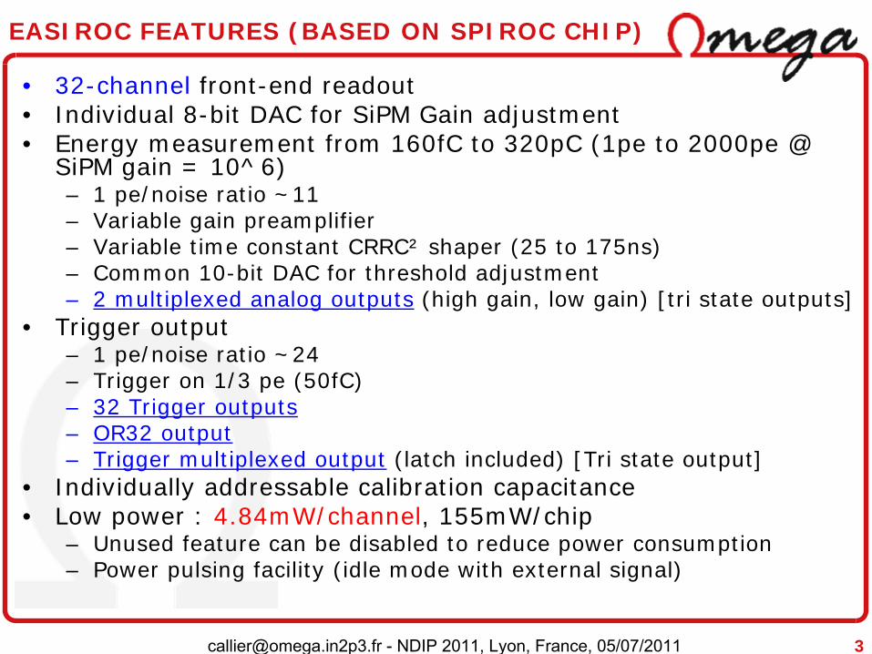
EASIROC FEATURES (BASED ON SPIROC CHIP)
• 32-channel front-end readout• Individual 8-bit DAC for SiPM Gain adjustment• Energy measurement from 160fC to 320pC (1pe to 2000pe @
SiPM gain = 10^6)– 1 pe/noise ratio ~11– Variable gain preamplifier– Variable time constant CRRC² shaper (25 to 175ns)– Common 10-bit DAC for threshold adjustment– 2 multiplexed analog outputs (high gain, low gain) [tri state outputs]
• Trigger output– 1 pe/noise ratio ~24– Trigger on 1/3 pe (50fC)– 32 Trigger outputs– OR32 output– Trigger multiplexed output (latch included) [Tri state output]
• Individually addressable calibration capacitance• Low power : 4.84mW/channel, 155mW/chip
– Unused feature can be disabled to reduce power consumption– Power pulsing facility (idle mode with external signal)
[email protected] - NDIP 2011, Lyon, France, 05/07/2011 4
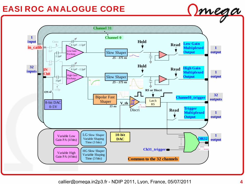
EASIROC ANALOGUE CORE
Variable LowGain PA (4 bits)
HoldRead
Low GainMultiplexedOutput
Ch31_trigger
Channel 0
Common to the 32 channels
Channel 31
Variable HighGain PA (4 bits)
+
V_thLatch
RS
Channel0_trigger
Discri
OR32
Slow Shaper25 - 175 ns
LG Slow ShaperVariable Shaping
Time (3 bits)
15 nsRead Trigger
MultiplexedOutput
Low GainPreAmp.
HG Slow ShaperVariable Shaping
Time (3 bits)
0.1pF - 1.5pF
1.5pF
10-bitDAC
RS or Discri
0.1pF - 1.5pF
15pF
High GainPreAmp.
HoldRead
High GainMultiplexedOutput
+Slow Shaper25 - 175 ns
3pF
in_calib
Bipolar Fast Shaper8-bit DAC
0-5V
INCh0
ONc15p
3pF
Ctest
32inputs
1input
1output
1output
1output
1output
32outputs
[email protected] - NDIP 2011, Lyon, France, 05/07/2011 5
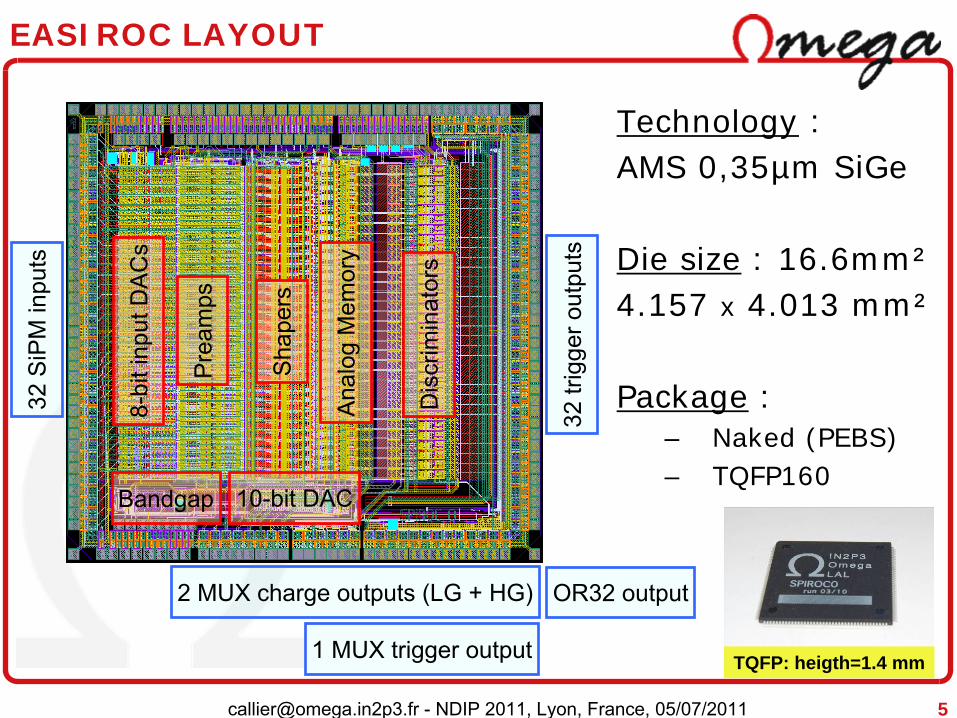
EASIROC LAYOUT
Technology : AMS 0,35µm SiGe
Die size : 16.6mm²4.157 x 4.013 mm²
Package :– Naked (PEBS)– TQFP160
Dis
crim
inat
ors
Sha
pers
Pre
amps
32 S
iPM
inpu
ts
10-bit DAC
Ana
log
Mem
ory
32 tr
igge
r out
puts
8-bi
t inp
ut D
AC
s
2 MUX charge outputs (LG + HG) OR32 output
1 MUX trigger output
Bandgap
TQFP: heigth=1.4 mm
[email protected] - NDIP 2011, Lyon, France, 05/07/2011 6
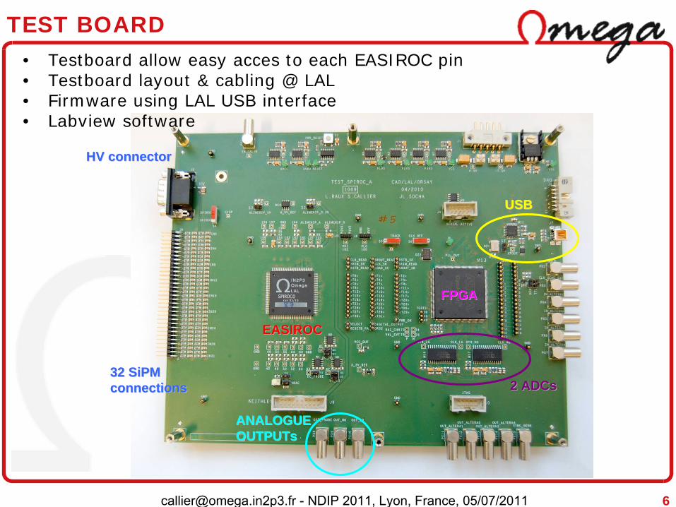
TEST BOARD
2 2 ADCsADCs
USBUSB
EASIROCEASIROC
ANALOGUE ANALOGUE OUTPUTsOUTPUTs
HV HV connectorconnector
32 32 SiPMSiPM connectionsconnections
FPGAFPGA
• Testboard allow easy acces to each EASIROC pin• Testboard layout & cabling @ LAL• Firmware using LAL USB interface• Labview software
[email protected] - NDIP 2011, Lyon, France, 05/07/2011 7
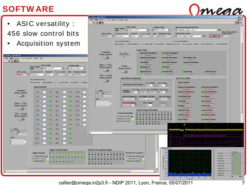
SOFTWARE
• ASIC versatility :456 slow control bits• Acquisition system
[email protected] - NDIP 2011, Lyon, France, 05/07/2011 8
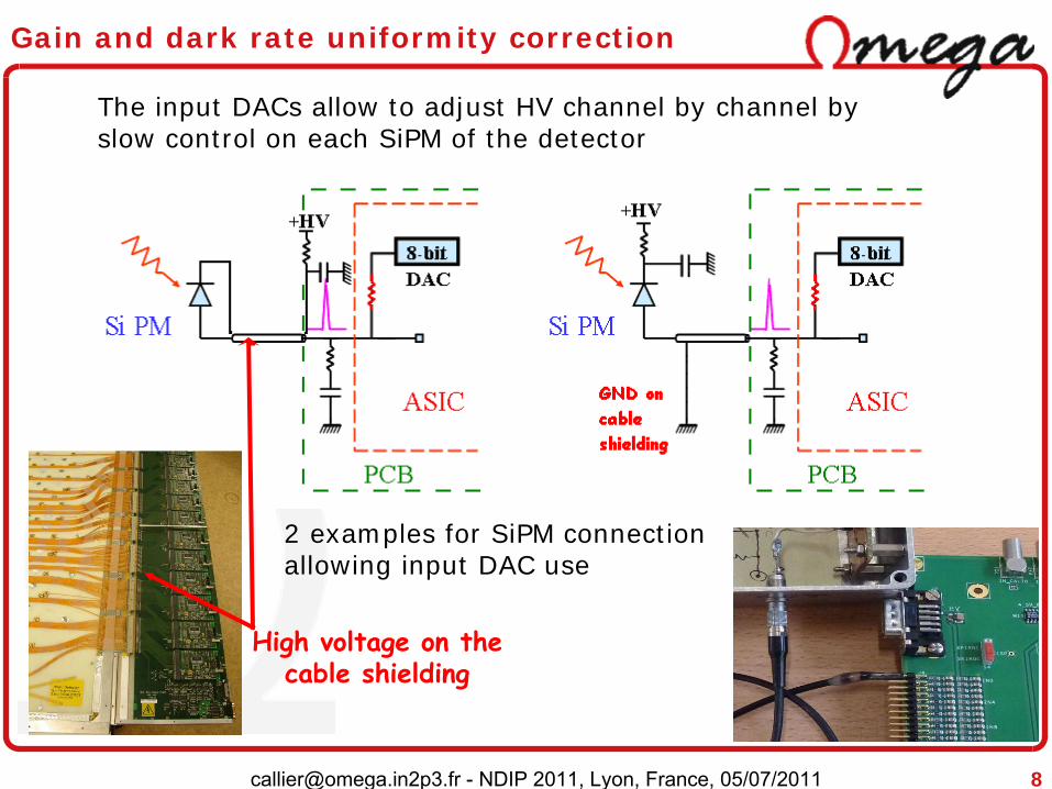
Gain and dark rate uniformity correction
High voltage on the cable shielding
The input DACs allow to adjust HV channel by channel by slow control on each SiPM of the detector
2 examples for SiPM connection allowing input DAC use
[email protected] - NDIP 2011, Lyon, France, 05/07/2011 9
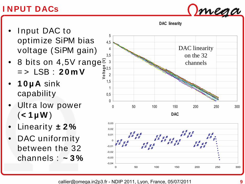
INPUT DACs
DAC linearity
00,5
11,5
22,5
33,5
44,5
5
0 50 100 150 200 250 300
DAC
Volta
ge (V
)
-0,04
-0,03
-0,02
-0,01
0
0,01
0,02
0,03
0 50 100 150 200 250 300
DAC linearity on the 32 channels
• Input DAC to optimize SiPM bias voltage (SiPM gain)
• 8 bits on 4,5V range => LSB : 20mV
• 10µA sink capability
• Ultra low power (<1µW)
• Linearity ±2%• DAC uniformity
between the 32 channels : ~3%
[email protected] - NDIP 2011, Lyon, France, 05/07/2011 10
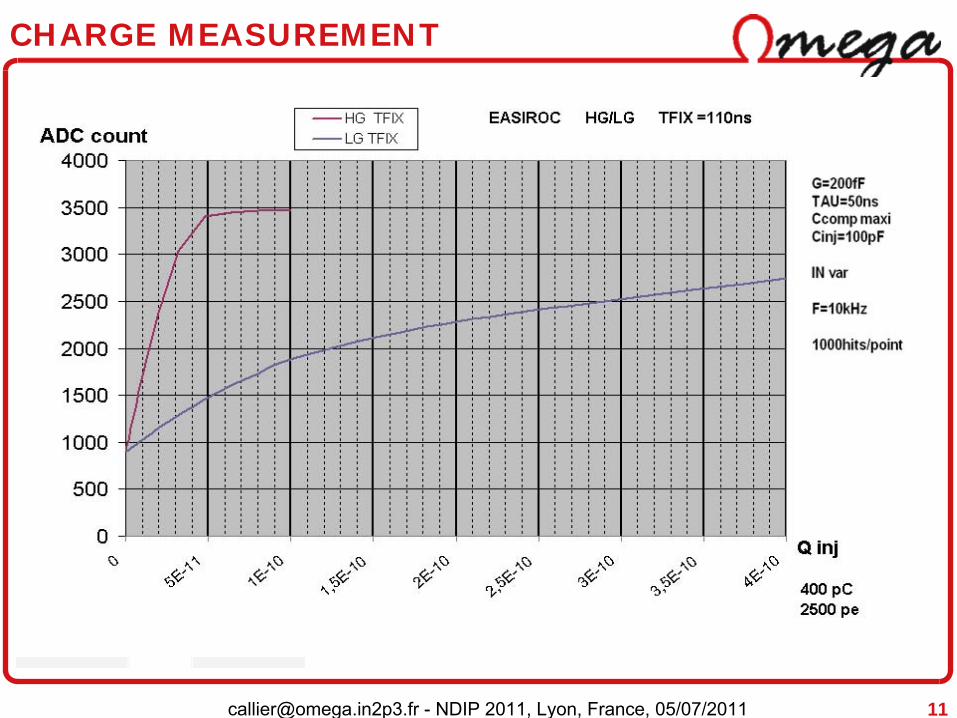
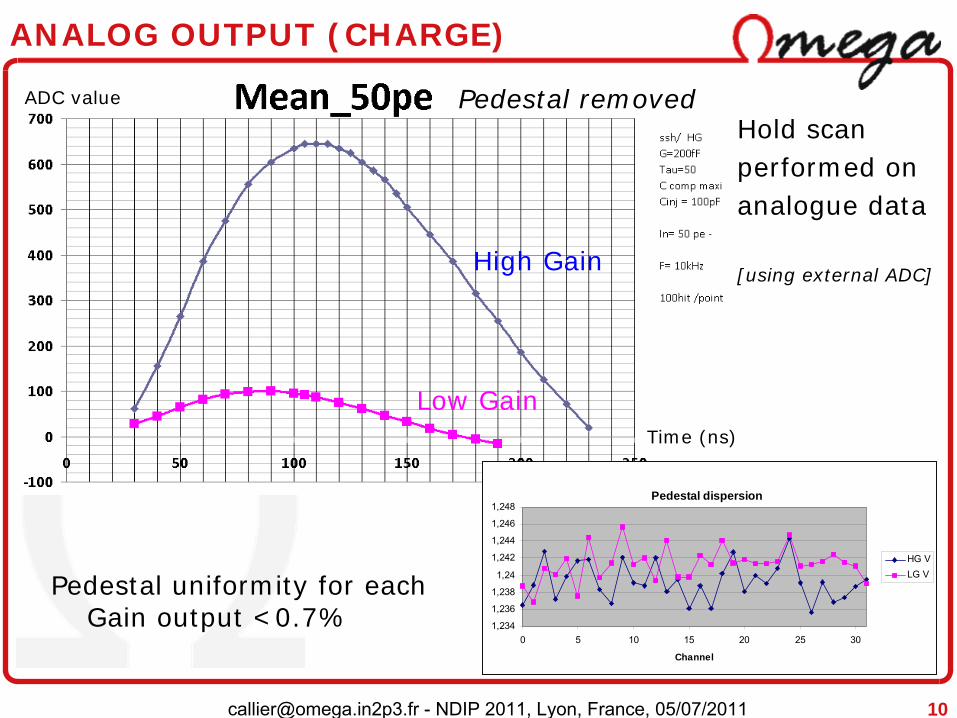
ANALOG OUTPUT (CHARGE)
Pedestal uniformity for each Gain output <0.7%
Pedestal removed
High Gain
Low Gain
Hold scanperformed onanalogue data
[using external ADC]
Time (ns)
ADC value
Pedestal dispersion
1,234
1,236
1,238
1,24
1,242
1,244
1,246
1,248
0 5 10 15 20 25 30
Channel
HG VLG V
[email protected] - NDIP 2011, Lyon, France, 05/07/2011 12
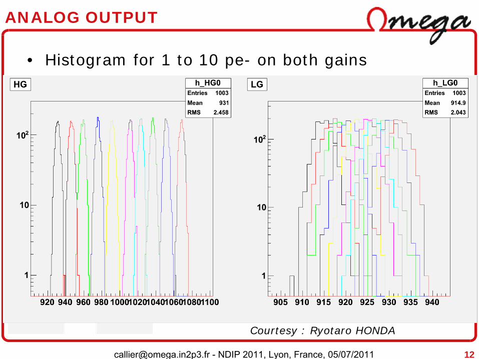
ANALOG OUTPUT
• Histogram for 1 to 10 pe- on both gains
Courtesy : Ryotaro HONDA
[email protected] - NDIP 2011, Lyon, France, 05/07/2011 13
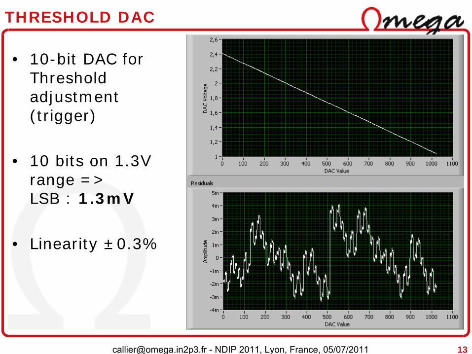
THRESHOLD DAC
• 10-bit DAC for Threshold adjustment (trigger)
• 10 bits on 1.3V range => LSB : 1.3mV
• Linearity ±0.3%
[email protected] - NDIP 2011, Lyon, France, 05/07/2011 14
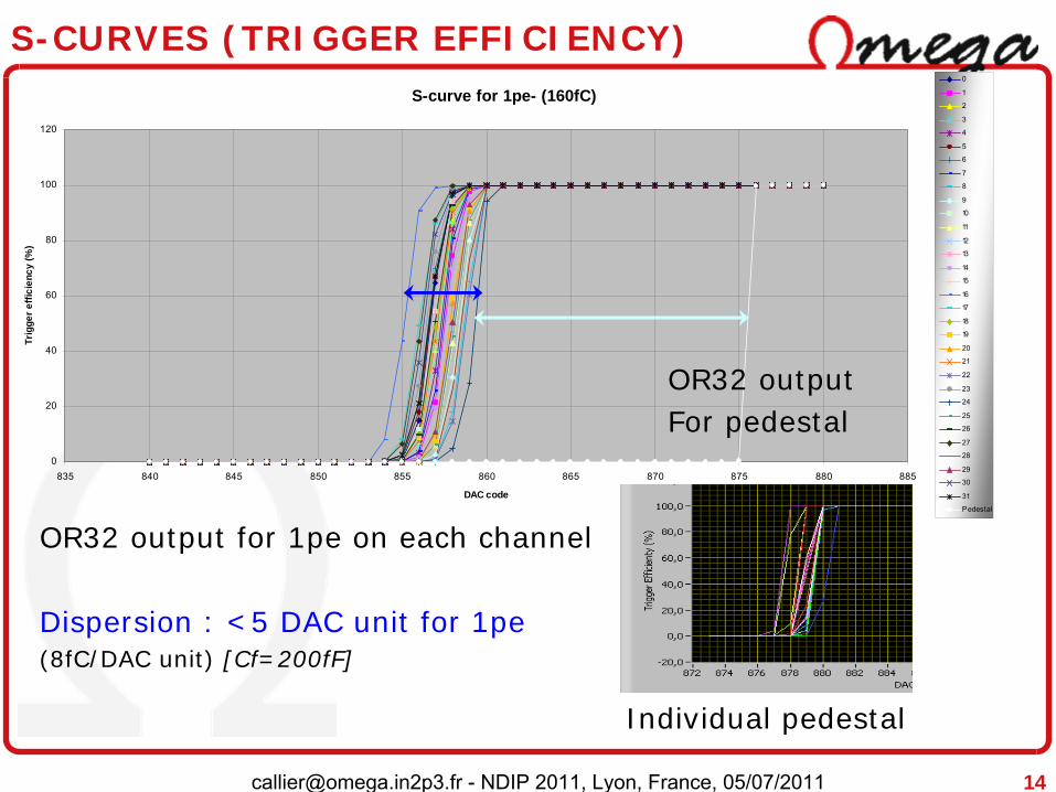
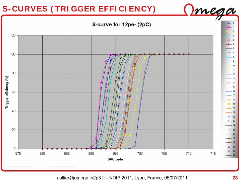
S-CURVES (TRIGGER EFFICIENCY)
OR32 output for 1pe on each channel
Dispersion : <5 DAC unit for 1pe(8fC/DAC unit) [Cf=200fF]
S-curve for 1pe- (160fC)
0
20
40
60
80
100
120
835 840 845 850 855 860 865 870 875 880 885
DAC code
Trig
ger e
ffici
ency
(%)
0
1
2
3
4
5
6
7
8
9
10
11
12
13
14
15
16
17
18
19
20
21
22
23
24
25
26
27
28
29
30
31
Pedestal
Individual pedestal
OR32 output For pedestal
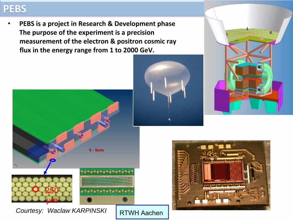
PEBS
Courtesy: Waclaw KARPINSKI
•
PEBS is a project in Research & Development phase
The purpose of the experiment is a precision measurement of the electron & positron cosmic rayflux in the energy range from 1 to 2000 GeV.
250 µm
RTWH Aachen

G. Saracino, Orsay, July 2, 2009 the MU-RAY Project: high-resolution muon radiography with scintillators 16
The MU-RAY project: high-resolution muon radiography with scintillators
Courtesy : Giulio SaracinoCourtesy : Giulio SaracinoINFN Napoli
•
International Collaboration
of physicists, geologists and volcanologists to perform muon radiography of geological structures, Mt. Vesuvius first of all
•
Des
ign and build muon telescopes
to be operated in difficult environments. Requirements:
•
modular, light, easy to transport and mount•
little need for maintenance•
very low power consumption•
Develop a methodology and a versatile instrument
Italy: Bologna,Firenze,Perugia,Napoli (INFN and Universities) Istituto Nazionale Geofisica e Vulcanologia)
Japan: Tokyo University and Hearth Research InstituteUSA: Fermilab
Given the mountain topology and the deep crater, there are ≈2 km of rock
to cross!
Location: Cable Cab(Seggiovia) 2.1 km
1.8 kmThe challenge of Mt. Vesuvius
Need for large detector areas!
International Collaboration of physicist,
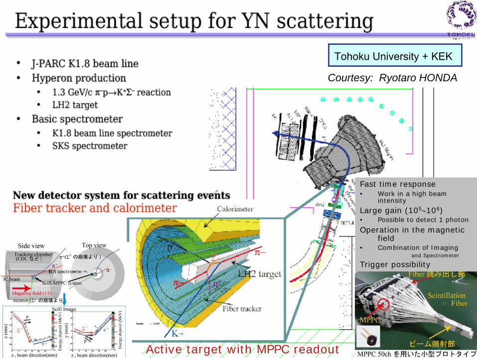
Active target with MPPC readout
Tohoku
University
+ KEK
Fast time response • Work in a high beam
intensity
Large gain (105106)• Possible to detect 1 photon
Operation in the magnetic field
• Combination of Imaging and Spectrometer
Trigger possibility
Courtesy: Ryotaro HONDA
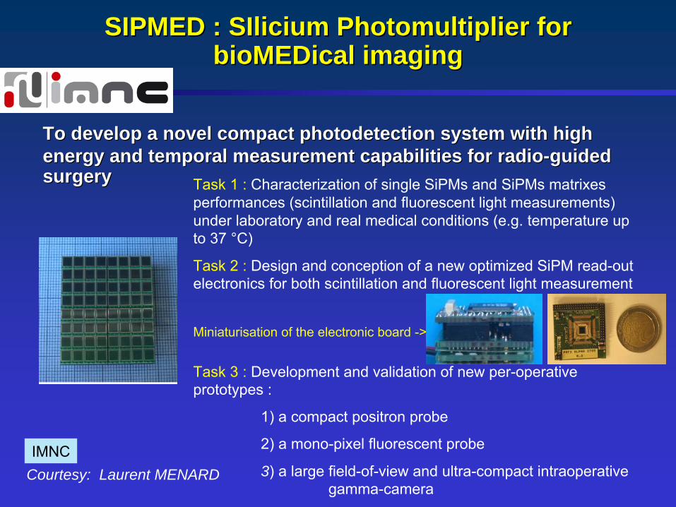
SIPMED : SIPMED : SIliciumSIlicium PhotomultiplierPhotomultiplier for for bioMEDicalbioMEDical imagingimaging
To To developdevelop a a novelnovel compact compact photodetectionphotodetection systemsystem withwith highhigh energyenergy andand temporal temporal measurementmeasurement capabilitiescapabilities for for radioradio--guidedguided surgerysurgery Task
1 : Characterization
of
single SiPMs
and
SiPMs
matrixes
performances (scintillation and
fluorescent light measurements) under
laboratory
and
real
medical
conditions (e.g.
temperature
up
to 37 °C)
Task
2 : Design and
conception of
a new optimized
SiPM
read-out
electronics
for both
scintillation and
fluorescent light measurement
Miniaturisation of
the
electronic
board
->
Task
3 : Development
and
validation of
new per-operative
prototypes :
1) a compact positron probe
2) a mono-pixel
fluorescent probe
3) a large field-of-view
and
ultra-compact
intraoperative
gamma-cameraCourtesy: Laurent MENARDIMNC
[email protected] - NDIP 2011, Lyon, France, 05/07/2011 19
EASIROC SUMMARY
• 1pe- -> 2000pe- charge measurement
• 100% Trigger efficiency @ 1/3photo-electron
• Versatility & easy use– Testboard & Software ready to use, embedding acquisition system
• Very low power consumption– Full power pulsing capability– Unused stages can be shut down
• Large scale production in 2010– Already used in experiments (astrophysics, vulcanology, nuclear
physics, medical imaging)
• Any extra information available on http://omega.in2p3.fr

BACKUP SLIDES
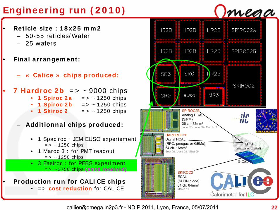
[email protected] - NDIP 2011, Lyon, France, 05/07/2011 22
• Reticle size : 18x25 mm2– 50-55 reticles/Wafer– 25 wafers
• Final arrangement:
– « Calice » chips produced:
• 7 Hardroc 2b => ~9000 chips• 1 Spiroc 2a => ~1250 chips• 1 Spiroc 2b => ~1250 chips• 1 Skiroc 2 => ~1250 chips
– Additionnal chips produced:
• 1 Spaciroc : JEM EUSO experiement=> ~1250 chips
• 1 Maroc 3 : for PMT readout=> ~1250 chips
• 3 Easiroc : for PEBS experiment=> ~3750 chips (5000 received)
• Production run for CALICE chips• => cost reduction for CALICE
Engineering run (2010)
SPIROC2BAnalog HCAL(SiPM)36 ch. 32mm²June 07 / June 08 / March 11
HARDROC2BDigital HCAL(RPC, µmegas or GEMs)64 ch. 16mm²Sept 06 / June 08 / Sept 09
SKIROC2ECAL(Si
PIN diode)64 ch. 64mm²March 11
E-CAL
H-CAL (analog or digital)
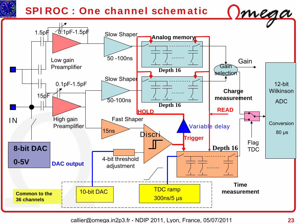
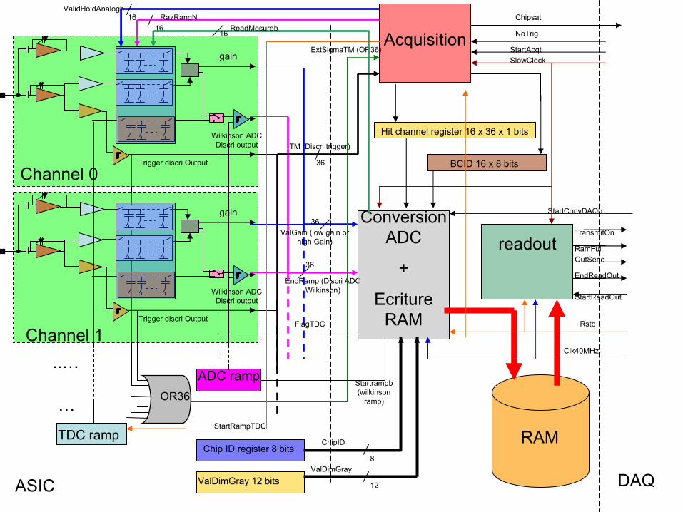
[email protected] - NDIP 2011, Lyon, France, 05/07/2011 23
SPIROC : One channel schematic
50 -100ns
50-100ns
Gain selection
4-bit threshold
adjustment
10-bit DAC
15ns
DAC output
HOLD
Slow Shaper
Slow Shaper
Fast
Shaper
Time measurement
Charge measurement
TDC ramp
300ns/5 µs
12-bit Wilkinson
ADC
Trigger
Depth 16
Depth 16
Depth 16
Common to the 36 channels
8-bit DAC
0-5V
Low
gain Preamplifier
High gain Preamplifier
Analog memory
15pF
1.5pF
0.1pF-1.5pF
Conversion
80 µs
READ
Variable delay
0.1pF-1.5pF
IN
Discri
Gain
Flag TDC
DAQASIC
Chip ID register
8 bits
gain
Trigger discri
Output
Wilkinson ADC Discri
output
gain
Trigger discri
Output
Wilkinson ADC Discri
output
..…
OR36
EndRamp
(Discri
ADC Wilkinson)
36
36
36
TM (Discri
trigger)
ValGain
(low
gain or high
Gain)
ExtSigmaTM
(OR36)
Channel 1
Channel 0
ValDimGray
12 bits
…
Acquisition
readoutConversion
ADC
+
Ecriture RAM
RAM
FlagTDC
ValDimGray
12
8
ChipID
Hit channel
register
16 x 36 x 1 bits
TDC rampStartRampTDC
BCID 16 x 8 bits
ADC rampStartrampb
(wilkinson
ramp)
1616
ValidHoldAnalogbRazRangN
16ReadMesureb
Rstb
Clk40MHz
SlowClockStartAcqt
StartConvDAQb
StartReadOut
NoTrig
RamFull
TransmitOn
OutSerie
EndReadOut
Chipsat
[email protected] - NDIP 2011, Lyon, France, 05/07/2011 25
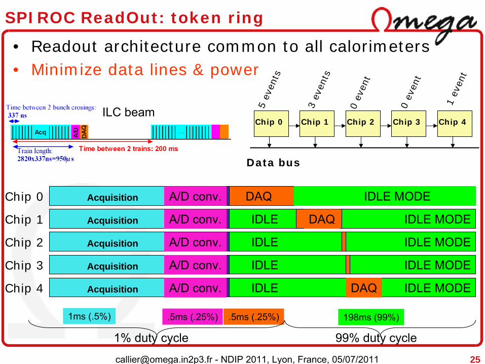
SPIROC ReadOut: token ring
Acquisition A/D conv. DAQ IDLE MODEChip 0
Chip 1 Acquisition A/D conv. DAQ IDLE MODEIDLE
Chip 2 Acquisition A/D conv. IDLE MODEIDLE
Chip 3 Acquisition A/D conv. IDLE MODEIDLE
Chip 4 Acquisition A/D conv. IDLE MODEIDLE DAQ
1ms (.5%) .5ms (.25%) .5ms (.25%)
1% duty
cycle 99% duty
cycle
198ms (99%)
• Readout architecture common to all calorimeters• Minimize data lines & power
5 ev
ents
3 ev
ents
0 ev
ent
1 ev
ent
0 ev
ent
Chip 0 Chip 1 Chip 2 Chip 3 Chip 4
Data bus
ILC beam
[email protected] - NDIP 2011, Lyon, France, 05/07/2011 26
ILC beam structure and SPIROC running modes
Acquisition1ms (.5%)
A/D conv..5ms (.25%)
DAQ.5ms (.25%)
1% duty cycle
IDLE MODE
99% idle cycle
198ms (99%)
time
Time between two trains: 200ms (5 Hz)
Time between two bunch crossing: 337 ns
Train length 2820 bunch X (950 µs)
Acquisition1ms (.5%)
A/D conv..5ms (.25%)
DAQ.5ms (.25%)
1% duty cycle
IDLE MODE
99% idle cycle
198ms (99%)
time
Time between two trains: 200ms (5 Hz)
Time between two bunch crossing: 337 ns
Train length 2820 bunch X (950 µs)
Two
orders
of
magnitude saved
on the
consumption
by using
the
ILC beam structure and
the
power
pulsing
Acquisition A/D conv. DAQ IDLE MODEChip 0
Chip 1 Acquisition DAQ IDLE MODEIDLE
Chip 2 Acquisition IDLE MODEIDLE
Chip 3 Acquisition IDLE MODEIDLE
Chip 4 Acquisition IDLE MODEIDLE DAQ
A/D conv.
A/D conv.
A/D conv.
A/D conv.
Acquisition A/D conv. DAQ IDLE MODEChip 0
Chip 1 Acquisition DAQ IDLE MODEIDLE
Chip 2 Acquisition IDLE MODEIDLE
Chip 3 Acquisition IDLE MODEIDLE
Chip 4 Acquisition IDLE MODEIDLE DAQ
A/D conv.
A/D conv.
A/D conv.
A/D conv.Chip 0 Chip 1 Chip 2 Chip 3 Chip 4
5 ev
ents
3 ev
ents
0 ev
ent
1 ev
ent
0 ev
ent
Data bus
•
Readout based on token ring mechanism initiated by DAQ
•
One data line activated by each chip sequentially
•
Readout rate few MHz to minimize power dissipation
[email protected] - NDIP 2011, Lyon, France, 05/07/2011 27
OTHERS
• Default value for Slow Control– Chip ready to use after a simple SC reset (except
Threshold DAC)
• Debug embedded feature :– Analog Probe system allow to monitor each critical point
in the chip• 32 PreAmplifiers High Gain output • 32 PreAmplifiers Low Gain output • 32 Slow Shapers High Gain output • 32 Slow Shapers Low Gain output • 32 Fast Shapers output
[email protected] - NDIP 2011, Lyon, France, 05/07/2011 28
S-CURVES (TRIGGER EFFICIENCY)
OR32 output for 1pe on each channel
Dispersion : <5 DAC unit for 1pe(8fC/DAC unit) [Cf=200fF]
[email protected] - NDIP 2011, Lyon, France, 05/07/2011 29
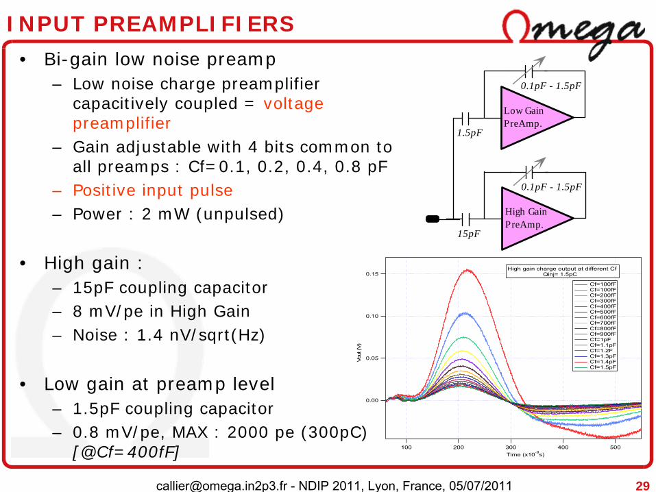
INPUT PREAMPLIFIERS
• Bi-gain low noise preamp– Low noise charge preamplifier
capacitively coupled = voltage preamplifier
– Gain adjustable with 4 bits common to all preamps : Cf=0.1, 0.2, 0.4, 0.8 pF
– Positive input pulse– Power : 2 mW (unpulsed)
• High gain :– 15pF coupling capacitor– 8 mV/pe in High Gain– Noise : 1.4 nV/sqrt(Hz)
• Low gain at preamp level– 1.5pF coupling capacitor– 0.8 mV/pe, MAX : 2000 pe (300pC)
[@Cf=400fF]
Low GainPreAmp.
0.1pF - 1.5pF
1.5pF
0.1pF - 1.5pF
15pF
High GainPreAmp.
0.15
0.10
0.05
0.00
Vout
(V)
500400300200100Time (x10-9s)
Cf=100fF Cf=100fF Cf=200fF Cf=300fF Cf=400fF Cf=500fF Cf=600fF Cf=700fF Cf=800fF Cf=900fF Cf=1pF Cf=1.1pF Cf=1.2F Cf=1.3pF Cf=1.4pF Cf=1.5pF
High gain charge output at different Cf Qinj= 1.5pC
[email protected] - NDIP 2011, Lyon, France, 05/07/2011 30
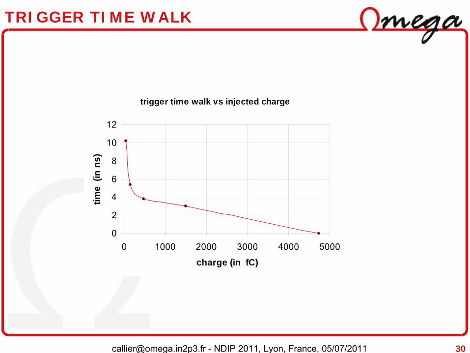
TRIGGER TIME WALK
trigger time walk vs injected charge
0
2
4
6
8
10
12
0 1000 2000 3000 4000 5000
charge (in fC)
time
(in
ns)
[email protected] - NDIP 2011, Lyon, France, 05/07/2011 31
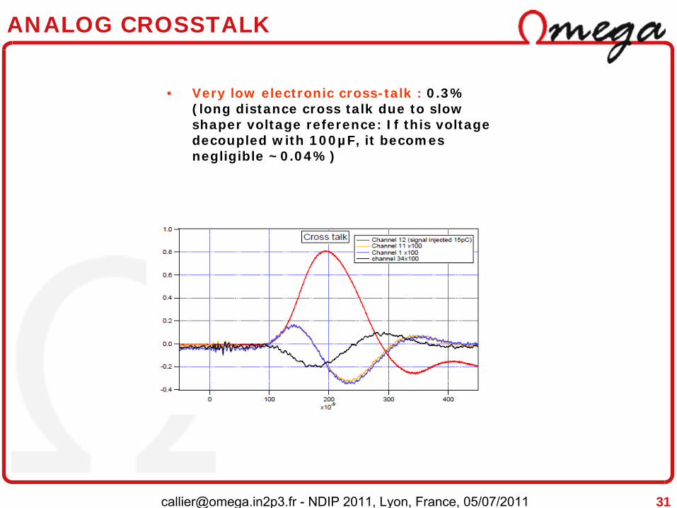
ANALOG CROSSTALK
• Very low electronic cross-talk : 0.3% (long distance cross talk due to slow shaper voltage reference: If this voltage decoupled with 100µF, it becomes negligible ~0.04%)
Copyright © 2022 FDOKUMEN

