


Bahasa
Halaman
Hukum

PHYSICAL REVIEW B 15 NOVEMBER 1999-IIVOLUME 60, NUMBER 20
Analysis of surface structures through determination of their composition using STM:Si„100…433-In and Si„111…431-In reconstructions
A. A. SaraninDepartment of Electronic Engineering, Faculty of Engineering, Osaka University, Suita, Osaka 565, Japan;
Institute of Automation and Control Processes, 690041 Vladivostok, Russia;and Faculty of Physics and Engineering, Far Eastern State University, 690000 Vladivostok, Russia
A. V. ZotovDepartment of Electronic Engineering, Faculty of Engineering, Osaka University, Suita, Osaka 565, Japan;
Department of Electronics, Vladivostok State University of Economics and Service, 690600 Vladivostok, Russia;and Institute of Automation and Control Processes, 690041 Vladivostok, Russia
V. G. LifshitsInstitute of Automation and Control Processes, 690041 Vladivostok, Russia;
Faculty of Physics and Engineering, Far Eastern State University, 690000 Vladivostok, Russia;and Department of Electronics, Vladivostok State University of Economics and Service, 690600 Vladivostok, Russia
J. -T. Ryu, O. Kubo, H. Tani, T. Harada, M. Katayama, and K. Oura*Department of Electronic Engineering, Faculty of Engineering, Osaka University, Suita, Osaka 565, Japan
~Received 2 October 1998; revised manuscript received 17 June 1999!
The advantages of scanning tunneling microscopy for the determination of the composition of the submono-layer metal/silicon interfaces has been demonstrated using Si~100!433-In and Si~111!431-In as sample re-constructions. It has been found that the Si~100!433-In unit cell is built of 7 In atoms and 6 Si atoms, whilethe Si~111!431-In unit cell contains 3 In atoms and 2 Si atoms in addition to the top Si~111! bilayer. Theobtained quantitative information provides the ground for discussion of the plausible atomic arrangement ofthese reconstructions.@S0163-1829~99!00744-4#
insuoelellll
oms
mt
a
etitu
nia)
ctd
fnsf
ith
re-
sel
n,
he
s,
I. INTRODUCTION
The complexity of the determination of the structuresduced by adsorbate submonolayers on the Si crystallinefaces@surface phases] posses a tremendous challenge tsurface scientists. In spite of the recent progress in this fiit should be noted that there are a limited number of wunderstood reconstructions, of which only a few being reacomplicated. One conceivable reason for this is that the cposition of the most of the adsorbate/silicon surface pha~especially, of those having relatively large unit cells! is gen-erally not known exactly. We define the surface phase coposition as a combination of the adsorbate coverage andSi atom density in the top Si substrate layer. Both valuesexpressed in monolayer~ML ! units. @1 ML equals the top Siatom density in the unreconstructed 131 Si surface, i.e.,7.831014 cm22 for Si~111! and 6.831014 cm22 forSi~100!#. It is clear that the composition can be expressalso as a number of atoms of adsorbate and silicon consing the surface unit cell.
The Si(100)433-In and Si(111)431-In furnish an ex-ample of the reconstructions, which atomic arrangemehave been extensively debated in the absence of the reldata on their exact composition. Consider first the Si(10033-In reconstruction. Starting with the work of Knallet al,1
the structure of the Si(100)433-In phase has been an objeof numerous investigations2–10 but still remains a debatetopic. The scanning tunneling microscopy~STM! images ob-
PRB 600163-1829/99/60~20!/14372~10!/$15.00
-r-
thed,-y
-es
-here
dt-
tsble4
tained by Baskiet al.2 did not provide atomic resolution oIn adatom locations but allowed to define certain restrictiofor a possible 433-In structural model. From comparison othe impact collision ion scattering spectroscopy~ICISS! dataand the computer-simulated fits, Steeleet al.4 proposed sev-eral models, which, however, appear to be in conflict wthe results of the most ensuing studies.5,6,9
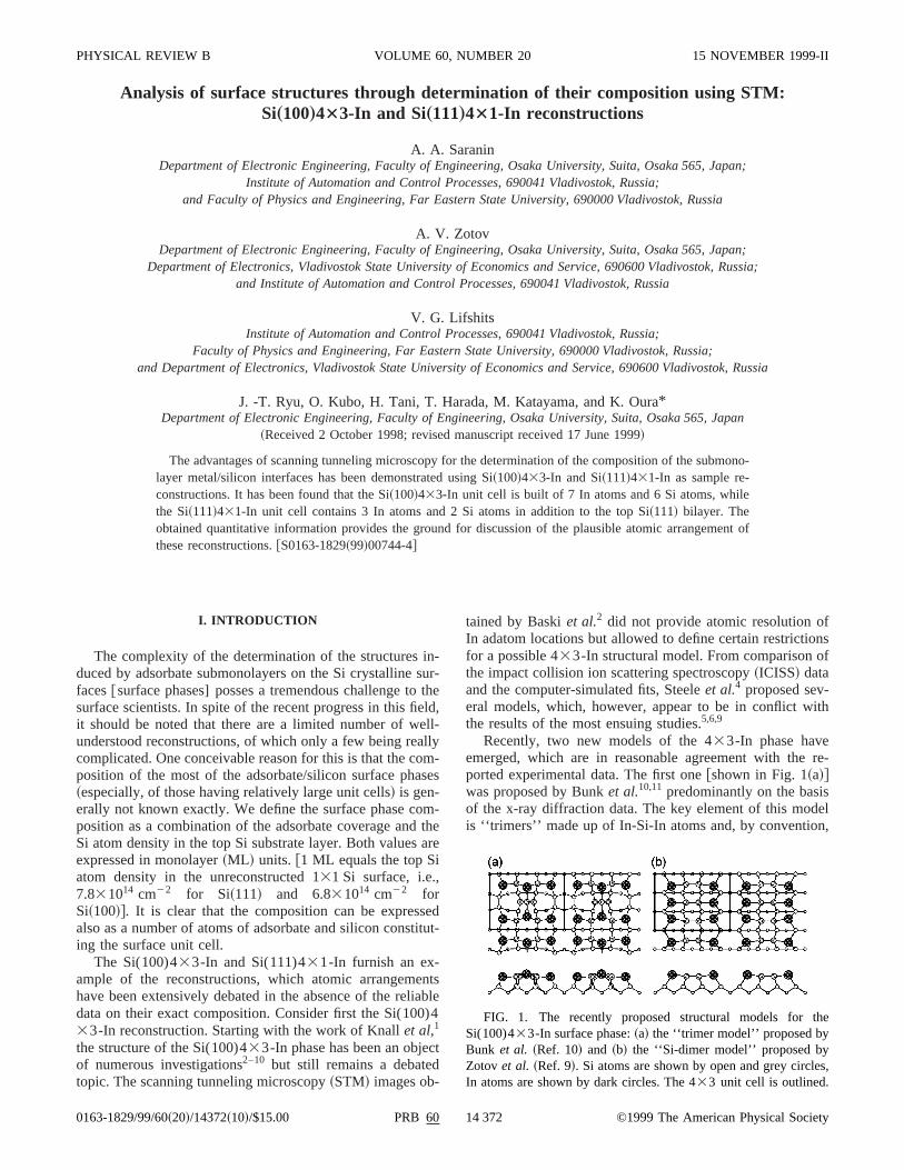
Recently, two new models of the 433-In phase haveemerged, which are in reasonable agreement with theported experimental data. The first one@shown in Fig. 1~a!#was proposed by Bunket al.10,11 predominantly on the basiof the x-ray diffraction data. The key element of this modis ‘‘trimers’’ made up of In-Si-In atoms and, by conventio
FIG. 1. The recently proposed structural models for tSi(100)433-In surface phase:~a! the ‘‘trimer model’’ proposed byBunk et al. ~Ref. 10! and ~b! the ‘‘Si-dimer model’’ proposed byZotov et al. ~Ref. 9!. Si atoms are shown by open and grey circleIn atoms are shown by dark circles. The 433 unit cell is outlined.
14 372 ©1999 The American Physical Society
e
PRB 60 14 373ANALYSIS OF SURFACE STRUCTURES THROUGH . . .
TABLE I. In coverage and top Si atom density of the Si(100)433-In reconstruction as suggested in threported structural models and determined in the present experiment.
In coverage Si atom density
‘‘Trimer model’’ of Bunk et al. ~Ref. 10! 0.50 ML 0.58 ML‘‘Si-dimer model’’ of Zotov et al. ~Ref. 9! 0.50 ML 0.50 MLExperiment 0.5960.02 0.5160.02 ML
e
hee
dereot
fo
reitctro
-
de
w
in
is
de
rodta
a-
Svse
ieetu
inie
S
hiles-
TheES0%ina-of
cten-
itage
bethe
d Si)4r-dis-n.
m
-
forcles,
we shall refer to this model as the ‘‘trimer model.’’ Thsecond model@shown in Fig. 1~b!# was proposed by Zotovet al.9 largely on the basis of the STM observations. Tmain structural element of this model is Si dimers boundby In atoms and, by convention, we shall refer to this moas the ‘‘Si-dimer model.’’ One can see that the structusuggested by two models differ in composition. Though bmodels assume 6 In atoms per 433 unit cell, the number ofthe top Si atoms incorporated in the unit cell is 7 and 6the ‘‘trimer model’’ and ‘‘Si-dimer model,’’ respectively.
The Si(111)431-In surface phase is another exampleconstruction which structure is still the debated topic in spof the abundance of data obtained by various surfasensitive techniques, namely, reflection high-energy elecdiffraction ~RHEED!,12–14 low-energy electron diffraction~LEED!,15,16 STM,16–20 ICISS,21,22 Auger electrondiffraction,14 Auger electron spectroscopy~AES!,14,16,23
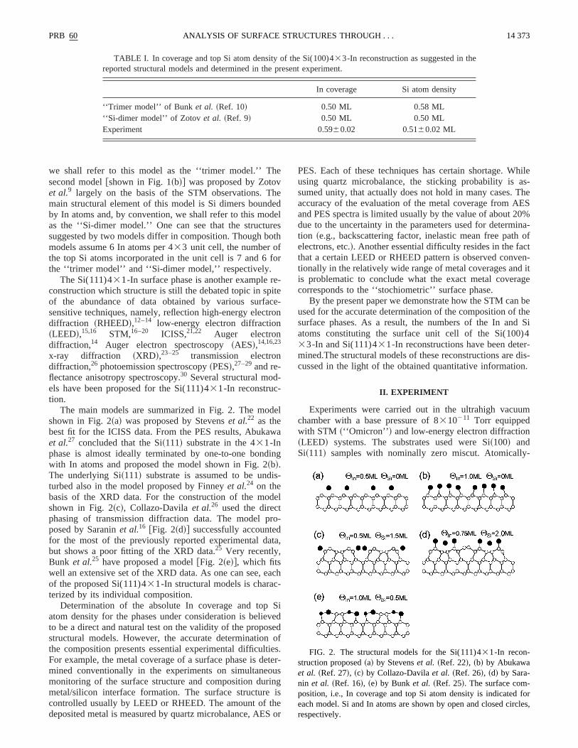
x-ray diffraction ~XRD!,23–25 transmission electrondiffraction,26 photoemission spectroscopy~PES!,27–29and re-flectance anisotropy spectroscopy.30 Several structural models have been proposed for the Si(111)431-In reconstruc-tion.
The main models are summarized in Fig. 2. The moshown in Fig. 2~a! was proposed by Stevenset al.22 as thebest fit for the ICISS data. From the PES results, Abukaet al.27 concluded that the Si~111! substrate in the 431-Inphase is almost ideally terminated by one-to-one bondwith In atoms and proposed the model shown in Fig. 2~b!.The underlying Si~111! substrate is assumed to be undturbed also in the model proposed by Finneyet al.24 on thebasis of the XRD data. For the construction of the moshown in Fig. 2~c!, Collazo-Davilaet al.26 used the directphasing of transmission diffraction data. The model pposed by Saraninet al.16 @Fig. 2~d!# successfully accountefor the most of the previously reported experimental dabut shows a poor fitting of the XRD data.25 Very recently,Bunk et al.25 have proposed a model@Fig. 2~e!#, which fitswell an extensive set of the XRD data. As one can see, eof the proposed Si(111)431-In structural models is characterized by its individual composition.
Determination of the absolute In coverage and topatom density for the phases under consideration is belieto be a direct and natural test on the validity of the propostructural models. However, the accurate determinationthe composition presents essential experimental difficultFor example, the metal coverage of a surface phase is dmined conventionally in the experiments on simultaneomonitoring of the surface structure and composition durmetal/silicon interface formation. The surface structurecontrolled usually by LEED or RHEED. The amount of thdeposited metal is measured by quartz microbalance, AE
dlsh
r
-ee-n
l
a
g
-
l
-
,
ch
iedd
ofs.er-sgs
or
PES. Each of these techniques has certain shortage. Wusing quartz microbalance, the sticking probability is asumed unity, that actually does not hold in many cases.accuracy of the evaluation of the metal coverage from Aand PES spectra is limited usually by the value of about 2due to the uncertainty in the parameters used for determtion ~e.g., backscattering factor, inelastic mean free pathelectrons, etc.!. Another essential difficulty resides in the fathat a certain LEED or RHEED pattern is observed convtionally in the relatively wide range of metal coverages andis problematic to conclude what the exact metal covercorresponds to the ‘‘stochiometric’’ surface phase.
By the present paper we demonstrate how the STM canused for the accurate determination of the composition ofsurface phases. As a result, the numbers of the In anatoms constituting the surface unit cell of the Si(10033-In and Si(111)431-In reconstructions have been detemined.The structural models of these reconstructions arecussed in the light of the obtained quantitative informatio
II. EXPERIMENT
Experiments were carried out in the ultrahigh vacuuchamber with a base pressure of 8310211 Torr equippedwith STM ~‘‘Omicron’’ ! and low-energy electron diffraction~LEED! systems. The substrates used were Si~100! andSi~111! samples with nominally zero miscut. Atomically
FIG. 2. The structural models for the Si(111)431-In recon-struction proposed~a! by Stevenset al. ~Ref. 22!, ~b! by Abukawaet al. ~Ref. 27!, ~c! by Collazo-Davilaet al. ~Ref. 26!, ~d! by Sara-nin et al. ~Ref. 16!, ~e! by Bunk et al. ~Ref. 25!. The surface com-position, i.e., In coverage and top Si atom density is indicatedeach model. Si and In atoms are shown by open and closed cirrespectively.
drsiteera
50ecthti
eaeb
n
m)
x-se4firiteChe
thbfceap
sp
ers-th
ri-V2ilale0.behedla
eri-
inhe
g
ans
Inted
the
inestoms
14 374 PRB 60A. A. SARANIN et al.
clean Si(100)231 and Si(111)737 surfaces were preparein situ by heating to 1250 °C after the samples were fioutgassed at 600 °C for several hours. Indium was deposfrom a Ta foil tube at a rate of about 0.15 ML/min. ThSi(100)433-In and Si(111)431-In surface phases werprepared conventionally by annealing of the room tempeture ~RT! deposited In submonolayers to about 22300 °C and to about 450 °C, respectively. The indirheating by radiation from the tungsten heater located atsample back was used. In the experiments on the interacof the Si(100)433-In and Si(111)431- In surfaces withatomic hydrogen, H2 gas was admitted through a leak valvA 1800 °C tungsten filament, 7 cm from the Si surface, wused to dissociate molecular hydrogen. The exposures wconducted with the specimen facing the filament andbackfilling the chamber with H2 at 531027 Torr. For STMobservations, electrochemically etched tungsten tips cleaby in situ heating were employed.
III. RESULTS AND DISCUSSION
A. Determination of the absolute In coverage
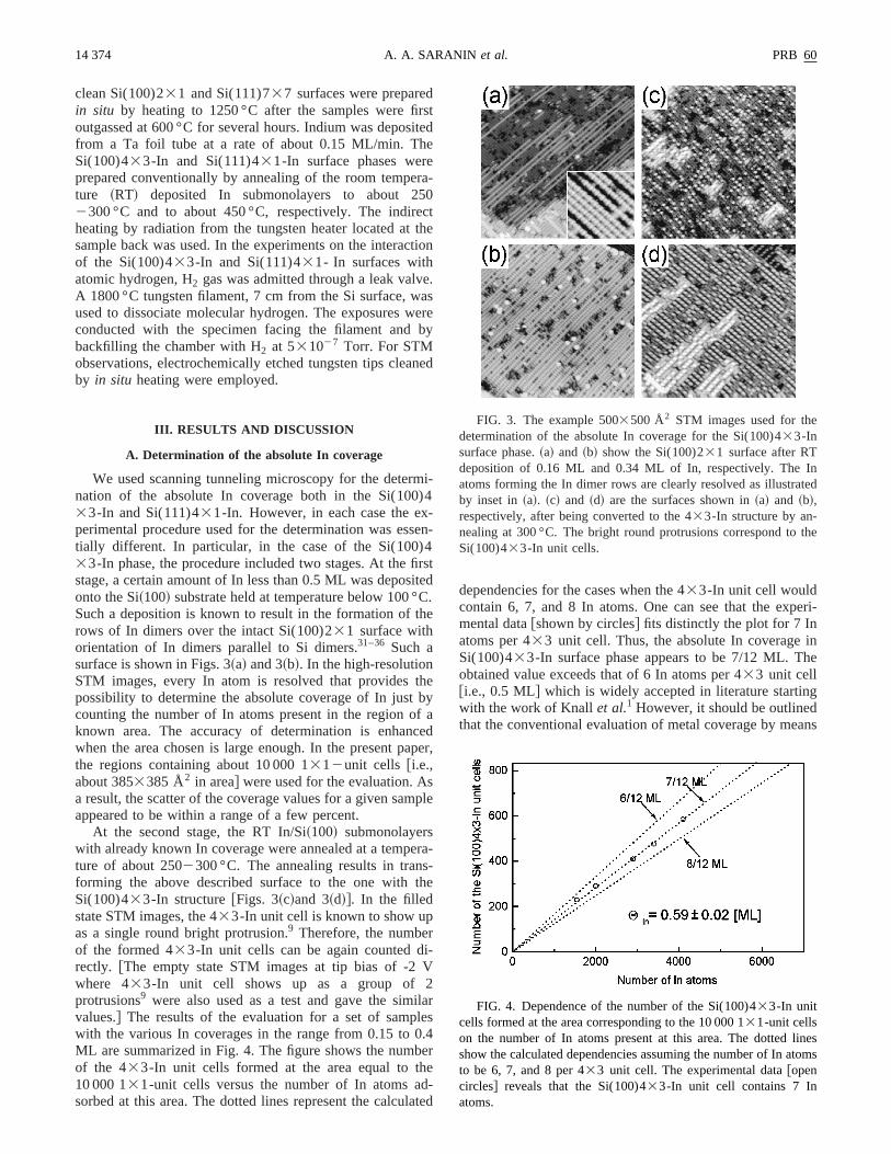
We used scanning tunneling microscopy for the deternation of the absolute In coverage both in the Si(10033-In and Si(111)431-In. However, in each case the eperimental procedure used for the determination was estially different. In particular, in the case of the Si(100)33-In phase, the procedure included two stages. At thestage, a certain amount of In less than 0.5 ML was deposonto the Si~100! substrate held at temperature below 100 °Such a deposition is known to result in the formation of trows of In dimers over the intact Si(100)231 surface withorientation of In dimers parallel to Si dimers.31–36 Such asurface is shown in Figs. 3~a! and 3~b!. In the high-resolutionSTM images, every In atom is resolved that providespossibility to determine the absolute coverage of In justcounting the number of In atoms present in the region oknown area. The accuracy of determination is enhanwhen the area chosen is large enough. In the present pthe regions containing about 10 000 1312unit cells @i.e.,about 3853385 Å2 in area# were used for the evaluation. Aa result, the scatter of the coverage values for a given samappeared to be within a range of a few percent.
At the second stage, the RT In/Si~100! submonolayerswith already known In coverage were annealed at a tempture of about 2502300 °C. The annealing results in tranforming the above described surface to the one withSi(100)433-In structure@Figs. 3~c!and 3~d!#. In the filledstate STM images, the 433-In unit cell is known to show upas a single round bright protrusion.9 Therefore, the numbeof the formed 433-In unit cells can be again counted drectly. @The empty state STM images at tip bias of -2where 433-In unit cell shows up as a group ofprotrusions9 were also used as a test and gave the simvalues.# The results of the evaluation for a set of sampwith the various In coverages in the range from 0.15 toML are summarized in Fig. 4. The figure shows the numof the 433-In unit cells formed at the area equal to t10 000 131-unit cells versus the number of In atoms asorbed at this area. The dotted lines represent the calcu
ted
-
te
on
.srey
ed
i-4
n-
std
.
eyader,
le
a-
e
rs4r
-ted
dependencies for the cases when the 433-In unit cell wouldcontain 6, 7, and 8 In atoms. One can see that the expmental data@shown by circles# fits distinctly the plot for 7 Inatoms per 433 unit cell. Thus, the absolute In coverageSi(100)433-In surface phase appears to be 7/12 ML. Tobtained value exceeds that of 6 In atoms per 433 unit [email protected]., 0.5 ML# which is widely accepted in literature startinwith the work of Knallet al.1 However, it should be outlinedthat the conventional evaluation of metal coverage by me
FIG. 3. The example 5003500 Å2 STM images used for thedetermination of the absolute In coverage for the Si(100)433-Insurface phase.~a! and ~b! show the Si(100)231 surface after RTdeposition of 0.16 ML and 0.34 ML of In, respectively. Theatoms forming the In dimer rows are clearly resolved as illustraby inset in ~a!. ~c! and ~d! are the surfaces shown in~a! and ~b!,respectively, after being converted to the 433-In structure by an-nealing at 300 °C. The bright round protrusions correspond toSi(100)433-In unit cells.
FIG. 4. Dependence of the number of the Si(100)433-In unitcells formed at the area corresponding to the 10 000 131-unit cellson the number of In atoms present at this area. The dotted lshow the calculated dependencies assuming the number of In ato be 6, 7, and 8 per 433 unit cell. The experimental data@opencircles# reveals that the Si(100)433-In unit cell contains 7 Inatoms.
L,beisdi
Inth
wb
thomb
I
ofi
ac
74
ctI)
nT
thecov--s,
rm
e
ed tontstheomha-acythes to
The
in.52es
ant
y,
-op
er ofhere-the
n
PRB 60 14 375ANALYSIS OF SURFACE STRUCTURES THROUGH . . .
of LEED-AES does not provide the accuracy of 1/12 Mwhich is required for the determination of the exact numof In atoms in the 433 unit cell. The demanded accuracybelieved to be reached in the present experiment. Thetailed discussion of the accuracy of the determinationgiven in Appendix.
To determine the In coverage of the Si(111)431-In, thefollowing procedure was used: The certain amount offrom the submonolayer range was deposited ontoSi(111)737 surface held at room temperature~RT! and an-nealed then to about 450 °C. After annealing, the surfaceexamined by STM and the fraction of the area occupiedeach of the In/Si~111! surface phases,A33A3,A313A31,and 431, was measured. For the reliable data averaging,area chosen for evaluation was large enough compared tdomain size. The results of the measurements are sumrized in Fig. 5, which shows the area fraction occupiedthe A33A3 @triangles, dotted line#, A313A31 @circles,dashed line#, and 431 @squares, solid line# phases versus Indeposition time. Taking into account that the absolutecoverage for the Si(111)A33A3-In phase is known to be1/3 ML, In deposition time@lower axis# can be converted tothe In coverage@upper axis#. One can see that the domainstheA313A31-In reconstruction are present at the surfacethe In coverage range from 0.35 to 0.73 ML and the surfis covered completely by theA313A31-In phase at 0.53 MLIn coverage. The formation of the Si(111)431-In recon-struction starts at 0.55 ML of In and is completed at 0.ML. In agreement with the AES data,16 the Si(111)431-Insurface demonstrates saturating behavior and it is unaffeby further In deposition. Thus, the value of the absolutecoverage determined in this experiment for the Si(11131-In phase is 0.75 ML, i.e., 3 In atoms per 431 surfaceunit cell.
B. Si redistribution and determination of the top Si atomdensity
Baskiet al.2 were the first who noticed that the formatioof the Si(100)433-In reconstruction by annealing of R
FIG. 5. The area fraction occupied by the Si(111)A33A3-In@triangles, dotted line#, Si(111)A313A31-In @circles, dashed line#and Si(111)431-In @squares, solid line# phases vs In depositiontime @lower axis# and In coverage@upper axis#.
r
e-s
e
asy
ethea-
y
n
ne
edn4
deposited In layer is accompanied by the formation offlat islands that are one atomic step height and are alsoered by the Si(100)433-In reconstruction. This result implies that the Si(100)433-In surface phase incorporateonly a fraction of the top Si~100! substrate layer and, thusthe formation of the Si(100)433-In phase goes along withthe displacement of the surplus Si surface atoms, which fosecond-layer islands with the Si(100)433-In reconstructionon top.
From Si mass balance equation, one can obtain that37
Q433Si 5Q231
Si 2S512S, ~1!
whereQ433Si and Q231
Si are the top Si atom densities in thSi(100)433-In phase and fresh Si(100)231 surface, re-spectively, andS is the fraction of the area covered by thsecond-layer islands on the surface completely convertethe Si(100)433-In reconstruction. Thus, the measuremeof the surface area occupied by different domains onSTM images enables the determination of the top Si atdensity in the surface phase. However, it should be empsized that, in fact, the reaching of the demanded accurpresents certain difficulties. The detailed discussion ofmain possible sources of experimental errors and the wayminimize them are given in Appendix.
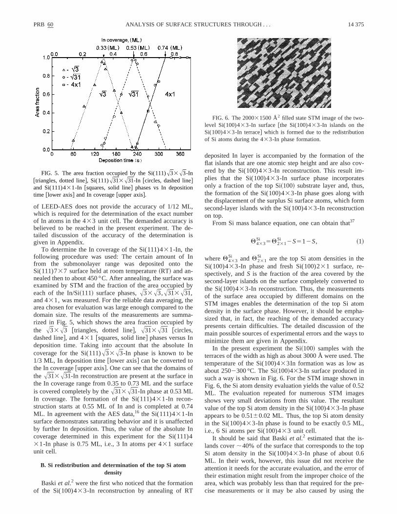
In the present experiment the Si~100! samples with theterraces of the width as high as about 3000 Å were used.temperature of the Si(100)433In formation was as low asabout 2502300 °C. The Si~100!433-In surface produced insuch a way is shown in Fig. 6. For the STM image shownFig. 6, the Si atom density evaluation yields the value of 0ML. The evaluation repeated for numerous STM imagshows very small deviations from this value. The resultvalue of the top Si atom density in the Si(100)433-In phaseappears to be 0.5160.02 ML. Thus, the top Si atom densitin the Si(100)433-In phase is found to be exactly 0.5 MLi.e., 6 Si atoms per Si(100)433 unit cell.
It should be said that Baskiet al.2 estimated that the islands cover;40% of the surface that corresponds to the tSi atom density in the Si(100)433-In phase of about 0.6ML. In their work, however, this issue did not receive thattention it needs for the accurate evaluation, and the errotheir estimation might result from the improper choice of tarea, which was probably less than that required for the pcise measurements or it may be also caused by using
FIG. 6. The 200031500 Å2 filled state STM image of the two-level Si(100)433-In surface@the Si(100)433-In islands on theSi(100)433-In terrace# which is formed due to the redistributioof Si atoms during the 433-In phase formation.
nn
om-
attoth
b-
n. A
fal-
edig
t
steby
L
ap-ic
m
he
outn-
r-is
sace
4
-
the
Sithe
etalnal
RT,y in
0
-
14 376 PRB 60A. A. SARANIN et al.
samples with the conventional terrace width of a few hudreds Å where the effect of the step edges cannot beglected.
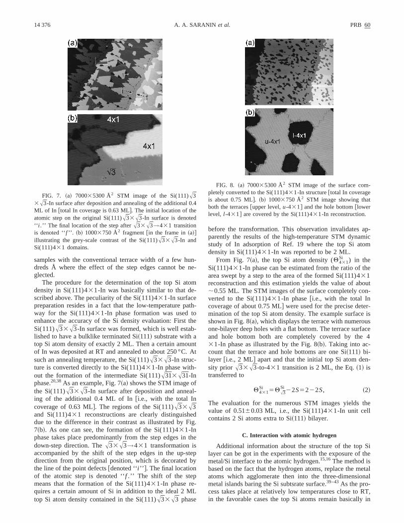
The procedure for the determination of the top Si atdensity in Si(111)431-In was basically similar to that described above. The peculiarity of the Si(111)431-In surfacepreparation resides in a fact that the low-temperature pway for the Si(111)431-In phase formation was usedenhance the accuracy of the Si density evaluation: FirstSi(111)A33A3-In surface was formed, which is well estalished to have a bulklike terminated Si~111! substrate with atop Si atom density of exactly 2 ML. Then a certain amouof In was deposited at RT and annealed to about 250 °Csuch an annealing temperature, the Si(111)A33A3-In struc-ture is converted directly to the Si(111)431-In phase with-out the formation of the intermediate Si(111)A313A31-Inphase.20,38As an example, Fig. 7~a! shows the STM image othe Si(111)A33A3-In surface after deposition and anneing of the additional 0.4 ML of [email protected]., with the total Incoverage of 0.63 ML#. The regions of the Si(111)A33A3and Si(111)431 reconstructions are clearly distinguishdue to the difference in their contrast as illustrated by F7~b!. As one can see, the formation of the Si(111)431-Inphase takes place predominantly from the step edges indown-step direction. TheA33A3→431 transformation isaccompanied by the shift of the step edges in the up-direction from the original position, which is decoratedthe line of the point defects@denoted ‘‘i ’’ #. The final locationof the atomic step is denoted ‘‘f . ’’ The shift of the stepmeans that the formation of the Si(111)431-In phase re-quires a certain amount of Si in addition to the ideal 2 Mtop Si atom density contained in the Si(111)A33A3 phase
FIG. 7. ~a! 700035300 Å2 STM image of the Si(111)A33A3-In surface after deposition and annealing of the additionalML of In @total In coverage is 0.63 ML#. The initial location of theatomic step on the original Si(111)A33A3-In surface is denoted‘‘ i . ’’ The final location of the step afterA33A3→431 transitionis denoted ‘‘f ’’. ~b! 10003750 Å2 fragment@in the frame in~a!#illustrating the grey-scale contrast of the Si(111)A33A3-In andSi(111)431 domains.
-e-
h-
e
tt
.
he
p
before the transformation. This observation invalidatesparently the results of the high-temperature STM dynamstudy of In adsorption of Ref. 19 where the top Si atodensity in Si(111)431-In was reported to be 2 ML.
From Fig. 7~a!, the top Si atom density (Q431Si ) in the
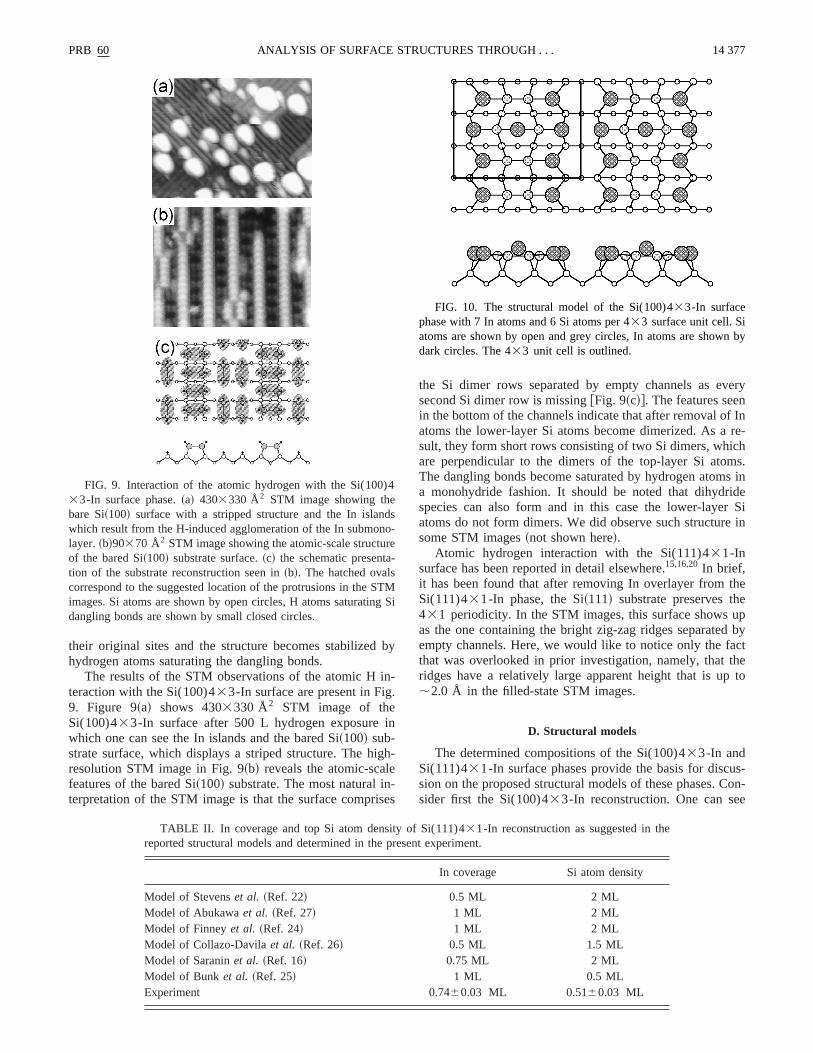
Si(111)431-In phase can be estimated from the ratio of tarea swept by a step to the area of the formed Si(111)431reconstruction and this estimation yields the value of ab;0.55 ML. The STM images of the surface completely coverted to the Si(111)431-In [email protected]., with the total Incoverage of about 0.75 ML# were used for the precise detemination of the top Si atom density. The example surfaceshown in Fig. 8~a!, which displays the terrace with numerouone-bilayer deep holes with a flat bottom. The terrace surfand hole bottom both are completely covered by the31-In phase as illustrated by the Fig. 8~b!. Taking into ac-count that the terrace and hole bottoms are one Si~111! bi-layer @i.e., 2 ML# apart and that the initial top Si atom density prior A33A3-to-431 transition is 2 ML, the Eq.~1! istransferred to
Q431Si 5QA3
Si 22S5222S, ~2!
The evaluation for the numerous STM images yieldsvalue of 0.5160.03 ML, i.e., the Si(111)431-In unit cellcontains 2 Si atoms extra to Si~111! bilayer.
C. Interaction with atomic hydrogen
Additional information about the structure of the toplayer can be got in the experiments with the exposure ofmetal/Si interface to the atomic hydrogen.15,16The method isbased on the fact that the hydrogen atoms, replace the matoms which agglomerate then into the three-dimensiometal islands baring the Si subtsrate surface.39–43As the pro-cess takes place at relatively low temperatures close toin the favorable cases the top Si atoms remain basicall
.4
FIG. 8. ~a! 700035300 Å2 STM image of the surface completely converted to the Si(111)431-In structure@total In coverageis about 0.75 ML#. ~b! 10003750 Å2 STM image showing thatboth the terraces@upper level,u-431# and the hole bottom@lowerlevel, l -431# are covered by the Si(111)431-In reconstruction.
b
in.
in
ige-se
very
f Inre-
chs.
s inide
Sie in
heeupd byct
heto
us-Con-e
)4
dnore-
Tg
n by
PRB 60 14 377ANALYSIS OF SURFACE STRUCTURES THROUGH . . .
their original sites and the structure becomes stabilizedhydrogen atoms saturating the dangling bonds.
The results of the STM observations of the atomic Hteraction with the Si(100)433-In surface are present in Fig9. Figure 9~a! shows 4303330 Å2 STM image of theSi(100)433-In surface after 500 L hydrogen exposurewhich one can see the In islands and the bared Si~100! sub-strate surface, which displays a striped structure. The hresolution STM image in Fig. 9~b! reveals the atomic-scalfeatures of the bared Si~100! substrate. The most natural interpretation of the STM image is that the surface compri
FIG. 9. Interaction of the atomic hydrogen with the Si(10033-In surface phase.~a! 4303330 Å2 STM image showing thebare Si~100! surface with a stripped structure and the In islanwhich result from the H-induced agglomeration of the In submolayer.~b!90370 Å2 STM image showing the atomic-scale structuof the bared Si~100! substrate surface.~c! the schematic presentation of the substrate reconstruction seen in~b!. The hatched ovalscorrespond to the suggested location of the protrusions in the Simages. Si atoms are shown by open circles, H atoms saturatindangling bonds are shown by small closed circles.
y
-
h-
s
the Si dimer rows separated by empty channels as esecond Si dimer row is missing@Fig. 9~c!#. The features seenin the bottom of the channels indicate that after removal oatoms the lower-layer Si atoms become dimerized. As asult, they form short rows consisting of two Si dimers, whiare perpendicular to the dimers of the top-layer Si atomThe dangling bonds become saturated by hydrogen atoma monohydride fashion. It should be noted that dihydrspecies can also form and in this case the lower-layeratoms do not form dimers. We did observe such structursome STM images~not shown here!.
Atomic hydrogen interaction with the Si(111)431-Insurface has been reported in detail elsewhere.15,16,20In brief,it has been found that after removing In overlayer from tSi(111)431-In phase, the Si~111! substrate preserves th431 periodicity. In the STM images, this surface showsas the one containing the bright zig-zag ridges separateempty channels. Here, we would like to notice only the fathat was overlooked in prior investigation, namely, that tridges have a relatively large apparent height that is up;2.0 Å in the filled-state STM images.
D. Structural models
The determined compositions of the Si(100)433-In andSi(111)431-In surface phases provide the basis for discsion on the proposed structural models of these phases.sider first the Si(100)433-In reconstruction. One can se
s-
MSi
FIG. 10. The structural model of the Si(100)433-In surfacephase with 7 In atoms and 6 Si atoms per 433 surface unit cell. Siatoms are shown by open and grey circles, In atoms are showdark circles. The 433 unit cell is outlined.
e
TABLE II. In coverage and top Si atom density of Si(111)431-In reconstruction as suggested in threported structural models and determined in the present experiment.In coverage Si atom density
Model of Stevenset al. ~Ref. 22! 0.5 ML 2 MLModel of Abukawaet al. ~Ref. 27! 1 ML 2 MLModel of Finneyet al. ~Ref. 24! 1 ML 2 MLModel of Collazo-Davilaet al. ~Ref. 26! 0.5 ML 1.5 MLModel of Saraninet al. ~Ref. 16! 0.75 ML 2 MLModel of Bunket al. ~Ref. 25! 1 ML 0.5 MLExperiment 0.7460.03 ML 0.5160.03 ML
ti
th
i
re
d-sL
ir
elthhe
-m
y
nr
-nheeeddg
u
ra-sid-
theus’’
ldingine-
ryther-
ehe
thes oftheofsen-on
rgeins
T
mslow
inallicon
ningces,
s
sed
nt.
files
14 378 PRB 60A. A. SARANIN et al.
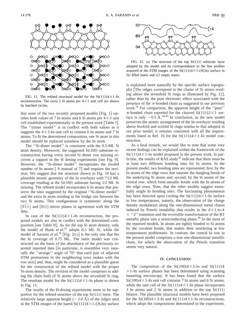
that none of the two recently proposed models@Fig. 1# sat-isfies both values of 7 In atoms and 6 Si atoms per 433 unitcell established experimentally in the present work@Table I#.The ‘‘trimer model’’ is in conflict with both values as isuggests the 433-In unit cell to contain 6 In atoms and 7 Satoms. To fit the determined composition, one Si atom inmodel should be replaced somehow by the In atom.
The ‘‘Si-dimer model’’ is consistent with the 0.5-ML Satom density. Moreover, the suggested Si~100! substrate re-construction having every second Si dimer row missingceives a support in the H dosing experiments@see Fig. 9#.However, the ‘‘Si-dimer model’’ incorporates the invalinumber of In atoms@ 6 instead of 7# and requires the revision. We suggest that the structure shown in Fig. 10 haplausible atomic geometry of the In overlayer with 7/12 Mcoverage residing at the Si~100! substrate having 1/2 ML Smissing. The refined model incorporates 6 In atoms that pserve the sites suggested by the original ‘‘Si-dimer modand the extra In atom residing in the bridge site betweentwo Si atoms. This configuration is symmetric along t
@01̄1# and @011# mirror planes in agreement with the STMdata.
In case of the Si(111)431-In reconstruction, the proposed models are also in conflict with the determined coposition @see Table II#. As for the top Si atom density, onlthe model of Bunket al.25 adopts 0.5 ML Si, while themodel of Saraninet al.16 @Fig. 2~c!# is the only one that fitsthe In coverage of 0.75 ML. The latter model was costructed on the basis of the abundance of the previouslyported reported data@in particular, it resembles very naturally the ‘‘strange’’ angle of 70° that each pair of adjaceSTM protrusions in the neighboring rows makes with trow axis# and, thus, might be considered as a plausible gufor the construction of the refined model with the propSi-atom density. The revision of the model comprises in aing the chain built of Si atoms above the sevenfold Si rinThe resultant model for the Si(111)431-In phase is shownin Fig. 11.
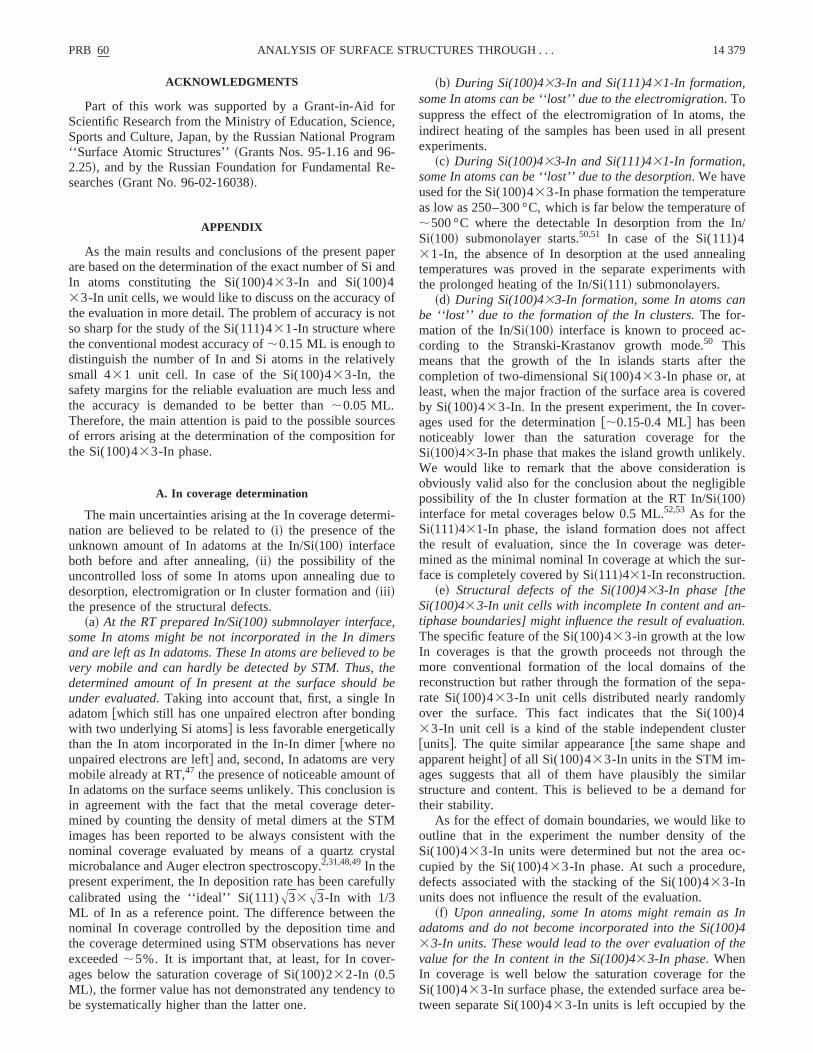
The results of the H-dosing experiments seem to be sportive for the refined structure of the top Si~111! layer. Therelatively large apparent height (;2.0 Å) of the ridges seenin the STM images of the bared Si(111)431-(H,In) surface
FIG. 11. The refined structural model for the Si(111)431-Inreconstruction. The extra 2 Si atoms per 431 unit cell are shownby hatched circles.
is
-
a
e-’’e
-
-e-
t
ssr-.
p-
is explained more naturally by the specific surface topogphy @The ridges correspond to the chains of Si atoms reing abovethe sevenfold Si rings as illustrated by Fig. 12#,rather than by the pure electronic effect associated withpresence of thep-bonded chain as suggested in our previowork.16 For comparison, the apparent height of the ‘‘purep-bonded chain reported for the cleaved Si(111)231 sur-face is only;0.5 Å.44,45 In conclusion, as the new modepreserves the atomic arrangement of the In overlayer resiabove fivefold and sixfold Si rings similar to that adoptedour prior model, it remains consistent with all the requirments listed in Ref. 16 for the Si(111)431-In model con-struction.
As a final remark, we would like to note that some verecent findings can be explained within the framework ofSi(111)431-In model proposed in the present work. In paticular, the results of RAS study30 indicate that there must bat least two different bonding sites for In atoms. In tpresent model, two bonding sites are represented, first, byIn atoms of the edge rows that saturate the dangling bondthe underlying Si atoms and, second, by the In atoms ofcentral row, which form metallic bonds with the In atomsthe edge rows. Note, that the other models suggest estially single In bonding sites. The fascinating phenomenhas been detected upon cooling the Si(111)431-In surfaceto low temperatures, namely, the observation of the chadensity modulation along the one-dimensional metal chainduced by Peierls instability that results in the 431-to-43 ‘‘2’’ transition and the reversible transformation of the Rmetallic phase into a semiconducting phase.46 In the most ofthe reported models, In atoms are tightly bonded to Si atoby the covalent bonds, that makes their reordering attemperatures problematic. In contrast, the central In rowthe present model comprises a true one-dimensional metchain, for which the observation of the Peierls transitiseems very natural.
IV. CONCLUSION
The composition of the Si(100)433-In and Si(111)431-In surface phases has been determined using scantunneling microscopy. It has been found that the surfaSi(100)433-In unit cell contains 7 In atoms and 6 Si atomwhile the unit cell of the Si(111)431-In phase incorporate3 In atoms and 2 Si atoms in addition to the top Si~111!bilayer. The plausible structural models have been propofor the Si(100)433-In and Si(111)431-In reconstructions,which adopt the compositions determined in the experime
FIG. 12. ~a! The structure of the top Si~111! substrate layeradopted by the model and its correspondence to the line proacquired at the STM images of the Si(111)431-(H,In) surface in~b! filled states and~c! empty states.
orcera-
Re
pa
ono
ely
an
rcfo
m
ceerothb
nngy
ryofnteMt
st
fu
thnevr-
y
thesent
reof
In/
lingwith
n
-
the
redr-
thely.isle
ctter-ur-
-on.
thehepa-y)4
terd
ilarfor
tohec-
e,
In0)4the
thebe-
PRB 60 14 379ANALYSIS OF SURFACE STRUCTURES THROUGH . . .
ACKNOWLEDGMENTS
Part of this work was supported by a Grant-in-Aid fScientific Research from the Ministry of Education, ScienSports and Culture, Japan, by the Russian National Prog‘‘Surface Atomic Structures’’~Grants Nos. 95-1.16 and 962.25!, and by the Russian Foundation for Fundamentalsearches~Grant No. 96-02-16038!.
APPENDIX
As the main results and conclusions of the present paare based on the determination of the exact number of SiIn atoms constituting the Si(100)433-In and Si(100)433-In unit cells, we would like to discuss on the accuracythe evaluation in more detail. The problem of accuracy isso sharp for the study of the Si(111)431-In structure wherethe conventional modest accuracy of;0.15 ML is enough todistinguish the number of In and Si atoms in the relativsmall 431 unit cell. In case of the Si(100)433-In, thesafety margins for the reliable evaluation are much lessthe accuracy is demanded to be better than;0.05 ML.Therefore, the main attention is paid to the possible souof errors arising at the determination of the compositionthe Si(100)433-In phase.
A. In coverage determination
The main uncertainties arising at the In coverage deternation are believed to be related to~i! the presence of theunknown amount of In adatoms at the In/Si~100! interfaceboth before and after annealing,~ii ! the possibility of theuncontrolled loss of some In atoms upon annealing duedesorption, electromigration or In cluster formation and~iii !the presence of the structural defects.
~a! At the RT prepared In/Si(100) submnolayer interfasome In atoms might be not incorporated in the In dimand are left as In adatoms. These In atoms are believed tvery mobile and can hardly be detected by STM. Thus,determined amount of In present at the surface shouldunder evaluated. Taking into account that, first, a single Iadatom@which still has one unpaired electron after bondiwith two underlying Si atoms# is less favorable energeticallthan the In atom incorporated in the In-In dimer@where nounpaired electrons are left# and, second, In adatoms are vemobile already at RT,47 the presence of noticeable amountIn adatoms on the surface seems unlikely. This conclusioin agreement with the fact that the metal coverage demined by counting the density of metal dimers at the STimages has been reported to be always consistent withnominal coverage evaluated by means of a quartz crymicrobalance and Auger electron spectroscopy.2,31,48,49In thepresent experiment, the In deposition rate has been carecalibrated using the ‘‘ideal’’ Si(111)A33A3-In with 1/3ML of In as a reference point. The difference betweennominal In coverage controlled by the deposition time athe coverage determined using STM observations has nexceeded;5%. It is important that, at least, for In coveages below the saturation coverage of Si(100)232-In ~0.5ML !, the former value has not demonstrated any tendencbe systematically higher than the latter one.
,m
-
ernd
ft
d
esr
i-
to
,sbeee
isr-
heal
lly
eder
to
~b! During Si(100)433-In and Si(111)431-In formation,some In atoms can be ‘‘lost’’ due to the electromigration. Tosuppress the effect of the electromigration of In atoms,indirect heating of the samples has been used in all preexperiments.
~c! During Si(100)433-In and Si(111)431-In formation,some In atoms can be ‘‘lost’’ due to the desorption. We haveused for the Si(100)433-In phase formation the temperatuas low as 250–300 °C, which is far below the temperature;500 °C where the detectable In desorption from theSi~100! submonolayer starts.50,51 In case of the Si(111)431-In, the absence of In desorption at the used anneatemperatures was proved in the separate experimentsthe prolonged heating of the In/Si~111! submonolayers.
~d! During Si(100)433-In formation, some In atoms cabe ‘‘lost’’ due to the formation of the In clusters.The for-mation of the In/Si~100! interface is known to proceed according to the Stranski-Krastanov growth mode.50 Thismeans that the growth of the In islands starts aftercompletion of two-dimensional Si(100)433-In phase or, atleast, when the major fraction of the surface area is coveby Si(100)433-In. In the present experiment, the In coveages used for the determination@;0.15-0.4 ML# has beennoticeably lower than the saturation coverage forSi~100!433-In phase that makes the island growth unlikeWe would like to remark that the above considerationobviously valid also for the conclusion about the negligibpossibility of the In cluster formation at the RT In/Si~100!interface for metal coverages below 0.5 ML.52,53 As for theSi~111!431-In phase, the island formation does not affethe result of evaluation, since the In coverage was demined as the minimal nominal In coverage at which the sface is completely covered by Si~111!431-In reconstruction.
~e! Structural defects of the Si(100)433-In phase [theSi(100)433-In unit cells with incomplete In content and antiphase boundaries] might influence the result of evaluatiThe specific feature of the Si(100)433-in growth at the lowIn coverages is that the growth proceeds not throughmore conventional formation of the local domains of treconstruction but rather through the formation of the serate Si(100)433-In unit cells distributed nearly randomlover the surface. This fact indicates that the Si(10033-In unit cell is a kind of the stable independent clus@units#. The quite similar appearance@the same shape anapparent height# of all Si(100)433-In units in the STM im-ages suggests that all of them have plausibly the simstructure and content. This is believed to be a demandtheir stability.
As for the effect of domain boundaries, we would likeoutline that in the experiment the number density of tSi(100)433-In units were determined but not the area ocupied by the Si(100)433-In phase. At such a procedurdefects associated with the stacking of the Si(100)433-Inunits does not influence the result of the evaluation.
~f! Upon annealing, some In atoms might remain asadatoms and do not become incorporated into the Si(1033-In units. These would lead to the over evaluation ofvalue for the In content in the Si(100)433-In phase. WhenIn coverage is well below the saturation coverage forSi(100)433-In surface phase, the extended surface areatween separate Si(100)433-In units is left occupied by the
c
s
m
l
iu
dL
h)c
)4heer
byor ai
gthr tos
ththat
ofit isfied.)4
14 380 PRB 60A. A. SARANIN et al.
undisturbed 231 reconstruction of the clean Si~100! surface.Cooling of the sample for the STM observations reproduessentially the situation taking place at RT In/Si~100! inter-face formation discussed in~a!. As a result, the In adatomleft should become coupled into the dimers. Indeed, shpieces of the In dimer rows can be found at thorough exanation of the STM images. However, the In amount accumlated in In dimers is as small as less than 1% of the totacoverage and, thus, can be neglected.
B. Top Si atom density determination
The errors of the determination of the top Si atom denscan be caused primarily by the presence of the structdefects and atomic steps at the initial Si~100! surface.
~a! The real initial Si(100)231 surface contains a certaindensity of structural defects which should results in theviation of the actual top Si atom density from the ideal 1 M.The typical defects of the clean Si(100)231 surface aremissing dimers rather than Si ad-dimers. This means thatactual top Si atom density in the Si(100)231 surface shouldbe less than 1 ML. If this fact is not taken into account, tobtained value of the top Si atom density for Si(10033-In would be over evaluated by the value of Si deficien
,
o
,
es
orti-
u-In
tyral
e-
the
e4y
at the initial Si(100)231 surface@see Eq.~1!#. The typicaldefect density amounts to a few percent (;1-5%).Thus, theactual value of the top Si atom density in the Si(10033-In might be only lower by a few percent compared to tvalue of 0.5 ML obtained in the present study, but not highas suggested by the estimation in the work by Baskiet al.2
~b! The result of the determination might be affectedthe presence of the step edges which can act as a sinksource for surface Si atoms.The effect of the steps on the Sredistribution becomes negligible when the migration lenof Si atoms is much less than the terrace width. In ordesatisfy this requirement,~i! the formation temperature habeen minimized to about 25022300 °C to suppress Si atommobility and ~ii ! the Si~100! sample has been chosen witerraces as wide as 3000-5000 Å. One can see in Fig. 6the upper-level Si(100)433-In islands are uniformly distrib-uted all over the area used for evaluation@;200032000 Å2# and the typical interisland separation@which isnaturally associated with the Si migration length# does notexceed 100 Å, i.e., it is small compared to both the sizethe region under consideration and the terrace width. So,safe to state that the above requirement has been satisThe above consideration is evidently valid for the Si(11131-In samples@see Fig. 8#.
u
s
a
ev.
.
.
s.
. B
c-
L.R.
f.
i-c-
er,
. B
ppl.
*Author to whom correspondence should be addressed. FAX:1816 876 4564. Electronic address: [email protected]
1J. Knall, J.-E. Sundgren, G.V. Hansson, and J.E. Greene, SSci. 166, 512 ~1986!.
2A.A. Baski, J. Nogami, and C.F. Quate, Phys. Rev. B43, 9316~1991!.
3L. Li, Y. Wei, and I.S.T. Tsong, Surf. Sci.304, 1 ~1994!.4B.E. Steele, D.M. Cornelison, and L. Li, Nucl. Instrum. Method
Phys. Res. B85, 414 ~1994!.5H.W. Yeom, T. Abukawa, Y. Takakuwa, Y. Mori, T. Shimatani
A. Kakizaki, and S. Kono, Phys. Rev. B54, 4456~1996!.6G. Krausch, K. Jacobs, R. Fink, J. Lohmu¨ller, B. Luckscheiter,
B.-U. Runge, U. Wo¨hrmann, and G. Schatz, Europhys. Lett.19,611 ~1992!.
7G. Krausch, R. Fink, K. Jacobs, B. Luckscheiter, J. LohmuelleB.-U. Runge, U. Woehrmann, and G. Schatz, Surf. Sci.285, 81~1993!.
8A.V. Zotov, A.A. Saranin, K.V. Ignatovich, V.G. Lifshits, M.Katayama, and K. Oura, Surf. Sci. Lett.391, L1188 ~1997!.
9A.V. Zotov, A.A. Saranin, V.G. Lifshits, J.-T. Ryu, O. Kubo, H.Tani, M. Katayama, and K. Oura, Phys. Rev. B57, 12 492~1998!.
10O. Bunk, G. Falkenberg, L. Seehofer, J.H. Zeysing, R.L. JohnsM. Nielsen, R. Feidenhans’l, and E. Landemark, Appl. Surf. Sc123/124, 104 ~1998!.
11O. Bunket al., Phys. Rev. B60, 13 905~1999!.12M. Kawaji, S. Baba, and A. Kinbara, Appl. Phys. Lett.34, 748
~1979!.13H. Hirayama, S. Baba, and A. Kinbara, Appl. Surf. Sci.33/34,
193 ~1988!.14N. Nakamura, K. Anno, and S. Kono, Surf. Sci.256, 129 ~1991!.15A.A. Saranin, E.A. Khramtsova, K.V. Ignatovich, V.G. Lifshits
T. Numata, O. Kubo, M. Katayama, I. Katayama, and K. OurPhys. Rev. B55, 5353~1997!.
16A.A. Saranin, A.V. Zotov, K.V. Ignatovich, V.G. Lifshits, T. Nu-
rf.
r,
n,i.
,
mata, O. Kubo, H. Tani, M. Katayama, and K. Oura, Phys. RB 56, 1017~1997!.
17S. Park, J. Nogami, and C.F. Quate, J. Microsc.152, 727 ~1988!.18J. Nogami, S. Park, and C.F. Quate, Phys. Rev. B36, 6221
~1987!.19Y. Tanishiro, K. Kaneko, H. Minoda, K. Yagi, T. Sueyoshi, T
Sato, and M. Iwatsuki, Surf. Sci.357/358, 407 ~1996!.20A.A. Saranin, A.V. Zotov, V.G. Lifshits, T. Numata, O. Kubo, H
Tani, M. Katayama, and K. Oura, Surf. Sci.398, 60 ~1998!.21D.M. Cornelison, M.S. Worthington, and I.S.T. Tsong, Phy
Rev. B43, 4051~1991!.22J.L. Stevens, M.S. Worthington, and I.S.T. Tsong, Phys. Rev
47, 1453~1993!.23M.S. Finney, C. Norris, P.B. Howes, and E. Vlieg, Surf. Sci.277,
330 ~1992!.24M.S. Finney, C. Norris, P.B. Howes, M.A. James, J.E. Ma
donald, A.D. Johnson, and E. Vlieg, Physica B198, 246~1994!.25O. Bunk, G. Falkenberg, J.H. Zeysing, L. Lottermoser, R.
Johnson, M. Nielsen, F. Berg-Rasmussen, J. Baker, andFeidenhans’l, Phys. Rev. B59, 12 228~1999!.
26C. Collazo-Davila, L.D. Marks, K. Nishii, and Y. Tanishiro, SurRev. Lett.4, 65 ~1997!.
27T. Abukawa, M. Sasaki, F. Hisamatsu, M. Nakamura, T. Knoshita, A. Kakizaki, T. Goto, and S. Kono, J. Electron Spetrosc. Relat. Phenom.80, 233 ~1996!.
28I.G. Hill and A.B. McLean, Phys. Rev. B56, 15 725~1997!.29I.G. Hill and A.B. McLean, Phys. Rev. B59, 9791~1999!.30F. Pedreschi, J.D. O’Mahony, P. Weightman, and J.R. Pow
Appl. Phys. Lett.73, 2152~1998!.31A.A. Baski, J. Nogami, and C.F. Quate, J. Vac. Sci. Technol. A9,
1946 ~1991!.32B.E. Steele, L. Li, J.L. Stevens, and I.S.T. Tsong, Phys. Rev
47, 9925~1993!.33C. Zhu, T. Hayashi, S. Misawa, and S. Tsukahara, Jpn. J. A
Phys., Part 133, 3706~1994!.
K
ki
i,
s,K
ra
a,
ra
d
.
ett.
ta,
hi,S.
rf.
Sci.
.
PRB 60 14 381ANALYSIS OF SURFACE STRUCTURES THROUGH . . .
34H.W. Yeom, T. Abukawa, M. Nakamura, S. Suzuki, S. Sato,Sakamoto, T. Sakamoto, and S. Kono, Surf. Sci.341, 328~1995!.
35H.W. Yeom, T. Abukawa, M. Nakamura, X. Chen, and S. SuzuSurf. Sci. Lett.340, L983 ~1995!.
36H.W. Yeom, T. Abukawa, Y. Takakuwa, Y. Mori, T. ShimatanA. Kakizaki, and S. Kono, Phys. Rev. B53, 1948~1996!.
37A.A. Saranin, A.V. Zotov, S. Ryzhkov, D. Tsukanov, V. LifshitJ.-T. Ryu, O. Kubo, H. Tani, T. Harada, M. Katayama, andOura, Phys. Rev. B58, 4972~1998!.
38A.A. Saranin, T. Numata, O. Kubo, M. Katayama, and K. OuAppl. Surf. Sci.121/122, 183 ~1997!.
39K. Oura, K. Sumitomo, T. Kobayashi, T. Kinoshita, Y. Tanakand F. Shoji, Surf. Sci. Lett.245, L460 ~1991!.
40A.A. Saranin, E.A. Khramtsova, and V.G. Lifshits, Surf. Sci.297,353 ~1993!.
41H. Ohnishi, Y. Yamamoto, I. Katayama, Y. Ohba, and K. OuJpn. J. Appl. Phys., Part 233, L1106 ~1994!.
42B.R. Williams, B.F. Mason, D.W. McComb, D.J. Moffatt, anP.A. Hackett, Surf. Sci. Lett.313, L790 ~1994!.
43E. Landemark, C.J. Karlsson, and R.I.G. Uhrberg, Phys. Rev44, 1950~1991!.
.
,
.
,
,
B
44R.M. Feenstra, W.A. Thompson, and A.P. Fein, Phys. Rev. L56, 608 ~1986!.
45T. Yokoyama, H. Tanaka, M. Itoh, T. Yokotsuka, and I. SumiPhys. Rev. B49, 5703~1994!.
46H.W. Yeom, S. Takeda, E. Rotenberg, I. Matsuda, K. HorikosJ. Schaefer, C.M. Lee, S.D. Kevan, T. Ohta, T. Nagao, andHasegawa, Phys. Rev. Lett.82, 4898~1999!.
47Z.-C. Dong, T. Yakabe, D. Fujita, Q.D. Jiang, and H. Nejo, SuSci. 380, 23 ~1997!.
48H. Itoh, J. Itoh, A. Schmid, and T. Ichinokawa, Surf. Sci.302,295 ~1994!.
49H. Itoh, J. Itoh, A. Schmid, and T. Ichinokawa, Phys. Rev. B48,14 663~1993!.
50J. Knall, S.A. Barnett, J.-E. Sundgren, and J.E. Greene, Surf.209, 314 ~1989!.
51D.J. Oostra, R.V. Smilgys, and S.R. Leone, Surf. Sci.226, 226~1990!.
52J. Nogami, A.A. Baski, and C.F. Quate, Phys. Rev. B44, 1415~1991!.
53H.W. Yeom, T. Abukawa, Y. Takakuwa, M. Nakamura, MKimura, A. Kakizaki, and S. Kono, Surf. Sci.365, 328 ~1996!.
Top Related
Copyright © 2022 FDOKUMEN

