


Bahasa
Halaman
Hukum

Coverage-dependent symmetry of the electronic states of the Pt(111)-Ag-Bi interface: the ARPESview of a structural transition
E. Frantzeskakis,1, ∗ S. Pons,1, 2 A. Crepaldi,3 H. Brune,4 K. Kern,3, 5 and M. Grioni11Laboratoire de Spectroscopie Electronique, Institut de Physique de la Matiere Condensee (ICPM),
Ecole Polytechnique Federale de Lausanne (EPFL), station 3, CH-1015 Lausanne, Switzerland2Institut des NanoSciences de Paris (INSP) , Universite Pierre et Marie Curie (UPMC) - Paris 6 - CNRS, France
3Laboratoire de Science a l’Echelle Nanometrique, Institut de Physique de la Matiere Condensee (ICPM),Ecole Polytechnique Federale de Lausanne (EPFL), station 3, CH-1015 Lausanne, Switzerland
4Laboratoire de Nanostructures Superficielles, Institut de Physique de la Matiere Condensee (ICPM),Ecole Polytechnique Federale de Lausanne (EPFL), station 3, CH-1015 Lausanne, Switzerland
5Max-Planck-Institut fur Festkorperforschung, D-70569 Stuttgart, Germany(Dated: August 9, 2011)
We studied by angle-resolved photoelectron spectroscopy the strain-related structural transition from a pseu-domorphic monolayer (ML) to a striped incommensurate phase in an Ag thin film grown on Pt(111). Weexploited the surfactant properties of Bi to grow ordered Pt(111)−xMLAg−Bi trilayers with 0 ≤ x ≤ 5 ML,and monitored the dispersion of the Bi-derived interface states to probe the structure of the underlying Ag film.We find that their symmetry changes from threefold to sixfold and back to threefold in the Ag coverage rangestudied. Together with previous STM and photoelectron diffraction data, these results provide a consistentmicroscopic description of the structural transition.
I. INTRODUCTION
Lattice mismatch is a crucial factor determining the growthmode and morphology of heteroepitaxial metal-metal inter-faces. It gives rise to pseudomorphic strained layers, but itcan also be accommodated either by the formation of moirestructures or of incommensurate phases containing misfit dis-locations, where the strain is locally relieved. Strain can alsobe important in homoepitaxial systems. The Au(111) surfaceis a paradigm of the latter. A 4% strain in the topmost layeris relieved by the formation of a pairwise dislocation network,yielding the well-studied (
√3 × 22) herringbone reconstruc-
tion [1, 2].The Pt(111)-Ag interface is a typical example of strain re-
lief in a heteroepitaxial system [3–6]. For sub-monolayer(ML) coverages it exhibits partial dislocations, which are re-moved by annealing to 800 K, or at the completion of thefirst ML at RT (a “re-entrant pseudomorphic growth”). Thefirst complete Ag ML is compressed with respect to a bulkAg(111) plane. The strain is relieved in the second Ag MLby the formation of a metastable striped incommensurate (SI)phase at room temperature. The SI phase transforms to anequilibrium structure with a triangular dislocation networkabove 800 K. In both phases dislocation lines separate do-mains with fcc and hcp stacking [7, 8].
While the morphology and structure of Pt-Ag(111) havebeen thoroughly investigated, relatively little is known of itsmicroscopic electronic properties. We present here angle-resolved photoelectron spectroscopy (ARPES) data on theband structure of Ag-Pt(111) and of a Pt(111)−xMLAg−Bitrilayer system with 1 ≤ x ≤ 5 ML. The latter was sug-gested by recent experiments on a BiAg2 surface alloy grownon Ag(111), showing a very large separation of opposite spinstates (Rashba effect) [9, 10]. Theory predicts [11] that thesize of the Rashba effect is very sensitive to slight changes
in the atomic structure, motivating us to explore the possibleinfluence of interfacial strain on the spin-orbit splitting.
Here we show that rather than the (√
3 ×√
3)R30◦ BiAg2
surface alloy formed on the Ag(111) substrate, Bi atoms ar-range themselves in an ordered overlayer with a (2× 2) sym-metry. The resulting band structure is distinct from that ofthe alloy and does not exhibit signatures of a large spin-orbitsplitting. By contrast, the Bi-derived states effectively probethe structure of the Ag film. Their angular dispersion is de-termined by the symmetry of the underlying layer. It exhibitsa change from threefold to sixfold in correspondence of thestructural transition to the SI phase at 2ML coverage, and thenback to threefold for larger Ag thicknesses. These observa-tions support the model of the transition proposed on the basisof STM and photoelectron diffraction studies [5, 7].
II. EXPERIMENTAL DETAILS
The Pt(111) substrate was prepared by repeated cycles ofAr sputtering and annealing at 1300 K. The crystal was thenexposed to an O2 partial pressure of p = 1 × 10⁻⁷mbar at900 K, in order to catalytically remove the carbon impuritieswhich had segregated from the bulk. Finally, it was annealedat 1000 K without O2. The order and cleanliness of the surfacewere verified by means of LEED and ARPES.
Ag was evaporated from a resistively heated tungsten bas-ket which had been accurately calibrated in previous experi-ments [12, 13]. Bi was deposited by electron-beam-assistedevaporation using a commercial EFM3 Omicron source. Thesample was kept at room temperature (RT) during the depo-sition of both Ag and Bi. A mild post-annealing resulted insharp LEED spots. The deposition order of Ag and Bi couldbe reversed without any effect on the crystalline order and thesymmetry and the electronic states, as probed respectively by
arX
iv:1
108.
1710
v1 [
cond
-mat
.mtr
l-sc
i] 8
Aug
201
1
2
LEED and ARPES.
ARPES spectra were acquired at RT and 21.2 eV photonenergy using a Phoibos 150 Specs Analyzer equipped witha monochromatized Gammadata VUV 5000 high brightnesssource. The base pressure was in the low 10−10 mbar range.
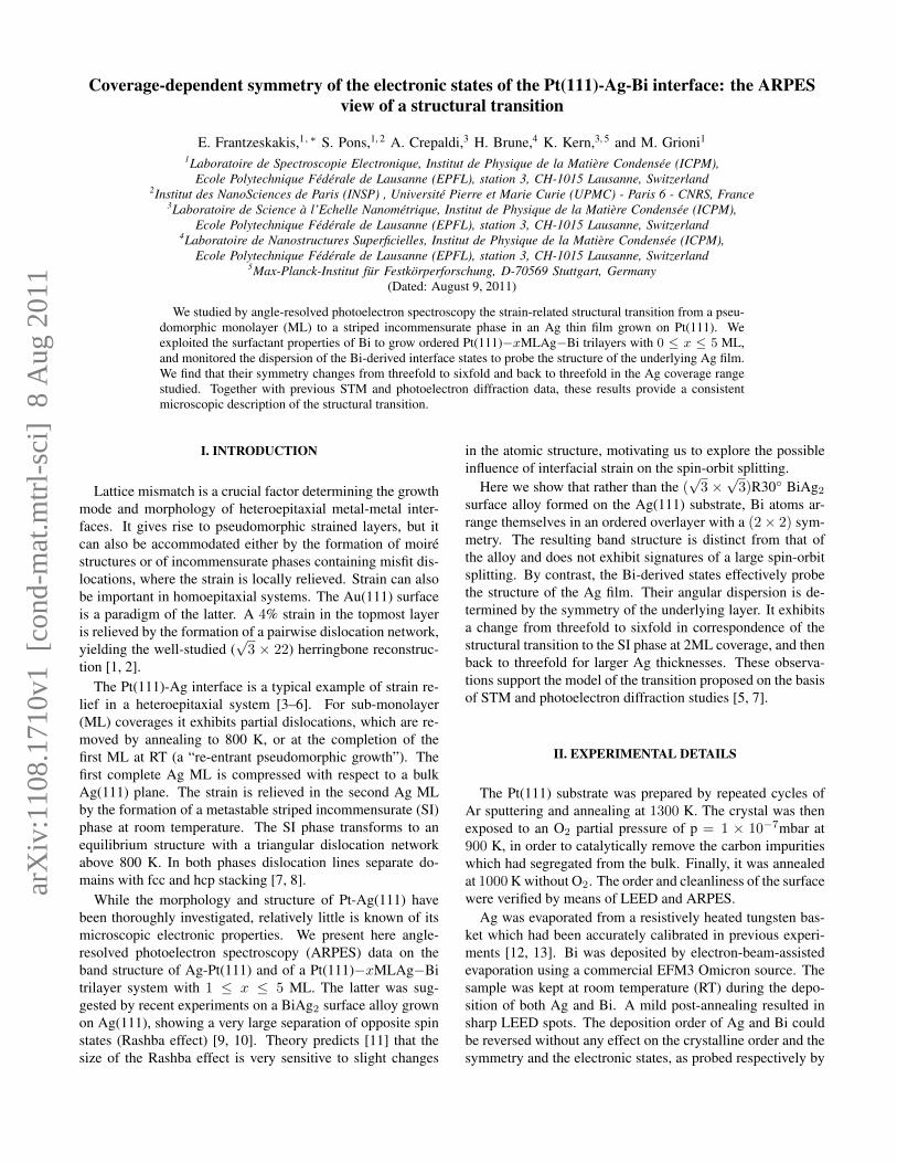
FIG. 1: (color online) ARPES results for the Pt(111) substrate. (a)Constant energy ARPES intensity map at E=EF. The second deriva-tive of the photoemission intensity is shown to enhance the experi-mental features. The hexagon is the Pt(111) (i.e. (1 × 1) surfaceBrillouin zone. Data measured within the dashed rectangles weresubsequently symmetrized using a sixfold axis. (b) and (c) ARPESintensity plots (second derivative) illustrate the band dispersion alongthe ΓM and ΓK high-symmetry directions. Solid lines highlight theprojected bulk band gaps [14, 15].
III. RESULTS
Figure 1 summarizes the ARPES results for the cleanPt(111) surface. Data were collected in the region of k spacewithin the dashed lines in Fig. 1 (a), and then symmetrizedby a sixfold rotation. Figure 1 (a) is a constant energy (CE)intensity map measured at the Fermi energy (EF). Figure 1(b) and 1 (c) illustrate the experimental energy-wave vectordispersion along the two high-symmetry directions ΓM and,respectively, ΓK of the surface Brillouin zone (BZ). The BZboundaries are at 1.31 A−1 (ΓM) and 1.51 A−1 (ΓK). Boththe CE map and the band dispersion are dominated by a statecentered at the Γ point and dispersing through EF. It givesrise to a nearly hexagonal Fermi surface (FS). The corner ofthe FS, along ΓM, is at kF(ΓM) ' 0.9 A−1, while the Fermicrossing along ΓK is at kF(ΓK) ' 0.8 A−1
Hexagonal contours are expected for surface states at the(111) surfaces of fcc crystals, by contrast with the threefoldsymmetry of bulk states. This point is further discussed inSection IV. However the bulk electronic structure of Pt doesnot present a projected gap around Γ that could support a sur-face state. Indeed, when the photon energy is varied, this stateexhibits a weak but finite k⊥ dispersion, typical of a bulk state.The hexagonal contour was then tentatively ascribed not to atrue surface state, but to a surface resonance associated with
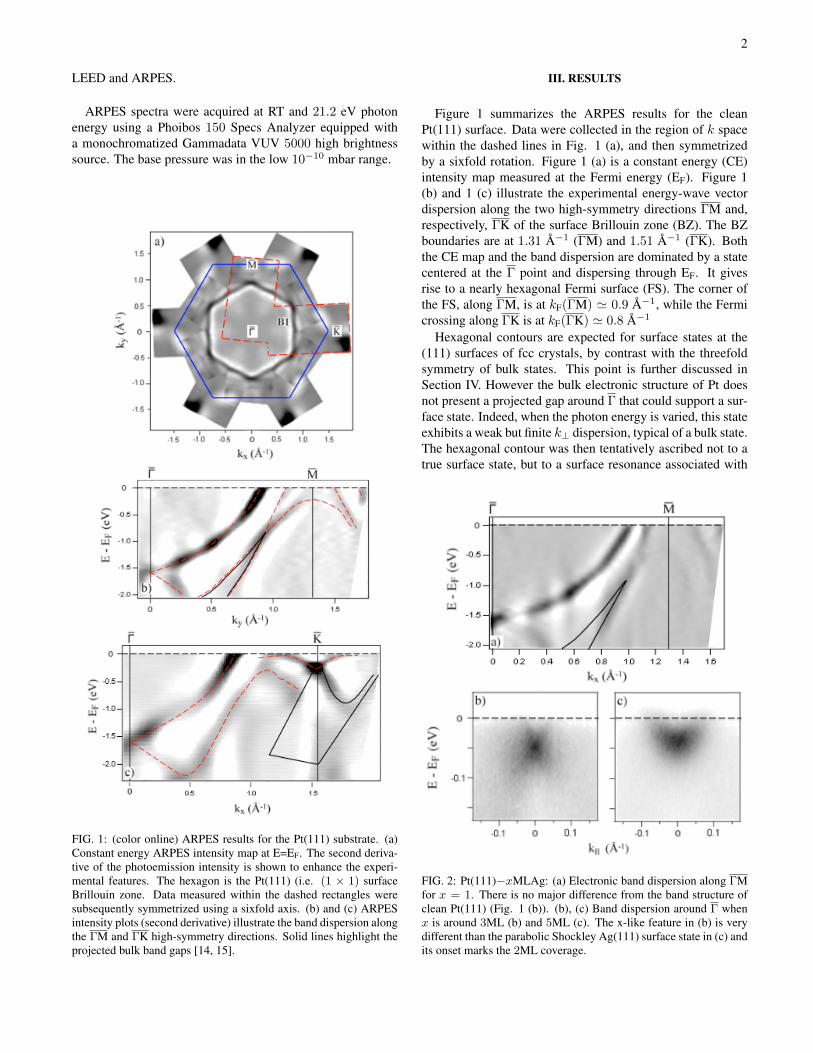
FIG. 2: Pt(111)−xMLAg: (a) Electronic band dispersion along ΓMfor x = 1. There is no major difference from the band structure ofclean Pt(111) (Fig. 1 (b)). (b), (c) Band dispersion around Γ whenx is around 3ML (b) and 5ML (c). The x-like feature in (b) is verydifferent than the parabolic Shockley Ag(111) surface state in (c) andits onset marks the 2ML coverage.
3
the sixth bulk band [14, 16]. That suggestion was later sup-ported by a density functional theory (DFT) calculation thatfound a state with 5dxz,yz character and a strong (10%) lo-calization in the surface layer [17]. However, it should alsobe noted that the predicted ARPES FS contour, which hasa threefold symmetry for a generic photon energy, becomesnearly hexagonal for specific values of hν (CE maps were cal-culated with the FLAN software, courtesy of Dr. E. Garcia-Michel [18]). The transition from a clearly sixfold to a clearlythreefold contour occurs by changing hν - or, equivalently, theinner potential V0 – by less than 2 eV, so that this observationcould be at least partly accidental.
Two weaker band features are observed at larger wave vec-tors. Along ΓM one crosses EF at ' 1.1 A−1 and again ata symmetric point on the opposite side of M, while the sec-ond has a maximum at M. Their dispersion follows the edgesof the projected bulk continuum, defined by solid lines in thefigure, and may continue as a surface resonance [14, 15, 19].Along the ΓK direction, there is a strong feature around theK point, where previous studies predicted the edge of a bulkprojected gap and a relatively flat surface resonance [14, 15].
The deposition of silver on the Pt(111) substrate was fol-lowed by LEED and ARPES. For ΘAg = 1ML the LEED pat-tern and the band structure within the range of Fig. 1 (Fig. 2(a)) are essentially identical to those of the clean substrate.New features appear at the completion of the second ML,namely a (
√3 × 14) LEED pattern, characteristic of the SI
phase [5]. Between 2 ML and 4 ML the ARPES intensity map(Fig. 2 (b)) exhibits an “x-like” feature just below EF centeredat the Γ point. This structure was recently observed in an inde-pendent ARPES experiment [20]. It was attributed to a surfaceresonance derived from the Shockley surface state of Pt(111),which is split on both sides of Γ by a large Rashba-type effect.This state, which for clean Pt(111) is located above EF in ahybridization gap, moves below EF by the interaction with theAg overlayer. The shape, splitting, binding energy, and alsothe rather diffuse intensity, all agree with the ARPES data for3 ML from Ref. 20. The Ag(111) (1 × 1)1 LEED pattern isfirst seen above 3 ML, and the Rashba-split band completelydisappears above ΘAg = 4 ML. For larger Ag coverages theAg(111) Shockley surface state is observed around Γ (Fig. 2(c)).
The deposition of bismuth induces significant changes inthe LEED and ARPES signatures, summarized in Fig. 3. TheBi evaporation source was calibrated using the characteristicLEED pattern of one ML of Bi on a pristine Ag (111) substrate[21]. A Bi coverage of ∼ 0.25 ML yields a sharp p(2 × 2)LEED pattern, irrespective of the thickness of the Ag layer,i.e both for the simple (1 × 1) (x < 2 ML; x > 3 ML) andfor the reconstructed (
√3× 14) (2 < x < 3 ML) Pt(111)-Ag
interface. The (2 × 2) structure is never observed for the Bi-free Pt(111)−xMLAg interface. As already mentioned, weobtained identical LEED and ARPES results even when thedeposition order of Ag and Bi was reversed, i.e. when Bi wasdirectly evaporated on the Pt(111) substrate. Further Bi evap-oration up to 0.5 ML does not yield any new superstructure,
but only results in a progressive deterioration of the (2 × 2)pattern. The data presented the following refer to ΘBi = 0.25ML.
These obervations indicate that the (2 × 2) superstructurecorresponds to a Bi-induced reconstruction where Bi mostlikely floats on top of the Ag layer. Bismuth therefore behavesas a surfactant in the layer-by-layer growth of Ag on Pt(111).This is not surprising if one consisders the well-known surfac-tant properties of Sb [22–24] – which is isoelectronic and has asmaller atomic radius – and of Pb [25–27], which immediatelyprecedes Bi in the periodic table. On the other hand, we couldnever obtain the (
√3×√
3)R30◦ pattern typical of the BiAg2surface alloy formed for 1/3 ML Bi coverage on the Ag(111)single crystal surface. Clearly, the strain-induced structuralmodifications at the Pb(111)-Ag interface are large enough tomodify the chemistry of the topmost Ag layer with respect tothe pristine Ag(111) surface. A detailed structural investiga-tion, e.g. by surface x-ray diffraction, and first-principles totalenergy calculations could clarify this point.
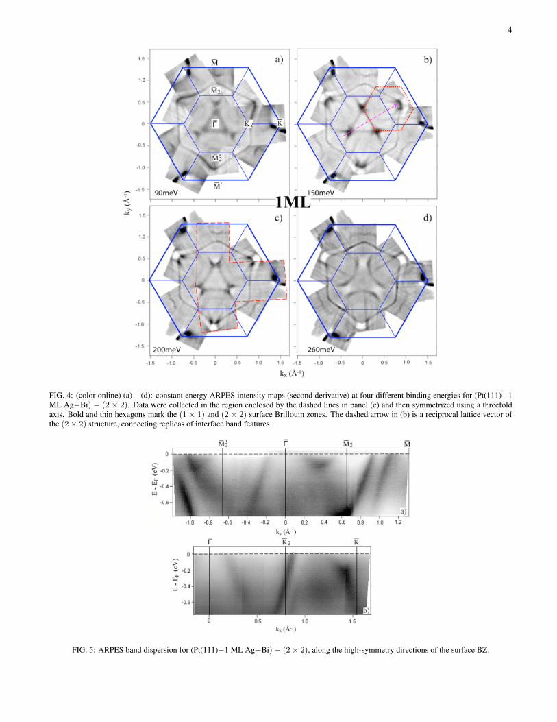
ARPES data for the ΘAg = 1 ML case are illustrated in Fig-ures 4 and 5. Figure 4 (a)-(d) are CE intensity maps, coveringa range of k-space similar to that of Fig. 1, for four bind-ing energies between 90 meV and 260 meV. Figure 5 (a) and(b) shows two corresponding energy vs. wave vector intensityplots along the M
′ΓM (kx = 0) and ΓK (ky = 0) high sym-
metry directions in the surface BZ. From a comparison withFig. 1, one can identify in both figures the Pt-derived states,namely the bands crossing EF at 0.9 A−1 and at 1.1 A−1 inthe ΓM direction. Remarkably, the CE contours of the formernow exhibit a distorted hexagonal shape, with threefold sym-metry, rather than the hexagonal shape of Fig. 1. We speculatethat with the formation of the Ag+Bi overlayer this state hasacquired a stronger bulk character. Alternatively, the changein work function – and consequently in the inner potential V0
– could be large enough to spoil the accidental condition atthe origin of the apparent sixfold symmetry.
An analysis of Fig. 4 and 5 also reveals new states whichhave no counterpart in the electronic structure of the Pt(111)substrate or the Pt(111)-Ag interface. New CE contours ap-
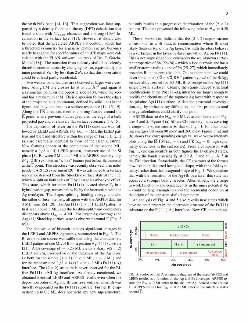
FIG. 3: (color online) A schematic diagram of the main ARPES andLEED results as a function of the Ag and Bi coverage. ARPES re-sults for ΘBi = 0 ML refer to the shallow Ag-induced state aroundΓ. ARPES results for ΘBi = 0.25 ML refer to the interface statesaround Γ.
4
FIG. 4: (color online) (a) – (d): constant energy ARPES intensity maps (second derivative) at four different binding energies for (Pt(111)−1ML Ag−Bi) − (2 × 2). Data were collected in the region enclosed by the dashed lines in panel (c) and then symmetrized using a threefoldaxis. Bold and thin hexagons mark the (1 × 1) and (2 × 2) surface Brillouin zones. The dashed arrow in (b) is a reciprocal lattice vector ofthe (2 × 2) structure, connecting replicas of interface band features.
FIG. 5: ARPES band dispersion for (Pt(111)−1 ML Ag−Bi) − (2 × 2), along the high-symmetry directions of the surface BZ.
5
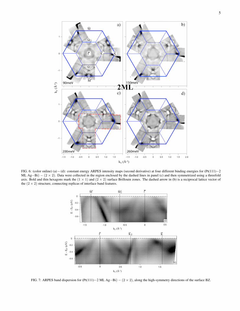
FIG. 6: (color online) (a) – (d): constant energy ARPES intensity maps (second derivative) at four different binding energies for (Pt(111)−2ML Ag−Bi) − (2 × 2). Data were collected in the region enclosed by the dashed lines in panel (c) and then symmetrized using a threefoldaxis. Bold and thin hexagons mark the (1 × 1) and (2 × 2) surface Brillouin zones. The dashed arrow in (b) is a reciprocal lattice vector ofthe (2 × 2) structure, connecting replicas of interface band features.
FIG. 7: ARPES band dispersion for (Pt(111)−2 ML Ag−Bi) − (2 × 2), along the high-symmetry directions of the surface BZ.
6
FIG. 8: Pt(111)-Ag-Bi: Constant-energy ARPES intensity (second derivative) maps at two binding energies for various Ag coverages limitedto k-values around Γ. They show the evolution from a threefold rotational symmetry at 1 ML, to a superposition of threefold and sixfold at 2and 3 ML, and back to threefold at 4 ML. The maps were not symmetrized.
pear centered around Γ. They evolve from a nearly triangularshape (Fig. 4 (a),(b)) to three disconnected arcs (Fig. 4 (c),(d))with increasing binding energy. Their origin must be found inthree identical bands upward dispersing from the three equiv-alent M
′2 points of the (2 × 2) surface BZ, and crossing EF
near Γ. One of these bands is readily visible along ΓM′2 and
ΓK respectively in Fig. 5 (a) and (b). The nearly circularCE contours (Fig. 4 (d)), which are only partially visible dueto ARPES matrix elements, indicate that these bands have anearly free-electron-like character near their origin. At largerwave vectors they feel more strongly the effect of the latticepotential, and the CE contours become hexagonal. One ofthem is outlined by the dashed line in Fig. 4 (b). The threebands cross at a binding energy of 150 meV, yielding a trian-gular contour with strong intensity at the vertices at this en-ergy. The shallow pocket along ΓM2 is a signature of theintersecting bands. At the same time, the gaps seen above thevertices of the triangular contour in Fig. 4 (a) demonstrate thatthe interaction between these bands is non negligible for otherwave vectors. These new interface states feel the (2× 2) peri-odicity of the system. This is appreciated most clearly in Fig.4 (b). Replicas of the three intense crossings around Γ, con-nected by reciprocal lattice vectors of the superstructure, areseen in the adjacent surface BZs, overlapping the Pt-derivedstates. In summary, all electronic states of the (Pt(111)−1 MLAg−Bi)−(2×2) system exhibit the threefold rotational sym-metry of the (111) surface of an fcc lattice.
ARPES data for the ΘAg = 2 ML case are illustrated bythe CE intensity maps of Fig. 6 and by the correspondingenergy vs. wave vector intensity plots of Fig. 7. The Pt-
derived bands and the interface states discussed above can stillbe identified, but a new state appears at this coverage. Its CEcontour exhibits a sixfold symmetry, most clearly visible inFig. 6 (d). It overlaps with and partially masks the triangularcontour of the 1 ML case. The dispersion of this new statecan be identified in the intensity maps of Fig. 7. In the ΓM
′2
direction (Fig. 7 (a)) it has a minimum at the M′2 point at a
binding energy of ∼0.5 eV. Along ΓK (Fig. 7 (b)) its Fermilevel crossing is essentially degenerate with that of the 1 MLstate, but its Fermi velocity is smaller.
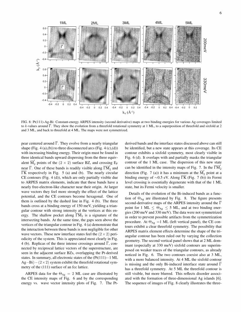
Details of the evolution of the Bi-induced bands as a func-tion of ΘAg are illustrated by Fig. 8. The figure presentssecond-derivative maps of the ARPES intensity around the Γpoint for 1 ML ≤ ΘAg ≤ 5 ML, and at two binding ener-gies (200 meV and 330 meV). The data were not symmetrizedin order to prevent possible artifacts from the symmetrizationprocedure. At ΘAg =1 ML (left vertical panel), the CE con-tours exhibit a clear threefold symmetry. The possibility thatARPES matrix element effects determine the shape of the tri-angular contour has been ruled out by varying the collectiongeometry. The second vertical panel shows that at 2 ML dom-inant (especially at 330 meV) sixfold contours are superim-posed on weaker traces of the triangular contours, as alreadynoticed in Fig. 6. The two contours coexist also at 3 ML,with a more balanced intensity. At 4 ML the sixfold contouris missing and the only Bi-induced interface state around Γhas a threefold symmetry. At 5 ML the threefold contour isstill visible, but more blurred. This reflects disorder associ-ated with the formation of three-dimensional Ag islands [6].The sequence of images of Fig. 8 clearly illustrates the three-
7
fold → threefold+sixfold → threefold evolution of the CEcontours, i.e. a re-entrant behavior of the rotational symme-try of the Bi-induced interface states as a function of the Agcoverage.
IV. DISCUSSION
The properties of the electronic states in a solid are stronglyconstrained by symmetry requirements. In the absence of amagnetic field, time-reversal (TR) symmetry requires that:
Ek,↑(↓) = E−k,↓(↑) , (1)
where the arrows stand for the spin-polarization. In the limitof a vanishing energy separation between the two spin states,Eq. (1) reduces to the simpler Ek = E−k. In a 2D close-packed system with a sixfold unit cell, irrespective of the mag-nitude of the spin-separation, a spin-integrated technique suchas ARPES yield electronic contours of hexagonal in-planesymmetry satisfying (1). Even if the 2D system only admits athreefold rotation axis, Eq. (1) still requires that the CE con-tours of the electronic structure exhibit a sixfold symmetry(1) [28, 29]. Therefore, as already pointed out, surface statescannot exhibit a threefold rotational symmetry, because thiswould be incompatible with TR symmetry.
Unlike surface states, bulk states are characterized by awell-defined perpendicular wave vector k⊥, and (1) appliesto the 3D k-vector. The combined effect of (1) and of a three-fold rotation axis yields a 3D band topology with an overallthreefold symmetry. Prime examples are the bulk electronicstructures of fcc metals [30]. ARPES is only sensitive to thein-plane component of k, and maps the full 3D dispersiononto the surface BZ. Therefore, in an ARPES measurementfrom the (111) surface of an fcc system, the threefold sym-metry of the bulk states coexists with the hexagonal surfaceBZ, e.g. for the well-studied case of Cu(111) [31, 32]. Forvalues of the surface wave vector outside the projected bulkgaps, there are no true surface states but only surface reso-nances, which hybridize significantly with the continuum ofbulk states. In an fcc system this typically yields a threefoldmodulation in their momentum distributions. This is e.g. thecase of the hole pockets at the Sb(111) surface [33]. Our ob-servation of sixfold CE contours around 2 ML suggests thatthe crystal structure has also acquired a sixfold symmetry atthis coverage. This is indeed consistent with the scenario ofthe Pt(111)-Ag interface developed from structural investiga-tions.
As already mentioned in the introduction, the first mono-layer of Ag on Pt(111) grows heteroepitaxially conserving thefcc stacking of the substrate. The 4.3% difference in the lat-tice constants of the two materials yields a coherently strainedcommensurate overlayer. Strain is relieved with the comple-tion of the second monolayer. At the annealing temperature(400 K) used in the present study, the SI phase is formed, asconfirmed by the (
√3× 14) LEED pattern. Moreover, at this
temperature there is no intermixing between Pt and Ag atoms
[3]. In the 2 ML SI phase, regions with fcc and hcp stack-ing coexist. The majority domains have been alternatively as-signed to the fcc stacking by STM [5] and to the hcp stackingby photoelectron diffraction [7]. Both experiments agree thatwith further Ag deposition the fcc stacking of the substrate isresumed, and that the growth is mainly two-dimensional at RTup to a critical thickness of 6− 9ML [6, 7].
The fcc stacking implies a threefold symmetry. By con-trast, the symmetry resulting from the hcp stacking is sixfold.The wavefunctions of the interface resonances certainly ex-tend into the bulk by at least 3 ML, which is enough to “feel”the difference between the two different stacking sequences.Hcp domains exist on the uppermost layers only after the de-position of 2 ML of Ag, and this is consistent with our ob-servation of coexisting threefold and sixfold CE contours atthis coverage. As more Ag is deposited, the fcc stacking ofthe uppermost layers is reflected in the electronic structure bythe dominance of the CE contour with a triangular shape. In-deed. the orientation of the triangular contour is consistentwith the structural reflection symmetry of an fcc slab. There-fore, the sequence threefold→ threefold+sixfold→ threefoldfinds a natural explanation in the growth mechanism of Ag onPt(111). In other words, ARPES successfully reveals the sym-metry of the growth domains and the strain-related transition.Following the above line of reasoning, our results favor hcpsites as the majority domains at ΘAg = 2 ML.
Our data suggests that Bi atoms reside on the topmost layer.They induce the formation of a long-range reconstruction bypreferential ordering at (2 × 2) sites, and do not affect thestructural symmetry of the underlying Pt(111)-Ag interface.Nonetheless, further structural meaurements are necessary tofully characterize the interface.
V. CONCLUSIONS
We have presented a detailed ARPES investigation of anordered Pt(111)-Ag-Bi trilayer system. In the studied Ag cov-erage range 1≤ ΘAg ≤ 5 ML we did not observe the expectedformation of the BiAg2 ’Rashba‘ surface alloy with periodic-ity (√
3×√
3)R30◦, characteristic of the Bi-Ag interface on apristine Ag(111) surface. We observed instead a novel p(2×2)phase, where the Bi atoms most likely float on top of the Aginterlayer yielding strong interface states which change withthe Ag coverage. The rotational symmetry of their constantenergy contours evolves from threefold, to a superposition ofthreefold and sixfold, and finally back to threefold. This evo-lution is consistent with the accepted model for the growthof Ag on the Pt(111) substrate, namely with a strain-inducedtransition at 2 ML Ag coverage. These results illustrate theconsequences of the structural changes on the character of theelectronic structure. They also show that an analysis of thesymmetry properties of the electronic states of a system mayprovide valuable insight into its structural properties.
We thank J. Audet for experimental contributions duringthe early stage of this work. E.F. acknowledges the financial
8
support of the Alexander S. Onassis Public Benefit Founda-tion. This research was supported by the Swiss NSF and theNCCR MaNEP.
∗ Current address: Synchrotron SOLEIL, L’Orme des Merisiers,Saint Aubin-BP 48, 91192 Gif sur Yvette Cedex, France; Elec-tronic address: [email protected]
[1] Y. Tanishiro, H. Kanamori, K. Takayanagi, K. Yagi, andG. Honjo, Surf. Sci. 111, 395 (1981).
[2] J. V. Barth, H. Brune, G. Ertl, and R. J. Behm, Phys. Rev. B 42,9307 (1990).
[3] H. Roder, R. Schuster, H. Brune, and K. Kern, Phys. Rev. Lett.71, 2086 (1993).
[4] H. Roder, H. Brune, J.-P. Bucher, and K. Kern, Surf. Sci. 298,121 (1993).
[5] H. Brune, H. Roder, C. Boragno, and K. Kern, Phys. Rev. B 49,2997 (1994).
[6] H. Roder, K. Bromann, H. Brune, and K. Kern, Surf. Sci. 376,13 (1997).
[7] G. Rangelov, T. Fauster, U. Struber, and J. Kuppers, Surf. Sci.331-333, 948 (1995).
[8] K. Bromann, H. Brune, M. Giovannini, and K. Kern, Surf. Sci.388, L107 (1997).
[9] C. R. Ast, J. Henk, A. Ernst, L. Moreschini, M. C. Falub,D. Pacile, P. Bruno, K. Kern, and M. Grioni, Phys. Rev. Lett.98, 186807 (2007).
[10] F. Meier, H. Dil, J. Lobo-Checa, L. Patthey, and J. Osterwalder,Phys. Rev. B 77, 165431 (2008).
[11] G. Bihlmayer, S. Blugel, and E. V. Chulkov, Phys. Rev. B 75,195414 (2007).
[12] E. Frantzeskakis, S. Pons, H. Mirhosseini, J. Henk, C. R. Ast,and M. Grioni, Phys. Rev. Lett. 101, 196805 (2008).
[13] E. Frantzeskakis, A. Crepaldi, S. Pons, K. Kern, and M. Grioni,J. Electron Spectr. Rel. Phenom. 181, 88 (2010).
[14] W. Di, K. E. Smith, and S. D. Kevan, Phys. Rev. B 45, 3652(1992).
[15] A. Ramstad, S. Raaen, and N. Barrett, Surf. Sci. 448, 179
(2000).[16] W. Di, K. E. Smith, and S. D. Kevan, Phys. Rev. B 43, 12062
(1991).[17] J. Wiebe, F. Meier, K. Hashimoto, G. Byhlmayer, S. Blugel,
P. Ferriani, S. Heinze, and R. Wiesendanger, Phys. Rev. B 72,193406 (2005).
[18] V. Joco, N. Mikuszeit, J. Martinez-Blanco, and E. G. Michel,(to be published).
[19] A. H. MacDonald, J. M. Daams, S. H. Vosko, and D. D.Koelling, Phys. Rev. B 23, 6377 (1981).
[20] A. Bendounan, K. Aıt-Mansour, J. Braun, J. Minar, S. Borne-mann, R. Fasel, O. Groning, F. Sirotti, and H. Ebert, Phys. Rev.B 83, 195427 (2011).
[21] M. F. Toney, J. G. Gordon, M. G. Samant, G. L. Borges, D. G.Wiesler, D. Yee, and L. B. Sorensen, Langmuir 7, 796 (1991).
[22] S. Oppo, V. Fiorentini, and M. Scheffler, Phys. Rev. Lett 71,2437 (1993).
[23] H. A. van der Vegt, J. Vrijmoeth, R. J. Behm, and E. Vlieg,Phys. Rev. B 57, 4127 (1998).
[24] V. Scheuch, K. Potthast, B. Voigtlander, and H. P. Bonzel, Surf.Sci. 318, 115 (1994).
[25] J. Camarero, L. Spendeler, G. Schmidt, K. Heinz, J. J.de Miguel, and R. Miranda, Phys. Rev. Lett 73, 2448 (1994).
[26] J. Camarero, J. Ferron, V. Cros, L. Gomez, A. L. V. de Parga,J. M. Gallego, J. E. Prieto, J. J. de Miguel, and R. Miranda,Phys. Rev. Lett 81, 850 (1998).
[27] M. C. G. Passeggi, J. E. Prieto, R. Miranda, and J. M. Gallego,Surf. Sci. 462, 45 (2000).
[28] J. Premper, M. Trautmann, J. Henk, and P. Bruno, Phys. Rev.B. 76, 073310 (2007).
[29] E. Frantzeskakis, S. Pons, and M. Grioni, Phys. Rev. B 82,085440 (2010).
[30] N. W. Ashcroft and N. D. Mermin, Solid State Physics (1976).[31] P. Aebi, J. Osterwalder, R. Fasel, D. Naumovic, and L. Schlap-
bach, Surf. Sci. 307-309, 917 (1994).[32] F. Baumberger, A. Tamai, M. Muntwiler, T. Greber, and J. Os-
terwalder, Surf. Sci. 532-535, 82 (2003).[33] K. Sugawara, T. Sato, S. Souma, T. Takahashi, M. Arai, and
T. Sasaki, Phys. Rev. Lett. 96, 046411 (2006).
Copyright © 2022 FDOKUMEN

