


Bahasa
Halaman
Hukum

Hindawi Publishing CorporationAdvances in Condensed Matter PhysicsVolume 2013, Article ID 968647, 10 pageshttp://dx.doi.org/10.1155/2013/968647
Research ArticleA Circuit Model for CMOS Hall Cells Performance Evaluationincluding Temperature Effects
Maria-Alexandra Paun,1,2 Jean-Michel Sallese,1 and Maher Kayal1
1 STI-IEL-Electronics Laboratory, Ecole Polytechnique Federale de Lausanne (EPFL), 1015 Lausanne, Switzerland2Department of Engineering, University of Cambridge, Cambridge CB2 1PZ, UK
Correspondence should be addressed to Maria-Alexandra Paun; [email protected]
Received 28 May 2013; Revised 6 August 2013; Accepted 8 August 2013
Academic Editor: Jan Alexander Jung
Copyright © 2013 Maria-Alexandra Paun et al. This is an open access article distributed under the Creative Commons AttributionLicense, which permits unrestricted use, distribution, and reproduction in any medium, provided the original work is properlycited.
In order to provide the information on theirHall voltage, sensitivity, and driftwith temperature, a new simpler lumped circuitmodelfor the evaluation of various Hall cells has been developed. In this sense, the finite element model proposed by the authors in thispaper contains both geometrical parameters (dimensions of the cells) and physical parameters such as the mobility, conductivity,Hall factor, carrier concentration, and the temperature influence on them. Therefore, a scalable finite element model in Cadence,for behavior simulation in circuit environment of CMOS Hall effect devices, with different shapes and technologies assessing theirperformance, has been elaborated.
1. Introduction
Hall effect sensors are largely used in the actual industrialcontext as magnetic sensors aimed primarily at sensingthe current in a large variety of applications, and also forproximity switching, positioning, or speed detection [1]. Thesensitivity, offset, and their temperature drift are importantparameters that dictate the performance of Hall effect sen-sors.
There is a strong connection between the geometry of theHall device and the performance [2]. For Hall effect sensorsperformance analysis, three-dimensional physical modelswere constructed and simulation results were reported by theauthors [3].
To achieve high sensitivity, small offset, and drift, var-ious Hall effect sensors configurations were integrated ina CMOS technology. Extensive measurements on the newproposed cells [4] proved that with specific shapes (XL) wemanaged to reach room temperature offset less than 30 𝜇Tand 0.039 𝜇T/∘C drift, which is 3-4 times lower than the stateof the art.
The motivation of the current work is to provide a circuitmodel able to predict the temperature effects on the Hall
effect sensors and their influence on the performance. Underthe assumed research objective, a different elementary cell,with a slightly modified design, including the temperatureeffects, is proposed and implemented in Cadence.
Section 2 focuses on presenting the Hall effect sensorsintegration, providing the basic equations related to thesemagnetic sensors. Within this section, a Hall sensors analysisby depicting the measurements results is also performed andthe shape providing the best results is identified. The XL celldesigned and integrated by the authors proved to have thelowest offset and offset temperature drift.
Section 3 aims to introduce the new simpler elementarycell to be used in the lumped circuit model. In this case,there are two independent magnetic and electric paths.The number of elementary cells in the FEM model can bevaried according to the accuracy level which needs to beachieved. However, for rough estimation of the Hall voltageand sensitivity, a single elementary cell can also be used.Details on the Hall cells polarization are also given at thispoint.
In Section 4, the FEM simulations results are presentedand interpreted for three differentHall cells, with informationon the Hall voltage and absolute sensitivity. In this section,
2 Advances in Condensed Matter Physics
Table 1: Specific parameters evaluation for some of the integratedHall cells.
Integrated geometry XL Optimum Borderless
Shape
Measured 𝑅 (kΩ)@𝑇 = 300K, 𝐵 = 0T 2.2 1.8 1.3
Measured 𝑆𝐼
(V/AT)@𝐼bias = 1mA 80.6 62.4 31.1
Measured offset drift(𝜇T/∘C) 0.039 0.328 0.526
L,W (𝜇m) of the n-well 𝐿 = 43.2 𝐿 = 50 𝐿 = 50
𝑊 = 19 𝑊 = 50 𝑊 = 50
Contacts length (𝜇m) 18.3 4.7 2.3
the emphasis is put on a particular Hall sensor in the shapeof the XL cell with prediction of its current-related sensitivitytemperature drift. Finally, Section 5 draws the conclusions.
2. Hall Effect Sensors Integration
2.1. Equations Related to Hall Effect Sensors. TheHall voltageis defined as follows [5] for voltage polarization:
𝑉𝐻= 𝐺𝜇𝐻
𝑊
𝐿𝑉bias𝐵 (1)
or equivalently for current polarization as
𝑉𝐻= 𝐺
𝑟𝐻
𝑛𝑞𝑡𝐼bias𝐵, (2)
where 𝐺 is the geometrical correction factor, 𝜇𝐻is the Hall
mobility,𝑊 and𝐿 stand for thewidth and length of the devicerespectively, 𝑉bias is the voltage bias, 𝑟𝐻 is the Hall scatteringfactor, 𝑛 is the carrier concentration, 𝑡 is the thickness of the𝑛-well implantation, and𝐵 is themagnetic field on a directionperpendicular to the semiconductor probe.
The current-related sensitivity 𝑆𝐼of a Hall effect sensor
has the following analytical expression:
𝑆𝐼=
𝑉𝐻
𝐵𝐼bias= 𝐺
𝑟𝐻
𝑛𝑞𝑡. (3)
2.2. Hall Effect Sensors Analysis and Measurements Results.DifferentHall effect sensors have been integrated in a 0.35 𝜇mCMOS technology and tested for their sensitivity, offset,and offset temperature drift. To this purpose, an automatedmeasurement setup presented by the authors in [4] to test theintegrated Hall effect sensors was used.
The following experimental results presented in Table 1,for three of these integrated Hall cells, were obtained. Thedesign parameters (the length, width, and the contactsdimension) are indicated for every structure. For each device,the input resistance, as well as the current-related sensitivityand offset temperature drift measurements, is included in the
0
0.5
1
1.5
2
2.5
3
3.5
4
XLPoly. (XL)
XL
Linear (XL)
y = 0.0422x2 − 0.0608x + 1.8401
R2 = 0.9973
y = 0.2767X + 1.3339
R2 = 0.9323
−40
−25.10
0.20
25.2
0 50
85.0
9
125.
09
R(kΩ
)
T (∘C)
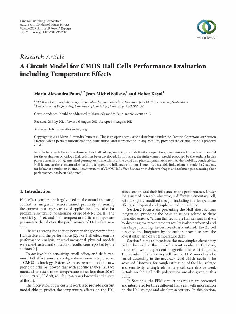
Figure 1: The measured input resistance versus temperature for XLcell.
table. We can observe that the XL cell presented the lowestoffset drift.
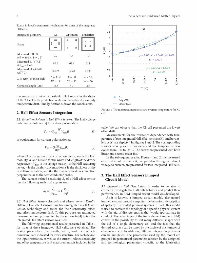
Measurements for the resistance dependence with tem-perature of two integratedHall effect sensors (XL and border-less cells) are depicted in Figures 1 and 2. The correspondingsensors were placed in an oven and the temperature wascycled from −40 to 125∘C.The curves are presented with bothlinear and second order fits.
In the subsequent graphs, Figures 1 and 2, the measuredelectrical input resistance 𝑅, computed as the regular ratio ofvoltage to current, are presented for two integrated Hall cells.
3. The Hall Effect Sensors LumpedCircuit Model
3.1. Elementary Cell Description. In order to be able tocorrectly investigate the Hall cells behavior and predict theirperformance, an FEM lumped circuit model was developed.
As it is known, a lumped circuit model, also namedlumped element model, simplifies the behaviour descriptionof spatially distributed physical systems. In fact, this modelis used to recreate the topology of a specific physical systemwith the aid of discrete entities that would approximate itsconduct. The advantages of the finite element model (FEM)consist in the possibility to test many different shapes withthe aid of a single elementary cell and the fact that thedesired accuracy can be tuned by the choice of the number ofelementary cells. In addition, different integration processescan be simulated. The parameters used by the model aregrouped in geometrical parameters (chosen by the designer)and technological parameters (specific to the fabrication
Advances in Condensed Matter Physics 3
y = 0.024x2− 0.0356x + 1.0964
R2 = 0.9971
R2 = 0.93140
0.5
1
1.5
2
2.5Borderless
BorderlessPoly. (borderless)Linear (borderless)
−39.90
−24.89
0.10 25
50.0
9
85.3
0
125.
09
R(kΩ
)
T (∘C)
y = 0.1566X + 0.8081
Figure 2: The measured input resistance versus temperature forborderless cell.
process). The latter can be either obtained by parametersextraction or by theoretical prediction where possible.
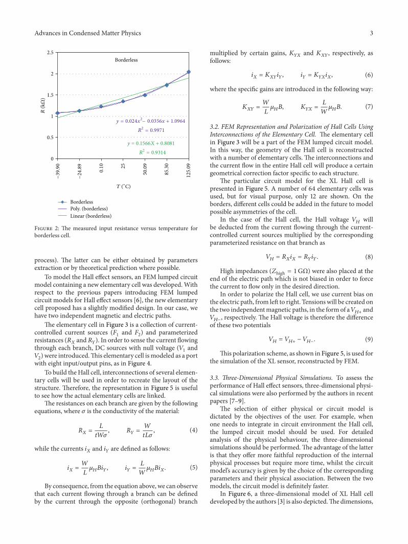
To model the Hall effect sensors, an FEM lumped circuitmodel containing a new elementary cell was developed.Withrespect to the previous papers introducing FEM lumpedcircuit models for Hall effect sensors [6], the new elementarycell proposed has a slightly modified design. In our case, wehave two independent magnetic and electric paths.
The elementary cell in Figure 3 is a collection of current-controlled current sources (𝐹
1and 𝐹
2) and parameterized
resistances (𝑅𝑋and𝑅
𝑌). In order to sense the current flowing
through each branch, DC sources with null voltage (𝑉1and
𝑉2) were introduced.This elementary cell ismodeled as a port
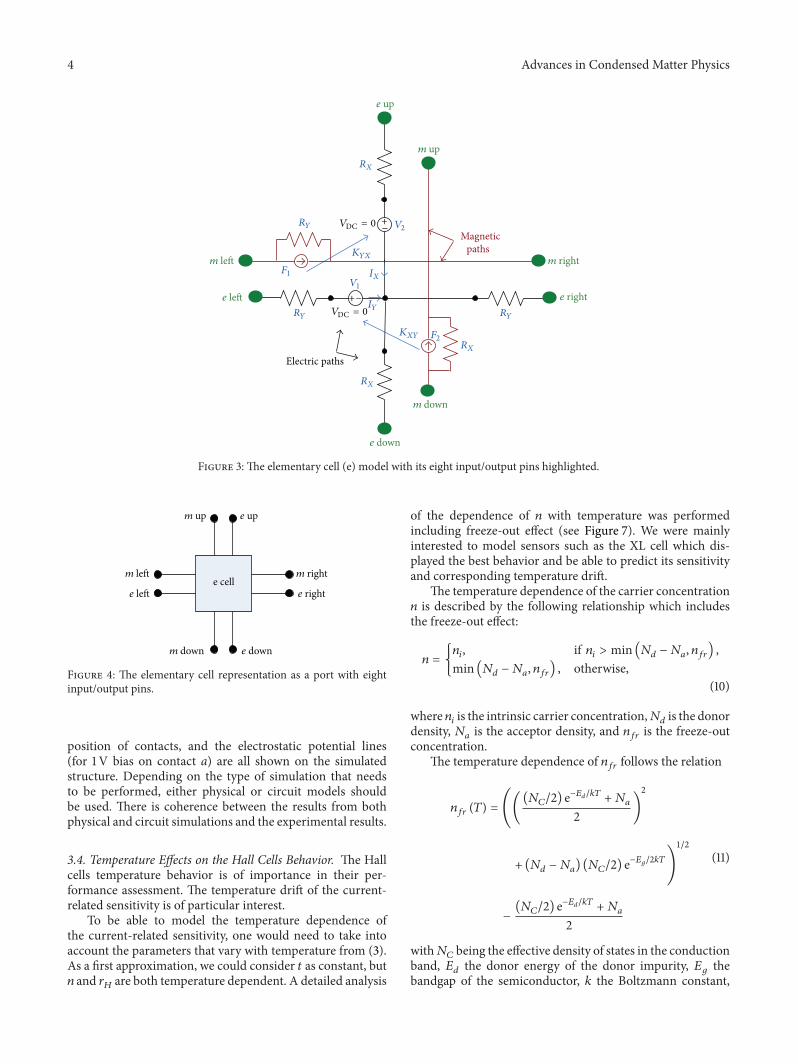
with eight input/output pins, as in Figure 4.To build theHall cell, interconnections of several elemen-
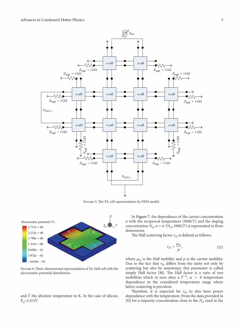
tary cells will be used in order to recreate the layout of thestructure. Therefore, the representation in Figure 5 is usefulto see how the actual elementary cells are linked.
The resistances on each branch are given by the followingequations, where 𝜎 is the conductivity of the material:
𝑅𝑋=
𝐿
𝑡𝑊𝜎, 𝑅
𝑌=𝑊
𝑡𝐿𝜎, (4)
while the currents 𝑖𝑋and 𝑖𝑌are defined as follows:
𝑖𝑋=𝑊
𝐿𝜇𝐻𝐵𝑖𝑌, 𝑖
𝑌=𝐿
𝑊𝜇𝐻𝐵𝑖𝑋. (5)
By consequence, from the equation above, we can observethat each current flowing through a branch can be definedby the current through the opposite (orthogonal) branch
multiplied by certain gains, 𝐾𝑌𝑋
and 𝐾𝑋𝑌
, respectively, asfollows:
𝑖𝑋= 𝐾𝑋𝑌𝑖𝑌, 𝑖
𝑌= 𝐾𝑌𝑋𝑖𝑋, (6)
where the specific gains are introduced in the following way:
𝐾𝑋𝑌
=𝑊
𝐿𝜇𝐻𝐵, 𝐾
𝑌𝑋=𝐿
𝑊𝜇𝐻𝐵. (7)
3.2. FEM Representation and Polarization of Hall Cells UsingInterconnections of the Elementary Cell. The elementary cellin Figure 3 will be a part of the FEM lumped circuit model.In this way, the geometry of the Hall cell is reconstructedwith a number of elementary cells. The interconnections andthe current flow in the entire Hall cell will produce a certaingeometrical correction factor specific to each structure.
The particular circuit model for the XL Hall cell ispresented in Figure 5. A number of 64 elementary cells wasused, but for visual purpose, only 12 are shown. On theborders, different cells could be added in the future to modelpossible asymmetries of the cell.
In the case of the Hall cell, the Hall voltage 𝑉𝐻
willbe deducted from the current flowing through the current-controlled current sources multiplied by the correspondingparameterized resistance on that branch as
𝑉𝐻= 𝑅𝑋𝑖𝑋= 𝑅𝑌𝑖𝑌. (8)
High impedances (𝑍high = 1GΩ) were also placed at theend of the electric path which is not biased in order to forcethe current to flow only in the desired direction.
In order to polarize the Hall cell, we use current bias onthe electric path, from left to right. Tensionswill be created onthe two independentmagnetic paths, in the formof a𝑉
𝐻+and
𝑉𝐻−
, respectively. The Hall voltage is therefore the differenceof these two potentials
𝑉𝐻= 𝑉𝐻+
− 𝑉𝐻−. (9)
This polarization scheme, as shown in Figure 5, is used forthe simulation of the XL sensor, reconstructed by FEM.
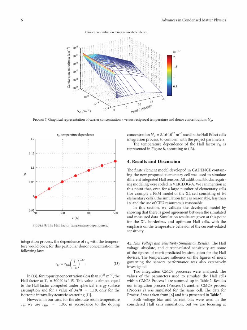
3.3. Three-Dimensional Physical Simulations. To assess theperformance of Hall effect sensors, three-dimensional physi-cal simulations were also performed by the authors in recentpapers [7–9].
The selection of either physical or circuit model isdictated by the objectives of the user. For example, whenone needs to integrate in circuit environment the Hall cell,the lumped circuit model should be used. For detailedanalysis of the physical behaviour, the three-dimensionalsimulations should be performed.The advantage of the latteris that they offer more faithful reproduction of the internalphysical processes but require more time, whilst the circuitmodel’s accuracy is given by the choice of the correspondingparameters and their physical association. Between the twomodels, the circuit model is definitely faster.
In Figure 6, a three-dimensional model of XL Hall celldeveloped by the authors [3] is also depicted.Thedimensions,
4 Advances in Condensed Matter Physics
Magnetic paths
Electric paths
m up
e up
m left
e left
m right
e right
m down
e down
RX
RX
RX
RYRY
RY
IX
IY
KXY
KYX
+
+
−
−
VDC = 0
VDC = 0
F1
F2
V1
V2
Figure 3: The elementary cell (e) model with its eight input/output pins highlighted.
e cell
e upm up
m right
e right
e downm down
m left
e left
Figure 4: The elementary cell representation as a port with eightinput/output pins.
position of contacts, and the electrostatic potential lines(for 1 V bias on contact a) are all shown on the simulatedstructure. Depending on the type of simulation that needsto be performed, either physical or circuit models shouldbe used. There is coherence between the results from bothphysical and circuit simulations and the experimental results.
3.4. Temperature Effects on the Hall Cells Behavior. The Hallcells temperature behavior is of importance in their per-formance assessment. The temperature drift of the current-related sensitivity is of particular interest.
To be able to model the temperature dependence ofthe current-related sensitivity, one would need to take intoaccount the parameters that vary with temperature from (3).As a first approximation, we could consider 𝑡 as constant, but𝑛 and 𝑟
𝐻are both temperature dependent. A detailed analysis
of the dependence of 𝑛 with temperature was performedincluding freeze-out effect (see Figure 7). We were mainlyinterested to model sensors such as the XL cell which dis-played the best behavior and be able to predict its sensitivityand corresponding temperature drift.
The temperature dependence of the carrier concentration𝑛 is described by the following relationship which includesthe freeze-out effect:
𝑛 = {𝑛𝑖, if 𝑛
𝑖> min (𝑁
𝑑− 𝑁𝑎, 𝑛𝑓𝑟) ,
min (𝑁𝑑− 𝑁𝑎, 𝑛𝑓𝑟) , otherwise,
(10)
where 𝑛𝑖is the intrinsic carrier concentration,𝑁
𝑑is the donor
density, 𝑁𝑎is the acceptor density, and 𝑛
𝑓𝑟is the freeze-out
concentration.The temperature dependence of 𝑛
𝑓𝑟follows the relation
𝑛𝑓𝑟(𝑇) = ((
(𝑁𝐶/2) e−𝐸𝑑/𝑘𝑇 + 𝑁
𝑎
2)
2
+ (𝑁𝑑− 𝑁𝑎) (𝑁𝐶/2) e−𝐸𝑔/2𝑘𝑇)
1/2
−(𝑁𝐶/2) e−𝐸𝑑/𝑘𝑇 + 𝑁
𝑎
2
(11)
with𝑁𝐶being the effective density of states in the conduction
band, 𝐸𝑑the donor energy of the donor impurity, 𝐸
𝑔the
bandgap of the semiconductor, 𝑘 the Boltzmann constant,
Advances in Condensed Matter Physics 5
e cell e cell
e cell e cell
e cell e cell
e cell e cell
e cell e cell
e cell e cell
Ibias
Zhigh = 1GΩZhigh = 1GΩZhigh = 1GΩ Zhigh = 1GΩ
Zhigh = 1GΩ
Zhigh = 1GΩZhigh = 1GΩ
Zhigh = 1GΩ
Zhigh = 1GΩZhigh = 1GΩ
Zhi
gh=1
GΩ
Zhi
gh=1
GΩ
VHALL−
VHALL+
Figure 5: The XL cell representation by FEMmodel.
Electrostatic potential (V)
a
d
b
c
2.715e + 00
2.252e + 00
1.788e + 00
1.325e + 00
8.609e − 01
3.972e − 01
−6.644e − 02
X Y
Z
Figure 6:Three-dimensional representation of XLHall cell with theelectrostatic potential distribution.
and 𝑇 the absolute temperature in K. In the case of silicon,𝐸𝑔=1.12 eV.
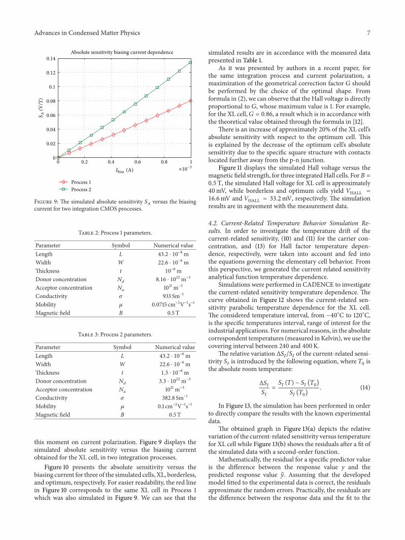
In Figure 7, the dependence of the carrier concentration𝑛 with the reciprocal temperature (1000/T) and the dopingconcentration𝑁
𝑑, 𝑛 = 𝑛 (𝑁
𝑑, 1000/𝑇) is represented in three
dimensions.The Hall scattering factor 𝑟
𝐻is defined as follows:
𝑟𝐻=𝜇𝐻
𝜇, (12)
where 𝜇𝐻is the Hall mobility and 𝜇 is the carrier mobility.
Due to the fact that 𝑟𝐻
differs from the unity not only byscattering but also by anisotropy, this parameter is calledsimply Hall factor [10]. The Hall factor is a ratio of twomobilities which in turn obey a 𝑇−𝛼, 𝛼 > 0 temperaturedependence in the considered temperature range wherelattice scattering is prevalent.
Therefore, it is expected for 𝑟𝐻
to also have powerdependence with the temperature. From the data provided in[11] for a impurity concentration close to the 𝑁
𝑑used in the
6 Advances in Condensed Matter Physics
Carrier concentration temperature dependence
1018
1017
1016
1015
1014
1013
1017
1016
10 0
2
1.5
1
0.5
510
1520
14
1015
×1017
1000/T (1000/K)
Nd (cm−3)
Carr
ier c
once
ntra
tionn
(cm
−3)
Figure 7: Graphical representation of carrier concentration 𝑛 versus reciprocal temperature and donor concentrations𝑁𝑑
.
200 300 400 5000.95
1
1.05
1.1
1.15
1.2
T (K)
r H
rH temperature dependence
Figure 8: The Hall factor temperature dependence.
integration process, the dependence of 𝑟𝐻with the tempera-
ture would obey, for this particular donor concentration, thefollowing law:
𝑟𝐻= 𝑟𝐻0(𝑇
𝑇0
)
0.13
. (13)
In (13), for impurity concentrations less than 1021m−3, theHall factor at 𝑇
0= 300K is 1.15. This value is almost equal
to the Hall factor computed under spherical energy surfaceassumption and for a value of 3𝜋/8 = 1.18, only for theisotropic intravalley acoustic scattering [11].
However, in our case, for the absolute room temperature𝑇0, we use 𝑟
𝐻0= 1.05, in accordance to the doping
concentration𝑁𝑑= 8.16⋅10
22m−3 used in theHall Effect cellsintegration process, to conform with the project parameters.
The temperature dependence of the Hall factor 𝑟𝐻
isrepresented in Figure 8, according to (13).
4. Results and Discussion
The finite element model developed in CADENCE contain-ing the new proposed elementary cell was used to simulatedifferent integratedHall sensors. All additional blocks requir-ingmodeling were coded in VERILOG-A.We canmention atthis point that, even for a large number of elementary cells(for example a FEM model of the XL cell consisting of 64elementary cells), the simulation time is reasonable, less than1 s, and the use of CPU resources is reasonable.
In this section, we validate the developed model byshowing that there is good agreement between the simulatedand measured data. Simulation results are given at this pointfor the XL, borderless, and optimum Hall cells, with theemphasis on the temperature behavior of the current-relatedsensitivity.
4.1. Hall Voltage and Sensitivity Simulation Results. The Hallvoltage, absolute, and current-related sensitivity are someof the figures of merit predicted by simulation for the Halldevices. The temperature influence on the figures of meritgoverning the sensors performance was also extensivelyinvestigated.
Two integration CMOS processes were analyzed. Thevalues of the parameters used to simulate the Hall cellswithin CMOS Process 1 are summed up in Table 2. Besidesour integration process (Process 1), another CMOS process(Process 2) was simulated for the same cell. The data forProcess 2 was taken from [6] and it is presented in Table 3.
Both voltage bias and current bias were used in theconsidered Hall cells simulation, but we are focusing at
Advances in Condensed Matter Physics 7
0 0.2 0.4 0.6 0.8 10
0.02
0.04
0.06
0.08
0.1
0.12
0.14
Process 1Process 2
Absolute sensitivity biasing current dependence
×10−3Ibias (A)
S A(V
/T)
Figure 9: The simulated absolute sensitivity 𝑆𝐴
versus the biasingcurrent for two integration CMOS processes.
Table 2: Process 1 parameters.
Parameter Symbol Numerical valueLength L 43.2 ⋅ 10
−6mWidth W 22.6 ⋅ 10
−6mThickness t 10
−6mDonor concentration 𝑁
𝑑
8.16 ⋅ 1022m−3
Acceptor concentration 𝑁𝑎
1021 m−3
Conductivity 𝜎 933 Sm−1
Mobility 𝜇 0.0715 cm−2V−1s−1
Magnetic field B 0.5 T
Table 3: Process 2 parameters.
Parameter Symbol Numerical valueLength L 43.2 ⋅ 10
−6mWidth W 22.6 ⋅ 10
−6mThickness t 1.5 ⋅ 10
−6mDonor concentration 𝑁
𝑑
3.3 ⋅ 1022m−3
Acceptor concentration 𝑁𝑎
1021 m−3
Conductivity 𝜎 382.8 Sm−1
Mobility 𝜇 0.1 cm−2V−1s−1
Magnetic field B 0.5 T
this moment on current polarization. Figure 9 displays thesimulated absolute sensitivity versus the biasing currentobtained for the XL cell, in two integration processes.
Figure 10 presents the absolute sensitivity versus thebiasing current for three of the simulated cells, XL, borderless,and optimum, respectively. For easier readability, the red linein Figure 10 corresponds to the same XL cell in Process 1which was also simulated in Figure 9. We can see that the
simulated results are in accordance with the measured datapresented in Table 1.
As it was presented by authors in a recent paper, forthe same integration process and current polarization, amaximization of the geometrical correction factor 𝐺 shouldbe performed by the choice of the optimal shape. Fromformula in (2), we can observe that the Hall voltage is directlyproportional to 𝐺, whose maximum value is 1. For example,for the XL cell, 𝐺 = 0.86, a result which is in accordance withthe theoretical value obtained through the formula in [12].
There is an increase of approximately 20% of the XL cell’sabsolute sensitivity with respect to the optimum cell. Thisis explained by the decrease of the optimum cell’s absolutesensitivity due to the specific square structure with contactslocated further away from the p-n junction.
Figure 11 displays the simulated Hall voltage versus themagnetic field strength, for three integratedHall cells. For𝐵 =0.5T, the simulated Hall voltage for XL cell is approximately40mV, while borderless and optimum cells yield 𝑉HALL =
16.6mV and 𝑉HALL = 33.2mV, respectively. The simulationresults are in agreement with the measurement data.
4.2. Current-Related Temperature Behavior Simulation Re-sults. In order to investigate the temperature drift of thecurrent-related sensitivity, (10) and (11) for the carrier con-centration, and (13) for Hall factor temperature depen-dence, respectively, were taken into account and fed intothe equations governing the elementary cell behavior. Fromthis perspective, we generated the current related sensitivityanalytical function temperature dependence.
Simulations were performed in CADENCE to investigatethe current-related sensitivity temperature dependence. Thecurve obtained in Figure 12 shows the current-related sen-sitivity parabolic temperature dependence for the XL cell.The considered temperature interval, from −40∘C to 120∘C,is the specific temperatures interval, range of interest for theindustrial applications. For numerical reasons, in the absolutecorrespondent temperatures (measured inKelvin), we use thecovering interval between 240 and 400K.
The relative variation Δ𝑆𝐼/𝑆𝐼of the current-related sensi-
tivity 𝑆𝐼is introduced by the following equation, where 𝑇
0is
the absolute room temperature:
Δ𝑆𝐼
𝑆𝐼
=𝑆𝐼(𝑇) − 𝑆
𝐼(𝑇0)
𝑆𝐼(𝑇0)
. (14)
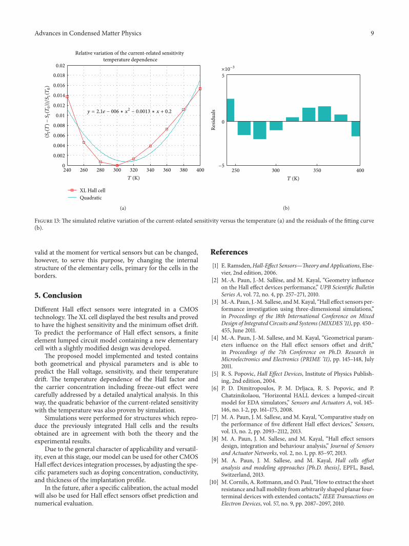
In Figure 13, the simulation has been performed in orderto directly compare the results with the known experimentaldata.
The obtained graph in Figure 13(a) depicts the relativevariation of the current-related sensitivity versus temperaturefor XL cell while Figure 13(b) shows the residuals after a fit ofthe simulated data with a second-order function.
Mathematically, the residual for a specific predictor valueis the difference between the response value y and thepredicted response value 𝑦. Assuming that the developedmodel fitted to the experimental data is correct, the residualsapproximate the random errors. Practically, the residuals arethe difference between the response data and the fit to the
8 Advances in Condensed Matter Physics
0 0.2 0.4 0.6 0.8 10
0.02
0.04
0.06
0.08
0.1
XL (simulated)Borderless (simulated)Optimum (simulated)
XL (measured)Optimum (measured)Borderless (measured)
×10−3Ibias (A)
S A(V
/T)
Figure 10: The simulated absolute sensitivity 𝑆𝐴
versus the biasing current for three integrated Hall cells.
0 1 2
Hall voltage magnetic field dependence
XLBorderlessOptimum
0.2
0.15
0.1
0.05
0
−0.05
−0.1
−0.15
−0.2−2 −1
B (T)
VH
ALL
(V)
Figure 11: The simulated Hall voltage 𝑉HALL versus the magneticfield strength for three integrated Hall cells.
response data. In this case, the residuals are adimensional, asthe initial fitted curve is a relative variation.
There is an excellent accordance of the simulationsresults obtained with the theoretical prediction and also withexperimental results. The same parabolic allure, but for thetemperature characteristic measurements of the “intrinsic”sensitivity (in fact the measured relative variation of the
240 260 280 300 320 340 360 380 40077.5
78
78.5
79Current-related sensitivity temperature dependence
T (K)
S I(V
/AT)
Figure 12: The simulated current-related sensitivity 𝑆𝐼
versus thetemperature.
current-related sensitivity of the Hall plate), is announced byManic [13] (except that the room temperature is 𝑇
0= 308K,
compared with the generally accepted 𝑇0= 300K).
We can mention that our simulations and both themeasured and simulated relative variations of the “current-related sensitivity related to the value at room temperature”as a function of temperature, 𝑆
𝐼(𝑇)/𝑆𝐼(𝑇0), reported in [14],
are also in good agreement.The FEM model developed can be applied to a variety of
Hall effect sensors shapes and different integration processes,by changing the specific parameters. However, the presentmodel is destined to analyze horizontal Hall cells and it is not
Advances in Condensed Matter Physics 9
240 260 280 300 320 340 360 380 4000
0.002
0.004
0.006
0.008
0.01
0.012
0.014
0.016
0.018
0.02
XL Hall cellQuadratic
Relative variation of the current-related sensitivitytemperature dependence
(SI(T
)−S I(T
0))/S
1(T
0)
T (K)
y = 2.1e − 006 ∗ x2 − 0.0013 ∗ x + 0.2
(a)
250 300 350 400
0
5
Resid
uals
−5
×10−3
T (K)
(b)
Figure 13: The simulated relative variation of the current-related sensitivity versus the temperature (a) and the residuals of the fitting curve(b).
valid at the moment for vertical sensors but can be changed,however, to serve this purpose, by changing the internalstructure of the elementary cells, primary for the cells in theborders.
5. Conclusion
Different Hall effect sensors were integrated in a CMOStechnology. The XL cell displayed the best results and provedto have the highest sensitivity and the minimum offset drift.To predict the performance of Hall effect sensors, a finiteelement lumped circuit model containing a new elementarycell with a slightly modified design was developed.
The proposed model implemented and tested containsboth geometrical and physical parameters and is able topredict the Hall voltage, sensitivity, and their temperaturedrift. The temperature dependence of the Hall factor andthe carrier concentration including freeze-out effect werecarefully addressed by a detailed analytical analysis. In thisway, the quadratic behavior of the current-related sensitivitywith the temperature was also proven by simulation.
Simulations were performed for structures which repro-duce the previously integrated Hall cells and the resultsobtained are in agreement with both the theory and theexperimental results.
Due to the general character of applicability and versatil-ity, even at this stage, our model can be used for other CMOSHall effect devices integration processes, by adjusting the spe-cific parameters such as doping concentration, conductivity,and thickness of the implantation profile.
In the future, after a specific calibration, the actual modelwill also be used for Hall effect sensors offset prediction andnumerical evaluation.
References
[1] E. Ramsden,Hall-Effect Sensors—Theory andApplications, Else-vier, 2nd edition, 2006.
[2] M.-A. Paun, J.-M. Sallese, and M. Kayal, “Geometry influenceon the Hall effect devices performance,” UPB Scientific BulletinSeries A, vol. 72, no. 4, pp. 257–271, 2010.
[3] M.-A. Paun, J.-M. Sallese, andM.Kayal, “Hall effect sensors per-formance investigation using three-dimensional simulations,”in Proceedings of the 18th International Conference on MixedDesign of Integrated Circuits and Systems (MIXDES ’11), pp. 450–455, June 2011.
[4] M.-A. Paun, J.-M. Sallese, and M. Kayal, “Geometrical param-eters influence on the Hall effect sensors offset and drift,”in Proceedings of the 7th Conference on Ph.D. Research inMicroelectronics and Electronics (PRIME ’11), pp. 145–148, July2011.
[5] R. S. Popovic, Hall Effect Devices, Institute of Physics Publish-ing, 2nd edition, 2004.
[6] P. D. Dimitropoulos, P. M. Drljaca, R. S. Popovic, and P.Chatzinikolaou, “Horizontal HALL devices: a lumped-circuitmodel for EDA simulators,” Sensors and Actuators A, vol. 145-146, no. 1-2, pp. 161–175, 2008.
[7] M. A. Paun, J. M. Sallese, and M. Kayal, “Comparative study onthe performance of five different Hall effect devices,” Sensors,vol. 13, no. 2, pp. 2093–2112, 2013.
[8] M. A. Paun, J. M. Sallese, and M. Kayal, “Hall effect sensorsdesign, integration and behaviour analysis,” Journal of Sensorsand Actuator Networks, vol. 2, no. 1, pp. 85–97, 2013.
[9] M. A. Paun, J. M. Sallese, and M. Kayal, Hall cells offsetanalysis and modeling approaches [Ph.D. thesis], EPFL, Basel,Switzerland, 2013.
[10] M. Cornils, A. Rottmann, andO. Paul, “How to extract the sheetresistance and hall mobility from arbitrarily shaped planar four-terminal devices with extended contacts,” IEEE Transactions onElectron Devices, vol. 57, no. 9, pp. 2087–2097, 2010.

10 Advances in Condensed Matter Physics
[11] E. Ohta andM. Sakata, “Temperature dependence of Hall factorin low-compensated n-Type Silicon,” Japanese Journal of AppliedPhysics, vol. 17, no. 10, pp. 1795–1804, 1978.
[12] W. Versnel, “Analysis of the Greek cross, a Van der Pauwstructure with finite contacts,” Solid State Electronics, vol. 22, no.11, pp. 911–914, 1979.
[13] D. Manic, J. Petr, and R. S. Popovic, “Temperature cross-sensitivity of Hall plate in submicron CMOS technology,”Sensors and Actuators A, vol. 85, no. 1, pp. 244–248, 2000.
[14] Y. Xu andH.-B. Pan, “An improved equivalent simulationmodelfor CMOS integrated hall plates,” Sensors, vol. 11, no. 6, pp.6284–6296, 2011.

Submit your manuscripts athttp://www.hindawi.com
Hindawi Publishing Corporationhttp://www.hindawi.com Volume 2014
High Energy PhysicsAdvances in
The Scientific World JournalHindawi Publishing Corporation http://www.hindawi.com Volume 2014
Hindawi Publishing Corporationhttp://www.hindawi.com Volume 2014
FluidsJournal of
Atomic and Molecular Physics
Journal of
Hindawi Publishing Corporationhttp://www.hindawi.com Volume 2014
Hindawi Publishing Corporationhttp://www.hindawi.com Volume 2014
Advances in Condensed Matter Physics
OpticsInternational Journal of
Hindawi Publishing Corporationhttp://www.hindawi.com Volume 2014
Hindawi Publishing Corporationhttp://www.hindawi.com Volume 2014
AstronomyAdvances in
International Journal of
Hindawi Publishing Corporationhttp://www.hindawi.com Volume 2014
Superconductivity
Hindawi Publishing Corporationhttp://www.hindawi.com Volume 2014
Statistical MechanicsInternational Journal of
Hindawi Publishing Corporationhttp://www.hindawi.com Volume 2014
GravityJournal of
Hindawi Publishing Corporationhttp://www.hindawi.com Volume 2014
AstrophysicsJournal of
Hindawi Publishing Corporationhttp://www.hindawi.com Volume 2014
Physics Research International
Hindawi Publishing Corporationhttp://www.hindawi.com Volume 2014
Solid State PhysicsJournal of
Computational Methods in Physics
Journal of
Hindawi Publishing Corporationhttp://www.hindawi.com Volume 2014
Hindawi Publishing Corporationhttp://www.hindawi.com Volume 2014
Soft MatterJournal of
Hindawi Publishing Corporationhttp://www.hindawi.com
AerodynamicsJournal of
Volume 2014
Hindawi Publishing Corporationhttp://www.hindawi.com Volume 2014
PhotonicsJournal of
Hindawi Publishing Corporationhttp://www.hindawi.com Volume 2014
Journal of
Biophysics
Hindawi Publishing Corporationhttp://www.hindawi.com Volume 2014
ThermodynamicsJournal of
Copyright © 2022 FDOKUMEN

