ZnO nanowires strips growth: Template reliability and morphology study; M. Pea, L. Maiolo, R....
6
ZnO nanowires strips growth: Template reliability and morphology study M. Pea a,⇑ , L. Maiolo b , R. Pilloton a , A. Rinaldi c,d , R. Araneo e , E. Giovine a , A. Orsini f , A. Notargiacomo a a Istituto di Fotonica e Nanotecnologie – CNR, Roma 00156, Italy b Istituto per la Microelettronica e i Microsistemi – CNR, Roma 00133, Italy c University of L’Aquila, International Research Center for Mathematics & Mechanics of Complex System (MEMOCS), Cisterna di Latina, LT 04012, Italy d ENEA, C.R. Casaccia, Santa Maria di Galeria, Rome 00123, Italy e Sapienza University of Rome, Rome 00185, Italy f University of Rome ‘‘Tor Vergata’’, Department of Electronic Engineering, Rome 00173, Italy article info Article history: Received 21 October 2013 Received in revised form 1 April 2014 Accepted 24 April 2014 Available online 10 May 2014 Keywords: Zinc oxide Nanowires Resist adhesion Hydrothermal growth Electron beam lithography abstract In this work we report on hydrothermal growth of ZnO nanostructures obtained by using strip-shaped resist templates made by electron beam lithography, with particular focus on: (i) the effects of materials used and processing on the template adhesion and its stability during wet growth; (ii) the influence of the template pattern dimensions on the nanowires morphology. Templates made of patterned films with methylmethacrylate–methacrylic acid copolymer showed greater adhesion and stability with respect to the commonly used poly (methylmethacrylate) electron resist or to the use of thin adhesion-promoter photoresist layers. The growth of nanowires in strip-shaped methyl methacrylate–methacrylic acid copolymer templates has been investigated using typical hydrothermal growth parameters and a marked dependence of nanowires length and diameter has been found on the template size for strips narrower than about 2 lm. Ó 2014 Elsevier B.V. All rights reserved. 1. Introduction Micro and nanoscale structured materials made of zinc oxide (ZnO) are particularly interesting for applications in electronics and photonics due to their outstanding properties including semi- conductivity, piezoelectricity, pyroelectricity, direct bandgap and biocompatibility [1–3]. Many kinds of ZnO nanostructures have been obtained over large areas with good uniformity using the hydrothermal synthesis on different kind of substrates (including GaN [4], ZnO single crystal [5], ZnO seed on Si or on other sub- strates [6]). This low cost growth process is attractive, however it hardly provides structures with both precise spatial arrangement and custom size and geometry, which may be required by novel micro/nano-devices based on ZnO such as for instance micro- arrays of addressable sensors. An approach to have a better control of the ZnO nanostructures is the localized growth by means of templates obtained using dif- ferent techniques [4,7,8], such as electron beam lithography (EBL) patterned resist which is the most used material for templated hydrothermal growth on a ZnO seed layer on Si [9]. The most com- mon template design used is made of circular holes in resist pat- terns. Many studies investigated the influence of growth parameters on the morphology of the nanostructures while only few works [9–11] deal with the influence of the template size on the morphological characteristics of ZnO NWs. In this work we report on ZnO NWs obtained by hydrothermal growth on strip-shaped resist templates made by EBL. In particular we focus on: (i) the effects of materials used and processing on the template film adhesion and its stability during the wet growth; (ii) the influence of the template pattern dimensions (strips width) on the NWs morphology. 2. Materials and methods The ZnO nanostructures were synthesized by hydrothermal growth on a Si substrate covered by a thin ZnO seed layer. The schematic in Fig. 1 shows the processing steps used for the tem- plated growth. After cleaning a Si substrate, by using piranha solu- tion for 3 min and a dip in HF (10%), a 30 nm thick seed layer was deposited on the substrate by radio frequency sputtering tech- nique at 150 W in argon atmosphere at a working pressure of 1.310 2 mbar. The ZnO layer was deposited at room temperature http://dx.doi.org/10.1016/j.mee.2014.04.045 0167-9317/Ó 2014 Elsevier B.V. All rights reserved. ⇑ Corresponding author. Address: Istituto di Fotonica e Nanotecnologie – CNR, Via Cineto Romano 42, 00156 Roma, Italy. Tel.: +39 06415221; fax: +39 0641522220. E-mail address: [email protected] (M. Pea). Microelectronic Engineering 121 (2014) 147–152 Contents lists available at ScienceDirect Microelectronic Engineering journal homepage: www.elsevier.com/locate/mee
Transcript of ZnO nanowires strips growth: Template reliability and morphology study; M. Pea, L. Maiolo, R....

Microelectronic Engineering 121 (2014) 147–152
Contents lists available at ScienceDirect
Microelectronic Engineering
journal homepage: www.elsevier .com/locate /mee
ZnO nanowires strips growth: Template reliability and morphologystudy
http://dx.doi.org/10.1016/j.mee.2014.04.0450167-9317/� 2014 Elsevier B.V. All rights reserved.
⇑ Corresponding author. Address: Istituto di Fotonica e Nanotecnologie – CNR, ViaCineto Romano 42, 00156 Roma, Italy. Tel.: +39 06415221; fax: +39 0641522220.
E-mail address: [email protected] (M. Pea).
M. Pea a,⇑, L. Maiolo b, R. Pilloton a, A. Rinaldi c,d, R. Araneo e, E. Giovine a, A. Orsini f, A. Notargiacomo a
a Istituto di Fotonica e Nanotecnologie – CNR, Roma 00156, Italyb Istituto per la Microelettronica e i Microsistemi – CNR, Roma 00133, Italyc University of L’Aquila, International Research Center for Mathematics & Mechanics of Complex System (MEMOCS), Cisterna di Latina, LT 04012, Italyd ENEA, C.R. Casaccia, Santa Maria di Galeria, Rome 00123, Italye Sapienza University of Rome, Rome 00185, Italyf University of Rome ‘‘Tor Vergata’’, Department of Electronic Engineering, Rome 00173, Italy
a r t i c l e i n f o a b s t r a c t
Article history:Received 21 October 2013Received in revised form 1 April 2014Accepted 24 April 2014Available online 10 May 2014
Keywords:Zinc oxideNanowiresResist adhesionHydrothermal growthElectron beam lithography
In this work we report on hydrothermal growth of ZnO nanostructures obtained by using strip-shapedresist templates made by electron beam lithography, with particular focus on: (i) the effects of materialsused and processing on the template adhesion and its stability during wet growth; (ii) the influence of thetemplate pattern dimensions on the nanowires morphology. Templates made of patterned films withmethylmethacrylate–methacrylic acid copolymer showed greater adhesion and stability with respectto the commonly used poly (methylmethacrylate) electron resist or to the use of thin adhesion-promoterphotoresist layers. The growth of nanowires in strip-shaped methyl methacrylate–methacrylic acidcopolymer templates has been investigated using typical hydrothermal growth parameters and a markeddependence of nanowires length and diameter has been found on the template size for strips narrowerthan about 2 lm.
� 2014 Elsevier B.V. All rights reserved.
1. Introduction
Micro and nanoscale structured materials made of zinc oxide(ZnO) are particularly interesting for applications in electronicsand photonics due to their outstanding properties including semi-conductivity, piezoelectricity, pyroelectricity, direct bandgap andbiocompatibility [1–3]. Many kinds of ZnO nanostructures havebeen obtained over large areas with good uniformity using thehydrothermal synthesis on different kind of substrates (includingGaN [4], ZnO single crystal [5], ZnO seed on Si or on other sub-strates [6]). This low cost growth process is attractive, however ithardly provides structures with both precise spatial arrangementand custom size and geometry, which may be required by novelmicro/nano-devices based on ZnO such as for instance micro-arrays of addressable sensors.
An approach to have a better control of the ZnO nanostructuresis the localized growth by means of templates obtained using dif-ferent techniques [4,7,8], such as electron beam lithography (EBL)patterned resist which is the most used material for templated
hydrothermal growth on a ZnO seed layer on Si [9]. The most com-mon template design used is made of circular holes in resist pat-terns. Many studies investigated the influence of growthparameters on the morphology of the nanostructures while onlyfew works [9–11] deal with the influence of the template size onthe morphological characteristics of ZnO NWs.
In this work we report on ZnO NWs obtained by hydrothermalgrowth on strip-shaped resist templates made by EBL. In particularwe focus on: (i) the effects of materials used and processing on thetemplate film adhesion and its stability during the wet growth; (ii)the influence of the template pattern dimensions (strips width) onthe NWs morphology.
2. Materials and methods
The ZnO nanostructures were synthesized by hydrothermalgrowth on a Si substrate covered by a thin ZnO seed layer. Theschematic in Fig. 1 shows the processing steps used for the tem-plated growth. After cleaning a Si substrate, by using piranha solu-tion for 3 min and a dip in HF (10%), a �30 nm thick seed layer wasdeposited on the substrate by radio frequency sputtering tech-nique at 150 W in argon atmosphere at a working pressure of1.3�10�2 mbar. The ZnO layer was deposited at room temperature

Fig. 1. Schematic of the templated growth process: (a) thin film seed layer deposition by sputtering; (b) resist patterning by EBL; (c) hydrothermal growth of ZnO nanowires;(d) resist removal; (e and f) 90� tilted SEM images of resulting ZnO structures showing the nanowires on top of a bulky ZnO buffer.
148 M. Pea et al. / Microelectronic Engineering 121 (2014) 147–152
with a rate of 17 nm/min. The obtained seed layer shows an opticalgap of 3.16 eV and a resistivity of 9.2 Xcm [12] (Fig. 1a).
The templated growth was obtained by using a masking resistlayer patterned by electron beam lithography (Leica EBPG 5 HR)(Fig. 1b). The following resist single-films and bilayers were con-sidered in order to test their adhesion during the hydrothermalgrowth:
(i) Poly (methyl methacrylate) (PMMA) at 4% dilution in ethyllactate, spin coated at 3000 rpm for 60 s and dried at170 �C for 5 min. The resist thickness was �350 nm.
(ii) Adhesion promoter photoresist layer (thickness �30 nm)followed by PMMA as described in (i); the photoresistsemployed are Shipley 1813 and AZ 5214 diluted 1:25 in pro-pylene glycol monomethyl ether acetate, spin coated at2000 rpm for 60 s and dried at 90 �C for 5 min. The totalresist thickness was �380 nm.
(iii) Commercial methylmethacrylate–methacrylic acid (MMA–MAA) copolymer (MMA(8.5)MAA) at 11% dilution in ethyllactate, spin coated at 5000 rpm for 60 s and dried at170 �C for 5 min. The resist thickness was �350 nm.
Different EBL doses are assigned depending on resist type andpattern size. The optimized dose using MMA-MAA copolymer forpattern width larger than 1 lm was 400 lC/cm2, while a largerdose up to 800 lC/cm2 was used for sizes smaller than 1 lm. ForPMMA resist increased doses of 500 lC/cm2 and up to 1000 lC/cm2 respectively were used.
The resists were developed in 1:1 isopropyl alcohol (IPA):-methyl isobutyl ketone (MIBK) for 1 min. A gentle oxygen plasmatreatment was made before the ZnO growth in order to removeany resist residue in the template apertures.
The hydrothermal growth of the NWs was performed by keep-ing the sample upside down, tilted by an angle of 60�, in an equi-molar aqueous solution (10 mM) of zinc nitrate hexahydrateZn(NO3)2�6H2O and hexamethylenetetramine (HMTA) in ultra pure
water. The growth temperature (T) ranged from 60 �C to 90 �C andthe growth time (t) was between 4.5 and 14 h. After growth thesamples were rinsed in IPA and soft dried in N2 (Fig. 1c). The resistwas then stripped in acetone (Fig. 1d).
The sample surface morphology was characterized by atomicforce microscopy (AFM) using a Digital Instruments D3100 micro-scope with Nanoscope IIIa controller operated in Tapping Mode.Commercial n+-doped silicon probes with nominal tip radii in the5 � 10 nm range, and a typical force constant of about 40 N m�1
were used. For the morphological characterization of ZnO nano-structure a ZEISS EVO MA10 scanning electron microscope (SEM)was used at an accelerating voltage of 5 kV. The NWs diametermeasurements were made by using top view images, while theNWs length was evaluated at 90� tilt angle after cleavage acrossthe strip-template patterns (see Fig. 1e and f). The NWs length doesnot include the thickness of the bulky ZnO buffer grown within thetemplate apertures, which height is equal to the resist thickness.
3. Results and discussion
3.1. Resist template stability and reliability
The hydrothermal growth of ZnO NWs using PMMA templateswith circular holes on our sputtered seed layer showed similarresults as reported in literature [9,10]. Frequently, we observed apoor PMMA adhesion which causes feed solution penetration,and thus ZnO growth, underneath the resist layer. This finding ismore evident in the case of template patterns made of considerablylong lines or trenches. Ultimately, in case of high growth tempera-ture and growth time, the resist film might show dramatic swell-ing, as shown in Fig. 2a.
Even if there is no visible MMA damage after growth and beforeresist removal, a resist adhesion loss can occur producing a slightbut not negligible ZnO growth underneath the resist film. Twoexamples of morphologies of such ZnO growth are reported in

Fig. 2. (a–d) 45� tilted SEM images of samples grown at T = 80� for 4.5 h. (a) PMMA template before resist stripping showing lifted PMMA strips; (b and c) P1 and P2 samples(after growth with PMMA template and resist removal) showing different ZnO growth between NWs strips; (d) M1 sample (after growth with MMA–MAA copolymertemplate and resist removal) with no evidence of growth underneath MMA–MAA copolymer. The sample P2 (c) and M1 (d) are grown together in the same run.
Fig. 3. (a–d) 4 � 4 lm AFM 2D images of (a) seed layer; (b) P1 and (c) P2 sampleswith PMMA template; (d) M1 sample with MMA–MAA template. Note that thegrayscale bars correspond to different height intervals; (e) comparison among lineprofiles taken on the four surfaces reported in AFM 2D views. The curves have beenoffset.
M. Pea et al. / Microelectronic Engineering 121 (2014) 147–152 149
Fig. 2b and c referring to samples (labeled as P1 and P2 respec-tively) which had the same PMMA template and were grown usingthe same hydrothermal growth parameter (T = 80 �C, t = 4.5 h) butin two different runs. Both images, collected after resist removal,show NWs strips grown inside apertures in the resist templateand a growth of ZnO in between, although the sample surfacewas masked by the resist. In detail, sample P1 (Fig. 2b) shows smallclusters made of thin and short ZnO NWs, while in sample P2(Fig. 2c) an inhomogeneous and rough ZnO film is present. The dif-ferences in such morphologies (size and shape) can be ascribed toseveral issues related to the resist adhesion loss, including theextension of the lost adhesion area, the gap formed between thePMMA and the seed layer, and how long and deep the solutionpenetrated below the resist.
In order to increase the resist adhesion and reliability duringthe hydrothermal growth we have investigated the use of very-thin photoresist films before spin coating the PMMA: such photo-resists usually show a stronger adhesion to the substrate thanPMMA and also promote the top PMMA film adhesion [13]. How-ever, only minor improvement has been achieved using such resistbilayers, with the additional side effect of making the process morecomplex.
The MMA–MAA copolymer, instead, showed a much strongeradhesion in solution and the growth underneath was stronglyreduced and eventually suppressed. Fig. 2d shows a SEM imageof a sample (labeled as M1) processed by using MMA–MAA copoly-mer template, after growth and resist removal: no ZnO growthoccurred between the NWs strips. This finding is significant assample M1 was grown in the same conditions of samples P1 andP2 (Fig. 2b and c) and in particular during same growth run of sam-ple P2 (Fig. 2c).
The sample surface was also characterized by AFM after growthin order to evaluate quantitatively the ZnO material growthbetween the strips pattern. Fig. 3a shows for comparison a typical4 � 4 lm surface of a ZnO seed, with visible grains of �50 nm indiameter, having a root mean square roughness (Rq) of 1.5 nm.Fig. 3b–d show 4 � 4 lm AFM images of the surface taken betweenNWs strips on samples P1, P2 and M1, respectively. The surface of
150 M. Pea et al. / Microelectronic Engineering 121 (2014) 147–152
P1 (Fig. 3b) has up to 160 nm deep pits (curve P1 in Fig. 3e) andseveral small pyramid-like structures are present, likely artifactdue to the convolution of the AFM tip with the needle-like NWs.The surface of P2 (Fig. 3c) instead is more homogenous and showsnarrow structures higher than 100 nm (curve P2 in Fig. 3e). Sam-ples P1 and P2 had Rq roughness values of 18.3 nm and 14.2 nmrespectively, i.e. about one order of magnitude greater than thatof the seed layer. Finally, Fig. 3d shows the topography of the sur-face between the strips of the sample M1 (MMA/MAA copolymertemplate). The surface is basically flat and very similar to the seedlayer, with some very thin (few nanometers) protruding structures.Its roughness is Rq = 1.8 nm, very close to that of the seed layer.This similarity between M1 and the seed layer is confirmed bythe comparison of the line profiles reported in Fig. 3e. Theenhanced adhesion of MMA–MAA copolymer to the ZnO seed layersubstrate could be ascribed to its polar nature, that produce betterhydrophilic properties respect to PMMA, as already reported in thestudy of the adhesion of these polymers on silicate glass [14].
In conclusion, the use of the MMA–MAA copolymer templatewas the most effective in terms of adhesion to the substrate, dis-playing good stability up to 90 �C for at least 14 h, allowing for aprecise and reliable definition of ZnO NWs patterns and their mor-phological characterization.
3.2. Morphological characterization of NWs grown on strip shapedtemplates
We now focus on the morphology of ZnO NWs grown by usingMMA–MAA copolymer templates of different shapes. We investi-gated arrays of strips with different width and circular holes withdifferent diameter (both width and diameter ranging from 160 to1700 nm) with a pitch of 10 lm; large area strips (width of 10and 640 lm) were also investigated. All the NWs grown in thetemplates had almost constant hexagonal section.
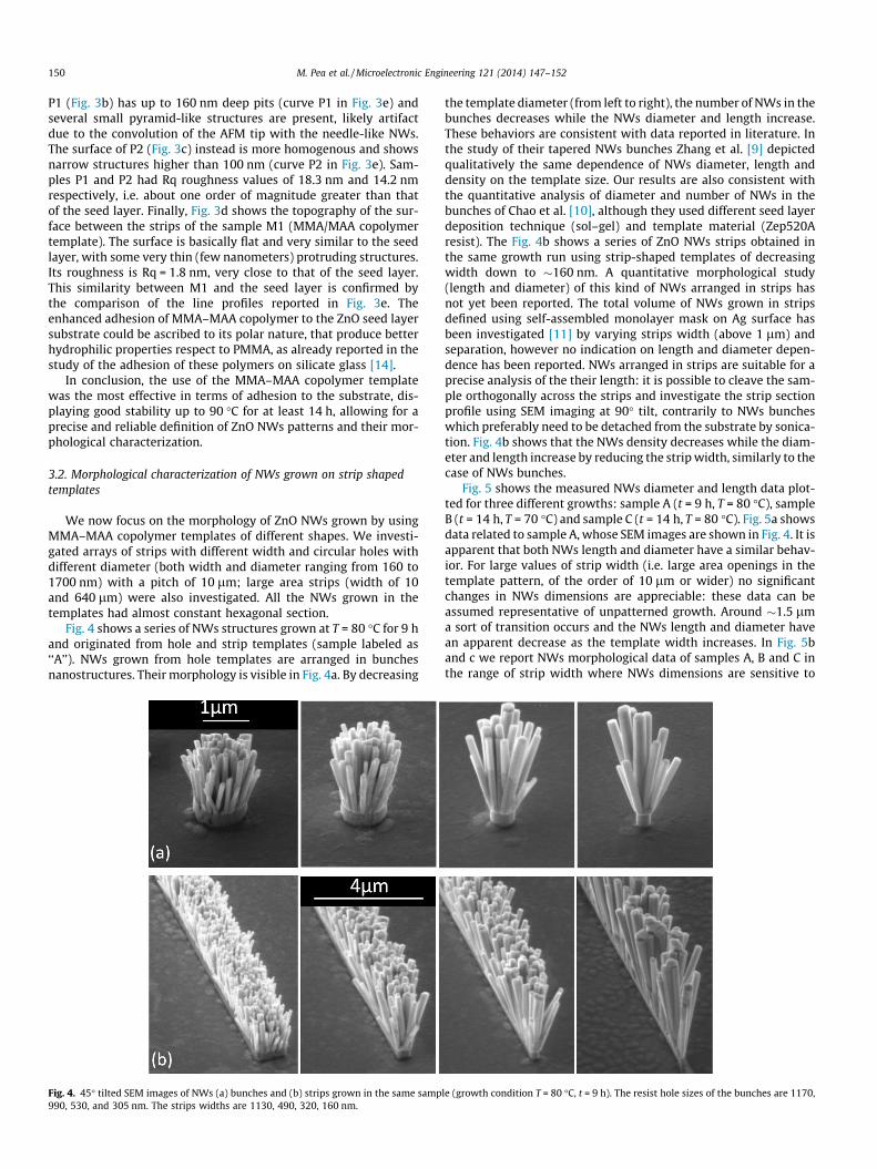
Fig. 4 shows a series of NWs structures grown at T = 80 �C for 9 hand originated from hole and strip templates (sample labeled as‘‘A’’). NWs grown from hole templates are arranged in bunchesnanostructures. Their morphology is visible in Fig. 4a. By decreasing
Fig. 4. 45� tilted SEM images of NWs (a) bunches and (b) strips grown in the same samp990, 530, and 305 nm. The strips widths are 1130, 490, 320, 160 nm.
the template diameter (from left to right), the number of NWs in thebunches decreases while the NWs diameter and length increase.These behaviors are consistent with data reported in literature. Inthe study of their tapered NWs bunches Zhang et al. [9] depictedqualitatively the same dependence of NWs diameter, length anddensity on the template size. Our results are also consistent withthe quantitative analysis of diameter and number of NWs in thebunches of Chao et al. [10], although they used different seed layerdeposition technique (sol–gel) and template material (Zep520Aresist). The Fig. 4b shows a series of ZnO NWs strips obtained inthe same growth run using strip-shaped templates of decreasingwidth down to �160 nm. A quantitative morphological study(length and diameter) of this kind of NWs arranged in strips hasnot yet been reported. The total volume of NWs grown in stripsdefined using self-assembled monolayer mask on Ag surface hasbeen investigated [11] by varying strips width (above 1 lm) andseparation, however no indication on length and diameter depen-dence has been reported. NWs arranged in strips are suitable for aprecise analysis of the their length: it is possible to cleave the sam-ple orthogonally across the strips and investigate the strip sectionprofile using SEM imaging at 90� tilt, contrarily to NWs buncheswhich preferably need to be detached from the substrate by sonica-tion. Fig. 4b shows that the NWs density decreases while the diam-eter and length increase by reducing the strip width, similarly to thecase of NWs bunches.
Fig. 5 shows the measured NWs diameter and length data plot-ted for three different growths: sample A (t = 9 h, T = 80 �C), sampleB (t = 14 h, T = 70 �C) and sample C (t = 14 h, T = 80 �C). Fig. 5a showsdata related to sample A, whose SEM images are shown in Fig. 4. It isapparent that both NWs length and diameter have a similar behav-ior. For large values of strip width (i.e. large area openings in thetemplate pattern, of the order of 10 lm or wider) no significantchanges in NWs dimensions are appreciable: these data can beassumed representative of unpatterned growth. Around �1.5 lma sort of transition occurs and the NWs length and diameter havean apparent decrease as the template width increases. In Fig. 5band c we report NWs morphological data of samples A, B and C inthe range of strip width where NWs dimensions are sensitive to
le (growth condition T = 80 �C, t = 9 h). The resist hole sizes of the bunches are 1170,

Fig. 5. Semilogarithmic plot of: (a) NWS length and diameter in strips vs. strip-template width for a growth of t = 9 h at T = 80� (sample A); NWs diameter (b) and length (c)for sample A (black hexagons) and for samples B (T = 70�, t = 14 h, blue open squares) and C (T = 80�, t = 14 h, red triangles). (For interpretation of the references to color in thisfigure legend, the reader is referred to the web version of this article.)
M. Pea et al. / Microelectronic Engineering 121 (2014) 147–152 151
the template size, i.e. for strips narrower than 2 lm. The NWslength and diameter have an apparent increase at higher tempera-ture indicating increased axial and lateral growth rates (compari-son between samples B and C). The length and diameter alsoincrease by increasing growth time, as effect of longer exposureto feeding solution (comparison between samples A and C), inagreement with data reported in literature [4]. NWs length anddiameter data for all three samples (A–C) reported in Fig. 5 showthe same overall behavior as a function of template width, despitethe different growth parameters. This finding indicates a stronginfluence of template dimensions on the NWs morphology. Theobserved decreasing behavior of NWs length and diameter up to�2 lm strip width could be related to a different amount of feedingmaterials that every NW can obtain from the solution: NWs grownin narrower strips are expected to benefit of more feeding materialsthan that in larger strips. This description is consistent with theobserved morphology of NWs in large strips: all NWs have uniformlength and diameter, while those in the edges are slightly longerand wider, likely due to the major amount of feeding solution avail-able in the edge. The local lowering of feeding concentration inpresence of NWs could be related to limited mass transport, compe-tition process among neighboring NWs, faster zinc precursor con-sumption over denser areas, or slow desorption of by-product ofthe reaction (such as hydrogen) from the surface [11,15]. Moreover,the NWs length and diameter data shown in Fig. 5 seem to have alinear behavior in the semilogarithmic plot, suggesting a logarith-mic dependence. However, more investigation on the NWs growthdriving mechanism and sophisticated modeling are required inorder to elucidate the origin of this data behavior, which were outof the scopes of this work.
4. Conclusions
We reported on a reliability study of resist used for the tem-plated hydrothermal growth of ZnO nanowires on sputtered seed
layer. We found that patterned MMA–MAA copolymer templatefilms have greater adhesion and stability with respect to the com-monly used PMMA electron resist or to the use of thin adhesion-promoter photoresist layers. The worse adhesion of the resist tem-plate implies a poorer control in NWs positioning and the presenceof unwanted growth underneath. The MMA–MAA copolymer bet-ter adhesion properties permit to obtain a clean and spatially con-trolled growth of ZnO NWs. This finding allowed us to investigatethe growth of ZnO NWs in strip-shaped MMA–MAA copolymertemplates. We found that, using typical hydrothermal growthparameters, NWs length and diameter have an apparent decreaseas the template size increases for strips narrower than about2 lm, likely related to the different amount of feeding materialavailable. For large strips, no significant effect of the template sizeis revealed in NWs morphology.
These results can open the way towards controlling shape andsize of distinct and well separated nanowires obtainable in a singlegrowth run, thus avoiding the need of multiple-step growth.
Acknowledgment
This work has been supported by Progetto FIRB Futuro in Ric-erca RBFR10VB42 (MIUR – ITALY).
References
[1] J.G. Lu, Z.Z. Ye, Y.Z. Zhang, Q.L. Liang, S. Fujita, Z.L. Wang, Appl. Phys. Lett. 89(2006) 023122.
[2] A. Janotti, C.G. Van de Walle, Rep. Prog. Phys. 72 (2009) 126501.[3] U. Özgür, Y.I. Alivov, C. Liu, A. Teke, M.A. Reshchikov, S. Dogan, et al., J. Appl.
Phys. 98 (2005) 041301.[4] X. Chen, X. Yan, Z. Bai, P. Lin, Y. Shen, X. Zheng, et al., CrystEngComm 15 (2013)
8022–8028.[5] J. Volk, T. Nagata, R. Erdélyi, I. Bársony, A.L. Tóth, I.E. Lukács, et al., Nanoscale
Res. Lett. 4 (2009) 699–704.[6] R. Erdelyi, T. Nagata, D.J. Rogers, F.H. Teherani, Z.E. Horvath, Z. Labadi, et al.,
Cryst Growth Des. 11 (2011) 2515–2519.

152 M. Pea et al. / Microelectronic Engineering 121 (2014) 147–152
[7] Y. Wei, W. Wu, R. Guo, D. Yuan, S. Das, Z.L. Wang, Nano Lett. 10 (2010) 3414–3419.
[8] Z. Szabó, J. Volk, E. Fülöp, A. Deák, I. Bársony, Photon Nanostruct. Fundam.Appl. 11 (2013) 1–7.
[9] D. Zhang, S. Wang, K. Cheng, S. Dai, B. Hu, X. Han, et al., ACS Appl. Mater.Interfaces. 4 (2012) 2969–2977.
[10] C.-H. Chao, J.-S. Huang, C.-F. Lin, J. Phys. Chem. C. 113 (2009)512–517.
[11] M.E. Coltrin, J.W.P. Hsu, D.A. Scrymgeour, J.R. Creighton, N.C. Simmons, C.M.Matzke, J. Cryst. Growth 310 (2008) 584–593, http://dx.doi.org/10.1016/j.jcrysgro.2007.11.030.
[12] A. Notargiacomo, L. Maiolo, Microelectron. Eng. 110 (2013) 465–469.[13] P. Lamarre, R. McTaggart, Electron Devices IEEE Trans. 37 (1990) 2406–2408.[14] L.B. Yakimtsova, E.L. Egorova, V.S. Yashchenko, Y.I. Matusevich, L.P. Krul, Russ.
J. Appl. Chem. 84 (2011) 2127–2130.[15] J.E. Boercker, J.B. Schmidt, E.S. Aydil, Cryst. Growth Des. 9 (2009) 2783–2789.