
Yield Management - YMS Magazine
52
Y ield M anagement Y ield M anagement Yield Enhancement and Process Control Strategies for the Semiconductor Industry SOLUTIONS Yield Enhancement and Process Control Strategies for the Semiconductor Industry V OLUME I I SSUE 3 SPRING 1999 $5.00 US 6 COVER STORY — CMP TECHNOLOGY TRENDS 12 EVALUATING INSPECTION STRATEGIES USING ADVANCED STATISTICAL METHODS 33 IMPROVED YIELD LEARNING IN CMP 6 COVER STORY — CMP TECHNOLOGY TRENDS 12 EVALUATING INSPECTION STRATEGIES USING ADVANCED STATISTICAL METHODS 33 IMPROVED YIELD LEARNING IN CMP SOLUTIONS
-
Upload
khangminh22 -
Category
Documents
-
view
1 -
download
0
Transcript of Yield Management - YMS Magazine

Yield ManagementYield ManagementYield Enhancement and Process Control Strategies
for the Semiconductor Industry
S O L U T I O N SYield Enhancement and Process Control Strategies
for the Semiconductor Industry
VOLUME I ISSUE 3 SPRING 1999 $5.00 US
6 COVER STORY —CMP TECHNOLOGY TRENDS
12 EVALUATING INSPECTION
STRATEGIES USING
ADVANCED STATISTICAL
METHODS
33 IMPROVED YIELD LEARNING
IN CMP
6 COVER STORY —CMP TECHNOLOGY TRENDS
12 EVALUATING INSPECTION
STRATEGIES USING
ADVANCED STATISTICAL
METHODS
33 IMPROVED YIELD LEARNING
IN CMP
S O L U T I O N S

Spring 1999 Yield Management Solutions2
C O N T E N T S
F e a t u r e s
C o v e r S t o r y
6 CMP Technology Trends: From Implementation toImprovement
Rapid changes in the semiconductor industry havemade CMP one of the most widely accepted planarization methods in IC technology. Long thedomain of the electrical or mechanical engineer,CMP has emerged as a complex methodologyrequiring the expertise of chemists and physicists.Managing implementation and improvements inCMP will be crucial to the advancement of products in the next millennium.
Cover image by Luie Lopez,Stephen Marley Productions
Yield Management Consulting
12 Evaluating Inspection Strategies Using AdvancedStatistical MethodsSample Planner 2 software developed by KLA-Tencorgives critical ability to determine and evolve the optimum inspection strategy through each operationalphase.
Analysis
15 Offline ADC Solution Maximizes Inspection ValueAutomated defect classification used with 7000series patterned inspection system helps fabs drive up baseline yields.
17 Intelligent Line MonitoringIntelligent line monitoring strategy helps IBM‘sMicroelectronics Division accelerate yield learningand improve productivity.
Metrology
21 Replacing C-V Monitoring with Non-Contact COSCharge AnalysisEarly warning of diffusion furnace contamination withQuantox system helps maintain high yields.
24 Control of HSG-Si Fabrication Using Film andSurface TechnologiesFilm and surface technologies monitor fabricationprocess of HSG-Si and predict DRAM capacitor performance.
Inspection
28 Wafer Inspection Technology Challenges for ULSIManufacturingToday’s technology challenges require comprehensiveinspection strategies — from detecting, classifyingand analyzing defects to recommending correctiveaction (Part one in a series).
Photo: Courtesy of SpeedFam-IPEC

Spring 1999 Yield Management Solutions 3
S P R I N G 1 9 9 9
S e c t i o n s
4 Editorial: The Responsibilities of Leadership
5 Business News
KLA-Tencor Adds Quantox and UltrapointeAcquisitions help KLA-Tencor provide new solutions and broadenrange of product offerings.
SEI Level 2 Software Capability AchievedKLA-Tencor is the first semiconductor equipment company to reachLevel 2 on the SEI five level SW-CMM.
40 KLA-Tencor Trade Show Calendar
44 Best of YMS
MiCRUS Corporation benefits from using KLA-Tencor product moni-toring tools at key process points to reveal causes of yield loss.
45 Yield Management Seminar Series
49 Q & A
KLA-Tencor answers questions about the Y2K issue.
P r o d u c t N e w s
50 AIT IIIn-line Defect Inspection System
2401Automated Macro DefectInspection System
FabVARS 500Digital Image ManagementSystem
SEMSpec Random ModeAdvanced E-beam InspectionSystem
51 8100XP-R CD SEMAdvanced Reticle MetrologySystem
5300Overlay Metrology System
SL3UVReticle Contamination InspectionSystem for DUV Lithography
363UVReticle Pattern Inspection Systemfor DUV Lithography
Yield Management Solutions ispublished by KLA-Tencor
Corporation. To receive YieldManagement Solutions contactCorporate Communications at:
KLA-Tencor Corporation160 Rio Robles
San Jose, CA 95134Tel 408.875.4200Fax 408.875.4144www.kla-tencor.com
For literature requests call:800.450.5308
©1999 KLA-Tencor Corporation. All rights reserved. Material may not be
reproduced without permission from KLA-Tencor Corporation.
Products in this document are identified by trademarks of their respective
companies or organizations.
12 336
33 Improved Yield Learning Using CMP Equipment MonitorsIntroduction of new CMP monitoring points leads to increasedyields at VLSI San Antonio.
36 Automation Comes to Litho InspectionNew automated macro defect inspection system detects widerange of defect types frequently missed by manual inspection techniques.
Lithography
38 Low k1 Lithography Redefines Photomask QualityWith low k1 lithography, conventional parameters for defining photomask quality are no longer adequate.
41 Analysis of Reticle CD Uniformity with CD SEMsToday’s mask industry needs new metrology technologies to meetcurrent and future CD control requirements.
Standards
46 The Role of Standards In Yield Management
Consistent application of metrology standards can help ensure theeffective use of yield data.
F e a t u r e s

the
EditorialS O L U T I O N SYield Management
Spring 1999 Yield Management Solutions4
S E C T I O N S
As companies grow and emerge from among their competitors as industry leaders, theymust assume new responsibilities in addition to those associated with continued financialsuccess and customer satisfaction. Whether they want to or not, by assuming the rank of “industry leader,” these companies bear an inherent responsibility to truly be leaders.They have an obligation to learn and understand where the new frontiers will be and to drive the advances in technologies or processes needed to meet future demands. Their visions further not just their own companies, but the industry as a whole.
Throughout the history of the semiconductor and equipment industries, the mantle ofleadership has been worn by some impressive companies. Unfortunately, those who areleaders in one time can quickly become followers in another. Those companies best positioned to understand the roadmaps of the future, and their implications for today,are also those best positioned to maintain customer satisfaction and a solid revenuestream over the long term.
The dynamic nature of the semiconductor equipment industry makes living up to theleadership role a multifaceted challenge. Not only must the leaders understand anddevelop solutions for new materials and new methods, such as copper interconnect, low kdielectrics, and new photomask designs, they must also continue to overcome existingchallenges in areas such as chemical mechanical planarization, automatic defect classifica-tion and yield ramp acceleration. Within this environment of rapid change, wherelinewidths decrease faster with each new generation of devices, leaders must combine the flexibility and agility of a start up organization with the critical mass of a well-established corporation.
Emerging as a leader through revenue growth is indeed a credible achievement.Maintaining that leadership by recognizing and developing solutions to the comingchallenges, by driving advances in current technologies, and by satisfying the needs of customers, both now and in the future, is the true test of a leading company in this or any industry.
CORPORATE HEADQUARTERSKLA-Tencor Corporation160 Rio RoblesSan Jose, California 95134408.875.4200
INTERNATIONAL OFFICESKLA-Tencor France SARLEvry Cedex, France011 33 16 936 6969
KLA-Tencor GmbHMunich, Germany011 49 89 8902 170
KLA-Tencor (Israel) CorporationMigdal Ha’Emek, Israel011 972 6 6449449
KLA-Tencor Japan Ltd.Yokohama, Japan011 81 45 335 8200
KLA-Tencor Korea Inc.Seoul, Korea011 822 41 50552
KLA-Tencor (Malaysia) Sdn. Bhd.Johor Bahru, Malaysia011 607 557 1946
KLA-Tencor (Singapore) Pte. Ltd.Singapore011 65 780 1088
KLA-Tencor Taiwan BranchHsinchu, Taiwan011 886 35 335163
KLA-Tencor LimitedWokingham, United Kingdom011 44 118 936 5700
EDITOR-IN-CHIEFRoberta Emerson
MANAGING EDITORJudy Dale
CONTRIBUTING EDITORSKern Beare Kavitha Kannan Holly Nielsen Viet Pham
ASSOCIATE EDITORKevin Clover
EDITORIAL ASSISTANTSRolando Gonzales Carol JohnsonMarie Sholar
ART DIRECTOR AND
PRODUCTION MANAGERShirley Short
DESIGN CONSULTANTCarlos Hueso
CIRCULATIONCathy Correia
KLA-Tencor Worldwide
Roberta Emerson
Vice President, Corporate Communications
Yield ManagementS O L U T I O N S
ResponsibilitiesLeadershipOF
Spring 1999 Yield Management Solutions 5
S E C T I O N S
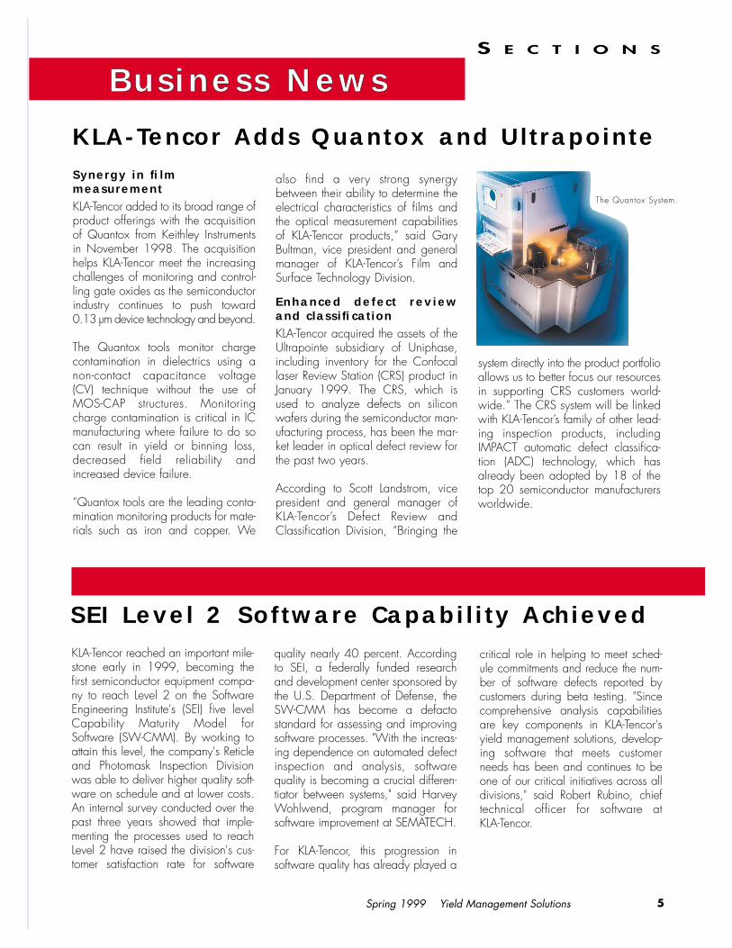
Synergy in film measurementKLA-Tencor added to its broad range ofproduct offerings with the acquisitionof Quantox from Keithley Instrumentsin November 1998. The acquisitionhelps KLA-Tencor meet the increasingchallenges of monitoring and control-ling gate oxides as the semiconductorindustry continues to push toward0.13 µm device technology and beyond.
The Quantox tools monitor chargecontamination in dielectrics using anon-contact capacitance voltage (CV) technique without the use ofMOS-CAP structures. Monitoringcharge contamination is critical in ICmanufacturing where failure to do socan result in yield or binning loss,decreased field reliability andincreased device failure.
“Quantox tools are the leading conta-mination monitoring products for mate-rials such as iron and copper. We
KLA-Tencor Adds Quantox and Ultrapointe
also find a very strong synergybetween their ability to determine theelectrical characteristics of films andthe optical measurement capabilitiesof KLA-Tencor products,” said GaryBultman, vice president and generalmanager of KLA-Tencor’s Film andSurface Technology Division.
Enhanced defect reviewand classificationKLA-Tencor acquired the assets of theUltrapointe subsidiary of Uniphase,including inventory for the Confocallaser Review Station (CRS) product inJanuary 1999. The CRS, which isused to analyze defects on siliconwafers during the semiconductor man-ufacturing process, has been the mar-ket leader in optical defect review forthe past two years.
According to Scott Landstrom, vicepresident and general manager ofKLA-Tencor’s Defect Review andClassification Division, “Bringing the
Business News
system directly into the product portfolioallows us to better focus our resourcesin supporting CRS customers world-wide.” The CRS system will be linkedwith KLA-Tencor’s family of other lead-ing inspection products, includingIMPACT automatic defect classifica-tion (ADC) technology, which hasalready been adopted by 18 of thetop 20 semiconductor manufacturersworldwide.
The Quantox System.
KLA-Tencor reached an important mile-stone early in 1999, becoming thefirst semiconductor equipment compa-ny to reach Level 2 on the SoftwareEngineering Institute's (SEI) five levelCapability Maturity Model forSoftware (SW-CMM). By working toattain this level, the company's Reticleand Photomask Inspection Divisionwas able to deliver higher quality soft-ware on schedule and at lower costs.An internal survey conducted over thepast three years showed that imple-menting the processes used to reachLevel 2 have raised the division's cus-tomer satisfaction rate for software
quality nearly 40 percent. Accordingto SEI, a federally funded researchand development center sponsored bythe U.S. Department of Defense, theSW-CMM has become a defactostandard for assessing and improvingsoftware processes. "With the increas-ing dependence on automated defectinspection and analysis, softwarequality is becoming a crucial differen-tiator between systems," said HarveyWohlwend, program manager forsoftware improvement at SEMATECH.
For KLA-Tencor, this progression in software quality has already played a
critical role in helping to meet sched-ule commitments and reduce the num-ber of software defects reported bycustomers during beta testing. "Sincecomprehensive analysis capabilitiesare key components in KLA-Tencor'syield management solutions, develop-ing software that meets customerneeds has been and continues to beone of our critical initiatives across alldivisions," said Robert Rubino, chieftechnical officer for software at KLA-Tencor.
SEI Level 2 Software Capability Achieved

by Anantha R. Sethuraman, Ph.D.,CMP Solutions, KLA-Tencor
hemical Mechanical Polishing(CMP) has become one of the
most widely-accepted and practicedplanarization methods in IC fabrica-tion in less than two decades. Theexplosive growth of this segment ofsemiconductor process technologyhas been remarkable in an industrythat has been credited with rapidgrowth. In an industry that aspiresto reach six sigma process controlbased on scientific first principles,CMP is still being used and devel-oped by artisans. The rigor in thedesign of experiments held as gospelby the semiconductor industry hasnot been applied in the developmentof CMP consumables. After morethan ten years of widespread assimi-lation of this technology, users needan integrated process control solu-tion for their CMP needs. This articlediscusses some of the history of thematuration of the technology, notescurrent challenges facing the indus-try and presents some views on thetimeliness of an integrated processcontrol solution for CMP.
Current status and emerging trendsWhen viewed as a process modulewithin a fab, CMP is comprised of anumber of elements from a numberof different suppliers (see figure 1).1
C
6
CMP TECHNOLOGY TRENDS: IMPLEMENTATION

Each user assembles a selection ofcomponents from this list and inte-grates the process in manufacture. Itis quite likely that each of these com-ponents are available from a relative-ly limited group of vendors who spe-cialize in products unique to CMPwhich are guarded by high levels ofsecrecy and intellectual property pro-tection. In contrast, for the moremature sectors such as plasma etch orthin film chemical vapor deposition(CVD), an equipment supplier canmore than likely provide the userwith the tool, best-known-methods(BKMs), endpoint detection, processconsumables, delivery systems andeven exhaust treatment systems.With the broadening of knowledgeand expertise in CMP, the technicalcommunity is driving towardsachieving the maturity level thatthey have become accustomed toexpect in widely accepted processes.However, due to the consumable-specific nature of CMP itself, the factremains that all slurries and pads willstill be specialty materials, controlledby one or two vendors. By its verynature — its multiple vendors andspecialty material requirements—CMP has developed into a niche mar-ket technology that demands gener-ous amounts of “black magic” andfolklore to achieve success!
7
SSttoorryyFROMTO IMPROVEMENT
Cover

starts per week that would needCMP, this number is in the thou-sands. This implies that the processhas emerged as a critical part of thearchitecture of an integrated circuitand is therefore needed for integratedcontrol of the process to achieve yieldgoals.
Emerging trends in equipment alsosupport the need. A typical layout ofa polishing area in the fab is shown infigure 4. As one can imagine, a waferfab with more than 10,000 waferstarts per week would have severalpolishers. Currently each polish andclean tool is intrinsically connectedwith the input and output device. Inthe future, a robot will be used toallow two or more polishers to beattached to a single input/outputsource and a single cleaning station.This arrangement will optimize tooluse and increase processing speed.
The development of the infrastruc-ture needed to support an efficientoperation is drawn from all the ven-dors that supply into the area. SinceCMP is a relatively new area forsemiconductor manufacture, theexpertise on the user side is sparsealthough growing. Larger organiza-tions such as IBM, Intel, MicronTechnology, Motorola and AMDhave over the years developed a rea-sonable methodology to manage thetechnology. The development of such
Spring 1999 Yield Management Solutions8
C O V E R S T O R Y
The rapid growth in the use of CMPtechnology is shown in figure 2.Between 1994 and 1998, CMP usemore than doubled — use of CMP oninterlayer dielectrics (ILD) grewfrom three to five layers, and polish-ing of metal contacts and the intro-duction of the damascene process cre-ated the need for CMP on metal. Forexample in a four metal layer processwith shallow trench isolation (STI),ILD and tungsten CMP: 15-25 pol-ishers would be needed at 60 percentutilization, with 20 wafers per hour,in a fab with 5000 wafer starts perweek.
Furthermore, the extension of CMPto the front-end in order to enableSTI integration has triggered theneed for innovation. STI has becomean architectural requirement for sub-0.25 micron device rules, as localizedoxidation of silicon (LOCOS) doesnot deliver the critical transistorproperties. The challenge of STI istypically to planarize a high densityplasma oxide over silicon nitride.The objective is to remove the over-burden without damaging thenitride excessively, while preservingthe integrity of the circuit. Althoughthis is a formidable requirement, itpresents a great opportunity. Theresult has been development of exot-ically exciting technical solutions inCMP consumables, especially high-selectivity slurries. In addition,process solutions using better end-pointing have also enabled STI CMP.
In the memory area (specificallyDRAM), polysilicon polish has beenin implementation for about a year.The volume is expected to increase asmore manufacturers adopt poly CMP.
Figure 3 describes the evolution ofCMP applications in chip manufac-ture. About two-thirds of the 93semiconductor fabs producingdevices with sub-0.5 micron geome-tries require some form of CMP.When considered in number of wafer
Figure 1. Elements of a CMP process
module.1
Figure 2. Growth of CMP utilization.2
Figure 3. Current and future
Planarization Metrology
Equipment Equipment EquipmentConditioner PVA Brush ThicknessEndpoint detect Tanks UniformityProcess Spin/rinse/dry ParticlesSlurry Hot DI water ScratchesPad Cold DI water DefectsInsert Process Electrical qualityTemplate Chemistry Setup standardsSlurry delivery Chemical deliverySlurry replenishing Chemical disposalSlurry recyclingSlurry disposal
ILD polishMetal polish
# of
Lay
ers
Polis
hed
1994 (0.8 - 0.5) 1998 (0.35 - 0.25 µm)
Application
1st Generation0.8-0.5 µm
2nd Generation<0.5 µm
3rd Generation< 0.25 µm
Post-CMPCleaning
Oxide (ILD)
Above + ILD0W CMP + STI
Above + Cu, Al & low kCMP + new applications
(both FE & BE, e.g. Poly Si)

methodologies has been evolutionary.The conventional control that asemiconductor engineer would liketo have over the various aspects of theprocess has not been possible withCMP, primarily due to the continu-ing and rapid metamorphosis of theprocess itself.
A history of CMP developmentLet us examine a little bit of history.The chronology described in figure 5shows the initial rollout of CMP3.Conceived and developed at IBMunder strictest secrecy during theearly 1980’s, the process was not wellpublicized. Vendors who suppliedequipment such as IPEC Westech, R.Howard Strasbaugh and process con-sumable suppliers with pads/carrierfilms from Rodel and slurry fromCabot were not told the end result oftheir involvement. This was a typicalpractice in early semiconductorprocess development, as intellectualproperty issues were not well workedout between vendors and chipmak-ers. The concept of joint develop-ment projects (JDPs) between ven-dors and chipmakers was alien in theera of big company research anddevelopment activities. The resultwas that early understanding of theintricacies of the process rested solelywith the users and an infrastructurefor development of an ideal solution
integrating both equipment andmaterials was not developed. Afterall, the concept of polishing a waferwith expensive circuitry that hadbeen developed and manufactured ina clean room environment using“dirty” particle-laden slurry wasstarted as an “experiment”. Given thedramatic shift in thinking requiredto accept such an idea, there were amultitude of skeptics who did notexpect CMP to survive, let alone bewhere it is today.
As with every breakthrough we havewitnessed in the technology sector,what was once deemed improbable,or even impossible, has become areality and is now accepted as anessential step. Until depth of focusrequirements necessitated morestringent planarity as the shift to0.35 micron devices occurred, CMPwas never seriously viewed as a long-range solution. Due to the secrecywith which it was developed, under-standing both the power and thechallenges of CMP has taken longerto achieve than many other processesin our industry’s history.
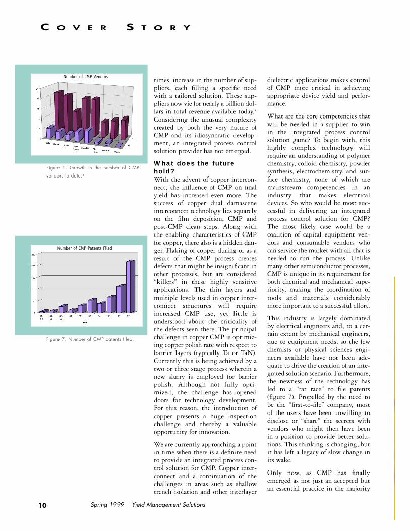
Following on the heels of IBM, Intellaunched CMP via technology trans-fer in the 1987-88 timeframe fol-lowed by Micron Technology in1989. The SEMATECH program onCMP was conceived in 1989 andthen began the pursuit of rigorouscharacterization of the process asadoption rose quickly. Member com-panies dispatched their best talent tocollaborate in this “sand box” calledSEMATECH. Technical advisoryboards were formed and vendors wereinitiated into the “inner circle”,although again restrictions againstdisclosing the JDP progress to non-member companies were imposed inan effort to ensure better return oninvestment for the member compa-nies. Figure 6 presents the number ofprocess areas that were involved inthe CMP sector in 1992 and theincrease to date. It depicts a 5-10
Spring 1999 Yield Management Solutions 9
C O V E R S T O R Y
Figure 4. Trends in equipment layout in the
CMP area.2
Figure 5. CMP development at IBM.
trends in CMP applications.
CMP Post-CMPCleaning
Single Platen/Single Head1-step polish
Multi-Platen/Multi-Head 2-step polish (buff step)
End-point detection On-board metrology
Integrated Dry-in/Dry-outMulti-Platen/Multi-HeadNon-Rotary (e.g. Orbital,Linear CMP) multi-step
polish, End-point detectionOn-board metrology
Conventional wafer cleaning(wet stations)
Wafer scrubbing/DI water
Wafer scrubbing/DI waterNH4OH
Integrated Dry-in/Dry-outMulti-Platen/DIW
NH4OH, HFNew cleaning methods &
New chemistries
Polish 1
I/O Clean
Polish 2
Robot
CleanPolish
I/O
East Fishkill Base Technology (83)East Fishkill Pilot Line (86)
Logic (Oxide, Al) (89)Logic (Oxide, W) (89)
Burlington Pilot Line (86)
4MB DRAM (89)
current future
dielectric applications makes controlof CMP more critical in achievingappropriate device yield and perfor-mance.
What are the core competencies thatwill be needed in a supplier to win in the integrated process control solution game? To begin with, thishighly complex technology willrequire an understanding of polymerchemistry, colloid chemistry, powdersynthesis, electrochemistry, and sur-face chemistry, none of which aremainstream competencies in anindustry that makes electricaldevices. So who would be most suc-cessful in delivering an integratedprocess control solution for CMP?The most likely case would be acoalition of capital equipment ven-dors and consumable vendors whocan service the market with all that isneeded to run the process. Unlikemany other semiconductor processes,CMP is unique in its requirement forboth chemical and mechanical supe-riority, making the coordination oftools and materials considerablymore important to a successful effort.
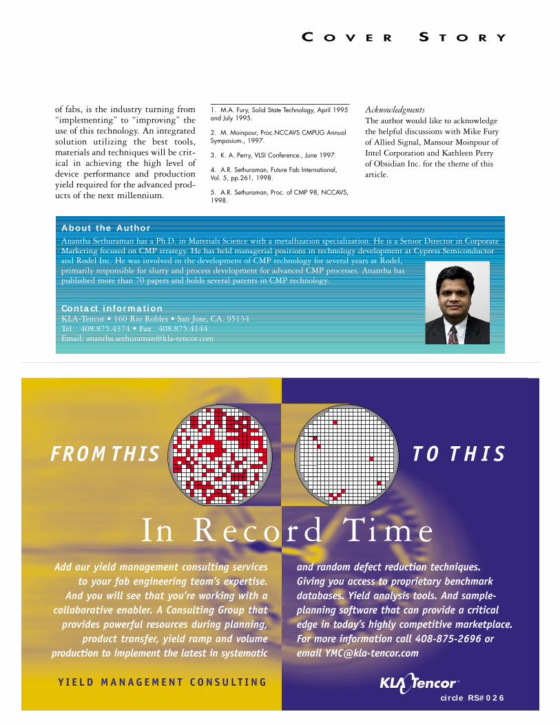
This industry is largely dominatedby electrical engineers and, to a cer-tain extent by mechanical engineers,due to equipment needs, so the fewchemists or physical sciences engi-neers available have not been ade-quate to drive the creation of an inte-grated solution scenario. Furthermore,the newness of the technology has led to a “rat race” to file patents (figure 7). Propelled by the need tobe the “first-to-file” company, mostof the users have been unwilling todisclose or “share” the secrets withvendors who might then have beenin a position to provide better solu-tions. This thinking is changing, butit has left a legacy of slow change inits wake.
Only now, as CMP has finallyemerged as not just an accepted butan essential practice in the majority
times increase in the number of sup-pliers, each filling a specific needwith a tailored solution. These sup-pliers now vie for nearly a billion dol-lars in total revenue available today.3Considering the unusual complexitycreated by both the very nature ofCMP and its idiosyncratic develop-ment, an integrated process controlsolution provider has not emerged.
What does the futurehold?With the advent of copper intercon-nect, the influence of CMP on finalyield has increased even more. Thesuccess of copper dual damasceneinterconnect technology lies squarelyon the film deposition, CMP andpost-CMP clean steps. Along withthe enabling characteristics of CMPfor copper, there also is a hidden dan-ger. Flaking of copper during or as aresult of the CMP process createsdefects that might be insignificant inother processes, but are considered“killers” in these highly sensitiveapplications. The thin layers andmultiple levels used in copper inter-connect structures will requireincreased CMP use, yet little isunderstood about the criticality ofthe defects seen there. The principalchallenge in copper CMP is optimiz-ing copper polish rate with respect tobarrier layers (typically Ta or TaN).Currently this is being achieved by atwo or three stage process wherein anew slurry is employed for barrierpolish. Although not fully opti-mized, the challenge has openeddoors for technology development.For this reason, the introduction ofcopper presents a huge inspectionchallenge and thereby a valuableopportunity for innovation.
We are currently approaching a pointin time when there is a definite needto provide an integrated process con-trol solution for CMP. Copper inter-connect and a continuation of thechallenges in areas such as shallowtrench isolation and other interlayer
Spring 1999 Yield Management Solutions110
C O V E R S T O R Y
Figure 6. Growth in the number of CMP
vendors to date.3
Figure 7. Number of CMP patents filed.
Number of CMP Vendors
Number of CMP Patents Filed
1. M.A. Fury, Solid State Technology, April 1995and July 1995.
2. M. Moinpour, Proc.NCCAVS CMPUG AnnualSymposium., 1997.
3. K. A. Perry, VLSI Conference., June 1997.
4. A.R. Sethuraman, Future Fab International, Vol. 5, pp.261, 1998.
5. A.R. Sethuraman, Proc. of CMP 98, NCCAVS,1998.
About the AuthorAnantha Sethuraman has a Ph.D. in Materials Science with a metallization specialization. He is a Senior Director in CorporateMarketing focused on CMP strategy. He has held managerial positions in technology development at Cypress Semiconductorand Rodel Inc. He was involved in the development of CMP technology for several years at Rodel, primarily responsible for slurry and process development for advanced CMP processes. Anantha has published more than 70 papers and holds several patents in CMP technology.
Contact informationKLA-Tencor • 160 Rio Robles • San Jose, CA. 95134Tel 408.875.4374 • Fax 408.875.4144Email: [email protected]
C O V E R S T O R Y
of fabs, is the industry turning from“implementing” to “improving” theuse of this technology. An integratedsolution utilizing the best tools,materials and techniques will be crit-ical in achieving the high level ofdevice performance and productionyield required for the advanced prod-ucts of the next millennium.
Acknowledgments The author would like to acknowledgethe helpful discussions with Mike Furyof Allied Signal, Mansour Moinpour ofIntel Corporation and Kathleen Perry of Obsidian Inc. for the theme of thisarticle.
FROM THIS T O T H I S
In R e c o r d Ti m eAdd our yield management consulting services
to your fab engineering team’s expertise. And you will see that you’re working with a
collaborative enabler. A Consulting Group thatprovides powerful resources during planning,
product transfer, yield ramp and volume production to implement the latest in systematic
and random defect reduction techniques. Giving you access to proprietary benchmarkdatabases. Yield analysis tools. And sample-planning software that can provide a criticaledge in today’s highly competitive marketplace. For more information call 408-875-2696 oremail [email protected]
Y I E L D M A N A G E M E N T C O N S U LT I N Gcircle RS#026

Spring 1999 Yield Management Solutions112
The problem of optimally applying inspec-tion equipment in defect inspection is verycomplex and only partially addressed1. Theproblem involves numerous interrelatedvariables such as the process technology,defect mechanisms, the inspection equip-ment, fab logistics, processing parameters,and financial data. Making the problemeven more complex, the fab’s inspectionrequirements are not static, they continu-ously evolve throughout a fab’s operationalphases. During the process transfer andyield learning phases, inspection is focusedon understanding and improving baselinedefect densities, as opposed to focused onexcursion control during the mature, fullproduction phase. Defect mechanisms andtypes also evolve — from a higher contentof systematic, process integration relatedissues during early phases — to more random-related process tool events at themature, full production phase. Defect excur-sion types and frequencies, wafer starts, anddevice average selling prices are just a few of the drivers that evolve and affect the opti-mum inspection strategy for each phase.
Advanced statistical and stochastic modelshave been developed to estimate the opti-mal defect inspection capacity, allocation,and operation (sampling strategy) in fabs.Sample Planner™ is a software program
Evaluating Inspection Strategies UsingAdvanced Statistical Methods
by Raman K. Nurani, Ph.D., Meryl Stoller, and Dadi Gudmundsson, KLA-Tencor; J. George Shanthikumar, Ph.D., University of California at Berkeley
Increasing fab construction costs, shortening product life cycles and eroding market prices are realities for today’s integratedcircuit (IC) manufacturers. In this competitive environment, cost-effective operations are an important part of a successfulbusiness plan. High yields have to be reached faster and maintained at lower wafer processing cost levels than ever before.Towards this goal, optimal capacity of inspection equipment and its allocation across different process steps are impera-tive, whether it is defect or metrology oriented.
based upon these models that uses an unprecedentednumber of variables to create and optimize a fab-wideinspection strategy. This software program can also beused as a tool for KLA-Tencor’s engineering and devel-opment to determine the best inspection technologyand configurations for future process technologies.
The sample planning problemIt has become well accepted that defect inspection toolsplay an important role in a fab’s yield managementstrategy. While few manufacturers currently operatewithout some type of defect inspection, many IC manu-facturers tend to view inspection as non-value addedand are overly conservative when planning inspectioncapacity. It is here that the sample planning problemarises, i.e. what types of inspections to perform, whereto locate them in the process, and how frequently toperform the inspections. The optimum level of inspec-tion is reached through the trade-off between the costof inspection operations, both fixed and variable, andthe cost of yield loss due to undetected yield-limitingdefects and process excursions.
The main decision parameters are: type of inspections(test wafer, product, or in-situ inspections), placementof the inspections (which process steps/tools), inspec-tion frequency (percent lots to sample, number ofwafers per lot, area per wafer), inspection sensitivitysetting, which parameters to track and respond to (sta-tistical process control scheme), the fraction of defectsto review, and inspection capacity. All of these parame-
ConsultingF E A T U R E S

quantify mean and variance of defects during in andout of control states, the propagation of defects to sub-sequent process steps, the types of excursions and thefrequency of excursions. Combining this informationwith yield and financial data allows the financial lossper year from excursions to be quantified. The financialloss due to excursions can be decreased by samplingmore often. To determine the cost of sampling wequantify: equipment sensitivity to defects, inspectiontool throughput, inspection tool operation, cost ofownership, and queuing/transit times. A stochasticalgorithm uses this information along with the excur-sion, yield, and financial data to calculate the overallcost. By iterating through several operationally feasiblesample plans, the algorithm determines the most costeffective inspection strategy.
Sample Planner 2A software tool called Sample Planner 2 has beendeveloped based on the above methodology. SamplePlanner 2 allows an unprecedented number of criticalvariables to be involved in sample planning optimiza-tion. Besides addressing the decision variables of thesample planning problem mentioned earlier, it incor-porates IC manufacturing issues such as, re-entrantflow, rework decisions, and complete process line modeling (300+ steps). The categories of data used by the Sample Planner are five: fab information, inspec-
ters are interrelated and each one gives rise to a set ofvariables that need to be understood. Overall, theproblem is so complex that no comprehensive solutionmethodologies existed prior to our efforts. The SamplePlanner cost model provides the framework and toolsto analyze critical fab parameters to develop an opti-mal inspection strategy with reasonable effort.
The excursion control methodologyIn its simplest form, the cost model methodology isbased around a recurring in-and-out of control cycleoccurring at each step in the process, see figure 2. Acycle starts where each step in the process is assumedto have an in-control mode of operation which deliversa high yield. After a random length of time an excur-sion takes place, causing lower yields. At this pointthe inspection sampling strategy determines howquickly the excursion is caught and fixed, restartingthe in-and-out of control cycle. The goal is to mini-mize financial loss by catching the excursions quickly,i.e. minimizing the time between excursion start anddetection. However, this needs to be done only for areasonable inspection cost, which is the essence of theoptimization. To do that, modeling mathematicallyhow the process behaves and how the inspection tools“see” the process is the foundation.
The widespread use of a standard statistical processcontrol (SPC) scheme results in accumulation ofimportant data from the processes. We process thisdata using statistical models and hypothesis tests to
Spring 1999 Yield Management Solutions 13
F E A T U R E S
Figure 1. Important decision parameters in sample planning.
Figure 2. The in-control and out-of-control cycle.
Figure 3. Sample Planner 2 inputs and outputs.
InspectionLayers?
InspectionMethod?
InspectionTools?
Percent ofLots?
Wafers PerLot?
InspectionDelays?
DefectSize?
e.g., 8 steps e.g., producttest wafer
e.g., 2XXX AIT
e.g., 40% of lots
e.g., 5 wafersper lot
e.g., queuing
e.g., 0.3 µmsensitivity
> 0.8 µ
> 0.5 µ
> 0.3 µ
Product
Test Wafer
In-situ
2XXX
AIT/SP
# De
fect
s
Proc
ess
Flow
Defect Size
Cyclestarts
Last samplebefore excursion
Excursionoccurs
First sampleafter excursion
Excursiondetected
Sourceidentified
Sourceeliminated
In-Control Out-of-Control
Material at Riskβ-risk
Fab Information
• Process flow• Baseline and excursion yields• Process cycle time• Average selling price• Test wafer costs• Labor rates• Re-entrant flow and photo
loop rework data
Inspection Technologies
• Inspection tool types• Capture rates• In-situ/Test wafer monitor• Throughput and Q times
Baseline Information
• Mean and variances• “In control” pareto• Defect propagation
Excursion Information
• Frequency by level• Yield impact• Out of Control pareto
Inspection Strategy
• Inspection points• Defect classification plan• DSA On/Off• Sampling plan• Control charts and limits
Input
Optimized Sampling StrategyBased Upon
• Excursion yield loss/costs• Inspection costs• Test wafer monitor costs• Lots at risk• False verification man hours• Root cause analysis time
Output

Malaysia
Israel
Spain
France
Italy
Ireland
Scotland
UnitedKingdom
United States
ChinaTaiwan
Holland
Korea
Singapore
Japan
AustriaGermany
F E A T U R E S
tion technologies, inspection strategy, baseline defectinformation, and excursion characteristics. The primarydata of interest in these categories can be seen in figure 3. This data is entered into the SamplePlanner database through a user friendly graphicalinterface where the user can outline many differentoperational scenarios to analyze.
Currently, the Sample Planner 2 software is being utilized in two ways, 1) by KLA-Tencor’s yield management consultants to help customer fabs deter-
Figure 4. Example output from Sample Planner 2 analysis.
S I N G L E P O I N T O F CO N TA C TTechnical Support Assistance
Scheduled or Emergency ServiceStatus Inquiries
Parts Ordering/Inquiries
L I V E7x24 Placement of Service Requests
Escalation Capability
C A L L T R A C K I N GAll Service RequestsAll Escalation Events
C E N T R A L R E S O U R C E S Service Report Filing
Performance ReportingAuto Notification for
Escalated Events
CUSTOMER RE SPONSE CENTERS
USA
1 - 8 0 0 - 6 0 0 - 282 9
EUROPE
0 8 0 0 - 1 74 728 ( U K )
0 8 0 0 - 9 0 - 0 3 - 8 0 ( F R A N C E )
1 3 0 - 8 1 - 6 5 - 8 3 ( G E R M A N Y )
1 6 7 7 - 8 0 - 3 7 0 ( I TA LY )
JAPAN
0 4 5 - 9 8 5 - 7 5 0 0
W O R L D W I D E S U P P O R T O P E R A T I O N S ( W S O )
mine the optimum inspection strategy for all phases of afab’s life cycle (from new fab planning, through yieldramp and into full production), and 2) by internal KLA-Tencorproduct development group to help determine the technology and configurations to use when developinginspection tools for future IC manufacturing processes. An example of the output from Sample Planner 2 analysisperformed for a customer is shown in figure 4.
ConclusionThe advanced statistical methodology developed by KLA-Tencor has greatly expanded the field of inspectionstrategy optimization. With its most recent capability,Sample Planner 2 gives users the critical ability to deter-mine and update/ evolve the optimum inspection strategythrough each operational phase. This methodology is nowbeing adapted to additional inspection avenues, such asreticle inspection and CD metrology.
1. Nurani, Raman K., Akella, Ram, Strojwas, Andrzej J. “In-line Defect SamplingMethodology in Yield Management: An Integrated Framework”. IEEETransactions on Semiconductor Manufacturing, vol. 9, No. 4, November 1996.
Adjusted total cost (million $/year)Total inspection time (hours/week)
Excu
rsio
n Co
sts
Insp
ecti
on H
ours
per
Wee
k
30% product lots, 4 wfrs per lot Increase product lots to 50%, Increase product lots to 100%tool monitors average 1 per day reduce wafers to 2 reduce wafers to 1
Line Monitor Excursion Cost/Inspection Capacity Analysis
Inspection Sampling Strategy
circle RS#000
circle RS#026
Spring 1999 Yield Management Solutions 15
Classification of defects allows a fabto trend defects by type rather thanby count. When looking at defectcounts alone, an operator or engineermay miss a process excursion causedby killer defects, even though thetotal count is below the defined con-trol limit. The advantage of trendingby defect type is that it can detecthidden excursions and provide a basisfor defect type baseline reductionefforts. In addition to indicating thepossible origin of defects, it enablesthe characterization and optimizationof manufacturing processes, processequipment and inspection recipes,and helps distinguish between killervs. non-killer or nuisance defects.
Implementing manual defect classifi-cation in a fab can prove costly interms of manpower and training andinherently lacks speed, consistencyand high accuracy. Automatic defectclassification (ADC), with its fixedcost and automation, thus becomes avery desirable solution. ADC alsocatches defects that humans may missand eliminates the variability associ-
Offline ADC Solution Maximizes Inspection Value
by David L. Goss, Lucent Technologies; Kevin Kan, Prashant Aji, KLA-Tencor
Although the semiconductor manufacturing industry is predominantly utilizing 0.50 µm or smaller design rules, there arecurrently a number of fabs operating at larger device geometries, some of which have not yet implemented defect classifica-tion as part of a defect reduction or yield management program. A standard tool in these fabs, the KLA-Tencor 7000 seriespatterned wafer inspection system is relied upon to monitor defect levels using total defect counts. Rarely is the defect popu-lation optically reviewed to track and analyze defects by type (rather than by count) to monitor their impact on yield. Tomaximize the value of the 7000 series inspection, however, intelligent classification schemes can be used in conjunction witha fab’s inspection methodology to obtain a great amount of useful data about the types and sources of defects that can thenhelp fabs drive up baseline yield.
ated with human operators, resulting in more accurateclassifications that match the capabilities of the fabexpert.
Because the 7000 series inspection systems employoblique angle laser scattering for defect detection,defects are frequently out of the field of view (OFOV)when attempting to review inspection results. Thedefect positioning inaccuracy of the 7000 series systemsthus has been an obstacle to effectively implementingADC. An ADC solution however, can be implementedon the white-light/laser Confocal Review Station (CRS),KLA-Tencor’s, high-resolution, off-line review tool thatis capable of performing offline ADC on wafers inspect-ed by various platforms. KLA-Tencor recently partnered
ADC
Operator
0% 10% 20% 30% 40% 50% 60% 70% 80% 90% 100%
PurityAccuracy
0.850.73
0.620.49
Figure 1. Manual operator vs. ADC per formance.
AnalysisF E A T U R E S

Spring 1999 Yield Management Solutions16
F E A T U R E S
with Lucent Technologies and successfully demonstrat-ed the use of an ADC solution on the CRS that com-pensates for the positioning inaccuracy of wafersscanned by 7700 and 7600 inspection systems.
For this study, ADC was conducted using images takenwith the 50x objective lens instead of the typical 100xor 150x objectives, and the CRS stage was calibrated tomore closely match that of the 7700. For purposes ofcomparison, five wafers at three levels — poly, metal 1,and base P — were each scanned on a 7700 in two different inspection modes. The wafers were thenreviewed and classified, both manually and automati-cally, on the CRS.
A strong correlation between saturation intensity andlarge fall-on defects1 allowed the sorting out of satura-tion intensity defects as a separate class before ADCwas performed. Thus, defects out of the field of view atsaturation intensity that would have been previouslyclassified as “undetected” could be binned as “largefall-on defects”. Once this screening of large, high-
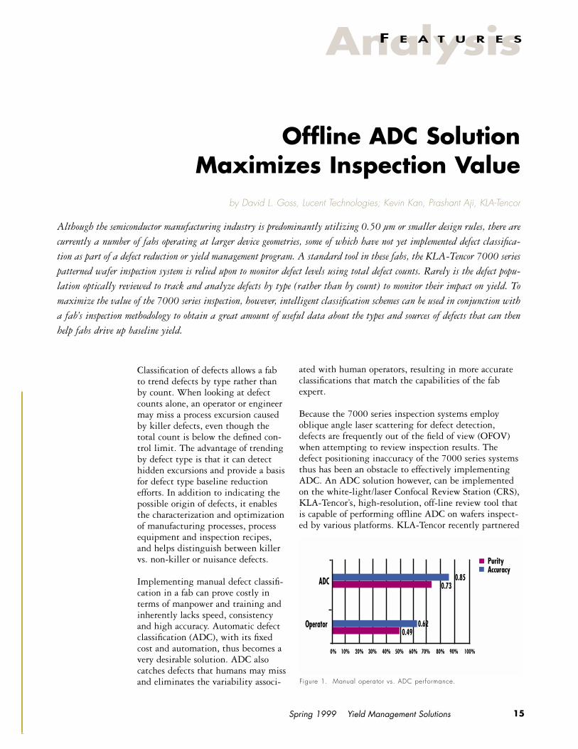
intensity defects occurred, virtually all remainingdefects from the 7000 scan fell inside the field of viewof the CRS at 50x magnification. As shown in figure 2,between 94 and 99 percent of the defects were IFOV,indicating the potential for high classification accuracy.
The type pareto charts in figure 3 demonstrate goodagreement between the expert manual and ADC classification of defects found on the wafers. The overallADC performance of 80 percent accuracy and 85 percent purity (figure 4) reveals that using the 50xobjective for ADC did not result in any loss of classifi-cation capability. Results from this study by LucentTechnologies indicate that ADC can be applied success-fully to 7000 series inspections and can be an effectivepart of a fab’s yield management program.
1. Goss, D. et al, “Offline ADC Solution for 7000 Series Inspectors using theCRS”, proceedings of KLA-Tencor Yield Management Solutions Seminar1998, Austin, Texas.
Figure 2. Defects within the field of view are ADC classifiable after
binning of large, high intensity defects.
Figure 3. Defect type pareto for manual “expert” vs. ADC.
100%
80%
60%
40%
20%
0%Base P Poly Metal 1
STDULT
98% 97% 96%94% 99% 94%
Defec
ts in
FOV
Inspection modeFOV Results
Standard Resolution (STD)Ultra High Resolution (ULT)
Defec
t Cou
nt
1 2 231 3 4 5 1 2 4 231 5 2 5 3 231
Manual ADC16014012010080604020
0
Base P Poly Metal 1
100%90%80%70%60%50%40%30%20%10%0%
Base P Poly Metal 1
AccuracyPurity
76.8% 83.2% 79.2%83.8% 86.6% 85.4%
AccuracyPurity
Figure 4. ADC performance shows high layer accuracy and purity
over manual classification techniques.
Analysis
Spring 1999 Yield Management Solutions 17
F E A T U R E S
Intelligent Line Monitoring
Maximum productivity through an integrated and automated strategy
by Tom Pilon, IBM Microelectronics Division; Mark Burns, Verlyn Fischer, Matthew Saunders, KLA-Tencor
The industry’s need for greater volumes ofintelligently collected defect data is mirrored at the state-of-the-art 0.25 µmtechnology fabrication facility of IBM’sMicroelectronics Division, which producesmultiple memory and logic devices across anumber of technologies. IBM recognized theneed to have a system that would help solveyield problems at a reasonable cost, maximizefab productivity and offer the flexibility tomake enhancements with the advances intechnology and manufacturing capacity.KLA-Tencor’s Intelligent Line MonitoringSystem (ILM) was installed to assess theeffectiveness of such an integrated approachto yield management.
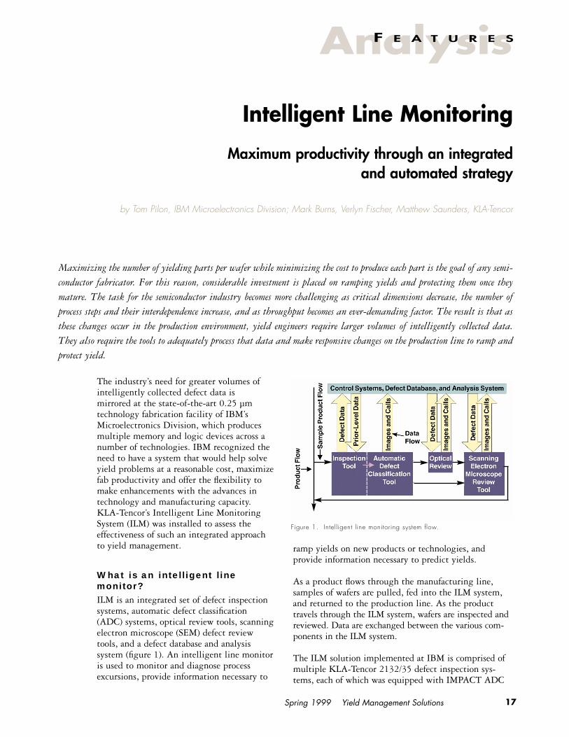
What is an intelligent line monitor?ILM is an integrated set of defect inspectionsystems, automatic defect classification(ADC) systems, optical review tools, scanningelectron microscope (SEM) defect reviewtools, and a defect database and analysis system (figure 1). An intelligent line monitoris used to monitor and diagnose processexcursions, provide information necessary to
Maximizing the number of yielding parts per wafer while minimizing the cost to produce each part is the goal of any semi-conductor fabricator. For this reason, considerable investment is placed on ramping yields and protecting them once theymature. The task for the semiconductor industry becomes more challenging as critical dimensions decrease, the number ofprocess steps and their interdependence increase, and as throughput becomes an ever-demanding factor. The result is that asthese changes occur in the production environment, yield engineers require larger volumes of intelligently collected data.They also require the tools to adequately process that data and make responsive changes on the production line to ramp andprotect yield.
ramp yields on new products or technologies, and provide information necessary to predict yields.
As a product flows through the manufacturing line,samples of wafers are pulled, fed into the ILM system,and returned to the production line. As the producttravels through the ILM system, wafers are inspected andreviewed. Data are exchanged between the various com-ponents in the ILM system.
The ILM solution implemented at IBM is comprised ofmultiple KLA-Tencor 2132/35 defect inspection sys-tems, each of which was equipped with IMPACT ADC
Figure 1. Intelligent line monitoring system flow.

Spring 1999 Yield Management Solutions118
F E A T U R E S
software, scanning electron defect review microscopeswith automatic defect location (ADL) capabilities such as the Amray 3800, off-line optical defect reviewstations such as the CRS-1010, 2552 data analysis stations, in-house operational systems, in-house analysissystems, and a Quest defect analysis system.
The fundamental difference between an integrateddefect reduction system and a non-integrated tool set isthat the integrated system leverages the capabilities ofthe point products through integration and automationto generate a maximally informative and cost-effectivesample (termed as “smart sample”). Such integrationhelps provide maximum information about only thosedefects that most detract from yield. This type of sampling strategy provides the greatest impact towardimproving chip yields and fabricator productivity.
Because SmartSampling™ is automated by the ILM system, data can be continuously collected as productsmove through the production line. SmartSampling provides information which allows a line monitoringsystem to optimally detect process excursions, predictyield, and assist in yield learning. It does this by providing the source, type, and quantity of defects forproducts and technologies at the various process levels.Distillation processing is the key feature of an ILM system used to produce a smart sample. It does this by choosing defects on which to collect additionalinformation based on the defects’ potential impact on yield and other current in-line information.
Improved productivityInstallation of the ILM system at IBM and its ability to intelligently sample the production line generatedseveral measurable productivity improvements:
Reallocation of ResourcesBy automating the optical review process, valuableresources can be reallocated from manual review activi-ties (such as performing review, training, or verification)to other value-added processing tasks or higher-levelyield improvement tasks.
Since the installation of ILM less than a year ago, IBMhas reallocated up to 40 percent of its review operatorsto other work. In addition, time spent on training andverifying classifiers has decreased with the implementa-tion of ADC versus manual classification techniques(figure 2). This occurred because ADC training sets arefixed, whereas human memory and judgment is subjec-tive and varies with each operator’s level of expertiseand knowledge of the defect source, defect-kill poten-tial, operator mood, and time during the week or shift.Furthermore, IBM has recently negated its originallyestablished need to increase their number of manualreview stations by 43 percent.
Cycle Time ReductionThe ILM solution reduced cycle time in three ways.First, by decreased defect review times. ADC has beenshown to require far less time to classify a defect thanmanual review (by as much as 66 percent). Second, bydecreased queue times. By coupling wafer inspectionand optical review, the queue time between these stepswas completely eliminated. Queue time is the timewafers sit on a shelf in between the inspection andreview steps and has been measured to be as much as 70minutes (on average) when performing manual review.
Using manual review versus ADC review systems on adefect sample set showed that the time savings with theADC system were significant (figure 3). Based on agate-oxide classifier, cycle time was reduced by as muchas 67 percent with in-line ADC versus off-line manualreview.
The third way cycle time was reduced was with the useof a minimized sample size. While reduction in thetime taken to process defects during review is animportant contribution to decreased cycle times, thegreatest benefit derived with the ILM solution is thatthe sample set can be smaller yet contain all the criticalinformation. This is important because a sample that istoo large and takes too long to measure can cost morein lost production than in lost yield. The ILM solutionallows on-the-fly defect filtering, which decreases theimpact of doing off-line optical and SEM review on
Figure 2. Reduction in time spent on classifier training and verification.
Figure 3. Cycle time for three 8" wafers, with 100 percent cover-
age, 0.62 µm pixel, and 100 defects classified per wafer.

Spring 1999 Yield Management Solutions 19
F E A T U R E S
total cycle time. This is especially important sinceSEM defect review is a costly inspection.
Figure 4 shows how the number of defects that aresent for ADC on optical review tools such as the Confocal Review Station and SEM defect review toolssuch as the Amray is reduced by using smart samplingtechniques.
Increased FlexibilityModular design of the ILM system allows inspectionsystems to be swapped, feature extensions to be madeor a system to be conveniently expanded and enhancedas demanded by shifts in technology and capacityrequirements. The benefit of increased flexibility, whichis especially important in a manufacturing environ-ment, is improved and protected cycle time.Component similarity of tools in the ILM systemallows the user to run a product interchangeablythrough similar tools eliminating overheads associatedwith set-up and extensive recipe management for eachindividual tool.
For the inspection/ADC components in an ILM systemto be interchangeable they must match. Matchingrequires that defects be identified equally well on oneor more inspection tools and that defect classificationcalls be similar on one or more ADC review systems.In other words, a lot placed at any inspector/ADC sys-tem will generate the same wafer map and reviewpareto as it would at any other inspector/ADC system.
The addition of database components to IBM’s ILMsystem, and feature extensions that were made with theaddition of ADC as an option to the defect inspectordemonstrate the ILM system flexibility. Inspectors herehave been matched on three product levels (at twoinspection sensitivities each) to 95 percent while ADCsystems have matched in the neighborhood of 80 percent on product wafers and up to 97 percent on adefect standard wafer (figure 5). In addition, the meansto track and maintain ADC matching has been studied.
ADC classifier extendibility across products and similarprocess levels for a given technology has limited theset-up time and classifier maintenance duties to rangesacceptable in a manufacturing environment. For exam-ple, without classifier extendibility, a fab running twotechnologies, two products each, and three via levelsper product would require 12 classifiers. However, withclassifier extendibility, that same fab would need tobuild only two ADC classifiers. At IBM, classifierextendibility has been shown to reduce classifier cre-ation by 80 percent.
Yield Protection and EnhancementThe time to detect a yield-limiting process excursion isthe sum of the beta risk, inspection time, and reviewtime. The beta risk is the time that a process is out-of-control but undetected and depends on a number ofparameters, including production rates, line samplingstrategy, and defect count statistics.
Data gathered on products at the via levels were usedto calculate time-to-detection using manual defect clas-sification (MDC) and ADC techniques (figure 6). Thegreatest contribution to detection time was the betarisk. In addition, it has been shown that review accura-cy has a significant impact in reducing the beta riskcontribution. The model that was used to make thiscalculation was developed by the CompetitiveSemiconductor Manufacturing (CSM) AutomatedInspection Focus Study Research Group.
Detection delay may also be represented in terms ofrevenue loss per hour. The total cost associated with an
Figure 4. Cycle-time reduction based on smart sampling.
Figure 5. ADC matching performance.
Figure 6. Total detection delay for via-level excursion monitoring
strategies.

excursion is the sum of five components. Beta risk isthe lost revenue due to product failing because of anout-of-control situation. Inspection cost is associatedwith the cost to operate an inspection system. Reviewcost is associated with the cost to perform review. Inthis model, ADC review cost was rolled into the costof inspection. Source identification is a measure of thecost to isolate the cause of a measured excursion, andfixing cost is associated with the cost of resolving theyield-limiting problem.
F E A T U R E S
Figure 7. Revenue loss per hour for via-level excursion monitoring
strategies.
THIN FILM SOFTWARE 2.xWORKSTATION
Off-tool data analysis andrecipe management
GEM/SECS softwaredevelopment and training tool
OLSA 1.xOff-line spectral analysis
software for recipe development,measurement simulation,
and analysis
RECIPE GENERATORAutomatic waferless recipe
creation using basic stepper andreticle database information
Recipe generation on a local tool or workstation database
LAPLINK™FOR NT
Remote control for diagnosticsand troubleshooting
For more information, circle RS#032 located on the business reply card or call (408) 875-7996.
New Off-Tool Software Products forIncreased Film Measurement Productivity
The two greatest contributions to the total revenue lossare the beta risk and cost of review (figure 7). Revenueloss due to excursions at the via levels has been reducedby 36 percent with the implementation of the ILMsolution.
The solutions for future challengesThe ILM system serves to improve productivity by limiting the number of wafers exposed to yield-limitingconditions, allowing valuable resources to be reallocatedto value-added processing tasks and reducing samplingcycle times while maintaining the integrity of the sample data.
As the ILM solution matures, new features will beadded which will further reduce time-to-results. Forexample adaptive sampling, singular integrated inter-faces, central inspection and classifier creation and management, intelligent classifier builds, signatureanalysis, automated engineering analysis and decisionmaking, parametric analysis, and ADC on SEM andlaser-based inspection tools will become standard features necessary to keep pace with the increasingdemands of the industry.
circle RS#012

Spring 1999 Yield Management Solutions 121
MetrologyF E A T U R E S
Poly MOSCAP process vs. in-lineElectrical testing is often used after thermaloxidation as a means of detecting oxide contaminants introduced or activated during processing. It is important, however,to recognize that the degree and type ofprocessing prior to test will influence thetype of information received. For instance,the sample preparation necessary to get polymetal oxide silicon capacitors (MOSCAP)wafers ready for capacitance voltage (C-V)testing results in a significant exposure ofthe test structure to high temperatures.This process mimics the thermal exposureto full-flow devices, so the C-V electricaltest parameters should ostensibly detectoxide problems that will ultimately resultin end-of-line test failure. The naturalannealing and cleaning action of theprocess, however, tends to mask true varia-tions in the as-grown oxide quality. From amanufacturing viewpoint, it would bepreferable to have an early warning systemthat flags impending problems before theyhave reached a critical stage. The standardC-V parameters are still desired, but with-out the cleaning action inherent in the polyMOSCAP deposition process. A preferredmethod would be an in-line technique analogous to C-V that does not requireMOSCAP processing.
This paper describes one of the first produc-tion implementations of such a system,
Replacing C-V Monitoring with Non-Contact COS Charge Analysis
by Kelvin Catmull, Richard Cosway, Motorola; Brian Letherer, Greg Horner, KLA-Tencor
Monitoring contamination levels in diffusion furnaces is necessary to ensure that a consistent environment is maintainedfor the production of semiconductor devices. Due to the large load sizes of diffusion furnaces, there is a potential for signif-icant amounts of scrap if adequate contamination monitoring is not maintained. In addition, a significant amount of prod-uct remains at-risk if contamination monitoring is not performed in a timely manner. Clearly, the value of monitor datais greatest immediately after a product run and this value decreases with time.
based on the corona-oxide-semiconductor (COS) tech-nique. To provide a well-known reference for this work,we will concentrate on the sensitivity differencesbetween poly MOSCAP test structures and the COStechnology.
COS technologyCOS is similar to quasi-static (low frequency) C-V testing. The principal difference is that COS is a non-contact method, whereas C-V requires MOSCAPprocessing. As in C-V technology, COS analysisrequires applying an electrical bias to the sample tomeasure the oxide’s electrical properties. For C-V, thisbias is a voltage applied to the MOSCAP through anelectrical prober and the response is the measuredcapacitance. With COS, the bias is applied by chargingthe oxide surface. The bias, in charge/area, is measuredby a coulombmeter attached in series with the chuck. A typical sweep may bias the surface to create an electric field of ±1MV/cm2 (the same bias range used inconventional C-V testing). The full sweep is composedof approximately 40 small charge depositions. Twotechniques are used to measure the response of thesemiconductor after each charge deposition:
1. Surface voltage (Vs) is measured by a noncontactvibrating Kelvin probe. Vs is controlled by the capacitance of the series-connected oxide and silicon.The oxide capacitance is a constant, while the siliconcapacitance has an inherent bias dependence due to thesemiconducting nature of the silicon.
2. Surface photovoltage (SPV) is the temporary voltagecreated when free carriers are photo-injected into the
near surface region of the silicon. In this case, the probevibration used to measure Vs is turned off, and a high-speed light flash is used to photo-generate carriers. Avoltage spike caused by the temporary collapse of thenear surface band bending is capacitively coupled to themotionless sensor and captured by a high speed A/Dconverter.
Measurement FundamentalsThe building blocks described above are used in a repet-itive fashion to build a COS data sweep: deposit charge(Q), measure Vs, and measure SPV. The resultant Q, Vs,and SPV curves are analyzed using non-linear curve fit-ting and a full quasi-static band bending analysis1.Several oxide electrical parameters (Vfb, Dit, Tox, Qtot,etc.) are extracted during this analysis.
Mobile Charge DeterminationIn the COS technique, mobile charge is pushed andpulled across the oxide. An electric field is appliedusing corona charge. Heat cycles similar to conventionalbias temperature stress measurements (200-250ºC) areperformed. The surface voltage drop that occurs duringa heat cycle is directly proportional to the amount ofmobile charge in the oxide.
ExperimentalIn an attempt to correlate C-V measurements to COSanalysis, samples with differing levels of Qm, Vfb, and
Quantox
Vfb Pre Resist Vfb Post Ash
Resist Ash
Ash Only
-0.4
-0.2
0.0
-1.0
-0.8
-0.6
Poly MOSCAP C-V
-0.4
-0.2
0.0
CV Control Resist and Ash-1.0
-0.8
-0.6Vfb
(V)
Dit were produced. All samples had 500 Å thermaloxides grown at 1050ºC on p-type, boron-doped (100) silicon substrates. The following methods wereemployed to change the characteristics of the thermaloxide intentionally:
1. Photoresist was applied to the surface of the wafer,then ashed off to increase Qm on several wafers.
2. An O2 flow during the temperature ramp down of athermal oxidation process was used to increase the fixedoxide charge and density of interface traps. A subse-quent forming gas anneal was used to passivate theSi/SiO2 interface.
3. An HCl treatment at elevated temperature was usedto remove mobile charge from the surface of the wafers.
The Vfb, Dit and Qm of all the wafers were measuredwith the Quantox Process Monitoring System, which isbased on COS technology. Pairs of wafers were measured
to verify repeatability. Measurements were made withthe Quantox system both before and after exposure tocontamination. Split lot experiments were carried outwith C-V testing, while control wafers were measuredwith both techniques.
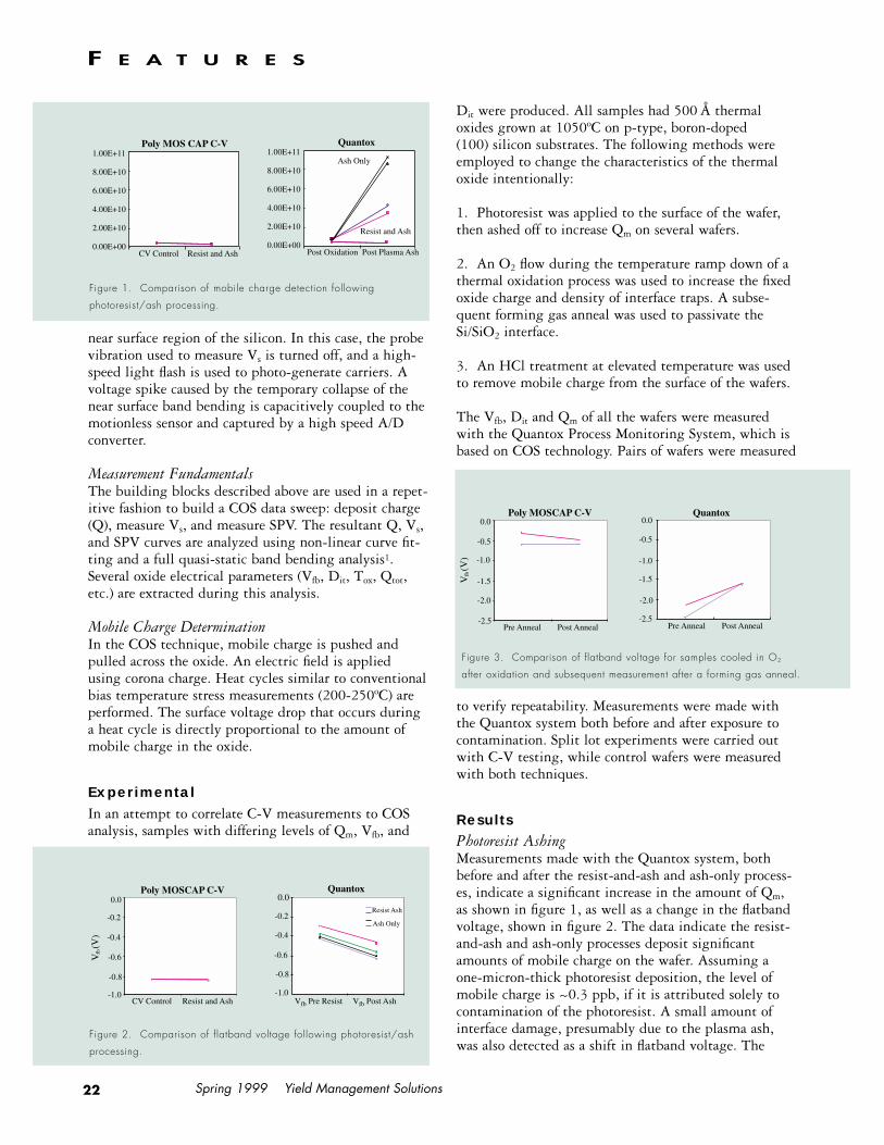
ResultsPhotoresist AshingMeasurements made with the Quantox system, bothbefore and after the resist-and-ash and ash-only process-es, indicate a significant increase in the amount of Qm,as shown in figure 1, as well as a change in the flatbandvoltage, shown in figure 2. The data indicate the resist-and-ash and ash-only processes deposit significantamounts of mobile charge on the wafer. Assuming aone-micron-thick photoresist deposition, the level ofmobile charge is ~0.3 ppb, if it is attributed solely tocontamination of the photoresist. A small amount ofinterface damage, presumably due to the plasma ash,was also detected as a shift in flatband voltage. The
Spring 1999 Yield Management Solutions22
F E A T U R E S
Figure 1. Comparison of mobile charge detection following
photoresist/ash processing.
Quantox1.00E+11
8.00E+10
6.00E+10
4.00E+10
2.00E+10
0.00E+00Post Oxidation Post Plasma Ash
Resist and Ash
Ash Only
Figure 2. Comparison of flatband voltage following photoresist/ash
processing.
Poly MOS CAP C-V1.00E+11
8.00E+10
6.00E+10
4.00E+10
2.00E+10
0.00E+00CV Control Resist and Ash
-2.5
-2.0
-1.0
-0.5
0.0
-1.5
Quantox
-1.5
Pre Anneal Post Anneal
Poly MOSCAP C-V
-2.5
-2.0
-1.5
-1.0
-0.5
0.0
Pre Anneal Post Anneal
-1.5Vfb
(V)
Figure 3. Comparison of flatband voltage for samples cooled in O2
after oxidation and subsequent measurement after a forming gas anneal.
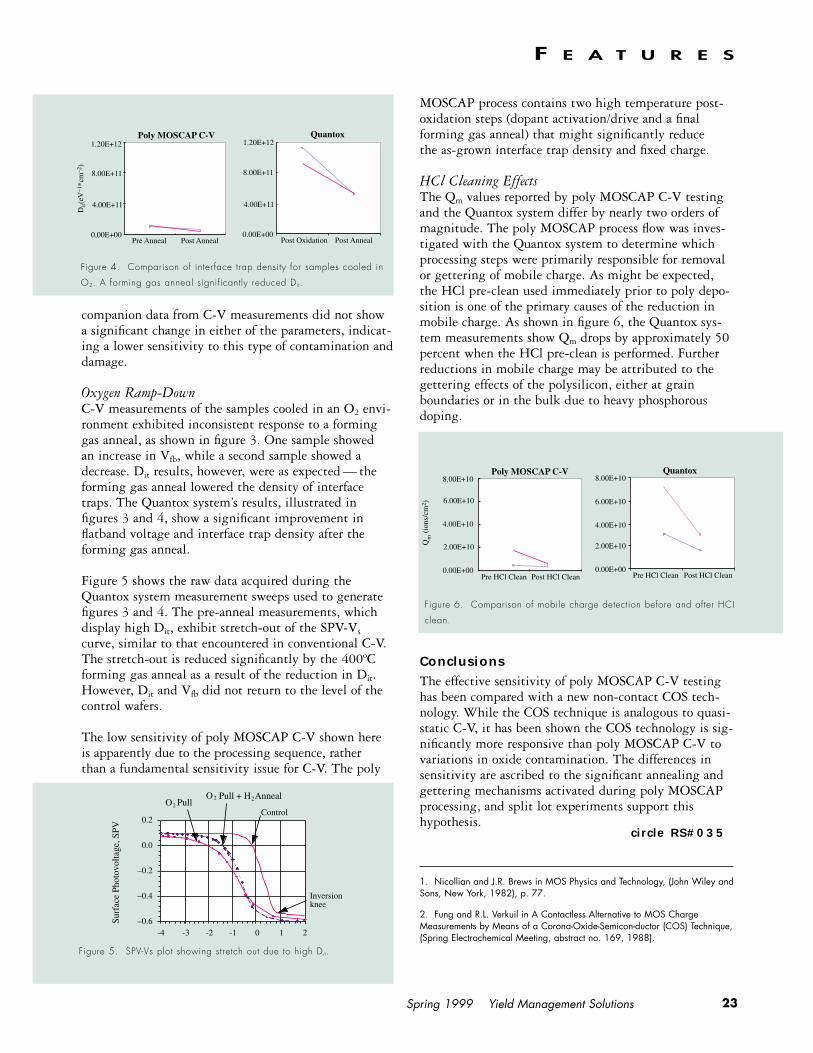
MOSCAP process contains two high temperature post-oxidation steps (dopant activation/drive and a finalforming gas anneal) that might significantly reduce the as-grown interface trap density and fixed charge.
HCl Cleaning EffectsThe Qm values reported by poly MOSCAP C-V testingand the Quantox system differ by nearly two orders ofmagnitude. The poly MOSCAP process flow was inves-tigated with the Quantox system to determine whichprocessing steps were primarily responsible for removalor gettering of mobile charge. As might be expected,the HCl pre-clean used immediately prior to poly depo-sition is one of the primary causes of the reduction inmobile charge. As shown in figure 6, the Quantox sys-tem measurements show Qm drops by approximately 50percent when the HCl pre-clean is performed. Furtherreductions in mobile charge may be attributed to thegettering effects of the polysilicon, either at grainboundaries or in the bulk due to heavy phosphorousdoping.
ConclusionsThe effective sensitivity of poly MOSCAP C-V testinghas been compared with a new non-contact COS tech-nology. While the COS technique is analogous to quasi-static C-V, it has been shown the COS technology is sig-nificantly more responsive than poly MOSCAP C-V tovariations in oxide contamination. The differences insensitivity are ascribed to the significant annealing andgettering mechanisms activated during poly MOSCAPprocessing, and split lot experiments support thishypothesis.
1. Nicollian and J.R. Brews in MOS Physics and Technology, (John Wiley andSons, New York, 1982), p. 77.
2. Fung and R.L. Verkuil in A Contactless Alternative to MOS ChargeMeasurements by Means of a Corona-Oxide-Semicon-ductor (COS) Technique,(Spring Electrochemical Meeting, abstract no. 169, 1988).
companion data from C-V measurements did not showa significant change in either of the parameters, indicat-ing a lower sensitivity to this type of contamination anddamage.
Oxygen Ramp-DownC-V measurements of the samples cooled in an O2 envi-ronment exhibited inconsistent response to a forminggas anneal, as shown in figure 3. One sample showed an increase in Vfb, while a second sample showed adecrease. Dit results, however, were as expected — theforming gas anneal lowered the density of interfacetraps. The Quantox system’s results, illustrated in figures 3 and 4, show a significant improvement in flatband voltage and interface trap density after theforming gas anneal.
Figure 5 shows the raw data acquired during theQuantox system measurement sweeps used to generatefigures 3 and 4. The pre-anneal measurements, whichdisplay high Dit, exhibit stretch-out of the SPV-Vs
curve, similar to that encountered in conventional C-V.The stretch-out is reduced significantly by the 400ºCforming gas anneal as a result of the reduction in Dit.However, Dit and Vfb did not return to the level of thecontrol wafers.
The low sensitivity of poly MOSCAP C-V shown hereis apparently due to the processing sequence, rather than a fundamental sensitivity issue for C-V. The poly
F E A T U R E S
23Spring 1999 Yield Management Solutions
Quantox
Post Oxidation Post Anneal0.00E+00
4.00E+11
8.00E+11
1.20E+12Poly MOSCAP C-V
0.00E+00
4.00E+11
8.00E+11
1.20E+12
Pre Anneal Post Anneal
Dit(
eV–1
*cm
–2)
Figure 4. Comparison of inter face trap density for samples cooled in
O2. A forming gas anneal significantly reduced Dit.
Quantox
0.00E+00
2.00E+10
4.00E+10
6.00E+10
8.00E+10
Pre HCl Clean Post HCl Clean0.00E+00
2.00E+10
4.00E+10
6.00E+10
8.00E+10Poly MOSCAP C-V
Pre HCl Clean Post HCl Clean
Qm
(io
ns/c
m2 )
Figure 6. Comparison of mobile charge detection before and after HCI
clean.
circle RS#0350.2
0.0
–0.2
–0.4
–0.6-4 -3 -2 -1 0 1 2
O2 Pull2 Pull + H2 Anneal
Inversionknee
O
Control
Surf
ace
Phot
ovol
tage
, SPV
Figure 5. SPV-Vs plot showing stretch out due to high Dit.

Spring 1999 Yield Management Solutions24
MetrologyF E A T U R E S
In this article, a KLA-Tencor UV-1250SEspectroscopic ellipsometer was used to mea-sure both the film thickness and the opticalproperties of seven HSG-Si films fabricatedusing a range of seeding and anneal temper-atures.
Capacitor fabrication was completed by thedeposition of a dielectric film on top of theHSG-Si followed by a top polysilicon elec-trode. We report a strong linear correlationbetween the HSG-Si film thickness and thecompleted device capacitance. Additionalinsight into the discontinuous surface struc-ture of HSG-Si films was provided by highresolution profilometry using a KLA-TencorHRP-220.
Wafer fabricationIn a typical fabrication of HSG-Si films, alayer of oxide (SiO2) is first deposited on acrystalline silicon (c-Si) substrate. A capaci-tor plate (or storage electrode) that consistsof a layer of doped amorphous silicon isformed on this oxide by low-pressure chem-ical vapor deposition. Silicon microcrystals– seeds – are then grown from the gaseousphase on the amorphous silicon layer. Thewafer is finally annealed in order to growthe amorphous silicon HSG-Si layer usingthe seeds as nucleation sites. During the
annealing process, which occurs under high vacuum,the HSG-Si seeds grow at the expense of the underlyingamorphous Si layer to yield the characteristically roughsurface. During annealing, the amorphous Si layerbecomes partially crystallized (and is hereafter referredto as polysilicon).
HSG surface topography and film parametersThe cross-section of a typical HSG-Si film stack is represented schematically in figure 1. The HSG-Si layeris composed of islands or “grains” of silicon, and can bedescribed by the mean grain diameter, height and thenumber of grains per unit surface area. The underlyingpolysilicon layer is assumed to be smooth.
Figure 2 is a topographic image obtained from an HSG-Si wafer using the profilometer. The area analyzed is 1 x 1 µm2. The maximum grain height is approximately 1000 Å.
Control of HSG-Si Fabrication UsingFilm and Surface Technologiesby Clive Hayzelden, Senior Technical Marketing Manager; Albert Bivas, Technical Marketing Manager; Carlos L. Ygartua, Process Module Manager; Kin-Chung Chan, Senior Applications Engineer; Jason Schneir, Product Marketing Manager
The fabrication of hemispherical-grained silicon (HSG-Si) was developed to increase the surface area of capacitor platesand consequently the storage capacitance of high-density dynamic random access memory (DRAM) devices. The increasein surface area (typically 1.8–2.4 times, as compared with smooth polysilicon electrode plates) is extremely sensitive toprocessing conditions (e.g., seeding and annealing temperatures). Tight in-line process control is, therefore, essential toobtain high yields.
Silicon (poly/amorphous)
Oxide
Silicon (crystaline)
HSG-Si
Figure 1. Schematic: cross-section of a typical HSG-Si film stack.

The SE optical path is represented schematically in fig-ure 3. The wafer is illuminated using linearly polarizedlight at a large angle of incidence. The reflected light iselliptically polarized and its polarization state is ana-lyzed over a selected wavelength range. In this analysiswe utilized the wavelength range 320-800 nm. Thiswavelength range included spectral information fromthe n and k peaks at 372 nm, while avoiding the effectsof scattering and absorption by the HSG-Si layer in thedeeper part of the ultra-violet part of the spectrum.
The SE measurement provides the experimental spectra,tanΨe(λ) and cos∆e(λ). Theoretical ellipsometry equa-tions, tanΨt(λ) and cos∆t(λ), represent the expectedreflected light polarization for a given set of film stackparameters.
TanΨ and cos∆ are derived from the complex electricalfield reflection coefficients, Rp and Rs, of the p and spolarization components of the reflected light, and fromthe phase difference, ∆, between these two componentsby the equation:
(1)
The quality of the spectral fit (goodness of fit or GOF)based upon the difference between these spectra is provided by the system.
Dispersion modelsA good fit between experimental and theoretical spectrarequires knowing or calculating the values of n and kat all the individual wavelengths in the spectra. As thisis not practically possible, continuous approximationmodels – with a limited number of variables – aredeveloped to describe the dispersion of the differentmaterials that constitute the film stack. During the calculations, n and k are fitted at the same time as thefilm thickness until the best fit is obtained.
The simplest physical model for the n and k dispersionsis the harmonic oscillator, which is based on the solu-tion for the dipole moment for a harmonically bound
Spring 1999 Yield Management Solutions 25
F E A T U R E S
For typical film stacks – composed of homogeneouslayers with smooth interfaces – the optical parametersof a film layer are the thickness, t, the refractive index,
n, and the extinction coefficient, k. The parameters forthe film substrate are its refractive index and extinc-tion coefficient. Since n and k depend on the wave-length in a way that is characteristic of the material (aproperty known as dispersion), it is important to mea-sure the optical properties of the film stack over abroad wavelength range. The UV-1250SE uses broad-band light in the wavelength range 240-800 nm.
Because the HSG-Si layer is discontinuous, the spec-troscopic ellipsometric analysis reports “effective” values of t, n and k for this layer. For the polysiliconlayer, both the thickness and degree of crystallinitywere determined.
Spectroscopic ellipsometrySpectroscopic ellipsometry (SE) measures the polariza-tion of the light reflected from the surface of a wafer.This technique has been widely adopted for the non-destructive determination of the thickness and opticalparameters of both single- and multi-layer thin filmstacks.
Figure 2. Topographic image obtained from an HSG-Si wafer using
an HRP-220.
Figure 3. Spectroscopic ellipsometry optical path schematic.
Figure 4. Schematic: deposition of a dielectric layer and polysilicon
top electrode on HSG-Si.
HSG
PolysiliconDielectric
Polysilicon
tanΨe • exp(i∆) = Rp
Rscos∆ = Re (exp(i∆))

Spring 1999 Yield Management Solutions26
F E A T U R E S
variable parameters. The thickness of the oxide wasfixed at 1000 Å. A standard n and k table, with novariable parameters, was used for the Si substrate.
ResultsWe analyzed each of the seven wafers at five sites usingSE. The thicknesses of the HSG-Si layer and underly-ing polysilicon layer were calculated, along with thecrystallinity of the polysilicon. After the optical mea-surements, the wafers were processed further to createcapacitors by first depositing a dielectric layer then apolysilicon top electrode on top of the HSG-Si (shownschematically in figure 4). The capacitance was thenmeasured at the same sites that were characterizedusing SE. An example of tanΨ(λ) and cos∆(λ) spectrafor one of the HSG-Si wafers (wafer #3 at site #1) ispresented in figure 5. The corresponding dispersionplots for n and k are shown in figure 6.
The calculation method and dispersion models workedwell for the entire range of process conditions and theresults are summarized in table 1.
Table 1 shows the average capacitance enhancementvalues (i.e., the ratio of the capacitance with an HSG-Silayer to that of capacitors with a flat electrode). A lin-ear correlation (>95 percent), with a reasonable sensi-tivity (slope), was found between the HSG-Si thicknessand the capacitance enhancement, as shown in figure7. The calculated percentages of amorphous silicon andvoids in the polysilicon layer indicate that this layerwas approximately 80 percent crystallized during thegrowth of HSG-Si. It was also found that wafer #6 hadbeen misprocessed as evidenced by abnormal polysili-con thickness, crystallinity and optical properties.
ConclusionThe characterization of HSG-Si wafers is particularlychallenging because the top layer is a rough and discon-tinuous film with a large sensitivity to process changes.
electron acted upon by an electromagnetic field. Thismodel was used to represent the effective dispersion ofthe HSG-Si.
The Bruggeman effective medium approximation(BEMA) model represents the film material as a mixture of several components, each defined by a tableof n and k values as a function of wavelength. In thecalculations, the volume fraction of each component inthe mixture is obtained. This model, which combinedamorphous Si, crystalline Si and voids, was used torepresent the polysilicon layer and account for a widerange of crystallinity.
The thermal silicon dioxide beneath the polysiliconwas modeled using a standard n and k table, with no
Figure 5. TanΨ(λ) and cos∆(λ) spectra for an HSG-Si wafer.
HSG HSG Polysilicon Polysilicon Polysilicon Goodness Capacitancewafer t(Å) n@633 nm t(Å) n@633 nm % crystallinity of fit enhancement
1 501.6 2.059 1031.2 3.488 0.799 0.9814 2.120
2 362.8 1.913 1041.3 3.626 0.802 0.9829 1.570
3 498.2 2.159 1037.3 3.436 0.786 0.9830 2.102
4 313.1 1.953 1049.9 3.676 0.789 0.9840 1.473
5 448.0 1.904 1053.5 3.501 0.827 0.9753 1.937
6 521.5 2.036 883.6 4.299 0.578 0.9806 2.032
7 475.3 1.944 1037.2 3.534 0.807 0.9803 1.958
Table 1. Summary of spectroscopic ellipsometry results for the HSG-Si, underlying polysilicon layer, and
capacitance enhancement values for the seven wafers.

High resolution profilometry is able to assess grain sizeand spatial distribution of the grains. In this study wedemonstrated that spectroscopic ellipsometry can beused to characterize both the HSG-Si and underlyingpolysilicon layers. A direct correlation between thethickness of the HSG-Si layer and the capacitanceenhancement of the fabricated devices was shown. Thedegree of crystallinity of the bottom electrode wasabout 80 percent. These two results can be used in pro-duction to monitor the fabrication process and to pre-dict DRAM capacitor performance.
F E A T U R E S
KLA-Tencor’s High Resolution Profiler (HRP)Series was recently honored with SemiconductorInternational magazine’s “Editors’ Choice Best Product” award for 1998. Nominations for this award are submitted to SemiconductorInternational by customers.
The HRP has been delivered to the top semiconductor manufacturers for advanced CMP development and production, includingcopper programs. With this broad installed base, KLA-Tencor continues to offer field-proven surface metrology solutions.
Visit our website at www.kla-tencor.com, or call 408-875-2098.
HIGH RESOLUTION PROFILER SERIES
Figure 7. Linear correlation between HSG-Si thickness and the
capacitance enhancement.
Figure 6. Dispersion plots for n and k for HSG-Si.
circle RS#002 + 005
circle RS#005

Spring 1999 Yield Management Solutions28
Inspection
Wafer Inspection Technology Challengesfor ULSI Manufacturing–Part I
by Stan Stokowski, Ph.D., Chief Scientist; Mehdi Vaez-Iravani, Ph.D., Principal Research Scientist
Evolution of the semiconductor manufacturing industry is placing ever greater demands on yield management and in par-ticular, on metrology and inspection systems. As critical dimensions shrink to 0.13 µm and 0.10 µm in the near futureand wafer sizes increase from 200 mm to 300 mm, economics will drive the industry to decrease the time for achievinghigh-yield, high-value production. Continued pressure to increase the return-on-investment for the semiconductor fabrica-tor has made it critical for inspection systems to evolve from stand-alone “tools” that just find defects to being a part of amore complete solution where detecting defects, classifying them, analyzing these results and recommending corrective actionare their functions.(Part one of two)
To understand how inspection systems willmeet the requirements of manufacturingintegrated circuits with smaller structureson larger wafers in the future, we need toconsider some of the basic physics, engineer-ing, and economic constraints imposed onthese systems.
Physics: To inspect an object we look at it viasome interrogating means, which are usuallyphotons or electrons scattered by the object.The detected scattered photons or electronsas a function of position (an image) hopeful-ly contain the information needed to deter-mine whether a defect is present. An imageprocessing system then decides if there is adefect. Thus, defect detection naturally con-sists of three main steps: first, obtaining theimage, second, processing the image, andthird, applying criteria to this processedimage to detect defects.
It is interesting to compare inspection tech-nology with that of lithography, in particu-lar, the exposure process. Lithography isalmost exclusively optical [I-line (365 nmwavelength), deep ultraviolet (DUV, 248 nm),193 nm, and eventually extreme ultraviolet(EUV, 13 nm)]. The print rate of opticallithography is now about 1010 resolution elements per second and is increasing to 1011
over the next few years. This high print rate is a conse-quence of the massive parallelism of optical techniques.On the other hand, the highest inspection rate currentlyis 6 x 108 pixels per sec. However, optical lithography has an easier task in that it does not have to process and analyze an image.
The challenge for inspection tools is then to detectsmall defects with a system resolution spot size muchlarger than the defect size. Fortunately, one does nothave to “resolve” a defect in order to detect it.Resolution, appropriately, does impact defect classifica-tion and identification. However, even for performingthese functions, we can sometimes obtain sufficientinformation without necessarily “resolving” the defect.
Even the first step of obtaining the image, by its nature,includes an optical processing step. How we illuminateand collect the resultant scattered light determines thecontrast between a defect and the background in whichit resides (surface or pattern scattering). Ideally onewants to maximize this contrast by carefully choosingthe optical arrangement. Fortunately, there are tools andtechniques for accomplishing this choice, some of whichare described here. In addition, for periodic array cellsoptical spatial filtering is effective. Finally, light polar-ization plays an extremely important role in enhancingsensitivity.
This article focuses on optical techniques for waferinspection because they are most commonly used.
F E A T U R E S

Brightfield and darkfield systemsAll optical inspection systems depend on photon scat-tering from the inspected object. Brightfield systemscollect both the scattered and reflected light throughthe same aperture to obtain an image. In addition, theobject is illuminated through the objective aperture.Basically, these systems are a high-speed microscope.Darkfield systems, on the other hand, only collect thescattered light; no part of the reflected light falls with-in the collection angle. They can have a multiplicity ofconfigurations, depending on the angle and type ofillumination, collection angles, and detector type.
Both these systems have their advantages and disadvan-tages for detecting different defect types. In general,darkfield systems are particularly useful when thedefect has some high-spatial-frequency topography,whereas brightfield is good at finding planar defects. Inmost cases darkfield systems find defects much smallerthan the system resolution or spot size; whereas, inbrightfield systems the detected defects are about thesame size as the system resolution. This fact has impor-tant implications for system throughput. Of particularimportance for system sensitivity, however, is the factthat no one optical arrangement is optimal for detect-ing all possible defect types.
Particle scatteringParticles or their effects are the source of a majority ofdefects in ICs. Thus, understanding particle scatteringhelps to design sensitive inspection tools. KLA-Tencor’sproprietary application software that calculates thepolarized scattering from a sphere into the 2π hemi-sphere above the substrate was used to calculate thescattering patterns described in this article, unless otherwise stated.
Figure 1 shows our definition of the spherical coordi-nates used in discussing scattering from particles, surfaces and defects. The polar angle is defined fromthe surface normal and the azimuthal angle counter-clockwise from the reflected beam projected onto thesurface plane. The illumination polarization definitions
Spring 1999 Yield Management Solutions 29
F E A T U R E S
are s (E perpendicular to the incidence plane) and p(E parallel to the incidence plane). The scattered fieldpolarization is s or p relative to the plane containingthe surface normal and the scattered light direction. Tounderstand some of the basic scattering rules, we startwith a polystyrene latex sphere (PSL) on silicon.Although PSL spheres are not found in IC fabs, theyare convenient for calibrating inspection systemsbecause they are spheres of known diameter.
Figure 2 shows scattering from PSL spheres as a func-tion of diameter, polarization, and angle of incidence.Of particular interest is the advantage of using p-polarized light for detecting small particles. Thetotal scattering cross section for a 60 nm PSL spherewith p-polarized illumination at 70º incident angle is86 times that with s-polarized light and 42 times thatwith normal incidence. Also note that most of the scattered light under oblique p-polarized illuminationis in the polar angular range of 20º to 70º. Thus, anoptimum system for detecting small particles usesobliquely incident p-polarized light and collects thescattered light over a large solid angle, 20º to 70º inpolar angle and almost 360º in azimuth.
The advantage of p-polarization for small particledetection is a consequence of the standing E-M wave
Surface Normal
ScatteredLight (s)
ScatteringPlane
ReflectedLight
IncidentLight (i)
IncidencePlane
Ep
Es
Ep(s)
Es(s)s0i0
sο
Figure 1. Diagram for coordinate and polarization definitions.
Figure 2. Scattered intensity patterns of PSL spheres on silicon as a
function of diameter, polarization, and incidence angle. The 488 nm
plane wave comes in from the left at 70° incidence and view is about
–90° in azimuth from the incidence plane. The last column of images
is for normal incidence, circular polarization. The numbers correspond
to the peak dif ferential cross sections and the total integrated cross
sections in µm2 divided by the cosine of the incidence angle.

where d is the spherediameter, λ is the illumi-nating wavelength, n isthe refractive index of thesphere and E is the elec-tric field at the sphere. Thus, higher refractive indexmaterials, such as semiconductors and metals, scattermore light. Figure 5 compares the total integratedscattering (TIS) for PSL, silicon, and aluminum sphereson silicon. As a consequence, if a system can detect 60nm PSL spheres on silicon, it can detect 40 nm alu-minum spheres on silicon.
Particle sizing is always of interest. Typically theindustry uses PSL spheres as a calibration standard. Ifan inspection system uses the total scattered lightintensity as an indication of particle size, figure 4reveals a problem: the intensity is not a monotonicfunction of the sphere diameter (oblique incidence hasless of a problem than normal incidence). Furthermore,the scattered intensity from spheres of other materialsobviously does not relate in a simple fashion to the PSLsphere response unless one compares the curves forsphere diameters less than 100 nm. To obtain bettersizing one needs to use more than one configuration ormode as suggested, for example, by the responsesshown in figure 4.
Surface scatteringFor unpatterned wafers the background noise comesfrom surface scattering. We will only describe here thekey parameters that determine surface scattering.
For surfaces that are rough, but with height variationsmuch less than the light wavelength, the scatteredpower per unit solid angle as a function of the polarangle and azimuth is:
where Pi is the input power, dΩ is the differential solidangle, θi, θs, φs are defined in figure 1, Qij(θi, θs, φs ) isthe polarization factor and PSD(fx, fy) is the powerspectral density of the surface height variation as a
fields above a surface. We can best describe this effectby realizing that for a small enough particle, the parti-cle acts as a probe of the near field because the far-fieldscattering depends on the E-M field present at the particle. If the particle is small enough, it does notsubstantially perturb the field that would be present inthe absence of the particle.
For 70º incidence figure 3 shows the electric field as afunction of distance above a silicon surface for s- and p-polarization. Note that s-polarized light has a low field
at the surface (“dark fringe”), whereas, p-polarizedlight is at a maximum. It follows then that small particle scattering is greatest for p-polarization.
Experimental results confirm the utility of the scatter-ing model. For example, figure 4 shows the agreementbetween measurements and modeling results as a func-tion of incidence angle and polarization.
The sensitivity of an inspection system for small parti-cle detection depends on the particle material. In theRayleigh limit the total integrated scattering of asphere in a medium depends on
Spring 1999 Yield Management Solutions30
F E A T U R E S
Figure 3. Magnitude of the electric field as a function of distance
above a silicon surface for s-polarization (solid line) and p-polarization
(dashed line) for 70° incidence and an input field amplitude of 1.
Figure 4. Scattering model calculations agree with measurements
for PSL spheres on silicon with 70° incidence angle, s-polarization
(squares) and p-polarization (triangles), and normal incidence
(diamonds). The collector covers the polar angles from about 25° to
72° and nearly 360° in azimuth.
Figure 5. Total integrated
scattering cross sections for
PSL (dotted line), silicon (solid
line), and aluminum (dashed
line) spheres on silicon.
d6 (n2 - 1) 2
λ4 (n2+ 2)• • E 2
dP 16π2
dΩ λ4= Pi • • [cos (θi) • cos2 (θs) • Qp, q (θi,θs,φs)] • PSD(fx, fy)
(1)
(2)

able from particles in a single channel detection sys-tem. The wafer manufacturers need to classify pits andparticles on silicon wafers. Pits are octahedral voids inCzochralski-grown silicon that have been exposed atthe surface by the polishing process. They are alsoknown as crystal-originated particles (COP), obviouslya misnomer. They sometimes are a single pit and, in alarge number of cases, partially overlapping doublepits.
Pits and scratches are “surface-breaking” defects; i.e.,they are into the surface. The scattering characteristics,therefore, of pits and particles are different and as aconsequence, we can classify detected defects as pits orparticles if we have information from multiple channelsor modes.
The first difference between pits and particles comesfrom their responses to normal and oblique illumina-tion. Figure 7 is a simple illustration of this difference.Part (a) shows the normal illumination with a sphereon a surface intercepting a cross section of the beam.Part (b) is the condition for an oblique beam where theilluminated area on the surface is the same as in part(a). Note that in this plane the same-sized sphere inter-cepts a larger fraction of the incident beam cross sec-tion. Thus, a sphere will scatter significantly more withoblique incidence (see figure 2). Part (c), however,shows that with oblique incidence a pit is at a signifi-cant disadvantage relative to a sphere on the surface forscattering light. Thus, comparing the scattered light innormal and oblique incidence can help classify pits andparticles.
A more important difference between pits and particlesis the angular pattern of the scattering. Both theoreti-cal calculations and experimental results show that particles scatter light principally into the polar anglerange from 20º to 70º when illuminated with p-polar-ized light. In contrast, pits scatter primarily toward the
function of the x and y components of the surface spatial frequency (1). The frequency components, fx and fy, are, in turn, related to the scattering anglesthrough the diffraction equations.
Once the surface PSD characteristic is known, we cancalculate, to a good approximation, the angular distri-bution of the light scattered by the surface.
Obviously, one tries to minimize surface scattering toobtain good defect sensitivity on rough surfaces. Ofparticular importance is the polarization factor of equa-tion 2. Figure 6 shows the variation of this factor forsilicon over the full scattering hemisphere for the fourcombinations of input and scattered polarizations and70º incidence. To minimize surface scattering, usingthe ss polarization combination and collecting light inthe vicinity of 90º and 270º azimuth is very effective.In addition, depending on the underlying material, thepp polarization combination and collecting scatteredlight in the forward direction is useful.
In equation 2 we can also see that the cos(θi) andcos2(θs) terms also imply that greater sensitivity todetecting particles is obtained in the double darkfieldconfiguration, where both angles are >45º.
Unpatterned inspection systems measure the back-ground scattering level, which the industry refers to as“haze”. The measured haze value obviously depends onwhere in the hemisphere we collect the scattered light.Obviously haze is related to the PSD characteristics of a surface, but the relationship is not necessarily asimple one.
Pit scatteringPits are of great interest to silicon wafer manufacturers.Pits have been a problem for inspection systemsbecause they also scatter light and are indistinguish-
Spring 1999 Yield Management Solutions 31
F E A T U R E S
Figure 6. Relative magnitudes of the optical polarization factors
Qi,j.cos2(θ) for 70° incidence on silicon: ss, pp, sp, and ps polariza-
tion combinations over the scattering hemisphere. (Gray scale conver t-
ed from color: bright band contour is 0.5 of the maximum.) The 488-nm
plane wave comes in from the left; view is near –90° in azimuth from
the incidence plane.
Figure 7. Schematic
illustrating the dif fer-
ence between parti-
cles and pits relative
to the illumination
incidence angle.

Scratches also scatter primarily toward the normal,similar to pits. Furthermore, for uniformly detectingscratches of any orientation, normal incidence is preferred.
Dielectric film effectsOn patterned wafers, dielectric films are present. Theselead to a couple of complications. One is the interfer-ence effect that produces color under broad band illu-mination and contrast variation under monochromaticillumination. These effects are particularly troublesomeif the film thickness is not uniform, and one is tryingto do a die-to-die comparison. In brightfield systemsbroad-band illumination has helped. In darkfield systems circularly polarized light is extremely useful in minimizing the film effect.
As a simple example, the scattering cross section of aPSL sphere on silicon dioxide on aluminum as a func-tion of the oxide thickness is shown in figure 9. Notethe substantial variations of total scattered light withfilm thickness with both s- and p-polarization withoblique incidence. However, because the s and p scat-tering are out-of-phase with respect to each other, scat-tering with circular polarization, which has both, is much less affected by film non-uniformity. For normal incidence, s, p, and circular are all equivalentand the film effect is worse than that seen with obliqueincidence.
Digs and scratch detection will also be affected bydielectric film thickness and polarization, but theirvariation in scattering is not in phase with the particlescattered intensity.
Previous layer defectsOne may or may not want to see previous layer defects,depending on the system application. Usually, whilemonitoring equipment one does not want to see downinto the previous layers. Oblique illumination with spolarization has much less penetration of energythrough transparent dielectrics than normal illumina-tion and thus is preferred for detecting current layerdefects.
Part II of this article addresses System Considerations to Meet theDesign Shrink Challenge and Future Needs and Developments in WaferInspection Technology and will appear in the next issue. To view thewhole article, you may also request an advance copy through theBRC or visit our website at www.kla-tencor.com/corpmag.
1. Church, E.L., Jenkinson, H.A., Zavada, J.M., Opt. Eng. 18, 125-138(1979)
normal; therefore, comparing the light scattered intohigher angles with those toward the normal will alsoclassify pits and particles. Even for normal incidencethis separation works; however, oblique incidenceworks best. We show experimental results for the p-polarized oblique incidence case are shown in figure 8.
Scratch scatteringScratches are important in CMP processes and may be yield-limiting. Scratches preferentially scatter perpendicular to their long dimension. Real scratchesare not perfect linear defects; in many cases they havecross-sectional variations along the scratch, may haveparticulate debris nearby, and commonly are “chattermarks.” These “chatter marks” or “micro-scratches”actually are a series of short small scratches along aline perpendicular to the long dimension of thescratches.
Spring 1999 Yield Management Solutions32
F E A T U R E S
Figure 8. Signal levels of PSL spheres and silicon pits with about 25°
to 72° collection vs. about 6° to 20° collection, shows superior classi-
fication of pits and particles using oblique incidence.
Figure 9. Scattered intensity for a 100 nm PSL sphere and a
250 nm PSL sphere on silicon dioxide on aluminum as a function of
oxide thickness and input polarization, p-polarization (long dash),
s-polarization (shor t dash), and circular polarization (solid). Scattered
light collected from about 25° to 72° polar angle.

Spring 1999 Yield Management Solutions 33
found that s-polarization and high sensitivity providedthe best results, especially in open areas of low patterndensity (figure 1).
The second step of the process involved collecting datafrom the manufacturing line at that inspection point,to establish a baseline and determine what impact thesedefects had on yield. Analysis of the data indicated thatdefects introduced at the CMP steps produce a highpotential for die loss. Based on this information, a teamwas formed to address the CMP processes as a source ofhigh yield impact.
At VLSI San Antonio, new inspectionpoints were introduced to monitor inter-metallic oxide (IMO) chemical mechanicalpolish (CMP) layers, and tungsten CMP(WCMP) layers. A combination of defectmonitoring using the AIT, defect reviewusing the CRS and JEOL SEM stations, andanalysis using Quest produced informationthat led VLSI to make changes to the way their CMP scrubbers and polishers are utilized. These changes provided significantbenefit to the yield learning rate at the San Antonio facility.
Introducing a new inspectionpointThe process that VLSI used for determiningwhether a new inspection point should be introduced for post-CMP layers wascomprised of several steps. First, the defectgroup characterized the proposed line moni-tor point. This involved setting up recipeson the AIT, and going through variouscombinations of polarizations and sensitivi-ty settings to determine which setup pro-vided the best capture of defects. In the caseof CMP layers, success meant capturing thelargest number of microscratches, shallowscratches, gouging and slurry residues whileminimizing false counts. The defect group
Improved Yield Learning Using CMP Equipment Monitors
by Scott Hiemke, Dean Spaugh, John Givens, Albert Liu, Miguel Delgado, VLSI San Antonio; Rebecca Howland Pinto, Ph.D., KLA-Tencor
When a new line monitoring point is introduced into a manufacturing line within a fab, it must be justified. Thisjustification process involves careful experimentation to determine that process excursions are occurring at these pointswhich have significant impact on yield. It involves verification that inspection and metrology tools are optimized toidentify the relevant excursions, and it involves bringing together people from several different groups within the fabto cooperate on the solution. Finally, the solution must be implemented on the manufacturing line.
cn pn sn
CMP defects by polarization
CM
P d
efec
ts
high low
CMP defects by sensitivity
CM
P d
efec
ts
Polarization Sensitivity
Figure 1. A combination of s input polarization and high sensitivity set -
tings on the AIT provided best capture of defects on CMP layers.
InspectionF E A T U R E S
nine lots through the process flow, measuring filmthickness and defectivity after each CMP step. The AITwas particularly well suited to this application, becauseits high throughput meant that every wafer in the lotcould be scanned to enable characterization of wafer-to-wafer variation. Examples of defects found after WCMPand after IMOCMP are given in figure 3. Note that several defect types were captured well in areas of densepattern.
Following the defect inspection, the wafers were mea-sured on the UV-1280SE to characterize the variation
Spring 1999 Yield Management Solutions34
F E A T U R E S
The team and its charterThe team’s charter was to optimize the CMP processes:specifically, to minimize defects introduced at CMPsteps, and maximize true up-time of the CMP polishers.VLSI set goals and deliverables for the project, and setlimitations on allowable methods for addressing theproblems. For example, existing CMP consumables(pads and slurries) and equipment had to be utilized.Defect inspection and film thickness measurements werethe chief techniques employed to attack the problem.
The interdepartmental team, comprised of process engineers from the defect group, CMP engineering and CMP manufacturing, discovered that the first steptowards solution of the problem was to establish a control action system. This system is represented by aflow chart that documents ownership for each step ofthe decision of what to do with out-of-control lots. Theprocess of documenting responsibility through the con-trol action system proved invaluable in making progresstowards the goals of the project.
The culpritsOnce the control action system was in place, the teambegan its investigation by examining the effectivenessof the post-CMP scrub. They discovered that changingthe scrub process significantly reduced the number ofdefects left on the wafer. A comparison of the new andold scrub processes is given in figure 2, along withexamples of defects found after scrubbing. Introducingthe new scrub process made an immediate, positiveimpact on defectivity.
The second area investigated was the nonuniformity ofthe oxide layer after CMP. The team followed a set of
Def
ect n
umbe
r
Each pairstudent’s t0.05
•
•
•• •••••
•••
•••
•••
•
STD scrubprocess
New scrubprocess
Figure 2. Introducing a new scrub process made an immediate,
positive impact on defectivity.
Figure 4. Film thickness measurements (using the UV-1280SE) showed
a domed oxide profile, which negatively af fected edge die yield.
Figure 3. Examples of defects detected after WCMP and after
IMOCMP.
Film
Thi
ckne
ss
Defect from Old Scrub Recipe
Defect detected at IMO2CMP
Defect detected at WCMP1
Site on the Wafer
CMP Manufacturing decided to change the pads morefrequently: three times more often to reduce the defectlevels. Introducing this inspection point has resulted ina dramatic change in the way maintenance is done onthe CMP polishers in this facility.
Faster yield learning now and in thefutureSince implementing the line monitoring methodologydescribed above, VLSI San Antonio has increased theiryield learning rate. A better yield learning rate trans-lates directly into higher profitability for the fab.Because of this success on their current products, VLSISan Antonio also elected to add an inspection point totheir below-0.25 µm development work, at shallow-trench isolation CMP (figure 6).
This paper is largely derived from a presentation first given in July 1998 atthe Yield Management Solutions Seminar during SEMICON/West.
Spring 1999 Yield Management Solutions 35
F E A T U R E S
in oxide thickness across the wafer (figure 4). The film thickness measurements showed that the oxide profile was domed, and as a result, edge die yield was negatively affected. This prompted the team to recommend tightening the specifications for post-CMPoxide uniformity.
Transfer to manufacturingThe last part of the team’s responsibility was to transferthe improved process to manufacturing. This meantthat the AIT had to be interfaced to PROMIS, VLSI’sWork In Progress (WIP) tracking system. Fortunately,more than 90 percent of the GEM/SECS code writtenoriginally for the Surfscan 7700 was transferable to theAIT. This ensured that the correct lot numbers, processlevels, recipes and data were being sent to Quest andtransferred to VLSI’s SPC system.
The line monitor was set up to monitor WIP in thequeue for a tool, and skip lots past the inspection stepsif more than a certain number of lots are waiting, or ifa recipe is missing. As a result of this setup, more than60 percent of the total volume are currently inspectedpost-CMP by scanning lots across 10 to 12 part types.In addition, over 50 percent of the other process layersare inspected on the AIT. At VLSI San Antonio, over19 process layers throughout the line are inspected bythe AIT.
The final step in transferring the process to manufac-turing involved training the CMP engineers and manu-facturing personnel to use Quest and the various reviewstations at their disposal.
The learning continuedOnce the improved process was successfully transferredto manufacturing, some other important discoverieswere made. One defectivity excursion at oxide CMPwas traced to a change in a drum of slurry, when thelines had been improperly flushed out (figure 5).
Another discovery was that just before a polishing padwas changed the defectivity level increased. As a result
Figure 5. Introduction of a line monitoring point helped trace defect excur-
sions to a faulty drum of slurry and wear and tear of a polishing pad.
Figure 6. Examples of defects found at a shallow trench isolation
(STI) CMP layer.
Avg
. de
fect
/waf
er (
#)
Time
Lots ran on polisher
after drum changePad changes
Inspection
Spring 1999 Yield Management Solutions36
F E A T U R E S
Automation Comes to Litho Inspection
by Alexander E. Braun, Associate Editor, Semiconductor International
Automated defect inspection and control strategies are commonplace across fabs, except for the litho cell. Because many lithoprocess defects are relatively large, applicable solutions are limited. For example, the cost-of-ownership of using highly sensitive inspection systems utilized in other process steps often cannot be justified. Anyway, litho error detection requires asystem that can be tuned to detect defect types with a wide range of characteristics.
to manual inspection techniques that provide little visibility or control and collect very little usable data—is a source of yield loss and scrap issues.
KLA-Tencor [has introduced] an inspection suitedesigned to overcome these limitations, the 2401Automated Macro Defect Inspection System. It isexpected to replace the bright-light MADI performedby human operators. It provides automated detection,classification and reporting of all yield-critical MADIdefect types, including hot spots, scratches, large parti-cles, extra and missing resist, unexposed fields, stria-tions and developer spots and splash-back (figure 1).
Since over 75 percent of yield-relevantdefect types are fairly large and visible tothe eye, macro after-develop inspection(MADI) traditionally has been a manual,operator-intensive process. Fabs rely mostlyon manual visual inspection to determinewhether a wafer passes (to further process-ing), is reworked (stripped and rerunthrough the litho cell) or scrapped. CurrentMADI systems are manual or semi-auto-mated, and illumination may range fromcommon green lights or spotlights to specialpoint sources and flat, monochromatic panels.Always, the detector is human.
This is limited; defect detection and classi-fication are inconsistent and unreliable,with results varying due to wafer complexi-ty, background patterning noise and humanboredom and fatigue. Up to 80 percent ofall MADI defects may go undetected untilafter etch or final test, when it is too late,resulting in higher scrap rates and lowersort yields. Depending on fab size, approxi-mately $3.6 million a year are wasted dueto defects undetected by human operators.
Increases in wafer complexity are adding toproblems likely to go undetected by manualinspection. While other process steps areimproved by baseline defect density reduc-tion through automated detection and control of defects, the litho cell — limited
Figure 1. Macro inspection is relatively inexpensive (approximately
$0.35 per wafer). If done properly, it ensures against expensive
problems.
Hot Spots
Contamination• particles• foreign materials
Edge-BeadRemoval• missing• wrong width• miscentering
Develop• wrong program• developer spots
Exposure• missing• focus error• gross misalign
Scratches• handling errors
Coating• missing/extra• splashback• striations• comets

F E A T U R E S
The system’s sensitivity and inspection consistency,repeatability and accuracy far exceed a human opera-tor’s, allowing disposition decisions to be made quicklyand accurately, reducing scrap and averting investmentin low-yielding wafers. Integrated with other yieldanalysis systems, it provides information that can beused to correct defect mechanisms.
The system integrates brightfield and darkfield inspec-tion technologies, necessary for detection of all MADIdefect types. These technologies, combined with detec-tion algorithms, simultaneous ADC and 80-wafers-per-hour throughput at 50 µm sensitivity, permit detectionof individual or continued excursions on any wafer atevery layer. Lacking the human equation, operatorinattention or inadequate sampling are no longerissues.
The system’s analysis capabilities provide recommend-ed go/no-go disposition decisions, summary statistics,defect maps and defect images. This allows more effec-
tive dispositioning for higher productivity, lower scrapand more accurate rework decisions.
Integrated as part of a yield analysis system, the systemcan provide production and engineering analysis capa-bilities impossible with manual MADI. For example, itcan create a composite map of wafers in a lot, revealingdefect mechanisms invisible when looking at one wafer.It also produces defect images that are transferable tothe analysis database for a better understanding ofdefect characteristics. Other analysis capabilities includecontrol charts, summary statistics, defect source analy-sis, layer subtraction and zone analysis. Pass/fail set-tings can be configured for each recipe, enabling auto-mated disposition decision-making. Information sup-porting the recommended decision — such as wafermaps and images — is also automatically provided.
Reprinted from SEMICONDUCTOR INTERNATIONAL, February 1999.Copyright 1999 by Cahners Business Information.
circle RS#034
200th
Nominated by customers for performance excellence
•Used by leading semiconductor fabs
as an inline defect inspection system for CMP and films on 64MB DRAM
and 0.25um logic devices
•Used for Cu CMP and Cu Plating
defect inspection applications at leading development fabs
FOR MORE INFORMATION CALL408-875-3000 OR VISIT
WWW.KLA-TENCOR.COM
ait system heads to samsungait system heads to samsung
circle RS#036
Spring 1999 Yield Management Solutions38
LithographyF E A T U R E S
Low k1 Lithography Redefines Photomask Quality
by Brian Grenon, Grenon Consulting, Inc.
Lithographers are continually driving their current lithography wavelength capabilities with the use of chemically-amplified resists (CAR), as well as resolution enhancement techniques (RET) such as phase shifting masks (PSM), opti-cal proximity correction (OPC), and off-axis illumination (OAI). While these improvements provide extended technicalcapability at a given wavelength and numerical aperture, they place an additional burden on the mask maker because thewafer lithographer is using a lower k1 factor to produce features on the wafer. As a result, the conventional parameters fordefining mask quality or specifications – historically based on a fraction of the wafer feature size times the reticle magni-fication – are no longer adequate. Mask specifications need to be closely coupled with the lithography techniques used by thewafer fabs, rather than just chip feature size and reticle magnification.
Low k1 leads to new defect classesFrom a practical sense, the parameters that determine aquality photomask are related to the amount of lighttransmitted through each feature on the mask. In thecase of critical dimension control — either CD-to-tar-get or uniformity — the amount of light transmittedthrough each feature is either too much or too little.Seldom is it exactly as required by design. These errorsare classically called CD errors and not transmissionerrors. In the case of clear and opaque defects, there iseither light transmitted where none is desired or nolight transmitted where it is required. An image place-ment error results in light transmission misplaced inthe x and y plane of the wafer.
The era of low k1 lithographyAs a result of RET’s extending the use of agiven wavelength for multiple generationsof lithography, lower k1 values are beingutilized to generate chips with today’sground rules. Because the cost of lithogra-phy represents one third of the cost of manufacturing a chip, extending a givenlithography tool set is the most cost-effec-tive method for maintaining profitability ina wafer fab. Figure 1 shows the relationshipbetween linewidth and k1 factor for a litho-graphy system with λ = 248 nm andnumerical aperture (NA) = 0.60. Today,many lithographers consider k1 valuessmaller than 0.60 to be “low k1 lithogra-phy”. A more simplistic definition is that ifyou are trying to make a feature smallerthan the wavelength of light used, you areprinting with a low k1 factor. (Some peoplerefer to this as “sub-wavelength lithogra-phy”). At low k1 factors both the mask tolerances and the parameters defined in the specification become more stringentthan for more relaxed higher k1 factors. As aresult, mask specifications at low k1 factorsrequire careful consideration.
Figure 1. The relationship between k1 factor and linewidth for a lithog-
raphy system at λ = 248nm and NA = 0.60.
.26 .25 .24 .23 .22 .21 .20 .19 .18 .17 .16 .15 .14 .13
k Factor
k F
acto
r
Linewidth (µm)
Linewidth (µm)Wavelength/NA
k =
Wavelength = 248 nmNA = 0.6
0.9
0.8
0.7
0.6
0.5
0.4
0.3
0.2
0.1
0
1
1
1
1
1
Low kVery Low k

Spring 1999 Yield Management Solutions 39
F E A T U R E S
Localized transmission lossWhen one looks at mask anomalies in terms of trans-mission errors, a different perspective develops relativeto the definition of a photomask defect. Lawes reportedthat the minimum printable defect (MPD) was definedas a constant fraction (0.18λ/NA) for all linewidthsdown to a k1 of 0.8.1 While this simple equation mayhold true for high k1 factor lithography, it does notwork at low k1. Loss of transmission becomes the mostimportant anomaly. Perhaps the best example of thefact that localized transmission loss represents a newclass of defects was reported by Vacca et al.2 Theauthors reported a stain-like anomaly on a photomaskas seen in figure 2. The left side of the figure shows adarker region or “stain” caused by localized reticle CDerrors. With the advent of low k1 factor lithographyand the development of KLA-Tencor’s advancedlinewidth measurement (ALM) algorithm, the truenature of this local CD anomaly was understood. Theright side of figure 2 shows the effect of this defect onthe wafer.
Figure 2 also demonstrates that CD errors result in lossof transmission and manifest themselves as printabledefects. The findings of Vacca et al. are consistent withthose reported by Wong et al.3 that as k1 factordecreases the mask error enhancement factor (MEEF)increases rapidly from unity.
MEEF = ∆resist CD/∆normalized (by reduction ratio) mask CD3
That is to say, when k1 factors are below 0.60, then theratio of mask CD error to wafer CD error is no longerlinear and mask errors have a greater effect on waferlithography quality and yield.
It is important to note that while errors associatedwith CD-to-target can be compensated by changingexposure at the wafer, localized CD errors (or CD non-uniformities) cannot be corrected by exposure. As aresult, to prevent reticle CD errors and defects fromconsuming an increasing percentage of the error budget, mask CD uniformity and defect specifications
Figure 2. (Left) shows a stain-like defect on a chrome mask, which is
in fact a localized CD error. The right side of the figure shows its
impact on the wafer. (Vacca, 1997).
should be aligned by dividing the historical extrapola-tions by the MEEF:
Low k1 reticle specification = Low k1 reticle specification/MEEF
Transmission loss due to defect repairThe second most common defect that has become asignificant concern to lithographers is the defect causedby transmission loss on the mask due to defect repair.Like localized CD errors, this defect can print on thewafer causing yield loss. Reynolds and Schellenbergreported on the effects of laser repair on mask transmis-sion and their printability.4 Similarly, focused ion beam(FIB) repairs can print if transmission loss is too high.
Transmission loss caused by mask repair is the result ofdamaging the quartz either by thermal shock with thelaser, or in the case of focused ion beam (FIB) byembedding ions or surface damage to the quartz.Figure 3 shows the relationship between transmissionloss and yield loss as a function of k1 factor. It can beseen from figure 3 that at k1 factors of around 0.60,transmission losses of 5 percent on the mask can have asignificant effect on yield. While figure 3 more accu-rately represents yield loss as a function of transmissionloss due to repair, it is safe to say that similar yield lossmay be expected for any localized transmission loss.Obviously, the location of the transmission loss willhave a significant effect on its impact on wafer yield.
Transmission loss due to organic defectsThe third type of transmission loss defect that hasrecently become more common in the low k1 factorlithography arena is the partially transparent organicdefect. Two of these defects are generally known. Thefirst is the defect caused by fragments of damaged
Figure 3. The potential ef fect of mask transmission loss on yield as a
function of k1 factor.
Yield Loss vs. Reticle Defect Transmission
% Y
ield
Los
s
Defect Transmission Loss %

Spring 1999 Yield Management Solutions40
pellicle material. There have beenincidents where small fragments ofpellicle material have remained onmasks during the pellicle replace-ment process. These fragments causelocalized transmission loss resultingin the type of defect shown in figure2 on the wafer. The second of theseis the so-called Santovar case, wherethis material when exposed to UVradiation is sublimed and re-crystal-lized at the edge of chrome imagescausing “killer” defects. Santovar isused as a staining protector in rubber adhesives. In this case thesource of the defect was identified as the pellicle adhesive. While thismaterial is no longer used in pellicleadhesives, other hydroquinones arealso used as UV stabilizers in thepolymer industry. Most hydro-quinones will absorb UV light andbe converted to quinones in theprocess. Many quinones are easilysublimed. The purpose of this dis-cussion is to highlight the pointthat many organic compoundsbecome volatile and undergo poly-merization when exposed to UVlight. Wavelengths of 248 and 365 nm are quite efficient for
F E A T U R E S
molecular photochemistry, which iswhy they are used for lithography.It is important to keep in mind thatsome volatile organic compoundsfound in the environment of thewafer fab can be polymerized onoptical surfaces. Two of those opti-cal surfaces are the photomask andthe pellicle. Inoue et al. reported onthe effects of various environmentalcontaminants on the transmissioncharacteristics of nitrocellulose pellicles.5
SummaryConsidering the increasing signifi-cance of transmission loss defects at low k1 factor lithography, it isimperative that both the mask tolerances and the parametersdefined in the specification becomemore stringent. At the same time, itis important that the systems usedto inspect for mask quality have thecapability to detect localized CDerrors and organic defects, as well astransmission losses resulting frommask repair. With the increased useof DUV lithography and the adventof 193 nm lithography, it is manda-
KLA-Tencor Trade Show Calendar
May 3-5 Electrochemical Society, Seattle, Washington
May 9-11 P2ID, Monterey, California
July 12-14 SEMICON/West, San Francisco, California
July 14-16 SEMICON/West, San Jose, California
September 6-10 VMIC, Santa Clara, California
September 15-16 BACUS, Monterey, California
September 15-17 SEMICON/Taiwan, Taipei, Taiwan
September 21-23 Diskcon, San Jose, California
September 28-30 ITC, Atlantic City, New Jersey
tory to identify all mask anomalies.The most effective method to assuremask quality is through a compre-hensive mask inspection routinewhich includes both transmittedand reflected light inspection,preferably as close as possible to the wavelength at which the maskwill be exposed.
1. Lawes, R. A., Future Developments for OpticalMask Technology, Microelectronics Engineering23, pp. 23-29 (1994).
2. Vacca, A., Eynon, B. and Yeomans, S., 100nm defect detection using an existing image acqui-sition system, Proceedings of SPIE 17th AnnualSymposium on Photomask Technology andManagement, Vol. 3236, pp. 208-214, (1997).
3. Wong, A., Ferguson, R. A., Liebmann, L. W.,Mansfield, S. M., Molless, A. F. and Neissier, M.O., Lithographic Effects of Mask CriticalDimension Error, SPIE’s 23rd InternationalSymposium on Microlithography, p.167, (1998).
4. Reynolds, J. A., and Schellenberg, F., The print-ability of laser mask repairs at Deep UV, ,Proceedings of SPIE 15th Annual Symposium onPhotomask Technology and Management, Vol.2621 pp. 145-156, (1995).
5. Inoue, N., Nakagawa, M., and Kitajima, M.,Pellicle vs. Influence of Clean Room Environments,SPIE Proceedings Photomask and X-ray MaskTechnologies II, Photomask Japan, Vol. 2512, pp.60-73, (1995).

Spring 1999 Yield Management Solutions 41
LithographyF E A T U R E S
Analysis of Reticle CD Uniformity with CD SEMs
by Waiman Ng, Ph.D., Senior Product Marketing Engineer
As device dimensions are scaled below 0.18 µm, increasing demands are placed on critical dimension (CD) control of thelithography process. One large contributor to this total CD error can be attributed to the reticle. This is pushing the maskindustry to improve their capabilities in pattern generation, inspection and metrology in order to meet these stringent CDrequirements. Current optical metrology tools are operating at the limit of their resolution. CD SEM technology will berequired to help mask makers meet these challenges.
characterization of both the reticle and printed waferwith the same system. This ability eliminates one possible source of error in reticle to wafer correlationstudies. This capability will become increasinglyimportant as CD uniformity and pattern fidelity forOPC features become more critical.
Adaptation of wafer CD SEMs for reticle CD metrologyis not a simple task. SEM imaging of chrome on glass(COG) reticles pose significant challenges, since glass isa highly insulating material. Isolated areas of chromeon glass have no direct path for charge dissipation; theresulting sample charging can be a major cause ofimage instability in conventional SEMs.
The KLA-Tencor 8100XP-R makes use of a proprietaryadvanced charge elimination (ACE™) system, whichensures that local surface changing on the reticle iseliminated. The ACE system allows the 8100XP-R to provide stable imaging and metrology even on isolatedchrome features. Figures 1 and 2 illustrate how the8100XP-R controls surface charging of an isolatedchrome feature on a reticle with an average chromedensity of 5 percent. This imaging technology allowedus to perform the following experiment to quantify thereticle contribution to CD error.
The requirements of semiconductor manu-facturers, as evidenced by the SIA roadmap,are driving the reticle development cycle atan ever-increasing rate. With the currenttrends toward employing optical proximitycorrections (OPC) to features to improve theimage transfer to the wafer, as well as phaseshift masks (PSM), both targeting the exten-sion of the range of optical lithography, evenmore emphasis is being placed on photomaskquality. This is driving the mask industry toimprove their capabilities and technology inorder to meet these stringent CD require-ments.
Previous reticle CD metrology is based pri-marily on optical technologies. As the reticlefeature size approaches the wavelength oflight used in these metrology instruments,diffraction can cause large proximity effects.This leads to a highly non-linear opticalresponse for metrology in the sub-micronrange. The mask industry must explore newCD measurement technologies in order tomeet the current and future CD controlrequirements.
Low voltage CD SEM-based imaging andmeasurement systems are the current platform of choice for high throughputautomated metrology systems used for lith-ography process control on silicon wafers.These systems offer the imaging resolutionand precision required for wafer CD controlbelow the 0.18 µm level. Recent modifica-tion of the wafer CD SEM for reticle usealso offers the additional advantage of direct
Figure 1. Typical sample charging
effect for isolated chrome feature.
Figure 2. The same isolated chrome
feature imaged with the ACE system.
Spring 1999 Yield Management Solutions42
F E A T U R E S
Case study: reticle CD uniformityIntrafield CD uniformity is becoming an increasinglimitation to integrated circuit performance. Tighterrestrictions are placed on the across chip linewidth variation (ACLV) to improve yield and device speed onan increasingly larger die. In addition, non-linear trans-fer of reticle CD errors to the wafer, known as MaskError Factor (MEF)1, has increased the importance ofstudying reticle CD variation on printed ACLV. Thecapability to identify and separate the componentsources of variation is essential when working to reduceACLV. In particular, quantification of the across-reticlecontribution of CD variation to the printed CD on thewafer is critical in order to isolate the CD non-unifor-mity effects of the exposure tool or process2.
For this experiment, a standard test reticle with CDmetrology cells located in a uniform array across asquare field was used. First, a set of 0.25 µm features on the reticle was directly measured with a CD SEM.The test reticle was then used to expose a set of testwafers. Next, the corresponding 0.25 µm features oneach stepper field on the printed wafer were measuredusing the CD SEM. These CD measurements were used to examine the impact of systematic reticle CDvariations on the estimate of the CD non-uniformity of a stepper projection lens.
Contour maps of the reticle and wafer CD data are plot-ted to create a “fingerprint” of the reticle contributionto the overall intrafield CD distribution. Figure 3 is thecontour plot for the isolated vertical line feature on thereticle. It is clear from this plot that the CD variationon the reticle is not purely random, but it has a strongradial distribution. This CD variation is most likely asignature of the wet process used on the mask. Figure 4is a contour plot of CD variation of the same feature asprinted on the wafers. The CD variations on the waferalso exhibit a radial component, but its distribution islopsided. To isolate the contribution of the stepper, weremoved the reticle CD data from the observed varia-tion of CDs printed on the wafer. Figure 5 is a contourplot of the wafer data with the reticle CD errorremoved. Figure 5 shows that after the radial compo-nent of reticle variation is compensated, a linear component is clearly visible on the plot. This linear CD distribution can be attributed to the stepper andprocessing of the wafer.
The CD SEM results presented in this article illustratea method to measure reticle CDs. Separating the reticleCD component from any stepper-induced CD variationallows for a more accurate assessment of the sources ofCD non-uniformity. It is possible to reduce the appar-ent stepper field uniformity by carefully extracting thereticle contribution to the overall measured field distor-tion. Using the reticle-compensated CD data can yieldbetter correction inputs to the stepper and provide bet-ter lithographic performance.
Acknowledgements: Special thanks to David Witko, Shawn Cassel, JamesFoster, Geoff Anderson and Richard Elliott. The author would also like tothank Raymond Yip for assistance with data analysis and contour plotting.
1. J.P. Kujiten, et.al., “Analysis of Reticle Contributions to CD Uniformity for0.25 µm DUV Lithography”, Presented at SPIE, Feb. 1998.
2. G. Anderson, et.al., “Intrafield CD Uniformity study in 0.25 µmLithography”, Presented at Olin Interface ’98.
Figure 3. Reticle CD contour plot, ver tical isolated line.
Figure 4. Wafer CD contour plot, ver tical isolated line.
Figure 5. Compensated CD contour, wafer – reticle/4.
circle RS#037
1130
1120
1110
1100
1090
1080
1070
1060
1050
1040
Reticle CD: Verticle Iso
285
280
275
270
265
260
255
250
245
240
235
Wafer CD: Verticle Iso
25
15
10
5
0
-5
-10
-15
-20
-25
-30
Wafer CD: Reticle CD/4.1: Vertical Iso

Spring 1999 Yield Management Solutions 43
Test reticlesfor lithographyand processevaluation
Leading fabsthroughoutthe worldrely onBenchmarktest reticlesto quicklyand accuratelyevaluate theirsteppers...
Shouldn t you?
FOCUS
EXPOSURE
PROXIMITY EFFECTS
PROCESS DEFECTS (COAT/DEVELOP/RESIST)
DEFECT SENSITIVITY (OPC and non-OPC)
LENS HEATING/ASTIGMATISM/COMA
RESOLUTION
FIELD TILT/CURVATURE
OVERLAY/MATCHING
ILLUMINATION UNIFORMITY/COHERENCE
WAFER CHUCK FLATNESS
BenchmarkTECHNOLOGIES
To learn more about Benchmark products, contact us at (781) 246-3303, or visit our

Best of YMS
44
implant mask, which provides aheavy load on the developer puddle.He said the n-well implant mask generally is considered “non-critical” and typically monitored less closelythan other mask steps.
Finally, a wavy short problem —sharp spikes of small metal-levelbridges — began to appear duringproduction. Monitoring of resist filmcontamination pointed to a resistapplication problem, with consistent-ly small-sized particles. Particle EDX,resist lot changes to accelerate theproblem and complete disassemblyand inspection of the precision resistpump showed no resist aging but a
defects. Another example revealshow a new design exposesprocess limits. A new category ofcatastrophic defects appeared onthe isolation level during initial volume ramp of logic products.The defects occurred variably bylot and density and favored thewafer’s outside edge, more common in dense pattern area.Corresponding particle levels onmonitor wafers in photo and metaletch were not detected.
The approach isolated defects byphoto tool and extensively reviewedtool parameters. Post-photo screeningusing the 2132 system was per-formed on indicated photo tools.SEM and EDX analysis of the batchon the defects revealed carbon mate-rial deposited over images. Resistcontamination, which redepositedout of the developer, also showed apH shift at the rinse step. To remedythe problem, the engineers increasedthe exhaust flow rate and replacedwater in the initial rinse process withclean developer.
Klymco further traced the problem tothe thick resist used in the n-well
The MiCRUS fab uses overlappingtechnologies, with KLA-Tencor 2132and 2135 product monitoring toolsat key process points, along withsector-based particle monitoring oftools and films on unpatterned siliconwafers to reveal causes of yield loss.For instance, partial development ofphotoresist caused different types ofyield problems. Depending on theproblem, follow-up actions couldinclude:
• Second Pareto of KLA-Tencor data,
• Tracing defects to specific process tools,
• Increased sector particle monitoring,
• Controlled or stressed process experiments,
• Process step partitioning and• Physical or chemical
particle analysis.
Goals in choosing such actionsinclude desire to minimize produc-tion disruption and gain enoughunderstanding to prevent recurrenceof the defect event. In this case, adeveloper module with excessiveN2 driving pressure caused the
New Processes Present Yield Loss Issues
by Laura Peters, Senior Editor, Semiconductor International
In efforts to utilize strategic improvements in production equipment rapidly, engineers at MiCRUS Corp. (HopewellJunction, NY) are rapidly identifying causes of yield degradation in evolving photolithography processes. As reported atKLA-Tencor’s Yield Management Solutions Seminar at Semicon/West, Paul Klymco explained how new resist materials,new equipment with unknown fail histories, processes with relatively narrow process margins and process modifications withlimited exercise in a production environment lead to a variety of defectivity mechanisms. Expeditious identification anderadication of these defect sources are key to enjoying the benefits new equipment and materials technologies afford.
S E C T I O N S
Spring 1999 Yield Management Solutions
Figure: Yield management defect density
pareto feedback
% De
fectiv
e KLA
-Tenco
r Sam
ple Ar
ea
APR MAY JUNE JUL AUG SEP LWK
2.5
2
1.5
1
0.5
0
Short In Ins.Damaged Ins.Part. Under MetalPart. In MetalBridge
1st Level Metal KLA-Tencor Yield, 4B Logic
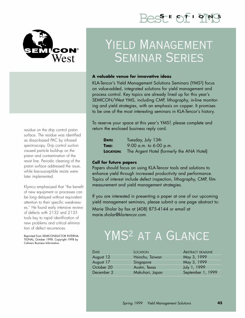
Best of YMS
Spring 1999 Yield Management Solutions 45
S E C T I O N S
Yield ManagementSeminar Series
A valuable venue for innovative ideas
KLA-Tencor’s Yield Management Solutions Seminars (YMS2) focuson value-added, integrated solutions for yield management andprocess control. Key topics are already lined up for this year’sSEMICON/West YMS, including CMP, lithography, in-line monitor-ing and yield strategies, with an emphasis on copper. It promises to be one of the most interesting seminars in KLA-Tencor’s history.
To reserve your space at this year‘s YMS2, please complete andreturn the enclosed business reply card.
DATE: Tuesday, July 13thTIME: 9:00 a.m. to 6:00 p.m.LOCATION: The Argent Hotel (formerly the ANA Hotel)
Call for future papersPapers should focus on using KLA-Tencor tools and solutions toenhance yield through increased productivity and performance.Topics of interest include defect inspection, lithography, CMP, filmmeasurement and yield management strategies.
If you are interested in presenting a paper at one of our upcomingyield management seminars, please submit a one page abstract to:
Marie Sholar by fax at (408) 875-4144 or email [email protected].
YMS2 at a GlanceDATE LOCATION ABSTRACT DEADLINE
August 12 Hsinchu, Taiwan May 3, 1999 August 17 Singapore May 3, 1999October 20 Austin, Texas July 1, 1999December 2 Makuhari, Japan September 1, 1999
residue on the drip control piston surface. The residue was identifiedas diazo-based PAC by infraredspectroscopy. Drip control suctioncaused particle build-up on thepiston and contamination of the resist line. Periodic cleaning of thepiston surface addressed the issue,while less-susceptible resists werelater implemented.
Klymco emphasized that “the benefitof new equipment or processes canbe long delayed without equivalentattention to their specific weakness-es.” He found early intensive reviewof defects with 2132 and 2135tools key to rapid identification ofnew problems and critical elimina-tion of defect recurrences.
Reprinted from SEMICONDUCTOR INTERNA-TIONAL, October 1998. Copyright 1998 byCahners Business Information.

Spring 1999 Yield Management Solutions46
Standards
In the past, significant confusion and disagreement inmeasurement science terminology has contributed to aninability to accurately compare data from multiplesources. Due to their universal nature, standards play akey role in defining such terminology on an interna-tional scale for a variety of industries.
Terms such as accuracy, precision, repeatability, repro-ducibility, random and systematic error pervade metrol-ogy activities in an often confusing and argumentativemanner. Worse yet, there have been significant differences in the statistical treatment of metrologydata in the various nations that participate in interna-tional commerce.
Consistent application of metrology standards plays arole in semiconductor manufacturing yield, as the effec-tive use of yield data by multi-national companiesdepends on a cohesive and consistent understanding ofmetrology technology and standards worldwide.
Resolving measurement uncertaintyIn the early 1990’s, worldwide adoption of an ISO2
protocol, “Guide to the Expression of Uncertainty in Measurement”, began to address this issue. This protocol, developed by an international working group,
F E A T U R E S
The Role of Standards In Yield Management
by Jim Greed, President, VLSI Standards
Metrology plays a significant role in the management of yield; many measurements of wafer and reticle attributes can be correlated with ultimate device electrical performance, and are therefore used to maintain process control in the fab. Calibration of metrology and inspection tools has assumed increasing importance due to both the requirements of contemporary quality systems and the demands of consistent worldwide multi-site manufacturing. Throughout the process,standards provide the enabling technology to perform these tasks.
An Overview of Standards
The term standard can mean either a
physical artifact such as a reference
material used to calibrate a metrology
tool, or a documented procedure or list
of attributes used to qualify a product
(e.g. a product safety standard,). In
the field of measurement science, the
uses of this term are usually inter-
twined as shown in figure 1, which
delineates some of the most basic types
of standards.
Physical standards have one or more
well established properties, and are
often traceable to a national authority
such as NIST1. The certified properties
of these standards that make them
suitable for instrument calibration are
often determined through the use of
standard test methods that are written
rather than physical standards.

In the process of physical standardscertification, the result of the certi-fied measurement is called the measurand. The measurand consistsof the value of the property (forexample, film thickness or defectsize) determined by certified mea-surement and the degree of uncer-tainty. In a successful calibrationprocess, the instrument being cali-brated reports a measurementresult that is within the range ofthe uncertainties of the calibration standard.
The value of measurement data inestablishing acceptable yield para-meters depends on calibration witha low uncertainty. Consider, forexample, a 4 nm gate oxide whichhas a process tolerance of 0.2 nm.In order to have a 4:1 ratio of mea-surement capability to process tol-erance, calibration standards musthave an uncertainty of less than0.05 nm. This is approximately one tenth of the spacing of siliconatoms (the lattice constant).
One simplistic way to view the concept of uncertainty is to considera measurement process which consists of a series of repeated trialswhere the arithmetic average (mean)of the measurements is recorded foreach of the trials. The dispersion ofthese mean values characterizes theuncertainty of that measurementprocess. Uncertainty should not beconfused with error, as it is anexpression of the statistical natureof the measurement process.
resulted in significantly greaterorder in the use of terminology anduniformity in the treatment of mea-surement data. By defining a con-sistent method for reporting theresults of measurements, the proto-col forms the foundation for theinternationally accepted definitionof traceability in measurements. Asdefined by the InternationalVocabulary of Basic and GeneralTerms in Metrology (VIM; 1993),traceability is:
“The property of the result of a measure-ment or the value of a standard wherebyit can be related to stated references,usually national or international standards, through an unbroken chainof comparisons all having stated uncertainties.”
Traceability is of value to the semi-conductor industry as it provides atangible benchmark for measure-ment from an impartial third partyarbiter of high level technical capa-bility. An IC manufacturer caninvoke the use of traceable stan-dards in the process of acceptancetesting a new metrology or processtool. Similarly, an IC manufacturercan use traceable metrology data tocertify the quality of the productsthat he ships.
Spring 1999 Yield Management Solutions 47
F E A T U R E S
Figure 1. A taxonomy of standards.
Standards
International Regional orNational
Physical andCertifiable
Written
Weights andMeasures
Properties ofMaterials
ProductQuality/Safety
Compulsory Voluntary

48
F E A T U R E S
If you’re responsible for thin filmthickness measurements, you wantthem to be right. And you definitelydon’t want to be embarrassed by ametrology tool that decides to drift ata critical time.
That’s why perfectionists insiston VLSI’s suite of thin-film metrologystandards. For silicon dioxide andsilicon nitride. The broadest selectionin the industry.
And now, oxide standards areavailable for 4.5nm and 7.5nm! It’s aVLSI exclusive.
So if you’re a metrology perfec-tionist, flaunt it! Call now for yourfree “Good Enough ISN’T” buttonalong with your free VLSI catalog...
VLSI Standards:(800) 228-8574. Or on the Internet:www.vlsistd.com
4 out of 5 Perfectionists Insist OnVLSI’s Thin Film Metrology Standards.
4 out of 5 Perfectionists Insist OnVLSI’s Thin Film Metrology Standards.
NOW:New “Skinny”
Standards for
4.5 & 7.5nm
Thickness!
New “Skinny”
Standards for
4.5 & 7.5nm
Thickness!
The Measurement Standards for the Industry.
Calibration challenges“The semiconductor world isshrinking!” This is the preamble tovirtually every presentation todayconcerning semiconductor manufac-turing, but consider how true thisstatement is:
• Gate oxides are approaching4 nm, and are forecast to be per-
haps 2 nm before a material changebecomes necessary — this puts thinfilm growth and measurementdimensions in the realm of a fewatomic layers.
• Particle and defect detection areoften done optically at dimensionsfar below the wavelength of lightemployed by the detection tool, buthow can we identify the source ofthe particle or deduce its size?
Clearly, these rapidly acceleratingchanges continue to demonstratethe need for accurate, precise andrepeatable measurements. With theinternational nature of the semicon-ductor industry, such measurementsmust be traceable to reliable anduniversal standards.
What the future holdsThe semiconductor industry is nowfocused on, among other things, anorganized, international, cooperativeforecasting of our technical needsfor the future and likely solutions,formulated into industry-wideroadmaps. This international effortprovides an opportunity to under-stand the needs for both advancedmetrology tools and the calibrationstandards to verify them. In addi-tion, the underlying need foradvanced education of measurementscience technologists continues tobe clear.
A shared vision among technolo-gists around the world is emerging,where a combination of physicalstandards and consensus-based
standards models will be used forcalibration of all types of advancedmetrology and inspection tools. Asachieving acceptable semiconductoryield levels continues to becomeincreasingly dependent on highlyaccurate metrology and inspection,such calibration standards will playa correspondingly significant role
in our future world of atomicdimensions.
1. The National Institute of Standards andTechnology, Gaithersburg, MD, USA.
2. International Organization for Standardization,Geneva, Switzerland.

program makes it impossible to fund allchanges internally. There is typically arange of potential solutions for a givenequipment set, reflecting individual cus-tomer characteristics and preferences,and necessitating the customer’s involve-ment in determining the appropriate solu-tion set. Costs are determined by whichsolutions are chosen and, very significant-ly, by whether the system is covered bycontract or warranty. For billable cus-tomers, how current their system configu-rations are would drive costs as well.KLA-Tencor’s policy is not to treat Year2000 as a revenue enhancement oppor-tunity. We expect Y2K revenues will onlypartially offset our program costs.
Q Will KLA-Tencor’s internalsystems be ready as well?
A The company has assigned dozensof people to inventory, evaluate, andremediate our internal business systemsand tooling. Activities are well along inall these areas. We anticipate completionof these activities, as well as evaluationof our suppliers by mid year.
&
Spring 1999 Yield Management Solutions 49
AQQ What is KLA-Tencor doing toaddress the Y2K issue?
A KLA-Tencor has a Year 2000 readi-ness project team and program wellunder way to identify and address all ofthe main areas of concern: KLA-Tencoryield management systems, internal busi-ness systems and services, internal net-working and tooling, and critical suppli-ers. Each product group has an assignedY2K product owner to coordinate anddrive the product-specific Y2K issues, andto work closely with the Y2K programteam. Senior management is closely monitoring the program to ensure that it receives the appropriate priority andresources.
Q What is KLA-Tencor doing tomake its products Y2K ready?
A Through our participation in theSEMATECH Year 2000 ReadinessSupplier Survey, we have evaluated allour current products with the SEMATECHrecommended version 2.0 test scenarios.The results are reported in KLA-Tencor'sProduct Readiness Matrix, which is avail-able to customers through KLA-Tencorsales and service personnel. In addition,C and C++ code have been inspectedfor date-related code. BIOS, embedded
processors, operating systems and thirdparty software have also been evaluated.
Q How many KLA-Tencor toolsare affected by Y2K?
A Because KLA-Tencor’s worldwideinstalled base is approximately 17,000,including retired systems and productsthat are no longer sold, the companyfaces a substantial challenge in address-ing the Y2K issue. While many of ourproducts are not affected by Y2K and many customers are not electingto upgrade all tools, we estimate thatbetween 8,000 and 9,000 tools will beupgraded by the program’s completion.Field audits, where service engineersdetermine the product hardware and soft-ware configurations, enter that informationinto our Y2K database and generate rec-ommended Y2K upgrades, will be sub-stantially complete by the time this articleis published. Where product obsoles-cence or other issues prevent KLA-Tencorfrom providing Y2K support, customersare being notified.
Q Will there be charges forthese Y2K upgrades?
A As companies in every industry arediscovering, the magnitude of the Y2K
Answers to your questions about KLA-Tencor and the Year 2000 issue.
S E C T I O N S
For more information contact your localaccount team or representative forproduct status, availability and pricingof Y2K upgrades.
KLA-Tencor takes the Y2K issue very seriously from both a product readiness and business continuity perspective. We understand the
magnitude of this issue for our customers and for our business. We are committed to doing everything we can to ensure a successful transition to and through the Year 2000.

Spring 1999 Yield Management Solutions50
Product NewsAIT II In-Line Defect Inspection SystemThe industry’s first 300 mm bridge tool for sub-0.18 µm design rules, the AITII offers exceptional defect sensitivity, high throughput and low cost-of-own-ership for fast and accurate feedback on process tool performance as well asadvanced line monitoring for films, CMP, non-critical etch and photo mod-ules. The AIT II detects particle and pattern yield-limiting defects at up to 40wafers per hour at maximum sensitivity, independent of device type. Further,the system’s MultiSpot™ feature provides tremendous inspection flexibilityby offering multiple, operator-selectable sensitivity setting options — large,medium, and small spot — that can be optimized based on whether theinspection system is used for line monitoring or tool monitoring.
2401 Automated Macro Defect Inspection SystemKLA-Tencor’s 2401 system is the industry’s first fully automated inspectionsystem designed to detect yield-killing macro defects (50 µm and larger) gen-erated in the lithography process. Replacing current manual after-developinspection (ADI) methodologies where operators miss up to 80 percent ofphoto-related defects, the 2401 enables reliable and repeatable detection ofcritical macro defect types, preventing further investment in low-yieldingwafers and dramatically reducing scrap/yield loss further downstream in themanufacturing process. In addition, the 2401 system allows advanced produc-tion and engineering analysis never before possible using manual macro ADI,enabling continuous process improvements for maximum ROI in minimumtime.
FabVARS 500 Digital Image Management SystemTo serve the current image management requirements in the semiconductorindustry, the FabVARS 500 stores and retrieves images generated from a broadvariety of on-line and off-line image generating systems. While previous gen-eration systems accepted and stored images only in analog format, the recentmigration of many image producing systems to a pure digital format has ren-dered this capability inadequate. The FabVARS 500 accepts and stores bothanalog and digital images in a digital format, enabling the system to be con-nected to a wider variety of tools and yield enhancement systems. This in turnallows wider deployment within manufacturing facilities for faster resolution of yield problems.
SEMSpec Random ModeKLA-Tencor’s SEMSpec advanced e-beam inspection system enables faster timeto results with its unique voltage contrast capabilities and 0.1 µm sensitivity forsub-0.25 µm fabs. It meets the challenges of today’s high aspect ratio structures,new materials and damascene processing. Engineers quickly identify killerdefects with advanced SEM-based inspection in Array mode. For increased capa-bility and additional flexibility, SEMSpec now offers Random mode, or die-to-die comparison. Without being limited to repeating array features, a larger partof the device can be inspected. With increased capabilities in advanced e-beaminspection, SEMSpec continues to add value and a strong competitive edge forprocess development, process transfer, and line auditing in leading-edge fabs.
circle RS#034
circle RS#030
circle RS#010

Spring 1999 Yield Management Solutions 51
5300 Overlay Metrology SystemKLA-Tencor’s 5300 overlay metrology system enables metrology and lithog-raphy engineers to control lithography tools down to the 0.13 µm level. It isthe first system of its kind to meet these design criteria. A bridge tooldesigned to handle both 200 and 300 mm wafers, the 5300 enables tighteroverlay budgets and improved overlay control. With the fastest time toresults, it maximizes utilization of expensive lithography tools by minimizingidle time. The 5300 is the only overlay system that can measure low-contrasttargets resulting from CMP and STI processing consistently and reliably,using a single recipe. It also features optional KLASS 4.0 for Windows analysissoftware for stepper-specific registration control, and recipe database manage-ment (RDM).
8100XP-R Advanced Reticle Metrology SystemThe 8100XP-R CD SEM is the newest addition to KLA-Tencor’s 8100 fami-ly of CD SEMs. In addition to its outstanding wafer metrology and imagingcapabilities, the 8100XP-R is optimized for reticle-specific applications. TheXP optics, combined with ACE™ (Advanced Charge Elimination), provides astable, repeatable imaging system for chrome-on-glass and phase shift masks.The enhanced resolution of the 8100XP-R enables the accurate characterizationof optical proximity correction features, and extends the linear range of mea-surements to below 0.15 µm, thus providing precise measurements into thesub-100 nm realm. The 8100XP-R is the advanced reticle metrology solutionfor tomorrow's reticles.
StarLight™ SL3UV Reticle Contamination InspectionSystemSL3UV is KLA-Tencor‘s new UV-based reticle contamination inspection sys-tem for sub-wavelength (low k1) lithography. Sub-wavelength lithography hasincreased reticle defect printability, created new UV-specific defect classes, andaccelerated advanced reticle deterioration, threatening yield and profitability.The SL3UV is the first UV contamination inspection system to detect newdefect classes, including transmission defects and wavelength-dependent con-taminants such as organic defects and gallium stains. The SL3UV can alsoinspect Tri-Tone PSMs and reticles with advanced OPC assist bars as well asprovide the sensitivity and minimum linewidth required for the inspection ofreticles for 4X lithography design rules at 0.18, 0.15 and 0.13 µm.
363UV Reticle Pattern Inspection SystemKLA-Tencor recently added the 363UV model to the 300UV Series of ReticleInspection Systems to increase inspection productivity and turn time for manyadvanced DUV reticles where slowdowns were occurring with the previous353UV model. The 363UV model includes a 300 MHz Sun MicrosystemsUltra60 workstation with 68 GB of available hard disc storage for faster datapreparation. Also included is a C3 or C5 rendering hardware upgrade from theprevious C2 or C4 to improve inspection times for some high figure count reticles. KLA-Tencor is offering: new systems, field upgrades of a 353UV, orexchanges of an older generation 351.
circle RS#037
circle RS#038

I N T E L L I G E N T L I N E M O N I T O R I N G
Defect excursions and yield busts can be such atragedy. But fortunately, now there’s professional help.
It’s our fully integrated and automated IntelligentLine Monitor solution. By detecting, classifying and analyzing yield-killing defects in real time, it lets you make instant, targeted process and equipment corrections.Enhance baseline yield. And ultimately, increase revenue.
As the industry’s only truly integrated line monitoring system, ILM delivers a complete solution for each process step. It starts with industry-leadingbrightfield and darkfield inspection technologies thatcover every application, from advanced engineering
analysis to line monitoring, process tool monitoring, andwafer and equipment qualification.
And it combines all this with production-proven on-lineand off-line automatic defect classification software. As wellas the industry’s first fully automated yield analysis system.
All of which results in quicker access to better infor-mation. Faster responses to process excursions. Reduceddefect density. And substantially improved baseline yields.
There. Aren’t you feeling better already?For more information, or to get a free copy of our
book “When Bad Things Happen To Good Wafers,” pleasecall 1-800-450-5308, or visit www.kla-tencor.com.
©19
98 K
LA
-Ten
cor,
In
c.