
WAT BHARGAVA Q - Bibliothèque et Archives Canada
155
THE UNNERSITY OF ALBERTA Simulation Models for Variable Speed Elecuic Drives WAT BHARGAVA Q A Thesis submitted to the Faculty of Graduate Snidies and Research in partial Nfdlment of the requirements for a degree of Master of Science Department of Electrical and Cornputer Engineering Edmonton, Alberta Fa11 1997
-
Upload
khangminh22 -
Category
Documents
-
view
4 -
download
0
Transcript of WAT BHARGAVA Q - Bibliothèque et Archives Canada
THE UNNERSITY OF ALBERTA
Simulation Models for Variable Speed Elecuic Drives
W A T BHARGAVA Q
A Thesis submitted to the Faculty of Graduate Snidies and Research
in partial Nfdlment of the requirements for a degree of
Master of Science
Department of Electrical and Cornputer Engineering
Edmonton, Alberta
Fa11 1997

National Library I*I of Canada Bibliothèque nationale du Canada
Acquisitions and Acquisitions et Bibliographie Services services bibliographiques
395 Wellington Street 395, rue Wellington ûtrawa ON K1A ON4 OttawaON K1AON4 Canada Canada
The author has granted a non- L'auteur a accordé une licence non exclusive licence allowing the exclusive permettant à la National L i b r v of Canada to Bibliothèque nationale du Canada de reproduce, loan, distribute or sell reproduire, prêter, distribuer ou copies of this thesis in microfonn, vendre des copies de cette thèse sous paper or electronic formats. la forme de microfiche/nlm, de
reproduction sur papier ou sur format électronique.
The author retains ownership of the L'auteur conserve la propriété du copyright in this thesis. Neither the droit d'auteur qui protège cette thèse. thesis nor substantial extracts fkom it Ni la thèse ni des extraits substantiels may be printed or otherwise de celle-ci ne doivent être imprimés reproduced without the author's ou autrement reproduits sans son permission. autorisation.

To Whom it may concern
Co-author of the papen :
1. SPICE3 simulation techniques in Power Electronics
2. SCR hannonic correction topologies for VSI drives
Dr. E. Nowicki
University of Calgary
Department of Electtical and Computer Engineering
2500 University Drive N.W.
Calgary, AB T2N 1N4
Phone : 403 220 5006
Email : nowicki @ enel.ucalgary .ca

To Whom it mav concern
As a CO-author of the papers titied "SPICE3 simulation techniques in Power
Electronics" and " "SCR harmonic correction topologies for VSI drives", 1 would iike to
grant permission to Mr. Rajat Bhargava to include these papers in his M.Sc thesis entitied
" Simulation Models for Variable Speed Elecaic Drives".
Mr. Emanuel Bocancea

ABSTRGCT
This thesis describes simulation models for assessing the performance of
variable speed power electronic dnve systems. Simulation models are developed for
both the Voltage Source Inverter (VSI) and the -nt Source Inverter (CSI) using
SPICE3. A simulation mode1 for a cornpiete drive system is presented for a VSI drive
system using a 12-puise input rectiner and a 3-level Pulse width modulation (PWM)
VSI.
Models are described for sirnuiating the action of the input, output and load
portions of both the CS1 and VSI drive types. The &ive systems are discussed with
reference to both 6-pulse and 12-pulse rectifier stages. The 12-puise rectifier input
stage uses a A-A / A-Y transformer. The modeling of a A-A / A-Y transformer is done
using d-q axis theory. DC Fïters are used to obrain a ripple fkee dc voltage or current,
which acts as the input to the inverter stage. Pulse width modulation (PWM) is used to
control the invener output stage of both drive systems. The induction motor acts as
the load to the inverter output stage and is also modeled using d-q axis theory-
Experirnental results are used to verifj that the simulation modeis are accurate and
represent the real system. The simulation rnodels are constnicted using actuai dnve
parameters obtained by performing various experimental tests. The performance of a
low distortion rectifier is investigated using both simulation and experimental data,
with emphasis on the current harnionics, the power factor and the total harmonie
distonion. îhe result of this performance anaiysis shows that the novel rectifier
topology c m be used to successfully Iower the total harmonic distortion of the rectifier
input line current whilst achieving a unity power factor.
The various simulation techniques developed in ihis work are implemented
using SPICE3 and lower the difficulty of simulating an entire drive topology. Fast run
times are obtained as a result and convergence problerns are improved. Close
agreement of the simulation results with experimental ones prove the accuracy of the
SPICE3 models.

AcknowIedgment
1 would like to extend my special thanks to:
the Department of Electrical and Computer Engineering for their financial and technical assistance.
my colleague, Emanuel Bocancea for being a great coworker.
Srinivas Padmanabhuni and Ram Maikala for their timely help.
Shilpee for being with me when 1 need her most
and most of al1 my supervisor, Dr. John C. Salmon for his vaiuable advice and encouragement throughout my work.

TABLE OF CONTENTS
List of Figures
List of Syrnbols
Chapter 1 : Introduction ........................................ - 1 1.1 Drive topologies ........................................ 1
1.2 Simulation and Experimental results ........................ 3
....................................... 1.3 Literature Survey 5
1.4 Organization of the Thesis ................................ 8
Chapter 2 : Introduction to SPICE3 simulation ...................... 10
2.1 The SPICE3 Sirnulator .................................. 10
2.2 Format of Circuit Files .................................. 12
2.3 SPICE for power electronics circuit simulation ................. 14
2.4 Troubleshooting ....................................... 17
Chapter 3 : Diode Bridge Rectifier ................................ 19
3.1 Six-pulse diode bridge rectifier ............................ 19
. . . . . . . . . . . . . . . 3.1.1 Simulation of 6-pulse diode bridge rectifier 20
3.1.2 C dc-link filter .................................... 21
..................... 3.1.3 Wavefomis andandysis for C filter 22
......................... 3.1.4 Harmonic analysis for C-filter 23
3.1.5 LC dc-link filter ................................... 24
................... 3.1.6 Waveforms and analysis for LC-fdter 24
........................ 3.1.7 Harmonic analysis for LC-filter 25
3.2 Twelve-pulse diode bridge rectifier .......................... 26
........... 3.2.1 d-q Axis Theory mode1 for A-NA-Y transformer 27
.................. 3.2.2 SPICE3 mode1 for A-NA-Y transformer 28
..................... 3.2.3 SPICE3 mode1 for 12-pulse rectifier 31
3.2.4 Waveforms and analysis for 12-pulse rectifier ............ 32
.................. 3.2.5 Harmonic analysis for 12-pulse rectifier 34
................................ Chapter 4 : Voltage Source Inverter 36
. ........................ 4.1 Ogpdse 2-level Square Wave Inverter 36
4.1.1 SPICE simulation .................................... 38
4.1.2 Waveform and analysis ................................ 40
4.2 Pulse Width Modulated Voltage Source Inverter ............... 41
4.2.1 Simulation of PWM VSI ............................ 43
4.2.2 Waveforms and analysis of PWM VSI .................... 46
4.3 Three-level PWM inverter ................................. 48
................. 4.3.1 Simulation of Three-level PWM inverter 51
4.3.2 Waveform and analysis of 3-level PWM inverter ........... 51
Chapter 5 : Current Source Inverter ................................ 53 ................. 5.1 o.pulse. 2-level PWM Current Source hverter 53
.................................. 5.1.1 SPICE3 Simulation 54
5.1.2 Waveform and analysis .............................. 57
.................................. 5.1.3 Harmonic analysis 58
5.2 Controlled Current Source for a CS1 ......................... 58
Chapter 6 : Induction Motor ..................................... 60
6.1 Induction motor drive ................................... 60
6.1.1 Induction motor modeling ............................ 60
6.1.2 SPICE3 simulation ................................. 64
6.1.3 Wavefonns and analysis .............................. 65
6.2 Constant voltagelfrequency operation ....................... - 6 6
6.2.1 SPICE3 simulation of constant VI f operation ............ -67
6.2.2 Analysis of constant V/f operation curves ................. 68

................................... Chspter 7 : Variable Speed Drive 72
7.1 Selectiog drive components ................................ - 7 2
7.2 VSI and CS1 Drive Topologies ............................... 74
7.3 1Zpulse . 3-level PWM VSI Drive ............................ -74
7.3.1 SPICE3 Simulation .................................. - 7 5
7.3.2 Waveform and analysis ............................... 78
7.4 VSI and CS1 Drives ...................................... 83
Chapter 8 : Novel RectXer Topology ................................ 84
8.1 Current harmonies and power factor .......................... 84
....................................... 8.2 Rectifier topology 86
........................ 8.2.1 Simulation of Rectifier topology 87
8.2.2 Waveform and analysis ................................. 89
8.2.3 Simulation tools used for circuit Performance Analysis ....... 92
8.2.4 Performance Analysis and Design ....................... 94
Chapter 9 : Conclusion ........................................... 100
9.1 SPICE3 simulation ...................................... 100
9.2 Drive Topology ......................................... 101
9.3 Novel Rectifier Topology ................................. 104
9.4 Suggestions for future work ................................ LOS
Bibliography . . . . . . . . . . . . . . . . . . . . . . . . . . . . . . . . . . . . . . . . . . . . . . 106
Append iv ...................................................... 111
A Harmonic analysis data for 6-pulse diode bridge rectifier ........... 111
B Test data for A 4 l A-Y transformer parameten ................... 112
C Harmonic analysis data for 12-pulse diode bridge rectifier ............ 113

....................... D Test data for Induction Motor parameters 114
.............................. E Harrnonic analysis for inverters -115
...... F Harmonic analysis data for resonant network rectifier topology 117
........................................ G SPICE3 Netlist files 119
...................... H Conference papers (CCECE'96, Calgary) 133

LIST OF FIGURES
.................. 1.1 Block Diagram of Voltage Source hverter Drive 2
................. 1.2 Block Diagram of Curent Source Inverter Drive -3
.......................... 2.1 SPICE3 sirnulator performance c w e 11
................... 2.2 Circuit Diagram for a half wave diode rectifier -13
.................. 2.3 SPICE3 schematic for a half wave diode rectifier 13
....................... 3.1 Three-phase diode bridge rectifier circuit 20
............ 3.2 SPICE3 mode1 for 6-pulse rectifier bridge with C filter - 2 1
3.3 Simulated and experimental waveforms for &pulse rectifier with C-
..................................................... filter 23
3.4 Simulated and experimental waveforms for &pulse rectifier with LC-
..................................................... filter 25
3.5 Block Diagram for 12-pulse diode bridge rectifier . . . . . . . . . . . . . . . . -26
3.6 Phasor diagram for d-q transformation for A-A transformer .......... 28
3.7 Phasor diagram for d-q transformation of the A-Y transformer ....... -29
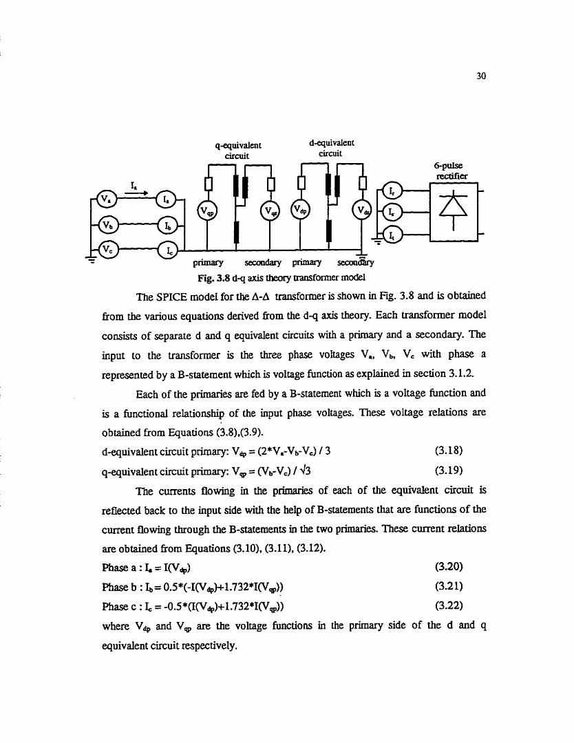
............................. 3.8 d-q axis theory transformer mode1 30
......................... 3.9 SPICE3 mode1 for the 12-pulse rectifier 31
......................... 3.10 Waveforms for A-A / A-Y transformer 32
3.1 1 Sirnulated and experimental line curent waveforms for the A-A/ A-Y
transformer ............................................... 33
3.12 Sirnulated and experimental output voltage waveforms for the 12-
............................................ pulse rectifier 35
4.1 Voltage Source Inverter schematic .............................. 37

............. 4.2 SPICE3 mode1 for square wave voltage source inverter 38
........ 4.3 Simulated and experimental waveforms for square wave VSI -41
4.4 Three phase PWM waveforms ................................ 42
................................ 4.5 SPICE3 mode1 for PWM VSI 43
4.6 PWM Sinewave generation .................................. 45
... . 4.7 Simulated ref sine wave and triangular carrier wave for PWM VSI 47
............. 4.8 Simulated and experimental waveforms for PWM VSI 48
4.9 Circuit for a 3-ievel PWM hverter ............................. 49
.............................. 4.10 PWM wavefonn for 3-level VSI 50
4.1 1 Typical output waveforms for 3-level inverter ................... 50
4.12 Sirnulated wavefonns for 3-level PWM inverter ................. -52
..................... 5.1 Circuit diagram for Curent Source Inverter 53
5.2 SPICE3 mode1 for PWM CS1 ................................ 55
........ 5.3 Switching pattern generation for CS1 over half carrier cycle - 5 6
........................... 5.4 Sirnulated wavefonns for CS1 PWM 57
............ 5.5 Block diagram for control scheme of the current source -59
..................... 6.1 Stationery A-B-C to d-q axes transformation 61
6.2 d-q Equivalent Circuits ...................................... 63
6.3 Per-phase equivalent circuit for Induction Motor ................. -64
6.4 SPICE3 mode1 for induction motor ............................ 64
6.5 Simulation waveforms for Induction Motor ...................... 66
............. 6.6 Constant volts per hertz curves for Induction Machine -70
............................. 7.1 Simplified circuit of a rnotor dnve 73
....... 7.2 Block diagram for 1Zpulse. 3-level PWM VSI Inverter Drive -75
7.3 Switching logic for dc-link cunent ............................ 76
............ 7.4 SPICE3 mode1 for the 12.pulse. 3-level PWM VSI drive 77

....... 7.5 Simulated waveforms for 1Zpulse. 3-level PWM Inverter drive 79
....... 7.6 Simulated waveforms for IZpulse, 3-level PWM Inverter drive 80
7.7 Simulated switching pattern waveforms ......................... 81
7.8 Sirnulated waveforms for ll.pulse, 3-level PWM Inverter drive ...... -82
7.9 Simulated waveforms for constant volts per hertz operation of 12-
pulse. 3-level PWM Inverter drive ............................. 82
........................................... 8.1 Utility Interface 85
.... 8.2 Resonant mode harmonic correction circuit for a 3+ diode bridge -86
8.3 12-pulse rectifier with a resonant-mode haxmonic correction topology . . 87
8.4 SPICE3 mode1 for 12-pulse rectifier with resonant mode harmonic
............................................ correctioncircuit 88
8.5 Waveforms for phase voltage (Vpb) and line current (U for a 6-pulse
rectifier bridge with resonant network ........................... 89
8.6 Simulated and expenmental waveforms for 3-phase diode bridge with
resonantnetwork ........................................... 90
8.7 Waveforms for the resonant capaciton ........................... 91
................. 8.8 Waveforms for the 6-pulse output rectifier voltage 91
8.9 6-pulse and 12-pulse rectifier performance curves keeping oo constant
mdvarying& .............................................. 95
8.10 6-pulse and 12-pulse rectifier performance curves keeping wo constant
andvarying Z, ............................................. 96 8.1 1 6-pulse and 12-pulse rectifier performance curves keeping Z, constant
............................................. a n d v q h g y 97
8.12 6-pulse and 12-pulse rectifier performance curves keeping Z. constant
a n d v q i n g o, ............................................. 98

LIST OF SYMBOLS
SPICE
. ac
VSI
CS1
PWM
DPF
THD
CDF
PF
A
RELTOL
ABSTOL
1.
Lm Lt
Vk PI^
LABVIEW
GPIB
d-axis
q-axis
SCR
kVA
GTO
NPC
rPvl
Simulation Program with htegrated Circuit Emphasis
alfernate current
Voltage Source Inverter
Current Source Inverter
milse Width Modulation
Displacement Power factor
Total Harmonic Distortion
Current Distortion Factor
Power Factor
Nodai admittance matrix
Relative Tolerance
Absolute Tolerance
Phase A Cument
Magne tizing inductance
Stator inductance
Phase A Voltage
Laboratory Virnial Instrument Engineexing Workbench
General Purpose Interface Bus
direct axis
quadrature axis
Silicon ControUed Rectifier
Kilovolt Amperes
Gate Turn-off Thyristor
Neutrai Point Clamped
Induction Motor

PCC
dc-link current
volts per hertz
induction motor flux linkage
electromagnetic torque
load torque
air-gap flux
slip frequency
source inductance
Point of Common Coupling
fundamental current
phase angle
Phase A capacitor current
Chapter 1
INTRODUCTION
The ac variable speed drive is a compiex non-Iinear system The cornputer
simulation and modeling becornes essentiai for the analysis and design of such a
systern. SPICE3, which is the simulation software used in this work, has now becorne
a widely accepted circuit simulation package for Power Electroaic circuits. To develop
a mode1 for an elecuic dnve system in SPICE3 is to widen its capabiiities by
simulating the whole &ive system in only one simulation. This avoids cornplex
mathematicai operations for its performance analysis. making dnve design more
straightfonvard and practical
Cornputer aided circuit simulation of power electronic systems offer the system
designer the opportunity to explore aU the various design trade-off and options and
also to perform wide-ranging comparative investigation, optimization and performance
anaiysis.
1.1 Drive Topologies
This work discusses two basic drive topologies - the Voltage Source Inverter
111-[3] and the Current Source Inverter [4], [SI. These two drives are the most
common drives used in the industry. Simulation models for these drives fafitates the
comparative analysis and design of new drive topologies.
The recwr stage of a drive is cornmonly either a 6-pulse diode bridge rectifier
or a 12-pulse diode bridge rectifier [6], [7]. For the 12-puise rectifier the input stage is
a Ad, A-Y transformer with the output voltages of the transformer phase shifted by
30" fiom each other. The series co~ection of two 6-pulse diode bridge rectifier
connected to such a transformer gives a 12-pulse operation which is applicable for
high power applications.
The dc-link filter stage is a large capacitor for the VSI so that the input to the
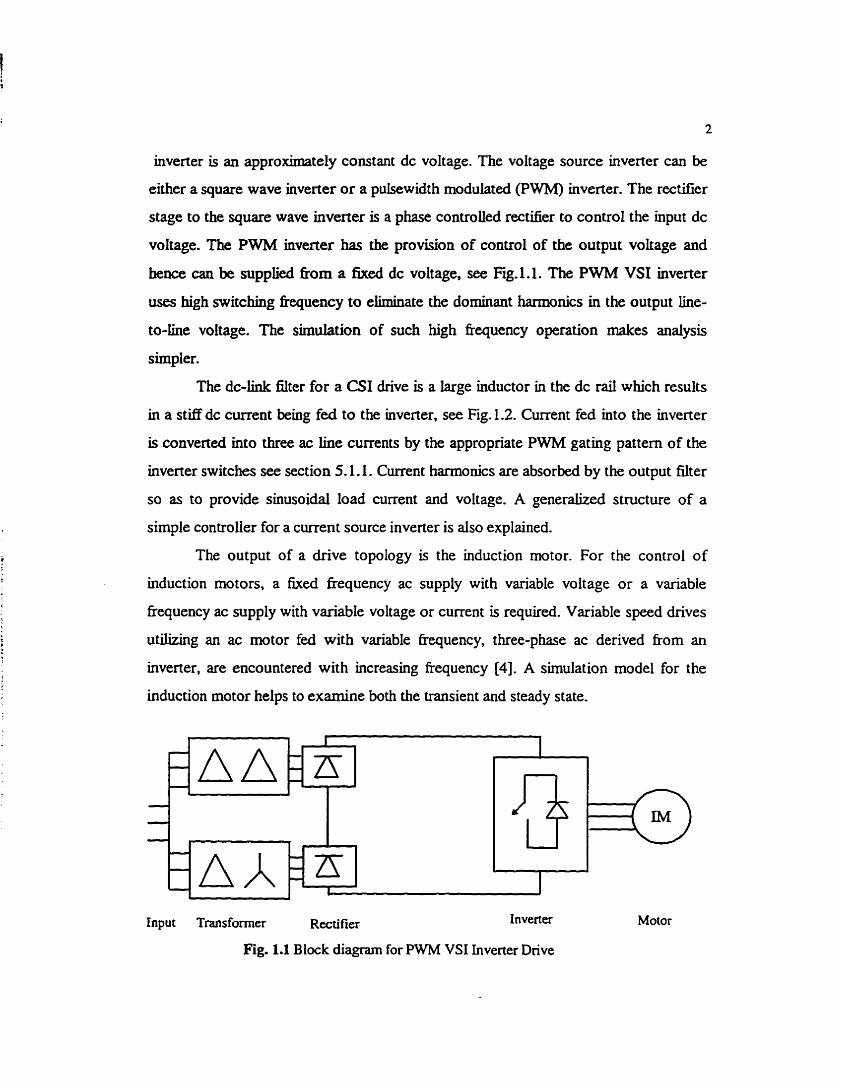
inverter is an approximately constant dc voltage. The voltage source inverter can be
either a square wave inverter or a pulsewidth modulated (PWM) inverter. The rectifier
stage to the square wave inverter is a phase controlled rectifier to control the input dc
voltage. TIE PWM inverter has the provision of control of the output vokage and
h e m can be suppiied fkom a fked dc voltage, see Fig. 1. l. The PWM VSI inverter
uses high switching lkequency to eiiminate the dominant hannonics in the output line-
to-line voltage. The simulation of such high hcpency operation rnakes analysis
simpler.
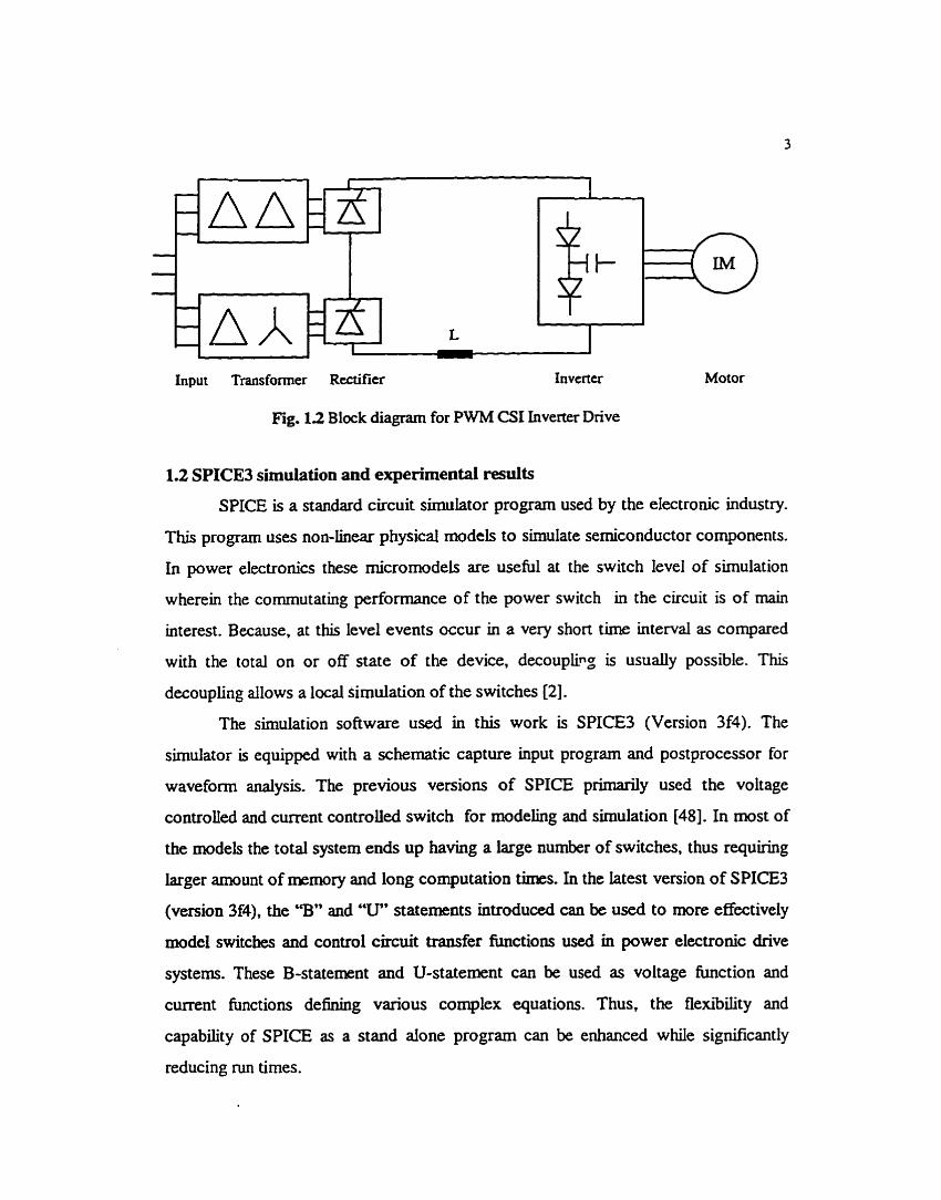
The dc-link filter for a CS1 drive is a large inductor in the dc rail which results
in a stiff dc current king fed to the inverter, see Fig. 1.2. Current fed into the inverter
is converted into three ac line currents by the appropriate PWM gating pattern of the
inverter switches see section 5.1.1. Current harmonics are absorbed by the output filter
so as to provide sinusoidal load current and voltage. A generalized structure of a
simple controller for a current source inverter is also explained.
The output of a drive topology is the induction motor. For the control of
induction motors, a f ~ e d fkequency ac supply with variable voltage or a variable
fkequency ac supply with variable voltage or current is required. Variable speed drives
utilizing an ac motor fed with variable bequency, three-phase ac derived fiom an
inverter, are encountered with increasing frequency [4]. A simulation mode1 for the
induction motor helps to examine both the transient and steady state.
Input Transformer Rectifier Inverter
Fig. 1.1 Block diagram for PWM VSI Inverter Drive
Input Transformer Rectifier Inverter
Fig. 12 Block diagram for PWM CS1 Inverter Drive
1.2 SPICE3 simulation and experimental results
SPICE is a standard circuit simulator program used by the electronic industry.
This program uses non-hear physical models to simulate semiconductor components.
In power electronics these micromodels are useful at the switch level of simulation
wherein the cornmutating performance of the power switch in the circuit is of main
interest. Because, at this level events occur in a very short tirne interval as compared
with the total on or off state of the device, decoupling is usually possible. This
decoupling allows a local simulation of the switches [2].
The simulation software used in tbk work is SPICE3 (Version 3f4). The
simuiator is equipped with a schernatic capture input program and postprocessor for
waveform analysis. The previous versions of SPICE prirnarily used the voltage
controlled and current controlied switch for modeling and simulation [48]. In most of
the models tht totai system ends up having a large number of switches, thus requiring
larger amount of mmory and long computation times. In the iatest version of SPICE3
(version 3f4), the '3" and "U" stateroents introduced can be used to more effectively
mode1 switches and control circuit transfer fûnctions used in power electronic drive
systerns. These B-statement and U-statement can be used as voltage function and
current functions d e m g various complex equations. Thus, the flexibility and
capability of SPICE as a stand alone program c m be enhanced while signifcantly
reducing mn times.

The new features of SPICE3 are used very effectively for the simulation of
various power electronic circuits [9]. The modeling of the A-A, A-Y transformer is
done using d q axis theory. In this theory the time varying parameters are eliminated
and the variables and parameters are expressed in orthogonal or mutually decoupled
direct (d) and quadrature (q) axes. The B-sîatement is used to model the cornplex
equations resulting bom the transformation The modeling of the induction machine is
also done in the same manner using d q axis theory.
The diode rectifier topology uses the simple power diode fiom the SPICE3
device iibrary. For better accuracy. such as for the simulation of the novel rectifier
topology the device parameters can be altered. The switching device in the case of a
square wave inverter is rnodeled by using a B-sraiement in series with a diode.
SPICEJ becornes very effective when modeling the inverter topology. At high
switching fkequency operations, as in the case of PWM inverters simulation has
convergence problems due to fast transfer of current fiom one switching device to the
other. The B-statement solves this problem by modeling the inverter legs by three B-
staternents representing the switching pattern of the six devices. This &O reduces the
number of switching devices.
In the present work. SPICE3 is used for generating the raw data for all the
sirnulated waveforms and the raw data is postprocessed using Excel to obtain the
wavefonn plots. Harrnonic ûnâiysis i s ako done using SPICE3. In addition. SPICE3 is
provided with the Interactive Interpreter that helps to monitor parameters in a single
mn by means of a do loop. This feature is used to generate the data for the various
performance cuves for the novel rectifier topology.
AU the parameters values used in the SPICE3 model are the same as that used
in the experimentai setup. For the A-A, A-Y transformer, the Open Circuit test and the
Short Circuit test is done to detennine the parameter values. Similarly, for the
induction motor the h a d test , the StandstiU test and the Stator dc test is done. This
helps in a logical cornparison of the simulation and expimental results.

The data used for the experimental waveforms was generated using a data
acquisition system called LABVIEW - Labonitory Vinual Instrument Engineering
Workbench The experimental measurement system consis ts of the folio wing:
Tektronix TDS 420 four channel oscillos~ope. Power Macintosh 7 100/66 computer
running LABVIEW 4.0 software, GPIB card NI-488, GPIB cable, high voltage probe
isolators with scaling factor of 1/500 and 1/50, clampon Hall-effect curent probe
isolator with scaling factor of 1 OOmVlA and 10mVlA.
1.3 Literature Sumey
Numerous digital and analogue computer simulation studies of the
performance of electrical dxives have ken done in the past [IO]-[14]. However,
because of the complexity of power electmnic circuits, the vast majority of these
snidies have neglected the power-electronic circuit topology and assumed a zero
impedance source, with the power electronic switching action represented solely by
the theoretical voltages (cux~ents) supplied to the drive motor.
Digital cornputer <mulation studies [15],[16] which have attempted to take
into account the power-electronic circuits and source impedance effects, for example
input rectifier, dc link hlter, inverter, etc. have all involved significant simpI@ing
assurnptions and therefore provides a very lirnited, albeit useful first approximation to
the various interactions.
The power and flexïbilïty of power electronic circuit simulation depends
heavüy on the CAD package library of power electronic devices and components
available to the user. To s p e d i z e these CAD packages for PWM inverter drive
system requires an additional range of library models to represent devices,
cornponents, machines and processes specifilc to power electronic systems to be
developed [17], [18].
A PC based simulation CAD tool, PECADS is proposed in [19]. It uses real
structure simulation (RSS) and digital identifcation for po wer electronic CO mpu ter
aided design and simulation. The simulation package foliows the RSS rule that each

block has to be simulateci in such a manner that the output s igna will represent the
sarne evolution as the real ones.
Another power electronic CAD package has been proposed in [19] which has
been specidy designed to cater for the simulation of pulse-w idt h modulation
controlied power electronic systems. This CAD package combines the features and
facilities of a previously developed PWM generation and analysis package called
PWLIB 1201 with a circuit analysis package called BTRAP. 'The "equivalent-circuit"
electromechanicai induction motor model, which, when incorporated into the
PWLIBBTRAP package, provides the CAD facilities for developing various
integrated drive systems.
A flexible method to design a complete three-phase inverter drive is to use a
circuit simuLator like SABER, but a serious problem is that designing a complete
three-phase inverter, especially operating at Iow fundamental eequency and higher
switching fiequency, will take rnany hours to do, and if parameters like gate resistance,
gate-drive supply and load currents are varied, optimized design is alrnost impossible.
Among the important power electronic devices. the power diode model has been
improved in [21] and the IGBT mode1 is developed in 1221. Both component models
are based on the SABER simulator. In [23], corresponding models are implemented in
SPICE. Practical implementation of a proposed model of a power diode is suggested
in [24] using both SPICE and SABER.
The functional defuitien of a switching converter is used to model three-phase
VSI or CS1 using PSpice 11 11. Simplifïed device models using controlled sources have
been proposed to speed up the simulation. For further si.rpIification, each converter is
simuiated as a multiport network, wherein the tirne solution of the cunents and
voltages, in the input and output terrnind, constitute the main objective of the analysis.
A considerable attention has k e n directeci to wards enhancing the performance
of power converters. Multilevel wavefomis are used to reduce the harmonic distortion
and increase the power rating of high-performance inverter power supplies [25]. There
has been great interest in the neutral point clarnped pulse-width modulated ( W C -
PWM) inverters drives. The NPC inverter's output voltage may contain fewer

h m n i c s than that of a conventional full bridge inverter [2] and since the imposed
source voltages across the main switching devices are halve the dc source voltage it is
particuiarly attractive in high power applications.
So far, several control schemes for NPC three-ievel inverters have k e n
proposed. Reported switchuig pattern based on selective harmonic elimination [2],
[26] did not consider the variations of the neutral point potential which is an inherent
problem of NPC inverters as pohted out in [27]. Vector control schemes which
consider the neutrai voltage balance have been reported [28].
The novel rectifier topology examined in this work is an improvement upon the
3-phase Y-switch networks explored in recent articles [29],[30] with the prime
application king the input stage to commercial variable speed drives. The converter
topologies examined in [29] are essentially SCR harmonic correction units (HCUs)
suitable as a retrofit or as a drive option. The work descn'bes a series of techniques
using thyristor switches that improve the hannonic content of diode rectifiers
connected to a voltage source inverter drive.
A new active interphase reactor for 12-pulse diode rectifier is proposed in [3 11.
It uses a conventional 12-pulse diode rectifier which requires an interphase reactor to
ensure the independent operation of the two parallel-connected three-phase diode
bridge rectitien. In this scheme, a low kVA (0.02 p.u) active curent source injects a
trianguiar curent into an interphase reactor of a 12-pulse diode rectifier. The
proposed system draws near sinusoidal current from the utility with Iess than 1%
THD.
The concept of reducing harmonic dûtortion associated with rectifier circuits
by third hanmaic curent inpCtion has been reported in [32]-[Ml. AU the above
schemes require a controIlabIe line synchronized extemai third harmonic cment
source. Scheme [34] necessitates the use of an input isolation transformer dong with
the access to its neutral terminal. [32] uses tuned LC branches in a network that
injects total third-hannonic modulated current into the ac terminais of the rectifier. A
modification of the scheme uses a rnagnetic device for current injection in a 3-phase,
sinusoidai-curreni utility interface.
modification of the scheme uses a magnetic device for current i n w o n in a 3-phase.
sinusoidal~urrent utility inteface.
1.4 Organization of the Thesis
The thesis begins with an introduction to the SPICE software with emphasis to
the latest version of SPICE3. SPICE3 has been very usefbl for the simulation of power
electronic circuits. The introduction of the B-statement and U-statement facilitates the
simulation of various complex circuitry. An o v e ~ e w of the SPICE simulator is
discussed which is important in solving various problems during simulation.
The rectifier stages of the drive topology are then described. The dpulse diode
bridge is discussed with amphasis to the performance with a C dc-luik hlter and LC
dc-link filter. Two series connected 6-puise diode bridge rec-rs give a 12-pulse
operation that is very useful for high power applications. The input stage to the 12-
pulse rectifier is a A-A, A-Y transformer with their output voltages phase shifted at 30"
fiom each other. The modeling of the A-A, A-Y transformer is done using d-q axis
theory. The use of B-statements help to sirnulate the transformer model very easily by
decouphg the input of the rectifier fkom its output. The cornparison of simulation
results with experimentai ones agree very closely.
The inverter stage can either be a Voltage Source Inverter (VSI) or a Current
Source Inverter (CSI) M. [3q. Both the square wave VSI and the pulsewidth
modulated VSI is discussed The PWM VSX inverter combines both voltage and
fiequency control within itseif and the high switching operation elirninates the voltage
harmoniEs Born the output P7]. The inverter kg is modeled using three B-statements
that represent the switcbing function of the six switching devices. A generahd
stnicture of a three-level voltage source inverter is presented with its simulation
wavefom. Cornparison of the simulated and experimental results for the wavefom
and the harmonic analysis of the output voltage are presented for each of the VSI.
The Current Source Inverter is discussed next. A variable dc link voltage is
generated by phase control which is converted to current source by comecting a

series inductance. The CS1 is modeled in much the same way as the VSI with three B
functions generating the P W switchùig pattern. Capacitors are comected at the
output of the inverter to absorb high hquency harmonies associated with the PWM
inverter output current The CS1 is ais0 viewed with reference to a constant current
source inverter where the dc current fed to the inverter is kept constant using a cIosed
loop scheme.
The output stage of the drive is the Induction Motor which is described next.
The motor is modeled using d q axis theory. The elhination of the tirne-varying
components in the d-q axis theory, heIps to mode1 the rnotor easily using voltage
functions. The simulation waveforms for the direct-on-line starting of the motor is
presented. The operation of the induction motor with constant V/f is explained and
various cuves are obtained using SPICE3 simulation.
The general features of the variable speed drives with emphasis to the PWM
inverter drives surnrnarizes the various stages of the drive topology. A 12-pulse, 3-
level PWM voltage source inverter is simulated in one single drive structure to
demonstrate the capability and flexibility of SPICE3 for cornplex circuit simuIation.
The thesis concludes by examining a novel rectifier topology that draws a h e
current with low total harmonic distortion at unity power factor. A resonant network
is used to build up a c m n t prior to the natwal conduction of the diodes thus helping
in waveshaping the line current. SPICE3 simulation wavefonns are used to compare
with the experimental results. The interactive interpreter, which is a new feature in
SPICE3 is w d to generate data for the performance aRalysis of the rectifier topology.
The ana.lysis and design of a new rectifier topology with the heip of SPICE3 simulation
tools is weU estabiished.

Chapter 2
INTRODUCTION TO SPICE SIMULATION
Circuit simulation is becoming an indispensable tool for circuit design in power
electronic drive sys tems. Numerical analysis of electrical circuits ap peal t O the circuit
designer as an alternative to tedious hand calculations. This concept facilitates the
augmenting or supplanting the laboratory testing in generai. This chapter introduces
the SPICE3 simulator and explains the various features of circuit simulation tools. The
general format of SPICE iç described with emphasis to its use in power electronic
applications.
2.1 The SPICE Sirnulator
SPICE ( Simulation Program with Integrated Circuit Emphasis ) is a general
purpose electro nic circuit simulation program. Since its introduction. SPlCE has gone
through its own evolution. The final upgraded version of SPICE is SPICE3 which was
converted Born the original FORTRAN program to the C program, though the core
algorithm have stayed the same. SPICE3f4 is the latest version in the long iine of
circuit simulators from University of Callomia, Berkeley, which are generally h o w n
under the family name of SPICE. It evolved fiom the older SPICE2g6 and is gradually
replacing the latter as the de fut0 standard among both academic and industrial
SPICE simulators.
SPICE fa& under the category of cûntinuous t h e simulator. The time for
cornputer solutions as shown in Fig. 2.1 for such simulators consists of two parts
TI,, - tirne to set up the modified nodal admittance matrix
Td - time to solve the equations
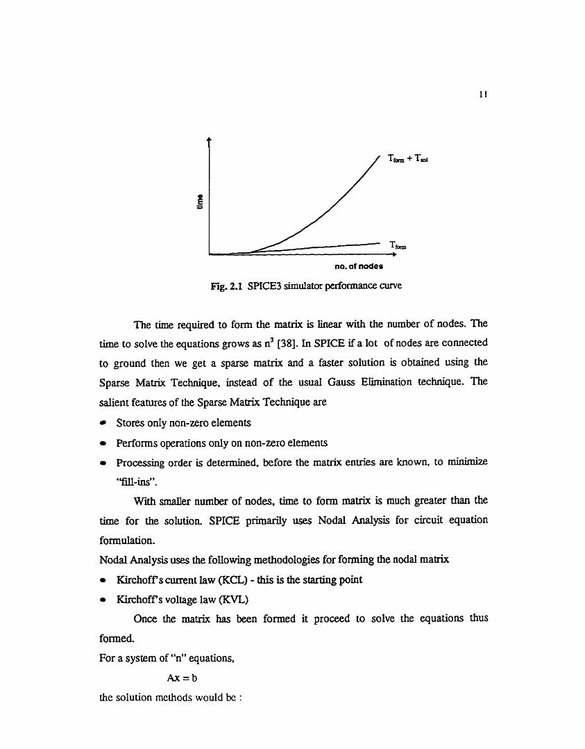
no. of nodes
Fig. 2.1 SPïCE3 sirndator performance m e
The time required to fom the mat* is iinear with the number of nodes. The
time to solve the equations grows as d [38]. In SPICE ifa lot of nodes are comected
to ground then we get a sparse matrix and a faster solution is obtained ushg the
Sparse Matrix Technique, instead of the usual Gauss EIimination technique. The
salient feames of the Sparse Matrix Technique are
Stores only non-zero elements
Performs operations only on non-zero elements
Processing order is determuied. before the matrix eniries are known. to minimue
"-iris".
With smaller number of nodes, tirne to form matrh is much greater than the
time for the solution SPICE primarily uses Nodal Analysis for circuit equation
formulation.
Nodal Analysis uses the following methodologies for forming the nodal ma&
Kirchoff s current law (KCL) - this is the starting point
Kirchoff s voltage law (KVL)
Once the matrix has k e n fomed it proceed to solve the equations thus
formed
For a systern of "n" equations.
A x = b
the solution rnethods wouId be :

Matrix inversion
- Cramer's rule
- x = ~ - ' b . $ operations for inversion
Gaussiun elimination
- forward elimination to fonn upper triangular systern and backward substitution
- n3 1 3 + d - n / 3 operations
LU decomposition
- momed fonn of Gaussian elimination
- reduction of A into L and U
- forward ehination and backward substitution
It can be seen fiom Fg. 2.1 , that the matrix solution time is significantly
smaller than the device evaluation the , although the dinerence decreases as the circuit
size increases [%].
2 2 Format of circuit fides
A circuit file that is read by the SPICE3 simulator is generated by the
schematic capture software. The circuit N e can be divided into five parts
(1) the title descnbing the type of circuit or any other comment
(2) the c i m i t describing the circuit elements and set of mode1 parameters
(3) the analysis description which defuies the type of analysis
(4) the output description which defmes the way the output is to be presented
(5) the end of the program
A circuit is described by statements stored in the circuit m. Each statement is
seif contained and independent of every other statement. Each element in the circuit is
connected between nodes that are assigned numbers. Node O is predehed as the
ground. The first statement of the me is always a comment line. The value of the
circuit is written after the nodes to which the elemint is connected. Modeis may be
used to assign values to the various parameters of the circuit elements. Of the various
types of analysis that SPICE offers, the tirne domain analysis, specifed by the .TRAN

statement, is used in the majority of the work The transient analysis portion of SPICE
cornputes the transiena output variables as a hiaction of ùme over a user-specified
t h e intervaL The initial conditions are automatically determined by a dc analysis. AU
sources which are no t time dependent ( for example, power supplies) are set to their
dc values. The last line of the circuit fïie terminates with the .END statement.
Given below in Fig. 2.2 is the circuit diagram for a simple half wave diode
rectifier and Fg. 2.3, is an example of its SPICE3 scheriiatic with its corresponding
circuit fde.
Fig. 2.2 Circuit diagram for Half wave diode rectifier
Fi. 23 SPICE3 schematic for a haLf wave diode rectiner
* half wave diode rectifier
.TRAN 20US 116.67MS lOOMS 20US W C
.OPTIONS METHOD=GEAR RELTOk0.03 ABSTOkIE-4
.MODEL PD D
RI23 1K
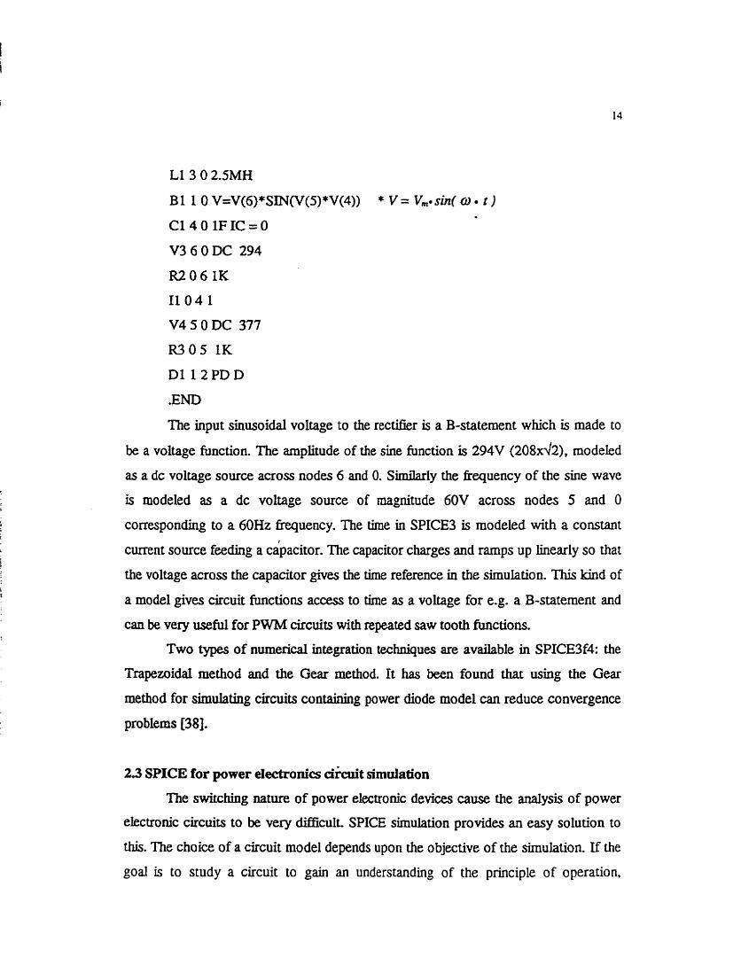
L13 O 2.SMH
B 1 1 0 V=V(6)*SIN(V(S)*V(4)) * V = V,,p sUi( t ) . C l 4 0 lFIC=O
V3 6 O DC 294
R2O6 1K
Il041
V450DC 377
R30S 1K
Dl 1 2 P D D
.END
The input sinusoidal voltage to the rectifier is a B-statement which is made to
be a voltage function. The amplitude of the sine function is 294V (208x42), modeled
as a dc voltage source across nodes 6 and 0. Similarly the kequency of the sine wave
is modeled as a dc voltage source of magnitude 60V across nodes 5 and O
corresponding to a 60Hz fiequency. The time in SPICE3 is rnodeled with a constant
cment source feeding a capacitor. The capacitor charges and ramps up linearly so that
the voltage across the capacitor gives the time reference in the simulation. This kind of
a model gives circuit functions access to t h e as a voltage for e.g. a B-statement and
can be very useful for PWM circuits with repeated saw tooth functions.
Two types of numerical integration techniques are available in SPICE3f4: the
Trapezoidal method and the Gear method. It has k e n found that using the Gear
method for sirnulating circuits containhg power diode model can reduce convergence
problems [38].
23 SPICE for power electronics circuit simulation
The switching nature of power electronic devices cause the anaiysis of power
ekctronic circuits to be very dBicult. SPICE simulation provides an easy solution to
this. The choice of a circuit model depends upon the objective of the simulation. If the
goal is to study a circuit to gain an understanding of the principle of operation.

components should be as eiementary as possible. Avoiding the use of actual non-hear
relationships for the device hastens the speed of simulation.
The major advantage of ushg SPICE in power electronics is that with the same
software a particular circuit can be aRalyzed and designed at various system and
subsystem levels, ie. at the level of the power switch or the circuit system as a whole
1121. However, for higher levels of simulation, a much simpler mode1 for the devices is
chosen for the circuit implementation to minimize convergence pro blems and reduce
the run times.
Power Electronic circuits are fiequentiy coupled to Drive Systems. A variable
speed AC machine co~ected to the rectifier-inverter system @va rise to cornpiex
stability problems. The machine is a non-linear mdtivariable system and interacts
dynamicaüy with the source irnpedance of the drive. Further complexity rnay arise
when for instance multiple machines are fed by a single inverter or multiple rectifiers
feed a single inverter. The analysis of such systems is tedious and cornputer simulation
becomes irnperative. The study of new control strategies, the effect of harrnonics and
the variation of system pa&eters are also facilitated by simulation results.
The recent updates made to SPICE at University of California, Beskley has
made O bsolete various simulation techniques O ften used for po wer electronic systems
191. The B-statement and the U-statement introduced in the iatest version of SPICE3
Le. Version 3f4, has simplihed the structure of control and switching functions used
fiequently in Power Eiectronics. The B-suternent can be either a current or voltage
function and is used to mode1 various complex circuitry without indulging in the
micromodeling and the device characteristics OP the switcbing device. This would
prevent long simulation nui times and convergence problems. The U-statement is
simply a cornparison statement that has a value of either 1 or O according to its
argument Some of the features of SPICE3 used for power electronic simulation are :
.OPTIONS - Various pantmeters of the simulations available in SPICE3 can be
altered to control the accuracy, speed or default values for sorne devices. These
parameters are changed via the .OPTIONS line. ABSTOL and RELTOL are the

two most common options used. ABSTOL mets the absolute current enor
tolerance of the program RELTOL resets the relative error toieraoce of the
P=%ra="- .TRAN - This dot command performs uansient anaiysis of the circuit. The general
form of .TRAN is
.TRAN TSTEP TSTOP TSTART TAUX UIC
TSTEP is the plotting incrernent for the output For use with the post-
processor. TSTEP is the suggested computing increment. TSTOP is the final t he , and
TSTART is the initial Me. If TSTART is omitted, it is assumed to be zero- The
transient analysis always begins at time zero. TMAX is usehl when one wishes to
guarantee a computing interval which is srnaller than the p ~ t e r increment, TSTEP.
niis would also ensure a more accurate numerical inkgration.
One of the advantages of choosing a srmil TSTEP is that it increases the
resolution of the waveforms obtained fkom SPICE3 simulation. This feature is made
use of in cases where the experimental waveforms have a resolution that is resuicted
by the resolution of the osciiioscope. This is frequently seen in the simulation
waveform of PWM Inverters where high switching frequency is used.
.IC - The IC line is for setting the transient initial conditions. When the UIC
parameter is specified on the .TRAN line, then the node voltages specifkd on the
.IC control line are used to compute the capacitor, diode and inductor initial
condition. Since no dc bias solution is compared before the transient anal@, it is
important to specify aü dc source voltages on the .IC control line if they are to be
used to cornpute device initial conditions.
.PRINT - The Print line helps in generating data for the vectors foilowing the print
cornmand. Output variables can be specifkd for any kind of analpis such as
TRAN (for transients analysis) just before the k t of vectors.
.PRINT TRAN vectorl vector2 . ..

.FOUR - The Four (or Fourier) line controls whether SPICE perfom analysis as
a part of the transient analysis. The dc component and the first nine harrnonics are
de termined.
.MODEL - Some devices that are included in SPICE require many parameter
values. Often, rnany devices in a circuit are defined by the same set of device
model parameters. For these reasons, a set of device mode1 parameters is dehnes
on a separate .MODEL line and assigned mode1 name. The device element lines in
SPICE then refer to the mode1 name.
In addition, SPICE3 is provided with the Interactive Interpreter that helps to
monitor parameters in a single run by means of a do loop. The stand alone program is
in the fom of a CONTROL file that uses simple syntax similar to C and the sheU
script. This feature of SPICE3 has been very usehl in the performance analysis of
Power Electronic circuits. Some of the features of the interactive interpreter are :
alias : It creates an alias for a command. It can be used to cause a word to be
aliased to text.
alter : It changes a devïce or model parameter.
destroy : It releases the memory holding the dau for the specifïed run.
echo : It prints out the given text to the screen during the simulation run.
print : It p ~ t s the vectors described by the expression following the print
statement. If the col argument is present, it p ~ t s the vectors named side by side in
column format If the line argument is given, the vectors are printed horizontally.
2.4 Troubleshooting
The major reason for any SPICE3 simulation to abort is due to convergence
problems. Both the DC and transient solutions are obtained by an iterative process
which is temiinated when both of the following conditions hold:
1) the non-linear branch currents converge to within a tolerance of 0.1% or 1
picoamps, whichever is larger.

2) The node voltages converge to within a tolerance of 0.1% or I microvolts,
whichever is Iarger.
The most common reason for failure to converge is sîxnply due to error in
specifykig circuit connections. element values or mode1 parameters. One characteristic
that has been blamed for many SPICE convergence problem is the "floating nodes".
These are circuits which have no conductance from the node to any other part of the
circuit This produces a row and column of zeros in the modined nodal analys3 ma&,
making it impossible to invert in practice.
Another common error is ' 'the step too smalI". SPICE3 provides an iteration-
count system of timestep controL If convergence is not obtained within a maximum
number of iterations, the solution is abandoned. the timestep cut by a factor of eight,
and the new srnalier step is attempted. If the convergence is obtained in fewer than a
minimum number of iterations. the timepoint is accepted and the timestep may be
doubled before attempting the next step. This technique relies very heavily on a good
choice of the starting timestep by the user. To circumvent this error the .TRAN values
are redefined, to change the tirne step for transient analysis. Aiso the RELTOL and
ABSTOL values are changed to resume simulation
SPICE also runs into convergence problems if in the circuit a capacitor is
connected across a voltage source or a cunent source feeds an inductor. The
simulation in this case aborts with an error message "check node W'. One way to solve
this problem is to add a small resistor to the circuit elernents which causes the
convergence probIem.

Chapter 3
DIODE BRIDGE RECTIFIERS
In most power electronic applications, the power input is in the form of a 50 or
60 Hz sinewave ac voltage provided by the electric utility, which is kst converted to a
dc voltage. A rnajority of the power electronk applications such as switching dc power
supplies, ac-mo tor drives and so on, use uncontroiied rectifiers. This chapter discusses
the six-pulse and twelve-pulse diode bridge rectifier topologies. A mode1 for the A-A,
A-Y transformer is presented m g d q axis theory. Simulated and experimerital results
are presented for cornparison The sirnulated and experirnental performance analysis
of the rectifier is done with emphasis on the line current harmonics and the THD.
3.1 Su-Pulse Diode Bridge Rectifier
In industrial applications where three-phase ac voltages are available, it is
preferable to use three phase rectifier circuits as compared to single-phase rectiners.
Three-phase rectiners have lower ripple content in the waveforms and a higher power
handling capability. A simple &cuit for a six-pulse diode bridge rectifier with U3 dc-
link Ilter is shown in Fig. 3.1.
The input line current of the three phase rectifier deviates Born king perfecdy
sinusoidaL By Fourier Anaiysis, the line current can be expressed in t e m of the
fwidarnental firequency and other harmonie components. If the iine voltage is assumed
to be purely shusoidaL then orily the fundamenta1 component of the iine current
contributes to the average power flow. The line current harmonics are generdy
dominated by odd harmonics.

Fig. 3.1 Three-phase diode bridge rectifier circuit
For a three phase diode bridge rectifier with an LC dc-link fdter, see Fig. 3.1
the line current harxnonics (assuming L -> Q) are theoretically given as :
Ln a diode bridge rec-r, two devices conduct at any instant. Each diode
conducts for 120" per cycle and a new diode begins to conduct after a 60" interval-
The output rectifed waveform which consists of portions of the line-to-line cunent ac
voltage waveforms, repeat with a 60" duraüon, making this a six-pulse rectifier.
3.1.1 Simulation of 6-pulse diode bridge rectifier
SPICE3 simulation and modeling is perfonned for a better understanding of
the analysis of the bridge rectifier. Broadly there are two approaches in modehg the
behavior of a semiconductor device like a diode. A macro-model mainiy based on an
empirical approach, is one that does not take into account the geometry and the
physical process of the device. This is to be distinguished fkom a micro-mode1 that is
based on the physical phenornena within the semiconductor modeL In the present

work, we use a SPICE model of the diode such that the device's known input/output
behavior is presented by an electricai equivalent circuit [25] and cm be expressed in
terms of its model parameter Iike breakdown voltage(BV), junction capacitance (UO)
and inverse saturation current (1s). Mode1 parameters for the diode are defïned on a
separate .MODEL line. The SPICE library has a mode1 for power diode which is
aliased as "PD" (power diode) and is used for the present circuit
3.1.2 C dc-link filter
The SPICE3 model for the 3-phase diode bridge is shown in Fig. 3.2. In this
rectifer topology we have a large C (94ûp.F) dc-link Nter at the rectifier output. For
all practical applications a finite source inductance is dways present. The values of the
output capacitor and load are exactly the same as used in the experimental setup. The
Fig. 3 3 SPICE3 model for 6-pulse rectifier bridge with C filter
input source inductance in the power electronics laboratory was estimated to be about
0.4 mH. The effect of the iine inductance is to slope off the veaicai portion on the line
current. This attenuates the higher order harmonics in particular. The SPICE3

schematic and its corresponding netlist for the six-pulse diode bridge rectifier is given
in Appendix G. 1. The saiient features of the SPICE mode1 in Fig. 3.2 are :
input sinusoidai voltage, Va
v. = vq* sin&* v< + VPb)
The input sinusoidal voltage is modeled with the help of a B-statement which is
a voltage function representing the sinusoidal.
time, Vt :
The t h e is modeled as the constant cment source in paralle1 with a capacitor.
The capacitor charges and ramps up linearly, thus the voltage node represents time.
amplitude. V,, :
The amplitude of the sinusoidal wave is modeled as a constant dc voltage
source of magnitude 169V (42 x 208 143 ).
ftequency, Vh:
The fiequency of the sinusoidal wave is modeled as a constant dc voltage
source of magnitude 60V corresponding to 60Hz
phase,vpb:
The phase shift between the three phase voltages of the shusoidal wave is
modeled as a constant dc voltage source of magnitude 120V which corresponds to
120".
3.1.3 Waveforms and analysis for C filter
The simuiated and experimental waveforms are shown in Fig. 3.3. As seen
fiom Fig. 3.3(a),(b) the output current is always discontinuous. This is more prominent
in the experimentaî waveform of the current. The reason king that the source
inductance for the simulation could not be lowered below 0.4mH. With a voltage
function feeding an inductor, any attempt to iower the inductance value causes a
convergence probbm. a problem commoniy encountered in SPICES. A larger value of
source inductance in the simulation also causes iarger commutation overlap as seen in
Fig. 3.3 (a). Two current pulses are drawn from each phase during every half-cycle.
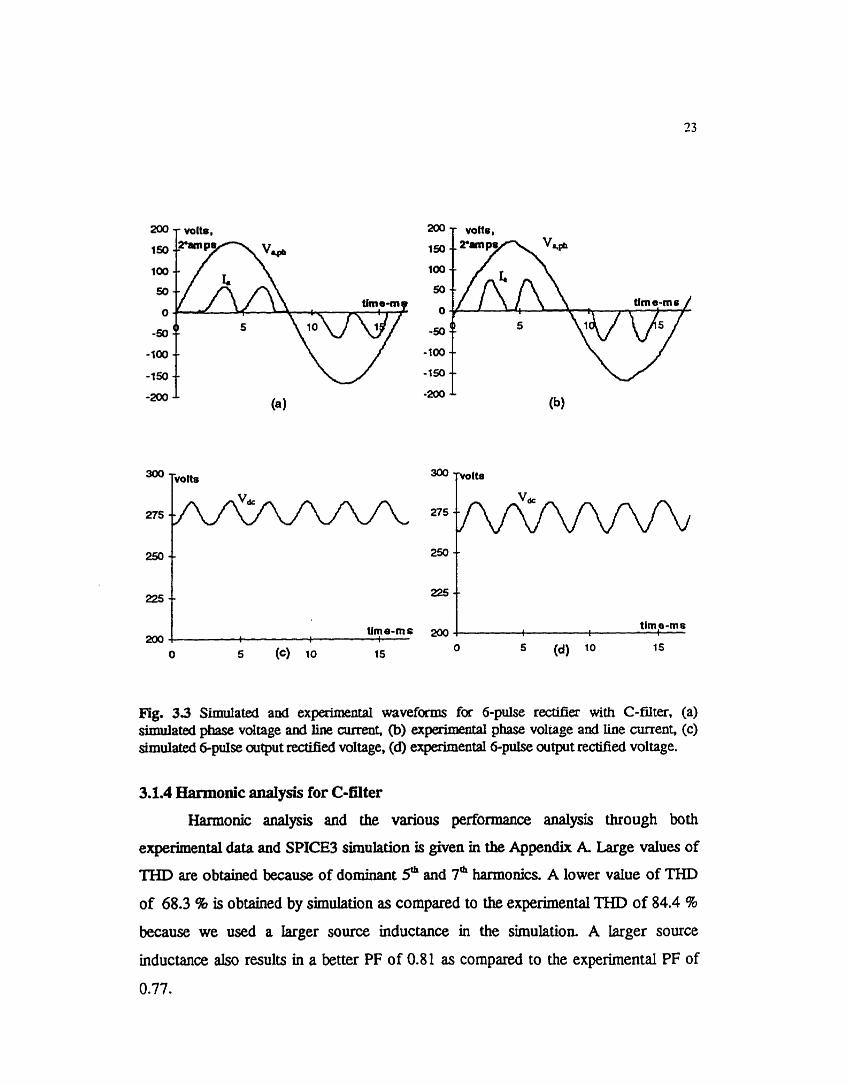
Fig. 3 3 Simulated and experimental w a v e f m for 6-pulse rectifier with C-filter. (a) simulated phase voltage and line curent, @) experhneatal phase volrage and line current, (c) simulated &pulse output rectified voltage, (ci) experimental &pulse output rectifîed voltage.
250
225
2 0 0 .
3.1.4 Harmonie andysis for C-filter
Hannonic analysis and the various peffonnance analysis through both
experimentai data and SPICE3 simulation is given in the Appendix A Large values of
THD are obtained because of dominant 5~ and 7& harmonies. A lower value of THD
of 68.3 % is obtained by simulation as compared to the experimental THD of 84.4 4b
because we used a larger source inductance in the simulation. A iarger source
inductance also results in a better PF of 0.81 as compared to the experimental PF of
0.77.
--
--
Ume-ms MO tirne-rns
O 5 (c) 10 15 I I O Ei (d) l* 15
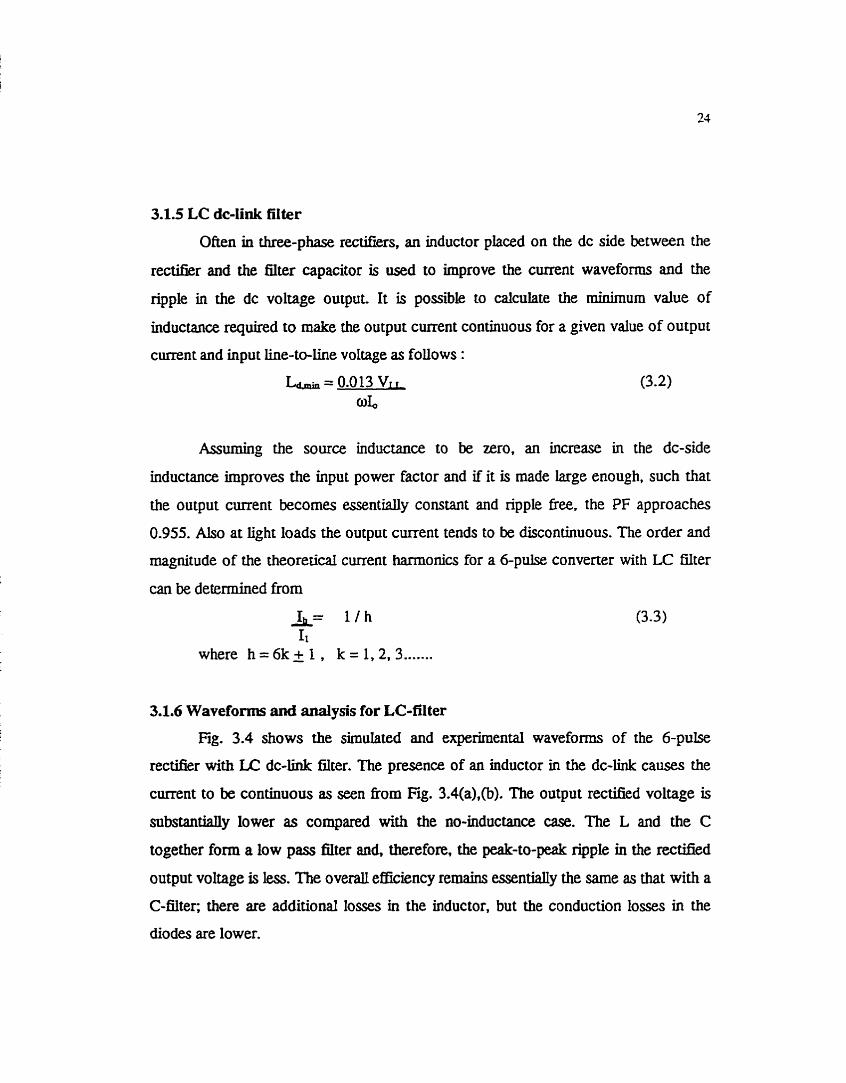
3.1.5 LC dc-Iink filter
Often in the-phase rectiners, an inductor placed on the dc side between the
rectiner and the filter capacitor is used to improve the current wavefom and the
ripple in the dc voltage output. It is possible to calculate the m . u m value of
inductance required to make the output current coatinuous for a given value of output
current and input line-to-line voltage as foilows :
AssumiOg the source inductance to be zero, an increase in the dc-side
inductance improves the input power factor and if it is made large enough, such that
the output cwent becomes essentially constant and ripple fie. the PF approaches
0.955. Aho at light loads the output cument tends to be discontinuous. The order and
magnitude of the theoreucal current hamonics for a 6-pulse converter with LC filter
cm be determined from
A= l l h 11
where h=6k-ç 1 , k = 1, 2, 3 .......
3.1.6 Wavefom and analysis for LC-filter
Fig. 3.4 shows the simulated and experimental wavefom of the 6-pulse
rectifier with LC dc-link hlter. The presence of an inductor in the dc-link causes the
current to be continuous as seen £rom Fig. 3.4(a),(b). The output rectined voltage is
snbstantially lower as compared with the no-inductance case. The L and the C
together form a low pass nIter and. therefore, the peak-to-peak ripple in the rectified
output voltage is iess. The ove& eniciency rem- essentially the same as that with a
C-filter, there are additional losses in the inductor, but the conduction losses in the
diodes are lower.
tim e-m r Ume-m8 2 0 0 . I I 200! 8 3 1
O 5 (c) 10 15 O 5 (d) 10 15
Fig. 3.4 Simulated and expexhental wavefonns for 6-puise redifier with LC-filter, (a) simulated phase voltage and fine current, (b) experimental phase voltage and lhe current, (c) gmulated 6-pulse output rectified voltage, (6) experimental6-puise output rectifieci voltage.
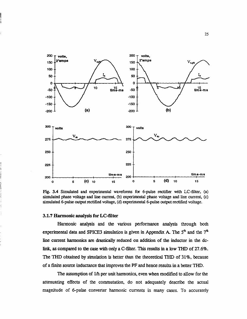
3.1.7 Harmonie anaiysis for LC-filter
Harmonic anaiysis and the various performance anaiysis through both
experimental data and SPICE3 simulation is given in Appendix k The 5' and the 7'
line current harmonics are drastically reduced on addition of the inductor in the dc-
link. as compared to the case with only a C-flter. This resuIts in a low THD of 27.6%.
The THD obtained by simulation is better than the theoreticai THD of 3 1 %. because
of a finite source inductance chat irnproves the PF and hence results in a better THD.
The assurnption of I/h per unit harmonics, even when rn-ed to aUow for the
attenuating effects of the commutation. do not adequately describe the actual
magnitude of 6-puise converter harmonic currents in many cases. To accurately

determine the characteristic converter harmonies. a caiculation procedure which takes
into account the ripple of the dc current reflected back into the ac line current must be
performed [6]. Evaluation of these ripple effects will tend to increase the magnitude of
the 5" harmonie whüe decreasing the magnitude of the higher order characteristic
harmonics.
3.2 Twelve-Pulse Diode Bridge Rectifier
For higher power applications, when the converter current or voltage is high.
diode bridges may be connected in series or paralleL For the present work, the series
comection of two diode bridges on the dc side is used. One converter bridge is fed
from a A-Y transformer that introduces a three phase set of secondary voltages shifted
by 30" with respect to the primary voltage. The other converter bridge is fed by a
secondary voltage, from a A-A transformer, which has no phase shift. Due to the phase
relationships it is seen that some of the current harmonics in one bridge are in
antiphase with those of the other. Thus, these phase shifting transfomers provide
mechanisrn for hamonic canceilation. In addition. they reduce the dc voltage output
Fig. 3.5 Block Diagram for 12-puise diode bridge rectifier

ripple. This effectively reduces the size of the Nter used in the dc-link Operation with
incmasing pulse num ber is very desirable for high-power converter applications suc h
as HVDC and large dc motor drives 1391.
The hamonic canceiïation of the input line current in ternis of the Fourier
cornponents is
In the operation of such multipulse converters, it is assurned that the dc circuit
is fütered such that any ripple caused by the dc load does not signincantly aEect the dc
current. This is me for passive loads and for most converters feeding dc power to
voltage source inverters. It is l es Iikely to be true for inverter loads of the current
source type, where practid filtering may be insufficient to prevent dc load Q p l e t?om
effecting the total ripple.
3.2.1 d-q Axis Theory modd for A-NA-Y transformer
The input of the 12-pulse rectifier bridge is the A-NA-Y transformer, with their
secondaries phase shifted by 30". The series impedance of the autotransformer used in
the experimental setup is taken into account in the simulation by using higher
inductance values for the A-NA-Y transformer.
The quivalent per phase circuit of the transformer is considered in ternis of
the dg axis theory [Ml. In this theory the tirne varying parameters are eIiminated and
the variabies and parameters are expressed in orthogonal or mutuaiiy decoupled direct
(d) and quadrature (q) axes, see Fig. 3.6. The supply voltages in terms of d and q
voltages are written in rnauix form as
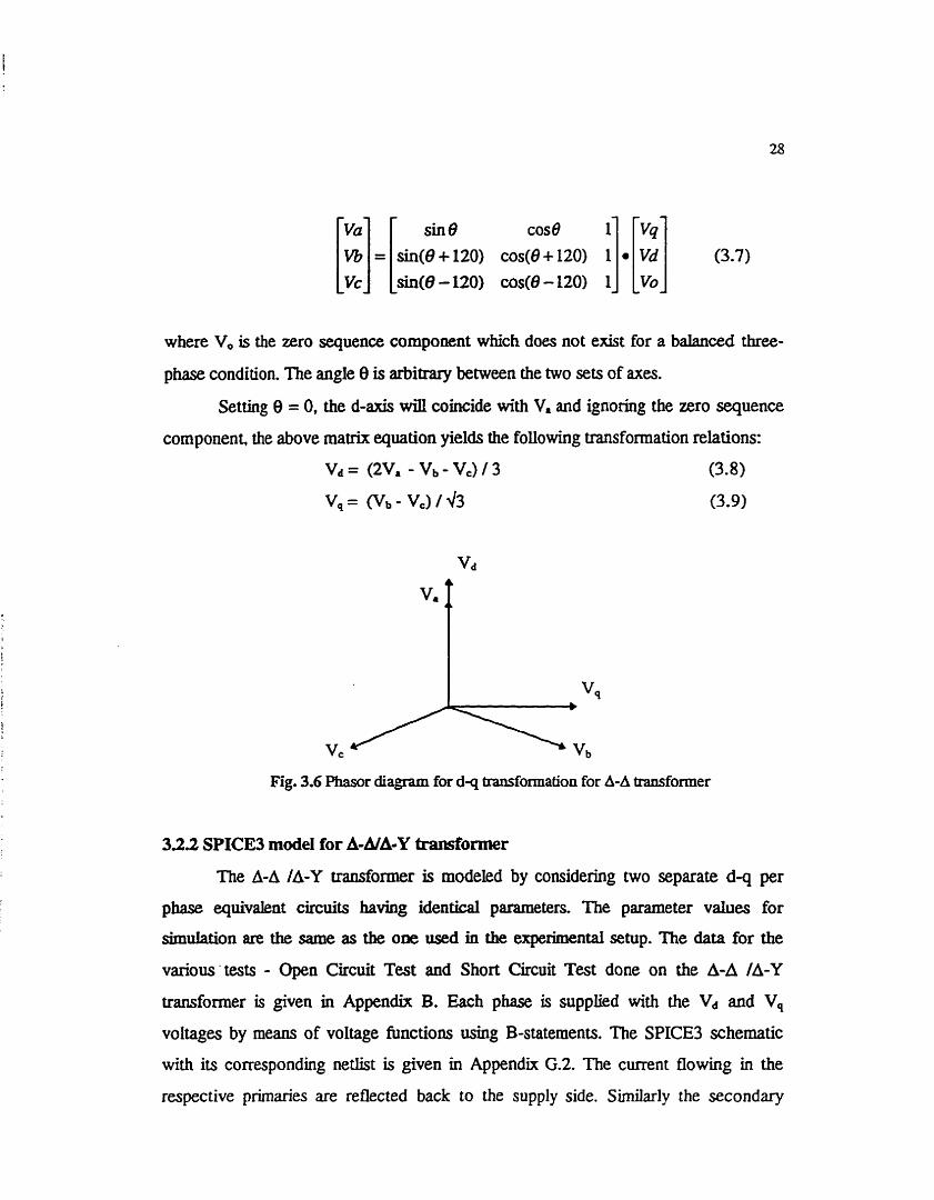
sin 8 cos9
where V, is the zero sequence component which does not eWt for a balanced three-
phase condition. The angle 0 is arbitrary between the two sets of axes.
Setting 0 = 0, the d-axis will coincide with V. and ignoring the zero sequence
component, the above ma& equation yields the foliowing transfomation relations:
vd = (Sv, - vb - vc) / 3 (3-8)
vq= (vb-vC)/d3 (3-9)
Fig. 3.6 Phasor diagram for d-q transformation for A-A transformer
3.2.2 SPICE3 mode1 for A-&A-Y transformer
The &A /A-Y transformer is modeled by considering two separate d q per
phase quivalent circuits havïng identicai parameters. The parameter values for
simulation are the same as the one used in the experimentai setup. The data for the
varioustests - Open Circuit Test and Short Circuit Test done on the A-A /A-Y
transformer is given in Appendix B. Each phase is suppiied with the Vd and V,
voltages by means of voltage functions using B-statements. The SPICE3 schematic
with its correspondhg netlist is given in Appendix G.2. The current flowing in the
respective primaries are reflected back to the supply side. Similarly the secondary

currents are reflected into the Ioad side. The expression for the phase currents in terms
of the d and q currents flowing in the A d transformer is
The A-Y mode1 differs fiom the A-A mode1 in that its input supply voltage is
30°phase shifted. The phasor diagram for the A-Y secondary phase voltages in terms
of the d and q voltages is given in Fig. 3.7
Fig. 3.7 Phasor diagram for d q transfafmation of the A-Y transformer
Similarly, the d and q voltages fed to the A-Y per phase quivalent circuit is
given by the transformation
V d = -(SVc - Va- Va) 1 3 (3.13)
and the cmnt relationships are
qequivaien t d-equivalen t circuit circuit
Fig. 3.8 d-q axis themy transformer mocW
The SPICE model for the A-A transfomer is shown in Fig. 3.8 and is obtained
fYom the various equations derived fiom the d q a h theory. Each transformer model
consists of separate d and q equivalent circuits with a primary and a secondary. The
input to the transformer is the three phase voltages V., VI,, Ve with phase a
represented by a B-suternent which is voltage hinction as explained in section 3.1.2.
Each of the primaries are fed by a B-statement which is a voltage function and
is a hnctiond relationship of the input phase voltages. These voltage relations are
obtained from Equations (3.8).(3.9).
d-quivalent circuit primary: Vdp = (2*Vi-Vb-Vc) 1 3 (3.18)
q-quivalent circuit prïinary: V, = (Vb-Vc) 1 43 (3.19)
The currents fiowing in the primaries of each of the equivalent circuit is
refkted back to the input side with the heip of B-statements that are functions of the
cunent flowing through the B-statements in the two prunaries. These current relations
are obtained nom Equations (3.10). (3.1 1). (3.12).
Phase a : I. = I(Vg) (3.20)
Phase b : b= OS*(-I(V&i.732*1&)) (3.2 1)
Ph= c : I, = -0.5*(I(V,jp)+1.732*I(V,)) (3.22)
where Vdp and V, are the voltage functions in the primary side of the d and q
equivalent circuit respectively.

Simüarly. the secondaries of the d and q quivalent circuits are fed by a B
function which is a voltage functions of the output voltages. The current in the
secondaries are reDected to the output and are functions of the current flowing
through the B-statements in the two secondaries. The three output B-statements thus
function as the input voltage to the &pulse diode bridge rectifier.
3.23 SPICE3 model for l2-pulse rectifier
The SPICE3 model of the 12-pulse diode bridge rectifier is shown in Fg. 3.9.
Two 6-pulse diode bridges are comected in series to give a 12-pulse operation. The
A d /A-Y transformer has two primarw and two secondaries. The d-q axis voltages
and cunent for the A-A transformer are defined by Equations (3.8)-(3.12) and the
correspondhg relationships for the A-Y transformer, whose output voltage is 30"
phase shifted fiom the A-A transformer, are defmed by Equations (3.13)-(3.17).
The use of B-statements to decouple the input and the output of the A-A /A-Y
transformer helps to sirnplifj the model by avoiding the non-linear interaction between
the input and the output This decouphg leads to more nodes king connected to the
ground thus generating a much sparse nodal admittance rnatrix during simulation The
Sparse Maerix technique thus used increases the speed of simuiation.
A-A transformer L
Fig. 3.9 SPICE3 model for the f 2-pulse rectifier
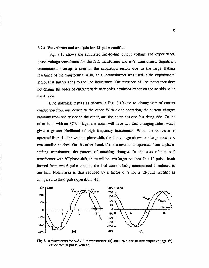
3.2.4 Waveforrns and analysis for 1Zpulse rectifier
Fïg. 3.10 shows the simulated line-to-line output voltage and experhnental
phase voltage wavefom for the A-A transformer and A-Y transformer. Signilicant
commutation overlap is seen in the simulation results due to the large leakage
reactance of the transformer. Also, an autotransfomer was used in the experimental
setup, that M e r adds to the ihe inductance. The presence of line inductance does
not change the order of characteristic harmonies produced either on the ac side or on
the dc side.
Line notchuig results as shown in Fig. 3.10 due to changeover of current
conduction h m one device to the other. With diode operation, the current changes
naturdy fkom one device to the other. and the notch has one fast rising side. On the
other hand with an SCR bridge, the notch will have two fast changing sides, which
gives a greater likelihood of high bquency interference. #en the converter is
operated from the line without phase shift, the line voltage shows one large notch and
two smaller notches. On the other hand. if the converter is operated £tom a phase-
shifüng transformer, the, pattern of notching changes. In the case of the A-Y
transformer with 30°phase shift, there wiU be two Larger notches. In a 12-pulse circuit
formed f?om two 6-pulse circuits. the load current king commutated is reduced to
one-half. Notch area is thus reduced by a factor of 2 for a 12-pulse rectifier as
compared to the &pulse operation [41].
Fig. 3.10 Waveforrns for A-A / A-Y transformer, (a) tirnulatecl fine-to-line output voltage, @) expetimental phase voI tage.
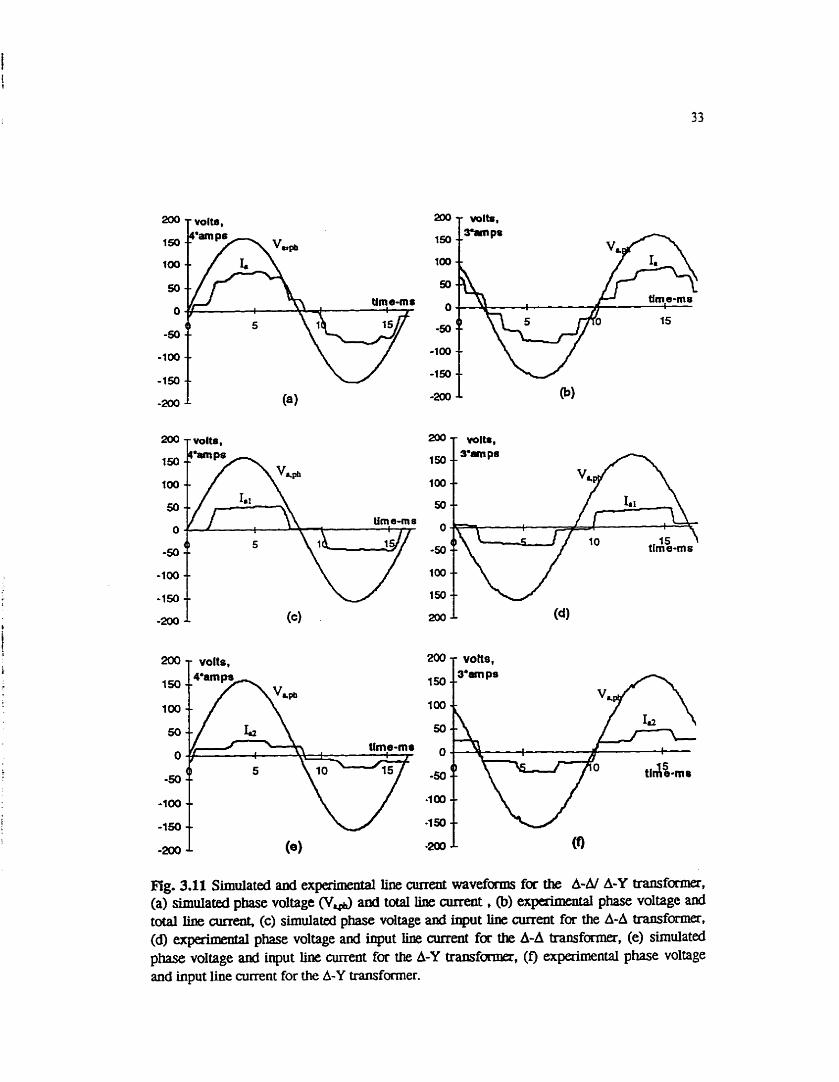
Fig. 3.11 Simulated and expaimental line curent wavefm foc the A-dl A-Y transforma, (a) simuïated phase voltage (Vlph) and tofal line airreat , @) phase voltage and total ih current, (c) simulated phase voltage and input lim current fu the A-A ~ f m . (d) experimental phase voltage and input line airrent for the A-A transfomia. (e) sirnuiated phase voltage and input line m e n t for the A-Y transforma, (f) expaimental phase voltage and input line current for the A-Y transformer.

The 12-pulse rectifier mode1 has two six-pulse diode bridge rectifier comected
in series. The load is resistive with a 2.5m.H inductor in both the positive and the
negative dc raiL The value of the load resistance is the same as used in the
experimental setup. Typical waveforms of the different line currents are given in Fig.
3.11. The wavefom are rounded instead of king the theoretical stair-type of
wavefom because of the inductive source and leakage irnpedances.
AU the h e currents in Fig. 3.1 1 show signifiant commutation overlap, which
is even more prominent in the simulation due to higher value of leakage reactances
used to compensate for the autotransformer used in the experimental setup.
3.2.5 Harmonic anal ysis for 1 Zpulse rectifier
Harmonic analysis and the various performance analysis through both
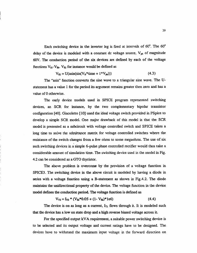
experimenial data and SPICE3 simulation is given in the Appendà C. The 5* and the
7& line current hamionics theoreticaliy get canceled as suggested by equation
(3.4),(3.5) and (3.6). Their negligible smail value as seen fkom AppendDr C is due to a
slight voltage imbaiance of the output of the A-A transformer and A-Y transformer.
This results is a low THD of 7.32 96. The experimental THD obtained is 10.9 %. The
12-pulse rectifier has the 11". 13&. 23" and other higher order hannonics in the hput
line current which make filtering relatively easy as compared to &pulse operation.
In high power rectifier circuits, the a<: Line cument during output shoa circuit is
sometimes fimited by purposely designing a transformer with a high reactance or
extenially adding a current Iimiting reactance. This extra reactance with a 12-pulse
rec-r circuit drasticaiiy reduces the 11' and the 13& harmonie currents of the 60Hz
ac system [n. The output rectified voltage waveforms of the two diode bridges are shown in
Fig. 3.12. High dc-link voltage with Io w voltage ripple is desirable since it reduces the
s k of the £iiter. These two 6-pulse waveforms are shifted by 30' with respect to each
other. Since these two bridges are connected in series on the dc side the total dc

voltage, V, has 12 ripple pulses per fundamental ac cycle. This results in the voltage
harmonies of the order h in Vk. where
h = 12k (k= integer)
and the 12* harmonic is the lowest order hamonic.
The six pulses generated by each of the transformer are no t identicai due to a
siight voltage imbaiance at the output of the A-A and A-Y transformer. This is due to
the fact that, for the A-Y transformer the tums ratio of 43 Le 1.732 is practically very
difficult to achieve with a lot of precision.
tim e-m e O I
O 5 @)IO 15
Ag. 3.12 SimuIated and experimental output voltage waveforms for the I 2-pulse rectifier. (a) sùnulated 6-pulse and 12-pulse rectifiai voltage. @) experimental 6-pulse and 12-puise rectifiai voltage.
In order to design more redistic 12-pulse diode bridge rectifier systems,
particular attention needs to be given to the voltage distortion already present in the
electric utilities due to other nonlinear loads and harmonic resonance conditions. In
many industrial systems with nonfinear loads, its is not uncommon to measure 1% to
3% voltage unbalance andlor 2.5% to 595 preexisting 5' and 7& hamonic voltage
distortion when a large percenage of loads are nonlinear [42].

Chapter 4
VOLTAGE SOURCE INVERTER
Inverters convert dc to variable ffequency ac. An inverter is categorized as
voltage source viewed fkom the load side, the ac terminais of the inverter function
as a voltage source. The voltage source inverter can be a square wave inverter or the
Pulse Width Modulation (PWM) inverter. In this chapter the SPICE3 simulation of
six-pulse, two level square wave inverter and PWM inverter have ken discussed The
square wave inverter is modeled using thyristor as the switching device, two in each
inverter leg. For the PWM inverter where the switching fkquency is much higher,
voltage functions are used in each inverter leg instead to facilitate SPICE3 simulation.
The experimental and simuhted waveforms have been compared. A generalized
structure of a three-level twelve pulse voltage source inverter is also expIained dong
with its SPICE3 simulation. A cornparison of the voltage hannonics present in the
output have been done using both simulation and experimental data,
4.1 dpulse, 2-Ievel Square Wave Inverter
The input dc voltage of a square wave voltage source inverter in controlled in
order t control the magnitude of the output ac voltage, and therefore the inverter has
to control oniy the fiequency of the output voltage. The output ac voltage waveform
is sixnilar to a square wave and hence the name.
Each control signal for the six switches in the inverter legs, see Fig. 4.1 has a
duration of R radians. The control signals are applied to the switches with a phase
dinerence of d 3 nidians, see Fig- 4.2. The switches in the same kg conduct
aitemately. Some t h e must elapse between the turn-off of one switch and tun-on of
another switch in the same leg to ensure that the two do not conduct simultaneously
and cause a short circuit.
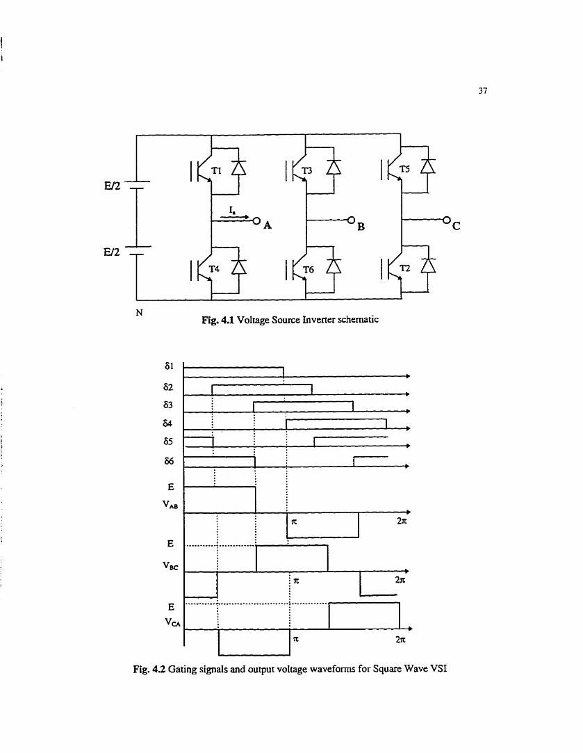
N Fig. 4.1 Voltage Source Inverter schernatk
Fig. 4.2 Gating signals and output voltage waveforms for Square Wave VSI
The magnitude of the fundamentai fkequency line-to-lùie rms voltage in the
output can be obtained fiom
v ~ = * E = 0.78E (4.1 1 II:
The line-to-luie output voltage waveform does not depend on the load and
contains harmonies (6n 1: 1; n = l.Z,3 ...), whose amplitudes decrease inversely
proportional to their hannonic order.
where h = 6 n + l ; n = 1 , 2 , 3 ..... (4.2)
4.1.1 SPICE3 simulation of square wave inverter
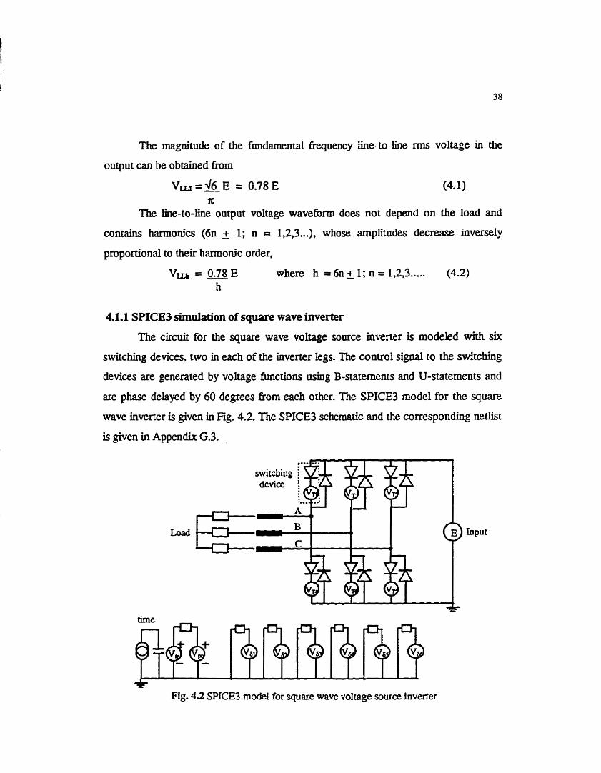
The circuit for the square wave voltage source inverter is modeled with six
switching devices, two in each of the inverter legs. The control signal to the switching
devices are generated by voltage hinctions using B-statements and U-statements and
are phase delayed by 60 degrees from each other. The SPICE3 mode1 for the square
wave inverter is given in Fig. 4.2. The SPICE3 schematic and the correspondhg netüst
is given in Appendix G.3.
f
Fig. 4.2 SPICE3 mode1 for square wave voltage source inverter
Each switching device in the inverter leg is f ~ e d at intervals of 60". The 60"
delay of the device is modeled with a constant dc voltage source, Vg of magnitude
60V. The conduction pend of the six devices are defineci by each of the voltage
functions Vsi-Va. Va for instance would be defined as
Va = U(asin(sin(V,*time + 1 *Vph))) (4.3
The "asin" function converts the sine wave to a triangular sine wave. The U-
statement has a value 1 for the period its argument rem- greater then zero and has a
value of O otherwise.
The early device rnodels used in SPICE program represented switching
devices, an SCR for instance, by the two complementary bipolar transistor
configuration [40]. Giacoletto [IO] used the ideal voltage switch provided in PSpice to
develop a simple SCR model. One major drawback of this model is that the SCR
model is presented as a subcircuit with voltage controlled switch and SPICE takes a
long time to solve the admittance matric for voltage controIIed switches where the
resistance of the switch changes from a few ohms to some megaohms. The use of six
such switching devices in a simple &pulse phase controlled rectiuer would thuç take a
considerable amount of simulation tirne. The switching device used in the mode1 in Fig.
4.2 can be considered as a GTO thyristor.
The above problem is overcome by the provision of a voltage function in
SPICE3. The switching device in the above circuit is modeled by having a diode in
series with a voltage fùnction using a B-statement as shown in Fig.4.2. The diode
maintains the unidirectional property of the device. The voltage fwction in the device
model defines the conduction perhd. The voltage hinction is defmed as
Vn = l[TL * (Va*0.05 + (1- Va)* le6) (4.4)
The device is on as long as a cunent, Itl flows through it. It is modeled such
that the device has a low on state drop and a high reverse biased voltage across it.
For the specified output kVA requirement, a suitable power switching device is
to be selected and its output voltage and current ratings have to be designed. The
devices have to withstand the maximum input voltage in the forward direction on

which the ma.@ due to commutation overshoot, typicaiiy 50% overvoltage, is added.
The diodes are usually of the fast-recovery type and have the same voltage rating as
the thyristor.
For the purpose of modeling, the input to the voltage source inverter is taken
as a rectined dc voltage of the same magnitude as the experknental setup. The rectified
voltage cm be obtained by employing a controkd rectiner. But this causes large
magnitude of low fiequency harmonies in the rectifier output voltage and source
eument resulting in low power factor of the rectifier at low output voltage. Rectined
output voltage c m also be obtained using a diode bridge rectifier foiiowed by a
chopper, such that the power factor remains close to unity under al1 conditions of
operation. The bypass diodes of the inverter clamps the load voltage to the input level
and also permit reverse current flow during reactive power flow and regeneration.
The output of the circuit in Fig. 4.2 is star connected ta mode1 the induction
motor stator. The values for the output used for simulation are the sarne as the
machine parameters for the experimental setup. The tests used to determine the values
of the parameters are given in Appendix D.
4.1.2 Waveform and analysis for square wave inverter
The simulated and experimental waveforms are shown in Fig. 4.4. The output
line voltage wave waveform, Fig. 4.4 (a),@) have a characteristic six-stepped wave
shape. The line current wave shape is due to the switching acfion of the devices in the
inverter legs. For the interval that the phase voltage is positive and the line current is
negative, the reactive cnrrent flows to the source through the bypass diodes. Also the
six-stepped wave shape is phase shifted fkom the line voltage by 30". The motor phase
current lags the voltage due to the presence of motor reactance.
The output voltage does not depend on the load. However, the duration of
each switch conduction is dependent on the power factor of the load. Even though the
switches are in their on-state for 180". due to the lagging power factor of the load,
their actual conduction interval are smaller than 180". As the power factor of the load
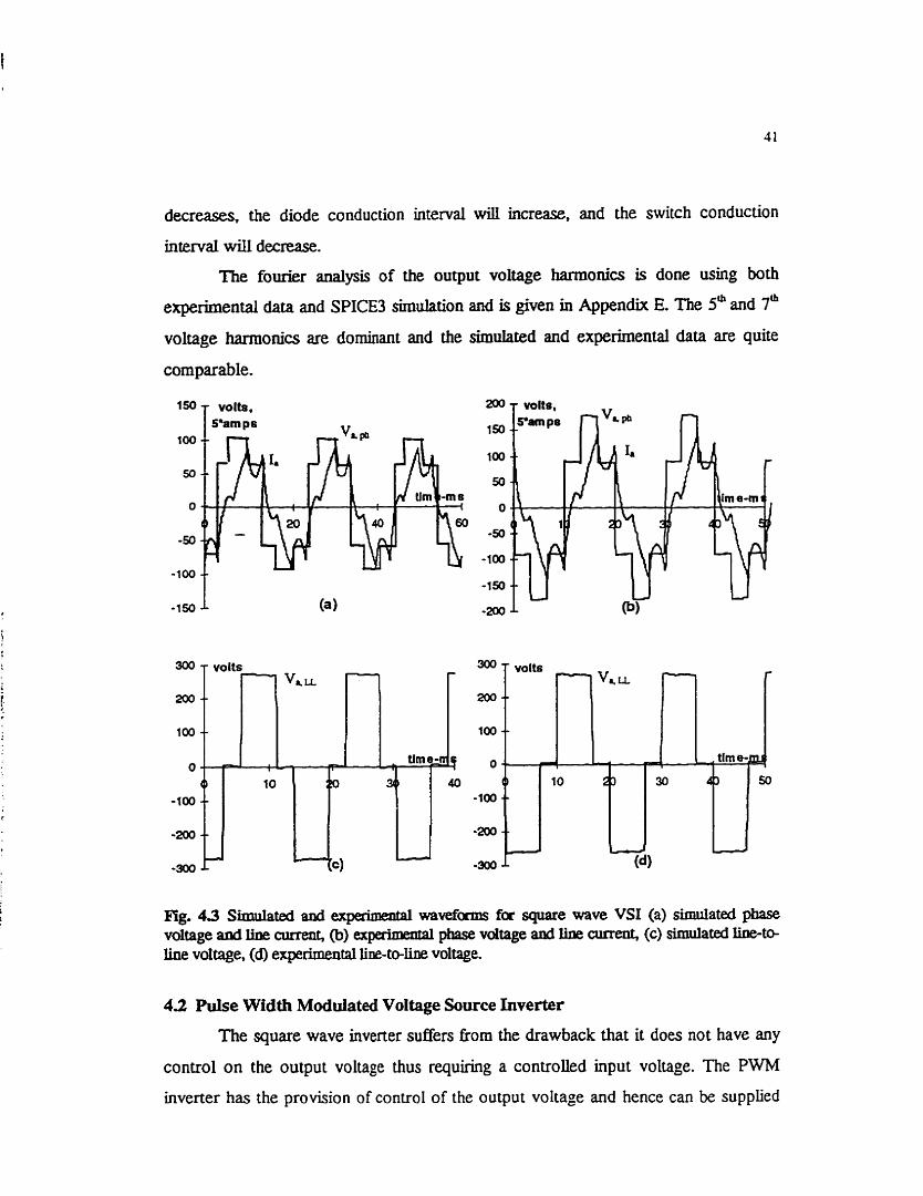
decreases, the diode conduc tio n interval will increase, and the switc h conduc tion
interval will decrease.
The fourier analysis of the output voltage harxnonics is done using both
experimental data and SPICE3 simulation and is given in Appendix E. The 5" and 7&
voltage harmonies are dominant and the simulated and experimental data are quite
comparable.
Fig. 4.3 Simulated and experimenral wavefixms fa square wave VSI (a) simulated phase voltage and line m e n t , @) expairnemal phase voitage and line ment, (c) simuiated lioe-te ïine voltage, (ci) expetimental line-to-Iine voltage.
- volts
4.2 Pulse Width Modulated Voltage Source Inverter
The square wave inverter suffers nom the drawback that it does not have any
control on the output voltage thus requiring a conuolled input voltage. The PWM
inverter has the provision of control of the output voltage and hence c m be supplied
r - - -&u
, the-*
10 30 43 50
.t- Ccr
(4
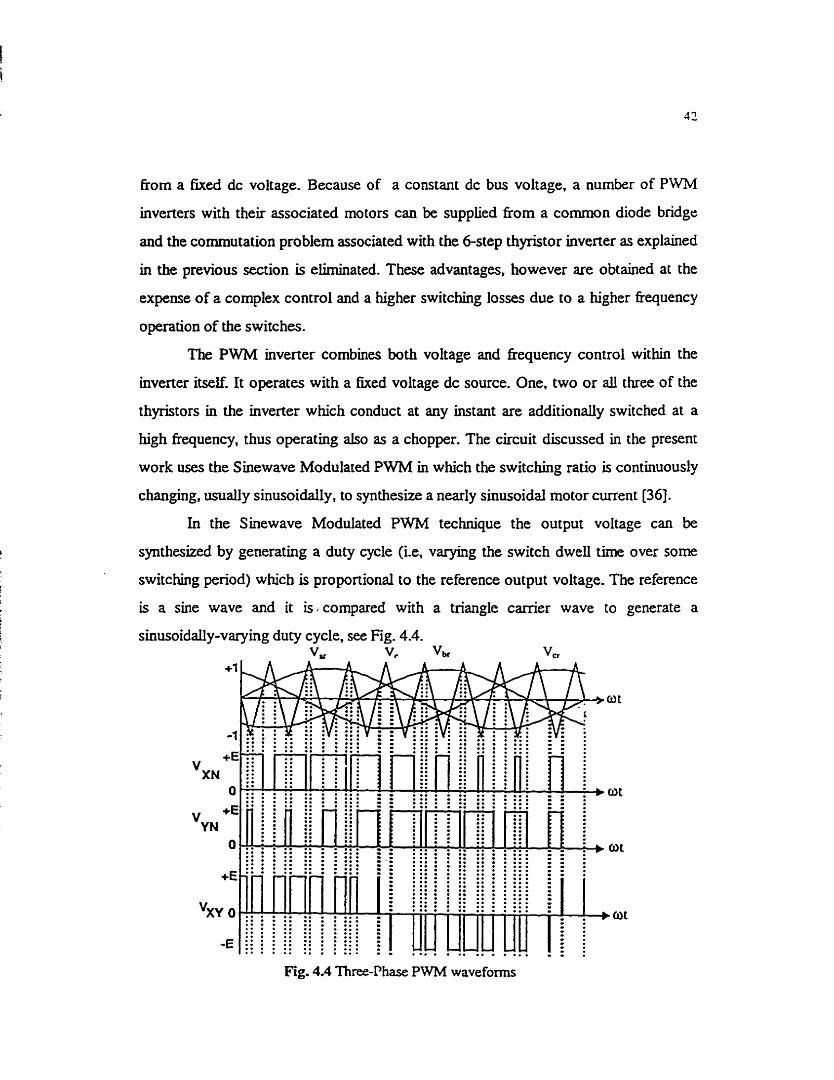
fiom a fixed dc voltage. Because of a constant dc bus voltage, a number of PWM
inverters with their associated motors c m be supplied from a cornmon diode bridge
and the commutation pro blem associated w it h the &tep thyristor invener as explaùied
in the previous section is eiirninated. These advantages, however are obtained at the
expense of a complex convoi and a higher switching losses due to a higher fiequency
operation of the switches.
The PWM inverter combines both voltage and fiequency control within the
inverter itself. It operates with a fixed voltage dc source. One, two or aU three of the
thyristors in the inverter which conduct at any instant are additionaliy switched at a
high fiquency, thus operating also as a chopper. The circuit discussed in the present
work uses the Sinewave Modulated PWM in which the switching ratio is continuously
changing, usually sinusoidaliy, to synthesize a nearly sinusoidal motor curent [36].
In the Sinewave Modulated PWM technique the output voltage can be
synthesized by generating a duty cycle (Le, v-g the switch dwell time over some
switching period) which is proportional to the reference output voltage. The reference
is a sine wave and it is. compared with a triangle carrier wave to generate a
sinusoidally-varying duty cycle, see Fig. 4.4.
Fig. 4.4 Three-Phase PWM waveforrns
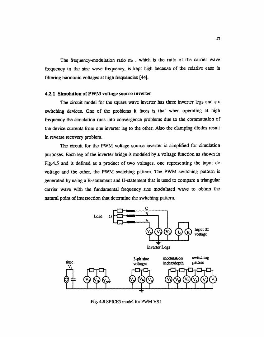
The hequency-modulation ratio mr , which is the ratio of the carrier wave
kequency to the sine wave fiequency, is kept high because of the relative ease in
filtering hmonic voltages at high fkquencies [44].
4.2.1 Simulation of P WM voltage source inverter
The circuit model for the square wave inverter has three inverter legs and sic
switchiog deMces. One of the problems it faces is that when operating at high
fiequency the simulation runs into convergence problems due to the cornmutalion of
the device currents fkom one inverter leg to the other. Also the clamping diodes result
in reverse recovery problem.
The circuit for the PWM voltage source inverter is simplined for simulation
purposes. Each Leg of the inverter bridge is modeled by a voltage function as shown in
Fig.4.5 and is defined as a product of two voltages, one representing the input dc
voltage and the other, the PWM switching pattern The PWM switching pattem is
generated by using a B-statement and U-statement that is used to compare a triangular
&er wave with the fugdarnental fkequency sine modulated wave to obtain the
naturd point of intersection that determine the switching pattern.
3-ph sine modulation swi-g voltages index/&pth Pa-
Fig. 4.5 SPICE3 model for PWM VSI

The modeling of the six switching devices with three simple voltage hinctions
simplifies- the problem of a complicated circuitry, current commutation from one
inverter leg to the other and reverse recovery problems of the diodes.
Switching pattern
The PWM switching pattern is generated by comparing the carrier and
reference waves. The reference waves are three phase supply fkequency sinusoidal
voltages, Vu, Vk and Va. The triangular carrier wave, V, is generated by the voltage
function
Vc = asin(sin(vfc * V-)) (4.5)
where Vf, is the carrier wave kequency. As seen from Fig. 4.6 the asin hinction
operates on the simple sinusoidal wave and convert it into a triangular sinusoidal
wave- Vfc is modeled as a constant voltage source.
The cornparison of the carrier and reference waves with the help of U-
statements generates the foliowing voltage functions, see Fig. 4.7
v, = UW,, VC) (4.6)
vy = u ( V b r , vc) (4.7)
VZ = UWcrr Vc) (4.8)
inverter legs
The three inverter legs are modeled with the help of voltage functions which
are voltage hinctions and are a function of the input dc voltage and the switching
pattern.
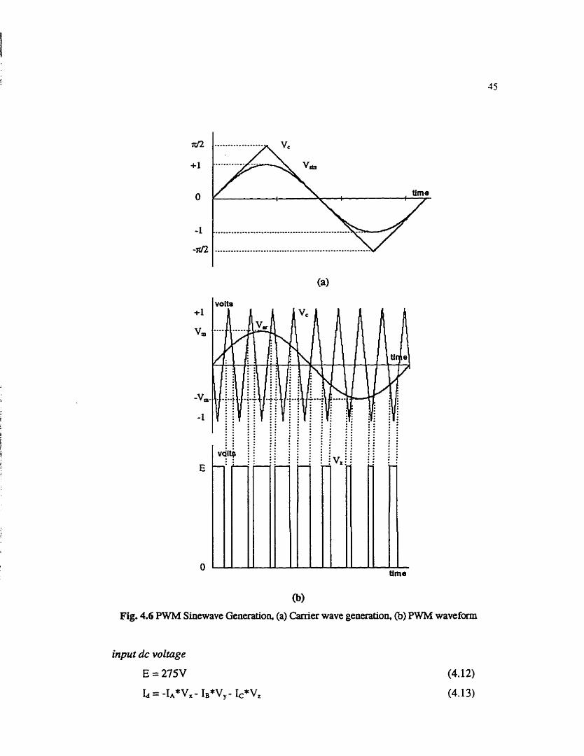
Fig. 4.6 PWM Sinewave Generation, (a) Carrier wave genmtion, @) PWM wavefm
input dc voltage
E = 27SV
L = -L*Vx - Ie*V, - k*V,

The input is modeled as a constant voltage source of magnitude equd to the
rectified voltage. The B-statement is used as a current source feeding the voltage
source and is a hinction of the cunent flowing in the inverter legs.
Load
The load to the PWM VSI Uiverter is a R-L load with the same value as that of
the induction motor parameters obtained by performing various tests of the Induction
Machine, see Appendix D.
The utility iaterface of the drive consists of a three phase diode bridge rectifier
with a capacitor dc-link hlter. So the input to the simulation mode1 is a constant dc
voltage. Because of the low harmonic content in the output voltage of the diode bridge
and in the input current of a PWM inverter, the hlter capacitor c m be srnaller and
consequently the drive response is faster than in the case of the square wave inverter.
4.2.2 Wavefom and analysis for PWM VSI Inverter
The load of the inverter is modeIed with the same machine parameters as the
square wave VSI. Typical simuiated and experimental waveshapes are shown in
Fig.4.8. As seen fkom Fig.4.7. undemodulation was used for the simulation purposes.
The maximum availabIe amplitude of the fundamental ftequency component is
not as high as we desire. This is the natural consequence of the notches as seen fkom
Fig.4.8 (a) (b). The amplitude can be increased by increasing the amplitude modulation
ratio a, which is the ratio of the peak of the skie wave to the peak of the triangle
canïer wave, greater then one. The inverter voltage wavefom then degenerates kom a
pulse-width modulated waveform into a square wave. For our simulation and
experimental results we used a m. less then 1, as seen h m Fig.4.7.
It can be seen fkom Fig.4.8(a),(b) that there are intervais during which aU three
phases of the load are short circuited and there is no power input fkom the dc bus, that
is the dc current is zero. The output voltage magnitude is controiied by controiiing the
duration of these short ckcuit intervais. Such intervals of three-phase short circuit do
not exist in a square wave mode of operation. Therefore, the output voltage magnitude
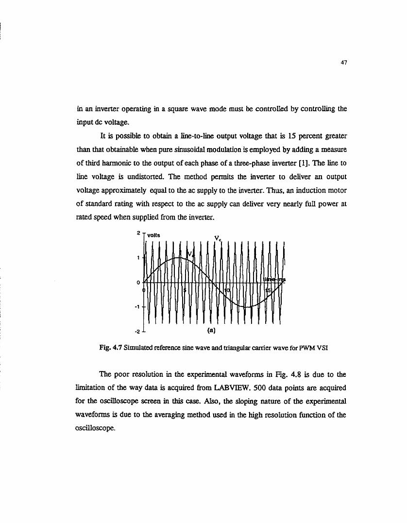
in an inverter operating in a square wave mode must be controiled by controlling the
input dc voltage.
It is possible to obtaïn a Iine-to-line output voltage that is 15 percent greater
than that obtauiable when pure sinusoidal modulation is employed by adding a measure
of third harmonic to the output of each phase of a three-phase inverter [Il. The line to
line voltage is undistoned. The method permits the inverter to deliver an output
voltage approximately equd to the ac supply to the inverter. Thus. an induction rnotor
of standard rathg with respect to the ac supply can deiiver very nearly h i U power at
rated speed when supplied from the inverter.
Fig. 4.7 Simulated =ference sine wave and triangular camier wave for PWM VSI
The poor resolution in the experimental waveforms in Fig. 4.8 is due to the
iimitation of the way data is aquired nom LABVIEW. 500 data points are aquired
for the osciIîoscope screen in this case. A h , the sloping nature of the experimental
wavefom is due to the averaging method used in the high resolution function of the
oscilloscope.
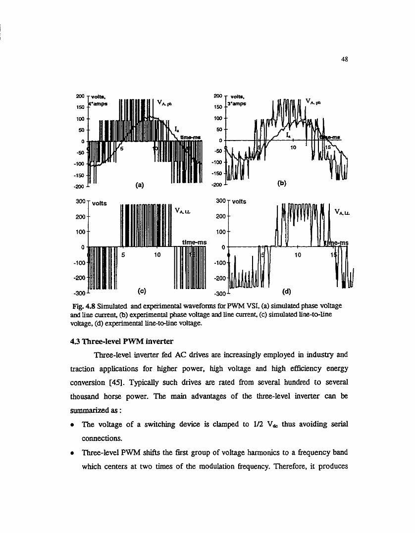
Fig. 4.8 Simulated and expalmental waveforms for PWM VSI, (a) simulatecl phase voltage and line curent, @) expimental phase voltage and Une current, (c) simulated line-tckLine voltage, (d) experimental Une-teUne voltage.
4.3 Three-level PWM inverter
Three-level inverter fed AC drives are increasingly employed in industry and
traction applications for higher power, high voltage and high efficiency energy
conversion 1451. Typically such drives are rated ftom several hundred to several
thohousand horse power. The main advantages of the three-level inverter can be
summarized as :
The voltage of a switching device is clarnped to 112 V, thus avoiding serial
connections.
Three-level PWM shifts the fist group of voltage harmonies to a fiequency band
which centers at two times of the modulation kequency. Therefore, it produces

bw hamionics in output voltage and current. This aiiows a low modulation
frequency to reduce the switch l o s of the inverter and increase efficiency.
Mullevel voltage waveform in general reduces the dvldt stress on the motor
High power rating can be achieved.
Harmonies cm be reduced as required through PWM voltage control
techniques, but harmonic reduction becornes impossible when the inverter U delivering
its full output. at which time the harmonic content of the output waveform is that of a
typical square wave. with absence of triplen harmonics.
Typicai circuit for a three-level kiverter is shown in Fig.4.9. The neutral-point-
clamped PWM inverter (NPC-PWM inverter) is suitable for high efficiency motor
drive system. Its output voltage contains less harmonics than that of a conventional
inverter. (0) indicates the neutral point with respect to the dc source; (Sii, S14). (S217
S2,t). (S3tr S34) are main transistors operating as switches for PWM; and (Siz, SU),
(Sn, SU), (S32, S 3 3 ) are auxüjacy transistors to ciamp the output terminal potentials to
the neutral point potentiaï,'together with (D11-D3*) . N
- -
Fig. 4.9 Circuit for a 3-IeveI P W Inverter
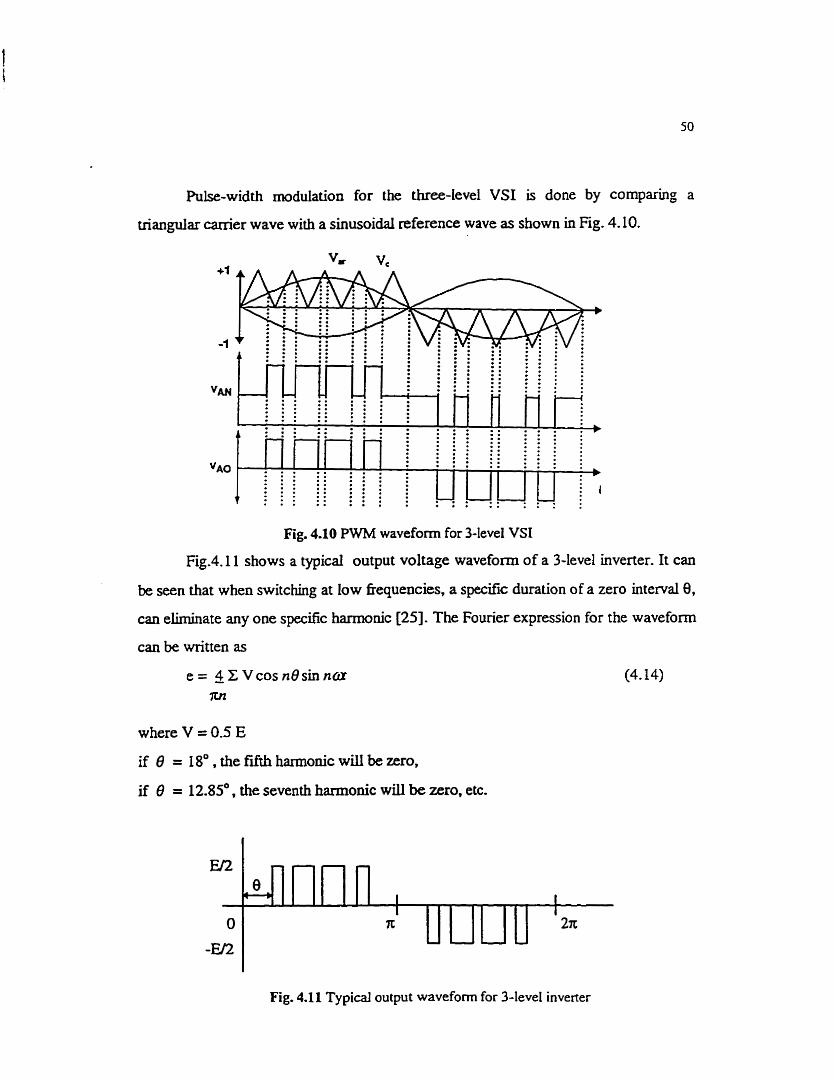
Puise-width modulation for the three-level VSI is done by comparing a
tnangular b e r wave with a sinusoida1 reference wave as shown in Fig. 4.10.
Fig. 4.10 PWM waveform for 3-level VSI
FigA. 11 shows a typicd output voltage waveform of a 3-level inverter. It can
be seen that when switching at low fiequencies. a specifc duration of a zero interval 0,
can elimuiate any one specinc harmonic [25]. The Fourier expression for the waveform
can be written as
where V = 0.5 E
if 8 = 18" . the fifth harmonic will be zero,
if 6 = 12-85' , the seventh harmonic will be zero, etc.
Fig. 4.11 Typical output waveform for 3-level inverter

4.3.1 Simulation of Thr-Ievel PWM inverter
The SPICE3 simulation for the 3-level PWM inverter has the same basic model
as that of the 2-level inverter. The input to the inverter is taken fiom a 12-puise diode
bridge rectifier with a split capacitor arrangement as discussed in Chapter 2. The
output of the inverter is modeled using the same IM stator parameters as in the 2-Ievel
inverter. The SPICE3 schematic for the 3-level inverter is very much sknilar to the 2-
level inverter in Fg.4.4, the only dinerence king the functions used to generate the
switching pattern. The input to the inverter is taken nom a 12-pulse split capacitor.
The +E, O and -E voltages of the dc-link are fed to the voltage functions in the inverter
legs. so that the B-staternents are voltage functions and are the product of the dc-link
voltage and the switching pattern. Detailed model of the 3-level inverter is explained
in section 7.3.1.
4.32 Waveform and anaiysis of 3-level PWM inverter
Typical simulated wavefom of the 3-Ievel PWM inverter is shown in Fig.
4.12. The wavefom in Fïg. 4.12 show that the voltage waveform have a positive,
negative and zero reference. The awiliary transistors switch complementary to the
main transistors. W~th such control, each output temind potential is ciarnped to the
neutral potential in the off period of the PWM control as seen fkom Fig. 4.12 (a). If we
compare these waveform with the conventional 2-level PWM inverter, we cm easïiy
recognize that the output terminal potentiaï of the conventional PWM inverter Vary
between +W2 and -E/2. but those of the NPC-PWM inverter Vary between iU2 and O
or -W2 and 0. This reduces the voltage stress on the switching devices and avoids
serial comection of the devices,

Fig. 4.12 Simulateci wavefonn for 3-level PWM inverter, (a) phase to neuûai voltage and line current, (b) fine-to-line voltage, ( c) phase voltage-
The zero interval duration as shown in Fïg.4.11 was adjusted to approxirnately
18" to eliminate the 5th hamonic at low switching fiequencies. The Fourier analysis
which is done using SPICE3 is given in Appendix E. It gives the 5th harmonics in the
output voltage for the 3-level inverter to be as low as 1.7 %. On the other hand. the
5th harmonics in the output voltage for the 2-level PWM inverter for the same
switcbing 6requency is 9.44 96.

Chapter 5
CURRENT SOURCE INVERTER
Inverters convert direct current to variable fkequency alternathg current. In a
Curent Source Inverter (CSI), the dc input a p p m as a dc cunent source (ideally
with the intemal impedance approaching infinity). The CS1 is presently used for v e r -
high power ac motor drives. This chapter discusses a PWM Current Source Inverter
(CSI). The sirnulated waveforms have been presented. A generalized structure of a
simple controuer for a current source inverter is dso explained.
5.1 Cpulse, Zlevel PWM Current Source Inverter
A general power circuit for a curent-fed inverter, supplied fiom a phase-
controlled rectifier is shown in Fîg.S.1. A variable dc link voltage is generated by the
phase controiied rectifier. A series inductance in the dc-link causes a stiff dc current to
be fed to the inverter. Although an infinite value of the inductor is desirable for an
ideal current source, the cost and size constraints iimit the inductance to a reasonabie
limit. At any instant one upper thyristor and one iuwer thyristor remains in conduction.
Capacitors are connecteci at the output of the inverter to absorb bigh frequency
harmonies associated with the PWM current source inverter output current.
-
&+ -
A AD
3-4 B ac s u p p l ~
4 vdc 4
! 1 - Fig. 5.1 Circuit diagram for Cumnt Source Inverter

As shown in Fig.S.1 above, the PWM CS1 in the present work is fed by a
cunent source obtained by the recmcation of a three phase ac mains voltage. The
c m n t source of the dc lùik is provided by a reactor which is large enough so as to act
as a current source with very Iittle ripple. Current fed into the inverter is converted
into three ac line cunents by the appropriate gating pattem of the inverter switches.
Current hannonics are absorbed by the output nIter so as to provide sinusoidal load
current and voltage. In a c m n t source inverter. the fundamental component machine
current can be varied by controlling the input current of the inverter. Therefore, PWM
is only required to improve the current wavefoms.
5.1.1 Simulation of &pulse, Zlevel PWM CS1
The rnodeiing of the PWM Cunent Source Inverter is done in much the same
way as the PWM VSI. The six switching devices are modeled with the help of three
cwent functions, each representing an inverter leg, see Fig. 5.2. The input to the
inverter is a constant cment source. Each B-function in the inverter leg is a product of
the PWM switching pattern and the constant current. The current flowing in the
inverter legs is reflected back in the input of the inverter. The output of the inverter
has capacitors to absorb the current harrnonics. Capacitors are &O required to absorb
the overvoltages which occur when the current in the switching device is cut off. The
load to the inverter is an induction motor and the resistance and reactance values in the
present mode1 is chosen to be the same as the motor stator parameters as given in
Appendix D. The SPICE3 schematic for the PWM CS1 dong with its netiist is given in
Appendix G.5.
The PWM switching pattem for the CS1 is generated as shown in Fig. 5.3.
where half caiTier cycle is comidered. Three phase sinusoidal reference waves are
compared with a trianguiar carrier wave varying at the modulating kequency.
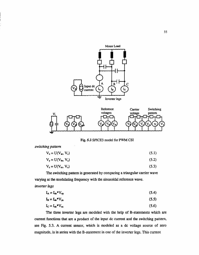
Reference Carrier S witching
Fig. 53 SPICE3 mode1 for PWM CS1
switching pattern
vx = UP,, VC) (5- 1)
v, = U V , VC) (5.2)
VZ = u(vQ, vC) (503)
The switching pattern is generated by comparing a viangular c d e r wave
varying at the modulatiog frequency with the sinusoidal reference wave.
ùtverter legs
I* = I&*v, (5.4)
IB b*vp (5.5)
Ic = IdcSVZx (5.6)
The three inverter legs are modebd with the help of B-statements which are
current hinctions that are a product of the input dc current and the switching pattern,
see Fig. 5.3. A current sensor, which is rnodeled as a dc voltage source of zero
magnihide, is in senes with the B-statement in one of the inverier legs. This current

fùnction helps to measure the inverter current and compare it with the out~ut motor
Fig. 53 Switching pattern generation for CS1 over half camer cycle.
input
b, = lOOA (5.7)
vd = vA*vx + vB*vy + vC*vz (5J3)
The input is modeled as a constant current source of magnitude equd to lOOA
for purpose of simulation. The B-staternent is used as a voltage function and is a
hinction of the voltages across the inverter legs.
One of the major advantages of using voltage or current functions to represent
the switching devices is that it eliminates the use of other available library devices like
BJT, MOSFET, etc. These devices are descriid as non-linear controlled source by
means of functions that contain exponential terms, resulting in slow execution tirnes.
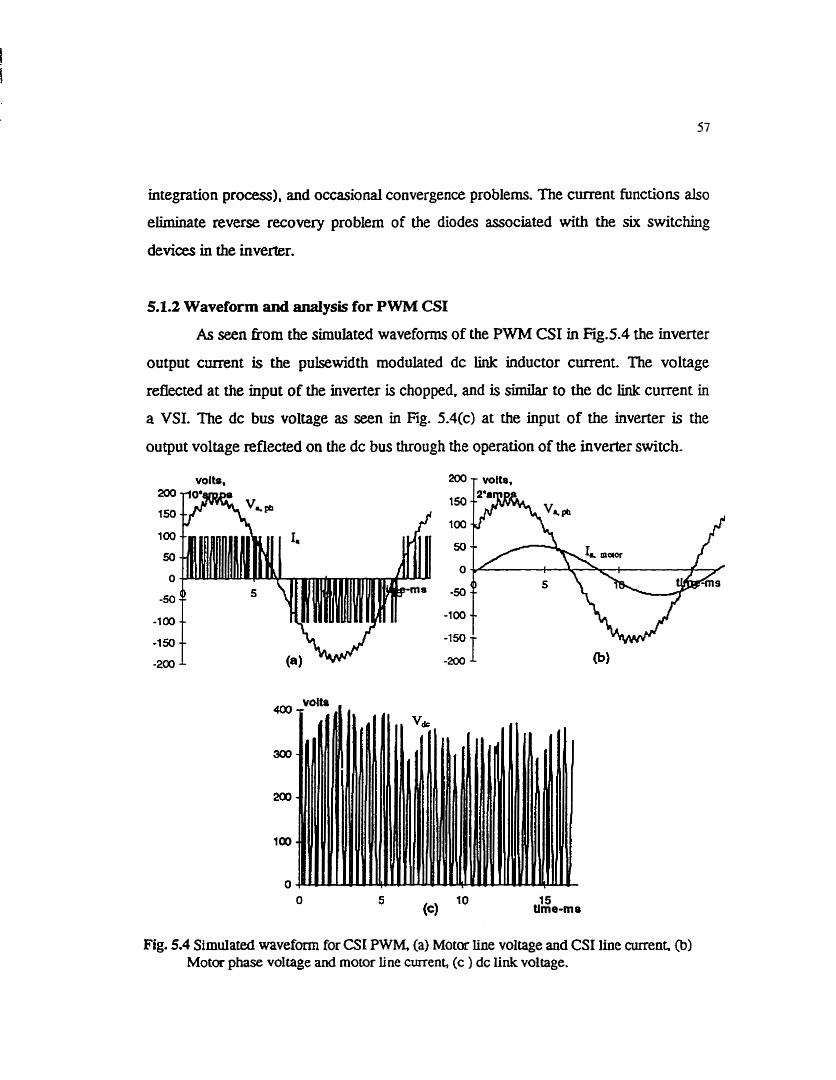
integration process), and occasional convergence problems. The current functions also
eiùnuiate reverse recovery problem of the diodes associated with the six switching
devices in the inverter.
5.1.2 Waveform and analysis for PWM CS1
As seen &om the simulated wavefom of the PWM CS1 in Fig.5.4 the inverter
output current is the pulsewidth modulated dc Luik inductor cument. The voltage
refiected at the input of the inverter is chopped. and is simüar to the dc iink current in
a VSI. The dc bus voltage as seen in fig. 5.4(c) at the input of the inverter is the
output voltage reflected on the dc bus through the operation of the inverter switch.
V O ~ , 200 T verts,
Fig. 5.4 Simulated waveforrn for CS1 PWM. (a) Motor Une voltage and CS1 Une aurenti (b) Moior phase voltage and motor line current, (c ) dc link voltage.

The dc-link voltage is chopped due to the inverter's switching nature.
Comparing the CS1 line current with the motor line cment we can see that the
capacitors at the output offer a Iow impedance path to the higher order hmonics thus
making the motor iine curent sinusoidaL Thus. with the inverter acting as a current
source nearly sinusoidal output voltage and current can be obtained.
5.13 Aarmonic analysis for PWM CS1
Low hamonic contents in both the output voltage and current of a CS1 is
desired for a nurnber of reasons. Current harrnonics cause additional heating of
windings. paaicularly in large motors where skin effect is more significant. Voltage
hamionics c m increase core losses and rapid rates of changes of voltage with t h e can
increase insulation stress. In addition, these harmonics may cause torque harrnonics
and acoustic noise.
Harrnonic analysis is done for the current harmonics in the CS1 line current and
the rnotor line current using SPICE simulation and is given Appendix E. The 5" and
the 7" current hannoniCs get significantly suppressed due the output capacitance.
Ako the output line current THD improves fiom 8.79% in the CS1 line current to
2.27% in the motor Iine current.
5.2 ControIIed Current Source for a CS1
Strictly speakiag, the scheme described above in section 5.1 does not act as a
current source. Any change in the machine irnpedance, with a change in slip. changes
the magnitude of 4 and machine phase currents. If both the wavefom and the
magnitudes of machine currents are to be made independent of changes in machine
operation, then the magnitude of h should &O be maintained constant This is
achieved by closed-loop conuol scheme of 4. Fig. 5.5 shows the current source
inverter scheme incorporating the closed loop current control The actual current, L is compared to the reference value. L*. The error is processed in a controuer to adjust
the rectifier fuing angle to eventually make the actuai current equal to the reference.
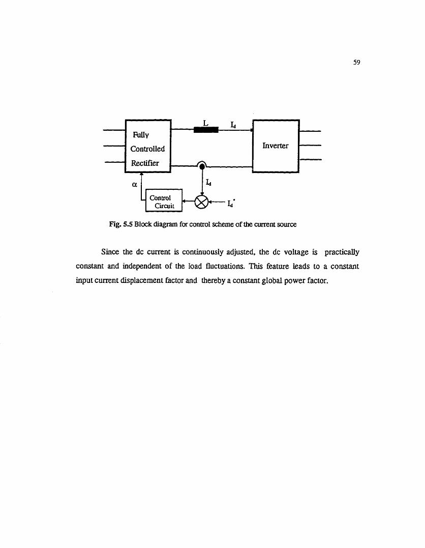
Fig. 5.5 BIock diagram for control scheme of the current source
Since the dc current is continuously adjusted. the dc voltage is practicaiiy
constant and independent of the Ioad fluctuations. This feature ieads to a constant
input current displacement factor and thereby a constant global power factor.

Chapter 6
INDUCTION MOTOR
The motors commoniy used in variable speed drives are induction motors, dc
motors and synchronous motors. For the purpose of our work the induction motor has
been used The d-q axis theory is used to mode1 the induction machine and the use of
B-statements to incorporate the complex equations is shown. The induction rnotor is
modeled for SPICE3 simulation and its m i e n t response is compared with
experimental results. A motor mode1 for constant voltage per hertz (V/O operation for
the induction rnotor is obtahed and the command interpreter is used for obtaining
various curves at different vaiues of V/f.
6.1 Induction Motor drive
Induction motors, particularly the squirrel-cage type induction motor, are
widely used in variable speed drives for a number of advantages. Some of them are
ruggedness; lower maintenance requirements; better reliability; lower cost, weight,
volume and inertia.
When operated directly fiom the line voltages (60Eiz utility input at essentially
constant voltage), an induction motor operates at a nearly constant speed. However,
by means of power electronic converters, it is possible to vary the speed of an
induction motor. In practice, the inverters used in variable speed drives produce three-
phase line voltages or currents, that are not perfectiy sinusoidal and contain higher
fkquency components that are harmonies of the fundamental fiquency.
6.1.1 Induction motor modeling
The induction motor is modekd using the two-axis or d q theory [40]. In this
theory the tirne-varying parameters are eliminated and the variables and parameters are
expressed in orthogonal or mutuaiiy decoupled direct(d) and quadrature(q) axis. The

d-q dynamic model of a machine can be expressed in either a stationery or a rotating
reference fkame. In a stationery reference frame, the reference d and q êxis are fmed on
the stator, whereas in a rotating reference fkame these are rotating. The rotating
reference fi-ame may be either fixed to the rotor or move at synchronous speed.
The two-axis machine equation can be formulated in vario us reference frames.
However for the cylindncal rotor squirrel-cage induction motor, the stator fixed axes
prove more convenient. since the motor mode1 c m then be dehed in terms of the
physically existing stator voltages and currents. This allows the interface between the
rnotor model and the rest of the power electronic system to be easily created, without
the need for the user to anaiyticaliy determine the interaction that arises between the
power electronics and die motor.
Considering ody the stator supply voltages we derive a transformation
relationship between the A-B-C axes and the d-q axes. where bo th are in the stationery
reference kame as shown in Fig.6.l. The O ther quantities, such as current and flux c m
also be transforrned in a similar manner.
Fig. 6.1 Stationery A-BC to d q axes transformation
The phase voltages in t m s of d and q voltages can be written in the matrk form as
sin 8 'Os0 ' ] . [ ~ d ] (6.1) sin(0 - t 20) cos@ - 120) 1
sin(@ + 120) cos(@ + 120) 1 V o

where the angle 8 is arbitrary between the two sets of axes and V, is the zero sequence
COmpOned For b;ùanced three-phase condition, the zero-sequence components does
not exist
Choosing the angle 0 = O, axîs A is coincident wiih axis d. Simplifying. we get
the foilowing relations
va= v,
If we consider separate d and q per phase equivalent circuit for the induction
motor, the flux Iinkage expression in terms of the currents can be wrinen as
The development of torque by the interaction of air gap flux and rotor mmf is
given by the expression
or in tenns of d q components as

A h , the motor speed is related to the torque as
Te-TL= &J& P dt
where TL is the load torque and J is the induction motor inertia
Equation (6.15) and (6.16) give the complete model of the electrornechanicd
dynamics of the induction motor in terms of the d q components. The non-Iinearity of
the model is very evident. The obtained model using the transformation equations c m
be simulated for studying the transient and steady state performances.
- - - - - - -
(bl
Fig. 63 d-q equivalent circuits, (a) d-axis circuit, (b) q-axis circuit
V, and V, are debed by equations(6.5) and (6.6) respectively. Similarly, Vk
and V, are defmed by equations(6.8) and (6.10) respectively.

6.1.2 SPICE3 simulation of Induction motor
The various equation in section 6.1.1 are used in simulating the induction
motor in SPICE3. The avaiiability of the B-statement and the U-statement facilitate
the modeling of the compIex equations. The parameters used in the d-q equivalent
circuit are the same as in the motor per phase equivalent circuit see Fig.6.3 such that :
%=Rh=& (6.17)
L=L&=L, (6.18)
R = % = & (6.19)
L = L = L , (6.20)
Fig. 63 Per-phase equivaient circuit for Induction Motor
TL
output
q-equivaien t d-equivalen t circuit circuit - - br k - t
Fig. 6.4 SPICE3 mode1 for induction motor

For the induction motor, two separate d and q per phase equivalent circuits are
considered. The input to the motor is the chree phase voltages Va, Vb and V.. As seen
frorn the SPICE3 mode1 in Fig.6.4. the input to each of the per phase quivalent circuit
are the respective d and q voltages as defmed by Equation (6.5),(6.6). The currents
flowing in the stator of the d and q equivalent circuits are dehed by the comsponduig
current expression similar to Equaiion(6.2),(6.3),(6.4) and are reflected back to the
input side of the motor. SimilarIy the current fiowing in the rotor of the d and q
equivalent circuit are reflected back to the output side of the motor. The stator and
rotor parameters used in the simulation are same as those of the actual motor used in
the experirnental setup. These values are found by various experimental tests as given
in Appendix D.
The output of the motor is defmed by the Equation(6.16). It is modeled as a B-
statement in paralle1 with a capacitor. The B-statement is a current function defined
by Equation (6.15) and represents the electrornagnetic torque. Te. The load torque, TL
is simulated by a constant current source drawùig current out of the capacitor. The
capacitor, Cj is the measure of the system inertia, J. The voltage, V, across the
capacitor would thus give the speed, see Equation (6.16).
The SPICE3 schematic for the induction machine dong with its netlist is given
in Appendix G.6.
6.1.3 Waveforms and analysis for Induction Motor
Eig.6.5 present the simulation results for direct-on-line @OL) starting of the
motor. The correspondhg experimental results in Fig.6.5(d) show good agreement
with the simulation results, thus confuming the vaiidity and accuracy of the motor
modeL As ülusuated, large transient overshoots of torque and current result and
persist for a number of cycles before final steady-state conditions are established.
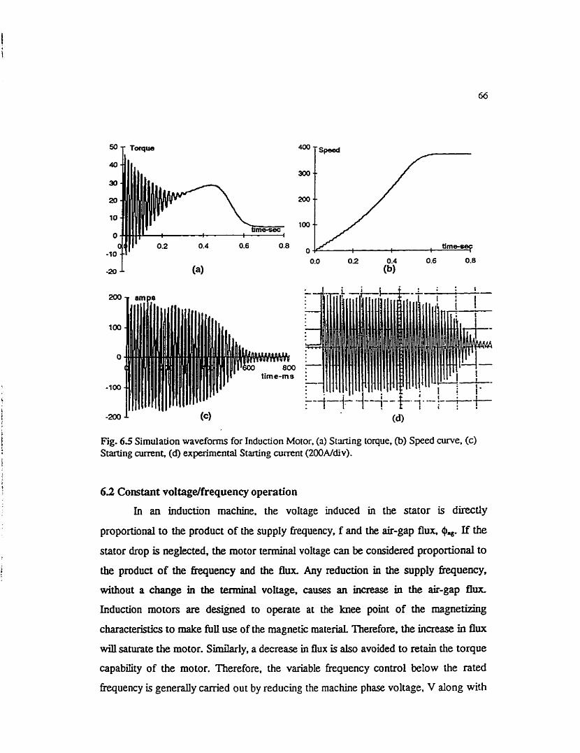
(a Fig. 6 5 Simulation waveforms for Induction Motor. (a) SvLirting toque, @) Speed m e . (c) Starting current, (ci) experïmental Starting current (200A/div).
6.2 Constant voltagdfrequency operation
In an induction machine. the voltage induced in the stator is directly
proportional to the product of the suppIy frequency, f and the air-gap flux, $%. If the
stator &op is neglected, the motor temiinal voltage c m be considered proportiond to
the product of the hquency and the flux Any reduction in the supply fiequency,
without a change in the terminai voltage. causes an increase in the air-gap flux
Induction motors are designed to operate at the knee point of the mgnethg
characteristics to make full use of the magnetic materiai Thedore, the increase in flux
WU saturate the moior. Similarly, a decrease in flux is ako avoided to retain the torque
capability of the motor. Therefore. the variable fieqoency control below the rated
frequency is generally canied out by reducing the machine phase voltage, V dong with

the fiequency. f in such a manner that the flux is maintained constant assuming the
stator Ynpedance is negligible.
$qJ = k. E$f = KV/f (6.2 1)
The motor speed can be varied by controlling the applied fkequency f. and the
air-gap flux should be kept constant at its rated value by controlling the magnitude of
the applied voltages in proportion to f. If an induction rnotor is controkd in such a
manner. then the motor is capable of supplying its rated torque while the slip
fiequency (fd), rotor curent, motor supply current and the percentage losses in the
rotor circuit ail remain within their respective rated values.
6.2.1 SPICE3 simulation of constant V/ f operation
The simulation for the constant V/f operation is done using the model of the
induction motor as explained in section 6.1.1 and modifymg it for steady state
operation. To minimize the starting transient in the motor current , the cunent in the
magnetizing inductor in both the d and q equivalent circuits are initialj7P,d. For the d
equivalent circuit. the current flowing in supply phase a is simply the primary current,
b . The current in the magneuzing inductor for the d equivalent circuit is init iakd to
a vaiue given by the equation below
The corresponding current in the q equivalent circuit is 90° phase s m d Born
the d equivalent &cuit. Thus the current in the q equivalent circuit goes through zero
at the instant the corresponding current in the d equivalent circuit goes through its
peak maXimm The magnetizing current in therefore initïabd to zro for the q
quivalent circuit These currents are initiallzed using the IC (initial cunent) statementi
The output torque-speed model is modified fkom the existing model of section
6.1.1 by removing the capacitor and the constant current source feeding the capacitor.
The speed of the motor is hxed to 1800 rpm (188 radsec). This is modeled by a
constant voltage source of magnitude 188. The output model is thus a B-statement

which is a current function of the rotor currents feeding a constant voltage source. The
current hinction represents the motor torque and the voltage across the voltage souce
represents the motor speed.
The . C O m O L statement of the comrnand interpreter is used to generate the
various curves using the above modified modeL The while loop is used to Vary slip
fkom O to 1 in steps of 0.01. Data is generated for dinerent values of V/f f3om 0.2 to 1
in steps of 0.2. The run file dong with the SPICE3 netiist file is given in Appendix G.9
and is quite self-explanatory.
63.2 Anaiysis of constant Vif operation curves
The various curves obtained using the mn fde are shown in Fig. 6.6. Fig.
6.6(a) and (c) show the variation of torque and rotor current with speed. At high
values of motor speed i e low slip, torque and rotor currents Vary hearly with speed.
As speed becornes les, torque and rotor current no longer increases linearly with
speed for the following reasons: (1) rotor circuit inductive reactance term is no longer
negligible a s compared top the rotor resistance. (2) large values of rotor current and
hence large stator current cause signifcant voltage drop across the stator winding
impedance causing Qq (= Edf) to decline for a h e d supply input voltage at a
hquency f 1391.
For small values of slip ie large speeds, keeping & constant results in a linear
relaîionship between torque and slip frequency, f at any value of E
Since f is varied. it is preferable to express torque as a hinction of the slip
The torque-speed characteristics shift horizontally in parael as seen in Fig.
6.6(a) for five different values of f. Considering the two kequencies 60Hz and 48Hz,

the synchronous speeds a and oa are in proportion to 60Hz and 48Hz If an equal
load-torque is to be delivered at both these frequencies, Born Eq.6.23, 6 .h = ch.
Therefore. in the torque speed plane, equal torques and equd slip s p d s result in
parailel but horizontally shifted characteristics. It can be seen fkom Eg. 6.6(c) that the
motor stârting current can be limited by choosing a lower fkequency set-. With a
constant magneùzing cunent due to constant $,, the stator current is kept fiom
becoming large.
Fig. 6.6(b) and (e) show the variacion of torque and input power respectively
with uicreasing motor current and have sinular characteristics. Torque varies as the
square of the rotor current. The pull-out torque decreaîes with decreasing fkequency
setting. A srnaLi magnetizing current exists for low speeds at zero torque. Fig. 6.6(d)
shows that the variation of power factor with increasing current is aImost identical for
aU Vlf settings. Power factor peaks to about 0.96 at approximately 30A for ail
fiequency settings. The efficiency of the motor peaks for di fkequency setting at a
motor current of 18A as seen fiorri Fig. 6.6(0 and decreases rapidly for increasing
current Large motor curent amount to larger copper loss, thus decreasing effciency.
As seen fiom Fig. 6.6(a). low frequency of operations, near zero speed causes
low torque capability. The stator voltage tends to be zero and it wül essentially be
absorbed by the stator resistance. The effect of the stator resistance can no longer be
neglected. Therefore, an auxGary voltage boost is required to overcorne the effect of
stator resistance so that the rated air-gap flux and full torque becornes avaiiable up to
zero speed.
The various Cumes in Fig. 6.6 are verined by an equation-based simulation
using the per-phase quivalent circuit in Fig. 6.3, sus validaüng the d q axis mode1 for
the induction machine. The Mathematica simulation run file is included in Appendix
G.9 dong with the SPICE3 run file.
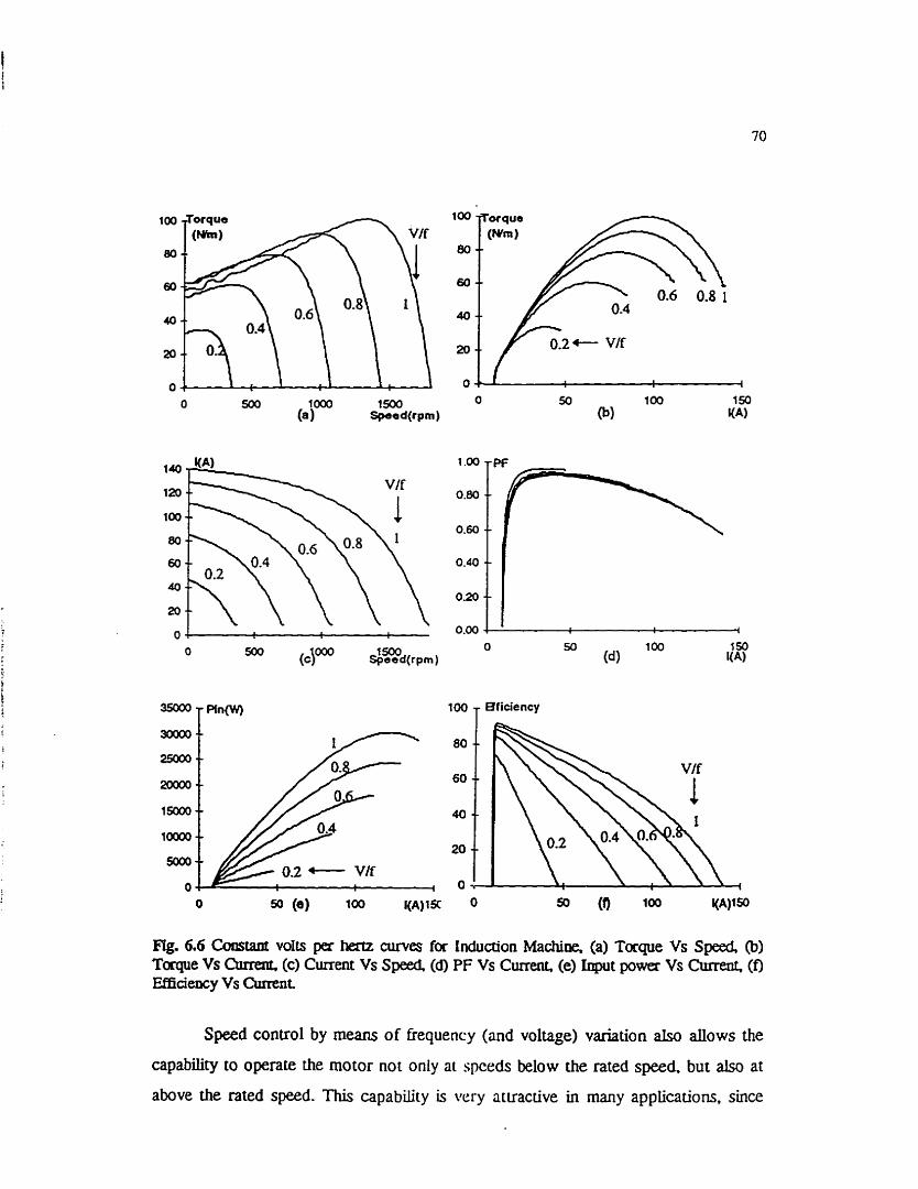
25000 -- n X K X ) --
0.2 - Vif
100 Bficiency T
Hg. 6.6 Comant volts per hera w e s for Induction Machine, (a) Torque Vs Speed @) Toque Vs aUran. (c) Curent Vs Speeü, (d) PF Vs Curent, (el Iriput po- Vs m e n t . (0 FBiQency Vs Curent.
Speed conuol by means of frequency (and voltage) variation also aiiows the
capability to operate the motor not only a[ spceds below the rated speed. but aiso at
above the rated speed. This capability is very aruactive in many applications, since

most induction motors, because of cheir niggcd construction c m be operated up to
twice the r a d speed without mechanical problems [39].
Chapter 7
VARIABLE SPEED DRIVE
For the conaol of induction motors, a fixed frequency ac supply with variable
voltage or a variable frequency ac supply with variable voltage or current is required.
Variable speed drives utilizing an ac motor fed with variable frequency, three-phase
ac derived from an inverter, are encountered with increasing frequency. This chapter
discusses the general features of a variable speed drive with emphasis to the PWM
inverter drives. The SPICE3 simulation of a 12-pulse, 3-level PWM VSI drive is
presented. The usehlness of SPICE3 for simulation of large drive topologies has been
explained.
7.1 Selecting drive components
A match between the motor and the power electronic converter is very
important for motor drives [39]. The power electronic converter topology and its
control depends on the type of motor drive selected. In general the power electronic
converter provides a controlled voltage to the motor in order to control the motor
current and hence the electromagnetic torque produced by the motor.
A motor can supply substantially large peak torque provided that the peak
torque is smaii compared with the thermal time constant of the rnotor. A peak torque
requires a corresponding peak current fkom the power electronic converters. The
c m n t capability of the power semiconductor devices used in the converter is Limited
by the maximum junction temperature within the device. The current rating of the
power electronic converter must be select& based on h t h the rms and peak values of
the torque that the motor is required to supply.
Motors produce a counter-emf e, that opposes the voltage v applied to it, as
shown in the simplified drive circuit in Fig.7.l. The rate at which the motor current
and hence
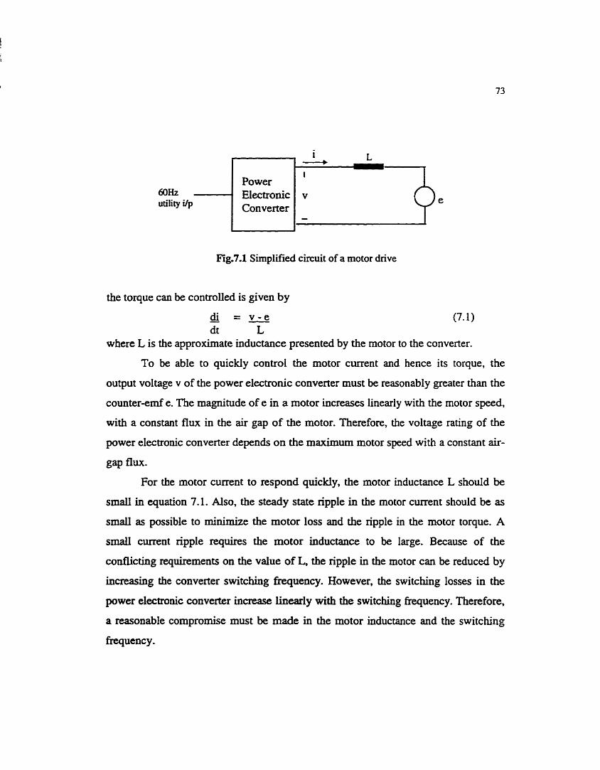
utility i/p
Fig.7.1 Simplified circuit of a motor drive
the torque can be controlled is given by
di = v - e - - (7- 1) dt L
where L is the approximate inductance presented by the motor to the converter.
To be able to quickly control the motor current and hence its torque, the
output voltage v of the power electronic converter must be reasonably greater than the
counteremf e. The magnitude of e in a motor increases lineariy with the motor speed.
with a constant flux in the air gap of the motor. Therefore, the voltage rating of the
power electronic converter depends on the maximum motor speed with a constant air-
gap flux.
For the motor current to respond quickly, the motor inductance L should be
small in equation 7.1. Also, the steady state ripple in the motor current should be as
s m d as possible to minimize the motor loss and the ripple in the motor torque. A
smaU current ripple requires the motor inductance to be large. Because of the
wnflicting requirements on the value of L, the ripple in the motor can be reduced by
increasing the converter switching fkequency. However, the switching losses in the
power electronic converter increasc linearly with the switching frequency. Therefore,
a reasonable compromise must be made in the motor inductance and the switching

7.2 VSI and CS1 Drive Topologies
The basic concept for both the VSI and CS1 drive topologies is the same. The
utility input is converteci into dc by means of either a controlled or an unconuolled
rectifier and then inverted to provide three phase voltages and currents to the motor,
adjustable in magniîude and frequency. Inverten used for this purpose should, in
addition to regulate the frequency in accord with the desired speed, aiso regulate the
voltage, more or less proportionally with the frequency, so as to maintain the flux
density withui the machine at the nomal operathg value 1361.
Typical block diagrams of the VSI and CS1 dnve are given in Fig.l.1 and
Fig. 1.2 respectively. The input to the drive in the A-A, A-Y transformer, so that their
secondaries are phase shifted by 30 degrees. For the PWM VSI, the series connected
diode bridge rectifier forms a 12-pulse rectifier that is most suitable for high power
application, see Fig. 1.1. The rectifier stage is a phase controlled bridge in case of a
square wave inverter, where it becomes necessary to control the input to the inverter.
In both the VSI, a large dc-bus capacitor is used to make the input to the inverter
appear as a voltage source with a very small impedance at the inverter switching
frequency. Fig.l.2 shows the block diagram of a CS1 drive where a he-voltage-
commutated controlled converter is used as the front end. Because of a large inductor
in the dc link, the input to the inverter appears as a dc current source.
7.3 12-pulse, 3-level PWM VSI Drive
The 12-puise, 3-level PWM VSI Drive have increasingly been employed in
industry and traction application where high power and eficiency energy conversion
is required [29]. This drive is highly suitable for high power and high voltage
applications. The 12-pulse rectifier provides a ripple less output voltage. The blocking
voltage of each switching device in the 3-level inverter is clamped to half the
blocking voltage which allows the use of lower voltage power devices without serial
connections.

Fig.72 Block diagram for 12-pulse, 3-level PWM VSI Inverter Drive
73.1 Simulation of 12-pulse, 3-level PWM VSI Drive
One of the advantages of SPICE3 is that a complete power electronic drive
system can be simulated in its entirety. SPICE3 is not restricted to the number of
nodes in the circuit as was the case with the earlier versions of SPICE and thus large
and complex circuits can be easily simuiated.
The SPICE3 schematic for the e n t h drive system dong with its netlist is
given in Appendix G.7. As seen from the SPICW mode1 in Fig.7.4, the input to the
drive is the A-& A-Y transformer which is modeled using separate d and q equivalent
circuits. The currents flowing in the transfomer primaries are reflected back to the
input side. The &A, A-Y transformer is slightly rnodified from the one in section
3.2.1. The transfomer in this simulation has a common primary and two separate
secondaries which is a common transformer comection in the industry, sec Fig.7.2.
The output of the A-A, A-Y transformer fonns the input to the 12-pulse rectifier which
has two serially comected &pulse diode bridge rectifier. B-statement is effdvely
used to decouple the output of the transformer and the input of the rectifier.
The output of the rectifier has a split dc capacitor rail. This rectified dc voltage
is fed to the 3-level PWM VSI inverter. The currentflowing in the legs of the inverter
are reflected back to the dc rail with the help of B-staternents which are current

functions. The current function in t e m of &,, the positive dc-link current and In, the
negative dc-link current can be defmed with the help of Fig. 7.3.
Fig. 73 S witching Iogic for dc-link current
The cumnt function is thus given as
$=Id,= IA+IB+Ic
In=I,Q=-I*-b -rc
The voltage function V~ is used to generate a triangular wave at the
modulating fkequency, V* which is modeled as a constant voltage source.
V, = asin(sin(Vd*Vtime))+l -57 (7.4)
This is used to generate the three carrier waves, V*, Vce, VcC with the help of
B-statements which are voltage functiom. VcA is defined as
V, = u(sin(Vt;cV-))*V, + (1 -u(sin(Vk*Vh))) * V~ (7.5)
U-statements are used to compare the carrier wave with the 3-phase sinusoidal
reference waves VrA, Va, Vc to generate the switching pattern for a 3-level inverter.
The resultant voltage function is defined as
VX = ~(VCA, VcA) (7.6)
The inverter leg is modeled as three B-statements similar to the 2-level case.
The B-statements are voltage hctions and are the product of the switching pattern
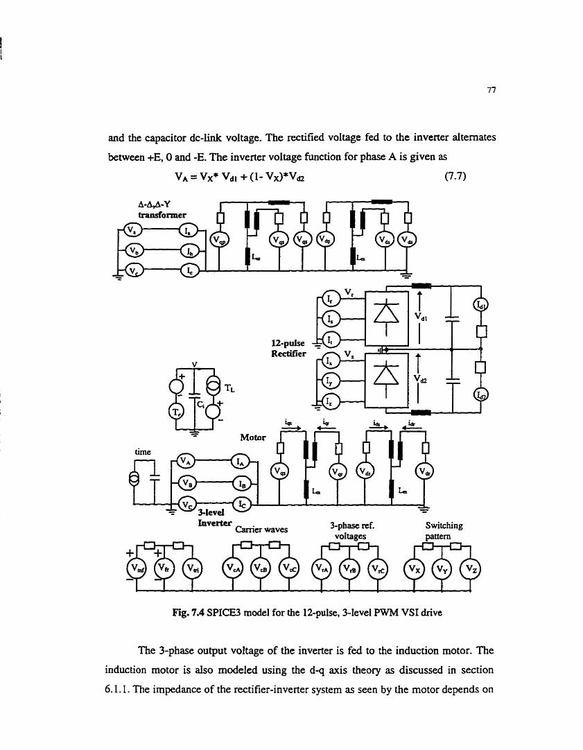
and the capacitor dc-link voltage. The rectified voltage fed to the inverter altemates
between +E, O and -E. The inverter voltage function for phase A is given as
VA = Vx* Vdl f (1' VX)*Vb2 (7-7)
A-A&Y transformer
Inverter Carrier waves $phase ref. S witching
voltages pattern
Fig. 7.4 SPICE3 mode1 for the 12-pulse, flevel PWM VSI drive
The 3-phase output voltage of the inverter is fed to the induction motor. The
induction motor is also mode1ed using the d q a i s theory as discussed in section
6.1.1. The impedance of the rectifier-inverter system as seen by the motor depends on

the conducting States of the power devices and changes according to the PWM
switching pattern and current flow. This is automatically accounted for by reflecting
the changes in the tirne-varying topology of the rectifier-inverter system in the input
to the motor model.
It is very important to decouple the various stages of a large drive system with
the help of B-statements. This elhinates the interaction of the various stages leading
to complex non-linear relationships. The decoupled stages undergo local simulation
thus reducing simulation nui times. With more and more decoupling, larger number
of nodes in the circuit are connected to ground, thus forming a sparse matrïx during
simulation.
For a large complex circuit simulation as in the present case, a functional
model for some paris of the circuit produces a dramatic simplification of the drive
system. On the other hand accurate modeling of complex converter circuits may lead
to a very large number of devices and cornponents and the simulation becornes very
t h e consuming. The same applies when increasing the switching frequency and the
simulation run interval. The probability of encountering convergence problems also
increases with the number of components and non-linear devices.
73.2 Waveform and aaalysis of lLpulse, 3-level PWM VSI Drive
SPICE3 simulation wavefom for the 12-pulse, 3-level PWM VSI Drive are
shown in Fig.7.5. Fig.7.5(a) shows the corresponding prirnary voltages of the d and q
quivalent circuit and are 90' phase shifted to each other thus validating the d q axis
mode1 of the transformer. The secondas, phase voltages and line-line voltages of the
A-A, A-Y transformer are phase shifted at 30°, see Fig.7.5(b) and Fig. 7.5(c)
respectively. The total input line current has a step shape and has significant
commutation overlap due to the large magnetizing inductor of the transfomer, see
Fig.7.6(a). The two series comected diode bridge rectifier give a 12-pulse rectified
output. see Fig.7.6(b). Fig. 7.6 (c) shows the input line currents to the rectifier. The
input and output currents of the A-A transformer are in phase with each other.
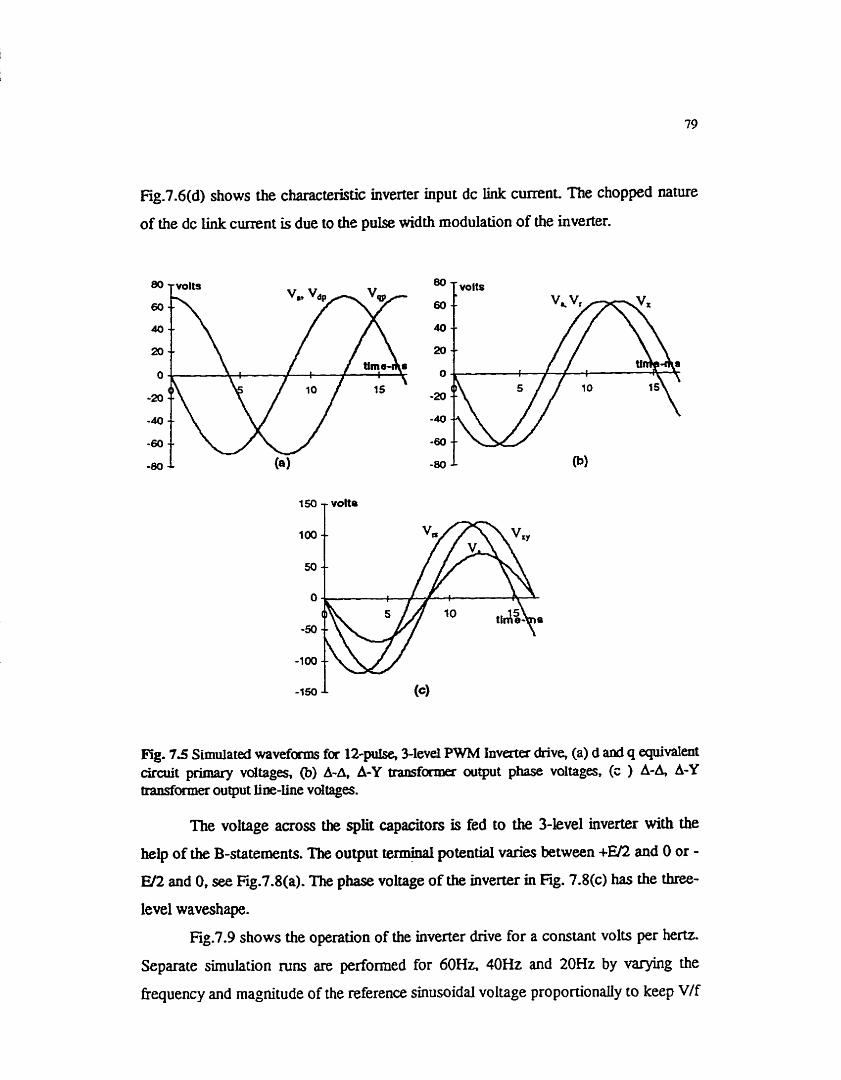
Figa7.6(d) shows the characteristic inverîer input dc Link current The chopped nature
of ?he dc Link current is due to the puise width modulation of the inverter.
150 volte T
Fig. 7.5 Sirnulated waveforms for 12-pulse, 3-leva PWM lnvertef drive, (a) d and q equivalent circuit primary voltages, (b) A-& A-Y ttansformer output phase voltages. (r ) A-& A-Y transformer output Une-line voltages.
The voltage across the split capacitors h fed to the 3-bel inverter with the
help of the B-statements. The output termmal potential varies between +En and O or - W2 and 0, see Fig.7.8(a). The phase voltage of the inverter in Eg. 7.8(c) has the three-
level waveshape.
Fig.7.9 shows the operation of the inverter drive for a constant volts per hertz.
Separate simulation mns are performed for 60Hz. MHz and 2OHz by varying the
frequency and magnitude of the reference sinusoidal voltage proportionally to keep V/f
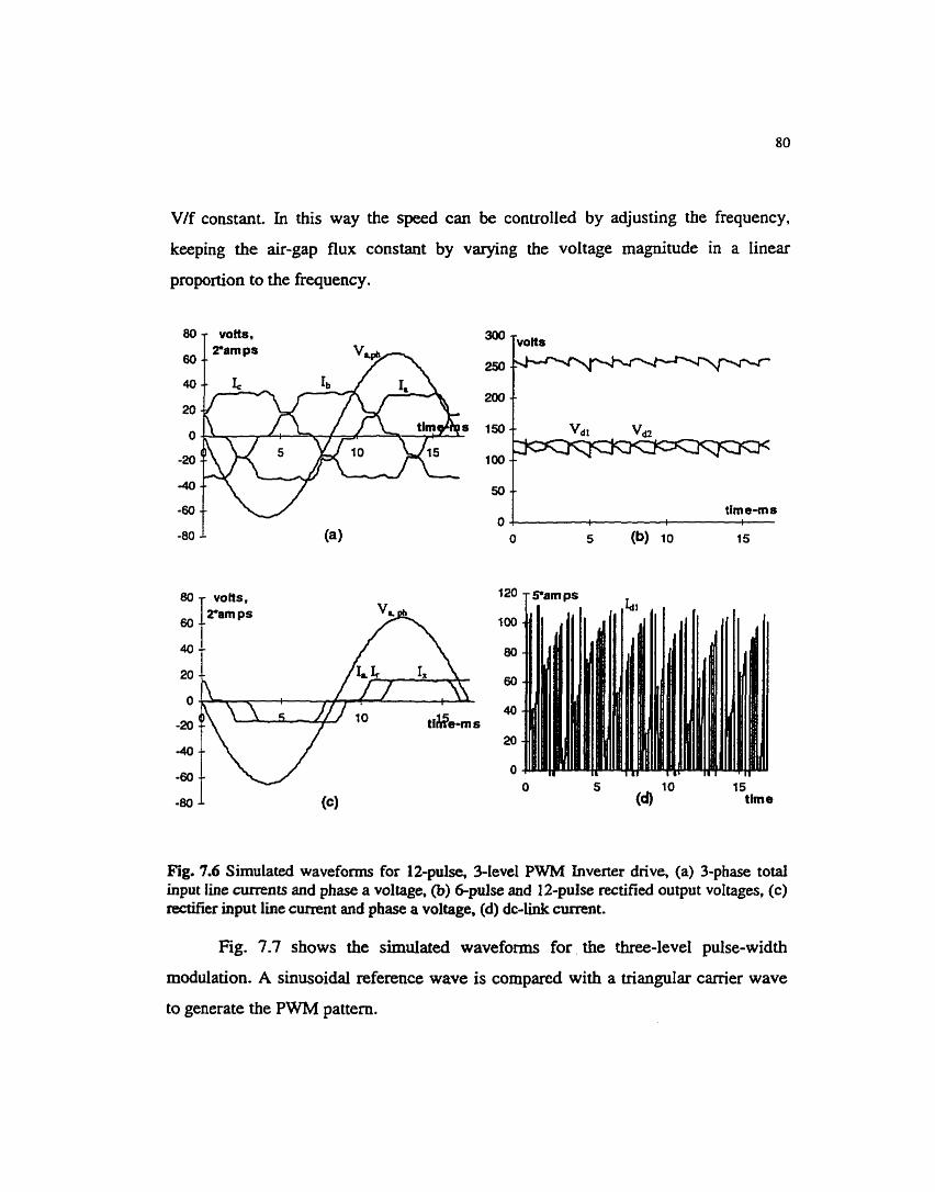
V/f constant In this way the speed can be controlled by adjusting the frequency,
keeping the air-gap flux constant by varying the voltage magnitude in a linear
proportion to the frequency.
80 ,- volts,
" t tim e-m s
80 Y volts. 1
Tarn ps 60 -- 100
40 -- 80
20 -- 60
40
20
O O 5 15
time
Fig. 7.6 Simulated waveforms for 12-puise, 3-level PWM Inverter drive, (a) 3-phase total input line currents and phase a voltage, (b) &pulse and 1 2-pulse reftified output voltages, (c) rectifier input line current and phase a voltage, (d) dc-link -nt.
Fig. 7.7 shows the simulated waveforms for, the three-level pulse-width
modulation. A sinusoidal reference wave is compareci with a viangular carrier wave
to generate the PWM pattern.
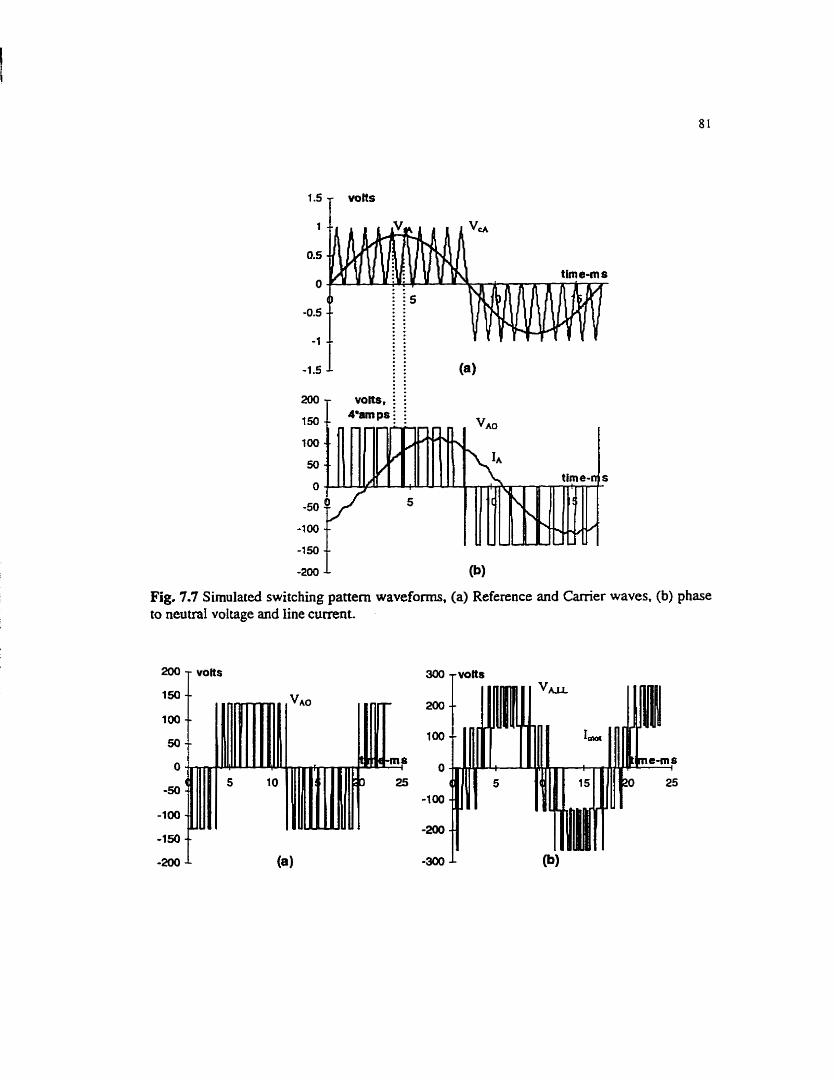
Fig. 7.7 Simulated switching pattern waveforms, (a) Reference and Carrier waves, (b) phase to neutral voltage and Iine current.
300
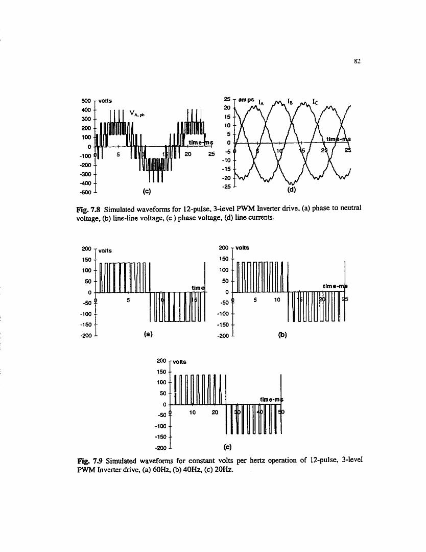
Fig. 7.8 Simulated waveforms for 12-pulse. f l eve l PWM hverter drive, (a) phase to neutral voÏtage, @) line-line voltage, (c ) phase voltage, (d) line currents.
tim d 200 volts
150 I
tim e-ff
Fig. 7.9 Simulated wavefom for constant volts per hertz operation of PWM Inverter drive, (a) 6ûHz, (b) 40Hz, (c) 20Hz.
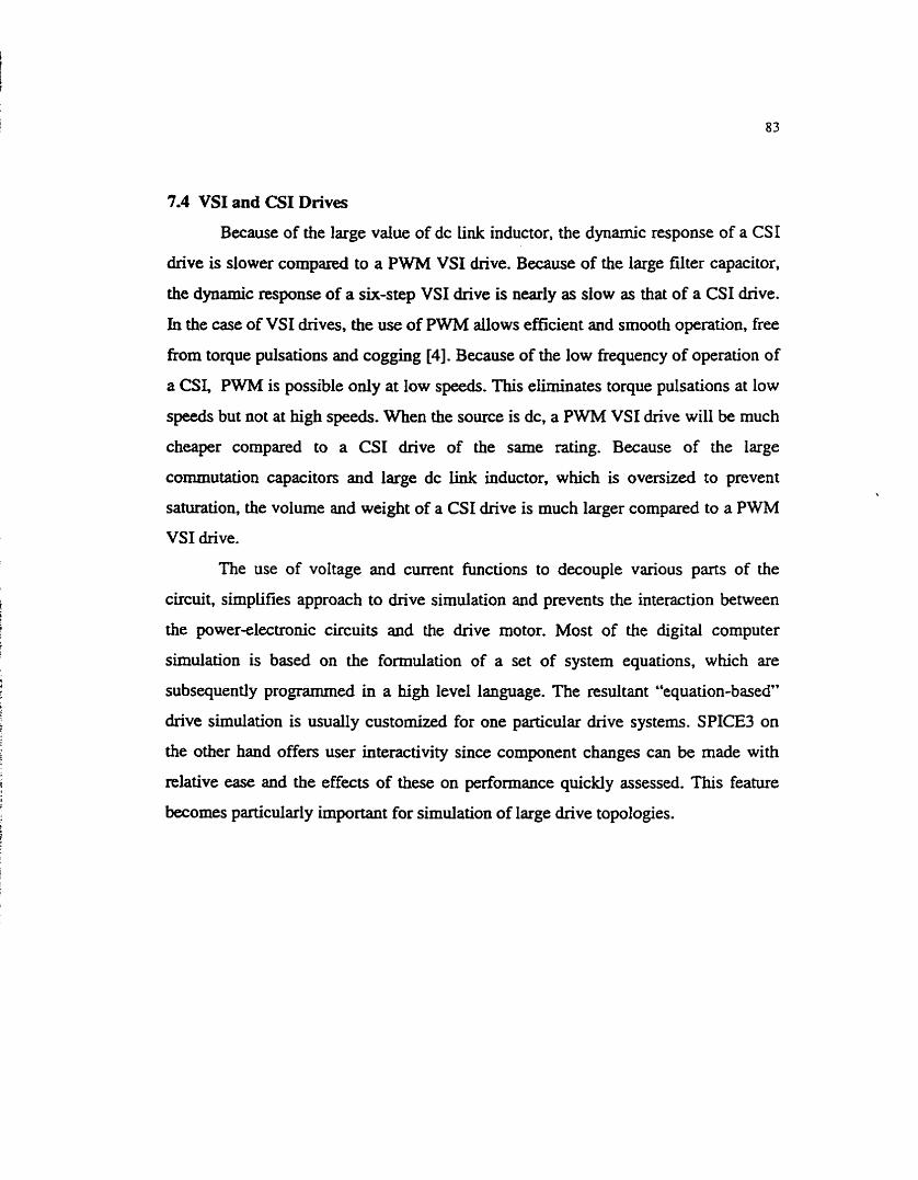
7.4 VSI and CS1 Drives
Because of the large value of dc Link inductor, the dynamic response of a CS1
drive is slower compared to a PWM VSI drive. Because of the large filter capacitor,
the dynamic response of a six-step VSI drive is nearly as slow as that of a CS1 drive.
In the case of VSI drives, the use of PWM allows efficient and smwth operation, free
from torque pulsations and cogging [4]. Because of the low fquency of operation of
a CSI, PWM is possible only at low speeds. This eliminates torque pulsations at low
speeds but not at high speeds. When the source is dc, a PWM VSI drive will be much
cheaper compared to a CS1 cirive of the same rating. Because of the large
commutation capacitors and large dc link inductor, which is oversized to prevent
saturation, the volume and weight of a CS1 drive is much larger compared to a PWM
VSI drive.
The use of voltage and curent functions to decouple various parts of the
circuit, simplifies approach to drive simulation and prevents the interaction between
the power-electronic circuits and the drive motor. Most of the digital computer
simulation is based on the formulation of a set of system equations, which are
subsequently programmeci in a high level language. The resultant 'equation-based"
drive simulation is usuaIiy customized for one particula. drive systems. SPICE3 on
the other hand offers user interactivity since component changes cm be made with
relative ease and the effects of these on performance quickly assesseci. This feature
becomes particuiarly important for simulation of large drive topologies.

Chapter 8
NOVEL RECTIFIER TOPOLOGY
The application of n a d y comrnutated converten in industrial
variable speed drive systerns has increased over the years to a point where the
converter now foxms a significant fraction of the load on a utility system [39]. Six-
pulse and twelve-pulse uncontrolled diode bridges are cornmonly used as an interface
between the three phase electnc utility and power electronic loads. Large hamonics,
poor power factor and high total harmonic distortion (THD) in the uiility interface are
common problems when nonlinear loads such as adjustable speed drives, power
supplies, UPS systems, etc. are connected to the electlic utility. In this chapter a novel
rectifier topology is presented that lower the line current THD with a power factor
close to unity. The rectifier performance is assessed with emphasis to its power factor,
the per-unit inductor size and the line current total hamonics distortion (THD). The
use of SPICE3 simulation tools to obtain the performance factors and design curves
of the new rectifier topology is explained.
8.1 Current harmonies and power factor
Ail power electronic converten cm add to the inherent power line disturbance
by distorthg the utiiity waveform due to the hannonics injectecl into the utility grid
ûnd by producing electromagnetic interference. A simple block diagram of the utility
interface is given in Fig.8.1. The line current i,, can be considered to be the sum of the
fundamentai component il, and the other harmonic components ih. Due to the finite
intemd impedance of the utility source which is simply represented by L, in Fig.8.1,
the voltage waveform at the point of common coupling to the other loads become
distorted, which may cause them to maifunction.
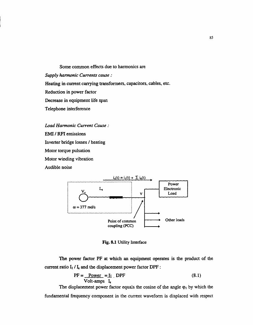
Some c o m o n effects due to hannonics are
Supply hamwnic Currents cause :
Heating in current canying transformers, capacitors, cables, etc.
Reduction in power factor
Decrease in equipment life span
Telephone interference
L o d Hamonic Current Cause :
EMI / RFI emissions
Inverter bridge losses / heating
Motor torque pulsation
Motor winding vibration
Audible noise
Point of comrnon coupling (PCC)
Fig. 8.1 Utility Interface
The power factor PF at which an equipment operates is the product of the
current ratio Ir / I, and the displacement power factor DPF :
PF = Power =A . DPF (8-1) Volt-amps 4
The displacement power factor equals the cosine of the angle cpl by which the
fundamental frequency component in the current waveform is disptaced with respect
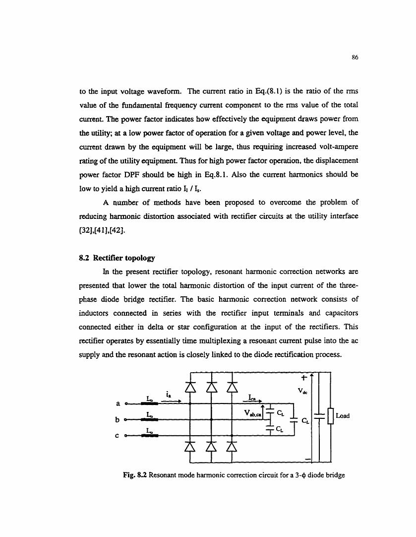
to the input voltage waveform. The current ratio in Eq.(8.L) is the ratio of the rms
value of the fundamental fkequency current component to the rms value of the total
cumnt. The power factor indicates how effectively the equipment draws power from
the utility; at a low power factor of operation for a given voltage and power level, the
current drawn by the equipment wiI1 be large, thus reqiiiring increased volt-ampere
rating of the utility equipment. Thus for high power factor operation, the displacernent
power factor DPF should be hi& in Eq.8.1. Also the current harmonies should be
low io yield a high current ratio Il / S.
A number of methods have been proposed to overcorne the problem of
reducing harinonic distortion associated with rectifier circuits at the utility interface
1321,14~I,f423*
8.2 Rectifier topology
In the present rectifier topology, resonant harrnonic correction networks are
presented that lower the total harmonic distortion of the input current of the three-
phase diode bridge rectifier. The basic hamonic correction network consists of
inductors connected in series with the rectifier input terminais and capaciton
connected either in delta or star configuration at the input of the rectifies. This
rectifier operates by essentially tirne multiplexing a resonant current pulse into the ac
supply and the resonant action is closely linked to the diode rectification process.
Fig. 82 Resonant mode harmonic correction circuit for a 3-41 diode bridge
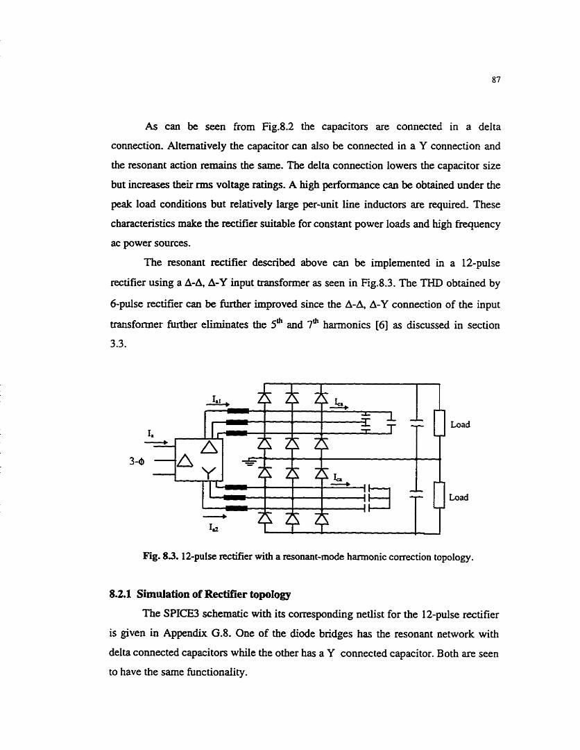
As cm be seen from Fig.8.2 the capaciton are connected in a delta
connection. Akematively the capacitor can also be connected in a Y connection and
the resonant action remains the same. The delta comection lowers the capacitor size
but increases their nns voltage ratings. A high performance can be obtained under the
peak load conditions but relatively large per-unit line inductors are required. These
characteristics make the rectifier suitable for constant power loads and high frequency
ac power sources.
The resonant rectifier describeci above can be implemented in a 12-pulse
rectifier using a A-& A-Y input transformer as seen in Fig.8.3. The THD obtained by
6-pulse rectifier c m be M e r improved since the A-& A-Y comection of the input
transformer further eliminates the 5' and 7* harmonics [6] as discussed in section
3.3.
Load
Load
Fig. 83.12-pulse rectifier with a resonant-mode hmonic correction topology.
8.2.1 Simulation of Rectitier topology
The SPICE3 schematic with its corresponding netlist for the 12-pulse rectifier
is given in Appendix (3.8. One of the diode bridges has the resonant network with
delta connected capacitors while the other has a Y connected capacitor. Both are seen
to have the sarne functionality.
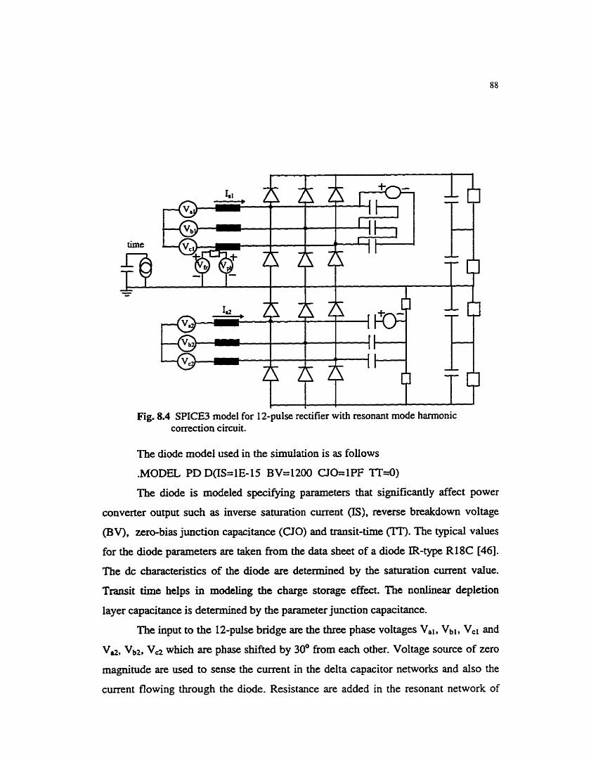
Fig. 8.4 SPICE3 mode1 for 12-pulse rectifier with resonant mode harmonic correction circuit.
The diode mode1 used in the simulation is as foliows
.MODEL PD D(IS=lE-15 BV=1200 CJO=lPF ?Ta)
The diode is modeled specimg parameters that significantly affect power
converter output such as inverse saturation current (IS), reverse breakdown voltage
(BV), zero-bias junction capacitance (CIO) and transit-time 0. The typical values
for the diode parameters are taken from the data sheet of a diode IR-type R l8C [46].
The dc characteristics of the diode are determined by the saturation current value.
Transit time helps in modehg the charge storage effect. The nonlinear depletion
layer capacitance is deter-ed by the parameter junction capacitance.
The input to the 12-puise bridge are the t h e phase voltages Val, Vbl , Vcl and
Vd, Vb2, VcZ which are phase shifted by 30' from each other. Voltage source of zero
magnitude are used to sense the current in the delta capacitor networks and also the
current flowing through the diode. Resistance are added in the resonant network of
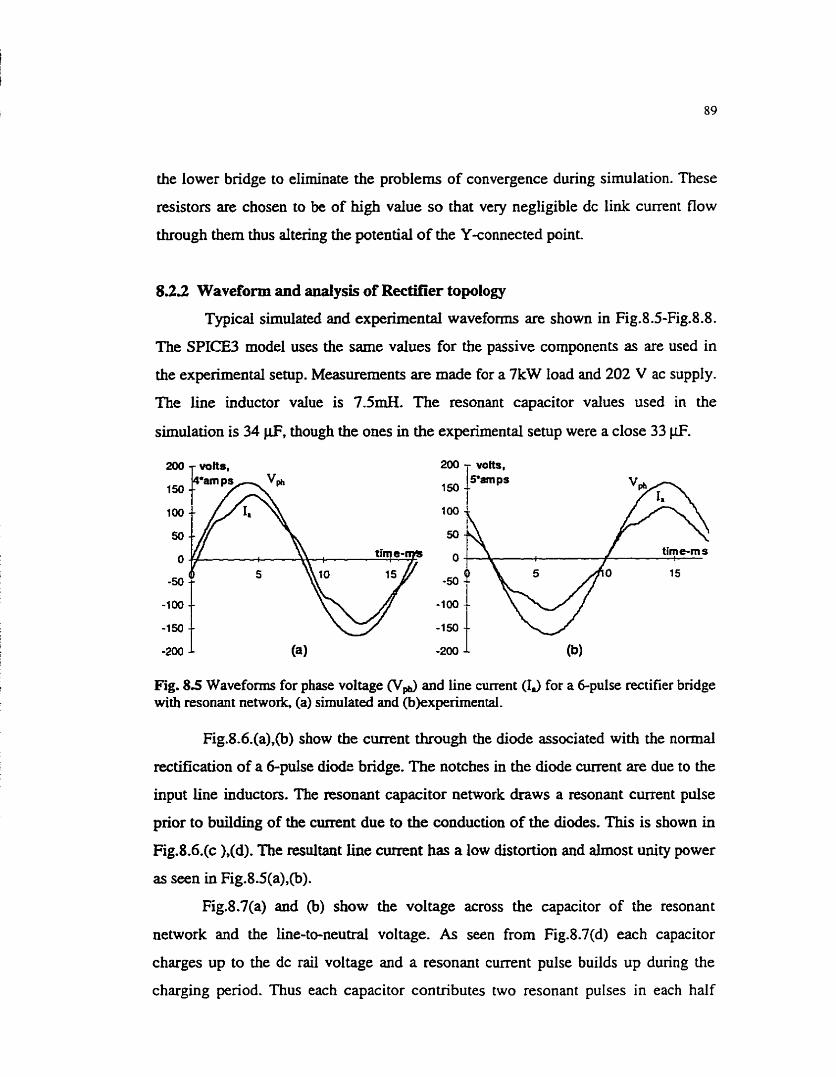
the lower bridge to elirninate the problems of convergence during simulation. These
resistors are chosen to be of high value so that very negligible dc link current flow
through them thus dtering the potential of the Y-comected point.
8.2.2 Waveform and analysis of Rectifier topology
Typical simulated and experimental waveforms are shown in Fig. 8 -5-Fig.8.8.
The SPICE3 mode1 uses the same values for the passive components as are used in
the experimental setup. Measurements are made for a 7kW load and 202 V ac supply.
The line inductor value is 7.5mH. The resonant capacitor values used in the
simulation is 34 pFt though the ones in the experimental setup were a close 33 p.
Fig. 8 5 Waveforms for phase voltage wpb) and line current (1,) for a 6-pulse rectifier bridge with resonant network, (a) simulated and (b)experimental .
Fig.8.6.(a),@) show the c m n t through the diode associated with the normal
rectification of a &pulse diode bridge. The notches in the diode current are due to the
input line inductors. The resonant capacitor network draws a resonant cunent pulse
prior to building of the current due to the conduction of the diodes. This is shown in
Fig.8.6.(c ),(d). The resultant line current has a low distortion and almost unity power
as seen in Fig.g.S(a),@).
Fig.8.7(a) and (b) show the voltage across the capacitor of the resonant
network and the he-to-neutral voltage. As seen from Fig.8.7(d) each capacitor
charges up to the dc rail voltage and a resonant current pulse builds up during the
charging period. Thus each capacitor contributes two resonant pulses in each half
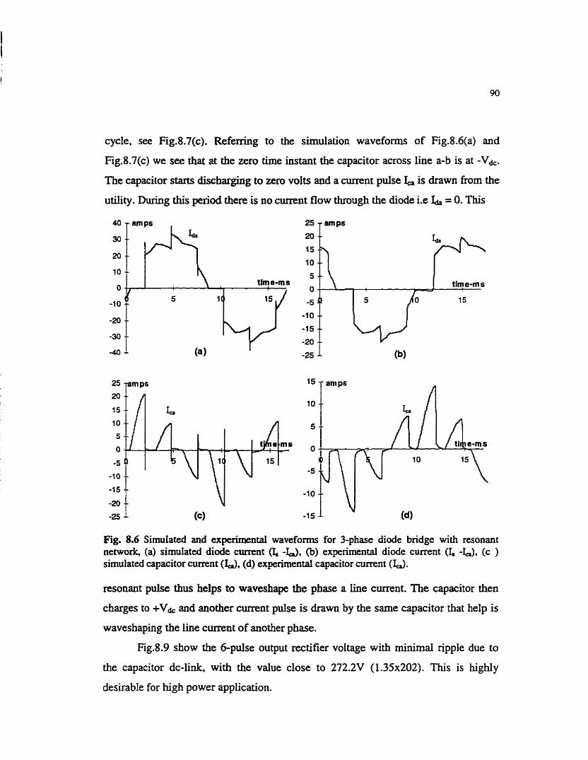
cycle, see Fig.8.7(c). Refemng to the simulation waveforms of Fig.8.6(a) and
Fig.8.7(c) we see that at the zero time instant the capacitor across line a-b is at -Vdc.
The capacitor starts discharging to zero volts and a current pulse I, is drawn from the
utility. During this period there is no current flow through the diode i.e b = O. This
Fig. 8.6 Simulated and expenmental waveforms for 3-phase diode bridge with resonant network, (a) simulated diode cumnt (I. -u. (b) experimentai diode current (I, -W. (c ) simulated capacitor nurent (W, (d) experimentai capacitor current (&J.
resonant pulse thus helps to waveshape the phase a h e current. The capacitor then
charges to +Vs, and another cumnt pulse is drawn by the same capacitor that help is
waveshaping the line current of another phase.
Fig.8.9 show the &pulse output rectifier voltage with minimal npple due to
the capacitor dc-link, with the value close to 272.2V (1.35~202). This is highly
desirable for high power application.
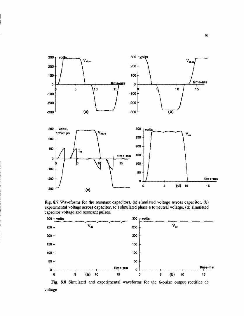
Fig. 8.7 Wavefom for the resonant capacitors, (a) simulated voltage across capacitor, (b) expenmental voltage across capacitor, (c ) simulated phase a to neuuaI volatge, (d) simuIated capacitor voltage and resonant pulses.
Fig. 8.8 Simutated and expenmental wavefonns for the &pulse output rectifier dc
50
vo 1 tage
-- 50 -- tlqte-mi O
0 1 the-ms
O s (a) IO 15 O 5 (b) IO 1s

Harmonic analysis of the resonant network is done using both SPICE3 and
experimentd data and is given in Appendix F. As seen from the SPICE3 simulation
results, a low THD of 6.1 95 and 8.6 46 are obtained for the upper and lower &pulse
diode bridges. The line current is nearly sinusoida1 with unity power factor. This is a
signincant improvernent over the &pulse diode bridge with LC filter which gave a
THD of 27.6 9b at 0.96 PF as discussed in Chapter 3. The total Ilne current of the 12-
pulse bridge has a THD as Iow as 3.3 % with a power factor of 0.97. This THD is
much better then the THD of 7.3 % obtained for a 12-pulse rectifier without the
nsonant network as discussed in Chapter 3. The significant improvement in the THD
for a 12-pulse rectifier is due to the canceilation of the 5" and 7* hannonics as can be
seen from the harmonic analysis in Appendix F.
8.2.2 Sinufation tools used for circuit Performance Analysis
SPICE3 consists of a fkont end for data andysis and plonuig. This is the
Interactive Interpreter and can be run as a separate "stand done" program. This run
fde is executed in batch mode uskg it as a raw file with the "-b" option. The general
format of the program used for the design andysis is given below.
scr resonant circuit .controIc set width = 275; set nobreak; set noheader, set noprintscale source netlistfile let name = expression;
whüe condition
............ alter device value;
............ tran tstep tstop tstart tmax uic let name = expression;

....*..*...- destroy al1
end print col expression . - . >> output file .endc
.end
The script begins with a blank line or a simple text line which is not read
during execution tirne. This is followed by the .CONTROLC statement. Ali SPICE3
commands are enclosed between the .CONTROLC statement and the .ENDC
statement. These commands are executed immediately after the circuit is loaded.
To generate the data for post processing the set options are fixed for the plot
width with no headers and no page breaks. The netlist file is sourced once at the
beginning of the program. To start with, al l the new vector are initialized to a value
specified by the expression using the let command.
The while-end, uses an arbitmy condition which may be in the form of a
algebraic expression, which if tme, executes the statement within the while-end loop.
The values for the various vecton are changed within the while loop using the alter
command. Each cornand is separated fiom the other by a semicolon. The let
command is used in the while ioop to set up the equations for the various performance
curves.
The tran statement performs a transient analysis and the tirne-step of
simulation is adjusted to obtain smoother and accurate curves. At the end of each loop
the data generated is destroyed using the command destroy. This helps in memory
management and performs the simulation in each loop a f h h since it releases the
memory holding the data for the specified m. The various vectors calculated for the
performance curves are printed in column format to a file using the print command.
The '>>" is used to direct the data to an outputfile in the append mode since the data
is dumped to the file after every loop. The program findly ends with the .end
statement,
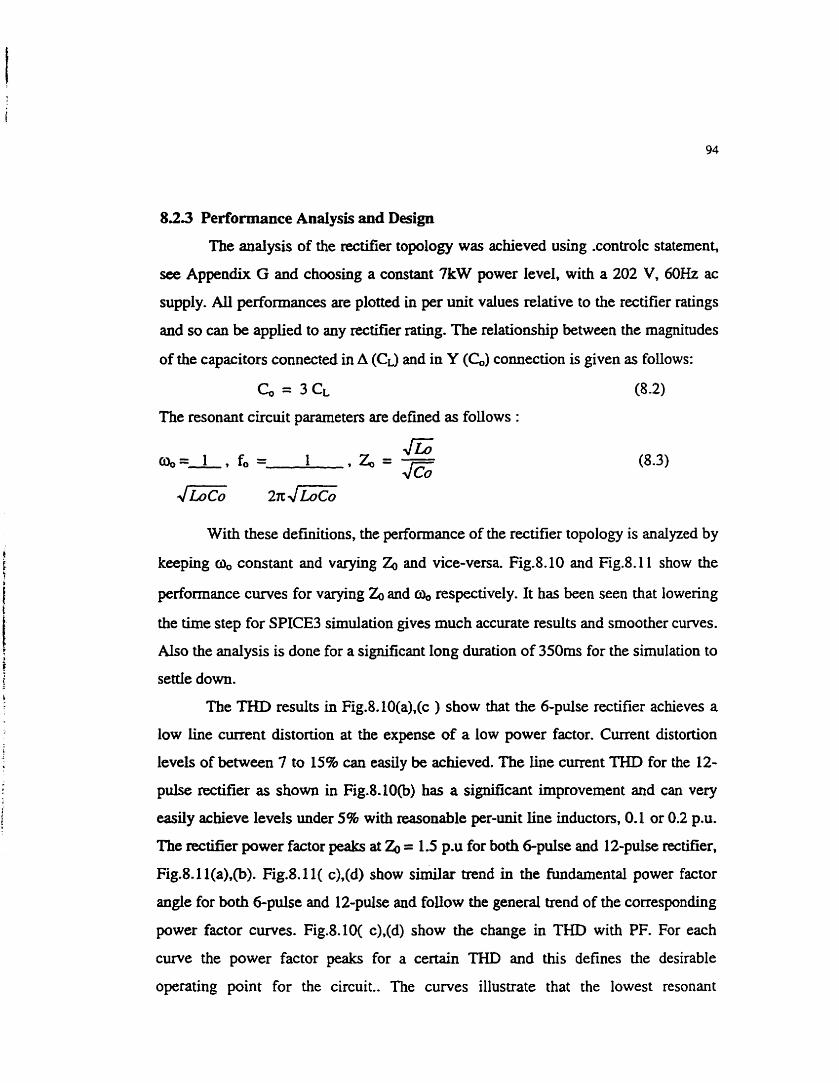
8 3 3 Performance Analysis and Design
The analysis of the rectifier topology was achieved using .controlc statement,
see Appendix G and choosing a constant 7kW power Ievel, with a 202 V, 60Hz ac
supply. AU pefiormances are plotted in per unit values relative to the rectifier ratings
and so can be applied 10 any rectifier rating. The relationship behveen the magnitudes
of the capacitors connected in A (CL) and in Y (c) connection is given as follows:
The resonant circuit parameters are defmed as follows :
With these definitions, the performance of the rectifier topology is analyzed by
keeping a, constant and varying & and vice-versa Fig.8.10 and Fig.8.11 show the
performance curves for varying and O&-, respectively. It has been seen that lowering
the time step for SPICE3 simulation gives much accurate results and smoother curves.
Also the analysis is done for a siwcant long duration of 350ms for the simulation to
settle down.
The THD results in Fig.8.l0(a),(c ) show that the 6-pulse rectifier achieves a
low h e current distortion at the expense of a low power factor. Current distortion
levels of behveen 7 to 15% can easily be achieved. The line cunent THD for the 12-
pulse rectifier as s h o w in Fig.â.lO@) has a siwcant improvement and can very
easily achieve levels under 5% with reasonable per-unit line inductors, 0.1 or 0.2 p.u.
The rectifier power factor peaks at = 1.5 p.u for both &puise and 12-pulse rectifier,
Fig.8.11 (a),@). Fig.8.11( c),(d) show similar trend in the fundamental power factor
angle for both &pulse and 12-pulse and follow the general trend of the corresponding
power factor Cumes. Fig.l.lO( c),(d) show the change in THD with PF. For each
c w e the power factor peaks for a certain THD and this defines the desirable
operating point for the circuit.. The curves illustrate that the lowest resonant
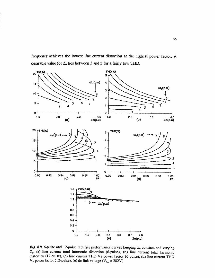
frequency achieves the lowest line current distortion at the highest power factor. A
desirable vahe for Z, lies between 3 and 5 for a fairly low THD.
Fig. 8.9. dpulse and 12-pulse rectifier performance curves keeping y constant and varying Z, (a) line current total harmonic distortion (6-pulse). @) line current total h m o n i c distortion (12-pulse). (c) line current THD Vs power factor (6-pulse), (d) line current THD Vs power factor (12-pulse). (e) dc link voltage (Vu = 202V)
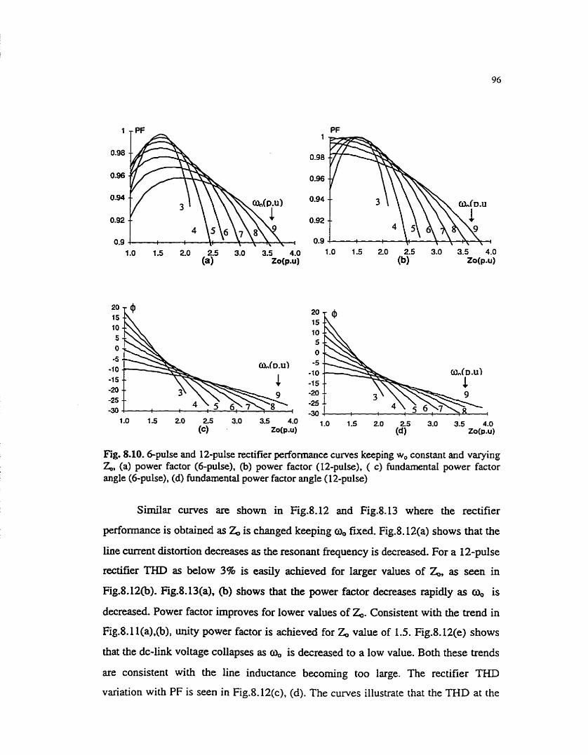
Fig. 8.10. &pulse and 12-pulse rectifier performance curves keeping w, constant and varying Z,, (a) power factor (6-pulse), (b) power factor (12-pulse), ( c) fundamental power factor angle (6-pulse), (d) fundamental power factor angle ( 1 Zpulse)
Similar curves are s h o w in Fig.8.12 and Fig.8.13 where the rectifier
performance is obtained as Z. is changed keeping oo faed. Fig.l.l2(a) shows that the
Iine current distonion decreases as the resonant frequency is decreased. For a 12-pulse
rectifier THD as below 3% is easily achieved for larger values of Z, as seen in
Fig.8.12@). Eg-8. U(a), (b) shows that the power factor decreases rapidly as y is
decreased. Power factor improves for lower values of &. Consistent with the trend in
Fig.8.1 l(a),(b), unity power factor is achieved for 2, value of 1.5. Fig.8.12(e) shows
that the dc-link voltage collapses as y is decreased to a low value. Both these trends
are consistent with the line inductance becoming too large. The rectifier THD
variation with PF is seen in Fig.8.12(c), (d). The curves illustrate that the THD at the
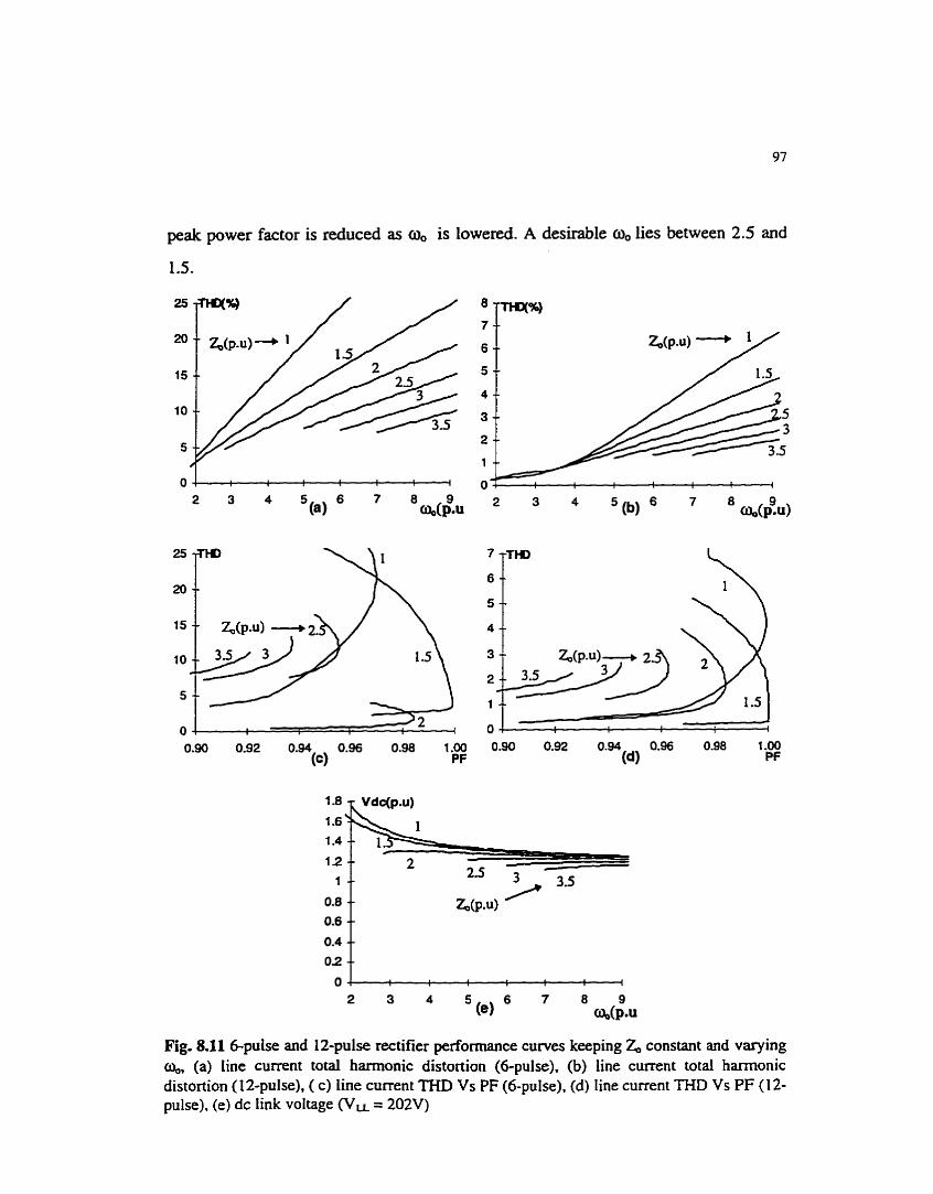
peak power factor is reduced as oo is lowered. A desirable 61, lies between 2.5 and
Fig. 8.11 &pulse and 12-pulse rectifier performance curves keeping Z, constant and varying a,,, (a) line current total harmonic distortion (6-pulse), (b) line current total h m o n i c distortion (IZpulse), ( c) line current THD Vs PF (6-pulse), (d) Iine current THD Vs PF ( 1 2- pulse), (e) dc link voltage (VU = 202V)
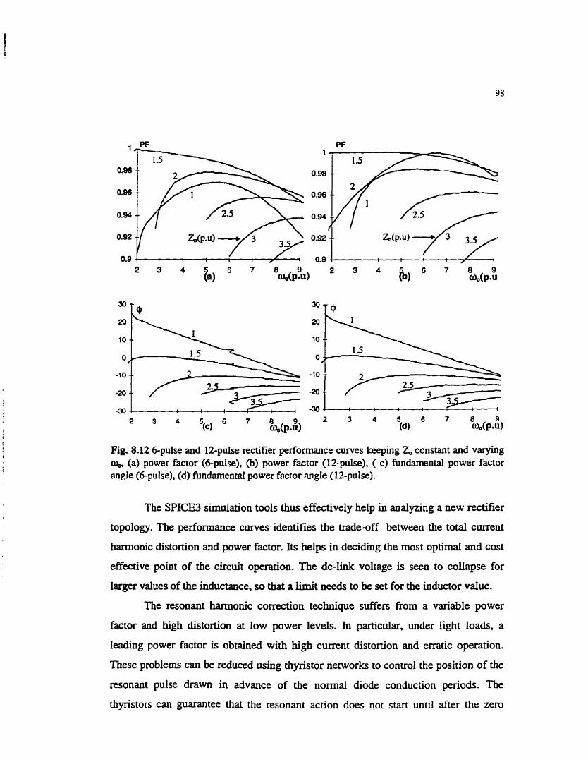
Fig. 8.12 &pulse and 12-pulse rectifier performance curves keeping Z, constant and varying o, (a) power factor (6-puise), (b) power factor (12-pulse), ( c) fundamental power factor angle (6-pulse), (d) hndamental power factor angle (12-pulse).
The SPICE3 simulation tools thus effectively help in analyzing a new rectifier
topology. The performance curves identifies the trade-off between the total current
harmonic distortion and power factor. Its helps in deciding the most optimal and cost
effective point of the circuit operation. The dc-link voltage is seen to coilapse for
larger vaiues of the inductance, so that a limit ne& to be set for the inductor value.
The resonant harmonic comtion technique suffers from a variable power
factor and high distortion at low power levels. In particular, under light Ioads, a
leading power factor is obtained with high current distortion and erratic operation.
These pmblems can be reduced using thyristor networks to control the position of the
resonant pulse drawn in advance of the normal diode conduction periods. The
thyristors can guarantee that the resonant action does not siart until after the zero

voltage cross-over of the line-to-neutral voltage. Additional benefits are obtained in
decoupling the resonant action from the ac utility supply.
The novel rectifier topology helps in obtaining a low input line THD with
nearly sinusoidal line current at unity power factor thus complying with the limits
specified in IEEE-519 [47] and proposed by the IEC-555 [48]. The additional
advantages of the proposed topology are as follows :
The proposed scheme is passive and does ndt interfere with the ac to dc
rectification process of the diode rectifier topology.
The required VA rating of the passive components is a fraction of the diode
rectifier VA.
These topologies do not use high frequency switches, thus reducing the switching
losses and are well suited for industrial applications.
The resonant network draws negligible fundamental current from the input supply.
The proposed scheme can be viewed as a cost effective retrofit to the existing
wide range of diode rectifier type utility interface applications.

Chapter 9
CONCLUSIONS
This work presents various simulation techniques. irnplemented using SPICE3
for simulating Power Electronic system. The study of new control strategies, the
effect of haxmonics and the performance analysis of the system are facilitated by
simulation results. The cornparison of simulation results with experimental ones
validate the simulation techniques of the drive topologies. A novel rectifier topology
is presented that draws line current from the utility with low current distortion and
unity power factor.
9.1 SPICE3 Simulation
The more recent version of SPICE3, namely .3f4 has various advanced
features that are very useful for implementing improved models and system analysis
of power electronic simulation and analysis [Il. The SPICE3 B-statement and U-
statement has simplifiecl the structure of control and switching function. SPICE3 also
provides an Interactive Interpreter that can be used as a stand alone program in the
form of a .CONTROL £de. This feature of SPICE3 has been used in this work for
design and performance analysis of Power Electronic circuits.
The understanding of SPICE3 as a continuou time dnven simulator is very
helpful in obtaining quick solutions to simulation problems. The most frequently
occtirxing error in the simulation is due to the inability for the matrix solution to
converge. The initial time step chosen as the initial guess for convergence is very
important for the matrix solution.
In the prwnt work, a large number of power electronic circuits with varying
complexity have been simulated. Simulation run time increases with the increase in
the number of nodes and switches. Most of the circuits use a diode that take
considerable Iess time then if a BJT or VOSFET was used. A better diode mode1 can
be used by choosing the various device parameters from the manufacturers data
handbook. This mode1 is used in the novel rectifier topology, where the device
parameters are adjusted to get better convergence during simulation.
The time1y consûuction of performance Cumes of the novel rectifier topology,
helps the results to be obtained at the least time step possible. Choosing a small t h e
step for transient analysis also increases the resolution of the simulated waveforms
obtained and prove a better aid for analysis than the experimental wavefonns whose
resolution is restxicted by the resolution of the oscilloscope. This feature of SPICE is
seen particularly for PWM inverter topologies where a high switching frequency is
used.
Simple representation of various circuits is achieved by decoupling the
cornplex circuitry so that they can be simulated as independent block of circuits. For
instance, the output of the transformer is decoupled fiom the input of the rectifier in
the 12-pulse rectifier topology with the help of B-function. This kind of modeling
isolates the two circuitry and simpWies simulation. Decoupling various parts of the
circuits connects more number of nodes to ground so that a much sparse nodal
admittance matrix is obtained. Sparse Matrix technique is used instead for matrix
solution thus increasing the speed of simulation.
Data for the various simulation waveforms are generated using the netlist file
as a raw file. Similarly the data for the experimental waveforms are generated using
the data acquisition system, LABVIEW. Experimental results are used to ve* the
simulations. SPICE3 has the provision of doing harmonic analysis for the various
currents and voltages with the help of the .controlc functions. Cornparison of the
simulated analysis with experimental ones show close agreement.
9.2 Drive Topology
The two drive topologies discussed in this work are the Voltage Source
Inverter and Current Source Inverter. The input, output and load of the drive systems
are simulated and analyzed separately before sirnulating the complete drive system.
Rectifier:
The rectifier stage have either a 6-pulse or a 12-pulse operation. For the input
to a 12-pulse rectifier stage to both the drive topology we use a A-A, A-Y transformer
that is highly applicable for high power. The 30' phase shift b e m n the secondaries
of the two transformer cancel the 5' and 7' hamionics in the input line current thus
significantly improving the total current distonion. The series connection of two
diode bridges form a 12-pulse rectifier. The THD of this 12-pulse rectifier which is a
low 7.3 % at a power factor of 0.98 as compared to a 6-pulse diode bridge rectifier
with C-filter with THD of 68.7 % at power factor of 0.8 1 and &pulse diode bridge
rectifier with LC-filter with THD of 27.6% with power factor of 0.96. The 12-pulse
rectifier has the Il", 13", 23* and other higher order harmonics in the input line
current which make fdtering relatively easy as compared to &pulse operation.
A-& A-Y transfomec
The modeling of the A-A, A-Y transfomer is achieved using d-q axis theory.
Functions cm be us& to decouple die d q axis mode1 of the A-A, A-Y transformer
from the inputs of the rectifier. The value of the transformer d q axis paraneters can
be directly linked to experimentally rneasured parameten and this is very helphil in
the cornparison of the simulation and experimental results.
Voltage Source Invertec
The dc link for the VSI is a capacitor that keep the input voltage to the inverter
stage constant. Both square wave inverter and PWM inverter is considered in this
work. The square wave inverter requires a phase controlled rectifier input stage for
controlling the input dc voltage. The phase controlled rectifier is simulated by
modeling the thyristor as a switching device. The pulse width modulation of the
voltage source inverter nduces the harmonics in the output line voltage, so that the
THD of the line voltage reduces to 17% in a PWM VSI from about 24% for a square
wave VSL A generalized stmcture of a three-level voltage source inverter is
described. The simulation waveforms of the three-Ievel inverter show close
resemblance with theoretical results. It aiso reduces the significant 5" and 7h
harrnonics.
Current Source Inverter:
The dc link for the CS1 is a large inductor that helps to keep a stiff input
cunent to the inverter. Modeling of a PWM CS1 is discussed in this work Capaciton
are connected at the output of the inverter to absorb high frequency harmonies
associated with the pwm inverter output currenr As a result the THD of the motor
line current improves significantly to 2.3 % from that of the CS1 line curent THD of
8.8%. The inverter legs are modeled as three pwrn current functions that simulate the
switching action of the six switching devices. This allows less run time during
SPICE3 simulation due to lesser number of switching devices.
induction Motor :
The induction motor is used as the load to the inverter stage. The induction
motor is modeled using d q axis theory in very much the same marner as the
transformer. Transformation of the a-b-c axes to the d-q axes eliminates the t h e -
varying parameters making modeling much simpler. The availability of the B-
statement and the U-statement in SPICE3 facilitate the modeling of the complex
equations, see paper in Appendix H. The model parameters are the same as that of the
actual machine obtained from various tests, see Appendix D. The simulation results
show good agreement with the corresponding experimental results, thus confimiing
the validity and accuracy of the motor model.
Constant Vlf operation for the induction motor is explained. The existing
model of the motor is modified to obtain simulation results at steady state for a fixed
speed. The .CONTROL statemetlt in the command interpreter is used to obtain
various curves for different values of V/f. The command interpreter which is a new
feature of SPICE3 cm be used to Vary the parameters easily using simple self
explanatory syntax.

9 3 Novel Rectifier Topology
The work describes a novel rectifier topology for the 6-pulse and 12-pulse
diode bridge rectifies. These rectifiers use resonant pulses to improve the line current
distortion associated with the rectifiers, see papa in Appendix H. The operation of
the rectifiers are illustrated with reference to the SPICEJ simulation and experimental
results. The performance of the rectifiers are investigated with reference to the line
current distortion (THD), rectifier input power factor and size of the line inductors.
The analysis is done using performance c w e s obtained using SPICE3 simulations.
The novel rectifier topology for a 6-pulse diode bndge rectifier gives a low
THD of 6.1 % with the line cumnt nearly sinusoidal at unity power factor. This is a
significant improvernent from the 6-pulse diode bridge rectifier with C dc-link fdter
with THD of 68.4 % and power factor of 0.8 1 or a LC dc-link filter with a THD of
. 27.6 % and power factor of 0.96. The line current quality further improves for the
novel 12-pulse rectifier topology and THD of less then 5% is easily obtained. A low 1 '
line cwent distortion of 3.3 % at 0.97 power factor is obtained. These proposed
topologies can be viewed as a cost effective retrofit to the existing wide range of
diode rectifier type utility interface applications.
9.4 Suggestions for Further Work
SPICE3 simulation is highly dependent on the number of switches and nodes
used in the circuit model. The rectifier topologies used in this work use a minimum of
six switching devices. Thus, a signincant improvement in both simulation run time
and convergence problem cm be achieved by modeling the entire diode bridge as a
functional model using a single h c t i o n statement or at least three function
statements representing each leg of the diode bndge.
For the novel rectifier topology al1 the data for the performance curves are
obtained using a tirne-step of 5 p. The curves, specially those of the line current
THD can be further smoothened by using a smaller time-step. The values of the

relative tolerance and absolute tolerance have to be adjusted accordingly to get a good
convergence at such small time-steps.
The proposai rectifier topology gives erratic operation and a leading power
factor under Iight loads. These problerns can be overcome by using a thyristor
network used as a Y-switch to control the position of the resonant pulse drawn in
advance of the normal diode conduction period.

I l ] J.A. Houldswmth and D-A-Granf, 'The use of hannonic Distortion to Increase the Output Voltage of a Three-Phase PWM Inverter," IEEE Trans. Ind. Appl., vol.IA-20, pp. 1224-1228, SeptJOct. 1984.
[2] A.Nabae, LTakahashi, and Himfumi Alcagi, "'A New Neutral-Point-Clamped PWM Inverter," IEEE Trans. hd. Appl., vo1.M-17, pp.5 18-523, SeptJOct. 198 1.
[3J G-Joos, G.Moschopoulos and P.D.Ziogas, "A High Performance Current Source Inverter," Conference Proceedings of PESC, 199 1, pp.112-130.
[4] T.L. Grant, T.H. Barton, "Control Strategies for PWM Drives," IEEE Trans. Ind. Appl., vol.IA-16, pp.211-215, Mar./Apr. 1980.
[SI L.H. Walker, " A High Performance ControUed Current lnverter Drive, "IEEE Trans. Ind. Appl., vo1.W- 16, No.2, pp. 193-202, MarJApr. 1980.
[6] D.E. Füce, "A Detailed halysis of Six-Pulse Converter harmonic Cuments," IEEE Trans. Ind. Appl., vo1.30, pp.294-304, MarchlApril 1994.
171 L Lee, "Cornputer Simulation of Power Line Hannonics or Conducted Emission Generated by 6-pulse and 12-pulse Rectifiers," Conference Proceedings of APEC, 5th Annuai Meeting, 1990, pp.598-602.
[8] L.Meares, C.Hymowitz, Simularing with SPICE. Intusufi, San Pedro, CA, 1988.
[9l J.C.Salmon, E. Bocancea, R. Bhargava, E. Nowicki,"SPICE3 simulation techniques in Power Electronics, CCECE'96 Conf.Records, Calgary, May 1996.
1101 L.D. Salazar, P.D. Ziogas and D.Vincenti,"Simple models for SPICE assisted power electronics circuit simulation on PC's," Conf. Rec.IAS'88, pp.1063-1068, 1988.

[ I 11 LLGiacoIetto, "Simple SCR and TRIAC Pspice computer models," IEEE Trans. Ind. Appl., vo1.36, N0.3, pp.45 1457. NovlDec., 1979.
[12J LD. Salazar, GJoos,"PSpice Simulation of Three-Phase Inverters by Means of Switching Functions," IEEE Trans. Power EIect.., vo1.96, No. 1, pp.35-42, Jan., 1994.
[13] S.D-T. Robertson, KM Hebber, "A digital mode1 for three-phase induction machines", IEEE Trans., 1969, PAS 88, pp. 1624-1632.
[14] V. Rajagopalan, "Cornputer-Aided Analysis of Power Electronic Circuits", Dekker, 1987-
[15] P.C. Krause, T.A Lipo, "Analysis and simplified representations of rectifier- inveaer induction motor drive", Ibid., 1969, PAS 88, pp.588-596.
[16] S.R. Bowes, J-C. Clare, " Digital computer simulation of variable speed PWM inverter-machine drives", IEE Proc., B, Electr Power Appl., 1983, 130(3), pp.149- 160.
[17] J.G Kassakian, 'Simulated Power Electronic Systerns-a new approach", Proc. IEEE, 1979,67, pp. 1428-1439.
[18] M.H Pong, R-D Jackson, '4Computer-aided Design of Power Electronic Circuits", Proc. IEE, Vol. 132, R B , No.6, 1985, pp.30 1-306.
1191 S. Lorenzo. J. Ruiz, F. Aldana, M Shaker, "A New Modeling and Simulation CAD Package for Power Converter Design," IEEE Trans. hd. Electr., vo1.37, NOS, pp.387-397, Oct, 1990.
[20] SR.. Bowes, J.C. Clare, "Cornputer aided design of PWM Inverter Drives Using General Purpose Circuit Analysis Packages," Conf. Rec.IAS'88, pp.507-5 14, 1988.
[21] S.R. Bowes, KR. Clements, "Computer aided design of PWM Inverter systems", IEE Roc., B. Electr Power Appl., 1982, 129(1), pp. 1- 17.
[22] C.L Mq P.O. Lauritzen, "A simple diode model with reverse recovery," IEEE Trans. Power Electron., vol.8. No.2, pp.342-346, 1993.
[23] A.R. Hefner. DM. Diebolt, "An experimentally verifeid IGBT model implemented in the Saber circuit simulator," in Proc. PESC19 1, pp. 10- 19.
(241 2. Shen, T.P. Chow, " Modeling and charactekation of the insulated gate bipolar transistor (IGBT) for SPICE simulation:' in Proc. ISPSD'93, pp. 165-170.
[25] K.J. Tseng, C.F. Foo, P.R. Palmer77'Implementing Power Diode Models in SPICE and SABER," Conf. Rec.PESC'94, pp.59-68, 1994.
1261 P.M. Bhagwat and V.R. Stefanovic, "Generalized Structure of a MuftileveI PWM Inverter," JEEE Trans. Ind. Appl., vo1.W- 19, pp. 1057- 1069, Nov.lDec. 1983.
[27] P.Prasad, R. Jakkli, "Optimal power control strategies for neutrai-point~lamped PWM inverter topology." IEEE Trans. Ind. Appl., ~01.28. No.3, pp.558-566, 1992.
[28] S. Ogasawara, T. Sawada, H. Akagi, 4'Analysis of the neutral point potential variation of neutrai-point<larnped voltage source PWM inverten," IEE JPN. Ind. Appl., vol. 1 13-D, No. 1, pp.41-48, 1993.
[29] JZhmg, "High perfromance control of a three-level IGBT inverter id AC drive," IEEE Trans. Ind. Appl.. vol.30, pp.68369 1, May/Jun., 1994.
1301 J.C.Salrnon, E. Bocancea, R. Bhargava, E. Nowicki,"SCR harmonic correction topologies for VSI drives", CCECE'96 Conf.Records, Calgary, May 1996.
[31] J-C Salmon, E.Nowicki, "A low distortion 3-phase rectifier using a resonant- mode Yconnected thyristor network", CCECE'96 Conf-Records, pp.70 1-703, May 1995.

[32] S.Choi, Prasad N. Enjeti, H-Lee, Ira J. Pitel, "A New Active Interphase Reactor for 12-Pulse Rectifiers Provides Clean Power Utility Interface," IEEE Trans. Ind. Appl.. vo1.32, N0.6, pp. 1304- 13 1 1, NovlDec., 1996.
[33] R Na& M. Rastogi, N. Mohan." A magnetic device for current injection in a three-phase, sinusoidalcurrent utility interface," Conf. Rec.IAS'93, pp.926-930, 1993.
[34] S.Kim, Prasad N. Enjeti, PPackebush, Ira J. Pitel, "A New Approach to improve Power Factor and reduce Kmonics in a 3-phase Diode Rectifier Type Utility Interface,'* IEEE Trans. Ind. Appl., vo1.30, No.6, pp. 1557-1564. Novmec., 1994.
[35] B.M Bird and J.F. Marsh, "Hannonic reduction in multiplex converters by triple frequency current injection," Proc.IEE, vol. 1 16, pp.857-864, July 1972.
[36] Gerald B.Klirnan, A.B Plunkett, "Developernent of a modulation Strategy for a PWM Inverter Drive.," IEEE Trans. Ind- Appl., vo1.h-15, No.1, pp.72-79, Jan./Feb., 1979.
[37] S.R Bowes, "New sinusoidal pulsewidth-rnodulated inverter", Proc. IEE, 1975, Vo1.122, pt.B, ppl279-1285.
[38] T.L.Quarles, " Anaiysis of Performance and Convergence Issues for Circuit Simulation", Electronics Research Lab., College of Engineering, University of Caiifomia, Berkeley, CA, Memorandum No. UCBIERL M89f42, April 1989.
[39) N-Mohan, T.Undeland, W.Robbins. Power Electronics : Converters Applications and Design. John Wiley & Sons, NY, 1989.
[40] B.K.Bose, Power Electronics and AC Drives, Prentice-Hall, Engelwood Cliffs. NJ, 1986.

[4l] D. A. Paice, Power Electronic Converter Hamnics: Mullipuke Methocis for Clean Power, New York; IEEE Press, 1996,
[42] D. A. Rendusara, A von Jouanne, Prasad N. Enjeti. Derek A-Paice, "Design Consideration for 12-Pulse Diode Rectifier Systems Operating under Voltage Unbalance and Pre-Existing Voltage Distortion with some Corrective Maures.," IEEE T m . Ind. Appl., vo1.32, N0.6, pp. 1293- 1303, NovJDec., 1996.
[43] L.J.Giacoletto, 'SCR modelling for SPICE cornputer program', Dept. of Elecuical Engg. intemal merno, Michigan State Univ., Jan 1978.
[44] Pekik Argo Dahono, Yukihiko Sato,"Analysis and Minimization of Ripple Components of Input Current and Voltage of PWM Inverters," IEEE Trans. Ind. Appl., vo1.32, No. 4, pp.945-951, July/August, 1996.
[45] Yo-Han Lee, Bum-Seok Suh,"A Novel PWM Scheme for a Three-Level Voltage Source Inverter with GTO Thynitor," IEEE Trans. hd. Appl., vo1.32, No.2, pp.260- 268. MarJApd., 1996.
[46] M.H Rashid, S P ( C E ' ~ O ~ Power Electronics and Electric Power, Prentice Hall, Englewood Cliffs, NI, 1993.
[47] CKDuffey and R.P.Stratford, "Update of hannonic Standard EEE-519 Recommended Practices abd Requirements for Hmonic Control in Elecvic Power Systems, " IEEULAS Petroleum and Chernical Industry Conference, 1988.
1481 Draft-Revision of Publication IEC 555-2: "Haimonics, Equipment for comection to the Public Law Voltage Supply System, " IEC SC 77A, 1990."
[49] B.M Bird, KG. King, D.A.G. Pedder, An Introduction to Power Electronics, John Wiley & Sons, Sussex, 1993.
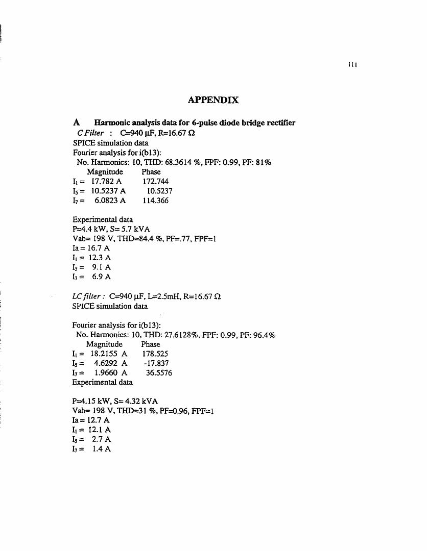
A Harmonic d y s i s data for 6-puise diode bridge rectifier C FiIter : C I = = pF, R=16.67 iZ
SPICE simulation data Fourier analysis for i@ 13): No. Haxmonics: 10, THD: 68.36 14 %, FPF: 0.99, PF: 8 1%
Magnitude Phase Il = 17.782 A 172.744 Is = 10.5237 A 10.5237 17= 6.0823 A 114.366
Experirnentai data P=4.4 kW, S= 5.7 kVA Vab= 198 V, Tm-84.4 %, PF=.77, FPF=I Ia= 16.7 A It = 12.3 A 15= 9.1A 1, = 6.9 A
LCfilter : C=940 pF, L=2.5mH, R=16.67 R SPICE simulation data
Fourier analysis for i@ 13): No. Harmonics: 10, THD: 27.6128%, FPF: 0.99, PF: 96.4%
Magnitude Phase I l = 18.2155A 178.525 Is = 4.6292 A -17.837 I7 = 1.9660 A 36.5576 Experimental data
P=4.15 kW, S= 4.32 kVA Vab= 198 V, TEID=3 1 %, PFd.96, FPF=1 Ia = 12.7 A II = 12.1 A Is = 2.7 A I,= 1.4 A

B Test data for A-A / A-Y transformer parameters
TRANSFORMER NAMEPLATE DATA
OPEN CIRCUIT TEST (at rat& voltage) A-A transformer
VdV) 11 (A) v209 % (K\K)~~hru 202.4 1.9 20 1.5 0.1 1
A-Y transformer VdV) 11 (A) V2(V) Pin (mV3p~ 202.4 2.76 201.1 0.14
SHORT CIRCUIT TEST (at rated curent) A-A transformer
A-Y transformer

C Harmonic analysis data for 12-pulse diode bridge rectifier L=~.M-I, ~ = 4 1.666 n
SPICE simulation data
Fourier analy sis for i@ 13): No. Harmonies: 10, THD: 7-32 %, FPF: 0.985, PF: 0.982
Magnitude Phase Il = 19.864 A -9.72 19 I5 = 1.2266 A 140.405 17= 0.7618A 125.005 I l l = 1,176 A II3 = 0-995 A 123 = O S 6 A
Experimentai data
P=6.3 kW, S= 6.5 kVA Vab= 194 V, THD=10.9 %, PF=0_97, FPF=0,98 Ia = 19.5 A 1, = 19.4 A I5 = 0.2 A I7 = 0-6 A f
III = 1.6 A I l 3 = I . l A Iu = 0.6 A
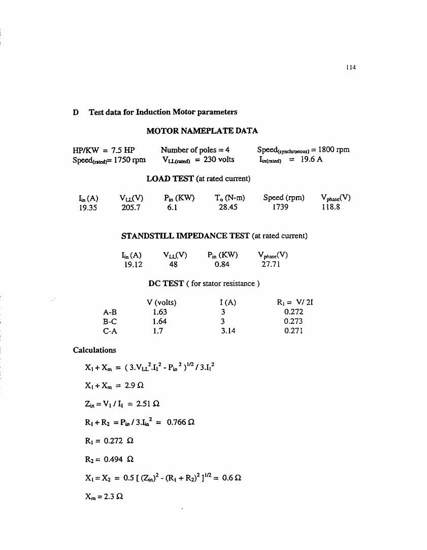
D Test data for Induction Motor parameters
MOTOR NAMEPLATE DATA
LOAD TEST (at rated current)
STANDSTILL IMPEDANCE TEST (at rated current)
DC TEST ( for stator resistance )
V (volts) 1 (A) RI = V/ 21 A-B 1.63 3 0.272 B-C 1.64 3 0.273 C-A 1.7 3.14 0.27 1
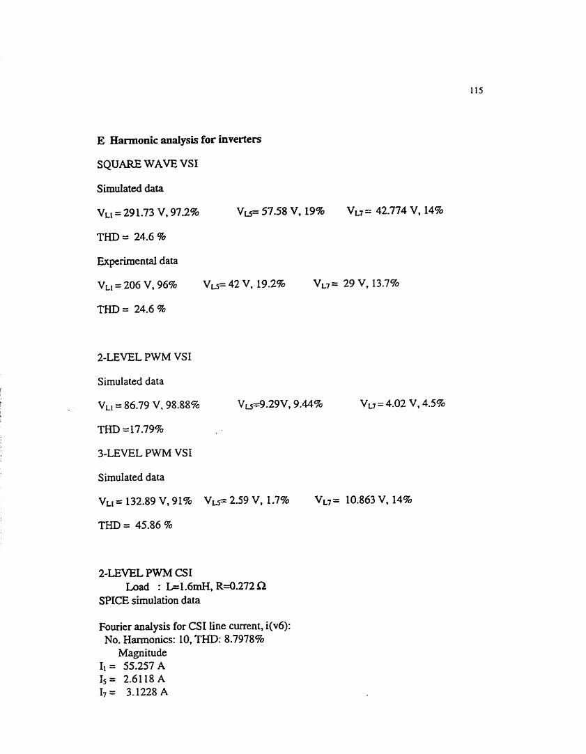
E Harmonic analysis for inverters
SQUARE WAVE VSI
Simuiated data
VLt = 29 1.73 V, 97.2% Vu= 57.58 V, 19% VL7= 42.774 V, 148
THD = 24.6 %
Experimentai data
VL1 = 206 V, 96% Vu= 42 V, 19.2% VL, = 29 V, 13.7%
2-LEVEL PWM VSI
Simulated data
VLI = 86.79 V, 98.88% V U S D V , 9.44% VL7 = 4.02 V, 4.5%
3-LEVEL PWM VSI
Sirnulated data
THD = 45.86 %
2-LEVEL PWM CS1 Load : kl.6mH, Rd.272 22
SPICE simulation data
Fourier malysis for CS1 line current, i(v6): No. Hannonics: 10, THD: 8.7978%
Magnitude Il = 55.257 A 15= 2.6118 A 1,= 3.1228 A

Fourier analysis for motor line current, i(1l): No. Harmonies: 10, THD: 2.2729 %
Magnitude 1, = 54.OS5A k = O.11OQA 1, = 0.076 1 A

F tfarmonic anaiysis data for resonant-mode network rectifier topology
P=7kW, Vu. = 202 V, L, = 7.5mH, C= 34 pF 6-p&e diode bridge (upper bridge line current) SPICE simulation data Fourier analysis for i(l6): No. Harmonics: 10, THD: 6.10703 %, FPF: 1 .O, PF: 1 .O
Magnitude Phase Il = 34.6 A 2.3 Is= 1-98 A -37 i7= 0,712A -88.096
Experirnental data P=4.4 kW, S= 5-7 kVA Vab= 198 V, THD=8.44 %, PF=1 .O, FPF= 1.0 Ia= 16.7 A 11 = 13.3 A Is= 9.1A 17= 6.9A Iil = 2.9A 1 1 3 = I - l A
6-pulse diode bridge (lower bridge Iine currenl) SPICE simulation data '
Fourier analysis for i(19): No. Harmonics: 10, THD: 8.59562 %, FPF: 0.99, PF: f .O
Magnitude Phase Il = 27.46 A 7.6 1 G = 2.15979A -162.11 17 = 0.953363A 98.77
Experimentai data P4-4 kW, S= 5.7 kVA Vab= 198 V, THD=9.1%, PF=1 .O, FPF=l.O Ia = 15.8 A II = 12.6 A 13= 0.9 A I s= 8.1A 1, = 6.3 A Ill= 3.1A I t 3 = 1.7A
12-pulse diode bridge (total input Iine current)) SPICE simulation data

Fourier anaiysis for i(l6)+i(l9): No. Harmonics: 10, THD: 3.326 %, FPF: 0.964, PF: 0.97
Magnitude Phase I l = 583828A -15.22 I5 = 1.92434A - 104.15 I7 = 0.25989 117.933
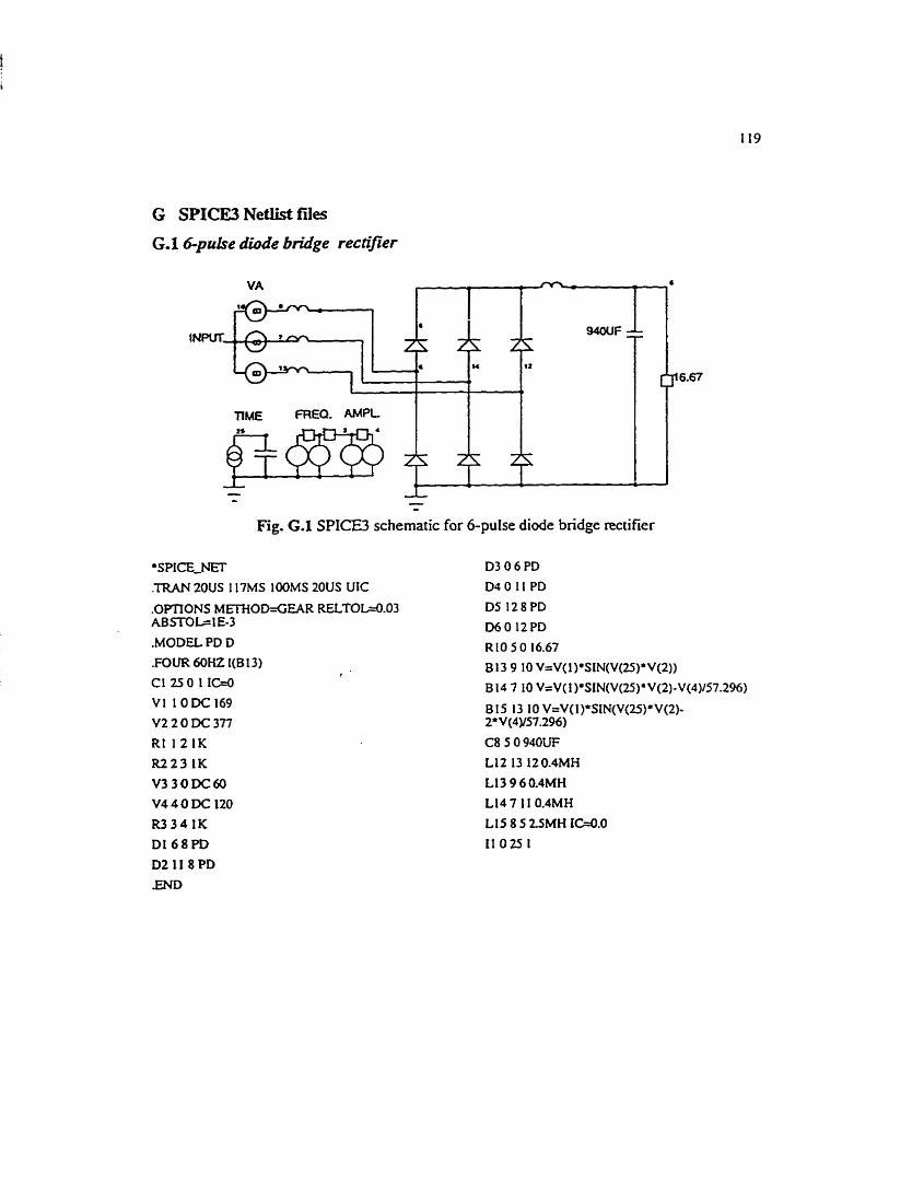
G SPICE3 Netiist files
G.16-puke diode bridge rectifier
Fig. G.l SPICE3 schematic for &pulse diode bridge rectifier
.SPICE-NFT
.IRAN 20US 117MS lOOMS 2OUS UIC
C8 5 O 940W
LIS 13 i20.4MH
L13 9 6 OAMH
D2118PD END

6.2 Il-puke diode bridge rectifier
Fig. G.2 SPICE3 schematic for 12-pulse diode bridge rectifier
'SPICE-NET I 87 O 13 V=l12'SIN(377*V(12))
.'IRAN lOOUS 1 16.67MS IOOMS lOOUS UIC B8 13 0 I=I(B5)
.MODEL PD D B 12 10 0 V=(2*V(I 6)-V(I8)-V(21))/3
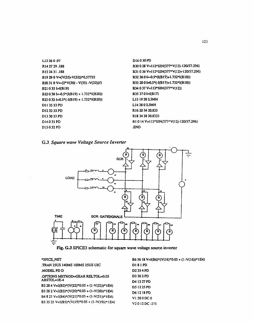
G 3 Square wave Voltage Source Inverter
- - Fig. G3 SPICE3 schematic for square wave voltage source inverter
.TRAN 25US 140MS 1 OOMS 2SUS UIC
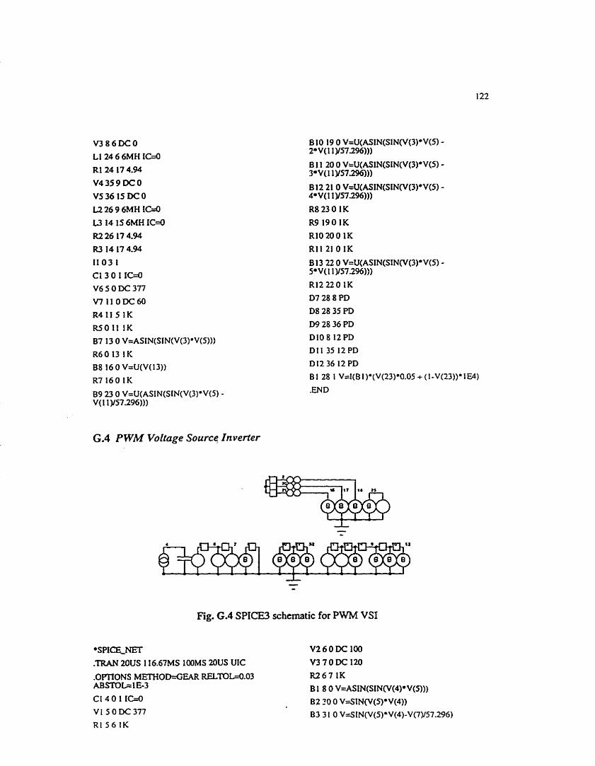
V386DCO
L124 6 6MH ICA RI 24 17 4.94
V4359iXO
V5 36 15 D C O U î 6 9 6 M H IC=O W 14 15 6MH IC=û R2 26 17 4.94
R3 14 17 4.94
Il O 3 1
C13011C=û
V6SODC377
V711ODc60
R4 11 5 1K MOI1 1K B7 13 0 V=ASIN(SlN(V(3)'V(S)))
R60 13 1K B8 16 0 V=U(V( 13))
R7 160 1K B9 23 O V=U(ASIN(SI N(V(3)*V(S) V(11 yS7.îg6)))
(2.4 P WM Voltage Source Inverfer
Fig. 6.4 SPICE3 schematic for PWM VSI
*SPICE_NEr
.W 20US 1 16.67MS lOOMS 2OUS UIC
.OPTiONS METHOMEAR RELTOLQ-03 ABSK)L:=lE-3
CI401IC=0
VI SODC377
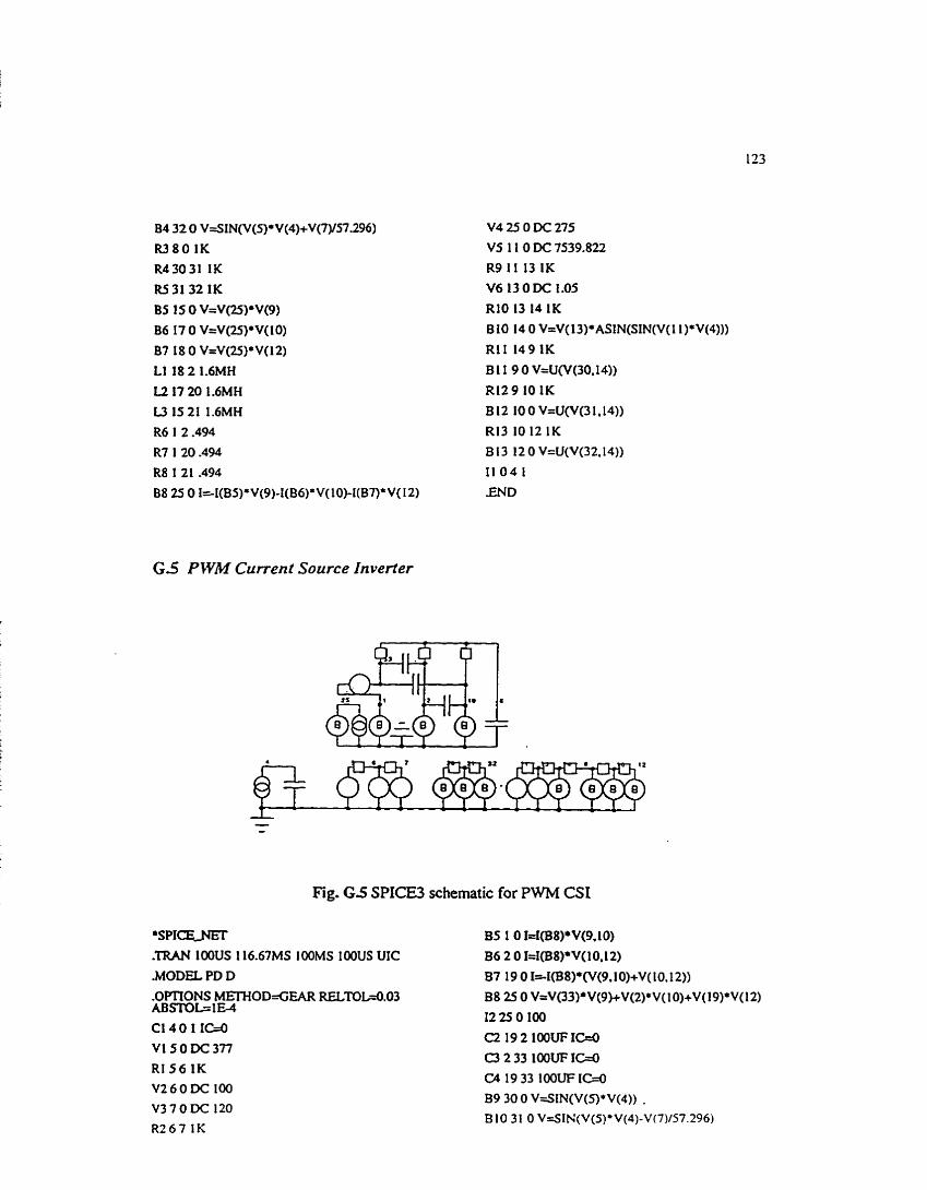
G 5 P WM Current Source Inverter
Fig. GS SPICE3 schematic for PWM CS1
*SPIcE-NEr .'IRAN lOOUS 1 16.67MS IWMS IOOUS üiC
MODEL PD D .OPTIONS MElHOD=GEAR RELTOL;=OL;=003 ABrnISlU
C I 4 0 1 I W v15oDC377
RI 56 1K V26ODC IO0 V370DC 120
R267 1K
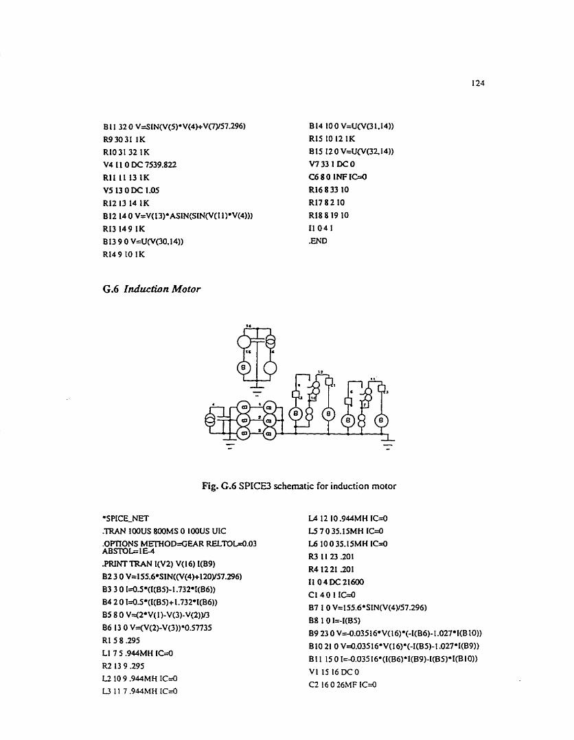
B 14 10 0 VdJ(V(31.14))
RIS 10 12 1K
s 1s t 2 0 VdJ(V(32.14)) V733 1 D C O
C68O lNFIC=O
R i 6 8 33 10
Rl7 8 2 10
RI8 8 19 IO
1 1 0 4 1
.END
Fig. (3.6 SPICE3 schernatic for induction motor
'SPICE-NET
.TRAN lOOUS 800MS O lOOUS UIC L6 10 O 35.15MH IC=û
R3 11 23 -201
R4 12 21 2 0 1
11 04DC21600
C l 4 0 1 IC=O 87 t O V=155.6*SIN(V(4)/57.296)
B8 1 O I=-I(BS)
B9 23 O V d . 0 3 5 16*V(l6)'(-I(B6)- 1 .O27* I(B IO)) B 10 21 O VdI.035 16*V(16)*(-I(B5)-1 .O27* I(B9))
B II 15 O IdI.035 16'(I(B6)*I(B9)-I(BS)*I(B 10))
VI IS 1 6 x 0
C2 16 O 26MF I C d
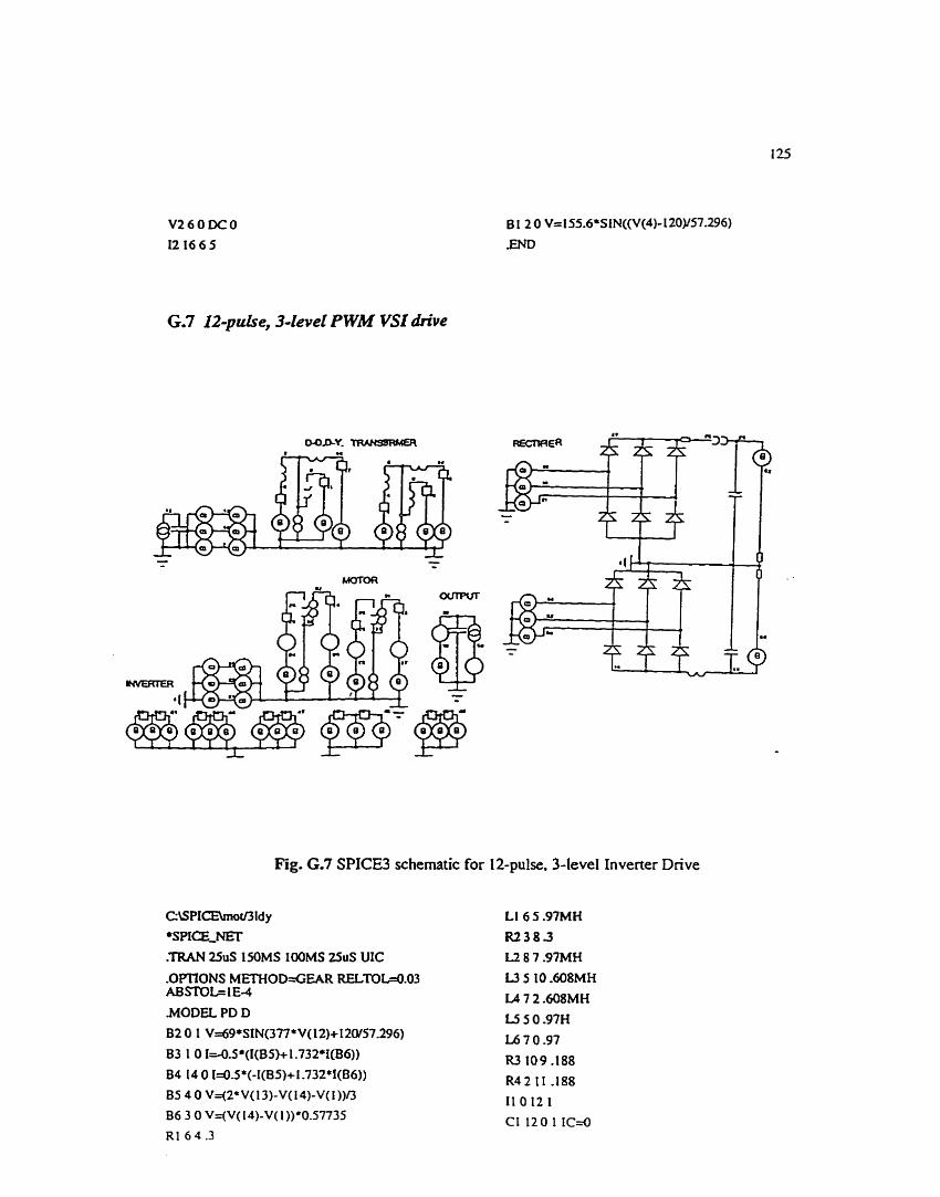
G.7 12-puke, 3-level P WM VSI drive
B 1 2 O V=l55.6'SIN((V(4)- 1 ZO)/S7.296)
END
Fig. G.7 SPICE3 schematic for 12-pulse. 3-level Inverter Drive
CSPICEhotBldy *SPICECENET .TRAN 25uS 150MS IOOMS 25uS UIC

B7 O 13 V=69*SIN(W7*V(12))
B8 13 0 I=I(B5)
B9 9 O V=(2*V(l&V(18)-V(2 1))/3
B 10 I I O v+(i wv(2 1 ))*0.57735
L9 5 24.608MH
L10 7 22.608MI-f
R7 24 29 -188
R8 22 31 -188
B 13 29 O vt(~(m-v(32))*0m35
B 14 3 1 O V=-(2*V(30) - V(35) -V(32))n
B21 100 16 I=I(B9)
vIûû 100 O dc O B22 O 21 I=4.!V(I(W)+I .732*I(B 10))
B23 O 18 1--05*(-I(B9)+1.732*I(B 10))
DI 1657PD
D2 l857PD
D3 21 57 PD
D4 74 16 PD
D5 74 18 PD
D67421 PD
B24 O 35 I=I(8 13)
B25 O 30 1s-OJ*(I(B 13) + 1.732*I(B 14))
B26 O 32 1=O.S8(-I(B 13) + 1.732*1(B 14))
D7 35 74 PD 1
D8 32 74 PD
D9 30 74 PD
Dl0035 PD
Dl1 OXPD
Dl20 30 PD
B27 15 O I=4.03516*(I(V3)*I(v6>f(v4)*1~))
V2 1539 D C O
C2 39 O 26MF IC=û sa 59 O I=0.5*(-I(V5)+1.732*I(v3))
829 51 O 1=03*(-I(V5)-1.732*I(V3))
B30 40 O V=(2*V(SO)-V(SI)-V(59)Y3 B3 1 49 O Vq(51)-V(S9))*057735
R10 53 41.295
LI3 55 53.944MH I W
R1147 48.295
L 14 45 48.944MH ICrO L 15 90 55 -944MI-I IC=O L 16 44 45.944MH IC=O LI7 55 O 35.I5MH ICrO
L18 45 O 35.15MH IC=O
R I 2 90 38 -201
V54041 D C O
V63438DCO
BSO 84 82 V=V(60)*ASW(SIN(V(l2)*V(19)* 1û-tl20i57.296 1)
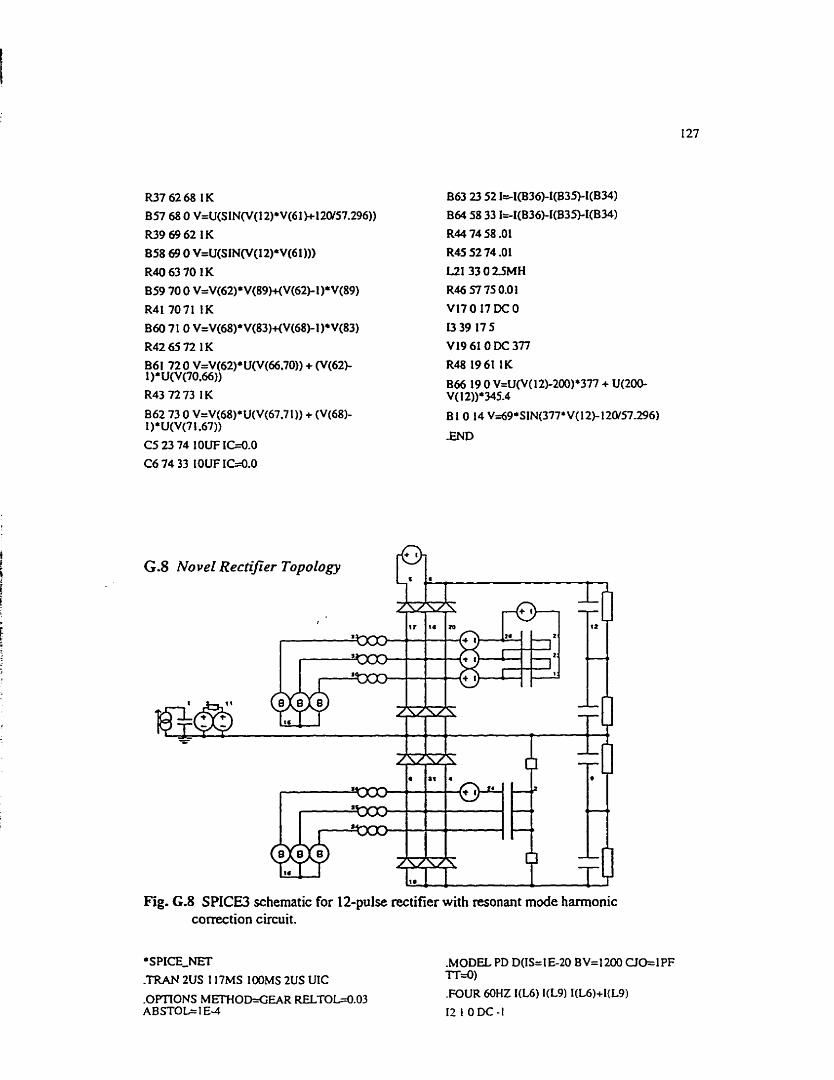
Fig. G.8 SPICE3 schematic for 12-pulse rectifier with resonant mode harmonic correction circuit.
*SPICE-NET
.M 2US 1 17MS lOOMS 20s UIC

CIO 28 21 4ûüF IC30 DlS2û8PD
C24 4 2 4ûUF IC=2oO
V6 1728DCO
V7 18 21 D C O VSîO23 DCO
V958DCO
V7 18 21 D C O
V8 2023 DCO
V958DCO
V10624DCO
R44 O 2 10K
END

G.9 Run Jile for conrtant V/F curves for induccion muchine
SPICE3 run file *torque speed curves for an induction motor * a = the per-unit speed sening * Fs = the base frequency seting of 60Hz * P = # of poles * W = base fine-line voltage at 60Hz = 208V * Wa = motor line-line voltage at the per-unit speed setthg a * F1= motor supply frequency at the per-unit speed sening a * Ns = motor synchronous speed at the per-unit speed setting a * Ws = motor synchronous speed at the per-unit speed setting a * Nr = rotor speed at the speed setting a and slip * Wr = rotor speed at the speed setting a and slip * slip = motor slip * Rs,Ls,Rr,Lr,Lrn are the motor equivalent circuit parameten * Kl,K2 are constants required in the dq-axis equivalent circuit * Irno is the initialization current for Im in the d-axis equivalent circuit. .controlc set width=275; set nobreak; set noheader; set noprintscale source im let Fs=oO;let P=2;Iet a=ûA;let VIl=208;let torque0;let Vlla=a+Vll;let Fl=a*Fs let Ns=a*Fs* 120tP;let Ws=Ns*3.1425927/30;Iet Nr=Ns;Iet Wt--Ws let Rs=0.29S;let W . 2 0 1 ;let Ls=0.000944;let Lr=O.O00944;let Lm=0.035 15;let K1=3*P*Lrn/2;let K2=l+Lr/Lm let V1la=arVII;let F 1 =a*Fs;let Irno=0.8 ld*VlV(6,283*Fs *@+Lm))
let slipS.0 while slip It 1 let Nr=(l-slip)*Ns;let Wr=Nr*3.14 1 alter v4=Fl;alter vS=Vlla;aIter v3=Wr;alter v7=Kl ;alter v6=K2 alter r 1 =&;alter r2=Rs;alter r3=Rr;alter r4=Rr alter ll=ls;alter 12=Ls;aiter 13=Lr;alter 14=Lr;alter 15=Lm;alter I6=Lm alter 11 ic=ho; alter W ic=-Imo tran 125uS 875mS 75ûmS 125uS uic let torque=mean(ï(v3));1et timcv(4) let va=v(l);let vb=v(Z);Iet vc=v(3);let ia=-i(b7);let ib=-i@ I);let ic=-i@2) let vab=va-vb; let vbc=vb-vc;let uca=vc-va let iabc=sqrt((mean(iaA2)+mean(ibA2)+mean(icA2))/3) ; let vabc=sqrt((mean(vabA2)+mean(vbc"2)+mean(vcaA2))/3); let pabc=mean(vab*ia)-mean(vbc*ic);let apabc=sqrt(3)*iabc*vabc;let p fabc=pabc/apabc let pout=torque* Wr. let eff= 1 ûû*pout/pabc
print col Nr slip torque pout iabc pabc pfabc eff
destroy al1 let slipcslipt0.0 1 end .endc end
steps: dat 10: dat04: sl ip4 dati O( dat 1 01 da1081 da1081 datO6l datoSl dat041 datMl dam21 dat04
G.10 Run füe for Novel Reccifiet Topology performance curves
scr resonant circuit .contsolc
source c let nz=l .O; let nfstart=2; let nfstepd.2; let nfstop=lO let Fbase=oO;let Vll=202;let Pbase=7000 let Vph=Wsqrt(3);let Vm=Vph/sqrt(2);let Wbase=Fbase*6.283 19 let base=Pbasd(V11*sqrt(3)); let Zbase=Vph/Ibase;

let n f d s ~ l e t zo=nz*Zbue; let fo&Fbase;let wo=6.283 19 * fo let 1-/wo;let CO= l/(wo*zo);let cU=co/î;let cphroI2 print col nz nfstart nfstep nfstopfl.0.abc print col nz nfstart nfstep nfstop>f 1 .O.xyz print col nz nfstart nfstep nfstop>fl .O. l2pulse set width=275; set nobreak; set noheader: set noprintscale let crz15E-6; let lac=lOE-3; let rld=6 let pa-; let thdabc=O; let pf-; let phabc=O; let mnabc=O; let pabc=O let pxm; let t h d x w ; let pfxyz=O; let phxyz=û; let mfzxyz=O; let p x y d let paa=0; let thd=O; let pfaa4; let p h d ; let mn=û; let p a a d let mnabc=û;let m ~ y z = O ; let mn=O
let nf=nfstart while nf lt nfstop let count=O let zo=nz*Zbase; let fo-.lPFbase;let wo=6.283 19*fo let lo=zo/wo;Iet CO= l/(wo*zo) ;let cll=col3;let cp h=co/2
while count It 4 aiter v4=Fbase;alter v3=Vll aiter 16=10; alter 17=Io; alter 18=lo;alter 19=10; alter llO=lo; alter Il 1 =lo
. . alter c I k U ; alter c l2=cU; alter c 14=clI;alter c22=co; alter c23=co; alter c24=co alter r 1 l=rld;aIter r12=rld;alter rl3=rId;alter r l4=rld tran 2uS 250mS 200mS 2uS uic
let time=v( 1) Iet va=v(33,1S);let vb=v(32, t 5);Iet vc=v(30, I5);let ia=i(l6);let ib=i(l7);let ic =i(18) let vab=va-vb; let vbc=vb-vc;Iet vca=vc-va let iabc=sqrt((mean(iaA2)+mean(ibA2)+mean(icA2))/3); let vabc=sqrt((mean(vabA2)+mean(vbcA2)+me~))/3); let pabc=mean(vab*ia)-mean(vbc*ic);let apabc=sqrt(3)*iabc*vabc;let pfabc=pabc/apabc let i 1 rabc=sqrt(2)*mem(ia*sin(Urbase*time)); let i 1 iabc=sqrt(2) *mean(ia*cos (Wbase*time)) let i 1 abc=sqrt(i lrabcA2+i 1 iabcA2);let phabc=atan(i liabdi 1 rabc) let ifabc=(abs(i 1 rabc)ri 1 rabc) *sqrt(2)*i 1 abc*sin(Wbase* time+phabc) let ihabc=ia-ifabc;let ihmisabc=sqrt(mean(ihabcA2)); let thdabc= 100*ihnnsaM 1 abc
let vx=v(36,16);1et vy=v(35,16);let vz=v(34,16);let ix=i(lg);Iet iy=i(l 1O);let iz=i(l 1 1) let vxy=vx-vy; let vyz=vy-=;let vn=vt-vx let ixyz=sqrt((mean(ixA2)+mean(iyA2)+mean(izA2))13) let vxyz=sqrt((mean(vxy".2)+mean(vyzA2)+mean(v~A2))/3) let pxyz=mean(vxy *ix)-mean(vyz* iz);let apxyz=sqrt(3) *ixyz*vxy z; let pfxyz=pxyzlap XYZ let i 1 rxyz=sqn(2)*mean(ix+sin(Wbase*time))

let i 1 ixy~rt(2)*mean(ix*cos(Wbasef the)) let i 1 xywqrt(i 1 rxyzA2+i 1 ixyzA2);let phxyz=atan(i l ixy di 1 rxy z) let ifxyz=(abs(i 1 rxyz)/i 1 nryz) *sqrt(2) *i 1 xyz*sin(Wbase *time+p hxy z) let ihxy--i.fkyz;let ihmisxywqrt(mean(iihxyzA2)); let thdxyz= 1 ûû*ihrmsxyt/i 1 xyz let ial=(ix-iy)/sqrt(3); let ibl =(iy-iz)/sqrt(3); let ic l=(iz-ix)/sqrt(3) let iaa=ia+ial ;Iet ibb=ib+ib 1 ;let icc=ic+ic 1 let i rmsaa=~~r~( (mean( iaa~2)+mean( ibb~2)+me) le aa ean vab*iaa)-mean(vbc*icc);let apaa=sqrt(3)*imaa*vak;let E$ 3 a i P =P aP let i lmq~(2)*mean(iaa*sin(wbase*be)); let i li=sqrt(2)*mean(iaa*cos(Wbase*time)) let il=sqrt(ilP2+iliA2);let ph=atan(ilÿilr) let if=(abs(i lr)/i lr)*sqrt(2)*i 1 *sin(Wbase*time+ph) let ihtiaa-ifilet ihrrns=sqrt(mean(ihA2)); let îhd= 1 OO*ihrms/i 1
let phabc=phabc*57.296;1et phxyz==hxyz*57.296+30;let ph=ph*57.296 let rld=rld*pabdPbase let rnn=mean(v(S));let mnabc=mn/vll; let mn=-mean(v(7));le t mnxyz=mn/v1l; let rnn=(rnnabc+mnxyz)/2
let count=count+ 1 destroy al1 end
pnnt nz print col nz nf Io CO cph cl1 rld pabc thdabc pfabc phabc mnabo>f l .O.abc print col nz nf Io CO cph cl1 rld pxyz thdxyz pfxyz phxyz m n x y ~ > f 1 .O.xyz print col nz nf la CO cph cl1 rld paa thd pfaa ph m n » f 1 .O. l2pulse let nf=nfstep+nf;Iet rld=6 end

SPlCE3 simulation techniques in power electronicç
This papcr dcwibts numaous SPICE3 rcchniqw
appro9riarcfaPowaElcaranics ïk1##u~madc to SPICE ar the Univasity of BaWy bas made absoku variorrr SPICE sioiiilarian tcchniquer 0Cwi uscd in Powa El-csrysrws.Manyncwf~havcalsobccuaddtd ta SPICES lhat aiiow many aew circuit dtsign ocjeutcd tasks CO bc paCarmed The inauduaion of the 'B-aarcmair". and thc comparwa ~ a i t s , mc W-ramp" and 'U--ait" has nmpliTrcd the suuaurt of carimi and switching funaions uscd frequenrly for Powu Ekamics . Various simulatjcm
&iqw arc iUwlarcd wifh the use of a variable s p d drive amfigurafion using a M. &Y inpur tansiormer. The cr~ruu UIvaur uses a phase anwlkd raxificr m r c p k Lhc DC ünk cumnr The voftagc source inventr uses a PWM rccfuiiquc to provide a Iow THD currenr on the
induction motor side. The papa dtsaibcs how d q anis
modcling in SPICE3 can be ustd tr, mode1 the induction motor and ihe rransformer. Experimcntai rcsulls art used co verify rhe SPICE3 simuiaions
Fig. 2 S p i s 3 sdianaric for M A Y aansformer and rcuiicrs
2 W S F û R M E R SIMULATION
The equivalcnt pcr phase circuit is considmd in rcmis of d q axis thcory. In this theory the urne varying parameurs afe
- - cluninaritd and ihe variaiks and paramcers arc exprrssed in ortfiogonal ar rnutaally decouplad dirta (d) and quadrame (4) axes. The srrppIy ~Itagcs arc g i v a by the ~ o r m a a o n wiurc v, is the zao sequeriot componait which does not min
sine
Thc saies connations of two diode bridges, fcd h m a â A
AY nansformcr, givez a 12 pulse rectification. This constant DC ourput is fcd to the input nage of a Volrage S m Inverru ('SI). in con- rht C m t Soum inverter (CSI) r r q u h phase conmil r u t i f i o n . The o q u t of the
simularcd suies co~ tc r t d re~ufiers yields rcniIts similar to
the expcrimeriral plols, as stiown in fig.4 and Gg5. The swirctiing device in an scr bridge is modelai by having
a diode in saies wirh a B - m a n a i t The diode rnainiains the
unidircctional propercy of ihe dcvicc.(set Fig.3).
(a) node for tune (b) swicching p m n (c) 9cr swiicti
B 1 2 O v = asin(sin(37ï*v(l)-9û/S7296)) 823 Ov= u(v(2))
03 5 4 v = i(B3)*(~(3)*0.05+(1-v(3))/1E6) D l 6 S P D
(d) spice3 mr listing Fig. 3 Spiu3 models
-2ooL
Fig. 6 S imuIared M and AY &orma stcondary voltages
Fig.7 Exprimaid M & AY &ormet saondary voltages
4.VûLTAGE SOURCE INVERTER
Fig9 PWM-VSI: s i m W phase voltage 8t I d atnait
7. CONCLUSIONS
Fa.13 Sirnthd scaring torque and spœd a m e s far IM
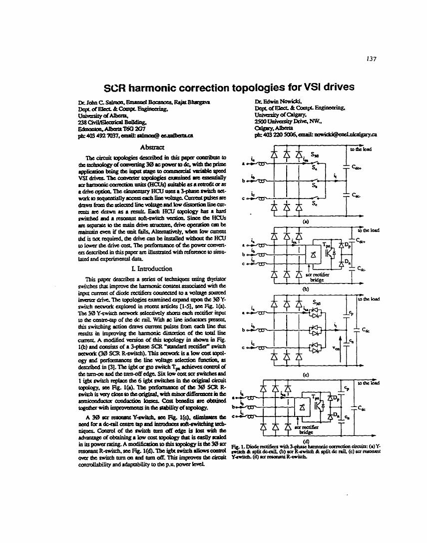
SCR harmonic correction topologies for VSI drives
L Introduction
A 30 su rcmaam Ylcwiteh. oee Fie. 1(c). eûmnnm . . ait
n c c d f a a d e m i i a r i t r t t a p m d i a a o b i a J O b A ~ ~ uiquts. Corusri1 of the swifch ûnn off edgc is bsl uifh &c a d v a n t a g c o f o b c a i n i n g & b w c n s t ~ ~ i s ~ y s u k d initspowctrafing.Amodidcatioato thistdpobgyUtbt30oa rcsonaotR-switdi,s6eFig. I(d).TbeigkrwirchaliuwsumW ovtraicswircbarmoriuidanaoa.~impovcsrbecirarit conodfability and adapcability to the p.& powltr b c i
lard
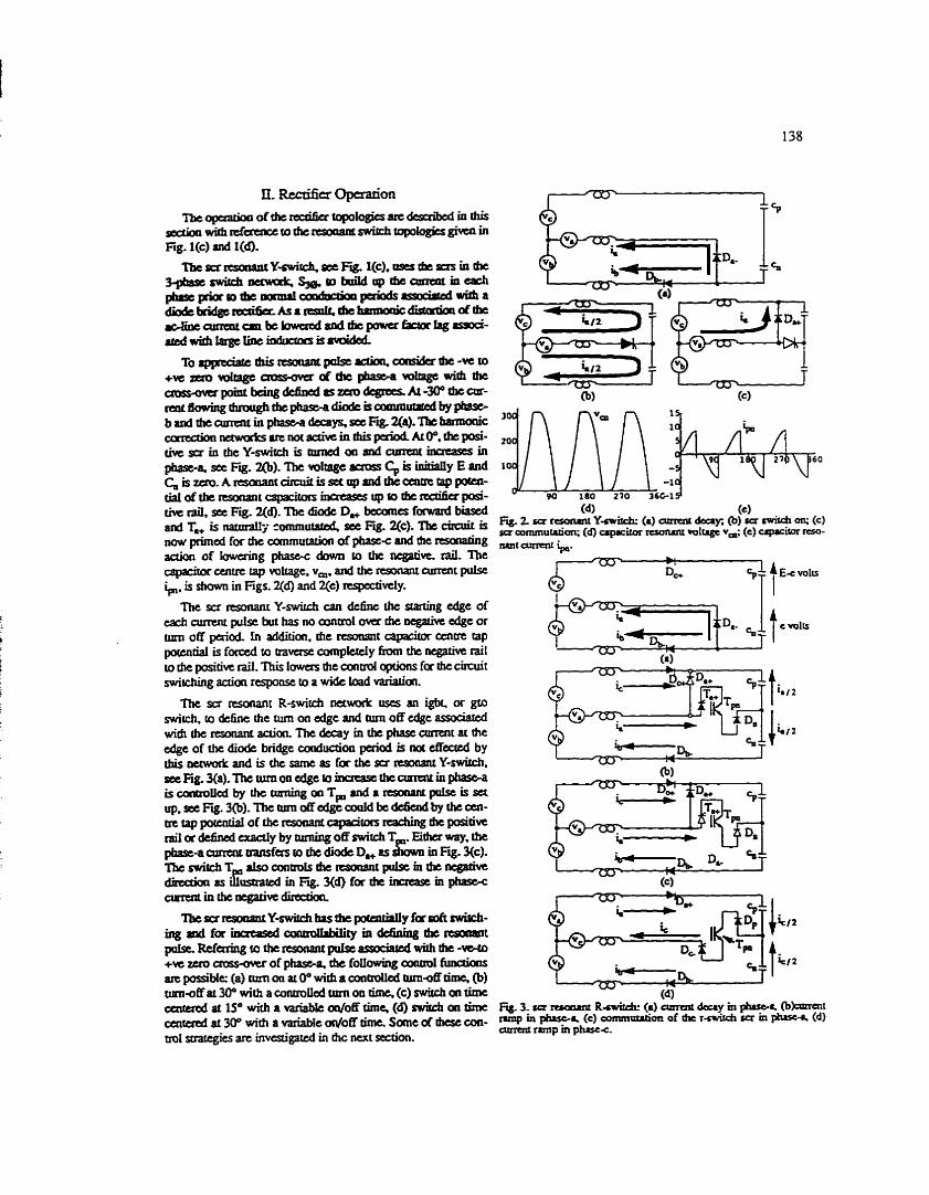
Tht =rtsonaruY-nrrirrhcari dctïnechesrarting edge of tach aimnt pulse but has no aonsol owr thc nc&e cdge or m off paiod In addition. die rtsonant ca@m cairn tap porui9al is f d CO ûavasc c w p W y fiDm the negative rail to thc positive rail. This lowas the conad opions fa die circuit swirching aclion rtspoosc to a widt Load variaria.
TbcscrresorÿmtY-switdihasrhcpoMtiallyfadrwirb- i n g d f a ~ c O n Q d h b i l i t y i n ~ t h t ~ t p k . R ~ f a r i n g ~ ~ t k ~ p i l s e a s s o c i a t t d w i t h t h e - ~ +vt m u avswwr of p b s ~ , rbe foiiowing amaol fumhas arc possible: (a) m on at O* with a amûdicd ~ L K U ~ cime, @) ttrmaff ar W with a conaroiicd uxn on rime. (c) swiich UI tirnt caireried at lSO with a variabk oa/oE ùmç (d) swircb on tirne caiwcdat30" widi avariablton/off timc.Someofbcori- ml smtcgies arc invesUgaccû in thc nwrt scctim.
Fig .3 :ecr~w#muR-nviub: (? )aonntdauym~~(b)cmrai i nmp m (c) commuuûon of ihe r-rwriidi SU III -4 (dl amma ranp in p b c .
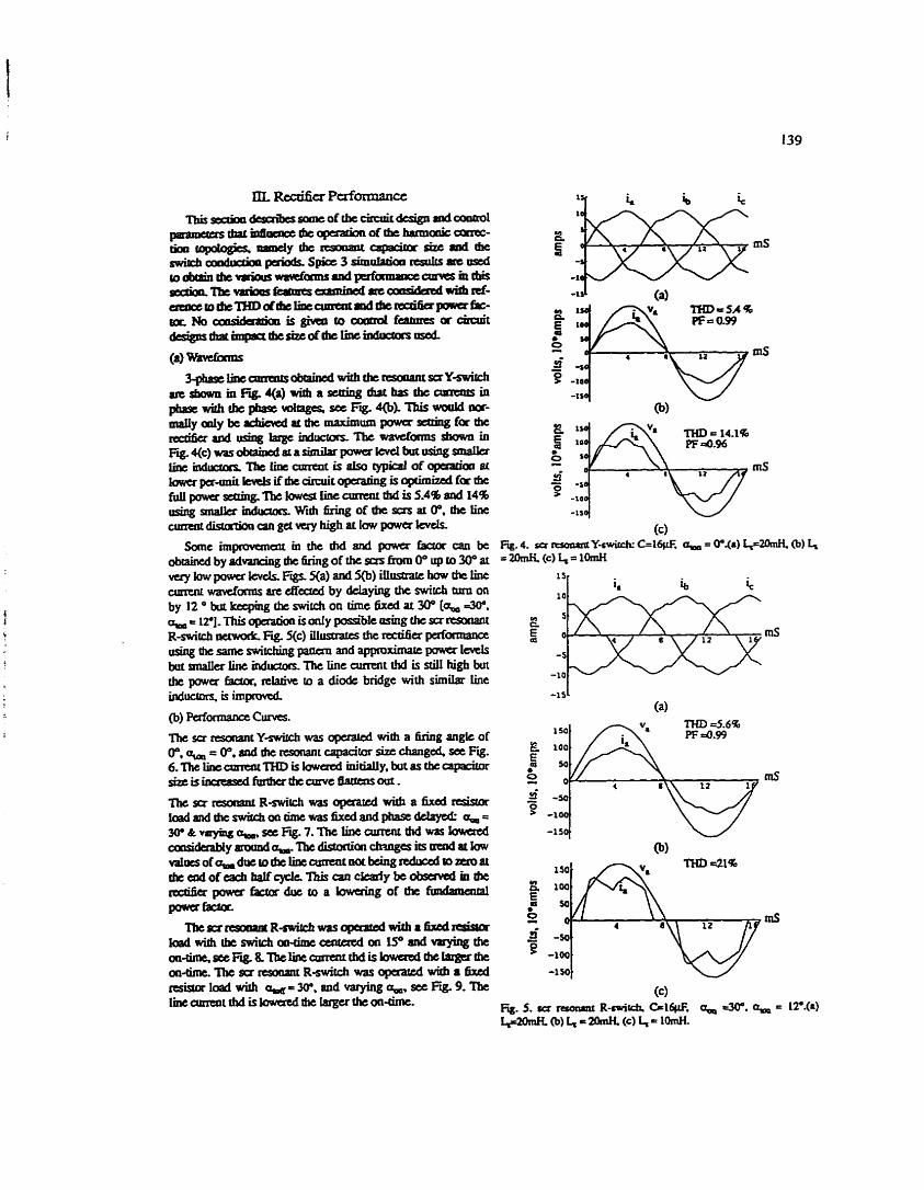
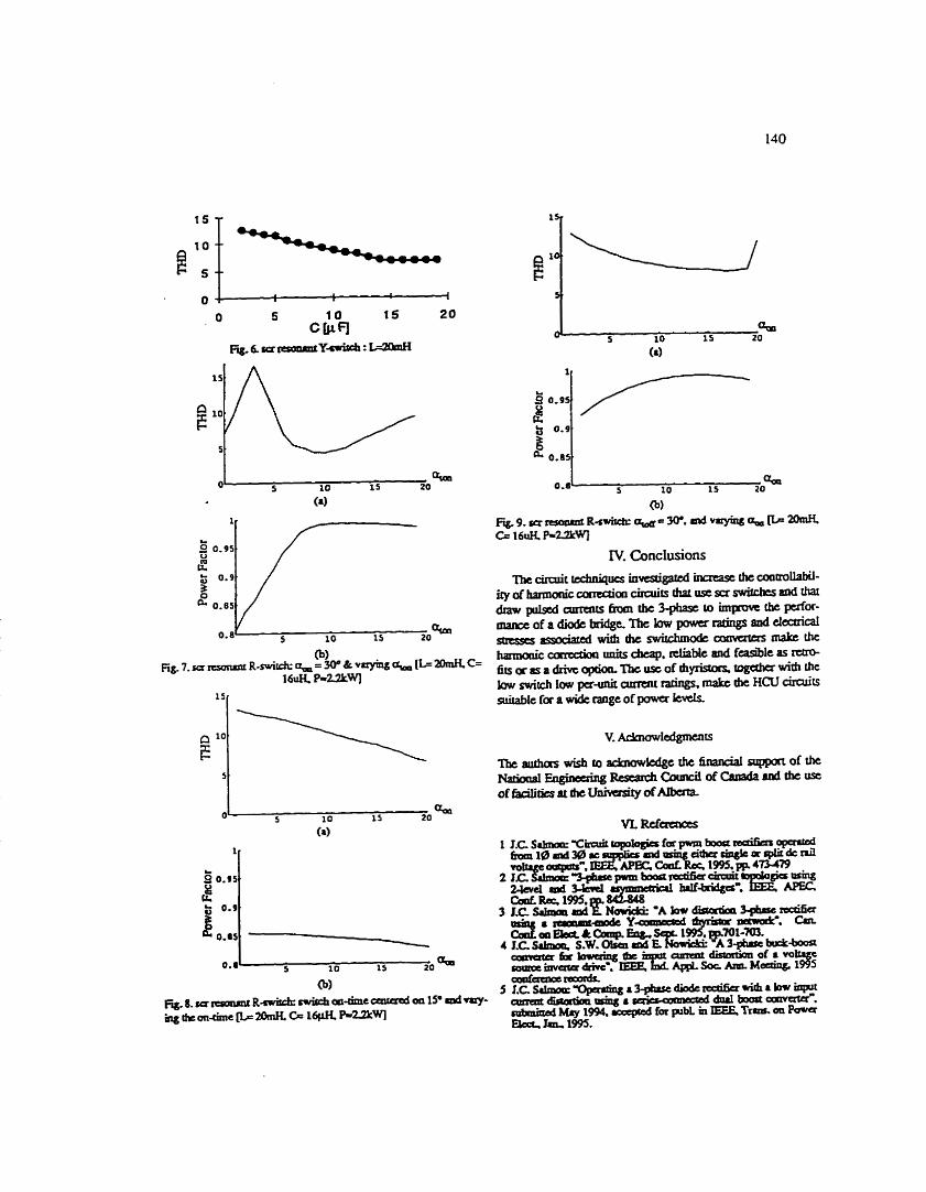
N. Conclusions