VMEbus for Software Engineers Introduction
23
1 VMEbus for Software Engineers Software and hardware engineers see things differently. So too with their views of VMEbus. Instead of nanoseconds and rise-times and access widths, system programmers want to know how and why to assign memory space, how to use special-purpose VME I/O boards without conflicting with on-board devices, and how to recognize software errors caused by hardware configuration problems. This article, originally published in 1993 (see “Publication History”), presents VMEbus operation and configuration from a software perspective, in terms and views familiar to the software engineer. Foundation – Why It Works That Way Introduction Early Years– Market Pressure and Competition Nuts and Bolts– Dry and Dusty Specifications Serial and Parallel – Watch Out! Roles, Players and Operations Master-Slave Operations– Changing Roles Taking Control– Who’s the Boss? Bus Errors– Five Kinds Interrupts– How Much Overhead? Moving Data – Meat and Potatoes Choices and Consequences Addressing Memory– Who’s On First Letting Go– Can’t Make Me! VME64– Life-Extender or Next Generation? Additional Information – Where To Get It Administrivia Publication History Author Introduction In the design and debugging of complex systems, it is becoming more and more important for software engineers to understand VMEbus. Embedded systems, in particular, make frequent use of this important architecture. Engineers with software skills are increasingly called upon to make full use of its capabilities, and a firm understanding of the standard’s intentions and limitations is essential.
-
Upload
khangminh22 -
Category
Documents
-
view
1 -
download
0
Transcript of VMEbus for Software Engineers Introduction

1
VMEbus for Software Engineers
Software and hardware engineers see things differently. So too with their views of VMEbus.
Instead of nanoseconds and rise-times and access widths, system programmers want to know
how and why to assign memory space, how to use special-purpose VME I/O boards without
conflicting with on-board devices, and how to recognize software errors caused by hardware
configuration problems.
This article, originally published in 1993 (see “Publication History”), presents VMEbus
operation and configuration from a software perspective, in terms and views familiar to the
software engineer.
Foundation – Why It Works That Way
Introduction
Early Years– Market Pressure and Competition
Nuts and Bolts– Dry and Dusty Specifications
Serial and Parallel – Watch Out!
Roles, Players and Operations
Master-Slave Operations– Changing Roles
Taking Control– Who’s the Boss?
Bus Errors– Five Kinds
Interrupts– How Much Overhead?
Moving Data – Meat and Potatoes
Choices and Consequences
Addressing Memory– Who’s On First
Letting Go– Can’t Make Me!
VME64– Life-Extender or Next Generation?
Additional Information – Where To Get It
Administrivia
Publication History
Author
Introduction
In the design and debugging of complex systems, it is becoming more and more important for
software engineers to understand VMEbus. Embedded systems, in particular, make frequent use
of this important architecture. Engineers with software skills are increasingly called upon to
make full use of its capabilities, and a firm understanding of the standard’s intentions and
limitations is essential.

2
This article describes VMEbus as it relates to the software realm. Included are some typical uses
as well as historical information that may help put developments and current usage into
perspective.
Early Years
Just as a person’s appearance is a product of their environment as much as their genes, so it is
with VMEbus. For a good understanding of current systems, it is very important to know the
configurations through which VMEbus has grown.
VME stands for VERSA Module Eurocard. A consortium of three manufacturers defined the
original standard in 1981: Mostek, Motorola, and Signetics. It was partially based on experience
with the Motorola VERSAbus that was used with early MC68000-family products. VMEbus has
now become a widely accepted standard. The IEEE P1014-1987 specification is the definitive
reference which has subsequently been expanded with the VME-64 Specification.
Early systems, regardless of the bus architecture, tended to place a CPU on one board, system
RAM on another, and I/O devices on additional boards. In these systems, almost all accesses
were performed across the bus. Typical CPU clock speeds were about one megahertz and system
RAM was often measured in multiples of 64K. A one megabyte machine was huge, and rare.
This was well before the advent of windows (X or others). Indeed, Unix was still running on
minicomputers. Unix on a micro was still several years in the future.
Many of these early systems used the M68000 CPU chip. This particular device, even though it
internally maintains 32-bits of data and addressing, only presents the low-order 24-bits of any
address through the chip’s connecting pins. That was the best the packaging technology could
supply at that time without using multiplex signals (more than one signal on a given pin,
presented at different times). I/O and RAM boards took advantage of this limitation and saved a
couple of bucks by including only the hardware needed to decode 24 bits of addressing: since
that’s all that the CPU boards offered, why decode more? After all, hardware costs money and in
a competitive market, useless circuitry is a costly waste.
As you no doubt know, in the early days, individual chips held only a limited amount of
circuitry. Indeed, hardware designers first used Small Scale Integration (SSI) for some parts, then
moved up to Medium Scale Integration (MSI) and then Large Scale Integration (LSI) before
pretty much abandoning the one-up-man-ship after Very Large Scale Integration (VLSI).

3
In the beginning, however, with most parts still in the SSI to MSI range, there was only so much
that could be put on a board. Some vendors experimented by placing components on both sides
or one chip straddling over the back of another, but the manufacturing steps were much more
difficult and, therefore, more costly than single-sided boards. And whether a board was
populated with chips on one or two sides, large boards with lots of chips suffer from vibration,
installation forces, and even the weight of the board itself. When the forces are big enough or
repeated too often, the delicate printed circuit lines suffer hairline fractures and electrical signals
become intermittent. That was a major pain! Lots of alternatives were tried but, in the final
analysis, “too big” was just “too bad.” Most circuit boards today look rather puny compared to
the huge, but fragile boards used earlier.
Lucky for them, as hardware designers tried to fit more complexity onto one board, the size of
individual components inside the integrated circuits continued to shrink and more logic was
placed inside each chip. And to make things even more exciting, at the same time, operating
speeds were also improving rapidly. Oddly, as designers were circling in on an optimal board
size, the number of chips they could fit on a given board had stabilized due to manufacturing and
tooling demands but, because the contents of each chip had gone way up in complexity, the total
circuitry on the board was increasing at an astonishing rate.
These factors all combined to permit essential hardware to move on-board with the CPU and
create the Single-Board Computer (SBC). In its common form, system RAM and the most
common I/O devices became “on-board” and the bus devices tended to become the less common
items. Devices moved on-board also because enough experimentation (in the market) had been
done to prove what was commonly needed. Typical devices included one or more serial ports, a
system counter/timer device and an interface to some permanent storage media device. Typically
some sort of Bus Interface circuitry is also found to manage board versus bus operations.
Also in this configuration, the “Local Bus” makes its first appearance as the means of
interconnecting CPU, RAM and on-board I/O devices. As time progresses and board
sophistication and speeds increase, this tendency toward multiple, hierarchical busses will
continue.

4
With the appearance of true Single Board Computers, the lessening of bus traffic and the
increased capabilities of processor boards (with RAM and on-board I/O) also made multi-SBC
configurations feasible. Much of the evolution in the system and software marketplace is in this
area. Multiple processors are used in a single backplane to solve complex problems that cannot
be economically resolved with single-processor configurations.
Nuts and Bolts
Before we go any further, however, let’s go back and get a basic understanding of what VMEbus
is all about.
The VMEbus specification defines the size, electrical voltage and power, and the signaling
protocols to be used. It sets upper and lower limits on various parameters in each of these three
categories.
For example, VMEbus boards can be either of two sizes and, consequently, plug in to one or two
connectors. Boards that use only a single connector have fewer capabilities (they cannot perform
32-bit wide transfers, for example) but are still able to operate with other VMEbus boards.
All VMEbus boards plug into the VMEbus backplane, all of which is housed in a chassis or
“cage.” The connectors in the backplane are connected, from one slot to the next, according to
the specification. Most of the wires are connected straight across: a given pin on Slot #1’s
connector is directly wired to the same pin on Slot #2, #3, and so forth.
The maximum number of boards that can be plugged into a VMEbus backplane is a function of
the width set aside for each board in the specification, the operating speed of the signaling, and
the settling-time requirements and bus terminations. These considerations all combine to set a
maximum physical length of the wires in the backplane (at least until the speed of light is
increased). A maximum of twenty-one boards is the mathematically-determined limit.
Serial and Parallel
Most of the wires in the VMEbus are parallel: a signal on a given wire is seen by every board
simultaneously (within a few nanoseconds). But there are also five “serial” signals in VMEbus.
5
But before we get too deeply into that, let me give a word of caution: the word “serial” is used
several different ways but in the VMEbus specification it has one and only one meaning. Before
learning about that one, let’s review the other ways “serial” is used in VMEbus systems (as
opposed to the VMEbus specification).
First of all, there is a pair of wires in the Utility Bus that can be used for serial communication in
VMSbus, a separate specification sometimes confused with but not really a part of VMEbus. But
since there are signal wires set aside for this in the VMEbus specification it can be confusing.
Suffice it so say that although a specification was defined for the use of this serial bus within
VMEbus, it has rarely been used. In this document, you won’t see it again.
The second place “serial” comes up in contemporary systems is when the interface to a terminal
or modem is being considered. Other terms associated with that connection include RS-232, DB-
25, DB-9, asynchronous, 9600 baud and so forth. The connection is an important part of many
VMEbus systems, but it has even less to do with VME than does VMSbus.
Finally, there are five signals defined in the VMEbus specification that are used in a serial
fashion. These are also known as “Daisy-Chain” signals and each one goes into a board plugged
into VMEbus, the board thinks about the signal, and then either propagates it to the next board in
the bus, or holds on to the signal. It is this final category, the five serial VMEbus signals, that are
the subject of the next couple of paragraphs. These signals are used in a “Do You Want This and
If Not I’ll Ask the Next Board?” fashion in VMEbus.
Usually, “bus” means that everybody sees everything at the same time and for most of the
signals of VMEbus, that’s true. All of the addressing, data, and hand-shake signals are seen by
all boards at the same instant. Looking at the VMEbus backplane we would see that these wires
go directly to each and every connector.
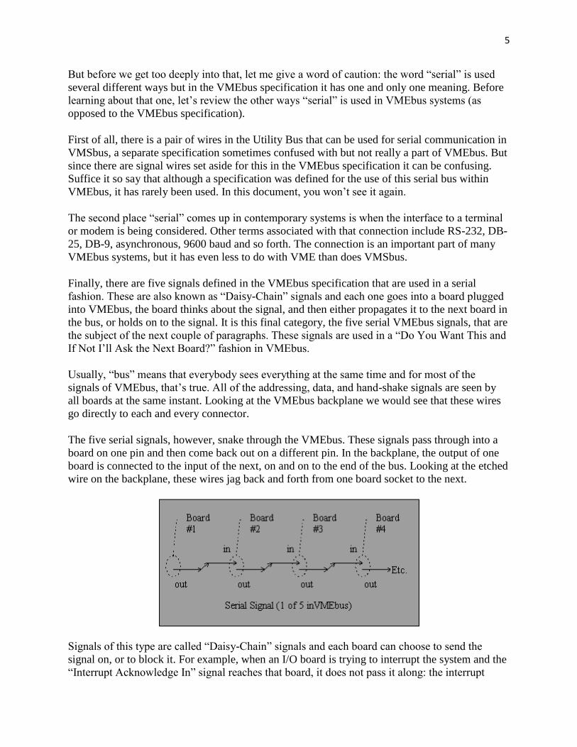
The five serial signals, however, snake through the VMEbus. These signals pass through into a
board on one pin and then come back out on a different pin. In the backplane, the output of one
board is connected to the input of the next, on and on to the end of the bus. Looking at the etched
wire on the backplane, these wires jag back and forth from one board socket to the next.
Signals of this type are called “Daisy-Chain” signals and each board can choose to send the
signal on, or to block it. For example, when an I/O board is trying to interrupt the system and the
“Interrupt Acknowledge In” signal reaches that board, it does not pass it along: the interrupt

6
acknowledgement was for it, not another board farther down the bus. Similarly, granting the use
of VMEbus to one board versus another is also done by serial signals, one for each of four
different “Bus Request / Bus Grant” numbers.
Because these signals go through each board, any empty slots in the VMEbus must pass these
signals to reach “down-stream” boards. In some systems this is done with hardware jumpers on
the backplane. In others, circuitry automatically senses whether a slot is empty or not and
propogates the five serial signals accordingly. (When adding and removing VMEbus boards,
don’t forget to change the backplane jumpering!)
The five serial signals in VMEbus include interrupt acknowledgement and the four bus grant
signals that pass into each board and are either passed or blocked. In all cases, the board in slot
#1 initiates each serial signal which then flows downstream through slot #2, slot #3, and so on.
That is, when any board wants to use VMEbus or acknowledge an interrupt, that board’s action
causes the board in slot #1 to initiate the appropriate serial signal. Slot #1, therefore, is special in
VMEbus and the board in that position is typically called the System Controller, or SYSCON.
For now, it’s important to know that when a board wants to use VMEbus for a data transfer or to
acknowledge an interrupt, it does something that SYSCON notices which, in turn, starts one of
the five serial signals. Whichever board first sees the appropriate serial signal for what it wants
to do can then use the bus.
Said differently, if two boards want to use VMEbus and they’ve been configured to use the same
serial bus request level and, hence, the same bus grant serial signal, whichever board is closest to
the system controller will always get to use the bus first. The downstream board will have to wait
until its upstream neighbor no longer wants the bus. In a small or lightly-loaded system, this
effect can be ignored but in a configuration with lots of boards and plenty of VMEbus activity,
bus position can make a huge difference in performance.
Before getting into that, however, some more basic concepts and definitions are needed. As
described, the board in slot #1 is special. Another role that boards have is being a bus master or a
bus slave. Unlike the SYSCON role, however, which is established permanently, bus master and
bus slave are roles that change from one instant to the next. At one moment, a board could be a
bus master and then, a few hundred nanoseconds later, it might be a bus slave.
Master-Slave Operations
The fundamental difference between master and slave involves the question, “Who wants to use
the bus for some purpose?” A board that requests the bus to do something is a bus master. A
board that is quietly sitting there minding its own business when someone else comes knocking
for a transfer is a bus slave.
A bus master is any board that initiates a data transfer via the VMEbus. A CPU that requests use
of the bus and then transfers data between the CPU and some bus-accessed peripheral device or

7
RAM would be considered a bus master. In the following drawing, the CPU board acts as a bus
Master when it uses the VMEbus to access the (slave) RAM board.
A bus slave, conversely, is any board that responds to a data transfer request. The above RAM
board is a bus slave: It does not initiate transfers. It only responds to requests from a bus master.
Some boards exhibit both master and slave operation. This is particularly true for processor
boards containing “Shared RAM.” Shared RAM is accessible by both the on-board CPU and
from VMEbus.
When one board accesses another board’s RAM, the second board must assume the role of
“slave” to allow its Shared RAM to respond to the VMEbus access.
Later, if the CPU on this second board initiates a bus transfer to (or from) the first board’s RAM,
then the second processor’s VMEbus logic will perform a bus-master operation as it initiates its
bus request. As you can see, “Master” and “Slave” roles can change from instant to instant in
today’s sophisticated configurations.
But now what would happen if two boards decide to be Bus Masters at the same time? What
would happen if two boards wanted to use the VMEbus at the same instant? What exists in
VMEbus to grant one board permission to use the bus while making another board wait?
Taking Control
Deciding who gets to use VMEbus next is the job of the System Controller.
In every VMEbus chassis (backplane) there must be a single System Controller present. In early
systems this was supplied by boards such as the Motorola MVME050 which contained a
veritable forest of jumper pins for all the various options. In later systems, however, most
processor boards contain the necessary logic to act as the System Controller which is configured
through software. This logic may enabled or disabled by a hardware jumper on the board or
through additional hardware logic.

8
In multiple processor configurations, the system installer must insure that there is exactly one
board acting as system controller. The left-most board, as viewed from the front, must contain
the hardware jumper enabling the system controller logic on that board. All other processor
boards in the same backplane will have their corresponding jumpers removed.
The System Controller performs bus arbitration when any bus master requests use of the
VMEbus. When several bus masters wish to use the bus at the same time, the System Controller
grants the bus to one of them. This determination makes use of the four pairs of Bus Request and
Bus Grant signals of VMEbus. Each pair can be used to represent a different “priority” request
and, when several Bus Masters are all requesting at the same instant, the bus arbiter logic (in the
System Controller) will “grant” use of the bus to 1) the highest priority requester who is 2)
nearest the System Controller.
When the System Controller always grants the bus to the highest priority requester, it is said to
be using “Priority Arbitration.” There are two other kinds of arbitration, Round-Robin and
Single-Level.
In Round-Robin arbitration, the arbiter keeps track of which VMEbus grant level is currently
using the bus and, when that user is finished, the arbiter looks at the next VMEbus request level.
If no board is requesting the bus at that level, then the arbiter goes on to the next level, and so on,
going round and round. Round-Robin arbitration attempts to give everyone a fair chance of using
the bus and, in lightly loaded systems, it does a pretty good job of this.
Single-Level arbitration is the simplest of the three. In this mode, the arbiter looks only at a
single bus request level and completely ignores the other three. When there is a minimum of bus
activity, or when only one or two boards account for the great majority of bus traffic, this mode
works well. For simple systems, this allows the arbiter to be constructed with a minimum of
components. For more complex applications, however, especially where the bus is becoming
relatively busy, single-level arbitration is the worst possible choice as it strongly favors boards
near the system controller which making other “downstream users” wait for extended periods to
use the bus. Single-Level arbitration is not recommended for today’s bus-intense applications.
Many VMEbus manufacturers set their boards to a default setting before shipping. System
arbitration is often configured to use the priority-based scheme since the most demanding system

9
will need that. This is the safest mode for arbitration even though, in some cases, it may be an
over-kill.
But since the manufacturers don’t know how a particular board will be used, when it comes to
which bus request level a board should use, the manufacturers are stuck: there’s no way to guess
which bus request level is “safest” since an individual customer might be getting boards from
several vendors. So, most manufacturers simply jumper (or otherwise configure) their boards to
request VMEbus access through Bus Request #3.
The effect of this, if you don’t change the default settings, will be to have all boards using a
single bus request level. Even though the arbiter is set, by default, to use priority arbitration, in
practice the only request level that will be used is #3. The system will behave exactly as if
Single-Level arbitration had been selected and, as mentioned just a moment ago, this is probably
the worst possible choice for a busy system!
Moral of the story: Look at the available bus request levels and decide which board should use
which one, and then make the appropriate changes. Also make certain your system controller is
using the style of arbitration (Priority, Round-Robin, or Single-Level) that is correct for your
needs.
In addition to the bus arbitration duties, the system controller also provides the Utility Bus
signals include a 16 Mhz SYSCLK signal, an AC fail ACFAIL detection, and a bus-wide system
reset called SYSRESET.
Bus Errors
The final duty of the System Controller we will mention is that of a dead-man switch for bus
access. On a railway train or subway, the dead-man switch is a lever or button that the engineer
must hold closed whenever the train is in motion. If the engineer releases the button for too long,
the train will automatically stop. In VMEbus, the System Controller watches bus accesses and,
through a hardware timer, it recognizes bus cycles to “dead” locations, memory locations that do
not respond for any of several reasons.
Because VMEbus operates in an asynchronous mode, a bus timer is needed to detect (and abort)
accesses to non-existent addresses. These may occur because of software bugs or during normal
operation. For example, I/O drivers may be configured for multiple devices that may or may not
be physically plugged in. This is common in ROM-based systems where the operating software
is burned into memory devices to support all possible hardware devices, one or more of which
may not be actually there today.
Contemporary boards with on-board RAM and several I/O devices may suffer bus time-outs for
any of several reasons. The following picture is typical of recent designs: It will be useful in this
discussion.

10
In this configuration, the MMU (Memory Management Unit) immediately connected to the CPU
will generate a Bus Error signal (to the CPU only) if the application software tries to touch an
address that has not been assigned to the current task. This would probably indicate a software
“bug” in the application task.
In addition, a Bus Error may also occur if, after the “Local Bus” has been acquired by the CPU,
the access cannot be completed.
Notice that if the “On-board I/O” devices are capable of reading and writing the “On-board
RAM,” and if for some reason they keep the Local Bus tied up for a long time, the CPU simply
waits. It will not time-out waiting to acquire the Local Bus.
Bit if the CPU is making an off-board reference, then the Local Bus will connect the CPU to the
VME interface logic. This hardware may pull BUSERR if, for some reason, the VMEbus cannot
be acquired within some programmable period of time. This might occur if peripheral devices or
other processor boards on the VMEbus are keeping the bus very busy.
And finally, as we mentioned at the beginning of this section, the System Controller may declare
a Bus Error if the address being referenced on the VMEbus fails to respond in time.
To summarize, there are at least five sources of Bus Error in most systems:
the MMU has detected a reference by the CPU to an un-mapped address;
the MMU detects a write (by the CPU) to a memory location that is mapped as “Read Only”
Local Bus Time Out (a cycle on the Local Bus took too long);
VMEbus Acquisition Time Out (the VME Interface logic was unable to acquire the
VMEbus in time); or
the System Controller has timed-out on the VMEbus data transfer cycle.

11
In debugging bus errors, it is very important to know if the error is from the MMU or from a
timer. In the case of a time-out, it is essential to find out which timer has expired, and then why.
To help in this, processor boards usually have status registers to indicate the particular timer that
popped. After that, however, figuring out the cause may require careful analysis of the overall
operation of the system in a specific application.
Interrupts
VMEbus supports seven levels of interrupt priority, running from one to seven. Lower numbered
priorities such as one and two are comparatively less important (or less urgent) than priority five
or six. Level seven, in addition to being the highest priority, is often used as a “non-maskable”
interrupt, but that is not a VMEbus requirement. Any device using VMEbus to announce an
interrupt must use one of the interrupt priorities but several devices can share the same one.
Priority tells the system how important an interrupt is, but not where it is coming from or where
the software is to deal with the interrupt. That’s the purpose of the interrupt vector.
When a device causes an interrupt, it must supply two numbers, an interrupt priority and also an
interrupt vector number. The vector number is used by the CPU to switch execution of the
software into an Interrupt Service Routine, or ISR. Vector numbers are usually not shared: each
device has a unique vector number even though several devices may use the same priority.
Interrupt Level Importance
Vector Number Software Location
Typically, the vector number for a device is assigned a default value by the manufacturer. This
number is included in the software and, if desired, it can be changed by the system installer.
Similarly, the interrupt priority may also have a manufacturer-assigned default value which may
need to be changed by the system installer. The operating system build procedures usually have
configuration steps or programs that will assist in changing these numbers for the supported
devices. During system start-up, the selected values are programmed into the device by the
software driver, usually by writing to a couple of control registers in the device.
In a VMEbus system with multiple single-board computers, things can get a little complicated.
Here are the basic rules:
1. Interrupts from a given VMEbus device must be handled by one and only one single-
board computer.
2. All VMEbus devices using the same interrupt level must all have their interrupt handling
performed by the same SBC.
3. Although it is theoretically possible to “change horses in mid-stream” and have a
different SBC take over a given interrupt level, in practice it isn’t done, or at least not in
most systems. Possible? yes. Practical? No.

12
The ability to look at or ignore a given VMEbus interrupt level comes from the Bus Interface
used in a single-board computer. Typically, this is one chip on an SBC. Over the years, it has
grown in sophistication and the Bus Interface devices available today are, to put it mildly, exotic.
Multiple VMEbus boards may request an interrupt at the same level, and at the same time. In a
VMEbus system with several processor boards, a given interrupt level must be handled by one
and only one processor board. Of course, a processor board may handle several VMEbus
interrupt levels but it would be an error to try and have two CPU boards handle the same level.
To segregate the interrupt handling into one SBC and keep it out of others, the Bus Interface on
each SBC must be programmed correctly. In many Bus Interface devices there is a mask that
admits or blocks each of the seven different VMEbus interrupt levels.
In this drawing, the Interrupt Mask is eight bits wide and the low-order bit is not used. The
binary value “0000101x” (where “x” denotes “don’t care”) has been programmed to allow the
right-most interrupt level to enter the system as well as the interrupt level two-bits to its left.
Whether these represent interrupt levels one and three, or seven and five is up to the designer of
the Bus Interface device.

13
The steps in handling a VMEbus interrupt are;
During system start-up, part of the software in each SBC programs its VMEbus interrupt
mask to allow-in those interrupts it will be handling from VMEbus. Also, each of the software
interrupt handlers on a given SBC then program their respective devices with the correct
interrupt level and vector numbers and lay claim to the corresponding interrupt vectors, pointing
them to the interrupt handler’s entry point. All this happens before the first interrupt can be
handled.
Then, during normal operation;
a device requests interrupt service using the interrupt level programmed into it;
the assigned CPU sees it (that SBC’s Interrupt Mask has been programmed to admit the
interrupt level the device is requesting) and so the SBC requests use of the VMEbus;
the system controller grants the bus to the CPU;
the assigned CPU signals it wants to do an IACK (Interrupt ACKnowledgement);
the system controller starts the serial (IACKIN, IACKOUT) search, one of the “serial”
signals in VMEbus;
the daisy-chained IACKIN signal reaches the device requesting interrupt service;
it supplies its vector number (DTACK + data bus contents);
the CPU releases the bus;
the device relinquishes interrupt request; and
the CPU uses the vector number to transfer execution to the interrupt handling software
for the device. (The software ISR will typically read a control register and other values
from the device to determine the specific reason for the interrupt. Each of these accesses
require additional use of VMEbus.)
When several I/O devices share the use of a single VMEbus interrupt level, the effect of the
serial IACKIN, IACKOUT search will be to favor the board closest to the System Controller.
That is, if two boards are requesting the same VMEbus interrupt level, the board nearest the
System Controller will get preferential treatment. For systems with low VMEbus-interrupt
activity this may be insignificant. But since many contemporary SBCs execute at ten to twenty
times the speed of VMEbus, it is quite possible for them to keep the bus extremely busy. Bus
position, in a busy system, can be critical.
The five serial signals in VMEbus all have this position-important attribute. Interrupts use one of
the five. The remaining four are for prioritizing use of the bus, as previously discussed. As with
the interrupts, bus position also favors the board nearest the System Controller when bus request
levels are being shared.
Moving Data
Much more common than interrupts, and simpler (at least to the software engineer), are the
millions of data transfers that pass through the bus every second.

14
Information is transferred between a bus master and a bus slave in 8-bit, 16-bit, 32-bit, and now,
64-bit widths. On any given transfer the width of the desired data is indicated by bus signals.
Bus operations include read, write, and read-modify-write. This latter operation is very important
in multiprocessor configurations and is supported in the CPU in operations such as the “Test And
Set,” or TAS instruction. At higher levels of the software this is used to build software
constructions such as the “semaphore.”
Many devices are capable of performing block transfers that are also supported by VMEbus.
Quite often a “DMA Controller” is used in this role.
Addressing Memory
We will now look at the different ways of addressing on VMEbus.
The VMEbus address signals may be used to access any of three address spaces: A16, A24, or
A32 (more in VME64). A group of VMEbus signal wires known as the Address Modifiers are
used to indicate which address space is being accessed. In addition, they also indicate the
execution privilege, user or supervisor, of the software making the access, and whether the CPU
is attempting to access an instruction or data. These additional classifications may be used by the
peripheral hardware to authenticate the accesses made by the CPU. For example, some I/O
devices require supervisory-mode data accesses only. Any other access, such as a user-mode data
access, will not be honored by the I/O device. This helps system integrity. In practice, however,
only the MMU actually uses this additional information. Most VMEbus devices ignore
everything except the address space designation.
Here are the most commonly used address spaces in VMEbus. Of these, the A32 space is the
biggest. In early systems when RAM was very expensive, A32 was rarely used. The A24 address
space will hold a total of 16 megabytes and, for many older systems, that was plenty. More
recently, however, RAM has become extremely cheap and RAM-needs have skyrocketed. As a
result, the older A24 space is used less and less. Pretty soon it will be completely ignored.
(VME64 adds three more address spaces, one of which allows for 64 bits of addressing!)

15
The sizes of the three address spaces in this diagram above are not in proportion. The A16
address space covers a total of 65,536 bytes, while the A24 address space spans sixteen
megabytes, and the A32 address space covers a total of 4.3 gigabytes. Each address space is 256
times bigger than its smaller neighbor.
The relationship between the addresses seen by a program and the A16, A24, and A32 address
spaces of the VMEbus is set up when a system is first installed. For this reason, these issues may
be considered as hardware or installation concerns. Indeed, for programmers who never directly
access the hardware, this is a safe but naive generalization.
Engineers who write device drivers or install hardware, on the other hand, will need to be aware
of the VMEbus address spaces. They will want to insure that the VMEbus interface has been
properly initialized so that every memory access within each specific range is translated
(mapped) to the proper address space on VMEbus, and thereby to the proper boards installed
within the system.
Different portions of the software need to access the different address spaces on VMEbus. The
memory seen by an I/O driver, for example, may consist of addresses in A16 Short I/O space as
well as in A32 (RAM) memory.

16
Quite often, the A16 address space is configured into the highest addresses and the A24 and A32
spaces into the lowest. This is particularly true in older systems.
Early peripheral boards, like serial port controllers, were designed to appear in the A16 address
space. Many early I/O boards attached only to the P1 connector. They were limited to A24 and
A16 address spaces, and to D08 and D16 access widths. Early memory boards, possibly because
of the 24-bit addressing restriction of the MC68000 chip pin-out, recognized only A24 address
space accesses.
Later, as device sophistication grew, the supporting hardware improved. I/O peripherals may
now be configured to appear in any one, or even all three address spaces according to the system
designer’s needs.
To bridge the software’s simple 32-bit address world to the VMEbus’s three (A16, A24, and
A32) address spaces, board designers often provide a number of programmable “windows”
through which different ranges of the 32-bit software view can be mapped to various portions of
the VMEbus address spaces.
When a CPU reaches out to VMEbus and attempts to touch an address, we saw earlier that would
be called a “Master” operation. Conversely, if someone else is reaching into a board from
VMEbus, that board would be a “Slave” for that access. The addressing windows into or out-
from a given board use these same terms. For example, a window that allows a CPU to reach out
to VMEbus and touch an address would be called a Master window. And a Slave window would
be one that allows someone to reach “in” to a board. (The Bus Interface chip used on many of the
VMEbus boards from Motorola includes four Master address ranges or “windows” and two

17
Slave ranges. In addition, one of the Master ranges performs a translation operation that will be
discussed after a couple more paragraphs.)
Obviously, with only the 32-bits of software addressing, it is not possible to access every byte of
all three VMEbus address spaces. So, a compromise is needed. In the next figure we see a very
typical mapping that was common a couple of years ago.
I
n this drawing of an older design, the A16 address space is available to the software in the
highest locations possible. Software addresses FFFF0000 through FFFFFFFF are mapped to the
VMEbus A16 address space. The A24 address space of VMEbus is at the other end of the
software’s address range. 00000000 through 00FFFFFF are mapped to access VMEbus A24
space. The remainder of the processor’s address space, the area between the A24 and A16
spaces, will access A32 VMEbus space.
Newer processor boards contain additional programmable viewports. These add flexibility for
the system designer. Each programmable window can be set to access the various VMEbus
address spaces, or any portion thereof. With these capabilities, the system can accommodate
most varieties of peripheral devices, regardless of age or sophistication.
Single board computers typically contain a significant amount of on-board RAM as well as
several “local” I/O devices. Unlike the RAM which is accessible by the on-board CPU as well as
from VMEbus, the I/O devices on the SBC are typically used only by the local CPU. In fact, it is
usually impossible for anything “out there” on VMEbus to reach in and touch the local I/O
devices. (This varies from one manufacturer and board to the next.)

18
In the following diagram which is typical for most SBCs today, a space for “local I/O devices” is
found just below the A16 address space which is still mapped to VMEbus. This allows the CPU
to access its on-board devices as well as any on VMEbus. Also, some Local ROM devices have
been added in this diagram of a typical single-board computer.
In this drawing the A24 space has been covered completely by the 32 megabytes of on-board
RAM. The A16 Short I/O area is mapped as usual, and the VMEbus A32 space fills the gap
between the end of RAM and the beginning of ROM. (The ROM starting and ending addresses
as well as the beginning address for the on-board I/O devices will vary considerably from one
board to the next. The addresses shown in italics are examples, not limits.)
Single-board computers often have their on-board RAM set to begin at address zero, as seen by
the on-board CPU. Thirty-two megabytes of local RAM will effectively “hide” the VMEbus A24
space from the CPU. So, when one of these systems contains an older A24 board, additional
hardware is needed to re-map the A24 space to a different range of addresses to the CPU.
Remember that devices only look at the low-order 24-bits of the address bus when the Address
Modifiers signal an A24 access. The CPU, however, uses a full 32-bits. By adding hardware that
“translates” CPU addresses within a certain range, for example in the F0xxxxxx address range to
VMEbus A24 accesses (xxxxxx), the CPU can again touch the VMEbus A24 devices.

19
This special hardware recognizes all references between F0000000 and F0FFFFFF and, by
dropping the high-order eight bits of the address and sending the result to VMEbus, the limited
A24 boards can still be used. The software, of course, must be configured to think of the A24
board as if it were programmed in the F0xxxxxx area instead of the actual “set-in-hardware”
address of 00xxxxxx. The actual A24 board, however, is still programmed at the A24 address.
As we saw earlier, when the system includes several single-board computers, things get much
more complicated. With more than one processor board on the same VMEbus, there are now
several different views of memory, one for each processor board in addition to the memory
visible from VME. For these CPUs to cooperate with each other, each single-board computer
will have to know how the other boards, as well as itself, have been configured.
As mentioned before, each CPU accesses its RAM via its on-board local bus. Quite often, RAM
is placed at location 00000000 as seen by the on-board CPU. Each processor will, therefore, see
its own on-board RAM at (local) address 00000000.
VMEbus, however, does not permit multiple boards to have the same VMEbus address.
Fortunately (or perhaps I should say, “By design”), these boards are constructed to allow access
to each board’s RAM at different addresses from VMEbus. It might be tempting to think that
each memory location has two addresses, one as seen by the on-board CPU and another as seen
from VMEbus, but this would be only partially correct.
20
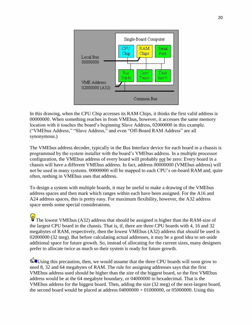
In this drawing, when the CPU Chip accesses its RAM Chips, it thinks the first valid address is
00000000. When something reaches in from VMEbus, however, it accesses the same memory
location with it touches the board’s beginning Slave Address, 02000000 in this example.
(“VMEbus Address,” “Slave Address,” and even “Off-Board RAM Address” are all
synonymous.)
The VMEbus address decoder, typically in the Bus Interface device for each board in a chassis is
programmed by the system installer with the board’s VMEbus address. In a multiple processor
configuration, the VMEbus address of every board will probably not be zero: Every board in a
chassis will have a different VMEbus address. In fact, address 00000000 (VMEbus address) will
not be used in many systems. 00000000 will be mapped to each CPU’s on-board RAM and, quite
often, nothing in VMEbus uses that address.
To design a system with multiple boards, it may be useful to make a drawing of the VMEbus
address spaces and then mark which ranges within each have been assigned. For the A16 and
A24 address spaces, this is pretty easy. For maximum flexibility, however, the A32 address
space needs some special considerations.
The lowest VMEbus (A32) address that should be assigned is higher than the RAM-size of
the largest CPU board in the chassis. That is, if, there are three CPU boards with 4, 16 and 32
megabytes of RAM, respectively, then the lowest VMEbus (A32) address that should be used is
02000000 (32 meg). But before calculating actual addresses, it may be a good idea to set-aside
additional space for future growth. So, instead of allocating for the current sizes, many designers
prefer to allocate twice as much so their system is ready for future growth.
Using this precaution, then, we would assume that the three CPU boards will soon grow to
need 8, 32 and 64 megabytes of RAM. The rule for assigning addresses says that the first
VMEbus address used should be higher than the size of the biggest board, so the first VMEbus
address would be at the 64 megabyte boundary, or 04000000 in hexadecimal. That is the
VMEbus address for the biggest board. Then, adding the size (32 meg) of the next-largest board,
the second board would be placed at address 04000000 + 01000000, or 05000000. Using this

21
method the address for the puny little 8 meg board would be calculated but, frankly, it’s probably
easiest to simply round that number up and put him at 06000000.
The goal in all this is to enable each CPU to be able to access all of its own on-board RAM and,
potentially, all of the RAM on every other CPU board as well, whether or not the boards actually
need to do so. This gives the maximum flexibility in designing a multiple CPU system.
With the addresses set for maximum flexibility, designers can then figure out how much access
is actually needed, and begin closing things down to improve the reliability of the system. To do
this, most Bus Interface devices allow the system designer to open “windows” out to the
VMEbus that are considerably smaller than the overall mapping. This is important for system
integrity. Although flexibility demands a non-overlapping approach, actually opening the system
up to access all of these addresses is a bad idea. Instead, each CPU should be permitted to access
only a much smaller range of addresses on each of the other CPU boards, as fits the application.
Letting Go
Remembering to set VMEbus addresses is easy because nothing works until it’s done. But
there are other settings, just as important to system operation, that may be ignored with
disastrous consequences. These are the bus release and arbitration characteristics.
Other features commonly found on VMEbus boards include a selection of various types of Bus
Release capabilities and data alignment issues (which are not a consideration of VMEbus but
rather of some CPU chips). The Bus Release characteristics of different boards have to do with
how long and under what conditions a board will surrender use of VMEbus.
As you may remember, one of the causes of the Bus Error exception was having to wait too long
to acquire the bus: release characteristics are, therefore, very important to system operation. For
single transfers of any size, all of these modes are essentially the same. But for DMA-like I/O
devices (or processors) transferring large amounts of information, the release selection is very
important to overall performance. The choices are:
Release-When-Done (RWD)
Release-On-Request (ROR), and
FAIR mode
The first of these, RWD, is the easiest to implement in hardware. In this mode, a board that
acquires VMEbus to perform a number of data transfers simply stays on the bus until finished.
No matter how many others want to use the bus, no matter what their priority, and no matter how
slow the two boards are performing the transfer, everyone waits until the transfer is finished
when RWD is in use. This mode might seem like a bad idea and, in some cases, it is. But when
an I/O device is extremely fast and when the data is coming in very quickly, it may well be the
best selection: it takes time to get on and off the bus and, if a transfer can be finished faster by
simply hanging on for a bit longer, then Release-When-Done may be the best choice.

22
ROR or Release-On-Request mode could be called “timid mode.” A board using this mode
monitors the Bus Request wires in VMEbus and, when any other board wants to use VMEbus, it
immediately stops what it is doing and let’s someone else use the bus. This keeps bus-acquisition
delays to a minimum but, since the timid board must now come back and ask for the bus again
(and suffer that delay), the overall throughput may be significantly lower than with the Release-
When-Done mode.
The “FAIR” in FAIR mode is not an abbreviation. It means exactly what it says. In this mode,
any board using it tries to be “fair” to other boards using the same bus request level and let
everyone get a turn. When a FAIR mode board wants to use the bus, before pulling on the bus
request line it has been programmed to use, it looks to see if that wire is already being pulled by
another board in VMEbus. If so, the FAIR board waits. Only when no one else is requesting the
bus (at that level), will the bus request from the FAIR requester be asserted.
You may have noticed that FAIR is really more of a “request” mode rather than a “release”
mode: that’s true. In some literature you may see it referred to as the “Request-On-No-Request
request mode” (phew!). The actual release characteristics of a FAIR requester could be ROR or
RWD but is not otherwise specified in many cases.
All boards using the same bus request level must use FAIR mode. One bad apple will spoil
the barrel!
VMEbus has several other new features we haven’t mentioned or dealt with in much detail.
These include memory management devices of various shapes and sizes, bus snooping logic,
data cache, programmable interrupt generators, and board-specific control register access from
the VMEbus are but a few of these. Unfortunately, these are outside the scope of what can be
covered here.
VME64
A later addition is VME64.
For the long-term survival of VMEbus are the addition in VME64 of three new address modes,
A12, A40 and A64.
Also in VME64, significant enhancements are defined for dynamic configuration. These
additions are intended to allow self-configuring systems that determine the mix of boards and
devices during start-up and automatically program the operational addresses for use after system
initialization.
Of all the VME64 additions, the “VME64 Multiplexed Data Transfer” feature is widely used.
This mode permits compatible boards to transfer a total of 8 bytes (64-bits) per VMEbus access.
This effectively doubles the VMEbus data transfer rate to a theoretical limit of 80 megabytes per
second.

23
Additional Information
Additional information may be found in a variety of places. User’s Manuals for the VMEbus
boards from different vendors will contain descriptions and programming information for the
particular hardware control registers and features available on that board.
The VMEbus Specification provides the definitive authority on the physical, electrical, and
signalling characteristics of the VMEbus. Copies of this and many other VMEbus-related
publications are available through the VITA organization in Scottsdale (Phoenix) Arizona.
VITA-USA
10229 N. Scottsdale Rd., Suite B
Scottsdale AZ 85253-1437 USA
1-602-951-8866
VITA also maintains an office on the European continent.
VITA-Europe
P.O. Box 192
NL-5300 AD Zaltbommel The Netherlands
31-4180.14661
Publication History
An earlier version of this article appeared in the June 1993 issue of Embedded Systems
Programming and also in VITA Journal, December, 1995. It has been available in several
revisions through the author’s web page starting in 1996. All versions are under full copyright
protection. Please contact the author for information concerning copies or commercial use.
Author
Ed Skinner is an instructor and software developer. He lives in Phoenix Arizona USA. Ed has
designed and programmed real-time systems since 1972 and has taught embedded software
design and debugging since 1990. He can be reached by email at [email protected], and on the web at
https://www.flat5.net/
© Copyright 1997 by Ed Skinner
All Rights Reserved.
Revised 2-August-2005