
New prototype of very compact LIDAR for atmospheric particulate monitoring
Upload
khangminh22Category
view
1download
0
Very Compact Hardware Implementations of theBlockcipher CLEFIA
Toru Akishita and Harunaga Hiwatari
Sony CorporationToru.Akishita,[email protected]
Abstract. The 128-bit blockcipher CLEFIA is known to be highly ef-ficient in hardware implementations. This paper proposes very com-pact hardware implementations of CLEFIA-128. Our implementationsare based on novel serialized architectures in the data processing block.Three types of hardware architectures are implemented and synthesizedusing a 0.13 µm standard cell library. In the smallest implementation,the area requirements are only 2,488 GE, which are about half of theprevious smallest implementation as far as we know. Furthermore, onlyadditional 116 GE enable to support decryption.
Key words: blockcipher, CLEFIA, compact hardware implementation,ASIC
1 Introduction
CLEFIA [9, 11] is a 128-bit blockcipher supporting key lengths of 128, 192 and256 bits, which is compatible with AES [2]. CLEFIA achieves enough immunityagainst known attacks and flexibility for efficient implementation in both hard-ware and software. It is reported that CLEFIA is highly efficient particularly inhardware implementations [12, 10, 13].
Compact hardware implementations are very significant for small embeddeddevices such as RFID tags and wireless sensor nodes because of their limitedhardware resources. As for AES with 128-bit keys, low-area hardware implemen-tations have been reported in [3] and [4]. The former uses a RAM based archi-tecture supporting both encryption and decryption with the area requirementsof 3,400 GE, while the latter uses a shift-register based architecture supportingencryption only with the area requirements of 3,100 GE. Both implementationsuse an 8-bit serialized data path and implement only a fraction of the Mix-Columns operation with additional three 8-bit registers, where it takes severalclock cycles to calculate one column. Very recently, another low-area hardwareimplementation of AES was proposed in [5] requiring 2,400 GE for encryptiononly. Unlike the previous two implementations, it implements MixColumns notin a serialized way, where one column of MixColumns is processed in 1 clockcycle. Thus it requires 4 times more XOR gates for MixColumns, but requiresno additional register and can reduce gate requirements for control logic.

In this paper, we present very compact hardware architectures of CLEFIAwith 128-bit keys based on 8-bit shift registers. We show that the data process-ing part of CLEFIA-128 can be implemented in a serialized way without anyadditional registers. Three types of hardware architectures are proposed accord-ing to required cycles for one block process by adaptively applying clock gatingtechnique. Those architectures are implemented and synthesized using a 0.13µm standard cell library. In our smallest implementation, the area requirementsare only 2,488 GE, which are to the best of our knowledge about half as smallas the previous smallest implementation, 4,950 GE [10, 12], and competitive tothe smallest AES implementation. Furthermore, only additional 116 GE are re-quired to support decryption by switching the processing order of F-functionsat even-numbered rounds.
The rest of the paper is organized as follows. Sect. 2 gives brief descriptionof CLEFIA and its previously proposed hardware implementations. In Sect. 3,we propose three types of hardware architectures. Sect. 4 describes additionalhardware resources to support decryption. Sect. 5 gives evaluation results forour implementations, compared with the previous results of CLEFIA and AES.Finally, we conclude in Sect. 6.
2 128-bit Blockcipher CLEFIA
2.1 Algorithm
CLEFIA [9, 11] is a 128-bit blockcipher with its key length being 128, 192, and256 bits. For brevity, we consider 128-bit key CLEFIA, denoted as CLEFIA-128,though similar techniques are applicable to CLEFIA with 192-bit and 256-bitkeys. CLEFIA-128 is divided into two parts: the data processing part and thekey scheduling part.
The data processing part employs a 4-branch Type-2 generalized Feistel net-work [14] with two parallel F-functions F0 and F1 per round. The number ofrounds r for CLEFIA-128 is 18. The encryption function ENCr takes a 128-bitplaintext P = P0|P1|P2|P3, 32-bit whitening keys WKi (0 ≤ i < 4), and 32-bit round keys RKj (0 ≤ j < 2r) as inputs, and outputs a 128-bit ciphertextC = C0|C1|C2|C3 as shown in Fig. 1.
The two F-functions F0 and F1 consist of round key addition, 4 non-linear8-bit S-boxes, and a diffusion matrix. The construction of F0 and F1 is shownin Fig. 2. Two kind of S-boxes S0 and S1 are employed, and the order of theseS-boxes are different in F0 and F1. The diffusion matrices of F0 and F1 are alsodifferent; the matrices M0 for F0 and M1 for F1 are defined as
M0 =
01 02 04 0602 01 06 0404 06 01 0206 04 02 01
, M1 =
01 08 02 0A08 01 0A 0202 0A 01 080A 02 08 01
.
The multiplications between these matrices and vectors are performed in GF(28)defined by a primitive polynomial z8 + z4 + z3 + z2 + 1.

F0
RK0 WK0
P1
/32
P0
/32
F1
RK1 WK1
P3
/32
P2
/32
RK2r−2 RK2r−1
F0
RK2
F1
RK3
F0 F1
WK2 WK3
/32 /32/32 /32
C0 C1 C2 C3
......
......
F0
RK4
F1
RK5
Fig. 1. Encryption function ENCr
0
1
2
3
x0
x1
x2
x3
k0 k1 k2 k3
S0
S1
S0
S1
y
y
y
y
M0
/ / / /
/
/
/
/
/
/
/
/
8
8
8
8
8
8
8
8
8 8 8 8
F0
x0
x1
x2
x3
k0 k1 k2 k3
S1
S0
S1
S0
y0
y1
y2
y3
M1
/ / / /
/
/
/
/
/
/
/
/
8
8
8
8
8
8
8
8
8 8 8 8
F1
Fig. 2. F-functions F0, F1
7 7
7 7
57 57
57 57
128 bits
Fig. 3. DoubleSwap function Σ
The key scheduling part of CLEFIA-128 takes a secret key K as an input,and outputs 32-bit whitening keys WKi (0 ≤ i < 4) and 32-bit round keysRKj (0 ≤ j < 2r). It is divided into the following two steps: generating a 128-bit intermediate key L (step 1) and generating WKi and RKj from K and L(step 2). In step 1, the intermediate key L is generated by 12 rounds of encryptionfunction which takes K as a plaintext and constant values CONi (0 ≤ i < 24)as round keys. In step 2, the intermediate key L is updated by the DoubleSwapfunction Σ, which is illustrated in Fig. 3. Round keys RKj (0 ≤ j < 36) isgenerated by mixing K, L, and constant values CONi (24 ≤ i < 60). Whiteningkeys WKi is equivalent to 32-bit chunks Ki of K as K = K0|K1|K2|K3.
2.2 Previous Hardware Implementations
Hardware implementations of CLEFIA-128 have been studied in [12, 10, 13].In [12], optimization techniques in data processing part including S-boxes and

diffusion matrices were proposed. The compact architecture, where F0 is pro-cessed in one cycle and F1 is processed in another cycle, was implemented, andits area requirements in area optimization are reported to be 4,950 GE.
In [10], two optimization techniques in key scheduling part were introduced.The first technique is related to implementation of the DoubleSwap function Σ.Σ is decomposed into the following Swap function Ω and SubSwap function Ψas Σ = Ψ Ω.
Ω : X 7→ Y
Y = X[64-127] | X[0-63]Ψ : X 7→ Y
Y = X[71-127] | X[57-70] | X[0-56]
X[a-b] denotes a bit string cut from the a-th bit to the b-th bit of X. Please notethat Ω and Ψ are both involutive. The 128-bit key register for the intermediatekey L is updated by applying Ω and Ψ alternately. Round keys are alwaysgenerated from the most significant 64-bit of the key register. After the finalround of encryption, L is re-stored into the key register by applying the followingFinalSwap function Φ.
Φ : X 7→ Y
Y = X[49-55] | X[42-48] | X[35-41] | X[28-34] | X[21-27] | X[14-20] |X[7-13] | X[0-6] | X[64-71] | X[56-63] | X[121-127] | X[114-120] |X[107-113] | X[100-106] | X[93-99] | X[86-92] | X[79-85] | X[72-78]
Please note that Φ is also involutive. In case of decryption, round keys are alwaysgenerated from the most significant 64-bit of the key register by applying theinverse functions of Ω, Ψ and Φ in reverse order of encryption. Due to theirinvolutive property, only three functions Ω, Ψ and Φ are required for encryptionand decryption.
In the second technique, XOR operations with the parts of round keys re-lated to a secret key K are moved by an equivalent transformation into the twodata lines where key whitening operations are processed. Therefore, these XORoperations and key whitening operations can be shared.
In [13], five types of hardware architectures were designed and fairly com-pared to the ISO 18033-3 standard blockciphers under the same conditions. Intheir results, the highest efficiency of 400.96 Kbps/gates was achieved, which isat least 2.2 times higher than that of the ISO 18033-3 standard blockciphers.
3 Proposed Architectures
In this section we propose three types of hardware architectures. Firstly, wepropose a compact matrix multiplier for CLEFIA-128. Next, in Type-I architec-ture, we propose a novel serialized architecture of the data processing block ofCLEFIA-128. By adaptively applying clock gating logic to Type-I architecture,

S0S1S0S1
k0 k1 k2 k3M0
a0a1a2a3
z0 z1 z2 z3
(a)
x0x1x2x3 w0 w1 w2 w302
02022:1
2:12:1
3:1R0R1R2R3
3:13:13:1z0
z1z2z3
ai
(b)
MUX2 MUX1
Matrix Multiplierl 1 2 3 4R0 z3⊕06a0 z2⊕04a0⊕06a1 z1⊕02a0⊕a1⊕06a2 z0⊕a0⊕02a1⊕04a2⊕06a3R1 z2⊕04a0 z3⊕06a0⊕04a1 z0⊕a0⊕02a1⊕04a2 z1⊕02a0⊕a1⊕06a2⊕04a3R2 z1⊕02a0 z0⊕a0⊕02a1 z3⊕06a0⊕04a1⊕02a2 z2⊕04a0⊕06a1⊕a2⊕02a3R3 z0⊕a0 z1⊕02a0⊕a1 z2⊕04a0⊕06a1⊕a2 z3⊕06a0⊕04a1⊕02a2⊕a3
(c)
Fig. 4. Matrix multiplier: (a) F -function F0, (b) Data path, (c) Contents of registersRj (0 ≤ j < 4) at the l-th cycle
we can reduce the number of multiplexers (MUXes) in Type-II and Type-IIIarchitectures with increasing cycle counts.
Clock gating is a power-saving technique used in synchronous circuits. Forhardware implementations of blockciphers, it was firstly introduced in [8] as atechnique to reduce gate counts and power, and have been applied to KATANfamily [1] and AES [5]. Clock gating works by taking the enable conditionsattached to registers. It can remove feedback MUXes to hold their present stateand replace them with clock gating logic. In case that several bits of registerstake the same enable conditions, their gate counts will be saved by applyingclock gating.
3.1 Matrix Multiplier
Among low-area AES implementations, MixColumns matrix operations arecomputed row by row in [3], while they are computed column by column in [4].In our architecture, matrix operations are computed column by column in thefollowing way.
The 4-byte output of M0 operation is XORed with the next 4-byte dataas shown in Fig. 4 (a). The matrix multiplier in Fig. 4 (b) performs the matrixmultiplication together with the above XOR operation in 4 clock cycles. Fig. 4 (c)presents the contents of the registers Ri at the l-th cycle (1 ≤ l ≤ 4). At the 1stcycle, the output a0 of S0 are fed to the multiplier and multiplied by 01, 02,04, and 06. The products are XORed with the data zi (0 ≤ i < 4), and thenthe intermediate results are stored in the four registers Rj (0 ≤ j < 4). As each

R00R01R02R03data_in
S0S102
CONi
2:1R102:1R112:1R122:1R133:1R30R31R32R332:1
2:102
022:1
2:12:12:1
3:1R20R21R22R23 4:1 4:1
3:13:13:1 32 323232
32
L00L01L02L03L10L11L12L13L20L21L22L23L30L31L32L332:12:1128
128 128128 1284:132
data_out
8-bit shift + Σ 8-bit shift + Σ-8key_in128
Data Processing Block
Key Scheduling Block
Fig. 5. Data path of Type-I architecture
column in M0 consists of the same coefficients, the matrix multiplication can beperformed by selecting the intermediate results through MUX2 and XORing theproducts of ai (i = 1, 2, 3) with them at the (i+1)-th cycle. After 4 clock cycles,wi (0 ≤ i < 4) are stored in Ri. The multiplication by M1 can be performed byswitching MUX1.
In [4], three 8-bit registers are required for the construction of a parallel-to-serial converter due to avoiding register competition with the next calculation ofa matrix. On the other hand, no competition occurs in our architecture becausezi is input at the 1st cycle of a matrix multiplication. wi can be moved into theregister where zi for the newly processing F-function is stored.
3.2 Type-I Architecture
Fig. 5 shows the data path of Type-I architecture, where the width of data path is8 bit except those written in the figure. It is divided into the following two blocks:the data processing block and the key scheduling block. Type-I architecture

processes a round of the encryption function in 8 clock cycles. We show, inappendix, the detailed data flow of the data registers Rij (0 ≤ i, j < 4) in Fig. 5for a round of the encryption processing. As described in Sect. 3.1, at the 1stand the 5th cycle in the 8 cycles, the data stored in R20–R23 are moved intoR03–R12, and simultaneously the data stored in R10–R13 are input to the matrixmultiplier. Therefore, no additional register but the 128-bit data register existsin the data processing block. Please note that R30–R33 hold the current state atthe 5–8th cycle by clock gating.
In the start of encryption, a 128-bit plaintext is located to Rij in 16 clockcycles by inputting it byte by byte from data in. After 18 rounds of the encryp-tion function which require 144 cycles, a 128-bit ciphertext is output byte bybyte from data out in 16 clock cycles. Therefore, it takes 176 cycles for encryp-tion. The reason why data out is connected to R30 is that no word rotation isnecessary at the final round of encryption. In the start of key setup, a 128-bitsecret key K input from key in is located to Rij in 16 clock. After 12 rounds ofthe encryption function which require 96 cycles, a 128-bit intermediate key L isstored into the key registers Lij (0 ≤ i, j < 4) by shifting Rij and Lij in 16 clockcycles. Therefore, it takes 128 cycles for key setup.
The two S-box circuits S0 and S1 are located in the data processing block,and one of those outputs is selected by a 2-to-1 MUX (8-bit width) and input tothe matrix multiplier. The encryption processing of CLEFIA-128 is modified bya equivalent transformation as shown in Fig. 7 (a). The 32-bit XOR operationwith 32-bit chunks Ki is reduced to the 8-bit XOR operation by locating it in thematrix multiplier. A 32-bit chunk Ki selected by a 32-bit 4-to-1 MUX is dividedinto four 8-bit data, and then one of the data is selected by a 8-bit 4-to-1 MUXand fed into the matrix multiplier one by one in 4 clock cycles.
In the key scheduling block, the intermediate key L stored in Lij is cyclicallyshifted by one byte, and the 8-bit chunk in L00 is fed into the data processingafter being XORed with the 8-bit chunk of CONi. At the end of even-numberedrounds, Lij is updated by (8-bit shift+Σ) operation; at the end of encryption, Lijis updated by (8-bit shift +Σ−8) operation in order to recover the intermediatekey L. After re-storing the intermediate key L, Lij hold it by clock gating untilnext start of encryption.
3.3 Type-II Architecture
In Type-II architecture, we aim the area optimization of the key schedulingblock. Since DoubleSwap function Σ is decomposed as Σ = Ψ Ω, where Ψand Ω are both involutive, as described in Sect. 2.2, Σ−8 satisfies the following

equations.
Σ−8 = (Ψ Ω)−8
= (Ω Ψ)8
= (Ω Ψ)8 (Ω Ω)= (Ω Ψ) · · · (Ω Ψ) (Ω Ω)
= Ω (Ψ Ω)8 Ω= Ω Σ8 Ω
Swap function Ω is realized by 8 iterations of cyclic shifting. Thus Σ−8 operationcan be achieved by 8 iterations of cyclic shifting, 8 iterations of Σ operation,and 8 iterations of cyclic shifting again, which require 24 cycle counts.
During the encryption processing the intermediate key L is updated by Σoperation at the 17th cycle after 16 iterations of cyclic shifting every two rounds.At the 17th cycle, the data registers must hold the current data by clock gat-ing. Accordingly, both 8 additional cycles for the encryption processing and 8additional cycles to recover the intermediate key L after outputting a ciphertextare required, which results in 192 cycles for encryption. In compensation for theincrease of 16 cycle counts, a 128-bit input of MUX in the key scheduling blockcan be removed.
3.4 Type-III Architecture
In Type-III architecture, we achieve the area optimization of the data processingblock by applying clock gating effectively. Fig. 6 shows the data path of Type-III architecture. Instead of using MUXes, the data stored in R10–R13 and thosestored in R20–R23 are swapped by cyclically shifting these registers in 4 clockcycles, while the other data register and the key registers hold the current stateby clock gating. Simultaneously, the XOR operation with a 32-bit chunk Ki
is done by XOR gates in the matrix multiplier, which leads the savings of 8XOR gates. These data swaps are required twice for a round of the encryptionprocessing. Therefore, it takes 16 cycles for a round of the encryption processing;in total 328 and 224 clock cycles are required for encryption and key setup,respectively. In compensation for the increase of many cycle counts, several 8-bit inputs of MUXes together with 8 XOR gates for secret key chunks can beremoved.
4 Supporting Decryption
Any encryption-only implementation can support decryption by using the CTRmode. Nevertheless, if an implementation itself supports decryption, it can beused for more applications, for example, an application requiring the CBC mode.Accordingly, we consider the three types of hardware architectures supportingdecryption.

R00R01R02R03data_in
S0S102
CONi
R10R11R12R133:1R30R31R32R332:1
2:102
022:1
3:12:12:1
2:1R20R21R22R23 4:1 4:1
2:12:13:1 32 323232
32
L00L01L02L03L10L11L12L13L20L21L22L23L30L31L32L332:1128128 128
4:132
data_out
Σ
key_in128
Data Processing Block
Key Scheduling Block
Fig. 6. Data path of Type-III architecture
Since the data processing part of CLEFIA employs a 4-branch Type-2 gener-alized Feistel network [14], the directions of word rotation are different betweenthe encryption function and the decryption function. The encryption and de-cryption processing of CLEFIA-128 is shown in Fig. 7 (a) and (b), respectively.When the hardware architectures described in Sect. 3 support the decryptionprocessing straightforwardly, many additional multiplexers are considered to berequired due to these different directions of word rotation. For avoiding this, weswitch the positions of F0 and those of F1 at even-numbered rounds as shownin Fig. 7 (c), and then the direction of word rotation becomes the same as theencryption processing shown in Fig. 7 (a). Thus we do not have to largely modifythe data path of the above three architectures by processing F1 ahead of F0 ateven-numbered rounds. However, as the order of round keys fed into the dataprocessing block has been changed, the 8-bit round keys are fed from L10 whenF1 is processed at even-numbered rounds and from L30 when F0 is processed ateven-numbered rounds. Accordingly, a 8-bit 3-to-1 MUX is required for selectingthe source registers of appropriate round keys including L00. Since the leading

RK34*F0C0 K2C1 RK35*F1
C2 K3C3RK32*F0 K3 RK33*F1 K2RK30*F0 K1 RK31*F1 K0RK4*F0 K2 RK5*F1 K3RK2*F0 K0 RK3*F1 K1RK0*F0 K0 RK1*F1 K1
RK34*F0C0 K2C1 RK35*F1
C2 K3C3RK33*F1 K2 RK32*F0 K3RK30*F0 K1 RK31*F1 K0RK5*F1 K3 RK4*F0 K2RK2*F0 K0 RK3*F1 K1RK1*F1 K1 RK0*F0 K0P0 P1 P2 P3 P2 P3 P0 P1(b) (c)
RK0*F0P0 K0P1 RK1*F1
P2 K1P3RK2*F0 K0 RK3*F1 K1RK4*F0 K2 RK5*F1 K3RK30*F0 K1 RK31*F1 K0RK32*F0 K3 RK33*F1 K2RK34*F0 K2 RK35*F1 K3
C0 C1 C2 C3(a)Fig. 7. (a) Encryption processing, (b) Decryption processing, (c) Modified decryptionprocessing. XOR operations with the part of round keys related to secret key K aremoved by an equivalent transformation, and thus RK∗j (0 ≤ j < 36) denote theremaining part of round keys.
byte of a ciphertext is stored in R10, not R30 for encryption, at the end of de-cryption because of the modified decryption processing, a 8-bit 2-to-1 MUX isrequired for selecting data out.
5 Implementation Results
We designed and evaluated the three types of hardware architectures presented inSect. 3 together with their versions supporting both encryption and decryption.The environment of our hardware design and evaluation is as follows:
Language Verilog-HDLDesign library 0.13 µm CMOS ASIC librarySimulator VCS version 2006.06Logic synthesis Design Compiler version 2007.03-SP3
One Gate Equivalent (GE) is equivalent to the area of a 2-way NAND with thelowest drive strength. For synthesis, we use a clock frequency of 100 KHz, whichis widely used operating frequency for RFID applications.
Recently, scan flip-flops have been used in the low-area implementations ofblockciphers instead of combinations of D flip-flops and 2-to-1 MUXes [8, 1, 5] toreduce area requirements. In our evaluation, a D flip-flop and a 2-to-1 MUX cost

XYXY 4-input AND-NOR gatewith 2 inputs inverted
XYXY 4-input OR-NAND gatewith 2 inputs invertedFig. 8. 4-input AND-NOR and 4-input OR-NAND gate with 2 inputs inverted, whichcorrespond to XOR and XNOR gate
4.5 and 2.0 GE, respectively, while a scan flip-flop costs 6.25 GE. Thus, we cansave 0.25 GE per bit of storage. Moreover, the library we used has the 4-inputAND-NOR and 4-input OR-NAND gates with 2 inputs inverted described inFig. 8. The outputs of these cells are corresponding to those of XOR or XNORgates when the inputs X,Y are set as shown in Fig. 8. Since these cells cost 2GE instead of 2.25 GE required for XOR or XNOR cell, we can save 0.25 GE perXOR or XNOR gate. Clock gating logics are inserted into the design manuallyby instantiating Integrated Clock Gating (ICG) cells to gate the clocks of specificregisters.
Table 1 shows the detailed implementations figures of the three types ofhardware architectures presented in Sect. 3. CON generator and selector, ICGcells, and buffers are included in controller.
The area savings for the key scheduling block of Type-II/III implementationover Type-I implementation are 128 GE. In the library we used, a register witha 3-to-1 MUX costs 7.25 GE per bit; a register with a 4-to-1 MUX costs 8.25 GEper bit. The key register of Type-I implementation consists of 120 registers witha 3-to-1 MUX (870 GE) and 8 registers with a 4-to-1 MUX (66 GE), while thekey register of Type-II/III implementation consists of 120 scan flip-flops (750GE) and 8 registers with a 3-to-1 MUX (58 GE). Thus, the area savings of 128GE are achieved.
The area savings for the data processing block of Type-III implementationover Type-I/II implementation are 78 GE. As for the data register of Type-IIIimplementation 32 scan flips-flops (200 GE) is replaced with 32 D flip-flops (144GE), which leads savings of 56 GE. 24 3-to-1 MUXes with output inverted (54GE) can be replaced with 24 2-to-1 MUXes with output inverted (42 GE) inthe matrix multiplier, leading to savings of 12 GE. In addition, 8 XOR gates(16 GE) for secret key XOR is merged to XOR gates in the matrix multiplier.Therefore, the area savings of 78 GE are achieved despite the additional 6 GEfor the other MUX.
Table 2 shows the implementation results of the proposed architectures to-gether with their versions supporting both encryption and decryption. We alsoshow, for comparison, the best known result of CLEFIA and low-area implemen-tation results of AES. Our implementations supporting encryption only achieve

Table 1. Detailed implementation figures
Components [GE] Type-I Type-II Type-III
Data Processing Block 1392.5 1392.5 1314.5Data Register (including MUX) 668 668 612S-box (including MUX) 332.5 332.5 332.5
S0 117.25 117.25 117.25S1 201.25 201.25 201.25
Matrix Multiplier 212 212 200Secret Key MUX 136 136 136Secret Key XOR 16 16 0∗
Round Key XOR 16 16 16Other MUX 12 12 18
Key Scheduling Block 952 824 824Key Register (including MUX) 936 808 808CON XOR 16 16 16
Controller 333 377.25 349.25
Total [GE] 2677.5 2593.75 2487.75
Encryption [cycles] 176 192 328
Key Setup [cycles] 128 128 224
Throughput @100KHz [Kbps] 73 67 39
∗: Secret key XOR is merged to XOR gates in matrix multiplier
46–50% reduction of the area requirements compared to the smallest implemen-tation [10, 12] of CLEFIA. As for implementations supporting both encryptionand decryption, our implementations are 44–47% smaller. Type-III implementa-tion is 4% larger than the smallest encryption-only implementation [5] of AES,but its encryption/decryption version achieves 23% reduction of the area re-quirements compared to the smallest encryption/decryption implementation [3]of AES.
6 Conclusion
In this paper, we have proposed very compact hardware architectures of CLE-FIA with 128-bit keys based on 8-bit shift registers. We showed that the dataprocessing part of CLEFIA-128 can be implemented in a serialized way withoutany additional registers. Three types of hardware architectures were proposedaccording to required cycles for one block process by adaptively applying clockgating technique. Those architectures were implemented and synthesized using a0.13 µm standard cell library. In our smallest implementation, the area require-ments are only 2,488 GE, which is 50% smaller than the smallest implementa-tion of CLEFIA-128, and competitive to the smallest AES-128 implementation.Moreover, the area requirements for its version supporting both encryption anddecryption are only 2,604 GE, which achieve 23% reduction of area requirementcompared to the smallest encryption/decryption implementation of AES-128.

Table 2. Implementation results and comparison
Algorithm Source ModeEnc/Dec Key Setup Area Throughput Tech.[cycles] [cycles] [GE] @100KHz [Kbps] [µm]
CLEFIA
Type-IEnc 176 128 2,678 73
0.13
Enc/Dec 176 128 2,781 73
Type-IIEnc 192 128 2,594 67
Enc/Dec 192/184 128 2,678 67/70
Type-IIIEnc 328 224 2,488 39
Enc/Dec 328/320 224 2,604 39/40[10, 12] Enc/Dec 36 24 4,950 356 0.09
AES[3] Enc/Dec 1,032/1,165 - 3,400 12/11 0.35[4] Enc 177 - 3,100 72 0.13[5] Enc 226 - 2,400 57 0.18
Future work will include the application of side-channel countermeasures suchas threshold implementations [6, 7] to the proposed architectures.
References
1. C. D. Canniere, O. Dunkelman, and M. Knezevic, “KATAN and KTANTAN –a Family of Small and Efficient Hardware-Oriented Block Ciphers”, CHES 2009 ,LNCS 5747, pp. 272–278, Springer-Verlag, 2009.
2. J. Daemen and V. Rijmen, The Design of Rijndael: AES – The Advanced Encryp-tion Standard (Information Security and Cryptography), Springer, 2002.
3. M. Feldhofer, J. Wolkerstorfer, and V. Rijmen, “AES Implementation on a Grainof Sand”, IEE Proceedings Information Security , vol. 152, pp. 13–20, 2005.
4. P. Hamalainen, T. Alho, M. Hannikainen, and T. Hamalainen, “Design and Im-plementation of Low-Area and Low-Power AES Encryption Hardware Core”, DSD2006 , pp. 577–583, IEEE Computer Society, 2006.
5. A. Moradi, A. Poschmann, S. Ling, C. Paar, and H. Wang, “Pushing the Limits:A Very Compact and a Threshold Implementation of AES”, EUROCRYPT 2011 ,LNCS 6632, pp. 69–88, Springer-Verlag, 2011.
6. S. Nikova, C. Rechberger, and V. Rijmen, “Threshold Implementations againstSide-channel Attacks and Glitches”, ICICS 2006 , LNCS 4307, pp. 529–545,Springer-Verlag, 2006.
7. S. Nikova, V. Rijmen, and M. Schlaffer, “Secure Hardware Implementation of Non-linear Functions in the Presence of Glitches”, ICICS 2008 , LNCS 5461, pp. 218–234, Springer-Verlag, 2008.
8. C. Rolfes, A. Poschmann, G. Lender, and C. Paar, “Ultra-Lightweight Implemen-tations for Smart Devices – Security for 1000 Gate Equivalents”, CARDIS 2008 ,LNCS 5189, pp. 89–103, Springer-Verlag, 2008.
9. T. Shirai, K. Shibutani, T. Akishita, S. Moriai, and T. Iwata, “The 128-bitBlockcipher CLEFIA (Extended Abstract)”, FSE 2007 , LNCS 4593, pp. 181–195,Springer-Verlag, 2007.
10. T. Shirai, K. Shibutani, T. Akishita, S. Moriai, and T. Iwata, “Hardware Im-plementations of the 128-bit Blockcipher CLEFIA”, Technical Report of IEICE ,vol. 107, no. 141, ISEC2007–49, pp. 29–36, 2007 (in Japanese).
11. “The 128-bit Blockcipher CLEFIA: Algorithm Specification”, Revision 1.0, 2007,Sony Corporation.http://www.sony.net/Products/cryptography/clefia/download/data/
clefia-spec-1.0.pdf
12. “The 128-bit Blockcipher CLEFIA: Security and Performance Evaluations”, Revi-sion 1.0, 2007, Sony Corporation.http://www.sony.net/Products/cryptography/clefia/download/data/
clefia-eval-1.0.pdf
13. T. Sugawara, N. Homma, T. Aoki, and A. Satoh, “High-Performance ASIC Imple-mentations of the 128-bit Block Cipher CLEFIA”, ISCAS 2008 , pp. 2925–2928,2008
14. Y. Zheng, T. Matsumoto, and H. Imai, “On the Construction of Block CiphersProvably Secure and not Relying on Any Unproved Hypotheses”, Crypto’89 ,LNCS 435, pp. 461–480, Springer-Verlag, 1989.
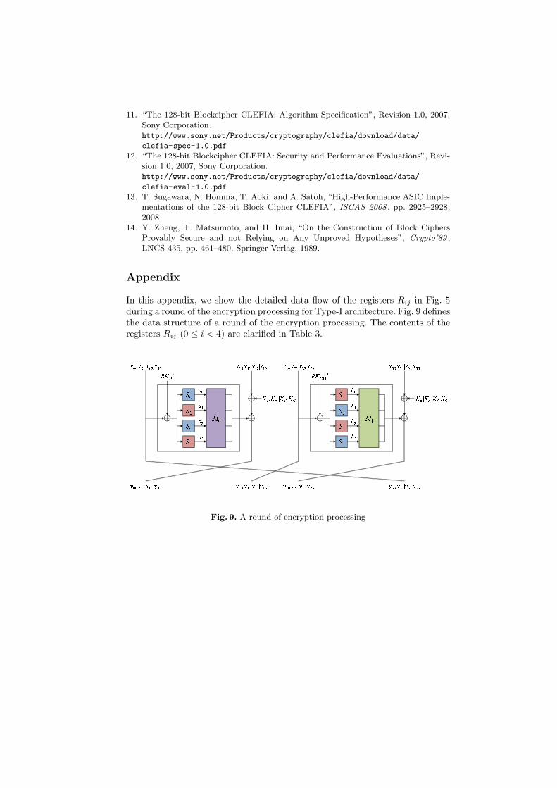
Appendix
In this appendix, we show the detailed data flow of the registers Rij in Fig. 5during a round of the encryption processing for Type-I architecture. Fig. 9 definesthe data structure of a round of the encryption processing. The contents of theregisters Rij (0 ≤ i < 4) are clarified in Table 3.
S1S0S1S0
RK2i+1*
M1b0b1b2b3
Kt0|Kt1|Kt2|Kt3x30|x31|x32|x33x20|x21|x22|x23
S0S1S0S1
RK2i*
M0a0a1a2a3
Ks0|Ks1|Ks2|Ks3x10|x11|x12|x13x00|x01|x02|x03
y00|y01|y02|y03 y10|y11|y12|y13 y20|y21|y22|y23 y30|y31|y32|y33Fig. 9. A round of encryption processing

Table 3. Contents of registers Rij (0 ≤ i, j < 4) at the l-th cycle
l 0 1 2 3 4R00 x00 x01 x02 x03 x20R01 x01 x02 x03 x20 x21R02 x02 x03 x20 x21 x22R03 x03 x20 x21 x22 x23R10 x10 x21 x22 x23 x30R11 x11 x22 x23 x30 x31R12 x12 x23 x30 x31 x32R13 x13 x30 x31 x32 x33R20 x20 x13⊕06a0 x12⊕04a0⊕06a1 x11⊕02a0⊕a1⊕06a2⊕Ks1 y00R21 x21 x12⊕04a0 x13⊕06a0⊕04a1 x10⊕a0⊕02a1⊕04a2⊕Ks0 y01R22 x22 x11⊕02a0 x10⊕a0⊕02a1⊕Ks0 x13⊕06a0⊕04a1⊕02a2 y02R23 x23 x10⊕a0⊕Ks0 x11⊕02a0⊕a1⊕Ks1 x12⊕04a0⊕06a1⊕a2⊕Ks2 y03R30 x30 x31 x32 x33 x00 (= y30)R31 x31 x32 x33 x00 x01 (= y31)R32 x32 x33 x00 x01 x02 (= y32)R33 x33 x00 x01 x02 x03 (= y33)
l 4 5 6 7 8R00 x20 x21 x22 x23 y00R01 x21 x22 x23 y00 y01R02 x22 x23 y00 y01 y02R03 x23 y00 y01 y02 y03R10 x30 y01 y02 y03 x20 (= y10)R11 x31 y02 y03 x20 x21 (= y11)R12 x32 y03 x20 x21 x22 (= y12)R13 x33 x20 x21 x22 x23 (= y13)R20 y00 x33⊕0Ab0 x32⊕02b0⊕0Ab1 x31⊕08b0⊕b1⊕0Ab2⊕Kt1 y20R21 y01 x32⊕02b0 x33⊕0Ab0⊕02b1 x30⊕b0⊕08b1⊕02b2⊕Kt0 y21R22 y02 x31⊕08b0 x30⊕b0⊕08b1⊕Kt0 x33⊕0Ab0⊕02b1⊕08b2 y22R23 y03 x30⊕b0⊕Kt0 x31⊕08b0⊕b1⊕Kt1 x32⊕02b0⊕0Ab1⊕b2⊕Kt2 y23R30 y30 y30 y30 y30 y30R31 y31 y31 y31 y31 y31R32 y32 y32 y32 y32 y32R33 y33 y33 y33 y33 y33
Copyright © 2022 FDOKUMEN