Using NRI Data for ESD Development - Jornada Experimental ...

Unique ESD failure mechanisms during negative to VccHBM tests
M. Chaine *, S. Smith, A. Bui
Texas Instruments Incorporated, P.O. Box 1443, M/S 681, Houston, TX 77251, USA
Received 23 January 1998; in revised form 15 April 1998
Abstract
HBM ESD tests on two types of 0.6 mm DRAM devices showed that internal circuit or output driver failures
would occur after the input or I/O pins were ESD stressed negative with respect to Vcc at ground. These failuresoccurred at lower than expected ESD stress voltages due to power-up circuit interactions that either turned-onunique internal parasitic ESD current paths or disrupted the normal operation of the output pin's ESD protectioncircuit. ESD analysis found there exists a set of power-up sensitive circuits and if placed near a Vcc bond pad can
result in low voltage ESD failures. # 1998 Elsevier Science Ltd. All rights reserved.
1. Introduction
Designing ESD protection circuits in 0.6 mm CMOS
integrated circuit technologies for the input/output
pins and for internal circuit protection have been a
challenge. Recent design approaches like gate
coupling [2], substrate trigger [6] and special trigger cir-
cuit techniques [7±9] have been proposed to improve
the ESD performance of the input/output or power
supply protection circuits in deep sub-micron technol-
ogies. All of these di�erent ESD design solutions have
been proven to work in their speci®c applications.
To improve the overall ESD performance of any IC
device understanding how the internal parasitic device
powers up and breaks down during the ESD event is a
di�erent challenge [4, 5]. Internal circuit and output
pin failures can occur at lower than expected ESD
stress voltages due to power-up circuit interactions
that either switch on an unwanted internal parasitic
ESD current path or disrupts the normal operation of
the output's pin ESD protection circuit [1]. This paper
examines two very di�erent examples where power-up
circuit interactions caused devices to fail for stress vol-tages at or below 2.0 kV.Section 1 of this paper describes the general ESD
problem of stressing input pins negative to the powersupply Vcc pin(s) when held at ground. Section 2reviews a speci®c case study where an internal CMOSinverter circuit failed at less than 2.0 kV after the
input pins were HBM stressed negative to Vcc. InSection 3, another case study investigates how uncon-trolled power-up of a device caused the output drivers
to randomly fail at less that 2.0 kV. Section 4 reviewsthe key ideas in these two case studies. Finally, the lastsection of the paper summarizes the results of the
paper.
2. Input/output pins stressed negative to Vcc
The Mil Std 883C, Method 3015.7, the ESDAssociation HBM test standard S5.l and the JEDECstandard 22, Method A-114 HBM all require that all
input, output and Vss (1) pins and any other unlikeVcc (1) pins are stressed both positive and negative toeach independent Vcc pin. For many IC devices the
worst case ESD stress pin combination with the lowestESD fail voltage occurs when the input and outputpins are stressed negative to grounded Vcc pin(s). To
Microelectronics Reliability 38 (1998) 1749±1761
0026-2714/98/$ - see front matter # 1998 Elsevier Science Ltd. All rights reserved.
PII: S0026-2714(98 )00178-4
PERGAMON
* Corresponding author. Tel.: 001 281 274 2673; Fax: 001
281 274 3885; E-mail: [email protected].

better understand why this pin combination can be theworst case test, the next section reviews in generalwhat happens when this type of ESD stress occurs.
2.1. Input pins stressed negative to Vcc
After stressing an input pin negative to Vcc that wasat ground, there exists at least two di�erent ESD cur-
rent paths between the pin under stress and the nearestVcc ground pin. A schematic in Fig. 1 illustrates howthe ESD current can ¯ow through two totally di�erent
routes. Path A is from the Vcc bond pad through theVcc±Vss ESD clamping circuits to the Vss bus throughthis resistive power bus and through the input pin's
ESD protection circuit to the negative current injectionsource at the input bond pad. The second possibleroute is path B. The ESD current ¯ows through theresistive Vcc power bus and through some internal
parasitic circuits, like CMOS inverter circuits. Finally,the current discharges through the resistive Vss busand eventually through the input pin's ESD input pro-
tection circuit to the negatively charged input bondpad.After a 2 kV HBM stress, the ESD current can ¯ow
from the input pad to the Vcc bond pad along path A,or path B or both paths A and B. The amount of cur-rent distributed along each path will be determined by
the relative di�erence in the trigger or snapback vol-
tage between the Vcc±Vss ESD clamping circuit and
the parasitic CMOS inverter circuits and by the rela-
tive di�erences in Vcc and Vss internal bus resistance
between paths A and B.
For example, if the Vcc±Vss ESD clamping circuit's
snapback voltage is much lower than the internal
Fig. 1. Two possible positive ESD current paths A and B that can occur after stressing an input pin negative with Vcc pad at
ground.
Fig. 2. The percentage of units HBM tested that had internal
circuit failures at or below 2 kV.
M. Chaine et al. / Microelectronics Reliability 38 (1998) 1749±17611750

CMOS circuit's trigger voltage and if the internal Vss
bus resistance (Rvss1+ Rvss2) is very low, then
almost all of the ESD current from the input pad to
Vcc will ¯ow along path A and very little current will
¯ow along path B. Since almost all of the ESD currentis shunted through the Vcc±Vss ESD clamp, the prob-
ability of a failure in the internal CMOS inverter cir-
cuits is quite low (Fig. 2).
In many devices the ESD current will ¯ow along
both paths A and B. This occurs because the di�erence
in the snapback and breakdown voltages between the
Vcc±Vss ESD clamping circuits and the parasitic in-
ternal circuits is not that large. As the ESD stress vol-
tages and currents increases, the I� R voltage risealong the power buses will switch-on both types of
devices. When this occurs the ESD fail voltage of the
device will be a strong function of how much current
the parasitic devices can handle, how many parasitic
devices can simultaneously switch on, and how the
ESD current is distributed through these devices.
Internal resistance inside each of these parasitic
devices will generally play a critical role in determining
the maximum current density through each device.
Very large CMOS inverter circuits will typically have
much lower internal resistance than smaller inverter
circuits.
Predicting where a parasitic internal circuit between
Vcc and Vss will breakdown and fail is a very complex
problem. This task is extremely di�cult because there
are so many di�erent variables such as the process andthe layout parameters that all interact together [10]. In
addition, there is one other critical factor that needs
consideration. Understanding how the parasitic in-
ternal circuit powers up during the ESD event and pre-
dicting which circuits are most likely to fail is also a
challenging ESD design problem.
Stressing the Vcc pins or stressing the input or out-
put pins directly can result in unusual power-up con-
ditions causing unwanted circuit interaction failures [1].The two case studies that will be examined in this
paper show the e�ects of unusual power-up states that
occur during this type of ESD test and how they can
result in devices to fail at or below 2 kV HBM ESD
tests.
Fig. 3. The drain to gate shorting in multiple ®ngers in the large NMOS transistors of the large CMOS inverter circuit.
M. Chaine et al. / Microelectronics Reliability 38 (1998) 1749±1761 1751

3. Internal circuit failure case study 1
During ESD HBM characterization testing (Fig. 2)
on a new DRAM device fabricated in a 0.6 mm LDD,non-salicide, non-epi, pumped substrate DRAMCMOS technology approximately 40% of the unitsstressed failed at or below 2 kV. Automatic test equip-
ment (ATE) testing of the failed units showed highstandby current, Idd2, exceeding 1 mA, the maximumlimits for the data sheet speci®cation. Additional ESD
tests isolated the failed ESD test conditions to I/O pinsnegative to Vcc held at ground.
3.1. Failure analysis
Physical failure analysis including EMMI analysis
isolated two photo-emission hot spots in two identicallarge CMOS inverter circuits near one of the Vcc bondpads. Scanning electron microscopy (SEM) inspection
of the EMMI (emission microscopy images) hot spotsshowed severe damage to the NMOS device of theCMOS inverter circuits. Fig. 3 shows a SEM photo-
graph of the extensive drain to source shorts.Close examination of Fig. 3 shows that the break-
down of the NMOS device in both CMOS invertercircuits was not due to a single drain to source short
but instead was due to multiple damage sites. In thistechnology the typical NMOS breakdown failuresshowed gate oxide notching and silicon melt ®laments
from the contacts to gate, but rarely drain to sourceshorts.The SEM photo also showed a consistent pattern
of damage sites occurring in the same region of thelong NMOS transistor highlighted by the white boxin the picture on the left.
3.2. Circuit schematics
The ESD protection circuits used in this design
(Fig. 4) included multiple placed gate couple grounded
NMOS (GCNMOS) protection circuits and ESD
diodes connected between Vcc and Vss at three di�er-
ent Vcc bond pads. The ESD protection of the input
pins used the classical pi ESD network that included a
small secondary NMOS clamp (FPD), an isolation
resistor (Riso) and a primary clamp (MSCR).
The GCNMOS device was designed to snapback
around 9.3 V. For the periphery CMOS circuitry the
channel length of these internal transistors was
designed at 0.6 mm. The PMOS punch-through voltage
was equal to ÿ9.5 V and the avalanche and snapback
voltages were equal to 11.5 and 8.5 V, respectively, for
the NMOS transistor. The ESD test data showed that
the large CMOS inverter in Fig. 3 failed when several
di�erent input pins were stressed negative with Vcc
held at ground. Why was this occurring? Why wasn't
the GCNMOS device providing ESD protection of this
internal CMOS circuit?
Fig. 4. The ESD input and Vcc±Vss ESD protection network used in this design.
Fig. 5. The schematic block diagram of the circuits that will
power-up when Vcc powers up.
M. Chaine et al. / Microelectronics Reliability 38 (1998) 1749±17611752
To answer this question an in depth analysis of thecircuit schematics was pursued. Fig. 5 illustrates the
failed NMOS transistor placed at the end of a longinverter chain. The diagram shows that this largeCMOS inverter drove a large internal chip capacitor in
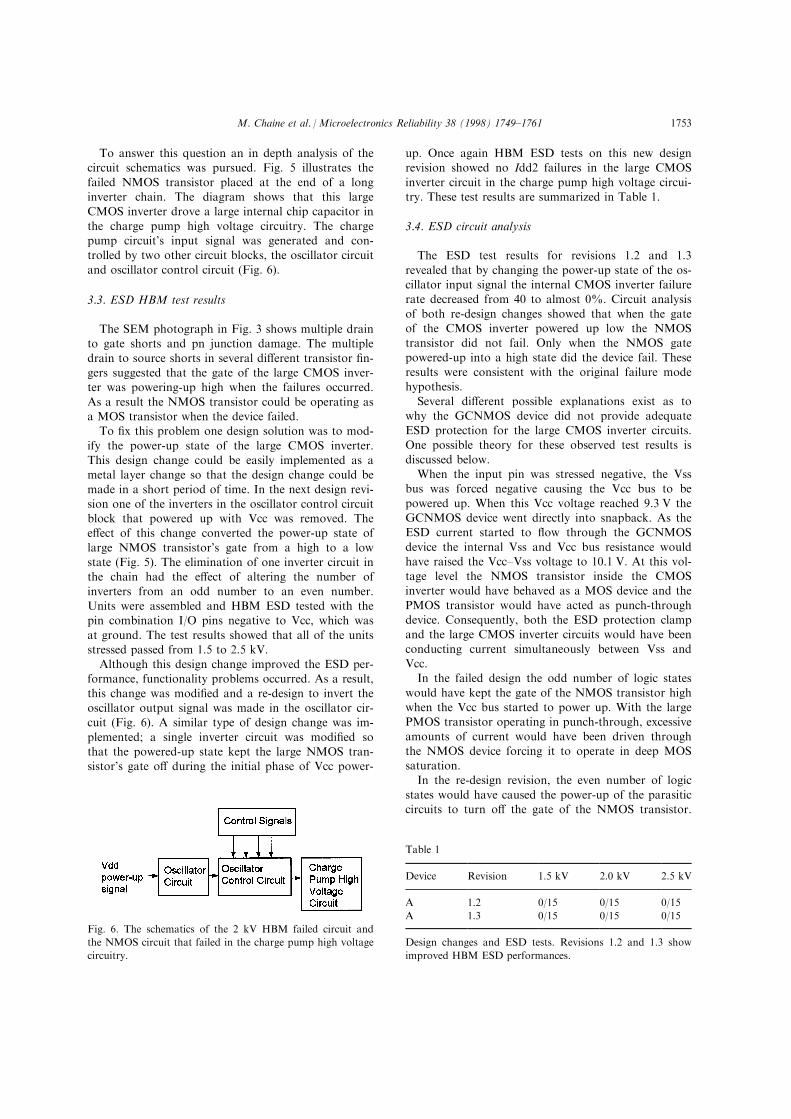
the charge pump high voltage circuitry. The chargepump circuit's input signal was generated and con-trolled by two other circuit blocks, the oscillator circuit
and oscillator control circuit (Fig. 6).
3.3. ESD HBM test results
The SEM photograph in Fig. 3 shows multiple drainto gate shorts and pn junction damage. The multiple
drain to source shorts in several di�erent transistor ®n-gers suggested that the gate of the large CMOS inver-ter was powering-up high when the failures occurred.
As a result the NMOS transistor could be operating asa MOS transistor when the device failed.To ®x this problem one design solution was to mod-
ify the power-up state of the large CMOS inverter.This design change could be easily implemented as ametal layer change so that the design change could be
made in a short period of time. In the next design revi-sion one of the inverters in the oscillator control circuitblock that powered up with Vcc was removed. Thee�ect of this change converted the power-up state of
large NMOS transistor's gate from a high to a lowstate (Fig. 5). The elimination of one inverter circuit inthe chain had the e�ect of altering the number of
inverters from an odd number to an even number.Units were assembled and HBM ESD tested with thepin combination I/O pins negative to Vcc, which was
at ground. The test results showed that all of the unitsstressed passed from 1.5 to 2.5 kV.Although this design change improved the ESD per-
formance, functionality problems occurred. As a result,
this change was modi®ed and a re-design to invert theoscillator output signal was made in the oscillator cir-cuit (Fig. 6). A similar type of design change was im-
plemented; a single inverter circuit was modi®ed sothat the powered-up state kept the large NMOS tran-sistor's gate o� during the initial phase of Vcc power-
up. Once again HBM ESD tests on this new designrevision showed no Idd2 failures in the large CMOS
inverter circuit in the charge pump high voltage circui-try. These test results are summarized in Table 1.
3.4. ESD circuit analysis
The ESD test results for revisions 1.2 and 1.3
revealed that by changing the power-up state of the os-cillator input signal the internal CMOS inverter failurerate decreased from 40 to almost 0%. Circuit analysis
of both re-design changes showed that when the gateof the CMOS inverter powered up low the NMOStransistor did not fail. Only when the NMOS gate
powered-up into a high state did the device fail. Theseresults were consistent with the original failure modehypothesis.
Several di�erent possible explanations exist as towhy the GCNMOS device did not provide adequateESD protection for the large CMOS inverter circuits.One possible theory for these observed test results is
discussed below.When the input pin was stressed negative, the Vss
bus was forced negative causing the Vcc bus to be
powered up. When this Vcc voltage reached 9.3 V theGCNMOS device went directly into snapback. As theESD current started to ¯ow through the GCNMOS
device the internal Vss and Vcc bus resistance wouldhave raised the Vcc±Vss voltage to 10.1 V. At this vol-tage level the NMOS transistor inside the CMOSinverter would have behaved as a MOS device and the
PMOS transistor would have acted as punch-throughdevice. Consequently, both the ESD protection clampand the large CMOS inverter circuits would have been
conducting current simultaneously between Vss andVcc.In the failed design the odd number of logic states
would have kept the gate of the NMOS transistor highwhen the Vcc bus started to power up. With the largePMOS transistor operating in punch-through, excessive
amounts of current would have been driven throughthe NMOS device forcing it to operate in deep MOSsaturation.In the re-design revision, the even number of logic
states would have caused the power-up of the parasiticcircuits to turn o� the gate of the NMOS transistor.
Fig. 6. The schematics of the 2 kV HBM failed circuit and
the NMOS circuit that failed in the charge pump high voltage
circuitry.
Table 1
Device Revision 1.5 kV 2.0 kV 2.5 kV
A 1.2 0/15 0/15 0/15
A 1.3 0/15 0/15 0/15
Design changes and ESD tests. Revisions 1.2 and 1.3 show
improved HBM ESD performances.
M. Chaine et al. / Microelectronics Reliability 38 (1998) 1749±1761 1753

Consequently, this device would have been driven into
npn bipolar breakdown allowing it to carry moreESD current than as a MOS transistor. This change ofoperating mode from a MOS transistor to a npn bipo-
lar transistor prevented these devices from failing.Although the design had three di�erent GCNMOS
circuits placed at three di�erent Vcc bond pads; the
unique sensitivity of this circuit to power up resultedin this device turning on in parallel to the ESD pro-tection circuits. The fact that these circuits wereplaced close to the Vcc bond pads allowed more
ESD current to ¯ow through these circuits drivingthese devices deeper into MOS saturation. Identicallydesigned circuits placed much further away from the
Vcc bond pads with higher Vcc bus resistance didnot fail.This ESD case study has shown that there exist sets
of power-up sensitive circuits. Low ESD failures canoccur if the placements of these circuits are near a Vccbond pad and if the power-up sequence can cause thegates to power-up high during the initial part of the
ESD event.
4. Output driver failure case study 2
ESD HBM characterization test results on another
DRAM device fabricated in the same 0.6 mm LDDnon-salicide, non-epi, pumped substrate DRAMCMOS technology showed NMOS pull-up driver fail-
ures with output low leakage levels greater than 1 mA.The initial 2 kV failure rate was approximately 46% as6/13 units had output pins that failed the 1 mA current
limit. This initial design was a 5 V (HV) device thatused an internal voltage regulator circuit to decreasethe voltage internally to 3.6 V. The output pull-up dri-
ver was connected directly to the 5 V supply while the
pre-drivers circuitry were connected to the regulatedlow voltage 3.6 V internal supply.ESD HBM characterization tests on a 3.6 V (LV)
metal option version of this same design was also com-pleted and the test results were di�erent from the HV(5 V) design as the output failure rate was 0% as none
of the units failed for output low leakage failures.Unlike the HV design, the LV design had both theoutput driver and the pre-driver circuitry connecteddirectly to Vcc.
Analysis of the ESD test conditions showed that theoutput low leakage failures would only occur in theHV device after the output pins were HBM stressed
negative to Vcc which was at ground. The output dri-vers passed all other ESD test combinations from 1.0to 4.0 kV.
4.1. ESD failure analysis
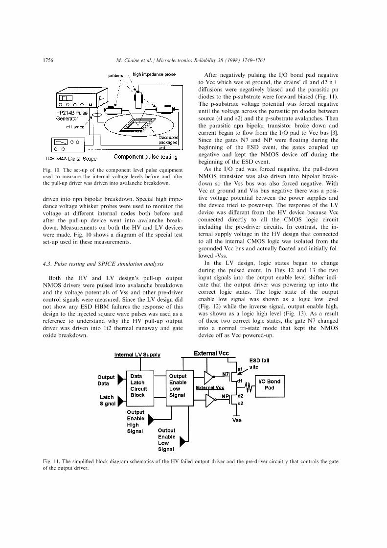
Physical failure analysis of the units that failed the 1mA output low leakage specs was isolated to thedamaged gate oxide region between the Vcc di�usionand the gate of the pull-up NMOS driver (Fig. 7).
SEM photographs of the damaged NMOS output pull-up driver showed gate oxide notching andsilicon melt ®laments from the Vcc contacts to the gate
Figs 8 and 9 show this type of damage that was typicalof the devices that failed.
4.2. ESD failure mechanism theory
Additional ESD HBM tests on di�erent HV wafer
lots found that the failure rate was very erratic and un-stable as the failure rate dropped from 46 to about 7±13%. The failure rate for the LV version of the design
Fig. 7. The isolated fail site in the pull-up NMOS driver.
M. Chaine et al. / Microelectronics Reliability 38 (1998) 1749±17611754

remained unchanged at 0%. This di�erence in the fail-
ure rate indicated that the fail mechanism was more
design dependent than process dependent. The one
signi®cant di�erence between the two devices was that
the HV regulator circuit, which converted the internal
voltage supply directly to Vcc, was disconnected in the
LV design.
This di�erence in the HBM failure rate of the output
drivers between the HV and LV designs was investi-
gated by building a special component level probe
station which allowed the injection of high current
square wave pulses into the output pin with Vcc held
at ground. The voltage of the square wave pulses was
gradually increased until the pull-up NMOS driver was
Fig. 8. The general location of the photo emission hot spots in the NMOS pull-up driver.
Fig. 9. The gate oxide notching and the Si melt ®lament near the notching region.
M. Chaine et al. / Microelectronics Reliability 38 (1998) 1749±1761 1755
driven into npn bipolar breakdown. Special high impe-dance voltage whisker probes were used to monitor the
voltage at di�erent internal nodes both before andafter the pull-up device went into avalanche break-down. Measurements on both the HV and LV devices
were made. Fig. 10 shows a diagram of the special testset-up used in these measurements.
4.3. Pulse testing and SPICE simulation analysis
Both the HV and LV design's pull-up outputNMOS drivers were pulsed into avalanche breakdown
and the voltage potentials of Vss and other pre-drivercontrol signals were measured. Since the LV design didnot show any ESD HBM failures the response of this
design to the injected square wave pulses was used as areference to understand why the HV pull-up outputdriver was driven into 1t2 thermal runaway and gate
oxide breakdown.
After negatively pulsing the I/O bond pad negative
to Vcc which was at ground, the drains' dl and d2 n+
di�usions were negatively biased and the parasitic pn
diodes to the p-substrate were forward biased (Fig. 11).
The p-substrate voltage potential was forced negative
until the voltage across the parasitic pn diodes between
source (sl and s2) and the p-substrate avalanches. Then
the parasitic npn bipolar transistor broke down and
current began to ¯ow from the I/O pad to Vcc bus [3].
Since the gates N7 and NP were ¯oating during the
beginning of the ESD event, the gates coupled up
negative and kept the NMOS device o� during the
beginning of the ESD event.
As the I/O pad was forced negative, the pull-down
NMOS transistor was also driven into bipolar break-
down so the Vss bus was also forced negative. With
Vcc at ground and Vss bus negative there was a posi-
tive voltage potential between the power supplies and
the device tried to power-up. The response of the LV
device was di�erent from the HV device because Vcc
connected directly to all the CMOS logic circuit
including the pre-driver circuits. In contrast, the in-
ternal supply voltage in the HV design that connected
to all the internal CMOS logic was isolated from the
grounded Vcc bus and actually ¯oated and initially fol-
lowed -Vss.
In the LV design, logic states began to change
during the pulsed event. In Figs 12 and 13 the two
input signals into the output enable level shifter indi-
cate that the output driver was powering up into the
correct logic states. The logic state of the output
enable low signal was shown as a logic low level
(Fig. 12) while the inverse signal, output enable high,
was shown as a logic high level (Fig. 13). As a result
of these two correct logic states, the gate N7 changed
into a normal tri-state mode that kept the NMOS
device o� as Vcc powered-up.
Fig. 10. The set-up of the component level pulse equipment
used to measure the internal voltage levels before and after
the pull-up driver was driven into avalanche breakdown.
Fig. 11. The simpli®ed block diagram schematics of the HV failed output driver and the pre-driver circuitry that controls the gate
of the output driver.
M. Chaine et al. / Microelectronics Reliability 38 (1998) 1749±17611756

In the HV device, the internal LV supply voltage
was not powering up correctly. As a result, the logic
signals like output enable high and low were unde®ned
because they were either not changing logic states or
were very slow in changing states. In Figs 14 and 15
both signals track the -Vss voltage potential, as a
result, only one of the two signals was in the correct
logic state. SPICE (simulated program with integrated
Fig. 12. LV output enable low signal is a logic low.
Fig. 13. LV output enable signal is a logic high.
M. Chaine et al. / Microelectronics Reliability 38 (1998) 1749±1761 1757

circuit emphasis) simulations of these two devices
showed that the LV design consistently powered up
into tri-state power-up mode. In addition, the simu-
lations also indicated that the HV design randomly
powered-up into an indeterminate mode. The SPICE
simulations showed that under some power-up con-
ditions the voltage at gate N7 followed the Vcc voltage
that was at ground. If this occurred during the middle
of the ESD event after the pull-up NMOS device was
in bipolar breakdown, the NMOS transistor would
switch on with a high gate potential. As a result, the
ESD current density along the surface abruptly chan-
Fig. 14. HV output enable low signal is a logic low.
Fig. 15. The HV output enable high signal is still a logic low.
M. Chaine et al. / Microelectronics Reliability 38 (1998) 1749±17611758

ged due to the high voltage potential on the gate. This
abrupt increase in surface current could result in cur-rent localization, thermal runaway and device
failure [3].
The SPICE simulation also showed that this was
only one of several di�erent power-up states that the
HV could generate. As a result of this random power-
up state, the ESD failure rate would become very ran-
dom because this worst case state would not always
occur. A review of the ESD failure rate showed thatthe frequency of failures ranged from 6±13% of the
units tested which agreed with the random power-up
hypothesis.
The best theory to explain the output driver failures
proposed that the failures occurred during sudden
power-up of the output's gate during the ESD event.
To eliminate this failure mechanism the power-up state
had to change from a random state to a known tri-state condition. As a result of this analysis, a redesign
of the HV output driver pre-drive circuitry occurred.
Several design changes made in the pre-drive circui-
try changed the power-up state into a known tri-state
mode. One change implemented re-routed an unused
power-up signal directly to the output pre-driver circui-
try. The inverse of this new signal would respond im-mediately to the power-up state and input the correctlogic state when the device started to power-up. Since
the logic states of the other pre-driver circuits wereindeterminate, conversion of the last stage CMOSinverter circuit into a NOR gate ®xed this problem.
Fig. 16 shows this redesign circuit.
4.4. ESD HBM test results
The new revision of the HV device with the modi®edoutput bu�er design was manufactured and HBMESD tests were performed A comparison of the new
re-design with the previous HBM ESD test is shown inTable 2.The HBM test data in Table 2 clearly shows that the
new design revision 1.1 had no output low leakage fail-ures from 1.5 to 4.0 kV. The previous design revision1.0 had approximately 6% constant failure rate. The
revision 1.1 data now matched the ESD test data forthe LV design, which also did not show any outputlow leakage failures. The data veri®ed that the pro-posed ESD failure mechanism was correct and that the
re-design solution worked and that it eliminated thisfail mechanism.
5. Discussion
The two ESD case studies just reviewed highlightthe unique power-up problem that occurs when the
input or output pins are stressed negative to Vcc. Thetwo examples clearly show that during this speci®cESD test the device powers up, CMOS circuitry
Fig. 16. The new power-up enable signal and the conversion of the CMOS inverter into a NOR gate circuit.
Table 2
Device Revision 1.5 kV 2.0 kV 3.0 kV 4.0 kV
B 1.0 0/76 5/76 1/71 1/70
B 1.1 0/55 0/55 0/55 0/55
Design improvements in revision 1.1 show a signi®cant
increase in the HBM failure threshold voltages.
M. Chaine et al. / Microelectronics Reliability 38 (1998) 1749±1761 1759

becomes active and logic states transfer from one cir-
cuit block to another.This change in logic states can a�ect how and where
the parasitic devices breakdown. Placement of large
CMOS drivers near Vcc bond pads potentially can cre-ate unwanted internal circuit failures. In the ®rst case
study, there were two other almost identical circuits tothe ones that failed, but they were placed much furtheraway from any input pin and their power bus resist-
ance from the input pins to those circuits was muchhigher than the failed circuits. Failure analysis of theunits that failed showed that these similarly designed
circuits did not fail.Another factor to consider was the relative size of
the CMOS driver. In this speci®c case the size of thedevice that failed was 325 mm wide which was almostthree times the average size CMOS inverter in this de-
sign. Any time there is only a very small subset ofCMOS inverters with extremely large sizes the morelikely they will be to carry more ESD current and the
higher probability that they may fail.This case study illustrated the limitation of the ESD
Vcc±Vss clamp circuit to protect an internal circuit.There was strong evidence in this study that showedthat the internal circuit failed independently of the
snapback voltage of the power bus ESD protection cir-cuit. The critical variable that determined this fail
mechanism was the sensitivity of this speci®c circuitblock to power-up state. This circuit block was uniquebecause the device powered-up with the NMOS tran-
sistor switched-on. Only by changing the logic statesso that the gate of the large NMOS transistor ®rstpowered-on into an o� state did the failures disappear.
Designing ESD protection networks that will protectagainst CMOS circuits that can power-up and become
active can be extremely di�cult since it is very di�cultto predict which circuits will become active. Circuitsimulations can help identify some of the most sensi-
tive circuitry especially those circuits that have inputsignals that are designed to ramp with Vcc. Special lay-out rules should be applied to those sets of very large
CMOS inverter circuits prohibiting their placement tooclose to any Vcc bond pad. If this layout rule can not
be followed, then SPICE simulations of those sensitivecircuits needs to be run to insure that the gate of theNMOS transistor does not power-up into a logic high
state.Preventing unwanted power-up feedback loops in
output pre-driver circuitry is also an important I/O de-sign issue. This task requires SPICE simulations thatshould model the normal power-up conditions. The
simulation results must show that the gates of eitherthe pull-up or pull-down drivers must remain o�during the entire power-up event. SPICE simulations
of the I/O circuitry during all types of power-up con-ditions must become a standard design practice.
6. Summary
This paper has reviewed two case studies whereHBM ESD tests on two types of 0.6 mm DRAMdevices showed that internal circuit or output driver
failures would occur after the input or I/O pins wereESD stressed negative with respect to Vcc at ground.These failures occurred at lower than expected ESD
stress voltages due to power-up circuit interactionsthat either turned-on unique internal parasitic currentpaths or disrupted the normal operation of the output
pin's ESD protection circuit.The ®rst case study examined how two large CMOS
inverter circuits placed near a Vcc bond pad powered-upand failed at 2 kV. Failure analysis showed extensive
drain to source shorts in the CMOS inverter's NMOStransistor. Circuit analysis revealed that the failed circuitblock was part of a long chain of inverter circuits driven
by an oscillator generator and a Vcc power-up signal.This circuit design intentionally powered the gate of thefailing CMOS inverter into a high state switching-on the
NMOS transistor as a MOS device during both normalVcc power-up and ESD induced power-up. This uniquepower-up state was proven to be the root cause for the
failures as circuit re-design solutions, which intention-ally changed the power-up sequence, eliminated the 2kV HBM Idd2 failures.The second case study showed that unusual power-
up states could also occur, when the output pins werestressed negative to Vcc that was at ground, causingthe pull-up driver's NMOS transistor to fail. When the
device tried to power-up, unpredictable logic states inthe output pre-driver circuits caused the driver's gateto turn on the NMOS transistor while it was operating
as a npn bipolar device. With both the NMOS and thebipolar npn devices simultaneously active, the ESDcurrent localized near the surface resulting in thermalrunaway and early device failure. Circuit re-design
changes were made based on this analysis to insurethat the output pre-driver gate always powered up intoa tri-state condition. ESD HBM tests of this new cir-
cuit design showed no output low leakage failuresproving that this design solution had eliminated thisESD fail mechanism.
Acknowledgements
The authors would like to thank Wilson Tan andEdgar Co for their failure analysis support in
Singapore and Thong Huynh and Long Nguyen fortheir failure analysis work in Houston. In addition theauthor would like to thank Dan Penny for his techni-
cal advice on the design of the charge pump circuitry.In addition, the authors would like to thank CharvakaDuvvury for his helpful comments during the prep-
M. Chaine et al. / Microelectronics Reliability 38 (1998) 1749±17611760

aration of this paper. Finally, the authors would liketo thank Terry Hughes for his work in ESD testing
many of the units discussed in this paper.
References
[1] Krakauer D, Mistry K, Partovi H. Circuit interactions
during electrostatic discharge. In: Proceedings of the
EOS/ESD Symposium, Las Vegas. 1994:113±9.
[2] Duvvury C, Diaz C. Dynamic gate coupling of NMOS
for e�cient output ESD protection. In: IRPS
Proceedings, 1991:141.
[3] Chen KL. The e�ects of interconnect process and snap-
back voltage on the ESD failure threshold of NMOST
transistors. IEEE Trans Electron Dev 1988;35(12):2140.
[4] Johnson C, Maloney T, Qawam S. Two unusual HBM
ESD fail mechanisms on a mature CMOS process. In:
Proceedings of the EOS/ESD Symposium, Orlando.
1993:225±31.
[5] Cook C, Daniel S. Characterization of new failure mech-
anism arising from power-pin ESD stressing. In:
Proceedings of the EOS/ESD Symposium, Orlando.
1993:149±56.
[6] Amerasekera A, Duvvury C, Reddy V, Rodder M.
Substrate triggering and salicide e�ects on ESD perform-
ance and protection circuit design in deep submicron
CMOS processes. In: Internal Electron Device Meeting
Technical Digest, 1995:547±50.
[7] Tandam N. ESD trigger circuits. In: Proceedings of the
EOS/ESD Symposium, Las Vegas. 1994:120±24.
[8] Dabral S, Aslett R, Maloney T. Core clamps for low vol-
tage technologies. In: Proceedings of the EOS/ESD
Symposium, Las Vegas. 1994:141±49.
[9] Worley E, Bupta R, Jones B, Kjar R, Nguyen C,
Tennyson M. Sub-micron chip ESD protection schemes
which avoid avalanching junctions. In: Proceedings of
the EOS/ESD Symposium, Phoenix. 1995:13±20.
[10] Duvvury C, McPhee RA, Baglee DA, Rountree RN.
ESD protection reliability in 1 mm CMOS technologies.
In: IRPS Proceedings, 1986:199±205.
M. Chaine et al. / Microelectronics Reliability 38 (1998) 1749±1761 1761
Copyright © 2022 FDOKUMEN