UC Irvine Electronic Theses and Dissertations - eScholarship
179
UC Irvine UC Irvine Electronic Theses and Dissertations Title PEROVSKITE AND PEROVSKITE-LIKE MATERIALS FOR SOLUTION-PROCESSED THIN-FILM SOLAR CELLS Permalink https://escholarship.org/uc/item/1p66d985 Author Fabian, David Publication Date 2018 Peer reviewed|Thesis/dissertation eScholarship.org Powered by the California Digital Library University of California
-
Upload
khangminh22 -
Category
Documents
-
view
3 -
download
0
Transcript of UC Irvine Electronic Theses and Dissertations - eScholarship
UC IrvineUC Irvine Electronic Theses and Dissertations
TitlePEROVSKITE AND PEROVSKITE-LIKE MATERIALS FOR SOLUTION-PROCESSED THIN-FILM SOLAR CELLS
Permalinkhttps://escholarship.org/uc/item/1p66d985
AuthorFabian, David
Publication Date2018 Peer reviewed|Thesis/dissertation
eScholarship.org Powered by the California Digital LibraryUniversity of California
UNIVERSITY OF CALIFORNIA,
IRVINE
PEROVSKITE AND PEROVSKITE-LIKE MATERIALS FOR SOLUTION-PROCESSED THIN-FILM SOLAR CELLS
DISSERTATION
submitted in partial satisfaction of the requirements for the degree of
DOCTOR OF PHILOSOPHY
in Chemistry
by
David M. Fabian
Dissertation Committee: Assistant Professor Shane Ardo, Chair
Associate Professor Matt Law Professor Eric Potma
2018

ii
Chapter 1 © 2014, 2015 David M. Fabian Chapter 2 © 2016 Royal Society of Chemistry
Chapter 3 © 2018 David M. Fabian Chapter 4 © 2018 Royal Society of Chemistry
Chapter 5 © 2018 David M. Fabian
iii
TABLE OF CONTENTS
List of Figures ......................................................................................................................v
List of Tables ................................................................................................................... xiii
Acknowledgments............................................................................................................ xiv
Curriculum Vitae .............................................................................................................. xv
Abstract of the Dissertation ........................................................................................... xviii
Dissertation at a Glance ...................................................................................................... 1 Chapter 1: Background, Deposition Procedure Development, and Novel Architectures of Perovskite Solar Cells ....................................................................................................3
1.1 Introduction ................................................................................................................3 1.2 Experimental ..............................................................................................................9
1.2.1 Preparation of MAPbX3 Solutions... ...........................................................9 1.2.2 Thin-Film Processing ................................................................................10 1.2.2.1 Substrate Preparation and Metal–Oxide Materials Deposition ..............10 1.2.2.2 Perovskite Deposition Methods .............................................................11 1.2.3 Photovoltaic Device Preparation ...............................................................13 1.2.4 Electrical Characterization ........................................................................14 1.2.5 Mercury-Drop Top-Contact Elecrode Setup .............................................16 1.2.6 Thermal Stability Tests .............................................................................16 1.2.7 Thin-Film Characterization .......................................................................16
1.3 Results & Discussion ...............................................................................................17 1.4 Conclusions ..............................................................................................................31 1.5 References ................................................................................................................32
Chapter 2: Hybrid Organic–Inorganic Photovoltaics Based on Bismuth Iodide and 1,6-Hexanediammonium Dication ..................................................................................37
2.1 Introduction ..............................................................................................................37 2.2 Experimental ............................................................................................................41
2.2.1 Preparation of MAPbI3 and HDABiI5 Solutions... ....................................41 2.2.2 Materials Processing .................................................................................42 2.2.3 Device Fabrication ....................................................................................43 2.2.4 Thermal Stability Tests .............................................................................44 2.2.5 Characterization ........................................................................................44
2.3 Results & Discussion ...............................................................................................46 2.4 Conclusions ..............................................................................................................55 2.5 References ................................................................................................................57
Chapter 3: Hybrid organic–inorganic bismuth–iodide materials incorporating divalent organic ligands for photovoltaics .....................................................................61
3.1 Introduction ..............................................................................................................61
iv
3.2 Experimental ............................................................................................................66 3.2.1 Single-Crystal Growth and Measurement.. ...............................................66
3.2.1.1 Single-Crystal Growth .......................................................................66 3.2.1.2 X-ray Data Collection and Structure Solution for EDA2Bi2I10 .........67 3.2.1.3 X-ray Data Collection and Structure Solution for HDABiI5 .............67 3.2.1.4 Structure Solution Definitions…………………………………..…………………..68
3.2.2 Density Functional Theory Calculations for HDABiI5 .............................69 3.2.3 Preparation of Hybrid Organic–Inorganic Bismuth–Iodide Solutions .....69 3.2.4 Materials Processing .................................................................................70 3.2.5 Device Fabrication ....................................................................................71 3.2.6 Ultrafast Laser Spectroscopy ....................................................................71 3.2.7 Characterization ........................................................................................72
3.3 Results & Discussion ...............................................................................................75 3.4 Conclusions ..............................................................................................................99 3.5 References ..............................................................................................................101
Chapter 4: Demonstration of photovoltaic action and enhanced stability from a quasi-two-dimensional hybrid organic–inorganic copper–halide material incorporating divalent organic ligands .................................................................................................105
4.1 Introduction ............................................................................................................105 4.2 Experimental ..........................................................................................................107
4.2.1 Preparation of (HDA)2CuBr6-xClx and (PA)4CuBr6 Solutions... .............108 4.2.2 (HDA)2CuBr6 Single-Crystal Growth…………………………………108 4.2.3 X-ray Data Collection and Structure Solution for (HDA)2CuBr6 ..........109 4.2.4 Materials Processing ...............................................................................109 4.2.5 Solar Cell Fabrication .............................................................................110 4.2.6 Stability Tests ..........................................................................................111 4.2.7 Materials Characterization ......................................................................111 4.2.8 Electrical Characterization ......................................................................113
4.3 Results & Discussion .............................................................................................114 4.4 Conclusions ............................................................................................................130 4.5 References ..............................................................................................................131
Chapter 5: Low-dimensional lead–halide perovskite materials incorporating divalent organic ligands ...............................................................................................................137
5.1 Introduction ............................................................................................................137 5.2 Experimental ..........................................................................................................141
5.2.1 Preparation of Lead–Iodide Solutions .....................................................141 5.2.2 Materials Processing ...............................................................................142 5.2.3 Ultrafast Laser Spectroscopy ..................................................................142 5.2.4 Characterization ......................................................................................144
5.3 Results & Discussion .............................................................................................145 5.4 Conclusions ............................................................................................................154 5.5 References ..............................................................................................................156
v
LIST OF FIGURES
Figure 1.1. Levelized cost of energy values and Department of Energy cost goals for solar electricity…………………………………………………………………………………………..4 Figure 1.2. Best research-cell efficiencies of emerging photovoltaic technologies...……………..5 Figure 1.3. (a) 1D and (b) 2D representation of general linking between organic moieties and inorganic moieties.………………………………………………………………………………...6 Figure 1.4. (a) Mesostructured, (b) planar n–i–p, and (c) planar p–i–n architectures typically employed in perovskite photovoltaics………………………………………………..…………....7 Figure 1.5. (a) Conventional spin-coat procedure for depositing perovskite precursor solution (e.g. MAPbI3 in DMF) on mesoporous metal oxide/compact TiO2/fluorine-doped tin oxide. (b) Fast deposition crystallization spin-coat procedure, which incorporates an antisolvent (e.g. chlorobenezene) during the spin-coat process………………………………………………..…..11 Figure 1.6. (a) Illustration and (b) digital photograph images of the gas-solid crystallization method whereby methylammonium iodide powder is sprinkled on the PbI2 film to form MAPbI3 perovskite during heating at 150 °C………………………………………………………………12 Figure 1.7. Digital photograph image of aqueous 2M HCl and zinc powder reacting to etch away the exposed fluorine-doped tin oxide……………………………………………………………..13 Figure 1.8. Digital photograph image of the photovoltaic device J–V measurement setup……....15 Figure 1.9. Digital photograph image of the mercury-drop top-contact electrode setup…………16 Figure 1.10. Current–voltage curves showing ohmic contacts of evaporated gold to a solution-deposited PEDOT:PSS thin film as well as liquid mercury to fluorine-doped tin–oxide and liquid mercury to PEDOT:PSS. Inset: zoomed-in area showing only slight differences in resistance for each contact……………………………………………………………………………………....18 Figure 1.11. Three-electrode cyclic voltammetry at 50 mV/s of 1 mM ferrocene in acetonitrile with 100 mM tetra-n-butylammonium hexafluorophosphate. Working electrodes studied are different metal–oxide architectures on a fluorine-doped tin–oxide coated glass substrate, the counter electrode is platinum mesh, and the reference electrode is a saturated calomel electrode………………………………………………………………………………………….19 Figure 1.12. Steady-state absorption spectra and photoluminescence emission spectra of PbI2 and MAPbI3 on fluorine-doped tin oxide. Insets are digital photograph images of the films………….21 Figure 1.13. Depth profiling by fluorescence lifetime confocal microscopy imaging on MAPbI3/mTiO2/cTiO2/FTO……………………………………………………………………...22
vi
Figure 1.14. Steady-state absorption spectra of an MAPbI3 thin film on mTiO2/cTiO2/FTO. On left are digital photograph images of the film after treatment…………………………………….23 Figure 1.15. (a) Digital photograph images and (b) top-view scanning electron microscopy images of MAPbI3 thin films on cTiO2/FTO, for which MAPbI3 was deposited via a conventional one-step spin-coating method or via a fast deposition crystallization technique for which chlorobenzene was used as the antisolvent. (c) Steady-state absorption spectra of the MAPbI3/cTiO2/FTO substrates shown in panel (a) as well as a spectrum of MAPbI3/cTiO2/FTO for which MAPbI3 was deposited via fast deposition crystallization with toluene as the antisolvent. (d) Grazing-incidence X-ray diffraction patterns of the MAPbI3/cTiO2/FTO substrates shown in panel (a)……………..24 Figure 1.16. Reverse-bias voltage sweeps at 100 mV/s of the best-performing cells of devices 1, 2, and 3………………………………………………………………………………….………..28 Figure 1.17. (a) Chronopotentiometry at open circuit and (b) chronoamperometry at short circuit (0 V vs. ref) of the best-performing perovskite cell of device 3……………………………...……29 Figure 1.18. Light-intensity-dependent measurements of the open-circuit voltage of a PV device. Inset: architectural layout of the cell (Au/PEDOT:PSS/MAPbI3/mAl2O3/cTiO2/FTO)…………..30 Figure 2.1. (a) The unit cell of lead-based organic–inorganic hybrid perovskite MAPbI3. (b) Crystal structure of the inorganic framework of a bismuth-based organic–inorganic hybrid material, from the top-down view and side view…………………………………………………38 Figure 2.2. (a) Cross-sectional scanning electron microscopy image of a representative HDABiI5 device, and (b) direct-bandgap and (c) indirect-bandgap Tauc plots of HDABiI5 deposited as thin films on FTO, and baseline corrected for the FTO substrate……………………………………...46 Figure 2.3. Top-view scanning electron microscopy image of (a) HDABiI5 and (b) MAPbI3 deposited on mTiO2/cTiO2/FTO……………………………………………………….…………47 Figure 2.4. Ultraviolet photoemission spectra (He I) of HDABiI5/FTO for direct determination of the (a) work function and (b) valence-band maximum………………………………………...…48 Figure 2.5. Energy-level diagram of spiro-OMeTAD/HDABiI5/TiO2, where the VBM of HDABI5 was determined by UPS measurement………………………………………………………..…..49 Figure 2.6. (a) Grazing-incidence XRD pattern and (b) XPS spectra of HDABiI5/ mTiO2/cTiO2/FTO…………………………………………………………………………….….50 Figure 2.7. (a) Sequential X-ray photoelectron spectra of the Bi 4f region, which demonstrate increased signal attributed to Bi0 compared to signal attributed to Bi3+ concomitant with longer exposure to Al Kα X-ray radiation. (b) First scan and (c) second scan of the Bi 4f region, with Shirley backgrounds and peak fits shown for clarity……………………………………………..50
vii
Figure 2.8. XPS region scans of (a) Ti 2p and (b) O 1s binding energies for HDABiI5/mTiO2/cTiO2/FTO, where the intensities are normalized to the I 3d5/2 peak in Figure 2.6b. Small peak intensities indicate near-complete coverage of mTiO2 by HDABiI5………...….51 Figure 2.9. (a) J–E behavior with scan direction indicated by the arrows and (b) chronoamperometry under 0.8 Suns, and (c) IPCE action spectrum for a complete Au/spiro-OMeTAD/HDABiI5/mTiO2/cTiO2/FTO device. Inset in panel (a) is a digital photograph image of the device………………………………………………………………………………………...53 Figure 2.10. Side-view representation of the layer-by-layer architecture of the complete photovoltaic device………………………………………………………………………………54 Figure 2.11. Transmission-mode UV–Vis electronic absorption spectra of (a) HDABiI5 and (b) MAPbI3 films on mTiO2/cTiO2/FTO. Inset in panel b shows absorption onsets in greater detail and with the same axes units as the main graph……………………………………………………….55 Figure 2.12. Plan-view SEM images of MAPbI3 (top row, a–d) and HDABiI5 (bottom row, e–h) thin films deposited on TiO2 via a simple one-step deposition (a, e), hot-casting (b, f), fast-deposition crystallization (c, g), or a novel “drop-heat-spin” technique that has been pioneered (d, h)………………………………………………………………………………………………....56 Figure 3.1. Electromagnetic radiation spectrum, with approximate positions of probing wavelengths of X-band time-resolved microwave conductivity, time-resolved terahertz, and transient absorption spectroscopic techniques and abilities of each technique to probe free carriers and/or excitons………………………………………………………………………………...…63 Figure 3.2. (a) A representation of the general linking of organic dications to one-dimensional bismuth–halide chains. (b) A representation of the organic dication crystal motif in dicationic organic–inorganic bismuth–halide materials, where the A2+ groups serve as “crystal fasteners” between one-dimensional bismuth–halide chains to enhance inter-chain conductivity, σ………..65 Figure 3.3. Molecular structure of EDA2Bi2I10 • 5H2O, with thermal ellipsoids drawn at the 50% probability level………………………………………………………………………………….75 Figure 3.4. (a) A digital photograph image of a single crystal of (EDA)2Bi2I10 • 5H2O. (b) A segment of the (EDA)2Bi2I10 • 5H2O crystal structure unit cell, with bond distances labeled. (c) The complete (EDA)2Bi2I10 • 5H2O unit cell……………………………………………………..75 Figure 3.5. Molecular structure of HDABiI5, with thermal ellipsoids drawn at the 50% probability level……………………………………………………………………………………………....77 Figure 3.6. (a) 1 x 1 x 3 unit cell structure of HDABiI5 with orientation in the [110] direction. (b) The same structure as displayed in panel (a) but rotated 90°. (c) The same structure as displayed in panel (b) with the organic HDA2+ groups removed. Hydrogens are omitted in each panel for clarity…………………………………………………………………………………………….78
viii
Figure 3.7. X-ray diffraction patterns of HDABiI5 predicted from the resolved single-crystal structure compared to powders scraped off of thin films measured using a synchrotron source………………………………………………………………………………………….…80 Figure 3.8. HSE06+SOC band structures of HDABiI5. The valence-band maximum is set to 0 eV…………………………………………………………………………………………….…..81 Figure 3.9. (a) Calculated optical absorption spectrum and (b) calculated spectroscopic limited maximum efficiency of HDABiI5…………………………………………………………….…..82 Figure 3.10. Optical bandgap as a function of number of carbons in the diammonium group for the hybrid bismuth–halide materials (hydra)BiI5 (0 carbons), EDABiI5 (2 carbons), BDABiI5 (4 carbons), HDABiI5 (6 carbons), and DDDABiI5 (12 carbons)…………………………………...83 Figure 3.11. UV–Vis electronic absorption spectra of a series of organic–inorganic hybrid bismuth–halide thin films, which range in structural dimensionality from zero-dimensional to two-dimensional……………………………………………………………………………………....85 Figure 3.12. Grazing-incidence X-ray diffraction patterns of thjn films of HDABiI5 and (PA)2BiI5 on FTO…………………………………………………………………………………………...86 Figure 3.13. Grazing-incidence X-ray diffraction patterns of thin films of (PA)2BiI5 processed in the conventional 4:1 DMF:DMSO solvent mixture and processed in an alternative acetonitrile (MeCN) with 15 wt. % butylamine……………………………………………………………….87 Figure 3.14. (a) Grazing-incidence X-ray diffraction patterns of a thjn film of (FA0.75Cs0.25)3Bi2I9 on fluorine-doped tin–oxide-coated glass and the calculated powder pattern of analogous (MA)3Bi2I9. (b) Single-crystal structure of analogous MA3Bi2I9, recreated from a .cif file provided by Kamminga and coworkers………………………………………………………………...…..87 Figure 3.15. Time-resolved microwave conductivity traces of a thin film of HDABiI5 on a quartz substrate. Excitation laser fluence is shown in the legend in parentheses with units of photons/cm2………………………………………………………………………………………89 Figure 3.16. Time-resolved microwave conductivity traces of a thin film of bpyBiI5 on a quartz substrate. Excitation laser fluence is shown in the legend in parentheses with units of photons/cm2…………………………………………………………………………………..…..90 Figure 3.17. Time-resolved microwave conductivity traces of a (FA0.75Cs0.25)3Bi2I9 thin film of on a quartz substrate. Excitation laser fluence is shown in the legend in parentheses with units of photons/cm2………………………………………………………………………………..……..91 Figure 3.18. Transient absorption spectra of a thin film of HDABiI5 using 450 nm laser excitation, with t = 0 indicating where the magnitude of ΔmOD integrated over wavelength was the largest……………………………………………………………………………………….……92
ix
Figure 3.19. (a) Transient absorption spectra at t = 0 and (b) kinetic traces of thin films of one-dimensional HDABiI5, supposed one-dimensional bpyBiI5, and zero-dimensional (FA0.75Cs0.25)3Bi2I9 using 450 nm laser excitation…………………………………………..……92 Figure 3.20. (a) Absorptance + reflectance spectra of HDABiI5 and (PA)2BiI5 thin films deposited on glass using a conventional one-step deposition and using a fast deposition crystallization with chlorobenzene as antisolvent. (b) Digital photograph images of the thin films corresponding to each absorptance spectrum…………………………………………………………………...…..93 Figure 3.21. Plan-view scanning electron microscopy images of thin films of HDABiI5/mTiO2/cTiO2/FTO (panels (a) and (b)) and (PA)2BiI5/mTiO2/cTiO2/FTO (panels (c) and (d))……………………………………………………………………………………………..…94 Figure 3.22. Absorption spectra and steady-state emission spectra of thin films of HDABiI5 and(PA)2BiI5 using 400 nm excitation……………………………………………………..……..95 Figure 3.23. Steady-state emission spectra of thin films of (a) HDABiI5 and (b) (PA)2BiI5 using 400 nm excitation – 500 nm excitation…………………………………………………………...95 Figure 3.24. (a) Temperature-dependent thermogravimetric analysis of HDABiI5 powder and (PA)2BiI5 powder. (b) Isothermal thermogravimetric analysis at 200 °C as a function of time………………………………………………………………………………………..……..96 Figure 3.25. (a) J–E behavior for solar cells consisting of Au/spiro-OMeTAD/Bi/TiOx/FTO, where Bi is HDABiI5 or (PA)2BiI5. (b) Digital photograph images of the solar cells containing HDABiI5 and (PA)2BiI5. (c) Chronoamperometry measurements of (PA)2BiI5 and HDABiI5………….…..97 Figure 3.26. (a) Grazing-incidence X-ray diffraction patterns of HDABiI5 and mixed organic dicationic (HDA-PhDA)BiI5 thin films normalized to the 011 peak at ~12 °. (b) Grazing-incidence X-ray diffraction patterns of a 95%-5% (HDA-PhDA)BiI5 thin film before and after thermal treatment at 200 °C for 19 h. (c) Transmission-mode electronic absorption spectra of mixed organic dicationic (HDA-PhDA)BiI5 thin films before and after thermal treatment at 200°C for 19 h……98 Figure 3.27. Through-plane conductivity J–E measurements of HDABiI5 (100-0) and the mixed-dication (HDA-PhDA)BiI5 (95-5, 85-15, 75-25) thin films………………………………………99 Figure 4.1. Unit cell crystal structure of (HDA)2CuBr6 showing the vertical alternation of copper (light blue)–bromide layers separated by hexanediammonium dications. Hydrogens are omitted for clarity. Shown on the right is a CuBr6 octahedral unit with the measured Cu–Br bond lengths……………………………………………………………………………………….….114 Figure 4.2. (a) Transmission-mode electronic absorbance spectra and steady-state photoluminescence emission spectra (λex ≈ 340 nm) of thin films of (HDA)2CuBr6 and (PA)4CuBr6. (b) Normalized steady-state photoluminescence emission spectra (λex ≈ 400 nm) of thin films of (HDA)2CuBr6 and (PA)4CuBr6, showing a broad tailing region due to emission from an electronic transition with λmax ≈ 580 nm. (c) Steady-state photoluminescence excitation spectra of
x
(HDA)2CuBr6 and (PA)4CuBr6 probed at emission peak wavelengths and at 580 nm, with the absorptance spectra of (HDA)2CuBr6 and (PA)4CuBr6 overlaid………………………………...116 Figure 4.3. (a) Indirect-bandgap Tauc plots of copper–halide hybrid organic–inorganic thin films deposited on glass and incorporating HDA2+ with varying halide compositions or PA+. (b) Digital photograph image of representative freshly-prepared (HDA)2CuBr6-xClx thin films deposited on glass, with x = 0, 1, and 2………………………………………………………………………..117 Figure 4.4. Direct-bandgap Tauc plots of copper–halide hybrid organic–inorganic thin films deposited on glass and incorporating HDA2+ with varying halide compositions or PA+………...118 Figure 4.5. Digital photograph images of freshly-prepared (HDA)2CuBr6-xClx with x = 0, 1, and 2, and (PA)4CuBr6 thin films deposited in the mesostructured assembly, Cu/mTiO2/cTiO2/FTO, where Cu is the copper–halide light absorber material……………..…………………………...119 Figure 4.6. X-ray photoelectron spectra of the Cu 2p3/2 region of thin films of (a) (HDA)2CuBr6 and (b) (PA)2CuBr4 on FTO. Best fits to the Cu 2p3/2 peaks are shown……………………...…..119 Figure 4.7. X-ray photoelectron spectra of the (a) Cu 2p region and the (b) Cl 2p region of copper–halide hybrid organic–inorganic thin films each deposited on FTO. Intensities in panel (a) are normalized to the Cu 2p3/2 peak that corresponds to Cu2+……………………………………….120 Figure 4.8. Best fits to the Cu 2p3/2 peaks of the X-ray photoelectron spectra of thin films of (a) (HDA)2CuBr6 and (b) (PA)4CuBr6 thin films each deposited on FTO following continued X-ray exposure………………………………………………………………………………………...121 Figure 4.9. Scans of the (a), (d) C 1s, (b), (e) N 1s, and (c), (f) Br 3p core level binding energy regions for thin films of (HDA)2CuBr6 and (PA)4CuBr6, each deposited on FTO………………122 Figure 4.10. Grazing-incidence X-ray diffraction patterns of thin films of (a) (HDA)2CuBr6 and (b) (PA)4CuBr6 when freshly-prepared and after exposure to 100 °C and ~50% relative humidity for 16 h. # denote peaks associated with the underlying FTO substrate………………………….123 Figure 4.11. Powder X-ray diffraction patterns and thin-film X-ray diffraction patterns for (a) (HDA)2CuBr6 and (b) (PA)4CuBr6…………………………………………………………...…123 Figure 4.12. (a) Transmission-mode absorption spectra of thin films of HDA2CuBr6 and (PA)4CuBr6 freshly-prepared and after exposure to 100 °C and ~50% relative humidity for 16 h, each corrected for background scattering. Inset: Digital photograph images of the thin films before and after exposure. (b) Normalized absorbance at 500 nm as a function of time for copper–halide perovskite thin films at room temperature and 50% relative humidity. Inset: Digital photograph image of (PA)4CuBr6 after 6 days and HDA2CuBr6 after 12 days…………………………...…..124 Figure 4.13. (a) Temperature-dependent thermogravimetric analysis of (HDA)2CuBr6, (PA)4CuBr6, and (DA)4CuBr6 powders. (b) Isothermal thermogravimetric analysis at 150 °C as a function of time…………………………………………………………………………………125

xi
Figure 4.14. a) Temperature-dependent thermogravimetric analysis of HDABr2, PABr, and DABr precursor powders. (b) Isothermal thermogravimetric analysis at 250 °C as a function of time……………………………………………………………………………………………..126 Figure 4.15. Powder XRD of (a) (HDA)2CuBr6 and (b) (PA)4CuBr6 during moisture stability tests at the indicated number of days into the tests……………………………………………………126 Figure 4.16. Cross-sectional scanning electron micrograph of a representative solar cell containing (HDA)2CuBr5Cl as the photoactive layer…………………………………………………….…127 Figure 4.17. Energy-dispersive X-ray spectroscopy mapping data of a thin-film cross section of (HDA)2CuBr6/mTiO2/cTiO2/FTO………………………………………………………………127 Figure 4.18 (a) J–E behavior for solar cells consisting of Au/spiro-OMeTAD/Cu/TiO2/FTO, where Cu is (HDA)2CuBr6 or (HDA)2CuBr5Cl. Inset: digital photograph image of a complete solar cell. (b) Impedance spectroscopy data, presented as a Mott–Schottky plot, for a solar cell consisting of Au/spiro-OMeTAD/(HDA)2CuBr5Cl/TiO2/FTO, and with the calculated flat-band potential (EFB) and dopant density (NA). Inset: standard Randles circuit used to model the impedance spectroscopy data…………………………………………………………………………….…128 Figure 4.19. Low-intensity X-ray photoelectron spectra of the cutoff region to determine work functions of copper–halide hybrid organic–inorganic materials each deposited on FTO………………………………………………………………………………………..……129 Figure 4.20. X-ray photoelectron valence-band spectra of copper–halide hybrid organic–inorganic materials each deposited on FTO showing (a) the entire valence-band region and (b) the valence-band position relative to the work function of the copper standard (set to 0.0 eV)………………130 Figure 4.21. Energy-level diagram of (HDA)2CuBr6-xClx thin films, with x = 0, x = 1, and x = 2, as well as a (PA)4CuBr6 thin film, each deposited on a fluorine-doped tin–oxide-coated glass substrate. The conduction-band minimum of TiO2 and valence-band maximum of spiro-OMeTAD were taken from a report by Chilvery et al………………………………………………………131 Figure 5.1. Proposed structure of the two-dimensional lead–halide perovskite ethylenediamine lead iodide (EDAPbI4) viewed along the plane of the n=1 sheets of PbI6 octahedra…………….137 Figure 5.2. (a) A schematic representation of time-resolved terahertz spectroscopy. (b) A diagram of the experimental setup of TRTS……………………………………………………………...139 Figure 5.3. (a) UV–Visible absorption spectra and (b) steady-state emission spectra (λex = 400 nm) of hybrid lead–halide material thin films…………………………………………………….….145 Figure 5.4. (a) Time-resolved photoluminescence kinetic traces and (b) time-resolved photoluminescence emission spectra of hybrid lead–halide thin films at 410 nm excitation…………………………………………………………………………………….….146

xii
Figure 5.5. Steady-state emission spectra of (a) EDAPbI4 and (b) BDAPbI4, and (c) HDAPbI4 thin films showing no spectral shifts when varying the excitation wavelength……………………....147 Figure 5.6. Grazing-incidence XRD patterns of hybrid lead–halide material thin films incorporating either ethylenediamine, butanediamine, or hexanediamine………………………148 Figure 5.7. Transient absorption (a) kinetic traces and (b) spectra of a thin film of EDAPbI4 at 400 nm excitation…………………………………………………………………………………....148 Figure 5.8. Transient absorption (a) kinetic traces and (b) spectra of a thin film of BDAPbI4 at 400 nm excitation…………………………………………………………………………………....149 Figure 5.9. Transient absorption (a) kinetic traces and (b) spectra of a thin film of HDAPbI4 at 400 nm excitation…………………………………………………………………………………....149 Figure 5.10. Transient absorption (a) kinetic traces and (b) spectra of a thin film of EDAPbI4 at 500 nm excitation……………………………………………………………………………….150 Figure 5.11. Transient absorption (a) kinetic traces and (b) spectra of a thin film of BDAPbI4 at 500 nm excitation……….………………………………………………………………………150 Figure 5.12. Transient absorption (a) kinetic traces and (b) spectra of a thin film of HDAPbI4 at 500 nm excitation……………………..………………………………………………………...151 Figure 5.13. Terahertz pump scans showing the charge-carrier kinetics of the hybrid lead–halide material thin films…………………………………………………………………………...….151 Figure 5.14. (a) Transient absorption spectra of a freshly-prepared MAPbBr3 thin film excited with 520 nm laser light………………………………………………………………………….152 Figure 5.15. Transient absorption spectra of a MAPbBr3 thin film that has been stored in a container in air for roughly three months………………………………………………………..153 Figure 5.16. Transient absorption spectra of a freshly-prepared BDAPbI4 thin film at 485 nm excitation, probing the exciton bleach peak at 496 nm…………………………………………..153 Figure 5.17. Terahertz probe scans of thin films of (a) MAPbBr3, (b) EDAPbI4, (c) BDAPbI4, and (d) HDAPbI4…………………………………………………………………………………….154
xiii
LIST OF TABLES
Table 1.1. Promising MAPbX3 perovskite PV devices. Deposition method refers to how the perovskite layer is deposited, FDC = fast deposition crystallization, VOC = open-circuit voltage, ISC = short-circuit current, JSC = short-circuit current density, FF = fill factor, PCE = power conversion efficiency…………………………………………………………………………………………27 Table 2.1. Approximate percent surface elemental composition (excluding hydrogen) of HDABiI5/mTiO2/cTiO2/FTO calculated from XPS region scans………………………….……..52 Table 3.1. Organic groups incorporated in dicationic hybrid organic–inorganic bismuth–halide materials for enhanced-conductivity PVs…………………………………………………….…..66 Table 3.2. Crystallographic data for EDA2Bi2I10•5H2O…………………………………...……..76 Table 3.3. Crystallographic data for HDABiI5…………………………………………………...79 Table 3.4. Optical bandgaps and corresponding digital images of a series of dicationic hybrid organic–inorganic bismuth–iodide thin films……………………………………………….……84 Table 4.1. Crystallographic data for (HDA)2CuBr6……………………………………………..115

xiv
ACKNOWLEDGMENTS
I would like to thank my parents, Debbie and Dave, and my three sisters, Laura, Sarah, and Becky,
for all their love and support in everything I have set my mind to over the years. I would also like
to thank my undergraduate advisor, Kristin Wustholz, who welcomed me into her group at the start
of my junior year and taught me the importance of great science writing. I thank my doctoral
advisor, Shane Ardo, for taking a chance with me and believing in me enough to give me
essentially full autonomy in the research I wanted to pursue. I also thank the faculty on my
committee for their guidance and for being incredibly brilliant representations of the world-class
faculty we have in the Department of Chemistry at UCI. I would like to thank all my friends for
keeping me sane throughout the PhD process by reminding me that I do have a life outside of
school. Lastly, many “thank you’s” go to my fiancé, Kelly, whose unconditional love and support
reminds me that I not only have something to live for (that is, a rewarding career), but also someone
to live for.
I would also like to thank sources of funding that have helped support me and my research
throughout my graduate school tenure: 1) the National Science Foundation Graduate Research
Fellowship under Grant number DGE-1321846, 2) the DOE, Office of Science, Office of
Workforce Development for Teachers and Scientists, Office of Science Graduate Student Research
(SCGSR) program under contract number DE‐SC0014664, the 2017 UC MEXUS-CONACYT
Collaborative Research Grant under Grant number UCM-208101, and the School of Physical
Sciences at the University of California, Irvine.
xv
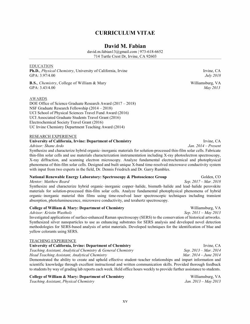
CURRICULUM VITAE
David M. Fabian [email protected] | 973-618-6652
714 Turtle Crest Dr, Irvine, CA 92603
EDUCATION Ph.D., Physical Chemistry, University of California, Irvine Irvine, CA GPA: 3.97/4.00 July 2018
B.S., Chemistry, College of William & Mary Williamsburg, VA GPA: 3.43/4.00 May 2013 AWARDS DOE Office of Science Graduate Research Award (2017 – 2018) NSF Graduate Research Fellowship (2014 – 2018) UCI School of Physical Sciences Travel Fund Award (2016) UCI Associated Graduate Students Travel Grant (2016) Electrochemical Society Travel Grant (2016) UC Irvine Chemistry Department Teaching Award (2014) RESEARCH EXPERIENCE University of California, Irvine: Department of Chemistry Irvine, CA Advisor: Shane Ardo Jan. 2014 – Present Synthesize and characterize hybrid organic–inorganic materials for solution-processed thin-film solar cells. Fabricate thin-film solar cells and use materials characterization instrumentation including X-ray photoelectron spectroscopy, X-ray diffraction, and scanning electron microscopy. Analyze fundamental electrochemical and photophysical phenomena of thin-film solar cells. Designed and built unique X-band time-resolved microwave conductivity system with input from two experts in the field, Dr. Dennis Friedrich and Dr. Garry Rumbles.
National Renewable Energy Laboratory: Spectroscopy & Photoscience Group Golden, CO Mentor: Matthew Beard Sep. 2017 – Mar. 2018 Synthesize and characterize hybrid organic–inorganic copper–halide, bismuth–halide and lead–halide perovskite materials for solution-processed thin-film solar cells. Analyze fundamental photophysical phenomena of hybrid organic–inorganic material thin films using time-resolved laser spectroscopic techniques including transient absorption, photoluminescence, microwave conductivity, and terahertz spectroscopy.
College of William & Mary: Department of Chemistry Williamsburg, VA Advisor: Kristin Wustholz Sep. 2011 – May 2013 Investigated applications of surface-enhanced Raman spectroscopy (SERS) to the conservation of historical artworks. Synthesized silver nanoparticles to use as enhancing substrates for SERS analysis and developed novel detection methodologies for SERS-based analysis of artist materials. Developed techniques for the identification of blue and yellow colorants using SERS. TEACHING EXPERIENCE University of California, Irvine: Department of Chemistry Irvine, CA Teaching Assistant, Analytical Chemistry & General Chemistry Sep. 2013 – Mar. 2014 Head Teaching Assistant, Analytical Chemistry Mar. 2014 – June 2014 Demonstrated the ability to create and uphold effective student–teacher relationships and impart information and scientific knowledge through excellent instructional and written communication skills. Provided thorough feedback to students by way of grading lab reports each week. Held office hours weekly to provide further assistance to students.
College of William & Mary: Department of Chemistry Williamsburg, VA Teaching Assistant, Physical Chemistry Jan. 2013 – May 2013
xvi
Offered dynamic instruction to assist students in successfully completing laboratory procedures. Instructed and supervised students in the use of computational chemistry software as well as spectroscopic techniques including infrared spectroscopy, nuclear magnetic resonance spectroscopy, and mass spectrometry. INDUSTRY EXPERIENCE Merck & Co., Inc. Summit, NJ Merck Manufacturing Division, Science Intern June 2012 – Aug. 2012 Worked as part of a pharmaceutical stability project management team that oversaw laboratory testing of several contract research organizations (CROs). Performed an extensive analysis of employee time cards from CROs and developed a schedule forecasting model that continues to serve as a tool for dividing up CRO workload. Improved the performance and functionality of the database used to record and forecast project hours. Collaborated with colleagues on a similar project management team based in West Point, PA and facilitated the harmonization of forecasting models by offering changes to improve their model. PUBLICATIONS 10. DM Fabian, AM Ganose, JW Ziller, DO Scanlon, MC Beard, S Ardo; “Hybrid organic–inorganic bismuth–halide materials incorporating divalent organic ligands for photovoltaics,” ACS Applied Materials & Interfaces, 2018, in preparation.
9. DM Fabian, JW Ziller, S Ardo; “Demonstration of photovoltaic action and enhanced stability from a quasi-two-dimensional hybrid organic–inorganic copper–halide material incorporating divalent organic ligands,” Journal of Materials Chemistry A, 2018, in preparation.
8. G Krueper, JM Cardon, J Angsono, K Tkacz, DM Fabian, H-Y Chen, S Ardo; “Synergistic effect of electrolyte cations on the rate of electron transfer between dye molecules anchored to TiO2 nanocrystallites cast as mesoporous thin films”, ACS Energy Letters, submitted.
7. SP Dunfield, DT Moore, TR Klein, DM Fabian, JA Christians, AG Dixon, B Dou, S Ardo, MC Beard, SE Shaheen, JJ Berry, MFAM van Hest; “Curtailing Perovskite Processing Limitations via Lamination at the Perovskite/Perovskite Interface”, ACS Energy Letters, 2018, 3(5), 1192-1197.
6. W White, CD Sanborn, DM Fabian, S Ardo; “Conversion of visible light into ionic power using photoacid-dye-sensitized bipolar ion-exchange membranes,” Joule, 2017, 2(1), 94-109.
5. W White, CD Sanborn, RS Reiter, DM Fabian, S Ardo; “Observation of photovoltaic action from photoacid-modified Nafion due to light-driven ion transport,” Journal of the American Chemical Society, 2017, 139(34), 11726-11733.
4. DM Fabian, S Ardo; “Hybrid organic–inorganic solar cells based on bismuth iodide and 1,6-hexanediammonium dication,” Journl of Materials Chemistry A, 2016, 4(18), 6837-6841. (invited; included in Emerging Investigators Special Issue and Themed Collection)
3. DM Fabian, S Hu, N Singh, FA Houle, T Hisatomi, K Domen, FE Osterloh, S Ardo; “Particle suspension reactors and materials for solar-driven water splitting,” Energy & Environmental Science, 2015, 8(10), 2825-2850. (awarded front cover art)
2. HE Mayhew, DM Fabian, SA Svoboda, KL Wustholz; “Surface-enhanced Raman spectroscopy studies of yellow organic dyestuffs and lake pigments in oil paint,” Analyst, 2013, 138, 4493-4499. (invited)
1. LH Oakley, DM Fabian, HE Mayhew, SA Svoboda, KL Wustholz; "Pretreatment Strategies for SERS Analysis of Indigo and Prussian Blue in Aged Painted Surfaces,” Analytical Chemistry, 2012, 84(18), 8006-8012. PRESENTATIONS 5. DM Fabian, S Ardo; “Perovskite-Like Photovoltaics Incorporating Organic Dications”, 2016 MRS Fall Meeting, Nov. 27 – Dec. 2, 2016, Boston, MA.
4. DM Fabian, S Ardo; “Hybrid Organic/Inorganic Bismuth-Based Materials for Solution-Processed Thin-Film Photovoltaics”, 229th Electrochemical Society Meeting, May 29 – Jun. 2, 2016, San Diego, CA. (invited)
xvii
3. DM Fabian, S Ardo; “XPS and UPS analysis of solution-processed hybrid organic–inorganic bismuth materials”, 2016 Kratos Analytical North American Users Meeting, May 23, 2016, Irvine, CA.
2. DM Fabian, HE Mayhew, SA Svoboda, KL Wustholz, “Surface-enhanced Raman Spectroscopy of Oil Paints in Historic Artworks,” Undergraduate Science Symposium, Feb. 22, 2013, Williamsburg, VA.
1. DM Fabian, “An Improved Forecasting Model for Increasing Efficiency and Productivity of CRO Testing Labs”, Merck Summer Intern/Co-op Poster Fair, Aug. 7, 2012, Rahway, NJ. MENTORING & OUTREACH Mentor – Ardo Laboratories Irvine, CA Apr. 2015 – Present Advised one Master’s student, two undergraduate students, and one high school student on conducting research in the Ardo Laboratories. Supervised laboratory work, discussed research results, and offered guidance for successful completion of their laboratory experiments. “Juice from Juice”: making solar cells using blackberries Irvine, CA Nov. 2013 – Present Instruct audiences of middle school students, high school students, and teachers on making dye-sensitized solar cells from commercially-available materials. Effectively communicate and demonstrate science as well as encourage younger audiences to pursue further studies in STEM disciplines. UCI Center for Solar Energy: Sustainable Foods Fair Irvine, CA Apr. 2016 Engaged in informing UC Irvine students and the public about solar energy research conducted in the Ardo Group and about the importance of sustainable energy. AFFILIATIONS American Chemical Society (2012 – Present) Materials Research Society (2013 – Present) Electrochemical Society (2016 – Present)
xviii
ABSTRACT OF THE DISSERTATION
Perovskite and Perovskite-Like Materials for Solution-Processed Thin-Film Solar Cells
By
David Fabian
Doctor of Philosophy in Chemistry
University of California, Irvine, 2018
Professor Shane Ardo, Chair
Lead–halide-based hybrid organic–inorganic perovskite materials (APbX3) have recently
garnered increased attention among researchers worldwide as promising thin-film photovoltaic
materials. Laboratory-scale solar cells incorporating APbX3 materials as the light absorber have
demonstrated impressive efficiencies of > 20%, but commercialization of solar cells based on
solution-cast materials and with only low-temperature processing steps is in-part limited by
toxicity and instability of the photoactive materials even under ambient conditions. Specifically,
APbX3 contains toxic lead and is not stable in ambient conditions in part because AX dissociates
into two water-soluble, low-boiling point species.
Therefore, the goal of my doctoral thesis project was to replace the organic monocationic
salts in perovskite materials with non-volatile and less water-soluble analogs in the form of organic
dicationic salts. Using this rationale, I have demonstrated the use of novel perovskite-like bismuth–
halide and copper–halide materials as the photoactive layer in solar cells, which contain
hexanediammonium dications (HDA2+) that serve as the organic crystal fastener. I have elucidated
structure–property relationships of these and related materials with different organic linkers
through measurement of crystal structure, powder and thin-film characterization of the materials,
xix
and long-term thermal and moisture stability. I have also studied these materials using ultrafast
spectroscopy techniques to elucidate energy-transport and charge-transport dynamics of these
materials as thin films. Efficient photovoltaic devices featuring a dicationic metal–halide material
that does not contain lead may offer a more environmentally-friendly, stable alternative to the
APbX3 photovoltaic devices that currently dominate emerging photovoltaic technology research.
1
DISSERTATION AT A GLANCE
Chapter 1 highlights the development of deposition procedures and novel architectures for
lead–halide perovskite solar cells. A proof-of-concept demonstration of the use of a mercury drop
as a top-contact electrode in high-throughput experimentation was shown. The best method for
depositing the compact TiO2 blocking layer was determined. The most promising solution-
deposition method to reproducibly fabricate high-quality thin films was discovered. Three
promising devices, one of which had a particularly novel architecture in that it employed a layer
of p-type PEDOT:PSS on top of the perovskite layer, boasted PCEs of > 1.3%.
Chapter 2 demonstrates use of a hybrid organic–inorganic material containing trivalent
bismuth and HDA2+ (HDABiI5) as the photoactive layer in solution-processed solar cells. These
proof-of-concept photovoltaics demonstrated a stable open-circuit photovoltage of 384 ± 12 mV
and steady-state short-circuit photocurrent density of 0.101 ± 0.020 mA/cm2. In comparison to the
widely studied lead–halide-based perovskites, the bismuth-based materials had superior coverage
on mesoporous TiO2 layers as determined by scanning electron microscopy. Moreover, thermal
stability tests demonstrated that these bismuth-based materials were stable at higher temperatures
than those for comparable lead-based materials.
In Chapter 3, a library of dicationic hybrid organic–inorganic bismuth–iodide thin films
were prepared and characterized in order to understand structure–property relationships. Ultrafast
laser spectroscopic techniques were employed to study hybrid organic–inorganic bismuth–iodide
thin films. A comparative study was performed on HDABiI5 vs. propylammonium bismuth
pentaiodide, (PA)2BiI5, a material that incorporates two propylammonium monocations (PA+) per
formula unit that together are about the same size as HDA2+. Preliminary results on mixed
dicationic organic moieties incorporating conjugated organic PhDA2+ groups were also obtained.

2
In Chapter 4, new copper–halide perovskite-like materials containing HDA2+ demonstrated
superior stability to heat and moisture treatments in comparison to an analogous copper–halide
perovskite material containing PA+. Electronic absorption spectra taken of the materials were
consistent with an indirect optical bandgap of ~1.8 eV, making them well-suited for application as
the photoactive layer in the top cell of a tandem solar cell with silicon. A champion single-junction
solar cell containing the dicationic material as the photoactive layer exhibited an open-circuit
photovoltage in excess of 200 mV and a short-circuit photocurrent density of ~30 μA/cm2.
Chapter 5 presents an analysis on a series of low-dimensional lead–halide perovskite
materials incorporating alkylammonium dications of varying alkyl chain length. Absorption,
photoluminescence, and ultrafast laser spectroscopy data of thin films of the materials showed
trends that support structural data obtained by X-ray diffraction. Exciton binding energies were
determined to be ~100-160 meV for the series of materials. The two-dimensional lead–halide
perovskite material incorporating butanediammonium dications exhibited the longest free-carrier
lifetimes.
3
CHAPTER 1: BACKGROUND, DEPOSITION PROCEDURE
DEVELOPMENT, AND NOVEL ARCHITECTURES OF PEROVSKITE
SOLAR CELLS
1.1 Introduction
It is evident that the finite supply of fossil fuels is leading to impending energy crises and
fossil fuel consumption associated with human activity is causing worldwide pollution problems.
In order to resolve these prominent societal issues, research into generating useful power from
renewable energy sources such as wind, hydroelectric, geothermal, biomass, and solar needs to be
prioritized. The amount of accessible energy directly from the Sun exceeds all other renewable
energy sources,1 and thus it can be argued that the most impactful renewable energy technologies
lie in the solar market. For this reason, commercialized technologies that directly convert clean,
renewable sunlight into electricity, e.g. photovoltaics (PVs), are becoming vastly important.
In recent years, PVs have become promising technologies due to improvements in PV
materials quality and lowered costs.2 Crystalline silicon (c-Si) PVs have cornered the solar market
for over 50 years due to their high crystal quality, robustness, and relatively low cost compared to
other commercialized PV materials.3 However, in order for a PV technology to be cost-competitive
with current fossil fuel-based grid electric power throughout the U.S., it is necessary that PV costs
are brought down further. In 2011, the U.S. Department of Energy launched an initiative to spur
innovative efforts to re-establish the U.S. as a leader in solar energy technologies. The goal of the
initiative is to drive the average price of utility-scale PV modules down to $0.06/kWh by 2020 and
to $0.03/kWh by 2030 (Figure 1.1).4 The PV market is currently ahead of the pace, as the 2020
utility-scale module price target of $0.06/kWh was reached in September 2017.5 In order to uproot
the established electricity industry and transform it into a solar-dominated industry, however, more
4
than just cost-competitive PV technologies are needed; emerging PV technologies have to be
substantially cheaper than current grid electric power to make the removal of established electricity
infrastructure economically feasible.
The halide perovskite is a specific class of materials that has been utilized in next-
generation PVs as an effective light absorber and charge transport material.6 Perovskite PVs have
an advantage over c-Si PVs in that they can be solution-processed at low temperatures, meaning
they are less expensive to fabricate.7 Based on materials and manufacturing costs, a utility-scale
perovskite PV module operating at 16% efficiency is projected to cost $0.05-0.08/kWh.8
Halide perovskite materials of the form APbX3 (where A+ is an organic monocation, PbII
is lead, and X– is a halide like iodide, bromide, chloride) were first introduced as light absorbers
in solar cells in 2009, when Miyasaka and colleagues used methylammonium lead iodide
perovskite (MAPbI3) in a dye-sensitized solar cell and reported a 3.8% power conversion
Figure 1.1. Levelized cost of energy values and Department of Energy cost goals for solar electricity.
5
efficiency (PCE).9 Three years later Miyasaka, Snaith, and colleagues reported a solar cell with
10% PCE and since then, research and development into these materials has soared.10 As of 2018,
APbX3 PVs have achieved laboratory efficiencies of > 22% (Figure 1.2).11 These promising
efficiencies can be explained by the numerous desirable properties of APbX3 as a PV absorber
material. APbX3 perovskites have a near-ideal bandgap for terrestrial PV use, high optical
absorption, benign grain boundaries, shallow-level defects, and small effective masses for charge-
carriers.12,13 APbX3 boasts high charge-carrier conductivity through PbX6 octahedra arranged in a
three-dimensional (3D) lattice. In addition, the A group in APbX3 contributes to dielectric and
ferroelectric properties and sets a low energetic barrier for reorientation of the A group within the
structure.14
Despite all these promising PV properties, the rapid growth rate of halide perovskite PV
materials came at the expense of several critical aspects that today, still remain unoptimized. The
critical unanswered fundamental question that I address in my work is whether stable, efficient,
and non-toxic visible-light-absorbing perovskite materials can be demonstrated. The halide
perovskites APbX3, ASnX3, and mixtures thereof are innately unstable in ambient conditions.13,15
Figure 1.2. Best research-cell efficiencies of emerging photovoltaic technologies (red traces).
6
APbX3 materials are not stable in part because AX dissociates into two water-soluble, low-boiling
point species (e.g. when AX = CH3NH3+X–, CH3NH2 and HX are formed). ASnX3 materials are not
stable in air, as Sn2+ readily oxidizes to Sn4+.16 In addition, PVs when in operation can reach
temperatures of > 45 °C after a few minutes of sunlight exposure, which is beyond the sublimation
point of both CH3NH2 and HX.17 Exposure to light and dry air has also been reported to rapidly
decompose APbX3 and ASnX3, especially when employed in mesostructured assemblies.18 This
means that for large-scale development, stringent atmospheric conditions are required for synthesis
and fabrication, which necessitates additional manufacturing and safety costs. Perovskite materials
are also ionically unstable, which results in current–voltage hysteresis. Vacancy-assisted migration
of iodide ions in the perovskite crystal was suggested to be an important factor contributing to the
observed hysteresis.19 Moreover, several APbX3-like materials do not form 3D crystals and instead
form one-dimensional (1D) or two-dimensional (2D) crystals,20–24 which more easily allows
ingress of molecules that degrade the cells. These 1D and 2D materials are also problematic
because inter-chain and inter-sheet spacing precludes rapid conduction between the inorganic
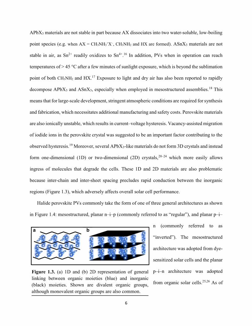
regions (Figure 1.3), which adversely affects overall solar cell performance.
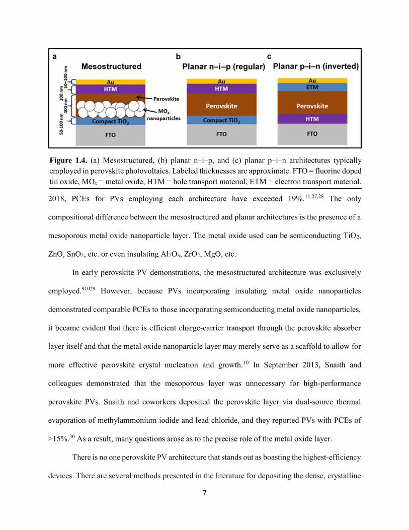
Halide perovskite PVs commonly take the form of one of three general architectures as shown
in Figure 1.4: mesostructured, planar n–i–p (commonly referred to as “regular”), and planar p–i–
n (commonly referred to as
“inverted”). The mesostructured
architecture was adopted from dye-
sensitized solar cells and the planar
p–i–n architecture was adopted
from organic solar cells.25,26 As of
Figure 1.3. (a) 1D and (b) 2D representation of general linking between organic moieties (blue) and inorganic (black) moieties. Shown are divalent organic groups, although monovalent organic groups are also common.
a b
7
2018, PCEs for PVs employing each architecture have exceeded 19%.11,27,28 The only
compositional difference between the mesostructured and planar architectures is the presence of a
mesoporous metal oxide nanoparticle layer. The metal oxide used can be semiconducting TiO2,
ZnO, SnO2, etc. or even insulating Al2O3, ZrO2, MgO, etc.
In early perovskite PV demonstrations, the mesostructured architecture was exclusively
employed.91029 However, because PVs incorporating insulating metal oxide nanoparticles
demonstrated comparable PCEs to those incorporating semiconducting metal oxide nanoparticles,
it became evident that there is efficient charge-carrier transport through the perovskite absorber
layer itself and that the metal oxide nanoparticle layer may merely serve as a scaffold to allow for
more effective perovskite crystal nucleation and growth.10 In September 2013, Snaith and
colleagues demonstrated that the mesoporous layer was unnecessary for high-performance
perovskite PVs. Snaith and coworkers deposited the perovskite layer via dual-source thermal
evaporation of methylammonium iodide and lead chloride, and they reported PVs with PCEs of
>15%.30 As a result, many questions arose as to the precise role of the metal oxide layer.
There is no one perovskite PV architecture that stands out as boasting the highest-efficiency
devices. There are several methods presented in the literature for depositing the dense, crystalline
Figure 1.4. (a) Mesostructured, (b) planar n–i–p, and (c) planar p–i–n architectures typically employed in perovskite photovoltaics. Labeled thicknesses are approximate. FTO = fluorine doped tin oxide, MOx = metal oxide, HTM = hole transport material, ETM = electron transport material.
8
compact TiO2 layer in n–i–p perovskite solar cells; four of these methods were compared by Huang
and colleagues.31 Common methods include chemical bath deposition, sol-gel method, spin-
coating, screen-printing, and spray-pyrolysis.3233 There are also several TiO2 precursor materials
used, which include TiCl4, titanium isopropoxide, and titanium diisopropoxide
bis(acetylacetonate), and commercially-available blocking layer titania pastes.31
Another drawback of halide perovskite PVs is the high cost of commercially-available p-
type hole transport materials, which are used in the regular n–i–p architecture, and n-type electron
transport materials, which are used in the inverted p–i–n architecture. Although poly(3,4-
ethylenedioxythiophene):poly(styrenesulfonate) (PEDOT:PSS) is a p-type hole transport material
commonly used in inverted p–i–n solar cells, it is not employed in regular n–i–p solar cells because
of solvent incompatibility issues. In the n–i–p architecture, the p-type hole transport material is
deposited on top of the intrinsic perovskite layer, which means the solvent used for the hole
transport material solution must not degrade the underlying perovskite layer during deposition. For
PEDOT:PSS solutions, water is the optimal solvent and water, like many polar solvents, readily
decomposes the perovskite by solubilizing the organic component, which compromises the
stability and integrity of the perovskite structure.34
Demonstrations of single-junction perovskite PVs with efficiencies > 20% make them
competitive options for large-scale deployment.35 In order to scale up the PV fabrication process,
innovative materials deposition methods are needed. Inkjet printing is not amenable to the
deposition of many high-quality semiconductor materials, because high-vacuum chemical-vapor-
deposition processes are often required, deposited material precursors must be homogeneous, and
the solvents for the inks must have a low vapor pressure so that regions do not dry prematurely.
These are not problems for perovskite materials, however. First, perovskite materials result in
9
efficient solar cells even when deposited by solution-based techniques. Second, mixing is not
crucial to obtaining homogeneous perovskite thin films; for example, studies have shown that PbI2
can be deposited into a mesoporous metal-oxide support and dried, and then subsequently
immersed into an alcohol solution of MAI to form MAPbI3 nanocrystallites that result in a > 15%
efficient solar cell.29 Third, ABX3 perovskite materials are often deposited from high-boiling point
solvents with low vapor pressures, such as N,N’-dimethylformamide (DMF) (153 °C),
dimethylsulfoxide (DMSO) (189 °C), N-methyl-2-pyrrolidone (203 °C), or γ-butyrolactone (204
°C),36 so that the crystallites can form prior to evaporation of the solvent. Perovskite materials can
therefore be interrogated using combinatorial printing and screening to investigate small
compositional changes and an extremely fine map of the crystallographic structures and bandgap
energies.
1.2 Experimental
1.2.1 Preparation of MAPbX3 Solutions
All chemicals were used as received. Methylammonium iodide (MAI) was synthesized by
slow addition of 6.5 mL of hydriodic acid (47% in water, stabilized with 1.5% hypophosphorous
acid, Sigma-Aldrich) at room temperature to 6 mL of methylamine (40 wt. % in methanol, TCI
America) at 0 °C with stirring, followed by continued stirring for 1 hr. MAI precipitate was
recovered by evaporation of solvents at 50 °C under reduced pressure. To purify MAI, the
precipitate was dissolved in ethanol, recrystallized from diethyl ether, and finally vacuum dried at
60 °C for 12 h. MAPbI3 solution was then prepared by mixing MAI and PbI2 (99%, Sigma-Aldrich)
powders in approximately a 1:1 mole ratio, but with MAI in slight excess, in anhydrous N,N-
dimethylformamide (DMF) at 70 °C inside a nitrogen-filled glovebox. For mixed-halide MAPbI3-
10
xClx solutions, PbI2 was replaced with PbCl2 (98%, Sigma-Aldrich) and powders were mixed in
approximately a 3:1 ratio of MAI to PbCl2. MAPbX3 solutions were stored in the glovebox until
use and were used within one week of preparation.
1.2.2 Thin-Film Processing
1.2.2.1 Substrate Preparation and Metal–Oxide Materials Deposition
All steps of materials deposition and photovoltaic device fabrication were performed in air
with 40–60% relative humidity, unless noted otherwise. All thermal treatments were performed
using a hot plate. Fluorine-doped tin oxide coated glass (FTO) substrates were cleaned as follows:
1) sonicated in Alconox solution, 2) rinsed with deionized water, 3) rinsed with ethanol, 4)
sonicated in ethanol, and 5) dried with nitrogen. To deposit the compact TiO2 (cTiO2) layer, a
solution of titanium diisopropoxide bis(acetylacetonate) was pipetted onto a cleaned FTO substrate
and then the substrate was spun at 2000 rpm (2000 rpm/s acceleration) for 60 s. The substrate was
subsequently dried at 125 °C and then sintered at 550 °C for 30 min. Nanoparticles of TiO2 were
synthesized following a procedure by Ito et al.37 The nanoparticle solution was used as is and was
deposited via blade coating to form a microns thick mesoporous TiO2 (mTiO2) layer for
fluorescence imaging microscopy. For all other thin-film preparation and measurements, the
nanoparticle solution was further diluted in ethanol at a weight ratio of 1:3.5 TiO2 nanoparticle
solution:ethanol. Mesoporous γ-phase Al2O3 nanoparticles (mAl2O3) were used in place of mTiO2
in some thin films and devices. mAl2O3 suspensions were prepared by mixing γ-phase Al2O3
nanoparticles, <50 nm particle size, 20 wt% in isopropanol (Sigma Aldrich) in a solution of ethyl
cellulose, ethanol, and terpineol. The mTiO2 or mAl2O3 layer was deposited by spin coating this
11
solution at 500 rpm (500 rpm/s acceleration) for 5 s and then 5000 rpm (5000 rpm/s acceleration)
for 25 s, then dried at 125 °C, and then sintered at 550 °C for 30 min.
For metal–oxide film coverage measurements, a 2M TiCl4 solution was prepared via slow
addition of TiCl4 (99%, Strem Chemicals) to deionized water. This solution was further diluted
with deionized water to make a 200 mM bath. TiCl4 deposition was carried out following a
procedure adapted from Yella and coworkers.38 Briefly, cTiO2/FTO substrates were submerged in
the TiCl4 bath kept at 70 °C for 30 minutes to allow for a thin capping layer of TiO2 to form on the
substrate. TiO2 thin films were rinsed with water, rinsed with ethanol, dried with a flow of N2, and
dried further in air at 100 °C for 60 minutes.
1.2.2.2 Perovskite Deposition Methods
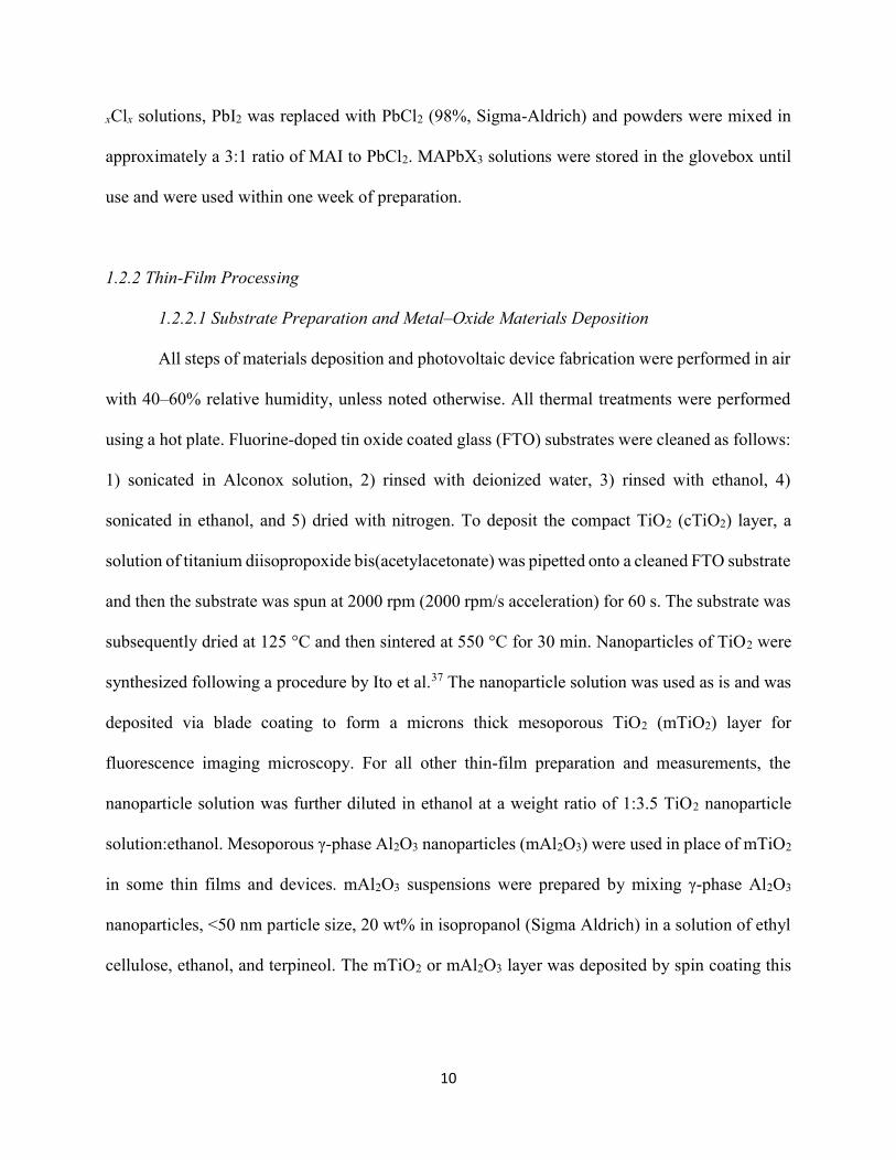
Figure 1.5. (a) Conventional spin-coat procedure for depositing perovskite precursor solution (e.g. MAPbI3 in DMF) on mesoporous metal oxide (MOx)/compact TiO2 (cTiO2)/fluorine-doped tin oxide (FTO). (b) Fast deposition crystallization (FDC) spin-coat procedure, which incorporates an antisolvent (e.g. chlorobenezene) during the spin-coat process.
a
b
12
A conventional one-step spin-
coating method was adapted from the
method of Lee and coworkers,10 in which a
filtered solution of MAPbI3 in DMF was
dropped on top of a metal–oxide(MOx)-
coated FTO substrate and then was spun at
2000 rpm (with 2000 rpm/s acceleration)
for 60 seconds using a spin coater. After
spinning was complete, the substrate was
quickly transferred to a hot plate that was preheated to 100 °C and annealed for 45-60 minutes to
ensure that all DMF evaporated. This conventional spin-coat method is shown pictorially in Figure
1.5a. Other deposition methods that were tested include fast deposition crystallization (FDC)
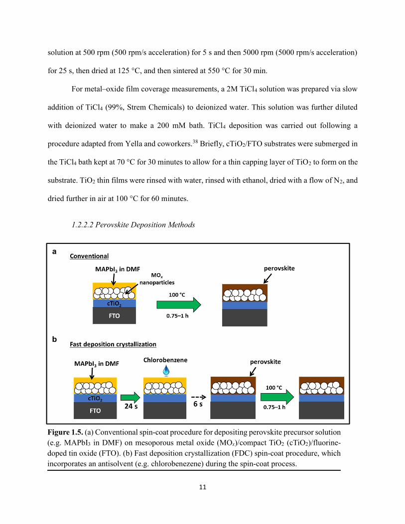
(Figure 1.5b),39 sequential deposition,40 gas-solid crystallization (Figure 1.6),41 vapor-assisted
solution process,42 and hot-casting.43
For the FDC method (shown pictorially in Figure 1.5b), the MAPbX3 solution was instead
spun at 6000 rpm for 30 seconds total, and 6 seconds before the end of the spin process, anhydrous
chlorobenzene (CB) or toluene was dropped onto the film while the substrate was spinning. The
faint yellow film immediately turned dark brown, indicating formation of the MAPbX3 perovskite
structure during the spinning process. For the hot-cast method, a substrate was heated to 130 °C
and the perovskite solution was kept at 70 °C. Then, the substrate was quickly transferred to the
spin coater, perovskite solution was dispensed, and immediately after dispensing, the substrate was
spun at 4000 rpm (4000 rpm/s acceleration) for 6 s. The faint yellow film turned dark brown while
the substrate was spinning, characteristic of perovskite formation. Shortly thereafter, the hole
Figure 1.6. (a) Illustration and (b) digital photograph images of the gas-solid crystallization method whereby methylammonium iodide (MAI) powder is sprinkled on the PbI2 film to form MAPbI3 perovskite during heating at 150 °C.
a
b
13
transport material was deposited or, in cases where no hole
transport material was used, the substrate was transferred to
the glovebox for thermal evaporation of the gold top contact.
1.2.3 Photovoltaic Device Preparation
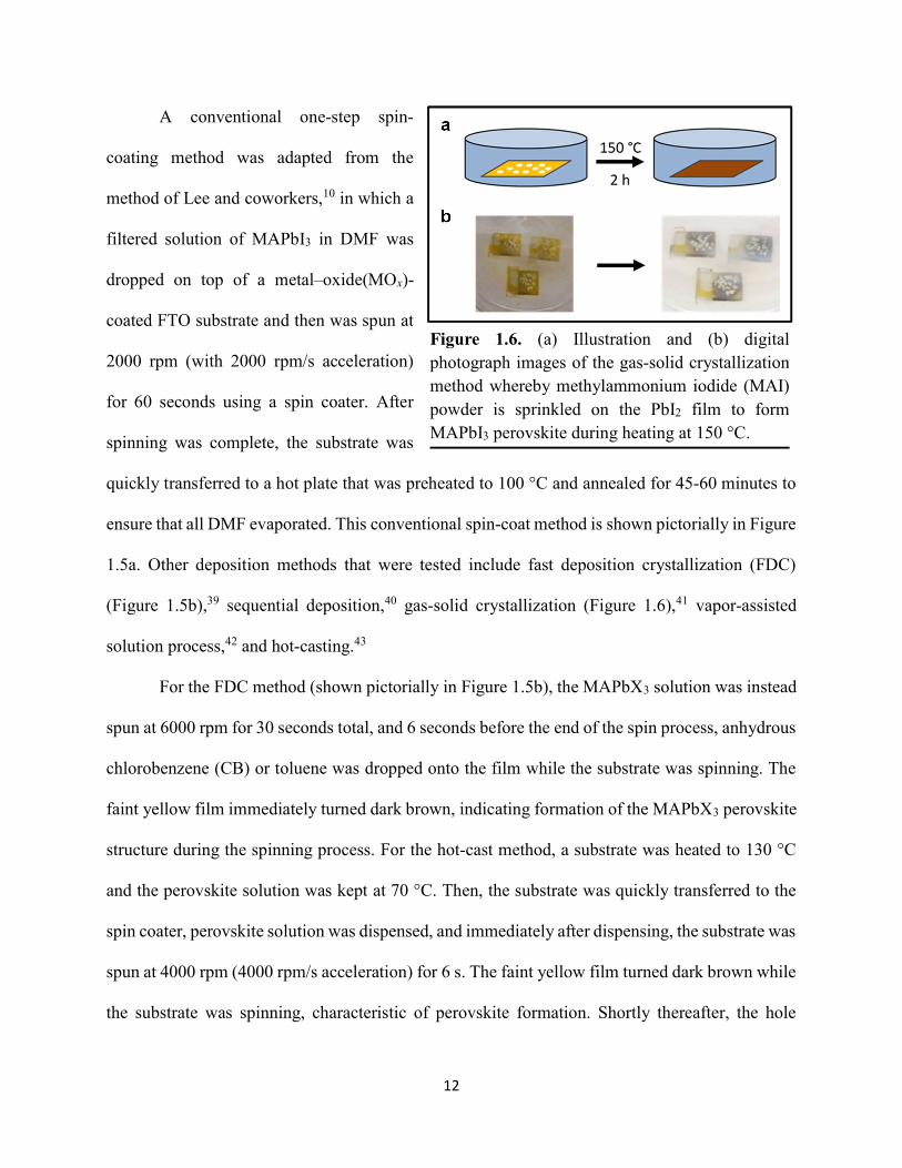
After an FTO-coated glass substrate was cut to a size
of 1 inch x 1 inch, roughly one-third of the FTO was etched
with aqueous 2M HCl and zinc powder in order to prevent
device shunting upon contact to the top Au electrode of the
device (Figure 1.7). To etch the FTO, roughly two-thirds of
the FTO was covered with masking tape, zinc powder was
sprinkled onto the exposed FTO, and aqueous 2M HCl was
dispensed and spread around the exposed FTO. The HCl and zinc powder were allowed to react
for approximately 3 min, and then the FTO was rinsed with deionized water followed by ethanol
and finally dried with a flow of N2. After performing the cleaning steps listed above (1.2.2.1
Substrate Preparation and Metal–Oxide Materials Deposition), substrates were further cleaned
using an O2 plasma treatment for 10 min. During the deposition of the compact TiO2 (cTiO2) layer
and the mesoporous MOx layer via spin coating, one of the corners as well as roughly one-half of
the etched region were masked with scotch tape.
Following deposition of MAPbX3 per one of the protocols described above (Perovskite
Deposition Methods subsection), a 50 mM solution of 2,2’,7,7’- tetrakis(N,N’-di-p-
methoxyphenylamine)-9,9’-spirobifluorene (spiro-OMeTAD) dissolved in chlorobenzene with
additives of 17.5 μL 4-tert-butylpyridine and 37.5 μL lithium bis(trifluoromethane)sulfonimide in
Figure 1.7. Digital photograph image of aqueous 2M HCl and zinc powder reacting to etch away the exposed fluorine-doped tin oxide.
14
acetonitrile (170 mg/mL) was deposited by spin coating at 3000 rpm (3000 rpm/s acceleration) for
60 s. For devices incorporating PEDOT:PSS as the hole transport material (HTM) instead of spiro-
OMeTAD, PEDOT:PSS pellets were dispersed in isopropanol at ~1 wt. % via vortexing and
sonication using an ultrasonic bath and ultrasonic horn. PEDOT:PSS solution was deposited by
spin coating at 2000 rpm (2000 rpm/s acceleration) for 60 s. The MAPbX3 and spiro-oMeTAD
HTM layers were deposited without masking via spin coating. Afterward, a razor blade was used
to scratch off the previously masked areas. Finally, the devices were transferred into a nitrogen-
filled glovebox and 80 nm of gold was thermally evaporated (custom, Law Group) in either a 3 x
3 array of dots or two rectangular strips that slightly overlap where the FTO had been etched away.
The evaporated gold served as the top-contact anode. For current density vs. voltage (J–V)
measurements, a masked area of 0.25 cm2 was illuminated by an ELH lamp of ~1 Sun light
intensity (calibrated with a Si diode).
1.2.4 Electrical Characterization
For electrochemical measurements performed outside the glovebox, including mercury
drop electrode measurements and metal–oxide film coverage measurements, a Biologic Science
VSP-300 was used. For mercury drop electrode and Au electrode conductivity measurements of
thin films, two-electrode cyclic voltammetry was performed vs. Eref by scanning from 0 V to +0.2
V to –0.2 V to 0 V at a scan rate of 100 mV s-1. The inner o-ring area in which the mercury drop
was placed was 0.032 cm2 and the Au dot had an area of 0.085 cm2. For studies on TiO2 film
coverage on FTO-coated glass substrates, thin films immersed in an electrolyte containing 1 mM
ferrocene and 100 mM tetra-n-butylammonium hexafluorophosphate in acetonitrile. An aqueous
KCl-saturated calomel electrode (SCE) was used as the potential-sensing reference electrode, and
15
a platinum mesh electrode and the FTO served as
the current-carrying counter and working
electrodes, respectively. Three-electrode cyclic
voltammetry was then performed vs. ESCE by
scanning from 0 V to +1.2 V to –1.2 V to 0 V at
a scan rate of 50 mV s-1.
For electrochemical measurements
performed inside the glovebox, including
photovoltaic device J–V measurements and light-
intensity-dependent measurements, a Gamry
Instruments Reference 600TM Potentiostat was used. For device J–V measurements, two-electrode
cyclic voltammetry was performed vs. Eref by scanning from 0 V to +1 V (under reverse bias) to –
1 V (under forward bias) to 0 V (under reverse bias) at a scan rate of 100 mV s-1. The gold electrode
of the device was gently contacted with a looped tinned copper wire that was connected to an
alligator clip wired to the potentiostat. Another alligator clip wired to the potentiostat was
contacted to the FTO-coated glass substrate (Figure 1.8). Devices were masked so that only one
“cell” (i.e. one gold pad) was exposed to light. Cells were light-soaked for 5 minutes prior to
running cyclic voltammetry. Current densities were calculated by dividing the current passed
through the potentiostat by the unmasked area of the device. For light-intensity-dependent
measurements, the ELH lamp position was varied to obtain light intensities ranging from ~0.2 to
~1 sun. Chronopotentiometry was performed for each light intensity and VOC values were recorded
60 s after the ELH lamp was turned on.
Figure 1.8. Digital photograph image of the photovoltaic device J–V measurement setup.
16
1.2.5 Mercury-Drop Top-Contact Electrode Setup
Liquid mercury was dropped inside an O-ring
placed on top of the film to be measured (Figure 1.9). A
platinum wire connected to a soldering aid (which was in
electrical contact to an alligator clip of the potentiostat)
was carefully submerged into the mercury drop. A washer
was contacted to the FTO substrate, which was in
electrical contact with a bolt, followed by an alligator clip
of the potentiostat.
1.2.6 Thermal Stability Tests
Thermal stability tests were performed in air for MAPbI3 thin films deposited on
mTiO2/cTiO2/FTO per the protocols above, but using a 70 °C annealing temperature for 60 min.
Then, a UV–Vis absorption spectrum was acquired. The hot plate temperature was raised from the
processing temperature (70 °C) to 90 °C, held for 10 min, and a UV–Vis absorption spectrum of
the thin film was acquired. Then, the temperature was raised to 100 °C, held for 10 min, and
another UV–Vis absorption spectrum was acquired. This procedure was repeated up to 200 °C as
such: 1) the processing temperature was raised by 20 °C, 2) the temperature was held for 10 min,
and 3) a UV–Vis absorption spectrum was acquired.
1.2.7 Thin-Film Characterization
Ultraviolet–visible light (UV–Vis) absorption measurements were carried out using an
Agilent Cary 60 spectrophotometer. Photoluminescence (PL) measurements were performed using
Figure 1.9. Digital photograph image of the mercury-drop top-contact electrode setup.
17
a Cary Eclipse fluorescence spectrophotometer. For fluorescence imaging microscopy
measurements, a 438 nm laser source (Spectra-Physics MaiTai HP) was used to excite the sample
and emission intensity at 650-750 nm was detected and imaged using an Olympus IX81 confocal
laser scanning microscope. Scanning electron microscopy (SEM) images were acquired on a FEI
Magellan 400L XHR. Grazing incidence X-ray diffraction (GIXRD) data were collected using a
Rigaku Smartlab diffractometer with Cu Kα radiation and in parallel beam geometry.
1.3 Results & Discussion
To assess the feasibility of using an inkjet printer system to print combinatorial libraries of
various perovskite material compositions, a mobile, non-destructive, easily deposited and removed
top-contact electrode would be beneficial for performing rapid J–V measurements on PV device
stacks. Because mercury is a liquid metal, it has been used as an electrode in electrochemical
measurements. The use of a mercury drop top-contact electrode would significantly lower the cost
of a high-throughput PV device performance testing system. Mercury is much less expensive than
typical noble metals used, such as gold, and does not require time-consuming vacuum-based
deposition techniques that evaporated metal contacts require for forming an electrode. A
drawback, however, is that mercury forms an amalgam with lead, which would cause
decomposition of the perovskite layer upon contact with the mercury drop. Therefore, in order to
prevent perovskite decomposition, a pinhole-free selective contact between the perovskite layer
and mercury drop is necessary.
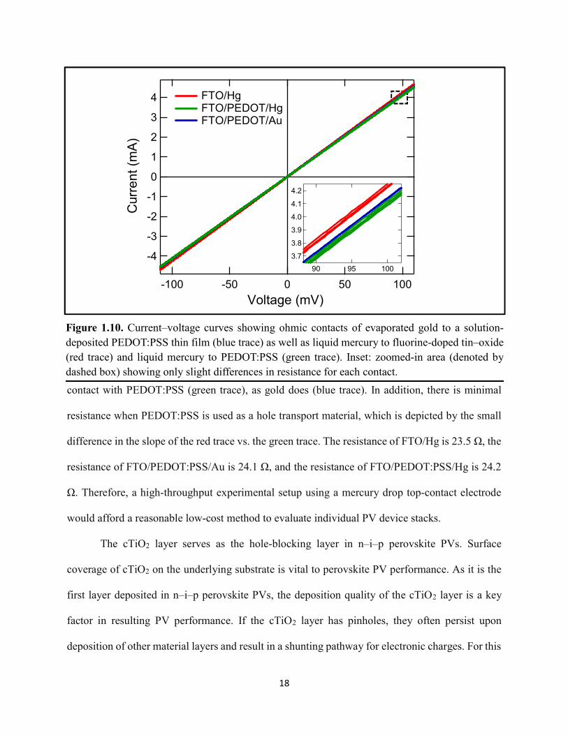
A proof-of-concept demonstration of the use of a mercury drop as a top-contact electrode was
performed and results are shown in Figure 1.10. White-light illumination from an ELH lamp was
incident through the FTO side of each sample. It is evident that liquid mercury forms an ohmic
18
contact with PEDOT:PSS (green trace), as gold does (blue trace). In addition, there is minimal
resistance when PEDOT:PSS is used as a hole transport material, which is depicted by the small
difference in the slope of the red trace vs. the green trace. The resistance of FTO/Hg is 23.5 Ω, the
resistance of FTO/PEDOT:PSS/Au is 24.1 Ω, and the resistance of FTO/PEDOT:PSS/Hg is 24.2
Ω. Therefore, a high-throughput experimental setup using a mercury drop top-contact electrode
would afford a reasonable low-cost method to evaluate individual PV device stacks.
The cTiO2 layer serves as the hole-blocking layer in n–i–p perovskite PVs. Surface
coverage of cTiO2 on the underlying substrate is vital to perovskite PV performance. As it is the
first layer deposited in n–i–p perovskite PVs, the deposition quality of the cTiO2 layer is a key
factor in resulting PV performance. If the cTiO2 layer has pinholes, they often persist upon
deposition of other material layers and result in a shunting pathway for electronic charges. For this
Figure 1.10. Current–voltage curves showing ohmic contacts of evaporated gold to a solution-deposited PEDOT:PSS thin film (blue trace) as well as liquid mercury to fluorine-doped tin–oxide (red trace) and liquid mercury to PEDOT:PSS (green trace). Inset: zoomed-in area (denoted by dashed box) showing only slight differences in resistance for each contact.
4.2
4.1
4.0
3.9
3.8
3.7
1009590
-4
-3
-2
-1
0
1
2
3
4
Cur
ren
t (m
A)
-100 -50 0 50 100
Voltage (mV)
FTO/Hg FTO/PEDOT/Hg FTO/PEDOT/Au
19
reason, determining the most effective precursor and deposition method for the cTiO2 layer is
crucial.
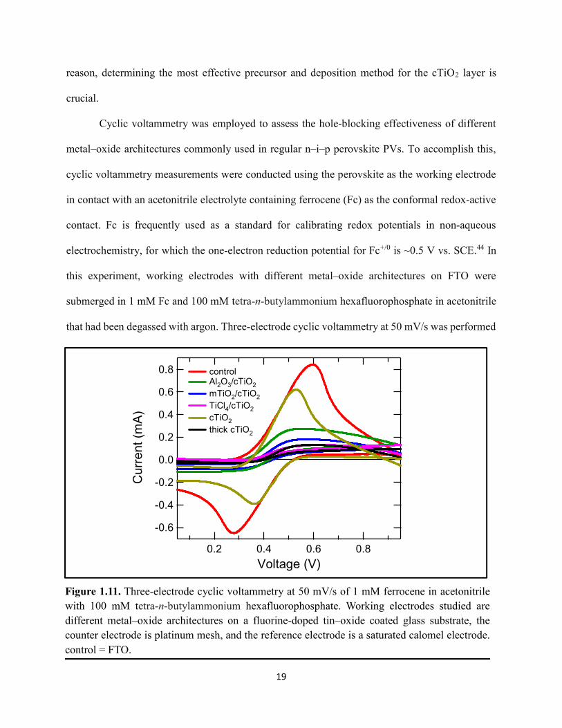
Cyclic voltammetry was employed to assess the hole-blocking effectiveness of different
metal–oxide architectures commonly used in regular n–i–p perovskite PVs. To accomplish this,
cyclic voltammetry measurements were conducted using the perovskite as the working electrode
in contact with an acetonitrile electrolyte containing ferrocene (Fc) as the conformal redox-active
contact. Fc is frequently used as a standard for calibrating redox potentials in non-aqueous
electrochemistry, for which the one-electron reduction potential for Fc+/0 is ~0.5 V vs. SCE.44 In
this experiment, working electrodes with different metal–oxide architectures on FTO were
submerged in 1 mM Fc and 100 mM tetra-n-butylammonium hexafluorophosphate in acetonitrile
that had been degassed with argon. Three-electrode cyclic voltammetry at 50 mV/s was performed
0.8
0.6
0.4
0.2
0.0
-0.2
-0.4
-0.6
Cur
rent
(m
A)
0.80.60.40.2
Voltage (V)
control Al2O3/cTiO2
mTiO2/cTiO2
TiCl4/cTiO2
cTiO2
thick cTiO2
Figure 1.11. Three-electrode cyclic voltammetry at 50 mV/s of 1 mM ferrocene in acetonitrile with 100 mM tetra-n-butylammonium hexafluorophosphate. Working electrodes studied are different metal–oxide architectures on a fluorine-doped tin–oxide coated glass substrate, the counter electrode is platinum mesh, and the reference electrode is a saturated calomel electrode. control = FTO.
20
for each working electrode and voltammograms are shown in Figure 1.11. For the electrode labeled
‘thick cTiO2’ (black trace), the cTiO2 solution was spun-coat using 2000 rpm (2000 rpm/s
acceleration) instead of 4000 rpm (4000 rpm/s acceleration) used for all other electrodes. Single-
electron transfer of Fc+/0 was first monitored on an FTO substrate as a control. For subsequent
films containing TiO2 in various architectures, the suppression of this single-electron transfer
reaction was calculated based on the area under the curve in relation to the control FTO substrate.
The cTiO2 film (gold trace) resulted in 26% suppression, mAl2O3/cTiO2 (green trace) resulted in
51% suppression, mTiO2/cTiO2 (blue trace) resulted in 79% suppression, TiCl4/cTiO2 (pink trace)
resulted in 84% suppression, and thick cTiO2 (black trace) resulted in 85% suppression. It is
evident that the thick cTiO2 and TiCl4/cTiO2 films promoted superior film coverage on FTO.
However, TiCl4 treatment resulted in the precipitation of large TiO2 particles, which introduces
larger surface roughness and thus poorer subsequent perovskite coverage and film smoothness.
For this reason, a slower spin-coat speed (2000 rpm with 2000 rpm/s acceleration) was determined
to be the best method for depositing the compact TiO2 blocking layer for future preparation of thin
films and fabrication of perovskite PVs.
Strong absorption of visible light and efficient charge separation and extraction are
essential properties for PV materials. In order to understand the photophysical, structural, and
morphological properties of MAPbI3, a series of characterizations were performed on MAPbI3 thin
films. Figure 1.12 displays steady-state absorption and steady-state photoluminescence (PL)
emission spectra of MAPbI3 and PbI2. Non-zero absorbance values at longer wavelengths than the
absorption onsets correspond to scattering of incident excitation light. Scattering can be due to
film roughness or differences in refractive index between the film and air. The absorption onset of
a PbI2 thin film was observed at 540 nm, corresponding to a 2.3 eV optical band gap, and the film
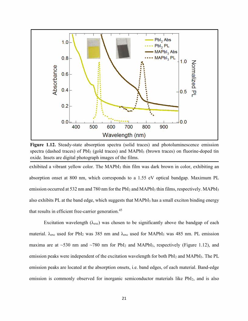
21
exhibited a vibrant yellow color. The MAPbI3 thin film was dark brown in color, exhibiting an
absorption onset at 800 nm, which corresponds to a 1.55 eV optical bandgap. Maximum PL
emission occurred at 532 nm and 780 nm for the PbI2 and MAPbI3 thin films, respectively. MAPbI3
also exhibits PL at the band edge, which suggests that MAPbI3 has a small exciton binding energy
that results in efficient free-carrier generation.45
Excitation wavelength (λexc) was chosen to be significantly above the bandgap of each
material. λexc used for PbI2 was 385 nm and λexc used for MAPbI3 was 485 nm. PL emission
maxima are at ~530 nm and ~780 nm for PbI2 and MAPbI3, respectively (Figure 1.12), and
emission peaks were independent of the excitation wavelength for both PbI2 and MAPbI3. The PL
emission peaks are located at the absorption onsets, i.e. band edges, of each material. Band-edge
emission is commonly observed for inorganic semiconductor materials like PbI2, and is also
Figure 1.12. Steady-state absorption spectra (solid traces) and photoluminescence emission spectra (dashed traces) of PbI2 (gold traces) and MAPbI3 (brown traces) on fluorine-doped tin oxide. Insets are digital photograph images of the films.
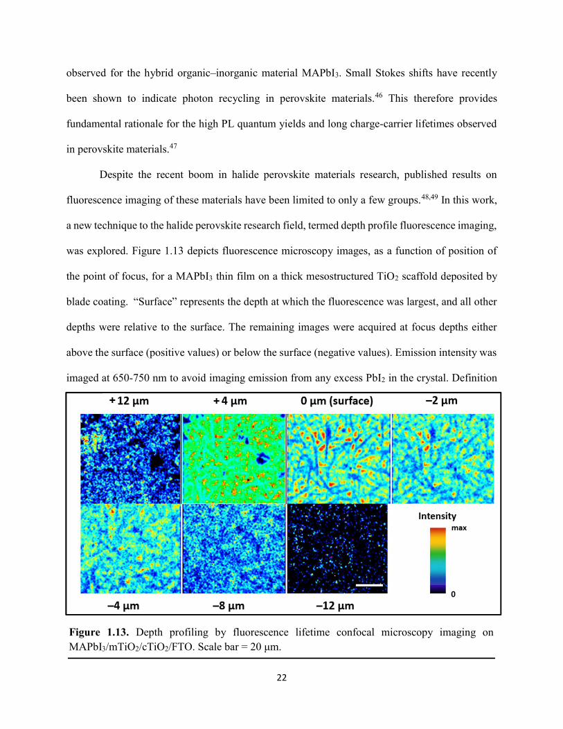
22
observed for the hybrid organic–inorganic material MAPbI3. Small Stokes shifts have recently
been shown to indicate photon recycling in perovskite materials.46 This therefore provides
fundamental rationale for the high PL quantum yields and long charge-carrier lifetimes observed
in perovskite materials.47
Despite the recent boom in halide perovskite materials research, published results on
fluorescence imaging of these materials have been limited to only a few groups.48,49 In this work,
a new technique to the halide perovskite research field, termed depth profile fluorescence imaging,
was explored. Figure 1.13 depicts fluorescence microscopy images, as a function of position of
the point of focus, for a MAPbI3 thin film on a thick mesostructured TiO2 scaffold deposited by
blade coating. “Surface” represents the depth at which the fluorescence was largest, and all other
depths were relative to the surface. The remaining images were acquired at focus depths either
above the surface (positive values) or below the surface (negative values). Emission intensity was
imaged at 650-750 nm to avoid imaging emission from any excess PbI2 in the crystal. Definition
Figure 1.13. Depth profiling by fluorescence lifetime confocal microscopy imaging on MAPbI3/mTiO2/cTiO2/FTO. Scale bar = 20 μm.
+ +
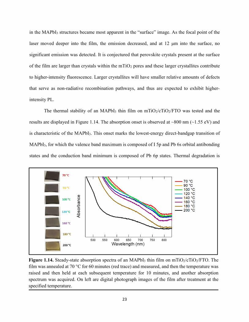
23
in the MAPbI3 structures became most apparent in the “surface” image. As the focal point of the
laser moved deeper into the film, the emission decreased, and at 12 μm into the surface, no
significant emission was detected. It is conjectured that perovskite crystals present at the surface
of the film are larger than crystals within the mTiO2 pores and these larger crystallites contribute
to higher-intensity fluorescence. Larger crystallites will have smaller relative amounts of defects
that serve as non-radiative recombination pathways, and thus are expected to exhibit higher-
intensity PL.
The thermal stability of an MAPbI3 thin film on mTiO2/cTiO2/FTO was tested and the
results are displayed in Figure 1.14. The absorption onset is observed at ~800 nm (~1.55 eV) and
is characteristic of the MAPbI3. This onset marks the lowest-energy direct-bandgap transition of
MAPbI3, for which the valence band maximum is composed of I 5p and Pb 6s orbital antibonding
states and the conduction band minimum is composed of Pb 6p states. Thermal degradation is
Figure 1.14. Steady-state absorption spectra of an MAPbI3 thin film on mTiO2/cTiO2/FTO. The film was annealed at 70 °C for 60 minutes (red trace) and measured, and then the temperature was raised and then held at each subsequent temperature for 10 minutes, and another absorption spectrum was acquired. On left are digital photograph images of the film after treatment at the specified temperature.
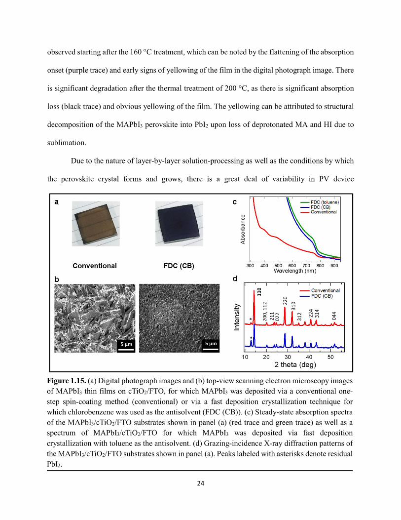
24
observed starting after the 160 °C treatment, which can be noted by the flattening of the absorption
onset (purple trace) and early signs of yellowing of the film in the digital photograph image. There
is significant degradation after the thermal treatment of 200 °C, as there is significant absorption
loss (black trace) and obvious yellowing of the film. The yellowing can be attributed to structural
decomposition of the MAPbI3 perovskite into PbI2 upon loss of deprotonated MA and HI due to
sublimation.
Due to the nature of layer-by-layer solution-processing as well as the conditions by which
the perovskite crystal forms and grows, there is a great deal of variability in PV device
Figure 1.15. (a) Digital photograph images and (b) top-view scanning electron microscopy images of MAPbI3 thin films on cTiO2/FTO, for which MAPbI3 was deposited via a conventional one-step spin-coating method (conventional) or via a fast deposition crystallization technique for which chlorobenzene was used as the antisolvent (FDC (CB)). (c) Steady-state absorption spectra of the MAPbI3/cTiO2/FTO substrates shown in panel (a) (red trace and green trace) as well as a spectrum of MAPbI3/cTiO2/FTO for which MAPbI3 was deposited via fast deposition crystallization with toluene as the antisolvent. (d) Grazing-incidence X-ray diffraction patterns of the MAPbI3/cTiO2/FTO substrates shown in panel (a). Peaks labeled with asterisks denote residual PbI2.
a
b
c
d
25
performance, even when processing procedures are nominally identical.50 When MAPbI3 is
solution-deposited on the same substrate (in this case, cTiO2/FTO), there are clear differences in
film morphology and absorption properties depending on how perovskite crystal formation and
growth is induced (Figure 1.15). Digital photograph images of MAPbI3/cTiO2/FTO substrates
show clear differences that are dependent on processing procedures used (Figure 1.15a). MAPbI3
thin films deposited via a conventional one-step spin-coating method10 (conventional) were a
transparent brown color whereas MAPbI3 thin films deposited via a fast deposition crystallization
technique for which chlorobenzene was used as the antisolvent39 (FDC (CB)) were a semi-
transparent black color. These appearance differences can be explained by the superior surface
coverage of MAPbI3 on the underlying cTiO2 layer when the FDC (CB) method is employed,
which results in denser, smoother thin films than those deposited using the conventional method.
Differences in film morphology can be viewed in the plan-view SEM images in Figure
1.15b. Absorption spectra support the images in Figures 1.15a and 1.15b in that the absorption
onset is sharper and the thin films absorb more light in the visible wavelength region (Figure
1.15c). The grazing-incidence XRD patterns shown in Figure 1.15d confirm crystallization of both
thin films in the tetragonal phase (space group: I4/mcm, Z=4)51 and lattice constants are a = b =
8.90 Å, c= 12.64 Å. The MAPbI3 (110) lattice plane corresponds to the most conductive carrier
transport direction,52 and thus the (110) preferential orientation of the PbI6 framework is beneficial
to MAPbI3 solar cell performance.53 All peaks are attributable to MAPbI3 perovskite except for
the peak labeled with an asterisk at 12.8°, which corresponds to the (001) plane of PbI2. This peak
is slightly more prominent in the film processed by FDC (CB), which can be explained by partial
solubility of MAPbI3 to residual CB in the film during annealing, resulting in decomposition to
26
PbI2. Therefore, the FDC method was the most successful method used to reproduce data of high-
quality films from literature reports.
Complete perovskite PV devices adopting a wide range of architectures and processing
conditions were fabricated and tested. Three promising devices, one of which had a novel
architecture (device 2), are shown in Table 1.1. For device 1, MAPbI3-xClx was hot-cast on
mAl2O3/cTiO2/FTO as described in the experimental section (1.2.2.2 Perovskite Deposition
Methods). Shortly thereafter, substrates were transferred into the glovebox for thermal evaporation
of the gold top contact without deposition of a hole transport material. The best-performing cell of
the device exhibited a PCE of 1.31 %. Device 2 has an architecture not previously reported in the
literature. PEDOT:PSS was employed as a p-type HTM on top of the MAPbI3 layer deposited via
the FDC method. The best-performing cell of the device exhibited a PCE of 2.33 %. Device 3,
which featured an architecture of Au/spiro-OMeTAD/MAPbI3-xClx/mAl2O3/cTiO2/FTO, produced
the highest-efficiency cell of 2.53 %. Devices with the same architecture as device 3 but with
mAl2O3 replaced by mTiO2 did not perform as well. These observations are potentially due to
faster recombination rates at the MAPbI3–mTiO2 interface than at the MAPbI3–mAl2O3 interface.
Reverse-bias voltage sweeps of the best-performing cell of each device are displayed in
Figure 1.16. Although the cell of device 3 had the lowest JSC of the group of cells, it had the highest
VOC and FF. A non-zero slope in reverse bias (i.e. negative potentials) indicates the presence of
shunts. Shunting can also occur when a device contains pinholes, which is an almost unavoidable
issue for solution-processed materials. Most devices tested exhibited significant shunting,
including devices 1 and 2, due to a less-than-optimal device architecture. Device 3, however, does
not exhibit significant shunting, as the slope of the voltage sweep under reverse-bias conditions is
nearly zero. This supports the SEM image shown in Figure 1.15b that indicates high surface
27
Tab
le 1
.1. P
rom
isin
g M
AP
bX3
pero
vski
te P
V d
evic
es.
Dep
osit
ion
met
hod
refe
rs t
o ho
w t
he p
erov
skit
e la
yer
is d
epos
ited
, FD
C =
fast
dep
osit
ion
crys
tall
izat
ion,
VO
C =
ope
n-ci
rcui
t vo
ltag
e, I
SC =
sho
rt-c
ircu
it c
urre
nt,
J SC =
sho
rt-c
ircu
it c
urre
nt d
ensi
ty,
FF =
fil
l
fact
or, P
CE
= p
ower
con
vers
ion
effi
cien
cy.
28
coverage in the FDC-prepared MAPbI3 film. Linear sloped behavior under large forward bias (i.e.
positive potentials) indicates series resistance in the device, which is primarily due to material
layer thicknesses that are too large. Some series resistance is unavoidable, due to the multilayer
nature of the device by which charge-transfer resistances are present at each material layer
interface.
Device 3 was further characterized by chronopotentiometry and chronoamperometry in
order to determine the stability of VOC and JSC values over time under 1 sun illumination. Figure
1.17a and Figure 1.17b show VOC and JSC tracking, respectively. The VOC of the cell exhibits a
rapid onset and plateaus after ~ 1 min (Figure 1.17a). The JSC, on the other hand continues to
increase even after ~2 minutes (Figure 1.17b). For this reason, cells were light-soaked for 5
minutes prior to measurement of J–V characteristics in order to obtain stable photocurrent output
from the cell.
-15
-10
-5
0
5
10
15
J (m
A c
m-2
)
0.80.60.40.20.0-0.2
Voltage (V)
1 2 3
Figure 1.16. Reverse-bias voltage sweeps at 100 mV/s of the best-performing cells of devices 1, 2, and 3.
29
For perovskite PVs incorporating a mesostructured TiO2 layer, it has been shown that
recombination kinetics deviate from first order, which is attributed to a dominant trap-assisted
recombination mechanism due to TiO2 trap states.5455 This observed behavior was tested in
perovskite PVs incorporating a mesostructured Al2O3 layer. Figure 1.18 shows the VOC values of
a PV cell with the architecture Au/PEDOT:PSS/MAPbI3/mAl2O3/cTiO2/FTO as a function of the
natural log of light intensity, with light intensity ranging from 0.2 suns to 1 sun. As expected, the
VOC has a linear dependence to the natural log of the light intensity, with a slope of 35.2 mV.
Because the slope is greater than kT/q, which is 26 mV at room temperature, this suggests that a
component of recombination in the device is attributed to trap-assisted recombination, is the
dominant recombination mechanism. which could be due to Al2O3 crystal impurities that form trap
states in the Al2O3 layer.56 The ideality factor (IF) of the device is 35.2 mV / 26 mV = 1.35. An
ideal pn-junction device has an IF of 1 and an ideal pin-junction device has an IF of 2.57 An IF
between 1 and 2 suggests hybrid behavior.
Light-intensity-dependent measurements presented in Figure 1.18. For data points
corresponding to lower light intensity, the slope is closer to 26 mV (i.e. IF is closer to 1), and for
Figure 1.17. (a) Chronopotentiometry at open circuit and (b) chronoamperometry at short circuit (0 V vs. ref) of the best-performing perovskite cell of device 3. Regions highlighted in yellow represent time when the cell was under illumination.
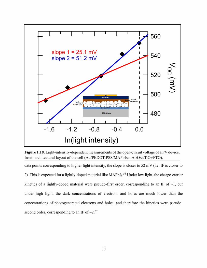
30
data points corresponding to higher light intensity, the slope is closer to 52 mV (i.e. IF is closer to
2). This is expected for a lightly-doped material like MAPbI3.58 Under low light, the charge-carrier
kinetics of a lightly-doped material were pseudo-first order, corresponding to an IF of ~1, but
under high light, the dark concentrations of electrons and holes are much lower than the
concentrations of photogenerated electrons and holes, and therefore the kinetics were pseudo-
second order, corresponding to an IF of ~2.57
560
540
520
500
480
VO
C (mV
)
-1.6 -1.2 -0.8 -0.4 0.0
ln(light intensity)
slope 1 = 25.1 mVslope 2 = 51.2 mV
Figure 1.18. Light-intensity-dependent measurements of the open-circuit voltage of a PV device. Inset: architectural layout of the cell (Au/PEDOT:PSS/MAPbI3/mAl2O3/cTiO2/FTO).
31
1.4 Conclusions
A proof-of-concept demonstration of the use of a mercury drop as a top-contact electrode
showed that liquid mercury forms an ohmic contact with PEDOT:PSS as gold does, meaning that
a high-throughput experimental setup using liquid mercury would afford a reasonable low-cost
method to evaluate individual PV device stacks. Cyclic voltammetry was employed to assess the
hole-blocking effectiveness of different metal–oxide architectures commonly used in regular n–i–
p perovskite PVs, from which it was determined that a slower spin-coat speed (2000 rpm with
2000 rpm/s acceleration) is the best method for depositing the compact TiO2 blocking layer. The
hybrid organic–inorganic material MAPbI3, like the all-inorganic PbI2, exhibits PL at the band
edge, which suggests that MAPbI3 has a small exciton binding energy that results in efficient free-
carrier generation. From fluorescence lifetime confocal microscopy imaging data, it was
conjectured that perovskite crystals present at the surface of the film are larger than crystallites
within the mTiO2 pores and these larger crystallites contribute to higher-intensity fluorescence.
The FDC method was the most successful method used to reproducibly fabricate high-
quality thin films. Three promising devices, one of which had a particularly novel architecture in
that it employed a layer of p-type PEDOT:PSS on top of the perovskite layer, boasted PCEs of >
1.3%. It was determined from light-intensity-dependent measurements that the MAPbI3 thin film
was lightly doped. The charge-carrier kinetics of a lightly-doped material were pseudo-first order
under low light, but under high light, the dark concentrations of electrons and holes are much lower
than the concentrations of photogenerated electrons and holes, and therefore the kinetics were
pseudo-second order.
32
1.5 References
(1) Perez, R.; Perez, M. IEA/SHC Sol. Updat. 2009, 50, 2–3.
(2) SunShot Vision Study http://energy.gov/eere/sunshot/sunshot-vision-study (accessed Oct
25, 2015).
(3) Zhang, S.; Yang, X.; Numata, Y.; Han, L. Energy Environ. Sci. 2013, 6, 1443.
(4) SunShot 2030 Fact Sheet https://www.energy.gov/sites/prod/files/2016/12/f34/SunShot
2030 Fact Sheet-12_16.pdf (accessed May 28, 2018).
(5) 2020 Utility-Scale Solar Goal Achieved https://www.energy.gov/eere/solar/articles/2020-
utility-scale-solar-goal-achieved (accessed May 28, 2018).
(6) Cui, J.; Yuan, H.; Li, J.; Xu, X.; Shen, Y.; Lin, H.; Wang, M. Sci. Technol. Adv. Mater.
2015, 16, 036004.
(7) Sum, T. C.; Mathews, N. Energy Environ. Sci. 2014, 7, 2518–2534.
(8) Song, Z.; McElvany, C. L.; Phillips, A. B.; Celik, I.; Krantz, P. W.; Watthage, S. C.;
Liyanage, G. K.; Apul, D.; Heben, M. J. Energy Environ. Sci. 2017, 10, 1297–1305.
(9) Kojima, A.; Teshima, K.; Shirai, Y.; Miyasaka, T. J. Am. Chem. Soc. 2009, 131, 6050–
6051.
(10) Lee, M. M.; Teuscher, J.; Miyasaka, T.; Murakami, T. N.; Snaith, H. J. Science 2012, 338,
643–647.
(11) Research Cell Efficiency Records https://www.energy.gov/eere/solar/downloads/research-
cell-efficiency-records (accessed May 28, 2018).
(12) Yin, W.; Shi, T.; Yan, Y. Adv. Mater. 2014, 26, 4653–4658.
(13) Saparov, B.; Mitzi, D. B. Chem. Rev. 2016, 116, 4558–4596.
(14) Frost, J. M.; Butler, K. T.; Brivio, F.; Hendon, C. H.; van Schilfgaarde, M.; Walsh, A. Nano
33
Lett. 2014, 14, 2584–2590.
(15) Slavney, A. H.; Smaha, R. W.; Smith, I. C.; Ja, A.; Umeyama, D.; Karunadasa, H. I. Inorg.
Chem. 2017, 56, 46–55.
(16) Cotton, F. A.; Wilkinson, G. Advanced Inorganic Chemistry: A Comprehensive Text.
Advanced Inorganic Chemistry, 1972, 657–669.
(17) Abate, A.; Paek, S.; Giordano, F.; Correa Baena, J. P.; Saliba, M.; Gao, P.; Matsui, T.; Ko,
J.; Zakeeruddin, S. M.; Dahmen, K. H.; Hagfeldt, A.; Grätzel, M.; Mohammad K., N.
Energy Environ. Sci. 2015, 8, 2946–2953.
(18) Aristidou, N.; Sanchez-Molina, I.; Chotchuangchutchaval, T.; Brown, M.; Martinez, L.;
Rath, T.; Haque, S. A. Angew. Chem Int. Ed. 2015, 54, 8208–8212.
(19) Eames, C.; Frost, J. M.; Barnes, P. R. F.; O’Regan, B. C.; Walsh, A.; Islam, M. S. Nat.
Commun. 2015, 6, 7497.
(20) Liang, K.; Mitzi, D. B.; Prikas, M. T. Chem. Mater. 1998, 10, 403–411.
(21) Mitzi, D. B.; Chondroudis, K.; Kagan, C. R. Inorg. Chem. 1999, 38, 6246–6256.
(22) Mitzi, D. B. Inorg. Chem. 2000, 39, 6107–6113.
(23) Smith, I. C.; Hoke, E. T.; Solis-Ibarra, D.; McGehee, M. D.; Karunadasa, H. I. Angew.
Chemie - Int. Ed. 2014, 53, 11232–11235.
(24) Cao, D.; Stoumpos, C. C.; Farha, O. K.; Hupp, J. T.; Kanatzidis, M. G. J. Am. Chem. Soc.
2015, 137, 7843–7850.
(25) Meng, L.; You, J.; Guo, T.-F. F.; Yang, Y. Acc. Chem. Res. 2015, 49, acs.accounts.5b00404.
(26) You, J.; Yang, Y. (Michael); Hong, Z.; Song, T.; Meng, L.; Liu, Y.; Jiang, C.; You, J.;
Yang, Y. M.; Hong, Z.; Song, T.; Meng, L. Appl. Phys. Lett. 2014, 105, 183902.
(27) Ye, S.; Rao, H.; Zhao, Z.; Zhang, L.; Bao, H.; Sun, W.; Li, Y.; Gu, F.; Wang, J.; Liu, Z.;
34
Bian, Z.; Huang, C. J. Am. Chem. Soc. 2017, 139, 7504–7512.
(28) Seok, S. I.; Grätzel, M.; Park, N.-G. Small 2018, 1704177.
(29) Burschka, J.; Pellet, N.; Moon, S.-J.; Humphry-Baker, R.; Gao, P.; Nazeeruddin, M. K.;
Grätzel, M. Nature 2013, 499, 316–319.
(30) Liu, M.; Johnston, M. B.; Snaith, H. J. Nature 2013, 501, 395–398.
(31) Zhang, C.; Luo, Y.; Chen, X.; Ou-yang, W.; Chen, Y.; Sun, Z. Appl. Surf. Sci. 2016, 388,
82–88.
(32) Heo, J. H.; Im, S. H.; Noh, J. H.; Mandal, T. N.; Lim, C.; Chang, J. A.; Lee, Y. H.; Kim,
H.; Sarkar, A.; Nazeeruddin, K.; Gra, M. Nat. Photonics 2013, 1–6.
(33) Dualeh, A.; Moehl, T.; Tétreault, N.; Teuscher, J.; Gao, P.; Nazeeruddin, M. K.; Grätzel,
M. ACS Nano 2014, 8, 362–373.
(34) Leijtens, T.; Eperon, G. E.; Noel, N. K.; Habisreutinger, S. N.; Petrozza, A.; Snaith, H. J.
Adv. Energy Mater. 2015, 5, 1500963.
(35) Green, M. A.; Hishikawa, Y.; Dunlop, E. D.; Levi, D. H.; Hohl-Ebinger, J.; Ho-Baillie, A.
W. Y. Prog. Photovoltaics Res. Appl. 2018, 26, 3–12.
(36) Eperon, G. E.; Burlakov, V. M.; Docampo, P.; Goriely, A.; Snaith, H. J. Adv. Funct. Mater.
2014, 24, 151–157.
(37) Ito, S.; Murakami, T. N.; Comte, P.; Liska, P.; Grätzel, C.; Nazeeruddin, M. K.; Grätzel, M.
Thin Solid Films 2008, 516, 4613–4619.
(38) Yella, A.; Heiniger, L. P.; Gao, P.; Nazeeruddin, M. K.; Grätzel, M. Nano Lett. 2014, 14,
2591–2596.
(39) Xiao, M.; Huang, F.; Huang, W.; Dkhissi, Y.; Zhu, Y.; Etheridge, J.; Gray-Weale, A.; Bach,
U.; Cheng, Y.-B.; Spiccia, L. Angew. Chemie - Int. Ed. 2014, 126, 10056–10061.

35
(40) Burschka, J.; Pellet, N.; Moon, S.-J.; Humphry-Baker, R.; Gao, P.; Nazeeruddin, M. K.;
Grätzel, M. Nature 2013, 499, 316–319.
(41) Hao, F.; Stoumpos, C. C.; Liu, Z.; Chang, R. P. H.; Kanatzidis, M. G. J. Am. Chem. Soc.
2014, 136, 16411–16419.
(42) Chen, Q.; Zhou, H.; Hong, Z.; Luo, S.; Duan, H.-S.; Wang, H.-H.; Liu, Y.; Li, G.; Yang, Y.
J. Am. Chem. Soc. 2014, 136, 622–625.
(43) Nie, W.; Tsai, H.; Asadpour, R.; Blancon, J.; Neukirch, A. J.; Gupta, G.; Crochet, J. J.;
Chhowalla, M.; Tretiak, S.; Alam, M. A.; Wang, H.; Mohite, A. D. Science 2015, 347, 522–
525.
(44) Gagne, R. R.; Koval, C. A.; Lisensky, G. C. Inorg. Chem. 1980, 19, 2854–2855.
(45) D’Innocenzo, V.; Grancini, G.; Alcocer, M. J. P.; Kandada, A. R. S.; Stranks, S. D.; Lee,
M. M.; Lanzani, G.; Snaith, H. J.; Petrozza, A. Nat. Commun. 2014, 5, 1–6.
(46) Yamada, T.; Aharen, T.; Kanemitsu, Y. Phys. Rev. Lett. 2018, 120, 57404.
(47) DeQuilettes, D. W.; Koch, S.; Burke, S.; Paranji, R. K.; Shropshire, A. J.; Ziffer, M. E.;
Ginger, D. S. ACS Energy Lett. 2016, 1, 438–444.
(48) Wen, X.; Sheng, R.; Ho-baillie, A. W. Y.; Benda, A.; Woo, S.; Ma, Q.; Huang, S.; Green,
M. A. J. Phys. Chem. Lett. 2014, 5, 3849–3853.
(49) DeQuilettes, D. W.; Vorpahl, S. M.; Stranks, S. D.; Nagaoka, H.; Eperon, G. E.; Ziffer, M.
E.; Snaith, H. J.; Ginger, D. S. Science 2015, 348, 683–686.
(50) Agarwal, S.; Nair, P. R. J. Appl. Phys. 2017, 122.
(51) Amat, A.; Mosconi, E.; Ronca, E.; Quarti, C.; Umari, P.; Nazeeruddin, M. K.; Grätzel, M.;
De Angelis, F. Nano Lett. 2014.
(52) Ishii, A.; Jena, A. K.; Miyasaka, T. APL Mater. 2014, 2, 091102.
36
(53) Docampo, P.; Hanusch, F. C.; Giesbrecht, N.; Angloher, P.; Ivanova, A.; Bein, T. APL
Mater. 2014, 2.
(54) Bi, D.; Yang, L.; Boschloo, G.; Hagfeldt, A.; Johansson, E. M. J. J. Phys. Chem. Lett. 2013,
4, 1532–1536.
(55) Bi, D.; Moon, S.-J.; Häggman, L.; Boschloo, G.; Yang, L.; Johansson, E. M. J.;
Nazeeruddin, M. K.; Grätzel, M.; Hagfeldt, A. RSC Adv. 2013, 3, 18762–18766.
(56) Sherkar, T. S.; Momblona, C.; Avila, J.; Sessolo, M.; Bolink, H. J.; Koster, L. J. A. ACS
Energy Lett. 2017, 2, 1214–1222.
(57) Sze, S. M.; Ng, K. K. Physics of Semiconductor Devices; 3rd ed.; Wiley: Hoboken, 2007.
(58) Laban, W. A.; Etgar, L. Energy Environ. Sci. 2013, 6, 3249.

37
CHAPTER 2: HYBRID ORGANIC–INORGANIC PHOTOVOLTAICS
BASED ON BISMUTH IODIDE AND 1,6-HEXANEDIAMMONIUM
DICATION
* In part a compilation of one publication1
2.1 Introduction
Lead–halide perovskite (APbX3) photovoltaics offer a potential low-cost alternative to
established silicon photovoltaic technologies, as most of the components can be deposited from
solution using conventional spin-coating methods.2,3 However, issues with lead toxicity and
APbX3 instability remain at the forefront of current research. Though the lead component in the
perovskite material is earth-abundant, lead halides are considered probable carcinogens, and due
to their moderate solubility in water, lead halides could potentially leach into water supplies, which
would deter use of APbX3 photovoltaics.4 Moreover, alkylammonium halide (AX) dissociates into
HX and alkylamine (A) which are both particularly volatile, and thus APbX3 films degrade in
humid or high-temperature conditions, leaving behind a film of PbX2.5 Lastly, many APbX3
photovoltaic architectures suffer from hysteresis during cyclic voltammetry measurements, which
has resulted in inaccurate and typically inflated efficiency values.4,6
These undesired properties of APbX3 motivate the investigation of a replacement for lead
that would allow for equally as inexpensive and more environmentally benign photovoltaics,
assuming they exhibit similar favorable optoelectronic properties. APbX3 materials feature a three-
dimensional lattice of lead halide that participates in charge-carrier conduction,7 and small
monocationic alkylammonium groups that occupy the cavities of the lead iodide lattice, which
have been suggested to result in slow charge-carrier recombination.8 Although studies on APbX3
materials for solar cell applications were first published in 2009,9 the more general class of hybrid
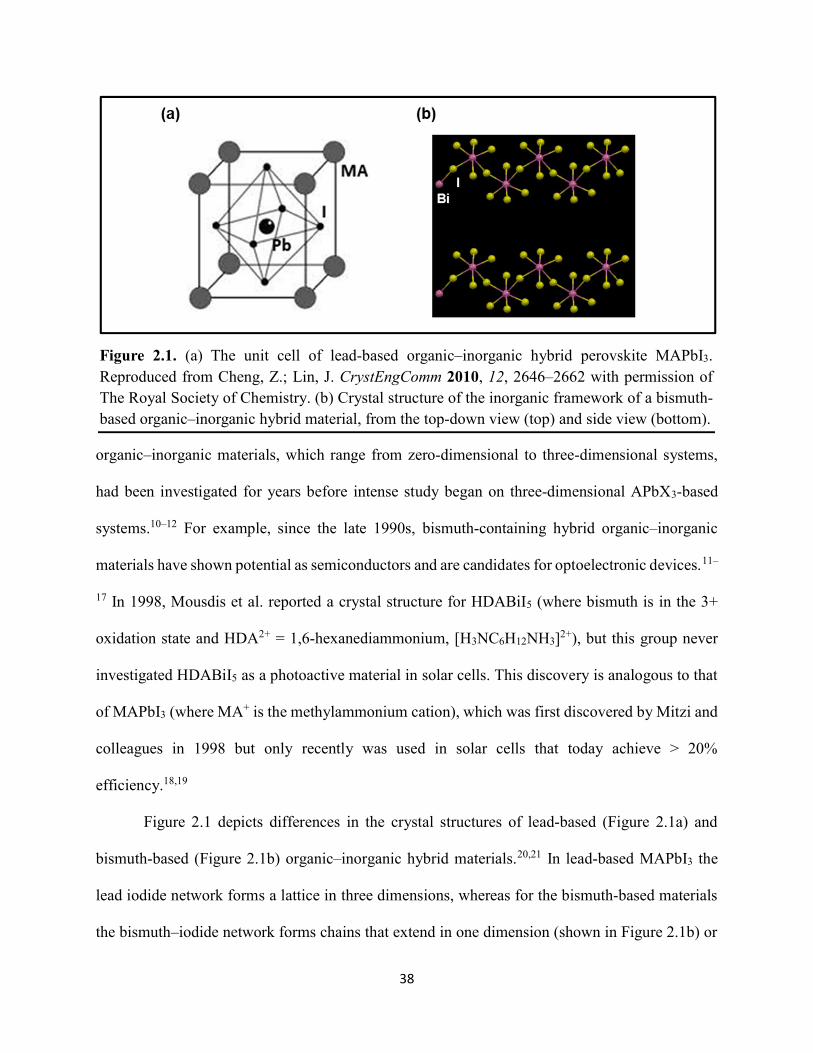
38
organic–inorganic materials, which range from zero-dimensional to three-dimensional systems,
had been investigated for years before intense study began on three-dimensional APbX3-based
systems.10–12 For example, since the late 1990s, bismuth-containing hybrid organic–inorganic
materials have shown potential as semiconductors and are candidates for optoelectronic devices.11–
17 In 1998, Mousdis et al. reported a crystal structure for HDABiI5 (where bismuth is in the 3+
oxidation state and HDA2+ = 1,6-hexanediammonium, [H3NC6H12NH3]2+), but this group never
investigated HDABiI5 as a photoactive material in solar cells. This discovery is analogous to that
of MAPbI3 (where MA+ is the methylammonium cation), which was first discovered by Mitzi and
colleagues in 1998 but only recently was used in solar cells that today achieve > 20%
efficiency.18,19
Figure 2.1 depicts differences in the crystal structures of lead-based (Figure 2.1a) and
bismuth-based (Figure 2.1b) organic–inorganic hybrid materials.20,21 In lead-based MAPbI3 the
lead iodide network forms a lattice in three dimensions, whereas for the bismuth-based materials
the bismuth–iodide network forms chains that extend in one dimension (shown in Figure 2.1b) or
Figure 2.1. (a) The unit cell of lead-based organic–inorganic hybrid perovskite MAPbI3. Reproduced from Cheng, Z.; Lin, J. CrystEngComm 2010, 12, 2646–2662 with permission of The Royal Society of Chemistry. (b) Crystal structure of the inorganic framework of a bismuth-based organic–inorganic hybrid material, from the top-down view (top) and side view (bottom).
Bi
I
39
binuclear clusters that render the material zero-dimensional. If a small dicationic organic group is
incorporated into the structure, it is hypothesized that the chains may be close enough to each other
to provide long-range charge transport in three dimensions similar to that observed in MAPbI3.
Dicationic alkyldiammonium bismuth–halide materials like HDABiI5 are noteworthy
because of reported single-crystal structural resolution, thin-film X-ray diffraction (XRD) patterns
that suggest preferred crystal orientation, and electronic absorption spectra that suggest an optical
bandgap of ~2.0 eV.11,13 Unlike the three-dimensional lead–halide lattice that forms in APbX3, the
metal–halide network of dicationic alkyldiammonium bismuth–halide materials is composed of
one-dimensional zig-zag chains of distorted BiX6 octahedra,11 and it has been suggested that the
role of the organic groups is to serve as molecular fasteners.22 Moreover, Bi3+ is the only stable
and nontoxic cation with the same 6s26p0 electronic configuration as Pb2+, which is important
because the favorable electronic properties of APbX3 materials, such as long carrier lifetimes and
shallow trap states, are in part due to the contributions of Pb2+ to both the conduction band (6p
orbitals) and valence band (6s orbitals).23,24 While Mousdis et al. and Mitzi et al. have previously
synthesized and crystallographically characterized HDABiI5,11,13 analysis of photovoltaic
performance when incorporated as the photoactive layer in a solar cell has not previously been
presented, thus motivating the work presented herein.
Recently, zero-dimensional (0D) A3Bi2I9 perovskite-like materials, where the A groups
are MA+, K+, Rb+, or Cs+, have been examined as lead-free candidate solar absorbers that were
stable in humid air and were shown to exhibit excited-state lifetimes on the order of
nanoseconds.25–28 Notably, a solar cell incorporating 0D Cs3Bi2I9 with an efficiency exceeding 1
% was reported.28 Moreover, the all-inorganic BiI3 was synthesized with phase purity and
exhibited photoluminescence, but no solar cells were fabricated.29 In a separate study a year later,
40
Hamdeh and colleagues reported a BiI3 solar cell with an efficiency just over 1 %.30 A Bi-
containing double perovskite, Cs2AgBiBr6, has been reported to be more heat-stable and moisture-
stable than APbX3, which then led to the synthesis and computational design of novel families of
double perovskites, Cs2BiMX6 and Cs2SbMX6, where M = Cu, Ag, or Au. These materials
exhibited high conductivities and tunable band gaps in the visible range.31 These observations
suggest that lower-dimensional dication-containing Bi–halide hybrid materials warrant further
investigation.
The presence of a well-defined crystal structure that includes organic groups of varying
size allows a unique opportunity to tune transport intra-chain in one-dimensional bismuth–halide
materials. This strategy has been employed in a somewhat related application to fabricate
superlattices of quantum dots for electronics and solar cell applications.32,33 However, there are
many differences in the strategy for quantum dots (versus for the hybrid organic–inorganic
materials described herein): (i) each quantum dot is a separate crystallite with poor-defined surface
termination to the organic linkers, (ii) most times single organic linkers are not thought to bridge
individual quantum dots but form clusters of organic groups between the quantum dots,34 (iii) there
is poor order in quantum dot films because the organic linker is not considered crystalline, (iv)
quantum dots do not bind well to metal-oxide layers without intentionally introducing linkers
between them, and (v) overall photovoltaic performance is often inhibited due to surface trap states
being responsible for rapid recombination.35 In hybrid organic–inorganic materials, the organic
group is innately incorporated as part of the crystallite and is therefore directed anisotropically,
which provides unique opportunities to carefully and controllably tune the ability for charges to
transport between individual chains. In this regard, the bandgap, the conductivity, moisture
stability and ultimately, device performance can be varied by modifying the nature of the organic
41
groups, and the strength of the intra-crystallite and inter-crystallite electronic interactions.36 With
the use of relatively small dications, it is hypothesized that these properties will be most optimized.
2.2 Experimental
2.2.1 Preparation of MAPbI3 and HDABiI5 Solutions
All chemicals were used as received. Methylammonium iodide (MAI) was synthesized by
slow addition of 6.5 mL of hydriodic acid (47% in water, stabilized with 1.5% hypophosphorous
acid, Sigma-Aldrich) at room temperature to 6 mL of methylamine (40 wt. % in methanol, TCI
America) at 0 °C with stirring, followed by continued stirring for 1 hr. MAI precipitate was
recovered by evaporation of solvents at 50 °C with a rotary evaporator. To purify MAI, the
precipitate was dissolved in ethanol, recrystallized from diethyl ether, and finally vacuum dried at
60 °C for 12 h. MAPbI3 solution was then prepared by mixing MAI and PbI2 (99%, Sigma-Aldrich)
powders at approximately a 1:1 mole ratio, but with MAI in slight excess, in anhydrous N,N-
dimethylformamide (DMF) at 70 °C inside a nitrogen-filled glovebox. The MAPbI3 solution was
stored in the glovebox until use and was used within one week of preparation.
To synthesize 1,6-hexanediamine dihydriodide (HDA•2HI), 260.9 mg of 1,6-
hexanediamine (98+%, Alfa Aesar) was dissolved in 5 mL methanol, and then 1 mL hydriodic
acid was added slowly at 0 °C with stirring, followed by stirring for an additional 30 min.
HDA•2HI precipitate was recovered by evaporation of solvents at 40 °C with a rotary evaporator.
The precipitate was rinsed with diethyl ether, and vacuum dried at 60 °C for 12 h. HDABiI5
solution was then prepared by mixing HDA•2HI and BiI3 (99%, Sigma-Aldrich) powders at an
approximately 1:1 mole ratio, but with HDA•2HI in slight excess, in anhydrous DMF at 70 °C
42
inside a nitrogen-filled glovebox. The HDABiI5 solution was stored in the glovebox until use and
was used within one week of preparation.
2.2.2 Materials Processing
All steps of materials deposition and device fabrication were performed in air with 40–
60% relative humidity and as described below, unless noted otherwise. All thermal treatments
were performed using a hot plate. Fluorine-doped tin oxide coated glass (FTO) substrates were
cleaned as follows: 1) sonication in Alconox solution, 2) rinse with deionized water, 3) rinse with
ethanol, 4) sonication in ethanol, and 5) dry with nitrogen. A compact TiO2 (cTiO2) layer was
deposited by pipetting a solution of titanium diisopropoxide bis(acetylacetonate) on a cleaned FTO
substrate and then the substrate was spun at 2000 rpm (2000 rpm/s acceleration) for 60 s. The
substrate was subsequently dried at 125 °C and then sintered at 550 °C for 30 min. Nanoparticles
of TiO2 were synthesized following a procedure by Ito et al.37 The nanoparticle solution was further
diluted in ethanol at a ratio of 1:3.5 TiO2 nanoparticle solution:ethanol, w/w to make a mesoporous
TiO2 (mTiO2) suspension. The mTiO2 layer was deposited by spin coating this solution at 500 rpm
(500 rpm/s acceleration) for 5 s and then 5000 rpm (5000 rpm/s acceleration) for 25 s, followed
by drying at 125 °C, and then sintering at 550 °C for 30 min. The substrates were allowed to cool
to room temperature. Unless otherwise noted, a conventional spin-coat deposition method was
adapted from Kim et al.38 and used for both MAPbI3 and HDABiI5. For this method, a filtered
MAPbI3 or HDABiI5 solution in DMF was pipetted on top of the mTiO2-coated FTO substrate and
then the substrate was spun at 2000 rpm (2000 rpm/s acceleration) for 60 s, followed by rapid
transfer to a hot plate that was preheated to 100 °C and subsequent annealing at 100 °C for 30 min.
43
Other procedures for depositing the photoactive layer (i.e. MAPbI3 or HDABiI5) that have
been tested include a fast-deposition crystallization (FDC) method, a hot-casting method, and a
“drop-heat-spin” (DHS) method that was pioneered as part of the work presented herein. All
deposition procedures are described in the experimental section of Chapter 1 (1.2.2.2 Perovskite
Deposition Methods) except the DHS method. For the DHS method, a substrate was placed on a
hot plate set at 70 °C and the substrate was allowed to reach thermal equilibrium with the hot plate.
A solution containing the precursors for the photoactive layer was kept at 70 °C during that time.
The solution was dispensed on the substrate at a volume of 17.5 μA/cm2 and the dispensed solution
was heated on the substrate at 70 °C for 2 min. Then, the substrate was quickly transferred to a
spin coater and spun at 3000 rpm (3000 rpm/s acceleration) for 60 s. The resulting film was
annealed at 100 °C for 60 min.
2.2.3 Device Fabrication
Prior to the FTO cleaning step, a region of the FTO film was etched using 2 M HCl and Zn
powder in order to prevent device shunting upon contact to the device top Au electrode. After
performing the cleaning steps listed above (Materials Processing subsection), FTO substrates were
further cleaned using an O2 plasma treatment for 10 min. Following deposition of HDABiI5 per
the protocol described above (Materials Processing subsection), a 50 mM solution of 2,2’,7,7’-
tetrakis(N,N’-di-p-methoxyphenylamine)-9,9’-spirobifluorene (spiro-OMeTAD) dissolved in
chlorobenzene with additives of 17.5 μL 4-tert-butylpyridine and 37.5 μL lithium
bis(trifluoromethane)sulfonimide in acetonitrile (170 mg/mL) was deposited by spin coating at
3000 rpm (3000 rpm/s acceleration) for 60 s. The devices were then transferred into a nitrogen-
filled glovebox and 80 nm of Au was thermally evaporated onto the devices at a base pressure of
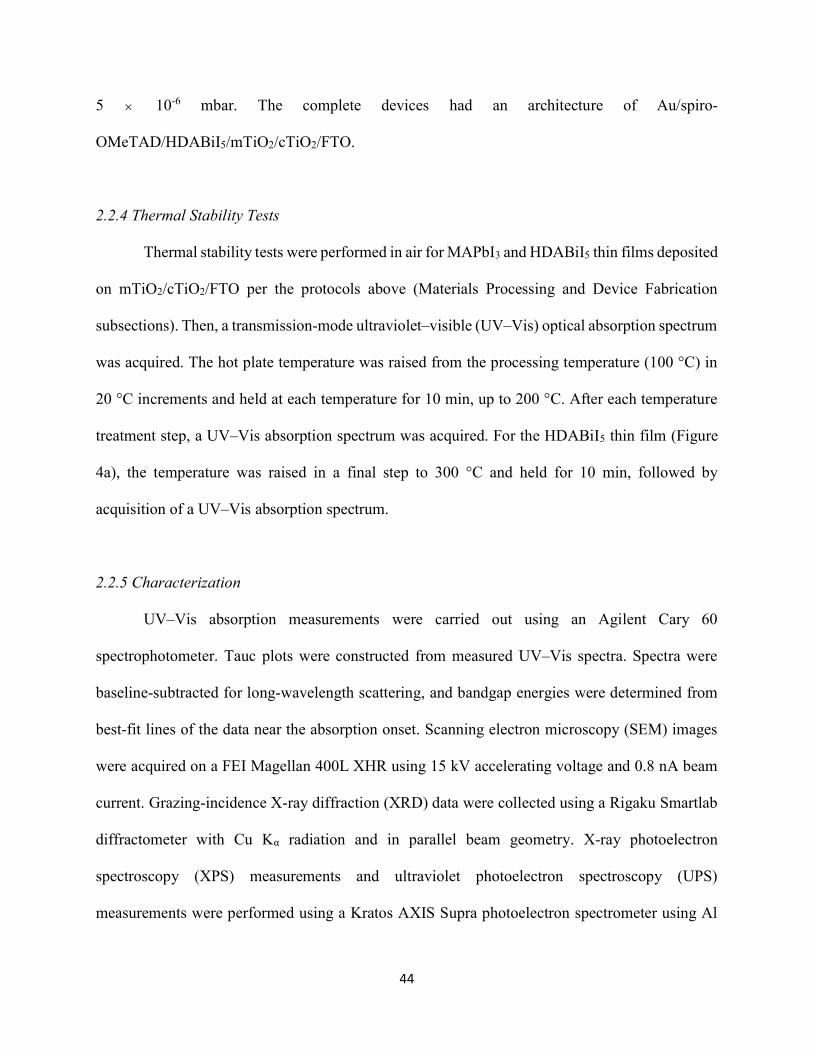
44
5 10-6 mbar. The complete devices had an architecture of Au/spiro-
OMeTAD/HDABiI5/mTiO2/cTiO2/FTO.
2.2.4 Thermal Stability Tests
Thermal stability tests were performed in air for MAPbI3 and HDABiI5 thin films deposited
on mTiO2/cTiO2/FTO per the protocols above (Materials Processing and Device Fabrication
subsections). Then, a transmission-mode ultraviolet–visible (UV–Vis) optical absorption spectrum
was acquired. The hot plate temperature was raised from the processing temperature (100 °C) in
20 °C increments and held at each temperature for 10 min, up to 200 °C. After each temperature
treatment step, a UV–Vis absorption spectrum was acquired. For the HDABiI5 thin film (Figure
4a), the temperature was raised in a final step to 300 °C and held for 10 min, followed by
acquisition of a UV–Vis absorption spectrum.
2.2.5 Characterization
UV–Vis absorption measurements were carried out using an Agilent Cary 60
spectrophotometer. Tauc plots were constructed from measured UV–Vis spectra. Spectra were
baseline-subtracted for long-wavelength scattering, and bandgap energies were determined from
best-fit lines of the data near the absorption onset. Scanning electron microscopy (SEM) images
were acquired on a FEI Magellan 400L XHR using 15 kV accelerating voltage and 0.8 nA beam
current. Grazing-incidence X-ray diffraction (XRD) data were collected using a Rigaku Smartlab
diffractometer with Cu Kα radiation and in parallel beam geometry. X-ray photoelectron
spectroscopy (XPS) measurements and ultraviolet photoelectron spectroscopy (UPS)
measurements were performed using a Kratos AXIS Supra photoelectron spectrometer using Al
45
Kα radiation. For XPS measurements, two separate spots on the sample were evaluated to confirm
matching peak intensities for binding energy scans of C 1s, N 1s, Bi 4f, I 3d, Ti 2p, and O 1s. XPS
data were analyzed using CasaXPS Processing Software and the peaks were fit to Gaussian–
Lorentzian (80/20) curves. UPS measurements were performed with an unfiltered He I (21.22 eV)
gas discharge lamp, and Fermi edge calibration was performed with a sputter-cleaned Ag standard
to ensure that all energies were referenced to a common Fermi level (0 eV). SEM, grazing-
incidence XRD, XPS, and UPS work was performed in the UC Irvine Materials Research Institute
(IMRI).
An ELH-type W–halogen lamp was used inside a nitrogen-filled glovebox as a source of
simulated solar illumination. Before measurement of device J–E behavior and
chronoamperometry, the light intensity was roughly approximated to be 1 Sun using a calibrated
Si photodiode (ThorLabs, Inc., FDS100) positioned at the location of the device. Based on the
integrated photocurrent of devices determined from the product of the incident-photon-to-current
efficiency (IPCE) values and the air mass 1.5 global (AM1.5G) solar photon flux spectrum at 1
Sun intensity, however, the simulated solar illumination for measurement of J–E behavior and
chronoamperometry was more accurately determined to be 0.8 Suns (i.e. the steady-state
photocurrent density measured by the ELH lamp was 0.115 mA/cm2, and the integrated
photocurrent density measured by the IPCE setup was 0.143 mA/cm2, and so 0.115 / 0.143 = 0.8).
Cyclic voltammetry measurements (at a scan rate of 100 mV s-1) and chronoamperometry
measurements were performed using a Gamry Reference 600 Potentiostat. The diode quality factor
of a device was measured by evaluating the dependence of the open-circuit photovoltage on light
intensity. The light intensity was varied by adjusting the position of the lamp source with respect
to the position of the tested device. The data were fit to the Shockley diode equation by the method
46
of least squares and the diode quality factor was determined to be ~1.3. IPCE action spectra were
determined using a Cornerstone 260 monochromator equipped with a 100 W APEX2 Xe arc lamp,
and an NREL-calibrated Si solar cell as the reference.
2.3 Results & Discussion
It has been demonstrated that issues of stability and conductivity can in part be mitigated
through use of new photovoltaic bismuth–halide “perovskite-like” materials that specifically
incorporate organic dications within their crystallites. These materials are considered “perovskite-
like” because, like perovskites, they are hybrid organic–inorganic materials, but the materials do
not adopt the perovskite structure. More details on the implications of this classification are
provided in Chapter 3. HDABiI5 was determined out of a library of hybrid organic–inorganic
Figure 2.2. (a) Cross-sectional scanning electron microscopy image of a representative HDABiI5 device, and (b) direct-bandgap and (c) indirect-bandgap Tauc plots of HDABiI5 deposited as thin films on FTO, and baseline corrected for the FTO substrate. D. M. Fabian and S. Ardo, J. Mater. Chem. A, 2016, 4, 6837 – Reproduced by permission of The Royal Society of Chemistry

47
bismuth–halide materials containing organic dications to be the ideal material candidate of its class
for PV use in terms of closest-to-ideal bandgap and high crystal quality when cast as a thin film.
Scanning electron microscopy (SEM) images of a cross section of a complete HDABiI5
device revealed that the HDABiI5-coated mesoporous TiO2 nanoparticle layer (HDABiI5/mTiO2)
was 200–250 nm thick (Figure 2.2a), which is comparable to the thickness of state-of-the-art
mesostructured perovskite solar cells.39 Top-down SEM images (Figure 2.2a) showed crystal
morphology and near-complete surface coverage of mTiO2 by HDABiI5. The majority of HDABiI5
crystal grains appeared to range in size between 200 nm and 400 nm with no preferential
orientation in the plane of the deposited film. Also, HDABiI5 covered the mTiO2 layer to a greater
extent than APbX3 processed by the same method (Figure 2.3). The transmission-mode
ultraviolet–visible (UV–Vis) absorption spectrum of an HDABiI5 thin film displayed as Tauc plots
are shown in Figure 2.2b and 2.2c and both suggest that the optical bandgap of HDABiI5 is ~2.1
eV with a lowest-energy indirect transition of 2.05 eV and a lowest-energy direct transition of 2.15
eV.
Figure 2.3. Top-view scanning electron microscopy image of (a) HDABiI5 and (b) MAPbI3 deposited on mTiO2/cTiO2/FTO. Overall surface coverage of MAPbI3 on mTiO2 is poor compared to that of HDABiI5 on mTiO2. D. M. Fabian and S. Ardo, J. Mater. Chem. A, 2016, 4, 6837 – Reproduced by permission of The Royal Society of Chemistry
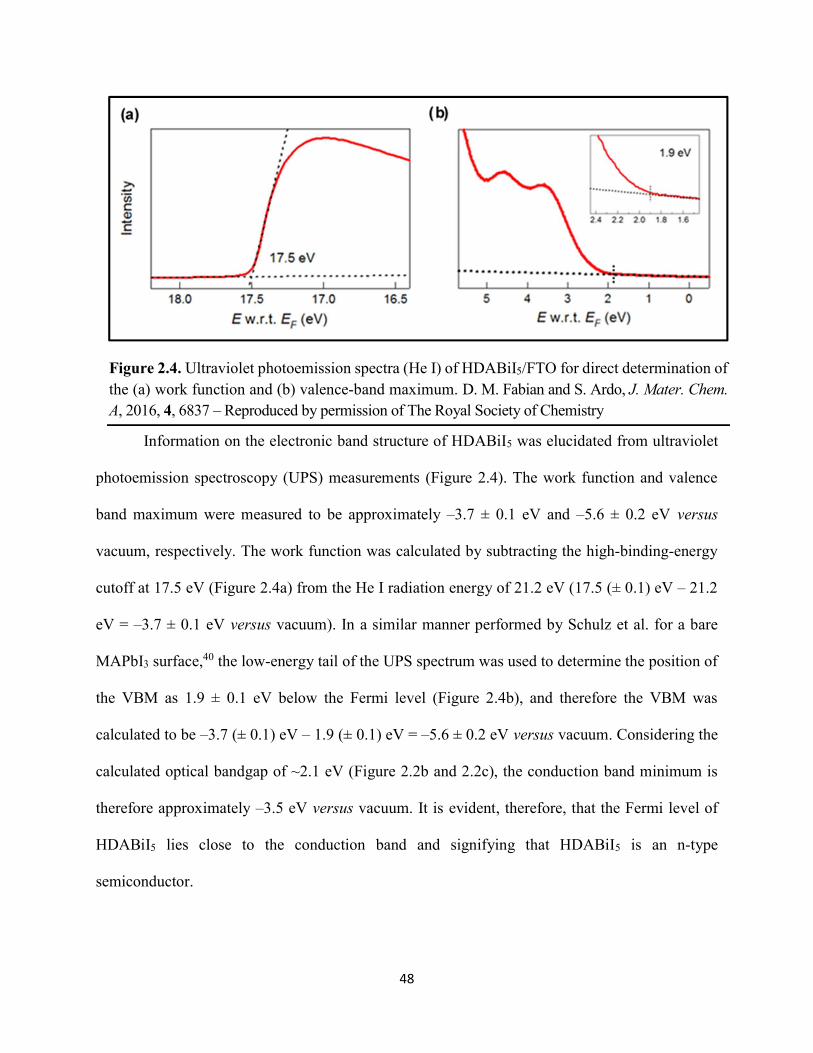
48
Information on the electronic band structure of HDABiI5 was elucidated from ultraviolet
photoemission spectroscopy (UPS) measurements (Figure 2.4). The work function and valence
band maximum were measured to be approximately –3.7 ± 0.1 eV and –5.6 ± 0.2 eV versus
vacuum, respectively. The work function was calculated by subtracting the high-binding-energy
cutoff at 17.5 eV (Figure 2.4a) from the He I radiation energy of 21.2 eV (17.5 (± 0.1) eV – 21.2
eV = –3.7 ± 0.1 eV versus vacuum). In a similar manner performed by Schulz et al. for a bare
MAPbI3 surface,40 the low-energy tail of the UPS spectrum was used to determine the position of
the VBM as 1.9 ± 0.1 eV below the Fermi level (Figure 2.4b), and therefore the VBM was
calculated to be –3.7 (± 0.1) eV – 1.9 (± 0.1) eV = –5.6 ± 0.2 eV versus vacuum. Considering the
calculated optical bandgap of ~2.1 eV (Figure 2.2b and 2.2c), the conduction band minimum is
therefore approximately –3.5 eV versus vacuum. It is evident, therefore, that the Fermi level of
HDABiI5 lies close to the conduction band and signifying that HDABiI5 is an n-type
semiconductor.
Figure 2.4. Ultraviolet photoemission spectra (He I) of HDABiI5/FTO for direct determination of the (a) work function and (b) valence-band maximum. D. M. Fabian and S. Ardo, J. Mater. Chem. A, 2016, 4, 6837 – Reproduced by permission of The Royal Society of Chemistry
49
An energy-level diagram is
displayed as Figure 2.5, where the
calculated CBM (–3.5 eV), VBM (–5.6
eV), and Fermi level (–3.7 eV) are
depicted. The electronic band gap of the
widely studied lead–halide-based
perovskites has been shown to be 0.1 eV
larger than the optical band gap,40 and
thus the CBM of HDABiI5 may in fact
lie at an energy closer to the vacuum
level. The CBM of TiO2 (–4.21 eV
versus vacuum) was taken from a report
by Xu et al.,41 and the VBM of spiro-
OMeTAD (–5.15 eV versus vacuum)
was taken from a report by Nguyen et
al.42 The spiro-OMeTAD/HDABiI5 and HDABiI5/TiO2 interfaces are responsible for combined
photovoltage losses of greater than 1 V, and so use of a hole-transporting material with a more
negative VBM and an electron-transporting material with a less negative CBM may result in a
device with a larger photovoltage.
Figure 2.6a displays a grazing-incidence XRD pattern of HDABiI5 infiltrated into an
mTiO2 layer on top of a cTiO2-coated FTO substrate (HDABiI5/mTiO2/cTiO2/FTO). The XRD
pattern of the solution-deposited HDABiI5 film matches the pattern determined by Mitzi et al. for
an HDABiI5 film deposited using a single source thermal ablation technique.43 HDABiI5
Figure 2.5. Energy-level diagram of spiro-OMeTAD/HDABiI5/TiO2, where the VBM of HDABI5 was determined by UPS measurement. D. M. Fabian and S. Ardo, J. Mater. Chem. A, 2016, 4, 6837 – Reproduced by permission of The Royal Society of Chemistry
50
crystallizes in a primitive orthorhombic crystal structure, with lattice constants that match those
determined for an HDABiI5 single crystal by Mousdis et al. (a = 15.2 Å, b = 14.4 Å, c = 8.7 Å).11
It is evident from grazing-incidence XRD that the (110) plane is orientated in the plane of the
underlying substrate. It is conjectured that the bismuth–iodide chains participate in carrier
conduction along the (110) plane, similar to the facilitated carrier conduction along the (110) plane
in the lead–halide network of APbX3.7
Figure 2.6. (a) Grazing-incidence XRD pattern and (b) XPS spectra of HDABiI5/ mTiO2/cTiO2/FTO. D. M. Fabian and S. Ardo, J. Mater. Chem. A, 2016, 4, 6837 – Reproduced by permission of The Royal Society of Chemistry
Figure 2.7. (a) Sequential X-ray photoelectron spectra of the Bi 4f region, which demonstrate increased signal attributed to Bi0 compared to signal attributed to Bi3+ concomitant with longer exposure to Al Kα X-ray radiation. (b) First scan (red circles) and (c) second scan (blue circles) of the Bi 4f region, with Shirley backgrounds (gold curves) and peak fits (black curves) shown for clarity. D. M. Fabian and S. Ardo, J. Mater. Chem. A, 2016, 4, 6837 – Reproduced by permission of The Royal Society of Chemistry
51
The speciation of the near-surface atoms was characterized by X-ray photoelectron
spectroscopy (XPS) (Figure 2.6b). Scans of the C 1s core level binding energy reveal the presence
of two peaks, corresponding to both C–C and C–N bonds in the organic HDA2+ groups.44 Bi 4f
core level binding energy scans indicate that Bi species exist predominantly in the 3+ oxidation
state, and a small amount as Bi0, which is suggested to be induced in part during measurement of
the XPS spectra. The first XPS Bi 4f region scan displayed in Figure 2.6b is also displayed in
Figure 2.7 (red traces) and was the first scan acquired for the sample. A subsequent Bi 4f scan was
acquired immediately afterward and is also shown in Figure 2.7 (blue traces). For each scan, an
emission current of 20 mA was used, and two sweeps were performed. Based on peak fitting to
Gaussian–Lorentzian (80:20) curves, percent concentration of Bi0 was determined to be ~15% in
the first scan and ~20% in the second scan. This suggests that some Bi0 species formed as
degradation during X-ray radiation, and that some Bi0 was most likely present on the surface of
the as-deposited HDABiI5. No Bi0 peaks could be resolved by grazing-incidence XRD, suggesting
that any Bi0 present at the surface of the as-deposited film existed as isolated atoms or small
amorphous clusters.
Figure 2.8. XPS region scans of (a) Ti 2p and (b) O 1s binding energies for HDABiI5/mTiO2/cTiO2/FTO, where the intensities are normalized to the I 3d5/2 peak in Figure 2.6b. Small peak intensities indicate near-complete coverage of mTiO2 by HDABiI5. D. M. Fabian and S. Ardo, J. Mater. Chem. A, 2016, 4, 6837 – Reproduced by permission of The Royal Society of Chemistry
52
Ti 2p and O 1s peaks were negligible indicating near-complete coating of mTiO2 by
HDABiI5. Approximate elemental composition was determined based on regions scans of
HDABiI5/mTiO2/cTiO2/FTO. To take into account the contribution of the Ti 2p1/2 peak that is
overlapped by the Bi 4d 3/2 peak, the overall peak area of Ti was approximated as the Ti 2p3/2 peak
area multiplied by 1.5, since the Ti 2p1/2 to Ti 2p3/2 area ratio is expected to be 1:2 (Figure 2.8).45
The percent composition of Ti was determined to be 0.6 atom % (Table 2.1). Approximate percent
elemental composition at the surface of HDABiI5/mTiO2/cTiO2/FTO (Table 2.1), which was
calculated based on region scans, indicates ~98% coating of mTiO2 by HDABiI5.
Complete photovoltaic devices with the architecture Au/spiro-
OMeTAD/HDABiI5/mTiO2/cTiO2/FTO, where spiro-OMeTAD is 2,2’,7,7’-tetrakis(N,N’-di-p-
methoxyphenylamine)-9,9’-spirobifluorene, were fabricated and their photovoltaic performance
was evaluated (Figure 2.9). A side-view representation of the complete device architecture is
shown in Figure 2.10. Current density versus potential (J–E) behavior of a device with an active
area of 0.25 cm2 was measured (Figure 2.9a). In the reverse scan direction (indicated by the left-
Table 2.1. Approximate percent surface elemental composition (excluding hydrogen) of HDABiI5/mTiO2/cTiO2/FTO calculated from XPS region scans. D. M. Fabian and S. Ardo, J. Mater. Chem. A, 2016, 4, 6837 – Reproduced by permission of The Royal Society of Chemistry
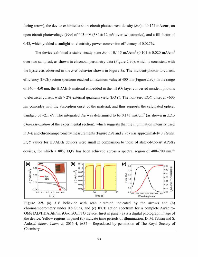
53
facing arrow), the device exhibited a short-circuit photocurrent density (JSC) of 0.124 mA/cm2, an
open-circuit photovoltage (VOC) of 403 mV (384 ± 12 mV over two samples), and a fill factor of
0.43, which yielded a sunlight-to-electricity power-conversion efficiency of 0.027%.
The device exhibited a stable steady-state JSC of 0.115 mA/cm2 (0.101 ± 0.020 mA/cm2
over two samples), as shown in chronoamperometry data (Figure 2.9b), which is consistent with
the hysteresis observed in the J–E behavior shown in Figure 3a. The incident-photon-to-current
efficiency (IPCE) action spectrum reached a maximum value at 400 nm (Figure 2.9c). In the range
of 340 – 450 nm, the HDABiI5 material embedded in the mTiO2 layer converted incident photons
to electrical current with > 2% external quantum yield (EQY). The non-zero EQY onset at ~600
nm coincides with the absorption onset of the material, and thus supports the calculated optical
bandgap of ~2.1 eV. The integrated JSC was determined to be 0.143 mA/cm2 (as shown in 2.2.5
Characterization of the experimental section), which suggests that the illumination intensity used
in J–E and chronoamperometry measurements (Figure 2.9a and 2.9b) was approximately 0.8 Suns.
EQY values for HDABiI5 devices were small in comparison to those of state-of-the-art APbX3
devices, for which > 80% EQY has been achieved across a spectral region of 400–700 nm.46
Figure 2.9. (a) J–E behavior with scan direction indicated by the arrows and (b) chronoamperometry under 0.8 Suns, and (c) IPCE action spectrum for a complete Au/spiro-OMeTAD/HDABiI5/mTiO2/cTiO2/FTO device. Inset in panel (a) is a digital photograph image of the device. Yellow regions in panel (b) indicate time periods of illumination. D. M. Fabian and S. Ardo, J. Mater. Chem. A, 2016, 4, 6837 – Reproduced by permission of The Royal Society of Chemistry
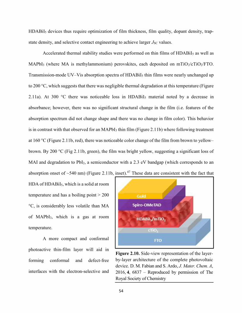
54
HDABiI5 devices thus require optimization of film thickness, film quality, dopant density, trap-
state density, and selective contact engineering to achieve larger JSC values.
Accelerated thermal stability studies were performed on thin films of HDABiI5 as well as
MAPbI3 (where MA is methylammonium) perovskites, each deposited on mTiO2/cTiO2/FTO.
Transmission-mode UV–Vis absorption spectra of HDABiI5 thin films were nearly unchanged up
to 200 °C, which suggests that there was negligible thermal degradation at this temperature (Figure
2.11a). At 300 °C there was noticeable loss in HDABiI5 material noted by a decrease in
absorbance; however, there was no significant structural change in the film (i.e. features of the
absorption spectrum did not change shape and there was no change in film color). This behavior
is in contrast with that observed for an MAPbI3 thin film (Figure 2.11b) where following treatment
at 160 °C (Figure 2.11b, red), there was noticeable color change of the film from brown to yellow–
brown. By 200 °C (Fig 2.11b, green), the film was bright yellow, suggesting a significant loss of
MAI and degradation to PbI2, a semiconductor with a 2.3 eV bandgap (which corresponds to an
absorption onset of ~540 nm) (Figure 2.11b, inset).47 These data are consistent with the fact that
HDA of HDABiI5, which is a solid at room
temperature and has a boiling point > 200
°C, is considerably less volatile than MA
of MAPbI3, which is a gas at room
temperature.
A more compact and conformal
photoactive thin-film layer will aid in
forming conformal and defect-free
interfaces with the electron-selective and
Figure 2.10. Side-view representation of the layer-by-layer architecture of the complete photovoltaic device. D. M. Fabian and S. Ardo, J. Mater. Chem. A, 2016, 4, 6837 – Reproduced by permission of The Royal Society of Chemistry
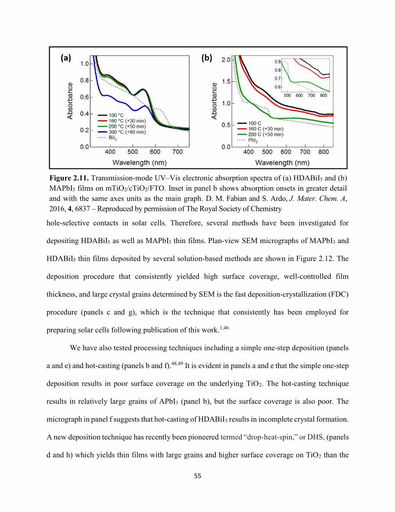
55
hole-selective contacts in solar cells. Therefore, several methods have been investigated for
depositing HDABiI5 as well as MAPbI3 thin films. Plan-view SEM micrographs of MAPbI3 and
HDABiI5 thin films deposited by several solution-based methods are shown in Figure 2.12. The
deposition procedure that consistently yielded high surface coverage, well-controlled film
thickness, and large crystal grains determined by SEM is the fast deposition-crystallization (FDC)
procedure (panels c and g), which is the technique that consistently has been employed for
preparing solar cells following publication of this work.1,46
We have also tested processing techniques including a simple one-step deposition (panels
a and e) and hot-casting (panels b and f).48,49 It is evident in panels a and e that the simple one-step
deposition results in poor surface coverage on the underlying TiO2. The hot-casting technique
results in relatively large grains of APbI3 (panel b), but the surface coverage is also poor. The
micrograph in panel f suggests that hot-casting of HDABiI5 results in incomplete crystal formation.
A new deposition technique has recently been pioneered termed “drop-heat-spin,” or DHS, (panels
d and h) which yields thin films with large grains and higher surface coverage on TiO2 than the
Figure 2.11. Transmission-mode UV–Vis electronic absorption spectra of (a) HDABiI5 and (b) MAPbI3 films on mTiO2/cTiO2/FTO. Inset in panel b shows absorption onsets in greater detail and with the same axes units as the main graph. D. M. Fabian and S. Ardo, J. Mater. Chem. A, 2016, 4, 6837 – Reproduced by permission of The Royal Society of Chemistry
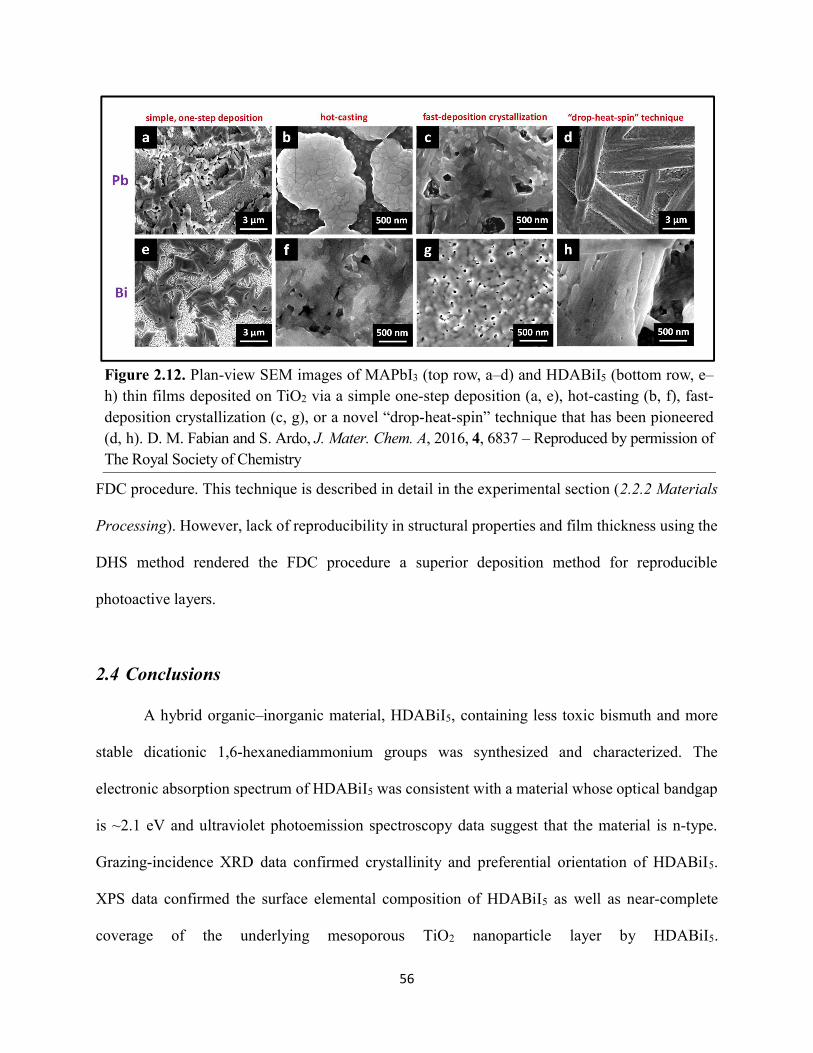
56
FDC procedure. This technique is described in detail in the experimental section (2.2.2 Materials
Processing). However, lack of reproducibility in structural properties and film thickness using the
DHS method rendered the FDC procedure a superior deposition method for reproducible
photoactive layers.
2.4 Conclusions
A hybrid organic–inorganic material, HDABiI5, containing less toxic bismuth and more
stable dicationic 1,6-hexanediammonium groups was synthesized and characterized. The
electronic absorption spectrum of HDABiI5 was consistent with a material whose optical bandgap
is ~2.1 eV and ultraviolet photoemission spectroscopy data suggest that the material is n-type.
Grazing-incidence XRD data confirmed crystallinity and preferential orientation of HDABiI5.
XPS data confirmed the surface elemental composition of HDABiI5 as well as near-complete
coverage of the underlying mesoporous TiO2 nanoparticle layer by HDABiI5.
Figure 2.12. Plan-view SEM images of MAPbI3 (top row, a–d) and HDABiI5 (bottom row, e–h) thin films deposited on TiO2 via a simple one-step deposition (a, e), hot-casting (b, f), fast-deposition crystallization (c, g), or a novel “drop-heat-spin” technique that has been pioneered (d, h). D. M. Fabian and S. Ardo, J. Mater. Chem. A, 2016, 4, 6837 – Reproduced by permission of The Royal Society of Chemistry
57
Photoelectrochemical measurements showed that an HDABiI5 device exhibited a steady-state
short-circuit photocurrent density of ~100 μA/cm2 and a stable open-circuit photovoltage of almost
400 mV under 0.8 Suns illumination. Thermal stability tests suggested that HDABiI5 is more
robust than MAPbI3, which is thought to be attributed to decreased volatility of the deprotonated
organic 1,6-hexanediamine group, compared to the deprotonated organic methylamine group of
MAPbI3. These results suggest that design of alternative structures with metal valency other than
two may allow combinations of organic cationic groups and metal cores necessary for stable and
nontoxic solution-processed photovoltaic materials. In terms of film quality and reproducibility it
was determined that the fast-deposition crystallization procedure was a superior method for
photoactive layer deposition in future device fabrication.
2.5 References
(1) Fabian, D. M.; Ardo, S. J. Mater. Chem. A 2016, 4, 6837–6841.
(2) Burschka, J.; Pellet, N.; Moon, S.-J.; Humphry-Baker, R.; Gao, P.; Nazeeruddin, M. K.;
Grätzel, M. Nature 2013, 499, 316–319.
(3) Stranks, S. D.; Eperon, G. E.; Grancini, G.; Menelaou, C.; Alcocer, M. J. P.; Leijtens, T.;
Herz, L. M.; Petrozza, A.; Snaith, H. J. Science 2013, 342, 341–344.
(4) Grätzel, M. Nat. Mater. 2014, 13, 838–842.
(5) Frost, J. M.; Butler, K. T.; Brivio, F.; Hendon, C. H.; van Schilfgaarde, M.; Walsh, A. Nano
Lett. 2014, 14, 2584–2590.
(6) Snaith, H. J.; Abate, A.; Ball, J. M.; Eperon, G. E.; Leijtens, T.; Noel, N. K.; Stranks, S. D.;
Wang, J. T.; Wojciechowski, K.; Zhang, W. J. Phys. Chem. Lett. 2014, 5, 1511–1515.
(7) Ishii, A.; Jena, A. K.; Miyasaka, T. APL Mater. 2014, 2, 091102.
(8) Motta, C.; El-Mellouhi, F.; Kais, S.; Tabet, N.; Alharbi, F.; Sanvito, S. Nat. Commun. 2015,
58
6, 7026.
(9) Kojima, A.; Teshima, K.; Shirai, Y.; Miyasaka, T. J. Am. Chem. Soc. 2009, 131, 6050–
6051.
(10) Papavassiliou, G. C. Prog. Solid State Chem. 1997, 25, 125–270.
(11) Mousdis, G. A.; Papavassiliou, G. C.; Terzis, A.; Raptopoulou, C. P. Z. Naturforsch. 1998,
53b, 927–931.
(12) Mitzi, D. B. Inorg. Chem. 2000, 39, 6107–6113.
(13) Mitzi, D. B.; Brock, P. Inorg. Chem. 2001, 40, 2096–2104.
(14) Lindsjö, M.; Fischer, A.; Kloo, L. Zeitschrift fur Anorg. und Allg. Chemie 2005, 631, 1497–
1501.
(15) Hrizi, C.; Samet, A.; Abid, Y.; Chaabouni, S.; Fliyou, M.; Koumina, A. J. Mol. Struct. 2011,
992, 96–101.
(16) Hrizi, C.; Trigui, A.; Abid, Y.; Chniba-Boudjada, N.; Bordet, P.; Chaabouni, S. J. Solid
State Chem. 2011, 184, 3336–3344.
(17) Hrizi, C.; Chaari, N.; Abid, Y.; Chniba-Boudjada, N.; Chaabouni, S. Polyhedron 2012, 46,
41–46.
(18) Liang, K.; Mitzi, D. B.; Prikas, M. T. Chem. Mater. 1998, 10, 403–411.
(19) Green, M. A.; Hishikawa, Y.; Dunlop, E. D.; Levi, D. H.; Hohl-Ebinger, J.; Ho-Baillie, A.
W. Y. Prog. Photovoltaics Res. Appl. 2018, 26, 3–12.
(20) Kazim, S.; Nazeeruddin, M. K.; Gratzel, M.; Ahmad, S. Angew. Chem. Int. Ed. 2014, 53,
2812–2824.
(21) Cheng, Z.; Lin, J. CrystEngComm 2010, 12, 2646–2662.
(22) Kodzasa, T.; Ushijima, H.; Matsuda, H.; Kamata, T. Mol. Cryst. Liq. Cryst. 2000, 343, 71–
59
75.
(23) Umebayashi, T.; Asai, K.; Kondo, T.; Nakao, A. Phys. Rev. B 2003, 67, 155405.
(24) Slavney, A. H.; Hu, T.; Lindenberg, A. M.; Karunadasa, H. I. J. Am. Chem. Soc. 2016, 138,
2138–2141.
(25) Lyu, M.; Yun, J. H.; Cai, M.; Jiao, Y.; Bernhardt, P. V.; Zhang, M.; Wang, Q.; Du, A.;
Wang, H.; Liu, G.; Wang, L. Nano Res. 2016, 9, 692–702.
(26) Lehner, A. J.; Fabini, D. H.; Evans, H. A.; Hébert, C.-A.; Smock, S. R.; Hu, J.; Wang, H.;
Zwanziger, J. W.; Chabinyc, M. L.; Seshadri, R. Chem. Mater. 2015, 27, 7137–7148.
(27) Hoye, R.; Brandt, R. E.; Osherov, A.; Stevanovic, V.; Stranks, S. D.; Wilson, M. W. B.;
Kim, H.; Akey, A. J.; Kurchin, R. C.; Poindexter, J. R.; Wang, E. N.; Bawendi, M. G.;
Bulovic, V.; Buonassisi, T. Chem. - A Eur. J. 2016, 22, 2605–2610.
(28) Park, B. W.; Philippe, B.; Zhang, X.; Rensmo, H.; Boschloo, G.; Johansson, E. M. J. Adv.
Mater. 2015, 27, 6806–6813.
(29) Brandt, R. E.; Kurchin, R. C.; Hoye, R. L. Z.; Poindexter, J. R.; Wilson, M. W. B.; Sulekar,
S.; Lenahan, F.; Yen, P. X. T.; Stevanovi??, V.; Nino, J. C.; Bawendi, M. G.; Buonassisi,
T. J. Phys. Chem. Lett. 2015, 6, 4297–4302.
(30) Hamdeh, U. H.; Nelson, R. D.; Ryan, B. J.; Bhattacharjee, U.; Petrich, J. W.; Panthani, M.
G. Chem. Mater. 2016, 28, 6567–6574.
(31) Volonakis, G.; Filip, M. R.; Haghighirad, A. A.; Sakai, N.; Wenger, B.; Snaith, H. J.;
Giustino, F. J. Phys. Chem. Lett. 2016, 7, 1254–1259.
(32) Kagan, C. R.; Murray, C. B. Nat. Nanotechnol. 2015, 10, 1013–1026.
(33) Yuan, M.; Liu, M.; Sargent, E. H. Nat. Energy 2016, 2, 16016.
(34) Nozik, A. J.; Beard, M. C.; Luther, J. M.; Law, M.; Ellingson, R. J.; Johnson, J. C.; Arrays,
60
Q. D. Chem. Rev. 2010, 110, 6873–6890.
(35) McDaniel, H.; Koposov, A. Y.; Pandey, A.; Fuke, N.; Klimov, V. I. US 20140275544 A1,
2014.
(36) Mali, S. S.; Shim, C. S.; Hong, C. K. NPG Asia Mater. 2015, 7, e208.
(37) Ito, S.; Murakami, T. N.; Comte, P.; Liska, P.; Grätzel, C.; Nazeeruddin, M. K.; Grätzel, M.
Thin Solid Films 2008, 516, 4613–4619.
(38) Kim, H.-S.; Lee, C.-R.; Im, J.-H.; Lee, K.-B.; Moehl, T.; Marchioro, A.; Moon, S.-J.;
Humphry-Baker, R.; Yum, J.-H.; Moser, J. E.; Grätzel, M.; Park, N.-G. Sci. Rep. 2012, 2,
591.
(39) Salim, T.; Sun, S.; Abe, Y.; Krishna, A.; Grimsdale, A. C.; Lam, Y. M. J. Mater. Chem. A
2014, 3, 8943–8969.
(40) Schulz, P.; Edri, E.; Kirmayer, S.; Hodes, G.; Cahen, D.; Kahn, A. Energy Environ. Sci.
2014, 7, 1377–1381.
(41) Xu, Y.; Schoonen, M. A. A. Am. Mineral. 2000, 85, 543–556.
(42) Nguyen, W. H.; Bailie, C. D.; Unger, E. L.; McGehee, M. D. J. Am. Chem. Soc. 2014, 136,
10996–11001.
(43) Mitzi, D. B.; Prikas, M. T.; Chondroudis, K. Chem. Mater. 1999, 11, 542–544.
(44) Moulder, J. F.; Stickle, W. F.; Sobol, P. E.; Bomben, K. D. Handbook of X-ray
Photoelectron Spectroscopy, 1995, 261.
(45) Watts, J. F.; Wolstenholme, J. An Introduction to Surface Analysis by XPS and AES; 1st ed.;
John Wiley & Sons Ltd.: Chichester, 2003.
(46) Xiao, M.; Huang, F.; Huang, W.; Dkhissi, Y.; Zhu, Y.; Etheridge, J.; Gray-Weale, A.; Bach,
U.; Cheng, Y.-B.; Spiccia, L. Angew. Chemie - Int. Ed. 2014, 126, 10056–10061.
61
(47) Ferreira da Silva, A.; Veissid, N.; An, C. Y.; Pepe, I.; Barros de Oliveira, N.; Batista da
Silva, A. V. Appl. Phys. Lett. 1996, 69, 1930.
(48) Lee, M. M.; Teuscher, J.; Miyasaka, T.; Murakami, T. N.; Snaith, H. J. Science 2012, 338,
643–647.
(49) Nie, W.; Tsai, H.; Asadpour, R.; Blancon, J.; Neukirch, A. J.; Gupta, G.; Crochet, J. J.;
Chhowalla, M.; Tretiak, S.; Alam, M. A.; Wang, H.; Mohite, A. D. Science 2015, 347, 522–
525.
61
CHAPTER 3: HYBRID ORGANIC–INORGANIC BISMUTH–IODIDE
MATERIALS INCORPORATING DIVALENT ORGANIC LIGANDS FOR
PHOTOVOLTAICS
* In part a compilation of one publication in preparation1
3.1 Introduction
A series of solution-processed hybrid organic–inorganic bismuth–iodide materials have
been developed where the organic monocations used in typical perovskite materials are replaced
with non-volatile and less water-soluble analogs in the form of organic dications, thus expanding
the suite of hybrid organic–inorganic materials. Through an understanding of fundamental
electronic, photophysical, and photochemical properties, promising hybrid organic–inorganic
bismuth–iodide photoactive materials can be determined. This would ultimately afford facile
processing of robust and environmentally-friendly photoactive materials for low-cost, high-
efficiency tandem PVs with market-dominating silicon absorbers.2
Ultrafast and nanosecond and longer transient spectroscopies are commonly employed for
the study of photophysical properties of hybrid organic–inorganic materials.3–8 These techniques
can provide a fundamental understanding of the small photocurrents observed with bismuth–iodide
organic-dication-containing photoactive layers in PVs. Broadband ultrafast transient absorption
spectroscopy has been employed to understand the charge-carrier dynamics of APbX3, and data
suggest that their photophysical properties are comparable to state-of-the-art bulk gallium arsenide
(GaAs).7 Furthermore, the advantage of APbX3 over GaAs, is that high-efficiency APbX3 PVs can
be solution processed in air at low temperatures.9 If the charge-carrier mobilities are low (i.e. less
than 0.0001 cm2 V-1 s-1), as they are predicted to be in hybrid organic–inorganic bismuth–halide
materials, then time-resolved microwave conductivity (TRMC) can determine in a non-contact
62
fashion the carrier mobility while such small mobilities are too small for detection by time-
resolved terahertz spectroscopy (TRTS).10 TRMC results on the nanosecond and longer timescale
have shown that charge separation occurs at both the APbX3/electron-transport-layer junction and
the APbX3/hole-transport-layer junction, and that charge recombination is significantly slower on
TiO2 than on Al2O3.11 TRMC measurements and time-resolved photoluminescence (TRPL)
spectroscopy measurements each on the nanosecond and longer timescale have also shown that
larger perovskite crystal grains, which are typical of planar, thin-film PVs, exhibit slower trap-
mediated charge recombination and higher mobilities than those of mesostructured assemblies,
due to the fewer number of grain boundaries in planar PVs.12 Time-correlated single-photon
counting (TCSPC) fluorescence measurements have corroborated the deleterious influence of
grain boundaries on charge-carrier lifetimes.13,14 In Figure 3.1, the spectrum of electromagnetic
radiation is shown indicating the probing wavelength regions of X-band TRMC, TRTS, and
transient absorption, as well as the type of charge carrier(s) each spectroscopic technique probes.
While transient absorption spectroscopy probes free carriers and excitons, the individual effects of
each remain convoluted.15 On the other hand, TRMC and TRTS typically probe only free carriers,
and so the contribution of excitons to the signal can be understood qualitatively through acquisition
of both transient absorption and TRMC or TRTS data.
The hybrid organic–inorganic bismuth–iodide material HDABiI5 reported on in Chapter 2
can be considered “perovskite-like” because, like perovskites, they are hybrid organic–inorganic
materials, but the materials do not adopt the perovskite structure. Goldschmidt’s tolerance factor
(t) provides a necessary condition for the formation of a perovskite crystal structure.16 The
tolerance factor equation is a formula relating the ionic radii of each component in the structure as
such:
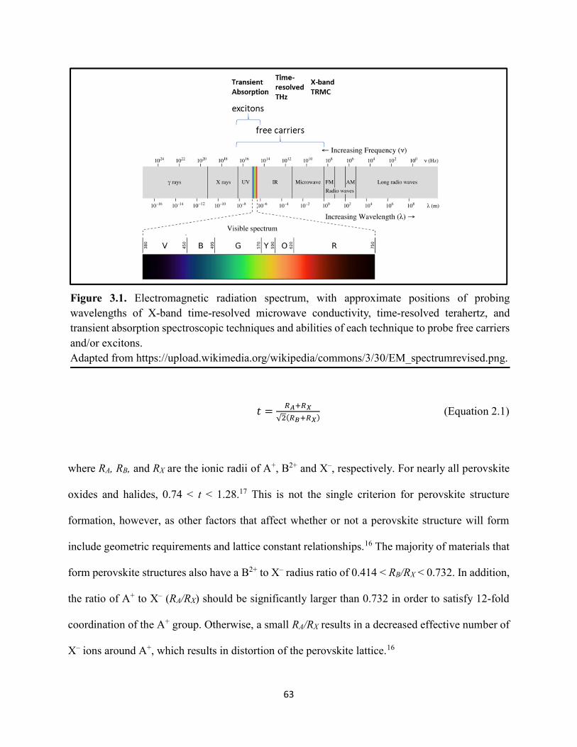
63
𝑡 =√ ( )
(Equation 2.1)
where RA, RB, and RX are the ionic radii of A+, B2+ and X–, respectively. For nearly all perovskite
oxides and halides, 0.74 < t < 1.28.17 This is not the single criterion for perovskite structure
formation, however, as other factors that affect whether or not a perovskite structure will form
include geometric requirements and lattice constant relationships.16 The majority of materials that
form perovskite structures also have a B2+ to X– radius ratio of 0.414 < RB/RX < 0.732. In addition,
the ratio of A+ to X– (RA/RX) should be significantly larger than 0.732 in order to satisfy 12-fold
coordination of the A+ group. Otherwise, a small RA/RX results in a decreased effective number of
X– ions around A+, which results in distortion of the perovskite lattice.16
Figure 3.1. Electromagnetic radiation spectrum, with approximate positions of probing wavelengths of X-band time-resolved microwave conductivity, time-resolved terahertz, and transient absorption spectroscopic techniques and abilities of each technique to probe free carriers and/or excitons. Adapted from https://upload.wikimedia.org/wikipedia/commons/3/30/EM_spectrumrevised.png.
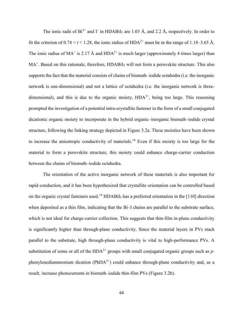
64
The ionic radii of Bi3+ and I– in HDABiI5 are 1.03 Å, and 2.2 Å, respectively. In order to
fit the criterion of 0.74 < t < 1.28, the ionic radius of HDA2+ must be in the range of 1.18–3.65 Å.
The ionic radius of MA+ is 2.17 Å and HDA2+ is much larger (approximately 4 times larger) than
MA+. Based on this rationale, therefore, HDABiI5 will not form a perovskite structure. This also
supports the fact that the material consists of chains of bismuth–iodide octahedra (i.e. the inorganic
network is one-dimensional) and not a lattice of octahedra (i.e. the inorganic network is three-
dimensional), and this is due to the organic moiety, HDA2+, being too large. This reasoning
prompted the investigation of a potential intra-crystallite fastener in the form of a small conjugated
dicationic organic moiety to incorporate in the hybrid organic–inorganic bismuth–iodide crystal
structure, following the linking strategy depicted in Figure 3.2a. These moieties have been shown
to increase the anisotropic conductivity of materials.18 Even if this moiety is too large for the
material to form a perovskite structure, this moiety could enhance charge-carrier conduction
between the chains of bismuth–iodide octahedra.
The orientation of the active inorganic network of these materials is also important for
rapid conduction, and it has been hypothesized that crystallite orientation can be controlled based
on the organic crystal fasteners used.19 HDABiI5 has a preferred orientation in the [110] direction
when deposited as a thin film, indicating that the Bi–I chains are parallel to the substrate surface,
which is not ideal for charge-carrier collection. This suggests that thin-film in-plane conductivity
is significantly higher than through-plane conductivity. Since the material layers in PVs stack
parallel to the substrate, high through-plane conductivity is vital to high-performance PVs. A
substitution of some or all of the HDA2+ groups with small conjugated organic groups such as p-
phenylenediammonium dication (PhDA2+) could enhance through-plane conductivity and, as a
result, increase photocurrents in bismuth–iodide thin-film PVs (Figure 3.2b).
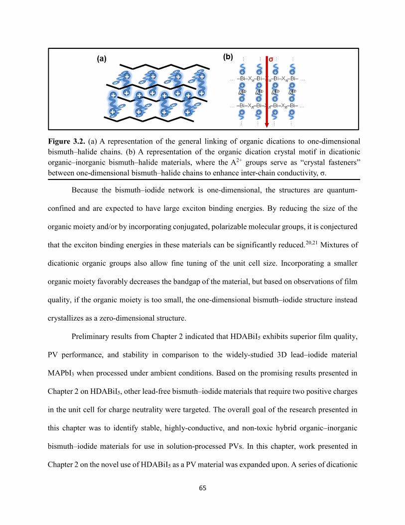
65
Because the bismuth–iodide network is one-dimensional, the structures are quantum-
confined and are expected to have large exciton binding energies. By reducing the size of the
organic moiety and/or by incorporating conjugated, polarizable molecular groups, it is conjectured
that the exciton binding energies in these materials can be significantly reduced.20,21 Mixtures of
dicationic organic groups also allow fine tuning of the unit cell size. Incorporating a smaller
organic moiety favorably decreases the bandgap of the material, but based on observations of film
quality, if the organic moiety is too small, the one-dimensional bismuth–iodide structure instead
crystallizes as a zero-dimensional structure.
Preliminary results from Chapter 2 indicated that HDABiI5 exhibits superior film quality,
PV performance, and stability in comparison to the widely-studied 3D lead–iodide material
MAPbI3 when processed under ambient conditions. Based on the promising results presented in
Chapter 2 on HDABiI5, other lead-free bismuth–iodide materials that require two positive charges
in the unit cell for charge neutrality were targeted. The overall goal of the research presented in
this chapter was to identify stable, highly-conductive, and non-toxic hybrid organic–inorganic
bismuth–iodide materials for use in solution-processed PVs. In this chapter, work presented in
Chapter 2 on the novel use of HDABiI5 as a PV material was expanded upon. A series of dicationic
Figure 3.2. (a) A representation of the general linking of organic dications to one-dimensional bismuth–halide chains. (b) A representation of the organic dication crystal motif in dicationic organic–inorganic bismuth–halide materials, where the A2+ groups serve as “crystal fasteners” between one-dimensional bismuth–halide chains to enhance inter-chain conductivity, σ.
66
hybrid organic–inorganic bismuth–iodide
thin films were prepared and characterized in
order to understand structure–property
relationships. Ultrafast laser spectroscopic
techniques were employed to study hybrid
organic–inorganic bismuth–iodide thin
films. A comparative study was performed
on HDABiI5 vs. propylammonium bismuth pentaiodide, (PA)2BiI5, a material that incorporates
two propylammonium monocations (PA+) per formula unit that together are about the same size
as HDA2+. Preliminary results on mixed dicationic organic moieties incorporating conjugated
organic PhDA2+ groups were also obtained. The two organic groups used in these mixed dicationic
bismuth–iodide materials are displayed in Table 3.1.
3.2 Experimental
3.2.1 Single-Crystal Growth and Measurement
3.2.1.1 Single-Crystal Growth
Single crystals of (EDA)2Bi2I10•5H2O were grown by vapor diffusion of acetonitrile into a
0.5 M solution of ethylenediamine (EDA), aqueous concentrated hydriodic acid (HI), and BiI3 in
N,N-dimethylformamide (DMF). The solution contained EDA, HI, and BiI3 in a molar ratio of
1:2:1, with HI in slight excess to ensure complete conversion of EDA and BiI3 into the final
product. Single crystals of HDABiI5 were grown by vapor diffusion of dichloromethane into a 0.5
M solution of 1:1 HDAI2:BiI3, with HDAI2 in slight excess to ensure there was no residual BiI3,
in a solvent mixture of 4:1 (v/v) DMF:dimethylsulfoxide (DMSO).
Table 3.1. Organic groups incorporated in dicationic hybrid organic–inorganic bismuth–halide materials for enhanced-conductivity PVs.
67
3.2.1.2 X-ray Data Collection and Structure Solution for (EDA)2Bi2I10•5H2O
An orange crystal of approximate dimensions 0.123 x 0.128 x 0.272 mm was mounted on
a glass fiber and transferred to a Bruker SMART APEX II diffractometer. The APEX222 program
package was used to determine the unit-cell parameters and for data collection (10 sec/frame scan
time for a sphere of diffraction data). The raw frame data was processed using SAINT23 and
SADABS24 to yield the reflection data file. Subsequent calculations were carried out using the
SHELXTL25 program. The diffraction symmetry was 2/m and the systematic absences were
consistent with the monoclinic space groups Cc and C2/c. It was later determined that space group
C2/c was correct.
The structure was solved by dual-space methods and refined on F2 by full-matrix least-
squares techniques. The analytical scattering factors26 for neutral atoms were used throughout the
analysis. Hydrogen atoms were included using a riding model. The molecule was dimeric
consisting of two half-dimers. One molecule was located about an inversion center while the other
was located on a two-fold rotation axis. There were five molecules of water solvent present.
Least-squares analysis yielded wR2 = 0.0395 and Goof = 1.210 for 261 variables refined
against 7836 data (0.77Å), R1 = 0.0208 for those 7508 data with I > 2.0(I).
3.2.1.3 X-ray Data Collection and Structure Solution for HDABiI5
A red crystal of approximate dimensions 0.125 x 0.127 x 0.276 mm was mounted on a
glass fiber and transferred to a Bruker SMART APEX II diffractometer. The APEX222 program
package was used to determine the unit-cell parameters and for data collection (10 sec/frame scan
time for a sphere of diffraction data). The raw frame data was processed using SAINT23 and
68
SADABS24 to yield the reflection data file. Subsequent calculations were carried out using the
SHELXTL25 program. The diffraction symmetry was mmm and the systematic absences were
consistent with the orthorhombic space groups Pnma and Pna21. It was later determined that space
group Pna21 was correct.
The structure was solved by dual space methods and refined on F2 by full-matrix least-
squares techniques. The analytical scattering factors26 for neutral atoms were used throughout the
analysis. Hydrogen atoms were included using a riding model. It was necessary to refine carbon
atoms isotropically (presumably due to high absorption). The complex formed an extended
structure.
Least-squares analysis yielded wR2 = 0.0646 and Goof = 1.150 for 100 variables refined
against 3940 data (0.78 Å), R1 = 0.0282 for those 3844 data with I > 2.0(I). The structure was
refined as an inversion twin.
3.2.1.4 Structure Solution Definitions
wR2 = [[w(Fo2-Fc
2)2] / [w(Fo2)2] ]1/2
R1 = ||Fo|-|Fc|| / |Fo|
Goof = S = [[w(Fo2-Fc
2)2] / (n-p)]1/2 where n is the number of reflections and p is the total
number of parameters refined.
The thermal ellipsoid plot is shown at the 50% probability level. For (EDA)2Bi2I10•5H2O,
symmetry-equivalent water molecules were omitted for clarity.
3.2.2 Density Functional Theory Calculations for HDABiI5
All density functional theory (DFT) calculations were performed using the Vienna Ab initio
69
Simulation Package (VASP), employing the projector augmented-wave (PAW) method to
describe the interactions and between valence and core electrons. A Γ-centered 2x2x1 k-point
sampling mesh was found to achieve convergence to within 1 meV/atom. The plane wave energy
cutoff was converged to 10 meV/atom, with a cutoff of 400 eV found to be sufficient. To prevent
errors arising from Pulay stress, the cutoff energy was raised to 520 eV during geometry
relaxations. The structures were deemed converged when the forces on each atom totaled less than
10 meV/Å.
Geometry relaxations were performed using the PBEsol functional, a version of the Perdew
Burke and Ernzerhof (PBE) functional revised for solids. PBEsol has been shown to accurately
reproduce the structure parameters of many materials containing post-transition metal cations. To
avoid errors arising from the systematic band gap underestimation in generalized gradient
approximation functionals such as PBEsol, the Heyd--Scuseria--Ernzerhof hybrid functional
(HSE06) was employed for density of states, band structure and optics calculations. In addition,
spin–orbit coupling (SOC) was treated explicitly to account for the relativistic effects on the
bismuth valence electrons. This combination of HSE06+SOC has previously been shown to
reproduce the electronic properties of a large number of solar absorber materials. The optical
response was calculated using density functional perturbation theory (DFPT) within the transversal
approximation, in which only direct valence to conduction band transitions are considered.
3.2.3 Preparation of Hybrid Organic–Inorganic Bismuth–Iodide Solutions
All chemicals were used as received. Diammonium iodide salts were synthesized by slow
addition of hydriodic acid (47% in water, stabilized with 1.5% hypophosphorous acid, Sigma-
Aldrich) to the diamine of choice dissolved in methanol. The hydriodic acid to diamine molar ratio
70
was 2:1, with hydriodic acid in slight excess. As an example, to synthesize 1,6-hexanediamine
dihydriodide (HDA•2HI), 260.9 mg of 1,6-hexanediamine (98+%, Alfa Aesar) was dissolved in 5
mL methanol, and then 1 mL hydriodic acid was added slowly at 0 °C with stirring, followed by
stirring for an additional 30 min. HDA•2HI precipitate was recovered by evaporation of solvents
at 40 °C with a rotary evaporator. The precipitate was rinsed with diethyl ether, and vacuum dried
at 60 °C for at least 12 h. HDABiI5 solution was then prepared by mixing HDA•2HI and BiI3 (99%,
Sigma-Aldrich) powders at an approximately 1:1 mole ratio, with HDA•2HI in slight excess, in an
anhydrous mixture of 4:1 (v/v) DMF:DMSO at 70 °C inside a nitrogen-filled glovebox. The
HDABiI5 solution was stored in the glovebox until use and was used within one week of
preparation.
3.2.4 Materials Processing
All steps of materials deposition and device fabrication were performed in air with 40–
60% relative humidity and as described below, unless noted otherwise. All thermal treatments
were performed using a hot plate. Fluorine-doped tin oxide coated glass (FTO) substrates were
cleaned as follows: 1) sonication in Alconox solution, 2) rinse with deionized water, 3) rinse with
ethanol, 4) sonication in ethanol, and 5) dry with nitrogen. A compact TiO2 (cTiO2) layer was
deposited by pipetting a solution of titanium diisopropoxide bis(acetylacetonate) on a cleaned FTO
substrate and then the substrate was spun at 2000 rpm (2000 rpm/s acceleration) for 60 s. The
substrate was subsequently dried at 125 °C and then sintered at 550 °C for 30 min. Nanoparticles
of TiO2 were synthesized following a procedure by Ito et al.27 The nanoparticle solution was further
diluted in ethanol at a ratio of 1:3.5 TiO2 nanoparticle solution:ethanol, w/w to make a mesoporous
TiO2 (mTiO2) suspension. The mTiO2 layer was deposited by spin coating this solution at 500 rpm
71
(500 rpm/s acceleration) for 5 s and then 5000 rpm (5000 rpm/s acceleration) for 25 s, followed
by drying at 125 °C, and then sintering at 550 °C for 30 min. The substrates were allowed to cool
to room temperature. Unless otherwise noted, a conventional spin-coat method was adapted from
Kim et al.28 and used for depositing the hybrid organic–inorganic bismuth–iodide solutions that
served as the photoactive layer. For this method, a filtered solution in 4:1 (v/v) DMF:DMSO was
pipetted on top of the mTiO2-coated FTO substrate and then the substrate was spun at 3000 rpm
(3000 rpm/s acceleration) for 60 s, followed by rapid transfer to a hot plate that was preheated to
100 °C and subsequent annealing at 100 °C for 30 min. In some cases, the fast-deposition
crystallization (FDC) method was employed for depositing the photoactive layer, which was
described in the experimental section of Chapter 1 (1.2.2.2 Perovskite Deposition Methods). For
all deposition methods, the photoactive layer solution was dispensed on the substrate at a volume
of 17.5 μL/cm2.
3.2.5 Device Fabrication
Prior to the FTO cleaning step, a region of the FTO film was etched using 2 M HCl and Zn
powder in order to prevent device shunting upon contact to the device top Au electrode. After
performing the cleaning steps listed above (Materials Processing subsection), FTO substrates were
further cleaned using an O2 plasma treatment for 10 min. Following deposition of HDABiI5 or
(PA)2BiI5 per the protocol described above (Materials Processing subsection), a 50 mM solution
of 2,2’,7,7’-tetrakis(N,N’-di-p-methoxyphenylamine)-9,9’-spirobifluorene (spiro-OMeTAD)
dissolved in chlorobenzene with additives of 17.5 μL 4-tert-butylpyridine and 37.5 μL lithium
bis(trifluoromethane)sulfonimide in acetonitrile (170 mg/mL) was deposited by spin coating at
3000 rpm (3000 rpm/s acceleration) for 60 s. The devices were then transferred into a nitrogen-
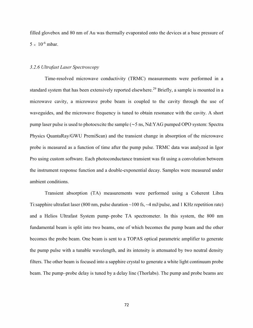
72
filled glovebox and 80 nm of Au was thermally evaporated onto the devices at a base pressure of
5 10-6 mbar.
3.2.6 Ultrafast Laser Spectroscopy
Time-resolved microwave conductivity (TRMC) measurements were performed in a
standard system that has been extensively reported elsewhere.29 Briefly, a sample is mounted in a
microwave cavity, a microwave probe beam is coupled to the cavity through the use of
waveguides, and the microwave frequency is tuned to obtain resonance with the cavity. A short
pump laser pulse is used to photoexcite the sample (∼5 ns, Nd:YAG pumped OPO system: Spectra
Physics QuantaRay/GWU PremiScan) and the transient change in absorption of the microwave
probe is measured as a function of time after the pump pulse. TRMC data was analyzed in Igor
Pro using custom software. Each photoconductance transient was fit using a convolution between
the instrument response function and a double-exponential decay. Samples were measured under
ambient conditions.
Transient absorption (TA) measurements were performed using a Coherent Libra
Ti:sapphire ultrafast laser (800 nm, pulse duration ~100 fs, ~4 mJ/pulse, and 1 KHz repetition rate)
and a Helios Ultrafast System pump–probe TA spectrometer. In this system, the 800 nm
fundamental beam is split into two beams, one of which becomes the pump beam and the other
becomes the probe beam. One beam is sent to a TOPAS optical parametric amplifier to generate
the pump pulse with a tunable wavelength, and its intensity is attenuated by two neutral density
filters. The other beam is focused into a sapphire crystal to generate a white light continuum probe
beam. The pump–probe delay is tuned by a delay line (Thorlabs). The pump and probe beams are
73
focused and overlapped onto the sample. The probe beam size is ~130 μm and the pump beam size
is ~1 mm. Samples were measured under ambient conditions.
3.2.7 Characterization
High-resolution synchrotron powder diffraction data were collected using beamline 11-
BM at the Advanced Photon Source (APS) at Argonne National Laboratory using a calibrated
wavelength of 0.41417 Å. Discrete detectors covering an angular range from -6 to 16º 2θ are
scanned over a 34º 2θ range, with data points collected every 0.001º 2θ and scan speed of 0.01º/s.
Data are collected while continually scanning the diffractometer 2θ arm. A mixture of NIST
standard reference materials, Si (SRM 640c) and Al2O3 (SRM 676) is used to calibrate the
instrument, where the Si lattice constant determines the wavelength for each detector. Corrections
are applied for detector sensitivity, 2θ offset, small differences in wavelength between detectors,
and the source intensity, as noted by the ion chamber before merging the data into a single set of
intensities evenly spaced in 2θ. For ease of data presentation, 2θ values were adjusted as if Cu Kα
radiation (1.5406 Å) was used.
Grazing-incidence XRD data were collected using a Rigaku Smartlab diffractometer with
Cu Kα radiation and in parallel beam geometry. Transmission and reflection spectra were obtained
using an integrating sphere in a Shimadzu UV-3600 ultraviolet-visible-near-infrared
spectrophotometer. Absorption was calculated by assuming Absorptance = 1 – Transmittance –
Reflectance. Steady-state photoluminescence (PL) was measured with a Horiba Jobin Yvon Model
FL-1039/40 Fluorolog, a Horiba Jobin Yvon iHR320 spectrograph, and a Horiba Jobin Yvon
SPEX Instruments S.A. Group Spectrum One G35 CCD camera. A monochromatized Xe lamp
was used as the excitation source. Scanning electron microscopy images were acquired on a FEI
74
Magellan 400L XHR using 15 kV accelerating voltage and 0.8 nA beam current. X-ray
photoelectron spectroscopy (XPS) measurements were performed using a Kratos AXIS Supra
photoelectron spectrometer using Al Kα radiation. XPS data were analyzed using CasaXPS
Processing Software. Thermogravimetric analysis data were obtained using a TGA Q500 by TA
Instruments.
An ELH-type W–halogen lamp was used inside a nitrogen-filled glovebox as a source of
simulated solar illumination. Before measurement of device J–E behavior, chronoamperometry,
and through-plane conductivity measurements, the light intensity was roughly approximated to be
1 Sun using a calibrated Si photodiode (ThorLabs, Inc., FDS100) positioned at the location of the
device. 2-electrode cyclic voltammetry measurements (at a scan rate of 100 mV s-1),
chronoamperometry measurements, and through-plane conductivity measurements were
performed using a Gamry Reference 600 Potentiostat.
Transmission, reflection, steady-state PL, TRMC, TAS, and some of the grazing-incidence
XRD measurements were performed in the Chemistry and Nanoscience Center at the National
Renewable Energy Laboratory. SEM, XPS, and some of the grazing-incidence XRD work was
performed in the UC Irvine Materials Research Institute (IMRI).
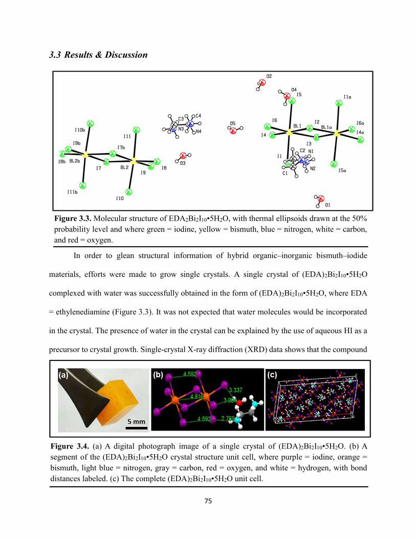
75
3.3 Results & Discussion
In order to glean structural information of hybrid organic–inorganic bismuth–iodide
materials, efforts were made to grow single crystals. A single crystal of (EDA)2Bi2I10•5H2O
complexed with water was successfully obtained in the form of (EDA)2Bi2I10•5H2O, where EDA
= ethylenediamine (Figure 3.3). It was not expected that water molecules would be incorporated
in the crystal. The presence of water in the crystal can be explained by the use of aqueous HI as a
precursor to crystal growth. Single-crystal X-ray diffraction (XRD) data shows that the compound
Figure 3.3. Molecular structure of EDA2Bi2I10•5H2O, with thermal ellipsoids drawn at the 50% probability level and where green = iodine, yellow = bismuth, blue = nitrogen, white = carbon, and red = oxygen.
Figure 3.4. (a) A digital photograph image of a single crystal of (EDA)2Bi2I10•5H2O. (b) A segment of the (EDA)2Bi2I10•5H2O crystal structure unit cell, where purple = iodine, orange = bismuth, light blue = nitrogen, gray = carbon, red = oxygen, and white = hydrogen, with bond distances labeled. (c) The complete (EDA)2Bi2I10•5H2O unit cell.
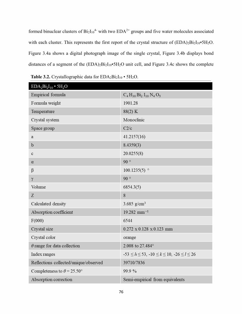
76
formed binuclear clusters of Bi2I104- with two EDA2+ groups and five water molecules associated
with each cluster. This represents the first report of the crystal structure of (EDA)2Bi2I10•5H2O.
Figure 3.4a shows a digital photograph image of the single crystal, Figure 3.4b displays bond
distances of a segment of the (EDA)2Bi2I10•5H2O unit cell, and Figure 3.4c shows the complete
Table 3.2. Crystallographic data for EDA2Bi2I10 • 5H2O.
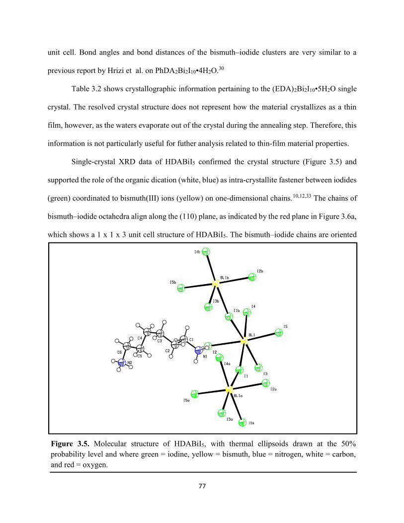
77
unit cell. Bond angles and bond distances of the bismuth–iodide clusters are very similar to a
previous report by Hrizi et al. on PhDA2Bi2I10•4H2O.30
Table 3.2 shows crystallographic information pertaining to the (EDA)2Bi2I10•5H2O single
crystal. The resolved crystal structure does not represent how the material crystallizes as a thin
film, however, as the waters evaporate out of the crystal during the annealing step. Therefore, this
information is not particularly useful for futher analysis related to thin-film material properties.
Single-crystal XRD data of HDABiI5 confirmed the crystal structure (Figure 3.5) and
supported the role of the organic dication (white, blue) as intra-crystallite fastener between iodides
(green) coordinated to bismuth(III) ions (yellow) on one-dimensional chains.10,12,33 The chains of
bismuth–iodide octahedra align along the (110) plane, as indicated by the red plane in Figure 3.6a,
which shows a 1 x 1 x 3 unit cell structure of HDABiI5. The bismuth–iodide chains are oriented
Figure 3.5. Molecular structure of HDABiI5, with thermal ellipsoids drawn at the 50% probability level and where green = iodine, yellow = bismuth, blue = nitrogen, white = carbon, and red = oxygen.
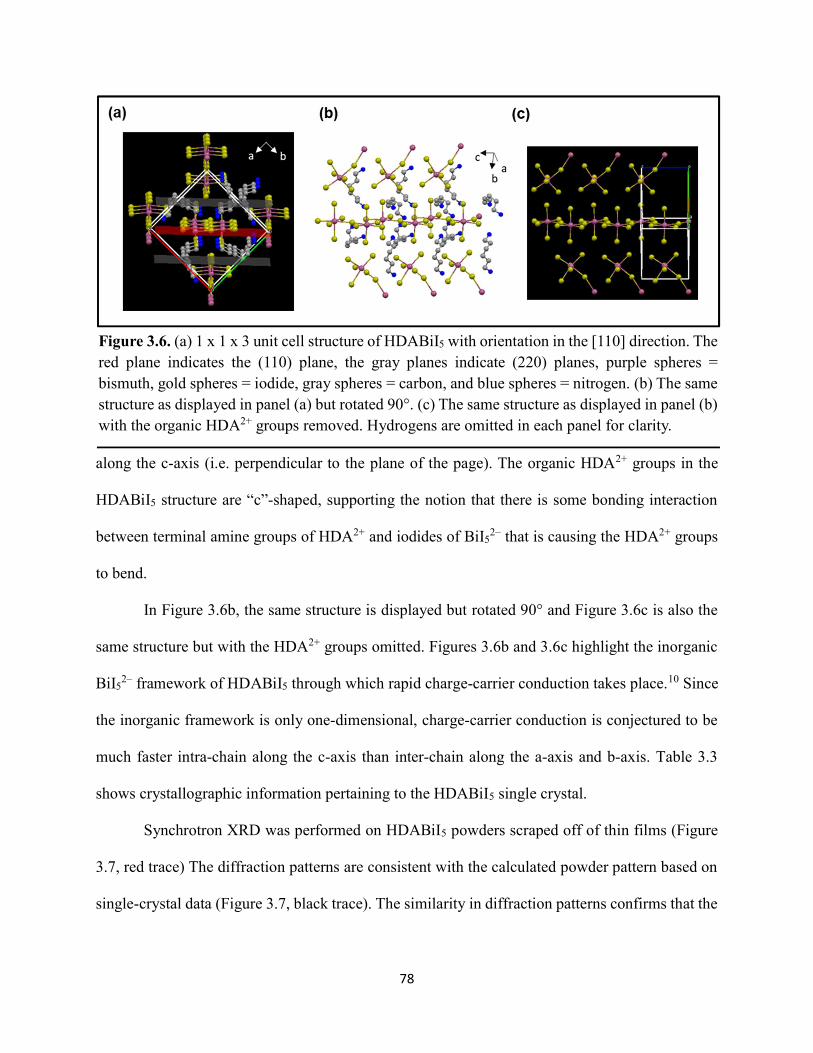
78
along the c-axis (i.e. perpendicular to the plane of the page). The organic HDA2+ groups in the
HDABiI5 structure are “c”-shaped, supporting the notion that there is some bonding interaction
between terminal amine groups of HDA2+ and iodides of BiI52– that is causing the HDA2+ groups
to bend.
In Figure 3.6b, the same structure is displayed but rotated 90° and Figure 3.6c is also the
same structure but with the HDA2+ groups omitted. Figures 3.6b and 3.6c highlight the inorganic
BiI52– framework of HDABiI5 through which rapid charge-carrier conduction takes place.10 Since
the inorganic framework is only one-dimensional, charge-carrier conduction is conjectured to be
much faster intra-chain along the c-axis than inter-chain along the a-axis and b-axis. Table 3.3
shows crystallographic information pertaining to the HDABiI5 single crystal.
Synchrotron XRD was performed on HDABiI5 powders scraped off of thin films (Figure
3.7, red trace) The diffraction patterns are consistent with the calculated powder pattern based on
single-crystal data (Figure 3.7, black trace). The similarity in diffraction patterns confirms that the
Figure 3.6. (a) 1 x 1 x 3 unit cell structure of HDABiI5 with orientation in the [110] direction. The red plane indicates the (110) plane, the gray planes indicate (220) planes, purple spheres = bismuth, gold spheres = iodide, gray spheres = carbon, and blue spheres = nitrogen. (b) The same structure as displayed in panel (a) but rotated 90°. (c) The same structure as displayed in panel (b) with the organic HDA2+ groups removed. Hydrogens are omitted in each panel for clarity.
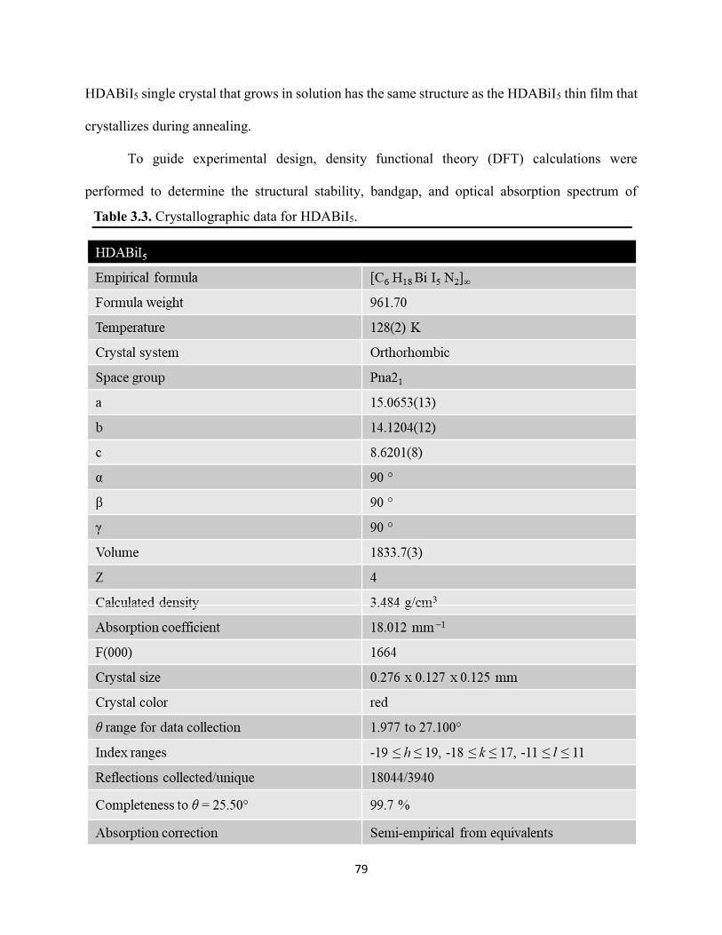
79
HDABiI5 single crystal that grows in solution has the same structure as the HDABiI5 thin film that
crystallizes during annealing.
To guide experimental design, density functional theory (DFT) calculations were
performed to determine the structural stability, bandgap, and optical absorption spectrum of
Table 3.3. Crystallographic data for HDABiI5.
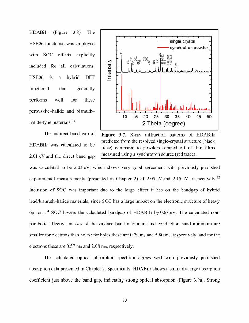
80
HDABiI5 (Figure 3.8). The
HSE06 functional was employed
with SOC effects explicitly
included for all calculations.
HSE06 is a hybrid DFT
functional that generally
performs well for these
perovskite–halide and bismuth–
halide-type materials.33
The indirect band gap of
HDABiI5 was calculated to be
2.01 eV and the direct band gap
was calculated to be 2.03 eV, which shows very good agreement with previously published
experimental measurements (presented in Chapter 2) of 2.05 eV and 2.15 eV, respectively.32
Inclusion of SOC was important due to the large effect it has on the bandgap of hybrid
lead/bismuth–halide materials, since SOC has a large impact on the electronic structure of heavy
6p ions.34 SOC lowers the calculated bandgap of HDABiI5 by 0.68 eV. The calculated non-
parabolic effective masses of the valence band maximum and conduction band minimum are
smaller for electrons than holes: for holes these are 0.79 m0 and 5.80 m0, respectively, and for the
electrons these are 0.57 m0 and 2.08 m0, respectively.
The calculated optical absorption spectrum agrees well with previously published
absorption data presented in Chapter 2. Specifically, HDABiI5 shows a similarly large absorption
coefficient just above the band gap, indicating strong optical absorption (Figure 3.9a). Strong
Figure 3.7. X-ray diffraction patterns of HDABiI5
predicted from the resolved single-crystal structure (black trace) compared to powders scraped off of thin films measured using a synchrotron source (red trace).
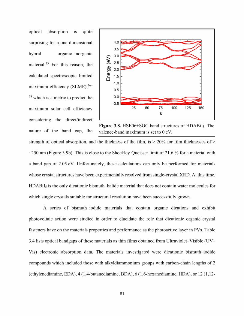
81
optical absorption is quite
surprising for a one-dimensional
hybrid organic–inorganic
material.35 For this reason, the
calculated spectroscopic limited
maximum efficiency (SLME),36–
38 which is a metric to predict the
maximum solar cell efficiency
considering the direct/indirect
nature of the band gap, the
strength of optical absorption, and the thickness of the film, is > 20% for film thicknesses of >
~250 nm (Figure 3.9b). This is close to the Shockley-Queisser limit of 21.6 % for a material with
a band gap of 2.05 eV. Unfortunately, these calculations can only be performed for materials
whose crystal structures have been experimentally resolved from single-crystal XRD. At this time,
HDABiI5 is the only dicationic bismuth–halide material that does not contain water molecules for
which single crystals suitable for structural resolution have been successfully grown.
A series of bismuth–iodide materials that contain organic dications and exhibit
photovoltaic action were studied in order to elucidate the role that dicationic organic crystal
fasteners have on the materials properties and performance as the photoactive layer in PVs. Table
3.4 lists optical bandgaps of these materials as thin films obtained from Ultraviolet–Visible (UV–
Vis) electronic absorption data. The materials investigated were dicationic bismuth–iodide
compounds which included those with alkyldiammonium groups with carbon-chain lengths of 2
(ethylenediamine, EDA), 4 (1,4-butanediamine, BDA), 6 (1,6-hexanediamine, HDA), or 12 (1,12-
Figure 3.8. HSE06+SOC band structures of HDABiI5. The valence-band maximum is set to 0 eV.
25 50 75 100 125 150-0.5
0.0
0.5
1.0
1.5
2.0
2.5
3.0
3.5
4.0
Ene
rgy
(eV
)k
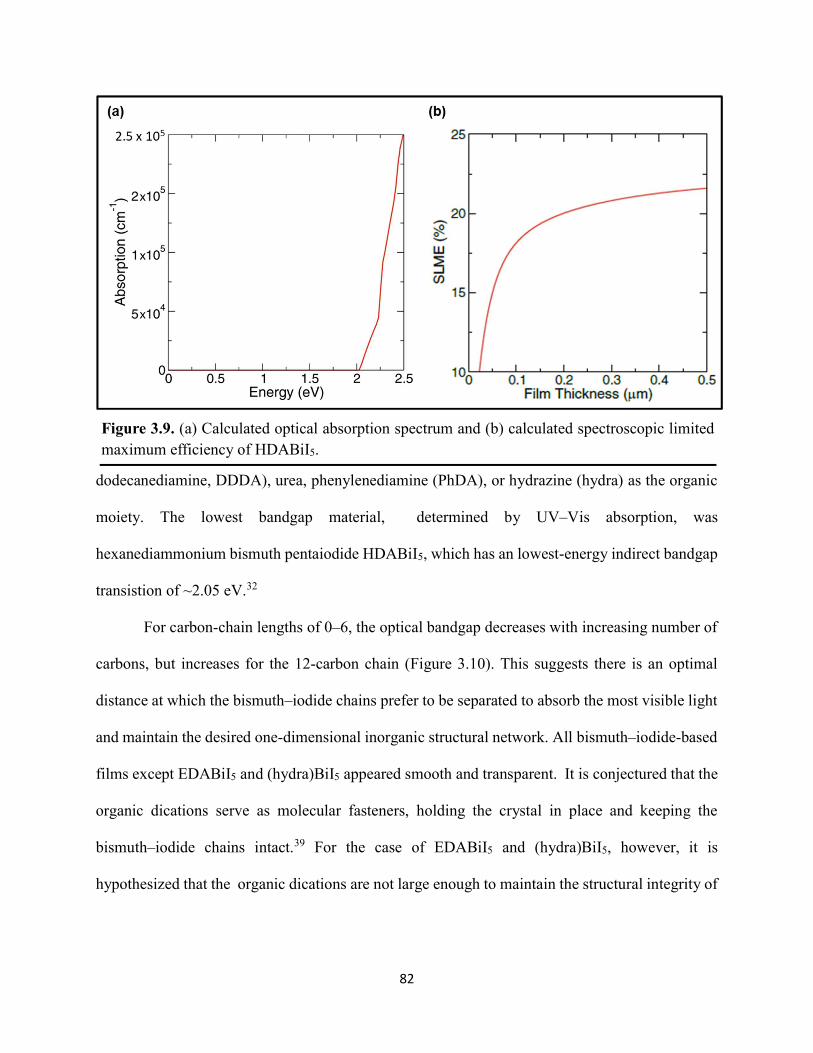
82
dodecanediamine, DDDA), urea, phenylenediamine (PhDA), or hydrazine (hydra) as the organic
moiety. The lowest bandgap material, determined by UV–Vis absorption, was
hexanediammonium bismuth pentaiodide HDABiI5, which has an lowest-energy indirect bandgap
transistion of ~2.05 eV.32
For carbon-chain lengths of 0–6, the optical bandgap decreases with increasing number of
carbons, but increases for the 12-carbon chain (Figure 3.10). This suggests there is an optimal
distance at which the bismuth–iodide chains prefer to be separated to absorb the most visible light
and maintain the desired one-dimensional inorganic structural network. All bismuth–iodide-based
films except EDABiI5 and (hydra)BiI5 appeared smooth and transparent. It is conjectured that the
organic dications serve as molecular fasteners, holding the crystal in place and keeping the
bismuth–iodide chains intact.39 For the case of EDABiI5 and (hydra)BiI5, however, it is
hypothesized that the organic dications are not large enough to maintain the structural integrity of
Figure 3.9. (a) Calculated optical absorption spectrum and (b) calculated spectroscopic limited maximum efficiency of HDABiI5.
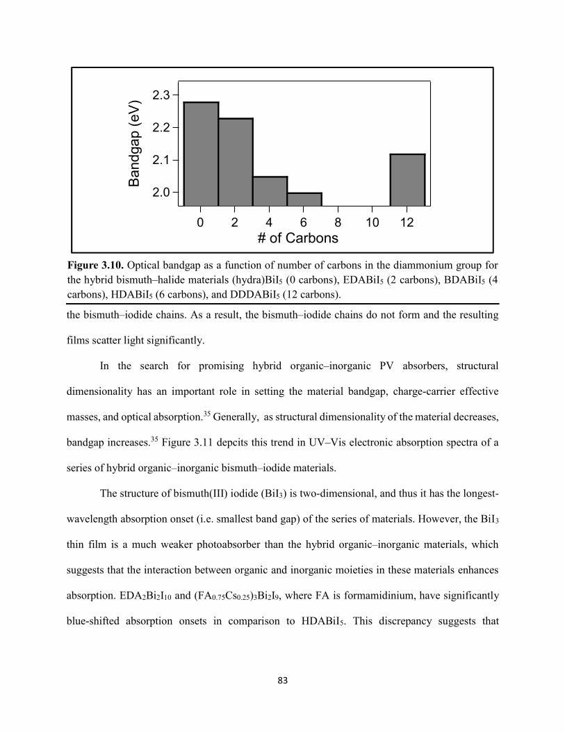
83
the bismuth–iodide chains. As a result, the bismuth–iodide chains do not form and the resulting
films scatter light significantly.
In the search for promising hybrid organic–inorganic PV absorbers, structural
dimensionality has an important role in setting the material bandgap, charge-carrier effective
masses, and optical absorption.35 Generally, as structural dimensionality of the material decreases,
bandgap increases.35 Figure 3.11 depcits this trend in UV–Vis electronic absorption spectra of a
series of hybrid organic–inorganic bismuth–iodide materials.
The structure of bismuth(III) iodide (BiI3) is two-dimensional, and thus it has the longest-
wavelength absorption onset (i.e. smallest band gap) of the series of materials. However, the BiI3
thin film is a much weaker photoabsorber than the hybrid organic–inorganic materials, which
suggests that the interaction between organic and inorganic moieties in these materials enhances
absorption. EDA2Bi2I10 and (FA0.75Cs0.25)3Bi2I9, where FA is formamidinium, have significantly
blue-shifted absorption onsets in comparison to HDABiI5. This discrepancy suggests that
2.3
2.2
2.1
2.0
Ban
dga
p (e
V)
121086420# of Carbons
Figure 3.10. Optical bandgap as a function of number of carbons in the diammonium group for the hybrid bismuth–halide materials (hydra)BiI5 (0 carbons), EDABiI5 (2 carbons), BDABiI5 (4 carbons), HDABiI5 (6 carbons), and DDDABiI5 (12 carbons).

84
EDA2Bi2I10 and (FA0.75Cs0.25)3Bi2I9 are
not one-dimensional materials like
HDABiI5,32 but are in fact zero-
dimensional materials.
The absorption onset of 4,4’-
bipyridinium bismuth iodide (bpyBiI5) is
intermediate between EDA2Bi2I10 and
(FA0.75Cs0.25)3Bi2I9 vs. HDABiI5. The
absorption onset of (PA)2BiI5 is gradual
unlike those of the other materials
presented in Figure 3.11. It is conjectured
that the (PA)2BiI5 thin film is composed
of a mix of two phases, one of which is
one-dimensional and the other that is
zero-dimensional. This is corroborated by
the XRD data of thin films presented in Figure 3.12. The XRD pattern of the HDABiI5 thin film
matches the patterns of the single crystal and powder presented in Figure 3.12, indicating a one-
dimensional framework of corner-sharing bismuth–iodide octahedra. For the XRD pattern of
(PA)2BiI5 (blue trace), however, there is a dominant peak at ~7.4° that can not be indexed to (PA)2
BiI5 with a one-dimensional framework of corner-sharing octahedra. This un-indexed peak is
postulated to be due to a zero-dimensional phase of the material.
Table 3.4. Optical bandgaps and corresponding digital images of a series of dicationic hybrid organic–inorganic bismuth–iodide thin films. HDA = 1,6-hexanediamine bismuth iodide, BDA = 1,4-butanediamine bismuth iodide, DDDA = 1,12-dodecanediamine bismuth iodide, PhDA = p-phenylenediamine bismuth iodide, EDA = 1,2-ethanediamine bismuth iodide, and hydra = hydrazine bismuth iodide.
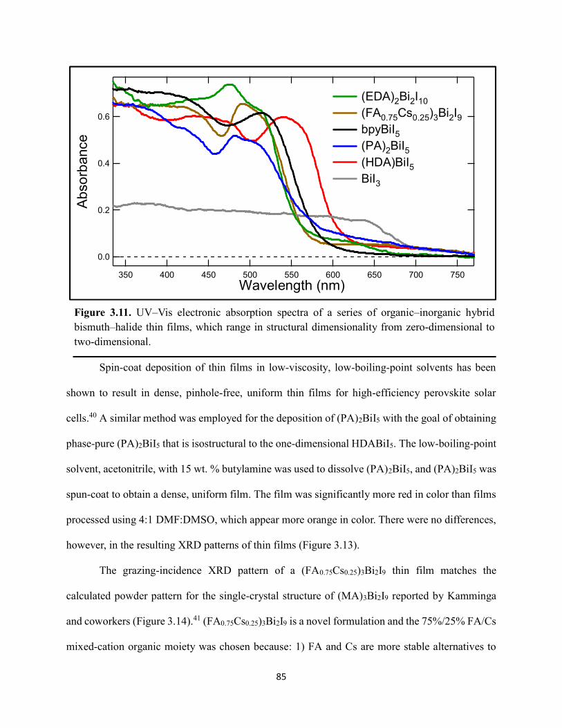
85
Spin-coat deposition of thin films in low-viscosity, low-boiling-point solvents has been
shown to result in dense, pinhole-free, uniform thin films for high-efficiency perovskite solar
cells.40 A similar method was employed for the deposition of (PA)2BiI5 with the goal of obtaining
phase-pure (PA)2BiI5 that is isostructural to the one-dimensional HDABiI5. The low-boiling-point
solvent, acetonitrile, with 15 wt. % butylamine was used to dissolve (PA)2BiI5, and (PA)2BiI5 was
spun-coat to obtain a dense, uniform film. The film was significantly more red in color than films
processed using 4:1 DMF:DMSO, which appear more orange in color. There were no differences,
however, in the resulting XRD patterns of thin films (Figure 3.13).
The grazing-incidence XRD pattern of a (FA0.75Cs0.25)3Bi2I9 thin film matches the
calculated powder pattern for the single-crystal structure of (MA)3Bi2I9 reported by Kamminga
and coworkers (Figure 3.14).41 (FA0.75Cs0.25)3Bi2I9 is a novel formulation and the 75%/25% FA/Cs
mixed-cation organic moiety was chosen because: 1) FA and Cs are more stable alternatives to
Figure 3.11. UV–Vis electronic absorption spectra of a series of organic–inorganic hybrid bismuth–halide thin films, which range in structural dimensionality from zero-dimensional to two-dimensional.
0.6
0.4
0.2
0.0
Ab
sorb
ance
750700650600550500450400350
Wavelength (nm)
(EDA)2Bi2I10
(FA0.75Cs0.25)3Bi2I9 bpyBiI5 (PA)2BiI5 (HDA)BiI5 BiI3

86
MA as the organic moiety and 2) the 75%/25% FA/Cs mixture results in approximately the same
average ionic radius as MA. This would yield a unit cell with approximately the same lattice
constants and XRD peaks as long as the inorganic moieties are isostructural. In fact, this is the
case, as the peak positions for the gold and gray traces are nearly identical. The inorganic
framework was determined by Kamminga and coworkers to be zero-dimensional and the
framework consists of face-sharing binuclear clusters of bismuth–iodide octahedra.41
Since the XRD patterns are nearly identical, it can be concluded that (FA0.75Cs0.25)3Bi2I9 is
isostructural to (MA)3Bi2I9 and consists of zero-dimensional face-sharing binuclear clusters of
Figure 3.12. Grazing-incidence X-ray diffraction patterns of thin films of HDABiI5 (red trace) and (PA)2BiI5 (blue trace) on FTO.
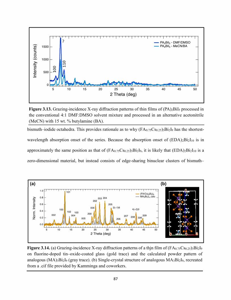
87
bismuth–iodide octahedra. This provides rationale as to why (FA0.75Cs0.25)3Bi2I9 has the shortest-
wavelength absorption onset of the series. Because the absorption onset of (EDA)2Bi2I10 is in
approximately the same position as that of (FA0.75Cs0.25)3Bi2I9, it is likely that (EDA)2Bi2I10 is a
zero-dimensional material, but instead consists of edge-sharing binuclear clusters of bismuth–
Figure 3.13. Grazing-incidence X-ray diffraction patterns of thin films of (PA)2BiI5 processed in the conventional 4:1 DMF:DMSO solvent mixture and processed in an alternative acetonitrile (MeCN) with 15 wt. % butylamine (BA).
Figure 3.14. (a) Grazing-incidence X-ray diffraction patterns of a thjn film of (FA0.75Cs0.25)3Bi2I9 on fluorine-doped tin–oxide-coated glass (gold trace) and the calculated powder pattern of analogous (MA)3Bi2I9 (gray trace). (b) Single-crystal structure of analogous MA3Bi2I9, recreated from a .cif file provided by Kamminga and coworkers.
(a) (b)
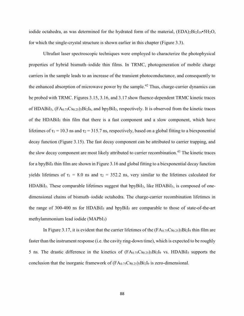
88
iodide octahedra, as was determined for the hydrated form of the material, (EDA)2Bi2I10•5H2O,
for which the single-crystal structure is shown earlier in this chapter (Figure 3.3).
Ultrafast laser spectroscopic techniques were employed to characterize the photophysical
properties of hybrid bismuth–iodide thin films. In TRMC, photogeneration of mobile charge
carriers in the sample leads to an increase of the transient photoconductance, and consequently to
the enhanced absorption of microwave power by the sample.42 Thus, charge-carrier dynamics can
be probed with TRMC. Figures 3.15, 3.16, and 3.17 show fluence-dependent TRMC kinetic traces
of HDABiI5, (FA0.75Cs0.25)3Bi2I9, and bpyBiI5, respectively. It is observed from the kinetic traces
of the HDABiI5 thin film that there is a fast component and a slow component, which have
lifetimes of τ1 = 10.3 ns and τ2 = 315.7 ns, respectively, based on a global fitting to a biexponential
decay function (Figure 3.15). The fast decay component can be attributed to carrier trapping, and
the slow decay component are most likely attributed to carrier recombination.43 The kinetic traces
for a bpyBiI5 thin film are shown in Figure 3.16 and global fitting to a biexponential decay function
yields lifetimes of τ1 = 8.0 ns and τ2 = 352.2 ns, very similar to the lifetimes calculated for
HDABiI5. These comparable lifetimes suggest that bpyBiI5, like HDABiI5, is composed of one-
dimensional chains of bismuth–iodide octahedra. The charge-carrier recombination lifetimes in
the range of 300-400 ns for HDABiI5 and bpyBiI5 are comparable to those of state-of-the-art
methylammonium lead iodide (MAPbI3)
In Figure 3.17, it is evident that the carrier lifetimes of the (FA0.75Cs0.25)3Bi2I9 thin film are
faster than the instrument response (i.e. the cavity ring-down time), which is expected to be roughly
5 ns. The drastic difference in the kinetics of (FA0.75Cs0.25)3Bi2I9 vs. HDABiI5 supports the
conclusion that the inorganic framework of (FA0.75Cs0.25)3Bi2I9 is zero-dimensional.
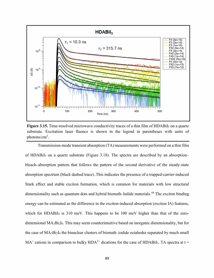
89
Transmission-mode transient absorption (TA) measurements were performed on a thin film
of HDABiI5 on a quartz substrate (Figure 3.18). The spectra are described by an absorption–
bleach–absorption pattern that follows the pattern of the second derivative of the steady-state
absorption spectrum (black dashed trace)..This indicates the presence of a trapped-carrier-induced
Stark effect and stable exciton formation, which is common for materials with low structural
dimensionality such as quantum dots and hybrid bismuth–halide materials.44 The exciton binding
energy can be estimated as the difference in the exciton-induced absorption (exciton IA) features,
which for HDABiI5 is 310 meV. This happens to be 100 meV higher than that of the zero-
dimensional MA3Bi2I9. This may seem counterintuitive based on inorganic dimensionality, but for
the case of MA3Bi2I9 the binuclear clusters of bismuth–iodide octahedra separated by much small
MA+ cations in comparison to bulky HDA2+ dications for the case of HDABiI5. TA spectra at t =
Figure 3.15. Time-resolved microwave conductivity traces of a thin film of HDABiI5 on a quartz substrate. Excitation laser fluence is shown in the legend in parentheses with units of photons/cm2.
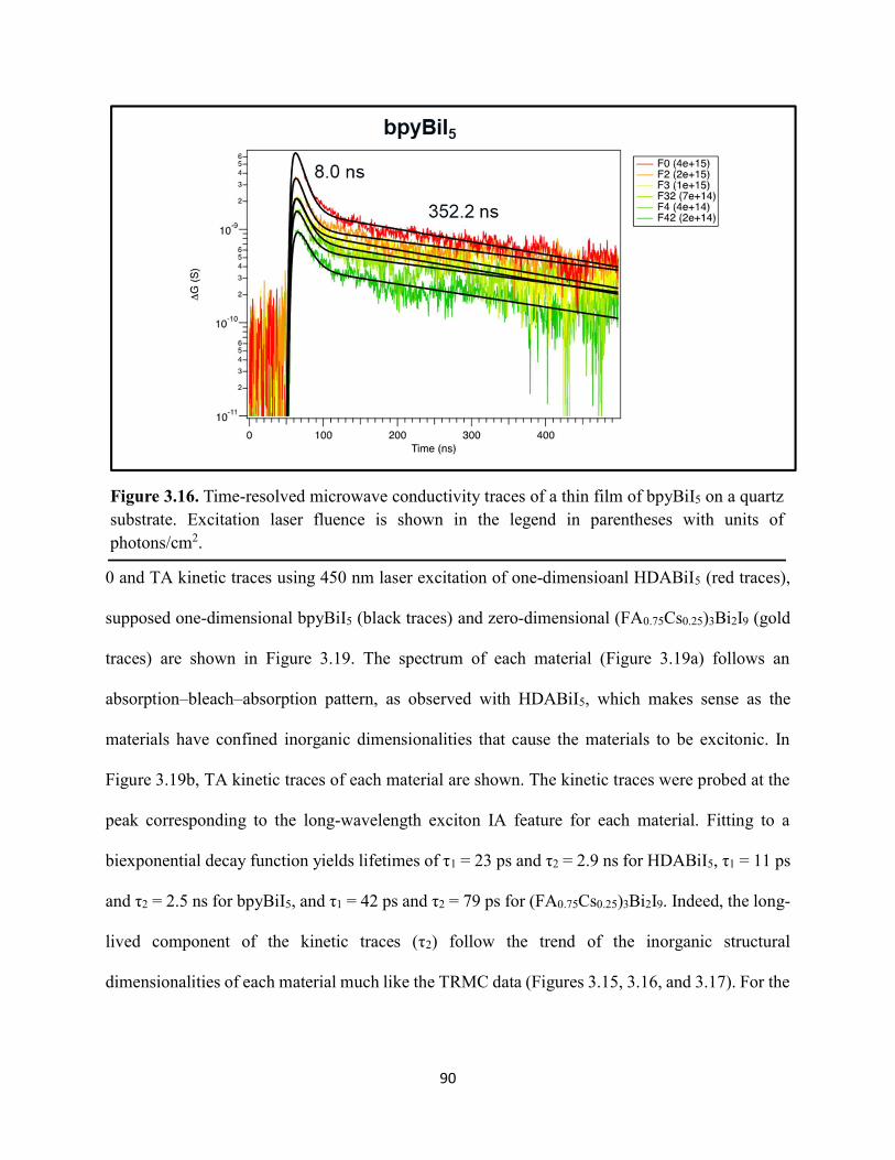
90
0 and TA kinetic traces using 450 nm laser excitation of one-dimensioanl HDABiI5 (red traces),
supposed one-dimensional bpyBiI5 (black traces) and zero-dimensional (FA0.75Cs0.25)3Bi2I9 (gold
traces) are shown in Figure 3.19. The spectrum of each material (Figure 3.19a) follows an
absorption–bleach–absorption pattern, as observed with HDABiI5, which makes sense as the
materials have confined inorganic dimensionalities that cause the materials to be excitonic. In
Figure 3.19b, TA kinetic traces of each material are shown. The kinetic traces were probed at the
peak corresponding to the long-wavelength exciton IA feature for each material. Fitting to a
biexponential decay function yields lifetimes of τ1 = 23 ps and τ2 = 2.9 ns for HDABiI5, τ1 = 11 ps
and τ2 = 2.5 ns for bpyBiI5, and τ1 = 42 ps and τ2 = 79 ps for (FA0.75Cs0.25)3Bi2I9. Indeed, the long-
lived component of the kinetic traces (τ2) follow the trend of the inorganic structural
dimensionalities of each material much like the TRMC data (Figures 3.15, 3.16, and 3.17). For the
Figure 3.16. Time-resolved microwave conductivity traces of a thin film of bpyBiI5 on a quartz substrate. Excitation laser fluence is shown in the legend in parentheses with units of photons/cm2.
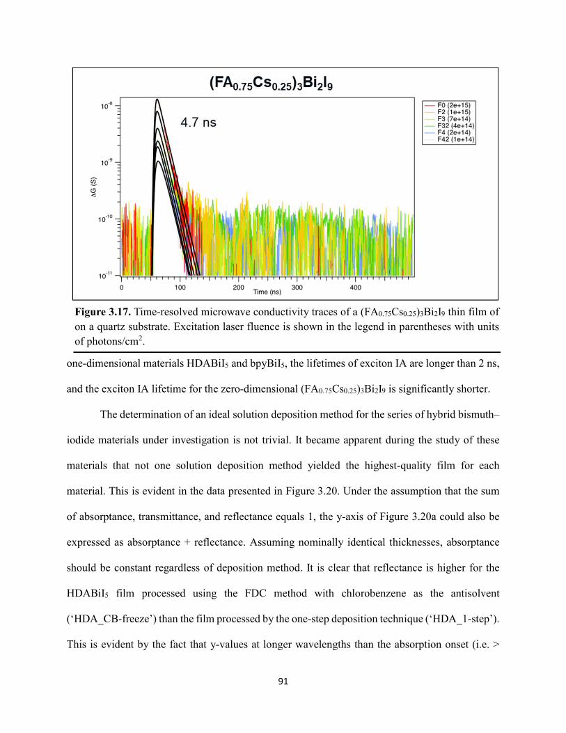
91
one-dimensional materials HDABiI5 and bpyBiI5, the lifetimes of exciton IA are longer than 2 ns,
and the exciton IA lifetime for the zero-dimensional (FA0.75Cs0.25)3Bi2I9 is significantly shorter.
The determination of an ideal solution deposition method for the series of hybrid bismuth–
iodide materials under investigation is not trivial. It became apparent during the study of these
materials that not one solution deposition method yielded the highest-quality film for each
material. This is evident in the data presented in Figure 3.20. Under the assumption that the sum
of absorptance, transmittance, and reflectance equals 1, the y-axis of Figure 3.20a could also be
expressed as absorptance + reflectance. Assuming nominally identical thicknesses, absorptance
should be constant regardless of deposition method. It is clear that reflectance is higher for the
HDABiI5 film processed using the FDC method with chlorobenzene as the antisolvent
(‘HDA_CB-freeze’) than the film processed by the one-step deposition technique (‘HDA_1-step’).
This is evident by the fact that y-values at longer wavelengths than the absorption onset (i.e. >
Figure 3.17. Time-resolved microwave conductivity traces of a (FA0.75Cs0.25)3Bi2I9 thin film of on a quartz substrate. Excitation laser fluence is shown in the legend in parentheses with units of photons/cm2.
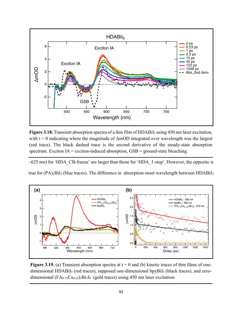
92
~625 nm) for ‘HDA_CB-freeze’ are larger than those for ‘HDA_1-step’. However, the opposite is
true for (PA)2BiI5 (blue traces). The difference in absorption onset wavelength between HDABiI5
Figure 3.18. Transient absorption spectra of a thin film of HDABiI5 using 450 nm laser excitation, with t = 0 indicating where the magnitude of ΔmOD integrated over wavelength was the largest (red trace). The black dashed trace is the second derivative of the steady-state absorption spectrum. Exciton IA = exciton-induced absorption, GSB = ground-state bleaching.
(a) (b)
Figure 3.19. (a) Transient absorption spectra at t = 0 and (b) kinetic traces of thin films of one-dimensional HDABiI5 (red traces), supposed one-dimensional bpyBiI5 (black traces), and zero-dimensional (FA0.75Cs0.25)3Bi2I9 (gold traces) using 450 nm laser excitation.
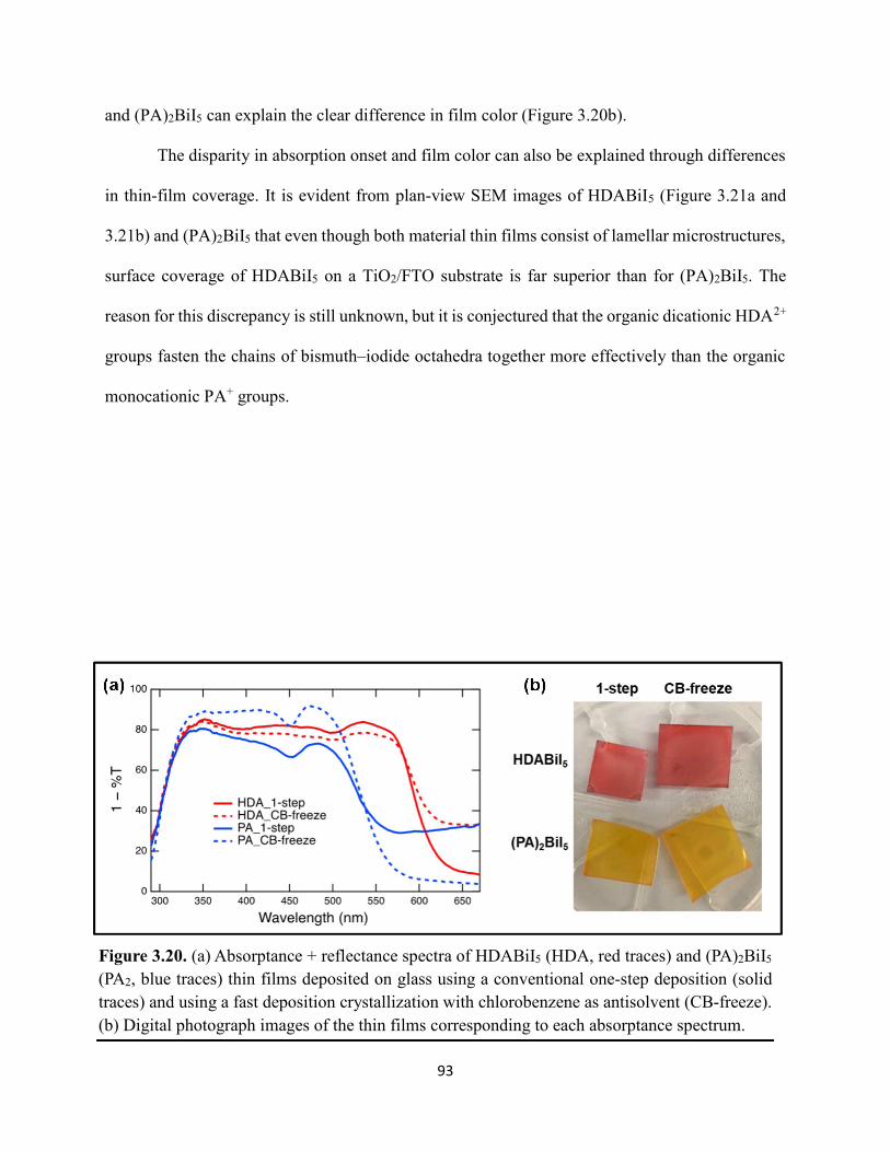
93
and (PA)2BiI5 can explain the clear difference in film color (Figure 3.20b).
The disparity in absorption onset and film color can also be explained through differences
in thin-film coverage. It is evident from plan-view SEM images of HDABiI5 (Figure 3.21a and
3.21b) and (PA)2BiI5 that even though both material thin films consist of lamellar microstructures,
surface coverage of HDABiI5 on a TiO2/FTO substrate is far superior than for (PA)2BiI5. The
reason for this discrepancy is still unknown, but it is conjectured that the organic dicationic HDA2+
groups fasten the chains of bismuth–iodide octahedra together more effectively than the organic
monocationic PA+ groups.
Figure 3.20. (a) Absorptance + reflectance spectra of HDABiI5 (HDA, red traces) and (PA)2BiI5 (PA2, blue traces) thin films deposited on glass using a conventional one-step deposition (solid traces) and using a fast deposition crystallization with chlorobenzene as antisolvent (CB-freeze). (b) Digital photograph images of the thin films corresponding to each absorptance spectrum.
(a) (b)
94
Absorption and steady-state emission spectra of thin films of HDABiI5 and (PA)2BiI5 are
displayed in Figure 3.22. The more gradual and blue-shifted absorption onset of (PA)2BiI5
compared to HDABiI5 supports the XRD data that the (PA)2BiI5 film is composed of a mix of one-
dimensional and zero-dimensional phases. Emission is present at the band edge of both materials,
suggesting that the emission is not from intra-gap trap states. It is also evident in Figure 3.23 that
there is no wavelength-dependent response to the emission of each film, indicating that the
observed signal is not due to Raman scattering. Some overlap between the incident excitation light
and the emission signal is apparent for 480 nm and 500 nm excitation of the (PA)2BiI5 film (Figure
3.23b).
Figure 3.21. Plan-view scanning electron microscopy images of thin films of HDABiI5/mTiO2/cTiO2/FTO (panels (a) and (b)) and (PA)2BiI5/mTiO2/cTiO2/FTO (panels (c) and (d)).
(a) (b)
(c) (d)

95
The thermal stability of HDABiI5 and (PA)2BiI5 powders were assessed by
thermogravimetric analysis (TGA) (Figure 3.24). The onset of significant mass loss occurs at a
lower temperature for (PA)2BiI5 (< 250 °C) than for HDABiI5 (> 300 °C), which is depicted in the
derivative plots (dash-dotted traces) of Figure 3.24a. It is also evident in Figure 3.24a that there is
a non-zero slope of the mass loss curve of (PA)2BiI5 (blue solid trace) even at temperatures below
200 °C whereas the mass loss curve of HDABiI5 is flat (red solid trace). This difference is
accentuated in the ramp and hold TGA data displayed in Figure 3.24b. The temperature in the
1.0
0.8
0.6
0.4
0.2
0.0
Ab
sorb
ance
750700650600550500450400350300
Wavelength (nm)
1.0
0.8
0.6
0.4
0.2
0.0
Norm
alized
PL HDABiI5 (PA)2BiI5
Figure 3.22. Absorption spectra (solid traces) and steady-state emission spectra (dashed traces) of thin films of HDABiI5 (red traces) and (PA)2BiI5 (blue traces) using 400 nm excitation.
(a) (b)
Figure 3.23. Steady-state emission spectra of thin films of (a) HDABiI5 and (b) (PA)2BiI5 using 400 nm excitation (pink traces) – 500 nm excitation (red traces).
96
TGA chamber was ramped to 200 °C and then held and monitored at 200 °C. After 1 hour, the
(PA)2BiI5 powder sample had ~8% mass loss, whereas HDABiI5 had ~0.5% mass loss. The greater
thermal stability of HDABiI5 compared to (PA)2BiI5 can be rationalized by differences in boiling
points of the organic precursors. The boiling point of HDA is 204 °C and the boiling point of PA
is 49 °C. In addition, part of the superior stability of HDABiI5 could be explained by the molecular
fasterner effect, where organic dicationic HDA2+ groups give HDABiI5 more structural rigidity
than the organic monocationic PA+ groups for (PA)2BiI5.
Photovoltaics (PV) devices containing (PA)2BiI5 as the photoactive layer were fabricated
with an n–i–p architecture of FTO/cTiO2/mTiO2/(PA)2BiI5/spiro-OMeTAD/Au. PV devices were
fabricated in a similar manner as those containing HDABiI5 presented in Chapter 2. (PA)2BiI5-
containing PV devices were measured using two-electrode cyclic voltammetry and exhibited
significant shunting, as indicated by the J–E curve of the (PA)2BiI5-containing device measured
in the light passing through the origin (Figure 3.25a). Incomplete surface coverage of (PA)2BiI5
on the underlying TiO2 layer results in shunting pathways for electronic charges (Figure 3.21).
(a) (b)
Figure 3.24. (a) Temperature-dependent thermogravimetric analysis of HDABiI5 powder (red traces) and (PA)2BiI5 powder (blue traces). The solid curves correspond to the % mass remaining (left axis) and the dash-dotted curves correspond to the derivative of the % mass with respect to temperature (right axis). The gray dotted vertical line corresponds to the temperature used in panel b. (b) Isothermal thermogravimetric analysis at 200 °C as a function of time.
97
Because the (PA)2BiI5-containing devices have shunting pathways, negligible photocurrent
(Figure 3.25c) and therefore negligible sunlight-to-electricity power-conversion efficiency was
observed.
PhDA2+ was targeted as a small conjugated organic moiety to incorporate into hybrid
bismuth–halide solar cells. Small conjugated organic moieties were investigated, because the one-
dimensional hybrid bismuth–halide thin films prefer a (110) orientation on an FTO substrate,
which aligns the chains of bismuth–iodide octahedra in parallel to the substrate surface (i.e. in
plane). Small conjugated organic groups could therefore assist in charge-carrier conduction
through the plane of the thin film. At first, an attempt at synthesizing and isolating stable PhDABiI5
proved challenging. Following deposition of a thin film of PhDABiI5,
XRD measurements were carried out and no XRD peaks were obtained. It is hypothesized
that the PhDA2+ groups favorably π-stack, which disrupts formation of a crystalline structure of
PhDABiI5. As a result, mixed-dication bismuth–halide materials, for which the mole percentage
Figure 3.25. (a) J–E behavior for solar cells consisting of Au/spiro-OMeTAD/Bi/TiOx/FTO, where Bi is HDABiI5 (red trace) or (PA)2BiI5 (blue trace) and where dashed traces are measurements performed in the dark and solid traces are measurements performed under 1 Sun illumination. (b) Digital photograph images of the solar cells containing HDABiI5 (top) and (PA)2BiI5 (bottom). (c) Chronoamperometry measurements of (PA)2BiI5 (blue trace) and HDABiI5 (red trace). Yellow shaded regions indicate periods of time the solar cells were under 1 Sun illumination.
(a) (b) (c)
98
of PhDA2+ did not exceed 25%, were explored. Figure 3.26a displays grazing-incidence XRD data
of HDABiI5 as well as 95%-5%, 85%-15%, and 75%-25% mixtures of organic dications HDA2+
and PhDA2+ incorporated as the organic moiety in hybrid bismuth–halide materials, denoted
(HDA-PhDA)BiI5. With increasing amount of PhDA2+, the (110) orientation became less
favorable, further indicating that PhDA2+ groups were detrimental to the integrity of the one-
(a) (b)
(c)
Figure 3.26. (a) Grazing-incidence X-ray diffraction patterns of HDABiI5 and mixed organic dicationic (HDA-PhDA)BiI5 thin films normalized to the 011 peak at ~12 °. (b) Grazing-incidence X-ray diffraction patterns of a 95%-5% (HDA-PhDA)BiI5 thin film before and after thermal treatment at 200 °C for 19 h. (c) Transmission-mode electronic absorption spectra of mixed organic dicationic (HDA-PhDA)BiI5 thin films before and after thermal treatment at 200°C for 19 h.
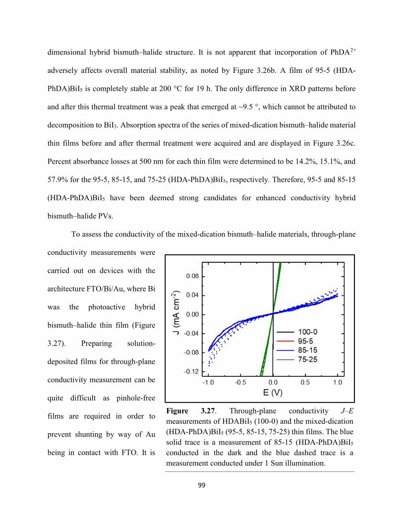
99
dimensional hybrid bismuth–halide structure. It is not apparent that incorporation of PhDA2+
adversely affects overall material stability, as noted by Figure 3.26b. A film of 95-5 (HDA-
PhDA)BiI5 is completely stable at 200 °C for 19 h. The only difference in XRD patterns before
and after this thermal treatment was a peak that emerged at ~9.5 °, which cannot be attributed to
decomposition to BiI3. Absorption spectra of the series of mixed-dication bismuth–halide material
thin films before and after thermal treatment were acquired and are displayed in Figure 3.26c.
Percent absorbance losses at 500 nm for each thin film were determined to be 14.2%, 15.1%, and
57.9% for the 95-5, 85-15, and 75-25 (HDA-PhDA)BiI5, respectively. Therefore, 95-5 and 85-15
(HDA-PhDA)BiI5 have been deemed strong candidates for enhanced conductivity hybrid
bismuth–halide PVs.
To assess the conductivity of the mixed-dication bismuth–halide materials, through-plane
conductivity measurements were
carried out on devices with the
architecture FTO/Bi/Au, where Bi
was the photoactive hybrid
bismuth–halide thin film (Figure
3.27). Preparing solution-
deposited films for through-plane
conductivity measurement can be
quite difficult as pinhole-free
films are required in order to
prevent shunting by way of Au
being in contact with FTO. It is
Figure 3.27. Through-plane conductivity J–E measurements of HDABiI5 (100-0) and the mixed-dication (HDA-PhDA)BiI5 (95-5, 85-15, 75-25) thin films. The blue solid trace is a measurement of 85-15 (HDA-PhDA)BiI5 conducted in the dark and the blue dashed trace is a measurement conducted under 1 Sun illumination.
100
apparent that the devices containing HDABiI5 (100-0) and 95-5 (HDA-PhDA)BiI5 exhibited
significant shunting and the device containing 75-25 (HDA-PhDA)BiI5 exhibited appreciable
shunting. This is not representative of the conductivity of the hybrid bismuth–halide material layer,
as the path of least resistance for current to flow is from FTO to Au or vice versa. The FTO/85-15
(HDA-PhDA)BiI5/Au device, however, behaves as expected. This suggests that the 85-15 (HDA-
PhDA)BiI5 has superior film coverage on FTO compared to the other hybrid bismuth–halide
materials. It can also be noted that the 85-15 (HDA-PhDA)BiI5 layer alone is photoconductive, as
the current density values measured under 1 Sun illumination are of larger magnitude than those
measured in the dark.
3.4 Conclusions
In the work presented in this chapter, a series of hybrid organic–inorganic bismuth–halide
materials that contained divalent organic cations were studied as stable alternatives to those
incorporating conventional monovalent organic cations employed in perovskite PVs. Information
regarding structure–PV property relationships and ideal solution-processing conditions within the
series of bismuth–halide materials were investigated. Appreciable steady-state PL at room
temperature for each of the bismuth–halide materials were measured. Time-resolved PL
measurements were performed, and PL lifetimes of the materials were either shorter than the
instrument response time or are just barely longer than the instrument response time. From TRMC
measurements on three of the bismuth–halide materials it was determined that, for the one-
dimensional materials, charge-carrier trapping lifetimes were ~10 ns and charge-carrier
recombination lifetimes were 300-400 ns, which is comparable to that of conventionally-used
methylammonium lead iodide. TRMC measurements on the zero-dimensional material containing

101
monovalent organic cations, (FA0.75/Cs0.25)3Bi2I9, no signal was observed outside the instrument
response. This could be attributed to the lack of interconnectivity of the inorganic units, as the
material structure is composed of isolated bismuth–iodide bioctahedra.
A similar trend was observed in TA measurements. TA spectra matched well with the
steady-state absorption spectra of each of the three materials, which suggested stable exciton
formation. TA kinetics of the same three materials were analyzed and it was determined that, for
the one-dimensional materials, excitons are long-lived, with lifetimes of 2-3 ns. The exciton
binding energy of HDABiI5 was determined to be ~310 meV from TA spectra. This is 100 meV
greater than the exciton binding energy of zero-dimensional MA3Bi2I9, which can be attributed to
the larger size of the HDA moiety. The exciton lifetime of zero-dimensional (FA0.75/Cs0.25)3Bi2I9
was much shorter (<100 ps) than the one-dimensional materials, which suggested faster
recombination in (FA0.75/Cs0.25)3Bi2I9.
3.5 References
(1) Fabian, D. M.; Ganose, A. M.; Ziller, J. W.; Scanlon, D. O.; Beard, M. C.; Ardo, S. ACS
Appl. Mater. Interfaces 2018, manuscript in preparation.
(2) Eperon, G. E.; Hörantner, M. T.; Snaith, H. J. Nat. Rev. Chem. 2017, 1, 0095.
(3) Reid, G. D.; Wynne, K. Encycl. Anal. Chem. 2000, 13644–13670.
(4) Phuong, L. Q.; Yamada, Y.; Nagai, M.; Maruyama, N.; Wakamiya, A.; Kanemitsu, Y. J.
Phys. Chem. Lett. 2016, 7, 2316–2321.
(5) Scholz, M.; Flender, O.; Oum, K.; Lenzer, T. J. Phys. Chem. C 2017, 121, 12110–12116.
(6) Yang, Y.; Yang, M.; Moore, D. T.; Yan, Y.; Miller, E. M.; Zhu, K.; Beard, M. C. Nat.
102
Energy 2017, 2, 1–7.
(7) Yang, Y.; Ostrowski, D. P.; France, R. M.; Zhu, K.; van de Lagemaat, J.; Luther, J. M.;
Beard, M. C. Nat. Photonics 2016, 10, 53–59.
(8) Yang, Y.; Yang, M.; Zhu, K.; Johnson, J. C.; Berry, J. J.; Lagemaat, J. Van De; Beard, M.
C. Nat. Commun. 2016, 7, 12613.
(9) Zhou, H.; Chen, Q.; Li, G.; Luo, S.; Song, T. -b.; Duan, H.-S.; Hong, Z.; You, J.; Liu, Y.;
Yang, Y. Science 2014, 345, 542–546.
(10) Ulbricht, R.; Hendry, E.; Shan, J.; Heinz, T. F.; Bonn, M. Rev. Mod. Phys. 2011, 83, 543–
586.
(11) Marchioro, A.; Teuscher, J.; Friedrich, D.; Kunst, M.; van de Krol, R.; Moehl, T.; Grätzel,
M.; Moser, J.-E. Nat. Photonics 2014, 1–6.
(12) Pascoe, A. R.; Yang, M.; Kopidakis, N.; Zhu, K.; Reese, M. O.; Rumbles, G.; Fekete, M.;
Duffy, N. W.; Cheng, Y. B. Nano Energy 2016, 22, 439–452.
(13) Stranks, S. D.; Eperon, G. E.; Grancini, G.; Menelaou, C.; Alcocer, M. J. P.; Leijtens, T.;
Herz, L. M.; Petrozza, A.; Snaith, H. J. Science 2013, 342, 341–344.
(14) Nie, W.; Tsai, H.; Asadpour, R.; Blancon, J.; Neukirch, A. J.; Gupta, G.; Crochet, J. J.;
Chhowalla, M.; Tretiak, S.; Alam, M. A.; Wang, H.; Mohite, A. D. Science 2015, 347, 522–
525.
(15) Berera, R.; van Grondelle, R.; Kennis, J. T. M. Photosynth. Res. 2009, 101, 105–118.
(16) Liang, L.; Wencong, L.; Nianyi, C. J. Phys. Chem. Solids 2004, 65, 855–860.
(17) Bartel, C. J.; Sutton, C.; Goldsmith, B. R.; Ouyang, R.; Musgrave, C. B.; Ghiringhelli, L.
M.; Scheffler, M. 2018, 6, 1–13.
(18) Collot, L.; Lefèvre-Seguin, V.; Brune, M.; Raimond, J. M.; Haroche, S. Europhys. Lett.
103
2007, 23, 327–334.
(19) Karlin, K. D. Progress in Inorganic Chemistry, Volume 48; John Wiley & Sons, Inc.: New
York, 1999.
(20) Nardes, A. M. On the conductivity of PEDOT:PSS thin films; Technische Universiteit
Eindhoven: Eindhoven, 2007.
(21) Park, B. W.; Philippe, B.; Zhang, X.; Rensmo, H.; Boschloo, G.; Johansson, E. M. J. Adv.
Mater. 2015, 27, 6806–6813.
(22) APEX2, 2014.
(23) SAINT, 2013.
(24) Sheldrick, G. M. SADABS, 2014.
(25) Sheldrick, G. M. SHELXTL, 2014.
(26) International Tables for X-Ray Crystallography; Vol C.; Kluwer Academic Publishers:
Dordrecht, 1992.
(27) Ito, S.; Murakami, T. N.; Comte, P.; Liska, P.; Grätzel, C.; Nazeeruddin, M. K.; Grätzel, M.
Thin Solid Films 2008, 516, 4613–4619.
(28) Kim, H.-S.; Lee, C.-R.; Im, J.-H.; Lee, K.-B.; Moehl, T.; Marchioro, A.; Moon, S.-J.;
Humphry-Baker, R.; Yum, J.-H.; Moser, J. E.; Grätzel, M.; Park, N.-G. Sci. Rep. 2012, 2,
591.
(29) Savenije, T. J.; Ferguson, A. J.; Kopidakis, N.; Rumbles, G. J. Phys. Chem. C 2013, 117,
24085–24103.
(30) Hrizi, C.; Samet, A.; Abid, Y.; Chaabouni, S.; Fliyou, M.; Koumina, A. J. Mol. Struct. 2011,
992, 96–101.
(31) Mousdis, G. A.; Papavassiliou, G. C.; Terzis, A.; Raptopoulou, C. P. Z. Naturforsch. 1998,
104
53b, 927–931.
(32) Fabian, D. M.; Ardo, S. J. Mater. Chem. A 2016, 4, 6837–6841.
(33) Jain, A.; Voznyy, O.; Sargent, E. H. J. Phys. Chem. C 2017, 121, 7183–7187.
(34) Du, M. H. J. Mater. Chem. A 2014, 2, 9091.
(35) Xiao, Z.; Meng, W.; Wang, J.; Mitzi, D. B.; Yan, Y. Mater. Horiz. 2017, 4, 206–216.
(36) Yu, L.; Zunger, A. Phys. Rev. Lett. 2012, 068701, 1–5.
(37) Savory, C. N.; Walsh, A.; Scanlon, D. O. ACS Energy Lett. 2016, 1, 949–955.
(38) Ganose, A. M.; Savory, C. N.; Scanlon, D. O. Chem. Commun. 2017, 53, 20–44.
(39) Kodzasa, T.; Ushijima, H.; Matsuda, H.; Kamata, T. Mol. Cryst. Liq. Cryst. 2000, 343, 71–
75.
(40) Noel, N. K.; Habisreutinger, S. N.; Wenger, B.; Klug, M. T.; Hörantner, M. T.; Johnston,
M. B.; Nicholas, R. J.; Moore, D. T.; Snaith, H. J. Energy Environ. Sci. 2017, 10, 145–152.
(41) Kamminga, M. E.; Stroppa, A.; Picozzi, S.; Chislov, M.; Zvereva, I. A.; Baas, J.; Meetsma,
A.; Blake, G. R.; Palstra, T. T. M. Inorg. Chem. 2017, 56, 33–41.
(42) Murthy, D. H. K.; Xu, T.; Chen, W. H.; Houtepen, a J.; Savenije, T. J.; Siebbeles, L. D. a;
Nys, J. P.; Krzeminski, C.; Grandidier, B.; Stiévenard, D.; Pareige, P.; Jomard, F.;
Patriarche, G.; Lebedev, O. I. Nanotechnology 2011, 22, 315710.
(43) Colbeau-Justin, C.; Valenzuela, M. A. Rev. Mex. Fis. 2013, 59, 191–200.
(44) Norris, D. J.; Sacra, A.; Murray, C. B.; Bawendi, M. G. Phys. Rev. Lett. 1994, 72, 2612–
2615.
105
CHAPTER 4: DEMONSTRATION OF PHOTOVOLTAIC ACTION AND
ENHANCED STABILITY FROM A QUASI-TWO-DIMENSIONAL
HYBRID ORGANIC–INORGANIC COPPER–HALIDE MATERIAL
INCORPORATING DIVALENT ORGANIC LIGANDS
* In part a compilation of one publication in preparation1
4.1 Introduction
Lead–halide hybrid organic–inorganic perovskite (APbX3) materials are a relatively new
class of materials used as photoactive layers in thin-film solar cells.2–4 They have tunable bandgaps
that allow them to operate efficiently as the photoactive layer in single-junction solar cells or as
the photoactive layer in the top cell of a tandem solar cell with silicon.5,6 Laboratory-scale solar
cells incorporating APbX3 materials as the photoactive layer have demonstrated impressive
efficiencies of > 20%.7,8 However, APbX3 materials incorporate toxic lead and are extremely
unstable to moisture and heat.9–11 Instability of APbX3 materials is observed under ambient
conditions, in part because the organic halide, AX, dissociates into two water-soluble, low-boiling-
point species. For example, when A+ = CH3NH3+ and X– is a halide, they dissociate into CH3NH2
and HX.12 Exposure to light and dry air has also been reported to decompose APbX3 materials,
especially when incorporated in mesostructured assemblies.13
One way to improve stability of APbX3 materials is to increase the size of the organic A+
moiety, and therefore decrease the vapor pressure of its deprotonated state, A. However, APbX3
materials form a three-dimensional (3D) Pb–X network of corner-sharing octahedra and therefore,
the ionic radii of Pb2+ and X– dictate the volume of the cuboctahedral voids that limit the allowable
size of the organic group to no larger than the isopropylammonium cation.14 Alternatively, one-
dimensional (1D) and two-dimensional (2D) hybrid organic–inorganic materials offer flexibility

106
to accommodate larger organic groups.15–19 However, weaker orbital overlap within the inorganic
network in these materials precludes efficient electronic conduction between adjacent 1D chains
or 2D sheets and, therefore, overall solar-cell performance.20 One strategy to overcome this
limitation is to incorporate divalent organic ligands in the unit cell to serve as bridges between the
inorganic chains or sheets. We recently used this strategy to fabricate a photovoltaic that contained
a 1D bismuth–iodide hybrid organic–inorganic material with bridging 1,6-hexanediammonium
divalent organic ligands (HDABiI5) as the photoactive layer.21
Like 3D APbX3 materials, which were first reported in 1893 and only in the last decade
were used as the photoactive layer in solar cells,22,23 1D and 2D halide-containing hybrid organic–
inorganic materials are not new. In terms of 1D materials, Mousdis et al. reported in 1998 the
single-crystal structure of HDABiI5, which they described as a 1D semiconductor.24 This class of
bismuth–halide hybrid organic–inorganic materials was further investigated by Mitzi and Brock
in the early 2000s,25 and more recently bismuth–halide hybrid organic–inorganic materials have
re-emerged as candidates for the photoactive layer in solar cells.21,26–33 The body of work on
bismuth–halide photoactive materials has shown that these materials have conductivities in the
range of 10-9 – 10-2 S·cm-1,26,29 tunable bandgaps in the visible spectral range, high crystal quality,
and superior heat and moisture stability compared to state-of-the-art 3D APbX3 materials.21
Although 1D bismuth–halide hybrid organic–inorganic materials can accommodate larger
organic cations in their crystal lattice, which can facilitate control over materials stability,
conduction through the inorganic network is limited. This can in part be overcome through use of
2D hybrid organic–inorganic materials, which should still offer flexibility in the allowable size of
the organic group as well as superior in-plane conductivity compared to 1D hybrid organic–
inorganic materials. The first crystallographic structural data of 2D copper–halide hybrid organic–
107
inorganic materials incorporating divalent organic ligands were reported in 1988 by Willett et al.34
These copper–halide materials containing diammonium salts, n(DA2+(R–)2), (i.e. salts of
[NH3(CH2)nNH3]2+) consisted of 2D copper–halide sheets arranged in an eclipsed conformation,
and materials with n = 3, 4, or 5 were shown to exhibit ferromagnetism.34 Recently, 2D
Ruddlesden–Popper halide perovskite materials have emerged as a promising photoactive layer in
solar cells.35 While they were reported to be more stable than APbX3, to-date only those that
contain lead or tin have been reported.36–40 A copper–chloride quasi-2D hybrid organic–inorganic
material containing 1,4-butanediammonium was investigated by Li and coworkers, and from this
study it was found that the organic moiety inhibits a phase transition and amorphization of the
crystal structure at high pressure.41 In 2016, Cortecchia and coworkers reported a series of
photoactive materials that consisted of 2D copper–halide sheets with a 2:1 molar ratio of
methylammonium monocations (MA+) to Cu2+.42 The sunlight-to-electrical power conversion
efficiency of a solar cell using (MA)2CuBr2Cl2 as the photoactive layer was reported to be 0.017%,
with an open-circuit photovoltage of 260 mV.42 For stability chloride incorporation in the materials
was necessary, because the all-bromide-containing (MA)2CuBr4 was extremely hygroscopic.42 In
a follow-up paper, Cortecchia et al. reported on the incorporation of an organic ligand within a 2D
copper–chloride network that contained hydrophobic aromatic units to improve moisture
stability.43 To assess the plausibility of using high-molecular-weight divalent organic ligands in
2D copper–halide hybrid organic–inorganic materials for applications in solar cells, a comparative
study on novel dicationic and monocationic copper–halide materials was conducted and the results
are reported herein.
4.2 Experimental
108
4.2.1 Preparation of (HDA)2CuBr6-xClx and (PA)4CuBr6 Solutions
All chemicals were used as received. 1,6-hexanediammonium bromide (HDABr2) and 1,6-
hexanediammonium chloride (HDACl2) were synthesized by slow addition of aqueous
hydrobromic acid (HBr, 48% in water, Oakwood Chemical) and aqueous hydrochloric acid (HCl,
37% in water, Macron Fine Chemicals), respectively, at room temperature to a solution of 1,6-
hexanediamine (98%, Alfa Aesar) dissolved in methanol (at a 2:1 mole ratio of HBr/HCl to 1,6-
hexanediamine) at 0 °C with stirring, followed by continued stirring for 30 min. In a similar
manner, propylammonium bromide (PABr) was synthesized by slow addition of HBr to a solution
of propylamine (98%, Alfa Aesar) dissolved in methanol (1:1 mole ratio of HBr to 1,6-
hexanediamine). HDABr2, HDACl2, and PABr precipitates were recovered by evaporation of
solvents at 50 °C under reduced pressure. To purify HDABr2, HDACl2, and PABr, precipitates
were dissolved in methanol, recrystallized from diethyl ether, and finally vacuum dried for 12 h.
(HDA)2CuBr6 and (PA)4CuBr6 solutions were prepared by mixing powders of the organic
precursor (either HDABr2 or PABr) and CuBr2 (99%, Alfa Aesar) at a 1:1 molar ratio, but with
the organic precursor in slight excess, in 4:1 v/v N,N-dimethylformamide to dimethyl sulfoxide
(4:1 DMF:DMSO) to make a 1 M solution. For (HDA)2CuBr5Cl and (HDA)2CuBr4Cl2 solutions,
a 5:1 ratio and 2:1 ratio of HDABr2 to HDACl2 were used, respectively. The solutions were stirred
at 70 °C inside a nitrogen-filled glovebox, stored in the glovebox until use, and used within two
weeks of preparation.
4.2.2 (HDA)2CuBr6 Single-Crystal Growth
Approximately 200 μL of a 1 M solution of (HDA)2CuBr6 in 4:1 v/v DMF:DMSO was
dispensed into a 4 mL vial and this vial was placed uncapped in a 20 mL vial containing ~2 mL
109
dichloromethane and the 20 mL vial was capped. (HDA)2CuBr6 single crystals grew overnight in
the 4 mL vial via diffusion of dichloromethane.
4.2.3 X-ray Data Collection and Structure Solution for (HDA)2CuBr6
A black crystal was mounted on a glass fiber and transferred to a Bruker SMART APEX
II diffractometer. The APEX244 program package was used to determine the unit-cell parameters
and for data collection (20 sec/frame scan time for a sphere of diffraction data). The raw frame
data was processed using SAINT45 and SADABS46 to yield the reflection data file. Subsequent
calculations were carried out using the SHELXTL47 program. There were no systematic absences
nor any diffraction symmetry other than the Friedel condition. The orthorhombic space group P21/c
was assigned and later determined to be correct.
The structure was solved by direct methods and refined on F2 by full-matrix least-squares
techniques. The analytical scattering factors48 for neutral atoms were used throughout the analysis.
Hydrogen atoms were included using a riding model.
4.2.4 Materials Processing
All steps of materials deposition and solar cell fabrication were performed in air with 40–
60 % relative humidity as described below, unless noted otherwise. All thermal treatments were
performed using a hot plate. Fluorine-doped tin–oxide-coated glass (FTO) substrates were cleaned
as follows: 1) sonicated in Alconox solution, 2) rinsed with deionized water, 3) rinsed with ethanol,
4) sonicated in ethanol, and 5) dried with nitrogen. To deposit the compact TiO2 (cTiO2) layer, a
solution of titanium diisopropoxide bis(acetylacetonate) was pipetted onto a cleaned FTO substrate
and after a 30 sec wait period the substrate was spun at 2000 rpm (2000 rpm/sec acceleration) for
110
60 sec. The substrate was subsequently dried at 125 °C and then sintered at 550 °C for 30 min.
Nanoparticles of TiO2 were synthesized following a procedure by Ito et al.49 The nanoparticle
solution was further diluted in ethanol at a weight ratio of 1:1 TiO2 nanoparticle solution:ethanol
to make a mesoporous TiO2 (mTiO2) suspension. The mTiO2 layer was pipetted on top of the
cTiO2/FTO substrate and after a 30 sec wait period the substrate was spun at 500 rpm (500 rpm/sec
acceleration) for 5 sec and then 5000 rpm (5000 rpm/sec acceleration) for 25 sec, dried at 125 °C,
and then sintered at 550 °C for 30 minutes. A conventional method was used to deposit the copper–
halide-containing solutions, which was adapted from Kim et al.50 A filtered copper–halide-
containing solution in 4:1 v/v DMF:DMSO was pipetted on top of the mTiO2/cTiO2/FTO substrate
and after a 60 sec wait period the substrate was spun at 2000 rpm (2000 rpm/sec acceleration) for
60 sec, followed by transfer to a hot plate that was preheated to 100 °C, and the substrate was
subsequently annealed at 100 °C for 45 min.
4.2.5 Solar Cell Fabrication
Prior to the FTO cleaning step, a region of the FTO film was etched using 2 M aqueous
HCl and Zn powder in order to prevent solar cell shunting upon contact to the top Au electrode.
After performing the cleaning steps listed above (Materials Processing subsection), FTO
substrates were further cleaned using an O2 plasma treatment for 10 min. Following deposition of
the copper–halide-containing solution per the protocol described above (Materials Processing
subsection), a 50 mM solution of 2,2’,7,7’-tetrakis(N,N’-di-p-methoxyphenylamine)-9,9’-
spirobifluorene (spiro-OMeTAD) dissolved in toluene was deposited by spin coating at 3000 rpm
(3000 rpm/sec acceleration) for 60 sec. The solar cells were left to dry in air for 20 min and then
were transferred into a nitrogen-filled glovebox, and 80 nm of Au was thermally evaporated onto
111
the solar cells at a base pressure of 5 10-6 mbar. The complete solar cells had an architecture of
Au/spiro-OMeTAD/Cu/mTiO2/cTiO2/FTO, where Cu = (HDA)2CuBr6, HDACuBr5Cl,
HDACuBr4Cl2, or (PA)4CuBr6.
4.2.6 Stability Tests
Stability tests were performed in air for (HDA)2CuBr6 and (PA)4CuBr6 thin films deposited
on mTiO2/cTiO2/FTO per the protocols above (Materials Processing and Solar Cell Fabrication
subsections). For the accelerated thermal stability tests, thin films were heated to 100 °C and
exposed to ~50 % relative humidity for 16 h. The X-ray diffraction patterns before and after
exposure are displayed in Figure 4 For the moisture stability tests, thin films and powders of
(HDA)2CuBr6 and (PA)4CuBr6 were exposed to ~50 % relative humidity. The thin films were
monitored over a period of 12 days using transmission-mode ultraviolet–visible electronic
absorption spectroscopy. The powders were monitored over a period of 14 days using X-ray
diffraction.
4.2.7 Materials Characterization
Electronic absorption spectroscopy measurements were carried out using an Agilent Cary
60 spectrophotometer with a resolution of 1 nm, and Tauc plots were constructed from the
measured spectra. Spectra were baseline-subtracted for long-wavelength scattering, and bandgap
energies were determined from best-fit lines of the data near the absorption onset. Scanning
electron microscopy and energy-dispersive X-ray spectroscopy images were acquired on a FEI
Magellan 400L XHR. Absorption coefficients of thin films were calculated based on the average
thickness measured from cross-sectional scanning electron microscopy images (740 ± 80 nm). For

112
thin films, grazing-incidence X-ray diffraction data were collected using a Rigaku Smartlab
diffractometer with Cu Kα radiation and in parallel-beam geometry. For powders, X-ray diffraction
data were collected in Bragg-Brentano geometry. Thermogravimetric analysis data were obtained
using a TGA Q500 by TA Instruments. Steady-state photoluminescence spectra were acquired at
room temperature using a Cary Eclipse fluorescence spectrophotometer by Agilent Technologies
with excitation light at 320-350 nm, matched slit widths of 10 nm, and detection in a right-angle
geometry. Films were positioned at ~60° relative to the detector (i.e. ~30° relative to the incident
excitation light). Data were corrected for the wavelength-dependent response of the detection
system.
XPS measurements were performed using a Kratos AXIS Supra photoelectron
spectrometer using Al Kα radiation. Cu 2p region scans were obtained immediately following
sample z-alignment in order to minimize X-ray induced reduction of Cu2+.51 The XPS data were
analyzed using CasaXPS Processing Software. XPS peaks were fit to Gaussian–Lorentzian (80:20)
curves. For XPS measurements of the cutoff region (determination of the work function) and
valence-band region (determination of the valence-band maximum), Fermi edge calibration was
performed with a sputter-cleaned Ag standard to ensure that all energies were referenced to a
common Fermi level (0 eV). XPS measurements were performed instead of ultraviolet
photoelectron spectroscopy (UPS) measurements because ultraviolet light has been shown to
induce significant work-function reduction on transparent-conductive-oxide substrate surfaces.52
Work functions were calculated by extrapolating the XPS cutoff region spectra to the x-intercept.
In a manner similar to that performed by Schulz et al.,53 the low-energy tail of the valence-band
spectrum was used to determine the position of the valence-band maximum relative to the Fermi
level. Using the determined optical bandgaps, the conduction-band minimum was calculated for
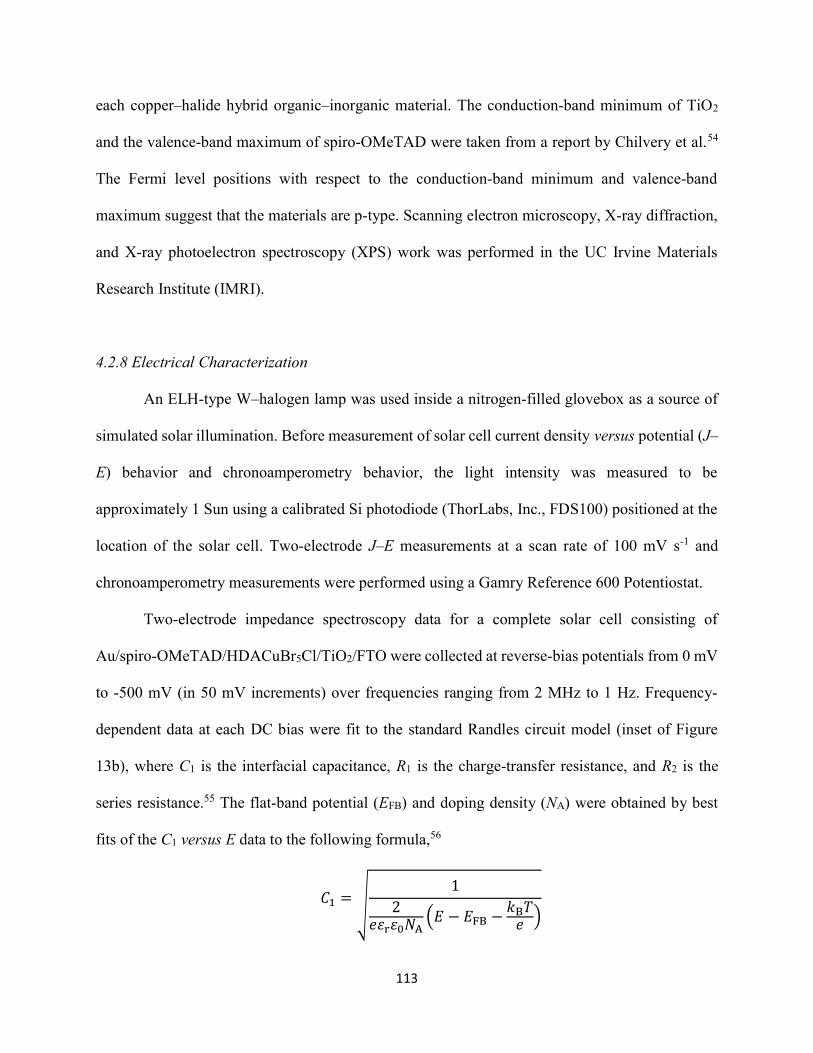
113
each copper–halide hybrid organic–inorganic material. The conduction-band minimum of TiO2
and the valence-band maximum of spiro-OMeTAD were taken from a report by Chilvery et al.54
The Fermi level positions with respect to the conduction-band minimum and valence-band
maximum suggest that the materials are p-type. Scanning electron microscopy, X-ray diffraction,
and X-ray photoelectron spectroscopy (XPS) work was performed in the UC Irvine Materials
Research Institute (IMRI).
4.2.8 Electrical Characterization
An ELH-type W–halogen lamp was used inside a nitrogen-filled glovebox as a source of
simulated solar illumination. Before measurement of solar cell current density versus potential (J–
E) behavior and chronoamperometry behavior, the light intensity was measured to be
approximately 1 Sun using a calibrated Si photodiode (ThorLabs, Inc., FDS100) positioned at the
location of the solar cell. Two-electrode J–E measurements at a scan rate of 100 mV s-1 and
chronoamperometry measurements were performed using a Gamry Reference 600 Potentiostat.
Two-electrode impedance spectroscopy data for a complete solar cell consisting of
Au/spiro-OMeTAD/HDACuBr5Cl/TiO2/FTO were collected at reverse-bias potentials from 0 mV
to -500 mV (in 50 mV increments) over frequencies ranging from 2 MHz to 1 Hz. Frequency-
dependent data at each DC bias were fit to the standard Randles circuit model (inset of Figure
13b), where C1 is the interfacial capacitance, R1 is the charge-transfer resistance, and R2 is the
series resistance.55 The flat-band potential (EFB) and doping density (NA) were obtained by best
fits of the C1 versus E data to the following formula,56
𝐶 =1
2𝑒𝜀 𝜀 𝑁
𝐸 − 𝐸 −𝑘 𝑇𝑒
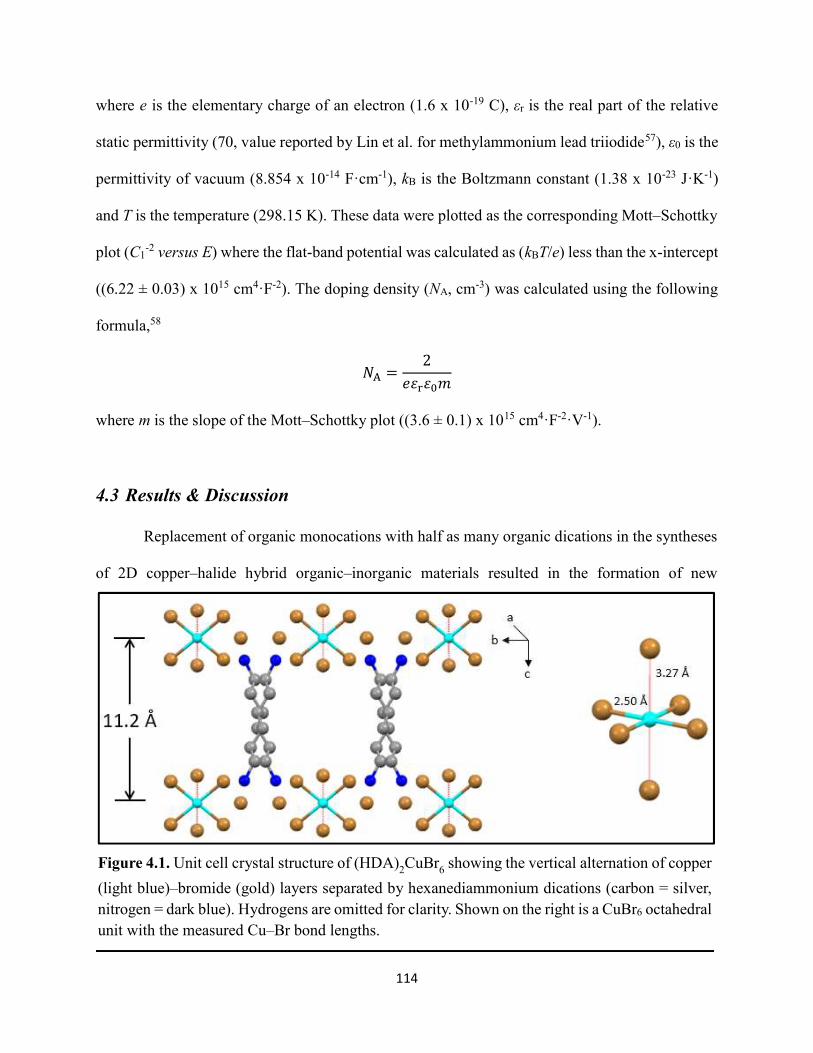
114
where e is the elementary charge of an electron (1.6 x 10⁻¹⁹ C), εr is the real part of the relative
static permittivity (70, value reported by Lin et al. for methylammonium lead triiodide57), ε0 is the
permittivity of vacuum (8.854 x 10⁻¹⁴ F·cm-1), kB is the Boltzmann constant (1.38 x 10⁻²³ J·K-1)
and T is the temperature (298.15 K). These data were plotted as the corresponding Mott–Schottky
plot (C1-2 versus E) where the flat-band potential was calculated as (kBT/e) less than the x-intercept
((6.22 ± 0.03) x 1015 cm4·F-2). The doping density (NA, cm-3) was calculated using the following
formula,58
𝑁 =2
𝑒𝜀 𝜀 𝑚
where m is the slope of the Mott–Schottky plot ((3.6 ± 0.1) x 1015 cm4·F-2·V-1).
4.3 Results & Discussion
Replacement of organic monocations with half as many organic dications in the syntheses
of 2D copper–halide hybrid organic–inorganic materials resulted in the formation of new
Figure 4.1. Unit cell crystal structure of (HDA)2CuBr6 showing the vertical alternation of copper
(light blue)–bromide (gold) layers separated by hexanediammonium dications (carbon = silver, nitrogen = dark blue). Hydrogens are omitted for clarity. Shown on the right is a CuBr6 octahedral unit with the measured Cu–Br bond lengths.
115
(HDA)2CuX6 materials, where HDA is 1,6-hexanediammonium (HDA2+). Single crystals of
(HDA)2CuBr6, in the form of black platelets, were grown and the single-crystal structure of
(HDA)2CuBr6 was resolved. The unit cell structure is shown in Figure 4.1. (HDA)2CuBr6 is
monoclinic (space group 14: C2/m), with lattice constants a = 10.2 Å, b = 16.9 Å, and c = 11.2 Å
and unit cell angles α = 90.0 °, β = 98.8 °, γ = 90.0 °. CuBr6 octahedra are isolated from each other,
but the octahedra arrange in quasi-2D sheets along the ab plane. Equatorial copper–bromide bond
lengths are 2.50 Å and axial copper–bromide bond lengths are 3.27 Å. This difference in bond
lengths can be attributed to Jahn–Teller elongation, which has been observed in analogous
materials containing CuBr6 octahedra.59 Table 4.1 shows crystallographic information pertaining
to the (HDA)3CuBr8 single crystal.
Table 4.1. Crystallographic data for (HDA)2CuBr6.

116
The transmission-mode ultraviolet–visible absorption spectra are shown in Figure 4.2a and
displayed as Tauc plots in Figure 4.3a for (HDA)2CuX6 materials as well as a control spectrum of
a copper–bromide perovskite material incorporating four propylammonium (PA+) groups per
copper atom, (PA)4CuBr6. PA+ was chosen for comparative studies because its C–N core is roughly
half the length of that of HDA2+. Each thin film exhibited a lowest-energy indirect bandgap of
~1.80 eV (Figure 4.3a), a direct bandgap of ~2.05–2.10 eV (Figure 4.4), and d–d transitions at
Figure 4.2. (a) Transmission-mode electronic absorbance spectra (dotted traces) and steady-state photoluminescence emission spectra (solid traces, λex ≈ 340 nm) of thin films of (HDA)2CuBr6 (red trace) and (PA)4CuBr6 (blue trace). (b) Normalized steady-state photoluminescence emission spectra (λex ≈ 400 nm) of thin films of (HDA)2CuBr6 (red trace) and (PA)4CuBr6 (blue trace), showing a broad tailing region due to emission from an electronic transition with λmax ≈ 580 nm. (c) Steady-state photoluminescence excitation spectra of (HDA)2CuBr6 and (PA)4CuBr6 probed at emission peak wavelengths (solid traces) and at 580 nm (dotted traces), with the absorptance spectra of (HDA)2CuBr6 (red squares trace) and (PA)4CuBr6 (blue squares trace) overlaid.

117
~1.60 eV (Figure 4.3a). The indirect bandgap of these materials is ~0.25 eV smaller than that of
thin films of HDABiI5,20 making them more suitable for applications as the photoactive layer in
the top cell of a tandem solar cell with silicon.4,5 Bandgap energies and molar absorption
coefficients are comparable to those reported for monocationic copper–halide perovskite
materials.41 Interestingly, the (PA)4CuBr6 thin film exhibited the weakest molar absorptivity of the
series, which suggests that incorporation of divalent organic ligands in these materials causes
enhancement of their absorption cross sections. Digital photograph images of freshly-prepared
(HDA)2CuBr6-xClx thin films deposited on glass are shown in Figure 4.3b. Analogous digital
photograph images of (HDA)2CuBr6-xClx and (PA)4CuBr6 deposited on mesoporous
TiO2/cTiO2/FTO for solar cell fabrication and testing are shown in Figure 4.5.
Figure 4.3. (a) Indirect-bandgap Tauc plots of copper–halide hybrid organic–inorganic thin films deposited on glass and incorporating HDA2+ with varying halide compositions (black, red, and green traces) or PA+ (blue trace). Data are corrected for scattering as described in the Materials Characterization subsection. Bold dashed lines represent best fits to the absorption onsets and thin dashed lines represent baselines for the indirect transitions. (b) Digital photograph image of representative freshly-prepared (HDA)2CuBr6-xClx thin films deposited on glass, with (from left to right) x = 0, 1, and 2.
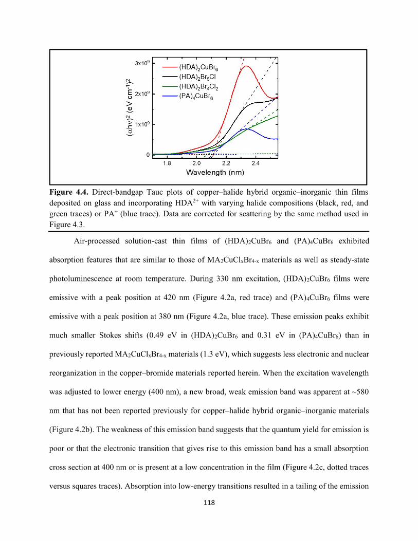
118
Air-processed solution-cast thin films of (HDA)2CuBr6 and (PA)4CuBr6 exhibited
absorption features that are similar to those of MA2CuClxBr4-x materials as well as steady-state
photoluminescence at room temperature. During 330 nm excitation, (HDA)2CuBr6 films were
emissive with a peak position at 420 nm (Figure 4.2a, red trace) and (PA)4CuBr6 films were
emissive with a peak position at 380 nm (Figure 4.2a, blue trace). These emission peaks exhibit
much smaller Stokes shifts (0.49 eV in (HDA)2CuBr6 and 0.31 eV in (PA)4CuBr6) than in
previously reported MA2CuClxBr4-x materials (1.3 eV), which suggests less electronic and nuclear
reorganization in the copper–bromide materials reported herein. When the excitation wavelength
was adjusted to lower energy (400 nm), a new broad, weak emission band was apparent at ~580
nm that has not been reported previously for copper–halide hybrid organic–inorganic materials
(Figure 4.2b). The weakness of this emission band suggests that the quantum yield for emission is
poor or that the electronic transition that gives rise to this emission band has a small absorption
cross section at 400 nm or is present at a low concentration in the film (Figure 4.2c, dotted traces
versus squares traces). Absorption into low-energy transitions resulted in a tailing of the emission
Figure 4.4. Direct-bandgap Tauc plots of copper–halide hybrid organic–inorganic thin films deposited on glass and incorporating HDA2+ with varying halide compositions (black, red, and green traces) or PA+ (blue trace). Data are corrected for scattering by the same method used in Figure 4.3.
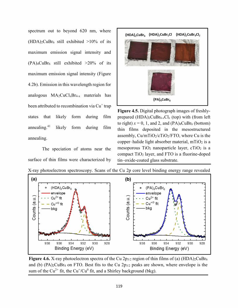
119
spectrum out to beyond 620 nm, where
(HDA)2CuBr6 still exhibited >10% of its
maximum emission signal intensity and
(PA)4CuBr6 still exhibited >20% of its
maximum emission signal intensity (Figure
4.2b). Emission in this wavelength region for
analogous MA2CuClxBr4-x materials has
been attributed to recombination via Cu+ trap
states that likely form during film
annealing.41 likely form during film
annealing.
The speciation of atoms near the
surface of thin films were characterized by
X-ray photoelectron spectroscopy. Scans of the Cu 2p core level binding energy range revealed
Figure 4.5. Digital photograph images of freshly-prepared (HDA)2CuBr6-xClx (top) with (from left to right) x = 0, 1, and 2, and (PA)4CuBr6 (bottom) thin films deposited in the mesostructured assembly, Cu/mTiO2/cTiO2/FTO, where Cu is the copper–halide light absorber material, mTiO2 is a mesoporous TiO2 nanoparticle layer, cTiO2 is a compact TiO2 layer, and FTO is a fluorine-doped tin–oxide-coated glass substrate.
Figure 4.6. X-ray photoelectron spectra of the Cu 2p3/2 region of thin films of (a) (HDA)2CuBr6 and (b) (PA)2CuBr4 on FTO. Best fits to the Cu 2p3/2 peaks are shown, where envelope is the sum of the Cu2+ fit, the Cu+/Cu0 fit, and a Shirley background (bkg).
120
the presence of Cu2+ and other peak(s) due to Cu+ and/or Cu0 (Figure 4.6, Figure 4.7a), which is
consistent with the absorptance and photoluminescence data. Deciphering between characteristic
peaks corresponding to Cu+ and Cu0 is a challenge because Cu+ and Cu0 states have very similar
binding energies. Peak fitting of the Cu 2p3/2 peaks revealed the copper composition profile of
(HDA)2CuBr6 to be approximately 81% Cu2+ and 19% Cu+/Cu0 (Figure 4.6a) and for (PA)4CuBr6,
approximately 66% Cu2+ and 34% Cu+/Cu0 (Figure 4.6b). These data suggest that reductive
degradation of the inorganic precursor material, CuBr2 occurred during thin-film fabrication. Scans
of the Cl 2p region were performed on the series of materials, which revealed near-surface
speciation of chloride in the (HDA)2CuBr4Cl2 and (HDA)2CuBr5Cl samples and no observed
chlorine species in the (HDA)2CuBr6 and (PA)4CuBr6 samples (Figure 4.7b). Following continued
X-ray exposure, through measurements of survey spectra and other core level binding energy
regions, the (HDA)2CuBr6 thin film contained approximately 75% Cu2+ and 25% Cu+/Cu0 (Figure
4.8a) and the (PA)4CuBr6 thin film contained approximately 60% Cu2+ and 40% Cu+/Cu0 (Figure
Figure 4.7. X-ray photoelectron spectra of the (a) Cu 2p region and the (b) Cl 2p region of copper–halide hybrid organic–inorganic thin films each deposited on a fluorine-doped tin–oxide-coated glass substrate. Intensities in panel (a) are normalized to the Cu 2p3/2 peak that corresponds to Cu2+.
121
4.8b), which marked a ~6% increase in near-surface Cu+/Cu0 for both thin films. The small
magnitude of these X-ray-induced changes provide evidence that there is Cu+/Cu0 present in both
thin films before exposure to the X-ray beam. The larger percentage of reduced copper species in
thin films of (PA)4CuBr6 supports observations of faster degradation of the Cu2+-containing
(PA)4CuBr6 thin films in comparison to the Cu2+-containing (HDA)2CuBr6 thin films. Scans of the
C 1s, N 1s, and Br 3p core level binding energy ranges for thin films of (HDA)2CuBr6 and
(PA)4CuBr6 were also performed (Figure 4.9). For both samples, the C 1s region spectra reveals
the presence of two peaks, which correspond to C–C bonds and C–N bonds in the organic groups.
The N 1s region spectrum contains a peak at 401.2 eV, which is consistent with the N 1s peak
position for MAPbX3 materials and is attributed to the nitrogen atoms in the ammonium groups.60
Strong Br 3p peaks were observed in (HDA)2CuBr6 and (PA)4CuBr6 thin films due to their large
bromide content.
Figure 4.8. Best fits to the Cu 2p3/2 peaks of the X-ray photoelectron spectra of thin films of (a) (HDA)2CuBr6 and (b) (PA)4CuBr6 thin films each deposited on a fluorine-doped tin–oxide-coated glass substrate following continued X-ray exposure, where envelope is the sum of the Cu2+ fit, the Cu+/Cu0 fit, and a Shirley background (bkg).

122
Evaluation of crystallinity and thermal stability were performed using grazing-incidence
X-ray diffraction. X-ray diffraction patterns of freshly-prepared thin films of dicationic
(HDA)2CuBr6 (Figure 4.10, solid red line) and analogous monocationic (PA)4CuBr6 (Figure 4.10,
solid blue line) show strong preferential orientation in the [001] direction, which is similar to the
patterns reported by Cortecchia et al.41 This indicates that the quasi-2D copper–halide sheets are
oriented in-plane with the FTO substrate. The observation of larger higher-order peaks in the
(HDA)2CuBr6 pattern in comparison to the (PA)4CuBr6 pattern indicates that there is a greater
amount of ordering at each Bragg reflection condition in the (HDA)2CuBr6 thin film.61 Because
the c-axis is orthogonal to the quasi-2D copper–halide sheets, the value of c is the sheet spacing
and can be determined from the two-theta values. For (HDA)2CuBr6, the (001) peak occurs at two-
theta = 7.80°, which indicates a sheet spacing of 11.3 Å. This value is consistent with the sheet
Figure 4.9. Scans of the (a), (d) C 1s, (b), (e) N 1s, and (c), (f) Br 3p core level binding energy regions for thin films of (HDA)2CuBr6 (top row) and (PA)4CuBr6 (bottom row), each deposited on a fluorine-doped tin–oxide-coated glass substrate.
123
spacing determined from single-crystal X-ray diffraction, which was 11.2 Å. In comparison, the
sheet spacing for (PA)4CuBr6 is 12.6 Å, which was calculated from a (PA)4CuBr6 (001) two-theta
value of 7.04°. The difference between sheet spacing in (HDA)2CuBr6 and (PA)4CuBr6 is logical
Figure 4.10. Grazing-incidence X-ray diffraction patterns of thin films of (a) (HDA)2CuBr6 (red) and (b) (PA)4CuBr6 (blue) when freshly-prepared (solid traces) and after exposure to 100 °C and ~50% relative humidity for 16 h (dashed traces). # denote peaks associated with the underlying fluorine-doped tin–oxide-coated glass substrate.
Figure 4.11. Powder X-ray diffraction patterns and thin-film X-ray diffraction patterns for (a) (HDA)2CuBr6 and (b) (PA)4CuBr6.
124
based on the slightly larger size of four PA+ in comparison to two HDA2+. A comparison of powder
versus thin-film X-ray diffraction patterns for both (HDA)2CuBr6 and (PA)4CuBr6 are shown in
Figure 4.11. Unlike for (HDA)2CuBr6, the largest-intensity peak for the (PA)4CuBr6 powder
occurred at a larger two-theta value relative to that of the thin film, which is speculated to be due
to water molecules present in (PA)4CuBr6 powder, which would suggest (PA)4CuBr6 is more
hygroscopic than (HDA)2CuBr6 since they were processed in nominally identical manners.
Accelerated thermal stability tests on thin films of (HDA)4CuBr6 resulted in minimal
changes in the grazing-incidence X-ray diffraction pattern (Figure 4.10a) and absorption spectrum
(Figure 5a, red data) in comparison to changes observed for thin films of (PA)4CuBr6 after the
same treatment (Figure 4.10b and Figure 4.12a, blue data). For (PA)4CuBr6 thin films, the (001)
peak intensity decreased significantly, the (001) peak shifted to 6.70°, and new peaks emerged at
Figure 4.12. (a) Transmission-mode absorption spectra of thin films of HDA2CuBr6 (red) and
(PA)4CuBr6 (blue) freshly-prepared (solid lines) and after exposure to 100 °C and ~50% relative
humidity for 16 h (dashed lines), each corrected for background scattering. Inset: Digital photograph images of the thin films before and after exposure. (b) Normalized absorbance at 500 nm as a function of time for copper–halide perovskite thin films at room temperature and 50% relative humidity. Inset: Digital photograph image of (PA)4CuBr6 after 6 days (left; blue circle in
main figure) and HDA2CuBr6 after 12 days (right; red circle in main figure).
125
two-theta values of 5.66° and 7.80°. Accelerated thermal stability tests using thermogravimetric
analysis on powders under an inert atmosphere showed similar trends when performed on
(HDA)2CuBr6 and (PA)4CuBr6 (Figure 4.13) and when performed directly on bromide salts of the
dicationic and monocationic organic moieties, i.e. HDABr2 and PABr precursor powders (Figure
4.14). The same thermogravimetric analyses were performed on the material (DA)4CuBr6, where
DA+ is the 1-decylammonium monocation (C10H21-NH3+), and the DABr precursor powder.
Protonated decylamine was chosen for comparative thermal stability tests because of the similar
boiling point of decylamine (217 °C) to 1,6-hexanediamine (204 °C). The results show that
copper–bromide materials as well as precursor powders containing HDA can withstand the
greatest amount of thermal input (Figure 4.13 and 4.14). These data suggest that for hybrid
organic–inorganic materials that can accommodate organic moieties with a net charge of 2+ per
formula unit, the presence of divalent organic ligands in the unit cell enhances stability, even in
cases where a monovalent organic precursor is slightly less volatile than a divalent organic
Figure 4.13. (a) Temperature-dependent thermogravimetric analysis of (HDA)2CuBr6, (PA)4CuBr6, and (DA)4CuBr6 powders. The solid curves correspond to the % mass remaining (left axis) and the dashed curves correspond to the derivative of the % mass with respect to temperature (right axis). The gray dotted vertical line corresponds to the temperature used in panel b. (b) Isothermal thermogravimetric analysis at 150 °C as a function of time.

126
precursor. Cortecchia et al. reported that partial substitution of bromide for chloride in
(MA)2CuBr4 improved crystallinity and moisture tolerance.41 However, Lichty et al. reported that
chloride-containing phases should be more soluble in water at room temperature than bromide-
containing phases, which may accelerate the degradation process of the chloride-containing
Figure 4.14. a) Temperature-dependent thermogravimetric analysis of HDABr2, PABr, and DABr precursor powders. The gray dotted vertical line corresponds to the temperature used in panel b. (b) Isothermal thermogravimetric analysis at 250 °C as a function of time.
Figure 4.15. Powder XRD of (a) (HDA)2CuBr6 and (b) (PA)4CuBr6 during moisture stability tests at the indicated number of days into the tests. The position of the (001) peak for the freshly-prepared thin film is labeled with a gray dotted vertical line.
127
films.62 Herein, moisture stability
studies on thin films of
(HDA)2CuBr6-xClx, 0 ≤ x ≤ 2, and
(PA)4CuBr6 indicated a trend
consistent with aqueous solubility
where thin films of (HDA)2CuBr6
were more tolerant to ambient
moisture (Figure 4.12b and Figure
4.15).
Solar cells were fabricated from the 2D (HDA)2CuBr6-xClx materials. All of the material
layers were deposited in air except for the gold top contact. A cross-sectional SEM image of a
representative solar cell containing (HDA)2CuBr5Cl as the light-absorbing layer is shown in Figure
4.16. This SEM image reveals that the (HDA)2CuBr5Cl layer is smooth, continuous, and, on
Figure 4.16. Cross-sectional scanning electron micrograph of a representative solar cell containing (HDA)2CuBr5Cl as the photoactive layer, and where spiro is spiro-OMeTAD, TiO2 is a compact TiO2 layer, and Cu is (HDA)2CuBr5Cl.
Figure 4.17. Energy-dispersive X-ray spectroscopy mapping data of a thin-film cross section of (HDA)2CuBr6/mTiO2/cTiO2/FTO, where mTiO2 is a mesoporous TiO2 nanoparticle layer, cTiO2 is a compact TiO2 layer, and FTO is a fluorine-doped tin–oxide-coated glass substrate.
128
average, roughly 200 nm thick. The mesoporous TiO2 scaffold is not visible as it is coated by the
(HDA)2CuBr5Cl layer. Energy-dispersive X-ray spectroscopy mapping data of the (HDA)2CuBr6
thin-film cross section are shown in Figure 4.17 and they support the location of elements within
the (HDA)2CuBr6, TiO2, and fluorine-doped tin–oxide-coated glass (FTO) layers.
The photovoltaic performances of these materials as solar cells are shown in Figure 4.18a.
Solar cells containing (HDA)2CuBr5Cl as the photoactive layer yielded the most promising
photovoltaic performance, which may be attributed to the improved crystallinity due to partial
substitution of bromide for chloride.36 The champion solar cell, with an active area of 0.25 cm2,
exhibited an open-circuit photovoltage (Voc) of 240 mV, a short-circuit photocurrent density (Jsc)
of ~30 μA cm-2, and a fill factor of 0.30, resulting in a light-to-electrical power conversion
efficiency of ~0.002 %. A similar-sized champion solar cell containing (HDA)2CuBr6 exhibited a
Figure 4.18 (a) J–E behavior for solar cells consisting of Au/spiro-OMeTAD/Cu/TiO2/FTO,
where Cu is (HDA)2CuBr6 (red traces) or (HDA)2CuBr5Cl (brown traces). Solid traces represent
measurements under 1 sun irradiance and dashed traces represent dark measurements. Inset: digital photograph image of a complete solar cell. (b) Impedance spectroscopy data, presented as a Mott–Schottky plot, for a solar cell consisting of Au/spiro-OMeTAD/(HDA)2CuBr5Cl/TiO2/FTO, and with the calculated flat-band potential (EFB) and
dopant density (NA). Inset: standard Randles circuit used to model the impedance spectroscopy
data.

129
much larger Voc of > 400 mV, but a significantly smaller Jsc of ~10 μA cm-2. Two-electrode
impedance spectroscopy was used to determine the flat-band potential and doping density of
(HDA)2CuBr5Cl. A non-linear least-squares best fit of the C–E data, depicted in the form of a
Mott–Schottky plot (Figure 4.18b), indicates a flat-band potential of 1.7 ± 0.2 V and a doping
density of ~6 x 1017 cm-3. Calculations are provided in the Electrical Characterization subsection
of the experimental section of this chapter. The maximum valence band energies of (HDA)2CuBr6-
xClx materials were calculated based on low-intensity X-ray photoelectron spectroscopy data
reporting on the work function (Figure 4.19) and the valence band (Figure 4.20). From these
measurements it was determined that the spiro-OMeTAD/(HDA)2CuBr6 interface and the
(HDA)2CuBr6/TiO2 interface are responsible for combined losses in photovoltage that exceed 750
mV (Figure 4.21). Therefore, the electron-transport layer and hole-transport layers of
(HDA)2CuBr6-xClx-based solar cells can be optimized in order to achieve larger Voc values. The
Figure 4.19. Low-intensity X-ray photoelectron spectra of the cutoff region to determine work functions of copper–halide hybrid organic–inorganic materials each deposited on a fluorine-doped tin–oxide-coated glass substrate.
130
energy difference between the conduction-band minimum and Fermi level in (HDA)2CuBr5Cl is
1.2 eV, which is in modest agreement with the flat-band potential calculated from Figure 4.18b.
Additional analysis associated with the X-ray photoelectron spectroscopy data is provided in the
Materials Characterization subsection of the experimental section.
4.4 Conclusions
With the aim to mitigate materials instability and toxicity, new 2D copper–halide hybrid
organic–inorganic materials incorporating divalent organic ligands were synthesized and
characterized. Electronic absorption spectra suggested indirect optical bandgaps of ~1.8 eV and
photoluminescence spectra indicated the presence of emissive Cu+ trap states. X-ray photoelectron
spectroscopy data confirmed surface elemental composition of these materials and supported the
faster degradation during sample processing observed for (PA)4CuBr6 in comparison to
(HDA)2CuBr6, possibly due to reduction of Cu2+ to Cu+/Cu0. Grazing-incidence X-ray diffraction
Figure 4.20. X-ray photoelectron valence-band spectra of copper–halide hybrid organic–inorganic materials each deposited on a fluorine-doped tin–oxide-coated glass substrate showing (a) the entire valence-band region and (b) the valence-band position relative to the work function of the copper standard (set to 0.0 eV).
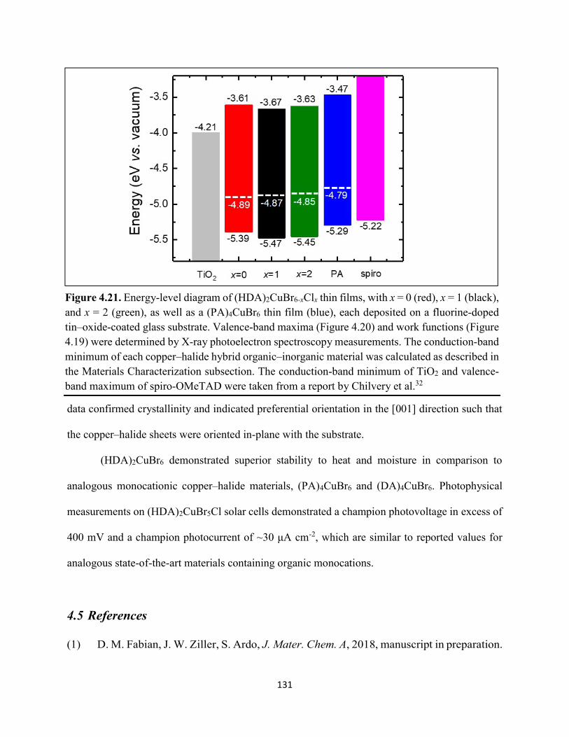
131
data confirmed crystallinity and indicated preferential orientation in the [001] direction such that
the copper–halide sheets were oriented in-plane with the substrate.
(HDA)2CuBr6 demonstrated superior stability to heat and moisture in comparison to
analogous monocationic copper–halide materials, (PA)4CuBr6 and (DA)4CuBr6. Photophysical
measurements on (HDA)2CuBr5Cl solar cells demonstrated a champion photovoltage in excess of
400 mV and a champion photocurrent of ~30 μA cm-2, which are similar to reported values for
analogous state-of-the-art materials containing organic monocations.
4.5 References
(1) D. M. Fabian, J. W. Ziller, S. Ardo, J. Mater. Chem. A, 2018, manuscript in preparation.
Figure 4.21. Energy-level diagram of (HDA)2CuBr6-xClx thin films, with x = 0 (red), x = 1 (black), and x = 2 (green), as well as a (PA)4CuBr6 thin film (blue), each deposited on a fluorine-doped tin–oxide-coated glass substrate. Valence-band maxima (Figure 4.20) and work functions (Figure 4.19) were determined by X-ray photoelectron spectroscopy measurements. The conduction-band minimum of each copper–halide hybrid organic–inorganic material was calculated as described in the Materials Characterization subsection. The conduction-band minimum of TiO2 and valence-band maximum of spiro-OMeTAD were taken from a report by Chilvery et al.32
132
(2) S. I. Seok, M. Grätzel and N.-G. Park, Small, 2018, 201704177.
(3) G. E. Eperon, M. T. Hörantner and H. J. Snaith, Nat. Rev. Chem., 2017, 1, 95.
(4) T. Leijtens, K. Bush, R. Cheacharoen, R. Beal, A. Bowring and M. D. McGehee, J.
Mater. Chem. A, 2017, 5, 11483.
(5) S. Albrecht, M. Saliba, J. P. Correa Baena, F. Lang, L. Kegelmann, M. Mews, L. Steier,
A. Abate, J. Rappich, L. Korte, R. Schlatmann, N. Mohammad K., A. Hagfeldt, M.
Grätzel and B. Rech, Energy Environ. Sci., 2016, 9, 81–88.
(6) K. A. Bush, A. F. Palmstrom, Z. J. Yu, M. Boccard, R. Cheacharoen, J. P. Mailoa, D.
P. McMeekin, R. L. Z. Hoye, C. D. Bailie, T. Leijtens, I. M. Peters, M. C. Minichetti,
N. Rolston, R. Prasanna, S. Sofia, D. Harwood, W. Ma, F. Moghadam, H. J. Snaith, T.
Buonassisi, Z. C. Holman, S. F. Bent and M. D. McGehee, Nat. Energy, 2017, 2, 17009.
(7) M. A. Green, Y. Hishikawa, E. D. Dunlop, D. H. Levi, J. Hohl-Ebinger and A. W. Y.
Ho-Baillie, Prog. Photovoltaics Res. Appl., 2018, 26, 3.
(8) M. Saliba, T. Matsui, J.-Y. Seo, K. Domanski, J.-P. Correa-Baena, M. K. Nazeeruddin,
S. M. Zakeeruddin, W. Tress, A. Abate, A. Hagfeldt and M. Gratzel, Energy Environ.
Sci., 2016, 9, 1989.
(9) B. Saparov and D. B. Mitzi, Chem. Rev., 2016, 116, 4558.
(10) A. H. Slavney, R. W. Smaha, I. C. Smith, A. Ja, D. Umeyama and H. I. Karunadasa,
Inorg. Chem., 2017, 56, 46.
(11) T. Leijtens, G. E. Eperon, N. K. Noel, S. N. Habisreutinger, A. Petrozza and H. J.
Snaith, Adv. Energy Mater., 2015, 5, 1500963.
(12) R. K. Misra, S. Aharon, B. Li, D. Mogilyansky, I. Visoly-Fisher, L. Etgar and E. A.
Katz, J. Phys. Chem. Lett., 2015, 6, 326.
133
(13) N. Aristidou, I. Sanchez-Molina, T. Chotchuangchutchaval, M. Brown, L. Martinez, T.
Rath and S. A. Haque, Angew. Chem., Int. Ed., 2015, 54, 8208.
(14) M. Becker, T. Klüner and M. Wark, Dalt. Trans., 2017, 46, 3500.
(15) K. Liang, D. B. Mitzi and M. T. Prikas, Chem. Mater., 1998, 10, 403.
(16) D. B. Mitzi, K. Chondroudis and C. R. Kagan, Inorg. Chem., 1999, 38, 6246.
(17) D. B. Mitzi, Inorg. Chem., 2000, 39, 6107.
(18) I. C. Smith, E. T. Hoke, D. Solis-Ibarra, M. D. McGehee and H. I. Karunadasa, Angew.
Chem., Int. Ed., 2014, 53, 11232.
(19) D. Cao, C. C. Stoumpos, O. K. Farha, J. T. Hupp and M. G. Kanatzidis, J. Am. Chem.
Soc., 2015, 137, 7843.
(20) R. K. Misra, B.-E. Cohen, L. Iagher and L. Etgar, ChemSusChem, 2017, 10, 3712.
(21) D. M. Fabian and S. Ardo, J. Mater. Chem. A, 2016, 4, 6837.
(22) H. L. Wells, Anorg. Chem., Int. Ed., 1893, 3, 195.
(23) A. Kojima, K. Teshima, Y. Shirai and T. Miyasaka, J. Am. Chem. Soc., 2009, 131,
6050.
(24) G. A. Mousdis, G. C. Papavassiliou, A. Terzis and C. P. Raptopoulou, Z. Naturforsch.,
1998, 53b, 927.
(25) D. B. Mitzi and P. Brock, Inorg. Chem., 2001, 40, 2096.
(26) R. E. Brandt, R. C. Kurchin, R. L. Z. Hoye, J. R. Poindexter, M. W. B. Wilson, S.
Sulekar, F. Lenahan, P. X. T. Yen, V. Stevanovi, J. C. Nino, M. G. Bawendi and T.
Buonassisi, J. Phys. Chem. Lett., 2015, 6, 4297.
(27) A. J. Lehner, D. H. Fabini, H. A. Evans, C.-A. Hébert, S. R. Smock, J. Hu, H. Wang,
J. W. Zwanziger, M. L. Chabinyc and R. Seshadri, Chem. Mater., 2015, 27, 7137.
134
(28) B. W. Park, B. Philippe, X. Zhang, H. Rensmo, G. Boschloo and E. M. J. Johansson,
Adv. Mater., 2015, 27, 6806.
(29) M. Lyu, J. H. Yun, M. Cai, Y. Jiao, P. V. Bernhardt, M. Zhang, Q. Wang, A. Du, H.
Wang, G. Liu and L. Wang, Nano Res., 2016, 9, 692.
(30) R. Hoye, R. E. Brandt, A. Osherov, V. Stevanovic, S. D. Stranks, M. W. B. Wilson, H.
Kim, A. J. Akey, R. C. Kurchin, J. R. Poindexter, E. N. Wang, M. G. Bawendi, V.
Bulovic and T. Buonassisi, Chem. - A Eur. J., 2016, 22, 2605.
(31) A. H. Slavney, T. Hu, A. M. Lindenberg and H. I. Karunadasa, J. Am. Chem. Soc.,
2016, 138, 2138.
(32) G. Volonakis, M. R. Filip, A. A. Haghighirad, N. Sakai, B. Wenger, H. J. Snaith and F.
Giustino, J. Phys. Chem. Lett., 2016, 7, 1254.
(33) K. K. Bass, L. Estergreen, C. N. Savory, J. Buckeridge, D. O. Scanlon, P. I. Djurovich,
S. E. Bradforth, M. E. Thompson and B. C. Melot, Inorg. Chem., 2017, 56, 42.
(34) R. Willett, H. Place and M. Middleton, J. Am. Chem. Soc., 1988, 110, 8639.
(35) C. C. Stoumpos, D. H. Cao, D. J. Clark, J. Young, J. M. Rondinelli, J. I. Jang, J. T.
Hupp and M. G. Kanatzidis, Chem. Mater., 2016, 28, 2852.
(36) H. Tsai, W. Nie, J.-C. Blancon, C. C. Stoumpos, R. Asadpour, B. Harutyunyan, A. J.
Neukirch, R. Verduzco, J. J. Crochet, S. Tretiak, L. Pedesseau, J. Even, M. A. Alam,
G. Gupta, J. Lou, P. M. Ajayan, M. J. Bedzyk, M. G. Kanatzidis and A. D. Mohite,
Nature, 2016, 536, 312.
(37) M. Safdari, P. H. Svensson, M. T. Hoang, I. Oh, L. Kloo and J. M. Gardner, J. Mater.
Chem. A, 2016, 4, 15638.

135
(38) C. C. Stoumpos, C. M. M. Soe, H. Tsai, W. Nie, J.-C. Blancon, D. H. Cao, F. Liu, B.
Traoré, C. Katan, J. Even, A. D. Mohite and M. G. Kanatzidis, Chem, 2017, 2, 427.
(39) D. H. Cao, C. C. Stoumpos, T. Yokoyama, J. L. Logsdon, T.-B. Song, O. K. Farha, M.
R. Wasielewski, J. T. Hupp and M. G. Kanatzidis, ACS Energy Lett., 2017, 2, 982.
(40) Z. Wang, A. M. Ganose, C. Niu and D. O. Scanlon, J. Mater. Chem. A, 2018, 6, 5652.
(41) Q. Li, S. Li, K. Wang, Z. Quan, Y. Meng and B. Zou, J. Phys. Chem. Lett., 2017, 8,
500.
(42) D. Cortecchia, H. A. Dewi, J. Yin, A. Bruno, S. Chen, T. Baikie, P. P. Boix, M. Grätzel,
S. Mhaisalkar, C. Soci and N. Mathews, Inorg. Chem., 2016, 55, 1044.
(43) D. Cortecchia, C. Soci, M. Cametti, A. Petrozza and J. Martí-Rujas, ChemPlusChem,
2016, 81, 1.
(44) APEX2, 2014.
(45) SAINT, 2013.
(46) Sheldrick, G. M. SADABS, 2014.
(47) Sheldrick, G. M. SHELXTL, 2014.
(48) International Tables for X-Ray Crystallography; Vol C.; Kluwer Academic Publishers:
Dordrecht, 1992.
(49) Ito, S.; Murakami, T. N.; Comte, P.; Liska, P.; Grätzel, C.; Nazeeruddin, M. K.;
Grätzel, M. Thin Solid Films 2008, 516, 4613.
(50) Kim, H.-S.; Lee, C.-R.; Im, J.-H.; Lee, K.-B.; Moehl, T.; Marchioro, A.; Moon, S.-J.;
Humphry-Baker, R.; Yum, J.-H.; Moser, J. E.; Grätzel, M.; Park, N.-G. Sci. Rep.
2012, 2, 591.
(51) Chusuei, C. C.; Brookshier, M. A.; Goodman, D. W. Langmuir 1999, 15, 2806.
136
(52) Schlaf, R.; Murata, H.; Kafafi, Z. J. Electron. Spectrosc. Relat. Phenom. 2001, 120,
149.
(53) Schulz, P.; Edri, E.; Kirmayer, S.; Hodes, G.; Cahen, D.; Kahn, A. Energy Environ. Sci.
2014, 7, 1377.
(54) Chilvery, A. K.; Guggilla, P.; Batra, A. K.; Gaikwad, D. D.; Currie, J. R. J. Photon.
Energy 2015, 5, 053093.
(55) Dualeh, A.; Moehl, T.; Tétreault, N.; Teuscher, J.; Gao, P.; Nazeeruddin, M. K.;
Grätzel, M. ACS Nano 2014, 8, 362.
(56) Gelderman, K.; Lee, L.; Donne, S. W. J. Chem. Ed. 2007, 84, 685.
(57) Lin, Q.; Armin, A.; Chandra, R.; Nagiri, R.; Burn, P. L.; Meredith, P. Nat. Photon.
2014, 9, 106.
(58) Bard, A. J.; Faulkner, L. R. Electrochemical Methods: Fundamentals and Applications,
2nd ed.; John Wiley & Sons, Inc.: New York, 2001.
(59) K. Halvorson and R. D. Willett, Acta Crystallogr., 1988, C44, 2071.
(60) J. Yan, X. Ke, Y. Chen, A. Zhang and B. Zhang, Appl. Surf. Sci., 2015, 351, 1191.
(61) A. R. West, Basic Solid State Chemistry, John Wiley & Sons, Inc., New York, 2nd ed.,
1999.
(62) D. M. Lichty, J. Am. Chem. Soc., 1903, 25, 469.
137
CHAPTER 5: LOW-DIMENSIONAL LEAD–HALIDE PEROVSKITE
MATERIALS INCORPORATING DIVALENT ORGANIC LIGANDS
* In part a compilation of one publication in preparation1
5.1 Introduction
Two-dimensional (2D) lead–halide perovskites incorporating divalent organic ligands have
an advantage over three-dimensional (3D) lead–halide perovskites with regard to the inherent
stability of the organic moiety.2 Due to their structural dimensionality, the low-dimensional lead–
halide perovskites are most likely better suited for use in light-emitting diodes as opposed to solar
cells for their emissive properties yet inferior charge-carrier conduction.3–5 The structural
confinement of the low-dimensional lead–halide perovskites results in excitonic behavior (i.e.
exciton binding energies are
not negligible), and as a
result, charge-carrier
diffusion lengths are
substantially lower than those
of 3D lead–halide
perovskites.6 If the structural
dimensionality is 2D the
material behaves like
quantum films, if it is 1D the
material behaves like
Figure 5.1. Proposed structure of the two-dimensional lead–halide perovskite ethylenediamine lead iodide (EDAPbI4) viewed along the plane of the n=1 sheets of PbI6 octahedra. From Zhang, T.; Dar, M. I.; Li, G.; Xu, F.; Guo, N.; Grätzel, M.; Zhao, Y. Sci. Adv. 2017, 3, e1700841. Reprinted with permission from AAAS.
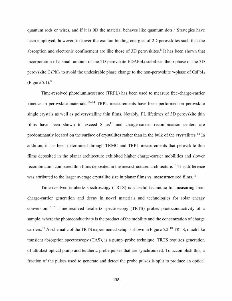
138
quantum rods or wires, and if it is 0D the material behaves like quantum dots.7 Strategies have
been employed, however, to lower the exciton binding energies of 2D perovskites such that the
absorption and electronic confinement are like those of 3D perovskites.8 It has been shown that
incorporation of a small amount of the 2D perovskite EDAPbI4 stabilizes the α phase of the 3D
perovskite CsPbI3 to avoid the undesirable phase change to the non-perovskite γ-phase of CsPbI3
(Figure 5.1).9
Time-resolved photoluminescence (TRPL) has been used to measure free-charge-carrier
kinetics in perovskite materials.10–14 TRPL measurements have been performed on perovskite
single crystals as well as polycrystalline thin films. Notably, PL lifetimes of 3D perovskite thin
films have been shown to exceed 8 μs11 and charge-carrier recombination centers are
predominantly located on the surface of crystallites rather than in the bulk of the crystallites.12 In
addition, it has been determined through TRMC and TRPL measurements that perovskite thin
films deposited in the planar architecture exhibited higher charge-carrier mobilities and slower
recombination compared thin films deposited in the mesostructured architecture.13 This difference
was attributed to the larger average crystallite size in planar films vs. mesostructured films.13
Time-resolved terahertz spectroscopy (TRTS) is a useful technique for measuring free-
charge-carrier generation and decay in novel materials and technologies for solar energy
conversion.15,16 Time-resolved terahertz spectroscopy (TRTS) probes photoconductivity of a
sample, where the photoconductivity is the product of the mobility and the concentration of charge
carriers.17 A schematic of the TRTS experimental setup is shown in Figure 5.2.18 TRTS, much like
transient absorption spectroscopy (TAS), is a pump–probe technique. TRTS requires generation
of ultrafast optical pump and terahertz probe pulses that are synchronized. To accomplish this, a
fraction of the pulses used to generate and detect the probe pulses is split to produce an optical
139
pump pulse. The terahertz pulse is delayed with respect to the optical pump pulse, the sample is
photoexcited by the pump pulse, and the sample attenuates, delays, and distorts the terahertz pulse
according to its complex photoexcited permittivity. As a result, kinetic processes that occur in the
terahertz region can be probed. The delay time between the optical pump and terahertz probe pulses
Figure 5.2. (a) A schematic representation of time-resolved terahertz (THz) spectroscopy (TRTS). There is a THz pulse, detector pulse, and photoexcitation pulse. THz pulses are generated via optical rectification of <100 fs pulses from an amplified Ti:Sapphire laser (fundamental wavelength = 800 nm) operating at a repetition rate of 1 kHz. (b) A diagram of the experimental setup of TRTS. The numbers correspond to the beam path of the THz pulse (1), the detector pulse (2), and the photoexcitation pulse (3). Key components are the pulsed laser source (a), THz generation crystal (b), detector crystal (c), near-IR linear polarizer (d), ¼ waveplate (e), beam-splitting polarizer (f), and balanced photodiodes (g). The THz pulse is focused onto the sample and overlapped with a visible pump pulse. THz radiation spans frequencies ~0.1 to 3 THz, or 3 mm to 100 microns, as a result, the THz radiation is typically focused down to approximately ~5 mm. One cannot then focus the visible pump pulse tighter than ~ 1 cm to ensure uniform excitation of the sample. In practical terms this implies that the size of the samples investigated be large (but not necessarily thick) and the necessary pulse energies for photo-excitation are higher even if the photon density is not then typically used for visible pump-probe measurements. Reprinted with permission from Beard, M.C.; Blackburn, J. L; Heben, M. J. Nano Lett., 2008, 8, 4238–4242. Copyright 2008 American Chemical Society.
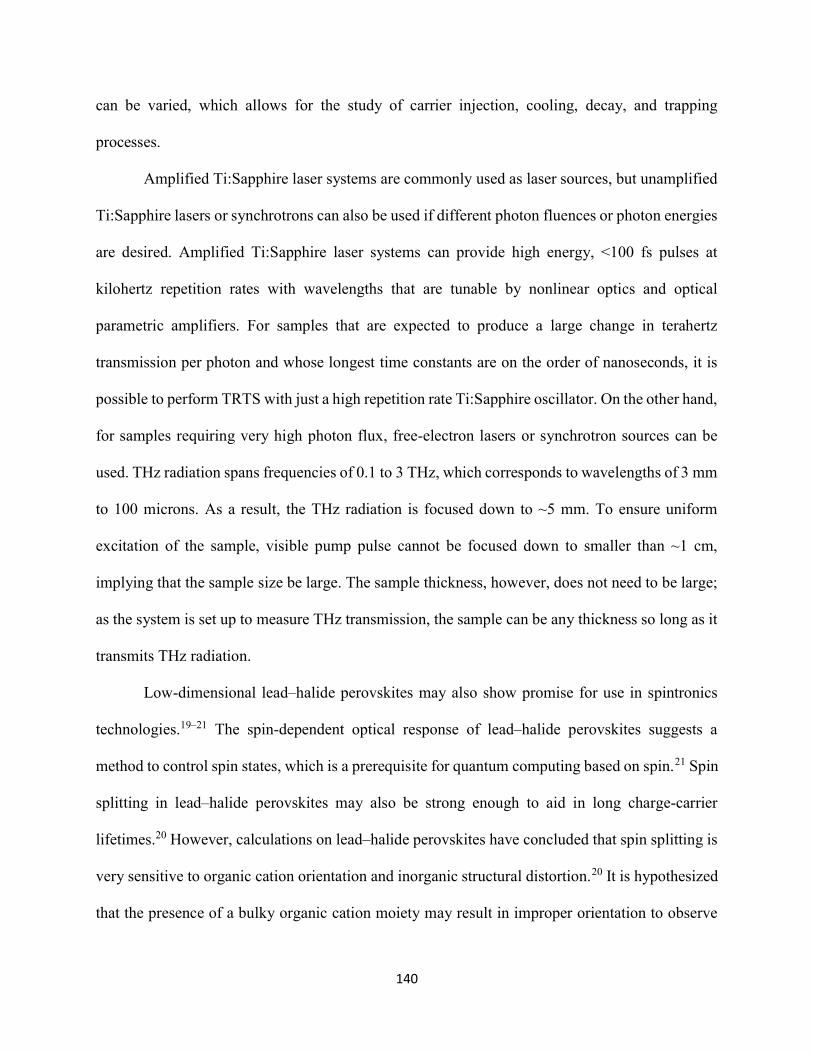
140
can be varied, which allows for the study of carrier injection, cooling, decay, and trapping
processes.
Amplified Ti:Sapphire laser systems are commonly used as laser sources, but unamplified
Ti:Sapphire lasers or synchrotrons can also be used if different photon fluences or photon energies
are desired. Amplified Ti:Sapphire laser systems can provide high energy, <100 fs pulses at
kilohertz repetition rates with wavelengths that are tunable by nonlinear optics and optical
parametric amplifiers. For samples that are expected to produce a large change in terahertz
transmission per photon and whose longest time constants are on the order of nanoseconds, it is
possible to perform TRTS with just a high repetition rate Ti:Sapphire oscillator. On the other hand,
for samples requiring very high photon flux, free-electron lasers or synchrotron sources can be
used. THz radiation spans frequencies of 0.1 to 3 THz, which corresponds to wavelengths of 3 mm
to 100 microns. As a result, the THz radiation is focused down to ~5 mm. To ensure uniform
excitation of the sample, visible pump pulse cannot be focused down to smaller than ~1 cm,
implying that the sample size be large. The sample thickness, however, does not need to be large;
as the system is set up to measure THz transmission, the sample can be any thickness so long as it
transmits THz radiation.
Low-dimensional lead–halide perovskites may also show promise for use in spintronics
technologies.19–21 The spin-dependent optical response of lead–halide perovskites suggests a
method to control spin states, which is a prerequisite for quantum computing based on spin.21 Spin
splitting in lead–halide perovskites may also be strong enough to aid in long charge-carrier
lifetimes.20 However, calculations on lead–halide perovskites have concluded that spin splitting is
very sensitive to organic cation orientation and inorganic structural distortion.20 It is hypothesized
that the presence of a bulky organic cation moiety may result in improper orientation to observe
141
the spin splitting effect. In addition, a low-dimensional or distorted inorganic framework may
inhibit the observation of spin splitting.
5.2 Experimental
5.2.1 Preparation of Hybrid Organic–Inorganic Lead–Iodide Solutions
All chemicals were used as received. Diammonium dihydroiodide salts were synthesized
by slow addition of hydriodic acid (57% in water, stabilized with 1.5% hypophosphorous acid,
Sigma-Aldrich) to the diamine of choice dissolved in methanol. The hydriodic acid to diamine
molar ratio was 2:1, with hydriodic acid in slight excess. As an example, to synthesize 1,6-
hexanediamine dihydriodide (HDA•2HI), 260.9 mg of 1,6-hexanediamine (98+%, Alfa Aesar) was
dissolved in 5 mL methanol, and then 1 mL hydriodic acid was added slowly at 0 °C with stirring,
followed by stirring for an additional 30 min. HDA•2HI precipitate was recovered by evaporation
of solvents at 40 °C with a rotary evaporator. The precipitate was rinsed with diethyl ether, and
vacuum dried at 60 °C for at least 12 h. HDAPbI4 solution was then prepared by mixing HDA•2HI
and PbI2 (99.999%, Sigma-Aldrich) powders at an approximately 1:1 mole ratio, with HDA•2HI
in slight excess, in an anhydrous mixture of 4:1 (v/v) DMF:DMSO at 70 °C inside a nitrogen-filled
glovebox. The HDAPbI4 solution was stored in the glovebox until use and was used within one
week of preparation.
MAPbBr3 solution was prepared by mixing methylammonium bromide (MABr, 98%,
Sigma-Aldrich) and PbI2 (99%, Sigma-Aldrich) powders at approximately a 1:1 mole ratio, but
with MABr in slight excess, , in an anhydrous mixture of 4:1 (v/v) DMF:DMSO at 70 °C inside a
nitrogen-filled glovebox. The MAPbBr3 solution was stored in the glovebox until use and was

142
used within one week of preparation. All powders were combined for solution preparation inside
a nitrogen-filled glovebox.
5.2.2 Materials Processing
Materials deposition and thin-film annealing were performed in a nitrogen-filled glovebox.
All substrates were cleaned as follows: 1) sonication in Alconox solution, 2) rinse with deionized
water, 3) rinse with ethanol, 4) sonication in ethanol, and 5) dry with nitrogen. The substrates were
further cleaned by UV/ozone treatment for 10 min. A conventional spin-coat method was adapted
from Kim et al.22 and used for depositing the hybrid organic–inorganic lead–iodide solutions. For
this method, a filtered 0.5 M solution in 4:1 (v/v) DMF:DMSO was pipetted on top of the substrate
and then the substrate was spun at 6000 rpm (6000 rpm/s acceleration) for 60 s, followed by rapid
transfer to a hot plate that was preheated to 100 °C and subsequent annealing at 100 °C for 45 min.
For all deposition methods, the photoactive layer solution was dispensed on the substrate at a
volume of 17.5 μA/cm2. For X-ray diffraction (XRD) measurements, the substrate used was
fluorine-doped tin oxide coated glass (FTO). For transmission, reflection, steady-state
photoluminescence (PL), and time-resolved photoluminescence (TRPL) measurements, the
substrate used was glass. For time-resolved tertahertz spectroscopy (TRTS) and transient
absorption spectroscopy (TAS), the substrate used was quartz.
5.2.3 Ultrafast Laser Spectroscopy
Time-resolved photoluminescence spectroscopy measurements were performed using the
time-correlated single photon counting technique. Excitation light was generated by a Fianium SC-
450-PP laser operating with an average power of 15.5 µW at a repetition rate of 10 MHz and a
143
wavelength of 450 nm selected by a Fianium AOTF system. A 470 nm long pass filter was used
to remove scattering from the excitation source. The emission was detected using a Hamamatsu
streak camera with a wavelength range of 200-900 nm and response of < 20 ps. To compare traces,
data were shifted and normalized so that maximal values of 1 occurred at t = 0 ns. Samples were
measured under ambient conditions.
TAS measurements were performed using a Coherent Libra Ti:sapphire ultrafast laser (800
nm, pulse duration ~100 fs, ~4 mJ/pulse, and 1 KHz repetition rate) and a Helios Ultrafast System
pump–probe TA spectrometer. In this system, the 800 nm fundamental beam is split into two
beams, one of which becomes the pump beam and the other becomes the probe beam. One beam
is sent to a TOPAS optical parametric amplifier to generate the pump pulse with a tunable
wavelength, and its intensity is attenuated by two neutral density filters. The other beam is focused
into a sapphire crystal to generate a white light continuum probe beam. The pump–probe delay is
tuned by a delay line (Thorlabs). The pump and probe beams are focused and overlapped onto the
sample. The pump excitation pulse power is measured using a power meter, and pump fluence was
calculated to be 0.29–1.16 mJ/cm2.The probe beam size is ~130 μm and the pump beam size is ~1
mm. Samples were measured under ambient conditions.
The experimental setup for TRTS measurements is described as follows. The optical pulse
beam (1 KHz repetition rate, <100 fs pulse duration, 4.5 mJ/ pulse energy, λ = 800 nm wavelength)
is provided by an amplified Ti:Sapphire laser (Coherent Libra) which consists of a regenerative
amplifier seeded by a mode-locked oscillator. The amplifier output is split to feed an optical
parametric amplifier (Light Conversion Ltd., TOPAS-C), which generates excitation pulses that
serve as the optical pump to photo-generate carriers in the sample. The pump excitation pulse
power is measured using a power meter, and pump fluence was calculated to be 0.27 mJ/cm2. A

144
second part of the beam is used to generate single cycle terahertz pulses by optical rectification in
a ZnTe non-linear crystal. The terahertz probe beam is focused on the sample using mirrors. The
transmitted terahertz pulses are detected in the time domain through free-space electro-optic
sampling. A third part of the initial pump beam is used as a gating beam and guided over a delay
line onto a ZnTe detector crystal. By varying the time delays between the optical pump pulse, the
terahertz probe pulse, and the gating, amplitude and phase changes of the terahertz single-cycle
pulses can be recorded. Amplitude changes of the terahertz pulses upon photo-excitation were
measured on balanced large-area silicon photodiodes on a time scale of up to 1.5 ns with sub-
picosecond time resolution. Samples were contained in an unsealed chamber kept under a constant
flow of nitrogen.
5.2.4 Characterization
Grazing-incidence XRD data were collected using a Rigaku Smartlab diffractometer with
Cu Kα radiation and in parallel beam geometry. Transmission and reflection spectra were obtained
using an integrating sphere in a Shimadzu UV-3600 ultraviolet-visible-near-infrared
spectrophotometer. Absorption was calculated by assuming Absorptance = 1 – Transmittance –
Reflectance. Steady-state photoluminescence (PL) was measured with a Horiba Jobin Yvon Model
FL-1039/40 Fluorolog, a Horiba Jobin Yvon iHR320 spectrograph, and a Horiba Jobin Yvon
SPEX Instruments S.A. Group Spectrum One G35 CCD camera. A monochromatized Xe lamp
was used as the excitation source.
Transmission, reflection, steady-state PL, TRPL, TAS, TRTS spectroscopy, and grazing-
incidence XRD measurements were performed in the Chemistry and Nanoscience Center at the
National Renewable Energy Laboratory.
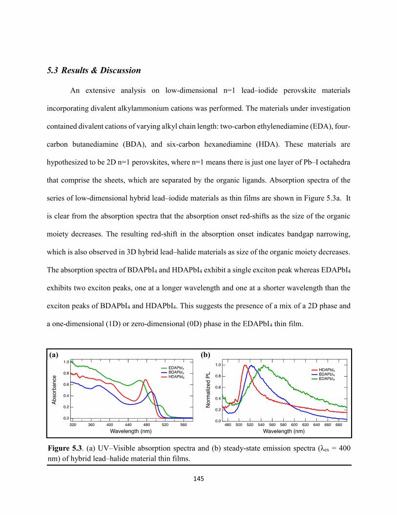
145
5.3 Results & Discussion
An extensive analysis on low-dimensional n=1 lead–iodide perovskite materials
incorporating divalent alkylammonium cations was performed. The materials under investigation
contained divalent cations of varying alkyl chain length: two-carbon ethylenediamine (EDA), four-
carbon butanediamine (BDA), and six-carbon hexanediamine (HDA). These materials are
hypothesized to be 2D n=1 perovskites, where n=1 means there is just one layer of Pb–I octahedra
that comprise the sheets, which are separated by the organic ligands. Absorption spectra of the
series of low-dimensional hybrid lead–iodide materials as thin films are shown in Figure 5.3a. It
is clear from the absorption spectra that the absorption onset red-shifts as the size of the organic
moiety decreases. The resulting red-shift in the absorption onset indicates bandgap narrowing,
which is also observed in 3D hybrid lead–halide materials as size of the organic moiety decreases.
The absorption spectra of BDAPbI4 and HDAPbI4 exhibit a single exciton peak whereas EDAPbI4
exhibits two exciton peaks, one at a longer wavelength and one at a shorter wavelength than the
exciton peaks of BDAPbI4 and HDAPbI4. This suggests the presence of a mix of a 2D phase and
a one-dimensional (1D) or zero-dimensional (0D) phase in the EDAPbI4 thin film.
Figure 5.3. (a) UV–Visible absorption spectra and (b) steady-state emission spectra (λex = 400 nm) of hybrid lead–halide material thin films.
(a) (b)
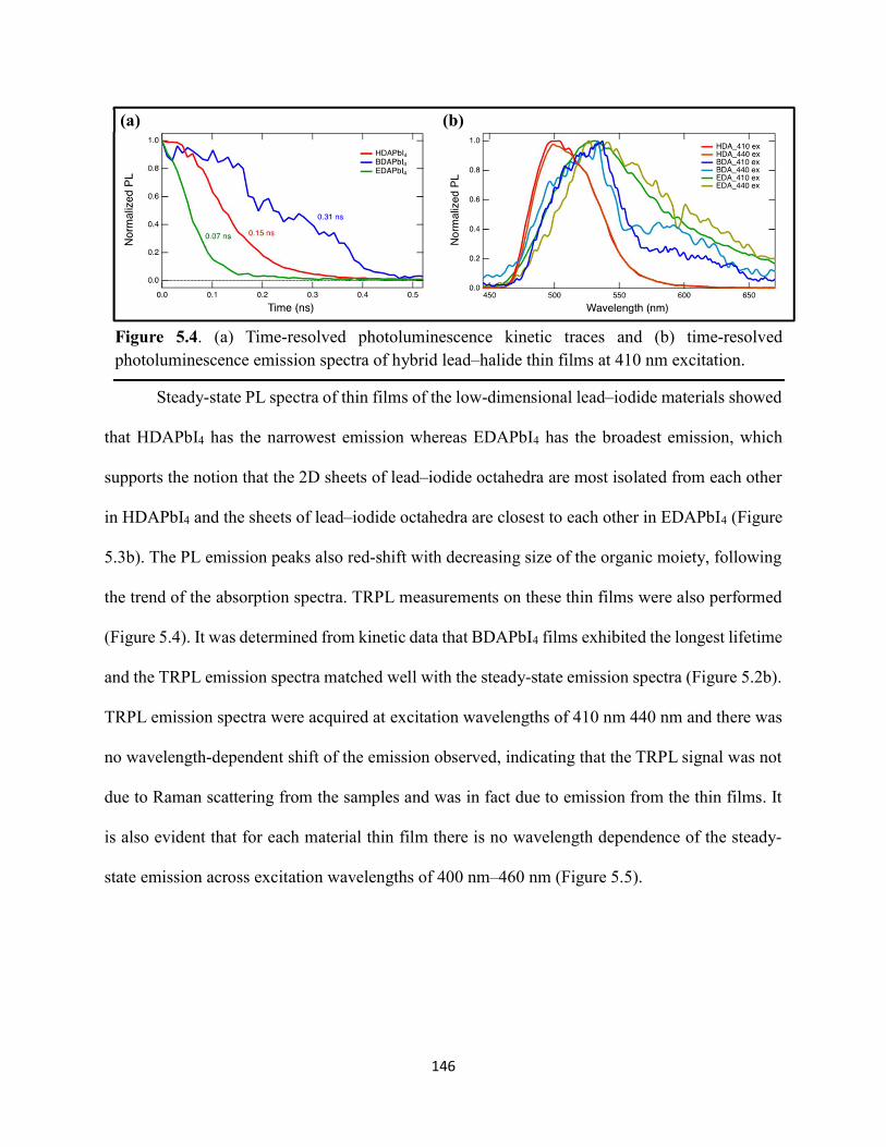
146
Steady-state PL spectra of thin films of the low-dimensional lead–iodide materials showed
that HDAPbI4 has the narrowest emission whereas EDAPbI4 has the broadest emission, which
supports the notion that the 2D sheets of lead–iodide octahedra are most isolated from each other
in HDAPbI4 and the sheets of lead–iodide octahedra are closest to each other in EDAPbI4 (Figure
5.3b). The PL emission peaks also red-shift with decreasing size of the organic moiety, following
the trend of the absorption spectra. TRPL measurements on these thin films were also performed
(Figure 5.4). It was determined from kinetic data that BDAPbI4 films exhibited the longest lifetime
and the TRPL emission spectra matched well with the steady-state emission spectra (Figure 5.2b).
TRPL emission spectra were acquired at excitation wavelengths of 410 nm 440 nm and there was
no wavelength-dependent shift of the emission observed, indicating that the TRPL signal was not
due to Raman scattering from the samples and was in fact due to emission from the thin films. It
is also evident that for each material thin film there is no wavelength dependence of the steady-
state emission across excitation wavelengths of 400 nm–460 nm (Figure 5.5).
Figure 5.4. (a) Time-resolved photoluminescence kinetic traces and (b) time-resolved photoluminescence emission spectra of hybrid lead–halide thin films at 410 nm excitation.
(a) (b)
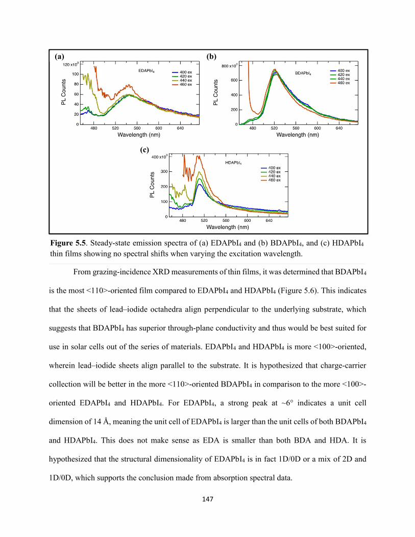
147
From grazing-incidence XRD measurements of thin films, it was determined that BDAPbI4
is the most <110>-oriented film compared to EDAPbI4 and HDAPbI4 (Figure 5.6). This indicates
that the sheets of lead–iodide octahedra align perpendicular to the underlying substrate, which
suggests that BDAPbI4 has superior through-plane conductivity and thus would be best suited for
use in solar cells out of the series of materials. EDAPbI4 and HDAPbI4 is more <100>-oriented,
wherein lead–iodide sheets align parallel to the substrate. It is hypothesized that charge-carrier
collection will be better in the more <110>-oriented BDAPbI4 in comparison to the more <100>-
oriented EDAPbI4 and HDAPbI4. For EDAPbI4, a strong peak at ~6° indicates a unit cell
dimension of 14 Å, meaning the unit cell of EDAPbI4 is larger than the unit cells of both BDAPbI4
and HDAPbI4. This does not make sense as EDA is smaller than both BDA and HDA. It is
hypothesized that the structural dimensionality of EDAPbI4 is in fact 1D/0D or a mix of 2D and
1D/0D, which supports the conclusion made from absorption spectral data.
(a) (b)
(c)
Figure 5.5. Steady-state emission spectra of (a) EDAPbI4 and (b) BDAPbI4, and (c) HDAPbI4 thin films showing no spectral shifts when varying the excitation wavelength.
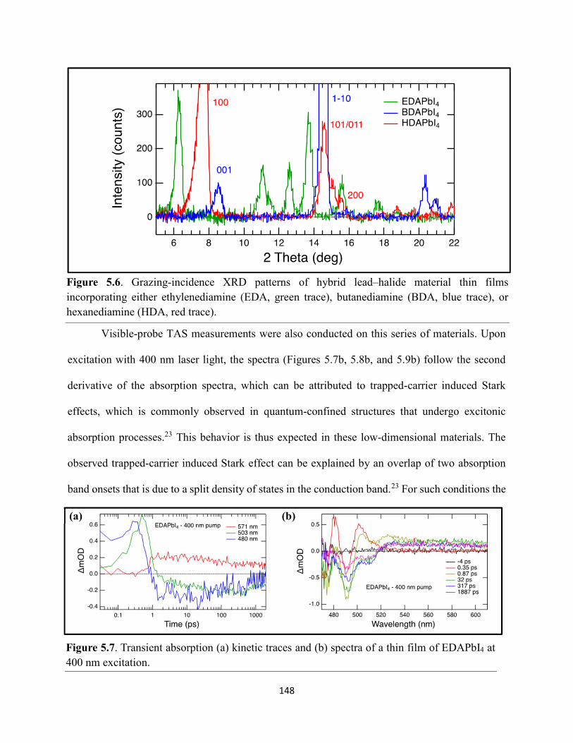
148
Visible-probe TAS measurements were also conducted on this series of materials. Upon
excitation with 400 nm laser light, the spectra (Figures 5.7b, 5.8b, and 5.9b) follow the second
derivative of the absorption spectra, which can be attributed to trapped-carrier induced Stark
effects, which is commonly observed in quantum-confined structures that undergo excitonic
absorption processes.23 This behavior is thus expected in these low-dimensional materials. The
observed trapped-carrier induced Stark effect can be explained by an overlap of two absorption
band onsets that is due to a split density of states in the conduction band.23 For such conditions the
Figure 5.6. Grazing-incidence XRD patterns of hybrid lead–halide material thin films incorporating either ethylenediamine (EDA, green trace), butanediamine (BDA, blue trace), or hexanediamine (HDA, red trace).
Figure 5.7. Transient absorption (a) kinetic traces and (b) spectra of a thin film of EDAPbI4 at 400 nm excitation.
(a) (b)
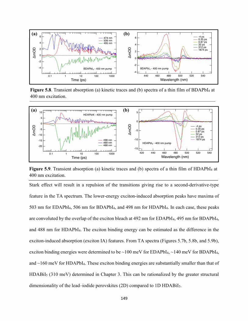
149
Stark effect will result in a repulsion of the transitions giving rise to a second-derivative-type
feature in the TA spectrum. The lower-energy exciton-induced absorption peaks have maxima of
503 nm for EDAPbI4, 506 nm for BDAPbI4, and 498 nm for HDAPbI4. In each case, these peaks
are convoluted by the overlap of the exciton bleach at 492 nm for EDAPbI4, 495 nm for BDAPbI4,
and 488 nm for HDAPbI4. The exciton binding energy can be estimated as the difference in the
exciton-induced absorption (exciton IA) features. From TA spectra (Figures 5.7b, 5.8b, and 5.9b),
exciton binding energies were determined to be ~100 meV for EDAPbI4, ~140 meV for BDAPbI4,
and ~160 meV for HDAPbI4. These exciton binding energies are substantially smaller than that of
HDABiI5 (310 meV) determined in Chapter 3. This can be rationalized by the greater structural
dimensionality of the lead–iodide perovskites (2D) compared to 1D HDABiI5.
Figure 5.8. Transient absorption (a) kinetic traces and (b) spectra of a thin film of BDAPbI4 at 400 nm excitation.
(a) (b)
Figure 5.9. Transient absorption (a) kinetic traces and (b) spectra of a thin film of HDAPbI4 at 400 nm excitation.
(a) (b)
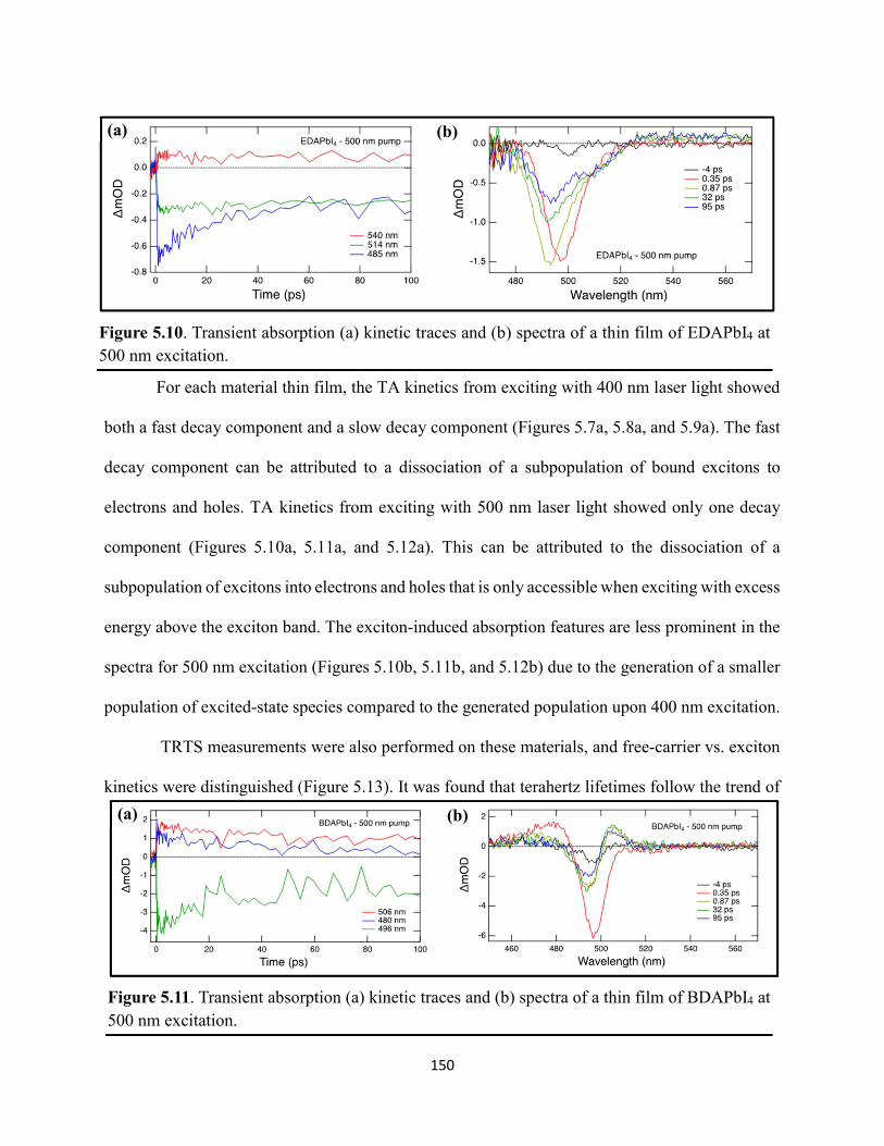
150
For each material thin film, the TA kinetics from exciting with 400 nm laser light showed
both a fast decay component and a slow decay component (Figures 5.7a, 5.8a, and 5.9a). The fast
decay component can be attributed to a dissociation of a subpopulation of bound excitons to
electrons and holes. TA kinetics from exciting with 500 nm laser light showed only one decay
component (Figures 5.10a, 5.11a, and 5.12a). This can be attributed to the dissociation of a
subpopulation of excitons into electrons and holes that is only accessible when exciting with excess
energy above the exciton band. The exciton-induced absorption features are less prominent in the
spectra for 500 nm excitation (Figures 5.10b, 5.11b, and 5.12b) due to the generation of a smaller
population of excited-state species compared to the generated population upon 400 nm excitation.
TRTS measurements were also performed on these materials, and free-carrier vs. exciton
kinetics were distinguished (Figure 5.13). It was found that terahertz lifetimes follow the trend of
Figure 5.10. Transient absorption (a) kinetic traces and (b) spectra of a thin film of EDAPbI4 at 500 nm excitation.
(a) (b)
Figure 5.11. Transient absorption (a) kinetic traces and (b) spectra of a thin film of BDAPbI4 at 500 nm excitation.
(a) (b)
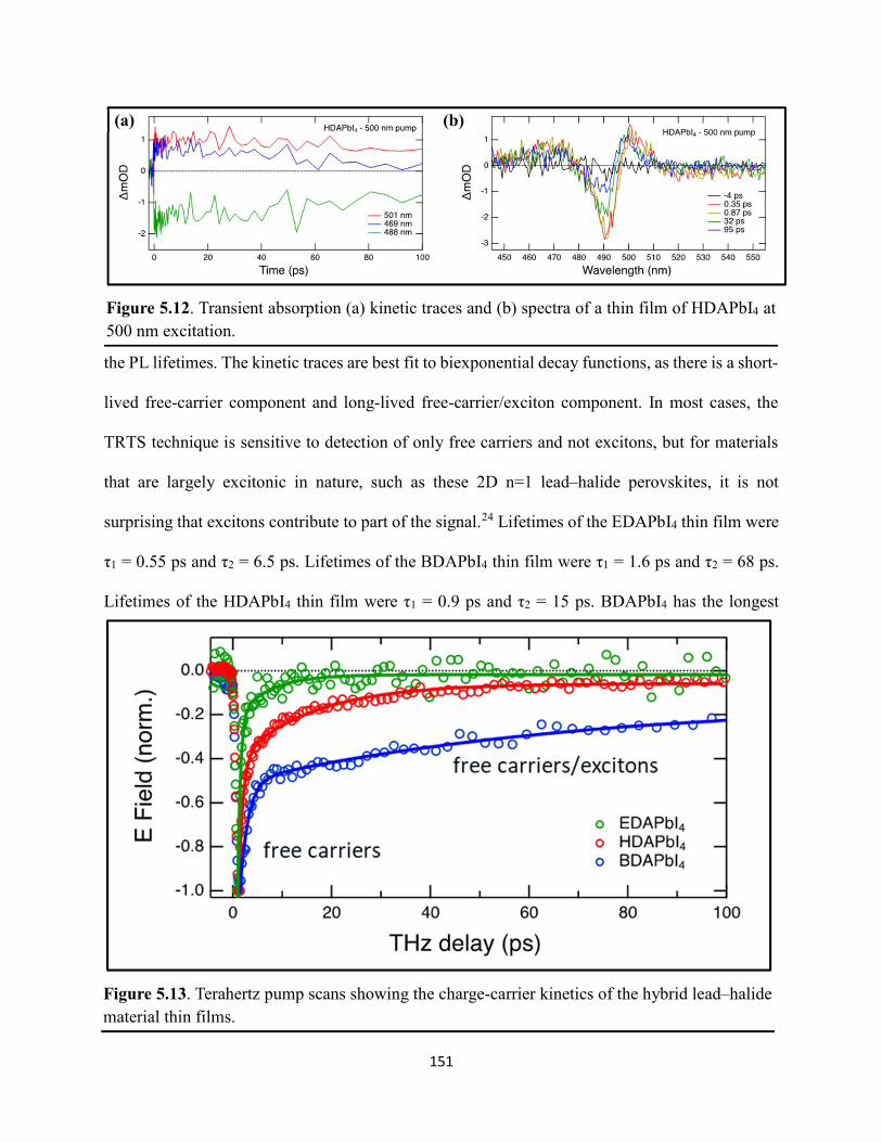
151
the PL lifetimes. The kinetic traces are best fit to biexponential decay functions, as there is a short-
lived free-carrier component and long-lived free-carrier/exciton component. In most cases, the
TRTS technique is sensitive to detection of only free carriers and not excitons, but for materials
that are largely excitonic in nature, such as these 2D n=1 lead–halide perovskites, it is not
surprising that excitons contribute to part of the signal.24 Lifetimes of the EDAPbI4 thin film were
τ1 = 0.55 ps and τ2 = 6.5 ps. Lifetimes of the BDAPbI4 thin film were τ1 = 1.6 ps and τ2 = 68 ps.
Lifetimes of the HDAPbI4 thin film were τ1 = 0.9 ps and τ2 = 15 ps. BDAPbI4 has the longest
Figure 5.13. Terahertz pump scans showing the charge-carrier kinetics of the hybrid lead–halide material thin films.
Figure 5.12. Transient absorption (a) kinetic traces and (b) spectra of a thin film of HDAPbI4 at 500 nm excitation.
(a) (b)
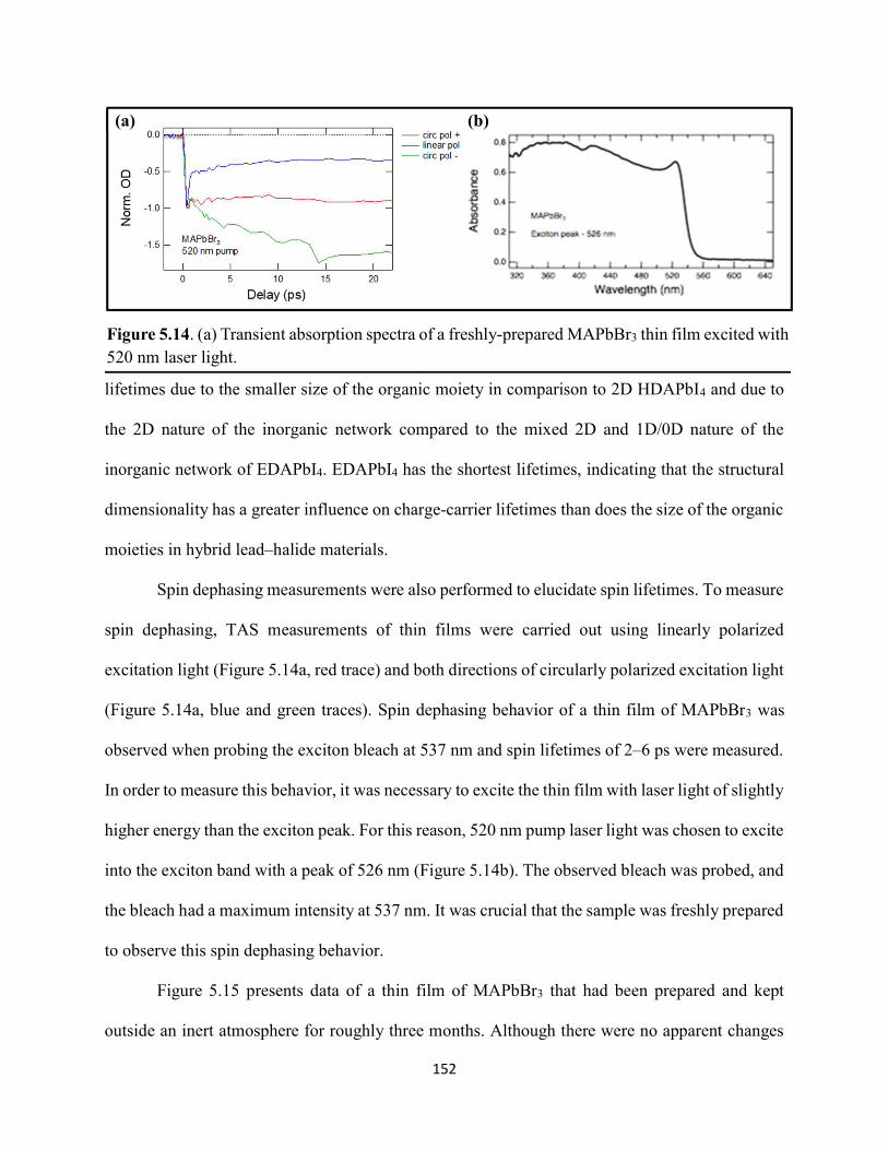
152
lifetimes due to the smaller size of the organic moiety in comparison to 2D HDAPbI4 and due to
the 2D nature of the inorganic network compared to the mixed 2D and 1D/0D nature of the
inorganic network of EDAPbI4. EDAPbI4 has the shortest lifetimes, indicating that the structural
dimensionality has a greater influence on charge-carrier lifetimes than does the size of the organic
moieties in hybrid lead–halide materials.
Spin dephasing measurements were also performed to elucidate spin lifetimes. To measure
spin dephasing, TAS measurements of thin films were carried out using linearly polarized
excitation light (Figure 5.14a, red trace) and both directions of circularly polarized excitation light
(Figure 5.14a, blue and green traces). Spin dephasing behavior of a thin film of MAPbBr3 was
observed when probing the exciton bleach at 537 nm and spin lifetimes of 2–6 ps were measured.
In order to measure this behavior, it was necessary to excite the thin film with laser light of slightly
higher energy than the exciton peak. For this reason, 520 nm pump laser light was chosen to excite
into the exciton band with a peak of 526 nm (Figure 5.14b). The observed bleach was probed, and
the bleach had a maximum intensity at 537 nm. It was crucial that the sample was freshly prepared
to observe this spin dephasing behavior.
Figure 5.15 presents data of a thin film of MAPbBr3 that had been prepared and kept
outside an inert atmosphere for roughly three months. Although there were no apparent changes
Figure 5.14. (a) Transient absorption spectra of a freshly-prepared MAPbBr3 thin film excited with 520 nm laser light.
(a) (b)
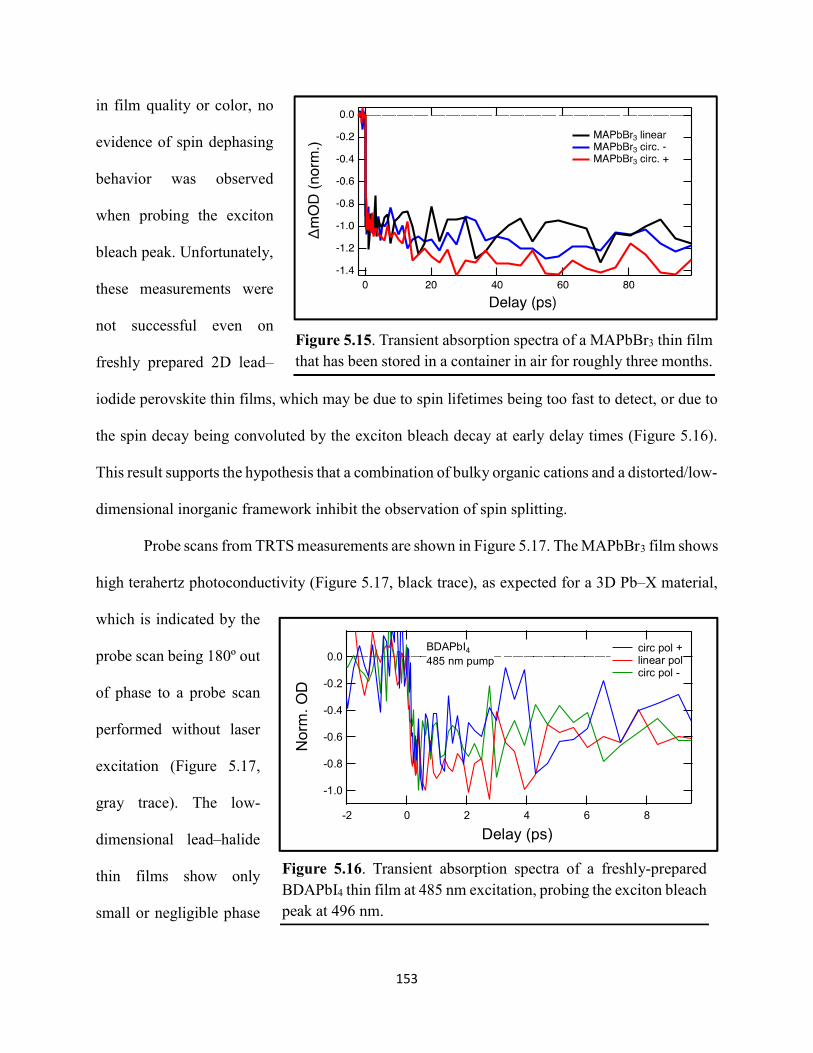
153
in film quality or color, no
evidence of spin dephasing
behavior was observed
when probing the exciton
bleach peak. Unfortunately,
these measurements were
not successful even on
freshly prepared 2D lead–
iodide perovskite thin films, which may be due to spin lifetimes being too fast to detect, or due to
the spin decay being convoluted by the exciton bleach decay at early delay times (Figure 5.16).
This result supports the hypothesis that a combination of bulky organic cations and a distorted/low-
dimensional inorganic framework inhibit the observation of spin splitting.
Probe scans from TRTS measurements are shown in Figure 5.17. The MAPbBr3 film shows
high terahertz photoconductivity (Figure 5.17, black trace), as expected for a 3D Pb–X material,
which is indicated by the
probe scan being 180º out
of phase to a probe scan
performed without laser
excitation (Figure 5.17,
gray trace). The low-
dimensional lead–halide
thin films show only
small or negligible phase
Figure 5.15. Transient absorption spectra of a MAPbBr3 thin film that has been stored in a container in air for roughly three months.
-1.0
-0.8
-0.6
-0.4
-0.2
0.0
No
rm.
OD
86420-2
Delay (ps)
circ pol + linear pol circ pol -
BDAPbI4485 nm pump
Figure 5.16. Transient absorption spectra of a freshly-prepared BDAPbI4 thin film at 485 nm excitation, probing the exciton bleach peak at 496 nm.
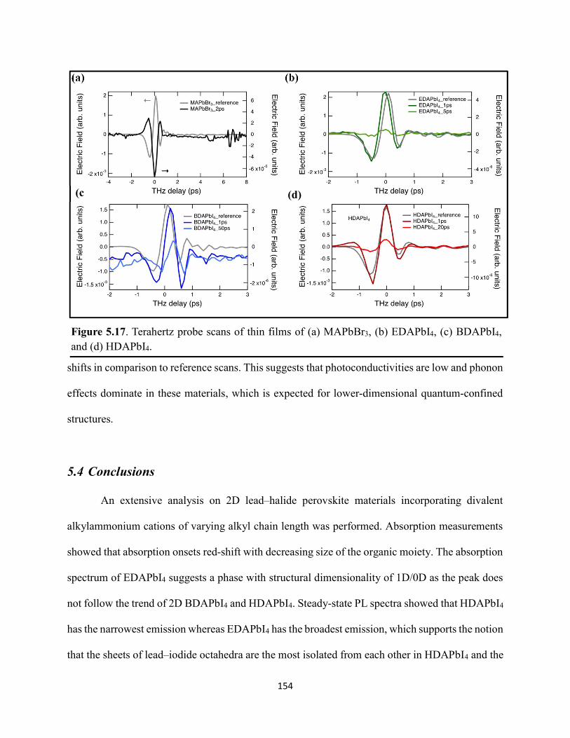
154
shifts in comparison to reference scans. This suggests that photoconductivities are low and phonon
effects dominate in these materials, which is expected for lower-dimensional quantum-confined
structures.
5.4 Conclusions
An extensive analysis on 2D lead–halide perovskite materials incorporating divalent
alkylammonium cations of varying alkyl chain length was performed. Absorption measurements
showed that absorption onsets red-shift with decreasing size of the organic moiety. The absorption
spectrum of EDAPbI4 suggests a phase with structural dimensionality of 1D/0D as the peak does
not follow the trend of 2D BDAPbI4 and HDAPbI4. Steady-state PL spectra showed that HDAPbI4
has the narrowest emission whereas EDAPbI4 has the broadest emission, which supports the notion
that the sheets of lead–iodide octahedra are the most isolated from each other in HDAPbI4 and the
(a) (b)
Figure 5.17. Terahertz probe scans of thin films of (a) MAPbBr3, (b) EDAPbI4, (c) BDAPbI4, and (d) HDAPbI4.
(c (d)

155
sheets are closest to each other in EDAPbI4. The PL emission peaks also red shift with decreasing
size of the organic group, following the trend of the absorption spectra. From TRPL measurements
on these materials it was determined that BDAPbI4 films exhibited the longest lifetime and the
emission spectra matched well with the steady-state emission.
Grazing-incidence XRD of thin films showed that BDAPbI4 is the most <110>-oriented
film, meaning sheets of lead–iodide octahedra are perpendicular to the substrate, which suggests
that BDAPbI4 has superior through-plane conductivity and thus would be best for use in solar cells.
Visible-probe TA measurements on these materials showed that the materials exhibited a trapped-
carrier induced Stark effect, which is behavior that has been observed in materials that undergo
excitonic absorption processes. In each of the materials, the TA kinetics from exciting with 400
nm laser light showed both a fast decay component and a slow decay component, whereas TA
kinetics from exciting with 500 nm laser light only showed one decay component. This could be
attributed to a dissociation of a subpopulation of excitons into electrons and holes that is only
accessible when exciting with excess energy above the exciton band. From TA spectra, exciton
binding energies were determined to be ~100 meV for EDAPbI4, ~140 meV for BDAPbI4, and
~160 meV for HDAPbI4.
From THz spectroscopic measurements it was found that free-carrier lifetimes probed by
THz radiation followed the trend of the PL lifetimes, where BDAPbI4 showed the longest free-
carrier lifetimes due to the smaller size of the organic moiety in comparison to HDAPbI4 and due
to the 2D structural dimensionality of BDAPbI4 compared to the mixed 2D and 1D/0D structural
dimensionality of EDAPbI4. Spin decoherence measurements were unfortunately not successful
on the 2D lead–halide perovskite materials, which may be due to spin lifetimes being too fast to
detect, or due to the spin decay being convoluted by the exciton bleach decay at early delay times.
156
This work represents promising materials discovery of low-dimensional lead–halide perovskites
that, if studied further, could prove promising for use in light-emitting diodes and quantum
computing.
5.5 References
(1) Fabian, D. M.; Beard, M. C.; Ardo, S. J. Phys. Chem. C 2018, manuscript in preparation.
(2) Safdari, M.; Svensson, P. H.; Hoang, M. T.; Oh, I.; Kloo, L.; Gardner, J. M. J. Mater. Chem.
A 2016, 4, 15638–15646.
(3) Vassilakopoulou, A.; Papadatos, D.; Koutselas, I. Appl. Mater. Today 2016, 5, 128–133.
(4) Yuan, Z.; Zhou, C.; Tian, Y.; Shu, Y.; Messier, J.; Wang, J. C.; Van De Burgt, L. J.;
Kountouriotis, K.; Xin, Y.; Holt, E.; Schanze, K.; Clark, R.; Siegrist, T.; Ma, B. Nat.
Commun. 2017, 8, 1–7.
(5) Chen, P.; Bai, Y.; Lyu, M.; Yun, J.-H.; Hao, M.; Wang, L. Sol. RRL 2018, 1700186,
1700186.
(6) Park, J.; Reid, O. G.; Rumbles, G. J. Phys. Chem. B 2015, 119, 7729–7739.
(7) Nozik, A. J.; Beard, M. C.; Luther, J. M.; Law, M.; Ellingson, R. J.; Johnson, J. C.; Arrays,
Q. D. Chem. Rev. 2010, 110, 6873–6890.
(8) Smith, M. D.; Pedesseau, L.; Kepenekian, M.; Smith, I. C.; Katan, C.; Even, J.; Karunadasa,
H. I. Chem. Sci. 2017, 8, 1960–1968.
(9) Zhang, T.; Dar, M. I.; Li, G.; Xu, F.; Guo, N.; Grätzel, M.; Zhao, Y. Sci. Adv. 2017, 3,
e1700841.
157
(10) Chen, Q.; Zhou, H.; Song, T.-B.; Luo, S.; Hong, Z.; Duan, H.-S.; Dou, L.; Liu, Y.; Yang,
Y. Nano Lett. 2014, 14, 4158–4163.
(11) DeQuilettes, D. W.; Koch, S.; Burke, S.; Paranji, R. K.; Shropshire, A. J.; Ziffer, M. E.;
Ginger, D. S. ACS Energy Lett. 2016, 1, 438–444.
(12) Stewart, R. J.; Grieco, C.; Larsen, A. V.; Maier, J. J.; Asbury, J. B. J. Phys. Chem. Lett.
2016, 7, 1148–1153.
(13) Pascoe, A. R.; Yang, M.; Kopidakis, N.; Zhu, K.; Reese, M. O.; Rumbles, G.; Fekete, M.;
Duffy, N. W.; Cheng, Y. B. Nano Energy 2016, 22, 439–452.
(14) Dunfield, S.; Moore, D. T.; Klein, T.; Fabian, D. M.; Christians, J. A.; Dixon, A. G.; Dou,
B.; Ardo, S.; Beard, M. C.; Shaheen, S. E.; Berry, J. J.; van Hest, M. F. A. M. ACS Energy
Lett. 2018, 3, 1192–1197.
(15) Ponseca Jr, C. S.; Sundström, V. Nanoscale 2016, 8, 6249–6257.
(16) Ponseca Jr, C. S.; Tian, Y.; Sundström, V.; Scheblykin, I. G. Nanotechnology 2016, 27,
082001.
(17) Marchioro, A.; Brauer, J. C.; Teuscher, J.; Grätzel, M.; Moser, J.-E. Proc. SPIE 2013, 8811,
881108.
(18) Beard, M. C.; Blackburn, J. L.; Heben, M. J. Nano 2008, 8, 2–6.
(19) Juarez-Perez, E. J.; Sanchez, R. S.; Badia, L.; Garcia-Belmonte, G.; Kang, Y. S.; Mora-
Sero, I.; Bisquert, J. J. Phys. Chem. Lett. 2014, 5, 2390–2394.
(20) Niesner, D.; Wilhelm, M.; Levchuk, I.; Osvet, A.; Shrestha, S.; Batentschuk, M.; Brabec,
C.; Fauster, T. Phys. Rev. B - Condens. Matter Mater. Phys. 2016, 117, 126401.
158
(21) Yang, Y.; Yang, M.; Zhu, K.; Johnson, J. C.; Berry, J. J.; Lagemaat, J. Van De; Beard, M.
C. Nat. Commun. 2016, 7, 12613.
(22) Kim, H.-S.; Lee, C.-R.; Im, J.-H.; Lee, K.-B.; Moehl, T.; Marchioro, A.; Moon, S.-J.;
Humphry-Baker, R.; Yum, J.-H.; Moser, J. E.; Grätzel, M.; Park, N.-G. Sci. Rep. 2012, 2,
591.
(23) Norris, D. J.; Sacra, A.; Murray, C. B.; Bawendi, M. G. Phys. Rev. Lett. 1994, 72, 2612–
2615.
(24) Beard, M. C. 2018, Personal Communication.