Tuning the electronic band structure of PCBM by electron irradiation
7
NANO EXPRESS Open Access Tuning the electronic band structure of PCBM by electron irradiation Seung Hwa Yoo, Jong Min Kum and Sung Oh Cho * Abstract Tuning the electronic band structures such as band-edge position and bandgap of organic semiconductors is crucial to maximize the performance of organic photovoltaic devices. We present a simple yet effective electron irradiation approach to tune the band structure of [6, 6]-phenyl-C61-butyric acid methyl ester (PCBM) that is the most widely used organic acceptor material. We have found that the lowest unoccupied molecular orbital (LUMO) level of PCBM up-shifts toward the vacuum energy level, while the highest occupied molecular orbital (HOMO) level down-shifts when PCBM is electron-irradiated. The shift of the HOMO and the LUMO levels increases as the irradiated electron fluence increases. Accordingly, the band-edge position and the bandgap of PCBM can be controlled by adjusting the electron fluence. Characterization of electron-irradiated PCBM reveals that the variation of the band structure is attributed to the molecular structural change of PCBM by electron irradiation. Keywords: tunable band structure, HOMO, LUMO, organic semiconductor, PCBM, electron irradiation Introduction Organic semiconductors such as small molecules [1,2] and conjugated polymers [3,4] are widely used in organic photovoltaic cells [4-6], dye-sensitized solar cells [2,7], organic field-effect transistors [8-10], and organic light-emitting diodes [3,11]. In particular, [6,6]-phenyl- C61-butyric acid methyl ester (PCBM) is a small mole- cule that is most widely used as an electron acceptor in organic photovoltaic (OPV) cells [1]. To improve the power conversion efficiency of OPV cells, open-circuit voltage (V oc ) of the cells should be increased. The upper limit of the V oc is determined by the energy difference between the highest occupied molecular orbital (HOMO) level of the electron donor and the lowest unoccupied molecular orbital (LUMO) level of the elec- tron acceptor [12]. Thus, several efforts have been made to increase the LUMO level of PCBM by chemical approach, for instance, placing electron-donating and electron-withdrawing substituents on the phenyl ring or synthesizing bisadduct analogue of PCBM [12-14]. How- ever, these approaches generally require complicated synthetic procedures and result in a low yield of the products [13]. As an alternative, radiation chemistry can be a good strategy to modify the chemical structures of particularly organic materials [15-18]. As a result of the chemical structural modification, the optical properties of the organic materials can be changed [19-21]. Here, we present a simple and novel approach to tune the HOMO and LUMO levels of PCBM based on electron irradiation. Only by irradiating an electron beam onto PCBM, the bandgap as well as the HOMO and LUMO levels of PCBM can be changed, and furthermore the electronic band structures of PCBM can be controlled by adjusting the electron fluence. Results and discussion Figure 1 shows the reduction and oxidation properties of electron-irradiated PCBM thin films as well as pris- tine PCBM measured by cyclic voltammetry (CV). Pris- tine PCBM exhibits three reduction peaks (-1.11 V, -1.33 V, and -1.92 V vs. Ag/Ag + ) and one oxidation peak (+1.76 V vs. Ag/Ag + ). Electron irradiation led to a negative shift of the reduction peaks and a positive shift of the oxidation peak. Interestingly, only two reduction peaks appeared for the electron-irradiated PCBM at flu- ences higher than 7.2 × 10 16 cm -2 . The first reduction peak of pristine PCBM was located at -1.11 V vs. Ag/Ag + ; however, the peak was negatively shifted to -1.22 V, -1.41 V, and -1.49 V as the electron fluence was * Correspondence: [email protected] Department of Nuclear and Quantum Engineering, Korea Advanced Institute of Science and Technology, Daejeon 305-701, South Korea Yoo et al. Nanoscale Research Letters 2011, 6:545 http://www.nanoscalereslett.com/content/6/1/545 © 2011 Yoo et al; licensee Springer. This is an Open Access article distributed under the terms of the Creative Commons Attribution License (http://creativecommons.org/licenses/by/2.0), which permits unrestricted use, distribution, and reproduction in any medium, provided the original work is properly cited.
-
Upload
independent -
Category
Documents
-
view
0 -
download
0
Transcript of Tuning the electronic band structure of PCBM by electron irradiation
NANO EXPRESS Open Access
Tuning the electronic band structure of PCBM byelectron irradiationSeung Hwa Yoo, Jong Min Kum and Sung Oh Cho*
Abstract
Tuning the electronic band structures such as band-edge position and bandgap of organic semiconductors iscrucial to maximize the performance of organic photovoltaic devices. We present a simple yet effective electronirradiation approach to tune the band structure of [6, 6]-phenyl-C61-butyric acid methyl ester (PCBM) that is themost widely used organic acceptor material. We have found that the lowest unoccupied molecular orbital (LUMO)level of PCBM up-shifts toward the vacuum energy level, while the highest occupied molecular orbital (HOMO)level down-shifts when PCBM is electron-irradiated. The shift of the HOMO and the LUMO levels increases as theirradiated electron fluence increases. Accordingly, the band-edge position and the bandgap of PCBM can becontrolled by adjusting the electron fluence. Characterization of electron-irradiated PCBM reveals that the variationof the band structure is attributed to the molecular structural change of PCBM by electron irradiation.
Keywords: tunable band structure, HOMO, LUMO, organic semiconductor, PCBM, electron irradiation
IntroductionOrganic semiconductors such as small molecules [1,2]and conjugated polymers [3,4] are widely used inorganic photovoltaic cells [4-6], dye-sensitized solar cells[2,7], organic field-effect transistors [8-10], and organiclight-emitting diodes [3,11]. In particular, [6,6]-phenyl-C61-butyric acid methyl ester (PCBM) is a small mole-cule that is most widely used as an electron acceptor inorganic photovoltaic (OPV) cells [1]. To improve thepower conversion efficiency of OPV cells, open-circuitvoltage (Voc) of the cells should be increased. The upperlimit of the Voc is determined by the energy differencebetween the highest occupied molecular orbital(HOMO) level of the electron donor and the lowestunoccupied molecular orbital (LUMO) level of the elec-tron acceptor [12]. Thus, several efforts have been madeto increase the LUMO level of PCBM by chemicalapproach, for instance, placing electron-donating andelectron-withdrawing substituents on the phenyl ring orsynthesizing bisadduct analogue of PCBM [12-14]. How-ever, these approaches generally require complicatedsynthetic procedures and result in a low yield of theproducts [13]. As an alternative, radiation chemistry can
be a good strategy to modify the chemical structures ofparticularly organic materials [15-18]. As a result of thechemical structural modification, the optical propertiesof the organic materials can be changed [19-21]. Here,we present a simple and novel approach to tune theHOMO and LUMO levels of PCBM based on electronirradiation. Only by irradiating an electron beam ontoPCBM, the bandgap as well as the HOMO and LUMOlevels of PCBM can be changed, and furthermore theelectronic band structures of PCBM can be controlledby adjusting the electron fluence.
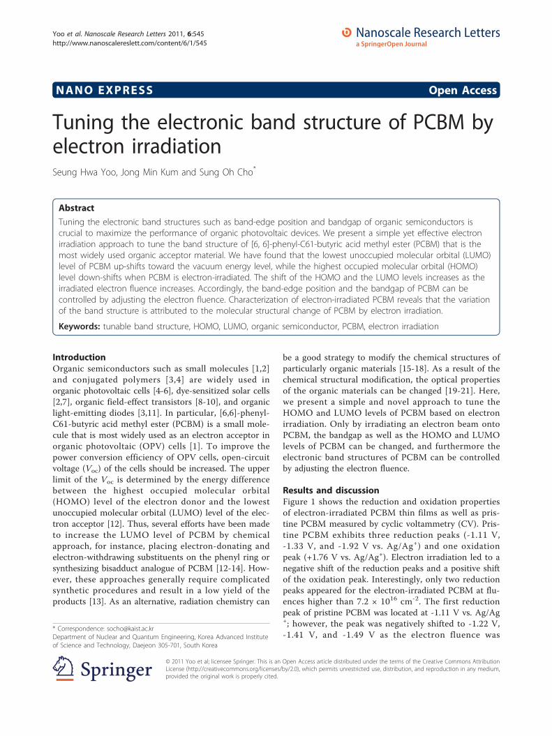
Results and discussionFigure 1 shows the reduction and oxidation propertiesof electron-irradiated PCBM thin films as well as pris-tine PCBM measured by cyclic voltammetry (CV). Pris-tine PCBM exhibits three reduction peaks (-1.11 V,-1.33 V, and -1.92 V vs. Ag/Ag+) and one oxidationpeak (+1.76 V vs. Ag/Ag+). Electron irradiation led to anegative shift of the reduction peaks and a positive shiftof the oxidation peak. Interestingly, only two reductionpeaks appeared for the electron-irradiated PCBM at flu-ences higher than 7.2 × 1016 cm-2. The first reductionpeak of pristine PCBM was located at -1.11 V vs. Ag/Ag+; however, the peak was negatively shifted to -1.22 V,-1.41 V, and -1.49 V as the electron fluence was
* Correspondence: [email protected] of Nuclear and Quantum Engineering, Korea Advanced Instituteof Science and Technology, Daejeon 305-701, South Korea
Yoo et al. Nanoscale Research Letters 2011, 6:545http://www.nanoscalereslett.com/content/6/1/545
© 2011 Yoo et al; licensee Springer. This is an Open Access article distributed under the terms of the Creative Commons AttributionLicense (http://creativecommons.org/licenses/by/2.0), which permits unrestricted use, distribution, and reproduction in any medium,provided the original work is properly cited.
increased to 3.6 × 10¹⁶, 7.2 × 10¹⁶, and 1.44 × 1017 cm-2,respectively. On the contrary, the oxidation peak waspositively shifted from the pristine value of 1.76 to 1.79,1.86, and 1.94 V with increasing the electron fluence to3.6 × 1016, 7.2 ×, and 1.44 × 10¹⁷, respectively.From the CV measurements, the LUMO and HOMO
levels of PCBM were calculated using the followingequation [22]:
LUMO (HOMO) (eV) = − 4.8 − (Eon − E1/2 (ferrocene)
)(1)
where Eon is the onset potential of the first reductionpeak for LUMO or the onset potential of the oxidationpeak for HOMO, and E1/2 (ferrocene) is the half-wavepotential of a ferrocene redox reaction. The LUMO
level up-shifts toward the vacuum energy level, whilethe HOMO level down-shifts with increasing the elec-tron fluence (Figure 1C, the detailed values are shownin Table 1). The LUMO level of the irradiated PCBMwas increased by 0.3 eV and the HOMO level wasdecreased by 0.07 eV compared to the respective valuesof the pristine PCBM when the electron fluence was1.44 × 1017 cm-2. Consequentially, the bandgap of elec-tron-irradiated PCBM gradually increases with increas-ing the electron fluence: the bandgap increases from thepristine value of 2.48 to 2.85 eV at the electron fluenceof 1.44 × 1017 cm-2.To investigate the origin of the change in the band
structure of electron-irradiated PCBM, the molecular
Figure 1 Reduction and oxidation properties of electron-irradiated PCBM thin films, pristine PCBM measured by cyclic voltammetry.Cyclic voltammogram of cathodic scan (A) and anodic scan (B) of PCBM film after electron irradiation at different fluences of (a) 0, (b) 3.6 × 10¹⁶
cm-2, (c) 7.2 × 1016 cm-2, and (d) 1.44 × 1017 cm-2. (C) HOMO and LUMO levels of PCBM changed by electron irradiation as a function ofelectron fluence.
Yoo et al. Nanoscale Research Letters 2011, 6:545http://www.nanoscalereslett.com/content/6/1/545
Page 2 of 7
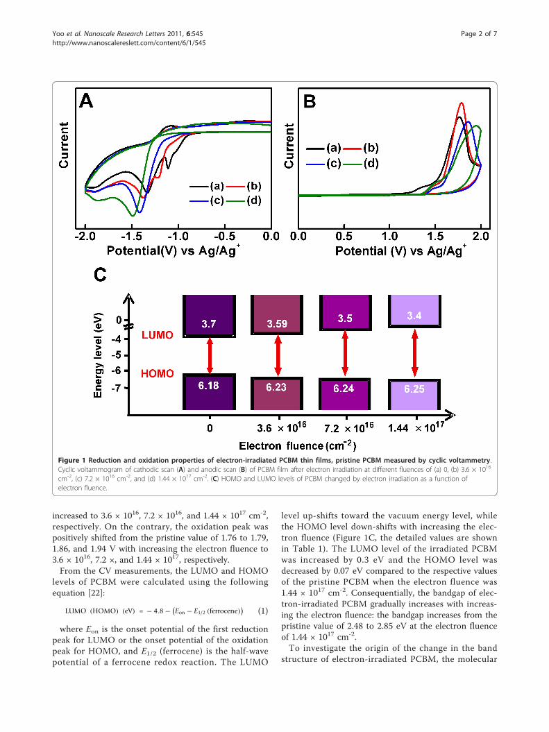
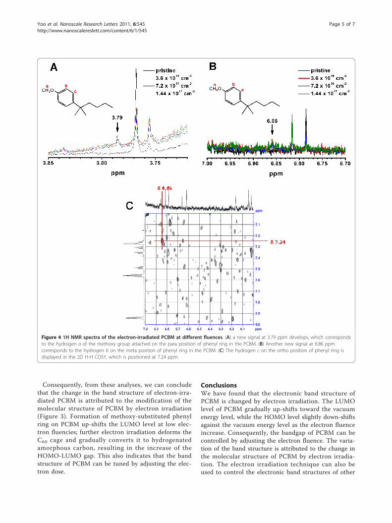
structure of electron-irradiated PCBM was characterizedby 1H nuclear magnetic resonance (NMR), Fouriertransform infrared (FTIR), and Raman spectroscopy.PCBM is a fullerene derivative of which molecular struc-ture comprises a side chain of butyric acid methyl esterand a phenyl ring attached on a C60 cage [1], FTIR spec-tra show that the intensities of all the peaks decreasedwith increasing the electron fluence (Figure 2A), sug-gesting that the molecular bonds of PCBM are graduallydecomposed by electron irradiation. Analysis on thepeak intensity variation reveals the C-O bond of thebutyric acid methyl ester is most rapidly decomposed(Figure 2B). This indicates that the C-O bond can beeasily detached from the side chain, forming methoxyradicals (Figure 3B). In addition, one of the C-H bondsin the phenyl ring was also broken by electron irradia-tion, producing phenyl radicals (Figure 3B). These tworadicals produced by radiolysis make bonds with eachother to form methoxy-substituted phenyl ring onPCBM (Figure 3C). The presence of methoxy-substi-tuted phenyl ring is verified by 1H NMR spectra. First, anew signal at 3.79 ppm appeared and this signal corre-sponds to the hydrogen a marked in Figure 4A, that is,the hydrogen of methoxy group attached on the paraposition of phenyl ring in electron-irradiated PCBM. Inaddition, another new signal at 6.86 ppm (Figure 4B)and 7.24 ppm (Figure 4C) emerged and these signals areattributed to the hydrogen b on the meta position andhydrogen c on the ortho position of methoxy-substitutedphenyl ring, respectively. It has been reported thatattaching methoxy group on phenyl ring up-shifts theLUMO level of PCBM [12,23]. Therefore, we proposethat the up-shift in the LUMO level of electron-irra-diated PCBM is partly attributed to the attachment ofmethoxy group on the phenyl ring of PCBM.Along with the modification in the side chain of buty-
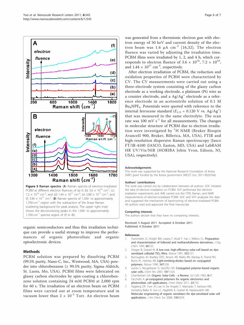
ric acid methyl ester, C60 backbone in PCBM moleculewas also deformed by electron irradiation. Figure 2Bverifies this fact that the intensities of peaks associatedwith the C60 cage gradually decreases as the electronfluence increases. For more detailed interpretation ofthe modification in C60 cage, electron-irradiated PCBMwas analyzed by Raman spectroscopy. PCBM shows tenRaman-active vibration modes, which originates from
the icosahedral symmetry (Ih) of C60 [24]. These vibra-tion modes are sorely affected by change in the Ih sym-metry of C60, therefore, the structural change of C60 atdifferent fluences of electron irradiation was analyzed byobserving the variation of those vibration modes. Atelectron fluence of 3.6 × 1016 cm-2, no significantchange was observed in the Raman spectrum, whichindicates the C60 cage was intact at low fluence of
Table 1 HOMO and LUMO levels of PCBM changed by electron irradiation as a function of electron fluence
Ep,red(1) Eon, red (1) LUMO Ep, ox Eon, ox HOMO
PCBM -1.11 -0.98 -3.70 1.76 1.50 -6.18
PCBM (3.6 × 1016 cm-2) -1.22 -1.09 -3.59 1.79 1.55 -6.23
PCBM (7.2 × 1016 cm-2) -1.41 -1.18 -3.50 1.86 1.56 -6.24
PCBM (1.44 × 1017 cm-2) -1.49 -1.28 -3.40 1.94 1.57 -6.25
The first reduction and oxidation peak potentials (voltage vs. Ag/Ag+), onset potentials, and LUMO and HOMO level (electron volts) of electron-irradiated PCBMat different fluences.
Figure 2 FTIR spectra. (A) FTIR spectrum of electron-irradiatedPCBM at electron fluence of (a) 0, (b) 3.6 × 1016 cm-2, (c) 7.2 × 10¹⁶
cm-2, and (d) 1.44 × 1017 cm-2 including assignment of severalvibration modes with its peak position. (B) Relative intensity ofvibration modes in the butyric acid methyl ester side chain andphenyl ring of electron-irradiated PCBM.
Yoo et al. Nanoscale Research Letters 2011, 6:545http://www.nanoscalereslett.com/content/6/1/545
Page 3 of 7
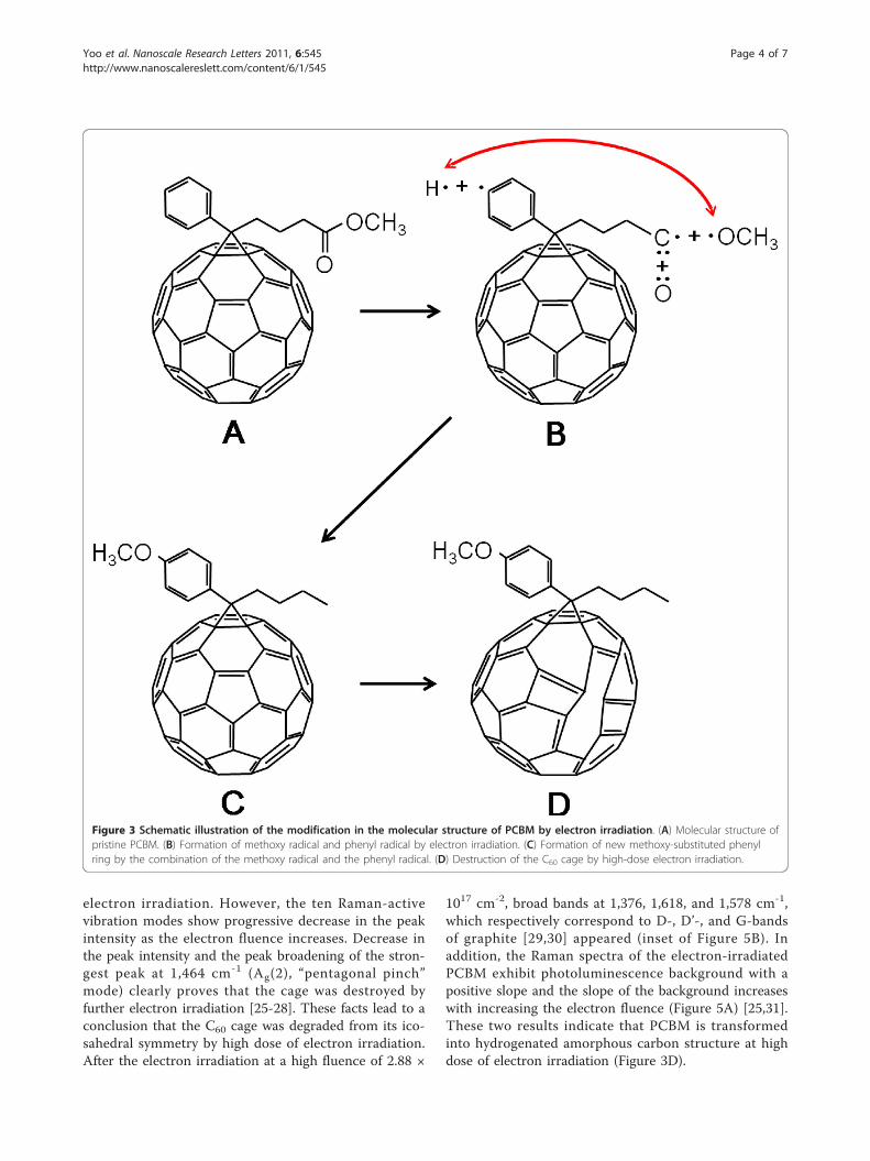
electron irradiation. However, the ten Raman-activevibration modes show progressive decrease in the peakintensity as the electron fluence increases. Decrease inthe peak intensity and the peak broadening of the stron-gest peak at 1,464 cm-1 (Ag(2), “pentagonal pinch”mode) clearly proves that the cage was destroyed byfurther electron irradiation [25-28]. These facts lead to aconclusion that the C60 cage was degraded from its ico-sahedral symmetry by high dose of electron irradiation.After the electron irradiation at a high fluence of 2.88 ×
1017 cm-2, broad bands at 1,376, 1,618, and 1,578 cm-1,which respectively correspond to D-, D’-, and G-bandsof graphite [29,30] appeared (inset of Figure 5B). Inaddition, the Raman spectra of the electron-irradiatedPCBM exhibit photoluminescence background with apositive slope and the slope of the background increaseswith increasing the electron fluence (Figure 5A) [25,31].These two results indicate that PCBM is transformedinto hydrogenated amorphous carbon structure at highdose of electron irradiation (Figure 3D).
Figure 3 Schematic illustration of the modification in the molecular structure of PCBM by electron irradiation. (A) Molecular structure ofpristine PCBM. (B) Formation of methoxy radical and phenyl radical by electron irradiation. (C) Formation of new methoxy-substituted phenylring by the combination of the methoxy radical and the phenyl radical. (D) Destruction of the C60 cage by high-dose electron irradiation.
Yoo et al. Nanoscale Research Letters 2011, 6:545http://www.nanoscalereslett.com/content/6/1/545
Page 4 of 7
Consequently, from these analyses, we can concludethat the change in the band structure of electron-irra-diated PCBM is attributed to the modification of themolecular structure of PCBM by electron irradiation(Figure 3). Formation of methoxy-substituted phenylring on PCBM up-shifts the LUMO level at low elec-tron fluencies; further electron irradiation deforms theC60 cage and gradually converts it to hydrogenatedamorphous carbon, resulting in the increase of theHOMO-LUMO gap. This also indicates that the bandstructure of PCBM can be tuned by adjusting the elec-tron dose.
ConclusionsWe have found that the electronic band structure ofPCBM is changed by electron irradiation. The LUMOlevel of PCBM gradually up-shifts toward the vacuumenergy level, while the HOMO level slightly down-shiftsagainst the vacuum energy level as the electron fluenceincrease. Consequently, the bandgap of PCBM can becontrolled by adjusting the electron fluence. The varia-tion of the band structure is attributed to the change inthe molecular structure of PCBM by electron irradia-tion. The electron irradiation technique can also beused to control the electronic band structures of other
Figure 4 1H NMR spectra of the electron-irradiated PCBM at different fluences. (A) a new signal at 3.79 ppm develops, which correspondsto the hydrogen a of the methoxy group attached on the para position of phenyl ring in the PCBM. (B) Another new signal at 6.86 ppmcorresponds to the hydrogen b on the meta position of phenyl ring in the PCBM. (C) The hydrogen c on the ortho position of phenyl ring isdisplayed in the 2D H-H COSY, which is positioned at 7.24 ppm.
Yoo et al. Nanoscale Research Letters 2011, 6:545http://www.nanoscalereslett.com/content/6/1/545
Page 5 of 7
organic semiconductors and thus this irradiation techni-que can provide a useful strategy to improve the perfor-mances of organic photovoltaic and organicoptoelectronic devices.
MethodsPCBM solution was prepared by dissolving PCBM(99.5% purity, Nano-C, Inc., Westwood, MA, USA) pow-der into chlorobenzene (≥ 99.5% purity, Sigma-Aldrich,St. Luois, Mo, USA). PCBM films were fabricated onglassy carbon electrodes by spin-coating a chloroben-zene solution containing 24 mM PCBM at 2,000 rpmfor 60 s. The irradiation of an electron beam on PCBMfilms were carried out at room temperature and invacuum lower than 2 × 10⁻⁵ Torr. An electron beam
was generated from a thermionic electron gun with elec-tron energy of 50 keV and current density of the elec-tron beam was 1.6 μA cm-2 [16,32]. The electronfluence was varied by adjusting the irradiation time.PCBM films were irradiated by 1, 2, and 4 h, which cor-responds to electron fluence of 3.6 × 10¹⁶, 7.2 × 10¹⁶,and 1.44 × 1017 cm-2, respectively.After electron irradiation of PCBM, the reduction and
oxidation properties of PCBM were characterized byCV. The CV measurements were carried out using athree-electrode system consisting of the glassy carbonelectrode as a working electrode, a platinum (Pt) wire asa counter electrode, and a Ag/Ag+ electrode as a refer-ence electrode in an acetonitrile solution of 0.1 MBu4NPF6. Potentials were quoted with reference to theinternal ferrocene standard (E1/2 = 0.120 V vs. Ag/Ag+)that was measured in the same electrolyte. The scanrate was 100 mV s-1 for all measurements. The changesin molecular structure of PCBM due to electron irradia-tion were investigated by 1H NMR (Bruker BiospinAvanceII 900, Bruker, Billerica, MA, USA), FTIR andhigh-resolution dispersive Raman spectroscopy (JascoFT/IR-4100 (JASCO, Easton, MD, USA) and LabRAMHR UV/Vis/NIR (HORIBA Jobin Yvon, Edison, NJ,USA), respectively).
AcknowledgementsThis work was supported by the National Research Foundation of Korea(NRF) grant funded by the Korea government (MEST) (no. 2011-0020764).
Authors’ contributionsThe work was carried out by collaboration between all authors. SOC initiatedthe idea of electron irradiation on PCBM. SHY performed the electronirradiation experiments and JMK carried out the FTIR, Raman, and NMRmeasurements of electron-irradiated PCBM. SOC and SHY analyzed the dataand suggested the mechanism of band-tuning of electron-irradiated PCBM.All authors read and approved the final manuscript.
Competing interestsThe authors declare that they have no competing interests.
Received: 5 August 2011 Accepted: 4 October 2011Published: 4 October 2011
References1. Hummelen JC, Knight BW, Lepeq F, Wudl F, Yao J, Wilkins CL: Preparation
and characterization of fulleroid and methanofullerene derivatives. J OrgChem 1995, 60:532.
2. Oregan B, Gratzel M: A low-cost, high-efficiency solar-cell based on dye-sensitized colloidal TiO2 films. Nature 1991, 353:737.
3. Burroughes JH, Bradley DDC, Brown AR, Marks RN, Mackay K, Friend RH,Burns PL, Holmes AB: Light-emitting-diodes based on conjugatedpolymers. Nature 1990, 347:539.
4. Gunes S, Neugebauer H, Sariciftci NS: Conjugated polymer-based organicsolar cells. Chem Rev 2007, 107:1324.
5. Chamberlain GA: Organic Solar-Cells - a Review. Sol Cells 1983, 8:47.6. Facchetti A: pi-conjugated polymers for organic electronics and
photovoltaic cell applications. Chem Mater 2011, 23:733.7. Hagberg DP, Yum JH, Lee H, De Angelis F, Marinado T, Karlsson KM,
Humphry-Baker R, Sun LC, Hagfeldt A, Gratzel M, Nazeeruddin MK:Molecular engineering of organic sensitizers for dye-sensitized solar cellapplications. J Am Chem Soc 2008, 130:6259.
Figure 5 Raman spectra. (A) Raman spectra of electron-irradiatedPCBM at different electron fluences of (a) 0, (b) 3.6 × 1016 cm-2, (c)7.2 × 1016 cm-2, and (d) 1.44 × 1017 cm-2, (e) 2.88 × 1017 cm-2, and(f) 3.96 × 1017 cm-2. (B) Raman spectra of 1,300- to approximately1,700-cm-1 region with the subtraction of the linear Ramanscattering background for peak analysis. The upper right insetshows the deconvoluting peaks in the 1,300- to approximately1,700-cm-1 spectra region of (f) in (B).
Yoo et al. Nanoscale Research Letters 2011, 6:545http://www.nanoscalereslett.com/content/6/1/545
Page 6 of 7
8. Garnier F, Horowitz G, Peng XH, Fichou D: An all-organic soft thin-filmtransistor with very high carrier mobility. Adv Mater 1990, 2:592.
9. Ortiz RP, Herrera H, Blanco R, Huang H, Facchetti A, Marks TJ, Zheng Y,Segura JL: Organic n-channel field-effect transistors based onarylenediimide-thiophene derivatives. J Am Chem Soc 2010, 132:8440.
10. Di CA, Yu G, Liu YQ, Guo YL, Sun XN, Zheng J, Wen YG, Wu WP, Zhu DB:Selective crystallization of organic semiconductors for high performanceorganic field-effect transistors. Chem Mater 2009, 21:4873.
11. Kulkarni AP, Tonzola CJ, Babel A, Jenekhe SA: Electron transport materialsfor organic light-emitting diodes. Chem Mater 2004, 16:4556.
12. Kooistra FB, Knol J, Kastenberg F, Popescu LM, Verhees WJH, Kroon JM,Hummelen JC: Increasing the open circuit voltage of bulk-heterojunctionsolar cells by raising the LUMO level of the acceptor. Org Lett 2007,9:551.
13. Lenes M, Wetzelaer GJAH, Kooistra FB, Veenstra SC, Hummelen JC,Blom PWM: Fullerene bisadducts for enhanced open-circuit voltages andefficiencies in polymer solar cells. Adv Mater 2008, 20:2116.
14. Yang C, Kim JY, Cho S, Lee JK, Heeger AJ, Wudl F: Functionalizedmethanofullerenes used as n-type materials in bulk-heterojunctionpolymer solar cells and in field-effect transistors. J Am Chem Soc 2008,130:6444.
15. Miller AA: Radiation chemistry of polydimethylsiloxane. I. Crosslinkingand gas yields. J Am Chem Soc 1959, 82:3519.
16. Kang HY, Saito O, Dole M: The radiation chemistry of polyethylene. IX.temperature coefficient of cross-linking and other effects. J Am ChemSoc 1967, 89:1980.
17. Li Y, Lee EJ, Cai W, Kim KY, Cho SO: Unconventional method formorphology-controlled carbonaceous nanoarrays based on electronirradiation of a polystyrene colloidal monolayer. Acs Nano 2008, 2:1108.
18. Novembre AE, Tai WW, Kometani JM, Hanson JE, Nalamasu O, Taylor GN,Reichmanis E, Thompson LF: Radiation-induced chemistry of poly(4-[(tert-butoxycarbonyl)oxy]styrene-co-sulfur dioxide). Chem Mater 1992, 4:278.
19. Lee HM, Kim YN, Kim BH, Kim SO, Cho SO: Fabrication of luminescentnanoarchitectures by electron irradiation of polystyrene. Adv Mater 2008,20:2094.
20. Davenas J, Boiteux G, Xu XL, Adem E: Role of the modifications inducedby ion-beam irradiation in the optical and conducting properties ofpolyimide. Nucl Instrum Meth B 1988, 32:136.
21. Hioki T, Noda S, Sugiura M, Kakeno M, Yamada K, Kawamoto J: Electricaland optical-properties of ion-irradiated organic polymer Kapton-H. ApplPhys Lett 1983, 43:30.
22. Al-Ibrahim M, Roth HK, Zhokhavets U, Gobsch G, Sensfuss S: Flexible largearea polymer solar cells based on poly(3-hexylthiophene)/fullerene. SolEnerg Mat Sol C 2005, 85:13.
23. Morvillo P, Bobeico E: Tuning the LUMO level of the acceptor to increasethe open-circuit voltage of polymer-fullerene solar cells: a quantumchemical study. Sol Energ Mat Sol C 2008, 92:1192.
24. Bethune DS, Meijer G, Tang WC, Rosen HJ: The vibrational Raman-spectraof purified solid films of C-60 and C-70. Chem Phys Lett 1990, 174:219.
25. Dmytrenko OP, Kulish NP, Belyi NM, Prylutskyy YI, Poperenko LV,Stashchuk VS, Poroshin VG, Pavlenko EL, Shlapatskaya VV, Bernas H,Scharff P: Dose dependences of the optical properties of fullerene filmssubjected to the electron irradiation. Thin Solid Films 2006, 495:365.
26. Robinson APG, Palmer RE, Tada T, Kanayama T, Preece JA, Philp D, Jonas U,Deiderich F: Electron beam induced fragmentation of fullerenederivatives. Chem Phys Lett 1998, 289:586.
27. Hunt MRC, Schmidt J, Palmer RE: Electron-beam-induced fragmentation inultrathin C-60 films on Si(100)-2 × 1-H: mechanisms of cage destruction.Phys Rev B 1999, 60:5927.
28. Liu Z, Suenaga K, Iijima S: Imaging the structure of an individual C-60fullerene molecule and its deformation process using HRTEM withatomic sensitivity. J Am Chem Soc 2007, 129:6666.
29. Cataldo F, Baratta GA, Strazzulla G: He+ ion bombardment of C-60fullerene: an FT-IR and Raman study. Fuller Nanotub Car N 2002, 10:197.
30. Meinardi F, Paleari A, Manfredini M, Milani P: Raman characterization ofamorphous-carbon produced by fullerite laser-induced transformation.Solid State Commun 1995, 93:335.
31. Marchon B, Gui J, Grannen K, Rauch GC, Ager JW, Silva SRP, Robertson J:Photoluminescence and Raman spectroscopy in hydrogenated carbonfilms. Ieee T Magn 1997, 33:3148.
32. Cho SO, Lee BC, Jeong YU: Effects of beam loss on the stability of arecirculating electrostatic accelerator for a long-pulse free-electron laser.Nucl Instrum Meth A 2003, 515:402.
doi:10.1186/1556-276X-6-545Cite this article as: Yoo et al.: Tuning the electronic band structure ofPCBM by electron irradiation. Nanoscale Research Letters 2011 6:545.
Submit your manuscript to a journal and benefi t from:
7 Convenient online submission
7 Rigorous peer review
7 Immediate publication on acceptance
7 Open access: articles freely available online
7 High visibility within the fi eld
7 Retaining the copyright to your article
Submit your next manuscript at 7 springeropen.com
Yoo et al. Nanoscale Research Letters 2011, 6:545http://www.nanoscalereslett.com/content/6/1/545
Page 7 of 7