Tuning structural and magnetic properties of Fe films on Si substrates by hydrogenation processing
9
Materials Science and Engineering B 181 (2014) 24–32 Contents lists available at ScienceDirect Materials Science and Engineering B jou rn al h om epa ge: www.elsevier.com/locate/mseb Tuning structural and magnetic properties of Fe films on Si substrates by hydrogenation processing S.G. Sandu a,b , P. Palade a , G. Schinteie a , A. Birsan a,b , L. Trupina a , V. Kuncser a,∗ a National Institute of Materials Physics, 077125 Bucharest-Magurele, Romania b Bucharest University, Faculty of Physics, 077125 Bucharest-Magurele, Romania a r t i c l e i n f o Article history: Received 8 May 2013 Received in revised form 16 October 2013 Accepted 2 November 2013 Available online 15 November 2013 Keywords: Thin films and interfaces CEMS MOKE a b s t r a c t In order to study specific phenomena at ferromagnetic/semiconducting interfaces, of potentially high interest in spintronics and information technology, structural aspects and magnetic properties of Fe thin films grown on Si(0 0 1) substrates by RF sputtering have been investigated using 57 Fe conversion electron Mössbauer spectroscopy (CEMS) and magneto-optic Keer effect (MOKE). Films of different thicknesses have been deposited either directly on crystalline Si substrates or on Cu buffer layers. An inherent Fe oxide layer is observed in all as prepared films, with a relative thickness decreasing drastically with the deposition time. The Cu buffer layer does not diminish either the interfacial diffusion or the oxidation process. An efficient method to prepare sharper oxygen- and silicon-free interfaces for an improved spin injection, via thermal treatment in hydrogen atmosphere, is proposed. Accordingly, the hydrogenation treatments are very efficient in the modification of the ferromagnetic film structure, phase composition, magnetic properties and interfacial mixing. © 2013 Elsevier B.V. All rights reserved. 1. Introduction An important topic of the present research in spintronics is related to the efficient injection of a spin-polarized current from an electrode into a semiconductor [1,2], with numerous applications related to novel spin dependent electron transport phenomena (e.g. giant magneto-resistance [3,4], tunneling magneto-resistance [5], etc.) or spin based electronic devices (e.g. spin wave logic devices [6], spin transfer torque [7–9] devices, etc.). Although magnetic semiconductor electrodes would be in principle more suitable in this respect, their main inconvenient is related to their relatively low Curie temperature [10]. An alternative solution consists in using an ordinary ferromagnetic film as electrode, with high rema- nent magnetization if possible, although the main breakdown is the “conductivity mismatch” [11] between the ferromagnetic (FM) electrode and the interfaced semiconductor (SC). The situation can be partially improved by using a high spin dependent resistance at the FM/SC interface [12], but the problem remains open for further achievements. Therefore, many efforts have been done in the last years for finding suitable FM/SC interfaces [13–20], requiring both convenient material combinations and negligible atomic intermix- ing. Fe films grown on crystalline Si (c-Si) substrates have been intensively studied [21–23] since it can represent an attractive solution, providing opportunities for integration of the interface ∗ Corresponding author. Tel.: +40 21 369 01 70/125; fax: +40 21 369 01 77. E-mail addresses: kuncser@infim.ro, [email protected] (V. Kuncser). in the conventional Si-based electronics. However, in the well- studied system of Fe films grown on c-Si substrates, the involved interface plays a key role, determining the overall structural and magnetic properties. Depending on the preparation conditions, atomic diffusion and intermixing processes can take place during the growth process leading to the so-called reaction of siliciza- tion [24–26]. Magnetically dead silicide layers [27–30] with low coercivity or even with non-magnetic character can be formed at different extends depending on the deposition method, with an expected negative impact not only on the magnetic properties of the ferromagnetic film but also on the quality of the FM/SC inter- face. One of the most common silicide phases formed at depositing Fe on c-Si at room temperature is the magnetic Fe 3 Si compound [31], but other phases can also be formed [32]. A solution to reduce the Fe–Si intermixing process has came out observing that metallic Fe layers can be grown epitaxially, with neg- ligible intermixing and with induced magnetic texture, on Ge(0 0 1) substrates [33]. Therefore, the growing of Fe layer on Si(0 0 1) sub- strates via a Si 1−x Ge x buffer layer has been successfully applied [34], by using the plasma enhanced chemical vapor deposition method. The RF sputtering deposition method, although it is one of the most effective for large scale production, leads unfortunately to a strong interfacial atomic intermixing and consequently, new meth- ods to reduce this process would be of large interest. To solve the aforementioned problem, we have considered to reduce the inter- mixing at the Fe/Si interface by the deposition of a buffer layer containing elements with lower diffusion coefficients relative to iron (e.g. Sb, CrSi 2 , Au or Cu buffer layers have been mentioned in 0921-5107/$ – see front matter © 2013 Elsevier B.V. All rights reserved. http://dx.doi.org/10.1016/j.mseb.2013.11.004
-
Upload
independent -
Category
Documents
-
view
0 -
download
0
Transcript of Tuning structural and magnetic properties of Fe films on Si substrates by hydrogenation processing

Tb
Sa
b
a
ARRAA
KTCM
1
rerge[stluntebtayciis
0h
Materials Science and Engineering B 181 (2014) 24– 32
Contents lists available at ScienceDirect
Materials Science and Engineering B
jou rn al h om epa ge: www.elsev ier .com/ locate /mseb
uning structural and magnetic properties of Fe films on Si substratesy hydrogenation processing
.G. Sandua,b, P. Paladea, G. Schinteiea, A. Birsana,b, L. Trupinaa, V. Kuncsera,∗
National Institute of Materials Physics, 077125 Bucharest-Magurele, RomaniaBucharest University, Faculty of Physics, 077125 Bucharest-Magurele, Romania
r t i c l e i n f o
rticle history:eceived 8 May 2013eceived in revised form 16 October 2013ccepted 2 November 2013vailable online 15 November 2013
a b s t r a c t
In order to study specific phenomena at ferromagnetic/semiconducting interfaces, of potentially highinterest in spintronics and information technology, structural aspects and magnetic properties of Fe thinfilms grown on Si(0 0 1) substrates by RF sputtering have been investigated using 57Fe conversion electronMössbauer spectroscopy (CEMS) and magneto-optic Keer effect (MOKE). Films of different thicknesseshave been deposited either directly on crystalline Si substrates or on Cu buffer layers. An inherent Fe
eywords:hin films and interfacesEMSOKE
oxide layer is observed in all as prepared films, with a relative thickness decreasing drastically with thedeposition time. The Cu buffer layer does not diminish either the interfacial diffusion or the oxidationprocess. An efficient method to prepare sharper oxygen- and silicon-free interfaces for an improved spininjection, via thermal treatment in hydrogen atmosphere, is proposed. Accordingly, the hydrogenationtreatments are very efficient in the modification of the ferromagnetic film structure, phase composition,
interf
magnetic properties and. Introduction
An important topic of the present research in spintronics iselated to the efficient injection of a spin-polarized current from anlectrode into a semiconductor [1,2], with numerous applicationselated to novel spin dependent electron transport phenomena (e.g.iant magneto-resistance [3,4], tunneling magneto-resistance [5],tc.) or spin based electronic devices (e.g. spin wave logic devices6], spin transfer torque [7–9] devices, etc.). Although magneticemiconductor electrodes would be in principle more suitable inhis respect, their main inconvenient is related to their relativelyow Curie temperature [10]. An alternative solution consists insing an ordinary ferromagnetic film as electrode, with high rema-ent magnetization if possible, although the main breakdown ishe “conductivity mismatch” [11] between the ferromagnetic (FM)lectrode and the interfaced semiconductor (SC). The situation cane partially improved by using a high spin dependent resistance athe FM/SC interface [12], but the problem remains open for furtherchievements. Therefore, many efforts have been done in the lastears for finding suitable FM/SC interfaces [13–20], requiring bothonvenient material combinations and negligible atomic intermix-
ng. Fe films grown on crystalline Si (c-Si) substrates have beenntensively studied [21–23] since it can represent an attractiveolution, providing opportunities for integration of the interface∗ Corresponding author. Tel.: +40 21 369 01 70/125; fax: +40 21 369 01 77.E-mail addresses: [email protected], [email protected] (V. Kuncser).
921-5107/$ – see front matter © 2013 Elsevier B.V. All rights reserved.ttp://dx.doi.org/10.1016/j.mseb.2013.11.004
acial mixing.© 2013 Elsevier B.V. All rights reserved.
in the conventional Si-based electronics. However, in the well-studied system of Fe films grown on c-Si substrates, the involvedinterface plays a key role, determining the overall structural andmagnetic properties. Depending on the preparation conditions,atomic diffusion and intermixing processes can take place duringthe growth process leading to the so-called reaction of siliciza-tion [24–26]. Magnetically dead silicide layers [27–30] with lowcoercivity or even with non-magnetic character can be formed atdifferent extends depending on the deposition method, with anexpected negative impact not only on the magnetic properties ofthe ferromagnetic film but also on the quality of the FM/SC inter-face. One of the most common silicide phases formed at depositingFe on c-Si at room temperature is the magnetic Fe3Si compound[31], but other phases can also be formed [32].
A solution to reduce the Fe–Si intermixing process has came outobserving that metallic Fe layers can be grown epitaxially, with neg-ligible intermixing and with induced magnetic texture, on Ge(0 0 1)substrates [33]. Therefore, the growing of Fe layer on Si(0 0 1) sub-strates via a Si1−xGex buffer layer has been successfully applied [34],by using the plasma enhanced chemical vapor deposition method.
The RF sputtering deposition method, although it is one of themost effective for large scale production, leads unfortunately to astrong interfacial atomic intermixing and consequently, new meth-ods to reduce this process would be of large interest. To solve the
aforementioned problem, we have considered to reduce the inter-mixing at the Fe/Si interface by the deposition of a buffer layercontaining elements with lower diffusion coefficients relative toiron (e.g. Sb, CrSi2, Au or Cu buffer layers have been mentioned in
ce and
[tga(dimi
moossXtms
2
dppttbtudbiDtot(CttwHpicAp
9qacAr
r3dItio
S.G. Sandu et al. / Materials Scien
35–38]). Moreover we propose a more efficient method, relatedo the post annealing of the RF sputtered iron films in hydro-en atmosphere at convenient temperature. Hydrogen is knowns a reducing agent when reactions at relatively high temperatures300–400 ◦C) occur. Previous studies revealed that the oxidationegree in thin films is considerably reduced and their crystallinity
s improved via hydrogenation treatments [39,40] and hence, ferro-agnetic/semiconducting interfaces more suitable for applications
n spintronics would be expected.The aim of this paper is the investigation of structural and
agnetic properties of iron films deposited by RF sputteringn c-Si substrates. A detailed study of the changes inducedn the deposited Fe films, by either Cu buffer layers or aubsequent annealing under high pressure of hydrogen is pre-ented. The experimental investigation has been performed using-ray reflectometry (XRR), conversion electron Mössbauer spec-
roscopy (CEMS), atomic force microscopy (AFM), magnetic forceicroscopy (MFM) and magneto-optic Kerr effect (MOKE) mea-
urements.
. Experimental details
Fe films enriched in the 57Fe Mössbauer isotope have beeneposited on c-Si(0 0 1) substrates. The samples have been pre-ared via RF sputtering in Ar atmosphere of a high purity Fe target,artially covered by small plackets of metallic Fe 95% enriched inhe 57Fe isotope and keeping the substrate at about room tempera-ure (the substrate holder was maintained at constant temperaturey flowing water at about 20 ◦C). A bottom-up configuration (bot-om horizontal 2′′ Fe target and top substrate at about 8 cm) wassed. The RF power was 100 W (no magnetron was used), in con-itions of a null self biasing potential for plasma confinement. Thease pressure was in the range of 5 × 10⁻⁶ mbar, while the work-
ng pressure was about 5 × 10⁻² mbar of argon (Ar flux of 40 sccm).ifferent deposition times – leading to different thicknesses of
he films – have been considered. Two sets of samples have beenbtained, one for Fe films grown directly on the c-Si substrate andhe other one consisting of Fe films grown on a Cu buffer layersimilar deposition conditions were used for the deposition of theu layer as for the Fe film). No chemical treatments were appliedo the c-Si substrate containing a native Si oxide with the intentiono avoid a considerably increase of roughness, but the substratesere priory sonicated and washed in acetone and ethyl alcohol.owever, both the target and the substrate surfaces were cleanedreviously to the deposition by suitable etching procedures. It is
mportant to consider that due to the lack of ultra high vacuumonditions, prior to the introduction of the high purity (99.9999%)r, a certain oxidation of films is expected during the depositionrocess.
A thermal treatment in hydrogen atmosphere at 300 ◦C, for0 min, and at a pressure of about 10 bars preceded by 20 subse-uent cycles of under vacuum cleaning and purging in hydrogen at
lower temperature (100–150 ◦C), has been applied afterwards. Aommercially available volumetric Sievert apparatus provided bydvanced Material Corporation, Pittsburgh, USA was used in thisespect.
The deposition time for the Fe films was of 1, 3, 5 and 8 min,espectively, whereas the Cu buffer layers were grown for just
min. An initial calibration concerning the relation between theeposition time and the film thickness was performed by Total
nterferometry Contrast on thicker Fe and Cu films and final deposi-ion rates were also confirmed by X-ray reflectometry, as discussedn the next section. The following sets of samples were finallybtained and analyzed:
Engineering B 181 (2014) 24– 32 25
• Si/Fe(3 nm), Si/Fe(9 nm), Si/Fe(15 nm), Si/Fe(24 nm) for Fe filmsdeposited directly on c-Si substrates for 1, 3, 5 and 8 min, respec-tively.
• Si/Cu(24 nm)/Fe(3 nm), Si/Cu(24 nm)/Fe(9 nm), Si/Cu(24 nm)/Fe(15 nm), Si/Cu(24 nm)/Fe(24 nm) for Fe films deposited for 1,3, 5 and 8 min on Cu buffer layers.
Corresponding samples treated via hydrogenation are addition-ally indexed by the suffix “ H”.
The atomic force microscopy (AFM) and magnetic forcemicroscopy (MFM) images have been obtained using a MFP-3D SA(Asylum Research) instrument working in non-contact mode bythe two-step method [41], at a resonance frequency of 72 kHz. AFMscans have been performed in the first step, recording the topogra-phy, while MFM scans have been collected in the second step, withan increased distance between the tip and the sample. Si cantileverscovered with a Co–Cr alloy were used.
The X-ray reflectometry (XRR) measurements have been per-formed with a Brucker type (AD 8 ADVANCED) diffractometerworking with Cu(K�) radiation of 0.154 nm wavelength. The LAP-TOS program was used for fitting the XRR patterns.
Conversion Electron Mössbauer Spectropscopy (CEMS) has beenused in order to study the phase composition and the local struc-ture of the Fe films. The measurements have been performed atroom temperature, in perpendicular geometry (with the gammaradiation perpendicular to the sample plane), and the sample hasbeen placed in a home-made gas flow proportional counter. A 57Cosource (Rh matrix) of about 35 mCi activity and a spectrometerworking with sinusoidal waveform have been used. The least-squares fitting of the CEM spectra has been performed via theNORMOS computer program [42]. The isomer shifts are reportedrelative to �-Fe at room temperature.
Vector magneto-optic Kerr effect (MOKE) magnetometry mea-surements have been done at room temperature using a miniMOKE(AMACC Anderberg & Modéer Accelerator AB) device with the laserbeam (wavelength of 640 nm) making an incident angle of 45◦
versus the sample plane (a 90◦ geometry between source and detec-tor and magnetic field in both the sample and the incidence plane).The polarizer and analyzer are of Glan–Thompson type and thelight modulation is made with a Faraday rotator (rod-like shape)working at 1000 Hz. The sample can be rotated in its own plane inorder to change the direction of a possible magnetic anisotropy axiswith respect to the direction of the applied field (azimuthal anglerotation).
3. Results and discussions
The thickness, density and roughness of the hydrogenatedsamples Si/Fe(9 nm) H and Si/Cu(24 nm)/Fe(9 nm) H have beenestimated via X-ray reflectometry (XRR). The mass density profilesobtained from the fitting of the XRR spectra of the above sam-ples are shown in Fig. 1. The corresponding XRR patterns (dottedline-experimental and solid curve – theoretical fit) are shown inthe insets. The best fit was obtained in the frame of the followingstructural models: Si substrate, a thin SiO2 layer, a Fe layer anda topmost Fe oxide layer, for sample Si/Fe(9 nm) H and Si sub-strate, a thin SiO2 layer, a Cu buffer layer, a Fe layer and an Feoxide layer, for sample Si/Cu(24 nm)/Fe(24 nm) H. The obtainedparameters (thickness, density and roughness) are also presentedin Table 1.
According to these results, it might be observed that in spite of
the etching process of the substrate, a SiO2 layer of 2–3 nm thick-ness remains present at the Si surface with a consistent roughnessof about 1 nm, similar to the Si substrate. On the other hand, despitethe hydrogenation treatment, a thin Fe oxide layer of just about
26 S.G. Sandu et al. / Materials Science and Engineering B 181 (2014) 24– 32
Fig. 1. Mass density profile obtained from the fitting of the XRR patterns of the hydrogenated samples Si/Fe(9 nm) H (a) and Si/Cu(24 nm)/Fe(9 nm) H (b). The depth in themass density profile is counted from the Si substrate (depth = 0). The corresponding XRR patterns are shown in the inset.
Table 1Thickness, roughness and density for each layer of the model system in samples Si/Fe(9 nm) H and Si/Cu(24 nm)/Fe(9 nm) H analyzed via XRR method. Errors of the last digitare given in brackets. The density of Si substrate was fixed.
Sample Layer Thickness (nm) Roughness (nm) Density (g/cm3)
Si/Fe(9 nm) H
Fe oxide 1.2(3) 0.3 4.0(3)Fe 9.8(9) 0.10(2) 8.5(5)SiO2 1.9(3) 0.9(2) 3.2(3)Si – 1.0(1) 2.3
Fe oxide 1.1(3) 0.10(2) 4.3(3)Fe 8.2(9) 0.10(2) 7.6(5)
1ewptnFttasfi
fnscha
aoiaiettstnonoa
Si/Cu(24 nm)/Fe(9 nm) H Cu 24.3(8)SiO2 3.1(3)
Si –
nm thickness is formed on the surface of the metallic Fe. How-ver, this is not surprising taking into account that the samplesere handled for days in normal environmental conditions, beforeerforming the XRR analysis. Completely different than the case ofhe SiO2/Fe, SiO2/Cu and Cu/Fe interfaces with a consistent rough-ess of about 1 nm, the upper part of the Fe layer (e.g. including thee/FexOy interface) is quite smooth (0.1 nm roughness). It is wortho notice that the thickness of the Fe film grown in similar condi-ions on a Cu buffer layer is about 15% lower than the thickness ofn Fe film grown directly on the c-Si(0 0 1) substrate and the depo-ition rate of the Cu film is about 3 times larger than that of the Felm.
The layer thickness for the rest of the samples can be estimatedrom XRR results, presuming that the hydrogenation treatment haso significant influence on the thickness of metallic layers. For aimpler approach, the deposition rate of Fe can be estimated in bothases as 3 nm/min, while the deposition rate of Cu is considerablyigher, of 8 nm/min. A geometrical configuration of the samples, aslready presented in Section 2, results straightforwardly.
Fig. 2 shows AFM images taken on sample Si/Fe(15 nm), beforend after hydrogenation, while both AFM and MFM images takenn sample Si/Fe(9 nm), before and after hydrogenation are shownn Fig. S1 (supplementary data). The AFM images indicate that boths prepared systems have a tridimensional type of growth, withsland-like morphologies (Volmer–Weber growth mode), of lat-ral average size of order of tenths of nanometers (25–30 nm inhe case of sample Si/Fe(9 nm)). The hydrogenated systems keephe island-like morphologies, but with an increased lateral averageize (45–50 nm in the case of sample Si/Fe(9 nm) H). In addition,he lateral average size is also increasing with the Fe film thick-ess (e.g. 40–45 nm in case of Si/Fe(15 nm) and 65–70 nm in casef Si/Fe(15 nm) H). Contrary, the root mean square (RMS) rough-
ess (related to the film morphology in this case) is in the rangef 1–2 nanometers for all analyzed samples, increasing slightlyfter the hydrogenation treatment. For example, in the case of1.3(2) 7.2(2)1.0(2) 2.7(3)0.8(1) 2.3
sample Si/Fe(9 nm), the roughness increases from 1.2 nm in the asdeposited film to 1.5 nm in the hydrogenated film, while in the caseof Si/Fe(15 nm), the roughness is 1 nm before treatment and 1.3 nmafter hydrogenation. Although the MFM images, shown in supple-mentary data (Fig. S1) are not very pertinent (due to mainly in planeorientation of the Fe spins and the presence of the top oxide layer),they suggest however the existence of island-type magnetic mon-odomains with the in-plane magnetization preferentially orientedalong a certain direction in the non-hydrogenated sample and withalmost no preferred orientation in the hydrogenated sample.
Supplementary material related to this article can be found,in the online version, at http://dx.doi.org/10.1016/j.mseb.2013.11.004.
Conversion electron Mössbauer (CEM) spectra collected at roomtemperature on the systems Si/Fe and Si/Cu/Fe before hydrogena-tion are shown in Fig. 3(a) and (b), respectively. In both systems,excepting the thinnest films of 3 nm thickness, the spectra present amain magnetic contribution consisting of a relatively broad sextetpattern which was fitted via a probability distribution of hyper-fine magnetic fields, shown on the right side of each correspondingspectrum. A second less intense central paramagnetic component(D) was also considered. The main hyperfine parameters (isomershift, IS, quadrupole splitting, QS, and magnetic hyperfine field, Bhf),derived from the fitting of the spectra, are gathered in Table 2.
The CEM spectrum of sample Si/Fe(3 nm) presents a broad cen-tral paramagnetic pattern which was fitted by two doublets (D1,D2). Their hyperfine parameters (the first one, D1 is characterizedby an IS of 0.3 mm/s and a QS of 0.7 mm/s, whereas the secondone, D2, has an IS of 0.4 mm/s and a QS of 1.1 mm/s) allow us toassume that they belong to superparamagnetic Fe3+ oxide phasesof different distortions. The bivalent Fe based wüstite (FeO) phaseis excluded because its paramagnetic spectrum contains a compo-
nent with an IS of approximately 0.9 mm/s [43], which is higherthan the values obtained in the present study. As for the sili-cide phases, although most of the paramagnetic phases of Fe–Si
S.G. Sandu et al. / Materials Science and Engineering B 181 (2014) 24– 32 27
Fig. 2. AFM images of samples: Si/Fe(15 nm) (a) and Si/Fe(15 nm) H (b).
Fig. 3. CEM spectra of the systems Si/Fe (a) and Si/Cu/Fe (b). The relative area (RA) of paramagnetic phases (D, D1 and D2) and of the magnetic phase (DIST) versus the Fefilm thickness for systems Si/Fe (c) and Si/Cu/Fe (d).
Table 2Hyperfine parameters (IS, isomer shift; QS, quadrupole splitting; Bhf, magnetic hyperfine field) for Si/Fe and Si/Cu/Fe systems. Errors of the last digit are given in brackets.
Sample Sublattice IS (mm/s) QS (mm/s) Bhf (T)
Si/Fe(3 nm) D1 0.30(1) 0.72(3) –D2 0.39(1) 1.16(3) –
Si/Fe(9 nm) DIST 0.16(2) −0.02(1) 22.9(2)D 0.48(7) 1.29(3) –
Si/Fe(15 nm) DIST 0.25(3) 0.04(2) 22.7(2)D 0.5(1) 1.24(6) –
Si/Fe(24 nm) DIST 0.11(1) −0.01(8) 21.19(9)D 0.45(2) 1.10(2) –
Si/Cu(24 nm)/Fe(3 nm) D1 0.346(7) 0.73(3) –D2 0.39(2) 1.21(3) –
Si/Cu(24 nm)/Fe(9 nm) DIST 0.17(4) −0.01(2) 23.2(4)D 0.42(6) 1.14(3) –
Si/Cu(24 nm)/Fe(15 nm) DIST 0.18(1) −0.01(1) 24.3(2)D 0.67(5) 1.30(3) –
Si/Cu(24 nm)/Fe(24 nm) DIST 0.18(2) −0.01(1) 22.8(2)
D 0.89(1) 1.17(1) –
28 S.G. Sandu et al. / Materials Science and Engineering B 181 (2014) 24– 32
F e relatt
cQ0tp
pmfia−pttTdttoss
ptsSci
ig. 4. CEM spectra of the hydrogenated systems Si/Fe H (a) and Si/Cu/Fe H (b). Thhickness for Si/Fe H (c) and Si/Cu/Fe H (d) systems.
ompounds (metastable c-FeSi, FexSi1−x with x < 0.5) have similarS to our values, the previously reported IS values between 0.07 and.27 mm/s [32] are lower than the values obtained in our study. Forhis reason, the assignation of paramagnetic phases of Fe–Si com-ounds to the obtained doublets is not taken into consideration.
At higher thickness, in the case of sample Si/Fe(9 nm), therevalent magnetic broad sextet can be observed, while the para-agnetic contribution is considerably reduced. The broad sextet,
tted with a distribution of magnetic hyperfine fields and noteds DIST, shows an average IS of 0.16 mm/s, low negative QS of0.02 mm/s and average Bhf of 22.9 T, being assigned to a silicidehase (Fe3Si). The ideal D03 structure of Fe3Si reported in litera-ure [31,44] has a distribution of hyperfine magnetic fields withwo maxima, at 20 T and 31 T, for A site and B site, respectively.he shape of the sextet and its associated average Bhf indicates aisordered Fe–Si structure, close compositionally to the B2 struc-ure. The less intense paramagnetic pattern is assigned, accordingo the previous discussion, to a Fe3+ based oxide. The CEM spectraf the samples Si/Fe(15 nm) and Si/Fe(24 nm) evidenced the samepectral components with similar hyperfine parameters as for theample Si/Fe(9 nm).
When introducing a buffer layer of Cu, the CEM spectra of sam-les Si/Cu(24 nm)/Fe(3 nm) and Si/Cu(24 nm)/Fe(9 nm) are similaro the previous case of films deposited directly on the Si sub-
trate. However, in the case of samples Si/Cu(24 nm)/Fe(15 nm)i/Cu(24 nm)/Fe(24 nm), the paramagnetic central component (D)orresponding to the superparamagnetic Fe oxide layer has an ISncreased at 0.67 mm/s and 0.89 mm/s, respectively, indicating thative area (RA) of magnetic (S) and paramagnetic (D) components versus the Fe film
the degree of oxidation increases at high thickness, toward IS val-ues corresponding to oxide phases containing Fe2+ ions. However,the values of the QS of 1.3 and 1.17 mm/s, higher than reported val-ues for wüstite (0.46 mm/s and 0.78 mm/s [43]) indicate a defectconfiguration. An asymmetric sextet distribution is observed forSi/Cu(24 nm)/Fe(15 nm) and Si/Cu(24 nm)/Fe(24 nm), especially forthe latter, expressing the deviation from a single-phase compo-sition with distributed Fe configurations and the formation of atleast two intermixing Fe phases. The high degree of oxidation maybe observed also from the decrease of relative area of the mag-netic silicide on the account of a relatively increased contributionof the paramagnetic pattern, as compared to the similar films growndirectly on the Si substrate.
The relative area (RA) of each sublattice versus the Fe film thick-ness for Si/Fe and Si/Cu/Fe systems is presented in Fig. 3(c) and (d),respectively. It might be observed that on average, excepting thethinnest Fe film, the relative amount of Fe oxide phase is about 12%in the films directly grown on the Si substrate and almost double(20%) in Fe films grown on Cu buffer layers. Accordingly, in cor-roboration to XRR measurements evidencing the presence of anFe oxide top layer on the analyzed systems, these results suggestrelative thicknesses for the uppermost oxide layers in range of 12%and 20%, respectively, from the thickness of the Fe containing layer,the rest of the deeper layer consisting of an atomically disordered
Fe–Si structure with an average composition close to Fe75Si25. It isworth noticing that the average value of the hyperfine field in thisstructure has to be very sensitive to the relative Si amount, x, in theformula unit Fe1−xSix, a higher value (closer to 33.14 T) meaning
S.G. Sandu et al. / Materials Science and Engineering B 181 (2014) 24– 32 29
Table 3Hyperfine parameters (IS, isomer shift; QS, quadrupole splitting; Bhf, magnetic hyperfine field) for Si/Fe H and Si/Cu/Fe H systems. Errors of the last digit are given in brackets.
Sample Sublattice IS (mm/s) QS (mm/s) Bhf (T)
Si/Fe(3 nm) HS −0.05(3) −0.02(1) 33.1(2)D 0.40(1) 0.93(2) –
Si/Fe(9 nm) HS −0.008(2) 0.004(4) 33.11(2)D 0.27(5) 0.93(8) –
Si/Fe(24 nm) HS −0.004(1) 0.014(2) 33.159(8)D 0.426(9) 1.01(2) –
Si/Cu(24 nm)/Fe(3 nm) HS −0.005(3) −0.03(2) 29.99(7)D 0.36(1) 0.96(3) –
Si/Cu(24 nm)/Fe(9 nm) HS −0.005(1) 0.002(3) 33.16(1)
)
2)
)
awa
galCtab
SShopc
D 0.36(2
Si/Cu(24 nm)/Fe(24 nm) HS −0.006(D 0.40(2
lower Si amount. Surprisingly, the average hyperfine field variesith less than 10% for all thicknesses between 9 and 24 nm, with
nd without Cu buffer layer.The slightly lower average value observed for the case of Fe films
rown on the Cu buffer layer (about 22 T as compared to about 23 T,s observed from Table 2) suggests a few less percents of Si in theseayers, but still close to about 20%. Hence, the intercalation of theu buffer layer was not able to drastically diminish the diffusion ofhe Si atoms from the substrate into the deposited Fe film and thelternative processing route of the hydrogenation treatment haseen further considered in this respect.
The CEM spectra of the samples Si/Fe(3 nm) H,i/Fe(9 nm) H, Si/Fe(24 nm) H, and Si/Cu(24 nm)/Fe(3 nm) H,i/Cu(24 nm)/Fe(9 nm) H, Si/Cu(24 nm)/Fe(24 nm) H after the
ydrogenation treatment, are shown in Fig. 4(a) and (b). In casef hydrogenated Si/Fe(3 nm) H and Si/Cu(24 nm)/Fe(3 nm) H sam-les with the lowest thickness of the Fe films, excepting the mainentral paramagnetic component (with IS around 0.38 mm/s andFig. 5. MOKE curves for: Si/Fe(9 nm) (a) and Si/Cu(24 nm)/Fe(9 nm
0.97(4) –0.003(2) 33.22(1)0.80(4) –
QS around 0.94 mm/s) which was assigned to the distorted Fe oxidesuperparamagnetic phase, an additional sextet like pattern (morepronounced in the second sample) with hyperfine parametersspecific to metallic Fe, was also evidenced. For the other samples,the paramagnetic component considerably decreases with thick-ness and the metallic �-Fe phase is prevailing. The Mössbauerhyperfine parameters related to the considered components in thespectra are given in Table 3 whereas the dependence of the relativespectral area of the two components (Fe oxide and metallic Fe)versus the Fe film thickness are given in Fig. 4(c) and (d). Accordingto the mentioned data, it is clearly proven that the hydrogenationtreatment reduces on one side the oxidation of the Fe films (e.g.at less than 10% relative contribution of the oxide phase in thickerfilms), due to the reducing effect of hydrogen, and on the other
side expels the Si atoms from the bcc structure of the Fe film.Once explored the structural and phase composition aspects of thefilms, it becomes interesting to see their influence on the magneticproperties of the systems.) (b). The azimuthal angle (in ◦) is inserted in each graph.

3 ce and Engineering B 181 (2014) 24– 32
asedfamfiatftfiMdstHSd
i2
t
0 S.G. Sandu et al. / Materials Scien
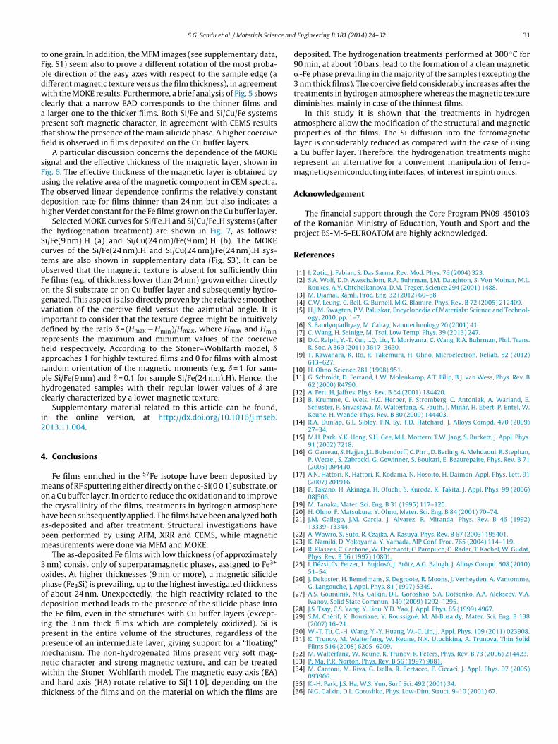
The hysteresis curves obtained by MOKE on the as grown Si/Fend Si/Cu/Fe systems, with thicknesses of the Fe films of 9 nm, arehown in Fig. 5. The measurements have been performed at differ-nt azimuthal angles (between the field direction and a preferredirection of the c-Si substrate, e.g. Si[1 1 0] in this case) in the rangerom −30 to 120◦. A strong dependence of the MOKE signal with thezimuthal angle is observed. According to the Stoner–Wohlfarthodel, briefly discussed in [45], this is a direct indication on the
lm magnetic texture. The hard axis (HA) of magnetization (anlmost linear dependence is observed for the magnetization versushe magnetic field applied along the HA, without any coercivity) isound at 0◦ to Si[1 1 0], while the easy axis (EA) (a rectangular hys-eresis loop presenting the highest coercivity is observed with theeld applied along the EA) is found at 90◦ relative to Si[1 1 0]. TheOKE signal of the sample Si/Fe(24 nm), shown in supplementary
ata (Fig. S2), presents a slight rotation toward left of the two axes,o that HA and EA are found at −30 and +60◦, respectively, relativeo Si[1 1 0]. A relative rotation of about +30◦ for the orientation ofA and EA is observed for both samples, Si/Cu(24 nm)/Fe(9 nm) andi/Cu(24 nm)/Fe(24 nm) (the latter shown also in supplementaryata, Fig. S2) grown on the Cu buffer layer.
Supplementary material related to this article can be found,
n the online version, at http://dx.doi.org/10.1016/j.mseb.013.11.004.On the other hand, discussing the Stoner–Wohlfarth model inerms of easy axes distributions (EAD), the most linear/rectangular
Fig. 7. MOKE curves for hydrogenated samples Si/Fe(9 nm) H (a) and Si/Cu(24
Fig. 6. MOKE signal versus the effective thickness of the magnetic layer for Si/Fe(full squares), and Si/Cu/Fe (full circles) and the linear fit lines, solid and dashed,respectively.
shape should be obtained for well magnetic textured films (narrowEAD) whereas more rounded loops should be obtained for less tex-tured films (broader EAD). Finally, a rounded loop which does notchange its shape versus the azimuthal angle should be obtained for
non-textured films (random angular distribution of easy axes). Thehypothesis of EAD is supported also by the island-type morphologyof the films observed via AFM (see Fig. 2), suggesting that the filmsare formed by magnetic monodomains, and each one correspondsnm)/Fe(9 nm) H (b). The azimuthal angle (in ◦) is inserted in each graph.
ce and
tFbdwcaptfi
sFuTdh
tSctoFogvidrfiarphc
i2
4
mothabm
3opodtippmnwat
[[
[[
[
[
[
[
[
[[[
[[[
[
[
[
[[
[[
[
S.G. Sandu et al. / Materials Scien
o one grain. In addition, the MFM images (see supplementary data,ig. S1) seem also to prove a different rotation of the most proba-le direction of the easy axes with respect to the sample edge (aifferent magnetic texture versus the film thickness), in agreementith the MOKE results. Furthermore, a brief analysis of Fig. 5 shows
learly that a narrow EAD corresponds to the thinner films and larger one to the thicker films. Both Si/Fe and Si/Cu/Fe systemsresent soft magnetic character, in agreement with CEMS resultshat show the presence of the main silicide phase. A higher coerciveeld is observed in films deposited on the Cu buffer layers.
A particular discussion concerns the dependence of the MOKEignal and the effective thickness of the magnetic layer, shown inig. 6. The effective thickness of the magnetic layer is obtained bysing the relative area of the magnetic component in CEM spectra.he observed linear dependence confirms the relatively constanteposition rate for films thinner than 24 nm but also indicates aigher Verdet constant for the Fe films grown on the Cu buffer layer.
Selected MOKE curves for Si/Fe H and Si/Cu/Fe H systems (afterhe hydrogenation treatment) are shown in Fig. 7, as follows:i/Fe(9 nm) H (a) and Si/Cu(24 nm)/Fe(9 nm) H (b). The MOKEurves of the Si/Fe(24 nm) H and Si/Cu(24 nm)/Fe(24 nm) H sys-ems are also shown in supplementary data (Fig. S3). It can bebserved that the magnetic texture is absent for sufficiently thine films (e.g. of thickness lower than 24 nm) grown either directlyn the Si substrate or on Cu buffer layer and subsequently hydro-enated. This aspect is also directly proven by the relative smootherariation of the coercive field versus the azimuthal angle. It ismportant to consider that the texture degree might be intuitivelyefined by the ratio ı = (Hmax − Hmin)/Hmax, where Hmax and Hminepresents the maximum and minimum values of the coerciveeld respectively. According to the Stoner–Wohlfarth model, ıpproaches 1 for highly textured films and 0 for films with almostandom orientation of the magnetic moments (e.g. ı = 1 for sam-le Si/Fe(9 nm) and ı = 0.1 for sample Si/Fe(24 nm) H). Hence, theydrogenated samples with their regular lower values of ı arelearly characterized by a lower magnetic texture.
Supplementary material related to this article can be found,n the online version, at http://dx.doi.org/10.1016/j.mseb.013.11.004.
. Conclusions
Fe films enriched in the 57Fe isotope have been deposited byeans of RF sputtering either directly on the c-Si(0 0 1) substrate, or
n a Cu buffer layer. In order to reduce the oxidation and to improvehe crystallinity of the films, treatments in hydrogen atmosphereave been subsequently applied. The films have been analyzed boths-deposited and after treatment. Structural investigations haveeen performed by using AFM, XRR and CEMS, while magneticeasurements were done via MFM and MOKE.The as-deposited Fe films with low thickness (of approximately
nm) consist only of superparamagnetic phases, assigned to Fe3+
xides. At higher thicknesses (9 nm or more), a magnetic silicidehase (Fe3Si) is prevailing, up to the highest investigated thicknessf about 24 nm. Unexpectedly, the high reactivity related to theeposition method leads to the presence of the silicide phase intohe Fe film, even in the structures with Cu buffer layers (except-ng the 3 nm thick films which are completely oxidized). Si isresent in the entire volume of the structures, regardless of theresence of an intermediate layer, giving support for a “floating”echanism. The non-hydrogenated films present very soft mag-
etic character and strong magnetic texture, and can be treatedithin the Stoner–Wohlfarth model. The magnetic easy axis (EA)
nd hard axis (HA) rotate relative to Si[1 1 0], depending on thehickness of the films and on the material on which the films are
[[
[[
Engineering B 181 (2014) 24– 32 31
deposited. The hydrogenation treatments performed at 300 ◦C for90 min, at about 10 bars, lead to the formation of a clean magnetic�-Fe phase prevailing in the majority of the samples (excepting the3 nm thick films). The coercive field considerably increases after thetreatments in hydrogen atmosphere whereas the magnetic texturediminishes, mainly in case of the thinnest films.
In this study it is shown that the treatments in hydrogenatmosphere allow the modification of the structural and magneticproperties of the films. The Si diffusion into the ferromagneticlayer is considerably reduced as compared with the case of usinga Cu buffer layer. Therefore, the hydrogenation treatments mightrepresent an alternative for a convenient manipulation of ferro-magnetic/semiconducting interfaces, of interest in spintronics.
Acknowledgement
The financial support through the Core Program PN09-450103of the Romanian Ministry of Education, Youth and Sport and theproject BS-M-5-EUROATOM are highly acknowledged.
References
[1] I. Zutic, J. Fabian, S. Das Sarma, Rev. Mod. Phys. 76 (2004) 323.[2] S.A. Wolf, D.D. Awschalom, R.A. Buhrman, J.M. Daughton, S. Von Molnar, M.L.
Roukes, A.Y. Chtchelkanova, D.M. Treger, Science 294 (2001) 1488.[3] M. Djamal, Ramli, Proc. Eng. 32 (2012) 60–68.[4] C.W. Leung, C. Bell, G. Burnell, M.G. Blamire, Phys. Rev. B 72 (2005) 212409.[5] H.J.M. Swagten, P.V. Paluskar, Encyclopedia of Materials: Science and Technol-
ogy, 2010, pp. 1–7.[6] S. Bandyopadhyay, M. Cahay, Nanotechnology 20 (2001) 41.[7] C. Wang, H. Seinige, M. Tsoi, Low Temp. Phys. 39 (2013) 247.[8] D.C. Ralph, Y.-T. Cui, L.Q. Liu, T. Moriyama, C. Wang, R.A. Buhrman, Phil. Trans.
R. Soc. A 369 (2011) 3617–3630.[9] T. Kawahara, K. Ito, R. Takemura, H. Ohno, Microelectron. Reliab. 52 (2012)
613–627.10] H. Ohno, Science 281 (1998) 951.11] G. Schmidt, D. Ferrand, L.W. Molenkamp, A.T. Filip, B.J. van Wess, Phys. Rev. B
62 (2000) R4790.12] A. Fert, H. Jaffres, Phys. Rev. B 64 (2001) 184420.13] B. Krumme, C. Weis, H.C. Herper, F. Stromberg, C. Antoniak, A. Warland, E.
Schuster, P. Srivastava, M. Walterfang, K. Fauth, J. Minár, H. Ebert, P. Entel, W.Keune, H. Wende, Phys. Rev. B 80 (2009) 144403.
14] R.A. Dunlap, G.L. Sibley, F.N. Sy, T.D. Hatchard, J. Alloys Compd. 470 (2009)27–34.
15] M.H. Park, Y.K. Hong, S.H. Gee, M.L. Mottern, T.W. Jang, S. Burkett, J. Appl. Phys.91 (2002) 7218.
16] G. Garreau, S. Hajjar, J.L. Bubendorff, C. Pirri, D. Berling, A. Mehdaoui, R. Stephan,P. Wetzel, S. Zabrocki, G. Gewinner, S. Boukari, E. Beaurepaire, Phys. Rev. B 71(2005) 094430.
17] A.N. Hattori, K. Hattori, K. Kodama, N. Hosoito, H. Daimon, Appl. Phys. Lett. 91(2007) 201916.
18] F. Takano, H. Akinaga, H. Ofuchi, S. Kuroda, K. Takita, J. Appl. Phys. 99 (2006)08J506.
19] M. Tanaka, Mater. Sci. Eng. B 31 (1995) 117–125.20] H. Ohno, F. Matsukura, Y. Ohno, Mater. Sci. Eng. B 84 (2001) 70–74.21] J.M. Gallego, J.M. Garcia, J. Alvarez, R. Miranda, Phys. Rev. B 46 (1992)
13339–13344.22] A. Wawro, S. Suto, R. Czajka, A. Kasuya, Phys. Rev. B 67 (2003) 195401.23] K. Namiki, D. Yokoyama, Y. Yamada, AIP Conf. Proc. 765 (2004) 114–119.24] R. Klasges, C. Carbone, W. Eberhardt, C. Pampuch, O. Rader, T. Kachel, W. Gudat,
Phys. Rev. B 56 (1997) 10801.25] I. Dézsi, Cs. Fetzer, L. Bujdosó, J. Brötz, A.G. Balogh, J. Alloys Compd. 508 (2010)
51–54.26] J. Dekoster, H. Bemelmans, S. Degroote, R. Moons, J. Verheyden, A. Vantomme,
G. Langouche, J. Appl. Phys. 81 (1997) 5349.27] A.S. Gouralnik, N.G. Galkin, D.L. Goroshko, S.A. Dotsenko, A.A. Alekseev, V.A.
Ivanov, Solid State Commun. 149 (2009) 1292–1295.28] J.S. Tsay, C.S. Yang, Y. Liou, Y.D. Yao, J. Appl. Phys. 85 (1999) 4967.29] S.M. Chérif, K. Bouziane, Y. Roussigné, M. Al-Busaidy, Mater. Sci. Eng. B 138
(2007) 16–21.30] W.-T. Tu, C.-H. Wang, Y.-Y. Huang, W.-C. Lin, J. Appl. Phys. 109 (2011) 023908.31] K. Trunov, M. Walterfang, W. Keune, N.K. Utochkina, A. Trunova, Thin Solid
Films 516 (2008) 6205–6209.32] M. Walterfang, W. Keune, K. Trunov, R. Peters, Phys. Rev. B 73 (2006) 214423.
33] P. Ma, P.R. Norton, Phys. Rev. B 56 (1997) 9881.34] M. Cantoni, M. Riva, G. Isella, R. Bertacco, F. Ciccaci, J. Appl. Phys. 97 (2005)093906.35] K.-H. Park, J.S. Ha, W.S. Yun, Surf. Sci. 492 (2001) 34.36] N.G. Galkin, D.L. Goroshko, Phys. Low-Dim. Struct. 9–10 (2001) 67.

3 ce and
[[
[
[
[
[42] R.A. Brand, Nuclear Instrum. Method B 28 (1987) 398.
2 S.G. Sandu et al. / Materials Scien
37] F. Zavaliche, W. Wulfhekel, H. Xu, J. Kirschner, J. Appl. Phys. 88 (2000) 5289.38] P. Bertoncini, D. Berling, P. Wetzel, A. Mehdaoui, B. Loegel, G. Gewinner, C.
Ulhaq-Bouillet, V. Pierron-Bohnes, Surf. Sci. 454–456 (2000) 755.
39] V. Kuncser, P. Palade, G. Schinteie, S.G. Sandu, L. Trupina, G.A. Lungu, N.G. Gheo-rghe, C.M. Teodorescu, C. Porosnicu, I. Jepu, C.P. Lungu, G. Filoti, J. Alloys Compd.512 (2012) 199–206.
40] V. Kuncser, F. Tolea, G. Schinteie, I. Jepu, P. Palade, Dig. J. Nanomater. Biostruct.6 (2011) 199–206.
[[[
Engineering B 181 (2014) 24– 32
41] V. Cambel, D. Gregusova, P. Elias, J. Fedor, I. Kostic, J. Manka, P. Ballo, J. Electr.Eng. 62 (2011) 37–43.
43] D.P. Johnson, Solid State Commun. 7 (1969) 1785.44] T. Shinjo, Y. Nakamura, N. Shikazono, J. Phys. Soc. Jpn. 18 (1963) 797.45] V. Kuncser, W. Keune, U. von Hörsten, G. Schinteie, N. Stefan, P. Palade, G. Filoti,
Thin Solid Films 518 (2010) 5981–5985.