
SELF-ADJUSTING PIPELINE DESIGNS AND TUNING ...
130
SELF-ADJUSTING PIPELINE DESIGNS AND TUNING METHODS FOR TIMING VARIATION TOLERANCE IN MULTI-PROCESSOR SYSTEMS A Thesis Presented to The Academic Faculty by Jayaram Natarajan In Partial Fulfillment of the Requirements for the Degree Doctor of Philosophy in the School of Electrical and Computer Engineering Georgia Institute of Technology August 2016 Copyright c 2016 by Jayaram Natarajan
-
Upload
khangminh22 -
Category
Documents
-
view
0 -
download
0
Transcript of SELF-ADJUSTING PIPELINE DESIGNS AND TUNING ...

SELF-ADJUSTING PIPELINE DESIGNS AND TUNINGMETHODS FOR TIMING VARIATION TOLERANCE IN
MULTI-PROCESSOR SYSTEMS
A ThesisPresented to
The Academic Faculty
by
Jayaram Natarajan
In Partial Fulfillmentof the Requirements for the Degree
Doctor of Philosophy in theSchool of Electrical and Computer Engineering
Georgia Institute of TechnologyAugust 2016
Copyright c© 2016 by Jayaram Natarajan

SELF-ADJUSTING PIPELINE DESIGNS AND TUNINGMETHODS FOR TIMING VARIATION TOLERANCE IN
MULTI-PROCESSOR SYSTEMS
Approved by:
Dr. Abhijit Chatterjee, AdvisorSchool of Electrical and ComputerEngineeringGeorgia Institute of Technology
Dr. Adit SinghDepartment of Electrical EngineeringAuburn University
Dr. Saibal MukhopadhyaySchool of Electrical and ComputerEngineeringGeorgia Institute of Technology
Dr. Arijit RaychowdhurySchool of Electrical and ComputerEngineeringGeorgia Institute of Technology
Dr. Sudhakar YalamanchiliSchool of Electrical and ComputerEngineeringGeorgia Institute of Technology
Date Approved: 05/02/2016

To my parents
Santha and PSN
iii

ACKNOWLEDGEMENTS
I am grateful to Prof. Abhijit Chatterjee for giving me the opportunity to pursue
research under his supervision. I joined Chat’s lab as a rookie without any prior
research experience. Chat’s guidance and teaching style has taught me how to articu-
late a complex problem into multiple simple problems and arrive at simple solutions.
This learning has helped me personally and professionally on multiple occasions and
I am, will be forever indebted to Chat. There were multiple times in the last 5
years(especially in the last 2 years of my professional life) I had decided to give up,
but his energy, determination, persistence and mental support had enabled me to
pass through those difficult phases and reconsider my decision. I am very fortunate
to have Adit as my co-advisor. His technical inputs and our intense discussions on
practical aspect of the work on delay balanced pipelines has significantly helped to
take my thesis towards completion. I would like to thank Prof. Sudha and Prof.
Saibal for being part of my proposal and defense committee and providing feedback
on my work. Thanks to Prof. Arijit for agreeing to be part of my final defense.
I would like to thank NSF and SRC for providing financial support. Thanks to
the ECE staff members Chris, Tasha,Daniela, Pam and Bev for making the logistics
easy. My internship experience at Qualcomm and Intel provided me with a valuable
experience to appreciate and understand challenges faced in an industrial environ-
ment. A special mention to my mentors Gaurav Verma, Antonio Valles and Rob Van
Der Wijngaart. I would like to thank all current and former members of the LARS
group for their wonderful company and thoughtful discussions. Going for weekend
outdoor activities with ORGT and playing free style soccer at the Roe Stamps Fields
helped me going with my life during my PhD. Thank you ORGT team and random
iv

unknown players at the soccer field for the experience. I had a wonderful social life
in Atlanta, thanks to Vijay, Shyam, Sourabh, Ashok, Kiran, Bravishma, Hemant,
Krishna, Kishore, Aditya Devurkar, Pawan, Rishiraj, Debesh, Siddharth, Ameya,
Aditya Joshi, Hrishikesh, Debashis, Kaustubh, Divyanshu, Narsi, Shailesh, Shiny,
Shanti, Shaloo and Ramesh. I would like to thank Eugene, Sameer and Afshin from
my present team at Qualcomm for making provisions to hold my job and grant me a
leave of absence to complete my PhD. Vamshi, Vijay and Bravishma have played a
big role in motivating me to go back to school to complete my PhD. My family mem-
bers, mother Santha, father PSN and brother Shriram have given me unconditional
love, affection, financial and mental support all through my life. Finally, I would like
to thank my partner and love Aparna for walking with me during the critical times of
my PhD. She walked into my life during my PhD studies and made our long distance
relationship look easy. I feel lucky to have her in my life as my partner, companion
and best friend.
v

TABLE OF CONTENTS
DEDICATION . . . . . . . . . . . . . . . . . . . . . . . . . . . . . . . . . . iii
ACKNOWLEDGEMENTS . . . . . . . . . . . . . . . . . . . . . . . . . . iv
LIST OF TABLES . . . . . . . . . . . . . . . . . . . . . . . . . . . . . . . ix
LIST OF FIGURES . . . . . . . . . . . . . . . . . . . . . . . . . . . . . . x
LIST OF SYMBOLS OR ABBREVIATIONS . . . . . . . . . . . . . . xv
SUMMARY . . . . . . . . . . . . . . . . . . . . . . . . . . . . . . . . . . . . xvii
I BACKGROUND AND PROBLEM DEFINITION . . . . . . . . . 1
1.1 Introduction . . . . . . . . . . . . . . . . . . . . . . . . . . . . . . . 1
1.2 Thesis contribution . . . . . . . . . . . . . . . . . . . . . . . . . . . 2
1.3 History and origin of problem . . . . . . . . . . . . . . . . . . . . . . 4
II LITERATURE SURVEY . . . . . . . . . . . . . . . . . . . . . . . . . 8
2.1 Fault tolerance in microprocessor pipelines . . . . . . . . . . . . . . 8
2.1.1 Post-manufacturing techniques for speed binning and theirchallenges . . . . . . . . . . . . . . . . . . . . . . . . . . . . 9
2.1.2 Online error detection and recovery for transient and wear-outfailures in single and multi-processor systems . . . . . . . . . 11
2.2 Robust, variation tolerant, power and performance efficient pipelinedesigns . . . . . . . . . . . . . . . . . . . . . . . . . . . . . . . . . . 16
2.2.1 Dynamic voltage scaling with online error monitoring . . . . 17
2.2.2 Error detection sequential and tunable replica circuits . . . . 18
2.2.3 Asynchronous systems . . . . . . . . . . . . . . . . . . . . . . 20
2.2.4 Synthesis tricks for timing variation tolerance . . . . . . . . . 22
2.2.5 Robust designs for error prevention . . . . . . . . . . . . . . 23
III MULTI-PROCESSOR SPEED TUNING . . . . . . . . . . . . . . . 25
3.1 Introduction . . . . . . . . . . . . . . . . . . . . . . . . . . . . . . . 25
3.2 Key features and contributions . . . . . . . . . . . . . . . . . . . . . 27
vi

3.3 Tuning approach . . . . . . . . . . . . . . . . . . . . . . . . . . . . . 29
3.3.1 Algorithm selection for fastest convergence . . . . . . . . . . 30
3.3.2 Selection of optimum value of redundant core pairs . . . . . . 30
3.4 Collaborative 2-D binary search test-tune-test . . . . . . . . . . . . 32
3.5 Architectural considerations: test-tune support . . . . . . . . . . . . 35
3.5.1 Signature generation and error checking . . . . . . . . . . . . 36
3.5.2 Simulation setup and error latency estimates . . . . . . . . . 37
3.6 Conclusions . . . . . . . . . . . . . . . . . . . . . . . . . . . . . . . 40
IV PATH DELAY MONITOR . . . . . . . . . . . . . . . . . . . . . . . . 43
4.1 Motivation . . . . . . . . . . . . . . . . . . . . . . . . . . . . . . . . 43
4.2 Introduction . . . . . . . . . . . . . . . . . . . . . . . . . . . . . . . 45
4.3 Real-time path delay monitoring . . . . . . . . . . . . . . . . . . . . 45
4.4 Greedy Selection Algorithm : Minimize path delay monitor overhead 49
4.4.1 GSA description . . . . . . . . . . . . . . . . . . . . . . . . . 50
4.4.2 GSA outcome evaluation . . . . . . . . . . . . . . . . . . . . 51
4.5 Circuit design and operation of PDM . . . . . . . . . . . . . . . . . 53
V DELAY BALANCED PIPELINES . . . . . . . . . . . . . . . . . . . 57
5.1 Operation and time lending benefits . . . . . . . . . . . . . . . . . . 57
5.2 Short paths and time lending window . . . . . . . . . . . . . . . . . 61
5.3 Error resiliency . . . . . . . . . . . . . . . . . . . . . . . . . . . . . . 63
5.3.1 Error detection . . . . . . . . . . . . . . . . . . . . . . . . . . 64
5.3.2 Error correction and recovery . . . . . . . . . . . . . . . . . . 67
5.4 Delay overhead in path delay monitor . . . . . . . . . . . . . . . . . 70
5.5 GSA outcome robustness . . . . . . . . . . . . . . . . . . . . . . . . 74
5.6 Quantitative evaluation . . . . . . . . . . . . . . . . . . . . . . . . . 77
5.6.1 Simulation setup . . . . . . . . . . . . . . . . . . . . . . . . . 79
5.6.2 Simulation results . . . . . . . . . . . . . . . . . . . . . . . . 83
5.7 Qualitative evaluation . . . . . . . . . . . . . . . . . . . . . . . . . . 95
vii

5.8 Conclusions . . . . . . . . . . . . . . . . . . . . . . . . . . . . . . . 98
VI CONCLUSIONS AND FUTURE WORK . . . . . . . . . . . . . . 100
REFERENCES . . . . . . . . . . . . . . . . . . . . . . . . . . . . . . . . . . 105
VITA . . . . . . . . . . . . . . . . . . . . . . . . . . . . . . . . . . . . . . . . 112
viii

LIST OF TABLES
1 Greedy Selection Algorithm outcome for logic blocks in DSP and super-scalar processor pipelines . . . . . . . . . . . . . . . . . . . . . . . . . 53
2 Avg. Power overhead in % of Total pipeline power @1.1V for PDM ineach stage of a MAC pipeline . . . . . . . . . . . . . . . . . . . . . . 83
3 Delays of various components in PDM of each pipeline stage in a two-stage MAC pipeline . . . . . . . . . . . . . . . . . . . . . . . . . . . . 84
4 Average PDM power overhead(% of total pipeline power)@1.1V forfetch, decode and execute stages in the micro-processor pipeline . . . 91
5 Delay overhead for various components in PDM for fetch, decode andexecute stages in the benchmark micro-processor pipeline . . . . . . . 92
ix

LIST OF FIGURES
1 Block Diagram showing key components and contributions of this thesis. 4
2 Shmoo plot of Delay vs Voltage for a 20nm inverter . . . . . . . . . . 6
3 (a) Resistive bridges due to manufacturing defect (b) Capacitive cou-pling effect between two switching lines . . . . . . . . . . . . . . . . . 10
4 FRITS Test Flow . . . . . . . . . . . . . . . . . . . . . . . . . . . . . 11
5 (a) CFC example (b) CFC and DFC combined for better error coverage 14
6 CASP technique proposed in[42] . . . . . . . . . . . . . . . . . . . . 16
7 Pipeline with Razor shadow latch, error detection and correction logic 17
8 (a) Conceptual timing diagram showing T max for a path in a pipelinestage for successful error detection (b) A dynamic voltage-frequencycontrol using on die reliability sensors as proposed in [72] . . . . . . . 19
9 (a) Basic block diagram of an asynchronous system (b) synchronoussystem . . . . . . . . . . . . . . . . . . . . . . . . . . . . . . . . . . . 21
10 (a)Micropipeline in asynchronous systems with fixed delay ∆ (b) Cur-rent sensing completion detection sensor as proposed in [22] . . . . . 21
11 Clock stretching using time-borrowing FF and clock shifters proposedin [18] . . . . . . . . . . . . . . . . . . . . . . . . . . . . . . . . . . . 23
12 Block Diagram showing system level overview of proposed approach . 27
13 FMAX of each core considered as a point in N dimensional space withorigin at Fmin . . . . . . . . . . . . . . . . . . . . . . . . . . . . . . . 29
14 Block diagram of tuning approach to converge to FMAX1 and FMAX2
in a core pair . . . . . . . . . . . . . . . . . . . . . . . . . . . . . . . 31
15 Figures showing snapshots of operating points of two core pairs in a2D binary space. (1) Iteration steps of a regular 2D binary searchas described in Case 1, shown in Figure D (2) Iteration steps in acollaborative 2D binary search as described in Case 2, shown in Figure C 33
16 (a) Normalized Minimum Clock Frequency of operation in each itera-tion of each core pair in a (4X3) multi-core array. The connected redand blue lines represent the average value of all core pairs for each it-eration (b) Normalized FMAX distribution in (4X3) array consideringWID process variations as modeled in [33] . . . . . . . . . . . . . . . 34
x
17 fop1 and fop2 (both normalized) at each step of collaborative 2D bi-nary search for two core pairs in a 4x3 array of cores(a) Normal-ized FMAX2= 0.990 and FMAX1=0.948, (b) Normalized FMAX2=0.824 and FMAX1=0.752 . . . . . . . . . . . . . . . . . . . . . . . . 35
18 Block diagram of a temporal compactor using MISR. Pi represent theoutputs of shift register latches(not shown in the figure) . . . . . . . . 36
19 Hardware overhead to support comparison based testing and tuning 38
20 Stages in a synthesized FabScalar pipeline . . . . . . . . . . . . . . . 38
21 Tool flow used to inject timing faults in 10% of fastest paths in executestage of a super-scalar pipeline model . . . . . . . . . . . . . . . . . . 39
22 Average Error Detection Latency in different benchmark runs for 100timing faults inserted into ALU stage of pipeline . . . . . . . . . . . . 41
23 Predicted(dotted) and Analytical(solid) V dd and f trends with tech-nology scaling from 45nm to 8nm . . . . . . . . . . . . . . . . . . . . 43
24 Factors contributing to safety margining in processor clock period andits trend with scaling . . . . . . . . . . . . . . . . . . . . . . . . . . . 44
25 (a)Block diagram of single stage pipeline driven by a fixed time periodCLK (b) Combinational logic design with multiple unequal delay pathsfrom input to output . . . . . . . . . . . . . . . . . . . . . . . . . . . 45
26 Probability Distribution of Path Delays for ten thousand randomlygenerated input vectors in a 16-bit RCA . . . . . . . . . . . . . . . . 46
27 (a) Block diagram of single pipeline stage operation with a path delaymonitor (b) Gates divided using dotted lines as per switching timeinterval (in multiples of ∆ ),for input transition T1 = 11000-01101.Note G4 switches during multiple intervals . . . . . . . . . . . . . . . 48
28 Visual representation of steps to select gates in GSA . . . . . . . . . 51
29 Block diagram of simulation setup to evaluate performance of GSA . 52
30 Circuit Diagram of Path Delay Monitor . . . . . . . . . . . . . . . . . 54
31 HSPICE simulation waveform showing operation of Path Delay Moni-tor in 16bit Adder block . . . . . . . . . . . . . . . . . . . . . . . . . 56
32 Block diagram of a two stage delay balanced pipeline . . . . . . . . . 58
33 Timing Diagrams showing (a) time sharing in delay balanced pipelines(b) time sharing capability enables global frequency scaling (c) timingerror(although infrequent) with additional global frequency scaling . 59
xi
34 (a) Block diagram showing a short path (with a very small delay d)from primary input to primary output in the output interface stage(b) Timing diagram showing effect of short path on error resilience indelay balanced pipeline (c) Solution 1 to short path problem: Bufferingshort paths to make them long (d) Solution 2: Adding latches to holdprimary outputs driven by short paths . . . . . . . . . . . . . . . . . 62
35 Timing diagram showing various path completion scenarios in a delaybalanced pipeline. The completion signal c pipe with (a) a positiveslack for two successive input vector transitions (b) a negative slackfollowed by a positive slack for two successive input vector transitions(c) a positive slack followed by a negative slack for two successive inputvector transitions . . . . . . . . . . . . . . . . . . . . . . . . . . . . . 65
36 (a) Timing error detection circuit to indicate presence/absence(ERROR=0/1)of a completion signal in one period of global CLK (b) Conceptual tim-ing diagram showing operation of error detection circuit in (a). Noteerror is detected in the same clock cycle of its occurrence . . . . . . . 68
37 Block diagram of error correction and recovery circuits . . . . . . . . 69
38 Conceptual timing diagram of error recovery in a three staged delaybalanced pipeline. * indicates a possible erroneous result. + indicatesreplayed instructions . . . . . . . . . . . . . . . . . . . . . . . . . . . 70
39 Various circuit components in PDM contributing to delay overhead . 71
40 HSPICE simulation result plot showing delay and capacitance valuesfor a sweep of No. of PSEUDO-NMOS devices(on X-axis) . . . . . . 72
41 HSPICE simulation result plot showing loading capacitance ratio(CCLK/C1)and delay for driving a range of flip-flop count . . . . . . . . . . . . . 73
42 Unexpected gate switching in PDM due to gate delay variations in thepresence of process/voltage variations . . . . . . . . . . . . . . . . . . 75
43 Block Diagram showing simulation setup to study scalability of GSAoutcome with gate delay variations and number of vectors consideredin input vector transition set . . . . . . . . . . . . . . . . . . . . . . . 76
44 GSA outcome robustness study with different process/delay instancesof a logic block for different benchmark logic block . . . . . . . . . . . 77
45 GSA outcome robustness study with varying number of input vectorsin different benchmark logic blocks . . . . . . . . . . . . . . . . . . . 78
xii

46 Benchmark pipeline designs considered for quantitative analysis, im-plemented in RTL and synthesized using 45nm NSCU PDK cell library(a) MAC pipeline (b) Three stage micro-processor pipeline of a super-scalar processor design which emulates PISA instruction decoding andexecution. . . . . . . . . . . . . . . . . . . . . . . . . . . . . . . . . . 80
47 Block diagram explaining detailed simulation setup for quantitativeevaluation of power and performance benefits of Delay Balanced Pipelinein a two stage MAC pipeline and a three stage micro-processor pipeline 81
48 Path Completion Times of longest paths in logic blocks of a MACpipeline for 10,000 randomly generated input vector transitions. Pipelinesynthesized to 1.1 ns global clock period . . . . . . . . . . . . . . . . 85
49 Slack(δ) distribution in ns indicating potential for delay balancing/timelending in a MAC pipeline at various global clock periods . . . . . . . 86
50 % Timing Error in a two-stage MAC pipeline over a range of scaledglobal clock period . . . . . . . . . . . . . . . . . . . . . . . . . . . . 87
51 Throughput improvement(%) with global clock period scaling. Through-put improvement over pipeline throughput at 1.2ns peak at 22.72% . 88
52 % Timing error in a two stage MAC pipeline for a range of scaledsupply voltages . . . . . . . . . . . . . . . . . . . . . . . . . . . . . . 89
53 % Energy savings and Normalized Energy Overhead in a MAC twostage pipeline for a range of scaled supply voltage values. Energysavings peak to 17.68% @ 1.04V . . . . . . . . . . . . . . . . . . . . . 90
54 Prob. of path completion times of longest paths in fetch, decode andexecute stages in a benchmark micro-processor pipeline for 40,000 ran-domly generated input vector transitions. Pipeline synthesized for 1.0ns global clock period. . . . . . . . . . . . . . . . . . . . . . . . . . . 92
55 % Error with global clock period scaling for bzip and mcf . . . . . . . 93
56 Throughput improvement(%) with global clock period scaling for bzipand mcf. . . . . . . . . . . . . . . . . . . . . . . . . . . . . . . . . . . 94
57 % Timing error in a three stage pipeline executing bzip and mcf for arange of scaled supply voltages . . . . . . . . . . . . . . . . . . . . . . 95
58 % Energy savings and Normalized Energy Overhead in a three stagepipeline for a range of scaled supply voltage values for bzip and mcf. . 96
xiii

59 (a) Conceptual representation of path delay distribution in high per-formance circuits after timing closure and in the presence of extremeprocess variations (b) Block diagram to use PDM as an error predic-tion mechanism to adjust operational clock frequency adaptively tochanging dynamic conditions on chip . . . . . . . . . . . . . . . . . . 103
xiv

LIST OF SYMBOLS OR ABBREVIATIONS
ALU Arithmetic and Logic Unit.
BIST Built-in Self Test.
CASP Concurrent Autonomous chip Self-test using Stored test Patterns.
CFC Control Flow Checks.
CMP Chip Multi-processors.
DBP Delay Balanced Pipeline.
DFC Data Flow Checks.
DFT Design for Testability.
DIVA Dynamic Implementation Verification Architecture.
DMR Dual Modular Redundancy.
DSP Digital Signal Processing.
DTD Die-to-Die.
DVS Dynamic Voltage Scaling.
EDS Error Detection Sequentials.
EM Electro-migration.
FRITS Functional Random Instruction Testing at Speed.
GOI Gate Oxide Integrity.
GSA Greedy Selection Algorithm.
ILP Instruction Level Parallelism.
ITRS International Technology and Roadmap for Semiconductors.
MAC Multiply Accumulate.
MISR Multiple Input Signature Register.
NBTI Negative Bias Temperature Instability.
NMR N-Modular Redundancy.
PDM Path Delay Monitor.
xv

PLL Phase Locked Loop.
RCA Ripple Carry Adder.
RTL Register Transfer Logic.
SDC Synopsys Design Compiler.
SDF Standard Delay Format.
SMT Simultaneous Multi-threading.
SPEC2000 Standard Performance Evaluation Corporation 2000.
TLFF Time Lending Flip Flops.
TMR Triple Modular Redundancy.
TRC Tuning Replica Circuits.
WTD With-in Die.
xvi

SUMMARY
One of the challenges faced today in the design of microprocessors is to obtain
power, performance scalability and reliability at the same time with technology scal-
ing, in the face of extreme process variations. The variation in delay behavior of the
same design within-die and die-to-die increases significantly at technology nodes below
10nm. In addition, timing variations during chip operation occur due to dynamically
changing factors like workload, temperature, aging. To guarantee lifetime opera-
tional correctness under timing uncertainties, safety margins in the form of one time
worst-case guard-bands are incorporated into the design. Microprocessor pipelines
are margined by operating the design at a higher voltage or lower frequency than
what the design can support. Incorporating safety margins is a temporary hack to an
increasing timing variation problem at lower technology nodes due to two reasons (1)
How much guard-bands will be enough to guarantee reliable operation under delay
variations is not known, which may result in difficult-to-model or difficult-to-detect
speed/timing related bugs to escape into the field, resulting in a blue screen during
system operation (2) The degree/amount of guard-bands to be incorporated to ensure
reliability continues to increase resulting in significant power and performance ineffi-
ciency. The first part of this thesis describes a low cost post-manufacturing self-testing
and speed-tuning methodology to top-up speed coverage and find the maximum re-
liable clock frequency of each processor pipeline in a multi-processor system. The
second part of this thesis details the design and operation of a novel timing varia-
tion tolerant pipeline design, which eliminates the need to incorporate timing safety
margins. Quantitative and qualitative analysis demonstrate great potential for co-
existence of power, performance efficiency and reliability in microprocessor pipelines
xvii

at lower technology nodes.
xviii
CHAPTER I
BACKGROUND AND PROBLEM DEFINITION
1.1 Introduction
There is a continuous demand and expectation to develop electronic systems which are
capable of performing more complex functions with lower response time, lesser energy
and high reliability, while keeping cost within acceptable limits. While these demands
continue to increase in this ubiquitous digital world, designing a digital system which
is energy efficient, performance efficient and highly reliable is a challenge. Designing
a digital system with the above mentioned characteristics is a challenge, given the
inter-dependence of power, performance and reliability at lower technology nodes. For
example, with decrease in device size, performance, power and manufacturing cost
scale; while reliability of devices become a concern due to increased susceptibility to
noise. The variation in delays of a device due to manufacturing process variations is
extreme at technology nodes below 10nm. At higher operating frequencies and lower
voltages, the sensitivity to delay variations due to dynamically changing workload
conditions, environmental conditions increases, which negatively effects the ability of
the system to produce a reliable computational result. Under timing variations, one of
the challenges faced in the design and operation of micro-processor datapath pipelines
is deciding on the optimum supply voltage and frequency operating points while en-
suring highly reliable operation. The power, performance efficiency and reliability
challenge is handled by a combination of making digital systems robust by design
and employing rigorous post-manufacturing testing and reconfiguration techniques.
While no design can be completely validated, the uncertainty and large variations in
1

delays in a digital system has made testing and validation process even more diffi-
cult. This may result in difficult-to-model or difficult-to-detect speed/timing related
bugs to escape into the field and result in a blue screen during system operation.
To guarantee a very high probability of operational correctness in the presence of
timing variations, safety margins in the form of one time worst-case guard-bands are
incorporated in the design. The guard-bands in microprocessor datapath pipelines
are often incorporated in the form of operating the design at higher operating voltage
or lower frequency. Incorporating timing guard-bands is a temporary hack to an in-
creasing timing variation problem especially in lower technology nodes in the presence
of extreme die-to-die and within-die timing variations mainly due to two reasons (1)
How much guard-bands will be enough to guarantee reliable operation under delay
variations is not known (2) The degree/amount of guard-bands to be incorporated
to ensure high probability of correctness continues to increase resulting in significant
power and performance inefficiency. As a result, there exists a need to develop de-
signs and strategies which will enable digital systems to benefit from scalar trends we
expect for power and performance in future technology nodes, while ensuring highly
reliable operation.
This PhD thesis focuses specifically on microprocessor pipelines to address the
power-performance scalability and reliability challenge we face today. The system
under consideration is a multi-processor system, which is subject to timing variations
due to extreme process variations and dynamically changing operating condition im-
pacting device delays. The main contributions of this thesis is stated next.
1.2 Thesis contribution
The objective of this PhD thesis is to develop robust, timing variation aware designs
and low cost post-manufacturing testing and tuning methodologies for reliable, per-
formance and energy efficient operation of a multi-processor system. The thesis is
2

divided into two parts and the contribution of each part is stated below. The block
diagram in Figure 1 describes the key components of this thesis work.
1. A low cost post-manufacturing testing and speed tuning methodology to find the
maximum reliable clock frequency of each processor pipeline in a multi-processor
system. In the presence of difficult-to-model and difficult-to-detect bugs, the
methodology presented when applied to a multi-processor system provides ad-
ditional confidence for reliable operation over existing post-manufacturing tech-
niques. In order to determine reliability of a processor pipeline at a particular
speed, a comparison based testing technique is employed in which instructions
are duplicated in neighboring processors and their execution results compared.
A collaborative tuning method is proposed to accelerate the total speed tuning
time in a cluster of cores with a varying FMAX profile, where FMAX is the
maximum reliable operating frequency. The hardware and architecture modi-
fications to enable comparison based checking is discussed. The reliability of
checking mechanism is verified and the fault detection latencies are calculated in
a synthesized super-scalar processor executing SPEC2000 integer benchmarks.
2. A timing variation tolerant pipeline design referred as ”delay balanced pipeline”,
which reduce/eliminate the need to incorporate timing guard-bands in every
processor of a multi-processor system. The pipeline delivers higher throughput
at the same operating voltage or delivers a fixed throughput while operating
at a lower energy than a fully synchronous design(which incorporates safety
margins). A path delay monitor is introduced for the first time, which has the
capability to sense timing delay variations in logic blocks of a pipeline. An
algorithm is formulated and solution determined to reduce the cost overhead
of the path delay monitor. Error detection and recovery circuits are discussed
to handle any timing errors that may occur under extreme timing variations.
3

The quantitative benefits in energy and performance over current pipeline de-
signs incorporating safety margins is evaluated using benchmark microprocessor
pipeline designs running SPEC2000 integer application workloads. Finally, the
qualitative evaluations are done with prior popular intrusive timing variation
tolerant pipeline designs.
Figure 1: Block Diagram showing key components and contributions of this thesis.
1.3 History and origin of problem
Since the early seventies, the semiconductor industry has been in a quest to maintain
technology trends as defined in Moores law [48].Transistor scaling results in better
performance-to-cost ratio. This has resulted in an exponential growth of the semicon-
ductor market. Dimension scaling is performed by keeping a constant electric field,
resulting in higher speed at the same time reduced power consumption in a digital sys-
tem. Speed and power consumption thus added to cost of integration as driving forces
4

to continue device shrinking. By continuing to scale beyond a certain device size, the
gain in speed and energy efficiency comes with side effects of reliability[10].Various
trends have resulted in increasing fault rates. Smaller devices tend to have a smaller
critical charge Qcrit.With decreasing Qcrit, the chance of a high energy particle hitting
the node and causing a transient bit flip increases[76][77]. Imperfections in the fabri-
cation process cannot be considered as noise anymore and their effects are beginning
to show noticeable impact on the electrical behavior[10]. With smaller dimensions
and greater process variability, there is an increasing probability that wires are too
thin to support the required current density or oxide dielectric is too thin to toler-
ate constant voltage across them. With larger number of transistors per unit area,
power density has increased resulting in increased temperature which worsens several
underlying physical phenomenon resulting in higher chance of a permanent failure[9].
In a quest to improve performance, more complicated designs have been proposed
in which a core includes out-of-order execution, speculative branch prediction, pre-
fetching etc. Complicated designs result in higher likelihood of design bugs eluding the
validation process and escaping to the field. Assuming a fixed fault rate per transistor,
an increase in the number of transistors per processor increases the probability of
fault occurrence. Supply voltage scaling has increased the susceptibility to noise
at lower dimensions. The limitation in manufacturing process causes uncertainty
in the threshold voltage of a MOS device which affects the ON-OFF speed of a
MOS transistor[12]. Gradual device wear-out effects due to aging like NBTI, EM,
GOI impact the reliability and life time of processors[69]. Other dynamic variations
include wide range of operating environment and workload conditions. Increase in the
number of simultaneous switching transistors increases noise caused in supply lines
due to voltage and ground bounce[5]. The above mentioned physical phenomenon
results in slowing the speed of a logic gate. A slow gate increases the chance of an
intermittent fault during system operation. A fault resulting in a failure due to timing
5

variations is referred as speed related failure. Aging effects in devices manifests as
speed failures at the onset of degradation.
Voltage(V)0.6 0.7 0.8 0.9 1
Del
ay (
no
rmal
ized
)
0.5
1
1.5
2
2.5
3Delay vs Voltage for a 20nm Inverter
Early DelayNominal DelayLate Delay
2X
16%
Figure 2: Shmoo plot of Delay vs Voltage for a 20nm inverter
To minimize design and manufacturing bugs, testing and validation is performed
through the design and manufacturing phase of the product[56]. However, realistic
designs cannot be completely validated[7]. Challenges exist in electrical and logic
timing validation due to limitations in existing fault models, difficult-to-model and
difficult-to-detect electrical bugs, limited post-manufacturing production debug time
and increased production test cost. To guarantee operational reliability through prod-
uct life cycle, one-time worst-case guard bands are incorporated into the design at the
beginning of lifetime. The worst-case designs in microprocessor pipelines are often
margined by increasing voltage or reducing frequency. The extent of delay variabil-
ity impact due to process variations as observed today is shown in Figure 2 [23].
Nominal, early and late delay curves over a range of supply voltage indicate that the
delay variability becomes worse at lower values of supply voltage. Almost 2X vari-
ability between the slowest and faster inverter and about 50% delay margins required
6

to meet worse-case delay. Such variability is bound to become even worse at lower
technology nodes under 10nm, warranting the need to incorporate huge delay vari-
ability margins resulting in significant power and performance inefficiency.To reduce
design and manufacturing cost at the same time provide high product quality, energy
and performance efficiency, a combination of robust design methods, low cost post-
manufacturing testing and tuning techniques and low overhead on-field error monitor-
ing mechanisms are required. This PhD thesis discusses various post-manufacturing
and on-line methodologies to achieve fault tolerance in micro-processor pipelines in
the presence of timing variations. Robust datapath pipeline designs with the ability
to detect timing variations due to static and dynamic changing factors by dynamically
adjusting its operating points is also discussed.
7

CHAPTER II
LITERATURE SURVEY
The literature survey section is divided into two parts
1. In the first Section, we discuss various methodologies to achieve fault toler-
ance under timing uncertainties in single and multi-processor pipelines. The
discussed methodologies are further classified into two categories depending on
their usage (a) offline/post-manufacturing and (b) online/on-field methods dur-
ing actual pipeline operation.
2. In the second Section, we discuss timing variation tolerant, error resilient micro-
processor pipeline designs proposed in literature.
2.1 Fault tolerance in microprocessor pipelines
Faults in a digital system can be classified depending on how it manifests itself during
system operation and cause the system to fail. Broadly faults can be classified into
two kinds. (1) Permanent (2) Transient. An example of a permanent fault is stuck-
at-fault, wherein a logic node is stuck at gnd or vdd. Transient faults can manifest
itself in different forms e.g a single event upset due to soft errors, an error at the
output of a flip-flop due to longer than expected transition of a gate output node
in a combinational logic resulting in a timing failure. My thesis work is focused on
transient faults and failures resulting due to path delay variations in micro-processor
pipelines. The literature survey section is divided into two parts. In the first part,
we prior work and existing state of art on methodologies at hardware, architecture
and compiler level which exploits data redundancy, physical redundancy and tem-
poral redundancy to handle transient faults and recovery mechanisms in single and
8

multi-processor systems is discussed. We discuss various error resilient mechanisms
in microprocessor system. The second part of literature survey focuses on timing
uncertainty/variation tolerant, error resilient pipeline designs proposed in literature
to reduce frequency and supply voltage guard-bands.
2.1.1 Post-manufacturing techniques for speed binning and their chal-lenges
In this Section, we discuss testing techniques employed during post-manufacturing
phase of product development. The two major classes of testing techniques are func-
tional testing and structural testing. Functional tests target circuit functions(like
running sequence of instructions through pipeline and checking result) while struc-
tural tests (scan based tests) target specific faults knowing the structure of the under-
lying design. Challenges in functional testing include high tester costs for performing
functional testing and manually generating high coverage functional test vectors[45].
Full scan based techniques have been adopted[25] to address the constraints of func-
tion testing. Attempting to reverse map a functional test for a complex core through
other on-chip logic is a difficult task. Structural or scan based tests involve a bit
of DFT and are easy to apply and give satisfactory fault coverage while providing a
way of delivery mechanism to get tests to cores from chip boundary. It uses BIST
mechanisms thus reducing reliance on expensive test equipments providing suitable
stimuli at operational clock rates. However, the effectiveness of scan based tests is a
concern especially when it comes to screening of delay defects. Delay defects can be
either gross delay defects or small delay defects.
With device scaling, dense packaging and pushing of clock performance limits,
small delay defects cannot be considered insignificant anymore as they fall within the
timing margins of the clock. Small delay defects (also referred as electrical bugs upon
failure) are caused due to manufacturing process variations resulting in resistive short,
open as shown in Figure 3. In addition to small delay defects due to manufacturing
9

variations, another class of design related issues like power droops[54] and capacitive
coupling between signal lines also appear as small delay defects which cause a shift
in the speed of operation. The simplified capacitive crosstalk model between two
switching wires is shown in the Figure 3. It is observed that small delay defects are
design, layout, data and process variation dependent. Time delay fault models and
path delay fault models are the most commonly used fault models to represent delay
defects. Path delay fault tests are more likely to detect small delay defects as com-
pared to time delay fault model based tests although the number of robustly testable
paths in typical circuits are very few[55]. The tests may miss critical paths and the
fault coverage is very low thus giving no help in deciding how much is enough[45].
Figure 3: (a) Resistive bridges due to manufacturing defect (b) Capacitive couplingeffect between two switching lines
In order to achieve cost effective at speed testing during real instruction execution
at the time of post manufacturing, the technique in FRITS [54] load thorough test
patterns/kernels directly into the cache from the tester. The kernels stored in the
cache generate pseudo random or directed sequences of machine code. There is a
restriction on the generated pattern as it cannot result in cache misses and consequent
bus cycles. Simple exceptional handling is used to prevent any external cycles from
being generated during the test. The results from register files and memory locations
10

are compressed and stored in the cache and dumped at the end of execution.
Figure 4: FRITS Test Flow
The challenges involved in this methodology are efficient instruction generation
algorithm[17][37], achieving good fault coverage with reasonable instruction count,
generating instructions which do not produce bus cycles which limits the coverage
on the die. FRITS dataflow is shown in Figure 4.Although structural and functional
test techniques have its advantages and disadvantages, functional testing faces the
following challenges (1) Achieving high fault coverage in the presence of difficult-to-
model and difficult-to-detect faults using fewer test vectors/instructions (2) self-test
methodology to reduce testing and tuning cost[44].
2.1.2 Online error detection and recovery for transient and wear-out fail-ures in single and multi-processor systems
Online error resilient mechanisms in microprocessor system to transient and wear-
out failures using data redundancy, physical redundancy and temporal redundancy
is discussed in this section. A significant portion of the prior work on online error
11
detection and recovery in single and multi-processor systems is referred from [67].
2.1.2.1 N-Modular Redundancy
The most common and trivial form of error detection method is to use NMR mode
where N = odd number. In this mode, the same computation is performed N times
and the results are compared using a voter which votes on majority[75]. In a multi-
processor system, the cores operate in a tightly lock-stepped manner and compare
their results before committing every instruction or less frequently; which determines
the error detection latency. This is conceptually a simple design but the hardware and
power over head is unacceptable in every application although it is used in mission
critical systems demanding high reliability like mainframes. With the advent of multi-
core processors, the idea of core redundancy has become more appealing especially
because of difficulty to keep all the cores busy all the time. The cores which are not
busy could be used to execute redundant threads. In[2][41] , the authors propose
DMR and TMR schemes in multi-core systems, making use of spatially similar cores
for redundant execution of threads.
2.1.2.2 Functional Units Test
For functional units like adders and multipliers, by knowing something about the
functionality of unit, efficient error detection schemes can be devised than pure phys-
ical redundancy. Arithmetic codes are special kind of error detecting codes that is
preserved by the arithmetic unit. For example, in the modulo checking scheme as
shown in Equation 1, a multiplication operation preserves the modulo on numbers.
Since modulo is a very small number compared to the actual number, the multipli-
cation of modulo can be performed with a smaller hardware. One of the drawbacks
of such a scheme is probability of aliasing.
AXB = C => [(A mod M)X(B mod M)] mod M = C mod M (1)
12

2.1.2.3 Multi-threading
Multi-threading has an inherent capability of achieving low cost redundancy in a sys-
tem which supports it. A SMT core can execute T software thread contexts at the
same time. Executing redundant operations/instructions while some of the hardware
resources are idle is an efficient way to take advantage of multi-threading with min-
imum impact on performance[65] . A classic example to detect transient errors in a
superscalar processor supporting SMT is presented in[60]. An active(A) and redun-
dant(R) thread run with a slight lag between them. The active thread places the
result in a delay buffer and the redundant thread compares its execution result from
the delay buffer and commits its instruction. The R-thread state is the error free state
and the recovery point in case of an error. AR-SMT as a temporal scheme can detect
wide range of transient errors. AR-SMT can also be used to detect permanent faults
if the A-thread and the R-thread are scheduled in different units (e.g ALU units)[62].
BlackJack combines both physical and temporal redundancy inherent in superscalar
processors which support SMT to detect both transient and permanent errors.
Modern processors are built with multiple cores on the same chip or on different
chips. While lock-stepping has inherent problems resulting in huge performance im-
pact, redundant execution of threads in SMT impacts performance due to contention.
In[41] , the authors propose to use redundant threads on multiple cores and commu-
nicate the results using the existing interconnection network. In chip multiprocessor
systems (CMP) with shared memory, one of the challenges is to manage memory re-
sources between the active and the redundant processors to ensure that both process
the same input data. In[31] , the authors propose input replication where the leading
core reads the value from the memory system and passes it to the trailing core.
13

2.1.2.4 Complier and hardware driven techniques using invariants
Correct invariants are indication of error free execution of the program and they can
be verified dynamically using a different hardware or by executing instructions in the
same hardware. Variants can be incorporated in the form of Data Flow Checks or
Control Flow Checks. CFC was proposed in[40] by generating fixed length signature
of control signals generated during instruction execution. A golden signature is em-
bedded in the code during compilation and dynamically compared with the generated
signature and if there is a difference, it indicates an error. Another technique is to
check if the hardware is executing the statistically compiler generated Control Flow
Graph [24].Given that the program can execute different patterns of control flow dur-
ing actual execution as per the data dependant branches, the compiler generates a
certificate or signature corresponding to each basic block. The signature of all possi-
ble successive basic blocks is also inserted into the current basic block. However, just
by embedding control flow signatures in basic blocks does not detect an error due to
which the program transferred control from basic block A to basic block D through C
instead of B as shown in Figure 5(a). By combining DFC along with CFC, as shown
in Figure 5(b) , such a program digression due to error could be detected[47].
Figure 5: (a) CFC example (b) CFC and DFC combined for better error coverage
Another technique with invariant based technique was introduced in DIVA [3] . It
uses heterogeneous physical redundancy. A simple in-order architecturally identical
14

pipeline ( 6% area compared to the big core) repeats the same operations of a com-
plicated ILP driven pipeline which acts are a perfect branch predictor and pre-fetcher
for the simpler core.
2.1.2.5 Techniques to detect failures due to device wear-out
The key observation when it comes to wear-out failures is that they occur as tim-
ing failures during the onset of degradation. In[8], the authors developed wear-out
detectors that can be placed at strategic locations within the core which convey in-
formation on delay degradation effects. In[63][20], the authors used existing scan
chains to perform periodic BIST during a ”computation epoch” which is the time
between two checkpoints. The scan chains are accessed using special instructions
called Access Control Instructions which replicate the capability of testing provided
by the hardware BIST. FIRST[66] performs BIST at various clock frequencies to ob-
serve at which clock frequency the pipeline no longer meets it timing requirements
for error free operation. CASP [42] relies on very thoroughly stored test patterns in
non-volatile memory. A CASP test controller in hardware disables actual execution
and communication on a core or couple of cores which are to be tested, backups states
of the current thread. The stored test patterns are then loaded and the results are
compared with golden signatures. The authors propose the use of existing scan chain
hardware to apply the test, capture the result and test compression features to store
the result. The testing process happens while the other cores which are not being
tested are executing actual applications (no system downtime). CASP has been ex-
tended in a virtual environment in Virtualization Assisted Concurrent Autonomous
Self-test (VAST)[34] to optimize trade-offs in system design complexity, system per-
formance, power impact and test thoroughness. CASP technique is summarized in
Figure 6.
15

Figure 6: CASP technique proposed in[42]
2.2 Robust, variation tolerant, power and performance ef-ficient pipeline designs
Reliable operation against timing variations can be guaranteed by using a combina-
tion of post manufacturing testing and tuning techniques followed by inserting timing
guard-bands to deal with operational uncertainties and un-modeled effects. The de-
sign operating points are not sub-optimal since guard-bands are added considering
worst case uncertainties. In this sub-section, prior work on error resilient, low power
and high performance pipelines is detailed. The dependency between performance
and power can be bridged using dynamic voltage scaling[57], by reducing the clock
frequency during low processor utilization periods thus allowing corresponding reduc-
tion in supply voltage. Since dynamic energy has a quadratic relation with supply
voltage, significant reduction in energy is possible[49] . However, enabling systems to
run at multiple frequency and voltage levels is a challenging process and requires ex-
haustive characterization of processor for correctness at various operating points. The
minimum possible supply voltage that results in correct operation is termed as the
critical supply voltage. The critical supply voltage is chosen such that under worst-
case process variations and environment variations, the processor always operates
correctly. Process variation can vary from DTD and WTD[12]. At the same time,
16

environmental variations depend on operating conditions like temperature. Path de-
lay is also data dependent and timing errors may result only for certain combination
of instruction and data sequences.
2.2.1 Dynamic voltage scaling with online error monitoring
One of the earlier works published along the lines of power aware computing is
Razor[26], which is based on circuit level timing speculation. DVS is employed in
which the supply voltage is dynamically scaled as low as possible (below the critical
voltage) while ensuring correct operation of the processor pipeline. The infrequently
occurring errors due to timing violation is detected by capturing the correct value in
a shadow latch which is driven by a time borrowed delay clock as shown in Figure 7.
Figure 7: Pipeline with Razor shadow latch, error detection and correction logic
To keep error rate within acceptable limits, the error rate is monitored contin-
uously. Supply voltage is tuned to continuously operate at an optimal point. The
amount of voltage over scaling is controlled such that the correct value gets latched
into the shadow Razor latch if path delay exceeds the clock period. Pipeline error
recovery mechanism using clock gating and counter-flow pipelining[68] is proposed
for recovery with slight impact on performance due to pipeline flush/stall while guar-
anteeing forward progress. Energy savings as high as 64.2% with a 3% impact on
performance due to error recovery is shown in a Kogge-Stone adder implementation.
17
Bubble Razor[29] is a modified architecture independent version of Razor which re-
places flip flops in the data path with two-phased latches. This overcomes the hold
time violation issue (arising due to minimum path delay constraint) in Razor as well
as increases the timing speculation window to 100% of clock. However, a two-phased
non-overlapping clock based latch design has its own design challenges and adds en-
ergy overhead for clock distribution.
2.2.2 Error detection sequential and tunable replica circuits
On-die supply voltage (VCC), temperature and aging sensors combined with adap-
tive techniques to adjust clock frequency (FCLK), VCC or body bias in response to
droop in VCC, change in temperature or slowing of gates due to aging have been
demonstrated in[28][46][72](refer Figure 8(b)). Adaptive FCLK and body bias en-
sures correct operation and lower leakage at higher temperatures. The disadvantages
of using on-die sensors coupled with adaptive approaches is the inability to respond
to fast-changing variations like high frequency VCC droops[50].Further, sensors and
adaptive circuits require substantial calibration time per die under process variations
to reduce the mismatch between the sensors and the critical paths thus increasing the
test cost time. A FCLK guard band is still necessary to ensure reliability across wide
range of fast changing VCC variations and temperature. In [26][53][21], the authors
propose a combination of timing error-detection and recovery circuits which enable
the pipeline to operate at nominal and not worst case operating points for FCLK and
VCC.
When dynamic variations induce a timing error, the error is detected and corrected
to ensure correct functionality and continue forward progress. Since the errors occur
infrequently due to low path activation probability of critical paths and the pipeline
rarely experiences worst case operating conditions, the effective throughput of the
system is higher than the throughput with worst case guard banding. The paper
18

Figure 8: (a) Conceptual timing diagram showing T max for a path in a pipelinestage for successful error detection (b) A dynamic voltage-frequency control using ondie reliability sensors as proposed in [72]
[15] addresses several implementation challenges in the design of error detection and
recovery circuits and propose a low sequential clock energy scheme to reduce overall
dynamic energy. The paper also addresses the issue of meta-stability and redirect the
meta-stability problem from both the data path and error path to only the error path
by replacing the main FF in Figure 7(a) to a latch based design. Error correction
is performed by replaying the instruction at half FCLK. Such a design imposes two
restrictions on the path timing which is stated in Equation2 and Equation 3.
Tmax ≤ Tcycle + Tw + Tsetup,clk−f (2)
where Tmax is the maximum path delay under dynamic variations, Tcycle is the clock
period = 1FCLK
, Tw is the duty cycle width shown in Figure 8 and Tsetup,clk−f is the
setup time based on the falling clock edge.
Tmin ≥ Tw + Thold,clk−f (3)
19

where Tmin is the minimum path delay to avoid short path problems and Thold,clk−f
is the hold time based on the falling clock edge. Violating these conditions could result
in an undetectable fault. To satisfy Equation 3, additional buffers are added during
synthesis and sufficient margin is left considering process variations. This results
in additional power consumption. Equation 2 limits the maximum timing specula-
tion possible which in turn limits the minimum operating VCC or maximum FCLK.
Test chip measurements demonstrate that resilient circuits enable 25-32% increase in
throughput gain at same VCC. In[16], the authors propose the use of tunable replica
circuits, which is a non-intrusive design with less overhead as compared to pipelines
using EDS. Low overhead tunable replica circuit monitor the worst case delay in every
pipeline stage. TRC are placed on die and errors are detected in the replica circuits on
worst-case path activation. Error recovery is performed using pipeline replay. Using
TRC requires delay guard band to ensure that delays of monitoring circuit is slower
than worst-case data path delays.
2.2.3 Asynchronous systems
Asynchronous system design is a whole new field by itself. Covering all work in this
field is beyond the scope of this thesis. In synchronous systems, simple Boolean
logic is used to describe and manipulate logic constructs; and time is discrete. The
logic values at nodes are considered valid only at discrete time instants as defined
by the clock. Asynchronous systems although assume binary nature of signals, but
remove the assumption of time discretization (refer Figure 9). Although the rigid
assumption of synchronous designs make pipeline design simpler and straight forward,
asynchronous design due to its delay insensitive nature is capable of providing a more
robust and flexible solution especially in scaled technologies. But the flexibility and
robustness comes with a baggage of design complexity.
A basic asynchronous micro-pipeline as proposed in [70] is shown in Figure 10
20

Figure 9: (a) Basic block diagram of an asynchronous system (b) synchronous system
.The components of an asynchronous micro-pipeline are the logic function unit FUn
, storage units Sn and Sn+1 , fixed delay units which correspond to worst case delay
in the corresponding function unit stage and the synchronization element C which is
often referred to as the Muller element. Cd and Pd are delayed versions of C - capture
and P pass to allow the registers to complete its operations before the control signals
are sent out upstream and downstream respectively.
Figure 10: (a)Micropipeline in asynchronous systems with fixed delay ∆ (b) Currentsensing completion detection sensor as proposed in [22]
The central issue is to synchronize the movement of data between subsequent
storage elements Sn and Sn+1 which is done by ensuring the following two conditions
(1) Pass condition: Sn must not pass the next data word Os,n(k + 1) to Sn+1 before
Sn+1 has safely stored the current word OFU,n(k) (2) Capture condition: Sn+1 must
not capture a new data word Is,n+1(k) at its input before it is valid and consistent.
Validity of data word Is,n+1(k) is indicated by logic completion in logic function
unit FUn. To ensure the Pass condition, safe storage of OFU,n(k) is indicated by
21
Cd coming out of Sn+1 which triggers P in upstream latch Sn. The output of delay
element from Sn−1 indicates correct data is available to capture into the storage
element Sn. The muller element C ensures capture of data occurs followed by pass
and finally Cd signal is sent downstream. In such a pipeline system, the delay ∆
is constant (worst case) and hence there is no sense of logic completion. They are
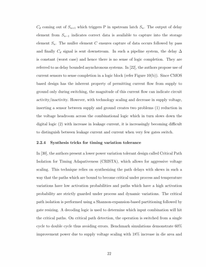
referred to as delay bounded asynchronous systems. In [22], the authors propose use of
current sensors to sense completion in a logic block (refer Figure 10(b)). Since CMOS
based design has the inherent property of permitting current flow from supply to
ground only during switching, the magnitude of this current flow can indicate circuit
activity/inactivity. However, with technology scaling and decrease in supply voltage,
inserting a sensor between supply and ground creates two problems (1) reduction in
the voltage headroom across the combinational logic which in turn slows down the
digital logic (2) with increase in leakage current, it is increasingly becoming difficult
to distinguish between leakage current and current when very few gates switch.
2.2.4 Synthesis tricks for timing variation tolerance
In [30], the authors present a lower power variation tolerant design called Critical Path
Isolation for Timing Adapativeness (CRISTA), which allows for aggressive voltage
scaling. This technique relies on synthesizing the path delays with skews in such a
way that the paths which are bound to become critical under process and temperature
variations have low activation probabilities and paths which have a high activation
probability are strictly guarded under process and dynamic variations. The critical
path isolation is performed using a Shannon-expansion-based partitioning followed by
gate resizing. A decoding logic is used to determine which input combination will hit
the critical paths. On critical path detection, the operation is switched from a single
cycle to double cycle thus avoiding errors. Benchmark simulations demonstrate 60%
improvement power due to supply voltage scaling with 18% increase in die area and
22

small overhead in performance.
2.2.5 Robust designs for error prevention
The techniques presented so far either dynamically change V DD or FCLK as a cor-
rection mechanism to replay the instruction which resulted in a timing error. With
a small performance penalty, the overall energy in the system is reduced consider-
ing the overhead of error detection and correction and power required to replay the
instruction. Aggressive voltage downscaling / frequency up-scaling is possible be-
cause path activation probabilities are appropriately distributed. In [18], the authors
present a clock stretching based technique using a time-borrowing flip-flopin few se-
lected critical paths. One of the big advantage of using TBFF is that the system
does not let error to occur (as time is borrowed from the next stage) but a flag is
raised on borrowing time and compensated immediately in the next clock cycle by
stretching the clock as shown in Figure 11. The paper assumes four phases of FCLK
with 0,90,180 and 270 phase-shift is generated using an embedded PLL. When time
borrowing occurs, it is detected using a shadow latch and a clock shifter is used to
shift the clock phase to allow all the stages in the pipeline a time borrowing window
of T BW = 0.25T min in the next clock cycle.
Figure 11: Clock stretching using time-borrowing FF and clock shifters proposed in[18]
In [13], the authors propose an adaptive clock distribution combined with clock
gating methodology to compensate for supply voltage variations. The motivation is
to avoid the use of complex error detection and correction mechanisms in [15] and
23

identify the occurrence of voltage droops before it actually impacts the timing in the
datapath. The idea is to use clock-data delay compensation during a V DD droop to
give enough response time for adaptation (using clock gating). A dynamic voltage
monitor is used at the clock source as an early detection monitor to detect the supply
fluctuation using TRC[16] and a adaptive clock gating control is used to suppress the
clock. A tunable length delay is used to extend the clock-data delay compensation
for sufficient number of clock cycles for the adaptive control to take into effect which
reduces the chances of error occurrence.
24

CHAPTER III
MULTI-PROCESSOR SPEED TUNING
3.1 Introduction
CMPs with large numbers of cores (≈ 1000) are projected in the near future. However,
technology scaling for device and interconnect pose two major challenges: (1) Small
delay-defects called electrical bugs which are difficult to detect, affect reliable system
operation and are of serious concern due to reduced noise margins from supply voltage
scaling[39], (2) WTD and DTD process variations require the use of worst-case design
margins limiting the linear increase in clock frequency with device scaling. In CMPs
containing large numbers of cores, the impact of intra-die and inter-die is expected
to be significant. While catastrophic defects in the cores and interconnect can be
detected relatively easily using current test algorithms, detection and diagnosis of
speed-related failures is a major problem particularly because all the cores in a large
die are not expected to have uniform delay/speed characteristics. To extract the
maximum performance from such an array of cores (considering homogeneous cores
in this thesis), it is imperative that we determine the maximum speed at which
each core can be operated reliably and rely on the core interconnection network
to support an asynchronous or quasi-synchronous data communication protocol for
data transport between the cores. However, finding the fastest reliable clock rate at
which each core can operate reliably is a difficult problem particularly in the presence
of difficult-to-test or difficult-to-verify electrical bugs. Such bugs can escape tests
generated by combinatorial test generation algorithms that model electrical effects
such as crosstalk, substrate noise and power/ground bounce only at a coarse level
of granularity. The fear is that such test escapes can cause blue screens for specific
25

applications that excite difficult-to-detect electrical bugs.
To avoid such blue screens,the following approach is proposed:
(a) Baseline speeds for each core are first determined using specialized tests that
target small delay defects. This baseline speed for each core is determined by running
such tests repetitively across pairs of cores running at different speeds and algorith-
mically (described later) determining the fastest speed at which each core can run
without failing the applied tests. In prior research, random instruction tests[54], ar-
chitecture specific tests, structure specific tests as well as real-time tests[35][56][38]
have been used to detect hard and soft delay defects. Such tests are typically per-
formed under different frequency, supply voltage and temperature conditions[39][4] .
Also fault models such as stuck-at, stuck-open, path delay, bridging and transition
delays are considered while generating structural test vectors for scan based test-
ing and functional test vectors[54]. Cores with catastrophic failures are isolated and
reconfigured using fault-handling circuitry.
(b) It is assumed that some hard-to-detect electrical design bugs and defects will
escape the above testing and tuning procedure. To top-up failure and electrical design
bug coverage provided by the above tests and to ensure that a blue screen is not seen
after CMP deployment in a product due to test/tuning escapes, we propose to run
applications on the CMP in redundant fail-safe mode for a certain length of time to
achieve further confidence in the reliability of the cores concerned. Due to the use
of redundancy, the maximum achievable throughput of the overall CMP is reduced
initially. However, during fail-safe operation, further speed tuning is performed until
the speeds of all the cores at which they can operate reliably with high confidence
are determined. Upon achieving this, fail-safe operation is terminated and each core
is run individually at its maximum reliable clock speed FMAX, allowing the overall
CMP to deliver maximum chip performance. We ensure that in the field, the FMAX
numbers for each core do not go beyond what was set using conventional specialized
26

tests mentioned in (a). The system level block diagram of the proposed approach is
shown in Figure 12
Figure 12: Block Diagram showing system level overview of proposed approach
3.2 Key features and contributions
Following are the key features of the proposed distributed speed-tuning methodology
1) Initially, pairs of processors are formed. Speed testing and tuning is performed
using an iterative test-tune-test methodology which involves running identical test
instructions or identical program threads of a real-time application on the pair of
cores and comparing signatures generated at inserted program checkpoints.
2) Signatures at checkpoints of test application instructions or checkpointed ap-
plication programs are compared and marked trusted/not trusted at the frequency of
operation at which testing is performed.
3) At any point during instruction execution, the execution results of one of the
processors in the pair can be trusted. Hence we do not need to compare execution re-
sults with a stored golden reference making it completely a self-tune based methodol-
ogy. Upon error detection, the test program/application execution can make forward
progress( no checkpointing and rollback required).
27

4) The distributed iterative algorithm converges in O(log Fp) steps, where Fp is
the number of discrete clock speeds possible. It is independent of the number of cores
in the system. Prior work has shown the error checking technique using signature
compression to have high fault coverage[59].
5) Aggressively scaled technologies undergo gradual device wear-out due to gate-
oxide breakdown, hot-carrier injection, Negative Bias Temperature Instability NBTI
etc[10] which appear as timing failures at the onset of degradation. The proposed
technique can be applied online/in the field periodically to prolong system lifetime at
the cost of core clock speed/performance.
6) The proposed technique requires minimum hardware overhead and uses some of
the inbuilt features (e.g multiple supply/frequency operation) of current processors.
The technique relies on the operating system to duplicate the program/processes such
that exactly same sequence of instructions are executed on the paired processors.
Following are the key contributions of this research work
1. Given an array of processors, we propose a novel collaborative binary search
algorithm to perform speed tuning.
2. The algorithm is optimized to reduce post manufacturing test-tune time and
to reduce the impact of test-tune procedure on throughput and performance of ap-
plications when applied on the field.
3. We discuss the architectural considerations and hardware overhead required
to support signature generation and checking. Transient faults are inserted spatially
and temporally in an out-of-order superscalar processor during SPEC 2000 benchmark
application execution and an estimate is obtained of the latency of propagation from
the time a transient fault has occurred to the time it can be detected.
28

3.3 Tuning approach
In a certain CMP system affected by extreme process variations, the maximum clock
speed (FMAX) at which each core can operate in a trusted manner can range from
Fmin to Fmax
Fmin ≤ FMAX ≤ Fmax (4)
Figure 13: FMAX of each core considered as a point in N dimensional space withorigin at Fmin
where (FMAX1, FMAX2, ..., FMAXN) are the trusted maximum clock speeds
of N cores in the system. Consider a point in a N dimensional space with co-ordinates
(FMAX1, FMAX2, ..., FMAXN) as shown in Figure 13. Note that Fmin = FMIN .
Tuning algorithm selection is done considering the following (1) the iterative test-
tune procedure should converge as fast as possible. If algorithm converges faster, it
decreases test-tune time during post-silicon validation. On the field its impact on
application throughput and performance is reduced (2) During tuning, select M such
29

that throughput impact is minimum on application while ensuring checking procedure
does not fail (3) While tuning the clock frequency of M processors in each pair, the
total time to execute I instructions is limited by the processor operating at the lowest
clock frequency among the M processors. This minimum clock frequency should be
as high as possible (4) Fail-safe operation of the application and OS on field while
tuning. The following sub-sections explain how algorithm selection and its application
to the problem of multi-core test-tune addresses the above four points.
3.3.1 Algorithm selection for fastest convergence
Referring to Figure 14, starting at Fmin for all the N cores, all the cores in the system
have to converge to the point (FMAX1, FMAX2, ..., FMAXN) with minimal num-
ber of algorithm iterations. Given that due to inter and intra die process variations,
the FMAX of each core can be anywhere in the range given by Equation 4, the
algorithm which converges fastest to the point shown in Figure 14 is a binary search
algorithm.The worst case computation complexity of a 1-dimensional binary search
algorithm is log2Fp, which would be the case if all cores in M are tuned in parallel,
where Fp is the number of discrete frequency points within the range of Fmin and
Fmax.The number of discrete frequency points in actual hardware will depend on the
number of Phase Locked Loop (PLL) locking frequency points within the PLL tuning
range which falls between Fmin and Fmax. If only one processor in pair is tuned at a
time keeping others constant, the worst case algorithm complexity for tuning all the
cores is M ∗ log2Fp .
3.3.2 Selection of optimum value of redundant core pairs
In this section, we discuss the impact of M on application throughput, reliability of
checking process and convergence of a multi- dimensional binary search algorithm.
During the tuning process, the application throughput is impacted by factor M .
However the signature comparison (error checking) is more reliable (for higher values
30

Figure 14: Block diagram of tuning approach to converge to FMAX1 and FMAX2
in a core pair
of N (in this case M) in a NMR system where each module in N is equally likely to
fail.Starting at FMIN for all M cores in the pair, during each step of the algorithm,
clock speed of one core is kept constant and remaining (M − 1) cores is tuned in
parallel. This ensures that one of the processor in the pair can be trusted making
the checking procedure equally reliable for M ≥ 2.The complexity of M-dim binary
search algorithm is M ∗log2Fp. For maximum throughput, it is better to have smallest
value of M (minimum 2) but not at the expense of increase in algorithm complexity.
We observe that in a M-dim binary search algorithm, since (M − 1) cores can be
tuned in parallel the worst case algorithm complexity is shown in Equation 5. Since
we tune all the pairs P in parallel, the algorithm complexity is independent of N .We
conclude that M=2 is the optimum value.
Complexity = 2× log2Fp for M ≥ 2 (5)
31

The block diagram of tuning approach for a pair of cores is shown in Figure
14. Initially the clock of all processors in the system is set to a minimum operating
frequency (FMIN) which is very low (e.g one half) as compared to their designed
frequency. Under the assumption that cores with permanent/irreparable faults are
excluded from the system or reconfigured, at frequency FMIN all processors should
operate functionally correct/trusted. Execution signatures are generated using data
results computed by the pipeline in every core. At checkpoints during application
execution, the signatures the core pairs are compared and the frequency of operation
of one of the two cores is increased/decreased. Only one core’s frequency of operation
changes at a time/one algorithmic step, which ensures that the result of one core is
always correct and can be used as a golden reference for comparison.
3.4 Collaborative 2-D binary search test-tune-test
Given that we have picked M = 2 as the optimum number of cores to be paired
and the complexity of the binary search algorithm as given in Equation 5, in this
section we describe a collaborative tuning approach which optimizes the movement
of operating frequency points in the 2D binary space to reduce the overall tuning
time. During an algorithm iteration, let Fop1 and Fop2 be frequency of operation of
the two cores in a pair. Although both the cores need not run in a lock-stepped
manner, both cannot completely run out of synchronization. The processor running
at a higher clock speed waits for the slower one by executing idle cycles. As a result,
the execution time for each iteration is limited by min (Fop1, Fop2), where Fop1 and
Fop2 is the clock speed of core1 and core2 during an algorithmic step. Tuning can be
done in two different ways,
Case 1: Tune one processor to find FMAX by changing clock speed along the
1-D binary search space while keeping the other constant (trusted) at baseline clock
frequency (Fmin). Then by keeping the processor tuned in the first step at its FMAX
32
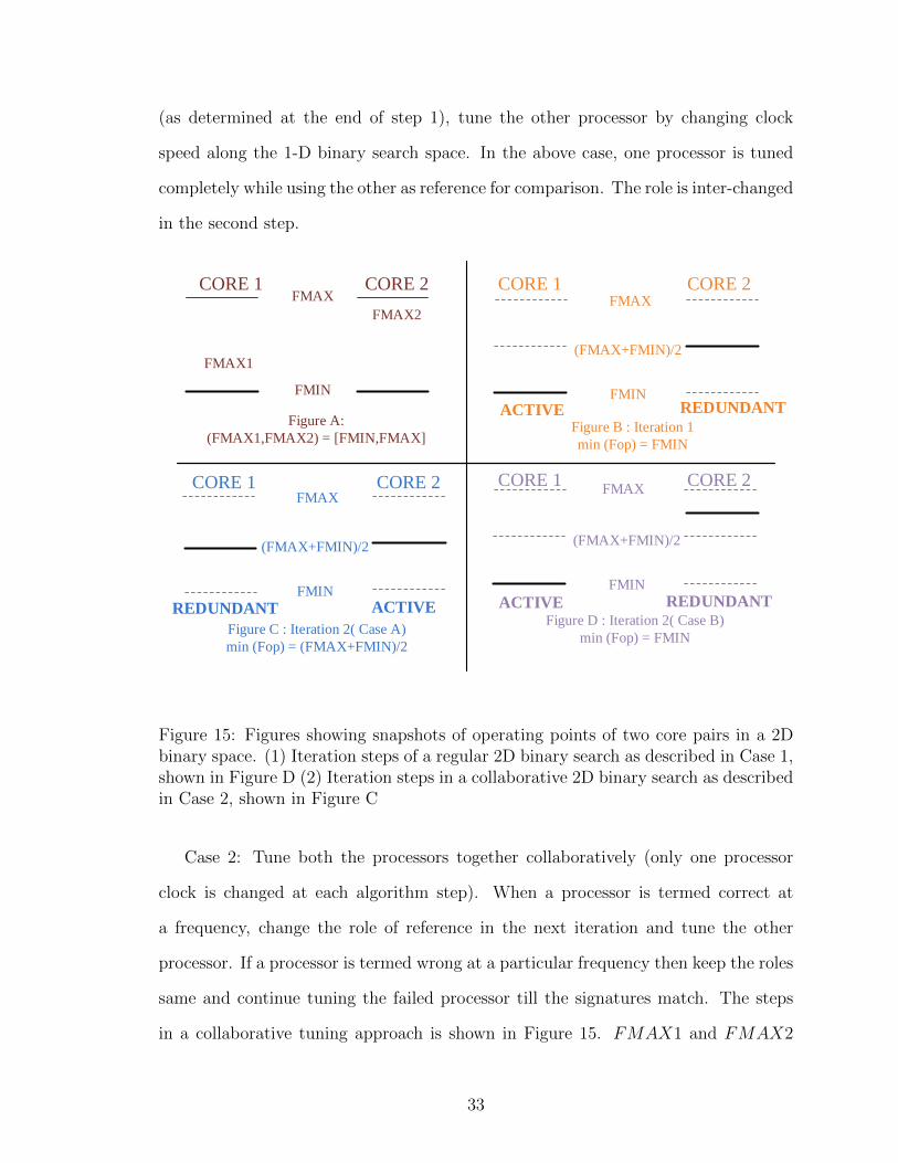
(as determined at the end of step 1), tune the other processor by changing clock
speed along the 1-D binary search space. In the above case, one processor is tuned
completely while using the other as reference for comparison. The role is inter-changed
in the second step.
FMAX
FMIN
(FMAX+FMIN)/2
ACTIVE REDUNDANT
FMAX
FMIN
(FMAX+FMIN)/2
REDUNDANT
FMAX
FMIN
(FMAX+FMIN)/2
ACTIVE REDUNDANT
Figure B : Iteration 1
min (Fop) = FMIN
Figure C : Iteration 2( Case A)
min (Fop) = (FMAX+FMIN)/2
Figure D : Iteration 2( Case B)
min (Fop) = FMIN
FMAX
FMIN
FMAX1
FMAX2
Figure A:
(FMAX1,FMAX2) = [FMIN,FMAX]
CORE 1 CORE 2 CORE 1 CORE 2
ACTIVE
CORE 1 CORE 1 CORE 2CORE 2
Figure 15: Figures showing snapshots of operating points of two core pairs in a 2Dbinary space. (1) Iteration steps of a regular 2D binary search as described in Case 1,shown in Figure D (2) Iteration steps in a collaborative 2D binary search as describedin Case 2, shown in Figure C
Case 2: Tune both the processors together collaboratively (only one processor
clock is changed at each algorithm step). When a processor is termed correct at
a frequency, change the role of reference in the next iteration and tune the other
processor. If a processor is termed wrong at a particular frequency then keep the roles
same and continue tuning the failed processor till the signatures match. The steps
in a collaborative tuning approach is shown in Figure 15. FMAX1 and FMAX2
33

represent the maximum operating frequencies of the two cores, which are the final
values at the end of 2D collaborative binary search. The operating points Fop1 and
Fop2 at each step of the collaborative tuning search is shown in bold. At each algorithm
step, the core being tested is termed as redundant while the core whose operational
results are considered correct (with a very high probability) is termed as active.
Figure C and Figure D represent operating points of cores when tuning is performed
as mentioned in Case 2 and Case 1 repectively. We observe that min (Fop1, Fop2)
for collaborative tuning(case 2) in Iteration 2(Figure C) is more than that for Case
1(Figure D)).
Figure 16: (a) Normalized Minimum Clock Frequency of operation in each iterationof each core pair in a (4X3) multi-core array. The connected red and blue linesrepresent the average value of all core pairs for each iteration (b) Normalized FMAXdistribution in (4X3) array considering WID process variations as modeled in [33]
We consider a 4X3 array of cores and use the FMAX distribution modeled in[33]
for WID process variations as shown in Figure 16(b) normalized with 3 GHz. The
tuning range is 2.1945-3.059 GHz and Fp = 15. Tuning results for Case 1 and Case 2
is shown in Figure 16(a). The points in red(star) and blue(circle) indicate min (Fop1,
Fop2) for every algorithm step for each pair (coupled column-wise) in the 4X3 array. It
34

is observed that the average min (Fop1, Fop2) for each iteration is higher for Case 2 as
compared to Case 1. The number of algorithm iterations is same for Case 1 and Case
2, however collaborative 2-D binary search reduces tuning time significantly(average
10.34%) during post manufacturing test-tune and also reduces impact on application
performance(on the field). Figure 17 shows two examples of collaborative tuning in
core pairs. Each graph plots Fop1 and Fop2 in each iteration step for a pair of cores
picked from a FMAX distribution in Figure 16(b). Upon convergence of a core pair,
each core can operate independently thus providing full throughput capability to the
multi-processor system at (FMAX1, FMAX2, ...., FMAXM).
Figure 17: fop1 and fop2 (both normalized) at each step of collaborative 2D binarysearch for two core pairs in a 4x3 array of cores(a) Normalized FMAX2= 0.990 andFMAX1=0.948, (b) Normalized FMAX2= 0.824 and FMAX1=0.752
3.5 Architectural considerations: test-tune support
In this section, we discuss the hardware overhead and architecture considerations
required to support comparison based testing between adjacent cores.
35

3.5.1 Signature generation and error checking
To determine the integrity of the redundant core in the core-pair at a particular
clock speed (Fop), execution signatures of both the active and redundant cores are
generated and compared at regular intervals during program execution. Signatures are
generated using signal compression technique by hashing the temporal internal states
of the processor into a n-bit value. The theory,application and aliasing probability
of different kinds of signature compression methods has been studied extensively
by the digital test community[59][58]. For our study, we implement Multiple Input
Signature Register based temporal compactor for signature generation which has an
aliasing probability of 2−(n−1), where n is the number of bits in the signature. A
block level implementation of MISR is shown in Figure 18. At any point in time, the
MISR outputs 32 bit values in O(0:31), P(0:31) represent the previous output states
of latches and I(0:31) represent the current input to be compressed.In our approach,
the design under test is the micro-processor pipeline.[51]
XOR XOR XOR XOR
I31 P30 I30 P29 I1 P0 I1
O31 O30 O1 O0
MISR Polynomial = x32 + x31 + x14 + x7 + x + 1
Figure 18: Block diagram of a temporal compactor using MISR. Pi represent theoutputs of shift register latches(not shown in the figure)
The signature is generated using consecutive data and address information of the
store instruction generated by the pipeline. FIFOs are used to store the signatures
36

generated from continuous store address and data at regular intervals of time (as
the two cores are running at different frequencies). Note, for correct comparison
based testing, the signatures of two cores need to be compared exactly after program
execution has completed upto a certain point in the application, hence an additional
instruction needs to be designed and inserted into the binary code to latch the MISR
output into the FIFO register at a fixed interval/point of the program code. The
comparison is done using a simple digital comparator. The 2D binary search algorithm
can be implemented using a state machine, with number of states equal to number
of possible unique combinations of Fop1 and Fop2. The block diagram of additional
hardware overhead required for signature generation and checking is shown in Figure
19. During test-tune operation, the multi-core system is operated in redundant multi-
threading mode and the hardware support required to ensure strict input replication
in both the cores is detailed in [31][51]. To operate the system in test-tune mode
and enable comparison based testing during real application execution, the multi-
processor system requires the support additional hardware and micro-architectural
support as detailed in [31][51]
3.5.2 Simulation setup and error latency estimates
To verify the error checking mechanism used in comparison based testing and get an
estimate of the latency of error detection, a RTL prototype model of a superscalar
out-of-order single core pipeline is used. The RTL model of a superscalar pipeline
is generated using the FabScalar toolset[19]. Fabscalar is a parameterizable, synthe-
sizable processor specification that allows for the generation and simulation of RTL
descriptions for various configurations of a simple and super-scalar processor archi-
tectures. Fabscalar allows the configuration of many microarchitectural parameters
which include superscalar width, fetch width and depth, issue width and depth, num-
ber and types of functional units in the execute stage , register file depth, reorder
37

CORE 1 PIPELINE
CORE 2 PIPELINE
L1 CACHE L1 CACHE
MISR MISR
FIFOFIFODATA_IN_EN DATA_IN_EN
=
STATE MACHINE
PLLFop1
Fop2
CA
CH
E W
RIT
ESC
AC
HE W
RITES
Implements 2D Binary Search
Figure 19: Hardware overhead to support comparison based testing and tuning
buffer, load and store queue size etc. Figure 20 shows various stages in a FabScalar
synthesized super-scalar pipeline. The execute stage of the pipeline consists of 4
functional units. FU0- Simple ALU : Executes simple arithmetic operations like add,
subtract , FU1-Complex ALU : Executes complex arithmetic instructions like mul-
tiply, divide, FU2- Executes address results for loads and stores , FU3 - Executes
branch address calculations. We consider Simple ALU as a candidate to inject faults.
A delay fault model kind of modeling is used to inject faults into the pipeline stage.
FETC
H
DEC
OD
E
REN
AM
E
DIS
PA
TCH
ISSU
E
Reg
Rea
d
EXEC
UTE
Load
Sto
re
Wri
teB
ack
RET
IRE
TIMING ERRORS INJECTED
Figure 20: Stages in a synthesized FabScalar pipeline
38

3.5.2.1 Fault modeling and simulation
The presence of electrical bugs/timing related failures manifest itself as incorrectly
computed output at the pipeline stage flip-flops when switching in the primary in-
puts activate/excite the critical paths of the combinational logic blocks. Errors are
simulated as incorrect final values at all the pipeline registers which fall within 10%
of critical paths in the combinational logic block assuming that pipeline designs are
generally frequency guard-banded by 10% of the designed clock frequency to account
for worst-case delay scenarios encountered during pipeline operation. To emulate a
timing error of this form at a particular clock cycle when critical paths are activated,
the corresponding primary outputs are considered stuck-at previous value. The block
diagram in Figure 21 shows the tool flow used to inject timing errors into super-
scalar pipeline model. The block diagram is divided into two parts : In the first part,
benchmark applications are executed while running RTL simulations of the super-
scalar pipeline and input vector transitions(of execute ALU stage) for consecutive
clock cycles are logged into a file for different benchmark applications.
RTL Design of super-scalar
pipeline
Synthesis
Execute Stage
Input Vector Transition Set
Guard Band (10%)
Fault Injector
RTL Simulator
GATE TIMING SIMULATOR
BENCHMARKS (BZIP,MCF,
VORTEX,PARSER)
RTL Simulator
RTL Design of super-scalar
pipeline
RTL Simulator
Input Vector Transitions
MISR
Golden
Simulator Stats.
Error Detect
Error Detect Latency
Figure 21: Tool flow used to inject timing faults in 10% of fastest paths in executestage of a super-scalar pipeline model
39

We consider four SPEC2000 2000 benchmark applications bzip,mcf,vortex and
parser. The execute stage is synthesized using Synopsys DC and NCSU PDK 45nm
cell library[52] with a timing constraint of 1ns time period. A gate level timing
simulator is designed which simulates a gate netlist of the ALU and identifies all
the set of consecutive input transition pairs (I1, I2) for which the paths considered
critical (T to T −(0.1∗T )) (freq. guard band) are activated. The corresponding clock
cycle tick is also noted. A list consisting of input vector transition set is generated for
each benchmark and provided to the fault injector. The fault injector interfaces with
the simulator(executing the benchmark)and forces the output of the execute stage
(which fall in the critical path) to be stuck to the same value in the previous clock
cycle. This process is repeated for about 100 input vector transition sets in the log
file in 100 different instance of simulation of the benchmark. For each simulation,
the total clock cycles needed for the transient fault to propagate to the MISR (at the
interface of pipeline and cache) is calculated. This process is repeated for about 100
fault injections for each application benchmark and the error detection latencies are
noted. Figure 22 plots the average error detection latencies for different benchmarks.
For each benchmark , 100 timing faults are simulated using the tool flow in Figure
21 and the detection latency for each fault is noted. The error detection latency (in
cycles) is the time it takes for a transient fault once it has occurred in the pipeline
to propagate into the store instruction result and be detected in the MISR signature.
Using a 32-bit MISR implementation, we observe that all the 400 timing faults are
detected.
3.6 Conclusions
The collaborative tuning methodology along with support for signature generation
and comparison can be used as a top-up speed coverage mechanism to determine the
FMAX of all cores in an array during the post-manufacturing verification phase.
40

0 100 200 300 400 500 600
Bzip
Mcf
Vortex
Parser
AVG.ERROR DETECTION LATENCY(cycles)
Figure 22: Average Error Detection Latency in different benchmark runs for 100timing faults inserted into ALU stage of pipeline
The methodology can also be used effectively on the field at periodic intervals, in
the background, while running real applications at the foreground without any sys-
tem downtime. Once the test-tune-test process is complete, all cores can operate
independently at their maximum reliable operating frequencies as determined by the
test-tune algorithm. The collaborative tuning methodology accelerates the tuning
process which reduces total post-manufacturing test time and impact on application
performance while running on the field(due to spatial redundancy). At any point
during tuning, the computation result of one of the processors in the core-pair can
be trusted and committed to memory. This ensures application execution can move
forward without having to checkpoint and rollback. It is important to note that our
methodology is proposed specifically to top-up speed coverage over existing frequency
binning methods in the presence of difficult-to-detect and difficult-to-model electrical
bugs.
In order for comparison based test to work correctly, both the core pairs must see
the same instruction sequence and input data. Since the core-pairs are not running
41

in a lock-stepped manner, in a multi-threaded application, their memory accesses
could result in input incoherence. In literature, micro-architecture changes have been
proposed to ensure input coherence in the core-pairs[31][51]. These changes need to
be incorporated into the multi-processor system to enable correct comparison based
testing. The features will incur additional area, but could be power gated when
testing-tuning is not being done. When the redundant core in the core-pair fails
at a particular clock frequency, the local memory and register contents needs to be
moved from the active core to the redundant core, before beginning the next iteration,
which will consume some memory bandwidth. The proposed methodology improves
reliability by topping-up speed coverage in every micro-processor pipeline. In the next
part of this thesis, we describe a novel pipeline design which has the ability to detect
and recover from timing errors during pipeline operation. Employing such pipelines
in every processor of a multi-processor system can significantly reduce the test and
tune time required during post-manufacturing verification phase and any additional
hardware and test-tune time required for on-field speed testing.
42

CHAPTER IV
PATH DELAY MONITOR
4.1 Motivation
Current microprocessor pipeline designs are guard-banded to operate reliably under
timing variations. The guard-banding is often done by operating the pipeline at a
higher supply voltage(V dd) or lower clock frequency(f) than its designed specifica-
tions. Figure 23 shows the trends in frequency(f) and supply voltage (V dd) with
technology scaling going from 45nm to 8nm[27]. The solid lines indicate the expected
analytical scaling trends as defined by the ITRS[36], while the dotted lines indicate
a conservative prediction of how the trends will look going into the future[11].
Tech Node
Vdd
Tech Node
f
Figure 23: Predicted(dotted) and Analytical(solid) V dd and f trends with technologyscaling from 45nm to 8nm
Figure 24 shows various factors contributing to safety margining, resulting in
timing guard bands in the processor operational clock period (TCLK). We observe
that although the pipeline design can operate at DESIGN TCLK ,the pipeline is
forced to operate at almost twice the period (ACTUAL TCLK). Further technology
scaling and even higher clock frequency designs will see higher percentage increase
in delay variability. We expect that the amount of safety margins as a percentage
of ACTUAL TCLK needed for highly reliable operation will show a linear increase
(trend shown in Figure 24), which will significantly contribute to the diminishing V dd
43

and f trends in Figure 23.
DESIGN TCLK
workload
temp
process
aging
SAFETY MARGIN
CLK
ACTUAL TCLK
Tech Node
f an
d V
dd
safe
ty
mar
gin
s(%
des
ign
)
Intrinsic path delays
Figure 24: Factors contributing to safety margining in processor clock period and itstrend with scaling
A system does not experience the worst-case effects of static and dynamic varia-
tions all the time, hence the pipeline does not have to always operate at ACTUAL
TCLK = WORST CASE TCLK . In addition, the pipeline does not always experience
worst-case intrinsic path delays as well. Considering an ideal pipeline (without any
static and dynamic variations), at certain operating states the pipeline can produce
a reliable result at period < DESIGN TCLK . Given that pipelines exhibit such
varying timing behaviors which directly impact the f and V dd (and hence power
and performance) required for its reliable operation,designing a pipeline which can
dynamically self-adjust to the timing variations on the fly can significantly improve
the power and performance efficiency. The proposed self-adjusting pipeline adapts
to timing variations during real-time operation and produce correct computational
result, thus providing an opportunity to eliminate/reduce the fixed safety margins.
The second part of this thesis discusses the following (1) Design and operation
of a self-adjusting pipeline referred as Delay Balanced Pipeline (2) How and why
power/performance can be scaled better in the design, while achieving high reliability
(3) Quantify the energy and throughput benefits over a pipeline design operating at
margined clock period (4) Discuss the practical design and implementation challenges
and qualitative benefits.
44

4.2 Introduction
Path delay is the total time taken for a transition at the primary input of a combina-
tional logic to propagate to the primary output through a sequence of gate transitions.
The block diagram of a single stage pipeline is shown in Figure 25(a). The pipeline
stage has multiple inputs and multiple outputs. The rate of data flow into the pipeline
and out of the pipeline is constant and fixed by TCLK . The combinational logic con-
sists of multiple paths from the input to the output with different path delays as
represented in Figure 25(b). The path with the maximum delay from the input to
the output is called the critical path and the corresponding delay is represented as
Tcritical.The condition for reliable operation of the pipeline is stated in Equation 6,
where Tclk−Q is the CLK-Q delay of the flip-flop at the primary input, Tsetup is the
setup time of the flip-flop at the primary output and Tcritical is the critical path delay.
Q
QSET
CLR
D
Q
QSET
CLR
DPath 1
Path 2
Q
QSET
CLR
D
Q
QSET
CLR
DLogic
CLK
Delay(Path 1) Delay (Path 2)
(a)
(b)
Figure 25: (a)Block diagram of single stage pipeline driven by a fixed time periodCLK (b) Combinational logic design with multiple unequal delay paths from inputto output
TCLK ≥ Tclk−Q + Tsetup + Tcritical (6)
4.3 Real-time path delay monitoring
Path delays in a combinational logic of a pipeline stage range anywhere between
0 < tpath ≤ TCLK . Figure 26 plots the path delay distribution for ten thousand input
45

vector combinations in a 16-bit RCA synthesized to operate at 1 GHz clock. We ob-
serve that for a very small percentage of input vector combinations(6%), the output
takes more than TCLK/2. The average path delay of such a design is 0.37 TCLK . Op-
erating the RCA as a pipeline stage with fixed period clock of Tclk to ensure reliability
under worst-case path delay is highly performance/power in-efficient. The added ef-
fect of timing variations due to uncertainty factors mentioned in Figure 24 makes
pipeline operation even more power/performance in-efficient in order to guarantee
high reliability. To address this inefficiency, we investigate how the fixed periodicity
of clock can be eliminated during pipeline operation.
Path Delays (ns)0 0.1 0.2 0.3 0.4 0.5 0.6 0.7 0.8 0.9 1
Pro
bab
ility
0
0.05
0.1
0.15
0.2
0.25
0.3
6%
Tavg
= 0.37ns
Figure 26: Probability Distribution of Path Delays for ten thousand randomly gen-erated input vectors in a 16-bit RCA
The function of a clock in a pipeline is to control the data hand-off into the
46

pipeline stage and out of the pipeline stage and this is done at a conservation rate
with a clock period governed by Equation 6. The first step towards making pipeline
operation timing variation tolerant is to eliminate the fixed period clock and introduce
an intelligent block which can monitor the path completion times dynamically on-
the-fly. We refer to this intelligent block as the Path Delay Monitor(PDM). The block
diagram of a PDM attached to a single stage pipeline is shown in Figure 27(a). The
data flow in the pipeline is controlled by the signal generated by the PDM, known as
path completion signal. The path completion signal is generated when computation
in a pipeline stage is complete and correct data can be handed out of the pipeline.
To understand the design and operation of the PDM, we first describe how a logic
transition at the primary input of a combinational logic propagates to the primary
output. When primary inputs in a combinational logic block switch, transitions ripple
through successive switching gates and propagate towards the primary output/s. Such
transition waves starting from the primary input may reach all the way to the primary
output or die along their way. Let the critical path time delay in a cominational logic
block be divided into multiple small time intervals(∆) as represented in Figure 27(b).
The gates falling within a particular ∆ interval is representative of their switching
times after the inputs have changed from 11000-01101 (exception is G4 as marked in
grey since it switches during multiple time intervals). For a particular input vector
transition, we observe the following : (i) One or more transition waves originate at
the primary input and propagate towards the output, e.g G0-G1-G3-G4 and G0-G1-
G3-G5-G7-G8 (ii) Following an input vector transition, while each transition wave
propagates, one or more gates switch at every interval which is multiple of ∆ until
switching completely ceases. For e.g in Figure 27(b), G0,G1,G2 switch during time
interval ’∆’ while G3 switches during time interval ’2∆’ (iii) For two different input
transitions, the time ( in integer multiples of ’∆’ ) at which all transition waves cease
may be different. For input transition 11000-01101, the wave propagation ceases after
47

’4∆’ while for input transition 01000-01001, the wave propagation ceases after ’3∆’
(this is due to path activation probabilities). Note that in general, the actual delays of
every gate will depend on inter and intra-die manufacturing process variations, delay
variations due dynamic variations, which may shift their switching intervals. However,
switching activity completion sensing is facilitated by the following observation: If
there is no switching activity over a period of time greater than ’∆’ after the previous
switching, where ’∆’ is the delay of the slowest logic gate in the circuit, then we can
guarantee that all logic activity in the circuit has been completed.
Q
QSET
CLR
D
Q
QSET
CLR
D
LOGIC
Q
QSET
CLR
D
PATH DELAY MONITOR
(a) (b)Path
Com
ple
tio
n Si
gnal
Figure 27: (a) Block diagram of single pipeline stage operation with a path delaymonitor (b) Gates divided using dotted lines as per switching time interval (in multi-ples of ∆ ),for input transition T1 = 11000-01101. Note G4 switches during multipleintervals
A reliable approach to determine switching activity completion is to sample every
logic gate output node into an transition detection sensor. Each transition detection
sensor is equipped with a double transition(high to low and low to high) detector
designed with two back to back inverters and an XOR gate(e.g shown in Figure 30).
A completion signal is triggered when none of the detectors indicate a transition for
a time interval greater than ’∆’. However, sampling output node of every gate in the
logic block will require as many transition detectors as the number of gates in the
logic block, which is impractical. From switching analysis of gates in the logic block
defined in 27(b),we observe that multiple gates switch at a particular ∆ interval. In
48

order to do path completion detection successfully by monitoring switching activity
of gates, we need not monitor output nodes of all gates in the logic block. In order
to systematically eliminate redundant gates switching at various intervals of ∆ for a
large number of input vector transitions, we propose a ’Greedy Selection Algorithm’.
We first state the basis for switching activity completion sensing in Criteria 1, then
formulate the problem in Section 4.4.1 and describe how the algorithm minimizes the
hardware and power overhead of the PDM.
Criteria 1: If a set of gates G can be identified such that at-least one gate in
G switches during consecutive time intervals of ’∆’ after an input transition; then
if none of the gates in G switch for an interval greater than ’∆’, we conclude that
all transition waves (logic activity) in the circuit has ceased and the computation is
complete.
4.4 Greedy Selection Algorithm : Minimize path delay mon-itor overhead
Referring to Figure 27(b), as per Criteria 1, for transition T1=11000-01101 it would
suffice to sense the set GS1 = {G4, G3, G7} such that a transition is observed during
every interval of ’∆’ until the switching activity ceases. For the same circuit in
Figure 27(b), with a different input transition T2= 01100-01110 it would suffice to
sense GS2 = {G2, G5, G7} to meet the above mentioned Criteria 1. Criteria 1 can be
satisfied for both T1 and T2 by sensing gates GS1 U GS2 = {G4, G3, G7, G2, G5}.
However, by careful visual observation we notice that GS1 U GS2 does not form the
minimum set to satisfy Criteria 1. The minimum gate set which just satisfies Criteria
1 is {G3, G7, G2, G5} (since G5 and G2 switch for both T1 and T2). To pick the
minimum set of gates for a large set of input vector transitions in T , we propose a
’Greedy Selection Algorithm’. The algorithm is iterative and picks gates on the basis
of their switching frequency at every iteration step. At the end of the algorithm, the
outcome is a minimum gate set Gopt while ensuring that Criteria 1 is satisfied for all
49

vectors in T . The algorithm behaves similar to a greedy search algorithm, making
locally optimal choices to pick gate candidates(at every iteration step) from a given
gate transition set. The input to the algorithm is a gate switching log file which
consists of exact switching times for all switching gates for every randomly picked
input vector transition in T .
4.4.1 GSA description
The problem formulation and solution steps of GSA is given below:
Given: A collection of switching gates at switching time intervals discretized in
multiples of ’∆’ forM randomly generated input vector transition I = {I1, I2, I3, ...IM},
which forms the gate switching log file.
Goal: From the gate switching log file, form a minimum gate set Gopt such that
for every input transition in I , there exists at-least one gate which switches during
consecutive ’∆’ intervals until switching completely ceases.
Solution:
1. Initialize Gopt = φ
2. Let the n gates in a combinational logic be represented as G = {G1, G2, Gn}.
Let T kp represent presence or absence of a transition for a particular gate in G,
where k = 1 to M and p = ∆, 2∆, 3∆... . T kp can be either 1 or 0.
3. Form a matrix APXQ with matrix elements T kp where each column represents
logic gates in G and each row represents an input vector Ik with ’∆’ time interval
as sub-script Ikp . A value of 1 in a matrix element indicates that the logic gate
in the corresponding column switched for input vector Ik at time interval p.
For e.g, 1 along the row I12 and column G1 indicates that gate G1 switches for
input vector I1 in the ’2∆’ interval (refer to Figure 28)
4. Find the number of times each gate switches for all combinations of Ikp by
50

column-wise addition of the matrix elements of A to form a single row vector.
From the row vector, by selecting the element with maximum value, we deter-
mine the gate (in the corresponding column) which switches most number of
times in the logic for all combinations of input vector transitions considered in
the gate switching log file.
5. Add the selected gate Gsel to Gopt.
6. Eliminate the rows of A for which T kp = 1 in the column of Gsel and form
another matrix A′.
7. Assign A=A’ and repeat Step 4 to 6 until all the rows of the matrix are elim-
inated. By eliminating all rows, we guarantee that the goal as stated above is
satisfied for each input transition vector in T . The overhead is minimized while
working towards satisfying Criteria 1 for every input vector in I (greedy select).
A visual representation of the steps in GSA algorithm is shown in Figure 28.
1
1 1 1
1
1
1
1
G0 G1 G2 G3 G4
I11
I22
I13
I21
I32
1
1 1 1
1
1
1
1
1
G0 G1 G2 G3 G4
I11
I12
I13
I21
I22
1
1 1 1
1
1
1
1
1
G0 G1 G2 G3 G4
I11
I12
I13
I21
I22
1
1
1
Gopt = {Φ } Gopt = {G3 } Gopt = {G3,G2 }
Figure 28: Visual representation of steps to select gates in GSA
4.4.2 GSA outcome evaluation
In order to study the effectiveness of GSA to reduce PDM overhead in logic blocks,
benchmark logic blocks are picked and characterized with a large set of input vector
transitions. The combinational logic blocks are representations of pipeline stages in
51

a DSP pipeline (performing FIR filtering) and a super-scalar out-of-order micropro-
cessor pipeline. A RTL model of an 8-bit Wallace Tree multiplier(CL1 mult8bit) and
32-bit RCA adder(CL2 adder16bit) is generated from[1]. RTL behavioral descrip-
tions of pipeline stages from a super-scalar pipeline is generated using the FabScalar
toolset[19]. The RTL behavioral models are synthesized using Synopsys Design Com-
piler(SDC). The block diagram of simulation setup is shown in Figure 29. The gate
cell libraries are used from an open source design kit NCSU45nm PDK[52]. From
the RTL behavioral model, a set of gate cell libraries and a timing constraint file,
SDC generates a Standard Delay Format (SDF) file and a verilog gate level netlist.
The SDF file includes the rise and fall times of every gate output for rise and fall
transition of each gate input.
BEHAVIORAL RTLMODEL
SYNOPSYS DC
SDF FILE
EVENT DRIVEN TIMING SIMULATOR
GATE NETLIST
GATE LIBRARY
CELLS
GATE SWITCHING LOG FILE
CONSTRAINTS FILE
Figure 29: Block diagram of simulation setup to evaluate performance of GSA
An event driven gate level timing simulator is implemented in C programming
language, which extracts the gate delay information from the SDF file and generates
the gate switching log file for a set of ten thousand input vector transitions. This file
is used as an input to GSA. The GSA as described in Section 4.4.1 is implemented
52

in C programming language. A set of ten thousand randomly generated input vector
transitions are used to generate the gate switching log file. A more detailed description
of the tool flow and simulation setup is given in Section 5.6.1. The RTL designs are
synthesized with a timing constraint of 1 ns clock period. Table 1 lists the GSA
outcome as percentage of total gates in the logic block. For simulations of all logic
blocks, critical path (1ns) is divided into intervals of ∆ = 0.1ns. GSA reduces the
PDM overhead to a realizable and practically feasible value. It is important to note
at this point that sensing 10% of the total number of gate output nodes might seem
high overhead especially considering an edge detector attached to each sensed gate
output node (refer to Figure 30),however not all gates used in the logic block are of
the same size/area. An accurate evaluation of total area and power overhead of PDM
in every logic block in Table 1 is performed using HSPICE/layout simulations and
clearly quantified in Section 5.6.2.
Table 1: Greedy Selection Algorithm outcome for logic blocks in DSP and super-scalarprocessor pipelines
Logic BlockNumber of gate output
nodes to be monitored(% oftotal gates in Logic Block)
CL1 mult8bit 9.8CL2 rca32bit 11.5
CL3 fetchstage 5.2CL4 decodestage 4.3
CL5 execalu1 4.2
4.5 Circuit design and operation of PDM
The output node of every gate in Gopt is connected to the PDM, which is a transition
detection sensor. The transition detection sensor detects switching in Gopt and if at
any point after the first switching begins there is no switching for a time interval
greater than ∆, the transition detection sensor enables the path completion signal.
The circuit diagram of a transition detection sensor is shown in Figure 30. The gate
53

output transitions are converted to narrow positive pulses using an edge detector
circuit consisting of two inverters and an XOR gate. The width of the pulse can be
controlled by the delay of back to back inverters. The inverters are sized to fix this
delay to 2∆. Every gate output from Gopt drives an edge detector circuit. Each edge
detector circuit drives the gate of a NMOS device in a PSEUDO-NMOS based circuit.
The function of the PSEUDO-NMOS based circuit is to hold its output(N1) low until
at-least one pulse at its input is still active (equivalent to OR operation).
Q
QSET
CLR
D
OP[0]
G1
G2
SIZE TO Δ DELAY
N0
{Gopt} = {G1,G2,..}
N1
Q
QSET
CLR
DOP[1]
OTHER GATES IN {Gopt}
Figure 30: Circuit Diagram of Path Delay Monitor
A single PMOS pull-up is biased (gate to ground) such that it tends to pull N1
to logic high all the time. In the absence of a transition in Gopt for a time interval
greater than ∆, none of the NMOS inputs will have a positive pulse and node N1 is
pulled to logic high, which indicates path completion in the logic block. A positive
transition of the path completion signal drives the output flip-flops of the pipeline
stage. The inverter delay can be made programmable to handle post-manufacturing
process variations and wear-out effects.
To demonstrate the operation of path delay sensor circuit in simulation, a 16-bit
RCA is used as a benchmark logic block. The RTL behavioral model of a 16-bit RCA
is synthesized using SDC to generate a verilog gate netlist. The verilog netlist is
54

converted into HSPICE netlist using Hercules toolset from Cadence. The procedure
as described in Section 4.4.2 is used to pick gate output nodes to be monitored in
the PDM. The edge detector and pseudo NMOS design in Figure 30 is added to the
HSPICE netlist of 16-bit RCA. The path completion signal drives the clock node
of all edge triggered flip-flops storing a 17-bit addition result. Figure 31 displays
the waveforms consisting of the following signals from top to bottom (1) The path
completion signal generated by the path delay sensor (2) Supply current to indicate
path completion generation after circuit activity is complete(no gates switching) (3)
Input 1 (X) and Input 2(Y) to the RCA and the result (S) to indicate functionally
correct operation. X and Y inputs are applied at constant rate of 0.7ns. In the
waveform, we observe different completion times for different input combinations of
X and Y.
55

Figure 31: HSPICE simulation waveform showing operation of Path Delay Monitorin 16bit Adder block
56

CHAPTER V
DELAY BALANCED PIPELINES
In the previous chapter, we explained the motivation/need to design a PDM for a logic
block in a pipeline. We formulated a criteria to perform path completion detection
by monitoring switching activity of gates in the pipeline. The GSA was presented as
a methodology to minimize the area and power overhead of the PDM. Finally, the
circuit design and operation of PDM for a 16-bit RCA was described in the last sec-
tion. In this chapter, we describe why a pipeline when equipped with PDM can scale
better in power and performance at lower technology nodes. We describe and address
the challenges to enable operational correctness in a pipeline when data hand-off is
triggered by a path completion signal instead of a fixed period clock as in a conven-
tional fully synchronous design. The quantitative energy and throughput benefits of
the proposed design is evaluated in a multi-stage DSP pipeline and a super-scalar
microprocessor pipeline design for SPEC2000 benchmark applications. Finally, qual-
itative evaluation of the proposed design compared to previously proposed intrusive
timing variation tolerant designs are discussed.
5.1 Operation and time lending benefits
Figure 32 shows a block diagram of a two-stage pipeline equipped with PDM in
each stage. The PDM of each stage has a very small area and power compared to
the actual logic block. Data is sampled into the first stage of the pipeline at a fixed
period rate using a global clock (CLK). Similarly, data is sampled out of the pipeline
at the same fixed period TCLK . The data hand-off between the two pipeline stages
is done at a variable rate as determined by the path completion signals generated by
both stages. It is important to AND both the path completion signals to ensure that
57

data result in the second pipeline stage is not corrupted by successive inputs vector
transitions. The output of AND gate is pulled to logic 1 when logic activity ceases
in both the pipeline stages and correct computation result can be handed-off from
the first pipeline stage to the second pipeline stage. The flip-flops at the input and
output interface of the pipeline driven by the global clock are referred as ’interface
flipflops ’ and the internal/intermediate flip-flops in which data hand-off is controlled
by the completion signals are referred as ’time lending flipflops(TLFF)’. The pipeline
is referred as a Delay Balanced Pipeline.
Q
QSET
CLR
D
Q
QSET
CLR
DQ
QSET
CLR
D
LOGIC BLOCK 1
LOGIC BLOCK 2
Q
QSET
CLR
D
Q
QSET
CLR
D
Q
QSET
CLR
D
PDM PDM
500 GHZ PATH COMPLETION SIGNALS
GLOBAL CLK
Q
QSET
CLR
D
Q
QSET
CLR
D
Time Lending FFs
Interface FFsInterface FFs
Figure 32: Block diagram of a two stage delay balanced pipeline
The concept of delay balancing between the two pipeline stages is explained next
with the help of a timing diagram in Figure 33. The timing diagram represents
the instruction movement in the pipeline and path completion times in two pipeline
stages for two consecutive clock periods of the global CLK. Y-axis represents different
pipeline stages and the X-axis represents time. The time gap between a particular
instruction completing its operation in a pipeline stage to the arrival of the global
clock with period T is the slack, represented as δ. In the first clock cycle, I1 completes
computation at time t1 while I0 completes its computation at time t2.
58

I0
I1
I1
I2
Time
Pip
eline Stage
Slack(δ)
Both I0 and I1 complete
t1 t2
Longest Path=T
Short Path
Global Period=T
Global Period=T-Δ1 Δ1
Longest Path=T
Global Period=T-Δ2
Δ2
Longest Path=T
Global Freq. Scale+
P1
P2
P2
Short Path
Short Path
Global Freq. Scale
TIMING MISSED
I0 I1
P2 I0 I1
t3
t2 t3
t2 t3
(a)
(b)
(c)
-δ
Figure 33: Timing Diagrams showing (a) time sharing in delay balanced pipelines(b) time sharing capability enables global frequency scaling (c) timing error(althoughinfrequent) with additional global frequency scaling
59

The PDM for pipeline stage P1 and P2 fires a completion signal at time t1 and t2
respectively. Referring to Figure 32(ANDing operation), data hand-off between the
two stages is triggered at time t2, thus leaving a slack of δ. The presence of slack
gives I1 in the next clock cycle a time delay of δ + T to complete its computation.
The longest path/critical path in the pipeline has path delay T . By detecting com-
pletion earlier than the arrival of clock edge, the global clock frequency can be scaled
to T − ∆1, while allowing computation with a path delay T to complete correctly
(Figure 32(b)). The capability to detect early completion coupled with the ability to
lend extra slack to a succeeding computation enables the pipeline to balance delays
between two successive computations in a pipeline, hence termed as Delay Balanced
Pipeline. Given that logic blocks exhibit path activation probabilities(refer to Figure
26), to obtain additional performance/power benefits from a delay balanced pipeline,
the global frequency is scaled even beyond the available slack(negative slack(−δ), re-
sulting in timing misses. Such a scenario is shown in Figure (32(c)). Timing misses
occur very infrequently for controlled amount of clock period scaling especially in
logic blocks showing path delay distribution as shown in Figure 26). Timing misses
result in small temporary loss in IPC due to instruction replay, however the overall
performance/power benefits obtained will be higher. Simple low overhead error detec-
tion circuits (refer Section 5.3) are designed to detect timing misses (negative slacks).
Upon a timing miss, an incorrect result maybe sampled by the output interface flip-
flop, which will result in error propagation in the downstream pipeline stages. To
avoid error propagation, the pipeline is equipped with error recovery circuits which
restore the pipeline to a non-erroneous state and continue forward progress in the
pipeline. In the next Section, we discuss the circuits for error detection and recovery
in delay balanced pipelines.
The ability of a delay balanced pipeline to detect completion gives the digital system
(in our case the pipeline) the capability to sense any variations in path delay timing
60

(due to factors like process variations, workload, environment variations, aging) and
makes the data hand-off process in pipelines timing variation tolerant. This comple-
tion detection ability coupled with ability of pipeline to detect and recover from any
timing errors makes the system error resilient, and enables us to eliminate/reduce the
one time safety margins resulting in power and performance scalability.
5.2 Short paths and time lending window
Paths between the primary input and primary output in a combinational logic block
which have small delays are referred to as short paths. Figure 34(a) shows a short
path wherein a single gate connects one of the primary input to the primary output.
In a delay balanced pipeline, the output interface flip-flops sample data using a free
running global clock while the time lending flip flops hand-off data dynamically using
the path completion signal. When a path completion signal arrives before the clock
edge, data is handed-off to the second pipeline stage before data has been sampled
into the output interface flip-flops. In order to prevent data corruption at the primary
outputs of the second pipeline stage by the short paths, the delay d of shortest path
in the logic block of the output pipeline stage should be larger than the positive time
slack(refer to Figure 34(b)). The short path problem introduces a delay relationship
between the shortest path in logic block of second pipeline stage and the maximum
time lending window δmax in the pipeline. Short path problems are common in better
than worse-case designs[26]. Two solutions are presented to prevent the short path
problem and the pros and cons of both the schemes are discussed
1. Adding buffers to make the short paths longer. As shown in Figure 34(c), for
a period of global clock, clearly define the buffering window and the maximum
time lending window δmax. Adding buffers to short paths can be done during
the design phase using a synthesis tool, while the maximum time lending win-
dow( δmax) can be controlled by holding the output of PDM to low until the
61

Q
QSET
CLR
DQ
QSET
CLR
D
Q
QSET
CLR
D
Q
QSET
CLR
D
Q
QSET
CLR
D
500 GHZ
LOGIC BLOCK
SHORT PATH(delay d)
c_pipe
c_pip
e
δ
d > δ (for last stage only)
Q
QSET
CLR
DQ
QSET
CLR
D
Q
QSET
CLR
D
Q
QSET
CLR
D
Q
QSET
CLR
D
500 GHZ
LOGIC BLOCK
SHORT PATH(delay d)
Q
QSET
CLR
D
HOLD SHORT PATH RESULTS
c_pip
e
Fixed sampling
edge
(a)(c)
(b)(d)
LONG PATHS
OUTPUT INTERFACE PIPELINE STAGE
δmax
CLK
BUFFERING WINDOW
FIX δmax window
δmax LONGER TIME
LENDING WINDOW
LATCHING WINDOW
Figure 34: (a) Block diagram showing a short path (with a very small delay d) fromprimary input to primary output in the output interface stage (b) Timing diagramshowing effect of short path on error resilience in delay balanced pipeline (c) Solution1 to short path problem: Buffering short paths to make them long (d) Solution 2:Adding latches to hold primary outputs driven by short paths
end of buffering window (this can be achieved by using an additional pseudo-
NMOS device in the PDM and driving it with the global CLK to hold the path
completion signal low until half the global clock period). Controlling the delay
of buffers in the presence of process variations can be challenging. Adding re-
dundant logic results in small increase in power. This method limits the lending
time δmax to TCLK/2. Note that the short path problem in a delay balanced
pipeline is only in the last pipeline stage unlike in case of [26], where the short
path problem has to be handled in all the pipeline stages.
2. Adding latches to hold the data in short paths temporarily as shown in Figure
62

34(d). As opposed to Scheme 1, no redundant logic is added to logic block.
The critical paths from the primary input to primary output can terminate
directly into interface flip-flops, while the primary output values driven by the
short paths can be temporarily held in flip-flops driven by the completion signal.
This scheme will resolve the short path problem with a small overhead of power
due to additional latches, without impacting delays of the critical/long paths.
Using this scheme the maximum time lending window can be easily extended
beyond δmax, by just adding few more latches to incorporate more paths if any in
the longer latching window. The overhead in this scheme is more than Scheme
1, but a potential for higher power and performance benefits.
Note, we proceed with Scheme 1 in our implementation. From our quantitative
analysis of the two schemes, given the path activation probabilities in the two pipeline
stages, we observed that the benefits obtained by providing a longer time lending win-
dow does not justify the power overhead due to the additional flip-flops. Having few
short paths() add very small power overhead due to additional buffers.
5.3 Error resiliency
Error detection is the process of detecting that a timing miss/error has occurred in the
pipeline during execution of instructions. We first discuss the criteria for classifying a
timing miss as an error in a delay balanced pipeline. Upon detecting a timing error,
following actions need to be taken for the pipeline to recover from a timing error and
make forward progress (1) The incorrectly handed-off result should not propagate
further into the downstream pipeline stages (2) The correct execution result should
be latched/stored temporarily or recomputed and handed-off correctly. In the next
two sections, we discuss different schemes for error detection and recovery, critical
parameters and challenges involved in their implementation.
63

5.3.1 Error detection
Under a certain operating condition of the pipeline or/and in the presence of static
and dynamic variation, the pipeline may experience a negative slack as indicated in
Figure 33(c). A negative slack can occur as a result of path delay completion signal in
any one of the two pipeline stages arriving after the global clock edge. The presence
of a negative slack in the pipeline may or may not result in a timing failure. To
explain this statement, we consider all possible scenarios with positive and negative
slack which can occur during pipeline operation. The four scenarios are shown in
Figure 35
The data hand-off in TLFF is controlled by the completion signal, while the
data hand-off in the interface flip-flops is controlled by a free running periodic global
clock. The presence of a completion signal within one clock period of the global
clock indicates an error free operation of pipeline. The absence of a completion signal
within a period of global clock indicates possible occurrence of a timing error in the
present or future operation of the pipeline. Within a period of the global clock, the
presence of a completion signal indicates safe error free operation because
(1) The first pipeline stage has handed-off the previous data to the second pipeline
stage and is ready to accept new data.
(2) Correct computation result is available in the final pipeline stage and it can
be safely handed-off by the output interface flip-flops.
A scenario shown in Figure 35(a) satisfies condition (1) and (2), hence no error.
The absence of a completion signal within a period of global clock results in an
immediate timing error due to violation of (1) or/and (2). (1) is violated if there is
a short path(e.g of short path shown in Figure 37) from primary input to primary
output of the first pipeline stage and it corrupts the data still waiting to be handed-
off. (2) is violated if the absence of completion signal is due to computation still active
in the last pipeline stage. To avoid violation of (1),buffers are inserted in the first
64

c_pipe c_pipe
c1c2c3
c_pipe
c_pipe c_pipe
-δ
(a)
(c)
c_pipec_pipe
-δ (d)
-δ
+ve slack
-ve slack introduced and compensated
c_pipec_pipe
-δ
(b)
-ve slack introduced
-ve slack gradually
building up
Figure 35: Timing diagram showing various path completion scenarios in a delaybalanced pipeline. The completion signal c pipe with (a) a positive slack for twosuccessive input vector transitions (b) a negative slack followed by a positive slackfor two successive input vector transitions (c) a positive slack followed by a negativeslack for two successive input vector transitions
65

pipeline stage to make path delay of every path at-least TCLK/2 by adding additional
buffers during synthesis. Violation of (2) can be easily detected with a circuit similar
to Figure 36(a), with c pipe replaced by c last. In the absence of a completion signal
, if violation of (1) is avoided using buffers and (2) is not violated during pipeline
operation, an immediate timing error does not occur, however timing error may or
may not occur in the future. Three scenarios are represented in Figure 35 (b) , (c) and
(d). A negative slack introduced in Figure 35 (b) may or may not be compensated
in future operations of the pipeline or as in the case of Figure 35 (c), the negative
slack is introduced and compensated in the immediate next clock cycle. A negative
slack may gradually start building up as shown in Figure 35 (d) and eventually cause
a failure in future cycles.
We propose two error detection schemes. One of the major criteria to pick either
scheme is the response time of the voltage-frequency controller to the negative slack
built-up in the pipeline. The pros and cons of each scheme is also discussed below.
(i) The error detection circuit flags an error on the very first instance of a negative
slack. The design of error detection circuit is very simple as shown in Figure 35(a).
The timing diagram in Figure 35(b) shows operation of the error detection circuit
which flags an ERROR at the rising clock edge of the global clock in the immediate
next clock cycle. For a fixed bit error and recovery rate during pipeline operation,
error detection on first instance of negative slack will restrict power/performance
benefits obtained by voltage/clock period scaling. Such a scheme will not require
any additional buffers to be inserted in the first pipeline stage, which makes a delay
sensitive assumption. The response time of v/f controller in this case is not very
critical.
(ii) The error detection circuit does not flag an error on the very first instance
of a negative slack, but sends a request to the v/f controller to temporarily throttle
the voltage or frequency so that negative slack does not build up in the pipeline.
66
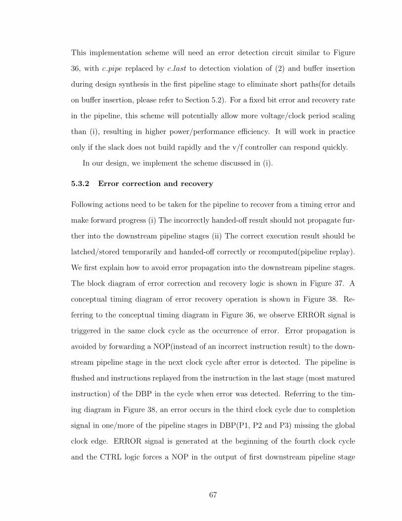
This implementation scheme will need an error detection circuit similar to Figure
36, with c pipe replaced by c last to detection violation of (2) and buffer insertion
during design synthesis in the first pipeline stage to eliminate short paths(for details
on buffer insertion, please refer to Section 5.2). For a fixed bit error and recovery rate
in the pipeline, this scheme will potentially allow more voltage/clock period scaling
than (i), resulting in higher power/performance efficiency. It will work in practice
only if the slack does not build rapidly and the v/f controller can respond quickly.
In our design, we implement the scheme discussed in (i).
5.3.2 Error correction and recovery
Following actions need to be taken for the pipeline to recover from a timing error and
make forward progress (i) The incorrectly handed-off result should not propagate fur-
ther into the downstream pipeline stages (ii) The correct execution result should be
latched/stored temporarily and handed-off correctly or recomputed(pipeline replay).
We first explain how to avoid error propagation into the downstream pipeline stages.
The block diagram of error correction and recovery logic is shown in Figure 37. A
conceptual timing diagram of error recovery operation is shown in Figure 38. Re-
ferring to the conceptual timing diagram in Figure 36, we observe ERROR signal is
triggered in the same clock cycle as the occurrence of error. Error propagation is
avoided by forwarding a NOP(instead of an incorrect instruction result) to the down-
stream pipeline stage in the next clock cycle after error is detected. The pipeline is
flushed and instructions replayed from the instruction in the last stage (most matured
instruction) of the DBP in the cycle when error was detected. Referring to the tim-
ing diagram in Figure 38, an error occurs in the third clock cycle due to completion
signal in one/more of the pipeline stages in DBP(P1, P2 and P3) missing the global
clock edge. ERROR signal is generated at the beginning of the fourth clock cycle
and the CTRL logic forces a NOP in the output of first downstream pipeline stage
67

Q
QSET
CLR
D
Global CLK
T Q1
c_pipe
ERROR(a)
Global
CLK
c_pipe
D
QD
ERROR
Q
QSET
CLR
D
(b)
COMPLETION
MISSED
Figure 36: (a) Timing error detection circuit to indicate pres-ence/absence(ERROR=0/1) of a completion signal in one period of global CLK (b)Conceptual timing diagram showing operation of error detection circuit in (a). Noteerror is detected in the same clock cycle of its occurrence
in the fourth clock cycle. An additional MUX logic is added to every primary in-
put of the first downstream pipeline stage to enable this functionality. The ERROR
signal also notifies another CTRL logic to reset the PC to re-fetch from the most
matured instruction in the DBP(in the example shown, instruction I1). The CTRL
68

logic also notifies the clock generation circuit to reduce the clock frequency to half
during pipeline replay. The flushing and replay operation for the example shown in
Figure 38 will incur a temporary loss in 10 clock cycles of fCLK .
Similar error recovery logic is implemented in [14] by using an extra pipeline
stage(referred as output buffer) at the output of the timing variation tolerant pipeline
to avoid error propagation. In a DBP, the error propagation can be avoided without
using an output buffer as the error detection scheme flags an error in the same clock
cycle when the error occurs. The methodology used for error detection in [14][26]
is with shadow latches which detects an error when data value in the shadow latch
does not match the data value in the data path latch. An ERROR is flagged in the
following clock cycle after the error has occurred. This necessitates the need for an
additional stage to avoid error propagation.
FFDELAY
BALANCED PIPELINE
CTRL LOGIC
NOP
ERROR DETECT
ERROR
CTRL LOGIC
CLOCK GENERATOR
UPSTREAM PIPELINE STAGES
AD
DR
(PC
)
ERROR
fCLK or fCLK/2
FF
CLK
DOWNSTREAM PIPELINE STAGE
Figure 37: Block diagram of error correction and recovery circuits
In the next Section, we consider some of the practical implementation aspects and
delay overheads involved in doing real-time hand-off using a PDM. These evaluations
69

P1
P2
P3
P4
P5
P6
I1 I2 I3 I4* I1+
I1 I2 I3* I4* I1+-
ERROR
- I1 I2 I3* I4*-
NOP NOP NOP
NOP NOP
I2+INSTRUCTION REPLAY
DB
P
TIME
PIP
ELINE STA
GE
C1 C2 C3 C4 C5 C6
-
-
-
-
-
- -
Figure 38: Conceptual timing diagram of error recovery in a three staged delay bal-anced pipeline. * indicates a possible erroneous result. + indicates replayed instruc-tions
are important to do a fair comparison of performance improvement with highly opti-
mized fully synchronous designs in industry as understood by us from our literature
survey and other adaptive designs previously proposed by other research groups.
5.4 Delay overhead in path delay monitor
In a synchronous processor design, all the pipeline stages perform state updates si-
multaneously at the clock edge. Significant effort is invested in the design, opti-
mization and verification of various high performance clock routing and distribution
schemes[61]. If the arrival time of the clock edge at the latches of the pipeline stage is
known apriori, effects of loading and other wire delays can be compensated to a good
extent by launching the clock edge at an earlier known time at the clock generation
source. However, in the case of delay balanced pipelines, the path completion signals
driving the latches are generated on the fly. Although the path completion signals
are generated by the PDM local to the pipeline(as opposed to that in case of a fully
synchronous design),the loading effects of the latches has to be taken into account
70

especially in microprocessor pipeline implementations where the number of latches
could be large.
Figure 39 displays the PDM broken down into three components with delays d1,
d2 and d3. Switching in the logic block ceases at time t3. The latches are triggered
at time t3 + d, where d = d1 + d2 + d3. The delay d1 depends on the sizing of the
inverters, which in turn depends on the numerical value of ∆ as discussed in Section
4.5 and limited by Equation ??. Selecting the optimum ∆ is very important. A large
value of ∆ will reduce the performance/power benefits in the delay balanced pipeline
by increasing d1,while a small value of ∆ increases the area/power overhead of PDM.
Q
QSET
CLR
D
Q
QSET
CLR
D
Q
QSET
CLR
D
CCLK
COR
C1
t1 t2 t
PDMt3 + d
d1
d2
d3
d=d1+d2+d3
0/1 1/00/1
1
1/0
0
t3
Q
QSET
CLR
D Q
QSET
CLR
D
Figure 39: Various circuit components in PDM contributing to delay overhead
Delay d2 is the time taken for the output of pseudo NMOS block to be pulled to
logic high after a series of positive pulses at the input of the parallel NMOS devices
71

cease. The rise time depends on the numerical value of COR and the ratio of sizing
of pull-up PMOS and NMOS. Figure 40 displays the COR and delay d2 for a range
of NMOS pull down devices and the range of delay values in our benchmark logic
blocks. The simulations are performed in HSPICE.
NO. OF NMOS DEVICES10 20 30 40 50 60 70 80 90 100
DE
LA
Y IN
ps
0
10
20
30
40
50
60
70
80
90
100
CO
R(f
F)
0
5
10
15
20
25
30
35
40
45
50OUTPUT CAP. AND DELAY OF PSEUDO-NMOS BLOCK
DELAY RANGE INBENCHMARK
LOGIC BLOCKS
Figure 40: HSPICE simulation result plot showing delay and capacitance values fora sweep of No. of PSEUDO-NMOS devices(on X-axis)
Delay d3 consists of the delay of AND gate driving a large capacitive load. The
AND gate drives all the TLFFs connecting the pipeline stages. The number of TLFFs
to drive for the output of AND gate could be large in a multi-stage pipeline of an
actual microprocessor design. Figure 41 plots No. of TLFFs to drive on X-axis.
The ratio CCLK/C1 is plotted on the Y-axis(in blue) and we observe that this delay
cannot be neglected, when driving a large number of TLFFs. To drive a large load,
72
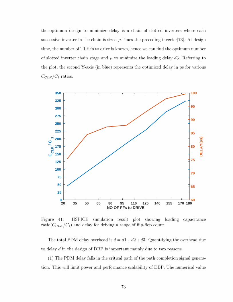
the optimum design to minimize delay is a chain of slotted inverters where each
successive inverter in the chain is sized µ times the preceding inverter[73]. At design
time, the number of TLFFs to drive is known, hence we can find the optimum number
of slotted inverter chain stage and µ to minimize the loading delay d3. Referring to
the plot, the second Y-axis (in blue) represents the optimized delay in ps for various
CCLK/C1 ratios.
NO OF FFs to DRIVE20 35 50 65 80 95 110 125 140 155 170 180
CC
LK
/ C
1
0
25
50
75
100
125
150
175
200
225
250
275
300
325
350
DE
LA
Y(p
s)60
65
70
75
80
85
90
95
100
Figure 41: HSPICE simulation result plot showing loading capacitanceratio(CCLK/C1) and delay for driving a range of flip-flop count
The total PDM delay overhead is d = d1 +d2 +d3. Quantifying the overhead due
to delay d in the design of DBP is important mainly due to two reasons
(1) The PDM delay falls in the critical path of the path completion signal genera-
tion. This will limit power and performance scalability of DBP. The numerical value
73

of d is taken into account while quantifying the benefits of delay balanced pipeline in
Section 5.6
(2) The error detection circuit in Figure 36 uses the completion signal edge at
t3 + d to detect the presence or absence of error during a period of global clock. A
false positive error may be triggered in the error detection circuit even if data is ready
to hand-off in the TLFFs.
Both (1) and (2) are related. Considering a fixed bit error rate(with recovery)
during pipeline operation, a false positive will limit the performance/power scalability
in delay balanced pipeline.
5.5 GSA outcome robustness
Timing variations in a pipeline may occur due to dynamic factors like temperature
variation, supply voltage variation due to vdd/ground bounce, capacitive coupling
effects etc and static variations like process variations which impacts the threshold
voltage of the transistors in the logic gates. It is impossible to verify the pipeline func-
tionality for all possible scenarios that may occur during actual pipeline operation.
These variations directly impact the delay of gates in the combinational logic block.
The PDM provides the ability to sense delay variations impacting the total path de-
lay. The PDM generates the path completion signal by monitoring switching activity
of gates at regular intervals of ∆. In other words, the GSA as described in Section
4.4.1 picks Gopt from a switching log file which is generated from one particular pro-
cess instance of the logic block. In addition, to pick Gopt, fixed finite set of randomly
picked input vector transition set is used to generate the switching log file. In the
presence of variability in the gate switching times and/or if an input transition which
has not been considered while picking Gopt occurs, unexpected gate switching may
result in the PDM. An example of unexpected gate switching in the pipeline is shown
in Figure 42. Unexpected gate switching can result in PDM signaling completion
74

although the correct computation output is not available.
Vt
VDD
SWITCH MISS
Figure 42: Unexpected gate switching in PDM due to gate delay variations in thepresence of process/voltage variations
While occurrence of such errors cannot be completely mitigated during pipeline
operation, but it can be minimized during design time when picking Gopt and detected
and corrected when errors occur during actual pipeline operation.To minimize the
errors due to uncharacterized input vector transition, static and dynamic variations,
the GSA algorithm previously described in Section 4.4.1 is modified as shown in
Figure 43. We study the robustness of GSA outcome against two variables. First
we vary the number of input vectors used to generate the gate switching file. In
the second experiment, we keep the number of input vectors constant and mimic the
impact of process variations and dynamic variations by varying the gate delays in the
.sdf file. For both cases, the GSA is modified to pick Gopt in a recursive manner, such
that the Gopt obtained from one instance of the switching file is used as the initial set
75

of gates for the successive instance and any additional gates required to satisfy the
conditions in GSA is added to the initial list to form the final list. The final list is
used as the initial list for the next instance. Figure 44 plots the outcome of GSA as
percentage of total gates in the logic block, Gopt/Glogicblock on the Y-axis for various
process instances on the X-axis.
GREEDY SELECT ALGORITHM
SWITCHING LOG FILE(1)
SWITCHING LOG FILE(2)
SWITCHING LOG FILE(N)
SWITCHING LOG FILE(3)
GATE NETLIST
RANDOM INPUT TRANSITIONS(10
000 to 40000)
TIMING SIMULATOR
GATE DELAY FILE(µ and σ variation)
µ 3σ 3σ
SWITCHING LOG FILE(i)
Gopt(i)
Gopt
Figure 43: Block Diagram showing simulation setup to study scalability of GSAoutcome with gate delay variations and number of vectors considered in input vectortransition set
The flattening behavior of the curves over successive process instance indicate two
very important conclusions (1)The outcome of recursive GSA remains the same over
different process instances, which implies robustness of PDM to flag a completion
signal correctly after switching activity in logic block ceases in the presence of static
and dynamic variations. This is also an indication that probability of error occurring
during real-time pipeline operation due to unexpected gate switching behavior is very
low. Similar behavior is observed as the number of input vector transitions used to
generate the gate switching file is varied as shown in Figure 45. During real time
operation, an error due to a missing pulse will result in two completion signals during
the same period of global clock. This scenario can be easily detected by the timing
76

error detection circuit shown in Figure 36.
Process Instance5 10 15 20 25 30
Go
pt/G
log
icb
lock
(%
)
3
4
5
6
7
8
9
10
11
12
13
14
Wallace Mult 8bitRCA 32bitDecodeExecute ALU
Figure 44: GSA outcome robustness study with different process/delay instances ofa logic block for different benchmark logic block
Conclusion: The flattening behavior of the graphs in Figure 44 and 45 for various
combinational logic blocks indicate high robustness of PDM operation to varying
gate delays due to static and dynamic variations and uncharacterized input vector
transitions. The probability of error occurrence due to unexpected gate switching in
PDM is very very low, although cannot be completely eliminated.
5.6 Quantitative evaluation
In the previous sections, we described the design and operation of a DBP and demon-
strated its potential to eliminate/reduce safety margins in microprocessor pipelines.
77

No. of Random Input Vectors( in thousands)0 2 4 6 8 10 12 14 16 18 20
Go
pt/
Glo
gic
blo
ck (
%)
3
4
5
6
7
8
9
10
11
12
Execute ALUDecodeWallace Mult 8bitRCA 32bit
Figure 45: GSA outcome robustness study with varying number of input vectors indifferent benchmark logic blocks
No study is complete without evaluating the quantitative benefits of the proposed
ideas in benchmark pipeline designs. We study the benefits of DBP in two pipeline
designs, a multiply-accumulate (MAC) pipeline which forms the basic block in many
DSP based applications (like FIR filtering) and a general purpose superscalar pipeline.
The quantitative benefits section is divided into two sub-sections (1) Simulation Setup
: In this Section, we describe the CAD process flow used to generate the benchmark
pipeline designs, GSA algorithm implementation and evaluation methods for PDM
and error resilience overheads. We also mention the CAD tools, simulators, softwares
and models used for quantitative assessment and state the assumptions made in the
process (2) Simulation Results : In this Section, we quantify the energy and delay
78

overheads in DBP, the energy and performance benefits obtained over a fully syn-
chronous pipeline (operating with safety margins), for both the pipeline designs. For
each benchmark pipeline design considered, the benefits section is divided into two
parts : (1) Throughput benefits obtained by scaling the clock frequency while keeping
supply voltage constant (2) Energy benefits obtained by scaling the supply voltage
while keeping clock frequency constant.
5.6.1 Simulation setup
The RTL behavioral model of a superscalar pipeline is generated using the FabGen
tool in FabScalar toolset[19]. Fabscalar is a parameterizable, synthesizable proces-
sor specification that allows for the generation and simulation of RTL descriptions
for various configurations of a simple and super-scalar processor architectures. The
RTL design emulates the hardware implementation of a pipeline which supports PISA
instructions, which is a simple MIPS like instruction set[43]. Fabscalar allows the con-
figuration of many micro-architectural parameters which include superscalar width,
fetch width and depth, issue width and depth, number and types of functional units
in the execute stage , register file depth, reorder buffer, load and store queue size
etc. Figure 20 shows various stages in a FabScalar synthesized super-scalar pipeline.
We picked three stages fetch, decode and execute of several stages in the superscalar
pipeline for our study, the execute stage being the most time critical. The RTL
behavioral model of a MAC pipeline is generated from [1]. The MAC pipeline is im-
plemented with two pipeline stages using a 8-bit wallace tree multiplier and a 16-bit
RCA. The components of the pipeline considered in our implementation is shown in
Figure 46.
The overall simulation setup is shown in Figure 47. The simulation setup is divided
into three parts and each part is explained below.
1. Generation of Gate Switching Log File:
79

FF FFFF
FF FF
X[n]
h[n-k]
y[n]
TLFFFF TLFFFETCH DECODE EXECUTE FF
PDM1
ERROR MONITOR
PDM2
PDM1 PDM2 PDM3
ERROR MONITOR
(a)
(b)
CLK GENERATOR
fCLK or fCLK/2
CLKCLK
CLK CLK
CLK GENERATOR
fCLK or fCLK/2
TLFF
Figure 46: Benchmark pipeline designs considered for quantitative analysis, imple-mented in RTL and synthesized using 45nm NSCU PDK cell library (a) MAC pipeline(b) Three stage micro-processor pipeline of a super-scalar processor design which em-ulates PISA instruction decoding and execution.
The SDC is used to generate a verilog gate level netlist from the behavioral
pipeline representation. Appropriate timing constraint file and gate cell library[52]
is provided as inputs to the design compiler tool. The SDC generates the verilog
gate netlist of all logic blocks in the pipeline, a delay file (in .sdf file format), av-
erage static and dynamic power estimates of the pipeline. An event driven Gate
Timing Simulator is designed in using a high level programming language(C).
The simulator emulates the functionality of all basic gates implemented in the
cell library. The interface to the simulator is designed such that we can pick one
of the logic blocks in the pipeline and run a switching driven event simulation of
80

the gates over consecutive input vector transitions. Using the high to low and
low to high transition delays of every gate in the logic block from the .sdf file,
we generate a log consisting of accurate switching times of each gate for every
input vector transition, referred as gate switching log file. Randomly generated
input vectors are used in this step for all the logic blocks in MAC and . The
process of log file generation is repeated for every logic block in the pipeline.
Behavioral RTL Pipeline
Implementation
Synopsys DC
Verilog Gate Netlist
Gate, clk-Q, setup delays(Standard
Delay Format file)
Static and Dynamic Power Log
Event Driven Gate Timing
Simulator
Random Input Vector Transitions
Gate switching Log File(G,t)
Gate switching Log File(G,t)
GSA algorithm implementation
Gopt
Verilog Gate Netlist
Event Driven Gate Timing
Simulator
Input Vector Transitions(Random/
Benchmarks)
Path Completion Times
Errors due to incorrect completion
PDM Delay Overhead
HSPICE SIM
Verilog Gate Netlist -> Spice Netlist
Timing Constraint
Cell library
VDD
Gopt
Delay= fn(VDD)
BENEFITS CALCULATOR
FabScalar Toolset
Fabscalar Generator
Power Overhead
Error Detect Circuit
Energy/ Performance Improvement Numbers
BER
VDD Freq.
Figure 47: Block diagram explaining detailed simulation setup for quantitative eval-uation of power and performance benefits of Delay Balanced Pipeline in a two stageMAC pipeline and a three stage micro-processor pipeline
2. Accurate calculation of path completion times:
We implement GSA in a high level programming language(C) as described in
Section 4.4.1, which uses the gate switching log file as an input and picks a set of
gates Gopt. The gate timing simulator is used once again to accurately estimate
81

the cycle to cycle longest path completion times of each logic block. The input
vector traces used in the MAC pipeline(x and h) are randomly generated. For
the superscalar pipeline, the fabscalar toolset is used to generate input vector
traces from real applications. In our study, we use SPEC2000 benchmark ap-
plications bzip and mcf. Any errors due to incorrect completion detection is
reported by the simulator. The simulation is run for hundred thousand clock
cycles.
3. Estimation of power and performance benefits:
HSPICE circuit simulation is done to obtain circuit level delay and power over-
heads. A circuit level representation of PDM shown in Figure 39 is simulated
in HSPICE. Spice cell libraries provided as part of NCSU 45nm PDK[52] is
used to calculate the delay and power overheads of PDM. The average power
over-head of error monitoring circuit is also calculated and provided to the Ben-
efits Calculator. In order to obtain path completion times of a logic block at
different supply voltages (V DD), each pipeline stage is simulated in SPICE
and its longest path delay is calculated for different V DD values. A second
order poly-fit equation is formulated to describe the relationship longest path
delay=fn(V DD). The nominal voltage used to generate gate netlist in NCSU
45nm PDK is 1.1V. The corresponding path delay at a particular V DD is
scaled proportional to the scaling of its longest path delays. Using the power
and delay overhead numbers provided from HPICE simulations combined with
path completion times obtained for nominal voltage of 1.1V from the event
driven timing simulator, the benefits calculator outputs the BER, Energy, Per-
formance improvement numbers for a wide range of global clock frequency and
supply voltage values. The temporary loss of performance (and energy) in the
presence of a timing error due to negative slack is accounted in the Benefits
calculator. Random input vector transitions are used to calculate Gopt in both
82
the pipelines. In our simulation, during actual pipeline operation, no errors due
to unexpected switching were detected.
5.6.2 Simulation results
The Simulation Results section is divided into two parts. We first quantify the ben-
efits in a MAC pipeline and then the multi-stage processor pipeline. The proposed
idea is generic and can be applied to any kind of pipeline. Depending on the de-
sign requirement, the objective of using adaptive DBPs could be to reduce voltage
margins or frequency margins. In other words, we may want to reduce power/energy
consumption or increase performance/speed. In the simulation results, we demon-
strate performance benefits by showing throughput improvements(in instructions per
second) by increasing clock frequency(keeping V DD constant) beyond that set for
a fully synchronous system with margins. Power benefits are demonstrated by scal-
ing V DD lower than that set for a fully synchronous design (operating with voltage
margins), while the clock frequency is kept constant as set during design time. For
each pipeline design, the delay and power overheads of PDM is clearly quantified in
a Table.
Table 2: Avg. Power overhead in % of Total pipeline power @1.1V for PDM in eachstage of a MAC pipeline
Pipeline StagePDM Avg. Power
@1.1V(% Total Power)wallace tree mult(8bit) 6.1
rca (16 bit) 8.3Total 14.6
5.6.2.1 MAC Pipeline
Delay and Power overheads:
The delay and power overhead of PDM depends on the number of logic gate output
nodes monitored in the PDM. The ∆ interval in PDM is governed by Equation ??.
83
The ∆ value for the two pipeline stages is 0.1ns and 0.08ns indicated as d1 in Table
3. Depending on the corresponding value of ∆, and knowing that only part of the
total ∆ intervals are monitored to restrict δmax window as explained in Section 5.2,
the average power overhead of PDM for the two pipeline stages is calculated and
indicated in Table 2. The power overheads are calculated in HSPICE. They include
both static and dynamic power and averaged for a set of input vector transitions.
Very few (at-least one) transition detectors are active at a ∆ interval within a clock
period. Majority of power is consumed in the PSEUDO-NMOS based OR circuit as
there is a constant current flow from VDD to GND as opposed to a CMOS based
design. The delay overheads d2 and d3 for both the pipeline stages is calculated using
delay plots in Figure 40 and Figure 41.
The error detection circuit shown in Figure 36 has very low overhead compared
to entire pipeline design (about 1% @ 1.1V).
Table 3: Delays of various components in PDM of each pipeline stage in a two-stageMAC pipeline
PDM DelayComponent
wallace treemult(8bit)
rca(16 bit)
d1 0.1ns 0.08nsd2 0.04ns 0.04nsd3 0.02ns 0.02ns
Performance Benefits:
The MAC pipeline is synthesized with a timing constraint of 1.1 ns global clock
period. Figure 48 plots the histogram of path completion delays of longest path for
about 10,000 randomly generated input vector transitions. Note that although the
pipeline is synthesized with a timing constraint of 1.1ns, few long paths go longer
than 1.1ns due to the delay overhead(d) of PDM. A 10% safety margin for a fully
synchronous design over the designed/synthesized global clock frequency is taken into
consideration for benefits calculation.
84

Path Completion Times (ns)0 0.1 0.2 0.3 0.4 0.5 0.6 0.7 0.8 0.9 1 1.1 1.2
# o
f p
ath
s
0
200
400
600
800
1000
1200
1400
1600
1800
2000
2200
24002500
Syn
thes
ized
Per
iod
CL2_RCACL1_WALLACE_MULT
Figure 48: Path Completion Times of longest paths in logic blocks of a MAC pipelinefor 10,000 randomly generated input vector transitions. Pipeline synthesized to 1.1ns global clock period
Figure 49 plots the slack (δ) distribution in the MAC pipeline at various global
clock time periods as indicated by the respective plots. Note, only the second pipeline
stage can utilize the positive slacks (as data is sampled into the first pipeline stage
at the global clock rate). The slack distribution moves to be left (towards negative
slack) as we decrease the clock period. The high probability of positive slacks even
at a global clock period 14.58% faster than safety, indicates a huge potential for time
lending/delay balancing during pipeline operation.
Figure 50 plots the global clock period (in ns) on the X-axis and BER(% error)
on the Y-axis for ten thousand randomly generated input vector transitions. Error
occurs in a particular cycle of global clock in the presence of -ve slack. The BER stays
85

Slack(ns)-0.2 -0.1 0 0.1 0.2 0.3 0.4 0.5
Pro
bab
ility
0
0.02
0.04
0.06
0.08
0.1
0.12
Safety(1.2ns)
Design(1.1ns)
2.08%-ve
slack
14.58%faster
Figure 49: Slack(δ) distribution in ns indicating potential for delay balancing/timelending in a MAC pipeline at various global clock periods
very low initially with increase in clock period, but rises exponentially beyond a cer-
tain global clock period due consecutive occurrence of negative slacks in the pipeline
resulting in pipeline replays at half the clock period. As noted previously, since the
first pipeline stage cannot borrow any slack (but can only lend time), the exponential
increase in errors is due to the first pipeline stage not having enough time for comple-
tion(note the steep increase in no. of paths around 0.9ns in CL1 WALLACE MULT
in Figure 48).
Errors occurring during pipeline operation are detected using the circuit shown
in Figure 36. Figure 51 plots the Throughput improvement(%) by scaling the global
clock over 1.2ns. The throughput of pipeline is calculated in MACOPS(MAC oper-
ations per second). The throughput increases steeply with increase in global clock
86

Global Clock Period(ns)0.8 0.85 0.9 0.95 1 1.05 1.1 1.15 1.2
% E
rro
r
0
10
20
30
40
50
60
70
80
90
Safety(10%)Design
19.5%perf.
improvement
Figure 50: % Timing Error in a two-stage MAC pipeline over a range of scaled globalclock period
frequency, peaking at 22.72%. As clock period is further scaled, the effect of replays
due to bit errors in the pipeline start impacting the throughput gains and the overall
throughput starts to drop down. Note, the impact of replays in a two-stage pipeline
is very low, hence the throughput peaks at a relatively large value of BER. If the
MAC pipeline is integrated into a pipeline with larger pipeline depth, the throughput
will begin to drop at a lower value of BER.
Energy Benefits: The energy benefits are evaluated by keeping the global clock
period constant @ 1.1ns, while scaling the supply voltage lower than 1.1V. Figure 52
plots the % error with voltage scaling. The shape of BER curve is similar to that in
the previous Figure 50, as the effect on slack distribution/path completion times is
similar with clock period down scaling and voltage downscaling. A 10% safety margin
87

Global Clock Period(ns)0.85 0.9 0.95 1 1.05 1.1 1.15 1.2
Th
rou
gh
pu
t Im
pro
vem
ent(
%)
0
5
10
15
20
25
0.92
22.72
Figure 51: Throughput improvement(%) with global clock period scaling. Through-put improvement over pipeline throughput at 1.2ns peak at 22.72%
in voltage is taken into account while quantifying the energy benefits, as plotted in
Figure 53.
A range of scaled voltage values is represented on the X-axis. The Y-axis on
the left (in blue) plots the energy savings (in %) by operating the pipeline at a
lower supply voltage. Both energy savings (with and without) considering energy
overhead of PDM is plotted in blue on the Y-axis. It is very important to note that
supply voltage of only the pipeline is scaled while that of PDM is not scaled. The
energy overhead of PDM is 14.6%@1.1V , which is referred as the baseline overhead.
Equation 7, Equation 8 and Equation 9 are used to calculate total consumed, energy
saved and normalized energy overhead respectively.
88

VDD(V)0.9 0.95 1 1.05 1.1 1.15 1.2
% E
rro
r
0
10
20
30
40
50
60
Safety(10%)Design
1.171.04
17.68%less
energy
Figure 52: % Timing error in a two stage MAC pipeline for a range of scaled supplyvoltages
Epipeline+PDM(@V DD) = [Eerror freepipeline +Ereplay
pipeline](@V DD)+[Eerror freePDM +Ereplay
PDM ](@1.1V )
(7)
Esavings(@V DD)(%) =Epipeline(@1.2V )− Epipeline+PDM(@V DD)
Epipeline(@1.2V )∗ 100 (8)
Normalized Eoverhead =EPDM(@V DD)
Epipeline(@1.2)(9)
Referring to the energy savings plot, we observe that at 1.2V, the total energy
savings is -15%, which is the sum of energy overhead of PDM and small energy
overhead of error detection circuitry. As the pipeline design is scaled below 1.2V, the
89
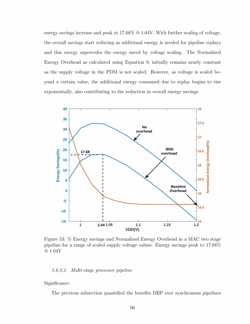
energy savings increase and peak at 17.68% @ 1.04V. With further scaling of voltage,
the overall savings start reducing as additional energy is needed for pipeline replays
and this energy supercedes the energy saved by voltage scaling. The Normalized
Energy Overhead as calculated using Equation 9, initially remains nearly constant
as the supply voltage in the PDM is not scaled. However, as voltage is scaled be-
yond a certain value, the additional energy consumed due to replay begins to rise
exponentially, also contributing to the reduction in overall energy savings.
VDD(V)1 1.05 1.1 1.15 1.2
En
erg
y S
avin
gs(
%)
-15
-10
-5
0
5
10
15
20
25
30
35
40
No
rmal
ized
En
erg
y O
verh
ead
(%)
14
14.5
15
15.5
16
16.5
17
17.5
18
Nooverhead
1.04
17.68
BaselineOverhead
Withoverhead
Figure 53: % Energy savings and Normalized Energy Overhead in a MAC two stagepipeline for a range of scaled supply voltage values. Energy savings peak to 17.68%@ 1.04V
5.6.2.2 Multi-stage processor pipeline
Significance:
The previous subsection quantified the benefits DBP over synchronous pipelines
90

in a MAC unit, which is commonly used in DSP pipelines. The significance of a
quantitative evaluation of the proposed idea on a multi-stage processor pipeline is
two folds (1) DSP pipelines are composed of logic blocks that are known to exhibit
certain statistics of path completion delay distribution (very few paths with long path
completion delays and activated less often), which bolsters the power-performance
scalability of our proposed design. It is interesting and important to identify how
well the proposed design can scale for other benchmark pipeline designs. In addition,
the loading delays in PDM for a bigger design is more due to the large number of
flip-flops to be driven. (2) Random input vector transitions were used in the MAC
pipeline to evaluate the benefits. During actual pipeline operation, real applications
are executed on the pipeline and it is important the evaluate the real slack distribution
over successive input vector transitions occurring in real applications to truly realize
the benefits of the proposed design approach.
Table 4: Average PDM power overhead(% of total pipeline power)@1.1V for fetch,decode and execute stages in the micro-processor pipeline
Pipeline StagePDM Avg. Power
@1.1V(% of Total Power)Fetch 3.1
Decode 3.3Execute 3.8
Total 10.2
We pick three stages fetch, decode and execute(most timing critical) of a mi-
croprocessor pipeline design as our benchmark design to evaluate the benefits. The
power and delay overheads of PDM for the three pipeline stages is indicated in Table
5. The path completion probabilities of longest paths for the three pipeline stages is
shown in Figure 54. The pipeline is synthesized for 1ns global clock period. We ob-
serve that the path completion times for many clock cycles go beyond the synthesized
global clock period due to high PDM delay overheads as indicated in Table 5. This is
mainly because the delay overhead due to loading is very high as compared to a MAC
91

pipeline due to a large number of TLFFs in the decode stage. Note, that d3 accounts
for almost about 10% of the global clock period. The power overheads for PDM in
every pipeline stage is indicated in Table 4. The PDM overheads for each pipeline
stage is lower than that in the MAC pipeline as the combinational logic blocks have
more gates (lower % of total gates have to be monitored as also indicated in Table
1).
Table 5: Delay overhead for various components in PDM for fetch, decode and executestages in the benchmark micro-processor pipeline
PDM DelayComponent
Fetch Decode Execute
d1 0.1ns 0.085ns 0.085nsd2 0.02ns 0.02ns 0.04nsd3 0.09ns 0.09ns 0.09ns
Path Completion Times(ns)0.2 0.3 0.4 0.5 0.6 0.7 0.8 0.9 1 1.1 1.2
Pro
bab
ility
0
0.05
0.1
0.15
0.2
0.25
0.3
0.35
0.4
FetchDecodeExecute
SynthesizedPeriod
Figure 54: Prob. of path completion times of longest paths in fetch, decode andexecute stages in a benchmark micro-processor pipeline for 40,000 randomly generatedinput vector transitions. Pipeline synthesized for 1.0 ns global clock period.
92
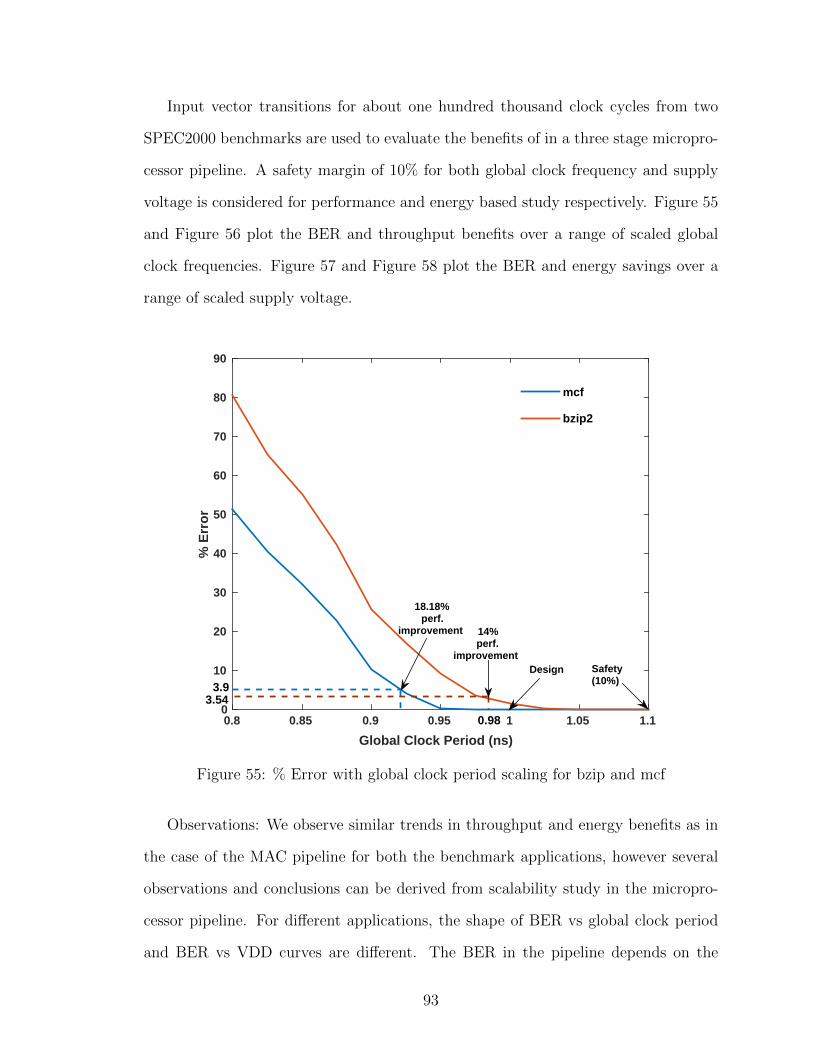
Input vector transitions for about one hundred thousand clock cycles from two
SPEC2000 benchmarks are used to evaluate the benefits of in a three stage micropro-
cessor pipeline. A safety margin of 10% for both global clock frequency and supply
voltage is considered for performance and energy based study respectively. Figure 55
and Figure 56 plot the BER and throughput benefits over a range of scaled global
clock frequencies. Figure 57 and Figure 58 plot the BER and energy savings over a
range of scaled supply voltage.
Global Clock Period (ns)
0.8 0.85 0.9 0.95 1 1.05 1.1
% E
rro
r
0
10
20
30
40
50
60
70
80
90
mcf
bzip2
Design Safety(10%)
0.98
14%perf.
improvement
18.18%perf.
improvement
3.543.9
Figure 55: % Error with global clock period scaling for bzip and mcf
Observations: We observe similar trends in throughput and energy benefits as in
the case of the MAC pipeline for both the benchmark applications, however several
observations and conclusions can be derived from scalability study in the micropro-
cessor pipeline. For different applications, the shape of BER vs global clock period
and BER vs VDD curves are different. The BER in the pipeline depends on the
93

Global Clock Period(ns)0.8 0.85 0.9 0.95 1 1.05 1.1
Th
rou
gh
pu
t Im
pro
vem
ent(
%)
0
2
4
6
8
10
12
14
16
18
20
22
mcfbzip
16.5
Figure 56: Throughput improvement(%) with global clock period scaling for bzip andmcf.
slack distribution of every stage in the pipeline over successive cycles of the clock.
This slack distribution varies depending on the netlist structure of the logic block,
the successive input vector transitions which in turn effects the sequence in which
long and short paths completion delays are activated in r=each pipeline stage and
the interdependence of path completion delays in each pipeline stage(given that com-
pletion is triggered only when all pipeline stages are complete).At a fixed value of
scaled global clock period or supply voltage, fewer errors occur in the pipeline for
mcf application as compared to bzip application. The operating points of the mi-
croprocessor pipeline can scale more giving us higher peak benefits of both energy
and performance in case of mcf application as opposed to bzip application. The peak
throughput benefit/improvement for bzip and mcf running on a DBP is 16.5% and
94

20% respectively while the peak energy benefit is 14.12% and 26.6% respectively.
VDD(V)0.9 0.95 1 1.05 1.1 1.15 1.2
% E
rro
r
0
10
20
30
40
50
60
70
80
mcf
bzip
Safety(10%)Design
1.06
1.25
14.12%less
energy
21.9%less
energy
Figure 57: % Timing error in a three stage pipeline executing bzip and mcf for arange of scaled supply voltages
5.7 Qualitative evaluation
In this Section, we discuss the qualitative evaluation of a delay balanced pipeline with
previously proposed intrusive better than worse-case designs in literature[26][15]. We
first enumerate the factor over which qualitative evaluation is done, the implication
each factor poses on design challenges, power and performance overhead, power and
performance scalability and reliability of a timing variation tolerant design.
1. Meta-stability : Meta-stability is an unpredictable state at the output of a flip-
flop in an event the setup or hold time at the input of the flip-flop is violated.
95

VDD(V)1 1.02 1.04 1.06 1.08 1.1 1.12 1.14 1.16 1.18 1.2
En
erg
y S
avin
gs(
%)
-20
-15
-10
-5
0
5
10
15
20
25
30
35
40
45
50
5
10
15
20
25
30
No
rmal
ized
En
erg
y O
verh
ead
(%)
5
10
15
20
25
30
26.6
14.12
Baseline
mcfbzip
Figure 58: % Energy savings and Normalized Energy Overhead in a three stagepipeline for a range of scaled supply voltage values for bzip and mcf.
The impact of meta-stability on the flip-flop output node is temporary unpre-
dictability in its output state to settle to either 0 or VDD. Meta-stability as
a major cause of concern due to timing uncertainties in synchronous designs
and better-than-worse case designs have been stated in literature[6] [32] [15].
Asynchronous pipeline designs or self-completion based designs are inherently
resilient to meta-stability as they hand-off data in a pipeline using handshaking
signals which indicate completion[32]. In better-than-worse case designs, meta-
stability can either be avoided by design[15] or an occurrence can be detected
and flagged as an error during pipeline operation. In[26], the authors propose
the use of meta-stability detection circuits at the output of datapath flip-flops to
detect meta-stable conditions and trigger an error. In[15], the authors propose
96

the use of error detection sequential elements to eliminate meta-stability in bet-
ter than worse-case designs. In our design, hand-off in the TLFFs is triggered
by the path completion signal. This behavior is similar to an asynchronous
data hand-off, eliminating the need for any meta-stable detectors. The output
interface flip-flops are prone to enter a meta-stable state, however given a finite
delay in PDM, such occurrence will trigger a timing error resulting in pipeline
replay. If the input of D flip-flop in Figure 36 does not stabilize before arrival
of the global CLK edge, it may enter into meta-stability condition and could
be detected using the meta-stability detection circuit used in[26]. Overall, the
overhead to detect/prevent a meta-stable condition is very low.
2. Error recovery overhead : In[26][15], the authors propose the use of an additional
output buffer stage to avoid error propagation into downstream pipeline stages.
This need for an additional stage arises because error detection is flagged in the
following clock cycle after the timing error occurs. In our design, the additional
output buffer stage may not be needed (please refer to Section 5.3.2) as a timing
error is detected in the same global clock cycle of its occurrence. This gives the
error recovery circuit sufficient time(one clock period) to take action. In [26][15],
timing errors are detected by comparing the data in the data-path flip-flop and
a shadow latch, while in our case, timing errors are detected indirectly using
arrival time of path completion signal with reference to the global clock edge.
This gives our design the potential to save power and performance.
3. Error detection overhead : In[26][15], the error detection over-heads depend on
the percentage of total paths which may become critical under timing variations.
In deeply scaled technologies, in high performance circuits after timing closure
and in the presence of increased variability this percentage could be very high
which may result in higher overhead for error detection. In our design, the
97

over-heads of PDM dominate the total overhead, which is independent of the
total number of critical or long paths in the design.
4. Time lending benefits : The ability to lend time between consecutive cycles of
global clock enables a path with a path delay greater than global clock period to
complete and hand-off data correctly. An exception is the first pipeline stage as
data is handed into the first pipeline stage at clock rate( please observe timing
diagram in Figure 33(a)). In [26][15], triggering of a path greater than the clock
period results in a timing error. The ability to lend time dynamically during
pipeline operation gives DBP the potential to scale in power and performance
more than the designs proposed in[26][15]. In other words, for a fixed BER
with replay during pipeline operation, our design can operate at a lower supply
voltage or higher clock frequency. However, the delay overhead due to PDM
as described in Section 5.4 and quantified in Table 3 and Table 5 limits the
potential for power and performance scalability in our design. This extra delay
overhead does not exist in [26][15] as data hand-off is not dynamically generated.
In pipeline designs where benefits due to time lending are higher than that
limited by the PDM delay overhead, our design has better scalability potential.
For logic blocks with skewed path activation probability distribution (similar
to Figure 26), time lending benefits may over-power the benefits limited due
to delay in PDM. In addition, the completion signal cpipe enables data hand-off
only when PDM of every logic block in the DBP indicates completion, which
may restrict the time lending ability in the overall pipeline depending on data
statistics of completion delays in the pipeline.
5.8 Conclusions
As devices continue to scale even as of today with the semiconductor industry looking
into 7nm technology, there is an increasing cause of concern for reliability. At the
98

same time the performance and power consumption in a micro-processor pipeline
is very critical to the overall throughput of a multi-processor system. To improve
operational reliability under timing variations, with increasing variations, designs can
no longer afford to incorporate safety margins. The solution going forward is to make
designs reliable by employing on-line error monitoring techniques which can detect
and correct failures as and when it happens. Such a system need not impose one-time
worse-case guard bands to achieve robustness, making them power and performance
efficient. Delay Balanced Pipeline is a timing variation tolerant pipeline design, which
presents a great potential to achieve power and performance scalability and high
reliability at the same time, by eliminating the need to incorporate timing guard-
bands in the design. The key contribution and novelty of this work is the realization
of a path delay monitor which can detect path delay completion in real-time by
monitoring selective gate output nodes in a combinational logic block. Quantitative
and qualitative evaluations show great potential for the proposed design.
99

CHAPTER VI
CONCLUSIONS AND FUTURE WORK
Incorporating timing guard-bands is a temporary hack solution to the timing un-
certainty problem especially in lower technology nodes under extreme die-to-die and
within-die timing variations mainly due to two reasons (1) How much timing guard-
bands will be enough to guarantee reliable operation under timing variations is not
known (2) The degree/amount of guard-bands to be incorporated to ensure high
probability of correctness continues to increase resulting in significant power and
performance inefficiency. In the light of above stated challenges, this thesis work
proposed two ideas.
In Chapter 2, a self-test and self-tune based collaborative tuning methodology was
introduced as a top-up speed coverage mechanism to determine the reliable FMAX
of all cores in an array during the post-manufacturing verification phase. During
post-manufacturing phase, high coverage functional tests[54] could be used as test
vectors during the tuning phase. The methodology can also be used effectively on the
field at periodic intervals, in the background, while running real applications at the
foreground without any system downtime. We expect that any speed related bugs
which may have escaped the post-manufacturing testing phase (application depen-
dent bugs) will show up at the output signature, although not affecting reliability of
normal system operation. Once the self test-tune process is complete, all cores can
operate independently at their maximum reliable operating frequencies as determined
by the test-tune algorithm. The FMAX frequency of each core does not exceed the
maximum frequency as determined using high coverage functional tests during post-
manufacturing phase. The collaborative tuning methodology accelerates the tuning
100

process which reduces total post-manufacturing test time and impact on application
performance while running on the field(due to spatial redundancy). At any point
during tuning, the computation result of one of the processors in the core-pair can
be trusted and committed to memory. This ensures application execution can move
forward without having to checkpoint and rollback. It is important to note that our
methodology is proposed specifically to top-up speed coverage over existing frequency
binning methods in the presence of difficult-to-detect and difficult-to-model electrical
bugs.
In order for comparison based test to work correctly, both the core pairs must see
the same instruction sequence and input data. Since the core-pairs are not running
in a lock-stepped manner, in a multi-threaded application, their memory accesses
could result in input incoherence. In literature, micro-architecture changes have been
proposed to ensure input coherence in the core-pairs[31][51]. These changes need to
be incorporated into the multi-processor system to enable correct comparison based
testing. The features will incur additional area, but could be power gated when test-
tune is not being done. When the redundant core in the core-pair fails at a particular
clock frequency, the local memory and register contents needs to be moved from the
active core to the redundant core, before beginning the next iteration, which will
consume some memory bandwidth. The proposed methodology improves reliability
by topping-up speed coverage in every micro-processor pipeline. In the second part
of this thesis, we describe a novel pipeline design which has the ability to detect and
recover from timing errors during pipeline operation. Employing such pipelines in
every processor of a multi-processor system can significantly reduce the test and tune
time required during post-manufacturing verification phase.
In the second part of this thesis, an intrusive timing variation tolerant pipeline
design was introduced to eliminate the timing guard bands in the presence of static
and dynamic factors causing timing variations. The pipeline addresses the reliability,
101

power and performance efficiency challenge under extreme timing variations. The
energy and throughput of a datapath pipeline unit contributes significantly to the re-
sponse time of a multi-processor system. By replacing each micro-processor pipeline
in a multi-processor system with a delay balanced pipeline, the response time can
be significantly improved at lower technology nodes under extreme timing variations.
The key component in the delay balanced pipeline is the PDM. In Chapter 3, a PDM
was introduced for the first time in literature as far as our knowledge extends, which
presented a viable and realizable design to sense path delay completion with very
high probability of correctness by monitoring switching in a small set of gates in the
combinational logic block. The PDM in addition to sensing timing variations, also
provides on-the-fly cycle-to-cycle time lending capability to the pipeline. Data hand-
off using a dynamically generated path completion signal incurs high delay overhead
due to loading. For e.g in the three stage pipeline design, the number of flip-flops
to be driven using a single completion signal is about 176. This incurs about 8% of
total clock period overhead. In pipelines and applications which generate a signif-
icant positive slack distribution, this overhead will be compensated by the benefits
obtained from time lending due to positive slacks. Our quantitative analysis of a
three stage micro-processor pipeline design running SPEC2000 application bench-
marks demonstrate time lending benefits weigh over the delay overheads in PDM.
A very detailed qualitative analysis of the delay balanced pipeline is done over pre-
viously proposed most popular intrusive timing variation tolerant adaptive pipeline
implementations[26][15].
Tuning Replica Circuits(TRC) have been used in prior work as a non-intrusive
method to reduce timing margins[16][71]. Copies of critical paths in the pipeline
stage of each logic block is made on chip in close proximity with the data-path to
predict the presence of a timing violation in the data-path pipeline. In deeply scaled
102

SYNCHRONOUS PIPELINE
PDM
CLK GENERATION BLOCK
ERROR PREDICT
CLK
# o
f p
ath
s
Path Delays
(a) (b)
path completion signal
Figure 59: (a) Conceptual representation of path delay distribution in high perfor-mance circuits after timing closure and in the presence of extreme process variations(b) Block diagram to use PDM as an error prediction mechanism to adjust operationalclock frequency adaptively to changing dynamic conditions on chip
technologies operating at very high frequency or very low voltage, after timing clo-
sure and in the presence of increased variability the percentage of critical paths(of
total paths) could be very high which may result in higher overhead in the replica
circuits. The combinational logic blocks often exhibit path activation probabilities
as shown in Figure 59(a). In our design, the overhead of PDM is independent of the
number of critical paths in the logic block. The information from PDM on cycle-
to-cycle path completion times in pipeline can be used as an early error prediction
mechanism to indicate a potential timing violation condition in the pipeline under
dynamic changing conditions. When path completion times in the pipeline stage ap-
proach closer to setup time violation times of the flip-flops, a feedback message can be
sent to the clock generation and distribution circuit to temporarily reduce the clock
period/supply voltage. The data hand-off in all pipeline stages is controlled by the
periodic clock just like a synchronous pipeline. However, some timing margins have
to be incorporated into the design due to finite response time of the clock generation
and distribution circuit. The block diagram in Figure 59(b) shows the use of PDM
and the path completion signal as an error prediction technique to dynamically adjust
clock frequency.
103

Finally, for full proof validation of a novel concept involving hardware modifica-
tions, a chip design is required for a satisfactory validation of the idea. A chip design
to demonstrate the operation and working of the delay balanced multi-stage pipeline
is left as part of future work.
104

REFERENCES
[1] “http://www.aoki.ecei.tohoku.ac.jp/arith/mg/index.html,”
[2] Aggarwal, N., Ranganathan, P., Jouppi, N. P., and Smith, J. E., “Con-figurable Isolation: Building High Availability Systems with Commodity Multi-core Processors,” in Proceedings of the 34th Annual International Symposium onComputer Architecture, ISCA ’07, (New York, NY, USA), pp. 470–481, ACM,2007.
[3] Austin, T. M., “DIVA: a reliable substrate for deep submicron microarchi-tecture design,” in 32nd Annual International Symposium on Microarchitecture,1999. MICRO-32. Proceedings, pp. 196–207, 1999.
[4] Baker, K. and Beers, J. v., “Shmoo plotting: the black art of IC testing,”in Test Conference, 1996. Proceedings., International, pp. 932–933, Oct. 1996.
[5] Becker, W. D., Eckhardt, J., Frech, R. W., Katopis, G. A., Klink,E., McAllister, M. F., McNamara, T. G., Muench, P., Richter, S. R.,and Smith, H., “Modeling, simulation, and measurement of mid-frequency si-multaneous switching noise in computer systems,” IEEE Transactions on Com-ponents, Packaging, and Manufacturing Technology: Part B, vol. 21, pp. 157–163, May 1998.
[6] Beer, S., Cannizzaro, M., Cortadella, J., Ginosar, R., and Lavagno,L., “Metastability in Better-Than-Worst-Case Designs,” in 2014 20th IEEEInternational Symposium on Asynchronous Circuits and Systems (ASYNC),pp. 101–102, May 2014.
[7] Bentley, B., “Validating the Intel Pentium 4 Microprocessor,” in Proceedingsof the 38th Annual Design Automation Conference, DAC ’01, (New York, NY,USA), pp. 244–248, ACM, 2001.
[8] Blome, J., Feng, S., Gupta, S., and Mahlke, S., “Self-calibrating OnlineWearout Detection,” in 40th Annual IEEE/ACM International Symposium onMicroarchitecture, 2007. MICRO 2007, pp. 109–122, Dec. 2007.
[9] Blum, M. and Wasserman, H., “Reflections on the Pentium division bug,”IEEE Transactions on Computers, vol. 45, pp. 385–393, Apr. 1996.
[10] Borkar, S., “Designing reliable systems from unreliable components: the chal-lenges of transistor variability and degradation,” IEEE Micro, vol. 25, pp. 10–16,Nov. 2005.
105

[11] Borkar, S., “The Exascale challenge,” in 2010 International Symposium onVLSI Design Automation and Test (VLSI-DAT), pp. 2–3, Apr. 2010.
[12] Bowman, K. A., Duvall, S. G., and Meindl, J. D., “Impact of die-to-dieand within-die parameter fluctuations on the maximum clock frequency distri-bution for gigascale integration,” IEEE Journal of Solid-State Circuits, vol. 37,pp. 183–190, Feb. 2002.
[13] Bowman, K. A., Tokunaga, C., Karnik, T., De, V. K., and Tschanz,J. W., “A 22nm dynamically adaptive clock distribution for voltage droop tol-erance,” in 2012 Symposium on VLSI Circuits (VLSIC), pp. 94–95, June 2012.
[14] Bowman, K. A., Tschanz, J. W., Kim, N. S., Lee, J. C., Wilkerson,C. B., Lu, S. L. L., Karnik, T., and De, V. K., “Energy-Efficient andMetastability-Immune Timing-Error Detection and Instruction-Replay-BasedRecovery Circuits for Dynamic-Variation Tolerance,” in Solid-State Circuits Con-ference, 2008. ISSCC 2008. Digest of Technical Papers. IEEE International,pp. 402–623, Feb. 2008.
[15] Bowman, K. A., Tschanz, J. W., Kim, N. S., Lee, J. C., Wilker-son, C. B., Lu, S. L. L., Karnik, T., and De, V. K., “Energy-Efficientand Metastability-Immune Resilient Circuits for Dynamic Variation Tolerance,”IEEE Journal of Solid-State Circuits, vol. 44, pp. 49–63, Jan. 2009.
[16] Bowman, K. A., Tschanz, J. W., Lu, S. L. L., Aseron, P. A., Khellah,M. M., Raychowdhury, A., Geuskens, B. M., Tokunaga, C., Wilker-son, C. B., Karnik, T., and De, V. K., “A 45 nm Resilient MicroprocessorCore for Dynamic Variation Tolerance,” IEEE Journal of Solid-State Circuits,vol. 46, pp. 194–208, Jan. 2011.
[17] Brahme, D. and Abraham, J. A., “Functional Testing of Microprocessors,”IEEE Transactions on Computers, vol. C-33, pp. 475–485, June 1984.
[18] Chae, K., Mukhopadhyay, S., Lee, C.-H., and Laskar, J., “A dynamictiming control technique utilizing time borrowing and clock stretching,” in 2010IEEE Custom Integrated Circuits Conference (CICC), pp. 1–4, Sept. 2010.
[19] Choudhary, N. K., Wadhavkar, S. V., Shah, T. A., Mayukh, H.,Gandhi, J., Dwiel, B. H., Navada, S., Najaf-abadi, H. H., and Roten-berg, E., “FabScalar: Composing Synthesizable RTL Designs of ArbitraryCores Within a Canonical Superscalar Template,” in Proceedings of the 38thAnnual International Symposium on Computer Architecture, ISCA ’11, (NewYork, NY, USA), pp. 11–22, ACM, 2011.
[20] Constantinides, K., Mutlu, O., Austin, T., and Bertacco, V.,“Software-Based Online Detection of Hardware Defects Mechanisms, Architec-tural Support, and Evaluation,” in 40th Annual IEEE/ACM International Sym-posium on Microarchitecture, 2007. MICRO 2007, pp. 97–108, Dec. 2007.
106
[21] Das, S., Roberts, D., Lee, S., Pant, S., Blaauw, D., Austin, T., Flaut-ner, K., and Mudge, T., “A self-tuning DVS processor using delay-error detec-tion and correction,” IEEE Journal of Solid-State Circuits, vol. 41, pp. 792–804,Apr. 2006.
[22] Dean, M. E., Dill, D. L., and Horowitz, M., “Self-timed logic usingcurrent-sensing completion detection (CSCD),” in Proceedings, 1991 IEEE Inter-national Conference on Computer Design: VLSI in Computers and Processors,1991. ICCD ’91, pp. 187–191, Oct. 1991.
[23] Deepchip 2014. http://www.deepchip.com/items/0540-05.html.
[24] Delord, X. and Saucier, G., “Formalizing Signature Analysis for ControlFlow Checking of Pipelined RISC Microprocessors,” in Test Conference, 1991,Proceedings., International, pp. 936–, Oct. 1991.
[25] Eichelberger, E. B. and Williams, T. W., “A Logic Design Structure forLSI Testability,” in Papers on Twenty-five Years of Electronic Design Automa-tion, 25 years of DAC, (New York, NY, USA), pp. 358–364, ACM, 1988.
[26] Ernst, D., Kim, N. S., Das, S., Pant, S., Rao, R., Pham, T., Ziesler,C., Blaauw, D., Austin, T., Flautner, K., and Mudge, T., “Razor: alow-power pipeline based on circuit-level timing speculation,” in 36th AnnualIEEE/ACM International Symposium on Microarchitecture, 2003. MICRO-36.Proceedings, pp. 7–18, Dec. 2003.
[27] Esmaeilzadeh, H., Blem, E., St. Amant, R., Sankaralingam, K., andBurger, D., “Dark Silicon and the End of Multicore Scaling,” in Proceedingsof the 38th Annual International Symposium on Computer Architecture, ISCA’11, (New York, NY, USA), pp. 365–376, ACM, 2011.
[28] Fischer, T., Desai, J., Doyle, B., Naffziger, S., and Patella, B., “A90-nm variable frequency clock system for a power-managed itanium architectureprocessor,” IEEE Journal of Solid-State Circuits, vol. 41, pp. 218–228, Jan. 2006.
[29] Fojtik, M., Fick, D., Kim, Y., Pinckney, N., Harris, D. M., Blaauw,D., and Sylvester, D., “Bubble Razor: Eliminating Timing Margins in anARM Cortex-M3 Processor in 45 nm CMOS Using Architecturally IndependentError Detection and Correction,” IEEE Journal of Solid-State Circuits, vol. 48,pp. 66–81, Jan. 2013.
[30] Ghosh, S., Bhunia, S., and Roy, K., “CRISTA: A New Paradigm for Low-Power, Variation-Tolerant, and Adaptive Circuit Synthesis Using Critical PathIsolation,” IEEE Transactions on Computer-Aided Design of Integrated Circuitsand Systems, vol. 26, pp. 1947–1956, Nov. 2007.
[31] Gomaa, M., Scarbrough, C., Vijaykumar, T. N., and Pomeranz, I.,“Transient-fault recovery for chip multiprocessors,” in 30th Annual InternationalSymposium on Computer Architecture, 2003. Proceedings, pp. 98–109, June 2003.
107

[32] Hauck, S., “Asynchronous design methodologies: an overview,” Proceedings ofthe IEEE, vol. 83, pp. 69–93, Jan. 1995.
[33] Humenay, E., Tarjan, D., and Skadron, K., “Impact of Process Variationson Multicore Performance Symmetry,” in Design, Automation Test in EuropeConference Exhibition, 2007. DATE ’07, pp. 1–6, Apr. 2007.
[34] Inoue, H., Li, Y., and Mitra, S., “VAST: Virtualization-Assisted ConcurrentAutonomous Self-Test,” in Test Conference, 2008. ITC 2008. IEEE Interna-tional, pp. 1–10, Oct. 2008.
[35] Intel, “Intel platform and component validation,” http://www.intel.com/
design/chipsets/labtour/pvpt_whitepaper.htm.
[36] ITRS http://www.itrs2.net/.
[37] Jayaraman, K., Vedula, V. M., and Abraham, J. A., “Native mode func-tional self-test generation for Systems-on-Chip,” in International Symposium onQuality Electronic Design, 2002. Proceedings, pp. 280–285, 2002.
[38] Josephson, D., “The good, the bad, and the ugly of silicon debug,” in 200643rd ACM/IEEE Design Automation Conference, pp. 3–6, 2006.
[39] Josephson, D. D., “The manic depression of microprocessor debug,” in TestConference, 2002. Proceedings. International, pp. 657–663, 2002.
[40] Kim, S. and Somani, A. K., “On-line integrity monitoring of microproces-sor control logic,” in 2001 International Conference on Computer Design, 2001.ICCD 2001. Proceedings, pp. 314–319, 2001.
[41] LaFrieda, C., Ipek, E., Martinez, J. F., and Manohar, R., “UtilizingDynamically Coupled Cores to Form a Resilient Chip Multiprocessor,” in 37thAnnual IEEE/IFIP International Conference on Dependable Systems and Net-works, 2007. DSN ’07, pp. 317–326, June 2007.
[42] Li, Y., Makar, S., and Mitra, S., “CASP: Concurrent Autonomous ChipSelf-Test Using Stored Test Patterns,” in Design, Automation and Test in Eu-rope, 2008. DATE ’08, pp. 885–890, Mar. 2008.
[43] LLC, S., “Simplescalar weblink,” 2004.
[44] Mak, T. M., Krstic, A., Cheng, K.-T. T., and Wang, L.-C., “New Chal-lenges in Delay Testing of Nanometer, Multigigahertz Designs,” IEEE Design &Test of Computers, vol. 21, no. 3, pp. 241–247, 2004.
[45] Maxwell, P., Hartanto, I., and Bentz, L., “Comparing functional andstructural tests,” in Test Conference, 2000. Proceedings. International, pp. 400–407, 2000.
108

[46] McGowen, R., Poirier, C. A., Bostak, C., Ignowski, J., Millican,M., Parks, W. H., and Naffziger, S., “Power and temperature control on a90-nm Itanium family processor,” IEEE Journal of Solid-State Circuits, vol. 41,pp. 229–237, Jan. 2006.
[47] Meixner, A., Bauer, M. E., and Sorin, D., “Argus: Low-Cost, Comprehen-sive Error Detection in Simple Cores,” in 40th Annual IEEE/ACM InternationalSymposium on Microarchitecture, 2007. MICRO 2007, pp. 210–222, Dec. 2007.
[48] Moore, G., “Cramming more components onto integrated circuits,”http://www.monolithic3d.com/uploads/6/0/5/5/6055488/gordon_moore_
1965_article.pdf.
[49] Mudge, T., “Power: a first-class architectural design constraint,” Computer,vol. 34, pp. 52–58, Apr. 2001.
[50] Muhtaroglu, A., Taylor, G., and Rahal-Arabi, T., “On-die droop de-tector for analog sensing of power supply noise,” IEEE Journal of Solid-StateCircuits, vol. 39, pp. 651–660, Apr. 2004.
[51] Mukherjee, S. S., Kontz, M., and Reinhardt, S. K., “Detailed designand evaluation of redundant multi-threading alternatives,” in 29th Annual Inter-national Symposium on Computer Architecture, 2002. Proceedings, pp. 99–110,2002.
[52] NCSU, “Open access-based process development kit for 45nm technology node,”http://www.eda.ncsu.edu/wiki/FreePDK.
[53] Nicolaidis, M., “Time redundancy based soft-error tolerance to rescuenanometer technologies,” in 17th IEEE VLSI Test Symposium, 1999. Proceed-ings, pp. 86–94, 1999.
[54] Parvathala, P., Maneparambil, K., and Lindsay, W., “FRITS - a mi-croprocessor functional BIST method,” in Test Conference, 2002. Proceedings.International, pp. 590–598, 2002.
[55] Patel, J., “Delay faults,” courses.engr.illinois.edu/ece543/docs/
DelayFault_6_per_page.pdf.
[56] Patra, P., “On the cusp of a validation wall,” IEEE Design Test of Computers,vol. 24, pp. 193–196, Mar. 2007.
[57] Pering, T., Burd, T., and Brodersen, R., “The simulation and evaluationof dynamic voltage scaling algorithms,” in 1998 International Symposium on LowPower Electronics and Design, 1998. Proceedings, pp. 76–81, Aug. 1998.
[58] Pomeranz, I., Kundu, S., and Reddy, S. M., “On output response compres-sion in the presence of unknown output values,” in Design Automation Confer-ence, 2002. Proceedings. 39th, pp. 255–258, 2002.
109

[59] Reddy, S. M., Saluja, K. K., and Karpovsky, M. G., “A data compres-sion technique for built-in self-test,” IEEE Transactions on Computers, vol. 37,pp. 1151–1156, Sept. 1988.
[60] Rotenberg, E., “AR-SMT: a microarchitectural approach to fault tolerance inmicroprocessors,” in Twenty-Ninth Annual International Symposium on Fault-Tolerant Computing, 1999. Digest of Papers, pp. 84–91, June 1999.
[61] Rusu, S., “Processor Clock Generation and Distribution,” in Processor Design(Nurmi, J., ed.), pp. 339–366, Springer Netherlands, 2007. DOI: 10.1007/978-1-4020-5530-0 15.
[62] Schuchman, E. and Vijaykumar, T. N., “BlackJack: Hard Error Detectionwith Redundant Threads on SMT,” in 37th Annual IEEE/IFIP InternationalConference on Dependable Systems and Networks, 2007. DSN ’07, pp. 327–337,June 2007.
[63] Shyam, S., Constantinides, K., Phadke, S., Bertacco, V., and Austin,T., “Ultra Low-cost Defect Protection for Microprocessor Pipelines,” in Proceed-ings of the 12th International Conference on Architectural Support for Program-ming Languages and Operating Systems, ASPLOS XII, (New York, NY, USA),pp. 73–82, ACM, 2006.
[64] Smolens, J. C., Gold, B. T., Falsafi, B., and Hoe, J. C., “Reunion:Complexity-Effective Multicore Redundancy,” in 39th Annual IEEE/ACM In-ternational Symposium on Microarchitecture, 2006. MICRO-39, pp. 223–234,Dec. 2006.
[65] Smolens, J. C., Kim, J., Hoe, J. C., and Falsafi, B., “Efficient ResourceSharing in Concurrent Error Detecting Superscalar Microarchitectures,” in 37thInternational Symposium on Microarchitecture, 2004. MICRO-37 2004, pp. 257–268, Dec. 2004.
[66] Smolens, J. C., Gold, B. T., Hoe, J. C., Falsafi, B., and Mai, K.,“Detecting emerging wearout faults,” in In Proceedings of the IEEE Workshopon Silicon Errors in Logic - System Effects, 2007.
[67] Sorin, D. J., “Fault Tolerant Computer Architecture,” Synthesis Lectures onComputer Architecture, vol. 4, pp. 1–104, Jan. 2009.
[68] Sproull, R. F., Sutherland, I. E., and Molnar, C. E., “The CounterflowPipeline Processor Architecture,” IEEE Design & Test of Computers, vol. 11,no. 3, pp. 48–59, 1994.
[69] Srinivasan, J., Adve, S. V., Bose, P., and Rivers, J. A., “Lifetime relia-bility: toward an architectural solution,” IEEE Micro, vol. 25, pp. 70–80, May2005.
110

[70] Sutherland, I. E., “Micropipelines,” Commun. ACM, vol. 32, pp. 720–738,June 1989.
[71] Tschanz, J., Bowman, K., Walstra, S., Agostinelli, M., Karnik, T.,and De, V., “Tunable replica circuits and adaptive voltage-frequency techniquesfor dynamic voltage, temperature, and aging variation tolerance,” in 2009 Sym-posium on VLSI Circuits, pp. 112–113, June 2009.
[72] Tschanz, J., Kim, N. S., Dighe, S., Howard, J., Ruhl, G., Vangal, S.,Narendra, S., Hoskote, Y., Wilson, H., Lam, C., Shuman, M., Toku-naga, C., Somasekhar, D., Tang, S., Finan, D., Karnik, T., Borkar,N., Kurd, N., and De, V., “Adaptive Frequency and Biasing Techniques forTolerance to Dynamic Temperature-Voltage Variations and Aging,” in Solid-State Circuits Conference, 2007. ISSCC 2007. Digest of Technical Papers. IEEEInternational, pp. 292–604, Feb. 2007.
[73] Uyemura, J. P., “Introduction to vlsi circuits and systems,”
[74] Wang, D. T., “Revisiting the FO4 Metric.”
[75] Yeh, Y. C., “Triple-triple redundant 777 primary flight computer,” in , 1996IEEE Aerospace Applications Conference, 1996. Proceedings, vol. 1, pp. 293–307vol.1, Feb. 1996.
[76] Ziegler, J. F., “Terrestrial cosmic rays,” IBM Journal of Research and Devel-opment, vol. 40, pp. 19–39, Jan. 1996.
[77] Ziegler, J. F., Curtis, H. W., Muhlfeld, H. P., Montrose, C. J.,Chin, B., Nicewicz, M., Russell, C. A., Wang, W. Y., Freeman, L. B.,Hosier, P., LaFave, L. E., Walsh, J. L., Orro, J. M., Unger, G. J.,Ross, J. M., O’Gorman, T. J., Messina, B., Sullivan, T. D., Sykes,A. J., Yourke, H., Enger, T. A., Tolat, V., Scott, T. S., Taber, A. H.,Sussman, R. J., Klein, W. A., and Wahaus, C. W., “IBM experiments insoft fails in computer electronics (1978 #x2013;1994),” IBM Journal of Researchand Development, vol. 40, pp. 3–18, Jan. 1996.
111

VITA
Jayaram Natarajan was born and raised in Mumbai, India. He received his Bachelors
Degree in Electronics Engineering from University of Mumbai. After working for a
couple of years as a Software Developer, he moved to Atlanta, GA to attend graduate
school at Georgia Tech. He received his Masters Degree in Electrical and Computer
Engineering in 2009 and is currently a PhD student. His areas of interest spans across
power and performance efficient micro-architecture designs, reliable computing and
parallel algorithms. During his PhD studies, he has held internship and full-time
positions at Intel and Qualcomm. He enjoys backpacking, travel, biking, soccer and
Barcelona.
112