
TRM-00J Communication Manual
49
DWG.No. 4B-6829-A TOHO ELECTRONICS INC. Operation Manual (Communication Edition) (TOHO Protocol, MODBUS ) Model: TRM-00J Name: Paperless Recorder
-
Upload
khangminh22 -
Category
Documents
-
view
10 -
download
0
Transcript of TRM-00J Communication Manual

DWG.No. 4B-6829-A
TOHO ELECTRONICS INC.
Operation Manual (Communication Edition)
(TOHO Protocol, MODBUS)
Model: TRM-00J
Name: Paperless Recorder

DWG.No. 4B-6829-A
Thank you very much for purchasing TRM-00J.
Kindly read this operation manual for proper usage.
Table of Contents
Section1 Before Using the Product ····································································································································································· - 1 -
1.1. About the Operation Manual ······················································································································································· - 1 -
1.2. Requirements for Communication ·············································································································································· - 1 -
1.3. Things Communication Function Can Do ···································································································································· - 1 -
1.4. Position (Priority) of Communication ··········································································································································· - 1 -
1.5. Settings to Be Made Prior to the Communication ······················································································································ - 1 -
Section2 Communication Settings ······································································································································································ - 2 -
2.1. Outline····························································································································································································· - 2 -
2.2. Setting of Communication Protocol ············································································································································· - 3 -
2.3. Setting of Format ··········································································································································································· - 3 -
2.4. Setting of Device Address ······························································································································································ - 3 -
2.5. Setting of Communication Speed, Data Length, Stop Bit, and Parity ······················································································· - 3 -
2.6. Setting of BCC ················································································································································································· - 3 -
2.7. Setting of Response Delay Time ··················································································································································· - 3 -
Section3 Communication Outline ······································································································································································· - 4 -
3.1. Communication Procedures ························································································································································· - 4 -
3.2. Kinds of Message ··········································································································································································· - 4 -
Section4 Explanation about TOHO Protocol Communication ························································································································· - 5 -
4.1. About the Format ·········································································································································································· - 5 -
4.2. Structure of Request Message (Data Transmission from Upper Computer to This Product) ················································ - 5 -
4.2.1. Structure of Read Request Message ······························································································································ - 5 -
4.2.2. Structure of Write Request Message ····························································································································· - 5 -
4.2.3. Structure of Save Request Message ······························································································································ - 5 -
4.3. Structure of Response Message (Data Transmission from This Product to Upper Computer) ············································· - 6 -
4.3.1. Response Message for Read Request Message ··········································································································· - 6 -
4.3.2. Response Message for Write/Save Request Message ································································································ - 6 -
4.3.3. Response Message for the Error ···································································································································· - 6 -
4.4. Explanation about Codes ······························································································································································ - 7 -
4.5. Things to Be Noted during the Communication ······················································································································· - 10 -
4.5.1. Timing of Transmission ·················································································································································· - 10 -
4.5.2. Request Interval ····························································································································································· - 10 -
4.5.3. Conditions for Response ··············································································································································· - 10 -
4.5.4. Address Specification Error ··········································································································································· - 10 -
4.5.5. Number of Digits of Data and Position of Decimal Point ··························································································· - 10 -
4.5.6. Operation after Receiving a Save Request Message ·································································································· - 10 -
4.5.7. Saving Data Other than Save Request Message ········································································································· - 10 -
4.6. Sample TOHO Communications ················································································································································ - 11 -
4.6.1. Sample Communication for Reading ··························································································································· - 11 -
4.6.2. Sample Communication for Writing ···························································································································· - 12 -
Section5 Explanation about MODBUS Protocol Communication ················································································································· - 13 -
5.1. MODBUS RTU ·············································································································································································· - 13 -
5.1.1. Structure of Request Message (Data Transmission from Upper Computer to This Product) ································ - 13 -
5.1.2. Structure of Response Message (Data Transmission from This Product to Upper Computer) ····························· - 14 -

DWG.No. 4B-6829-A
5.1.3. Explanation about Codes ·············································································································································· - 15 -
5.1.4. Things to Be Noted during the Communication ········································································································· - 17 -
5.2. MODBUS ASCII ············································································································································································· - 18 -
5.2.1. Structure of Request Message (Data Transmission from Upper Computer to This Product) ································ - 18 -
5.2.2. Structure of Response Message (Data Transmission from This product to Upper Computer) ····························· - 19 -
5.2.3. Explanation About Codes ·············································································································································· - 20 -
5.2.4. Things to Be Noted during the Communication ········································································································· - 22 -
Section6 List of Identifiers ·················································································································································································· - 23 -
6.1. Other Commands ········································································································································································ - 23 -
6.2. Input ······························································································································································································ - 25 -
6.3. Scaling ··························································································································································································· - 26 -
6.4. Display ··························································································································································································· - 28 -
6.5. Scale ······························································································································································································ - 29 -
6.6. Alarm ····························································································································································································· - 30 -
6.7. REC/CALC ······················································································································································································ - 35 -
6.8. Group name ················································································································································································· - 36 -
6.9. Group channel ·············································································································································································· - 36 -
6.10. Graph Display ··········································································································································································· - 38 -
6.11. Auto switching ········································································································································································· - 39 -
6.12. Record Operation ···································································································································································· - 39 -
6.13. Schedule ··················································································································································································· - 40 -
6.14. Message ··················································································································································································· - 40 -
6.15. DI ······························································································································································································· - 43 -
6.16. Progress time ··········································································································································································· - 43 -
6.17. LCD backlight ············································································································································································ - 44 -
6.18. Key function ············································································································································································· - 44 -
6.19. Comm. Settings ········································································································································································ - 45 -
6.20. Clock ·························································································································································································· - 45 -
6.21. Language ·················································································································································································· - 45 -
Section7 List of ASCII Codes ··············································································································································································· - 46 -

Communication manual TOHO ELECTRONICS INC.
DWG.No. 4B-6829-A
- 1 -
Section1 Before Using the Product
1.1. About the Operation Manual
This manual explains the communication function of TRM-00J.
1.2. Requirements for Communication
As a standard feature for communication, this product is equipped with RS-485 and USB communication function.
1.3. Things Communication Function Can Do
Allows user to write and read to items of this product that are described in “Section6List of Identifiers” such as “To change, start, or stop
items that can be operated through front keys” and “To read the information that can be displayed on the display section.”
Provided, however, that since the RAM of this product is used during the reading/writing of data through ordinary command, the data
that was written will be replaced by the previous data (data that is saved in EEPROM) if the power is turned OFF and then turned ON.
To save the written data into the EEPROM of this product, execute the save request message.
(See “4.5.” , “5.1.4.” and “5.2.4.” Things to Be Noted during the Communication.)
1.4. Position (Priority) of Communication
This product allows the user to change parameters through the key (including touch operation, hereinafter referred to as “key
operation”) even during the communication. Although the same setting can be changed simultaneously through key operation and
communication, do not change the setting through communication while the setting is being edited through key operation since there is
no priority between key operation and communication.
1.5. Settings to Be Made Prior to the Communication
Several settings need to be made to this product in order for it to perform a communication function. See “Section2Communication
Settings”

Communication manual TOHO ELECTRONICS INC.
DWG.No. 4B-6829-A
- 2 -
Section2 Communication Settings
2.1. Outline
Initial settings need to be made to this product in order for it to perform a communication function. Settings shall be made through key
operation.
Follow the procedure shown below to navigate between setting screens. See User’s Manual for details.
Power-on
Initial screen
Horizontal Trend
4 Sec. after
Main Menu
MENU key
System Setting
Comm. Setting

Communication manual TOHO ELECTRONICS INC.
DWG.No. 4B-6829-A
- 3 -
2.2. Setting of Communication Protocol
Select the communication protocol.
2.3. Setting of Format
Sets the format for each protocol. See “Section4Explanation about TOHO Protocol Communication” and “Section5Explanation about
MODBUS Protocol Communication” for details.
2.4. Setting of Device Address
Setting must be made in accordance with format setting specifications.
2.5. Setting of Communication Speed, Data Length, Stop Bit, and Parity
Setting must be made in accordance with the settings of upper computer that shall be connected.
During the setting of MODBUS RTU, data length will be fixed to 8 bits (data length setting will be ignored).
2.6. Setting of BCC
In case of TOHO Protocol, set “With or Without BCC Check (Turn BCC Check ON/OFF).”
2.7. Setting of Response Delay Time
Set the time to take for the upper computer to complete the receiving of “request message,” open the line, and get ready for the next
input.

Communication manual TOHO ELECTRONICS INC.
DWG.No. 4B-6829-A
- 4 -
Section3 Communication Outline
3.1. Communication Procedures
This product returns the “response message” as a reply to the “request message” that will be sent by the upper computer.
Therefore, the transmission will never be initiated by this product.
High-level computer
This product
Request message
Response message
Request message
Response message
Transmitted by a highlevel
computer
Transmitted by this
product
Transmitted by a highlevel
computer
Transmitted by this
product
0-250ms 2 ms or more
Response delay
3.2. Kinds of Message
■ Kinds of message can briefly be classified into the following:
Read request message
Write request message
Request message (transmitted
from a high-level computer)
Response message (transmitted
from this product)
Receipt acknowledgement and data
response
Write complete response
Reception error and error description
response
:Response when a normal "request message" is received
:When a received "request message" contains an error
Store complete responseStore request message
■ In case of TOHO Protocol, all codes (except for BCC) will be expressed in ASCII code.
■ In case of MODBUS RTU, all codes will be expressed in binary code.
■ In case of MODBUS ASCII, all codes will be expressed in ASCII code.
■ To code the program for the upper computer, see “Section6List of Identifiers” and “Section7List of ASCII Codes”
See “4.5.1.” , “5.1.4.1.” and
“5.2.4.1.” Timing of Transmission
See “4.5.2.” , “5.1.4.2.” and
“5.2.4.2.” Request Interval

Communication manual TOHO ELECTRONICS INC.
DWG.No. 4B-6829-A
- 5 -
Section4 Explanation about TOHO Protocol Communication
4.1. About the Format
There are two types of format for TOHO Protocol—namely, Type 1 and Type 2—with the difference in the specification of address and
second identifier.
See “4.4.Explanation about Codes” for details.
4.2. Structure of Request Message (Data Transmission from Upper Computer to This Product)
■ See “4.4.Explanation about Codes” for codes from ① to ⑪.
■ See “4.6.1.Sample Communication for Reading” and “4.6.2.Sample Communication for Writing” for concrete
samples of the request message.
4.2.1. Structure of Read Request Message
STX□ □ R □ □ □
ETX
BCC
① ② ③ ④ ⑦ ⑧⑤
□ □
4.2.2. Structure of Write Request Message
STX□ □ W □ □ □
ETX
BCC
① ② ③ ④ ⑦ ⑧
□ □ □ □ □
⑥
□ □
⑤
4.2.3. Structure of Save Request Message
STX□ □ W S T R
ETX
BCC
① ② ③ ④ ⑦ ⑧

Communication manual TOHO ELECTRONICS INC.
DWG.No. 4B-6829-A
- 6 -
4.3. Structure of Response Message (Data Transmission from This Product to Upper Computer)
■ See “4.4.Explanation about Codes” for codes from ① to ⑪.
■ See “4.6.1.Sample Communication for Reading” and “4.6.2.Sample Communication for Writing” for concrete
samples of the response message.
4.3.1. Response Message for Read Request Message
STX□ □
ACK□ □ □
① ② ⑨ ④
ETX
BCC
⑦ ⑧
□ □ □ □ □
⑥
□ □
⑤
4.3.2. Response Message for Write/Save Request Message
STX□ □
ETX
BCC
① ② ⑦ ⑧
ACK
⑨
4.3.3. Response Message for the Error
STX□ □
ETX
BCC
① ② ⑦ ⑧
NAK
⑩
□
⑪

Communication manual TOHO ELECTRONICS INC.
DWG.No. 4B-6829-A
- 7 -
4.4. Explanation about Codes
■ The following codes other than ⑧BCC will be expressed in ASCII code.
■ See “Section7List of ASCII Codes” for the detail about ASCII codes.
■ To convert into ASCII code, see “4.6.Sample TOHO Communications”
①STX
It is a code that is necessary for the receiving side to detect the start of the message. It shall be attached to the start of the character
string to be sent.
② Address
Format = Type 1
Specifies the device that will be communicated by the upper computer. Address setting value shall serve as the address of this
product.
Format = Type 2
Specifies the channel of the device that will be communicated by the upper computer. Address of the subjected channel shall
be computed by the following formula:
Address = {(Address Setting Value - 1) x 6} + Subjected Channel
Example) Address of channel 4 where address setting value = 5
Address = {(5 - 1) x 6} + 4 = 28
③ Contents of Request
Set the symbol R or W.
R: If the data is to be read from this product
W: If the data is to be written or saved into this product
④ First Identifier
It is a classification symbol (identifier) of the data to be read or written that will be expressed by the 3-digit alphanumeric ASCII code.
See “10. List of Identifiers (Codes).”
⑤ Second Identifier
Format = Type 1
It is used to specify the channel for the data to be specified by the firstidentifier that has been allocated to each channel.
This is not necessary for the data that is not allocated per channel. Do not include it in the request message.
See “Section6List of Identifiers” to check if the second identifier is required or not.
Format = Type 2
This will not be used. Do not include it in the request message.

Communication manual TOHO ELECTRONICS INC.
DWG.No. 4B-6829-A
- 8 -
⑥ Numerical Data
Upon writing, 5-digit or 6-digit numerical data can be written. Upon reading, numerical data will be converted into 5-digit or 6-digit
numerical data in accordance with the configuration of this product.
Negative data: The symbol “-” is considered one digit to be displayed at the largest digit.
Position of decimal point: Decimal point will not be included in the data.
Example: 5-digit numerical data “00010” means the following:
Example Meaning of Numerical Value
If the display unit of the data is without decimal point
→ 10
If the display unit of the data is up to the first decimal place
→ 1.0
If the display unit of the data is up to the second decimal place
→ 0.10
⑦ ETX
It is a code that is necessary for the receiving side to detect the end of the message. It shall be attached to the end of the character
string to be sent (except for BCC).
⑧ BCC
Get Ex-OR of all characters from STX to ETX with the check code for the detection of error.
This code shall not be included in the response message if BCC Check is turned OFF at the communication setting of this product.
See “2.6.Setting of BCC”
⑨ ACK
It is an acknowledge code that will be included in the “response message” to be replied by this product if no error is found in the
received message.
⑩ NAK
It is a reject code that will be included in the “response message” to be replied by this product if error is found in the received
message.
If there is an error in the received “request message,” content of error (⑪ Error Code) will also be attached (next to NAK) to the
“response message” that will be returned by this product.

Communication manual TOHO ELECTRONICS INC.
DWG.No. 4B-6829-A
- 9 -
⑪ Error Code
If there is an error in the “request message” that was received by this product, the description of the said error (number in the table
shown below) will be attached (next to “⑩ NAK”) to the “response message” that will be returned by this product.
Since error number “0” indicates the breakdown of measuring equipment (memory error or A/D conversion error), it will be
included in the “response message” whether or not there is an error in the “request message.”
For multiple errors, the largest error number will be included.
Contents and classification of error are the following:
Error Number Description of errors in “Request Message” that was received by this product
0 Malfunction of measuring equipment (memory error or A/D conversion error)
1 Numerical value data is out of the “setting range that is specified individually by the setting item”
2 Changing of the requested item is prohibited or no item to read
3
ASCII code that is other than numeric value has been set to the portion for the numeric value ASCII code that is other than “0” or “-” has been set to the position for the symbol
4 Format Error
5 BCC Error
6 Overrun Error
7 Framing Error
8 Parity Error

Communication manual TOHO ELECTRONICS INC.
DWG.No. 4B-6829-A
- 10 -
4.5. Things to Be Noted during the Communication
4.5.1. Timing of Transmission
Upon using the communication function, set enough response delay time to ensure the communication (sending/receiving) with the
host computer.
See “2.7.Setting of Response Delay Time”
4.5.2. Request Interval
If “request message” is to be sent continuously by the upper computer, wait for at least 2msecs from the arrival of the “response
message” from this product before sending the next request message.
4.5.3. Conditions for Response
This product will not return the “response message” if STX and ETX (BCC) are not included in the “request message.”
Therefore, although there is an error in the “request message,”“response message” with NAK and error code will not be returned unless
the above condition is met.
Therefore, the upper computer should resend the necessary “request message” if the “response message” is not returned within
areasonable time.
Once STX is received, this product clears all codes that were received prior to the said STX.
4.5.4. Address Specification Error
This product will not respond to any “request message” that specifies the address that is other than the one that has been set to itself.
Therefore, if there is an error in the address section of the “request message,” none of the slave stations will return the “response
message.”
Therefore, the upper computer should resend the necessary “request message” if the “response message” is not returned within
areasonable time.
Once STX is received, this product clears all codes that were received prior to the said STX.
4.5.5. Number of Digits of Data and Position of Decimal Point
See “4.4. Explanation About Codes ⑥ Numerical Data.”
4.5.6. Operation after Receiving a Save Request Message
This product starts the saving of data once it receives the save request message correctly from the upper computer.
Only the data that is different from the one stored in EEPROM (changed data) shall be saved. Data will be saved within 6 seconds.
This product will send the response (ACK) when the save request message is received. Some data may be lost if the product is turned OFF
while the saving process is in progress. Do not turn the power of this product OFF for at least 6 seconds after sending a save request
message.
4.5.7. Saving Data Other than Save Request Message
This product saves the parameter into EEPROM even without receiving the save request message in this case:
・ If the parameter is changed through key operation, it writes only changed parameter and other related parameters.
Communication manual TOHO ELECTRONICS INC.
DWG.No. 4B-6829-A
- 11 -
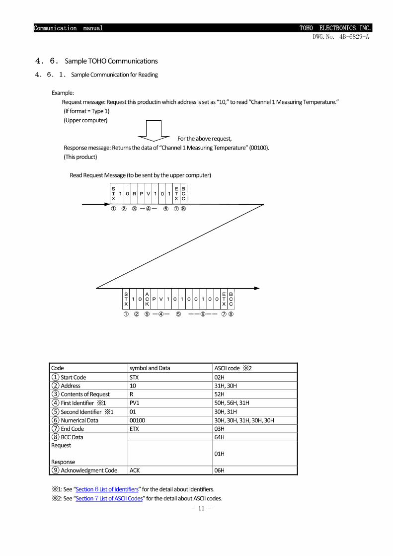
4.6. Sample TOHO Communications
4.6.1. Sample Communication for Reading
Example:
Request message: Request this productin which address is set as “10,” to read “Channel 1 Measuring Temperature.”
(If format = Type 1)
(Upper computer)
For the above request,
Response message: Returns the data of “Channel 1 Measuring Temperature” (00100).
(This product)
Read Request Message (to be sent by the upper computer)
STX1 0 R P V 1
STX1 0
ACK
BCC
P V 1ETX
0 0 1 0 0
① ② ③ |④|
① ② ⑨ |④| ⑦ ⑧||⑥||
BCC
ETX
⑦ ⑧
0 1
⑤
0 1
⑤
Code symbol and Data ASCII code ※2
① Start Code STX 02H
② Address 10 31H, 30H
③ Contents of Request R 52H
④ First Identifier ※1 PV1 50H, 56H, 31H
⑤ Second Identifier ※1 01 30H, 31H
⑥ Numerical Data 00100 30H, 30H, 31H, 30H, 30H
⑦ End Code ETX 03H
⑧ BCC Data Request
Response
64H
01H
⑨ Acknowledgment Code ACK 06H
※1: See “Section6List of Identifiers” for the detail about identifiers.
※2: See “Section7List of ASCII Codes” for the detail about ASCII codes.

Communication manual TOHO ELECTRONICS INC.
DWG.No. 4B-6829-A
- 12 -
4.6.2. Sample Communication for Writing
Example:
Request message: To change “Channel 3 Input Type” to “Pt100 (13)” and write it into this product.
(Upper computer)
For the above request,
Response message: Return the message to tell that the request message has been received.
(This product) ※ Read the data separately to check if the data is written correctly.
Write Request Message (to be sent by the upper computer)
STX0 1
ACK
BCC
ETX
STX0 1 W
BCC
I N PETX
0 0 0 1 3
① ② ③ |④| ⑦ ⑧||⑥||
① ② ⑦ ⑧⑨
0 3
⑤
Code symbol and Data ASCII code ※2
① Start Code STX 02H
② Address 01 30H, 31H
③ Contents of Request W 57H
④ First Identifier ※1 INP 49H, 4EH, 50H
④ Second Identifier ※1 03 30H, 33H
⑤ Numerical Data 00013 30H, 30H, 30H, 31H, 33H
⑥ End Code ETX 03H
⑦ BCC Data Request
Response
31H
06H
⑧ Acknowledgment Code ACK 06H
※1: See “Section6List of Identifiers” for the detail about identifiers.
※2: See “Section7List of ASCII Codes” for the detail about ASCII codes.

Communication manual TOHO ELECTRONICS INC.
DWG.No. 4B-6829-A
- 13 -
Section5 Explanation about MODBUS Protocol Communication
5.1. MODBUS RTU
5.1.1. Structure of Request Message (Data Transmission from Upper Computer to This Product)
5.1.1.1. Structure of Read Request Message
a) Slave Address 01H
b) Function Code 03H
c) Register Address Upper 00H
First register address Lower 00H
d) Number of Registers Upper 00H
2 (fixed) Lower 02H
e) CRC-16 Lower C4H
Upper 0BH
5.1.1.2. Structure of Write Request Message
a) Slave Address 01H
b) Function Code 10H
c) Register Address Upper 01H
First register address Lower 00H
d) Number of Registers Upper 00H
2 (fixed) Lower 02H
f) Number of Bytes 04H Number of Registers x 2
g)
Data for the first register (Lower word)
Upper 00H ③
Data structure is ①②③④H. (① represents 1 byte)
Lower 0DH ④
Data for the first register (Upper word)
Upper 00H ①
Lower 00H ②
e) CRC-16 Lower 6FH
Upper FCH
5.1.1.3. Structure of Save Request Message
a) Slave Address 01H
b) Function Code 10H
c) Register Address Upper 20H
First register address Lower 0EH
d) Number of Registers Upper 00H
2 (fixed) Lower 02H
f) Number of Bytes 04H Number of Registers x 2
g)
Data for the first register (Lower word)
Upper 00H
Data for the saving of setting is optional.
Lower 00H
Data for the first register (Upper word)
Upper 00H
Lower 00H
e) CRC-16 Lower EBH
Upper E2H

Communication manual TOHO ELECTRONICS INC.
DWG.No. 4B-6829-A
- 14 -
5.1.2. Structure of Response Message (Data Transmission from This Product to Upper Computer)
5.1.2.1. Response Message for Read Request Message
a) Slave Address 01H
b) Function Code 03H
f) Number of Bytes 04H Number of Registers x 2
g)
Data for the first register (Lower word)
Upper 00H ③
Data structure is ①②③④H. (① represents 1 byte)
Lower 64H ④
Data for the first register (Upper word)
Upper 00H ①
Lower 00H ②
e) CRC-16 Lower BBH
Upper ECH
5.1.2.2. Response Message for Write/Save Request Message
a) Slave Address 01H
b) Function Code 10H
c) Register Address Upper 01H
First register address Lower 00H
d) Number of Registers Upper 00H
2 (fixed) Lower 02H
e) CRC-16 Lower 40H
Upper 34H
5.1.2.3. Response Message for the Error
a) Slave Address 01H
b) Function Code 83H ← In case of error, the value that is consist of function code of request message + 80H will be set.
h) Error Number 03H
e) CRC-16 Lower 01H
Upper 31H

Communication manual TOHO ELECTRONICS INC.
DWG.No. 4B-6829-A
- 15 -
5.1.3. Explanation about Codes
■ The following codes from (a) Slave Address, (b) Function Code up to (h) Error Number will beexpressed in 8-bit binary code:
(a) Slave Address
It is an address of the device that will be communicated by the upper computer (this product).
Address in the response message form this product indicates the source of response message.
(b) Function Code
Enter the code 03H or 10H.
・ 03H: If the data is to be read from this product
・ 10H: If the data is to be written or saved into this product
(c) Register Address
Specifies the position of data to be read or written with 2bytes.
See “Section6List of Identifiers” for the address of each command.
(d) Number of Registers
Specifies the number of registers that writes.
Since the number of registers of this product is fixed to 2, set it to “0002H.”
(e) CRC-16
It is an error-checking code for the detection of a possible error in the message. It sends CRC-16 (Cyclic Redundancy Code).
Generating polyomical of CRC-16 that is used in this product is X16 + X15 + X2 + 1.
If it is to be attached at the end of the message as an error number, attach the lower byte of CRC before the upper byte.
(f) Number of Bytes
Specifies the number of registers that reads and writes x 2.
Since the number of registers of this product is 2 (fixed), set “04H.”
(g) Data Section
Specifies the data to be written into the register. Data is 4 bytes (fixed).
If the data contains a decimal point, set the numeric value that ignores the decimal point.
Data that is enclosed inparentheses is the value that will be used in the actual message to be sent. See “5.1.1.
Structure of Request Message (Data Transmission from Upper Computer to This Product)” for details.
Contents of Communication HEX Data
PV = 1200.0 (℃) 00002EE0h (2EE00000) PV = -10.00 (℃) FFFFFC18h (FC18FFFF)

Communication manual TOHO ELECTRONICS INC.
DWG.No. 4B-6829-A
- 16 -
(h) Error Number
If there is an error in the message that was sent by the upper computer, the error number will be included in the “response
message” of this product for the reply.
For multiple errors, the largest error number will be included.
Contents and classification of error are the following:
Error Number Description of errors in “Request Message” that was received by this product
01 Received an unsupported function code
02 Received an unspecified address
03 Numerical value data is out of the “setting range that is specified individually by the setting item”
04 Malfunction of measuring equipment (memory error or A/D conversion error)

Communication manual TOHO ELECTRONICS INC.
DWG.No. 4B-6829-A
- 17 -
5.1.4. Things to Be Noted during the Communication
5.1.4.1. Timing of Transmission
Upon using the communication function, set enough response delay time to ensure the communication (sending/receiving) with the
host computer.
See “2.7.Setting of Response Delay Time”
5.1.4.2. Request Interval
If “request message” is to be sent continuously by the upper computer, wait for at least 2msecs from the arrival of the “response
message” from this product before sending the next request message.
5.1.4.3. Conditions for Response
This product will not return the “response message” if there is a time interval of more than 3.5 characters between data that consist of
the “request message” since it cannot identify these data as one whole “request message.”
Therefore, although there is an error in the “request message,”“response message” with the error number (response for the error) will
not be returned unless the above condition is met.
Therefore, the upper computer should resend the necessary “request message” if the “response message” is not returned within
areasonable time.
At a time interval of more than 3.5 characters, this product clears all characters that were received prior to the said interval.
5.1.4.4. Address Specification Error
This product will not respond to any “request message” that specifies the address that is other than the one that has been set to itself.
Therefore, if there is an error in the address section of the “request message,” none of the slave stations will return the “response
message.”
Therefore, the upper computer should resend the necessary “request message” if the “response message” is not returned within
areasonable time.
At a time interval of more than 3.5 characters, this product clears all characters that were received prior to the said interval.
5.1.4.5. Number of Digits of Data and Position of Decimal Point
See “5.1.3.Explanation about Codes (g) Data Section.”
5.1.4.6. Operation after the Receiving of Save Request Message
This product starts the saving of data once it receives the save request message correctly from the upper computer.
Only the data that is different from the one stored in EEPROM (changed data) shall be saved. Data will be saved within 6 seconds.
This product will send the response (ACK) when the save request message is received. Some data may be lost if the product is turned OFF
while the saving process is in progress. Do not turn the power of this product OFF for at least 6 seconds after the sending of save request
message.
5.1.4.7. Saving Data Other than Save Request Message
This product saves the parameter into EEPROM even without receiving the save request message in this case:
・ If the parameter is changed through key operation, it writes only changed parameter and other related parameters.

Communication manual TOHO ELECTRONICS INC.
DWG.No. 4B-6829-A
- 18 -
5.2. MODBUS ASCII
5.2.1. Structure of Request Message (Data Transmission from Upper Computer to This Product)
5.2.1.1. Structure of Read Request Message
a) Start Code ':'
b) Slave Address '0','1'
c) Function Code '0','3'
d) Register Address Upper '0','0'
First register address Lower '0','0'
e) Number of Registers Upper '0','0'
2 (fixed) Lower '0','2'
f) LRC 'F','A'
g) End Code CR,LF
5.2.1.2. Structure of Write Request Message
a) Start Code ':'
b) Slave Address '0','1'
c) Function Code '1','0'
d) Register Address Upper '0','1'
First register address Lower '0','0'
e) Number of Registers Upper '0','0'
2 (fixed) Lower '0','2'
h) Number of Bytes '0','4' Number of Registers x 2
i)
Data for the first register (Lower word)
Upper '0','0' ③
Data structure is ①②③④H. (① represents 1 byte)
Lower '0','D' ④
Data for the first register (Upper word)
Upper '0','0' ①
Lower '0','0' ②
f) LRC 'D','B'
g) End Code CR,LF
5.2.1.3. Structure of Save Request Message
a) Start Code ':'
b) Slave Address '0','1'
c) Function Code '1','0'
d) Register Address Upper '2','0'
First register address Lower '0','E'
e) Number of Registers Upper '0','0'
2 (fixed) Lower '0','2'
h) Number of Bytes '0','4' Number of Registers x 2
i)
Data for the first register (Lower word)
Upper '0','0'
Data for the saving of setting is optional. Lower '0','0'
Data for the first register (Upper word)
Upper '0','0'
Lower '0','0'
f) LRC 'B','B'
g) End Code CR,LF

Communication manual TOHO ELECTRONICS INC.
DWG.No. 4B-6829-A
- 19 -
5.2.2. Structure of Response Message (Data Transmission from This product to Upper Computer)
5.2.2.1. Response Message for Read Request Message
a) Start Code ':'
b) Slave Address '0','1'
c) Function Code '0','3'
h) Number of Bytes '0','4' Number of Registers x 2
i)
Data for the first register (Lower word)
Upper '0','0' ③
Data structure is ①②③④H. (① represents 1 byte)
Lower '6','4' ④
Data for the first register (Upper word)
Upper '0','0' ①
Lower '0','0' ②
f) LRC '9','4'
g) End Code CR,LF
5.2.2.2. Response Message for Write/Save Request Message
a) Start Code ':'
b) Slave Address '0','1'
c) Function Code '1','0'
d) Register Address Upper '0','1'
First register address Lower '0','0'
e) Number of Registers Upper '0','0'
2 (fixed) Lower '0','2'
f) LRC 'E','C'
g) End Code CR,LF
5.2.2.3. Response message for the error
a) Start Code ':'
b) Slave Address '0','1'
c) Function Code '8','3' ← In case of error, the value that is consist of function code of request message + 80H will be set.
j) Error Number '0','3'
f) LRC '7','9'
g) End Code CR,LF

Communication manual TOHO ELECTRONICS INC.
DWG.No. 4B-6829-A
- 20 -
5.2.3. Explanation About Codes
■ The following codes from (a) Start Code, (b) Slave Address up to (j) Error Number will be expressed in ASCII code:
■ See “Section7List of ASCII Codes" or the detail about ASCII codes. ■ For the conversion into ASCII code,
See “5.2.1.Structure of Request Message (Data Transmission from Upper Computer to This Product)” for details.
(a) Start Code It is a code that is necessary for the receiving side to detect the start of the message. It shall be attached to the start of the character string to be sent.
(b) Slave Address
It is an address of the device that will be communicated by the upper computer (this product). Address in the response message form this product indicates the source of response message.
(c) Function Code
Enter the code 03H or 10H.
・ 03H: If the data is to be read from this product
・ 10H: If the data is to be written or saved into this product
(d) Register Address Specifies the position of data to be read or written with 2bytes.
See “Section6List of Identifiers” for the address of each command.
(e) Number of Registers Specifies the number of registers that writes. Since the number of registers of this product is fixed to 2, set it to “0002H.”
(f) LRC
It is an error-checking code for the detection of a possible error in the message. It sends LRC. LRC that is used in this product is a value where all data in the message, except for start code and end code, are summed upwithout performing a carry over and treated the sum total as the complement of 2. Any portion that is expressed as “1” and “B” shall be considered as “1BH.” If 12H was computed as an error number, attach “1” and “2” at the end of the message.
(g) End Code
It is a code that is necessary for the receiving side to detect the end of the message. CR(0DH) and LF(0AH) shall be attached at the end of the character string to be sent.
(h) Number of Bytes
Specifies the number of registers that reads and writes x 2. Since the number of registers of this product is 2 (fixed), set “04H.”

Communication manual TOHO ELECTRONICS INC.
DWG.No. 4B-6829-A
- 21 -
(i) Data Section
Specifies the data to be written into the register. Data is 4 bytes (fixed).
If the data contains a decimal point, set the numeric value that ignores the decimal point.
Data that is enclosed in parentheses is the value that will be used in the actual message to be sent. See “5.2.1.
Structure of Request Message (Data Transmission from Upper Computer to This Product)” for details.
Contents of Communication HEX Data
PV = 1200.0 (℃) 00002EE0h (2EE00000) PV = -10.00 (℃) FFFFFC18h (FC18FFFF)
(j) Error Number If there is an error in the message that was sent by the upper computer, the error number will be included in the “response message” of this product for the reply. For multiple errors, the largest error number will be included.
Contents and classification of error are the following:
Error Number Description of errors in “Request Message” that was received by this product
01 Received an unsupported function code
02 Received an unspecified address
03 Numerical value data is out of the “setting range that is specified individually by the setting item”
04 Malfunction of measuring equipment (memory error or A/D conversion error)

Communication manual TOHO ELECTRONICS INC.
DWG.No. 4B-6829-A
- 22 -
5.2.4. Things to Be Noted during the Communication
5.2.4.1. Timing of Transmission
Upon using the communication function, set enough response delay time to ensure the communication (sending/receiving) with the
host computer.
See “2.7.Setting of Response Delay Time”
5.2.4.2. Request Interval
If “request message” is to be sent continuously by the upper computer, wait for at least 2msecs from the arrival of the “response
message” from this product before sending the next request message.
5.2.4.3. Conditions for Response
This product will not return the “response message” if start code and end code are not included in the “request message.”
Therefore, although there is an error in the “request message,”“response message” with the error number (response for the error) will
not be returned unless the above condition is met.
Therefore, the upper computer should resend the necessary “request message” if the “response message” is not returned within
areasonable time.
Once the start code is received, this product clears all codes that were received prior to the said start code.
5.2.4.4. Address Specification Error
This product will not respond to any “request message” that specifies the address that is other than the one that has been set to itself.
Therefore, if there is an error in the address section of the “request message,” none of the slave stations will return the “response
message.”
Therefore, the upper computer should resend the necessary “request message” if the “response message” is not returned within
areasonable time.
Once the start code is received, this product clears all codes that were received prior to the said start code.
5.2.4.5. Number of Digits of Data and Position of Decimal Point
See “5.1.3 Explanation About Codes (i) Data Section.”
5.2.4.6. Operation after the Receiving of Save Request Message
This product starts the saving of data once it receives the save request message correctly from the upper computer.
Only the data that is different from the one stored in EEPROM (changed data) shall be saved. Data will be saved within 6 seconds.
This product will send the response (ACK) when the save request message is received. Some data may be lost if the product is turned OFF
while the saving process is in progress. Do not turn the power of this product OFF for at least 6 seconds after the sending of save request
message.
5.2.4.7. Saving Data Other than Save Request Message
This product saves the parameter into EEPROM even without receiving the save request message in this case:
・ If the parameter is changed through key operation, it writes changed parameter and other related parameters.

Communication manual TOHO ELECTRONICS INC.
DWG.No. 4B-6829-A
- 23 -
Section6 List of Identifiers ■ See User’s Manual of this product for setting range, selection items, initial value, and other related information.
Note:“□” in the frame of identifier means space (ASCII code: 20H).
6.1. Other Commands
TOHO MODBUS Name Command Remark First
Identifier Second
Identifier Absolute
(DEC) Relative
(hex)
PV1 01 40001 0000 CH1 PV R Temperature input:0.0 ℃ unit
Analog input:1 digit unit TOHO When “-H-” or “B.OUT”
is displayed:HHHHH
When “-L-” is displayed:LLLLL MODBUS When “-H-” or “B.OUT”
is displayed:48484848h When “-L-”
is displayed:4C4C4C4Ch
PV1 02 40003 0002 CH2 PV R
PV1 03 40005 0004 CH3 PV R
PV1 04 40007 0006 CH4 PV R
PV1 05 40009 0008 CH5 PV R
PV1 06 40011 000A CH6 PV R
MD□ 40025 0018 Record operation RW 0:Stop
1:Start
OM1 48195 2002 DO Monitor 1 R
④③②①
①~④ 0:OFF
1:ON
①:DO1
②:DO2
③:DO3
④:DO4
OM2 48197 2004 DO Monitor 2 R
④③②①
①~④ 0:OFF
1:ON
①:DO5
②:DO6
③:DO7
④:DO8
OM3 48199 2006 DO Monitor 3 R
④③②①
①~④ 0:OFF
1:ON
①:DO9
②:DO10
③:DO11
④:DO12

Communication manual TOHO ELECTRONICS INC.
DWG.No. 4B-6829-A
- 24 -
TOHO MODBUS Name Command Remark First
Identifier Second
Identifier Absolute
(DEC) Relative
(hex)
EM1 48201 2008 DI1 Monitor R
④③②①
①~④ 0:DI OFF
1:DI ON
①:DI1
②:DI2
③:DI3
④:DI4
EM2 48203 200A DI2 Monitor R
④③②①
①~④ 0:DI OFF
1:DI ON
①:DI5
②:DI6
③:DI7
④:DI8
EM3 48205 200C DI3 Monitor R
④③②①
①~④ 0:DI OFF
1:DI ON
①:DI9
②:DI10
③:DI11
④:DI12
STR 48207 200E Store instruction W
INI Initialize the setting W
1:Parameter setting
2:Input
3:Display
4:Record
5:Others
11:System setting
12:Device/Other
99:All setting

Communication manual TOHO ELECTRONICS INC.
DWG.No. 4B-6829-A
- 25 -
6.2. Input
TOHO MODBUS Name Command Remark First
Identifier Second
Identifier Absolute
(DEC) Relative
(hex)
INP 01 40257 0100 CH1 Input Type RW
0:K
1:J
2:T
3:E
4:R
5:S
6:B
7:N
8:U
9:L
10:WRe5-26
11:PR40-20
12:PL2
13:Pt100
14:JPt100
15:-10~10(mV)
16:0~20(mV)
17:0~50(mV)
18:-1~1(V)
19:-10~10(V)
20:0~10(V)
21:4~20(mA)
INP 02 40259 0102 CH2 Input Type RW
INP 03 40261 0104 CH3 Input Type RW
INP 04 40263 0106 CH4 Input Type RW
INP 05 40265 0108 CH5 Input Type RW
INP 06 40267 010A CH6 Input Type RW
BAO 01 40269 010C CH1 Burnout RW
0:OFF
1:ON
BAO 02 40271 010E CH2 Burnout RW
BAO 03 40273 0110 CH3 Burnout RW
BAO 04 40275 0112 CH4 Burnout RW
BAO 05 40277 0114 CH5 Burnout RW
BAO 06 40279 0116 CH6 Burnout RW
RJF 01 40281 0118 CH1 RJC RW
0:Internal
1:Specified Channel
2:OFF
RJF 02 40283 011A CH2 RJC RW
RJF 03 40285 011C CH3 RJC RW
RJF 04 40287 011E CH4 RJC RW
RJF 05 40289 0120 CH5 RJC RW
RJF 06 40291 0122 CH6 RJC RW
RJC 01 40293 0124 CH1 RJC Channel RW 0:CH01
1:CH02
2:CH03
3:CH04
4:CH05
5:CH06
RJC 02 40295 0126 CH2 RJC Channel RW
RJC 03 40297 0128 CH3 RJC Channel RW
RJC 04 40299 012A CH4 RJC Channel RW
RJC 05 40301 012C CH5 RJC Channel RW
RJC 06 40303 012E CH6 RJC Channel RW

Communication manual TOHO ELECTRONICS INC.
DWG.No. 4B-6829-A
- 26 -
6.3. Scaling
TOHO MODBUS Name Command Remark First
Identifier Second
Identifier Absolute
(DEC) Relative
(hex)
SQL 01 40513 0200 CH1 Square root RW
0:OFF
1:ON
SQL 02 40515 0202 CH2 Square root RW
SQL 03 40517 0204 CH3 Square root RW
SQL 04 40519 0206 CH4 Square root RW
SQL 05 40521 0208 CH5 Square root RW
SQL 06 40523 020A CH6 Square root RW
SIH 01 40525 020C CH1 Meas. upr lim RW
SIH 02 40527 020E CH2 Meas. upr lim RW
SIH 03 40529 0210 CH3 Meas. upr lim RW
SIH 04 40531 0212 CH4 Meas. upr lim RW
SIH 05 40533 0214 CH5 Meas. upr lim RW
SIH 06 40535 0216 CH6 Meas. upr lim RW
SIL 01 40537 0218 CH1 Meas. lwr lim RW
SIL 02 40539 021A CH2 Meas. lwr lim RW
SIL 03 40541 021C CH3 Meas. lwr lim RW
SIL 04 40543 021E CH4 Meas. lwr lim RW
SIL 05 40545 0220 CH5 Meas. lwr lim RW
SIL 06 40547 0222 CH6 Meas. lwr lim RW
SOH 01 40549 0224 CH1 Scale upr lim RW
SOH 02 40551 0226 CH2 Scale upr lim RW
SOH 03 40553 0228 CH3 Scale upr lim RW
SOH 04 40555 022A CH4 Scale upr lim RW
SOH 05 40557 022C CH5 Scale upr lim RW
SOH 06 40559 022E CH6 Scale upr lim RW
SOL 01 40561 0230 CH1 Scale lwr lim RW
SOL 02 40563 0232 CH2 Scale lwr lim RW
SOL 03 40565 0234 CH3 Scale lwr lim RW
SOL 04 40567 0236 CH4 Scale lwr lim RW
SOL 05 40569 0238 CH5 Scale lwr lim RW
SOL 06 40571 023A CH6 Scale lwr lim RW
DP□ 01 40573 023C CH1 Decimal Point RW 0:0
1:0.0
2:0.00
3:0.000
4:0.0000
DP□ 02 40575 023E CH2 Decimal Point RW
DP□ 03 40577 0240 CH3 Decimal Point RW
DP□ 04 40579 0242 CH4 Decimal Point RW
DP□ 05 40581 0244 CH5 Decimal Point RW
DP□ 06 40583 0246 CH6 Decimal Point RW

Communication manual TOHO ELECTRONICS INC.
DWG.No. 4B-6829-A
- 27 -
TOHO MODBUS Name Command Remark First
Identifier Second
Identifier Absolute
(DEC) Relative
(hex)
UNI 01 40585 0248 CH1 Unit RW 0:℃
1:゚ F
2:K
3:mV
4:V
5:mA
6:A
7:mW
8:W
9:%
10:%RH
11:ppc
12:ppm
13:ppb
UNI 02 40587 024A CH2 Unit RW
UNI 03 40589 024C CH3 Unit RW
UNI 04 40591 024E CH4 Unit RW
UNI 05 40593 0250 CH5 Unit RW
UNI 06 40595 0252 CH6 Unit RW

Communication manual TOHO ELECTRONICS INC.
DWG.No. 4B-6829-A
- 28 -
6.4. Display
TOHO MODBUS Name Command Remark First
Identifier Second
Identifier Absolute
(DEC) Relative
(hex)
TAG 01 CH1 Tag RW
Up to 29 alphanumeric characters
TAG 02 CH2 Tag RW
TAG 03 CH3 Tag RW
TAG 04 CH4 Tag RW
TAG 05 CH5 Tag RW
TAG 06 CH6 Tag RW
EXP 01 CH1 Description RW
Up to 29 alphanumeric characters
EXP 02 CH2 Description RW
EXP 03 CH3 Description RW
EXP 04 CH4 Description RW
EXP 05 CH5 Description RW
EXP 06 CH6 Description RW
COL 01 40769 0300 CH1 Display Color RW 0:Red
1:Green
2:Blue
3:Purple
4:Yellow
5:Aqua
6:Dark Red
7:Lime
8:Dark Blue
9:Bright Purple
10:Blue Green
11:Olive
12:Gray
13:Khaki
14:Brown
15:Orange
COL 02 40771 0302 CH2 Display Color RW
COL 03 40773 0304 CH3 Display Color RW
COL 04 40775 0306 CH4 Display Color RW
COL 05 40777 0308 CH5 Display Color RW
COL 06 40779 030A CH6 Display Color RW

Communication manual TOHO ELECTRONICS INC.
DWG.No. 4B-6829-A
- 29 -
6.5. Scale
TOHO MODBUS Name Command Remark First
Identifier Second
Identifier Absolute
(DEC) Relative
(hex)
SCH 01 41057 0420 CH1 Rng of ScaleU RW
Temperature input:0.0 ℃ unit
Analog input:1 digit unit
SCH 02 41059 0422 CH2 Rng of ScaleU RW
SCH 03 41061 0424 CH3 Rng of ScaleU RW
SCH 04 41063 0426 CH4 Rng of ScaleU RW
SCH 05 41065 0428 CH5 Rng of ScaleU RW
SCH 06 41067 042A CH6 Rng of ScaleU RW
SCL 01 41069 042C CH1 Rng of ScaleL RW
Temperature input:0.0 ℃ unit
Analog input:1 digit unit
SCL 02 41071 042E CH2 Rng of ScaleL RW
SCL 03 41073 0430 CH3 Rng of ScaleL RW
SCL 04 41075 0432 CH4 Rng of ScaleL RW
SCL 05 41077 0434 CH5 Rng of ScaleL RW
SCL 06 41079 0436 CH6 Rng of ScaleL RW
SCN 01 41081 0438 CH1 Scale No. RW
0:No.1
1:No.2
2:No.3
SCN 02 41083 043A CH2 Scale No. RW
SCN 03 41085 043C CH3 Scale No. RW
SCN 04 41087 043E CH4 Scale No. RW
SCN 05 41089 0440 CH5 Scale No. RW
SCN 06 41091 0442 CH6 Scale No. RW
SCS 01 41093 0444 CH1 Partitions RW
SCS 02 41095 0446 CH2 Partitions RW
SCS 03 41097 0448 CH3 Partitions RW
SCS 04 41099 044A CH4 Partitions RW
SCS 05 41101 044C CH5 Partitions RW
SCS 06 41103 044E CH6 Partitions RW

Communication manual TOHO ELECTRONICS INC.
DWG.No. 4B-6829-A
- 30 -
6.6. Alarm
TOHO MODBUS Name Command Remark First
Identifier Second
Identifier Absolute
(DEC) Relative
(hex)
SF1 01 41281 0500 CH1 Alarm1 Alarm Type RW
0:OFF
1:Alim Up Lim
2:Alm Lw Lim
3:Abnl Alarm
SF1 02 41283 0502 CH2 Alarm1 Alarm Type RW
SF1 03 41285 0504 CH3 Alarm1 Alarm Type RW
SF1 04 41287 0506 CH4 Alarm1 Alarm Type RW
SF1 05 41289 0508 CH5 Alarm1 Alarm Type RW
SF1 06 41291 050A CH6 Alarm1 Alarm Type RW
SF2 01 41293 050C CH1 Alarm2 Alarm Type RW
SF2 02 41295 050E CH2 Alarm2 Alarm Type RW
SF2 03 41297 0510 CH3 Alarm2 Alarm Type RW
SF2 04 41299 0512 CH4 Alarm2 Alarm Type RW
SF2 05 41301 0514 CH5 Alarm2 Alarm Type RW
SF2 06 41303 0516 CH6 Alarm2 Alarm Type RW
SF3 01 41305 0518 CH1 Alarm3 Alarm Type RW
SF3 02 41307 051A CH2 Alarm3 Alarm Type RW
SF3 03 41309 051C CH3 Alarm3 Alarm Type RW
SF3 04 41311 051E CH4 Alarm3 Alarm Type RW
SF3 05 41313 0520 CH5 Alarm3 Alarm Type RW
SF3 06 41315 0522 CH6 Alarm3 Alarm Type RW
SF4 01 41317 0524 CH1 Alarm4 Alarm Type RW
SF4 02 41319 0526 CH2 Alarm4 Alarm Type RW
SF4 03 41321 0528 CH3 Alarm4 Alarm Type RW
SF4 04 41323 052A CH4 Alarm4 Alarm Type RW
SF4 05 41325 052C CH5 Alarm4 Alarm Type RW
SF4 06 41327 052E CH6 Alarm4 Alarm Type RW

Communication manual TOHO ELECTRONICS INC.
DWG.No. 4B-6829-A
- 31 -
TOHO MODBUS Name Command Remark First
Identifier Second
Identifier Absolute
(DEC) Relative
(hex)
AO1 01 41329 0530 CH1 Alarm1 Alm Tgt Conn RW
0:OFF
1:ALM
2:DO01
3:DO02
4:DO03
5:DO04
6:DO05
7:DO06
8:DO07
9:DO08
10:DO09
11:DO10
12:DO11
13:DO12
AO1 02 41331 0532 CH2 Alarm1 Alm Tgt Conn RW
AO1 03 41333 0534 CH3 Alarm1 Alm Tgt Conn RW
AO1 04 41335 0536 CH4 Alarm1 Alm Tgt Conn RW
AO1 05 41337 0538 CH5 Alarm1 Alm Tgt Conn RW
AO1 06 41339 053A CH6 Alarm1 Alm Tgt Conn RW
AO2 01 41341 053C CH1 Alarm2 Alm Tgt Conn RW
AO2 02 41343 053E CH2 Alarm2 Alm Tgt Conn RW
AO2 03 41345 0540 CH3 Alarm2 Alm Tgt Conn RW
AO2 04 41347 0542 CH4 Alarm2 Alm Tgt Conn RW
AO2 05 41349 0544 CH5 Alarm2 Alm Tgt Conn RW
AO2 06 41351 0546 CH6 Alarm2 Alm Tgt Conn RW
AO3 01 41353 0548 CH1 Alarm3 Alm Tgt Conn RW
AO3 02 41355 054A CH2 Alarm3 Alm Tgt Conn RW
AO3 03 41357 054C CH3 Alarm3 Alm Tgt Conn RW
AO3 04 41359 054E CH4 Alarm3 Alm Tgt Conn RW
AO3 05 41361 0550 CH5 Alarm3 Alm Tgt Conn RW
AO3 06 41363 0552 CH6 Alarm3 Alm Tgt Conn RW
AO4 01 41365 0554 CH1 Alarm4 Alm Tgt Conn RW
AO4 02 41367 0556 CH2 Alarm4 Alm Tgt Conn RW
AO4 03 41369 0558 CH3 Alarm4 Alm Tgt Conn RW
AO4 04 41371 055A CH4 Alarm4 Alm Tgt Conn RW
AO4 05 41373 055C CH5 Alarm4 Alm Tgt Conn RW
AO4 06 41375 055E CH6 Alarm4 Alm Tgt Conn RW

Communication manual TOHO ELECTRONICS INC.
DWG.No. 4B-6829-A
- 32 -
TOHO MODBUS Name Command Remark First
Identifier Second
Identifier Absolute
(DEC) Relative
(hex)
AS1 01 41377 0560 CH1 Alarm1 Alarm Value RW
Temperature input:0.0 ℃ unit
Analog input:1 digit unit
AS1 02 41379 0562 CH2 Alarm1 Alarm Value RW
AS1 03 41381 0564 CH3 Alarm1 Alarm Value RW
AS1 04 41383 0566 CH4 Alarm1 Alarm Value RW
AS1 05 41385 0568 CH5 Alarm1 Alarm Value RW
AS1 06 41387 056A CH6 Alarm1 Alarm Value RW
AS2 01 41389 056C CH1 Alarm2 Alarm Value RW
AS2 02 41391 056E CH2 Alarm2 Alarm Value RW
AS2 03 41393 0570 CH3 Alarm2 Alarm Value RW
AS2 04 41395 0572 CH4 Alarm2 Alarm Value RW
AS2 05 41397 0574 CH5 Alarm2 Alarm Value RW
AS2 06 41399 0576 CH6 Alarm2 Alarm Value RW
AS3 01 41401 0578 CH1 Alarm3 Alarm Value RW
AS3 02 41403 057A CH2 Alarm3 Alarm Value RW
AS3 03 41405 057C CH3 Alarm3 Alarm Value RW
AS3 04 41407 057E CH4 Alarm3 Alarm Value RW
AS3 05 41409 0580 CH5 Alarm3 Alarm Value RW
AS3 06 41411 0582 CH6 Alarm3 Alarm Value RW
AS4 01 41413 0584 CH1 Alarm4 Alarm Value RW
AS4 02 41415 0586 CH2 Alarm4 Alarm Value RW
AS4 03 41417 0588 CH3 Alarm4 Alarm Value RW
AS4 04 41419 058A CH4 Alarm4 Alarm Value RW
AS4 05 41421 058C CH5 Alarm4 Alarm Value RW
AS4 06 41423 058E CH6 Alarm4 Alarm Value RW

Communication manual TOHO ELECTRONICS INC.
DWG.No. 4B-6829-A
- 33 -
TOHO MODBUS Name Command Remark First
Identifier Second
Identifier Absolute
(DEC) Relative
(hex)
AH1 01 41425 0590 CH1 Alarm1 Hysteresis RW
Temperature input:0.0 ℃ unit
Analog input:1 digit unit
AH1 02 41427 0592 CH2 Alarm1 Hysteresis RW
AH1 03 41429 0594 CH3 Alarm1 Hysteresis RW
AH1 04 41431 0596 CH4 Alarm1 Hysteresis RW
AH1 05 41433 0598 CH5 Alarm1 Hysteresis RW
AH1 06 41435 059A CH6 Alarm1 Hysteresis RW
AH2 01 41437 059C CH1 Alarm2 Hysteresis RW
AH2 02 41439 059E CH2 Alarm2 Hysteresis RW
AH2 03 41441 05A0 CH3 Alarm2 Hysteresis RW
AH2 04 41443 05A2 CH4 Alarm2 Hysteresis RW
AH2 05 41445 05A4 CH5 Alarm2 Hysteresis RW
AH2 06 41447 05A6 CH6 Alarm2 Hysteresis RW
AH3 01 41449 05A8 CH1 Alarm3 Hysteresis RW
AH3 02 41451 05AA CH2 Alarm3 Hysteresis RW
AH3 03 41453 05AC CH3 Alarm3 Hysteresis RW
AH3 04 41455 05AE CH4 Alarm3 Hysteresis RW
AH3 05 41457 05B0 CH5 Alarm3 Hysteresis RW
AH3 06 41459 05B2 CH6 Alarm3 Hysteresis RW
AH4 01 41461 05B4 CH1 Alarm4 Hysteresis RW
AH4 02 41463 05B6 CH2 Alarm4 Hysteresis RW
AH4 03 41465 05B8 CH3 Alarm4 Hysteresis RW
AH4 04 41467 05BA CH4 Alarm4 Hysteresis RW
AH4 05 41469 05BC CH5 Alarm4 Hysteresis RW
AH4 06 41471 05BE CH6 Alarm4 Hysteresis RW

Communication manual TOHO ELECTRONICS INC.
DWG.No. 4B-6829-A
- 34 -
TOHO MODBUS Name Command Remark First
Identifier Second
Identifier Absolute
(DEC) Relative
(hex)
AD1 01 41473 05C0 CH1 Alarm1 Alm Dly (sec) RW
AD1 02 41475 05C2 CH2 Alarm1 Alm Dly (sec) RW
AD1 03 41477 05C4 CH3 Alarm1 Alm Dly (sec) RW
AD1 04 41479 05C6 CH4 Alarm1 Alm Dly (sec) RW
AD1 05 41481 05C8 CH5 Alarm1 Alm Dly (sec) RW
AD1 06 41483 05CA CH6 Alarm1 Alm Dly (sec) RW
AD2 01 41485 05CC CH1 Alarm2 Alm Dly (sec) RW
AD2 02 41487 05CE CH2 Alarm2 Alm Dly (sec) RW
AD2 03 41489 05D0 CH3 Alarm2 Alm Dly (sec) RW
AD2 04 41491 05D2 CH4 Alarm2 Alm Dly (sec) RW
AD2 05 41493 05D4 CH5 Alarm2 Alm Dly (sec) RW
AD2 06 41495 05D6 CH6 Alarm2 Alm Dly (sec) RW
AD3 01 41497 05D8 CH1 Alarm3 Alm Dly (sec) RW
AD3 02 41499 05DA CH2 Alarm3 Alm Dly (sec) RW
AD3 03 41501 05DC CH3 Alarm3 Alm Dly (sec) RW
AD3 04 41503 05DE CH4 Alarm3 Alm Dly (sec) RW
AD3 05 41505 05E0 CH5 Alarm3 Alm Dly (sec) RW
AD3 06 41507 05E2 CH6 Alarm3 Alm Dly (sec) RW
AD4 01 41509 05E4 CH1 Alarm4 Alm Dly (sec) RW
AD4 02 41511 05E6 CH2 Alarm4 Alm Dly (sec) RW
AD4 03 41513 05E8 CH3 Alarm4 Alm Dly (sec) RW
AD4 04 41515 05EA CH4 Alarm4 Alm Dly (sec) RW
AD4 05 41517 05EC CH5 Alarm4 Alm Dly (sec) RW
AD4 06 41519 05EE CH6 Alarm4 Alm Dly (sec) RW

Communication manual TOHO ELECTRONICS INC.
DWG.No. 4B-6829-A
- 35 -
6.7. REC/CALC
TOHO MODBUS Name Command Remark First
Identifier Second
Identifier Absolute
(DEC) Relative
(hex)
PDF 01 41537 0600 CH1 Inp Fltr (sec) RW
PDF 02 41539 0602 CH2 Inp Fltr (sec) RW
PDF 03 41541 0604 CH3 Inp Fltr (sec) RW
PDF 04 41543 0606 CH4 Inp Fltr (sec) RW
PDF 05 41545 0608 CH5 Inp Fltr (sec) RW
PDF 06 41547 060A CH6 Inp Fltr (sec) RW
REC 01 41549 060C CH1 Record Type RW
0:OFF
1:Inst. val
2:Average
3:Max/Min
REC 02 41551 060E CH2 Record Type RW
REC 03 41553 0610 CH3 Record Type RW
REC 04 41555 0612 CH4 Record Type RW
REC 05 41557 0614 CH5 Record Type RW
REC 06 41559 0616 CH6 Record Type RW
PVS 01 41561 0618 CH1 Offset RW
Temperature input:0.0 ℃ unit
Analog input:1 digit unit
PVS 02 41563 061A CH2 Offset RW
PVS 03 41565 061C CH3 Offset RW
PVS 04 41567 061E CH4 Offset RW
PVS 05 41569 0620 CH5 Offset RW
PVS 06 41571 0622 CH6 Offset RW
PVG 01 41573 0624 CH1 Gain RW
PVG 02 41575 0626 CH2 Gain RW
PVG 03 41577 0628 CH3 Gain RW
PVG 04 41579 062A CH4 Gain RW
PVG 05 41581 062C CH5 Gain RW
PVG 06 41583 062E CH6 Gain RW

Communication manual TOHO ELECTRONICS INC.
DWG.No. 4B-6829-A
- 36 -
6.8. Group name
TOHO MODBUS Name Command Remark First
Identifier Second
Identifier Absolute
(DEC) Relative
(hex)
GN1 Group1 Group Name RW
Up to 29 alphanumeric characters
GN2 Group2 Group Name RW
GN3 Group3 Group Name RW
GN4 Group4 Group Name RW
GN5 Group5 Group Name RW
GN6 Group6 Group Name RW
GN7 Group7 Group Name RW
GN8 Group8 Group Name RW
GF1 41809 0710 Group1 Group Display RW
0:OFF
1:ON
GF2 41811 0712 Group2 Group Display RW
GF3 41813 0714 Group3 Group Display RW
GF4 41815 0716 Group4 Group Display RW
GF5 41817 0718 Group5 Group Display RW
GF6 41819 071A Group6 Group Display RW
GF7 41821 071C Group7 Group Display RW
GF8 41823 071E Group8 Group Display RW
TF1 41793 0700 Group1 Label Display RW
0:Channel No.
1:Tag
TF2 41795 0702 Group2 Label Display RW
TF3 41797 0704 Group3 Label Display RW
TF4 41799 0706 Group4 Label Display RW
TF5 41801 0708 Group5 Label Display RW
TF6 41803 070A Group6 Label Display RW
TF7 41805 070C Group7 Label Display RW
TF8 41807 070E Group8 Label Display RW
6.9. Group channel
TOHO MODBUS Name Command Remark First
Identifier Second
Identifier Absolute
(DEC) Relative
(hex)
G11 42049 0800 Group01 CH01 RW
0:Non-select
1:Select
G12 42051 0802 Group01 CH02 RW
G13 42053 0804 Group01 CH03 RW
G14 42055 0806 Group01 CH04 RW
G15 42057 0808 Group01 CH05 RW
G16 42059 080A Group01 CH06 RW
G21 42061 080C Group02 CH01 RW
G22 42063 080E Group02 CH02 RW
G23 42065 0810 Group02 CH03 RW
G24 42067 0812 Group02 CH04 RW
G25 42069 0814 Group02 CH05 RW
G26 42071 0816 Group02 CH06 RW

Communication manual TOHO ELECTRONICS INC.
DWG.No. 4B-6829-A
- 37 -
TOHO MODBUS Name Command Remark First
Identifier Second
Identifier Absolute
(DEC) Relative
(hex)
G31 42073 0818 Group03 CH01 RW
0:Non-select
1:Select
G32 42075 081A Group03 CH02 RW
G33 42077 081C Group03 CH03 RW
G34 42079 081E Group03 CH04 RW
G35 42081 0820 Group03 CH05 RW
G36 42083 0822 Group03 CH06 RW
G41 42085 0824 Group04 CH01 RW
G42 42087 0826 Group04 CH02 RW
G43 42089 0828 Group04 CH03 RW
G44 42091 082A Group04 CH04 RW
G45 42093 082C Group04 CH05 RW
G46 42095 082E Group04 CH06 RW
G51 42097 0830 Group05 CH01 RW
G52 42099 0832 Group05 CH02 RW
G53 42101 0834 Group05 CH03 RW
G54 42103 0836 Group05 CH04 RW
G55 42105 0838 Group05 CH05 RW
G56 42107 083A Group05 CH06 RW
G61 42109 083C Group06 CH01 RW
G62 42111 083E Group06 CH02 RW
G63 42113 0840 Group06 CH03 RW
G64 42115 0842 Group06 CH04 RW
G65 42117 0844 Group06 CH05 RW
G66 42119 0846 Group06 CH06 RW
G71 42121 0848 Group07 CH01 RW
G72 42123 084A Group07 CH02 RW
G73 42125 084C Group07 CH03 RW
G74 42127 084E Group07 CH04 RW
G75 42129 0850 Group07 CH05 RW
G76 42131 0852 Group07 CH06 RW
G81 42133 0854 Group08 CH01 RW
G82 42135 0856 Group08 CH02 RW
G83 42137 0858 Group08 CH03 RW
G84 42139 085A Group08 CH04 RW
G85 42141 085C Group08 CH05 RW
G86 42143 085E Group08 CH06 RW

Communication manual TOHO ELECTRONICS INC.
DWG.No. 4B-6829-A
- 38 -
6.10. Graph Display
TOHO MODBUS Name Command Remark First
Identifier Second
Identifier Absolute
(DEC) Relative
(hex)
TW1 42305 0900 Group1 Horz trend RW
0:OFF
1:ON
TW2 42307 0902 Group2 Horz trend RW
TW3 42309 0904 Group3 Horz trend RW
TW4 42311 0906 Group4 Horz trend RW
TW5 42313 0908 Group5 Horz trend RW
TW6 42315 090A Group6 Horz trend RW
TW7 42317 090C Group7 Horz trend RW
TW8 42319 090E Group8 Horz trend RW
TL1 42321 0910 Group1 Vert trend RW
0:OFF
1:ON
TL2 42323 0912 Group2 Vert trend RW
TL3 42325 0914 Group3 Vert trend RW
TL4 42327 0916 Group4 Vert trend RW
TL5 42329 0918 Group5 Vert trend RW
TL6 42331 091A Group6 Vert trend RW
TL7 42333 091C Group7 Vert trend RW
TL8 42335 091E Group8 Vert trend RW
BD1 42337 0920 Group1 Bar graph RW
0:OFF
1:ON
BD2 42339 0922 Group2 Bar graph RW
BD3 42341 0924 Group3 Bar graph RW
BD4 42343 0926 Group4 Bar graph RW
BD5 42345 0928 Group5 Bar graph RW
BD6 42347 092A Group6 Bar graph RW
BD7 42349 092C Group7 Bar graph RW
BD8 42351 092E Group8 Bar graph RW
DD1 42353 0930 Group1 Digital disp. RW
0:OFF
1:ON
DD2 42355 0932 Group2 Digital disp. RW
DD3 42357 0934 Group3 Digital disp. RW
DD4 42359 0936 Group4 Digital disp. RW
DD5 42361 0938 Group5 Digital disp. RW
DD6 42363 093A Group6 Digital disp. RW
DD7 42365 093C Group7 Digital disp. RW
DD8 42367 093E Group8 Digital disp. RW

Communication manual TOHO ELECTRONICS INC.
DWG.No. 4B-6829-A
- 39 -
6.11. Auto switching
TOHO MODBUS Name Command Remark First
Identifier Second
Identifier Absolute
(DEC) Relative
(hex)
DCA 42561 0A00 Auto display RW 0:OFF
1:ON
DCT 42563 0A02 Change cycle RW
0:5 sec
1:10 sec
2:15 sec
3:30 sec
4:60 sec
6.12. Record Operation
TOHO MODBUS Name Command Remark First
Identifier Second
Identifier Absolute
(DEC) Relative
(hex)
DRT 42817 0B00 Record Cycle RW
0:0.1 sec
1:1 sec
2:2 sec
3:3 sec
4:5 sec
5:10 sec
6:15 sec
7:20 sec
8:30 sec
9:1 min
10:2 min
11:3 min
12:5 min
13:10 min
14:15 min
15:20 min
16:30 min
17:60 min
FRT 42819 0B02 File rec. cy RW
0:10Minute
1:1 Hour
2:1 Day
3:1 Week
4:1 Month
5:1 Year
FOW 42821 0B04 File overwrite RW 0:Disable
1:Enable

Communication manual TOHO ELECTRONICS INC.
DWG.No. 4B-6829-A
- 40 -
6.13. Schedule
TOHO MODBUS Name Command Remark First
Identifier Second
Identifier Absolute
(DEC) Relative
(hex)
SCD 43073 0C00 Schedule RW
0:OFF
1:Week Day
2:Every Day
STH 43075 0C02 Start Time hour RW
STM Start Time min RW
STS Start Time sec RW
ENH 43077 0C04 End Time hour RW
ENM End Time min RW
ENS End Time sec RW
WE1 43079 0C06 Sun RW
0:Non-select
1:Select
WE2 43081 0C08 Mon RW
WE3 43083 0C0A Tue RW
WE4 43085 0C0C Wed RW
WE5 43087 0C0E Thu RW
WE6 43089 0C10 Fri RW
WE7 43091 0C12 Sat RW
6.14. Message
TOHO MODBUS Name Command Remark First
Identifier Second
Identifier Absolute
(DEC) Relative
(hex)
ME1 Message01 Message RW
Up to 29 alphanumeric characters
ME2 Message02 Message RW
ME3 Message03 Message RW
ME4 Message04 Message RW
ME5 Message05 Message RW
ME6 Message06 Message RW
ME7 Message07 Message RW
ME8 Message08 Message RW
ME9 Message09 Message RW
MEA Message10 Message RW
MEB Message11 Message RW
MEC Message12 Message RW
MED Message13 Message RW
MEE Message14 Message RW
MEF Message15 Message RW
MEG Message16 Message RW
MEH Message17 Message RW
MEI Message18 Message RW
MEJ Message19 Message RW
MEK Message20 Message RW

Communication manual TOHO ELECTRONICS INC.
DWG.No. 4B-6829-A
- 41 -
TOHO MODBUS Name Command Remark First
Identifier Second
Identifier Absolute
(DEC) Relative
(hex)
MT1 43329 0D00 Message01 Timing RW
0:OFF
1:Func Key
2:Alarm On
3:Alarm Off
4:DI ON
5:DI OFF
MT2 43331 0D02 Message02 Timing RW
MT3 43333 0D04 Message03 Timing RW
MT4 43335 0D06 Message04 Timing RW
MT5 43337 0D08 Message05 Timing RW
MT6 43339 0D0A Message06 Timing RW
MT7 43341 0D0C Message07 Timing RW
MT8 43343 0D0E Message08 Timing RW
MT9 43345 0D10 Message09 Timing RW
MTA 43347 0D12 Message10 Timing RW
MTB 43349 0D14 Message11 Timing RW
MTC 43351 0D16 Message12 Timing RW
MTD 43353 0D18 Message13 Timing RW
MTE 43355 0D1A Message14 Timing RW
MTF 43357 0D1C Message15 Timing RW
MTG 43359 0D1E Message16 Timing RW
MTH 43361 0D20 Message17 Timing RW
MTI 43363 0D22 Message18 Timing RW
MTJ 43365 0D24 Message19 Timing RW
MTK 43367 0D26 Message20 Timing RW
MC1 43369 0D28 Message01 Channel No. RW
0:CH01
1:CH02
2:CH03
3:CH04
4:CH05
5:CH06
MC2 43371 0D2A Message02 Channel No. RW
MC3 43373 0D2C Message03 Channel No. RW
MC4 43375 0D2E Message04 Channel No. RW
MC5 43377 0D30 Message05 Channel No. RW
MC6 43379 0D32 Message06 Channel No. RW
MC7 43381 0D34 Message07 Channel No. RW
MC8 43383 0D36 Message08 Channel No. RW
MC9 43385 0D38 Message09 Channel No. RW
MCA 43387 0D3A Message10 Channel No. RW
MCB 43389 0D3C Message11 Channel No. RW
MCC 43391 0D3E Message12 Channel No. RW
MCD 43393 0D40 Message13 Channel No. RW
MCE 43395 0D42 Message14 Channel No. RW
MCF 43397 0D44 Message15 Channel No. RW
MCG 43399 0D46 Message16 Channel No. RW
MCH 43401 0D48 Message17 Channel No. RW
MCI 43403 0D4A Message18 Channel No. RW
MCJ 43405 0D4C Message19 Channel No. RW
MCK 43407 0D4E Message20 Channel No. RW

Communication manual TOHO ELECTRONICS INC.
DWG.No. 4B-6829-A
- 42 -
TOHO MODBUS Name Command Remark First
Identifier Second
Identifier Absolute
(DEC) Relative
(hex)
MA1 43409 0D50 Message01 Alarm No. RW
0:Alarm 01
1:Alarm 02
2:Alarm 03
3:Alarm 04
MA2 43411 0D52 Message02 Alarm No. RW
MA3 43413 0D54 Message03 Alarm No. RW
MA4 43415 0D56 Message04 Alarm No. RW
MA5 43417 0D58 Message05 Alarm No. RW
MA6 43419 0D5A Message06 Alarm No. RW
MA7 43421 0D5C Message07 Alarm No. RW
MA8 43423 0D5E Message08 Alarm No. RW
MA9 43425 0D60 Message09 Alarm No. RW
MAA 43427 0D62 Message10 Alarm No. RW
MAB 43429 0D64 Message11 Alarm No. RW
MAC 43431 0D66 Message12 Alarm No. RW
MAD 43433 0D68 Message13 Alarm No. RW
MAE 43435 0D6A Message14 Alarm No. RW
MAF 43437 0D6C Message15 Alarm No. RW
MAG 43439 0D6E Message16 Alarm No. RW
MAH 43441 0D70 Message17 Alarm No. RW
MAI 43443 0D72 Message18 Alarm No. RW
MAJ 43445 0D74 Message19 Alarm No. RW
MAK 43447 0D76 Message20 Alarm No. RW
MD1 43449 0D78 Message01 DI No. RW
0:DI01
1:DI02
2:DI03
3:DI04
4:DI05
5:DI06
6:DI07
7:DI08
8:DI09
MD2 43451 0D7A Message02 DI No. RW
MD3 43453 0D7C Message03 DI No. RW
MD4 43455 0D7E Message04 DI No. RW
MD5 43457 0D80 Message05 DI No. RW
MD6 43459 0D82 Message06 DI No. RW
MD7 43461 0D84 Message07 DI No. RW
MD8 43463 0D86 Message08 DI No. RW
MD9 43465 0D88 Message09 DI No. RW
MDA 43467 0D8A Message10 DI No. RW
MDB 43469 0D8C Message11 DI No. RW
MDC 43471 0D8E Message12 DI No. RW
MDD 43473 0D90 Message13 DI No. RW
MDE 43475 0D92 Message14 DI No. RW
MDF 43477 0D94 Message15 DI No. RW
MDG 43479 0D96 Message16 DI No. RW
MDH 43481 0D98 Message17 DI No. RW
MDI 43483 0D9A Message18 DI No. RW
MDJ 43485 0D9C Message19 DI No. RW
MDK 43487 0D9E Message20 DI No. RW

Communication manual TOHO ELECTRONICS INC.
DWG.No. 4B-6829-A
- 43 -
6.15. DI
TOHO MODBUS Name Command Remark First
Identifier Second
Identifier Absolute
(DEC) Relative
(hex)
DI1 43585 0E00 DI1 Function RW
0:OFF
1:Rec. ON/OFF
2:LCD ON/OFF
DI2 43587 0E02 DI2 Function RW
DI3 43589 0E04 DI3 Function RW
DI4 43591 0E06 DI4 Function RW
DI5 43593 0E08 DI5 Function RW
DI6 43595 0E0A DI6 Function RW
DI7 43597 0E0C DI7 Function RW
DI8 43599 0E0E DI8 Function RW
DI9 43601 0E10 DI9 Function RW
6.16. Progress time
TOHO MODBUS Name Command Remark First
Identifier Second
Identifier Absolute
(DEC) Relative
(hex)
ET□ 43841 0F00 Progress time RW 0:OFF
1:ON
ETF 43843 0F02 Condition RW
0:Record
1:Alm ocrd
2:DI
ETC 43845 0F04 Channel No. RW
0:CH01
1:CH02
2:CH03
3:CH04
4:CH05
5:CH06
ETA 43847 0F06 Alarm No. RW
0:Alarm 01
1:Alarm 02
2:Alarm 03
3:Alarm 04
4:All
ETD 43849 0F08 DI No. RW
0:DI01
1:DI02
2:DI03
3:DI04
4:DI05
5:DI06
6:DI07
7:DI08
8:DI09

Communication manual TOHO ELECTRONICS INC.
DWG.No. 4B-6829-A
- 44 -
6.17. LCD backlight
TOHO MODBUS Name Command Remark First
Identifier Second
Identifier Absolute
(DEC) Relative
(hex)
SPT 44097 1000 Slp t (min) RW
LAC 44099 1002 Actv. brt. RW
LSC 44101 1004 Slp brt. RW
ABK 44103 1006 Alm rcvy RW 0:OFF
1:ON
6.18. Key function
TOHO MODBUS Name Command Remark First
Identifier Second
Identifier Absolute
(DEC) Relative
(hex)
FU□ 44609 1200 FUNC Key RW
0:OFF
1:Switching of Screen
2:Message
KLF 44611 1202 Key Lock RW 0:OFF
1:ON
MKF 44613 1204 Menu Lock RW
0:Free
1:Parameter
2:System
3:All
HKF 44615 1206 Hard Key Lock RW
0:Free
1:REC
2:FUNC
3:REC+FUNC

Communication manual TOHO ELECTRONICS INC.
DWG.No. 4B-6829-A
- 45 -
6.19. Comm. Settings
TOHO MODBUS Name Command Remark First
Identifier Second
Identifier Absolute
(DEC) Relative
(hex)
PRT 44865 1300 Protocol RW 0:TOHO
1:MODBUS
MFO 44867 1302 Format RW 0:Type 1/RTU
1:Type 2/ASCII
ADR 44869 1304 Comm. Address RW
BPS 44871 1306 Comm. Speed RW
0:2400bps
1:4800bps
2:9600bps
3:19200bps
4:38400bps
DAT 44873 1308 Data Length RW 0:7bit
1:8bit
STB 44875 130A Stop bit RW 0:1bit
1:2bit
PAL 44877 130C Parity check RW
0:OFF
1:EVEN
2:ODD
BCC 44879 130E BCC check RW 0:OFF
1:ON
AWT 44881 1310 Resp delay RW
6.20. Clock
TOHO MODBUS Name Command Remark First
Identifier Second
Identifier Absolute
(DEC) Relative
(hex)
TYE 44353 1100 Year RW
TMO 44355 1102 Month RW
TDA 44357 1104 Day RW
THO 44359 1106 Hour RW
TMI 44361 1108 Minute RW
TSE 44363 110A Second RW
6.21. Language
TOHO MODBUS Name Command Remark First
Identifier Second
Identifier Absolute
(DEC) Relative
(hex)
LNG 40027 001A Language RW 0:English
1:Japanese

Communication manual TOHO ELECTRONICS INC.
DWG.No. 4B-6829-A
- 46 -
Section7 List of ASCII Codes
Upper Lower 00h 10h 20h 30h 40h 50h 60h 70h
00h NUL DLE Space 0 @ P ̀ p
01h SOH DC1 ! 1 A Q a q
02h STX DC2 " 2 B R b r
03h ETX DC3 # 3 C S c s
04h EOT DC4 $ 4 D T d t
05h ENQ NAK % 5 E U e u
06h ACK SYN & 6 F V f v
07h BEL ETB ' 7 G W g w
08h BS CAN ( 8 H X h x
09h HT EM ) 9 I Y i y
0Ah LF SUB * : J Z j z
0Bh VT ESC + ; K [ k {
0Ch FF FS , < L ¥ l |
0Dh CR GS - = M ] m }
0Eh SO RS . > N ̂ n ~
0Fh SI US / ? O _ o DEL
※How to Use ASCII Code Table: (ASCII Code) = (Upper) + (Lower)
Example 1: If "A": (41h) = (40h) + (01h) Example 2: If "m": (6Dh) = (60h) + (0Dh)