TQPM01D - Opto-Link telecommunications technology Co., Ltd
14
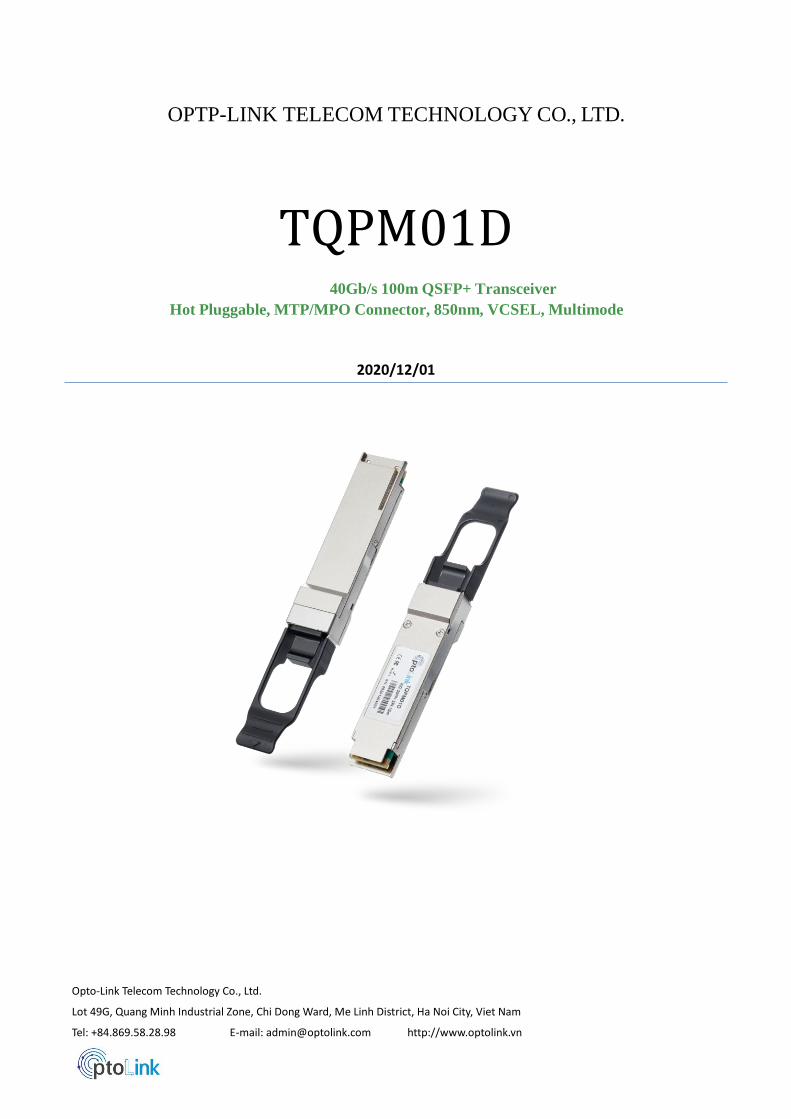
OPTP-LINK TELECOM TECHNOLOGY CO., LTD. TQPM01D 40Gb/s 100m QSFP+ Transceiver Hot Pluggable, MTP/MPO Connector, 850nm, VCSEL, Multimode 2020/12/01 Opto-Link Telecom Technology Co., Ltd. Lot 49G, Quang Minh Industrial Zone, Chi Dong Ward, Me Linh District, Ha Noi City, Viet Nam Tel: +84.869.58.28.98 E-mail: [email protected] http://www.optolink.vn
-
Upload
khangminh22 -
Category
Documents
-
view
2 -
download
0
Transcript of TQPM01D - Opto-Link telecommunications technology Co., Ltd
OPTP-LINK TELECOM TECHNOLOGY CO., LTD.
TQPM01D
40Gb/s 100m QSFP+ Transceiver
Hot Pluggable, MTP/MPO Connector, 850nm, VCSEL, Multimode
2020/12/01
Opto-Link Telecom Technology Co., Ltd.
Lot 49G, Quang Minh Industrial Zone, Chi Dong Ward, Me Linh District, Ha Noi City, Viet Nam
Tel: +84.869.58.28.98 E-mail: [email protected] http://www.optolink.vn
TQPM01D
2
Features:
4 independent full-duplex channels
Up to 11.2Gbps per channel bandwidth
Aggregate bandwidth of > 40Gbps
MTP/MPO optical connector
QSFP MSA compliant
Digital diagnostic capabilities
Capable of over 100m transmission on OM3 Multimode Fiber (MMF)and 150m on OM4 MMF
CML compatible electrical I/O
Single +3.3V power supply operating
TX input and RX output CDR retiming
Built-in digital diagnostic functions
Temperature range 0°C to 70°C
RoHS Compliant Part
Applications:
Rack to rack
Data centers
Metro networks
Switches and Routers
Infiniband 4x SDR, DDR, QDR
Description:
The TQPM01D is a parallel 40Gbps Quad Small Form-factor Pluggable (QSFP) optical module
that provides increased port density and total system cost savings. The QSFP full-duplex optical
module offers 4 independent transmit and receive channels, each capable of 10Gbps operation
for an aggregate bandwidth of 40Gbps 100m on OM3 Multimode Fiber (MMF)and 150m on
OM4 MMF.
An optical fiber ribbon cable with an MPO/MTP connector at each end plugs into the QSFP
TQPM01D
3
module receptacle. The orientation of the ribbon cable is “keyed” and guide pins are present
inside the module’s receptacle to ensure proper alignment. The cable usually has no twist (key
up to key up) to ensure proper channel to channel alignment. Electrical connection is achieved
though a z-pluggable 38-pin IPASS® connector.
The module operates from a single +3.3V power supply and LVCMOS/LVTTL global control
signals such as Module Present, Reset, Interrupt and Low Power Mode are available with the
modules. A 2-wire serial interface is available to send and receive more complex control signals
and to obtain digital diagnostic information. Individual channels can be addressed and unused
channels can be shut down for maximum design flexibility.
The TQP01 is designed with form factor, optical/electrical connection and digital diagnostic
interface according to the QSFP Multi-Source Agreement (MSA). It has been designed to meet
the harshest external operating conditions including temperature, humidity and EMI
interference. The module offers very high functionality and feature integration, accessible via a
two-wire serial interface.
Absolute Maximum Ratings
Parameter Symbol Min. Typical Max. Unit
Storage Temperature TS -40 +85 °C
Supply Voltage VCCT, R -0.5 4 V
Relative Humidity RH 0 85 %
Recommended Operating Environment:
Parameter Symbol Min. Typical Max. Unit
Case operating Temperature TC 0 +70 °C
Supply Voltage VCCT, R +3.13 3.3 +3.47 V
Supply Current ICC 1000 mA
Power Dissipation PD 3.5 W
Electrical Characteristics (TOP = 0 to 70 °C, VCC = 3.13 to 3.47 Volts
Parameter Symbol Min Typ Max Unit Note
Data Rate per Channel - 10.3125 11.2 Gbps
Power Consumption - 2.5 3.5 W
Supply Current Icc 0.75 1.0 A
TQPM01D
4
Control I/O Voltage-High VIH 2.0 Vcc V
Control I/O Voltage-Low VIL 0 0.7 V
Inter-Channel Skew TSK 150 Ps
RESETL Duration 10 Us
RESETL De-assert time 100 ms
Power On Time 100 ms
Transmitter
Single Ended
Tolerance
Output Voltage
0.3
4
V
1
Common mode Voltage Tolerance 15 mV
Transmit Input Diff Voltage VI 120 1200 mV
Transmit Input Diff Impedance ZIN 80 100 120
Data Dependent Input Jitter DDJ 0.1 UI
Data Input Total Jitter TJ 0.28 UI
Receiver
Single Ended Output Voltage
Tolerance
0.3
4
V
Rx Output Diff Voltage Vo 600 800 mV
Rx Output Rise and Fall Voltage Tr/Tf 35 ps 1
Total Jitter TJ 0.7 UI
Deterministic Jitter DJ 0.42 UI
Note:
1. 20~80%
Optical Parameters(TOP = 0 to 70 °C, VCC = 3.0 to 3.6 Volts)
Parameter Symbol Min Typ Max Unit Ref.
Transmitter
Optical Wavelength λ 840 860 nm
RMS Spectral Width Pm 0.5 0.65 nm
Average Optical Power per Channel Pavg -7 -2.5 +1.0 dBm
Laser Off Power Per Channel Poff -30 dBm
Optical Extinction Ratio ER 3.5 dB
Relative Intensity Noise Rin -128 dB/HZ 1
Optical Return Loss Tolerance 12 dB
Receiver
Optical Center Wavelength λC 840 860 nm
Receiver Sensitivity per Channel R -10 dBm
Maximum Input Power PMAX +0.5 dBm
TQPM01D
5
Receiver Reflectance Rrx -12 dB
LOS De-Assert LOSD -14 dBm
LOS Assert LOSA -30 dBm
LOS Hysteresis LOSH 0.5 dB
Note
1. 12dB Reflection
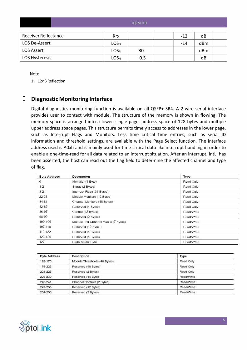
Diagnostic Monitoring Interface
Digital diagnostics monitoring function is available on all QSFP+ SR4. A 2-wire serial interface
provides user to contact with module. The structure of the memory is shown in flowing. The
memory space is arranged into a lower, single page, address space of 128 bytes and multiple
upper address space pages. This structure permits timely access to addresses in the lower page,
such as Interrupt Flags and Monitors. Less time critical time entries, such as serial ID
information and threshold settings, are available with the Page Select function. The interface
address used is A0xh and is mainly used for time critical data like interrupt handling in order to
enable a one-time-read for all data related to an interrupt situation. After an interrupt, IntL, has
been asserted, the host can read out the flag field to determine the affected channel and type
of flag.
7
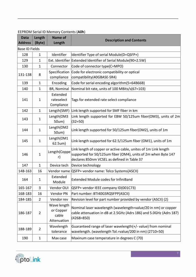
EEPROM Serial ID Memory Contents (A0h)
Data
Address
Length
(Byte)
Name of
Length
Description and Contents
Base ID Fields
128 1 Identifier Identifier Type of serial Module(D=QSFP+)
129 1 Ext. Identifier Extended Identifier of Serial Module(90=2.5W)
130 1 Connector Code of connector type(C=MPO)
131-138
8 Specification
compliance
Code for electronic compatibility or optical
compatibility(40GBASE-SR4)
139 1 Encoding Code for serial encoding algorithm(5=64B66B)
140 1 BR, Nominal Nominal bit rate, units of 100 MBits/s(67=103)
141
1
Extended
rateselect
Compliance
Tags for extended rate select compliance
142 1 Length(SMF) Link length supported for SMF fiber in km
143
1 Length(OM3
50um)
Link length supported for EBW 50/125um fiber(OM3), units of 2m
(32=50)
144
1 Length(OM2
50um)
Link length supported for 50/125um fiber(OM2), units of 1m
145
1 Length(OM1
62.5um)
Link length supported for 62.5/125um fiber (OM1), units of 1m
146
1
Length(Coppe
r)
Link length of copper or active cable, unites of 1m Link length
supported for 50/125um fiber (OM4), units of 2m when Byte 147
declares 850nm VCSEL as defined in Table 37
147 1 Device tech Device technology
148-163 16 Vendor name QSFP+ vendor name: Telco Systems(ASCII)
164
1 Extended
Module
Extended Module codes for InfiniBand
165-167 3 Vendor OUI QSFP+ vendor IEEE company ID(001C73)
168-183 16 Vendor PN Part number: BTI40GSRQSFPP(ASCII)
184-185 2 Vendor rev Revision level for part number provided by vendor (ASCII) (2)
186-187
2
Wave length
or Copper
cable
Attenuation
Nominal laser wavelength (wavelength=value/20 in nm) or copper
cable attenuation in dB at 2.5GHz (Adrs 186) and 5.0GHz (Adrs 187)
(4268=850)
188-189
2 Wavelength
tolerance
Guaranteed range of laser wavelength(+/- value) from nominal
wavelength. (wavelength Tol.=value/200 in nm) (2710=50)
190 1 Max case Maxinum case temperature in degrees C (70)
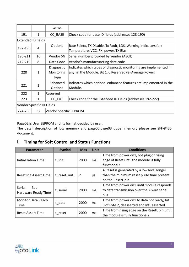
8
temp.
191 1 CC_BASE Check code for base ID fields (addresses 128-190)
Extended ID fields
192-195
4 Options Rate Select, TX Disable, Tx Fault, LOS, Warning indicators for:
Temperature, VCC, RX, power, TX Bias
196-211 16 Vendor SN Serial number provided by vendor (ASCII)
212-219 8 Date Code Vendor's manufacturering date code
220
1
Diagnostic
Monitoring
Type
Indicates which types of diagnostic monitoring are implemented (if
any) in the Module. Bit 1, 0 Reserved (8=Average Power)
221
1 Enhanced
Options
Indicates which optional enhanced features are implemented in the
Module.
222 1 Reserved
223 1 CC_EXT Check code for the Extended ID Fields (addresses 192-222)
Vendor Specific ID Fields
224-255 32 Vendor Specific EEPROM
Page02 is User EEPROM and its format decided by user.
The detail description of low memory and page00.page03 upper memory please see SFF-8436
document.
Timing for Soft Control and Status Functions
Parameter Symbol Max Unit Conditions
Initialization Time
t_init
2000
ms
Time from power on1, hot plug or rising
edge of Reset until the module is fully
functional2
Reset Init Assert Time
t_reset_init
2
μs
A Reset is generated by a low level longer
than the minimum reset pulse time present
on the ResetL pin.
Serial Bus
Hardware Ready Time
t_serial
2000
ms
Time from power on1 until module responds
to data transmission over the 2-wire serial
bus
Monitor Data Ready
Time
t_data
2000
ms Time from power on1 to data not ready, bit
0 of Byte 2, deasserted and IntL asserted
Reset Assert Time
t_reset
2000
ms Time from rising edge on the ResetL pin until
the module is fully functional2
10
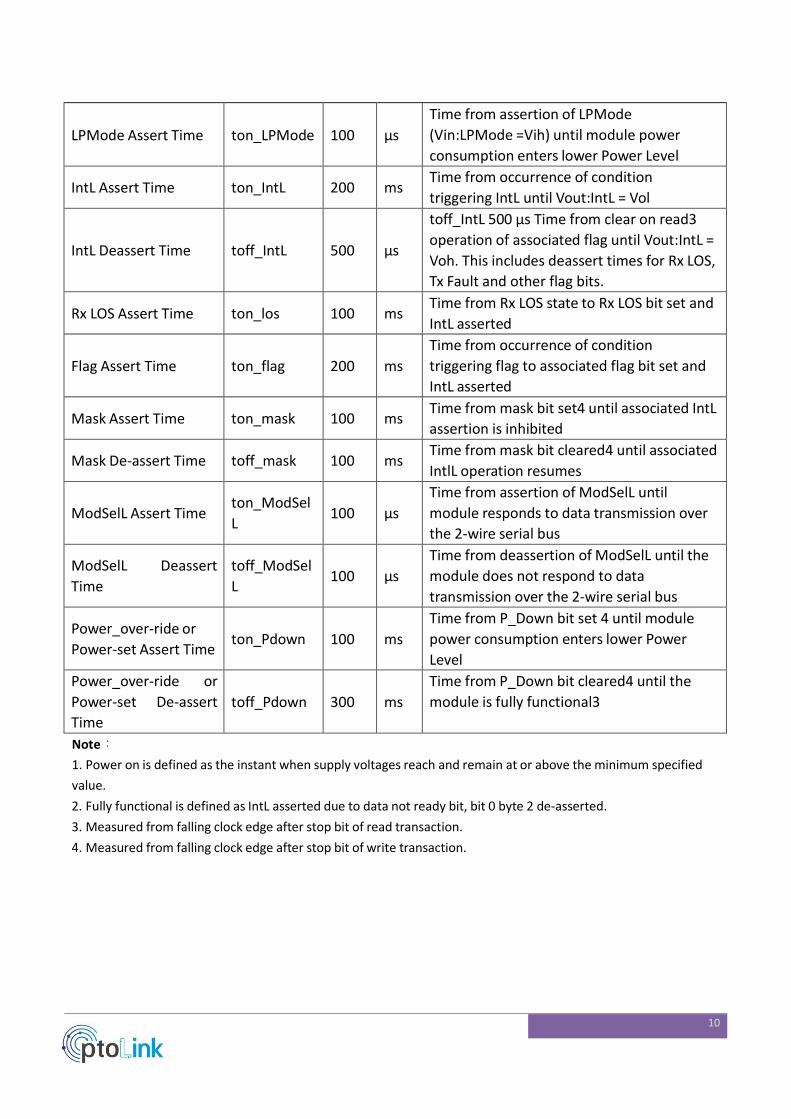
LPMode Assert Time
ton_LPMode
100
μs
Time from assertion of LPMode
(Vin:LPMode =Vih) until module power
consumption enters lower Power Level
IntL Assert Time
ton_IntL
200
ms Time from occurrence of condition
triggering IntL until Vout:IntL = Vol
IntL Deassert Time
toff_IntL
500
μs
toff_IntL 500 μs Time from clear on read3
operation of associated flag until Vout:IntL =
Voh. This includes deassert times for Rx LOS,
Tx Fault and other flag bits.
Rx LOS Assert Time
ton_los
100
ms Time from Rx LOS state to Rx LOS bit set and
IntL asserted
Flag Assert Time
ton_flag
200
ms
Time from occurrence of condition
triggering flag to associated flag bit set and
IntL asserted
Mask Assert Time
ton_mask
100
ms Time from mask bit set4 until associated IntL
assertion is inhibited
Mask De-assert Time
toff_mask
100
ms Time from mask bit cleared4 until associated
IntlL operation resumes
ModSelL Assert Time
ton_ModSel
L
100
μs
Time from assertion of ModSelL until
module responds to data transmission over
the 2-wire serial bus
ModSelL Deassert
Time
toff_ModSel
L
100
μs
Time from deassertion of ModSelL until the
module does not respond to data
transmission over the 2-wire serial bus
Power_over-ride or
Power-set Assert Time
ton_Pdown
100
ms
Time from P_Down bit set 4 until module
power consumption enters lower Power
Level
Power_over-ride or
Power-set De-assert
Time
toff_Pdown
300
ms
Time from P_Down bit cleared4 until the
module is fully functional3
Note:
1. Power on is defined as the instant when supply voltages reach and remain at or above the minimum specified
value.
2. Fully functional is defined as IntL asserted due to data not ready bit, bit 0 byte 2 de-asserted.
3. Measured from falling clock edge after stop bit of read transaction.
4. Measured from falling clock edge after stop bit of write transaction.
11
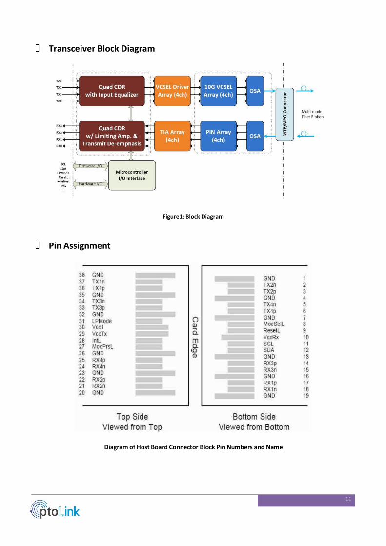
Transceiver Block Diagram
Figure1: Block Diagram
Pin Assignment
Diagram of Host Board Connector Block Pin Numbers and Name
12
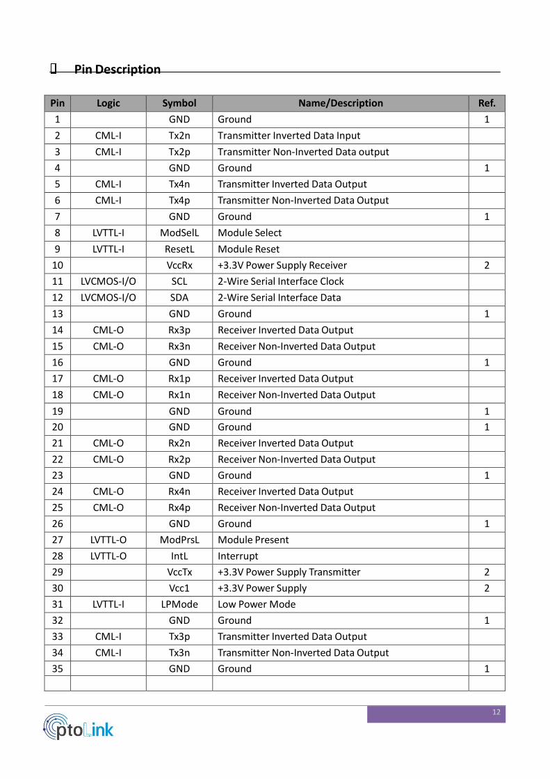
Pin Description
Pin Logic Symbol Name/Description Ref.
1 GND Ground 1
2 CML-I Tx2n Transmitter Inverted Data Input
3 CML-I Tx2p Transmitter Non-Inverted Data output
4 GND Ground 1
5 CML-I Tx4n Transmitter Inverted Data Output
6 CML-I Tx4p Transmitter Non-Inverted Data Output
7 GND Ground 1
8 LVTTL-I ModSelL Module Select
9 LVTTL-I ResetL Module Reset
10 VccRx +3.3V Power Supply Receiver 2
11 LVCMOS-I/O SCL 2-Wire Serial Interface Clock
12 LVCMOS-I/O SDA 2-Wire Serial Interface Data
13 GND Ground 1
14 CML-O Rx3p Receiver Inverted Data Output
15 CML-O Rx3n Receiver Non-Inverted Data Output
16 GND Ground 1
17 CML-O Rx1p Receiver Inverted Data Output
18 CML-O Rx1n Receiver Non-Inverted Data Output
19 GND Ground 1
20 GND Ground 1
21 CML-O Rx2n Receiver Inverted Data Output
22 CML-O Rx2p Receiver Non-Inverted Data Output
23 GND Ground 1
24 CML-O Rx4n Receiver Inverted Data Output
25 CML-O Rx4p Receiver Non-Inverted Data Output
26 GND Ground 1
27 LVTTL-O ModPrsL Module Present
28 LVTTL-O IntL Interrupt
29 VccTx +3.3V Power Supply Transmitter 2
30 Vcc1 +3.3V Power Supply 2
31 LVTTL-I LPMode Low Power Mode
32 GND Ground 1
33 CML-I Tx3p Transmitter Inverted Data Output
34 CML-I Tx3n Transmitter Non-Inverted Data Output
35 GND Ground 1
13
36 CML-I Tx1p Transmitter Inverted Data Output
37 CML-I Tx1n Transmitter Non-Inverted Data Output
38 GND Ground 1
Notes:
1. GND is the symbol for single and supply(power) common for QSFP modules, All are common within the
QSFP module and all module voltages are referenced to this potential otherwise noted. Connect these
directly to the host board signal common ground plane. Laser output disabled on TDIS >2.0V or open,
enabled on TDIS <0.8V.
2. VccRx, Vcc1 and VccTx are the receiver and transmitter power suppliers and shall be applied
concurrently. Recommended host board power supply filtering is shown below. VccRx, Vcc1 and VccTx
may be internally connected within the QSFP transceiver module in any combination. The connector
pins are each rated for maximum current of 500mA.
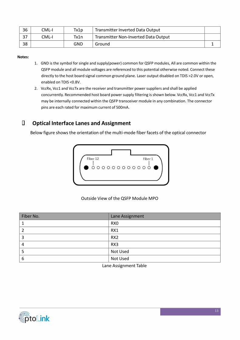
Optical Interface Lanes and Assignment
Below figure shows the orientation of the multi-mode fiber facets of the optical connector
Outside View of the QSFP Module MPO
Fiber No. Lane Assignment
1 RX0
2 RX1
3 RX2
4 RX3
5 Not Used
6 Not Used
Lane Assignment Table
14
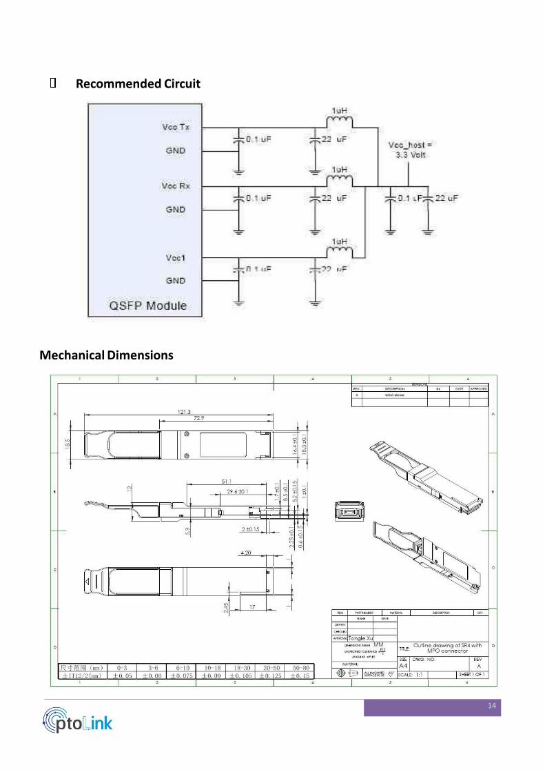
Recommended Circuit
Mechanical Dimensions

15
Opto-Link reserves the right to make changes to the products or information contained herein without notice. No liability is assumed as a result of their use or application. No rights under any patent accompany the sale of any such products or information. Published by Opto-Link Telecom Technology Co., Ltd. Copyright © OPTO-LINK All Rights Reserve

16