TPS6213x 3-V to17-V, 3-A Step-Down Converter In 3-mm × 3 ...
38
TPS6213x 3-V to17-V, 3-A Step-Down Converter In 3-mm × 3-mm QFN Package 1 Features • DCS-Control ™ topology • Input voltage range: 3 V to 17 V • Up to 3-A output current • Adjustable output voltage from 0.9 V to 6 V • Pin-selectable output voltage (nominal, + 5%) • Programmable soft start and tracking • Seamless power save mode transition • Quiescent current of 17 µA (typical) • Selectable operating frequency • Power-good output • 100% duty cycle mode • Short circuit protection • Overtemperature protection • Pin-to-pin compatible with the TPS62140 and TPS62150 • Available in a 3-mm × 3-mm, QFN-16 package • Use the TPS82130 for faster designs 2 Applications • Standard 12-V rail supplies • POL supply from single or multiple Li-ion battery • Solid-state drives • Embedded systems • LDO replacement • Mobile PCs, tablets, modems, cameras • Server, microserver • Data terminal, point of sales (ePOS) 3 Description The TPS6213x family are easy-to-use synchronous step down DC-DC converters optimized for applications with high power density. A high switching frequency of typically 2.5 MHz allows the use of small inductors and provides fast transient response as well as high output voltage accuracy by use of the DCS- Control topology. With their wide operating input voltage range of 3 V to 17 V, the devices are ideally suited for systems powered from either a Li-Ion or other batteries as well as from 12-V intermediate power rails. They support up to 3-A continuous output current at output voltages between 0.9 V and 6 V (with 100% duty cycle mode). The output voltage start-up ramp is controlled by the soft-start pin, which allows operation as either a stand-alone power supply or in tracking configurations. Power sequencing is also possible by configuring the Enable and open-drain Power Good pins. In power save mode, the devices draw quiescent current of approximately 17 μA from V IN . Power save mode, entered automatically and seamlessly if the load is small, maintains high efficiency over the entire load range. In shutdown mode, the device is turned off and shutdown current consumption is less than 2 μA. The device, available in adjustable and fixed output voltage versions, is packaged in a 16-pin VQFN package measuring 3 mm × 3 mm (RGT). Device Information PART NUMBER PACKAGE (1) BODY SIZE (NOM) TPS6213x VQFN (16) 3.00 mm × 3.00 mm (1) For all available packages, see the orderable addendum at the end of the data sheet. PVIN AVIN EN SS/TR DEF FSW SW VOS PG FB AGND PGND TPS62131 0.1 F 3.3 nF 10 F (3 .. 17) V 100 k 22 F 1 / 2.2 μH 1.8 V / 3 A Typical Application Schematic 40 50 60 70 80 90 100 0.0 0.5 1.0 1.5 2.0 2.5 3.0 VIN=5V VIN=12V VIN=17V Output Current (A) Efficiency (%) VOUT=3.3V fsw=1.25MHz G001 Efficiency vs Output Current TPS62130, TPS62130A, TPS62131, TPS62132, TPS62133 SLVSAG7F – NOVEMBER 2011 – REVISED NOVEMBER 2021 An IMPORTANT NOTICE at the end of this data sheet addresses availability, warranty, changes, use in safety-critical applications, intellectual property matters and other important disclaimers. PRODUCTION DATA.
-
Upload
khangminh22 -
Category
Documents
-
view
1 -
download
0
Transcript of TPS6213x 3-V to17-V, 3-A Step-Down Converter In 3-mm × 3 ...

TPS6213x 3-V to17-V, 3-A Step-Down Converter In 3-mm × 3-mm QFN Package
1 Features• DCS-Control™ topology• Input voltage range: 3 V to 17 V• Up to 3-A output current• Adjustable output voltage from 0.9 V to 6 V• Pin-selectable output voltage (nominal, + 5%)• Programmable soft start and tracking• Seamless power save mode transition• Quiescent current of 17 µA (typical)• Selectable operating frequency• Power-good output• 100% duty cycle mode• Short circuit protection• Overtemperature protection• Pin-to-pin compatible with the TPS62140 and
TPS62150• Available in a 3-mm × 3-mm, QFN-16 package• Use the TPS82130 for faster designs
2 Applications• Standard 12-V rail supplies• POL supply from single or multiple Li-ion battery• Solid-state drives• Embedded systems• LDO replacement• Mobile PCs, tablets, modems, cameras• Server, microserver• Data terminal, point of sales (ePOS)
3 DescriptionThe TPS6213x family are easy-to-use synchronous step down DC-DC converters optimized for applications with high power density. A high switching frequency of typically 2.5 MHz allows the use of small inductors and provides fast transient response as well as high output voltage accuracy by use of the DCS-Control topology.
With their wide operating input voltage range of 3 V to 17 V, the devices are ideally suited for systems powered from either a Li-Ion or other batteries as well as from 12-V intermediate power rails. They support up to 3-A continuous output current at output voltages between 0.9 V and 6 V (with 100% duty cycle mode). The output voltage start-up ramp is controlled by the soft-start pin, which allows operation as either a stand-alone power supply or in tracking configurations. Power sequencing is also possible by configuring the Enable and open-drain Power Good pins.
In power save mode, the devices draw quiescent current of approximately 17 μA from VIN. Power save mode, entered automatically and seamlessly if the load is small, maintains high efficiency over the entire load range. In shutdown mode, the device is turned off and shutdown current consumption is less than 2 μA.
The device, available in adjustable and fixed output voltage versions, is packaged in a 16-pin VQFN package measuring 3 mm × 3 mm (RGT).
Device InformationPART NUMBER PACKAGE(1) BODY SIZE (NOM)
TPS6213x VQFN (16) 3.00 mm × 3.00 mm
(1) For all available packages, see the orderable addendum at the end of the data sheet.
PVIN
AVIN
EN
SS/TR
DEF
FSW
SW
VOS
PG
FB
AGND
PGND
TPS62131
0.1 F
3.3 nF
10 F
(3 .. 17) V
100 k 22 F
1 / 2.2 µH
1.8 V / 3 A
Typical Application Schematic
40
50
60
70
80
90
100
0.0 0.5 1.0 1.5 2.0 2.5 3.0
VIN=5V VIN=12V VIN=17V
Output Current (A)
Effic
iency (
%)
VOUT=3.3V
fsw=1.25MHz
G001
Efficiency vs Output Current
TPS62130, TPS62130A, TPS62131, TPS62132, TPS62133SLVSAG7F – NOVEMBER 2011 – REVISED NOVEMBER 2021
An IMPORTANT NOTICE at the end of this data sheet addresses availability, warranty, changes, use in safety-critical applications, intellectual property matters and other important disclaimers. PRODUCTION DATA.

Table of Contents1 Features............................................................................12 Applications..................................................................... 13 Description.......................................................................14 Revision History.............................................................. 25 Device Comparison Table...............................................36 Pin Configuration and Functions...................................37 Specifications.................................................................. 4
7.1 Absolute Maximum Ratings(1) ....................................47.2 ESD Ratings............................................................... 47.3 Recommended Operating Conditions.........................47.4 Thermal Information....................................................47.5 Electrical Characteristics.............................................57.6 Typical Characteristics................................................ 6
8 Detailed Description........................................................78.1 Overview..................................................................... 78.2 Functional Block Diagram........................................... 88.3 Feature Description.....................................................98.4 Device Functional Modes..........................................11
9 Application and Implementation.................................. 13
9.1 Application Information............................................. 139.2 Typical Application.................................................... 139.3 System Examples..................................................... 25
10 Power Supply Recommendations..............................2811 Layout...........................................................................28
11.1 Layout Guidelines................................................... 2811.2 Layout Example...................................................... 2911.3 Thermal Information................................................ 29
12 Device and Documentation Support..........................3012.1 Device Support....................................................... 3012.2 Documentation Support.......................................... 3012.3 Receiving Notification of Documentation Updates..3012.4 Support Resources................................................. 3012.5 Trademarks.............................................................3012.6 Electrostatic Discharge Caution..............................3012.7 Glossary..................................................................30
13 Mechanical, Packaging, and Orderable Information.................................................................... 31
4 Revision HistoryNOTE: Page numbers for previous revisions may differ from page numbers in the current version.
Changes from Revision E (August 2016) to Revision F (November 2021) Page• Added link to the TPS82130 product page ........................................................................................................ 1• Updated the numbering format for tables, figures, and cross-references throughout the document. ................1• Edited data sheet for grammar........................................................................................................................... 1
Changes from Revision D (June 2016) to Revision E (August 2016) Page• Changed the TJ MAX value From: 125°C To: 150°C in the Absolute Maximum Ratings .................................. 4• Changed (TJ = –40°C to 85°C) To: (TJ = –40°C to 125°C) in the Section 7.5 conditions................................... 5• Added a test condition for IQ at TA = -40°C to +85°C in the Section 7.5 ............................................................5• Added Table 8-1 and Table 8-2 ........................................................................................................................10
TPS62130, TPS62130A, TPS62131, TPS62132, TPS62133SLVSAG7F – NOVEMBER 2011 – REVISED NOVEMBER 2021 www.ti.com
2 Submit Document Feedback Copyright © 2021 Texas Instruments Incorporated
Product Folder Links: TPS62130 TPS62130A TPS62131 TPS62132 TPS62133

5 Device Comparison TablePART NUMBER OUTPUT VOLTAGE POWER GOOD LOGIC LEVEL (EN = LOW)
TPS62130 adjustable High Impedance
TPS62130A adjustable Low
TPS62131 1.8 V High Impedance
TPS62132 3.3 V High Impedance
TPS62133 5.0 V High Impedance
6 Pin Configuration and Functions
3
Exposed
Thermal Pad
9
10
11
12
8765
4
2
1
16 15 14 13
PVIN
PVIN
AVIN
SS/TR
SW
SW
SW
PG
PG
ND
PG
ND
VO
S
EN
FB
AG
ND
FS
W
DE
F
Figure 6-1. 16-Pin VQFN With Exposed Thermal Pad (RGT) Top View
Table 6-1. Pin FunctionsPIN(1)
I/O DESCRIPTIONNO. NAME
1,2,3 SW O Switch node, which is connected to the internal MOSFET switches. Connect an inductor between SW and the output capacitor.
4 PG O Output power good (High = VOUT ready, Low = VOUT below nominal regulation); open drain (requires pullup resistor)
5 FB I Voltage feedback of adjustable version. Connect a resistive voltage divider to this pin. It is recommended to connect FB to AGND on fixed output voltage versions for improved thermal performance.
6 AGND Analog Ground. Must be connected directly to the Exposed Thermal Pad and common ground plane.
7 FSW I Switching Frequency Select (Low ≈ 2.5 MHz, High ≈ 1.25 MHz(2) for typical operation)(3)
8 DEF I Output voltage scaling (Low = nominal, High = nominal + 5%)(3)
9 SS/TR I Soft-Start/Tracking Pin. An external capacitor connected to this pin sets the internal voltage reference rise time. It can be used for tracking and sequencing.
10 AVIN I Supply voltage for control circuitry. Connect to the same source as PVIN.
11,12 PVIN I Supply voltage for power stage. Connect to the same source as AVIN.
13 EN I Enable input (High = enabled, Low = disabled)(3)
14 VOS I Output voltage sense pin and connection for the control loop circuitry
15,16 PGND Power Ground. Must be connected directly to the Exposed Thermal Pad and common ground plane.
Exposed Thermal Pad
Must be connected to AGND (pin 6), PGND (pin 15,16), and common ground plane. See the Layout Example. Must be soldered to achieve appropriate power dissipation and mechanical reliability.
(1) For more information about connecting pins, see the Detailed Description and Application and Implementation sections.(2) Connect FSW to VOUT or PG in this case.(3) An internal pulldown resistor keeps logic level low if pin is floating.
www.ti.comTPS62130, TPS62130A, TPS62131, TPS62132, TPS62133
SLVSAG7F – NOVEMBER 2011 – REVISED NOVEMBER 2021
Copyright © 2021 Texas Instruments Incorporated Submit Document Feedback 3
Product Folder Links: TPS62130 TPS62130A TPS62131 TPS62132 TPS62133

7 Specifications7.1 Absolute Maximum Ratings(1)
over operating junction temperature range (unless otherwise noted)MIN MAX UNIT
Pin voltage range(2)
AVIN, PVIN –0.3 20V
EN, SS/TR –0.3 VIN+0.3
SW –0.3 VIN+0.3 V
DEF, FSW, FB, PG, VOS –0.3 7 V
Power Good sink current PG 10 mA
Operating junction temperature, TJ –40 150 °C
Storage temperature, Tstg –65 150 °C
(1) Stresses beyond those listed under absolute maximum ratings may cause permanent damage to the device. These are stress ratings only, and functional operation of the device at these or any other conditions beyond those indicated under recommended operating conditions is not implied. Exposure to absolute-maximum-rated conditions for extended periods may affect device reliability.
(2) All voltages are with respect to network ground terminal.
7.2 ESD RatingsVALUE UNIT
V(ESD) Electrostatic discharge(1)Human-body model (HBM), per ANSI/ESDA/JEDEC JS-001(2) ±2000
VCharged-device model (CDM), per JEDEC specification JESD22-C101(3) ±500
(1) ESD testing is performed according to the respective JESD22 JEDEC standard.(2) JEDEC document JEP155 states that 500-V HBM allows safe manufacturing with a standard ESD control process.(3) JEDEC document JEP157 states that 250-V CDM allows safe manufacturing with a standard ESD control process.
7.3 Recommended Operating Conditionsover operating junction temperature range (unless otherwise noted)
MIN MAX UNITSupply Voltage, VIN (at AVIN and PVIN) 3 17 V
Operating junction temperature, TJ –40 125 °C
7.4 Thermal Information
THERMAL METRIC(1)TPS6213X
UNITSRGT 16 PINS
RθJA Junction-to-ambient thermal resistance 45
°C/W
RθJCtop Junction-to-case(top) thermal resistance 53.6
RθJB Junction-to-board thermal resistance 17.4
ψJT Junction-to-top characterization parameter 1.1
ψJB Junction-to-board characterization parameter 17.4
RθJCbot Junction-to-case(bottom) thermal resistance 4.5
(1) For more information about traditional and new thermal metrics, see the Semiconductor and IC Package Thermal Metrics application report.
TPS62130, TPS62130A, TPS62131, TPS62132, TPS62133SLVSAG7F – NOVEMBER 2011 – REVISED NOVEMBER 2021 www.ti.com
4 Submit Document Feedback Copyright © 2021 Texas Instruments Incorporated
Product Folder Links: TPS62130 TPS62130A TPS62131 TPS62132 TPS62133

7.5 Electrical Characteristicsover operating junction temperature (TJ = –40°C to 125°C), typical values at VIN = 12 V and TA=25°C (unless otherwise noted)
PARAMETER TEST CONDITIONS MIN TYP MAX UNITSUPPLYVIN Input voltage range(1) 3 17 V
IQ Operating quiescent current EN=High, IOUT = 0 mA, device not switching
17 30µA
TA = -40°C to +85°C 17 25
ISD Shutdown current(2) EN=Low1.5 25
µATA = -40°C to +85°C 1.5 4
VUVLO Undervoltage lockout thresholdFalling Input Voltage (PWM mode operation) 2.6 2.7 2.8 V
Hysteresis 200 mV
TSD Thermal shutdown temperature 160°C
Thermal shutdown hysteresis 20
CONTROL (EN, DEF, FSW, SS/TR, PG)
VHHigh level input threshold voltage (EN, DEF, FSW) 0.9 0.65 V
VL Low level input threshold voltage (EN, DEF, FSW)
0.45 0.3 V
ILKG Input leakage current (EN, DEF, FSW) EN=VIN or GND; DEF, FSW=VOUT or GND 0.01 1 µA
VTH_PG Power good threshold voltageRising (%VOUT) 92% 95% 98%
Falling (%VOUT) 87% 90% 94%
VOL_PG Power good output low IPG=–2mA 0.07 0.3 V
ILKG_PG Input leakage current (PG) VPG=1.8V 1 400 nA
ISS/TR SS/TR pin source current 2.3 2.5 2.7 µA
POWER SWITCH
RDS(ON)
High-side MOSFET ON-resistanceVIN≥6V 90 170
mΩVIN=3V 120
Low-side MOSFET ON-resistanceVIN≥6V 40 70
mΩVIN=3V 50
ILIMF High-side MOSFET forward current limit(3) VIN =12V, TA= 25°C 3.6 4.2 4.9 A
OUTPUTILKG_FB Input leakage current (FB) TPS62130, VFB=0.8V 1 100 nA
VOUT
Output voltage range (TPS62130) VIN ≥ VOUT 0.9 6.0 V
DEF (Output voltage programming) DEF=0 (GND) VOUT
DEF=1 (VOUT) VOUT+5%
Initial output voltage accuracy(4)
PWM mode operation, VIN ≥ VOUT +1V 785.6 800 814.4
mVPWM mode operation, VIN ≥ VOUT +1V,TA = –10°C to 85°C 788.0 800 812.8
Power Save Mode operation, COUT=22µF 781.6 800 822.4
Tracking Feedback Voltage (TPS62130) VSS/TR = 350mV 212.6 225 237.4 mV
Load regulation(5) VIN=12V, VOUT=3.3V, PWM mode operation 0.05 %/A
Line regulation(5) 3V ≤ VIN ≤ 17V, VOUT=3.3V, IOUT= 1A, PWM mode operation 0.02 %/V
(1) The device is still functional down to Under Voltage Lockout (see parameter VUVLO).(2) Current into AVIN+PVIN pin.(3) This is the static current limit. It can be temporarily higher in applications due to internal propagation delay (see Section 8.4.4 section).(4) This is the accuracy provided at the FB pin for the adjustable VOUT version (line and load regulation effects are not included). For the
fixed output voltage versions the (internal) resistive divider is included.(5) Line and load regulation depend on external component selection and layout (see Figure 9-16 and Figure 9-17).
www.ti.comTPS62130, TPS62130A, TPS62131, TPS62132, TPS62133
SLVSAG7F – NOVEMBER 2011 – REVISED NOVEMBER 2021
Copyright © 2021 Texas Instruments Incorporated Submit Document Feedback 5
Product Folder Links: TPS62130 TPS62130A TPS62131 TPS62132 TPS62133

7.6 Typical Characteristics
Figure 7-1. Quiescent Current Figure 7-2. Shutdown Current
0.0
20.0
40.0
60.0
80.0
100.0
120.0
140.0
160.0
180.0
200.0
0.0 3.0 6.0 9.0 12.0 15.0 18.0 20.0
−40°C
−10°C
25°C
85°C
125°C
Input Voltage (V)
RD
Son H
igh−
Sid
e (
mΩ
)
G001
Figure 7-3. High-Side Switch Resistance
0.0
20.0
40.0
60.0
80.0
100.0
0.0 3.0 6.0 9.0 12.0 15.0 18.0 20.0
−40°C
−10°C
25°C
85°C
125°C
Input Voltage (V)
RD
Son L
ow
−S
ide (
mΩ
)
G001
Figure 7-4. Low-Side Switch Resistance
TPS62130, TPS62130A, TPS62131, TPS62132, TPS62133SLVSAG7F – NOVEMBER 2011 – REVISED NOVEMBER 2021 www.ti.com
6 Submit Document Feedback Copyright © 2021 Texas Instruments Incorporated
Product Folder Links: TPS62130 TPS62130A TPS62131 TPS62132 TPS62133

8 Detailed Description8.1 OverviewThe TPS6213x synchronous switched mode power converters are based on DCS-Control (Direct Control with Seamless Transition into power save mode), an advanced regulation topology that combines the advantages of hysteretic, voltage mode, and current mode control including an AC loop directly associated to the output voltage. This control loop takes information about output voltage changes and feeds it directly to a fast comparator stage. It sets the switching frequency, which is constant for steady state operating conditions, and provides immediate response to dynamic load changes. To get accurate DC load regulation, a voltage feedback loop is used. The internally compensated regulation network achieves fast and stable operation with small external components and low-ESR capacitors.
The DCS-Control topology supports PWM (Pulse Width Modulation) mode for medium and heavy load conditions and a power save mode at light loads. During PWM, the device operates at its nominal switching frequency in continuous conduction mode. This frequency is typically approximately 2.5 MHz or 1.25 MHz with a controlled frequency variation depending on the input voltage. If the load current decreases, the converter enters power save mode to sustain high efficiency down to very light loads. In power save mode, the switching frequency decreases linearly with the load current. Since DCS-Control supports both operation modes within one single building block, the transition from PWM to power save mode is seamless without effects on the output voltage.
Fixed output voltage versions provide the smallest solution size and lowest current consumption, requiring only four external components. An internal current limit supports nominal output currents of up to 3 A.
The TPS6213x family offers both excellent DC voltage and superior load transient regulation, combined with very low output voltage ripple, minimizing interference with RF circuits.
www.ti.comTPS62130, TPS62130A, TPS62131, TPS62132, TPS62133
SLVSAG7F – NOVEMBER 2011 – REVISED NOVEMBER 2021
Copyright © 2021 Texas Instruments Incorporated Submit Document Feedback 7
Product Folder Links: TPS62130 TPS62130A TPS62131 TPS62132 TPS62133

8.2 Functional Block Diagram
control logic
Soft
start
Thermal
ShtdwnUVLO PG control
power
control
error
amplifier
gate
drive
HS lim
LS lim
PVINPVINAVINPG
PGNDPGNDAGND
comp
comp
+
_timer tON
DCS - ControlTM
direct control
&
compensation
comparator
ramp
SW
SW
SW
EN*
SS/TR
DEF*
FSW*
VOS
FB
*This pin is connected to a pull down resistor internally
(see Feature Description section).
* This pin is connected to a pulldown resistor internally (see Section 8.3).
Figure 8-1. TPS62130 and TPS62130A (Adjustable Output Voltage)
TPS62130, TPS62130A, TPS62131, TPS62132, TPS62133SLVSAG7F – NOVEMBER 2011 – REVISED NOVEMBER 2021 www.ti.com
8 Submit Document Feedback Copyright © 2021 Texas Instruments Incorporated
Product Folder Links: TPS62130 TPS62130A TPS62131 TPS62132 TPS62133

control logic
Soft
start
Thermal
ShtdwnUVLO PG control
power
control
error
amplifier
gate
drive
HS lim
LS lim
PVINPVINAVINPG
PGNDPGNDAGND
comp
comp
+
_timer tON
DCS - ControlTM
direct control
&
compensation
comparator
ramp
SW
SW
SW
EN*
SS/TR
DEF*
FSW*
VOS
FB*
*This pin is connected to a pull down resistor internally
(see Feature Description section).
* This pin is connected to a pulldown resistor internally (see Section 8.3).
Figure 8-2. TPS62131/2/3 (Fixed Output Voltage)
8.3 Feature Description8.3.1 Enable / Shutdown (EN)
When Enable (EN) is set High, the device starts operation. Shutdown is forced if EN is pulled Low with a shutdown current of typically 1.5 µA. During shutdown, the internal power MOSFETs as well as the entire control circuitry are turned off. The internal resistive divider pulls down the output voltage smoothly. The EN signal must be set externally to High or Low. An internal pulldown resistor of approximately 400 kΩ is connected and keeps EN logic low, if Low is set initially and then the pin gets floating. It is disconnected if the pin is set High.
Connecting the EN pin to an appropriate output signal of another power rail provides sequencing of multiple power rails.
8.3.2 Soft Start / Tracking (SS/TR)
The internal soft start circuitry controls the output voltage slope during start-up. This avoids excessive inrush current and ensures a controlled output voltage rise time. It also prevents unwanted voltage drops from high-impedance power sources or batteries. When EN is set to start device operation, the device starts switching after a delay of approximately 50 µs and VOUT rises with a slope controlled by an external capacitor connected to the SS/TR pin. See Figure 9-34 and Figure 9-35 for typical start-up operation.
Using a very small capacitor (or leaving SS/TR pin un-connected) provides fastest start-up behavior. There is no theoretical limit for the longest start-up time. The TPS6213x can start into a pre-biased output. During monotonic pre-biased start-up, both the power MOSFETs are not allowed to turn on until the internal ramp of the device sets an output voltage above the pre-bias voltage. As long as the output is below approximately 0.5 V, a reduced current limit of typically 1.6 A is set internally. If the device is set to shutdown (EN = GND), undervoltage lockout, or thermal shutdown, an internal resistor pulls the SS/TR pin down to ensure a proper low level. Returning from those states causes a new start-up sequence as set by the SS/TR connection.
www.ti.comTPS62130, TPS62130A, TPS62131, TPS62132, TPS62133
SLVSAG7F – NOVEMBER 2011 – REVISED NOVEMBER 2021
Copyright © 2021 Texas Instruments Incorporated Submit Document Feedback 9
Product Folder Links: TPS62130 TPS62130A TPS62131 TPS62132 TPS62133

A voltage supplied to SS/TR can be used for tracking a primary voltage. The output voltage will follow this voltage in both directions up and down (see Section 9).
8.3.3 Power Good (PG)
The TPS6213x has a built-in power good (PG) function to indicate whether the output voltage has reached its appropriate level or not. The PG signal can be used for start-up sequencing of multiple rails. The PG pin is an open-drain output that requires a pullup resistor (to any voltage below 7 V). It can sink 2 mA of current and maintain its specified logic low level. With TPS62130, it is high impedance when the device is turned off due to EN, UVLO, or thermal shutdown. The TPS62130A features PG = Low in this case and can be used to actively discharge VOUT (see Figure 9-41). VIN must remain present for the PG pin to stay Low. See the TPS62130A Differences to TPS62130 Application Report for application details. If not used, the PG pin should be connected to GND but may be left floating.
space
Table 8-1. Power Good Pin Logic Table (TPS62130)
DEVICE STATEPG LOGIC STATUS
HIGH IMPEDANCE LOW
Enable (EN = High)VFB ≥ VTH_PG √
VFB ≤ VTH_PG √
Shutdown (EN = Low) √
UVLO 0.7 V < VIN < VUVLO √
Thermal Shutdown TJ > TSD √
Power Supply Removal VIN < 0.7 V √
space
Table 8-2. Power Good Pin Logic Table (TPS62130A)
DEVICE STATEPG LOGIC STATUS
HIGH IMPEDANCE LOW
Enable (EN = High)VFB ≥ VTH_PG √
VFB ≤ VTH_PG √
Shutdown (EN = Low) √
UVLO 0.7 V < VIN < VUVLO √
Thermal Shutdown TJ > TSD √
Power Supply Removal VIN < 0.7 V √
space
8.3.4 Pin-Selectable Output Voltage (DEF)
The output voltage of the TPS6213x devices can be increased by 5% above the nominal voltage by setting the DEF pin to High.1 When DEF is Low, the device regulates to the nominal output voltage. Increasing the nominal voltage allows the user to adapt the power supply voltage to the variations of the application hardware. More detailed information on voltage margining using TPS6213x can be found in Voltage Margining Using the TPS62130 Application Report. A pulldown resistor of approximately 400 kΩ is internally connected to the pin to ensure a proper logic level if the pin is high impedance or floating after initially set to Low. The resistor is disconnected if the pin is set High.
8.3.5 Frequency Selection (FSW)
To get high power density with a very small solution size, a high switching frequency allows the use of small external components for the output filter. However, switching losses increase with the switching frequency. If efficiency is the key parameter, more than solution size, the switching frequency can be set to half (1.25 MHz
1 Maximum allowed voltage is 7 V. Therefore, it is recommended to connect it to VOUT or PG, not VIN.
TPS62130, TPS62130A, TPS62131, TPS62132, TPS62133SLVSAG7F – NOVEMBER 2011 – REVISED NOVEMBER 2021 www.ti.com
10 Submit Document Feedback Copyright © 2021 Texas Instruments Incorporated
Product Folder Links: TPS62130 TPS62130A TPS62131 TPS62132 TPS62133

typical) by pulling FSW to High. It is mandatory to start with FSW = Low to limit inrush current, which can be done by connecting the pin to VOUT or PG. Running with lower frequency, a higher efficiency, but also a higher output voltage ripple, is achieved. Pull FSW to Low for high frequency operation (2.5 MHz typical). To get low ripple and full output current at the lower switching frequency, it is recommended to use an inductor of at least 2.2 µH. The switching frequency can be changed during operation, if needed. A pulldown resistor of about 400 kΩ is internally connected to the pin, acting the same way as at the DEF pin (see above).
8.3.6 Undervoltage Lockout (UVLO)
If the input voltage drops, the undervoltage lockout prevents misoperation of the device by switching off both the power FETs. The undervoltage lockout threshold is set typically to 2.7 V. The device is fully operational for voltages above the UVLO threshold and turns off if the input voltage trips the threshold. The converter starts operation again once the input voltage exceeds the threshold by a hysteresis of typically 200 mV.
8.3.7 Thermal Shutdown
The junction temperature (TJ) of the device is monitored by an internal temperature sensor. If TJ exceeds 160°C (typical), the device goes into thermal shutdown. Both the high-side and low-side power FETs are turned off and PG goes high impedance. When TJ decreases below the hysteresis amount, the converter resumes normal operation, beginning with soft start. To avoid unstable conditions, a hysteresis of typically 20°C is implemented on the thermal shutdown temperature.
8.4 Device Functional Modes8.4.1 Pulse Width Modulation (PWM) Operation
The TPS6213x operates with pulse width modulation in continuous conduction mode (CCM) with a nominal switching frequency of 2.5 MHz or 1.25 MHz, selectable with the FSW pin. The frequency variation in PWM is controlled and depends on VIN, VOUT, and the inductance. The device operates in PWM mode as long the output current is higher than half the ripple current of the inductor. To maintain high efficiency at light loads, the device enters power save mode at the boundary to discontinuous conduction mode (DCM). This happens if the output current becomes smaller than half the ripple current of the inductor.
8.4.2 Power Save Mode Operation
The TPS6213x enters its built-in power save mode seamlessly if the load current decreases. This secures a high efficiency in light-load operation. The device remains in power save mode as long as the inductor current is discontinuous.
In power save mode, the switching frequency decreases linearly with the load current maintaining high efficiency. The transition into and out of power save mode happens within the entire regulation scheme and is seamless in both directions.
The TPS6213x includes a fixed on-time circuitry. An estimate for this on time in steady-state operation with FSW = Low is:
nsV
Vt
IN
OUT
ON400×=
(1)
For very small output voltages, an absolute minimum on time of approximately 80 ns is kept to limit switching losses. The operating frequency is thereby reduced from its nominal value, which keeps efficiency high. Also, the off time can reach its minimum value at high duty cycles. The output voltage remains regulated in such case. Using tON, the typical peak inductor current in power save mode can be approximated by:
ON
OUTIN
peakLPSM tL
VVI ×
-
=
)()(
(2)
When VIN decreases to typically 15% above VOUT, the TPS6213x does not enter power save mode, regardless of the load current. The device maintains output regulation in PWM mode.
www.ti.comTPS62130, TPS62130A, TPS62131, TPS62132, TPS62133
SLVSAG7F – NOVEMBER 2011 – REVISED NOVEMBER 2021
Copyright © 2021 Texas Instruments Incorporated Submit Document Feedback 11
Product Folder Links: TPS62130 TPS62130A TPS62131 TPS62132 TPS62133

8.4.3 100% Duty-Cycle Operation
The duty cycle of the buck converter is given by D = VOUT / VIN and increases as the input voltage comes close to the output voltage. In this case, the device starts 100% duty cycle operation turning on the high-side switch 100% of the time. The high-side switch stays turned on as long as the output voltage is below the internal set point. This allows the conversion of small input to output voltage differences (for example, for the longest operation time of battery-powered applications). In 100% duty cycle mode, the low-side FET is switched off.
The minimum input voltage to maintain output voltage regulation, depending on the load current and the output voltage level, can be calculated as:
( )L)on(DSOUT(min)OUT(min)IN RRIVV ++= (3)
where
• IOUT is the output current.• RDS(on) is the RDS(on) of the high-side FET.• RL is the DC resistance of the inductor used.
8.4.4 Current Limit And Short Circuit Protection
The TPS6213x devices have protection against heavy load and short circuit events. If a short circuit is detected (VOUT drops below 0.5 V), the current limit is reduced to 1.6 A typically. If the output voltage rises above 0.5 V, the device runs in normal operation again. At heavy loads, the current limit determines the maximum output current. If the current limit is reached, the high-side FET is turned off. Avoiding shoot-through current, then the low-side FET switches on to allow the inductor current to decrease. The low-side current limit is typically 3.5 A. The high-side FET turns on again only if the current in the low-side FET has decreased below the low-side current limit threshold.
The output current of the device is limited by the current limit. Due to internal propagation delay, the actual current can exceed the static current limit during that time. The dynamic current limit can be calculated as follows:
PD
L
LIMFtyppeak tL
VII ×+=)(
(4)
where
• ILIMF is the static current limit, specified in the Electrical Characteristics.• L is the inductor value.• VL is the voltage across the inductor (VIN - VOUT).• tPD is the internal propagation delay.
The current limit can exceed static values, especially if the input voltage is high and very small inductances are used. The dynamic high-side switch peak current can be calculated as follows:
( )ns
L
VVII OUTIN
LIMFtyppeak 30)( ×-
+=(5)
TPS62130, TPS62130A, TPS62131, TPS62132, TPS62133SLVSAG7F – NOVEMBER 2011 – REVISED NOVEMBER 2021 www.ti.com
12 Submit Document Feedback Copyright © 2021 Texas Instruments Incorporated
Product Folder Links: TPS62130 TPS62130A TPS62131 TPS62132 TPS62133

9 Application and ImplementationNote
Information in the following applications sections is not part of the TI component specification, and TI does not warrant its accuracy or completeness. TI’s customers are responsible for determining suitability of components for their purposes, as well as validating and testing their design implementation to confirm system functionality.
9.1 Application InformationThe TPS6213x is a switched mode step-down converter that is able to convert a 3V- to 17-V input voltage into a 0.9-V to 6-V output voltage, providing up to 3 A. The device needs a minimum amount of external components. Apart from the LC output filter and the input capacitors, only the TPS62130 (TPS62130A) with adjustable output voltage needs an additional resistive divider to set the output voltage level.
9.2 Typical Application
C3
22uF
VOUT / 3A
TPS62130
R1
R2
PVIN
AVIN
EN
SS/TR
DEF
FSW
SW
VOS
PG
FB
AGND
PGND
100k
1 / 2.2 µH
C1
10uF
(3 .. 17)V
C5
3.3nF
C7
0.1uF
Figure 9-1. 3-A Step-Down Converter for Point-Of-Load Power Supply Using the TPS62130
9.2.1 Design Requirements
The following design guideline provides a component selection to operate the device within the recommended operating conditions. Using the FSW pin, the design can be optimized for highest efficiency or smallest solution size and lowest output voltage ripple. For highest efficiency set FSW = High and the device operates at the lower switching frequency. For the smallest solution size and lowest output voltage ripple, set FSW = Low and the device operates with higher switching frequency. The typical values for all measurements are VIN = 12 V, VOUT = 3.3 V and T = 25°C, using the external components of Table 9-1.
The component selection used for measurements is given as follows:
Table 9-1. List Of ComponentsREFERENCE DESCRIPTION MANUFACTURER(1)
IC 17-V, 3-A Step-Down Converter, QFN TPS62130RGT, Texas Instruments
L1 2.2 µH, 0.165 inch x 0.165 inch XFL4020-222MEB, Coilcraft
C1 10 µF, 25 V, Ceramic, 1210 Standard
C3 22 µF, 6.3 V, Ceramic, 0805 Standard
C5 3300 pF, 25 V, Ceramic, 0603 Standard
C7 0.1 µF, 25 V, Ceramic, 0603 Standard
R1 depending on VOUT
R2 depending on VOUT
R3 100 kΩ, Chip, 0603, 1/16W, 1% Standard
(1) See the Third-Party Products Disclaimer.
www.ti.comTPS62130, TPS62130A, TPS62131, TPS62132, TPS62133
SLVSAG7F – NOVEMBER 2011 – REVISED NOVEMBER 2021
Copyright © 2021 Texas Instruments Incorporated Submit Document Feedback 13
Product Folder Links: TPS62130 TPS62130A TPS62131 TPS62132 TPS62133

9.2.2 Detailed Design Procedure9.2.2.1 Programming The Output Voltage
While the output voltage of the TPS62130 (TPS62130A) is adjustable, the TPS62131, TPS62132, and TPS62133 are programmed to fixed output voltages. For fixed output voltage versions, the FB pin is pulled down internally and can be left floating. It is recommended to connect to AGND to improve thermal resistance. The adjustable version can be programmed for output voltages from 0.9 V to 6 V by using a resistive divider from VOUT to AGND. The voltage at the FB pin is regulated to 800 mV. The value of the output voltage is set by the selection of the resistive divider from Equation 6. It is recommended to choose resistor values that allow a current of at least 2 μA, meaning the value of R2 should not exceed 400 kΩ. Lower resistor values are recommended for the highest accuracy and most robust design. For applications requiring lowest current consumption, the use of fixed output voltage versions is recommended.
÷ø
öçè
æ-= 1
0.8V
VRR
OUT21
(6)
In case the FB pin gets opened, the device clamps the output voltage at the VOS pin internally to approximately 7.4 V.
9.2.2.2 External Component Selection
The external components have to fulfill the needs of the application, but also the stability criteria of the devices control loop. The TPS6213x is optimized to work within a range of external components. The inductance of the LC output filter and capacitance have to be considered together, creating a double pole, responsible for the corner frequency of the converter (see Section 9.2.2.4). Table 9-2 can be used to simplify the output filter component selection. Checked cells represent combinations that are proven for stability by simulation and lab test. Further combinations should be checked for each individual application. See Optimizing the TPS62130/40/50/60 Output Filter Application Report for details.
Table 9-2. Recommended LC Output Filter Combinations4.7 µF 10 µF 22 µF 47 µF 100 µF 200 µF 400 µF
0.47 µH(1)
1 µH(1) √ √ √ √
2.2 µH(1) √ √(2) √ √ √
3.3 µH(1) √ √ √ √
4.7 µH(1)
(1) The values in the table are nominal values. The effective capacitance was considered to vary by +20% and -50%.(2) This LC combination is the standard value and recommended for most applications.
The TPS6213x can be run with an inductor as low as 1 µH. FSW should be set Low in this case. However, for applications running with the low frequency setting (FSW = High) or with low input voltages, 2.2 µH is recommended.
9.2.2.2.1 Inductor Selection
The inductor selection is affected by several effects like inductor ripple current, output ripple voltage, PWM-to-PSM transition point, and efficiency. In addition, the inductor selected has to be rated for appropriate saturation current and DC resistance (DCR). Equation 7 and Equation 8 calculate the maximum inductor current under static load conditions.
2
(max)
(max)(max)
L
OUTL
III
D+=
(7)
TPS62130, TPS62130A, TPS62131, TPS62132, TPS62133SLVSAG7F – NOVEMBER 2011 – REVISED NOVEMBER 2021 www.ti.com
14 Submit Document Feedback Copyright © 2021 Texas Instruments Incorporated
Product Folder Links: TPS62130 TPS62130A TPS62131 TPS62132 TPS62133

÷÷÷÷÷
ø
ö
ççççç
è
æ
×
-
×=DSW
IN
OUT
OUTLfL
V
V
VI(min)
(max)
(max)
1
(8)
where
• IL(max) is the maximum inductor current.• ΔIL is the peak-to-peak inductor ripple current.• L(min) is the minimum effective inductor value.• fSW is the actual PWM switching frequency.
Calculating the maximum inductor current using the actual operating conditions gives the required minimum saturation current of the inductor. It is recommended to add a margin of approximately 20%. A larger inductor value is also useful to get lower ripple current, but increases the transient response time and size as well. The following inductors have been used with the TPS6213x and are recommended for use:
Table 9-3. List Of InductorsTYPE INDUCTANCE [µH] CURRENT [A](1) DIMENSIONS [L × B ×
H] mmMANUFACTURER(2)
XFL4020-102ME_ 1.0 µH, ±20% 4.7 4 × 4 × 2.1 Coilcraft
XFL4020-152ME_ 1.5 µH, ±20% 4.2 4 × 4 × 2.1 Coilcraft
XFL4020-222ME_ 2.2 µH, ±20% 3.8 4 × 4 × 2.1 Coilcraft
IHLP1212BZ-11 1.0 µH, ±20% 4.5 3 × 3.6 × 2 Vishay
IHLP1212BZ-11 2.2 µH, ±20% 3.0 3 × 3.6 × 2 Vishay
SRP4020-3R3M 3.3µH, ±20% 3.3 4.8 × 4 × 2 Bourns
VLC5045T-3R3N 3.3µH, ±30% 4.0 5 × 5 × 4.5 TDK
(1) Lower of IRMS at 40°C rise or ISAT at 30% drop.(2) See the Third-Party Products Disclaimer.
The inductor value also determines the load current at which power save mode is entered:
LPSMloadII D=
2
1
)((9)
Using Equation 9, this current level can be adjusted by changing the inductor value.
9.2.2.2.2 Capacitor Selection9.2.2.2.2.1 Output Capacitor
The recommended value for the output capacitor is 22 μF. The architecture of the TPS6213x allows the use of tiny ceramic output capacitors with low-equivalent series resistance (ESR). These capacitors provide low output voltage ripple and are recommended. To keep its low resistance up to high frequencies and to get narrow capacitance variation with temperature, it is recommended to use X7R or X5R dielectric. Using a higher value can have some advantages like smaller voltage ripple and a tighter DC output accuracy in power save mode (see Optimizing the TPS62130/40/50/60 Output Filter Application Report).
NoteIn power save mode, the output voltage ripple depends on the output capacitance, its ESR, and the peak inductor current. Using ceramic capacitors provides small ESR and low ripple.
9.2.2.2.2.2 Input Capacitor
For most applications, 10 µF will be sufficient and is recommended, though a larger value reduces input current ripple further. The input capacitor buffers the input voltage for transient events and also decouples the converter
www.ti.comTPS62130, TPS62130A, TPS62131, TPS62132, TPS62133
SLVSAG7F – NOVEMBER 2011 – REVISED NOVEMBER 2021
Copyright © 2021 Texas Instruments Incorporated Submit Document Feedback 15
Product Folder Links: TPS62130 TPS62130A TPS62131 TPS62132 TPS62133

from the supply. A low-ESR multilayer ceramic capacitor is recommended for best filtering and should be placed between PVIN and PGND as close as possible to those pins. Even though AVIN and PVIN must be supplied from the same input source, it is required to place a capacitance of 0.1 μF from AVIN to AGND, to avoid potential noise coupling. An RC, low-pass filter from PVIN to AVIN can be used but is not required.
9.2.2.2.2.3 Soft-Start Capacitor
A capacitance connected between the SS/TR pin and AGND allows a user-programmable start-up slope of the output voltage. A constant current source supports 2.5 µA to charge the external capacitance. The capacitor required for a given soft-start ramp time for the output voltage is given by:
[ ]FV
AtC
SSSS
251
52
.
. m×=
(10)
where
• CSS is the capacitance (F) required at the SS/TR pin.• tSS is the desired soft-start ramp time (s).
Note
DC Bias effect: High capacitance ceramic capacitors have a DC Bias effect, which will have a strong influence on the final effective capacitance. Therefore the right capacitor value has to be chosen carefully. Package size and voltage rating in combination with dielectric material are responsible for differences between the rated capacitor value and the effective capacitance.
9.2.2.3 Tracking Function
If a tracking function is desired, the SS/TR pin can be used for this purpose by connecting it to an external tracking voltage. The output voltage tracks that voltage. If the tracking voltage is between 50 mV and 1.2 V, the FB pin will track the SS/TR pin voltage as described in Equation 11 and shown in Figure 9-2.
TRSSFBVV
/64.0 ×» (11)
VFB [V]
VSS/
TR [V]
0.2 0.4 0.6 0.8
0.4
1.2
0.8
Figure 9-2. Voltage Tracking Relationship
Once the SS/TR pin voltage reaches approximately 1.2 V, the internal voltage is clamped to the internal feedback voltage and device goes to normal regulation. This works for rising and falling tracking voltages with the same behavior, as long as the input voltage is inside the recommended operating conditions. For decreasing SS/TR pin voltage, the device does not sink current from the output. So, the resulting decrease of the output voltage can be slower than the SS/TR pin voltage if the load is light. When driving the SS/TR pin with an external voltage, do not exceed the voltage rating of the SS/TR pin which is VIN + 0.3 V.
If the input voltage drops into undervoltage lockout or even down to zero, the output voltage will go to zero, independent of the tracking voltage. Figure 9-3 shows how to connect devices to get ratiometric and simultaneous sequencing by using the tracking function.
TPS62130, TPS62130A, TPS62131, TPS62132, TPS62133SLVSAG7F – NOVEMBER 2011 – REVISED NOVEMBER 2021 www.ti.com
16 Submit Document Feedback Copyright © 2021 Texas Instruments Incorporated
Product Folder Links: TPS62130 TPS62130A TPS62131 TPS62132 TPS62133

TPS62130
PVIN
AVIN
EN
SS/TR
DEF
FSW
SW
VOS
PG
FB
AGND
PGND
TPS62130
PVIN
AVIN
EN
SS/TR
DEF
FSW
SW
VOS
PG
FB
AGND
PGND
R1
R2
VOUT1
VOUT2
Copyright © 2016, Texas Instruments Incorporated
Figure 9-3. Sequence For Ratiometric And Simultaneous Start-Up
The resistive divider of R1 and R2 can be used to change the ramp rate of VOUT2 faster, slower, or the same as VOUT1.
A sequential start-up is achieved by connecting the PG pin of VOUT1 to the EN pin of VOUT2. A ratiometric start-up sequence happens if both supplies are sharing the same soft-start capacitor. Equation 10 calculates the soft-start time, though the SS/TR current has to be doubled. Details about these and other tracking and sequencing circuits are found in Sequencing and Tracking With the TPS621-Family and TPS821-Family Application Report.
NoteIf the voltage at the FB pin is below its typical value of 0.8 V, the output voltage accuracy may have a wider tolerance than specified.
9.2.2.4 Output Filter And Loop Stability
The devices of the TPS6213x family are internally compensated to be stable with L-C filter combinations corresponding to a corner frequency to be calculated with Equation 12:
CLf LC
×
=
p2
1
(12)
Proven nominal values for inductance and ceramic capacitance are given in Table 9-2 and are recommended for use. Different values can work, but care has to be taken on the loop stability which will be affected. More information including a detailed LC stability matrix can be found in Optimizing the TPS62130/40/50/60 Output Filter Application Report.
The TPS6213x devices, both fixed and adjustable output voltage versions, include an internal 25-pF feedforward capacitor, connected between the VOS and FB pins. This capacitor impacts the frequency behavior and sets a pole and zero in the control loop with the resistors of the feedback divider, per Equation 13 and Equation 14:
pFRf zero
252
1
1××
=
p (13)
www.ti.comTPS62130, TPS62130A, TPS62131, TPS62132, TPS62133
SLVSAG7F – NOVEMBER 2011 – REVISED NOVEMBER 2021
Copyright © 2021 Texas Instruments Incorporated Submit Document Feedback 17
Product Folder Links: TPS62130 TPS62130A TPS62131 TPS62132 TPS62133

÷÷ø
öççè
æ+×
×=
21
11
252
1
RRpFf pole
p (14)
Though the TPS6213x devices are stable without the pole and zero being in a particular location, adjusting their location to the specific needs of the application can provide better performance in power save mode, improved transient response, or both. An external feedforward capacitor can also be added. A more detailed discussion on the optimization for stability versus transient response can be found in Optimizing Transient Response of Internally Compensated DC-DC Converters Application Report and Feedforward Capacitor to Improve Stability and Bandwidth of TPS621/821-Family Application Report.
TPS62130, TPS62130A, TPS62131, TPS62132, TPS62133SLVSAG7F – NOVEMBER 2011 – REVISED NOVEMBER 2021 www.ti.com
18 Submit Document Feedback Copyright © 2021 Texas Instruments Incorporated
Product Folder Links: TPS62130 TPS62130A TPS62131 TPS62132 TPS62133
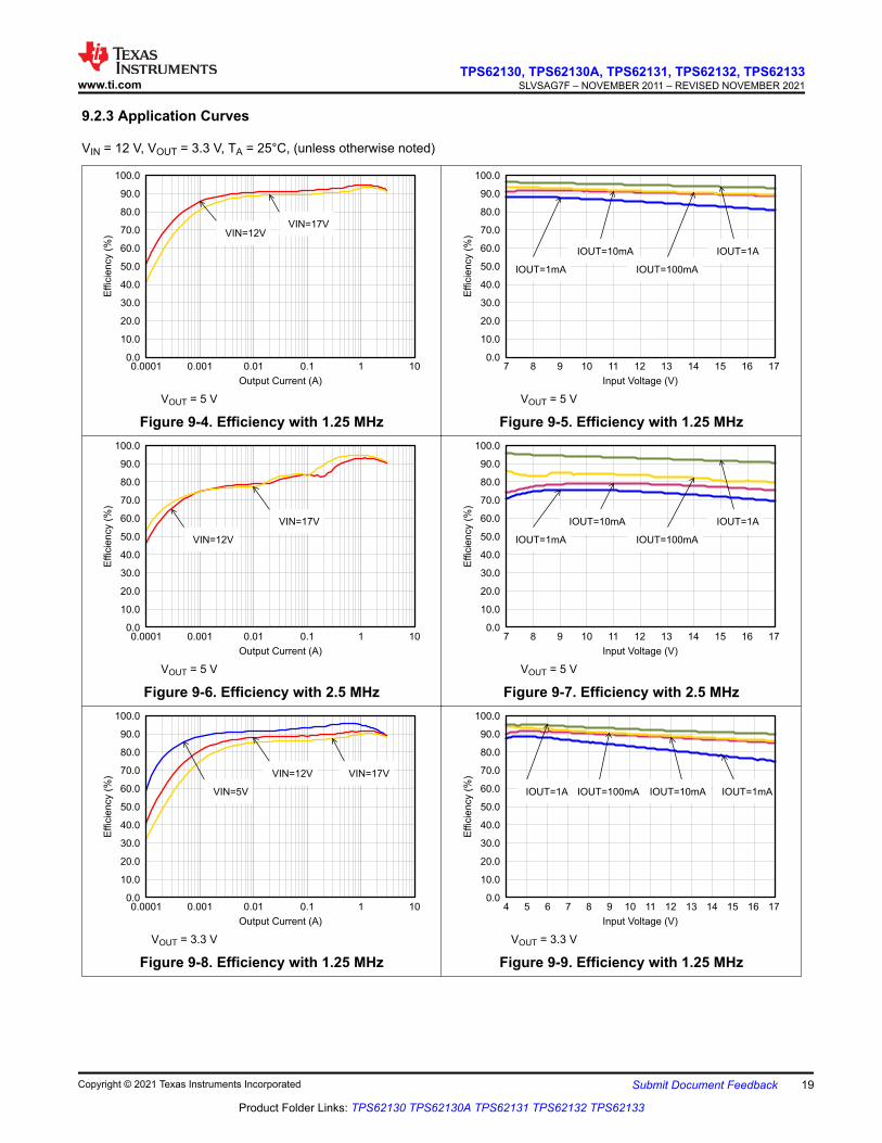
9.2.3 Application Curves
VIN = 12 V, VOUT = 3.3 V, TA = 25°C, (unless otherwise noted)
0.0
10.0
20.0
30.0
40.0
50.0
60.0
70.0
80.0
90.0
100.0
0.0001 0.001 0.01 0.1 1 10
VIN=12VVIN=17V
Output Current (A)
Effic
iency (
%)
VOUT = 5 V
Figure 9-4. Efficiency with 1.25 MHz
0.0
10.0
20.0
30.0
40.0
50.0
60.0
70.0
80.0
90.0
100.0
7 8 9 10 11 12 13 14 15 16 17
IOUT=1mA
IOUT=10mA
IOUT=100mA
IOUT=1A
Input Voltage (V)
Effic
iency (
%)
VOUT = 5 V
Figure 9-5. Efficiency with 1.25 MHz
0.0
10.0
20.0
30.0
40.0
50.0
60.0
70.0
80.0
90.0
100.0
0.0001 0.001 0.01 0.1 1 10
VIN=12V
VIN=17V
Output Current (A)
Effic
iency (
%)
VOUT = 5 V
Figure 9-6. Efficiency with 2.5 MHz
0.0
10.0
20.0
30.0
40.0
50.0
60.0
70.0
80.0
90.0
100.0
7 8 9 10 11 12 13 14 15 16 17
IOUT=1mA
IOUT=10mA
IOUT=100mA
IOUT=1A
Input Voltage (V)
Effic
iency (
%)
VOUT = 5 V
Figure 9-7. Efficiency with 2.5 MHz
0.0
10.0
20.0
30.0
40.0
50.0
60.0
70.0
80.0
90.0
100.0
0.0001 0.001 0.01 0.1 1 10
VIN=5V
VIN=12V VIN=17V
Output Current (A)
Effic
iency (
%)
VOUT = 3.3 V
Figure 9-8. Efficiency with 1.25 MHz
0.0
10.0
20.0
30.0
40.0
50.0
60.0
70.0
80.0
90.0
100.0
4 5 6 7 8 9 10 11 12 13 14 15 16 17
IOUT=1mAIOUT=10mAIOUT=100mAIOUT=1A
Input Voltage (V)
Effic
iency (
%)
VOUT = 3.3 V
Figure 9-9. Efficiency with 1.25 MHz
www.ti.comTPS62130, TPS62130A, TPS62131, TPS62132, TPS62133
SLVSAG7F – NOVEMBER 2011 – REVISED NOVEMBER 2021
Copyright © 2021 Texas Instruments Incorporated Submit Document Feedback 19
Product Folder Links: TPS62130 TPS62130A TPS62131 TPS62132 TPS62133

0.0
10.0
20.0
30.0
40.0
50.0
60.0
70.0
80.0
90.0
100.0
0.0001 0.001 0.01 0.1 1 10
VIN=5V
VIN=12V VIN=17V
Output Current (A)
Effic
iency (
%)
VOUT = 3.3 V
Figure 9-10. Efficiency with 2.5 MHz
0.0
10.0
20.0
30.0
40.0
50.0
60.0
70.0
80.0
90.0
100.0
4 5 6 7 8 9 10 11 12 13 14 15 16 17
IOUT=1mA
IOUT=10mA
IOUT=100mA
IOUT=1A
Input Voltage (V)
Effic
iency (
%)
VOUT = 3.3 V
Figure 9-11. Efficiency with 2.5 MHz
0.0
10.0
20.0
30.0
40.0
50.0
60.0
70.0
80.0
90.0
100.0
0.0001 0.001 0.01 0.1 1 10
VIN=5V
VIN=12V VIN=17V
Output Current (A)
Effic
iency (
%)
VOUT = 1.8 V
Figure 9-12. Efficiency with 1.25 MHz
0.0
10.0
20.0
30.0
40.0
50.0
60.0
70.0
80.0
90.0
100.0
3 4 5 6 7 8 9 10 11 12 13 14 15 16 17
IOUT=1mAIOUT=10mA
IOUT=100mAIOUT=1A
Input Voltage (V)
Effic
iency (
%)
VOUT = 1.8 V
Figure 9-13. Efficiency with 1.25 MHz
0.0
10.0
20.0
30.0
40.0
50.0
60.0
70.0
80.0
90.0
100.0
0.0001 0.001 0.01 0.1 1 10
VIN=5V
VIN=12V VIN=17V
Output Current (A)
Effic
iency (
%)
VOUT = 0.9 V
Figure 9-14. Efficiency with 1.25 MHz
0.0
10.0
20.0
30.0
40.0
50.0
60.0
70.0
80.0
90.0
100.0
3 4 5 6 7 8 9 10 11 12 13 14 15 16 17
IOUT=1mAIOUT=10mA
IOUT=100mA
IOUT=1A
Input Voltage (V)
Effic
iency (
%)
VOUT = 0.9 V
Figure 9-15. Efficiency with 1.25 MHz
TPS62130, TPS62130A, TPS62131, TPS62132, TPS62133SLVSAG7F – NOVEMBER 2011 – REVISED NOVEMBER 2021 www.ti.com
20 Submit Document Feedback Copyright © 2021 Texas Instruments Incorporated
Product Folder Links: TPS62130 TPS62130A TPS62131 TPS62132 TPS62133

3.20
3.25
3.30
3.35
3.40
0.0001 0.001 0.01 0.1 1 10
VIN=5V
VIN=12V
VIN=17V
Output Current (A)
Outp
ut V
oltage (
V)
Figure 9-16. Output Voltage Accuracy (Load Regulation)
3.20
3.25
3.30
3.35
3.40
4 7 10 13 16
IOUT=1mAIOUT=10mA
IOUT=100mAIOUT=1A
Input Voltage (V)
Outp
ut V
oltage (
V)
Figure 9-17. Output Voltage Accuracy (Line Regulation)
0
0.5
1
1.5
2
2.5
3
3.5
4
6 8 10 12 14 16 18
IOUT=0.5A IOUT=1A
IOUT=2A IOUT=3A
Input Voltage (V)
Sw
itchin
g F
requency (
MH
z)
G000
FSW = Low VOUT = 5 V
Figure 9-18. Switching Frequency vs Input Voltage
0
0.5
1
1.5
2
2.5
3
3.5
4
0 0.5 1 1.5 2 2.5 3
Output Current (A)
Sw
itchin
g F
requency (
MH
z)
G000
FSW = Low VOUT = 5 V
Figure 9-19. Switching Frequency vs Output Current
0
0.5
1
1.5
2
2.5
3
3.5
4
4 6 8 10 12 14 16 18
IOUT=0.5A IOUT=1A
IOUT=2A IOUT=3A
Input Voltage (V)
Sw
itchin
g F
requency (
MH
z)
G000
FSW = Low VOUT = 3.3 V
Figure 9-20. Switching Frequency vs Input Voltage
0
0.5
1
1.5
2
2.5
3
3.5
4
0 0.5 1 1.5 2 2.5 3
Output Current (A)
Sw
itchin
g F
requency (
MH
z)
G000
FSW = Low VOUT = 3.3 V
Figure 9-21. Switching Frequency vs Output Current,
www.ti.comTPS62130, TPS62130A, TPS62131, TPS62132, TPS62133
SLVSAG7F – NOVEMBER 2011 – REVISED NOVEMBER 2021
Copyright © 2021 Texas Instruments Incorporated Submit Document Feedback 21
Product Folder Links: TPS62130 TPS62130A TPS62131 TPS62132 TPS62133

0
0.5
1
1.5
2
2.5
3
3.5
4
3 5 7 9 11 13 15 17
IOUT=0.5A IOUT=1A
IOUT=2A IOUT=3A
Input Voltage (V)
Sw
itchin
g F
requency (
MH
z)
G000
FSW = Low VOUT = 1.8 V
Figure 9-22. Switching Frequency vs Input Voltage
0
0.5
1
1.5
2
2.5
3
3.5
4
0 0.5 1 1.5 2 2.5 3
Output Current (A)
Sw
itchin
g F
requency (
MH
z)
G000
FSW = Low VOUT = 1.8 V
Figure 9-23. Switching Frequency vs Output Current
0
0.5
1
1.5
2
2.5
3
3 5 7 9 11 13 15 17
IOUT=1A
IOUT=2A IOUT=3A
IOUT=0.5A
Input Voltage (V)
Sw
itchin
g F
requency (
MH
z)
G000
FSW = Low VOUT = 1 V
Figure 9-24. Switching Frequency vs Input Voltage
0
0.5
1
1.5
2
2.5
3
0 0.5 1 1.5 2 2.5 3
Output Current (A)
Sw
itchin
g F
requency (
MH
z)
G000
FSW = Low VOUT = 1 V
Figure 9-25. Switching Frequency vs Output Current
0
0.01
0.02
0.03
0.04
0.05
0 0.3 0.6 0.9 1.2 1.5 1.8 2.1 2.4 2.7 3
VIN=5V
VIN=12V
VIN=17V
Output Current (A)
Outp
ut V
oltage R
ipple
(V
)
Figure 9-26. Output Voltage Ripple
0
0.5
1
1.5
2
2.5
3
3.5
4
4.5
5
5.5
6
4 5 6 7 8 9 10 11 12 13 14 15 16 17
−40°C
25°C
85°C
Input Voltage (V)
Outp
ut C
urr
ent (A
)
Figure 9-27. Maximum Output Current
TPS62130, TPS62130A, TPS62131, TPS62132, TPS62133SLVSAG7F – NOVEMBER 2011 – REVISED NOVEMBER 2021 www.ti.com
22 Submit Document Feedback Copyright © 2021 Texas Instruments Incorporated
Product Folder Links: TPS62130 TPS62130A TPS62131 TPS62132 TPS62133

0
10
20
30
40
50
60
70
80
90
100
10 100 1k 10k 100k 1M
VIN=5V
VIN=12V
VIN=17V
Frequency (Hz)
PS
RR
(dB
)
VOUT=3.3V, IOUT=1A
L=2.2uH (XFL4020)
Cin=10uF, Cout=22uF
G000
FSW = 2.5 Mhz
Figure 9-28. Power Supply Rejection Ratio
0
10
20
30
40
50
60
70
80
90
100
10 100 1k 10k 100k 1M
VIN=5V
VIN=12V
VIN=17V
Frequency (Hz)
PS
RR
(dB
)
VOUT=3.3V, IOUT=0.1A
L=2.2uH (XFL4020)
Cin=10uF, Cout=22uF
G000
FSW = 2.5 MHz
Figure 9-29. Power Supply Rejection Ratio
VIN = 12 VOUT = 3.3 V with 50 mV/Div
Figure 9-30. PWM-PSM-TransitionIOUT = 0.5 to 3 to 0.5 A
Figure 9-31. Load Transient Response
Figure 9-32. Load Transient Response of Figure 9-31, Rising Edge
Figure 9-33. Load Transient Response of Figure 9-31, Falling Edge
www.ti.comTPS62130, TPS62130A, TPS62131, TPS62132, TPS62133
SLVSAG7F – NOVEMBER 2011 – REVISED NOVEMBER 2021
Copyright © 2021 Texas Instruments Incorporated Submit Document Feedback 23
Product Folder Links: TPS62130 TPS62130A TPS62131 TPS62132 TPS62133

Figure 9-34. Start-Up Into 100 mA Figure 9-35. Start-Up Into 3 A
IOUT = 1 A
Figure 9-36. Typical Operation In PWM ModeIOUT = 10 mA
Figure 9-37. Typical Operation In Power Save Mode
55
65
75
85
95
105
115
125
0 0.5 1 1.5 2 2.5 3 3.5
Output Current (A)
Fre
e−
Air
Tem
pera
ture
(°C
)
FSW = 2.5 MHz TPS62130EVML = 2.2 µH (XFL4020)
Figure 9-38. Maximum Ambient Temperature
55
65
75
85
95
105
115
125
0 2 4 6 8 10 12
Output Power (W)
Fre
e−
Air
Tem
pera
ture
(°C
)
FSW = 2.5 MHz TPS62130EVML = 2.2 µH (XFL4020)
Figure 9-39. Maximum Ambient Temperature
TPS62130, TPS62130A, TPS62131, TPS62132, TPS62133SLVSAG7F – NOVEMBER 2011 – REVISED NOVEMBER 2021 www.ti.com
24 Submit Document Feedback Copyright © 2021 Texas Instruments Incorporated
Product Folder Links: TPS62130 TPS62130A TPS62131 TPS62132 TPS62133

9.3 System Examples9.3.1 LED Power Supply
The TPS62130 can be used as a power supply for power LEDs. The FB pin can be easily set down to lower values than nominal by using the SS/TR pin. With that, the voltage drop on the sense resistor is low to avoid excessive power loss. Since this pin provides 2.5 µA, the feedback pin voltage can be adjusted by an external resistor per Equation 15. This drop, proportional to the LED current, is used to regulate the output voltage (anode voltage) to a proper level to drive the LED. Both analog and PWM dimming are supported with the TPS62130. Figure 9-40 shows an application circuit, tested with analog dimming:
22uF10uF
2.2 µH(4 .. 17) V
0.1R187k
ADIM
PVIN
AVIN
EN
SS/TR
DEF
FSW
SW
VOS
PG
FB
AGND
PGND
TPS621300.1uF
Figure 9-40. Single Power LED Supply
The resistor at SS/TR sets the FB voltage to a level of approximately 300 mV and is calculated from Equation 15.
TRSSFBRAV
/.. ××= m52640 (15)
The device now supplies a constant current, set by the resistor at the FB pin, by regulating the output voltage accordingly. The minimum input voltage has to be rated according the forward voltage needed by the LED used. More information is available in the Step-Down LED Driver With Dimming With the TPS621-Family and TPS821-Family Application Report.
9.3.2 Active Output Discharge
The TPS62130A pulls the PG pin Low when the device is shut down by EN, UVLO, or thermal shutdown. Connecting PG to VOUT through a resistor can be used to discharge VOUT in those cases (see Figure 9-41). The discharge rate can be adjusted by R3, which is also used to pull up the PG pin in normal operation. For reliability, keep the maximum current into the PG pin less than 10 mA.
22uF
Vout / 3A
10uF
1 / 2.2 µH(3 .. 17)V
3.3nF
PVIN
AVIN
EN
SS/TR
DEF
FSW
SW
VOS
PG
FB
AGND
PGND
R3
R1
R2
TPS62130A
0.1uF
Figure 9-41. Discharge VOUT Through PG Pin with TPS62130A
9.3.3 –3.3-V Inverting Power Supply
The TPS62130 can be used as an inverting power supply by rearranging external circuitry as shown in Figure 9-42. As the former GND node now represents a voltage level below system ground, the voltage difference between VIN and VOUT has to be limited for operation to the maximum supply voltage of 17 V (see Equation 16).
maxINOUTIN VVV £+ (16)
www.ti.comTPS62130, TPS62130A, TPS62131, TPS62132, TPS62133
SLVSAG7F – NOVEMBER 2011 – REVISED NOVEMBER 2021
Copyright © 2021 Texas Instruments Incorporated Submit Document Feedback 25
Product Folder Links: TPS62130 TPS62130A TPS62131 TPS62132 TPS62133

TPS62130
PVIN
AVIN
EN
SS/TR
DEF
FSW
SW
VOS
PG
FB
AGND
PGND
2.2µH(3 .. 13.7)V
10uF
383k
1.21M
22uF
-3.3V
10uF
3.3nF
0.1uF
Figure 9-42. –3.3-V Inverting Power Supply
The transfer function of the inverting power supply configuration differs from the buck mode transfer function, incorporating a right half plane zero additionally. The loop stability has to be adapted and an output capacitance of at least 22 µF is recommended. A detailed design example is given in Using the TPS6215x in an Inverting Buck-Boost Topology Application Report.
9.3.4 Various Output Voltages
The following example circuits show how to use the various devices and configure the external circuitry to furnish different output voltages at 3 A.
22uF
5V / 3A1 / 2.2 µH
TPS62133
PVIN
AVIN
EN
SS/TR
DEF
FSW
SW
VOS
PG
FB
AGND
PGND
100k10uF
(5 .. 17)V
3.3nF
0.1uF
Figure 9-43. 5-V/3-A Power Supply
22uF
3.3V / 3A
TPS62132
PVIN
AVIN
EN
SS/TR
DEF
FSW
SW
VOS
PG
FB
AGND
PGND
100k
1 / 2.2 µH
10uF
(3.3 .. 17)V
3.3nF
0.1uF
Figure 9-44. 3.3-V/3-A Power Supply
TPS62130, TPS62130A, TPS62131, TPS62132, TPS62133SLVSAG7F – NOVEMBER 2011 – REVISED NOVEMBER 2021 www.ti.com
26 Submit Document Feedback Copyright © 2021 Texas Instruments Incorporated
Product Folder Links: TPS62130 TPS62130A TPS62131 TPS62132 TPS62133

22uF
2.5V / 3A
10uF
(3 .. 17)V
3.3nF
TPS62130
390k
180k
PVIN
AVIN
EN
SS/TR
DEF
FSW
SW
VOS
PG
FB
AGND
PGND
100k0.1uF
1 / 2.2 µH
Figure 9-45. 2.5-V/3-A Power Supply
22uF
1.8V / 3A
10uF
1 / 2.2 µH(3 .. 17)V
3.3nF
TPS62131
PVIN
AVIN
EN
SS/TR
DEF
FSW
SW
VOS
PG
FB
AGND
PGND
100k0.1uF
Figure 9-46. 1.8-V/3-A Power Supply
22uF
1.5V / 3A
TPS62130
130k
150k
PVIN
AVIN
EN
SS/TR
DEF
FSW
SW
VOS
PG
FB
AGND
PGND
100k
1 / 2.2 µH
10uF
(3 .. 17)V
3.3nF
0.1uF
Figure 9-47. 1.5-V/3-A Power Supply
22uF
1.2V / 3A
TPS62130
75k
150k
PVIN
AVIN
EN
SS/TR
DEF
FSW
SW
VOS
PG
FB
AGND
PGND
100k
1 / 2.2 µH
10uF
(3 .. 17)V
3.3nF
0.1uF
Figure 9-48. 1.2-V/3-A Power Supply
22uF
1V / 3A
TPS62130
51k
200k
PVIN
AVIN
EN
SS/TR
DEF
FSW
SW
VOS
PG
FB
AGND
PGND
100k
1 / 2.2 µH
10uF
(3 .. 17)V
3.3nF
0.1uF
Figure 9-49. 1-V/3-A Power Supply
www.ti.comTPS62130, TPS62130A, TPS62131, TPS62132, TPS62133
SLVSAG7F – NOVEMBER 2011 – REVISED NOVEMBER 2021
Copyright © 2021 Texas Instruments Incorporated Submit Document Feedback 27
Product Folder Links: TPS62130 TPS62130A TPS62131 TPS62132 TPS62133

10 Power Supply RecommendationsThe TPS6213x are designed to operate from a 3-V to 17-V input voltage supply. The output current of the input power supply needs to be rated according to the output voltage and the output current of the power rail application.
11 Layout11.1 Layout GuidelinesA proper layout is critical for the operation of a switched mode power supply, even more at high switching frequencies. Therefore, the PCB layout of the TPS6213x demands careful attention to ensure operation and to get the performance specified. A poor layout can lead to issues like the following:
• Poor regulation (both line and load)• Stability and accuracy weaknesses• Increased EMI radiation• Noise sensitivity
See Figure 11-1 for the recommended layout of the TPS6213x, which is designed for common external ground connections. Therefore, both AGND and PGND pins are directly connected to the exposed thermal pad. On the PCB, the direct common ground connection of AGND and PGND to the exposed thermal pad and the system ground (ground plane) is mandatory. Also connect the VOS pin in the shortest way to VOUT at the output capacitor. To avoid noise coupling into the VOS line, this connection should be separated from the VOUT power line/plane as shown in Section 11.2.
Provide low inductive and resistive paths for loops with high di/dt. Therefore, paths conducting the switched load current should be as short and wide as possible. Provide low capacitive paths (with respect to all other nodes) for wires with high dv/dt. Therefore, the input and output capacitance should be placed as close as possible to the IC pins and parallel wiring over long distances as well as narrow traces should be avoided. Loops which conduct an alternating current should outline an area as small as possible, as this area is proportional to the energy radiated.
Sensitive nodes like FB and VOS need to be connected with short wires and not nearby high dv/dt signals (for example, SW). As they carry information about the output voltage, they should be connected as close as possible to the actual output voltage (at the output capacitor). The capacitor on the SS/TR pin and on AVIN as well as the FB resistors, R1 and R2, should be kept close to the IC and connect directly to those pins and the system ground plane.
The exposed thermal pad must be soldered to the circuit board for mechanical reliability and to achieve appropriate power dissipation.
The recommended layout is implemented on the EVM and shown in the TPS6213x Buck Converter Evaluation Module User's Guide. Additionally, the Gebers for HPA505 EVM are available for download.
TPS62130, TPS62130A, TPS62131, TPS62132, TPS62133SLVSAG7F – NOVEMBER 2011 – REVISED NOVEMBER 2021 www.ti.com
28 Submit Document Feedback Copyright © 2021 Texas Instruments Incorporated
Product Folder Links: TPS62130 TPS62130A TPS62131 TPS62132 TPS62133

11.2 Layout Examplespace
VIN
GND
AGND
VOUT
SW
SW
PG
AVIN
PVIN
PVIN
PG
ND
EN
PG
ND
AG
ND
FB
SW
VO
S
SS/TR
FS
W
DE
F
R1
R2C7
C1 C3
C5
L1
Figure 11-1. Layout Example
11.3 Thermal InformationImplementation of integrated circuits in low-profile and fine-pitch surface-mount packages typically requires special attention to power dissipation. Many system-dependent issues such as thermal coupling, airflow, added heat sinks and convection surfaces, and the presence of other heat-generating components affect the power-dissipation limits of a given component.
Three basic approaches for enhancing thermal performance are listed below:
• Improving the power dissipation capability of the PCB design• Improving the thermal coupling of the component to the PCB by soldering the Exposed Thermal Pad• Introducing airflow in the system
For more details on how to use the thermal parameters, see the application notes: Thermal Characteristics of Linear and Logic Packages Using JEDEC PCB Designs Application Report and Semiconductor and IC Package Thermal Metrics Application Report.
The TPS6213x is designed for a maximum operating junction temperature (TJ) of 125°C. Therefore, the maximum output power is limited by the power losses that can be dissipated over the actual thermal resistance, given by the package and the surrounding PCB structures. Since the thermal resistance of the package is fixed, increasing the size of the surrounding copper area and improving the thermal connection to the IC can reduce the thermal resistance. To get an improved thermal behavior, it is recommended to use top layer metal to connect the device with wide and thick metal lines. Internal ground layers can connect to vias directly under the IC for improved thermal performance.
If short circuit or overload conditions are present, the device is protected by limiting internal power dissipation. Experimental data, taken from the TPS62130 EVM, shows the maximum ambient temperature (without additional cooling like airflow or heat sink), that can be allowed to limit the junction temperature to at most 125°C (see Figure 9-38).
www.ti.comTPS62130, TPS62130A, TPS62131, TPS62132, TPS62133
SLVSAG7F – NOVEMBER 2011 – REVISED NOVEMBER 2021
Copyright © 2021 Texas Instruments Incorporated Submit Document Feedback 29
Product Folder Links: TPS62130 TPS62130A TPS62131 TPS62132 TPS62133

12 Device and Documentation Support12.1 Device Support12.1.1 Third-Party Products Disclaimer
TI'S PUBLICATION OF INFORMATION REGARDING THIRD-PARTY PRODUCTS OR SERVICES DOES NOT CONSTITUTE AN ENDORSEMENT REGARDING THE SUITABILITY OF SUCH PRODUCTS OR SERVICES OR A WARRANTY, REPRESENTATION OR ENDORSEMENT OF SUCH PRODUCTS OR SERVICES, EITHER ALONE OR IN COMBINATION WITH ANY TI PRODUCT OR SERVICE.
12.2 Documentation Support12.2.1 Related Documentation
• Texas Instruments, Voltage Margining Using the TPS62130 Application Report• Texas Instruments, Using the TPS62150 as Step-Down LED Driver With Dimming Application Report• Texas Instruments, Using the TPS6215x in an Inverting Buck-Boost Topology Application Report• Texas Instruments, Optimizing the TPS62130/40/50/60/70 Output Filter Application Report• Texas Instruments, TPS62130/40/50 Sequencing and Tracking Application Report• Texas Instruments, Optimizing Transient Response of Internally Compensated dc-dc Converters With
Feedforward Capacitor Application Report• Texas Instruments, Using a Feedforward Capacitor to Improve Stability and Bandwidth of
TPS62130/40/50/60/70 Application Report• Texas Instruments, Thermal Characteristics of Linear and Logic Packages Using JEDEC PCB Designs
Application Report• Texas Instruments, Semiconductor and IC Package Thermal Metrics Application Report• Texas Instruments, TPS62130EVM-505, TPS62140EVM-505, and TPS62150EVM-505 Evaluation Modules
User's Guide• Texas Instruments, EVM Gerber Data
12.3 Receiving Notification of Documentation UpdatesTo receive notification of documentation updates, navigate to the device product folder on ti.com. Click on Subscribe to updates to register and receive a weekly digest of any product information that has changed. For change details, review the revision history included in any revised document.
12.4 Support ResourcesTI E2E™ support forums are an engineer's go-to source for fast, verified answers and design help — straight from the experts. Search existing answers or ask your own question to get the quick design help you need.
Linked content is provided "AS IS" by the respective contributors. They do not constitute TI specifications and do not necessarily reflect TI's views; see TI's Terms of Use.
12.5 TrademarksDCS-Control™ and TI E2E™ are trademarks of Texas Instruments.All trademarks are the property of their respective owners.12.6 Electrostatic Discharge Caution
This integrated circuit can be damaged by ESD. Texas Instruments recommends that all integrated circuits be handled with appropriate precautions. Failure to observe proper handling and installation procedures can cause damage.ESD damage can range from subtle performance degradation to complete device failure. Precision integrated circuits may be more susceptible to damage because very small parametric changes could cause the device not to meet its published specifications.
12.7 GlossaryTI Glossary This glossary lists and explains terms, acronyms, and definitions.
TPS62130, TPS62130A, TPS62131, TPS62132, TPS62133SLVSAG7F – NOVEMBER 2011 – REVISED NOVEMBER 2021 www.ti.com
30 Submit Document Feedback Copyright © 2021 Texas Instruments Incorporated
Product Folder Links: TPS62130 TPS62130A TPS62131 TPS62132 TPS62133

13 Mechanical, Packaging, and Orderable InformationThe following pages include mechanical, packaging, and orderable information. This information is the most current data available for the designated devices. This data is subject to change without notice and revision of this document. For browser-based versions of this data sheet, refer to the left-hand navigation.
www.ti.comTPS62130, TPS62130A, TPS62131, TPS62132, TPS62133
SLVSAG7F – NOVEMBER 2011 – REVISED NOVEMBER 2021
Copyright © 2021 Texas Instruments Incorporated Submit Document Feedback 31
Product Folder Links: TPS62130 TPS62130A TPS62131 TPS62132 TPS62133

PACKAGE OPTION ADDENDUM
www.ti.com 9-Aug-2021
Addendum-Page 1
PACKAGING INFORMATION
Orderable Device Status(1)
Package Type PackageDrawing
Pins PackageQty
Eco Plan(2)
Lead finish/Ball material
(6)
MSL Peak Temp(3)
Op Temp (°C) Device Marking(4/5)
Samples
TPS62130ARGTR ACTIVE VQFN RGT 16 3000 RoHS & Green NIPDAU Level-2-260C-1 YEAR -40 to 125 PA6I
TPS62130ARGTT ACTIVE VQFN RGT 16 250 RoHS & Green NIPDAU Level-2-260C-1 YEAR -40 to 125 PA6I
TPS62130RGTR ACTIVE VQFN RGT 16 3000 RoHS & Green NIPDAU Level-2-260C-1 YEAR -40 to 125 PTSI
TPS62130RGTT ACTIVE VQFN RGT 16 250 RoHS & Green NIPDAU Level-2-260C-1 YEAR -40 to 125 PTSI
TPS62131RGTR ACTIVE VQFN RGT 16 3000 RoHS & Green NIPDAU Level-2-260C-1 YEAR -40 to 125 QVX
TPS62131RGTT ACTIVE VQFN RGT 16 250 RoHS & Green NIPDAU Level-2-260C-1 YEAR -40 to 125 QVX
TPS62132RGTR ACTIVE VQFN RGT 16 3000 RoHS & Green NIPDAU Level-2-260C-1 YEAR -40 to 125 QVY
TPS62132RGTT ACTIVE VQFN RGT 16 250 RoHS & Green NIPDAU Level-2-260C-1 YEAR -40 to 125 QVY
TPS62133RGTR ACTIVE VQFN RGT 16 3000 RoHS & Green NIPDAU Level-2-260C-1 YEAR -40 to 125 QVZ
TPS62133RGTT ACTIVE VQFN RGT 16 250 RoHS & Green NIPDAU Level-2-260C-1 YEAR -40 to 125 QVZ
(1) The marketing status values are defined as follows:ACTIVE: Product device recommended for new designs.LIFEBUY: TI has announced that the device will be discontinued, and a lifetime-buy period is in effect.NRND: Not recommended for new designs. Device is in production to support existing customers, but TI does not recommend using this part in a new design.PREVIEW: Device has been announced but is not in production. Samples may or may not be available.OBSOLETE: TI has discontinued the production of the device.
(2) RoHS: TI defines "RoHS" to mean semiconductor products that are compliant with the current EU RoHS requirements for all 10 RoHS substances, including the requirement that RoHS substancedo not exceed 0.1% by weight in homogeneous materials. Where designed to be soldered at high temperatures, "RoHS" products are suitable for use in specified lead-free processes. TI mayreference these types of products as "Pb-Free".RoHS Exempt: TI defines "RoHS Exempt" to mean products that contain lead but are compliant with EU RoHS pursuant to a specific EU RoHS exemption.Green: TI defines "Green" to mean the content of Chlorine (Cl) and Bromine (Br) based flame retardants meet JS709B low halogen requirements of <=1000ppm threshold. Antimony trioxide basedflame retardants must also meet the <=1000ppm threshold requirement.
(3) MSL, Peak Temp. - The Moisture Sensitivity Level rating according to the JEDEC industry standard classifications, and peak solder temperature.
(4) There may be additional marking, which relates to the logo, the lot trace code information, or the environmental category on the device.

PACKAGE OPTION ADDENDUM
www.ti.com 9-Aug-2021
Addendum-Page 2
(5) Multiple Device Markings will be inside parentheses. Only one Device Marking contained in parentheses and separated by a "~" will appear on a device. If a line is indented then it is a continuationof the previous line and the two combined represent the entire Device Marking for that device.
(6) Lead finish/Ball material - Orderable Devices may have multiple material finish options. Finish options are separated by a vertical ruled line. Lead finish/Ball material values may wrap to twolines if the finish value exceeds the maximum column width.
Important Information and Disclaimer:The information provided on this page represents TI's knowledge and belief as of the date that it is provided. TI bases its knowledge and belief on informationprovided by third parties, and makes no representation or warranty as to the accuracy of such information. Efforts are underway to better integrate information from third parties. TI has taken andcontinues to take reasonable steps to provide representative and accurate information but may not have conducted destructive testing or chemical analysis on incoming materials and chemicals.TI and TI suppliers consider certain information to be proprietary, and thus CAS numbers and other limited information may not be available for release.
In no event shall TI's liability arising out of such information exceed the total purchase price of the TI part(s) at issue in this document sold by TI to Customer on an annual basis.
OTHER QUALIFIED VERSIONS OF TPS62130A :
• Automotive : TPS62130A-Q1
NOTE: Qualified Version Definitions:
• Automotive - Q100 devices qualified for high-reliability automotive applications targeting zero defects

PACKAGE MATERIALS INFORMATION
www.ti.com 3-Jun-2022
TAPE AND REEL INFORMATION
Reel Width (W1)
REEL DIMENSIONS
A0B0K0W
Dimension designed to accommodate the component lengthDimension designed to accommodate the component thicknessOverall width of the carrier tapePitch between successive cavity centers
Dimension designed to accommodate the component width
TAPE DIMENSIONS
K0 P1
B0 W
A0Cavity
QUADRANT ASSIGNMENTS FOR PIN 1 ORIENTATION IN TAPE
Pocket Quadrants
Sprocket Holes
Q1 Q1Q2 Q2
Q3 Q3Q4 Q4 User Direction of Feed
P1
ReelDiameter
*All dimensions are nominal
Device PackageType
PackageDrawing
Pins SPQ ReelDiameter
(mm)
ReelWidth
W1 (mm)
A0(mm)
B0(mm)
K0(mm)
P1(mm)
W(mm)
Pin1Quadrant
TPS62130ARGTR VQFN RGT 16 3000 330.0 12.4 3.3 3.3 1.1 8.0 12.0 Q2
TPS62130ARGTT VQFN RGT 16 250 180.0 12.4 3.3 3.3 1.1 8.0 12.0 Q2
TPS62130RGTR VQFN RGT 16 3000 330.0 12.4 3.3 3.3 1.1 8.0 12.0 Q2
TPS62130RGTT VQFN RGT 16 250 180.0 12.4 3.3 3.3 1.1 8.0 12.0 Q2
TPS62130RGTT VQFN RGT 16 250 180.0 12.5 3.3 3.3 1.1 8.0 12.0 Q2
TPS62131RGTR VQFN RGT 16 3000 330.0 12.4 3.3 3.3 1.1 8.0 12.0 Q2
TPS62131RGTT VQFN RGT 16 250 180.0 12.4 3.3 3.3 1.1 8.0 12.0 Q2
TPS62132RGTR VQFN RGT 16 3000 330.0 12.4 3.3 3.3 1.1 8.0 12.0 Q2
TPS62132RGTT VQFN RGT 16 250 180.0 12.4 3.3 3.3 1.1 8.0 12.0 Q2
TPS62133RGTR VQFN RGT 16 3000 330.0 12.4 3.3 3.3 1.1 8.0 12.0 Q2
TPS62133RGTT VQFN RGT 16 250 180.0 12.4 3.3 3.3 1.1 8.0 12.0 Q2
Pack Materials-Page 1

PACKAGE MATERIALS INFORMATION
www.ti.com 3-Jun-2022
TAPE AND REEL BOX DIMENSIONS
Width (mm)
W L
H
*All dimensions are nominal
Device Package Type Package Drawing Pins SPQ Length (mm) Width (mm) Height (mm)
TPS62130ARGTR VQFN RGT 16 3000 552.0 367.0 36.0
TPS62130ARGTT VQFN RGT 16 250 552.0 185.0 36.0
TPS62130RGTR VQFN RGT 16 3000 552.0 367.0 36.0
TPS62130RGTT VQFN RGT 16 250 552.0 185.0 36.0
TPS62130RGTT VQFN RGT 16 250 338.0 355.0 50.0
TPS62131RGTR VQFN RGT 16 3000 367.0 367.0 35.0
TPS62131RGTT VQFN RGT 16 250 210.0 185.0 35.0
TPS62132RGTR VQFN RGT 16 3000 367.0 367.0 35.0
TPS62132RGTT VQFN RGT 16 250 210.0 185.0 35.0
TPS62133RGTR VQFN RGT 16 3000 367.0 367.0 35.0
TPS62133RGTT VQFN RGT 16 250 210.0 185.0 35.0
Pack Materials-Page 2

PACKAGE MATERIALS INFORMATION
www.ti.com 3-Jun-2022
TUBE
L - Tube lengthT - Tube height
W - Tube width
B - Alignment groove width *All dimensions are nominal
Device Package Name Package Type Pins SPQ L (mm) W (mm) T (µm) B (mm)
TPS62130ARGTR RGT VQFN 16 3000 381 4.83 2286 0
TPS62130ARGTT RGT VQFN 16 250 381 4.83 2286 0
TPS62130RGTR RGT VQFN 16 3000 381 4.83 2286 0
TPS62130RGTT RGT VQFN 16 250 381 4.83 2286 0
TPS62131RGTR RGT VQFN 16 3000 381 4.83 2286 0
TPS62131RGTT RGT VQFN 16 250 381 4.83 2286 0
TPS62132RGTR RGT VQFN 16 3000 381 4.83 2286 0
TPS62132RGTT RGT VQFN 16 250 381 4.83 2286 0
TPS62133RGTR RGT VQFN 16 3000 381 4.83 2286 0
TPS62133RGTT RGT VQFN 16 250 381 4.83 2286 0
Pack Materials-Page 3


IMPORTANT NOTICE AND DISCLAIMERTI PROVIDES TECHNICAL AND RELIABILITY DATA (INCLUDING DATA SHEETS), DESIGN RESOURCES (INCLUDING REFERENCE DESIGNS), APPLICATION OR OTHER DESIGN ADVICE, WEB TOOLS, SAFETY INFORMATION, AND OTHER RESOURCES “AS IS” AND WITH ALL FAULTS, AND DISCLAIMS ALL WARRANTIES, EXPRESS AND IMPLIED, INCLUDING WITHOUT LIMITATION ANY IMPLIED WARRANTIES OF MERCHANTABILITY, FITNESS FOR A PARTICULAR PURPOSE OR NON-INFRINGEMENT OF THIRD PARTY INTELLECTUAL PROPERTY RIGHTS.These resources are intended for skilled developers designing with TI products. You are solely responsible for (1) selecting the appropriate TI products for your application, (2) designing, validating and testing your application, and (3) ensuring your application meets applicable standards, and any other safety, security, regulatory or other requirements.These resources are subject to change without notice. TI grants you permission to use these resources only for development of an application that uses the TI products described in the resource. Other reproduction and display of these resources is prohibited. No license is granted to any other TI intellectual property right or to any third party intellectual property right. TI disclaims responsibility for, and you will fully indemnify TI and its representatives against, any claims, damages, costs, losses, and liabilities arising out of your use of these resources.TI’s products are provided subject to TI’s Terms of Sale or other applicable terms available either on ti.com or provided in conjunction with such TI products. TI’s provision of these resources does not expand or otherwise alter TI’s applicable warranties or warranty disclaimers for TI products.TI objects to and rejects any additional or different terms you may have proposed. IMPORTANT NOTICE
Mailing Address: Texas Instruments, Post Office Box 655303, Dallas, Texas 75265Copyright © 2022, Texas Instruments Incorporated