Topics in Applied Physics Volume 93
298
-
Upload
khangminh22 -
Category
Documents
-
view
0 -
download
0
Transcript of Topics in Applied Physics Volume 93


Topics in Applied PhysicsVolume 93
Topics in Applied Physics is part of [SpringerLink] service. For all customers with standing ordersfor Topics in Applied Physics we offer the full text in electronic form via [SpringerLink] free ofcharge. Please contact your librarian who can receive a password for free access to the full articlesby registration at:
springerlink.com → Orders
If you do not have a standing order you can nevertheless browse through the table of contents ofthe volumes and the abstracts of each article at:
springerlink.com → Browse Publications
There you will also f ind more information about the series.
3BerlinHeidelbergNew YorkHong KongLondonMilanParisTokyo
Topics in Applied Physics
Topics in Applied Physics is a well-established series of review books, each of which presents acomprehensive survey of a selected topic within the broad area of applied physics. Edited and writtenby leading research scientists in the f ield concerned, each volume contains review contributionscovering the various aspects of the topic. Together these provide an overview of the state of the artin the respective f ield, extending from an introduction to the subject right up to the frontiers ofcontemporary research.Topics in Applied Physics is addressed to all scientists at universities and in industry who wish toobtain an overview and to keep abreast of advances in applied physics. The series also provides easybut comprehensive access to the f ields for newcomers starting research.Contributions are specially commissioned. The Managing Editors are open to any suggestions fortopics coming from the community of applied physicists no matter what the f ield and encourageprospective editors to approach them with ideas.See also: springeronline.com
Managing EditorsDr. Claus E. AscheronSpringer-Verlag HeidelbergTopics in Applied PhysicsTiergartenstr. 1769121 HeidelbergGermanyEmail: [email protected]
Assistant Editor
Dr. Werner SkolautSpringer-Verlag HeidelbergTopics in Applied PhysicsTiergartenstr. 1769121 HeidelbergGermanyEmail: [email protected]
Dr. Hans J. KoelschSpringer-Verlag New York, Inc.Topics in Applied Physics175 Fifth AvenueNew York, NY 10010-7858USAEmail: [email protected]

Hiroshi Ishiwara Masanori OkuyamaYoshihiro Arimoto (Eds.)
FerroelectricRandom Access Memories
Fundamentals and Applications
With 125 Figuresand 12 Tables
1 3
Prof. Hiroshi IshiwaraTokyo Institute of TechnologyFrontier Collaborative Research Center4259 Nagatsuta, Midoriku226-8503 [email protected]
Prof. Masanori OkuyamaOsaka UniversityGraduate School of Engineering ScienceDepartment of Systems Innovation1-3 Machikaneyama-cho, Toyonaka560-8531 [email protected]
Dr. Yoshihiro ArimotoFujitsu Laboratories Ltd.Silicon Technology Laboratories243-0197 [email protected]
Library of Congress Cataloging in Publication DataFerroelectric random access memories: fundamentals and applications/ Hiroshi Ishiwara, Masanori Okuyama,Yoshihiro Arimoto (eds.). p. cm. – (Topics in applied physics; v. 93) Includes bibliographical references and index.ISBN 3-540-40718-9 (alk. paper) 1. Ferroelectric storage cells. I. Ishiwara Hiroshi, 1945- II. Okuyama, Masanori,1946- III. Arimoto yoshihiro, 1952- IV. Series. TK7895.M4F38 2004 621.39’73–dc22 2003059057
Physics and Astronomy Classification Scheme (PACS): 77.84.B, 68.55.J
ISSN print edition: 0303-4216ISSN electronic edition: 1437-0859ISBN 3-540-40718-9 Springer-Verlag Berlin Heidelberg New York
This work is subject to copyright. All rights are reserved, whether the whole or part of the material is concerned,specif ically the rights of translation, reprinting, reuse of illustrations, recitation, broadcasting, reproduction onmicrof ilm or in any other way, and storage in data banks. Duplication of this publication or parts thereof ispermitted only under the provisions of the German Copyright Law of September 9, 1965, in its current version, andpermission for use must always be obtained from Springer-Verlag. Violations are liable for prosecution under theGerman Copyright Law.
Springer-Verlag is a part of Springer Science+Business Media
springeronline.com
© Springer-Verlag Berlin Heidelberg 2004Printed in Germany
The use of general descriptive names, registered names, trademarks, etc. in this publication does not imply, even inthe absence of a specif ic statement, that such names are exempt from the relevant protective laws and regulationsand therefore free for general use.
Typesetting: DA-TEX · Gerd Blumenstein · www.da-tex.deCover design: design & production GmbH, Heidelberg
Printed on acid-free paper 56/3141/mf 5 4 3 2 1 0
Preface
As modern portable electronic devices such as mobile phones and notebookcomputers become more and more popular, there is a confirmed increasein the demand for nonvolatile memories. The ferroelectric random accessmemory (FeRAM) is one of the most promising candidates for satisfyingthis demand, because its power consumption is the lowest among the vari-ous semiconductor memories, and it also possesses nonvolatile and randomaccess characteristics. Thus, research and development for this memory arebeing conducted actively in many semiconductor companies, and FeRAMs upto 256 kb have already been mass-produced for RF tag and computer gameapplications. Furthermore, production of Mb-scale FeRAMs is also being pre-pared.
On the basis of this background, the 1st International Meeting on Ferro-electric Memories was held in Gotemba City, Japan, in November 2001. Atthis meeting, the publication of a new book on FeRAM was discussed and theoutline of the book was determined. After the meeting, the individual chap-ters were written, mainly by the attendees of the meeting. Thus, I believethat each chapter in this book has been written by one of the best authors,who knows the specific field very well. The book consists of five parts – (I) fer-roelectric thin films, (II) deposition and characterization methods, (III) thefabrication process and circuit design, (IV) advanced-type memories, and(V) applications and future prospects – and each part is further divided intoseveral chapters. I hope that this book will contribute to the research anddevelopment of future FeRAMs.
Finally, I am grateful to Dr. C. E. Ascheron of Springer-Verlag for hisencouragement and patience during the chapter collection and reviewingperiods. I am also grateful to Dr. S. Yamamoto (Research Associate) andMs. I. Sugita (Secretary) for their advice and efforts in converting almost allof the manuscripts into LATEX style.
Tokyo, Hiroshi IshiwaraOsaka, Masanori OkuyamaAtsugi, February 2004 Yoshihiro Arimoto

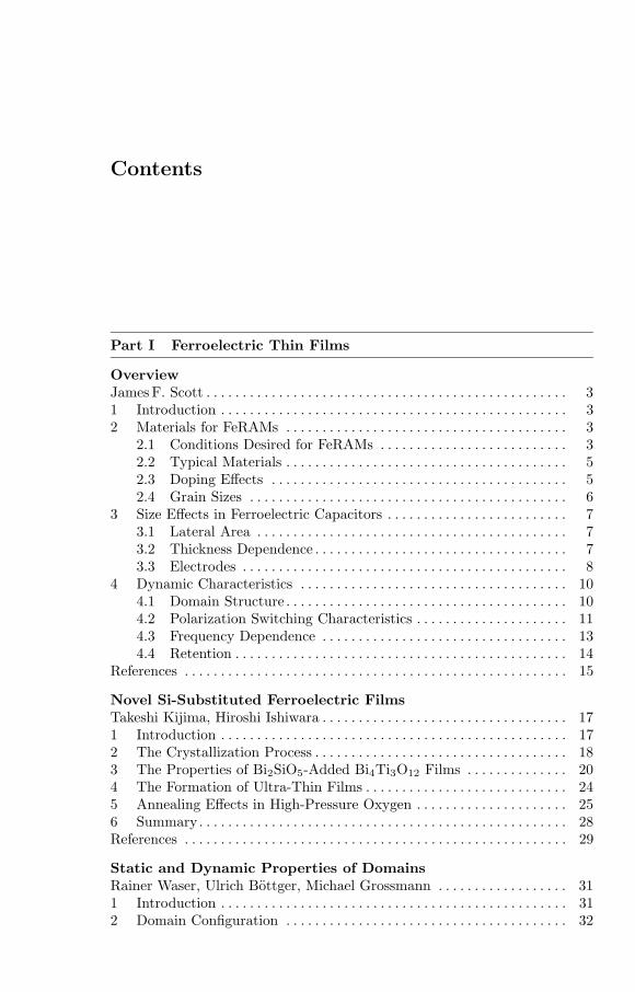
Contents
Part I Ferroelectric Thin Films
OverviewJames F. Scott . . . . . . . . . . . . . . . . . . . . . . . . . . . . . . . . . . . . . . . . . . . . . . . . . . 31 Introduction . . . . . . . . . . . . . . . . . . . . . . . . . . . . . . . . . . . . . . . . . . . . . . . . 32 Materials for FeRAMs . . . . . . . . . . . . . . . . . . . . . . . . . . . . . . . . . . . . . . . 3
2.1 Conditions Desired for FeRAMs . . . . . . . . . . . . . . . . . . . . . . . . . . 32.2 Typical Materials . . . . . . . . . . . . . . . . . . . . . . . . . . . . . . . . . . . . . . . 52.3 Doping Effects . . . . . . . . . . . . . . . . . . . . . . . . . . . . . . . . . . . . . . . . . 52.4 Grain Sizes . . . . . . . . . . . . . . . . . . . . . . . . . . . . . . . . . . . . . . . . . . . . 6
3 Size Effects in Ferroelectric Capacitors . . . . . . . . . . . . . . . . . . . . . . . . . 73.1 Lateral Area . . . . . . . . . . . . . . . . . . . . . . . . . . . . . . . . . . . . . . . . . . . 73.2 Thickness Dependence . . . . . . . . . . . . . . . . . . . . . . . . . . . . . . . . . . . 73.3 Electrodes . . . . . . . . . . . . . . . . . . . . . . . . . . . . . . . . . . . . . . . . . . . . . 8
4 Dynamic Characteristics . . . . . . . . . . . . . . . . . . . . . . . . . . . . . . . . . . . . . 104.1 Domain Structure . . . . . . . . . . . . . . . . . . . . . . . . . . . . . . . . . . . . . . . 104.2 Polarization Switching Characteristics . . . . . . . . . . . . . . . . . . . . . 114.3 Frequency Dependence . . . . . . . . . . . . . . . . . . . . . . . . . . . . . . . . . . 134.4 Retention . . . . . . . . . . . . . . . . . . . . . . . . . . . . . . . . . . . . . . . . . . . . . . 14
References . . . . . . . . . . . . . . . . . . . . . . . . . . . . . . . . . . . . . . . . . . . . . . . . . . . . . 15
Novel Si-Substituted Ferroelectric FilmsTakeshi Kijima, Hiroshi Ishiwara . . . . . . . . . . . . . . . . . . . . . . . . . . . . . . . . . . 171 Introduction . . . . . . . . . . . . . . . . . . . . . . . . . . . . . . . . . . . . . . . . . . . . . . . . 172 The Crystallization Process . . . . . . . . . . . . . . . . . . . . . . . . . . . . . . . . . . . 183 The Properties of Bi2SiO5-Added Bi4Ti3O12 Films . . . . . . . . . . . . . . 204 The Formation of Ultra-Thin Films . . . . . . . . . . . . . . . . . . . . . . . . . . . . 245 Annealing Effects in High-Pressure Oxygen . . . . . . . . . . . . . . . . . . . . . 256 Summary. . . . . . . . . . . . . . . . . . . . . . . . . . . . . . . . . . . . . . . . . . . . . . . . . . . 28References . . . . . . . . . . . . . . . . . . . . . . . . . . . . . . . . . . . . . . . . . . . . . . . . . . . . . 29
Static and Dynamic Properties of DomainsRainer Waser, Ulrich Bottger, Michael Grossmann . . . . . . . . . . . . . . . . . . 311 Introduction . . . . . . . . . . . . . . . . . . . . . . . . . . . . . . . . . . . . . . . . . . . . . . . . 312 Domain Configuration . . . . . . . . . . . . . . . . . . . . . . . . . . . . . . . . . . . . . . . 32
VIII Contents
3 Reversible and Irreversible Polarization Contributions . . . . . . . . . . . . 354 Ferroelectric Switching . . . . . . . . . . . . . . . . . . . . . . . . . . . . . . . . . . . . . . . 375 Long-Term Effects . . . . . . . . . . . . . . . . . . . . . . . . . . . . . . . . . . . . . . . . . . . 41
5.1 Fatigue . . . . . . . . . . . . . . . . . . . . . . . . . . . . . . . . . . . . . . . . . . . . . . . . 415.2 Retention Loss . . . . . . . . . . . . . . . . . . . . . . . . . . . . . . . . . . . . . . . . . 425.3 Imprint . . . . . . . . . . . . . . . . . . . . . . . . . . . . . . . . . . . . . . . . . . . . . . . . 42
References . . . . . . . . . . . . . . . . . . . . . . . . . . . . . . . . . . . . . . . . . . . . . . . . . . . . . 44
Nanoscale Phenomena in Ferroelectric Thin FilmsValanoor Nagarajan, Chandan S. Ganpule, Ramamoorthy Ramesh . . . . 471 Introduction . . . . . . . . . . . . . . . . . . . . . . . . . . . . . . . . . . . . . . . . . . . . . . . . 472 Experimental Details . . . . . . . . . . . . . . . . . . . . . . . . . . . . . . . . . . . . . . . . 483 Nanoscale Domain Imaging
in Ferroelectric Thin Films . . . . . . . . . . . . . . . . . . . . . . . . . . . . . . . . . . . 504 Nanoscale Piezoelectric and Hysteresis Behavior . . . . . . . . . . . . . . . . . 615 Summary. . . . . . . . . . . . . . . . . . . . . . . . . . . . . . . . . . . . . . . . . . . . . . . . . . . 66References . . . . . . . . . . . . . . . . . . . . . . . . . . . . . . . . . . . . . . . . . . . . . . . . . . . . . 67
Part II Deposition and Characterization Methods
The Sputtering TechniqueKoukou Suu . . . . . . . . . . . . . . . . . . . . . . . . . . . . . . . . . . . . . . . . . . . . . . . . . . . . 711 Introduction . . . . . . . . . . . . . . . . . . . . . . . . . . . . . . . . . . . . . . . . . . . . . . . . 712 A Sputtering System for Mass Production . . . . . . . . . . . . . . . . . . . . . . 723 The Optimization of Sputtering Conditions . . . . . . . . . . . . . . . . . . . . . 754 The Ferroelectric Characteristics of Sputtered PZT Capacitors . . . . 795 Sputtering of SBT Films and Hydrogen Barrier Layers . . . . . . . . . . . 806 Future Development Tasks . . . . . . . . . . . . . . . . . . . . . . . . . . . . . . . . . . . 82References . . . . . . . . . . . . . . . . . . . . . . . . . . . . . . . . . . . . . . . . . . . . . . . . . . . . . 82
A Chemical Approach Using Liquid Sources Tailoredto Bi-Based Layer-Structured Perovskite Thin FilmsKazumi Kato . . . . . . . . . . . . . . . . . . . . . . . . . . . . . . . . . . . . . . . . . . . . . . . . . . . 851 Introduction . . . . . . . . . . . . . . . . . . . . . . . . . . . . . . . . . . . . . . . . . . . . . . . . 852 SrBi2(Ta, Nb)2O9 and CaBi2Ta2O9 Thin Films
Deposited via Triple Alkoxides of Sr–Bi–Ta/Nb and Ca–Bi–Ta . . . . 863 CaBi3Ti3O12−X , CaBi4Ti4O15, and Ca2Bi4Ti5O18 Thin Films
Deposited via Mixtures of Ca–Bi and Bi–Ti Double Alkoxides . . . . . 90References . . . . . . . . . . . . . . . . . . . . . . . . . . . . . . . . . . . . . . . . . . . . . . . . . . . . . 93
Recent Development in the Preparationof Ferroelectric Thin Films by MOCVDHiroshi Funakubo . . . . . . . . . . . . . . . . . . . . . . . . . . . . . . . . . . . . . . . . . . . . . . . 951 Introduction . . . . . . . . . . . . . . . . . . . . . . . . . . . . . . . . . . . . . . . . . . . . . . . . 952 Low-Temperature Deposition . . . . . . . . . . . . . . . . . . . . . . . . . . . . . . . . . 96
Contents IX
2.1 SBT Films . . . . . . . . . . . . . . . . . . . . . . . . . . . . . . . . . . . . . . . . . . . . . 962.2 PZT Films . . . . . . . . . . . . . . . . . . . . . . . . . . . . . . . . . . . . . . . . . . . . . 97
3 Novel Materials Research . . . . . . . . . . . . . . . . . . . . . . . . . . . . . . . . . . . . . 993.1 Solid Solution
of SrBi2(Ta0.7Nb0.3)2O9 – Bi3TaTiO9 [(1 − x)SBT-xBTT] . . . 993.2 (Bi,Ln)4(Ti,V)3O12 . . . . . . . . . . . . . . . . . . . . . . . . . . . . . . . . . . . . . 100
4 Summary. . . . . . . . . . . . . . . . . . . . . . . . . . . . . . . . . . . . . . . . . . . . . . . . . . . 101References . . . . . . . . . . . . . . . . . . . . . . . . . . . . . . . . . . . . . . . . . . . . . . . . . . . . . 102
Materials Integration StrategiesOrlando Auciello, Anil M. Dhote, Bao T. Liu, Sanjeev Aggarwal,Ramamoorthy Ramesh . . . . . . . . . . . . . . . . . . . . . . . . . . . . . . . . . . . . . . . . . . 1051 Introduction . . . . . . . . . . . . . . . . . . . . . . . . . . . . . . . . . . . . . . . . . . . . . . . . 1052 An Experimental Method for the Synthesis and Characterization
of Ferroelectric Capacitor Layers . . . . . . . . . . . . . . . . . . . . . . . . . . . . . . 1083 The Magnetron-Based Synthesis and Characterization
of Ti–Al Layers and LSCO/Ti–Al Heterostructures . . . . . . . . . . . . . . 1094 Studies of Ti–Al and LSCO Film Growth
and Oxidation Processes . . . . . . . . . . . . . . . . . . . . . . . . . . . . . . . . . . . . . 1134.1 Microstructure–Deposition Environment Relationships
for Ti–Al Layers . . . . . . . . . . . . . . . . . . . . . . . . . . . . . . . . . . . . . . . . 1144.2 Studies of Ti–Al/LSCO Heterostructured Layer Growth
and Oxidation Processes via Complementaryin situ Analytical Techniques . . . . . . . . . . . . . . . . . . . . . . . . . . . . . 114
5 Electrical Characterization of Ferroelectric Capacitorswith a Ti–Al Diffusion Barrier/Electrode Layer . . . . . . . . . . . . . . . . . 118
6 Summary. . . . . . . . . . . . . . . . . . . . . . . . . . . . . . . . . . . . . . . . . . . . . . . . . . . 120References . . . . . . . . . . . . . . . . . . . . . . . . . . . . . . . . . . . . . . . . . . . . . . . . . . . . . 121
Characterization by Scanning Nonlinear Dielectric MicroscopyYasuo Cho . . . . . . . . . . . . . . . . . . . . . . . . . . . . . . . . . . . . . . . . . . . . . . . . . . . . . 1231 Introduction . . . . . . . . . . . . . . . . . . . . . . . . . . . . . . . . . . . . . . . . . . . . . . . . 1232 The Principles and Theory of SNDM . . . . . . . . . . . . . . . . . . . . . . . . . . 124
2.1 Nonlinear Dielectric Imaging with Sub-Nanometer Resolution 1242.2 A Comparison between SNDM Imaging
and Piezo-Response Imaging . . . . . . . . . . . . . . . . . . . . . . . . . . . . . 1283 Higher-Order Nonlinear Dielectric Microscopy . . . . . . . . . . . . . . . . . . . 129
3.1 The Theory of Higher-Order NonlinearDielectric Microscopy . . . . . . . . . . . . . . . . . . . . . . . . . . . . . . . . . . . 129
3.2 Experimental Details of Higher-OrderNonlinear Dielectric Microscopy . . . . . . . . . . . . . . . . . . . . . . . . . . 130
4 Three-Dimensional Measurement Techniques . . . . . . . . . . . . . . . . . . . . 1334.1 The Principle and the Measurement System . . . . . . . . . . . . . . . . 1334.2 Experimental Results . . . . . . . . . . . . . . . . . . . . . . . . . . . . . . . . . . . 134
References . . . . . . . . . . . . . . . . . . . . . . . . . . . . . . . . . . . . . . . . . . . . . . . . . . . . . 135
X Contents
Part III The Fabrication Process and Circuit Design
The Current Status of FeRAMGlenR. Fox, Richard Bailey, William B. Kraus, Fan Chu, Shan Sun,Tom Davenport . . . . . . . . . . . . . . . . . . . . . . . . . . . . . . . . . . . . . . . . . . . . . . . . . 1391 Introduction . . . . . . . . . . . . . . . . . . . . . . . . . . . . . . . . . . . . . . . . . . . . . . . . 1392 The High-Density FeRAM Roadmap . . . . . . . . . . . . . . . . . . . . . . . . . . . 1413 The Current Status of PZT Capacitor Materials . . . . . . . . . . . . . . . . . 1454 Summary. . . . . . . . . . . . . . . . . . . . . . . . . . . . . . . . . . . . . . . . . . . . . . . . . . . 147References . . . . . . . . . . . . . . . . . . . . . . . . . . . . . . . . . . . . . . . . . . . . . . . . . . . . . 148
Operation Principle and Circuit Design IssuesAli Sheikholeslami . . . . . . . . . . . . . . . . . . . . . . . . . . . . . . . . . . . . . . . . . . . . . . 1491 Introduction . . . . . . . . . . . . . . . . . . . . . . . . . . . . . . . . . . . . . . . . . . . . . . . . 1492 The Ferroelectric Capacitor . . . . . . . . . . . . . . . . . . . . . . . . . . . . . . . . . . . 151
2.1 The Hysteresis Loop Characteristic . . . . . . . . . . . . . . . . . . . . . . . 1532.2 Pulse-Based Characteristics . . . . . . . . . . . . . . . . . . . . . . . . . . . . . . 154
3 The Ferroelectric Memory Cell:Read and Write Operations . . . . . . . . . . . . . . . . . . . . . . . . . . . . . . . . . . . 155
4 Sensing Schemes . . . . . . . . . . . . . . . . . . . . . . . . . . . . . . . . . . . . . . . . . . . . 1585 Ferroelectric Memory Architectures . . . . . . . . . . . . . . . . . . . . . . . . . . . . 159
5.1 The Wordline-Parallel Plateline (WL//PL) . . . . . . . . . . . . . . . . 1595.2 The Bitline-Parallel Plateline (BL//PL) . . . . . . . . . . . . . . . . . . . 1605.3 The Segmented Plateline (Segmented PL) . . . . . . . . . . . . . . . . . . 161
6 Summary. . . . . . . . . . . . . . . . . . . . . . . . . . . . . . . . . . . . . . . . . . . . . . . . . . . 161References . . . . . . . . . . . . . . . . . . . . . . . . . . . . . . . . . . . . . . . . . . . . . . . . . . . . . 162
High-Density IntegrationKinam Kim . . . . . . . . . . . . . . . . . . . . . . . . . . . . . . . . . . . . . . . . . . . . . . . . . . . . 1651 Introduction . . . . . . . . . . . . . . . . . . . . . . . . . . . . . . . . . . . . . . . . . . . . . . . . 1652 Key Technologies for High-Density FeRAM
with a Small Cell Size Factor . . . . . . . . . . . . . . . . . . . . . . . . . . . . . . . . . 1682.1 Reliable Ferroelectric Capacitor Technology . . . . . . . . . . . . . . . . 1682.2 Vertical Shape Capacitor Etching Technology
with Low Etching Damage . . . . . . . . . . . . . . . . . . . . . . . . . . . . . . . 1692.3 Plug Technology . . . . . . . . . . . . . . . . . . . . . . . . . . . . . . . . . . . . . . . . 1702.4 Encapsulated Hydrogen Barrier Technology . . . . . . . . . . . . . . . . 1712.5 Novel Integration Technology . . . . . . . . . . . . . . . . . . . . . . . . . . . . . 1722.6 Sub-10 F2 Future FeRAM Technology . . . . . . . . . . . . . . . . . . . . . 173
3 Summary. . . . . . . . . . . . . . . . . . . . . . . . . . . . . . . . . . . . . . . . . . . . . . . . . . . 175References . . . . . . . . . . . . . . . . . . . . . . . . . . . . . . . . . . . . . . . . . . . . . . . . . . . . . 175
Contents XI
Testing and ReliabilityYasuhiro Shimada . . . . . . . . . . . . . . . . . . . . . . . . . . . . . . . . . . . . . . . . . . . . . . . 1771 Leakage Current . . . . . . . . . . . . . . . . . . . . . . . . . . . . . . . . . . . . . . . . . . . . 1772 Electrical Breakdown . . . . . . . . . . . . . . . . . . . . . . . . . . . . . . . . . . . . . . . . 1783 Hysteresis Measurement . . . . . . . . . . . . . . . . . . . . . . . . . . . . . . . . . . . . . . 1814 Ferroelectric Fatigue . . . . . . . . . . . . . . . . . . . . . . . . . . . . . . . . . . . . . . . . . 1835 Pulse Polarization Measurement . . . . . . . . . . . . . . . . . . . . . . . . . . . . . . . 1846 Retention . . . . . . . . . . . . . . . . . . . . . . . . . . . . . . . . . . . . . . . . . . . . . . . . . . 1857 Imprint . . . . . . . . . . . . . . . . . . . . . . . . . . . . . . . . . . . . . . . . . . . . . . . . . . . . 188References . . . . . . . . . . . . . . . . . . . . . . . . . . . . . . . . . . . . . . . . . . . . . . . . . . . . . 192
Part IV Advanced-Type Memories
Chain FeRAMsDaisaburo Takashima and Yukihito Oowaki . . . . . . . . . . . . . . . . . . . . . . . . 1971 Introduction . . . . . . . . . . . . . . . . . . . . . . . . . . . . . . . . . . . . . . . . . . . . . . . . 1972 Conventional FeRAM . . . . . . . . . . . . . . . . . . . . . . . . . . . . . . . . . . . . . . . . 1983 The Concept of Chain FeRAM . . . . . . . . . . . . . . . . . . . . . . . . . . . . . . . . 199
3.1 The Basic Structure . . . . . . . . . . . . . . . . . . . . . . . . . . . . . . . . . . . . . 1993.2 Two Basic Operations . . . . . . . . . . . . . . . . . . . . . . . . . . . . . . . . . . . 200
4 The High-Speed Technique . . . . . . . . . . . . . . . . . . . . . . . . . . . . . . . . . . . 2025 High-Density Techniques . . . . . . . . . . . . . . . . . . . . . . . . . . . . . . . . . . . . . 204
5.1 The Advantage of Chain Architecture . . . . . . . . . . . . . . . . . . . . . 2045.2 The One-Pitch-Shift Cell . . . . . . . . . . . . . . . . . . . . . . . . . . . . . . . . 2045.3 The Hierarchical Wordline Scheme without Extra Metal . . . . . 2055.4 The Small-Area Dummy Cell Scheme . . . . . . . . . . . . . . . . . . . . . . 2065.5 Chip Size Comparison . . . . . . . . . . . . . . . . . . . . . . . . . . . . . . . . . . . 208
6 Low-Voltage Design . . . . . . . . . . . . . . . . . . . . . . . . . . . . . . . . . . . . . . . . . 2107 Summary. . . . . . . . . . . . . . . . . . . . . . . . . . . . . . . . . . . . . . . . . . . . . . . . . . . 212References . . . . . . . . . . . . . . . . . . . . . . . . . . . . . . . . . . . . . . . . . . . . . . . . . . . . . 212
Capacitor-on-Metal/Via-Stacked-Plug (CMVP)Memory Cell Technologies and Application toa Nonvolatile SRAMHiromitsu Hada, Kazushi Amanuma, Tohru Miwa, Sota Kobayashi,Toru Tatsumi, Yukihiko Maejima, Junichi Yamada, Hiroki Koike,Hideo Toyoshima, Takemitsu Kunio . . . . . . . . . . . . . . . . . . . . . . . . . . . . . . . 2151 Introduction . . . . . . . . . . . . . . . . . . . . . . . . . . . . . . . . . . . . . . . . . . . . . . . . 2152 The CMVP Memory Cell . . . . . . . . . . . . . . . . . . . . . . . . . . . . . . . . . . . . . 216
2.1 The cell Structure and Process . . . . . . . . . . . . . . . . . . . . . . . . . . . 2162.2 The Electrical Properties of the PZT Capacitor . . . . . . . . . . . . . 2202.3 Plug-Contact Resistance . . . . . . . . . . . . . . . . . . . . . . . . . . . . . . . . . 2212.4 The Cell-Array Monitor . . . . . . . . . . . . . . . . . . . . . . . . . . . . . . . . . 222
XII Contents
3 A Nonvolatile SRAM with Backup Ferroelectric Capacitors(NV-SRAM) . . . . . . . . . . . . . . . . . . . . . . . . . . . . . . . . . . . . . . . . . . . . . . . . 2223.1 Conventional Shadow RAMs Using Ferroelectric Capacitors . . 2233.2 The NV-SRAM Cell . . . . . . . . . . . . . . . . . . . . . . . . . . . . . . . . . . . . 225
3.2.1 The Cell Structure . . . . . . . . . . . . . . . . . . . . . . . . . . . . . . . . 2253.2.2 The READ Operation . . . . . . . . . . . . . . . . . . . . . . . . . . . . . 2253.2.3 The WRITE Operation . . . . . . . . . . . . . . . . . . . . . . . . . . . . 2253.2.4 The STORE Operation . . . . . . . . . . . . . . . . . . . . . . . . . . . . 2263.2.5 The RECALL Operation . . . . . . . . . . . . . . . . . . . . . . . . . . . 2263.2.6 The Cell Layout . . . . . . . . . . . . . . . . . . . . . . . . . . . . . . . . . . . 2273.2.7 Other Advantages . . . . . . . . . . . . . . . . . . . . . . . . . . . . . . . . . 228
3.3 Chip Fabrication and Experiments . . . . . . . . . . . . . . . . . . . . . . . . 2294 Summary. . . . . . . . . . . . . . . . . . . . . . . . . . . . . . . . . . . . . . . . . . . . . . . . . . . 231References . . . . . . . . . . . . . . . . . . . . . . . . . . . . . . . . . . . . . . . . . . . . . . . . . . . . . 231
The FET-Type FeRAMHiroshi Ishiwara . . . . . . . . . . . . . . . . . . . . . . . . . . . . . . . . . . . . . . . . . . . . . . . . 2331 Introduction . . . . . . . . . . . . . . . . . . . . . . . . . . . . . . . . . . . . . . . . . . . . . . . . 2332 Novel Applications of Ferroelectric-Gate FETs . . . . . . . . . . . . . . . . . . 234
2.1 The Single-Transistor-Cell-Type Digital Memory . . . . . . . . . . . . 2342.2 Reconfigurable LSIs . . . . . . . . . . . . . . . . . . . . . . . . . . . . . . . . . . . . . 2362.3 An Analog Memory for Storing Synaptic Weight
in a Neural Network . . . . . . . . . . . . . . . . . . . . . . . . . . . . . . . . . . . . 2363 The Basic Operation of Ferroelectric-Gate FETs . . . . . . . . . . . . . . . . 238
3.1 Generation of the Depolarization Field . . . . . . . . . . . . . . . . . . . . 2383.2 Improvement of the Data Retention Characteristics . . . . . . . . . 2383.3 A Comparison of the MFIS and MFMIS Structures . . . . . . . . . 240
4 Recent Experimental Results . . . . . . . . . . . . . . . . . . . . . . . . . . . . . . . . . 2414.1 The Relation between the Buffer Layer Thickness
and the Area Ratio . . . . . . . . . . . . . . . . . . . . . . . . . . . . . . . . . . . . . 2414.2 Control of the Crystal Orientation . . . . . . . . . . . . . . . . . . . . . . . . 2434.3 Other Important Buffer Layers and Ferroelectric Films . . . . . . 245
5 The 1T-2C-Type Ferroelectric Memory . . . . . . . . . . . . . . . . . . . . . . . . . 2465.1 The Cell Structure and Basic Operation . . . . . . . . . . . . . . . . . . . 2465.2 Experimental Results . . . . . . . . . . . . . . . . . . . . . . . . . . . . . . . . . . . 2475.3 High-Density Integration . . . . . . . . . . . . . . . . . . . . . . . . . . . . . . . . 250
References . . . . . . . . . . . . . . . . . . . . . . . . . . . . . . . . . . . . . . . . . . . . . . . . . . . . . 250
Part V Applications and Future Prospects
Ferroelectric Technologies for Portable EquipmentYoshikazu Fujimori, Takashi Nakamura, and Hidemi Takasu . . . . . . . . . . 2551 Introduction . . . . . . . . . . . . . . . . . . . . . . . . . . . . . . . . . . . . . . . . . . . . . . . . 2552 Process Technologies for Low-Voltage Operation . . . . . . . . . . . . . . . . . 256
Contents XIII
2.1 Experimental and Characterization . . . . . . . . . . . . . . . . . . . . . . . 2562.2 Experimental Results . . . . . . . . . . . . . . . . . . . . . . . . . . . . . . . . . . . 257
3 Nonvolatile Logic . . . . . . . . . . . . . . . . . . . . . . . . . . . . . . . . . . . . . . . . . . . . 2613.1 The Ferroelectric Nonvolatile Latch . . . . . . . . . . . . . . . . . . . . . . . 2613.2 Test Chip Measurement . . . . . . . . . . . . . . . . . . . . . . . . . . . . . . . . . 2633.3 Scaling Issues . . . . . . . . . . . . . . . . . . . . . . . . . . . . . . . . . . . . . . . . . . 2653.4 Other Nonvolatile Latch Circuits . . . . . . . . . . . . . . . . . . . . . . . . . 2653.5 Applications Using the Nonvolatile Latch . . . . . . . . . . . . . . . . . . 2663.6 A Novel Functional Device . . . . . . . . . . . . . . . . . . . . . . . . . . . . . . . 267
4 Summary. . . . . . . . . . . . . . . . . . . . . . . . . . . . . . . . . . . . . . . . . . . . . . . . . . . 269References . . . . . . . . . . . . . . . . . . . . . . . . . . . . . . . . . . . . . . . . . . . . . . . . . . . . . 269
The Application of FeRAM to Future Information TechnologyWorldShoichi Masui, Shunsuke Fueki, Koichi Masutani, Amane Inoue,Toshiyuki Teramoto, Tetsuo Suzuki, Shoichiro Kawashima . . . . . . . . . . . 2711 Introduction – A Prospect
for the Future Information Technology World . . . . . . . . . . . . . . . . . . . 2712 Smart Card Market/System Requirements . . . . . . . . . . . . . . . . . . . . . . 2733 Nonvolatile Memory Characteristics . . . . . . . . . . . . . . . . . . . . . . . . . . . 2744 Contactless Cards . . . . . . . . . . . . . . . . . . . . . . . . . . . . . . . . . . . . . . . . . . . 2755 Code-Reprogrammable Multi-Application Cards . . . . . . . . . . . . . . . . . 2786 Future Trends . . . . . . . . . . . . . . . . . . . . . . . . . . . . . . . . . . . . . . . . . . . . . . 282References . . . . . . . . . . . . . . . . . . . . . . . . . . . . . . . . . . . . . . . . . . . . . . . . . . . . . 282
Index . . . . . . . . . . . . . . . . . . . . . . . . . . . . . . . . . . . . . . . . . . . . . . . . . . . . . . . . . 283
Overview
JamesF. Scott
Symetrix Centre for Ferroics, Earth Sciences Department, Cambridge University,Cambridge CB2 3EQ, [email protected]
Abstract. A review on ferroelectric thin films used for nonvolatile random accessmemories is given. Particular attention is paid to fundamental limitations on thematerials. Optimization of ferroelectric films by impurity doping and grain-size con-trol is first discussed; then size effects are considered (both thickness and lateraldimensions) from the point of view of both depolarization field instabilities and elec-trical breakdown mechanisms. Finally, dynamic characteristics such as polarizationswitching and retention are discussed, in which a theory on polarization reversalis presented and three characteristic fields, the breakdown field, the coercive field,and the activation field, are compared.
1 Introduction
The recent development of ferroelectric random access memories (FeRAMs)has shown that extremely high-density ferroelectric memory devices (ULSI)will become commercially feasible within the next few years [1, 2, 3]. Despitethis progress in commercializing these integrated ferroelectric devices, therehas been little emphasis in the published literature on the fundamental limita-tions of such micro-electric memories. In this chapter, after reviewing typicalferroelectric materials used for FeRAMs, I address some questions concerningmainly SBT thin films, which are important in the fabrication of high-densityFeRAMs. Basic questions include: What is the ultimate switching speed ina ferroelectric thin film and what is the rate-limiting parameter? What isthe ultimate minimum thickness for a ferroelectric film before depolarizationfields creep in from the surfaces and destroy the switching properties? Whatis the ultimate breakdown field or voltage for a dielectric film? How small inlateral area can one construct a ferroelectric capacitor cell without fringingfield limitations [4]?
2 Materials for FeRAMs
2.1 Conditions Desired for FeRAMs
A ferroelectric crystal exhibits a polarization (an electric dipole moment perunit volume) even in the absence of an external electric field, and the direc-tion of the spontaneous polarization can be reversed by an external electric
H. Ishiwara, M. Okuyama, Y. Arimoto (Eds.): Ferroelectric Random Access Memories,Topics Appl. Phys. 93, 3–17 (2004)c© Springer-Verlag Berlin Heidelberg 2004
4 J. F. Scott
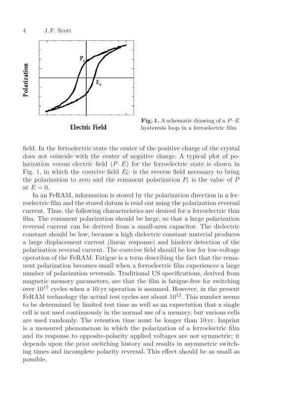
Fig. 1. A schematic drawing of a P–Ehysteresis loop in a ferroelectric film
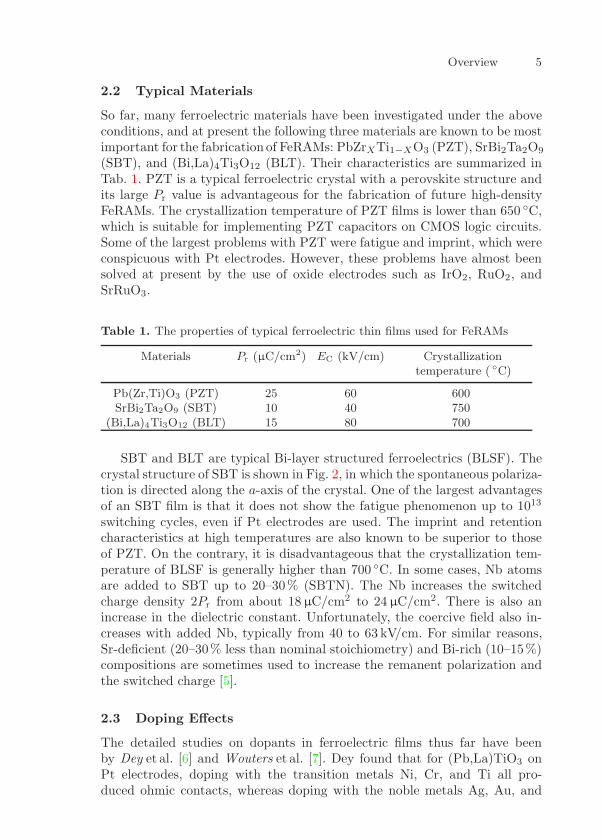
field. In the ferroelectric state the center of the positive charge of the crystaldoes not coincide with the center of negative charge. A typical plot of po-larization versus electric field (P–E) for the ferroelectric state is shown inFig. 1, in which the coercive field EC is the reverse field necessary to bringthe polarization to zero and the remanent polarization Pr is the value of Pat E = 0.
In an FeRAM, information is stored by the polarization direction in a fer-roelectric film and the stored datum is read out using the polarization reversalcurrent. Thus, the following characteristics are desired for a ferroelectric thinfilm. The remanent polarization should be large, so that a large polarizationreversal current can be derived from a small-area capacitor. The dielectricconstant should be low, because a high dielectric constant material producesa large displacement current (linear response) and hinders detection of thepolarization reversal current. The coercive field should be low for low-voltageoperation of the FeRAM. Fatigue is a term describing the fact that the rema-nent polarization becomes small when a ferroelectric film experiences a largenumber of polarization reversals. Traditional US specifications, derived frommagnetic memory parameters, are that the film is fatigue-free for switchingover 1015 cycles when a 10-yr operation is assumed. However, in the presentFeRAM technology the actual test cycles are about 1012. This number seemsto be determined by limited test time as well as an expectation that a singlecell is not used continuously in the normal use of a memory, but various cellsare used randomly. The retention time must be longer than 10 yr. Imprintis a measured phenomenon in which the polarization of a ferroelectric filmand its response to opposite-polarity applied voltages are not symmetric; itdepends upon the prior switching history and results in asymmetric switch-ing times and incomplete polarity reversal. This effect should be as small aspossible.
Overview 5
2.2 Typical Materials
So far, many ferroelectric materials have been investigated under the aboveconditions, and at present the following three materials are known to be mostimportant for the fabrication of FeRAMs: PbZrXTi1−XO3 (PZT), SrBi2Ta2O9
(SBT), and (Bi,La)4Ti3O12 (BLT). Their characteristics are summarized inTab. 1. PZT is a typical ferroelectric crystal with a perovskite structure andits large Pr value is advantageous for the fabrication of future high-densityFeRAMs. The crystallization temperature of PZT films is lower than 650 C,which is suitable for implementing PZT capacitors on CMOS logic circuits.Some of the largest problems with PZT were fatigue and imprint, which wereconspicuous with Pt electrodes. However, these problems have almost beensolved at present by the use of oxide electrodes such as IrO2, RuO2, andSrRuO3.
Table 1. The properties of typical ferroelectric thin films used for FeRAMs
Materials Pr (µC/cm2) EC (kV/cm) Crystallizationtemperature ( C)
Pb(Zr,Ti)O3 (PZT) 25 60 600SrBi2Ta2O9 (SBT) 10 40 750
(Bi,La)4Ti3O12 (BLT) 15 80 700
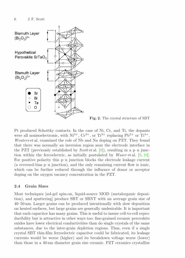
SBT and BLT are typical Bi-layer structured ferroelectrics (BLSF). Thecrystal structure of SBT is shown in Fig. 2, in which the spontaneous polariza-tion is directed along the a-axis of the crystal. One of the largest advantagesof an SBT film is that it does not show the fatigue phenomenon up to 1013
switching cycles, even if Pt electrodes are used. The imprint and retentioncharacteristics at high temperatures are also known to be superior to thoseof PZT. On the contrary, it is disadvantageous that the crystallization tem-perature of BLSF is generally higher than 700 C. In some cases, Nb atomsare added to SBT up to 20–30% (SBTN). The Nb increases the switchedcharge density 2Pr from about 18 µC/cm2 to 24 µC/cm2. There is also anincrease in the dielectric constant. Unfortunately, the coercive field also in-creases with added Nb, typically from 40 to 63 kV/cm. For similar reasons,Sr-deficient (20–30% less than nominal stoichiometry) and Bi-rich (10–15%)compositions are sometimes used to increase the remanent polarization andthe switched charge [5].
2.3 Doping Effects
The detailed studies on dopants in ferroelectric films thus far have beenby Dey et al. [6] and Wouters et al. [7]. Dey found that for (Pb,La)TiO3 onPt electrodes, doping with the transition metals Ni, Cr, and Ti all pro-duced ohmic contacts, whereas doping with the noble metals Ag, Au, and
6 J. F. Scott
Fig. 2. The crystal structure of SBT
Pt produced Schottky contacts. In the case of Ni, Cr, and Ti, the dopantswere all nonisoelectronic, with Ni3+, Cr3+, or Ti3+ replacing Pb2+ or Ti4+.Wouters et al. examined the role of Nb and Na doping on PZT. They foundthat there was normally an inversion region near the electrode interface inthe PZT (previously established by Scott et al. [8]), resulting in a p–n junc-tion within the ferroelectric, as initially postulated by Waser et al. [9, 10].For positive polarity this p–n junction blocks the electrode leakage current(a reversed-bias p–n junction), and the only remaining current flow is ionic,which can be further reduced through the influence of donor or acceptordoping on the oxygen vacancy concentration in the PZT.
2.4 Grain Sizes
Most techniques [sol-gel spin-on, liquid-source MOD (metalorganic deposi-tion), and sputtering] produce SBT or SBNT with an average grain size of40–50 nm. Larger grains can be produced intentionally with slow depositionon heated surfaces, but large grains are generally undesirable. It is importantthat each capacitor has many grains. This is useful to insure cell-to-cell repro-ducibility but is attractive in other ways too: fine-grained ceramic perovskiteoxides have lower electrical conductivities than do single crystals of the samesubstances, due to the inter-grain depletion regions. Thus, even if a singlecrystal SBT thin-film ferroelectric capacitor could be fabricated, its leakagecurrents would be worse (higher) and its breakdown voltage worse (lower)than those in a 40 nm diameter grain size ceramic. PZT ceramics crystallize
Overview 7
with columnar grains that usually extend all the way from anode to cathode.However, SBT grains are globular polyhedra. A 0.2 µm×0.2 µm SBT cell willcontain at least 25 grains of 40 nm in size, depending upon the thickness.
In some ferroelectrics, domain walls cannot move through grain bound-aries, but Gruverman et al. have recently demonstrated [11] that domain wallsin oxide perovskite ferroelectrics move through grain boundaries. The wallsdo this by extending finger-like tips into neighboring grains at oblique anglesto the grain boundaries. Very recently, Gruverman et al. have shown thatdomain stability is a simple function of the distance to the nearest grainboundary.
3 Size Effects in Ferroelectric Capacitors
3.1 Lateral Area
The fundamental limitation in lateral area probably arises from the fringingfield. One can calculate the fringing field correction for a thin parallel platecapacitor from conformal integral techniques. The result is that for an aspectratio of 10 : 1 a capacitance correction of about 7% is found. However, thecorrection increases nonlinearly as the aspect ratio approaches unity; a 20%correction is found for the 5 : 1 aspect ratio now used commercially (0.7 µmwidth and 1.0 µm diagonal on a 0.2 µm thickness). For aspect ratios smallerthan 5 : 1 the fringing field corrections are not small perturbation (the linesof force are not normal to the capacitor surfaces), and one should rather solveLaplace’s equation for a box of the geometry representing the actual capaci-tor shape. Unfortunately, since the main interest in this problem is switchingkinetics and the speed of the sensed displacement current, this method isuseless, because Laplace’s equation is not satisfied in the time-varying case(except for a few special examples, such as uniform coaxial cables and TEMwaves). The general problem of switching behavior in a sub-micron ferro-electric capacitor is therefore not immediately accessible: numerical solutionsstarting with Maxwell’s equations are required.
Simple approximations show, however, that the switched charge for a small-area capacitor of length b and width a will be proportional not to a · b, butto b · log a. Here, a is the smaller dimension, and it is assumed that b a.Hence, the switched charge might be expected to vary logarithmically, asobserved in SBT by Amanuma and Kunio [12].
3.2 Thickness Dependence
As a ferroelectric film gets thinner, depolarization fields from the surface pen-etrate and destroy the ferroelectricity. For a very thin film, the polarizationstate is no longer bistable. Early estimates by Batra and Silverman [13] sug-gested that “very thin” meant 400 nm on semiconducting electrodes and 4 nm
8 J. F. Scott
on metals; we know now that the threshold for this depolarization instabilityis about 6–9 nm and at most 20 nm [Fridkin (private communication) reportsswitching in copolymer Langmuir–Blodgett films down to 0.9 nm (two mono-layers)]. Since ferroelectric nonvolatile memories will be about 80–200 nmthick, this intrinsic problem is primarily of academic interest.
Breakdown in ferroelectric thin films is generally avalanche-like, in thatit is electronically initiated but characterized by thermal runaway when theleakage currents reach certain thresholds. As such it is best understood bycareful studies of leakage currents. In SBT, like PZT and (Ba,Sr)TiO3 (BST),the leakage is Schottky-like up to about 400 kV/cm at 295 K, above whichFowler–Nordheim tunneling becomes very important.
3.3 Electrodes
The primary consideration for electrode choice (assuming that only robust,chemically inert metals are considered) is the leakage current and consequentbreakdown voltage. In this regard, it is useful to pick an electrode metal withthe highest work function; Pt with a work function of about 5.3 eV is probablythe best choice. It gives a maximum breakdown field of about 2.8MV/cm inSBT and a leakage current of approximately 1 nA/cm2 at 2.7 V operatingvoltage across 180 nm thickness. For other metal electrodes, the breakdownfield can be calculated using a formula originally proposed by von Hippel in1935 [14]:
qλEB = ΦH . (1)
Here, q is the electron charge; λ is the electron mean free path in a ferro-electric (typically 0.1 nm); EB is the breakdown field; and ΦH is a quantizedbut unspecified characteristic energy which I take as the contact potentialat the interface (metal work function minus ferroelectric electron affinity).Considering only this criterion for electrodes, Pt would be the best choice;Pd or W would be acceptable; and Ag or Au would be worst.
It is important to note that most ferroelectric perovskite oxides are p-typewide-bandgap semiconductors with bandgaps between 3.2 and 4.3 eV. Eg inSBT is 4.2 eV [15]. However, despite being nominally p-type, the thin filmsbehave as fully depleted devices. All the conduction carriers are electronsinjected from the cathodes, not holes. Hole concentration (double injection)occurs only under illumination or at very high voltages (possibly at 12 Vacross 180 nm in SBT). PZT and BST exhibit n-type inversion within 20 nmof the Pt electrodes [8], but such an inversion is smaller in SBT.
A simple abrupt Schottky model of SBT/Pt is shown [16] in Fig. 3, butthe actual band model of the Pt interface is not compatible with a completelyabrupt Schottky model. The Pt work function ΦM is 5.3 eV. The measuredSchottky barrier height is 0.9 eV (Watanabe et al. [17]). But the SBT electronaffinity χ is 3.4 eV (XPS data, Hartmann et al. [15]). The Schottky barrier
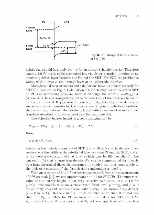
Overview 9
Fig. 3. An abrupt Schottky modelof SBT/Pt
height ΦBn should be simply ΦM−χ for an abrupt Schottky barrier. Thereforeexactly 1.0 eV needs to be accounted for, via either a graded junction or aninsulating defect layer between the Pt and the SBT. For PZT the problem isworse, with a large 20 nm damage layer at the electrode interface.
More detailed measurements and calculations have been made recently forSBT/Pt, as shown in Fig. 3. Calculation of the Schottky barrier height in SBTon Pt is an interesting problem, because although the index S = dΦBn/dX(where X is the electronegativity of the ferroelectric) of the interface behaviorfor such an ionic ABO3 perovskite is nearly unity, the very large density ofsurface states compensates for the ionicity, resulting in an interface conditionthat is midway between the covalent, trap-limited case and the more ionic,trap-free situation often considered as a limiting case [18].
The Schottky barrier height is given approximately by
ΦBn = c(ΦM − χ) + (1 − c)(Eg − Φ0) − ∆ Φ . (2)
Here,
c = 2qεNAδ/ε2i , (3)
where ε is the dielectric constant of SBT (about 500); NA is the density of ac-ceptors; δ is the width of the interfacial layer between Pt and the SBT; and εi
is the dielectric constant of that layer (which may be BiPt or Bi2Pt). Onecan see in (3) that a large trap density NA can be compensated for linearlyby a large interfacial dielectric constant εi, provided that εi is comparable tothe dielectric constant of the ferroelectric semiconductor itself, ε.
With an estimate of 5×10¹⁴ surface traps per cm2, from the measurementsof Mihara et al. [19], we can approximate c = 0.7 for SBT/Pt. The numericalvalue of the barrier height is not very sensitive to this value; c = 1.0 forpurely ionic models with no surface-state Fermi level pinning, and c = 0for a purely covalent semiconductor with a very high surface trap density(c = 0.27 in Si). Hence c in SBT must be much more than 0.27 and lessthan 1.0. ΦM = 5.3 eV for Pt; we measure χ = 3.4 eV for SBT via XPS;Eg = 4.2 eV from UV absorption; and Φ0 is the energy level at the surface
10 J. F. Scott
(the SBT Fermi level versus the SBT valence band level), which from our XPSdata is 2.1 eV – approximately half the bandgap. By comparison, the valuesof Φ0 in Si, GaP, or GaAs are always around 0.3Eg, increasing to 0.6Eg inmore ionic II–VI compounds such as CdS [20], so this result is reasonable.
This gives ΦBn = 0.7 × 1.9 eV + 0.3 × 2.1 eV − ∆ Φ = 1.96 − ∆ Φ, where∆ Φ is the image field barrier reduction energy. It is given by [qE/(4πεop)]1/2,where E is the electric field and εop is not the DC dielectric constant [becausethe electrons move through the interface in a time t = (6 nm)/(105 m/s) =10−13 s] much faster than the dielectric relaxation time, so that the ionsare not perturbed and the response is purely electronic, but approximatelyn2 = εop, where n is the index of refraction in the visible region, about2.4. For this value of the dielectric constant, the Schottky barrier width isabout 2 nm. At the measuring voltages of about 2 V, ∆Φ = 0.8± 0.3 eV (forcomparison, from Mead and Spitzer [20], it is 0.55±0.22 eV in Si at the samefield levels, the value being lower by the square root of the ratio of εop, whichis 11.7 in Si and 2.4 × 2.4 = 5.8 in SBT); and hence the SBT/Pt barrierheight is calculated as 1.1 ± 0.3 eV.
Experimentally, Watanabe et al. [17] measure 0.83 eV Schottky barrierheight, and Lee et al. report 0.9–1.1 eV, which is in complete agreement withthis calculation. Extremely similar values are obtained by a careful fit of theSchottky emission in BST on Pt. In this case, Joshi et al. [21] showed thatthe zero-voltage Schottky barrier height is 1.5 eV (compared with our valueof 1.96 eV in SBT above) and that the barrier reduction value is 0.8 eV at 3 V(across 150 nm), exactly as we calculate above for SBT, so that the reducedbarrier height is 0.7± 0.2 eV for BST, in close agreement with our calculatedvalue of 1.1±0.3 eV for SBT and even closer to Watanabe’s experimental valueof 0.83 eV. Similarly, Waser gives 1.1 eV experimentally for SrTiO3/Pt [22].Thus, we see that band model calculations work well for these materials andthat BST, PZT, and SBT films for DRAM and FeRAM capacitors all behaveas wide-bandgap p-type semiconductors with n-type inversion layers at thePt interface, thermally populated at an ambient temperatures. Under normaloperating voltages of about 3 V, they act as fully depleted devices, so that allof the charge carriers are electrons injected from the cathode. This was firstestablished by Melnick et al. [23] and later confirmed by Wouters et al. [7].
4 Dynamic Characteristics
4.1 Domain Structure
Because SBT is a highly uniaxial ferroelectric (c/a 1), it does not gener-ally exhibit 90-degree domains. The domain structure consists of ribbon-likerectangles of 180-degree domains. The domain size depends critically on thegrain size and film thickness. As the grain diameter (or film thickness) de-creases, the domain size also decreases. In general, for a bulk ferroelectric thestable ground state is a single large domain; but as the film gets thinner or the
Overview 11
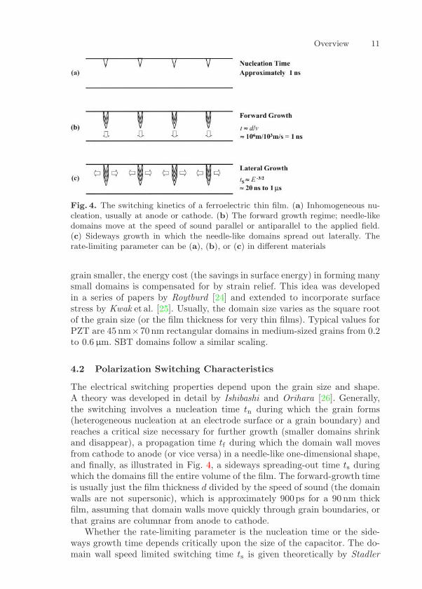
Fig. 4. The switching kinetics of a ferroelectric thin film. (a) Inhomogeneous nu-cleation, usually at anode or cathode. (b) The forward growth regime; needle-likedomains move at the speed of sound parallel or antiparallel to the applied field.(c) Sideways growth in which the needle-like domains spread out laterally. Therate-limiting parameter can be (a), (b), or (c) in different materials
grain smaller, the energy cost (the savings in surface energy) in forming manysmall domains is compensated for by strain relief. This idea was developedin a series of papers by Roytburd [24] and extended to incorporate surfacestress by Kwak et al. [25]. Usually, the domain size varies as the square rootof the grain size (or the film thickness for very thin films). Typical values forPZT are 45 nm×70 nm rectangular domains in medium-sized grains from 0.2to 0.6 µm. SBT domains follow a similar scaling.
4.2 Polarization Switching Characteristics
The electrical switching properties depend upon the grain size and shape.A theory was developed in detail by Ishibashi and Orihara [26]. Generally,the switching involves a nucleation time tn during which the grain forms(heterogeneous nucleation at an electrode surface or a grain boundary) andreaches a critical size necessary for further growth (smaller domains shrinkand disappear), a propagation time tf during which the domain wall movesfrom cathode to anode (or vice versa) in a needle-like one-dimensional shape,and finally, as illustrated in Fig. 4, a sideways spreading-out time ts duringwhich the domains fill the entire volume of the film. The forward-growth timeis usually just the film thickness d divided by the speed of sound (the domainwalls are not supersonic), which is approximately 900ps for a 90 nm thickfilm, assuming that domain walls move quickly through grain boundaries, orthat grains are columnar from anode to cathode.
Whether the rate-limiting parameter is the nucleation time or the side-ways growth time depends critically upon the size of the capacitor. The do-main wall speed limited switching time ts is given theoretically by Stadler

12 J. F. Scott
and Zachmanidis [27] as:
ts = (2Nrν2/9)−1/3 , (4)
where N is the number of nucleation sites per surface area; ν is the averagewall speed; and r is the nucleation rate. Nucleation rates are not known forSBT, but for PZT Duiker et al. [28] measured r for surface nucleation. Byfitting switching current transients i(t) they derived parameters from whicha ts value of 600 ± 300 ps can be inferred for typical PZT capacitors [29].This number can be compared with the time of about 200ps which it takesfor the output current from one gate to recharge the interconnect between itand the next gate (this, not the clock frequency, determines the basic speedof a silicon chip).
The nucleation time tn is given in general by
tn = (NrA)−1 , (5)
where A is the capacitor area. Hence for the nucleation time to be negligible,we require, from (4) and (5):
NrA (Nrν2)1/3 (6)
or
ν/(Nr) A3/2 . (7)
Theoretically, both ν and r vary as E3/2, so (7) is valid independent offield E (or voltage V ). If we insert realistic numbers for ν, N , and r, we findthat nucleation will be the rate-limiting step in the switching of ferroelectriccapacitor cells that are smaller than 2 µm×2 µm. So domain wall propagationspeed is not important in the access speed of a 1Gb ULSI FeRAM, onlynucleation time. Ishibashi originally assumed that the total switching timet (t = tn + tf + ts) varies as
t = BE−jτk , (8)
and empirically found j and k of order of 1–2, where B is a constant; E is theapplied field; and τ is the reduced temperature (TC−T )/TC, where TC is theCurie temperature. tn, tf , and ts stand for, respectively, the nucleation time,the forward-growth time, and the sideways spreading time for ferroelectricdomains. In the low-field regime, the theory of Stadler gives j = 3/2 exactly,which is confirmed experimentally for KNO3 films in Fig. 5. At higher fields,a more accurate description (Scott et al. [30]) is given by
t = B exp (Eα/E) , (9)
where Eα is an activation field that is proportional to τ . When expanded tothe first few terms, the exponential in (9) averages to T and E power lawswith averaging of the linear and quadratic terms in the expansion.

Overview 13
Fig. 5. The switching speed vary-ing as E−3/2 in KNO3 for filmthickness of 180, 270, and 400 nm
It is interesting to compare the breakdown fields EB, the coercive fields EC,and the activation fields (for switching) Eα in ferroelectric films. There is noexpected relationship between the breakdown field and the other two char-acteristic fields, because the breakdown fields are the same above and belowthe Curie temperature, in the ferroelectric and paraelectric phases, and hencehave nothing to do with domains, whereas the coercive field and the activa-tion field relate to domain creation and domain wall motion. For many oxideferroelectric films, these values are similar. The breakdown field depends uponthickness, electrodes, temperature, and other factors, but typically it is about1.3MV/cm in PZT, 1.0MV/cm in KNO3, and 1 MV/cm in SBT. The coercivefields are generally between 1/2 and 1/4 of the activation fields.
For example, EC in potassium nitrate is 100 kV/cm, while Eα is 180 kV/cm.In PZT the coercive field is typically 65 kV/cm, while Eα is 210 kV/cm. Infact, one might ask why the activation field isn’t exactly equal to the co-ercive field. The probable answer is that the activation field measures theability to nucleate a domain, and the coercive field to switch an already ex-isting domain. Although these fields should be comparable, it appears thatthe nucleation field is typically larger by a factor of approximately 3.
4.3 Frequency Dependence
Most laboratory measurements on SBT are in the kHz regime. But FeRAMwill operate at very high internal clock-rates – at least 100 MHz and perhaps300 MHz. The frequency dependence of the coercive field is the most impor-tant parameter in this regard. A theory was recently developed [31] whichpredicts
EC = CfD/α , (10)
14 J. F. Scott
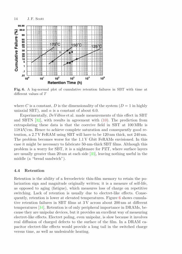
Fig. 6. A log-normal plot of cumulative retention failures in SBT with time atdifferent values of T
where C is a constant, D is the dimensionality of the system (D = 1 in highlyuniaxial SBT), and α is a constant of about 6.0.
Experimentally, DeVilbiss et al. made measurements of this effect in SBTand SBTN [32], with results in agreement with (10). The prediction fromextrapolating these data is that the coercive field in SBT at 100 MHz is118 kV/cm. Hence to achieve complete saturation and consequently good re-tention, a 2.7V FeRAM using SBT will have to be 120 nm thick, not 240 nm.The problem becomes worse for the 1.1 V Gbit FeRAMs envisioned. In thiscase it might be necessary to fabricate 50-nm-thick SBT films. Although thisproblem is a worry for SBT, it is a nightmare for PZT, where surface layersare usually greater than 20 nm at each side [33], leaving nothing useful in themiddle (a “bread sandwich”).
4.4 Retention
Retention is the ability of a ferroelectric thin-film memory to retain the po-larization sign and magnitude originally written; it is a measure of self-life,as opposed to aging (fatigue), which measures loss of charge on repetitiveswitching. Lack of retention is usually due to electret-like effects. Conse-quently, retention is lower at elevated temperatures. Figure 6 shows cumula-tive retention failures in SBT films at 3 V across about 200 nm at differenttemperatures [34]. Retention is of only peripheral importance in DRAMs, be-cause they are unipolar devices, but it provides an excellent way of measuringelectret-like effects. Electret poling, even unipolar, is slow because it involvesreal diffusion of charged defects to the surface of the film. In a DRAM ca-pacitor electret-like effects would provide a long tail in the switched chargeversus time, as well as undesirable heating.
Overview 15
References
1. T. S. Moise, S.R. Summerfelt, H. McAdams, S. Aggarwal, K.R. Udayakumar,F.G. Celii, J. S. Martin, G. Xing, L. hall, K. J. Taylor, T. Hurd, J. Rodriguez,K. Remack, M.D. Khan, K. Boku, G. Stacey, M. Yao, M.G. Albrecht, E. Zielin-ski, M. Thakre, S. Kuchimanchi, A. Thomas, B. McKee, J. Rickes, A. Wang,J. Grace, J. Fong, D. Lee, C. Pietrzyk, R. Lanham, S.R. Gilbert, D. Taylor,J. Amano, R. Bailey, F. Chu, G. Fox, S. Sun, T. Davenport: Int. ElectronDevices Meeting, Tech. Digest, San Francisco, No.21.1 (2002) 3
2. Y. Horii, Y. Hikosaka, A. Itoh, K. Matsuura, M. Kurasawa, G. Komuro,K. Maruyama, T. Eshita, S. Kashiwagi: Int. Electron Devices Meeting, Tech.Digest, San Francisco, No.21.2 (2002) 3
3. M.-K. Choi, B.-G. Jeon, N. Jang, B.-J. Min, Y.-J. Song, S.-Y. Lee, H.-H. Kim,D.-J. Jung, H.-J. Joo, K. Kim: IEEE J. Solid-State Circuits 37, 1472 (2002) 3
4. J. F. Scott: IEICE Trans. Electron. 81-C, 477 (1998) 35. T. Noguchi, T. Hase, Y. Miyasaka: Jpn. J. Appl. Phys. 35, 4900 (1996) 56. S.K. Dey, P. Alluri, J.-J. Lee, R. Zuleeg: Integr. Ferroelectr. 8, 715 (1995) 57. D. J. Wouters, G. Willems, G. Groeseneken, H.E. Maes, K. Brooks, R. Klis-
surska: Proc. EMIF-1, Nijmegen (July 1995)8. J. F. Scott: Integr. Ferroelectr. 9, 1 (1995) 5, 10 6, 89. R. Waser, T. Baiatu, H. Hardtl: J. Am. Ceram. Soc. 73, 1645 (1990) 6
10. R. Waser, M. Klee: Integr. Ferroelectr. 2, 288 (1992) 611. A. Gruverman, H. Tokumoto, A. S. Prakash, S. Aggarwal, B. Yang, M. Wuttig,
R. Ramesh, O. Auciello, T. Venkatensan: Appl. Phys. Lett. 71, 3492 (1997) 712. K. Amanuma, T. Kunio: Jpn. J. Appl. Phys. 35, 5229 (1996) 713. I. P. Batra, B. D. Silverman: Solid State Commun. 11, 291 (1972) 714. A. von Hippel: Ergeb. exakt. Naturwiss. 14, 118 (1935) 815. A. J. Hartmann, J. F. Scott et al.: J. Phys. (Paris) (1998) 816. A. J. Hartmann, J. F. Scott et al.: EMIF-2, Versailles, Sept. 1997 817. K. Watanabe, M. Tanaka, N. Nagel, K. Katori, M. Sugiyama, H. Yamoto,
H. Yagi: Integr. Ferroelectr. 14, 95 (1997) 8, 1018. S.M. Sze: Physics of Semiconductor Devices, 2nd edn. (Wiley, New York 1981)
p. 273 919. T. Mihara, H. Watanabe, H. Yoshimori, C. A. Paz de Araujo, B. Melnick, I. D.
MacMillan: Integr. Ferroelectr. 1, 269 (1992) 920. C.A. Mead, W.G. Spitzer: Phys. Rev. 134, A713 (1964) 1021. V. Joshi, C. P. DaCruz, J.D. Cuchiaro, C. A. Paz de Araujo, R. Zuleeg: Integr.
Ferroelectr. 14, 133 (1997) 1022. R. Waser: Science and Technology of Electroceramic Thin Films (Kluwer, 1995)
p. 223 1023. B.M. Melnick, J. F. Scott, C.A. Paz de Araujo, L. D. McMillan: Ferroelectr.
135, 163 (1992) 1024. A.L. Roytburd: Phys. Stat. Sol. A37, 329 (1976) 1125. B. S. Kwak, A. Erbil, B. J. Wilkens, J. D. Budai, M.F. Chisholm, L.A. Boatner:
Phys. Rev. Lett. 68, 3733 (1992); Phys. Rev. B 49, 14865 (1994) 1126. Y. Ishibashi, Y. Takagi: J. Phys. Soc. Jpn. 31, 506 (1971) 1127. H.L. Stadler, P. J. Zachmanidis: J. Appl. Phys. 34, 3255 (1963) 1228. H.M. Duiker, P.D. Beale, J. F. Scott, C.A. Paz de Araujo, B. M. Melnick, J. D.
Cuchiaro, L.D. MacMillan: J. Appl. Phys. 68, 5783 (1990) 12
16 J. F. Scott
29. J. F. Scott: Ferroelectr. Rev. 1, 1 (1998) 1230. J. F. Scott, L. Kamerdiner, M. Parris, S. Traynor, V. Ottenbacher, A. Shaw-
bkeh, W. F. Oliver: J. Appl. Phys. 64, 787 (1988) 1231. Y. Ishibashi, H. Orihara: Integr. Ferroelectr. 9, 57 (1995) 1332. A.D. DeVilbiss, W. J. Connor, G. F. Derbenwick: Abstracts Int. Symp. Integr.
Ferroelectr. No. 18c, Tempe, Arizona (1996) 1433. J. F. Scott, D. Galt, J. C. Price, J. A. Beall, R.H. Ono, C. A. Paz de Araujo,
L.D. MacMillan: Integr. Ferroelectr. 6, 189 (1995) 1434. Y. Shimada, M. Azuma, K. Nakao, S. Chaya, N. Moriwaki, T. Otsuki: Jpn.
J. Appl. Phys. 36, 5912 (1997) 14
Index
(Bi,La)4Ti3O12 (BLT), 5
activation field, 12
bandgap– inversion, 8barrier height– electron affinity, 8Bi-layer structured ferroelectric
(BLSF), 5breakdown field, 13
coercive field, 4, 13Curie temperature, 12
depolarization field, 7dielectric constant, 4domain, 10dopant, 5
electret-like effect, 14electrode– breakdown, 8
fatigue, 4
ferroelectric– crystal polarization, 3frequency dependence, 13fringing field, 7
grain size, 6
imprint phenomenon, 4
oxide electrode, 5
PbZrXTi1−XO3 (PZT), 5
remanent polarization, 4retention, 14retention time, 4
Schottky model, 8SrBi2Ta2O9 (SBT), 5switching– forward-growth time, 11– nucleation time, 11– propagation time, 11– spreading-out time, 11
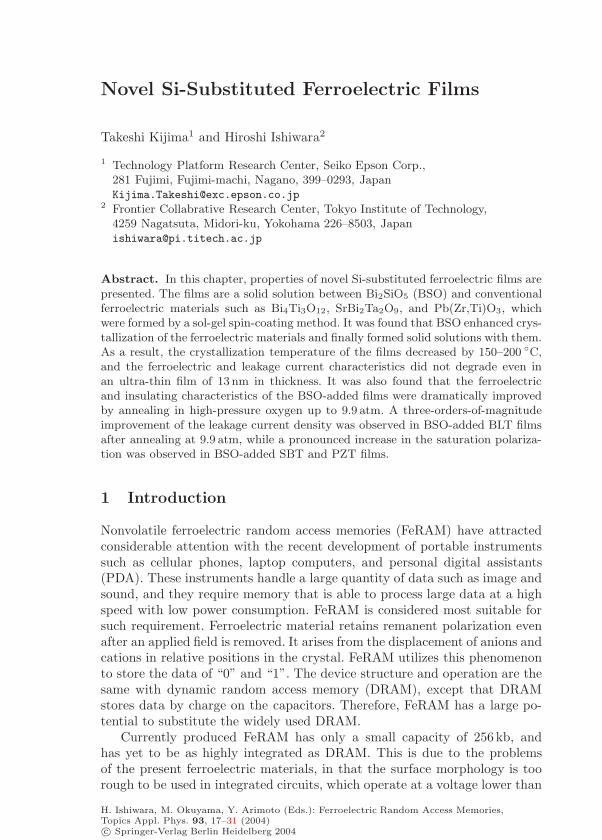
Novel Si-Substituted Ferroelectric Films
Takeshi Kijima1 and Hiroshi Ishiwara2
1 Technology Platform Research Center, Seiko Epson Corp.,281 Fujimi, Fujimi-machi, Nagano, 399–0293, [email protected]
2 Frontier Collabrative Research Center, Tokyo Institute of Technology,4259 Nagatsuta, Midori-ku, Yokohama 226–8503, [email protected]
Abstract. In this chapter, properties of novel Si-substituted ferroelectric films arepresented. The films are a solid solution between Bi2SiO5 (BSO) and conventionalferroelectric materials such as Bi4Ti3O12, SrBi2Ta2O9, and Pb(Zr,Ti)O3, whichwere formed by a sol-gel spin-coating method. It was found that BSO enhanced crys-tallization of the ferroelectric materials and finally formed solid solutions with them.As a result, the crystallization temperature of the films decreased by 150–200 C,and the ferroelectric and leakage current characteristics did not degrade even inan ultra-thin film of 13 nm in thickness. It was also found that the ferroelectricand insulating characteristics of the BSO-added films were dramatically improvedby annealing in high-pressure oxygen up to 9.9 atm. A three-orders-of-magnitudeimprovement of the leakage current density was observed in BSO-added BLT filmsafter annealing at 9.9 atm, while a pronounced increase in the saturation polariza-tion was observed in BSO-added SBT and PZT films.
1 Introduction
Nonvolatile ferroelectric random access memories (FeRAM) have attractedconsiderable attention with the recent development of portable instrumentssuch as cellular phones, laptop computers, and personal digital assistants(PDA). These instruments handle a large quantity of data such as image andsound, and they require memory that is able to process large data at a highspeed with low power consumption. FeRAM is considered most suitable forsuch requirement. Ferroelectric material retains remanent polarization evenafter an applied field is removed. It arises from the displacement of anions andcations in relative positions in the crystal. FeRAM utilizes this phenomenonto store the data of “0” and “1”. The device structure and operation are thesame with dynamic random access memory (DRAM), except that DRAMstores data by charge on the capacitors. Therefore, FeRAM has a large po-tential to substitute the widely used DRAM.
Currently produced FeRAM has only a small capacity of 256 kb, andhas yet to be as highly integrated as DRAM. This is due to the problemsof the present ferroelectric materials, in that the surface morphology is toorough to be used in integrated circuits, which operate at a voltage lower than
H. Ishiwara, M. Okuyama, Y. Arimoto (Eds.): Ferroelectric Random Access Memories,Topics Appl. Phys. 93, 17–31 (2004)c© Springer-Verlag Berlin Heidelberg 2004
18 T. Kijima and H. Ishiwara
2 V. It is also important to decrease the present crystallization temperature(higher than 600 C) to fabricate future high-density FeRAMs. In this chap-ter, we show that these problems can be solved by forming solid solutionsbetween Bi2SiO5 (BSO) [1, 2] and conventional ferroelectric materials suchas Bi4Ti3O12 (BIT) [3, 4], SrBi2Ta2O9 (SBT) [5] and Pb(Zr,Ti)O3 (PZT).The crystallization temperatures of the new ferroelectric films were loweredby 150–200 C and the surface of the crystallized films became very flat andsmooth. Because of these excellent properties, very thin (13–25 nm thick) fer-roelectric capacitors were successfully fabricated, in which the polarizationwas well saturated at an applied voltage of 0.5 V [6, 7].
2 The Crystallization Process
In the experiment, combinations of BSO and BIT were first attempted, sinceboth have similar Bi-layered structures, and since the lattice mismatch ofthe basal plane is as small as 0.5% between the two materials. The rema-nent polarization of a bulk BIT crystal is about 50µC/cm2 along the a-axisand it is about 4 µC/cm2 along the c-axis [4]. On the other hand, BSO hasa crystallization temperature as low as 400 C [1,2], and it is known to act asa solid acid catalyst [8,9]. The film was formed by a simple sol-gel spin-coatingmethod. Commercially available sol-gel solutions of BSO (Bi2O3:SiO2 = 1:1)and BIT (manufactured by Mitsubishi Material Co.) were mixed. Since bothof them are dissolved in n-butyl alcohol, they mix well at an arbitrary molratio. After several attempts, the optimum mol ratio R of BSO to BIT, atwhich improvement of the film quality as well as lowering of the crystalliza-tion temperature were most clearly demonstrated, was determined to be 0.4.
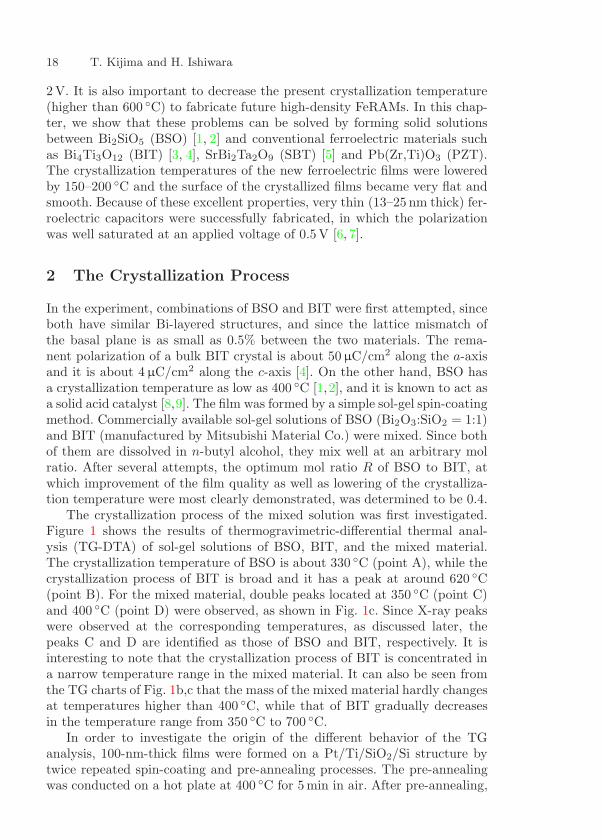
The crystallization process of the mixed solution was first investigated.Figure 1 shows the results of thermogravimetric-differential thermal anal-ysis (TG-DTA) of sol-gel solutions of BSO, BIT, and the mixed material.The crystallization temperature of BSO is about 330 C (point A), while thecrystallization process of BIT is broad and it has a peak at around 620 C(point B). For the mixed material, double peaks located at 350 C (point C)and 400 C (point D) were observed, as shown in Fig. 1c. Since X-ray peakswere observed at the corresponding temperatures, as discussed later, thepeaks C and D are identified as those of BSO and BIT, respectively. It isinteresting to note that the crystallization process of BIT is concentrated ina narrow temperature range in the mixed material. It can also be seen fromthe TG charts of Fig. 1b,c that the mass of the mixed material hardly changesat temperatures higher than 400 C, while that of BIT gradually decreasesin the temperature range from 350 C to 700 C.
In order to investigate the origin of the different behavior of the TGanalysis, 100-nm-thick films were formed on a Pt/Ti/SiO2/Si structure bytwice repeated spin-coating and pre-annealing processes. The pre-annealingwas conducted on a hot plate at 400 C for 5 min in air. After pre-annealing,
Novel Si-Substituted Ferroelectric Films 19
Fig. 1. TG-DTA charts of (a) BSO,(b) BIT, and (c) BSO-added BIT sys-tems. The measurement temperaturewas increased at a rate of 10 C/min
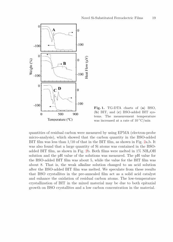
quantities of residual carbon were measured by using EPMA (electron-probemicro-analysis), which showed that the carbon quantity in the BSO-addedBIT film was less than 1/10 of that in the BIT film, as shown in Fig. 2a,b. Itwas also found that a large quantity of Si atoms was contained in the BSO-added BIT film, as shown in Fig. 2b. Both films were melted in 1% NH4OHsolution and the pH value of the solutions was measured. The pH value forthe BSO-added BIT film was about 5, while the value for the BIT film wasabout 8. That is, the weak alkaline solution changed to an acid solutionafter the BSO-added BIT film was melted. We speculate from these resultsthat BSO crystallites in the pre-annealed film act as a solid acid catalystand enhance the oxidation of residual carbon atoms. The low-temperaturecrystallization of BIT in the mixed material may be due to both epitaxialgrowth on BSO crystallites and a low carbon concentration in the material.
20 T. Kijima and H. Ishiwara
Fig. 2. EPMA spectra for pre-annealed(a) BIT and (b) BSO-added BIT films
3 The Properties of Bi2SiO5-Added Bi4Ti3O12 Films
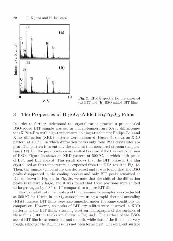
In order to further understand the crystallization process, a pre-annealedBSO-added BIT sample was set in a high-temperature X-ray diffractome-ter (X’Pert-Pro with high-temperature holding attachment; Philips Co.) andX-ray diffraction (XRD) patterns were measured. Figure 3a shows an XRDpattern at 400 C, in which diffraction peaks only from BSO crystallites ap-pear. The pattern is essentially the same as that measured at room tempera-ture (RT), but the peak positions are shifted because of the thermal expansionof BSO. Figure 3b shows an XRD pattern at 500 C, in which both peaksof BSO and BIT coexist. This result shows that the BIT phase in the filmcrystallized at this temperature, as expected from the DTA result in Fig. 1c.Then, the sample temperature was decreased and it was found that the BSOpeaks disappeared in the cooling process and only BIT peaks remained atRT, as shown in Fig. 3c. In Fig. 3c, we note that the shift of the diffractionpeaks is relatively large, and it was found that these positions were shiftedto larger angles by 0.3 to 1 compared to a pure BIT film.
Next, crystallization annealing of the pre-annealed samples was conductedat 500 C for 10 min in an O2 atmosphere using a rapid thermal annealing(RTA) furnace. BIT films were also annealed under the same conditions forcomparison. However, no peaks of BIT crystallites were observed in XRDpatterns in the BIT films. Scanning electron micrographs of the surfaces ofthese films (100 nm thick) are shown in Fig. 4a,b. The surface of the BSO-added BIT film is extremely flat and smooth, while that of the BIT film is veryrough, although the BIT phase has not been formed yet. The excellent surface
Novel Si-Substituted Ferroelectric Films 21
Fig. 3. XRD patterns of a BSO-added BITfilm (a) at 400 C, (b) at 500 C, and (c) atRT after crystallization. In (a) and (b), thepattern shift due to thermal expansion wascorrected, so that the peak positions of Si(400) were superposed on that in (c)
Fig. 4. Surface morphologies of (a) BIT and (b) BSO-added BIT films crystallizedat 500 C
morphology is considered to originate from the fact that BSO crystallites areuniformly distributed in the pre-annealed film and they act as nucleationsites for the crystallization of BIT.
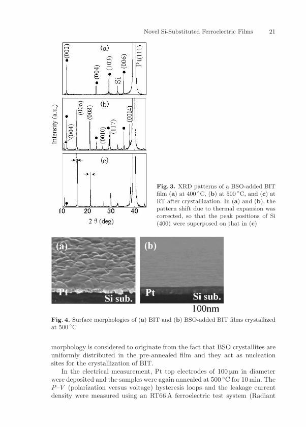
In the electrical measurement, Pt top electrodes of 100µm in diameterwere deposited and the samples were again annealed at 500 C for 10 min. TheP–V (polarization versus voltage) hysteresis loops and the leakage currentdensity were measured using an RT66 A ferroelectric test system (Radiant

22 T. Kijima and H. Ishiwara
Fig. 5. Variation of P–V hysteresis curves of a BSO-added BIT capacitor. Solidline; initial, closed squares; after fatigue test of 1010 switching cycles at 100 kHz,cross; after a hydrogen immunity test at 400 C
Technologies, Inc.) at a frequency of 1 kHz and a pA meter connected toa DC voltage source, respectively. Figure 5 shows P–V hysteresis loops forthe same sample before and after fatigue measurement. As can be seen fromthe figure, a square-shaped hysteresis loop with the remanent polarization of18 µC/cm2 was obtained and no fatigue (degradation of the hysteresis shape)was observed even after 1010 switching cycles with a frequency of 100 kHz.The result for a hydrogen immunity test, in which the sample with top Ptelectrodes was annealed in an N2 atmosphere with 3% H2 at 400 C for 10 min,is also shown in the figure. As can be seen from the figure, degradation ofthe hysteresis loop is not significant in this sample. This result is completelydifferent from the usual case [10], in which the remanent polarization of a fer-roelectric film becomes zero by annealing in 3% H2 at 250 C. This excellentferroelectricity is partly due to the fact that a uniformly packed dense filmis formed in this method.
So far, we have shown that the BSO peaks in the film disappear during thecooling process to RT and that the ferroelectric properties of the obtained filmare excellent. Concerning the stability of a ferroelectric film with a perovskitestructure, it is known that the stability is increased when the covalency of theB-site ion is increased [11]. We speculate from these results that the crystalstructure of BSO crystallites in the BSO-added BIT film was changed to theBi-layered perovskite structure during the cooling process of the film, andthat a mixed crystal Bi4(Ti,Si)3O12 with Si concentration as high as 30% wasformed. In other words, the SiO4−
4 tetragonal structure in a BSO crystal waschanged to the SiO8−
6 octahedron structure; that is, the coordinate numberof the Si atoms was changed from 4 to 6. This is a new hypothesis, because it

Novel Si-Substituted Ferroelectric Films 23
Fig. 6. XPS spectra for Si 2p states in(solid line) films
is generally known that the ionic radius of Si is too small to be crystallized ina perovskite structure at atmospheric pressure. Actually, it is reported thatCaSiO3 or MgSiO3 with a perovskite structure is formed in the mantle layerof the Earth, where a compressive stress in excess of 20GPa is applied to theconstituent materials [12, 13].
Then, in order to investigate the change of the coordinate number of the Siatoms, X-ray photoelectron spectroscopy (XPS) measurement was conductedfor the BSO and BSO-added BIT films. Figure 6 shows Si 2p spectra in bothfilms, in which the peak position in the spectrum shows the binding energyof the Si 2p state. As can be seen from the figure, the shape of the spectra isdifferent between the two samples, and the binding energy of the Si 2p stateshifts to the higher energy by about 1.5 eV in the BSO-added BIT film. Itis also known that the Si 2p binding energy is about 99 eV in an Si crystaland it is about 103 eV in SiO2, which is composed of the SiO4−
4 tetragonalstructure. These results strongly suggest that the coordinate number of the Siatoms was changed from 4 to 6 in the BSO-added BIT film and that a mixedcrystal with the Bi-layered perovskite structure was formed.
At present, the precise mechanism on the change of the coordinate numberof Si atoms is not well understood. However, we speculate that BSO crys-tallites in the film are compressed by the surrounding BIT crystals duringthe cooling stage, because of the difference between the thermal expansioncoefficients of the two materials, and the generated stress is high enough toform the SiO8−
6 octahedron structure. We can calculate the thermal expan-sion coefficient of BSO from Fig. 3a and the XRD pattern at RT is about12×10−6 (1/ C). We can also calculate the coefficient for the BSO–BIT filmfrom Fig. 3b,c. As we mentioned before, the diffraction peaks in Fig. 3c areshifted to a higher-angle direction, compared to a pure BIT crystal. Thus, thethermal expansion coefficient derived from Fig. 3b,c is as large as 90 × 10−6
(1/ C). In order to calculate the stress generated in this system [14], we fur-ther need to know the elastic stiffness constants of BSO and BIT. However,these values are unknown at present. If we assume that these values are equalto that of PbTiO3, the stress value is about 30GPa, which is high enough tochange the coordinate number of the Si atoms.
24 T. Kijima and H. Ishiwara
4 The Formation of Ultra-Thin Films
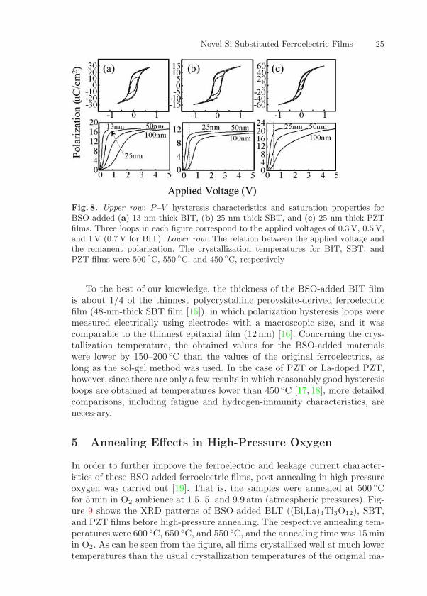
Based on the results described above, the formation of ultra-thin ferroelec-tric films was attempted in the BSO-added BIT system. At the same time,the possibility of BSO-added SBT and BSO-added PZT systems was investi-gated, since the epitaxial alignment effect in the BSO-added BIT system wasnot found to be essential in obtaining excellent ferroelectricity. It was foundfrom these experiments that BSO was also effective in improving the surfacemorphology and in lowering the crystallization temperature of the SBT andPZT films. The minimum values of the film thickness were 13 nm, 25 nm, and25 nm for BSO-added BIT, SBT, and PZT, respectively. The films were crys-tallized at the lowest temperature for each thickness, below which the filmsdid not exhibit excellent ferroelectricity. Thus, the crystallization tempera-tures were 500 C, 550 C, and 450 C for the BSO-added BIT, BSO-addedSBT, and BSO-added PZT films, respectively. The mole ratios R of BSO toBIT, SBT, and PZT were 0.4, 0.33, and 0.1, respectively.
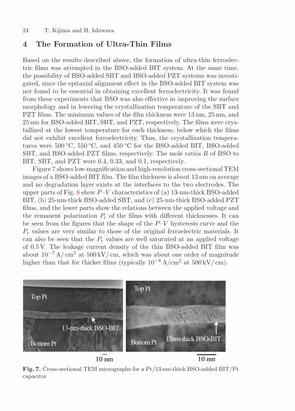
Figure 7 shows low-magnification and high-resolution cross-sectional TEMimages of a BSO-added BIT film. The film thickness is about 13 nm on averageand no degradation layer exists at the interfaces to the two electrodes. Theupper parts of Fig. 8 show P–V characteristics of (a) 13-nm-thick BSO-addedBIT, (b) 25-nm-thick BSO-added SBT, and (c) 25-nm-thick BSO-added PZTfilms, and the lower parts show the relations between the applied voltage andthe remanent polarization Pr of the films with different thicknesses. It canbe seen from the figures that the shape of the P–V hysteresis curve and thePr values are very similar to those of the original ferroelectric materials. Itcan also be seen that the Pr values are well saturated at an applied voltageof 0.5 V. The leakage current density of the thin BSO-added BIT film wasabout 10−7 A/ cm2 at 500 kV/ cm, which was about one order of magnitudehigher than that for thicker films (typically 10−8 A/cm2 at 500 kV/ cm).
Fig. 7. Cross-sectional TEM micrographs for a Pt/13 nm-thick BSO-added BIT/Ptcapacitor
Novel Si-Substituted Ferroelectric Films 25
Fig. 8. Upper row : P–V hysteresis characteristics and saturation properties forBSO-added (a) 13-nm-thick BIT, (b) 25-nm-thick SBT, and (c) 25-nm-thick PZTfilms. Three loops in each figure correspond to the applied voltages of 0.3 V, 0.5 V,and 1V (0.7 V for BIT). Lower row : The relation between the applied voltage andthe remanent polarization. The crystallization temperatures for BIT, SBT, andPZT films were 500 C, 550 C, and 450 C, respectively
To the best of our knowledge, the thickness of the BSO-added BIT filmis about 1/4 of the thinnest polycrystalline perovskite-derived ferroelectricfilm (48-nm-thick SBT film [15]), in which polarization hysteresis loops weremeasured electrically using electrodes with a macroscopic size, and it wascomparable to the thinnest epitaxial film (12 nm) [16]. Concerning the crys-tallization temperature, the obtained values for the BSO-added materialswere lower by 150–200 C than the values of the original ferroelectrics, aslong as the sol-gel method was used. In the case of PZT or La-doped PZT,however, since there are only a few results in which reasonably good hysteresisloops are obtained at temperatures lower than 450 C [17, 18], more detailedcomparisons, including fatigue and hydrogen-immunity characteristics, arenecessary.
5 Annealing Effects in High-Pressure Oxygen
In order to further improve the ferroelectric and leakage current character-istics of these BSO-added ferroelectric films, post-annealing in high-pressureoxygen was carried out [19]. That is, the samples were annealed at 500 Cfor 5 min in O2 ambience at 1.5, 5, and 9.9 atm (atmospheric pressures). Fig-ure 9 shows the XRD patterns of BSO-added BLT ((Bi,La)4Ti3O12), SBT,and PZT films before high-pressure annealing. The respective annealing tem-peratures were 600 C, 650 C, and 550 C, and the annealing time was 15 minin O2. As can be seen from the figure, all films crystallized well at much lowertemperatures than the usual crystallization temperatures of the original ma-
26 T. Kijima and H. Ishiwara
Fig. 9. X-ray diffraction patterns of (a) 50-nm-thick BSO-added BLT, (b) SBT,and (c) PZT films after crystallization annealing
terials. It was also found that the film surfaces became flatter than those ofthe original materials.
Figure 10 shows variations of the XRD peak intensity and position withoxygen pressure during the high-pressure annealing. The four peaks in eachfigure correspond to the initial sample and the annealed samples at 1.5, 5,and 9.9 atm from bottom to top. As can be seen from Fig. 10a, the XRDpeak position in the BLT film hardly changed, but the peak intensity becamesomewhat weak as the oxygen pressure increased. On the other hand, inthe BSO-added ferroelectric films, the peak intensities became stronger andtheir positions shifted to higher angles as the oxygen pressure increased.That is, in the BSO-added BLT, SBT, and PZT films annealed at 9.9 atm,the peak intensities became twice, three times, and 1.5 times stronger thanthe initial intensity, and the peak positions shifted by 0.45 , 0.6 , and 0.25 ,respectively. These results clearly show that the crystallinity of BSO-addedferroelectric films is improved by annealing in high-pressure oxygen, which isdifferent from the behavior of a usual ferroelectric film, as shown in Fig. 10a.
Next, the leakage current and P–V characteristics of these films wereinvestigated. Typical leakage current characteristics are shown in Fig. 11. Ascan be seen from the figure, the leakage current densities were dramaticallydecreased by high-pressure annealing, particularly when the oxygen pressurewas 9.9 atm. In a BSO-added BLT film, the leakage current density decreasedat least by three orders of magnitude, and in a BSO-added SBT film, the valuewas less than 1 × 10⁻⁸ A/ cm2 at a voltage of 5 V (1MV/ cm).
Figure 12 shows a comparison of the initial P–V hysteresis loop with thatof the sample annealed at 9.9 atm. As can be seen from Fig. 12a, the hysteresisloop of a BSO-added BLT film was hardly changed by high-pressure anneal-ing. On the contrary, in a BSO-added SBT film, the shape of the hysteresisloop as well as the saturation polarization were improved. Furthermore, in
Novel Si-Substituted Ferroelectric Films 27
Fig. 10. XRD peak shifts of (a) 100-nm-thick BLT, (b) 50-nm-thick BSO-addedBLT, (c) SBT, and (d) PZT films after high-pressure annealing at 1.5, 5, and9.9 atm
Fig. 11. Leakage current densities of 50-nm-thick BSO-added (a) BLT, (b) SBT,and (c) PZT films after high-pressure annealing at 1.5, 5, and 9.9 atm
a BSO-added PZT film, both the saturation polarization and the coercivevoltage were increased with an increase in the oxygen pressure. The reasonfor the different behavior of the ferroelectric and insulating characteristics isnot well understood at present. A difference in the crystal structures, such asbetween perovskite and Bi-layered structures, may cause the different behav-ior. Although we need more detailed investigations, we can show evidence ofthe structural change of the film due to annealing in high-pressure oxygen.
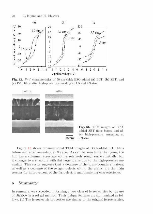
28 T. Kijima and H. Ishiwara
Fig. 12. P–V characteristics of 50-nm-thick BSO-added (a) BLT, (b) SBT, and(c) PZT films after high-pressure annealing at 1.5 and 9.9 atm
Fig. 13. TEM images of BSO-added SBT films before and af-ter high-pressure annealing at9.9 atm
Figure 13 shows cross-sectional TEM images of BSO-added SBT filmsbefore and after annealing at 9.9 atm. As can be seen from the figure, thefilm has a columnar structure with a relatively rough surface initially, butit changes to a structure with flat large grains due to the high-pressure an-nealing. This result suggests that a decrease of the grain-boundary regions,as well as a decrease of the oxygen defects within the grains, are the mainreasons for improvement of the ferroelectric and insulating characteristics.
6 Summary
In summary, we succeeded in forming a new class of ferroelectrics by the useof Bi2SiO5 in a sol-gel method. Their unique features are summarized as fol-lows. (1) The ferroelectric properties are similar to the original ferroelectrics,
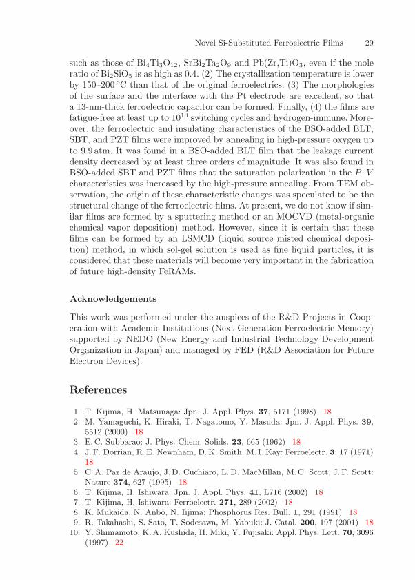
Novel Si-Substituted Ferroelectric Films 29
such as those of Bi4Ti3O12, SrBi2Ta2O9 and Pb(Zr,Ti)O3, even if the moleratio of Bi2SiO5 is as high as 0.4. (2) The crystallization temperature is lowerby 150–200 C than that of the original ferroelectrics. (3) The morphologiesof the surface and the interface with the Pt electrode are excellent, so thata 13-nm-thick ferroelectric capacitor can be formed. Finally, (4) the films arefatigue-free at least up to 1010 switching cycles and hydrogen-immune. More-over, the ferroelectric and insulating characteristics of the BSO-added BLT,SBT, and PZT films were improved by annealing in high-pressure oxygen upto 9.9 atm. It was found in a BSO-added BLT film that the leakage currentdensity decreased by at least three orders of magnitude. It was also found inBSO-added SBT and PZT films that the saturation polarization in the P–Vcharacteristics was increased by the high-pressure annealing. From TEM ob-servation, the origin of these characteristic changes was speculated to be thestructural change of the ferroelectric films. At present, we do not know if sim-ilar films are formed by a sputtering method or an MOCVD (metal-organicchemical vapor deposition) method. However, since it is certain that thesefilms can be formed by an LSMCD (liquid source misted chemical deposi-tion) method, in which sol-gel solution is used as fine liquid particles, it isconsidered that these materials will become very important in the fabricationof future high-density FeRAMs.
Acknowledgements
This work was performed under the auspices of the R&D Projects in Coop-eration with Academic Institutions (Next-Generation Ferroelectric Memory)supported by NEDO (New Energy and Industrial Technology DevelopmentOrganization in Japan) and managed by FED (R&D Association for FutureElectron Devices).
References
1. T. Kijima, H. Matsunaga: Jpn. J. Appl. Phys. 37, 5171 (1998) 182. M. Yamaguchi, K. Hiraki, T. Nagatomo, Y. Masuda: Jpn. J. Appl. Phys. 39,
5512 (2000) 183. E.C. Subbarao: J. Phys. Chem. Solids. 23, 665 (1962) 184. J. F. Dorrian, R.E. Newnham, D.K. Smith, M. I. Kay: Ferroelectr. 3, 17 (1971)
185. C.A. Paz de Araujo, J.D. Cuchiaro, L. D. MacMillan, M.C. Scott, J. F. Scott:
Nature 374, 627 (1995) 186. T. Kijima, H. Ishiwara: Jpn. J. Appl. Phys. 41, L716 (2002) 187. T. Kijima, H. Ishiwara: Ferroelectr. 271, 289 (2002) 188. K. Mukaida, N. Anbo, N. Iijima: Phosphorus Res. Bull. 1, 291 (1991) 189. R. Takahashi, S. Sato, T. Sodesawa, M. Yabuki: J. Catal. 200, 197 (2001) 18
10. Y. Shimamoto, K.A. Kushida, H. Miki, Y. Fujisaki: Appl. Phys. Lett. 70, 3096(1997) 22
30 T. Kijima and H. Ishiwara
11. H. Miyazawa, E. Natori, S. Miyashita, T. Shimoda, F. Ishii, T. Oguchi: Jpn. J.Appl. Phys. 39, 5679 (2000) 22
12. T. Irifune, A. E. Ringwood: Earth Planet. Sci. Lett. 117, 101 (1993) 2313. K. S. Savena, L. S. Dubrovinsky, P. Lasor, Y. Cerenius, P. Haeggkvist, M. Han-
fland, J. Hu: Science 274, 1357 (1996) 2314. H. Ishiwara, T. Sato, A. Sawaoka: Appl. Phys. Lett. 61, 1951 (1992) 2315. S. Narayan, V. Joshi, L. McMillan, C. A. Paz de Araujo: Integr. Ferroelectr.
25, 169 (1999) 2516. N. Yanase, K. Abe, N. Fukushima, T. Kawakubo: Jpn. J. Appl. Phys. 38, 5305
(1999) 2517. M. Aratani, K. Nagashima, H. Funakubo: Jpn. J. Appl. Phys. 40, 4126 (2001)
2518. M. Mandeljc, M. Kosec, B. Malic, Z. Samardzija: Integr. Ferroelectr. 30, 149
(2000) 2519. T. Kijima, Y. Kawashima, Y. Idemoto, H. Ishiwara: Jpn. J. Appl. Phys. 41,
L1164 (2002) 25
Index
Bi2SiO5 (BSO), 18Bi4Ti3O12 (BIT), 18Bi-layered perovskite structure, 22– octahedron structure, 22– tetragonal structure, 22
compressive stress, 23coordinate number, 22cross-sectional TEM, 24, 27crystallization temperature, 18, 25– epitaxial film, 25
EPMA (electron-probe micro-analysis),19
high-pressure, 25– post-annealing, 25hydrogen immunity, 22hysteresis– loop, 21
leakage current, 26
PZT, 24
rapid thermal annealing (RTA), 20
SBT, 24sol-gel, 18solid acid catalyst, 18solid solution, 18
thermal expansion, 23thermogravimetric-differential thermal
analysis, 18
X-ray diffraction (XRD), 20X-ray photoelectron spectroscopy
(XPS), 23

Static and Dynamic Properties of Domains
Rainer Waser1,2, Ulrich Bottger2, and Michael Grossmann2
1 Institut fur Festkorperforschung, Research Center Julich,52425 Julich, [email protected]
2 Institut fur Werkstoffe der Elektrotechnik, RWTH Aachen,52056 Aachen, Germany
Abstract. The static domain pattern of ferroelectric thin films results from thecrystal structure of the film and the misfit strain caused by the substrate. A com-parison of conceptual considerations and experimental results of atomic force mi-croscope studies is presented. The motion of the domain walls is analyzed withrespect to reversible and irreversible jumps as extracted from small-signal C–Vand large-signal P–V measurements. The ferroelectric switching is described in theclassical manner for single crystals and compared to the behavior of thin films,in which a superposition of Curie–von Schweidler relaxation processes is observed.The resulting voltage dependence of ferroelectric switching is essential for the speedof FeRAM devices. There are three major types of long-term effects: fatigue, re-tention, and imprint. The impact of the domain walls and domain wall motion isdiscussed.
1 Introduction
The electrical behavior of ferroelectric thin films used for FeRAM devicesis predominantly determined by the domain configuration within the filmsand the motion of the domain walls. For this reason, the static and dynamicproperties of domains and domain walls are described in this chapter. Thepresentation starts with a consideration of the static biaxial stress situationof ferroelectric thin films as a function of the substrate-induced misfit strainand the resulting domain configurations. An example of detailed imaging andanalysis by atomic force microscopy (AFM) is given. In a subsequent section,the dynamic small- and large-signal behaviour is presented and interpretedin terms of reversible and irreversible domain wall motions. Based on this,ferroelectric switching is introduced. Obviously, the speed of this processultimately controls the operating frequencies of real FeRAM devices. Theempirical Merz equations and their application to ferroelectric single crystalsare compared to the results obtained for thin films. The significant differencesare traced back to the dielectric relaxation currents, which follow the Curie–von Schweidler law.
The long-term reliability is affected by three processes: the decrease ofthe ferroelectric polarization upon continuous large-signal cycling is calledfatigue, storage at zero bias leads to retention losses due to ferroelectric re-laxation, and, in addition, a shift of the hysteresis characteristics along theH. Ishiwara, M. Okuyama, Y. Arimoto (Eds.): Ferroelectric Random Access Memories,Topics Appl. Phys. 93, 31–46 (2004)c© Springer-Verlag Berlin Heidelberg 2004
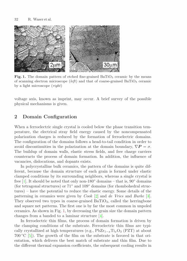
32 R. Waser et al.
Fig. 1. The domain pattern of etched fine-grained BaTiO3 ceramic by the meansof scanning electron microscope (left) and that of coarse-grained BaTiO3 ceramicby a light microscope (right)
voltage axis, known as imprint, may occur. A brief survey of the possiblephysical mechanisms is given.
2 Domain Configuration
When a ferroelectric single crystal is cooled below the phase transition tem-perature, the electrical stray field energy caused by the noncompensatedpolarization charges is reduced by the formation of ferroelectric domains.The configuration of the domains follows a head-to-tail condition in order toavoid discontinuities in the polarization at the domain boundary, ∇P = σ.The buildup of domain walls, elastic stress fields, and free charge carrierscounteracts the process of domain formation. In addition, the influence ofvacancies, dislocations, and dopants exists.
In polycrystalline bulk ceramics, the pattern of the domains is quite dif-ferent, because the domain structure of each grain is formed under elasticclamped conditions by its surrounding neighbors, whereas a single crystal isfree [1]. It should be noted that only non-180 domains – that is, 90 domains(for tetragonal structures) or 71 and 109 domains (for rhombohedral struc-tures) – have the potential to reduce the elastic energy. Some details of thepatterning in ceramics were given by Cook [2] and de Vries and Burke [3].They observed two types in coarse-grained BaTiO3, called the herringboneand square net patterns. The first one is by far the most common in unpoledceramics. As shown in Fig. 1, by decreasing the grain size the domain patternchanges from a banded to a laminar structure [4].
In ferroelectric thin films, the process of domain formation is driven bythe clamping conditions of the substrate. Ferroelectric thin films are typi-cally crystallized at high temperatures (e.g., PbZr1−xTixO3 (PZT) at about700 C [5]). The growth of the film on the substrate is favored in that ori-entation, which delivers the best match of substrate and thin film. Due tothe different thermal expansion coefficients, the subsequent cooling results in
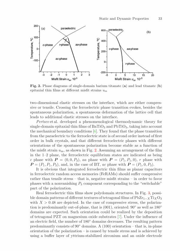
Static and Dynamic Properties 33
Fig. 2. Phase diagrams of single-domain barium titanate (a) and lead titanate (b)epitaxial thin films at different misfit strains um
two-dimensional elastic stresses on the interface, which are either compres-sive or tensile. Crossing the ferroelectric phase transition evokes, besides thespontaneous polarization, a spontaneous deformation of the lattice cell thatleads to additional elastic stresses on the interface.
Pertsev et al. developed a phenomenological thermodynamic theory forsingle-domain epitaxial thin films of BaTiO3 and PbTiO3, taking into accountthe mechanical boundary conditions [6]. They found that the phase transitionfrom the paraelectric to the ferroelectric state is of second order instead of firstorder in bulk crystals, and that different ferroelectric phases with differentorientations of the spontaneous polarization become stable as a function ofthe misfit strain um, as shown in Fig. 2. Assuming an arrangement of the filmin the 1–2 plane, the ferroelectric equilibrium states are indicated as beingc phase with P = (0, 0, P3), aa phase with P = (P1, P1, 0), r phase withP = (P1, P1, P3), and, in the case of BT, ac phase with P = (P1, 0, P3).
It is obvious that integrated ferroelectric thin films as planar capacitorsin ferroelectric random access memories (FeRAMs) should suffer compressiverather than tensile stress – that is, negative misfit strains – in order to favorphases with a nonvanishing P3 component corresponding to the “switchable”part of the polarization.
Real ferroelectric thin films show polydomain structures. In Fig. 3, possi-ble domain patterns of different textures of tetragonal films of PbZr1−XTiXO3
with X > 0.48 are depicted. In the case of compressive stress, the polariza-tion is predominantly out-of-plane, that is (001), oriented: 90 as well as 180
domains are expected. Such orientation could be realized by the depositionof tetragonal PZT on magnesium oxide substrates [7]. Under the influence ofan electric field, the number of 180 domains decreases. The resulting patternpredominantly consists of 90 domains. A (100) orientation – that is, in-planeorientation of the polarization – is caused by tensile stress and is achieved byusing a buffer layer of yttrium-stabilized zirconium and an oxide electrode
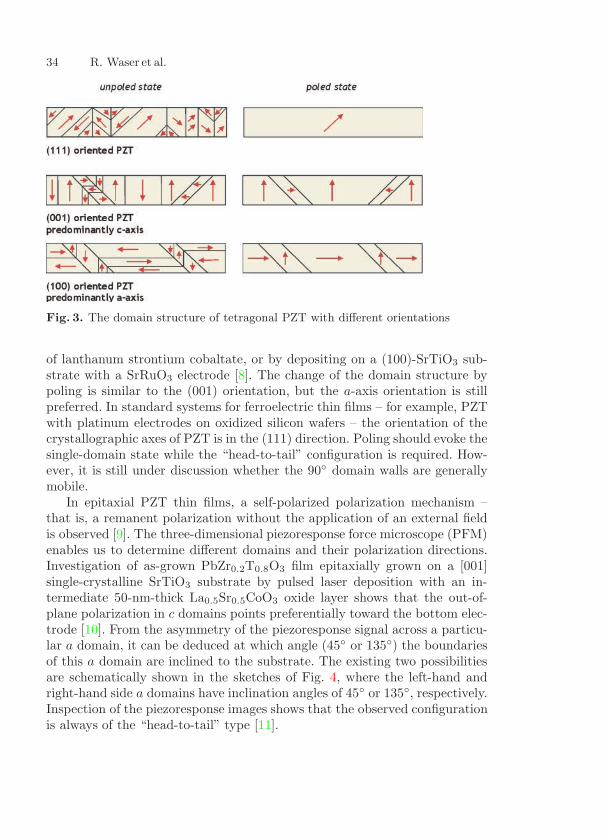
34 R. Waser et al.
Fig. 3. The domain structure of tetragonal PZT with different orientations
of lanthanum strontium cobaltate, or by depositing on a (100)-SrTiO3 sub-strate with a SrRuO3 electrode [8]. The change of the domain structure bypoling is similar to the (001) orientation, but the a-axis orientation is stillpreferred. In standard systems for ferroelectric thin films – for example, PZTwith platinum electrodes on oxidized silicon wafers – the orientation of thecrystallographic axes of PZT is in the (111) direction. Poling should evoke thesingle-domain state while the “head-to-tail” configuration is required. How-ever, it is still under discussion whether the 90 domain walls are generallymobile.
In epitaxial PZT thin films, a self-polarized polarization mechanism –that is, a remanent polarization without the application of an external fieldis observed [9]. The three-dimensional piezoresponse force microscope (PFM)enables us to determine different domains and their polarization directions.Investigation of as-grown PbZr0.2T0.8O3 film epitaxially grown on a [001]single-crystalline SrTiO3 substrate by pulsed laser deposition with an in-termediate 50-nm-thick La0.5Sr0.5CoO3 oxide layer shows that the out-of-plane polarization in c domains points preferentially toward the bottom elec-trode [10]. From the asymmetry of the piezoresponse signal across a particu-lar a domain, it can be deduced at which angle (45 or 135) the boundariesof this a domain are inclined to the substrate. The existing two possibilitiesare schematically shown in the sketches of Fig. 4, where the left-hand andright-hand side a domains have inclination angles of 45 or 135, respectively.Inspection of the piezoresponse images shows that the observed configurationis always of the “head-to-tail” type [11].

Static and Dynamic Properties 35
Out-of-plane signal
1 m
In-plane signal
Fig. 4. Out-of-plane and in-plane piezoresponse images of as-grown epitaxial PZT.The contrast corresponds to different orientations of polarizations in the domains
3 Reversible and Irreversible PolarizationContributions
To characterize ferroelectric materials, the dependence of the polarization onthe applied voltage is usually measured by means of a Sawyer–Tower circuit orby recording the current response to a voltage step. The P (V ) hysteresis curveis used to determine the remanent polarization and coercive field, respectively.These two parameters are of critical importance in the design of externalcircuits of FeRAMs.
The origin of the ferroelectric hysteresis is the existence of irreversiblepolarization processes; that is, the irreversible polarization reversal of a singleferroelectric lattice cell as explained by the Landau–Devonshire theory [12].However, the exact interplay among this fundamental process, domain walls,defects, and the overall appearance of the ferroelectric hysteresis is still notprecisely known.
The separation of the total polarization into reversible and irreversiblecontributions that has long been appreciated in the study of ferromagneticmaterials [13] might facilitate the understanding of ferroelectric polarizationmechanisms. In particular, the irreversible processes would be important forferroelectric memory devices, since the reversible processes cannot be usedto store information.
For ferroelectrics, mainly two possible mechanisms for irreversible pro-cesses exist [14, 15]. First, lattice defects interact with a domain wall andhinder it from returning into its initial position after removal of the electricfield that initiated the domain wall motion (“pinning”) [16]. Second, there isthe nucleation and growth of new domains which do not disappear after the
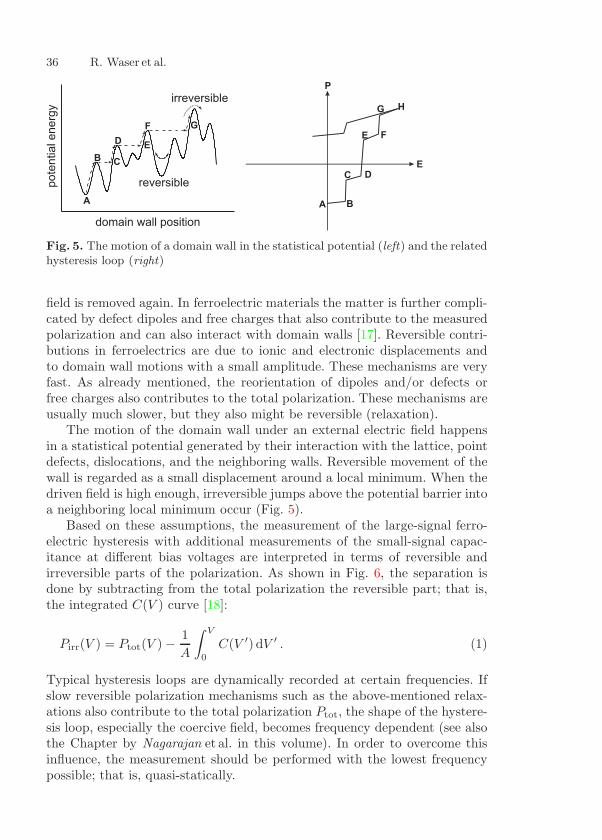
36 R. Waser et al.
Fig. 5. The motion of a domain wall in the statistical potential (left) and the relatedhysteresis loop (right)
field is removed again. In ferroelectric materials the matter is further compli-cated by defect dipoles and free charges that also contribute to the measuredpolarization and can also interact with domain walls [17]. Reversible contri-butions in ferroelectrics are due to ionic and electronic displacements andto domain wall motions with a small amplitude. These mechanisms are veryfast. As already mentioned, the reorientation of dipoles and/or defects orfree charges also contributes to the total polarization. These mechanisms areusually much slower, but they also might be reversible (relaxation).
The motion of the domain wall under an external electric field happensin a statistical potential generated by their interaction with the lattice, pointdefects, dislocations, and the neighboring walls. Reversible movement of thewall is regarded as a small displacement around a local minimum. When thedriven field is high enough, irreversible jumps above the potential barrier intoa neighboring local minimum occur (Fig. 5).
Based on these assumptions, the measurement of the large-signal ferro-electric hysteresis with additional measurements of the small-signal capac-itance at different bias voltages are interpreted in terms of reversible andirreversible parts of the polarization. As shown in Fig. 6, the separation isdone by subtracting from the total polarization the reversible part; that is,the integrated C(V ) curve [18]:
Pirr(V ) = Ptot(V ) − 1A
∫ V
0
C(V ′) dV ′ . (1)
Typical hysteresis loops are dynamically recorded at certain frequencies. Ifslow reversible polarization mechanisms such as the above-mentioned relax-ations also contribute to the total polarization Ptot, the shape of the hystere-sis loop, especially the coercive field, becomes frequency dependent (see alsothe Chapter by Nagarajan et al. in this volume). In order to overcome thisinfluence, the measurement should be performed with the lowest frequencypossible; that is, quasi-statically.
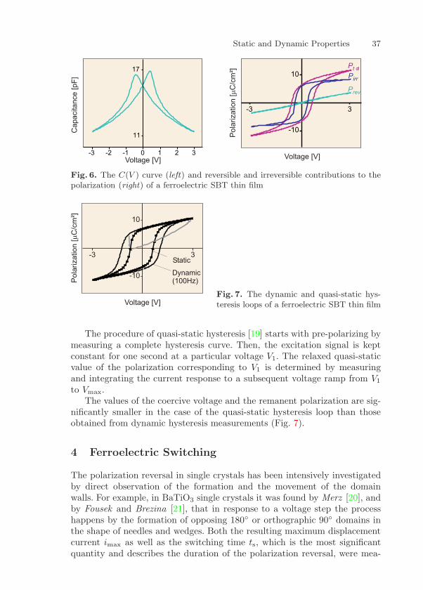
Static and Dynamic Properties 37
Capacitance
[pF
]
Voltage [V]-3 -2 -1 0 1 2 3
11
17
Voltage [V]
Pola
rization
[C
/cm
²]
-3 3
-10
10P
t ot
Pirr
Prev
Fig. 6. The C(V ) curve (left) and reversible and irreversible contributions to thepolarization (right) of a ferroelectric SBT thin film
Voltage [V]
Pola
rization
[C
/cm
²]
-3 3
-10
10
Static
Dynamic(100Hz)
Fig. 7. The dynamic and quasi-static hys-teresis loops of a ferroelectric SBT thin film
The procedure of quasi-static hysteresis [19] starts with pre-polarizing bymeasuring a complete hysteresis curve. Then, the excitation signal is keptconstant for one second at a particular voltage V1. The relaxed quasi-staticvalue of the polarization corresponding to V1 is determined by measuringand integrating the current response to a subsequent voltage ramp from V1
to Vmax.The values of the coercive voltage and the remanent polarization are sig-
nificantly smaller in the case of the quasi-static hysteresis loop than thoseobtained from dynamic hysteresis measurements (Fig. 7).
4 Ferroelectric Switching
The polarization reversal in single crystals has been intensively investigatedby direct observation of the formation and the movement of the domainwalls. For example, in BaTiO3 single crystals it was found by Merz [20], andby Fousek and Brezina [21], that in response to a voltage step the processhappens by the formation of opposing 180 or orthographic 90 domains inthe shape of needles and wedges. Both the resulting maximum displacementcurrent imax as well as the switching time ts, which is the most significantquantity and describes the duration of the polarization reversal, were mea-

38 R. Waser et al.
Fig. 8. The polarization switching current of a TGFB single crystal with a de-creasing electric field [23] (left) and switching by nucleation and growth of domains(right)
sured as a function of the applied field E and follow empirical laws:
imax = i0 · exp(−Eα/E) , (2)ts = t0 · exp(Eα/E) , (3)
where i0 and t0 are constants. The constant activation field Eα is the samein both equations [22].
The above-mentioned equations are only applicable when the appliedfield E is constant during the polarization reversal that is, the time con-stant of the dielectric charging τRC must be much smaller than the switchingtime ts. The dielectric charging is determined by the capacitance of the sam-ple and the inevitable series resistors (source, lines, etc.). The switching timeis determined by many factors: the domain structure, the nucleation rate ofopposite domains, the mobility of the domain walls, and many others [24].As shown in Fig. 8, the condition is fullfilled and dielectric charging is clearlyseparated from the polarization switching hump.
Another approach to analyzing the polarization reversal process in ferro-electrics is the hysteresis loop. The problem of an undetermined excitationvoltage step is avoided by the constant increasing and decreasing of the elec-tric field, which can be much more easily electrically controlled. However, theinterpretation of the loop is much more difficult and needs an integral calcu-lation method. This has been evolved successfully by the group of Ishibashiand Orihara [25]. Based on the Kolmogorov–Avrami model [26] that wasoriginally developed for phase transition kinetics, they have included thefield dependence of the polarization switching and modeled the D–E hys-teresis loops, which depend on the excitation frequency. They found goodagreement with the experimental data for tri-glycine fluoroberyllic (TGFB)single crystals, especially the pronounced frequency dependence of the coer-
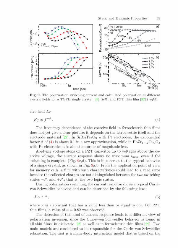
Static and Dynamic Properties 39
Fig. 9. The polarization switching current and calculated polarization at differentelectric fields for a TGFB single crystal [23] (left) and PZT thin film [32] (right)
cive field EC:
EC ∝ f−β . (4)
The frequency dependence of the coercive field in ferroelectric thin filmsdoes not yet give a clear picture: it depends on the ferroelectric itself and theelectrode material [27]. In SrBi2Ta2O9 with Pt electrodes, the exponentialfactor β of (4) is about 0.1 in a raw approximation, while in PbZr1−XTiXO3
with Pt electrodes it is about an order of magnitude less.Applying voltage steps on a PZT capacitor up to voltages above the co-
ercive voltage, the current response shows no maximum imax, even if theswitching is complete (Fig. 9c,d). This is in contrast to the typical behaviorof a single crystal, as shown in Fig. 9a,b. From the application point of viewfor memory cells, a film with such characteristics could lead to a read errorbecause the collected charges are not distinguished between the two switchingstates −Pr and +Pr; that is, the two logic states.
During polarization switching, the current response shows a typical Curie–von Schweidler behavior and can be described by the following law:
J ∝ t−κ , (5)
where κ is a constant that has a value less than or equal to one. For PZTthin films, a value of κ = 0.82 was observed.
The detection of this kind of current response leads to a different view ofpolarization inversion, since the Curie–von Schweidler behavior is found inall thin films; in dielectric [28] as well as in ferroelectric thin films [29]. Twomain models are considered to be responsible for the Curie–von Schweidlerrelaxation. The first is a many-body interaction model that is based on the
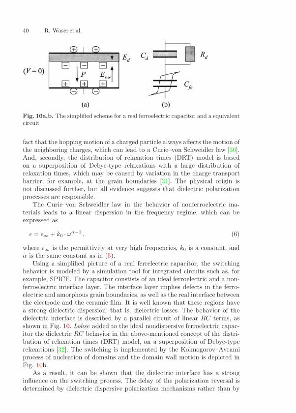
40 R. Waser et al.
Fig. 10a,b. The simplified scheme for a real ferroelectric capacitor and a equivalentcircuit
fact that the hopping motion of a charged particle always affects the motion ofthe neighboring charges, which can lead to a Curie–von Schweidler law [30].And, secondly, the distribution of relaxation times (DRT) model is basedon a superposition of Debye-type relaxations with a large distribution ofrelaxation times, which may be caused by variation in the charge transportbarrier; for example, at the grain boundaries [31]. The physical origin isnot discussed further, but all evidence suggests that dielectric polarizationprocesses are responsible.
The Curie–von Schweidler law in the behavior of nonferroelectric ma-terials leads to a linear dispersion in the frequency regime, which can beexpressed as
ε = ε∞ + k0 ·ωα−1 , (6)
where ε∞ is the permittivity at very high frequencies, k0 is a constant, andα is the same constant as in (5).
Using a simplified picture of a real ferrelectric capacitor, the switchingbehavior is modeled by a simulation tool for integrated circuits such as, forexample, SPICE. The capacitor constists of an ideal ferroelectric and a non-ferroelectric interface layer. The interface layer implies defects in the ferro-electric and amorphous grain boundaries, as well as the real interface betweenthe electrode and the ceramic film. It is well known that these regions havea strong dielectric dispersion; that is, dielectric losses. The behavior of thedielectric interface is described by a parallel circuit of linear RC terms, asshown in Fig. 10. Lohse added to the ideal nondispersive ferroelectric capac-itor the dielectric RC behavior in the above-mentioned concept of the distri-bution of relaxation times (DRT) model, on a superposition of Debye-typerelaxations [32]. The switching is implemented by the Kolmogorov–Avramiprocess of nucleation of domains and the domain wall motion is depicted inFig. 10b.
As a result, it can be shown that the dielectric interface has a stronginfluence on the switching process. The delay of the polarization reversal isdetermined by dielectric dispersive polarization mechanisms rather than by
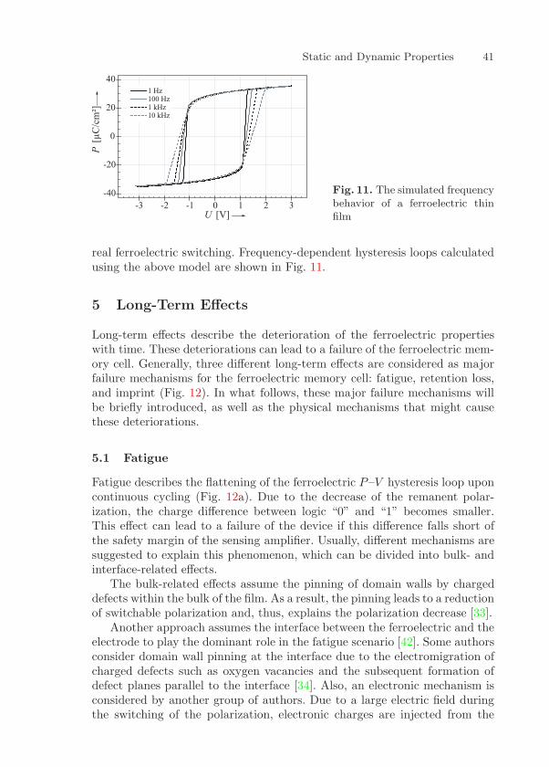
Static and Dynamic Properties 41
Fig. 11. The simulated frequencybehavior of a ferroelectric thinfilm
real ferroelectric switching. Frequency-dependent hysteresis loops calculatedusing the above model are shown in Fig. 11.
5 Long-Term Effects
Long-term effects describe the deterioration of the ferroelectric propertieswith time. These deteriorations can lead to a failure of the ferroelectric mem-ory cell. Generally, three different long-term effects are considered as majorfailure mechanisms for the ferroelectric memory cell: fatigue, retention loss,and imprint (Fig. 12). In what follows, these major failure mechanisms willbe briefly introduced, as well as the physical mechanisms that might causethese deteriorations.
5.1 Fatigue
Fatigue describes the flattening of the ferroelectric P–V hysteresis loop uponcontinuous cycling (Fig. 12a). Due to the decrease of the remanent polar-ization, the charge difference between logic “0” and “1” becomes smaller.This effect can lead to a failure of the device if this difference falls short ofthe safety margin of the sensing amplifier. Usually, different mechanisms aresuggested to explain this phenomenon, which can be divided into bulk- andinterface-related effects.
The bulk-related effects assume the pinning of domain walls by chargeddefects within the bulk of the film. As a result, the pinning leads to a reductionof switchable polarization and, thus, explains the polarization decrease [33].
Another approach assumes the interface between the ferroelectric and theelectrode to play the dominant role in the fatigue scenario [42]. Some authorsconsider domain wall pinning at the interface due to the electromigration ofcharged defects such as oxygen vacancies and the subsequent formation ofdefect planes parallel to the interface [34]. Also, an electronic mechanism isconsidered by another group of authors. Due to a large electric field duringthe switching of the polarization, electronic charges are injected from the
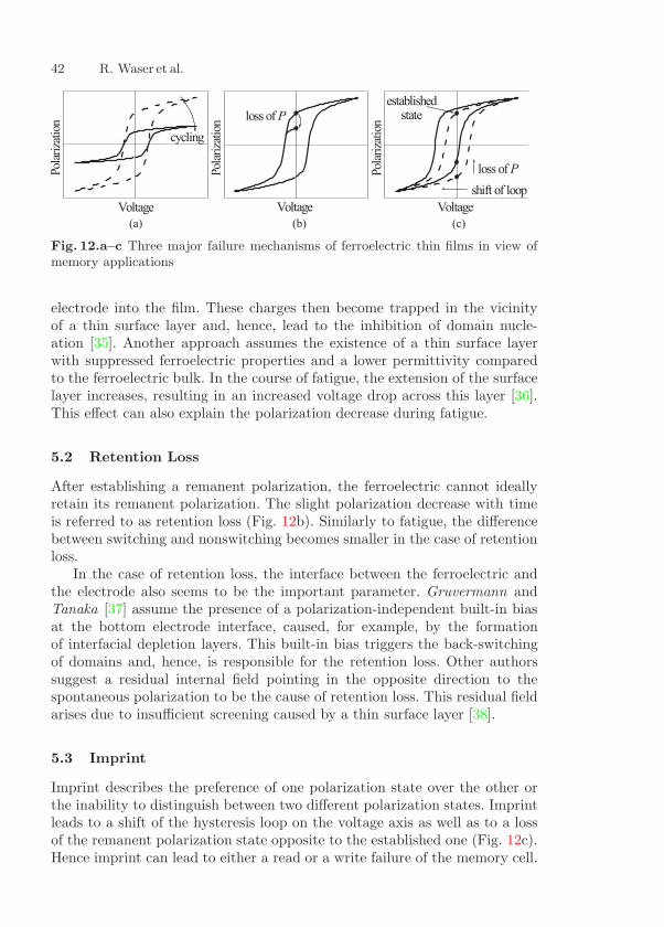
42 R. Waser et al.
Fig. 12.a–c Three major failure mechanisms of ferroelectric thin films in view ofmemory applications
electrode into the film. These charges then become trapped in the vicinityof a thin surface layer and, hence, lead to the inhibition of domain nucle-ation [35]. Another approach assumes the existence of a thin surface layerwith suppressed ferroelectric properties and a lower permittivity comparedto the ferroelectric bulk. In the course of fatigue, the extension of the surfacelayer increases, resulting in an increased voltage drop across this layer [36].This effect can also explain the polarization decrease during fatigue.
5.2 Retention Loss
After establishing a remanent polarization, the ferroelectric cannot ideallyretain its remanent polarization. The slight polarization decrease with timeis referred to as retention loss (Fig. 12b). Similarly to fatigue, the differencebetween switching and nonswitching becomes smaller in the case of retentionloss.
In the case of retention loss, the interface between the ferroelectric andthe electrode also seems to be the important parameter. Gruvermann andTanaka [37] assume the presence of a polarization-independent built-in biasat the bottom electrode interface, caused, for example, by the formationof interfacial depletion layers. This built-in bias triggers the back-switchingof domains and, hence, is responsible for the retention loss. Other authorssuggest a residual internal field pointing in the opposite direction to thespontaneous polarization to be the cause of retention loss. This residual fieldarises due to insufficient screening caused by a thin surface layer [38].
5.3 Imprint
Imprint describes the preference of one polarization state over the other orthe inability to distinguish between two different polarization states. Imprintleads to a shift of the hysteresis loop on the voltage axis as well as to a lossof the remanent polarization state opposite to the established one (Fig. 12c).Hence imprint can lead to either a read or a write failure of the memory cell.
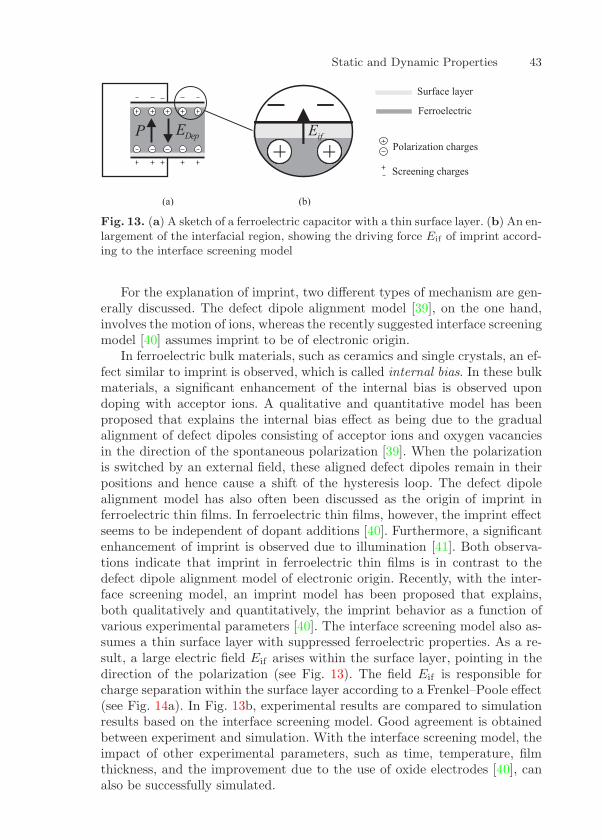
Static and Dynamic Properties 43
Fig. 13. (a) A sketch of a ferroelectric capacitor with a thin surface layer. (b) An en-largement of the interfacial region, showing the driving force Eif of imprint accord-ing to the interface screening model
For the explanation of imprint, two different types of mechanism are gen-erally discussed. The defect dipole alignment model [39], on the one hand,involves the motion of ions, whereas the recently suggested interface screeningmodel [40] assumes imprint to be of electronic origin.
In ferroelectric bulk materials, such as ceramics and single crystals, an ef-fect similar to imprint is observed, which is called internal bias. In these bulkmaterials, a significant enhancement of the internal bias is observed upondoping with acceptor ions. A qualitative and quantitative model has beenproposed that explains the internal bias effect as being due to the gradualalignment of defect dipoles consisting of acceptor ions and oxygen vacanciesin the direction of the spontaneous polarization [39]. When the polarizationis switched by an external field, these aligned defect dipoles remain in theirpositions and hence cause a shift of the hysteresis loop. The defect dipolealignment model has also often been discussed as the origin of imprint inferroelectric thin films. In ferroelectric thin films, however, the imprint effectseems to be independent of dopant additions [40]. Furthermore, a significantenhancement of imprint is observed due to illumination [41]. Both observa-tions indicate that imprint in ferroelectric thin films is in contrast to thedefect dipole alignment model of electronic origin. Recently, with the inter-face screening model, an imprint model has been proposed that explains,both qualitatively and quantitatively, the imprint behavior as a function ofvarious experimental parameters [40]. The interface screening model also as-sumes a thin surface layer with suppressed ferroelectric properties. As a re-sult, a large electric field Eif arises within the surface layer, pointing in thedirection of the polarization (see Fig. 13). The field Eif is responsible forcharge separation within the surface layer according to a Frenkel–Poole effect(see Fig. 14a). In Fig. 13b, experimental results are compared to simulationresults based on the interface screening model. Good agreement is obtainedbetween experiment and simulation. With the interface screening model, theimpact of other experimental parameters, such as time, temperature, filmthickness, and the improvement due to the use of oxide electrodes [40], canalso be successfully simulated.
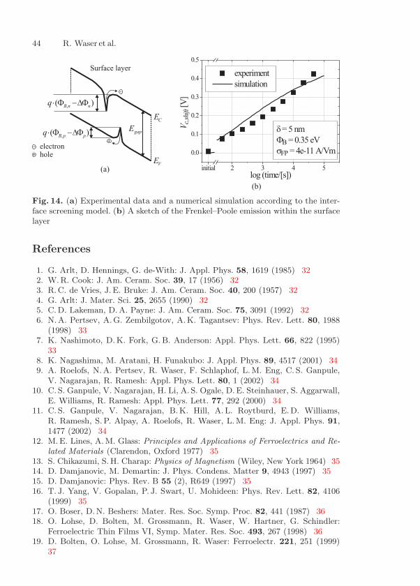
44 R. Waser et al.
Fig. 14. (a) Experimental data and a numerical simulation according to the inter-face screening model. (b) A sketch of the Frenkel–Poole emission within the surfacelayer
References
1. G. Arlt, D. Hennings, G. de-With: J. Appl. Phys. 58, 1619 (1985) 322. W.R. Cook: J. Am. Ceram. Soc. 39, 17 (1956) 323. R.C. de Vries, J. E. Bruke: J. Am. Ceram. Soc. 40, 200 (1957) 324. G. Arlt: J. Mater. Sci. 25, 2655 (1990) 325. C.D. Lakeman, D.A. Payne: J. Am. Ceram. Soc. 75, 3091 (1992) 326. N.A. Pertsev, A.G. Zembilgotov, A.K. Tagantsev: Phys. Rev. Lett. 80, 1988
(1998) 337. K. Nashimoto, D.K. Fork, G. B. Anderson: Appl. Phys. Lett. 66, 822 (1995)
338. K. Nagashima, M. Aratani, H. Funakubo: J. Appl. Phys. 89, 4517 (2001) 349. A. Roelofs, N.A. Pertsev, R. Waser, F. Schlaphof, L.M. Eng, C. S. Ganpule,
V. Nagarajan, R. Ramesh: Appl. Phys. Lett. 80, 1 (2002) 3410. C. S. Ganpule, V. Nagarajan, H. Li, A. S. Ogale, D. E. Steinhauer, S. Aggarwall,
E. Williams, R. Ramesh: Appl. Phys. Lett. 77, 292 (2000) 3411. C. S. Ganpule, V. Nagarajan, B.K. Hill, A. L. Roytburd, E.D. Williams,
R. Ramesh, S. P. Alpay, A. Roelofs, R. Waser, L.M. Eng: J. Appl. Phys. 91,1477 (2002) 34
12. M.E. Lines, A.M. Glass: Principles and Applications of Ferroelectrics and Re-lated Materials (Clarendon, Oxford 1977) 35
13. S. Chikazumi, S.H. Charap: Physics of Magnetism (Wiley, New York 1964) 3514. D. Damjanovic, M. Demartin: J. Phys. Condens. Matter 9, 4943 (1997) 3515. D. Damjanovic: Phys. Rev. B 55 (2), R649 (1997) 3516. T. J. Yang, V. Gopalan, P. J. Swart, U. Mohideen: Phys. Rev. Lett. 82, 4106
(1999) 3517. O. Boser, D.N. Beshers: Mater. Res. Soc. Symp. Proc. 82, 441 (1987) 3618. O. Lohse, D. Bolten, M. Grossmann, R. Waser, W. Hartner, G. Schindler:
Ferroelectric Thin Films VI, Symp. Mater. Res. Soc. 493, 267 (1998) 3619. D. Bolten, O. Lohse, M. Grossmann, R. Waser: Ferroelectr. 221, 251 (1999)
37
Static and Dynamic Properties 45
20. W. J. Merz: Phys. Rev. 95, 690 (1954) 3721. J. Fousek, B. Brezina: Czech. J. Phys. B 10, 511 (1960) 3722. C. F. Pulvari, W. Kuebler: J. Appl. Phys. 29, 1742 (1958) 3823. O. Lohse, M. Grossmann, U. Bottger, D. Bolten, R. Waser: J. Appl. Phys. 89,
2332 (2001) 38, 3924. V. Shur, E. Rumyantsev, S. Makarov: J. Appl. Phys. 84, 445 (1998) 3825. Y. Ishibashi, H. Orihara: Integr. Ferroelectr. 9, 57 (1995) 3826. M. Avrami: J. Chem. Phys. 7, 1103 (1939) 3827. J. F. Scott, F.M. Ross, C.A. Paz de Araujo, M. C. Scott, M. Huffmann: MRS
Bull. 21, 33 (1996) 3928. M. Schumacher, G. W. Dietz, R. Waser: Integr. Ferroelectr. 10, 231 (1995) 3929. X. Chen, A. I. Kingon, L. Mantese, O. Auciello, K.Y. Hsieh: Integr. Ferroelectr.
3, 355 (1993) 3930. L.A. Dissado, R.M. Hill: J. Mater. Sci. 16, 1410 (1981) 4031. H. Kliem: IEEE Trans. Electr. Insul. 24, 185 (1989) 4032. O. Lohse: Dissertation, RWTH Aachen (2001) 39, 4033. E. L. Colla, D.V. Taylor, A.K. Taganstev, N. Setter: Appl. Phys. Lett. 72,
2478 (1998) 4134. M. Dawber, J. F. Scott: Appl. Phys. Lett. 76, 1060 (2000) 4135. I. Stolichnov, A.K. Tagantsev, E. L. Colla, N. Setter: Appl. Phys. Lett. 73,
1361 (1998) 4236. A.M. Bratkovsky, A.P. Levanyuk: Phys. Rev. Lett. 84, 3177 (2000) 4237. A. Gruvermann, M. Tanaka: J. Appl. Phys. 89, 1836 (2001) 4238. A.K. Tagantsev, M. Landivar, E. Colla, N. Setter: J. Appl. Phys. 78, 2623
(1995) 4239. G. Arlt, H. Neumann: Ferroelectr. 87, 109 (1988) 4340. M. Grossmann: Dissertation, RWTH Aachen (2001) 4341. M. Grossmann, S. Hoffmann, S. Gusowski, R. Waser, S.K. Streiffer, C. Basceri,
C.B. Parker, S.E. Lash, A. I. Kingon: Integr. Ferroelectr. 22, 83 (1998) 4342. R. Ramesh, A. Inam, W.K. Chan, B. Wilkens, K.Myers, K. Remschnig,
D.L. Hart, J. M. Tarascon: Science 252, 944 (1991) 41
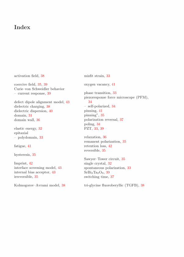
Index
activation field, 38
coercive field, 35, 39Curie–von Schweidler behavior– current response, 39
defect dipole alignment model, 43dielectric charging, 38dielectric dispersion, 40domain, 31domain wall, 36
elastic energy, 32epitaxial– polydomain, 33
fatigue, 41
hysteresis, 35
Imprint, 42interface screening model, 43internal bias acceptor, 43irreversible, 35
Kolmogorov–Avrami model, 38
misfit strain, 33
oxygen vacancy, 41
phase transition, 33piezoresponse force microscope (PFM),
34– self-polarized, 34pinning, 41pinning”, 35polarization reversal, 37poling, 34PZT, 33, 39
relaxation, 36remanent polarization, 35retention loss, 42reversible, 35
Sawyer–Tower circuit, 35single crystal, 32spontaneous polarization, 33SrBi2Ta2O9, 39switching time, 37
tri-glycine fluoroberyllic (TGFB), 38
Nanoscale Phenomena
in Ferroelectric Thin Films
Valanoor Nagarajan1, Chandan S. Ganpule, and Ramamoorthy Ramesh2
1 Department IFF, Forschungzentrum Juelich, 52425 Juelich, [email protected]
2 Department of Materials Science and Engineering and Department of Physics,219 Hearst Mining Building,University of California, Berkeley, CA 94720, [email protected]
Abstract. In this chapter, recent progress in our group in the area of thin-filmferroelectrics is reviewed. The specific focus is on nanoscale phenomena such as po-larization relaxation dynamics and piezoelectric characterization in model thin filmsand nanostructures, using voltage-modulated scanning force microscopy. Using thistechnique, we show the three-dimensional reconstruction of the polarization vectorin lead zirconate titanate (PZT) thin films. Secondly, the time-dependent relax-ation of remanent polarization in epitaxial PZT ferroelectric thin films, containinga uniform two-dimensional grid of 90 domains (c-axis in the plane of the film),has been investigated extensively. The 90 domain walls preferentially nucleate the180 reverse domains during relaxation. Relaxation occurs through the nucleationand growth of reverse 180 domains, which subsequently coalesce and consume theentire region as a function of relaxation time. The kinetics of relaxation is mod-eled through the Johnson–Mehl–Avrami–Kolmogorov approach, with a decreasingdriving force. In addition, we also present results on investigation of the relaxationphenomenon on a very local scale, where pinning and bowing of domain walls hasbeen observed. We also show how this technique is used for obtaining quantitativeinformation on piezoelectric constants and, by engineering special structures, howwe realize ultra-high values of piezoconstants. It is shown that the piezo-constantof free-standing nanoscale capacitors is much higher than clamped values, and thatthere is a complex interplay between the substrate-induced constraint and the piezo-response. Lastly we also show direct hysteresis loops on nanoscale capacitors, wherethere is no observable loss of polarization in capacitors as small as 0.16 µm2 in area.
1 Introduction
At present, there is considerable interest in ferroelectric thin films as a mediumfor nonvolatile data storage [1]. In particular, much attention is focused oninvestigating high-density giga-bit data storage using scanning probe tech-niques [2]. As ferroelectric random access memory (FeRAM) devices scaledown to the Gbit density regimes, it becomes imperative to understand phys-ical phenomena that affect device performance at the nanoscale. For example,the ferroelectric element in these storage media is subject to progressive loss
H. Ishiwara, M. Okuyama, Y. Arimoto (Eds.): Ferroelectric Random Access Memories,Topics Appl. Phys. 93, 47–69 (2004)c© Springer-Verlag Berlin Heidelberg 2004
48 V. Nagarajan et al.
of polarization, commonly referred to as “polarization relaxation”. Polar-ization relaxation shows a very complex interplay between various factors,such as defects, the domain wall dynamics, the crystallographic structure,etc., and hence it has been a subject of intense scientific research. All ofthe above-mentioned factors have characteristic dimensions in the range ofa few hundred to a few thousand angstroms, which really means that in or-der to fully appreciate their role, one must have an approach to the study ofphenomena at those scales.
With the advent of Piezoresponse Scanning Force Microscopy (Piezo-response SFM), the investigation of nanoscale ferroelectric phenomena hasnot only become viable but also a necessity. It is a unique nondestructivecharacterization tool coupled with a relatively easy method of sample prepa-ration, which can provide critical information on key nanoscale processes. Inthis chapter, we show in the first part how this tool has been so effective inobserving domain relaxation. In this section, we focus on imaging nanoscalephenomena, particularly the phenomena of relaxation. It will be clear how“defects” such as domain walls act as nucleation centers and how nanoscopicsites act as pinning centers to inhibit complete reversal. The physical natureof this problem and early studies on the microscopic origins of polarizationreversal using scanning force microscope techniques [3] show that they havethe potential to quantify the physical origin of the relaxation kinetics. TheJohnson–Mehl–Avrami–Kolmorogov (JMAK) theory is a useful approach forsystems exhibiting nucleation and growth-based phase change kinetics [4].We review in detail a study to apply this theory to the nanoscale investi-gation of polarization reversal in ferroelectric thin films via the atomic forcemicroscope. In addition, the same technique can be used to image the domainstructure of epitaxial ferroelectric thin films. We also show, by using carefulinterpretation of domain images, one can reconstruct the three-dimensionalpolarization picture in these thin films.
The second section on our observations will concentrate on obtainingquantitative information from such nanoscale capacitors. In particular, thedependence of the capacitor on orientation, size, and constraint has beeninvestigated as far as the d33 goes. Since the probe itself measures only sev-eral tens of nanometers, it gives us the advantage of probing piezoelectricand ferroelectric properties of sub-micron capacitors. Consequently, we havebeen able to show piezoelectricity in capacitors as small as 70 nm×70 nm anddirect hysteresis loops in sub-micron capacitors. We summarize this reviewwith some results of direct hysteresis and fatigue measurements on nanoscalecapacitors. Finally, some areas for future research are also highlighted.
2 Experimental Details
In order to create films with systematically varying crystalline quality, threedifferent types of substrates were used: (1) conventional platinized silicon (Pt/
Nanoscale Phenomena in Ferroelectric Thin Films 49
TiO2/SiO2/Si, abbreviated to Pt–Si); (2) (La0.5Sr0.5)CoO3-buffered Pt–Si(LSCO/Pt–Si); and (3) LSCO/STO/Si. The thickness of STO is 15 nm. De-tails of the STO deposition process are described elsewhere. About 70 nmthick LSCO top and bottom electrodes were deposited by RF sputteringand crystallized in oxygen for 1 h at 600–650 C. The PZT thin films (withZr : Ti ratio = 40 : 60 (40/60), if not specified) were prepared by sol-gel andspin-coating techniques. The annealing of the PZT was done at 600–650 Cfor 1 h and at 450 C for the samples prepared with the new precursor. X-raydiffraction (XRD) and transmission electron microscopy (TEM) were em-ployed to probe the phase formation and microstructure of the samples. Thetop electrodes (Pt and LSCO) were made by photolithography and sputter-ing, so that the capacitors for electrical measurements show a symmetric con-figuration – Pt/PZT/Pt–Si, Pt/LSCO/PZT/LSCO/Pt–Si, and Pt/LSCO/PZT/LSCO/STO/Si, respectively. The ferroelectric measurement was doneby the use of an RT-66A tester.
Our experimental studies typically involve two distinct types of samples.A significant fraction of our domain imaging studies use epitaxial PZT filmsas model systems. Our piezoresponse measurements involve films with sys-tematically different microstructures (epitaxial to polycrystalline) as well asa variety of substrates. Films are grown by either pulsed laser deposition [5]and/or by sol-gel processing. The epitaxial PZT films of high tetragonal-ity (e.g., 20/80) contain a uniform two-dimensional grid of 90 domains(i.e., c-axis in the plane of the film). Such 90 domains have been shownto have a strong impact on the hysteretic polarization behavior of ferroelec-tric films [6]. Due to the absence of a top electrode, the polarization andpiezoresponse hysteresis loops show a marked asymmetry, thereby indicatinga built-in internal field.
Voltage-modulated scanning force microscopy [7] has been employed tostudy the piezoelectric effect and to image and modify the domain structurein thin-film samples. The experimental setup is shown in Fig. 1. Piezo-SFMis based on the detection of the local electromechanical vibration of the fer-roelectric sample caused by an external AC voltage. The voltage is appliedthrough the probing tip, which is used as a movable top electrode. The ex-ternal driving voltage with frequency ω generates a sample surface vibrationwith the same frequency due to the converse piezoelectric effect. This surfacedisplacement can be approximated by
∆ z(t) =
Tf∫
0
d thin film33 EAC(t, z) dz , (1)
where EAC is the AC electric field as a function of time t and displacementz, and Tf is the thickness of the ferroelectric layer. The modulated deflec-tion signal from the cantilever, which oscillates together with the sample, isdetected using the lock-in technique. The amplitude of the first harmonic sig-nal from the lock-in amplifier is a function of the piezoelectric displacement
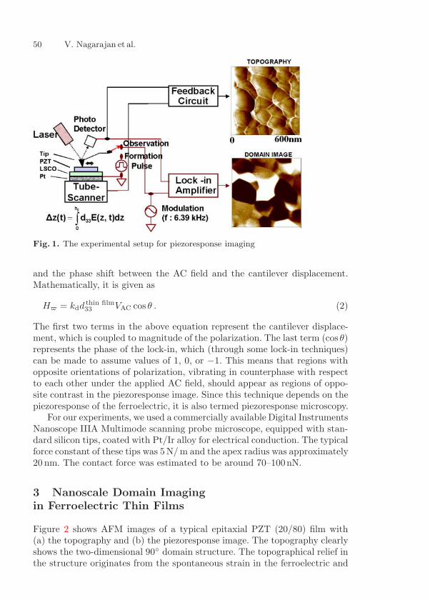
50 V. Nagarajan et al.
Fig. 1. The experimental setup for piezoresponse imaging
and the phase shift between the AC field and the cantilever displacement.Mathematically, it is given as
H = kdd thin film33 VAC cos θ . (2)
The first two terms in the above equation represent the cantilever displace-ment, which is coupled to magnitude of the polarization. The last term (cos θ)represents the phase of the lock-in, which (through some lock-in techniques)can be made to assume values of 1, 0, or −1. This means that regions withopposite orientations of polarization, vibrating in counterphase with respectto each other under the applied AC field, should appear as regions of oppo-site contrast in the piezoresponse image. Since this technique depends on thepiezoresponse of the ferroelectric, it is also termed piezoresponse microscopy.
For our experiments, we used a commercially available Digital InstrumentsNanoscope IIIA Multimode scanning probe microscope, equipped with stan-dard silicon tips, coated with Pt/Ir alloy for electrical conduction. The typicalforce constant of these tips was 5 N/ m and the apex radius was approximately20 nm. The contact force was estimated to be around 70–100nN.
3 Nanoscale Domain Imagingin Ferroelectric Thin Films
Figure 2 shows AFM images of a typical epitaxial PZT (20/80) film with(a) the topography and (b) the piezoresponse image. The topography clearlyshows the two-dimensional 90 domain structure. The topographical relief inthe structure originates from the spontaneous strain in the ferroelectric and

Nanoscale Phenomena in Ferroelectric Thin Films 51
Fig. 2. (a) The topography of epitaxial PbZr0.2Ti0.8O3 film grown via pulsed laserdeposition. (b) Piezoresponse images of the same film. The 90 domain structureis clearly seen in both images as a two-dimensional grid
the tilting of a-domains away from the normal, which has been discussed indetail elsewhere [8, 9, 10]. The piezoresponse image compares very well withthe topographical image. Piezoresponse images of the film surface show thepresence of long needle-like orthogonal structures that have been identifiedto be 90 twinned domains. These domains form to relax the strains asso-ciated with lattice mismatch and phase transformation from the cubic tothe tetragonal (ferroelectric) phase [8]. The image contrast in between theneedle-like regions is uniformly bright, suggesting that the entire region ispre-poled in a specific direction. This was confirmed by measurements of thepiezo-hysteresis loop from a local region [11], which showed a marked asym-metry indicating a built-in internal field. This as-grown sample was switchedinto the opposite state by scanning the surface of the film with the AFM tipbiased at −10 V (scan speed 1 Hz), leading to a strong change in the imagecontrast from bright to dark, as will be shown later. We observed that thisswitched state (in the c-axis regions of the film) begins to relax back to theoriginal bright state.
We first discuss the use of this technique to map out the polarizationorientation in a given ferroelectric thin film. This technique was first ap-plied by Eng et al. [12] to image the three-dimensional polarization map ina BaTiO3 single crystal, and later Roelofs et al. [13] demonstrated 3D po-larization imaging on polycrystalline PZT thin films. In order to map thepolarization vectors in the a-domains, the lateral differential signal from thephotodiode was tracked. This signal effectively represents the torsion defor-mation of the AFM cantilever. As the tip scans over the a-domain regions, theelectrical field through the tip produces the shearing deformation mentionedearlier, giving rise to the torsion signal in the photodiode. This is schemati-cally illustrated in Fig. 3a,b for oppositely oriented a-domains. The phase ofthis torsion motion of the tip with respect to the input sinusoidal electric fieldprovides information about the orientation of polarization in the domain. Itshould be pointed out that the scan direction of the tip is chosen to be such
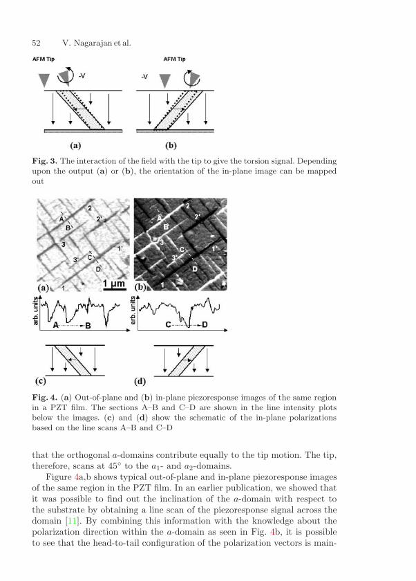
52 V. Nagarajan et al.
Fig. 3. The interaction of the field with the tip to give the torsion signal. Dependingupon the output (a) or (b), the orientation of the in-plane image can be mappedout
Fig. 4. (a) Out-of-plane and (b) in-plane piezoresponse images of the same regionin a PZT film. The sections A–B and C–D are shown in the line intensity plotsbelow the images. (c) and (d) show the schematic of the in-plane polarizationsbased on the line scans A–B and C–D
that the orthogonal a-domains contribute equally to the tip motion. The tip,therefore, scans at 45 to the a1- and a2-domains.
Figure 4a,b shows typical out-of-plane and in-plane piezoresponse imagesof the same region in the PZT film. In an earlier publication, we showed thatit was possible to find out the inclination of the a-domain with respect tothe substrate by obtaining a line scan of the piezoresponse signal across thedomain [11]. By combining this information with the knowledge about thepolarization direction within the a-domain as seen in Fig. 4b, it is possibleto see that the head-to-tail configuration of the polarization vectors is main-
Nanoscale Phenomena in Ferroelectric Thin Films 53
tained across the 90 domain wall. Thus, domains aligned at 45 and 135 tothe substrate are phase shifted by 180 and therefore lead to different con-trast levels in the in-plane image. Figure 4c plots a line scan of the verticaldifferential signal across A–B in Fig. 4a, thereby implying that the domainis oriented as illustrated schematically in Fig. 4c. Figure 4d plots a similarline scan across C–D in Figure 4a, thus showing that this a-domain is oppo-sitely oriented with respect to the substrate. As expected, the image contrastwithin these domains is reversed, as noted in the in-plane image of Fig. 4b.
By suitably biasing the scanning AFM tip, it is possible to reverse thedomain state within the film. In Fig. 5a (out-of-plane piezoresponse image),the regions of dark contrast were poled into the opposite polarity by scanningthe tip with a DC bias of −8 V. Figure 5b shows a corresponding in-planepiezoresponse image. Thus, we have effectively created 180 domain walls.If the tip is directly on top of a 180 domain wall and the AFM cantileveris aligned along the wall, the electric field penetrates regions of oppositelypoled domains on either side of the cantilever. The differential piezoelectricactivity in these domains causes the AFM cantilever to torque, as illustratedin Fig. 5c. Therefore, it is in principle possible to image a single 180 domainwall. However, the nonuniform field distribution below the tip and the ge-ometry of the tip leads us to believe that the width of the 180 domain wall(20 nm) as seen in the line scan (Fig. 5d) is clearly an upper bound.
As mentioned earlier, the absence of a top electrode in our samples leadsto a favorable state of polarization along the c-axis, as seen in Figs. 2b and 4a.This stable state of polarization can be switched into the opposite unstablestate, as shown in Fig. 6a. This unstable state decays over time, and throughnucleation and growth of the original stable state converts the switched regionback into the as-grown state of polarization.
For the relaxation experiments, a 5 µm × 5 µm area of the sample wasswitched from its original state (bright contrast) to the reversed state (darkcontrast) by scanning the film with the AFM tip biased at −5 V. Piezore-sponse images were recorded from the same region, as a function of time froma few minutes to several days. The polarization spontaneously reversed itsdirection, as illustrated in the sequence of piezoresponse images in Fig. 6b–d.However, it is evident in Fig. 6d that complete reversal of the polarizationdoes not occur; rather, there are some small regions of dark contrast, whichseem to be pinned.
The key aspects of the reversal experiments are as follows. The internalfield present due to the asymmetry of the electrode structure drives the re-versal. Nucleation of the reverse domains was found to occur preferentiallyat the twin boundaries, as illustrated schematically in Fig. 7a, and was fol-lowed by the growth of the reversed regions to cover an increasing area ofthe film. These observations were found to be very repeatable in several ex-periments conducted over various parts of the sample. The thermodynamicdriving force for relaxation is a result of the built-in field due to charge re-
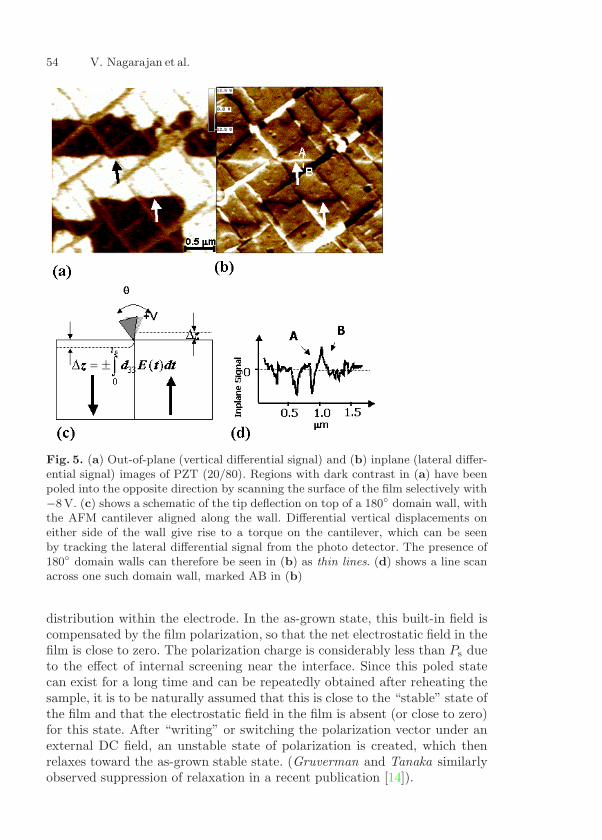
54 V. Nagarajan et al.
Fig. 5. (a) Out-of-plane (vertical differential signal) and (b) inplane (lateral differ-ential signal) images of PZT (20/80). Regions with dark contrast in (a) have beenpoled into the opposite direction by scanning the surface of the film selectively with−8V. (c) shows a schematic of the tip deflection on top of a 180 domain wall, withthe AFM cantilever aligned along the wall. Differential vertical displacements oneither side of the wall give rise to a torque on the cantilever, which can be seenby tracking the lateral differential signal from the photo detector. The presence of180 domain walls can therefore be seen in (b) as thin lines. (d) shows a line scanacross one such domain wall, marked AB in (b)
distribution within the electrode. In the as-grown state, this built-in field iscompensated by the film polarization, so that the net electrostatic field in thefilm is close to zero. The polarization charge is considerably less than Ps dueto the effect of internal screening near the interface. Since this poled statecan exist for a long time and can be repeatedly obtained after reheating thesample, it is to be naturally assumed that this is close to the “stable” state ofthe film and that the electrostatic field in the film is absent (or close to zero)for this state. After “writing” or switching the polarization vector under anexternal DC field, an unstable state of polarization is created, which thenrelaxes toward the as-grown stable state. (Gruverman and Tanaka similarlyobserved suppression of relaxation in a recent publication [14]).
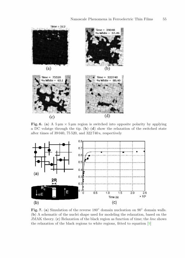
Nanoscale Phenomena in Ferroelectric Thin Films 55
Fig. 6. (a) A 5µm × 5 µm region is switched into opposite polarity by applyinga DC volatge through the tip. (b)–(d) show the relaxation of the switched stateafter times of 39 040, 75 520, and 322 740 s, respectively
Fig. 7. (a) Simulation of the reverse 180 domain nucleation on 90 domain walls.(b) A schematic of the nuclei shape used for modeling the relaxation, based on theJMAK theory. (c) Relaxation of the black region as function of time; the line showsthe relaxation of the black regions to white regions, fitted to equation [9]
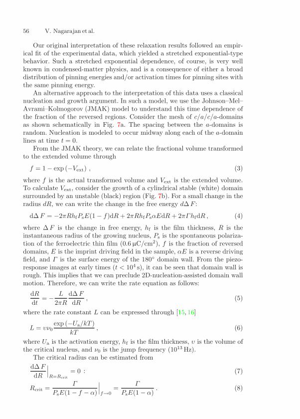
56 V. Nagarajan et al.
Our original interpretation of these relaxation results followed an empir-ical fit of the experimental data, which yielded a stretched exponential-typebehavior. Such a stretched exponential dependence, of course, is very wellknown in condensed-matter physics, and is a consequence of either a broaddistribution of pinning energies and/or activation times for pinning sites withthe same pinning energy.
An alternative approach to the interpretation of this data uses a classicalnucleation and growth argument. In such a model, we use the Johnson–Mel–Avrami–Kolmogorov (JMAK) model to understand this time dependence ofthe fraction of the reversed regions. Consider the mesh of c/a/c/a-domainsas shown schematically in Fig. 7a. The spacing between the a-domains israndom. Nucleation is modeled to occur midway along each of the a-domainlines at time t = 0.
From the JMAK theory, we can relate the fractional volume transformedto the extended volume through
f = 1 − exp (−Vext) , (3)
where f is the actual transformed volume and Vext is the extended volume.To calculate Vext, consider the growth of a cylindrical stable (white) domainsurrounded by an unstable (black) region (Fig. 7b). For a small change in theradius dR, we can write the change in the free energy d∆ F :
d∆ F = −2πRhfPsE(1 − f)dR + 2πRhfPsαEdR + 2πΓhfdR , (4)
where ∆ F is the change in free energy, hf is the film thickness, R is theinstantaneous radius of the growing nucleus, Ps is the spontaneous polariza-tion of the ferroelectric thin film (0.6 µC/cm2), f is the fraction of reverseddomains, E is the imprint driving field in the sample, αE is a reverse drivingfield, and Γ is the surface energy of the 180 domain wall. From the piezo-response images at early times (t < 104 s), it can be seen that domain wall isrough. This implies that we can preclude 2D-nucleation-assisted domain wallmotion. Therefore, we can write the rate equation as follows:
dR
dt= − L
2πR
d∆ F
dR, (5)
where the rate constant L can be expressed through [15, 16]
L = υν0exp (−Ua/kT )
kT, (6)
where Ua is the activation energy, hf is the film thickness, υ is the volume ofthe critical nucleus, and ν0 is the jump frequency (1013 Hz).
The critical radius can be estimated fromd∆ F
dR
∣∣∣R=Rcrit
= 0 : (7)
Rcrit =Γ
PsE(1 − f − α)
∣∣∣f→0
=Γ
PsE(1 − α). (8)

Nanoscale Phenomena in Ferroelectric Thin Films 57
Therefore,
dR
dt= − L
2πR
d∆ F
dR= PsELhf(1 − f − α)
(1 − Rcrit
R
). (9)
Rcrit has been calculated to be of the order of 40 A, which is much smallerthan the resolution limit of our imaging technique. Thus we can ignore theterm involving Rcrit in (9). This leads to an estimate for Vext as
Vext =
t∫
0
N(ξ)π [R(t − ξ)]2 hfdξ
= N0πh3f P
2s E2L2
⎡⎣
t∫
0
(1 − f − α)dt
⎤⎦
2
, (10)
where N(ξ) is the nucleation density. We assume that the number of nu-cleation sites does not change with time and therefore it is a constant, N0.Finally, we can write the reversed fraction f as
f = 1 − exp(−Vext)
= 1 − exp
⎧⎪⎨⎪⎩−N0πh3
f P2s E2L2
⎡⎣
t∫
0
(1 − f − α)dt
⎤⎦
2⎫⎪⎬⎪⎭ . (11)
This equation can be plotted numerically to fit the pre-exponent parameters
Table 1. Values of N0, α, and Ua obtained after fitting the data to (11) for variousDC write voltages
Voltage (V) N0 α L (m3/Js) Ua (eV)
−8.0 8.89 × 10¹² 0.35 1.428 × 10⁻¹⁷ 0.9076
−10.0 7.77 × 10¹² 0.40 2.381 × 10⁻¹⁸ 0.9522
−12.0 1.89 × 10¹² 0.82 7.142 × 10⁻¹⁸ 0.9249
C = N0πh3f P
2s E2L2 and α. Figure 7c plots the numerical solution to (11)
fitted to the experimental data. The values of L and α are 5.95×10⁻¹⁸ m3/Jsand 0.1, respectively. This gives an estimate of 0.962 eV for Ua. It is enticing tocorrelate this activation energy with the activation energy for the diffusion ofspecific defects, such as oxygen vacancies. However, detailed understanding ofthe atomic-scale origins of this activation process needs considerable furtherstudy. An important question that arises is this: Is this polarization reversalaccompanied by reversal within the a-domain?

58 V. Nagarajan et al.
Fig. 8. (a) An out-of-plane domain image. (b) An in-plane image for the sameregion. (c) The same region, after being poled into opposite polarity, shows relax-ation of the unstable black region into stable white regions. (d) The accompanyingin-plane images. The region marked AB shows that in-plane polarization has alsoswitched from the original black contrast to white contrast to maintain unchargeddomain walls. (e) and (g) show out-of-plane images after longer waiting periods,(f) and (h) are the corresponding in-plane images. Note that in the in-plane images180 domains are present inside the 90 domains
Figure 8a,b is in-plane and out-of-plane domain images of the PZT filmbefore writing (as grown). The out-of-plane polarization state within the re-gion scanned was switched into the opposite state by scanning with the tipbiased at −8 V. The in-plane polarization within the a-domains was seen toswitch at the same time, such that no charged interfaces could be identified.Images (c) and (d), (e) and (f), and (g) and (h) were acquired after wait timesof 1.8×10⁴ s, 2.6×10⁴ s, and 5.9×10⁴ s, respectively. The reversed c-domainsin Fig. 8c are seen to reach the c/a domain interface AB, but no reversal ofthe in-plane polarization within the a-domain is observed. This interface istherefore likely to be charged, as it represents a head-to-head arrangementof dipoles. The polarization within the a-domain is seen to reverse only af-ter stable c-domains have nucleated on the opposite side of AB, as seen inFig. 8e, and have grown to meet the interface AB (in Fig. 8g), thereby caus-ing electrostatic pressure to be applied on both sides of the a-domain. Itis possible that the sluggish nature of in-plane reversal under zero externalfield (relaxation) could be attributed to the small dimension (width) of thea-domain.
Nanoscale Phenomena in Ferroelectric Thin Films 59
Fig. 9. (a) The temperature dependence of polarization relaxation. It is seen thatas the temperature is increased the time for achieving full relaxation decreases.(b) An Arrhenius plot, showing the time for saturation (on log scales) versus 1/T .The slope of the plot yields an activation energy of 0.8 eV
An obvious question that comes to mind in the discussion of such kineticphenomenon is the role of temperature. To investigate the temperature de-pendence of the relaxation process, a 10 µm × 10 µm region of the samplewas switched into the oppositely poled state and the sample was incremen-tally heated to the following temperatures: 175 C, 185 C, 190 C, 220 C,250 C, and 300 C. The sample was held at the temperature of interest forvarious time periods, ranging from a few seconds to a day, depending on thetemperature, and then cooled to ambient temperature. For each such timeinterval, a domain image was captured until saturation to the white regionwas achieved. Figure 9a shows the fraction of white domains plotted as heat-ing times for each temperature. Clearly, the saturation time shows a strongdependence on the heating temperature. The higher the temperature, theshorter is the time for saturation; that is, there is a faster rate of relaxation.In other words, as one would expect, the kinetics of polarization reversal isaccelerated with increasing temperature. Since the saturation time for eachtemperature is known, an Arrhenius plot of the saturation time versus theinverse of the temperature is shown in Fig. 9b. This analysis yields an acti-vation energy of 0.8 eV, which is obtained from the slope of a straight-line fitto the data in Fig 9b.
Until now, we have discussed the polarization phenomenon more or less onthe macroscale. It becomes pertinent to investigate this physical phenomenonon a very local scale. Figure 10a–d shows the transformation in a single“cell” that is 500 nm wide. The domain wall is seen to meander across fromthe nucleation site inside one of the sides toward the opposite a-domain walluntil it gets pinned by defect sites, as observed in Fig. 10b. In the early stagesthere is enough driving force for the domain wall to overcome the pinningsites, as can be seen in the series of images shown in Fig. 10b,c.

60 V. Nagarajan et al.
Fig. 10. (a)–(c) Relaxation in a “single cell”. The data illustrate the role of pinningin governing the local velocity of the 180 domain wall. In (b) pinning is clearlyobserved inside the circle. The moving domain wall breaks away from the site in (c),moving in the direction shown by the arrows, and gets pinned at another site (d)
Fig. 11. Relaxation in a “single grain”. The data illustrate the role of grain bound-aries in the relaxation process. In (c) polarization reversal is clearly observed adja-cent to the grain boundary
Nanoscale Phenomena in Ferroelectric Thin Films 61
However, as the relaxation proceeds to later stages, the driving force isexhausted and the wall, unable to break free from the pinning sites, bows out.The difficulty of estimating this small driving field at the end of the relaxationprevents an accurate estimation of the wall energy. The direct observation ofpinned walls at small fields and their noncrystallographic orientation allowsus to suggest that the main controlling mechanism of domain wall mobilityis the overcoming of pinning points in the field. The domain wall movementshould then require 2D nucleation and this diminishes the mobility dramat-ically. In addition to these features, we have also reported faceting of thedomain walls, which results in metastable shapes with clear crystallographicorientations [16].
Figure 11a–c shows the relaxation observed for a polycrystalline film. Itis clear that grain boundaries play a crucial role in the relaxation behavior.Figure 11a is the virgin grain, which shows that the polarization has a darkcontrast. Figure 11b is the image of the same grain after a DC bias of 6 V. Itshows that the DC bias has switched the grain into opposite polarity.
Figure 11c,d is images taken after 60 s and 106 s, respectively. In Fig. 11cwe observe that the relaxation process proceeds from the grain boundaries.In this way, it is analogous to the role of 90 domain boundaries in thenucleation of reverse polarization nuclei. Secondly, it is seen that even after106 s the polarization is not completely reversed back. In fact, it is pinned byalmost 50% of its original value. This set of images clearly reveals the roleof grain boundaries on polarization relaxation.
4 Nanoscale Piezoelectric and Hysteresis Behavior
This section focuses in detail on our recent observations and findings onthe quantification of ferroelectric and piezoelectric phenomena in sub-microncapacitors. The SFM probe tip is used to make contact with the ferroelectricthrough a top electrode, typically LSCO/Pt, and hence the SFM can now beused as a “nano-probe” station. We begin this section with a brief descriptionof processing approaches to control the crystalline quality as well as theorientation in the ferroelectric layer.
As shown in Fig. 12, the PZT layer on STO/Si is not only pure perovskitebut is also found to be epitaxial. Because of the highly oriented nature, the(00l) peak intensities of epitaxial PZT are much higher than those in the poly-crystalline samples. The inset of Fig. 12a is the φ-scan of the epitaxial PZT,indicating its four-fold symmetry. TEM observation (not shown) has revealedthat the interfaces between layers are clean and flat; no obvious diffusion be-tween adjacent layers was observed. Figure 12b compares the hysteresis loopsfor four types of films. The (001)-textured PZT (on LSCO/Pt–Si) has slightlyhigher polarization than the polycrystalline PZT (on Pt–Si); a larger polar-ization, however, was obtained on the epitaxial PZT. This polarization dif-ference between polycrystalline and epitaxial PZT is a primary consequence
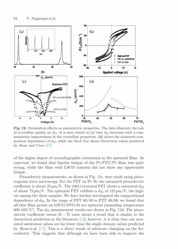
62 V. Nagarajan et al.
Fig. 12. Orientation effects on piezoelectric properties. The data illustrate the roleof crystalline quality on d33. It is seen clearly in (c) that d33 increases with a com-mensurate improvement in the crystalline properties. (d) shows the measured com-position dependence of d33, while the black line shows theoretical values predictedby Haun and Cross [17]
of the higher degree of crystallographic orientation in the epitaxial films. Asexpected, we found that bipolar fatigue of the Pt/PZT/Pt films was quitestrong, while the films with LSCO contacts did not show any appreciablefatigue.
Piezoelectric measurements, as shown in Fig. 12c, were made using piezo-response force microscopy. For the PZT on Pt–Si, the saturated piezoelectriccoefficient is about 25 pm/V. The (001)-textured PZT shows a saturated d33
of about 75 pm/V. The epitaxial PZT exhibits a d33 of 125pm/V, the high-est among the three samples. We have further investigated the compositionaldependence of d33. In the range of PZT 60/40 to PZT 40/60, we found thatall thin films grown on LSCO/STO/Si are epitaxial (annealing temperature600–650 C). The d33 measurement results are shown in Fig. 12d. The piezo-electric coefficient versus Zr : Ti ratio shows a trend that is similar to thetheoretical prediction in the literature [13]; however, it is clear that our mea-sured saturation values are far lower than the single domain values predictedby Haun et al. [17]. This is a direct result of substrate clamping on the fer-roelectric. This suggests that although we have been able to improve the
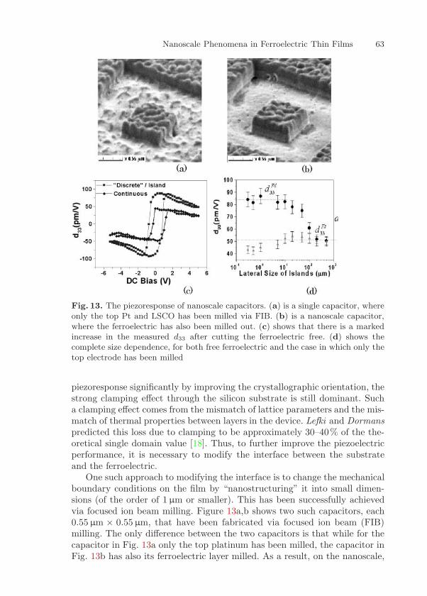
Nanoscale Phenomena in Ferroelectric Thin Films 63
Fig. 13. The piezoresponse of nanoscale capacitors. (a) is a single capacitor, whereonly the top Pt and LSCO has been milled via FIB. (b) is a nanoscale capacitor,where the ferroelectric has also been milled out. (c) shows that there is a markedincrease in the measured d33 after cutting the ferroelectric free. (d) shows thecomplete size dependence, for both free ferroelectric and the case in which only thetop electrode has been milled
piezoresponse significantly by improving the crystallographic orientation, thestrong clamping effect through the silicon substrate is still dominant. Sucha clamping effect comes from the mismatch of lattice parameters and the mis-match of thermal properties between layers in the device. Lefki and Dormanspredicted this loss due to clamping to be approximately 30–40% of the the-oretical single domain value [18]. Thus, to further improve the piezoelectricperformance, it is necessary to modify the interface between the substrateand the ferroelectric.
One such approach to modifying the interface is to change the mechanicalboundary conditions on the film by “nanostructuring” it into small dimen-sions (of the order of 1 µm or smaller). This has been successfully achievedvia focused ion beam milling. Figure 13a,b shows two such capacitors, each0.55 µm × 0.55 µm, that have been fabricated via focused ion beam (FIB)milling. The only difference between the two capacitors is that while for thecapacitor in Fig. 13a only the top platinum has been milled, the capacitor inFig. 13b has also its ferroelectric layer milled. As a result, on the nanoscale,
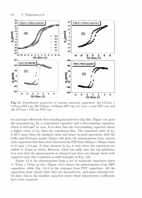
64 V. Nagarajan et al.
Fig. 14. Piezoelectric properties of various nanoscale capacitors: (a) 0.25 µm ×0.25 µm SBT cap; (b) 0.09 µm × 0.09 µm SBT cap; (c) 1µm× 1 µm PZT cap; and(d) 0.07 µm × 0.07 µm PZT cap
we now have effectively free-standing ferroelectric thin film. Figure 13c plotsthe measured d33 for a constrained capacitor and a free-standing capacitor,which is 0.01 µm2 in area. It is clear that the free-standing capacitor showsa higher value of d33 than the continuous film. The measured value of d33
is 50% more than the clamped value and hence in good agreement with theLefki and Dormans model. Figure 13d plots the piezoresponse from varioussuch capacitors that have been fabricated by FIB from 100 µm×100 µm downto 0.1 µm × 0.1 µm. A clear increase in d33 is seen when the capacitors aremilled to 10 µm or below. However, when one mills only the top platinum,it is seen that the piezoresponse is clamped and does not change much withcapacitor size; this is plotted as solid triangles in Fig. 13d.
Figure 14 is the piezoresponse from a set of nanoscale capacitors downto 70 nm × 70 nm in size. Figure 14a,b shows the piezoresponse from SBTcapacitors, while Fig. 14c,d is the response from PZT capacitors. All thecapacitors show clearly that they are piezoelectric, and hence ferroelectric.To date, this is the smallest capacitor stack whose piezoelectric coefficientshave been reported.
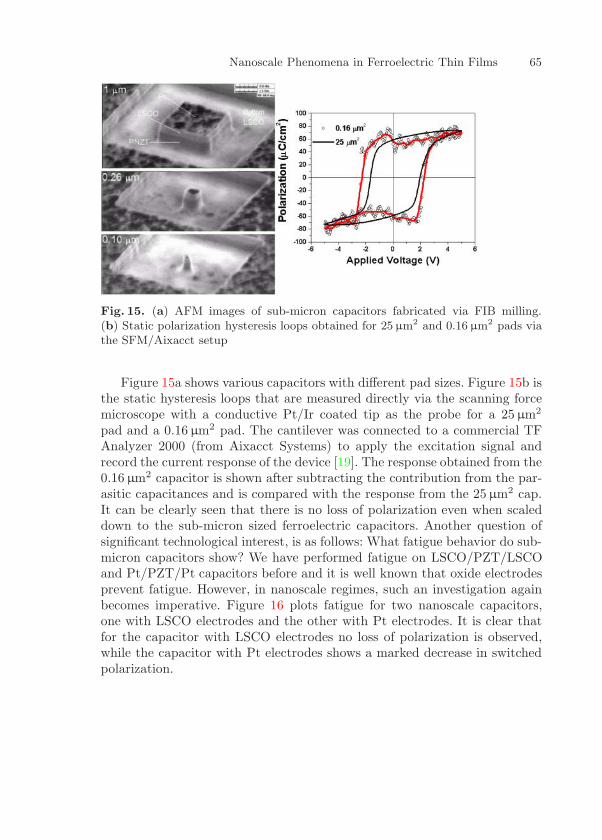
Nanoscale Phenomena in Ferroelectric Thin Films 65
Fig. 15. (a) AFM images of sub-micron capacitors fabricated via FIB milling.(b) Static polarization hysteresis loops obtained for 25 µm2 and 0.16 µm2 pads viathe SFM/Aixacct setup
Figure 15a shows various capacitors with different pad sizes. Figure 15b isthe static hysteresis loops that are measured directly via the scanning forcemicroscope with a conductive Pt/Ir coated tip as the probe for a 25 µm2
pad and a 0.16 µm2 pad. The cantilever was connected to a commercial TFAnalyzer 2000 (from Aixacct Systems) to apply the excitation signal andrecord the current response of the device [19]. The response obtained from the0.16 µm2 capacitor is shown after subtracting the contribution from the par-asitic capacitances and is compared with the response from the 25 µm2 cap.It can be clearly seen that there is no loss of polarization even when scaleddown to the sub-micron sized ferroelectric capacitors. Another question ofsignificant technological interest, is as follows: What fatigue behavior do sub-micron capacitors show? We have performed fatigue on LSCO/PZT/LSCOand Pt/PZT/Pt capacitors before and it is well known that oxide electrodesprevent fatigue. However, in nanoscale regimes, such an investigation againbecomes imperative. Figure 16 plots fatigue for two nanoscale capacitors,one with LSCO electrodes and the other with Pt electrodes. It is clear thatfor the capacitor with LSCO electrodes no loss of polarization is observed,while the capacitor with Pt electrodes shows a marked decrease in switchedpolarization.

66 V. Nagarajan et al.
Fig. 16. Nanoscale fatigue: Pt/PZT/Pt capacitors show polarization fatigue whileLSCO/PZT/LSCO capacitors are fatigue free
5 Summary
Scanning piezoforce microscopy is evolving to be a powerful tool that hasenabled investigations of a variety of phenomena in ferroelectric thin films atthe nanoscale. Our work has focused on size scaling issues, the dynamics ofboth 180 and 90 domain walls in constrained as well as constraint-relievednanostructures, and a fundamental understanding of polarization relaxationbehavior. This surface probe, in conjunction with nano-fabrication techniquessuch as focused ion beam milling or e-beam lithography, provides an ideal“playground” for nanoscale science of ferroelectric materials.
Over the past few years, our studies on polarization relaxation behaviorindicate that relaxation occurs through the nucleation of reverse domainsat heterogeneities. The JMAK model for phase change kinetics has beenapplied to describe the observed transformation-time data for 180 domainreversal under a constantly decaying internal driving field. The effect of localcurvature on driving the domain relaxation kinetics has been studied and ithas been observed that the curvature of growing domains decreases. Pinningand bowing of 180 domain walls is observed in the late stages of relaxation.
Acknowledgements
We have been fortunate to be able to collaborate with several colleagues bothwithin Maryland as well as around the world. We wish to gratefully acknowl-edge their on-going contributions to the central theme of our research effort;specifically, the work of Dr. A. Stanishevsky on focused ion beam milling,that of Professor A. Roytburd on theoretical modeling, that of ProfessorEllen Williams on fundamental studies of dynamics, and that of Dr. BaotingLiu on thin film processing. This work is supported by the NSF under grants
Nanoscale Phenomena in Ferroelectric Thin Films 67
DMR 00-80008 and DMR 99-03279, and by DOE grants from PNNL and theArgonne National Laboratory.
References
1. J. F. Scott: Ferroelectric Memories, Springer Ser. Adv. Microelectron. 3(Springer, Berlin, Heidelberg 2000)D. Damjanovic: Rep. Prog. Phys. 61, 1267 (1998) 47
2. T. Hidaka, T. Mayurama, M. Saitoh, N. Mikoshiba, M. Shimizu, T. Shiosaki,L.A. Wills, R. Hiskes, S.A. Dicarolis, J. Amano: Appl. Phys. Lett. 68, 2358(1996)C.H. Ahn, T. Tybell, L. Antognazza, K. Char, R.H. Hammond, M.R. Beasley,Ø. Fisher, J.-M. Triscone: Science 276, 1100 (1997) 47
3. A. Gruverman, H. Tokumoto, A. S. Prakash, S. Aggarwal, B. Yang, M. Wuttig,R. Ramesh, O. Auciello, T. Venkatesan: Appl. Phys. Lett 71, 3492 (1997) 48
4. J.D. Axe, Y. Yamada: Phys. Rev. B 34, 1 599 (1986)K. Sekimoto: Physica A 125, 261 (1984), Phys. Rev. B 128, 1 32 (1984), Phys.Rev. B 135, 328 (1986)S. Ohta, T. Ohta, K. Kawasaki: Physica A 140, 478 (1987)R.M. Bradly, P.N. Strenski: Phys. Rev. B 40, 8967 (1989)K. Sekimoto: Int. J. Mod. Phys. B 5, 1843 (1991)Y.A. Andrienko, N.V. Brilliantov, P.V. Krapivsky: Phys. Rev. A 45, 2263(1992) 48
5. G.E. Pike, W.L. Warren, D. Dimos, B. A. Tuttle, R. Ramesh, J. Lee,V.G. Keramidas, J. T. Evans, Jr.: Appl. Phys. Lett. 66, 484 (1995) 49
6. V. Nagarajan, I.G. Jenkins, S. P. Alpay, H. Li, S. Aggarwal, L. Salamanca-Riba,A.L. Roytburd, R. Ramesh: J. Appl. Phys. 86, 595 (1999) 49
7. P. Guthner, K. Dransfeld: Appl. Phys. Lett. 61, 1137 (1992)A. Gruverman, O. Auciello, H. Tokumoto: Appl. Phys. Lett. 69, 3191 (1996)T. Tybell, C. H. Ahn, J.-M. Triscone: Appl. Phys. Lett. 72, 1454 (1998)O. Auciello, A. Gruverman, H. Tokumoto, S.A. Prakash, S. Aggarwal,R. Ramesh: Mater. Res. Bull. 23, 33 (1998) 49
8. A.L. Roitburd: Phys. Status Solidi A 37, 329 (1976) 519. B. S. Kwak, A. Erbil, J. D. Budai, M.F. Chrisholm, L. A. Boatner,
B. J. Wilkens: Phys. Rev. B 49, 14865 (1994) 51, 5510. C.M. Foster, Z. Li, M. Buckett, D. Miller, P.M. Baldo, L. E. Rehn, G.R. Bai,
D. Guo, H. You, K. L. Merkle: J. Appl. Phys. 78, 2607 (1995) 5111. C. S. Ganpule, V. Nagarajan, H. Li, A. S. Ogale, D. E. Steinhauer, S. Aggarwal,
E. Williams, R. Ramesh: Appl. Phys. Lett. 77, 292 (2000) 51, 5212. L.M. Eng, M. Abplanalp, P. Gunter: Appl. Phys. A 66, S679 (1998) 5113. A. Roelofs, U. Bottger, R. Waser, F. Schlaphof, S. Trogisch, L.M. Eng: Appl.
Phys. Lett. 77, 3444 (2000) 51, 6214. A. Gruverman, M. Tanaka: J. Appl. Phys. 89, 1836 (2001) 5415. P. G. Shewmon: Transformations in Metals (McGraw-Hill, New York 1969)
B.Y. Lyubov: Kinetic Theory of Phase Transformation (National Bureau ofStandards, New Delhi 1978) 56
16. C. S. Ganpule, A.L. Roytburd, V. Nagarajan, B. K. Hill, S.B. Ogale,E.D. Williams, R. Ramesh, J. F. Scott: Phys. Rev. B 65, 14101 (2002) 56, 61
68 V. Nagarajan et al.
17. M. J. Huan, L. E. Cross: Ferroelectr. 99, 45 (1989) 6218. K. Lefki, G. J. M. Dormans: J. Appl. Phys. 76, 1764 (1994) 6319. S. Tiedke, T. Schmitz, K. Prume, A. Roelofs, T. Schneller, U. Kall, R. Waser,
C. S. Ganpule, V. Nagarajan, A. Stanishevsky, R. Ramesh: Appl. Phys. Lett.79, 3678 (2001) 65
Index
(La0.5Sr0.5)CoO3, 48
activation energy, 56AFM, 50
built-in field, 54– stretched exponential dependence, 55
clamping effect, 63
d33, 49, 62domain, 50domain wall, 59
epitaxial, 49, 61
fatigue, 65free-standing capacitor, 64
grain boundary, 61
hysteresis– loop, 64
internal field, 53
Johnson–Mel–Avrami–Kolmogorov(JMAK) model, 55
lock-in technique, 50LSCO, 49
nano-probe, 61nanostructuring, 63nucleation, 55
piezo-hysteresis loop, 51piezoelectric coefficient, 62piezoresponse force microscopy, 62Piezoresponse Scanning Force
Microscopy, 48pinning site, 59polarization relaxation, 47polarization vector, 52PZT, 49
relaxation, 53relaxation process– temperature dependence, 59
scanning force microscopy, 49– cantilever, 49
topography, 50
The Sputtering Technique
Koukou Suu
ULVAC Inc., 1220-1 Suyama, Susono, Shizuoka 410-1231, Japankoukou [email protected]
Abstract. In this chapter, the formation of ferroelectric films using the sputteringtechnique is described. A main topic is a mass production system for Pb(Zr,Ti)O3
(PZT) films, which includes discussions on the concept of the system, optimizationof the sputtering conditions, the ferroelectric properties of sputtered PZT films, andso on. It is concluded from the switching charge data of PZT films sputtered on 1000substrates that the uniformity and stability of the system are excellent. Sputteringdata for related materials, such as SrBi2Ta2O9 films and hydrogen barrier layers,are also presented in the last part of this chapter.
1 Introduction
Ferroelectric random access memories (FeRAMs) have interesting featuressuch as a high-speed rewriting capacity and nonvolatility characteristics, andthus they are referred to as the ultimate memory. In general, ferroelectric thinfilms for FeRAMs are required to have the following characteristics: 1. a largeamount of polarization reversal charge (Pr > 10 µC/cm2); 2. a small coerciveelectric field (low-voltage operation); 3. a strong resistance to polarizationfatigue; 4. a high polarization reversal speed; 5. a small leakage current (notexceeding 10−6 A/cm2); 6. excellent data retention characteristics (10 yearsand over); and 7. a small dielectric constant (large S/N ratio).
Pb(Zr,Ti)O3 (PZT) and SrBi2Ta2O9 (SBT) films are considered to be themost promising candidates as ferroelectric materials that satisfy the abovecharacteristics for FeRAM. We have been developing mass production tech-nology for PZT [1, 2, 3, 4, 5], since we consider PZT as the most promisingcandidate for the ferroelectric material used in FeRAMs, due to its longerperiod of research, the existence of actual production, its manufacturing ca-pability within the tolerable temperature range of general Si LSI processes,and the recent reports on the dramatic improvement of the fatigue charac-teristics and imprint/retention characteristics [6, 7]. In addition, with an eyetoward the potentiality for larger integration in the future, we are simul-taneously developing mass production technology for SBT ferroelectric thinfilms [8].
The characteristics of major PZT thin-film formation methods are shownin Table 1. We selected the sputtering method for the mass production offerroelectric thin films from the following factors: 1. good compatibility withconventional Si LSI processes; 2. superb controllability of film quality (e.g.,H. Ishiwara, M. Okuyama, Y. Arimoto (Eds.): Ferroelectric Random Access Memories,Topics Appl. Phys. 93, 71–84 (2004)c© Springer-Verlag Berlin Heidelberg 2004
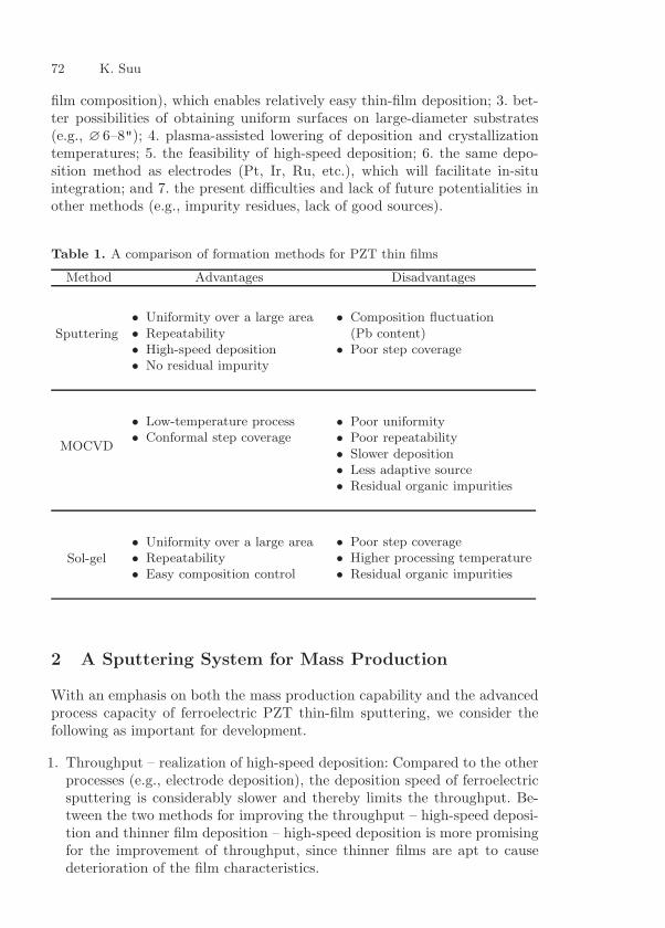
72 K. Suu
film composition), which enables relatively easy thin-film deposition; 3. bet-ter possibilities of obtaining uniform surfaces on large-diameter substrates(e.g., ∅ 6–8"); 4. plasma-assisted lowering of deposition and crystallizationtemperatures; 5. the feasibility of high-speed deposition; 6. the same depo-sition method as electrodes (Pt, Ir, Ru, etc.), which will facilitate in-situintegration; and 7. the present difficulties and lack of future potentialities inother methods (e.g., impurity residues, lack of good sources).
Table 1. A comparison of formation methods for PZT thin films
Method Advantages Disadvantages
Sputtering
• Uniformity over a large area• Repeatability• High-speed deposition• No residual impurity
• Composition fluctuation(Pb content)
• Poor step coverage
MOCVD
• Low-temperature process• Conformal step coverage
• Poor uniformity• Poor repeatability• Slower deposition• Less adaptive source• Residual organic impurities
Sol-gel• Uniformity over a large area• Repeatability• Easy composition control
• Poor step coverage• Higher processing temperature• Residual organic impurities
2 A Sputtering System for Mass Production
With an emphasis on both the mass production capability and the advancedprocess capacity of ferroelectric PZT thin-film sputtering, we consider thefollowing as important for development.
1. Throughput – realization of high-speed deposition: Compared to the otherprocesses (e.g., electrode deposition), the deposition speed of ferroelectricsputtering is considerably slower and thereby limits the throughput. Be-tween the two methods for improving the throughput – high-speed deposi-tion and thinner film deposition – high-speed deposition is more promisingfor the improvement of throughput, since thinner films are apt to causedeterioration of the film characteristics.

The Sputtering Technique 73
2. Control of film composition: The film composition determines other filmqualities (crystal structure, electric characteristics). Since volatile contentsare included in the materials, such as PZT or SBT, they are sensitive andthey fluctuate easily according to the temperature or plasma status. Filmcomposition control is the fundamental factor in this process.
3. Uniformity on large-diameter substrates: Large-diameter substrates of ∅ 6–8" are expected to be used for mass production. Film thickness and uni-formity of the film quality are the keys to mass production.
4. Process stability/reliability: Under circumstances in which there are manyunknown factors, such as new materials, ceramic targets, insulator sputter-ing, and so on, process stability/reliability is the more pertinent factor. Infact, there has been a problem in film composition that has changed overtime.
5. Measures against particles: While characteristics such as ceramic targets orinsulating thin film increase the mechanical factors (e.g., adherence, ther-mal expansion) for particle occurrence, they also produce electrical factors(e.g., dielectric breakdown due to charge-up) and make the measures diffi-cult to obtain.
6. Others (to be discussed in Sect. 6 “Future Development Tasks”)
Based on these concepts, we designed and set up a multi-chamber typemass production sputtering system, equipped with an exclusive sputteringmodule for ferroelectric materials, CERAUS ZX-1000 from ULVAC (Fig. 1).This system has the following features, in addition to features such as easymaintenance, short exhausting time, short down time, etc. 1. It can mount∅ 300 mm (∅ 12") targets and process large-diameter substrates of ∅ 200 mm.At present, deposition of PZT and SBT thin films on ∅ 6" and ∅ 8" sub-strates and of (Ba,Sr)TiO3 (BST) thin films on ∅ 8" substrates is performedusing ∅ 12" single ceramic targets. 2. Including the heat chamber, this systemhas five process chambers, thereby achieving high flexibility. The system ispresently executing the following in-situ processes as standard: pre-heating ofsubstrate → substrate sputtering (e.g., Ti, TiN, Pt) → ferroelectric materialsputtering. 3. As a substrate heating mechanism, this system is capable ofprecise and rapid heating over a wide range from low to high temperatures,with the aid of an electrostatic chuck type hot plate, in addition to lampheating. 4. This system uses RF sputtering for ferroelectric deposition andcounters RF noises.
We adapted the RF magnetron sputtering method for sputtering of PZTtargets. PZT sputtering methods include high-temperature sputtering [9,10],where film deposition is carried out at substrate temperatures of 500 Cor more, and low-temperature deposition, where the films are deposited ataround room temperature and then crystallized by heat treatment. We chosethe latter, where the crystallization was performed after deposition throughheat treatment, because of the high volatility of the Pb component, whichmade composition control difficult in high-temperature deposition. In what
74 K. Suu
Fig. 1. The multi-chamber typemass production sputtering system
follows, the improvement in high-speed deposition, film composition control,and stability of sputtering processes are discussed.
The representative PZT sputtering conditions are shown in Table 2. Sincea ceramic target with an inferior thermal conductivity was used, the appli-cation of high power led to the destruction of the target. Therefore, we useda backing plate with an elevated cooling efficiency and a higher-density target,and achieved further rate improvement by an increase in the sputtering rateand high power application. Presently, the necessary film thickness on a de-vice is considered not to exceed 200 nm, and with this sputtering method, wemade it possible to create a PZT film in approximately 3 min, 7 min shorterthan the conventional deposition method. This will lead to a considerableimprovement in throughput, which is presently limited by the PZT film de-position process.
Table 2. Typical PZT sputtering conditions
Sputtering method RF magnetron sputteringTarget Sintered PZT ceramic target (12")Substrate Pt(100 nm)/TiOx(20 nm)/SiO2/SiBase pressure 1.0 × 10⁻⁵ PaGas (Ar) flow rate 10–50 sccmRF power 1.0–2.0 kWSubstrate temperature Room temperatureFilm thickness < 200 nm
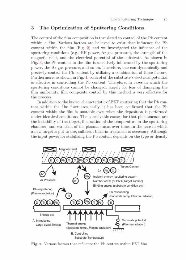
The Sputtering Technique 75
3 The Optimization of Sputtering Conditions
The control of the film composition is translated to control of the Pb contentwithin a film. Various factors are believed to exist that influence the Pbcontent within the film (Fig. 2) and we investigated the influence of thesputtering conditions (e.g., RF power, Ar gas pressure), the strength of themagnetic field, and the electrical potential of the substrate. As shown inFig. 3, the Pb content in the film is sensitively influenced by the sputteringpower, the Ar gas pressure, and so on. Therefore, one can dynamically andprecisely control the Pb content by utilizing a combination of these factors.Furthermore, as shown in Fig. 4, control of the substrate’s electrical potentialis effective in controlling the Pb content. Therefore, in cases in which thesputtering conditions cannot be changed, largely for fear of damaging thefilm uniformity, film composite control by this method is very effective forthe process.
In addition to the known characteristic of PZT sputtering that the Pb con-tent within the film fluctuates easily, it has been confirmed that the Pbcontent within the film is unstable even when the deposition is performedunder identical conditions. The conceivable causes for that phenomenon arethe instability of the target, fluctuation of the temperature in the sputteringchamber, and variation of the plasma status over time. In the case in whicha new target is put to use, sufficient burn-in treatment is necessary. Althoughthe input power for stabilizing the Pb content depends on the type or density
Fig. 2. Various factors that influence the Pb content within PZT film
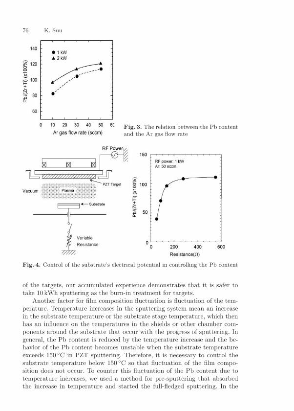
76 K. Suu
Fig. 3. The relation between the Pb contentand the Ar gas flow rate
Fig. 4. Control of the substrate’s electrical potential in controlling the Pb content
of the targets, our accumulated experience demonstrates that it is safer totake 10 kWh sputtering as the burn-in treatment for targets.
Another factor for film composition fluctuation is fluctuation of the tem-perature. Temperature increases in the sputtering system mean an increasein the substrate temperature or the substrate stage temperature, which thenhas an influence on the temperatures in the shields or other chamber com-ponents around the substrate that occur with the progress of sputtering. Ingeneral, the Pb content is reduced by the temperature increase and the be-havior of the Pb content becomes unstable when the substrate temperatureexceeds 150 C in PZT sputtering. Therefore, it is necessary to control thesubstrate temperature below 150 C so that fluctuation of the film compo-sition does not occur. To counter this fluctuation of the Pb content due totemperature increases, we used a method for pre-sputtering that absorbedthe increase in temperature and started the full-fledged sputtering. In the
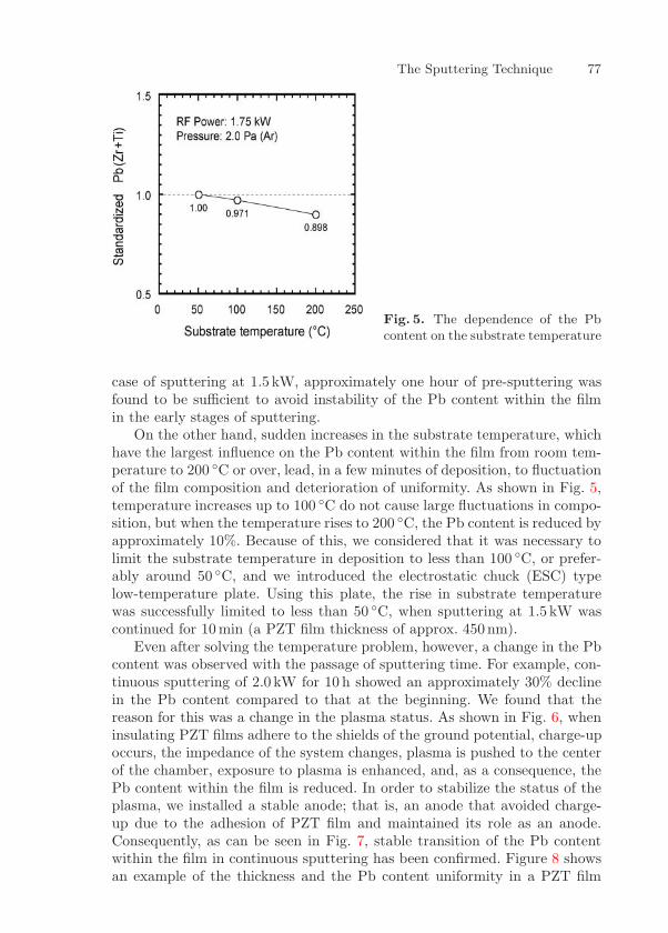
The Sputtering Technique 77
Fig. 5. The dependence of the Pbcontent on the substrate temperature
case of sputtering at 1.5 kW, approximately one hour of pre-sputtering wasfound to be sufficient to avoid instability of the Pb content within the filmin the early stages of sputtering.
On the other hand, sudden increases in the substrate temperature, whichhave the largest influence on the Pb content within the film from room tem-perature to 200 C or over, lead, in a few minutes of deposition, to fluctuationof the film composition and deterioration of uniformity. As shown in Fig. 5,temperature increases up to 100 C do not cause large fluctuations in compo-sition, but when the temperature rises to 200 C, the Pb content is reduced byapproximately 10%. Because of this, we considered that it was necessary tolimit the substrate temperature in deposition to less than 100 C, or prefer-ably around 50 C, and we introduced the electrostatic chuck (ESC) typelow-temperature plate. Using this plate, the rise in substrate temperaturewas successfully limited to less than 50 C, when sputtering at 1.5 kW wascontinued for 10 min (a PZT film thickness of approx. 450 nm).
Even after solving the temperature problem, however, a change in the Pbcontent was observed with the passage of sputtering time. For example, con-tinuous sputtering of 2.0 kW for 10 h showed an approximately 30% declinein the Pb content compared to that at the beginning. We found that thereason for this was a change in the plasma status. As shown in Fig. 6, wheninsulating PZT films adhere to the shields of the ground potential, charge-upoccurs, the impedance of the system changes, plasma is pushed to the centerof the chamber, exposure to plasma is enhanced, and, as a consequence, thePb content within the film is reduced. In order to stabilize the status of theplasma, we installed a stable anode; that is, an anode that avoided charge-up due to the adhesion of PZT film and maintained its role as an anode.Consequently, as can be seen in Fig. 7, stable transition of the Pb contentwithin the film in continuous sputtering has been confirmed. Figure 8 showsan example of the thickness and the Pb content uniformity in a PZT film

78 K. Suu
Fig. 6. Change in the plasma status, which is responsible for Pb content variation
Fig. 7. The stable transition ofthe Pb content within film in con-tinuous sputtering
Fig. 8. Uniformity in the ∅ 8"area
on an 8 " substrate. Both the thickness and the Pb content uniformity var-ied according to the deposition conditions and they were minimized arounda sputtering pressure of 1.0Pa. Uniformity in the film thickness and the Pbcontent represents a good result, as low as ±1.9% and ±1.1%, respectively.These uniformity values were confirmed as being good and stable enough tosatisfy the requirements of mass production.
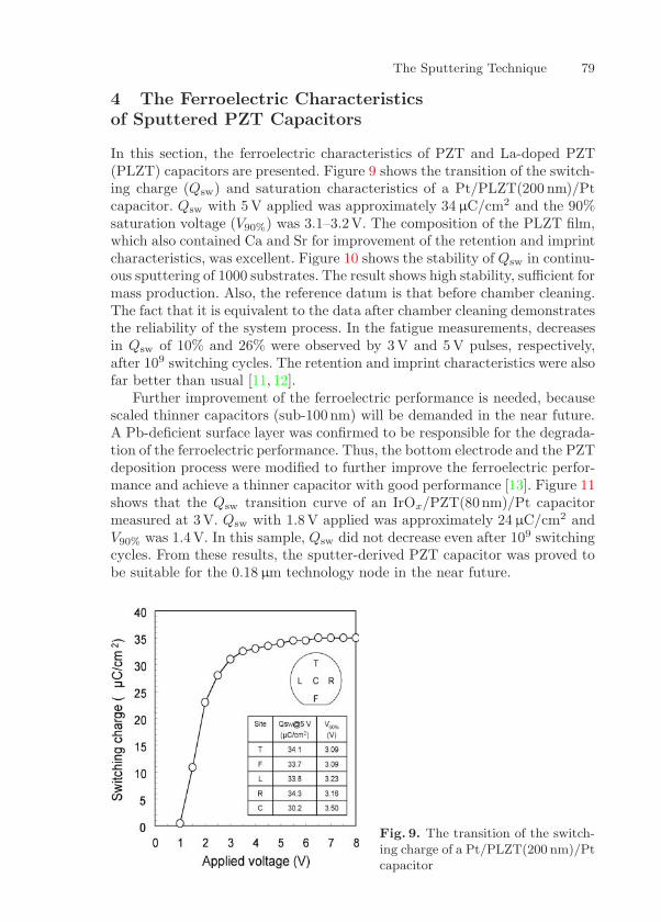
The Sputtering Technique 79
4 The Ferroelectric Characteristicsof Sputtered PZT Capacitors
In this section, the ferroelectric characteristics of PZT and La-doped PZT(PLZT) capacitors are presented. Figure 9 shows the transition of the switch-ing charge (Qsw) and saturation characteristics of a Pt/PLZT(200 nm)/Ptcapacitor. Qsw with 5 V applied was approximately 34 µC/cm2 and the 90%saturation voltage (V90%) was 3.1–3.2V. The composition of the PLZT film,which also contained Ca and Sr for improvement of the retention and imprintcharacteristics, was excellent. Figure 10 shows the stability of Qsw in continu-ous sputtering of 1000 substrates. The result shows high stability, sufficient formass production. Also, the reference datum is that before chamber cleaning.The fact that it is equivalent to the data after chamber cleaning demonstratesthe reliability of the system process. In the fatigue measurements, decreasesin Qsw of 10% and 26% were observed by 3 V and 5 V pulses, respectively,after 109 switching cycles. The retention and imprint characteristics were alsofar better than usual [11, 12].
Further improvement of the ferroelectric performance is needed, becausescaled thinner capacitors (sub-100 nm) will be demanded in the near future.A Pb-deficient surface layer was confirmed to be responsible for the degrada-tion of the ferroelectric performance. Thus, the bottom electrode and the PZTdeposition process were modified to further improve the ferroelectric perfor-mance and achieve a thinner capacitor with good performance [13]. Figure 11shows that the Qsw transition curve of an IrOx/PZT(80nm)/Pt capacitormeasured at 3V. Qsw with 1.8V applied was approximately 24 µC/cm2 andV90% was 1.4V. In this sample, Qsw did not decrease even after 109 switchingcycles. From these results, the sputter-derived PZT capacitor was proved tobe suitable for the 0.18 µm technology node in the near future.
Fig. 9. The transition of the switch-ing charge of a Pt/PLZT(200 nm)/Ptcapacitor
80 K. Suu
Fig. 10. The stability of Qsw inthe continuous sputtering of 1000substrates
Fig. 11. The transition of theswitching charge of an IrOx/PZT(80 nm)/Pt capacitor
5 Sputtering of SBT Filmsand Hydrogen Barrier Layers
We have also been trying sputtering of SBT films. In addition to PZT sput-tering, we have had difficulty in SBT film sputtering due to the high volatil-ity of Bi, which is an obstacle to composition control. We have also haddifficulty with narrow processing margins, such as the requirement for high-temperature processing, and so on [14]. However, recent experiments haveshown that superb ferroelectric characteristics can be obtained through theoptimization of the film composition and the conditions for crystallization.Therefore, sputtering is expected to become a powerful means of mass-pro-ducing carbon-free SBT films. Figure 12 shows the Qsw and fatigue charac-teristics of a 200 nm-thick Nb-doped SBT film (SBTN). In 5V application,Qsw is as high as 12 µC/cm2 and it does not degrade until at least after 109
cycles [15, 16]. In addition, the temperature required for the crystallization
The Sputtering Technique 81
Fig. 12. The fatigue characteris-tics of Pt/SBTN(200 nm)/Pt ca-pacitor
process of SBTN films was 730 C, which was lower than usual. This is a greatstep toward mass production.
In the fabrication of FeRAMs, there is a serious issue in that ferroelec-tric layers are damaged by hydrogen during the process associated with theintegration of ferroelectric capacitors. In order to solve this problem, it isproposed that the ferroelectric capacitors should be covered with a hydro-gen barrier layer. Alumina (Al2O3) thin film is one of the most promisingcandidates as a hydrogen barrier layer, because of its high chemical stabil-ity [17, 18].
Alumina thin films as a hydrogen barrier layer were prepared by a RFmagnetron sputtering method using a sintered alumina ceramic target, andthe fundamental properties of these films, such as the refractive index, wereprimarily investigated. Ferroelectric capacitors coated with alumina barrierlayers were annealed in forming gas and further characterized in terms offerroelectric properties. Alumina films 100 nm in thickness were deposited byRF reactive sputtering. The oxygen partial pressure was varied from 10% to80% under 2.0 kW of RF power and 1.0Pa of sputtering pressure at roomtemperature (R.T.). In this experiment, sufficiently oxidized alumina, whichis supposed to be one of the essential conditions for a hydrogen barrier layer,was obtained under the condition of a higher oxygen partial pressure.
Next, the hydrogen barrier effect was investigated by annealing PZT ca-pacitors in forming gas. The effects of the oxygen partial pressure on aluminadeposition were investigated first, as shown in Fig. 13. The RF power andsputtering pressure were maintained at 2.0 kW and 1.0Pa, respectively. Form-ing gas (3% H2 + N2) annealing was performed at a temperature of 450 C,at atmospheric pressure. As can be seen in this figure, ferroelectric capacitorswithout an alumina layer were obviously degraded, while those with an alu-mina layer were not so affected. Within the samples covered with alumina,the barrier performance of the sample deposited with oxygen as a sputter-ing gas was relatively higher. The dependency on the alumina film thickness
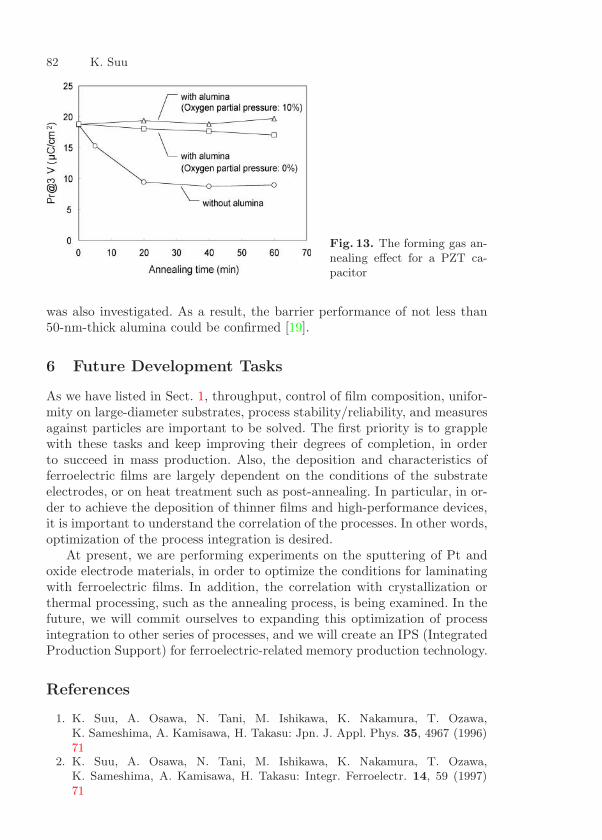
82 K. Suu
Fig. 13. The forming gas an-nealing effect for a PZT ca-pacitor
was also investigated. As a result, the barrier performance of not less than50-nm-thick alumina could be confirmed [19].
6 Future Development Tasks
As we have listed in Sect. 1, throughput, control of film composition, unifor-mity on large-diameter substrates, process stability/reliability, and measuresagainst particles are important to be solved. The first priority is to grapplewith these tasks and keep improving their degrees of completion, in orderto succeed in mass production. Also, the deposition and characteristics offerroelectric films are largely dependent on the conditions of the substrateelectrodes, or on heat treatment such as post-annealing. In particular, in or-der to achieve the deposition of thinner films and high-performance devices,it is important to understand the correlation of the processes. In other words,optimization of the process integration is desired.
At present, we are performing experiments on the sputtering of Pt andoxide electrode materials, in order to optimize the conditions for laminatingwith ferroelectric films. In addition, the correlation with crystallization orthermal processing, such as the annealing process, is being examined. In thefuture, we will commit ourselves to expanding this optimization of processintegration to other series of processes, and we will create an IPS (IntegratedProduction Support) for ferroelectric-related memory production technology.
References
1. K. Suu, A. Osawa, N. Tani, M. Ishikawa, K. Nakamura, T. Ozawa,K. Sameshima, A. Kamisawa, H. Takasu: Jpn. J. Appl. Phys. 35, 4967 (1996)71
2. K. Suu, A. Osawa, N. Tani, M. Ishikawa, K. Nakamura, T. Ozawa,K. Sameshima, A. Kamisawa, H. Takasu: Integr. Ferroelectr. 14, 59 (1997)71
The Sputtering Technique 83
3. K. Suu, A. Osawa, Y. Nishioka, N. Tani: Jpn. J. Appl. Phys. 36, 5789 (1997)71
4. K. Suu, Y. Nishioka, A. Osawa, N. Tani: Oyo Buturi 65, 1248 (1996) (inJapanese) 71
5. K. Suu: Proc. Semicon. Korea Tech. Symp. (1998) p. 255 716. T. Nakamura, Y. Nakao, A. Kamisawa, H. Takasu: Appl. Phys. Lett. 65, 1522
(1994) 717. T. D. Hadnagy, T. Davenport: Integr. Ferroelectr. 22, 183 (1998) 718. K. Suu, T. Masuda, Y. Nishioka, N. Tani: Proc. Int. Symp. Appl. Ferroelectr.
(ISAF XI) (1998) p. 332 719. N. Inoue, Y. Maejima, Y. Hayashi: Tech. Dig. Int. Electron Devices Meeting
(1997) p. 605 7310. N. Inoue, T. Takeuchi, Y. Hayashi: Tech. Dig. Int. Electron Devices Meeting
(1998) p. 819 7311. F. Chu, G. Hickert, T.D. Hadnagy, K. Suu: Integr. Ferroelectr. 26, 47 (1999)
7912. K. Suu, N. Tani, F. Chu, G. Hickert, T. D. Hadnagy, T. Davenport: Integr.
Ferroelectr. 26, 9 (1999) 7913. F. Chu, G. Fox, T. Davenport, Y. Miyaguchi, K. Suu: Integr. Ferroelectr. 48,
161 (2002) 7914. K. Suu, T. Masuda, Y. Nishioka, N. Tani: Integr. Ferroelectr. 21, 407 (1998)
8015. S. Sun, G.R. Fox, T.D. Hadnagy: Integr. Ferroelectr. 26, 31 (1999) 8016. T. Masuda, Y. Miyaguchi, K. Suu, S. Sun: Integr. Ferroelectr. 31, 23 (2000)
8017. I. S. Park, Y.K. Kim, S.M. Lee, J. H. Chung, S. B. Kang, C. S. Park, C.Y. Yoo,
S. I. Lee, M. Y. Lee: Tech. Dig. Int. Electron Devices Meeting (1997) p. 617 8118. D. J. Jung, B. G. Jeon, H.H. Kim, Y. J. Song, B. J. Koo, S.Y. Lee, S.O. Park,
Y.W. Park, K. Kim: Tech. Dig. Int. Electron Devices Meeting (1999) p. 27981
19. T. Jimbo, Y. Miyaguchi, S. Kikuchi, I. Kimura, M. Tanimura, K. Suu,M. Ishikawa: Integr. Ferroelectr. 45, 105 (2002) 82
Index
burn-in treatment, 76
capacitor– sub-100 nm, 79charge-up, 77
hydrogen barrier, 81
integrated production support (IPS),82
mass production, 72– multi-chamber, 73
Pb content, 75Pb-deficient, 79pre-sputtering, 77
PZT, 71
RF magnetron sputtering, 73
SBT, 80sputtering, 71stability, 79substrate temperature, 76switching charge, 79
technology– 0.18 µm, 79thin film– alumina, 81
uniformity, 78

A Chemical Approach Using Liquid Sources
Tailored to Bi-Based Layer-StructuredPerovskite Thin Films
Kazumi Kato1,2
1 Ceramics Research Institute, National Instituteof Advanced Industrial Science and Technology,2266-98 Anagahora, Shimoshidami, Moriyama-ku, Nagoya 463-8560, Japan
2 Frontier Collaborative Research Center, Tokyo Institute of Technology,4259 Nagatsuda-cho, Midori-ku, Yokohama 226-8503, [email protected]
Abstract. The electrical properties of Bi-based layer-structured perovskite com-pounds strongly depend on their anisotropic crystal structure. Because of this de-pendence, the properties are expected to be designed or controlled through twokinds of crystallographic approaches: the choice of cations in both the A and B sitesof the perovskite layers between the Bi-O layers; and adjustment of the number,n, of oxygen octahedra along the c-axis. Chemical solution deposition is superiorto other deposition techniques in precise compositional control and a low process-ing temperature for multi-component oxide thin films. In particular, it would bea promising technique for control of the crystal structure when the molecules in theprecursor solutions are tailored to have optimum structures for easy transformationto the functional oxides. In this chapter, discussions are focused on the effects of thechoice of Ca2+ as the A site cation and adjustments of n in the range of 2 to 5 on theproperties of thin films. Namely, thin films of CaBi2Ta2O9 (n = 2), CaBi3Ti3O12−δ
(n = 3), CaBi4Ti4O15 (n = 4), and Ca2Bi4Ti5O18 (n = 5) were deposited usingprecursor solutions which were synthesized by chemical reactions of metal alkoxideson the basis of the original concept. The properties of the novel thin films were pri-marily investigated. The relationship between the crystallographic and electronicproperties is fundamentally considered and then the potential for application toFeRAMs is addressed.
1 Introduction
Chemical processing is a promising technique for the synthesis of thin filmsof multi-component electronic ceramics such as ferroelectrics. The electri-cal properties of the ceramic thin films are predominantly determined bytheir crystal structure, composition, and microstructure. Precise control ofthe three fundamental factors is the key to developing high performance.In particular, one should focus on chemical processing via liquid sources,because there are many attractive advantages. By designing the molecularstructure of the liquid source and optimizing its reactivity for the hydroly-sis reaction, photoreaction, and combustion, low-temperature crystallizationH. Ishiwara, M. Okuyama, Y. Arimoto (Eds.): Ferroelectric Random Access Memories,Topics Appl. Phys. 93, 85–95 (2004)c© Springer-Verlag Berlin Heidelberg 2004
86 Kazumi Kato
and a uniform microstructure would be achieved in the ceramic thin film.Furthermore, the use of liquid sources with designed structures is essentialfor integration of the ceramic thin films into silicon, because of the capabilityof low-temperature crystallization. In this chapter, the synthesis of a series oftraditional and novel Bi-based layer-structured perovskite thin films by usingliquid sources containing structure-designed molecules is described, primarilyaddressing their electrical properties.
2 SrBi2(Ta, Nb)2O9 and CaBi2Ta2O9 Thin FilmsDeposited via Triple Alkoxidesof Sr–Bi–Ta/Nb and Ca–Bi–Ta
Thin films of layer-structured perovskite compounds, such as SrBi2Ta2O9
(SBT) and SrBi2(Ta,Nb)2O9, have been considered to be promising materi-als for nonvolatile ferroelectric memory applications because of their excellentferroelectric properties, especially with respect to fatigue performance [1].The solid solutions, SrBi2M2O9 (where M is Ta or Nb), known as Aurivil-lius compounds, consist of a stack of alternating layers of Bi2O2+
2 with twopseudoperovskite layers of oxygen octahedra, (SrM2O7)2−, in the c-direction.The high spontaneous polarization is parallel to the plane of the layers (inthe a-direction), because this direction contains the O–M–O chains that areknown to have high polarizibilities, as in the perovskite ferroelectrics. It is im-perative to lower the processing temperatures of these compounds to achievecompatibility with the complementary metal-oxide–semiconductor (CMOS)technology. Another problem is that the bottom electrode thin film interfacereactions at relatively high temperatures cause degradation of the electricalproperties.
Precursors for layer-structured perovskite thin films of SBT andSrBi2Nb2O9 (SBN) have been prepared by the reactions of a strontium–bismuth double methoxyethoxide and tantalum or niobium methoxyethoxidein methoxyethanol, followed by partial hydrolysis. Several spectroscopic tech-niques, such as 1H-, 13C-, and 93Nb-NMR (nuclear magnetic resonance), andFourier transform infrared spectroscopy, can be used to analyze the arrange-ment of the metals and oxygen in the precursor molecules. The precursorscontain Sr–O–M (where M is Ta or Nb) bonds (i.e., a strontium is connectedto two MO6 octahedra) and Sr–O–Bi bonds, with a bismuth atom bonded tothe oxygens of the MO6 octahedron. The arrangement of metals and oxygenis considered to be similar to the layer-structured perovskite crystal sublattice(Fig. 1).
As a result, the alkoxy-derived SBT thin films can be crystallized by rapidthermal annealing in an oxygen atmosphere below 550 C, and they exhibita preferred (115) orientation. The crystallinity is improved and the crystallitesize increases with temperature up to 700 C. In the case of SBN thin films,a low heating rate (2 C/min) is necessary for control of the crystallographic

Title Suppressed Due to Excessive Length 87
Fig. 1. The proposed molecular structure of triple alkoxides and the crystal struc-tures of SrBi2Ta2O9, SrBi2(Ta,Nb)2O9, and SrBi2Nb2O9
(115) orientation, whereas a rate of 200 C/s (rapid thermal annealing) pro-duces films that exhibit a c-axis orientation. The (115) SBT thin film, heatedto 700 C, exhibits improved ferroelectric properties [2, 3, 4, 5]. The 700 C-annealed SBT thin film does not show fatigue after 1010 cycles of switching.
The film, deposited from the complex ethoxide solution and afterwardscalcined at 250 C in the mixture of water vapor and an oxygen flow, con-tains a relatively smaller amount of the remaining alkoxy groups. Therefore,it crystallized to SBT via rapid thermal annealing at a temperature below500 C in an oxygen flow. The crystallinity had improved significantly andthe microstructure had developed up to 650 C. Remarkable grain growth wasobserved, particularly in the SBT thin film deposited from the ethanolic so-lution of the complex ethoxide. Films annealed at 650 C exhibited saturatedP–E hysteresis loop and improved endurance behavior [6, 7, 8].
As described above, the ferroelectric properties of Bi-based layer-struc-tured perovskite originate in the unique and anisotropic crystal structure.On the basis of crystallographic aspects, there are two important approachesto controling the ferroelectric properties: precise substitution of the A-siteand B-site cations and adjustment of the number of oxygen octahedra alongthe c-axis in the perovskite layer. Substitution of the Sr2+ ion by the Ca2+
ion in SBT is a typical approach of the former method, which leads to theformation of CaBi2Ta2O9 (CBT).
CBT thin films were prepared on Pt-coated quartz glass substrates bymeans of the solution of a Ca–Bi–Ta triple alkoxide which was synthesizedby a method similar to that used for Sr–Bi–Ta triple alkoxide, except for the
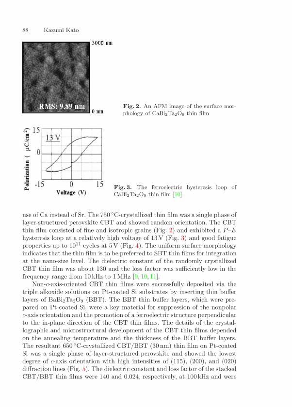
88 Kazumi Kato
Fig. 2. An AFM image of the surface mor-phology of CaBi2Ta2O9 thin film
Fig. 3. The ferroelectric hysteresis loop ofCaBi2Ta2O9 thin film [10]
use of Ca instead of Sr. The 750 C-crystallized thin film was a single phase oflayer-structured perovskite CBT and showed random orientation. The CBTthin film consisted of fine and isotropic grains (Fig. 2) and exhibited a P–Ehysteresis loop at a relatively high voltage of 13V (Fig. 3) and good fatigueproperties up to 1011 cycles at 5V (Fig. 4). The uniform surface morphologyindicates that the thin film is to be preferred to SBT thin films for integrationat the nano-size level. The dielectric constant of the randomly crystallizedCBT thin film was about 130 and the loss factor was sufficiently low in thefrequency range from 10 kHz to 1MHz [9, 10, 11].
Non-c-axis-oriented CBT thin films were successfully deposited via thetriple alkoxide solutions on Pt-coated Si substrates by inserting thin bufferlayers of BaBi2Ta2O9 (BBT). The BBT thin buffer layers, which were pre-pared on Pt-coated Si, were a key material for suppression of the nonpolarc-axis orientation and the promotion of a ferroelectric structure perpendicularto the in-plane direction of the CBT thin films. The details of the crystal-lographic and microstructural development of the CBT thin films dependedon the annealing temperature and the thickness of the BBT buffer layers.The resultant 650 C-crystallized CBT/BBT (30 nm) thin film on Pt-coatedSi was a single phase of layer-structured perovskite and showed the lowestdegree of c-axis orientation with high intensities of (115), (200), and (020)diffraction lines (Fig. 5). The dielectric constant and loss factor of the stackedCBT/BBT thin films were 140 and 0.024, respectively, at 100kHz and were
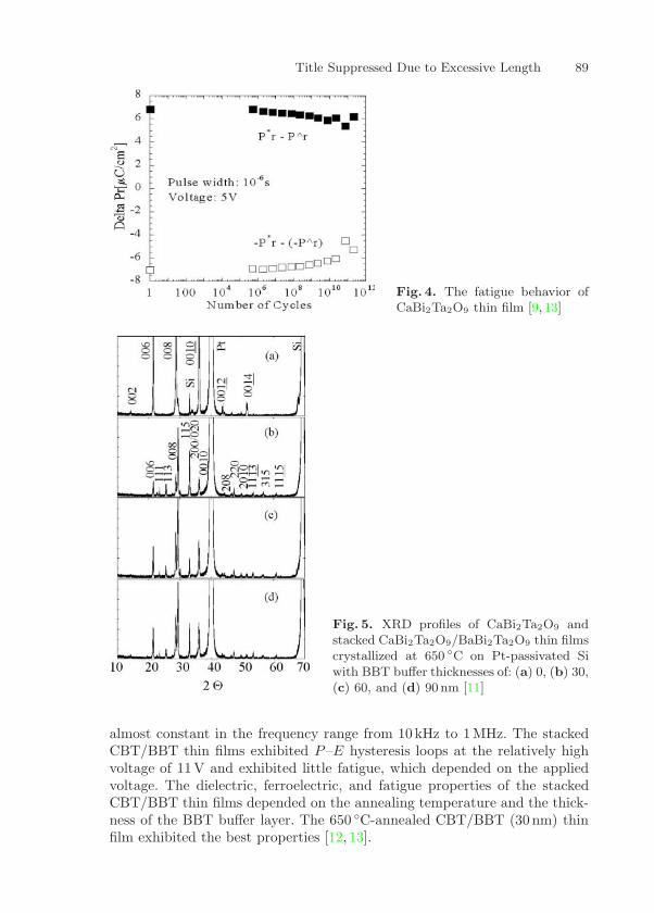
Title Suppressed Due to Excessive Length 89
Fig. 4. The fatigue behavior ofCaBi2Ta2O9 thin film [9, 13]
Fig. 5. XRD profiles of CaBi2Ta2O9 andstacked CaBi2Ta2O9/BaBi2Ta2O9 thin filmscrystallized at 650 C on Pt-passivated Siwith BBT buffer thicknesses of: (a) 0, (b) 30,(c) 60, and (d) 90 nm [11]
almost constant in the frequency range from 10 kHz to 1MHz. The stackedCBT/BBT thin films exhibited P–E hysteresis loops at the relatively highvoltage of 11V and exhibited little fatigue, which depended on the appliedvoltage. The dielectric, ferroelectric, and fatigue properties of the stackedCBT/BBT thin films depended on the annealing temperature and the thick-ness of the BBT buffer layer. The 650 C-annealed CBT/BBT (30 nm) thinfilm exhibited the best properties [12, 13].
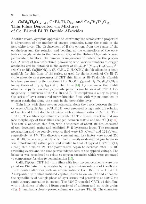
90 Kazumi Kato
3 CaBi3Ti3O12−X, CaBi4Ti4O15, and Ca2Bi4Ti5O18
Thin Films Deposited via Mixturesof Ca–Bi and Bi–Ti Double Alkoxides
Another crystallographic approach to controling the ferroelectric propertiesis adjustment of the number of oxygen octahedra along the c-axis in theperovskite layer. The displacement of B-site cations from the center of theoctahedron and the rotation and bending at the connections of the octa-hedra strongly relate to the ferroelectricity of the Bi-based layer-structuredperovskite. Therefore, the number is imperiative to determine the proper-ties. A series of layer-structured perovskite with various numbers of oxygenoctahedra can be obtained in the system of (Bi2O2)2+(Mm−1TimO3m+1)2−
(M: Ca or Bi). Ca[Bi(OR)4]2 (R: C2H5, C2H4OCH3) double alkoxide is againavailable for thin films of the series, as used for the synthesis of Ca–Bi–Tatriple alkoxide as a precursor of CBT thin films. A Bi–Ti double alkoxidehas been prepared by the reaction of Bi(OCOCH3)3 and Ti2(OC2H4OCH3)8for synthesis of Bi4Ti3O12 (BIT) thin films [14]. By the use of the doublealkoxide, a pyrochlore-free perovskite phase began to form at 670 C. Ho-mogeneity in mixtures of the Ca–Bi and Bi–Ti complexes is a key to givingthe series of layer-structured perovskite thin films with various numbers ofoxygen octahedra along the c-axis in the perovskite layer.
Thin films with three oxygen octahedra along the c-axis between the Bi–O layers, CaBi3Ti3O12−x (CBTi133), were prepared using a mixture solutionof Ca–Bi and Bi–Ti double alkoxides with an atomic ratio of Ca : Bi : Ti =1 : 3 : 3. These films crystallized below 550 C. The crystal structure and sur-face morphology of these films changed between 600 C and 650 C (Fig. 6).The 650 C-annealed thin film, with a thickness of about 100nm, consistedof well-developed grains and exhibited P–E hysteresis loops. The remanentpolarization and the coercive electric field were 8.5 µC/cm2 and 124kV/cm,respectively, at 7V. The dielectric constant and loss factor were about 250and 0.048, respectively, at 100kHz. The primarily evaluated fatigue behaviorwas unfortunately rather poor and similar to that of typical Pb(Zr, Ti)O3
(PZT) thin films on Pt. The polarization began to decrease after 2 × 10⁶
switching cycles and the change was independent of the applied voltage. Thebehavior was considered to relate to oxygen vacancies which were generatedto compensate for charge neutralization [15].
CaBi4Ti4O15 (CBTi144) thin films with four oxygen octahedra were pre-pared on Pt-coated Si substrates by using a mixture solution of Ca–Bi andBi–Ti double alkoxides with an atomic ratio of Ca : Bi : Ti = 1 : 4 : 4.As-deposited thin films initiated crystallization below 550 C and enhancedthe crystallinity of a single phase of layer-structured perovskite at 650 C viarapid thermal annealing in oxygen. The 650 C-annealed CBTi144 thin filmswith a thickness of about 130nm consisted of uniform and isotropic grains(Fig. 7), and had a closely packed columnar structure (Fig. 8). The character-
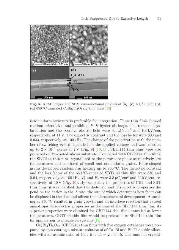
Title Suppressed Due to Excessive Length 91
Fig. 6. AFM images and SEM cross-sectional profiles of (a), (c) 600 C and (b),(d) 650 C-annealed CaBi3Ti3O12−δ thin films [15]
istic uniform structure is preferable for integration. These thin films showedrandom orientation and exhibited P–E hysteresis loops. The remanent po-larization and the coercive electric field were 9.4 µC/cm2 and 106kV/cm,respectively, at 11V. The dielectric constant and the loss factor were 300 and0.033, respectively, at 100kHz. The change of the polarization with the num-ber of switching cycles depended on the applied voltage and was constantup to 2 × 10¹⁰ cycles at 7 V (Fig. 9) [16, 17]. SBTi144 thin films were alsoprepared on Pt-coated silicon substrate. Compared with CBTi144 thin films,the SBTi144 thin films crystallized to the perovskite phase at relatively lowtemperatures and consisted of small and nonuniform grains. Plate-shapedgrains developed randomly in heating up to 750 C. The dielectric constantand the loss factor of the 650 C-annealed SBTi144 thin film were 330 and0.04, respectively, at 100 kHz. Pr and Ec were 3.3 µC/cm2 and 66 kV/cm, re-spectively, at 10V (Fig. 10). By comparing the properties of CBT and SBTthin films, it was clarified that the dielectric and ferroelectric properties de-pend on the cation in the A site, the size of which determines how far it canbe displaced in the site, and affects the microstructural development. Anneal-ing at 750 C resulted in grain growth and an interface reaction that causedanisotropic ferroelectric properties in the case of the SBTi144 thin film. Assuperior properties were obtained for CBTi144 thin films annealed at lowertemperatures, CBTi144 thin film would be preferable to SBTi144 thin filmfor application to integrated systems [18].
Ca2Bi4Ti5O18 (CBTi245) thin films with five oxygen octahedra were pre-pared by spin-coating a mixture solution of of Ca–Bi and Bi–Ti double alkox-ides with an atomic ratio of Ca : Bi : Ti = 2 : 4 : 5. The onset of crystal-
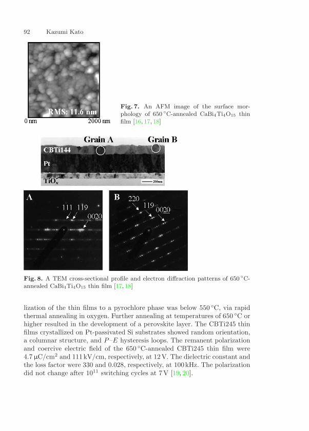
92 Kazumi Kato
Fig. 7. An AFM image of the surface mor-phology of 650 C-annealed CaBi4Ti4O15 thinfilm [16, 17, 18]
Fig. 8. A TEM cross-sectional profile and electron diffraction patterns of 650 C-annealed CaBi4Ti4O15 thin film [17, 18]
lization of the thin films to a pyrochlore phase was below 550 C, via rapidthermal annealing in oxygen. Further annealing at temperatures of 650 C orhigher resulted in the development of a perovskite layer. The CBTi245 thinfilms crystallized on Pt-passivated Si substrates showed random orientation,a columnar structure, and P–E hysteresis loops. The remanent polarizationand coercive electric field of the 650 C-annealed CBTi245 thin film were4.7 µC/cm2 and 111kV/cm, respectively, at 12V. The dielectric constant andthe loss factor were 330 and 0.028, respectively, at 100kHz. The polarizationdid not change after 1011 switching cycles at 7V [19, 20].
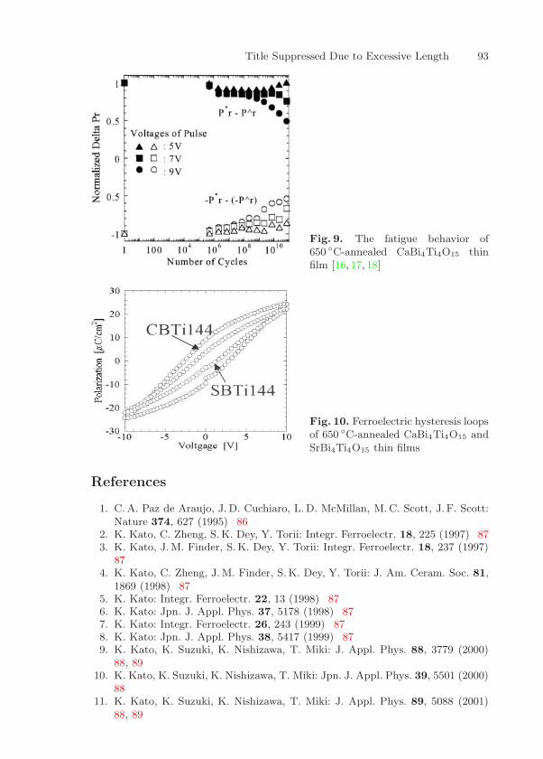
Title Suppressed Due to Excessive Length 93
Fig. 9. The fatigue behavior of650 C-annealed CaBi4Ti4O15 thinfilm [16, 17, 18]
Fig. 10. Ferroelectric hysteresis loopsof 650 C-annealed CaBi4Ti4O15 andSrBi4Ti4O15 thin films
References
1. C. A. Paz de Araujo, J. D. Cuchiaro, L.D. McMillan, M. C. Scott, J. F. Scott:Nature 374, 627 (1995) 86
2. K. Kato, C. Zheng, S.K. Dey, Y. Torii: Integr. Ferroelectr. 18, 225 (1997) 873. K. Kato, J. M. Finder, S.K. Dey, Y. Torii: Integr. Ferroelectr. 18, 237 (1997)
874. K. Kato, C. Zheng, J. M. Finder, S.K. Dey, Y. Torii: J. Am. Ceram. Soc. 81,
1869 (1998) 875. K. Kato: Integr. Ferroelectr. 22, 13 (1998) 876. K. Kato: Jpn. J. Appl. Phys. 37, 5178 (1998) 877. K. Kato: Integr. Ferroelectr. 26, 243 (1999) 878. K. Kato: Jpn. J. Appl. Phys. 38, 5417 (1999) 879. K. Kato, K. Suzuki, K. Nishizawa, T. Miki: J. Appl. Phys. 88, 3779 (2000)
88, 8910. K. Kato, K. Suzuki, K. Nishizawa, T. Miki: Jpn. J. Appl. Phys. 39, 5501 (2000)
8811. K. Kato, K. Suzuki, K. Nishizawa, T. Miki: J. Appl. Phys. 89, 5088 (2001)
88, 89
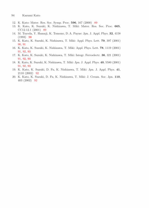
94 Kazumi Kato
12. K. Kato: Mater. Res. Soc. Symp. Proc. 596, 167 (2000) 8913. K. Kato, K. Suzuki, K. Nishizawa, T. Miki: Mater. Res. Soc. Proc. 665,
CC12.12.1 (2001) 8914. M. Toyoda, Y. Hamaji, K. Tomono, D.A. Payne: Jpn. J. Appl. Phys. 32, 4158
(1993) 9015. K. Kato, K. Suzuki, K. Nishizawa, T. Miki: Appl. Phys. Lett. 79, 397 (2001)
90, 9116. K. Kato, K. Suzuki, K. Nishizawa, T. Miki: Appl. Phys. Lett. 78, 1119 (2001)
91, 92, 9317. K. Kato, K. Suzuki, K. Nishizawa, T. Miki: Integr. Ferroelectr. 36, 321 (2001)
91, 92, 9318. K. Kato, K. Suzuki, K. Nishizawa, T. Miki: Jpn. J. Appl. Phys. 40, 5580 (2001)
91, 92, 9319. K. Kato, K. Suzuki, D. Fu, K. Nishizawa, T. Miki: Jpn. J. Appl. Phys. 41,
2110 (2002) 9220. K. Kato, K. Suzuki, D. Fu, K. Nishizawa, T. Miki: J. Ceram. Soc. Jpn. 110,
403 (2002) 92
Index
BaBi2Ta2O9 (BBT), 88
Ca2Bi4Ti5O18 (CBTi245), 92
CaBi2Ta2O9 (CBT), 87
– Ca–Bi–Ta triple alkoxide, 88
– Sr–Bi–Ta triple alkoxide, 88
CaBi3Ti3O12−x (CBTi133)
– Ca–Bi and Bi–Ti double alkoxide, 91
CaBi4Ti4O15 (CBTi144), 91
chemical processing, 85
Fourier transform infrared spectroscopy,86
liquid source, 85
nuclear magnetic resonance (NMR)– 13C-, 86– 1H-, 86– 93Nb, 86
SrBi2(Ta,Nb)2O9, 86SrBi2Ta2O9 (SBT), 86
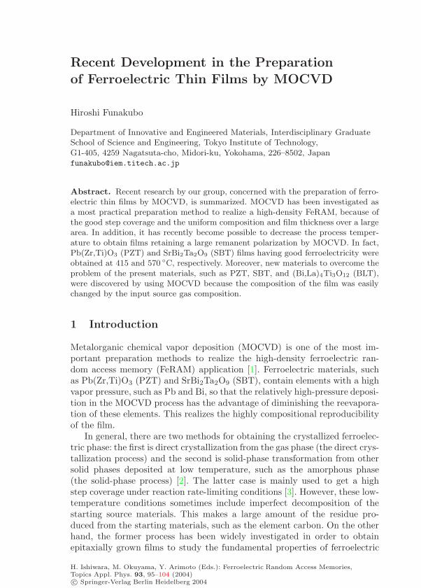
Recent Development in the Preparation
of Ferroelectric Thin Films by MOCVD
Hiroshi Funakubo
Department of Innovative and Engineered Materials, Interdisciplinary GraduateSchool of Science and Engineering, Tokyo Institute of Technology,G1-405, 4259 Nagatsuta-cho, Midori-ku, Yokohama, 226–8502, [email protected]
Abstract. Recent research by our group, concerned with the preparation of ferro-electric thin films by MOCVD, is summarized. MOCVD has been investigated asa most practical preparation method to realize a high-density FeRAM, because ofthe good step coverage and the uniform composition and film thickness over a largearea. In addition, it has recently become possible to decrease the process temper-ature to obtain films retaining a large remanent polarization by MOCVD. In fact,Pb(Zr,Ti)O3 (PZT) and SrBi2Ta2O9 (SBT) films having good ferroelectricity wereobtained at 415 and 570 C, respectively. Moreover, new materials to overcome theproblem of the present materials, such as PZT, SBT, and (Bi,La)4Ti3O12 (BLT),were discovered by using MOCVD because the composition of the film was easilychanged by the input source gas composition.
1 Introduction
Metalorganic chemical vapor deposition (MOCVD) is one of the most im-portant preparation methods to realize the high-density ferroelectric ran-dom access memory (FeRAM) application [1]. Ferroelectric materials, suchas Pb(Zr,Ti)O3 (PZT) and SrBi2Ta2O9 (SBT), contain elements with a highvapor pressure, such as Pb and Bi, so that the relatively high-pressure deposi-tion in the MOCVD process has the advantage of diminishing the reevapora-tion of these elements. This realizes the highly compositional reproducibilityof the film.
In general, there are two methods for obtaining the crystallized ferroelec-tric phase: the first is direct crystallization from the gas phase (the direct crys-tallization process) and the second is solid-phase transformation from othersolid phases deposited at low temperature, such as the amorphous phase(the solid-phase process) [2]. The latter case is mainly used to get a highstep coverage under reaction rate-limiting conditions [3]. However, these low-temperature conditions sometimes include imperfect decomposition of thestarting source materials. This makes a large amount of the residue pro-duced from the starting materials, such as the element carbon. On the otherhand, the former process has been widely investigated in order to obtainepitaxially grown films to study the fundamental properties of ferroelectric
H. Ishiwara, M. Okuyama, Y. Arimoto (Eds.): Ferroelectric Random Access Memories,Topics Appl. Phys. 93, 95–104 (2004)c© Springer-Verlag Berlin Heidelberg 2004
96 H. Funakubo
thin films [4, 5, 6, 7, 8, 9, 10, 11, 12, 13, 14]. However, from the practical pointof view, this process has hardly been employed because of the increase inthe surface roughness and the risk of low step coverage under deposition indiffusion rate-limiting conditions except for the case of PZT film preparation.
In the present study, we have reported that the direct crystallization of theferroelectric phase by MOCVD is useful in decreasing the process temperatureto obtain a film that has good polarization hysteresis [4, 5, 6, 7, 8, 9, 10, 11,12, 13, 14]. Moreover, our research into a new composition that will overcomethe problems of the present ferroelectric materials is also mentioned.
2 Low-Temperature Deposition
The lowering of the deposition temperature is one of the most importantkey issues in realizing high-density FeRAM. This is because of the reductionof the interdiffusion between each layer in the devices. To obtain the crys-talline ferroelectric phase, the solid-phase process was rate-limited by thesolid-phase diffusion of species including the constituent elements, which isgenerally slower than the direct crystallization process from the gas phase.This means that direct crystallization from the gas phase is suitable to obtainthe crystalline films at low temperature.
2.1 SBT Films
In SBT [15, 16, 17, 18, 19, 20, 21] it is widely known to be difficult to obtainsufficient ferroelectricity at a low process temperature. A process temperatureabove 650 C is widely reported as a necessary temperature to get sufficientferroelectricity by the process of solid-phase transformation. However, in thatcase, most of the crystalline SBT phase is obtained by transformation fromthe amorphous or fluorite phases.
We have succeeded in obtaining directly crystallized SBT film even at570 C by electron cyclotron resonance (ECR) plasma enhanced-MOCVD on(111)Ir/TiO2/ SiO2/Si substrates. The deposited film exhibited around (103)single orientation originated from the local epitaxial growth on (111)-orientedIr grains, as shown in Fig. 1a. These films showed well-saturated P–E hys-teresis loops without subsequent heat treatment, as shown in Fig. 1b,c. Twicethe remanent polarization (2Pr) and the coercive field (Ec) of the resultantfilm were 16.1 µC/cm2 and 83kV/cm, respectively. This 2Pr value was 88% ofthe estimated value of the (103) orientation of the SBT films, both from theepitaxial films and from the detailed crystal structure analysis. Moreover, thisfilm had a smooth surface with an average roughness (Ra) of 8.5 nm, which isreflected in the low leakage current density, of the order of 10−7 A/cm2 up to400kV/cm. These results clearly show that direct crystallization of the fer-roelectric phase is very effective in obtaining films with good ferroelectricityat a low process temperature.
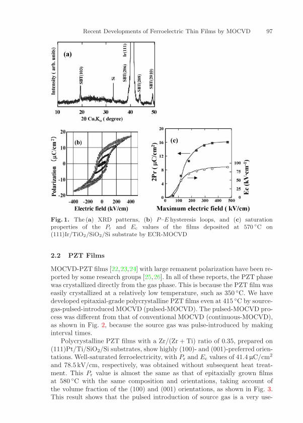
Recent Developments of Ferroelectric Thin Films by MOCVD 97
Fig. 1. The (a) XRD patterns, (b) P–E hysteresis loops, and (c) saturationproperties of the Pr and Ec values of the films deposited at 570 C on(111)Ir/TiO2/SiO2/Si substrate by ECR-MOCVD
2.2 PZT Films
MOCVD-PZT films [22,23,24] with large remanent polarization have been re-ported by some research groups [25,26]. In all of these reports, the PZT phasewas crystallized directly from the gas phase. This is because the PZT film waseasily crystallized at a relatively low temperature, such as 350 C. We havedeveloped epitaxial-grade polycrystalline PZT films even at 415 C by source-gas-pulsed-introduced MOCVD (pulsed-MOCVD). The pulsed-MOCVD pro-cess was different from that of conventional MOCVD (continuous-MOCVD),as shown in Fig. 2, because the source gas was pulse-introduced by makinginterval times.
Polycrystalline PZT films with a Zr/(Zr + Ti) ratio of 0.35, prepared on(111)Pt/Ti/SiO2/Si substrates, show highly (100)- and (001)-preferred orien-tations. Well-saturated ferroelectricity, with Pr and Ec values of 41.4 µC/cm2
and 78.5 kV/cm, respectively, was obtained without subsequent heat treat-ment. This Pr value is almost the same as that of epitaxially grown filmsat 580 C with the same composition and orientations, taking account ofthe volume fraction of the (100) and (001) orientations, as shown in Fig. 3.This result shows that the pulsed introduction of source gas is a very use-
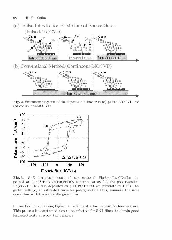
98 H. Funakubo
Fig. 2. Schematic diagrams of the deposition behavior in (a) pulsed-MOCVD and(b) continuous-MOCVD
Fig. 3. P–E hysteresis loops of (a) epitaxial Pb(Zr0.3Ti0.7)O3 film de-posited on (100)SrRuO3//(100)SrTiO3 substrate at 580 C, (b) polycrystallinePb(Zr0.3Ti0.7)O3 film deposited on (111)Pt/Ti/SiO2/Si substrate at 415 C, to-gether with (c) an estimated curve for polycrystalline films, assuming the sameorientation with the epitaxially grown one
ful method for obtaining high-quality films at a low deposition temperature.This process is ascertained also to be effective for SBT films, to obtain goodferroelectricity at a low temperature.
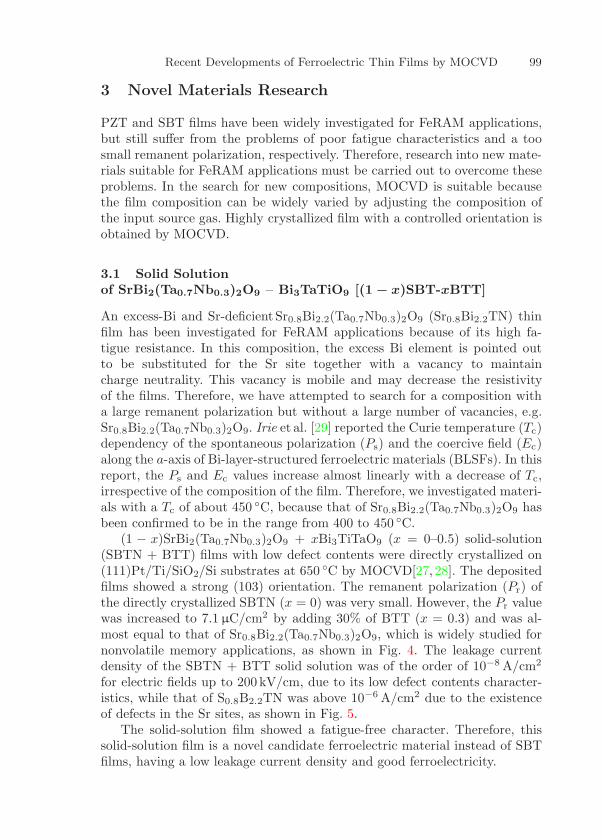
Recent Developments of Ferroelectric Thin Films by MOCVD 99
3 Novel Materials Research
PZT and SBT films have been widely investigated for FeRAM applications,but still suffer from the problems of poor fatigue characteristics and a toosmall remanent polarization, respectively. Therefore, research into new mate-rials suitable for FeRAM applications must be carried out to overcome theseproblems. In the search for new compositions, MOCVD is suitable becausethe film composition can be widely varied by adjusting the composition ofthe input source gas. Highly crystallized film with a controlled orientation isobtained by MOCVD.
3.1 Solid Solutionof SrBi2(Ta0.7Nb0.3)2O9 – Bi3TaTiO9 [(1 − x)SBT-xBTT]
An excess-Bi and Sr-deficient Sr0.8Bi2.2(Ta0.7Nb0.3)2O9 (Sr0.8Bi2.2TN) thinfilm has been investigated for FeRAM applications because of its high fa-tigue resistance. In this composition, the excess Bi element is pointed outto be substituted for the Sr site together with a vacancy to maintaincharge neutrality. This vacancy is mobile and may decrease the resistivityof the films. Therefore, we have attempted to search for a composition witha large remanent polarization but without a large number of vacancies, e.g.Sr0.8Bi2.2(Ta0.7Nb0.3)2O9. Irie et al. [29] reported the Curie temperature (Tc)dependency of the spontaneous polarization (Ps) and the coercive field (Ec)along the a-axis of Bi-layer-structured ferroelectric materials (BLSFs). In thisreport, the Ps and Ec values increase almost linearly with a decrease of Tc,irrespective of the composition of the film. Therefore, we investigated materi-als with a Tc of about 450 C, because that of Sr0.8Bi2.2(Ta0.7Nb0.3)2O9 hasbeen confirmed to be in the range from 400 to 450 C.
(1 − x)SrBi2(Ta0.7Nb0.3)2O9 + xBi3TiTaO9 (x = 0–0.5) solid-solution(SBTN + BTT) films with low defect contents were directly crystallized on(111)Pt/Ti/SiO2/Si substrates at 650 C by MOCVD[27, 28]. The depositedfilms showed a strong (103) orientation. The remanent polarization (Pr) ofthe directly crystallized SBTN (x = 0) was very small. However, the Pr valuewas increased to 7.1 µC/cm2 by adding 30% of BTT (x = 0.3) and was al-most equal to that of Sr0.8Bi2.2(Ta0.7Nb0.3)2O9, which is widely studied fornonvolatile memory applications, as shown in Fig. 4. The leakage currentdensity of the SBTN + BTT solid solution was of the order of 10−8 A/cm2
for electric fields up to 200 kV/cm, due to its low defect contents character-istics, while that of S0.8B2.2TN was above 10−6 A/cm2 due to the existenceof defects in the Sr sites, as shown in Fig. 5.
The solid-solution film showed a fatigue-free character. Therefore, thissolid-solution film is a novel candidate ferroelectric material instead of SBTfilms, having a low leakage current density and good ferroelectricity.
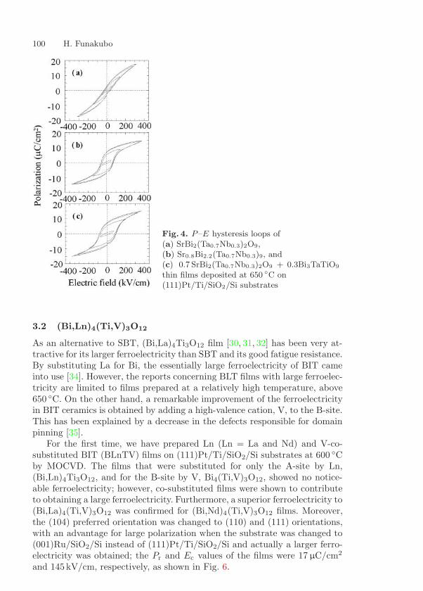
100 H. Funakubo
Fig. 4. P–E hysteresis loops of(a) SrBi2(Ta0.7Nb0.3)2O9,(b) Sr0.8Bi2.2(Ta0.7Nb0.3)9, and(c) 0.7 SrBi2(Ta0.7Nb0.3)2O9 + 0.3Bi3TaTiO9
thin films deposited at 650 C on(111)Pt/Ti/SiO2/Si substrates
3.2 (Bi,Ln)4(Ti,V)3O12
As an alternative to SBT, (Bi,La)4Ti3O12 film [30, 31, 32] has been very at-tractive for its larger ferroelectricity than SBT and its good fatigue resistance.By substituting La for Bi, the essentially large ferroelectricity of BIT cameinto use [34]. However, the reports concerning BLT films with large ferroelec-tricity are limited to films prepared at a relatively high temperature, above650 C. On the other hand, a remarkable improvement of the ferroelectricityin BIT ceramics is obtained by adding a high-valence cation, V, to the B-site.This has been explained by a decrease in the defects responsible for domainpinning [35].
For the first time, we have prepared Ln (Ln = La and Nd) and V-co-substituted BIT (BLnTV) films on (111)Pt/Ti/SiO2/Si substrates at 600 Cby MOCVD. The films that were substituted for only the A-site by Ln,(Bi,Ln)4Ti3O12, and for the B-site by V, Bi4(Ti,V)3O12, showed no notice-able ferroelectricity; however, co-substituted films were shown to contributeto obtaining a large ferroelectricity. Furthermore, a superior ferroelectricity to(Bi,La)4(Ti,V)3O12 was confirmed for (Bi,Nd)4(Ti,V)3O12 films. Moreover,the (104) preferred orientation was changed to (110) and (111) orientations,with an advantage for large polarization when the substrate was changed to(001)Ru/SiO2/Si instead of (111)Pt/Ti/SiO2/Si and actually a larger ferro-electricity was obtained; the Pr and Ec values of the films were 17 µC/cm2
and 145 kV/cm, respectively, as shown in Fig. 6.
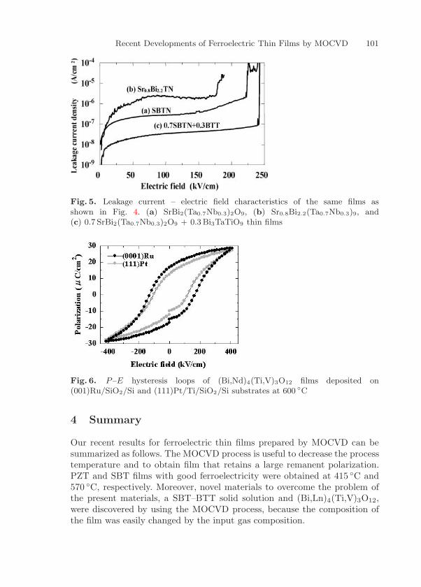
Recent Developments of Ferroelectric Thin Films by MOCVD 101
Fig. 5. Leakage current – electric field characteristics of the same films asshown in Fig. 4. (a) SrBi2(Ta0.7Nb0.3)2O9, (b) Sr0.8Bi2.2(Ta0.7Nb0.3)9, and(c) 0.7 SrBi2(Ta0.7Nb0.3)2O9 + 0.3 Bi3TaTiO9 thin films
Fig. 6. P–E hysteresis loops of (Bi,Nd)4(Ti,V)3O12 films deposited on(001)Ru/SiO2/Si and (111)Pt/Ti/SiO2/Si substrates at 600 C
4 Summary
Our recent results for ferroelectric thin films prepared by MOCVD can besummarized as follows. The MOCVD process is useful to decrease the processtemperature and to obtain film that retains a large remanent polarization.PZT and SBT films with good ferroelectricity were obtained at 415 C and570 C, respectively. Moreover, novel materials to overcome the problem ofthe present materials, a SBT–BTT solid solution and (Bi,Ln)4(Ti,V)3O12,were discovered by using the MOCVD process, because the composition ofthe film was easily changed by the input gas composition.
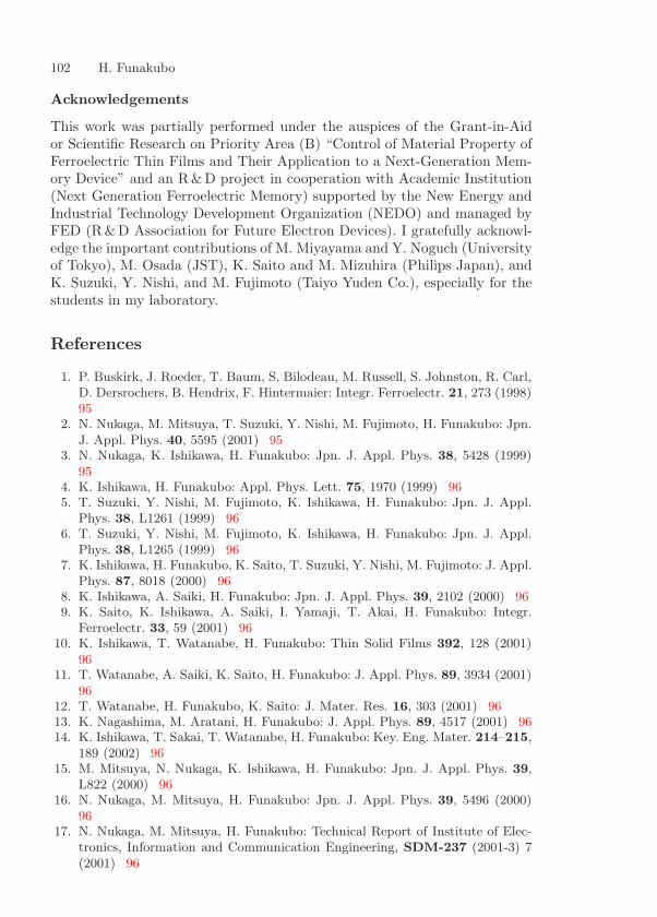
102 H. Funakubo
Acknowledgements
This work was partially performed under the auspices of the Grant-in-Aidor Scientific Research on Priority Area (B) “Control of Material Property ofFerroelectric Thin Films and Their Application to a Next-Generation Mem-ory Device” and an R &D project in cooperation with Academic Institution(Next Generation Ferroelectric Memory) supported by the New Energy andIndustrial Technology Development Organization (NEDO) and managed byFED (R &D Association for Future Electron Devices). I gratefully acknowl-edge the important contributions of M. Miyayama and Y. Noguch (Universityof Tokyo), M. Osada (JST), K. Saito and M. Mizuhira (Philips Japan), andK. Suzuki, Y. Nishi, and M. Fujimoto (Taiyo Yuden Co.), especially for thestudents in my laboratory.
References
1. P. Buskirk, J. Roeder, T. Baum, S. Bilodeau, M. Russell, S. Johnston, R. Carl,D. Dersrochers, B. Hendrix, F. Hintermaier: Integr. Ferroelectr. 21, 273 (1998)95
2. N. Nukaga, M. Mitsuya, T. Suzuki, Y. Nishi, M. Fujimoto, H. Funakubo: Jpn.J. Appl. Phys. 40, 5595 (2001) 95
3. N. Nukaga, K. Ishikawa, H. Funakubo: Jpn. J. Appl. Phys. 38, 5428 (1999)95
4. K. Ishikawa, H. Funakubo: Appl. Phys. Lett. 75, 1970 (1999) 965. T. Suzuki, Y. Nishi, M. Fujimoto, K. Ishikawa, H. Funakubo: Jpn. J. Appl.
Phys. 38, L1261 (1999) 966. T. Suzuki, Y. Nishi, M. Fujimoto, K. Ishikawa, H. Funakubo: Jpn. J. Appl.
Phys. 38, L1265 (1999) 967. K. Ishikawa, H. Funakubo, K. Saito, T. Suzuki, Y. Nishi, M. Fujimoto: J. Appl.
Phys. 87, 8018 (2000) 968. K. Ishikawa, A. Saiki, H. Funakubo: Jpn. J. Appl. Phys. 39, 2102 (2000) 969. K. Saito, K. Ishikawa, A. Saiki, I. Yamaji, T. Akai, H. Funakubo: Integr.
Ferroelectr. 33, 59 (2001) 9610. K. Ishikawa, T. Watanabe, H. Funakubo: Thin Solid Films 392, 128 (2001)
9611. T. Watanabe, A. Saiki, K. Saito, H. Funakubo: J. Appl. Phys. 89, 3934 (2001)
9612. T. Watanabe, H. Funakubo, K. Saito: J. Mater. Res. 16, 303 (2001) 9613. K. Nagashima, M. Aratani, H. Funakubo: J. Appl. Phys. 89, 4517 (2001) 9614. K. Ishikawa, T. Sakai, T. Watanabe, H. Funakubo: Key. Eng. Mater. 214–215,
189 (2002) 9615. M. Mitsuya, N. Nukaga, K. Ishikawa, H. Funakubo: Jpn. J. Appl. Phys. 39,
L822 (2000) 9616. N. Nukaga, M. Mitsuya, H. Funakubo: Jpn. J. Appl. Phys. 39, 5496 (2000)
9617. N. Nukaga, M. Mitsuya, H. Funakubo: Technical Report of Institute of Elec-
tronics, Information and Communication Engineering, SDM-237 (2001-3) 7(2001) 96

Recent Developments of Ferroelectric Thin Films by MOCVD 103
18. M. Aratani, T. Oikawa, A. Ozeki, H. Funakubo: Jpn. J. Appl. Phys. 40, L343(2001) 96
19. M. Mitsuya, N. Nukaga, H. Funakubo: Jpn. J. Appl. Phys. 40, 3337 (2001)96
20. M. Mitsuya, N. Nukaga, T. Watanabe, H. Funakubo, K. Saito: Jpn. J. Appl.Phys. 40, L758 (2001) 96
21. N. Nukaga, M. Mitsuya, H. Funakubo: Ferroelectr. 260, 51 (2001) 9622. M. Aratani, K. Nagashima, H. Funakubo: Jpn. J. Appl. Phys. 40, 4126 (2001)
9723. M. Aratani, T. Oikawa, T. Ozeki, H. Funakubo: Appl. Phys. Lett. 79, 1000
(2001) 9724. M. Aratani, K. Nagashima, H. Funakubo: Ferroelectr. 260, 69 (2001) 9725. H. Fujisawa, S. Nakashima, K. Kaibara, M. Shimizu, H. Niu: Jpn. J. Appl.
Phys. 38, 5392 (1999) 9726. P. Buskirk, S. Bilodeau, J. Roeder, P. Kirlin: Jpn. J. Appl. Phys. 35, 2520
(1996) 9727. M. Mitsuya, N. Nukaga, T. Watanabe, H. Funakubo: Appl. Phys. Lett. 79,
2067 (2001) 9928. M. Mitsuya, M. Osada, H. Funakubo: J. Crystal Growth 237–239, 473 (2002)
9929. H. Irie, M. Miyayama, T. Kudo: Key. Eng. Mater. 181–182, 27 (2000) 9930. M. Osada, M. Kakihana, M. Mitsuya, T. Watanabe, H. Funakubo: Jpn.
J. Appl. Phys. 40, L891 (2001) 10031. M. Osada, M. Tada, M. Kakihana, T. Watanabe, H. Funakubo: Jpn. J. Appl.
Phys. 40, 5527 (2001) 10032. T. Watanabe, H. Funakubo, M. Osada, Y. Noguchi, M. Miyayama: Appl. Phys.
Lett. 80, 100 (2002) 10033. T. Watanabe, K. Saito, H. Funakubo: J. Crystal Growth 235, 389 (2002)34. B. H. Park, B. Kang, S. Bu, T. Noh, L. Lee, W. Joe: Nature 401, 682 (1999)
10035. Y. Noguchi, M. Miyayama: Appl. Phys. Lett. 78, 1903 (2001) 100
Index
(Bi,La)4(Ti,V)3O12, 100(Bi,La)4Ti3O12 (BLT), 100(Bi,Nd)4(Ti,V)3O12, 100
Bi3TiTaO9
– solid-solution, 99
Curie temperature, 99
direct crystallization process, 95
Metalorganic chemical vapor deposition(MOCVD), 95
pulsed-MOCVD, 97
PZT, 97
SBT, 96
SBT film
– by electron cyclotron resonance(ECR), 96
– plasma enhanced-MOCVD, 96
solid-phase process, 95
Materials Integration Strategies
Orlando Auciello1, Anil M. Dhote1, BaoT. Liu2, Sanjeev Aggarwal2, andRamamoorthy Ramesh2
1 Materials Science Division, Argonne National Laboratory,Argonne, IL 60439, [email protected]
2 Materials and Nuclear Engineering Department, University of Maryland,College Park, MD 20742, USA
Abstract. In this chapter, materials integration strategies for the fabrication ofhigh-density nonvolatile ferroelectric random access memories (FeRAMs), are dis-cussed, in which unique combinations of in situ and ex situ analytical techniques ca-pable of providing information about thin-film surface and interface processes at theatomic scale are used. These methods are also useful for establishing composition–microstructure–property relationships critical for the integration of ferroelectric ca-pacitors with silicon microcircuits. We demonstrate that Ti–Al layers can be usedas a material with a double diffusion barrier/bottom electrode functionality forintegration of ferroelectric capacitors with complimentary metal oxide semiconduc-tor (CMOS) devices for the fabrication of FeRAMs. We discuss here results fromsystematic studies designed to understand Ti–Al film growth and oxidation pro-cesses using sputter-deposition in conjunction with complementary in situ atomiclayer-resolution mass spectroscopy of recoil ion (MSRI) and surface-sensitive X-rayphotoelectron spectroscopy (XPS) and ex situ transmission electron microscopyand electrical characterization.
1 Introduction
Low-density nonvolatile ferroelectric random access memories (FeRAMs) havebeen introduced in the market in various devices, including “smart cards” [1]and microprocessors with embedded memories. The next major effort is fo-cused on the development of high-density FeRAMs. In this case, conductingdiffusion barrier layers will play an even more critical role, since the fer-roelectric capacitors, involving the growth of oxide layers at relatively hightemperatures, will be fabricated directly on top of complimentary metal oxidesemiconductor (CMOS) transistors. There is an intense research and develop-ment effort to develop materials processing and integration strategies for therealization of high-density FeRAMs [1,2,3,4,5,6,7,8]. A stacked architectureis needed for the high-density memory application [9, 10]. This requires thecapacitor to be located directly on top of the drain of the CMOS transistorto minimize the total area of the memory cell [11].
Direct electrical contact between the drain of the transistor and the bot-tom electrode of the capacitor is established via a conducting polycrystalline-Si (poly-Si) plug. This geometry requires elimination of any inter-diffusionH. Ishiwara, M. Okuyama, Y. Arimoto (Eds.): Ferroelectric Random Access Memories,Topics Appl. Phys. 93, 105–123 (2004)c© Springer-Verlag Berlin Heidelberg 2004

106 O. Auciello et al.
between the components of the transistor and capacitor, to prevent the degra-dation of the transistor electrical properties. The dramatically different ma-terials chemistry between the ferroelectric oxides and Si makes necessary theintroduction of a diffusion barrier layer. The fact that this barrier layer mustbe a good conductor and form an ohmic contact to Si further complicatesthis material integration problem.
Among a variety of metals, Pt was chosen as an electrode material pri-marily because of its refractive nature and resistance to oxidation (unlike,for example, Al). Studies on the integration of Pt into ferroelectric capaci-tors yielded devices with FeRAMs-compatible properties, such as large valuesof remanent polarization, film resistivity values higher than 1010 Ω cm, andsufficient retention characteristics [12,13]. However, Pt does not prevent oxy-gen diffusion to the poly-Si plug [14]. Furthermore, these films suffered fromsome fundamental reliability limitations, such as fatigue and imprint. Theproblem of fatigue has, to a large extent, been solved through one of twoapproaches: (i) the use of conducting oxide electrodes with PZT as the fer-roelectric layer [15, 16]; and (ii) the replacement of PZT with the layeredferroelectric material, strontium bismuth titanate (SBT) [17].
Despite success at addressing such fundamental reliability issues as thosediscussed above, among the various levels of process integration steps, thedevelopment of conducting barrier layers to directly contact the ferroelectriccapacitor to the poly-Si plug of the pass-gate transistor in the memory cellis a key requirement. An obvious earlier choice for such a barrier layer wasTiN, especially since it was already widely used in the semiconductor indus-try [18]. Unfortunately, TiN starts to oxidize at ∼ 200–300 C [19], which ismuch lower than the optimum processing temperature for oxide ferroelectricmaterials. To overcome the shortcoming of the TiN layer in terms of temper-ature, Pt or Ir have been used as protective layers [20, 21]. Another approachthat has been adopted is that of doping TiN with Al to form (Ti,Al)N [7]or using silicides [22, 23] or other complex structures [24]. The most commonapproaches currently being explored use a combination of at least two lay-ers to create a composite barrier layer scheme. Taking the PZT system asa prototype example, one approach uses the combination of (Pt,Ir)/(Ti,Al)Nas the composite barrier layer scheme. Many research groups, including ours,have been able to demonstrate the integration of PZT-based capacitors withsilicon using the (Pt,Ir)/nitride approach.
Notwithstanding the potential for a successful process integration of ferro-electric layers on a poly-Si plug using this approach, there are several techno-logical and possibly strategic issues related to the use of Pt and Ir that needto be considered as part of the barrier layer structure. From the technologicalpoint of view, the use of Pt or Ir in this stack poses some challenges. First, dryetching of Pt or Ir is still a very difficult problem, although there have beensome breakthroughs in this regard. A dry etch process (such as a reactiveion beam etching process) is essential in order for the memory technology to
Materials Integration Strategies 107
be manufacturable with high yield. Since both Pt and Ir are relatively inert,the ability to form volatile reaction species during dry etching appears to belimited. Secondly, from the strategic point of view, the use of either Pt orIr (both being precious metals) in such quantities may have an impact onthe supply and demand economics of these metals (Hwang, personal commu-nication). These issues prompted us to initiate some exploratory studies ofalloys and compounds that would eliminate the use of these noble metals.Our preliminary studies have already shown some very striking results thatare scientifically interesting and have strong technological potential.
Thin films of structurally amorphous metallic alloys, such as Cu–Zr andTi–Si–N, have been widely used as diffusion barriers in semiconductor met-allization, as ultrahard coatings, and as micromachining elements [25, 26].These applications take advantage of one or more unique properties of thesefilms, such as inertness to corrosive environments, electrical conduction or in-sulation, and the ability to remain X-ray amorphous up to processing temper-atures. The reason for the formation of amorphous phases of binary metallicalloys appears to be the large differences in the atomic radii of the compo-nents, deep eutectics in the phase diagram, and a strong affinity between thecomponents of the alloy [27]. In addition, the presence of a predominantlycovalently bonded species such as Al favors the formation of these phases.Controlling extrinsic parameters such as introducing O or N impurities andextremely high cooling or deposition rates have also been demonstrated to fa-vor the formation of amorphous phases [28]. Based on the above information,we decided to investigate Ti–Al (nominal composition 3 : 1) as a conducting(300 µΩ · cm) diffusion barrier deposited between poly-Si and the ferroelectriccapacitor, and this is the topic of this chapter.
Because of its low resistivity (≤ 300 µΩ · cm), the Ti–Al layer can be usedin a double functionality as diffusion barrier and bottom electrode, replacingconventional electrode-barrier structures such as Pt/TiN or Ir/TiN. The useof a material such as Ti–Al for double barrier/bottom electrode functionalitymay offer other advantages such as easier reactive ion etching than for Ptor Ir, and lower cost. High-density memory integration will require very thinfilms with smooth surfaces and sharp ferroelectric stack/Ti–Al/poly-Si inter-faces. These interfaces play significant roles in defining device performance,especially because they will be exposed to various processing steps duringthe device fabrication.
The control and the microstructure of thin Ti–Al barrier layers dependstrongly on the initial stages of film growth, which also affect interfacessuch as those created in heterostructures such as La–Sr–Co–O (LSCO)/Ti–Al/poly-Si. We demonstrated that the LSCO/a[amorphous]-Ti–Al hetero-structure exhibits a desirable ohmic behavior, while an LSCO/polycrystallineTi–Al (c[crystalline]-Ti–Al) layer, where the c-Ti–Al layer has a columnarmicrostructure across the entire film thickness, exhibits a nonohmic behav-ior [29, 30]. The a- or c-microstructures are obtained via control of the sput-
108 O. Auciello et al.
tering process used to grow these layers [29, 30]. The nonohmic behavior ofthe LSCO/c-Ti–Al heterostructure described above was attributed to the dif-fusion of Al, through the grain boundaries of the columnar microstructure ofthe Ti–Al layer, to the LSCO/Ti–Al interface, and the formation of an Al2O3
interfacial layer, as shown by XPS analysis [29, 30].Our own earlier work did not provide information to help us understand
the fundamental processes underlying the interaction of oxygen atmosphereswith the Ti–Al layer. Since this understanding is critical for optimization ofthe heterostructures described above and for device performance, we studiedthe growth and oxidation process of Ti–Al diffusion barriers and reportedthese results in a recent paper [31]. This chapter is therefore focused on a re-view of our recent work, directed at understanding the fundamental processesinvolved in the integration of PZT capacitors with silicon platforms, and ondeveloping the appropriate materials integration strategies for the fabricationof FeRAMs based on PZT capacitors.
2 An Experimental Method for the Synthesisand Characterization of Ferroelectric Capacitor Layers
The Ti–Al layers were deposited on poly-Si/highly boron-doped (1×10¹⁹ atm/cm3) single-crystal [100]Si substrates (or on undoped Si wafers for the four-probe measurements) at room temperature, using DC magnetron sputteringor ion beam sputter deposition, the latter in an integrated ion beam sput-ter-deposition (IBSD)/in situ mass spectroscopy of recoil ions (MSRI)/X-rayphotoelectron spectroscopy (XPS) (implemented with Al X-rays provided byAl–Kα = 1486.6 eV line) system described elsewhere [32]. The Ti–Al lay-ers synthesized by magnetron or ion beam sputter-deposition exhibit eitherpolycrystalline or amorphous microstructures, depending on the depositionconditions. The polycrystalline structure is obtained when using high mag-netron power (400W or larger), while the amorphous structure is induced bylow magnetron power (less than 400W), in the case of magnetron sputter-deposition. The IBSD method generally results in amorphous a-Ti–Al layers.
Subsequent to the growth of the Ti–Al layers, La0.5Sr0.5CoO3 (LSCO)electrode layers (70 nm thick) were grown by RF sputtering (300W for 30minusing an Ar : O2 (5 : 1) gas mixture) and annealed at 450 C in an oxygen-flowing tube furnace. Ferroelectric layers, PbZr0.4Ti0.6O3 (PZT) or PbNb0.04/Zr0.28Ti0.68O3 (PNZT), were grown using either a conventional sol-gel tech-nique with lead (IV) acetate, titanium isopropoxide, and zirconium-n-bu-toxide precursor solutions dissolved in stoichiometric proportions in hexane(excess lead (7%) was incorporated in the lead precursor to compensate forlead loss during crystallization) or a new solution involving lead acetate tri-hydrate, titanium tetra-iso-propoxide, zirconium tetra-n-butoxide, acetylace-tone, propylene glycol, and low-viscosity alcohol as the diluent. In both cases,the PZT solutions were spin-deposited onto the LSCO/Ti–Al in ∼120nm
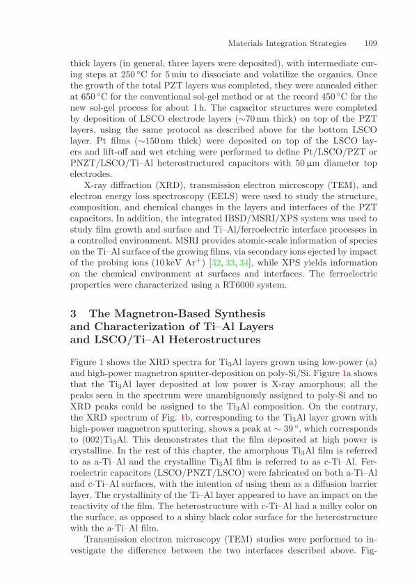
Materials Integration Strategies 109
thick layers (in general, three layers were deposited), with intermediate cur-ing steps at 250 C for 5 min to dissociate and volatilize the organics. Oncethe growth of the total PZT layers was completed, they were annealed eitherat 650 C for the conventional sol-gel method or at the record 450 C for thenew sol-gel process for about 1 h. The capacitor structures were completedby deposition of LSCO electrode layers (∼70 nm thick) on top of the PZTlayers, using the same protocol as described above for the bottom LSCOlayer. Pt films (∼150nm thick) were deposited on top of the LSCO lay-ers and lift-off and wet etching were performed to define Pt/LSCO/PZT orPNZT/LSCO/Ti–Al heterostructured capacitors with 50 µm diameter topelectrodes.
X-ray diffraction (XRD), transmission electron microscopy (TEM), andelectron energy loss spectroscopy (EELS) were used to study the structure,composition, and chemical changes in the layers and interfaces of the PZTcapacitors. In addition, the integrated IBSD/MSRI/XPS system was used tostudy film growth and surface and Ti–Al/ferroelectric interface processes ina controlled environment. MSRI provides atomic-scale information of specieson the Ti–Al surface of the growing films, via secondary ions ejected by impactof the probing ions (10 keV Ar+) [32, 33, 34], while XPS yields informationon the chemical environment at surfaces and interfaces. The ferroelectricproperties were characterized using a RT6000 system.
3 The Magnetron-Based Synthesisand Characterization of Ti–Al Layersand LSCO/Ti–Al Heterostructures
Figure 1 shows the XRD spectra for Ti3Al layers grown using low-power (a)and high-power magnetron sputter-deposition on poly-Si/Si. Figure 1a showsthat the Ti3Al layer deposited at low power is X-ray amorphous; all thepeaks seen in the spectrum were unambiguously assigned to poly-Si and noXRD peaks could be assigned to the Ti3Al composition. On the contrary,the XRD spectrum of Fig. 1b, corresponding to the Ti3Al layer grown withhigh-power magnetron sputtering, shows a peak at ∼ 39 , which correspondsto (002)Ti3Al. This demonstrates that the film deposited at high power iscrystalline. In the rest of this chapter, the amorphous Ti3Al film is referredto as a-Ti–Al and the crystalline Ti3Al film is referred to as c-Ti–Al. Fer-roelectric capacitors (LSCO/PNZT/LSCO) were fabricated on both a-Ti–Aland c-Ti–Al surfaces, with the intention of using them as a diffusion barrierlayer. The crystallinity of the Ti–Al layer appeared to have an impact on thereactivity of the film. The heterostructure with c-Ti–Al had a milky color onthe surface, as opposed to a shiny black color surface for the heterostructurewith the a-Ti–Al film.
Transmission electron microscopy (TEM) studies were performed to in-vestigate the difference between the two interfaces described above. Fig-
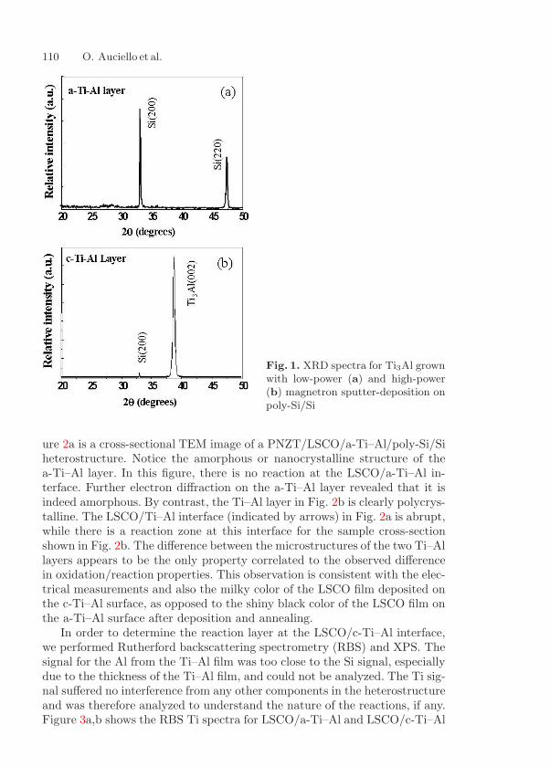
110 O. Auciello et al.
Fig. 1. XRD spectra for Ti3Al grownwith low-power (a) and high-power(b) magnetron sputter-deposition onpoly-Si/Si
ure 2a is a cross-sectional TEM image of a PNZT/LSCO/a-Ti–Al/poly-Si/Siheterostructure. Notice the amorphous or nanocrystalline structure of thea-Ti–Al layer. In this figure, there is no reaction at the LSCO/a-Ti–Al in-terface. Further electron diffraction on the a-Ti–Al layer revealed that it isindeed amorphous. By contrast, the Ti–Al layer in Fig. 2b is clearly polycrys-talline. The LSCO/Ti–Al interface (indicated by arrows) in Fig. 2a is abrupt,while there is a reaction zone at this interface for the sample cross-sectionshown in Fig. 2b. The difference between the microstructures of the two Ti–Allayers appears to be the only property correlated to the observed differencein oxidation/reaction properties. This observation is consistent with the elec-trical measurements and also the milky color of the LSCO film deposited onthe c-Ti–Al surface, as opposed to the shiny black color of the LSCO film onthe a-Ti–Al surface after deposition and annealing.
In order to determine the reaction layer at the LSCO/c-Ti–Al interface,we performed Rutherford backscattering spectrometry (RBS) and XPS. Thesignal for the Al from the Ti–Al film was too close to the Si signal, especiallydue to the thickness of the Ti–Al film, and could not be analyzed. The Ti sig-nal suffered no interference from any other components in the heterostructureand was therefore analyzed to understand the nature of the reactions, if any.Figure 3a,b shows the RBS Ti spectra for LSCO/a-Ti–Al and LSCO/c-Ti–Al
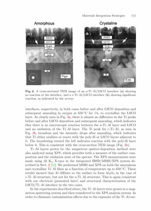
Materials Integration Strategies 111
Fig. 2. A cross-sectional TEM image of an a-Ti–Al/LSCO interface (a) showingno reaction at the interface, and a c-Ti–Al/LSCO interface (b) showing significantreaction, as indicated by the arrows
interfaces, respectively, in both cases before and after LSCO deposition andsubsequent annealing in oxygen at 650 C for 1 h, to crystallize the LSCOlayer. As clearly seen in Fig. 3a, there is almost no difference in the Ti peaksbefore and after LSCO deposition and subsequent annealing, which indicatesthat there is no macroscopic reaction between the a-Ti–Al layer and LSCOand no oxidation of the Ti–Al layer. The Ti peak for c-Ti–Al, as seen inFig. 3b, broadens and the intensity drops after annealing, which indicatesthat Ti either oxidizes or reacts with the poly-Si or LSCO layers adjacent toit. The broadening toward the left indicates reaction with the poly-Si layerbelow it. This is consistent with the cross-section TEM image (Fig. 2b).
Ti–Al layers grown by the magnetron sputter-deposition method werealso analyzed using XPS, which provides both a measure of the surface com-position and the oxidation state of the species. The XPS measurements weremade using Al–Kα X-rays in the integrated IBSD/MSRI/XPS system de-scribed in Sect. 2 [33]. We performed MSRI and XPS on both the amorphousand crystalline Ti–Al films as a function of temperature up to 650 C. Theseresults showed that Al diffuses to the surface to form Al2O3 in the case ofc-Ti–Al structure, but not for the a-Ti–Al structure. This is again consistentwith our electrical (presented later) and structural characterization of theLSCO/Ti–Al interface in the two cases.
In the experiments described above, the Ti–Al layers were grown in a mag-netron sputtering system and then transferred to the XPS analysis system. Inorder to eliminate contamination effects due to the exposure of the Ti–Al sur-
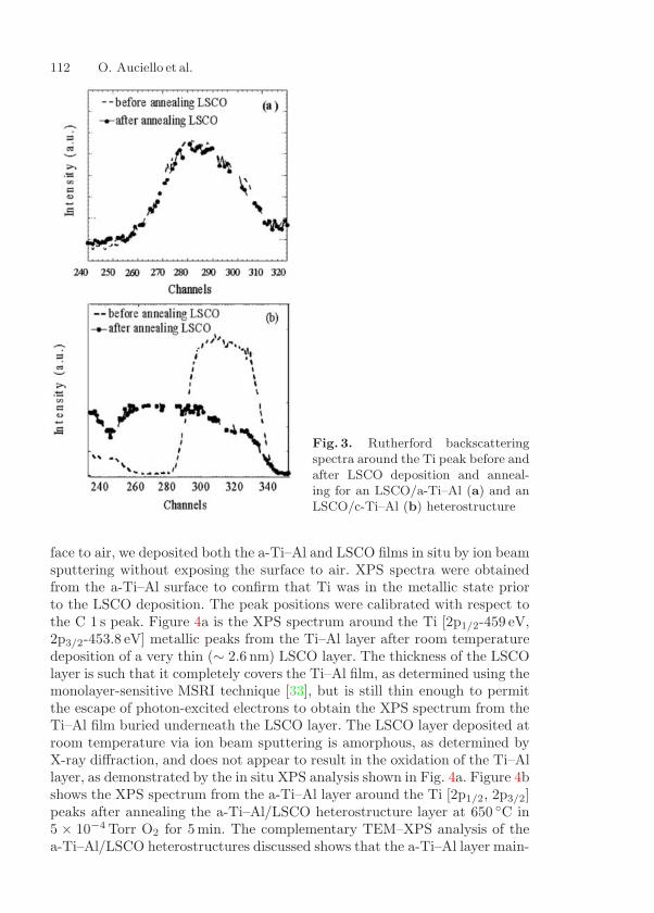
112 O. Auciello et al.
Fig. 3. Rutherford backscatteringspectra around the Ti peak before andafter LSCO deposition and anneal-ing for an LSCO/a-Ti–Al (a) and anLSCO/c-Ti–Al (b) heterostructure
face to air, we deposited both the a-Ti–Al and LSCO films in situ by ion beamsputtering without exposing the surface to air. XPS spectra were obtainedfrom the a-Ti–Al surface to confirm that Ti was in the metallic state priorto the LSCO deposition. The peak positions were calibrated with respect tothe C 1 s peak. Figure 4a is the XPS spectrum around the Ti [2p1/2-459 eV,2p3/2-453.8 eV] metallic peaks from the Ti–Al layer after room temperaturedeposition of a very thin (∼ 2.6 nm) LSCO layer. The thickness of the LSCOlayer is such that it completely covers the Ti–Al film, as determined using themonolayer-sensitive MSRI technique [33], but is still thin enough to permitthe escape of photon-excited electrons to obtain the XPS spectrum from theTi–Al film buried underneath the LSCO layer. The LSCO layer deposited atroom temperature via ion beam sputtering is amorphous, as determined byX-ray diffraction, and does not appear to result in the oxidation of the Ti–Allayer, as demonstrated by the in situ XPS analysis shown in Fig. 4a. Figure 4bshows the XPS spectrum from the a-Ti–Al layer around the Ti [2p1/2, 2p3/2]peaks after annealing the a-Ti–Al/LSCO heterostructure layer at 650 C in5 × 10−4 Torr O2 for 5 min. The complementary TEM–XPS analysis of thea-Ti–Al/LSCO heterostructures discussed shows that the a-Ti–Al layer main-
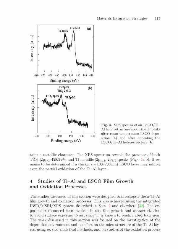
Materials Integration Strategies 113
Fig. 4. XPS spectra of an LSCO/Ti–Al heterostructure about the Ti peaksafter room-temperature LSCO depo-sition (a) and after annealing theLSCO/Ti–Al heterostructure (b)
tains a metallic character. The XPS spectrum reveals the presence of bothTiO2 [2p3/2-458.5 eV] and Ti metallic [2p1/2, 2p3/2] peaks (Figs. 4a,b). It re-mains to be determined if a thicker (∼ 100–200 nm) LSCO layer may inhibiteven the partial oxidation of the Ti–Al layer.
4 Studies of Ti–Al and LSCO Film Growthand Oxidation Processes
The studies discussed in this section were designed to investigate the a-Ti–Alfilm growth and oxidation processes. This was achieved using the integratedIBSD/MSRI/XPS system described in Sect. 2 and elsewhere [32]. The ex-periments discussed here involved in situ film growth and characterizationto avoid surface exposure to air, since Ti is known to readily absorb oxygen.The work discussed in this section was focused on the investigation of thedeposition environment and its effect on the microstructure of the Ti–Al lay-ers, using ex situ analytical methods, and on studies of the oxidation process
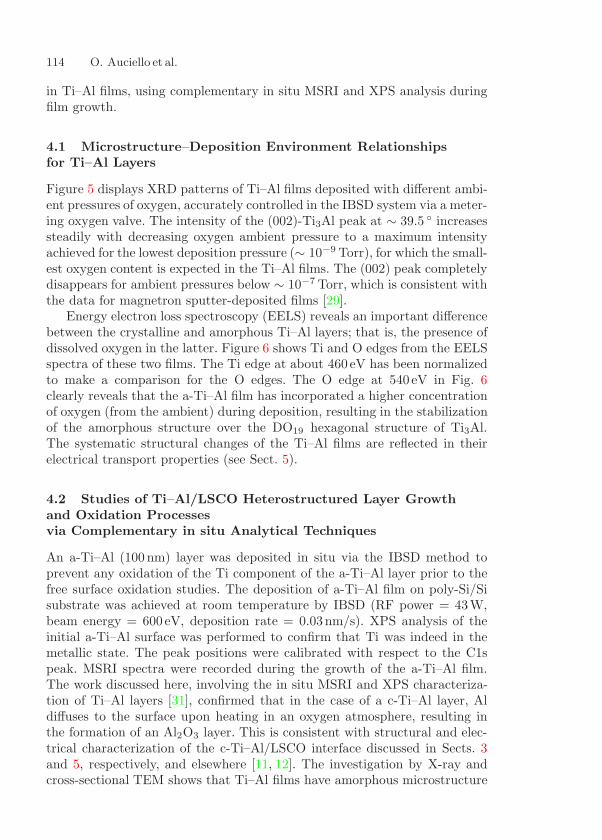
114 O. Auciello et al.
in Ti–Al films, using complementary in situ MSRI and XPS analysis duringfilm growth.
4.1 Microstructure–Deposition Environment Relationshipsfor Ti–Al Layers
Figure 5 displays XRD patterns of Ti–Al films deposited with different ambi-ent pressures of oxygen, accurately controlled in the IBSD system via a meter-ing oxygen valve. The intensity of the (002)-Ti3Al peak at ∼ 39.5 increasessteadily with decreasing oxygen ambient pressure to a maximum intensityachieved for the lowest deposition pressure (∼ 10−9 Torr), for which the small-est oxygen content is expected in the Ti–Al films. The (002) peak completelydisappears for ambient pressures below ∼ 10−7 Torr, which is consistent withthe data for magnetron sputter-deposited films [29].
Energy electron loss spectroscopy (EELS) reveals an important differencebetween the crystalline and amorphous Ti–Al layers; that is, the presence ofdissolved oxygen in the latter. Figure 6 shows Ti and O edges from the EELSspectra of these two films. The Ti edge at about 460 eV has been normalizedto make a comparison for the O edges. The O edge at 540 eV in Fig. 6clearly reveals that the a-Ti–Al film has incorporated a higher concentrationof oxygen (from the ambient) during deposition, resulting in the stabilizationof the amorphous structure over the DO19 hexagonal structure of Ti3Al.The systematic structural changes of the Ti–Al films are reflected in theirelectrical transport properties (see Sect. 5).
4.2 Studies of Ti–Al/LSCO Heterostructured Layer Growthand Oxidation Processesvia Complementary in situ Analytical Techniques
An a-Ti–Al (100 nm) layer was deposited in situ via the IBSD method toprevent any oxidation of the Ti component of the a-Ti–Al layer prior to thefree surface oxidation studies. The deposition of a-Ti–Al film on poly-Si/Sisubstrate was achieved at room temperature by IBSD (RF power = 43W,beam energy = 600 eV, deposition rate = 0.03nm/s). XPS analysis of theinitial a-Ti–Al surface was performed to confirm that Ti was indeed in themetallic state. The peak positions were calibrated with respect to the C1speak. MSRI spectra were recorded during the growth of the a-Ti–Al film.The work discussed here, involving the in situ MSRI and XPS characteriza-tion of Ti–Al layers [31], confirmed that in the case of a c-Ti–Al layer, Aldiffuses to the surface upon heating in an oxygen atmosphere, resulting inthe formation of an Al2O3 layer. This is consistent with structural and elec-trical characterization of the c-Ti–Al/LSCO interface discussed in Sects. 3and 5, respectively, and elsewhere [11, 12]. The investigation by X-ray andcross-sectional TEM shows that Ti–Al films have amorphous microstructure
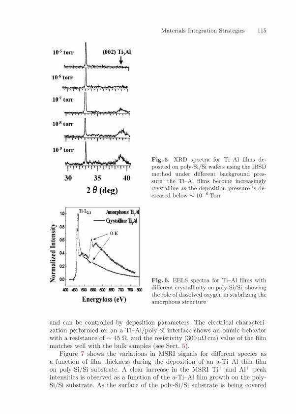
Materials Integration Strategies 115
Fig. 5. XRD spectra for Ti–Al films de-posited on poly-Si/Si wafers using the IBSDmethod under different background pres-sure; the Ti–Al films become increasinglycrystalline as the deposition pressure is de-creased below ∼ 10−6 Torr
Fig. 6. EELS spectra for Ti–Al films withdifferent crystallinity on poly-Si/Si, showingthe role of dissolved oxygen in stabilizing theamorphous structure
and can be controlled by deposition parameters. The electrical characteri-zation performed on an a-Ti–Al/poly-Si interface shows an ohmic behaviorwith a resistance of ∼ 45 Ω, and the resistivity (300 µΩ cm) value of the filmmatches well with the bulk samples (see Sect. 5).
Figure 7 shows the variations in MSRI signals for different species asa function of film thickness during the deposition of an a-Ti–Al thin filmon poly-Si/Si substrate. A clear increase in the MSRI Ti+ and Al+ peakintensities is observed as a function of the a-Ti–Al film growth on the poly-Si/Si substrate. As the surface of the poly-Si/Si substrate is being covered
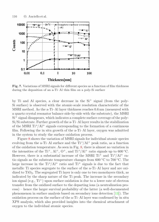
116 O. Auciello et al.
Fig. 7. Variations of MSRI signals for different species as a function of film thicknessduring the deposition of an a-Ti–Al thin film on a poly-Si surface
by Ti and Al species, a clear decrease in the Si+ signal (from the poly-Si surface) is observed with the atomic-scale resolution characteristic of theMSRI method. As the a-Ti–Al layer thickness reaches 0.6 nm (measured witha quartz crystal resonator balance side-by-side with the substrate), the MSRISi+ signal disappears, which indicates a complete surface coverage of the poly-Si/Si substrate. Further growth of the a-Ti–Al layer results in the stabilizationof the MSRI Ti+/Al+ signals corresponding to the formation of a continuousfilm. Following the in situ growth of the a-Ti–Al layer, oxygen was admittedin the system to study the surface oxidation process.
Figure 8 shows the variation of MSRI signals for individual atomic speciesevolving from the a-Ti–Al surface and the Ti+/Al+ peak ratio, as a functionof the oxidation temperature. As seen in Fig. 8, there is almost no variation inthe intensities of the Ti+, Al+, O+, and Ti+/Al+ ratio signals up to 600 C.However, there is a substantial increase of the MSRI Ti+ and Ti+/Al+ ra-tio signals as the substrate temperature changes from 600 C to 700 C. Thelarge increase in the Ti+/Al+ ratio and Ti+ signals is due to the fact thatmetallic Ti species segregate to the surface of the a-Ti–Al layer and are oxi-dized to TiO2. The segregated Ti layer is only one to two monolayers thick, asindicated by the sharp nature of the Ti peak. The increase in the secondaryion signal (e.g., Ti+) upon surface oxidation is due to a lower rate of electrontransfer from the oxidized surface to the departing ions (a neutralization pro-cess) – hence the larger survival probability of the latter (a well-documentedphenomenon in surface analysis based on secondary ions detection [13]). Theoxidation process on the surface of the a-Ti–Al layer was confirmed by in situXPS analysis, which also provided insights into the chemical attachment ofoxygen to the individual atomic species.
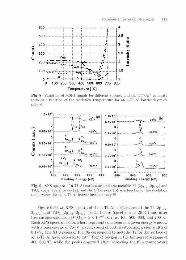
Materials Integration Strategies 117
Fig. 8. Variation of MSRI signals for different species, and the Ti+/Al+ intensityratio as a function of the oxidation temperature for an a-Ti–Al barrier layer onpoly-Si
Fig. 9. XPS spectra of a-Ti–Al surface around the metallic Ti [2p1/2, 2p3/2] andTiO2[2p1/2, 2p3/2] peaks (a); and the O[1 s] peak (b) as a function of the oxidationtemperature for an a-Ti–Al barrier layer on poly-Si
Figure 9 shows XPS spectra of the a-Ti–Al surface around the Ti [2p1/2,2p3/2] and TiO2 [2p1/2, 2p3/2] peaks before (spectrum at 20 C) and afterfree surface oxidation [P (O2)= 5 × 10⁻⁴ Torr] at 400, 500, 600, and 700 C.Each XPS spectrum shown here represents one scan in a given energy windowwith a pass energy of 25 eV, a scan speed of 500ms/step, and a step width of0.1 eV. The XPS peaks of Fig. 9a correspond to metallic Ti for the surface ofan a-Ti–Al layer exposed to 10−3 Torr of oxygen in the temperature range of400–600 C, while the peaks observed after increasing the film temperature

118 O. Auciello et al.
from 600 C to 700 C are clearly correlated with the presence of TiO2 for-mation on the a-Ti–Al surface. In addition, the evolution of the XPS oxygenpeak (Fig. 9b) shows a one-to-one correlation with the evolution of the Tiand TiO2 peaks in Fig. 9a. The combined MSRI/XPS data indicate that thea-Ti–Al layer is stable up to 600 C in oxygen, and that upon transition from600 to 700 C there is a segregation of Ti to the surface of the alloy, concur-rently with a chemical attachment of oxygen to the segregated Ti species toform TiO2. This is consistent with the MSRI data in Fig. 8 (increase in Ti+
and Ti+/Al+) that indicate oxidation of Ti.In conclusion, in situ sputter-deposition and MSRI analysis of growing
a-Ti–Al layers on poly-Si/Si substrates revealed that the substrate is com-pletely covered with a pinhole-free layer of only 0.6 nm of film thickness.Concurrent MSRI/XPS analysis of the a-Ti–Al surface revealed that thislayer is resistant to oxidation up to at least 600 C. Upon a film temperatureincrease from 600 to 700 C in an oxygen environment, oxygen is chemicallyattached to a segregated Ti layer on the surface of the Ti–Al alloy.
5 Electrical Characterizationof Ferroelectric Capacitorswith a Ti–Al Diffusion Barrier/Electrode Layer
The systematic structural changes of the Ti–Al films are reflected in their elec-trical transport properties. Four-point I–V data from these samples (Fig. 10)show that films grown at oxygen ambient pressures below 10−6 Torr are metal-lic, with the resistivity progressively increasing from 30 µΩ cm at 10−9 Torr to185 µΩcm at 10−6 Torr; for films grown at 10−5 Torr, the resistivity increasesdramatically to about 7 µΩ cm.
Ferroelectric LSCO/PZT [35]/LSCO capacitors were produced on the var-ious Ti–Al layers described above, using two different approaches. In thecase of the crystalline Ti–Al barrier layer, cross-section TEM [29] and in situXPS [29] studies revealed a reaction between the Ti–Al and the LSCO layer(the bottom electrode of the PZT capacitor), especially when processing thecapacitor heterostructure at 650 C. These capacitors yielded poor ferroelec-tric properties. On the other hand, capacitors fabricated on a-Ti–Al barriersexhibited excellent ferroelectric properties (i.e., relatively high polarization,a low coercive field, negligible polarization fatigue and imprint, and longpolarization retention).
Figure 11 displays typical polarization hysteresis loops, measured at 5V,for LSCO/PZT/LSCO/a-Ti–Al ferroelectric capacitors produced by two sol-gel processes [14, 15]. The inset at the top left of Fig. 11 is the remanentpolarization (∆P = P ∗ − P ) as a function of the applied voltage, while theinset at the bottom right is the pulse width dependence of ∆P at 5V for thetwo types of capacitor. The ferroelectric films typically exhibit resistivitiesin the range of 1–3 × 10¹⁰ Ω cm at 5V, with ∆ P values ∼ 18–20 µC/cm2 at5V and a 1 µs pulse width. An interesting (and technologically important)
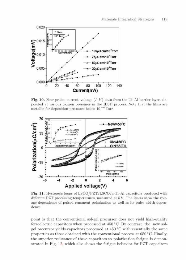
Materials Integration Strategies 119
Fig. 10. Four-probe, current–voltage (I–V ) data from the Ti–Al barrier layers de-posited at various oxygen pressures in the IBSD process. Note that the films aremetallic for deposition pressures below 10 −6 Torr
Fig. 11. Hysteresis loops of LSCO/PZT/LSCO/a-Ti–Al capacitors produced withdifferent PZT processing temperatures, measured at 5V. The insets show the volt-age dependence of pulsed remanent polarization as well as its pulse width depen-dence
point is that the conventional sol-gel precursor does not yield high-qualityferroelectric capacitors when processed at 450 C. By contrast, the new sol-gel precursor yields capacitors processed at 450 C with essentially the sameproperties as those obtained with the conventional process at 650 C. Finally,the superior resistance of these capacitors to polarization fatigue is demon-strated in Fig. 12, which also shows the fatigue behavior for PZT capacitors
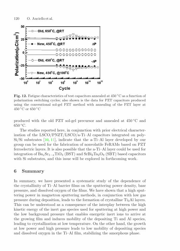
120 O. Auciello et al.
Fig. 12. Fatigue characteristics of test capacitors annealed at 450 C as a function ofpolarization switching cycles; also shown is the data for PZT capacitors producedusing the conventional sol-gel PZT method with annealing of the PZT layer at450 C or 650 C
produced with the old PZT sol-gel precursor and annealed at 450 C and650 C.
The studies reported here, in conjunction with prior electrical character-ization of the LSCO/PNZT/LSCO/a-Ti–Al capacitors integrated on poly-Si/Si substrates [10, 11], indicate that the a-Ti–Al layer developed by ourgroup can be used for the fabrication of nonvolatile FeRAMs based on PZTferroelectric layers. It is also possible that the a-Ti–Al layer could be used forintegration of BaxSr1−xTiO3 (BST) and SrBi2Ta2O9 (SBT) based capacitorswith Si substrates, and this issue will be explored in forthcoming work.
6 Summary
In summary, we have presented a systematic study of the dependence ofthe crystallinity of Ti–Al barrier films on the sputtering power density, basepressure, and dissolved oxygen of the films. We have shown that a high sput-tering power in magnetron sputtering methods, in conjunction with low gaspressure during deposition, leads to the formation of crystalline Ti3Al layers.This can be understood as a consequence of the interplay between the highkinetic energy of the inert gas species used for sputtering at high power andthe low background pressure that enables energetic inert ions to arrive atthe growing film and induces mobility of the depositing Ti and Al species,leading to crystallization at low temperature. On the other hand, the growthat low power and high pressure leads to low mobility of depositing speciesand dissolved oxygen in the Ti–Al film, stabilizing the amorphous phase.
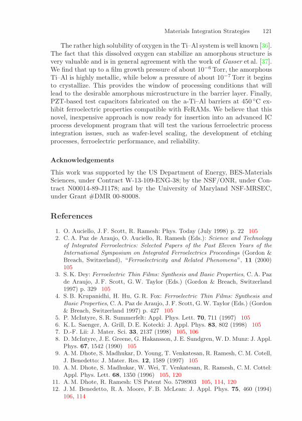
Materials Integration Strategies 121
The rather high solubility of oxygen in the Ti–Al system is well known [36].The fact that this dissolved oxygen can stabilize an amorphous structure isvery valuable and is in general agreement with the work of Gasser et al. [37].We find that up to a film growth pressure of about 10−6 Torr, the amorphousTi–Al is highly metallic, while below a pressure of about 10−7 Torr it beginsto crystallize. This provides the window of processing conditions that willlead to the desirable amorphous microstructure in the barrier layer. Finally,PZT-based test capacitors fabricated on the a-Ti–Al barriers at 450 C ex-hibit ferroelectric properties compatible with FeRAMs. We believe that thisnovel, inexpensive approach is now ready for insertion into an advanced ICprocess development program that will test the various ferroelectric processintegration issues, such as wafer-level scaling, the development of etchingprocesses, ferroelectric performance, and reliability.
Acknowledgements
This work was supported by the US Department of Energy, BES-MaterialsSciences, under Contract W-13-109-ENG-38; by the NSF/ONR, under Con-tract N00014-89-J1178; and by the University of Maryland NSF-MRSEC,under Grant #DMR 00-80008.
References
1. O. Auciello, J. F. Scott, R. Ramesh: Phys. Today (July 1998) p. 22 1052. C. A. Paz de Araujo, O. Auciello, R. Ramesh (Eds.): Science and Technology
of Integrated Ferroelectrics: Selected Papers of the Past Eleven Years of theInternational Symposium on Integrated Ferroelectrics Proceedings (Gordon &Breach, Switzerland), “Ferroelectricity and Related Phenomena”, 11 (2000)105
3. S.K. Dey: Ferroelectric Thin Films: Synthesis and Basic Properties, C. A. Pazde Araujo, J. F. Scott, G. W. Taylor (Eds.) (Gordon & Breach, Switzerland1997) p. 329 105
4. S. B. Krupanidhi, H. Hu, G.R. Fox: Ferroelectric Thin Films: Synthesis andBasic Properties, C. A. Paz de Araujo, J. F. Scott, G. W. Taylor (Eds.) (Gordon& Breach, Switzerland 1997) p. 427 105
5. P. McIntyre, S.R. Summerfelt: Appl. Phys. Lett. 70, 711 (1997) 1056. K. L. Saenger, A. Grill, D. E. Kotecki: J. Appl. Phys. 83, 802 (1998) 1057. D.-F. Lii: J. Mater. Sci. 33, 2137 (1998) 105, 1068. D. McIntyre, J. E. Greene, G. Hakansson, J. E. Sundgren, W.D. Munz: J. Appl.
Phys. 67, 1542 (1990) 1059. A.M. Dhote, S. Madhukar, D. Young, T. Venkatesan, R. Ramesh, C. M. Cotell,
J. Benedetto: J. Mater. Res. 12, 1589 (1997) 10510. A.M. Dhote, S. Madhukar, W. Wei, T. Venkatesan, R. Ramesh, C.M. Cottel:
Appl. Phys. Lett. 68, 1350 (1996) 105, 12011. A.M. Dhote, R. Ramesh: US Patent No. 5798903 105, 114, 12012. J. M. Benedetto, R.A. Moore, F.B. McLean: J. Appl. Phys. 75, 460 (1994)
106, 114
122 O. Auciello et al.
13. J. J. Lee, C. L. Thio, S. B. Desu: Phys. Status Solidi (a) 151, 171 (1995) 106,116
14. J. O. Olowolafe, R. E. Jones, Jr., A.C. Campbell, R. I. Hegde, C. J. Mogab,R.B. Gregory: J. Appl. Phys. 73, 1764 (1993) 106, 118
15. H.N. Al-Shareef, A. I. Kingon: Ferroelectric Thin Films: Synthesis and BasicProperties, C. A. Paz de Araujo, J. F. Scott, G.W. Taylor (Eds.) (Gordon &Breach, Switzerland 1997) p. 193 106, 118
16. S. Aggarwal, B. Yang, R. Ramesh: Thin Film Ferroelectric Materials and De-vices, R. Ramesh (Ed.) (Kluwer, Dordrecht 1998) p. 221 106
17. C. A. Paz de Araujo, J. D. Cuchlaro, L.D. McMillan, M. C. Scott, J. F. Scott:Nature 374, 627 (1995) 106
18. M. Wittmer, J. Noser, H. Melchoir: J. Appl. Phys. 52, 6659 (1981) 10619. H.G. Tompkins: J. Appl. Phys. 71, 980 (1992) 10620. P. McIntyre, S.R. Summerfelt: J. Appl. Phys. 82, 4577 (1997) 10621. K. L. Saenger, A. Grill, D. E. Kotecki: J. Appl. Phys. 83, 802 (1998) 10622. K. L. Saenger, A. Grill, C. Cabral, Jr.: J. Mater. Res. 13, 462 (1998) 10623. S. Madhukar, S. Aggarwal, A.M. Dhote, R. Ramesh, S. B. Samavedam,
S. Choopun, R.P. Sharma: J. Mater. Res. 14, 940 (1999) 10624. H.D. Bhatt, S. B. Desu, D.P. Vijay, Y. S. Hwang, X. Zhang, M. Nagata,
A. Grill: Appl. Phys. Lett. 71, 719 (1997) 10625. S. Veprek, S. Reiprich, S.H. Li: Appl. Phys. Lett. 66, 2640 (1995) 10726. X. Sun, J. S. Reid, E. Kolawa, M.-A. Nicolet: J. Appl. Phys. 81, 664 (1997)
10727. A. L. Greer: Intermetallic Compounds, vol. 1, J. H. Westbrook, R. L. Fleischer
(Eds.) (Wiley, New York 1995) p. 371 10728. S.M. Gasser, E. Kolawa, M.-A. Nicolet: J. Appl. Phys. 86, 1974 (1999) 10729. S. Aggarwal, B. Nagaraj, H. Li, R. P. Sharma, L. Salamanca-Riba, R. Ramesh,
A.M. Dhote, A.R. Krauss, O. Auciello: Acta Mater. 48, 3387 (2000) 107,108, 114, 118
30. S. Aggarwal, A.M. Dhote, H. Li, S. Ankem, R. Ramesh: Appl. Phys. Lett. 74,230 (1999) 107, 108
31. A.M. Dhote, O. Auciello, D.M. Gruen, R. Ramesh: Appl. Phys. Lett. 79, 800(2001) 108, 114
32. O. Auciello, A.R. Krauss, J. Im, J. A. Schultz: Ann. Rev. Mater. Sci. 28, 375(1998) 108, 109, 113
33. A.R. Krauss, O. Auciello, A.M. Dhote, J. Im, E.A. Irene, Y. Gao,A.H. Mueller, S. Aggarwal, R. Ramesh: Integr. Ferroelectr. 32, 121 (2001)109, 111, 112
34. S. Aggarwal, A.M. Dhote, H. Li, S. Ankem, R. Ramesh: Appl. Phys. Lett. 74,230 (1999) 109
35. N. Soyama, K. Maki, S. Mori, K. Ogi: Jpn. J. Appl. Phys. 39, 5434 (2000)118
36. M. X. Zhang, K.C. Hsieh, J. DeKock, Y.A. Chang: Scr. Metal. Mater. 27,1361 (1992) 121
37. S.M. Gasser, E. Kolawa, M.-A. Nicolet: J. Appl. Phys. 86, 1974 (1999) 121
Index
diffusion barrier layer, 106DO19 hexagonal structure, 114
electrode, 105Energy electron loss spectroscopy
(EELS), 114
hysteresis– loop, 118
IBSD, 108ion beam sputter, 108
La0.5Sr0.5CoO3 (LSCO), 108LSCO, 118
magnetron sputtering, 108materials integration, 105MSRI, 115
neutralization process, 117
oxidation process, 113
plug, 105PNZT, 108PZT, 108
Rutherford backscattering spectrome-try (RBS), 110
sol-gel, 108
TEM, 109Ti3Al, 109Ti–Al– microstructure, 107TiO2, 117
XPS, 108, 110XRD, 109
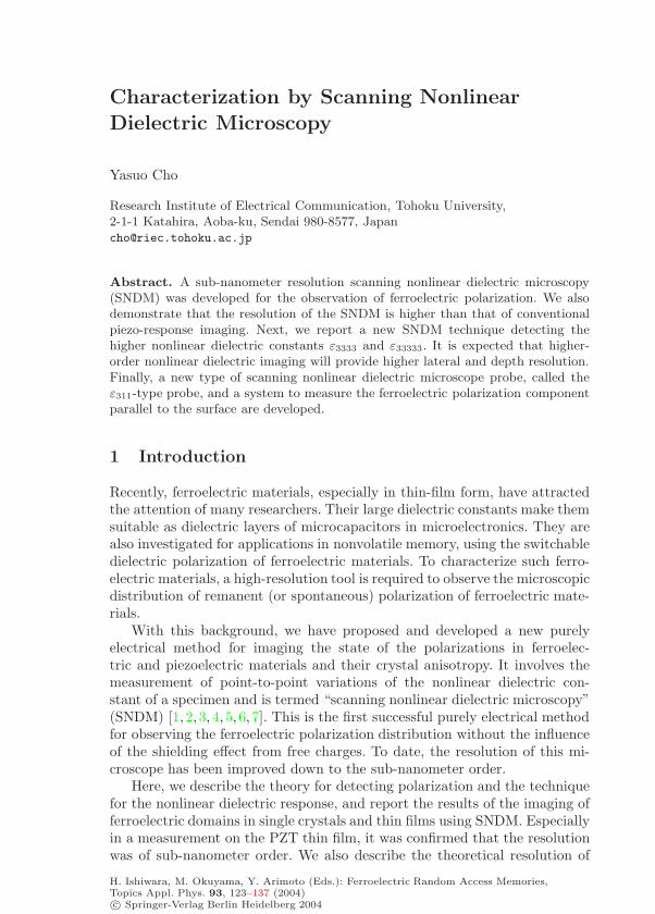
Characterization by Scanning Nonlinear
Dielectric Microscopy
Yasuo Cho
Research Institute of Electrical Communication, Tohoku University,2-1-1 Katahira, Aoba-ku, Sendai 980-8577, [email protected]
Abstract. A sub-nanometer resolution scanning nonlinear dielectric microscopy(SNDM) was developed for the observation of ferroelectric polarization. We alsodemonstrate that the resolution of the SNDM is higher than that of conventionalpiezo-response imaging. Next, we report a new SNDM technique detecting thehigher nonlinear dielectric constants ε3333 and ε33333. It is expected that higher-order nonlinear dielectric imaging will provide higher lateral and depth resolution.Finally, a new type of scanning nonlinear dielectric microscope probe, called theε311-type probe, and a system to measure the ferroelectric polarization componentparallel to the surface are developed.
1 Introduction
Recently, ferroelectric materials, especially in thin-film form, have attractedthe attention of many researchers. Their large dielectric constants make themsuitable as dielectric layers of microcapacitors in microelectronics. They arealso investigated for applications in nonvolatile memory, using the switchabledielectric polarization of ferroelectric materials. To characterize such ferro-electric materials, a high-resolution tool is required to observe the microscopicdistribution of remanent (or spontaneous) polarization of ferroelectric mate-rials.
With this background, we have proposed and developed a new purelyelectrical method for imaging the state of the polarizations in ferroelec-tric and piezoelectric materials and their crystal anisotropy. It involves themeasurement of point-to-point variations of the nonlinear dielectric con-stant of a specimen and is termed “scanning nonlinear dielectric microscopy”(SNDM) [1, 2, 3, 4, 5, 6, 7]. This is the first successful purely electrical methodfor observing the ferroelectric polarization distribution without the influenceof the shielding effect from free charges. To date, the resolution of this mi-croscope has been improved down to the sub-nanometer order.
Here, we describe the theory for detecting polarization and the techniquefor the nonlinear dielectric response, and report the results of the imaging offerroelectric domains in single crystals and thin films using SNDM. Especiallyin a measurement on the PZT thin film, it was confirmed that the resolutionwas of sub-nanometer order. We also describe the theoretical resolution of
H. Ishiwara, M. Okuyama, Y. Arimoto (Eds.): Ferroelectric Random Access Memories,Topics Appl. Phys. 93, 123–137 (2004)c© Springer-Verlag Berlin Heidelberg 2004
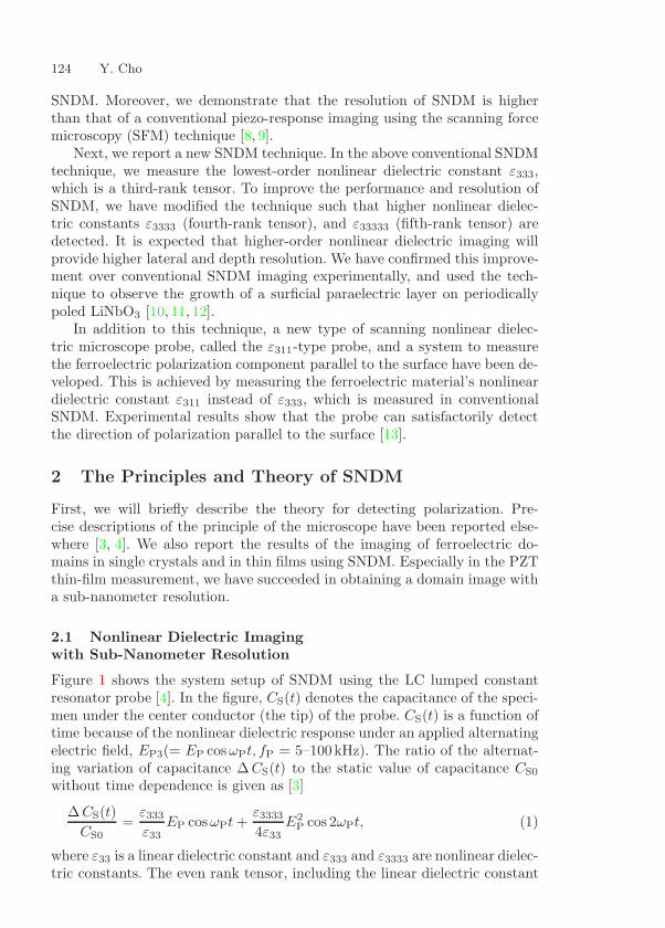
124 Y. Cho
SNDM. Moreover, we demonstrate that the resolution of SNDM is higherthan that of a conventional piezo-response imaging using the scanning forcemicroscopy (SFM) technique [8, 9].
Next, we report a new SNDM technique. In the above conventional SNDMtechnique, we measure the lowest-order nonlinear dielectric constant ε333,which is a third-rank tensor. To improve the performance and resolution ofSNDM, we have modified the technique such that higher nonlinear dielec-tric constants ε3333 (fourth-rank tensor), and ε33333 (fifth-rank tensor) aredetected. It is expected that higher-order nonlinear dielectric imaging willprovide higher lateral and depth resolution. We have confirmed this improve-ment over conventional SNDM imaging experimentally, and used the tech-nique to observe the growth of a surficial paraelectric layer on periodicallypoled LiNbO3 [10, 11, 12].
In addition to this technique, a new type of scanning nonlinear dielec-tric microscope probe, called the ε311-type probe, and a system to measurethe ferroelectric polarization component parallel to the surface have been de-veloped. This is achieved by measuring the ferroelectric material’s nonlineardielectric constant ε311 instead of ε333, which is measured in conventionalSNDM. Experimental results show that the probe can satisfactorily detectthe direction of polarization parallel to the surface [13].
2 The Principles and Theory of SNDM
First, we will briefly describe the theory for detecting polarization. Pre-cise descriptions of the principle of the microscope have been reported else-where [3, 4]. We also report the results of the imaging of ferroelectric do-mains in single crystals and in thin films using SNDM. Especially in the PZTthin-film measurement, we have succeeded in obtaining a domain image witha sub-nanometer resolution.
2.1 Nonlinear Dielectric Imagingwith Sub-Nanometer Resolution
Figure 1 shows the system setup of SNDM using the LC lumped constantresonator probe [4]. In the figure, CS(t) denotes the capacitance of the speci-men under the center conductor (the tip) of the probe. CS(t) is a function oftime because of the nonlinear dielectric response under an applied alternatingelectric field, EP3(= EP cosωPt, fP = 5–100kHz). The ratio of the alternat-ing variation of capacitance ∆CS(t) to the static value of capacitance CS0
without time dependence is given as [3]
∆ CS(t)CS0
=ε333
ε33EP cosωPt +
ε3333
4ε33E2
P cos 2ωPt, (1)
where ε33 is a linear dielectric constant and ε333 and ε3333 are nonlinear dielec-tric constants. The even rank tensor, including the linear dielectric constant
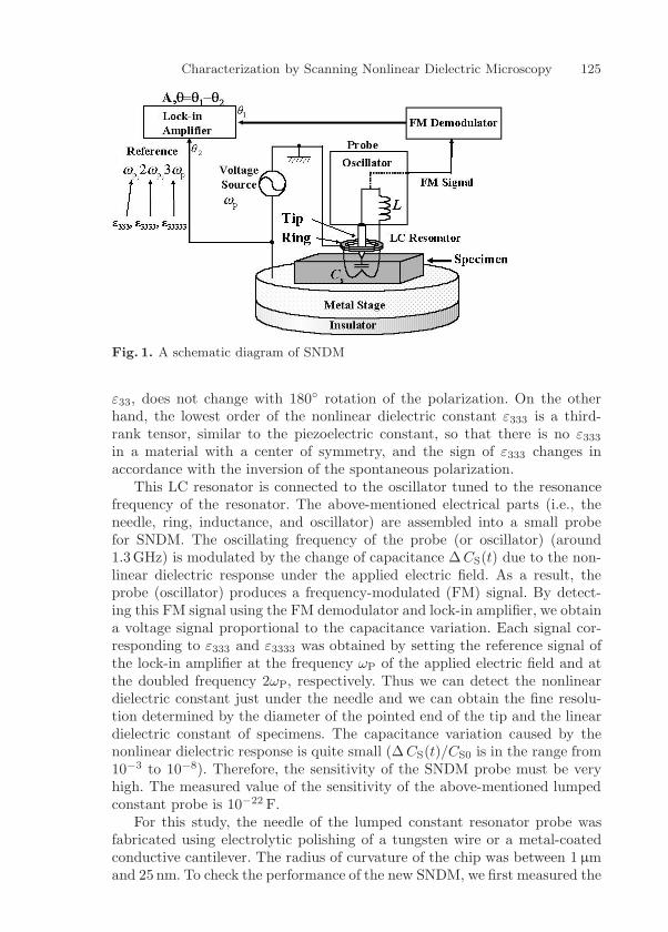
Characterization by Scanning Nonlinear Dielectric Microscopy 125
Fig. 1. A schematic diagram of SNDM
ε33, does not change with 180 rotation of the polarization. On the otherhand, the lowest order of the nonlinear dielectric constant ε333 is a third-rank tensor, similar to the piezoelectric constant, so that there is no ε333
in a material with a center of symmetry, and the sign of ε333 changes inaccordance with the inversion of the spontaneous polarization.
This LC resonator is connected to the oscillator tuned to the resonancefrequency of the resonator. The above-mentioned electrical parts (i.e., theneedle, ring, inductance, and oscillator) are assembled into a small probefor SNDM. The oscillating frequency of the probe (or oscillator) (around1.3GHz) is modulated by the change of capacitance ∆ CS(t) due to the non-linear dielectric response under the applied electric field. As a result, theprobe (oscillator) produces a frequency-modulated (FM) signal. By detect-ing this FM signal using the FM demodulator and lock-in amplifier, we obtaina voltage signal proportional to the capacitance variation. Each signal cor-responding to ε333 and ε3333 was obtained by setting the reference signal ofthe lock-in amplifier at the frequency ωP of the applied electric field and atthe doubled frequency 2ωP, respectively. Thus we can detect the nonlineardielectric constant just under the needle and we can obtain the fine resolu-tion determined by the diameter of the pointed end of the tip and the lineardielectric constant of specimens. The capacitance variation caused by thenonlinear dielectric response is quite small (∆ CS(t)/CS0 is in the range from10−3 to 10−8). Therefore, the sensitivity of the SNDM probe must be veryhigh. The measured value of the sensitivity of the above-mentioned lumpedconstant probe is 10−22 F.
For this study, the needle of the lumped constant resonator probe wasfabricated using electrolytic polishing of a tungsten wire or a metal-coatedconductive cantilever. The radius of curvature of the chip was between 1 µmand 25 nm. To check the performance of the new SNDM, we first measured the
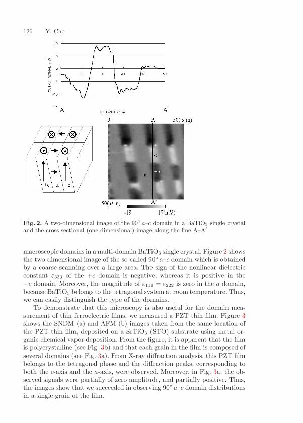
126 Y. Cho
Fig. 2. A two-dimensional image of the 90 a–c domain in a BaTiO3 single crystaland the cross-sectional (one-dimensional) image along the line A–A′
macroscopic domains in a multi-domain BaTiO3 single crystal. Figure 2 showsthe two-dimensional image of the so-called 90 a–c domain which is obtainedby a coarse scanning over a large area. The sign of the nonlinear dielectricconstant ε333 of the +c domain is negative, whereas it is positive in the−c domain. Moreover, the magnitude of ε111 = ε222 is zero in the a domain,because BaTiO3 belongs to the tetragonal system at room temperature. Thus,we can easily distinguish the type of the domains.
To demonstrate that this microscopy is also useful for the domain mea-surement of thin ferroelectric films, we measured a PZT thin film. Figure 3shows the SNDM (a) and AFM (b) images taken from the same location ofthe PZT thin film, deposited on a SrTiO3 (STO) substrate using metal or-ganic chemical vapor deposition. From the figure, it is apparent that the filmis polycrystalline (see Fig. 3b) and that each grain in the film is composed ofseveral domains (see Fig. 3a). From X-ray diffraction analysis, this PZT filmbelongs to the tetragonal phase and the diffraction peaks, corresponding toboth the c-axis and the a-axis, were observed. Moreover, in Fig. 3a, the ob-served signals were partially of zero amplitude, and partially positive. Thus,the images show that we succeeded in observing 90 a–c domain distributionsin a single grain of the film.

Characterization by Scanning Nonlinear Dielectric Microscopy 127
Fig. 3. Images of a PZT film on a SrTiO3 substrate: (a) domain patterns by SNDM;(b) surface morphology by AFM
Fig. 4. The nanoscale ferroelectric domain on the PZT thin film. (a) The domainimage of the nanoscale 180 c–c domain; (b) the cross-sectional (one-dimensional)image of the phase signal along the line A–A′
These images of the film were taken from a relatively large area. Therefore,we also tried to observe very small domains in the same PZT film on STOsubstrate. The results are shown in Fig. 4a and b. The bright and dark areascorrespond to negative polarization and positive polarization, respectively.This shows that we can successfully observe a nanoscale 180 c–c domainstructure. Figure 4b shows a cross-sectional image taken along line A–A′ inFig. 4a. As shown in this figure, we measured the c–c domain with a widthof 1.5 nm. Moreover, we found that the resolution of the microscope is lessthan 0.5 nm.
To clarify the reason why such a high resolution can be easily obtained,even if a relatively thick needle is used for the probe, we show the calculatedresults of the one-dimensional image of the 180 c–c domain boundary lyingat y = 0 (we chose y direction as the scanning direction) [14, 15]. Figure 5shows the calculated results, where Y0 is the tip position normalized withrespect to the tip radius a. The resolution of the SNDM image is heavilydependent on the dielectric constant of the specimen. For example, for the
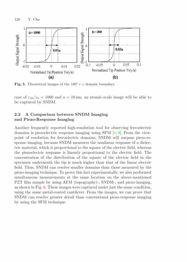
128 Y. Cho
Fig. 5. Theoretical images of the 180 c–c domain boundary
case of ε33/ε0 = 1000 and a = 10 nm, an atomic-scale image will be able tobe captured by SNDM.
2.2 A Comparison between SNDM Imagingand Piezo-Response Imaging
Another frequently reported high-resolution tool for observing ferroelectricdomains is piezoelectric response imaging using SFM [8, 9]. From the view-point of resolution for ferroelectric domains, SNDM will surpass piezo-re-sponse imaging, because SNDM measures the nonlinear response of a dielec-tric material, which is proportional to the square of the electric field, whereasthe piezoelectric response is linearly proportional to the electric field. Theconcentration of the distribution of the square of the electric field in thespecimen underneath the tip is much higher than that of the linear electricfield. Thus, SNDM can resolve smaller domains than those measured by thepiezo-imaging technique. To prove this fact experimentally, we also performedsimultaneous measurements at the same location on the above-mentionedPZT film sample by using AFM (topography)-, SNDM-, and piezo-imaging,as shown in Fig. 6. These images were captured under just the same condition,using the same metal-coated cantilever. From the images, we can prove thatSNDM can resolve greater detail than conventional piezo-response imagingby using the SFM technique.

Characterization by Scanning Nonlinear Dielectric Microscopy 129
Fig. 6. Simultaneously captured images of a PZT film. (a) Topography by AFM;(b) domain patterns by SNDM; (c) domain patterns by SFM (piezo-imaging)
3 Higher-Order Nonlinear Dielectric Microscopy
A higher-order nonlinear dielectric microscopy technique with higher lateraland depth resolution than conventional nonlinear dielectric imaging is inves-tigated. The technique is demonstrated to be very useful for observing surfacelayers of the order of unit cell thickness on ferroelectric materials.
3.1 The Theory of Higher-Order NonlinearDielectric Microscopy
Equation (2) is a polynomial expansion of the electric displacement D3 asa function of electric field E3
D3 = Ps3 + ε33E3 +12ε333E
23 +
16ε3333E
33 +
124
ε33333E43 + · · · . (2)
Here, ε33, ε333, ε3333, and ε33333 correspond to linear and nonlinear dielectricconstants and are tensors of second, third, fourth, and fifth rank, respectively.Even-ranked tensors including the linear dielectric constant ε33 do not changewith polarization inversion, whereas the sign of the odd-ranked tensors re-verses. Therefore, information regarding polarization can be elucidated bymeasuring odd-ranked nonlinear dielectric constants such as ε333 and ε33333.
Considering the effect up to E4, the ratio of the alternating variation ofcapacitance ∆ CS underneath the tip to the static capacitance CS0 is givenby
∆ CS(t)CS0
≈ ε333
ε33EP cosωPt +
14
ε3333
ε33E2
P cos 2ωPt
+124
ε33333
ε33E3
P cos 3ωPt + · · · . (3)
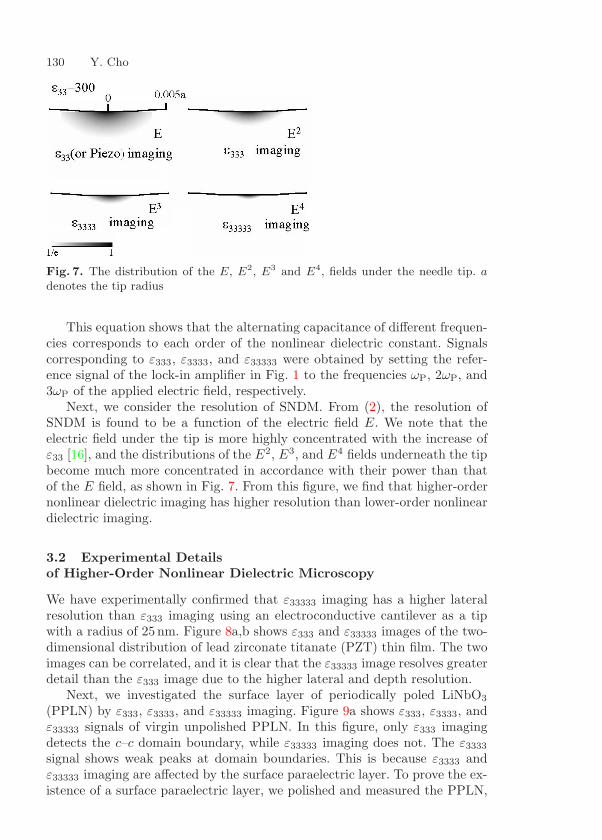
130 Y. Cho
Fig. 7. The distribution of the E, E2, E3 and E4, fields under the needle tip. adenotes the tip radius
This equation shows that the alternating capacitance of different frequen-cies corresponds to each order of the nonlinear dielectric constant. Signalscorresponding to ε333, ε3333, and ε33333 were obtained by setting the refer-ence signal of the lock-in amplifier in Fig. 1 to the frequencies ωP, 2ωP, and3ωP of the applied electric field, respectively.
Next, we consider the resolution of SNDM. From (2), the resolution ofSNDM is found to be a function of the electric field E. We note that theelectric field under the tip is more highly concentrated with the increase ofε33 [16], and the distributions of the E2, E3, and E4 fields underneath the tipbecome much more concentrated in accordance with their power than thatof the E field, as shown in Fig. 7. From this figure, we find that higher-ordernonlinear dielectric imaging has higher resolution than lower-order nonlineardielectric imaging.
3.2 Experimental Detailsof Higher-Order Nonlinear Dielectric Microscopy
We have experimentally confirmed that ε33333 imaging has a higher lateralresolution than ε333 imaging using an electroconductive cantilever as a tipwith a radius of 25 nm. Figure 8a,b shows ε333 and ε33333 images of the two-dimensional distribution of lead zirconate titanate (PZT) thin film. The twoimages can be correlated, and it is clear that the ε33333 image resolves greaterdetail than the ε333 image due to the higher lateral and depth resolution.
Next, we investigated the surface layer of periodically poled LiNbO3
(PPLN) by ε333, ε3333, and ε33333 imaging. Figure 9a shows ε333, ε3333, andε33333 signals of virgin unpolished PPLN. In this figure, only ε333 imagingdetects the c–c domain boundary, while ε33333 imaging does not. The ε3333
signal shows weak peaks at domain boundaries. This is because ε3333 andε33333 imaging are affected by the surface paraelectric layer. To prove the ex-istence of a surface paraelectric layer, we polished and measured the PPLN,
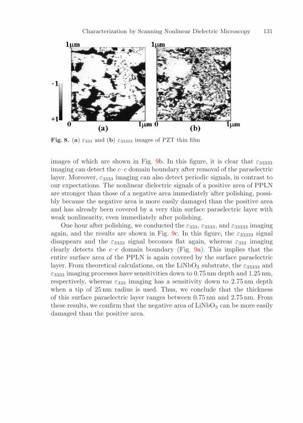
Characterization by Scanning Nonlinear Dielectric Microscopy 131
Fig. 8. (a) ε333 and (b) ε33333 images of PZT thin film
images of which are shown in Fig. 9b. In this figure, it is clear that ε33333
imaging can detect the c–c domain boundary after removal of the paraelectriclayer. Moreover, ε3333 imaging can also detect periodic signals, in contrast toour expectations. The nonlinear dielectric signals of a positive area of PPLNare stronger than those of a negative area immediately after polishing, possi-bly because the negative area is more easily damaged than the positive areaand has already been covered by a very thin surface paraelectric layer withweak nonlinearity, even immediately after polishing.
One hour after polishing, we conducted the ε333, ε3333, and ε33333 imagingagain, and the results are shown in Fig. 9c. In this figure, the ε33333 signaldisappears and the ε3333 signal becomes flat again, whereas ε333 imagingclearly detects the c–c domain boundary (Fig. 9a). This implies that theentire surface area of the PPLN is again covered by the surface paraelectriclayer. From theoretical calculations, on the LiNbO3 substrate, the ε33333 andε3333 imaging processes have sensitivities down to 0.75 nm depth and 1.25nm,respectively, whereas ε333 imaging has a sensitivity down to 2.75nm depthwhen a tip of 25 nm radius is used. Thus, we conclude that the thicknessof this surface paraelectric layer ranges between 0.75 nm and 2.75 nm. Fromthese results, we confirm that the negative area of LiNbO3 can be more easilydamaged than the positive area.
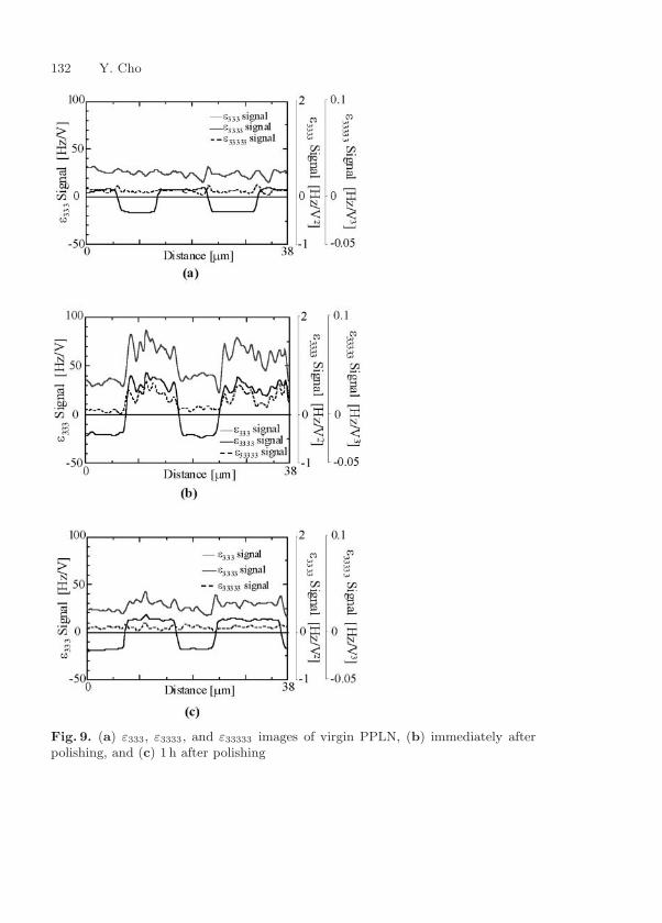
132 Y. Cho
Fig. 9. (a) ε333, ε3333, and ε33333 images of virgin PPLN, (b) immediately afterpolishing, and (c) 1 h after polishing
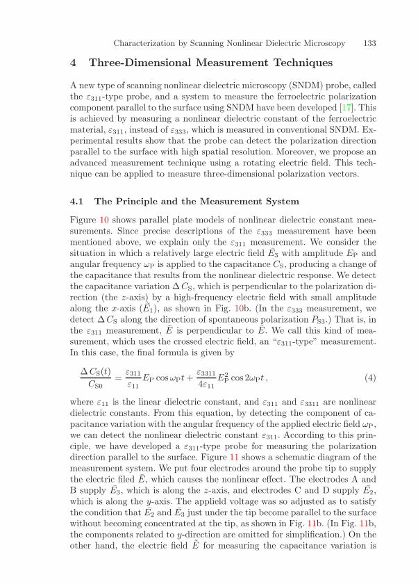
Characterization by Scanning Nonlinear Dielectric Microscopy 133
4 Three-Dimensional Measurement Techniques
A new type of scanning nonlinear dielectric microscopy (SNDM) probe, calledthe ε311-type probe, and a system to measure the ferroelectric polarizationcomponent parallel to the surface using SNDM have been developed [17]. Thisis achieved by measuring a nonlinear dielectric constant of the ferroelectricmaterial, ε311, instead of ε333, which is measured in conventional SNDM. Ex-perimental results show that the probe can detect the polarization directionparallel to the surface with high spatial resolution. Moreover, we propose anadvanced measurement technique using a rotating electric field. This tech-nique can be applied to measure three-dimensional polarization vectors.
4.1 The Principle and the Measurement System
Figure 10 shows parallel plate models of nonlinear dielectric constant mea-surements. Since precise descriptions of the ε333 measurement have beenmentioned above, we explain only the ε311 measurement. We consider thesituation in which a relatively large electric field E3 with amplitude EP andangular frequency ωP is applied to the capacitance CS, producing a change ofthe capacitance that results from the nonlinear dielectric response. We detectthe capacitance variation ∆CS, which is perpendicular to the polarization di-rection (the z-axis) by a high-frequency electric field with small amplitudealong the x-axis (E1), as shown in Fig. 10b. (In the ε333 measurement, wedetect ∆CS along the direction of spontaneous polarization PS3.) That is, inthe ε311 measurement, E is perpendicular to E. We call this kind of mea-surement, which uses the crossed electric field, an “ε311-type” measurement.In this case, the final formula is given by
∆ CS(t)CS0
=ε311
ε11EP cosωPt +
ε3311
4ε11E2
P cos 2ωPt , (4)
where ε11 is the linear dielectric constant, and ε311 and ε3311 are nonlineardielectric constants. From this equation, by detecting the component of ca-pacitance variation with the angular frequency of the applied electric field ωP,we can detect the nonlinear dielectric constant ε311. According to this prin-ciple, we have developed a ε311-type probe for measuring the polarizationdirection parallel to the surface. Figure 11 shows a schematic diagram of themeasurement system. We put four electrodes around the probe tip to supplythe electric filed E, which causes the nonlinear effect. The electrodes A andB supply E3, which is along the z-axis, and electrodes C and D supply E2,which is along the y-axis. The applield voltage was so adjusted as to satisfythe condition that E2 and E3 just under the tip become parallel to the surfacewithout becoming concentrated at the tip, as shown in Fig. 11b. (In Fig. 11b,the components related to y-direction are omitted for simplification.) On theother hand, the electric field E for measuring the capacitance variation is
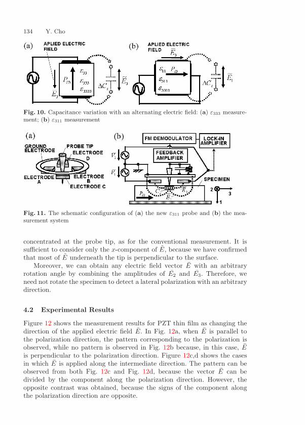
134 Y. Cho
Fig. 10. Capacitance variation with an alternating electric field: (a) ε333 measure-ment; (b) ε311 measurement
Fig. 11. The schematic configuration of (a) the new ε311 probe and (b) the mea-surement system
concentrated at the probe tip, as for the conventional measurement. It issufficient to consider only the x-component of E, because we have confirmedthat most of E underneath the tip is perpendicular to the surface.
Moreover, we can obtain any electric field vector E with an arbitraryrotation angle by combining the amplitudes of E2 and E3. Therefore, weneed not rotate the specimen to detect a lateral polarization with an arbitrarydirection.
4.2 Experimental Results
Figure 12 shows the measurement results for PZT thin film as changing thedirection of the applied electric field E. In Fig. 12a, when E is parallel tothe polarization direction, the pattern corresponding to the polarization isobserved, while no pattern is observed in Fig. 12b because, in this case, Eis perpendicular to the polarization direction. Figure 12c,d shows the casesin which E is applied along the intermediate direction. The pattern can beobserved from both Fig. 12c and Fig. 12d, because the vector E can bedivided by the component along the polarization direction. However, theopposite contrast was obtained, because the signs of the component alongthe polarization direction are opposite.

Characterization by Scanning Nonlinear Dielectric Microscopy 135
Fig. 12. Images of PZT thin film: (a)–(d) ε311 images, (e) a ε333 image, and (f) thetopography
Moreover, the new probe can measure both ε311 and ε333 independently.Figure 12e shows an ε333 image, which corresponds to the perpendicularcomponent of the polarization. From the same position in Fig. 12a, signalsare observed. This means that this polarization has both parallel and per-pendicular components; that is, the polarization tilts away from the surface.Figure 12f is the topography, which is also measured simultaneously. Fromthese results, we have confirmed that the new probe and system can be ap-plied to three-dimensional polarization measurements.
References
1. Y. Cho, A. Kirihara, T. Saeki: Denshi Joho Tsushin Gakkai Ronbunshi J78-C-1, 593 (1995) [in Japanese] 123
2. Y. Cho, A. Kirihara, T. Saeki: Electronics and Communication in Japan,Part 2, Scripta Technica 79, 68 (1996) 123
3. Y. Cho, A. Kirihara, T. Saeki: Rev. Sci. Instrum. 67, 2297 (1996) 123, 1244. Y. Cho, S. Atsumi, K. Nakamura: Jpn. J. Appl. Phys. 36, 3152 (1997) 123,
1245. Y. Cho, S. Kazuta, K. Matsuura: Appl. Phys. Lett. 72, 2833 (1999) 1236. H. Odagawa, Y. Cho: Surf. Sci. 463, L621 (2000) 1237. H. Odagawa, Y. Cho: Jpn. J. Appl. Phys. 39 5719 (2000) 1238. A. Gruverman, O. Auciello, R. Ramesh, H. Tokumoto: Nanotechnol. 8, A38
(1997) 124, 1289. L.M. Eng, H.-J. Gu, G. A. Schneider, U. Kopke, J. Munoz Saldana: Appl.
Phys. Lett. 74, 233 (1999) 124, 12810. Y. Cho, K. Ohara, A. Koike, H. Odagawa: Jpn. J. Appl. Phys. 40, 3544 (2001)
124
136 Y. Cho
11. K. Ohara, Y. Cho: Jpn. J. Appl. Phys 40, 5833 (2001) 12412. Y. Cho, K. Ohara: Appl. Phys. Lett. 79, 3842 (2001) 12413. H. Odagawa, Y. Cho: Ferroelectr. 268, 149 (2002) 12414. Y. Cho, K. Ohara, S. Kazuta, H. Odagawa: J. Eur. Ceram. Soc. 21, 2135
(2001) 12715. H. Odagawa, Y. Cho: Jpn. J. Appl. Phys. 39, 5719 (2000) 12716. K. Matsuura, Y. Cho, H. Odagawa: Jpn. J. Appl. Phys. 40, 3534 (2001) 13017. H. Odagawa, Y. Cho: Appl. Phys. Lett. 80, 2159 (2002) 133
Index
90 A–c domain, 126ε311-type probe, 133
BaTiO3
– single crystal, 126
domain– 180 c–c, 127
higher-order nonlinear dielectricmicroscopy, 129
LC resonator– FM demodulator, 125– lock-in amplifier, 125
nonlinear dielectric constant– ε33333, 124– ε3333, 124
– ε333, 124– LiNbO3, 124
periodically poled LiNbO3 (PPLN),130
polarization, 123PZT, 126
scanning force microscopy (SFM), 124scanning nonlinear dielectric mi-
croscopy (SNDM), 123SrTiO3, 126
tensor– even-ranked ε333, 129– odd-ranked, 129three-dimensional polarization vector,
133
The Current Status of FeRAM
Glen R. Fox, Richard Bailey, William B. Kraus, Fan Chu, Shan Sun,and Tom Davenport
Ramtron International Corporation,1850 Ramtron Drive, Colorado Springs, CO 80921, [email protected]
Abstract. Ferroelectric nonvolatile memories (FeRAM) have been mass-producedsince 1992 and densities up to 256 kb are currently available in a range of products.Both memory density and the market for FeRAM are increasing at an exponentialrate due to the demands for nonvolatility, high read/write endurance, fast accessspeed, and low-power operation. Current applications include smart cards, data col-lection and storage (e.g., power meters), configuration storage, and buffers. FeRAMcell designs utilize a PbZrxTi1−xO3 based bistable ferroelectric capacitor structurethat is integrated with a transistor (1T-1C) or a complementary capacitor andtwo transistors (2T-2C). The small memory cell sizes under development will notonly enable high-density stand-alone memories but also extend the application ofFeRAM, which is already used in embedded and system-on-chip devices. A review offerroelectric materials performance in current memory products will be presented.Recent development has led to capacitor performance with an endurance beyond1012 read/write cycles and operation at 1.8 V. A roadmap for future FeRAM de-velopment will be presented.
1 Introduction
Over the past 15 years, the nonvolatile ferroelectric random access memory(FeRAM) has evolved from a concept on paper to a memory product that isused in a variety of consumer products and industrial applications. FeRAMis a vital component of applications including smart cards, power meters,printers, and video games. The advantage of using FeRAM instead of othertypes of nonvolatile memory, such as EEPROM and battery-backed SRAM,varies according to the application. FeRAM exhibits a unique combinationof performance features, including low power consumption, high read/writeendurance, a fast read/write access time, and long-term retention. Not onlyis FeRAM of interest as a high-performance stand-alone memory, but it alsoprovides a low-cost embedded memory solution that can be scaled to highdensities.
FeRAM was first demonstrated in 1988 using PbZrxTi1−xO3 (PZT) as theferroelectric material for data storage (Fig. 1). The FeRAM cell consisted oftwo transistors and two capacitors, commonly referred to as a 2T-2C cell.The ferroelectric capacitors were added to the underlying CMOS by apply-ing backend ferroelectric, electrode, metallization, and inter-level dielectric
H. Ishiwara, M. Okuyama, Y. Arimoto (Eds.): Ferroelectric Random Access Memories,Topics Appl. Phys. 93, 139–149 (2004)c© Springer-Verlag Berlin Heidelberg 2004
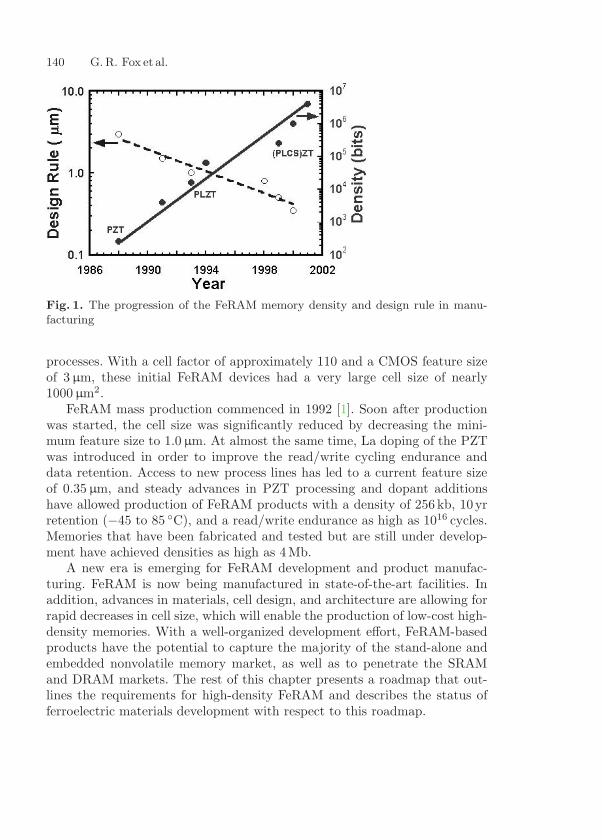
140 G. R. Fox et al.
Fig. 1. The progression of the FeRAM memory density and design rule in manu-facturing
processes. With a cell factor of approximately 110 and a CMOS feature sizeof 3 µm, these initial FeRAM devices had a very large cell size of nearly1000 µm2.
FeRAM mass production commenced in 1992 [1]. Soon after productionwas started, the cell size was significantly reduced by decreasing the mini-mum feature size to 1.0 µm. At almost the same time, La doping of the PZTwas introduced in order to improve the read/write cycling endurance anddata retention. Access to new process lines has led to a current feature sizeof 0.35 µm, and steady advances in PZT processing and dopant additionshave allowed production of FeRAM products with a density of 256 kb, 10 yrretention (−45 to 85 C), and a read/write endurance as high as 1016 cycles.Memories that have been fabricated and tested but are still under develop-ment have achieved densities as high as 4Mb.
A new era is emerging for FeRAM development and product manufac-turing. FeRAM is now being manufactured in state-of-the-art facilities. Inaddition, advances in materials, cell design, and architecture are allowing forrapid decreases in cell size, which will enable the production of low-cost high-density memories. With a well-organized development effort, FeRAM-basedproducts have the potential to capture the majority of the stand-alone andembedded nonvolatile memory market, as well as to penetrate the SRAMand DRAM markets. The rest of this chapter presents a roadmap that out-lines the requirements for high-density FeRAM and describes the status offerroelectric materials development with respect to this roadmap.
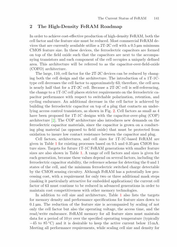
The Current Status of FeRAM 141
2 The High-Density FeRAM Roadmap
In order to achieve cost-effective production of high-density FeRAM, both thecell factor and the feature size must be reduced. Most commercial FeRAM de-vices that are currently available utilize a 2T-2C cell with a 0.5 µm minimumCMOS feature size. In these devices, the ferroelectric capacitors are formedon top of the field oxide such that the capacitors are next to the accompa-nying transistors and each component of the cell occupies a uniquely definedarea. This architecture will be referred to as the capacitor-over-field-oxide(COFO) architecture.
The large, 110, cell factor for the 2T-2C devices can be reduced by chang-ing both the cell design and the architecture. The introduction of a 1T-1C-type cell decreases the cell factor to approximately 63; therefore, the cell areais nearly half that for a 2T-2C cell. Because a 2T-2C cell is self-referencing,the change to a 1T-1C cell places stricter requirements on the ferroelectric ca-pacitor performance with respect to switchable polarization, retention, andcycling endurance. An additional decrease in the cell factor is achieved bybuilding the ferroelectric capacitor on top of a plug that contacts an under-lying access control transistors, as shown in Fig. 2. Cell factors as small as 4have been proposed for 1T-1C designs with the capacitor-over-plug (COP)architecture [2]. The COP architecture also introduces new demands on theferroelectric capacitor materials, since the capacitor is grown on a conduct-ing plug material (as opposed to field oxide) that must be protected fromoxidation to insure low contact resistance between the capacitor and plug.
Cell factors, architectures, and cell sizes for 1T-1C-based FeRAM aregiven in Table 1 for existing processes based on 0.5 and 0.35 µm CMOS fea-ture sizes. Targets for future 1T-1C FeRAM generations with smaller featuresizes are also shown in Table 1. A range of cell factors and sizes is given foreach generation, because these values depend on several factors, including theferroelectric capacitor stability, the reference scheme for detecting the 0 and 1states of the cell, and the minimum ferroelectric switched charge detectableby the CMOS sensing circuitry. Although FeRAM has a potentially low pro-cessing cost, with a requirement for only two or three additional mask steps(making it particularly attractive for embedded applications) the current cellfactor of 63 must continue to be reduced in advanced generations in order tomaintain cost competitiveness with other memory technologies.
In addition to cell size and architecture, Table 1 also lists the targetsfor memory density and performance specifications for feature sizes down to0.1 µm. The reduction of the feature size is accompanied by scaling of notonly the cell factor but also the operating voltage, the access time, and theread/write endurance. FeRAM memory for all feature sizes must maintaindata for a period of 10yr over the specified operating temperature (typically−45 to 85 C) and it is desirable to keep the active current below 15mA.Meeting all performance requirements, while scaling cell size and density for
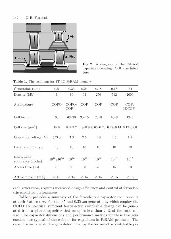
142 G. R. Fox et al.
Fig. 2. A diagram of the FeRAMcapacitor-over-plug (COP) architec-ture
Table 1. The roadmap for 1T-1C FeRAM memory
Generation (µm) 0.5 0.35 0.25 0.18 0.13 0.1
Density (Mb) 1 16 64 256 512 2000
Architecture COFO COFO/ COP COP COP COP/COP 3DCOP
Cell factor 63 63–30 30–15 20–8 16–8 12–6
Cell size (µm2) 15.8 8.0–3.7 1.9–0.9 0.65–0.26 0.27–0.14 0.12–0.06
Operating voltage (V) 5/3.3 3.3 2.5 1.8 1.5 1.2
Data retention (yr) 10 10 10 10 10 10
Read/writeendurance (cycles)
1010/1016 1016 1016 1016 1016 1017
Access time (ns) 70 50 30 20 15 10
Active current (mA) < 15 < 15 < 15 < 15 < 15 < 15
each generation, requires increased design efficiency and control of ferroelec-tric capacitor performance.
Table 2 provides a summary of the ferroelectric capacitor requirementsat each feature size. For the 0.5 and 0.35 µm generations, which employ theCOFO architecture, sufficient ferroelectric switchable charge can be gener-ated from a planar capacitor that occupies less than 20% of the total cellsize. The capacitor dimensions and performance metrics for these two gen-erations are typical of those found for capacitors in FeRAM products. Thecapacitor switchable charge is determined by the ferroelectric switchable po-
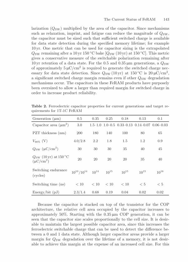
The Current Status of FeRAM 143
larization (QSW) multiplied by the area of the capacitor. Since mechanismssuch as relaxation, imprint, and fatigue can reduce the magnitude of QSW,the capacitor must be sized such that sufficient switched charge is availablefor data state detection during the specified memory lifetime; for example10 yr. One metric that can be used for capacitor sizing is the extrapolatedQSW remaining after a 10 yr 150 C bake [QSW (10 yr) at 150 C]. This metricgives a conservative measure of the switchable polarization remaining after10 yr retention of a data state. For the 0.5 and 0.35 µm generations, a QSW
of approximately 5 µC/cm2 is required to generate the switched charge nec-essary for data state detection. Since QSW (10 yr) at 150 C is 20 µC/cm2,a significant switched charge margin remains even if other QSW degradationmechanisms occur. The capacitors in these FeRAM products have purposelybeen oversized to allow a larger than required margin for switched charge inorder to increase product reliability.
Table 2. Ferroelectric capacitor properties for current generations and target re-quirements for 1T-1C FeRAM
Generation (µm) 0.5 0.35 0.25 0.18 0.13 0.1
Capacitor area (µm2) 3.0 1.5–1.0 1.0–0.5 0.33–0.13 0.14–0.07 0.06–0.03
PZT thickness (nm) 200 180 140 100 80 65
V90% (V) 4.0/2.8 2.2 1.8 1.5 1.2 0.9
QSW (µC/cm2) 30 30 30 35 40 45
QSW (10 yr) at 150 C20 20 20 20 35 40
(µC/cm2)
Switching endurance1010/1014 1014 1015 1015 1015 1016
(cycles)
Switching time (ns) < 10 < 10 < 10 < 10 < 5 < 5
Energy/bit (pJ) 2.3/1.4 0.68 0.19 0.04 0.02 0.02
Because the capacitor is stacked on top of the transistor for the COParchitecture, the relative cell area occupied by the capacitor increases toapproximately 50%. Starting with the 0.35 µm COP generation, it can beseen that the capacitor size scales proportionally to the cell size. It is desir-able to maintain the largest possible capacitor area, since this increases theferroelectric switchable charge that can be used to detect the difference be-tween a 0 and 1 data state. Although larger capacitor areas provide a largermargin for QSW degradation over the lifetime of a memory, it is not desir-able to achieve this margin at the expense of an increased cell size. For this

144 G. R. Fox et al.
reason, it is required that QSW increases for generations with feature sizessmaller than 0.25 µm in order to maintain sufficient switched charge for datastate retention. In addition, less degradation of QSW is allowed for advancedgenerations, as can be seen from the reduced difference between QSW andQSW (10 yr) at 150 C. For the 0.1 µm generation, meeting the QSW scalingrequirement with a planar PZT-based capacitor becomes difficult. A QSW
of at least 45 µC/cm2 is required even with a cell factor of 12. Smaller cellfactors will require even larger QSW values. In order to meet the switchedcharge requirement for an aggressive cell factor of 6 at the 0.1 µm generation,three-dimensional capacitor structures are expected to be required.
Since a high number of switching cycles can degrade the magnitude ofQSW, Table 2 lists the switching endurance; that is, the number of cycles – re-quired without appreciable loss of QSW. For the 0.5 and 0.35 µm generations,some reduction of QSW with cycling is allowable due to the margin affordedby the oversized capacitors. Modeling of reliability test data has confirmedthat 3.3V FeRAM products can achieve 1016 read/write cycle endurance [3].But as the feature size is decreased, less margin in QSW is available andnearly fatigue free films are required for the endurance specification. A ca-pacitor endurance specification of at least 1016 cycles is required for use ina parallel FeRAM to insure a 10 yr lifetime. Taking into account differencesin bit access within a FeRAM memory and the continuous cycling in a ca-pacitor test allows a capacitor with an extrapolated fatigue-free 1015 cyclesto achieve 1016 read/write cycles in a memory. As the memory access timedecreases, a corresponding increase in read/write endurance is required. Atthe 0.1 µm generation, an endurance of 1017 read/write cycles is required forthe memory, which indicates that the capacitor within a bit must have anendurance of at least 1016 cycles.
A PZT thickness reduction is introduced with each generation for two rea-sons. One reason is to maintain a reasonable capacitor height to width aspectratio to minimize difficulties with a single-step capacitor stack etch process.But the primary reason for scaling the PZT thickness is to meet the operat-ing voltage requirements for each generation. In order to insure proper dataretention and data state detection, PZT must switch at voltages below thestandard operating voltage of the FeRAM product. Saturation of ferroelectricswitching as a function of the applied voltage is quantified by determiningthe voltage at which 90% of the maximum QSW is achieved (V90%). Becauseof the operating voltage reduction with each generation (Table 1), V90% mustbe scaled accordingly (Table 2). Typically, V90% should be 20–30% belowthe operating voltage to insure performance over a range of temperature andstress conditions. Since ferroelectric switching is determined by the magni-tude of the electric field applied to the ferroelectric, the most direct methodfor reducing V90% is to reduce the PZT thickness. This approach is expectedto be viable even for the 0.1 µm generation, where it is estimated that PZTfilms as thick as 65 nm can be used to achieve a V90% of 0.9V. Dopants can
The Current Status of FeRAM 145
also be introduced to lower V90%, but strong effects on processing and otherferroelectric properties, such as QSW, can complicate this approach.
By combining the QSW and operating voltage requirements for each tech-nology node, the energy per bit; that is, the energy required to change datastates within a single capacitor, can be calculated. This energy is extremelylow even at the 0.5 µm generation and it decreases with advanced genera-tions. The energy required to switch the data state within a ferroelectriccapacitor is in fact negligible in comparison with the energy required to drivethe supporting circuitry; therefore, the active current for FeRAM memory isprimarily determined by the circuit design.
3 The Current Status of PZT Capacitor Materials
Development of the capacitor stack for the 0.5 and 0.35 µm generations isfor the most part complete. The capacitor properties for both the 0.5 and0.35 µm generations and the mass-produced memories at the 0.5 µm gen-eration (memories for the 0.35 µm generation have not yet been qualified)meet the specifications listed in Tables 1 and 2. For both generations, thecapacitor stack consists of a Pt bottom electrode, a PZT ferroelectric, andan IrOX top electrode. The Pt has a 111 texture, which seeds the growthof 111-textured PZT. It has been confirmed that the PZT and Pt have cor-responding rocking curve angular widths for films that give the most efficientferroelectric switching performance.
Because FeRAM materials development is currently driven by access toproduction facilities, the next generation of FeRAM products could be intro-duced with 0.25, 0.18, or 0.13 µm minimum feature sizes. For this reason, basicmaterials studies are focused on thickness scaling to meet the reduced op-erating voltages for these generations. These studies also determine whethersufficient QSW and retention can be achieved in films with reduced thickness.
Figure 3 shows the change in V90% and QSW as a function of the PZT filmthickness. The PZT has a Zr:Ti ratio of 40:60 and also contains dopants ofLa, Ca, and Sr. The PZT sputter deposition and anneal processes were estab-lished at a film thickness of 180nm and then thinner films were produced withthe same process by reducing the deposition time. For all film thicknesses,greater than 90% (by volume) 111 texture was maintained. It is observedthat the V90% decreases linearly with thickness until 80 nm, where it departsfrom linear behavior. With V90% = 1.8 V, the 100nm thick film could be usedfor the 0.25 µm generation. Process reoptimization for this thickness is likelyto provide the 1.5V V90% needed for the 0.18 µm generation. The QSW for the100nm thick film is below the value required for both the 0.25 and 0.18 µmgenerations. In addition, the QSW (10 yr) at 150 C for both the same-stateand the opposite-state retention tests is insufficient even though the absoluterate of QSW degradation with bake time remains constant with thicknessscaling. As with the V90% metric, it is expected that careful attention to
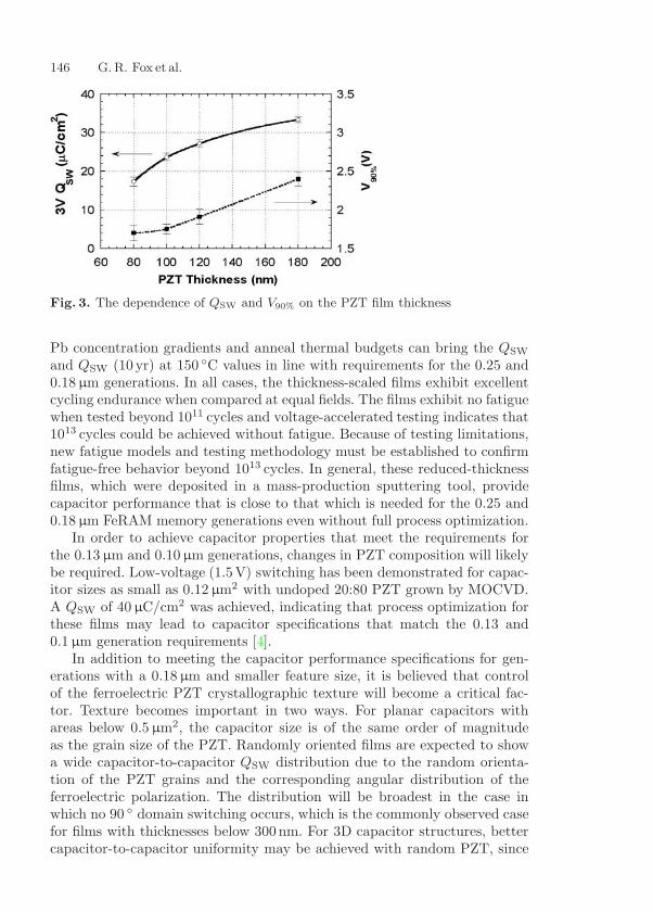
146 G. R. Fox et al.
Fig. 3. The dependence of QSW and V90% on the PZT film thickness
Pb concentration gradients and anneal thermal budgets can bring the QSW
and QSW (10 yr) at 150 C values in line with requirements for the 0.25 and0.18 µm generations. In all cases, the thickness-scaled films exhibit excellentcycling endurance when compared at equal fields. The films exhibit no fatiguewhen tested beyond 1011 cycles and voltage-accelerated testing indicates that1013 cycles could be achieved without fatigue. Because of testing limitations,new fatigue models and testing methodology must be established to confirmfatigue-free behavior beyond 1013 cycles. In general, these reduced-thicknessfilms, which were deposited in a mass-production sputtering tool, providecapacitor performance that is close to that which is needed for the 0.25 and0.18 µm FeRAM memory generations even without full process optimization.
In order to achieve capacitor properties that meet the requirements forthe 0.13 µm and 0.10 µm generations, changes in PZT composition will likelybe required. Low-voltage (1.5V) switching has been demonstrated for capac-itor sizes as small as 0.12 µm2 with undoped 20:80 PZT grown by MOCVD.A QSW of 40 µC/cm2 was achieved, indicating that process optimization forthese films may lead to capacitor specifications that match the 0.13 and0.1 µm generation requirements [4].
In addition to meeting the capacitor performance specifications for gen-erations with a 0.18 µm and smaller feature size, it is believed that controlof the ferroelectric PZT crystallographic texture will become a critical fac-tor. Texture becomes important in two ways. For planar capacitors withareas below 0.5 µm2, the capacitor size is of the same order of magnitudeas the grain size of the PZT. Randomly oriented films are expected to showa wide capacitor-to-capacitor QSW distribution due to the random orienta-tion of the PZT grains and the corresponding angular distribution of theferroelectric polarization. The distribution will be broadest in the case inwhich no 90 domain switching occurs, which is the commonly observed casefor films with thicknesses below 300 nm. For 3D capacitor structures, bettercapacitor-to-capacitor uniformity may be achieved with random PZT, since
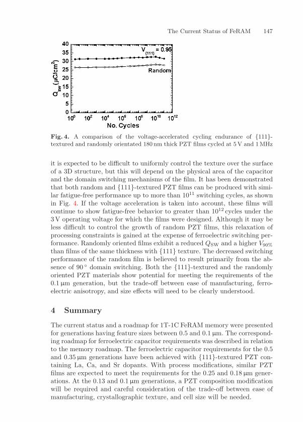
The Current Status of FeRAM 147
Fig. 4. A comparison of the voltage-accelerated cycling endurance of 111-textured and randomly orientated 180 nm thick PZT films cycled at 5V and 1MHz
it is expected to be difficult to uniformly control the texture over the surfaceof a 3D structure, but this will depend on the physical area of the capacitorand the domain switching mechanisms of the film. It has been demonstratedthat both random and 111-textured PZT films can be produced with simi-lar fatigue-free performance up to more than 1011 switching cycles, as shownin Fig. 4. If the voltage acceleration is taken into account, these films willcontinue to show fatigue-free behavior to greater than 1012 cycles under the3V operating voltage for which the films were designed. Although it may beless difficult to control the growth of random PZT films, this relaxation ofprocessing constraints is gained at the expense of ferroelectric switching per-formance. Randomly oriented films exhibit a reduced QSW and a higher V90%
than films of the same thickness with 111 texture. The decreased switchingperformance of the random film is believed to result primarily from the ab-sence of 90 domain switching. Both the 111-textured and the randomlyoriented PZT materials show potential for meeting the requirements of the0.1 µm generation, but the trade-off between ease of manufacturing, ferro-electric anisotropy, and size effects will need to be clearly understood.
4 Summary
The current status and a roadmap for 1T-1C FeRAM memory were presentedfor generations having feature sizes between 0.5 and 0.1 µm. The correspond-ing roadmap for ferroelectric capacitor requirements was described in relationto the memory roadmap. The ferroelectric capacitor requirements for the 0.5and 0.35 µm generations have been achieved with 111-textured PZT con-taining La, Ca, and Sr dopants. With process modifications, similar PZTfilms are expected to meet the requirements for the 0.25 and 0.18 µm gener-ations. At the 0.13 and 0.1 µm generations, a PZT composition modificationwill be required and careful consideration of the trade-off between ease ofmanufacturing, crystallographic texture, and cell size will be needed.
148 G. R. Fox et al.
References
1. T. Davenport, S. Mitra: Integr. Ferroelectr. 31, 213 (2000) 1402. D. Takashima, S. Shuto, I. Kunishima, H. Takenaka, Y. Oowaki, S. Tanaka:
IEEE J. Solid-State Circuits 34, 1557 (1999) 1413. T.D. Hadnagy, D. Dalton, B. Thomas, S. Sun, R. Bailey: Integr. Ferroelectr.
37, 215 (2001) 1444. T. S. Moise, S.R. Summerfelt, G. Xing, L. Colombo, T. Sakoda, S.R. Gilbert,
A. Loke, S. Ma, R. Kavari, L.A. Wills, T. Hsu, J. Amano, S.T. Johnston,D. J. Vestyck, M.W. Russell, S.M. Bilodeau: Tech. Dig. Intern. Electron De-vices Meeting (1999) p. 940 146
Index
1T-1C, 1412T-2C– cell, 139
capacitor-over-field-oxide (COFO)architecture, 141
capacitor-over-plug (COP), 141cell factor, 140
dopant, 145
endurance, 140
fatigue, 144feature size, 140, 141FeRAM– memory density, 141
minimum feature size, 140
operating voltage, 144
plug, 141
PZT– texture, 145
roadmap, 141
scaling, 145switchable charge, 142
three-dimensional capacitor structure,144
Operation Principle and Circuit Design Issues
Ali Sheikholeslami
Department of Electrical and Computer Engineering,University of Toronto, Toronto, [email protected]
Abstract. This chapter provides an introduction to the circuit design aspects offerroelectric random access memories (FeRAM). A FeRAM stores binary data in anarray of FeRAM cells, each consisting of either two transistors and two capacitors(2T-2C cell) or one transistor and one capacitor (1T-1C cell). The 2T-2C cell storesboth the binary data and its complement on the two capacitors. Compared to the1T-1C cell, the 2T-2C cell provides data storage that is robust to process variationat the price of using twice the silicon area. The 1T-1C cell stores the binary dataonly, and not its complement, to save silicon area at the price of more complexdata sensing. Two well-known approaches for data sensing are step sensing andpulse sensing. There are a variety of circuit architectures for FeRAMs. This chapterpresents a few well-known architectures and points to the literature for the mostrecently proposed FeRAM architectures.
1 Introduction
Ferroelectric random access memories (FeRAM) belong to a family of semi-conductor memories that are known as nonvolatile memories. A nonvolatilememory stores digital information in an array of memory cells and retainsthis information indefinitely without electrical power. Two other types ofnonvolatile memories are electrically-erasable-and-programmable read-only-memories (EEPROM) and Flash memories. Table 1 compares a FeRAM,an EEPROM, and a Flash memory in terms of density, read access-time,write-access time, and the energy consumed in a 32 bit read/write operation.Enjoying a mature process technology, EEPROMs and Flash memories [1, 2]are superior to ferroelectric memories in terms of density. Also, they requireless power compared to ferroelectric memories for read operations, a factorthat will keep them popular in applications that demand numerous memoryreads but only occasional memory writes. An example of such applicationsis an identity card, where an identity code is programmed into the memoryonce but read many times afterwards.
Ferroelectric memories, on the other hand, are superior to EEPROMs andFlash memories in terms of write-access time and overall power consumption,hence target applications where a nonvolatile memory is required with suchfeatures. Two examples of such applications are contactless smart cards anddigital cameras. Contactless smart cards require nonvolatile memories withlow power consumption as they use only electromagnetic coupling to powerH. Ishiwara, M. Okuyama, Y. Arimoto (Eds.): Ferroelectric Random Access Memories,Topics Appl. Phys. 93, 149–164 (2004)c© Springer-Verlag Berlin Heidelberg 2004
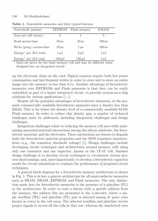
150 Ali Sheikholeslami
Table 1. Nonvolatile memories and their typical features
Nonvolatile memory EEPROM Flash memory FeRAM
Area per cell (norm.) 2 1 5
Read access-time 50 ns 50 ns 100 ns
Write (prog.) access-time 10 µs 1µs 100 ns
Energy per 32 b write 1 µJ 2µJ 1 nJ
Energy per 32 b read 150 pJ 150 pJ 1 nJ Data are given for the basic memory cell and may be different when
designed into an integrated circuit
up the electronic chips on the card. Digital cameras require both low powerconsumption and fast-frequent writes in order to store and re-store an entireimage into the memory in less than 0.1 s. Another advantage of ferroelectricmemories over EEPROMs and Flash memories is that they can be easilyembedded as part of a larger integrated circuit, to provide system-on-a-chipsolutions for various applications [3, 4].
Despite all the potential advantages of ferroelectric memories, at the mo-ment commercially available ferroelectric memories have a density less than256kb. This is far below the density level of a commercially available 64MbFlash memory. In order to reduce this density gap, a number of technicalchallenges must be addressed, including integration challenges and designchallenges.
Integration challenges relate to reducing the memory cell area while mini-mizing unwanted material interactions among the silicon substrate, the ferro-electric material, and the electrodes. These interactions are known to degradeboth the ferroelectric material properties and the MOS transistor character-istics (e.g., the transistor threshold voltage) [5]. Design challenges includedeveloping circuit techniques and architectures around memory cells usingonly one transistor and one capacitor, known as the 1T-1C cell. Anotherdesign challenge is to develop circuit techniques to circumvent various pro-cess shortcomings, and, more importantly, to develop a ferroelectric capacitormodel for circuit simulations to evaluate the performance of proposed circuittechniques.
A general block diagram for a ferroelectric memory architecture is shownin Fig. 1. This is in fact a generic architecture for all semiconductor memoriessuch as SRAM, DRAM, EEPROM, and Flash memories. The only distinc-tion made here for ferroelectric memories is the presence of a plateline (PL)in the architecture. In order to read a datum with a specific address fromthe memory, the address bits are presented to the x-decoder, where a sin-gle wordline (WL) and plateline (PL) pair is selected among 2r pairs (alsoknown as rows) in the cell array. The selected wordline and plateline receiveproper signals to access all the cells in that row, whereas the unselected rows
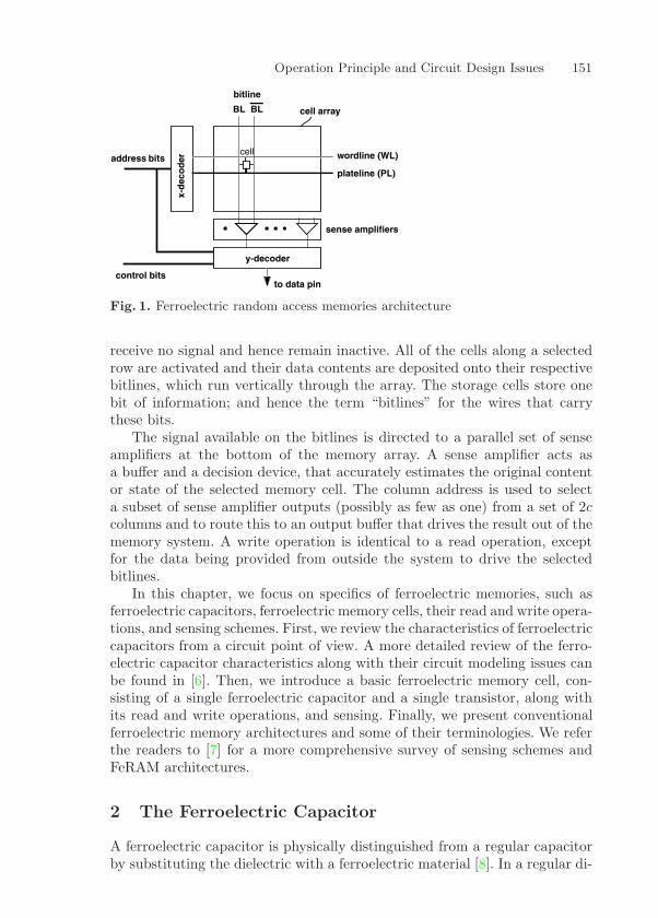
Operation Principle and Circuit Design Issues 151
wordline (WL)
x-d
eco
der
y-decoder
to data pin
address bits
control bits
sense amplifiers
cell
cell array
bitline
BL BL
plateline (PL)
Fig. 1. Ferroelectric random access memories architecture
receive no signal and hence remain inactive. All of the cells along a selectedrow are activated and their data contents are deposited onto their respectivebitlines, which run vertically through the array. The storage cells store onebit of information; and hence the term “bitlines” for the wires that carrythese bits.
The signal available on the bitlines is directed to a parallel set of senseamplifiers at the bottom of the memory array. A sense amplifier acts asa buffer and a decision device, that accurately estimates the original contentor state of the selected memory cell. The column address is used to selecta subset of sense amplifier outputs (possibly as few as one) from a set of 2ccolumns and to route this to an output buffer that drives the result out of thememory system. A write operation is identical to a read operation, exceptfor the data being provided from outside the system to drive the selectedbitlines.
In this chapter, we focus on specifics of ferroelectric memories, such asferroelectric capacitors, ferroelectric memory cells, their read and write opera-tions, and sensing schemes. First, we review the characteristics of ferroelectriccapacitors from a circuit point of view. A more detailed review of the ferro-electric capacitor characteristics along with their circuit modeling issues canbe found in [6]. Then, we introduce a basic ferroelectric memory cell, con-sisting of a single ferroelectric capacitor and a single transistor, along withits read and write operations, and sensing. Finally, we present conventionalferroelectric memory architectures and some of their terminologies. We referthe readers to [7] for a more comprehensive survey of sensing schemes andFeRAM architectures.
2 The Ferroelectric Capacitor
A ferroelectric capacitor is physically distinguished from a regular capacitorby substituting the dielectric with a ferroelectric material [8]. In a regular di-

152 Ali Sheikholeslami
“0” “1”
positive electric fieldpositive polarization
negative electric fieldnegative polarization
Ti/Zr Oxygen Pb
Fig. 2. Two stable states in PZT: the orientation of the spontaneous polarizationis reversed by applying a proper electric field
electric, upon the application of an electric field, positive and negative chargeswill be displaced from their original positions – a concept that is character-ized by polarization. This polarization, or displacement, will vanish, however,when the electric field returns back to zero. In a ferroelectric material, on theother hand, there is a spontaneous polarization – a displacement that is in-herent to the crystal structure of the material and does not disappear in theabsence of an electric field. In addition, the direction of this polarization canbe reversed or reoriented by applying an appropriate electric field.
One of the well-known ferroelectric materials that has been used for overa decade is lead zirconate titanate (PZT). Figure 2 illustrates a unit cell ofthis material. The central atom in this unit cell is either titanium (Ti) orzirconium (Zi), depending on the contribution of each atom to the material’schemical formula, Pb(ZrXTi1−X)O3. An appropriate electric field is capableof displacing the central atom from its previous stable position and, thereby,changing the polarization state of the unit cell. Although the polarization ofeach individual unit cell is tiny, the net polarization of several domains – eachconsisting of a number of aligned unit cells – can be large enough for detec-tion using standard sense amplifier designs. The gross effect of polarization isa nonzero charge per unit area of the ferroelectric capacitor that exists at 0 Vand does not disappear over time. The polarization charge, which is simplyreferred to as the capacitor charge in this chapter, responds to the voltageacross the capacitor in the same way as the magnetic flux of a ferromagneticcore responds to the current through the core. In this sense, ferroelectriccapacitors are duals of ferromagnetic cores, and justify their names. Ferro-electric capacitors sit on top of a conventional CMOS process and providea typical polarization charge of 150 fC/(µm)2 in a typical area of 2(µm)2.This nonvolatile polarization charge level is about 20 times larger than thevolatile polarization level on gate oxide (SiO2), in a typical CMOS process,when subjected to a full power supply voltage.
There are two common methods of characterizing a ferroelectric capaci-tor behavior. One is to monitor the polarization charge on the ferroelectric

Operation Principle and Circuit Design Issues 153
V CFE
Q
V
Qs
Qr “0”
“1”
VC
-VC
Vmax
-Qr
-Qs
Fig. 3. The hysteresis loop characteris-tic of a ferroelectric capacitor. Three im-portant parameters of the loop are: re-manent charge (Qr), saturation charge(Qs), and coercive voltage (VC)
capacitor while a low-frequency sinusoidal waveform is applied to a seriescombination of the ferroelectric capacitor and a large linear capacitor, a cir-cuit setup known as the Sawyer–Tower circuit. The other method is to mon-itor the transient current of the capacitor while a sequence of voltage pulsesis applied to a series combination of the ferroelectric capacitor and a linearresistor. We describe both characterization methods in the following sections.
2.1 The Hysteresis Loop Characteristic
A hysteresis loop for a ferroelectric capacitor, as shown in Fig. 3, displaysthe total charge on the capacitor as a function of the applied voltage. Whenthe voltage across the capacitor is 0V, the capacitor assumes one of the twostable states: “0” or “1”. The total charge stored on the capacitor is Qr, fora “0”, or −Qr, for a “1”. Both Qr and −Qr are bound charges that cannotbe released for sensing until a voltage pulse is applied to the ferroelectriccapacitor. A “0” can be switched to a “1” by applying a negative voltagepulse across the capacitor. By doing so, the total charge on the capacitor isreduced by 2Qr, a change of charge that can be sensed by the sense circuitry asexplained later in this chapter. Similarly, a “1” can be switched back to a “0”by applying a positive voltage pulse across the capacitor, hence restoring thecapacitor charge to +Qr.
Three parameters are often extracted from a hysteresis loop: the rema-nent charge, Qr, the saturation charge, Qs, and the coercive voltage, VC. Theremanent charge and the saturation charge are self-explanatory from Fig. 3.The coercive voltage is defined as the voltage at which the net charge onthe capacitor is zero. For a hysteresis loop with sharp transitions at VC, thisvoltage can be interpreted as the approximate switching voltage for all theferroelectric domains. For a hysteresis loop with typically smooth transitionsat VC, there is no fixed switching voltage but a range of voltage during whichdomains switch gradually. This is referred to as the partial switching of do-mains in a ferroelectric capacitor. Partial switching has a voltage distributionthat can be quantified by plotting the capacitor charge increment per unitapplied voltage versus applied voltage or, equivalently, the voltage derivative
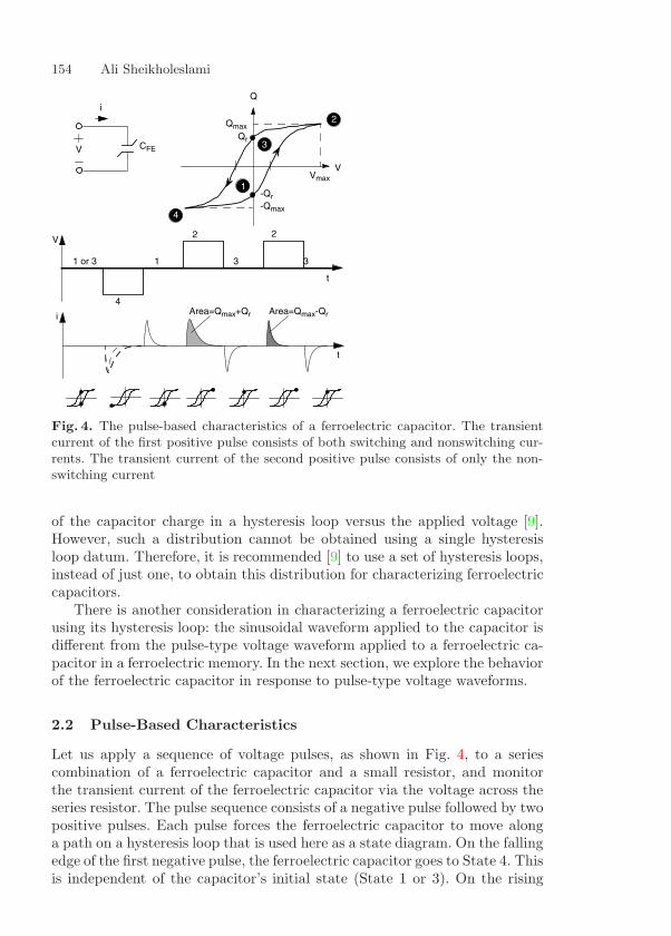
154 Ali Sheikholeslami
2
4
t
V
1 or 3
4
1
2
3
2
3
Area=Qmax+Qr Area=Qmax-Qri
t
V
i
3
1
CFE
Q
V
QmaxQr
Vmax
-Qr-Qmax
Fig. 4. The pulse-based characteristics of a ferroelectric capacitor. The transientcurrent of the first positive pulse consists of both switching and nonswitching cur-rents. The transient current of the second positive pulse consists of only the non-switching current
of the capacitor charge in a hysteresis loop versus the applied voltage [9].However, such a distribution cannot be obtained using a single hysteresisloop datum. Therefore, it is recommended [9] to use a set of hysteresis loops,instead of just one, to obtain this distribution for characterizing ferroelectriccapacitors.
There is another consideration in characterizing a ferroelectric capacitorusing its hysteresis loop: the sinusoidal waveform applied to the capacitor isdifferent from the pulse-type voltage waveform applied to a ferroelectric ca-pacitor in a ferroelectric memory. In the next section, we explore the behaviorof the ferroelectric capacitor in response to pulse-type voltage waveforms.
2.2 Pulse-Based Characteristics
Let us apply a sequence of voltage pulses, as shown in Fig. 4, to a seriescombination of a ferroelectric capacitor and a small resistor, and monitorthe transient current of the ferroelectric capacitor via the voltage across theseries resistor. The pulse sequence consists of a negative pulse followed by twopositive pulses. Each pulse forces the ferroelectric capacitor to move alonga path on a hysteresis loop that is used here as a state diagram. On the fallingedge of the first negative pulse, the ferroelectric capacitor goes to State 4. Thisis independent of the capacitor’s initial state (State 1 or 3). On the rising

Operation Principle and Circuit Design Issues 155
edge of this pulse, the capacitor goes to State 1. This first negative pulsehelps to establish the initial state of the capacitor before applying the nexttwo positive pulses. In a ferroelectric memory, this pulse can be consideredas a signal that writes a binary digit “1” into the cell.
On the rising edge of the first positive voltage pulse, the capacitor acquiresa charge increment of Qmax+Qr and, as a result, its state changes to State 2.On the falling edge of the same pulse, the capacitor will lose Qmax − Qr asit goes to State 3. The transient current corresponding to the falling edge,therefore, will have less area underneath it than the one corresponding tothe rising edge of the first pulse. The net effect of the first positive pulseis a charge increment of 2Qr. In a ferroelectric memory, this pulse can beconsidered as a signal which reads a binary digit “1” into the bitline.
The second positive pulse causes a state transition from 3 to 2 and backto 3 again, a total charge increment of 0. In a ferroelectric memory, thiscorresponds to reading a binary digit “0” into the bitline.
3 The Ferroelectric Memory Cell:Read and Write Operations
Figure 5 shows a simplified schematic of a fully differential 2T-2C cell (two-transistor, two-capacitor) memory cell and that of a 1T-1C cell. The 1T-1Ccell occupies half the semiconductor area required by the 2T-2C cell. There-fore, a memory architecture based on the 1T-1C cell achieves twice the den-sity of an architecture based on the 2T-2C cell, albeit at the price of a morecomplex sensing scheme [7]. In the rest of this section, we concentrate on theread/write operations of the 1T-1C cell.
The 1T-1C cell consists of a single ferroelectric capacitor that is connectedto a plateline (PL) at one end and, via an access transistor, to a bitline (BL) atthe other end. The cell is accessed by raising the wordline (WL) and, hence,turning ON the access transistor. The access is one of two types: a writeaccess or a read access.
The timing diagram for a write operation is shown in Fig. 6a. To writea “1” into the memory cell, the BL is raised to VDD, then the WL is raised toVDD + VT (known as boosted VDD [10]), where VT is the threshold voltage ofthe access transistor. This allows a full VDD to appear across the ferroelectriccapacitor (−VDD according to the voltage convention adopted in Fig. 5). Atthis time, the state of the ferroelectric capacitor is independent of the initialstate of the ferroelectric capacitor, as shown in Fig. 6b. Next, the plateline(PL) is pulsed; that is, pulled up to VDD and subsequently pulled back downto ground. Note that the WL stays activated until the PL is pulled downcompletely and the BL is driven back to zero. The final state of the capacitoris a negative charge state S1 (defined as digital “1” in this chapter). Finally,deactivating the WL leaves this state undisturbed until the next access.
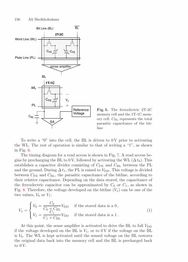
156 Ali Sheikholeslami
BL
CFECFE
Bit Line (BL)
Word Line (WL)
2T-2C
PL
CFE
BL
WL1T-1C
SA
ReferenceVoltage
sense amplifier
Plate Line (PL)
Vc
CBL
Fig. 5. The ferroelectric 2T-2Cmemory cell and the 1T-1C mem-ory cell. CBL represents the totalparasitic capacitance of the bit-line
To write a “0” into the cell, the BL is driven to 0V prior to activatingthe WL. The rest of operation is similar to that of writing a “1”, as shownin Fig. 6.
The timing diagram for a read access is shown in Fig. 7. A read access be-gins by precharging the BL to 0 V, followed by activating the WL (∆ t0). Thisestablishes a capacitor divider consisting of CFE and CBL between the PLand the ground. During ∆ t1, the PL is raised to VDD. This voltage is dividedbetween CFE and CBL, the parasitic capacitance of the bitline, according totheir relative capacitance. Depending on the data stored, the capacitance ofthe ferroelectric capacitor can be approximated by C0 or C1, as shown inFig. 8. Therefore, the voltage developed on the bitline (Vx) can be one of thetwo values, V0 or V1:
Vx =
⎧⎪⎨⎪⎩
V0 =C0
C0 + CBLVDD if the stored data is a 0 ,
V1 =C1
C1 + CBLVDD if the stored data is a 1 .
(1)
At this point, the sense amplifier is activated to drive the BL to full VDD
if the voltage developed on the BL is V1, or to 0 V if the voltage on the BLis V0. The WL is kept activated until the sensed voltage on the BL restoresthe original data back into the memory cell and the BL is precharged backto 0V.
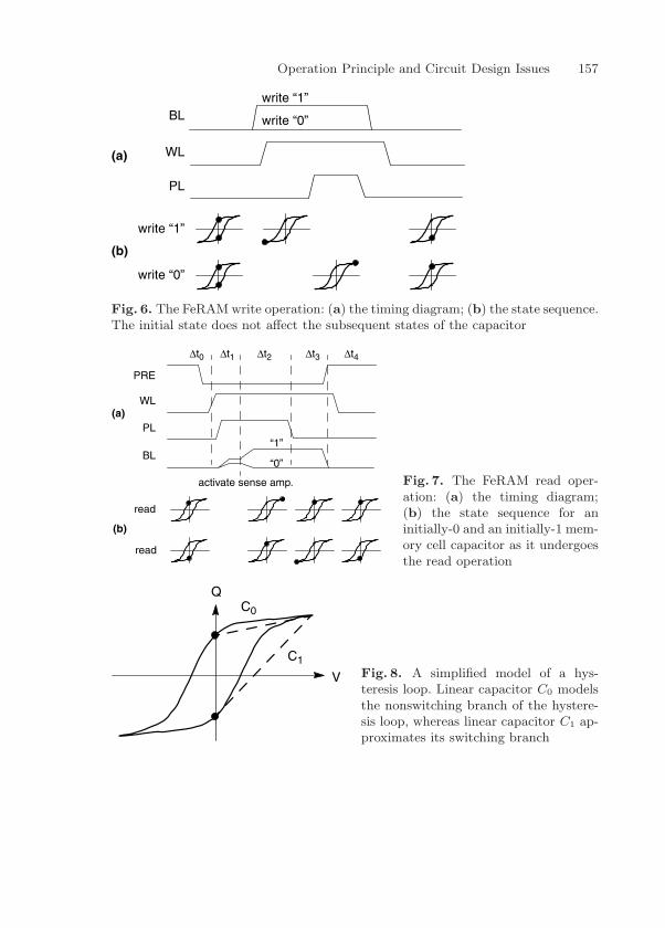
Operation Principle and Circuit Design Issues 157
write “0”
write “1”
WL
PL
BLwrite “1”
write “0”
(b)
(a)
Fig. 6. The FeRAM write operation: (a) the timing diagram; (b) the state sequence.The initial state does not affect the subsequent states of the capacitor
WL
PL
activate sense amp.
“1”
“0”
read
read
BL
PRE
∆t1 ∆t2 ∆t3∆t0 ∆t4
(a)
(b)
Fig. 7. The FeRAM read oper-ation: (a) the timing diagram;(b) the state sequence for aninitially-0 and an initially-1 mem-ory cell capacitor as it undergoesthe read operation
Q
V
C1
C0
Fig. 8. A simplified model of a hys-teresis loop. Linear capacitor C0 modelsthe nonswitching branch of the hystere-sis loop, whereas linear capacitor C1 ap-proximates its switching branch
158 Ali Sheikholeslami
4 Sensing Schemes
The read access as presented above is known in the literature as the step-sensing approach, since a step voltage (the rising edge of a pulse) is appliedto the PL prior to sensing. An alternative is the pulse-sensing approach, inwhich a full pulse is applied to the PL prior to activating the sense amplifiers.The charge transferred to the BL in a pulse-sensing scheme is either 0, fora stored “0”, or 2Qr for a stored “1”. Equivalently, the voltage developed onthe BL is either 0V, for a stored “0”, or V1−V0 (refer to (1)) for a stored “1”.
In both step- and pulse-sensing schemes, the voltage difference betweena stored “1” and a stored “0” on the BL is equal to V1 − V0. Their common-mode voltage, however, is equal to (V1 + V0)/2 in the step-sensing approach,as compared to (V1 − V0)/2 in the pulse-sensing approach. Therefore, thestep-sensing approach provides a higher common-mode voltage on the BLthat simplifies the sense amplifier design when a bias voltage is required.Another advantage of the step-sensing approach is that it provides a fasterread-access, as the sensing does not wait for the PL to be pulled low.
Both the step-sensing and the pulse-sensing approaches restore “1”, butonly the step-sensing approach fully reinforces a “0”. To substantiate thispoint, note that during a read operation in a step-sensing approach, a fer-roelectric capacitor storing a “0” experiences a voltage sequence [11] of 0V,VDD − V0, VDD, and 0 V (a full-VDD excursion). In a pulse-sensing approach,the corresponding voltage sequence is 0V, VDD − V0, and 0V (a VDD − V0
excursion). Neither of the two voltage sequences upsets the original data (i.e.,“0”) of the ferroelectric capacitor. However, the latter provides a weak rein-forcement of “0” by applying a voltage less than VDD across the capacitor.This seems to cause the capacitor’s long-term retention performance to de-teriorate [12]. To remedy this situation, a second pulse must be applied tothe PL to fully restore the “0” into the capacitor. This implies that the cy-cle time for the pulse-sensing approach can be twice as large as that for thestep-sensing approach.
The pulse-sensing approach applies to both the leading edge and the trail-ing edge of the voltage pulse to the ferroelectric capacitor prior to sensing.The trailing edge eliminates the nonswitching part of the polarization thatwas introduced on the BL by the rising edge and, therefore, bypasses theeffect of the nonswitching part of the polarization and its process variationsaltogether. This seems to be the only advantage of the pulse-sensing approachover the step-sensing approach.
So far, we have assumed that the sense amplifier can discriminate betweena “0” and “1” voltage signal on the BL. This is only possible if a referencevoltage, midway between a “0” and a “1” signal, is provided for the sense am-plifier. We refer the readers to [7] for a survey of reference generation schemes.
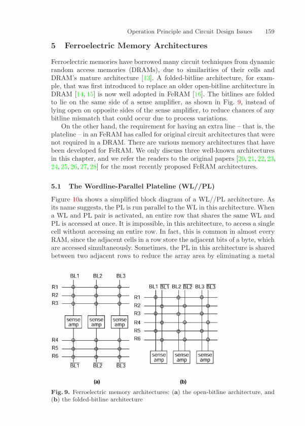
Operation Principle and Circuit Design Issues 159
5 Ferroelectric Memory Architectures
Ferroelectric memories have borrowed many circuit techniques from dynamicrandom access memories (DRAMs), due to similarities of their cells andDRAM’s mature architecture [13]. A folded-bitline architecture, for exam-ple, that was first introduced to replace an older open-bitline architecture inDRAM [14, 15] is now well adopted in FeRAM [16]. The bitlines are foldedto lie on the same side of a sense amplifier, as shown in Fig. 9, instead oflying open on opposite sides of the sense amplifier, to reduce chances of anybitline mismatch that could occur due to process variations.
On the other hand, the requirement for having an extra line – that is, theplateline – in an FeRAM has called for original circuit architectures that werenot required in a DRAM. There are various memory architectures that havebeen developed for FeRAM. We only discuss three well-known architecturesin this chapter, and we refer the readers to the original papers [20, 21, 22, 23,24, 25, 26, 27, 28] for the most recently proposed FeRAM architectures.
5.1 The Wordline-Parallel Plateline (WL//PL)
Figure 10a shows a simplified block diagram of a WL//PL architecture. Asits name suggests, the PL is run parallel to the WL in this architecture. Whena WL and PL pair is activated, an entire row that shares the same WL andPL is accessed at once. It is impossible, in this architecture, to access a singlecell without accessing an entire row. In fact, this is common in almost everyRAM, since the adjacent cells in a row store the adjacent bits of a byte, whichare accessed simultaneously. Sometimes, the PL in this architecture is sharedbetween two adjacent rows to reduce the array area by eliminating a metal
Fig. 9. Ferroelectric memory architectures: (a) the open-bitline architecture, and(b) the folded-bitline architecture
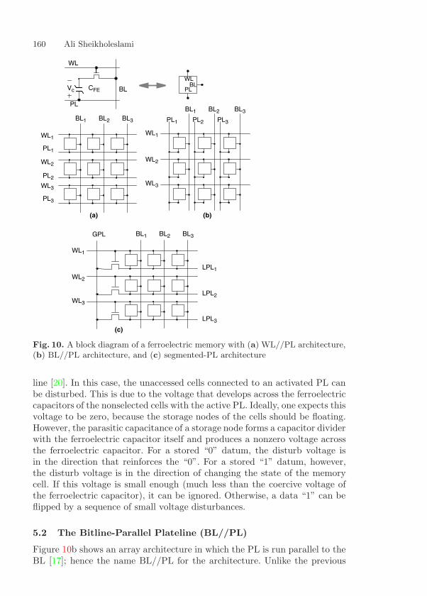
160 Ali Sheikholeslami
WL1
PL1
WL2
PL2
WL3
PL3
BL1 BL2 BL3
PL
WL
BLCFEVc PL
WLBL
WL1
WL2
WL3
BL1 BL2 BL3
PL1 PL2 PL3
WL1
WL2
WL3
BL1 BL2 BL3GPL
(a) (b)
(c)
LPL1
LPL2
LPL3
Fig. 10. A block diagram of a ferroelectric memory with (a) WL//PL architecture,(b) BL//PL architecture, and (c) segmented-PL architecture
line [20]. In this case, the unaccessed cells connected to an activated PL canbe disturbed. This is due to the voltage that develops across the ferroelectriccapacitors of the nonselected cells with the active PL. Ideally, one expects thisvoltage to be zero, because the storage nodes of the cells should be floating.However, the parasitic capacitance of a storage node forms a capacitor dividerwith the ferroelectric capacitor itself and produces a nonzero voltage acrossthe ferroelectric capacitor. For a stored “0” datum, the disturb voltage isin the direction that reinforces the “0”. For a stored “1” datum, however,the disturb voltage is in the direction of changing the state of the memorycell. If this voltage is small enough (much less than the coercive voltage ofthe ferroelectric capacitor), it can be ignored. Otherwise, a data “1” can beflipped by a sequence of small voltage disturbances.
5.2 The Bitline-Parallel Plateline (BL//PL)
Figure 10b shows an array architecture in which the PL is run parallel to theBL [17]; hence the name BL//PL for the architecture. Unlike the previous
Operation Principle and Circuit Design Issues 161
architecture, only a single memory cell can be selected by simultaneous ac-tivation of a WL and a PL. This is the memory cell that is located at theintersection of the WL and the PL. It is possible to select more than onememory cell in a row by activating their corresponding platelines.
This architecture absorbs the function of a y-decoder in the selection of theplatelines. In fact, the activation of the sense amplifiers is controlled by thesame signal as the PL. Therefore, only one sense amplifier is activated if onlyone memory cell needs to be accessed. This reduces the power consumptionsignificantly. On the other hand, if an entire row needs to be accessed, thenall of the platelines are selected simultaneously, hence increasing the dynamicpower consumption due to charging and discharging of the platelines.
The main disadvantage of this architecture is that activating a PL coulddisturb all of the cells in the corresponding column [17]. This is very similar tothe situation discussed for the WL//PL architecture with PL shared betweentwo adjacent rows.
5.3 The Segmented Plateline (Segmented PL)
A WL//PL architecture is power-consuming and relatively slow, because thePL is activated in its full length to access all of the cells in the row at once.Also, a BL//PL architecture could be power-consuming if multiple platelineswere activated to access multiple memory cells in the selected row. For largerarrays, the PL can be segmented into local plate lines (LPL) that run parallelto the WL and controlled by a global plate line (GPL) that runs parallel tothe BL [18, 19]. As shown in Fig. 10c, a GPL is ANDed with the WL togenerate the signal for the LPL. Since the LPL is only connected to a fewmemory cells (eight in this example), it can respond much faster than a PL inthe WL//PL architecture. Also, since the GPL is gated by the WL, there isno disturbance to the nonselected cells in the column as it was in the BL//PLarchitecture.
Among the three architectures discussed so far, the segmented-PL archi-tecture seems to be the most feasible architecture for a large-density ferro-electric memory. A compromise between speed and power consumption canbe made by choosing the number of LPLs per GPL.
6 Summary
Ferroelectric capacitors are the basic storage elements for ferroelectric memo-ries. We presented an overview of ferroelectric capacitor behavior in responseto a low-frequency sinusoidal waveform and a high-frequency pulse sequence.Also, we described the read and write operations for a basic ferroelectricmemory cell, as well as sensing methods. In the last section, we briefly dis-cussed conventional architectures for ferroelectric memories.
162 Ali Sheikholeslami
Acknowledgements
Generous financial support from Fujitsu Labs, Japan, and the Natural Sci-ences and Engineering Council of Canada (NSERC) are acknowledged.
References
1. B. Ricco, G. Torelli, M. Lanzoni, A. Manstretta, H. Maes, D. Montanari,A. Modelli: Proc. IEEE 86, 2399 (1998) 149
2. P. Pavan, R. Bez, P. Olivi, E. Zanoni: Proc. IEEE 85, 1248 (1997) 1493. K. Amanuma, T. Tatsumi, Y. Maejima, S. Takahashi, H. Hada, H. Okizaki,
T. Kunio: Tech. Dig. Intern. Electron Devices Meeting, (1998) p. 363 1504. J. Yamada, T. Miwa, H. Koike, H. Toyoshima, K. Amanuma, S. Kobayashi,
T. Tatsumi, Y. Maejima, H. Hada, H. Mori, S. Takahashi, H. Takeuchi, T. Ku-nio: Tech. Dig. Intern. Solid-State Circuits Conf. (2000) p. 270 150
5. R. E. Jones Jr.: IEEE Custom Integrated Circuits Conf. (1998) p. 431 1506. A. Sheikholeslami, P.G. Gulak: IEEE Trans. Ultrason. Ferroelectr. Freq. Con-
trol 44, 917 (1997) 1517. A. Sheikholeslami, P.G. Gulak: Proc. IEEE 88, 667 (2000) 151, 155, 1588. J. C. Burfoot, G.W. Taylor: Polar Dielectrics, Their Applications (University
of California Press, Berkeley 1979) 1519. A. Sheikholeslami, P.G. Gulak, H. Takauchi, H. Tamura, H. Yoshioka,
T. Tamura: IEEE Trans. Ultrason. Ferroelectr. Freq. Control 44, 784 (2000)154
10. W. Kraus, L. Lehman, D. Wilson, T. Yamazaki, C. Ohno, E. Nagai, H. Ya-mazaki, H. Suzuki: Tech. Dig. Symp. VLSI Circuits (1998) p. 242 155
11. N. Abt: Mater. Res. Soc. Symp. Proc. 200, 303 (1990) 15812. Y. Chung, M. Choi, S. Oh, B. Jeon, K. Suh: Tech. Dig. Symp. VLSI Circuits
(1999) 15813. W. Kinney: Integr. Ferroelectr. 4, 131 (1994) 15914. R. F. Harland: US Patent No. 4045783 (Aug. 30, 1977) 15915. R.C. Foss: Tech. Dig. Intern. Solid-State Circuits Conf. (1979) p. 140 15916. W.L. Larson: US Patent No. 5371699 (Dec. 6, 1994) 15917. R. Womak, D. Tolsch: Tech. Dig. Intern. Solid-State Circuits Conf. (1989)
p. 242 160, 16118. T. Sumi, N. Moriwaki, G. Nakane, T. Nakakuma, Y. Judai, Y. Uemoto,
Y. Nagano, S. Hayashi, M. Azuma, E. Fujii, S. Katsu, T. Otsuki, L. McMillan,C. A. Paz de Araujo, G. Kano: Tech. Dig. Intern. Solid-State Circuits Conf.(1994) p. 268 161
19. R.E. Jones Jr.: US Patent No. 5373463 (Dec. 13, 1994) 16120. M. Aoki, H. Takauchi, H. Tamura: Tech. Dig. Intern. Electron Devices Meeting
(1997) p. 942 159, 16021. D. Takashima, I. Kunishima: IEEE J. Solid-State Circuits 33, 787 (1998) 15922. D. Takashima, S. Shuto, I. Kunishima, H. Takenaka, Y. Oowaki, S. Tanaka:
Tech. Dig. Intern. Solid-State Circuits Conf. (1999) p. 102 15923. N. Tanabe, S. Kobayashi, T. Miwa, K. Amanuma, H. Mori, N. Inoue,
T. Takeuchi, S. Saitoh, Y. Hayashi, J. Yamada, H. Koike, H. Hada, T. Kunio:Tech. Dig. Symp. VLSI Circuits (1998) p. 124 159

Operation Principle and Circuit Design Issues 163
24. N. Tanabe, S. Kobayashi, H. Hada, T. Kunio: Tech. Dig. Intern. ElectronDevices Meeting (1997) p. 863 159
25. S. Kawashima, T. Endo, A. Yamamoto, K. Nakabayashi, M. Nakazawa,K. Morita, M. Aoki: Tech. Dig. Symp. VLSI Circuits (2001) p. 127 159
26. H.B. Kang, D.M. Kim, K.Y. Oh, J. S. Roh, J. J. Kim, J. H. Ahn, H.G. Lee,D.C. Kim, W. Jo, H.M. Lee, S.M. Cho, H. J. Nam, J. W. Lee, C. S. Kim: Tech.Dig. Intern. Solid-State Circuits Conf. (1999) p. 108 159
27. H. Koike, T. Otsuki, T. Kimura, M. Fukuma, Y. Hayashi, Y. Maejima,K. Amanuma, M. Tanabe, T. Matsuki, S. Saito, T. Takeuchi, S. Kobayashi,T. Kunio, T. Hase, Y. Miyasaka, N. Shohota, M. Takada: Tech. Dig. Intern.Solid-State Circuits Conf. (1996) p. 368 159
28. H. Hirano, T. Honda, N. Moriwaki, T. Nakakuma, A. Inoue, G. Nakane,S. Chaya, T. Sumi: IEEE J. Solid-State Circuits 32, 649 (1997) 159
Index
1T-1C cell, 150– bitline, 155– plateline, 155– wordline, 1552T-2C– cell, 155
bitline-parallel plateline, 160
circuit design, 149coercive voltage, 153
FeRAM, 149– access time, 149
hysteresis– loop, 153
memory architecture– folded-bitline, 159
– open-bitline, 159
nonvolatile, 149
partial switching, 153polarization, 152pulse-sensing approach, 158PZT, 152
reference voltage, 156remanent charge, 153
saturation charge, 153Sawyer–Tower circuit, 153segmented plateline, 161sensing scheme, 151step-sensing, 158
wordline-parallel plateine (WL//PL),159
High-Density Integration
Kinam Kim
Semiconductor R& D Center, Semiconductor Business, Samsung Electronics Co.,San #24, Nongseo-Ri, Kiheung-Eup, Yongin-City, Kyungki-Do, 449-711, Koreakn [email protected]
Abstract. Ferroelectric random access memory (FeRAM) has been pursued asa promising new memory due to its ideal memory properties, such as fast randomaccess in read/write mode and nonvolatility with unlimited usage. However, FeRAMhas only achieved limited success in low-density applications because of its largecell size (large cell size factor). Recently, mega-bit density scaled FeRAMs havebeen developed with many key process and new integration technologies. Amongthose technologies, 1T-1C COB (capacitor over bit line) cell structure is the mostimportant, because it can greatly reduce the cell size of FeRAM. With these tech-nologies, 0.25 µm 32 Mb FeRAM with the 15F2 cell size factor of a 1T-1C COB cellhas been successfully developed. In order to further reduce the cell size factor to itstheoretical limits of 6 F2 or 8F2, it is highly desirable to develop three-dimensionalferroelectric capacitor technology, where CVD technology is essential for fabricatingferroelectrics as well as electrodes.
1 Introduction
Ideal memory should have properties such as random access, fast read andfast write operations, unlimited usage with nonvolatility, and a small cell size.None of the existing memories, such as DRAM, SRAM, and Flash memory,can satisfy these requirements for an ideal memory. For instance, DRAMand SRAM do not possess nonvolatility, while Flash memory satisfies neitherfast write operation nor unlimited usage. On the way to pursuing the idealmemory, FeRAM, which potentially satisfies all of the requirements for anideal memory, has been introduced in the past decade [1].
In spite of the excellent properties of the ferroelectric memory, only low-density FeRAM products have been commercialized compared to its coun-terparts among memory devices, such as DRAM, SRAM, and Flash memory.The low-density FeRAM products have resulted from the large cell size of its2T2C cell architecture. Cell size has been one of the most important figuresof merit to measure the competitiveness of memory products, regardless ofthe memory type. The cell size of the memory is typically evaluated by thecell size factor for a given technology generation. The cell size factor is de-termined using the ratio of the unit cell area to the square of the minimumfeature size F. The minimum feature size F in memory devices is typicallygiven by the half pitch of the minimum pitch of the bit line or word line.Therefore, the cell size factor denotes how much area is consumed in storingH. Ishiwara, M. Okuyama, Y. Arimoto (Eds.): Ferroelectric Random Access Memories,Topics Appl. Phys. 93, 165–177 (2004)c© Springer-Verlag Berlin Heidelberg 2004

166 K. Kim
Fig. 1. The cell size factor for variousmemories (DRAM, SRAM, Flash,and FeRAM)
Fig. 2. The evolution of the cell size fac-tor for 2T2C and 1T-1C FeRAMs
one bit of data for the given technology. Figure 1 shows the cell size factorsfor various types of commercially available memory products. As indicatedin Fig. 1, the cell size factor of DRAM approaches its theoretical limit of8F2 in folded bit line architecture [2]. NAND Flash has the smallest cell sizefactor due to its one-transistor (1T) cell architecture. SRAM has the biggestcell size factor, ranging from 120 to 60, and depending on the configurationsof a six-transistor (6T) cell. The cell size factor of the FeRAM with 2T2Ccell architecture ranges from 100 to 60. Therefore, current FeRAM is lesscompetitive than DRAM and SRAM in cost-effectiveness.
In order to improve the cost-effectiveness of FeRAM so that it is closeto that of DRAM and/or Flash memory, it is necessary to reduce the cellsize factor of FeRAM close to that of DRAM and/or Flash memory by usinga 1T-1C cell architecture [3]. Since the first 1T-1C FeRAM was demonstrated,much effort has been put into developing a high-density 1T-1C FeRAM whosecell size factor can compete with that of DRAM. Figure 2 shows the trendof the cell size factor of the 1T-1C FeRAM. Since the 1T-1C 64kb FeRAMwith a CUB (capacitor under bit line) cell architecture was successfully devel-
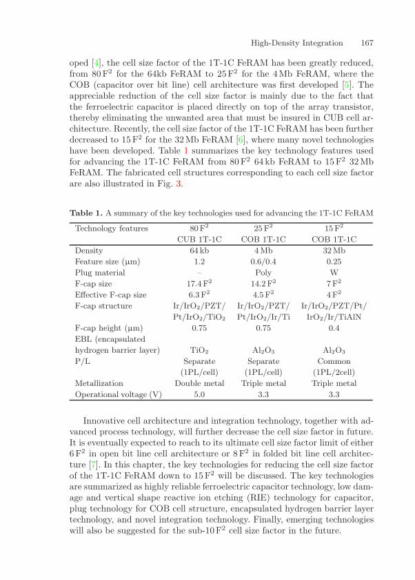
High-Density Integration 167
oped [4], the cell size factor of the 1T-1C FeRAM has been greatly reduced,from 80F2 for the 64kb FeRAM to 25F2 for the 4Mb FeRAM, where theCOB (capacitor over bit line) cell architecture was first developed [5]. Theappreciable reduction of the cell size factor is mainly due to the fact thatthe ferroelectric capacitor is placed directly on top of the array transistor,thereby eliminating the unwanted area that must be insured in CUB cell ar-chitecture. Recently, the cell size factor of the 1T-1C FeRAM has been furtherdecreased to 15F2 for the 32Mb FeRAM [6], where many novel technologieshave been developed. Table 1 summarizes the key technology features usedfor advancing the 1T-1C FeRAM from 80F2 64 kb FeRAM to 15F2 32MbFeRAM. The fabricated cell structures corresponding to each cell size factorare also illustrated in Fig. 3.
Table 1. A summary of the key technologies used for advancing the 1T-1C FeRAM
Technology features 80F2 25 F2 15 F2
CUB 1T-1C COB 1T-1C COB 1T-1C
Density 64 kb 4 Mb 32 Mb
Feature size (µm) 1.2 0.6/0.4 0.25
Plug material – Poly W
F-cap size 17.4 F2 14.2 F2 7F2
Effective F-cap size 6.3 F2 4.5 F2 4F2
F-cap structure Ir/IrO2/PZT/ Ir/IrO2/PZT/ Ir/IrO2/PZT/Pt/
Pt/IrO2/TiO2 Pt/IrO2/Ir/Ti IrO2/Ir/TiAlN
F-cap height (µm) 0.75 0.75 0.4
EBL (encapsulated
hydrogen barrier layer) TiO2 Al2O3 Al2O3
P/L Separate Separate Common
(1PL/cell) (1PL/cell) (1PL/2cell)
Metallization Double metal Triple metal Triple metal
Operational voltage (V) 5.0 3.3 3.3
Innovative cell architecture and integration technology, together with ad-vanced process technology, will further decrease the cell size factor in future.It is eventually expected to reach to its ultimate cell size factor limit of either6F2 in open bit line cell architecture or 8F2 in folded bit line cell architec-ture [7]. In this chapter, the key technologies for reducing the cell size factorof the 1T-1C FeRAM down to 15F2 will be discussed. The key technologiesare summarized as highly reliable ferroelectric capacitor technology, low dam-age and vertical shape reactive ion etching (RIE) technology for capacitor,plug technology for COB cell structure, encapsulated hydrogen barrier layertechnology, and novel integration technology. Finally, emerging technologieswill also be suggested for the sub-10F2 cell size factor in the future.

168 K. Kim
Fig. 3. Advances in the 1T-1CFeRAM from 80 F2 to 15F2 cell sizefactor. (a) A cross-sectional SEM im-age of an 80F2 cell of a 64 kb 1T-1C CUB FeRAM with 1.2 µm tech-nology. (b) A cross-sectional SEM im-age of a 25 F2 cell of a 4Mb 1T-1CCOB FeRAM with 0.60 µm technol-ogy. (c) A cross-sectional SEM imageof a 15F2 cell of 32Mb 1T-1C COBFeRAM with a 0.25 µm technology
2 Key Technologies for High-Density FeRAMwith a Small Cell Size Factor
2.1 Reliable Ferroelectric Capacitor Technology
A reliable ferroelectric capacitor is essential for FeRAM technology regardlessof its cell architecture (2T2C or 1T-1C) or its cell structure (CUB or COB). Itis well known that a high-quality ferroelectric film and appropriate bottom/top electrodes are the most crucial factors in achieving a reliable ferroelectriccapacitor. The high-quality ferroelectric film must have high directionalityof the crystal orientation without any second phase, such as a pyrochlorephase. In order to fabricate highly directional ferroelectric film, it is veryimportant to optimize the crystallization process as well as the material pa-rameters of the ferroelectric film, such as the composition, thickness, anddeposition method. By systematically investigating the various parameters,it was concluded that the sol-gel method, Ti-rich PZT film, and rapid ther-mal processing (RTP) are optimal for preparing reliable ferroelectic films.The details of our ferroelectric film have been reported elsewhere [3]. For the
High-Density Integration 169
appropriate bottom electrode, platinum (Pt) is used, because a ferroelectricfilm with high (111) directionality can easily be grown on top of the Pt elec-trode. As for the top electrode, either IrO2 or Ir/IrO2 is used, because themetal oxide top electrode greatly improves the resistance of the ferroelectriccapacitor against fatigue [4].
2.2 Vertical Shape Capacitor Etching Technologywith Low Etching Damage
In addition to a high-quality ferroelectric film and proper electrodes, capac-itor etching processes for the top electrode, the ferroelectric film, and thebottom electrode are very critical for maintaining good properties of ferro-electric capacitors, because severe etching damage is easily generated duringthe capacitor etching process [8]. These issues, which must be considered inseriously in FeRAM fabrication, are not relevant in the case of 1T-1C DRAM,because it is not necessary to etch the dielectric of the DRAM capacitor. Inthe 1T-1C DRAM capacitor, at first, each storage node (electrode) is sepa-rately formed, and then the dielectric is blanket-deposited. Plate electrodewas blanket-deposited on the dielectric. The plate node is then defined as ar-ray by array, not cell by cell, so that it is not necessary to etch the capacitordielectric cell by cell.
On the other hand, in FeRAM, the bottom metal electrode of the FeRAMcapacitor is first blanket-deposited, and ferroelectric thin film is coated overthe bottom metal electrode, which is then annealed at a high temperaturefor crystallization. After heat treatment for crystallization of the ferroelec-tric film, the top metal electrode for the plate node is also blanket-depositedover the crystallized ferroelectric film. After depositing all layers for the ca-pacitor, each capacitor is formed by sequential etching of the top electrode,the ferroelectric thin film, and the bottom electrode. Although these threedifferent layers, the top electrode, the ferroelectric film, and the bottom elec-trode, can be etched with an one-mask, two-mask, or three-mask process, ithas been concluded that a three-mask process produces the smallest plasma-induced etching damage [9, 10]. The plasma-induced damage becomes muchmore pronounced as the number of masks decreases. On the contrary, thearea penalty increases as the number of masks increases. Therefore, there isa trade-off between area penalty and plasma-induced damage for the currentFeRAM capacitor technology. In order to make a small cell size for a 1T-1CFeRAM for a given CMOS technology, either a low-damage single-mask pro-cess or a novel process that is no longer based on ferroelectric film etchingmust be developed [10].
In order to etch a capacitor stack with one mask, it is very importantto select an appropriate material for the hard etching mask. Thick titaniumnitride (TiN) film is found to have excellent properties as a mask layer, suchas good selectivity against the top electrode, the PZT film, and the bottomelectrode. Even though the etching-induced damage might be generated at
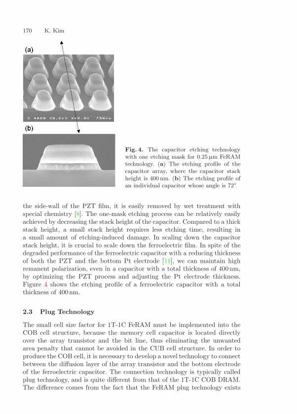
170 K. Kim
Fig. 4. The capacitor etching technologywith one etching mask for 0.25 µm FeRAMtechnology. (a) The etching profile of thecapacitor array, where the capacitor stackheight is 400 nm. (b) The etching profile ofan individual capacitor whose angle is 72
the side-wall of the PZT film, it is easily removed by wet treatment withspecial chemistry [8]. The one-mask etching process can be relatively easilyachieved by decreasing the stack height of the capacitor. Compared to a thickstack height, a small stack height requires less etching time, resulting ina small amount of etching-induced damage. In scaling down the capacitorstack height, it is crucial to scale down the ferroelectric film. In spite of thedegraded performance of the ferroelectric capacitor with a reducing thicknessof both the PZT and the bottom Pt electrode [11], we can maintain highremanent polarization, even in a capacitor with a total thickness of 400nm,by optimizing the PZT process and adjusting the Pt electrode thickness.Figure 4 shows the etching profile of a ferroelectric capacitor with a totalthickness of 400nm.
2.3 Plug Technology
The small cell size factor for 1T-1C FeRAM must be implemented into theCOB cell structure, because the memory cell capacitor is located directlyover the array transistor and the bit line, thus eliminating the unwantedarea penalty that cannot be avoided in the CUB cell structure. In order toproduce the COB cell, it is necessary to develop a novel technology to connectbetween the diffusion layer of the array transistor and the bottom electrodeof the ferroelectric capacitor. The connection technology is typically calledplug technology, and is quite different from that of the 1T-1C COB DRAM.The difference comes from the fact that the FeRAM plug technology exists
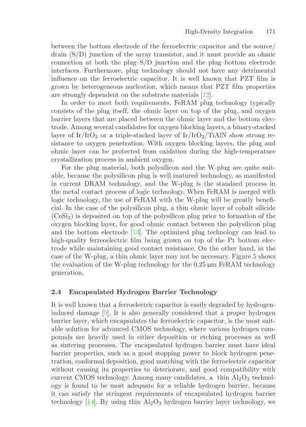
High-Density Integration 171
between the bottom electrode of the ferroelectric capacitor and the source/drain (S/D) junction of the array transistor, and it must provide an ohmicconnection at both the plug–S/D junction and the plug–bottom electrodeinterfaces. Furthermore, plug technology should not have any detrimentalinfluence on the ferroelectric capacitor. It is well known that PZT film isgrown by heterogeneous nucleation, which means that PZT film propertiesare strongly dependent on the substrate materials [12].
In order to meet both requirements, FeRAM plug technology typicallyconsists of the plug itself, the ohmic layer on top of the plug, and oxygenbarrier layers that are placed between the ohmic layer and the bottom elec-trode. Among several candidates for oxygen blocking layers, a binary-stackedlayer of Ir/IrO2 or a triple-stacked layer of Ir/IrO2/TiAlN show strong re-sistance to oxygen penetration. With oxygen blocking layers, the plug andohmic layer can be protected from oxidation during the high-temperaturecrystallization process in ambient oxygen.
For the plug material, both polysilicon and the W-plug are quite suit-able, because the polysilicon plug is well matured technology, as manifestedin current DRAM technology, and the W-plug is the standard process inthe metal contact process of logic technology. When FeRAM is merged withlogic technology, the use of FeRAM with the W-plug will be greatly benefi-cial. In the case of the polysilicon plug, a thin ohmic layer of cobalt silicide(CoSi2) is deposited on top of the polysilicon plug prior to formation of theoxygen blocking layer, for good ohmic contact between the polysilicon plugand the bottom electrode [13]. The optimized plug technology can lead tohigh-quality ferreoelectric film being grown on top of the Pt bottom elec-trode while maintaining good contact resistance. On the other hand, in thecase of the W-plug, a thin ohmic layer may not be necessary. Figure 5 showsthe evaluation of the W-plug technology for the 0.25 µm FeRAM technologygeneration.
2.4 Encapsulated Hydrogen Barrier Technology
It is well known that a ferroelectric capacitor is easily degraded by hydrogen-induced damage [9]. It is also generally considered that a proper hydrogenbarrier layer, which encapsulates the ferroelectric capacitor, is the most suit-able solution for advanced CMOS technology, where various hydrogen com-pounds are heavily used in either deposition or etching processes as wellas sintering processes. The encapsulated hydrogen barrier must have idealbarrier properties, such as a good stopping power to block hydrogen pene-tration, conformal deposition, good matching with the ferroelectric capacitorwithout causing its properties to deteriorate, and good compatibility withcurrent CMOS technology. Among many candidates, a thin Al2O3 technol-ogy is found to be most adequate for a reliable hydrogen barrier, becauseit can satisfy the stringent requirements of encapsulated hydrogen barriertechnology [14]. By using thin Al2O3 hydrogen barrier layer technology, we

172 K. Kim
Fig. 5. The W-plug technologyfor 0.25 µm FeRAM technology.(a) A SEM image of the W-plugused for a 0.25 µm 32 Mb 1T-1C COB FeRAM. (b) The con-tact resistance of the W-plug be-tween the bottom electrode andthe diffusion junction of an arraytransistor of the 0.25 µm FeRAMtechnology, where the contactsize is 0.25 µm × 0.25 µm
can eliminate hydrogen damage from hydrogen-rich CMOS processes, so thata reliable ferroelectric capacitor can be maintained even after full integration.
2.5 Novel Integration Technology
In order to realize the 15F2 cell size factor of 32Mb FeRAM, it is required todevelop novel cell integration technologies, in addition to key process tech-nologies, as previously discussed. The novel cell structure has been inventedby merging two adjacent plate line contacts into one common plate line con-tact. Thus, in the novel integration technology used for 32Mb FeRAM, everyadjacent pair of cells shares one common plate line [15]. It should be notedthat every cell has its own separate plate line in conventional 1T-1C COBFeRAM, such as 25F2 4 Mb FeRAM. The common plate line technology con-sists of four steps: the formation of the capacitor contact, an additional localplate line, a local common via for two adjacent cells, and a global commonplate line. These process steps are depicted in Fig. 6. The brief process se-quences of common plate line technology are as follows. In order to fabricatethe common plate line, it is indispensable to have an inter-layer dielectric(ILD) planarization process. For the purpose of ILD planarization, undopedsilicate glass (USG) oxide is deposited on patterned substrates, and is followedby spin-coating of spin-on-glass (SOG) oxide films. After the SOG oxide film
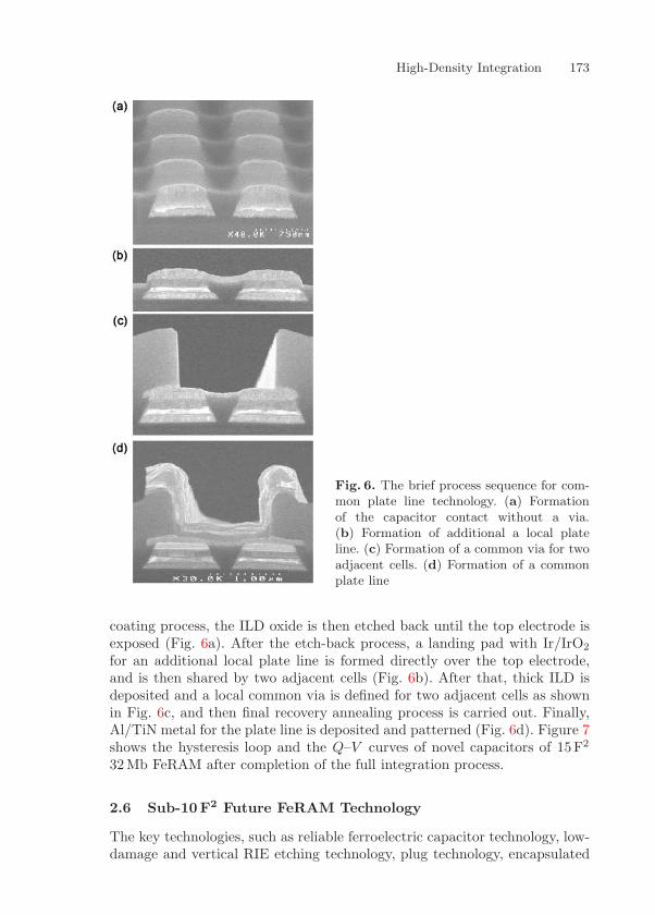
High-Density Integration 173
Fig. 6. The brief process sequence for com-mon plate line technology. (a) Formationof the capacitor contact without a via.(b) Formation of additional a local plateline. (c) Formation of a common via for twoadjacent cells. (d) Formation of a commonplate line
coating process, the ILD oxide is then etched back until the top electrode isexposed (Fig. 6a). After the etch-back process, a landing pad with Ir/IrO2
for an additional local plate line is formed directly over the top electrode,and is then shared by two adjacent cells (Fig. 6b). After that, thick ILD isdeposited and a local common via is defined for two adjacent cells as shownin Fig. 6c, and then final recovery annealing process is carried out. Finally,Al/TiN metal for the plate line is deposited and patterned (Fig. 6d). Figure 7shows the hysteresis loop and the Q–V curves of novel capacitors of 15F2
32Mb FeRAM after completion of the full integration process.
2.6 Sub-10F2 Future FeRAM Technology
The key technologies, such as reliable ferroelectric capacitor technology, low-damage and vertical RIE etching technology, plug technology, encapsulated
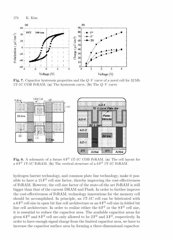
174 K. Kim
Fig. 7. Capacitor hysteresis properties and the Q–V curve of a novel cell for 32 Mb1T-1C COB FeRAM. (a) The hysteresis curve. (b) The Q–V curve
Fig. 8. A schematic of a future 6 F2 1T-1C COB FeRAM. (a) The cell layout fora 6F2 1T-1C FeRAM. (b) The vertical structure of a 6F2 1T-1C FeRAM
hydrogen barrier technology, and common plate line technology, make it pos-sible to have a 15F2 cell size factor, thereby improving the cost-effectivenessof FeRAM. However, the cell size factor of the state-of-the art FeRAM is stillbigger than that of the current DRAM and Flash. In order to further improvethe cost-effectiveness of FeRAM, technology innovations for the memory cellshould be accomplished. In principle, an 1T-1C cell can be fabricated witha 6 F2 cell size in open bit line cell architecture or an 8F2 cell size in folded bitline cell architecture. In order to realize either the 6F2 or the 8F2 cell size,it is essential to reduce the capacitor area. The available capacitor areas forgiven 6 F2 and 8 F2 cell are only allowed to be 2F2 and 3 F2, respectively. Inorder to have enough signal charge from the limited capacitor area, we have toincrease the capacitor surface area by forming a three-dimensional capacitor.
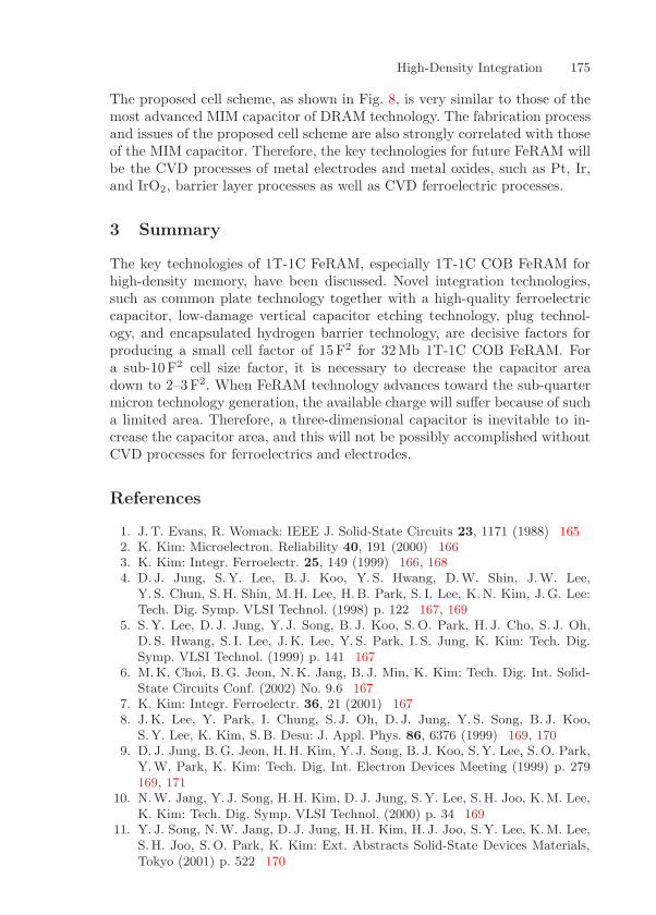
High-Density Integration 175
The proposed cell scheme, as shown in Fig. 8, is very similar to those of themost advanced MIM capacitor of DRAM technology. The fabrication processand issues of the proposed cell scheme are also strongly correlated with thoseof the MIM capacitor. Therefore, the key technologies for future FeRAM willbe the CVD processes of metal electrodes and metal oxides, such as Pt, Ir,and IrO2, barrier layer processes as well as CVD ferroelectric processes.
3 Summary
The key technologies of 1T-1C FeRAM, especially 1T-1C COB FeRAM forhigh-density memory, have been discussed. Novel integration technologies,such as common plate technology together with a high-quality ferroelectriccapacitor, low-damage vertical capacitor etching technology, plug technol-ogy, and encapsulated hydrogen barrier technology, are decisive factors forproducing a small cell factor of 15F2 for 32Mb 1T-1C COB FeRAM. Fora sub-10F2 cell size factor, it is necessary to decrease the capacitor areadown to 2–3F2. When FeRAM technology advances toward the sub-quartermicron technology generation, the available charge will suffer because of sucha limited area. Therefore, a three-dimensional capacitor is inevitable to in-crease the capacitor area, and this will not be possibly accomplished withoutCVD processes for ferroelectrics and electrodes.
References
1. J. T. Evans, R. Womack: IEEE J. Solid-State Circuits 23, 1171 (1988) 1652. K. Kim: Microelectron. Reliability 40, 191 (2000) 1663. K. Kim: Integr. Ferroelectr. 25, 149 (1999) 166, 1684. D. J. Jung, S.Y. Lee, B. J. Koo, Y. S. Hwang, D.W. Shin, J.W. Lee,
Y. S. Chun, S.H. Shin, M.H. Lee, H.B. Park, S. I. Lee, K.N. Kim, J.G. Lee:Tech. Dig. Symp. VLSI Technol. (1998) p. 122 167, 169
5. S.Y. Lee, D. J. Jung, Y. J. Song, B. J. Koo, S.O. Park, H. J. Cho, S. J. Oh,D. S. Hwang, S. I. Lee, J. K. Lee, Y. S. Park, I. S. Jung, K. Kim: Tech. Dig.Symp. VLSI Technol. (1999) p. 141 167
6. M. K. Choi, B.G. Jeon, N.K. Jang, B. J. Min, K. Kim: Tech. Dig. Int. Solid-State Circuits Conf. (2002) No. 9.6 167
7. K. Kim: Integr. Ferroelectr. 36, 21 (2001) 1678. J. K. Lee, Y. Park, I. Chung, S. J. Oh, D. J. Jung, Y. S. Song, B. J. Koo,
S.Y. Lee, K. Kim, S. B. Desu: J. Appl. Phys. 86, 6376 (1999) 169, 1709. D. J. Jung, B. G. Jeon, H.H. Kim, Y. J. Song, B. J. Koo, S.Y. Lee, S.O. Park,
Y.W. Park, K. Kim: Tech. Dig. Int. Electron Devices Meeting (1999) p. 279169, 171
10. N.W. Jang, Y. J. Song, H.H. Kim, D. J. Jung, S.Y. Lee, S.H. Joo, K.M. Lee,K. Kim: Tech. Dig. Symp. VLSI Technol. (2000) p. 34 169
11. Y. J. Song, N.W. Jang, D. J. Jung, H.H. Kim, H. J. Joo, S.Y. Lee, K.M. Lee,S.H. Joo, S.O. Park, K. Kim: Ext. Abstracts Solid-State Devices Materials,Tokyo (2001) p. 522 170

176 K. Kim
12. Y. J. Song, Y. Zhu, S. B. Desu: Appl. Phys. Lett. 72, 2686 (1998) 17113. H.H. Kim, D. J. Jung, S.Y. Lee, Y. J. Song, N.W. Jang, J. K. Lee, K. Kim:
Integr. Ferroelectr. 39, 239 (2001) 17114. Y.T. Lee, H. J. Cho, S. J. Oh, S.H. Joo, J. J. Lee, K.M. Lee, S.O. Park,
Y.W. Park, S. I. Lee: Ext. Abstracts Solid-State Devices Materials, Tokyo(1999) p. 394 171
15. K. Kim: 1st Int. Meeting Ferroelectric Random Access Memories, Gotemba(2001) Ext. Abstracts, p. 11 172
Index
1T-1C– COB, 1656 F2 cell size in open bit line cell
architecture, 1748 F2 cell size in folded bit line cell
architecture, 174
additional local plate line, 173advanced process technology, 167area penalty, 169
cell architecture– cost-effectiveness, 166cell size, 165common plate line technology, 172CVD technology, 165
encapsulated hydrogen barriertechnology, 171
FeRAM, 165– CVD process of metal electrodes and
metal oxides, 175
– nonvolatility, 165– resistance to oxygen penetration, 171
high directionality, 168
ILD planarization, 172integration technology, 167
MIM capacitor, 175minimum feature size F, 165
ohmic contact, 171one-mask etching process, 170
plasma-induced damage, 169pyrochlore phase, 168
thin Al2O3 technology, 171three-dimensional ferroelectric
capacitor technology, 165three-mask process, 169
W-plug technology, 171
Testing and Reliability
Yasuhiro Shimada
Semiconductor Device Research Center, Matsushita Electric Industrial Co. Ltd.,1-1 Saiwai-cho, Takatsuki, Osaka 5691193, [email protected]
Abstract. In ferroelectric random access memories (FeRAMs), the difference inthe displacement charge between the two polarization states is fundamental to dis-criminate the binary states, “1” and “0”. Therefore, the durability of the differencein the displacement charge and circuit techniques for sensing the difference are inti-mately related to the reliability of FeRAMs. In this chapter, we deal with electricaldegradation phenomena in ferroelectric capacitors, such as resistance degradation,time-dependent dielectric breakdown (TDDB), ferroelectric fatigue, charge reten-tion, and imprint, which affect the sensing of displacement charges from a memorycell all the way. In each topic, we refer to related testing techniques to characterizeand qualify the performance and reliability of ferroelectric capacitors. These discus-sions include some fundamental considerations on aging mechanisms in ferroelectriccapacitors, which may provide essential and meaningful feedback for materials, cir-cuit design, and manufacturing process improvements.
1 Leakage Current
Since ferroelectrics are used as capacitor dielectrics in FeRAMs, leakage cur-rents and electrical breakdown are potential concerns in determining the op-erating voltage and device performance. Leakage currents in insulators, in-cluding ferroelectrics, arise from carrier conduction under high fields and hightemperatures. For this reason, a charge in a ferroelectric capacitor under anelectric field cannot be stored definitely, and it ultimately leaks off. Leakagecurrent measurements are made by applying a ramped potential across theferroelectric capacitor at a given temperature. The current–voltage (J–V )curves are plotted on different scales in accordance with an adequate conduc-tion mechanism.
Possible conduction mechanisms in insulators are briefly summarized in [1],which includes Schottky emission, Frenkel–Poole emission, Fowler–Nordheimtunneling, and space-charge-limited and ohmic currents. In particular, theSchottky emission and Frenkel–Poole emission mechanisms are responsiblefor the leakage currents at high electric fields in ferroelectric capacitors usingBa1−xSrxTaO3 (BST) [2, 3, 4, 5, 6, 7], PbZrxTi1−xO3 (PZT) [8, 9, 10], andSrBi2Ta2O9 (SBT) [11,12]. Schottky emission occurs when carriers overcomean interfacial potential barrier by thermal activation, so that the current islimited by the interface and depends on the temperature, the applied field,and the barrier height. Frenkel–Poole emission occurs when carriers trappedH. Ishiwara, M. Okuyama, Y. Arimoto (Eds.): Ferroelectric Random Access Memories,Topics Appl. Phys. 93, 177–195 (2004)c© Springer-Verlag Berlin Heidelberg 2004
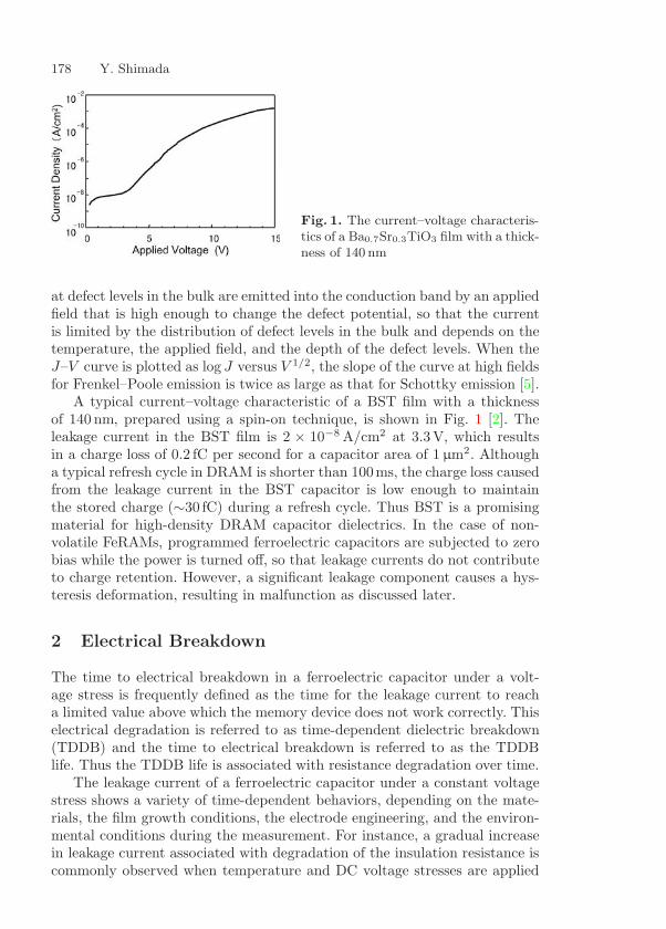
178 Y. Shimada
Fig. 1. The current–voltage characteris-tics of a Ba0.7Sr0.3TiO3 film with a thick-ness of 140 nm
at defect levels in the bulk are emitted into the conduction band by an appliedfield that is high enough to change the defect potential, so that the currentis limited by the distribution of defect levels in the bulk and depends on thetemperature, the applied field, and the depth of the defect levels. When theJ–V curve is plotted as log J versus V 1/2, the slope of the curve at high fieldsfor Frenkel–Poole emission is twice as large as that for Schottky emission [5].
A typical current–voltage characteristic of a BST film with a thicknessof 140 nm, prepared using a spin-on technique, is shown in Fig. 1 [2]. Theleakage current in the BST film is 2 × 10⁻⁸ A/cm2 at 3.3V, which resultsin a charge loss of 0.2 fC per second for a capacitor area of 1 µm2. Althougha typical refresh cycle in DRAM is shorter than 100ms, the charge loss causedfrom the leakage current in the BST capacitor is low enough to maintainthe stored charge (∼30 fC) during a refresh cycle. Thus BST is a promisingmaterial for high-density DRAM capacitor dielectrics. In the case of non-volatile FeRAMs, programmed ferroelectric capacitors are subjected to zerobias while the power is turned off, so that leakage currents do not contributeto charge retention. However, a significant leakage component causes a hys-teresis deformation, resulting in malfunction as discussed later.
2 Electrical Breakdown
The time to electrical breakdown in a ferroelectric capacitor under a volt-age stress is frequently defined as the time for the leakage current to reacha limited value above which the memory device does not work correctly. Thiselectrical degradation is referred to as time-dependent dielectric breakdown(TDDB) and the time to electrical breakdown is referred to as the TDDBlife. Thus the TDDB life is associated with resistance degradation over time.
The leakage current of a ferroelectric capacitor under a constant voltagestress shows a variety of time-dependent behaviors, depending on the mate-rials, the film growth conditions, the electrode engineering, and the environ-mental conditions during the measurement. For instance, a gradual increasein leakage current associated with degradation of the insulation resistance iscommonly observed when temperature and DC voltage stresses are applied
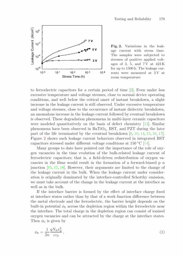
Testing and Reliability 179
Fig. 2. Variations in the leak-age current with stress time.The samples were subjected tostresses of positive applied volt-ages of 3, 5, and 7V at 423 Kfor up to 1500 h. The leakage cur-rents were measured at 3 V atroom temperature
to ferroelectric capacitors for a certain period of time [3]. Even under lessexcessive temperature and voltage stresses, close to normal device operatingconditions, and well below the critical onset of instant breakdown, a slightincrease in the leakage current is still observed. Under excessive temperatureand voltage stresses, close to the occurrence of instant dielectric breakdown,an anomalous increase in the leakage current followed by eventual breakdownis observed. These degradation phenomena in multi-layer ceramic capacitorswere modeled quantitatively on the basis of defect chemistry [13]. Similarphenomena have been observed in BaTiO3, BST, and PZT during the laterpart of the life terminated by the eventual breakdown [8, 10, 14, 15, 16, 17].Figure 2 shows such leakage current behaviors observed in integrated BSTcapacitors stressed under different voltage conditions at 150 C [14].
Many groups to date have pointed out the importance of the role of oxy-gen vacancies in the time evolution of the bulk-related leakage current offerroelectric capacitors; that is, a field-driven redistribution of oxygen va-cancies in the films would result in the formation of a forward-biased p–njunction [15, 17, 18]. However, their arguments are limited to the change ofthe leakage current in the bulk. When the leakage current under consider-ation is originally dominated by the interface-controlled Schottky emission,we must take account of the change in the leakage current at the interface aswell as in the bulk.
If the interface barrier is formed by the effect of interface charge fixedat interface states rather than by that of a work function difference betweenthe metal electrode and the ferroelectric, the barrier height depends on thebuilt-in potential φb across the depletion region within the ferroelectric nearthe interface. The total charge in the depletion region can consist of ionizedoxygen vacancies and can be attracted by the charge at the interface states.Then φb is given by
φb =12n
qNdx2d
εε0, (1)

180 Y. Shimada
Fig. 3. A comparison of the charge distribution ρ, the electric field E, and energyband variation as a function of the direction x near the cathode of a BST capacitor(a) before and (b) after stressing
where q is the electronic charge, n is the average ionic valence of oxygenvacancies, Nd is the concentration of oxygen vacancies, xd is the extent ofthe depletion region, ε is the dielectric constant of the ferroelectric, and ε0 isthe permittivity of vacuum.
When the temperature is elevated, oxygen vacancies initially distributedacross the film are thermally activated and may begin to migrate toward thecathode under a high field. Finally, the oxygen vacancies accumulate nearthe cathode. Since the total charge in the depletion region qNdxd remainsconstant in terms of the fixed interface charge, the extent of the depletionregion xd decreases as the concentration of oxygen vacancies Nd increases.Then the barrier height φb is lowered due to the accumulation of oxygenvacancies at the cathode, as illustrated in Fig. 3. As a result of the barrierlowering at the cathode, bulk-controlled conduction appears to be predom-inant. Then the space-charge-limited or Frenkel–Poole emission current willcontribute to the total current.
When a lot of sample capacitors are tested, the TDDB lifetimes are dis-tributed over a wide range of time durations. Then we need to assume a well-defined statistical distribution of the TDDB lifetimes. The Weibull distribu-tion is one of the best descriptions for TDDB lifetimes [19]. Using a Weibullplot, for instance, we can determine the relation between voltage stress andTDDB lifetime for given ferroelectric capacitors. Figure 4a shows a Weibullplot of TDDB lifetimes for integrated BST capacitors in a microcontrollerstressed under different field conditions at 125 C. The time to 0.1% cumu-lative failure is then expressed as a function of the field strength. Since theshape parameter of the distribution, m, is greater than unity, the failure modeof the integrated BST capacitors is intrinsic. From Fig. 4b, an estimated life-
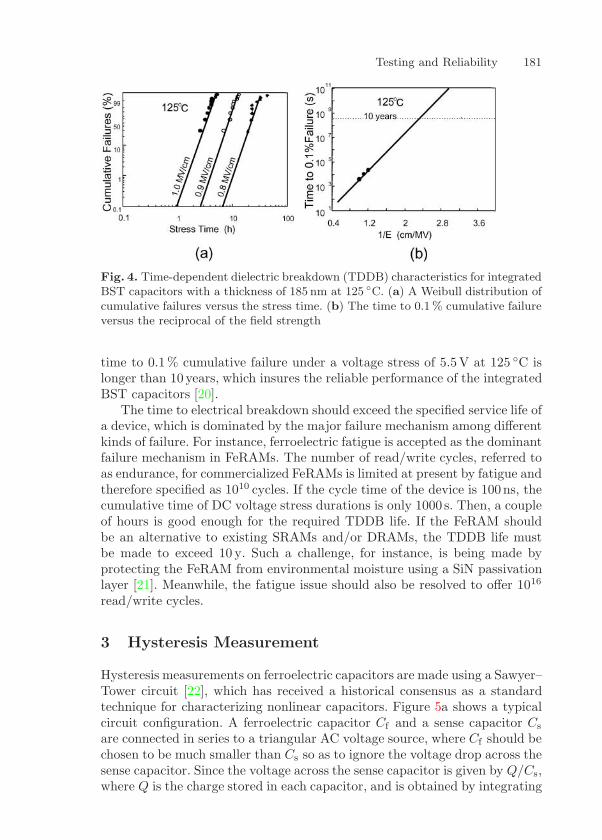
Testing and Reliability 181
Fig. 4. Time-dependent dielectric breakdown (TDDB) characteristics for integratedBST capacitors with a thickness of 185 nm at 125 C. (a) A Weibull distribution ofcumulative failures versus the stress time. (b) The time to 0.1 % cumulative failureversus the reciprocal of the field strength
time to 0.1% cumulative failure under a voltage stress of 5.5V at 125 C islonger than 10 years, which insures the reliable performance of the integratedBST capacitors [20].
The time to electrical breakdown should exceed the specified service life ofa device, which is dominated by the major failure mechanism among differentkinds of failure. For instance, ferroelectric fatigue is accepted as the dominantfailure mechanism in FeRAMs. The number of read/write cycles, referred toas endurance, for commercialized FeRAMs is limited at present by fatigue andtherefore specified as 1010 cycles. If the cycle time of the device is 100ns, thecumulative time of DC voltage stress durations is only 1000 s. Then, a coupleof hours is good enough for the required TDDB life. If the FeRAM shouldbe an alternative to existing SRAMs and/or DRAMs, the TDDB life mustbe made to exceed 10 y. Such a challenge, for instance, is being made byprotecting the FeRAM from environmental moisture using a SiN passivationlayer [21]. Meanwhile, the fatigue issue should also be resolved to offer 1016
read/write cycles.
3 Hysteresis Measurement
Hysteresis measurements on ferroelectric capacitors are made using a Sawyer–Tower circuit [22], which has received a historical consensus as a standardtechnique for characterizing nonlinear capacitors. Figure 5a shows a typicalcircuit configuration. A ferroelectric capacitor Cf and a sense capacitor Cs
are connected in series to a triangular AC voltage source, where Cf should bechosen to be much smaller than Cs so as to ignore the voltage drop across thesense capacitor. Since the voltage across the sense capacitor is given by Q/Cs,where Q is the charge stored in each capacitor, and is obtained by integrating

182 Y. Shimada
Fig. 5. (a) A Sawyer–Tower circuit for hysteresis measurements. (b) A typicalhysteresis curve
the current flowing through the ferroelectric capacitor over a measurementcycle, a hysteresis curve is obtained, as illustrated in Fig. 5b, by connectingthe voltage source and sense capacitor to the X and Y inputs, respectively, ofan oscilloscope. Figure 6 shows the signal responses in accordance with thevoltage Vf applied to the ferroelectric capacitor. For readers’ convenience,each step is numbered in order in accordance with the numbered hysteresisexcursion in Fig. 5b. Since the voltage generator charges up the ferroelectriccapacitor through an output impedance of Ro, the measurement speed islimited by the time constant. In addition, impedance matching should beconsidered for higher-frequency measurements [23].
To measure the current response flowing through the ferroelectric capaci-tor, the sense capacitor is replaced with a sense resistor. A typical waveformof the response is illustrated in Fig. 6b. At higher frequencies this sense resis-tor in series with the output impedance will contribute to the limiting timeconstant of the system [24]. Then there will be a limitation on the capacitanceof the ferroelectric capacitors that are measurable with such a system.
When the resistance of a ferroelectric capacitor is degraded to competewith its capacitive reactance, the leakage component will cause a deforma-tion of the hysteresis curve along the Q-axis. Such a ferroelectric capacitorwill burn out sooner or later, because the leakage component will be signifi-cantly large (> 10−2 A/cm2). Therefore, hysteresis measurements should beconducted with J–V measurements.
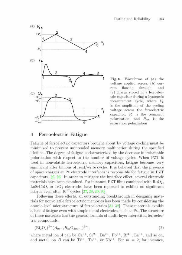
Testing and Reliability 183
Fig. 6. Waveforms of (a) thevoltage applied across, (b) cur-rent flowing through, and(c) charge stored in a ferroelec-tric capacitor during a hysteresismeasurement cycle, where Vp
is the amplitude of the cyclingvoltage across the ferroelectriccapacitor, Pr is the remanentpolarization, and Psat is thesaturation polarization
4 Ferroelectric Fatigue
Fatigue of ferroelectric capacitors brought about by voltage cycling must beminimized to prevent unintended memory malfunction during the specifiedlifetime. The degree of fatigue is characterized by the decrease in switchablepolarization with respect to the number of voltage cycles. When PZT isused in nonvolatile ferroelectric memory capacitors, fatigue becomes verysignificant after billions of read/write cycles. It is believed that the presenceof space charges at Pt electrode interfaces is responsible for fatigue in PZTcapacitors [25, 26]. In order to mitigate the interface effect, several electrodematerials have been examined. For instance, PZT films combined with RuO2,LaSrCoO, or IrO2 electrodes have been reported to exhibit no significantfatigue even after 1012 cycles [27, 28, 29, 30].
Following these efforts, an outstanding breakthrough in designing mate-rials for nonvolatile ferroelectric memories has been made by considering theatomic-level microstructure of ferroelectrics [31, 32]. These materials exhibita lack of fatigue even with simple metal electrodes, such as Pt. The structureof these materials has the general formula of multi-layer interstitial ferroelec-tric compounds:
(Bi2O2)2+(Am−1BmO3m+1)2− , (2)
where metal ion A can be Ca2+, Sr2+, Ba2+, Pb2+, Bi3+, La3+, and so on,and metal ion B can be Ti4+, Ta5+, or Nb5+. For m = 2, for instance,
184 Y. Shimada
Bi2O2 layers are periodically alternated with perovskite-like AB2O7 layerswith double oxygen octahedral units. Thus m is the number of octahedralunits in between the Bi2O2 layers. The direction of the spontaneous polar-ization is parallel to the a–b plane of the layers, as this plane contains theperiodic O–B–O chains that are known to be effective in the perovskite fer-roelectric. In contrast, there is no spontaneous polarization along the c-axisbecause of the lack of periodic symmetry in the O–B–O chain. The periodiclattice parameters for stoichiometric SBT are a = 5.52237 A, b = 5.52408A,and c = 25.02641 A, exhibiting an orthorhombic distortion [33]. The choiceof Sr for the metal A site is advantageous in suppressing the metal deficiencythat causes degradations in ferroelectricity, compared to the use of volatilePb in PZT. In addition, the stacked Bi2O2 layers can be an oxygen sourcefor compensation of oxygen vacancies induced in perovskite-like octahedra,because the oxygen ions in the perovskite-like layers are much more stablethan those in the Bi2O2 layers [34]. Thus oxygen vacancies generated in theperovskite-like layers to cause fatigue are readily exchanged with oxygen ionsin the Bi2O2 layers [35]. Therefore the bismuth oxide materials, such as SBT,are hardly degradable in ferroelectricity, characterized by remanent polariza-tion and coercive field, even if the deoxidation of the ferroelectric occursunder the influence of Pt electrodes.
Fatigue testing is coordinated by making hysteresis measurements on fa-tigued ferroelectric capacitors after a number of voltage cycles. In order topredict the reliability of FeRAMs, accelerated fatigue testing is required. Incommon accelerated tests for semiconductor devices, a number of devicesare subjected to failure-causing stresses such as temperature and voltagebias, each related to a different acceleration factor that is needed to describea relationship between failure times in a use condition and the acceleratedcondition. However, there is no definite temperature dependence of fatigue inSBT capacitors [36]. Recently, an empirical voltage acceleration model basedon the Eyring model was proposed for fatigue in SBT capacitors [37]. Thenumber of voltage cycles to fatigue failure is well described by the followingexpression:
log(cycles) = C +Ea
kT− n∗ log Vf , (3)
where Ea is the activation energy, k is the Boltzmann constant, T is theabsolute temperature, Vf is the cycling voltage applied to the ferroelectriccapacitor, C is a constant, and n∗ is a function of temperature. Although themajority of fatigue data exhibit a logarithmic decrease in switching polar-ization with the number of voltage cycles, and there should be a meaningfulrelation between the motions of domain walls and defects, confident physicalinsights into the underlying mechanism have not yet been established.
5 Pulse Polarization Measurement
The macroscopic electric field in a poled ferroelectric capacitor in which a re-manent polarization is preserved is substantially zero when both the capacitor

Testing and Reliability 185
Fig. 7. A typical hysteresis loop, showing charge losses after the storage for a certainperiod of time. (a) Psw: the switched polarization charge extracted from a capac-itor in the up state. (b) Pns: the nonswitched polarization charge extracted froma capacitor in the down state
electrodes are grounded after poling, so that the ferroelectric capacitor can beregarded as being under an equilibrium condition. Nevertheless, ferroelectriccapacitors exhibit an aging effect characterized by the decay in remanent po-larization during high-temperature storage (retention testing) [38, 39, 40, 41].This suggests that the aging effect is a manifestation of microscopic changesin the ferroelectric capacitor. Another aspect of the aging effect referred tois the loss of switchable polarization from the preliminarily poled remanentstate to the opposite (complementary) state, resulting from the establishmentof a preference for the remanent state over the opposite state during stor-age or unipolar voltage pulsing [42, 43, 44, 45]. This phenomenon is termedimprint.
Both the retention and imprint measurements are based on the pulsepolarization measurement technique, which yields Psw or Pns by pulsing theferroelectric capacitor in accordance with whether a binary “1” or “0” isstored. To give a definite discrimination between “1” and “0”, there shouldbe a certain difference between Psw and Pns, which can be defined as
Pnv = Psw − Pns . (4)
Then Pnv is a function of the time interval between pulse polarization mea-surements. Following this definition, retention is characterized by makingpulse polarization measurements for the same states as those preliminarilypoled, as shown in Fig. 7. Imprint, on the other hand, is characterized bymaking pulse polarization measurements for the opposite states to those pre-liminarily poled. In either case, Pnv is an important measure for evaluatingthe nonvolatility of FeRAMs when the power is turned off.
6 Retention
Figure 8 shows a plot of Pnv versus retention time for SrBi2(Ta,Nb)2O9
(SBTN) capacitors [46]. The data set for the first 530ms after poling was
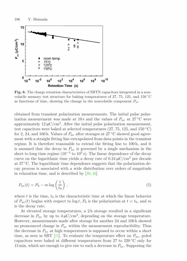
186 Y. Shimada
Fig. 8. The charge retention characteristics of SBTN capacitors integrated in a non-volatile memory test structure for baking temperatures of 27, 75, 125, and 150 Cas functions of time, showing the change in the nonvolatile component Pnv
obtained from transient polarization measurements. The initial pulse polar-ization measurement was made at 10 s and the values of Pnv at 27 C wereapproximately 12 µC/cm2. After the initial pulse polarization measurement,test capacitors were baked at selected temperatures (27, 75, 125, and 150 C)for 2, 24, and 100 h. Values of Pnv after storages at 27 C showed good agree-ment with a straight fitting line extrapolated from data points in the transientregime. It is therefore reasonable to extend the fitting line to 100h, and itis assumed that the decay in Pnv is governed by a single mechanism in theshort to long time regime (10−3 to 105 s). The linear dependence of the decaycurve on the logarithmic time yields a decay rate of 0.24 µC/cm2 per decadeat 27 C. The logarithmic time dependence suggests that the polarization de-cay process is associated with a wide distribution over orders of magnitudein relaxation time, and is described by [39, 40]
Pnv(t) = P0 − m log(
t
t0
), (5)
where t is the time, t0 is the characteristic time at which the linear behaviorof Pnv(t) begins with respect to log t, P0 is the polarization at t = t0, and mis the decay rate.
At elevated storage temperatures, a 2 h storage resulted in a significantdecrease in Pnv by up to 4 µC/cm2, depending on the storage temperature.However, measurements made after storage for another 24 and 100h showedno pronounced change in Pnv within the measurement reproducibility. Thusthe decrease in Pnv at high temperatures is supposed to occur within a shorttime, as seen in SBT [11]. To evaluate the temperature effect on Pnv, poledcapacitors were baked at different temperatures from 27 to 220 C only for15min, which are enough to give rise to such a decrease in Pnv. Supposing the

Testing and Reliability 187
Fig. 9. The polarization charge difference Pnv versus the baking temperature T ,where TC is the Curie temperature. Polarization measurements were made at 27 Cafter storage at temperatures from 27 to 220 C for 15min
second-order transition to be near the Curie temperature, TC, the values ofPnv were plotted as a function of the baking temperature, T , so as to obtainthe relation between Pnv and (TC−T )1/2. As shown in Fig. 9, an extrapolationfrom this data set symbolized by closed circles indicates a collapse of Pnv ata temperature of 330 C, which is close to an experimentally determined valueof the Curie temperature for SBTN films [47].
To account for the temperature effect in the high-temperature storagetest, values of Pnv in Fig. 8, whose measurements were made after storagefor 2–100h, were overlaid on the same plot (Fig. 9). Then we found a goodagreement in the temperature dependence between the long-time storage val-ues and the 15min storage values. This indicates that the decrease in Pnv athigh temperatures from its initial (t0 = 10 s) value is primarily due to aninstantaneous decrease in remanent polarization within 15min, and that thetemperature dependence is quite similar to that of spontaneous polarizationin the vicinity of the second-order transition. The decrease in Pnv caused athigh temperatures is explained by the loss of measurable charge in the ca-pacitor electrodes, coupled with a polarization charge. Therefore, Pnv at hightemperatures is quenched to room temperature.
Small changes in Pnv resulting from storage times of 2, 24, and 100 hstorages at high temperatures lead to a supposition that Pnv at high tem-peratures has a logarithmic time dependence similar to that at 27 C. Whendiscussing the origin of the distributed relaxation time for the decay in re-manent polarization, one can indicate two possible factors: (1) distributionin the coercive energy responsible for polarization reversal; and (2) distribu-tion in the depth of the traps responsible for space charge transport. Whenthe first mechanism is invoked, the polarization decay process is governed bythe stochastic switching of thermally fluctuating displacement dipoles fromone well to the other in the double-minimum potential with distributed coer-
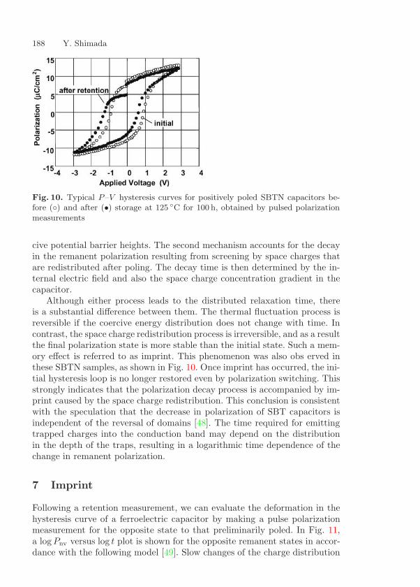
188 Y. Shimada
Fig. 10. Typical P–V hysteresis curves for positively poled SBTN capacitors be-fore () and after (•) storage at 125 C for 100 h, obtained by pulsed polarizationmeasurements
cive potential barrier heights. The second mechanism accounts for the decayin the remanent polarization resulting from screening by space charges thatare redistributed after poling. The decay time is then determined by the in-ternal electric field and also the space charge concentration gradient in thecapacitor.
Although either process leads to the distributed relaxation time, thereis a substantial difference between them. The thermal fluctuation process isreversible if the coercive energy distribution does not change with time. Incontrast, the space charge redistribution process is irreversible, and as a resultthe final polarization state is more stable than the initial state. Such a mem-ory effect is referred to as imprint. This phenomenon was also obs erved inthese SBTN samples, as shown in Fig. 10. Once imprint has occurred, the ini-tial hysteresis loop is no longer restored even by polarization switching. Thisstrongly indicates that the polarization decay process is accompanied by im-print caused by the space charge redistribution. This conclusion is consistentwith the speculation that the decrease in polarization of SBT capacitors isindependent of the reversal of domains [48]. The time required for emittingtrapped charges into the conduction band may depend on the distributionin the depth of the traps, resulting in a logarithmic time dependence of thechange in remanent polarization.
7 Imprint
Following a retention measurement, we can evaluate the deformation in thehysteresis curve of a ferroelectric capacitor by making a pulse polarizationmeasurement for the opposite state to that preliminarily poled. In Fig. 11,a log Pnv versus log t plot is shown for the opposite remanent states in accor-dance with the following model [49]. Slow changes of the charge distribution
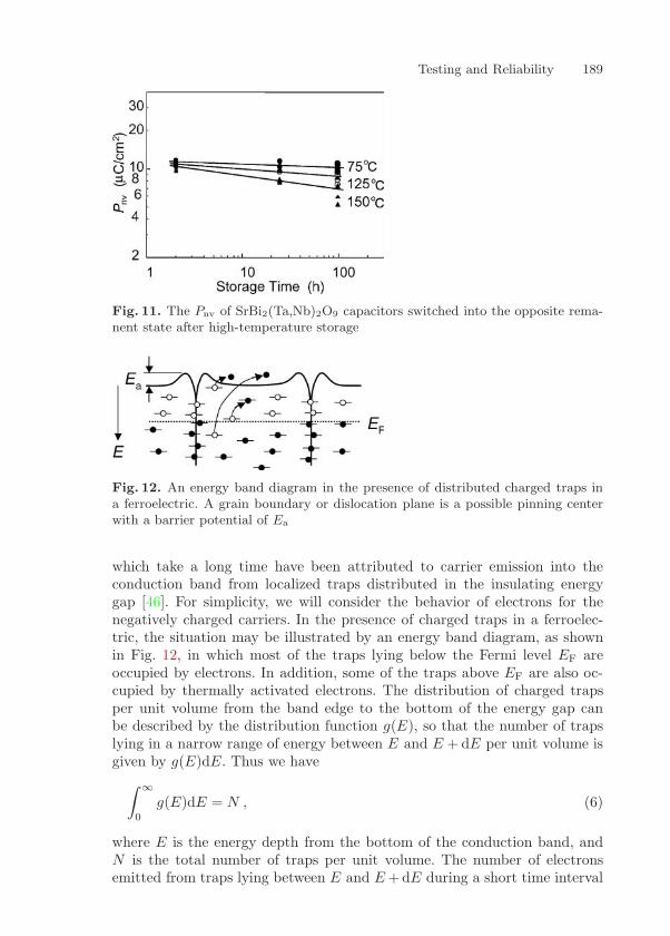
Testing and Reliability 189
Fig. 11. The Pnv of SrBi2(Ta,Nb)2O9 capacitors switched into the opposite rema-nent state after high-temperature storage
Fig. 12. An energy band diagram in the presence of distributed charged traps ina ferroelectric. A grain boundary or dislocation plane is a possible pinning centerwith a barrier potential of Ea
which take a long time have been attributed to carrier emission into theconduction band from localized traps distributed in the insulating energygap [46]. For simplicity, we will consider the behavior of electrons for thenegatively charged carriers. In the presence of charged traps in a ferroelec-tric, the situation may be illustrated by an energy band diagram, as shownin Fig. 12, in which most of the traps lying below the Fermi level EF areoccupied by electrons. In addition, some of the traps above EF are also oc-cupied by thermally activated electrons. The distribution of charged trapsper unit volume from the band edge to the bottom of the energy gap canbe described by the distribution function g(E), so that the number of trapslying in a narrow range of energy between E and E + dE per unit volume isgiven by g(E)dE. Thus we have
∫ ∞
0
g(E)dE = N , (6)
where E is the energy depth from the bottom of the conduction band, andN is the total number of traps per unit volume. The number of electronsemitted from traps lying between E and E +dE during a short time interval
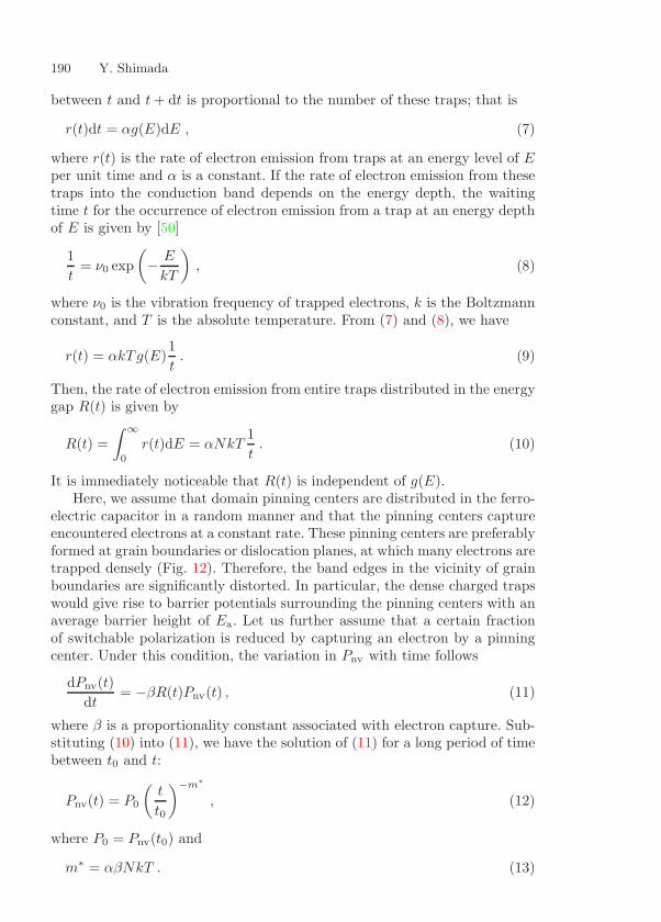
190 Y. Shimada
between t and t + dt is proportional to the number of these traps; that is
r(t)dt = αg(E)dE , (7)
where r(t) is the rate of electron emission from traps at an energy level of Eper unit time and α is a constant. If the rate of electron emission from thesetraps into the conduction band depends on the energy depth, the waitingtime t for the occurrence of electron emission from a trap at an energy depthof E is given by [50]
1t
= ν0 exp(− E
kT
), (8)
where ν0 is the vibration frequency of trapped electrons, k is the Boltzmannconstant, and T is the absolute temperature. From (7) and (8), we have
r(t) = αkTg(E)1t
. (9)
Then, the rate of electron emission from entire traps distributed in the energygap R(t) is given by
R(t) =∫ ∞
0
r(t)dE = αNkT1t
. (10)
It is immediately noticeable that R(t) is independent of g(E).Here, we assume that domain pinning centers are distributed in the ferro-
electric capacitor in a random manner and that the pinning centers captureencountered electrons at a constant rate. These pinning centers are preferablyformed at grain boundaries or dislocation planes, at which many electrons aretrapped densely (Fig. 12). Therefore, the band edges in the vicinity of grainboundaries are significantly distorted. In particular, the dense charged trapswould give rise to barrier potentials surrounding the pinning centers with anaverage barrier height of Ea. Let us further assume that a certain fractionof switchable polarization is reduced by capturing an electron by a pinningcenter. Under this condition, the variation in Pnv with time follows
dPnv(t)dt
= −βR(t)Pnv(t) , (11)
where β is a proportionality constant associated with electron capture. Sub-stituting (10) into (11), we have the solution of (11) for a long period of timebetween t0 and t:
Pnv(t) = P0
(t
t0
)−m∗
, (12)
where P0 = Pnv(t0) and
m∗ = αβNkT . (13)
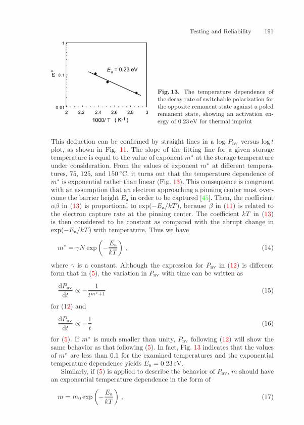
Testing and Reliability 191
Fig. 13. The temperature dependence ofthe decay rate of switchable polarization forthe opposite remanent state against a poledremanent state, showing an activation en-ergy of 0.23 eV for thermal imprint
This deduction can be confirmed by straight lines in a log Pnv versus log tplot, as shown in Fig. 11. The slope of the fitting line for a given storagetemperature is equal to the value of exponent m∗ at the storage temperatureunder consideration. From the values of exponent m∗ at different tempera-tures, 75, 125, and 150 C, it turns out that the temperature dependence ofm∗ is exponential rather than linear (Fig. 13). This consequence is congruentwith an assumption that an electron approaching a pinning center must over-come the barrier height Ea in order to be captured [45]. Then, the coefficientαβ in (13) is proportional to exp(−Ea/kT ), because β in (11) is related tothe electron capture rate at the pinning center. The coefficient kT in (13)is then considered to be constant as compared with the abrupt change inexp(−Ea/kT ) with temperature. Thus we have
m∗ = γN exp(−Ea
kT
), (14)
where γ is a constant. Although the expression for Pnv in (12) is differentform that in (5), the variation in Pnv with time can be written as
dPnv
dt∝ − 1
tm∗+1(15)
for (12) and
dPnv
dt∝ −1
t(16)
for (5). If m∗ is much smaller than unity, Pnv following (12) will show thesame behavior as that following (5). In fact, Fig. 13 indicates that the valuesof m∗ are less than 0.1 for the examined temperatures and the exponentialtemperature dependence yields Ea = 0.23 eV.
Similarly, if (5) is applied to describe the behavior of Pnv, m should havean exponential temperature dependence in the form of
m = m0 exp(−Ea
kT
), (17)

192 Y. Shimada
where m0 is a proportionality constant. From the values of m obtained fromPnv versus log t plots for different temperatures, Ea is calculated be 0.19 eV.This coincidence leads us to believe that the decay in remanent polariza-tion has the same origin as the decay in switchable polarization. A possibleexplanation is that emitted electrons are captured by preferred pinning cen-ters, to screen or compensate for the polarization charges as well as to pinthe domains. A similar argument can also be put forward for holes as thepositively charged carriers. The above argument leads us to a comprehensiveunderstanding of imprint as a result of the redistribution of emitted carri-ers, and this also agrees with the deduction in the previous discussion thatthe decay in remanent polarization is due to the redistribution of carriersrather than polarization reversal [48]. However, it should be noted that suchredistribution of carriers must be highly localized, because the J–V charac-teristics before and after high-temperature storage indicate that there is nomacroscopic change in the entire charge distribution throughout the capacitorduring the thermal aging process [46].
References
1. S.M. Sze: Physics of Semiconductor Devices, 2nd ed. (Wiley, New York 1981)177
2. M. Azuma, M. Scott, E. Fujii, T. Otsuki, G. Kano, C. A. Paz de Araujo: Ab-stracts 4th Int. Symp. Integr. Ferroelectr., Monterey (1992) p. 109 177, 178
3. R. Waser, M. Klee: Abstracts 3rd Int. Symp. Integr. Ferroelectr., ColoradoSprings (1991) p. 288 177, 179
4. P. Bhattacharya, T. Komeda, K.-H. Park, Y. Nishioka: Jpn. J. Appl. Phys. 32,4103 (1993) 177
5. P. Li, T.M. Lu: Phys. Rev. B 43, 14261 (1991) 177, 1786. Y. Shimada, A. Inoue, T. Nasu, K. Arita, Y. Nagano, A. Matsuda, Y. Uemoto,
E. Fujii, M. Azuma, Y. Oishi, S. Hayashi, T. Otsuki: Jpn. J. Appl. Phys. 35,140 (1996) 177
7. Y. Fukuda, K. Numata, K. Aoki, A. Nishimura: Jpn. J. Appl. Phys. 35, 5178(1996) 177
8. X. Chen, A. I. Kingon, L. Mantese, O. Auciello, K.Y. Hsieh: Integr. Ferroelectr.3, 355 (1993) 177, 179
9. H. Hu, S. B. Krupanidhi: J. Mater. Res. 9, 1484 (1994) 17710. X. Chen, A. I. Kingon, H.N. Al-Shareef, K.R. Bellur, K. Gifford, O. Auciello:
Integr. Ferroelectr. 7, 291 (1995) 177, 17911. D. J. Taylor, R. E. Jones, P. Zurcher, P. Chu, Y.T. Lii, B. Jiang, S. J. Gillespie:
Appl. Phys. Lett. 68, 2300 (1996) 177, 18612. K. Watanabe, A. J. Hartmann, R.N. Lamb, J. F. Scott: J. Appl. Phys. 84, 2170
(1998) 17713. R. Waser: J. Am. Ceram. Soc. 73, 1645 (1990) 17914. Y. Shimada, A. Inoue, T. Nasu, Y. Nagano, A. Matsuda, K. Arita, Y. Uemoto,
E. Fujii, T. Otsuki: Jpn. J. Appl. Phys. 35, 4919 (1996) 17915. S.B. Desu, I.K. Yoo: J. Electrochem. Soc. 140, L133 (1993) 179
Testing and Reliability 193
16. K. Numata, Y. Fukuda, K. Aoki, A. Nishimura: Jpn. J. Appl. Phys. 34, 5245(1995) 179
17. D. J. Wouters, G. Willems, G. Groeseneken, H.E. Meas, K. Brooks: Integr.Ferroelectr. 7, 173 (1995) 179
18. T. Baiatu, R. Waser, K.-H. Hardtl: J. Am. Ceram. Soc. 73, 1663 (1990) 17919. D. J. Klinger, Y. Nakada, M. Menendez (Eds.): AT&T Reliability Manual (Van
Nostrand Reinhold, New York 1990) 18020. E. Fujii, Y. Uemoto, S. Hayashi, T. Nasu, Y. Shimada, A. Matsuda, M. Kibe,
M. Azuma, T. Otsuki, G. Kano, M. Scott, L.D. McMillan, C. A. Paz de Araujo:Tech. Dig. Int. Electron Devices Meeting, San Francisco (1992) p. 267 181
21. E. Fujii, T. Otsuki, Y. Judai, Y. Shimada, M. Azuma, Y. Uemoto, Y. Nagano,T. Nasu, Y. Izutsu, A. Matsuda, K. Nakao, K. Tanaka, K. Hirano, T. Ito,T. Mikawa, T. Kutsunai, L. D. McMillan, C. A. Paz de Araujo: Tech. Dig. Int.Electron Devices Meeting, Washington, DC (1997) p. 597 181
22. C.B. Sawyer, C.H. Tower: Phys. Rev. 35, 296 (1930) 18123. P.K. Larsen, G. L.M. Kampschoer, M. J. E. Ulenaers, G. A.C. M. Spierings,
R. Cuppens: Appl. Phys. Lett. 29, 611 (1991) 18224. A.D. DeVilbiss, A. J. DeVilbiss: Integr. Ferroelectr. 26, 285 (1999) 18225. J. F. Scott, C. A. Araujo, B. M. Melnick, L.D. McMillan, R. Zuleeg: J. Appl.
Phys. 70, 382 (1991) 18326. J.M. Benedetto, R.A. Moore, F.B. McLean: J. Appl. Phys. 75, 460 (1994)
18327. R. Ramesh, W.K. Chan, B. Wilkens, H. Gilchrist, T. Sands, J. M. Tarascon,
V.G. Keramidas, D.K. Fork, J. Lee, A. Safari: Appl. Phys. Lett. 61, 1537(1992) 183
28. S.D. Bernstein, T.Y. Wong, Y. Kisler, R.W. Tustison: J. Mater. Res. 8, 12(1993) 183
29. I.K. Yoo, S. B. Desu, J. Xing: Mater. Res. Soc. Symp. Proc. 310, 165 (1993)183
30. T. Nakamura, Y. Nakao, A. Kamisawa, H. Takasu: Appl. Phys. Lett. 65, 1522(1994) 183
31. C.A. Paz de Araujo, J.D. Cuchiaro, L. D. McMillan, M. C. Scott, J. F. Scott:Nature 374, 627 (1995) 183
32. T. Sumi, N. Moriwaki, G. Nakane, T. Nakakuma, Y. Judai, Y. Uemoto,Y. Nagano, S. Hayashi, M. Azuma, E. Fujii, S. Katsu, T. Otsuki, L. McMillan,C.A. Paz de Araujo, G. Kano: Tech. Dig. Int. Solid-State Circuits Conf., SanFrancisco (1994) p. 268 183
33. Y. Shimakawa, Y. Kubo, Y. Nakagawa, T. Kamiyama, H. Asano, F. Izumi:Appl. Phys. Lett. 74, 1904 (1999) 184
34. B.H. Park, S. J. Hyun, S.D. Bu, T. W. Noh, J. Lee, H.-D. Kim, T. H. Kim,W. Jo: Appl. Phys. Lett. 74, 1907 (1999) 184
35. O. Auciello, A.R. Krauss, J. Im, D.M. Gruen, E. A. Irene, R. P.H. Chang,G.E. McGuire: Appl. Phys. Lett. 69, 2671 (1996) 184
36. T. Noguchi, T. Hase, Y. Miyasaka: Integr. Ferroelectr. 17, 57 (1997) 18437. V. Joshi, N. Solayappan, C. A. Paz de Araujo: Abstracts 12th Int. Symp.
Integr. Ferroelectr., Aachen (2000) p. 96 18438. A. Gregory, R. Zucca, S.Q. Wang, M. Brassington, N. Abt: IEEE Int. Relia-
bility Phys. Symp., San Diego (1992) p. 91 18539. R. Moazzami, N. Abt, Y. Nissan-Cohen, W.H. Shepherd, M.P. Brassington,
C. Hu: Tech. Dig. Symp. VLSI Technol., Oiso (1991) p. 61 185, 186
194 Y. Shimada
40. N.E. Abt: Abstracts 3rd Int. Symp. Integr. Ferroelectr., Colorado Springs(1991) p. 404 185, 186
41. T. Mihara, H. Yoshimori, H. Watanabe, C.A. Paz de Araujo: Jpn. J. Appl.Phys. 34, 2380 (1995) 185
42. J.M. Benedetto, M. L. Roush, I.K. Lloyd, R. Ramesh, B. Rychlik: Integr. Fer-roelectr. 10, 279 (1995) 185
43. W.L. Warren, D. Dimos, G. E. Pike, B.A. Tuttle, M. V. Raymond, R. Ramesh,J. T. Evans, Jr.: Appl. Phys. Lett. 67, 866 (1995) 185
44. W.L. Warren, B. A. Tuttle, D. Dimos, G.E. Pike, H.N. Al-Shareef, R. Ramesh,J. T. Evans, Jr.: Jpn. J. Appl. Phys. 35, 1521 (1996) 185
45. E.G. Lee, D. J. Wouters, G. Willems, H.E. Maes: Appl. Phys. Lett. 69, 1223(1996) 185, 191
46. Y. Shimada, K. Nakao, A. Inoue, M. Azuma, Y. Uemoto, E. Fujii, T. Otsuki:Appl. Phys. Lett. 71, 2538 (1997) 185, 189, 192
47. Y. Oishi, S. Hayashi, T. Otsuki, J.D. Cuchiaro, C. A. Paz de Araujo: AbstractsMater. Res. Soc. Spring Meeting, San Francisco (1996) p. 336 187
48. K. Amanuma, T. Kunio: Jpn. J. Appl. Phys. 35, 5229 (1996) 188, 19249. Y. Shimada, A. Noma, K. Nakao, T. Otsuki: Jpn. J. Appl. Phys. 38, 2816
(1999) 18850. N.F. Mott, R.W. Gurney: Electronic Processes in Ionic Crystals, 2nd ed. (Ox-
ford University Press, London 1940) 190
Index
aging effect, 185
Ba1−xSrxTaO3 (BST), 177barrier height, 179BaTiO3, 179built-in potential, 179
capacitor– thermal aging process, 192cumulative failure, 180Curie temperature, 187– SBTN film, 187
DC voltage stresses, 178decay in remanent polarization, 185depletion region, 179
electrical breakdown, 178electron capture, 190endurance, 181Eyring model, 184
failure-causing stress, 184fatigue, 181Frenkel–Poole emission, 177
higher-frequency measurement, 182
imprint, 185, 188interface effect, 183interface state, 179
localized trap, 189logarithmic time dependence, 186
metal electrode, 183
multi-layer interstitial ferroelectric, 183
oxygen octahedral unit, 184oxygen vacancy, 179, 184
passivation, 181PbZrxTi1−xO3 (PZT), 177perovskite, 184pinning center, 190, 191polarization decay process– logarithmic time dependence, 188
relaxation time, 186– distributed coercive potential barrier
height, 187– double-minimum potential, 187– polarization decay, 187reliability, 177remanent state, 185retention– pulse polarization measurement, 185
Sawyer–Tower circuit, 181Schottky emission, 177, 179second-order transition, 187spontaneous polarization, 184SrBi2Ta2O9 (SBT), 177switchable polarization, 183
time-dependent dielectric breakdown(TDDB), 178
voltage cycling, 183
Weibull distribution, 180
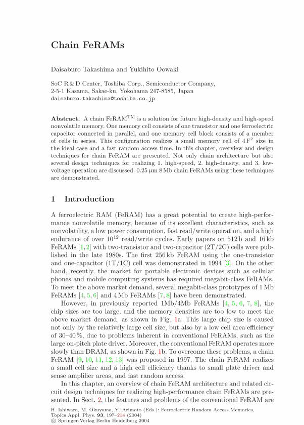
Chain FeRAMs
Daisaburo Takashima and Yukihito Oowaki
SoC R& D Center, Toshiba Corp., Semiconductor Company,2-5-1 Kasama, Sakae-ku, Yokohama 247-8585, [email protected]
Abstract. A chain FeRAMTM is a solution for future high-density and high-speednonvolatile memory. One memory cell consists of one transistor and one ferroelectriccapacitor connected in parallel, and one memory cell block consists of a memberof cells in series. This configuration realizes a small memory cell of 4 F2 size inthe ideal case and a fast random access time. In this chapter, overview and designtechniques for chain FeRAM are presented. Not only chain architecture but alsoseveral design techniques for realizing 1. high-speed, 2. high-density, and 3. low-voltage operation are discussed. 0.25 µm 8Mb chain FeRAMs using these techniquesare demonstrated.
1 Introduction
A ferroelectric RAM (FeRAM) has a great potential to create high-perfor-mance nonvolatile memory, because of its excellent characteristics, such asnonvolatility, a low power consumption, fast read/write operation, and a highendurance of over 1012 read/write cycles. Early papers on 512b and 16 kbFeRAMs [1,2] with two-transistor and two-capacitor (2T/2C) cells were pub-lished in the late 1980s. The first 256 kb FeRAM using the one-transistorand one-capacitor (1T/1C) cell was demonstrated in 1994 [3]. On the otherhand, recently, the market for portable electronic devices such as cellularphones and mobile computing systems has required megabit-class FeRAMs.To meet the above market demand, several megabit-class prototypes of 1 MbFeRAMs [4, 5, 6] and 4Mb FeRAMs [7, 8] have been demonstrated.
However, in previously reported 1Mb/4Mb FeRAMs [4, 5, 6, 7, 8], thechip sizes are too large, and the memory densities are too low to meet theabove market demand, as shown in Fig. 1a. This large chip size is causednot only by the relatively large cell size, but also by a low cell area efficiencyof 30–40%, due to problems inherent in conventional FeRAMs, such as thelarge on-pitch plate driver. Moreover, the conventional FeRAM operates moreslowly than DRAM, as shown in Fig. 1b. To overcome these problems, a chainFeRAM [9, 10, 11, 12, 13] was proposed in 1997. The chain FeRAM realizesa small cell size and a high cell efficiency thanks to small plate driver andsense amplifier areas, and fast random access.
In this chapter, an overview of chain FeRAM architecture and related cir-cuit design techniques for realizing high-performance chain FeRAMs are pre-sented. In Sect. 2, the features and problems of the conventional FeRAM areH. Ishiwara, M. Okuyama, Y. Arimoto (Eds.): Ferroelectric Random Access Memories,Topics Appl. Phys. 93, 197–214 (2004)c© Springer-Verlag Berlin Heidelberg 2004
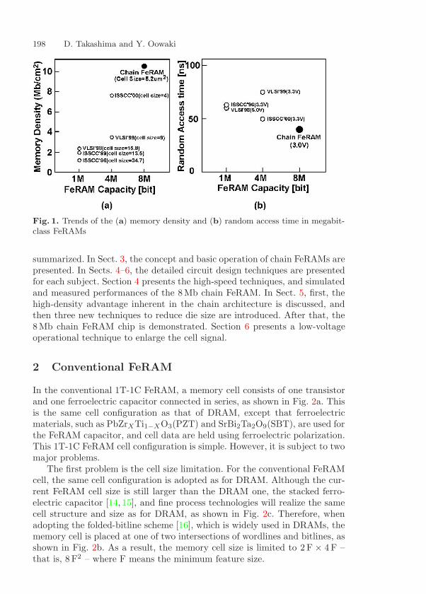
198 D. Takashima and Y. Oowaki
Fig. 1. Trends of the (a) memory density and (b) random access time in megabit-class FeRAMs
summarized. In Sect. 3, the concept and basic operation of chain FeRAMs arepresented. In Sects. 4–6, the detailed circuit design techniques are presentedfor each subject. Section 4 presents the high-speed techniques, and simulatedand measured performances of the 8Mb chain FeRAM. In Sect. 5, first, thehigh-density advantage inherent in the chain architecture is discussed, andthen three new techniques to reduce die size are introduced. After that, the8Mb chain FeRAM chip is demonstrated. Section 6 presents a low-voltageoperational technique to enlarge the cell signal.
2 Conventional FeRAM
In the conventional 1T-1C FeRAM, a memory cell consists of one transistorand one ferroelectric capacitor connected in series, as shown in Fig. 2a. Thisis the same cell configuration as that of DRAM, except that ferroelectricmaterials, such as PbZrXTi1−XO3(PZT) and SrBi2Ta2O9(SBT), are used forthe FeRAM capacitor, and cell data are held using ferroelectric polarization.This 1T-1C FeRAM cell configuration is simple. However, it is subject to twomajor problems.
The first problem is the cell size limitation. For the conventional FeRAMcell, the same cell configuration is adopted as for DRAM. Although the cur-rent FeRAM cell size is still larger than the DRAM one, the stacked ferro-electric capacitor [14, 15], and fine process technologies will realize the samecell structure and size as for DRAM, as shown in Fig. 2c. Therefore, whenadopting the folded-bitline scheme [16], which is widely used in DRAMs, thememory cell is placed at one of two intersections of wordlines and bitlines, asshown in Fig. 2b. As a result, the memory cell size is limited to 2 F × 4 F –that is, 8 F2 – where F means the minimum feature size.
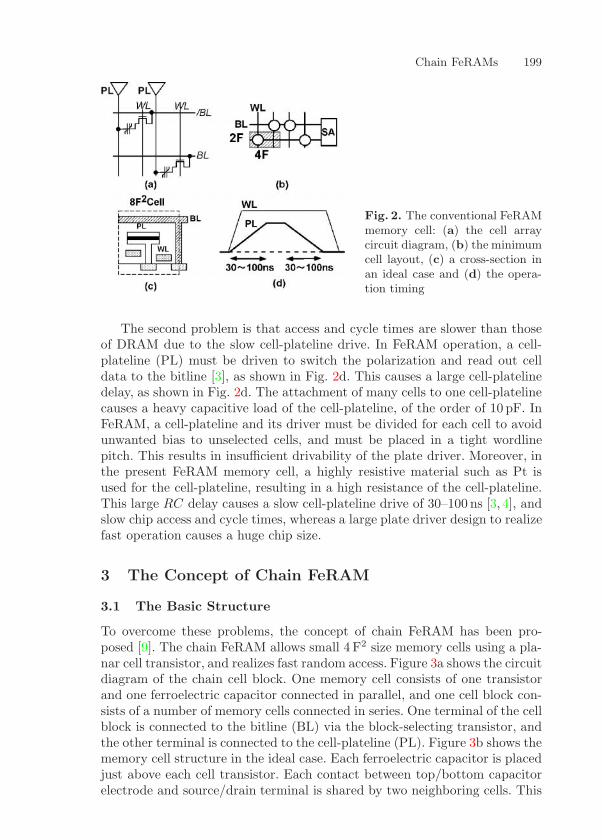
Chain FeRAMs 199
Fig. 2. The conventional FeRAMmemory cell: (a) the cell arraycircuit diagram, (b) the minimumcell layout, (c) a cross-section inan ideal case and (d) the opera-tion timing
The second problem is that access and cycle times are slower than thoseof DRAM due to the slow cell-plateline drive. In FeRAM operation, a cell-plateline (PL) must be driven to switch the polarization and read out celldata to the bitline [3], as shown in Fig. 2d. This causes a large cell-platelinedelay, as shown in Fig. 2d. The attachment of many cells to one cell-platelinecauses a heavy capacitive load of the cell-plateline, of the order of 10 pF. InFeRAM, a cell-plateline and its driver must be divided for each cell to avoidunwanted bias to unselected cells, and must be placed in a tight wordlinepitch. This results in insufficient drivability of the plate driver. Moreover, inthe present FeRAM memory cell, a highly resistive material such as Pt isused for the cell-plateline, resulting in a high resistance of the cell-plateline.This large RC delay causes a slow cell-plateline drive of 30–100 ns [3, 4], andslow chip access and cycle times, whereas a large plate driver design to realizefast operation causes a huge chip size.
3 The Concept of Chain FeRAM
3.1 The Basic Structure
To overcome these problems, the concept of chain FeRAM has been pro-posed [9]. The chain FeRAM allows small 4 F2 size memory cells using a pla-nar cell transistor, and realizes fast random access. Figure 3a shows the circuitdiagram of the chain cell block. One memory cell consists of one transistorand one ferroelectric capacitor connected in parallel, and one cell block con-sists of a number of memory cells connected in series. One terminal of the cellblock is connected to the bitline (BL) via the block-selecting transistor, andthe other terminal is connected to the cell-plateline (PL). Figure 3b shows thememory cell structure in the ideal case. Each ferroelectric capacitor is placedjust above each cell transistor. Each contact between top/bottom capacitorelectrode and source/drain terminal is shared by two neighboring cells. This

200 D. Takashima and Y. Oowaki
Fig. 3. The chain FeRAM memory cell block concept: (a) the circuit diagram,(b) a cross-section in an ideal case, and (c) the minimum cell layout
cell configuration allows a small 4 F2 size memory cell, since the minimumcell size is determined by the wordline pitch (2 F) and the bitline pitch (2 F),as shown in Fig. 3c.
3.2 Two Basic Operations
Figure 4 shows the basic operation of a chain FeRAM, using a driven cell-platescheme [10, 11]. During the standby cycle, as shown in Fig. 4a, all wordlines(WL0–WL3) are boosted to high voltage, the block-selecting signal (BS) andcell-plateline (PL) are set at ground, and the bitline (BL) is also prechargedat ground. So all ferroelectric capacitors are short-circuited by turned-on celltransistors. Therefore, as shown in the hysteresis loop of Fig. 4a, both “1” and“0” data are held steadily at zero bias points without noise to the capacitorelectrodes. During the active cycle, as shown in Fig. 4b, when accessing thecell data of capacitor C1, the selected wordline (WL2) is pulled down, andthe block-selecting signal (BS) is pulled up. After that, the cell-plateline (PL)is pulled up to the Vdd level. Therefore, full the Vdd bias is only applied tothe selected ferroelectric capacitor (C1), and the cell data is read out to thebitline (BL), as shown in the loci of the hysteresis loop of Fig. 4b. When“1” data is read, a large charge is read out to the bitline by polarizationswitching. When “0” data is read, a small charge is read out to the bitline bynonpolarization switching. A sense amplifier amplifies the readout signal. Onthe other hand, cell data of unselected cells are protected by short-circuitingcapacitors. Thus, completely random access is realized.
In order to realize fast FeRAM operation, a nondriven half-Vdd cell-platescheme is also applicable to both conventional FeRAM [4, 17] and chainFeRAM [9], as shown in Fig. 5. When accessing a memory cell, a half-Vdd
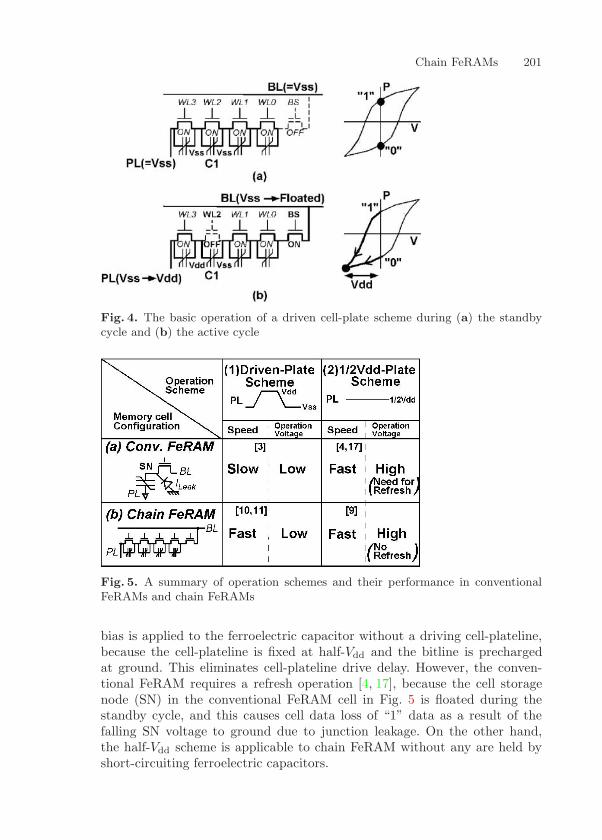
Chain FeRAMs 201
Fig. 4. The basic operation of a driven cell-plate scheme during (a) the standbycycle and (b) the active cycle
Fig. 5. A summary of operation schemes and their performance in conventionalFeRAMs and chain FeRAMs
bias is applied to the ferroelectric capacitor without a driving cell-plateline,because the cell-plateline is fixed at half-Vdd and the bitline is prechargedat ground. This eliminates cell-plateline drive delay. However, the conven-tional FeRAM requires a refresh operation [4, 17], because the cell storagenode (SN) in the conventional FeRAM cell in Fig. 5 is floated during thestandby cycle, and this causes cell data loss of “1” data as a result of thefalling SN voltage to ground due to junction leakage. On the other hand,the half-Vdd scheme is applicable to chain FeRAM without any are held byshort-circuiting ferroelectric capacitors.
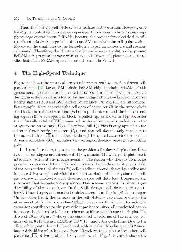
202 D. Takashima and Y. Oowaki
Thus, the half-Vdd cell-plate scheme realizes fast operation. However, onlyhalf-Vdd is applied to ferroelectric capacitor. This imposes relatively high sup-ply voltage operation on FeRAMs, because the present ferroelectric film stillrequires a relatively large bias of about 3 V to switch the cell polarization.Moreover, the small bias to the ferroelectric capacitor causes a small readoutcell signal. Therefore, the driven cell-plate scheme is a solution for presentFeRAMs. A practical array architecture and driven cell-plate scheme to re-alize fast chain FeRAM operation are discussed in Sect. 4.
4 The High-Speed Technique
Figure 6a shows the practical array architecture with a new fast driven cell-plate scheme [10] for an 8 Mb chain FeRAM chip. In chain FeRAM of thisgeneration, eight cells are connected in series in a chain block. In practicaldesign, in order to realize a folded-bitline configuration, two kinds of block-se-lecting signals (BS0 and BS1) and cell-platelines (PL and PL) are introduced.For example, when accessing the cell data of capacitor C1 in the upper chaincell block, the selected wordline (WL6) is pulled down, and the block-select-ing signal (BS0) of upper cell block is pulled up, as shown in Fig. 6b. Afterthat, the cell-plateline (PL) connected to the upper block is pulled up to thearray operation voltage (Vaa). Therefore, full Vaa bias is only applied to theselected ferroelectric capacitor (C1), and the cell data is only read out tothe upper bitline (BL). The lower bitline (BL) is used as a reference bitline.A sense amplifier (SA) amplifies the voltage difference between the bitlinepair.
In this architecture, to overcome the problem of a slow cell-plateline drive,two new techniques are introduced. First, a metal M1 wiring cell-plateline isintroduced, without any process penalty. The reason why there is no processpenalty is discussed latter. This reduces the cell-plateline resistance to 1/25of the conventional platinum (Pt) cell-plateline. Second, the cell-plateline andits plate driver are shared with 16 cells in two chain cell blocks, since the cell-plate drive of unselected cells does not cause cell data loss, because of theshort-circuited ferroelectric capacitor. This scheme enables 16 times largerdrivability of the plate driver. In the 8Mb design, each driver is chosen tobe 3.2 times larger, and each total driver area in a chip is 1/5 times larger.On the other hand, the increase in the cell-plateline capacitance due to theattachment of 16 cells is less than 20%, because only the selected ferroelectriccapacitor contributes to the parasitic capacitance, since all unselected capac-itors are short-circuited. These schemes achieve a high-speed cell-platelinedrive of 10 ns. Figure 7 shows the simulated waveforms of the memory cellarray of an 8 Mb chain FeRAM at 3.0 V Vdd and 70 ns cycle time. Due to theeffect of the plate-driver being shared with 16 cells, this chip has a 3.2 timeslarger drivability of each plate-driver. Therefore, this chip realizes a fast cell-plateline (PL) drive of about 10 ns, as shown in Fig. 7. Figure 8 shows the
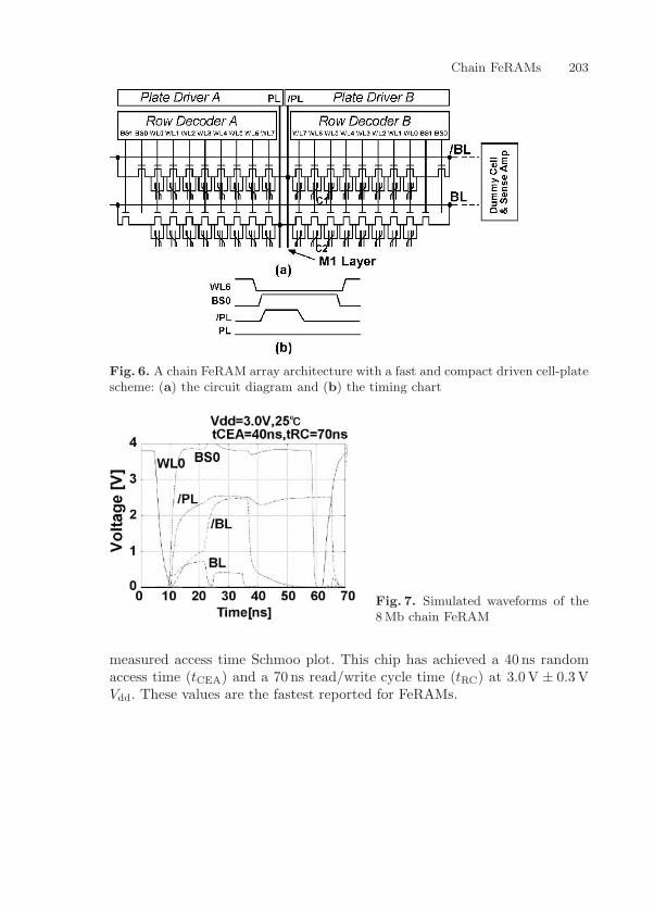
Chain FeRAMs 203
Fig. 6. A chain FeRAM array architecture with a fast and compact driven cell-platescheme: (a) the circuit diagram and (b) the timing chart
Fig. 7. Simulated waveforms of the8 Mb chain FeRAM
measured access time Schmoo plot. This chip has achieved a 40 ns randomaccess time (tCEA) and a 70 ns read/write cycle time (tRC) at 3.0 V ± 0.3 VVdd. These values are the fastest reported for FeRAMs.
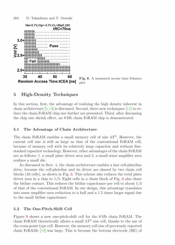
204 D. Takashima and Y. Oowaki
Fig. 8. A measured access time Schmooplot
5 High-Density Techniques
In this section, first, the advantage of realizing the high density inherent inchain architecture [9,10] is discussed. Second, three new techniques [11] to re-duce the chain FeRAM chip size further are presented. Third, after discussingthe chip size shrink effect, an 8 Mb chain FeRAM chip is demonstrated.
5.1 The Advantage of Chain Architecture
The chain FeRAM enables a small memory cell of size 4 F2. However, thecurrent cell size is still as large as that of the conventional FeRAM cell,because of memory cell with its relatively large capacitor and without fine-stacked capacitor technology. However, other advantages of the chain FeRAMare as follows: 1. a small plate driver area and 2. a small sense amplifier arearealizes a small die.
As discussed in Sect. 4, the chain architecture enables a fast cell-platelinedrive, because the cell-plateline and its driver are shared by two chain cellblocks (16 cells), as shown in Fig. 6. This scheme also reduces the total platedriver area in a chip to 1/5. Eight cells in a chain block of Fig. 6 also sharethe bitline contact. This reduces the bitline capacitance per cell to about 1/3of that of the conventional FeRAM. In our design, this advantage translatesinto sense amplifier area reduction to a half and a 1.5 times larger signal dueto the small bitline capacitance.
5.2 The One-Pitch-Shift Cell
Figure 9 shows a new one-pitch-shift cell for the 8Mb chain FeRAM. Thechain FeRAM theoretically allows a small 4 F2 size cell, thanks to the use ofthe cross-point type cell. However, the memory cell size of previously reportedchain FeRAMs [10] was large. This is because the bottom electrode (BE) of
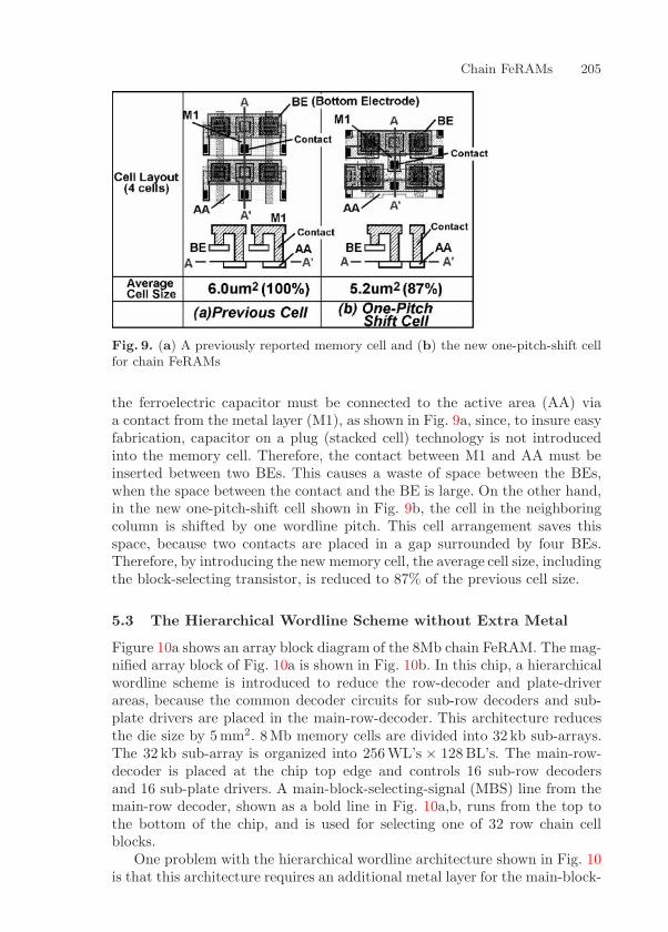
Chain FeRAMs 205
Fig. 9. (a) A previously reported memory cell and (b) the new one-pitch-shift cellfor chain FeRAMs
the ferroelectric capacitor must be connected to the active area (AA) viaa contact from the metal layer (M1), as shown in Fig. 9a, since, to insure easyfabrication, capacitor on a plug (stacked cell) technology is not introducedinto the memory cell. Therefore, the contact between M1 and AA must beinserted between two BEs. This causes a waste of space between the BEs,when the space between the contact and the BE is large. On the other hand,in the new one-pitch-shift cell shown in Fig. 9b, the cell in the neighboringcolumn is shifted by one wordline pitch. This cell arrangement saves thisspace, because two contacts are placed in a gap surrounded by four BEs.Therefore, by introducing the new memory cell, the average cell size, includingthe block-selecting transistor, is reduced to 87% of the previous cell size.
5.3 The Hierarchical Wordline Scheme without Extra Metal
Figure 10a shows an array block diagram of the 8Mb chain FeRAM. The mag-nified array block of Fig. 10a is shown in Fig. 10b. In this chip, a hierarchicalwordline scheme is introduced to reduce the row-decoder and plate-driverareas, because the common decoder circuits for sub-row decoders and sub-plate drivers are placed in the main-row-decoder. This architecture reducesthe die size by 5 mm2. 8Mb memory cells are divided into 32 kb sub-arrays.The 32 kb sub-array is organized into 256 WL’s × 128 BL’s. The main-row-decoder is placed at the chip top edge and controls 16 sub-row decodersand 16 sub-plate drivers. A main-block-selecting-signal (MBS) line from themain-row decoder, shown as a bold line in Fig. 10a,b, runs from the top tothe bottom of the chip, and is used for selecting one of 32 row chain cellblocks.
One problem with the hierarchical wordline architecture shown in Fig. 10is that this architecture requires an additional metal layer for the main-block-

206 D. Takashima and Y. Oowaki
Fig. 10. (a) The array block diagram of an 8Mb chain FeRAM chip, and (b) mag-nified array blocks of (a)
selecting-signal (MBS) line. The new chain cell block structure with an MBSline shown in Fig. 11 overcomes this problem. The M1 layer used for cellinterconnections is also used for the main-block-selecting-signal (MBS) line,and this MBS line is placed in the otherwise unused space over the block-selecting transistors. Therefore, this architecture reduces the chip size by5 mm2 without an extra metal layer and area penalty for the chain cell block.Moreover, the M1 layer is also used for the cell-plateline (PL and PL). Thisenables a low-resistance M1 cell-plateline without any process penalty, andrealizes a fast cell-plateline drive, as discussed in Sect. 4.
5.4 The Small-Area Dummy Cell Scheme
A key issue for realizing 1T-1C FeRAM operation is how to achieve a sta-ble reference bitline (BL) voltage using small dummy cells, because FeRAMrequires a relatively high reference BL voltage, and needs a large dummy ca-pacitor for a dummy cell. In the FeRAM operation shown in Fig. 12a, whenadopting a fast single-plate pulse sensing scheme [3, 5], after pulling up thecell-plateline (PL) to the array operation voltage (Vaa), the bitline (BL) volt-ages of the “0” data as well as those of the “1” data rise from ground level,by an amount determined by nonswitching and switching cell polarizations.Therefore, the reference BL voltage – the intermediate voltage between the“1” and “0” data – also becomes high. Moreover, considering the signal mar-gin test, a high reference BL voltage of about a half Vaa is required, as shownin Fig. 12a.
In the conventional dummy cell [6] shown in Fig. 12b, the reference BLvoltage is obtained by the charge of the dummy capacitor (Cd), by pulling upthe dummy plateline (DPL). Therefore, in order to obtain a high reference BL
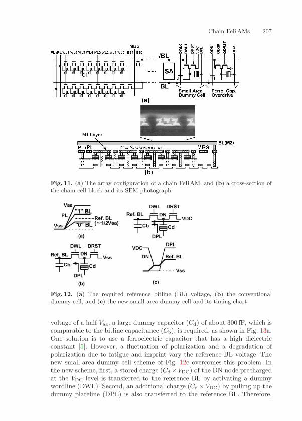
Chain FeRAMs 207
Fig. 11. (a) The array configuration of a chain FeRAM, and (b) a cross-section ofthe chain cell block and its SEM photograph
Fig. 12. (a) The required reference bitline (BL) voltage, (b) the conventionaldummy cell, and (c) the new small area dummy cell and its timing chart
voltage of a half Vaa, a large dummy capacitor (Cd) of about 300 fF, which iscomparable to the bitline capacitance (Cb), is required, as shown in Fig. 13a.One solution is to use a ferroelectric capacitor that has a high dielectricconstant [5]. However, a fluctuation of polarization and a degradation ofpolarization due to fatigue and imprint vary the reference BL voltage. Thenew small-area dummy cell scheme of Fig. 12c overcomes this problem. Inthe new scheme, first, a stored charge (Cd×VDC) of the DN node prechargedat the VDC level is transferred to the reference BL by activating a dummywordline (DWL). Second, an additional charge (Cd ×VDC) by pulling up thedummy plateline (DPL) is also transferred to the reference BL. Therefore,
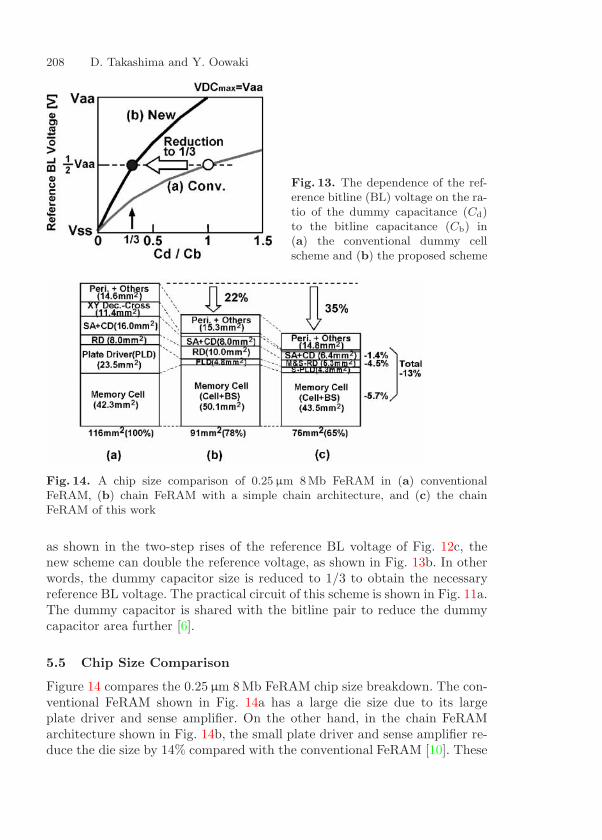
208 D. Takashima and Y. Oowaki
Fig. 13. The dependence of the ref-erence bitline (BL) voltage on the ra-tio of the dummy capacitance (Cd)to the bitline capacitance (Cb) in(a) the conventional dummy cellscheme and (b) the proposed scheme
Fig. 14. A chip size comparison of 0.25 µm 8Mb FeRAM in (a) conventionalFeRAM, (b) chain FeRAM with a simple chain architecture, and (c) the chainFeRAM of this work
as shown in the two-step rises of the reference BL voltage of Fig. 12c, thenew scheme can double the reference voltage, as shown in Fig. 13b. In otherwords, the dummy capacitor size is reduced to 1/3 to obtain the necessaryreference BL voltage. The practical circuit of this scheme is shown in Fig. 11a.The dummy capacitor is shared with the bitline pair to reduce the dummycapacitor area further [6].
5.5 Chip Size Comparison
Figure 14 compares the 0.25 µm 8 Mb FeRAM chip size breakdown. The con-ventional FeRAM shown in Fig. 14a has a large die size due to its largeplate driver and sense amplifier. On the other hand, in the chain FeRAMarchitecture shown in Fig. 14b, the small plate driver and sense amplifier re-duce the die size by 14% compared with the conventional FeRAM [10]. These

Chain FeRAMs 209
shrinks also reduce the large crossing-area between the X-decoder (the row-decoder and the plate-driver) and the Y-decoder (the sense amplifier andthe column-decoder), and reduce the die size by 8%. Therefore, the chainarchitecture reduces the die size by 22%. Furthermore, in the 8Mb chainFeRAM [11] shown in Fig. 14c, the new one-pitch-shift cell, the hierarchicalwordline scheme, and the small-area dummy cell scheme reduce the die sizeby 5.7%, 4.5%, and 1.4%, respectively. The further shrinking of the crossing-area due to these techniques also reduces die size by 1.3%. The total chiparea reduction by these new techniques is 13%. As a result, the 8 Mb chainFeRAM die size of this work is reduced to 65% of that of the conventionalFeRAM.
A chain 8Mb FeRAM was fabricated using 0.25 µm two-metal CMOStechnology. A micrograph of the 8Mb chain FeRAM is shown in Fig. 15. Thecapacitor size is 0.9 µm × 0.95 µm. The average cell size is 5.2 µm2. A PZTfilm is used for the ferroelectric capacitor. The chip size is 76mm2. This chipachieved the highest memory density, 10.5Mb/cm2, and the highest averagecell/chip area efficiency, 57.4%, reported in FeRAMs. The active current is30mA at a 70 ns cycle time. The features of the device are summarized inTable 1.
Fig. 15. A chip microphotograph ofthe 8Mb chain FeRAM
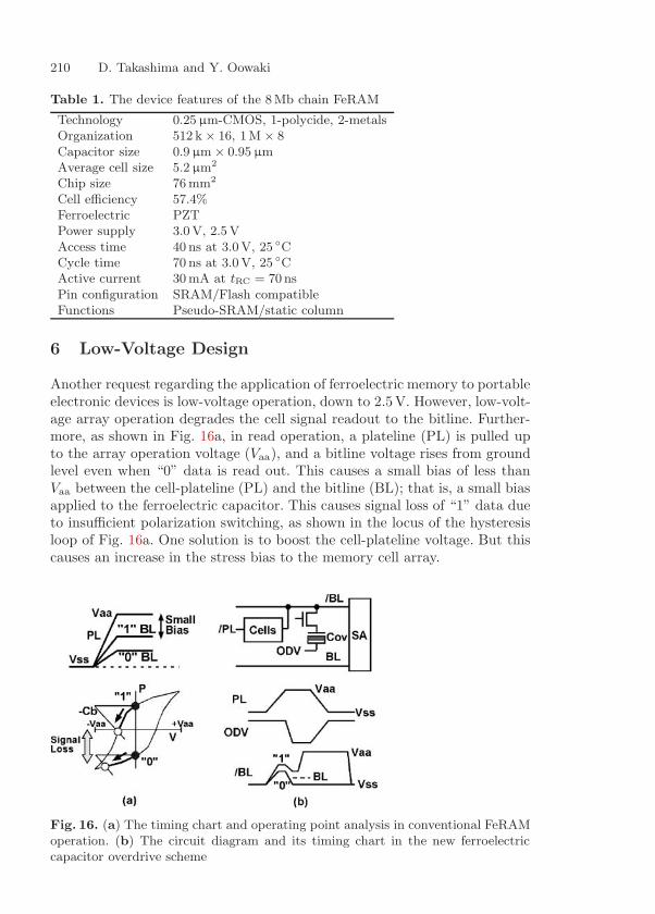
210 D. Takashima and Y. Oowaki
Table 1. The device features of the 8Mb chain FeRAM
Technology 0.25 µm-CMOS, 1-polycide, 2-metalsOrganization 512 k × 16, 1M × 8Capacitor size 0.9 µm × 0.95 µmAverage cell size 5.2 µm2
Chip size 76 mm2
Cell efficiency 57.4%Ferroelectric PZTPower supply 3.0 V, 2.5 VAccess time 40 ns at 3.0 V, 25 CCycle time 70 ns at 3.0 V, 25 CActive current 30 mA at tRC = 70nsPin configuration SRAM/Flash compatibleFunctions Pseudo-SRAM/static column
6 Low-Voltage Design
Another request regarding the application of ferroelectric memory to portableelectronic devices is low-voltage operation, down to 2.5V. However, low-volt-age array operation degrades the cell signal readout to the bitline. Further-more, as shown in Fig. 16a, in read operation, a plateline (PL) is pulled upto the array operation voltage (Vaa), and a bitline voltage rises from groundlevel even when “0” data is read out. This causes a small bias of less thanVaa between the cell-plateline (PL) and the bitline (BL); that is, a small biasapplied to the ferroelectric capacitor. This causes signal loss of “1” data dueto insufficient polarization switching, as shown in the locus of the hysteresisloop of Fig. 16a. One solution is to boost the cell-plateline voltage. But thiscauses an increase in the stress bias to the memory cell array.
Fig. 16. (a) The timing chart and operating point analysis in conventional FeRAMoperation. (b) The circuit diagram and its timing chart in the new ferroelectriccapacitor overdrive scheme
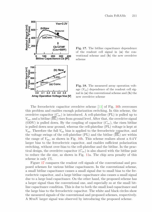
Chain FeRAMs 211
Fig. 17. The bitline capacitance dependenceof the readout cell signal in (a) the con-ventional scheme and (b) the new overdrivescheme
Fig. 18. The measured array operation volt-age (Vaa) dependence of the readout cell sig-nal in (a) the conventional scheme and (b) thenew overdrive scheme
The ferroelectric capacitor overdrive scheme [11] of Fig. 16b overcomesthis problem and enables enough polarization switching. In this scheme, theoverdrive capacitor (Cov) is introduced. A cell-plateline (PL) is pulled up toVaa, and a bitline (BL) rises from ground level. After that, the overdrive signal(ODV) is pulled down. By the coupling of capacitor (Cov), the risen bitlineis pulled down near ground, whereas the cell-plateline (PL) voltage is kept atVaa. Therefore the full Vaa bias is applied to the ferroelectric capacitor, andthe voltage swings of the cell-plateline (PL) and the bitline (BL) are withinthe range of Vaa, as shown in Fig. 16b. This scheme realizes about a 0.4Vlarger bias to the ferroelectric capacitor, and enables sufficient polarizationswitching, without over-bias to the cell-plateline and the bitline. In the prac-tical design, the overdrive capacitor (Cov) is also shared with the bitline pairto reduce the die size, as shown in Fig. 11a. The chip area penalty of thisscheme is only 1%.
Figure 17 compares the readout cell signals of the conventional and pro-posed schemes for various bitline capacitances. In the conventional scheme,a small bitline capacitance causes a small signal due to small bias to the fer-roelectric capacitor, and a large bitline capacitance also causes a small signaldue to a large load capacitance. On the other hand, the proposed scheme hasa larger signal than the conventional one, and especially so at the small bit-line capacitance condition. This is due to both the small load capacitance andthe large bias to the ferroelectric capacitor. The white and black circles showthe measured signals of the conventional and proposed schemes, respectively.A 90mV larger signal was observed by introducing the proposed scheme.

212 D. Takashima and Y. Oowaki
Figure 18 shows the measured array operation voltage (Vaa) dependenceof the readout cell signal. These data were measured by sweeping the refer-ence bitline voltage precisely. At any array operation voltages, the proposedscheme constantly has a signal that is 90mV larger than that of the conven-tional scheme, thanks to the almost constant bias increase to the ferroelectriccapacitor. This result implies that the signal-increasing ratio becomes largerin lower-voltage operation. The signal-increasing ratio was 26% at 2V Vaa.Under the same cell signal conditions, the operation voltage of the proposedscheme is 0.23V lower than that of the conventional scheme.
7 Summary
This chapter has reviewed the chain FeRAM architecture, and presentedmany circuit design techniques. The chain FeRAM allows a small memory cellof 4 F2 size, thanks to the cross-point cell, and achieves random access. First,the concept and basic operation of chain FeRAM were presented. Second,a high-speed cell-plateline drive technique was presented. The chain FeRAMrealized a 40 ns random-access time and a 70 ns read/write cycle time, whichare the fastest reported in FeRAMs. Third, after discussing the merits ofa high density of chain FeRAM, three new techniques to reduce the die fur-ther – 1. the one-pitch-shift cell, 2. the hierarchical wordline scheme withoutextra metal, and 3. the small-area dummy cell scheme – were presented.A chain architecture with these techniques reduced the die size to 65% ofthat of the conventional FeRAM, and realized a small 8Mb chain FeRAMdie of 76mm2, using a 0.25 µm two-metal CMOS. This chip achieved thehighest memory density, 10.5Mb/cm2, and the highest average cell/chip areaefficiency, 57.4%, reported in FeRAMs. Fourth, a new ferroelectric capacitoroverdrive scheme to realize low-voltage operation was presented. A 90mVlarger signal was observed by introducing this overdrive scheme. This schemereduces the array operation voltage by 0.23V.
Acknowledgements
The authors thank J. Miyamoto and S. Sawada for their encouragement andsupport of this work. They are also grateful to members of the Toshiba-Infi-neon FeRAM Development Alliance (FDA) for chip design, device fabrication,and measurement.
References
1. J. T. Evans, R. Womack: IEEE J. Solid-State Circuits 23, 1171 (1989) 1972. R. Womack, D. Tolsch: Tech. Dig. Int. Solid-State Circuits Conf. (1989) p. 242
197

Chain FeRAMs 213
3. T. Sumi, N. Moriwaki, G. Nakane, T. Nakakuma, Y. Judai, Y. Uemoto,Y. Nagano, S. Hayashi, M. Azuma, E. Fujii, S. Katsu, T. Otsuki, L. McMillan,C. Araujo, G. Kano: Tech. Dig. Int. Solid-State Circuits Conf. (1994) p. 268197, 199, 206
4. H. Koike, T. Otsuki, T. Kimura, M. Fukuma, Y. Hayashi, Y. Maejima,K. Amanuma, N. Tanane, T. Matsuki, S. Saito, T. Takeuchi, S. Kobayashi,T. Kunio, T. Hase, Y. Miyasaka, N. Shohata, M. Takada: IEEE J. Solid-StateCircuits 31, 1625 (1996) 197, 199, 200, 201
5. W. Keaus, L. Lehman, D. Wilson, T. Yamazaki, C. Ohno, E. Nagi,H. Yamazaki, H. Suzuki: Tech. Dig. Symp. VLSI Circuits (1998) p. 242 197,206, 207
6. T. Miyakawa, S. Tanaka, Y. Itoh, Y. Takeuchi, R. Ogiwara, S.M. Doumae,H. Takenaka, I. Kunishima, S. Shuto, O. Hidaka, O. Ohtsuki, S. Tanaka: Tech.Dig. Int. Solid-State Circuits Conf. (1999) p. 104 197, 206, 208
7. Y. Chung, M.K. Choi, K. Oh, B.G. Jeon, K.D. Suh: Dig. Symp. VLSI Circuits(1997) p. 97 197
8. B. G. Jeon, M.K. Choi, Y. Song, S.K. Oh, Y. Chung, K.D. Suh, K. Kim: Tech.Dig. Int. Solid-State Circuits Conf. (2000) p. 272 197
9. D. Takashima, I. Kunishima: IEEE J. Solid-State Circuits 33, 787 (1998) 197,199, 200, 204
10. D. Takashima, S. Shuto, I. Kunishima, H. Takenaka, Y. Oowaki, S. Tanaka:IEEE J. Solid-State Circuits 34, 1557 (1999) 197, 200, 202, 204, 208
11. D. Takashima, Y. Takeuchi, T. Miyakawa, Y. Itoh, R. Ogiwara, M. Kamoshida,K. Hoya, S.M. Doumae, T. Ozaki, H. Kanaya, M. Aoki, K. Yamakawa,I. Kunishima, Y. Oowaki: Tech. Dig. Int. Solid-State Circuits Conf. (2001)p. 40 197, 200, 204, 209, 211
12. D. Takashima: IEICE Trans. Electron. E84-C, 747 (2001) 19713. D. Takashima, Y. Oowaki, I. Kunishima: Tech. Dig. Symp. VLSI Circuits
(1999) p. 103 19714. S. Onishi, K. Hamada, K. Ishihara, Y. Ito, S. Yokoyama, J. Kudo K. Sakiyama:
Tech. Dig. Int. Electron. Device Meeting (1994) p. 843 19815. K. Shoji, M. Moniwa, H. Yamashita, T. Kisu, T. Kaga, K. Torii, T. Kumihashi,
T. Morimoto, H. Kawakami, Y. Gotoh, T. Itoga, T. Tanaka, N. Yokoyama,T. Kure, M. Ohkura, Y. Fujisaki, K. Sakata, K. Kimura: Tech. Dig. Symp.VLSI Circuits (1996) p. 28 198
16. H. Masuda , R. Hori, Y. Kamigaki, K. Itoh, H. Kawamoto, H. Katto: IEEEJ. Solid-State Circuits 15, 846 (1980) 198
17. K. Takeuchi, K. Matsuno, Y. Nakagome, M. Aoki: IEICE Trans. Electron.E79-C, 234 (1996) 200, 201

Index
1T-1C, 1984 F2, 199
bitline, 199block-selecting signal, 202
chain FeRAM, 197chip size, 208
driven cell-plate scheme, 200dummy cell, 206
folded-bitline configuration, 202folded-bitline scheme, 198
half-Vdd, 201
hierarchical wordline scheme, 205
low-voltage operation, 210
main-block-selecting-signal (MBS) line,205
minimum feature size, 198
one-pitch-shift cell, 204overdrive scheme, 211
plateline, 199
Schmoo plot– access time, 203small-area dummy cell scheme, 207
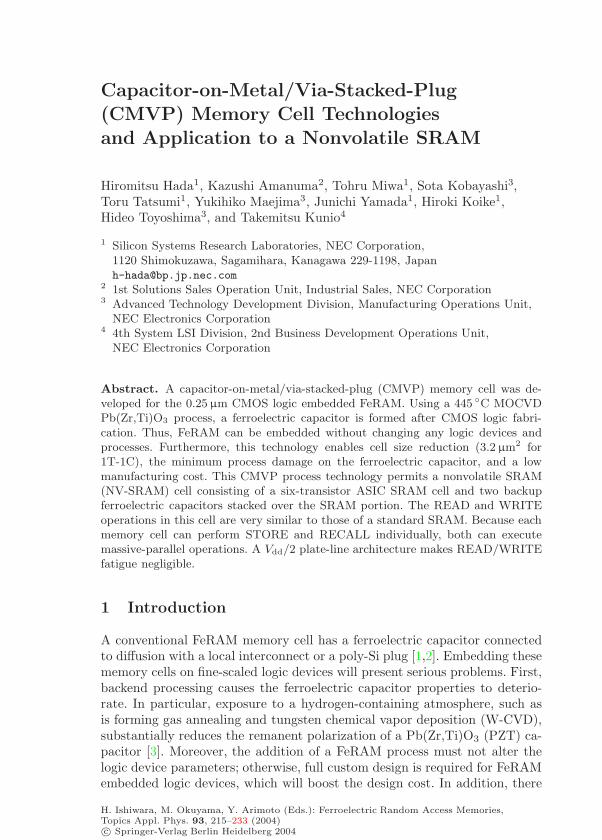
Capacitor-on-Metal/Via-Stacked-Plug(CMVP) Memory Cell Technologies
and Application to a Nonvolatile SRAM
Hiromitsu Hada1, Kazushi Amanuma2, Tohru Miwa1, Sota Kobayashi3,Toru Tatsumi1, Yukihiko Maejima3, Junichi Yamada1, Hiroki Koike1,Hideo Toyoshima3, and Takemitsu Kunio4
1 Silicon Systems Research Laboratories, NEC Corporation,1120 Shimokuzawa, Sagamihara, Kanagawa 229-1198, [email protected]
2 1st Solutions Sales Operation Unit, Industrial Sales, NEC Corporation3 Advanced Technology Development Division, Manufacturing Operations Unit,
NEC Electronics Corporation4 4th System LSI Division, 2nd Business Development Operations Unit,
NEC Electronics Corporation
Abstract. A capacitor-on-metal/via-stacked-plug (CMVP) memory cell was de-veloped for the 0.25 µm CMOS logic embedded FeRAM. Using a 445 C MOCVDPb(Zr,Ti)O3 process, a ferroelectric capacitor is formed after CMOS logic fabri-cation. Thus, FeRAM can be embedded without changing any logic devices andprocesses. Furthermore, this technology enables cell size reduction (3.2 µm2 for1T-1C), the minimum process damage on the ferroelectric capacitor, and a lowmanufacturing cost. This CMVP process technology permits a nonvolatile SRAM(NV-SRAM) cell consisting of a six-transistor ASIC SRAM cell and two backupferroelectric capacitors stacked over the SRAM portion. The READ and WRITEoperations in this cell are very similar to those of a standard SRAM. Because eachmemory cell can perform STORE and RECALL individually, both can executemassive-parallel operations. A Vdd/2 plate-line architecture makes READ/WRITEfatigue negligible.
1 Introduction
A conventional FeRAM memory cell has a ferroelectric capacitor connectedto diffusion with a local interconnect or a poly-Si plug [1,2]. Embedding thesememory cells on fine-scaled logic devices will present serious problems. First,backend processing causes the ferroelectric capacitor properties to deterio-rate. In particular, exposure to a hydrogen-containing atmosphere, such asis forming gas annealing and tungsten chemical vapor deposition (W-CVD),substantially reduces the remanent polarization of a Pb(Zr,Ti)O3 (PZT) ca-pacitor [3]. Moreover, the addition of a FeRAM process must not alter thelogic device parameters; otherwise, full custom design is required for FeRAMembedded logic devices, which will boost the design cost. In addition, there
H. Ishiwara, M. Okuyama, Y. Arimoto (Eds.): Ferroelectric Random Access Memories,Topics Appl. Phys. 93, 215–233 (2004)c© Springer-Verlag Berlin Heidelberg 2004
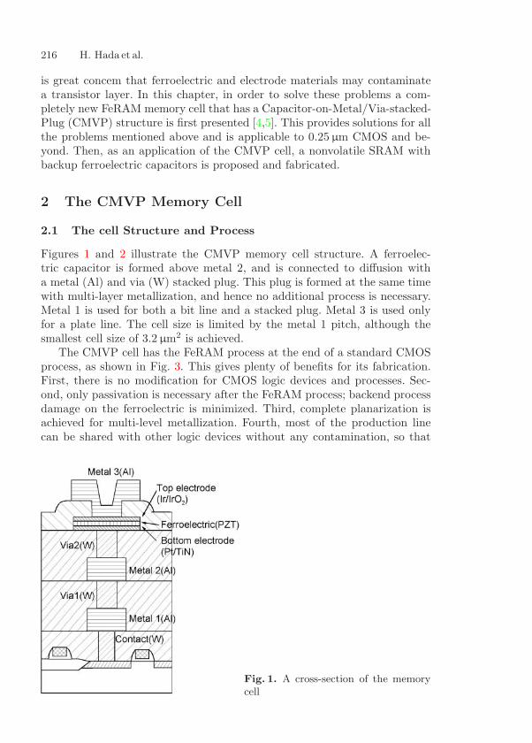
216 H. Hada et al.
is great concem that ferroelectric and electrode materials may contaminatea transistor layer. In this chapter, in order to solve these problems a com-pletely new FeRAM memory cell that has a Capacitor-on-Metal/Via-stacked-Plug (CMVP) structure is first presented [4,5]. This provides solutions for allthe problems mentioned above and is applicable to 0.25 µm CMOS and be-yond. Then, as an application of the CMVP cell, a nonvolatile SRAM withbackup ferroelectric capacitors is proposed and fabricated.
2 The CMVP Memory Cell
2.1 The cell Structure and Process
Figures 1 and 2 illustrate the CMVP memory cell structure. A ferroelec-tric capacitor is formed above metal 2, and is connected to diffusion witha metal (Al) and via (W) stacked plug. This plug is formed at the same timewith multi-layer metallization, and hence no additional process is necessary.Metal 1 is used for both a bit line and a stacked plug. Metal 3 is used onlyfor a plate line. The cell size is limited by the metal 1 pitch, although thesmallest cell size of 3.2 µm2 is achieved.
The CMVP cell has the FeRAM process at the end of a standard CMOSprocess, as shown in Fig. 3. This gives plenty of benefits for its fabrication.First, there is no modification for CMOS logic devices and processes. Sec-ond, only passivation is necessary after the FeRAM process; backend processdamage on the ferroelectric is minimized. Third, complete planarization isachieved for multi-level metallization. Fourth, most of the production linecan be shared with other logic devices without any contamination, so that
Fig. 1. A cross-section of the memorycell
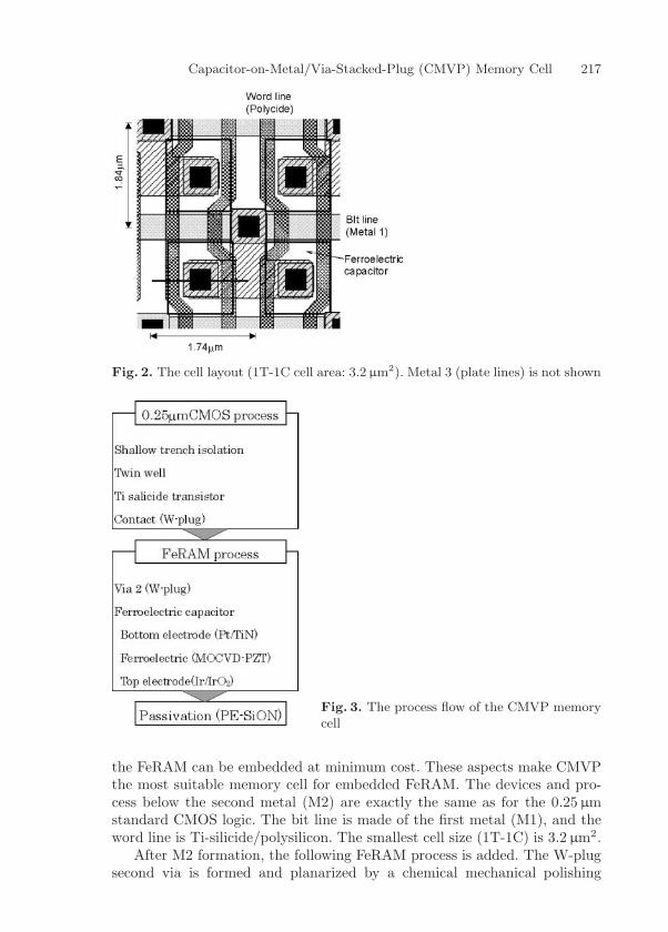
Capacitor-on-Metal/Via-Stacked-Plug (CMVP) Memory Cell 217
Fig. 2. The cell layout (1T-1C cell area: 3.2 µm2). Metal 3 (plate lines) is not shown
Fig. 3. The process flow of the CMVP memorycell
the FeRAM can be embedded at minimum cost. These aspects make CMVPthe most suitable memory cell for embedded FeRAM. The devices and pro-cess below the second metal (M2) are exactly the same as for the 0.25 µmstandard CMOS logic. The bit line is made of the first metal (M1), and theword line is Ti-silicide/polysilicon. The smallest cell size (1T-1C) is 3.2 µm2.
After M2 formation, the following FeRAM process is added. The W-plugsecond via is formed and planarized by a chemical mechanical polishing
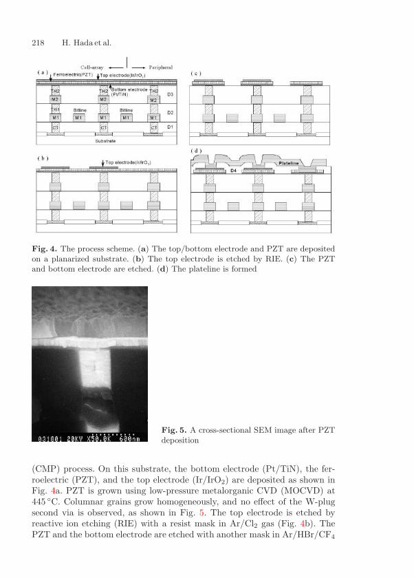
218 H. Hada et al.
Fig. 4. The process scheme. (a) The top/bottom electrode and PZT are depositedon a planarized substrate. (b) The top electrode is etched by RIE. (c) The PZTand bottom electrode are etched. (d) The plateline is formed
Fig. 5. A cross-sectional SEM image after PZTdeposition
(CMP) process. On this substrate, the bottom electrode (Pt/TiN), the fer-roelectric (PZT), and the top electrode (Ir/IrO2) are deposited as shown inFig. 4a. PZT is grown using low-pressure metalorganic CVD (MOCVD) at445 C. Columnar grains grow homogeneously, and no effect of the W-plugsecond via is observed, as shown in Fig. 5. The top electrode is etched byreactive ion etching (RIE) with a resist mask in Ar/Cl2 gas (Fig. 4b). ThePZT and the bottom electrode are etched with another mask in Ar/HBr/CF4
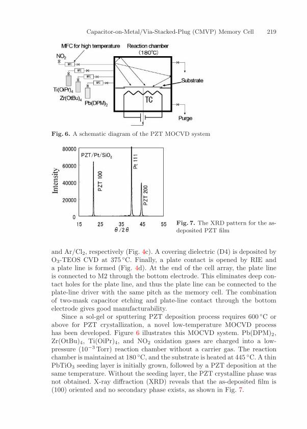
Capacitor-on-Metal/Via-Stacked-Plug (CMVP) Memory Cell 219
Fig. 6. A schematic diagram of the PZT MOCVD system
Fig. 7. The XRD pattern for the as-deposited PZT film
and Ar/Cl2, respectively (Fig. 4c). A covering dielectric (D4) is deposited byO3-TEOS CVD at 375 C. Finally, a plate contact is opened by RIE anda plate line is formed (Fig. 4d). At the end of the cell array, the plate lineis connected to M2 through the bottom electrode. This eliminates deep con-tact holes for the plate line, and thus the plate line can be connected to theplate-line driver with the same pitch as the memory cell. The combinationof two-mask capacitor etching and plate-line contact through the bottomelectrode gives good manufacturability.
Since a sol-gel or sputtering PZT deposition process requires 600 C orabove for PZT crystallization, a novel low-temperature MOCVD processhas been developed. Figure 6 illustrates this MOCVD system. Pb(DPM)2,Zr(OtBu)4, Ti(OiPr)4, and NO2 oxidation gases are charged into a low-pressure (10−3 Torr) reaction chamber without a carrier gas. The reactionchamber is maintained at 180 C, and the substrate is heated at 445 C. A thinPbTiO3 seeding layer is initially grown, followed by a PZT deposition at thesame temperature. Without the seeding layer, the PZT crystalline phase wasnot obtained. X-ray diffraction (XRD) reveals that the as-deposited film is(100) oriented and no secondary phase exists, as shown in Fig. 7.

220 H. Hada et al.
Fig. 8. Hysteresis curves for parallel-con-nected PZT capacitors (1µm × 1 µm). Thethickness of the PZT film was 200 nm.100 kHz triangle waves of 2.5 V and 5V wereused
Fig. 9. (a) Fatigue and (b) imprint endurance for the 1 µm× 1 µm capacitors. Theswitching and nonswitching charges were measured by applying 2.5 V pulses
2.2 The Electrical Properties of the PZT Capacitor
MOCVD PZT showed good ferroelectric properties and no degradation wasobserved for a ferroelectric capacitor due to the low-temperature backendprocessing. After plate-line etching, capacitors show good hysteresis prop-erties, as shown in Fig. 8. The PZT film thickness is 200nm. More than10 µC/cm2 remanent polarization (Pr) was obtained for 1 µm × 1 µm capac-itors at 2.5V. The maximum polarization increased slightly as the capacitorsize decreased from 3 µm × 3 µm to 1 µm × 1 µm, while Pr remained almostthe same. This tendency was also observed when the ferroelectric was etchedwith a top electrode pattern. Therefore, it is not due to the fringe capacitorat the top electrode edge. 1µm × 1 µm capacitors showed good fatigue andimprint properties. Figure 9 shows (a) fatigue and (b) imprint endurance forthe 1 µm × 1 µm capacitors. As can be seen from the figure, the switchingcharge degradation during 109 switching cycles was less than 10%, and littlechange was observed for switching or nonswitching charges due to 109 im-
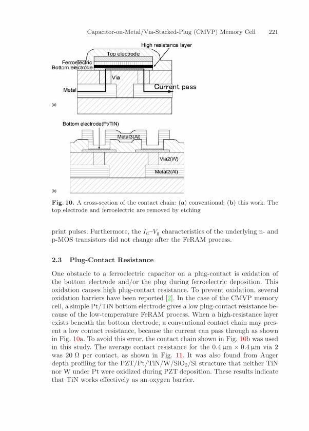
Capacitor-on-Metal/Via-Stacked-Plug (CMVP) Memory Cell 221
Fig. 10. A cross-section of the contact chain: (a) conventional; (b) this work. Thetop electrode and ferroelectric are removed by etching
print pulses. Furthermore, the Id–Vg characteristics of the underlying n- andp-MOS transistors did not change after the FeRAM process.
2.3 Plug-Contact Resistance
One obstacle to a ferroelectric capacitor on a plug-contact is oxidation ofthe bottom electrode and/or the plug during ferroelectric deposition. Thisoxidation causes high plug-contact resistance. To prevent oxidation, severaloxidation barriers have been reported [2]. In the case of the CMVP memorycell, a simple Pt/TiN bottom electrode gives a low plug-contact resistance be-cause of the low-temperature FeRAM process. When a high-resistance layerexists beneath the bottom electrode, a conventional contact chain may pres-ent a low contact resistance, because the current can pass through as shownin Fig. 10a. To avoid this error, the contact chain shown in Fig. 10b was usedin this study. The average contact resistance for the 0.4 µm × 0.4 µm via 2was 20 Ω per contact, as shown in Fig. 11. It was also found from Augerdepth profiling for the PZT/Pt/TiN/W/SiO2/Si structure that neither TiNnor W under Pt were oxidized during PZT deposition. These results indicatethat TiN works effectively as an oxygen barrier.
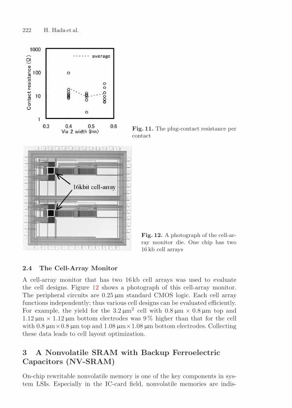
222 H. Hada et al.
Fig. 11. The plug-contact resistance percontact
Fig. 12. A photograph of the cell-ar-ray monitor die. One chip has two16 kb cell arrays
2.4 The Cell-Array Monitor
A cell-array monitor that has two 16kb cell arrays was used to evaluatethe cell designs. Figure 12 shows a photograph of this cell-array monitor.The peripheral circuits are 0.25 µm standard CMOS logic. Each cell arrayfunctions independently; thus various cell designs can be evaluated efficiently.For example, the yield for the 3.2 µm2 cell with 0.8 µm × 0.8 µm top and1.12 µm × 1.12 µm bottom electrodes was 9% higher than that for the cellwith 0.8 µm×0.8 µm top and 1.08 µm×1.08 µm bottom electrodes. Collectingthese data leads to cell layout optimization.
3 A Nonvolatile SRAM with Backup FerroelectricCapacitors (NV-SRAM)
On-chip rewritable nonvolatile memory is one of the key components in sys-tem LSIs. Especially in the IC-card field, nonvolatile memories are indis-
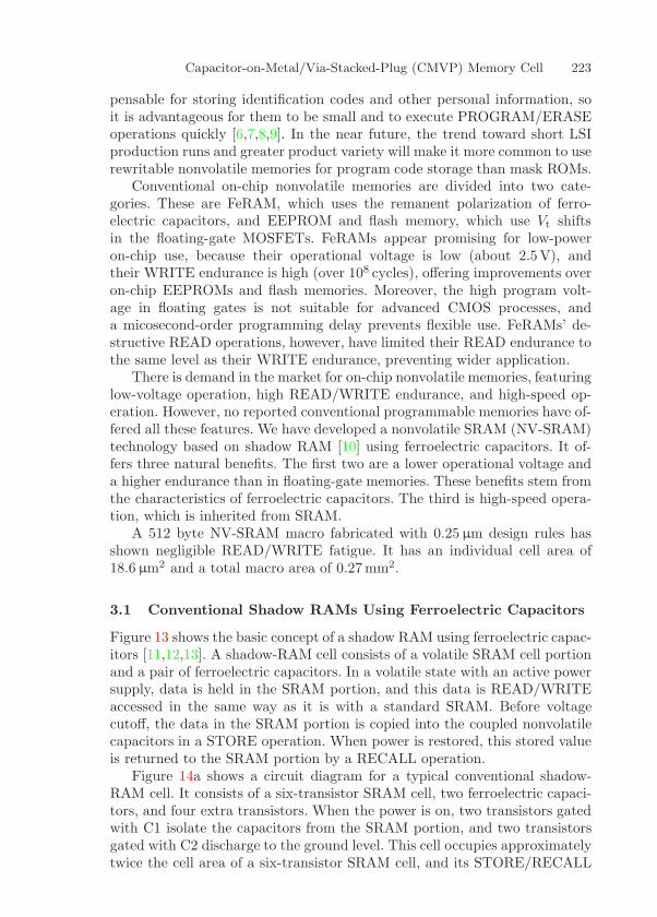
Capacitor-on-Metal/Via-Stacked-Plug (CMVP) Memory Cell 223
pensable for storing identification codes and other personal information, soit is advantageous for them to be small and to execute PROGRAM/ERASEoperations quickly [6,7,8,9]. In the near future, the trend toward short LSIproduction runs and greater product variety will make it more common to userewritable nonvolatile memories for program code storage than mask ROMs.
Conventional on-chip nonvolatile memories are divided into two cate-gories. These are FeRAM, which uses the remanent polarization of ferro-electric capacitors, and EEPROM and flash memory, which use Vt shiftsin the floating-gate MOSFETs. FeRAMs appear promising for low-poweron-chip use, because their operational voltage is low (about 2.5V), andtheir WRITE endurance is high (over 108 cycles), offering improvements overon-chip EEPROMs and flash memories. Moreover, the high program volt-age in floating gates is not suitable for advanced CMOS processes, anda micosecond-order programming delay prevents flexible use. FeRAMs’ de-structive READ operations, however, have limited their READ endurance tothe same level as their WRITE endurance, preventing wider application.
There is demand in the market for on-chip nonvolatile memories, featuringlow-voltage operation, high READ/WRITE endurance, and high-speed op-eration. However, no reported conventional programmable memories have of-fered all these features. We have developed a nonvolatile SRAM (NV-SRAM)technology based on shadow RAM [10] using ferroelectric capacitors. It of-fers three natural benefits. The first two are a lower operational voltage anda higher endurance than in floating-gate memories. These benefits stem fromthe characteristics of ferroelectric capacitors. The third is high-speed opera-tion, which is inherited from SRAM.
A 512 byte NV-SRAM macro fabricated with 0.25 µm design rules hasshown negligible READ/WRITE fatigue. It has an individual cell area of18.6 µm2 and a total macro area of 0.27 mm2.
3.1 Conventional Shadow RAMs Using Ferroelectric Capacitors
Figure 13 shows the basic concept of a shadow RAM using ferroelectric capac-itors [11,12,13]. A shadow-RAM cell consists of a volatile SRAM cell portionand a pair of ferroelectric capacitors. In a volatile state with an active powersupply, data is held in the SRAM portion, and this data is READ/WRITEaccessed in the same way as it is with a standard SRAM. Before voltagecutoff, the data in the SRAM portion is copied into the coupled nonvolatilecapacitors in a STORE operation. When power is restored, this stored valueis returned to the SRAM portion by a RECALL operation.
Figure 14a shows a circuit diagram for a typical conventional shadow-RAM cell. It consists of a six-transistor SRAM cell, two ferroelectric capaci-tors, and four extra transistors. When the power is on, two transistors gatedwith C1 isolate the capacitors from the SRAM portion, and two transistorsgated with C2 discharge to the ground level. This cell occupies approximatelytwice the cell area of a six-transistor SRAM cell, and its STORE/RECALL
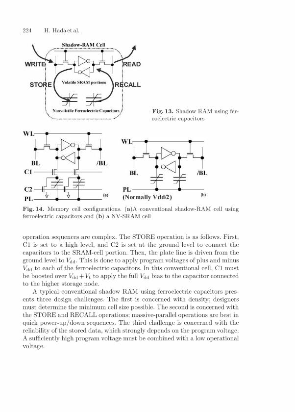
224 H. Hada et al.
Fig. 13. Shadow RAM using fer-roelectric capacitors
Fig. 14. Memory cell configurations. (a)A conventional shadow-RAM cell usingferroelectric capacitors and (b) a NV-SRAM cell
operation sequences are complex. The STORE operation is as follows. First,C1 is set to a high level, and C2 is set at the ground level to connect thecapacitors to the SRAM-cell portion. Then, the plate line is driven from theground level to Vdd. This is done to apply program voltages of plus and minusVdd to each of the ferroelectric capacitors. In this conventional cell, C1 mustbe boosted over Vdd +Vt to apply the full Vdd bias to the capacitor connectedto the higher storage node.
A typical conventional shadow RAM using ferroelectric capacitors pres-ents three design challenges. The first is concerned with density; designersmust determine the minimum cell size possible. The second is concerned withthe STORE and RECALL operations; massive-parallel operations are best inquick power-up/down sequences. The third challenge is concerned with thereliability of the stored data, which strongly depends on the program voltage.A sufficiently high program voltage must be combined with a low operationalvoltage.
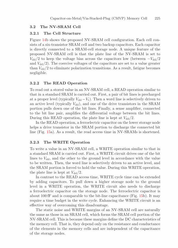
Capacitor-on-Metal/Via-Stacked-Plug (CMVP) Memory Cell 225
3.2 The NV-SRAM Cell
3.2.1 The Cell Structure
Figure 14b shows the proposed NV-SRAM cell configuration. Each cell con-sists of a six-transistor SRAM cell and two backup capacitors. Each capacitoris directly connected to a SRAM-cell storage node. A unique feature of theproposed NV-SRAM cell is that the plate line of the NV-SRAM is set toVdd/2 to keep the voltage bias across the capacitors low (between −Vdd/2and Vdd/2). The coercive voltages of the capacitors are set to a value greaterthan Vdd/2 to eliminate polarization transitions. As a result, fatigue becomesnegligible.
3.2.2 The READ Operation
To read out a stored value in an NV-SRAM cell, a READ operation similar tothat in a standard SRAM is carried out. First, a pair of bit lines is prechargedat a proper level (typically Vdd−Vt). Then a word line is selectively driven toan active level (typically Vdd), and one of the drive transistors in the SRAMportion pulls down one of the bit lines. Finally, a sense amplifier, connectedto the bit line pair, amplifies the differential voltage between the bit lines.During this READ operation, the plate line is kept at Vdd/2.
In the READ operation, a ferroelectric capacitor on the lower storage nodehelps a drive transistor in the SRAM portion to discharge the connected bitline (Fig. 15a). As a result, the read access time in NV-SRAMs is shortened.
3.2.3 The WRITE Operation
To write a value in an NV-SRAM cell, a WRITE operation similar to that ina standard SRAM is carried out. First, a WRITE circuit drives one of the bitlines to Vdd, and the other to the ground level in accordance with the valueto be written. Then, the word line is selectively driven to an active level, andthe SRAM portion is forced to hold the value. During this WRITE operation,the plate line is kept at Vdd/2.
In contrast to the READ access time, WRITE cycle time can be extendedby adding capacitors. To pull down a higher storage node to the groundlevel in a WRITE operation, the WRITE circuit also needs to dischargea ferroelectric capacitor on the storage node. The ferroelectric capacitor isabout 100 fF and is comparable to the bit-line capacitance (Fig. 15b). It mayrequire a time budget in the write cycle. Enhancing the WRITE circuit is aneffective way of overcoming this disadvantage.
The static noise and WRITE margins of an NV-SRAM cell are naturallythe same as those in an SRAM cell, which forms the SRAM cell portion of theNV-SRAM cell. This is because these margins define the DC characteristics ofthe memory cell. That is, they depend only on the resistance and conductanceof the elements in the memory cells and are independent of the capacitanceof the storage nodes.
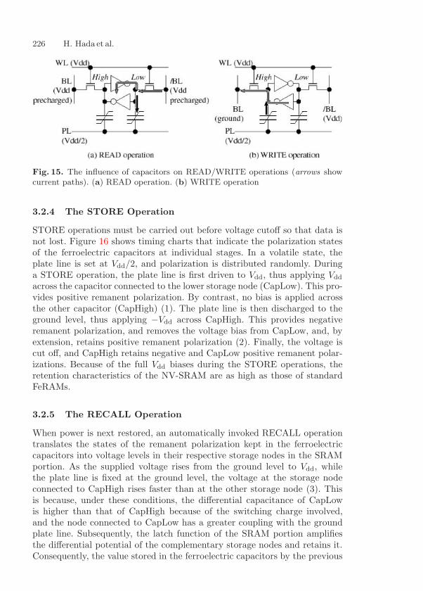
226 H. Hada et al.
Fig. 15. The influence of capacitors on READ/WRITE operations (arrows showcurrent paths). (a) READ operation. (b) WRITE operation
3.2.4 The STORE Operation
STORE operations must be carried out before voltage cutoff so that data isnot lost. Figure 16 shows timing charts that indicate the polarization statesof the ferroelectric capacitors at individual stages. In a volatile state, theplate line is set at Vdd/2, and polarization is distributed randomly. Duringa STORE operation, the plate line is first driven to Vdd, thus applying Vdd
across the capacitor connected to the lower storage node (CapLow). This pro-vides positive remanent polarization. By contrast, no bias is applied acrossthe other capacitor (CapHigh) (1). The plate line is then discharged to theground level, thus applying −Vdd across CapHigh. This provides negativeremanent polarization, and removes the voltage bias from CapLow, and, byextension, retains positive remanent polarization (2). Finally, the voltage iscut off, and CapHigh retains negative and CapLow positive remanent polar-izations. Because of the full Vdd biases during the STORE operations, theretention characteristics of the NV-SRAM are as high as those of standardFeRAMs.
3.2.5 The RECALL Operation
When power is next restored, an automatically invoked RECALL operationtranslates the states of the remanent polarization kept in the ferroelectriccapacitors into voltage levels in their respective storage nodes in the SRAMportion. As the supplied voltage rises from the ground level to Vdd, whilethe plate line is fixed at the ground level, the voltage at the storage nodeconnected to CapHigh rises faster than at the other storage node (3). Thisis because, under these conditions, the differential capacitance of CapLowis higher than that of CapHigh because of the switching charge involved,and the node connected to CapLow has a greater coupling with the groundplate line. Subsequently, the latch function of the SRAM portion amplifiesthe differential potential of the complementary storage nodes and retains it.Consequently, the value stored in the ferroelectric capacitors by the previous
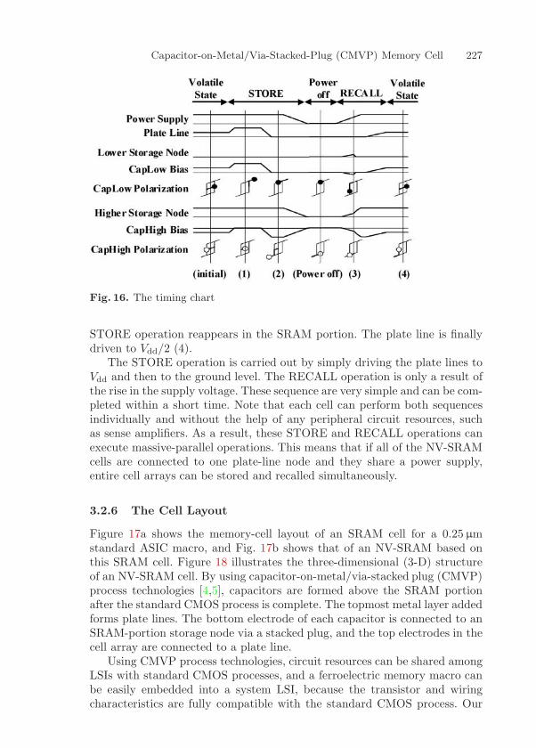
Capacitor-on-Metal/Via-Stacked-Plug (CMVP) Memory Cell 227
Fig. 16. The timing chart
STORE operation reappears in the SRAM portion. The plate line is finallydriven to Vdd/2 (4).
The STORE operation is carried out by simply driving the plate lines toVdd and then to the ground level. The RECALL operation is only a result ofthe rise in the supply voltage. These sequence are very simple and can be com-pleted within a short time. Note that each cell can perform both sequencesindividually and without the help of any peripheral circuit resources, suchas sense amplifiers. As a result, these STORE and RECALL operations canexecute massive-parallel operations. This means that if all of the NV-SRAMcells are connected to one plate-line node and they share a power supply,entire cell arrays can be stored and recalled simultaneously.
3.2.6 The Cell Layout
Figure 17a shows the memory-cell layout of an SRAM cell for a 0.25 µmstandard ASIC macro, and Fig. 17b shows that of an NV-SRAM based onthis SRAM cell. Figure 18 illustrates the three-dimensional (3-D) structureof an NV-SRAM cell. By using capacitor-on-metal/via-stacked plug (CMVP)process technologies [4,5], capacitors are formed above the SRAM portionafter the standard CMOS process is complete. The topmost metal layer addedforms plate lines. The bottom electrode of each capacitor is connected to anSRAM-portion storage node via a stacked plug, and the top electrodes in thecell array are connected to a plate line.
Using CMVP process technologies, circuit resources can be shared amongLSIs with standard CMOS processes, and a ferroelectric memory macro canbe easily embedded into a system LSI, because the transistor and wiringcharacteristics are fully compatible with the standard CMOS process. Our
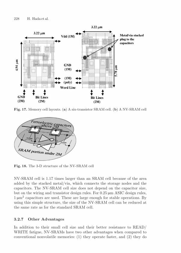
228 H. Hada et al.
Fig. 17. Memory cell layouts. (a) A six-transistor SRAM cell. (b) A NV-SRAM cell
Fig. 18. The 3-D structure of the NV-SRAM cell
NV-SRAM cell is 1.17 times larger than an SRAM cell because of the areaadded by the stacked metal/via, which connects the storage nodes and thecapacitors. The NV-SRAM cell size does not depend on the capacitor size,but on the wiring and transistor design rules. For 0.25 µm ASIC design rules,1 µm2 capacitors are used. These are large enough for stable operations. Byusing this simple structure, the size of the NV-SRAM cell can be reduced atthe same rate as for the standard SRAM cell.
3.2.7 Other Advantages
In addition to their small cell size and their better resistance to READ/WRITE fatigue, NV-SRAMs have two other advantages when compared toconventional nonvolatile memories: (1) they operate faster, and (2) they do
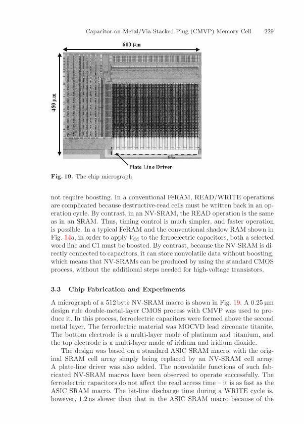
Capacitor-on-Metal/Via-Stacked-Plug (CMVP) Memory Cell 229
Fig. 19. The chip micrograph
not require boosting. In a conventional FeRAM, READ/WRITE operationsare complicated because destructive-read cells must be written back in an op-eration cycle. By contrast, in an NV-SRAM, the READ operation is the sameas in an SRAM. Thus, timing control is much simpler, and faster operationis possible. In a typical FeRAM and the conventional shadow RAM shown inFig. 14a, in order to apply Vdd to the ferroelectric capacitors, both a selectedword line and C1 must be boosted. By contrast, because the NV-SRAM is di-rectly connected to capacitors, it can store nonvolatile data without boosting,which means that NV-SRAMs can be produced by using the standard CMOSprocess, without the additional steps needed for high-voltage transistors.
3.3 Chip Fabrication and Experiments
A micrograph of a 512byte NV-SRAM macro is shown in Fig. 19. A 0.25 µmdesign rule double-metal-layer CMOS process with CMVP was used to pro-duce it. In this process, ferroelectric capacitors were formed above the secondmetal layer. The ferroelectric material was MOCVD lead zirconate titanite.The bottom electrode is a multi-layer made of platinum and titanium, andthe top electrode is a multi-layer made of iridium and iridium dioxide.
The design was based on a standard ASIC SRAM macro, with the orig-inal SRAM cell array simply being replaced by an NV-SRAM cell array.A plate-line driver was also added. The nonvolatile functions of such fab-ricated NV-SRAM macros have been observed to operate successfully. Theferroelectric capacitors do not affect the read access time – it is as fast as theASIC SRAM macro. The bit-line discharge time during a WRITE cycle is,however, 1.2 ns slower than that in the ASIC SRAM macro because of the
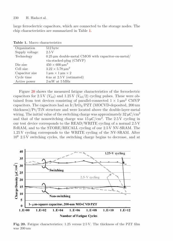
230 H. Hada et al.
large ferroelectric capacitors, which are connected to the storage nodes. Thechip characteristics are summarized in Table 1.
Table 1. Macro characteristics
Organization 512 byteSupply voltage 2.5 VTechnology 0.25 µm double-metal CMOS with capacitor-on-metal/
via-stacked-plug (CMVP)Die size 450 × 600 µm2
Cell size 3.22 × 5.78 µm2
Capacitor size 1 µm × 1 µm × 2Cycle time 6 ns at 2.5 V (estimated)Active power 2mW at 5MHz
Figure 20 shows the measured fatigue characteristics of the ferroelectriccapacitors for 2.5V (Vdd) and 1.25V (Vdd/2) cycling pulses. These were ob-tained from test devices consisting of parallel-connected 1 × 1 µm2 CMVPcapacitors. The capacitors had an Ir/IrO2/PZT (MOCVD-deposited, 200 nmthickness)/Pt/TiN structure and were located above the double-layer-metalwiring. The initial value of the switching charge was approximately 32 µC/cm2
and that of the nonswitching charge was 15 µC/cm2. The 2.5V cycling inour test device corresponds to the READ/WRITE cycling of a normal 2.5VFeRAM, and to the STORE/RECALL cycling of our 2.5V NV-SRAM. The1.25V cycling corresponds to the WRITE cycling of the NV-SRAM. After106 2.5V switching cycles, the switching charge begins to decrease, and at
Fig. 20. Fatigue characteristics: 1.25 versus 2.5 V. The thickness of the PZT filmwas 200 nm
Capacitor-on-Metal/Via-Stacked-Plug (CMVP) Memory Cell 231
109 cycles it becomes lower than the initial value. At 1012 1.25V switchingcycles, by contrast, the switching charge is hardly affected at all. A 2.5VNV-SRAM has at least 104 times better READ/WRITE endurance thana 2.5V FeRAM. It also has a power-up and power-down endurance of 108.
4 Summary
The CMVP memory cell was demonstrated as being a promising technologyfor embedded FeRAM. A PZT capacitor was formed on a metal (Al)/via (W)stacked plug using low-temperature MOCVD process. Two-mask capacitoretching and a plate-line contact through the bottom electrode were intro-duced to the CMVP process. 1 µm × 1 µm PZT capacitors showed Pr valuesof more than 10 µC/cm2 at 2.5V and good fatigue/imprint endurance. The0.25 µm 16kb cell-array monitor was fully functionable and proved effectivefor cell design optimization.
Then, the CMVP process was successfully applied to the fabrication ofa 512 byte nonvolatile SRAM (NV-SRAM) test macro, in which a 0.25 µmdouble-metal-layer CMOS process was used. Its Vdd/2 plate-line architecturecontributes to its negligible (more than 1012) fatigue/imprint characteristics.Because of the CMVP 3-D structure, the memory cell occupies an area only1.17 times larger than that of a standard ASIC SRAM cell produced with thesame design rules. The cell has an area of 18.6 µm2, and the total macro areais 0.27 mm2. The READ/WRITE cycle time of the NV-SRAM is comparablewith that of a standard SRAM macro, because its READ/WRITE operationsare based on those of standard SRAMs.
References
1. N. Tanabe, T. Matsuki, S. Saitoh, T. Takeuchi, S. Kobayashi, T. Nakajima,Y. Maejima, Y. Hayashi, K. Amanuma, T. Hase, Y. Miyasaka, T. Kunio: Tech.Dig. Symp. VLSI Technol. (1995) p. 123 215
2. J. Kudo, Y. Ito, S. Mitarai, N. Ogata, S. Yamazaki, H. Urashima, A. Okutoh,M. Nagata, K. Ishihara: Tech. Dig. Int. Electron Device Meeting (1997) p. 609215, 221
3. T. Hase, T. Noguchi, Y. Miyasaka: Abstracts Integr. Ferroelectr. (1997) p. 29215
4. K. Amanuma, T. Tatsumi, Y. Maejima, S. Takahashi, H. Hada, H. Okizaki,T. Kunio: Tech. Dig. Int. Electron Device Meeting (1998) p. 363 216, 227
5. K. Amanuma, S. Kobayashi, T. Tatsumi, Y. Maejima, H. Hada, J. Yamada,T. Miwa, H. Koike, H. Toyoshima, T. Kunio: Ext. Abstracts Solid-State De-vices Materials (1999) p. 384 216, 227
6. T. Sumi, M. Azuma, T. Otsuki, J. Gregory, C.A. Paz de Araujo: Tech. Dig.Int. Solid-State Circuits Conf. (1995) p. 70 223
7. T. Fukushima, A. Kawahara, T. Namba, M. Matsumoto, T. Nishimoto,N. Ikeda, Y. Judai, T. Sumi, K. Arita, T. Otsuki: Tech. Dig. Symp. VLSICircuits (1996) p. 46 223
232 H. Hada et al.
8. T. Miwa, J. Yamada, Y. Okamoto, H. Koike, H. Toyoshima, H. Hada,Y. Hayashi, H. Okizaki, Y. Miyasaka, T. Kunio, H. Miyamoto, H. Gomi,H. Kitajima: Proc. Custom Integrated Circuits Conf. (1998) p. 439 223
9. J. Yamada, T. Miwa, H. Koike, H. Toyoshima, K. Amanuma, S. Kobayashi,T. Tatsumi, Y. Maejima, H. Hada, H. Mori, S. Takahashi, H. Takeuchi,T. Kunio: Tech. Dig. Int. Solid-State Circuits Conf. (2000) p. 270 223
10. J. Drori, S. Jewell-Larsen, R. Klevin, W. Owen, R. Simko, W. Tchon: Tech.Dig. Int. Solid-State Circuits Conf. (1981) p. 148 223
11. K. Dimmler, S. S. Eaton: Memory cell with volatile and nonvolatile portionshaving ferroelectric capacitors, US Patent No. 4,809,225 (1987) 223
12. S. S. Eaton, D.B. Butler, M. Parris, D. Wilson, H. McNeillie: Tech. Dig. Int.Solid-State Circuits Conf. (1998) p. 130 223
13. S. S. Eaton, M. Michael: SRAM with programmable capacitance divider, USPatent No. 4,918,654 (1990) 223
Index
1T-1C, 217
ASIC macro, 227
boosting, 229bottom electrode, 218
EEPROM, 223embedded FeRAM, 217
FeRAM– Id–Vg characteristic, 221– oxygen barrier, 221FeRAM process– CMVP, 216flash memory– READ endurance, 223– WRITE endurance, 223
IC-card, 222
mask ROM, 223MOCVD, 219
Nonvolatile SRAM, 222
plate line, 224PZT, 218
RECALL operation, 223
seeding layer, 219sense amplifier, 225shadow RAM, 223sol-gel, 219sputtering, 219STORE operation, 223
top electrode, 218
Vdd/2, 225
The FET-Type FeRAM
Hiroshi Ishiwara
Frontier Collaborative Research Center, Tokyo Institute of Technology,4259 Nagatsuta, Midori-ku, Yokohama 226-8503, [email protected]
Abstract. The current status of the fabrication and integration of ferroelectric-gate field effect transistors (FETs) is reviewed. Novel applications of ferroelectric-gate FETs are first discussed, which include a single-transistor-cell-type digitalmemory, reconfigurable LSIs, and an analog memory for an artificial neural network.In the neural network application, the fabrication and basic operation of a pulse-frequency-modulation-type adaptive-learning neuron circuit are described, and alsoanSOI (silicon-on-insulator)-type FET array for synaptic connection is proposed.
Then, the data retention characteristics of ferroelectric-gate FETs with MFIS(M, metal; F, ferroelectric; I, insulator (buffer layer); S, semiconductor) and MFMISstructures are discussed. It is shown that the important factors in improving thedata retention characteristics are (1) increasing the buffer layer capacitance, (2) de-creasing the leakage current of both the ferroelectric film and the buffer layer,and (3) optimization of the area ratio between the MFM and MIS parts in theMFMIS structure. In the experiment, the properties of novel ferroelectrics suchas Sr2(Ta,Nb)2O7 and Pb5Ge3O11 are discussed as well as those for the conven-tional ferroelectrics. Finally, a novel FET-type FeRAM with a 1T-2C structure isintroduced and some experimental results are presented.
1 Introduction
So far, various kinds of ferroelectric memories have been discussed. However,the principle of the READ operation is the same in these memories. That is,the polarization reversal current is detected using a sense amplifier and thusa REWRITE operation is necessary after each READ operation. There isanother type of ferroelectric memory, called an FET-type ferroelectric mem-ory, which was proposed much earlier than the conventional capacitor-typememory. A key device in the FET-type memory is a ferroelectric-gate FETor an MFSFET (metal–ferroelectric–semiconductor FET), in which the gateinsulator is composed of a ferroelectric material, as shown in Fig. 1. In thisFET, the polarization direction of the ferroelectric film can be read out non-destructively using the drain current. The NDRO (nondestructive read-out)characteristic is one of the most important features of the FET-type FeRAM.The ferroelectric-gate FET can also be used as a nonvolatile analog memoryif the polarization of the ferroelectric film is continuously controlled by ap-plying pulse signals that are shorter than the polarization reversal time.
The original idea of the ferroelectric-gate FET was proposed by Bell Lab-oratories in 1955 [1] and many experimental studies were conducted in theH. Ishiwara, M. Okuyama, Y. Arimoto (Eds.): Ferroelectric Random Access Memories,Topics Appl. Phys. 93, 233–252 (2004)c© Springer-Verlag Berlin Heidelberg 2004
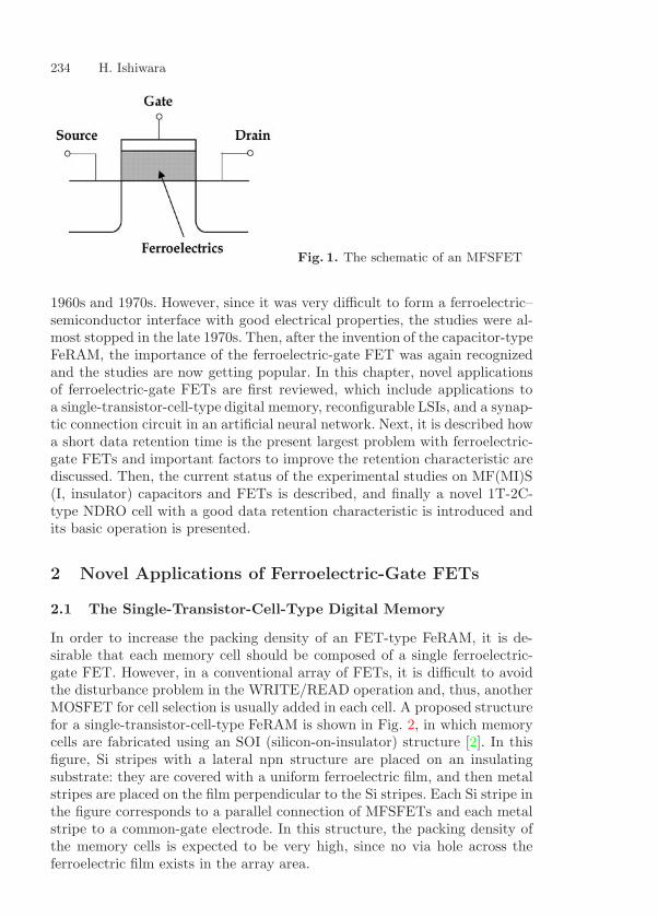
234 H. Ishiwara
Fig. 1. The schematic of an MFSFET
1960s and 1970s. However, since it was very difficult to form a ferroelectric–semiconductor interface with good electrical properties, the studies were al-most stopped in the late 1970s. Then, after the invention of the capacitor-typeFeRAM, the importance of the ferroelectric-gate FET was again recognizedand the studies are now getting popular. In this chapter, novel applicationsof ferroelectric-gate FETs are first reviewed, which include applications toa single-transistor-cell-type digital memory, reconfigurable LSIs, and a synap-tic connection circuit in an artificial neural network. Next, it is described howa short data retention time is the present largest problem with ferroelectric-gate FETs and important factors to improve the retention characteristic arediscussed. Then, the current status of the experimental studies on MF(MI)S(I, insulator) capacitors and FETs is described, and finally a novel 1T-2C-type NDRO cell with a good data retention characteristic is introduced andits basic operation is presented.
2 Novel Applications of Ferroelectric-Gate FETs
2.1 The Single-Transistor-Cell-Type Digital Memory
In order to increase the packing density of an FET-type FeRAM, it is de-sirable that each memory cell should be composed of a single ferroelectric-gate FET. However, in a conventional array of FETs, it is difficult to avoidthe disturbance problem in the WRITE/READ operation and, thus, anotherMOSFET for cell selection is usually added in each cell. A proposed structurefor a single-transistor-cell-type FeRAM is shown in Fig. 2, in which memorycells are fabricated using an SOI (silicon-on-insulator) structure [2]. In thisfigure, Si stripes with a lateral npn structure are placed on an insulatingsubstrate: they are covered with a uniform ferroelectric film, and then metalstripes are placed on the film perpendicular to the Si stripes. Each Si stripe inthe figure corresponds to a parallel connection of MFSFETs and each metalstripe to a common-gate electrode. In this structure, the packing density ofthe memory cells is expected to be very high, since no via hole across theferroelectric film exists in the array area.
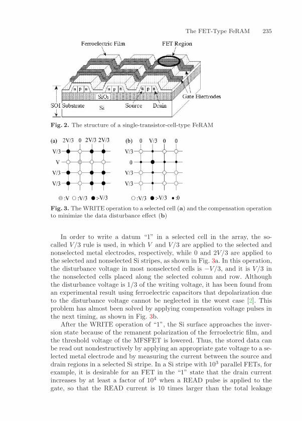
The FET-Type FeRAM 235
Fig. 2. The structure of a single-transistor-cell-type FeRAM
Fig. 3. The WRITE operation to a selected cell (a) and the compensation operationto minimize the data disturbance effect (b)
In order to write a datum “1” in a selected cell in the array, the so-called V/3 rule is used, in which V and V/3 are applied to the selected andnonselected metal electrodes, respectively, while 0 and 2V/3 are applied tothe selected and nonselected Si stripes, as shown in Fig. 3a. In this operation,the disturbance voltage in most nonselected cells is −V/3, and it is V/3 inthe nonselected cells placed along the selected column and row. Althoughthe disturbance voltage is 1/3 of the writing voltage, it has been found froman experimental result using ferroelectric capacitors that depolarization dueto the disturbance voltage cannot be neglected in the worst case [2]. Thisproblem has almost been solved by applying compensation voltage pulses inthe next timing, as shown in Fig. 3b.
After the WRITE operation of “1”, the Si surface approaches the inver-sion state because of the remanent polarization of the ferroelectric film, andthe threshold voltage of the MFSFET is lowered. Thus, the stored data canbe read out nondestructively by applying an appropriate gate voltage to a se-lected metal electrode and by measuring the current between the source anddrain regions in a selected Si stripe. In a Si stripe with 103 parallel FETs, forexample, it is desirable for an FET in the “1” state that the drain currentincreases by at least a factor of 104 when a READ pulse is applied to thegate, so that the READ current is 10 times larger than the total leakage
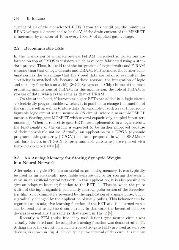
236 H. Ishiwara
current of all of the nonselected FETs. From this condition, the minimumREAD voltage is determined to be 0.4 V, if the drain current of the MFSFETis increased by a factor of 10 in every 100 mV of applied gate voltage.
2.2 Reconfigurable LSIs
In the fabrication of a capacitor-type FeRAM, ferroelectric capacitors areformed on top of CMOS transistors which have been fabricated using a stan-dard process. Thus, it is said that the integration of logic circuits and FeRAMis easier than that of logic circuits and DRAM. Furthermore, the former com-bination has the advantage that the stored data are retained even after theelectricity is switched off. Because of these reasons, the integration of logicand memory functions on a chip (SOC; System-on-a-Chip) is one of the mostpromising applications of FeRAM. In this application, the role of FeRAM isstorage of data, which is the same as that of DRAM.
On the other hand, if ferroelectric-gate FETs are added in a logic circuitas electrically programmable switches, it is possible to change the function ofthe circuit itself as well as to store data. An example of such a real-time recon-figurable logic circuit is the neuron-MOS circuit, where a neuron-MOSFETmeans a floating-gate MOSFET with several capacitively coupled input ter-minals [3]. When ferroelectric-gate FETs are implemented in a logic circuit,the functionality of the circuit is expected to be further improved becauseof their nonvolatile nature. Actually, an application to a DPGA (dynamicprogrammable gate array (DPGA)) has been proposed, in which SRAMs oranti-fuse devices in FPGA (field programmable gate array) are replaced withferroelectric-gate FETs [4].
2.3 An Analog Memory for Storing Synaptic Weightin a Neural Network
A ferroelectric-gate FET is also useful as an analog memory. It can typicallybe used as an electrically modifiable synapse device for storing the weightvalue in an artificial neural network. In this application, it is also possible togive an adaptive-learning function to the FET [5]. That is, when the pulsewidth of the input signals is sufficiently narrow, polarization of the ferroelec-tric film is not completely reversed by the application of a single pulse, but itis gradually changed by the application of many pulses. This behavior can beregarded as an adaptive-learning function of the FET and the learned resultcan be read out using the drain current. In this case, the layout of synapsedevices is essentially the same as that shown in Fig. 2 [6].
Recently, a PFM (pulse frequency modulation) type neuron circuit wasactually fabricated and the adaptive-learning function was demonstrated [7].A diagram of the circuit, in which ferroelectric-gate FETs are used as synapsedevices, is shown in Fig. 4. The output pulse interval of this circuit is mainly
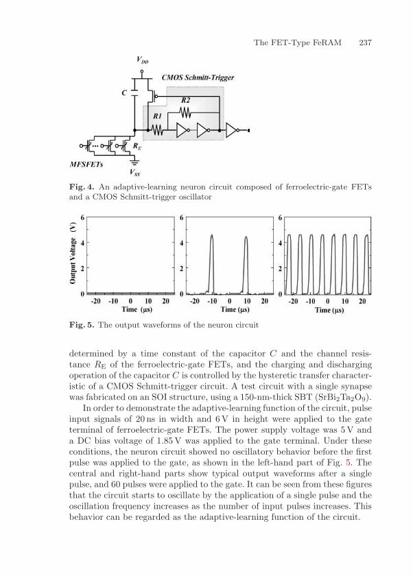
The FET-Type FeRAM 237
Fig. 4. An adaptive-learning neuron circuit composed of ferroelectric-gate FETsand a CMOS Schmitt-trigger oscillator
Fig. 5. The output waveforms of the neuron circuit
determined by a time constant of the capacitor C and the channel resis-tance RE of the ferroelectric-gate FETs, and the charging and dischargingoperation of the capacitor C is controlled by the hysteretic transfer character-istic of a CMOS Schmitt-trigger circuit. A test circuit with a single synapsewas fabricated on an SOI structure, using a 150-nm-thick SBT (SrBi2Ta2O9).
In order to demonstrate the adaptive-learning function of the circuit, pulseinput signals of 20 ns in width and 6 V in height were applied to the gateterminal of ferroelectric-gate FETs. The power supply voltage was 5 V anda DC bias voltage of 1.85 V was applied to the gate terminal. Under theseconditions, the neuron circuit showed no oscillatory behavior before the firstpulse was applied to the gate, as shown in the left-hand part of Fig. 5. Thecentral and right-hand parts show typical output waveforms after a singlepulse, and 60 pulses were applied to the gate. It can be seen from these figuresthat the circuit starts to oscillate by the application of a single pulse and theoscillation frequency increases as the number of input pulses increases. Thisbehavior can be regarded as the adaptive-learning function of the circuit.
238 H. Ishiwara
3 The Basic Operation of Ferroelectric-Gate FETs
3.1 Generation of the Depolarization Field
A typical sheet carrier density in the channel region of a MOSFET is about 2×1012 cm−2, assuming that tOX = 30 nm and VG − VT = 3 V, where tOX is theoxide thickness, VG is the gate voltage, and VT is the threshold voltage. Thisvalue corresponds to a charge density of 0.32 µC/cm2, and thus the remanentpolarization of a ferroelectric film does not need to be large for the fabricationof ferroelectric-gate FETs, if it is effectively used to induce carriers on thesemiconductor surface. However, if a ferroelectric film is directly depositedon a Si surface, it is generally difficult to form a good interface between them,since the constituent elements in both materials easily diffuse each other, andsince a transition layer is formed at the interface. In order to improve theinterface properties, a buffer layer is often inserted between a ferroelectricfilm and an Si substrate, which is composed of either a dielectric material(a MFIS structure, I, insulator) or a stacked structure of conductive anddielectric materials (a MFMIS structure).
In the MFIS or MFMIS structure, however, a new problem arises in thata depolarization field is generated in the ferroelectric film and it degradesthe data retention characteristic of the FET significantly. The generationmechanism can be explained using a series connection model of ferroelectricand dielectric capacitors, as follows. When the power supply is turned off andthe gate terminal of the FET is grounded, the top and bottom electrodes ofthe two capacitors are short-circuited. Under this condition, electrical charges±Q appear on the electrodes of the both capacitors, due to the remanentpolarization of the ferroelectric film and due to the charge neutrality conditionat a node between the two capacitors (the FI interface in the MFIS structureor the floating gate electrode M in the MFMIS structure).
The Q–V relation for the buffer layer capacitor is Q = CV and, thus, therelation in the ferroelectric capacitor becomes Q = −CV under the short-circuited condition, where C is the capacitance of the buffer layer. That is,the direction of the electric field in the ferroelectric capacitor is opposite tothat of the polarization of the film. This field is known as a depolarizationfield and it reduces the data retention time significantly, particularly whenC is small.
3.2 Improvement of the Data Retention Characteristics
The above discussion shows that the buffer layer capacitance C must be aslarge as possible, so that the depolarization field becomes small. This condi-tion means that a thin buffer layer with a high dielectric constant is prefer-able. So far, several buffer layers with high dielectric constants have been re-ported, including CeO2 [8], SrTiO3 [9], Y2O3 [10], Bi2SiO5 [11], SrTa2O6 [12],Si3N4 [13], LaAlO3 [14], and so on. Their dielectric constants range from 7
The FET-Type FeRAM 239
to 100. The dielectric constant of SrTiO3 is as high as 300, but when it isdeposited on a Si substrate, the effective value reduces to about 70 becauseof the existence of a transition layer.
However, the dielectric constants of usual ferroelectric films are known tobe much higher than those of the buffer layers. Thus, if both the ferroelectricand the buffer layer capacitors are made at the same size, most of the externalvoltage is applied to the buffer layer. In order to solve this mismatch problemof the dielectric constants, it is necessary to form a small-area ferroelectriccapacitor with a thick film. However, if a too thick ferroelectric film is used,there is a drawback that the operational voltage of the FET becomes high.
The leakage current of both the ferroelectric film and the buffer layer isalso important. If the charge neutrality at a node between the two capacitorsis destroyed by the leakage current, electrical charges on the electrodes ofthe buffer layer capacitor disappear, which means that carriers on the semi-conductor surface disappear and the stored data cannot be read out by thedrain current of the FET, even if the polarization of the ferroelectric film isretained. Thus, it is very important to reduce the leakage current of both theferroelectric film and the buffer layer.
Another important point is the matching of the induced charge betweenthe buffer layer and the ferroelectric film. The remanent polarization valuesof PZT (PbZrXTi1−XO3) and SBT are about 40 µC/cm2 and 10 µC/cm2,respectively, and they can induce the same density of positive and negativecharges on the electrodes of a capacitor. These values are generally muchlarger than the maximum charge density induced by a dielectric film. Forexample, the maximum induced charge density of SiO2 is about 3.5 µC/cm2
for an electric field of 10MV/cm and the film breaks down for the higherelectric field.
Thus, if a ferroelectric capacitor with a large remanent polarization isconnected in series with a SiO2 capacitor that has the same area, and ifa sufficiently high voltage is applied across the two capacitors, the SiO2 filmbreaks down before the polarization of the ferroelectric film is saturated.This situation is illustrated in Fig. 6a, for a combination of SBT and SiO2. Asshown in the figure, only a small hysteresis loop of SBT can be used under thecondition that the SiO2 buffer layer does not break down. It should be notedthat this condition is independent of the film thickness of both capacitors.
In order to solve the induced charge mismatch problem, it is necessary toform an MFMIS structure and to optimize the area ratio between the ferro-electric capacitor and the buffer layer capacitor. That is, in order to use thesaturation polarization of the ferroelectric film effectively, it is important tomake the ferroelectric capacitor area small. If the area of the SBT capacitoris reduced to 1/5 of the SiO2 capacitor, the vertical scale of the P–V (polar-ization versus voltage) characteristic equivalently becomes 1/5, as shown inFig. 6b, and the saturation polarization curve can be drawn in the region in
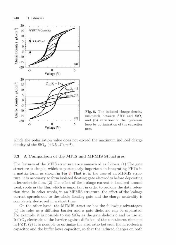
240 H. Ishiwara
Fig. 6. The induced charge densitymismatch between SBT and SiO2
and (b) variation of the hysteresisloop by optimization of the capacitorarea
which the polarization value does not exceed the maximum induced chargedensity of the SiO2 (±3.5 µC/cm2).
3.3 A Comparison of the MFIS and MFMIS Structures
The features of the MFIS structure are summarized as follows. (1) The gatestructure is simple, which is particularly important in integrating FETs ina matrix form, as shown in Fig 2. That is, in the case of an MFMIS struc-ture, it is necessary to form isolated floating gate electrodes before depositinga ferroelectric film. (2) The effect of the leakage current is localized aroundweak spots in the film, which is important in order to prolong the data reten-tion time. In other words, in an MFMIS structure, the effect of the leakagecurrent spreads out to the whole floating gate and the charge neutrality iscompletely destroyed in a short time.
On the other hand, the MFMIS structure has the following advantages.(1) Its roles as a diffusion barrier and a gate dielectric can be separated.For example, it is possible to use SiO2 as the gate dielectric and to use anIr/IrO2 electrode as the barrier against diffusion of the constituent elementsin PZT. (2) It is possible to optimize the area ratio between the ferroelectriccapacitor and the buffer layer capacitor, so that the induced charges on both
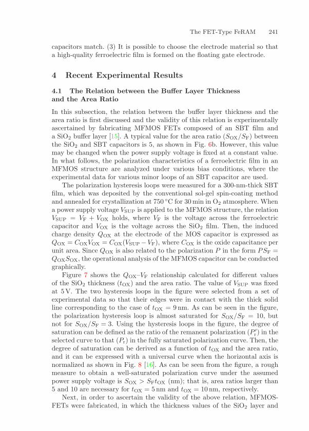
The FET-Type FeRAM 241
capacitors match. (3) It is possible to choose the electrode material so thata high-quality ferroelectric film is formed on the floating gate electrode.
4 Recent Experimental Results
4.1 The Relation between the Buffer Layer Thicknessand the Area Ratio
In this subsection, the relation between the buffer layer thickness and thearea ratio is first discussed and the validity of this relation is experimentallyascertained by fabricating MFMOS FETs composed of an SBT film anda SiO2 buffer layer [15]. A typical value for the area ratio (SOX/SF) betweenthe SiO2 and SBT capacitors is 5, as shown in Fig. 6b. However, this valuemay be changed when the power supply voltage is fixed at a constant value.In what follows, the polarization characteristics of a ferroelectric film in anMFMOS structure are analyzed under various bias conditions, where theexperimental data for various minor loops of an SBT capacitor are used.
The polarization hysteresis loops were measured for a 300-nm-thick SBTfilm, which was deposited by the conventional sol-gel spin-coating methodand annealed for crystallization at 750 C for 30 min in O2 atmosphere. Whena power supply voltage VSUP is applied to the MFMOS structure, the relationVSUP = VF + VOX holds, where VF is the voltage across the ferroelectriccapacitor and VOX is the voltage across the SiO2 film. Then, the inducedcharge density QOX at the electrode of the MOS capacitor is expressed asQOX = COXVOX = COX(VSUP −VF), where COX is the oxide capacitance perunit area. Since QOX is also related to the polarization P in the form PSF =QOXSOX, the operational analysis of the MFMOS capacitor can be conductedgraphically.
Figure 7 shows the QOX–VF relationship calculated for different valuesof the SiO2 thickness (tOX) and the area ratio. The value of VSUP was fixedat 5V. The two hysteresis loops in the figure were selected from a set ofexperimental data so that their edges were in contact with the thick solidline corresponding to the case of tOX = 9 nm. As can be seen in the figure,the polarization hysteresis loop is almost saturated for SOX/SF = 10, butnot for SOX/SF = 3. Using the hysteresis loops in the figure, the degree ofsaturation can be defined as the ratio of the remanent polarization (P ′
r ) in theselected curve to that (Pr) in the fully saturated polarization curve. Then, thedegree of saturation can be derived as a function of tOX and the area ratio,and it can be expressed with a universal curve when the horizontal axis isnormalized as shown in Fig. 8 [16]. As can be seen from the figure, a roughmeasure to obtain a well-saturated polarization curve under the assumedpower supply voltage is SOX > SFtOX (nm); that is, area ratios larger than5 and 10 are necessary for tOX = 5 nm and tOX = 10 nm, respectively.
Next, in order to ascertain the validity of the above relation, MFMOS-FETs were fabricated, in which the thickness values of the SiO2 layer and
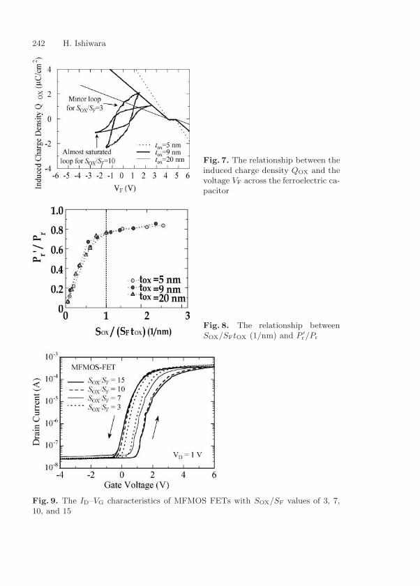
242 H. Ishiwara
Fig. 7. The relationship between theinduced charge density QOX and thevoltage VF across the ferroelectric ca-pacitor
Fig. 8. The relationship betweenSOX/SFtOX (1/nm) and P ′
r/Pr
Fig. 9. The ID–VG characteristics of MFMOS FETs with SOX/SF values of 3, 7,10, and 15
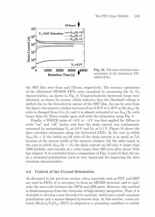
The FET-Type FeRAM 243
Fig. 10. The data retention char-acteristics of the fabricated MF-MOS FETs
the SBT film were 9 nm and 150 nm, respectively. The memory operationsof the fabricated MFMOS FETs were examined by measuring the ID–VG
characteristics, as shown in Fig. 9. Counterclockwise hysteresis loops wereobtained, as shown by arrows, which indicates that the threshold voltage isshifted due to the ferroelectric nature of the SBT film. As can be seen fromthe figure, the memory window increases from 0.35 V to 1.40 V as the SOX/SF
ratio is changed from 3 to 15, and it is almost saturated at an SOX/SF ratiolarger than 10. These results agree well with the estimation using Fig. 8.
Finally, a WRITE pulse of +6 V or −4 V was first applied for 100 ms towrite “on” and “off” states, and then the drain current was continuouslymeasured by maintaining VG at 0.8 V and VD at 0.1 V. Figure 10 shows thedata retention estimation using the fabricated FETs. In the case in whichSOX/SF = 3, the initial on/off ratio of the drain current is as small as 7.0,because of the narrow width of the memory window. On the other hand, inthe case in which SOX/SF = 15, the drain current on/off ratio is larger than1800 initially, and remains at a value larger than 200 even after about 10 hrhas elapsed. It is concluded from a comparison of Figs. 8 and 10 that the useof a saturated polarization curve is very important for improving the dataretention characteristics.
4.2 Control of the Crystal Orientation
As discussed in the previous section, when materials such as PZT and SBTare used in FETs, it is necessary to form an MFMIS structure and to opti-mize the area ratio between the MFM and MIS parts. However, this methodis disadvantageous from the viewpoint of high-density integration. Thus, it isdesirable to develop a new ferroelectric material, which has a small remanentpolarization and a square-shaped hysteresis loop. In this section, c-axis ori-ented (Ba,La)4Ti3O12 (BLT) is adopted as a promising candidate to satisfy
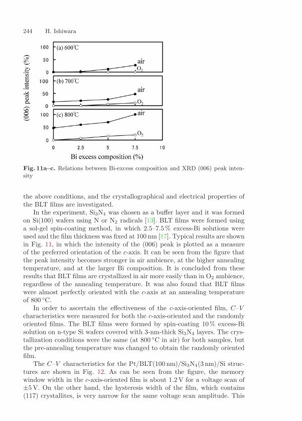
244 H. Ishiwara
Fig. 11a–c. Relations between Bi-excess composition and XRD (006) peak inten-sity
the above conditions, and the crystallographical and electrical properties ofthe BLT films are investigated.
In the experiment, Si3N4 was chosen as a buffer layer and it was formedon Si(100) wafers using N or N2 radicals [13]. BLT films were formed usinga sol-gel spin-coating method, in which 2.5–7.5% excess-Bi solutions wereused and the film thickness was fixed at 100 nm [17]. Typical results are shownin Fig. 11, in which the intensity of the (006) peak is plotted as a measureof the preferred orientation of the c-axis. It can be seen from the figure thatthe peak intensity becomes stronger in air ambience, at the higher annealingtemperature, and at the larger Bi composition. It is concluded from theseresults that BLT films are crystallized in air more easily than in O2 ambience,regardless of the annealing temperature. It was also found that BLT filmswere almost perfectly oriented with the c-axis at an annealing temperatureof 800 C.
In order to ascertain the effectiveness of the c-axis-oriented film, C–Vcharacteristics were measured for both the c-axis-oriented and the randomlyoriented films. The BLT films were formed by spin-coating 10% excess-Bisolution on n-type Si wafers covered with 3-nm-thick Si3N4 layers. The crys-tallization conditions were the same (at 800 C in air) for both samples, butthe pre-annealing temperature was changed to obtain the randomly orientedfilm.
The C–V characteristics for the Pt/BLT(100 nm)/Si3N4(3 nm)/Si struc-tures are shown in Fig. 12. As can be seen from the figure, the memorywindow width in the c-axis-oriented film is about 1.2 V for a voltage scan of±5 V. On the other hand, the hysteresis width of the film, which contains(117) crystallites, is very narrow for the same voltage scan amplitude. This
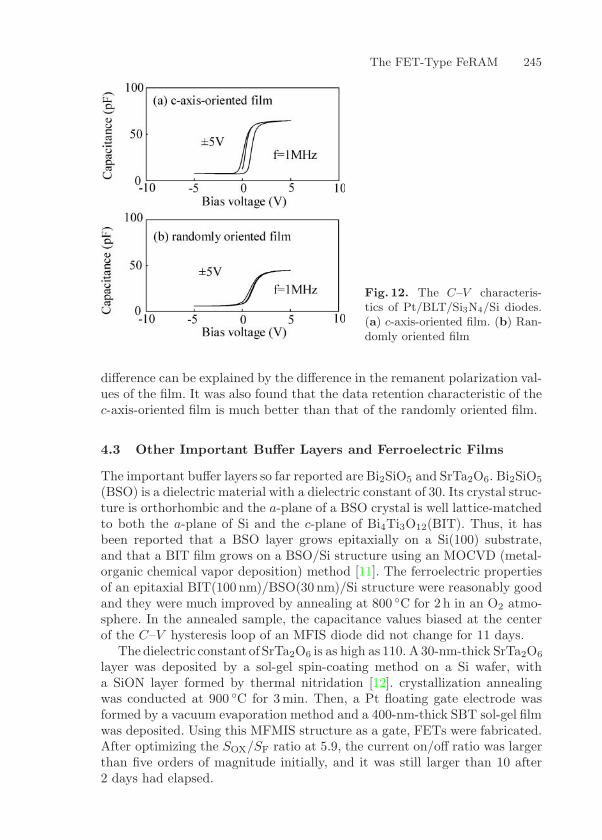
The FET-Type FeRAM 245
Fig. 12. The C–V characteris-tics of Pt/BLT/Si3N4/Si diodes.(a) c-axis-oriented film. (b) Ran-domly oriented film
difference can be explained by the difference in the remanent polarization val-ues of the film. It was also found that the data retention characteristic of thec-axis-oriented film is much better than that of the randomly oriented film.
4.3 Other Important Buffer Layers and Ferroelectric Films
The important buffer layers so far reported are Bi2SiO5 and SrTa2O6. Bi2SiO5
(BSO) is a dielectric material with a dielectric constant of 30. Its crystal struc-ture is orthorhombic and the a-plane of a BSO crystal is well lattice-matchedto both the a-plane of Si and the c-plane of Bi4Ti3O12(BIT). Thus, it hasbeen reported that a BSO layer grows epitaxially on a Si(100) substrate,and that a BIT film grows on a BSO/Si structure using an MOCVD (metal-organic chemical vapor deposition) method [11]. The ferroelectric propertiesof an epitaxial BIT(100 nm)/BSO(30 nm)/Si structure were reasonably goodand they were much improved by annealing at 800 C for 2 h in an O2 atmo-sphere. In the annealed sample, the capacitance values biased at the centerof the C–V hysteresis loop of an MFIS diode did not change for 11 days.
The dielectric constant of SrTa2O6 is as high as 110. A 30-nm-thick SrTa2O6
layer was deposited by a sol-gel spin-coating method on a Si wafer, witha SiON layer formed by thermal nitridation [12]. crystallization annealingwas conducted at 900 C for 3 min. Then, a Pt floating gate electrode wasformed by a vacuum evaporation method and a 400-nm-thick SBT sol-gel filmwas deposited. Using this MFMIS structure as a gate, FETs were fabricated.After optimizing the SOX/SF ratio at 5.9, the current on/off ratio was largerthan five orders of magnitude initially, and it was still larger than 10 after2 days had elapsed.

246 H. Ishiwara
Concerning the ferroelectric films, important results have been obtainedusing Sr2(Ta,Nb)2O7 and Pb5Ge3O11. Sr2(Ta,Nb)2O7 (STN) is a ferroelectricmaterial with a tungsten–bronze crystal structure. For a film with a Ta/Nbratio of 70/30, the remanent polarization and the dielectric constant havebeen measured to be 1.0 µC/cm2 and 40, respectively [18]. MFMIS FETs witha SOX/SF ratio of 3.12 were fabricated using the gate structure of Pt/STN(150 nm)/Pt/IrO2/poly-Si/SiO2(13 nm)/Si, in which the memory window inthe ID–VG characteristic was 3.8 V for the gate voltage scan of ±5 V. Concern-ing the retention characteristics, the variation of the high state capacitance ofan MFMIS diode with the above structure was not large (from 6pF to 5.4 pF)during the 2-week measurement period, while the low state capacitance didnot change during the measurement.
Pb5Ge3O11 (PGO) is a ferroelectric material with a dielectric constantof 30, a remanent polarization of 3 µC/cm2, and a coercive field of 100 kV/cm.Using this material, MFMIS FETs with excellent FET characteristics havebeen fabricated [19]. The film was deposited by MOCVD and a damasceneprocess was used for forming a gate structure composed of Pt/PGO(300 nm)/Ir/poly-Si/SiO2(6 nm)/Si. In the fabricated FETs, the memory window inthe ID–VG characteristic was as large as 3 V for the gate voltage scan of±3 V. Furthermore, the current on/off ratio was larger than eight orders ofmagnitude and the shift in the threshold voltage was retained at least for5 days.
5 The 1T-2C-Type Ferroelectric Memory
5.1 The Cell Structure and Basic Operation
As discussed above, the improvement of the data retention characteristic isthe most important issue in commercialization of the ferroelectric-gate FET.However, since the leakage current due to the depolarization field is one ofthe main reasons for the short retention time, it is very difficult to prolongthe retention time to 10 years. In order to solve this problem, a 1T-2C-typecell has been proposed, in which two ferroelectric capacitors with the samearea are connected to the gate electrode of a MOSFET [20], and the basicoperation of the cell has been demonstrated [21].
The cell structure and the polarization directions of the ferroelectric ca-pacitors are shown in Fig. 13. In order to write a datum in this cell, a positiveor negative pulse is applied between the terminals A and B, so that the twoferroelectric films are polarized oppositely with respect to the gate electrodeof the MOSFET. In this case, the electrical charges induced at the electrodesof both capacitors cancel each other and no charge is induced at the gateelectrode of the FET, which means that no depolarization field is generatedin the ferroelectric film, and a retention time as long as that of the usual1T1C-type memory can be expected. In the cell shown in Fig. 13, the ferro-electric film thickness of both capacitors is assumed to be the same. However,

The FET-Type FeRAM 247
Fig. 13a,b. An equivalent circuitof the 1T-2C-type memory andthe polarization directions of data“0” and “1”
it is not necessary for them to be the same if the polarization is well saturatedin both ferroelectric films.
For the READ operation, positive voltage pulses are applied to termi-nal B, keeping terminal A open. In this operation, when the stored datumis “0”, no polarization reversal occurs in the ferroelectric film and a smalldrain current flows through the MOSFET, assuming an n-channel FET. Onthe contrary, when the stored datum is “1”, the polarization of CFB is re-versed and a large drain current flows. As discussed here, the application ofREAD pulses is essential to distinguish the “0” and “1” data in this cell.However, the pulse height does not need to be high enough to reverse thepolarization of the ferroelectric film completely, but a partial change of thepolarization is preferable from the viewpoint of avoiding the fatigue phenom-enon and avoiding the data disturbing effect on nonselected cells.
5.2 Experimental Results
The 1T-2C ferroelectric memory cell was designed by using a 5 µm rule andit was fabricated on a silicon-on-insulator (SOI) structure. The gate MF-MOS structure of a memory cell is as follows: Pt (60 nm)/SBT (150 nm)/Pt (60 nm)/Ti (10 nm)/SiO2 (9 nm)/Si. The SBT film was deposited by a liq-uid source misted chemical deposition (LSMCD) method and annealed at750 C for 30 min in an O2 atmosphere for crystallization. Figure 14 showsthe difference in the drain current between the data “0” and “1”. It can beseen from the figure that the current on/off ratio in the READ operation isas high as 430 and that the current level after the READ operation is almostthe same as that before the operation. Then, the NDRO (nondestructiveread-out) function was investigated by applying READ pulses repeatedly.Figure 15 shows the variation of the drain current for the datum “0” andthe datum “1” state, in which the drain current of each memory state hardlychanged even after 103 pulses were applied.
Finally, the data retention characteristics of the fabricated memory cellwere examined by measuring the variation of the drain current with timefor various polarization states, as shown in Fig. 16. The states (A) and (B)correspond to the data “1” and “0” for the 1T-2C memory cell, respectively.The state (C) corresponds to datum “1” of the conventional MFMOS FET,
248 H. Ishiwara
Fig. 14. The READ operations of the 1T-2C-type ferroelectric memory cell
Fig. 15. NDRO operation for (a) da-tum “0” and (b) datum “1”, in which103 READ pulses were employed
The FET-Type FeRAM 249
Fig. 16. The data retention characteristics of the fabricated 1T-2C memory cellat various polarization states of the ferroelectric capacitors. The polarization di-rections of the capacitors and the measurement conditions are as follows. (A)CFA, down; CFB, up. (B) CFA, up; CFB, down. (C) CFA, down; CFB, down;VA = VB = 0V. (D) CFA, up; CFB, up; VA = VB = 0V. (E) CFA, down; CFB,down; VA = VB = 0.5 V. (F) (dashed line) CFA, up; CFB, down; VA = VB = 0V
since the polarization directions of both capacitors are downward. Similarly,the state (D) corresponds to datum “0” of the conventional MFMOS FET. Inthe state (E), an adequate VG of 0.5 V was applied to both capacitors duringmeasurement, so that the retention characteristics were improved. The state(F) was chosen to monitor the initial state of the 1T-2C memory cell withtime.
When the polarization directions of both capacitors are parallel [states(C), (D), and (E)], the “1” and “0” data can be distinguished without anyREAD signals, but the drain current of the datum “1” drastically decreaseswithin 104 s, due to the depolarization field. On the other hand, when thepolarization directions of both capacitors are opposite [states (A) and (B)],the data can be distinguished only when READ pulses are applied, and theresponse current to READ pulses does not degrade at least up to 105 s, asshown in Fig. 16. It is concluded from these measurements that the effec-tive suppression of the depolarization field is the origin of the excellent dataretention characteristics of the 1T-2C memory cell.
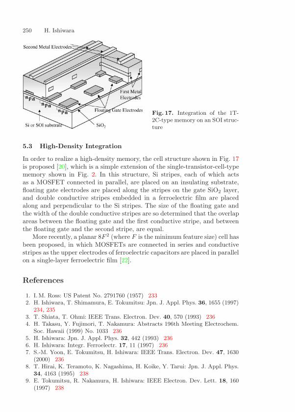
250 H. Ishiwara
Fig. 17. Integration of the 1T-2C-type memory on an SOI struc-ture
5.3 High-Density Integration
In order to realize a high-density memory, the cell structure shown in Fig. 17is proposed [20], which is a simple extension of the single-transistor-cell-typememory shown in Fig. 2. In this structure, Si stripes, each of which actsas a MOSFET connected in parallel, are placed on an insulating substrate,floating gate electrodes are placed along the stripes on the gate SiO2 layer,and double conductive stripes embedded in a ferroelectric film are placedalong and perpendicular to the Si stripes. The size of the floating gate andthe width of the double conductive stripes are so determined that the overlapareas between the floating gate and the first conductive stripe, and betweenthe floating gate and the second stripe, are equal.
More recently, a planar 8F 2 (where F is the minimum feature size) cell hasbeen proposed, in which MOSFETs are connected in series and conductivestripes as the upper electrodes of ferroelectric capacitors are placed in parallelon a single-layer ferroelectric film [22].
References
1. I.M. Ross: US Patent No. 2791760 (1957) 2332. H. Ishiwara, T. Shimamura, E. Tokumitsu: Jpn. J. Appl. Phys. 36, 1655 (1997)
234, 2353. T. Shiata, T. Ohmi: IEEE Trans. Electron. Dev. 40, 570 (1993) 2364. H. Takasu, Y. Fujimori, T. Nakamura: Abstracts 196th Meeting Electrochem.
Soc. Hawaii (1999) No. 1033 2365. H. Ishiwara: Jpn. J. Appl. Phys. 32, 442 (1993) 2366. H. Ishiwara: Integr. Ferroelectr. 17, 11 (1997) 2367. S.-M. Yoon, E. Tokumitsu, H. Ishiwara: IEEE Trans. Electron. Dev. 47, 1630
(2000) 2368. T. Hirai, K. Teramoto, K. Nagashima, H. Koike, Y. Tarui: Jpn. J. Appl. Phys.
34, 4163 (1995) 2389. E. Tokumitsu, R. Nakamura, H. Ishiwara: IEEE Electron. Dev. Lett. 18, 160
(1997) 238

The FET-Type FeRAM 251
10. B.-E. Park, E. Tokumitsu, H. Ishiwara: Jpn. J. Appl. Phys. 37, 5145 (1998)238
11. T. Kijima, H. Matsunaga: Jpn. J. Appl. Phys. 38, 2281 (1999) 238, 24512. E. Tokumitsu, G. Fujii, H. Ishiwara: Appl. Phys. Lett. 75, 575 (1999) 238, 24513. Y. Fujisaki, T. Kijima, H. Ishiwara: Appl. Phys. Lett. 78, 1285 (2001) 238,
24414. B.-E. Park, H. Ishiwara: Appl. Phys. Lett. 79, 806 (2001) 23815. S.-M. Yoon, E. Tokumitsu, H. Ishiwara: Jpn. J. Appl. Phys. 39, 2119 (2000)
24116. H. Ishiwara: Proc. 12th IEEE Int. Symp. Applications of Ferroelectrics 1, 331
(2000) 24117. T. Kijima, Y. Fujisaki, H. Ishiwara: Jpn. J. Appl. Phys. 40, 2977 (2001) 24418. Y. Fujimori, T. Nakamura, A. Kamisawa: Jpn. J. Appl. Phys. 38, 2285 (1999)
24619. T. Li, S.-T. Hsu, B. D. Ulrich, L. Stecker, D.R. Evans, J. J. Lee: IEEE Electron.
Dev. Lett. 23, 339 (2002) 24620. H. Ishiwara: Integr. Ferroelectr. 34, 11 (2001) 246, 25021. S.-M. Yoon, H. Ishiwara: IEEE Trans. Electron. Dev. 48, 2002 (2001) 24622. S. Yamamoto, H. S. Kim, H. Ishiwara: Jpn. J. Appl. Phys. 42, 2059 (2003) 250

Index
(Ba,La)4Ti3O12 (BLT), 2431T-2C– type, 246
adaptive-learning, 236area ratio, 241– between the ferroelectric capacitor
and the buffer layer capacitor, 239artificial neural network, 236
buffer layer, 238– Bi2SiO5, 245– Si3N4, 244– SrTa2O6, 245
capacitor-type memory, 233charge neutrality, 238
depolarization field, 238, 247dielectric constant, 238disturbance problem, 234dynamic programmable gate array
(DPGA), 236
FeRAM– silicon-on-insulator, 234ferroelectric-gate FET, 233FET-type ferroelectric memory, 233
hysteresis– loop, 241
induced charge, 239
leakage current, 239
memory cell, 234memory window, 243metal–ferroelectric–semiconductor FET
(MFSFET), 233MFIS, 238, 240MFMIS, 238, 240minimum feature size, 250modifiable synapse, 236
neuron-MOS, 236nondestructive read-out, 247nondestructive read-out (NDRO), 233
Pb5Ge3O11, 246pulse frequency modulation (PFM),
236
reconfigurable logic circuit, 236retention characteristic, 247
SBT, 237, 241, 247Schmitt-trigger circuit, 237single-transistor-cell-type, 234sol-gel, 241Sr2(Ta,Nb)2O7, 245SrTa2O6, 245system-on-a-chip (SOC), 236
V/3 rule, 235
Ferroelectric Technologies
for Portable Equipment
Yoshikazu Fujimori, Takashi Nakamura, and Hidemi Takasu
Semiconductor R& D Headquarters, ROHM Co., Ltd.,21, Saiin Mizosaki-cho, Ukyo-ku, Kyoto 615-8585, [email protected]
Abstract. Key technologies for portable equipment are low-voltage operation, lowpower consumption, and protocol-flexibility. Ferroelectric technology can contributenonvolatility and flexibility to the portable systems. In this chapter, process tech-nologies for low-voltage operation are first described. Then, nonvolatile logic circuitsare introduced for low power consumption. Several nonvolatile latch circuits, whichare basic elements of powering off LSIs, are shown. We also discuss reconfigurablearchitecture using ferroelectric technologies.
1 Introduction
Portable equipment, including the cellular phone and the personal digital as-sistant (PDA), is spreading rapidly today. The power consumption decreasedemand for LSIs has risen along with it. The power consumption of a transis-tor is decreased by reducing the design rule. However, the power consumptionincreases due to the requirement for high integration and high performance,and an improvement by means of a review of the device structure or othermethods is required. There is a proposal by which the power consumptionof the transistor is reduced without degradation of the performance by usinghigh-k materials for the gate insulator as the one expedient. Moreover, thereis a method of decreasing the power consumption, which is called the multi-ple-threshold (MT) CMOS method, and involves stopping the power supplyto the circuit blocks that do not operate.
The requirement for a power consumption decrease is also strong forthe semiconductor memory. Especially, current nonvolatile memories suchas EEPROM (electrically erasable programmable read-only memory) andFLASH consume a large amount of power during the writing of data. Itis not especially low in power consumption, although new memories such asMRAM (magnetoresistance RAM) [1] and OUM (Ovonic unified memory) [2]are high in performance. The ferroelectric memory is more advantageous thanMRAM and OUM with regard to low power consumption. MRAM and OUMare the types that use variable resistance and thus an applied voltage mustbe enlarged as the size decreases to obtain the same amount of signal. On theother hand, the ferroelectric memory does not have the necessity for applyinga voltage greater than the polarization saturation voltage of the ferroelec-tric capacitor, and the operational voltage can be decreased by reducing theH. Ishiwara, M. Okuyama, Y. Arimoto (Eds.): Ferroelectric Random Access Memories,Topics Appl. Phys. 93, 255–270 (2004)c© Springer-Verlag Berlin Heidelberg 2004
256 Y. Fujimori et al.
polarization saturation voltage. The polarization saturation voltage can bedecreased by process improvements and by making a thinner film.
The ferroelectric memory is not only an ideal memory with clear ad-vantages such as nonvolatility, low power consumption, high endurance, andhigh-speed writing, but is also the most suitable device for memory embed-ded applications [3]. Its manufacturing process makes it more compatiblewith the standard CMOS process than the traditional nonvolatile memoryprocess, since it does not require high-voltage operation, and the ferroelectricprocess does not influence the characteristics of the CMOS devices used inlogic cells, analog cells, and core cells. In the spreading of the intellectualproperty (IP) application for the LSI industry, this embedded applicationtakes on a more important role.
In the near future, ferroelectric memory technology will be incorporatedinto reconfigurable devices as programmable interconnect switches besides be-ing used as embedded memories. These ferroelectric memory based reconfig-urable devices can be used as dynamic programmable gate arrays (DPGAs),which can be reconfigured from their original logic in a system under anoperational mode.
New logic circuits will be operated with lower power consumption or a re-sume function by introducing ferroelectric gated transistors or ferroelectriccapacitors. Even though ferroelectric memory technology has many advan-tages, it is not popular yet, since the conventional semiconductor processdegrades the ferroelectric layer easily. The means of preventing degradationof ferroelectric films in the silicon wafer process will also be discussed.
2 Process Technologies for Low-Voltage Operation
2.1 Experimental and Characterization
Pb(Zr,Ti)O3 (PZT) ferroelectric thin films were prepared by the conventionalsol-gel method [4]. The sol-gel solution was made by Mitsubishi MaterialsCorp. and the solvent was 2-metoxyethanol. The Zr/Ti ratio was 52/48. Sil-icon p-type wafers were used as the substrates. Pt(175 nm)/IrO2(65 nm) orIrO2 (65 nm) was deposited as the bottom electrode by magnetron sputter-ing. Figure 1 shows the flow diagram for film deposition. After spin-coatingof the PZT precursor, the films were baked at 200 C to evaporate the sol-vent and pre-annealed at 400 C in dry air to eliminate organic components.These processes were repeated several times, until the film thickness wasabout 300nm. The deposited films were crystallized by low-pressure rapidthermal annealing (RTA) and/or the two-step annealing technique. The irid-ium system top electrode was deposited by sputtering and patterned by dryetching. The area of the top electrode was 50 µm × 50 µm.
Figure 2 shows a flow diagram of the ferroelectric film crystallizationprocess. In the conventional crystallization process, the spin-coated films arecrystallized by RTA (first annealing). Then, the top electrodes are deposited.
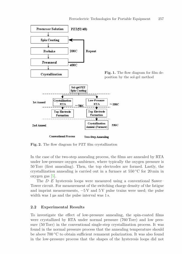
Ferroelectric Technologies for Portable Equipment 257
Fig. 1. The flow diagram for film de-position by the sol-gel method
Fig. 2. The flow diagram for PZT film crystallization
In the case of the two-step annealing process, the films are annealed by RTAunder low-pressure oxygen ambience, where typically the oxygen pressure is50 Torr (first annealing). Then, the top electrodes are formed. Lastly, thecrystallization annealing is carried out in a furnace at 550 C for 20 min inoxygen gas [5].
The D–E hysteresis loops were measured using a conventional Sawer–Tower circuit. For measurement of the switching charge density of the fatigueand imprint measurements, −5 V and 5 V pulse trains were used; the pulsewidth was 1 µs and the pulse interval was 1 s.
2.2 Experimental Results
To investigate the effect of low-pressure annealing, the spin-coated filmswere crystallized by RTA under normal pressure (760 Torr) and low pres-sure (50 Torr) in the conventional single-step crystallization process. It wasfound in the normal pressure process that the annealing temperature shouldbe above 700 C to obtain sufficient remanent polarization. It was also foundin the low-pressure process that the shapes of the hysteresis loops did not
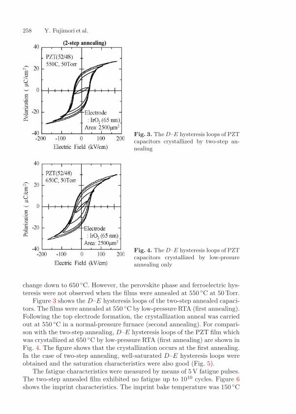
258 Y. Fujimori et al.
Fig. 3. The D–E hysteresis loops of PZTcapacitors crystallized by two-step an-nealing
Fig. 4. The D–E hysteresis loops of PZTcapacitors crystallized by low-presureannealing only
change down to 650 C. However, the perovskite phase and ferroelectric hys-teresis were not observed when the films were annealed at 550 C at 50 Torr.
Figure 3 shows the D–E hysteresis loops of the two-step annealed capaci-tors. The films were annealed at 550 C by low-pressure RTA (first annealing).Following the top electrode formation, the crystallization anneal was carriedout at 550 C in a normal-pressure furnace (second annealing). For compari-son with the two-step annealing, D–E hysteresis loops of the PZT film whichwas crystallized at 650 C by low-pressure RTA (first annealing) are shown inFig. 4. The figure shows that the crystallization occurs at the first annealing.In the case of two-step annealing, well-saturated D–E hysteresis loops wereobtained and the saturation characteristics were also good (Fig. 5).
The fatigue characteristics were measured by means of 5 V fatigue pulses.The two-step annealed film exhibited no fatigue up to 1010 cycles. Figure 6shows the imprint characteristics. The imprint bake temperature was 150 C
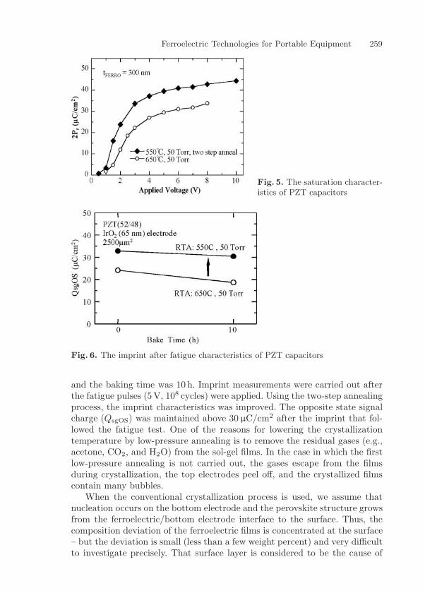
Ferroelectric Technologies for Portable Equipment 259
Fig. 5. The saturation character-istics of PZT capacitors
Fig. 6. The imprint after fatigue characteristics of PZT capacitors
and the baking time was 10 h. Imprint measurements were carried out afterthe fatigue pulses (5 V, 108 cycles) were applied. Using the two-step annealingprocess, the imprint characteristics was improved. The opposite state signalcharge (QsgOS) was maintained above 30 µC/cm2 after the imprint that fol-lowed the fatigue test. One of the reasons for lowering the crystallizationtemperature by low-pressure annealing is to remove the residual gases (e.g.,acetone, CO2, and H2O) from the sol-gel films. In the case in which the firstlow-pressure annealing is not carried out, the gases escape from the filmsduring crystallization, the top electrodes peel off, and the crystallized filmscontain many bubbles.
When the conventional crystallization process is used, we assume thatnucleation occurs on the bottom electrode and the perovskite structure growsfrom the ferroelectric/bottom electrode interface to the surface. Thus, thecomposition deviation of the ferroelectric films is concentrated at the surface– but the deviation is small (less than a few weight percent) and very difficultto investigate precisely. That surface layer is considered to be the cause of
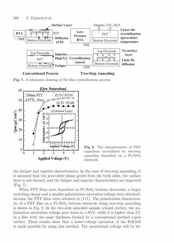
260 Y. Fujimori et al.
Fig. 7. A schematic drawing of the film crystallization process
Fig. 8. The characteristics of PZTcapacitors crystallized by two-stepannealing deposited on a Pt/IrO2
electrode
the fatigue and imprint characteristics. In the case of two-step annealing, itis assumed that the perovskite phase grows from the both sides, the surfacelayer is not formed, and the fatigue and imprint characteristics are improved(Fig. 7).
When PZT films were deposited on Pt/IrO2 bottom electrodes, a largerswitching charge and a smaller polarization saturation voltage were obtained,because the PZT films were oriented to (111). The polarization characteris-tic of a PZT film on a Pt/IrO2 bottom electrode using two-step annealingis shown in Fig. 8. In the two-step annealed sample (closed circles), the po-larization saturation voltage goes down to 1.65V, while it is higher than 2 Vin a film with the same thickness formed by a conventional method (opencircles). These results show that a lower-voltage operation of the FeRAMis made possible by using this method. The operational voltage will be de-

Ferroelectric Technologies for Portable Equipment 261
Fig. 9. Acceleration test in voltage stress
creased to less than 1V in the figure by using thinner films. Recently, therehas been a report about having obtained a polarization saturation voltage of0.5V by using thin films [6].
When this process is used, the reliability of the PZT films improves consid-erably. A fatigue characteristic accelerated by the voltage is shown in Fig. 9.As can be seen from the figure, PZT film formed by the new process hasan endurance of more than 2 × 10¹⁵ times in 3V. Ferroelectric film alreadyhas the ability that a read/write cycle is unlimited, and the read/write cyclelimit of the FeRAM will be removed by the establishment of an evaluationmethod.
3 Nonvolatile Logic
The reduction of the power consumption is becoming more essential forportable systems. Several standby leakage reduction schemes have been re-ported. One is the MT-CMOS. This method, however, requires high Vth ad-ditional latches branched from the critical path, like a balloon latch [7]. Theother is the variable-threshold (VT) CMOS [8]. This requires a triple-wellstructure and an additional circuit to control the substrate bias. Accordingto the ITRS 2001 roadmap, the gate leakage for low standby will be compara-ble to source–drain leakage by 2005. The nonvolatile latch circuit disussed inthis section is useful to reduce gate leakage like that of a MT-CMOS circuit.
3.1 The Ferroelectric Nonvolatile Latch
Figure 10 shows the concept of the MT-CMOS with a nonvolatile latch. Byadding nonvolatility to a conventional latch, the latched data are kept duringpower off. Figure 11 shows a nonvolatile latch circuit. This circuit requirestwo additional ferroelectric capacitors (C1, C2) and one plate line (PL) to
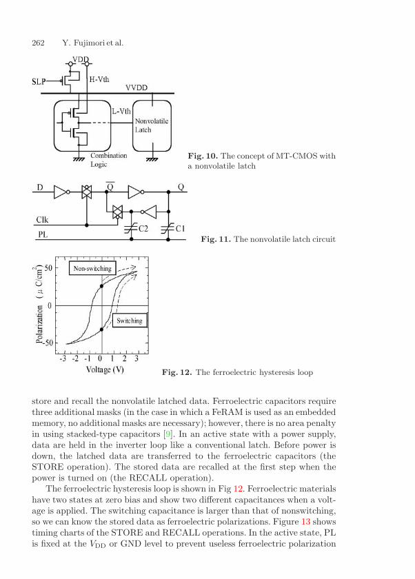
262 Y. Fujimori et al.
Fig. 10. The concept of MT-CMOS witha nonvolatile latch
Fig. 11. The nonvolatile latch circuit
Fig. 12. The ferroelectric hysteresis loop
store and recall the nonvolatile latched data. Ferroelectric capacitors requirethree additional masks (in the case in which a FeRAM is used as an embeddedmemory, no additional masks are necessary); however, there is no area penaltyin using stacked-type capacitors [9]. In an active state with a power supply,data are held in the inverter loop like a conventional latch. Before power isdown, the latched data are transferred to the ferroelectric capacitors (theSTORE operation). The stored data are recalled at the first step when thepower is turned on (the RECALL operation).
The ferroelectric hysteresis loop is shown in Fig 12. Ferroelectric materialshave two states at zero bias and show two different capacitances when a volt-age is applied. The switching capacitance is larger than that of nonswitching,so we can know the stored data as ferroelectric polarizations. Figure 13 showstiming charts of the STORE and RECALL operations. In the active state, PLis fixed at the VDD or GND level to prevent useless ferroelectric polarization
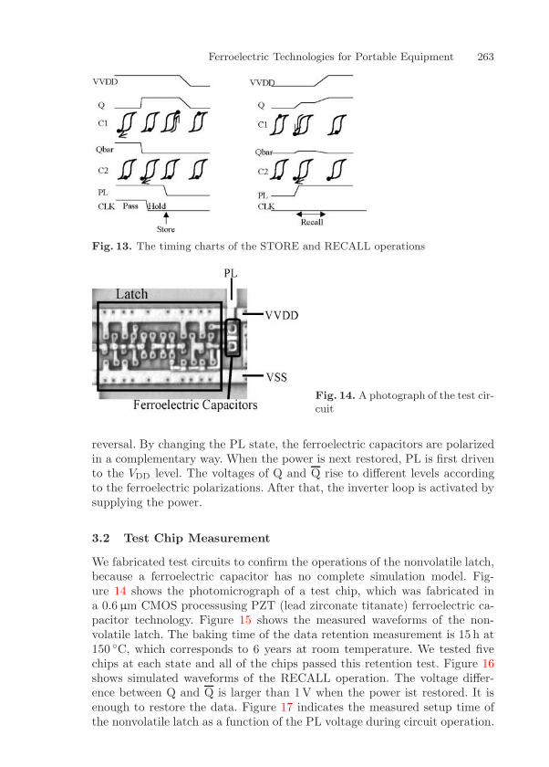
Ferroelectric Technologies for Portable Equipment 263
Fig. 13. The timing charts of the STORE and RECALL operations
Fig. 14. A photograph of the test cir-cuit
reversal. By changing the PL state, the ferroelectric capacitors are polarizedin a complementary way. When the power is next restored, PL is first drivento the VDD level. The voltages of Q and Q rise to different levels accordingto the ferroelectric polarizations. After that, the inverter loop is activated bysupplying the power.
3.2 Test Chip Measurement
We fabricated test circuits to confirm the operations of the nonvolatile latch,because a ferroelectric capacitor has no complete simulation model. Fig-ure 14 shows the photomicrograph of a test chip, which was fabricated ina 0.6 µm CMOS processusing PZT (lead zirconate titanate) ferroelectric ca-pacitor technology. Figure 15 shows the measured waveforms of the non-volatile latch. The baking time of the data retention measurement is 15 h at150 C, which corresponds to 6 years at room temperature. We tested fivechips at each state and all of the chips passed this retention test. Figure 16shows simulated waveforms of the RECALL operation. The voltage differ-ence between Q and Q is larger than 1V when the power ist restored. It isenough to restore the data. Figure 17 indicates the measured setup time ofthe nonvolatile latch as a function of the PL voltage during circuit operation.

264 Y. Fujimori et al.
Fig. 15. The measured waveform ofthe nonvolatile latch
Fig. 16. The simulated waveform of theRECALL operation
Fig. 17. The setup time as a function of the PLvoltage
When the PL is kept at VDD/2, a reversal of the ferroelectric polarizationoccurs every time the Q state changes and the operation speed decreases.Therefore the PL should be fixed at the VDD or GND level. These values forthe setup time are comparable with those of a conventional latch circuit.
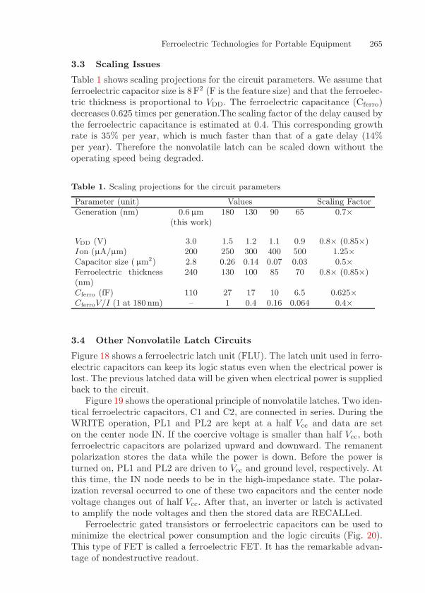
Ferroelectric Technologies for Portable Equipment 265
3.3 Scaling Issues
Table 1 shows scaling projections for the circuit parameters. We assume thatferroelectric capacitor size is 8F2 (F is the feature size) and that the ferroelec-tric thickness is proportional to VDD. The ferroelectric capacitance (Cferro)decreases 0.625 times per generation.The scaling factor of the delay caused bythe ferroelectric capacitance is estimated at 0.4. This corresponding growthrate is 35% per year, which is much faster than that of a gate delay (14%per year). Therefore the nonvolatile latch can be scaled down without theoperating speed being degraded.
Table 1. Scaling projections for the circuit parameters
Parameter (unit) Values Scaling FactorGeneration (nm) 0.6 µm 180 130 90 65 0.7×
(this work)
VDD (V) 3.0 1.5 1.2 1.1 0.9 0.8× (0.85×)Ion (µA/µm) 200 250 300 400 500 1.25×Capacitor size ( µm2) 2.8 0.26 0.14 0.07 0.03 0.5×Ferroelectric thickness(nm)
240 130 100 85 70 0.8× (0.85×)
Cferro (fF) 110 27 17 10 6.5 0.625×CferroV/I (1 at 180 nm) – 1 0.4 0.16 0.064 0.4×
3.4 Other Nonvolatile Latch Circuits
Figure 18 shows a ferroelectric latch unit (FLU). The latch unit used in ferro-electric capacitors can keep its logic status even when the electrical power islost. The previous latched data will be given when electrical power is suppliedback to the circuit.
Figure 19 shows the operational principle of nonvolatile latches. Two iden-tical ferroelectric capacitors, C1 and C2, are connected in series. During theWRITE operation, PL1 and PL2 are kept at a half Vcc and data are seton the center node IN. If the coercive voltage is smaller than half Vcc, bothferroelectric capacitors are polarized upward and downward. The remanentpolarization stores the data while the power is down. Before the power isturned on, PL1 and PL2 are driven to Vcc and ground level, respectively. Atthis time, the IN node needs to be in the high-impedance state. The polar-ization reversal occurred to one of these two capacitors and the center nodevoltage changes out of half Vcc. After that, an inverter or latch is activatedto amplify the node voltages and then the stored data are RECALLed.
Ferroelectric gated transistors or ferroelectric capacitors can be used tominimize the electrical power consumption and the logic circuits (Fig. 20).This type of FET is called a ferroelectric FET. It has the remarkable advan-tage of nondestructive readout.
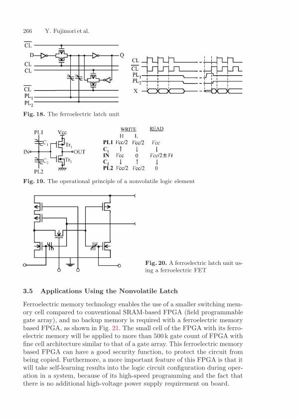
266 Y. Fujimori et al.
Fig. 18. The ferroelectric latch unit
Fig. 19. The operational principle of a nonvolatile logic element
Fig. 20. A ferroelectric latch unit us-ing a ferroelectric FET
3.5 Applications Using the Nonvolatile Latch
Ferroelectric memory technology enables the use of a smaller switching mem-ory cell compared to conventional SRAM-based FPGA (field programmablegate array), and no backup memory is required with a ferroelectric memorybased FPGA, as shown in Fig. 21. The small cell of the FPGA with its ferro-electric memory will be applied to more than 500k gate count of FPGA withfine cell architecture similar to that of a gate array. This ferroelectric memorybased FPGA can have a good security function, to protect the circuit frombeing copied. Furthermore, a more important feature of this FPGA is that itwill take self-learning results into the logic circuit configuration during oper-ation in a system, because of its high-speed programming and the fact thatthere is no additional high-voltage power supply requirement on board.
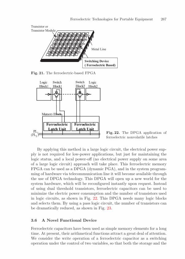
Ferroelectric Technologies for Portable Equipment 267
Fig. 21. The ferroelectric-based FPGA
Fig. 22. The DPGA application offerroelectric nonvolatile latches
By applying this method in a large logic circuit, the electrical power sup-ply is not required for low-power applications, but just for maintaining thelogic status, and a local power-off (no electrical power supply on some areaof a large logic circuit) approach will take place. This ferroelectric memoryFPGA can be used as a DPGA (dynamic PGA), and in the system program-ming of hardware via telecommunication line it will become available throughthe use of DPGA technology. This DPGA will open up a new world for thesystem hardware, which will be reconfigured instantly upon request. Insteadof using dual threshold transistors, ferroelectric capacitors can be used tominimize the electric power consumption and the number of transistors usedin logic circuits, as shown in Fig. 22. This DPGA needs many logic blocksand selects them. By using a pass logic circuit, the number of transistors canbe dramatically reduced, as shown in Fig. 23.
3.6 A Novel Functional Device
Ferroelectric capacitors have been used as simple memory elements for a longtime. At present, their arithmetical functions attract a great deal of attention.We consider the write operation of a ferroelectric capacitor as a switchingoperation under the control of two variables, so that both the storage and the
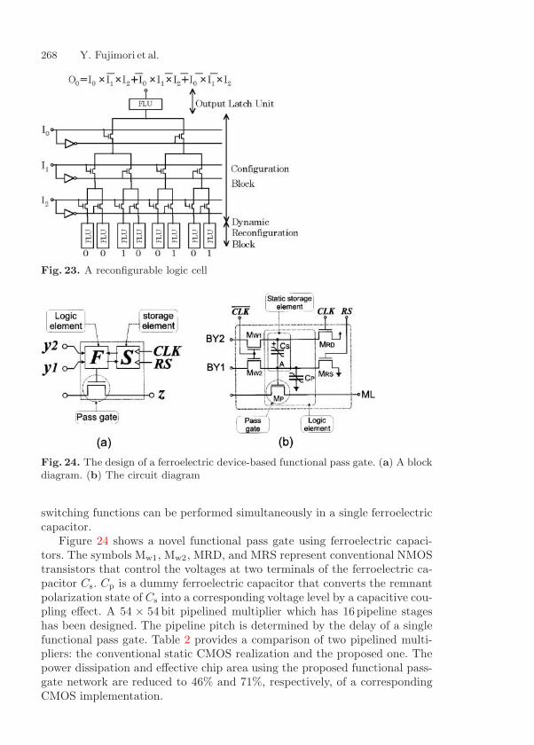
268 Y. Fujimori et al.
Fig. 23. A reconfigurable logic cell
Fig. 24. The design of a ferroelectric device-based functional pass gate. (a) A blockdiagram. (b) The circuit diagram
switching functions can be performed simultaneously in a single ferroelectriccapacitor.
Figure 24 shows a novel functional pass gate using ferroelectric capaci-tors. The symbols Mw1, Mw2, MRD, and MRS represent conventional NMOStransistors that control the voltages at two terminals of the ferroelectric ca-pacitor Cs. Cp is a dummy ferroelectric capacitor that converts the remnantpolarization state of Cs into a corresponding voltage level by a capacitive cou-pling effect. A 54 × 54 bit pipelined multiplier which has 16 pipeline stageshas been designed. The pipeline pitch is determined by the delay of a singlefunctional pass gate. Table 2 provides a comparison of two pipelined multi-pliers: the conventional static CMOS realization and the proposed one. Thepower dissipation and effective chip area using the proposed functional pass-gate network are reduced to 46% and 71%, respectively, of a correspondingCMOS implementation.
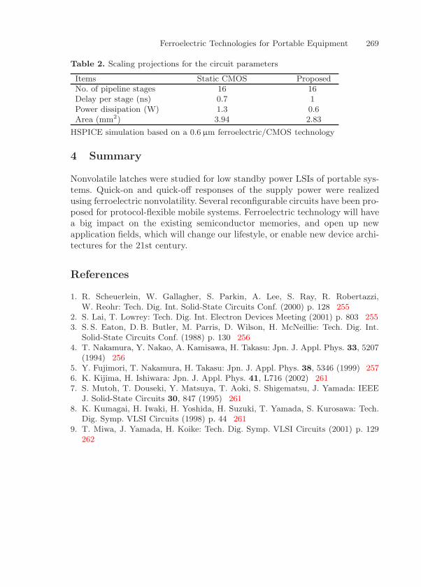
Ferroelectric Technologies for Portable Equipment 269
Table 2. Scaling projections for the circuit parameters
Items Static CMOS ProposedNo. of pipeline stages 16 16Delay per stage (ns) 0.7 1Power dissipation (W) 1.3 0.6Area (mm2) 3.94 2.83
HSPICE simulation based on a 0.6 µm ferroelectric/CMOS technology
4 Summary
Nonvolatile latches were studied for low standby power LSIs of portable sys-tems. Quick-on and quick-off responses of the supply power were realizedusing ferroelectric nonvolatility. Several reconfigurable circuits have been pro-posed for protocol-flexible mobile systems. Ferroelectric technology will havea big impact on the existing semiconductor memories, and open up newapplication fields, which will change our lifestyle, or enable new device archi-tectures for the 21st century.
References
1. R. Scheuerlein, W. Gallagher, S. Parkin, A. Lee, S. Ray, R. Robertazzi,W. Reohr: Tech. Dig. Int. Solid-State Circuits Conf. (2000) p. 128 255
2. S. Lai, T. Lowrey: Tech. Dig. Int. Electron Devices Meeting (2001) p. 803 2553. S. S. Eaton, D.B. Butler, M. Parris, D. Wilson, H. McNeillie: Tech. Dig. Int.
Solid-State Circuits Conf. (1988) p. 130 2564. T. Nakamura, Y. Nakao, A. Kamisawa, H. Takasu: Jpn. J. Appl. Phys. 33, 5207
(1994) 2565. Y. Fujimori, T. Nakamura, H. Takasu: Jpn. J. Appl. Phys. 38, 5346 (1999) 2576. K. Kijima, H. Ishiwara: Jpn. J. Appl. Phys. 41, L716 (2002) 2617. S. Mutoh, T. Douseki, Y. Matsuya, T. Aoki, S. Shigematsu, J. Yamada: IEEE
J. Solid-State Circuits 30, 847 (1995) 2618. K. Kumagai, H. Iwaki, H. Yoshida, H. Suzuki, T. Yamada, S. Kurosawa: Tech.
Dig. Symp. VLSI Circuits (1998) p. 44 2619. T. Miwa, J. Yamada, H. Koike: Tech. Dig. Symp. VLSI Circuits (2001) p. 129
262
Index
(MT) CMOS, 255(VT) CMOS, 261
circuit parameter– scaling, 265
dynamic programmable gate array(DPGA), 256
fatigue, 258FeRAM– ferroelectric thin film, 256– Pb(Zr,Ti)O3 (PZT), 256ferroelectric– gated transistor, 265– latch unit (FLU), 265field programmable gate array (FPGA),
266
functional pass gate– pipeline, 268
hysteresis– loop, 257
Imprint, 259ITRS 2001 roadmap, 261
magnetoresistance RAM (MRAM), 255
nonvolatile latch, 261nonvolatile logic, 261
Ovonic unified memory (OUM), 255
rapid thermal annealing (RTA), 257
The Application of FeRAM
to Future Information Technology World
Shoichi Masui1, Shunsuke Fueki2, Koichi Masutani2, Amane Inoue2,Toshiyuki Teramoto2, Tetsuo Suzuki2, and Shoichiro Kawashima2
1 Fujitsu Laboratories Limited, 4-1-1 Kamikodanaka, Nakahara-ku, Kawasaki,211-8588, [email protected]
2 Fujitsu Limited, 4-1-1 Kamikodanaka, Nakahara-ku, Kawasaki, 211-8588, Japan
Abstract. The future information technology world needs a simple identificationand secure information storage medium. The advanced smart card is a promisingtechnology to extend information-providing services from terminal (PC and mobilephone) dominated schemes to more flexible schemes in which the users’ intentiondominates. In this smart card, unique identification, individual information andvalues are stored in nonvolatile memories; among the nonvolatile memories, FeRAMpresents overwhelming characteristics compared to conventional floating-gate typememories in terms of programming time, energy consumption, and its scalability/affinity to below 0.18 µm standard CMOS technology. FeRAM can improve thetransaction time in transportation applications through its fast programming time;moreover, a data protection scheme from power failure can be implemented withoutthe addition of off-chip components, through its low energy consumption. Scalabilityto advanced CMOS technology enables enhancement services in multi-applicationcards, which include a mobile phone identity module. A smart card LSI embeddedwith 32 bit RISC CPU and 64 kB FeRAM is introduced with an associated OS.Further applications of the FeRAM circuit are discussed, along with its technologytrend.
1 Introduction – A Prospectfor the Future Information Technology World
The upcoming establishment and enhancement of the information networkassure fast and secure internet access through the personal computer (PC),personal digital assistance (PDA), and the mobile phone. The realized openinformation society creates opportunities to improve the effectiveness of gov-ernment, corporate, and individual activities. Moreover, information tech-nology breakthroughs should provide additional conveniences and diversifiedservices for those who are not familiar with electronic devices, such as youngchildren and older people. The smart card is the simplest device that doesnot have any input terminals; however, it is a robust medium to identify theperson who holds it, as well as to store the values and information of theholder.
H. Ishiwara, M. Okuyama, Y. Arimoto (Eds.): Ferroelectric Random Access Memories,Topics Appl. Phys. 93, 271–284 (2004)c© Springer-Verlag Berlin Heidelberg 2004
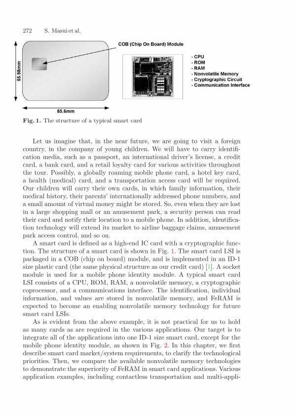
272 S. Masui et al.
Fig. 1. The structure of a typical smart card
Let us imagine that, in the near future, we are going to visit a foreigncountry, in the company of young children. We will have to carry identifi-cation media, such as a passport, an international driver’s license, a creditcard, a bank card, and a retail loyalty card for various activities throughoutthe tour. Possibly, a globally roaming mobile phone card, a hotel key card,a health (medical) card, and a transportation access card will be required.Our children will carry their own cards, in which family information, theirmedical history, their parents’ internationally addressed phone numbers, anda small amount of virtual money might be stored. So, even when they are lostin a large shopping mall or an amusement park, a security person can readtheir card and notify their location to a mobile phone. In addition, identifica-tion technology will extend its market to airline baggage claims, amusementpark access control, and so on.
A smart card is defined as a high-end IC card with a cryptographic func-tion. The structure of a smart card is shown in Fig. 1. The smart card LSI ispackaged in a COB (chip on board) module, and is implemented in an ID-1size plastic card (the same physical structure as our credit card) [1]. A socketmodule is used for a mobile phone identity module. A typical smart cardLSI consists of a CPU, ROM, RAM, a nonvolatile memory, a cryptographiccoprocessor, and a communications interface. The identification, individualinformation, and values are stored in nonvolatile memory, and FeRAM isexpected to become an enabling nonvolatile memory technology for futuresmart card LSIs.
As is evident from the above example, it is not practical for us to holdas many cards as are required in the various applications. Our target is tointegrate all of the applications into one ID-1 size smart card, except for themobile phone identity module, as shown in Fig. 2. In this chapter, we firstdescribe smart card market/system requirements, to clarify the technologicalpriorities. Then, we compare the available nonvolatile memory technologiesto demonstrate the superiority of FeRAM in smart card applications. Variousapplication examples, including contactless transportation and multi-appli-
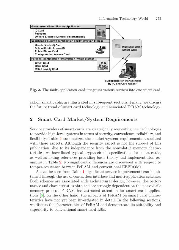
Information Technology World 273
Fig. 2. The multi-application card integrates various services into one smart card
cation smart cards, are illustrated in subsequent sections. Finally, we discussthe future trend of smart card technology and associated FeRAM technology.
2 Smart Card Market/System Requirements
Service providers of smart cards are strategically requesting new technologiesto provide high-level systems in terms of security, convenience, reliability, andflexibility. Table 1 summarizes the market/system requirements associatedwith these aspects. Although the security aspect is not the subject of thispublication, due to its independence from the nonvolatile memory charac-teristics, we have listed typical crypto-circuit specifications for smart cards,as well as listing references providing basic theory and implementation ex-amples in Table 2. No significant differences are discovered with respect totamper-resistance between FeRAM and conventional EEPROMs.
As can be seen from Table 1, significant service improvements can be ob-tained through the use of contactless interface and multi-application schemes.Both schemes are associated with architectural design; however, the perfor-mance and characteristics obtained are strongly dependent on the nonvolatilememory process. FeRAM has attracted attention for smart card applica-tions [5]; on the other hand, the impacts of FeRAM on smart card charac-teristics have not yet been investigated in detail. In the following sections,we discuss the characteristics of FeRAM and demonstrate its suitability andsuperiority to conventional smart card LSIs.
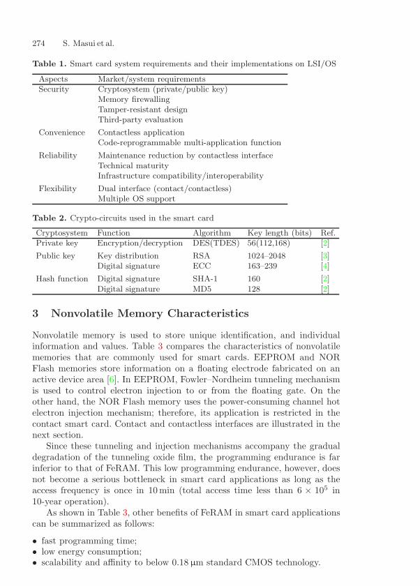
274 S. Masui et al.
Table 1. Smart card system requirements and their implementations on LSI/OS
Aspects Market/system requirementsSecurity Cryptosystem (private/public key)
Memory firewallingTamper-resistant designThird-party evaluation
Convenience Contactless applicationCode-reprogrammable multi-application function
Reliability Maintenance reduction by contactless interfaceTechnical maturityInfrastructure compatibility/interoperability
Flexibility Dual interface (contact/contactless)Multiple OS support
Table 2. Crypto-circuits used in the smart card
Cryptosystem Function Algorithm Key length (bits) Ref.Private key Encryption/decryption DES(TDES) 56(112,168) [2]
Public key Key distribution RSA 1024–2048 [3]Digital signature ECC 163–239 [4]
Hash function Digital signature SHA-1 160 [2]Digital signature MD5 128 [2]
3 Nonvolatile Memory Characteristics
Nonvolatile memory is used to store unique identification, and individualinformation and values. Table 3 compares the characteristics of nonvolatilememories that are commonly used for smart cards. EEPROM and NORFlash memories store information on a floating electrode fabricated on anactive device area [6]. In EEPROM, Fowler–Nordheim tunneling mechanismis used to control electron injection to or from the floating gate. On theother hand, the NOR Flash memory uses the power-consuming channel hotelectron injection mechanism; therefore, its application is restricted in thecontact smart card. Contact and contactless interfaces are illustrated in thenext section.
Since these tunneling and injection mechanisms accompany the gradualdegradation of the tunneling oxide film, the programming endurance is farinferior to that of FeRAM. This low programming endurance, however, doesnot become a serious bottleneck in smart card applications as long as theaccess frequency is once in 10 min (total access time less than 6 × 10⁵ in10-year operation).
As shown in Table 3, other benefits of FeRAM in smart card applicationscan be summarized as follows:
• fast programming time;• low energy consumption;• scalability and affinity to below 0.18 µm standard CMOS technology.

Information Technology World 275
Table 3. Nonvolatile memory characteristics
Characteristics FeRAM EEPROM NOR FlashRead cycle time 180 ns 70 ns 70 nsProgramming cycle time 180 ns 2ms > 1 sRead power < 1mW/MHz < 1mW/MHz 1 mW/MHzProgramming power < 1mW/MHz 1mW/MHz > 10 mW/MHzProgramming energy 0.18 nJ 2µJ 8 µJCell area 8–15 F2 > 20F2 6 F2
Endurance 1010 106 106
Scalability Good Restricted RestrictedAffinity with CMOS Good Restricted Restricted
The fast programming time and low energy consumption can bring about su-perior features for contactless applications. Scalability is becoming a criticalfactor in high-end multi-application cards, since the market requires a largecapacity for nonvolatile memory. The power consumption is less significantcompared to the RFID (radio frequency identification) application [7], sincethe CPU and cryptographic coprocessors consume more power than the non-volatile memory in smart card applications.
MRAM might be considered as a nonvolatile memory candidate for thesmart card [8]; however, as is described in the contactless smart card stan-dard [9], the smart card must function after exposure to a static 640kA/mmagnetic field. This magnitude is far higher than the coercive force of themagnetoresistive material.
4 Contactless Cards
A contactless interface can enhance reliability due to the lack of electrical con-tacts over a conventional contact interface; moreover, its data rate exceeds106kbps. Table 4 compares the characteristics of contact and contactless in-terfaces. The data rate of a contactless interface is more than 10 times higherthan that of a contact interface. A fast contactless interface is especiallyexpected for transportation applications, since the total transaction time isrestricted to below 200ms, so as to accomodate a human’s walking speedthrough an interrogator gate.
Table 4. A comparison of the characteristics of contact and contactless interfaces
Contact ContactlessISO/IEC standards 7816 14443Power/data communication Wired Inductive couplingClock/carrier frequency 3.57 MHz 13.56 MHzCommunication data rate 9.6(optionally, 19.2/38.4) kbps 106 kbpsAnticollision function Not implemented Implemented
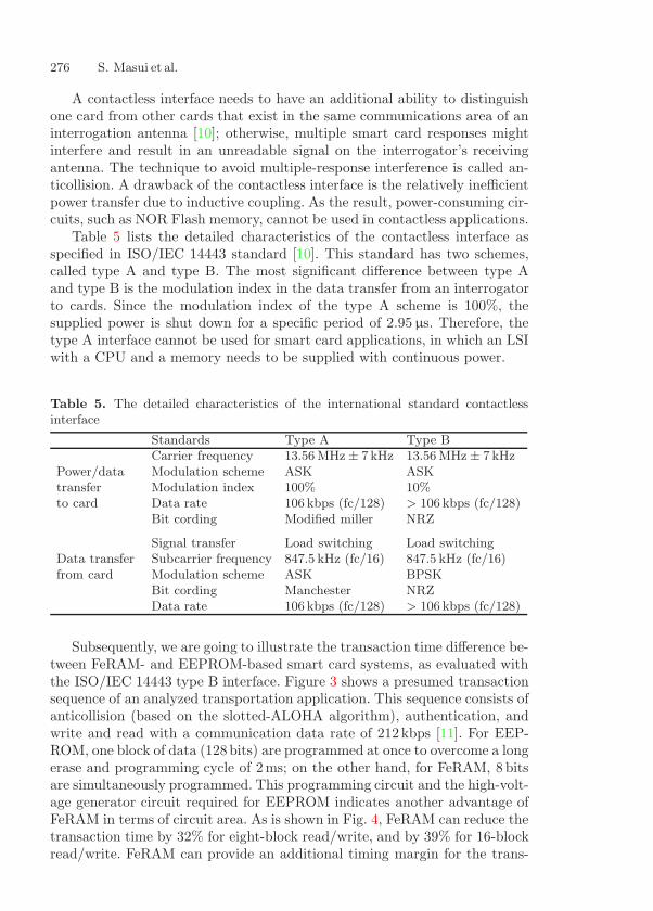
276 S. Masui et al.
A contactless interface needs to have an additional ability to distinguishone card from other cards that exist in the same communications area of aninterrogation antenna [10]; otherwise, multiple smart card responses mightinterfere and result in an unreadable signal on the interrogator’s receivingantenna. The technique to avoid multiple-response interference is called an-ticollision. A drawback of the contactless interface is the relatively inefficientpower transfer due to inductive coupling. As the result, power-consuming cir-cuits, such as NOR Flash memory, cannot be used in contactless applications.
Table 5 lists the detailed characteristics of the contactless interface asspecified in ISO/IEC 14443 standard [10]. This standard has two schemes,called type A and type B. The most significant difference between type Aand type B is the modulation index in the data transfer from an interrogatorto cards. Since the modulation index of the type A scheme is 100%, thesupplied power is shut down for a specific period of 2.95 µs. Therefore, thetype A interface cannot be used for smart card applications, in which an LSIwith a CPU and a memory needs to be supplied with continuous power.
Table 5. The detailed characteristics of the international standard contactlessinterface
Standards Type A Type BCarrier frequency 13.56 MHz ± 7 kHz 13.56 MHz ± 7 kHz
Power/data Modulation scheme ASK ASKtransfer Modulation index 100% 10%to card Data rate 106 kbps (fc/128) > 106 kbps (fc/128)
Bit cording Modified miller NRZ
Signal transfer Load switching Load switchingData transfer Subcarrier frequency 847.5 kHz (fc/16) 847.5 kHz (fc/16)from card Modulation scheme ASK BPSK
Bit cording Manchester NRZData rate 106 kbps (fc/128) > 106 kbps (fc/128)
Subsequently, we are going to illustrate the transaction time difference be-tween FeRAM- and EEPROM-based smart card systems, as evaluated withthe ISO/IEC 14443 type B interface. Figure 3 shows a presumed transactionsequence of an analyzed transportation application. This sequence consists ofanticollision (based on the slotted-ALOHA algorithm), authentication, andwrite and read with a communication data rate of 212kbps [11]. For EEP-ROM, one block of data (128bits) are programmed at once to overcome a longerase and programming cycle of 2ms; on the other hand, for FeRAM, 8 bitsare simultaneously programmed. This programming circuit and the high-volt-age generator circuit required for EEPROM indicates another advantage ofFeRAM in terms of circuit area. As is shown in Fig. 4, FeRAM can reduce thetransaction time by 32% for eight-block read/write, and by 39% for 16-blockread/write. FeRAM can provide an additional timing margin for the trans-
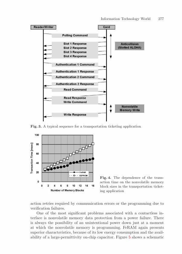
Information Technology World 277
Fig. 3. A typical sequence for a transportation ticketing application
Fig. 4. The dependence of the trans-action time on the nonvolatile memoryblock sizes in the transportation ticket-ing application
action retries required by communication errors or the programming due toverification failures.
One of the most significant problems associated with a contactless in-terface is nonvolatile memory data protection from a power failure. Thereis always the possibility of an unintentional power down just at a momentat which the nonvolatile memory is programming. FeRAM again presentssuperior characteristics, because of its low energy consumption and the avail-ability of a large-permittivity on-chip capacitor. Figure 5 shows a schematic
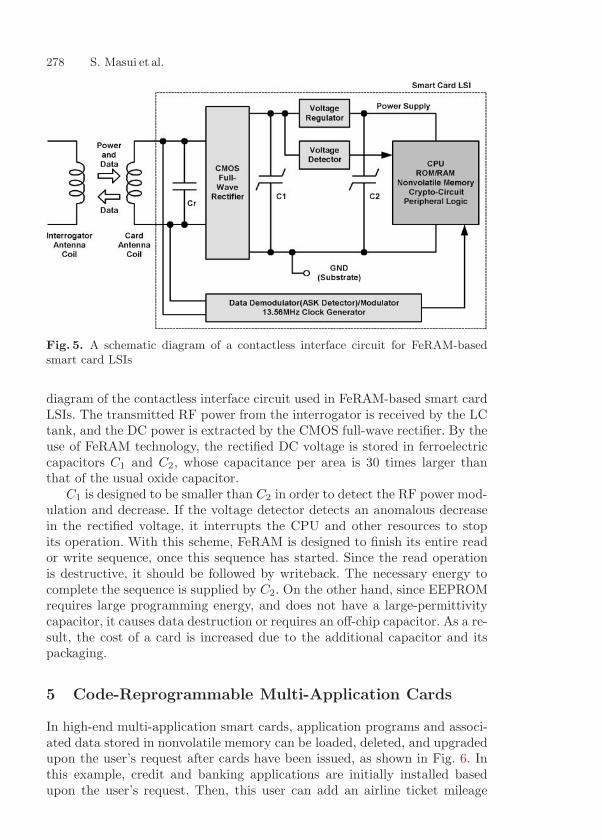
278 S. Masui et al.
Fig. 5. A schematic diagram of a contactless interface circuit for FeRAM-basedsmart card LSIs
diagram of the contactless interface circuit used in FeRAM-based smart cardLSIs. The transmitted RF power from the interrogator is received by the LCtank, and the DC power is extracted by the CMOS full-wave rectifier. By theuse of FeRAM technology, the rectified DC voltage is stored in ferroelectriccapacitors C1 and C2, whose capacitance per area is 30 times larger thanthat of the usual oxide capacitor.
C1 is designed to be smaller than C2 in order to detect the RF power mod-ulation and decrease. If the voltage detector detects an anomalous decreasein the rectified voltage, it interrupts the CPU and other resources to stopits operation. With this scheme, FeRAM is designed to finish its entire reador write sequence, once this sequence has started. Since the read operationis destructive, it should be followed by writeback. The necessary energy tocomplete the sequence is supplied by C2. On the other hand, since EEPROMrequires large programming energy, and does not have a large-permittivitycapacitor, it causes data destruction or requires an off-chip capacitor. As a re-sult, the cost of a card is increased due to the additional capacitor and itspackaging.
5 Code-Reprogrammable Multi-Application Cards
In high-end multi-application smart cards, application programs and associ-ated data stored in nonvolatile memory can be loaded, deleted, and upgradedupon the user’s request after cards have been issued, as shown in Fig. 6. Inthis example, credit and banking applications are initially installed basedupon the user’s request. Then, this user can add an airline ticket mileage
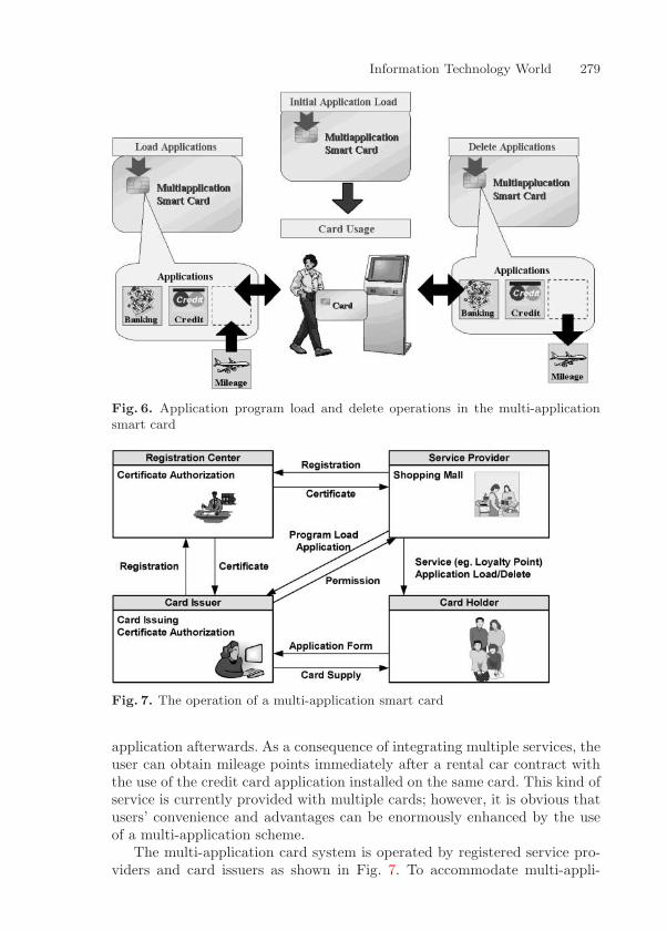
Information Technology World 279
Fig. 6. Application program load and delete operations in the multi-applicationsmart card
Fig. 7. The operation of a multi-application smart card
application afterwards. As a consequence of integrating multiple services, theuser can obtain mileage points immediately after a rental car contract withthe use of the credit card application installed on the same card. This kind ofservice is currently provided with multiple cards; however, it is obvious thatusers’ convenience and advantages can be enormously enhanced by the useof a multi-application scheme.
The multi-application card system is operated by registered service pro-viders and card issuers as shown in Fig. 7. To accommodate multi-appli-
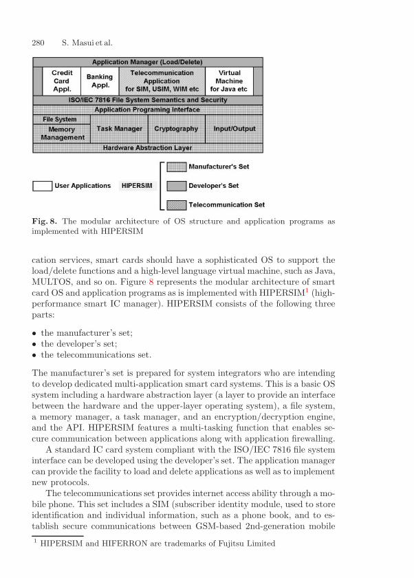
280 S. Masui et al.
Fig. 8. The modular architecture of OS structure and application programs asimplemented with HIPERSIM
cation services, smart cards should have a sophisticated OS to support theload/delete functions and a high-level language virtual machine, such as Java,MULTOS, and so on. Figure 8 represents the modular architecture of smartcard OS and application programs as is implemented with HIPERSIM1 (high-performance smart IC manager). HIPERSIM consists of the following threeparts:
• the manufacturer’s set;• the developer’s set;• the telecommunications set.
The manufacturer’s set is prepared for system integrators who are intendingto develop dedicated multi-application smart card systems. This is a basic OSsystem including a hardware abstraction layer (a layer to provide an interfacebetween the hardware and the upper-layer operating system), a file system,a memory manager, a task manager, and an encryption/decryption engine,and the API. HIPERSIM features a multi-tasking function that enables se-cure communication between applications along with application firewalling.
A standard IC card system compliant with the ISO/IEC 7816 file systeminterface can be developed using the developer’s set. The application managercan provide the facility to load and delete applications as well as to implementnew protocols.
The telecommunications set provides internet access ability through a mo-bile phone. This set includes a SIM (subscriber identity module, used to storeidentification and individual information, such as a phone book, and to es-tablish secure communications between GSM-based 2nd-generation mobile1 HIPERSIM and HIFERRON are trademarks of Fujitsu Limited
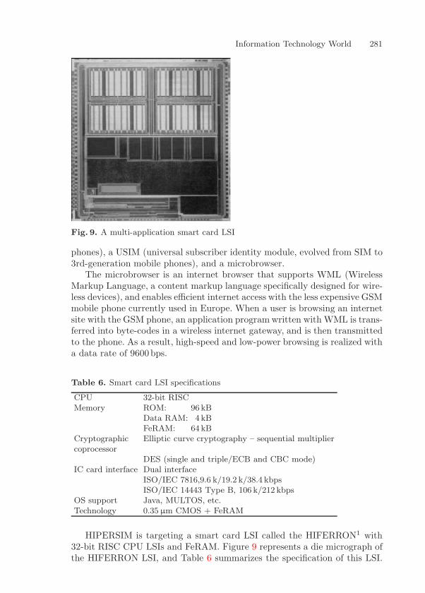
Information Technology World 281
Fig. 9. A multi-application smart card LSI
phones), a USIM (universal subscriber identity module, evolved from SIM to3rd-generation mobile phones), and a microbrowser.
The microbrowser is an internet browser that supports WML (WirelessMarkup Language, a content markup language specifically designed for wire-less devices), and enables efficient internet access with the less expensive GSMmobile phone currently used in Europe. When a user is browsing an internetsite with the GSM phone, an application program written with WML is trans-ferred into byte-codes in a wireless internet gateway, and is then transmittedto the phone. As a result, high-speed and low-power browsing is realized witha data rate of 9600bps.
Table 6. Smart card LSI specifications
CPU 32-bit RISCMemory ROM: 96 kB
Data RAM: 4 kBFeRAM: 64 kB
Cryptographic Elliptic curve cryptography – sequential multipliercoprocessor
DES (single and triple/ECB and CBC mode)IC card interface Dual interface
ISO/IEC 7816,9.6 k/19.2 k/38.4 kbpsISO/IEC 14443 Type B, 106 k/212 kbps
OS support Java, MULTOS, etc.Technology 0.35 µm CMOS + FeRAM
HIPERSIM is targeting a smart card LSI called the HIFERRON1 with32-bit RISC CPU LSIs and FeRAM. Figure 9 represents a die micrograph ofthe HIFERRON LSI, and Table 6 summarizes the specification of this LSI.

282 S. Masui et al.
0.35 µm three-layer metal CMOS technology enables 64 kB FeRAM alongwith secure and efficient implementation of CPU and crypto-circuits. FeRAMis used not only for the storage of identification, individual information, andvalues, but also for application programs and cache memory. The fast pro-gram time of the FeRAM can mitigate the program load time during theinitial application load and the actual operational schemes. As for the secu-rity aspect, a triple DES hardware macro and an elliptic curve cryptosystemcoprocessor are embedded. To assure tamper-resistance, scrambled wiringand metal covering technologies are carefully utilized. FeRAM has its ownhardware firewalling structure to protect it from illegal access.
6 Future Trends
As mentioned in the previous section, FeRAM is an enabling technologyfor the realization of multi-application smart card technology. This multi-application card would require an increasing capacity of nonvolatile memorystorage, from 64 kb to over 256kb. With the continuous scaling of devicetechnology, FeRAM would be able to establish an unwavering position fornonvolatile memory.
Not only for the smart card application but also for various security sys-tems, secure processing and identification information data storage would berequired. In the field of consumer electronics, the set-top box and the gamesmachine are using their own identification module for the protection of in-tellectual properties. The market for this type of secure LSI is consideredto extend toward communications networks. FeRAM would accommodatea secure computing architecture.
Acknowledgements
The authors would like to thank Dr. Jedidi Kamouaa for marketing informa-tion, and Dr. Hidetoshi Nishi and Dr. Yoshihito Arimoto for their continuousencouragement.
References
1. ISO/IEC 7816-2 Identification cards – Integrated circuit(s) cards with con-tacts – Part 2: Dimensions and location of the contacts 272
2. B. Schneier: Applied Cryptography, 2nd edn. (Wiley, New York 1996) 2743. C. K. Koc: RSA Hardware Implementation (RSA Laboratories, Redwood City
1995) 2744. M. Rosing: Implementing Elliptic Curve Cryptography (Manning, Greenwich
1999) 2745. J. Yamada, T. Miwa, H. Koike, H. Toyoshima, K. Amanuma, S. Kobayashi,
T. Tatsumi, Y. Maejima, H. Hada, H. Mori, S. Takahashi, H. Takeuchi, T. Ku-nio: Tech. Dig. Int. Solid-State Circuits Conf. (2000) p. 270 273
Information Technology World 283
6. A. Sharma: Semiconductor Memories (IEEE Press, New York 1997) 2747. U. Kaiser, W. Steinhagan: IEEE J. Solid-State Circuits 30, 301 (1995) 2758. M. Durlam, P. Naji, M. DeHerrera, S. Tehrani, G. Kerszykowski, K. Kyler:
Tech. Dig. Int. Solid-State Circuits Conf. (2000) p. 130 2759. ISO/IEC 14443-1 Identification cards – Contactless integrated circuit(s)
cards – Proximity cards, Part 1: Physical characteristics 27510. ISO/IEC 14443-2 Identification cards – Contactless integrated circuit(s)
cards – Proximity cards, Part 2: Air interface 27611. SONY FeliCa Card User’s Manual Rev. 1.52e, available from
http://www.sony.co.jp/en/Products/felica/contents02b.html (2000)276
12. S. Masui, E. Ishii, T. Iwawaki, Y. Sugawara, K. Sawada: Tech. Dig. Int.Solid-State Circuits Conf. (1999) p. 162
Index
anticollision, 276
contactless interface, 276crypto-circuit, 273
DES, 282
EEPROM, 274elliptic curve cryptosystem, 282
flash memory, 274
microbrowser, 281MRAM, 275multi-application, 272, 278
power failure
– data protection, 277
radio frequency identification (RFID),275
smart card, 271– cryptographic coprocessor, 272subscriber identity module (SIM), 280
tamper-resistance, 282transaction time, 276
universal subscriber identity module(USIM), 281
wireless markup language (WML), 281