Aryl-Copper(III)-Acetylides as Key Intermediates in C-sp2-C-sp Model Couplings under Mild Conditions
Upload
khangminh22Category
view
4download
0
Ref. No. TTD-99-1014
June, 1999
TMFXII/II-CTMFXIII/III-C
TECHNICAL DOCUMENT(ELECTRICAL)
(9906)
From
the
libra
ry o
f: D
iam
ond
Nee
dle
Cor
p

1
FOREWORD
This technical document is revised on the basis of TTD-94-1012 “TMFX-C Technical Document” in order
to accommodate the contents for the TMFX-II/II-C and TMFX-III/III-C Series.
We hope this document will be helpful to you very much in your after-sale and other activities.
CONTENTS
TMFXII/II-C, III/III-C, General Machine Construction Page
1. Controller
1-1. Genera l functions of the Controller ¥¥¥¥¥¥¥¥¥¥¥¥¥¥¥¥¥¥¥¥¥¥¥¥¥¥ 2
1-2. Voltage check in the major inner sections ¥¥¥¥¥¥¥¥¥¥¥¥¥¥¥¥¥¥¥¥¥ 3
2. Power Supply / Driver Box
2-1. General functions of Power Supply / Driver Box ¥¥¥¥¥¥¥¥¥¥¥¥¥¥¥¥ 3
2-2. Voltage check in the major inner sections ¥¥¥¥¥¥¥¥¥¥¥¥¥¥¥¥¥¥¥¥¥ 4
3. Other Cards
3-1. General functions of other cards¥¥¥¥¥¥¥¥¥¥¥¥¥¥¥¥¥¥¥¥¥¥¥¥¥¥¥¥¥ 6
3-2. Voltage check in the major inner sections ¥¥¥¥¥¥¥¥¥¥¥¥¥¥¥¥¥¥¥¥¥ 7
4. Block Diagrams / Connecting Diagrams
4-1. Controller - Block Diagram¥¥¥¥¥¥¥¥¥¥¥¥¥¥¥¥¥¥¥¥¥¥¥¥¥¥¥¥¥¥¥¥¥¥ 8
4-2. Power Supply Card - Block Diagram ¥¥¥¥¥¥¥¥¥¥¥¥¥¥¥¥¥¥¥¥¥¥¥¥¥ 9
4-3. X/Y-axis Driver - Block Diagram ¥¥¥¥¥¥¥¥¥¥¥¥¥¥¥¥¥¥¥¥¥¥¥¥¥¥¥¥¥ 10
4-4. Main Shaft Driver - Block Diagram ¥¥¥¥¥¥¥¥¥¥¥¥¥¥¥¥¥¥¥¥¥¥¥¥¥¥¥ 11
4-5.Head Card - Block Diagram¥¥¥¥¥¥¥¥¥¥¥¥¥¥¥¥¥¥¥¥¥¥¥¥¥¥¥¥¥¥¥¥¥ 12
4-6. Color Change Card - Block Diagram ¥¥¥¥¥¥¥¥¥¥¥¥¥¥¥¥¥¥¥¥¥¥¥¥¥ 13
4-7. TMFXII/II-C, III/III-C - Total Connecting Diagram¥¥¥¥¥¥¥¥¥¥¥¥¥¥¥ 14
From
the
libra
ry o
f: D
iam
ond
Nee
dle
Cor
p

2
TMFXII/II-C, III/III-C, General Machine Construction
1.Controller
1-1. General Functions of the Controller
Controller takes charge of all the embroidery machine operations and controls of embroidery machine.
(1) Major functions of CPU Card [X-CPU]
CPU Card takes charge of all the machine controls in principle.
1) System Memory 256K byte
Data Memory 256K byte
2) I/F with Head Card and Color Change Card
3) Sensor I/F, including Rotary Encoder
4) I/F for input from UTC Sensor
5) I/F to control X/Y-axes
6) I/F to control Main Shaft Motor
7) PWM [Note*] circuit to control Jump, Color Change, Upper Thread Holding Pulse Motors
8) I/F to control Thread Trimming, Picker Solenoid
9) I/F to control Operation Panel Card, FIP [Note**], Extension Card, Floppy Disk Drive
10) PTR I/F, Communication I/F for serial I/F (RS-232C etc.)
11) Equipped with a P-ROM (IPL) for system program installation
[Note*] PWM: Pulse width modulation
A method to module pulse width, depending on the signal amplitude value (voltage, current)
[Note**] FIP: Fluorescent Indicator Panel (registered trademark of NEC)
(2) Major functions of Extension Card [FX2 ADAPTER BOARD]
Extension Card extends the capacity of Data Memory.
Data memory capacity (for extension): 512,000 stitches
From
the
libra
ry o
f: D
iam
ond
Nee
dle
Cor
p

3
1-2. Voltage check in the major inner sections
Use a tester in principle for voltage check.
Measuring pointsVoltagevalue Application Plus side Minus side
Normalrange
Measuringrange
+5V* To control cards* To drive FDD* To drive FIP
Pin No.1 of CN2on CPU Card
Pin No. 2 of CN2CPU Card
+4.95V to +5.2V DC
+12V * To control cards Pin No.3 of CN2on CPU Card
Pin No.4 of CN2on CPU Card
+11.0V to +12.5V DC
+24V * To drive PTR Pin No.5 of CN2on CPU Card
Pin No.6 of CN2CPU Card
+25.0V to +27.0V DC
-5V * To control cards Pin No.7 of CN2on CPU Card
Pin No.2 of CN2on CPU Card
-4.75V to -5.25V DC
<Table 1> Power supply voltage for the Controller
2. Power Supply / Driver Box
2-1. General functions of Power Supply / Driver Box
Various types of power supply circuits and motor drive circuits for Main Shaft, X-axis and Y-axis
are built-in.
(1) Power Supply Card [X-PÇ vR]
Generates power supply for various sections (common for both single phase and 3 phase)
±5V, 12V, 24V, 50V, 60V
(2) Main Shaft Driver [X-DUB]
Drive circuit to control Main Shaft Motor with inverter and servo functions.
(3) X/Y-axis Driver [X-DUA]
Drive circuit for X-axis or Y-axis motor (pulse motor)
From
the
libra
ry o
f: D
iam
ond
Nee
dle
Cor
p

4
2-2. Voltage check at the major inner sections
Use a tester in principle for voltage check.
(1) Power Supply Card
Measuring pointsVoltagevalue Application Plus side Minus side
Normalrange
Measuringrange
+5V To supply power tocontrol the cards Pin No.1 of CN1 Pin No.2 of CN1 +5.1V to
+5.2V DC
+12V To supply power tocontrol the cards Pin No.3 Pin of CN1 Pin No.4 Pin of CN1 +11.5V to
+12.5V DC
To supply CPU Cardwith power to drivePTR
Pin No. 5 of CN1 Pin No.6 Pin of CN1
+24V To supply Head andColor Change Cardswith power to drivesmall type pulse motors
Pin No.1 Pin of CN2 Pin No.4 Pin of CN2
+25.0V to +27.0V DC
+20VTo supply X/Y-axisDrivers with power tocontrol cards
Pin No.4 pin of CN3 Pin No.2 Pin of CN3 +19.0V to +21.0V DC
+24V(FXII,
III/III-C)
To supply ColorChange Cards withpower to drive ATHand Picker Solenoids
Pin No. 2 of CN2 Pin No. 4 of CN2 +25.0V to +27.0V DC
+50V(FXII-Conly)
To supply ColorChange Cards withpower to drive ATHand Picker Solenoids
Pin No.6 of CN2 Pin No. 4 of CN2 +52.0V to +58.0V DC
+60V
* To supply Head Cardsand Color ChangeCards with power forsurge absorption circuitto suppress surgevoltage, generatedwhen small type pulsemotors are operated.
* To supply ColorChange Cards withpower to drive SequinSolenoid.
Pin No.3 of CN2 Pin No.4 of CN2 +52.0V to +58.0V DC
-5V To supply power tocontrol the cards Pin No.7 of CN1 Pin No.2 of CN1 -4.75V to
-5.25V DC
AC100Vsystem
AC200Vsystem
To supply Main ShaftDriver and X/Y axisDrivers with powersupply to drive MainShaft Motor andX/Y axis Pulse Motors
Pin No.5 Pin of CN3 Pin No.6 Pin of CN3
AC90V to AC132V
AC180V to AC264V
AC
<Table 2> Power supply voltage inside Power Supply Card
From
the
libra
ry o
f: D
iam
ond
Nee
dle
Cor
p

5
(2) X/Y-axis Driver
Measuring pointsVoltagevalue Application Plus side Minus side
Normalrange
measuringRange
+5V To control cards Pin No.6 of CN3 Pin No.7 of CN3 +5.1V to +5.2V DC
+12V To control cards Pin No.5 of CN3 Pin No.7 of CN3 +11.5V to +12.5V DC
-5V To control cards Pin No.8 of CN3 Pin No.7 of CN3 -4.75V to -5.25V DC
AC100VSystem
AC200VSystem
To drive X/Y-axispulse motors Pin No.1 of CN2 Pin No.4 of CN2
AC90V to AC132VAC180V to AC264V
AC
<Table 3> X/Y-axis Driver - power supply voltage
(2) Main Shaft Driver
Measuring pointsVoltage
value Application Plus side Minus sideNormalrange
measuringRange
+5V To control cards Pin No.6 of CN3 Pin No.7 of CN3 +5.1V to +5.2V DC
+12V To control cards Pin No. 5 of CN3 Pin No.7 of CN3 +11.5V to +12.5V DC
-5V To control cards Pin No.8 of CN3 Pin No.7 of CN3 -4.75V to -5.25V DC
AC100VSystem
AC200Vsystem
To drive Main ShaftMotor Pin No.1 of CN2 Pin No.4 of CN2
AC90V to AC132VAC180V to AC264V
AC
<Table4> Main Shaft Driver - power supply voltage
From
the
libra
ry o
f: D
iam
ond
Nee
dle
Cor
p
6
3. Other cards
3-1. General functions of other cards
(1) Joint Card
Joint Card is a card to divide input/output signal and power supply to the Controller.
(2) Color Change Card [X-CHG]
Color Change Card is a circuit to drive needle position detection I/F, Color Change Motor (pulse
motor), Thread Trimming Solenoid, Picker Solenoid and Sequin Solenoid.
Needle position detection I/F has a circuit to convert the voltage from potentiometer [Note] into digital
signal (A/D converter) and input it as a needle position.
[Note] Potentiometer is a precision variable resistor.
(3) Head Card [X-HEAD]
Head Card is a circuit to drive Jump Pulse Motor, Thread Holding Pulse Motor and to detect thread
breakage signal I/F from Tension Base.
A signal when Thread Take-up spring contacts with Thread Breakage Detecting Contact Point is
transmitted to Tension Base Card → Head Card → CPU Card for thread breakage detection.
(4) Tension Base Card
1) Detects thread breakage with Thread Take-up Spring.
2) Has Tension Base Switch and LED.
3) LED is lit in green and red and displays thread breakage and head operation status.
From
the
libra
ry o
f: D
iam
ond
Nee
dle
Cor
p

7
3-2. Voltage check
Use a tester in principle for voltage check.
(1) Color Change CardMeasuring pointsVoltage
value Application Plus side Minus sideNormalrange
Measuringrange
+5V* To control cards* To supply power topotentiometer
No. 1 pin of CN7 No. 2 pin of CN7 +4.85V to +5.2V DC
+24V * To drive ColorChange Motor No. 4 pin of CN7 No. 5 pin of CN7 +25.0V to
+27.0V DC
+24V(FXII, III,
III-C)
* To drive ThreadTrimming PickerSolenoid
No. 9 pin of CN7 No. 5 pin of CN7 +25.0V to +27.0V DC
+50V(FXII-Conly)
* To drive ThreadTrimming PickerSolenoid
No. 9 pin of CN7 No. 5 pin of CN7 +52.0V to +58.0V DC
+60V
*To drive Sequin Solenoid* For surge absorption circuit
No. 3 pin of CN7 No. 5 pin of CN7 +52.0V to +58.0V DC
<Table 5> Color Change Card - power supply voltage
(2) Head CardMeasuring pointsVoltage
value Application Plus side Minus sideNormalrange
Measuringrange
+5V * To control cards Pin No.8 of CN2 Pin No.5 of CN2 +4.85V to +5.2V DC
+24V
* To drive JumpMotor and ThreadHolding Motor Pin No.4 of CN7 Pin No.5 of CN7 +25.0V to
+27.0V DC
+60V * For surgeabsorption circuit Pin No.3 of CN7 Pin No.5 of CN7 +52.0V to
+58.0V DC
<Table 6> Head Card - power supply voltage
(3) Tension Base CardMeasuring pointsVoltage
value Application Plus side Minus sideNormalrange
Measuringrange
+5V* To control cards*To detect upper thread breakage
Pin No.8 of CN2 Pin No.5 of CN2 +4.85V to +5.2V DC
<Table7> Tension Base Card - power supply voltage
From
the
libra
ry o
f: D
iam
ond
Nee
dle
Cor
p

8
4. Block Diagrams/Connecting Diagrams
4-1. Controller - Block Diagram
SRAM(512K byte)
FIP DriveCircuit
Designdataarea
ExtensionCard
MP228-1A
PTR
RS232C
RS485A
ControlCircuit
Switch CardMP142-2
Controller
I/F
SRAM(512K byte)
PROM(128K byte)
FDC FDD
CPU(V53)I/F
I/FSRAM
(128K byte)SRAM
(128K byte)
SRAM(128K byte)
SRAM(128K byte)
Small typemotor
PWN circuit
UTC Sensorinput I/F
CN1
CN6
CN7
CN2 CN3 CN5
CN4 CN1
IPL for systemprogram installation
ColorChange Card
MP140-1Head CardMP139-1D
Working area+
System area
Designdataarea
CN1
X/Y-axis Driver
Main Shaft Driver
Power Supply Card
Main Shaft Encoder
Start/Stop SW
Cap Framesensor
UTCController
Joint CardMP143-2
CN9
CN8
CN20
CN5 CN1~3
CN12 CN15 CN18
CN2
CN3
CN16
CN1 Power Supply/Driver Box
FIP(Indicator)
Frame LimitSW
(FXIII, III-C)
CN14
From
the
libra
ry o
f: D
iam
ond
Nee
dle
Cor
p

4-2. POWER SUPPLY CARD - LOCK DIAGRAM
MainSwitch
NoiseFilter
POWER SUPPLY CARD MP138-3-C
SurgeAbsorber
RectifierCircuit
AC100V - 120VAC200V - 240V
CN4
SwitchingCircuit
Transformer
CN3
CN2
NoiseFilter
Main Shaft Driver X/Y-axis Driver Color ChangeCard Head Card
CN3
CN2 CN7 CN7
CN2
Small MotorNoise AbsorptionCircuit
Voltage Regulator Circuit
Voltage Regulator Circuit
CN1
CN16
Joint Card
AC100V -120VAC200V –240V
9
From
the
libra
ry o
f: D
iam
ond
Nee
dle
Cor
p
CPUCard
Joint Card
CN9
CN4
CN1orCN2 CN3
VR3 Rotary��SW1
Electric CommandCircuit(To convert sine wave PWMsignal from 0 to 5V singlevoltage to 2.5V to -2.5Vdouble voltage)
INH
Low pathfilter
PowerSupply Card
Trianglewave
generationcircuit
Gain adjustmentcircuit
(To fit sinewave widthwith that oftriangle wave)
PWMcircuit
Electric current detectioncircuit
(To compare currentcommand value withactual voltage value)
(Electric current feedback)
Amplifiercircuit
CN1
φφφφA
φφφφA
φφφφB �φφφφB
X/Y-axis Motor
Clamp Filter
(Sine wavePWM fromCPU)
Sine wave PWM, converted todouble-sided voltage tofacilitate subsequent control ofOP Amplifier
(Preparation to smooth sine wavePWM from CPUAnd to suppress noise generationfrom the motor)
(Smooth sine wave PWM todrive X/Y-axis pulse motors
INH
CN3
CN2
Monitor Circuit(To monitor alarmsignal of ON/OFFsurge currentdetection circuit formotor excitation)
Excitation SW Monitor LED
Surge current detection circuit
(Command signal to remove currentfrom current command circuit orsubsequent ones in response tothe motor-free status due toexcitation SW or alarm signal fromsurge current detection circuit.
Automaticvoltageswitchcircuit
Double sidedcircuit
X/Y-axis Driver
When primaryvoltage is AC100Vsystem.
(AC100V- 120V)
When primaryvoltage is AC200VSystem.
To facilitatesubsequentOP amplifiercontrol.
10
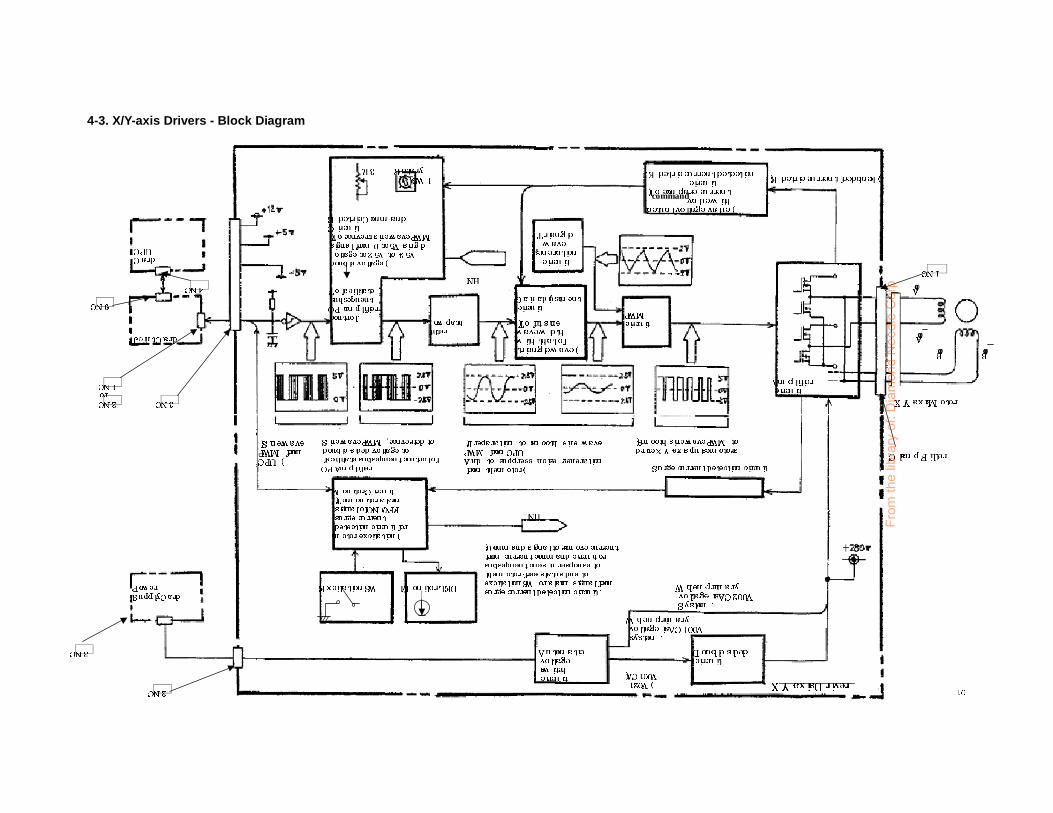
4-3. X/Y-axis Drivers - Block Diagram
From
the
libra
ry o
f: D
iam
ond
Nee
dle
Cor
p

4-4. Main Shaft Driver - Block Diagram
CPU Card
CN9 CN4
Joint Card
CN3
CN3
VR3 Rotary SW1
INH
PWMcircuit Amplifier
circuit
Main Shaft MotorCN1
INH
Main Shaft DriverCN3
CN211
Electric CommandCircuit(To convert sine wave PWMsignal from 0 to 5V singlevoltage to 2.5V to -2.5Vdouble voltage)
To facilitatesubsequentOP amplifiercontrol.
Low pathfilter
Trianglewave
generationcircuit
Electric current detectioncircuit
(To compare currentcommand value with actualvoltage value)
(Electric current feedback)
(To fit sinewave widthwith that oftriangle wave)
Gain adjustmentcircuit
Clamp filter
(Sine wave PWMfrom CPU)
Monitor Circuit(To monitor alarmsignal of ON/OFFsurge currentdetection circuit formotor excitation) (Command signal to remove current
from current command circuit orsubsequent ones in response tothe motor-free status due toexcitation SW or alarm signal fromsurge current detection circuit.Excitation SW Monitor LED When primary
voltage is AC200Vsystem.
Double sidedcircuit
(AC100V- 120V)
When primaryvoltage is AC100Vsystem.
Automaticvoltageswitchcircuit
PowerSupply Card
Surge current detection circuit
(Smooth sine wave PWM todrive X/Y-axis pulse motors)
(Preparation to smooth sine wave PWM from CPUAnd to suppress noise generation from the motor)
Sine wave PWM,converted to double-sided voltage tofacilitate subsequentcontrol of OP Amplifier
From
the
libra
ry o
f: D
iam
ond
Nee
dle
Cor
p

&&38�38�&&DUDUGG&R&ROORU�&KDQRU�&KDQJJHH&&DUDUGG
&&11��&&11��
&&11��
--XPS�0XPS�0RRWRWRUU
&&11��
&&11��
ϕϕΑΑ
$P$PSSOLILHU�&LUFXLOLILHU�&LUFXLWW
77KUHDGKUHDG+RO+ROGGLQJLQJ0RWR0RWRUU
&&11��
7KUHDG�7KUHDG�77DNH�XSDNH�XS6SULQ6SULQJJ
�8S�8SSSHU�WKUHDHU�WKUHDGGEUEUHDHDNDNDJJH�VLJH�VLJQQDODO��
�5'�5'��
�',�',11�
$GGUHV$GGUHVV�V�JHQHUJHQHUDDWLRQWLRQ&LUFXL&LUFXLWW�&LUFXLW�WR�&LUFXLW�WR��UHFRJQL]HUHFRJQL]HZZKKLFK�1LFK�1RR����RI�KRI�KHHDGDGVV��ZZKKLFK�KLFK�KHHDG�FDUGVDG�FDUGV��
��66LQH�ZDYLQH�ZDYH�H�3:03:0��
77KUHDG�EUKUHDG�EUHHDDNNDJH�7DJH�700
��))))556677�
&&11��
&&11��
&1�
��227&7&��
&&11��
**DWDWH�H�DUUDDUUD\\
//((''
66ZZLLWFWFKK
&&11��
&&11��
��227&7&��
77HQHQVVLRQ�LRQ�%%DVDVHH&&DUDUGG
$P$PSSOLILHU�&LUFXLOLILHU�&LUFXLWW
(RD)
��''228877��
&1�
&1�
77R�R���QGQG��++HDGHDG��+HD+HDG�G�&DU&DUGG
77R��R��UUGG����WKWK��++HDGVHDGV��+HD+HDG�G�&DUG&DUGVV
,,��
)OLS�IORS
&R&RPPSDUSDUDDWRWRUU
+HDG�+HDG�&&DUDUGG
0033��������������
(RD)
�'287�
(RD)
��''228877��
$P$PSSOLILHU�&LUFXLOLILHU�&LUFXLWW
77KUHDG�EUKUHDG�EUHHDDNNDJH�7DJH�700
))OLOLS�S�IORIORSS
4-5. Head Card - Block Diagram
From
the
libra
ry o
f: D
iam
ond
Nee
dle
Cor
p

&38�&D&38�&DUUGG
��
&&11��
7KUHD7KUHDGG77ULPPLQULPPLQJJ6RO6ROHHQQRRLLGG 3LFNHU�3LFNHU�66RROOHHQQRRLLGG
&&11��
);,,�&);,,�&��);,,��);,,,�,,,);,,��);,,,�,,,��&&��
$PS$PSOOLILILLHU�&LUHU�&LUFFXXLLWW
φφ$$
&R&ROORU�&KRU�&KDDQQJJH�0H�0RRWRWRUU
�6LQ�6LQH�H�ZDZDYYH�3:0H�3:0��
$�'�&$�'�&RRQQYYHUHUWWHHUU
&ROR&RORU�U�&KDQJH�&DU&KDQJH�&DUGG
MP140-1
&&11��
3RW3RWHHQQWWLRLRPPHHWWHHUU�1HH�1HHGGOOH�SH�SRRVVLLWWLLRRQQ
VHVHQQVRUVRU��
�33RWRWHHQQWWLRLRPPHHWWHUHUURWDURWDWWHHV�V�ZZLLWWK�K�FFRRORORUU&KD&KDQQJJH�H�0R0RWWRRUU����
&&11��
&R&ROORURU&KD&KDQQJJHH&DU&DUGG
&&11��
&&11��
�/�/�� �5�5��
6HTX6HTXLLQ�Q�66RROOHHQQRRLLGG
$GG$GGUUHHVVV�JV�JHHQHUQHUDDWWLLRRQQFLUFXFLUFXLLWW
&&11��
&&11��
&&11��
&&11��
+HDG�&D+HDG�&DUUGG
$PS$PSOOLILILLHU�&LUHU�&LUFFXXLLWW
$PS$PSOOLILILLHU�&LUHU�&LUFFXXLLWW
����
4-6. Color Change Card - Block Diagram������99
������99
From
the
libra
ry o
f: D
iam
ond
Nee
dle
Cor
p

(([WHQVLR[WHQVLRQQ&D&DUUGG
03�����03�����$$
6:�&DU6:�&DUGG03����03������
))'''' ),),33 %%X]]HX]]HUU
&38�&DU&38�&DUGG03����03������
6WDUW�6WRS�66WDUW�6WRS�6::
0DLQ�6K0DLQ�6KDDIWIW((QFQFRRGHGHUU
&&DDS�)UDPHS�)UDPH22ULJLQULJLQ6HQVR6HQVRUU
6DIHW\�GHYLFH6DIHW\�GHYLFH��VHVHOOHFWLRQHFWLRQFFRQQHFRQQHFWWRU��:KHQRU��:KHQ��RSHQ��VDIHW\RSHQ��VDIHW\GGHHYLFH�LV�QRW�HTXLSSHGYLFH�LV�QRW�HTXLSSHG������
%HDP�6HQVR%HDP�6HQVRUU��5HIOHFWRU5HIOHFWRUWW\\SSHH�
<�<�DD[L[LVV0R0RWWRRUU
0DLQ�6K0DLQ�6KDDIWIW0R0RWWRRUU))RRUU
);,,,);,,,��,,,,,,��&&��↔↔������↔↔����
�(�(�LVLVDDYDLODEOHYDLODEOHRRQO\�ZLWKQO\�ZLWK�+���+��+���+���
0DLQ�6K0DLQ�6KDDIWIW''ULYHUULYHU
�03�����03�������&�&��
<�<�DD[L[LVV''ULYHUULYHU
�03�����03��������
;�;�DD[L[LVV''ULYHUULYHU
�03�����03��������
--RLQW�&DURLQW�&DUGG03����03������
3RWHQWL3RWHQWLRRPHWHPHWHUU
�);,�);,,,�&�&��
�);,,�);,,��,,,,�,,,�,,,,�&,�&��
�);,�);,,,�&�&��
��([WHQGHG([WHQGHGWR�WR���QGQG��DQDQGG6XEVHTXHQW6XEVHTXHQWKHDGKHDGVV
4-7. TMFXII/II-C, III/III-C, - Total Connecting Diagram
Sequin solenoid(R)
Thread TrimmingSolenoid
Picker Solenoid
Jump Motor
Thread HoldingMotor +HDG�&D+HDG�&DUUGG
03�����03�������''
7KUHDG7KUHDG77DNH�DNH�XXSS6SU6SULLQQJJ
((TTXLSSHG�RQXLSSHG�RQOO\�ZLWK\�ZLWK���);,,��);,,�&&��
(([WHQVLRQ�&D[WHQVLRQ�&DUUGG03����03������
>>1RWH1RWH@@:KHQ� WKH� Q:KHQ� WKH� QXXPEHU�PEHU� RRI� KHDGVI� KHDGV� R� RI� WKHI� WKH�� PDFKPDFKLLQH� LQFUHDVQH� LQFUHDVHHV�� WKHV�� WKH�� GRWWHGGRWWHGVHFWLRQ�VHFWLRQ� �� � �� � �� �� �� � �� � LOOXVWUDWHG�OHIW�LQFUHDLOOXVWUDWHG�OHIW�LQFUHDVVHV�LQHV�LQ��SSUURRSSRUWLRQ�RUWLRQ�WWR�WKHR�WKH��QQXXPEHUPEHURRI�KHDGVI�KHDGV��
((PHUJHQF\PHUJHQF\6W6WRRS�6ZLWFS�6ZLWFKK
8787&&
33RRZHUZHU66XXSSSSOO\�&DU\�&DUGG03�����03���������&&
11RLVH�)LORLVH�)LOWWHHUU
����
�6+7�6+7��
$&���9��$&���9����������99$&���9��$&���9����������99
>1RWH@�,I�SULPDU\>1RWH@�,I�SULPDU\��LQSXW�SRZHULQSXW�SRZHU��VXSSO\�VXSSO\�LLV�VLQJOHV�VLQJOH��SKSKDDVH��FRQQHFWLRQVH��FRQQHFWLRQ
ZZLLWK�3LWK�3LQ�Q�1R���RI�&1��1R���RI�&1��LLV�QRW�QHFHV�QRW�QHFHVVVDUVDU\\��
������99��1RW�XVHG1RW�XVHG��
6X6XUUJH�3URWHFWRJH�3URWHFWRUU
������99
Sequin solenoid(L)
;�;�DD[L[LVV0R0RWWRRUU
((TTXLSSHG�RQXLSSHG�RQOO\�ZLWK\�ZLWK���);,,��);,,�$$QG�);,,,�QG�);,,,�,,,,,,��&&��
&&RORU�&KDRORU�&KDQQJH�0RWRJH�0RWRUU
1)1)%%
From
the
libra
ry o
f: D
iam
ond
Nee
dle
Cor
p
Copyright © 2022 FDOKUMEN