Authority for Sale and Privity of Contract: The Proprietary Basis ...
Upload
khangminh22Category
view
2download
0
THIS DOCUMENT CONTAINS PROPRIETARY INFORMATION AND SUCH INFORMATION MAY NOT BE DISCLOSED TO OTHERS FOR ANY
PURPOSES WITHOUT WRITTEN PERMISSION FROM SELEX Sistemi Integrati Inc.
Copyright © 2005, SELEX Sistemi Integrati Inc.
Operations and Maintenance Manual
Model 1150 Doppler VHF Omnirange (DVOR)
571150-0002 Rev G April, 2003
SELEX Sistemi Integrati Inc. 11300 West 89th Street
Overland Park, KS U.S.A. 66214

THIS SHEET INTENTIONALLY BLANK
SAFETY SUMMARY
The following are general safety precautions that are unrelated to specific procedures and therefore do not appear elsewhere in this publication. These are recommended precautions that personnel should understand and apply during through the many phases of operation and maintenance.
ELECTROSTATIC SENSITIVE DEVICES PRECAUTIONS Since most modules used in all models of equipment have Electrostatic Discharge (ESD) sensitive devices included in them, all modules should be considered sensitive to electrostatic discharge. Handling in the field shall be the same as in the factory. Each system is shipped with a wrist strap that must be worn while maintaining the equipment. The wrist strap shall be fastened to the equipment chassis either in the designated plug-in or attached to the equipment chassis with the alligator clip. The wrist strap must be used before any modules are removed from the equipment and at all times while handling the modules until they are placed in a protective environment such as an anti-static bag. Modules or boards must not be placed on any non-conducting surface such as wooden work benches, painted metal work benches, plastics, or technical manuals. Any work surface to be used must have a conducting mat placed on it and attached to earth ground. The mat and additional wrist straps can be obtained from SELEX Sistemi Integrati Inc.
KEEP AWAY FROM LIVE CIRCUITS Operating personnel must at all times observe all safety regulations. Under no circumstances should any person remove any protective covers that expose lethal voltages. Do not replace components or make adjustments inside the equipment with primary power supply turned on. Under certain conditions, dangerous potentials may exist when the power is in the off position, due to charges retained by capacitors. To avoid casualties, always remove power and allow time for the capacitors to discharge before touching it.
DO NOT SERVICE OR ADJUST ALONE Under no circumstances should any person reach into or enter the enclosure for the purpose of servicing or adjusting the equipment except in the presence of someone who is capable of rendering aid.
RESUSCITATION Personnel working with or near high voltages should be familiar with modern methods of resuscitation.

THIS SHEET INTENTIONALLY BLANK

SELEX Sistemi Integrati Inc.
This equipment is supplied by SELEX Sistemi Integrati Inc. For replacement parts and repair service, contact SELEX Sistemi Integrati Inc. using the contact information provided below.
HOW TO ORDER REPLACEMENT PARTS When ordering replacement parts, you should contact SELEX Sistemi Integrati Inc. by fax, phone or email. Please address the following items (as applicable) in your correspondence to enable us to provide the best possible service.
1. SELEX Sistemi Integrati Inc. model number, type and serial number of equipment. 2. Unit sub-assembly number (where applicable). 3. Item or reference symbol number from parts list or schematic. 4. SELEX Sistemi Integrati Inc. part number and description. 5. Manufacturer's code, name and part number (where applicable). 6. Quantity of each replacement part required.
HOW TO REQUEST REPAIR SERVICE In order to ensure prompt attention, parts returned for repair should have the following:
1. RMA number (Return Material Authorization number), assigned prior to return when requesting repair service. 2. Unit part number 3. Site location 4. System information 5. Ship-to address for return 6. Contact name and number 7. Date and time of request
CONTACT INFORMATION
SELEX Sistemi Integrati Inc.
11300 W 89th Street Overland Park KS, 66214, USA
Main Switchboard: (913) 495-2600 Main Fax: (913) 492-0870 Toll free: (800) 331-2744 CSM Direct Phone: (913) 495-2625 CSM E-mail: [email protected] World Wide Web URL: www.selex-si-us.com

THIS SHEET INTENTIONALLY BLANK

MANUFACTURER’S WARRANTY
SELEX Sistemi Integrati Inc.
The following warranty is applicable in all cases, except where modified or superseded by specific contract terms. Contact SELEX Sistemi Integrati Inc. if clarification is required.
A. The Manufacturer warrants to the original Purchaser, subject to the limitations and exclusions stated below, that mechanical and electrical parts of products which it manufactures, (the “Products” will be free of defects in materials and workmanship for a period of (i) twelve (12) months from the date of Final Acceptance or (ii) eighteen (18) months from the date of shipment, whichever occurs first (the “Warranty Period”). B. If the Customer believes a Product is defective, notice thereof shall be provided to the Manufacturer’s Customer Service Department at the address provided on the cover page and (if applicable) to the selling distributor. A defect in material and workmanship covered by this warranty shall be deemed to have occurred only if, and as of the time when, the Manufacturer is notified in writing by the Customer, within the Warranty Period, that the Product has become defective, and the Manufacturer’s personnel verify that the said Product, in fact, does not comply with the warranty provided hereunder and it is determined that:
(i) The Products, during the entire Warranty Period, have been operated within normal service conditions, recommended by the Manufacturer and recognized in the industry, and (ii) The Products have been installed and adjusted according to the Manufacturer’s procedures as stated in the Instruction Manual or other instructions supplied in writing by the Manufacturer.
C. Failures caused by lightning or other acts of God, or power surges, are not considered to be defects in materials and workmanship and are not covered under this warranty. Routine Maintenance and calibration are also not considered to be defects in materials and workmanship and are not covered under this warranty. Any change, modification or alteration of the Manufacturer’s Products not specifically authorized by the Manufacturer will void this warranty. D. If it is determined that the conditions for warranty coverage, as described above, have been satisfied, the Manufacturer shall repair or replace the defective products or parts thereof in accordance with the following procedures:
(i) Customer will contact the Manufacturer’s customer Service Department which will issue the Customer a Return Authorization (RA) number. (ii) The Component, defective part, or Product, as appropriate, shall be returned to the Manufacturer for inspection, freight prepaid by the customer. The RA number must be clearly displayed on the exterior of the shipping container. No shipments will be accepted without a RA number. All custom duties, fees, etc. will be paid by the Customer. (iii) If, upon inspection it is determined by Manufacturer’s personnel that the Product or component thereof is indeed defective and covered by this warranty, then Manufacturer, at its option, may either repair the Product or defective components thereof and return the same to the Customer or ship a replacement for the defective Product or part thereof, freight paid. All customs duties, fees, etc. will be paid by the Customer. The Product or component thereof will be returned to the Customer utilizing a shipping mode similar to that used by Customer to ship the same to the Manufacturer. (iv) If, upon inspection by Manufacturer, it is determined that the Product or component thereof was not defective or was not covered by this warranty, then the cost of all of Manufacturer’s inspections and the return shipping charges will be charged to Customer.

MANUFACTURER’S WARRANTY (cont.)
SELEX Sistemi Integrati Inc. E. The Manufacturer reserves the right to make modifications and alterations to Products without obligation to install such improvements on, in, or in place of theretofore manufactured products of Manufacturer. F. Manufacturer does not warranty any Products, components, subassemblies, or parts not of its own manufacture. Manufacturer hereby transfers to Customer any and all warranties (if any) which it receives from its suppliers. G. This warranty applies only to the original purchaser and, unless Customer receives the express written consent of an officer of Manufacturer, this warranty may not be assigned, transferred, or conveyed to any third party, even if the third party is a bon a fide purchaser of the Products. H. THIS WARRANTY IS EXPRESSLY IN LIEU OF ALL OTHER WARRANTIES, EXPRESSED OR IMPLIED, WHETHER STATUTORY OR OTHERWISE, INCLUDING AN IMPLIED WARRANTY OF MERCHANTABILITY OR FITNESS FOR A PARTICULAR PURPOSE. IN NO EVENT SHALL THE MANUFACTURER BE LIABLE FOR INDIRECT, INCIDENTAL, COLLATERAL, PUNITIVE, OR CONSEQUENTIAL DAMAGES OF ANY KIND, WHETHER ARISING OUT OF CONTRACT, TORT, NEGLIGENCE, STRICT LIABILITY, OR OTHER PRODUCTS LIABILITY THEORY. I. CUSTOMER’S SOLE REMEDY FOR ANY BREACH OF THE WARRANTY SHALL BE THE REPAIR OR REPLACEMNT OF THE PRODUDCTS BY THE MANUFACTURER AS PROVIDED HEREIN, AND IN NO EVENT SHALL THE MANUFACTURER BE REQUIRED TO INCUR COSTS FOR THE REPAIR OR REPLACEMENT OF ANY PRODUCT IN EXCESS OF THE PURCHASE PRICE OF SUCH PRODUCT, PLUS ANY TRANSPORTATION CHARGES ACTUALLY PAID ATTRIBUTABLE TO SUCH PRODUCTS.

Model 1150 DVOR
Rev. G April, 2003 This document contains proprietary information and such information may not be disclosed to others for any purposes
without written permission from SELEX Sistemi Integrati Inc.
i
TABLE OF CONTENTS Paragraph # Description Page 1 GENERAL INFORMATION AND REQUIREMENTS .......................................... 1-1 1.1 INTRODUCTION ..................................................................................................... 1-1 1.2 EQUIPMENT DESCRIPTION. ................................................................................ 1-1 1.2.1 Electronics Cabinet. ................................................................................................... 1-2 1.2.1.1 Status Display Panel Assembly (1A1)....................................................................... 1-5 1.2.1.2 RF Monitor Assembly (1A2). .................................................................................... 1-6 1.2.1.3 Carrier-Plus-Sideband (CSB) Power Amplifier Assembly (1A3, 1A19). ................. 1-6 1.2.1.4 Frequency Generator Assembly (1A4, 1A20). .......................................................... 1-6 1.2.1.5 Sideband Generator Assembly (1A5, 1A6, 1A21, 1A22). ........................................ 1-6 1.2.1.6 Audio Generator CCA (1A7, 1A23). ......................................................................... 1-7 1.2.1.7 Monitor CCA (1A8, 1A24)........................................................................................ 1-7 1.2.1.8 Modem CCA (1A9) Part Number 012101-1001 ....................................................... 1-7 1.2.1.9 Serial Interface CCA (1A10) ..................................................................................... 1-7 1.2.1.10 Facilities CCA (1A11) ............................................................................................... 1-8 1.2.1.11 Test Generator CCA (1A12)...................................................................................... 1-8 1.2.1.12 Central Processor Unit (CPU) CCA (1A13).............................................................. 1-8 1.2.1.13 Low Voltage Power Supply (LVPS) CCA (1A14, 1A15, 1A16) .............................. 1-9 1.2.1.14 RSCU Control Interface CCAs.................................................................................. 1-9 1.2.1.14.1 1138 RSCU Control Interface CCA (1A26) Part Number 012741-1002. ................. 1-9 1.2.1.14.2 1138 RSCU Control Interface CCA (1A26) Part Number 012741-1002 .................. 1-9 1.2.1.15 Battery Charger Power Subsystem (BCPS) (1A33, 1A34). ...................................... 1-9 1.2.1.16 Power Panel Assembly .............................................................................................. 1-9 1.2.2 Commutator Rack .................................................................................................... 1-10 1.2.2.1 Commutator Rack Upgrade ..................................................................................... 1-10 1.2.2.2 Control Assembly (2A1).......................................................................................... 1-10 1.2.2.2.1 Pin Diode Driver CCA............................................................................................. 1-10 1.2.2.2.2 PIN Diode Driver CCA Upgrade............................................................................. 1-12 1.2.2.3 Commutator CCA (2A2, 2A3)................................................................................. 1-12 1.2.2.4 Monitor Interface Assembly .................................................................................... 1-12 1.2.2.4.1 Transient Suppressor................................................................................................ 1-12 1.2.2.4.2 Signal Splitter (HY1) ............................................................................................... 1-12 1.2.2.4.3 Field Detector Assembly (2A6A1, 2A6A2) ............................................................ 1-13 1.2.3 Portable Maintenance Data Terminal (PMDT)........................................................ 1-13 1.2.4 Transmitting Antenna System.................................................................................. 1-13 1.2.4.1 Carrier Antenna (Version 1) .................................................................................... 1-13 1.2.4.2 Carrier Antenna (Version 2) .................................................................................... 1-15 1.2.4.3 Sideband Antenna (Version 1)................................................................................. 1-16 1.2.4.4 Sideband Antenna (Version 2)................................................................................. 1-17 1.2.4.5 Balun. ....................................................................................................................... 1-18 1.2.4.6 Tuning Stub.............................................................................................................. 1-18 1.2.4.7 Positioning Piece...................................................................................................... 1-19

Rev. G April, 2003 This document contains proprietary information and such information may not be disclosed to others for any purposes
without written permission from SELEX Sistemi Integrati Inc.
ii
TABLE OF CONTENTS (Continued) Paragraph # Description Page 1.2.4.8 Pedestal .................................................................................................................... 1-19 1.2.4.9 Radome .................................................................................................................... 1-19 1.2.5 Field Monitor Antenna............................................................................................. 1-21 1.2.6 Counterpoise ............................................................................................................ 1-21 1.2.7 Equipment Shelter.................................................................................................... 1-21 1.2.8 Battery Backup Unit (Optional)............................................................................... 1-22 1.3 EQUIPMENT SPECIFICATION DATA................................................................ 1-22 1.3.1 Transmitter and Antenna System............................................................................. 1-22 1.3.1.1 Transmitter............................................................................................................... 1-22 1.3.1.2 Antenna System ....................................................................................................... 1-24 1.3.1.3 Field Monitor ........................................................................................................... 1-25 1.3.1.4 Monitor .................................................................................................................... 1-25 1.3.1.5 Mechanical and Electrical........................................................................................ 1-26 1.3.2 Remote Control System ........................................................................................... 1-27 1.3.2.1 Design Features:....................................................................................................... 1-27 1.3.2.2 RSCU Controls and Indicators: ............................................................................... 1-27 1.3.2.3 RSU Controls and Indicators ................................................................................... 1-28 1.3.2.4 RSCU/RSU Specifications....................................................................................... 1-28 1.3.3 Remote Maintenance Monitor and Control System................................................. 1-29 1.3.3.1 Design Features........................................................................................................ 1-29 1.3.3.2 Specifications:.......................................................................................................... 1-29 1.3.3.3 Remote Terminal Specifications:............................................................................. 1-30 1.3.4 Remote Receiver Monitoring................................................................................... 1-30 1.3.4.1 Design Features........................................................................................................ 1-30 1.3.4.2 Controls and Indicators ............................................................................................ 1-30 1.3.4.3 Receiver Specifications............................................................................................ 1-30 1.3.5 Environmental.......................................................................................................... 1-31 1.3.5.1 Operating Temperature ............................................................................................ 1-31 1.3.5.2 Relative Humidity.................................................................................................... 1-31 1.3.5.3 Wind......................................................................................................................... 1-31 1.3.5.4 Ice and Snow............................................................................................................ 1-31 1.3.5.5 Altitude: ................................................................................................................... 1-31 1.4 EQUIPMENT AND ACCESSORIES SUPPLIED ................................................. 1-31 1.5 EQUIPMENT REQUIRED BUT NOT SUPPLIED ............................................... 1-32 1.6 OPTIONAL EQUIPMENT ..................................................................................... 1-33 2 TECHNICAL DESCRIPTION.................................................................................. 2-1 2.1 INTRODUCTION ..................................................................................................... 2-1 2.2 OPERATING PRINCIPLES ..................................................................................... 2-1 2.2.1 DVOR Antenna Principles......................................................................................... 2-4 2.3 THEORY OF OPERATION...................................................................................... 2-4 2.3.1 Simplified System Block Diagram ............................................................................ 2-5 2.3.1.1 Electronics Cabinet (Unit 1) ...................................................................................... 2-6

Model 1150 DVOR
Rev. G April, 2003 This document contains proprietary information and such information may not be disclosed to others for any purposes
without written permission from SELEX Sistemi Integrati Inc.
iii
TABLE OF CONTENTS (Continued) Paragraph # Description Page 2.3.1.1.1 Cabinet Insert (A18) .................................................................................................. 2-7 2.3.2 Detailed System Block Diagram................................................................................ 2-7 2.3.2.1 Frequency Synthesizer (1A4, 1A20) Block Diagram Theory. .................................. 2-9 2.3.2.1.1 Frequency Synthesizer (1A4, 1A20) Detailed Circuit Theory. ............................... 2-12 2.3.2.2 Audio Generator CCA (1A7, 1A23) Block Diagram Theory.................................. 2-20 2.3.2.2.1 Micro controller and Memory Circuits Block Diagram Theory.............................. 2-22 2.3.2.2.2 Reference and Sideband Generator Circuits Block Diagram Theory...................... 2-24 2.3.2.2.3 Reference Modulation Circuit Block Diagram Theory ........................................... 2-26 2.3.2.2.4 Sideband Modulation and Phase Control Circuit Block Diagram Theory .............. 2-26 2.3.2.2.5 Voice and Test Tone Circuit Block Diagram Theory.............................................. 2-28 2.3.2.2.6 Audio Generator CCA (1A7, 1A23) Detailed Circuit Theory................................. 2-30 2.3.2.3 CSB Power Amplifier Assembly (1A3, 1A19) Block Diagram Theory ................. 2-40 2.3.2.3.1 CSB Power Amplifier Assembly (1A3, 1A19) Detailed Circuit Theory ................ 2-40 2.3.2.3.2 Exciter CCA (A3) Block Diagram Theory .............................................................. 2-41 2.3.2.3.3 Exciter CCA (A3) Detailed Theory ......................................................................... 2-42 2.3.2.3.4 Power Amplifier CCA (A2) Block Diagram Theory............................................... 2-43 2.3.2.3.5 Power Amplifier CCA (A2) Detailed Circuit Theory.............................................. 2-44 2.3.2.3.6 Bias Regulator/Exciter Modulator CCA (A4) Block Diagram Theory ................... 2-46 2.3.2.3.7 Bias Regulator/Exciter Modulator CCA (A4) Detailed Circuit Theory .................. 2-47 2.3.2.3.8 Power Amplifier Modulator CCA (A1) Block Diagram Theory............................. 2-49 2.3.2.3.9 Power Amplifier Modulator CCA (A1) Detailed Circuit Theory............................ 2-50 2.3.2.3.10 Modulator Bias CCA (A5) Block Diagram Theory................................................. 2-51 2.3.2.3.11 Modulator Bias CCA (A5) Detailed Circuit Theory................................................ 2-52 2.3.2.4 Low Pass Filter Assembly (1A35, 1A36) Block Diagram ...................................... 2-52 2.3.2.4.1 Low Pass Filter Assembly (1A35, 1A36) Detailed Theory..................................... 2-53 2.3.2.5 Bi-Directional Couplers (1DC1, 1DC2) .................................................................. 2-53 2.3.2.6 Sideband Generator Assembly (1A5, 1A6, 1A21, 1A22) Block Diagram Theory . 2-53 2.3.2.6.1 Sideband Generator Assembly (1A5, 1A6, 1A21, 1A22) Detailed Circuit Theory 2-54 2.3.2.6.2 Sideband Amplifier CCA (A2, A4) Block Diagram Theory ................................... 2-57 2.3.2.6.3 Sideband Amplifier CCA (A2, A4) Detailed Circuit Theory .................................. 2-61 2.3.2.6.4 Sideband Controller CCA (A1, A3) Block Diagram Theory .................................. 2-63 2.3.2.6.5 Sideband Controller CCA (A1, A3) Detailed Circuit Theory ................................. 2-66 2.3.2.7 Sideband Sample Assembly (1A29, 1A30, 1A31, 1A32) ....................................... 2-73 2.3.2.7.1 Sideband Sample CCA (A1) Block Diagram Theory.............................................. 2-73 2.3.2.7.2 Sideband Sample CCA (A1) Detailed Circuit Theory............................................. 2-74 2.3.2.8 RF Monitor Assembly (1A2) Block Diagram Theory............................................. 2-75 2.3.2.8.1 RF Monitor Assembly (1A2) Detailed Circuit Theory............................................ 2-77 2.3.2.8.2 RF Monitor CCA (A1) Block Diagram Theory....................................................... 2-77 2.3.2.8.3 RF Monitor CCA (A1) Detailed Circuit Theory...................................................... 2-79 2.3.2.9 Backplane CCA (1A17)........................................................................................... 2-82 2.3.2.10 Central Processing Unit CCA (1A13) Block Diagram Theory ............................... 2-83 2.3.2.10.1 Central Processing Unit CCA (1A13) Detailed Circuit Theory .............................. 2-84

Rev. G April, 2003 This document contains proprietary information and such information may not be disclosed to others for any purposes
without written permission from SELEX Sistemi Integrati Inc.
iv
TABLE OF CONTENTS (Continued) Paragraph # Description Page 2.3.2.11 Facilities CCA (1A11) Block Diagram Theory ....................................................... 2-87 2.3.2.11.1 Facilities CCA (1A11) Detailed Circuit Theory...................................................... 2-89 2.3.2.12 Serial Interface CCA (1A10) Block Diagram Theory ............................................. 2-93 2.3.2.12.1 Serial Interface CCA (1A10) Detailed Theory ........................................................ 2-95 2.3.2.13 Test Generator CCA (1A12) Block Diagram Theory.............................................. 2-97 2.3.2.13.1 Test Generator CCA (1A12) Detailed Circuit Theory............................................. 2-99 2.3.2.14 Modem CCA (1A9) (Part No. 012101-1001) Block Diagram Theory.................. 2-102 2.3.2.14.1 Modem CCA (1A9) (Part No. 012101-1001) Detailed Circuit Theory................. 2-102 2.3.2.15 RSCU Interface Assembly (1A26) (Optional)....................................................... 2-104 2.3.2.15.1 RSCU Control Interface CCA (012741-1002) Block Diagram Theory ................ 2-105 2.3.2.15.2 RSCU Control Interface CCA (012741-0001) Detailed Circuit Theory ............... 2-106 2.3.2.16 Low Voltage Power Supply CCA (1A14, 1A15, 1A16) Block Diagram Theory . 2-109 2.3.2.16.1 Low Voltage Power Supply CCA (1A14, 1A15, 1A16) Detailed Circuit Theory 2-110 2.3.2.17 Jack Assembly (1A38)........................................................................................... 2-111 2.3.2.18 Display Panel Assembly (1A1).............................................................................. 2-111 2.3.2.18.1 Display CCA (A1, A2) Block Diagram Theory .................................................... 2-111 2.3.2.18.2 Display CCA (A1, A2) Detailed Circuit Theory ................................................... 2-112 2.3.2.19 Blower Assembly (1A39) ...................................................................................... 2-113 2.3.2.20 Field Detector Assembly (1A27, 1A28) ................................................................ 2-114 2.3.2.20.1 Field Detector CCA (A1) Block Diagram Theory................................................. 2-114 2.3.2.20.2 Field Detector CCA (A1) Detailed Circuit Theory................................................ 2-115 2.3.2.21 Monitor CCA (1A8, 1A24) Block Diagram Theory.............................................. 2-116 2.3.2.21.1 Monitor CCA (1A8, 1A24) Detailed Theory......................................................... 2-125 2.3.2.22 Power Panel ........................................................................................................... 2-132 2.3.2.23 Battery Charger Power Subsystem (1A33, 1A34)................................................. 2-132 2.3.2.23.1 Base Unit................................................................................................................ 2-133 2.3.2.23.2 UPS Module........................................................................................................... 2-134 2.3.2.23.3 48 Vdc Module ...................................................................................................... 2-136 2.3.2.23.4 28 Vdc Module ...................................................................................................... 2-136 2.4 COMMUTATOR (UNIT 2) .................................................................................. 2-136 2.4.1 Control Assembly (2A1)........................................................................................ 2-137 2.4.2 Pin Diode Driver CCA Block Diagram Theory..................................................... 2-137 2.4.2.1 Pin Diode Driver CCA Detailed Circuit Theory.................................................... 2-139 2.4.3 Commutator CCA (2A2, 2A3) Block Diagram Theory......................................... 2-143 2.4.3.1 Commutator CCA (2A2, 2A3) Detailed Circuit Theory ....................................... 2-146 2.4.4 Monitor Interface Assembly (2A6)........................................................................ 2-147 2.4.4.1 Transient Suppressor Circuits ................................................................................ 2-147 2.4.4.2 Field Detector Assembly (2A6A1, 2A6A2) (Current Version DVOR) ................ 2-149 2.4.4.2.1 Field Detector CCA (A1)....................................................................................... 2-149 2.5 BATTERIES (UNIT 3).......................................................................................... 2-149 2.6 FIELD MONITOR KIT (UNIT 4)......................................................................... 2-149 2.7 VIDEO TERMINAL (UNIT 5) ............................................................................. 2-150

Model 1150 DVOR
Rev. G April, 2003 This document contains proprietary information and such information may not be disclosed to others for any purposes
without written permission from SELEX Sistemi Integrati Inc.
v
TABLE OF CONTENTS (Continued) Paragraph # Description Page 3 OPERATION............................................................................................................. 3-1 3.1 Introduction................................................................................................................ 3-1 3.2 REMOTE CONTROL STATUS UNIT (RCSU) ...................................................... 3-1 3.3 REMOTE STATUS UNIT (RSU) ............................................................................. 3-1 3.4 PORTABLE MAINTENANCE DATA TERMINAL (PMDT) ................................ 3-1 3.4.1 Equipment Turn On & Shutdown. ............................................................................. 3-2 3.4.1.1 Equipment Turn On. .................................................................................................. 3-2 3.4.1.1.1 Connecting the PMDT ............................................................................................... 3-2 3.4.1.1.2 Starting the PMDT Application................................................................................. 3-3 3.4.1.1.3 Turning On the VOR ................................................................................................. 3-3 3.4.1.2 Equipment Shutdown................................................................................................. 3-3 3.4.1.2.1 Equipment Turn Off................................................................................................... 3-3 3.4.1.2.2 PMDT PC Turn Off ................................................................................................... 3-3 3.4.2 PMDT Screens ........................................................................................................... 3-3 3.4.2.1 General....................................................................................................................... 3-3 3.4.2.1.1 Menus......................................................................................................................... 3-4 3.4.2.1.2 System Status at a Glance; Sidebar Status and Control............................................. 3-5 3.4.2.1.3 Screen Area................................................................................................................ 3-6 3.4.2.2 Configuring the PMDT.............................................................................................. 3-7 3.4.2.3 Connecting to the VOR.............................................................................................. 3-7 3.4.2.3.1 Security Levels........................................................................................................... 3-7 3.4.2.3.2 PMDT Logon via Direct or Modem Connection....................................................... 3-9 3.4.2.4 RMS Status Screens................................................................................................. 3-10 3.4.2.5 RMS Data Screens ................................................................................................... 3-11 3.4.2.5.1 RMS Maintenance Alerts Screen............................................................................. 3-11 3.4.2.5.2 Analog-to-Digital Data Screen ................................................................................ 3-12 3.4.2.6 RMS Logs Screen .................................................................................................... 3-13 3.4.2.6.1 Operational Summary Screen .................................................................................. 3-13 3.4.2.6.2 Alarms Log Screen .................................................................................................. 3-14 3.4.2.6.3 Maintenance Alerts Log Screen............................................................................... 3-15 3.4.2.6.4 Command Activity Screen....................................................................................... 3-16 3.4.2.6.5 Parameter Change Log Screen................................................................................. 3-17 3.4.2.7 RMS Configuration Screen...................................................................................... 3-18 3.4.2.7.1 General RMS Configuration Screen - Refer to Figure 3-13 .................................... 3-19 3.4.2.7.1.1 General Configuration the VOR .............................................................................. 3-20 3.4.2.7.2 Station Configuration Screen................................................................................... 3-23 3.4.2.7.3 A/D Limits Configuration Screen........................................................................... 3-25 3.4.2.7.4 Security Codes Configuration Screen...................................................................... 3-26 3.4.2.7.4.1 User Account Maintenance...................................................................................... 3-27 3.4.2.7.4.2 Add a User Account................................................................................................. 3-27 3.4.2.7.4.3 Change a User’s Password....................................................................................... 3-27 3.4.2.7.4.4 Delete a User’s Account. ......................................................................................... 3-28

Rev. G April, 2003 This document contains proprietary information and such information may not be disclosed to others for any purposes
without written permission from SELEX Sistemi Integrati Inc.
vi
TABLE OF CONTENTS (Continued) Paragraph # Description Page 3.4.2.8 RMS Commands...................................................................................................... 3-29 3.4.2.9 Monitor Configuration Screens................................................................................ 3-31 3.4.2.9.1 Monitor Alarm Limit Configuration Screen ............................................................ 3-31 3.4.2.9.2 Monitor Offsets and Scale Factor Configuration Screen......................................... 3-32 3.4.2.10 Monitor Commands ................................................................................................. 3-33 3.4.2.11 Monitor Data Screens .............................................................................................. 3-34 3.4.2.11.1 Integrity Data Screen ............................................................................................... 3-34 3.4.2.11.1.1 Test DATA Screen................................................................................................... 3-35 3.4.2.11.1.2 Monitor Certification Test Results Screen............................................................... 3-36 3.4.2.11.1.3 Notch Monitor Screen............................................................................................ 3-38 3.4.2.11.2 Sideband Antenna VSWR Screen............................................................................ 3-40 3.4.2.11.2.1 VOR Ground Check Data Screen ............................................................................ 3-41 3.4.2.11.2.2 VOR Ground Check Data Advanced Screen ........................................................... 3-43 3.4.2.11.2.3 VOR Fault History Screens ..................................................................................... 3-43 3.4.2.11.2.4 Fault History Monitor Data Screen.......................................................................... 3-44 3.4.2.11.2.5 Fault History System Status Screen........................................................................ 3-45 3.4.2.12 Transmitters Data Screens ....................................................................................... 3-46 3.4.2.12.1 Transmitter Data Screen .......................................................................................... 3-46 3.4.2.13 Transmitters Configuration Screen .......................................................................... 3-47 3.4.2.13.1 TX 1 & 2 Offsets & Scale Factors ........................................................................... 3-48 3.4.2.14 Transmitters Nominal Screens................................................................................. 3-49 3.4.2.15 Transmitter Commands............................................................................................ 3-50 3.4.2.16 Controlling the Transmitter via the PMDT.............................................................. 3-52 3.4.2.16.1 General Transmitter Control .................................................................................... 3-52 3.4.2.16.2 Change the Azimuth Index ...................................................................................... 3-53 3.4.2.16.3 Change the CSB Output Power............................................................................... 3-53 3.4.2.16.4 Change the Voice Depth of Modulation .................................................................. 3-53 3.4.2.16.5 Change the Identification Depth of Modulation ...................................................... 3-54 3.4.2.16.6 Change the Reference Depth of Modulation ........................................................... 3-54 3.4.2.16.7 Change the Sideband Power Level .......................................................................... 3-54 3.4.2.17 Diagnostics Screen................................................................................................... 3-55 3.4.2.17.1 Power-Up Diagnostics Results ................................................................................ 3-55 3.4.2.17.2 Fault Isolation Test Results...................................................................................... 3-56 3.5 RMM........................................................................................................................ 3-56 3.6 STATUS PANEL/ POWER CONTROL................................................................. 3-57 3.7 REMOTE MAINTENANCE SUB-SYSTEM (RMS) CCA (1A13) ....................... 3-58 3.8 MONITOR CCA (1A8, 1A24) ................................................................................ 3-58 3.9 SYNTHESIZER CCA (1A4, 1A20) ........................................................................ 3-59 4 STANDARDS AND TOLERANCES....................................................................... 4-1 4.1 INTRODUCTION ..................................................................................................... 4-1 5 PERIODIC MAINTENANCE................................................................................... 5-1 5.1 INTRODUCTION ..................................................................................................... 5-1

Model 1150 DVOR
Rev. G April, 2003 This document contains proprietary information and such information may not be disclosed to others for any purposes
without written permission from SELEX Sistemi Integrati Inc.
vii
TABLE OF CONTENTS (Continued) Paragraph # Description Page 5.2 PERFORMANCE CHECK SCHEDULE.................................................................. 5-1 6 MAINTENANCE PROCEDURES ........................................................................... 6-1 6.1 INTRODUCTION ..................................................................................................... 6-1 6.2 PERFORMANCE CHECK PROCEDURES ............................................................ 6-1 6.2.1 Test Equipment .......................................................................................................... 6-1 6.2.2 Battery Backup Transfer Performance Check ........................................................... 6-1 6.2.3 Carrier Output Power Performance Check ................................................................ 6-1 6.2.4 Carrier Frequency Performance Check...................................................................... 6-2 6.2.5 30 Hz and 9960 Hz Modulation and Deviation Ratio Performance Check............... 6-2 6.2.6 Operating Frequency Performance Check ................................................................. 6-2 6.2.7 Antenna VSWR Performance Check......................................................................... 6-3 6.2.8 Automatic Transfer Performance Checks.................................................................. 6-3 6.2.9 VOR Monitor Performance Check ............................................................................ 6-4 6.2.10 Certification Test VOR Monitor................................................................................ 6-4 6.2.11 RSCU Operation Performance Check ....................................................................... 6-5 6.2.11.1 Single Equipment Performance Check ...................................................................... 6-5 6.2.11.2 Dual Equipment Performance Check........................................................................ 6-5 6.2.12 Checking Battery on CPU (1A13) CCA.................................................................... 6-5 6.2.13 Station Identification Checks..................................................................................... 6-5 6.3 OTHER MAINTENANCE PROCEDURES............................................................. 6-6 6.3.1 Equipment Inspection ................................................................................................ 6-6 6.3.1.1 Site Inspection............................................................................................................ 6-6 6.3.1.2 Inspection of Antenna System ................................................................................... 6-7 6.3.1.3 Inspection of the Field Monitor Antenna................................................................... 6-7 6.3.1.4 Equipment Inspection ................................................................................................ 6-7 6.3.1.5 Inspection of Battery Backup Unit ............................................................................ 6-7 6.3.1.6 Maintenance of Blowers and Air Filters.................................................................... 6-8 6.3.1.7 Reassign Main/Standby Transmitters (Dual Systems Only) ..................................... 6-8 6.3.1.8 Verification of BITE VSWR Calibration. - ............................................................... 6-8 6.3.1.9 Verification of BITE Frequency Counter Calibration ............................................... 6-9 6.3.1.10 Verification of BITE Wattmeter Calibration ........................................................... 6-10 6.4 SPECIAL MAINTENANCE PROCEDURES........................................................ 6-11 6.4.1 Replacement of Assemblies with 1/4 Turn Fasteners.............................................. 6-11 6.4.2 Replacement of CCA without 1/4 Turn Fasteners................................................... 6-12 6.4.3 Cabinet Backplane Connector Adjustment .............................................................. 6-12 6.4.4 Replacing CPU (1A13) CCA.................................................................................. 6-13 6.4.5 Update of DVOR Software...................................................................................... 6-13 6.4.6 Changing the Station Rotation (Azimuth) ............................................................... 6-14 6.4.7 Changing the Monitoring Offsets ............................................................................ 6-14 6.4.8 Changing the CPU (1A13) CCA Lithium Battery................................................... 6-15 6.4.9 Test Generator Check with a VOR Phasemeter....................................................... 6-16 6.4.10 Modulation Reading Change ................................................................................... 6-16

Rev. G April, 2003 This document contains proprietary information and such information may not be disclosed to others for any purposes
without written permission from SELEX Sistemi Integrati Inc.
viii
TABLE OF CONTENTS (Continued) Paragraph # Description Page 6.4.11 DME Keying Check................................................................................................. 6-16 6.4.12 Monitor Detector Alignment.................................................................................... 6-16 6.4.13 DVOR Frequency Synthesizer Alignment............................................................... 6-17 6.4.14 DVOR Sideband Amplifier Alignment for New Frequency ................................... 6-18 6.4.15 Antenna VSWR Check for New Frequency ............................................................ 6-20 7 CORRECTIVE MAINTENANCE ............................................................................ 7-1 7.1 INTRODUCTION ..................................................................................................... 7-1 7.2 TEST EQUIPMENT REQUIRED............................................................................. 7-1 7.3 ON-SITE CORRECTIVE MAINTENANCE............................................................ 7-1 7.3.1 General Troubleshooting Information ....................................................................... 7-1 7.4 OFFSITE REPAIR..................................................................................................... 7-5 7.5 PACKING INSTRUCTIONS.................................................................................... 7-5 8 PARTS LIST.............................................................................................................. 8-1 8.1 INTRODUCTION ..................................................................................................... 8-1 9 INSTALLATION, INTEGRATION, AND CHECKOUT........................................ 9-1 9.1 INTRODUCTION ..................................................................................................... 9-1 9.2 SITE INFORMATION .............................................................................................. 9-1 9.2.1 Shelter Requirements ................................................................................................. 9-1 9.3 UNPACKING AND REPACKING .......................................................................... 9-2 9.3.1 Environmental Considerations................................................................................... 9-2 9.4 INPUT REQUIREMENT SUMMARY .................................................................... 9-2 9.5 INSTALLATION PROCEDURES ........................................................................... 9-2 9.5.1 Tools and Test Equipment Required.......................................................................... 9-2 9.5.2 Counterpoise and Shelter Foundation Installation..................................................... 9-3 9.5.3 Monitoring Antenna AC and Signal Lines ................................................................ 9-3 9.5.4 Shelter Installation ..................................................................................................... 9-5 9.5.5 Counterpoise Installation ........................................................................................... 9-6 9.5.6 Initial Conditions ....................................................................................................... 9-6 9.5.7 Sideband Antenna Installation ................................................................................... 9-6 9.5.8 Carrier Antenna Installation....................................................................................... 9-6 9.5.9 Installation of Field Monitor Antenna ....................................................................... 9-6 9.5.9.1 Installation of Obstruction Lights on Field Monitor Antenna Tower........................ 9-6 9.5.10 Unistrut Rail Mounting Procedures ........................................................................... 9-9 9.5.11 Antenna Cable Exterior Cable Entrance Installation ................................................. 9-9 9.5.12 Air Conditioner Installation ..................................................................................... 9-10 9.5.13 Transmitter Cabinet Installation .............................................................................. 9-10 9.5.14 Commutator Rack Installation ................................................................................. 9-10 9.5.15 Battery Back Up Installation.................................................................................... 9-14 9.5.16 DC Voltage and Battery Installation........................................................................ 9-15 9.5.17 AC Voltage Installation ........................................................................................... 9-15 9.5.18 Collocated DVOR/DME Wiring Interconnect......................................................... 9-17 9.5.19 Cutting Antenna Cables to Proper Electrical Length............................................... 9-18

Model 1150 DVOR
Rev. G April, 2003 This document contains proprietary information and such information may not be disclosed to others for any purposes
without written permission from SELEX Sistemi Integrati Inc.
ix
TABLE OF CONTENTS (Continued) Paragraph # Description Page 9.5.20 Tuning the Antennas ................................................................................................ 9-18 9.5.21 Sideband RF Feed Cables to Commutator Connections.......................................... 9-18 9.5.22 Adjusting Phase Length of Sideband Antennas to Carrier Antenna........................ 9-20 9.5.23 Transmitter to Commutator Cable Connections ...................................................... 9-20 9.6 INSPECTION .......................................................................................................... 9-20 9.6.1 Visual Inspection ..................................................................................................... 9-20 9.7 INITIAL STARTUP AND PRELIMINARY TESTING.- ...................................... 9-21 9.7.1 Strapping Battery Charger Power Subsystem (BCPS) for 240 Vac Operation ....... 9-21 9.7.2 Input Voltage Checks............................................................................................... 9-22 9.7.3 Checking Battery Charger Power Subsystem for 28 Vdc Output............................ 9-22 9.7.4 Checking Battery Charger Power Subsystem for 43 or 48 Vdc Output .................. 9-23 9.7.5 Low Voltage Power Supply Output Voltage Checks. ............................................. 9-24 9.7.6 Installing Modules in Transmitter Cabinet .............................................................. 9-25 9.7.7 Setting Transmitter Frequency................................................................................. 9-25 9.7.8 Lithium Battery Jumper Removal............................................................................ 9-28 9.7.9 PMDT Setup and Hookup........................................................................................ 9-28 9.7.10 DVOR Station Power-Up ........................................................................................ 9-28 9.7.11 Log-On Procedure.................................................................................................... 9-29 9.7.12 Setting Date and Time ............................................................................................. 9-29 9.7.13 Setting Station's Name ............................................................................................. 9-30 9.7.14 Password Change ..................................................................................................... 9-30 9.7.15 Setting System Configuration .................................................................................. 9-30 9.7.16 Sideband Cable Calibration ..................................................................................... 9-30 9.7.17 Transmitter Tuneup Procedures............................................................................... 9-32 9.7.17.1 Checking Output Frequency of Frequency Synthesizer .......................................... 9-32 9.7.17.2 Amplitude Adjustment............................................................................................. 9-33 9.7.17.3 Sideband Generator Phasing .................................................................................... 9-38 9.7.18 SETTING NO. 1 TRANSMITTER OPERATING PARAMETERS...................... 9-41 9.7.18.1 Setting No. 1 Transmitter Azimuth (Az) Index ....................................................... 9-41 9.7.18.2 Setting No. 1 Transmitter Ident Code ...................................................................... 9-42 9.7.18.3 Setting No. 1 Transmitter Voice Modulation .......................................................... 9-42 9.7.18.4 Setting No. 1 Transmitter Ident Modulation............................................................ 9-42 9.7.18.5 Setting No. 1 Transmitter Reference Modulation.................................................... 9-43 9.7.18.6 Setting No. 1 Transmitter SBO Modulation ............................................................ 9-43 9.7.18.7 Saving No. 1 Transmitter Operating Parameters ..................................................... 9-43 9.7.19 SETTING MONITOR ALARM LIMITS ............................................................... 9-43 9.7.19.1 Setting Monitor Az Angle Low Limit ..................................................................... 9-43 9.7.19.2 Setting Monitor Az Angle High Limit..................................................................... 9-44 9.7.19.3 Setting High Monitor 30 Hz Mod Low Limit.......................................................... 9-44 9.7.19.4 Setting Monitor 30 Hz Mod High Limit .................................................................. 9-44 9.7.19.5 Setting Monitor 9960 Hz Mod Low Limit............................................................... 9-44 9.7.19.6 Setting Monitor 9960 Hz Mod High Limit .............................................................. 9-44

Rev. G April, 2003 This document contains proprietary information and such information may not be disclosed to others for any purposes
without written permission from SELEX Sistemi Integrati Inc.
x
TABLE OF CONTENTS (Continued) Paragraph # Description Page 9.7.19.7 Setting Monitor 9960 Hz Dev Low Limit................................................................ 9-45 9.7.19.8 Setting Monitor Field Intensity Low Limit.............................................................. 9-45 9.7.19.9 Setting Monitor Field Intensity High Limits ........................................................... 9-45 9.7.19.10 Saving Monitor Alarm Limits.................................................................................. 9-45 9.7.20 SETTING MONITOR CERTIFICATION LIMITS................................................ 9-46 9.7.21 SETTING MONITOR TEST GENERATOR ......................................................... 9-46 9.7.21.1 Setting Monitor Test Gen Az Angle ........................................................................ 9-46 9.7.21.2 Setting Monitor Test Gen 30 Hz Modulation .......................................................... 9-46 9.7.21.3 Setting Monitor Test Gen 9960 Hz Modulation ...................................................... 9-46 9.7.21.4 Setting Monitor Test Gen 9960 Hz Deviation ......................................................... 9-46 9.7.21.5 Setting Monitor Test Gen Ident Modulation............................................................ 9-47 9.7.21.6 Setting Monitor Test Gen Ident Control .................................................................. 9-47 9.7.21.7 Setting Monitor Test Gen Audio Modulation.......................................................... 9-47 9.7.21.8 Setting Monitor Test Gen Audio Frequency............................................................ 9-47 9.7.21.9 Saving Monitor's Test Generator Setup Parameters ................................................ 9-47 9.7.22 SETTING NO. 2 TRANSMITTER OPERATING PARAMETERS...................... 9-47 9.7.22.1 Setting No. 2 Transmitter Azimuth (Az) Index ....................................................... 9-48 9.7.22.2 Setting No. 2 Transmitter Power Out ...................................................................... 9-48 9.7.22.3 Setting No. 2 Transmitter Ident Code ...................................................................... 9-48 9.7.22.4 Setting No. 2 Transmitter Voice Modulation .......................................................... 9-48 9.7.22.5 Setting No. 2 Transmitter Ident Modulation............................................................ 9-49 9.7.22.6 Setting No. 2 Transmitter Reference Modulation.................................................... 9-49 9.7.22.7 Setting No. 2 Transmitter SBO Modulation ............................................................ 9-49 9.7.22.8 Saving No. 2 Transmitter Operating Parameters ..................................................... 9-49 9.7.23 Reference to Sideband Phasing................................................................................ 9-49 9.8 INSTALLATION VERIFICATION TEST............................................................. 9-50 9.8.1 Records .................................................................................................................... 9-50 9.8.2 Special Tests ............................................................................................................ 9-50 10 SOFTWARE............................................................................................................ 10-1 10.1 INTRODUCTION ................................................................................................... 10-1 11 TROUBLESHOOTING SUPPORT ........................................................................ 11-1 11.1 INTRODUCTION ................................................................................................... 11-1

Model 1150 DVOR
Rev. G April, 2003 This document contains proprietary information and such information may not be disclosed to others for any purposes
without written permission from SELEX Sistemi Integrati Inc.
xi
TABLE OF FIGURES Figure # # Description Page Figure 1-1. Model 1150 Dual Doppler VHF Omnirange (DVOR) Station..................................... 1-1 Figure 1-2. DVOR Cabinet (Front View)........................................................................................ 1-2 Figure 1-3. DVOR Cabinet.............................................................................................................. 1-3 Figure 1-4. Location of Major Assemblies in the Electronics Cabinet (Front View) ..................... 1-4 Figure 1-5. Commutator Rack ....................................................................................................... 1-11 Figure 1-6. Carrier Antenna (Version 1) ....................................................................................... 1-14 Figure 1-7. Carrier Antenna (Version 2) ....................................................................................... 1-15 Figure 1-8. Sideband Antenna (Version 1).................................................................................... 1-16 Figure 1-9. Sideband Antenna (Version 2).................................................................................... 1-17 Figure 1-10. Balun, Tuning Stub, and Positioning Piece ............................................................... 1-18 Figure 1-11. Antenna Pedestal and Radome Diagram..................................................................... 1-20 Figure 1-12. DVOR Field Monitor Yagi Antenna........................................................................... 1-21 Figure 2-1. RF Spectrum of a Doppler VOR................................................................................... 2-3 Figure 2-2. Simplified DVOR System Block Diagram................................................................... 2-6 Figure 2-3. DVOR Synthesizer Block Diagram.............................................................................. 2-9 Figure 2-4, Carrier RF Generation Loop ....................................................................................... 2-12 Figure 2-5, Carrier Phase Control Loop ........................................................................................ 2-15 Figure 2-6 Upper Sideband RF Generation Loop......................................................................... 2-18 Figure 2-7. Audio Generator CCA, Block Diagram...................................................................... 2-21 Figure 2-8. Audio Generator CCA Block Diagram....................................................................... 2-22 Figure 2-9. Audio Generator CCA Block Diagram....................................................................... 2-24 Figure 2-10. Audio Generator CCA Block Diagram....................................................................... 2-26 Figure 2-11. Audio Generator CCA Block Diagram....................................................................... 2-28 Figure 2-12. Audio Generator CCA Block Diagram....................................................................... 2-29 Figure 2-13. CSB Power Amplifier Assembly Block Diagram ...................................................... 2-40 Figure 2-14. Exciter CCA Block Diagram ...................................................................................... 2-43 Figure 2-15. Power Amplifier CCA Block Diagram....................................................................... 2-45 Figure 2-16. Bias Regulator/Exciter Modulator CCA Block Diagram ........................................... 2-47 Figure 2-17. Power Amplifier Modulator CCA Block Diagram..................................................... 2-49 Figure 2-18. Modulator Bias CCA Block Diagram......................................................................... 2-51 Figure 2-19. Low Pass Filter Assemblly Block Diagram................................................................ 2-52 Figure 2-20. Sideband Generator Assemblly, Block Diagram........................................................ 2-56 Figure 2-21. Sideband Generator Assembly Interconnect Diagram................................................ 2-58 Figure 2-22. Sideband Amplifier CCA Block Diagram .................................................................. 2-60 Figure 2-23. Sideband Controller CCA Block Diagram ................................................................. 2-65 Figure 2-24. Sideband Sample CCA Block Diagram...................................................................... 2-74 Figure 2-25. RF Monitor Assembly Block Diagram....................................................................... 2-76 Figure 2-26. RF Monitor CCA Block Diagram............................................................................... 2-78 Figure 2-27. Backplane CCA Pin Functions ................................................................................... 2-82 Figure 2-28. CPU CCA Block Diagram.......................................................................................... 2-83 Figure 2-29. Facilities CCA Block Diagram ................................................................................... 2-88 Figure 2-30. Serial Interface CCA, Block Diagram ........................................................................ 2-94

Rev. G April, 2003 This document contains proprietary information and such information may not be disclosed to others for any purposes
without written permission from SELEX Sistemi Integrati Inc.
xii
TABLE OF FIGURES (Continued) Figure # # Description Page Figure 2-31. Test Generator CCA, Block Diagram......................................................................... 2-98 Figure 2-32. Modem CCA (012101-1001), Block Diagram ......................................................... 2-101 Figure 2-33. RSCU Control Interface CCA (012601), Block Diagram ........................................ 2-105 Figure 2-34. Low Voltage Power Supply CCA, Block Diagram .................................................. 2-110 Figure 2-35. Display CCA, Block Diagram .................................................................................. 2-112 Figure 2-36. Blower Assembly, Block Diagram ........................................................................... 2-114 Figure 2-37. Field Detector CCA, Block Diagram........................................................................ 2-114 Figure 2-38. Monitor CCA, Block Diagram (sheet 1)................................................................... 2-118 Figure 2-39. Monitor CCA, Block Diagram (sheet 2)................................................................... 2-119 Figure 2-40. Monitor CCA, Block Diagram (sheet 3)................................................................... 2-121 Figure 2-41. Monitor CCA, Block Diagram (sheet 4)................................................................... 2-122 Figure 2-42. Monitor CCA, Block Diagram (sheet 5) (Current Version) ..................................... 2-124 Figure 2-43. Power Panel .............................................................................................................. 2-133 Figure 2-44. Battery Charger Power Subsystem ........................................................................... 2-135 Figure 2-45. Pin Diode Driver CCA, Block Diagram ................................................................... 2-138 Figure 2-46. Commutator CCA, Block Diagram........................................................................... 2-145 Figure 2-47. Transient Suppressor Assembly, Block Diagram ..................................................... 2-148 Figure 3-1. Screen Depicting Sidebar Data ..................................................................................... 3-6 Figure 3-2. Modem Configuration Screen....................................................................................... 3-7 Figure 3-3. Modem Dial Screen ...................................................................................................... 3-9 Figure 3-4. Log In Screen................................................................................................................ 3-9 Figure 3-5. VOR/DME Status Screen ........................................................................................... 3-10 Figure 3-6. RMS Maintenance Alerts Screen................................................................................ 3-11 Figure 3-7. RMS A/D Data Screen................................................................................................ 3-12 Figure 3-8. Operational Summary Screen ..................................................................................... 3-13 Figure 3-9. Alarm Log Screen ....................................................................................................... 3-14 Figure 3-10. Maintenance Alert Logs.............................................................................................. 3-15 Figure 3-11. Command Activity Log Screen .................................................................................. 3-16 Figure 3-12. Parameter Change Log Screen.................................................................................... 3-17 Figure 3-13. General Configuration Screen..................................................................................... 3-19 Figure 3-14. Station Configuration Screen...................................................................................... 3-23 Figure 3-15. Synthesizer Switch Setting Screen.............................................................................. 3-24 Figure 3-16. A/D Limits Configuration........................................................................................... 3-25 Figure 3-17. Security Codes Screen ................................................................................................ 3-26 Figure 3-18. RMS Commands......................................................................................................... 3-29 Figure 3-19. DME Commands ........................................................................................................ 3-30 Figure 3-20. Monitor Alarm Limits Screen..................................................................................... 3-31 Figure 3-21. Monitor Offsets and Scale Factors.............................................................................. 3-32 Figure 3-22. Monitor Commands .................................................................................................... 3-33 Figure 3-23. Integrity Data Screen .................................................................................................. 3-34 Figure 3-24. Monitor Test Data Screen ........................................................................................... 3-35 Figure 3-25. Certification Test Results Screen................................................................................ 3-36

Model 1150 DVOR
Rev. G April, 2003 This document contains proprietary information and such information may not be disclosed to others for any purposes
without written permission from SELEX Sistemi Integrati Inc.
xiii
TABLE OF FIGURES (Continued) Figure # # Description Page Figure 3-26. Notch Monitor Screen................................................................................................. 3-39 Figure 3-27. Sideband Antenna VSWR........................................................................................... 3-40 Figure 3-28. Ground Check Screen ................................................................................................. 3-42 Figure 3-29. Advanced Ground Check Screen ................................................................................ 3-43 Figure 3-30. Fault History, Monitor Data........................................................................................ 3-44 Figure 3-31. Fault History, System Status....................................................................................... 3-45 Figure 3-32. Transmitter Data Screen ............................................................................................. 3-46 Figure 3-33. Transmitter Offsets and Scale Factors ........................................................................ 3-48 Figure 3-34. Transmitter Nominal Screen ....................................................................................... 3-49 Figure 3-35. Transmitter Commands............................................................................................... 3-50 Figure 3-36. Transmitter Commands, Antenna Control.................................................................. 3-51 Figure 3-37. Transmitter Ident Control ........................................................................................... 3-52 Figure 3-38. Power Up Diagnostics Results.................................................................................... 3-55 Figure 3-39. Fault Isolation Test Results......................................................................................... 3-56 Figure 3-40. Synthesizer Front Panel .............................................................................................. 3-60 Figure 3-41. Sideband Generator Controls...................................................................................... 3-61 Figure 7-1. Waveform - A2 Sideband Reflected Power.................................................................. 7-6 Figure 7-2. Waveform - A2 Sideband Reflected Power (test)......................................................... 7-7 Figure 7-3. Waveform - A2 Carrier Forward Power ....................................................................... 7-7 Figure 7-4. A2 Waveform - Carrier Reflected Power ..................................................................... 7-8 Figure 7-5. Waveform - A4/A20 TP1/TP2 LSB/USB Quadrature Signal ...................................... 7-8 Figure 7-6. Waveform - A4/A20 Relationship of Quadrature to Sin Signals ................................. 7-9 Figure 7-7. Waveform - A5/A6/A22 TP1/TP10 Sideband Dynamic Phase Control Voltage ......... 7-9 Figure 7-8. Waveform - A5/A6/A21/A22 TP5/TP6 Forward Power Detected............................. 7-10 Figure 7-9. Waveform - A5/A6/A21/A22 TP5/TP6 Forward Power Detected............................. 7-10 Figure 7-10. Waveform - A7/A23 TP1 Signal Generator Output Connected to A38 MIC input ... 7-11 Figure 7-11. Waveform - A7/A23 TP2 Signal Generator Output Connected to A38 MIC input ... 7-11 Figure 7-12. Waveform - A7/A23 Signal Generator Output Connected to A38 MIC input ........... 7-12 Figure 7-13. Waveform - A7/A23 TP11 Signal Generator Output Connected to A38 MIC Input . 7-12 Figure 7-14. Waveform - A7/A23 Signal Generator Output Connected to A38 MIC input ........... 7-13 Figure 7-15. Waveform - A7/A23 TP6 Signal Generator Output Connected to A38 MIC input ... 7-13 Figure 7-16. Waveform - A7/A23 TP7 360 Hz sin ......................................................................... 7-14 Figure 7-17. Waveform - A7/A23 TP8 360 Hz cos......................................................................... 7-14 Figure 7-18. Waveform - A7/A23 TP7 360 Hz sin/TP8 360 Hz cos .............................................. 7-15 Figure 7-19. Waveform - A7/A23 TP9 1020 Hz Identity Tone ...................................................... 7-15 Figure 7-20. Wveform - A7/A23 TP10 30 Hz Reference Signal .................................................... 7-16 Figure 7-21. Waveform - A7/A23 TP6 30% Hz Reference Modulation (typical) @100 Watts ..... 7-16 Figure 7-22. Waveform - A11 TP1 Two Second Period ................................................................. 7-17 Figure 7-23. Waveform - A12 TP1 Normal Appearance for Monitor Calibration ......................... 7-17 Figure 7-24. Waveform - A12 TP1 Re-configuring for Generator Test of Monitor ....................... 7-18 Figure 7-25. Waveform - A12 TP2 Sync Signal ............................................................................. 7-18 Figure 7-26. Waveform - A12 TP3 983.04 kHz Clock ................................................................... 7-19

Rev. G April, 2003 This document contains proprietary information and such information may not be disclosed to others for any purposes
without written permission from SELEX Sistemi Integrati Inc.
xiv
TABLE OF FIGURES (Continued) Figure # # Description Page Figure 7-27. Waveform - A8/A24 TP1 and TP2 Voice Output ...................................................... 7-19 Figure 7-28. Waveform - A8/A24 TP3 600 Hz Voice .................................................................... 7-20 Figure 7-29. Waveform - A8/A24 TP4 Detected Voice.................................................................. 7-20 Figure 7-30. Waveform - A8/A24 TP5 Composite Signal .............................................................. 7-21 Figure 7-31. Waveform - A8/A24 TP3 Audio Signal Level (ID Only) .......................................... 7-21 Figure 7-32. Waveform - A8/A24 TP8 Ident Signal Level ............................................................. 7-22 Figure 7-33. Waveform - A8/A24 TP9 ID Square Pulse................................................................. 7-22 Figure 7-34. Waveform - A8/A24 Monitor CCA TP9 and TP8...................................................... 7-23 Figure 7-35. Waveform - A8/A24 TP10 Continuous ID Tone........................................................ 7-23 Figure 7-36. Waveform - A8/A24 TP6 Half Wave Rectified ......................................................... 7-24 Figure 7-37. Waveform - A8/A24 TP7 30 Hz AM Squared Signal ................................................ 7-24 Figure 7-38. Waveform - A8/A24 Monitor CCA TP12 .................................................................. 7-25 Figure 7-39. Waveform - A8/A24 TP11 and TP12 ......................................................................... 7-25 Figure 7-40. Waveform - A8/A24 TP14 DC Voltage ..................................................................... 7-26 Figure 7-41. Waveform - A8/A24 TP13 Half Wave Rectified 30 Hz FM...................................... 7-26 Figure 7-42. Waveform - A8/A24 TP15 30 Hz FM Squared Signal............................................... 7-27 Figure 7-43. Waveform - A8/A24 TP15 and TP7 (0 Degrees) ....................................................... 7-27 Figure 7-44. Waveform - A8/A24 TP15 and TP7 (90 Degrees) ..................................................... 7-28 Figure 7-45. Waveform - A8/A24 TP15 and TP7 (180 Degrees) ................................................... 7-28 Figure 7-46. Waveform - A8/A24 TP15 and TP7 (270 Degrees) ................................................... 7-29 Figure 7-47. Waveform - A8/A24 TP16 300 Hz Clock Pulse......................................................... 7-29 Figure 7-48. Waveform - A8/A24 TP16 200 Hz Clock Pulses (showing time between pulses) .... 7-30 Figure 9-1. Typical Shelter Foundation Drawing............................................................................ 9-4 Figure 9-2. Shelter Grounding Diagram.......................................................................................... 9-5 Figure 9-3. Exterior Cable Entrance Installation............................................................................. 9-7 Figure 9-4. Shelter Wall Hole Drilling Layout................................................................................ 9-8 Figure 9-5. Unistrut Layout for Interior Shelter Wall ................................................................... 9-11 Figure 9-6. Transmitter Cabinet to Shelter Wall Installation Diagram ......................................... 9-12 Figure 9-7. Commutator Rack to Shelter Wall Installation Diagram............................................ 9-13 Figure 9-8. Battery Backup Wiring Diagram ................................................................................ 9-14 Figure 9-9. Dual Battery Backup Wiring Diagram ....................................................................... 9-15 Figure 9-10. AC & DC Interconnect Wiring Diagram.................................................................... 9-17 Figure 9-11. Sideband RF Feed Cable to Commutator Connections .............................................. 9-19 Figure 9-12. Terminal Layout for BCPS 1A33/1A34 ..................................................................... 9-23 Figure 9-13. Test Equipment Setup for Sideband Cable Calibration .............................................. 9-31 Figure 9-14. Typical Diagram of Improperly and Properly Adjusted Waveforms ......................... 9-35 Figure 9-15. Typical Diagram of Improperly and Properly Adjusted Waveforms ......................... 9-36 Figure 9-16. Sideband Phasing Diagram......................................................................................... 9-39 Figure 9-17. Frequency Generator; Front Panel View .................................................................... 9-40 Figure 9-18. Sideband Generator, Front and Side Panel View........................................................ 9-41

Model 1150 DVOR
Rev. G April, 2003 This document contains proprietary information and such information may not be disclosed to others for any purposes
without written permission from SELEX Sistemi Integrati Inc.
xv
Table 1-1. DVOR Equipment Specifications (Transmitter) .............................................................. 1-22 Table 1-2. DVOR Equipment Specifications (Antenna System)....................................................... 1-24 Table 1-3. DVOR Equipment Specifications (Field Monitor)........................................................... 1-25 Table 1-4. DVOR Equipment Specifications (Monitor).................................................................... 1-25 Table 1-5. DVOR Equipment Specifications (Mechanical and Electrical) ....................................... 1-26 Table 1-6. Equipment and Accessories Supplied .............................................................................. 1-32 Table 1-7. Equipment Required but Not Supplied............................................................................. 1-32 Table 1-8. Optional Equipment.......................................................................................................... 1-33 Table 2-1. DAC Binary Code to Vref Conversion.............................................................................. 2-33 Table 2-2. Listing of Facilities CCA Signals..................................................................................... 2-91 Table 2-3. CCA 012741 Tone Control to 1138 RCSU.................................................................... 2-108 Table 2-4. CCA 012741 Tone Controls from 1138 ......................................................................... 2-109 Table 2-5. Commutator Driver/Antenna Switch Sequence ............................................................. 2-141 Table 2-6. VOR Groundcheck Offset Table .................................................................................... 2-142 Table 3-1. PMDT Interconnect Cable.................................................................................................. 3-2 Table 3-2. PMDT Available Functions................................................................................................ 3-4 Table 3-3. VOR Security Levels.......................................................................................................... 3-8 Table 3-4. General Configuration Parameters ................................................................................... 3-20 Table 3-5. Monitor Certification Test Criteria................................................................................... 3-37 Table 3-6. Dual Equipment Control Panel Functions........................................................................ 3-57 Table 3-7. RMS CCA (1A13) Controls and Indicators ..................................................................... 3-58 Table 3-8. Monitor CCA (1A8, 1A24) Controls and Indicators........................................................ 3-58 Table 3-9. Synthesizer CCA (1A4, 1A20) Controls and Indicators .................................................. 3-62 Table 3-10. Sideband Generator (1A5, 1A6, 1A21, 1A22) Controls and Indicators ........................ 3-62 Table 4-1. Standards and Tolerances ................................................................................................... 4-1 Table 5-1. Performance Check Schedule............................................................................................. 5-1 Table 6-1. Test Equipment................................................................................................................... 6-1 Table 7-1. Onsite Corrective Maintenance .......................................................................................... 7-3 Table 7-2. Test Point Data ................................................................................................................... 7-6 Table 8-1. Model 1150 Dual DVOR.................................................................................................... 8-1 Table 8-2. Dual 1150 DVOR (240V) Parts List .................................................................................. 8-1 Table 8-3. Dual 1150 DVOR (120V) Parts List .................................................................................. 8-3 Table 8-4. Model 1150 DVOR Kits and Optional Equipment ............................................................ 8-5 Table 9-1. Tools and Test Equipment.................................................................................................. 9-2 Table 9-2. Tools Needed for Installation ............................................................................................. 9-3 Table 9-3. Frequency Selection Chart ............................................................................................... 9-26

Rev. G April, 2003 This document contains proprietary information and such information may not be disclosed to others for any purposes
without written permission from SELEX Sistemi Integrati Inc.
xvi
THIS SHEET INTENTIONALLY BLANK

Model 1150 DVOR
Rev. G April, 2003 This document contains proprietary information and such information may not be disclosed to others for any purposes
without written permission from SELEX Sistemi Integrati Inc.
1-1
1 GENERAL INFORMATION AND REQUIREMENTS
NOTE:
The nomenclature Systems Control and Interface Processor (SCIP) has been replaced by Remote Maintenance System Processor (RMS) in order to be consistent with the 2100 ILS Product.
1.1 INTRODUCTION
This manual provides the data required to operate and maintain the Model 1150 Dual Doppler VHF Omnirange (DVOR) Station (Figure 1-1). Included are equipment description and specifications, block diagram level theory of operation, operating procedures, standards and tolerances, periodic maintenance procedures, corrective maintenance procedures, parts list, schematics, and other diagrams.
Figure 1-1. Model 1150 Dual Doppler VHF Omnirange (DVOR) Station
1.2 EQUIPMENT DESCRIPTION.
The DVOR system provides a reference from which aircraft bearing can be determined. To do this, a carrier is radiated in the 108 to 118 MHZ band and modulated by two 30 Hz signals. One amplitude modulates and the other frequency modulates (also called the reference phase and variable phase signals, respectively) the carrier signal. This is done in such a way that the phase difference of the 30 Hz signals varies degree for degree with the magnetic bearing around the VOR station.
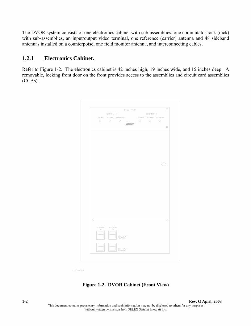
Rev. G April, 2003 This document contains proprietary information and such information may not be disclosed to others for any purposes
without written permission from SELEX Sistemi Integrati Inc.
1-2
The DVOR system consists of one electronics cabinet with sub-assemblies, one commutator rack (rack) with sub-assemblies, an input/output video terminal, one reference (carrier) antenna and 48 sideband antennas installed on a counterpoise, one field monitor antenna, and interconnecting cables.
1.2.1 Electronics Cabinet.
Refer to Figure 1-2. The electronics cabinet is 42 inches high, 19 inches wide, and 15 inches deep. A removable, locking front door on the front provides access to the assemblies and circuit card assemblies (CCAs).
Figure 1-2. DVOR Cabinet (Front View)

Model 1150 DVOR
Rev. G April, 2003 This document contains proprietary information and such information may not be disclosed to others for any purposes
without written permission from SELEX Sistemi Integrati Inc.
1-3
The left side panel (Figure 1-3) contains the blower assembly for cooling the carrier/sideband (CSB) power amplifier assemblies. Ambient air is drawn through a replaceable air filter by two fans that blow the air over the CSB power amplifier heat sinks. The rear panel fastens to the cabinet with eight screws. This panel when removed, provides access to cabinet wiring, sideband RF circulators, changeover relays, sideband RF sample assemblies, directional couplers, terminal boards, etc. Early versions of the VOR system have two field detectors mounted inside the cabinet. Later versions have the field detectors located in the commutator rack. Ambient air is drawn through a replaceable air filter by the battery charger power subsystem (BCPS) fans. These fans provide cooling air for the BCPS assemblies. Figure 1-4 illustrates the location of major assemblies of the electronics cabinet with the front cover removed.
(Left Side View) (Rear View)
Figure 1-3. DVOR Cabinet

Rev. G April, 2003 This document contains proprietary information and such information may not be disclosed to others for any purposes
without written permission from SELEX Sistemi Integrati Inc.
1-4
1150-113
A18POWER PANEL(PART OF) 1A34 POWER SUPPLY (STANDBY)
950350-0002
950350-0002POWER SUPPLY (MAIN)1A33
030398-0002
030757-0001
030749-0001
030363-0002
030757-0001
030398-0002
012616-1003
012617-1003
012743-0001
012743-0001
012743-0001
012618-1003
012689-1001
012620-0001
012619-0002
012101-1001
012617-1003
012616-1003
A1 RF MONITOR ASSEMBLY
SIDEBAND GENERATOR
SYTHESIZER
CSB POWER AMPLIFIER
JACK ASSEMBLY
SYTHESIZER
SIDEBAND GENERATOR
AUDIO GENERATOR
MONITOR
LOW VOLTAGE POWER SUPPLY
LOW VOLTAGE POWER SUPPLY
LOW VOLTAGE POWER SUPPLY
CPU
TEST GENERATOR
FACILITIES
SERIAL INTERFACE
MODEM
MONITOR
AUDIO GENERATOR
A2
1A7
1A8
1A9
1A10
SPARE 1SPARE 2
1A11
1A12
1A13
1A14
1A15
1A16
1A24
1A23
1A21
1A20
1A19
1A38
1A4
1A3
1A5
CCA DISPLAY A1A1 & A1A2
SYSTEM
NORM
AC INPUTPOWER
DC INPUTPOWER
BA
OFF
ON
ON
OFF
AUDIO
1150 VORSYSTEM A
OFF
ON
INTERNATIONAL,INC.SYSTEMSAIRPORT
CABINET DOOR REMOVED FOR CLARITY
ON
OFF
MIC
NORM ALARM BYPASS
030364-0001
OR 030363-0003
OR 030363-0003030363-0002
SIDEBAND GENERATOR1A6 030398-0002
SIDEBAND GENERATOR030398-0002
1A22
Figure 1-4. Location of Major Assemblies in the Electronics Cabinet (Front View) RF connections between the electronics cabinet and the commutator rack are via coaxial adapters located on top of the cabinets. Most of the assemblies slide into the cabinet from the front and mate with a backplane assembly or connectors of the main interconnect wiring harness assembly. Two redundant battery charger power subsystems (BCPS) are on the floor of the electronics cabinet behind the power panel assembly. Operating in conjunction with an optional battery bank, the BCPS supplies uninterruptible dc power to the DVOR.

Model 1150 DVOR
Rev. G April, 2003 This document contains proprietary information and such information may not be disclosed to others for any purposes
without written permission from SELEX Sistemi Integrati Inc.
1-5
The dual DVOR contains two complete sets of assemblies comprising two dual redundant transmitters:
Audio Generator (2) Sideband Generators (4) Frequency Generator (2) VOR Monitor (2) CSB Power Amplifier (2) Low Voltage Power Supply (2)
Either transmitter may be designated as “main”. Additionally, the DVOR uses a single Remote Maintenance System (RMS), consisting of these major CCAs:
Central Processor Unit (CPU) (1) Facilities (1) Serial Interface (1) Low Voltage Power Supply (1)
The following CCAs mate with the RMS backplane but are independent of RMS functions:
Modem (1) Test Generator (1) RSCU Control Interface (Optional)(1)
NOTE Early versions of the VOR system have the RSCU control interface mounted to the rear face of the power panel assembly. These units use a different interconnect wiring harness than later versions with the board mounted in the RMS assembly. Five coaxial latching relays, on a panel directly behind the RF monitor, are used to transfer station operation to standby or main equipment.
1.2.1.1 Status Display Panel Assembly (1A1).
Refer to Figure 1-4. The status display panel assembly (A2) is located at the upper portion of the cabinet and measure 14-1/8 inches wide and 3-3/4 inches high. The assembly contains two circuit card assemblies that provide a visual status of the DVOR monitor.

Rev. G April, 2003 This document contains proprietary information and such information may not be disclosed to others for any purposes
without written permission from SELEX Sistemi Integrati Inc.
1-6
1.2.1.2 RF Monitor Assembly (1A2).
The RF Monitor assembly is located at the top of the electronics cabinet and measures 13-3/8 inches wide, 9-1/4 inches deep, and 3-1/4 inches high. The RF monitor assembly functions as an RF detector/amplifier and distributor of the detected RF signals. The RF monitor assembly has a high power dummy load for the carrier mounted to a heat sink that is attached to the assembly chassis. There are two locations for the four medium power sideband dummy loads. On early equipment these loads were mounted to the RF Monitor assembly chassis. On later equipment four connectorized loads are mounted directly to the coaxial relays. There are three test connectors on the front of the assembly. These connectors provide access for external test equipment.
1.2.1.3 Carrier-Plus-Sideband (CSB) Power Amplifier Assembly (1A3, 1A19).
The CSB power amplifier assembly is located on the left side of the cabinet and measures 3-1/2 inches wide, 10-1/8 inches deep, and 11-15/16 inches high. The CSB power amplifier assembly amplifies and modulates the carrier RF signal to its final operating level. This assembly contains four CCAs: a power amplifier modulator, a bias regulator/exciter modulator, an exciter, and a power amplifier. Early units also had a smaller modulator bias CCA which is no longer required.
1.2.1.4 Frequency Generator Assembly (1A4, 1A20).
The frequency generator assembly is located to the right of the CSB power amplifier and measures 2-1/4 inches wide, 9-1/2 inches deep, and 8 7/8inches high. The frequency generator assembly generates the operational RF frequencies which consists of the carrier, the upper sideband, and the lower sideband frequencies using crystal controlled oscillators. This assembly contains five CCAs: the carrier/sideband drive, the frequency generator control, a mixer, and two voltage controlled crystal oscillators.
1.2.1.5 Sideband Generator Assembly (1A5, 1A6, 1A21, 1A22).
The sideband generator assembly is located to the right of the frequency generator assembly and measures 2-1/4 inches wide, 9-1/2 inches deep, and 8-7/8 inches high. Each sideband generator contains two sideband amplifier CCAs and two sideband controller CCAs. The sideband generators process the four separate Sideband-Only (SBO) RF signals.

Model 1150 DVOR
Rev. G April, 2003 This document contains proprietary information and such information may not be disclosed to others for any purposes
without written permission from SELEX Sistemi Integrati Inc.
1-7
1.2.1.6 Audio Generator CCA (1A7, 1A23).
The audio generator CCA measures 9 inches wide, 8-7/8 inches high, and has a 64 pin connector which connects to the main cabinet interconnecting wiring harness. The audio generator is responsible for developing and controlling the audio signals, generating the carrier modulation signals and monitoring and controlling RF power level and phase control signals used in the DVOR. In addition, DC analog voltages representing different modulation and power levels of the DVOR RF signals are applied to and analyzed by the audio generator to determine carrier power levels, carrier percent modulation, sideband power levels and VSWR. A on-board micro controller and memory circuitry controls all functions within the CCA communication with the DVOR system CPU is via the serial interface CCA.
1.2.1.7 Monitor CCA (1A8, 1A24).
The monitor CCA measures 9 inches wide, 8-7/8 inches high, and has a 64 pin connector which connects to the main cabinet interconnecting wiring harness. The monitor CCA monitors and analyzes the detected RF signals from the field detectors and initiates an alarm status signal if the DVOR fails to operate within specified limits.
1.2.1.8 Modem CCA (1A9) Part Number 012101-1001
The modem CCA measures 6-7/8 inches deep, 4-3/16 inches high, and has a 64 pin connector which connects to the backplane and a connector that connects to the main cabinet interconnecting wiring harness. The modem CCA contains a Serial Communications Controller (SCC) and a dial up modem module, providing an interface between the DVOR system and an offsite computer terminal.
1.2.1.9 Serial Interface CCA (1A10)
The serial interface CCA measures 6-7/8 inches deep, 4-3/16 inches high, and has a 64 pin connector which connects to the backplane and two connectors that connect to the main cabinet interconnecting wiring harness. The serial interface provides the communications interface for the CPU assembly to communicate with other devices. This CCA contains four dual channel Serial Communications Controllers (SCCs) which accomplish two-way communications with: the local video terminal, DME transponders no. 1 and/or no. 2 (if collocated), audio generator for transmitter no. 1 and transmitter no. 2 and DVOR monitors no. 1 and no. 2.

Rev. G April, 2003 This document contains proprietary information and such information may not be disclosed to others for any purposes
without written permission from SELEX Sistemi Integrati Inc.
1-8
1.2.1.10 Facilities CCA (1A11)
The facilities CCA measures 6-7/8 inches deep, 4-3/16 inches high, and has a 64 pin connector which connects to the backplane and one connector that connects to the main cabinet interconnecting wiring harness. The facilities CCA collects and integrates the DVOR system status information and sends it to the CPU assembly for processing and storage. It also provides a unique transfer status signal to the Remote Status/Control Unit (RSCU) that signifies a transmitter transfer has occurred as well as the standard status signals. Additionally, BCPS on/off control and status signals, display panel LED driver signals, control signals from the RSCU and power supply status signals are either generated by, or applied to, this CCA for processing.
1.2.1.11 Test Generator CCA (1A12).
The test generator CCA measures 6-7/8 inches deep, 4-3/16 inches high, and has a 64 pin connector which connects to the backplane and one connector that connects to the main cabinet interconnecting wiring harness. Test generator CCA performs two functions. The primary function is to provide a standard reference signal to the DVOR monitors for automatic calibration at power-up or whenever directed by the RMS CPU for monitor integrity testing. The secondary function is an operator maintenance function, which is to allow test signals to be sent to the monitor(s), as directed by an operator through the video terminal. The operator can vary signal parameters (i.e., frequency, percent modulation, phase shift, etc.) to determine if a monitor is functioning properly and will alarm at the required settings.
1.2.1.12 Central Processor Unit (CPU) CCA (1A13)
The CPU CCA measures 6-7/8 inches deep, 4-3/16 inches high, and has a 64 pin connector which connects to the backplane and one connector that connects to the main cabinet interconnecting wiring harness. The CPU is responsible for monitoring and controlling the DVOR system and directing communications with external devices. The CPU is mounted in the RMS card cage assembly where it connects to the backplane bus. The CPU contains a micro controller, RAM, EPROM, EEPROM, bus control and power monitor circuitry. It processes the system status, directs communications with the outside world, and communicates with the DVOR monitor and audio generator assemblies.

Model 1150 DVOR
Rev. G April, 2003 This document contains proprietary information and such information may not be disclosed to others for any purposes
without written permission from SELEX Sistemi Integrati Inc.
1-9
1.2.1.13 Low Voltage Power Supply (LVPS) CCA (1A14, 1A15, 1A16)
There are three LVPS assemblies used on the transmitter cabinet. The low voltage power supply CCA measures 6-7/8 inches deep, 4-3/16 inches high, and has a 10 pin connector which connects to the main cabinet interconnecting wiring harness. LVPS 1A14 is designed to provide +/-12 Vdc and +5 Vdc power to the RMS card cage. LVPS 1A15 and 1A16 are located in the RMS card cage but do not connect to the backplane assembly. LVPS 1A15 is the low voltage power supply for transmitter 1 and 1A16 is the LVPS for transmitter 2. Each LVPS is identical in construction and operation. Each is interchangeable with the other.
1.2.1.14 RSCU Control Interface CCAs
1.2.1.14.1 1138 RSCU Control Interface CCA (1A26) Part Number 012741-1002.
The 1138 RSCU control interface CCA is located in the RMS unit. It measures 6-7//8 inches deep, 4-3/16 inches high, and has a 64 pin connector which connects to the backplane and two connectors that connect to the main cabinet interconnecting wiring harness. The RSCU control interface CCA provides status data to and control data from a remote status and control unit.
1.2.1.14.2 1138 RSCU Control Interface CCA (1A26) Part Number 012741-1002
The 1138 RSCU control interface CCA is located in the RMS unit. It measures 6-7/8 inches deep, 4-3/16 inches high, and has a 64 pin connector which connects to the backplane and two connectors that connect to the main cabinet interconnecting wiring harness. The RSCU control interface CCA provides status data to and control data from a remote status and control unit.
1.2.1.15 Battery Charger Power Subsystem (BCPS) (1A33, 1A34).
The BCPS is located on the floor of the cabinet behind the power panel and measures 5-3/8 inches wide, 13 inches deep, and 8-3/4 inches high. Operating in conjunction with the battery supply, the BCPS supplies un-interruptible +28 and +43/48 volt DC power to the DVOR, and also functions as a battery charger when AC power is applied. On board fans provide cooling for the BCPS. Ambient air is drawn through a replaceable filter by the BCPS fans. These fans provide cooling for the BCPS.
1.2.1.16 Power Panel Assembly
The power panel assembly is located at the lower front portion of the cabinet and measures 14-7/8 inches wide and 8-5/8 inches high. The power panel contains the AC input and DC input circuit breakers. AC input power circuit breakers control the application of AC voltage to BCPS. DC input power circuit breakers control the application of DC voltage to BCPS.

Rev. G April, 2003 This document contains proprietary information and such information may not be disclosed to others for any purposes
without written permission from SELEX Sistemi Integrati Inc.
1-10
The power panel is hinge mounted to the electronics cabinet and is secured by two knurled thumbscrews. This panel must be lowered to gain access to the terminal connections, plugs and adjustment controls of the BCPS. On some early versions of the VOR, the RSCU interface assembly is mounted to the back side of this assembly.
1.2.2 Commutator Rack
Refer to Figure 1-5. The commutator rack is separate from the electronics cabinet and contains one control assembly with a commutator driver CCA. The Commutator Driver CCA, one low voltage power supply modules the pin diode drive for the commutators. Dimensions of the commutator rack are the same as those for the transmitter cabinet. The commutator rack has two removable side panels and a removable rear panel which are fastened with eight screws each. The rear panel has two large circular cut-outs that allow the commutator RF coaxial cables to pass through to the antenna system. The removable side panels provide ease of access to the numerous coaxial cable connectors on the rear of the commutator driver CCAs.
1.2.2.1 Commutator Rack Upgrade
Newer versions of the DVOR commutator rack have a monitor interface assembly upgrade. The upgrade centralizes all components that send or receive signals external to the DVOR station into one location (commutator rack). This assembly can be mounted on either side of the commutator rack, dependent upon the mounting location of the commutator rack to the transmitter cabinet. The monitor interface assembly consists of a signal splitter, two field detectors, transient suppressor components and associated terminal boards mounted on a chassis which is secured to the rack by six screws.
1.2.2.2 Control Assembly (2A1)
The control assembly measures 15 inches wide, 6 inches high. It contains the Pin Diode Driver CCA.
1.2.2.2.1 Pin Diode Driver CCA
The pin diode driver CCA measures 13 ¾ inches long, 5 ½ inches wide. The CCA has a 25 pin connector which connects to a 25 conductor cable from the DVOR cabinet, a 10 pin connector that provides power to the Field Detector assemblies, and two 40 pin connectors that connect to ribbon cable from the Commutator CCAs. Also, a 4 pin header may be strapped to enable/disable automatic ground-check.

Model 1150 DVOR
Rev. G April, 2003 This document contains proprietary information and such information may not be disclosed to others for any purposes
without written permission from SELEX Sistemi Integrati Inc.
1-11
2A2
2A3
2A1A1
INTERNATIONAL,INC.
CONTROL ASSEMBLY
030752-0001/012098-0001
012702-0001
COMMUTATOR CCA
012702-0001
COMMUTATOR CCA
1150-686 Figure 1-5. Commutator Rack
Rev. G April, 2003 This document contains proprietary information and such information may not be disclosed to others for any purposes
without written permission from SELEX Sistemi Integrati Inc.
1-12
1.2.2.2.2 PIN Diode Driver CCA Upgrade
Capability for the ground performance of the antennas and commutator switching is provided. This check is automatic after started by the technician and therefore is called an Automatic Ground Check system. When started, the Monitor processor software (012617 cca) sends a switch position code to the Pin Diode Driver CCA via the 25 pin cable between the VOR transmitter cabinet and the commutator cabinet. The switch positions start at 0 and increment by one until 15. Each position represents 22.5 degrees of antenna rotation from the nominal position. At each position the Monitor CCA determines the azimuth angle at the Field Monitor antenna location. From this data the errors are measured and a Fourier Analysis is performed to generate the display data. The error as determined during the ground check is analyzed to determine the bias, the duantal error, quadrantal error and octantal error. The bias error is the average error around the station. The duantal error is sinusoidal with a rate of one cycle in the 360 degrees around the station. The quandrantal error is sinusoidal with a rate of four cycles in the 360 degrees around the station. The octantal error is sinusoidal with a rate of four cycles in the 360 degrees around the station.
1.2.2.3 Commutator CCA (2A2, 2A3)
The commutator CCA measures 15-7/8 inches high and 14-7/8 inches wide. There are two commutator CCAs installed in the commutator rack. They are located above and below the control assembly. The upper commutator CCA is used to switch the RF signals to all the odd antennas, and the lower commutator CCA drives the even antennas. Each commutator has twenty-seven N type RF connectors and two 36 pin D-shell connectors.
1.2.2.4 Monitor Interface Assembly
The monitor interface assembly contains several circuits that centralize all station input/output signals within the commutator rack. The assembly contains: transient suppressor circuitry, a signal splitter, and two field detector assemblies (later version DVOR systems only). All communication lines and field monitor antenna RF signals pass through the monitor interface assembly.
1.2.2.4.1 Transient Suppressor
All communications with the outside environment passes through this circuit. The transient suppressor is a protective device that prevents dangerous voltage potentials from entering the DVOR equipment and damaging vital circuitry within the system.
1.2.2.4.2 Signal Splitter (HY1)
The signal splitter is used to divide the detected VOR signal from the field monitor antenna into two equal components. The signal splitter is mounted to the commutator rack and measures 3/4 inch high, 1-1/4 inches long, and 1-1/4 inches wide.
Model 1150 DVOR
Rev. G April, 2003 This document contains proprietary information and such information may not be disclosed to others for any purposes
without written permission from SELEX Sistemi Integrati Inc.
1-13
1.2.2.4.3 Field Detector Assembly (2A6A1, 2A6A2)
The field detector assembly detects the radiated VOR signal received by the field monitor antenna. Each field detector measures 2 inches wide, 1-1/2 inches high, and 4 inches long. Each is mounted to the monitor interface assembly.
1.2.3 Portable Maintenance Data Terminal (PMDT)
The PMDT consists of a laptop portable computer and is used for monitoring, local control and maintenance of the DVOR station. Refer to Section 3 on the use of the PMDT.
1.2.4 Transmitting Antenna System
The DVOR antenna system consists of a single carrier antenna assembly at the center of the counterpoise, and 48 sideband antenna assemblies spaced equally in a 44 foot diameter circle concentric with the carrier antenna assembly. All antennas are enclosed in small, weatherproof, fiberglass radomes.
1.2.4.1 Carrier Antenna (Version 1)
Refer to Figure 1-6. Carrier Antenna version 1 is a single Alford loop on a support plate. The antenna is supported above the counterpoise by a metal pedestal. This antenna is electrically tuned to the station frequency by means of two large, air-dielectric capacitors. This antenna is designed to function with a collocated distance measuring equipment (DME) or tactical air navigation (TACAN) antenna system. When required, a metal pipe passes through the center of the support plate and center of the antenna. The pipe serves as a conduit for feed lines and cables to a DME or TACAN antenna and obstruction lights, when installed. When collocated with a TACAN, the antenna is enclosed within a fiberglass shelter.

Rev. G April, 2003 This document contains proprietary information and such information may not be disclosed to others for any purposes
without written permission from SELEX Sistemi Integrati Inc.
1-14
Figure 1-6. Carrier Antenna (Version 1)

Model 1150 DVOR
Rev. G April, 2003 This document contains proprietary information and such information may not be disclosed to others for any purposes
without written permission from SELEX Sistemi Integrati Inc.
1-15
1.2.4.2 Carrier Antenna (Version 2)
Refer to Figure 1-7. Carrier antenna version 2 is electrically identical to carrier antenna (Version 1). The Version 2 antenna has been upgraded. The two large, air-dielectric, metal disc capacitors used in the Version 1 antenna have been replaced by a single, high voltage, glass capacitor. This greatly improves tuning and makes the antenna less susceptible to vibration and corrosion because of the reduction in the number of mechanical parts. Mounting is identical to version 1.
Figure 1-7. Carrier Antenna (Version 2)

Rev. G April, 2003 This document contains proprietary information and such information may not be disclosed to others for any purposes
without written permission from SELEX Sistemi Integrati Inc.
1-16
1.2.4.3 Sideband Antenna (Version 1)
Refer to Figure 1-8. Each sideband antenna is an Alford loop, similar to carrier antenna (Version 1) but without the large hole in the support plate. This antenna is electrically tuned to the station frequency by means of two large, air-dielectric, metal disc capacitors. The antennas are mounted independently on individual support plates, supported above the counterpoise by metal pedestals equal in height to the carrier antenna.
Figure 1-8. Sideband Antenna (Version 1)

Model 1150 DVOR
Rev. G April, 2003 This document contains proprietary information and such information may not be disclosed to others for any purposes
without written permission from SELEX Sistemi Integrati Inc.
1-17
1.2.4.4 Sideband Antenna (Version 2)
Refer to Figure 1-9. Each sideband antenna is electrically identical to sideband antenna Version 1. The Version 2 antenna has been upgraded. The two large, air-dielectric, metal disc capacitors used in the Version 1 antenna have been replaced by a single, high voltage, glass capacitor. This greatly improves stuning and makes the antenna less susceptible to vibration and corrosion because of the reduction in the number of mechanical parts. Mounting is identical to version 1.
Figure 1-9. Sideband Antenna (Version 2)

Rev. G April, 2003 This document contains proprietary information and such information may not be disclosed to others for any purposes
without written permission from SELEX Sistemi Integrati Inc.
1-18
1.2.4.5 Balun.
Refer to Figure 1-10. The balun is a line section approximately 180 in length that hangs directly under the center of the antenna inside the pedestal and is used to develop a balanced signal output from a coaxial line input.
Figure 1-10. Balun, Tuning Stub, and Positioning Piece
1.2.4.6 Tuning Stub
Refer to Figure 1-10. The tuning stub is a line section made out of RG-214 cable with a connector on one end and open at the other end. The basic function of the stub is to supply the needed capacitive reactance to make the point of the stub attachment pure resistive.

Model 1150 DVOR
Rev. G April, 2003 This document contains proprietary information and such information may not be disclosed to others for any purposes
without written permission from SELEX Sistemi Integrati Inc.
1-19
1.2.4.7 Positioning Piece
Refer to Figure 1-10. The positioning piece is a length of RG-214 cable with a connector at each end. The purpose of the positioning piece is to place the tuning stub at a point on the input line where the resistive component of the complex impedance is equal to the characteristic impedance of the line (50 ohms). The length of the positioning piece is factory selected for the frequency band of operation.
1.2.4.8 Pedestal
Refer to Figure 1-11. The pedestal is a 6061-T6 aluminum tube with mounting plates on each end. The pedestal supports the Alford loop antenna and provides a conduit for the feed cable, balun, positioning piece, and tuning stub.
1.2.4.9 Radome
Refer to Figure 1-11. The radome is a fiberglass enclosure that protects the radiating elements of the antenna from the weather and vermin infestation.

Rev. G April, 2003 This document contains proprietary information and such information may not be disclosed to others for any purposes
without written permission from SELEX Sistemi Integrati Inc.
1-20
Figure 1-11. Antenna Pedestal and Radome Diagram

Model 1150 DVOR
Rev. G April, 2003 This document contains proprietary information and such information may not be disclosed to others for any purposes
without written permission from SELEX Sistemi Integrati Inc.
1-21
1.2.5 Field Monitor Antenna
Refer to Figure 1-12. There is one field monitor antenna in each DVOR system. A single Yagi antenna and dual detectors are used in each DVOR system. The antenna is installed on a support tower 300 to 360 feet from the carrier antenna. It may be installed on any radial.
Figure 1-12. DVOR Field Monitor Yagi Antenna
1.2.6 Counterpoise
The counterpoise is a circular, metallic support structure upon which the transmitting antenna system is installed. The counterpoise typically is between 60 and 100 feet in diameter, 8 to 12 feet above ground level. It can be aluminum or galvanized steel and is assembled of segments bolted together.
1.2.7 Equipment Shelter
The electronic part of the DVOR (transmitter cabinet and commutator rack) is housed in a shelter environmentally-controlled with heating, cooling and ventilation. Normally, the shelter is installed below the counterpoise and directly underneath the carrier antenna.

Rev. G April, 2003 This document contains proprietary information and such information may not be disclosed to others for any purposes
without written permission from SELEX Sistemi Integrati Inc.
1-22
1.2.8 Battery Backup Unit (Optional)
There are two versions of the battery backup supply. One version contains a single battery box containing four lead-acid maintenance free batteries. The other version consists of two battery boxes each containing two lead-acid maintenance-free batteries. Additional backup capacity can be achieved by adding additional groups of four batteries.
1.3 EQUIPMENT SPECIFICATION DATA
Equipment specifications are listed in Table 1-1.
1.3.1 Transmitter and Antenna System
1.3.1.1 Transmitter
Table 1-1. DVOR Equipment Specifications (Transmitter)
Parameter Specification Input Power Requirements 115/230 Vac ±15%, 47 to 400 Hz, single-phase, or 48 VDC.
Four 12 volt, sealed, lead-acid batteries (65 amp/hour) in series
will provide approximately 2.5 hours of battery operation.
Power consumption is 1200 W with one transmitter on and batteries on trickle charge. With two transmitters on and maximum battery charging current, power used is 3000 Watts max.
Carrier Frequency Range: 108 to 118 MHZ with 50 kHz channel spacing. Frequency Control: Synthesizer Carrier Frequency Tolerance: +/-0.0005% (5 PPM) Carrier Output Power: Transmitter output power adjustable from 50 to 100 Watts in 1
Watt increments (17 to 20 dB) Effective Radiated Power: 23 dBW minimum Carrier Level Shift: less than 3% for modulation depth up to 80% Duty Cycle: Continuous
Model 1150 DVOR
Rev. G April, 2003 This document contains proprietary information and such information may not be disclosed to others for any purposes
without written permission from SELEX Sistemi Integrati Inc.
1-23
Table 1-1. DVOR Equipment Specifications (Transmitter)
Parameter Specification Spurious Outputs: greater than 77 dB below the carrier at 30% modulation Harmonic Radiation: Meets or exceeds U.S. FCC requirements. Harmonics of 9960 Hz
meet or exceed: Second harmonic 30 dB lower than fundamental Third harmonic 50 dB lower than fundamental Fourth and higher harmonics 60 dB lower than fundamental Hum and Noise: With voice, VOR reference and identification inputs, hum and
noise on the carrier are more than 30 dB below the audio level equivalent of 30% modulation.
Maximum Range: Line-of-sight, 175 nautical miles at 37,500 feet above the facility. Accuracy: When site meets requirements of ICAO, bearing information on
the horizontally-polarized radiation is within ±1.0° (at a distance of approximately 300 meters) for all elevation angles between 0 and 60 degrees, measured from the center of the VOR antenna.
Reference Phase Signal (30 Hz AM) Frequency: 30 Hz ±0.01% Modulation depth: 28 to 32% digitally controlled Variable Phase Signal (30 Hz FM) Frequency: 30 Hz ±0.01% Sub-Carrier Signal (9960 Hz FM) Center frequency: 9960 Hz ±1% Deviation ratio: 16 ±1 at 115 MHZ Modulation depth: 28 to 32%, digitally controlled Identification Signal Keyer type: Solid State Frequency: 1020 Hz ±10 Hz Modulation depth: 5 to 20%, adjustable Harmonic distortion: less than 1.5% Code: 2,3,4 letters in Morse Code Rate: 8 words per minute Repetition: 4 times/30 seconds; 3 times with co-located DME

Rev. G April, 2003 This document contains proprietary information and such information may not be disclosed to others for any purposes
without written permission from SELEX Sistemi Integrati Inc.
1-24
Table 1-1. DVOR Equipment Specifications (Transmitter)
Parameter Specification Voice Frequency: 300 to 3000 Hz Modulation depth: up to 30%, adjustable Harmonic distortion: less than 2% Input level: -20 dBm to 9 dBm
1.3.1.2 Antenna System
Table 1-2. DVOR Equipment Specifications (Antenna System)
Parameter Specification Type: Alford loop with associated pedestal and fiberglass radome Frequency Range: 108 to 118 MHZ, field-tunable Polarization: Horizontal Antenna System Bearing Error: less than 0.5° DME Co-location: Permits coaxial mounting of DME antenna above carrier Weather Protection Fiberglass radome Blending Function: COS .836X Number of Antenna: 48 Sideband, 1 Carrier Modulation Type: Double-Sideband Commutator Type: Solid-State Frequency Range: 108-118 MHZ broadband, no tuning Blocking attenuation (off switches:) Greater than 60 dB Insertion Loss: 1.2 dB maximum Difference in insertion loss: Less than 0.2 dB Phase Balance Less than 6 degrees VSWR: Less than 1.2:1

Model 1150 DVOR
Rev. G April, 2003 This document contains proprietary information and such information may not be disclosed to others for any purposes
without written permission from SELEX Sistemi Integrati Inc.
1-25
1.3.1.3 Field Monitor
Table 1-3. DVOR Equipment Specifications (Field Monitor)
Parameter Specification Antenna Type: Yagi Number of Antennas: 1 Standard, 2 Optional Frequency Range: 108 to 118 MHZ Output: Composite VOR signal, RF Installation: Located at minimum of 91.4 m (300 ft) from center of
counterpoise and level with counterpoise Position: Any azimuth angle VSWR: 1.5:1 at 112 MHZ
1.3.1.4 Monitor
Table 1-4. DVOR Equipment Specifications (Monitor)
Parameter Specification Configuration "And", "or" user selectable Azimuth Measurement Resolution: ±0.01° Azimuth Measurement Range: 0 to 360° Azimuth Measurement Accuracy: ±0.2° Azimuth Readout Indication: Digital, using display/control terminal Phase Shift Control: Calibrated against test generator Monitoring of VOR signal: at any azimuth Alarm Limits Monitor Limits Bearing: any radial, ±9.9° 30Hz AM amplitude: adjustable, 0-50° 30Hz FM amplitude: adjustable, 12-20 (ratio) 9960 Hz subcarrier amplitude: adjustable, 0-50%

Rev. G April, 2003 This document contains proprietary information and such information may not be disclosed to others for any purposes
without written permission from SELEX Sistemi Integrati Inc.
1-26
Table 1-4. DVOR Equipment Specifications (Monitor)
Parameter Specification Level Alarm: Adjustable, 0-6 dB of nominal Identification: lack of ident, continuous, or level drop of 50% Stability of Alarms Phase shift: better than ±0.3° Amplitude: better than ±0.3% Alarm Time Delay: Adjustable, 4-99 seconds Monitor Startup Time Delay: Adjustable, 4-99 seconds VSWR Measurement: Continuous measurement and display of individual sideband
antenna VSWR. Maintenance alert if limit exceeded Alarm Limit: 1.0 to 3.0:1
1.3.1.5 Mechanical and Electrical
Table 1-5. DVOR Equipment Specifications (Mechanical and Electrical)
Parameter Specification Size of Cabinet: 48.26cm w x 38.1cm d x 104.8cm h (19" w x 15" d x 41.25" h) Weight of Cabinet: 87.5kg (193 lbs) Size of Commutator Rack: 48.26cm w x 38.1cm d x 104.8cm h (19" w x 15" d x 41.25" h) Weight of Commutator Rack: 31.75kg (70 lbs) Primary Power: 115/230 V AC +/-15%, 47 to 400 Hz, single phase Standby Power: Built-in (dual) Battery Charger/Power Supply,
used in conjunction with 4 lead-acid 12V batteries, 65 Amp-Hour
provides approximately 2.5 hours operation; double battery set provides approximately 5 hours operation.
Power Consumption: 1200 Watts (1 transmitter and trickle charging
batteries); 3000 Watts (2 transmitters and

Model 1150 DVOR
Rev. G April, 2003 This document contains proprietary information and such information may not be disclosed to others for any purposes
without written permission from SELEX Sistemi Integrati Inc.
1-27
Table 1-5. DVOR Equipment Specifications (Mechanical and Electrical)
Parameter Specification maximum battery charging)
Duty Cycle: Continuous
1.3.2 Remote Control System
1.3.2.1 Design Features:
The optional remote control system consists of a Remote Status and Control Unit (RSCU) and one Remote Slave Unit (RSU). The RSCU is designed for installation in a standard 13.33 cm (5.25") rack panel space in a Control Tower Equipment Room and the RSU's are designed for installation at a controllers' position in the Tower Cab. The RSCU contains provisions for six individual control modules for ILS Localizer, Glideslope, Outer Marker and Middle Marker and DME and VOR stations. The modules are supplied with the appreciation. Each of the respective stations is connected to the RSCU by an RF data link or a single dedicated telephone line pair. The RSU is then slaved to the RSCU by interconnecting cables.
1.3.2.2 RSCU Controls and Indicators:
A. Each Module (Single-Equipment Stations):
Indicators Controls NORM Transmitter On/Off ALARM NO DATA
B. Each Module (Dual-Equipment Stations):
Indicators Controls ALARM #1 Transmitter On/Off NO DATA #2 Transmitter On/Off #1 NORM #1 ANT #2 NORM #2 ANT

Rev. G April, 2003 This document contains proprietary information and such information may not be disclosed to others for any purposes
without written permission from SELEX Sistemi Integrati Inc.
1-28
C. Common (on the RSCU panel itself)
Indicators Controls Alarm Loudness (Aural Alarm) Aural Alarm Lamp Intensity (for all lamps) Fuse Alarm Test/Alarm Silence Switch DC On Power On/Off
1.3.2.3 RSU Controls and Indicators
A. Indicators
TX1 NORM TX2 NORM ALARM
COMM FAILURE
Aural Alarm B. Controls
Alarm Loudness Lamp Intensity - for all NORM lights Lamp Test Power On/Off - on rear panel
1.3.2.4 RSCU/RSU Specifications
a. Primary Power: 110/220 ± 20% VAC, 47 to 440 Hz, 180 Watts maximum
b. Transmission Type: DTMF (Dual Tone Multi-Frequency) c. Line Impedance: 600 Ohms d. Output Tone Level: -7 dBm into 600 Ohms e. Input Sensitivity -8 to -38 dBm

Model 1150 DVOR
Rev. G April, 2003 This document contains proprietary information and such information may not be disclosed to others for any purposes
without written permission from SELEX Sistemi Integrati Inc.
1-29
1.3.3 Remote Maintenance Monitor and Control System
1.3.3.1 Design Features
A Remote Maintenance Monitoring and Control feature is included with the 1150. This provides all monitored data and system control via an internal circuit card assembly modem and a dial-up telephone line to a primary remote computer using the PMDT software. The modem is 9600 baud and Hayes compatible. In the event of an alarm condition, the system will initiate a dial-out to the primary remote terminal and leave its message. If connection with the remote terminal is not successful, the system will re-dial the remote at 10 minute intervals until a successful connection is made. The system may be dialed at any time from the primary remote terminal for maintenance or control operations. In addition, multiple remote terminals may be used at any time for calling the facility for maintenance or control operations. An optional local printer at each of the facilities provides a permanent record of all station activity, either local or remote.
1.3.3.2 Specifications:
I. Modem: Hayes compatible
Telephone Line: Standard Dial-Up line or RF data link Telephone Number: Programmed into the system
Dialing Protocol: Tone or Pulse as required by the telephone line
II Remote Display/Control Terminal Type IBM PC compatible computer with hard drive,
printer and PMDT communication software
Display Type Color
Mounting Table mounting
The terminal and peripherals operate on 120 or 220 VAC, 60 or 50 Hz. Major control functions as well as verification and adjustment of proper transmitting parameters are available via an RS-232 communications port and a PMDT. The system is password controlled such that adjustments are not possible without entry of the proper security codes.

Rev. G April, 2003 This document contains proprietary information and such information may not be disclosed to others for any purposes
without written permission from SELEX Sistemi Integrati Inc.
1-30
1.3.3.3 Remote Terminal Specifications:
Modem: Hayes compatible Telephone Line: Standard Dial-Up line or RF data link Computer: Windows operating system with PMDT software
installed Printer: Standard "Parallel"
1.3.4 Remote Receiver Monitoring
1.3.4.1 Design Features
The optional 1150 remote receiver monitoring system consists of a receiver unit suitable for installation either in a standard 13.33cm (5.25") rack panel space or on a table top, VOR yagi antenna and all necessary interconnecting cables. The receiver is typically installed in a control tower cab or equipment room or other convenient location on the airport and provides on/off status of the 1150 without the use of wire lines to the facility. The receiver is based on a TSO's aircraft VOR receiver unit for high reliability and is tuneable to any of the standard VOR frequencies.
1.3.4.2 Controls and Indicators
Controls Indicators LAMP TEST SWITCH VOR NORMAL AUDIBLE ALARM BYPASS SWITCH ALARM SPEAKER VOLUME CONTROL POWER ON POWER ON/OFF SWITCH AUDIBLE ALARM TUNED FREQUENCY
1.3.4.3 Receiver Specifications
Frequency Range 108 to 117.95 Hz Sensitivity: 2.0 µV (hard) typical 1.0 µV (hard) Antenna Type: Yagi Input Power: 120/240 V AC +-15%, 47-63 Hz 12 VDC Input for external DC backup (Front panel switch selectable)

Model 1150 DVOR
Rev. G April, 2003 This document contains proprietary information and such information may not be disclosed to others for any purposes
without written permission from SELEX Sistemi Integrati Inc.
1-31
1.3.5 Environmental
The components of the 1150 are designed to meet the following environmental conditions:
1.3.5.1 Operating Temperature
a. Indoor Equipment: -10° to +55° b. Outdoor Equipment: -50° C to +70°
1.3.5.2 Relative Humidity
a. Indoor Equipment: 95% (non-condensing) at +50° C. b. Outdoor Equipment: 100% at +70° C
1.3.5.3 Wind
More than 100 mph (85 knots) with shelter and counterpoise on concrete foundation.
1.3.5.4 Ice and Snow
5 cm (2 in.) Ice coating causes negligible course error.
1.3.5.5 Altitude:
0 to 4500 m (0 to 15,000 ft.)
1.4 EQUIPMENT AND ACCESSORIES SUPPLIED
Table 1-6 is a list of all major equipment and accessories supplied.

Rev. G April, 2003 This document contains proprietary information and such information may not be disclosed to others for any purposes
without written permission from SELEX Sistemi Integrati Inc.
1-32
Table 1-6. Equipment and Accessories Supplied
Quantity Nomenclature Unit Number
Dimensions (in inches)
Weight
1 Electronics Cabinet 1 19w x 15d x 41.25h 193 lbs 1 Commutator Rack 2 19w x 15d x 41.25h 70 lbs 49 Transmitting Antennas E1 thru
E49 20.25w x 20.25d E49 x 5.5h each
13 lbs
1 Field Monitor Antenna 4 Prior to assembly:
5.5w x 86d x 6.5h 20 lbs
1 Portable Terminal
(PMDT) 5
Consisting of: IBM Compatible laptop
computer 13w x 13.25d x 3h 10 lbs
PMDT Software
1.5 EQUIPMENT REQUIRED BUT NOT SUPPLIED
Table 1-7 is a list of all equipment that is not supplied but is required to make the equipment operational.
Table 1-7. Equipment Required but Not Supplied
Quantity Nomenclature Part No. 1 Shelter, 8ft x 12ft 890123-4110 Equipment Cabinet Mounting Kit 470190-0001 1 Counterpoise, 60 ft 470280-0002 1 Counterpoise, 100 ft 470537-0003

Model 1150 DVOR
Rev. G April, 2003 This document contains proprietary information and such information may not be disclosed to others for any purposes
without written permission from SELEX Sistemi Integrati Inc.
1-33
1.6 OPTIONAL EQUIPMENT
Table 1-8 is a list of optional equipment that can expand the capabilities of the VOR system or aid a technician in maintenance and troubleshooting. Equivalent test equipment can be substituted for that recommended.
Table 1-8. Optional Equipment
Quantity Nomenclature Part No. 1 Battery Backup (Unit 3) 470108-0001 1 Printer (Unit 6) 950311-0003 1 950550-0001 (120 VAC) 950550-0002 (240 VAC) 1 VOR Control 470196-0001 (for Model 1138 RSCU) 1 VOR-DME Monitor 001159-0101(120 VAC) 001159-0102(240 VAC) 1 Oscilloscope Oscilloscope; 100 MHZ Dual Trace, Delayed Sweep 1 Frequency Counter 950260-0000 1 RF Wattmeter 950258-0000, Bird Model 43 1 5-W Wattmeter Element 950268-0000, Bird 5B 1 100-W Wattmeter Element 950552-0405, Bird 100C 1 250-W Wattmeter Element 950474-0001, Bird 250C 1 RF Sampler Element 950262-0000, Bird 4274-025 1 Wattmeter Body Connector 950265-0000 Type N-Male Bird Model 4240-063 1 Digital Multimeter 950257-0000 3 ½ Digit 1 Torque Wrench 399003-0000 (For SMA RF Connectors) 1 Adapter, BNC Female to Phone 180218-0000 2 Dummy Load, 5-Watt, Type N-Male 950270-0000, Bird 80M

Rev. G April, 2003 This document contains proprietary information and such information may not be disclosed to others for any purposes
without written permission from SELEX Sistemi Integrati Inc.
1-34
THIS SHEET INTENTIONALLY BLANK

Model 1150 DVOR
Rev. G April, 2003 This document contains proprietary information and such information may not be disclosed to others for any purposes
without written permission from SELEX Sistemi Integrati Inc.
2-1
2 TECHNICAL DESCRIPTION
2.1 INTRODUCTION
The Model 1150 DVOR system is a dual-channel transmitter system, with dual monitoring facilities. It is designed for terminal and en route navaid operation. Aurally, the VOR is identified by a specifically assigned two to four letter morse code identity and may also include voice and automatic terminal information service (ATIS) information. The DVOR can be collocated with DME to provide distance information in addition to bearing data. The DVOR concept is based on the 360° radials which originate from a transmitting station and on the airborne equipment which resolves the particular radial data from the station. The resolved radial, called line-of-position (LOP) is the displacement angle between magnetic north and the aircraft, as measured from the DVOR antenna. Therefore, regardless of its heading, an aircraft which is on the 0° radial is north of the DVOR station. The magnetic course to the station is the reciprocal of the radial. In addition, to/from orientation data, relative to the DVOR station, is also resolved by the airborne equipment.
2.2 OPERATING PRINCIPLES
Operation of the DVOR is based on the phase difference between two 30 Hz signals modulated on the carrier, called the reference phase and the variable phase. Refer to Figure 2-1. The reference phase signal is obtained by amplitude modulating the carrier with a 30 Hz sinewave signal. This amplitude modulated signal is radiated omni-directionally in the horizontal plane by the central, carrier antenna. The radiation pattern is a circle, and produces in the aircraft receiver a 30 Hz signal with a phase independent of azimuth.
NOTE DVOR system theory stipulates that there are separately radiated upper and lower sideband frequencies which are displaced ±9960 Hz from the carrier frequency. Model 1150 DVOR has synthesizer controlled frequencies which are assigned as follows: carrier (on-channel) station frequency, carrier frequency plus 10 kHz, carrier frequency minus 10 kHz. The 40 Hz difference is within the tolerance limits set by the International Civil Aviation Organization (ICAO) Annex 10, vol. 1. To prevent confusion in understanding the theory of operation of Model 1150 DVOR all technical discussions are based on the ideal value of 9960 Hz.

Rev. G April, 2003 This document contains proprietary information and such information may not be disclosed to others for any purposes
without written permission from SELEX Sistemi Integrati Inc.
2-2
The variable phase signal is obtained from the 9960 Hz frequency modulated subcarrier which amplitude modulates the carrier. This amplitude modulation of the carrier is often referred to as the space modulation, since it is obtained by adding in space the omni-directionally radiated carrier and the separately radiated upper and lower sideband signals emanating from the ring of sideband antennas. The upper and lower sideband signals are displaced, on average, 9960 Hz above and below the carrier respectively and, when added in correct phase to the carrier, will produce a resultant signal which is amplitude modulated at 9960 Hz. The subcarrier is frequency modulated at a 30 Hz rate. The sideband signals are sequentially distributed to and radiated from the 48 sideband antennas in such a way as to simulate two diametrically opposed antennas, rotating counterclockwise about the circumference of the sideband antenna ring at 30 revolutions per second, with one antenna radiating the upper sideband signal and the other the lower sideband signal. Since the effective length of the path of travel between the rotating sideband sources and the distant point of reception varies at a 30 Hz rate, the observed frequency of the sideband signals varies also at a 30 Hz rate (i.e., the sidebands) and therefore, the subcarrier is frequency modulated at 30 Hz. The amount of frequency deviation is proportional to the diameter of the sideband antenna ring expressed in wavelengths at the operating frequency. Setting the diameter to 44.0 feet (13.4 meters) produces peak frequency deviation of 480 Hz at a frequency of 113.85 MHZ, 454 Hz at 108 MHZ and 497 Hz at 118 MHZ. Figure 2-1 depicts a typical RF spectrum of a DVOR with an operating frequency of fc. The corresponding deviation ratio varies therefore from 15.13 at 108 MHZ to 16.57 at 118 MHZ.

Model 1150 DVOR
Rev. G April, 2003 This document contains proprietary information and such information may not be disclosed to others for any purposes
without written permission from SELEX Sistemi Integrati Inc.
2-3
VARIABLEDOPPLER EFFECT
+/- 480 Hz
VARIABLEDOPPLER EFFECT
+/- 480 Hz
REFERENCE30 Hz AM
SIDEBANDS
Fc - 10KHz Fc + 10KHzFc
LOWER SIDEBANDCHANNEL
UPPER SIDEBANDCHANNEL
Figure 2-1. RF Spectrum of a Doppler VOR The deviation frequency is determined by the formula:
πλω xx=f d
Where: fd equals the deviation frequency in hertz. ω equals the angular velocity of the signal (30 Hz). λ equals the diameter of the ring in wavelengths. π equals 3.14.
30f=r d
d
In the aircraft receiver, a 30 Hz signal is extracted from the 9960 Hz FM subcarrier. The phase of this second 30 Hz signal varies linearly with the change of the azimuth bearing of the receiving point; for each degree of azimuth change, the phase of the 30 Hz variable phase signal changes by one degree.

Rev. G April, 2003 This document contains proprietary information and such information may not be disclosed to others for any purposes
without written permission from SELEX Sistemi Integrati Inc.
2-4
The sequential energizing of the sideband antennas and the 30 Hz amplitude modulation of the carrier are time related in such a way that the reference and the variable phase 30 Hz signals are in phase at zero degrees (0 ) magnetic from the DVOR station. As the receiving point is moved clockwise around the station, the variable phase signal (30 Hz FM) begins to lead the reference signal (30 Hz AM). For example, for the observer West of the DVOR, the 30 Hz FM signal leads the 30 Hz AM signal by 270 degrees. The aircraft receiver determines the phase difference between the two 30 Hz signals and thus its bearing in degrees (magnetic), relative to the station, as the number of degrees by which the 30 Hz AM signal lags the 30 Hz FM signal.
2.2.1 DVOR Antenna Principles
The DVOR antenna system simulates a rotating arm with a transmitting antenna at each end, radiating the upper sideband signal from one end and the lower sideband signal from the other end. This is achieved electronically by using 48 antennas spaced equally around the perimeter of a circle 44 feet (13.4 meters) in diameter, with an antenna in the center of the circle radiating a reference carrier. Consider the effect of simulated antenna rotation on an airborne receiver. When the upper sideband source is moving toward the aircraft, the doppler effect causes the airborne receiver input frequency to become higher than fc+9960 Hz, and for the lower sideband source, which is moving away, the frequency becomes less than fc±9960 Hz, fc being the carrier frequency. The frequency difference changes sinusoidally due to the simulated rotation. The difference is maximum when the line joining the two radiating antennas is perpendicular to the radial to the aircraft. The difference is equal to zero when the two sideband sources align with the radial to the aircraft since, at that moment, the distance between each sideband source and the receiver does not vary.
NOTE Technical discussions will use the standard VOR Subcarrier frequency (9960 Hertz). The subcarrier frequency used is 10 kHz which is within the 9960 +/-1% tolerance required. The moment of zero frequency deviation is different for different positions of the aircraft around the station. Therefore, the recovered 30 Hz FM signal will have a different phase for each of these different positions. For the receiver North of the DVOR station, the 30 Hz FM signal must be in phase with the 30 Hz AM signal; both signals passing through their positive zero crossings at the same time. To achieve this, the following has to be observed: At the moment that the 30 Hz amplitude modulation of the carrier is passing through its positive zero crossing, the simulated rotating antennas shall align with antenna number 1 (at North) and antenna number 25 (at South), with the North antenna radiating the peak of the lower sideband signal and the South antenna radiating the peak of the upper sideband signal. The lower sideband frequency will be decreasing; the upper increasing. The subcarrier frequency will be increasing from exactly 9960 Hz (10 kHz) up and the 30 Hz FM signal will be passing through its positive zero crossing.
2.3 THEORY OF OPERATION
The following paragraphs provide a technical description of the Model 1150 DVOR, its individual components and accessories. Refer to Figure 2-2 for simplified block diagram, Figure 11-1 (early version) and Figure 11-2 (later version) for a detailed block diagram of the DVOR system.

Model 1150 DVOR
Rev. G April, 2003 This document contains proprietary information and such information may not be disclosed to others for any purposes
without written permission from SELEX Sistemi Integrati Inc.
2-5
2.3.1 Simplified System Block Diagram
Refer to Figure 2-2. The transmitter (main and standby) consists of a frequency synthesizer assembly, CSB power amplifier assembly, low pass filter, directional coupler, audio generator CCA, two sideband generators, and two sideband RF sample assemblies. The frequency synthesizer assembly produces the three interrelated RF signals used by the DVOR. The on- channel carrier RF signal drives the CSB power amplifier assembly. The upper and lower sideband RF signals drive the two sideband generator assemblies. The CSB power amplifier assembly amplifies and modulates the carrier RF signal to the operational output level. Three versions of this assembly were built. Version 1, the 030363-0001 contains five subassemblies and is no longer produced. Version 2, the 030363-0002 and version 3, the 030363-0003 contain four subassemblies and differ in the final output transistor source of manufacture. All subassemblies will be discussed in detail in paragraph 2.3.2.3. The low pass filter assembly consists of a four pole filter network which removes spurious harmonics from the RF carrier signal. The filter also samples a portion of the RF energy to be used as an error correction that is sent back (feedback) to the frequency generator assembly. The bi-directional coupler obtains a sample of the forward and reflected RF carrier power. The sampled forward and reflected power is directed to the RF monitor assembly where the signal is used in the detection and analysis process circuitry. The RF monitor assembly functions as an RF detector/amplifier and distributor of the detected RF signals. The assembly also contains the dummy load for the standby transmitter carrier RF signal. There are versions of the RF Monitor Assembly. The initial version included built-in dummy loads for the four sideband signals. The present version does not include internal dummy loads. The present design is not fully interchangeable with the older version. Dummy loads for all four sidebands have been placed directly on the transfer relays. The audio generator CCA generates and processes all of the modulation signals transmitted by a DVOR transmitter and generates the power level and phase control signals needed to operate the transmitter and commutator. It is also responsible for monitoring the operational status of the transmitter. The DVOR system uses two sideband generator assemblies for each transmitter. Each sideband generator contains two sideband amplifier CCAs and two sideband controller CCAs. The sideband generator amplifies the sideband RF signal from the frequency generator to the operational output power levels. This assembly also produces amplitude and phase error signals to control distortion within the Side band RF signal.

Rev. G April, 2003 This document contains proprietary information and such information may not be disclosed to others for any purposes
without written permission from SELEX Sistemi Integrati Inc.
2-6
FREQUENCYSYNTHESIZER
A4/A20
CSB POWERAMPLIFIERA3/A19 A35/A36
FILTERLOW PASS BI-DIRECTIONAL
COUPLPERDC1/DC2
A7/A23GENERATORAUDIO SIDEBAND
GENERATORA5/A6/A21/A22
SIDEBANDSAMPLEASSY
A29/A30/A31/A32
RFMONITOR
A2
DISPLAY1A1A1/1A1A2SYSTEM CONTROL
ANDINTERFACEPROCESSOR(SCIP)
108 TO118 MHzCARRIER
360 Hz SIN
360 Hz COS
USB SIN
USB COS
LSB SIN
LSB COS
2A6A1/2A6A2FIELD DETECTOR
COMMUTATORCCA
2A2/2A3
TRANSMITTER(MAIN/STANDBY)
DVOR COMMUTATOR
USB RF
2A1DRIVER
PIN DIODE
MICROPHONE/VOICE INPUT
VIDEO TERMINAL
IDENT SYNCTO DME
CARRIERANTENNA
ANTENNAS 1-48SIDEBAND
FIELDMONITOR
1150-151
30 Hz +1020 Hz +
VOICE +
MONITORA8/A24
LSB RF
REV
FWD
ISO1
ISO2
ISO3
ISO4
FWD
FWD
FWD
FWD
REV
REV
REV
REV
DC
AUDIO OUT
Figure 2-2. Simplified DVOR System Block Diagram The sideband sample assembly mixes a portion of the two USB or two LSB RF signals to obtain an error correction feedback signal that is sent back to the frequency generator assembly. The Remote Maintenance System Processor (RMS) handles all command, control, communications and information for the DVOR system. Two field detectors detect the radiated RF signal obtained from the field monitor antenna. The detectors send their signals to the VOR monitors for processing and analysis. In early versions of the DVOR, these detectors were located in unit 1. In the current version these detectors are located in (unit 2) the commutator. The VOR monitor CCA works independently from the transmitter and from each other; however, the alarm control features of both monitors can be organized to function in a logical AND or logical OR arrangement. The commutator contains the assemblies needed to control the electronic switching of the sideband antennas. Current versions of the DVOR have two field detectors, a signal splitter and transient suppression circuitry included on a monitor interface assembly within the commutator.
2.3.1.1 Electronics Cabinet (Unit 1)
The VOR electronics cabinet assembly contains all of the electronic assemblies that generate, control, and monitor the DVOR modulated radio frequencies. The location of the VOR field detectors is

Model 1150 DVOR
Rev. G April, 2003 This document contains proprietary information and such information may not be disclosed to others for any purposes
without written permission from SELEX Sistemi Integrati Inc.
2-7
dependent upon which version of the DVOR system is installed. Early versions have the detectors located within the electronics cabinet; current versions locate them within the commutator rack.
2.3.1.1.1 Cabinet Insert (A18)
The cabinet insert is the cage assembly that holds the transmitter and RMS modules. It provides the means to physically secure the modules within the electronics cabinet and provides for the interconnection of the modules to the main wiring harness. Attached, but independent from it, are four voltage regulators (for the sideband amplifiers), two low pass filters (for the carrier output of each CSB power amplifier assembly), four sideband sample assemblies (two per transmitter system), the RMS cage, and the changeover relay panel, and one AC resistor assembly for each transmitter There are five coaxial latching relays mounted to the cabinet insert directly behind the RF monitor assembly. The relays are latched by applying a ground pulse to either the latch or release coil. The relays are powered from a common 28 volt source. The relays switch the ten RF inputs (main and standby) between the antenna system and the dummy loads. They also provide DC logic signals which are used by the RMS micro controller to sense which transmitter system is connected to the antenna system. The DC logic signal is also supplied to the audio generator to enable commutator switching signals and ident to be applied from the on-air audio generator CCA.
2.3.2 Detailed System Block Diagram
Refer to Figures 11-1 and 11-2. The DVOR system block diagram depicts the main components (both optional and required) of a functional station and identifies primary signal, control and voltage paths within the station. Because the standby transmitter is an exact duplicate of the main transmitter, only components of the main transmitter are shown. The heart of the DVOR system consists of an electronics cabinet assembly and a commutator. External to these units are the video terminal, carrier antenna, sideband antennas, field monitor antenna, and optional assemblies (printer, and backup batteries). The electronics cabinet is next broken down into its main components which are a status panel assembly, RMS, main and standby transmitters, VOR monitor CCAs, field detectors (early version), RF monitor, changeover relays, battery charger power subsystems, and sideband RF isolators. The status panel contains the display boards that provide a visual indication of the status of the VOR monitors. The RMS group handles all command, control, communications, and information for the station.

Rev. G April, 2003 This document contains proprietary information and such information may not be disclosed to others for any purposes
without written permission from SELEX Sistemi Integrati Inc.
2-8
The main transmitter consists of a frequency synthesizer assembly, CSB power amplifier assembly, low pass filter, directional coupler, audio generator CCA, two sideband generators, and two sideband RF sample assemblies. Supplying the voltage for the main transmitter is a stand-alone battery charger power subsystem, and a Low Voltage Power Supply (LVPS). The current version includes a resistor assembly attached to the input of the BCPS assembly. This resistor suppresses any oscillation that may occur when the AC circuit breaker is opened. Without this suppression opening the circuit breaker may cause the power fail indicators to toggle. The frequency synthesizer assembly is further subdivided into the two CCAs that comprise it. This assembly produces the three interrelated RF signals used by the DVOR. The on-channel carrier RF signal drives the CSB power amplifier assembly. The upper and lower sideband RF signals drive the two sideband generator assemblies. The audio generator CCA generates the carrier modulation signals, monitors and controls power levels, and directs the RF phase control signals for the DVOR transmitter. Each sideband generator is further subdivided to depict the functional arrangement of the circuit card assemblies within the assembly. Functionally, each sideband generator has two sideband amplifiers with each sideband amplifier consisting of a sideband amplifier CCA and a sideband controller CCA. Only one amplifier in each generator is shown on the block diagram for clarity. Each sideband amplifier is designed to amplify and modulate one of the four individual sideband signals used by the DVOR system. A sideband RF sample assembly mixes a portion of the two USB or two LSB RF signals to obtain an error correction feedback signal that is sent back to the frequency generator assembly. The current CSB power amplifier assembly is further subdivided to depict the four CCAs and 6 major transistors that comprise it. The primary RF and control signals between those circuit cards and components are shown on the block diagram. The CSB power amplifier assembly amplifies the carrier RF signal to the operational power level of the station and modulates it with the specified audio signals. A separate low pass filter assembly eliminates spurious harmonics from the RF signal. The filter samples a portion of the RF energy to be used as an error correction feedback signal that is sent to the frequency generator assembly. A second sample provides a sample of the RF at a front panel test point on the RF monitor assembly. A directional coupler in the carrier feed-line allows sampling of the forward and reflected RF energy. The RF monitor processes the main and standby RF signals for use by the audio generator and VOR monitor CCAs. Early versions of the RF monitor contained all the dummy loads, for use by the standby transmitter. Current versions include only the carrier signal load. The standby transmitter sideband signals are terminated in dummy loads at the transfer relay output. Four sideband RF isolators are used to obtain a sample of reflected RF energy from each sideband RF cable feeding the commutator rack and sideband antennas. Two field detectors detect the radiated RF signal obtained from the field monitor antenna. The detectors send their signals to the VOR monitors for processing and analysis. In early versions of the DVOR, thesedetectors were located in unit 1. In the later versions, these detectors were located in unit 2.

Model 1150 DVOR
Rev. G April, 2003 This document contains proprietary information and such information may not be disclosed to others for any purposes
without written permission from SELEX Sistemi Integrati Inc.
2-9
Each VOR monitor CCA works independently from the main transmitter and from each other; however, the alarm control features of both monitors can be organized to function in a logical AND or logical OR arrangement.
2.3.2.1 Frequency Synthesizer (1A4, 1A20) Block Diagram Theory.
Functional Block Diagram
DIVIDE BY 1000(10 KHz REF)
U2, U6
DIVIDE BY 4(2.5 MHzCLOCK)
U3
10 MHz REFTCXO
CARRIER LOOPCONTROLLER
CARRIER LOADERPROCESSOR
LOOPFILTER
VCO ANDBUFFERS
FREQ/2560DIVIDER
RESETGENERATOR
U5
CARRIER FREQ COUNTER OUTPUT
CVOR OUTPUT (NOT USED IN DVOR)
TEST PORT OUTPUT
CARRIER MEAN ANDDYNAMIC PHASER
CARRIERAMPLIFIER
TEST PORTBUFFER
CVOROUTPUTBUFFER
PHASEDETECTOR
VOR SYSTEMCARRIER AMPLIFIER
(EXTERNAL)
BUFFER/FILTER
CAR/SB PHASECONTROL INPUT
VOR SYSTEMCARRIER OUTPUT
FREQUENCYSELECT
SWITCHES
LSB LOOPCONTROLLER
LSB LOADERMICROPROCESSOR
USB LOOPCONTROLLER
USB LOADERMICROPROCESSOR
LOOPFILTER
VCO ANDBUFFERS
LOOPFILTER
VCO ANDBUFFERS
UPPER SIDEBANDAMPLIFIERS(EXTERNAL)
LOWER SIDEBANDAMPLIFIERS(EXTERNAL)
UPPERSIDEBANDSAMPLE
(EXTERNAL)
UPPERSIDEBANDSAMPLE
(EXTERNAL)
UPPER SIDEBANDOUTPUTS
LOWER SIDEBANDOUTPUTS
FREQ/2560DIVIDER
FREQ/2560DIVIDER LSB FREQ COUNTER OUTPUT
USB FREQ COUNTER OUTPUT
FEEDBACKSELECT
FEEDBACKSELECT
NOTE: SHADED BOXESINDICATE VOR SYSTEM
COMPONENTS EXTERNALTO THE SYNTHESIZER
MODULE
Figure 2-3. DVOR Synthesizer Block Diagram

Rev. G April, 2003 This document contains proprietary information and such information may not be disclosed to others for any purposes
without written permission from SELEX Sistemi Integrati Inc.
2-10
The function of the frequency synthesizer assembly is to create the Carrier, Upper Sideband, and Lower Sideband radio frequencies radiated by the VOR transmitter. In addition to the three PLL synthesized RF generators, there is another phase lock loop in the synthesizer. This loop is used to maintain the carrier phase relative to the reference RF signal, and correcting for amplitude modulation induced phase mod on the VOR carrier transmitter output signal. Feedback from samples of the sideband amplifiers is used to maintain proper frequency and phase characteristics of the upper and lower sideband signals as well. There are two boards (CCA’s) in the frequency synthesizer, the 012100 synthesizer CCA, and the 012102 interconnect CCA. The majority of the circuitry is located on the 012100 synthesizer CCA; with only the test port buffer amplifier circuitry (described below) on the 012102 interconnect CCA. There is a temperature compensated crystal oscillator, or TCXO, on the synthesizer CCA that generates a 10.000 MHz reference signal. This signal is divided by 4 to create a 2.5 MHz clock signal for the control microprocessors, and is divided by 1000 to create the precision 10 KHz synthesizer loop reference signal. Refer to Figure 2-3. The DVOR carrier frequency is generated by a PLL synthesizer, referenced to the precision 10 KHz signal. A voltage controlled oscillator, or VCO, generates the RF signal. This signal is buffered, and a portion of the signal fed back to the PLL controller, where it is divided by a programmable divider. The divided output is compared to the precision 10 KHz reference signal in the PLL controller’s phase comparator. The phase comparator generates an error voltage signal that is filtered and applied to the voltage control input of the VCO, thus locking the VCO output frequency to the reference. VOR channel selection is accomplished by changing the divide ratio of the PLL controller’s divider. This divide ratio is programmed into the PLL controller by the carrier control microprocessor. This microprocessor reads the channel select dip switches, calculates the proper information, and loads this information into the PLL controller IC. The output of this carrier synthesizer is split and routed to the carrier phaser, the carrier frequency counter divider, the test port buffer amplifier, and a buffer amplifier that is used to drive the CVOR sideband amplifiers. In the DVOR, this buffer amplifier output is not used, and is terminated in a resistive load. The test port buffer amplifier is located on the 012102 Interconnect CCA, on the backside of the frequency synthesizer module. The output of this buffer is attenuated to provide the 10 mW typical carrier frequency output signal available on the front panel SMA connector. The attenuator also serves to provide a resistive load for the buffer when no external load is connected to the SMA connector. There is no other circuitry on the 012102 interconnect board, it simply serves to connect the module 25 pin D shell connector to the 30 pin header connector which mates with the 012100 synthesizer board, as well as provide the RF interconnections for the sideband sample feedback signals. The output of the carrier phaser is amplified by the carrier buffer amplifier, and feeds the high power carrier amplifier module in the DVOR. In the process of amplitude modulation, the VOR carrier amplifier generates undesired phase modulation of the output signal. In addition, the transfer phase of the RF amplifier chain will drift due to temperature. The carrier phaser is used to counter both of these effects. Feedback from the VOR carrier output signal is routed back to the Frequency Synthesizer module. This feedback is representative of the final RF carrier output signal, and has both the 30 Hz amplitude modulation, and the undesired phase shift information.

Model 1150 DVOR
Rev. G April, 2003 This document contains proprietary information and such information may not be disclosed to others for any purposes
without written permission from SELEX Sistemi Integrati Inc.
2-11
This carrier feedback signal is first passed through a limiter in the Frequency Synthesizer module to remove the 30 Hz AM information. The output of the limiter is applied to a phase detector where it is compared to the direct output of the carrier PLL synthesizer. The output of this phase detector is a phase error signal, which is amplified and filtered to drive the carrier phaser. The carrier phaser is modulated to maintain the error voltage at zero volts, hence countering the undesired phase shift and phase modulation effects of the VOR carrier RF amplifier. There is a DC offset input to the carrier phase error amplifier that has the effect of shifting the phase of the VOR carrier output signal with respect to the reference phase in the frequency synthesizer module. This allows for phase adjustment of the carrier to sideband output RF signals to optimize the signal in space characteristics of the VOR radiated signal. The carrier frequency counter divider is also programmed by the carrier control microprocessor. It provides a fixed divide by 2560 CMOS compatible output for carrier frequency monitoring. The upper and lower sideband frequencies are generated in PLL synthesizers that operate in the same manner as the carrier PLL synthesizer described above. Since the synthesizer loops use a 10 KHz precision reference, they can be programmed in 10 KHz increments. This allows generation of the upper sideband frequency by programming the loop to 10 KHz above the VOR channel frequency. Similarly, the lower sideband frequency is generated by programming the loop to 10 KHz below the VOR channel frequency. These offsets are generated by the upper and lower sideband control microprocessors. All three processors (carrier, upper SB and lower SB) read the same set of channel select switches. The upper and lower sideband control microprocessors determine the proper divide ratios to load into the loop controller PLL chips to generate the 10 KHz offsets from the VOR channel frequency. This eliminates the need to select the frequencies for the upper and lower sidebands individually, insuring proper operation of the frequency synthesizer assembly. In the DVOR system external to the synthesizer assembly, there are two Sideband Sample assemblies. In these, the sine and cosine modulated sideband frequencies are sampled and summed together to create upper and lower sideband feedback signals, which contain the average phase information of the radiated sideband frequencies. These sideband sample outputs are routed to the frequency synthesizer module. These feedback signals are limited, buffered, and used by the PLL controller IC’s in the upper and lower sideband synthesizers. In this manner, the output phase and frequency of the sideband transmitters is controlled, maintaining the phase with respect to the 10 KHz precision reference in the frequency synthesizer module. Both the upper and lower sideband PLL synthesizers have fixed divide by 2560 dividers that operate in the same fashion as the carrier PLL synthesizer to provide for upper and lower sideband frequency monitoring. All three frequency generation PLL synthesizers use the same 10 KHz precision reference. This has the effect of maintaining the phase of the 10 KHz frequency difference between the upper sideband and carrier, and lower sideband and carrier in a fixed relationship. When these signals are radiated by the DVOR antenna system, the upper and lower sidebands combine with the carrier signal in space to create a 10 KHz amplitude modulation of the carrier signal. As mentioned above, the phase of the carrier signal can be shifted to optimize the performance of the radiated signals in space.

Rev. G April, 2003 This document contains proprietary information and such information may not be disclosed to others for any purposes
without written permission from SELEX Sistemi Integrati Inc.
2-12
2.3.2.1.1 Frequency Synthesizer (1A4, 1A20) Detailed Circuit Theory.
Frequency Reference Circuitry
U1 is a temperature compensated crystal oscillator, or TCXO, which provides a precision 10.000 MHz CMOS compatible signal at it’s output. There is a trim adjustment on U1 used to make fine adjustments to output frequency, and to compensate for crystal aging. The output of U1 routes to U2a, ½ of a dual decade counter. This counter divides the input signal by 10, then routes it to U2b, the other half of this IC. Here it is divided by 10 again, creating a 100 KHz signal. This 100 KHz signal is applied to the input of U6a, another decade counter. This counter divides the 100 KHz input by 10, creating the 10 KHz precision reference used by the three synthesized RF generators within the module. The output of U1 is also applied to the input of U3a, a flip flop configured to divide the 10.000 MHz signal by 2. This resulting 5.000 MHz signal is applied to the input of U3b, which again divides by 2, resulting in a 2.50 MHz signal. This 2.50 MHz signal is used as a clock signal for the three synthesizer loading microprocessors.
DIVIDE BY 1000(10 KHz REF)
U2, U6
DIVIDE BY 4(2.5 MHzCLOCK)
U3
10 MHz REFTCXO
CARRIER LOOPCONTROLLER
U8
CARRIER LOADERPROCESSOR
U4
CHANNELSELECT
SWITCH S1
LOOPFILTERC18,C22R26,R27
C24
VCOU12
FREQ/1280DIVIDER
U9
RESETGENERATOR
U5
CARRIER FREQ COUNTER OUTPUT
BUFFERAMPLIFIER
U13
FREQ/2DIVIDER
U11A
RESISTIVEPOWER
SPLITTER
BUFFERAMPLIFIER
U14
BUFFERAMPLIFIER
U15
CVOR OUTPUT (NOT USED IN DVOR)
PHASE DETECTOR REFERENCE RF(HY1)
CARRIER SIGNAL RF (T1)
TEST PORT OUTPUT (J8)
BUFFERAMPLIFIER
U1(012102 BD)
Figure 2-4. Carrier RF Generation Loop
Carrier PLL Synthesizer Circuitry
Refer to Figure 2-4, the carrier RF generation loop block diagram. The carrier radio frequency is generated by a phase lock loop synthesizer. The loop is comprised of a voltage controlled oscillator, or VCO, buffer amplifiers and power splitters, a loop controller IC, and a microprocessor. Voltage regulator U10 provides a low-noise +12V supply to the VCO, U12. This regulator provides isolation from sources of power supply noise which would adversely affect the RF spectrum of the VCO output.

Model 1150 DVOR
Rev. G April, 2003 This document contains proprietary information and such information may not be disclosed to others for any purposes
without written permission from SELEX Sistemi Integrati Inc.
2-13
U12, the VCO is an oscillator that generates a RF signal, the frequency of which is proportional to a control voltage at pin 5, the tuning input. The output of this oscillator is applied to an attenuator made up of three resistors, R34, R35 and R37. This attenuator provides a broad band matched impedance to the output of the VCO, and also provides isolation to external noise influences. Buffer amplifier U13 provides gain to bring the signal back up to approximately +7 dBm, as well as providing additional reverse isolation to prevent signal degradation from noise. The output of buffer U13 is applied to a resistive power splitter / attenuator combination made up of R40, R42 – R47. The output of R40 is amplified by U14, where it is again split and attenuated. The output of R230 is applied to U8, the synthesizer loop controller IC. The output from R47 is amplified by U15. Voltage regulator U7 provides a +5 volt source for U8, the carrier loop controller IC. By using a separate +5V source, the sensitive charge pump output of U8 will not be affected by other VOR system +5V circuitry. U8 provides a number of functions. It contains the programmable divider network used to set the operating frequency of the phase locked loop, the phase comparator, the charge pump output used to drive the loop low pass filter, lock detection circuitry, and a programmable divider on the loop reference frequency input. In this application, since the reference frequency is the same as the 10.00 KHz reference applied to the oscillator input of U8, the reference divider is programmed to pass the reference signal through undivided. The variable frequency feedback signal from U14 is applied to the variable frequency input (Fin) of U8. This signal is divided in a programmable divider to match the loop reference frequency, or 10.00 KHz. For example, if the desired VOR channel is 113.000 MHz, the programmable divider will divide the incoming RF signal by 11,300. If the desired channel is 117.950 MHz, the programmable divider will divide this input signal by 11,795. After the variable RF signal is divided by the programmable divider, it is applied to U8’s internal phase comparator, where it is compared to the 10.00 KHz reference signal. If the variable RF signal phase slightly lags the 10.00 KHz reference signal, U8’s charge pump output (CPO) is driven high, causing the voltage at the VCO control input to increase. This will increase the frequency of the VCO, until the phase difference between the variable signal and the reference signal is near zero. In the same manner, if the variable RF signal phase slightly leads the 10.00 KHz reference signal phase, the charge pump output is driven low, causing the voltage at the VCO control input to reduce, lowering the VCO output frequency, until the difference between the variable signal phase and the reference signal phase are near zero. This has the effect of locking the output frequency to the precision 10.00 KHz reference signal, multiplied in frequency by the number programmed into U8’s input divider network. When the variable phase and reference phase within the loop controller IC are locked together, U8 provides an output indicating that the phase locked loop synthesizer is in the locked state. The information for programming the dividers within U8 is provided by the microprocessor U4. Microprocessor U4 reads the desired frequency information from the frequency select switch S1, calculates the required programmable divider settings, and creates the serial data stream, clock signals, and data latch signals used to program U8, the synthesizer loop controller IC.
Rev. G April, 2003 This document contains proprietary information and such information may not be disclosed to others for any purposes
without written permission from SELEX Sistemi Integrati Inc.
2-14
Microprocessor U4 also examines the state of the lock indication output from U8 mentioned above. When U4 determines that the loop is indeed locked, it switches the lock detect output low, illuminating CR1 and providing a logic low output used to indicate carrier RF generation loop lock. If microprocessor U4 senses that the carrier RF generation loop is unlocked, it switches the logic low output to a logic high indicating loop unlock, extinguishes CR1, and goes through the process to re-initialize the loop controller IC, U8. RF signal is routed through the signal splitter / attenuator parts R31, R228, and R187 where it is applied to the carrier frequency divider U9. U9 is actually the same type part as U8, the carrier synthesizer loop controller IC. In this application, however, U9 is used simply as a frequency divider, dividing the RF signal by 1280. U9 is programmed by microprocessor U4 to operate as a fixed divide by 1280, with the output provided at pin 14, FO/LD. This output is a short duration pulse, occurring at 1/1280 of the programmed VOR channel frequency. This pulse is applied to flip flop U11a, where it is divided by two to create a square wave signal at the carrier frequency divided by 2560. This output is used elsewhere in the VOR system to monitor the frequency of the carrier synthesizer. The output of amplifier U15 is split in a resistive power splitter / attenuator combination and is used in four separate functions. In the DVOR synthesizer, the output of R56 is terminated via jumper JP1 by resistor R58. In the CVOR, the output at resistor R56 is connected to J2 via jumper JP1 for use in driving the CVOR sideband amplifiers. RF output is taken from R51, applied to amplifier U21, then routed through an attenuator (R97, R100, R101) where it is applied to phase detector HY1 as the reference RF phase for the carrier phase correction loop (not to be confused with the carrier RF generation loop). RF output is taken from R50 and routed via jumper JP2 to the carrier phase shift network. RF signal is routed through R57 and C41 to E3. E3 is a one pin connector that provides a RF feed through to the 012102 interconnect CCA.
NOTE: This paragraph applies to circuitry contained on the 012102 Interconnect CCA. Since this is the only active circuit contained on the 012102 board, the theory of operation has been placed here, rather than in a separate manual section.
The RF signal from E3 is amplified by U1 (on the 012102 board), passes through an attenuator made up of R3, R4, and R5, then made available on the front panel of the synthesizer module via J8, Carrier Frequency Output.

Model 1150 DVOR
Rev. G April, 2003 This document contains proprietary information and such information may not be disclosed to others for any purposes
without written permission from SELEX Sistemi Integrati Inc.
2-15
PHASE LOCKDETECT WINDOW
COMPARATORU17:A, U17:B
PHASESHIFTFILTER
PHASEDETECTOR
HY1
BUFFERAMPLIFIER
U21
INTEGRATORDUMP
SWITCHU18
BUFFERAMPLIFIER
U23
MEAN PHASEINTEGRATOR
AMPLIFIERU19
LIMITERHY2
PHASE ERRORAMPLIFIER
U20:A
OFFSETADJUST
R81
PHASESHIFTER
T1, T2
BUFFERAMPLIFIER
U22
PHASESHIFTER
T3, T4
BUFFERAMPLIFIER
U24
CARRIEROUTPUT
AMPLIFIERQ1
RF FEEDBACKFROM
VOR SYSTEMCARRIER OUTPUT
RF INPUTFROM CARRIER PLL
SYNTHESIZER
REFERENCE RF INPUT FROMCARRIER PLL SYNTHESIZER
CARRIER PHASE LOCK DETECTOUTPUT
350 mW (TYP)CARRIER
RF OUTPUT
PHASE OFFSETBUFFER/FILTER
U20:B
CARRIER / SB PHASEINPUT FROM
VOR SYSTEM
BIASADJUST
R125
DYNAMICPHASE
NETWORKC128
Figure 2-5, Carrier Phase Control Loop
Carrier Phase Control Loop
Refer to Figure 2-5, Carrier Phase Control Loop Block Diagram. RF from the carrier frequency PLL synthesizer is applied to buffer amplifier U21, and then routed to the reference phase input of phase detector hybrid HY1. The VOR system takes a sample of the carrier transmitter output from the system low pass filter assembly. This sample of the modulated carrier output signal is brought into the 030757 Synthesizer assembly via connector J3 on the back panel. The signal passes through limiter hybrid HY2, which serves to remove the 30 percent amplitude modulation, but leaving the phase distortion information intact. This limited signal then goes through buffer amplifier U23, a phase shift network consisting of C71, C72, C75, C77, C81, L16 and L17. This phase shift network provides approximately 180 degrees of RF phase shift to the signal. The signal is then applied to the variable phase input of phase detector HY1. HY1 provides a DC output that is proportional to the phase difference between the reference input signal and the variable input signal. When the two signals are in quadrature (the normal operating condition), the output is zero volts. Output voltage increases with the variable phase input signal delayed with respect to the reference phase, and decreases with the variable phase input signal advanced with respect to the reference phase. Resistor R103 provides the proper terminating impedance for the hybrid phase detector output. The output of the phase detector hybrid HY1 takes two paths. One is referred to as the “mean phase” correction path, the other the “dynamic phase” correction path.

Rev. G April, 2003 This document contains proprietary information and such information may not be disclosed to others for any purposes
without written permission from SELEX Sistemi Integrati Inc.
2-16
The mean phase path is DC coupled, with a very low frequency bandwidth. This path serves to correct for any long-term phase drift with temperature, etc, within the carrier power amplifier assembly in the VOR system. The phase error voltage developed by phase detector HY1 is applied to the inverting input of integrator amplifier U19. This amplifier provides a very high gain to DC signals, with limited gain for AC components. The output of integrator U19 is low pass filtered further by R78 and C54, then applied to the phase error amplifier U20A. The output of U20A controls the tuning voltage on the varactor diodes contained in the phase shifter network. This control voltage causes the phase shifter network to provide the proper phase shift to the synthesizer module carrier output signal to force the output of the phase detector hybrid HY1 to zero volts. This locks the DC component of the system carrier power amplifier output phase to the reference phase within the synthesizer module. When the VOR system carrier power amplifier amplitude modulates the carrier output signal, it also causes inadvertent phase modulation. In the DVOR system, this appears as a 30Hz phase modulation, with components at harmonics of 30 Hz. This is referred to as the dynamic phase shift. The output of phase detector HY1 is AC coupled through capacitor C128 and phase lead network C164 / R200 to the non-inverting input of phase error amplifier U20A. The high pass frequency response of this network is chosen to provide adequate gain to the 30 Hz and above components of the phase error signal, but minimal low frequency (down to DC) gain to avoid interaction with the mean phase signal processing described above. This AC coupled path is referred to as the dynamic phase correction path. The dynamic phase error signal is amplified by U20A, applied to the phase shift network, and provides a “counter modulation” effect to minimize the phase distortion in the VOR system carrier output signal. Carrier frequency RF signal from the Carrier PLL Synthesizer is applied via JP2 to the input of the carrier phase shift network, or phaser. For additional details on the carrier phase shift network (phaser), refer to sheet 2 of the 012100 schematic diagram, Figure 11-12. RF from the carrier synthesizer loop is applied to pin 3 of transformer T1. Transformer T1 along with capacitors C59 and C61 function as a 4 port hybrid, or 90 degree power splitter. RF energy applied to pin 3 is split equally into two parts at pins 1 and 2, with 90 degrees of phase difference between pin 1 and pin 2. Pins 1 and 2 are terminated with series LC circuits consisting of L6/CR6 at pin 1, L8/CR7 at pin 2. Inductors L7 and L9 are RF chokes, providing high RF impedance with DC connections to ground for varactor diode control voltage reference. The capacitance of the varactor diodes is changed by varying the control voltage applied to the cathodes, with a RF ground provided by C60. With the purely reactive load presented to pins 1 and 2 by the two series LC networks (L6/CR6 and L8/CR7), the RF energy is reflected back into pins 1 and 2, with the phase of the reflected signal changed by the variable reactance on these pins.

Model 1150 DVOR
Rev. G April, 2003 This document contains proprietary information and such information may not be disclosed to others for any purposes
without written permission from SELEX Sistemi Integrati Inc.
2-17
The reflected signals from pins 1 and 2 are 180 degrees out of phase from each other at pin 3, the input port, and in phase at pin 4, the output port. The signals add together at the output port, and cancel at the input port. This has a net effect of a minimal loss broadband phase shift network, with the output signal shifted in phase by the varying reactance of the varactor diode / inductor networks. The other three phase shifter networks function in a manner identical to the T1 circuit described above. Attenuator networks between T1 and T2, T3 and T4 serve to provide consistent RF impedance matching as the varactor control voltage is changed. Amplifier U22 provides gain and isolation between the sections of the phase shift network. The output of T4 is then routed to buffer amplifier U24. Amplifier U24 feeds signal to the transistor amplifier Q1. Output bias current, and amplifier gain, are adjusted by R125. Input and output impedance matching networks, along with the series RLC feedback (R129, C101, and printed circuit interconnect traces) provide broadband operation of Q1, with no frequency specific tuning required. There is sufficient gain compression in U24 and Q1 to minimize any changes in attenuation due to the small changes in loss of the phaser network with varying control voltage. Resistor R81 is used to provide a DC offset in the output of U20A. This offset is adjusted so that the error voltage seen at the phase control loop integrator U19 output is a nominal zero volts, maximizing the useful control range of U19. This error voltage is available at a test point (TP3) on the front panel of the synthesizer module. R81 is adjusted to set the phase error voltage as measured at TP3 to a nominal zero volts, +/- 0.050 volts when the synthesizer module is installed in the VOR system cabinet. Note that in some cases, due to the large available phase shift of the phaser network (>450 degrees) R81 can be adjusted to achieve zero volts at TP3 at two separate points. The actual phase loop control voltage (output of U20A) is measured at TP4 on the synthesizer front panel. R81 should be adjusted to provide zero volts error voltage at TP3 between 2 and 8 volts as seen at TP4. If a zero volt phase error is achieved below 2 volts or above 8 volts, re-adjust R81 to see if a lock condition can be found between these two points.

Rev. G April, 2003 This document contains proprietary information and such information may not be disclosed to others for any purposes
without written permission from SELEX Sistemi Integrati Inc.
2-18
USB LOOPCONTROLLER
U40
USB LOADERMICROPROCESSOR
U37
LOOPFILTER
C156, C161R195,R197
C162
VCOU43
FREQ/1280DIVIDER
U39USB FREQ COUNTER OUTPUT
FEEDBACKSELECT
U48
10 KHZ REFERENCE
2.5 MHZ CLOCK
FREQ SELECT INPUTS
FREQ/2DIVIDER
U41:A
VCOBUFFER
U44
RESISTIVEPOWER
SPLITTER
FEEDBACKBUFFER
U45
OUTPUTBUFFER
U46USB RF OUTPUT
DIODELIMITER
CR14,CR15USB SIDEBANDSAMPLE INPUT
RESET INPUT Figure 2-6 Upper Sideband RF Generation Loop
Sideband RF Generation Loops
The sideband RF generation loops (upper and lower) are similar in function to the carrier sideband RF generation circuitry described above. The block diagram in Figure 2-6 depicts the upper sideband loop. The upper and lower sideband generation circuits are identical (other than reference designators), with one minor exception. The microprocessors that read the settings of the frequency select switches and program the loop controller IC’s have an additional input not found in the carrier control microprocessor circuit. In the upper sideband generator, pin 18 of U37 (USB loader microprocessor) is pulled to 5 volts by R180. In the lower sideband generator, pin 17 of U26 (LSB loader microprocessor) is pulled to 5 volts by R132. In the carrier circuitry, neither of these pins is pulled to 5 volts. During power up or reset conditions, these pins are read by the startup routine in the processor. If pin 18 is high, the loader microprocessor programs the synthesizer output frequency to 10 KHz above the carrier frequency selected by the frequency select switch, S1. This creates the upper sideband frequency. If pin 17 is high, the loader microprocessor programs the synthesizer output frequency to 10 KHz below the carrier frequency selected, creating the lower sideband frequency. If neither pin is pulled high, the synthesizer is programmed to operate at the frequency selected by the switch S1. This scheme allows the use of identical programs in all three synthesizer microprocessors, eliminating the need to have three separate software versions for these parts. The operation of the upper sideband generator circuit will be explained here. Refer to Figure 2-6, Upper Sideband RF Generation Loop. Since the lower sideband generation loop is identical with the exception of the pull up resistor discussed previously, only the upper loop will be described in this manual.

Model 1150 DVOR
Rev. G April, 2003 This document contains proprietary information and such information may not be disclosed to others for any purposes
without written permission from SELEX Sistemi Integrati Inc.
2-19
The voltage controlled oscillator (VCO) U43 generates an RF signal with a frequency proportional to the voltage at pin 5, the tuning voltage input. The RF output from the VCO is attenuated by R202, R203, and R205, then fed to the buffer amplifier U44. The attenuator and the buffer amplifier serve to provide a broadband constant impedance to the VCO output, and to provide approximately 40 or more dB of reverse isolation, effectively isolating the VCO from load pulling and noise effects. The output of buffer U44 is split into two paths by a resistive splitter. One path is applied to the input of output amplifier U46. U46 brings the RF signal level up to exceed the required output power for the synthesizer module. An attenuator at the output of U46 made of R224, R225 and R227 reduces this power to the proper level. The attenuator also provides isolation for the output buffer U46, protecting it from failure due to shorted or open circuits at the output connector. The second path taken by the RF signal from the power splitter on the output of U44 is to RF switch U48. U48 is used to select the feedback source for the phase locked loop synthesizer. When the microprocessor U37 lock detect output is high, RF signal from U44 is fed to the input of feedback buffer amplifier U45 through RF switch U48. The output of U45 is attenuated and divided into two paths. The first path is to the variable frequency input of the loop controller integrated circuit, U40. The second path is to the input of the upper sideband frequency divider U39. When the microprocessor U37 lock detect output is low, feedback for the phase locked loop is obtained from the sideband sample module located in the VOR system. The lock detect output from U37 is delayed approximately 50 mS from the lock detect output of the synthesizer loop controller U30. This allows sufficient time for RF signal to appear at the outputs of the VOR system sideband amplifier assemblies. The sine and cosine modulated sideband amplifier outputs are summed in the sideband sample module, resulting in a CW output representative of the two signals. This CW signal is routed through system cabling to the upper sideband frequency feedback connector, J6. The signal is passed through a diode limiter made of CR14 and CR15, then to RF switch U48. By using this feedback path for locking the upper sideband PLL circuit, the output phase of the sideband transmitter is maintained in a constant state with respect to the reference signal in the synthesizer module. U39, the frequency divider integrated circuit, is programmed to a fixed divide by 1280 condition by the loader microprocessor U37. The output of U37 is a narrow pulse, occurring at 1/1280 times the upper sideband frequency. This narrow pulse is applied to the input of U41A, a flip-flop configured as a divide by two. The output of U41A is a square wave signal at 1/2560 of the upper sideband RF frequency. This signal is used in the VOR system to provide monitoring capability of the sideband frequency. Voltage regulator U38 provides a low noise 5 volt power supply for operation of the noise critical circuits in the loop controller IC. This eliminates the potential for RF signal degradation due to noise on the VOR system 5 volt power supply.

Rev. G April, 2003 This document contains proprietary information and such information may not be disclosed to others for any purposes
without written permission from SELEX Sistemi Integrati Inc.
2-20
Voltage regulator U42 provides a low-noise 12 volt power supply for the operation of the VCO, U43. Again, this is to provide isolation from VOR system power supply noise. Jumper JP10 can be used to disable the upper sideband VCO for troubleshooting purposes. In normal operation, this jumper must be in place. The loop controller integrated circuit U40 contains the loop reference signal input, the programmable divider for the variable frequency input, phase detector, and charge pump output. The programmable divider is configured by the upper sideband loop loader microprocessor U37 in the same manner as the carrier loop discussed earlier. The resultant divided variable frequency signal is compared in the phase detector to the 10.000 KHz precision reference input. The output of the phase comparator drives the charge pump circuit in U40, sourcing current when the variable phase lags the reference phase, and sinking current when the variable phase leads the reference phase. The output of the charge pump is applied to the loop low pass filter consisting of C156, C161, R195, R197, and C162. These components set the operating bandwidth of the phase locked loop. The output voltage from the loop filter drives the tuning voltage of the VCO, causing it to increase in frequency when the variable phase lags the reference phase, and decrease in frequency when the variable phase leads the reference phase, thus locking the output signal to the precision 10.000 KHz reference signal.
2.3.2.2 Audio Generator CCA (1A7, 1A23) Block Diagram Theory
Refer to Figure 2-7. The audio generator is responsible for developing and controlling the audio signals used in the DVOR. The on-board micro controller and memory circuitry control all functions within the assembly. Communications from the audio generator CCA to the DVOR system CPU is accomplished through the serial interface CCA. Adjustment parameters from the transmitter screens are sent from the RMS to the Audio Generator at power-up and whenever a change to these screens are made. Transmitter monitoring data is sent from the Audio Generator to the RMS when the technician selects the Transmitter Data Screen.

Model 1150 DVOR
Rev. G April, 2003 This document contains proprietary information and such information may not be disclosed to others for any purposes
without written permission from SELEX Sistemi Integrati Inc.
2-21
MICROCONTROLLERU1
DACU31
MEMORYCIRCUITSU4-U6
REFERENCEMODULATIONCIRCUITU25
EPROM - U21
EPLD - U9
U7, U18DAC OCTAL
LATCHU26
DACU23
MULTIPLEXERU10
BUFFERAMPLIFIER
U8
IDENT LEVEL
REF MOD LEVEL
VOICE DAC OUT
BIPHASE SIGNALTO SIGNALGENERATOR
SBO 1 AM
SBO 2 AM
IDENT AM
REFERENCE
SIDEBANDPOWER DCLEVELS
LEVELSCARRIER DC
CARRIER
REFERENCEPOWERLEVEL
AMPLIFIERU32, U15, U16
FILTERU17VOICE IN
FROM U9 CLOCK
TO MICROCONTROLLER U1
VOICE OUT
SB1, SB2, SB3, SB4 PHASE CONTROLSIDEBAND GENERATOR& PHASE CONTROL
ADDRESS/DATA BUS
AMPLIFIERSU13, U33, U34
1150-172
IDENT SQ
SBO 3 AM
SBO 4 AM
D/AU25
CONTROLVOICE LEVEL
U3LATCH
Figure 2-7. Audio Generator CCA, Block Diagram

Rev. G April, 2003 This document contains proprietary information and such information may not be disclosed to others for any purposes
without written permission from SELEX Sistemi Integrati Inc.
2-22
2.3.2.2.1 Micro controller and Memory Circuits Block Diagram Theory
Refer to Figure 2-8. U36 and U8A comprise a precision voltage reference source which provide a +5 volt reference standard and a temp/volt reference that is proportional to cabinet temperature. U1 uses this reference for analog to digital conversions. The resolution of the conversions is (VREF/1024) or 5 millivolts. VREF is adjusted with R33 to 5.11 +/- 0.01 volts measured at U36 Pin 6. The output of U33 represents the cabinet temperature in the RMS data screen with a magnitude of 2.3 mV/Deg.
CONTROLLERMICRO-
REFERENCETEMP/VOLT
1150-060
U36, U33B
U43
POWERMONITOR
TX MAINTENANCEOFF-BOARD
SIGNALS
U1
SWITCHESQ2, Q3 BCPS MARGIN
S/B GEN CTRL
EPLDU9U6
RAMEPROMU5
PROMU4 CHIP SELECT
Y1
ON-BOARDDATA SIGNALS
ADD/DATA BUSU11A,RS-232
U12C
TO SERIALINTERFACE
BOARD
+28V
+5V
SIGNALS
+5V REF STANDARD
INPUT
MONITORINGPOWER
CIRCUITSU8B, U10
CARRIERREFLD PWR
SIDEBANDFWD/REFLD
PWR
CARRIERFWD PWR
Figure 2-8. Audio Generator CCA Block Diagram
(Micro controller and Memory Circuits).

Model 1150 DVOR
Rev. G April, 2003 This document contains proprietary information and such information may not be disclosed to others for any purposes
without written permission from SELEX Sistemi Integrati Inc.
2-23
Input power monitor circuit U43 compares the +28 Vdc sample, from the battery power charger subsystem (BCPS), and the +5 Vdc, from the low voltage power supply (LVPS). As long as the +28 Vdc output of the BCPS is normal the power monitor outputs a high and inverted by Q1. When the +28 Vdc output drops below +21 Vdc the change is sensed by the input power monitor and its output changes from HIGH to LOW. The LOW output of the input power monitor circuit places the micro controller (NMI) into a stop processing/continuous loop condition. If the +28 Vdc output of the BCPS is no longer abnormal, U1 will be reset and will start processing information again. The audio generator receives DC analog voltages which represent the different modulation and power levels of the DVOR RF signals. These voltages are processed by a power monitoring circuit consisting of U10, R50, R66 through R74, C6, C8 through C17. By analyzing the outputs of the power monitoring circuit, micro controller U1 can determine carrier power levels, sideband power levels, and VSWR. Micro controller U1 communicates with the RMS central processor unit (CPU) CCA via the serial interface CCA. Serial communications data is sent by U1 to the serial interface CCA through line driver U11A. U11A converts the TTL signals from the U1 into RS-232 signal levels. Serial communications information from the serial interface CCA is received by U1 through line receiver U12C. U12C converts the RS-232 level data to TTL levels. Periodic requests for status from the RMS to the Audio Generator occur at a 1 second rate. Failure of the audio generator to respond results in a communications error. Failure of the RMS to request status for 5 seconds results in shutdown of the transmitter. Crystal Y1 supplies a 12 MHZ clock signal to micro controller Ul. The audio generator utilizes several different types of memory devices to store and manipulate data. Programmable read only memory (EPROM) U4 contains the software program for U1. Electrically Erasable memory (EEPROM) U5 stores significant variable information for each DVOR. Random access memory (RAM) U6 provides temporary storage for data manipulation, and current transmitter operational parameters. Transistors Q2 and Q3 are controlled by U1. U1 controls the functional operation of the sideband generators by means of Q3. Under normal conditions U1 applies a LOW to Q3. This LOW keeps Q3 turned off. A HIGH applied to Q3 will turn it on and prevent the sideband generator assemblies from supplying an output. U1 uses Q2 to control the output of the BCPS 48 Vdc power supply module. Normally, U1 applies a HIGH, which keeps Q2 turned on. This causes the 48 Vdc module of the BPCS to output 43 Vdc (margin voltage). When needed, U1 turns off Q2 which allows the 48 Vdc module of the BPCS to output 48 Vdc. When the modulation setting in the transmitter setup exceeds 42% (sum of voice, ident and reference levels) the output voltage is set to 48Vdc. If less than 42% the output will be 43 Vdc.

Rev. G April, 2003 This document contains proprietary information and such information may not be disclosed to others for any purposes
without written permission from SELEX Sistemi Integrati Inc.
2-24
2.3.2.2.2 Reference and Sideband Generator Circuits Block Diagram Theory
Refer to Figure 2-9. At turn-on, U1 programs EPLD U9 with data necessary to configure it for the phase adjustment and EPROM clocking for development of the azimuth signal. U9 provides two primary output signals: one drives the reference channel; the other drives the variable (sideband) channel.
1150-061
U19AMPLEPROM
U21LCAU9 U30B
AMPLU23DAC
VOLTAGEREFERENCE
REFERENCE
ADD/DATA BUS
ON-BOARDCLOCKDATA &CONTROLSIGNALS
QUADDACU7
OCTALLATCHU26
DIFFLINE
DRIVERSU27,U28
AMPLU33C, U13B
AMPLU33A, U13A
AMPLU33B
SBO1AM
SBO2AM
IDENTAM
KEY
FROMU1
ENABLE FROM
REFERENCE IDENT
SINEBIPHASE
COSINEBIPHASE
REFERENCEVOLTAGE
COMMUTATORSWITCH SIGNALS(DVOR ONLY)
1.5 MHZ
(CARRIER POWER LEVEL)
TRANSFER RELAY
LATCHU3
U29
CARRIERVOICEIDENT
LEVELCONTROL
U18
QUADDAC
U34A, U13D
U34B, U13CAMPL
AMPL
SBO3AM
SBO4AM
SB
U25LEVEL
uP DATA BUS
Figure 2-9. Audio Generator CCA Block Diagram
(Reference & Sideband Generators).

Model 1150 DVOR
Rev. G April, 2003 This document contains proprietary information and such information may not be disclosed to others for any purposes
without written permission from SELEX Sistemi Integrati Inc.
2-25
U9 receives on-board clock, address/data, and control signals from micro controller U1. U9 outputs a separate 1.5 MHZ clock signal. U9 outputs 2-16 bit data words to EPROM U21 for the reference channel and the sideband channel. The reference channel will be discussed first followed by a discussion of the sideband channel. U9 provides address codes to EPROM U21. Jumper E5 selects either DVOR or DVOR mode of operation. When E5 is open DVOR signals are produced. U21 is programmed with a digital representation of the 30 Hz carrier modulation waveform. U21 applies the subcarrier waveform data to digital-to-analog converter (DAC) U7 and U18. The referenced data is latched into U3 when the REF LATCH signal goes from low to high. U23 converts the digital waveform information from U3 into an analog waveform. The output of U23 is a 30 Hz sinusoidal reproduction of the digitized waveform. The amplitude of this waveform is determined by the reference voltage applied to U23. The reference voltage for U23 is supplied by R13, U25 DAC and is representative of the combined carrier and sideband power levels. The output of U23 is applied to amplifier U19. U19 is designed to convert the current output of the digital to analog converter to an analog voltage signal. The 30 Hz signal is next applied to amplifier U30B. U30B amplifies the 30 Hz signal and removes the dc voltage. This reference modulation is added at U33D with voice; ident and carrier (DC) signals. EPROM U21 is also the variable (sideband) channel. It is programmed with the digital representation of two 360 Hz waveforms (one in quadrature with respect to the other), a 1020 Hz waveform, and the bi- phase/antenna switch code. The digital information supplied by U21 is applied to DAC U7 and U18 and to latch U26. U7 converts the data from U21 into the respective variable and identity tones. U7 contains 4 DACs. Only sections B, C and D provide active outputs. Section B controls sideband output 1, section D controls sideband 2 output , and section C controls the identity tones. The reference voltage for the active sections of U7 is provided by U25. The reference voltage sets the amplitude of the modulation produced by the DACs. The uP controls the level from U25 and therefore the modulating level. The output for the active section of U7 is applied to amplifier U33 sections A, and C. U33C functions as an amplifier/level shifter that removes any DC component from the signal. The output of U33C is the SBO 1AM signal and is applied to amplifier U13B. The output of U33A is the SBO 2 AM signal and is applied to amplifier U13A. The output of U33B is the 1020 Hz identity signal. The output of U33B is applied to U33D. Octal latch U26 receives data from U22 and passes it to its outputs when clocked by U9. This data is the bi-phase signal and antenna switch code. The bi-phase signals are applied to the sideband generator assemblies.
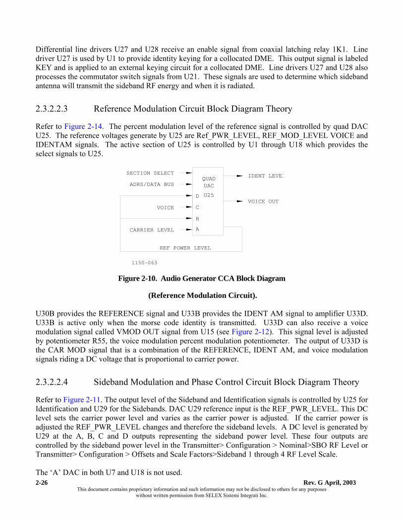
Rev. G April, 2003 This document contains proprietary information and such information may not be disclosed to others for any purposes
without written permission from SELEX Sistemi Integrati Inc.
2-26
Differential line drivers U27 and U28 receive an enable signal from coaxial latching relay 1K1. Line driver U27 is used by U1 to provide identity keying for a collocated DME. This output signal is labeled KEY and is applied to an external keying circuit for a collocated DME. Line drivers U27 and U28 also processes the commutator switch signals from U21. These signals are used to determine which sideband antenna will transmit the sideband RF energy and when it is radiated.
2.3.2.2.3 Reference Modulation Circuit Block Diagram Theory
Refer to Figure 2-14. The percent modulation level of the reference signal is controlled by quad DAC U25. The reference voltages generate by U25 are Ref_PWR_LEVEL, REF_MOD_LEVEL VOICE and IDENTAM signals. The active section of U25 is controlled by U1 through U18 which provides the select signals to U25.
1150-063
QUADDAC
U25D
C
B
A
IDENT LEVEL
VOICE OUT
REF POWER LEVEL
ADRS/DATA BUS
VOICE
CARRIER LEVEL
SECTION SELECT
Figure 2-10. Audio Generator CCA Block Diagram
(Reference Modulation Circuit). U30B provides the REFERENCE signal and U33B provides the IDENT AM signal to amplifier U33D. U33B is active only when the morse code identity is transmitted. U33D can also receive a voice modulation signal called VMOD OUT signal from U15 (see Figure 2-12). This signal level is adjusted by potentiometer R55, the voice modulation percent modulation potentiometer. The output of U33D is the CAR MOD signal that is a combination of the REFERENCE, IDENT AM, and voice modulation signals riding a DC voltage that is proportional to carrier power.
2.3.2.2.4 Sideband Modulation and Phase Control Circuit Block Diagram Theory
Refer to Figure 2-11. The output level of the Sideband and Identification signals is controlled by U25 for Identification and U29 for the Sidebands. DAC U29 reference input is the REF_PWR_LEVEL. This DC level sets the carrier power level and varies as the carrier power is adjusted. If the carrier power is adjusted the REF_PWR_LEVEL changes and therefore the sideband levels. A DC level is generated by U29 at the A, B, C and D outputs representing the sideband power level. These four outputs are controlled by the sideband power level in the Transmitter> Configuration > Nominal>SBO RF Level or Transmitter> Configuration > Offsets and Scale Factors>Sideband 1 through 4 RF Level Scale. The ‘A’ DAC in both U7 and U18 is not used.

Model 1150 DVOR
Rev. G April, 2003 This document contains proprietary information and such information may not be disclosed to others for any purposes
without written permission from SELEX Sistemi Integrati Inc.
2-27
Sideband 1 modulation is generated in Quad DAC U7. The data bus from U21 to U7 defines the audio signal. With A0 at logic 1, A1 logic 0 and the Write input to DAC rising edge the data is written for Sideband 1 into DAC B of U7. The output level of Sideband 1 is controlled by U29 DAC A. The U29 DAC A output is connected to U7 VREFB input. This level is set by the entry of a value into the Transmitter> Configuration > Nominal>SBO RF Level or Transmitter> Configuration > Offsets and Scale Factors> Sideband 1 RF Level Scale menus. Sideband 2 modulation is generated in Quad DAC U7. The data bus from U21 to U7 defines the audio signal. With A0 at logic 1, A1 logic 1 and the Write input to DAC rising edge the data is written for Sideband 2 into DAC D of U7. The output level of Sideband 2 is controlled by U29 DAC C. The U29 DAC C output is connected to U7 VREFD input. This level is set by the entry of a value into the Transmitter> Configuration > Nominal>SBO RF Level or Transmitter> Configuration > Offsets and Scale Factors> Sideband 2 RF Level Scale menus. Sideband 3 modulation is generated in Quad DAC U18. The data bus from U21 to U18 defines the audio signal. With A0 at logic 1, A1 logic 0 and the Write input to DAC rising edge the data is written for Sideband 3 into DAC B of U18. The output level of Sideband 3 is controlled by U29 DAC B. The U29 DAC B output is connected to U18 VREFB input. This level is set by the entry of a value into the Transmitter>Configuration> Nominal>SBO RF Level or Transmitter> Configuration> Offsets and Scale Factors> Sideband 3 RF Level Scale menus. Sideband 4 modulation is generated in Quad DAC U18. The data bus from U21 to U18 defines the audio signal. With A0 at logic 1, A1 logic 1 and the Write input to DAC rising edge the data is written for Sideband 4 into DAC D of U18. The output level of Sideband 4 is controlled by U29 DAC D. The U29 DAC D output is connected to U7 VREFD input. This level is set by the entry of a value into the Transmitter>Configuration> Nominal>SBO RF Level or Transmitter> Configuration> Offsets and Scale Factors> Sideband 4 RF Level Scale menus. Sideband 1 Phase is generated in Quad DAC U31. A DC level is generated that is connected to pin P1-A28 and then to Sideband Amplifier 1. The phase level of Sideband 1 is controlled by U31 DAC C. The U31 VREFC input is connected to the fixed VREF source. The DAC C output level is set by the entry of a value into the Transmitter> Configuration> Offsets and Scale Factors> Sideband 1-2 Phase Offset menu. Sideband 3 Phase is generated in Quad DAC U31. A DC level is generated that is connected to pin P1-C20 and then to Sideband Amplifier 3. The phase level of Sideband 3 is controlled by U31 DAC D. The U31 VREFD input is connected to the fixed VREF source. The DAC D output level is set by the entry of a value into the Transmitter> Configuration> Offsets and Scale Factors> Sideband 3-4 Phase Offset menu. Sideband 2-4 Phase is generated in Quad DAC U31. A DC level is generated that is connected to pin P1-C8 and then to Sideband Amplifiers 2 and 4. The phase level of Sideband 2 and 4 are controlled by U31 DAC B. The U31 VREFB input is connected to the fixed VREF source. The DAC B output level is set by U1 at 0 degrees and not technician selectable.

Rev. G April, 2003 This document contains proprietary information and such information may not be disclosed to others for any purposes
without written permission from SELEX Sistemi Integrati Inc.
2-28
Carrier to Sideband Phase is generated in Quad DAC U31. A DC level is generated that is connected to pin P1-A30 and then to the Synthesizer. The Carrier to Sideband Phase is controlled by U31 DAC A. The U31 VREFA input is connected to the fixed VREF source. The DAC A output level is set by the entry of a value into the Transmitter> Configuration> Offsets and Scale Factors> Carrier to Sideband Phase Offset menu.
1150-062
ADD/DATA BUSREF_PWR_LEVEL SBO2 LEVEL TO U7
SBO3 LEVEL TO U18
QUADDACU29
DCBA
SBO1 LEVEL TO U7
SBO4 LEVEL TO U18
+5VEFADD/DATA BUS
U29DACQUAD
ABCD
SB3 PHASE
SB1 PHASE
SB2/4 PHASE
CARRIER/ SB PHASE
Figure 2-11. Audio Generator CCA Block Diagram
(Sideband Level & Phase Control Circuit)
2.3.2.2.5 Voice and Test Tone Circuit Block Diagram Theory
Refer to Figure 2-12. The voice circuitry provides for voice to be modulated onto the carrier RF signal. Voice signals are applied either through a microphone or remotely through telephone lines. Potentiometer R7 is adjusted to prevent over driving the voice circuitry. The selected audio signal is applied to a buffer amplifier circuit which consists of U32A and B. U32A and B amplify the signal and apply it to amplifier U15.

Model 1150 DVOR
Rev. G April, 2003 This document contains proprietary information and such information may not be disclosed to others for any purposes
without written permission from SELEX Sistemi Integrati Inc.
2-29
1150-064
U17FILTERNOTCH
P/OFILTER
TRANSMIT
U15
NOTCH DEPTHR21
(300-3000 BANDPASS)
COMPAMPLU16
P/OAMPLPWR
U15
BFR AMPLU32A,U32B
TP2
U13ASWITCH
MIC IN
R7INPUTLEVEL
(STAIR-STEP FILTER)
RECEIVEFILTERP/OU15
VOICE VMODOUT
CLOCK FROM U9 VOICE
VOICE GAIN
D/AU25
Figure 2-12. Audio Generator CCA Block Diagram
(Voice and Test Tone Circuits).
The primary output of U32A and B is applied to the power amplifier section of U15. The output of this section of U15 (pins 6 and 7) is applied to voice gain compression amplifier U16. U16 provides a constant amplitude over an approximate 20 dB variation in signal level. The audio output of U16 is applied to the D/A converter U25 for voice mod controls and then to input of notch filter U17. U17 is configured to remove any frequency components between 1005 to 1035 Hz at the -3 dB points. Potentiometer R21 adjusts the center frequency of the notch and hence the attenuation of the ident and is set at the factory. Notch filter U17 requires a clock frequency that is fifty times the desired notch frequency, or 51 kHz. EPLD U9 provides this output frequency. The output of U17 is all voice frequencies excluding the 1020 Hz ±15 Hz. This filtered signal is applied to the transmit filter section of U15. The output of the transmit filter section of U15 is the VOICE signal. The filter section of U15 removes any voice modulation below 300 Hz and above 3000 Hz that may interfere with the 30 Hz and 9960 Hz navigation tones. The output signal of this section of U15 is labeled VMODOUT and is applied to the input of U33D (see Figure 2-12) through potentiometer R55.

Rev. G April, 2003 This document contains proprietary information and such information may not be disclosed to others for any purposes
without written permission from SELEX Sistemi Integrati Inc.
2-30
2.3.2.2.6 Audio Generator CCA (1A7, 1A23) Detailed Circuit Theory
The audio generator CCA is responsible for developing and controlling the audio signals used in the DVOR. The on-board micro controller and memory circuitry control all functions within the assembly. Communications with the VOR system CPU micro controller is accomplished through the serial interface CCA. Refer to Figure 11-17 (sheet 1 of 4). Micro controller U1 accomplishes numerous tasks and housekeeping chores to maintain proper power and modulation levels for the transmitter system. PROM U4 is a 512 k bit (64 k by 8 bit) device that contains the software program for U1. EEPROM U5 is a 16 bit (2k by 8 bit) device that stores significant variable information for each VOR (i.e., percent modulation levels, power factors, identity code, etc.). RAM U6 is a 64 bit (8k by 8 bit) device that provides temporary storage locations which are used by U1 for current transmitter operational parameters, data manipulation, stack pointers, floating point operations, etc. Octal latch U2 is controlled by the address latch enable (ALE) signal from U1. U2 controls the application of addresses A0-A7 to U4, U5, and U6. U9 decodes data from address/data bus lines AD8-AD15 to provide chip select enable signals to U5 and U6. U9 provides chip select enable signals to DACs , U25, U29 and U31. Ul operates with a clock frequency of 12 MHZ, obtained from crystal Y1. It outputs a clock signal of 6 MHZ to the clock input of U9. Precision voltage reference source U36 provides a +5 volt reference standard, labeled +5REF, for U1 and several other devices. The +5 volt reference is set by R33. This provides compensation capability for individual circuit conditions. It also performs as a temperature transducer providing an output signal that is approximately 630 mV at 25 degree C and changes 2.1 mV per degree celsius. U1 uses this voltage to monitor the cabinet temperature of the VOR. The temperature output signal of U36 is buffered by operational amplifier U8A before it is processed by U1. The TTL LOW output of U43A drives the non-maskable interrupt (NMI) input of U1 through Q1. A LOW on this line and makes Q1 go HIGH and places the micro controller into a stop processing/continuous loop condition. It is prevented from processing software instructions while in this interrupt state. This action is in essence a power fail notice to the micro controller to instruct it to stop processing data due to a loss of power. This also prevents U1 from storing any critical parameter data in memory which may have been calculated by using corrupted information supplied during the power failure. U43 is an external reset circuit. The function of the reset circuit is to insure the micro controller and associated integrated circuits are properly reset and started in sync with each other when power is first applied. When power is first applied, U43 conducts applying a LOW to the reset input pin of U1.

Model 1150 DVOR
Rev. G April, 2003 This document contains proprietary information and such information may not be disclosed to others for any purposes
without written permission from SELEX Sistemi Integrati Inc.
2-31
U1 communicates with the RMS CPU CCA via the serial interface CCA at a band rate of 19,200. Serial communications data is sent by U1 to the serial interface CCA through line driver U11A. A line driver converts TTL level (HIGH = 5V; LOW = 0V) signals to RS-232 level (HIGH = +12V; LOW = -12V) signals. RS-232 levels are ideal for the long distances the signals must travel within the interconnect wiring harness. Serial communications information from the serial interface CCA is received by U1 through line receiver U12C. U12C converts the RS-232 level data to TTL levels. U1 monitors the status of the frequency generator circuits by checking the level of the USB lock, LSB lock and carrier mean phase lock signals. The USB lock signal enters on connector P1-26A; LSB lock enters on connector P1-5A; OSC lock enters on connector P1-28C. Two lock signals from the sideband generators are provided to U1 to ensure the generators are functioning properly. The signal from the sideband generator that processes the LSB RF signal is labeled as SB1/2 lock. The signal from the sideband generator that processes the USB RF signal is labeled as SB3/4 lock. The SB1/2 lock signal enters on connector P1-27A; SB3/4 lock enters on connector P1-6A. The audio generator micro controller not only monitors the operational status of the transmitter, but it also monitors the temperature the CSB power amplifier. This signal is the thermal shutdown signal that enters on connector P1-27C. It is used to notify U1 that the final RF power transistors have reached a dangerous operating temperature and a transmitter shutdown is occurring. This signal is not used by the 030757-0001 Synthesizer. U9 is the source of a (10 KHz) reference signal that is sent to the 030362-0002 frequency generator assembly. It is used to phase and frequency lock the USB and LSB frequencies to the carrier frequency to reduce errors from crystal drift. The reference signal is labeled 10 kHz and leaves by connector P1-7A. This signal is not used by the 030757-0001 Synthesizer. Transistors Q2 and Q3 are controlled by micro controller U1. U1 controls the output of the 48 Vdc section of the BCPS and the sideband generators for the transmitter. U1 controls the modulated RF output of the sideband generators by means of Q3. To enable the sideband generators, U1 outputs a LOW to Q3 keeping it turned off. If U1 must shut off the RF output of the sideband generators, it sends a HIGH to Q3 causing Q3 to conduct. This places a ground on the control lines to the sideband generators. This LOW will be used to shut down the sideband RF modulation drive circuits. This LOW is sent out on connector P1-9A and P1- 12C. U1 uses Q2 to control the margin function of the BCPS 48 Vdc module. Operating the 48 Vdc module in the margin mode reduces the output voltage of the 48 Vdc module by 10 percent; therefore, the output voltage will decrease from 48 Vdc to approximately 43 Vdc. The VOR is designed to operate normally with a modulator voltage of 43 Vdc. When the total of Reference, voice and ident modulation exceeds 42% the micro controller will direct the BCPS 48 Vdc module to increase its output voltage to 48 Vdc. For less than 42% operation, U1 applies a LOW to the base of Q2 which keeps Q2 turned off. This allows the margin control line to float at approximately +1 Vdc. Turning on Q2 grounds the margin control line which allows the power supply module to provide 48 Vdc to the CSB power amplifier modulator section. The margin of control signal leaves on connector P1-13A.

Rev. G April, 2003 This document contains proprietary information and such information may not be disclosed to others for any purposes
without written permission from SELEX Sistemi Integrati Inc.
2-32
Refer to Figure 11-17 (sheet 3 of 4). The 16-bit address codes for EPROM U21 are determined by EPLD U9. Within the EPLD the oscillator controls the internal clocking of a 16-bit latch processes and holds the value provided by U1 for the amount of phase shift required for the transmitter. The EPLD internal 16-bit counter directly provides the 16-bit data code to outputs A0 thru A15 to address U21 during the time when REF LATCH is low. A 16-bit adder within the EPLD takes the output of the 16-bit counter and shifts the count in accordance with the value stored in the 16-bit latch. The 16-bit adder drives sum outputs Q0 thru A15 when the REF LATCH signal is high. A decoder within U9 determines when to latch values into U7 and U18. The A17 input to U21 controls whether the signals will be DVOR or CVOR. With E5 Pins 1 and 2 closed CVOR signals will be generated. If open DVOR signals will be generated. Address A16 controls whether sideband or reference signals are generated. This signal is driven from U9 Pin 113. U9 relies on the value programmed into transmitter configuration nominal; 1 screen (azimuth index) or transmitter configuration offsets and scale factors (azimuth angle offset) to determine the appropriate amount of phase shift between the azimuth producing signals. This phase shift is required to align the 0° point of the transmitter radiated signal with magnetic north. The amount of phase shift that can be introduced is ±50.00° in increments of 0.01°. U9 holds the reference point for the address codes sent for reference constant while shifting the reference point for the address codes for the sideband signals, and the commutator antenna switching and bi-phase signals. U9 receives a 6 MHZ clock signal from U1 into a programmed I/O line pin 17. The 6 MHZ clock drives the oscillator and frequency divider circuit that provides a new clock signal of 1.5 MHZ. This clock is used by the voice bandpass amplifier U15 to set its internal filter. EPROM U21 is programmed with a digital representation of a 30 Hz waveform. EPROM U21 is also programmed with the digital representation of two 360 Hz waveforms (one is in quadrature with respect to the other), a 1020 Hz waveform, and the commutator antenna and bi-phase switching sequence codes. The 360 Hz waveforms are not true sinusoidal signals. The signal is actually equal to the value of cos 0.836 x which provides a much improved blending function of the radiated pattern. U21 outputs 8-bit binary codes which represent either audio signals the antenna switching code, or the bi- phase signals. U23 is a 8-bit multiplying DAC used in the reference channel. The DAC operates as a current device rather than a voltage device. The amount of current that each output sinks is directly related to the applied binary code. With the output impedance remaining constant, a change in current is equivalent to a change in voltage; therefore, the effective output voltage can be represented by the formula:
⎟⎠⎞
⎜⎝⎛−=
256xVV refout

Model 1150 DVOR
Rev. G April, 2003 This document contains proprietary information and such information may not be disclosed to others for any purposes
without written permission from SELEX Sistemi Integrati Inc.
2-33
where VOUT is the output voltage of the DAC, VREF is the reference voltage applied to the DAC and x is the decimal equivalent of the 8-bit binary code. This value ranges from 0 to 255; therefore, VOUT can range from 0 volts to -VREF(255/256). Table 2-1 provides a simplified basic listing of the binary code table for unipolar operation and the corresponding analog output. This multiplying process is applicable to all of the digital-to-analog converters used in this system.
Table 2-1. DAC Binary Code to Vref Conversion
DAC DATA INPUT
MSB LSB ANALOG OUTPUT 1 1 1 1 1 1 1 1 -Vref (255/256) 1 0 0 0 0 0 0 1 -Vref (129/256) 1 0 0 0 0 0 0 0 -Vref (128/256) = -Vref/2 0 1 1 1 1 1 1 1 -Vref (127/256) 0 0 0 0 0 0 0 1 -Vref (1/256) 0 0 0 0 0 0 0 0 -Vref (0/256) = 0
The reference voltage applied to U23 is the carrier level DC voltage which is representative of the actual carrier power level. The 8-bit digital code applied to this device from U21 determines what proportion of the reference current will be sunk by the positive output port, Io+, and the negative output port, Io-. With Io- grounded, the output from the DAC, working in conjunction with operational amplifier U19, acts as a negative low impedance output circuit. With the Io+ output connected directly to the inverting input of U19 and the non-inverting input grounded, there will be almost no signal voltage present at the Io+ output. However, the output current will vary as a sinusoidal reproduction of the digitized 30 Hz waveform. Operational amplifier U19 is specifically selected for its special characteristics of high slew rate, fast output response and excellent settling time which make it ideal for use as a DAC output amplifier. U19 will convert the changing current output of U23 into an amplified voltage waveform without distorting the original signal. U19 has an effective gain of 2.5. U30B is a non-inverting, level translation, summing amplifier. It is a non-inverting amplifier to the audio signal acting with a gain of one. It is also a summing amplifier with level translation that has unity gain. The carrier level DC voltage is summed with the positive DC offset voltage of the audio signal from U19. These DC voltages cancel which has the effect of performing a level translation on the audio signal from a positive DC reference to a zero volt reference. The output of U30B is the amplified 30 Hz audio signal referenced at zero volts DC. This signal can be measured at test point TP10 and is labeled REFERENCE.

Rev. G April, 2003 This document contains proprietary information and such information may not be disclosed to others for any purposes
without written permission from SELEX Sistemi Integrati Inc.
2-34
U7 is a quad 8-bit multiplying DAC. Only sections B, C and D provide active outputs. Active outputs are those which are affected by the 8-bit word applied to the DAC. Each section of U7 contains an internal latch that holds the most recent 8-bit word that was written to that section. This allows section B to continue to output a signal level while section C is receiving a new 8-bit word and changing levels. Section B processes the sideband 360 Hz sin signal, section D processes the sideband 360 Hz cos signal and section C processes the 1020 Hz identity tone signal. The reference voltages for the active sections of U7 are the levels obtained from DACs U25 and U29. These levels set the sideband and identity signals in proper ratio to the carrier power level. As the carrier level changes, the sideband and identity levels will change likewise. The combination of the levels of the data select outputs of U9 (S0 and S1) and the write output of U9 determine the sequence selection of the four sections of U7. U9 selection sequence is: latch sideband 1, sideband 2, and then identity. This means that three sections of U7 are activated in the following sequence: section B (sideband 1), section C (identity 2) then section D (sideband 2). When S0 and S1, or the write line are set HIGH, U7 is placed into a hold condition. This hold condition causes all section data latches to retain the data that was present on the bus line just prior to the HIGH transition. Therefore, during the latch output state select of U9, U7 is active with the last valid data supplied by U21. This hold state provides the necessary time for U9 to address U21 to send the commutator antenna switching and bi-phase signals to data latch U26. DAC U7B drives the non-inverting input of U33C. U33C provides unity gain and level shift. U33C feeds U13B. The output signal has now been level translated to a zero volt DC reference. The output of U13B is a 360 Hz sinewave signal. This will become the modulation signal for sideband amplifier 1. It is measured at test point TP7 and is referred to as the 360 Hz sin signal. U7C functions identically to U7B. U33A, U13A are functionally identical to U33C and U33B. U7C also provides a 360 Hz sinewave signal; however, this signal is shifted 90º in phase with respect to the sideband output 1 signal. This signal is measured at test point TP8 and is the modulation signal for sideband amplifier 2. This signal is referred to as the 360 Hz cos signal. The output of U7C is the 1020 Hz identity frequency that rides a positive DC voltage level. With U7C active, the analog identity tone is developed and amplified by U33B. Again, the carrier level DC voltage is summed with the audio DC offset voltage to produce a zero volt DC reference for the audio signal in the output of U33B. The output of U33B is an amplified 1020 Hz identity tone. This is the identity modulation signal which will sum at U33D and modulate the RF carrier signal. It is measured at test point TP9. U26 is a D-type octal latch that is also connected to the 8-bit data output of U22. However, U26 will not process any data that appears on this bus until it is enabled by U9. This occurs when U9 provides a clock pulse to U26 at pin 11. A LOW to HIGH transition of the clock pulse causes the data that appears at the data inputs of U26 to be clocked to the Q outputs of U26. This data will remain latched at the outputs until another rising clock pulse occurs. Then the current data on the inputs will be latched into the outputs. The low order nibble (D0-D3) of the 8-bit word that is sent to U26 consists of: a sine bi-phase bit, a cosine bi-phase bit, a clock bit and a transfer bit. The high order nibble (D4-D7) is the binary data that will be decoded by the commutator to select which sideband antenna will radiate RF energy.

Model 1150 DVOR
Rev. G April, 2003 This document contains proprietary information and such information may not be disclosed to others for any purposes
without written permission from SELEX Sistemi Integrati Inc.
2-35
The bi-phase signals are square waves that are synchronized with the 360 Hz sin and 360 Hz cos audio signals. The bi-phase signal will be a TTL logic HIGH whenever the audio signal makes a negative to positive transition through its zero average reference point. The bi-phase signal will switch to a TTL LOW whenever the audio signal makes a positive to negative transition through its zero average reference point. U26 output Q0 is the sin bi-phase signal that provides a synchronous timing signal to sideband amplifiers 1 and 3. This signal leaves on connector P1-18C. U26 output Q1 is the cos bi-phase signal that provides a synchronous timing signal to sideband amplifiers 2 and 4. This signal leaves via connector P1-16A. Outputs Q2-Q7 send the antenna switching control signals to quad differential line drivers U27 and U28. Differential signal outputs are used to reduce the effects of extraneous noise interfering with the switching signals. The differential antenna switching output signals of U27 and U28 for system A are paralleled with those of system B. To ensure that only the on-air audio generator CCA controls commutator switching and collocated DME keying, U27 and U28 of the on-air audio generator CCA receive a DVOR enable signal from coaxial latching relay 1K1. The enable input of U27 and U28 is pulled HIGH by means of a pull-up resistor. Relay 1K1 will provide a LOW via connector P1-15C only to the on-air audio generator. This LOW enables the outputs of U27 and U28. U27 has three inputs and three outputs. The micro controller provides an identity keying signal into U27A. The signal from U27A(+), labeled DME KEY, is used as a key command signal that drives switching transistor U20. U20 is part of an external keying circuit for a collocated DME. Outputs Q2 and Q3 of U26 provide the other signals into U27. U26 output Q2 is the clock bit from U22. This is labeled as the doppler switch control zero (DSC0) signal that is applied to the input of U27D. The differential output of U27D is the doppler VOR switch control zero normal (DVSC0+) and doppler VOR switch control zero invert (DVSC0-) signals that provide the timing for the commutator. U27D+ output leaves via connector P1-9C. U27D- output leaves via connector P1-8A. U26 output Q3 is the transfer bit from U22. This is labeled as the DSC1 signal which drives the input of U27C. The outputs of U27C are the DVSC1+ which leaves via connector P1-5C and the DVSC1- signal which leaves via connector P1-6C. U26 outputs pins Q4-Q7 are the DSC2, DSC3, DSC4, and DSC5 signals. They drive the inputs of U28. These signals comprise the 4-bit antenna switching signals. The arrangement of the antennas connected to the commutator CCAs require the use of 4 bits to control two sets of twelve pairs of antennas. These four binary bits are decoded to determine which antennas are selected to radiate the sideband signals. The four differential outputs of U28 are sent to the commutator. U28B(+) outputs the doppler VOR switch control two normal (DVSC2+) signal on connector P1-14A. U28B(-) outputs the DVSC2- signal on connector P1- 15A. The DVSC3± through DVSC5± signals exit on connectors P1-13C, -14C, -18A, -17A, -17C and -16C, respectively. Refer to Figure 11-17 (sheet 4 of 4). The percent modulation level of the reference signal is controlled by quad 8-bit multiplying DAC U25. U25 is a 10 bit DAC with 2 bits grounded thus making it an 8 bit DAC. U1 and U9 jointly control the selection of this device. U9 provides the DAC select signal. The micro controller provides additional selection through address lines A0 and A1. The reference voltages for sections A, B, C, and D of U20 are the +5REF, Ref_Pwr_Level, Voice_Dac_In and Ref_Pwr_Level signals, respectively.

Rev. G April, 2003 This document contains proprietary information and such information may not be disclosed to others for any purposes
without written permission from SELEX Sistemi Integrati Inc.
2-36
When U25A is selected, a fractional portion of the applied +5 volt reference voltage is applied to V out A. The amount of voltage applied is proportional to the 8-bit binary code on address/data lines AD0-AD7. A change to the value programmed into parameter transmitter>configuration>nominal screen (output power) will change the 8-bit data that is latched into U25A. The output of U25A is a DC voltage which will be proportional to the carrier power level and will be mixed with the audio modulation signals to control the carrier RF output from the CSB power amplifier. U25B provides the reference modulation drive signal and U25D provides the identity modulation drive signal to DAC U7C. U25D is only active when the VOR morse code identity is transmitted. The non-inverting input of U34C can also receive the audio voltage from the voice output signal of U15. This signal level is set by the voice percent modulation potentiometer R55. Potentiometer R55 is adjusted to produce a carrier RF signal that is modulated by a voice signal to the depth of modulation as set on the PMDT. Example: if transmitters configuration > nominal > voice modulation displays 30%, an audio signal is injected into the audio generator voice circuits. R55 must be adjusted to produce a 30% aural modulated carrier RF signal. This calibrates the voice modulation circuit. If voice modulation is later changed to 15%, micro controller U1 will adjust the output of U25C to provide the correct voice modulation signal level to U33D. Therefore, the output of U33D, labeled CARMOD, is the combination of the REFERENCE, voice and identity modulation signals all riding a DC voltage level that determines the carrier power level. This signal can be measured at test point TP6 and exits through connector P1-26C. U25C reference voltage is the voice signal that is processed by U16. When U25C is active, a portion of the voice signal is sent to operational amplifier. U34A sends the signal, labeled Voice_Dac_Out, back to U7 for notch filtering. It then returns from U15, labeled as VMODOUT. The VMODOUT signal can be measured at test point TP4 before it is adjusted by R55. Sideband 1 modulation is generated in Quad DAC U7. The data bus from U21 to U7 defines the audio signal. With A0 at logic 1, A1 logic 0 and the Write input to DAC rising edge the data is written for Sideband 1 into DAC B of U7. The output level of Sideband 1 is controlled by U29 DAC A. The U29 DAC A output is connected to U7 VREFB input. This level is set by the entry of a value into the Transmitter> Configuration > Nominal>SBO RF Level or Transmitter> Configuration > Offsets and Scale Factors> Sideband 1 RF Level Scale menus. The Sideband 1 signal is connected to the non-inverting input of U33C through RN4B. The inverting input to U33C is connected to the Sideband 1 reference signal and removes DC bias and the output of U33C is referenced to ground potential. U33C output connects to the non-inverting input of U13B. The Sideband 1 audio exits on pin P1-A21 and is labeled SB1 Audio. Sideband 2 modulation is generated in Quad DAC U7. The data bus from U21 to U7 defines the audio signal. With A0 at logic 1, A1 logic 1 and the Write input to DAC rising edge the data is written for Sideband 2 into DAC D of U7. The output level of Sideband 2 is controlled by U29 DAC C. The U29 DAC C output is connected to U7 VREFD input. This level is set by the entry of a value into the Transmitter> Configuration > Nominal>SBO RF Level or Transmitter> Configuration > Offsets and Scale Factors> Sideband 2 RF Level Scale menus. The Sideband 2 signal is connected to the non-inverting input of U33A through RN3B. The inverting input to U33A is connected to the Sideband 2 reference signal and removes DC bias and the output of U33A is referenced to ground potential. U33A output connects to the non-inverting input of U13A. The Sideband 2 audio exits on pin P1-C21 and is labeled SB2 Audio.

Model 1150 DVOR
Rev. G April, 2003 This document contains proprietary information and such information may not be disclosed to others for any purposes
without written permission from SELEX Sistemi Integrati Inc.
2-37
Sideband 3 modulation is generated in Quad DAC U18. The data bus from U21 to U18 defines the audio signal. With A0 at logic 1, A1 logic 0 and the Write input to DAC rising edge the data is written for Sideband 3 into DAC B of U18. The output level of Sideband 3 is controlled by U29 DAC B. The U29 DAC B output is connected to U18 VREFB input. This level is set by the entry of a value into the Transmitter>Configuration> Nominal>SBO RF Level or Transmitter> Configuration> Offsets and Scale Factors> Sideband 3 RF Level Scale menus. The Sideband 3 signal is connected to the non-inverting input of U34B through RN8B. The inverting input to U34B is connected to the Sideband 3 reference signal and removes DC bias and the output of U34B is referenced to ground potential. U34B output connects to the non-inverting input of U13C. The Sideband 3 audio exits on pin P1-A12 and is labeled SB3 Audio. Sideband 4 modulation is generated in Quad DAC U18. The data bus from U21 to U18 defines the audio signal. With A0 at logic 1, A1 logic 1 and the Write input to DAC rising edge the data is written for Sideband 4 into DAC D of U18. The output level of Sideband 4 is controlled by U29 DAC D. The U29 DAC D output is connected to U7 VREFD input. This level is set by the entry of a value into the Transmitter>Configuration> Nominal>SBO RF Level or Transmitter> Configuration> Offsets and Scale Factors> Sideband 4 RF Level Scale menus. The Sideband 4 signal is connected to the non-inverting input of U34A through RN9B. The inverting input to U34A is connected to the Sideband 4 reference signal and removes DC bias and the output of U34A is referenced to ground potential. U34A output connects to the non-inverting input of U13D. The Sideband 4 audio exits on pin P1-A10 and is labeled SB4 Audio. U31B outputs a DC voltage to SB2 and SB4. It is the manual phase control voltage that holds the SB2 and SB4 RF phase to a set (0 degree) reference. The amount of drive voltage is calculated by U1 based on the frequency of operation of the station. This DC voltage is affected by an entry to transmitter configuration>offsets and scale factors (Frequency). This signal exits on connector P1-8C and is labeled SB2/4 PHASE. With this phase control voltage set by U1, all sidebands can be phased with respect to each other. Adjusting the SB1 phase to SB2 automatically sets SB1 to SB4 phase also. The same is true for SB3 phase which is adjusted to SB4 and therefore, it will also be matched with SB1 phase. U31A outputs a DC voltage to the frequency generator assembly 1A4 where it is used to shift the phase relationship of all sideband RF signals with respect to the carrier RF signal. This DC voltage is affected by an entry to transmitter configuration screen (Reference to Sideband Phase Adjust) and will vary with each transmitter system. This signal exits through connector P1-30A and is labeled CARRIER/SB PHASE. The voice circuitry of the audio generator CCA provides for voice to be modulated onto the carrier RF. Aural signals are obtained by means of an audio input signal that may be provided to the VOR either through the microphone input jack on jack assembly 1A38 or remotely via terminal board TB14. Refer to Figure 11-17 (sheet 2 of 4). Potentiometer R7 is adjusted to limit the level of the microphone audio signal that enters on connector P1-3A to prevent over-driving the voice circuitry. The voice circuitry is designed to accept an input signal that can range from -40 to -10 dBm (0 dBm = 1 mW at 600 ohms). The signal level can be measured at test point TP1. The selected audio signal is applied to the non-inverting input of amplifier U32A. U32A functions as a buffer between the voice input signals and the audio amplifier circuits.

Rev. G April, 2003 This document contains proprietary information and such information may not be disclosed to others for any purposes
without written permission from SELEX Sistemi Integrati Inc.
2-38
The output of U32A is amplified by amplifier U32B. Potentiometer R16 is in the feedback path of U32B. R16 is the gain adjust for U32B and is set for an average signal level of -20 dBm at the output of U32B. This can be measured at test point TP2. The audio output of U32B is sent to voice bandpass filter/amplifier U15. U15 processes the voice through its internal power amplifier circuitry. The power amplifier input is an unbalanced input (labeled PWRI). The output of the power amplifier is a differential signal (labeled PWRO+ and PWRO-) that drives the differential input of voice gain compression amplifier U16. U16 is designed to maintain a constant signal level out with a signal input that can vary 20 dB. The audio output of U16 is applied to the DAC U25 Pin 2 and labeled VOICE DAC IN. The DAC U25 is controlled from the Transmitters. Configuration, Nominal, Voice Modulation Level and the Transmitters. Configuration, Offsets and Scale Factors. The output of the DAC is labeled VOICE DAC OUT and connects to the input of universal dual filter U17. This audio output signal can be measured at test point TP3. U17 is configured to function as a notch filter. U17 is a dual device, only one half is used. U17 has a very narrow notch frequency response centered about 1020 Hz. The purpose of U17 is to remove any frequency components that range from 1005 Hz to 1035 Hz from the audio signal at the - 3 dB corners. Potentiometer R21 is used to adjust the center frequency and hence the depth of the notch and is factory set to provide a minimum of 30 dB attenuation at 1020 Hz. During factory alignment, a jumper is placed between terminals E4 Pins 1 to 2 or E4 Pins 3 to 4 to select an operational mode of U17 that will produce the best response. Eliminating the 1020 Hz frequency from the audio signal ensures that the VOR monitor will only transmit the 1020 Hz from the transmitted identity signal. This eliminates the possibility of false identity alarms from incorrectly analyzing the 1020 Hz frequency contained in a voice transmission. For proper operation of the notch filter requires a clock frequency that is fifty times the desired notch frequency. This is obtained from U9. The output of U17 will be comprised of all voice frequencies excluding 1020 Hz (±15 Hz). This filtered audio signal is applied back into the transmitter filter section of U15 which is labeled VFXI. This filter section of U15 attenuates all frequencies below 300 Hz and above 3000 Hz. The output of the transmitter filter stage, labeled VFXO, is sent to U15 pin 10 (VFRI), the receiver filter stage of U15. The receiver filter stage input is labeled VFRI. The receiver filter stage is specifically designed to remove out of 300 to 3000 Hz band spurious energy that may interfere with the navigation tones.. The receive filter stage output is labeled VFRO. The output signal, labeled VMODOUT, is sent to the input of U30A through potentiometer R55. The modulation voltage for the RF final amplifiers is normally the 43 Vdc. With the BCPS margin control line grounded, the output of the 48 volt power supply module in the BCPS is boosted from 43 Vdc to 48 Vdc. This provides the necessary voltage for the final RF transistor amplifiers. When the modulation level for reference, voice and ident in the transmitter set up screen exceeds 41% the 48 volt BCPS is boosted. When lower than 41% the BCPS voltage is decreased to 43 volts.
Model 1150 DVOR
Rev. G April, 2003 This document contains proprietary information and such information may not be disclosed to others for any purposes
without written permission from SELEX Sistemi Integrati Inc.
2-39
An auxiliary function of the audio generator CCA is to provide remote DME keying capability. Only the on-air audio generator will be capable of providing this signal. The morse code sequence from U27A+ drives the cathode of U20. This signal is usually held HIGH by the biasing arrangement of resistors R79 and R80 which keeps U20 turned off. When either a dot or dash must be transmitted by the collocated DME, U1 provides a HIGH into U27A. This makes U27A+ output go LOW which turns on U20. U20 will provide a low impedance path that will activate the external keyer circuit for the DME. U20 opto-isolator protects from reverse polarity voltages that may be applied from the DME or from induced voltages on the remote keying lines. Synchronization of DME and VOR identity keying is required for collocated systems. Voltage regulator U45 converts +12 Vdc to +5 Vdc and supplies a separate, regulated +5 Vdc to provide the operating voltage for integrated circuit U16. Refer to Figure 11-17 (sheet 4 of 4). The audio generator CCA receives DC analog voltages which represent the different modulation and power levels of the VOR RF signals. Sampling of these analog voltages is controlled by U1. These voltages are processed by analog multiplexer U10, and operational amplifier U8B. Multiplexer U10 has the DC analog voltages that represent sidebands 1, 2, 3, and 4 forward and reflected powers applied to its input terminals. Sideband 1 thru 4 forward power signals enter through connectors P1- 22A, -23A, -24A, and -25A, respectively. Sideband 1 thru 4 reflected power signals enter through connectors P1-22C, -23C, -24C, and -25C, respectively. U10 has the DC analog voltages that represent the carrier forward and reflected powers. The carrier forward power signal enters through connector P1-29A. The carrier reflected power signal enters through connector P1-30C. All signals are referenced to a common return path back to the RF monitor 1A2 via connector P1-29C. U1 controls the address lines of U10. These address lines are labeled as MA1, MA2, MA3, and MA4. A differential input signal that represents the modulation and RF power level of either the VOR carrier or sideband RF signal is applied to U10. U10 outputs drives amplifier U8B. By selecting various inputs and analyzing the output of U8B, U1 can determine carrier forward or reflected power level, sideband forward or reflected power. These measurements are made via port ACHO on the micro controller. Refer to Figure 11-17 (sheet 4 of 4). Voltage regulator U37 converts -12 Vdc to -5 Vdc which is used by U15 and U17 and is applied to terminal E5.
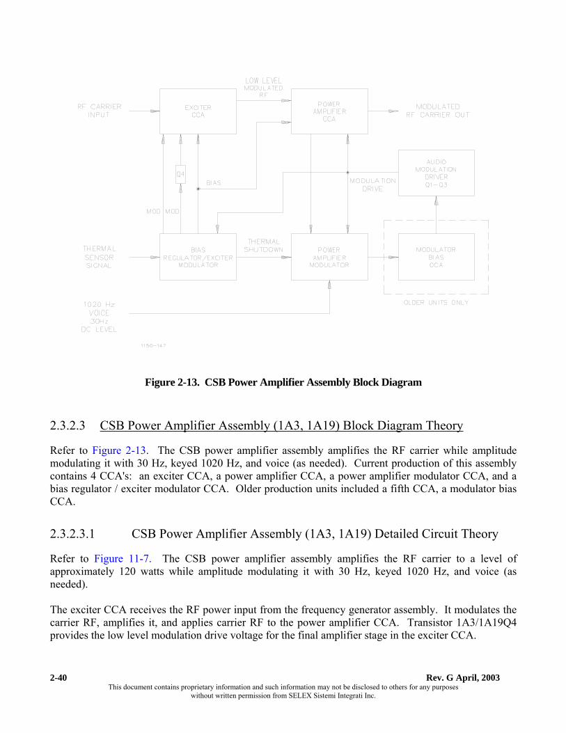
Rev. G April, 2003 This document contains proprietary information and such information may not be disclosed to others for any purposes
without written permission from SELEX Sistemi Integrati Inc.
2-40
Figure 2-13. CSB Power Amplifier Assembly Block Diagram
2.3.2.3 CSB Power Amplifier Assembly (1A3, 1A19) Block Diagram Theory
Refer to Figure 2-13. The CSB power amplifier assembly amplifies the RF carrier while amplitude modulating it with 30 Hz, keyed 1020 Hz, and voice (as needed). Current production of this assembly contains 4 CCA's: an exciter CCA, a power amplifier CCA, a power amplifier modulator CCA, and a bias regulator / exciter modulator CCA. Older production units included a fifth CCA, a modulator bias CCA.
2.3.2.3.1 CSB Power Amplifier Assembly (1A3, 1A19) Detailed Circuit Theory
Refer to Figure 11-7. The CSB power amplifier assembly amplifies the RF carrier to a level of approximately 120 watts while amplitude modulating it with 30 Hz, keyed 1020 Hz, and voice (as needed). The exciter CCA receives the RF power input from the frequency generator assembly. It modulates the carrier RF, amplifies it, and applies carrier RF to the power amplifier CCA. Transistor 1A3/1A19Q4 provides the low level modulation drive voltage for the final amplifier stage in the exciter CCA.
Model 1150 DVOR
Rev. G April, 2003 This document contains proprietary information and such information may not be disclosed to others for any purposes
without written permission from SELEX Sistemi Integrati Inc.
2-41
The power amplifier CCA takes the low level modulated RF signal from the exciter CCA, amplifies it, and applies it to a low-pass filter assembly. The bias regulator/exciter modulator CCA develops the bias voltage for the exciter CCA and power amplifier CCA. It also develops the carrier thermal shutdown command control signal, and the low level modulation drive signals for the exciter CCA. The power amplifier modulator CCA controls the RF modulation and power levels within the CSB power amplifier assembly. The power amplifier modulator CCA amplifies the audio signals which will modulate the RF signal and the DC level that will determine the final output power level. The power amplifier modulator CCA monitors the modulation signal level to the power amplifier CCA and the modulated RF signal from the power amplifier CCA. It also uses a thermal shutdown control signal from the bias regulator/exciter modulator CCA to control the RF signal. This prevents the final RF power amplifier transistors from being pulsed with modulation when the shutdown command clears. Power transistors 1A3/1A19Q1, Q2, Q3, Q4, Q5, and Q6 are thermally connected to the assembly chassis. The power amplifier assembly must dissipate a significant quantity of heat; therefore, a major portion of the assembly consists of heat sink material making the assembly very heavy. The modulator bias CCA develops a bias potential for the gates of final audio modulation driver transistors Q1, Q2, and Q3. Final audio modulation driver transistors 1A3/1A19Q1, Q2, and Q3 are a matched set. Failure of any one of these transistors requires the replacement of all three. The sources of these transistors are connected to the 43/48 volt power supply module of the BCPS and the amplified audio and DC modulation signal is applied to their gates. The audio modulation signal changes the conduction of these transistors and varies the amount of voltage available at their drains. The DC voltage establishes an average operating point which allows the RF amplifiers to produce a specific power level. This variable drain voltage is the operating voltage for the final RF power amplifier transistors 1A3/1A19Q5 and Q6. This varying voltage is high level modulation of the RF carrier signal in the power amplifier CCA.
2.3.2.3.2 Exciter CCA (A3) Block Diagram Theory
Refer to Figure 2-14. The Carrier RF signal from the frequency generator assembly and the exciter Q1 Bias In voltage from the bias regulator modulator CCA are applied to RF amplifier Q1. Q1 amplifies the carrier RF and modulates it with the exciter Q1 modulator signal. The modulated carrier RF from Q1 is applied to RF amplifier Q2. The bias voltage for Q2 (Exciter Q2 Bias In) is set on the bias regulator modulator CCA. The modulation drive voltage for Q2 is supplied by modulator driver transistor 1A3/1A19Q4, which is mounted on the CSB power amplifier chassis. Q2 amplifies the signal level to approximately 20 W at it's output. This signal is then applied to the Power Amplifier CCA

Rev. G April, 2003 This document contains proprietary information and such information may not be disclosed to others for any purposes
without written permission from SELEX Sistemi Integrati Inc.
2-42
2.3.2.3.3 Exciter CCA (A3) Detailed Theory
Refer to Figure 11-11. The exciter CCA contains two RF transistor amplifiers which produce approximately 20 watts of modulated RF power from an input of about 300 mW CW from the frequency generator assembly. The Carrier Rf In from the frequency generator assembly enters the CSB power amplifier assembly via RF connector J1. Input impedance matching circuitry consists of C17, C4 (which is factory adjusted for optimum input VSWR), L5, and L1. Resistor R1 applies the bias current to transistor Q1, and also provides some impedance matching of the input of Q1. Amplifier Q1 raises the input signal level to about 3 W carrier power at the output. The bias for transistor Q1 is supplied by the bias regulator modulator CCA as Exciter Q1 Bias In voltage. This is adjusted by resistor R19 on the bias regulator modulator CCA and applied via connector P1-2. Under quiescent conditions (no RF signal applied), potentiometer R19 is adjusted to produce a voltage drop of 25 mV across test points TP3 and TP4. This corresponds to a quiescent current of approximately 50 mA through Q1. The exciter Q1 modulator signal is the drain voltage supplied by the bias regulator modulator CCA. This voltage is a signal with a DC component corresponding to desired carrier power, with all of the AC VOR modulation removed by low pass filter components on the bias regulator modulator CCA. Interstage impedance matching is done by C6, C8 (again, factory adjusted for optimum modulator voltage and transmitter efficiency), L2, C9, and L3. The modulated RF is applied to the gate of transistor Q2, where it is amplified to approximately 20 watts. Resistor R5 supplies the bias current to transistor Q2, and provides some impedance matching for the input of Q2. Resistor R4 and capacitor C13 provide a low-frequency feedback path around Q2, which serves to enhance amplifier stability and increases amplifier bandwidth. Output matching is accomplished by L6, C18, L4, C14, and C15. C16 is a coupling capacitor to block the DC from the output path. The bias current transistor Q2 is supplied by the bias regulator modulator CCA. This signal is adjusted by R20 on the bias regulator modulator CCA, and is applied via connector P1-9 to the gate of Q2. Under quiescent conditions, the jumper between terminals E3 and E4 is removed. Potentiometer R20 on the bias regulator modulator CCA is adjusted to produce a voltage drop of 55 mV across test points TP1 and TP2. This corresponds to a bias current of approximately 25 mA through Q2. After the adjustment is made, the jumper is re-installed between terminals E3 and E4. Bias adjustments for Q2 are factory set, and field adjustment should not be attempted. Exciter Q2 Modulation Drive signal is the drain voltage supplied to transistor Q2. This signal is provided by modulator drive transistor 1A3/1A19Q4, mounted on the CSB amplifier chassis. This signal is routed through connector P1 pins 11,12,13 and 14. A sample of this signal is used for feedback control of the modulator, and is routed through P1-10. As in the Q1 modulator signal, this signal consists of a DC component and the AC VOR modulation waveforms. The approximately 20 W output is routed via E2 through a point-to-point coaxial cable to the power amplifier CCA.

Model 1150 DVOR
Rev. G April, 2003 This document contains proprietary information and such information may not be disclosed to others for any purposes
without written permission from SELEX Sistemi Integrati Inc.
2-43
Figure 2-14. Exciter CCA Block Diagram
2.3.2.3.4 Power Amplifier CCA (A2) Block Diagram Theory
Refer to Figure 2-15. The power amplifier CCA receives the approximately 20 W signal from the exciter CCA, and amplifies it to the proper level required for the DVOR system. The modulated RF from the exciter CCA is divided into two paths for amplification. Since the two paths are identical, only one will be discussed. The RF enters the assembly as is divided into two parallel paths. Attenuators AT1 and AT2 serve to balance any slight impedance differences between the two paths, and help the two power output devices to share the load equally. Transformer T3 is an iron core coaxial transformer with a 9:1 impedance ratio. It also serves to drive the dual transistor Q5 in a balanced push-pull configuration. Bias for Q5 is applied via the secondary winding of T3. The output of Q5 is applied to the 4:1 impedance ratio transformer T4, which also converts from a balanced to unbalanced signal. The modulation signal is applied via the low-impedance winding of T4 to the drains of Q5. The two outputs (T4 and T2) are connected in parallel, and impedance matched to the 50 ohm output by C29, L1, C10 and C11. A sample of the output signal is provided to the power amplifier modulator CCA for feedback control of the output signal waveform. Thermistor RT1 is mechanically connected to the heat sink of the power amplifier assembly, and is used for over-temperature protection of the amplifier assembly.

Rev. G April, 2003 This document contains proprietary information and such information may not be disclosed to others for any purposes
without written permission from SELEX Sistemi Integrati Inc.
2-44
2.3.2.3.5 Power Amplifier CCA (A2) Detailed Circuit Theory
Refer to Figures 11-9 and 11-10. The power amplifier CCA takes the modulated RF signal from the exciter CCA and amplifies it to the proper levels (typically 100 W) for DVOR system operation. Two output devices are used to provide the required power. The two are driven in phase, with simple parallel signal dividers / combiners. Attenuators AT1 and AT2 serve to balance out any small input impedance differences in the two output devices, insuring that both devices share equally in the output load. At this point the signal is split into two identical paths. Only one path will be discussed in detail. Transformer T3 is a 9:1 impedance ratio (3:1 turns ratio) coaxial transformer. (Older -0001 and -0002 power amplifier assemblies utilized a 4:1 impedance ratio transformer) The center conductor of the coax provides the 3 turns, while the outer conductors of the coax provide the 1 turn secondary. The secondary of the transformer is center tapped, and the center tap is RF grounded through capacitor C3. This arrangement causes the transformer to act as a balun transformer, converting the unbalanced input drive to a balanced, out of phase drive for the two gates in dual device Q5. Input bias voltage is applied through the secondary of T3 to the gates of Q5. Transistor Q5 is actually a matched pair of FET transistors in one package, designed to operate as a push-pull RF amplifier. Transistor Q5 is configured as a common source amplifier, operating in a push-pull configuration. Resistors R7 and R8, along with their leads (forming inductance) and capacitors C4 and C6, are used as low-frequency negative feedback around the device. This feedback serves to enhance amplifier stability and greatly broadens the amplifier bandwidth. The amplifier stage provides approximately 7 dB of gain, raising the 10 W input power (½ of the 20 W nominal input to the CCA) to typically 50 W of output power. The modulation drive voltage for Q5 is the Modulator In 48V signal. This signal is provided by transistors 1A3/1A19 Q1, Q2, and Q3, which are mounted on the power amplifier assembly heatsink. The modulation voltage is applied to the center tap of the primary of output transformer T4. Bias for Q5 is controlled by the bias regulator modulator CCA. Two types of bias operation have been used in the history of the power amplifier assembly. In the older -0001 and old version -0002 power amplifiers, potentiometer R21 on the bias regulator modulator CCA is adjusted to produce a voltage drop of 0.01 VDC across TP1 and TP2 for Q5 (TP3 and TP4 for Q6) with 24 volts DC applied to the Modulator In signal point, with no RF signal applied to the power amplifier assembly. This corresponds to a quiescent current of approximately 450 mA for Q5. In the newer -0002 and -0003 power amplifier assemblies, the bias point on the output devices has been changed to a smaller level than the older amplifiers. This provides increased efficiency and reduced heat in the power amplifier assembly. The bias control potentiometers are adjusted for 0.005 +/- .0005 volts across TP1 and TP2 for Q5, and across TP3 and TP4 for Q6 under quiescent operating conditions (no RF applied, approximately 15 VDC on the Modulator In signal point). Do not be tempted to adjust older -0001 and -0002 units to this point, as it will not provide proper operation. Older -0002 assemblies can be recognized by 4:1 impedance transformers on the input matching, rather than the 9:1 units used in current production. The 4:1 transformers are made up of two pieces of rigid coax, while the 9:1 transformers are three layers of coax inside the iron cores.

Model 1150 DVOR
Rev. G April, 2003 This document contains proprietary information and such information may not be disclosed to others for any purposes
without written permission from SELEX Sistemi Integrati Inc.
2-45
CAUTION
Potentiometers R21 and R22 on the bias regulator modulator CCA are factory set. Do not attempt to adjust these resistors in the field. Incorrect bias levels can destroy the final RF power amplifier transistors.
Figure 2-15. Power Amplifier CCA Block Diagram
Output transformer T4 has a primary to secondary impedance ratio of 1:4. This is used to match the output impedance of the transistor Q5 to the junction point impedance where the output of Q5 is added to the output of Q6. This junction point is then matched to the 50 ohm output impedance of the power amplifier assembly by capacitors C28, C29, C10 and C11, and inductor L1. Capacitor C11 is factory adjusted for optimum performance of the power amplifier CCA. The capacitive voltage divider formed by C12 and C9 is used to provide a sample of the RF output signal to the power amplifier modulator CCA, where it is detected and used to provide feedback control of the modulator voltage.

Rev. G April, 2003 This document contains proprietary information and such information may not be disclosed to others for any purposes
without written permission from SELEX Sistemi Integrati Inc.
2-46
Thermistor RT1 is thermally connected through it's mounting to the amplifier heatsink. It has a value of approximately 10 K ohms at 25 degrees C (amplifier cold, room temperature). As the temperature of the heat sink rises, the resistance of RT1 reduces. RT1 is wired as part of a resistive voltage divider, hence the voltage at the thermal output signal reduces as the amplifier temperature increases. This signal is used by the bias regulator modulator CCA to shut down the power amplifier in the event of excessive heat sink temperature. This voltage is also used to provide some feedback for the bias voltage generation circuitry, reducing bias currents as the heatsink temperature increases.
2.3.2.3.6 Bias Regulator/Exciter Modulator CCA (A4) Block Diagram Theory
Refer to Figure 2-16. The final amplifier modulation in signal from 1A3/1A19 Q1, Q2, and Q3 is used as input to the exciter modulator CCA. The AC component of the final modulation in signal is removed by R16 and C11 and the resultant DC level (representative of the carrier power in the output signal) is applied to one input of a differential amplifier made up of transistor pair Q1 and Q2. The output of the differential amplifier is further amplified by Q5. The output of Q5 is used as the modulator voltage for the exciter CCA transistor 1A3/1A19 A3Q1. The output of Q5 is also applied to the other input of the differential amplifier, where it is used as feedback control of the modulator output. The final amplifier modulation in signal is also applied to differential amplifier pair Q3 and Q4. The output of this differential amplifier is applied to transistor 1A3/1A19 Q4, mounted on the power amplifier heatsink. The output of 1A3/1A19 Q4 is the modulator drive voltage for Q2 on the exciter CCA. The output of 1A3/1A19 Q4 is applied to the other input of the differential amplifier Q3/Q4 as feedback to control the modulator voltage. The reflected power analog in signal from the RF monitor assembly is applied to amplifier U1. The output of U1 is applied to comparator U3B through a fast attack, slow decay circuit. U3B compares the voltage output of U1to a 1.63 volt reference. If the voltage exceeds this reference, the output of U3B goes low, causing a reflected power shutdown. The thermal sensor input is applied to voltage regulator U2. U2 generates the bias voltages for all of the RF power transistors in the power amplifier assembly. As the temperature of the power amplifier heatsink increases, the voltage at the thermal sensor input decreases. This causes a reduction in the bias voltage applied to the RF power transistors. The thermal input sensor signal is also applied to comparator U3A, where it is compared to a 1.2 volt reference signal. If the thermal sensor input voltage goes below 1.2 volts, indicating excessive heatsink temperature, comparator U3A output switches low, which causes a carrier thermal shutdown output. Transistor Q6 is used to logically "OR" the outputs of the thermal shutdown detector circuit and the reflected power shutdown detector circuit. If either of these detectors switches low, the collector of Q6 is pulled to +5 volts. The collector of Q6 is the Shutdown Control Command output from the bias regulator modulator CCA. This output is applied to the sideband generators and the audio generator CCA in the DVOR to shut them down at the time of power amplifier shutdown.

Model 1150 DVOR
Rev. G April, 2003 This document contains proprietary information and such information may not be disclosed to others for any purposes
without written permission from SELEX Sistemi Integrati Inc.
2-47
Figure 2-16. Bias Regulator/Exciter Modulator CCA Block Diagram
2.3.2.3.7 Bias Regulator/Exciter Modulator CCA (A4) Detailed Circuit Theory
Refer to Figure 11-11. The bias regulator / exciter modulator CCA is used to develop several control signals for the power amplifier assembly.
Rev. G April, 2003 This document contains proprietary information and such information may not be disclosed to others for any purposes
without written permission from SELEX Sistemi Integrati Inc.
2-48
The output voltage from transistors 1A3/1A19 Q1, Q2, and Q3 (the final amplifier modulator transistors, mounted on the CSB amplifier chassis) is applied to the bias regulator modulator CCA as the controlling modulation input. The modulation input is low pass filtered by R16 and C11, effectively removing the AC component of the final modulation, leaving a DC level that varies depending on power output. This signal is applied to the base of Q1, one input of the differential amplifier formed by Q1 and Q2. The output of Q1 is further amplified by Q5. The output of Q5 is the modulation drive signal for the first RF amplifier transistor on the exciter CCA. The output of Q5 is also used as feedback to the second input of the Q1/Q2 differential amplifier to control the output voltage. The unfiltered modulation input is applied to the input of a second differential amplifier transistor pair, Q3/Q4. The output of Q3 is routed off the board through J1-21 to drive transistor 1A3/1A19 Q4, mounted on the amplifier heatsink. The output of this transistor is the modulation drive signal for the second RF amplifier on the exciter CCA, 1A3/1A19A3Q2. Feedback from the output of 1A3/1A19 Q4 is applied to the second input of the differential amplifier at the base of Q4 to control the operation of this amplifier. The reflected power analog in signal (from the RF monitor assembly) represents the CSB reflected power. Amplifier U1 is a unit gain non-inverting amplifier that serves to buffer the incoming signal. The output of U1 is applied to a fast attack, slow decay circuit made up of CR5, C10, C8, and R35. This circuit forms a peak reflected power detector. The output of the peak detector is applied to the inverting input of voltage comparator U3B, where it is compared to a 1 volt reference. If the reflected power exceeds a safe limit, the output of U3B switches low, activating the reflected power shutdown output. The thermal sensor mounted on the amplifier heatsink at the final amplifier CCA. This thermistor has a 10K ohm nominal impedance at 25 degrees C. It is connected with R30, R29, and R28 to control the output of voltage regulator U2. As the temperature of the heatsink rises, the resistance of the thermistor on the power amplifier decreases, decreasing the output voltage of U2. The voltage at the thermal sensor input is also applied to voltage comparator U3A at the non-inverting input, where it is compared to a 1.2 volt reference. If the thermal sensor voltage goes below 1.2 volts, the output of U3A goes low, activating the carrier thermal shutdown output. Both the carrier thermal shutdown output and the reflected power shutdown output are tied to the base of transistor Q6 via R39 and R40, respectively. If either output goes low, transistor Q6 is turned on, pulling the shutdown control command output to +5 volts. Voltage regulator U2 provides a regulated output voltage of approximately +7 volts maximum. This voltage is used to produce the bias control voltages for the 4 RF power amplifier transistors in the amplifier assembly. As mentioned earlier, the output of this regulator is controlled by the thermal sensor input. The regulator has a sense voltage input which controls the output level. This sense voltage input is driven by a voltage divider made up of R30, R29, R28, and the thermistor RT1 mounted on the final amplifier CCA. As the temperature of the amplifier heatsink increases, causing a decrease in the resistance of RT1, the voltage applied to the non-inverting reference control input (pin 5) decreases, causing a decrease in the output voltage of U2. This reduction in output voltage as temperature increases causes a reduction in the bias current of the RF amplifier transistors, protecting them from thermal runaway.

Model 1150 DVOR
Rev. G April, 2003 This document contains proprietary information and such information may not be disclosed to others for any purposes
without written permission from SELEX Sistemi Integrati Inc.
2-49
Potentiometers R19, R20, R21, and R22 are used to adjust the bias currents of the RF amplifiers as discussed in the exciter CCA and the final amplifier CCA sections of this text. These adjustments are factory set, and should not be attempted in the field, as serious damage to the RF transistors may result.
2.3.2.3.8 Power Amplifier Modulator CCA (A1) Block Diagram Theory
Refer to Figure 2-17. The power amplifier modulator compares the detected output signal of the CSB amplifier assembly to the reference audio input, and adjusts the final amplifier modulation drive to control the output waveforms of the CSB amplifier. A sample of the CSB RF signal (from the final amplifier CCA) is envelope detected by diode CR1. This detected signal is passed through a buffer amplifier, U1A. The output of U1A is compared to the audio input signal by error amplifier U2. U2 drives transistor Q1, which provides the gate drive for final amplifier modulator transistors 1A3/1A19 Q1, Q2, and Q3, mounted on the amplifier heatsink. The output of transistors 1A3/1A19 Q1, Q2, and Q3 is also routed back to the power amplifier modulator CCA as the Sample Modulation signal. With the jumpers configured in the test mode, this signal rather than the detected RF signal is used to control the modulator feedback loop. This mode is used in the factory to allow testing and alignment of the RF amplifier stages. In addition, there is an over voltage protection circuit, U1B, that will reduce the final modulation voltage if it starts to get excessive. This would typically happen upon failure of one or more of the RF devices in the CSB amplifier assembly. One additional control input, the Shutdown Control In, (from the bias regulator modulator CCA) is applied to the inverting input of the error amplifier U2. When activated, this input is pulled up to +5 VDC on the bias regulator modulator CCA. This 5 volt signal applied to the inverting input of U2 causes it to shut down it's output, disabling the modulation to the final amplifier stages.
Figure 2-17. Power Amplifier Modulator CCA Block Diagram

Rev. G April, 2003 This document contains proprietary information and such information may not be disclosed to others for any purposes
without written permission from SELEX Sistemi Integrati Inc.
2-50
2.3.2.3.9 Power Amplifier Modulator CCA (A1) Detailed Circuit Theory
Refer to Figure 11-8. The power amplifier modulator CCA is the feedback control amplifier that compares the detected RF output of the power amplifier assembly to the reference audio input signal. It modifies the power amplifier modulation drive signal to control the RF output of the amplifier assembly. The shutdown control in signal from the bias regulator modulator CCA causes the power amplifier modulator CCA to turn off the modulation voltage to the RF amplifier stages. A sample of the output RF signal comes to the power amplifier modulator CCA from the final amplifier CCA. It is envelope detected by diode CR1. Diode CR1 is biased into it's linear detection range by diode CR2. Diodes CR1 and CR2 are a matched pair, and must be replaced as a set if one fails. The output of detector CR1 is filtered by L2 and C3, and applied to the non inverting input of unity gain buffer U1A. The output of U1A is an analog voltage representative of the RF output waveform. Amplifier U2 is the feedback error voltage amplifier that controls the modulation loop. The reference audio input from the audio generator card in the VOR system is applied to the non-inverting input, and the feedback control voltage is applied to the inverting input. A difference in these two signals creates an output voltage from U2, which drives the modulation transistors for the final amplifier. The feedback control voltage can come from one of two locations. During normal system operation, terminal E1 is jumpered to terminal E2, and the detected RF level discussed in the preceding paragraph is used. There is a test mode of operation available in addition to this. If terminal E3 is jumpered to terminal E2, a sample of the modulator output voltage is used as the feedback control voltage. This mode is used in the factory for test and alignment of the RF stages of the CSB amplifier assembly. The test mode should not be used for normal operation, as slight amplifier non-linearities or other such distortion are not corrected by the modulation control loop. The sample modulator output voltage is also compared to a reference level by U1B. In the event that modulator voltage is excessive, this amplifier will apply a positive voltage to the inverting input of loop control amplifier U2, causing it to shut down or clamp it's output drive signal. This would normally only happen in an event like RF transistor failure, where the modulator is greatly increasing the output voltage trying to make up for the failure. This feature protects the rest of the RF transistors in the event of a failure of this nature. The output of amplifier U2 is further amplified by transistor Q1, which provides the gate drive for the final amplifier modulator transistors 1A3/1A19 Q1, Q2, and Q3 which are mounted on the amplifier heatsink. Resistor R17 and capacitor C8 are used to tailor the closed loop response of the feedback system, providing proper stable operation of the loop. Transistor Q1 has no on-board pull up network, and as such is configured as a current sink only.

Model 1150 DVOR
Rev. G April, 2003 This document contains proprietary information and such information may not be disclosed to others for any purposes
without written permission from SELEX Sistemi Integrati Inc.
2-51
2.3.2.3.10 Modulator Bias CCA (A5) Block Diagram Theory
Refer to Figure 2-18. This CCA is only used in the -0001 power amplifier assemblies, and older -0002 units. The output transistor on the final amplifier modulator is configured as a current sink device only (please refer to Figure 11-8, and the final amplifier modulator theory of operation). The modulator bias CCA serves to actively pull up the gates of the final amplifier modulation transistors, 1A3/1A19 Q1, Q2, and Q3. The gates of these transistors are essentially large capacitors, and the active pull up was intended to speed up the charging of these capacitors. Current versions of the CSB amplifier assembly do not use this CCA, but instead use a power resistor to pull up the gates of the final modulation transistors. In CVOR applications, the 9960 Hz modulation was being slightly distorted by the inherent time delays associated with Q1 on the modulator bias CCA, and changing to the resistor on new production units was done to eliminate this distortion. All warranty repair work being done on CSB amplifier assemblies includes retrofitting the amplifier to remove the modulator bias CCA and replace with 1A3/1A19 R12 as shown on the power amplifier interconnect diagram, Figure 11-7. All non-warranty repairs should consider returning the amplifier to the factory for updating to the latest configuration.
Figure 2-18. Modulator Bias CCA Block Diagram

Rev. G April, 2003 This document contains proprietary information and such information may not be disclosed to others for any purposes
without written permission from SELEX Sistemi Integrati Inc.
2-52
2.3.2.3.11 Modulator Bias CCA (A5) Detailed Circuit Theory
Refer to Figure 11-7 (CSB Power Amplifier Interconnect Diagram). The modulator bias CCA develops a bias potential for the gates of power transistors 1A3/1A19Q1, Q2, and Q3. Transistor Q1 is a small signal transistor with 43/48 Vdc applied directly to the collector from terminal E4. The emitter of Q1 is connected to terminals E2 and E3. Transistor Q1 is self- biased by resistor R2 and diode CR2 which allows a fixed DC voltage to be applied to the gates of modulation drivers 1A3/1A19Q1, Q2 and Q3. This fixed bias is developed across resistor R1 and diode CR1 and the output circuitry of Q1 on the power amplifier modulator CCA. Diodes CR1 and CR2 are fast recovery diodes that are used to protect the base-emitter junction of Q1 and to provide rapid restoration of the static condition of Q1.
Figure 2-19. Low Pass Filter Assemblly Block Diagram
Transistors 1A3/1A19Q1,Q2 andQ3 are MOSFET transistors wired in parallel with current balancing resistors in series with each gate. This means the capacitance of each gate is additive; therefore, the effective gate capacitance of the three devices is comparatively large. This large capacitance has the ability to store a charge and resist a change in voltage. In order to prevent any distortion of the audio modulation signal, this charge must be quickly drained off from the gates. The biasing of Q1 insures that as the changing audio modulation signal which comes in at terminal E1 is applied to the gates, the cumulative charges on each of the gates is effectively drained. The circuitry for Q1 also provides the drain current path for Q1 on the power amplifier modulator CCA. The gates of the modulation drivers are essentially driven by the varying drain potential of Q1 on the power amplifier modulator CCA.
2.3.2.4 Low Pass Filter Assembly (1A35, 1A36) Block Diagram
Refer to Figure 2-19. The low pass filter assembly consists of a four pole filter network that removes harmonics from the carrier RF signal.

Model 1150 DVOR
Rev. G April, 2003 This document contains proprietary information and such information may not be disclosed to others for any purposes
without written permission from SELEX Sistemi Integrati Inc.
2-53
RF carrier signal enters the low pass filter assembly via RF connector J1. The RF carrier signal is applied to a four pole filter network that removes harmonic frequencies of the carrier RF signal that may be present. The RF signal exits the low pass filter via RF connector J2. The low pass filter assembly has a pickup loop that induces a small RF voltage into the loop. This RF signal is the carrier feedback and is applied to the frequency generator assembly via connector J3. A sample of the RF output signal is developed by a voltage divider network. This signal is applied to the RF monitor assembly as the system A (or B) RF sample via connector J4.
2.3.2.4.1 Low Pass Filter Assembly (1A35, 1A36) Detailed Theory
Refer to Figure 11-28. The low pass filter assembly consists of a four pole filter network that removes harmonic frequencies from the carrier RF signal. The RF carrier signal from the CSB power amplifier assembly enters the low pass filter assembly via RF connector J1. The RF carrier signal is applied to a four pole filter network that removes any harmonic energy above 250 MHZ that may be present in the carrier signal. The RF signal exits the low pass filter via RF connector J2. The low pass filter assembly has a pickup loop situated in close proximity to the primary conductor of the main RF carrier signal. The RF signal induces a small RF current into the loop which is developed across R1, a 50 ohm resistor, for impedance matching. This RF signal is applied to the frequency generator assembly as the carrier feedback signal via connector J3. A sample of the RF output signal, for test purposes, is developed by a voltage divider network comprised of capacitor C9 and resistor R2. R2 is a 50 ohm resistor for impedance matching the signal developed across it to the coaxial cable. This signal will be approximately 100 to 300 mW for a 100 watt RF carrier power output. This RF signal is applied to the RF monitor assembly as the system A (or B) carrier sample via connector J4.
2.3.2.5 Bi-Directional Couplers (1DC1, 1DC2)
The bi-directional coupler is used to obtain a representative sample of the forward and reflected RF powers of the carrier signal (refer to Figure 11-1 or 11-2, DVOR system block diagram). The coupler has negligible insertion loss between the input and output connectors. Internal directional pickup loops couple a portion of the forward and reflected powers to the output sampling ports. These ports provide a fixed ratio of the sampled powers to the RF monitor assembly for detection and analysis processing.
2.3.2.6 Sideband Generator Assembly (1A5, 1A6, 1A21, 1A22) Block Diagram Theory
Refer to Figure 2-20. The DVOR uses two sideband generator assemblies for each transmitter system. Each generator contains two sideband amplifier CCAs and two sideband controller CCAs. One generator processes the lower sideband RF and the other processes the upper sideband RF.

Rev. G April, 2003 This document contains proprietary information and such information may not be disclosed to others for any purposes
without written permission from SELEX Sistemi Integrati Inc.
2-54
The sideband controller CCA is responsible for developing the sideband dynamic phase control voltage, modulator drive signal, the sideband manual phase control voltage, and the sideband mean phase control voltage. The sideband dynamic phase control voltage is applied to the sideband dynamic phase control filter on the sideband amplifier CCA where it is used to set the operating point of the dynamic phase control filter. The modulator drive signal is used as a supply voltage for transistor Q105/205 on the sideband amplifier CCA The sideband manual phase control voltage is used on the sideband amplifier CCA to set the operating point for the sideband manual phase control filter. The sideband mean phase control voltage is applied to the sideband mean phase control filter on the sideband amplifier CCA where it is used to set the operating point of the sideband mean phase control filter. The sideband amplifier CCA is responsible for producing the amplified sideband RF signal. It also produces and amplitude product detector error signal, a phase product detector error signal and a forward power detected level signal. The amplitude product detector error signal is processed by the sideband controller CCA as a feedback signal to compensate for gradual amplitude changes in the modulation level of the sideband modulating signal. The phase product detector error signal is processed by the sideband controller CCA as a feedback signal for the sideband mean and dynamic phase control circuits. The forward power detector level signal is sent to the sideband controller CCA where it is sampled, buffered, and then applied to the audio generator CCA to control the sideband power level and the monitor CCA for VSWR calculations.
2.3.2.6.1 Sideband Generator Assembly (1A5, 1A6, 1A21, 1A22) Detailed Circuit Theory
Refer to Figure 2-21. Since all sideband amplifier CCAs and sideband controller CCAs are functionally identical, the analysis will be limited to one sideband amplifier group which consists of one sideband amplifier CCA and one sideband controller CCA. When a sideband generator assembly is placed into the 1A5 or 1A21 position, it processes the signals for sideband amplifier 1 and sideband amplifier 2. When a sideband generator is placed into the 1A6 or 1A22 position, it processes the signals for sideband amplifier 3 and sideband amplifier 4.

Model 1150 DVOR
Rev. G April, 2003 This document contains proprietary information and such information may not be disclosed to others for any purposes
without written permission from SELEX Sistemi Integrati Inc.
2-55
NOTE
It is important to remember which sideband generator assembly and which sideband amplifier number you are adjusting. Because of the interaction of these amplifiers with each other, care must be exercised when making any adjustments. SB1 processes the LSB RF signal modulated by the 360 Hz sin frequency. SB2 processes the LSB RF signal modulated by the 360 Hz cos frequency. SB3 processes the USB RF signal modulated by the 360 Hz sin frequency. SB4 processes the USB RF signal modulated by the 360 Hz cos frequency. The USB/LSB RF signals are supplied by the frequency synthesizer assembly. The sideband RF signal enters the sideband generator assembly through RF connector J1 located on the rear plate which interconnects with terminal E45 on the A4 sideband amplifier CCA. The 0 dBm RF input signal (minimum -1.0 dBm) is divided equally between the two amplifier groups within the sideband generator assembly. The electrical distance that the RF signal travels from terminal E46 to terminal E47 on the A4 sideband amplifier CCA and from terminal E46 on the A4 sideband amplifier CCA to terminal E47 on the A2 sideband amplifier CCA is held to very close tolerances. Significant differences in the electrical distance traveled by the RF signals on these two paths may cause significant phase errors between the sideband RF output signals.

Rev. G April, 2003 This document contains proprietary information and such information may not be disclosed to others for any purposes
without written permission from SELEX Sistemi Integrati Inc.
2-56
Figure 2-20. Sideband Generator Assemblly, Block Diagram
Each sideband generator assembly has an associated voltage regulator working in conjunction with it. The voltage regulators for sideband generator assemblies 1A5 and 1A6 are located on the cabinet insert assembly behind each sideband generator assembly. They are 1VR1 for the 1A5 module and 1VR3 for the 1A6 module. The voltage regulators for sideband generators 1A21 and 1A22 are located on the cabinet insert assembly behind each sideband generator assembly. They are 1VR2 for the 1A21 module and 1VR4 for the 1A22 module. These independent regulators convert the +28 Vdc to an isolated +12 Vdc power source for each sideband generator assembly. This isolation prevents modulation currents from appearing on the main power supply lines and possibly affecting the other sideband signals.
Model 1150 DVOR
Rev. G April, 2003 This document contains proprietary information and such information may not be disclosed to others for any purposes
without written permission from SELEX Sistemi Integrati Inc.
2-57
The sideband amplifier CCA uses feed-thru capacitors which are interconnected by bus wire to terminals on the sideband controller CCA. The sideband controller CCA has the primary multi-pin connector that interconnects with the cabinet wiring harness. RF connections are made to the sideband amplifier CCA. There is no interconnection between SB1 and SB2 other than the internal RF cable between terminal A4E46 and A2E47. Each sideband amplifier group (SB1, SB2, SB3, or SB4) has several components mounted to the assembly that are reference designated with hundred series numbers. Specifically, one hundred series numbers are used with SB1 or SB3 and two hundred series numbers are used with SB2 or SB4. Additionally, the functional equality of the sideband amplifiers requires duplicity with the test points. The mirror-image construction of the sideband generator requires each test point to have a different reference designator; although, like-function test points will be identified as paired numbers. For example, the sideband manual phase control voltage can be measured at test points TP2/TP9. TP2 is the test point for SB1 or SB3; TP9 is the test point for SB2 or SB4.
2.3.2.6.2 Sideband Amplifier CCA (A2, A4) Block Diagram Theory
Refer to Figure 2-22. The sideband RF signal is amplified by RF amplifier Q1 before it is phase shifted by the sideband manual phase control network which consists of CR1, CR2, L2 and L3. A sideband manual phase control voltage from the sideband controller CCA sets the operating point of the manual phase control network. RF amplifier U1 amplifies the RF signal so that it can be divided between the product detector circuits and RF amplifier Q2. Q2 amplifies the phase shifted sideband RF and applies it to a bi-phase modulator circuit which consists of diodes CR3, CR4, CR5, CR6, and power divider HY1. The bi-phase modulator passes the RF signal to RF amplifier U2.

Rev. G April, 2003 This document contains proprietary information and such information may not be disclosed to others for any purposes
without written permission from SELEX Sistemi Integrati Inc.
2-58
Figure 2-21. Sideband Generator Assembly Interconnect Diagram

Model 1150 DVOR
Rev. G April, 2003 This document contains proprietary information and such information may not be disclosed to others for any purposes
without written permission from SELEX Sistemi Integrati Inc.
2-59
U2 amplifies the RF signal from the bi-phase modulator and applies it to the sideband mean phase control filter. The sideband mean phase control filter is an electronic filter which establishes an average phase shift of the sideband RF signal. The sideband mean phase control voltage is a DC voltage that establishes the operating point of the sideband mean phase control filter. The RF signal is next applied to the sideband dynamic phase control filter. This filter constantly adjusts the instantaneous phase of the sideband RF to eliminate any incidental phase distortion created by amplitude modulation of the sideband RF. The dynamic phase control voltage is a DC voltage that continually adjusts the operating point for this filter. RF amplifier U3 amplifies the sideband RF from the dynamic phase control filter and applies it to RF power amplifier transistor Q103/Q203. Q103/203 amplifies the sideband RF signal and applies it to RF amplifier modulator Q105/Q205. The supply voltage for Q105/Q205 is the modulator output signal that is supplied by the sideband controller CCA. The output of Q105/205 drives a low pass filter network which consists of capacitor C57 thru C58, C61 thru C64, and inductors L22 thru L26. This filter is designed to remove any high order harmonics from the sideband RF signal. From the low pass filter, the modulated sideband RF is sent to three separate circuits: an envelope detector network; phase product detector circuits, and to the RF output connector on the rear plate of the sideband generator assembly as the sideband RF output signal. The portion of the sideband RF that is applied to the envelope detector is converted back into the analog modulation signal which is buffered by U6A. This detected signal is sent to the sideband controller CCA as the forward power detector signal which is processed by the sideband controller CCA to compensate for gradual amplitude changes in the modulation level of the sideband modulation drive signal. The sample portion of the modulated sideband RF signal is used as a comparator signal for the phase detector. The modulated sideband RF output signal is applied to power splitter HY7 where it is divided into equal components with 0 phase shift. The two equal components are then used as the variable inputs for the phase product detector circuit which consists of HY2, HY5, and U4. The reference input signal which is obtained from the output of U1, is applied to 90 power splitter HY3. One output of HY3 is shifted 90 with respect to the other output signal. The two components are then used as the reference inputs for the phase product detector circuit and a termination resistor. The output of the phase product detector is the phase product detector error signal which is processed by the sideband controller CCA to develop the dynamic and mean phase control DC voltages which will automatically adjust the dynamic and mean phase control filters.

Rev. G April, 2003 This document contains proprietary information and such information may not be disclosed to others for any purposes
without written permission from SELEX Sistemi Integrati Inc.
2-60
DYNAMICPHASE
CONTROL
MANUALPHASE
CONTROLFILTERCR1,CR2
RF IN
RFAMPLQ2
BIPHASEMODULATORCR3,4,5,6
HY1
U2AMPLRF
RF AMPLU3 Q103/Q203
AMPLRF
DRIVE INMODULATOR
L22-L26FILTER
LOW PASS
HY7SPLITTERPOWER
ENVELOPEDETECTORNETWORK U6A
BUFFER FORWARD POWERDETECTOR LEVEL
OUTDETECTORPRODUCTPHASE
PHASEPRODUCTDETECTORHY2,HY5,U4
POWERSPLITTER
HY3
REFERENCE SIGNAL
SB MEANPHASECONTROLVOLT IN
DYNAMICPHASECONTROLVOLT IN
RF OUTPUTCONNECTOR
REFERENCE SIGNAL
00
90 0
BIASR34
PHASE CONTROL INSB MANUAL
L2,L3
CONTROLFILTERL7-L15CR7-CR15
MEAN PHASE
L16,L18FILTER
RFMODULATORQ105/Q205
C57-C64
MODULATEDSIDEBAND
CR16,CR17
C109J2 OR J3
MODIFIEDBIPHASE DRIVE
U1AMPLRFRF
AMPLQ1
1150-144
Figure 2-22. Sideband Amplifier CCA Block Diagram

Model 1150 DVOR
Rev. G April, 2003 This document contains proprietary information and such information may not be disclosed to others for any purposes
without written permission from SELEX Sistemi Integrati Inc.
2-61
2.3.2.6.3 Sideband Amplifier CCA (A2, A4) Detailed Circuit Theory
Refer to Figure 11-16. The sideband amplifier CCA amplifies the sideband RF signal from the frequency generator assembly to the operational output power level required. This CCA also produces amplitude and phase error signals to control modulation and reduce distortion of the sideband RF signal. The sideband amplifier CCA has a -3.0 dBm sideband RF signal present at solder pad terminal E47. From terminal E47 the sideband RF is applied to transistor Q1. Q1 amplifies the sideband RF and applies it to the sideband manual phase control filter. The sideband manual phase control filter is a two pole electronic filter which is similar in operation to the carrier phase control filters. The control voltage that sets the operating point of this filter is obtained from the sideband controller CCA via feed-thru capacitor C16. The amount of phase shift that the sideband RF energy undergoes is determined by an entry that is programmed through the PMDT. For sideband amplifier 1, a numeric value, in degrees, that is programmed into Transmitter 1 offsets and scale factors screen will change the DC voltage that is applied to the manual phase control filter on the A2 sideband amplifier CCA in the 1A5 sideband generator assembly. A numeric value representing the station frequency that is programmed into RMS station configuration screen will change the DC voltage that is applied to the manual phase control filters on the A4 sideband amplifier CCA's in both the 1A5 and 1A6 sideband generator assemblies. SB2 and SB4 manual phase control voltage inputs are interconnected through the cabinet wiring harness. From the sideband manual phase control filter the sideband RF signal is applied to RF amplifier U1. U1 has a fixed power gain of 12 dB. The output of U1 is approximately +7 dBm. The signal is then divided with approximately +1 dBm used as a reference signal for the phase and amplitude product detector circuits and the remainder being sent to RF amplifier Q2. Q2 amplifies the sideband RF before applying it to the input terminal of power divider HY1. There are two outputs from HY1 with 180 phase difference between the outputs. The sideband RF signals from the outputs of HY1 are applied to steering diodes CR3 thru CR6. The bi-phase drive signal is applied to terminal E32. In DVOR systems this bi-phase drive signal is a constant +11 Vdc or a constant -11 Vdc, depending on the position of the jumper placed between terminals E6 thru E8 on the sideband controller CCA. This constant voltage level is applied to steering diodes CR3 thru CR6. Only one pair of diodes will be forward biased by the bi-phase drive signal which will allow only the 0º or 180º phase shifted sideband RF signal to reach the input of RF amplifier U2. RF amplifier U2 is a fixed gain block amplifier with a power gain of +12 dB. The amplified RF from U2 is applied to the sideband mean phase control electronic filter. This is a nine pole filter network that functions identically as the carrier mean phase control filter. The DC control voltage for this filter is obtained from the sideband controller CCA via feed-thru capacitor C40. This filter establishes an average shift in phase of the sideband RF energy.

Rev. G April, 2003 This document contains proprietary information and such information may not be disclosed to others for any purposes
without written permission from SELEX Sistemi Integrati Inc.
2-62
WARNING
Do not attempt to field tune the mean Q control filter inductors.
The sideband mean phase control circuit on the sideband controller CCA monitors any average phase change incurred by the sideband RF signal after initial setup. If a phase change is detected, a correction voltage, which is the sideband mean phase control voltage, is sent to the sideband mean phase control filter to offset the detected phase shift and maintain a phase stable RF output signal. Because the filter is part of a null- seeking loop, there must always be an initial control voltage applied to the filter for proper operation. By maintaining the phase shift of the sideband RF signal to a relatively constant value with respect to the other sidebands, a significant reduction in phase offset drift between the sidebands is achieved. This improves the accuracy of azimuth generation. The output of the mean phase control filter drives the input of the sideband dynamic phase control filter. The input DC voltage to this filter is constantly adjusting the instantaneous phase of the sideband RF signal to eliminate any incidental phase modulation created by amplitude modulation of the sideband RF signal. The DC voltage that controls the dynamic phase control filter is obtained from the sideband controller CCA via feed-thru capacitor C45. RF amplifier U3 is a fixed gain block amplifier with a power gain of +8 dB. The output of this amplifier drives the base of transistor Q103/Q203. Capacitor C110 in conjunction with L27 form a "L" network to match the input impedance of Q103/Q203 to the output impedance of U3 which is approximately 50 Ohms. Q103/Q203 is a Class C medium power amplifier which drives the modulated output stage, Q105/Q205. L20, C53, and L21 form a "T" network to match the high output impedance of Q103/Q203 to the low impedance input of the power FET, Q105/Q205. A quiescent DC bias is applied to the output stage to set the DC current with no RF drive to 25 mA. R34 is used to set the bias. The DC drain current of the output stage may be read by removing jumper W1 between TP3 and TP4 or alternatively the drop across the 0.2 Ohm resistor R79 may be read with a voltmeter at TP4 and TP5 and the current calculated. The output stage Q105/Q205 is matched to approximately 50 Ohms by the network consisting of L31, L22, C57, C58, and L23. Jumper W18 may be removed to enable test of the amplifier or the output low pass filter. If power is applied to the stage there is a DC voltage at W18 so a blocking capacitor (1000 pF) should be provided to prevent any connected test equipment from shorting out the DC voltage. Modulation is applied to the DC drain voltage supply which enters the CCA via feed through capacitor C95. The RF output from the Q105/Q205 matching network is routed to a low pass filter, C61, L24, C62, L25, C63, L26, and C64, which removes the undesired harmonics from the amplifier output. From the low pass filter network, the modulated signal is sent to three places

Model 1150 DVOR
Rev. G April, 2003 This document contains proprietary information and such information may not be disclosed to others for any purposes
without written permission from SELEX Sistemi Integrati Inc.
2-63
• The RF output connector • The phase product detectors • An envelope detector circuit
The main portion of the sideband amplifier output is nominally 2.2 watts and this signal is sent to the output connector via solder pad terminal E48. A sample of the RF output is coupled, by means of C88 and C99, to a envelope detector and also to an attenuator, R69, R67, and R66, which feeds the amplitude and phase product detectors via power splitter HY-7 The envelope detector consists of diode CR23 and associated circuitry. CR24 temperature compensates the DC threshold variation with temperature of CR23. Operational amplifier U6A scales and buffers the detector output and provides a signal proportional to RF power output to the sideband controller CCA via feed through capacitor C106. The phase product detector is driven from the output of power splitter HY-7. The modulated sideband RF is divided into equal components in 0º phase shift power splitter HY7. One output component of HY7 is used as the variable input to the product detector circuit. The reference input, which is obtained from the output of U1, is sent to 90º power splitter HY3. The output of HY3 that drives the phase product detector circuit has a 90º phase shift in comparison with the HY7 output that drives the HY5 phase product detector circuit. Each product detector circuit divides the reference and variable input signals further in two 180º power splitters: HY2 and HY5 for the phase product detector. These power splitters feeds the, dual-paired transistor network, U4. The output of U4 is a balanced phase error signal which is processed by the sideband controller CCA as a feedback signal to the dynamic and mean phase control filters. The phase product detector output signal exits via feed-thru capacitors C91 and C92.
2.3.2.6.4 Sideband Controller CCA (A1, A3) Block Diagram Theory
Refer to Figure 2-23. Amplification of the sideband manual phase control voltage from the audio generator CCA is accomplished by the sideband controller CCA. The sideband manual phase control voltage is applied to amplifier U1A. U1A amplifies the sideband manual phase control voltage and applies it to the manual phase control electronic filter on the sideband amplifier CCA. The voltage is measured at test point TP2/TP9.

Rev. G April, 2003 This document contains proprietary information and such information may not be disclosed to others for any purposes
without written permission from SELEX Sistemi Integrati Inc.
2-64
The forward power detector level signal from the sideband amplifier CCA is sent to potentiometer R100. R100 adjusts the amount of signal into buffer U6D. U6D buffers the sideband forward power detector signal from the sideband amplifier CCA and applies it to the audio generator CCA and the VOR monitor CCA as the control forward power sample and monitor forward power sample signals. The detected sideband RF output is measured at TP5/TP6. The balanced phase product detector error signal from the sideband amplifier CCA is applied to buffer U6C and instrumentation amplifier U6A. Phase balance potentiometer R51 sums a DC offset voltage with one input to U6A to cancel phase detector offset. U6A and U6C reference the phase product detector signal to ground and apply it to the Cy input of analog switch U8C and to inverting amplifier U6B. U6B inverts the signal and applies it to the Cx input of analog switch U8C. In the DVOR application U8C is programmed so the inverted input from U6B is always enabled. The output from U8C drives the inputs of amplifiers U3 and U7A. The signal into U3 is summed with a DC voltage that is set by the dynamic phase control voltage potentiometer R102. The output of U3 is the sideband dynamic phase control voltage that is applied to the dynamic phaser on the sideband amplifier CCA. It is also sent to test point TP1/10. The input signal to U7A is summed with a DC voltage set by phase zero control potentiometer R97. The output of U7A is applied to operational amplifier U1B. This is the mean phase error voltage and is measured at test point TP4/7. U1B has a DC offset voltage applied to it by mean phase control voltage set potentiometer R73. The output of U1B is the mean phase control voltage that is applied to the mean phase control filter onto the sideband amplifier CCA. It is routed to test point TP3/8. The amplitude product detector error signal is applied to buffer U7B and instrumentation amplifier U5B. Potentiometer R18 is called the carrier balance CVOR & half DVOR control. Its function is to sum a DC voltage with the amplitude product detector error signal that will offset the modulation drive signal to the sideband amplifier CCA. In a DVOR system, R18 only controls one-half of the modulation drive signal. R18 is a factory adjustment that sets the initial DC operating point of the amplitude control loop and must never be adjusted in the field. The output of U5B drives the Ax input of analog switch U8A and the input of U5A. Carrier balance half DVOR potentiometer R24 provides a DC offset voltage to U5A that is used to balance the amplitude of the error signal out of U8A. The output of U5A goes to the Ay input of U8A. The on-board bi-phase drive signal is applied to the switch input of U8A. The logic level of the bi-phase signal causes U8A to alternately select the Ax or Ay input signal and pass it on to amplifier U5D. Terminals E17 and E19 must be jumpered for DVOR operation. The output of U5D is an amplitude error feedback signal that is applied to push-push amplifiers U9 and U10 to control modulation signal levels. The sideband audio signal from the audio generator CCA is buffered by U5C before it is applied to the inputs of U9 and U10.

Model 1150 DVOR
Rev. G April, 2003 This document contains proprietary information and such information may not be disclosed to others for any purposes
without written permission from SELEX Sistemi Integrati Inc.
2-65
Figure 2-23. Sideband Controller CCA Block Diagram

Rev. G April, 2003 This document contains proprietary information and such information may not be disclosed to others for any purposes
without written permission from SELEX Sistemi Integrati Inc.
2-66
The outputs of U9 and U10 are controlled by enable signals from a logic switch network that are comprised of NOR gates U11A and D. The enable signals are of opposite polarity which alternately turns on U9 or U10. This alternating action causes amplification of both the positive and negative halves of the audio modulation signal; however, the negative portion is inverted. The combined output of U9 and U10 drive the gate of modulation driver transistor Q101/Q201. The output of Q101/Q201 is the modulator output signal consisting of a DC component with superimposed AC which is sent to RF transistor Q105/Q205 on the sideband amplifier assembly.
2.3.2.6.5 Sideband Controller CCA (A1, A3) Detailed Circuit Theory
See Figure 11-15. The sideband controller CCA's connector numbers are circuit card level. When both CCAs are placed within the assembly, connector P1 is: 1A5/1A21P2 for SB1, 1A5/1A21P1 for SB2, 1A6/1A22P2 for SB3, and 1A6/1A22P1 for SB4. Amplification of the sideband manual phase control voltage from the audio generator CCA is accomplished in operational amplifier U1A. The digitally developed sideband manual phase control voltage enters on connector P1-20 (SB1, SB2 or SB3). For the 1A5/1A21 sideband generator, the SB2 manual phase control voltage exits via connector P1 pin 14 and is sent through cabinet wiring harness W1 to the 1A6/1A22 sideband generator assembly where it enters via connector P1 pin 14. This procedure allows both SB2 and SB4 to receive the same level of control voltage to keep them locked in phase and simplify sideband generator phasing procedures. The sideband manual phase control voltage is applied to the non-inverting input of U1A. +28 volts is applied to a voltage divider network consisting of resistor R7 and diode CR1. Diode CR1 is a small signal diode that is forward biased to produce a small, positive offset voltage for the inverting input of U1A. CR1 will also decrease its forward voltage drop slightly as the ambient temperature of the circuit increases. This small change in the offset voltage provides a means to compensate for temperature variations within the sideband generator. U1A has a gain of less than five (5). The output of U1A is the manual phase control voltage that sets the operating point of the manual phase control electronic filter on the sideband amplifier CCA. This signal is made available at terminal E35 and can be measured at test point TP2/TP9 on the front panel of the sideband generator assembly.

Model 1150 DVOR
Rev. G April, 2003 This document contains proprietary information and such information may not be disclosed to others for any purposes
without written permission from SELEX Sistemi Integrati Inc.
2-67
The forward power detector output from the sideband amplifier CCA enters at terminal E16 and is developed across potentiometer R100 on the sideband controller CCA. R100 is the sideband output power calibration level control. R100 is adjusted in the field by monitoring the output power of the appropriate sideband signal with a wattmeter. R100 is adjusted in small increments until the sideband forward output power displayed on the wattmeter matches the sideband forward power level calculated by the audio generator micro controller and displayed on the F;1 or F;2 screen. The calibration voltage from R100 is buffered by U6D. U6D provides the necessary drive to distribute this signal to both the audio generator CCA and the VOR monitor CCA. The signal to the audio generator CCA is identified as the control forward power signal and it leaves via assembly connector P1-6 for SB2 or SB4 or assembly connector P2-6 for SB1 or SB3. The signal to the VOR monitor CCA is identified as the monitor forward power signal. Only the monitor forward power signals from SB1 and SB2 are sent to the VOR monitor CCA for processing. The SB1 monitor forward power signal leaves via assembly connector P2-18 and the SB2 monitor forward power signal leaves via assembly connector P1-18. The detected sideband RF signal is measured at test point TP5/TP6 on the front panel of the sideband generator assembly. The sideband controller CCA takes the balanced phase product detector signal from the sideband amplifier CCA and converts it to an unbalanced signal. The balanced phase product detector signal enters on terminals E24 and E39. Operational amplifiers U6A, U6B, and U6C process the balanced signal and reference it to ground before it is applied to analog switch U8C. U6C is a voltage follower which applies one half of the balanced phase product detector error signal to the inverting input of instrumentation amplifier U6A. The other half of the balanced signal is applied to the non-inverting input of U6A via terminal E24. The signal at the non-inverting input is summed with a DC voltage that is set by phase balance potentiometer R51. It is important to remember that the adjustment of R51 affects both the mean and the dynamic phase control circuits. The output of U6A is directly applied to the Cy input of U8C. U6B inverts the output of U6A before applying it to the Cx input of U8C. In the DVOR system, no jumper is in-stalled across terminals E9 and E10. This places the switch input of U8C at a constant logic LOW by pull-down resistor R46 which causes U8C to always select the Cx input. Therefore, the output of U8C will always be the inverted phase product detector error signal from U6B. The output from U8C drives the sideband mean and dynamic phase lock circuits. These circuits process the phase product detector error signal, which is used as a negative feedback error correction signal, into two distinct control voltages and a status signal. The mean phase control voltage is used to compensate for phase changes to the sideband RF signal that may occur over a period of time. The dynamic phase loop is used to cancel undesired phase modulation of the sideband RF output that occurs from amplitude modulation of the sideband RF signal. The mean phase control circuit also provides a status signal which is sent to the audio generator CCA that indicates if the circuit is in a phase lock state. A portion of the output from U8C is supplied through DC blocking capacitor C32 to the dynamic phase circuit. The resultant AC signal is summed with a DC voltage obtained from dynamic phase set potentiometer R102 and applied to the inverting input of amplifier U3. R102 is adjusted to produce a nominal +4 Vdc offset for the AC component of the dynamic phase control signal at test point TP1/10. The output of U3 is the sideband dynamic phase control voltage. This control voltage is applied to terminal E36 and can be measured at test point TP1/10. Terminals E13 and E14 are provided for factory tests and alignment only and must remain open for normal operation.

Rev. G April, 2003 This document contains proprietary information and such information may not be disclosed to others for any purposes
without written permission from SELEX Sistemi Integrati Inc.
2-68
U8C directly drives the non-inverting input of the loop amplifier U7A. Resistor R52 and capacitor C21 function as a low pass filter that removes the AC component from the signal, leaving only the average (or mean) DC voltage which represents the average phase of the sideband RF signal. This DC voltage is summed with a DC potential set by phase zero potentiometer R97. Even though R97 is in the mean phase control circuit, it does affect the dynamic phase control circuit because the phase product detector on the sideband amplifier CCA is the common source point for both signals. R97 is adjusted in conjunction with R51 to produce a clean, stable dynamic phase control signal at TP1/10. This establishes a working reference point for the mean phase control circuit. Capacitor C22 is the loop filter capacitor for U7A. The output of U7A drives the inverting input of amplifier U1B. This is the mean phase control error voltage which is measured at test point TP4/7. The output of the phase detector and the loop amplifier is symmetrical about ground and must be inverted and level shifted. U1B inverts the output of the loop amplifier U7A and also provides an adjustable DC offset to set the bias point of the varactors in the mean phase control filters to a nominal positive voltage. The control voltage to the mean phase control filter must be positive at all times to keep the varactors reverse biased. An adjustable DC offset voltage applied to the inverting input of U1B from R73 permits the DC offset to be optimized and to center the phase detector in the center of the operating range. U1B operates with a gain of 2, so level shift voltages up to about 20 volts may be obtained. Adjusting R73 also affects the phase error sensed by the loop amplifier U7A. As it is desired to initially make this error as small as possible, R73 is adjusted so the error voltage at the output of U7A is near zero initially. This voltage is measured at TP4/7. From U1B the output goes to the mean phase control filter varactors via E33, and also to test point TP3/8. The entire operation of the mean phase control circuit is to function initially as a null detector with a reference output. The null is measured at TP4/7 and the reference is measured at TP3/8. The DC voltage that drives the mean phase control filter on the sideband amplifier CCA is determined by R73; hence, R73 is adjusted to initially produce a null (0 volts) at TP4/7. If there is any change to the average phase of the sideband RF signal after the initial setup, the error voltage will change proportionally which will affect the mean phase control drive voltage. As the overall phase of the sideband RF signal changes, the average DC voltage of the phase product detector error signal changes. This will be either a positive or negative change from the initial reference level into U7A causing the output of U7A to change either positive or negative in a proportional manner. This change in the error output of U7A is processed by U1B to drive the phase shift introduced by the mean phase control filter on the sideband amplifier CCA in a direction opposite to the drift. The purpose of this action is to maintain the relative output phase of the sideband RF signal constant as the internal components that can affect the RF phase change over time. The circuit is not actively null-seeking. This is based on the requirement that the amount of mean phase control drive voltage needed to offset the drift is developed from the error voltage produced by U7A. Therefore, this error voltage will not return to zero volts as the mean phase control electronic filter changes the sideband RF phase. Instead, an equilibrium point of operation occurs which appears as a change from the null point and this is maintained as a stable phase lock condition.

Model 1150 DVOR
Rev. G April, 2003 This document contains proprietary information and such information may not be disclosed to others for any purposes
without written permission from SELEX Sistemi Integrati Inc.
2-69
The loop amplifier U7A operates a full open loop gain at DC. If the loop does not lock, it is possible for U7A to output a full positive or negative control voltage and tune the mean phase control filter far off frequency. This can result in a latched condition from which the loop will not recover. To ensure phase lock under transient or start up conditions, a lock detection and acquisition circuit is provided. U4A and U4B and the associated circuitry perform this function. They also provide an out of lock indication to the RMM. U4A and U4B operate as a window comparator. Resistors R64 and R65 form a voltage divider network that sets a high limit trip point of +3.66 Vdc for the window comparator. This voltage is applied to the non-inverting input of U4A. The low limit trip point is set at 0 Vdc by the ground that is applied to the inverting input of U4B. The other inputs of U4A and U4B are set by the potential developed by the voltage divider network consisting of resistors R66 and R67. R66 has +12 Vdc applied to one side of it. The potential at the other end of the voltage divider is determined by the error output voltage of U7A. With the error voltage set at 0 Vdc, the voltage divider network applies +1.85 Vdc to the opposite polarity inputs of U4A and U4B and the comparator output is a logic HIGH. When the error voltage changes to approximately +2.18 Vdc, the voltage divider network applies a potential of +3.7 Vdc to the window comparator. This level is greater than the trip point of U4A causing its output to go to a logic LOW. If the error voltage changes to approximately -2.22 Vdc, the voltage divider network applies a potential of -0.01 Vdc to the window comparator. This level is less than the trip point of U4B causing its output to go to a logic LOW. Normal phase conditions will cause the window comparator to output a HIGH. This HIGH is developed by the pull-up resistor combination of R57 and R58. This HIGH keeps transistor Q6 biased off. With Q6 biased off, a negative potential is applied to the gates of transistors Q4 and Q5 which bias them off. A phase unlock condition also causes Q6 to be biased on by the window comparator. Q6 now applies a positive bias to the gates of transistors Q4 and Q5. When Q5 conducts it grounds the input of U7A and causes capacitor C21 to discharge. When Q4 conducts, it provides a discharge path for integration capacitor C22. These conditions force U7A to output zero volts which is the ideal setting for this circuit. Effectively, the action of Q6, Q5 and Q4 is to provide an automatic reset/restart for the mean phase control circuit. With U7A providing a zero volt output, the mean phase control voltage is again proportional to the level that was initially set by R73. The window comparator senses a normal condition and resets itself. This causes Q6, Q5 and Q4 to all turn off in an attempt to allow the mean phase control loop to maintain the sideband RF phase constant. This circuit allows the system to start up automatically and track until a lock-on condition is reached. It also allows a reset action to occur in case a momentary excessive phase shift occurs. If a faulty phase shift continues to exist, the circuit will attempt to reset again. However, the value of capacitor C33 insures that only one alarm condition is sent out. Terminals E11 and E12 are provided for factory testing only and must remain open for normal operation. The out-of-lock alarm circuit functions as follows. When the loop is locked the open collector outputs of U4A and U4B are both high which sources a +12 volt signal to the non-inverting input of U4C. The inverting input of U4C is referenced to +5 volts as is the non-inverting input of U4D. It is desired to combine the out of lock signals from both sideband amplifiers within a module to provide a common output which will indicate if either of the amplifier mean phaser loops lose lock. This is accomplished by means of a "wired-OR" connection to R82 at the inverting input of U4D.

Rev. G April, 2003 This document contains proprietary information and such information may not be disclosed to others for any purposes
without written permission from SELEX Sistemi Integrati Inc.
2-70
If the inverting input is taken low (i.e. below 5 volts) the output of U4 (pin 13) will go HIGH due to pull up R79 and indicate an out of lock condition to the audio generator which monitors the sideband amplifier phase lock condition. The "wired-OR" is driven by the open collector output at pin 14 of U4C and will go low if the loop unlocks because the outputs of U4A and U4B will go low and this signal will be passed through U4C, to pull down the input of U4D. Similarly, if the PLL on the other sideband amplifier unit within a module goes out of lock, the signal (from U4C on the other sideband amp CCA) enters this CCA on P1-Pin 17. It is routed to R82 and Pin 10 of U4D where it pulls the inverting input low and again causes U4D to initiate an out of lock output on P1-Pin 5. Capacitor C33 slows the response time at the input to U4D to prevent sending out of lock signals due to momentary transients. The amplitude control feedback loop is discussed next. This loop has several functions:
a. It converts the blending function audio which is a bipolar sine like waveform to the full wave rectified waveform which is actually used to modulate the sideband RF output stage.
b. It provides a means to DC offset each half cycle of this wave form to create the desired carrier level output.
c. It "un-rectifies" the detected RF envelope and converts the detected signal back from a half wave rectified waveform to an un-rectified sine like waveform that can be used in the feed back loop to reduce modulation distortion by comparing it to the input from the audio generator.
d. It also provides a means to shut the RF output off by turning off the modulator from thermal shutdown on ON/OFF command signals.
The amplitude control feedback loop operates as follows. The balanced output of the amplitude product detector is input to the CCA on terminal E16. This signal appears on the output of U5B at pin 7. This detected signal resembles a full wave rectified sine wave. R18 and R24 enable an adjustable DC offset to be individually summed into what will become each half cycle of the reconstructed sine like wave form.
Model 1150 DVOR
Rev. G April, 2003 This document contains proprietary information and such information may not be disclosed to others for any purposes
without written permission from SELEX Sistemi Integrati Inc.
2-71
The detected waveform at the output of U5B on Pin 7 is routed to one input of U8A which is a two position analog switch. The signal is also routed to U5A which is a unity gain inverting amplifier, into which the DC offset from R24 is also input. The output of U5A on Pin 1 is then sent to the other input of the analog switch on pin 13 of U8A. Switching of U8A will make either an inverted or non-inverted version of the input waveform (each with an adjustable DC offset) available at the common output on Pin 14. Synchronous "de-rectification" of the detected signal is accomplished by controlling the switch, U8A, with the Bi-phase drive signal which enters the CCA from the audio generator on pins 8 and 21 of P1. On alternate half signals the switch selects either the inverted on the non-inverted output and thus converts the rectified wave from back into a sine like un-rectified waveform suitable for use in the amplitude control loop. This occurs because, as will be explained below, the same bi-phase drive signal is used to create the rectified signal applied to the modulator. From U8A the sine like signal is routed via jumper E17-E19 and on to amplifier U5D. Jumper position E15- E17 is used only for CVOR applications. The output of U5D is routed via jumper E21-E22 to U9 and U10 which are the loop amplifiers. Jumper position E22-E23 is used in factory test to set up the modulator by bypassing the RF modulation and detection portion of the feedback loop. Loop Amplifiers U9 and U10 each operate on one half of the input modulation waveform and perform synchronous rectification of the input sine like signal to produce the rectified waveform actually applied to the modulator transistor Q101/Q201. U9 and U10 are type CA3094 amplifiers with differential inputs, a strobe input which allows the device to be enabled/disabled, and an open collector output. Sideband audio, from the audio generator, is input to the CCA on Pins 7 and 19 of P1 and routed via buffer U5C to U9 and U10. This signal which is the "blending function" is similar to a sine wave in appearance. The signal is summed with a +5 volt DC offset from regulator U12, and applied to the inverting input of U9 and the non-inverting input of U10. Thus by alternately and synchronously enabling U9 or U10 at the zero crossing of the sine like signal, rectification (i.e. inversion of alternate half cycles) can be accomplished by wiring the open collector outputs of U9 and U10 together. This process creates the waveform actually applied to the modulator, Q101/Q201. Also applied to U9 and U10 is the reconstructed sine like wave form from the amplitude product detector which comes from E22 as discussed above. This signal is also summed with a +5 volt offset which is obtained from U12 via R34 in the same manner as the input audio. U9 and U10 are the loop amplifiers which amplify any error at their inputs in such a way as to drive modulator Q101/Q201 to produce a modulation envelope which accurately reflects the sideband audio input - except it is full wave rectified due to the alternate cycle inversion created by alternately enabling Q9 and Q10. The frequency response of the loop amplifiers is controlled by R38, C16, and R105 which form the loop filter. The purpose of the loop filter is to roll off the high frequency response of the loop, with a controlled phase shift, to prevent oscillation of the feedback loop.

Rev. G April, 2003 This document contains proprietary information and such information may not be disclosed to others for any purposes
without written permission from SELEX Sistemi Integrati Inc.
2-72
Alternate enabling of Q9 and Q10 is obtained by application of bias current to Pin 5 of each device via R36 and R39. Assume for the following discussion that Q1 is biased ON producing a LOW at the Pins 1 and 13 of U11. The bi-phase drive signal which enters the CCA on pins 8 and 21 of P1 is routed to U11A where it is inverted and then routed from Pin 3, via R36, to pin 5 of U9. Thus a LOW on the input of U11A at Pin 2 will result in a HIGH output and in current being sourced into Pin 5 and U9 will be enabled. The HIGH output from U11A is routed to U11D, which inverts the signal. This results in a LOW at the output of U11D. No current is sourced via R39 into pin 5 of U10 and it is disabled. When the bi-phase drive signal goes from LOW to high at the input to the CCA these conditions will reverse. The output of U11A will go LOW and U9 will be disabled. At the same time the output of U11D will go HIGH and U10 will be enabled. Thus the input to U9 and U10 will be inverted on alternate half cycles, under control of the bi-phase drive signal, and the desired waveform obtained at the output, Pin 8 of each device. Pin 8 sinks current via R90 and R101/R201 and drives the modulator transistor, FET Q101/Q201, which applies a modulated DC signal to Q105/Q205 to produce the desired modulated RF sideband signal. If either the thermal shutdown or transmitter enable (on/off) signal becomes a logic LOW, diode CR5 or CR6 will become forward biased and allow that LOW to be applied to the toggle input of U8B. The LOW forces U8B to select the Bx input for its output. The Bx input is a logic HIGH. The logic HIGH is applied to one input of NOR gates U11A and U11D. This HIGH forces both NOR gates to output a logic LOW. These logic LOW signals disable power amplifiers U9 and U10 which has the effect of shutting off the final RF amplifier transistor in the sideband amplifier circuit. Q101/Q201 provides the modulated drain voltage for modulator transistor Q105/Q205. This signal goes to the sideband amplifier CCA via point-to-point wiring from the drain of Q101/Q201 to feed-thru capacitor C95 on the sideband amplifier CCA. The bi-phase signal from the audio generator CCA must go to identical sideband amplifiers within each sideband generator. The sine bi-phase enters via assembly connector P2-8 of the 1A5/1A21 sideband generator. It also exits via connector P2-21 and interconnects through cabinet wiring harness W1 with assembly connector P2-8 of the 1A6/1A22 sideband generator. Likewise, the cosine bi-phase signal enters via assembly connector P1-8 of the 1A5/1A21 sideband generator. It also exits via connector P1-21 and interconnects through cabinet wiring harness W1 with assembly connector P1-8 of the 1A6/1A22 sideband generator. The bi-phase signal is applied to terminal E3. Terminals E3, E4 and E5 provide a means to test the sideband controller in the factory. Normal field operation requires the jumper to be placed in the normal position which is across terminals E3 and E4. The jumper must never be placed in the test position during field operation. Terminal E4 supplies the on-board bi-phase signal to various sections on the sideband controller CCA. In a DVOR system, an active bi-phase signal is not required for the bi-phase modulation circuit on the sideband amplifier CCA. Therefore, there is no jumper installed across terminals E1 and E2. However, a steering potential for the steering diodes in the bi-phase modulator is required. This is obtained from switching transistors Q1, Q2 and Q3. The capability for a gross phase shift of 0° or 180° is provided by dual NOR gates U11B and U11C and terminals E6, E7 and E8.

Model 1150 DVOR
Rev. G April, 2003 This document contains proprietary information and such information may not be disclosed to others for any purposes
without written permission from SELEX Sistemi Integrati Inc.
2-73
With no active bi-phase input into U11B and U11C, all inputs are pulled to a logic LOW by pull-down resistor R8. This LOW also appears at terminal E6. The parallel gates convert the logic LOW on their inputs to a logic HIGH output. This HIGH appears at terminal E8. During factory alignment the gross phase shift jumper is installed across terminals E6 and E7 to produce a 0° phase shift control signal or between terminals E7 and E8 to produce a 180° phase shift control signal. The position of this jumper is set during factory alignment to produce the best tuning response of the sideband amplifier CCA for operation throughout the entire VOR frequency range. This jumper must not be changed from its factory set position. A logic LOW from terminal E7 will bias Q1 off. This forces Q2 to be biased off. Q3 is now forward biased by the self-biasing action of resistors R11 and R104. With Q3 turned on, approximately -11 Vdc is applied as the modified bi-phase drive output voltage to terminal E32. CR2 prevents the negative base bias voltage on Q3 from appearing at E32. A logic HIGH from terminal E7 will bias Q1 on. This will turn on Q2 causing the positive emitter voltage to appear at the collector of Q2. This positive voltage shuts off Q3 and forward biases CR2. With Q2 and CR2 on, approximately +11 Vdc will appear at E32.
2.3.2.7 Sideband Sample Assembly (1A29, 1A30, 1A31, 1A32)
The sideband sample assembly is used to mix together a small sample of each of the 360 Hz sin and cos RF signals after they leave a sideband generator assembly. There are four sideband sample assemblies, one for each sideband generator assembly. The sideband sample assembly is mounted onto the cabinet insert directly behind the sideband generator assembly it is operating with. The sideband sample assembly that receives the RF signals from either the 1A5 or 1A21 sideband generator assembly processes the LSB sin and LSB cos RF signals and sends two signals to frequency generator assembly 1A4 or 1A20. The sideband sample assembly that receives the RF signals from either the 1A6 or 1A22 sideband generator assembly processes the USB sin and USB cos RF signals and sends two signals to frequency generator assembly 1A4 or 1A20.
2.3.2.7.1 Sideband Sample CCA (A1) Block Diagram Theory
Refer to Figure 2-24. A sideband RF signal from a sideband generator enters the sideband sample assembly on connector J1 and is applied to one input of 2-way combiner HY1. The second sideband RF signal from the same sideband generator enters the sideband sample assembly on connector J3 and is applied to the second input of HY1. The two signals are combined in HY1 to produce two distinct resultant signals. The output ports of HY1 are identified by the mixing action that occurred to the two input signals. The signal present at the 0° port indicates that the two input signals mixed in phase. This signal is sent to the frequency generator assembly as a feedback signal. The signal present at the 180° port indicates that the two input signals mixed exactly out of phase. This signal is sent to RF transformer T1.

Rev. G April, 2003 This document contains proprietary information and such information may not be disclosed to others for any purposes
without written permission from SELEX Sistemi Integrati Inc.
2-74
T1 matches the output impedance of HY1 to the input impedance of the envelope detector network. The output of the envelope detector network is buffered by amplifier U1. The detected signal leaves the sideband sample assembly and is sent to the frequency generator assembly to be used as a maintenance test signal. This is the quadrature detected signal.
Figure 2-24. Sideband Sample CCA Block Diagram
2.3.2.7.2 Sideband Sample CCA (A1) Detailed Circuit Theory
Refer to Figure 11-27. The sideband sample CCA contains all the electrical components of the sideband sample assembly. RF connectors J1, J2, J3, and J4 are straight through ports. These ports are not directional; consequently, either connector may be used as an input or output port. The RF signal sent through the J1/J2 port is proportionally applied into hybrid mixer HY1 on the sideband sample CCA and is labeled as port J for the mixer. The RF signal sent through the J3/J4 port is also proportionally applied into HY1 and this is labeled as the S port. HY1 has two output distinct output signals as a result of the unique mixing of the two input signals. The output ports of HY1 are identified by the mixing action that occurred to the two input signals. The signal present at the 0° port indicates that the two input signals mixed in phase (S+J). This is the sum port. Since the two input RF signals were modulated with a sine and cosine audio phase relationship, the RF output will be a constant amplitude RF signal with no audio modulation present. This signal is sent to the frequency generator assembly as the LSB or USB feedback signal for the appropriate sideband generator. The signal present at the 180° port indicates that the two input signals mixed exactly out of phase (S-J). This is the difference port. The two input RF signals are mixing exactly 180° out of phase. However, mixing a sine signal 180° out of phase with a cosine signal produces a triangular waveform. Therefore, the resultant RF signal present at S-J port appears to have been modulated by a triangular modulation waveform. This signal is sent to RF transformer T1.

Model 1150 DVOR
Rev. G April, 2003 This document contains proprietary information and such information may not be disclosed to others for any purposes
without written permission from SELEX Sistemi Integrati Inc.
2-75
Transformer T1 matches the output impedance of the hybrid mixer port to the input impedance of an envelope detector network. The envelope detector output is buffered by amplifier U1. The detected signal exits the sideband sample assembly via P1-4 and is sent to the frequency generator assembly where it can be observed at test point TP7 (LSB detected Quadrature sample) or at TP8 (USB detected Quadrature sample).
2.3.2.8 RF Monitor Assembly (1A2) Block Diagram Theory
Refer to Figure 2-25. There are three test jacks on the front of the assembly. These jacks provide access for test equipment to sample: the carrier RF signal of system A (test jack J7) and the carrier RF signal of system B (test jack J8). Test jack J6 is not used on the DVOR system. There are nine test points on the front of the RF monitor assembly which provide access to the detected carrier forward and reflected powers and the sideband reflected power which the RF monitor CCA processes. The standby transmitter RF carrier power is applied to dummy load R1. A sample of the carrier signal from R1 is applied to the RF monitor CCA. This signal is not used in the DVOR system. The carrier forward and reflected powers and the sideband reflected powers are applied to the RF monitor assembly where they are processed by the RF monitor CCA and sent to various circuits within the DVOR.
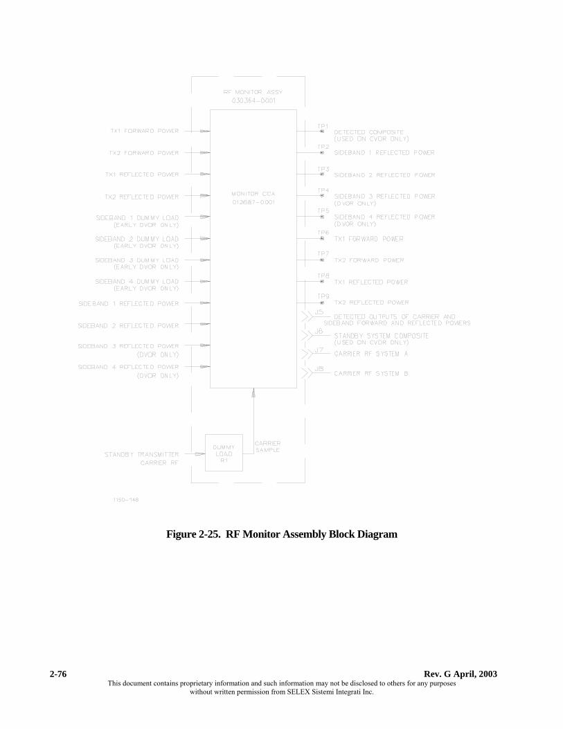
Rev. G April, 2003 This document contains proprietary information and such information may not be disclosed to others for any purposes
without written permission from SELEX Sistemi Integrati Inc.
2-76
Figure 2-25. RF Monitor Assembly Block Diagram

Model 1150 DVOR
Rev. G April, 2003 This document contains proprietary information and such information may not be disclosed to others for any purposes
without written permission from SELEX Sistemi Integrati Inc.
2-77
2.3.2.8.1 RF Monitor Assembly (1A2) Detailed Circuit Theory
The RF monitor assembly functions as an RF detector/amplifier and distributor of the detected analog RF signals. The assembly contains a high power dummy load that is capable of dissipating the 100 watts of RF power from the standby transmitter. In older equipments four dummy loads are mounted to the monitor assy frame which acts as a heatsink. In current equipment connectorized loads are mounted on the transfer relays. These dummy loads dissipate the sideband RF power from the standby transmitter. There are three test jacks on the front of the assembly. These jacks provide access for test equipment to sample the carrier RF signal of system A (test jack J7) and the carrier RF signal of system B (test jack J8). Test jack J6 is not used on the DVOR system. Refer to Figure 11-5. Resistor R1 is the dummy load for the standby transmitter RF carrier power. The RF power enters the assembly via RF connector P4. A sample of the RF signal applied to R1 is obtained by means of an RF voltage divider network consisting of capacitor C1 and resistor R3. This carrier sample signal is not used in the DVOR system. There are nine test points on the front of the RF monitor assembly. The test points are the center conductors of feed-thru capacitors C1-C9. They provide access to the detected carrier forward and reflected powers and the sideband reflected powers which the RF monitor assembly processes. These detected signals are monitored by the audio generator and VOR monitor CCAs. One test point is the detected composite which is not used in the DVOR system. There is a 1 amp fuse on the front panel of the assembly that provides protection for an independent dc/dc converter module used in the RF monitor assembly.
2.3.2.8.2 RF Monitor CCA (A1) Block Diagram Theory
Refer to Figure 2-26. The TX1 +28 Vdc and TX2 +28 Vdc signals are applied to fuse F1 through an OR gate circuit consisting of CR11 and CR12. From F1 the voltage is applied to the antenna transfer relays (1K1-1K5) and to power supply adapter PS1. PS1 converts the +28 Vdc to ±12 Vdc for use within the RF monitor CCA. The circuitry for processing the four sideband reflected power signals are functionally identical; therefore, only a general description of the circuit used to detect the SB1 reflected power signal will be discussed. The SB1 reflected power signal is applied to an RC input impedance matching network consisting C38, and R57 thru R59. From the impedance network the SB1 reflected power is applied to impedance matching RF transformer T4. Variable capacitor C39 is between the output of T4 and the input of the envelope detector network. C39 is factory adjusted to reduce reflections from the detector circuit back to the sideband generator. This capacitor MUST NOT be adjusted in the field. RF transformer T4 matches the low input impedance of the RF signal to the high input impedance of the envelope detector. The output of the envelope detector is applied to buffer U8A. U8A supplies the detected signal to SB1 reflected power calibration adjust potentiometer R118. The voltage obtained from R118 is applied to amplifier U8B. U8B amplifies the signal and applies it to SB1 reflected power test point TP2 and to other circuits within the DVOR system.

Rev. G April, 2003 This document contains proprietary information and such information may not be disclosed to others for any purposes
without written permission from SELEX Sistemi Integrati Inc.
2-78
The circuits for processing the carrier forward powers are identical, therefore only the circuit for processing the TX1 forward power is discussed. The TX1 forward power is applied to an envelope detector network. The output of the envelope detector is applied to buffer U1A. From U1A the detected TX1 forward power is developed across TX1 forward power calibration adjust potentiometer R114. The signal obtained from R114 applied to buffer U1B and sent to TX1 forward power test point TP6 and to other circuits within the DVOR system.
Figure 2-26. RF Monitor CCA Block Diagram

Model 1150 DVOR
Rev. G April, 2003 This document contains proprietary information and such information may not be disclosed to others for any purposes
without written permission from SELEX Sistemi Integrati Inc.
2-79
The carrier reflected power circuits function identically to the forward power circuits. In early systems a preamplifier (U6, U7) was used to increase the low level of the reflected power prior to the envelope detectors. In the present systems this preamplifier has been removed because it was found to compress at very high levels of reflected power causing some error in the measured VSWR. As part of this change the unity gain buffers (U3B, U4B) were changed to gain stages to maintain the same output levels from the CCA. The circuits for processing the carrier reflected powers are identical, therefore, only the circuit used to process the TX1 reflected power is discussed. In the early equipment the TX1 reflected power was applied to a preamplifier circuit U6 which had a gain of 8 db. The signal was then routed to impedance matching transformer T1. In later equipment the preamplifier is not used and the signal is routed directly to T1. T1 matches the 50 Ohm source (the preamp or the direct input signal) to the envelope detector and in the process provides a 2X voltage gain. The envelope detector consists of CR5 which is the actual detector, and CR6 which provides a temperature matched forward bias to CR5 to ensure the detector transfer function stays constant with temperature and is not affected by the variation of diode threshold voltage with temperature. The detected output is routed via the unity gain buffer, U3A, to the calibration adjustment R116 and then to output amplifier U3B. In early equipment U3B was a unity gain stage; while in present production the gain is set to approximately 3 by feedback resistors R 30 and R131. The output from U3B is then routed to J5. J5 provides 3 outputs, one signal goes to TP8 on the assembly front panel, one goes to the audio generator card, and one goes to the CSB power amplifier.
2.3.2.8.3 RF Monitor CCA (A1) Detailed Circuit Theory
Refer to Figure 11-6 (sheet 3 of 3). The RF monitor CCA contains the functional components of the RF monitor assembly. Each transmitter BCPS supplies +28 Vdc to the RF monitor. The voltage from transmitter 1 enters on connector J5-28A; the voltage from transmitter 2 enters on connector J5-29A. Isolation diodes CR11 and CR12 logically "OR" the voltages to ensure a continuous power source for the RF monitor. This voltage exits via connector J5-32C to fuse F1 (of the RF monitor assembly) and returns via connector J5-1C. From J5-1C, the voltage is applied to power supply adapter CCA (A1) terminal E1. The power supply adapter contains a dc/dc converter that provides +/-12 Vdc to the operational amplifiers used on the RF monitor CCA. The +28 Vdc source is also returned to cabinet interconnection wiring harness W1 via connector J5- 2C to provide power for antenna transfer relays, 1K1 thru 1K5. Four sideband RF signals from the standby transmitter sideband generator assemblies are applied to dummy loads R39, R42, R55, and R56 in early DVORs. External loads used in present equipment. The remaining circuitry found on Figure 11-6 is not used on the DVOR system.

Rev. G April, 2003 This document contains proprietary information and such information may not be disclosed to others for any purposes
without written permission from SELEX Sistemi Integrati Inc.
2-80
Refer to Figure 11-5 (RF Monitor Interconnect Diagram) Coaxial cables W13, W14, W15, and W16 supply a sample of the reflected sideband signals from the on-air transmitter to the RF monitor CCA (1A8/1A24). These reflected signals are obtained from the reflected power ports of the sideband RF isolators (ISO1, ISO2, ISO3, and ISO4). These signals are detected and converted to analog voltages by the RF monitor CCA. All four sideband reflected power signals are sent to the audio generator CCA for analysis. The audio generator uses these signals to determine the relative VSWR of the sideband feed-lines to the commutator and all of the antennas. The sideband 1 and sideband 2 detected reflected power signals are also sent to the VOR monitor CCA. The VOR monitor CCA is responsible for determining the exact VSWR of an individual DVOR sideband antenna at the time it is radiating. It will evaluate all 48 antennas and the results will be displayed on the F;11 screen. If two or more sideband antennas have an excessive VSWR value, a maintenance alert is initiated. Refer to Figure 11-6 (sheet 2 of 3). The circuitry for processing the four sideband reflected power signals are functionally identical; therefore, only the description of the circuit used to detect the sideband 1 reflected power is discussed. The sideband reflected RF power signal enters on terminal E14 and is applied to an RC input impedance and filter network which consists of resistors R57 thru R59, and capacitor C38. This network supplies the sideband 1 reflected power to the primary of RF transformer T4. T4 matches the low impedance of the input RF signal to the high input impedance of the envelope detector network. Variable capacitor C39 is located between the output of T4 and the input of the detector. C39 is factory adjusted to reduce reflections from the detector circuitry back into the sideband circulator; hence, back into the sideband generator assembly. This capacitor must not be adjusted in the field. The output of the envelope detector is buffered by U8A. U8A supplies the detected signal to sideband 1 reflected power calibration adjust potentiometer R118. The dc voltage obtained from R118 is buffered by U8B. The output of U8B is supplied to three connectors: J5-32A (SB1 reflected detected power to audio generator 1), J5-31A (SB1 reflected detected power to audio generator 2), and J5-30A (SB1 reflected detected power) which connects to test point TP2 on the front panel of the assembly. Each transmitter has a bi-directional coupler installed in the main RF carrier path between the low pass filter assembly and coaxial antenna transfer relay 1K1. This coupler (DC1, DC2) provides a fixed ratio sample of forward and reflected power of the carrier RF signal of both transmitters. These sample signals are applied to the RF monitor assembly via coaxial cables W5 and W6 (transmitter 1 and transmitter 2 forward power) and W7 and W8 (transmitter 1 and transmitter 2 reflected power). The circuitry for processing the forward powers for transmitter 1 and transmitter 2 are functionally the same; therefore, only the circuit used for processing transmitter 1 forward power is discussed. The TX1 forward RF power signal is applied to terminal E6. From E6 the signal is applied to an envelope detector network. The output of the envelope detector is applied to buffer U1A. U1A applies the signal across TX1 forward power calibration adjust potentiometer R114. U1B buffers the signal from R114 and supplies it to connectors J5-12A (transmitter 1 forward power to audio generator 1), J5-11A (spare, not currently used), and J5-10A which applies the TX1 forward detected power signal to test point TP6 (transmitter 1 forward power) on the front panel of the assembly.

Model 1150 DVOR
Rev. G April, 2003 This document contains proprietary information and such information may not be disclosed to others for any purposes
without written permission from SELEX Sistemi Integrati Inc.
2-81
The carrier reflected power circuits function identically to the forward power circuits. In early systems a preamplifier (U6, U7) was used to increase the low level of the reflected power prior to the envelope detectors. In the present systems this preamplier has been removed because it was found to compress at very high levels of reflected power causing some error in the measured VSWR. As part of this change the unity gain buffers (U3B, U4B) were changed to gain stages to maintain the same output levels from the CCA. The circuits for processing the carrier reflected powers are identical, therefor, only the circuit used to process the TX1 reflected power is discussed. In the early equipment the TX1 reflected power was applied to a preamplifier circuit U6 which had a gain of 8 db. The signal was then routed to impedance matching transformer T1. In later equipment the preamplifier is not used and the signal is routed directly to T1. T1 matches the 50 Ohm source (the preamp or the direct input signal) to the envelope detector and in the process provides a 2X voltage gain. The envelope detector consists of CR5 which is the actual detector, and CR6 which provides a temperature matched forward bias to CR5 to ensure the detector transfer function stays constant with temperature and is not affected by the variation of diode threshold voltage with temperature. The detected output is routed via the unity gain buffer, U3A, to the calibration adjustment R116 and then to output amplifier U3B. In early equipment U3B was a unity gain stage; while in present production the gain is set to approximately 3 by feedback resistors R 30 and R131. The output from U3B is then routed to J5. J5 provides 3 outputs, one signal goes to TP8 on the assembly front panel, one goes to the audio generator card, and one goes to the CSB power amplifier.

Rev. G April, 2003 This document contains proprietary information and such information may not be disclosed to others for any purposes
without written permission from SELEX Sistemi Integrati Inc.
2-82
2.3.2.9 Backplane CCA (1A17)
Refer to Figure 2-27.
1A GND 1C +5V 2A MCS0 2C BAD15 I/O 3A GND 3C BAD14 I/O 4A BAD13 I/O 4C BAD12 I/O 5A BAD11 I/O 5C GND 6A BAD10 I/O 6C BAD9 I/O 7A BAD8 I/O 7C BA7 8A GND 8C BA6 9A BA5 9C BA4 10A BA3 10C GND 11A BA2 11C BA1 12A BA0 12C RING (Single Modem) 13A GND 13C RSTM (Single Modem) 14A OH (Single Modem) 14C MCS1 15A PCS1 15C GND 16A PWRDWN 16C -12V 17A +12V 17C BCLK 18A GND 18C PCS2 19A PCS3 19C PCS4 20A VBB 20C GND 21A BDIR 21C BWR 22A ARDY 22C BRD 23A GND 23C CD (Single Modem) 24A INT2 24C INT3 25A BALE 25C GND 26A INT1 26C BRES 27A BAD7 I/O 27C BAD6 I/O 28A GND 28C BAD5 I/O 29A BAD4 I/O 29C BAD3 I/O 30A BAD2 I/O 30C GND 31A BAD1 I/O 31C BAD0 I/O 32A +5V 32C GND
Figure 2-27. Backplane CCA Pin Functions
The backplane CCA is used within the RMS card cage assembly. It provides a common interconnection bus for any card that plugs into it. The CCAs that may interconnect into the backplane CCA are: central processing unit CCA (1A13), facilities CCA (1A11), serial interface CCA (1A10), LVPS CCA (1A14), test generator CCA (1A12), modem CCA (1A9), optional RSCU Control Interface CCA (1A26).
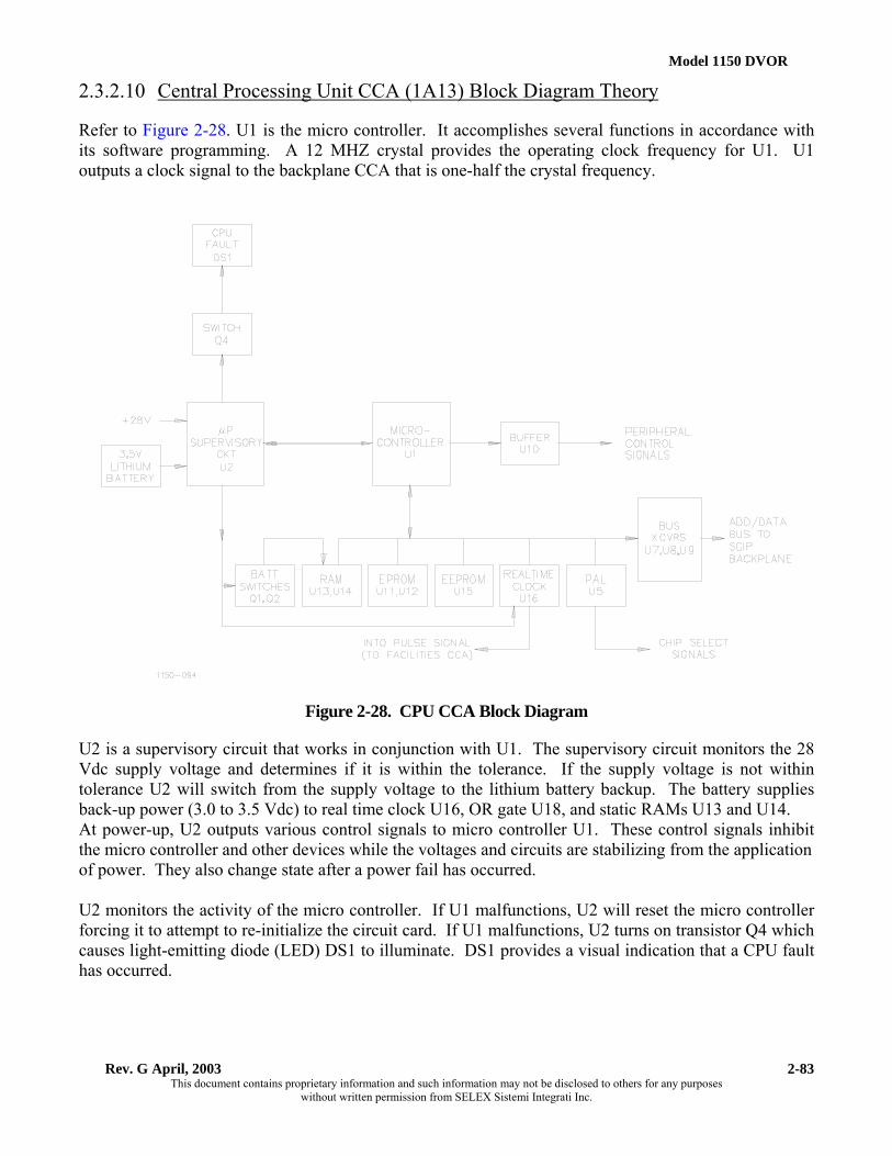
Model 1150 DVOR
Rev. G April, 2003 This document contains proprietary information and such information may not be disclosed to others for any purposes
without written permission from SELEX Sistemi Integrati Inc.
2-83
2.3.2.10 Central Processing Unit CCA (1A13) Block Diagram Theory
Refer to Figure 2-28. U1 is the micro controller. It accomplishes several functions in accordance with its software programming. A 12 MHZ crystal provides the operating clock frequency for U1. U1 outputs a clock signal to the backplane CCA that is one-half the crystal frequency.
Figure 2-28. CPU CCA Block Diagram
U2 is a supervisory circuit that works in conjunction with U1. The supervisory circuit monitors the 28 Vdc supply voltage and determines if it is within the tolerance. If the supply voltage is not within tolerance U2 will switch from the supply voltage to the lithium battery backup. The battery supplies back-up power (3.0 to 3.5 Vdc) to real time clock U16, OR gate U18, and static RAMs U13 and U14. At power-up, U2 outputs various control signals to micro controller U1. These control signals inhibit the micro controller and other devices while the voltages and circuits are stabilizing from the application of power. They also change state after a power fail has occurred. U2 monitors the activity of the micro controller. If U1 malfunctions, U2 will reset the micro controller forcing it to attempt to re-initialize the circuit card. If U1 malfunctions, U2 turns on transistor Q4 which causes light-emitting diode (LED) DS1 to illuminate. DS1 provides a visual indication that a CPU fault has occurred.

Rev. G April, 2003 This document contains proprietary information and such information may not be disclosed to others for any purposes
without written permission from SELEX Sistemi Integrati Inc.
2-84
U1 performs the major function of handling address/data control for the system. The software program for operating the VOR system resides in EPROMS, U11 and U12. The micro controller also uses two static RAMs, U13 and U14, for the temporary and non volatile storage of data. The last memory circuit used is EEPROM U15. The micro controller utilizes U15 to store all local parameters such as alarm points, station identifier, station morse code call letters, etc. for the VOR system when requested by the technician in the G;13 command. Real time clock U16 contains a day/date/time counter, an oscillator clock, an interrupt control, an 8-bit data I/O, five address inputs, and several control inputs. This device provides a true time and calendar output to the micro controller through the bi-directional 8-bit data lines. U16 also provides a timer interval signal (TINT) which is used by U1 as an interrupt signal and which is also sent to the facilities CCA. U5 is a programmable array logic device (PAL) that is programmed to function as a chip select decoder. Octal buffer U10 interfaces the data transfer direction, reset, address latch enable, read, write, clock, and A0 bit control signals sent to the other integrated circuits on the circuit board. Other integrated circuits used on the CPU circuit board are; octal bus transceivers U7, U8, and U9.
2.3.2.10.1 Central Processing Unit CCA (1A13) Detailed Circuit Theory
Refer to Figure 11-23 (sheet 1 of 2). The central processing unit (CPU) CCA is responsible for monitoring and controlling the VOR system and directing communications with peripheral devices. The CPU CCA contains a micro controller, RAM, EPROM, EEPROM, bus control, real time clock, and power monitor circuitry. It processes the system status, directs communications with other devices, monitors collocated DME systems, and communicates with the VOR monitor and audio generator CCAs. The baud rates for the monitors and audio generators and local terminal is 4800 baud. For the remote RMM and DMEs the baud rate is 1200. In addition to the connections made through the backplane CCA, the CPU CCA has one 14-pin connector that mates with cabinet interconnect wiring harness W1. U1 is the micro controller; it accomplishes several major and minor functions in accordance with its software programming. Y1 is a 12 MHZ crystal; it provides the operating clock frequency for U1. U1 outputs a clock signal to the backplane CCA that is one-half the crystal frequency, or 6 MHZ. Schmitt trigger inverter U6F is for factory use only and is not used during normal operation.

Model 1150 DVOR
Rev. G April, 2003 This document contains proprietary information and such information may not be disclosed to others for any purposes
without written permission from SELEX Sistemi Integrati Inc.
2-85
Microprocessor supervisor U2 is a watchdog, battery changeover, reset generator that works in conjunction with U1. 28 Vdc enters the board via connector J1-1 and is applied to a voltage divider network consisting of resistors R1 and R2. The power fail sense line of U2 samples a preset ratio of the supply voltage. A normal supply voltage produces a reference voltage of approximately 1.75 Vdc at the power fail input (PFI) of U2. This voltage is greater than the internal 1.25 Vdc power fail limit reference. Lithium battery BT1 is connected to U2 at the battery (Vbatt) input. If the supply voltage is normal, the VBB voltage to the board is obtained from the Vcc supply voltage applied to U2. If a power failure is sensed by U2, the source of the VBB output voltage is instantaneously switched to the lithium battery. Under the control of U2, the battery supplies 3.5 Vdc back-up power to real time clock U16, OR gate U18, and static RAMs U13 and U14. At power up, U2 outputs an RST and (reset and NOT reset) signal to U1 and other devices on the board. These lines inhibit the micro controller and other devices while the voltages and circuits are stabilizing from the application of power. They also change state after a power fail has occurred. U2 receives a watchdog signal from U1. The watchdog circuit monitors the activity of the microcontroller. If U1 does not toggle the watchdog input (WDI) every 1.6 seconds, the reset lines change state forcing the micro controller to attempt to re-initialize the board. If U1 malfunctions, an internal watchdog timer in U2 forces the watchdog output (WDO) LOW. This turns on transistor Q4 which causes light-emitting diode (LED) DS1 to illuminate. DS1 provides a visual indication that a CPU fault has occurred. U2 provides control signals to several devices to indicate the circuit board is on battery power (battery on [BON] goes HIGH) and it also provides a power fail signal (PFO goes LOW) to U1 via Schmitt trigger inverter U6C and OR gate U18D. The other input of U18D is the timer interrupt 0 signal from real time clock U16. The output of U18D is applied to the interrupt 0 (INT0) line of U1. With a normal supply voltage, the PFO line is HIGH. This is inverted into a LOW by U6C and applied to U18D. The INT0 signal is a short duration positive going pulse which is passed through U18D to the INT0 input of U1. This notifies U1 that the real time clock is functioning and the supply voltage is normal. When a power failure occurs, PFO goes LOW. This LOW is inverted to a HIGH by U6C. This LOW to HIGH transition is passed by U18D and interpreted by U1 as an interrupt. To interpret the difference between a power fail condition and the normal operation of the real time clock, U1 attempts to clear the INT0 flag. If the flag remains cleared, then the HIGH was generated by U16. If the flag is again set, then the HIGH was generated by a power fail condition and U1 is forced into a data protect condition by the software program. U1 has three other interrupts; interrupt 1 (INT1), interrupt 2 (INT2), and interrupt 3 (INT3). INT1 indicates the modem is waiting to communicate with U1. INT2 indicates the audio generator for transmitter #1 or transmitter #2, or the VOR monitor associated with transmitter #1 or transmitter #2 is waiting to communicate with U1. INT3 indicates the video terminal or DME system is waiting to communicate with U1. U1 also monitors an asynchronous ready line to insure the input/output (I/O) communications devices on the serial interface CCA are ready to transfer data.

Rev. G April, 2003 This document contains proprietary information and such information may not be disclosed to others for any purposes
without written permission from SELEX Sistemi Integrati Inc.
2-86
Refer Figure 11-23 (sheet 2 of 2). U1 also performs the major function of handling address/data control for the system. The program for operating the VOR system is stored in EPROMS U11 and U12 which are two 512 bit (64 k by 8 bit) memory devices. Chip select signal CS0 enables U11 and U12. The micro controller also uses two 256 bit (32 k by 8 bit) static RAM memory devices, U13 and U14, to store stack pointers, perform floating point algorithms, for the temporary storage of data, and for the storage of operational parameters, test and historical data needed for a finite duration. U1 uses this data while performing calculations and data processing. The memory circuit, EEPROM U15, a 16 bit (2 k by 8 bit) device is used to store all local parameters such as alarm points, station identifier, station morse code call letters, etc. for the VOR system. To prevent corruption of data, parameters are stored in U13, U14 and U15 with a checksum. Upon application of power the data in U13 and U14 is checked against the checksum. If the data is correct, it is used. If the data is incorrect then the data from U15 is checked against its checksum. If the data is correct, it is used. If incorrect default values from U11 and U12 are used. Real time clock U16 contains a day/date/time counter (0.01 seconds to years), an oscillator clock, an interrupt control, an 8-bit data I/O, five address inputs, and several control inputs. This device provides a true time and calendar output to the micro controller through the bi-directional 8-bit data lines. When normal supply power is lost, 3.5 Vdc from lithium battery BT1 is applied to the power bus line by U2 to maintain the internal clock function and interrupt signal of U16. U16 uses a 32.768 kHz clock frequency obtained from crystal Y2. Capacitor C23 is used to fine tune the clock frequency to produce a precise timer interval (TINT) signal from U16. The adjustment of C23 is performed by monitoring the signal at 1A11TP1 which is on the facilities CCA. C23 is adjusted to produce a one second positive going gate at 1A11TP1. The TINT pulse is a short duration (less than 50 microseconds) pulse that is inverted by U6A. This signal is the interrupt zero (INT0) pulse that is sent to U18D and U1 and will occur every 2 seconds. This pulse is also sent to the facilities CCA via connector J1-9. Transistor Q3 is used to control the low order 8-bits of the address/data bus. If U2 senses a power failure, the reset (RST) signal it sends out is applied to the base of Q3. This is normally a LOW signal which switches HIGH when a reset is initiated. The HIGH cuts off Q3 which allows a pull-down resistor to apply ground potential to resistor pack RP3 which the address/data lines are connected to. If a power failure is occurring, the data on the address/data lines may become corrupted. To prevent corrupted data from possibly being written to the U15 or U16 during a power failure, the address/data lines are grounded. Transistors Q1 and Q2 are RAM controller transistors. Their outputs are tied to the enable pins of U14 and U13 respectively. The input to Q1 is chip select signal CS2 from PAL U5. The input to Q2 is chip select signal CS3 from U5. Q1 and Q2 provide the active LOW chip select signals which allow U14 and U13 to have data written to their memory address locations. U14 and U13 receive their operational power from VBB. When a power fail occurs, U5 ceases to function by the action of U1. This removes the chip select signals from the bases of Q1 and Q2 and forces the NOT chip select inputs of U14 and U13 to go HIGH. This disables U13 and U14, preventing any arbitrary write transactions with corrupted data from occurring. The VBB voltage is now supplied from battery BT1; therefore, the data that is stored in memory is retained during the power loss. For this reason, U13 and U14 act as non-volatile memory devices.
Model 1150 DVOR
Rev. G April, 2003 This document contains proprietary information and such information may not be disclosed to others for any purposes
without written permission from SELEX Sistemi Integrati Inc.
2-87
The other integrated circuits used on the CPU circuit board are: octal bus transceivers U7, U8, and U9; octal latches U3, U4, and U17; octal buffer U10; and programmable array logic device U5. U5 is programmed to function as a chip select decoder. Octal buffer U10 interfaces the data transfer direction, reset, address latch enable, read, write, clock, and A0 bit control signals sent to the other circuits on the circuit board. At start-up the U2 is LOW. Once the supply voltage PFI input exceeds the internal reference, a 50 millisecond timer begins. After the 50 msec period has ended, the line goes HIGH and allows U1 to function according to the software program stored in U11 and U12. The timer insures that the voltage remains constant and is not cycling on and off. Under the control of U1, data is transferred bi-directionally through U7, U8, and/or U9. Address information is passed unidirectionally through U3, U4, and U17. The CPU communicates with the serial interface, facilities, and the dual modem CCAs by means of the address/data bus. The CPU CCA communicates with the VOR monitor and audio generator CCA micro controllers, DMEs, through the serial interface CCA at 4800 baud. Thus, it can pass pertinent VOR monitor or audio generator information to the video terminal at 4800 baud or modem at 9600 baud. Communication from the VOR input/output terminal (IOT) passes through the serial interface to the appropriate DME. Through the facilities CCA, the CPU CCA obtains data on the system (i.e., power supply voltages and status, communications status, transmitter status, etc.) and provides this information to the video terminal, modem, display panel, or remote status and control unit.
2.3.2.11 Facilities CCA (1A11) Block Diagram Theory
Refer to Figure 2-29. A decoder circuit consisting of decoder U5, inverter U16B and OR gate U18D decode data on the address lines to produce the on-board chip select signals. The main address/data line into the board is controlled by bus transceiver U1 and is selected by the CPU CCA micro controller. The direction of data flow through U1 is also determined by the CPU CCA micro controller. U8 is a line driver. The inputs to this device are the status signals coming from the main and standby BCPS units. When selected, the condition of each status signal will be placed onto the address/data bus to be analyzed by the CPU CCA micro controller.

Rev. G April, 2003 This document contains proprietary information and such information may not be disclosed to others for any purposes
without written permission from SELEX Sistemi Integrati Inc.
2-88
Figure 2-29. Facilities CCA Block Diagram

Model 1150 DVOR
Rev. G April, 2003 This document contains proprietary information and such information may not be disclosed to others for any purposes
without written permission from SELEX Sistemi Integrati Inc.
2-89
U9 is a latching flip-flop that takes a data word from the address/data bus and provides control signals to the display panel LED driver transistors. U2A is identical to U8 in function. U2A applies the RSCU command signals from an optional remote control system onto the address/data bus to be acted upon by U1. These signals will turn on or turn off the VOR system. U17 is identical to U9. The signals on the data bus at the time that U17 is enabled are latched onto its output lines. U17 outputs a transfer signal, to the optional RSCU control interface CCA, an address code, to multiplexer U3, and transistor enable signals to transistors Q5 and Q6. U11 is also a latching flip-flop that provides address selection signals to three multiplexed multiplexers U12, U13, and U14. The inputs to U12, U13 and U14 are representative samples of the main and standby BCPS analog voltages and weather measurement voltages (if installed) as well as the ground references. The CPU CCA micro controller selects an input by addressing U11. The output of U12 or U13 and U14 is then applied to analog to digital converter (ADC) U10. U6 provides a precision +5 Vdc reference (VREF) source for use by U10.
2.3.2.11.1 Facilities CCA (1A11) Detailed Circuit Theory
The facilities CCA collects and integrates the system status information and sends it to the CPU CCA for processing and storage. It provides status signals to and receives commands from the optional RSCU interface CCA. Additionally, BCPS status signals and battery charger on/off control signals, display panel LED driver signals, power supply voltages, and antenna control will all be processed by this circuit card for the CPU CCA micro controller. Because the facilities CCA must receive signals from all sections of the VOR system, a 50-pin connector is used to mate the board into cabinet interconnect wiring harness W1. Many of the signals have mnemonic abbreviations for the signal names. A comprehensive list of connector pin numbers, mnemonic names, and signal names is provided in Table 2-2. Refer to Figure 11-21 (sheet 1 of 2). The main address/data line into the board is controlled by octal bus transceiver U1. This device is selected by the CPU CCA micro controller via peripheral chip select line #2 (PCS2). U1 also receives a direction control signal (BDIR). The condition of this signal sets the direction of data flow through U1. U5 is a 3-to-8 line decoder. U5 decodes address bits BA4, BA5, and BA6 to produce the on-board chip select signals which enable U2A, U7B, U8, U9, U11, and U17. Each chip select signal is processed by a dedicated section of negated input NAND gates U4 or U18. A negated input NAND gate is electrically identical to an OR gate but the active signal out is a LOW (negative logic) versus the HIGH (positive logic) for the OR gate. The second input of each section of U4 or U18 is the appropriate read or write command signal for the particular device it drives. Chip select #7 (CS7) is inverted by U16B.

Rev. G April, 2003 This document contains proprietary information and such information may not be disclosed to others for any purposes
without written permission from SELEX Sistemi Integrati Inc.
2-90
Dual quad buffer line driver U2 has four status inputs and three control signal inputs with U2A handling the status signals and U2B handling the control signals. The four status inputs to U2A are #1 ON, #2 ON, OFF, and TX IND. The CPU CCA micro controller enables U2A by setting the read (RD) and chip select #3 (CS3) lines LOW. With U2A enabled, the status signals are placed onto data bus lines ID0- ID3. The data is then transferred through U1 to the CPU CCA micro controller. These status signals come from an RSCU via the RSCU control interface CCA. U2B is always enabled. Clock, read, and write (BCLK, BRD, BWR) control signals are applied to the inputs of U2B. U2B buffers these signals before applying them to other integrated circuits on the board. The clock output of U2B is sent to divide-by-five ripple counter U7A. The counter divides the 6 MHZ input into a 1.2 MHZ output which is used as the clock signal for analog to digital converter (ADC) U10. U8 is an octal buffer line driver. The eight inputs to this device are the status signals coming from the main and standby BCPS units. The over temperature, on-battery, battery low, and power fail condition of each BCPS provides an 8-bit input into the line driver. When selected, it will place this data word onto the address/data bus to be passed on to the CPU CCA micro controller. Octal, non-inverting, latching, D-type flip-flop U9 takes a 6-bit word from the address/data bus to provide the control signals to the display panel LED driver transistors. The output of U9 provides the monitor 1 and monitor 2 normal, alarm, and bypass signals to drive the green, red, and amber LEDs, respectively, on each display board. U17 is identical to U9. The signals on the data bus at the time that U17 is enabled are latched into the output lines of U17. These signals are used as: a transfer status signal, a 2-bit address code, and transistor enable signals. The transfer signal is sent to the optional RSCU control interface CCA via connector J1-43. This signal changes states when a transmitter transfer occurs. This change in state is interpreted by an optional remote status and control unit as a transfer alert. S0 and S1 are a two bit address which is sent to dual 1-of-4 multiplexer U3. These two bits select the active channel of this multiplexer. The multiplexer U3 is not used in the current version. Transistors Q5 and Q6 control the main and standby BCPS charger disconnect signals. A logic HIGH to the base of these transistors keeps them turned off. This high impedance condition allows the battery charger portion of the uninterruptible power supply (UPS) module of the BCPS to function. When U17 applies a low to the base of either Q5 or Q6 during RMS fault isolation, it turns that transistor on and a ground is applied back into the UPS module. This LOW shuts off the battery charger function of the UPS module. The battery voltage is then checked by the BCPS and the battery low status is activated. Transistors Q1, Q2, Q3, and Q4 are not currently used.

Model 1150 DVOR
Rev. G April, 2003 This document contains proprietary information and such information may not be disclosed to others for any purposes
without written permission from SELEX Sistemi Integrati Inc.
2-91
Table 2-2. Listing of Facilities CCA Signals
PIN PIN # MNEMONIC DESCRIPTION # MNEMONIC DESCRIPTION
1 M48V Sys. A BCPS 48 Vdc 2 S48V Sys. B BCPS 48 Vdc 3 M28V Sys. A BCPS 28 Vdc 4 S28V Sys. B BCPS 28 Vdc 5 M12V Sys. A LVPS 12 Vdc 6 S12V Sys. B LVPS 12 Vdc 7 M5V Sys. A LVPS 5 Vdc 8 S5V Sys. B LVPS 5 Vdc 9 M-12V Sys. A LVPS -12 Vdc 10 S-12V Sys. B LVPS -12 Vdc 11 GENLVL Test Generator Level 12 SPARE1 Spare 1 (future use) 13 MBCRET Sys. A BCPS Return (N/C) 14 BARO RET Barometer Sensor Return 15 SBCRET Sys. B BCPS Return (N/C) 16 WIND RET Wind Sensor Return 17 MTXRET Sys. A Transmitter Return 18 TX OUT (OUT) Antenna Status to RSCU 19 STXRET Sys. B Transmitter Return 20 TACH Tachometer 21 MBCOT Sys. A BCPS Overtemp Sta-
tus 22 MBCUPS Sys. A BCPS UPS Status
23 MBCBL Sys. A BCPS Battery Low Status
24 MBCPF Sys. A BCPS Power Fail Status
25 SBCOT Sys. B BCPS Overtemp Sta-tus
26 SBCUPS Sys. B BCPS UPS Status
27 SBCBL Sys. B BCPS Battery Low Status
28 SBCPF Sys. B BCPS Power Fail Status
29 MALM Monitor 1 Alarm 30 MNORM Monitor 1 Normal 31 MBYP Monitor 1 Bypass 32 SALM Monitor 2 Alarm 33 SNORM Monitor 2 Normal 34 SBYP Monitor 2 Bypass 35 MBCCD Sys. A BCPS Charger Dis-
connect (ON/OFF) 36 SBCCD Sys. B BCPS Charger Discon-
nect (ON/OFF) 37 #1 ON Turn-on Sys. A Signal
from RSCU Control Interface CCA
38 #2 ON Turn-on Sys. B Signal from RSCU Control Interface CCA
39 OFF Turn-off On-Air System Signal from RSCU Control Interface CCA
40 TX IND (IN) On-Air Transmitter Indicator Status from Relay 1K1
41 SPARE 8 Spare 8 (future use) 42 Spare 7 Spare 7 (future use) 43 TRANSFER Transfer Status to RSCU
Control Interface CCA 44 SPARE2 Spare 2 (future use)
45 SPARE3 Spare 3 (future use) 46 SPARE4 Spare 4 (future use) 47 SPARE 5 Spare 5 (future use) 48 TIME INTER-
VAL INTO Signal from CPU CCA
49 SPARE 6 Spare 6 (future use) 50 FAN2 (Disabled)

Rev. G April, 2003 This document contains proprietary information and such information may not be disclosed to others for any purposes
without written permission from SELEX Sistemi Integrati Inc.
2-92
U11 is also identical to U9. It provides address selection signals to three multiplexers U12, U13, and U14. The inputs to U12 and several of the inputs to U13 are representative samples of the main and standby BCPS analog voltages. The eight inputs to U12 are the main and standby 48 volt, 28 volt, 12 volt, and 5 volt levels. U13 processes the main and standby -12 volt levels. All levels are applied to a resistive voltage divider network to achieve a standardized representative level of the applied voltage. The other inputs to U13 are a +5 volt reference, and a test generator operation level signal. U14 processes the ground references for the signals applied to U12 and U13. The CPU CCA micro controller selects a voltage input by addressing U11. This address code is latched to the output of U11. This code will enable either U12 or U13 and U14 as well as select the appropriate inputs that are to be passed. The output of U12 or U13 is then sent to the V+ input of ADC U10. The corresponding ground reference output of U14 is applied to the V- input of ADC U10. The A/D converter may be either an integrated circuit of type ADC1205 from national Semiconductor or a printed circuit board part number 012002-0001. For the ADC1205 A/D converter, the conversion requires two data cycles to complete. Conversion starts when the microprocessor sets the proper multiplexor channel then executes a write to the device. The microprocessor then waits approximately 20 uSec for completion then reads the data. For the 012002 CCA the operation of A/D conversion is the same as the ADC1205 A/D. The 012002 CCA includes a MAX191 A/D converter and programmed EPLD (ATV750L) to duplicate the operation of the single chip ADC1205 entirely. Integrated circuit U6 is a precision +5 Vdc reference (VREF) source which is trimmed by potentiometer R1 to compensate for minor component differences. Potentiometer R2 is used to adjust the zero reference operating level of the internal comparator amplifier within U10. Potentiometer R1 is adjusted for +5.00 ±0.01 Vdc at test point TP2. Potentiometer R2 is adjusted for OVDC ±0.01 with ADC1205 installed test point TP4. If the 012002-0001 CCA is installed then R2 is adjusted for -0.090 ±0.25 VDC with the 012002 CCA removed during adjustment. The settings of R1 and R2 determine the input differential signal span that will produce the output digital word. The amount of the span determines the precision of the digital word. R1 and R2 are adjusted at the factory during initial alignment. Adjustment of these potentiometers outside the tolerances listed will introduce significant errors in the conversion of the analog voltages into a digital word. VREF is used for two specific functions. First, it is measured by the CPU micro controller during fault isolation diagnostic testing of the facilities CCA. This voltage is applied to input #7 (IN7) of U13 which allows the CPU micro controller to check the reference level to ensure proper ADC upper limit operation. Secondly it is used as a common offset voltage reference to allow measurement of the -12 Vdc power supply voltages. This arrangement sets up a positive potential into U13 which can be processed by U10 into a digital word that represents -12 Vdc. The micro controller converts this data to display the value as a -12 Vdc level.
Model 1150 DVOR
Rev. G April, 2003 This document contains proprietary information and such information may not be disclosed to others for any purposes
without written permission from SELEX Sistemi Integrati Inc.
2-93
The 12-bit word that represents the converted analog input voltage is placed onto the address/data bus in two 8-bit groups. The first group contains the 8 most significant bits of the 12-bit word. During the second write cycle, the next four bits plus four dummy bits are placed onto the address/data bus. This action occurs for each parameter which is converted from an analog voltage into a digital 12-bit word. During fault isolation of the facilities CCA by the CPU CCA, the ground reference of U10 is verified for proper ADC lower limit operation. During fault isolation of the test generator CCA, the test generator outputs a constant voltage level to the facilities CCA that is converted by U10 and verified by the CPU CCA micro controller. Refer to Figure 11-21 (sheet 2 of 2). The inputs to U15A and U15B and the operation of potentiometer R27 have been disabled. The CPU CCA micro controller is programmed to ignore this section. The timer interval signal (INT0) from the real time clock on the CPU CCA is applied to inverter U16F. The inverted pulse which occurs once every second is applied to the divide-by-two section of decade counter U7B. U7B is enabled by the CS7 signal from U16B. U7B converts the short duration interval pulse into a square wave which is 2 seconds in duration. The square wave signal is inverted again by U16E. This two second square wave is observed at test point TP1. The one second positive going portion of the gate enables the strobe input of U3. The strobe signal enables U3 to output a signal for exactly one second. Address bits S0 and S1 from U17 determine which input port of U3 will be selected as the output signal. Currently, there are no active input ports.
2.3.2.12 Serial Interface CCA (1A10) Block Diagram Theory
Refer to Figure 2-30. The serial interface CCA provides the communications interface for the CPU CCA to communicate with other devices. The circuits that handle communications between the CPU CCA and the various devices within and external to the DVOR system are functionally the same; therefore, only a description of the serial communications controller (SCC) circuit that communicates with the audio generator CCA is discussed. Each SCC is a dual communications device that is capable of independent communications. However, for this manual, the term SCC refers to function and the device is specified by the section A or B tag. U1 is an octal bus transceiver for the address/data bus going to SCC U5A. U1 transfers data to/from SCC U5A as determined by the logic level of the direction signal. When the direction signal is logic HIGH data from the address/data bus is transferred to the SCC. When the direction signal is logic LOW data from the SCC is transferred to the address/data bus. U2 is a buffer line driver that processes various control signals that are applied to the SCC. U3 is a three to eight line decoder that decodes address data on the address lines and provides chip select signals for the SCC.

Rev. G April, 2003 This document contains proprietary information and such information may not be disclosed to others for any purposes
without written permission from SELEX Sistemi Integrati Inc.
2-94
Figure 2-30. Serial Interface CCA, Block Diagram
(Typical SCC Communications Circuit)
To send data to monitor 1 the CPU micro controller applies a logic HIGH to the direction input of octal bus transceiver U1. This allows data from the address/data bus to be transferred to U5A. The parallel data transferred to U5A is converted to serial data and applied to the RS-232 TXD circuit which consists of line driver U9B. The RS-232 TXD circuit converts the TTL level serial data signal to RS-232 level serial data and applies to the audio generator CCA. To receive data from the audio generator CCA the RS-232 level serial data is converted to TTL level data by the RS-232 RCVR circuit which consists of line receiver U8B and applies it to U5A. U5A sends an interrupt request to the CPU micro controller to notify it that information is waiting to be processed. The CPU micro controller polls all devices with the same interrupt to determine the source. U5A is checked for any information it may have. U5A converts the received serial data to parallel data and places it on the address/data bus and applies it through U1 for processing by the CPU CCA micro controller.

Model 1150 DVOR
Rev. G April, 2003 This document contains proprietary information and such information may not be disclosed to others for any purposes
without written permission from SELEX Sistemi Integrati Inc.
2-95
2.3.2.12.1 Serial Interface CCA (1A10) Detailed Theory
Refer to Figure 11-20. The serial interface CCA provides the communications interface for the CPU CCA to communicate with other devices. Primarily, it contains four dual channel serial communications controllers (SCCs) which accomplish two-way communications with the local video terminal, DME transponders #1 and/or #2 (if installed), audio generator CCAs for transmitter #1 and transmitter #2, and VOR monitors #1 and #2. The serial interface CCA has two multi-pin connectors. A twenty-six pin connector mates the board with the interconnect wiring harness W1. The SCCs notify the CPU micro controller that data is ready to be received by sending an interrupt signal to the micro controller. Interrupt #2 (INT2) comes from SCC U5 or U7 and interrupt #3 (INT3) comes from SCC U4 or U6. U1 is an octal bus transceiver for the address/data bus going to the serial communications controllers. U1 receives the peripheral chip select control signal (PSC1) from the CPU CCA micro controller via the backplane bus. U1 also receives a data direction transfer signal from U10 on the CPU CCA via the backplane bus. When U1 is selected, it can transfer data to or from an SCC dependent on the logic level of the direction signal. Octal buffer line driver U2 processes address bits BA1 and BA2 to the particular serial communications controller circuit along with the associated clock and read or write signals. Three to eight line decoder U3 decodes address bits BA4, BA5, and BA6 to provide four chip select signals, one for each SCC. The other four output lines are not used. This configuration allows the CPU CCA micro controller to select which SCC and which portion (A or B) of the SCC it wants active. There are two independent controllers in each SCC package. At start-up, the software program directs the CPU micro controller to program the SCCs to prepare them for operation. Programming entails setting baud rates, data encoding protocol and data modes. Communications baud rates for the audio generators or the monitors are set at 4800 bps; rates for the DMEs are set at 1200 bps; the rate for the video terminal is set at 9600 bps. SCC U5A handles communications with audio generator CCA #1 (labeled TX1), U5B handles VOR monitor #1 (MONITOR1), U6A handles the video terminal, U7A handles audio generator CCA #2 (TX2) and U7B handles VOR monitor #2 (MONITOR2). The communications process with either audio generator CCA or either VOR monitor CCA is straightforward. For audio generator #1, serial data from the audio generator CCA is received on connector J2-17. The RS-232 level serial data is converted to TTL level data by line receiver U8B. The serial data goes to the receive data input of U5A. U5A sends an interrupt request (INT2) to the CPU micro controller to notify it that information is waiting to be processed. The micro controller polls U5 and U7 for any information they may have. When enabled, U5A converts the received data to parallel data and writes it onto the address/data bus for processing by the CPU micro controller. U5A is now ready to receive more data from audio generator #1.

Rev. G April, 2003 This document contains proprietary information and such information may not be disclosed to others for any purposes
without written permission from SELEX Sistemi Integrati Inc.
2-96
The CPU micro controller sends instructions to audio generator #1 by placing the data bytes onto the address/data bus and enabling U5A with a read command to read the bus. U5A then converts the 8-bit word into serial data and outputs it via the transmit data terminal of U5A. The TTL level serial data signal is converted to RS-232 level serial data by line driver U9B. The serial data is now sent to audio generator #1 via connector J2-18 for processing. The format for processing information through U5B, U7A and U7B is similar to the process used with U5A. Line receiver U8A and line driver U9D process input and output serial data to U5B for VOR monitor #1. Data is received on connector J2-19 and is sent out on connector J2-20. Line receiver U8D and line driver U9A process input and output serial data to U7A for audio generator #2. Data is received on connector J2- 21 and is sent out on connector J2-22. Line receiver U8C and line driver U9C process input and output serial data to U7B for VOR monitor #2. Data is received on connector J2-23 and is sent out on connector J2-24. Communications with the local video terminal is handled by U6A. Serial data from the video terminal enters on connector J2-16 and is processed through line receiver U10A to U6A receive data input. U6 uses INT3 to notify the CPU micro controller that information is waiting for processing. U6A transmit data is sent to line driver U12A which goes to the video terminal via connector J2-14. U6A is capable of providing a data terminal ready (DTR) signal via connector J1-15. This signal is not used to complete the communications process with the video terminal that is supplied with the VOR system. A serial data handshake protocol xon/xoff is used to control data flow. The video terminal will send the xoff character to notify the VOR to stop sending characters until the video terminal is ready. This occurs often when a local printer is attached SCC U4 is used to communicate with collocated DME systems (if installed). Section A handles DME transponder #1 (DME1) and section B handles DME transponder #2 (DME2). The VOR monitors the DME's status signals and which system is connected to the antenna. The VOR does not serially communicate with the DME's except when the operator selects a DME either locally or remotely or either DME attempts to dial-out to the RMM facility. DME #1 receive data, which is used for the transfer of serial communications data, enters on connector J2-7 and is converted by line receiver U11B to TTL logic levels and sent to the data receive input of SCC U4A. DME #1 status input, which only provides status information, enters on connector J2-8 and is sent through SW1 section 8 to a special data control input on U4A. When directed by the CPU CCA, the micro controller polls U4A for the data which represents the status of DME #1. DME #2 receive data, which enters on connector J2-12, is converted to TTL logic levels by line receiver U11C. DME #2 status enters on connector J2-10 and is sent to a special data control input on U4B. DME antenna status enters on connector J2-9 and is sent directly to a special control data input on U4A and U4B. The logic state of the DME antenna data indicates which DME (#1 or #2) is connected to the DME antenna. If the PMDT is logged on to the VOR, remote communications via the modem input to a DME is still possible. The CPU CCA will process both communications independently. Therefore, the PMDT can communicate to the VOR while a remote PMDT is talking to a DME, or vice versa. An external DCD control signal is made available on connector J2-4 which then goes to SW1, section 7. The outputs of SW1, sections 7 and 8 are tied together. For normal operation, SW1, section 7 is open and section 8 is closed.

Model 1150 DVOR
Rev. G April, 2003 This document contains proprietary information and such information may not be disclosed to others for any purposes
without written permission from SELEX Sistemi Integrati Inc.
2-97
Switch SW1, sections 1 through 6, allow the operator to select the type of communications signal level to be used with the single modem or an external modem, if desired. VOR single modem CCA 1A9 utilizes TTL levels; therefore, the standard settings for SW1, sections 1 through 6 are: sections 2, 4 and 6 are set closed while 1, 3 and 5 are set open. Provisions are made to allow a separate, independent modem using RS-232 signal levels to be used with the VOR system. For RS-232 signal levels, switch SW1, sections 1 through 6 are set as follows: sections 1, 3 and 5 are set closed while 2, 4 and 6 are set open. RS-232 receive data enters on connector J1-9; TTL receive data enters on J1-2. RS-232 data carrier detect (DCD) enters on J1-10; TTL DCD enters on J1-1. RS-232 SPEED enters on J2-3; TTL SPEED enters on J1-13. External modem speed must be 1200 baud for RMS software versions earlier than 3.0. RS-232 data is converted to TTL levels by line receivers U10B, C, and D before being applied to switch SW1. The converted RS-232 or TTL serial data is sent to U6B. Two of the three outputs of U6B are also dualized to provide TTL or RS-232 levels. TTL transmit data is sent to connector J1-3 and through line driver U12C to provide an RS-232 level signal to connector J1-11. U6B DTR output signal is sent to connector J1-4 as the TTL level DTR signal and to line driver U12B to provide an RS-232 level signal at J1-12. The single modem CCA requires a reset signal. The ready to send (RTS) output of U6B is sent to line driver U13D and line receiver U11A to provide a modem reset signal at backplane bus connector P1- 13C.
2.3.2.13 Test Generator CCA (1A12) Block Diagram Theory
Refer to Figure 2-31. The primary function of the test generator is to provide a standard reference signal to the DVOR monitors at power-up or whenever directed by the RMS CPU for monitor testing. The test generator's secondary function is an operator maintenance function, which is to allow test signals to be sent to the monitor(s). At turn-on, the CPU micro controller configures logic cell array (LCA) U1 to operate as a 16-bit counter, a 15 line multiplexer, a 12 line data transceiver, and a clock. PAL U5 aids the CPU micro controller during the configuration process of U1. After U1 has its internal parameters established, the micro controller calculates the required audio signal characteristics of a VOR waveform and stores this test pattern data into RAMs U6 and U7.

Rev. G April, 2003 This document contains proprietary information and such information may not be disclosed to others for any purposes
without written permission from SELEX Sistemi Integrati Inc.
2-98
Figure 2-31. Test Generator CCA, Block Diagram
U1 now outputs a changing data address code. This code continuously sweeps through the memory address locations of U6 and U7 where the ideal DVOR test pattern is stored. The DVOR test pattern is used by the DVOR monitors for integrity and certification checks and diagnostics. DAC U8 converts the digital test pattern data obtained from U6 and U7 into an analog signal that is representative of a true and correct detected RF radiated signal from an ideal DVOR facility. The output of U8 is sent to amplifier U3. The output of U3 is applied to the input of U9. U9 is a sample/hold circuit which eliminates the stepping distortion caused by the digital to analog conversion process. U9 operates from a clock signal provided by U1. The noise-free audio signal is next applied to buffers U4A and U4B. U4A and U4B buffer the signal before it is applied to DVOR monitors #1 and #2 and also to the facilities CCA. This signal is measured at TP1 and is used for fault isolation and diagnostic checks of the VOR monitor circuits and fault isolation of the test generator.

Model 1150 DVOR
Rev. G April, 2003 This document contains proprietary information and such information may not be disclosed to others for any purposes
without written permission from SELEX Sistemi Integrati Inc.
2-99
2.3.2.13.1 Test Generator CCA (1A12) Detailed Circuit Theory
Refer to Figure 11-22. The test generator CCA is a stand alone circuit that performs three functions. The primary function is to provide a standard calibration signal to the DVOR monitors at power-up or whenever directed by the CPU CCA. For this operation, the test generator is directed under software control to develop an ideal DVOR test signal that has these properties: a 30% 30 Hz signal; a 30% 9960 Hz signal; a 16 deviation factor for the 9960 Hz signal, and an azimuth angle that is equal to the mid-point value between the low and high azimuth angle alarm points. The test generator will reconfigure to calibrate each monitor separately. On power-up the monitor alerts the RMS that a calibration is required. The RMS calculates and stores the waveform. The RMS then alerts the monitor that the waveform is ready for the calibration. The second function is to configure itself for monitor certification. In this operation, the test generator will configure itself to produce a DVOR test signal in accordance with the values programmed in the Monitor, Data, Cert. For a certification test of a monitor, the test generator will be set first for all the low limit values and then it will reconfigure for all the high limit values. The last function is the operator maintenance condition. The test generator is configured by values programmed into the Monitor, Data, Test Data. This condition allows the test generator to be used as built-in test equipment by a maintenance technician to test the operation of a monitor. Y1 is a 3.932160 MHZ crystal that is used to operate the internal clock and counter circuits of U1. Capacitor C9 is used to adjust the crystal for the specified frequency. The internal clock circuits of U1 divide the oscillator frequency by four. Capacitor C9 is adjusted for a frequency of 983.040 ±0.04 kHz at TP3. At turn-on, the CPU micro controller configures LCA U1 to have the following functions: a 16-bit counter, a 15 line multiplexer, a 12 line data transceiver, and a clock. PAL U5 aids the CPU micro controller during the configuration process of U1. Address lines BA0, BA1, BA2, and BA6, peripheral chip select line PCS3, address/data lines AD5-AD7, read (BRD) and write (BWR) are applied to the inputs of U5. During configuration, U5 outputs signals to U1 which go to the reset, configuration clock (CCLK), AD0, and done/program (D/) inputs. U1 operates in a slave mode and programming is accomplished with serial data entering U1 on the AD0 line which is supplied by U5. CCLK provides the clock signal to U1 during configuration. The D/ line is held LOW which allows U1 to be programmed. When programming is completed, the D/ line then goes HIGH which allows U1 to operate as dictated by its configuration setup. Fault isolation of the test generator involves a reset to U1, programming U1 and checking for the done status. A constant DC level is programmed into U6 and U7 and checked with the facilities A/D converter.
Rev. G April, 2003 This document contains proprietary information and such information may not be disclosed to others for any purposes
without written permission from SELEX Sistemi Integrati Inc.
2-100
After U1's internal parameters are established, the CPU micro controller calculates the required audio signal characteristics of a proper DVOR system and stores that information as digital data into static RAMs U6 and U7. The CPU micro controller uses the address/data bus to set a 15-bit word onto address lines A0-A14. This selects the specific memory location of U6 and U7 to be written. Next, the CPU micro controller places the digitized data for a portion of the ideal DVOR waveform onto the address/data bus. This 12-bit word is passed through the transceiver section of U1 and placed onto the 12-bit data bus which connects to the input/output ports of U6 and U7. A command is then sent to write the data to the memory address. This continues until the entire digitized waveform is stored into U6 and U7. Once programmed, the test generator will continue to output the test signal because the internal clock of U1 is continuously selecting the memory address locations of U6 and U7. U1 outputs a changing data code on address lines A0-A14. This code continuously sweeps through the address locations of U6 and U7 where the ideal DVOR test pattern is stored. The outputs of U7 provide the lower 8 bits (B0-B7) of the 12-bit data word that is sent to DAC U8. Only output data bits D0-D3 are used in U6. This nibble is placed onto data lines B8-B11 and contains the four most significant bits of the 12-bit word to U8. The 12-bit word is the digital representation of the DVOR test waveform which is used by the DVOR monitors for integrity and certification checks and maintenance diagnostics. DAC U8 converts the 12-bit test pattern data, obtained from U6 and U7, into an analog signal that is representative of a true and correct detected RF radiated signal from an ideal DVOR facility. Integrated circuit U2 is a precision +5 Vdc reference source. The output of U2 is applied to the VREF+ input of U8 while the VREF- input is tied through resistors to ground. This establishes a stable reference voltage for the analog waveform to be developed. The output of U8 is sent to inverting, high speed amplifier U3. The fast output response combined with its excellent settling time rating makes it ideal for use as a digital to analog converter output amplifier. U9 is a precision instrumentation switched-capacitor integrated circuit device that is set up to function as a sample/hold circuit. When U8 is switching from one output level to another, noise spikes may occur at the instant the state change occurs. If these spikes are allowed to remain in the waveform, significant high frequency distortion will be present. Elimination of this stepping distortion is accomplished by sampling the output signal level of U3 after allowing U8 enough time to switch levels and settle. A 983.04 kHz clock from U1 is applied to the oscillator input of U9. U9 has internal charge-balanced switching circuits which are controlled by the internal oscillator. During the DAC transition period, U9 removes capacitor C15 from the output of U3. After the DAC has completed it level change and settled at its new output level, U9 connects C15 to the output of U3 and allows C15 to change to the new voltage level. C15 integrates the sampled voltages into a smooth output waveform that is relatively free from high frequency distortion. This process produces a truer representation of the recovered digitized wave into an analog format. The noise-free audio signal is next applied to amplifiers U4A and U4B. U4A and U4B buffer the signal developed across C15 before it is applied to other circuits. U4A sends the test generator waveform to DVOR monitor #1 via connector J1-1. U4B sends the test generator waveform to DVOR monitor #2 via connector J1-3 and also to the facilities CCA via connector J1-5. This signal is measured at TP1 and is used for fault isolation diagnostic checks of the test generator and VOR monitor circuits.

Model 1150 DVOR
Rev. G April, 2003 This document contains proprietary information and such information may not be disclosed to others for any purposes
without written permission from SELEX Sistemi Integrati Inc.
2-101
The test generator can be used as a maintenance device under the control of an operator. Specific parameters of the test generator waveform can be entered by an operator through the video terminal. The CPU micro controller will use the operator-entered data and calculate the values needed to create the new test waveform. The CPU micro controller then takes control of U1 and uses it to store the digitized waveform information into static RAMs U6 and U7. The test generator then outputs a waveform that is configured in accordance with the operator's test specifications. When the test generator CCA is undergoing fault isolation diagnostics testing, the CPU micro controller programs U6 and U7 memory locations so that a constant analog DC voltage will be produced by U8 which is amplified by U3. This known DC voltage is sent to the facilities CCA where it is processed back into a digital word which is read by the CPU micro controller. The micro controller compares this word against the value stored as a reference to determine if the test generator CCA is functioning properly. Test point TP2 provides a sync pulse for an oscilloscope when performing an alignment or maintenance of the DVOR monitor CCA with the test generator signal.
U2
EPLD
P1
Con
nect
or
JP1SELECT
U1
SCCBAD0-7
BDIR
/INT1
/INT3
Control
J3ISP
U3DEDICATED
MODEM
J1 C
onne
ctor
J2 C
onne
ctor
BCLK, BRD, BWRBA2, BA1
D0-7
SCC_RXSCC_DCD
/INT RTSATXA
TXBRTSB
RXBDCDB
TTL TORS232
TIP, RINGRXD
DCDD
EXT_RTS
EXT_TX
RS232TO TTL
EXT_RX
EXT_DCD
U4DIAL-UPMODEM
TIP, RING
ANALOG TO DIGITALCONVERTERS
TTL INPUTS AND OUTPUTS
DME 28V
DME MON
RXEDCDE
Figure 2-32. Modem CCA (012101-1001), Block Diagram

Rev. G April, 2003 This document contains proprietary information and such information may not be disclosed to others for any purposes
without written permission from SELEX Sistemi Integrati Inc.
2-102
2.3.2.14 Modem CCA (1A9) (Part No. 012101-1001) Block Diagram Theory.
Refer to Figure 2-36. The modem CCA provides the capability to communicate with an offsite monitoring facility through an on-board dial-up modem. An on-board dedicated modem is also included for communications to an RCSU. The dedicated modem may be disabled in favor of an off-board external modem, selectable by software control. The on-board dedicated modem is the default power-on selection. Both on-board modems are capable of 9600 baud, 8 bits, and no parity communications with V.32 compatibility. Signals enter from the backplane through connector P1. The U2 EPLD acts as bus transceiver and I/O decoder for the CCA. Factory programming of the U2 EPLD is accomplished via the in-system programming (ISP) connector J3. The U2 EPLD controls bus access to the U1 serial communications controller (SCC), read/write control of the TTL inputs/outputs, and enabling of the dedicated or external modem. Buffered address, data, and control signals connect between EPLD U2 and SCC U1. The U1 SCC controls both the dedicated/external and dial-up modems. Software may select either RX and DCD from modem U3 or RX and DCD from an external modem, through U2, to SCC_RX and SCC_DCD of U1. Interrupts from SCC U1 are strapped to either /INT1 or /INT3 by JP1. The dial-up, external, and dedicated modem signals enter/exit from connector J1. The external modem RTS and TX signals are converted from TTL to RS232 levels before exiting while the RX and DCD signals are shifted from RS232 to TTL levels after entering the CCA. Connector J2 routes both TTL I/O and analog inputs on the CCA. All J2 signals may be used for environmental monitoring and DME control. The TTL I/O connects directly while the analog inputs are converted to digital signals before routing to EPLD U2.
2.3.2.14.1 Modem CCA (1A9) (Part No. 012101-1001) Detailed Circuit Theory
Refer to Figure 11-19. All bus control signals including buffered direction (BDIR), buffered data (BAD0-7), buffered address (BA1-7), and processor chip select (PCS3) connect to programmable logic device (EPLD) U2. The U2 EPLD is factory programmed via connector J3 and resistors R5, R6, and R7. The PCS3 chip select and BA1-7 address lines define the address range used by the CCA. The BDIR control determines whether data is being read from the bus or data is being placed upon the bus in conjunction with buffered read (BRD) and buffered write (BWR). Signals PCS3, BDIR, and BRD would all be logic low during a read operation, for example. EPLD U2 processes BWR, BRD, buffered clock (BCLK), BA2, and BA1 and applies them to serial communications controller (SCC) U1. These control signals are used to determine whether SCC U1A or U1B is active and when U1 will write or read data to/from EPLD U2 on data bus D0-7. Resistor network RN3 is used as pull-ups for the data bus.

Model 1150 DVOR
Rev. G April, 2003 This document contains proprietary information and such information may not be disclosed to others for any purposes
without written permission from SELEX Sistemi Integrati Inc.
2-103
After buffered reset (/BRES) goes high, the CPU micro controller programs SCC U1 for operation. Programming entails setting baud rates, data encoding protocol, and data modes. The CPU microcontroller sends instructions to SCC U1 by placing the data bytes on the data bus and enabling U1 with a read command. The data on the bus is transferred through EPLD U2 and applied to the data inputs of SCC U1. SCC U1 reads the information on the bus, converts the 8-bit word into serial data, and outputs the data via its transmit data port. U4 is one of the two modem modules on the CCA. It is used as an interface between the station and an offsite computer terminal. Light Emitting diode (LED) CR2 flashes when the phone line rings. SCC U1 sends the transmit data (TXDB) and the data terminal ready/request (/DTRB) signals to modem U4. The /DTRB signal notifies modem U4 that data is ready to be transmitted. The TXDB signal contains the data that modem U4 transmits over the telephone lines. Data from the telephone line is processed by modem U4 and applied to SCC U1 as serial data. SCC U1 sends an interrupt request (/INT) to the CPU micro controller via /INT1 or /INT3, depending on the JP1 strap selection. The interrupt notifies the micro controller that information is waiting to be processed. SCC U1 converts the received data to parallel data and writes it onto the data bus when polled by the micro controller. Modem U3 may be used for communications as a dedicated modem to an RCSU. Data processing occurs the same as for modem U3 except that LED CR1 lights when the data carrier signal is detected. Resistor R2 and transformer T1 condition the modem signals for direct connection over long distances. Modem U3 may be bypassed entirely in favor of an external modem. TXDA and /DTRA signals from SCC U1 are converted from TTL to RS232 levels by U9B and U9C, transient protected by CR24 and CR26, then routed to connector J1. External modem signals RS232_RX and RS232_DCD from connector J1 are transient protected by CR25 and CR27, then converted from RS232 to TTL levels by U10B and U10C. Software may choose either the external modem or the on-board modem U3, depending on the selection made inside EPLD U2. Whichever modem is selected, its RX and DCD signals are channeled to RXDA and /DCDA of SCC U1 through EPLD U2. The U2 EPLD directly controls outputs REM_ON_1, REM_ON_2, REMOTE_OFF, and LOCAL_LED. These outputs are pulled up by resistors R36–39 and connect to the gates of transistors Q1-4. The drains of transistors Q1-4 are transient protected by CR14, CR15, CR16, and CR23 before routing to connector J2. The drains will be pulled up externally by the equipment to be controlled. SPARE_IO1 and SPARE_IO2 may be programmed by software to act as either inputs or outputs, depending on the selection made inside EPLD U2. Resistors R28, R33, R34, and R35 provide pull-up while CR21 and CR22 provide transient protection. As outputs, the lines may drive high or low at TTL levels.

Rev. G April, 2003 This document contains proprietary information and such information may not be disclosed to others for any purposes
without written permission from SELEX Sistemi Integrati Inc.
2-104
DME1_28VDC and DME2_28VDC enter the CCA at connector J2 and are voltage divided by resistor networks RN1 and RN2. Capacitors C9 and C10 filter while CR17 and CR18 provide transient protection to the divided signals before presentation to comparators U6A and U6B. The divided signals are compared against a reference voltage generated by U7 and R21. If the reference voltage is less than the divided voltage, the output of the comparator is low, indicating the DME voltage is acceptable. Resistors R23 and R24 provide pull-up to the outputs, named /DME1_VOLT_OK and /DME2_VOLT_OK, if the DME voltage is not acceptable. DME1_MON_LED and DME2_MON_LED are signals joining connector J2 and resistors R29-32 with transient protection CR19 and CR20. Resistors R29 and R32 act as pull-downs in the event of an open connection while resistors R30 and R31 act as current limiters to minimize powering of off-board equipment during power down. Two reference voltages are created by U7, R25, R26, and R27. The higher reference voltage is at the junction of resistors R25, R26, and comparators U5A and U5C. The lower reference voltage is at the junction of resistors R26, R27, and comparators U5B and U5D. Comparators U5A and U5B define a binary code for the DME1_MON_LED analog input while comparators U5C and U5D perform the same for DME2_MON_LED. The bits of the binary code are named DME1_B0, DME1_B1, DME2_B0, and DME2_B1 at the outputs of the comparators and are defined as follows:
DME1_B1 / DME2_B1
DME1_B0 / DME2_B0
Description of DME Status
0 0 Shutdown
0 1 Alarm
1 0 Unknown / undefined
1 1 Normal
The comparator outputs are pulled up by resistors R16-19 before arriving at the U2 EPLD. The remaining signals from connector J2 are digital inputs SMOKE_DETECT+, INTRUSION_SENSOR+, LOCAL_CNTL, MAIN1_CNTL, MAIN2_CNTL, MONITOR_BYPASS, DME1_BYPASS_LOGIC, and DME2_BYPASS_LOGIC. The signals are pulled up by resistors R8-15 and transient protected by CR6-13. Three of the inputs are diode isolated by CR3-5 to prevent accidental powering of the CCA during power-down. These three inputs are MONITOR_BYPASS, DME1_BYPASS_LOGIC, and DME2_BYPASS_LOGIC. All inputs connect to EPLD U2 for processing.
2.3.2.15 RSCU Interface Assembly (1A26) (Optional)
The RSCU Interface CCA interfaces a VOR facility with a remote status and control unit (RSCU). The RSCU interface assembly provides status data to and control data from an RSCU. The RSCU is usually located at a designated remote monitoring facility, such as an airport control tower. Refer to Operations and Maintenance Manual Part Number 571138-0001.

Model 1150 DVOR
Rev. G April, 2003 This document contains proprietary information and such information may not be disclosed to others for any purposes
without written permission from SELEX Sistemi Integrati Inc.
2-105
Figure 2-33. RSCU Control Interface CCA (012601), Block Diagram
2.3.2.15.1 RSCU Control Interface CCA (012741-1002) Block Diagram Theory
Refer to Figure 2-33. DVOR status signals, from the facilities CCA, and a binary count, from the encoder state/time-base generator, are applied to the tone encoder/transmitter circuit which consists of programmable array logic (PAL) U14 and dual-tone multi frequency (DTMF) generator U13. The VOR status signals are encoded into a DTMF signal and applied to the data access arrangement (DAA) circuit as the tone out signal. The 3.58 MHZ oscillator circuit creates the timing signal for the tone encoder/transmitter U13/U14 and the tone receiver U7. The oscillator consists of invertors U1D, U1E, and U1F, resistors R3 and R19, and crystal Y1. The DAA circuit is an amplifier buffer circuit that consists of amplifiers U12A, U12B, and U12C and impedance matching transformer T1. The tone out signal is amplified and buffered within the DAA circuit then sent to the RSCU as a tone coded data stream. The tone coded data stream from the RSCU is applied to the DAA circuit where if is amplified, buffered, and applied to the tone receiver circuit as the tone in signal. The tone receiver circuit consists of DTMF receiver U7 and terminal boards TB1 and TB2. U7 decodes the tone in signal into four bit binary data which is applied to the decoder circuit. Jumpers on terminal boards TB1 and TB2 are used to select the sensitivity of U7. The decoder consists of decoders U8 and U11 and inverter U1A. U8 and U11 decode the data from U7 and generate preset or clear signals that go to the function latch/driver circuit.
Rev. G April, 2003 This document contains proprietary information and such information may not be disclosed to others for any purposes
without written permission from SELEX Sistemi Integrati Inc.
2-106
The function latch/driver circuit consists of quad D-type flip-flops U2 and U9, positive AND drivers U3 and U10, and terminal boards TB3, TB4, and TB7. It converts the preset or clear signals to status signals and applies them to the VOR facilities CCA for processing.
2.3.2.15.2 RSCU Control Interface CCA (012741-0001) Detailed Circuit Theory
Refer to Operations and Maintenance Manual Part Number 571138-0001, Figure 11-7. The RSCU interface assembly provides the RSCU with information which is decoded and transformed into a visual indication of the operating status of the VOR system. Invertors U1E, and U1F, resistors R19, and R3, capacitor C26, and crystal Y1 form a phase shift oscillator circuit which creates the 3.58 MHZ clock signal for use by DTMF generator U13 and DTMF Receiver U7. This signal is buffered by inverter by U1D before being applied to U13 and U7. Timer U16 creates a 10 Hz signal which is applied to the A input of 4-bit binary counter U15. The B input of U15 is connected to the QA output. This cascades the divider sections of U15 to provide a maximum count length for U15. U15 is enabled by an active LOW from the Q NOT output of U9A. U9A is a function latch that processes the last bit command from the 1138 RSCU data stream to command the VOR 012741 interface CCA to send the VOR status signals back to the 1138 RSCU. Therefore, the only time U15 outputs a count is after it was directed by the remote RSCU. The 1138 acts as a master by sending command information which allows the VOR 012741 CCA to respond. The 4-bit count from U15 drives select inputs on PAL U14. The other inputs to U14 are the VOR status inputs. The QD output of U15 also drives the clock input of U9A. This bit is used to reset U9A which causes the Q NOT output to go HIGH. With the reset inputs of U15 HIGH the outputs of U15 are all forced LOW. This, in effect, disables U15 and prepares it for the next transmit command from the RSCU. PAL U14 selects the #1 ANT, Alarm, #2 NORM and #1 NORM signals from the facilities CCA by means of the 4-bit code from U15. Unused inputs are pulled HIGH by resistor pack R4. Each bit of the six bit status input is encoded by U14 to develop a proper row and column data signal for DTMF generator U13. Number 2 antenna input to U14 is not used. The eight inputs of U13 are organized to represent the four rows and columns of an expanded keypad. Selecting a unique row and column combination causes U13 to generate the unique DTMF tone that is associated with that combination. The DTMF signal from U13 is the tone out signal that is applied to amplifier U12B. Potentiometer R10 is used to adjust the level of the tone out signal before it is applied to U12B. R10 should be adjusted to produce a 1 Vpp signal level on the telephone lines for that portion of the signal data stream when the RSCU interface board is replying to the RSCU. This level is approximately equivalent to -7 dBm at 600 ohms and it insures that the signal driving the tone decoder circuit in the RSCU is not distorted from being over driven. U12B amplifies the tone out signal with an approximate gain of 1. Voltage divider network R17 and R18 establishes a reference of approximately 3 volts at the non-inverting input of U12B. The output of U12B is applied to the inverting input of U12A. The non-inverting input of U12A is also set to a reference of approximately 3 volts by voltage divider network R17 and R18. The output of U12A is applied to transformer T1.

Model 1150 DVOR
Rev. G April, 2003 This document contains proprietary information and such information may not be disclosed to others for any purposes
without written permission from SELEX Sistemi Integrati Inc.
2-107
T1 is an impedance matching transformer that matches the output impedance of U12A to the 600 ohm input impedance of the telephone lines. The signal from T1 is sent to the RSCU on the tip and ring telephone lines or data cable. The DTMF tone signals from the RSCU enter the interface assembly via connector J1 and pass through impedance matching transformer T1. The signals are next applied to the inverting input of amplifier U12C. U12C amplifies the signals with an approximate gain of 1.5. The output of U12C is coupled to DTMF receiver U7 by capacitor C3. Bypass capacitor C1 filters the +5 Vdc entering via connector P1-1C and P1-32C. Zener diodes VR1 and VR2 are used to eliminate telephone line transients in excess of 5.1 volts. A jumper is installed across terminal J3 which allows the RSCU interface assembly to obtain +5 VDC power from the backplane CCA and must be installed for use in the DVOR. U7 decodes the DTMF signals into four bit binary data which is applied to decoders U8 and U11. The strobe output of U7 is used to enable U8 and U11. The strobe goes to logic HIGH after a valid tone pair is sensed and decoded at the data outputs. The strobe remains a logic HIGH until a valid end-of-signal pause occurs or when the clear input is driven to a logic HIGH. Once cleared, the strobe will not rise to a logic HIGH until a new valid tone is detected. Jumpers on terminal boards TB1 and TB2 are used to select the sensitivity of the SIG IN input of U7 to a maximum of -38 dBm. Decoders U8 and U11 decode the lower three bits of the 4-bit output from U7 and generate active-low preset or clear signals that are applied to the function latch/driver. The D3 output of U7 is applied to the G2A enable input of U8 and to the G2A input of U11 through inverter U1A. A LOW on this line will be seen as a LOW on the G2A input of U8, enabling U8. This LOW will be inverted by U1A and be seen as a HIGH on the G2A input of U11, disabling U11. The strobe output of U7 is applied to the G1 inputs of U8 and U11. Under normal conditions the strobe output of U7 will be HIGH enabling U8 and U11. A LOW strobe will disable U8 and U11 causing all of their outputs to go logic HIGH. D-type flip-flops U2A, U2B, U9A, and U9B all operate the same, so only the operation of U2A will be discussed. Active LOW signals from decoder U8 are applied to either the preset (PR) or clear (CL) of U2A. A LOW on the PR input of U2A causes its Q output to go logic HIGH. A LOW applied to the CL input of U2A will cause its NOT Q output to go logic LOW. These signals are applied to terminal board TB4. Jumpers across TB4 are used to select the Q (active HIGH) or NOT Q (active LOW) outputs of U2A. This signal exits the RSCU interface assembly as the #2 ON signal via J2-8. D-type flip-flop U9A is used to reset binary counter U15 and to clear DTMF receiver U7. Whenever a logic LOW is applied to the PR input of U9A; U9A presets causing its Q output to go HIGH and its NOT Q output to go LOW. A HIGH on the Q output sends a clear pulse to DTMF receiver U7 which forces its Strobe output to a logic LOW. This insures that U7 will not decode the RSCU interface tones which are being sent to the RSCU. A LOW on the NOT Q output is applied to the R0(2) input of binary counter U15. This LOW enables U15. The clear input of U9A is affected by the LOW to HIGH transition of the QD output of U15. When this occurs, the LOW on the D input of U9A set the Q output back to LOW and the NOT Q output back to HIGH. This allows U7 to be ready to decode the next tone sequence from the RSCU and it disables and resets U15.

Rev. G April, 2003 This document contains proprietary information and such information may not be disclosed to others for any purposes
without written permission from SELEX Sistemi Integrati Inc.
2-108
Components C2, R2, TB5, TB6, U1C U4A, U4B, U5, U6, and U12D are not used in the VOR system.
Table 2-3. CCA 012741 Tone Control to 1138 RCSU
Touchtone Digit output Row/Column Time Slot Description of input combinations
7 (852,1209 Hz)
R3C1 1 ANT1 = 0 TX 1 into antenna
8 (852,1336 Hz)
R3C2 1 U15 QA=1
ANT1 = 1 TX 2 into antenna
D (941,1633 Hz)
R4C4 2 ALM = 0
1 (697,1209 Hz)
R1C1 2 ALM = 1
6 (770,1477 Hz)
R2C3
3 U15 QA,QB=1
NORM2=0 Defined by ANT1= 1 or both NORM1 or NORM2 =0
9 (852,1477 Hz)
R3C3 3 U15 QA,QB=1
NORM2=1 Defined by ANT1 =0 with Either NORM1 or NORM2 = 1
2 (697,1336 Hz)
R1C2 4 U15 QC=1
NORM1 = 0 Defined by ANT1=0 or both NORM1 or NORM2 = 0
5 (770,1336 Hz)
R2C2 4 U15 QC=1
NORM1 = 1 Defined by ANT1 = 1 AND both NORM1 AND NORM2 = 1

Model 1150 DVOR
Rev. G April, 2003 This document contains proprietary information and such information may not be disclosed to others for any purposes
without written permission from SELEX Sistemi Integrati Inc.
2-109
Table 2-4. CCA 012741 Tone Controls from 1138
Touchtone Digit input Row/Column Time Slot Control from 1138 RSCU
1 (697,1209 Hz)
R1C1 1
Turn on TX No 2 Preset U2A
2 (697,1336 Hz)
R1C2 1
Do not Turn on Tx 2 Clear U2A
3 (697,1477 Hz)
R1C3 0 Do not Turn on Tx 1 Clear U2B
5 (770,1336 Hz)
R2C2 3
Do not Reset Preset U5A
6 (770,1477 Hz)
R2C3 3
Assert Reset Clear U5A
8 (852,1336 Hz)
R3C2 4
Turn OFF both TX Preset U9B
* (941,1209 Hz)
R4C1 4
Do not Turn OFF both TX Clear U9B
D (941,1633 Hz)
R4C4 0 Turn ON No 1 TX Preset U2B
9 (852,1477 Hz)
R3C3 8
End of transmission Prest U9A
2.3.2.16 Low Voltage Power Supply CCA (1A14, 1A15, 1A16) Block Diagram Theory
Refer to Figure 2-34. Low voltage power supply (LVPS) CCAs 1A14, 1A15, and 1A16 are designed to provide ±12 Vdc and +5 Vdc power. Each is totally interchangeable with each other. 28 Vdc power is applied to spike protection circuit RV1, L1. From VR1, 28 Vdc is applied to the inputs of two sealed dc/dc converter modules, PS1 and PS2. PS2 converts the applied 28 Vdc source voltage into a dual output voltage equal to ±12 volts. PS1 converts the 28 Vdc source voltage into +5 Vdc. These dc/dc converters are highly regulated switching converters that require no adjustments, alignments, or loads for proper operation.

Rev. G April, 2003 This document contains proprietary information and such information may not be disclosed to others for any purposes
without written permission from SELEX Sistemi Integrati Inc.
2-110
Figure 2-34. Low Voltage Power Supply CCA, Block Diagram
2.3.2.16.1 Low Voltage Power Supply CCA (1A14, 1A15, 1A16) Detailed Circuit Theory
Refer to Figure 11-24. The LVPS CCA reference designator 1A14 is designed to provide ±12 Vdc and +5 Vdc power to the RMS card cage. LVPS CCAs 1A15 and 1A16 are located in the RMS card cage but they do not connect into the backplane CCA. LVPS CCA 1A15 is the low voltage power supply for transmitter #1. LVPS CCA 1A16 is the low voltage power supply for transmitter #2. Each LVPS is identical in construction and operation. Each is totally interchangeable with each other. 28 Vdc power enters the board via connector J1-9 and J1-10. The input voltage is conditioned by a spike, noise suppression protection circuit formed by RV1 and L1 and then applied to the inputs of two sealed dc/dc converter modules, PS1 and PS2. PS2 converts the applied 28 Vdc source voltage into a dual output voltage equal to ±12 volts. PS1 converts the 28 Vdc source voltage into +5 Vdc. These dc/dc converters are highly regulated switching converters that require no adjustments or alignments. The output voltages are made available to the backplane bus connector for the 1A14 CCA only, and to the front edge connectors. The +12 Vdc is available at connector J1-2; the -12 Vdc is available at connector J1- 1 and the +5 Vdc is available at connector J1-3 and J1-4. Ground occupies connector J1-5 thru J1-8.

Model 1150 DVOR
Rev. G April, 2003 This document contains proprietary information and such information may not be disclosed to others for any purposes
without written permission from SELEX Sistemi Integrati Inc.
2-111
2.3.2.17 Jack Assembly (1A38)
Refer to Figure 11-29. The jack assembly provides a common tie point to send or receive audio signals within the VOR system. Microphone jack J1 is used whenever an operator wishes to connect a microphone to the VOR to transmit voice. Terminal board TB1-1 and TB1-2 allow a remote-located microphone to send in the voice signal into the jack assembly. This signal is sent to 600 ohm matching transformer T1. The output of T1 is tied into jack J1 so that a local microphone will cut off the signal from a remote microphone. The microphone signal exits the jack assembly for the audio generator CCAs via terminal board TB1-3 and TB1-4. Audio jack J2 provides a means for an operator to plug in a headset and listen to the detected audio supplied by the controlling VOR monitor CCA. Transformer T2 is a 600 ohm impedance matching transformer that allows the detected audio to be sent out to a remote location. Terminal board TB2-4 and TB3-2 handle the signals from the VOR monitors. Terminal board TB3-3 and TB3-4 are the exit points for the audio signal to a remote location.
2.3.2.18 Display Panel Assembly (1A1)
The display panel assembly is located at the top front of the cabinet and it contains the two display boards that provide the visual status of the VOR monitors.
2.3.2.18.1 Display CCA (A1, A2) Block Diagram Theory
Refer to Figure 2-35. The display CCA contains the circuitry that processes the monitor status signals from the facilities CCA. The display circuit contains three LED driver transistors and three colored LEDs. Three conditions are displayed: "NORM" for a normal integrity status, "ALARM" for a fault condition and "BYPASS" for when the monitors are placed into a shutdown inhibit mode. The signals to control the transistors are directed by the micro controller on the CPU CCA and are processed via the facilities CCA. The norm, alarm and bypass indications are grouped as System A and System B. The System A reflects the status detected by the 1A8 monitor. System B, reflects the 1A24 monitor. Each monitor checks the on air transmitter. A steady normal indication on System A indicates transmitter 1 is radiating into antenna. Likewise a steady normal indication on System B indicates transmitter 2 is radiating into the antennas. A flashing normal light indicates that the transmitter is in warm standby mode. When the VOR monitor is functioning properly, a control signal from the facilities CCA is applied to transistor switch Q1. This signal allows Q1 to conduct which turns on "NORM" LED CR1. CR1 is the green LED used to provide the normal visual status condition. When a fault condition is detected by the RMS CPU CCA, a control signal from the facilities CCA is applied to transistor switch Q2. This signal allows Q2 to conduct which turns on "ALARM" LED CR2. CR2 is the red LED used to indicate an alarm condition.

Rev. G April, 2003 This document contains proprietary information and such information may not be disclosed to others for any purposes
without written permission from SELEX Sistemi Integrati Inc.
2-112
Figure 2-35. Display CCA, Block Diagram
When the VOR monitors are placed into a bypass condition for system maintenance or tests, a control signal from the facilities CCA is applied to transistor switch Q3. This signal allows Q3 to conduct which turns on "BYPASS" LED CR3. CR3 is the yellow LED used to provide the bypass visual status condition.
2.3.2.18.2 Display CCA (A1, A2) Detailed Circuit Theory
Refer to Figure 11-4. The display CCA contains the circuitry that processes the monitor status signals from the facilities CCA. The display circuit contains three LED driver transistors and three colored LEDs. Three conditions are displayed: "NORM" for a normal integrity status, "ALARM" for a communications fault condition and "BYPASS" for when the monitors are placed into a shutdown inhibit mode. The signals to control the transistors are directed by the micro controller on the CPU CCA and are processed via the facilities CCA. When the VOR monitor is certified to have a valid integrity status, a logic HIGH enters via connector J1-3 and is sent to the base of NPN transistor Q1. The HIGH switches Q1 on which provides a path to ground for LED CR1. The anode of CR1 is connected to a +5 Vdc source. CR1 is the green LED used to provide the normal visual status condition. When a system fault is detected by the RMS CPU CCA, a logic HIGH enters via connector J1-4 and is sent to the base of NPN transistor Q2. The HIGH switches Q2 on which provides a path to ground for LED CR2. The anode of CR2 is connected to a +5 Vdc source. CR2 is the red LED used to provide the fault visual status condition.

Model 1150 DVOR
Rev. G April, 2003 This document contains proprietary information and such information may not be disclosed to others for any purposes
without written permission from SELEX Sistemi Integrati Inc.
2-113
When the VOR monitors are placed into a bypass condition for system maintenance or tests, a logic HIGH enters via connector J1-5 and is sent to the base of NPN transistor Q3. The HIGH switches Q3 on which provides a path to ground for LED CR3. The anode of CR3 is connected to a +5 Vdc source. CR3 is the yellow LED used to provide the bypass visual status condition. Each display board operates from a +5 Vdc supplied by the 1A14 LVPS CCA.
2.3.2.19 Blower Assembly (1A39)
The blower assembly provides forced air cooling for the VOR transmitter system. There are two fans for reliability. These blowers are driven by a high-reliability brush-less motor. In current production equipment the blowers operate from the + 48 volt module of the BCPS. In dual systems, Blower B-1 is wired directly (via the harness) to A33, BCPS System A. Blower B2 is wired directly to A34, BCPS System B. The red wire from each blower goes to the positive terminal E1 on its associated BCPS. The black wire from each blower goes to the negative terminal E2 on the associated BCPS. In single equipment systems both blowers operate from the single BCPS. For earlier equipment, produced prior to May, 1997, refer to Figure 2-36. The blowers operated from 28 Vdc supplied individually from each BCPS transmitter system. Fan #1 red lead connects to 1A39TB1-1 and fan #2 red lead connects to 1A39TB1-4, which in turn connected to the +28 Volt power supplies via the wiring harness. There is no speed or air flow monitor circuitry for these fans. It is necessary to insure that forced air cooling of the CSB power amplifiers is maintained. This includes appropriate filter cleaning routine and, if CSB power amplifier 1A19 is removed from the cabinet, a temporary cover from the accessory kit must be placed over the opening to direct the forced air into the 1A3 CSB power amplifier module. Failure to maintain proper airflow will cause a thermal shutdown condition to occur. Connected to terminal board 1A39TB1 are two isolation diodes (1A39CR1 and 1A39CR2, refer to Figure 2-43) that logically OR the +28 Vdc from both BCPS subsystems. This common +28 Vdc is used to provide power to the RF monitor 1A2 and the LVPS CCA 1A14 for the RMS cage.

Rev. G April, 2003 This document contains proprietary information and such information may not be disclosed to others for any purposes
without written permission from SELEX Sistemi Integrati Inc.
2-114
Figure 2-36. Blower Assembly, Block Diagram
Figure 2-37. Field Detector CCA, Block Diagram
2.3.2.20 Field Detector Assembly (1A27, 1A28)
The field detector assembly detects the radiated VOR signal received by the field monitor antenna. The field detector is designed to be used with either a Conventional or Doppler VOR system.
2.3.2.20.1 Field Detector CCA (A1) Block Diagram Theory
Refer to Figure 2-37. The RF signal from the field monitor antenna enters the field detector assembly and is applied to attenuator AT1. AT1 provides a means to adjust the RF level into the board. It is adjusted to provide sufficient RF drive to the detector circuits to achieve the required detected output signal level without producing any distortion or clipping of the detected signal.

Model 1150 DVOR
Rev. G April, 2003 This document contains proprietary information and such information may not be disclosed to others for any purposes
without written permission from SELEX Sistemi Integrati Inc.
2-115
From AT1 the RF signal is applied to a CVOR/DVOR jumper select circuit. The jumpers are placed in the DVOR configuration and the detected signal is routed to a preamplifier circuit consisting of U1 and U2. U1 and U2 are RF amplifiers that are used to amplify the RF signal before it is processed by the actual detector circuitry. From U1 and U2 the signal is applied to impedance matching transformer T1. T1 provides impedance matching of the output of U2 to the envelope detector network. The output of the envelope detector is next applied to a buffer amplifier circuit that consists of U3A and U3B U3A and U3B buffer the output of the envelope detector circuit and amplify the signal. The output of U3B is set by potentiometer R14. R14 is adjusted for an average DC voltage level of 2.5 volts The detected output signal is sent to both VOR monitor CCAs.
2.3.2.20.2 Field Detector CCA (A1) Detailed Circuit Theory
Refer to Figure 11-34. The RF signal from the field monitor antenna enters the field detector assembly via RF connector J1. J1 connects directly to the field detector CCA. A gas discharge tube is wired between the input RF line and the circuit card and chassis ground to prevent induced surge voltages from near-by lightning strikes or other electromagnetic interference sources from damaging the field detector CCA. Attenuator AT1 provides a means to adjust the RF level into the amplifier circuits located on the CCA. AT1 is adjusted to provide sufficient RF drive to the detector circuits to achieve the required detected output signal level without producing any distortion or clipping of the detected signal. AT1 is adjusted to produce a minimum drive required to produce the required audio output signal level. The field detector assembly is usable in both CVOR and DVOR applications. DVOR installations place the field monitor antenna approximately 350 feet from the transmitter antenna system resulting in increased signal loss and a lower RF input to the field monitor. In the DVOR application the signal from attenuator, AT1, is routed via jumpers E1 - E2 and E6 - E5 through an RF amplifier consisting of U1 and U2. This amplifier provides sufficient gain to overcome the increased path loss. After amplification, the signal is routed to transformer T-1 which steps up the impedance to approximately the 200 Ohm level. This provides impedance gain and results in a larger input voltage to the envelope detector CR1. CR1 is a temperature compensated envelope detector which is slightly forward biased by the drop across CR2. This has two desirable effects.
a. The detector turn-on threshold (about 0.5 volts) is canceled out which results in much lower audio distortion.

Rev. G April, 2003 This document contains proprietary information and such information may not be disclosed to others for any purposes
without written permission from SELEX Sistemi Integrati Inc.
2-116
b. The change in turn-on threshold with temperature (about -1.5 millivolts per degree C) is also cancelled, since CR2 and CR1 are the same type and the turn on thresholds will track over a wide temperature range.
The output of CR1 is filtered (by C8, L3 and C9) to remove the RF and then applied to the non-inverting input of the unity gain buffer U3A. From U3A the detected RF signal is routed to the output amplifier U3B. U3B has two adjustments. R1 is used to sum a DC offset current into the non-inverting input for the purpose of canceling out any residual DC offset due to the temperature compensation bias applied to CR1 which will appear on the output of U3A. R14 is used to set the gain of U3B so a DC level of +2.5 volts (corresponding to the transmitter carrier level) is obtained. The detected audio signal is sent to both monitor CCAs.
2.3.2.21 Monitor CCA (1A8, 1A24) Block Diagram Theory
Refer to Figure 2-38. The monitor CCA is an independent unit designed to monitor and analyze the radiated signal from the DVOR and initiate an alarm status signal if the DVOR fails to operate within specified limits. The DVOR monitors are designed for dual operation with both monitors checking the signal from the field detectors. The DVOR field monitor is normally connected with one antenna with an output RF signal split and feeding two detectors in the commutator cabinet. The monitor CCA has two field detector inputs one for each detector. The detector used is selected by the RMS configuration screen to allow flexibility, reliability and testing. The monitor may be placed in a BYPASS mode to allow testing through the local or remote terminal to the RMS microprocessor. Only one of the two monitors may be the "controlling monitor" and perform the control function. The controlling monitor operates the transfer relays and provides the audio output to the headphone jack and telephone terminal strip. The controlling monitor is set by the RMS automatically. When aj particular transmitter is turned on the associated monitor is chosen to be the controlling monitor. A 30 Hz test signal is injected into the 30 Hz bandpass filters. The phase angle of this signal is measured and stored as a reference. Once every 2 minutes this 30 Hz signal is injected to measure the phase angle of the signal. If the phase through the bandpass filters has shifted then a correction value is computed to correct in the Azimuth angle measurement. This process is called Internal Calibration Communications with the RMS is performed serially using 19200 baud. The RMS sends requests for status once every second and sends setup information such as limits when these are changed by the technician. The relay control is performed only by the controlling monitor and when directed by the RMS microprocessor.

Model 1150 DVOR
Rev. G April, 2003 This document contains proprietary information and such information may not be disclosed to others for any purposes
without written permission from SELEX Sistemi Integrati Inc.
2-117
Frequency Measurement is performed by the monitor on the composite signal from the chosen detector. The transmitter RF signals are measured only from the associated transmitter. Monitor A measures the Carrier, Upper and Lower frequencies from the associated transmitter A. Likewise monitor B measures the Carrier, Upper and Lower frequencies from the associated transmitter B. Micro controller U9 operates from 12 MHZ clock frequency supplied by crystal Y1. U1 outputs a 6 MHZ clock frequency which is applied to a divider circuit consisting of U22A, U22B, and U24. U9 also outputs a 3 kHz clock signal that is applied to dividers U42A and U42B. U8 is a PAL that provides chip select signals to NVRAM U2, RAM U10, and timers U11 and U14. U8 also provides a clock signal to latch flip-flop U13 and section enable inputs for DAC U35. The monitor's software program is stored in EPROM U1. U9 utilizes RAM U10 to provide temporary data storage and all of the local operating parameters for the VOR monitor. NVRAM U2 is used to store all of the offset constants and alarm limits. U9 is responsible for setting the status of the antenna transfer coaxial latching relays. It outputs a relay latch coil signal that goes to the latch coil relay switch circuit which consists of amplifier U4B and transistor Q4. This circuit amplifies the latch coil signal and applies it to the latch coil of the coaxial latching relays to select Transmitter A. U9 also outputs a relay release coil signal that goes to the release coil relay switch circuit to select Transmitter B. The release coil relay switch circuit consists of amplifier U4A and transistor Q5. It amplifies the relay release coil signal and applies it to the release coil of the coaxial latching relays. U11 and U14 form a dual triple timer circuit that is used to create precision gates and clock signals which are applied to various circuits within the monitor CCA. Crystal oscillator Y2 provides a 2 MHZ input clock to this circuit. The 2 MHZ signal is converted to 10 second gate pulse that is used to establish the count interval for U14. The 6 MHZ clock from U9 is converted into a 599.995 kHz and a 428.539 kHz which is used by bandpass filter U28 as the high end and low end cutoff clock frequencies, 9960 CH and 9960 CL respectively. Frequencies from several on-board and off-board locations are sent to the input lines of multiplexer U21. A three-bit code from U12 is used to select which frequency is passed through U21 to be counted by timer U14.

Rev. G April, 2003 This document contains proprietary information and such information may not be disclosed to others for any purposes
without written permission from SELEX Sistemi Integrati Inc.
2-118
1150-111
MICRO-CONTROLLER
U9
U1EPROM NVRAM
U2 U10RAM LATCH/LN-
U12,U13U8PAL
CHIP SELECTSIGNALS
U4A,Q5SWITCHRELAY
RELAYSWITCHU4B,Q4
SELECTEDFREQ TO
BE COUNTED
1:8MUXU21
CAR FREQUSB FREQLSB FREQ1020 Hz9960 Hz30 Hz AM30 Hz FM
CLOCKS
DUALTRIPLETIMERS
U11, U14
ADD/DATA BUS
U22A,BDIVIDERS
DIVIDERSU42A,B 30 Hz TEST
1.5 MHz
IDENT CLK
OFF-SIGNALSDATA SIGNALS
TO LATCHCOIL OF
TO RELEASECOIL OF
Y1
ANTENNA SELECTSIGNALS FOR AUTO
GROUND CHECK
3 kHz
ALL RELAYS
ALL RELAYS
ON BOARD DATA SIGNALS
6 MHz
LATCH COIL
SIGNALSCHIP SELECT
RELEASE COIL
6 MHz
SIGNALSCHIP SELECT
U23
1.5 MHz
DRIVER
( CVOR ONLY )
CONTROLLINGMONITOR SIGNAL
Y212 MHz 2 MHz
Figure 2-38. Monitor CCA, Block Diagram (sheet 1)
The 6 MHZ clock from U9 is applied to a divider circuit consisting of binary counter U22A, U22B and U23. This circuit divides the 6 MHZ clock and outputs a 1.5 MHZ clock that is sent to voice bandpass filter U25 and back to U9. It also develops a 100 kHz clock labeled IDENTCLK which controls the clock inputs of ident bandpass filter U26. Dividers U42A and U42B form a divider circuit that is used by micro controller U9 to convert a 3 kHz signal to an accurate 30 Hz signal that is used to test the 30 Hz AM and 30 Hz FM frequency filter circuits. Refer to Figure 2-39. U16 and U18 are quad input differential multiplexers. They have detected RF signals from the field detectors, and the test generator signal, applied to their inputs. U20 is also quad input multiplexer that has the sideband 1 and sideband 2 forward and reflected power analog DC voltages applied to it.

Model 1150 DVOR
Rev. G April, 2003 This document contains proprietary information and such information may not be disclosed to others for any purposes
without written permission from SELEX Sistemi Integrati Inc.
2-119
The outputs of U16 and U18 are buffered by amplifiers U15A, U15B, and U15D. The output of this circuit is an AC and DC composite of the detected RF signal. A portion of the composite signal is applied to a low pass filter that consists of capacitor C103 and resistor R103. This filter removes all AC variations from the signal. The remaining DC voltage is buffered by U7D and applied to U9 for analysis. Decoder U24 is used by U9 to provide an address code that will activate one of the four inputs of U16 and U18.
Figure 2-39. Monitor CCA, Block Diagram (sheet 2)
Refer to Figure 2-40. A portion of the composite signal is applied to voice bandpass filter U25. U25 also has a 1.5 MHZ clock signal applied to it. The output of U25 a 300-3000 Hz aural signal which is applied to two circuits. The 300 to 3000 Hz aural output of U25 is feed back into the amplifier section of U25 along with a DC bias voltage provided by switches Q8 and Q9. If the monitor is the controlling monitor, an active LOW is sent to Q8 and Q9. This LOW causes LED CR11 to conduct and the DC bias goes to zero. Zero bias allows the audio amplifier section of U25 to function and an audio signal is sent to jack assembly 1A38. If the monitor is not the controlling monitor, Q8 is disabled which shuts off CR11 and allows Q9 to apply a negative bias on the audio amplifier input which shuts off the audio output to the jack assembly. This insures only the controlling monitor can send audio to the jack assembly. The second section that processes the 300-3000 Hz aural signal is the identity circuitry. This filter uses a mode of operation that requires a clock frequency which is 100 times the desired bandpass frequency. The 100 kHz IDENTCLK signal from U22A is used as the clock signal for U26. The output of U26 is the ident signal centered on 1020 Hz.

Rev. G April, 2003 This document contains proprietary information and such information may not be disclosed to others for any purposes
without written permission from SELEX Sistemi Integrati Inc.
2-120
This ident signal is equally divided between an ident peak modulation detector circuit and a zero crossing detector circuit. The ident modulation peak detector circuit consists of U27C, U27D, and diode CR9. It rectifies the ident frequency and filters it to remove any 1020 Hz ripple remaining on the DC voltage. The voltage is then buffered by U31C and applied to U9. U9 uses this input to calculate the percent modulation of the identity frequency. Amplifier U32B and U30B operates as a zero crossing detector. The output of the zero crossing detector is a 1020 Hz pulse that occurs whenever the 1020 Hz ident signal passes through its zero crossing point. Refer to Figure 2-41. The composite signal is also sent to the 9960 Hz (10 kHz) circuitry. The composite signal is applied to buffer U32A before being applied to 9960 Hz (10 kHz) bandpass filter U28. U28 requires a clock frequency that is 50 times the high and low cutoff frequencies of the bandpass. These clock signals are the 9960CH and 9960CL signals. The clock frequencies set the high end roll-off at approximately 12000 Hz and the low end roll-off at approximately 8571 Hz. The filtered output from U28 is applied to the 9960 modulation peak detector circuit and the 9960 limiter circuit. The 9960 modulation peak detector circuit consists of U29C, U29D, and diode CR10. It rectifies and filters the signal. Potentiometer R43 is adjusted to ensure the peaks of the rectified pulses are equal. The filter removes any residual 9960 Hz ripple and provides a pure DC voltage that represents the percent modulation level of the 9960 Hz (10 kHz) signal. The DC voltage is buffered by amplifier U31D and applied to U9. This signal is used by U9 to calculate the percent modulation level of the 9960 Hz (10 kHz) signal. The output U29C is fed to the Notch Monitor circuit consisting of R86, R89, U44, CR18 and CR19. The Notch Monitor circuit provides a signal that contains the DVOR sideband modulation to the microprocessor U9. This signal is sampled at 48 different times when individual sideband antennas are radiating. When an antenna is not radiating correctly the signal level will change at the time when that particular antenna is radiating. R86 and R89 provide voltage division prior to entering the U44 filter input. A 200 kHz clock sets the cutoff frequency for the 6th order low pass filter at 4000 Hz. This low pass filter eliminates the 9960 Hertz component but allows the DVOR modulation frequencies of 720 and 1440 Hertz to pass. Amplifier U44B buffers the signal. CR18 and CR19 limit the signal voltage range to U9.
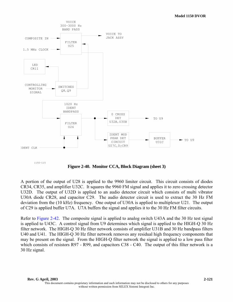
Model 1150 DVOR
Rev. G April, 2003 This document contains proprietary information and such information may not be disclosed to others for any purposes
without written permission from SELEX Sistemi Integrati Inc.
2-121
1150-115
VOICE300-3000 HzBAND PASS
FILTERU25
SWITCHESQ8,Q9
LEDCR11
U26FILTER
TO U9
0 CROSSDET
U32B,U30B
IDENT MODPEAK DETCIRCUIT
U27C,D;CR9
BUFFERU31C
VOICE TOJACK ASSYCOMPOSITE IN
CONTROLLINGMONITORSIGNAL
1020 HzIDENT
BANDPASS
IDENT CLK
1.5 MHz CLOCK
TO U9
Figure 2-40. Monitor CCA, Block Diagram (sheet 3)
A portion of the output of U28 is applied to the 9960 limiter circuit. This circuit consists of diodes CR34, CR35, and amplifier U32C. It squares the 9960 FM signal and applies it to zero crossing detector U32D. The output of U32D is applied to an audio detector circuit which consists of multi vibrator U30A diode CR28, and capacitor C29. The audio detector circuit is used to extract the 30 Hz FM deviation from the (10 kHz) frequency. One output of U30A is applied to multiplexer U21. The output of C29 is applied buffer U7A. U7A buffers the signal and applies it to the 30 Hz FM filter circuits. Refer to Figure 2-42. The composite signal is applied to analog switch U43A and the 30 Hz test signal is applied to U43C. A control signal from U9 determines which signal is applied to the HIGH-Q 30 Hz filter network. The HIGH-Q 30 Hz filter network consists of amplifier U31B and 30 Hz bandpass filters U40 and U41. The HIGH-Q 30 Hz filter network removes any residual high frequency components that may be present on the signal. From the HIGH-Q filter network the signal is applied to a low pass filter which consists of resistors R97 - R99, and capacitors C38 - C40. The output of this filter network is a 30 Hz signal.

Rev. G April, 2003 This document contains proprietary information and such information may not be disclosed to others for any purposes
without written permission from SELEX Sistemi Integrati Inc.
2-122
1150-115
VOICE300-3000 HzBAND PASS
FILTERU25
SWITCHESQ8,Q9
LEDCR11
U26FILTER
TO U9
0 CROSSDET
U32B,U30B
IDENT MODPEAK DETCIRCUIT
U27C,D;CR9
BUFFERU31C
VOICE TOJACK ASSYCOMPOSITE IN
CONTROLLINGMONITORSIGNAL
1020 HzIDENT
BANDPASS
IDENT CLK
1.5 MHz CLOCK
TO U9
Figure 2-41. Monitor CCA, Block Diagram (sheet 4)
The 30 Hz AM signal is amplified by U39C. The output of U39C is applied to DAC U35A where it is used as the reference voltage. The output of U35A is amplified by U39D and applied to two circuits. One is a half-wave rectifier consisting of resistors R62 and R91 and limiter-clipper diodes CR24 and CR25. The other is zero crossing detector U27A. The half-wave rectifier converts the full-wave 30 Hz signal into a half-wave signal that is analyzed by U9 to determine the percent modulation. U27A converts the 30 Hz AM signal into an accurate 30 Hz square wave that changes state whenever the 30 Hz waveform crosses the zero reference point. This signal is sent to an input of frequency counter multiplexer U21 so that it can be counted by interval timer U14 and the results supplied to U9. The crossing point of the 30 Hz signal is also used by U9 to calculate the VOR azimuth from the composite signal. The 30 Hz square wave test signal is applied to the input ports of analog switches U43C and U43D. When U9 performs a test of the 30 Hz circuits, U43C and U43D supply a 30 Hz signal to the 30 Hz AM and 30 Hz FM circuits. For normal operation, these analog switches are in an "open" state.
Model 1150 DVOR
Rev. G April, 2003 This document contains proprietary information and such information may not be disclosed to others for any purposes
without written permission from SELEX Sistemi Integrati Inc.
2-123
The 30 Hz FM signal is applied analog switch U43B. U43B is controlled by U9 which determines whether U43A will allow the 30 Hz FM signal to pass through or not. The 30 Hz FM or the 30 Hz test signal is next applied to a HIGH-Q 30 Hz filter network which consists of amplifier U7B and 30 Hz bandpass filters U37 and U38. This filter network removes any residual high frequencies that may be present on the signal. The output of the HIGH-Q filter network is applied to a low pass filter which consists of resistors R5, R6, R35 and capacitors C112 - C114. The output of the low pass filter is applied to amplifier is U39B. The output of U39B is used as a reference voltage for DAC U35B. The output of U35B is applied to amplifier U39A. The output of U35B is amplified by U39A and applied to two circuits. One is a half-wave rectifier consisting of resistors R18 and R40 and limiter-clipper diodes CR26 and CR27. The other is zero crossing detector U29A. The half-wave rectifier converts the full-wave 30 Hz signal into a half-wave signal that is analyzed by U9 to determine the percent modulation.
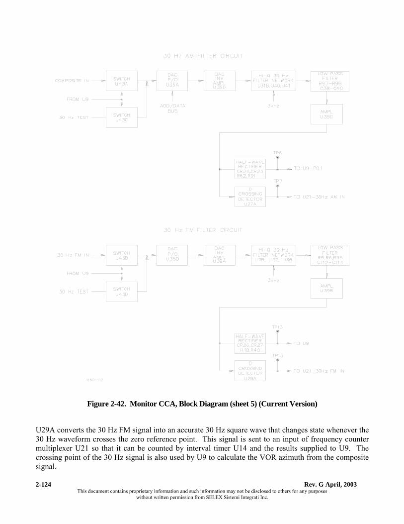
Rev. G April, 2003 This document contains proprietary information and such information may not be disclosed to others for any purposes
without written permission from SELEX Sistemi Integrati Inc.
2-124
Figure 2-42. Monitor CCA, Block Diagram (sheet 5) (Current Version)
U29A converts the 30 Hz FM signal into an accurate 30 Hz square wave that changes state whenever the 30 Hz waveform crosses the zero reference point. This signal is sent to an input of frequency counter multiplexer U21 so that it can be counted by interval timer U14 and the results supplied to U9. The crossing point of the 30 Hz signal is also used by U9 to calculate the VOR azimuth from the composite signal.

Model 1150 DVOR
Rev. G April, 2003 This document contains proprietary information and such information may not be disclosed to others for any purposes
without written permission from SELEX Sistemi Integrati Inc.
2-125
NOTE The DVOR 9960 Hz subcarrier is actually a 10 kHz frequency that may vary with a deviation that can range from ±454 Hz to ±497 Hz, dependent on the station frequency. To simplify the discussion of the VOR monitor CCA detailed theory, the standard values of 9960 Hz ±480 Hz will be used.
2.3.2.21.1 Monitor CCA (1A8, 1A24) Detailed Theory
Refer to Figure 11-18 (sheet 1 of 4). The monitor CCA is an independent unit designed to monitor and analyze the radiated signal from the VOR and initiate an alarm status signal if the VOR fails to operate within specified limits. The monitor analyzes one of several audio signals applied it. It can select a signal from field detector 1 or field detector 2, or the test generator signal. The monitor selects the desired composite VOR audio signal and extracts the individual audio components and DC levels to determine RF power level of the signal, percent modulation of the identity, 9960 Hz (10 kHz) subcarrier, and 30 Hz AM signals. It also determines the 9960 Hz (10 kHz) deviation ratio and the phase difference between the 30 Hz AM and 30 Hz FM signals. There are two monitors installed in the DVOR system. The monitors can be selectively organized by the operator to function in a logical "OR" or a logical "AND" configuration. The "OR" arrangement will allow either the controlling or redundant monitor to initiate a shutdown/transfer command. The "AND" configuration requires both monitors to agree that an out-of-tolerance condition exists before a shutdown/transfer command is initiated. The monitor CCA also measures the station RF frequency for accuracy. Micro controller U9 is identical to the micro controller used on the audio generator CCA. It handles numerous tasks and housekeeping chores to maintain monitor integrity, data analysis, and communications with the CPU CCA. Due to similarities with the audio generator CCA micro controller (paragraph 2.3.2.2.6) only a brief description of like functions are described here. Micro controller reset is accomplished by resistor R2, capacitor C1, inverter U4E, and switching transistor Q1. Power failure monitoring is accomplished by resistive voltage divider R3 and R1, amplifier U15C, and line receiver U6C. Terminals E1 and E2 provide the capability to have the NMI input to the micro controller disabled for factory testing. U9 communicates with the serial interface CCA by means of line driver U5A and line receiver U6B. U9 operates from 12 MHZ crystal Y1 and outputs a 6 MHZ clock frequency. U3 is an octal, D-type latch that passes address bits A0-A7. U9 provides an ALE output to the enable input of U3. U8 is a PAL that provides chip select signals to NVRAM U2, RAM U10, and timers U11 and U14. It also provides a clock signal to octal D-type flip-flop U13 and the section enable inputs of DAC U35.

Rev. G April, 2003 This document contains proprietary information and such information may not be disclosed to others for any purposes
without written permission from SELEX Sistemi Integrati Inc.
2-126
The software program for the monitor CCA is stored in 256 kbit (32 k by 8 bit) EPROM U1. Micro controller U9 utilizes RAM U10 to provide the temporary memory storage space needed for stack pointers and vectors, floating point calculations, and temporary data storage. U10 is a 256 kbit (32 k by 8 bit) memory device. NVRAM U2 is a 16 kbit (2 k by 8 bit) memory device that stores all of the calibration constants and alarm limits and all of the local operating parameters for the VOR monitor. The controlling monitor micro controller is responsible for setting the status of the antenna transfer coaxial latching relays. U9 has two output ports which drive invertors U4B and U4A. U4B, in turn, drives the base input of darlington transistor Q4. U4A drives the base input of darlington transistor Q5. The emitters of Q4 and Q5 are grounded. The collector of Q4 goes to the latching coils of the coaxial latching relays. The collector of Q5 goes to the releasing coils of the coaxial latching relays. When Q4 is turned on by U9, a ground is applied to the latching coils of the coaxial latching relays connecting system A to the antenna array and system B to the dummy loads. When Q5 is turned on, a ground is applied to the releasing coils of the coaxial latching relays connecting system B to the antenna array and system A to the dummy loads. Address/data bits AD4-AD6 are latched by U12 to produce a 3-bit code for the address inputs of 1-of-8 multiplexer U21. Address/data bit AD7 is used to determine the controlling monitor which controls the enable input of U13 and the amplifier section of voice bandpass filter U25. Triple, 16-bit, programmable, interval timers U11 and U14 are used to create precision gates within which pulses of different frequencies can be counted with great accuracy. Y2 is a 2 MHZ crystal that is used with inverter U4F to form a simple oscillator circuit. The output of the oscillator goes to U11 counter 0 clock input CLK0. U11 and U14 receive their chip select signals from U8. U11 and U14 are interconnected into the address/data bus bits AD0-AD7, thereby providing a means for U9 to program the six counters and read count data stored internally. Address bits A0 and A1 and the read and write bits from U9 complete the control signals sent to U11 and U14. The three counter gate control inputs of U11 are all tied HIGH. U11 counter 0 is programmed to divide the input frequency by a factor of 10,000. Counter 0 output OUT0 should be a 2.0 MHz frequency. Capacitor C4 is used to trim the oscillator for a frequency of 2000 MHz at test point TP16. OUT0 drives the CLK1 input of U11 counter 1. Counter 1 is programmed to divide the input frequency by a factor of 2000 which produces a precise 10 second (0.1 Hz) positive gate at OUT1. The 10 second gate sets the interval counting period for U14 counter 0 and provides an interrupt to U9 via inverter U4C. The CLK0 and CLK1 inputs of U14 are pulse trains that come from the output of U21. U14 counter 0 gate input G0 is the 10 second positive enable pulse which will establish the counter interval for U14 counter 0. At the end of the count interval, the count value is converted into a 12-bit word and placed onto the 8-bit address/data bus with two write commands under the control of U9. When counting low frequency signals such as 30 Hz or 9960 Hz, there is no concern with overflow. However, when attempting to count the carrier sample frequency, overflow may be a problem. The output of U14 counter 0 is an overflow from 16-bit counter 0. This output is inverted by inverter U36B and applied to U14 counter 1 G1 input with the pulse train from U21 applied to CLK1. This allows the second 16-bit counter to count the overflow pulses during the entire 10 second interval. Again, at the end of the interval, the 32-bit count is converted into a 12-bit data word and sent to U9 via the address/data bus.

Model 1150 DVOR
Rev. G April, 2003 This document contains proprietary information and such information may not be disclosed to others for any purposes
without written permission from SELEX Sistemi Integrati Inc.
2-127
The 6 MHZ clock signal from U9 enters the CLK2 inputs of U11 and U14. U11 counter 2 is programmed to divide the input frequency by a factor of approximately ten. With a 6 MHZ input, the output frequency will be 599.995 kHz. This frequency is used by the 9960 Hz (10 kHz) bandpass filter U28 as the high end cutoff clock frequency which is labeled 9960CH. U14 counter 2 is programmed to divide the 6 MHZ input frequency by a factor of approximately fourteen which will produce an output frequency of 428.539 kHz. This frequency is used by U28 as the low end cutoff frequency and is labeled 9960CL. Frequencies from several on-board and off-board locations are sent to the input lines of multiplexer U21. These signals are: on-channel carrier sample frequency; USB sample frequency; LSB sample frequency; 30 Hz AM signal frequency; 9960 Hz (10 kHz) FM subcarrier frequency; and 30 Hz FM signal frequency. A three bit code from U12 is used to select which frequency is passed through U21 to be counted by timer U14. U34 is a three terminal voltage regulator that converts +12 Vdc to +5 Vdc. This is used as a separate regulated 5 volt source on the monitor CCA that is isolated from the general +5 Vdc (Vcc) power bus. U17 is a three terminal voltage regulator that converts -12 Vdc to -5 Vdc. U19 is a precision reference voltage source that produces a +5 Vdc reference (VREF). Potentiometer R10 is adjusted to trim the output voltage (To 5.11±0.1) which can be measured at test point TP17. U16, U18, and U20 are quad differential input multiplexers. U16 section 1 has the audio signal from field detector #1 applied to it. U16 section 2 has the audio signal from field detector #2 applied to it. U16 section 3 is not currently used. U16 section 4 has the test generator signal applied to it. U18 sections 1, 2, 3 and 4 are not currently used. U20 has the sideband 1 and sideband 2 forward and reflected power DC analog voltages applied to it. The differential outputs of U16 and U18 are tied together and buffered by U15B and U15D. Instrumentation amplifier U15A is a unity gain amplifier that references the signal to ground. Under normal operating conditions, this signal will be an AC and DC composite of the detected RF signal. The level of the composite output of U15A can be measured at test point TP5. A portion of the composite signal is sent through a low pass filter consisting of R103 and C41 that removes all AC variations. The remaining DC voltage is buffered by U7D before it is sent to U9 for analysis. The input to U9 is protected by a limiter-clipper circuit. This DC voltage represents the field intensity of the DVOR transmitter that is directly related to the carrier power level. Triple analog switch U24 is used by U9 to provide a 2-bit address code that will activate one of the four inputs of U16 or U18. The third output from U24 goes directly to the enable input of U16 and is inverted by U4D before going to the enable input of U18. U9 can control which multiplexer and which input will be activated to provide the input signal to the monitor CCA. Terminals E3 and E4 provide a means to force the monitor CCA to constantly receive the test generator signal. This is used during test, alignment, or maintenance of the monitor CCA.
Rev. G April, 2003 This document contains proprietary information and such information may not be disclosed to others for any purposes
without written permission from SELEX Sistemi Integrati Inc.
2-128
In order for the monitor CCA to select the signal from field detector #1, U9 sets the X1 and Y1 inputs to U24 to a logic LOW and the Z1 input to a logic HIGH. The switch inputs of U24 are set HIGH by pull-up resistor R27. Therefore, U24 provides a logic LOW on the X and Y outputs and a logic HIGH on the Z output. To select field detector #2, the X output of U24 must be a logic HIGH, the Y output must be a logic LOW and the Z output must be a logic HIGH. When a jumper is placed across terminals E3 and E4, the switches of U24 are set to a logic LOW. This forces U24 to select the X0, Y0 and Z0 inputs as the output signals. The X0, Y0 and Z0 inputs are all tied to VCC which is a logic HIGH. Therefore, the output of U24 instructs U16 to select the test generator input for the monitor. The 6 MHZ clock from U9 is applied to binary counter U22B. The divide-by-four output of U22B is a 1.5 MHZ clock that is sent to voice bandpass filter U25 and to an input port of U9. The divide-by-two output of U22B is a 3 MHZ clock which drives the clock input of presettable, synchronous, 4-bit binary up/down counter U23. U23 is set to operate as a count up device and is preprogrammed with a count of one in its internal counter circuit. This means the counter will start counting from 1 up to 15 and then produce a carry output. The output of U23 is a 200 kHz signal (3 MHZ ÷ 15) which drives the clock input of binary counter U22A. The output of U22A is a 100 kHz clock signal labeled IDENTCLK which controls the clock inputs of ident bandpass filter U26. The aural section of the monitor CCA is responsible for extracting the identity and voice components from the composite signal output of U15A. A portion of the composite signal is first applied to voice bandpass filter U25. This filter is identical to the voice bandpass filter used on the audio generator CCA so the function of the internal sections are similar. U25 has a 1.5 MHZ clock signal from U22B applied to it. The composite signal is applied to the input of the receiver filter stage VFRI. The output of the receiver filter stage VFRO directly feeds the input of the transmitter filter stage VFXI. The transmitter filter stage is a 300 to 3000 Hz bandpass filter. The transmitter filter stage output VFXO is an aural signal that can contains all the frequencies within the bandpass of 300 to 3000 Hz. This aural signal is proportionally applied to two circuits. The first circuit is the input to the power amplifier section of U25. Also tied to that input is bias control transistor Q9. The base of Q9 is driven by the collector of transistor Q8. LED CR11 is connected to the emitter of Q8. The control monitor signal from U12 is applied to the base of Q8. If this monitor is the controlling monitor, then the signal applied to the base of Q8 is a logic LOW. This turns on Q8 which allows CR11 to illuminate. CR11 is a green LED which is the visual indication to identify the controlling monitor. Turning on Q8 turns off Q9 which removes the negative potential bias voltage from the input of the power amplifier section. This allows the power amplifier section to amplify the audio signal obtained from VFXO and pass it out the power amplifier differential output ports (PWRO+ and PWRO-). Therefore, the controlling monitor will be the monitor that supplies an audio signal to the jack assembly or a remote aural monitor. If the monitor CCA is not the designated controlling monitor, a HIGH is applied to the base of Q8 which will turn it off. LED CR11 is extinguished and the HIGH is removed from the base of Q9. Q9 is now turned on by self-biasing resistor R52. With Q9 on, a negative potential is applied to the power amplifier input which effectively shuts off the power amplifier section. Potentiometer R21 is adjusted to set the gain of the power amplifier stage. The voice output signal can be measured at test points TP1 and TP2. R21 is factory set to produce 3.5 Vpp at TP4 when the test generator is set to 20% Ident and 30% Voice (1500 Hz). Adjustment of R21 to a lower output level may affect the monitoring of the ident level.

Model 1150 DVOR
Rev. G April, 2003 This document contains proprietary information and such information may not be disclosed to others for any purposes
without written permission from SELEX Sistemi Integrati Inc.
2-129
The second section that processes the 300-3000 Hz aural signal is the identity circuitry. Ident bandpass filter U26 is a 1020 Hz switched capacitor bandpass filter. This filter uses a mode of operation that requires a clock frequency which is 100 times the desired bandpass frequency. The 100 kHz IDENTCLK signal from U22A is used as the clock signal for both sections of U26. Because the desired frequency is 1020 Hz, the circuit is designed to take advantage of the error of the internal switched capacitors. Potentiometers R90 and R91 are adjusted at the factory to skew the center frequency of the switched capacitor filter from 1000 Hz to 1020 Hz. Potentiometers R90 and R91 are adjusted during ident to maximum ident output at TP8. Terminals E5, E6, and E7 are jumpered at the factory for best operation of the filter. The aural signal is applied to the input of U26A. The bandpass port (output of U26A) and is applied to the input of U26B. The bandpass port (output of U26B) is a frequency centered at 1020 Hz with over 30 dB attenuation ±15 Hz from the center frequency. The ident signal can be measured at test point TP8. This ident signal is equally divided between an ident peak modulation detector circuit and a zero crossing detector circuit. The ident peak modulation detector consists of a full wave rectifier, a low pass filter, and a buffer. The ident frequency is rectified by an active full wave rectifier circuit comprised of amplifiers U27C and U27D and diode CR9. The output signal is filtered by a low pass filter consisting of resistor R36 and capacitor C98 which removes any 1020 Hz or 10 kHz ripple remaining on the DC voltage. Test point TP10 is used to measure the DC voltage which represents the peak value of ident modulation at this point. The voltage is then buffered by amplifier U31C. The output of U31C drives a protected input port of U9. U9 uses this input to calculate the percent modulation of the identity frequency. Amplifier U32B operates as a filtered zero crossing detector. The filtering action is to insure all traces of the 100 kHz clock signal are removed from the signal. Its output is sent through a limiter-clipper to the positive toggle input of one-shot multi vibrator U30B. U30B stabilizes the 1020 Hz crossover pulse from U32B before it is applied to U9. The output of U30B goes HIGH whenever the output of U32B transitions from a LOW to a HIGH. The duration of the output pulse is approximately 3 microseconds. U9 no longer requires U21 to evaluate the ident frequency; therefore, the ident pulses that go to U21 are no longer passed through to timer U14. The composite signal is also sent to the 9960 Hz circuitry to extract the peak 9960 Hz (10 kHz) modulation and the 30 Hz FM modulation signal. The composite signal is buffered by amplifier U32A before it is applied to 9960 Hz bandpass filter U28. U28 is identical to U26. U28 requires a clock frequency that is 50 times the high and low cutoff frequencies of the bandpass. These clock signals are the 9960CH and 9960CL signals. The clock frequencies set the high end roll-off at approximately 12000 Hz and the low end roll-off at approximately 8570 Hz. This provides room for the 9960 ±480 Hz FM subcarrier signal to pass through without attenuation. The filtered output from U28 is measured at test point TP11. The signal is then applied to the 9960 level detector circuit and the 9960 limiter circuit. The 9960 level detector uses an active full wave rectifier circuit consisting of amplifiers U29C, U29D, and diode CR10. This active rectifier circuit uses potentiometer R43 to provide an offset adjust that is factory adjusted to ensure the peaks of the rectified pulses are equal. The signal is sent through a low pass filter comprised of resistor R49 and capacitor C25. This filter removes any residual 9960 Hz or clock frequency ripple and provides a pure DC voltage that represents the percent modulation level of the 9960 Hz (10 kHz) signal. The DC voltage is buffered by U31D before it is made available for measurement at test point TP14 and applied to a protected input of U9. U9 uses this input to calculate the percent modulation level of the 9960 Hz (10 kHz) signal.

Rev. G April, 2003 This document contains proprietary information and such information may not be disclosed to others for any purposes
without written permission from SELEX Sistemi Integrati Inc.
2-130
The output U29C is fed to the Notch Monitor circuit consisting of R86, R89, U44, U29B, CR18 and CR19. The Notch Monitor circuit provides a signal that contains the DVOR sideband modulation to the microprocessor U9. This signal is sampled at 48 different times when individual sideband antennas are radiating. When an antenna is not radiating correctly the signal level will change at the time when that particular antenna is radiating. R86 and R89 provide voltage division prior to entering the U44 filter input. A 100 kHz clock sets the cutoff frequency for the 6th order low pass filter at 4000 Hz. This low pass filter eliminates the 9960 Hertz component but allows the DVOR modulation frequencies of 720 and 1440 Hertz to pass. Amplifier U29B buffers the signal. CR18 and CR19 limit the signal voltage range to U9. The 9960 limiter circuit consists of U32C and diodes CR34 and CR35 in the feedback path. The limiter squares the 9960 ±480 Hz FM signal before it is applied to U32D which functions as another filtered zero crossing detector. The variable pulse width pulse train passes through a limiter-clipper before being applied to the positive toggle input of one-shot multi vibrator U30A. U30A is used to generate 9960 Hz (10 kHz) FM frequency pulses that will be counted by U9 and to recover the 30 Hz FM modulation signal. Every LOW to HIGH transition of the output pulse from U32D causes U30A to toggle. When this happens, the Q output goes HIGH for approximately 3 microseconds. The pulses from the Q output vary in frequency between 9480 Hz and 10440 Hz. These 9960 Hz FM pulses are sent to one input of frequency counter multiplexer U21 where it will eventually be counted by interval timer U14 and the resultant count is provided to U9. The 9960 Hz (10 kHz) FM pulses, from the Q output of U30B can be measured at test point TP12. Capacitor C29 is allowed to charge through resistor R56. The output is normally HIGH. When U30A toggles, the output goes LOW. This allows capacitor C29 to discharge through the low impedance path established by diode CR28 and the port. After U30B returns to its stable state, capacitor C29 begins to charge up again. Because the width between toggle pulses varies at the FM modulation frequency, the average voltage on C29 changes according to the modulation frequency. The charge/discharge pulses of C29 are buffered by U7A before they are sent to the 30 Hz FM filter circuit. The 30 Hz AM filter circuit extracts the 30 Hz AM signal from the composite signal. The composite signal is sent to analog switch U43A. U43A is controlled by U9 which determines whether U43A will allow the composite signal to pass through or not. U43A is enabled, except when U9 places the monitor CCA into a test mode. During initial internal calibration and once every two minutes a reference 30 Hz signal is passed through the two filters and the phase difference is measured. If a phase change occurs after calibration the Azimuth measurement is corrected. A tenth order active bandpass filter circuit which consists of amplifier U31B, dual switched capacitor 30 Hz bandpass filters U40 and U41, and two low pass RC filter circuits. U31B is a 30 Hz bandpass filter designed with a Q of ten. The output passes through a low pass filter comprised of resistor R102, resistor network RN9 section 7-8, and capacitor C105. This filter removes any residual high frequencies that may be present on the signal. U40 and U41 operate from a 3 kHz clock supplied by U9. The output of U41 is sent through a three pole low pass filter that rejects any residual 3 kHz clock frequency from the 30 Hz AM signal. The output signal is the 30 Hz AM frequency ±2 Hz at the 3 dB points.

Model 1150 DVOR
Rev. G April, 2003 This document contains proprietary information and such information may not be disclosed to others for any purposes
without written permission from SELEX Sistemi Integrati Inc.
2-131
The composite signal is applied to DAC 35A and OP Amp U39D. U35A is being used as an active attenuator that controls the level of the 30 Hz AM signal by U9. The output of U35A is inverted by amplifier U39D. The output of U39D is a fullwave 30 Hz signal. The gain of U39D is determined by the internal feedback resistor in U35A. The signal is then equally divided before being sent to the micro controller. The fullwave signal is converted into a rectified halfwave signal by limiter-clipper diodes CR24 and CR25. The halfwave 30 Hz signal is applied to an input port of U9. During calibration, U9 reads the peak value and adjusts DAC U35A for a constant level. U9 senses this level to determine the percent modulation of the 30 Hz AM signal. The halfwave signal is measured at test point TP6. The 30 Hz AM signal is also sent to amplifier U27A which functions as a saturating zero crossing detector that converts the 30 Hz AM signal into an accurate 30 Hz square wave. This signal is measured at test point TP7. This signal is sent to an input of frequency counter multiplexer U21 where it can be counted by interval timer U14 and the resultant data is supplied to U9. The output of U27A is passed through limiter--clipper diodes CR32 and CR16 before it is sent to U9. The zero crossing point of the 30 Hz signal is used by U9 to calculate the VOR azimuth from the composite signal. U9 also uses this zero crossing as a time reference to measure the half wave signal at TP6. After a negative edge occurs U9 delays then measures the peak of the 30 Hz half wave signal. Refer to Figure 11-18 (sheet 3 of 4). Micro controller U9 provides a 3 kHz signal to decade divider U42A. U42A supplies a 300 Hz signal to decade divider U42B. The output of U42B is an accurate 30 Hz signal that is used by U9 to test the 30 Hz AM and 30 Hz FM frequency circuits. The 30 Hz square wave test signal is buffered by U27B before it is applied to the input ports of analog switches U43C and U43D. Line receiver U5C is used an inverter for the micro controller control signal from U9. U5C inverts the control signal sent to the control inputs of U43C and U43D so that they operate opposite to U43A and U43B. When U9 performs a test of the 30 Hz circuits, U43C and U43D supply a 30 Hz signal to the 30 Hz AM and 30 Hz FM circuits. For normal operation, these analog switches are set to an "open" state. Once every 2 minutes the test signal is used to check the phase shift through the 30 Hz bandpass filters. The 30 Hz FM circuit is identical to the 30 Hz AM circuit described above. The 30 Hz FM pulses which were generated by C29 and buffered by U7A are sent through analog switch U43B to the 30 Hz FM filter circuit. The active components used in the 30 Hz FM bandpass filter are: amplifier U7B and switched capacitor filters U37 and U38. The high gain amplifier is U39B. DAC U35B is the active attenuator for the 30 Hz FM signal with operational amplifier U39A as the output amplifier. Amplifier U29A is the saturated zero crossing detector that provides the 30 Hz FM square wave to U9 and U21. This signal is measured at test point TP15. (On early versions of the monitor CCA, TP15 was omitted. Therefore, the signal can be measured at the junction of U29 pin 1 and R83). The half wave 30 Hz signal is sent to U9 to monitor the level of the 30 Hz FM modulation. Test point TP13 is used to measure this signal.

Rev. G April, 2003 This document contains proprietary information and such information may not be disclosed to others for any purposes
without written permission from SELEX Sistemi Integrati Inc.
2-132
2.3.2.22 Power Panel
Refer to Figure 2-43. The power panel, located on the lower front portion of the electronics cabinet, contains the AC input and DC input circuit breakers for system A and system B. AC input power enters the cabinet via terminal board 1TB1 terminals 1, 2 and 3. Positive DC input power wires from the optional battery backup (unit 3) enter the cabinet via terminal board 1TB1 terminals 4 and 5. The negative DC input power wires connect directly to grounding lug 1E1. Circuit breakers 1CB1 and 1CB2 control the application of AC voltage to system A and system B battery charger power subsystems respectively. Circuit breakers 1CB3 and 1CB4 control the application of DC voltage to system A and system B battery charger power subsystems respectively.
2.3.2.23 Battery Charger Power Subsystem (1A33, 1A34)
Refer to Figure 2-44. Each VOR transmitter system has a separate battery charger power subsystem (BCPS) installed. The BCPS is a modularized, non-repairable unit capable of operation from either 115 Vac or 230 Vac power source. With the jumper installed across terminals 1 and 2 of TB2, operation at 115 Vac is selected. The BCPS is comprised of a base unit; a 48 Vdc, 1000 W uninterruptible power supply (UPS) module; a 48 Vdc, 16 A single output module; and a 28 Vdc, 8.6 A single output module.

Model 1150 DVOR
Rev. G April, 2003 This document contains proprietary information and such information may not be disclosed to others for any purposes
without written permission from SELEX Sistemi Integrati Inc.
2-133
Figure 2-43. Power Panel
2.3.2.23.1 Base Unit
The base unit contains the main AC rectifier, electromagnetic interference (EMI) and DC filters, sync and bias supplies, a 300 Vdc isolated bus, DC fan and system control and status circuitry. The AC voltage is filtered by the EMI filter and applied to a soft start circuit which limits in-rush current. A rectifier and filter circuit converts the applied AC voltage to 300 Vdc. This is the common bus voltage used within the BCPS to power all subordinate modules and functions. A sync and bias supply inverter operates from the 300 volt bus to provide synchronous module control signals. This ensures all power supply modules sense system changes synchronously. The bias supply inverter also provides power to a separate rectifier/filter circuit which supplies power to the base unit DC fan and system control circuits.
Rev. G April, 2003 This document contains proprietary information and such information may not be disclosed to others for any purposes
without written permission from SELEX Sistemi Integrati Inc.
2-134
2.3.2.23.2 UPS Module
The UPS module is capable of providing up to 1000 W of automatic battery backup power. This module contains a 48 volt to 300 volt DC/DC converter (UPS section), a three stage 300 volt to 48 volt automatic battery charger, and a control and logic section. Switching from AC to battery operation is automatic and transient free. This module interconnects with the 300 Vdc bus of the base unit. With AC voltage applied, the UPS module applies a trickle voltage (factory adjusted) to maintain the backup batteries in a fully charged condition. In this mode, the module is capable of monitoring the charge quality of the backup batteries. The charge cycle of the UPS module operates in three stages. Initially, the charger will provide 4 amperes of charging current until the battery voltage rises to the overcharge voltage level (set at the factory). In the overcharge mode, the charger will maintain the voltage constant until charging current falls below 0.5 amperes. The charger will then switch to a trickle voltage. The charger will supply the trickle charge voltage for a fixed period of time and then shut off the charger circuit to measure battery voltage. If the voltage is insufficient, the trickle charge mode is enabled again. This action will continue to insure the battery system maintains its charged condition. The UPS module also continuously monitors the status of the applied AC voltage by sampling the 300 Vdc bus voltage. Loss of the applied AC power causes the bus voltage to decrease. The UPS module senses this loss and switches from battery charger mode to UPS mode. The UPS mode converts 48 Vdc from the backup batteries to 300 Vdc. This voltage is applied to the base unit bus to provide an uninterrupted voltage source for the DC power supply modules to operate from.

Model 1150 DVOR
Rev. G April, 2003 This document contains proprietary information and such information may not be disclosed to others for any purposes
without written permission from SELEX Sistemi Integrati Inc.
2-135
Figure 2-44. Battery Charger Power Subsystem
The UPS module provides two status signals to the system micro controller: a UPS on signal and a battery low signal. The UPS on signal notifies the system micro controller that the UPS module is in the UPS mode of operation. The battery low signal notifies the system micro controller that the charge quality of the backup batteries is deficient and battery inspection is needed. This status signal is present whenever the backup batteries fail to hold a sufficient charge or whenever the system has been operated from the backup batteries for a period of time sufficient enough to significantly deplete them. The UPS module also receives a BCPS charger off command signal from the system micro controller. This command signal will shut off the charger portion of the UPS module. The UPS module has a UPS inhibit logic input which is permanently tied low, which places the UPS module in a constant enable condition.

Rev. G April, 2003 This document contains proprietary information and such information may not be disclosed to others for any purposes
without written permission from SELEX Sistemi Integrati Inc.
2-136
2.3.2.23.3 48 Vdc Module
This power supply module provides a nominal 48 volts of fully regulated output voltage at a maximum current of 16 amperes. The module is factory adjusted to output 48 Vdc. This power supply module features an output voltage margin function. The margin function allows the module, under the control of the audio generator micro controller, to reduce its output voltage approximately ten percent. Within the transmitter system, the module normally operates with the margin enabled; that is, the output voltage will be approximately 43.2 Vdc. When directed by the audio generator micro controller, the margin is disabled, allowing the voltage to increase to 48 Vdc. This module provides an output voltage sense signal to the facilities board where it is converted to a binary code that is read by the system micro controller. This power supply module only provides output voltage to the CSB power amplifier assembly.
2.3.2.23.4 28 Vdc Module
This power supply module provides a nominal 28 volts of fully regulated output voltage at a maximum current of 8.6 amperes. The module is factory adjusted for an output of 28 Vdc. This module provides an output voltage sense signal to the facilities board where it is converted to a binary code that is read by the system micro controller. It provides the common 28 Vdc operational voltage to power the VOR transmitter, RMS and RF monitor assemblies and the commutator.
2.4 COMMUTATOR (UNIT 2)
The DVOR commutator rack contains a control assembly, two commutator assemblies and a monitor interface assembly. Standard coaxial RF cables bring the four sideband RF signals and the carrier RF signal from the DVOR equipment cabinet into the commutator rack. The sideband RF signals are directed to the commutator CCAs. The carrier RF signal and the sideband RF signals from the output jacks of the commutator CCAs are sent through high quality, low loss coaxial feed cables to their respective antennas. The purpose of the commutator is to effectively apply the four DVOR sideband RF signals to the appropriate sideband antennas, in such a manner, as to make it appear that the mean RF level of the sideband signals are rotating counterclockwise about the central radiating antenna. To reduce error in the radiated signal, pin-diode technology and EPROM signal programming are used to produce the cos.836x blending function. This limits the ±480 Hz instantaneous frequency deviation in space to ±564 Hz rather than the ±680 Hz which many other DVOR systems encounter.

Model 1150 DVOR
Rev. G April, 2003 This document contains proprietary information and such information may not be disclosed to others for any purposes
without written permission from SELEX Sistemi Integrati Inc.
2-137
2.4.1 Control Assembly (2A1)
The control assembly contains the pin driver CCA.
2.4.2 Pin Diode Driver CCA Block Diagram Theory
Refer to Figure 2-45. The pin diode driver CCA processes all signal steering for antennas 1 through 48. Commutator switch control signals from the audio generator CCA are applied to a differential line receiver circuit on the pin diode driver CCA. The line receiver circuit which consists of line receivers U5A, U5B, U5C, U5D, U6A, and U6B converts the differential signals to TTL signal levels. From the line receiver circuit the control signals are applied to programmable logic device (PLD) U4. PLD U4 performs decoding and distribution of the antenna and transfer signals. To simplify discussion, only the odd antenna operation shall be discussed. The output of PLD U4 is applied to a level converter circuit which consists of U7A, U7B, U7C, and U7D. This circuit converts the antenna select data, which is referenced to TTL levels, to logic levels referenced at -10V to +5 VDC. The output of this circuit is applied to a 4:16 line decoder U12. PLD U4 also outputs signals to a transfer generation circuit which consists of amplifiers U17A, U17B and transistors Q2, Q3, Q4 and Q1. The outputs of the transfer circuit are the ODD and NOT ODD XFR signals. These are opposite polarity CMOS logic signals that change state every 1/60th of a second. U12 decodes the antenna select data code to select one of the twelve outputs used in the 48 antenna system. The remaining outputs of U12 are not used. The twelve output lines are normally HIGH (+5 volts). When selected, it is pulled LOW (-10 volts). Each output line is applied to a display driver circuit which consists of drivers U8 through U11, U13 through U16, and U18 through U21. This circuit provides the necessary drive to operate the odd numbered antenna RF signal switching pin diodes on the upper commutator CCA. Ground check switch control signals from the monitor CCA are applied to a differential line receiver circuit on the pin diode driver CCA. The line receiver circuit, which consists of line receivers U3A, U3B, U3C and U3D, converts the differential signals to the TTL signal levels. Automatic ground check may be user enabled to verify operation of the DVOR. The ground check feature is normally disabled. If enabled, the TTL level ground check signals will be added as an offset inside of PLD U4. Refer to Table 2-6.

Rev. G April, 2003 This document contains proprietary information and such information may not be disclosed to others for any purposes
without written permission from SELEX Sistemi Integrati Inc.
2-138
Doppler VOR System001150-XXXX
J3-DB25Connector
RS422 toCMOS TTLConverters
PowerSwitch Fuse
+28VDCOR'ingDiodes
DC-DCConverter
CMOS TTLto Bi-levelConverters
Ground Check /Antenna Select
Decoder
J1 OddConnector
J2 EvenConnector
J4 FieldDetectorsConnector
Odd CommutatorCCA 012702-0001
Even CommutatorCCA 012702-0001
Dipole AntennaArray - 48elements
Monitor Interface Assy030544-0001
Regulator
Regulator
+5VDC
+3.3VDC
-10VDC
+12VDC
-12VDC
PIN Diode Driver CCA012098-1001
DVOR CommutatorUnit
030442-000X
Ground CheckEnable Strap
Figure 2-45. Pin Diode Driver CCA, Block Diagram

Model 1150 DVOR
Rev. G April, 2003 This document contains proprietary information and such information may not be disclosed to others for any purposes
without written permission from SELEX Sistemi Integrati Inc.
2-139
2.4.2.1 Pin Diode Driver CCA Detailed Circuit Theory
Refer to Figure 11-31. Commutator switch control signals from the audio generator CCA are applied to the input of the master pin diode driver CCA that processes the signals for the antennas. These control signals consist of the four balanced antenna select signals, a transfer signal, and a clock signal applied to quad differential line, receivers U5 and U6. Two inputs of U6 are not used and are tied to ground. The antenna switch signals are applied to PLD U4. PLD U4 is programmed to perform all decoding and distribution of the antenna and transfer signals. The clock signal provides a synchronous timing signal for all switching activities. The ground check switch control lines are translated to TTL levels by differential line receiver U3. If the automatic ground check feature is enabled at J5, the ground check control lines are added as an offset inside PLD U4. Each increment of the ground check control is added as an offset of 3 to the antenna selected by the DVOR switch control lines. U4 drives quad converter U7. U7 translates the antenna select data, which is referenced to TTL levels, into CMOS levels (+5V and -10V). The data from U7 is next applied to 4-to-16 line decoder U12. U4 uses the LOW to HIGH transition of the 720 Hz clock signal to control the timing of the odd antenna switching signals. U4 uses the HIGH to LOW transition of the clock signal to control even antenna switching signals. The time difference is 1/1440th of a second which is the timing difference between a sine and cosine radiated sideband signal. U12 decodes the antenna select 4-bit data code to select one of the twelve active outputs used in the 48 antenna system. Outputs 13, 14, 15, and 16 are not used. The twelve lines are normally HIGH (+5 volts). When an output line is selected, it is pulled LOW (-10 volts). Each output line feeds the A input of a decoder driver circuit (U6 through U11, U13 through U16 and U18 through U21). The B and C inputs are tied to +5 volts while the D input is tied to -10 volts. The segment driver outputs of each display driver are uniquely paralleled to provide the necessary drive current to operate the RF signal switching pin diodes. Effectively, there are two outputs from each display driver: one is designated the "ON" line, and the other is the "OFF" line. U12 decoder output S∅NOT controls display driver U8 which changes the ON and OFF control signals on commutator antenna control lines OFF 1 and 25, and ON 1 and 25. U12 decoder output S1NOT controls U13 which controls lines OFF 3 and 27, and ON 3 and 27. OFF 1 and 25 is labeled 1A and ON1 & 25 is labeled 14B on the 012702-0001 commutator CCA. Also OFF 3 and 27 and ON 3 and 27 are labeled 2A and 15B on the commutator CCA. To simplify the discussion of the operation of the decoder driver signals, only the action of U8 will be examined. U8 controls the 1A and 14B ON and OFF lines. If U8 is not selected by U12, then the ON line will have a potential of -10 Vdc and the OFF line will have a potential of +5 Vdc. When U12 selects U8, the ON line switches to +5 Vdc and the OFF line switches to -10 Vdc. This condition exists for the entire time that the selected antenna will radiate, which is 1/720 of a second.

Rev. G April, 2003 This document contains proprietary information and such information may not be disclosed to others for any purposes
without written permission from SELEX Sistemi Integrati Inc.
2-140
U4 also outputs signals used to generate a ODD_XFR and a ODD XFR NOT signal. PLD U4 outputs a signal to the inverting input of voltage comparator U17A. The non-inverting input of U17A is referenced at approximately 1.5 volts by a voltage divider network which consists of resistors R14 and R15. When U4 outputs a logic LOW, it is inverted by U17A to a HIGH which turns off Q2. When Q2 turns off, Q1 is turned on by self- biasing resistor RN6 section 3-14. With Q1 on, a potential of approximately -10 Vdc is applied to the ODD XFR line to the commutator CCA. The LOW output from U4 is also applied to the non-inverting input of U17B. U17B has a +1.5 Vdc bias applied to its inverting input by R14 and R15. The LOW in makes U17B output a LOW which turns on transistor Q4. The emitter of Q4 is tied to VCC. With Q4 turned on, a positive voltage is applied to the base of Q3 and the anode of CR30. The positive bias on the base of Q3 keeps Q3 turned off. However, CR30 becomes forward biased and a positive potential of approximately +5 Vdc is applied to the ODD XFR NOT line to the commutator. When the output of U4 changes to a HIGH, Q2 and CR29 in the ODD XFR section are biased on and Q3 in the ODD XFR NOT section is biased. This changes the polarity of the signals on the ODD XFR and ODD XFR NOT lines. The ODD XFR and ODD XFR NOT changes state every 1/60th of a second. Scope Synch is available on the ODD XFR signal at test point TP1. Power for the CCA enters via J3 – 12 and J3 – 13. Diodes CR4 and CR6 form an “OR” for the two +28V supplies into Switch S1. If fuse F1 is intact, LED CR5 lights when switch S1 is in the ON position. The DC-DC converter PS1 converts the +28V to +5V, +12V and -12V supplies. Regulator U1 regulates the -12V supply to -10V. Regulator U2 regulates the +5V to +3.3V for powering the PLD U4. Connector J6 is used for in-system programming of PLD U4 and should not be utilized by the customer. Connector J7 is used for test of the CCA and should not be utilized by the customer. Connector J4 provides +12V and -12V power for the Field Detectors. All control lines entering via connector J3 are surge protected by transient voltage suppressors (TVS) CR9 though CR28. The +28V supply is protected by TVS CR7. The +5V, +12V, and -12V supplies are protected by TVS CR2, CR3 and CR1. The auto-ground check enable input is transient protected by TVS CR8.

Model 1150 DVOR
Rev. G April, 2003 This document contains proprietary information and such information may not be disclosed to others for any purposes
without written permission from SELEX Sistemi Integrati Inc.
2-141
Table 2-5. Commutator Driver/Antenna Switch Sequence
Antenna Number U12 (U27) Decoder Output Display Driver
Commutator CCA Position Odd (Even)
0 U8 (U23) 1A 1 2 1 U13 (U28) 2A 3 4 2 U18 (U32) 3A 5 6 3 U9 (U24) 4A 7 8 4 U14 (U29) 5A 9 10 5 U19 (U33) 6A 11 12 6 U10 (U25) 7A 13 14 7 U15 (U30) 8A 15 16 8 U20 (U34) 9A 17 18 9 U11 (U26) 10A 19 20 10 U16 (U31) 11A 21 22 11 U21 (U35) 12A 23 24 0 U8 (U23) 14B 25 26 1 U13 (U28) 15B 27 28 2 U18 (U32) 16B 29 30 3 U9 (U24) 17B 31 32 4 U14 (U29) 18B 33 34 5 U19 (U33) 19B 35 36 6 U10 (U25) 20B 37 38 7 U15 (U30) 21B 39 40 8 U20 (U34) 22B 41 42 9 U11 (U26) 23B 43 44 10 U16 (U31) 24B 45 46 11 U21 (U35) 25B 47 48

Rev. G April, 2003 This document contains proprietary information and such information may not be disclosed to others for any purposes
without written permission from SELEX Sistemi Integrati Inc.
2-142
Table 2-6. VOR Groundcheck Offset Table
Antenna #
(0-47)
Ground Check
(GCSC4..1)
Final Antenna # (0 -
47)
Antenna #
(0-47)
Ground Check
(GCSC4..1)
Final Antenna #(0-
47)
0 0 0 3 0 3
0 1 3 3 1 6
0 2 6 3 2 9
0 3 9 3 3 12
0 4 12 3 4 15
0 5 15 3 5 18
0 6 18 3 6 21
0 7 21 3 7 24
0 8 24 3 8 27
0 9 27 3 9 30
0 10 30 3 10 33
0 11 33 3 11 36
0 12 36 3 12 39
0 13 39 3 13 42
0 14 42 3 14 45
0 15 45 3 15 0
1 0 1 4 0 4
1 1 4 4 1 7
1 2 7 4 2 10
1 3 10 4 3 13
1 4 13 4 4 16
1 5 16 4 5 19
1 6 19 4 6 22
1 7 22 4 7 25
1 8 25 4 8 28
1 9 28 4 9 31
1 10 31 4 10 34
1 11 34 4 11 37
1 12 37 4 12 40

Model 1150 DVOR
Rev. G April, 2003 This document contains proprietary information and such information may not be disclosed to others for any purposes
without written permission from SELEX Sistemi Integrati Inc.
2-143
Table 2-6. VOR Groundcheck Offset Table
Antenna #
(0-47)
Ground Check
(GCSC4..1)
Final Antenna # (0 -
47)
Antenna #
(0-47)
Ground Check
(GCSC4..1)
Final Antenna #(0-
47)
1 13 40 4 13 43
1 14 43 4 14 46
1 15 46 4 15 1
2 0 2 \ \ \
2 1 5 \ \ \
2 2 8 \ \ \
2 3 11 47 0 47
2 4 14 47 1 2
2 5 17 47 2 5
2 6 20 47 3 8
2 7 23 \ \ \
2 8 26 \ \ \
2 9 29 47 14 41
2 10 32 47 15 44
2 11 35
2 12 38
2 13 41
2 14 44
2 15 47
2.4.3 Commutator CCA (2A2, 2A3) Block Diagram Theory
Refer to Figure 2-46. There are two commutator CCAs installed in the commutator rack, one to switch the RF signals to all the odd antennas, and the other to drive the even antennas. Since both CCAs perform exactly alike, the discussion is limited to the odd antenna switch circuit board. To simplify the interconnection of the signals and antennas used in the 48 antenna system, table 2-5 is available as an aid. The pin numbers of the 012098 Pin Driver CCA and the 012702 commutator do not match due to the different styles of connector (i.e. 40 pin dual row and 37 pin D type). Each individual antenna switch circuit on a commutator CCA is functionally identical with the others. Pin diodes are used to perform the active switching of the RF to the individual antennas, and to swap the LSB and USB signals between each half of a switch assembly.

Rev. G April, 2003 This document contains proprietary information and such information may not be disclosed to others for any purposes
without written permission from SELEX Sistemi Integrati Inc.
2-144
Each commutator CCA can be thought of as having two halves, each half is connected to twelve antennas. One half is energized by the LSB RF and the other half by USB RF. The condition of the transfer and NOT transfer lines (from the driver board) determine which half of the commutator CCA will process the two RF signals. Each antenna switch on each half is applied RF energy via a common bus. The transfer control switches the two RF signals between the two bus lines, while maintaining complete isolation between them. Since the pin diode switches are operating with either +5V or -10V applied, those voltages insure the diodes are either fully on or off. When the XFR line is high (+5V) the NOT XFR line is low (-10V), the arrangement turns on A bus pin diode switch 1 and B bus pin diode switch 2. B bus pin diode switch 1 and A bus pin diode switch 2 are biased off. Therefore, the LSB RF signal will be switched to the A bus and the USB RF signal will be switched to the B bus. When the XFR and NOT XFR signals change polarity, the condition of the A and B pin diode switches change which makes the LSB RF signal be sent to the B bus and the USB RF signal goes to the A bus. To enable the RF energy to be selectively applied to an individual sideband antenna, and at the same time prevent parasitic re-radiation from an adjacent antenna, a pin diode antenna switch is used. The drive levels are similar to the transfer levels used to switch the LSB and USB RF energy. Each antenna assembly has twenty-four switches. Twelve are connected to the "A" bus and twelve to the "B" bus. Display driver U8 on the driver board drives both the 1A and 14B positions; display driver U13 handles both the 2A and 15B positions, etc. (see Table 2-5). This allows opposite paired antennas to radiate the LSB and USB signals. Each display driver will control two antennas simultaneously. If sideband antenna #1 is a radiating antenna, then sideband antenna #25 is also a radiating antenna. The action of the pin diode antenna switch networks will supply the RF energy from the two buses into antenna #1 and #25 RF feed cables and the RF feed lines of all the other antennas are switched into on-board dummy loads.

Model 1150 DVOR
Rev. G April, 2003 This document contains proprietary information and such information may not be disclosed to others for any purposes
without written permission from SELEX Sistemi Integrati Inc.
2-145
Figure 2-46. Commutator CCA, Block Diagram

Rev. G April, 2003 This document contains proprietary information and such information may not be disclosed to others for any purposes
without written permission from SELEX Sistemi Integrati Inc.
2-146
Each antenna pair is selectively enabled by the selection of its assigned display driver. Each antenna line is also protected from extreme voltage spikes caused from lightning or other EMF generators by a gas surge suppressor.
2.4.3.1 Commutator CCA (2A2, 2A3) Detailed Circuit Theory
Refer to Figure 11-31. There are two commutator CCAs installed in the commutator rack; one to switch the RF signals to all the odd antennas, and the other to drive the even antennas. Since both CCAs perform exactly alike, the discussion is limited to the odd antenna switch circuit board. To simplify the interconnection of the signals and antennas used in the 48 antenna system, table 2-5 is available as an aid. Each individual antenna switch circuit on a commutator CCA is functionally identical with the others. Pin diodes are used to perform the active switching of the RF to the individual antennas, and to swap the LSB and USB signals between each half of a switch assembly. Each commutator CCA can be thought of as having two halves, each half is connected to twelve antennas. One half is energized by the LSB sin RF and the other half by USB sin RF. The condition of the transfer and NOT transfer lines (from the driver board) determine which half of the commutator CCA the LSB and USB RF signals are connected. Each antenna switch on each half is applied RF energy via a common bus. The transfer control switches the two RF signals between the two bus lines, while maintaining complete isolation between them. The pin diode switches are operating with either +5V or -10V applied, to insure the diodes are either fully on or off. When the XFR line is HIGH (+5 Vdc), the NOT XFR line is LOW (-10 Vdc). This forward biases diodes CR301, CR302, CR305, CR308, CR311 and CR312. Diodes CR303, CR304, CR306, CR307, CR309 and CR310 are reversed biased. This allows the LSB RF signal to flow through CR311 and CR308 and apply RF to the "A" bus switches. The USB RF signal goes through CR302 and CR305 to the "B" bus antenna switches. Note that CR306 and CR307 are both biased off which provides isolation, while at the same time CR301 and CR312 are biased on to insure any RF in that portion of the circuitry will be shorted to ground. When the XFR and NOT XFR signal switch, the LSB RF signal is applied to the "B" bus via forward biased diodes CR307 and CR310; the USB RF signal is sent to the "A" bus via forward biased diodes CR303 and CR306. To enable the RF energy to be selectively applied to an individual sideband antenna, and at the same time prevent parasitic re-radiation from an adjacent antenna, a pin diode antenna switch is used. The drive levels are similar (+5V, -10VDC) to the transfer levels used to switch the LSB and USB RF energy.
Model 1150 DVOR
Rev. G April, 2003 This document contains proprietary information and such information may not be disclosed to others for any purposes
without written permission from SELEX Sistemi Integrati Inc.
2-147
Each antenna assembly has twenty-four switches. Twelve are connected to the "A" bus and twelve to the "B" bus. Display driver U8 on the driver board drives both the 1A and 14B positions; display driver U13 handles both the 2A and 15B positions, etc. (see Table 2-5). This allows opposite paired antennas to radiate the LSB and USB signals. Each display driver provides two switchable outputs to each antenna pin diode switch. For simplicity, the discussion is limited to the 1A switch circuits. Each antenna pin diode switch circuit has a different reference designator series, starting with 10 and incrementing in groups of 10. Refer to the schematic for all of the group reference designators. When display driver U8 is selected, the 1A ON line has +5 Vdc applied to it and the 1A OFF line has -10 Vdc on it. This forward biases diodes CR12 and CR14 and reverse biases diodes CR11 and CR13. If LSB RF energy is on the A bus, it will travel through diodes CR12 and CR14 and be applied to the sideband RF cable that feed that sideband antenna. If U8 is not selected, then the 1A ON line has -10 Vdc on it and the 1A OFF line has +5 Vdc on it. This forward biases diodes CR11 and CR13 and reverse biases diodes CR12 and CR14. CR14 blocks RF energy from the A bus from traveling through the switch circuit. CR11 will pass any RF energy that may appear on the antenna feed cable to 47 ohm resistor R11. Capacitor C12 is a low impedance path at RF frequencies; therefore, resistor R11 is effectively shorted to ground. Each antenna that is not radiating an RF signal is now connected to an on-board dummy load. Additionally, any RF that may leak through CR14 will pass through CR13 to ground also via capacitor C15. Each antenna line is protected from extreme voltage spikes caused from lightning or other EMF generators by a gas surge suppressor.
2.4.4 Monitor Interface Assembly (2A6)
The monitor interface assembly contains several circuits that centralizes all station input/output signals within the commutator rack. The assembly contains: a signal splitter (HY1), transient suppressor circuitry and two field detector assemblies (2A6A1/A2). All communications lines and field monitor antenna RF signals pass through the monitor interface assembly. The monitor interface assembly is installed in current versions of the DVOR systems only.
2.4.4.1 Transient Suppressor Circuits
Refer to Figure 2-47. All communications with the outside environment must pass through the transient suppressor circuitry that is constructed on the monitor interface assembly. This circuitry contains two voltage transient suppressor protective devices connected to each incoming/outgoing line. Since the circuit is duplicated for each line only line one is explained. Early systems used gas discharge tubes. Current versions use metal oxide varistors (MOV) as the initial protection device. Both devices are designed to reduce the incoming energy pulse. For simplicity, only the gas discharge tube operation is discussed. However, the MOV characteristics are: it conducts when the applied voltage exceeds 150 volts, it is designed to handle up to 4500 amps of instantaneous current and it shuts off when the applied potential decreases below 150 volts.

Rev. G April, 2003 This document contains proprietary information and such information may not be disclosed to others for any purposes
without written permission from SELEX Sistemi Integrati Inc.
2-148
Two low ohm, high wattage resistors (R1 is 15 ohms and R2 is 10 ohms) are placed in series with the signal line. R1 connects to the external communications lines while R2 connects to the VOR system lines. A gas discharge tube or MOV is connected between the junction of the two resistors and chassis ground. One end of a bi-directional solid-state transient protector is connected between R2, on the side closest to the VOR system lines, and chassis ground. Both devices are included to suppress both short and long term, low and high energy transient current or voltage spikes that may occur on the communications lines. This will prevent dangerous voltages or current energy pulses from entering the VOR equipment and damaging vital circuitry within the system. When a large voltage or current spike enters via the external communications line, it encounters the resistance offered by R1. As the voltage potential increases, gas-discharge tube V1 fires. This provides a conduction path to chassis ground for a majority of the energy in the spike. However, V1 is not capable of dissipating all of the excess voltage due to the nature of it gas structure. The remaining voltage is developed across R2 and is the applied to the bi-directional solid state transient protector device CR1. CR1 is capable of conducting a current in either direction. The device acts as a high-resistance circuit until such time that a voltage applied across its terminals exceeds the break over voltage of the device. At that time, CR1 turns on which changes it state to a very low resistance. This will further reduce the energy from the transient spike to a level manageable by the internal VOR circuits. The gas discharge tube normally conducts when the applied voltage exceeds 80 to 90 volts. CR1 will conduct when the applied voltage exceeds 15 volts.
Figure 2-47. Transient Suppressor Assembly, Block Diagram

Model 1150 DVOR
Rev. G April, 2003 This document contains proprietary information and such information may not be disclosed to others for any purposes
without written permission from SELEX Sistemi Integrati Inc.
2-149
2.4.4.2 Field Detector Assembly (2A6A1, 2A6A2) (Current Version DVOR)
Refer to paragraph 2.3.2.20 for the technical description of the field detector assembly.
2.4.4.2.1 Field Detector CCA (A1)
Refer to paragraph 2.3.2.20.1 for the block diagram theory or paragraph 2.3.2.20.2 for the detailed circuit theory of the field detector CCA.
2.5 BATTERIES (UNIT 3)
Four 12 volt 65 amp/hour batteries are connected in series to provide the needed 48 volt backup battery voltage used with the UPS in the BCPS. The standard batteries supplied will normally provide up to 2 hours of emergency operation.
2.6 FIELD MONITOR KIT (UNIT 4)
The field monitor kit contains all components needed to set up a receiving antenna system for the VOR. For the DVOR, the basic arrangement is one yagi receiving antenna feeding two field detector assemblies. The RF signal from the yagi antenna is applied to a signal splitter which divides the RF signal into two equal signals. Each portion of the RF is then sent to a field detector assembly where the recovered audio and a DC voltage proportional to the RF power level are sent to the VOR monitor. The Yagi antenna maintains a respectable front-to-back ratio with at least 9 dB gain in the forward direction. This reduces the possibility of interference from other external RF sources mixing with the received DVOR signal. The field monitor antenna is located approximately 300 feet from the DVOR antenna array.

Rev. G April, 2003 This document contains proprietary information and such information may not be disclosed to others for any purposes
without written permission from SELEX Sistemi Integrati Inc.
2-150
2.7 VIDEO TERMINAL (UNIT 5)
The video terminal is a commercially obtained computer terminal used for local control, monitoring and maintenance analysis of the DVOR system. It is comprised of a cathode-ray-tube (CRT) display and an associated alphanumeric keyboard. The video terminal is typically located on a shelf or desk in the vicinity of the electronics cabinet. The video terminal is interconnected to the VOR via an RS-232 communications cable. The cable has a standard DB-25 connector on one end that mates with a connector on the back of the CRT display. The other end of the cable is hardwired to a terminal board located in the electronic equipment cabinet. The video terminal provides the technician access to the DVOR adjustments, tests and measurements. To the greatest extent possible, all indications of voltage, power and monitoring parameters are available through the video terminal. All parameters available locally are also available to a remote video terminal and an RMM. For remote maintenance monitoring, a video terminal with a modem is used. Station security control is provided through a three level password system. Level three is a read-only mode; all screens can be viewed but no changes can be made. Level two provides the capability to execute any command that is on the two command menu screens. Level one allows complete access, which includes the ability to change all operational parameters and the security codes.

Model 1150 DVOR
Rev. G April, 2003 This document contains proprietary information and such information may not be disclosed to others for any purposes
without written permission from SELEX Sistemi Integrati Inc.
3-1
3 OPERATION
3.1 INTRODUCTION
The operation of the Model 1150 VOR is controlled by a system of local and remote controls and status displays that provides the following general capabilities:
1. Control of operational parameters and comprehensive display of operational status through the use of user friendly Windows (based graphical user interfaces on standard portable computer operator interfaces.
2. Control and display of equipment operation in the airport maintenance room and tower cab.
3. Remote control and status via modem and dial-up telephone line with the same displays and control menus as are used with local control.
3.2 REMOTE CONTROL STATUS UNIT (RCSU)
This unit provides summary level control and status of the VOR equipment. The RCSU is usually located in the airport equipment maintenance room. The controls and indicators on this panel are described in the RCSU manual (572138-0001) specific to this equipment.
3.3 REMOTE STATUS UNIT (RSU)
This unit displays the same summary level status as the RCSU but on a smaller panel that is suitable for installation in a console in the tower cab. The controls and indicators on this panel are described in the RCSU manual (572138-0001) specific to this equipment.
3.4 PORTABLE MAINTENANCE DATA TERMINAL (PMDT)
This subsystem is comprised of an IBM ( PC compatible portable computer and associated control and monitoring software. The PMDT can be used in differing applications including:
1. Local control and status of VOR equipment in the equipment shelter. In this application the PMDT connects directly to the Remote Maintenance Subsystem (RMS) using the 070406-0001 cable.
2. Remote Maintenance Monitor (RMM). The same software and hardware used in the shelter for direct control of the equipment can be used remotely to control and monitor the equipment.
The PMDT uses software that allows the operator to easily select control parameters and monitor thresholds for display and change, and to select operation and status parameters for display. The operator can control the operational state of the equipment for maintenance purposes.

Rev. G April, 2003 This document contains proprietary information and such information may not be disclosed to others for any purposes
without written permission from SELEX Sistemi Integrati Inc.
3-2
3.4.1 Equipment Turn On & Shutdown.
3.4.1.1 Equipment Turn On.
3.4.1.1.1 Connecting the PMDT
When connecting directly to the VOR, the PMDT PC connects to the DB25-Male connector on the 070406-0001 cable provided in the 470116-0001 VOR accessory kit. This cable connects the DB25 Male to TB13 positions 5,6,7 and 8 at the inside bottom of the VOR cabinet. The cable between the PMDT and the DB25 is a DB9-Female (PC end) to DB25-Male (VOR end), which is a typical IBM™ modem adapter cable (ASII #950472-0000). A gender changer is also provided to use between the two cables. Refer to Table 3-1 for the pin-out of this cable. An adaptor may be provided with some lap top computers to convert a laptop computer USB output to the DB9 serial port.
Table 3-1. PMDT Interconnect Cable
DB9-F DB25-M
1 8
2 3
3 2
4 20
5 7
6 6
7 4
8 5
9 22
When the PMDT is used as an RMM, the connection is made by plugging a telephone connector into the line input on the PMDT modem

Model 1150 DVOR
Rev. G April, 2003 This document contains proprietary information and such information may not be disclosed to others for any purposes
without written permission from SELEX Sistemi Integrati Inc.
3-3
3.4.1.1.2 Starting the PMDT Application
Upon power up the PMDT PC will perform a standard boot sequence for an IBM ( compatible PC which results in the automatic invocation of Windows ™ . Double click on the PMDT icon to start the program. It is located on the Desktop, as well as in the Start >> Programs >> SELEX SI. menu.
3.4.1.1.3 Turning On the VOR
Turn on both AC circuit breakers, and then both DC circuit breakers. The system will perform its initialization, and then start transmitting.
3.4.1.2 Equipment Shutdown.
3.4.1.2.1 Equipment Turn Off
Log out of the PMDT by selecting System >> Logoff/Disconnect. If the VOR is currently in a non-standard mode of operation, the user will be prompted to correct the issue(s) before continuing with the logoff. Once the PMDT is logged off, turn off both DC circuit breakers, and then both AC circuit breakers.
3.4.1.2.2 PMDT PC Turn Off
The power to the PMDT PC should not be removed until the Windows Shutdown sequence has been performed. This is done by selecting Start >> Shut Down... >> Shut down >> OK. When prompted, turn off the PMDT PC.
3.4.2 PMDT Screens
This section describes each of the screens used by the PMDT operator to control and monitor the performance of the VOR equipment.
3.4.2.1 General
The PMDT screens are graphical and WindowsTM based. The screens presented to the operator by the PMDT software contain three sections; Menus, the Sidebar, and Screens. The screens are intended to be used with a mouse where the operator positions a cursor on a screen control symbol and clicks the left mouse button to activate the control. Clicking one of the menu items will cause the program to present screens associated with the broad category described by the function (RMS, Transmitter, Monitor, Diagnostics etc.).

Rev. G April, 2003 This document contains proprietary information and such information may not be disclosed to others for any purposes
without written permission from SELEX Sistemi Integrati Inc.
3-4
3.4.2.1.1 Menus
The PMDT functions are arranged in hierarchical menus such that selecting one menu will cause a lower level menu of functions to drop down. A “<” symbol to the right of a menu item indicates that a lower level menu will appear if the cursor is briefly kept on the menu item, or if that menu is selected. Each menu item contains an underlined character. The menu item can be selected from the keyboard without using the mouse by simultaneously pressing the “Alt” key and the underlined character. This provides an alternate method for making screen selections should a mouse not be available with the PMDT. Similarly, screens containing several controls can be negotiated through the use of the arrow keys, the ‘Tab” key, and the space bar. Refer to Table 3-2 for a list of functions available through the PMDT. Note that throughout this manual, the nomenclature used to indicate the navigation through the PMDT application(s menus and selections is as follows: System >> Connect >> Direct Using the mouse (left-click) or keyboard (highlight & press Enter), select the System menu, then the Connect menu item, then the Direct menu item.
Table 3-2. PMDT Available Functions
System Selects System Functions
Logon RMS Log on to the VOR
Logoff/Disconnect Logs off from the system. Also disconnects the RMM Modem
Configuration Save Save the current configuration settings to a file
Configuration Load Load the current settings from a file
Configuration Print Prints the Configuration Data to the printer
PMDT Setup Allows Direct and Modem Port Configuration
Print Setup Allows Printer Setup by displaying the Windows Print configuration
Exit PMDT Exits PMDT Software to Windows
RMS Selects the RMS System Functions
Status Selects RMS Status Screen
Data Selects RMS Data Screen
Logs Selects RMS Logs Screen
Configuration Selects RMS Configuration Screen
Commands Selects RMS Commands Screen
Config Restore Restore data from EEPROM
Config Backup Backup settings to EEPROM

Model 1150 DVOR
Rev. G April, 2003 This document contains proprietary information and such information may not be disclosed to others for any purposes
without written permission from SELEX Sistemi Integrati Inc.
3-5
Monitors Displays the Integral, Standby and Maintenance Data for Monitor 1 and 2
Data Selects the Fault History Screen
Configuration Settings for limits, delay times and Offset/Scale Factors
Commands Bypass ON/OFF
Abort all tests
Transmitters
Data Selects Transmitters Data Screen
Configuration Selects Transmitters Configuration Screen
Commands Selects Transmitters Commands Screen
Diagnostics
Power Up Results Displays the results of the last Power-Up Diagnostic tests
Fault Isolation Used to run Automatic Fault Isolation and display the results
Info
About PMDT Displays PMDT Version and Date information
3.4.2.1.2 System Status at a Glance; Sidebar Status and Control
The Sidebar status and control is presented on every screen as shown in Figure 3-1. The portion of the screen under the “Connected” indication is called the “Sidebar”. The Sidebar presents the current status of the VOR. The data is refreshed approximately once per second. At a glance the technician can determine the state of the VOR. The display shown is for a Dual transmitter. If configured as a Single transmitter lower status indicators are displayed along with controls. There are areas that are drawn as buttons. Using the mouse, the technician can point to the button and use the left button on the mouse to select the function. Buttons are provided for Tx1 Main, Tx2 Main, Tx1 Antenna, Tx2 Antenna, Tx1 Load, Tx2 Load, Tx1 Off, Tx2 Off. There are two buttons for Bypass. Pressing only one of the buttons will toggle the current bypass state on BOTH monitors. The displayed data originates from either Monitor 1 or Monitor 2 and is dependant on which transmitter is operating. If Transmitter 1 is connected to the antennas then Monitor 1 will provide the data for the sidebar. The Data displayed in the sidebar comes from the monitor associated with the current transmitter (i.e. monitor 1 when Transmitter 1 in operational.

Rev. G April, 2003 This document contains proprietary information and such information may not be disclosed to others for any purposes
without written permission from SELEX Sistemi Integrati Inc.
3-6
3.4.2.1.3 Screen Area
The screen area contains selected parameters and status data that are grouped together into a common display. The screen may present tabs and buttons that allow the operator to make further selections. Shortcuts are included in the PMDT to make the Next, Close, Apply, and Reset buttons accessible without the use of a mouse. These buttons are enabled as applicable when navigating through the various PMDT screens. When they are enabled, pressing the following function key results in the specified action: F5 Next Move to the next screen in the current group. F6 Close Close the current group of screens. F7 Apply Save the changes made in the current screen. F8 Reset Cancels any changes to the current screen, leaving the data unchanged.
Figure 3-1. Screen Depicting Sidebar Data

Model 1150 DVOR
Rev. G April, 2003 This document contains proprietary information and such information may not be disclosed to others for any purposes
without written permission from SELEX Sistemi Integrati Inc.
3-7
The main PMDT screen also contains two buttons that are used as follows:
Print Screen - Pressing this button sends an image of the current PMDT screen, including the Sidebar, to the default printer. The printer can be configured through the System >> Print Setup command.
Copy Data to Clipboard - Available only when a block of text is displayed on a screen, such as in the RMS >> Logs screens. Pressing this button copies the text data to the Windows Clipboard, so that the user can (Paste( it into another Windows application.
3.4.2.2 Configuring the PMDT
The PMDT Configuration screen is used to configure the Direct Connect Port and the Modem Port, as well as any additional modem initialization commands required. To display the PMDT Configuration screen once the PMDT application is running, select the System >> PMDT Setup menu item. The PMDT Configuration Screen shown in Figure 3-2 will be displayed. Change the port settings if required.
• Set the • • “Direct Connect Port” to the
COM port associated with the external DB9 or DB25 connection of the computer.
• Set the “Modem Port” to the COM port associated with the modem.
• No modem initialization string is normally required and this field is left blank.
Figure 3-2. Modem Configuration Screen
3.4.2.3 Connecting to the VOR
3.4.2.3.1 Security Levels
Access to the VOR system via the PMDT is restricted through the use of four security levels. Level 1 is the lowest security level, and Level 4 is the highest security level. These security levels are accessed as shown in Table 3-3:

Rev. G April, 2003 This document contains proprietary information and such information may not be disclosed to others for any purposes
without written permission from SELEX Sistemi Integrati Inc.
3-8
Table 3-3. VOR Security Levels
Security Level Accessed by Permissions
Level 1 Logging on with either: User ID of “GUEST”, without a password, or a valid Level 1 User ID and the corresponding Password.
System Status and Parameters. At this level, the user has display-only access to all screens except for the security codes screen. The user has no control over the system
Level 2 Logging on with: A valid Level 2 User ID and the corresponding Password
Non-Critical Functions. At this level, the user has Level 1 access plus the issuance of discrete commands which do not modify the signal in space. For example, the user can turn the signal on/off, but cannot modify the course position.
Level 3 Logging on with: A valid Level 3 User ID and the corresponding Password
Critical Functions (except Passwords) - The user has access to all functions that are available in the system, except for the Security Screen.
Level 4 Logging on with: The valid Level 4 User ID and the corresponding password.
Critical Functions - The user has access to all functions that are available in the system, including assignment of User IDs, Passwords, and Security Levels in the Security Screen.
The default Level 4 user account information, which is case-sensitive, is:
User Name: SEC4 Password: FOUR
The default Level 3 user account information, which is case-sensitive, is:
User Name: SEC3 Password: THREE
To maintain system security, this default user account information should be changed by the authorized personnel.
NOTES: After 3 failed attempts to logon (ie. invalid User ID or Password), further logon attempts will be blocked for a period of 5 minutes.
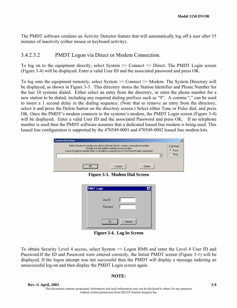
Model 1150 DVOR
Rev. G April, 2003 This document contains proprietary information and such information may not be disclosed to others for any purposes
without written permission from SELEX Sistemi Integrati Inc.
3-9
The PMDT software contains an Activity Detector feature that will automatically log off a user after 15 minutes of inactivity (either mouse or keyboard activity).
3.4.2.3.2 PMDT Logon via Direct or Modem Connection.
To log on to the equipment directly, select System >> Connect >> Direct. The PMDT Login screen (Figure 3-4) will be displayed. Enter a valid User ID and the associated password and press OK. To log onto the equipment remotely, select System >> Connect >> Modem. The System Directory will be displayed, as shown in Figure 3-3. This directory stores the Station Identifier and Phone Number for the last 10 systems dialed. Either select an entry from the directory, or enter the phone number for a new station to be dialed, including any required dialing prefixes such as “9”. A comma “,” can be used to insert a 1 second delay in the dialing sequence. (Note that to remove an entry from the directory, select it and press the Delete button on the directory screen.) Select either Tone or Pulse dial, and press OK. Once the PMDT’s modem connects to the systems’s modem, the PMDT Login screen (Figure 3-4) will be displayed. Enter a valid User ID and the associated Password and press OK. If no telephone number is used then the PMDT software assumes that a dedicated leased line modem is being used. This leased line configuration is supported by the 470549-0001 and 470549-0002 leased line modem kits.
To obtain Security Level 4 access, select System >> Logon RMS and enter the Level 4 User ID and Password.If the ID and Password were entered correctly, the Initial PMDT screen (Figure 3-1) will be displayed. If the logon attempt was not successful then the PMDT will display a message indicting an unsuccessful log-on and then display the PMDT Login screen again.
NOTE:
Figure 3-3. Modem Dial Screen
Figure 3-4. Log In Screen
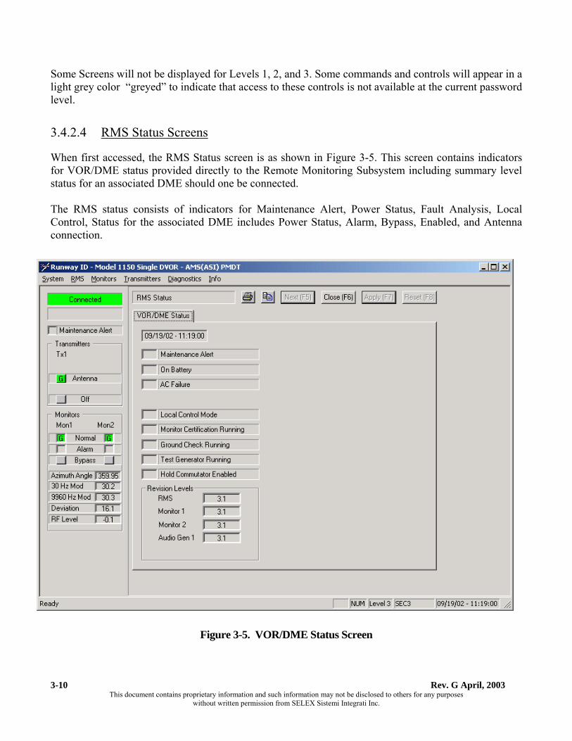
Rev. G April, 2003 This document contains proprietary information and such information may not be disclosed to others for any purposes
without written permission from SELEX Sistemi Integrati Inc.
3-10
Some Screens will not be displayed for Levels 1, 2, and 3. Some commands and controls will appear in a light grey color “greyed” to indicate that access to these controls is not available at the current password level.
3.4.2.4 RMS Status Screens
When first accessed, the RMS Status screen is as shown in Figure 3-5. This screen contains indicators for VOR/DME status provided directly to the Remote Monitoring Subsystem including summary level status for an associated DME should one be connected. The RMS status consists of indicators for Maintenance Alert, Power Status, Fault Analysis, Local Control, Status for the associated DME includes Power Status, Alarm, Bypass, Enabled, and Antenna connection.
Figure 3-5. VOR/DME Status Screen

Model 1150 DVOR
Rev. G April, 2003 This document contains proprietary information and such information may not be disclosed to others for any purposes
without written permission from SELEX Sistemi Integrati Inc.
3-11
3.4.2.5 RMS Data Screens
This set of two screens is accessed by selecting the tab for the screen or by clicking the “Next” button. These screens and their contents are described below.
3.4.2.5.1 RMS Maintenance Alerts Screen
Refer to Figure 3-6. This screen shows all of the maintenance alert status for the general alerts/alarms, RMS digital input alerts, monitor mismatches, and monitor specific alerts. When a maintenance alert/alarm is indicated on the sidebar, the RMS >> Data >> Maintenance Alerts/Alarms screen provides a general summation of all alerts/alarms. From this screen the operator can determine the alert/alarm and proceed to the associated screen to observe the specific data driving the alert/alarm.
Figure 3-6. RMS Maintenance Alerts Screen
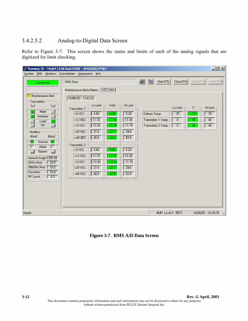
Rev. G April, 2003 This document contains proprietary information and such information may not be disclosed to others for any purposes
without written permission from SELEX Sistemi Integrati Inc.
3-12
3.4.2.5.2 Analog-to-Digital Data Screen
Refer to Figure 3-7. This screen shows the status and limits of each of the analog signals that are digitized for limit checking.
Figure 3-7. RMS A/D Data Screen
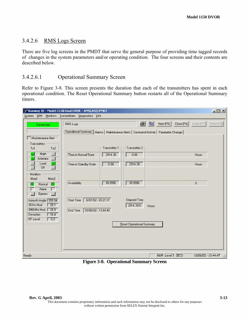
Model 1150 DVOR
Rev. G April, 2003 This document contains proprietary information and such information may not be disclosed to others for any purposes
without written permission from SELEX Sistemi Integrati Inc.
3-13
3.4.2.6 RMS Logs Screen
There are five log screens in the PMDT that serve the general purpose of providing time tagged records of changes in the system parameters and/or operating condition. The four screens and their contents are described below.
3.4.2.6.1 Operational Summary Screen
Refer to Figure 3-8. This screen presents the duration that each of the transmitters has spent in each operational condition. The Reset Operational Summary button restarts all of the Operational Summary timers.
Figure 3-8. Operational Summary Screen

Rev. G April, 2003 This document contains proprietary information and such information may not be disclosed to others for any purposes
without written permission from SELEX Sistemi Integrati Inc.
3-14
3.4.2.6.2 Alarms Log Screen
Refer to Figure 3-9. This screen provides the latest 100 alarms that have occurred. When 100 or more alarms have occurred, subsequent alarms will replace the oldest alarms in the log. Entries in the log identify the date and time the alarm occurred, the type of alarm, the test that detected the alarm, and the current status of the alarm condition. The Update button reloads the log file from the RMS and updates the display with any new entries. The Reset button clears the log file in the RMS.
Figure 3-9. Alarm Log Screen
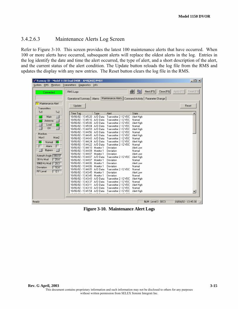
Model 1150 DVOR
Rev. G April, 2003 This document contains proprietary information and such information may not be disclosed to others for any purposes
without written permission from SELEX Sistemi Integrati Inc.
3-15
3.4.2.6.3 Maintenance Alerts Log Screen
Refer to Figure 3-10. This screen provides the latest 100 maintenance alerts that have occurred. When 100 or more alerts have occurred, subsequent alerts will replace the oldest alerts in the log. Entries in the log identify the date and time the alert occurred, the type of alert, and a short description of the alert, and the current status of the alert condition. The Update button reloads the log file from the RMS and updates the display with any new entries. The Reset button clears the log file in the RMS.
Figure 3-10. Maintenance Alert Logs
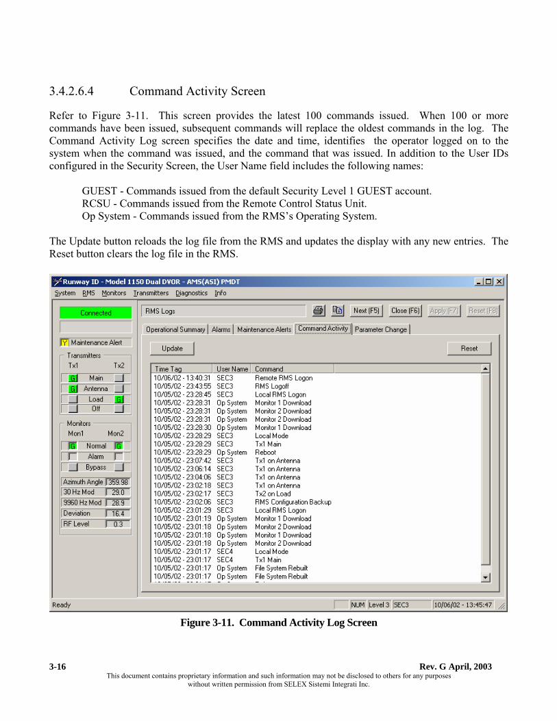
Rev. G April, 2003 This document contains proprietary information and such information may not be disclosed to others for any purposes
without written permission from SELEX Sistemi Integrati Inc.
3-16
3.4.2.6.4 Command Activity Screen
Refer to Figure 3-11. This screen provides the latest 100 commands issued. When 100 or more commands have been issued, subsequent commands will replace the oldest commands in the log. The Command Activity Log screen specifies the date and time, identifies the operator logged on to the system when the command was issued, and the command that was issued. In addition to the User IDs configured in the Security Screen, the User Name field includes the following names:
GUEST - Commands issued from the default Security Level 1 GUEST account. RCSU - Commands issued from the Remote Control Status Unit. Op System - Commands issued from the RMS’s Operating System.
The Update button reloads the log file from the RMS and updates the display with any new entries. The Reset button clears the log file in the RMS.
Figure 3-11. Command Activity Log Screen

Model 1150 DVOR
Rev. G April, 2003 This document contains proprietary information and such information may not be disclosed to others for any purposes
without written permission from SELEX Sistemi Integrati Inc.
3-17
3.4.2.6.5 Parameter Change Log Screen
Refer to Figure 3-12. This screen provides the latest 100 changes made in the operator parameters. When 100 or more changes have been made, subsequent changes will replace the oldest changes in the log. The Parameter Change screen specifies the date and time, identifies the operator logged on to the system when the change was made, and the file in which the data was changed. The Update button reloads the log file from the RMS and updates the display with any new entries. The Reset button clears the log file in the RMS.
Figure 3-12.Parameter Change Log Screen

Rev. G April, 2003 This document contains proprietary information and such information may not be disclosed to others for any purposes
without written permission from SELEX Sistemi Integrati Inc.
3-18
3.4.2.7 RMS Configuration Screen
The PMDT contains four RMS Configuration Screens that are used to define the operating parameters for the RMS - General, Station, A/D Limits, and Security Codes. These screens and their contents are described below. Any changes made to a configuration that should remain after a power cycle or Reset, should be backed up. To backup the current configuration in RAM to EEPROM, first login to Security Level 3 or higher, then select RMS >> Configuration Backup. Press OK at the prompt. To save the current configuration to hard drive or diskette select System >> Configuration Save. Select the destination and file name and press Save. To restore a configuration from disk select System >> Configuration Load, enter the file name and press Open. When completed, backup the configuration to EEPROM by selecting RMS >> Configuration Backup. Press OK at the prompt. Note that the station’s configuration can be printed in text form using the System >> Configuration Print menu option.

Model 1150 DVOR
Rev. G April, 2003 This document contains proprietary information and such information may not be disclosed to others for any purposes
without written permission from SELEX Sistemi Integrati Inc.
3-19
3.4.2.7.1 General RMS Configuration Screen - Refer to Figure 3-13
This screen allows the operator to configure the general parameters of the VOR system.
Figure 3-13. General Configuration Screen

Rev. G April, 2003 This document contains proprietary information and such information may not be disclosed to others for any purposes
without written permission from SELEX Sistemi Integrati Inc.
3-20
3.4.2.7.1.1 General Configuration the VOR
The parameters in the General Configuration Screen must be set to correctly correspond to the equipment installation at each site. Refer to Table 3-4 for details pertaining to each of the configurable parameters in the General Configuration Screen. Note that some parameters are only applicable to Dual Equipment. In Single Equipment systems, these parameters will not be displayed.
Table 3-4. General Configuration Parameters
Parameter
Description
RCSU Configuration
RCSU Present
When the 1138/None is selected the Modem connection to a 2138 is not selected. A parallel connection to an 1138 interface CCA may be active. When 2138 is selected the connection between the RCSU and RMS is enabled.
Connection Type
(only when 2138 selected)
Set to AHard Wired@ when connecting to the RCSU via the VOR=s RCSU Modem Set to ARadio Modem@ when connecting to the RCSU via a Radio Modem CCA.
Monitor Configuration
Monitor Startup Delay Sets the delay from startup until the shutdown timer starts. This gives additional time for transmitter stabilization.
Monitor Shutdown Delay Sets the delay from alarm occurrence until the transmitter shutdown (transfer if dual equipment)
Monitor Voting Logic
(Dual Equipment)
Selects either AND or OR voting logic for multiple monitor systems.
Monitor 1 Detector
Sets which Monitor detector the Monitor 1 will use for monitoring. This is useful if one of the two detectors fails. Reassignment will allow dual monitoring to continue. Also if two different locations are required for Field Monitoring then Monitor 1 and Monitor 2 must be set to different detectors.
Monitor 2 Detector Sets which Monitor detector Monitor 2 will use for monitoring.
Ident Configuration
Transmitter 1 Ident
This setting sets the Ident code transmitted by Transmitter 1. This code may be 2,3 or 4 characters. Numbers are not allowed. If less

Model 1150 DVOR
Rev. G April, 2003 This document contains proprietary information and such information may not be disclosed to others for any purposes
without written permission from SELEX Sistemi Integrati Inc.
3-21
Table 3-4. General Configuration Parameters
Parameter
Description than 4 characters use “spaces” to fill the unused characters.
Transmitter 2 Ident
This setting sets the Ident code transmitted by Transmitter 1. This code may be 2,3 or 4 characters. Numbers are not allowed. If less than 4 characters use “spaces” to fill the unused characters.
Digital I/O Configuration
Smoke Alarm Smoke Alarm detection is enabled when checked.
Intrusion Alarm
Intrusion Alarm detection is enabled when checked.
Spare #1 Usage
Configures the Spare #1 I/O channel
Spare #2 Usage
Configures the Spare #2 I/O channel
Modem Configuration
Dial In # Rings Sets the ring number that the modem answers incoming calls
Tone Dial Out
Tone dialing is used to dial out when checked. Pulse dialing is used to dial out when it is not checked.
Dial Out Enabled
VOR dials out on alerts/alarms when checked.
Dial Out DME Enabled VOR dials out on DME alerts/alarms when checked.
Dial Out Phone Number
Stores the phone number used when dialing out
Dial Out VOR Identifier
Stores the text identifier displayed remotely when dialing out.
Automatic Restarts
Automatic Restarts Enabled
Both Automatic Restarts (adjustable and fixed) are enabled when the checkbox is checked, and disabled when it is not checked.
First Restart Delay (seconds)
Sets the delay following a shutdown until the system will automatically restart. The system also has an additional 5 minute (fixed) restart delay.
DME Configuration

Rev. G April, 2003 This document contains proprietary information and such information may not be disclosed to others for any purposes
without written permission from SELEX Sistemi Integrati Inc.
3-22
Table 3-4. General Configuration Parameters
Parameter
Description
Present DME connection, status, and control enabled when checked.
Dual
Dual DME operation enabled when checked. Single DME operation enabled when not checked.
Keying Output
Enables the DME Keyer.

Model 1150 DVOR
Rev. G April, 2003 This document contains proprietary information and such information may not be disclosed to others for any purposes
without written permission from SELEX Sistemi Integrati Inc.
3-23
3.4.2.7.2 Station Configuration Screen
Refer to Figure 3-14. This screen is used to configure the various system-level parameters for the VOR station: CVOR/DVOR, Dual/Single, Hot Standby, and the station’s Transmitter Frequency. The value for each of these settings currently stored in the RMS and is also displayed for reference. Note that any changes under User Configuration do not take affect until the “Apply” button is pressed. Any discrepancies between the User Configuration, and RMS will be indicated with a red background, and should be corrected by the user. This can be done by backing up the configuration (RMS >> Config Backup).
Figure 3-14. Station Configuration Screen

Rev. G April, 2003 This document contains proprietary information and such information may not be disclosed to others for any purposes
without written permission from SELEX Sistemi Integrati Inc.
3-24
Once the user has set the User Configuration parameters as desired and pressed “Apply”, pressing the “Display DIP Switch Settings” button will display the corresponding DIP switch settings for the Synthesizer S1 as shown in Figure 3-15. These DIP switches should be set according to the displayed information.
Figure 3-15. Synthesizer Switch Setting Screen

Model 1150 DVOR
Rev. G April, 2003 This document contains proprietary information and such information may not be disclosed to others for any purposes
without written permission from SELEX Sistemi Integrati Inc.
3-25
3.4.2.7.3 A/D Limits Configuration Screen
Refer to Figure 3-16. This screen is used to configure the upper and lower alarm limits. A checkbox is provided to enable the Exterior Temperature sensor parameter’s Maintenance Alert. If the checkbox is checked, a Maintenance Alert will be generated when the Exterior Temperature Sensor parameter is out of the specified limits.
Figure 3-16. A/D Limits Configuration

Rev. G April, 2003 This document contains proprietary information and such information may not be disclosed to others for any purposes
without written permission from SELEX Sistemi Integrati Inc.
3-26
3.4.2.7.4 Security Codes Configuration Screen
Refer to Figure 3-17. This screen is used to configure the security access passwords for each user, including User ID, Password, and Security Level. This User ID/Password information is encrypted and stored in the non-volatile RAM (NVRAM) on the RMS CCA. This screen is only available to the Level 4 user.
Figure 3-17. Security Codes Screen

Model 1150 DVOR
Rev. G April, 2003 This document contains proprietary information and such information may not be disclosed to others for any purposes
without written permission from SELEX Sistemi Integrati Inc.
3-27
3.4.2.7.4.1 User Account Maintenance
As part of initial configuration, several user accounts should be setup, corresponding to the access levels required. User account maintenance can only be done through a direct connection (i.e. not via a remote modem) in the LOCAL mode, from within Security Level 4, with the exception of changing the current user’s password. All users can change their own passwords, when connected directly and the system is in Local Mode, through the RMS >> Commands >> Change Password menu option. Refer to Figure 3-17 for the Security Codes Configuration Screen.
3.4.2.7.4.2 Add a User Account.
1. Log on to Security Level 3 and select the RMS >> Configuration >> Security Codes screen.
2. Click on any empty User ID field.
3. Enter the desired User ID. Note that the User ID must be 4 to 8 characters in length, is case-sensitive, and can contain any alphanumeric characters.
4. Press TAB to move to the associated Password field.
5. Enter the desired Password. Asterisks will hide the password on the display. Note that the password must be 4 to 8 characters in length, is case-sensitive, and can contain any alphanumeric characters.
6. Select the desired Security Level for this user.
7. Repeat these steps for any additional users.
8. When all users have been configured, press the Apply button to save the new User Account data. This will clear the asterisks in the password field to hide the length of the password.
9. To store the new account information in the RMS’s NVRAM, select RMS >> Config Backup. If this is not done, the user data will revert to the values stored in the NVRAM following the next system reset or power-cycle.
3.4.2.7.4.3 Change a User’s Password.
All User account information, including passwords, is accessible from Security Level 4 as follows:
1. Log on to Security Level 4 and select the RMS >> Configuration >> Security Codes screen.
2. Select the Password field associated with the desired User ID.
3. Enter the desired Password, which is case-sensitive. Asterisks will hide the password on the display. Note that the password must be 4 to 8 characters in length, and can contain any alphanumeric characters.
4. Press the Apply button to save the new User Account data. This will clear the asterisks in the password field.

Rev. G April, 2003 This document contains proprietary information and such information may not be disclosed to others for any purposes
without written permission from SELEX Sistemi Integrati Inc.
3-28
5. To store the new account information in the RMS’s NVRAM, select RMS >> Config Backup. If this is not done, the user data will revert to the values stored in the NVRAM following the next system reset or power-cycle.
From other Security Levels, only the current user’s password can be changed. This is done as detailed below:
1. Log on directly (not via a Modem connection).
2. Select the RMS >> Commands >> Change Password menu item.
3. Enter the Current Password and press TAB to move to the next field.
4. Enter the New Password, which is case-sensitive. Asterisks will hide the password on the display. Note that the password must be 4 to 8 characters in length, and can contain any alphanumeric characters. Press TAB to move to the next field.
5. Re-enter the New Password and press OK to save the new password.
6. A message box will be displayed, indicating that the password has been changed. Press OK to clear this message.
3.4.2.7.4.4 Delete a User’s Account.
1. Log on to Security Level 4 and select the RMS >> Configuration >> Security Codes screen.
2. Select the desired User ID field.
3. Delete the User ID in this field, leaving it blank.
4. Press the Apply button to save the new User Account data.
5. To store the new account information in the RMS’s NVRAM, select RMS >> Config Backup. If this is not done, the user data will revert to the values stored in the NVRAM following the next system reset or power-cycle.

Model 1150 DVOR
Rev. G April, 2003 This document contains proprietary information and such information may not be disclosed to others for any purposes
without written permission from SELEX Sistemi Integrati Inc.
3-29
3.4.2.8 RMS Commands
The RMS Commands menu, shown in Figure 3-18, provides system level controls for setting the time and date of the VOR station to the PMDT PC’s current settings, changing the current user’s password, resetting the Intrusion and Smoke Detectors, resetting the RMS hardware, and basic control of a co-located Distance Measuring Equipment (DME) if so equipped.
Figure 3-18. RMS Commands

Rev. G April, 2003 This document contains proprietary information and such information may not be disclosed to others for any purposes
without written permission from SELEX Sistemi Integrati Inc.
3-30
The DME Commands sub-menu of the RMS Commands menu shown in Figure 3-19 is used for basic control of a co-located DME. It is only available if the DME is configured present in the RMS >> Configuration >> General screen. The DME Control >> Transfer command is used to transfer between the Main and Standby transmitters in a dual DME system.
Figure 3-19. DME Commands

Model 1150 DVOR
Rev. G April, 2003 This document contains proprietary information and such information may not be disclosed to others for any purposes
without written permission from SELEX Sistemi Integrati Inc.
3-31
3.4.2.9 Monitor Configuration Screens
The PMDT contains two Monitor Configuration Screens that are used to configure the VOR’s Monitors. The screens and their contents are described below.
3.4.2.9.1 Monitor Alarm Limit Configuration Screen
Refer to Figure 3-20. This screen is used to configure the alarm limits for the VOR’s Monitors. It also contains a check box control to enable the Ident Monitoring. The Azimuth Angle setting is separate for Monitor 1 and Monitor 2 to allow for two different field monitor positions. All other alarm parameters have common limits. The ability to set the nominal reading is also provided. The nominal angle must be set for the ground check to operate properly. If for instance the field monitor position is 118.5 degrees then enter 118.50 degrees into the Monitor 1 Azimuth Angle Nominal value. Repeat this for Monitor 2.
Figure 3-20. Monitor Alarm Limits Screen

Rev. G April, 2003 This document contains proprietary information and such information may not be disclosed to others for any purposes
without written permission from SELEX Sistemi Integrati Inc.
3-32
3.4.2.9.2 Monitor Offsets and Scale Factor Configuration Screen
Refer to Figure 3-21. This screen is used to configure the operation of the Monitors. Each parameter measured by the monitor may be scaled to display a corrected value. The Test Generator should be used as the initial reference for the offsets and scale factors. After a successful completion of the Generator Test each parameter in this screen should be adjusted. Run the Generator Test until the final outcome of the Generator test is the same as the setting for the test. When the Integrity Monitor offset and scale factors are correct then press the copy button and then the F7. This will duplicate the Integrity Offsets and scale factors for the Certification Tests.
Figure 3-21. Monitor Offsets and Scale Factors

Model 1150 DVOR
Rev. G April, 2003 This document contains proprietary information and such information may not be disclosed to others for any purposes
without written permission from SELEX Sistemi Integrati Inc.
3-33
3.4.2.10 Monitor Commands
Refer to Figure 3-22. The Bypass state of the Integral Monitor can be changed using the corresponding command under the Monitors >> Commands menu.
Figure 3-22. Monitor Commands

Rev. G April, 2003 This document contains proprietary information and such information may not be disclosed to others for any purposes
without written permission from SELEX Sistemi Integrati Inc.
3-34
3.4.2.11 Monitor Data Screens
The PMDT contains seven Monitor Data Screens that are used to view the current status of the monitored parameters. The screens and their contents are described below.
3.4.2.11.1 Integrity Data Screen
Refer to Figure 3-23. This screen displays the low and high alarm limits and pre-alarm limits with current operating values for Monitor 1 and Monitor 2. A green background for a parameter indicates that the parameter falls within the Prealarm and Alarm limits. A yellow background indicates that the parameter falls outside of the prealarm limits but is still within the integrity alarm limits. The Comm status if green indicates that normal serial communications exist with the Monitors. A box indicates which of the two monitors is the controlling monitor. The controlling monitor has control of the ground check switch capability and the audio output to the headset jack and telephone line interface. The LED on the monitor edge will also light when the monitor is the controlling monitor. The RMS will assign the controlling monitor function to Monitor 1 if Transmitter 1 is on the antenna and to Monitor 2 if Transmitter 2 is on the antenna.
Figure 3-23. Integrity Data Screen
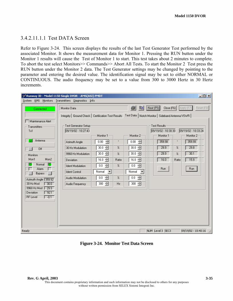
Model 1150 DVOR
Rev. G April, 2003 This document contains proprietary information and such information may not be disclosed to others for any purposes
without written permission from SELEX Sistemi Integrati Inc.
3-35
3.4.2.11.1.1 Test DATA Screen
Refer to Figure 3-24. This screen displays the results of the last Test Generator Test performed by the associated Monitor. It shows the measurement data for Monitor 1. Pressing the RUN button under the Monitor 1 results will cause the Test of Monitor 1 to start. This test takes about 2 minutes to complete. To abort the test select Monitors>> Commands>> Abort All Tests. To start the Monitor 2 Test press the RUN button under the Monitor 2 data. The Test Generator settings may be changed by pointing to the parameter and entering the desired value. The identification signal may be set to either NORMAL or CONTINUOUS. The audio frequency may be set to a value from 300 to 3000 Hertz in 30 Hertz increments.
Figure 3-24. Monitor Test Data Screen

Rev. G April, 2003 This document contains proprietary information and such information may not be disclosed to others for any purposes
without written permission from SELEX Sistemi Integrati Inc.
3-36
3.4.2.11.1.2 Monitor Certification Test Results Screen
Refer to Figure 3-25. This screen displays the results of the last Certification Test performed by the associated Monitor. It shows the measurements for Monitor 1 Low Limit test and Monitor 1 High limit test. Pressing the RUN button to the right of Monitor 1 results will cause the Certification Test of Monitor 1 to start. This test takes about 3 minutes to complete. To abort the test select Monitors>> Commands>> Abort All Tests. To start the Monitor 2 Certification Test press the RUN button to the right of Monitor 2 data. The certification limits may be entered by pointing to the parameter and entering the desired value. The preferred method is to point and click on the “Set to Monitor Limits” button. This will automatically set the Certification Limits to the same value as the Monitor Integral Limits in the Monitors>>Configuration>>Alarm Limits screen. If the Monitor finds that the parameter exceeds the tolerance then the parameter is declared in alarm and the Monitors >> Data > > Certification Test Results shows the background in red on the parameter that is out of tolerance. Refer to Table 3-5 for Certification Test Criteria.
Figure 3-25. Certification Test Results Screen

Model 1150 DVOR
Rev. G April, 2003 This document contains proprietary information and such information may not be disclosed to others for any purposes
without written permission from SELEX Sistemi Integrati Inc.
3-37
Table 3-5. Monitor Certification Test Criteria
TEST CASE/
PARAMETER
TEST
GENERATOR SETTING
PASS CRITERIA CERTIFICATION
Alarm High Test: Azimuth Angle 30 Hz Modulation 9960 Hz Modulation FM Deviation
High Alarm Limit High Alarm Limit High Alarm Limit High Alarm Limit
High Alarm Limit " 0.2 degrees
High Alarm Limit "1% High Alarm Limit "1%
High Alarm Limit " 0.2 Ratio
Alarm Low Test:
Azimuth Angle 30 Hz Modulation 9960 Hz Modulation FM Deviation
Low Alarm Limit Low Alarm Limit Low Alarm Limit Low Alarm Limit
Low Alarm Limit " 0.2 degrees Low Alarm Limit "1% Low Alarm Limit "1%
Low Alarm Limit " 0.2 Ratio

Rev. G April, 2003 This document contains proprietary information and such information may not be disclosed to others for any purposes
without written permission from SELEX Sistemi Integrati Inc.
3-38
3.4.2.11.1.3 Notch Monitor Screen
Refer to Figure 3-26. This screen displays the data from the DVOR Notch Monitor circuit. This circuit monitors the signal from the Field Detector for “notches” in the detected signal. A notch indicates a fault in one or more transmitting antennas, feed cables or commutator switch channels. When a failure occurs in one of these channels there is a lack of signal and therefore a notch in the detected signal pattern. The 1150 DVOR is a double sideband configuration and therefore there are four sideband antennas on at any one time. Therefore the notch will not fall to zero but since three other antennas are contributing to the signal only a reduction in signal can be expected. The tolerance for notch monitoring should be set to approximately 20% but the technician can adjust this tolerance as needed for more or less sensitivity. It can be expected that when one antenna fails there will be an out of tolerance indication for one to four of the possible radiating antennas. When an out of tolerance condition exists, the Sideband VSWR data screen should be viewed. If there is an indication of Sideband VSWR alarm, investigate the VSWR alarm indication first. There are three controls on the Notch Monitor screen; Enable Notch Monitoring, Executive Alarm, and Record Baseline. When the Enable Notch Monitoring is checked data is then collected and alarm limits applied. When the Executive bit is set then an out of tolerance condition by one or more antennas will cause an Integral alarm and shutdown/ Transfer after the alarm timer expires. The Record baseline button is used when the technician is confidant that the DVOR is operating properly for example after a flight inspection of the facility. When the Record Baseline is selected then the current data is copied into memory as the “Baseline” Data and then used as the reference. When the measured signal exceeds the Baseline +/- the tolerance the alarm indication is generated. When the Executive Alarm is selected then a RED background will appear at the selected antenna or antennas. When the Executive indication is not selected then a YELLOW background will appear at the selected antenna or antennas. The Monitor Circuit Card associated with the Transmitter connected to the antenna performs the measurement. The Monitor CCA uses a signal from the Audio Generator representing the Commutator Transfer Indication to time the collection of samples from TP4 on the Monitor CCA. The Monitor precisely times the sampling of data from TP4 to measure the depth of the notches in the signals. The Monitor CCA requires that the signal level at TP4 remain fairly constant. If the Sideband power is varied, then a new baseline will be required.

Model 1150 DVOR
Rev. G April, 2003 This document contains proprietary information and such information may not be disclosed to others for any purposes
without written permission from SELEX Sistemi Integrati Inc.
3-39
Figure 3-26. Notch Monitor Screen

Rev. G April, 2003 This document contains proprietary information and such information may not be disclosed to others for any purposes
without written permission from SELEX Sistemi Integrati Inc.
3-40
3.4.2.11.2 Sideband Antenna VSWR Screen
The PMDT contains the Sideband Antenna VSWR Screen which displays the current data from the Sideband Antenna VSWR monitoring along with the tolerance and Executive alarm control. The Monitor Circuit Card associated with the Transmitter connected to the antenna performs the measurement. The Monitor CCA uses a signal from the Audio Generator representing the Commutator Transfer Indication to time the collection of samples. These samples originate at the Sideband 1 and Sideband 2 reflected power test points on the 1A2 RF Monitor Assy. The Monitor precisely times the sampling of data from the 1A5 TP5 and TP6 if transmitter 1 is connected to the antenna and 1A21 TP5 and TP6 if transmitter 2 is connected to the antenna for the forward power indication of Sidebands 1 and 2. The Monitor then uses the samples of the Sideband 1 and Sideband 2 reflected power from the 1A2 RF Monitor to calculate the VSWR of each sideband antenna. The time of the sample determines which sideband antenna is radiating. The result of the calculation is displayed in the VSWR column. If the measured data exceeds the programmable tolerance on the screen then the data background color will change to yellow if the Sideband VSWR Executive Alarm is not checked. If the Sideband VSWR Executive Alarm is checked then the background color will change to red. If the number of antennas in alarm (RED) exceeds the programmed “Number of Antennas in Alarm” then after the alarm delay the DVOR will shut down.
Figure 3-27. Sideband Antenna VSWR
Model 1150 DVOR
Rev. G April, 2003 This document contains proprietary information and such information may not be disclosed to others for any purposes
without written permission from SELEX Sistemi Integrati Inc.
3-41
3.4.2.11.2.1 VOR Ground Check Data Screen
Refer to Figure 3-28. This screen provides a control to start a VOR Ground Check and display of the data from the ground check. The 1150 DVOR provides the ability to perform a ground check. The ground check requires the use of the 012616-1003, Audio Generator CCA and the 012098-1001 Pin Diode Driver CCA. These Circuit Cards are available in DVORs shipped after August 2002. The monitor controls the RS422 data to the Pin Diode Driver cca to rotate the position of the DVOR from the normal position in 22.5 degree increments. At each of these positions the Monitor measures the signal and computes the error for that position. When all 16 positions have been measured then a Fourier Analysis is computed and the resulting errors submitted for display. The outcome of the Fourier analysis are Duantal, Quadrantal, Octantal and Bias errors. Duantal error has one maximum and one minimum in 360 degrees around the DVOR. Similarly Quadrantal error has two peaks and two minimums around the 360 degrees. The Octantal Error has four peaks and four minimums around the DVOR. The Bias error is the average azimuth shift of the DVOR station. The Station error is a plot of the errors from the data in the Station Error column of data. The FFTs errors are the individual Duantal, Quadrantal, Octantal and Bias errors. The FFT sum is the summation of the FFT errors. When performed correctly the FFT sum plot should look like the Station error plot. By selecting one of the graph options the data appears on the graph along with the legend (If checked) for that data. Pressing the advanced button will display the Advanced Ground Check screen which allows viewing a larger graph, printing and copying the graph to a file. Note: The Nominal Monitor Angle must be set in the Monitors>>Configuration>>Alarm Limits screens. Jumper E3 on the 012616-1003 must be in positions 1 to 2 and Pin Diode driver 012098-1001 J5 Pins 1 to 2 must be connected to enable the ground check.
NOTE: The DVOR Automatic Ground check changes the radiated signal and a NOTAM must be issued to notify that the DVOR is not in service during this test.

Rev. G April, 2003 This document contains proprietary information and such information may not be disclosed to others for any purposes
without written permission from SELEX Sistemi Integrati Inc.
3-42
Figure 3-28. Ground Check Screen

Model 1150 DVOR
Rev. G April, 2003 This document contains proprietary information and such information may not be disclosed to others for any purposes
without written permission from SELEX Sistemi Integrati Inc.
3-43
3.4.2.11.2.2 VOR Ground Check Data Advanced Screen
Refer to Figure 3-29. This screen shows VOR Ground Check Data in more detail than the previous Ground Check screen. By selecting one of the graph options the data appears on the graph along with the legend (If checked) for that data. By pointing and clicking the print button the graph will be printed on the current Windows printer. Selecting the Copy button will direct the technician to store the data to a file.
Figure 3-29. Advanced Ground Check Screen
3.4.2.11.2.3 VOR Fault History Screens
Refer to Figure 3-30 and 3-31. There are two screens that provide the fault history for the last three faults. These faults caused a shutdown and transfer from the Main to the Standby Transmitter.

Rev. G April, 2003 This document contains proprietary information and such information may not be disclosed to others for any purposes
without written permission from SELEX Sistemi Integrati Inc.
3-44
3.4.2.11.2.4 Fault History Monitor Data Screen
This screen shows the latest monitor data along with the last pre-alarm data This pre-alarm was the last data available with no integrity alarms. The time and date is also shown for each occurrence.
Figure 3-30. Fault History, Monitor Data

Model 1150 DVOR
Rev. G April, 2003 This document contains proprietary information and such information may not be disclosed to others for any purposes
without written permission from SELEX Sistemi Integrati Inc.
3-45
3.4.2.11.2.5 Fault History System Status Screen
This screen shows the state of the system during the last three faults. The time and date is also shown for each occurrence to allow correlation with the Fault History Monitor Data screen..
Figure 3-31. Fault History, System Status
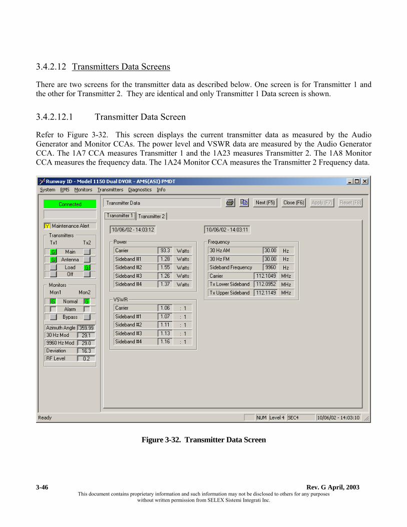
Rev. G April, 2003 This document contains proprietary information and such information may not be disclosed to others for any purposes
without written permission from SELEX Sistemi Integrati Inc.
3-46
3.4.2.12 Transmitters Data Screens
There are two screens for the transmitter data as described below. One screen is for Transmitter 1 and the other for Transmitter 2. They are identical and only Transmitter 1 Data screen is shown.
3.4.2.12.1 Transmitter Data Screen
Refer to Figure 3-32. This screen displays the current transmitter data as measured by the Audio Generator and Monitor CCAs. The power level and VSWR data are measured by the Audio Generator CCA. The 1A7 CCA measures Transmitter 1 and the 1A23 measures Transmitter 2. The 1A8 Monitor CCA measures the frequency data. The 1A24 Monitor CCA measures the Transmitter 2 Frequency data.
Figure 3-32. Transmitter Data Screen

Model 1150 DVOR
Rev. G April, 2003 This document contains proprietary information and such information may not be disclosed to others for any purposes
without written permission from SELEX Sistemi Integrati Inc.
3-47
3.4.2.13 Transmitters Configuration Screen
There is one screen used for configuring the offsets and scale factors for the parameters of each of the two transmitters. Any changes made to a configuration that should remain after a power cycle or Reset, should be backed up. To backup the current configuration in RAM to EEPROM, select RMS >> Configuration Backup. Press OK at the prompt. To save the current configuration to hard drive or diskette select System >> Configuration Save. Select the destination and file name and press Save. To restore a configuration from disk select System >> Configuration Load, enter the file name and press Open. The status of the restore will be displayed in the bottom left corner. When completed, backup the configuration to EEPROM by selecting RMS >> Configuration Backup. Press OK at the prompt.
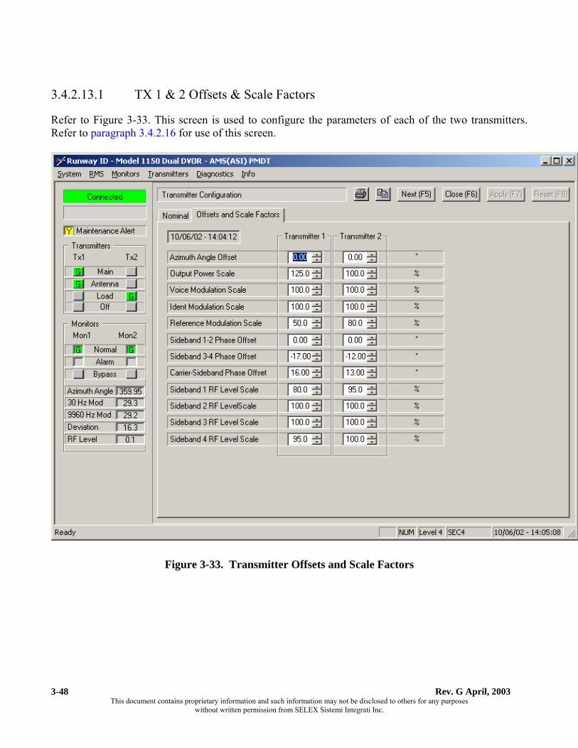
Rev. G April, 2003 This document contains proprietary information and such information may not be disclosed to others for any purposes
without written permission from SELEX Sistemi Integrati Inc.
3-48
3.4.2.13.1 TX 1 & 2 Offsets & Scale Factors
Refer to Figure 3-33. This screen is used to configure the parameters of each of the two transmitters. Refer to paragraph 3.4.2.16 for use of this screen.
Figure 3-33. Transmitter Offsets and Scale Factors

Model 1150 DVOR
Rev. G April, 2003 This document contains proprietary information and such information may not be disclosed to others for any purposes
without written permission from SELEX Sistemi Integrati Inc.
3-49
3.4.2.14 Transmitters Nominal Screens
This screen is used to specify the transmitter waveform. The screen. holds data used by the Audio Generator associated with a Transmitter to calculate the appropriate values to be placed in the D/A converters on the Audio Generator CCA. The values represent a composite waveform at TP6 on the Audio Generator CCA. When a change is made, the change takes place once the Apply button is pressed.
Figure 3-34. Transmitter Nominal Screen

Rev. G April, 2003 This document contains proprietary information and such information may not be disclosed to others for any purposes
without written permission from SELEX Sistemi Integrati Inc.
3-50
3.4.2.15 Transmitter Commands
The Transmitter Commands menu, shown in Figure 3-35, provides direct control of transferring between the Main and Standby transmitters, as well as selecting either Tx 1 or Tx 2 specific commands, or VOR Ident commands.
Figure 3-35. Transmitter Commands

Model 1150 DVOR
Rev. G April, 2003 This document contains proprietary information and such information may not be disclosed to others for any purposes
without written permission from SELEX Sistemi Integrati Inc.
3-51
The Tx 1 and Tx 2 command menus, shown in Figure 3-36, provide the following commands to the corresponding transmitter:
Switch to Antenna Switch to Load Turn Off
Figure 3-36. Transmitter Commands, Antenna Control

Rev. G April, 2003 This document contains proprietary information and such information may not be disclosed to others for any purposes
without written permission from SELEX Sistemi Integrati Inc.
3-52
The VOR Ident command menu, shown in Figure 3-37, is used to select the Ident, either Normal, Off, or Continuous.
Figure 3-37. Transmitter Ident Control
3.4.2.16 Controlling the Transmitter via the PMDT
Transmitter parameters are adjusted using the Nominal Screen (Figure 3-34) and the Transmitter Offsets and Scale factors Screen (Figure 3-33). Refer to these screens for the following paragraphs.
3.4.2.16.1 General Transmitter Control
With Transmitter #1 on the antenna, configure the Nominal settings for the desired signal in space. Adjust the Tx #1 offsets and scale factors to obtain this signal in space for Transmitter #1. Transfer to Transmitter #2 and adjust the Tx #2 offset and scale factors to obtain the same desired signal in space.

Model 1150 DVOR
Rev. G April, 2003 This document contains proprietary information and such information may not be disclosed to others for any purposes
without written permission from SELEX Sistemi Integrati Inc.
3-53
NOTE:
The Waveform is used to provide the desired setting, for example a Reference Modulation of 30%. The Transmitter offsets and scale factors allow an adjustment to obtain this actual setting.
3.4.2.16.2 Change the Azimuth Index
To affect both Transmitter #1 and Transmitter #2, select Transmitters >> Configuration >> Nominal. Adjust the Azimuth Index by selecting the parameter with the mouse then either enter the value or use the spin controls. Press the Apply button (or the “F7" key) to apply the change. To affect only one transmitter, select Transmitters >> Configuration >> Offsets and Scale Factors screen. Adjust the Transmitter 1 (or 2, as desired) Az Angle Offset by selecting the parameter with the mouse, then either enter the offset value or use the spin controls. Press the Apply button (or the ‘F7" key) to apply the change.
3.4.2.16.3 Change the CSB Output Power
To affect both Transmitter #1 and Transmitter #2, select Transmitters >> Configuration >> Nominal. Adjust the CSB power output level by selecting the CSB Output Power parameter with the mouse then either enter the value or use the spin controls. Press the Apply button (or the “F7" key) to apply the change. The value entered is a percentage of the maximum available for the CSB amplifier. A value of 100% represents approximately 125 Watts. Note that the power change in the Nominal Screen also affects the Sideband RF Level. To affect only one transmitter (so that both transmitters provide the same level), select Transmitters >> Configuration >> Offsets and Scale Factors screen. Adjust the Transmitter 1 (or 2, as desired) Power Output level by selecting the Output Power Scale parameter with the mouse then either enter the percentage value or use the spin controls. Press the Apply button (or the “F7" key) to apply the change.
3.4.2.16.4 Change the Voice Depth of Modulation
To affect both Transmitter #1 and Transmitter #2, select Transmitters >> Configuration >> Nominal. Adjust the Voice Modulation Level by selecting the Voice Modulation parameter with the mouse then either enter the value or use the spin controls. Press the Apply button (or the “F7" key) to apply the change. To affect only one transmitter, select Transmitters >> Configuration >> Offsets and Scale Factors screen Adjust the Transmitter 1 (or 2, as desired) Voice Modulation Scale Percent by selecting the parameter with the mouse, then either enter the percentage value or use the spin controls. Press the Apply button (or the “F7" key) to apply the change.

Rev. G April, 2003 This document contains proprietary information and such information may not be disclosed to others for any purposes
without written permission from SELEX Sistemi Integrati Inc.
3-54
3.4.2.16.5 Change the Identification Depth of Modulation
To affect both Transmitter #1 and Transmitter #2, select Transmitters >> Configuration>>Nominal. Adjust the ident modulation level by selecting the Ident Mod Level parameter with the mouse then either enter the value or use the spin controls. Press the Apply button (or the “F7" key) to apply the change. To affect only one transmitter, select Transmitters >> Configuration >> Transmitter 1 (or 2, as desired) Offsets and Scale Factors screen. Adjust the ident modulation level by selecting the Ident Level Scale parameter with the mouse then either enter the percentage value or use the spin controls. Press the Apply button (or the (F7" key) to apply the change.
3.4.2.16.6 Change the Reference Depth of Modulation
To affect both Transmitter #1 and Transmitter #2, select Transmitters >> Configuration >> Nominal. Adjust the Reference Modulation Level by selecting the Reference Modulation parameter with the mouse then either enter the value or use the spin controls. Press the Apply button (or the “F7" key) to apply the change. To affect only one transmitter, select Transmitters >> Configuration >> Offsets and Scale Factors screen Adjust the Transmitter 1 (or 2, as desired) Reference Modulation Scale Percent by selecting the parameter with the mouse, then either enter the percentage value or use the spin controls. Press the Apply button (or the “F7" key) to apply the change.
3.4.2.16.7 Change the Sideband Power Level
To affect both Transmitter #1 and Transmitter #2, select Transmitters >> Configuration >> Nominal. Adjust the SBO power output level by selecting the SBO RF Level parameter with the mouse then either enter the value or use the spin controls. Press the Apply button (or the “F7" key) to apply the change. The value entered is a percentage of the maximum available for the SBO amplifier. Note that the power change of the Output Power level in the Transmitters >> Configuration >> Nominal Screen also affects the SBO RF Level. To affect only one transmitter, select Transmitters >> Configuration >> Offsets and Scale Factors screen. Adjust the Transmitter 1 or 2 (as required) Sideband 1 RF level by selecting the Sideband 1 RF Level Scale parameter with the mouse then either enter the percentage value or use the spin controls. Press the Apply button (or the “F7" key) to apply the change. Note that a value of 100% scales the Sideband 1 power output by 1.0, and a value of 70.7% scales the Sideband 1 power output by 0.5 (since this is a Voltage Scale Factor). Sidebands 2,3 and 4 can also be adjusted individually in this screen.

Model 1150 DVOR
Rev. G April, 2003 This document contains proprietary information and such information may not be disclosed to others for any purposes
without written permission from SELEX Sistemi Integrati Inc.
3-55
3.4.2.17 Diagnostics Screen.
3.4.2.17.1 Power-Up Diagnostics Results
Refer to Figure 3-38. This screen shows the results of the most recent power-up diagnostics test. Each time an embedded software processor is reset or powered up, it performs a series of internal diagnostic tests to verify its integrity. The results of those tests are displayed on this screen for the RMS, Monitors and Audio Generators. CPU Functional tests are instruction and data fetches, bit operations, and math operations. RAM checks are extensive tests on individual bit positions of all RAM. PROM checks are checksum calculations and comparison against checksums established at the factory. EEPROM checks are checksum validations of data held in EEPROM. Green indications are normal. If a module indicates a power-up diagnostic failure, it should be replaced.
Figure 3-38. Power Up Diagnostics Results

Rev. G April, 2003 This document contains proprietary information and such information may not be disclosed to others for any purposes
without written permission from SELEX Sistemi Integrati Inc.
3-56
3.4.2.17.2 Fault Isolation Test Results
Refer to Figure 3-39. This screen shows the results of the most recent Fault Isolation Test. Pressing the “Run Full Diagnostic”, which is only available in Local Mode from Security Level 3 or higher, causes the system to execute the complete built-in diagnostics. This requires the system to be NOTAM’d off. Pressing the “Run On Air Diagnostics”, which is available either locally or remotely from Security Level 2 or higher, causes the system to execute a subset of the full diagnostics that does not require the system to be NOTAM’d off. Once started, the diagnostics can be canceled by the user with the “Cancel” button. The results are shown in the Fault Results window at the bottom of the screen.
Figure 3-39. Fault Isolation Test Results
3.5 RMM
The RMM uses the same hardware and software as the PMDT but interconnects to the equipment via a modem and a telephone circuit. The software screens and operator selection of this usage of the PMDT are described above in the PMDT paragraphs

Model 1150 DVOR
Rev. G April, 2003 This document contains proprietary information and such information may not be disclosed to others for any purposes
without written permission from SELEX Sistemi Integrati Inc.
3-57
3.6 STATUS PANEL/ POWER CONTROL
The STATUS PANEL mounts on the face of the VOR at the top equipment cabinet. The POWER CONTROL in on the face of the VOR at the lower part of the cabinet. The functions of each switch and indicator are described in Table 3-6.
Table 3-6. Dual Equipment Control Panel Functions
POWER CONTROL
TX1 AC
AC Circuit Breaker - In the A1" position powers AC and also charges the Battery Set.
TX1 DC
DC Circuit Breaker - In the A1" position connects the BCPS to the battery.
TX2 AC
AC Circuit Breaker - In the A1" position powers AC and also charges the Battery Set
TX2 DC
DC Circuit Breaker - In the A1" position connects the BCPS to the battery.
STATUS PANEL
Integral Normal1 Indicators
Illuminates to indicate the normal condition of monitor 1. During an AC Failure this LED will cycle on and off.
Integral Alarm 1 Indicators
Illuminates to indicate the alarm condition of monitor 1.
Integral Normal 2 Indicators
Illuminates to indicate the normal condition of monitor 2. During an AC Failure this LED will cycle on and off.
Integral Alarm 2 Indicators
Illuminates to indicate the alarm condition of monitor 2.
Integral Bypass Switch and Indicator
The indicator illuminates when bypass is active.

Rev. G April, 2003 This document contains proprietary information and such information may not be disclosed to others for any purposes
without written permission from SELEX Sistemi Integrati Inc.
3-58
3.7 REMOTE MAINTENANCE SUB-SYSTEM (RMS) CCA (1A13)
Refer to Table 3-7 for the indicators and controls on the RMS CCA.
Table 3-7. RMS CCA (1A13) Controls and Indicators
CPU Fault
This LED when lit (RED) indicates that the RMS processor has reset due to power failure or memory problems within the RMS CCA.
3.8 MONITOR CCA (1A8, 1A24)
Refer to Table 3-8 for the indicators and controls on the Monitor CCA.
Table 3-8. Monitor CCA (1A8, 1A24) Controls and Indicators
Integral Fault LED
Illuminated when the Monitor CCA detects an Integral Fault.
TP1
Detected Voice+ Signal from differential transformer driver
TP2
Detected Voice- Signal from differential transformer driver
TP3
Detected Audio Signal Level
TP4 Detected Notch Data. This signal includes the 720, and 1440 Hertz signals and
will have a “notch” when an antenna is inoperative. TP5
Composite Audio. This includes DC, 30 Hz, 9960 Hertz and Ident signals.
TP6 30 hertz AM Signal. This is a half rectified 30 Hz signal used for measurement
of the 30 AM level TP7
This is 30 Hertz AM square wave. This signal enters the uP for angle measurement.
TP8
Ident Signal Level. This is the 1020 Hz signal after the bandpass filter. When keying is detected the 1020 Hz sine wave is present.
TP9
This signal is the 1020 signal square wave signal.
TP10
Ident Modulation level Voltage. This voltage peak when keying is present and decays when keying stops.
TP11
9960 Signal after the bandpass filter

Model 1150 DVOR
Rev. G April, 2003 This document contains proprietary information and such information may not be disclosed to others for any purposes
without written permission from SELEX Sistemi Integrati Inc.
3-59
Table 3-8. Monitor CCA (1A8, 1A24) Controls and Indicators
TP12 9960 Signal after the One- Shot multivibrator.. TP13
30 hertz FM Signal. This is a half rectified 30 Hz signal used for measurement of the Deviation ratio.
TP14
9960 Hertz signal level. This is a DC voltage representing the level of the 9960 Hertz Signal.
TP15
This is 30 Hertz FM square wave. This signal enters the uP for angle measurement.
TP0 (GND)
This test point is available for scope or voltmeter ground.
3.9 SYNTHESIZER CCA (1A4, 1A20)
Refer to Figure 3-61 and Table 3-9 for the indicators and controls on the Synthesizer CCA.

Rev. G April, 2003 This document contains proprietary information and such information may not be disclosed to others for any purposes
without written permission from SELEX Sistemi Integrati Inc.
3-60
1150-610
R81
1A4/A20
CARRIER FREQ.10 mW (TYP.)
J8
TP4
TP5
GND
TP1
TP2
TP3
Figure 3-40. Synthesizer Front Panel

Model 1150 DVOR
Rev. G April, 2003 This document contains proprietary information and such information may not be disclosed to others for any purposes
without written permission from SELEX Sistemi Integrati Inc.
3-61
Figure 3-41. Sideband Generator Controls
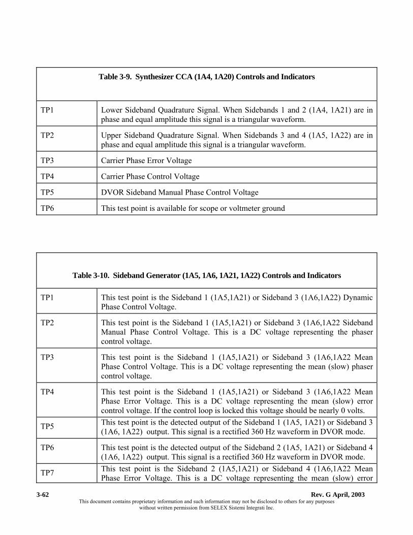
Rev. G April, 2003 This document contains proprietary information and such information may not be disclosed to others for any purposes
without written permission from SELEX Sistemi Integrati Inc.
3-62
Table 3-9. Synthesizer CCA (1A4, 1A20) Controls and Indicators
TP1
Lower Sideband Quadrature Signal. When Sidebands 1 and 2 (1A4, 1A21) are in phase and equal amplitude this signal is a triangular waveform.
TP2
Upper Sideband Quadrature Signal. When Sidebands 3 and 4 (1A5, 1A22) are in phase and equal amplitude this signal is a triangular waveform.
TP3
Carrier Phase Error Voltage
TP4
Carrier Phase Control Voltage
TP5
DVOR Sideband Manual Phase Control Voltage
TP6
This test point is available for scope or voltmeter ground
Table 3-10. Sideband Generator (1A5, 1A6, 1A21, 1A22) Controls and Indicators
TP1
This test point is the Sideband 1 (1A5,1A21) or Sideband 3 (1A6,1A22) Dynamic Phase Control Voltage.
TP2
This test point is the Sideband 1 (1A5,1A21) or Sideband 3 (1A6,1A22 Sideband Manual Phase Control Voltage. This is a DC voltage representing the phaser control voltage.
TP3
This test point is the Sideband 1 (1A5,1A21) or Sideband 3 (1A6,1A22 Mean Phase Control Voltage. This is a DC voltage representing the mean (slow) phaser control voltage.
TP4
This test point is the Sideband 1 (1A5,1A21) or Sideband 3 (1A6,1A22 Mean Phase Error Voltage. This is a DC voltage representing the mean (slow) error control voltage. If the control loop is locked this voltage should be nearly 0 volts.
TP5 This test point is the detected output of the Sideband 1 (1A5, 1A21) or Sideband 3
(1A6, 1A22) output. This signal is a rectified 360 Hz waveform in DVOR mode. TP6
This test point is the detected output of the Sideband 2 (1A5, 1A21) or Sideband 4 (1A6, 1A22) output. This signal is a rectified 360 Hz waveform in DVOR mode.
TP7 This test point is the Sideband 2 (1A5,1A21) or Sideband 4 (1A6,1A22 Mean
Phase Error Voltage. This is a DC voltage representing the mean (slow) error

Model 1150 DVOR
Rev. G April, 2003 This document contains proprietary information and such information may not be disclosed to others for any purposes
without written permission from SELEX Sistemi Integrati Inc.
3-63
Table 3-10. Sideband Generator (1A5, 1A6, 1A21, 1A22) Controls and Indicators
control voltage. If the control loop is locked this voltage should be nearly 0 volts. TP8
This test point is the Sideband 2 (1A5,1A21) or Sideband 4 (1A6,1A22 Mean Phase Control Voltage. This is a DC voltage representing the mean (slow) phaser control voltage.
TP9
This test point is the Sideband 2 (1A5,1A21) or Sideband 4 (1A6,1A22 Sideband Manual Phase Control Voltage. This is a DC voltage representing the phaser control voltage.
TP10
This test point is the Sideband 2 (1A5,1A21) or Sideband 4 (1A6,1A22) Dynamic Phase Control Voltage.
A1/A3 R18
This adjustment point is the Sideband Carrier Balance Adjustment. It adjusts the balance of every other peak in DVOR.
A1/A3 R24 This adjustment point is the Sideband Carrier Balance Adjustment. It adjusts the
balance of every other peak in DVOR. A1/A3 R51
This adjustment point is the Phase Detector DC offset Adjustment.
A1/A3 R73
This adjustment point is the Sideband Mean Phase Control Voltage Set Adjustment.
A1/A3 R97
This adjustment point is the Sideband Phase zero control.
A1/A3 R100
This adjustment point is the Sideband Detector Calibration Adjustment. It adjusts the power level displayed on the PMDT.
A1/A3 R102
This adjustment point is the Sideband Dynamic Phase Control Voltage Set Adjustment.
GND
This test point is available for scope or voltmeter ground.

Rev. G April, 2003 This document contains proprietary information and such information may not be disclosed to others for any purposes
without written permission from SELEX Sistemi Integrati Inc.
3-64
THIS SHEET INTENTIONALLY BLANK

Model 1150 DVOR
Rev. G April, 2003 This document contains proprietary information and such information may not be disclosed to others for any purposes
without written permission from SELEX Sistemi Integrati Inc.
4-1
4 STANDARDS AND TOLERANCES
4.1 INTRODUCTION
Table 4-1 is a list of equipment parameters, their standards, and their limits. In the Parameter column, each parameter measured or adjusted is listed. The paragraphs of Section 9 that describe the procedures used to establish the values of the parameters are listed in the Reference Paragraph column. In the Standard column are listed the optimum values of the parameters. The Tolerance column is the maximum possible deviation, above or below the standard value, when the DVOR equipment is commissioned initially or subsequent to any modification.
Table 4-1. Standards and Tolerances
Reference Parameter Standard Tolerance Paragraph a. Max Antenna 1.0:1 ˜1.2:1 6.2.7 VSWR b. Power Output (1) Carrier Value established by
flight inspection 50% of standard (-3dB)
6.2.3
9.7.17.2 (2) Sideband For 30% AM Nominal, ±2% 9.7.17.2 c. Frequencies (1) Carrier Assigned Freq. Nominal, ±0.0005% 6.2.4 (2) 9960 Hz 9960 Hz ±1% 6.2.6 (3) 30 Hz Variable 30 Hz ±1% 6.2.6 (4) 30 Hz Reference 30 Hz ±1% 6.2.6 (5) Ident 1020 Hz ±20 Hz 6.2.13 (6) Ident (Dot Length) 100 ms ±5 ms d. Modulation (1) 30 Hz 30% ±2% 6.2.5 (2) 9960 Hz 30% ±2% 6.2.5 (3) 9960 Hz Deviation 16:1 ±1 6.2.5 (4) Ident 5% ±1% 6.2.13 (5) Voice 30% +0,-2% e. Reflected Powers (1) Reference VSWR 1.0:1 ˜1.2:1 6.2.7,
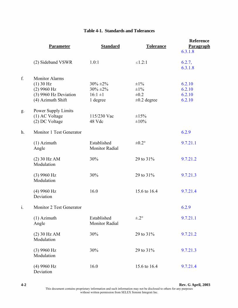
Rev. G April, 2003 This document contains proprietary information and such information may not be disclosed to others for any purposes
without written permission from SELEX Sistemi Integrati Inc.
4-2
Table 4-1. Standards and Tolerances
Reference Parameter Standard Tolerance Paragraph 6.3.1.8 (2) Sideband VSWR 1.0:1 ˜1.2:1 6.2.7, 6.3.1.8 f. Monitor Alarms (1) 30 Hz 30% ±2% ±1% 6.2.10 (2) 9960 Hz 30% ±2% ±1% 6.2.10 (3) 9960 Hz Deviation 16:1 ±1 ±0.2 6.2.10 (4) Azimuth Shift 1 degree ±0.2 degree 6.2.10 g. Power Supply Limits (1) AC Voltage 115/230 Vac ±15% (2) DC Voltage 48 Vdc ±10% h. Monitor 1 Test Generator 6.2.9 (1) Azimuth Established ±0.2° 9.7.21.1 Angle Monitor Radial (2) 30 Hz AM 30% 29 to 31% 9.7.21.2 Modulation (3) 9960 Hz 30% 29 to 31% 9.7.21.3 Modulation (4) 9960 Hz 16.0 15.6 to 16.4 9.7.21.4 Deviation i. Monitor 2 Test Generator 6.2.9 (1) Azimuth Established ±.2° 9.7.21.1 Angle Monitor Radial (2) 30 Hz AM 30% 29 to 31% 9.7.21.2 Modulation (3) 9960 Hz 30% 29 to 31% 9.7.21.3 Modulation (4) 9960 Hz 16.0 15.6 to 16.4 9.7.21.4 Deviation

Model 1150 DVOR
Rev. G April, 2003 This document contains proprietary information and such information may not be disclosed to others for any purposes
without written permission from SELEX Sistemi Integrati Inc.
4-3
Table 4-1. Standards and Tolerances
Reference Parameter Standard Tolerance Paragraph j. Monitor Limits (1) Azimuth Executive -1° 9.7.19.1 Angle Low Monitor Radial (2) Azimuth Executive +1° 9.7.19.2 Angle High Monitor Radial (3) 30 Hz AM Established -2% of 9.7.19.3 Modulation by flight Standard Low check or 30% (4) 30 Hz AM Established +2% of 9.7.19.4, Modulation by flight Standard High check or 30% (5) 9960 Hz Established -2% of 9.7.19.5 Modulation by flight Standard Low check or 30% (6) 9960 Hz Established +2% of 9.7.19.6 Modulation by flight Standard High check or 30% (7) 9960 Hz 16.0 15.0 9.7.19.7 Deviation Low (8) 9960 Hz 16.0 17.0 9.7.19.8 Deviation High (9) Field Established -3 dB 9.7.19.9 Intensity value Low (10) Field Established +2 dB 9.7.19.10 Intensity value High k. Monitor Certification 6.2.10 (1) Azimuth Executive ±0.2° of 9.7.20.1 Angle Low Monitor Standard Radial -1.0°

Rev. G April, 2003 This document contains proprietary information and such information may not be disclosed to others for any purposes
without written permission from SELEX Sistemi Integrati Inc.
4-4
Table 4-1. Standards and Tolerances
Reference Parameter Standard Tolerance Paragraph (2) Azimuth Executive ±0.2° of 9.7.20 Angle High Monitor Standard Radial +1.0° (3) 30 Hz AM Established ±1% of 9.7.20 Modulation Low Modulation -2% Standard (4) 30 Hz AM Established ±1% of 9.7.20 Modulation High Modulation +2% Standard (5) 9960 Hz Established ±1% of 9.7.20 Modulation Low Modulation -2% Standard (6) 9960 Hz Established ±1% of 9.7.20 Modulation High Modulation +2% Standard (7) 9960 Hz Established ±0.2 9.7.20 Deviation Low Deviation Low Limit (8) 9960 Hz Established ±0.2 9.7.20 Deviation High Deviation High Limit

Model 1150 DVOR
Rev. G April, 2003 This document contains proprietary information and such information may not be disclosed to others for any purposes
without written permission from SELEX Sistemi Integrati Inc.
5-1
5 PERIODIC MAINTENANCE
5.1 INTRODUCTION
This section contains instructions for system level performance testing and maintenance of the Model 1150 DVOR. The DVOR is capable of continuous, unattended operation. Maintainability is based on a schedule consisting of a monthly, quarterly, semi-annual and annual performance checks. The performance checks are described in the following paragraphs. If maintenance action has potentially degraded system performance to such a degree that its published aircraft approach procedures may not be achieved, system performance is to be verified by a flight inspection aircraft prior to returning the facility to normal service.
5.2 PERFORMANCE CHECK SCHEDULE
Table 5-1 is a summary of the various performance checks and their recommended intervals. Supervising personnel are responsible for scheduling these checks based on the recommended intervals. Information contained in table 5-1 is limited to equipment specifically covered in this manual.
Table 5-1. Performance Check Schedule
Reference Paragraph
Performance Check Standards & Tolerances
Maintenance Procedures
MONTHLY a. Generator Test VOR Monitor Table 4-1.h/I 6.2.9 (RMM) b. Certification Test VOR Monitor Table 4-1.k 6.2.10 (RMM) c. Check RSCU Status/Control N/A 6.2.11 d. Check 30 Hz and 9960 Hz
Modulation Table 4-1.d 6.2.5 (RMM)
e. Check Deviation Ratio Table 4-1.d 6.2.5 (RMM) QUARTERLY a. Site Inspection N/A 6.3.1.1, 6.3.1.4 b. Clean Air Filters N/A 6.3.1.6, 6.3.1.4

Rev. G April, 2003 This document contains proprietary information and such information may not be disclosed to others for any purposes
without written permission from SELEX Sistemi Integrati Inc.
5-2
Table 5-1. Performance Check Schedule
Reference Paragraph
Performance Check Standards & Tolerances
Maintenance Procedures
c. Check Carrier Output Power Table 4-1.b 6.2.3 d. Check Station Ident Table 4-1.c 6.2.13 e. Check Antenna VSWR Table 4-1.a 6.2.7 f. Check Battery Backup Transfer N/A 6.2.2 g. Check Auto-Transfer N/A 6.2.8 h. Reassign Main/Standby Transmitters N/A 6.3.1.7 SEMI-ANNUAL a. Inspect Battery Backup N/A 6.3.1.5 b. Check Carrier Frequency Table 4-1.c 6.2.4 c. Check Operating Frequency Table 4-1.c 6.2.6 ANNUAL a. Verify BITE Wattmeter Calibration N/A 6.3.1.10 b. Verify BITE Frequency Counter
Calibration N/A 6.3.1.9
c. Verify BITE VSWR Calibration N/A 6.3.1.8 d. Check Battery on CPU (1A13) CCA N/A 6.2.12 e. Antenna System and Radome
Inspection N/A 6.3.1.2
f. Inspect Field Monitor Antenna N/A 6.3.1.3

Model 1150 DVOR
Rev. G April, 2003 This document contains proprietary information and such information may not be disclosed to others for any purposes
without written permission from SELEX Sistemi Integrati Inc.
6-1
6 MAINTENANCE PROCEDURES
6.1 INTRODUCTION
This section provides the procedures required for accomplishing incidental maintenance activities. This section is divided into three parts: performance check procedures, other maintenance procedures, and special maintenance procedures.
6.2 PERFORMANCE CHECK PROCEDURES
When abnormal performance conditions are indicated during the performance check procedures, refer to Section 7.
6.2.1 Test Equipment
The performance checks are designed to make optimum use of the Built-in Equipment (BITE) by personnel responsible for the maintenance of the DVOR facility. The test equipment (or equivalent) listed in table 6-1 are required to perform DVOR maintenance procedures.
Table 6-1. Test Equipment
Oscilloscope, Type TAS250 (Tektronics) Detecting Elements Models 250B or 250C Multimeter, Digital, Model 77 (Fluke) Dummy Load, 5-T-N (Bird) Frequency Counter, Model 1856A (B&K) Type "N" Barrel (Qty. 2) Power Meter, Model 4130A (Bird) Type "N" Tee
6.2.2 Battery Backup Transfer Performance Check
a. Select Screen [RMS, DATA],
b. Starting with all cabinet circuit breakers in the ON position (AC and DC), remove AC power from Transmitter 1. Verify that the DVOR system continues to function and that "On Batteries" changes from No to Yes.
c. If the VOR is a dual system, remove AC power from Transmitter 2. Verify that the DVOR system continues to function and that "On Batteries" changes from No to Yes.
d. Restore AC power for Transmitters 1 and 2 (if dual equipment). Verify that the system continues to function and that "On Batteries" changes from Yes to No for both systems.
6.2.3 Carrier Output Power Performance Check
a. Verify that transmitter 1 is operating.

Rev. G April, 2003 This document contains proprietary information and such information may not be disclosed to others for any purposes
without written permission from SELEX Sistemi Integrati Inc.
6-2
b. Select screen Transmitters, Configuration. Typically Carrier Power is set for 100 watts (en route) or 50 watts (terminal).
c. Select screen, VOR Transmitters, Data, Transmitter 1, and observe that Carrier Power is within ±10% of the setting in step b.
d. Change operating transmitter to 2 by pointing and clicking on the Tx2 Antenna.
e. Select screen Transmitters, Data, Transmitter 2. and observe that Carrier power is within ±10% of the setting.
6.2.4 Carrier Frequency Performance Check
a. Verify that transmitter is powered.
b. Connect frequency counter to "CARRIER FREQUENCY" jack of Synthesizer Generator Assembly (1A4).
c. Observe the station operating frequency while transmitter 1 is operating. Verify that the frequency is within the tolerance in Table 4-1.
d. Connect frequency counter to "CARRIER FREQUENCY" jack of Frequency Synthesizer assembly (1A20).
e. Observe the station operating frequency while transmitter 2 is operating. Verify that the frequency is within the tolerance of Table 4-1.
6.2.5 30 Hz and 9960 Hz Modulation and Deviation Ratio Performance Check
a. Select Monitors, Data Screen. Observe the Monitor 1, 30 Hz modulation and verify it is within the low-high limits.
b. Observe Monitor 1, 9960 Hz modulation and verify it is within low-high limits.
c. Observe Monitor 1, Deviation Ratio and verify it is within low-high limits.
d. Observe Monitor 2, Integrity Data. Observe the 30 Hz modulation and verify it is within the low-high limits.
e. Observe Monitor 2, 9960 Hz modulation and verify it is within low-high limits.
f. Observe Monitor 2, Deviation Ratio and verify it is within low-high limits.
g. Change operating transmitter by pointing and clicking Tx2 Antenna. Repeat steps a. through f. after Monitors have stabilized.
6.2.6 Operating Frequency Performance Check
a. Verify that transmitter 1 is operating.
b. Select Transmitters, Data, Transmitter 1.
c. Observe the 30 Hz frequency and assure it is within ±1%.

Model 1150 DVOR
Rev. G April, 2003 This document contains proprietary information and such information may not be disclosed to others for any purposes
without written permission from SELEX Sistemi Integrati Inc.
6-3
d. Observe the 9960 Hz frequency and assure it is within ±1%.
NOTE: The frequencies displayed are not to be used.
e. Observe the Carrier frequency and assure that it is within ±0.02%.
f. Observe Lower Sideband frequency and assure it is 10 KHz below Carrier ±0.02%.
g. Observe Upper Sideband frequency and assure it is 10 KHz above Carrier ±0.02%.
h. Change operating transmitter to 2 by pointing and clicking Tx 2 antenna.
i. Select Transmitters, Data, Transmitter 2
j. Observe the 30 Hz frequency and assure it is within ±1%.
k. Observe the 9960 Hz frequency and assure it is within ±1%.
l. Observe the Carrier frequency and assure that it is within ±0.02%.
m. Observe Lower Sideband frequency and assure it is 10 KHz below Carrier ±0.02%.
n. Observe Upper Sideband frequency and assure it is 10 KHz above Carrier ±0.02%.
6.2.7 Antenna VSWR Performance Check
a. On the video terminal, select screen Transmitters, Data, Transmitter 1. Observe Carrier VSWR. Verify that this value is less than 1.2:1.
b. On the same screen, observe Sideband 1, Sideband 2, Sideband 3 and Sideband 4 VSWR. Verify that these values are less than 1.2:1.
c. On screen Monitors, Data, Sideband Antenna VSWR observe the sideband antenna VSWR. Verify that no antennas are out of tolerance as indicated by an alert condition.
6.2.8 Automatic Transfer Performance Checks
a. Log on to system. Select transmitter 1 as main by pointing and clicking the Tx1 main button.
b. Enter the Monitors, Configuration, Offsets and Scale Factors screen and change the Azimuth Angle Offset for Monitor 1 so that an out-of-tolerance condition exists for Monitor 1.
c. Change the Azimuth Angle offset for Monitor 2 of the limits so that an out-of-tolerance condition exists for Monitor 2.
d. Verify that transmitter 2 turns on, relays change, and transmitter 1 turns off.
e. Enter Monitors, Configuration, Offsets and Scale Factors screen and restore the angle offsets to the original settings.
f. Select transmitter 2 as main by pointing and clicking on Tx 2 main button..

Rev. G April, 2003 This document contains proprietary information and such information may not be disclosed to others for any purposes
without written permission from SELEX Sistemi Integrati Inc.
6-4
g. Enter the Monitors, Configuration, Offsets and Scale Factors screen and change the Azimuth Angle Offset for Monitor 1 so that an out-of-tolerance condition exists for Monitor 1.
h. Change the Azimuth Angle offset for Monitor 2 of the limits so that an out-of-tolerance condition exists for Monitor 2.
i. Verify that transmitter 2 turns on, relays change, and transmitter 1 turns off.
j. Enter Monitors, Configuration, Offsets and Scale Factors screen and restore the limits to the original settings.
6.2.9 VOR Monitor Performance Check
a. Select Monitors, Data, Test Data Screen. Point and click on the RUN button for Monitor 1.
b. When complete the data from the monitor will be displayed under Test Results for azimuth angle, 30 Hz modulation, and 9960 Hz modulation/deviation.
c. Verify the displayed data is within tolerances as stated in Table 4-1, section h (Monitor 1).
d. Point and click on the Run button under Monitor 2.
e. The data from the monitor will be displayed under Data, for azimuth angle, 30 Hz modulation, and 9960 Hz modulation/deviation.
f. Verify the displayed data is within tolerances as stated in Table 4-1, section i (Monitor 2).
6.2.10 Certification Test VOR Monitor
a. Select Monitors, Configuration, Offsets and Scale Factors. Point and Click the Copy Button. Press F7.
b. Select screen Monitors, Data, Certification Test Results. Click and press set to monitor limits. Press F7. Click and press the RUN button in the Monitor 1 Section. The internal test generator will automatically perform a test of the number 1 monitor, using the upper and lower test limits displayed. The entire test takes several minutes.
c. When complete the results of the upper and lower limit test of the monitor will be displayed under data, for azimuth angle, 30 Hz modulation, and 9960 Hz modulation/deviation.
d. Point and click the RUN button for Monitor 2. The internal test generator will automatically perform a test of the number 2 monitor, using the upper and lower test limits displayed. The entire test takes several minutes.
e. When complete the results of the upper and lower limit test of the monitor will be displayed under Data, for azimuth angle, 30 Hz modulation, and 9960 Hz modulation/deviation.

Model 1150 DVOR
Rev. G April, 2003 This document contains proprietary information and such information may not be disclosed to others for any purposes
without written permission from SELEX Sistemi Integrati Inc.
6-5
6.2.11 RSCU Operation Performance Check
This check may be performed only by authorized tower control or local control personnel on a routine schedule.
6.2.11.1 Single Equipment Performance Check
a. At the remote site perform a lamp test. Verify all lights illuminate.
b. At the remote site, assure that the indicator for DVOR transmitter 1 Normal light is on and the "DATA FAULT" is off.
c. From the RSCU, turn off transmitter. Verify that the NORMAL light is off.
d. At the remote site turn on the transmitter. Verify that the NORMAL light is on and the ALARM light is off.
6.2.11.2 Dual Equipment Performance Check
a. Put the DVOR in normal configuration, with transmitter 1 selected as main.
b. At the remote site, perform a lamp test. Verify all lights illuminate.
c. At the remote site, assure that the indicator for DVOR transmitter 1 NORMAL and antenna indicator "#1" lights are on and the "DATA FAULT" lamp is off.
d. From the RSCU, turn on the number 2 transmitter. Verify that the DVOR changes transmitters and the number 2 transmitter comes up normally. Verify the antenna indicator "#2" light is on. A visual and audible alarm will also occur with transfer. Clear the alarm by holding #2 switch to on.
e. From the RSCU, turn off transmitter 2. Turn on transmitter 1. Assure that the indicators for DVOR transmitter 1 NORMAL and antenna indicator #1 lights are on.
6.2.12 Checking Battery on CPU (1A13) CCA
a. Connect digital voltmeter negative lead to chassis ground.
b. Place the positive probe tip against the exposed battery case on the CPU CCA (1A13). This may be accomplished while the system is operational. Verify that the voltage is greater than 2.0 Vdc.
6.2.13 Station Identification Checks
a. Connect oscilloscope probe to 1A8-TP5. Select Transmitters, Commands, VOR IDENT, Continuous.
b. Adjust the oscilloscope controls to obtain a pattern showing 2 or 3 cycles of the 1020 identification modulation.
Rev. G April, 2003 This document contains proprietary information and such information may not be disclosed to others for any purposes
without written permission from SELEX Sistemi Integrati Inc.
6-6
c. Adjust Transmitters, Configuration, Ident modulation to the desired modulation level. Set Reference and Voice Modulation to 0%.
d. Adjust the Transmitters, configuration, offsets and scale factors, Ident Modulation Scale for Transmitter 1 until the oscilloscope pattern indicates the same modulation as determined by the following relation:
Emax - Emin % Ident Modulation = ----------------------
Emax + Emin
d. Connect frequency counter input to test point 1A8 - TP8
e. Observe the Ident frequency and verify it is within ±20 Hz.
f. Turn on transmitter 2 by pointing and clicking the Tx 2 antenna button.
g. Repeat Step D for Transmitter 2.
h. Connect frequency counter input to test point 1A24-TP8.
i. Observe the Ident frequency and verify it is within ±20 Hz.
j. Select Transmitters, Commands, VOR Ident, Normal.
k. On the Monitors, Data, Integrity screen, verify that the Ident is NORMAL.
6.3 OTHER MAINTENANCE PROCEDURES
6.3.1 Equipment Inspection
The equipment inspection is a visual inspection that is done prior to performing any maintenance procedure. This will assure the technician that the system is properly connected and all electrical bonds are in good condition.
6.3.1.1 Site Inspection
a. Check that the site is clear of any new obstructions or materials which could affect the normal operation of the DVOR system.
b. Check the shelter, inside and out, for any sign of water filtration, damage, or other deterioration.
c. Check the condition of the air conditioner, shelter lighting, obstruction lights, baseboard heaters, electrical outlets, lightening arrestors, etc.
d. Check for and remove any accumulation of snow, ice, or debris on the field monitor antennas.
e. Check for and remove any accumulation of snow, ice or debris on the counterpoise surface.

Model 1150 DVOR
Rev. G April, 2003 This document contains proprietary information and such information may not be disclosed to others for any purposes
without written permission from SELEX Sistemi Integrati Inc.
6-7
6.3.1.2 Inspection of Antenna System
a. Insure that both DVOR transmitters are turned off.
b. The DVOR antennas are contained within fiberglass radomes.
c. Inspect the mating areas of the radomes where the radome interfaces with the radome base or where the radome interfaces with the antennas. Check for any signs of water leakage or deterioration. Repair or replace as necessary.
d. Inspect the antenna for any signs of deterioration of water damage. Check the input cables and connectors for breaks, cracks or corrosion. Check that the connectors are securely fastened, and inspect the remaining parts of the antenna for damage or signs of vermin infestation.
e. Inspect the counterpoise for any signs of deterioration, paying special attention to the welded joints, bolted connections, mesh, etc. Check for proper electrical connection between the counterpoise segments and grounding connections.
f. Remove any articles carried into the radome area and replace the antenna radome covers.
6.3.1.3 Inspection of the Field Monitor Antenna
a. Inspect the condition of the field monitor antenna. Make sure it is solidly mounted, and that all nuts and bolts are tightened.
b. Inspect the condition of the field monitor antenna coaxial cables for signs of cracks or breakage. Replace if necessary.
6.3.1.4 Equipment Inspection
a. Visually inspect interconnecting wire harnesses, coaxial cables and connectors for corrosion, cracks, breaks, and burns. Insure all RF connectors are tightened.
b. Inspect all peripheral equipment connected to the DVOR, including the PMDT, printer, etc.
c. Inspect the front panel indicators on the DVOR and assure that indicators are normal.
d. Inspect the DVOR air filters. Clean the air filters by removing them from the cabinet and shaking out any loose dirt and debris. Wash the filter with mild detergent and water. Dry the filters completely prior to replacing in the cabinet.
6.3.1.5 Inspection of Battery Backup Unit
Refer to Figure 9-5.
a. Place the circuit breakers on the battery boxes in the OFF position.

Rev. G April, 2003 This document contains proprietary information and such information may not be disclosed to others for any purposes
without written permission from SELEX Sistemi Integrati Inc.
6-8
b. Remove the covers from the battery boxes. Visually inspect the condition of each battery, and inspect the connectors and cables for any cracks, breaks, burns, or corrosion. Make sure that all connectors are fastened tightly to their terminals. Clean battery area as necessary.
c. Replace the battery box covers and place the circuit breakers in the ON position.
6.3.1.6 Maintenance of Blowers and Air Filters
The DVOR blowers use lifetime lubricated bearings and do not require maintenance.
a. Inspect the DVOR air filters. Clean the air filters by removing them from their housing and shaking any out loose dirt and debris. Wash the filter with mild detergent and water. Dry the filters completely prior to replacing in the cabinet.
6.3.1.7 Reassign Main/Standby Transmitters (Dual Systems Only)
a. Log on to the PMDT.
b. Point and click on the Tx 1 Main or the Tx 2 Main Button as desired on Sidebar.
6.3.1.8 Verification of BITE VSWR Calibration. -
a. Make sure that both transmitters are off.
b. Disconnect the Carrier feed cable from the top of the DVOR cabinet. Replace with type "N" barrel, type "N" TEE and 250W load. Attach type "N" barrel to the open port of the TEE.
c. Turn on transmitter 1 by pointing and clicking the Tx 1 Antenna button. Place transmitter in BYPASS by pointing and clicking the Bypass button.
d. Select screen Transmitters, Data, Transmitter 1 observe Carrier VSWR. The display VSWR should be between 1.20 to 1.23.
e. If the levels are not within this range, carefully adjust (on the RF Monitor Assembly) the transmitter 1 reflected power detector potentiometer (TX1 RFD) located behind the DVOR status panel. Turning the pot clockwise will increase VSWR reading and counterclockwise will decrease. Make a small adjustment and wait for display to stabilize.
f. Point and click the Tx 2 Antenna Button.
g. Select screen [Transmitters, Data, Transmitter 2, observe Carrier VSWR. The display VSWR should be between 1.20 to 1.23.
h. If the levels are not within this range, carefully adjust (on the RF Monitor Assembly) the transmitter 2 reflected power detector potentiometer (TX2 RFD) located behind the DVOR status panel. Turning the pot clockwise will increase VSWR reading and counterclockwise will decrease. Make a small adjustment and wait for display to stabilize.
i. Point and click the OFF button for Transmitter 1 and Transmitter 2.

Model 1150 DVOR
Rev. G April, 2003 This document contains proprietary information and such information may not be disclosed to others for any purposes
without written permission from SELEX Sistemi Integrati Inc.
6-9
j. Move the barrels, bullets, and TEE to the Sideband 1 output (J2). Replace the carrier cable. Place a 5W termination on the TEE output. Place the Carrier Transmitter cable back to its original position.
k. Turn on transmitter 1 by pointing and clicking the Tx 1 Antenna button. Place transmitter in BYPASS by pointing and clicking the Bypass button.
l. Select screen Monitors, Data, Sideband Antenna VSWR, observe odd numbered Antenna VSWR. The displayed VSWR should be between 1.20 to 1.23 for odd numbered antennae.
m. If the levels are not within this range, carefully adjust (on the RF Monitor Assembly) the transmitter 1, SB1 reflected power detector potentiometer (SB1 RFD) located behind the DVOR status panel. Turning the pot clockwise will increase VSWR reading and counterclockwise will decrease.
n. Turn both transmitters are off. Move the load barrels, bullets, and TEE to the Sideband 2 output.
o. Select screen Monitors, Data, Sideband Antenna VSWR, observe even numbered Antenna VSWR. The displayed VSWR should be between 1.20 to 1.23 for even numbered antennae.
p. If the levels are not within this range, carefully adjust (on the RF Monitor Assembly) the transmitter 1, SB2 reflected power detector potentiometer (SB2 RFD) located behind the DVOR status panel. Turning the pot clockwise will increase VSWR reading and counterclockwise will decrease.
q. Turn both transmitters off.
r. Remove termination, TEE and bullets. Place cables in their original positions.
s. Turn the system on and clear the bypass condition by clicking by clicking on the bypass button.
6.3.1.9 Verification of BITE Frequency Counter Calibration
a. Turn off all power. Remove VOR Monitor (1A8) CCA, replace with a CCA extender and attach the VOR Monitor CCA to the extender.
b. Turn on power.
c. Connect scope to TP16 of the VOR Monitor (1A8) CCA and verify that 200 MHz pulse signal is present. Select Transmitters, data, Transmitter 1 screen. Adjust C4 on the Monitor CCA as necessary to cause displayed Carrier frequency to match the actual Carrier frequency (as measured in 6.2.4) ±.002%. The reading will update approximately once every 90 seconds. Make small adjustments and wait for update.
d. Turn on Tansmitter 1 by clicking the Tx 1 Antenna Button.
e. Connect the external frequency counter to 1A8-TP7.
f. On the video terminal select Transmitters, Data, VOR Transmitter 1 Trend.
g. Observe the 30 Hz frequency and assure it is within ±1.0% of the reading from the frequency counter.

Rev. G April, 2003 This document contains proprietary information and such information may not be disclosed to others for any purposes
without written permission from SELEX Sistemi Integrati Inc.
6-10
h. Connect the external frequency counter to 1A8-TP11.
i. Observe the 9960 Hz frequency and assure it is within ±1.0% of the reading from the frequency counter.
j. Turn off power. Remove VOR Monitor (1A8) CCA from extender. Put the VOR Monitor (1A24) CCA on extender. Turn on power.
k. Turn on power. Change operating transmitter to 2 by pointing to Tx 2 antenna.
l. Connect scope to TP16 of the VOR Monitor (1A24) CCA and verify that 2.00 MHz pulse signal is present. Select Transmitters, Data, Transmitter 2 screen. Adjust C4 on the Monitor CCA as necessary to cause displayed Carrier frequency to match the actual Carrier frequency (as measured in 6.2.4) ±.002%. The reading will update approximately once every 90 seconds. Make small adjustments and wait for update.
m. Connect the external frequency counter to 1A24-TP7.
n. On the video terminal select Tansmitters, data, Transmitter 2.
o. Observe the 30 Hz frequency and assure it is within ±1.0% of the reading from the frequency counter.
p. Connect the external frequency counter to 1A24-TP11.
q. Observe the 9960 Hz frequency and assure it is within ±1.0% of the reading from the frequency counter. This reading will be close to 10 KHz.
r. Remove VOR Monitor (1A24) CCA from extender and place the VOR Monitor (1A24) CCA back into its original position.
6.3.1.10 Verification of BITE Wattmeter Calibration
a. Insert a 250 Watt plug-in element into the thru-line wattmeter body in the carrier feed cable.
b. Point and click the Tx 1 antenna button to turn on Transmitter. Point and click the Bypass button to place the transmitter in BYPASS.
c. Select screen Transmitters, data, Transmitter 1, observe Carrier power output. The displayed output is to coincide with the external wattmeter indication.
d. If the levels are not the same, carefully adjust (on the RF Monitor Assembly) the transmitter 1 forward power detector potentiometer (TX1 FWD) located behind the DVOR status panel. Turning the pot clockwise will decrease power reading and counterclockwise will increase. Make a small adjustment and wait for display to stabilize.
e. Point and click on the Tx 2 antenna button.
f. Select screen Transmitters, data, Transmitter 2, observe Carrier power output. The displayed output is to coincide with the external wattmeter indication.
g. If the levels are not the same, carefully adjust (on the RF Monitor Assembly) the transmitter 2 forward power detector potentiometer (TX2 FWD) located behind the DVOR status panel. Turning the pot clockwise will decrease power reading and counterclockwise will increase. Make a small adjustment and wait for display to stabilize.
h. Turn on Transmitter 1 by pointing and clicking Tx 1 Antenna button.

Model 1150 DVOR
Rev. G April, 2003 This document contains proprietary information and such information may not be disclosed to others for any purposes
without written permission from SELEX Sistemi Integrati Inc.
6-11
i. Insert a 5 Watt plug-in element into the thru-line wattmeter body in the Sideband 1 feed cable.
j. Select screen Transmitters, data, Transmitter , observe Sideband 1 power output. The displayed output is to coincide with the external wattmeter indication.
k. If the levels are not the same, carefully adjust the Sideband 1 forward power detector potentiometer A5A1R100 located on the Sideband Generator (1A5) Assembly. Turning the pot clockwise will increase power reading and counterclockwise will increase. Make a small Adjustment and wait for display to stabilize.
l. Select screen [J], Maintenance Command Directory. Point and click on Tx 2 Antenna button to change Transmitters.
m. Select screen Transmitters, data, Transmitter 2, observe Sideband 1 power output. The displayed power is to coincide with the external wattmeter indication.
n. If the levels are not the same, carefully adjust Sideband 1 forward power detector potentiometer A21A1R100 located on the Sideband Generator (1A21) Assembly. Turning the pot clockwise will increase power reading and counterclockwise will increase. Make a small adjustment and wait for display to stabilize.
o. Move the 5 Watt plug-in element from the thru-line wattmeter body at the Sideband 1 output to the thru-line wattmeter body at the Sideband 2 output.
p. Repeat steps i. through n. for Sideband 2, 3, 4 forward power output.
q. Take the system out of BYPASS by pointing and clicking on the bypass button.
6.4 SPECIAL MAINTENANCE PROCEDURES
6.4.1 Replacement of Assemblies with 1/4 Turn Fasteners
This procedure is used when a module is removed and replaced.
a. Set the DVOR SYSTEM A DC INPUT (batteries) and SYSTEM B DC INPUT (batteries, dual system) circuit breaker to the OFF position.
b. Set the DVOR SYSTEM A AC INPUT (line) and SYSTEM B AC INPUT (line) circuit breakers to the OFF position.
c. Observe ESD precautions.
d. Loosen the 1/4 turn fasteners securing faulty assembly in place.
e. Pull faulty assembly forward until it is clear of the transmitter cabinet.
f. Slide new assembly into transmitter cabinet until it is mounted flush against mating connectors. If difficulty occurs during installation, refer to paragraph 6.4.3.

Rev. G April, 2003 This document contains proprietary information and such information may not be disclosed to others for any purposes
without written permission from SELEX Sistemi Integrati Inc.
6-12
g. Tighten the 1/4 turn fasteners to hold the assembly securely in the transmitter cabinet assembly.
h. Perform the appropriate tune up procedures as detailed in paragraph 9.7.
6.4.2 Replacement of CCA without 1/4 Turn Fasteners
a. Set the DVOR SYSTEM A DC INPUT (batteries) and SYSTEM B DC INPUT (batteries, dual system) circuit breaker to the OFF position.
b. Set the DVOR SYSTEM A AC INPUT (line) and SYSTEM B AC INPUT (line) circuit breakers to the OFF position.
c. Using ESD procedures, pull faulty CCA forward until it is clear of the transmitter cabinet.
d. Slide new CCA in to transmitter cabinet until it is mounted flush against mating surface.
e. Perform the appropriate tune up procedures as detailed in paragraph 9.7.
6.4.3 Cabinet Backplane Connector Adjustment
Due to the physical characteristics of the DVOR cabinet, difficulty may be encountered during the installation of new RF Modules. If difficulty is encountered, refer to the following backplane adjustment procedure.
a. Swing the hinged transmitter cabinet assembly away from the shelter wall.
b. Remove the eight (8) screws securing the transmitter cabinet back panel and remove it. This allows access to the cabinet backplane connector.
c. Determine which RF Module will not properly mate with the cabinet backplane connector.
NOTE:
In order to adjust backplane for Sideband Amplifiers, it will be necessary to loosen screws for regulators attached to the chassis insert.
d. From the rear of the transmitter cabinet, loosen (do not remove) the six (6) screws securing the cabinet backplane connector mounting plate of the RF Module that will not fit properly into transmitter cabinet. This allows for slight adjustment of the cabinet backplane connector mounting plate.
e. Carefully slide the RF Module into place to position the cabinet backplane connector mounting plate. Carefully tighten the cabinet backplane connector mounting plate screws. Check the installation by installing and removing the RF Module. Repeat the process until RF Module mates smoothly with cabinet backplane connector. If Sideband Amplifier was replaced, carefully tighten the screws for regulators.
Model 1150 DVOR
Rev. G April, 2003 This document contains proprietary information and such information may not be disclosed to others for any purposes
without written permission from SELEX Sistemi Integrati Inc.
6-13
f. The cabinet backplane connector mounting plate contains D-shell connectors that may cause binding to occur. If the occurs, adjust the position of the D-shell connector by loosening (do not remove) the two (2) screws securing the D-shell connector. This allows for slight adjustment of the D-shell connector. Note that screws are to be loosened slightly so the D-shell connector will retain its position when the RF Module is removed from the cabinet.
g. Carefully slide the RF Module into place to position the D-shell connector. Carefully tighten the D shell connector screws. Check the installation by installing and removing the RF Module. Repeat the process until RF Module mates smoothly with cabinet backplane connector.
h. Replace cabinet back panel and secure using appropriate hardware.
i. Swing the cabinet assembly until it is flush with shelter wall and secure to the unistrut with appropriate hardware.
6.4.4 Replacing CPU (1A13) CCA
a. Select System, Configuration, Save, [enter]. Select a distinctive filename and save.
b. Set the DVOR SYSTEM A DC INPUT (batteries) and SYSTEM B DC INPUT (batteries, dual system) circuit breaker to the OFF position.
c. Set the DVOR SYSTEM A AC INPUT (line) and SYSTEM B AC INPUT (line) circuit breakers to the OFF position.
d. Using proper ESD handling procedures, disconnect the front card edge connector and pull faulty CPU CCA (1A13) forward until it is clear of the transmitter cabinet.
e. Insert the new CPU CCA into the cabinet and seat securely into backplane connector. Reconnect the front card edge connector.
f. Set the DVOR SYSTEM A AC INPUT (line) and SYSTEM B AC INPUT (line) circuit breakers to the ON position.
g. Set the DVOR SYSTEM A DC INPUT (batteries) and SYSTEM B DC INPUT (batteries, dual system) circuit breakers to the ON position.
h. Select System, Configuration Load, and choose the Filename from Step a.
i. Select RMS, Config Backup.
j. Set the current date and time by selecting RMS, Commands, Set Time and Date, [enter].
6.4.5 Update of DVOR Software
a. Select System, Configuration Save, [enter]. Select a distinctive filename and save.
b. Set the DVOR SYSTEM A DC INPUT (batteries) and SYSTEM B DC INPUT (batteries, dual system) circuit breaker to the OFF position.

Rev. G April, 2003 This document contains proprietary information and such information may not be disclosed to others for any purposes
without written permission from SELEX Sistemi Integrati Inc.
6-14
c. Set the DVOR SYSTEM A AC INPUT (line) and SYSTEM B AC INPUT (line) circuit breakers to the OFF position.
d. Using proper ESD handling procedures, disconnect the front card edge connector and pull the CPU CCA (1A13) forward until it is clear of the transmitter cabinet.
e. Replace the U11 and U12 integrated circuits, observing proper orientation of parts in sockets. Insert the CPU CCA (1A13) into the cabinet and reconnect the front connector.
f. Pull the Audio Generator CCA (1A7) forward. Locate and remove the U4 integrated circuit.
g. Replace the U4 integrated circuit and install the Audio Generator CCA (1A7) into its original location.
h. Pull the VOR Monitor CCA (1A8) forward. Locate and remove the U1 integrated circuit.
i. Replace the U1 integrated circuit and install the VOR Monitor CCA (1A8) into its original location.
j. Repeat steps f. through i. for the Audio Generator (1A23) and VOR Monitor (1A24) CCAs.
k. Set the DVOR SYSTEM A AC INPUT (line) and SYSTEM B AC INPUT (line) circuit breakers to the ON position.
l. Set the DVOR SYSTEM A DC INPUT (batteries) and SYSTEM B DC INPUT (batteries, dual system) circuit breakers to the ON position.
m. Pull the VOR Monitor CCA (1A8) forward. Locate and remove the U1 integrated circuit.
n. Replace the U1 integrated circuit and install the VOR Monitor CCA (1A8) into its original location.
o. Repeat steps f. through i. for the Audio Generator (1A23) and VOR Monitor (1A24) CCAs.
6.4.6 Changing the Station Rotation (Azimuth)
This step may be requested during a flight inspection of the VOR station.
a. If the operating transmitter is Transmitter 1, Select Transmitters, Configuration, Offsets and Configuration, Transmitter 1, Azimuth angle offset or Transmitter 2, Azimuth angle offset.
b. Change the desired amount of rotation. Enter a positive number for clockwise rotation or a negative number for counterclockwise rotation. The allowable entry is ±40 degrees in 0.01 degree increments.
6.4.7 Changing the Monitoring Offsets
This procedure is required after commissioning flight check to make the monitors agree with flight inspection results.
a. Turn on Transmitter 1.
b. Select Monitors, Data, Integrity Data.

Model 1150 DVOR
Rev. G April, 2003 This document contains proprietary information and such information may not be disclosed to others for any purposes
without written permission from SELEX Sistemi Integrati Inc.
6-15
c. The Azimuth index offset is the difference of the desired angle less the current value is azimuth for Monitor 1 and Monitor 2.
d. Select Monitors, Configuration, Offsets and Scale Factors. Enter the new azimuth offset for Monitor 1 and Monitor 2.
e. Select Monitors, data, Integrity data. Verify that the Azimuth value displayed is correct.
f. Compute the 30 Hz Modulation correct factors by the formula
.Re0.30 OffsetCurrentX
adingCurrent
g. Select Monitors, Configuration, Offsets and Side factors and read the current 30 Hz modulation offset and apply the formula if step f.
h. Enter the new offset value for Monitor 1 and Monitor 2, 30 Hz modulation
i. Repeat steps f, g and h for 9960 Hz Modulator and 9960 Hz deviation ratio.
j. Compute the field intensity offset by reading the field intensity value in Monitors, Data, Integrity data and subtracting the reading from 0.0. Place this offset value in Monitors, Configuration, Offsets and Scale Factors for Monitor 1 and for Monitor 2.
6.4.8 Changing the CPU (1A13) CCA Lithium Battery
a. Select RMS, Config Backup to save the parameters into EEPROM.
b. Select System Configuration Save, [enter]. Select a filename and save.
c. Set the DVOR SYSTEM A DC INPUT (batteries) and SYSTEM B DC INPUT (batteries, dual system) circuit breaker to the OFF position.
d. Set the DVOR SYSTEM A AC INPUT (line) and SYSTEM B AC INPUT (line) circuit breakers to the OFF position.
e. Using proper ESD handling procedures, disconnect the front card edge connector and pull the CPU CCA (1A13) forward until it is clear of the transmitter cabinet.
f. Disconnect the jumper between E1 and E2. Remove the lithium battery from its holder.
g. Insert the new lithium battery in the holder. Insert the CPU CCA (1A13) into the original position.
h. Set the DVOR SYSTEM A DC INPUT (batteries) and SYSTEM B DC INPUT (batteries, dual system) circuit breaker to the ON position.
i. Set the DVOR SYSTEM A AC INPUT (line) and SYSTEM B AC INPUT (line) circuit breakers to the ON position.
j. Place the jumper back between the CPU (1A13) CCA E1 to E2 terminals.

Rev. G April, 2003 This document contains proprietary information and such information may not be disclosed to others for any purposes
without written permission from SELEX Sistemi Integrati Inc.
6-16
6.4.9 Test Generator Check with a VOR Phasemeter
a. Select Monitors, Data, Test Data.
b. Enter the desired angle to test. Insure that the modulation levels for 30 Hz AM and 9960 Hz modulation are set to 30% and the 9960 deviation is set to a ratio of 16.0. Ident and voice modulation should be set to 0.
c. Connect the VOR phasemeter (ZIFOR III or equivalent) between VOR Test Generator (1A12) TP1 (pos.) and TP0 (gnd).
NOTE The ZIFOR III is intolerant to abrupt angle changes and may require cycling of ZIFOR III AC power to obtain the proper reading.
d. Click on the monitor 1 Run button to generate the desired angle. Wait approximately two minutes for completion of the waveform.
6.4.10 Modulation Reading Change
Refer to 6.4.7.
6.4.11 DME Keying Check
This procedure is used on systems where the DVOR is collocated with a DME.
a. Set the DVOR SYSTEM A DC INPUT (batteries) and SYSTEM B DC INPUT (batteries, dual system) circuit breaker to the ON position.
b. Set the DVOR SYSTEM A AC INPUT (line) and SYSTEM B AC INPUT (line) circuit breakers to the ON position.
c. Place DME equipment circuit breakers to the ON position.
d. Listen for the DME keying. If keying is not detected or is not in synchronization with the DVOR check terminal board wiring and connections.
6.4.12 Monitor Detector Alignment
This alignment should be performed at installation and after a detector has been replaced.
a. Place DVOR systems AC and DC circuit breakers to the ON position.
b. Log on to system.
c. Verify the monitor to detector settings in the RMS, Configuration, Station. Verify that Monitor 1 detector is 1 and Monitor 2 detector is 2. Press F7 if changed.
d. Turn on the Transmitter.
e. Connect oscilloscope probe to test point TP5 on the Monitor 1 CCA (1A8).
Model 1150 DVOR
Rev. G April, 2003 This document contains proprietary information and such information may not be disclosed to others for any purposes
without written permission from SELEX Sistemi Integrati Inc.
6-17
f. Observe the waveform on the oscilloscope. Adjust Detector 1 potentiometer R14 for minimum signal output at 1A8-TP5.
g. Adjust Detector 1 AT1 for 1 Vdc at 1A8-TP5.
h. Adjust audio potentiometer R14 for 2.5 VDC 1A8-TP5.
i. Connect oscilloscope probe to test point TP5 on the Monitor 2 CCA (1A24).
j. Observe the waveform on the oscilloscope. Adjust Detector 2 potentiometer R14 for minimum signal output at 1A24-TP5.
k. Adjust Detector 1 AT1 for 1 Vdc at 1A24-TP5.
l. Adjust audio potentiometer R14 for 2.5 VDC as indicated on 1A24-TP5.
6.4.13 DVOR Frequency Synthesizer Alignment
The following procedure must be used to properly align the Frequency Synthesizer Assembly for operation at a new frequency. Instructions are provided for adjusting the 1A4 Frequency Synthesizer Assembly, substitute 1A20 for 1A4 when performing the procedure on DVOR Transmitter No. 2 Frequency Synthesizer Assembly.
a. Remove power from the DVOR.
b. Remove the Frequency Synthesizer 1A4 from the VOR cabinet. Remove the left side cover (the one with the greater number of screws).
c. Refer to Table 9-3, set the frequency select dip switch S1 for the desired frequency of operation.
d. Connect the 1A4 Frequency Synthesizer Assembly to the DVOR with extender cables.
e. Apply power to the DVOR.
NOTE Placing the Frequency Synthesizer Assembly on extender cables may cause the carrier phase control loop to unlock. This phase control loop effects only the RF output to the carrier power amplifier, and will have no effect on the frequency counter readings taken at the test port output, J8 on the front panel of the Frequency Synthesizer Assembly. However, it may be desirable to check system operation while on extender cables. If the carrier phase control loop is unlocked, temporarily adjust 1A4R81 through the hole on the front panel of the 1A4 Frequency Synthesizer Assembly for 0.0 +/- 0.1 VDC at 1A4TP3 (carrier phase control loop error voltage) When the loop is properly locked, a small CCW adjustment of 1A4R81 will cause the error voltage to decrease, a small CW adjustment of 1A4R81 will cause the error voltage to increase. Due to the long time constants involved in the mean phase control loop, there is some time lag between adjustments of 1A4R81 and the error voltage reading (1A4TP3). Allow the reading to settle between small adjustments.
NOTE

Rev. G April, 2003 This document contains proprietary information and such information may not be disclosed to others for any purposes
without written permission from SELEX Sistemi Integrati Inc.
6-18
The RF power level at 1A4J8 on the front panel of the Frequency Synthesizer Assembly can be as high as +15 dBm. In the following step, use attenuators as appropriate for the frequency counter used to properly protect any counter input ports.
f. Connect a frequency counter to 1A4J8, the SMA connector on the front panel of the Frequency Synthesizer Assembly.
g. Measure the output frequency of the 1A4 Frequency Synthesizer Assembly. It should be the desired station frequency, within +/- 250 Hz of nominal. If the frequency is more than 2000 Hz away from station frequency, double check the positions of the frequency select switch, S1. An oscilloscope probe can be used to connect a frequency counter to test point TP1, near U1, the 10.000 MHz TCXO in the Frequency Synthesizer Assembly. This frequency should be 10.000 MHz, +/- 20 Hz. Small adjustments can be made to the capacitor within U1 to achieve this. Once the TCXO is set to 10.000 MHz, the station frequency should be within +/- 250 Hz.
h. Remove power from the DVOR.
i. Replace the Frequency Synthesizer Assembly side cover, and replace in the system cabinet.
j. Apply power to the DVOR.
k. With a DMM, monitor the carrier phase loop error voltage at TP3 on the Frequency Synthesizer Assembly front panel. Slowly adjust 1A4R81 to obtain 0.0 +/- 0.05 volts on TP3.
l. Measure the voltage at 1A4TP4, carrier phase loop control voltage. This voltage should be between 2 volts and 8 volts. If it is below 2 volts, or above 8 volts, re-adjust 1A4R81 to obtain a locked condition (0.0 +/- 0.05 volts at TP3) with TP4 between 2 and 8 volts. Because the phase shift control range is approximately 450 degrees in the carrier phaser circuitry within the Frequency Synthesizer Assembly, it should be possible to obtain a control voltage in the 2 to 8 volt range. While the active range of this control voltage is roughly 1 volt to 11 volts, it is desired to find a lock point that allows operation at a point not close to the 1 to 11 volt extremes in control voltage.
6.4.14 DVOR Sideband Amplifier Alignment for New Frequency
The following procedure is to be used to optimize the sideband generator amplifiers for operation at a new frequency. This procedure may also be used to verify optimum performance of sideband generator amplifiers. Instructions are provided using the 1A5 Lower Sideband Generator Assembly reference designator; substitute 1A6 for 1A5 when performing the procedures on DVOR transmitter No. 1 Upper Sideband Generator Assembly. Substitute 1A21 when performing the procedures on DVOR transmitter No. 2 Lower Sideband Generator Assembly or substitute 1A22 when performing the procedures on DVOR Transmitter Frequency Generator Assembly.
a. Remove power from the DVOR.
b. Remove Sideband Generator Assembly 1A5 from the DVOR cabinet.
c. Place Sideband Generator Assembly 1A5 on extender cables.

Model 1150 DVOR
Rev. G April, 2003 This document contains proprietary information and such information may not be disclosed to others for any purposes
without written permission from SELEX Sistemi Integrati Inc.
6-19
d. Apply power to the DVOR.
e. Adjust 1A5A1R73 to lock signal at TP5/6 and a locked ac voltage a TP3/8.
f. Refer to Figure 9-18. Connect oscilloscope to 1A5TP1. If steady waveform exists, adjust 1A5A1R102 so that the DC offset at the bottom of the waveform is 4 volts.
g. If waveform is not steady, adjust 1A5A1R73 to obtain a steady waveform then adjust 1A5A1R102 so that the DC offset at the bottom of the waveform is 4 volts. If waveform will not stabilize it may be necessary to adjust DC offset to 5 or 6 volts.
h. Adjust potentiometers 1A5A1R97 and 1A5A1R51 for best waveform. The waveform must remain between 3 and 6 Vp-p.
i. Connect DVM to 1A5TP4. Adjust potentiometer 1A5A1R73 for approximately 0.00 Vdc ±50 mV. Verify that the DC offset at the bottom of the waveform is still 4 volts. Readjust if necessary.
j. Refer to Figure 9-15. Verify waveform on 1A5TP5. Adjust potentiometer 1A5A1R24 so waveform peaks are equal in amplitude.
k. Refer to Figure 9-14. Connect oscilloscope to 1A5TP10. If steady waveform exists, adjust 1A5A3R102 so that the DC offset at the bottom of the waveform is 4 volts.
l. If waveform is not steady, adjust 1A5A3R73 to obtain a steady waveform then adjust 1A5A3R102 so that the DC offset at the bottom of the waveform is 4 volts.
m. Adjust potentiometers 1A5A3R97 and 1A5A3R51 for best waveform. The waveform must remain between 3 and 6 Vp-p.
n. Connect DC Voltmeter to 1A5TP7. Adjust potentiometer 1A5A3R73 for approximately 0.00 Vdc ±50 mV.
o. Refer to Figure 9-15. Verify proper waveform on 1A5TP6. Adjust potentiometer 1A5A3R24 so waveform peaks are equal in amplitude.
p. Set DVOR SYSTEM A DC INPUT (BATTERY) and SYSTEM B DC INPUT (BATTERY) circuit breakers to the OFF position.
q. Set DVOR SYSTEM A AC INPUT (LINE) and SYSTEM B AC INPUT (LINE) circuit breakers to the OFF position.
r. Place Sideband Generator assembly 1A6 on extender cables.
s. Set DVOR SYSTEM A DC INPUT (BATTERY) and SYSTEM B DC INPUT (BATTERY) circuit breakers to the ON position.
t. Set DVOR SYSTEM A AC INPUT (LINE) and SYSTEM B AC INPUT (LINE) circuit breakers to the ON position.
u. Refer to Figure 9-14. Connect oscilloscope to 1A6TP1. If steady waveform exists, adjust 1A6A1R102 so that the DC offset at the bottom of the waveform is 4 volts.
v. If waveform is not steady, adjust 1A6A1R73 to obtain a steady waveform then adjust 1A6A1R102 so that the DC offset at the bottom of the waveform is 4 volts. If waveform will not stabilize it may be necessary to adjust DC offset to 5 or 6 volts.

Rev. G April, 2003 This document contains proprietary information and such information may not be disclosed to others for any purposes
without written permission from SELEX Sistemi Integrati Inc.
6-20
w. Adjust potentiometers 1A6A1R97 and 1A6A1R51 for best waveform. The waveform must remain between 3 and 6 Vp-p.
x. Connect voltmeter to 1A6TP4. Adjust potentiometer 1A6A1R73 for approximately 0.00 Vdc ±50 mV. Verify that the DC offset at the bottom of the waveform is still 4 volts. Readjust if necessary.
y. Refer to Figure 9-15. Verify proper waveform on 1A6TP5. Adjust potentiometer 1A6A1R24 so waveform peaks are equal in amplitude.
z. Refer to Figure 9-14. Connect oscilloscope to 1A6TP10. If steady waveform exists, adjust 1A6A3R102 so that the DC offset at the bottom of the waveform is 4 volts.
aa. If waveform is not steady, adjust 1A6A3R73 to obtain a steady waveform then adjust 1A6A3R102 so that the DC offset at the bottom of the waveform is 4 volts.
bb. Adjust potentiometers 1A6A3R97 and 1A6A3R51 for best waveform. The waveform must remain between 3 and 6 Vp-p.
cc. Connect DVM to 1A6TP7. Adjust potentiometer 1A6A3R73 for approximately 0.00 Vdc ±50 mV.
dd. Refer to Figure 9-15. Verify proper waveform on 1A6TP6. Adjust potentiometer 1A6A3R24 so waveform peaks are equal in amplitude.
ee. Remove power from the DVOR. Disconnect all test equipment. Disconnect all extender cables.
ff. Replace the Sideband Generator Assembly in the DVOR cabinet. Repeat procedures in steps a. through ee., above, for DVOR transmitter No. 2.
gg. Restore power to the DVOR.
hh. Measure and record all Frequency Synthesizer Assembly and Sideband Generator Assembly test points.
ii. Observe DVOR operation. Select RMS, Data Screen. There should be no unlocks sideband observed for a minimum of 30 minutes.
6.4.15 Antenna VSWR Check for New Frequency
All of the radiating antennas in the DVOR antenna system were installed with an initial VSWR that was less than 1.10:1. DVOR antennas are narrow-band devices that are critically tuned using mechnical components (stubs, positioning pieces, and capacitors) to produce a resonant antenna that is matched to a 50 ohm impedance feed cable. Any significant change in the operating frequency of the DVOR will change the resonant point of operation of the antenna and that will affect the VSWR of the antenna and the signal in space of the DVOR system. Perform the following procedures to determine of there is a need to retune the antenna system.
a. Remove power from the DVOR.
b. Install a power meter (Bird model 43 or equivalent) in the carrier antenna feed cable.
c. Install a 100 W or 250 Watt detecting element in the wattmeter to measure forward power.

Model 1150 DVOR
Rev. G April, 2003 This document contains proprietary information and such information may not be disclosed to others for any purposes
without written permission from SELEX Sistemi Integrati Inc.
6-21
d. Record the DVOR carrier forward power.
e. Install a 1 W or 5 W detecting element in the wattmeter to measure reflected power.
f. Record the DVOR reflected power.
g. Calculate the VSWR of the Carrier Antenna using the formula:
PowerREFLPowerFWDPowerREFLPowerFWD
VSWR−
+=
h. If the calculated VSWR exceeds 1.20:1, then it is cause to suspect the frequency change has affected the antenna tuning.
i. With the DVOR operational check the Monitors, Data, Sideband Antenna VSWR screen readings.
j. The frequency change may have affected the resonant point of the antennas and attempts to improve their VSWR is not successful because the tuning stubs now appear to be cut too short.
k. If possible problems exist in steps h or j above, then perform the antenna tuning procedures in the DVOR Antenna Manual, P/N 571150-0002. If the VSWR of the antennas cannot be reduced to less than 1.20:1, it may be necessary to replace the tuning stubs or the antenna positioning pieces to insure optimum operation at the new frequency.

Rev. G April, 2003 This document contains proprietary information and such information may not be disclosed to others for any purposes
without written permission from SELEX Sistemi Integrati Inc.
6-22
THIS SHEET INTENTIONALLY BLANK

Model 1150 DVOR
Rev. G April, 2003 This document contains proprietary information and such information may not be disclosed to others for any purposes
without written permission from SELEX Sistemi Integrati Inc.
7-1
7 CORRECTIVE MAINTENANCE
7.1 INTRODUCTION
This section contains instructions required for on-site corrective maintenance and offsite repair of the DVOR system. Required test equipment is defined and packing instructions are included in this section.
7.2 TEST EQUIPMENT REQUIRED
Refer to Section 1 for test equipment requirements.
7.3 ON-SITE CORRECTIVE MAINTENANCE
The following paragraph provides general troubleshooting information and table 7-1 is the troubleshooting chart. The troubleshooting chart is intended only as a guide and does not give all possible symptoms or all possible causes of trouble.
7.3.1 General Troubleshooting Information
a. Identify the symptom.
b. List the symptoms that you find or a field technician describes. If someone else describes the symptoms to you, check the symptoms yourself or have that person demonstrate the symptoms to make sure the problem is not an operator error.
c. Do a careful visual inspection of the suspected assembly, including the following suggestions.
1. Check for signs of excessive heat.
2. Check that all integrated circuits (ICs) are firmly seated in their sockets and that the ICs have no bent pins.
3. Check that printed circuit board edge connectors are clean and seated fully.
4. Check the ribbon-cable connectors.
d. Check the power supplies. Power supplies are a very common source of problems. Low output voltage or excessive ripple may be an indication that an IC is defective.
1. Measure the power supply output voltages and check that they are within specifications.
2. Check with an oscilloscope to insure that the power supply does not have excessive noise on the outputs.
e. Using an oscilloscope, check waveforms of the suspected faulty assembly against those in this section.

Rev. G April, 2003 This document contains proprietary information and such information may not be disclosed to others for any purposes
without written permission from SELEX Sistemi Integrati Inc.
7-2
f. Verify the clock signals. Using an oscilloscope, check that the clock signals are present and correct.
g. Verify the microprocessor input control signals.
1. Check input signals, such as CLOCK, RESET, READY, HOLD, INT, etc., are at the proper level for normal operations. A common problem is that the processor will get stuck in a wait, hold, reset, or interrupt condition because of some other hardware problem.
2. If one of these signals is at the wrong level. Refer to the proper schematic and see what is connected to the input and track down the problem.
h. Verify the microprocessor output control signals.
1. Check active output signals. The absence of these signals indicates a bad processor IC.
2. Check whether pulses are present on lower address lines and data lines. On a normal oscilloscope these pulses will appear as random, 0 to +5Vdc pulses. This is a quick way to find out whether the CPU is sending out addresses and whether the data bus is active.
3. Check with an oscilloscope whether the memory decoders are producing chip-select signals. If a decoder is not producing these signals, the decoder may be defective or may not be getting enabled.

Model 1150 DVOR
Rev. G April, 2003 This document contains proprietary information and such information may not be disclosed to others for any purposes
without written permission from SELEX Sistemi Integrati Inc.
7-3
Table 7-1. Onsite Corrective Maintenance
Symptom Possible Cause Troubleshooting Procedure a. System Alarm Condition Exists
Module Fault (1) Perform fault isolation test. (2) Check for field monitor signal input to the monitor.
b. RMS Fault One of the modules in RMS has failed.
Perform Fault Isolation test. Replace faulty module.
c. Transmitter No. 1 Fault
One of the modules in transmitter No. 1 has failed.
Perforem Fault Isolation test. Replace faulty module.
d. Monitor No. 1 Fault
Fault in monitor No. 1. Perform Fault Isolation test. Replace faulty module.
e. Transmitter No. 2 Fault
One of the modules in transmitter No. 2 has failed.
Perform Fault Isolation test.. Replace faulty module
f. Monitor No. 2 Fault
Fault in monitor No. 2 Perform Fault Isolation test. Replace faulty module.
g. BCPS Power Failure
Faulty BCPS Module 1A/33/1A34
(1) Perform input voltage check as per paragraph 9.7.2. If voltage is not present check AC input. If voltage is present go to step 2. (2) Perform +28 Vdc output check as per paragraph 9.7.3. If voltage is not +28 Vdc ±0.5 Vdc, adjust voltage potentiometer (located on 28 Vdc module) for +28 Vdc. If voltage is not present or if voltage will not adjust to +28 Vdc ±0.5 Vdc, replace BCPS 1A33/1A34. If proper voltage is present proceed to step 3. (3) Perform +43 Vdc output check as per paragraph 9.7.4. If voltage is not +43 Vdc ±0.5 Vdc adjust voltage adjust potentiometer (located on 48 Vdc module) for +43 Vdc. If voltage is not present or if voltage will not adjust to +43 Vdc ±0.5 Vdc. Replace BCPS 1A33/1A34.

Rev. G April, 2003 This document contains proprietary information and such information may not be disclosed to others for any purposes
without written permission from SELEX Sistemi Integrati Inc.
7-4
Table 7-1. Onsite Corrective Maintenance
Symptom Possible Cause Troubleshooting Procedure
h. No Carrier Power Output
(1) +48 Vdc is not being supplied by BCPS 1A33/1A34.
Check BCPS 1A33 for +43 Vdc as detailed in paragraph 9.7.4. If voltage is present go to possible cause step 2.
(2) Faulty CSB Power Amplifier 1A3/A19.
Replace suspected faulty PA with the power amplifier from standby system. If carrier power has been restored, replace faulty power amplifier. If carrier power has not been restored proceed to step 3.
(3) Frequency Synthesizer 1A4/1A20 is not producing carrier frequency.
Place Frequency Synthesizer 1A4 on extender cables. Connect frequency counter to carrier output 1A4P2/A20P2. If carrier frequency is not present replace frequency generator 1A4 or 1A20.
(4) Faulty Frequency Synthesizer 1A4
Replace suspected fault with frequency synthesizer from standby system. If carrier power has been restored, troubleshoot wiring harness.
i. No Upper Sideband Output
(1) +28 Vdc is not being supplied by BCPS 1A33/1A34.
Perform +28 Vdc output check as per paragraph 9.7.3. If voltage is not +28 Vdc ±0.5 Vdc adjust voltage adjust potentiometer (located on 28 Vdc module) for + 28 Vdc. If voltage is not present or if voltage will not adjust to ±28Vdc ±0.5. Replace BCPS 1A33/1A34. If proper voltage is present proceed to possible cause step 2.
(2) Frequency Synthesizer is not producing Upper Sideband frequency.
Place Frequency Synthesizer 1A4 or 1A20 on extender cables. Connect frequency counter to upper sideband output 1A4J4 or 1A20J4. If upper sideband is not present replace frequency synthesizer 1A4 or 1A20. If upper sideband is present proceed to possible step 3.
(3) Faulty Sideband Generator 1A6/A22
Replace suspected faulty sideband generator with a sideband generator 1 from the standby system. If upper sideband has been restored, repair faulty sideband generator. If upper sideband power has not been restored, troubleshoot wiring harness.

Model 1150 DVOR
Rev. G April, 2003 This document contains proprietary information and such information may not be disclosed to others for any purposes
without written permission from SELEX Sistemi Integrati Inc.
7-5
Table 7-1. Onsite Corrective Maintenance
Symptom Possible Cause Troubleshooting Procedure j. No Lower Sideband Output
(1) +28 Vdc is not being supplied by BCPS 1A33/1A34
Perform +28 Vdc output check as per paragraph 9.7.3. If voltage is not +28 Vdc ±0.5 Vdc adjust voltage adjust potentiometer (located on 28 Vdc module) for +28 Vdc. If voltage is not present or if voltage will not adjust to +28 Vdc ±0.5 Vdc. Replace BC{S 1A331A34. If proper voltage is present proceed to possible cause step 2.
(2) Frequency Synthesizer is not producing Lower Sideband frequency.
Place Frequency Synthesizer 1A4 or 1A20 on extender cables. Connect frequency counter to lower sideband output 1A4J5 or 1A20J5. If lower sideband is not present replace frequency synthesizer 1A4 or 1A20. If lower sideband is present proceed to possible cause step 3.
(3) Faulty Sideband Generator 1A5/A21.
Replace suspected faulty sideband generator with a sideband generator from the standby system. If lower sideband has been restored, repair faulty sideband generator. If lower sideband power has not been restored, troubleshoot wiring harness.
7.4 OFFSITE REPAIR
There are no assemblies that require offsite overhaul or calibration.
7.5 PACKING INSTRUCTIONS
Equipment requiring shipment from the site for repair shall be individual packaged and marked. All items sensitive to electrostatic discharge (ESD) shall be packed in ESD bags or containers.

Rev. G April, 2003 This document contains proprietary information and such information may not be disclosed to others for any purposes
without written permission from SELEX Sistemi Integrati Inc.
7-6
Table 7-2. Test Point Data
NOTE: Unless otherwise indicated, Carrier output power is 100 watts and Sideband output power is 2.5 watts. Scope probe is 10:1, trigger source is Channel 1, input is DC coupled (zero ground reference point is indicated by the arrow(s) on the left side of each figure). The "A" arrow is the zero reference point for channel 1. The "B" arrow is the zero reference point for channel 2. 20 MHz bandwidth limiting turned on. All oscilloscope presentations are typical; however, variations are possible due to site-specific operating requirements.
Figure 7-1. Waveform - A2 Sideband Reflected Power
A2 RF Monitor Assy SB1 REFLD/SB2 REFLD/SB3 REFLD/SB4 REFLD VSWR Range 1.02 to 1.2:1 DC offset due to 10 kHz filtering

Model 1150 DVOR
Rev. G April, 2003 This document contains proprietary information and such information may not be disclosed to others for any purposes
without written permission from SELEX Sistemi Integrati Inc.
7-7
Figure 7-2. Waveform - A2 Sideband Reflected Power (test)
A2 RF Monitor Assy SB1 REFLD/SB2 REFLD/SB3 REFLD/SB4 REFLD VSWR 1.07:1 DC offset due to 10 kHz filtering Sideband output connected to dummy load
Figure 7-3. Waveform - A2 Carrier Forward Power
A2 RF Monitor Assy TX1 FWD/TX2 FWD 30% Modulation @ 30 Hz

Rev. G April, 2003 This document contains proprietary information and such information may not be disclosed to others for any purposes
without written permission from SELEX Sistemi Integrati Inc.
7-8
Figure 7-4. A2 Waveform - Carrier Reflected Power
A2 RF Monitor Assy TX1 REFLD/TX2 REFLD 30% Modulation VSWR 1.03:1 Amplitude varies with VSWR
Figure 7-5. Waveform - A4/A20 TP1/TP2 LSB/USB Quadrature Signal
A4/A20 Frequency Synthesizer Assy TP7/TP8 LSB/USB Quadrature Signal

Model 1150 DVOR
Rev. G April, 2003 This document contains proprietary information and such information may not be disclosed to others for any purposes
without written permission from SELEX Sistemi Integrati Inc.
7-9
Figure 7-6. Waveform - A4/A20 Relationship of Quadrature to Sin Signals
A4/A20 Frequency Synthesizer Assy Top Trace TP1/TP2 Bottom Trace /TP5 A5/A6/A21/A22 Sideband Generator Assy Relationship of LSB or USB quadrature with LSB or USB sin signal Sideband output connected to commutator
Figure 7-7. Waveform - A5/A6/A22 TP1/TP10 Sideband Dynamic Phase Control Voltage
A5/A6/A21/A22 Sideband Generator Assy TP1/TP10 Sideband Dynamic Phase Control Voltage

Rev. G April, 2003 This document contains proprietary information and such information may not be disclosed to others for any purposes
without written permission from SELEX Sistemi Integrati Inc.
7-10
Figure 7-8. Waveform - A5/A6/A21/A22 TP5/TP6 Forward Power Detected
A5/A6/A21/A22 Sideband Generator Assy TP5/TP6 Forward Power Detected
Figure 7-9. Waveform - A5/A6/A21/A22 TP5/TP6 Forward Power Detected
A5/A6/A21/A22 Sideband Generator Assy TP5/TP6 Forward Power Detected Expanded view showing R24 imbalance

Model 1150 DVOR
Rev. G April, 2003 This document contains proprietary information and such information may not be disclosed to others for any purposes
without written permission from SELEX Sistemi Integrati Inc.
7-11
Figure 7-10. Waveform - A7/A23 TP1 Signal Generator Output Connected to A38 MIC input
A7/A23 Audio Generator Assy TP1 600 Hz tone, 30% voice modulation Signal generator set to 600 Hz, 850 mV peak. Signal Generator output connected to A38 MIC input.
Figure 7-11. Waveform - A7/A23 TP2 Signal Generator Output Connected to A38 MIC input
A7/A23 Audio Generator Assy TP2 600 Hz tone, 30% voice modulation Signal generator set to 600 Hz, 850 mV peak Signal generator output connected to A38 MIC input.

Rev. G April, 2003 This document contains proprietary information and such information may not be disclosed to others for any purposes
without written permission from SELEX Sistemi Integrati Inc.
7-12
Figure 7-12. Waveform - A7/A23 Signal Generator Output Connected to A38 MIC input
A7/A23 Audio Generator Assy TP3 600 Hz tone, 30% voice modulation. Signal generator set to 600 Hz, 850 mV peak. Signal generator output connected to A38 MIC input.
Figure 7-13. Waveform - A7/A23 TP11 Signal Generator Output Connected to A38 MIC Input
A7/A23 Audio Generator Assy TP11 600 Hz tone, 30% voice modulation Signal generator set to 600 Hz, 850 mV peak. Signal generator output connected to A38 MIC input.
NOTE:
Waveform distortion caused by amplifier noise and notch filter.

Model 1150 DVOR
Rev. G April, 2003 This document contains proprietary information and such information may not be disclosed to others for any purposes
without written permission from SELEX Sistemi Integrati Inc.
7-13
Figure 7-14. Waveform - A7/A23 Signal Generator Output Connected to A38 MIC input
A7/A23 Audio Generator Assy TP4 600 Hz Tone, 30% voice modulation Signal generator set to 600 Hz, 850 mV peak. Signal generator output connected to A38 MIC input.
Figure 7-15. Waveform - A7/A23 TP6 Signal Generator Output Connected to A38 MIC input
A7/A23 Audio Generator Assy TP6 Power 100 watts 600 Hz tone 30% voice modulation Signal generator set to 600 Hz, 850 mV peak. Signal generator output connected to A38 MIC input.
NOTE:
Voice audio signal only. Navigation and ID signals excluded.

Rev. G April, 2003 This document contains proprietary information and such information may not be disclosed to others for any purposes
without written permission from SELEX Sistemi Integrati Inc.
7-14
Figure 7-16. Waveform - A7/A23 TP7 360 Hz sin
A7/A23 Audio Generator Assy TP7 360 Hz sin
Figure 7-17. Waveform - A7/A23 TP8 360 Hz cos
A7/A23 Audio Generator Assy TP8 360 Hz cos

Model 1150 DVOR
Rev. G April, 2003 This document contains proprietary information and such information may not be disclosed to others for any purposes
without written permission from SELEX Sistemi Integrati Inc.
7-15
Figure 7-18. Waveform - A7/A23 TP7 360 Hz sin/TP8 360 Hz cos
A7/A23 Audio Generator Assy TP7 and TP8 Top Trace 360 Hz sin TP7 Bottom trace 360 Hz cos (TP8) Trigger sync (TP7)
Figure 7-19. Waveform - A7/A23 TP9 1020 Hz Identity Tone
A7/A23 Audio Generator Assy TP9 1020 Hz Identity Tone

Rev. G April, 2003 This document contains proprietary information and such information may not be disclosed to others for any purposes
without written permission from SELEX Sistemi Integrati Inc.
7-16
Figure 7-20. Wveform - A7/A23 TP10 30 Hz Reference Signal
A7/A23 Audio Generator Assy TP10 30 Hz Reference Signal
Figure 7-21. Waveform - A7/A23 TP6 30% Hz Reference Modulation (typical) @100 Watts
A7/A23 Audio Generator Assy TP6 30% 30 Hz reference modulation (typical) @ 100 Watts No voice, No Ident

Model 1150 DVOR
Rev. G April, 2003 This document contains proprietary information and such information may not be disclosed to others for any purposes
without written permission from SELEX Sistemi Integrati Inc.
7-17
Figure 7-22. Waveform - A11 TP1 Two Second Period
A11 Facilities CCA TP1 Two second period
Figure 7-23. Waveform - A12 TP1 Normal Appearance for Monitor Calibration
A12 Test Generator CCA TP1 Normal appearance for Monitor Calibration 305 30 Hz, 9960 Hz, 16 Dev, 2.5 Vdc

Rev. G April, 2003 This document contains proprietary information and such information may not be disclosed to others for any purposes
without written permission from SELEX Sistemi Integrati Inc.
7-18
Figure 7-24. Waveform - A12 TP1 Re-configuring for Generator Test of Monitor
A12 Test Generator CCA TP1 Re-configuring for generator test of monitor ID set to “P” mode
Figure 7-25. Waveform - A12 TP2 Sync Signal
A12 Test Generator CCA TP2 Sync Signal

Model 1150 DVOR
Rev. G April, 2003 This document contains proprietary information and such information may not be disclosed to others for any purposes
without written permission from SELEX Sistemi Integrati Inc.
7-19
Figure 7-26. Waveform - A12 TP3 983.04 kHz Clock
A12 Test Generator CCA TP3 983.04 kHz Clock
Figure 7-27. Waveform - A8/A24 TP1 and TP2 Voice Output
A8/A24 Monitor CCA TP1 and TP2 Top Trace TP1 Voice Output of U25 600 Hz Bottom Trace TP2 Voice Output of U25 600 Hz 10% modulation level 600 Hz test tone R21 adjusted for level

Rev. G April, 2003 This document contains proprietary information and such information may not be disclosed to others for any purposes
without written permission from SELEX Sistemi Integrati Inc.
7-20
Figure 7-28. Waveform - A8/A24 TP3 600 Hz Voice
A8/A24 Moinotor CCA TP3 600 Hz Voice 10% modulation level 600 Hz test tone R21 adjusted for level
Figure 7-29. Waveform - A8/A24 TP4 Detected Voice
A8/A24 Monitor CCA TP4 Detected Voice 10% Voice modulation level, 600 HZ tone/No ident Amplitude varies with frequency/Signal generator set to 600 Hz, 850 mV peak. Signal generator output connected to A38 MIC input.

Model 1150 DVOR
Rev. G April, 2003 This document contains proprietary information and such information may not be disclosed to others for any purposes
without written permission from SELEX Sistemi Integrati Inc.
7-21
Figure 7-30. Waveform - A8/A24 TP5 Composite Signal
A8/A24 Monitor CCA TP5 Composite Signal (test generator provided) 30% 30 Hz, 30% 9960 Hz 16 dev 5% 1020 Hz Ident Zero dB field intensity (avg DC is 2.5 Vdc)
Figure 7-31. Waveform - A8/A24 TP3 Audio Signal Level (ID Only)
A8/A24 Monitor CCA 012617-0001 TP3 Audio Signal Level (ID Only) Monitor has 5% 1020 Hz at TP5

Rev. G April, 2003 This document contains proprietary information and such information may not be disclosed to others for any purposes
without written permission from SELEX Sistemi Integrati Inc.
7-22
Figure 7-32. Waveform - A8/A24 TP8 Ident Signal Level
A8/A24 Monitor CCA TP8 Ident Signal Level Monitor has 5% 1020 Hz at TP5
Figure 7-33. Waveform - A8/A24 TP9 ID Square Pulse
A8/A24 Monitor CCA TP9 ID Square Pulsse (occurs at zero crossover point of 1020 Hz signal). Typically ˜0.25 µs. Trigger from Anode of CR31 Ideal test generator composite w/continuous 1020 Hz

Model 1150 DVOR
Rev. G April, 2003 This document contains proprietary information and such information may not be disclosed to others for any purposes
without written permission from SELEX Sistemi Integrati Inc.
7-23
Figure 7-34. Waveform - A8/A24 Monitor CCA TP9 and TP8
A8/A24 Monitor CCA TP9 and TP8 Trigger at TP9 Bottom trace TP9 0.25 µs
Figure 7-35. Waveform - A8/A24 TP10 Continuous ID Tone
A8/A24 Monitor CCA TP10 Continuous ID tone (G; 8 ID on C) from test generator 5% modulation level
NOTE:
This DC voltage will very in amplitude as the ID morse code is detected.

Rev. G April, 2003 This document contains proprietary information and such information may not be disclosed to others for any purposes
without written permission from SELEX Sistemi Integrati Inc.
7-24
Figure 7-36. Waveform - A8/A24 TP6 Half Wave Rectified
A8/A24 Monitor CCA TP6 Half Wave Rectified 30 Hz AM Signal
Figure 7-37. Waveform - A8/A24 TP7 30 Hz AM Squared Signal
A8/A24 Monitor CCA TP7 30 Hz AM Squared Signal

Model 1150 DVOR
Rev. G April, 2003 This document contains proprietary information and such information may not be disclosed to others for any purposes
without written permission from SELEX Sistemi Integrati Inc.
7-25
Figure 7-38. Waveform - A8/A24 Monitor CCA TP12
A8/A24 Monitor CCA TP12 .25 µs 9960 Hz Pulse Ideal test generator composite
Figure 7-39. Waveform - A8/A24 TP11 and TP12
A8/A24 Monitor CCA TP11 and TP12 Trigger from anode of CR30 Top trace TP11, 9960 Hz Bottom trace TP12 .25 µs pulse at zero crossover point.

Rev. G April, 2003 This document contains proprietary information and such information may not be disclosed to others for any purposes
without written permission from SELEX Sistemi Integrati Inc.
7-26
Figure 7-40. Waveform - A8/A24 TP14 DC Voltage
A8/A24 Monitor CCA TP14 DC Voltage Ideal test generator composite input signal 30% 9960 Hz modulation level
Figure 7-41. Waveform - A8/A24 TP13 Half Wave Rectified 30 Hz FM
A8/A24 Monitor CCA TP13 Half Wave Rectified 30 Hz FM Ideal test generator composite input signal 16 Dev (30 Hz FM)

Model 1150 DVOR
Rev. G April, 2003 This document contains proprietary information and such information may not be disclosed to others for any purposes
without written permission from SELEX Sistemi Integrati Inc.
7-27
Figure 7-42. Waveform - A8/A24 TP15 30 Hz FM Squared Signal
A8/A24 Monitor CCA TP15 30 Hz FM squared signal Ideal test generator composite input signal 16 Dev (30 Hz FM)
Figure 7-43. Waveform - A8/A24 TP15 and TP7 (0 Degrees)
A8/A24 Monitor CCA TP15 and TP7 Top trace TP15 30 Hz FM Bottom trace TP7 30 Hz AM Test generator 9 degrees azimuth

Rev. G April, 2003 This document contains proprietary information and such information may not be disclosed to others for any purposes
without written permission from SELEX Sistemi Integrati Inc.
7-28
Figure 7-44. Waveform - A8/A24 TP15 and TP7 (90 Degrees)
A8/A24 Monitor CCA TP15 and TP7 Top trace TP15 30 Hz FM Bottom trace TP7 30 Hz AM Test generator 90 degrees azimuth
Figure 7-45. Waveform - A8/A24 TP15 and TP7 (180 Degrees)
A8/A24 Monitor CCA TP15 and TP7 Top trace TP15 30 Hz FM Bottom trace TP7 30 Hz AM Test generator 180 degrees azimuth

Model 1150 DVOR
Rev. G April, 2003 This document contains proprietary information and such information may not be disclosed to others for any purposes
without written permission from SELEX Sistemi Integrati Inc.
7-29
Figure 7-46. Waveform - A8/A24 TP15 and TP7 (270 Degrees)
A8/A24 Monitor CCA TP15 and TP7 Top trace TP15 30 Hz FM Bottom trace TP7 30 Hz AM Test generator 270 degrees
Figure 7-47. Waveform - A8/A24 TP16 300 Hz Clock Pulse

Rev. G April, 2003 This document contains proprietary information and such information may not be disclosed to others for any purposes
without written permission from SELEX Sistemi Integrati Inc.
7-30
Figure 7-48. Waveform - A8/A24 TP16 200 Hz Clock Pulses (showing time between pulses)
A8/A24 Monitor CCA TP16 200 Hz Clock Pulses (showing time between pulses)

Model 1150 DVOR
Rev. G April, 2003 This document contains proprietary information and such information may not be disclosed to others for any purposes
without written permission from SELEX Sistemi Integrati Inc.
8-1
8 PARTS LIST
8.1 INTRODUCTION
Table 8-1 contains a list of the different variations of the Model 1150 DVOR. Table 8-2 contains a list of the assemblies and printed circuit cards used in the Dual Model 1150 DVOR (240V). Table 8-3 contains a list of the assemblies and printed circuit cards used in the Dual Model 1150 DVOR (120V). Table 8-4 contains a list of the kits and optional equipment used in the Dual Model 1150 DVOR. Detailed Parts Lists are available through the electronic version of this manual.
Table 8-1. Model 1150 Dual DVOR
Part Number Description
001150-0202 VOR Transmitter Assembly Dual,Doppler 240V
001150-1202 VOR Transmitter Assembly Dual,Doppler 120V
Table 8-2. Dual 1150 DVOR (240V) Parts List
Part Number Description Ref Des
030600-0004 Cabinet Assembly A1
012610-0001 Display CCA A1/A2
030364-0001 RF Monitor Assembly 1A2
012687-0001 RF Monitor CCA A1
030363-0003 CSB Power Amplifier Assembly 1A3/1A19
012624-0001 Power Amplifier Modulator CCA A1
012625-0002 Power Amplifier CCA A2
012627-0002 Exciter CCA A3
012626-0001 Bias Regulator/Exciter Modulator CCA A4
030757-0001 Synthesizer Assembly 1A4/1A20
012100-1001 Synthesizer CCA A1

Rev. G April, 2003 This document contains proprietary information and such information may not be disclosed to others for any purposes
without written permission from SELEX Sistemi Integrati Inc.
8-2
Table 8-2. Dual 1150 DVOR (240V) Parts List
Part Number Description Ref Des
012102-0001 Interconnect CCA A2
030398-0002 Sideband Generator Assembly 1A5/1A6/1A21/1A22
012636-0001 Sideband Control CCA A1/A3
012793-0002 Sideband Amplifier CCA A2/A4
012616-1003 Audio Generator CCA w/Software 1A7/1A23
012617-1003 Monitor CCA w/Software 1A8/1A24
012101-1001 Modem CCA w/Software 1A9
012619-0002 Serial Interface CCA 1A10
012620-0001 SCIP Facilities CCA 1A11
012689-1001 Test Generator CCA w/Software 1A12
012618-1003 Microprocessor CCA w/Software 1A13
012743-0001 Low Voltage Power Supply CCA 1A14/1A15/1A16
012600-0004 Backplane CPU CCA 1A17
030358-0002 Chassis Insert Assembly A18
030478-0001 Sideband RF Assembly 1A29/1A30/1A31/1A32
012714-0001 Sideband Sample CCA A1
950350-0002 Power Supply Switching 1A33/1A34
030448-0001 Low Pass Filter Assembly 1A35/1A36
030749-0001 Jack Assembly 1A38
012090-0001 Jack CCA Microphone & Headphones
070683-0001 Wiring Harness Chassis Insert W1
030359-0001 Blower Assembly 1A39
030442-0001 DVOR Commutator Assembly
030752-0001 Commutator Assembly 2A1
012098-1001 Pin Diode-Driver CCA w/Software
012702-0001 Commutator Doppler Antenna CCA 2A2/2A3
030544-0001 Monitor Interface Assembly 2A6
030470-0001 Field Detector Assembly 2A6A1/2A6A2

Model 1150 DVOR
Rev. G April, 2003 This document contains proprietary information and such information may not be disclosed to others for any purposes
without written permission from SELEX Sistemi Integrati Inc.
8-3
Table 8-2. Dual 1150 DVOR (240V) Parts List
Part Number Description Ref Des
012708-0001 Field Detector CCA A1
Table 8-3. Dual 1150 DVOR (120V) Parts List
Part Number Description Ref Des
030600-0008 Cabinet Assembly A1
012610-0001 Display CCA A1/A2
030364-0001 RF Monitor Assembly 1A2
012687-0001 RF Monitor CCA A1
030363-0003 CSB Power Amplifier Assembly 1A3/1A19
012624-0001 Power Amplifier Modulator CCA A1
012625-0002 Power Amplifier CCA A2
012627-0002 Exciter CCA A3
012626-0001 Bias Regulator/Exciter Modulator CCA A4
030757-0001 Synthesizer Assembly 1A4/1A20
012100-1001 Synthesizer CCA A1
012102-0001 Interconnect CCA A2
030398-0002 Sideband Generator Assembly 1A5/1A6/1A21/1A22
012636-0001 Sideband Control CCA A1/A3
012793-0002 Sideband Amplifier CCA A2/A4
012616-1003 Audio Generator CCA w/Software 1A7/1A23
012617-1003 Monitor CCA w/Software 1A8/1A24
012101-1001 Modem CCA w/Software 1A9
012619-0002 Serial Interface CCA 1A10
012620-0001 SCIP Facilities CCA 1A11
012689-1001 Test Generator CCA w/Software 1A12

Rev. G April, 2003 This document contains proprietary information and such information may not be disclosed to others for any purposes
without written permission from SELEX Sistemi Integrati Inc.
8-4
Table 8-3. Dual 1150 DVOR (120V) Parts List
Part Number Description Ref Des
012618-1003 Microprocessor CCA w/Software 1A13
012743-0001 Low Voltage Power Supply CCA 1A14/1A15/1A16
012600-0004 Backplane CPU CCA 1A17
030358-0002 Chassis Insert Assembly A18
030478-0001 Sideband RF Assembly 1A29/1A30/1A31/1A32
012714-0001 Sideband Sample CCA A1
950350-0002 Power Supply Switching 1A33/1A34
030448-0001 Low Pass Filter Assembly 1A35/1A36
030749-0001 Jack Assembly 1A38
012090-0001 Jack CCA Microphone & Headphones
070683-0001 Wiring Harness Chassis Insert W1
030359-0001 Blower Assembly 1A39
030442-0001 DVOR Commutator Assembly
030752-0001 Commutator Assembly 2A1
012098-1001 Pin Diode-Driver CCA w/Software
012702-0001 Commutator Doppler Antenna CCA 2A2/2A3
030544-0001 Monitor Interface Assembly 2A6
030470-0001 Field Detector Assembly 2A6A1/2A6A2
012708-0001 Field Detector CCA A1

Model 1150 DVOR
Rev. G April, 2003 This document contains proprietary information and such information may not be disclosed to others for any purposes
without written permission from SELEX Sistemi Integrati Inc.
8-5
Table 8-4. Model 1150 DVOR Kits and Optional Equipment
Part Number Description
001138-0101 Remote Status/Control Unit 120V
001138-0201 Remote Status/Control Unit 240V
001159-0101 VOR-DME Monitor 120V
001159-0102 VOR-DME Monitor 240V
470077-0003 Test Equipment Kit
470077-0005 Test Equipment Kit
470108-0001 Battery Backup Kit w/Batteries Wall Mount
470108-0003 Battery Backup Kit w/o Batteries Wall Mount
470115-0001 Test Equipment Kit DVOR
470116-0001 Accessory Kit CVOR/DVOR
470159-0003 Remote Maintenance System Kit w/Computer (120V)
470159-0004 Remote Maintenance System Kit w/Computer (240V)
470165-0003 Antenna Kit 48 Antennas
470177-0001 Radome Kit
470178-0002 Field Monitor Kit
470190-0001 Equipment Cabinet Mounting Kit
470196-0001 Interface Kit 1138 RSCU
470200-0001 Mast Kit Co-Location
470208-0001 Carrier Antenna Kit Walk-In Radome
470209-0001 Carrier Antenna Kit Stand Alone
470252-0001 Civil Installation Kit 25G Rohn Tower
470344-0001 Transmitter Mounting Kit Reiff Shelter
470360-0001 Portable Maintenance Computer Kit
PMDT
470487-0002 Interface Kit Factory Installed
480001-0001 Spares Kit Full,Board & Modules
480003-0001 Spares Kit Components
480039-0001 Spares Kit Recommended,RSCU

Rev. G April, 2003 This document contains proprietary information and such information may not be disclosed to others for any purposes
without written permission from SELEX Sistemi Integrati Inc.
8-6
Table 8-4. Model 1150 DVOR Kits and Optional Equipment
Part Number Description
Interface
480054-0001 Spares Kit Recommended
480056-0001 Spares Kit Minimum
480081-0001 Spares Kit Components,RSCU Interface

Model 1150 DVOR
Rev. G April, 2003 This document contains proprietary information and such information may not be disclosed to others for any purposes
without written permission from SELEX Sistemi Integrati Inc.
9-1
9 INSTALLATION, INTEGRATION, AND CHECKOUT
9.1 INTRODUCTION
This section contains installation data and initial tune-up procedures for the Model 1150 Doppler VHF Omnirange (DVOR) electronic subsystem. Refer to the appropriate equipment manuals for specific antenna installation and siting requirements. Before the equipment is installed, shelter construction must be completed. After equipment is unpacked and inspected, the installation work is divided into two major sections.
a. First, site construction work consisting of the concrete, antenna counterpoise, shelter, primary AC power installation, and DVOR system hardware is to be installed. At sites where SELEX Sistemi Integrati Inc., does not supply the antenna counterpoise, shelter, or primary AC power, the customer or end user is responsible for these items and their installation.
b. Second, the transmitter is powered up and aligned.
9.2 SITE INFORMATION
All obstructions within 1000 feet of the station shall be removed. No groups of trees shall be within 1000 feet or subtend a vertical angle of more than 2 degrees. Farm type wire fences about 4 feet high are not permitted within 200 feet and chain link type fences (6 feet high) are not allowed within 500 feet. Overhead power and control lines may be installed beyond 600 feet but should be essentially radial to the station for a minimum of 1200 feet. Power and control lines to the station should be buried underground within 600 feet of the station. There should be no lines or supporting structures that subtend a vertical angle of 1.5 degrees as measured from the station ground elevation. At mountain top sites no trees within 1000 feet should be visible from the antenna array. All other conditions and considerations applicable to specific sites should follow specifications of FAA Order 6820.10, VOR/VORTAC Siting Criteria, and ICAO Annex 10, Part 1 Volume 1, Attachment C, Paragraph 3.2, VOR Siting Guidance.
9.2.1 Shelter Requirements
The DVOR requires a shelter which is centrally located under the counterpoise. The wall on which the commutator is mounted should face the center of the counterpoise.

Rev. G April, 2003 This document contains proprietary information and such information may not be disclosed to others for any purposes
without written permission from SELEX Sistemi Integrati Inc.
9-2
9.3 UNPACKING AND REPACKING
The DVOR electronic subsystem and commutator are shipped unassembled. Only general precautions can be given because the crating and unpacking depends upon destination and which optional equipment is included. Most items are packed separately in individual containers; these are then grouped for crating. Each crate contains a packing list which details what equipment is enclosed in the crate. Unpack the equipment and visually inspect each item for accuracy and damage, but DO NOT REMOVE any ESD protective wrapping. Report damage immediately. After inspection, repack each item to prevent damage. During installation, unpack items as they are needed.
9.3.1 Environmental Considerations
The environmental conditions must not exceed those listed in the Specifications of Table 1-1.
9.4 INPUT REQUIREMENT SUMMARY
The requirements for input power must not exceed those listed in the Specification of Table 1-1.
9.5 INSTALLATION PROCEDURES
9.5.1 Tools and Test Equipment Required
Refer to table 9-1 for a list of special tools and test equipment that is not listed in Table 1-6. Refer to table 9-2 for a list of tools needed for installation but not for normal operation of the system.
Table 9-1. Tools and Test Equipment
Part Number Description
Dummy Load, 50 ohm, 100 Watt, Load, 1kW max.
950270-0000 Dummy Loads, 50 ohm, 5 Watt (5 required)
399006-0000 ESD Wrist Strap (part of 470116-0001 accessory kit)
339003-0000 SMA Wrench
950267-0000 1 Watt Element
950268-0000 5 Watt Element
950292-0000 10 Watt Element
950552-0405 100 Watt Element, Bird, 100C
950474-0001 250 Watt Element, Bird, 250B or 250C

Model 1150 DVOR
Rev. G April, 2003 This document contains proprietary information and such information may not be disclosed to others for any purposes
without written permission from SELEX Sistemi Integrati Inc.
9-3
Table 9-2. Tools Needed for Installation
Part No. Description
Theodolite
950505-0000 Vector Voltmeter, HP, Model 8508A
950505-0001 Or Agilent Model 8712 Network Analyzer
Accessory Kit, Vector Voltmeter, Model HP11570A
234617-0000 NARDA Bi-directional Coupler, PN 3020A
Soldering Iron, 30 watt
Soldering Gun, 120 Watt
Heat Gun, Ungar, Professional Model 6970
900065-0000 Silicon Sealant
Obtain locally 3/16" Drill Bit
Obtain locally 2-1/2" Hole Saw
9.5.2 Counterpoise and Shelter Foundation Installation
Refer to Figures 9-1 and 9-2. The counterpoise and shelter foundation drawing is a typical installation drawing and will change per local building codes. Refer to SELEX SI VOR Counterpoise Manual, Part Number 571150-0006 for complete details about an SELEX SI supplied VOR Counterpoise. For counterpoise and shelters not supplied by SELEX Sistemi Integrati Inc., the manufacturer of the counterpoise or shelter should supply drawings for the siting engineer.
9.5.3 Monitoring Antenna AC and Signal Lines
Refer to Figure 11-36.

Rev. G April, 2003 This document contains proprietary information and such information may not be disclosed to others for any purposes
without written permission from SELEX Sistemi Integrati Inc.
9-4
78"
(198.12)
C OF
BOLTS
L PIERS
C OF
(182.88)
72"
(274.32)
C OF PIERS
L
108"
24"
(111.76)
44"
2"
(5.08)(60.96)
(91.44)
36"
C L
(7.62)
(91.44) MIN. OR
(30.48) BELOW
FROST LINE
3"
(10.16)
4"
(22.86)
9"
(15.24)
(7.62) 12" (30.48)
SQ. OR ROUND
6"
3"
TIE DOWN PLATE
FURNISHED WITH
BUILDING.
CRUSHED ROCK 4" DEEP
3" AROUND FOUNDATION
PERIMETER. MAXIMUM
ROCK SIZE OF 1".
LC OF PIER
5/8"- 11 UNC ANCHOR BOLT
5/8"- 11 UNC HEX NUT
BEVELED WASHER
TIE DOWN PLATE
(TYP. 4 PLACES)
(TYP. 4 PLACES)
ZZ
8' BY 12' SHELTER
DETAIL A
TYPICAL
SHELTER FOUNDATION
VIEW Z - Z
CONCRETE PIER &
TIE-DOWN PLATE
GROUND LEVEL
5/8" ANCHOR BOLT
SEE DETAIL A
SHELTER
SEE DETAIL B
NOTES:
1. CONCRETE SHALL DEVELOP 3000 PSI IN 28 DAYS, WITH A MAXIMUM
SLUMP OF 3" MAXIMUM. AGGREGATE SIZE SHALL BE 3/4".
2. CONCRETE FOUNDATION BASED ON 3000 PSF VERTICAL SOIL BEARING
PRESSURE AND 200 PSF LATERAL SOIL BEARING PRESSURE PER FOOT
BELOW SURFACE.
3. CONCRETE DEPTH SHOWN IS MINIMUM AND MAY VARY DUE LOCAL
SOIL AND FROST CONDITIONS (MINIMUM: 1 FOOT BELOW FROST LINE).
4. IF FILL AND GRADING IS REQUIRED, IT SHALL BE BUILT UP IN LAYERS
NOT EXCEEDING 6". EACH LAYER SHALL BE THOROUGHLY TAMPED AND
COMPACTED TO 95% OF MAXIMUM DENSITY AT OPTIMUM WATER
CONTENT. GRADING OF SOIL AND ROCK SHOULD BE SUCH THAT ALL
DRAINAGE IS AWAY FROM FOUNDATIONS.
5. SURFACE OF FOUNDATION SHALL BE LEVEL 1/8".
6. ANC HOR BOLTS SHALL BE HOT DIP GALVANIZED STEEL PER ASTM-A153,
AND ASTM-A354. WASHERS AND NUTS SHALL BE HOT DIP GALVANIZED
STEEL PER ASTM-A153 AND ASTM-A354.
7. LOCATE REBAR SO THAT IT DOES NOT INTERFERE WITH ANCHOR BOLT
LOCATION.
8. BROOM FINISH SURFACE OF CONCRETE.
9. CONCRETE, REBAR AND TIES SHALL BE CONTRACTOR FURNISHED.
10. MILLIMETERS ARE CALLED OUT IN PARENTHESIES, (00.00).
DETAIL B
L
DETAIL C SITE GRADE LINE
8"
12"
4" DEPTH
3/4" AGGREGATE
STOOP
2"
24"
(20.32)
(30.48)
(10.16)
(60.96)
(5.08)
4"
BUILDING WALL
SEE DETAIL C
SHELTER GROUNDING
HEAVY DUTY BUS-
TERMINAL, THOMPSON
NO.551,#8-#6 AWG
BARE COPPER WIRE.
1150-173
Figure 9-1. Typical Shelter Foundation Drawing

Model 1150 DVOR
Rev. G April, 2003 This document contains proprietary information and such information may not be disclosed to others for any purposes
without written permission from SELEX Sistemi Integrati Inc.
9-5
9.5.4 Shelter Installation
Shelter installation procedures are for a 8' x 12' shelter supplied by SELEX Sistemi Integrati Inc.
a. Refer to Figure 9-1. Using a crane and four (4) nylon slings (20' long), position the equipment shelter on the concrete foundations. Attach shelter to the foundation anchor bolts using the 5/8" hardware and mounting plates.
b. Install shelter ground rods, refer to Figure 9-2.
1150-044
SHELTER
LEGEND
GROUND ROD
EXOTHERMIC WELD
AC POWER GND
#2/0 AWGSHELTER GROUND
#2/0 AWGSHELTER GROUND
WIRE IF REQ'D
#6/0
#2/0 AWG
#4/0 AWG
GROUND ROD, 4X(SEE NOTES 1, 2, & 3)
MONITORTO FIELD
GNDBY OTHERS
ACTRANSFORMER
#4/0
Notes: 1. All ground rods shall be 3/4" x 10' copper clad steel, driven to 12' below grade. 2. Unless otherwise indicated, all bonds below grade shall be exothermically welded. 3. All ground rods shall be at least 24" from any foundation (6' max.). 4. Strip all bonding locations to bare, clean metal and apply anti-oxidation compound. 5. Resistance to earth of the complete earth electrode system will be 5 ohms or less.
Figure 9-2. Shelter Grounding Diagram

Rev. G April, 2003 This document contains proprietary information and such information may not be disclosed to others for any purposes
without written permission from SELEX Sistemi Integrati Inc.
9-6
9.5.5 Counterpoise Installation
Refer to SELEX Sistemi Integrati Inc. Manual, Part Number 571150-0006 for counterpoise installations instructions. For a counterpoise not supplied by SELEX Sistemi Integrati Inc. refer to the manufacturer's installation drawings.
9.5.6 Initial Conditions
Turn off DVOR AC and DC Circuit Breakers. Do not turn on until instructions indicate to do so.
9.5.7 Sideband Antenna Installation
The sideband antennas must be mounted on a radius of 22 feet from the center of the counterpoise and evenly spaced at 7.5° intervals. They must be uniform in height and aligned with the carrier antenna which is mounted at the center of the counterpoise. There are two methods used in locating the sideband antennas on the counterpoise mounting rail: the theodolite method and the tape measure and spirit level method. The theodolite method is the preferred method. Refer to Section 9.4 of the Model 1150 DVOR Antenna Operations and Maintenance Manual (570002-0001).
9.5.8 Carrier Antenna Installation
Refer to Section 9.4.4 of the Model 1150 DVOR Antenna Operations and Maintenance Manual (570002-0001) and drawing 470200 in the 470200 Carrier Antenna kit for details. At this time install optional DME antenna and cables as shown in 470200 drawing provided with the kit.
9.5.9 Installation of Field Monitor Antenna
Refer to 1150 DVOR Antenna Operations and Maintenance Manual, part no. 570002-0001, for installation procedures.
9.5.9.1 Installation of Obstruction Lights on Field Monitor Antenna Tower
The use of obstruction lights on the DVOR field monitor antenna tower is on a site by site basis. To determine if obstruction lights are required refer to FAA Advisory Circular AC 70/7460- 1F, for domestic installations. International installations are dependent upon ICAO and local regulations.

Model 1150 DVOR
Rev. G April, 2003 This document contains proprietary information and such information may not be disclosed to others for any purposes
without written permission from SELEX Sistemi Integrati Inc.
9-7
Figure 9-3. Exterior Cable Entrance Installation

Rev. G April, 2003 This document contains proprietary information and such information may not be disclosed to others for any purposes
without written permission from SELEX Sistemi Integrati Inc.
9-8
Figure 9-4. Shelter Wall Hole Drilling Layout

Model 1150 DVOR
Rev. G April, 2003 This document contains proprietary information and such information may not be disclosed to others for any purposes
without written permission from SELEX Sistemi Integrati Inc.
9-9
9.5.10 Unistrut Rail Mounting Procedures
Refer Figure 9-5.
a. Using Unistrut rail (MP3), as a guide, drill four 3/16" holes (maximum depth of 1") per verticalUnistrut rail into the inside shelter wall. Make sure Unistrut mounting rails are perpendicular to the shelter floor and attach each Unistrut rail (MP3) to shelter wall using 1/4" x 1-1/4" lag screws and a flat washer.
b. Attach and secure the horizontal Unistrut mounting rails (MP1) to vertical Unistrut mounting
rails (MP3) using appropriate hardware.
9.5.11 Antenna Cable Exterior Cable Entrance Installation
Refer to Figure 9-3 and Figure 9-4.
NOTE: The following installation may be altered to match local requirements. Two larger conduits may be substituted in concrete shelters. The cable entrance may be made through the shelter ceiling in which case the top entrance through the commutator can be used.
a. Placement of the entrance holds for the Carrier and sideband cables is dependent on the location of the Commutator Cabinet on the shelter wall. Determine the location of the Commutator on the wall and mark the shelter wall with the two 8 inch holes at the rear of the Commutator cabinet. The holes marked should not interfere with the vertical ribs (depressions that mark internal reinforcement) in a fiberglass shelter or within 1 inch of unistrut used to mount the Commutator.
b. Locate and mark six two inch conduit holes within the marked eight inch holes. Drill six 3/16" pilot holes in the exterior shelter wall.
c. Using a 2 ½" diameter hole saw, cut a hole in the shelter wall centered on the pilot hole drilled in step b.
d. Cut the 3 foot sections of threaded conduit into six sections one inch longer than the thickness of the wall.
e. Place a bead of silicone sealant around the 2 ½" inside surface of the sholder washer on both the interior and exterior shelter walls.
f. Tighten the 2 ½" locknuts against the shoulder washers on both the exterior and interior walls. Do not over tighten the locknuts so that the shelter wall compresses. Only tighten to secure the conduits.
g. Install and tighten the 2 ½ " bushings snugly on the conduits.
h. Neatly organize the cables into groups and feed them through the conduits.

Rev. G April, 2003 This document contains proprietary information and such information may not be disclosed to others for any purposes
without written permission from SELEX Sistemi Integrati Inc.
9-10
9.5.12 Air Conditioner Installation
If a wall mounted air conditioner is supplied install the air conditioner in the wall opening and secure it in place using brackets supplied.
9.5.13 Transmitter Cabinet Installation
Refer to Figures 9-6, 9-7 and 9-8. Remove rear cover until installation and checkout is complete.
a. Secure the two 28" mounting rails (MP2) to the open end of the strap hinges (MP6).
b. Attach and secure strap hinges (MP6) to Unistrut mounting rails (MP1) using appropriate mounting hardware.
c. Secure the two 28" mounting rails (MP2) to the open end of the strap hinges.
d. Secure the DVOR transmitter cabinet to the hinged Unistrut mounting rails using appropriate hardware.
NOTE:
Equipment mounting for Vertex shelters (straight wall) is shown in Figure 9-5. For equipment mounting in Rieff shelters (slanting wall) please refer to details in drawing 470344 found in the 470190 shelter mounting kit.
9.5.14 Commutator Rack Installation
Refer to Figure 9-5 and 9-7. Secure the DVOR commutator rack to the horizontal Unistrut rails using appropriate hardware. Remove rear and side panels until installation is complete.

Model 1150 DVOR
Rev. G April, 2003 This document contains proprietary information and such information may not be disclosed to others for any purposes
without written permission from SELEX Sistemi Integrati Inc.
9-11
Figure 9-5. Unistrut Layout for Interior Shelter Wall

Rev. G April, 2003 This document contains proprietary information and such information may not be disclosed to others for any purposes
without written permission from SELEX Sistemi Integrati Inc.
9-12
Figure 9-6. Transmitter Cabinet to Shelter Wall Installation Diagram

Model 1150 DVOR
Rev. G April, 2003 This document contains proprietary information and such information may not be disclosed to others for any purposes
without written permission from SELEX Sistemi Integrati Inc.
9-13
Figure 9-7. Commutator Rack to Shelter Wall Installation Diagram

Rev. G April, 2003 This document contains proprietary information and such information may not be disclosed to others for any purposes
without written permission from SELEX Sistemi Integrati Inc.
9-14
9.5.15 Battery Back Up Installation
Refer to Figure 9-5. The installation procedures given are those required for installing optional battery back unit (part number 470108-0001) in supplied shelter.
a. Using 20" Unistrut rail (MP4), as a guide, drill 2 - 3/16" holes (maximum depth of 1") per vertical Unistrut rail into the inside shelter wall. Make sure Unistrut mounting rails are perpendicular to the shelter floor. Attach each Unistrut rail (MP4) to shelter wall using 1/4" x 1-1/4" lag screws, a flat washer, and a lock washer.
b. Attach and secure the horizontal Unistrut mounting rails (MP3) to vertical Unistrut mounting rails (MP4) using appropriate hardware and attach battery housings to mounting rails.
c. Cut sealtite conduit and attach fittings as required to attach sealtite to the battery housings and the DVOR transmitter. Insure there is sufficient sealtite conduit to allow the transmitter to swing out properly. Holes may be drilled or punched in the cabinets as required.
Figure 9-8. Battery Backup Wiring Diagram

Model 1150 DVOR
Rev. G April, 2003 This document contains proprietary information and such information may not be disclosed to others for any purposes
without written permission from SELEX Sistemi Integrati Inc.
9-15
Figure 9-9. Dual Battery Backup Wiring Diagram
9.5.16 DC Voltage and Battery Installation
Install the four (4) 12 Vdc batteries in the battery boxes and connect wiring between the batteries as shown in Figures 9-9 or 9-10 and 9-11 if a dual battery configuration.
a. Set DVOR equipment circuit breakers AC INPUT POWER and DC INPUT BATTERY to the OFF position.
b. Remove 8 screws securing the back cover of the DVOR transmitter cabinet. Carefully
remove the back panel from the cabinet. Locate the AC power and battery terminal block. TB1 is located to the left of BCPS supplies.
c. Attach the wiring from the batteries to TB1. TB1 is located to the right of BCPS 1A33.
1. Connect battery plus (+) wire to TB1-4 and TB1-5.
2. Connect battery minus (-) wire to the ground lug.
9.5.17 AC Voltage Installation
a. Set the primary AC power circuit breakers (located in the shelter main circuit breaker box) to the OFF position.
b. Refer to Figure 1-4. Set DVOR SYSTEM A DC INPUT (BATTERY) and SYSTEM B DC INPUT (BATTERY) circuit breakers to the OFF position.
c. Set DVOR SYSTEM A AC INPUT (LINE) and SYSTEM B AC INPUT (LINE) circuit breakers to the OFF position.

Rev. G April, 2003 This document contains proprietary information and such information may not be disclosed to others for any purposes
without written permission from SELEX Sistemi Integrati Inc.
9-16
d. Cut sealtite conduit and attach fittings as required to attach sealtite to the bottom of the transmitter cabinet and the AC power junction box located beneath the transmitter cabinet. Insure there is enough sealtite to allow the transmitter cabinet to swing out. Insure it does not interfere or bind with the battery cable conduit.
e. Using No. 10 AWG stranded copper wire, fabricate system power line. Route system power line through hole in bottom of DVOR transmitter cabinet to TB1.
NOTE:
AC and DC power cables must be routed through separate conduits.
f. Connect AC input ground (green wire) to TB1-3.
g. Connect AC low input (white wire) to TB1-2.
h. Connect AC high input (black wire) to TB1-1.
CAUTION:
Black, white and green wiring will also be used in International installations. For those locations, technicians must note that the black wire is the AC HIGH and the white wire is the AC LOW. This condition may not be the same as local wiring standards, and caution must be observed when working on the AC supply wiring.
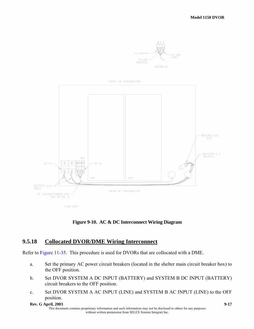
Model 1150 DVOR
Rev. G April, 2003 This document contains proprietary information and such information may not be disclosed to others for any purposes
without written permission from SELEX Sistemi Integrati Inc.
9-17
Figure 9-10. AC & DC Interconnect Wiring Diagram
9.5.18 Collocated DVOR/DME Wiring Interconnect
Refer to Figure 11-35. This procedure is used for DVORs that are collocated with a DME.
a. Set the primary AC power circuit breakers (located in the shelter main circuit breaker box) to the OFF position.
b. Set DVOR SYSTEM A DC INPUT (BATTERY) and SYSTEM B DC INPUT (BATTERY) circuit breakers to the OFF position.
c. Set DVOR SYSTEM A AC INPUT (LINE) and SYSTEM B AC INPUT (LINE) to the OFF position.

Rev. G April, 2003 This document contains proprietary information and such information may not be disclosed to others for any purposes
without written permission from SELEX Sistemi Integrati Inc.
9-18
d. Place DME equipment circuit breakers to the OFF position.
e. Wire the DVOR and DME as shown in Figure 11-35 using the cable harness provided in the 470222-0001 interconnect kit.
NOTE: DME/DVOR interconnect wires must be routed through conduit. Terminal boards TB3 and TB4 are located in the commutator rack on the monitor interface assembly.
9.5.19 Cutting Antenna Cables to Proper Electrical Length
The RF cables from commutator to the antenna cables are precut and phased matched at the factory.
9.5.20 Tuning the Antennas
Refer to Section 9.4.6 of the DVOR Antenna Manual.
9.5.21 Sideband RF Feed Cables to Commutator Connections
Using Figure 9-11 as a guide attach all sideband antenna RF feed cables to the upper or lower commutator CCAs as required. Note that connector J25 has no sideband RF feed cable attached to it.
NOTE: If the DVOR is co-located with a DME, it is advisable to also run the DME RF cables and obstruction light power cable at this time.

Model 1150 DVOR
Rev. G April, 2003 This document contains proprietary information and such information may not be disclosed to others for any purposes
without written permission from SELEX Sistemi Integrati Inc.
9-19
Figure 9-11. Sideband RF Feed Cable to Commutator Connections

Rev. G April, 2003 This document contains proprietary information and such information may not be disclosed to others for any purposes
without written permission from SELEX Sistemi Integrati Inc.
9-20
9.5.22 Adjusting Phase Length of Sideband Antennas to Carrier Antenna
Refer to Section 9.4.7 of the 1150 DVOR Operations and Maintenance Manual.
9.5.23 Transmitter to Commutator Cable Connections
Refer to Figure 11-30.
a. Locate RF connectors J1 to J5 on the top of DVOR transmitter cabinet.
b. Locate RF connectors J1 to J5 on the top of the DVOR commutator rack.
c. Securely fasten carrier antenna RF feed cable (part number 070400-0001) to connector J5 on the transmitter cabinet and to connector J5 on commutator rack.
d. Securely fasten sideband 1 RF cable (part number 070400-0001) to connector J1 on the transmitter cabinet and to connector J1 on the commutator rack.
e. Securely fasten sideband 2 RF cable (part number 070400-0001) to connector J2 on the transmitter cabinet and to connector J2 on the commutator rack.
f. Securely fasten sideband 3 RF cable (part number 070400-0001) to connector J3 on the transmitter cabinet and to connector J3 on the commutator rack.
g. Securely fasten sideband 4 RF cable (part number 070400-0001) to connector J4 on the transmitter cabinet and to connector J4 on the commutator rack.
h. Securely fasten ribbon cable (950483-0003) to connector J8 on the transmitter cabinet and to connector P1 on the commutator rack.
i. The white multiconductor cable from the detectors located on the Commutator Monitor Interface Assembly (030544-0001) must be routed to TB15 and TB16 in the transmitter cabinet. Use standard installation techniques to properly dress the cable between the units. Terminate the red wire on TB15-4. Terminate the white wire on TB16-4. Terminate the black wire on TB16-2.
9.6 INSPECTION
9.6.1 Visual Inspection
The visual inspection is made prior to operating or energizing the equipment.
a. Visually inspect wire, coaxial cables, and connectors for corrosion, loose connectors, and improperly assembled connectors.

Model 1150 DVOR
Rev. G April, 2003 This document contains proprietary information and such information may not be disclosed to others for any purposes
without written permission from SELEX Sistemi Integrati Inc.
9-21
b. Unscrew 2 captive screws holding front power panel closed and open panel. Insure all terminal boards are free of foreign objects such as, pieces of wire, or other objects that could cause electrical shorts within the equipment. Remove foreign objects as necessary and re-secure power panel.
c. Inspect rear of DVOR Transmitter cabinet for foreign objects, remove as necessary.
d. Inspect all peripheral equipment connected to the DVOR, including the PMDT, printer, etc. for proper connections.
e. Inspect the battery backup units to ensure that all terminals and connectors are tight and that no metal shavings or other objects that could cause damage to the equipment.
9.7 INITIAL STARTUP AND PRELIMINARY TESTING.-
NOTE:
Step 9.7.1 is necessary for the 950350-0000 Power Supply. The 950350-0001 Power Supply has an automatic 120/240 volt selection input. Refer to Figure 9-12. Disregard step 9.7.1 for the 950350-0001 and determined if terminal strip TB2 has only 3 positions.
9.7.1 Strapping Battery Charger Power Subsystem (BCPS) for 240 Vac Operation
Refer to Figure 9-12. Figure 9-12 shows the BCPS unit strapped for operation at 120 Vac. For 240 Vac operation, the strapping must be changed. Refer to the following procedure for 240 Vac operation.
a. Set the primary AC power circuit breakers to the OFF position.
b. Set DVOR SYSTEM A DC INPUT (BATTERY) and SYSTEM B DC INPUT (BATTERY) circuit breakers to the OFF position.
c. Place DVOR SYSTEM A AC INPUT (LINE) and SYSTEM B AC INPUT (LINE) circuit breakers to the OFF position.
d. Unscrew 2 captive screws holding front power panel closed and open panel.
e. Remove the snap-on protective cover from terminal board 1A33TB2.
f. Remove the jumper that is installed between terminals 1 and 2 of TB2. System is now set for 240 Vac operation.
g. Replace the snap-on protective cover on terminal board 1A33TB2.
h. For a dual system, repeat steps e, f, and g for the second BCPS (1A34).

Rev. G April, 2003 This document contains proprietary information and such information may not be disclosed to others for any purposes
without written permission from SELEX Sistemi Integrati Inc.
9-22
9.7.2 Input Voltage Checks
After the AC and DC power has been connected to the DVOR transmitter it is necessary to check the input power to ensure the proper voltage is applied to the system.
a. Set DVOR SYSTEM A DC INPUT (BATTERY) and SYSTEM B DC INPUT (BATTERY) circuit breakers to the OFF position.
b. Set DVOR SYSTEM A AC INPUT (LINE) and SYSTEM B AC INPUT (LINE) circuit breakers to the OFF position.
c. Ensure that the primary (shelter) AC power circuit breakers are in the OFF position.
d. Locate the AC power terminal block TB1. TB1 is located to the left of the BCPS lA33/lA34 assemblies.
e. Set the primary AC power circuit breakers to the ON position.
f. Using an AC voltmeter check voltage across terminals 1 and 2 of TB1. Ensure proper voltage for the site is present here and that the polarity is observed. Insure that the voltage present is correct for BCPS operation
g. Set the primary AC power circuit breakers to the OFF position.
9.7.3 Checking Battery Charger Power Subsystem for 28 Vdc Output
This procedure is to determine that the battery charger power subsystem(s) are supplying the correct voltages to be applied to the system's low voltage power supply circuits.
a. Set DVOR SYSTEM A DC INPUT (BATTERY) and SYSTEM B DC INPUT (BATTERY) circuit breakers to the OFF position.
b. Place DVOR SYSTEM A AC INPUT (LINE) and SYSTEM B AC INPUT (LINE) circuit breakers to the OFF position.
c. Unscrew 2 captive screws holding front power panel closed and open panel.
d. Refer to Figure 9-12. Locate TB1 on battery power subsystem 1A33.
e. Set DVOR SYSTEM A DC INPUT (BATTERY) and SYSTEM B DC INPUT (BATTERY) circuit breakers to the ON position.
f. Set DVOR SYSTEM A AC INPUT (LINE) and SYSTEM B AC INPUT (LINE) circuit breakers to the ON position.
g. Using a DC voltmeter check for + 28 Vdc ±0.5 volts across terminals 1 and 4 of TB1. If voltage is not within tolerance adjust 28 Vdc voltage adjust potentiometer located on +28 Vdc module to bring the voltage to the desired level.
h. Locate TB1 on battery power subsystem 1A34.
i. Using a DC voltmeter check for +28 Vdc ±0.5 volts across terminals 1 and 4 of TB1. If voltage is not within tolerance adjust 28 Vdc voltage adjust potentiometer located on 28 Vdc module to bring the voltage to the desired level.

Model 1150 DVOR
Rev. G April, 2003 This document contains proprietary information and such information may not be disclosed to others for any purposes
without written permission from SELEX Sistemi Integrati Inc.
9-23
j. Set DVOR SYSTEM A DC INPUT (BATTERY) and SYSTEM B DC INPUT (BATTERY) circuit breakers to the OFF position.
k. Set DVOR SYSTEM A AC INPUT (LINE) and SYSTEM B AC INPUT (LINE) circuit breakers to the OFF position.
Figure 9-12. Terminal Layout for BCPS 1A33/1A34
9.7.4 Checking Battery Charger Power Subsystem for 43 or 48 Vdc Output
This procedure is to determine that the battery charger power subsystem(s) are supplying the correct voltages to be applied to the system's CSB power amplifiers.
NOTE: Total modulation of voice, reference and ident must be less than 42% as programmed in the transmitter configuration screen. If the total modulation is 42% or more, then the required output voltage must be 48 Vdc ±0.5 volts.
a. Refer to Figure 9-12. Locate terminals E1 and E2 on battery power subsystem 1A33.

Rev. G April, 2003 This document contains proprietary information and such information may not be disclosed to others for any purposes
without written permission from SELEX Sistemi Integrati Inc.
9-24
b. Set DVOR SYSTEM A DC INPUT (BATTERY) and SYSTEM B DC INPUT (BATTERY) circuit beakers to the ON position.
c. Set DVOR SYSTEM A AC INPUT (LINE) and SYSTEM B AC INPUT (LINE) circuit breakers to the ON position.
d. Using a DC voltmeter check for +43 Vdc ±0.5 volts across terminals E1 and E2 of battery charger power subsystem 1A33. If voltage is not within tolerance adjust the voltage adjust potentiometer on the 48 Vdc module to bring the voltage within tolerance.
e. Locate terminals E1 and E2 on battery power subsystem 1A34 for a dual transmitter VOR.
f. Using a DC voltmeter check for +43 Vdc +0.5 volts across terminals E1 and E2 on battery charger power subsystem 1A34. If voltage is not within tolerance adjust the voltage adjust potentiometer on the 48 Vdc module to bring the voltage within tolerance.
g. Close front power panel and tighten 2 captive screws securing the panel.
9.7.5 Low Voltage Power Supply Output Voltage Checks.
a. Set DVOR SYSTEM A DC INPUT (BATTERY) and SYSTEM B DC INPUT (BATTERY) circuit breakers to the OFF position.
b. Set DVOR SYSTEM A AC INPUT (LINE) and SYSTEM B AC INPUT (LINE) circuit breakers to the OFF position.
c. Refer to Figure 1-4. Install low voltage power supply modules 1A14, 1A15, and 1A16.
d. Set DVOR SYSTEM A DC INPUT (BATTERY) and SYSTEM B DC INPUT (BATTERY) circuit breakers to the ON position.
e. Set DVOR SYSTEM A AC INPUT (LINE) and SYSTEM B AC INPUT (LINE) circuit breakers to the ON position.
CAUTION:
Power supply jack numbers are numbered from 1 to 10, bottom to top. Therefore, +28 Vdc (red wire) is at J1-10, which is at the top of the connector.
f. Check connectors 1A14J1-2, 1A15J1-2, 1A16J1-2, and 2A1A1J1-2 for +12 Vdc +0.5 volts.
g. Check connectors 1A14J1-1, 1A15J1-1, 1A16J1-l, and 2A1A1J1-1 for -12 Vdc +0.5 volts.
h. Check connectors 1A14J1-3, 1A14J1-4, 1A15J1-3, 1A15J1-4, 1A16J1-3 and 1A16J1-4, for +5 Vdc +0.25 volts.
i. Set DVOR SYSTEM A DC INPUT (BATTERY) and SYSTEM B DC INPUT (BATTERY) circuit breakers to the OFF position.
j. Set DVOR SYSTEM A AC INPUT (LINE) and SYSTEM B AC INPUT (LINE) circuit breakers to the OFF position.

Model 1150 DVOR
Rev. G April, 2003 This document contains proprietary information and such information may not be disclosed to others for any purposes
without written permission from SELEX Sistemi Integrati Inc.
9-25
9.7.6 Installing Modules in Transmitter Cabinet
Since the DVOR transmitter cabinet is shipped separately from its electronic modules, it will be necessary to install them into the transmitter equipment cabinet. Refer to Figure 1-4 for proper module and CCA locations.
CAUTION
Many of the modules used in the DVOR transmitter contain Electrostatic Discharge (ESD) sensitive components. ALWAYS wear the protective grounding wrist strap when installing modules or CCAs.
Before modules are installed into transmitter cabinet, check modules or CCAs for cracked or broken connectors, bent pins, and loose hardware. Report damage immediately.
NOTE
Ensure that the DVOR SYSTEM A DC INPUT (BATTERY) and SYSTEM B DC INPUT (BATTERY) circuit breakers are in the OFF position. Set DVOR SYSTEM A AC INPUT (LINE) and SYSTEM B AC INPUT (LINE) circuit breakers to the OFF position.
9.7.7 Setting Transmitter Frequency
a. Remote the 1A4 Synthesizer Assy from the cabinet.
b. Remove the cover on the left side of the assembly.
c. Locate the S1 DIP switch circuit card
d. Program S1 per Table 9-3. A “1” in the Table is a closed (on) position on the switch.
e. Replace the cover on the synthesizer.
f. Put the 1A4 module into the VOR.
g. Repeat steps a through f for 1A20.

Rev. G April, 2003 This document contains proprietary information and such information may not be disclosed to others for any purposes
without written permission from SELEX Sistemi Integrati Inc.
9-26
Table 9-3. Frequency Selection Chart
S1 Switch Setting 12345678
VOR Frequency MHz
S1 Switch Setting 12345678
VOR Frequency MHz
S1 Switch Setting 12345678
VOR Frequency MHz
10000000 108.000 10001010 112.000 10000101 116.000 01000000 108.050 01001010 112.050 01000101 116.050 11000000 108.100 11001010 112.100 11000101 116.100 00100000 108.150 00101010 112.150 00100101 116.150 10100000 108.200 10101010 112.200 10100101 116.200 01100000 108.250 01101010 112.250 01100101 116.250 11100000 108.300 11101010 112.300 11100101 116.300 00010000 108.350 00011010 112.350 00010101 116.350 10010000 108.400 10011010 112.400 10010101 116.400 01010000 108.450 01011010 112.450 01010101 116.450 11010000 108.500 11011010 112.500 11010101 116.500 00110000 108.550 00111010 112.550 00110101 116.550 10110000 108.600 10111010 112.600 10110101 116.600 01110000 108.650 01111010 112.650 01110101 116.650 11110000 108.700 11111010 112.700 11110101 116.700 00001000 108.750 00000110 112.750 00001101 116.750 10001000 108.800 10000110 112.800 10001101 116.800 01001000 108.850 01000110 112.850 01001101 116.850 11001000 108.900 11000110 112.900 11001101 116.900 00101000 108.950 00100110 112.950 00101101 116.950 10101000 109.000 10100110 113.000 10101101 117.000 01101000 109.050 01100110 113.050 01101101 117.050 11101000 109.100 11100110 113.100 11101101 117.100 00011000 109.150 00010110 113.150 00011101 117.150 10011000 109.200 10010110 113.200 10011101 117.200 01011000 109.250 01010110 113.250 01011101 117.250 11011000 109.300 11010110 113.300 11011101 117.300 00111000 109.350 00110110 113.350 00111101 117.350 10111000 109.400 10110110 113.400 10111101 117.400 01111000 109.450 01110110 113.450 01111101 117.450 11111000 109.500 11110110 113.500 11111101 117.500 00000100 109.550 00001110 113.550 00000011 117.550 10000100 109.600 10001110 113.600 10000011 117.600 01000100 109.650 01001110 113.650 01000011 117.650 11000100 109.700 11001110 113.700 11000011 117.700 00100100 109.750 00101110 113.750 00100011 117.750 10100100 109.800 10101110 113.800 10100011 117.800 01100100 109.850 01101110 113.850 01100011 117.850 11100100 109.900 11101110 113.900 11100011 117.900 00010100 109.950 00011110 113.950 00010011 117.950

Model 1150 DVOR
Rev. G April, 2003 This document contains proprietary information and such information may not be disclosed to others for any purposes
without written permission from SELEX Sistemi Integrati Inc.
9-27
10010100 110.000 10011110 114.000 01010100 110.050 01011110 114.050 11010100 110.100 11011110 114.100 00110100 110.150 00111110 114.150 10110100 110.200 10111110 114.200 01110100 110.250 01111110 114.250 11110100 110.300 11111110 114.300 00001100 110.350 00000001 114.350 10001100 110.400 10000001 114.400 01001100 110.450 01000001 114.450 11001100 110.500 11000001 114.500 00101100 110.550 00100001 114.550 10101100 110.600 10100001 114.600 01101100 110.650 01100001 114.650 11101100 110.700 11100001 114.700 00011100 110.750 00010001 114.750 10011100 110.800 10010001 114.800 01011100 110.850 01010001 114.850 11011100 110.900 11010001 114.900 00111100 110.950 00110001 114.950 10111100 111.000 10110001 115.000 01111100 111.050 01110001 115.050 11111100 111.100 11110001 115.100 00000010 111.150 00001001 115.150 10000010 111.200 10001001 115.200 01000010 111.250 01001001 115.250 11000010 111.300 11001001 115.300 00100010 111.350 00101001 115.350 10100010 111.400 10101001 115.400 01100010 111.450 01101001 115.450 11100010 111.500 11101001 115.500 00010010 111.550 00011001 115.550 10010010 111.600 10011001 115.600 01010010 111.650 01011001 115.650 11010010 111.700 11011001 115.700 00110010 111.750 00111001 115.750 10110010 111.800 10111001 115.800 01110010 111.850 01111001 115.850 11110010 111.900 11111001 115.900 00001010 111.950 00000101 115.950

Rev. G April, 2003 This document contains proprietary information and such information may not be disclosed to others for any purposes
without written permission from SELEX Sistemi Integrati Inc.
9-28
NOTE:
Shaded areas in the above table are set aside as ILS frequencies, therefore are non-valid VOR frequencies. Setting the switches to any of the shaded combinations in the table will result in the synthesizer being programmed to 108.000 MHz. Switch settings that would result in frequencies higher than 119.750 MHz will result in the synthesizer being programmed to 117.950 MHz. This will prevent the VOR transmitter system from operating on a non-valid VOR frequency.
9.7.8 Lithium Battery Jumper Removal
The central processing unit (CPU) CCA 1A13 is shipped with a lithium battery installed on the circuit board. It is responsible for providing power to various circuits on the CPU CCA when a power failure occurs. When shipped, the lithium battery is disabled with the position of a jumper placed across terminals E2, and E3. Only while power is applied to the system, should the position of the Jumper should be changed so that it is across terminals E1 and E2 of the CPU CCA.
CAUTION:
Installation of the jumper across terminal E1 and E2 without power being properly applied to the CPU CCA may result in high current use by the static RAM devices on the CPU CCA. This will cause rapid discharge of the lithium battery and loss of data in the VOR system.
9.7.9 PMDT Setup and Hookup
Install the 978178 software onto the computer. Connect the 25 pin D serial cable to the PMDT computer.
9.7.10 DVOR Station Power-Up
Refer to Section 3 of this manual for detailed instruction on DVOR operation. The DVOR is microprocessor controlled, transmitter one will come up in the on-line mode as the normal mode of operation.
a. Turn on the PMDT. Refer to Section 3 for operating instructions.
b. Set DVOR SYSTEM A AC INPUT (LINE) and SYSTEM B AC [NPUT (LINE) circuit breakers to the ON position.
c. Set DVOR SYSTEM A DC INPUT and SYSTEM B DC INPUT circuit breakers to the ON position.
Model 1150 DVOR
Rev. G April, 2003 This document contains proprietary information and such information may not be disclosed to others for any purposes
without written permission from SELEX Sistemi Integrati Inc.
9-29
9.7.11 Log-On Procedure
Refer to paragraph 3.4.2.3 for DVOR system log on procedures.
a. Place system in bypass using the PMDT mouse to point and click the BYPASS button on the left side of the display command and shutdown transmitter by pointing and clicking the OFF button on the screen.
9.7.12 Setting Date and Time
a. Point and click the RMS TAB pull down menu.
b. Select set time and date and push the enter key.
c. The RMS time will be updated to the current time on the PMDT laptop.

Rev. G April, 2003 This document contains proprietary information and such information may not be disclosed to others for any purposes
without written permission from SELEX Sistemi Integrati Inc.
9-30
9.7.13 Setting Station's Name
Refer to Table 3-4 and paragraph 3.4.2.7.2 for this procedure. The station name is an alpha or numeric descriptor that allows you to readily identify a DVOR system. This is very useful when there is more than one system that you are monitoring. This code is not broadcast by the DVOR.
9.7.14 Password Change
Refer to paragraph 3.4.2.7.4 for this procedure.
9.7.15 Setting System Configuration
Refer to paragraph 3.4.2.7.1.1 for this procedure.
9.7.16 Sideband Cable Calibration
a. Select Transmitter No. 1 as main transmitter. Ensure that system is set with Transmitter No. 1 connected to the antennas.
b. Set DVOR SYSTEM A DC INPUT and SYSTEM B DC INPUT circuit breakers to the OFF position.
c. Set DVOR SYSTEM A AC INPUT (LINE) and SYSTEM B AC INPUT (LINE) circuit breakers to the OFF position.
d. Remove Sideband Generators (1A5, 1A6) modules from the transmitter cabinet.
e. Connect a cable to the front panel test connector of the Frequency Synthesizer.
f. Connect vector voltmeter, signal generator, and T connectors to DVOR transmitter and commutator as shown in Figure 9-13
g. Calibrate vector voltmeter for an indication of 0, sideband (SB1) is now the reference for this procedure.
h. Reconnect cable to connector J27.
i. Connect equipment to measure the phase length of sideband 2 (SB2) by connecting the test cable of probe "A" to connector 1A5J2 and connecting the test cable probe "B" to the cable that is connected to lower commutator connector J27.
j. Read and record phase length of SB2. Reconnect SB2 cable to lower commutator connector J27.
k. Repeat the procedure for the 1A6J3 connector and measuring SB3 at the upper commutator connector J26. Read and record the phase length of sideband 3 (SB3).

Model 1150 DVOR
Rev. G April, 2003 This document contains proprietary information and such information may not be disclosed to others for any purposes
without written permission from SELEX Sistemi Integrati Inc.
9-31
l. Repeat the procedure for the 1A6J2 connector and measuring SB4 at the lower commutator connector J26. Read and record the phase length of sideband 4 (SB4).
1150-109
SYSTEM
AC INPUTPOWER
DC INPUTPOWER
SYSTEM
SPARE 1
SPARE 2
BA
NORM ALARM BYPASS NORM ALARM BYPASS
SYSTEM BSYSTEM A
POWER SUPPLY
POWER SUPPLY
POWER SUPPLY
SERIAL INTRFC
CPU
FACILITIES
TEST GEN.
MODEMJACK
MONITOR
AUDIO GENERATOR
SIDEBAND GENERATOR
SIDEBAND GENERATOR
CSB POWER AMPLIFIER
CSB POWER AMPLIFIER
MONITOR
AUDIO GENERATOR
FREQUENCY
1A5J2
1A5J3 1A6J3
1A6J2
UPPERCOMMUTATOR
J26 J27
J27J26
COMMUTATORLOWER
VECTOR VOLTMETER
SB4
SB3
SB2
SB1
A B
"B" PROBE
50 OHMTEE
SIDEBANDRF CABLE
TEE
TO SIDEBAND
"A" PROBE
GENERATOR 1A5J3
CABLEFROM SIGNALGENERATOR
SYNTHESIZER
FREQUENCY
SYNTHESIZER
Figure 9-13. Test Equipment Setup for Sideband Cable Calibration
NOTE
Use the same test cable when checking phase length of the sidebands, different test cables will have different phases.
m. Reinstall Sideband Generators (1A5, 1A6) modules into the transmitter cabinet.

Rev. G April, 2003 This document contains proprietary information and such information may not be disclosed to others for any purposes
without written permission from SELEX Sistemi Integrati Inc.
9-32
n. Set DVOR SYSTEM A DC INPUT and SYSTEM B DC INPUT circuit breakers to the ON
position.
o. Set DVOR SYSTEM A AC INPUT (LINE) and SYSTEM B AC INPUT (LINE) circuit breakers to the ON position.
p. Select Transmitter No. 2 as the main Transmitter so that Transmitter No. 2 is connected to
the antennas and not the dummy loads.
q. Set DVOR SYSTEM A DC INPUT and SYSTEM B DC INPUT circuit breakers to the OFF position.
r. Set DVOR SYSTEM A AC INPUT (LINE) and SYSTEM B AC INPUT (LINE) circuit
breakers to the OFF position.
s. Remove Sideband Generators (1A21, 1A22) modules from the transmitter cabinet.
t. Connect vector voltmeter, signal generator, and T connectors to DVOR transmitter and commutator similar to what is shown in Figure 9-13, but make connections to Transmitter No. 2 instead of Transmitter No. 1. Do not recalibrate vector voltmeter.
u. Repeat steps h. thru l. for Transmitter No. 2.
v. Add or subtract cable length where the cables are connected to the transfer relays or the
isolators until all the sideband cables for Transmitter No. 1 and Transmitter No. 2 are within 5 ° phase difference of each other.
w. Replace Sideband Generator Assemblies 1A21 and 1A22.
x. Reconnect sideband cables to the commutator.
9.7.17 Transmitter Tuneup Procedures.
9.7.17.1 Checking Output Frequency of Frequency Synthesizer
a. Connect frequency counter to the carrier frequency connector on the front of the Frequency Synthesizer 1A4. Refer to Figure 9-17.
b. Make sure the carrier frequency is within the proper operating frequency tolerance of Table 4-1c for the station.
c. If the frequency is not within tolerance refer to paragraph 6.4.13.

Model 1150 DVOR
Rev. G April, 2003 This document contains proprietary information and such information may not be disclosed to others for any purposes
without written permission from SELEX Sistemi Integrati Inc.
9-33
d. Check 1A4TP4 for a locked voltage. The voltage at this point should be between 2 and 8 volts. If voltage is below 2 volts, turn 1A4R81 clockwise to obtain a locked voltage between 2 and 8 volts. If the voltage is above 8 volts, turn 1A4R81 counterclockwise to obtain a locked voltage between 2 and 8 volts.
e. Using a DDM, check 1A4TP3. Make small adjustments to 1A4R81 for 0.0 VDC +/-0.05 VDC at 1A4TP3.
f. Re-check 1A4TP4 for a locked voltage between 2 and 8 volts.
g. Repeat steps a through f for 1A20 frequency synthesizer.
NOTE:
The DVOR Transmitter has feedback control loops that are external to the frequency generator assembly that aid in stabilizing the transmitter RF output with respect to power, phase and frequency. Unstable operation of the frequency synthesizer may be caused by an external condition, rather than an internal fault or misalignment.
9.7.17.2 Amplitude Adjustment
a. Setting Transmitter Frequency. Select RMS>>Configuration>>Station then the Operating Frequency (in MHz), then press F7. The transmitter new Operating Frequency will be entered into the station's temporary memory. This parameter is necessary to calculate phaser setting. This setting does not change the output frequency.
b. Set DVOR SYSTEM A AC INPUT (LINE) and SYSTEM B AC INPUT (LINE) circuit breakers to the OFF position.
c. Set DVOR SYSTEM A DC INPUT (BATTERY) and SYSTEM B DC INPUT (BATTERY) circuit breakers to the OFF position.
d. Connect in-line wattmeter thru body between connector 1J5 and carrier feed cable. Install a 250 watt element into the wattmeter to measure forward power.
e. Set DVOR SYSTEM A DC INPUT (BATTERY) and SYSTEM B DC INPUT (BATTERY) circuit breakers to the ON position.
f. Set DVOR SYSTEM A AC INPUT (LINE) and SYSTEM B AC INPUT (LINE) circuit breakers to the ON position.
g. Insure that system 1 is on line.
h. Place transmitter in the BYPASS mode of operation.
i. Select Transmitters>>Configuration>>Nominal. This will display the Transmitter Nominal Operating Parameters screen.
j. Set reference modulation to 30.0 and press [F7].
k. Select Transmitters>>Configuration>>Nominal. Enter the desired Output Power from 0 to 100 Watts then F7. Select Transmitters>>Configuration>>Offsets and Scale Factors. Adjust

Rev. G April, 2003 This document contains proprietary information and such information may not be disclosed to others for any purposes
without written permission from SELEX Sistemi Integrati Inc.
9-34
the Output Power Scale for Transmitter 1 from 0 to 150% so that the Wattmeter displays the desired output power.
NOTE:
If the VOR is to be operated as an enroute facility, use the 250 watt element and set the station for 100 watts. If the facility is to be used as a terminal facility, use the 100 watt element and set the station for 50 watts. Other power settings between 50 and 100 watts should be at customer's request. Use the wattmeter element that provides the best display.
l. Select Transmitters>>Data>>Transmitter 1. This will display the Transmitter No. 1 Data screen.
m. Adjust potentiometer 1A2A1R114 until Carrier Power displayed on the Transmitters, Data, Transmitter 1 screen indicates the same value as the wattmeter.
n. Select Transmitters>>Configuration, and adjust the SBO RF Level to 50.0% and F7.
o. Turn off DVOR by using the mouse to point and click on the Transmitter 1 OFF button. Remove in-line wattmeter thru body on connector 1J5 and install it on sideband 1 (SB1) connector 1J1. Install a 5 watt element into wattmeter body.
p. Click on the Transmitter 1 ON button. Select Transmitters>>Configuration>>Nominal. Adjust the SBO RF Level to obtain 2.5 watts on the wattmeter.
q. Select Transmitter>>Data>>Transmitter 1. Adjust potentiometer 1A5A1R100 for a power out of 2.5 watts on the Sideband 1 display. Turn off transmitter by clicking on the Transmitter 1 OFF button.
r. Remove wattmeter thru body on connecter 1J1 and install it on sideband 2 (SB2) connector 1J2. Turn on transmitter by clicking on the Transmitter 1 ON button. Select the Transmitters>>Configuration>>Offsets and Scale Factors. Adjust the Sideband 2 RF Level Scale for Transmitter 1 to obtain 2.5 watts on the Wattmeter.
s. Select the Transmitters>>Data screen, and adjust potentiometer 1A5A3R100 for a power out display of 2.5 watts for Sideband 2.
t. Turn off transmitter by clicking on the Transmitter 1 OFF button. Remove wattmeter thru body on connector 1J2 and install it on sideband 3 (SB4) connector 1J4. Turn on transmitter by clicking on the Transmitter 1 ON button. Select Transmitters>>Configuration>>Offsets and Scale Factors. Adjust Sideband 3 RF Level Scale for Transmitter 1 to obtain 2.5 watts on the Wattmeter.
u. Select the Transmitter Data screen and adjust potentiometer 1A6A1R100 for a power out of 2.5 watts for sideband 3.
Model 1150 DVOR
Rev. G April, 2003 This document contains proprietary information and such information may not be disclosed to others for any purposes
without written permission from SELEX Sistemi Integrati Inc.
9-35
v. Turn off transmitter by clicking on the Transmitter 1 OFF button. Remove wattmeter thru body on connector 1J2 and install it on sideband 4 (SB4) connector 1J4. Turn on transmitter by clicking on the Transmitter 1 button. Select the Transmitters>>Configuration>>Offsets and Scale Factors. Adjust Sideband 4 RF Level Scale for Transmitter 1 to obtain 2.5 watts on the Wattmeter.
w. Select the Transmitter>>Data screen and adjust potentiometer 1A6A3R100 for a power out of 2.5 watts.
x. Select RMS>>Config Backup and press [enter]. This stores the settings into EEPROM.
y. Set DVOR SYSTEM A DC INPUT (BATTERY) and SYSTEM B DC INPUT (BATTERY) circuit breakers to the OFF position.
z. Set DVOR SYSTEM A AC INPUT (LINE) and SYSTEM B AC INPUT (LINE) circuit breakers to the OFF position.
aa. Place Sideband Generator assembly 1A5 on extender cables.
bb. Set DVOR SYSTEM A DC INPUT (BATTERY) and SYSTEM B DC INPUT (BATTERY) circuit breakers to the ON position.
cc. Set DVOR SYSTEM A AC INPUT (LINE) and SYSTEM B AC INPUT (LINE) circuit breakers to the ON position.
dd. Adjust 1A5A1R73 to lock signal at TP5/6 and a locked ac voltage a TP3/8.
ee. Refer to Figure 9-14. Connect oscilloscope to 1A5TP1. If steady waveform exists, adjust 1A5A1R102 so that the DC offset at the bottom of the waveform is 4 volts.
Figure 9-14. Typical Diagram of Improperly and Properly Adjusted Waveforms
At 1A5/1A6/1A21/1A22TP1/10

Rev. G April, 2003 This document contains proprietary information and such information may not be disclosed to others for any purposes
without written permission from SELEX Sistemi Integrati Inc.
9-36
ff. If waveform is not steady, adjust 1A5A1R73 to obtain a steady waveform then adjust 1A5A1R102 so that the DC offset at the bottom of the waveform is 4 volts. If waveform will not stabilize it may be necessary to adjust DC offset to 5 or 6 volts.
gg. Adjust potentiometers 1A5A1R97 and 1A5A1R51 for best waveform. The waveform must
remain between 3 and 6 Vp-p.
hh. Connect DVM to 1A5TP4. Adjust potentiometer 1A5A1R73 for approximately 0.00 Vdc ±50 mV. Verify that the DC offset at the bottom of the waveform is still 4 volts. Readjust if necessary.
ii. Refer to Figure 9-15. Verify waveform on 1A5TP5. Adjust potentiometer 1A5A1R24 so
waveform peaks are equal in amplitude.
jj. Refer to Figure 9-14. Connect oscilloscope to 1A5TP10. If steady waveform exists, adjust 1A5A3R102 so that the DC offset at the bottom of the waveform is 4 volts.
Figure 9-15. Typical Diagram of Improperly and Properly Adjusted Waveforms
At 1A5/1A6/1A21/1A22TP5/6. OSCILLOSCOPE SET TO MEASURE D.C TIME BASE 5 ms/DIV VOLT/DIV 1V/DIV

Model 1150 DVOR
Rev. G April, 2003 This document contains proprietary information and such information may not be disclosed to others for any purposes
without written permission from SELEX Sistemi Integrati Inc.
9-37
kk. If waveform is not steady, adjust 1A5A3R73 to obtain a steady waveform then adjust
1A5A3R102 so that the DC offset at the bottom of the waveform is 4 volts.
ll. Adjust potentiometers 1A5A3R97 and 1A5A3R51 for best waveform. The waveform must remain between 3 and 6 Vp-p.
mm. Connect DC Voltmeter to 1A5TP7. Adjust potentiometer 1A5A3R73 for approximately 0.00 Vdc ±50 mV.
nn. Refer to Figure 9-15. Verify proper waveform on 1A5TP6. Adjust potentiometer 1A5A3R24 so waveform peaks are equal in amplitude.
oo. Set DVOR SYSTEM A DC INPUT (BATTERY) and SYSTEM B DC INPUT (BATTERY) circuit breakers to the OFF position.
pp. Set DVOR SYSTEM A AC INPUT (LINE) and SYSTEM B AC INPUT (LINE) circuit breakers to the OFF position.
qq. Place Sideband Generator assembly 1A6 on extender cables.
rr. Set DVOR SYSTEM A DC INPUT (BATTERY) and SYSTEM B DC INPUT (BATTERY) circuit breakers to the ON position.
ss. Set DVOR SYSTEM A AC INPUT (LINE) and SYSTEM B AC INPUT (LINE) circuit breakers to the ON position.
tt. Refer to Figure 9-14. Connect oscilloscope to 1A6TP1 . If steady waveform exists, adjust 1A6A1R102 so that the DC offset at the bottom of the waveform is 4 volts.
uu. If waveform is not steady, adjust 1A6A1R73 to obtain a steady waveform then adjust 1A6A1R102 so that the DC offset at the bottom of the waveform is 4 volts. If waveform will not stabilize it may be necessary to adjust DC offset to 5 or 6 volts.
vv. Adjust potentiometers 1A6A1R97 and 1A6A1R51 for best waveform. The waveform must remain between 3 and 6 Vp-p.
ww. Connect voltmeter to 1A6TP4. Adjust potentiometer 1A6A1R73 for approximately 0.00 Vdc ±50 mV. Verify that the DC offset at the bottom of the waveform is still 4 volts. Readjust if necessary.
xx. Refer to Figure 9-15. Verify proper waveform on 1A6TP5. Adjust potentiometer 1A6A1R24 so waveform peaks are equal in amplitude.
yy. Refer to Figure 9-14. Connect oscilloscope to 1A6TP10. If steady waveform exists, adjust 1A6A3R102 so that the DC offset at the bottom of the waveform is 4 volts.
zz. If waveform is not steady, adjust 1A6A3R73 to obtain a steady waveform then adjust 1A6A3R102 so that the DC offset at the bottom of the waveform is 4 volts.
aaa. Adjust potentiometers 1A6A3R97 and 1A6A3R51 for best waveform. The waveform must remain between 3 and 6 Vp-p.
bbb. Connect DVM to 1A6TP7. Adjust potentiometer 1A6A3R73 for approximately 0.00 Vdc ±50 mV.

Rev. G April, 2003 This document contains proprietary information and such information may not be disclosed to others for any purposes
without written permission from SELEX Sistemi Integrati Inc.
9-38
ccc. Refer to Figure 9-15. Verify proper waveform on 1A6TP6. Adjust potentiometer 1A6A3R24 so waveform peaks are equal in amplitude.
ddd. Set DVOR SYSTEM A DC INPUT (BATTERY) and SYSTEM B DC INPUT (BATTERY) circuit breakers to the OFF position.
eee. Set DVOR SYSTEM A AC INPUT (LINE) and SYSTEM B AC INPUT (LINE) circuit breakers to the OFF position.
9.7.17.3 Sideband Generator Phasing
a. Install 5 watt dummy loads to sidebands 3 and 4 at the transmitter. Install a 180° cable in-line with sideband 1 (ensure that the 180° line section is phased for the station frequency.).
b. Disconnect carrier feed from commutator bulkhead and terminate with at least a 100 watt load. Connect the carrier antenna feed cable to the field detector input. (Use RF adapters supplied with the accessory kit to connect the N type RF cable to the TNC connector on HY1 of the monitor interface assembly.).
c. Set DVOR SYSTEM A DC INPUT (BATTERY) and SYSTEM B DC INPUT (BATTERY) circuit breakers to the ON position.
d. Set DVOR SYSTEM A AC INPUT (LINE) and SYSTEM B AC INPUT (LINE) circuit breakers to the ON position.
e. Connect oscilloscope to 1A8TP5. Adjust oscilloscope so that a waveform fills about 3/4 of the screen with a ground reference at the bottom of the grid. Refer to Figure 9-16. In order to do this alignment adjust the time base on the oscilloscope so individual sawtooth waveforms can be viewed.
f. Select Transmitters>>Configuration>>Offsets and Scale Factors screen. Add or subtract degrees to Transmitter 1 Sideband 1-2 Phase Offset until all nulls of the sawtooth are at ground or as close as possible to ground. Once this is done the waveform should look like an even band across the grid. If some of the nulls are excessively out of phase with the others (nulls are far from reaching ground); the antennas corresponding to these nulls are out of phase with the other sideband antennas with respect to the carrier antenna. Refer to 1150 DVOR Antenna Operations and Maintenance Manual to check phase length of antenna feed cables.
g. Click on the Transmitter 1 OFF button to shut off the transmitter. Remove 180° line section from sideband 1.
h. Install 5 watt dummy loads to sidebands 1 and 2 at the commutator input. Reconnect sidebands 3 and 4, and install 180° line section in sideband 3. Click on the Transmitter 1 ANTENNA Button to restart Transmitter No. 1 as the on-air transmitter.
i. Adjust oscilloscope so that a waveform fills about ¾ of the screen with a ground reference at the bottom of the grid. Refer to Figure 9-16. In order to do this alignment adjust the time base on the oscilloscope so individual sawtooth waveforms can be viewed.
Model 1150 DVOR
Rev. G April, 2003 This document contains proprietary information and such information may not be disclosed to others for any purposes
without written permission from SELEX Sistemi Integrati Inc.
9-39
j. Select Transmitters>>Configuration>>Offsets and Scale Factors screen. Add or subtract degrees to Transmitter 1 Sideband 3-4 Phase Offset until all nulls of the sawtooth are at ground or as close as possible to ground. Once this is done the waveform should look like a nice even band across the grid. If some of the nulls are excessively out of phase with the others (nulls are far from reaching ground); the antennas corresponding to these nulls are out of phase with the other sideband antennas with respect to the carrier antenna. Refer to 1150 DVOR Antenna Operations and Maintenance Manual to check phase length of antenna feed cables.
k. Click on the Transmitter 1 OFF button. Remove all loads and 180° line section. Reconnect all cables to their respective antennas.
Figure 9-16. Sideband Phasing Diagram
NOTE:
Bottom peaks within 5% of ground reference considered within tolerance.

Rev. G April, 2003 This document contains proprietary information and such information may not be disclosed to others for any purposes
without written permission from SELEX Sistemi Integrati Inc.
9-40
1150-610
R81
1A4/A20
CARRIER FREQ.10 mW (TYP.)
J8
TP4
TP5
GND
TP1
TP2
TP3
Figure 9-17. Frequency Generator; Front Panel View

Model 1150 DVOR
Rev. G April, 2003 This document contains proprietary information and such information may not be disclosed to others for any purposes
without written permission from SELEX Sistemi Integrati Inc.
9-41
Figure 9-18. Sideband Generator, Front and Side Panel View
9.7.18 SETTING NO. 1 TRANSMITTER OPERATING PARAMETERS
Before the carrier forward power, carrier VSWR, SBO forward powers, and SBO VSWR's can be calibrated it will be necessary to check/set Transmitter No. 1's operating parameters.
9.7.18.1 Setting No. 1 Transmitter Azimuth (Az) Index
a. Select Transmitters>>Configuration>>Nominal. Set the Azimuth Index to 0.00 degrees..
b. Select Transmitters>>Configuration>>Offsets and Scale Factors. In the Transmitter 1 Azmuth Angle Offset enter the Az offset from -20.00 to +20.00 as needed then presss [F7]. Transmitter No. 1’s new Az index will be entered into the station’s temporary memory.

Rev. G April, 2003 This document contains proprietary information and such information may not be disclosed to others for any purposes
without written permission from SELEX Sistemi Integrati Inc.
9-42
NOTE:
AZ index is used to rotate the RF signal pattern from the installed 0.0 reference point established at the time sideband antenna No. 1 was installed.
9.7.18.2 Setting No. 1 Transmitter Ident Code
Type RMS>>Configuration>>then enter Transmitter 1’s ident, then press [enter]. Transmitter No. 1's new station's code will be entered into the station's temporary memory.
NOTE The system will accept only four alpha characters for the ident code. When the assigned code is only 2 or 3 letters, enter the 2 or 3 letter code and press the spacebar until four characters are entered. Failure to use spaces will result in the lack of Ident Keying.
9.7.18.3 Setting No. 1 Transmitter Voice Modulation
Select Transmitters>>Configuration>>Nominal. Enter the voice modulation from 0% to 30%, then press [enter]. The new voice modulation will be entered into the station’s temporary memory. Select Transmitters>>Configuration. Offsets and Scale Factors. For the Voice Modulation Scale for Voice Modulation, enter a value from 0 to 200% to adjust the value entered into the Nominal setting to the correct value.
9.7.18.4 Setting No. 1 Transmitter Ident Modulation
Select Transmitters>>Configuration>>Nominal. Enter the identification modulation from 0% to 25%, then press [F7]. The new ident modulation will be entered into the station’s temporary memory. Select Transmitters>>Configuration>>Offsets and Scale Factors. For the Ident Modulation Scale for Ident Modulation, enter a value from 0 to 200% to adjust the value entered into the Nominal setting to the correct value.
NOTE
Typical setting for ident modulation is 10.0%

Model 1150 DVOR
Rev. G April, 2003 This document contains proprietary information and such information may not be disclosed to others for any purposes
without written permission from SELEX Sistemi Integrati Inc.
9-43
9.7.18.5 Setting No. 1 Transmitter Reference Modulation
Select Transmitters>>Configuration>>Nominal. Enter the Reference modulation from 0% to 30%, then press [F7]. The new Reference modulation will be entered into the station’s temporary memory. Select Transmitters>>Configuration>>Offsets and Scale Factors. For the Reference Modulation Scale for Reference Modulation, enter a value from 0 to 200% to adjust the value entered into the Nominal setting to the correct value.
NOTE Normal setting is 30.0%
9.7.18.6 Setting No. 1 Transmitter SBO Modulation
Refer to 9.7.19.2.
9.7.18.7 Saving No. 1 Transmitter Operating Parameters
a. Select RMS>>Config Backup and then press [enter]. This will place Transmitter No. 1's new operating parameters into electrically erasable memory. By means of the lithium battery, Transmitter No. 1's operating parameters are preserved in static ram if system power is lost. The electrically erasable memory is an added precaution against the loss of setup parameters.
b. A permanent copy should be placed onto the PMDT file system. Select System>>Configuration Save. You will be prompted for a file name. It is suggested that the configuration is saved into different files depicting progress up through the commissioning with different file names for each.
9.7.19 SETTING MONITOR ALARM LIMITS
Once Transmitter No. 1's operating parameters have been set it will be necessary to check/set the Monitor alarm limits. Refer to Section 4 for appropriate limits.
9.7.19.1 Setting Monitor Az Angle Low Limit
a. Select Monitors>>Configuration>>Alarm Limits. The Alarm and Prealarm limits will be displayed for Monitor 1 and Monitor 2.
b. Enter the Az Angle Low Alarm Limit that is needed, then press [F7]. Monitor No. 1’s new Az Angle Low Limit will be entered into the station’s temporary memory.
c. Enter the Az Angle Low PreAlarm Limit that is needed, then press [F7]. Monitor No 1 and 2’s new Az Angle Low PreAlarm Limit will be entered into the station’s temporary memory.

Rev. G April, 2003 This document contains proprietary information and such information may not be disclosed to others for any purposes
without written permission from SELEX Sistemi Integrati Inc.
9-44
9.7.19.2 Setting Monitor Az Angle High Limit
a. Select Monitors>>Configuration>>Alarm Limits. The Alarm and Prealarm limits will be displayed for Monitor 1 and Monitor 2.
b. Enter the az angle high alarm limit that is needed, then press [F7].
c. Enter the az angle high prealarm limit that is needed, then press [F7]. Monitor No. 1’s new az angle low prelaarm limit will be entered into the station’s temporary memory.
9.7.19.3 Setting High Monitor 30 Hz Mod Low Limit
a. Select Monitors>>Configuration>>Alarm Limits. The Alarm and Prealarm limits will be displayed for Monitor 1 and Monitor 2.
b. Enter the 30 Hz Mod low alarm limit that is needed, then press [F7]. Monitor No. 1 and 2’s 30 Hz Mod low limit will be entered into the station’s temporary memory.
c. Enter the 30 Hz Mod low prealarm limit that is needed, then press [F7]. Monitor No. 1 and 2’s new 30 Hz Mod low prealarm limit will be entered into the station’s temporary memory.
9.7.19.4 Setting Monitor 30 Hz Mod High Limit
a. Select Monitors>>Configuration>>Alarm Limits. The Alarm and Prealarm limits will be displayed for Monitor 1 and Monitor 2.
b. Enter the 30 Hz Mod high alarm limit that is needed, then press [F7]. Monitor No. 1 and 2’s new 30 Hz Mod high limit will be entered into the station’s temporary memory.
c. Enter the 30 Hz Mod high prealarm limit that is needed then press [F7].
9.7.19.5 Setting Monitor 9960 Hz Mod Low Limit
a. Select Monitors>>Configuration>>Alarm Limits. The Alarm and Prealarm limits will be displayed for Monitor 1 and Monitor 2.
b. Enter the 9960 Hz Mod low alarm limit that is needed, then press [F7]. Monitor No. 1 and 2’s new 9960 Hz Mod low limit will be entered into the station’s temporary memory.
c. Enter the 9960 Hz Mod low prealarm limit that is needed, then press [F7]. Monitor No. 1 and 2’s new 9960 Hz Mod low prealarm limit will be entered into the station’s temporary memory.
9.7.19.6 Setting Monitor 9960 Hz Mod High Limit
a. Select Monitors>>Configuration>>Alarm Limits. The Alarm and Prealarm limits will be displayed for Monitor 1 and Monitor 2.
b. Enter the 9960 Hz Mod high alarm limit that is needed, then press [F7]. Monitor No. 1 and 2’s new 9960 Hz Mod high limit will be entered into the station’s temporary memory.

Model 1150 DVOR
Rev. G April, 2003 This document contains proprietary information and such information may not be disclosed to others for any purposes
without written permission from SELEX Sistemi Integrati Inc.
9-45
c. Enter the 9960 Hz Mod high prealarm limit that is needed, then press [F7]. Monitor No. 1 and 2’s new 9960 Hz Mod high prealarm limit will be entered into the station’s temporary memory.
9.7.19.7 Setting Monitor 9960 Hz Dev Low Limit
a. Select Monitors>>Configuration>>Alarm Limits. The Alarm and Prealarm limits will be displayed for Monitor 1 and Monitor 2.
b. Enter the 9960 Hz Dev low alarm limit that is needed, then press [F7]. Monitor No. 1 and 2’s new 9960 Hz Dev low limit will be entered into the station’s temporary memory.
c. Enter the 9960 Hz Dev low prealarm limit that is needed, then press [F7]. Monitor No. 1 and 2’s new 9960 Hz Dev high prealarm limit will be entered into the station’s temporary memory.
9.7.19.8 Setting Monitor Field Intensity Low Limit
a. Select Monitors>>Configuration>>Alarm Limits. The Alarm and Prealarm limits will be displayed for Monitor 1 and Monitor 2.
b. Enter the Field Intensity Low Alarm Limit that is needed, then press [F7]. Monitor No. 1 and 2’s new Field Intensity Low Alarm Limit will be entered into the station’s temporary memory.
c. Enter the Field Intensity Low PreAlarm Limit that is needed, then press [F7]. Monitor No. 1 and 2’s new Field Intensity Low PreAlarm limit will be entered into the station’s temporary memory.
9.7.19.9 Setting Monitor Field Intensity High Limits
a. Select Monitors>>Configuration>>Alarm Limits. The Alarm and Prealarm limits will be displayed for Monitor 1 and Monitor 2.
b. Enter the Field Intensity High Alarm Limit that is needed, then press [F7]. Monitor No. 1 and 2’s new Field Intensity High Alarm Limit will be entered into the station’s temporary memory.
c. Enter the Field Intensity High Alarm Limit that is needed, then press [F7]. Monitor No. 1 and 2’s new Field Intensity High PreAlarm Limit will be entered into the station’s temporary memory.
9.7.19.10 Saving Monitor Alarm Limits
a. Select RMS>>Config Backup and then press [enter]. This will place the Monitor’s new operating parameters into electrically erasable memory.

Rev. G April, 2003 This document contains proprietary information and such information may not be disclosed to others for any purposes
without written permission from SELEX Sistemi Integrati Inc.
9-46
b. A permanent copy should be placed onto the PMDT file system. Select System, Configuration Save. You will be prompted for a file name. It is suggested that the configuration is saved into different files depicting progress up through the commissioning with different file names for each.
9.7.20 SETTING MONITOR CERTIFICATION LIMITS
Once Monitor alarm limits have been set it will be necessary to check/set Monitor certification limits.
a. Select Monitors>>Data>>Certification Test Results. Point to the button at the lower right of the screen where the display “SET TO MONITOR LIMITS”. Click on the button and then press [return]. This copies the Monitor alarm limit values to the certification limits. This is preferred over setting each parameter individually. Press F7.
9.7.21 SETTING MONITOR TEST GENERATOR
Once the DVOR Monitor certification setups have been completed it will be necessary to check/set the Monitor Test Generator.
9.7.21.1 Setting Monitor Test Gen Az Angle
a. Select Monitors>>Data>>Test Data. This will display the Monitors Test Generator Setup and results screen.
b. Select the Monitor No. 1 and Monitor No. 2 Azimuth Angle that is needed then press F7.
NOTE
The normal setting is the same as the radial being monitored.
9.7.21.2 Setting Monitor Test Gen 30 Hz Modulation
Select the Monitor No. 1 and No. 2 30 Hz Modulation that is needed, then press [F7].
9.7.21.3 Setting Monitor Test Gen 9960 Hz Modulation
Select the Monitor No. 1 and No. 2 9960 Hz Modulation that is needed, then press [F7].
9.7.21.4 Setting Monitor Test Gen 9960 Hz Deviation
Select the Monitor No. 1 and No. 2 9960 Hz Deviation that is needed, then press [F7].

Model 1150 DVOR
Rev. G April, 2003 This document contains proprietary information and such information may not be disclosed to others for any purposes
without written permission from SELEX Sistemi Integrati Inc.
9-47
9.7.21.5 Setting Monitor Test Gen Ident Modulation
Select the Monitor No. 1 and No. 2 Ident Modulation that is needed, the press [F7].
NOTE
This value is normally set to 0.0
9.7.21.6 Setting Monitor Test Gen Ident Control
Point to the “Down Arrow” button on the Ident control parameter. Select the Test Generator Ident Control code that is needed, C = continuous, P = pulse, then press [F].
9.7.21.7 Setting Monitor Test Gen Audio Modulation
Select the Monitor No. 1 and No. 2 Audio Modulation that is needed, the press [F7].
NOTE
This level is normally set to 0.0
9.7.21.8 Setting Monitor Test Gen Audio Frequency
Select the Monitor No. 1 and No. 2Test Generator Audio Frequency that is needed, then press [F7]. The value entered will be rounded to the nearest 30 Hz increment automatically.
NOTE:
This level is normally set to 30.0.
9.7.21.9 Saving Monitor's Test Generator Setup Parameters
a. Select RMS>>Config Backup and then press [enter]. This will place the Monitor’s new operating parameters into electrically erasable memory.
b. A permanent copy should be placed onto the PMDT file system. Select System, Configuration Save. You will be prompted for a file name. It is suggested that the configuration is saved into different files depicting progress up through the commissioning with different file names for each.
9.7.22 SETTING NO. 2 TRANSMITTER OPERATING PARAMETERS

Rev. G April, 2003 This document contains proprietary information and such information may not be disclosed to others for any purposes
without written permission from SELEX Sistemi Integrati Inc.
9-48
9.7.22.1 Setting No. 2 Transmitter Azimuth (Az) Index
a. Select Transmitters>>Configuration>>Offsets and Scale Factors. In the Transmitter 2 Azimuth Angle Offset, enter the Az offset from -20.00 to +20.00 as needed, then press [F7]. Transmitter No. 2’s new Az index will be entered into the station’s temporary memory.
NOTE:
AZ index is used to rotate the signal pattern from the installed reference point established at the time installation occurred normally due to flight check requirements.
9.7.22.2 Setting No. 2 Transmitter Power Out
a. Turn off DVOR system using the circuit breakers..
b. Place Bird thruline wattmeter (with a 250 watt plug-in element) in the carrier output line.
c. Turn on the DVOR system.
d. The Transmitters>>Configuration>>Nominal desired Output Power was set in 9.7.19.2. Adjust the Output Power Scale for Transmitter 2 from 0 to 150% so that the Wattmeter displays the desired output power.
e. Select RMS>>Config Backup and then [enter] to save the changes.
f. Turn off DVOR system using the circuit breakers.
g. Remove the Bird Thruline wattmeter from the carrier output line.
9.7.22.3 Setting No. 2 Transmitter Ident Code
Type RMS>>Configuration, then enter Transmitter 2’s ident, then press [enter]. Transmitter No. 2's new station's code will be entered into the station's temporary memory.
NOTE The system will accept only four alpha characters for the ident code. When the assigned code is only 2 or 3 letters, enter the 2 or 3 letter code and press the space bar until four characters are entered. Failure to use spaces will result in the lack of Ident Keying.
9.7.22.4 Setting No. 2 Transmitter Voice Modulation
The Transmitters>>Configuration>>Nominal voice modulation was previously set in 9.7.20.4. Select Transmitters, Configuration, Offsets and Scale Factors. For the Transmitter 2 Voice Modulation Scale for Voice Modulation, enter a value from 0 to 200% to adjust the value entered into the Nominal setting to the correct value.

Model 1150 DVOR
Rev. G April, 2003 This document contains proprietary information and such information may not be disclosed to others for any purposes
without written permission from SELEX Sistemi Integrati Inc.
9-49
9.7.22.5 Setting No. 2 Transmitter Ident Modulation
Select Transmitters>>Configuration>>Nominal. Enter the identification modulation from 0% to 25%, then press [enter]. The new ident modulation will be entered into the station’s temporary memory. Select Transmitters>>Configuration>>Offsets and Scale Factors. For the Ident Modulation Scale for Ident Modulation, enter a value from 0 to 200% to adjust the value entered into the Nominal setting to the correct value.
9.7.22.6 Setting No. 2 Transmitter Reference Modulation
The Transmitters>>Configuration>>Nominal Reference modulation was previously set in 9.7.18.5. Select Transmitters, Configuration, Offsets and Scale Factors. For the Transmitter 2 Reference Modulation Scale for Reference Modulation, enter a value from 0 to 200% to adjust the value entered into the Nominal setting to the correct value.
9.7.22.7 Setting No. 2 Transmitter SBO Modulation
Refer to 9.7.19.2.
9.7.22.8 Saving No. 2 Transmitter Operating Parameters
a. Select RMS>>Config Backup and then press [enter]. This will place Transmitter No. 2’s new operating parameters into electrically erasable memory.
b. A permanent copy should be placed onto the PMDT file system. Select System>>Configuration Save. You will be prompted for a file name. It is suggested that the configuration is saved into different files depicting progress up through the commissioning with different file names for each.
9.7.23 Reference to Sideband Phasing
In order to properly phase the reference signal to the sideband signal it may be necessary to insert a cable in the carrier line from the transmitter to commutator cabinet.
a. Set DVOR SYSTEM A AC INPUT (LINE) and SYSTEM B AC INPUT (LINE) circuit breakers to the ON position.
b. Set DVOR SYSTEM A DC INPUT (BATTERY) and SYSTEM B DC INPUT (BATTERY) circuit breakers to the ON position.
c. Ensure the DVOR transmitter is operating normally, and that all the sidebands are at proper power levels. Place the monitors in bypass.
d. Connect oscilloscope to 1A8TP5. Note composite signal waveform.
e. Adjust oscilloscope so that the composite signal is a full 30 Hz waveform (33 ms).

Rev. G April, 2003 This document contains proprietary information and such information may not be disclosed to others for any purposes
without written permission from SELEX Sistemi Integrati Inc.
9-50
f. Synchronize the oscilloscope using the test point TP1 on the Pin Diode Driver CCA in the commutator assy.
g. On the PMDT select Transmitters>>Configuration>>Offset and Scale Factors for transmitter 1. Add or subtract degrees for the Carrier Sideband Phase Offset until the waveforms on the scope reach maximum ampliltude. Look at the 9960 AM level displayed by the Montior. The level will reach a maximum when the phase is optimal. It may be necessary to add a 90º, 180º or 90º plus 180º segments of cable to the carrier cable and readjust the Reference Sideband phasing until the maximum amplitude is observed..
h. Switch transmitters so that Transmitter No. 2 is now operating normally.
i. Connect oscilloscope to 1A24TP5. Note composite signal waveform.
j. On the PMDT select Transmitters>>Configuration>>Offset and Scale Factors for transmitter 2. Add or subtract degrees for the Carrier-Sideband Phase Offset until the waveforms on the scope reach maximum amplitude. Look at the 9960 AM level displayed by the Monitor. The level will reach a maximum when the phase is optimal. It may be necessary to readjust the Reference Sideband phasing until the maximum amplitude is observed.
k. Once the reference to sideband phasing values have been established save the operating parameters.
l. Switch transmitters so that Transmitter No. 1 is now operating normally.
m. Further minor adjustments to the reference to sideband phasing may be required during commissioning flight check. This adjustment will affect the 9960 AM level as determined by the flight check panel technician. If during flight check the 9960 modulation is less than 30 percent the Reference-Sideband Phasing Parameter should be adjusted slightly to find the peak reading as determined by the panel technician. This will provide better sideband efficiency than by adjusting the sideband power higher.
9.8 INSTALLATION VERIFICATION TEST
Check to make sure that all RF and power connections have been accomplished. If there are no further adjustments needed to be made to the antenna feed cables, fill the outside of the six conduits with putty to seal against water and vermin.
9.8.1 Records
Select RMS>>Config Backup and then press [enter]. This will place Transmitter No. 2’s new operating parameters into electrically erasable memory.
9.8.2 Special Tests
Perform verification procedures of Section 6.

Model 1150 DVOR
Rev. G April, 2003 This document contains proprietary information and such information may not be disclosed to others for any purposes
without written permission from SELEX Sistemi Integrati Inc.
10-1
10 SOFTWARE
10.1 INTRODUCTION
Not applicable to this manual

Rev. G April, 2003 This document contains proprietary information and such information may not be disclosed to others for any purposes
without written permission from SELEX Sistemi Integrati Inc.
10-2
THIS SHEET INTENTIONALLY BLANK

Model 1150 DVOR
Rev. G April, 2003 This document contains proprietary information and such information may not be disclosed to others for any purposes
without written permission from SELEX Sistemi Integrati Inc.
11-1
11 TROUBLESHOOTING SUPPORT
11.1 INTRODUCTION
This section contains a list of drawings useful during installation and maintenance. Copies of all drawings can be found in the CDROM version of the manual. Drawings that are needed during installation are provided in paper form within the appropriate kit. Paper copies of all drawings can be purchased by contacting the SELEX Sestemi Integrati Inc. Customer Service organization.
Description Schematic No. Figure CDROM Kit Detailed System, Block Diagram (Early Version) 11-1 X
Detailed System, Block Diagram (Later Version) 11-2 X
DVOR Interconnect Diagram (Sheets 1-6) 001150-9105 11-3 X Display CCA 012610-9001 11-4 X RF Monitor Assy 030364-9001 11-5 X RF Monitor CCA (Sheets 1-3) 012687-9001 11-6 X CSB Power Amplifier Assy 030363-9001 11-7 X Power Ampl Mod CCA 012624-9001 11-8 X Power Ampl CCA 012625-9001 11-9 X Exciter CCA 012627-9001 11-10 X Bias Reg/Exciter CCA 012626-9001 11-11 X Freq Gen Cntl CCA (Sheets 1-4) 012100-9001 11-12 X Interconnect CCA 012102-9001 11-13 X Sideband Generator Assy 030398-9001 11-14 X Sideband Control CCA 012636-9001 11-15 X Sideband Amplifier CCA 012793-9001 11-16 X

Rev. G April, 2003 This document contains proprietary information and such information may not be disclosed to others for any purposes
without written permission from SELEX Sistemi Integrati Inc.
11-2
Audio Generator Assy (Sheets 1–4) 012616-9003 11-17 X Monitor CCA (Sheets 1–4) 012617-9001 11-18 X Modem CCA (Sheets 1-2) 012101-9001 11-19 X Serial Interface 012619-9001 11-20 X Facilities CCA (Sheets 1-2) 012620-9001 11-21 X Test Generator CCA 012689-9001 11-22 X CPU CCA (Sheets 1-2) 012618-9001 11-23 X Low Voltage Power Supply CCA 012743-9001 11-24 X Backplane CCA 012600-9001 11-25 X Sideband Sample Assy 030478-9001 11-26 X Sideband Sample CCA 012714-9001 11-27 X Low Pass Filter Assy 030448-9001 11-28 X VOR Jack CCA 012090-9001 11-29 X UNIT 2 DVOR Commutator Interconnect 030442-9001 11-30 X Pin Diode-Driver CCA (Sheets 1-3) 012098-9001 11-31 X Commutator CCA (Sheets 1-2) 012702-9001 11-32 X Monitor Interface Assy 030544-9001 11-33 X Field Detector Assy CCA 012708-9001 11-34 X VOR/DME Interface Kit 470222-9001 11-35 X X Counterpoise Foundation Drawing 470538-0001 11-36 X X
Copyright © 2022 FDOKUMEN