Increasing Energy Efficiency of Processor Caches via Line ...
Upload
independentCategory
view
0download
0
Thermal Management of On-Chip Caches Through
Power Density Minimization
Ja Chun Ku, Serkan Ozdemir, Gokhan Memik, Yehea Ismail Department of Electrical and Computer Eng., Northwestern University
{j-ku, soz463, memik, ismail}@ece.northwestern.edu
Abstract
Various architectural power reduction techniques have been proposed for on-chip caches in the last
decade. In this paper, we first show that these power reduction techniques can be suboptimal when thermal
effects are considered. Then, we propose a thermal-aware cache power-down technique that minimizes the
power density of the active parts by turning off alternating rows of memory cells instead of entire banks.
The decrease in the power density lowers the temperature, which then exponentially reduces the leakage.
Thus, leakage power of the active parts is reduced in addition to the power eliminated from the parts that
are turned off. Simulations based on SPEC2000 benchmarks in a 70nm technology show that the proposed
thermal-aware architecture can reduce the total energy consumption by 53% compared to a conventional
cache, and 14% compared to a cache architecture with thermal-unaware power reduction scheme. Second,
we show a block permutation scheme that can be used during the design of the caches to maximize the
distance between blocks with consecutive addresses. Because of spatial locality, blocks with consecutive
addresses are likely to be accessed within a short time interval. By maximizing the distance between such
blocks, we minimize the power density and hence reduce the peak temperature. This, in return, results in
an average leakage power reduction of 8.7% compared to a conventional cache without affecting the
dynamic power. Overall, both of our architectures add no extra run-time penalty compared to the thermal-
unaware power reduction schemes, yet they reduce the total energy consumption of the processor, by up to
14% and 5.6%, respectively.
1. Introduction
The increasing significance of low-power VLSI designs has inspired a number of studies on power reduction techniques for
CUCIS TECHNICAL REPORT #CUCIS-2005-07-001 CUCIS, Northwestern University, Evanston, IL Copyright © CUCIS, July 2005. Copyright and distribution without permission strictly prohibited.
on-chip caches. The main motivation behind these studies is the fact that a large fraction of a chip area is devoted to caches.
For instance, 60% of StrongARM is devoted to caches, and in some cases on-chip L1 caches alone can compromise over
40% of the total chip power budget [1, 2]. Initially, low-power cache designs have focused on reducing the dynamic power
since it used to dominate the total power consumption [2-4]. However, with the aggressive scaling of CMOS devices, the
transistor threshold voltage and the supply voltage have scaled down simultaneously in order to maintain the performance
improvement. This decrease in the threshold voltage has resulted in an exponential increase in the subthreshold leakage
current, which is the dominant source of leakage power [5]. Leakage power has already become comparable to dynamic
power, and it is projected to dominate the total chip power in near future technologies. Thus, the focus of low-power design
has been shifting more towards reducing the leakage power instead of the dynamic power, especially through suppressing the
subthreshold current. Since caches are very dense and relatively inactive, their power consumption is dominated by leakage
power in current and future technologies. Hence, caches have become a major target for leakage power reduction techniques
[6-10].
Cache arrays are typically divided into a number of smaller banks to reduce the delay [11]. Many of the dynamic power
reduction techniques take advantage of the fact that not all the banks are frequently accessed [2, 4]. Those techniques allow
only a limited set of banks to be active, and disable the rest by turning off components such as decoders, precharges and
sense-amplifiers. However, such approaches alone have limited impact when the power dissipation is dominated by leakage.
Thus, leakage reduction techniques also have been employed to turn off the unused banks to a low-leakage mode. Common
leakage reduction techniques include gated-Vdd [6] that utilizes stack effect [12] by placing a high threshold transistor as a
switch between memory cells and Vdd and/or ground lines, ABB-MTCMOS [7] that dynamically increases the threshold
voltages of the transistors in the memory cell by raising the source to body voltage of the transistors, and drowsy cache [8, 9]
that reduces the leakage by dynamically decreasing the supply voltage. However, none of these techniques considers thermal
effects as a design factor. In leakage dominant technologies, the exponential relationship between the leakage power and
temperature makes the inclusion of the thermal behavior fundamentally important. In other words, current power reduction
techniques for caches may not be fully optimized in the presence of thermal effects.
There exists a common misconception that thermal effects are not very important for caches since they are relatively cold
spots of a chip. However, this is not true when majority of the cache power comes from leakage. Figure 1 shows SPICE
simulation results illustrating how the leakage power changes with temperature as well as the relative change in the leakage
power due to a change in temperature at different temperature values. Interestingly, the relative change in the leakage power
due to a change in temperature is actually larger for lower temperatures. This trend implies that thermal effects can still have
a significant impact on the power of caches as long as the power is dominated by leakage. In this paper, thermal effects used
to control the leakage power of on-chip caches. Particularly, the major contribution of this paper is the study of thermal-
aware cache architectures. To the best of our knowledge, there is no previous work in thermal-aware architectural
optimizations for caches. Specifically, our two main contributions in this paper are: 1) a novel technique to improve the
efficiency of existing power-down techniques for data caches and 2) a low-power cache architecture for minimizing the
thermal effects of spatial locality. Both techniques reduce leakage power utilizing the idea of power density minimization. In
other words, parts of a cache with high activity are intentionally placed far away from each other in order to alleviate the hot
spots in the cache. This, in return, reduces the leakage power consumption.
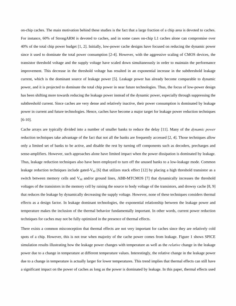
The existing power reduction techniques for caches can eliminate almost all the leakage power of the parts on power-down
mode. However, the power of the active parts is still kept the same (high-leakage). The core idea of the proposed cache
architecture is to minimize power density of the active parts in the cache. Figure 2 illustrates a simple example of this idea
using two banks. In Figure 2(a), bank 0 is turned on while bank 1 is turned off to save power as commonly done. On the
other hand, Figure 2(b) turns off alternating rows of both banks, thereby halving the power density of the rows that are on
active mode. While the number of rows turned off is the same in both cases, the reduction in the power density in Figure 2(b)
lowers the junction temperature, resulting in an exponential reduction in the leakage of the active rows. Thus, the leakage
power of the active rows is reduced in addition to the eliminated power of the inactive parts that are turned off. This
proposed cache architecture is called Power density-Minimized Architecture (PMA) hereafter in this paper. Although the
notion of PMA can be applied to different power reduction techniques, in this paper, we use a scheme that combines
selective cache ways [4] and gated-Vdd [6] as the example of a thermal-unaware power reduction technique. Specifically, we
modify this thermal-unaware scheme with PMA to investigate how the leakage and total power reduction is affected by our
optimization.
Figure 1. Temperature dependence of leakage power and its relative change 50 60 70 80 90 100 110 1200
0.05
0.1
(LeakPower (T) - LeakPower (T-1ºC))/LeakPower(T)
50 60 70 80 90 100 110 1200
10
20
Temperature (ºC)
Normalized Leakage Power

Second technique proposed in this paper reduces the leakage power of caches utilizing their spatial locality. If a particular
block is accessed, it is very likely that blocks that are logically neighbors to the accessed block will also be accessed soon.
This spatial locality is one of the most important reasons why caches are developed in the first place. However, when temperature is
considered, physical locality (or density) should be avoided. In conventional caches, logically neighboring blocks are also
physically neighbors. Therefore, the spatial locality results in the power sources being concentrated in a small area in the
memory bank, which raises the temperature of the hot spots. We propose a new scheme that maximizes the physical distance
between blocks that are logically neighbors by permuting the physical location of blocks in the architecture. The power
density of the hot spots is therefore minimized, and the leakage power is reduced. This scheme is called Block Permutation
Scheme (BPS).
Next section provides the analytical theory behind the concept of power density minimization by presenting the power and
thermal models, and their relation to the power density. Section 3 briefly reviews how selective cache ways and gated-Vdd
schemes work since they are used as the underlying thermal-unaware cache architecture in our PMA studies. Section 4 then
describes PMA and its implementation, and Section 5 explains BPS. Section 6 discusses the simulation results, and Section 7
concludes the paper with a summary.
2. Power and Thermal Models
2.1 Power Dissipation
Power dissipation in a cache memory can be subdivided into two major components
.leakagedynamic PPP += (1)
Dynamic power, Pdynamic is the power consumed when a cache is accessed through charging and discharging capacitances
such as wordlines, bitlines, address lines, and data output lines. Previous studies have developed analytical models of the
dynamic power for caches [11, 13]. The dynamic power in caches is becoming smaller compared to the leakage power as the
(a) (b)
Active modePower-down mode
Bank 0 Bank 1 Bank 0 Bank 1
Figure 2. A simple example of minimizing the power density ofactive parts in a cache. (a) conventional (b) proposed scheme
technology scales down, and is temperature-independent unless the operating frequency is indirectly affected by the
temperature.
Leakage power Pleakage, on the other hand, is increasing exponentially with technology scaling due to the decrease in the
threshold voltage. The leakage current is dominated mainly by the subthreshold current, which for each gate, is given by
( )( )
⎟⎠⎞
⎜⎝⎛ −⎟⎟
⎠
⎞⎜⎜⎝
⎛−⎟
⎠⎞
⎜⎝⎛=
−−kT
qVmkT
VVq
oxldsubthresho
dstg
eeq
kTmL
WCI 112
µ (2)
where µ is the mobility, Cox is the oxide capacitance, and m is the body effect coefficient whose value is usually around 1.1-
1.4 [14]. W, L, k, T, q, Vg, Vt and Vds represent channel width, channel length, Boltzmann’s constant, temperature, electronic
charge, gate voltage, threshold voltage and drain-source voltage, respectively. The exponential increase in the subthreshold
current with temperature is due to the increase in kT/q (which is proportional to the subthreshold slope) in (2), and the
decrease in the threshold voltage as the temperature is raised. The temperature sensitivity of the threshold voltage was
determined to be about 0.8mV/ºC [14, 15].
2.2 Thermal Model
The heat generated from a chip is dissipated through the package. The heat flow in the package depends on many parameters
such as geometry, flux source and placement, package orientation, next-level package attachment, heat sink efficiency, and
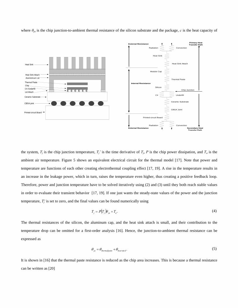
method of chip connection. In this paper, we consider a typical flip-chip C4 package adapted from a model by Kromann [16]
as shown in Figure 3. A simplified thermal network appears in Figure 4. Most of the heat generated is conducted upwards
through the silicon to the thermal paste, aluminum cap, heat sink attach, and heat sink, then convectively removed to the
ambient air. In addition to this primary heat transfer path, there is also a secondary heat flow path by conduction downwards
in parallel, through the C4 bumps and the epoxy underfill, ceramic substrate, lead balls to the printed-circuit board. However,
since the heat removed through the secondary heat transfer path is usually small especially in a densely populated board,
adiabatic boundary conditions are typically assumed on the four sides and the top of the chip, and only the primary heat
transfer path is considered. Hence, the one-dimensional heat equation is applied for a simple chip thermal model [17, 18]
ajajjjja TTPTcT +=+ θθ )(' (3)
where θja is the chip junction-to-ambient thermal resistance of the silicon substrate and the package, c is the heat capacity of
the system, Tj is the chip junction temperature, Tj’ is the time derivative of Tj, P is the chip power dissipation, and Ta is the
ambient air temperature. Figure 5 shows an equivalent electrical circuit for the thermal model [17]. Note that power and
temperature are functions of each other creating electrothermal coupling effect [17, 19]. A rise in the temperature results in
an increase in the leakage power, which in turn, raises the temperature even higher, thus creating a positive feedback loop.
Therefore, power and junction temperature have to be solved iteratively using (2) and (3) until they both reach stable values
in order to evaluate their transient behavior [17, 19]. If one just wants the steady-state values of the power and the junction
temperature, Tj' is set to zero, and the final values can be found numerically using
( ) .ajajj TTPT += θ (4)
The thermal resistances of the silicon, the aluminum cap, and the heat sink attach is small, and their contribution to the
temperature drop can be omitted for a first-order analysis [16]. Hence, the junction-to-ambient thermal resistance can be
expressed as
.sin kheattethermalpasja θθθ += (5)
It is shown in [16] that the thermal paste resistance is reduced as the chip area increases. This is because a thermal resistance
can be written as [20]
Figure 3. A typical flip-chip C4 package.
Figure 4. A simplified thermal network of the package.
Heat Sink
Heat Sink AttachAluminimum Lid
Thermal Paste
Lid Attach
Ceramic Substrate
C4 /Underfill
CBGA joint
Printed-circuit Board
Chip
Chip Junction
Thermal Paste
Module Cap
Heat Sink Attach
Heat Sink
Silicon
UnderfillC4
Ceramic Substrate
CBGA Joint
Printed-circuit Board
Radiation Convection
Radiation Convection
External Resistance
Internal Resistance
External Resistance
Primary HeatTransfer Path
Secondary HeatTransfer Path

A
Rth=θ (6)
where Rth is the unit thermal resistance, and A is the cross-sectional area. An increase in the chip area directly increases the
area of the thermal paste placed above it, thus assuming the chip area equals to the thermal paste area, (4) can be rewritten as
( ) ( ) akheatjtethermalpaschip
jj TTPRA
TPT ++⎟⎠⎞
⎜⎝⎛= sinθ (7)
where P(Tj)/Achip represents the power density of the chip, and Rthermalpaste is the unit thermal resistance of the thermal paste.
Convective thermal resistance of the heat sink, θheatsink is affected less by the chip area since the heat is usually spread out
more uniformly (using a heat spreader) before it reaches the heat sink. However, in case of adapting an advanced fan heat
sink
as commonly done in today’s technology, the heat sink resistance becomes small enough that the thermal paste resistance
takes up the majority of the total junction-to-ambient thermal resistance (more than 60%) [16]. Therefore, reducing the
power density of the chip can significantly lower the junction temperature.
A simple one-dimensional chip thermal model has been used in this section to explain the basic theory behind the proposed
schemes in this paper. However, the heat transfer through lateral diffusion, and the secondary heat transfer path to the
printed-circuit board are also included for the simulations that will be discussed in Section 5 using HotSpot [21].
3. Thermal-Unaware Low-Power Cache Architecture (SGA)
In this paper, as the example of low-power cache architecture that is thermal-unaware, we combined selective cache ways [4]
and gated-Vdd [6] technique. Selective cache ways was employed to decide the optimum number of banks that will be
enabled, and gated-Vdd was used to eliminate the leakage power in the disabled banks. This cache architecture is called here
Selective cache ways with Gated-Vdd Architecture (SGA). Note however, that the application of our scheme is not only
limited to SGA: it can be applied to any general cache structure that uses power-down techniques for different banks or finer
granularities. Our goal in this paper is to show that existing cache architectures and power reduction techniques can be
Figure 5. One-dimensional chip thermal model.
θja
P c Ta
Tj
easily enhanced with the consideration of thermal effects to achieve significantly better power efficiency through power
density minimization. The reason we chose selective cache ways and gated-Vdd as the underlying example in this paper is
their simplicity and popularity. Following subsections briefly review how selective cache ways and gated-Vdd work.
3.1 Selective Cache Ways
Selective cache ways [4] disables a subset of the ways in a set-associative cache during periods of modest cache activity
depending on how memory-intensive each application is. When a way is disabled, its decoders, precharges and the sense-
amplifiers are turned off to eliminate the dynamic power. Due to the fact that it uses the array partitioning that is already
present for performance reasons, only minor changes to a conventional cache are required, and thus the performance penalty
is small. For each application, the optimum number of enabled ways is the case that consumes the lowest power for a given
performance degradation threshold determined by the designer. In this paper, we consider the performance degradation
threshold of 2% for finding the optimum number of enabled ways.
3.2 Gated-Vdd
In gated-Vdd [6], an extra high-threshold transistor is placed as a switch in the supply voltage or ground path of the memory
cells. This extra transistor is turned on when the section is being used, and turned off for low-power mode. When the
transistor turns off, the leakage power is drastically reduced (practically eliminated). This is due to the huge reduction in the
subthreshold current by stack effect of self reverse-biasing series-connected transistors [12].
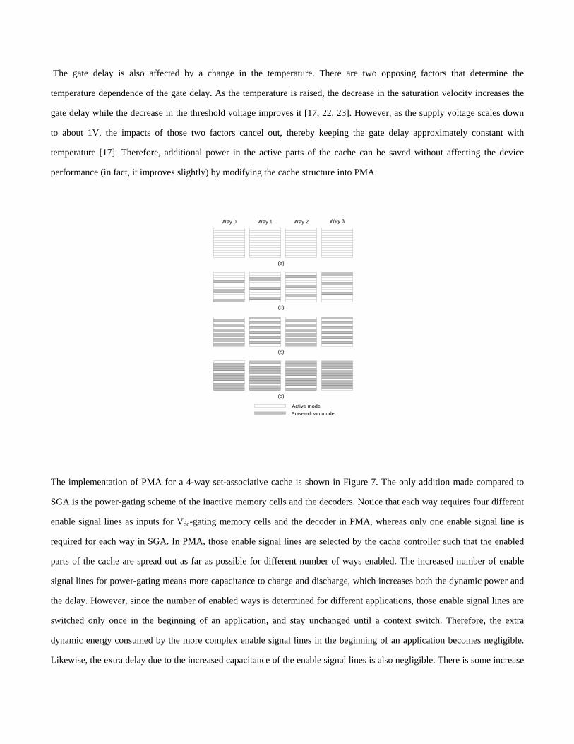
4. Power density-Minimized Architecture (PMA)
Figure 6 shows how PMA works for a 4-way set-associative cache. Similar to selective cache ways, the optimal number of
ways is first determined for each application. Then, the cache is configured for this selection of ways. Instead of disabling
and enabling an entire bank, enabled rows are distributed in a way that minimizes the power density. Hence, PMA will have
the same cache hit rates as the selective cache ways although the physical architecture has been modified. Although in this
paper, we describe the scheme where each application selects the number of ways during execution, similar to the selective
cache ways scheme, the turning on and off of the rows can even be performed dynamically during the execution of an
application.
It was shown in the previous section that a decrease in the power density can significantly lower the junction temperature.
The drop in the temperature reduces the leakage power of the enabled parts of the cache exponentially, which then decreases
the temperature even further. This electrothermal coupling effect continues until both the power and the temperature reach
the steady-state.
The gate delay is also affected by a change in the temperature. There are two opposing factors that determine the
temperature dependence of the gate delay. As the temperature is raised, the decrease in the saturation velocity increases the
gate delay while the decrease in the threshold voltage improves it [17, 22, 23]. However, as the supply voltage scales down
to about 1V, the impacts of those two factors cancel out, thereby keeping the gate delay approximately constant with
temperature [17]. Therefore, additional power in the active parts of the cache can be saved without affecting the device
performance (in fact, it improves slightly) by modifying the cache structure into PMA.
The implementation of PMA for a 4-way set-associative cache is shown in Figure 7. The only addition made compared to
SGA is the power-gating scheme of the inactive memory cells and the decoders. Notice that each way requires four different
enable signal lines as inputs for Vdd-gating memory cells and the decoder in PMA, whereas only one enable signal line is
required for each way in SGA. In PMA, those enable signal lines are selected by the cache controller such that the enabled
parts of the cache are spread out as far as possible for different number of ways enabled. The increased number of enable
signal lines for power-gating means more capacitance to charge and discharge, which increases both the dynamic power and
the delay. However, since the number of enabled ways is determined for different applications, those enable signal lines are
switched only once in the beginning of an application, and stay unchanged until a context switch. Therefore, the extra
dynamic energy consumed by the more complex enable signal lines in the beginning of an application becomes negligible.
Likewise, the extra delay due to the increased capacitance of the enable signal lines is also negligible. There is some increase
Figure 6. PMA for a 4-way set-associative cache (a) 4 ways enabled (b) 3 ways enabled (c) 2 ways enabled (d) 1 way enabled(the straddled rows indicate disabled rows)
Active modePower-down mode
(b)
(a)
(c)
(d)
Way 0 Way 1 Way 2 Way 3

in the dynamic power in PMA compared to SGA since precharges and sense-amplifiers are no longer gated. However, this
increase in the dynamic power was found to be insignificant from SPICE simulations of our layout, which will be discussed
further in Section 6. There is also a degree of freedom to tradeoff between complexity of the enable signal lines and power
savings. In our 4-way associative cache example, power density of the active parts can decrease by a factor of up to four
(when only one way is enabled as shown in Figure 6(d)). However, one may choose to have only two enable signal lines per
way instead of four, which means that alternating rows in a bank are grouped together to turn on or off simultaneously.
Hence, only cases like Figure 6(a) and (c) are possible. In this case, power density of the active parts can decrease only by a
factor of two even when only one way is enabled. If the number of enabled ways happens to be one quite frequently, there is
more merit to have four enable signal lines per way since it will decrease the power density of the active parts up to four
times. On the other hand, there would be no reason to have four enable signal lines per way instead of two if the number of
enabled ways is mostly two.
The design complexity of other power/delay optimization techniques such as wordline and bitline partitioning is not affected
by PMA. It is clear from the design depicted in Figure 7 that the only change to conventional cache architecture is gating the
ground or Vdd for each row in the data arrays and the decoders. However, the rest of the design is kept unchanged, and hence
our PMA scheme can be applied to any cache design.
Figure 7. Implementation of PMA for a 4-way set-associative cache.
Enableway 0
Enableway 1
Enableway 2
Enableway 3
Way 0
Turning off adecoder row
Vdd-gating arow of
memory cells
Cache WaySelect
Way 3
Data ArrayData Array
Sta
tus
Tag
Sta
tus
deco
der
deco
der
Tag
CacheController
tag index offset
Address
5. Block Permutation Scheme (BPS)
The second temperature-aware power optimization scheme we developed is called Block Permutation Scheme (BPS). An
example of BPS is illustrated in Figure 8. The main idea in BPS is to generate a permutation of the physical location of
blocks such that the average distance between logically neighboring blocks is maximized. Figure 8(a) shows a conventional
cache addressing scheme where the distance between logically neighboring blocks is always 1. On the other hand, a
permutation of these blocks as shown in Figure 8(b) increases the average distance between logically neighboring blocks to
roughly 4 in this example. Note that, we are not only interested in increasing the distance between two consecutive blocks,
instead we are interested in increasing the area of a working set which are formed by a number of consecutive blocks. In
other words, we are interested in making a number of consecutive blocks as far away from each other as possible. For
example, consider a loop that works on 4 consecutive blocks. Since these 4 blocks will be accessed over and over again, our
scheme tries to maximize the distance between all, or tries to make the total area covered by them as large as possible. For
the same example, while all possible set of four consecutive blocks cover an area of 4 in the conventional cache, the 4
consecutive blocks in our scheme covers 7.6 blocks on average. The pseudo-code to generate the permutation for each way is
given in Figure 9. This function generates the permutation for the block numbers between init and init + size - 1 in the
memory bank array. For a bank with n blocks, the recursive function will have n/2 levels. To further reduce the power
density of the hot spots, the input is shifted with a different offset for each way. This way, we can make sure that the blocks
that are physically next to each other do not correspond to the same logical rows, and thus are not accessed simultaneously.
BPS results in a temperature drop in the hot spots, but also a temperature rise in the relatively colder parts in the bank. In
other words, it distributes the active blocks more uniformly, which in return results in reduction in the overall peak
temperature. Because of the exponential temperature dependence of the leakage power, the total energy of the bank is
reduced although the leakage power of the relatively colder parts in the bank is increased. Note that BPS has no effect on the
latency of the cache and the dynamic power, because it only requires a rearrangement of the decoders without adding any
hardware.

6. Simulation Results
6.1 Simulation Setup
To investigate the performance of the proposed techniques, we simulate SPEC2000 applications using the SimpleScalar 3.0
simulator [24]. Important characteristics of the applications are presented in Table 1. We first found the optimum number of
ways to enable for each SPEC200 application as done by Albonesi [4] under performance degradation threshold of 2%. The
baseline processor configuration is described in Table 2. In our simulations, we use 4-way and 8-way set-associative caches
to observe the effectiveness of PMA and the BPS. Particularly, we target a 64KB 4-way associative cache and a 64KB 8-way
associative cache with 32-byte block sizes. We performed the simulations for level 1 data and instruction caches with these
configurations. However, the energy consumptions of the instruction caches were not affected by the PMA, because we
could not reduce the associativity without significant effect on the performance. These results are similar to the study by
Albonesi [4]. Similarly, the BPS optimization did not change the energy consumption of the data caches because of the
relatively low level of spatial locality observed. Therefore, we present the results for data cache optimizations using PMA
and instruction cache optimization by BPS.
Table 3 shows the optimum number of enabled ways for each application obtained from the simulations, the runtime increase
when only the optimum number of ways was enabled, and the relative energy-delay product after applying PMA. It can be
seen that on average, about half the ways can be disabled for the 4-way set-associative cache, and about five ways can be
disabled for the 8-way set-associative cache. The number of accesses for each row in the memory bank was recorded during
Figure 8. Illustration of BPS (a) conventionalscheme (b) BPS
generate_perm(init,size, array) { if (size > 2){ for(i=0 ; i<size; i+=2) { perm_array[i]=array[init+2*i] perm_array[size/2+i]=array[init+2*i+] } generate_perm(init, size/2, perm_array)
t (i it+ i /2 i /2 )
Figure 9. Pseudo-code for generating the block permutation.
Way 3Way 2Way 1Way 0
Way 3Way 2Way 1Way 0
block 0block 1block 2block 3block 4block 5block 6block 7
block 5block 1block 7block 3block 4block 0block 6block 2
block 6block 2block 5block 1block 7block 3block 4block 0
block 4block 0block 6block 2block 5block 1block 7block 3
block 7block 3block 4block 0block 6block 2block 5block 1
block 0block 1block 2block 3block 4block 5block 6block 7
block 0block 1block 2block 3block 4block 5block 6block 7
block 0block 1block 2block 3block 4block 5block 6block 7
(a)
(b)
simulations. For all the programs, the simulator was run for 300 million instructions from each application with fast-
forwarding application-specific number of instruction determined by Sherwood et al [25].
To measure the change in the temperature, we recorded the activity (hit and miss) of each block in epochs of 10 million
cycles. Then, for each of these intervals, we found the steady-state temperature (using an iterative method that is described in
the next paragraph). The selection of the interval length (10 million) lies in the nature of the heat transfer. The thermal time
constant is usually in the range of milliseconds, which is significantly bigger than the cycle time. Therefore, we need to
select
Table 1. Important characteristics of the applications used in the simulation
64 K 4-way Data Cache 64K 8-way data cache
L1 – D cache L1 – I cache L1 – D cache L1 –I cache Application Number of cycles [million]
Accesses [million]
Miss Rate
SGA Miss Rate
Accesses[million] Miss Rate
Numberof cycles[million]
Accesses[million] Miss Rate SGA Miss
Rate Accesses[million] Miss Rate
ammp 600 116 6.1% 7.1% 324 0.0% 602 116 6.1% 5.2% 324 0.0% applu 497 115 10.1% 10.6% 303 0.0% 497 115 10.1% 10.6% 303 0.0% apsi 228 111 2.1% 2.6% 328 0.0% 228 111 2.2% 2.6% 328 0.0% art 1881 103 39.7% 40.4% 332 0.0% 1881 103 39.7% 40.4% 332 0.0%
crafty 178 118 0.2% 1.1% 407 0.0% 177 118 0.1% 0.2% 407 0.0% equake 965 127 15.3% 15.9% 306 0.0% 950 127 12.1% 15.4% 306 0.0%
gap 196 113 0.5% 0.6% 416 0.0% 196 113 0.5% 0.6% 416 0.0% gcc 228 124 1.1% 2.1% 424 0.1% 227 124 1.0% 1.4% 424 0.1% gzip 165 70 4.0% 4.0% 350 0.0% 163 70 3.9% 4.0% 350 0.0% lucas 537 72 15.7% 16.6% 300 0.0% 538 72 15.7% 16.6% 300 0.0% mcf 8684 85 74.5% 74.4% 307 0.0% 8684 85 74.5% 74.4% 307 0.0% mesa 143 109 0.5% 0.7% 326 0.0% 143 109 0.5% 0.7% 326 0.0% mgrid 411 110 7.0% 7.1% 301 0.0% 411 110 7.0% 7.1% 301 0.0% parser 492 85 5.3% 6.9% 391 0.0% 492 85 5.2% 4.4% 391 0.0% perl 175 108 1.0% 1.2% 345 0.1% 174 108 1.0% 0.6% 345 0.1%
twolf 606 98 6.2% 6.9% 406 0.0% 606 98 6.1% 6.9% 406 0.0% vortex 174 122 0.4% 0.5% 313 0.1% 174 122 0.4% 0.4% 313 0.1%
vpr 576 115 3.8% 4.7% 379 0.0% 576 115 3.8% 4.7% 379 0.0% wupwise 223 92 1.9% 2.1% 349 0.0% 223 92 1.9% 2.1% 349 0.0%
ARITH. MEAN 893 105 10.3% 10.8% 348 0.0% 892 105 10.1% 10.4% 348 0.0%
Table 2. Base processor configuration. Issue width 8 instructions
Number of RUU entries 32 Number of LSQ entries 16
Branch prediction Bi-modal with 2048 entries Number of ALU’s 8 int / 8 fp
Number of Mul/Div Units 2 int / 2 fp
L1 data cache 64 KB, 4/8-way set-associative, 32-byte blocks
L1 instruction cache 64 KB, 4-way set-associative, 32-byte blocks
L2 cache 512KB, 4-way set-associative, 128-byte blocks
L1 access time 2 cycles L2 access time 16 cycles
Memory access time 250 cycles Memory bus width 8 bytes
Table 3. Optimum number of enabled ways for 2% performance degradation threshold, run-time increases, and relative energy-delay product after applying PMA.
4-way Set-Associative Cache 8-way Set-Associative Cache
Application Number of Enabled Ways
Runtime Increase
Norm. Energy-
Delay Product
Number of Enabled Ways
Runtime Increase
Norm. Energy- Delay Prıduct
ammp 2 0.89% 94,10% 7 0.95% 99,34%
applu 2 0.20% 92,92% 2 0.30% 90,54%
apsi 2 0.23% 92,83% 2 0.50% 88,84%
art 1 1.34% 91,98% 1 1.34% 90,90%
crafty 2 1.66% 95,32% 4 1.18% 93,51%
equake 2 0.81% 94,00% 2 0.29% 94,27%
gap 2 0.29% 92,99% 3 1.97% 90,55%
gcc 2 1.43% 94,78% 3 1.30% 92,95%
lucas 1 1.44% 92,30% 1 1.36% 91,17%
mcf 1 0.03% 89,28% 1 0.02% 87,99%
mesa 2 0.63% 92,46% 2 0.99% 90,81%
mgrid 2 0.00% 92,56% 2 0.00% 89,95%
parser 2 1.35% 94,82% 6 1.53% 98,34%
perl 3 1.40% 98,07% 7 0.96% 98,33%
twolf 2 0.32% 92,93% 2 0.08% 90,03%
vortex 2 0.38% 93,28% 4 1.96% 94,62%
vpr 2 0.33% 93,00% 2 1.68% 92,88%
wupwise 2 0.29% 93,00% 2 0.25% 90,22%
MEAN 1.9 0.72% 93,36% 2.9 0.92% 92,50%
a relatively large interval. However, if the interval is too large, we will lose the transient behavior. Therefore, we selected 10
million cycles (10 milliseconds for a 1 GHz machine), because it exhibits the optimum point for being able to observe the
transient behavior as well as the thermal dissipation.
According to CACTI 3.2 [11], the optimum number of banks for both 4-way and 8-way set-associative 64KB cache is eight,
each consisting of 256 x 256 bits. Hence, we laid out a 256 x 256 bit memory bank for 70nm BPTM [26] technology for
three cases: conventional cache, SGA, and PMA (Figure 10). Note that, the properties of the BPS is identical to the
conventional cache, hence we did not generate a separate layout for it. Then, the dynamic power of each component in the
memory bank was estimated using HSPICE simulations of the layout, and the cache event information obtained from
SimpleScalar simulations. The leakage power of the memory cells is also obtained from HSPICE simulations. For
components outside a bank such as the output driver and the tag side components, CACTI 3.2 [11] was used to estimate their
power consumption. Conventionally, leakage power of a cache has been calculated for a constant temperature (e.g. 27ºC or
100ºC). However, this may create large errors especially in leakage dominant technologies due to the electrothermal coupling
effect explained in the previous sections. Therefore, the coupling between power and temperature has to be taken into
account for more accurate leakage power estimation. An iterative method was used to numerically determine the steady-state
power and temperature. HotSpot [21] was used to estimate the temperature of each row in a memory bank. Separate power
input was given to each row in a memory bank in order to include the effect of lateral heat diffusion between different rows
within the bank. In each iteration, HSPICE is run to obtain the leakage power at given a temperature, then a new temperature
value is calculated using HotSpot with the new power value calculated. This new temperature is fed into HSPICE simulation
Figure 11. Flowchart of the simulation process to estimate power and temperature.
Figure 10. A zoomed-in layout picture of a 256 x 256 bit memory bank.
HSPICE Simulation
Power Calculation
Temperature Update
Equilibrium?Yes No
Done
HotSpot Simulation
of the next loop as the temperature parameter to calculate the new leakage power. The iteration ends when both power and
temperature reach equilibrium. The flowchart of this simulation process is illustrated in Figure 11.
6.2 Evaluation of PMA
Figure 12 presents the energy consumption of the SGA and PMA architectures with respect to the conventional cache for the
simulated applications. Figure 13, on the other hand, shows how the dynamic and the leakage components of the energy
changes on average for the three different cache structures. Figure 14 presents the average and peak temperatures of the
active banks, which is the main cause of the energy reduction. When both the average and the peak temperatures are studied,
we see that SGA does not change the temperature significantly. For SGA, there are three forces in action. First, since some of
the banks are closed, the total power consumption is reduced and parts of the heat generated by the active banks will
dissipate into neighboring disabled banks, having a positive effect on the temperature. In addition, since the execution times
are also increasing, the total energy consumption and hence the temperature tends to decrease. Third, since some of the banks
are closed, the number of accesses to the active banks increases (due to an increase in the miss rates), having a negative
impact on the temperature. Note that since we do not use any way-prediction schemes, in the conventional cache, all ways
are accessed in parallel. Therefore, when some banks are closed, the change in activity in the enabled banks is not drastic.
Nevertheless, in many applications, this increase is large enough to cancel out the positive effects of turning off banks. As a
result, we see that the peak temperature is
Figure 12. Normalized energy of SGA and PMA with respect to conventional cache for (a) 4-way set-associative caches (b) 8-way set-associative caches.
(a) (b)
0
0,2
0,4
0,6
0,8
1
ammp
applu ap
si artcra
fty
equa
ke gap
gcc
lucas mcf
mesa
mgrid
parse
rpe
rltw
olf
vorte
x vpr
wupwise
MEAN
Nor
mal
ized
Ene
rgy
SGA PMA
0
0,2
0,4
0,6
0,8
1
ammp
applu ap
si art
crafty
equa
ke gap
gcc
lucas mcf
mesa
mgrid
parse
rpe
rltw
olf
vorte
x vpr
wupwise
MEAN
Nor
mal
ized
Ene
rgy
SGA PMA
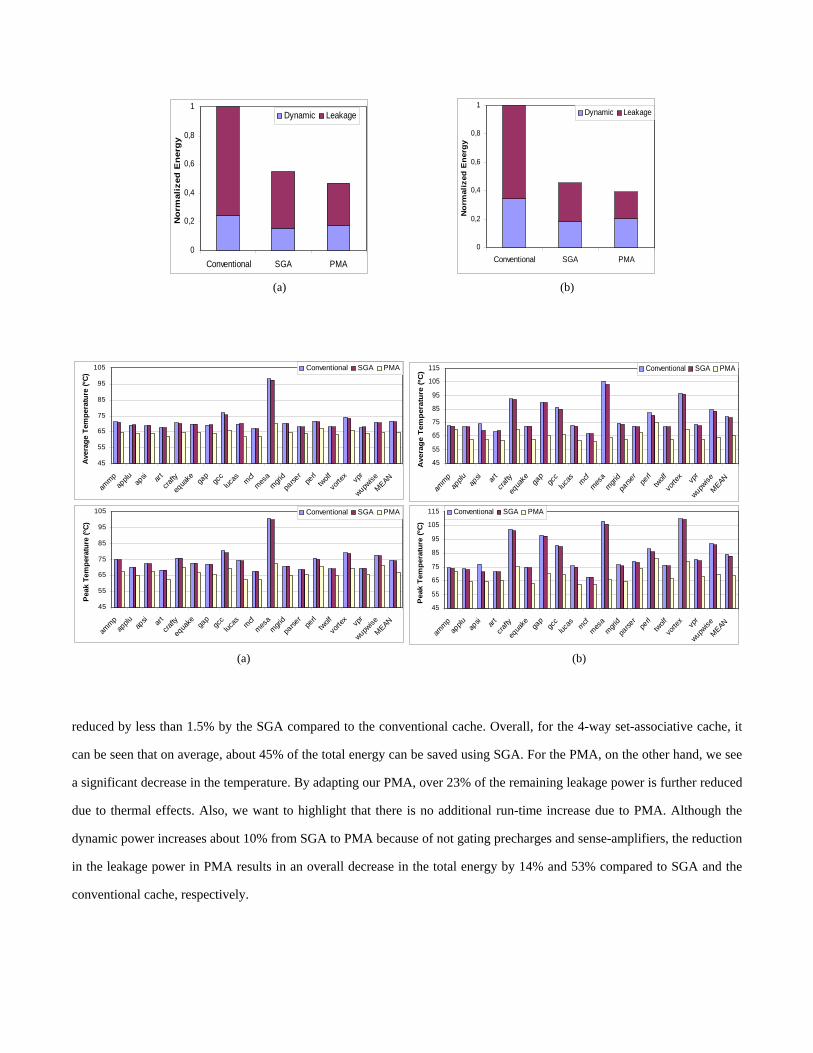
reduced by less than 1.5% by the SGA compared to the conventional cache. Overall, for the 4-way set-associative cache, it
can be seen that on average, about 45% of the total energy can be saved using SGA. For the PMA, on the other hand, we see
a significant decrease in the temperature. By adapting our PMA, over 23% of the remaining leakage power is further reduced
due to thermal effects. Also, we want to highlight that there is no additional run-time increase due to PMA. Although the
dynamic power increases about 10% from SGA to PMA because of not gating precharges and sense-amplifiers, the reduction
in the leakage power in PMA results in an overall decrease in the total energy by 14% and 53% compared to SGA and the
conventional cache, respectively.
(a) (b)
Figure 14. Average and peak temperature of active banks in conventional cache, SGA, and PMA for (a) 4-way set-associative caches (b) 8-way set-associative caches.
Figure 13. Normalized average dynamic and leakage power in different cache structures for (a) 4-way set-associative caches (b) 8-way set-associative caches.
(a) (b)
45
55
65
75
85
95
105
ammp
applu ap
si artcra
fty
equa
ke gap
gcc
lucas mcf
mesa
mgridpa
rser
perl
twolf
vorte
x vpr
wupwise
MEAN
Aver
age
Tem
pera
ture
(ºC
)
Conventional SGA PMA
45
55
65
75
85
95
105
ammp
applu ap
si artcra
fty
equa
ke gap
gcc
lucas mcf
mesa
mgridpa
rser
perl
twolf
vorte
x vpr
wupwise
MEAN
Peak
Tem
pera
ture
(ºC)
Conventional SGA PMA
45
55
65
75
85
95
105
115
ammp
applu ap
si artcra
fty
equa
ke gap
gcc
lucas mcf
mesa
mgrid
parse
rpe
rltw
olf
vorte
x vpr
wupwise
MEAN
Ave
rage
Tem
pera
ture
(ºC
) Conventional SGA PMA
45
55
65
75
85
95
105
115
ammp
applu ap
si art
crafty
equa
ke gap
gcc
lucas mcf
mesa
mgridpa
rser
perl
twolf
vorte
x vpr
wupwise
MEAN
Pea
k Te
mpe
ratu
re (º
C)
Conventional SGA PMA
0
0,2
0,4
0,6
0,8
1
Conventional SGA PMA
No
rmal
ized
En
ergy
Dynamic Leakage
0
0,2
0,4
0,6
0,8
1
Conventional SGA PMA
No
rmal
ized
En
erg
y
Dynamic Leakage
For PMA of the 8-way set-associative cache, the additional leakage reduction from SGA is higher (32%) than that of the 4-
way set-associative cache for two reasons. One is the fact that the power density can be decreased by a factor of up to eight,
and the temperature of the 8-way set-associative caches is usually higher which means there is more room for the
temperature to drop. However, the total additional energy is about 13%, which is actually lower than that of the 4-way set-
associative cache. This is because in 8-way set-associative cache, SGA itself eliminates about 55% of the total energy of the
conventional cache by disabling more than half the ways on average, thus not leaving much for further leakage reduction by
PMA. Furthermore, the penalty in the dynamic power also becomes relatively more significant. It can be seen from the
results that the adaptation of our PMA is most effective when around half of the ways are enabled.
6.3 Evaluation of BPS
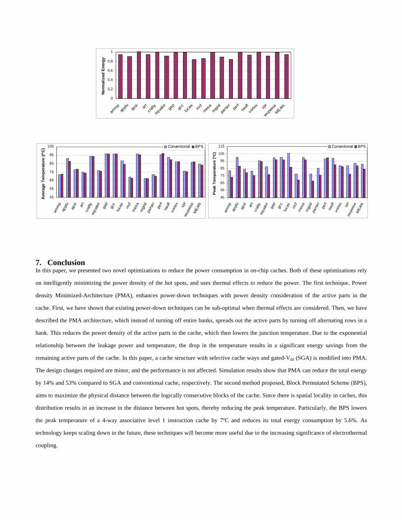
The effectiveness of BPS is illustrated in Figure 15, which presents the energy consumption of the level 1 instruction cache enhanced with
BPS relative to a conventional cache. Note that this optimization has no overhead (in terms of both execution time and cache latency).
Since the dynamic power stays the same for both cases, any change in the total energy consumption is caused by the reduction in the
leakage energy. It can be seen that BPS can be very effective for some applications such as lucas, mcf, and parser where the total energy is
reduced up to 16%. Since permuting the block does not always guarantee a better power density compared to the conventional case, it may
not always improve the energy. In fact, in case of apsi, the total energy actually increases by 1%. In general, BPS is useful when there is
strong spatial locality in instruction sequences. Since most applications exhibit this property, generally we observe a reduction in the total
energy consumption. On average, the leakage power and the total energy are reduced by 8.7% and 5.6%, respectively. Figure 16 compares
the temperature of the banks for the conventional cache and the cache with BPS. It is interesting to notice that the average temperature
does not change very much while the peak temperature drops more significantly for the cache with BPS. This is because in memory banks
of conventional instruction cache, hot spots are close to each other, thereby pushing up the peak temperature of the bank. In the cache with
BPS, the power density of the hot spots is minimized through a more uniform distribution of the power dissipation sources, and thus the
peak temperature is significantly lowered. Particularly, the BPS reduces the peak temperature about 7ºC on average. The drop in the
peak temperature results in the leakage reduction of the hot spots, decreasing the overall leakage power in the
bank.
7. Conclusion In this paper, we presented two novel optimizations to reduce the power consumption in on-chip caches. Both of these optimizations rely
on intelligently minimizing the power density of the hot spots, and uses thermal effects to reduce the power. The first technique, Power
density Minimized-Architecture (PMA), enhances power-down techniques with power density consideration of the active parts in the
cache. First, we have shown that existing power-down techniques can be sub-optimal when thermal effects are considered. Then, we have
described the PMA architecture, which instead of turning off entire banks, spreads out the active parts by turning off alternating rows in a
bank. This reduces the power density of the active parts in the cache, which then lowers the junction temperature. Due to the exponential
relationship between the leakage power and temperature, the drop in the temperature results in a significant energy savings from the
remaining active parts of the cache. In this paper, a cache structure with selective cache ways and gated-Vdd (SGA) is modified into PMA.
The design changes required are minor, and the performance is not affected. Simulation results show that PMA can reduce the total energy
by 14% and 53% compared to SGA and conventional cache, respectively. The second method proposed, Block Permutated Scheme (BPS),
aims to maximize the physical distance between the logically consecutive blocks of the cache. Since there is spatial locality in caches, this
distribution results in an increase in the distance between hot spots, thereby reducing the peak temperature. Particularly, the BPS lowers
the peak temperature of a 4-way associative level 1 instruction cache by 7ºC and reduces its total energy consumption by 5.6%. As
technology keeps scaling down in the future, these techniques will become more useful due to the increasing significance of electrothermal
coupling.
Figure 16. Average and peak temperature of memory banks in conventional cache, and cache with BPS.
Figure 15. Normalized energy of caches with BPS with respect to conventional caches.
45
55
65
75
85
95
105
amm
pap
plu
apsi art
craf
tyeq
uake gap
gcc
luca
sm
cfm
esa
mgr
idpa
rser
perl
twol
fvo
rtex
vpr
wupw
ise
MEA
N
Ave
rage
Tem
pera
ture
(/ºC
) Conventional BPS
45
55
65
75
85
95
105
115
amm
pap
plu
apsi art
craf
tyeq
uake gap
gcc
luca
sm
cfm
esa
mgr
idpa
rser
perl
twol
fvo
rtex
vpr
wupw
ise
MEA
N
Pea
k Te
mpe
ratu
re (º
C)
Conventional BPS
0
0,2
0,4
0,6
0,8
1
ammp
applu ap
si artcra
fty
equa
ke gap
gcc
lucas mcf
mesa
mgrid
parse
rpe
rltw
olf
vorte
x vpr
wupwise
MEANN
orm
aliz
ed E
nerg
y

8. References
[1] S. Manne, A. Klauser, and D. Grunwald, “Pipeline gating: speculation control for energy reduction”, in ISCA, pp. 132-141, June 1998
[2] J. Montanaro et al, “A 160-MHz, 32-b, 0.5W CMOS RISC microprocessor,” in Dig. Tech J., vol. 9, no. 1, pp. 49-62, 1997
[3] J. Kin, M. Gupta, and W. Mangione-Smith, “The filter cache: an energy efficient memory structure,” in Proc. MICRO, pp. 184-193,
Dec. 1997
[4] D. Albonesi, “Selective cache ways: on-demand cache resource allocation”, in Proc. MICRO, pp. 248-259, Nov. 1999
[5] V. De and S. Borkar, “Technology and design challenges for low power and high performance,” in Proc. ISLPED, pp. 163-168, 1999
[6] M. Powell, et al, “Gated-Vdd: a circuit technique to reduce leakage in deep-submicron cache memories,” in Proc. ISLPED, pp. 90-95,
2000
[7] K. Nii, et al, “A low power SRAM using auto-backgate-controlled MT-CMOS,” in Proc. ISLPED, pp. 293-298, 1998
[8] K. Flautner, et al, “Drowsy caches: simple techniques for reducing leakage power,” in Proc. ISCA, pp. 148-157, 2002
[9] N. Kim, K. Flautner, D. Blaauw, T. Mudge,“Drowsy instruction caches,” in Proc. ISCA, pp. 219-230. 2002
[10] Y. Meng, T. Sherwood, R. Kastner, “On the limits of leakage power reduction in caches,” in Proc. HPCA, 2005
[11] P. Shivakumar and N. Jouppi, “CACTI 3.0: an integrated cache timing, power and area model,” in WRL Research Report, 2003
[12] Y. Ye, S. Borkar, and V. De, “A new technique for standby leakage reduction in high performance circuits,” in IEEE Symp. on VLSI
Circuits, pp. 40-41, 1998
[13] M. Kamble and K. Ghose, “Analytical energy dissipation model for low power caches,” in Proc. ISLPED, Aug, 1997
[14] Y. Taur and T. Ning, Fundamentals of modern VLSI devices. Cambridge University Press, 1998
[15] K. Roy, S. Mukhopadhyay, H. Mahmoodi-Meimand, “Leakage current mechanisms and leakage reduction techniques in deep-
submicrometer CMOS circuits,” in Proc. IEEE, vol. 91, no. 2, pp. 305-327, Feb. 2003
[16] G. Kromann, “Thermal modeling and experimental characterization of the C4/surface-mount-array interconnect technology,” in IEEE
Trans. on Component, Packaging, and Manufacturing Technology, vol. 18, no. 1, pp. 87-93, Mar. 1995
[17] K. Kanda, K. Nose, H. Kawaguchi, and T. Sakurai, “Design impact of positive temperature dependence on drain current in sub-1-V
CMOS VLSIs,” in IEEE J. Solid-State Circuits, vol. 36, pp1559-1564, Oct. 2001
[18] S. Im and K. Banerjee, “Full-chip thermal analysis of planar (2-D) and vertically integrated (3-D) high performance ICs,” Tech. Dig.
IEDM, pp. 727-730, 2000
[19] K. Banerjee et al, “A self-consistent junction temperature estimation methodology for nanometer scale ICs with implications for
performance and thermal management,” in IEDM, pp. 887-890, 2003
[20] A. Chapman, Fundamentals of heat transfer. Macmillan Press, 1987
[21] K. Skadron, et al, “Temperature-aware microarchitecture,” in Proc. ISCA, pp. 2-13, 2003
[22] R. Quay, C. Moglestue, V. Palankovski, S. Selberherr, “A temperature dependent model for the saturation velocity in semiconductor
materials,” in Material Science in Semiconductor Processing 3, pp. 149-155, 2000
[23] Y. Cheng et al, “Modeling temperature effects of quarter micrometer MOSFETs in BSIM3v3 for circuit simulation,” in Semicond.
Sci. Technol. 12, pp. 1349-1354, 1997

[24] http://www.simplescalar.com/tools.html
[25] T. Sherwood, E. Perelman, and B. Calder, “Basic block distribution analysis to find periodic behavior and simulation points in
applications,” in Proc. PACT, 2001
[26] http://www-device.eecs.berkeley.edu/~ptm/mosfet.html
Copyright © 2022 FDOKUMEN