Test Access Circuit for Education
6
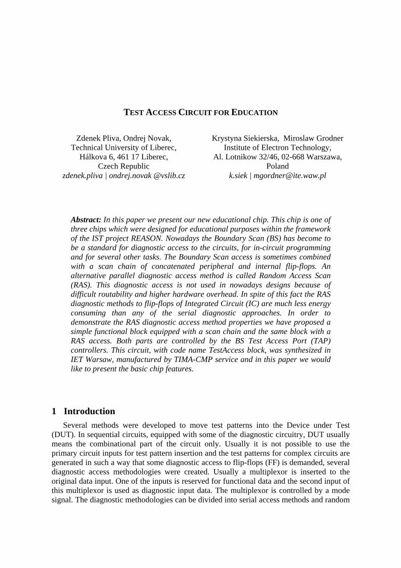
TEST ACCESS CIRCUIT FOR EDUCATION Zdenek Pliva, Ondrej Novak, Technical University of Liberec, Hálkova 6, 461 17 Liberec, Czech Republic zdenek.pliva | ondrej.novak @vslib.cz Krystyna Siekierska, Miroslaw Grodner Institute of Electron Technology, Al. Lotnikow 32/46, 02-668 Warszawa, Poland k.siek | [email protected] Abstract: In this paper we present our new educational chip. This chip is one of three chips which were designed for educational purposes within the framework of the IST project REASON. Nowadays the Boundary Scan (BS) has become to be a standard for diagnostic access to the circuits, for in-circuit programming and for several other tasks. The Boundary Scan access is sometimes combined with a scan chain of concatenated peripheral and internal flip-flops. An alternative parallel diagnostic access method is called Random Access Scan (RAS). This diagnostic access is not used in nowadays designs because of difficult routability and higher hardware overhead. In spite of this fact the RAS diagnostic methods to flip-flops of Integrated Circuit (IC) are much less energy consuming than any of the serial diagnostic approaches. In order to demonstrate the RAS diagnostic access method properties we have proposed a simple functional block equipped with a scan chain and the same block with a RAS access. Both parts are controlled by the BS Test Access Port (TAP) controllers. This circuit, with code name TestAccess block, was synthesized in IET Warsaw, manufactured by TIMA-CMP service and in this paper we would like to present the basic chip features. 1 Introduction Several methods were developed to move test patterns into the Device under Test (DUT). In sequential circuits, equipped with some of the diagnostic circuitry, DUT usually means the combinational part of the circuit only. Usually it is not possible to use the primary circuit inputs for test pattern insertion and the test patterns for complex circuits are generated in such a way that some diagnostic access to flip-flops (FF) is demanded, several diagnostic access methodologies were created. Usually a multiplexor is inserted to the original data input. One of the inputs is reserved for functional data and the second input of this multiplexor is used as diagnostic input data. The multiplexor is controlled by a mode signal. The diagnostic methodologies can be divided into serial access methods and random
Transcript of Test Access Circuit for Education
TEST ACCESS CIRCUIT FOR EDUCATION
Zdenek Pliva, Ondrej Novak, Technical University of Liberec,
Hálkova 6, 461 17 Liberec, Czech Republic
zdenek.pliva | ondrej.novak @vslib.cz
Krystyna Siekierska, Miroslaw Grodner Institute of Electron Technology,
Al. Lotnikow 32/46, 02-668 Warszawa, Poland
k.siek | [email protected]
Abstract: In this paper we present our new educational chip. This chip is one of three chips which were designed for educational purposes within the framework of the IST project REASON. Nowadays the Boundary Scan (BS) has become to be a standard for diagnostic access to the circuits, for in-circuit programming and for several other tasks. The Boundary Scan access is sometimes combined with a scan chain of concatenated peripheral and internal flip-flops. An alternative parallel diagnostic access method is called Random Access Scan (RAS). This diagnostic access is not used in nowadays designs because of difficult routability and higher hardware overhead. In spite of this fact the RAS diagnostic methods to flip-flops of Integrated Circuit (IC) are much less energy consuming than any of the serial diagnostic approaches. In order to demonstrate the RAS diagnostic access method properties we have proposed a simple functional block equipped with a scan chain and the same block with a RAS access. Both parts are controlled by the BS Test Access Port (TAP) controllers. This circuit, with code name TestAccess block, was synthesized in IET Warsaw, manufactured by TIMA-CMP service and in this paper we would like to present the basic chip features.
1 Introduction Several methods were developed to move test patterns into the Device under Test
(DUT). In sequential circuits, equipped with some of the diagnostic circuitry, DUT usually means the combinational part of the circuit only. Usually it is not possible to use the primary circuit inputs for test pattern insertion and the test patterns for complex circuits are generated in such a way that some diagnostic access to flip-flops (FF) is demanded, several diagnostic access methodologies were created. Usually a multiplexor is inserted to the original data input. One of the inputs is reserved for functional data and the second input of this multiplexor is used as diagnostic input data. The multiplexor is controlled by a mode signal. The diagnostic methodologies can be divided into serial access methods and random

access methods. Historically the main representative of the serial diagnostic access methods was the method called the LSSD [6] and the method Random Access Scan (RAS) [2] can serve us as a representative of the parallel methods. In 1993 a new serial method called Boundary Scan (BS) [3] , [9] was standardized. This method enables scanning in and out circuit inputs and outputs and it can perform several other functions. During the last decade the serial diagnostic access methods became to be the most important diagnostic access method within all the methods and nowadays are widely used. In order to further simplify testing of sequential circuits the BS is completed with a chain of scan cells (SC), which replace the internal FFs. On the contrary to the chain of BS cells, the internal FF chain affects the DUT during shifting test patterns. With growing size of the produced ICs new problems occurred: shifting test patterns in long scan chains causes unacceptably big heat dissipation, the test clock frequency has to be lowered and/or special gates avoiding signal wide spreading has to be used. This high consumption should be a problem in the novel battery powered portable devices and in the high clock frequency designs.
The RAS diagnostic access method is advantageous because it spares energy, which is necessary for reading and writing diagnostic data. The main disadvantage of the RAS method is that it requires higher number of wires and thus the hardware overhead is greater than it is in case of the BS. Modern IC production technologies allow higher connectivity of the construction blocks of ICs and it seems that it could be possible to accept higher hardware overhead in order to get the advantages of random access diagnostic methods. The main advantage of the serial diagnostic access methods is that they need fewer wires for controlling the diagnostic data shifting through the scan chain. Another situation occurs if we want to have a diagnostic access to internal FFs. These internal FFs can be concatenated into a scan chain (SC) but as the FF outputs are directly connected with the rest of functional logic, shifting patterns through the scan chain causes an activity of the combinational part of the circuit. An overview of methods for power minimization during testing is given in [7] . It is also possible to reduce both average and peak power dissipation by generating test patterns in ATPGs, which minimize the number of transitions in the DUT between two consecutive vectors by reordering test patterns or by modifying the order of scan FFs in the chain and partitioning the scan chain - see [4] , [5] , [8] , [12] , [17] and [18] . Some experimental results on benchmark circuits show that a reduction ranging from 10% to 86% (see e.g. [15] can be obtained by the mentioned techniques without fault coverage reduction. The power dissipation problem occurs also when using built-in pseudo random pattern generator for testing the circuit.
Using the RAS diagnostic access methodology may be an alternative solution of the power minimization problem. In [14] , [15] , [16] our proposed methods of implementing RAS cells into a serial diagnostic access design were introduced. We have improved this solution and we offered full compatibility with Boundary Scan.
2 TestAccess block structure Our proposed TestAccess block (TA-block) is one part of the EduChip. The main idea
of our part is described in Figure 1. The second part of this chip (DefSim_analog) was designed at WUT (Warsaw University of Technology) and is dedicated to analog measurements of the basic digital cells with intentionally introduced physical defects [13] . The TA-block contains two separated parts with the same functionality and with a different diagnostic access methodology – BS-RAS part and BS-SC part.

Figure 1: General scheme of TestAccess block
The block scheme of the TA-block is presented in Figure 2. It is a simple sequential circuit containing a 32bit adder, input and output registers with diagnostic access, 8 input and 8 output data pins and 6 control pins. In operation mode, the parallel input bit values are transformed to two 32 bit input registers with the help of a demultiplexor controlled by the address decoder. The 32 bit output register values and the Carry bit are transformed to the 8 parallel outputs with the help of a multiplexor and the same address decoder.
Figure 2: Block scheme of the TA-block
The described structure is placed twice in the TA-block and both these parts use the same chip pins. The activity of these blocks is selected by the scsel input signal – either the BS-SC or the BS-RAS part is active. The TA-block is equipped with Boundary Scan diagnostic access. Both parts of this block, BS-RAS and BS-SC, have its own Boundary Scan interface with its own Test Access Port (TAP) controller. The TAP controller has four-bit instruction register, only the basic mandatory instructions were built – Bypass, Extest and Sample/Preload. The scheme of the TA-block in the test mode is presented in Figure 3.
In BS-SC part the internal flip-flops are concatenated into a scan chain, which is connected between the input BS cells and the output BS cells. In the test mode the scan chain is clocked by the TAP controller. The BS-RAS part is equipped with the Random Access Scan diagnostics access. This circuit is controlled in the test mode with a similar TAP controller as the BS-SC part; the difference is that all the FFs are transformed to RAS cells. These RAS cells are addressed by a decoder, which is clocked from the TAP controller. At one time only one cell is addressed and has its output active – connected to

TDO output. The incoming logic value from TDI is accepted only by this selected cell. All other resting RAS cells are not active during the read/write operation of the addressed cell and their TDO outputs are in the 3rd state, disconnected from the TDO output.
Figure 3: A block scheme of the TA-block in the Test mode
It was said that during the test only one part of the TA-block is active. All the parts of TA-block – BS-SC, BS-RAS, and MUX (see Figure 1) – have a separated power pins and with the help of that it is possible to connect only the measured part to VDD.
BS-RAS
BS-SC
Figure 4: Microphotograph of the TestAccess die (TA-block is shown on the left side). Published with kind permissions of IET (PL) and W.A. Pleskacz (WUT, PL)

3 Conclusion VHDL models of the both test sub circuits (BS-SC and BS-RAS) were transformed into
RTL synthesizable versions in IET (Institute of Electron Technology, Warsaw). After verification by VHDL simulations they were synthesized with usage of AMS 0.8um CMOS-CYE standard cell library [1] . The obtained final netlists were also functionally verified by simulation of related VHDL structural models. These results were compared with results of the previous simulation of the RTL models. The validated final netlist was next used to generate layout of the both sub circuits and the MUX part. The whole TestAccess circuit was designed in AMS 0.8 CMOS-CYE technology [1]. The final layout of the TA_block was synthesized by Krystyna Siekierska and Miroslaw Grodner form IET (Institute of Electron Technology, Warsaw) (see Figure 4) with close cooperation with W. A. Pleskacz, from WUT (Warsaw University of Technology). The size of TestAccess circuit is 4725 µm x 4069 µm, the JLCC84 standard package was used for packaging the die. The first prototype of chip was manufactured by TIMA-CMP service [10]. Till now only initial measurements were done. Now we have to do final measurements of the test access and after that the power consumption during test pattern shifting will be measured. The exercise scenarios, application modules will be published after finalizing these measures. The software tools, which have to be developed, will enable us to control inputs and read outputs and to run a test sequence stored in a PC memory. Simultaneously the software will control the current measuring system. Possible exercises are:
• Performing a test of the circuit with the help of parallel inputs. The tools enable to feed the primary inputs with test patterns and to read the circuit responses. The proposed circuit consists of simple logical blocks and thus the test sequence could be short and easy to be checked whether it covers all possible faults. When asking students to create their own test sets, the fault coverage of the prepared test set can be evaluated by a fault simulator help.
• Performing a test with the help of the BS and internal SC diagnostic access. This exercise has to demonstrate that it is simpler to use the diagnostic access design and to generate test patterns for the combinational parts only.
• Comparison of the power consumption of the BS-SC and RAS register seeding with randomly generated patterns. The pseudorandom bits will be generated in a PC. A given number of bits will be generated and loaded to the BS-SC or RAS FFs while IDD current consumption will be measured. This measurement will demonstrate problems bounded with simultaneous switching of big numbers of FFs in the chip and propagation of the scan chain activity to the connected combinational logic. An alternative exercise is to order a set of randomly generated test vectors so that the power consumption is reduced. The result can be checked by the real IDD measurement.
• Comparison of the energy consumed by testing the circuit through parallel inputs and outputs and by diagnostic access utility. This measurement can compare the energies consumed by the real deterministic test sequences performance.
Acknowledgments The research was in part supported by the IST-2000-30193 grant (REASON) and by the
research grant of the Czech Grant Agency GACR 102/04/2137.

References [1] http://asic.amsint.com/ (16.1.2005) [2] Ando, H., “Testing VLSI with RAS”, Diag. Papers Compcon 80, IEEE pub. 80CH1491-OC,
pp. 50-52, Feb. 1980. [3] Bleeker, H., Book “Boundary-Scan Test, a practical approach”, ISBN 0-7923-9296-5, 1993. [4] Corno F., Prinetto P., Rebaudengo M. and Sonza Reorda M., “A Test Pattern Generation
Methodology for Low Power Consumption ‘, Proc. IEEE VLSI Test Symp., pp. 453-459, 1998. [5] Dabholkar V., Chakravarty S., Pomeranz I. and Reddy S.M., “Techniques for Reducing Power
Dissipation During Test Application in Full Scan Circuits”, Journal IEEE Transactions on CAD, Vol. 17, No. 12, pp. 1325-1333, Dec. 1998.
[6] Eichelberger E.B. and Williams T.W., "A Logic Design Structure for LSI Testability," Journal Design Automation and Fault-Tolerant Computing”, vol. 2, 1978, pp. 165-178.
[7] Girard, P.: “Low Power Testing of VLSI Circuits: Problems and Solutions”. Proc. of the ISQUED Symposium, pp. 173-179, Jan. 2000.
[8] Girard P., Guiller L., Landrault C. and Pravossoudovitch S., “A Test Vector Ordering Technique for Switching Activity Reduction during Test Operation “, Proc. IEEE Great Lakes Symposium on VLSI, pp. 24-27.
[9] IEEE Std 1149.1-2001, IEEE Standard “Test Access Port and Boundary Scan Architecture”. [10] http://cmp.imag.fr (16.1.2005). [11] Manich, S., Gabarró, A., Lopez, M., Figueras, J., Girard, P., Guiller, L., Landrault, C.,
Pravossoudovitch, S., Teixeira P., Santos, M., “Low Power BIST by Filtering Non-Detecting Vectors“, JETTA Vol. 16, No. 3, ISSN: 0923-8174, Jun 2000.
[12] Nicolici, N., Al-Hashimi, B. M., "Scan Latch Partitioning into Multiple Scan Chains for Power Minimization in Full Scan Sequential Circuits", Proc. Of DATE 2000, Paris, Pp. 715-722, ISBN:1-58113-244-1, Mar. 2000.
[13] Pleskacz W. A., Borejko T., Gugala T., Pizon P., Stopjakova V.: “DefSim - the Educational Integrated Circuit for Defect Simulation,” Submitted for publication in Proc. of the IEEE International Conference on Microelectronic Systems Education – MSE’05, Anaheim, California, USA, Jun. 2005.
[14] Pliva z., Novak O., Bourdeu d’Aguerre P., ”Hardware overhead of Boundary Scan and RAS design methodologies”, Proc. of DDECS2002, pp. 36-43, Brno, Apr. 2002.
[15] Pliva Z., Novak O., ”Low Power Boundary Scan design”, Proc. of the 8th Biennial Baltic Electronics Conference, Tallin, pp. 265-268, Oct. 2002.
[16] Pliva, Z., Novak, O., Noullet, J-L.: ”Comparison of the Low-Power Diagnostics Methods”, Proc. of ECMS 2003, Liberec, pp. 299-304, ISBN 80-7083-708-X, Jun. 2003.
[17] Wang S. and Gupta S.K., “ATPG for Heat Dissipation Minimization During Scan Testing”, Proc. of ACM/IEEE Design Auto.Conf., pp. 614-619, Jun. 1997.
[18] Zorian, Y., “A distributed BIST control scheme for complex VLSI devices”, Proc. of IEEE VTS’93, pp. 4-9, Apr. 1993.