Telemetric Torque Measurement System - WMU's ScholarWorks
108
Western Michigan University Western Michigan University ScholarWorks at WMU ScholarWorks at WMU Honors Theses Lee Honors College 4-17-1997 Telemetric Torque Measurement System Telemetric Torque Measurement System Jason Joseph Western Michigan University, [email protected] Francisco Sinta Western Michigan University Jeff Williams Western Michigan University Follow this and additional works at: https://scholarworks.wmich.edu/honors_theses Part of the Electrical and Computer Engineering Commons Recommended Citation Recommended Citation Joseph, Jason; Sinta, Francisco; and Williams, Jeff, "Telemetric Torque Measurement System" (1997). Honors Theses. 1471. https://scholarworks.wmich.edu/honors_theses/1471 This Honors Thesis-Open Access is brought to you for free and open access by the Lee Honors College at ScholarWorks at WMU. It has been accepted for inclusion in Honors Theses by an authorized administrator of ScholarWorks at WMU. For more information, please contact [email protected].
-
Upload
khangminh22 -
Category
Documents
-
view
1 -
download
0
Transcript of Telemetric Torque Measurement System - WMU's ScholarWorks

Western Michigan University Western Michigan University
ScholarWorks at WMU ScholarWorks at WMU
Honors Theses Lee Honors College
4-17-1997
Telemetric Torque Measurement System Telemetric Torque Measurement System
Jason Joseph Western Michigan University, [email protected]
Francisco Sinta Western Michigan University
Jeff Williams Western Michigan University
Follow this and additional works at: https://scholarworks.wmich.edu/honors_theses
Part of the Electrical and Computer Engineering Commons
Recommended Citation Recommended Citation Joseph, Jason; Sinta, Francisco; and Williams, Jeff, "Telemetric Torque Measurement System" (1997). Honors Theses. 1471. https://scholarworks.wmich.edu/honors_theses/1471
This Honors Thesis-Open Access is brought to you for free and open access by the Lee Honors College at ScholarWorks at WMU. It has been accepted for inclusion in Honors Theses by an authorized administrator of ScholarWorks at WMU. For more information, please contact [email protected].

THE CARL AND WINIFRED LEE HONORS COLLEGE
CERTIFICATE OF ORAL EXAMINATION
Jason Joseph, having been admitted to the Carl and Winifred Lee Honors College in 1993,successfully presented the Lee Honors College Thesis on April 17, 1997.
The title of the paper is:
"Telemetric Torque Measurement System"
Ly a4w;.
Dr. John Gesink
Electrical and Computer Engineering

"Telemetric Torque Measurement System"
By Jason Joseph, Francisco Sinta, Jeff Williams
Advisor: Dr. John Gesink
Electrical and Computer Engineering 482
April 15,1997

Abstract
The Telemetric Torque Measurement System(TTMS) was designed to measure
the torque produced by a snowmobile engine. The design of the TTMS was refined and
modified in stages, leading to the final design. The TTMS consists oftwo basic sections:
the transmitter sectionand the frequency demodulator section. The transmitter section
effectively measures the torque on a snowmobilejack-shaft. The torque signal is
converted into a voltage which is then fed into a voltage to frequency converter and
converted into an audio tone. This tone is broadcast in the FM broadcast band via an FM
transmitter. An FM receiver then receives the audio tone. The frequency demodulator
section receives the encoded signal from the FM receiver through a headphone jack and
converts the signal into a voltage that is proportional to torque applied to the snowmobile
jack-shaft.
Several tests were completed to verify the operation ofthe TTMS and its ability to
meet the design specifications. Some specifications were not verified because of lack of
test equipment. The TTMS project was tested and calibrated using known torque values.
The test results showed that the TTMS is capable of producing a linear output voltage
that is proportional to torque. The TTMS is capable of running for at least 3 hours on one
set ofbatteries, and is capable of spinningat a speed ofat least 2000 RPM. The
dimensions of the TTMS meet specifications, and the range oftransmission is at least 10
feet. Someminorchangesto the TTMS designwere made consisting of onlycomponent
value changes. Overall, the TTMS project was successful.

Disclaimer
This report was generated by a group ofengineering seniors at Western MichiganUniversity. It is primarily a record ofa project conducted by these students as part ofcurriculum requirements for being awarded an engineering degree. Western MichiganUniversity makes no representation that the materialcontained in this report is error freeor complete in all respects. Therefore, Western Michigan University, its faculty, itsadministration or the students make no recommendation for use of said material and take
no responsibility for such usage. Thus persons or organizationswho choose to use saidmaterial for such usage do so at their own risk.
11

WESTERN MICHIGAN UNIVERSITY
COLLEGE OF ENGINEERING AND APPLIED SCIENCES
DEPARTMENT OF ELECTRICAL ENGINEERING
KALAMAZOO, MICHIGAN 49008
SENIOR DESIGN PROJECT REPORT RELEASE FORM
In accordance with the "Policy on Patents and Release ofReports Resulting from SeniorDesign Projects" as adopted by the Executive Committee Ofthe College ofEngineeringand Applied Scienceson Feb. 9, 1989, permission is hereby granted by the individualslisted below to release copies ofthe final report written for the Senior Design Projectentitled:
PROJECT TITLE: Telemetric Torque Measurement System
PROJECT SPONSOR: Smiths Industries
TEAM MEMBERS NAMES:
NAME PRINTED NAME SIGNED DATE
Jason Joseph ^^<fr/w^r^^p\j J^ _JlliLl22
Francisco Sinta
Jeff Williams
in

Table of Contents
Abstract i
Disclaimer ii
Project Release Form iiiTable of Contents iv
Acknowledgments 1Summary 2Introduction 5
Discussion 7
Conclusion 29
Appendix A - Parts ListAppendix B - Test DataAppendix C - Lithium BatteryAppendix D - Strain GagesAppendixE - ADM666 Voltage RegulatorAppendix F - AMP04 Instrumentation AmplifierAppendix G - OP90 Operational AmplifierAppendix H - AD654 Voltage to FrequencyConverterAppendix I - FM-5 FM TransmitterAppendix J - LM565 Phase Locked Loop
iv

Acknowledgments
The design team would like to thank our sponsor, Smiths Industries, for their
support and assistance with this project. We would like to thank our advisor, Dr. John
Gesink, for his help in all aspects of this project. We would also like to thank James
Vandepolder, the Mechanical Engineering Department, and the Automotive Engineering
Department for their continued support in testing and development of the project.

Summary
The Telemetric Torque Measurement System (TTMS) was designed to measure
torque applied to a rotating shaft at speeds up to 9000 RPM. Several approaches were
considered for the design, leading to the final TTMS design concept. The final design
uses a strain gage bridge to sense torque in a rotating shaft. This torque signal is
transmitted to a stationary receiver that outputs a voltage proportional to the torque
applied to the shaft.
The main design constraint was the overall physical size of the TTMS. The
specifications require the TTMS to have a radial clearance of .75" and an axial lengthof
1.5" not including the straingage array. The TTMS was designed by researching
components and using a syntheses design methodology.
The basic structure of the TTMS beginswith a strain gage array to gather torque
data in the form ofa voltage proportional to strain measured. An instrumentation
amplifier is then used to amplify the strain gage signal. A voltage to frequency converter
is used to modulate the voltage signal for FM transmission. This signal is then fed into an
FM transmitter to transmit the torque data. An FM receiver demodulates the transmitted
signal. Finally, a frequency demodulator circuit is used to convert the signal from the FM
transmitter into a voltage proportional to the torque applied.
The transmitter section ofthe TTMS is powered by two 3.5V lithium batteries
connected in series. The 7V supply is regulated to 5V by a voltage regulator. The

receiver section is powered by a ±9V supply in the form oftwo 9V batteries connected in
series with the mid-point connected to ground.
The transmitter section ofthe TTMS is built on a printed circuit board, and
secured in a nylon housing that also houses the FM transmitter and lithiumion batteries.
The phase locked loop section ofthe TTMS is built on a breadboard.
The TTMS was tested using five different tests. The first test was designed as a
preliminary test to verify the operation ofthe TTMS. This test was completed
qualitatively, and was used to judge the overall operation ofthe circuit. This test showed
that the TTMS was capableof producing an output voltage that was proportional to the
differential voltage applied to the input of the TTMS. The second test was designed to
measure abilityofthe TTMS to measure torque under static conditions, without rotation.
This test showed that the TTMS produces a linearoutput voltage that is proportional to
torque appliedto the shaft under test. The third test was designed to measure the battery
life of the TTMS system. Test results showed that the battery life ofthe TTMS is greater
than three hours, and exceeds the requirements outlined by the design specifications. The
fourth test was designed to measure the ability ofthe TTMS to rotate at high speeds
without physical damage. This test was completed at a rotational speed of2000 RPM and
no physical damagewas incurred. The final test was used to test the transmissionrangeof
the TTMS. The test results showed that the TTMS is capable of transmitting a distance
greater than 10 feet.

Overall, the TTMS system operates as expected. Design modifications were
minimal, and the test results showed that the voltage output ofthe frequency demodulator
circuit is proportional to the torque applied to the shaft under test.

Introduction
The Telemetric Torque Measurement System (TTMS) was designed to measure
torque in the rotating jack-shaft of a snowmobile. The TTMS project was introduced
because of a desire to maximize snowmobile performance for racing applications. For
racing, it is necessary to maximize the torque output of a snowmobile to improve
acceleration. In order to adjust engine settings, a dynamic torque measurement system
that is capable ofmeasuring the torque output of a snowmobile engine is required. This
project is also designed to test and improve the design skillsof the design team.
The success of the project is dependant on satisfying several questions. Is it
feasible to have electrical components rotating at speeds in excess of 8000 RPM? Is it
feasible to transmit signals in the radio frequency band at these high speeds and receive a
cleansignal? If so, shouldthese delicate componentsbe protected and how will they be
protected? The purpose ofthis project was to answer these questions and analyze the
performance characteristics ofthe TTMS through engineering design, development, and
testing. The performance characteristics include the ability ofthe TTMS to effectively
measure torque on a rotating snowmobile jack-shaft. To effectively measure torque, the
TTMS must meet the required design specifications.
The scopeof this project was to design, build, test, and analyze a working
prototypeof the Telemetric Torque Measurement System. Learning, developing, and
testing the engineering concepts involved in the TTMS using true engineering design
methodology were also included in the scope of the project. The final aspect of the scope
was to showthe relationship between theoretical design and practical application, and
5

illustrate the types of problems that arise and solutions that can be obtained onlyby fully
analyzing all aspects ofthe design. The TTMS project illustrates some typical problems
and solutions that occurwhen dealing with signal processing systemsand electronic
measurement of mechanical variables.

Discussion
Typical Torque Measurement System
All torque measurement systems have a similar structure. A typical torque
measurement system is shown below in figure 1.
TorqueMechanically
AppliedTransducer
Electrical SignalProportionalto
Torque> Signal Decoder
Numerical TorqueValue
Figure 1 - Torque Measurement System
The input to the torque measurement system is a torque mechanically applied to a
given object. This torque is sensed by a transducer. A transducer converts this
mechanical input into an electrical output. Thiselectrical output is proportional to the
torque applied to the object. This electrical output is then converted into a numerical
torque value by a signal decoder. A signal decoder is a device that takes an electrical
input and produces a readable output. Examples of signal decoders include multi-meters
and oscilloscopes.
Torque Measurement System for a Rotating Shaft
This system changes depending on the application for which it is designed.
Consider torque produced by any motor, such as and automobile engines and snowmobile
engines. An engine's power is delivered to these vehicles through a drive-train, which

includes a drive shaft. The power delivered by the engine creates a torque in the drive
shaft, which must rotate to propel the vehicle. Therefore, one application ofa torque
measurement system involves measuringtorque on a rotating shaft.
The system shown in figure 1 is used to measure torque on a rotating shaft.
Torque is input to a transducer, which converts the torque signal into an electrical signal.
The method in which the transduceroutput is delivered to a decoder must be changed for
a rotating system. This changeoccurs becausewires cannot be connected directly from the
transducer to the decoder unless the decoder is located on the shaft. Logically, fastening a
decoder directly to a shaft is not desirable. For this reason, the decoder is located away
from the shaft.
There are two basic methods for delivering the torque signal from a transducer to a
decoder circuit. The first method involves using slip-rings, and the second method
involves using wireless communication. In certain applications, slip-rings are desirable
because ofthe ability to directly connect the transducer to the decoder. Because ofthis
simplicity, the system shown in figure 1 will not change. However, slip rings are usually
large and cannot be conveniently located in small engine compartments. Using wireless
transmission, a torque measurement system can be constructed using only additional
electronic components. Using the wireless technology that is available today, the size of
the system can be minimized.
A signal flow diagram ofa wireless torque measurement system is shown in figure
2.

TorqueMechanically
AppliedTransducer
Electrical SignalProportionalto
Torque Wireless
Transmitter
Circuitry
Transmitted Signal
Electrical SignalProportionalto
TorqueTransmitted Signal
Receiver
CircuitryDecoder
Circuitry
Nemerical TorqueValue
Figure 2 - Wireless Torque Measurement System
Telemetric Torque Measurement System
Specificationswere developed with Smiths Industries for the Telemetric Torque
Measurement System (TTMS). The specifications have been divided into two sections.
The first section is the transmitter section. The transmitter includes all components
leading from the transducer to transmitter. The second section, the receiver section,
consists of the receiver and decoder circuitry. These two sections make up the TTMS.
The specification for the system are given below.
(R = Requirement, G = Goal, P = Preference)
1. The torque measurement system must be capable of measuring unidirectional torque
values ranging from 0 ft-lb. to 110 ft-lb. (Olb-in to 1320 lb-in) on a 1" diameter shaft
of a snowmobile. R
2. The torque measurement system must be capable of measuring strains on the shaft of a
snowmobile that will be present on a carbon steel shaft with a modulus of elasticity
(G) of approximately 30,000,000 psi. R

3. The torque measurement system must operate at shaft rotation speeds up to 9000
revolutions per minute. G
4. The transmitter section must have an axial mounting length on the shaft of less than
1.5". The outer diameter ofthe transmitter section must be less than 2.5". R
5. The transmitter section must have a self contained power supply (i.e. a battery). R
6. The transmitter section must have a battery life greater than or equal to one hour. G
7. The transmitter section must modulate an FM carrier signal with a frequency
proportional to the strain measured by the transducer. R
8. The instantaneous frequency of the transmitted signal must be within the range of
lOOHztolOkHz. R
9. The carrier frequency of the FM transmitter must be adjustable from 88MHz to
108Mhz. R
10. The transmitter section and receiver section must operate properly at a distance of 10
feet apart. R
11. The output of the torque measurement system must be a voltage that is proportional to
the torque being applied to the shaft ofthe unit under test. R
12. The cost ofthe torque measurement system must be kept to a minimum. The absolute
maximum cost for components is $2000. R
13. The torque measurement system must not entail manufacturing processes that are not
within the ability of Smiths Industries or that of the design team. R
10
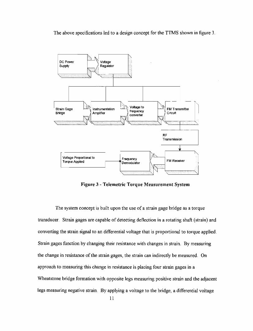
The above specifications led to a design concept for the TTMS shown in figure 3.
DC Power
Supply
Strain GageBridge
^ VoltageRegulator
Instrumentation
Amplifier
Voltage tofrequencyconverter
Voltage Proportional toTorque Applied
Frequency' Demodulator
FM Transmitter
Circuit
RF
Transmission
FM Receiver
Figure 3 - Telemetric Torque Measurement System
The system concept is built upon the use of a strain gage bridge as a torque
transducer. Strain gages are capable of detecting deflection in a rotating shaft (strain) and
converting the strain signal to an differential voltage that is proportional to torque applied.
Straingages function by changing their resistance with changes in strain. By measuring
the change in resistance of the strain gages, the strain can indirectlybe measured. On
approach to measuring this change in resistance is placingfour strain gages in a
Wheatstone bridge formation with opposite legs measuring positive strainand the adjacent
legs measuring negative strain. By applying a voltage to the bridge, a differential voltage
11

that is proportional to the change in resistance is developed that can be measured. Since
torque is related to strain by a constant that is dependant on the material ofthe shaft, and
change in strain gage resistance can be related to torque, and thus to differential voltage.
Typical changes in the resistance of strain gages are very small. Because of this,
the differential voltage produced by a Wheatstone bridge is also very small. In order to
improve transmission ofthe voltage signal that is proportional to torque, an amplifier must
be used. To minimize the effects ofnoise on the system, a instrumentation amplifier was
selected because of its high common mode rejection ratio.
The output signal of the instrumentation amplifier is converted to a frequency in
the audio band (20Hz - 20kHz) that is proportional to torque applied via a voltage to
frequency converter. The output of the voltage to frequency converter(VFC) is
transmitted to an FM receiver via an FM transmitter in the FM broadcast band (88 - 108
MHz).
The modulated FM signal is transmitted a short distance (approx. 10ft.) and
demodulated by the FM receiver. The output of the receiver is the audio tone and is
proportional to the torque measured by the strain gage array. A tone decoding circuit
then converts the audio tone into a voltage proportional to the torque transmitted by the
jack-shaft. Adjustable gain and offset features were added to the frequency demodulator
circuit to allow for fine tuning and calibration of the TTMS. The output voltage from the
frequency demodulator circuit canbe fed into a volt-meter, an oscilloscope, or a chart
recorder, depending on the needs of the user.
12

The circuits that were developed for the TTMS are shown in figure 4 and figure 5 .
A partslist of the TTMS is also shown in Table AI ofAppendix A.
The strain gage array was simulatedwith potentiometers to produce the varying
differential voltage ofthe Wheatstone Bridge. A 9VDC power supply was substituted for
batteriesin this test circuit. The output ofthe Wheatstone Bridge is a voltage with a
range of 0 to 2.24mV, based on a gage factor of2. This signal is fed into the AMP04
instrumentation amplifier. The 0 to 2.24mV range corresponds to a torque range of0 to
110 ft-lb. The AMP04 has a gain of 125, and has an offset of 1.12V that is set by the
OP90 in a voltage follower configuration to align the zero torque frequency of the voltage
to frequency converter. The output ofthe AMP04 is then attenuated by a voltage divider,
Ripi and RiP2, resulting in a voltage swing from 666V to 1 000V for positive torque. This
voltage is then fed into a voltage to frequency converter. The frequency output of the
AD654(VFC) swings between 2000Hz and about 2500Hz. The output ofthe voltage to
frequency converter is then fed into a FM-5 transmitter for broadcast in the 88MHz to
108MHz FM band. A signal flow block diagram is shown in figure 6.
13


Power Supply
PSl +9V
&—!PLUG
Cr2
PS2 iv?
PLUG OND
<"
FM Receiver
Small SignalOutput Jack
—I—Cr6
J"
RrlI N/V*-| 1Vrecv Jdi | D2
^^1N4004 22lN4004
~IOND
Crl
2.2uF
OND Cr5
OluFZ
GND
7K
VpU
EM355
Cr7
OOluF
Rr4
luF GND
T~10uF
OND
-*\A/^-
Frequency Demodulator Circuit
Figure 5 Size
A
Number
Date
File:
B-Apr-1997C:\DATAV.\RCVRSCH
->Vpllout
Sheet of
Drawn By:

TorqueMechanically
Applied Strain GageBridge
VdiffAMP-04
Differential
Amplifier (U2)
Vamp
VfoutVamp AD654 Voltageto Frequency
Converter (U4)
FM-5
Transmitter
Vrecv Vpllout
FM Receiver
LM565 Phase
Locked Loop(UR1)
Figure 6 - Signal Flow Block Diagram
A signal timing diagram ofthe TTMS is shown in figure 7.
16

fViSi 9 no,1 Tinin = D agr an
no ft-ib -
Torque
0 ft-lb-
2.24 nV -
Vdiff
0 nV -
3.374 V -
Vanp
1.134 V -
1,20V -
Vfout
ov-
1.0 V -
Vrecv
ov-
5V -
Vpllout
ov -
- i i
i
_ _
i_
. L
HiIlil
Figure 7 - Signal Timing Diagram
A JVC model RX555 FM receiver was used to receive the transmitted FM signal.
Theattached headphone jack was used as an output of the receiver to the frequency
demodulator circuitry. The output of the receiver is an audio tone that contains the
encoded torque signal. Two 9-Volt batteriesare connected in series to give the frequency
demodulator a ±9V power supply. The demodulatorcircuit uses a LM565 phase locked
loop. The output of the LM565 is amplified usingan OP90 operational amplifier, and
potentiometers are used to adjust offset and gain. The output signal of the frequency
demodulator is a voltage that is proportional to torque applied to the snowmobile shaft.
Several thingswere learnedduring the final phases ofthe TTMS project. After
observing the output signal from the frequency demodulator, it was noticed that the gain
of the TTMS was much too high to allow large changes in torque to be properly
measured. The main problem became the phase locked loop's inabilityto lock on to
frequencies in excess of 2.7kHz. This presented a problem, seeing that the original design
17

used frequencies ranging from 1kHz to 3kHz. For this reason, Rgainwas changed to
800£1 After the gain was adjusted, it was noticed that the phase locked loop would not
lock on to frequencies that were near the edges of its operation. For this reason, the zero
torque operating frequency was changed from 1kHz to 2kHz by changing the value ofR*.
This allowed the phase locked loop to gain lock on power up without having to apply
torque to the system to produce 2kHz and then remove the torque to begin testing.
Although the overall sensitivity ofthe system was reduced, the TTMS gained the ability to
measure bi-directional torque if the need should ever arise. These minor changes to the
TTMS produced very desirable results, and are considered the final TTMS design. The
original design specifications are fully detailed in the TTMS project proposal
18

Test Procedures and Results
A single printed circuit was fabricated and a housing was built to accommodate the
transmitter section ofthe TTMS. The circuit board layout is shown in figure 8 and figure
9. A diagram of the TTMS housing is shown in figure 10. A line drawing of the TTMS
mounting scheme is shown in figure 11. The testing procedure for the system is outlined
below.
Test #1- BreadboardModel of the TTMS
The purpose ofthis test was to test the operation ofthe TTMS design and
determine any necessary circuit modifications. All voltages and frequencies were checked
and compared to calculated values in each stage ofthe circuit.
• Potentiometers are used to simulate the straingages.
• The TTMS was energized and the potentiometers were varied to produce a bridge
output voltage ranging from OmV to 2.24mV. The output voltage from the AMP04
and frequency output of the AD654 were measured and compared signal values as
shown in figure 7.
• The output ofthe phase locked loop is monitoredon an oscilloscope and the gain and
offset controls ofthe frequency demodulator are adjusted to give -5V to +5V readings
as the bridge output is varied from OmV to 2.24mV.
19

TTMS Component Layout
o
Scale 2:1
•figure 8

TTMS Trace Layout
K>
Scale 2:1
•figure 9

LO)
dCD
uno2
inh.
en
oo(J.
oinm
md
cu
oin
OcuL0
CO
O
>CD
CD
oo.
inru
ooCD
O
I
<Io+
>uCDC
O
o•—
i
LO)

Telemetric Torque Measurement System
1,0* Dianeter Carbon Steel Shaft
2,5" DianeterNylon Housinq
__!
Detail View
figure 11

Test #2 - Calibration Test
The purpose ofthis test is to calibrate the TTMS using known values of torque
and verify the torque measurement abilityofthe TTMS.
• Strain gages were mounted on a 1" diameter carbon steel shaft.
• The TTMS was connected to the straingages and energised
• Variable torque ranging from 0 to 1lOft-lb in 10 ft-lb increments and output voltages
from the frequency decoder (Vpii0ut) were recorded.
Test #3 - Battery Life Test
The purpose ofthis test was to determine the life of the batteries used in the
TTMS.
• The TTMS and straingages were mounted to a 1" diameter carbon steel shaft.
• The TTMS was energized and zero torque was applied to the shaft.
• The output ofthe frequency demodulator was monitored and the time until the circuit
stopped operating was measured.
Test #4 - Rotation Test
The purpose of this test was to determine the ability of the TTMS to spin at high
speeds and remain in tact.
• The TTMS and shaft weremounted on a lathe machine to incorporate spinning ofthe
system.
• The shaft was rotated at 2000 RMP for at least one minute.
24

• The TTMS was removed and examined for mechanical failures and structural stability.
Test #5 - Operational Range Test
The purpose of this test was to verify the transmission ability ofthe TTMS to the
stationary receiver at a distance greater than 10 feet.
• The receiver and frequency demodulator circuit were placed 15 feet away from the
TTMS transmitter section.
• The TTMS was energized andthe output ofthe frequency demodulator (Vpuout) was
monitored for properoperationwith different torque inputs.
The above tests were completed and the following results were obtained.
Test #7 Results
After the breadboard model was tested, it was determined that the circuit operated
as expected. As the bridge voltage (Vd^) was varied from OmV to 2.24mV, Vfout was
monitored and its frequency visually inspected. It was noted that when Vd^ was set to
OmV, the frequency ofVfout was approximately 2kHz. As Vms was increased to 2.24mV,
the frequency ofVf0ut increased to approximately 2.5kHz. The output of the frequency
demodulator (VpUout) was also monitored as Vd^ was varied. It was noted that Vpn0ut
changed from approximately OV to +6V as Voiffwas varied.
25

Test n Results
The test data from the calibration test is shown in Table Bl in Appendix B. The
average value of the three sets of test data was then plotted and is shown in figure 12.
7.00
6.00
^ 5.00§>W)
I 4.00o
>J 3.00a
Z 2.00
1.00
0.00
TTMS Output Voltage vs. Applied Torque
y =-0.0384X + 1.9438 ^^m^^-
^0/^^
^Jr^ .
20 40 60 80 100
Applied Torque (ft-lb)
120
• Output Voltage(V)
— Linear (OutputVoltage (V))
Figure 12 - Calibration Test Data
The calibration test data showsa linearrelationship betweentorque applied to a
shaft and Vpuout from the TTMS. The offset in the curveat 1 94V is adjustable, and was
set to 1 94V to verifythat the phase locked loop was in lock at all times. The curve
shows a slope of .0384. This constant relates the torqueinput to the voltage output of the
TTMS, and can be used to measure torque on a 1" diameter shaft.
26

Test #3 Results
The battery life test was conducted. The two Lithium Ion batteries that powered
the transmitter section of the TTMS lasted well over three hours. The test was not
conducteduntil the circuit stopped functioning because of the limited supply ofbatteries
available for testing. The FM transmitterbatteries have continued to supply adequate
power throughout the testing procedure. The two 9V batteries used for the frequency
demodulator circuit lasted over six hours. The TTMS has a battery life greater than one
hour, therefore, it meets the battery life specification.
Test #4 Results
The TTMS was mounted on a 1" diameter steel shaft and placed in a lathe
machine. The machine was energized and the maximum speed was approximately 2000
RPM. The TTMS was allowed to spin for 1 minute and was then removed from the lathe.
The circuit was examined for component failures and missing wire connections. All
components and wires remained in tact, and no physical deterioration was noticed.
Because ofthe limits ofthe test equipment, it is unknown whether or not the TTMS will
function at speeds ofup to 9000 RPM.
Test #5 Results
The operational range test was completed. The TTMS operated properly at a
distance of 15 feet andregistered voltage changes when different values oftorque were
27

placed on the shaft. The TTMS meets specifications and operates properly at distances
greater than 10 feet.
The TTMS meets many of the design specifications. Many ofthe specifications
could not be tested because of equipment limitations and lack ofequipment. The overall
performance ofthe TTMS, however, was very satisfying. The TTMS accurately measures
torque applied on a 1" diameter shaft, and produces a linear output that is proportional to
torque applied.
28

Conclusion
The Telemetric Torque Measurement System (TTMS) was found to
operate successfully. The TTMS is capable of measuring torque up to 110 ft-lb on a 1"
diameter shaft. The overall size is within the allowable limits of the design specifications.
The battery life of the TTMS is much greater than one hour. The TTMS operates
properly at distances greater than 10 feet, and can rotate at high speeds. The test data
(shown in Table Bl in Appendix B) shows that the TTMS produces a linear relationship
between output voltage and input torque. Although several changes were made to
component values of the TTMS during the testing phases, the overall system design
remains unchanged.
By utilizing a zero torque center frequency at 2kHz and allowing positive and
negative torque to be applied, the performance of the TTMS was much improved.
Without centering the frequency ofthe voltage to frequency converter, the phase locked
loop was unpredictable in its lock ability. The frequency must be centered for the phase
locked loop to operate properly.
The gain of the instrumentation amplifier was also decreased to limit the voltage
swing ofthe phase locked loop. As frequencies reached the outer limits of the phase
locked loop's lock range, operation becameunpredictable, and the phase locked loop
occasionallywas reset to zero volts output.
These modifications allowed the TTMS to meet design specifications in most
areas. The calibration test showed a linear relationship between torque and output voltage
that can be used for future measurements ofunknowntorque. The battery life of the
29

TTMS was much greaterthan required, and the mounting dimensions were within the
limits specified in the design. Although the performance of the TTMS could not be tested
at speeds greater than 2000 RPM, the solid nylon housing provided firm support for all
internal components and there was no indication of fatigue or failure by any of the
components.
Listed below are several suggestions for improving the performance of the TTMS.
• Improve the layout ofthe printed circuit board
• Remove surface jumper wires and mount the batteries directly on the circuit board
• Combine the FM transmitter and the existing printed circuit board on to one
printed circuit board to save space and wiring hassles
• Reduce the size ofthe lithium ion batteries
• Improve the layout of the frequency demodulator circuit
• Design and build a printed circuit board to house the components for the frequency
demodulator section of the TTMS
• Improve the design of the FM transmitter
• Improve transmission stability
30

Appendix A - Parts List

Table Al Parts List
Qty Component Source Description Max Tolerance Dimensions (in) Cost ea ($)2 LS14250 Avex Lithium Battery N/A .571DX.98L $6.00
AD666AR-8 Analog Devices Voltage Regulator N/A .244WX.197LX.102H $0.52AMP04SO-8 Analog Devices Instrumentation Amplifier N/A .244WX.197LX.102H $0.82
2 EA-06-250TK-10C Micro-Measurements Strain Gage N/A .74L X .55W $19.402 OP-90GS Analog Devices Operational Amplifier N/A .244WX.197LX.102H $0.52
AD654JR Analog Devices Voltage to Frequency Converter N/A .244WX.197LX.102H $0.68FM-5 Ramsey Electronics FM Transmitter Kit N/A .75W X .8 L X .375H $20.00PCB Stock Printed Circuit Board N/A N/A $50.00LM565CN National Semiconductor Phase Locked Loop IC N/A .25WX.74LX.145H $2.00
2 1N4004 Stock Diode N/A 1/4 Watt Package $0.1010kflPot Stock 10k Potentiometer N/A N/A $0.37250kn Pot Stock 250k Potentiometer N/A N/A $0.42470kfl Pot Stock 470k Potentiometer N/A N/A $0.35
2 1uF Chip Cap Stock 1uF Surface Mount Cap (10V) 20% N/A $0.12.33uF Chip Cap Stock .33uF Surface Mount Cap (10V) 1% N/A $0.1815k Chip Res Stock 15k Surface Mount Res (1/4 W) 1% 1/4 Watt Package $0.0810uFCap Stock 10uF Ceramic Cap (10V) 20% N/A $0.15
3 1uFCap Stock 1uF Ceramic Cap (10V) 20% N/A $0.122.2uF Cap Stock 2.2uF Ceramic Cap (10V) 20% N/A $0.15.OIuFCap Stock .01 uF Mylar Wrap Cap (10V) 1% N/A $0.19.001 uF Cap Stock .001 uF Ceramic Cap (10V) 20% N/A $0.08
2 1k Res Stock 1k Res (1/4 Watt) 10% 1/4 Watt Package $0.0647k Res Stock 47k Res (1/4 Watt) 10% 1/4 Watt Package $0.06150k Stock 150k Res (1/4 Watt) 10% 1/4 Watt Package $0.12390 Res Stock 390 Res (1/4 Watt) 10% 1/4 Watt Package $0.06J 78 Chip Res Stock 178 Res (1/4 Watt) Surface Mount 10% 1/4 Watt Package $0.1851.1k Chip Res Stock 51.1k Res (1/4 Watt) Surface Mount 1% 1/4 Watt Chip Resistor $0.1814.7k Chip Res Stock 14.7k Res (1/4 Watt) Surface Mount 1% 1/4 Watt Chip Resistor $0.18910 Chip Res Stock 100 Res (1/4 Watt) Surface Mount 5% 1/4 Watt Chip Resistor $0.18422 Chip Res Stock 422 Res (1/4 Watt) Surface Mount 5% 1/4 Watt Chip Resistor $0.181k Chip Res Stock 1k Res (1/4 Watt) Surface Mount 5% 1/4 Watt Chip Resistor $0.1810k Chip Res Stock 10k Res (1/4 Watt) Surface Mount 1% 1/4 Watt Chip Resistor $0.18174 Chip Res Stock 174 Res (1/4 Watt) Surface Mount 1% 1/4 Watt Chip Resistor $0.18.5uF Chip Cap Stock .5uF Cap (10V) Surface Mount 20% N/A $0.22.68uF Chip Cap Stock .68uF Cap (10V) Surface Mount 20% N/A $0.25
Total Cost $104.46
Note: Parts Designated as "Stock" are stocked in Smiths Industries inventory. Package sizes and tolerances may vary based on supplies.
A-1

Appendix B - Test Data

Table BI - Calibration 1rest Data
Applied Torque(ft-lb)
OutputVoltage (V)
Run#1
Output Voltage(V) Run #1
OutputVoltage (V)
Run#1
Average
OutputVoltage (V)
0 1.90 2.00 1.88 1.93
10 2.28 2.32 2.31 2.30
20 2.66 2.75 2.72 2.71
30 3.17 3.09 3.07 3.11
40 3.60 3.48 3.37 3.48
50 3.90 3.77 3.73 3.80
60 4.40 4.35 4.22 4.32
70 4.70 4.67 4.56 4.64
80 5.10 5.17 4.96 5.08
90 5.60 5.48 5.21 5.43
100 5.90 5.76 5.61 5.76
110 6.18 6.14 5.95 6.09
B-1

Appendix C - LS14250 Lithium Ion Battery
Supplied by House of Batteries16512 Burke Lane
Huntington Beach, CA 92647(800) 432-3385

Saft 3.6 V low rate system:
LS small size series
All-round production automation of the Saft LS smoll sizeseries cells delivers ahigh+eliobility, cost-effective solution.LS cells feature ahigh operating voltage (3.6 V), wideoperating temperature ronge (• 55°/+ 100 °C) and veryhigh energydensity of up to 900 Wh/dm\ Their lockof toxic materials, low pressure system and reliable glass-tometal feedthrough all guarantee safe operation. In fact,Saft LS cells offer designers not just abetter power source,but often their only viable solution.
ChemistryAnode: lithium (Li)Colhodo: thionyl chloride (SOCk)Eleclrolyte: lithium tetrachloro oluminale in Ihionyl chloride
Electrochemical reaction
A Li + 2 SOCI, —> 4 LiCI + S02 + S
DesignCell electrode: bobbin constructionContainer material: stainless steelSealing system: gloss-lo-metol feedthroughSorely system: venting
Cell
Electrical reatvrw
Nominal capoeily oi C/700/2O"C/68-f/2,0 VcuioH
Open circuit »oll«jc |al 208C/68"F)Nominal volluge til C/700/20'C/68"F
Mawmgm recommendedconjtnni nm«tf (50% yield) oi 20'C/6d*P
Temperature
Opnroling*
Storage
Physical features
Diameter (max) or I * I
Height (mo*)
Weight
References
Ul Recognition
100"C/5JI / t" p°"ie'e 1°' *l,0,, F*"°ds of rime'• IS 9 V D: version wiih die/to
IEC
ANSI
AH
volis
mA
"C
•F
rrm
£_
02
Pwi>«• mkr**)m'SMlafetf steel lafstall
ttnVMHMHiiell
Stoinleu ikd tan
SoWnm inwialw
LS14250
I/2R6
I/2AA
1514250
0°<
3.67
3 5
35
LS14250
•55/* 85*
•67MB5'
-55/* 85
47/+165
1514250
14.5
0 571
24.9
0 980
7.5
0 26
LSI 4250
LSI 4500
R6
AA
IS14S00
2.1
367
3.5
70
LS145O0
•55A85*
•l//* 18.*)'
•55A85
-67/« 18.5
LS145O0
14,3
0.571
504
1.984
150
0.525
LS14500
LS9V
LS9V
0.95
11.0
106
35
LS9V
-40/* 85
*40/t185
•40/*85
•40/?1S5
IS9V
26.5x17.3
1.043 « 0 68
48.6
1,913
33.5
1 172
LS9V
C-l

Available models of LS small Size Cells (dimensions in mm ore for sleeved and labelled cells)
r.LS 14250
(ref. USA: BA)
♦ 04
24.5 -0.4
LS 14250 CNA
(ref. USA: AX)
♦ 0.0
116.0-O0
LS 14250 CNR
(ref. USA: ST}
i 04
24.5 -M
•to
05.5-00
•I H ©
♦ 0.3
014.2-OJ
H h e♦ o.o
87.5-00
|- l5° .| 0.127jx— +
*0.3
014.2-03
0.127
© <£±zi±:
25.2
(For other terminals, pleose contact Soft)
12 Nnfi • Lithium Ccitnlogue
1i LSI 4250 3PF
(ref. USA: 3PF)
0
♦ 0424.5 - 0.4
©
LS 9 y/LS 9 VD
U.2-
T i—i i—i
4U-"
i
•M4W-W
1
¥
Rigid plastic cased
C-2

Typical discharge curves of LS batteries
LS 14250 Discharge profiles ot * 20*C (68 *F)
Average voltage (V)
J2«U Uni
10 30 IUU
;—^ 'A
! I 0.3**1 |1.3*4 0.7ni 0.12*4
Time (hoorj)
300 1000 3 000 10000
LS 14500 Discharge profile-s at ♦ 20 "C (68 *F)
Average velloge (V)
I ?
43 mA SI Ml 6.feuV 3.4 Mi
Time (hour*)
10 N 50 100 200 S00 1000
LS 14250 Operating voltage vs droin and temperaturekul-off voltage: 2.0V) rAverage voltage (V)
LS 14500 Operating voltogo vs droin and temperature(cut-off voltage: 2.0V) r
Average voltage (V)
1200
1000
800
600
400
?00
0.1 0.3
— — wcoisrn
• »*€
(vel'B
Current drain (mAJ
10 30
LS 14250 Capacity vs drain and temperaturekw-off voltage: J.0V) rAverage copaciry (mAh)
0.1 0.3
\
\
t70-C(+1S«'F|
Current druin (mA)
10 30
10
♦ 7fl,C|.|S«,F)
t20*Cf»te*F>
Currentdrain |mAJ
M 100
IS 14500 Capacity vs drain ond temperature(cvroffvotwfle:i.0Vl rAverage copaciry (mAh)
2000 ... ♦lO'Ct+Wf)
"N
ISOO
1000
W0'C|*fUf)
10
Current drain (mA)30 tuu
LS 9 V Capacity vs droin at +20 CC 168 °FI(orr-eft voltgge: S.0V)
Average capacity (mAh)
LS 9 VD Copaciry vs drain at 4 20 °C (68 °F)M-ofT voltogo: 5.0 V| ' '
1000
800
400
400
?O0
0
14 Jio'l !,ih,um C.9<i»H>tVH
Average capacity (mAh)1000
\
\
IDA
400
400
200
Current drain (mAJ
10 1000
1
\
Current drain (mAJ
'• 100
03

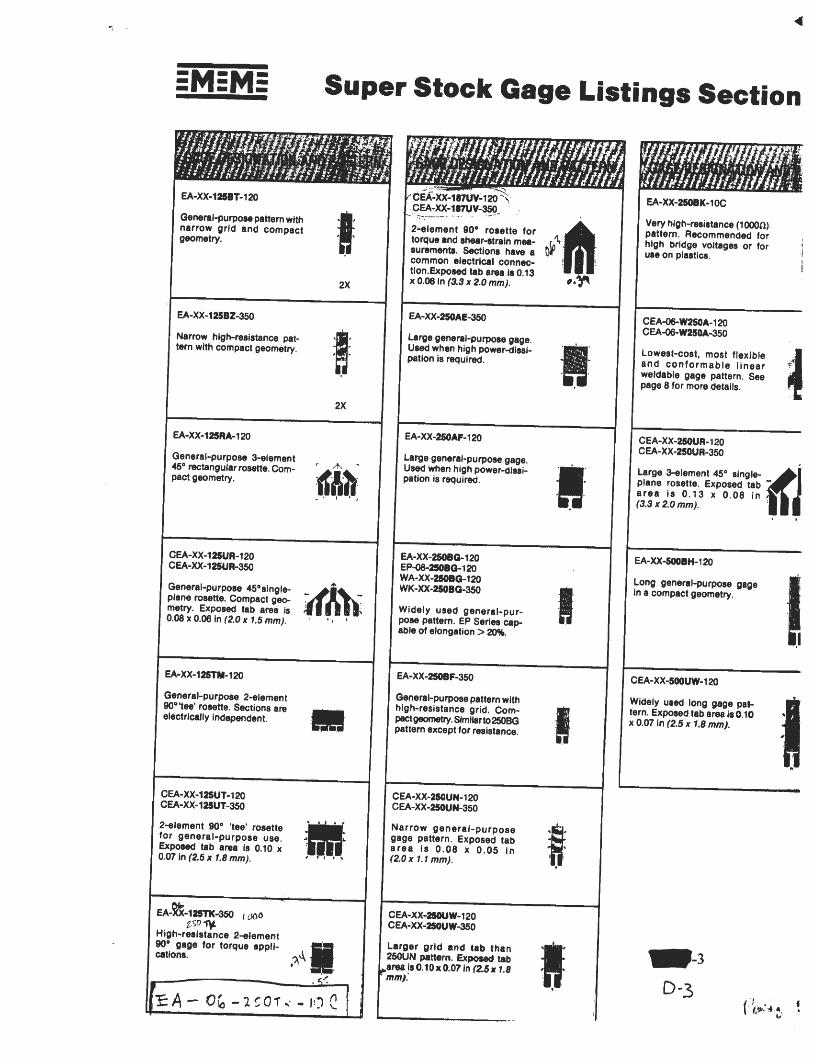
Appendix D - EA-06-250TK-10C Strain Gages
Manufactured by Micro MeasurementsP.O. Box 27777
Raleigh, NC 27611(919) 365-3800

2.0 Gage Selection Parameters
2.1 Strain-Sensing Alloys
The principal component which determines the operatingcharacteristics of a straingageis thestrain-sensitive alloyusedinthe foil grid. However, the alloy isnot in every case anindependently selectable parameter. This is because each Micro-Measurements strain gage series (identified by thefirst two, orthree, letters in the alphanumeric gage designation — see diagram on page 11) isdesigned as acomplete system. That systemis comprised ofa particular foil and backing combination, andusually incorporates additional gage construction features (suchasencapsulation, integral leadwires, or solder dots) specific tothe series in question.
Micro-Measurements suppliesa varietyof straingage alloysas follows iwith, fripir rpgpprtivp lpttftr rlesipnationgl:
A: Constantan in self-temperature-compensated form.
Sted umalunttui. • ~~
D: Isoelastic.
K: Nickel-chromium alloy,a modified Karma inself-temperature-compensated form.
2.1.1 Constantan Alloy
Of all modern strain gage alloys, constantan is the oldest,and still the most widely used. This situation reflects the factthat constantan has the best overall combination of propertiesneeded for many strain gage applications. This alloy has, forexample, an adequately high strain sensitivity, or gage factor,which is relatively insensitive to strain level and temperature.Its resistivity is high enoughto achieve suitable resistance values in even very small grids, and its temperature coefficient ofresistance is not excessive. In addition, constantan is characterizedbygoodfatigue lifeandrelatively highelongation capability. It mustbe noted, however, thatconstantan tends toexhibitacontinuous drift at temperatures above +150°F (+65°C); andthis characteristic should be taken into account when zero stability of thestraingageiscritical overa period of hours or days.
Very importantly, constantan can be processed for self-temperature compensation (see box at right) to match a v/iderange of test material expansion coefficients. Micro-Measurements A alloy is a self-temperature-compensated form of constantan. A alloy is supplied in self-temperature-compensation(S-T-C) numbers 00, 03, 05. 06, 09, 13. 15. 18. 30,40 and 50,for use on test materials with corresponding thermal expansioncoefficients(expressedin ppm/cF).
For the measurement of very large strains, 5% (50 000/ie) orabove, annealed constantan (P alloy) is the grid material normally selected. Constantan in this form is very ductile; and. ingage lengths of 0.125 in (3 mm) and longer, can be strained to>20%. It should be borne in mind, however, that under highcyclic strains the P alloy will exhibit some permanent resistancechangewitheach cycle, and cause a corresponding zero shift inthe strain gage. Because of this characteristic,and the tendencyfor prematuregrid failure with repeated straining,P alloy is notordinarily recommended for cyclic strain applications. P alloyis available with S-T-C numbers of 08 and 40 for use on metals
and plastics, respectively.
2.1.2 Isoelastic Alloy
When purely dynamic strain measurements are to be made— that is, whenit is not necessaryto maintaina stablereferencezero— isoelastic (D alloy) offers certain advantages. Principalamong these are superior fatigue life, compared toAalloy, anda high gage factor (approximately 3.2) which improves the signal-to-noise ratio in dynamic testing.
Self-Temperature Compensation
An important property shared by constantan andmodified Karma strain gage alloys is their responsiveness to specialprocessing for self-temperature compensation. Self-temperature-compensated strain gages aredesigned to produce minimum thermal output(temperature-inducedapparent strain) over the temperature rangefrom about -50° to +400°F (-45° to +200°C). Whenselecting either constantan (A-alloy) or modified Karma(K-alloy) strain gages, the self-temperature-compensation (S-T-C)number must be specified. The S-T-Cnumber is the approximate thermal expansion coefficient inppm/°F of the structural material on which the straingage willdisplay minimum thermal output.
The accompanying graph illustrates typical thermaloutput characteristics for A and K alloys. The thermaloutput of uncompensated isoelastic alloy is included inthesamegraphforcomparison purposes. In normalpractice, the S-T-C number for an A- or K-alloy gage isselected to most closely match the thermal expansioncoefficient of the test material. However, the thermaloutput curves for these alloys can be rotated about theroom-temperature reference point to favor a particulartemperature range. This is done by intentionally mismatching the S-T-C number and the expansion coefficient in the appropriate direction. When the selectedS-T-C number is lower than the expansion coefficient,the curve is rotated counterclockwise. An opposite mismatch produces clockwise rotation of the thermal outputcurve. Under conditions of S-T-C mismatch, the thermaloutput curves for A and K alloys (supplied with eachpackage of strain gages) do not apply, of course, and itwill generally be necessary to calibrate the installationfor thermal output as a function of temperature.
For additional information on strain gage temperatureeffects, see Measurements Group Tech Note TN-504.
vu +500-50
-100
TEMPERATURE in *C
0 ♦» +1,00 »1g +2,00
0 +100 +200 +300
TEMPERATURE IN°F
-^ +500
— 2 — D-(

f
suringstrains in a concrete structure it is ordinarilydesirable touse a straingage of sufficientgage lengthto span severalpiecesof aggregate in order to measure the representative strainin thestructure. In other words, it is usually the average strain that issought in such instances, not the severe local fluctuations instrain occurring at the interfaces between the aggregate particles and the cement. In general, when measuring strains onstructures made of composite materials of any kind, the gagelength should normally be largewith respect to the dimensionsof the inhomogeneities in the material.
As a generally applicable guide,whenthe foregoing considerations do not dictate otherwise, gage lengths in the range from0.125 to 0.25 in (3 to6 mm) are preferable. The largest selectionof gage patterns and stock gages is available in this range oflengths. Furthermore, larger or smaller sizes generally costmore, and larger gages do not noticeably improve fatigue life,stability, or elongation, while shorter gages are usually inferiorin these characteristics.
2.5 Gage Pattern
The gage pattern refers cumulativelyto the shapeof the grid,the number and orientation of the grids in a multiple-grid gage,the solder tab configuration, and various construction featureswhich are standard for a particular pattern. All details of thegrid and solder tab configurations are illustrated in the "GagePattern" columns of Catalog 500. The wide variety of patternsin the list is designed to satisfy the full range of normal gageinstallation and strain measurement requirements.
With single-grid gages, pattern suitability for a particularapplication depends primarily on the following:
Solder tabs — These should, of course, be compatible in sizeand orientation with the space available at the gage installation site. It is also important that the tab arrangement be suchas to not excessively tax the proficiency of the installer inmaking proper lead wire connections.
Grid width — When severe strain gradients perpendicular tothe gage axis exist in the test specimen surface, a narrow gridwill minimize the averaging error. Wider grids, when available and suitable to the installation site, will improve theheat dissipation and enhance gage stability — particularlywhen the gage is to be installed on a material or specimenwith poor heat transfer properties.
Gage resistance — In certain instances, the only differencebetween two gage patterns available in the same series is thegrid resistance — typically 120 ohms vs. 350 ohms. Whenthe choice exists, the higher-resistance gage is preferable inthat it reduces the heat generation rate by a factor of three(for the same applied voltage across the gage). Higher gageresistance also has the advantage of decreasing leadwireeffects such as circuit desensitization due to leadwire resis
tance, and unwanted signal variations caused by leadwireresistance changes with temperature fluctuations. Similarly,when the gage circuit includes switches, slip rings, or othersources of random resistance change, the signal-to-noiseratio is improved with higher resistance gages operating atthe same power level.
In experimental stress analysis, a single-grid gage wouldnormally be used only when the stress state at the point of measurement is known to be uniaxial and the directions of the principal axes are known with reasonable accuracy (±5°).
— 7
These requirements severely limit the meaningful applicability of single-grid strain gages in stress analysis; and failure toconsider biaxiality of the stress state can lead to large errors inthe stress magnitude inferred from measurements made with asingle-grid gage.
For a biaxial stress state — a com
mon case necessitating strain measurement — a two- or three-element
rosette is required in order to determine the principal stresses. When thedirections of the principal axes areknown in advance, a two-element 90-degree (or "tee") rosette can beemployed with the gage axes aligned to coincide with the principal axes. The directions of the principal axes can sometimesbe determined with sufficient accuracy from one of several considerations. For example, the shape of the test object and themode of loading may be such that the directions of the principalaxes are obvious from the symmetry of the situation, as in acylindrical pressure vessel. The principal axes can also bedefined by testing with photoelasticcoatings.
In the most general case of surface stresses, when the directionsof the principal axes are not knownfrom other considerations, a three-
element rosette must be used to
obtain the principal stress magnitudes. The rosette can be installed
with any orientation, but is usuallymounted so that one of the grids isaligned with some significant axisof the test object. Three-elementrosettes are available in both 45-
degree rectangular and 60-degreedelta configurations. The usualchoice is the rectangular rosettesince the data-reduction task is
somewhat simpler for this configuration.
When a rosette is to be employed,careful consideration should alwaysbe given to the difference in characteristics between single-plane andstacked rosettes. For any given gagelength, the single-plane rosette issuperior to the stacked rosette in termsof heat transfer to the test specimen,generallyproviding better stabilityand accuracyfor staticstrainmeasurements. Furthermore, when there is a significant straingradient perpendicular to the test surface (as in bending), thesingle-plane rosette will produce more accurate strain databecause all grids are as close as possible to the test surface. Stillanother consideration is that stacked rosettes are generally lessconformable to contoured surfaces than single-plane rosettes.
On the other hand, when there are large strain gradients inthe planeof the test surface,as is often the case, the single-planerosette can produce errors in strain indication because the gridssample the strain at different points. For these applications thestacked rosette is ordinarily preferable. The stacked rosette isalso advantageous when the space for mounting the rosette islimited.
L ' I * J
45-degree rosette
»
60-degree rosette
1ST
=M=M= Super Stock Gage
EA-XX-128BT-120
General-purpose patternwithnarrow grid and compactgeometry.
EA-XX-125BZ-350
Narrow high-resistance pattern with compact geometry.
EA-XX-125RA-120
General-purpose 3-element45° rectangular rosette. Compact geometry.
CEA-XX-125UR-120CEA-XX-125UH-350
General-purpose 45°single-planerosette. Compactgeometry. Exposed tab area is0.08 x 0.06 in(2.0x 1.5 mm).
EA-XX-125TM-120
General-purpose 2-element90°'tee' rosette. Sections areelectrically independent.
CEA-XX-125UT-120CEA-XX-125UT-350
2-element 90° 'tee' rosettetor general-purpose use.Exposed tab area is 0.10 x0.07 in (2.5 x 1.8mm).
EA-XX-12STK-350 iooO
High-resistance 2-element90s gage for torque applications.
R
2X
2X
m
p/\- 04 -ggOTvioG
2-element 90° rosette fortorque and shear-strain measurements. Sections have acommon electrical connec-tion.Exposed tab area is 0.13x 0.08 in (3.3 x 2.0 mm).
EA-XX-250AE-350
Large general-purpose gage.Used when high power-dissipation is required.
EA-XX-250AF-120
Large general-purpose gage.Used when high power-dissipation is required.
EA-XX-250BG-120EP-08-250BG-120WA-XX-250BG-120WK-XX-250BG-350
Widely used general-purpose pattern. EP Series capable of elongation > 20%.
EA-XX-2SOBF-350
General-purposepatternwithhigh-resistance grid. Compact geometry. Similarto250BGpattern except for resistance.
CEA-XX-280UN-120CEA-XX-250UN-350
Narrow general-purposegage pattern. Exposed tabarea is 0.08 x 0.05 In(2.0x1.1 mm).
Or1 In
n
CEA-XX-250UW-120CEA-XX-2SOUW-350
Larger grid and tab than250UN pattern. Exposed tab
*area is0.10 x 0.07 In(2.5m1.8rmm>: i
Section
Very high-resistance(1000O)pattern. Recommended forhigh bridge voltages or foruse on plastics.
CEA-06-W250A-120CEA-06-W250A-350
Lowest-cost, most flexibleand conformable linearweldable gage pattern. Seepage 8 for more details. \
CEA-XX-250UR-120CEA-XX-250UR-350
Large 3-element 45° single-plane rosette. Exposed tabarea is 0.13 x 0.08 in(3.3x2.0 mm). aEA-XX-500BH-120
Long general-purpose gagein a compact geometry.
CEA-XX-500UW-120
Widely used long gage pattern. Exposed tab area is 0.10x 0.07 in (2.5 x 1.8mm).
D-3
!
I

l>J
m
WA
r
EP
ED
wri
SD
EK
WK
SK
S2K
Standard Strain Gage Series Selection Chart
Constantan foil in combination with a tough, flexible,polyimide backing. Wide range of options available.Primarily intended for general-purpose static anddynamic stress analysis*Not recommended for highestaccuracy transducers.
Ivtrsak general-purpose strain .gages. Constantanw<grKJ completely encapsulated in polyimide, with large.iruggeti copper-coated tabs. Primarily used for general-purpose static and dynamicstress analysis. 'C'-Feature.gag^sate specials highlighted throughout the gage list-
^Gatfllqg^ >|V f nm: ,ir »Open-faced constantan foilgages with a thin, laminated,polyimide-film backing. Primarily recommended for usein precision transducers, the N2A Series is characterized by low and repeatable creep performance. Alsorecommended for stress analysis applications employing large gage patterns, where the especially flat matrixeases gage installation.
Fully encapsulated constantan gages with high-endurance leadwires. Useful over wider temperatureranges and in more extreme environments than EASeries. Option W available on some patterns, butrestricts fatigue life to some extent.
Fully encapsulated constantan gages with solder dots.Same matrix as WA Series. Same uses as WA Series
but derated somewhat in maximum temperature andoperating environment because of solder dots.
Specially annealed constantan foil wi:h tough, high-elongation polyimide backing. Used primarily for measurements of large post-yield strains. Available withOptions E, L, and LE (may restrict elongation capability).
Isoelastic foil in combination with tough, flexible polyimide film. High gage factor and extended fatigue lifeexcellent for dynamic measurements. Not normally usedin static measurements due to very high thermal-outputcharacteristics.
Fully encapsulated isoelastic gages with high-endurance leadwires. Used in wide-range dynamic strainmeasurement applications in severe environments.
Equivalent to WD Series, but with solder dots instead ofleadwires.
K-alloy foil in combination with a tough, flexible polyimide backing. Primarily used where a combination ofhigher grid resistances, stability at elevated temperature, and greatest backing flexibility are required.
Fully encapsulated K-alloy gages with high-enduranceleadwires. Widest temperature range and most extremeenvironmental capability of any general-purpose gagewhen self-temperature compensation is required.Option W available on some patterns, but restricts bothfatigue lifeand maximum operating temperature.
Fully encapsulated K-alloy gages with solder dots.Same uses as WK Series, but derated in maximum temperature and operating environment because of solderdots.
K-alloy foil laminated to 0.001 in (0.025 mm) thick,high-performance polyimide backing, with a laminated polyimide overlay fully encapsulating the grid and soldertabs. Provided with large solder pads for ease of lead-wire attachment.
Normal:-100° to+350°F
(-75° to+175°C)Special or Short-Term:
-320° to +400°F
(-195° to +205°C)
Normal:-100° to+350*F(-75°to+175°C)
Stacked rosettes limited to+150°F (+65°C)
Normal StaticTransducer Service:
-100° to+200° F
(-75° to +95°C)
Normal:-100° to+400°F
(-75° to +205°C)Special or Short-Term:
-320° to +500CF(-195° to +260°C)
Normal:-100° to+400°F
(-75° to +205°C)Special or Short-Term:
-320= to +450°F (-195° to +230CC)
-100°to+400°F
(-75° to +205°C)
Dynamic:-320° to +400°F
(-195° to +205°C)
Dynamic:-320° to +500°F
(-195° to +260°C)
Dynamic:-320° to +400°F(-195° to +205°C)
Normal: -320° to +350°F(-195° to+175°C)
Special or Short-Term:-452° to +400°F (-269° to +205°C)
Normal: -452° to +550°F
(-269° to +290°C)Special or Short-Term:
-452° to +750°F
(-269° to +400° C)
Normal: -452° to +450°F
(-269° to +230° C)Special or Short-Term:
-452c to +500°F (-269° to +260°C)
Normal:-100° to+250°F
(-75° to+120°C)Special or Short-Term:
-300° to +300°F
(-185° to+150°C)
±3% for gagelengths under
1/8 in (3.2 mm)±5% for 1/8 in
and over
£3% for gage*lengthsunder•
1/8 in f£2*vn>±5% fori/8 in r
and ova? i **&
±3%
±2%
±2%
±10% for gagelengths under
1/8 in (3.2 mm)±20% for 1/8 in
and over
±2%
Nonlinear at
strain levels
over ±0.5%
±1.5% — non
linear at strain
levels over ±0.5%
±1.5%
See above note
±1.5%
±1.5%
±1.5%
±1.5%
The performance datagiven here are nominal, andapply primarily togagesof0.125-in (3-mm) gage length or larger.
_4 —
±1800
±1500
±1200
±1500
±1500
'T T'
Fatigue life improvedusing lowrmgdM,Jul ^> <yfc fc J.& i..
±1700
±1500
±2000
±1800
±1500
±1800
±1500
±1000
10D106108
.106
10s107
10=10e107
10c107
10"
EP gages show zero shiftunder high-cyclic strains.
±2500
±2200
±3000
±2500
±2200
±2500
±2200
±1800
±2400
±2200
±2000
±2200
±2000
±1800
±1500
10c107
10'
107108
10c107
10'
10°107108
10s107
10
107
D-M

Appendix £ - ADM666 Voltage Regulator
Manufactured by Analog Devices1 Technology Way
P.O. Box 9106
Norwood, MA 02062(800) 262-5643

ANALOGDEVICES
+5 VFixed, AdjustableMicropower Linear Voltage Regulators
FEATURES
5 V Fixed or +1.3 V to +16V AdjustableLow Power CMOS: 12 uA max Quiescent Current40 mA Output CurrentCurrent LimitingPin Compatible with MAX663/666+2 V to +16.5 V Operating RangeLow Battery Detector A0M666No Overshoot on Power-Up
APPLICATIONS
Handheld Instruments
LCD Display SystemsPagersRemote Data Acquisition
GENERAL DESCRIPTION
The ADM663/ADM666 are precision voltage regulators featuring a maximum quiescent current of 12 uA. They can be used togive a fixed +5 V output with no additional external components or can be adjusted from 1.3 V to 16 V using two externalresistors. Fixed or adjustable operation is automatically selectedvia the Vset Input. The low quiescent current makes these devicesespecially suitable for battery powered systems. The inputvoltage range is 2 V to 16.5 V and an output current up to40 mA is provided. The ADM663 can directly drive an externalpass transistor for currents in excessof 40 mA. Additional features include current limiting and low power shutdown. Thermal shutdown circuitry is also included for additional safety.
The ADM666 features additional low battery monitoringcircuitry to detect for low battery voltages.
The ADM663/ADM666 are pin-compatible replacements forthe MAX663/666. Both are available in 8-pin DIP and in narrow surface mount (SOIC) packages.
ORDERING GUIDE
Model Temperature Range Package Option
ADM663AN
ADM663AR
ADM666ANADM666AR
-40°C to +85°C
-40°C to +85°C
-40°C to +85°C
-40°C to +85°C
N-8
R-8
N-8
R-8
REV.O
Information furnished by Analog Devices is believed to be accurate andreliable. However, no responsibility is assumed by Analog Devices for itsuse, nor for any infringements of patents or other rights of third partieswhich may result from its use. No license is granted by implication orotherwise under any patent or patent rights of Analog Devices.
WON
OND
8HDN
OND
ADM663/ADM666FUNCTIONAL BLOCK DIAGRAMS
Yf
JT
ADM663
^=HVOUT2
voun
6 SENSE
LBO
One Technology Way, P.O. Box 9106, Norwood. MATel: 617/329-4700
2-9106, U.S.A.617/326-8703

ADM663/ADM666-SPECIFICATI0NS(v• = +9Vf Vout = +5V,TA =+25°C unless othemrise noted)
Parameter
Input Voltage, VrjvjQuiescent Current, Iq
Output Voltage, V0tjtLine Regulation, AVquj/AVumLoad Regulation, AVout/AIout
ReferenceVoltage, VSetReference Tempco, AVSet/ATVSET Internal Threshold, VF/A
Vset Input Current, IsetShutdown Input Voltage, VSHdn
Shutdown Input Current, IshdnSENSE Input Threshold, Vout-VSenseSENSE Input Resistance, RsenseInput-Output Saturation Resistance, Rsat
ADM663 Vouti
OutputCurrentfrom VOUT(2), lourMinimum LoadCurrent, IL (mem)
LBI Input Threshold, VlbiLBI Input Current, IlbiLBO Output Saturation Resistance, R^tLBO Output Leakage CurrentVTC Open Circuit Voltage, VjcVTC Sink Current, l-pcVxc Temperature Coefficient
Min
2.0
4.75
1.27
1.4
40
1.21
2.0
Typ Max Units
16.5
6 12 MA15 ma
5.0 5.25 V
0.03 0.35 %/v
3.0 7.0 Q
1.0 5.0 Q
3.0 7.0 a
1.33 V
±100 ppm/°C50 mV
±0.01 ±10 nA
V
0.3 V
±0.01 ±10 nA
0.5 V
3 MG
200 500 Q
70 150 Q
50 150 a
mA
1.0 MA5.0 pA
1.28 1.37 V
±0.01 ±10 nA
35 100 Q
10 nA
0.9 V
8.0 mA
+2.5 mV/°C
Test Conditions/Comments
Ta = Tmin to TmaxNo Load, Vin =+16.5 VTA = +25°CTa = Tmin to TmaxTa = Tmin to Tmax. Vset - GND+2V<VTN<+15V,Volrr = VREFADM663, 1 mA <, I0ur2 < 20 mAADM663, 50 pA <, Iouri £ 5 mAADM666, 1 mA < I0ur £ 20 mAVqut = VsetTa = Tmtn to TmaxVset < VF/a for +5 V Out;Vset > Vf/a for Adj. OutTa = Tmin to TmaxVshdn High = Output OffVshdn Low = Output On
Current Limit Threshold
Vtn = +2 V, Iout • 1 mAVrN = +9V,I0uT=2mAVrjsj = +15 V, lour = 5 mA+3 V < VrN ^ +16.5 V, V^-Vour = +1.5 VTA - +25°CTa = Tmin to TmaxADM666
ADM666
ADM666, Isat - 2 mAADM666, LBI = 1.4 V
ADM663
ADM663
ADM663
Specifications subject to changewithout notice.
ABSOLUTE MAXIMUM RATINGS*
(T/v= +25°C unless otherwise noted)
Input Voltage, V^ +18 VTerminal Voltage
(ADM663) Pins 1,3, 5,6, 7(GND - 0.3 V) to (VrN + 0.3 V)
(ADM666)Pinsl,2,3, 5,6(GND - 0.3 V) to (VrN + 0.3 V)
(ADM663) Pin 2 (GND - 0.3 V) to (Vquti + 0.3 V)(ADM666) Pin 7 (GND - 0.3 V) to +16.5V
Output Source Current(ADM663, ADM666) Pin 2 50 mA(ADM663) Pin 3 25 mA
Output Sink Current,(ADM663, ADM666) Pin 7 -20 mA
Power Dissipation, N-8 625 mW(Derate 8.3 mW/°C above +50°C)0JA, Thermal Impedance 120°CA/V
Power Dissipation R-8 450 mW(Derate 6 mW/°C above +50°C)8jA, Thermal Impedance 170°C/W
Operating Temperature RangeIndustrial (A Version) -40°C to +85°CStorage Temperature Range -65°C to +150°C
Lead Temperature (Soldering, 10 sec) +300°CVapor Phase (60 sec) +215°CInfrared (15 sec) +220°C
ESD Rating >5000 V
"This is a stressratingonlyand functional operationof the device at theseor anyother conditions above those indicated in the operation sections of this specification is not implied. Exposuretoabsolute maximumratingconditionsforextendedperiods of time may affect reliability.
E-2

DIP & SOIC PIN CONFIGURATIONS
VoOTl H
Voun [IOND (T
ADM663
TOP VIEW
(NottoScata)
I]vmI]Vtc
T] WON
SENSE JT
VOUT E
OND (T
ADM666
TOP VIEW
(Net to Seal*)
13 Vm7] LBO
IJV«TT\ SHDN
GENERAL INFORMATION
The ADM663/ADM666 contains a micropower bandgap reference voltagesource, an error amplifierAl, two comparatorsCI, C2 and a seriespass output transistor. A P-channel FETand an NPN transistor are used on the ADM663 while theADM666 usesan NPN output transistor.
CIRCUIT DESCRIPTION
The internal bandgap reference is trimmed to 1.3 V± 30 mV.This isused as a reference input to the erroramplifier Al. Thefeedback signal from the regulator output is supplied to theother input byan on-chipvoltagedivider or by two external resistors. When Vsetisat ground, the internal divider providesthe error amplifier'sfeedback signalgiving a +5 V output. WhenVset Is at more than 50 mV above ground, the erroramplifier'sinput is switched directly to the VSet P'n, and external resistorsare used to set the output voltage. The external resistors areselectedso that the desired output voltagegives 1.3 V at V^t-
Comparator CI monitors the output current via the SENSEinput. This input, referenced to VoUT(2), monitors the voltagedrop acrossa load sense resistor. If the voltagedrop exceeds0.5V, then theerror amplifier Aj isdisabled and the outputcurrent is limited.
The ADM663 hasan additional amplifier, A2, which provides atemperature-proportional output, VTC. If this is summed intothe inverting input of the error amplifier, a negative temperaturecoefficient results at the output. This is usefulwhen poweringliquid crystal displays over wide temperature ranges.
The ADM666 has an additional comparator, C3 which compares the voltageon the Low Battery Input, LBI, pin to the internal +1.3 V reference. The output from the comparator drives
ADM663/ADM666
PIN FUNCTION DESCRIPTION
Mnemonic Function
VoUT(l) (2) Voltage Regulator Output (s)
Vfn Voltage Regulator InputSENSE Current Limit Sense Input. (Referenced to
Vout(2).) If not used it should be connectedtoVoUT(2)
GND Ground Pin. Must be connected to 0 V
LBI Low Battery Detect Input. Compared with 1.3 VLBO Low Battery Detect Output. Open Drain OutputSHDN Digital Input. May be used to disable the device
so that the power consumption is minimized
Vset VoltageSetting Input. Connect to GND for +5 Voutput or connect to resistive divider for adjustable output
vTC Temperature-Proportional Voltage for negativeTC Output
an open drain FET connected to the Low BatteryOutput pin,LBO. The Low Battery Threshold may be set using a suitablevoltagedivider connected to LBI. When the voltageon LBI fallsbelow 1.3 V, the open drain output LBO is pulled low.
Both the ADM663 and the ADM666 contain a shutdown(SHDN) input whichcan be used to disable the error amplifierand hence the voltage output. The quiescent current in shutdown is less than 12 uA.
6 SENS!
SHDN
OND
Figure 1. ADM663 Functional Block Diagram
E-3

ADM663/ADM666
SHDN
OND
Figure 2. ADM666 Functional Block Diagram
Circuit ConfigurationsFor a fixed +5 V output the Vset input is grounded and no external resistors are necessary. This basic configuration is shownin Figure 3. Current limiting is not being utilized so the SENSEinput is connected to V0ut(2)- The input voltage can range from+6 V to +16 V and output currents up to 40 mA are availableprovided that the maximum package power dissipation is notexceeded.
•MJVTO+WVINPUT
Vm SENSE
ADM6G3
ADM666 VouT(2)
OND Vlr SHDN
±
1*HV
OUTPUT
Figure 3. ADM663/ADM666 Fixed +5 VOutput
Output Voltage SettingIf VSet Isnot connected to GND, the output voltage is set according to the following equation.
Vnrrr = VOUT SET
RI + R2
mwhere VSET = 1.30 V
The resistor values may be selected by firstly choosing avalue for Rl and then selecting R2 according to the followingequation.
R2=R\xV ^IOUT 11.30
The input leakage current on VSet is 10 nA maximum. This allows large resistor values to be chosen for Rl and R2 with littledegradation in accuracy. For example, a 1 MQ resistormaybeselected for Rl and then R2 maybe calculated accordingly.The tolerance on VSetis guaranteed at less than ±30 mVso inmost applications, fixed resistors will be suitable.
+WTO-M6V
INPUT ADM663
ADM666
SHDN
OND
T
SENSE
'OUT?)
•MJ»VTO*1«VOUTPUT
Figure 4. ADM663/ADM666 Adjustable Output
Current LimitingCurrent limiting may be achieved by using an external currentsenseresistor in series with V0jjt(2)- When the voltage acrossthe sense resistor exceeds the internal 0.5 V threshold, currentlimiting is activated. The sense resistor Is therefore chosen suchthat the voltageacross it will be 0.5 V when the desired currentlimit is reached.
Rcl ~0.5
lCL
where Rcl is the current sense resistor, Icl is the maximumcurrent limit.
The value chosen for Rcl should also ensure that the current islimited to less than the 50 mA absolute maximum rating andalso that the power dissipation will also be within the packagemaximum ratings.
If current limiting is employed, there will be an additional voltage drop across the sense resistor which must be consideredwhen determining the regulators dropout voltage.
If current limiting is not used, the SENSE input should be connected to V0UT(2)-
Shutdown Input (SHDN)The SHDN input allows the regulator to be switched off with alogic level signal. Tills will disable the output and reduce thecurrent drain to a low quiescent (12 uA maximum) current.This is very useful for low power applications. The SHDN inputshould be driven with a CMOS logic level signal since the inputthreshold is 0.3 V. In TTL systems, an open collector driverwith a pull-up resistor may be used.
If the shutdown function is not being used, then SHDN shouldbe connected to GND.
Low Supply or Low Battery DetectionThe ADM666containson-chip circuitry for lowpowersupplyor battery detection. If the voltage on the LBI pin falls below theInternal 1.3 V reference, then the open drain output LBO willgo low. The lowthreshold voltage may be set to any voltageabove 1.3 V by appropriate resistor divider selection.
where R3 and R4 are the resistive divider resistors and Vbatt isthe desired low voltage threshold.
E-4

Since the LBI input leakage current is less than 10 nA, large values may be selected for R3 and R4 in order to minimize loading.For example, a 6 V low threshold, maybe set using 10 Mfl forR3 and 2.7 MQ for R4.
•MJVTO+HV
OUTPUT
BATTERY T?OUTPUT
Figure 5. ADM666 Adjustable Output with Low BatteryDetection
High Current OperationThe ADM663 contains an additional output, Vouti. suitablefor directly driving the base of an external NPN transistor. Figure 6 shows a configuration which can be used to provide +5 Vwith boosted current drive. A 1 li current sensing resistor limitsthe current at 0.5 A.
•*-t
+
SHUTDOWN
votm
ADM663 Vou"
SHDN
VSET OND SENSE
±
2»4237
ioon
1.0a
+ | *fv,a', 0.SA
IOjiP ^ OUTPUT
Figure 6. ADM663 Boosted Output Current (0.5 A)
Temperature Proportional OutputThe ADM663 contains a Vtc output with a positive temperature coefficient of +2.5 mV/°C. This may be connected to thesummingjunction of the error amplifier (VSet) through a resistor resulting in a negative temperature coefficient at the outputof the regulator.
This is especially useful in multiplexed LCD displays to compensate for the inherent negative temperature coefficient of theLCD threshold. At 25°Cthe voltage at the VTC output is typically 0.9 V. The equations for setting both the output voltageand the tempco are given below. If this function is not beingused, then VTC should be left unconnected.
A0M663/ADM666
-Ov0
Figure 7. ADM663 TemperatureProportional Output
V0UT =VsETx(l +jfj+J5x(VSET-VTc)-Rl
TCV, xTVCjOUT 7?jr V^TC
where VSET = +1.3 V, V^ - +0.9 V, TCV'rc= +2.5 mVI°C
APPLICATION HINTS
Input-Output (Dropout Voltage)A regulator's minimum input-output differential or dropoutvoltage determines the lowest input voltage for a particular output voltage. The ADM663/ADM666 dropout voltage is 0.8 V atits rated output current. For example when used as a fixed +5 Vregulator the minimum input voltage is +5.8 V. At loweroutputcurrents, (lour < 5 mA), on the ADM663, Vouti may be usedas the output driver in order to achieve lower dropout voltages.Please refer to Figure 9. In this case the dropout voltage depends on the voltage drop across the Internal FET transistor.This may be calculated by multiplying the FET's saturation resistance by the output current. As the current limit circuitry isreferenced to Vout2. Vout2 should be connected to Vouti- Forhigh current operation VQut2 should be used alone and Vqutileft unconnected.
Bypass CapacitorsThe high frequency performance of the ADM663/ADM666may be improved by decoupling the output using a filter capacitor. A capacitor value of 10 pF is suitable.
An input capacitor helps reduce noise and improves dynamicperformance. A suitable input capacitor of 0.1 pF or greatermay be used.
E-5

ADM663/ADM666-Typical Performance Characteristics
at
K 40
20
! 1 III 1VINDC«+SV
v,«i»i»-«v
VouTDC-^fV•-T I"
0.01 0.1 1 10 wo
FREQUENCY-Hz
1000 10000
Figure 8. Power Supply Rejection Ratio vs. Frequency
2.0
i.«
S M
I 03
*«,04
M
00 2 4 « 8 10 12 14 16 18 20
Figure 9. Vouti Input-OutputDifferential vs. OutputCurrent
v«« ♦2V T, L-+2I °c
v, • •*•
1«V
12
Ta-I♦arc
VOOT" ♦sv
_^—•""' I...
VOOT" ♦3.3V
10
2 4 6 S 10 12 14 16
V„,-VWto
Figure 10. Quiescent Current vs. Input Voltage
13
03
0.8
0.7
I
1 OJ
fid*03
0.2
0.1
0
1
TA»4«S°C
v«-«v
^?^vm-*i«vv,«-^v
10 20 SO
louTj-mA
40 60
Figure 11. Voutw Input-Output Differential vs. OutputCurrent
OUTLINE DIMENSIONS
Dimensions shown in inches and (mm).
8 Lead Plastic DIP
(N-8)
l.1W(4.N)'0.115(2.93),
-••m*. u »i0.022(0.551) 0.100 0.070
OS*)BSC
0.014(0.356) 0.045(1.15)
VSIATWOPLANE
8 Lead Narrow-Body(R-8)
nnnn
1.1574(4.00)
MM
\ I0.1407(3.00)
0.2204(6.00)i 0.2440(0.
0.2284(5.
0.0000(0.25) j^0.0040(0.10) T~j
FrJO0.1000 (5.00) I . . 0.0100(0.50)
•^0.1000(4.00) J | -1 P-0.00H(0.25)• • •• 5 0.102(2.50) , _T \_
q k *n* t -nL^ *i0.0600 >3N£JM6j 0,0000(0.25) ° "*(1JT) 0.0130(0.35) 6.0075(0.10) °"
0.0500(1.27)
0.01 (S (0.41)
E-6

ORDERING GUIDE
Model Temperature Range Package Option4'
ADM663AN
ADM663AR
ADM666AN
ADM666AR
-40°C to +85°C
-40°C to +85°C
-40°C to +85°C
-40°C to +85°C
N-8
R-8
N-8
R-8
*For outline information see Package Information section.
FOR CATALOG
ADM663/ADM666 ADM663/ADM666
ADM663/ADM666 ADM663/ADM666
ADM663/ADM666
E-7

Appendix F - AMP04 Instrumentation Amplifier
Manufactured by Analog Devices1 Technology Way
P.O. Box 9106
Norwood, MA 02062
(800) 262-5643

• ANALOGDEVICES
FEATURES
Single Supply OperationLow Supply Current: 700 |iA maxWide Gain Range: 1 to 1000Low Offset Voltage: 150 jiV maxZero-In/Zero-Out
Single-Resistor Gain Set8-pin Mini DIP and SO packages
APPLICATIONS
Strain GagesThermocouplesRTDs
Battery Powered EquipmentMedical Instrumentation
Data Acquisition SystemsPC Based Instruments
Portable Instrumentation
GENERAL DESCRIPTION
TheAMP-04 is a single-supply instrumentation amplifierdesigned to work over a +5 voir to *15 volt supply range. Itoffers an excellent combination ofaccuracy, low power consumption, wide input voltage range, and excellent gainperformance.
Gain is set by a single external resistor and can be from 1 to1000. Input common-mode voltage range allows the AMP-04 tohandle signals with full accuracy from ground to within 1 volt ofthe positive supply. And the output can swing to within 1 voltofthe positive supply. Gain bandwidth is over 700 kHz. Inaddition to being easy to use, the AMP-04 draws only 700 yJi ofsupply current.
For high resolution data acquisition systems, laser trimming oflow drift thin-film resistors limits the inpui offset voltage tounder 150 u.V, and allows the AMP-04 to offer gain noniinearityof 0.005% anda gain ternpeo of30ppm/°C. '
A proprietary input structure limits input offset currents to lessthan 5 nA with drift ofonly 8 pA/°C, allowing direct connectionof the AMP-04 to high impedance transducers and other signalsources.
'Protected by U.S. Patent No: 5,075.633.
REV.O
'OUSTS!! fumished bY Ana,°9 Devices is believed to be accurate andreliable. However no respons.bility is assumed bv Analog Devices for itsuee. nor tor 8nv infringements of patents or other rignw.of thinI oanie"which may resuit from ,ts use. No .icense .s gr^teo byTrnp SSon o'rothcrwrse unoor any catent oroaxem rights ofAn8,og Dev.ces
Precision Single SupplyInstrumentation Amplifier
AMP-04:FUNCTIONAL BLOCK DIAGRAM
INPUT .BUFFERS
The AMP-04 is specified over the extended industrial (-40'C :o+85°Q temperature rmge. AMP-04s are available in plastic andceramic DIPplus SO-8 surface mount packages.Contact your local sales office for MIL-STD-883 data sheci andavailability.
PIN CONNECTIONS
8-Lcad Epoxy DIP(P Suffix)
.IN [7v-E
AMP-04
3VOOTSjHEP
S-Lead Narrow-Body SO(S Suffix)
AMP-04
-'"GA*
—ZJ voutJH6F
F-l
One Technology Way, P.O. Box 9106. Norwood. MA 02062-9108 US aTel: 617/329-4700 F._. K.l,^'S,A
Fax: 617/326-8703
£LZt ~TZ8 iT9© 10:60 96/T0/TTCZO/OTOia xio in iav

AMP-04—SPECIFICATIONSELECTRICAL CHARACTERISTICS «=+5, »tt =+u v. T.
OFFSET VOLTAGEInput Offset Voltage
Input Offset Voltage DriftOutput Offset Voltage
Output Offset Voltage Drift
INPUT CURRENTInput Bias Current
Input Bias Current DriftInput Offset Current
Input Offset Current Drift
INPUT
Common-Mode Input ResistanceDifferential Input ResistanceInput Voltage RangeCommon-Mode Rejection
Common-Mode Rejection
Gain RangeNoniinearity
Gain Temperature Coefficient
OUTPUT
Output Voltage Swing High
Outpur Voltage Swing Low
Output Current Limit
CZO/TTO® hid in iav
= +25°C unless otherwise noted)
ZLZV TZ8 IT9S, 80=60 96/T0/TT

AMP-04
Parameter Symbol Conditions
AMP-04E
I Min Typ MaxAMP-04F
j Min Typ Max Units
NOISE
Noise Voltage Density, RTI
Noise Current Density, RTIInput Noise Voltage
!«nP"P
f = 1 kHz, G = 1f « 1kHz, G - 10f = 100 Hz, G = 100f = 100 Hz, G = 1000f = 100 Hz, G * 1000.1 to 10 Hz, G - 10.1 to 10 Hz, G= 100.1 to 10 Hz, G - 100 |
1270
45
30
25
4
7
1.5
0.7
270
45
30
25
4 1
7
1.5
0.7 |
1
nV/vHz"nV/vHznV/vHznV/vHzpA/vHzu.Vp-pnVp-pM-Vp-p
DYNAMIC RESPONSESmall Signal Bandwidth
— —j-BW G= 1, -3dB , 300 j 300 kHz
POWER SUPPLYSupply Current
1
ISY-40°C s= TA < +85eC j
550 700 !850 |
700 |850 j uA
Specifications subject to change without notice.
ELECTRICAL SPECIFICATIONS (Vs = zt15 V, VCM • 0 V, T, = +25°C unless otherwise noted)
Parameter
OFFSET VOLTAGEInput Offset Voltage
Input Offset Voltage DriftOutput Offset Voltage
Output Offset Voltage Drift
INPUT CURRENTInput Bias Current
Input Bias Current DriftInput Offset Current
Input Offset Current Drift
INPUT
Common-Mode Input ResistanceDifferential-Mode Input ResistanceInput Voltage RangeCommon-Mode Rejection
Power Supply Rejection
CZ0/ZT0®
Symbol I ConditionsAMP-04E
Min Typ Max
'1ST
CMR
CMR
PSRR
"12V<VCM < +12 V |G = 1 1 60 80G = 10 | 80 100G = 100 90 105G - 1000 90 105
1 - s -11 V
—*0DC s TA < + 85°C
G = 1 55
G = 10 75
G = 100 85
I G = 1000 85
j ±2.5 V < Vs s = 18 V
-40°C < TA < +85°C
G- 1 75
! G = 10 90
I G - 100 j 95
1 G = 1000 95
HIo in iav cizr TZS !T9£
AMP-04F |Min Typ Max Units
55
75
80
80
50
70
75
75
70
80
85
35
F-3
+ 12
dB
dB
dB
dB
dB
dB
dB
dB
dB
dB
dB
dB
80=60 96/T0/TT

AMP-04
Parameter Symbol j Conditions Min
AMP-04E
Typ MaxGAIN (G = 100 K/RCAIK)
Gain Equation Accuracy
Gain RangeNoniinearity
Gain Temperature Coefficient j4G/ATOUTPUT I
Output Voltage Swing High VOH
Outpur Voltage Swing Low
Output Current Limit
'or.
NOISE
Noise Voltage Density, RTI cM
Noise Current Density, RTI iNInput Noise Voltage eN p-p
cn P-P
DYNAMIC RESPONSESmall Signal Bandwidth
POWER SUPPLYSupply Current
! CN p-p
SpeciCcaiions subject to change without notice
G = 1 to 100G - 1000
G = 1 to 100
-40"C s TA : •85°C
G = 1, RL - 5 kfiG = 10, RL = 5 kf)G = 100, RL = 5 kfl
+ 13RL = 2kORL = 2kfl-40°C £ TARc = 2kH-40°C s TA as + 85eCSink
Source
f= 1kHz, G = 1f = 1 kHz, G = 10f = 100 Hz, G = 100f= 100 Hz, G = 1000f = 100 Hz, G = 1000.1 to 10 Hz, G = 10.1 to 10 Hz, G = 100.1 to 10 Hz, G = 100
s +85°C +12.5
0.2
0.4
0.005
0.015
0.025
30
13.4
30
15
270
45
30
25
4
5
I
0.5
0.5
0.8
1000
-14.5
^^^^^I^E!^!!!^-♦"*r, =♦« untess ,„_„«,«Parameter
OFFSET VOLTAGEInput Offset VoltageOutput Offset Voltage
INPUT CURRENTInput Bias CurrentInput Offset Current
INPUT
Common-Mode Rejection
Common-Mode Rejection
0 v * vcm =s 3.0 VG= 1
G = 10G = 100G » 1000
VsJ-=15V, -UVsV^s+uvG = 10
G = 100
G *= 1000
AMP-04F
Min Typ Max Units
+ 13
+ 12.5
0.75
0.005
0.015
0.025
50
30
15
270
45
30
25
4
5
1
0.5
0.75
1.0
1000
-14.5
%
%
%
V/V
%
%
%
pprn^C
V
mA
mA
nV/vHznV/vHznV/vHznV/vHzpA/VHzM-Vp-pM-Vp-pM-V p-p
55 dB min75 dB mirr
80 dB min80 dB min
55
75p_jdB min
dB min80 dB minSO dB min
CZ0/CT0® hid in lav £LZl TZ8 IT9© 80-60 96/TO/TT

Parameter
Power Supply Rejection
GAIN (G -= 100 K^oxrKjGain Equation Accuracy
OUTPUT
Output Voltage Swing HighOutput Voltage Swing Low
POWER SUPPLY
Supply Current
NOTE
Electrical tests and wafer probe to the limits shown. Due to variations in assembly methods and normal yield loss, yield after packaging is not guaranteed forstandard product dice. Consult factory to negotiate specifications based on dice lot qualifications through sample lot assembly and tesunB *ABSOLUTE MAXIMUM RATINGS1 'Supply Voltage =:18 VCommon-Mode Input Voltage* 218 VDifferential Input Voltage 36 VOutput Short-Circuit Duration to GND IndefiniteStorage Temperature Range
Z Package _65*c t0 +175oCP, S Package _65»C t0 +I50°C
Operating Temperature RangeAMP-04A -55°C to + 125°CAMP-04E, F _40-c t0 +85cC
Junction Temperature RangeZ Package _65-c I0 +I75oCP, S Package _65°c I0 .150oC
Lead Temperature Range (Soldering, 60 sec) +300°C
Package Type
8-Pin Cerdip (Z)8-Pin Plastic DIP (P)8-Pin SOIC (S)
6 JA
148
103
158
»JC
16
43
43
AMP-04
Conditions
4.0 V ^ Vs < 12 VG= 1
G= 10
G - 100
G= 1000
Limit
85
95
95
95
Units
dB min
dB min
dB min
dB nun
G = 1 to 100 0.75 % max
Rc = 2 kfiRL = 2kfl
4.0
2.5V min
mV max
Vs = ±15 900
700
mA mixjiA max
Units
°C/W
°C/W
°C/W
ORDERING GUIDE
Vos @ +5 V Cerdip Plastic 1 TemperatureTA =5 +25°C 1 8-Pin 8-Pin Range*
AMP04AZ/883 MIL150 u.V AMP04EP XIND300 u-V AMP04FP XIND300 m-V AMP04FS XIND300 m-V AMP04GBC +25CC
"Consult MIL-STD-883 data sheet.
DICE CHARACTERISTICS
NOTES
'Absolute maximum ratings apply to both DICE and packaged pans, unlessotherwise noted.
'For supply voltages less than =18 V, the absolute maximum input voltage isequal to the supply voltage.
'Oja is specified for the worst case conditions, i.e., 9JA is specified for device insocket for cerdip, P-DIP, and LCC packages; 6JA is specified for devicesoldered in circuitboardfor SOIC package.
ceo/ho® hid in iav
v- «
5 REF
AMP-04 Die Size 0.075 x 0.99 inch, 7,425 sq. mils.Substrate (Die Backside) Is Connected to V-h.Transistor Count, 81.
F-5
ZLZt T28 1T9© 60=60 96/T0/TT

AMP-04
APPLICATIONSCommon-Mode RejectionThe purpose of the instrumentation amplifier is to amplify thedifference between the two input signals while ignoring offsetand noise voltages common to both inputs. One way of judgingthe device's ability to reject this offset is the common-modegain, which is the ratio between a change mthe common-modevoltage and the resulting output voltage change. Instrumentationamplifiers are often judged by the common-mode rejection ratio,which is equal to 20 x logI0 ofthe ratio ofthe user-seiected differential signal gain to the common-mode gain, commonly calledthe CMRR. The AMP-04 offers excellent CMRR, guaranteed tobe greater than 90 dB at gains of 100 or greater. Input offsetsattain very low temperature drift by proprietary laser-trimmcdthin-film resistors and high gain amplifiers.Input Common-Mode Range Includes GroundThe AMP-04 employs apatented topology ''Figure I) thatuniquely allows the common-mode input'voltage to truly extendto zero volts where other instrumentation amplifiers fail Toillustrate, take for example the single supply, gain of 100 instrumentation amplifier as in Figure 2. As the inputs approach zerovolts, in order for the output to go positive, amplifier A's output(VoaJ must be allowed to go below ground, to -0.094 voltsClearly this is not possible in asingle supplv environment. Consequently this instrumentation amplifier configuration's inputcommon-mode voltage cannot go below about 0.4volts. In com-panson, the AMP-04 has no such restriction. Its inputs w,llfunction with azero-volt common-mode voltage
->®—O—0-^0INPUT. MM
look
Figure 1. Functional Block Diagram
Figure 2. Gain = WO Instrumentation Amplifier
CZ0/ST0® hid in iav
Input Common-Mode Voltage Below GroundAlthough not tested and guaranteed, the AMP-04 inputs arebiased in a way that they can amplify signals linearly withcommon-mode voltage as low as -0.25 volts below ground. Thisholds true over the industrial temperature range from -40°C to+85°C.
Extended Positive Common-Mode RangeOn the high side, other instrumentation amplifier configurations, such as the three op amp instrumentation amplifier, canhave severe positive common-mode range limitations. Figure 3shows an example of again of 1001 amplifier, with an inputcommon-mode voltage of 10volts. For this circuit to function.VOB must swing to 15.01 volts in order for the output to go to10.01 volts. Clearly no op amp can handle this swing range(given a +15 Vsupply) as the output will saturate long beforeit reaches the supply rails. Again the AMP-04's topology doesnot have this limitation. Figure 4illustrates the AMP-04 operating at the same common-mode conditions as in Figure 3. Noneof the internal nodes has a signal high enough to cause amplifiersaturation. As a result, theAMP-04 can accommodate muchwider common-mode range than most instrumentation amplifiers.
Figure 3. Gain = 1001, Three Op Amp InstrumentationAmplifier
100k
Figure 4. Gain = WOO, AMP-04
F-6
ZLZX TZ8 IT9© 60:60 96/T0/TT

r-
Programming the GainThe gain of the AMP-04is programmed by the user by selectinga single external resistor—Rqain:
Gain = 100 KVRGAW
The output voltage is then defined as the differential input voltage times the gain.
vout " CV|n- ~ VjnJ x GamIn single supply systems, offsetting the ground is often desiredfor several reasons. Ground may beoffset from zeroto provide aquieter signal reference point, or to offset "zero" to allow a unipolar signal range to represent both positiveand negative values.
In noisy environments such as those having digital switching,switching power supplies or externally generated noise, groundmay not be the ideal place to reference a signal in a high accuracy system.
Often, real world signals such as temperature or pressure maygenerate voltages that are represented by rhanpxin polarity. Ina single supply system the signal input cannot beallowed to gobelow ground, and therefore the signal must be offset to accommodate this change in polarity. On the AMP-04, a referenceinput pin is provided to allow offsetting of theinput range
The gain equation is more accurately represented by includingthis reference input.
V0ut • (YtN^ - VWJ X Gain + V^p
Grounding
The most common problems encountered in high performanceanalog instrumentation and data acquisition system designs arefound in the management of offset errors and ground noise. Primarily, the designer must consider temperature differentials andthermocouple effects due to dissimilar metals, IR voltage drops,and the effects of stray capacitance. The problem is greatlycompounded when high speed digiial circuitry, suchas thataccompanying data conversion components, is brought into theproximity of the analog section. Considerable noise and errorcontributions such as fast-moving logic signals that easily propagate into sensitive analog lines, and the unavoidable noise common to digital supply lines must all bedealt with if theaccuracyof the carefully designed analog section is to bepreserved.Besides the temperarure drift errors encountered in the amplifier, thermal errors due to the supporting discrete componentsshould be evaluated. The use of high quality, low-TC components where appropriate is encouraged. What ismore important,large thermal gradients can create not only unexpected changesin component values, but also generate significani thermoelectricvoltages due to the interface between dissimilar metals such aslead solder, copper wire, gold socketcontacts, Kovar leadframes, etc. Thermocouple voltages developed at these junctionscommonly exceed the TCVos contribudon of the AMP-04.Component layout that takes into account the power dissipationat critical locations in thecircuit and nunimizes gradient effectsand differential common-mode voltages bytaking advantage ofinput symmetry will minimize many of these errors.
High accuracy circuitry can experience considerable error contributions due to the coupling of stray voltages into sensitive areas,including high impedance amplifier inputs which benefit fromsuch techniques as ground planes, guard rings, and shields.Careful circuit layout, including good grounding and signal rout
C20/9T0® HID III IQT
AMP-04
ing practice to mrrrirmTr stray coupling and ground loops is recommended. Leakage currents can be minimized by using highquality socket and circuit board materials, and by carefullycleaning and coating complete board assemblies.
As mentioned above, the high speed transitionnoise found inlogic circuitry is the sworn enemy of the analog circuit designer.Great care must be taken to maintain separation between themto minimize coupling. A major path for these error voltages willbe found in the powersupply lines. Low impedance, loadrelated variations andnoise levels that are completely acceptablein the high thresholds of the digital domain make the digitalsupply unusable in nearly allhigh performance analog applications. The user is encouraged to maintain separate power andground between the analog and digital systems wherever possible, joining only at the supply itself if necessary, and to observecareful grounding layout and bypass capacitor scheduling in sensitive areas.
Input Shield DriversHigh impedance sources and long cable runs from remote transducers in noisy industrial environments commonly experiencesignificant amounts of noise coupled to the inputs. Both straycapacitance errors and noise coupling from external sources canbe minimized by running the input signal through shieldedcable. The cable shield is often grounded at theanalog inputcommon, however improved dynamic noise rejection and areduction in effective cable capacitance is achieved by drivingthe shield with a buffer amplifier at a potential equal to the voltage seenat the input. Driven shields are easily realized with theAMP-04. Examination of the simplified schematic shows thatthe potentials at the gain set resistor pins of the AMP-04 followthe inputs precisely. As shown in Figure 5, shield drivers areeasily realized by buffering the potential at these pins by a dual.single supply op amp such as the OP-213. Alternatively, applications with single-ended sources or thatuse twisted-pair cablecould drive a single shield. To minimize error contributions dueto this additional circuitry, all components and wiring shouldremain in proximity to the AMP-04 and careful grounding andbypassing techniques should be observed.
r^H1/2 OP-213
<ZM>{>-<kw*-&
Figure 5. Cable Shield Drivers
F-7
ZLZX TZ8 LT9&, 01=60 96/T0/TT

r
A
Figure 7c. 10 Hz Low-Pass Filtered Output
Power Supply ConsiderationsIn dual supply applications (for example r 15 V) if the input isconnected to a low resistance source less than 100 fl, a largecurrent may flow in the input leads if the positive supply isapplied before the negative supply during power-up. A similarcondition may also result upon a loss of the negative supply. Ifthese conditions could be present in you system, it is recommended that a series resistor up to 1 kfl be added to the inputleads to limit the input current.
This condition can not occur in a single supply environment aslosing the negative supply effectively removes any current returnpath.
Offset Nulling in Dual SupplyOffset may be nulled by feeding a correcting voltage at theVREF pin (Pin 5). However, it is important that the pin bedriven with a low impedance source. Any measurable resistancewill degrade the amplifier's common-mode rejection performance as well as its gain accuracy. An op amp may be used tobuffer the offset null circuit as in Figure 8.
o output
•OP-90 FOR LOW POWER (^ *"OP-113 FOR LOW DRIFT _6V' =SmV
AOJ
range:
-sv
Figure 8. Offset Adjust for Dual Supply Applications
Offset Nulling in Single SupplyNulling the offset in single supply systems is difficult becausethe adjustment is made to try to attain zero volts. At zero voltsout, the output is in saturation (to the negative rail) and the output voltage is indistinguishable from the normal offset error.Consequcntiy the offset nulling circuit in Figure 9 must be usedwith caution.
CZO/ITO® hid in iav
AMP-04
First, the potentiometer should be adjusted to cause the outputto swing in the positive direction; then adjust it in the reversedirection, causing the output to swing toward ground, until theoutput just stops changing. At that point the output is at thesaturation limit.
v>y&T±y iooc 90k
Figure 9. Offset Adjust for Single Supply Applications
Alternative Nulling MethodAn alternative null correction technique is to inject an offsetcurrent into the summing node of the output amplifier as inFigure 10. This method does not require an external op amp.However the drawback is chat the amplifier will move off itsnull as the input common-mode voltage changes. It is a lessdesirable nulling circuit than the previous method.
IN(-)
IN(.)
Figure 10. Current Injection Offsetting Is NotRecommended
F-8
ZLZt TZ8 I190 01:60 96/TO/TT

AMP-04
APPLICATION CIRCUITSLow Power Precision Single Supply RTD AmplifierFigure 11 shows a linearized RTD amplifier that is powered offa single +5 volt supply. However, the circuit will work up to36 volts without modification. The RTD is excited by a 100 ^Aconstant current that is regulated by amplifier A (OP-295). The0.202 volts reference voltage used to generaie the constant current is divided down from the 2.500 volt reference. The AMP-.04 amplifies the bridge outpui to a 10 mV/"C output coefficient.
35000. STRAIN
GAGE BR10GE
VNOTES; ALLRESISTORS .0.5%.=25 PPM/'C
AU. POTENTIOMETERSs2S PRM/'C
Figure 11. Precision Single Supply RTD ThermometerAmplifier
The RTD is linearized by feeding aportion of the signal back tothe reference circuit, increasing the reference voltage as the temperature mcreases. When calibrated properlv, the RTD's non-linearity error will be canceled.
oEf™!"***"56 •"•canai. A«-L RESISTORS =1%OH BETTER POTENTIOMETER TEMPCO « 80 PPM/ "C
To calibrate, cither immerse the RTD into azero-degree icebath orsubstitute ancxaa 100 CI resistor in place ofthe RTDThen adjust bridge BALANCE potentiometer R3 for a 0 voltoutput. Note that a 0 volt output is also the negative outputswing limit ofthe AMP-04 powered with a single supply. Therefore, be sure to adjust R3 to first cause the ourput to swingpositive and then back offuntil the output just stop swingingnegatively.
Next, set the LINEARITY ADJ. potentiometer to the mid-range. Substitute an exact 247.04 Cl resistor (equivalent to 400eCtemperature) in place of the RTD. Adjust the FULL-SCALEpotentiometer for a 4.000 volts output.
Finally substitute a 175-84 fl resistor (equivalent to 200°C temperature), and adjust the LINEARITY ADJ potentiometer for a2.000 volts at the output. Repeat the full-scale and the half-scaleadjustments as needed.
When properly calibrated, the circuit achieves better than±0.5^ accuracy within a temperature measurement range from0°C to 400eC.
Precision 4-20mA Loop Transmitter With NonintcractiveTrim
Figure 12 shows afull bridge strain gage transducer amplifiercircuit that is powered off the 4-20 mA current loop TheAMP-04 amplifies the bridge signal differentially and is converted to a current by the output amplifier. The total quicsccmcurrent drawn by the circuit, which includes the bridge, theamplifiers, and the resistor biasing, is only a fraction ofthe4mA null current that flows through the current-sense resistorRsense- The voltage across RS£NSE feeds back to the OP-90'sinput, whose common-mode is fixed at the current summingreference voltage, thus regulating the output current.With no bridge signal, the 4mA null is simplv set up by the50 kfi NULL potentiometer plus the 976 kfi 'resistors thatinject an offset that forces an 80 mV drop across RSENSE. At a50 mV full-scale bridge voltage, the AMP-04 amplifies thevoltage-to-current convener for a full-scale of 20 mA at the output. Since the OP-90's input operates at a constant 0 voltcommon-mode voltage, the null and the span adjustments do
dmANULL
S1N4002
'null • 'span
C20/8T0®
Figure 12. Precision 4-20 mA Loop Transmitter Features Noninteractive TrimsHID III IOT ZLZt TZ8 1T9© TT:60 96/TO/TT

not interact with one another. Calibration is simple and easywith the NULL adjusted first, followed by SPAN adjust. Theentire circuit can be remotely placed, and powered from the4-20 mA 2-wire loop.
4-20 mA Loop ReceiverAt the receiving end of a4-20mA loop, the AMP-04 makes aconvenient differential receiver to convert the current back to ausable voltage (Figure 13). The 4-20 mAsignal current passesthrough a 100 fl sense resistor. The voirage drop is differentiallyamplified by the AMP-04. The 4mA offcet is removed by theoffset correction circuit.
+ -
POWERSUPPLY
Figure 13. 4 to 20 mA Line Receiver
Low Power, Pulsed Load-Cell AmplifierFigure 14 shows a350 CI load cell that is pulsed with alow dutycycle to conserve power. The OP-295's rail-to-rail output capability allows amaximum voltage of 10 volts to be applied to thebridge. The bridge voltage is selectively pulsed on when a measurement is made, A negative-going pulse lasting 200 ms shouldbe applied to the MEASURE input. The long pulse width isnecessary to allow ample settling time for the long time constantof the low-pass filter around the AMP-04. Amuch faster settlingtune can be achieved by omitting the filar capacitor
iov
IN
0UT REF-01
GND
T
•—ovn
MEASURE
50k *—'
Figure 14. Pulsed Load Cell Bridge Amplifier
CZ0/6T0&9] HID 111 IOV
AMP-04
Single Supply Programmable Gain Instrumentation AmplifierCombining with the single supply ADG221 quad analog switchthe AMP-04 makes a useful programmable gain amplifier thatcan handle input and output signals at zero volts. Figure 15shows the implementation. A logic low input to any of thegain control ports will cause the gain tochange byshorting again-set resistor across AMP-04's Pins 1and 8. Trirnming isrequired at higher gains to improve accuracy because the switchON-resistance becomes amore significant part ofthe gain-setresistance. The gain of 500 setting has two switches connectedin parallel to reduce the switch resistance.
»5VTO*90V
Out
Figure 15. Single Supply Programmable Gain Instrumentation Amplifier
The switch ON resistance is lower if the supplv voltage is12 volts or higher. Additionally the overall amplifier's temperature coefficient also improves with higher supply voltage.
F-10
ZLZt TZ8 IT9S TT:60 96/TO/TT

AMP-04
-aoo -i«o -lao -ao -40 o *o so 120INPUT OFFSET VOLTAGE - i»V
ISO 200
Figure 16. Input Offset (V,QS) Distribution <G> +5 V
1.00 1.23 130
TCV^s-uV/'C230
-03 -0.4 -oa -u2 -0.1 0 0.1 aa ojINPUT OFFSET VOLTAGE - mV
<U 03
^/gure 77. /npur Offset (V,os) Distribution @ r 75 V
120
0^5 030 0.7S 1.00 1.25 130 1.75 230 2J2S 230TCV^-mVTC
Figure 18. Input Offset Drift <TCV,os> Otarlbuton 9 ~5 V rVur. 19. input Offset Drift <TCV,os, Dilution ®SlSv
120
-1.6 -1.2 -0.8 -04 0 04 03OUTPUT OFFSET - mV
1-2 1.8 2.0-* -1 O 1 2
OUTPUT OFFSET - mV
Figure 20. Output Offset (Voos) Distribution (5> ^5 V er -,, ^oos' oution &rS V Figure 21 Qutput QffseT (]/^s) Distriburion @±1SV
F-ll
czo/ozo® HID III iav ZLZt TZ8 Z.T9S- ZT:60 96/T0/TT

Figure 22. Output Offset Drift (TCVOOS) Distribution(a +5 V
0 25 SOTEMPERATURE - 'C
Figure 24. Output Voltage Swing vs. Temperature<§ t5V
0 25 SO
TEMPERATURE-'C
F/gure 25. /npLff S/as Current vs. Temperature
CZO/TZO® HID 111 iav
AMP-04
120
I | | J I!'J I SOD UNITS
V5 «t15V
Vc-OV
.;'•• u<V:<~
'X\A 'i',
| |ZZim
$ X*<-••><«; *::: ': I ! ""
m ' ; -1
100
Ui
Oa
20
10 12 14 10 10 20
16VMc*|iV/*C22 24
Frgure 23. Ourpor O/feer Dr/fr (TCV00J Distribution(7?-75 1/
0 23 SO
TEMPERATURE -«C
Figure 25. Oufpur l/o/rage Siv/ng vs. Temperature@±15V
-25 o as so
TEMPERATURE - 'C
Figure 27. Input Offset Current vs. Temperature
F-12
CiZr TZ8 1T9S- CT:60 96/TO/TT

[
CZO/ZZO®
»• 100VOLTAGEGAIN- Q
Figure 34. Voltage Noise Density vs. Gain
140
100
FREQUENCY - Hz
Figure 36. Voltage Noise Density vs. Frequency
0 as so
TEMPERArUHE - 'C
Figure 38. Supply Current vs. Tempers*ure
100
HID 111 IQT
AMP-04
*
1hi i T—T
~l~^ —r-r± =
-i— -i—^.
T*«♦arc 4.
s. 1 I .
va = i15V » -
/ • ihHz
100x
L-r-5 *__ 1 4
10——. i 1
..
,jf: z —r--
"T"I
_ II i10 100
VOLTAGE GAIN -G
Figure 35. Voltage Noise Density vs. Gain, f= 1kHz
V, k ttSV, QAM . 1000, 0.1 TO 10Hz BANDPASS
Figure 37. Input Noise Voltage
Ik 10kLOAD RESISTANCE- fl
100k
Figure 39. Maximum Output Voltage vs. Load Resistance
F-13
ZLZX TZ8 1T9S CT:60 96/TO/TT

AMP-04
czo/czo®
OUTLINE DIMENSIONSDimcasioos shown in '"'•frfr and (dub).
8-Lead Plastic DIP (N-8)
W V V tf_^ Lj_9OTP f1,7T)
8-Lead Cerdip (Q-8)
1(1.4)1
Ir-i r-i 11 i-»
IT0. J10 CTmTl
ao»(a.7f)I o.JM w.tai i
"• ejpgrr jrn f^
q.MJ Bill g. 100 (2.S4) \ »•'»•HATING POM
8-Lead Narrow-Body SO (SO-8)
0 B5
yi
rm
T
i
OJIWIO.BO)
(1781 oeoaa(a.39|*.___,«, 0.0»» 11.381 -mu \*m-
OAMi r»-*») *SC M1BKNI ____ UtMBM 0.0— <1.m I0.0100 to «i)
hid in iav Clot T28 iT9®
F-14
rT;60 96/TO/TI

Appendix G - OP90 Operational Amplifler
Manufactured by Analog Devices1 Technology Way
P.O. Box 9106
Norwood, MA 02062(800) 262-5643
ANALOGDEVICES
Precision, Low Voltage MicropowerOperational Amplifier
FEATURES
• Single/Dual Supply Operation +l.6Vto+36V+0.8Vto±18V
• True Single-Supply Operation; Input and OutputVoltage Ranges Include Ground
• Low Supply Current 20uA Max• High Output Drive 5mA Min• Low Input Offset Voltage « 150uV Max• High Open-Loop Gain « 700V/mV Min• Outstanding PSRR 5.6uV/V Max• Standard 741 Pinout with Nulling to V-• Available in Die Form
GENERAL DESCRIPTION
The OP-90 is a high performance micropower op amp thatoperates from a single supply of+1.6V to +36V or from dualsupplies of ±0.8 to ±18V. Input voltage range includes thenegative rail allowing the OP-90 to accommodate inputsignals down to ground in single supply operation. TheOP-90s output swing also includes ground when operatingfrom a single supply, enabling "zero-in, zero-out" operation.
The OP-90 draws less than 20/uAof quiescent supply current,while able to deliver over 5mA of output current to a load.Input offset voltage is below 150/zV eliminating the need forexternal nulling. Gain exceeds 700,000 and common-moderejection is better than 100dB. The power supply-rejectionratio of under 5.6^V/V minimizes offset voltage changesexperienced in battery powered systems.
The low offset voltage and high gain offered by the OP-90bring precision performance to micropower applications.The minimal voltage and current requirements of the OP-90
SIMPLIFIED SCHEMATIC
-mo—VW
-ELECTRONICALLY ADJUSTED ON CHIPFOR MINIMUM OFFSET VOLTAGE
6
? f
C)
•HC
C)
OP-90suit it for battery and solar powered applications, such asportable instruments, remote sensors, and satellites.
ORDERING INFORMATION jPACKAGE
TA =25°C OPERATINGVojjMAX CERDIP PLASTIC LCC TEMPERATURE
<mV) BePIN 8-PIN 2f>COMTACT RANGE
150
150
250
450
450
OP90AZ*OP90EZ
OP90FZ
OP90ARC/B83 MIL
INO
»ND
XIND
XINDOP90GP
OP90GSnFordevices processed in total compliance to MIL-STD-883. add /B83 after partnumber. Consult factory for 883 data sheet.Burn-in is available on commercial and industrial tampsratura range parts in
CerDiP, plastic DIP, and TO-can packages.Foravailability and burn-in information on SO and PLCC packages, contactyour local sates office.
PIN CONNECTIONS
8-PIN HERMETIC DIP
(Z-Suffix)
8-PIN EPOXY MINI-DIP
(P-Stiffix)
8-PIN SO (S-Suffix)
Q> I<
< hi—-te
•-<
o ' + o o
1 t
«.C TJ g M.C.•m Tj Q> v.
H.c. 7] [w n.o.♦m 3 [jjj out
"•c. 7J (m n.c.
\SM6IBm/
OP-90 ARC/883LCC (RC-Suffrx)
|| I' OOUTFUT
G-l
ur-uu
ABSOLUTE MAXIMUM RATINGS (Note 1) Junction Temperature (Tj) -8S°C to +150'CSupply Voltage. *18V Lead Temperature (Soldering^60aec) +300°CDifferential Input Voltage.., [(V-) - 20V1 to [(V+) +20V] pm>kaoetype e,A(M©*2) eJC uwtsCommon-Mode Input Voltage •__;
[(V-) - 20V] to[(V+) +20V] t-P»nHenrw»oplP(Z) «• !• ___.Output Short-Circuit Duration Indefinite 6^HasecDiP(P) u» as x___Storage Temperature Range ao<*rta-LCC(RC) j_» « __w
Z Package -65°C to +150"C a-Pin80(8) tse 43 __wP Package -65°Cto +150'C notes:
Operating Temperature Range '• a**** trwernum ratings apply to bo^OP-90A -55°CtO+125'C wfaenotad.X«™ "nnMc ocor^^ORor «• ®iaisspechTedforwwetOBBenwntJngcorKttions,OP-90E, OP-90F -25 Cto+85 C 2jBoit*c«OP,P«»MtC^^OP-90G -40°CtO+85'C dared to printed drcutbi)ard for SO package.
ELECTRICAL CHARACTERISTICS at Vs =±1.5V to ±15V, TA =+25°C, unless otherwise noted.OP-90A/E OP-90F OP-90G
PARAMETER SYMBOL CONDITIONS MIN TYP MAX MIN TYP MAX MIN TYP MAX UNITSInput Offset Voltage Vos - 50 ISO ' 75 Z50 - 125 450 _V_VwFjAQttgttOflrra* Sos ^cm-'W - Q4 _ ~ 0A * ~ 0A * __input Bias Current lB VCM =0V - 4.0 15 40 *" - 40 ?s __
VS= ±15V, V0=±10VRL=100kft 700 1200 — 500 1000 - 400 800 -RL=10kn 350 600 — 250 500 — 200 400 —
Large Signal _ RL =2kO 125 250 - 100 200 10° 20° V/mVVoltage Gain y+ _ 5V y__ QV
1V<V0<4VRL=100kft 200 400 - 125 300 - 100 250 -RL^10kn 100 180 ___- 75 140 - 70 140 -
V+= 5V, V- = 0V 0/4 - — 0/4 — — 0/4 — —Input Voltage Range IVR Vs =±1sv (Note2) -isn3,5 _ - -15/13.5 - - -15/13.5 - -
VS= ±15VV0 RL=t0kn ±14 ±14.2 - ±14 ±14.2 - ±14 ±14.2 - V
RL=2kO ±11 ±12 - ±11 ±12 - ±11 ±12 -V+ = 5V. V- = 0V v
Output voltage Swing VOH RL=2kn 4.0 4.2 - 4.0 4.2 4.0 4.2 _V+= 5V.V-=0V v
vOl Rt=10kfl - 100 500 - 100 500 - 100 500V+-6V.V-- 0V. ^ 11Q 80 100 - 80 100
Common Mode CMR 0V<VCM<4V - dBRejection VS = ±15V. _ 90 120 - 90 120
-15V < VCM < 13.5V _______
Power Supply psRR _ 1Q 56 _ 10 56 _ 32 10 mV/vRejection Ratio _________________
Slew Rate SR VS=±15V 5 12 — 5 12 - 5 12 - V/msVS = ±1.5V — 9 15 — 9 15 — 9 15Supply Current lSY ys_±isv - 14 20 - 14 20 14 20 "*Av = +1
Capacitive Load No Oscillations 250 650 - 250 650 - 250 650 - pFStability (Notej)
Input Noise Voltage enp.p J^JJJJJt010Hz _ 3 - 3 - 3 - ,*„inputResistance _ _ _ 30 _ _ 30 MODifferential Mode IN s
input Resistance Vs-±15V - 20 - 20* - - 20 GOCommon Mode INCM s
NOTE8:
1. Guaranteed but not 100% tested.
2. Guaranteed by CMR test.
-2- G-2

OP-90
ELECTRICAL CHARACTERISTICS at Vs = ±15V to ±15V, -55°C < TA < 125°C. unless otherwise noted.
PARAMETER SYMBOL CONDITIONS MIN
OP-90ATYP MAX UNITS
Input Offset Voltage Vos — 80 400 /iV
Average Input OffsetVoltage Drift
TCVqs -0.3 2.5 MWC
Input Offset Current IOS VCM=0V - 1.5 5 nA
Input Bias Current la vCM=ov -4.0 20 nA
Vs= ±15V,Vo = ±10Vo — iiYUrn
Large SignalVoltage Gain
Input Voltage Range
Output Voltage Swing
IVR
Vo
RL=100kflRL=10knRL= 2kfl
V+ - 5V, V- = 0V,
1V<V0<4V
RL=100knRL=10kD
V+ = 5V, V- = OV
VS= ±15V
VS= ±15VRL=10kil
RL = 2kn
V+ = 5V, V- = 0V
RL = 2Wl
(Note 1)
225 400
125 240
50 no
100
50
0/3.5
-15/13.5
±13.5
±10.5
3.9
200
110
±13.7
±11.5
4.1
V/mV
VolV+ - 5V, V- = 0V
Rt = 10kn —. 100 500^v
Common Mode Rejection CMRV+ = 5V, V- • 0V,0V < VCM < 3.5VVs» ±15V, 15V < VCM < 13.5V
85
95
105
115
—
dB
Power Supply
Rejection RatioPSRR -
3.2 10 /iV/V
Supply Current 'svVS= ±1.5VV8= ±15V
15
19
25
30ma
NOTE:
1. Guaranteed by CMR test.
G-3
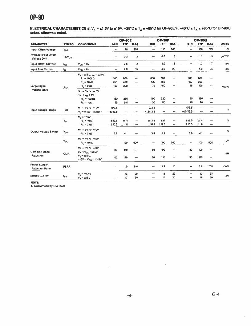
OP-90
ELECTRICAL CHARACTERISTICS atV- =_1.5V to _15V, -25°C _ TA _ +WC for OP-90E/F, -40°C - TA * +85°C for OP-90G,unless otherwise noted.
PARAMETER SYMBOL CONDITIONS
OP-90E
MIN TYP MAX
OP-90F
MIN TYP MAX MIN
OP-90GTYP IMAX UNITS
Input Offset Voltage Vos 70 270 110 650 180 675 *v
Average Input Offset
Voltage DriftTCVos — 03 2 — 0.6 5
-12 5 ^iV/»C
Input Offset Current IOS Vcm-OV — 0.8 3 — 1.0 5 - 1.3 7 nA
Input Bias Current >B Vcw = OV — 4.0 15 4.0 20 - 4.0 25 nA
VS=±15V, Vo=±10VRL= 100kn 500 800 — 350 700 — 300 600 —
RL= 10kft 250 400 — 175 350 — 150 250 —
RL=2kft 100 200 -76 150 -
75 125—
V+ = 5V.V- = 0V.
1V<V0<4V
Large Signal
Voltage Gam
Input Voltage Range
Avo
IVR
Vo
Output Voltage Swing VOH
Common Mode
Rejection
Power Supply
Rejection Ratio
Supply Currant
CMR
PSRR
NOTE:
1. Guaranteed by CMR test.
RL=-100k„R,=10kn
V+ - 6V, V- = 0V
VS=±15V (Notel)
Vs= ±15V
RL-10knRL=2kH
V+ = 5V, V- = 0V
RL=2kfl
V+ = 5V, V- = 0V
RL=10kO
VI -5V,V =0V,
0V<Vcv<3.5V
VS= ±15V,-15V < VCM < 13.5V
VS=±1.5V
VS=±15V
150
75
280
140
0/3.5 -
-15/13.5 -
±13.5 ±14
±10.5 ±11.8
3.9 4.1
— 100 500
90 110 —
100 120 —
— 1.0 5.6
— 13 25
- 17 30
100 220
50 110
0/3.5 -
-16/13.5 —
±13.5 ±14
±10.5 ±11.8
3.9 4.1
— 100 500
80 100 -
90 110 -
— 3.2 10
13 25
17 30
80
40
0/3.5
-15/13.5
160
90
±13.5 ±14
±10.5 ±11.8
3.9 4.1 -
— 100 500
60 100 —
90 110 -
— 5.6
- 12
— 16
17.8
25
30
G-4
V/mV
nV
dB
jiV/V
U«
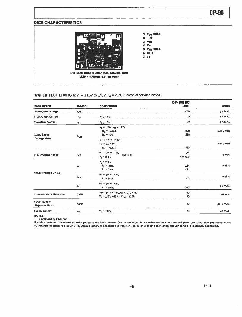
OP-90
DICE CHARACTERISTICS
•
1. VosNULL2. -IN
3. +IN
4. V-
•^-« i 1 -ill-jrjl.•••la.';. :^i!l»L
81 1S 1
'.,.———Km ". *i?:_ -ijTlsftH.M
1©5. VotNULL6. OUT
7. V+
&i[B^»;IS?iCI_DIE SIZE 0.086 x 0.067 Inch, 5762 sq. mils
(2.18 x 1.70mm, 3.71 sq. mm) •
WAFER TEST LIMITS at Vs= +1.5Vto ±15V, Ta = 25°C, unless otherwise noted.
PARAMETER SYMBOL CONDITIONS
OP-90GBCLIMIT UNITS
input Offset Voltage Vos 250 MVMAX
Input Offset Current •os Vcm-ov 5 nAMAX
Input Bias Current hi Vcm-OV 20 nAMAX
VS"±15V,Vo = ±10VRL=100kftRL=10kOLarge Signal
Voltage Gain
Input Voltage Range
Output Voltage Swing
Avo
rvR
Vo
"OH
V+ = 5V, V- = 0V,
1V<V0<4V
R, = 100kO
V+ = 5V,V- = 0V
VS= ±15V
VS=±15V
RL=i0knRL=2k«
V+ = 6V, V- = 0V
RL-2kn
(Notel)
500
250
125
0/4
-15/13.5
±14
±11
4.0
V/mV MIN
V/mV MIN
VM1N
VMIN
VMIN
VolV+ «= 5V. V- - 0V
RL = 10k(l 500/iVMAX
Common Mode Rejection CMRV+= 5V,V- - 0V.0V< VCM < 4VVs- ±15V,-15V < Vcw< 13.5V
80
90dBMIN
Power Supply
Rejection RatioPSRR
'SY
10 AiV/V MAX
Supply Current Vs = ±15V 20 MAMAX
NOTES:
1. Guaranteed by CMR tast.Electrical tests are performed at wafer probe to the limits shown. Due to variations in assembly methods and normal yield loss, yield afterguaranteed for standard product dice. Consult factory to negotiate specifications based on dice lot qualification through sample lot assembly and
packaging is nottesting.
-5- G-5

OP-90
TYPICAL PERFORMANCE CHARACTERISTICS
INPUT OFFSET VOLTAGE
vs TEMPERATURE
1 to>
-
I-1-
i,— JO
0
V1•±«v
1—
-73 -so -_ o a » n too _
TEMPERATURE («C)
SUPPLY CURRENT
va TEMPERATURE—I—I—
NO LOAD
|
v»= ±1.5V
-75-80-28 0 25 SO 75 100 125
TEMPERATURE <*C)
Z
i| 2036
CLOSED-LOOP GAIN
VS FREQUENCY
11
1VTa'
"i
-i
111:*V
I5*C
1
Ik Wk
FREQUENCY (Hi)
INPUT OFFSET CURRENT
vs TEMPERATURE
*.=1—"±«V
1—
J
-75-50-25 0 25 SO 75 100 125
TEMPERATURE CC)
OPEN-LOOP GAIN vs
SINGLE-SUPPLY VOLTAGE900 "1 ' •
RL-«nn 1T»=2s-c_
_
TA-B5-C
3 1008
o
TA-128*C_
wo
08 10 15 20 25
SINGLE-SUPPLY VOLTAOE (VOLTS)
fa 4
a
I.
OUTPUT VOLTAGE SWING
vs LOAD RESISTANCE
V-t
ta
1IV.
rTTTn—OV
Ik Wk
LOAD RESISTANCE (ft)
-"
INPUT BIAS CURRENT
v* TEMPERATURE
v, = ±nv
1
31
I
-75 -SO -25 0 25 SO 75 100 125
TBMP6RATURE CO
OPEN-LOOP GAIN AND
PHASE SHIFT vs FREQUENCYMO. 1 r " •
V, = i1SVT.-WC
V
*l- •wkt»^
0
45
135
M
•0
40
20
0
\ „OAtN
^-,1\
\.
\N
**N
N\
s10 WO lit
FREQUENCY (Hz)
in2s
OUTPUT VOLTAGE SWINGvs LOAD RESISTANCE
POSITIVE
Twe SATO E
Ta WC
t15V
mi
= -
no Ik 10k
LOAD RESISTANCE (O)
G-6

OP-90
TYPICAL PERFORMANCE CHARACTERISTICS
g wo
Io
s _Sj so
POWER SUPPLY REJECTION
vs FREQUENCY
TaH n rr
C
— rIII 1
•EQATTVE SUPPLY
I *
k, Inil
•osmvEst jpply
W 100
FREQUENCY (He)
CURRENT NOISE DENSITY
vs FREQUENCY
Tn—_
_v«=±__TA-S-
1,-H c
|1 „
IO
ill5
K
3O
0.1w wo
FREQUENCY (Hr)
BURN-IN CIRCUIT
COMMON-MODE REJECTION
vs FREQUENCY
1 1 MilVg*±1SV
g«A- 25'C
HI
o
SI so
| so
40W wo
FREQUENCY (Hz)
SMALL-SIGNAL
TRANSIENT RESPONSE
NOISE VOLTAGE DENSITY
vs FREQUENCYwoo •T~ T'T.
V, '±WV
I»a »_«c
>
JJ
1
I •i
1 _
1 W WO
FREQUENCY (Hz)
LARGE-SIGNAL
TRAN8IENT RESPONSE
+WV
I I
2 7
OP-90 seS
4
0-WV
APPLICATIONS INFORMATION
BATTERY-POWERED APPLICATIONS
The OP-90 can be operated on a minimum supply voltage of+1.6V, or with dual supplies ±0.8V, and draws only 14^A ofsupply current. In many battery-powered circuits, the OP-90can be continuously operated for thousands of hours beforerequiring battery replacement, reducing equipment downtime and operating cost.
High-performance portable equipment and instruments frequently use lithium cells because of their long shelf-life, lightweight, and high energy density relative to older primarycells. Most lithium cells have a nominal output voltageof 3V and are noted for a flat discharge characteristic. Thelow supply voltage requirement of the OP-90, combined withthe flat discharge characteristic of the lithium cell, indicatesthat the OP-90 can be operated over the entire useful life olthe cell. Figure 1 shows the typical discharge characteristicof a 1Ah lithkim cell powering an OP-90 which, in turn, isdriving full output swing into a 100kft load.
-7- G-7

OP-90
FIGURE 1: Lithium Sulphur Dioxide Cell DischargeCharacteristic With OP-90 and 100kft Load
INPUT VOLTAGE PROTECTION
The OP-90 uses a PNP input stage with protection resistors inseries with the inverting and noninverting inputs. The highbreakdown of the PNP transistors coupled with the protection resistors provides a large amount of input protection,allowing the inputs to be taken 20V beyond either supplywithout damaging the amplifier.
OFFSET NULLING
The offset null circuit of Figure 2 provides 6mV of offsetadjustment range. A 100kft resistor placed in series with thewiper of the offset null potentiometer, as shown in Figure 3,
FIGURE 2: Offset Nulling Circuit
v+
o 4-*H_
o &OP-00^2^ 4 -O
?W0kfti
—I IV
1
FIGURE 3: High Resolution Offset Nulling Circuit
v+
O J -**%L
a .... *OP-SO^jP 0
_^r —i1 I wokn
4T1NhA
1 OV-
reduces the offset adjustment range to 400mV and is recommended for applications requiring high null resolution.Offset nulling does not affect TCVos performance.
SINGLE-SUPPLY OUTPUT VOLTAGE RANGEIn single-supply operation the OP-90's input and outputranges include ground. This allows true "zero-in. zero-out"operation. The output stage provides an active pull-down toaround 0.8V above ground. Below this level, a load resistanceof up to 1Mil to ground is required to pull the output down tozero.
In the region from ground to 0.8Vthe OP-90 has voltage gainequal to the data sheet specification. Output current sourcecapability is maintained over the entire voltage range including ground.
APPLICATIONS
BATTERY-POWERED VOLTAGE REFERENCE
The circuit of Figure 4 is a battery-powered voltage referencethat draws only 17^A of supply current. At this level, two AAcells can power this reference over 18 months. At an outputvoltage of 1.23V @ 25°C, drift of the reference is only5.5fiV/°C over the industrial temperature range. Load regulation is 85MV/mA with line regulation at 120a*V/V.
Design of the reference is based on the bandgap technique.Scaling of resistors R1 and R2 produces unequal currents inQ1 and Q2. The resulting VBe mismatch creates a temperature-proportional voltage across R3 which, in turn, producesa larger temperature-proportional voltage across R4 and R5.This voltage appears at the output added to the VBE of Q1,which has an opposite temperature coefficient. Adjusting the
FIGURE 4: Battery Powered Voltage Reference
C1WOOpF
Rlaokn
OUTPUTADJUST
Rl240W1
R3AA-
R4wokn
"O (+Z.8V TO +38V)
^~' (1.25V @25'C)
i*i
G-8

output to 1.23V at 25°C produces minimum drift over temperature. Bandgap references can have start-up problems. Withno current in R1 and R2, the OP-90 is beyond its positive inputrange limit and has an undefined ouput state. Shorting Pin 5(an offset adjust pin) to ground forces the output high underthese conditions and insures reliable start-up without significantly degrading the OP-90's offset drift.
SINGLE OP AMP FULL-WAVE RECTIFIERFigure 5 shows a full-wave rectifier circuit that provides theabsolute value of input signals up to +2.5V even thoughoperated from a single 5V supply. For negative inputs, theamplifier acts as an unity gain inverter. Positive signals forcethe op amp output to ground. The 1N914 diode becomesreversed-biased and the signal passes through R1 and R2 tothe output. Since output impedance is dependent on inputpolarity, load impedances cause an asymmetric output. Forconstant load impedances, this can be corrected by reducingR2. varying or heavy loads can be buffered by a secondOP-90. Figure 6 shows the output of the full-wave rectifierwith a 4Vp.p, 10Hzinput signal.
FIGURE 5: Single Op-Amp Full Wave Rectifier
R1
VinO VrVWkn
HP5082-2S00 /\*
n.2
-WV-
h-M-
FIGURE 7: Two Wire 4-20mA Transmitter
+5VREFERENCE O-
2mA MAX
R2
+ 0 —WV—tSkfi
VM
_C—_____
•O Voyr
OP-90
FIGURE6: Output of Full-Wave Rectifier With 4Vp.p,10Hz Input
TWO WIRE 4-20mA CURRENT TRANSMITTER
The current transmitter of Figure 7 provides an output of 4mAto 20mA that is linearly proportional to the input voltage.Linearity of the transmitterexceeds 0.004% and line rejectionis 0.0005%/volt.
Biasing for the current transmitter is provided by the REF-02EZ. The OP-90EZ regulates the output current to satisfythe current summation at the noninverting node:
"OUT R6 VV,N R5^ 5V R6
R2 R1
For the values shown in Figure 7,
,0UT=(l-b^>)V,N + 4mA
giving a full-scale output of 20mA with a 100mV input.Adjustment of R2 will provide an offset trim and adjustment ofR1 will provide a gain trim. These trims do not interact sincethe noninverting input of the OP-90 is at virtual ground. TheSchottky diode, D1, prevents input voltage spikes from pull-
R5
-A/A
REF-O—-
R4wokn
'OUT" _,n +*m*
t O v+(+WV TO +40V)
RCwon
•out I
r
-9-G-9

OP-90
ing the noninverting input more than 300mV below theinverting input. Without the diode, such spikes could causephase reversal of the OP-90 and possible latch-up of thetransmitter. Compliance of this circuit is from 10V to 40V. Thevoltage reference output can provide up to 2mA for transducer excitation.
MICROPOWER VOLTAGE-CONTROLLED OSCILLATORTwo OP-90s in combination with an inexpensive quad CMOSswitch comprise the precision VCO of Figure 8. This circuitprovides triangle and square wave outputs and draws only50/jA from a single 5V supply. A1 acts as an integrator; S1switches the charging current symmetrically to yield positive
FIGURE 8: Micropower Voltage Controlled Oscillator
Vcow—ol
R1
•^vV y
R3
wokn
IOUT/IN
I
bVtS
n
M
"T__ IN/OUT
n.
7Snf
>bo
COMT
and negative ramps. The integrator is bounded by A2 whichacts as a Schmitt trigger with a precise hysteresis of 1.67volts, set by resistors R5, R6, and R7, and associated CMOSswitches. The resulting output of A1 is a triangle wave withupper and lower levels of 3.33 and 1.67volts. The output of A2is a square wave with almost rail-to-rail swing. With the components shown, frequency of operation is given by theequation:
/0UT= VCONTROL (VOlts) X 10Hz/V
but this is easily changed by varying C1. The circuit operateswell up to a few hundred hertz.
TRIANGLEOUT
♦—«vVN—O+sv <-SflOkO
1
-O+SV
M >R7200)01 S-200M)
^O SQUARE^OUT
-10- G-10

MICROPOWER SINGLE-SUPPLY
INSTRUMENTATION AMPLIFIER
The simple instrumentation amplifier of Figure 9 providesover 110dB of common-mode rejection and draws only 15/xAof supply current. Feedback is to the trim pins rather than tothe inverting input. This enables a single amplifier to providedifferential to single-ended conversion with excellentcommon-mode rejection. Distortion of the Instrumentationamplifier is that of a differential pair, so the circuit is restricted to high gain applications. Noniinearity is less than0.1% for gains of 500 to 1000 over a 2.5V output range. Resistors R3 and R4 set the voltage gain and, with the valuesshown, yield a gain of 1000. Gain tempco of the instrumentation amplifier is only 50ppm/°C Offset voltage is under 150/tVwith drift below 2/uV/°C. The OP-90's input and output voltage ranges include the negative rail which allows the instrumentation amplfier to provide true "zero-in, zero-out"operation.
FIGURE 9: Micropower Single-Supply InstrumentationAmplifier
OP-90
SINGLE-SUPPLY CURRENT MONITOR
Current monitoring essentially consists of amplifying thevoltage drop across a resistor placed in series with the current to be measured. The difficulty is that only small voltagedrops can be tolerated and with low precision op amps thisgreatly limits the overall resolution. The single-supply current monitor of Figure 10 has a resolution of 10pA and iscapable of monitoring 30mA of current. This range can beadjusted by changing the current sense resistor Rl Whenmeasuring total system current, it may be necessary toinclude the supply current of the current monitor, whichbypasses the current sense resistor, in the final result. Thiscurrent can be measured and calibrated (together with theresidual offset) by adjustment of the offset trim potentiometer, R2. This produces a deliberate offset that is temperature dependent. However, the supply current of the OP-90 isalso proportional to temperature and the two effects tend totrack. Current in R4 and R5, which also bypasses R1, can beaccounted for by a gain trim.
FIGURE 10: Single-Supply Current Monitor
+ o
TO CIRCUITUNDER TEST
-O I
< "TOT
R5< rw<wons wokn'
v+
o
-O Vour WOmV/mA (I——)
-11- G-ll

Appendix H - AD654 Voltage to Frequency Converter
Manufactured by Analog Devices1 Technology Way
P.O. Box 9106
Norwood, MA 02062
(800) 262-5643

• ANALOGDEVICES
^ Low Cost MonolithicVoltage-to-Frequency Converter
FEATURESLow Cost
Single or Dual Supply, 5to 36 Volts, ±5Vto ±18VFull Scale Frequency Up to 50OkHzMinimum Number ofExternal Components NeededVersatile Input Amplifier
Positive or Negative Voltage ModesNegative Current ModeHigh Input Impedance, Low Drift
Low Power: 2.0mA Quiescent CurrentLow Offset: 1mV
PRODUCT DESCRIPTIONThe AD654 is amonolithic V/F converter consisting of an inputamphfier, aprecision oscillator system, and ahigh current outputfull scale (F.S.) frequency up to 500kHz and any F.S. inputvoltage up to _30V. Linearity error is only 0.03% for a250k_feK5., and operation is guaranteed over an 80dB dynamic range 'The overall temperature coefficient (excluding the effects ofexternal components) is typically _50ppm/X. The AD654operates from asingle supply of 5to 36V and consumes onlv.z.OmA quiescent current.
The low drift C4,xV/-C typ) input amplifier allows operationdirectly fr0m small signals such as thermocouples orltr^nSTv/?£ e•„*? <250M»> inP« distance. Unlikemost V/F converters, the AD654 provides asquare-wave output
pout LOGICCOMMON
>40554 Pin Configuration
w ^PRODUCT HIGHLIGHTS1. Packaged in both an 8-pin mini-DlP and an 8-pin SOIC
package the AD654 is acomplete V/F converter requiringonly an RC timing network to set the desired full scale frequencyand aselectable pull-up resistor for the open-collector outputstage. Any full scale input voltage range from I0OmV to 10volts (or greater, depending on +Vs) can be accommodatedby proper selection ofthe timing resistor. The full scalefrequency ,s then set by the timing capacitor from the simplerelationship, f = V/10RC.
2. Aminimum number of low cost external components arcnecessary A single RC network is all that is required to setup any full scale frequency up to 500kHz and any full scaleinput voltage up to _30V.
3. Plastic packaging allows low cost implementation of thestandard VFC applications: A/D conversion, isolated signaltransmission, F/V conversion, phasclockcd loops, and tuningswitchcd-capacitor filters. g
4. Power supply requirements are minimal; only 2.0mA ofquiescent current is drawn from the single positive supplyfrom 4.5 to 36 volts. In this mode, positive inputs J'varyfrom 0volts (ground) to (+Vs .4) volts. Negative input?can easily be connected for below ground operation.
5" Jo^ri^ °pen-CoUcci0r 0U*P"r ««f can sink more than10mA with asaturation voltage less than 0.4 volts. The LogicCommon terminal can be connected to any level betweenground (or - V.) and 4volts below +Vs. This allows «Sydirect interface to any logic family with either positive ornegative logic levels.
Information furnished bv Analno n_;_ •and reliable. However, S£SS£h!7J 2_T_? t0 * «=«"«•for its use; nor for any InfrtSSSS LTUmed by Anal09 °eviceparties which may result from |«C," NoS$ °T °Ther ri9hls °f *Irdtion or otherwise under any p8„n? or oarimJ$ 'V™* by in**iC9-
pawnt or DaTer,t i-'ghts of Analog Devices.wEKsr*p- °e- *<*•• -—*~>«-»i- US.A.Telex: 924491 „ . Tw*: 710/394-6577
Cables: ANALOG NORWOOOMASS
CZ0/Z00® HIO III IGT C_Zr TS8 _T9S C0:60 96/TO/TT

SPECIFICATIONS«_Model
CURRENT-TO-FREQUENCY CONVERTERFrequencyRangeNoniinearity'
fn_r = 250kHzfm« - 500kHz
FullScaleCalibrationErrorC = 390pF,IIN- 1.000mAvs. Supply(fm;ix£ 250kHz)
V»- + 4.75 to + 5.25VVs = +5.25 to + 16.5V
vs.Temp(0to70°C)
ANALOG INPUT AMPLIFIER(Voltagc-to-Current Converter)VoltageInput Range
SingleSupplyDual Supply
Input Bias Current(Either Input)
Input OfFseiCurrentInput Resistance (Non-Inverting)Inpui OffsetVoltage
vs. SupplyVs = -1-4.75 to + 5.25VVs= + 5.25 to + 16.5V
vs. Tcmp(0to70°C)
OUTPUT INTERFACE (Open CoUccior Output)(Symmetrical Square Wave)Output Sink Current inLogic "0"2
vout = 0.4Vmax,25"CVotnr = 0.4Vmax,0 to70°C
Output Leakage Current inLogic "1"0to70°C
Logic Common Level RangeRise/Fall Times (CT = 0.01 p.F)
Iin • 1mAIin = Im-A
POWER SUPPLYVoltage,Rated PerformanceVoltage, Operating Range
SingleSupplyDual Supply
Quiescent CurrentVs (Total) - 5VVs(Total)- 30V
TEMPERATURERANGEOperatingRange
PACKAGE OPTIONSSOIC
Plastic DIP
+25°C and V$ (total) =5to 16.5V, unless otherwise specified. All testing done (qj Vs • +5V)AD654JN/JR
Min Typ Max Units
0 500 kHz
0.06 0.1 %
0.20 0.4 %
-10 10 %
0.20 0.40 %/v
0.05 0.10 . %/v50
•—--
ppm/°C
0 (+vs '4) V-Vs (+vs -4) V
30 50 nA5 nA250 Mil0.5 1.0 mV
0.1 0.25 mV/V0.03 0.1 mV/V4 u.V/°C
10 20 mA5 10 mA
10 100 nA50 500 nA
-Vs
0.2
1
(+vs- 4) V
\ls
tlS.
4.5
4.5
±5
-40
2.0
AD654JR")AD654JN
16.5
36
zl8
2.5
3.0
85
V
V
mA
mA
NOTES -'
'AlfmM =JStS" J1" "" lkilXr 39°PF'I'M - 0.1mA.•iCS-T 500kH7:RT • IW».Ct =200pF,I,N =0-imA.«rhiCir^U,"rarUrhe^OUnCOfCUrTCnCtha,Cannow,nioPin ' of the AD654•Mfem_nttuu„famaximum voltage of0.4V between Pin 1and Logic Common.
ipecificBtions subject tochange without notice. «w~wmunu>.
H-2
-2-
C20/C00® hid in iav ZLZt TZ8 _T9© C0:60 96/TO/TT
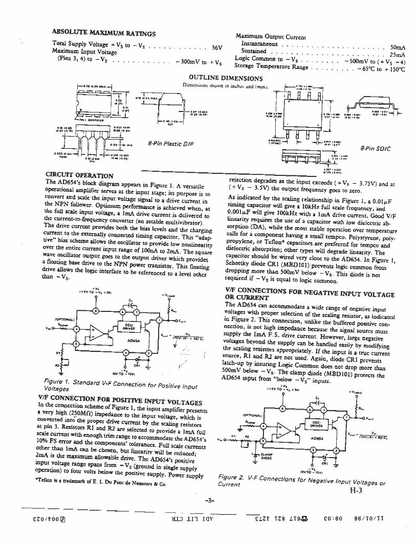
ABSOLUTE MAXIMUM RATINGS
Total Supply Voltage -f- Vs to - VsMaximum Input Voltage
(Pins 3, 4) to -Vs
36V
Maximum Output CurrentInstantaneousSustained
Logic Common to - Vs
50mA
25mA-300mVto +VS ^^ommonto -Vs -500mVto( +Vs -4)
storage Temperature Range -65°C to +150°C
OUTLINE DIMENSIONSj <Ut l»5ll t_l_JLi—i _a e_ i—•'—•
Dimensions shown in incho and (mm;. L * >M i • me I
_ a b11
CIRCUIT OPERATION
Jr^^5.4'5 W^k di2gram aPPCarS h Fi^rc LA™*Hcoperation.I amplifier serve* as the input stage; its purpose is to
_£ £n ? °PUmUm l»*™_c_ is achieved when, atthe m scale input voltage, a1mA drive current is delivered tothe current-to-frequency convener (an asiable multivibrator)The dnve current provides both the bias levels and the chargine
_J_- rh^ ••*• ** ^^or to provide low noniinearityover the entire current input range of lOOnA to 2mA. The «££wave osciUator output goes to the output driver which prov^dTafloating base dnve to the NPN power transistor. Th_ZZdnve allows the logic interface to be referenced to alevel oX?
-v.
(OV TO - 15VI
vEZLstandard V'F Connection for *»"** **>*«V/F CONNECTION FOR POSITIVE INPUT VOLTAGESIn the connection scheme ofFigure 1 the innm L rra verv hich r250M n> ;-. a I npui""P^presentsconverted mto the proper dnve current by the scalint? r____~acpm 3. Resistor, Rl and R2 are selected'* Pro^TeVln^TullmSZT"tT***" "•* »«con_SodTte the A^65rs10% FSenor and thecomponents'tolerancr* p.,h ,_-«- _*..«,«__„, L^^t^r*
Teflon is atrademark of E. I. Du Pont de Nemours &Co.
j!f-f^Z____TlLO 11 IB 1*1 IBIS t»M,
J
~~~ T
yir_fTj-_fv;ig©V»#>? 50/C
rejection degrades as the input exceeds (+ Vs - 3.75V) and at(+ VS - 3.5V) the output frequency goes to zero.As indicated by the scaling relationship in Figure 1. a0.0lu.Ftuning capacitor will g,ve a 10kHz full scale frequency, andO.OOloJF will give 100kHz with a1mA drive c^rent £d V/Flinearity requires the use of acapacitor with low dielectric absorption (DA), while the most stable operation over temperaturecaUs for acomponent having asmall tempco. Polystyrene, polv-propylene or Teflon* capacitors are prefencd for tempco £|dielcctnc absorption; other types will degrade linearity Thecapacitor should be wired very close to the AD654. In Figure ISchottky diode CR1 (MBD10I) prevents logic common fZdropping more than 500mV below - Vs. This diode is notrequired ,f - Vs is equal to logic common.
IkcSSP°SS F°R NECATIVE WFUT VOLTAGEvot_ftr^T" accomm0date aWide ran8e of «»i" input«^SSJ_ Th10^ SdeCt,0n °f *" $Calin« r«istor> - Seatedin Figure 2. This connection, unlike the buffered positive con-nection is not high impedance because the signal s^rcc m_stsupply the ImA F.S. drive current. However l^n£™vo ugcs bevo-d ^ SUppJy can ^ ha.dlcd ^ ^ve
source, Rl and R2 are not used. Again, diode CR1 prevents5__v__. ~ vg iogic Conmon does not dr°p ~<LAD654 input from "below inputs.
• tSVTO
HDVJlRi'ifUil-
(OVTO -15V)
C^f ^"F^^^^ Native Input Voltages orH-3
-3-
cso/roo® hid in iav ZLZt T28 _T90 C0:60 96/TO/TT

Figure 3d. Offset Trim Negative Input (-10V FS)
OFFSET CALIBRATIONIn theory, two adjustments calibrate a V/F: scale and offset. Inpractice, most applications find the AD654's lmV max voltageoffset sufficiently low to forgo offset calibration. However, theinput amplifier's 30nA (typ) bias currents will generate an offsetdue to the difference in DC source resistance between the inputterminals. This offset can be substantial for large values ofRT - R, -*- R2 and will vary as the bias currents drift overtemperature. Therefore, to maintain the AD654's low offset, theapplication may require balancing the DC source resistances atthe inputs (pins 3 and 4).
For positive inputs, this is accomplished by adding acompensationresistor nominally equal to RT inseries with the input as shownin Figure 3a. This limits the offset to the product ofthe 30nAbias cunent and the mismatch between the source resistance RT•«j Rcomj>. Asecond, smaller offset arises from the inputs' 5nAoffset cunent flowing through the source resistance RT or RCOMPFor negative input voltage and current connections, the com-pensation resistor is added at pin 4as shown in Figure 3b inlieu of grounding the pin directly. For both positive and negativeinputs, the use of RcOMJ, may lead to noise coupling at pin 4and should therefore be bypassed for lowest noise operation Figure 3e. Offset Trim Bias Network
FULL SCALE CALIBRATIONFull scale trim is the calibration of the circuit to produce thedesired output frequency with a full scale input applied Inmosi cases this is accomplished by adjusting the scaling resistorKt- Precise calibration ofthe AD654 requires the use ofanaccurate voltage standard set to the desired FS value and anaccurate frequency meter. Ascope is handy for monitoringoutput waveshape. Verification of convener linearity requiresthe use of aswitchable voltage source or DAC having a linearityerror below _0.005%, and the use of long measurement intervalsto minimize count uncertainties. Since each AD654 is factorytested for linearity, it is unnecessary for the end-user to performthis tedious and time consuming test on a routine basis.Sufficient FS calibration trim range must be provided to accommodate the worst-case sum ofall major scaling enors Thisincludes the AD654's 10% full scale enor, the tolerance of thefixed scaling resistor, and the tolerance of the timing capacitoromT T'^S areSiSl0r l°leranCC °f I% "*aapicit0T <olc«°«of Ly f P3rt U,C SCahnB rcsist0r should ** amaximum? ac/% ,n0minai' WIth *" variable P°r-on elected to allowuo/o of the nominal.
If the input is in the form of anegative cunent source, theS^LeS1Sl°uJln0 ,0ngCr reqUired' <*-*»*« the capabilityof tnmming FS frequency in this fashion. Since it „ usually notpractical to smoothly vary the capacitance for trimming purposesan alternative scheme such as the one shown in Figure 4isneeded. Designed for aFS of 1mA, this circuit divides theinput into two current paths. One path is through the lOOfl
C (OPTIONAL
Figure 3m. Bias Current Compensation - Positive InputsC (OPnONAL!
Figure 3b. Bias Current Compensation - Negative InputsIf the AD654's lmV offset voltage must be trimmed, the trimmust be performed external to the device. Figure 3c shows anoptional connection for positive inputs in which Ro™ andKoffj add avariable resistance in series with RT. Avariablesource of ±0.6V applied to Rom then adjusts the offset _ lmVSimilarly a ±0.6V variable source is applied to 1W _,Mgurc 3d to trim offset for negative inputs. The ±0.6V bipolarsource could simply be an AD589 reference connected as shownin Figure 3e.
I ^**» m ^^ •
rO.GV
Figure 3c. Offset Trim Positive Input (10V FS)
-4-
CSO/SOO® XL3 111 IdY ZLZt T28 _T9©
(20V) C7
•OPTIONAL OFFSETTRIM
Figure 4. Current Source FS Trim H-4
fr0:60 96/TO/TT

Figure 5. Input Protection
of 0.9mV arc sufficient to cause momentary malfunction.
This effect can be minimized by using a simple low-pass filterahead of the convener or a guard ring around the RT pin. Thefilter can be assembled using the bias current compensationresistor discussed in the previous section. For an FS of 10kHz,a single-pole filter witha time constant of 100ms wUl be suitable,but the optimum configuration will depend on the applicationand the type of signal processing. Noise spikes are only likely tobe a cause of error when the input current remains near itsnunimum value for long periods of time; above lOOnA fullintegration ofadditive input noise occurs. Like the inputs, thecapacitor terminals are sensitive tointerference from other signals.The timing capacitor should be located as close as possible tothe AD654 to minimize signal pickup in the leads. In somecases, guard rings or shielding may be required.
DECOUPLING
It is good engineering practice to use bypass capacitors on thesupply-voltage pins and to insen small-valued resistors (10 to100n) in the supply lines to provide ameasure ofdecouplingbetween the various circuits in the system. Ceramic capacitorsofO.ljxF to 1.0p.F should be applied between the supply-voltagepins and analog signal ground for proper bypassing on the AD654.A proper ground scheme appears in Figure 6.
DIGITALP.5.
resistor Rl, and flowing into pin 3; it constitutes the signalcunent It to be convened. The second path, through another100O resistor R2, carries the same nominal current. Two equalvalued resistors offer the best overall stability, and should beeither 1% discrete film units, or apair from acommon anay.Since the 1mA FS input cunent is divided into two 500jiA legs(one to pound and one to pin 3), the total input signal cunentfls) is divided by a factor of two in this network. To achieve thesame conversion scale factor, CT must be reduced by a factor oftwo. This results in atransfer unique to this hookup:
r.Ju(20V) CT
For calibration purposes, resistors R3 and R4 are added to thenetwork, allowing a ± 15% trim of scale factor with the valuesshown. By varying R4's value the trim range can be modified toaccommodate wider tolerance components or perhaps the calibration tolerance on acunent output transducer such as theAD592 temperature sensor. Although the values of Rl - R4shown arc valid for 1mA FS signals only, they can be scaledupward proportionately for lower FS currents. For instance,they should be increased by a factor of ten for a FS current of100|xA.
In addition to the offsets generated by the input amplifier's biasand offset cunents, an offset voltage induced parasitic currentarises from the current fork inputnetwork. These effects arcminimized by using the bias current compensation resistor RoFFand offset trim scheme shown in Figure 3e.
Although device warmup drifts are small, it is good practice toallow the devices operating environment to stabilize before trim,and insure the supply, source and load are appropriate. Ifprovisionis made to trim offset, begin bysetting the input to 1/10,000 offull scale. Adjust the offset pot until the output is 1/10,000 offull scale (for example, 25Hz for aFS of250kHz). This is mosteasily accomplished using a frequency meter connected to theoutput. The FS input should then be applied and the gain potshould be adjusted until the desired FS frequency is indicated.
INPUT PROTECTIONThe AD654 was designed to be used with aminimum ofadditionalhardware. However, the successful application ofaprecision ICinvolves agood understanding of possible pitfalls and the use ofsuitable precautions. Thus +VW and RT pins should not bedriven more than 300mV below - Vs. Likewise, Logic Commonshould not drop more than 500mV below - Vs. This wouldcause internal junctions to conduct, possibly damaging the IC.In addition to the diode shown in Figures 1and 2protectingLogic Common, asecond Schottky diode (MBD101) can protectthe AD654's inputs from "below - Vs" inputs as shown inFigure 5. It is also desirable not to drive +V^ and RT above+Vs. In operation, the converter will exhibit azero output forinputs above (M-V, - 3.5V). Also, control cunents above 2mAwill increase noniinearity.
The AD654's 80dB dynamic range guarantees operation from acontrol current of 1mA (nominal FS) down to 100nA (equivalentto lmV to 10V FS). Below lOOnA improper operation oftheoscillator may result, causing afalse indication of input amplitudeIn many cases this might be due to shon-livcd noise spikeswhich become added to input. For example, when scaled toaccept an FS input of IV, the -80dB level is only lOO^V sowhen the mean mput is only 60dB below FS (lmV), noise spikes
'ouT O
CZO/900®
AGNDO
Figure 6. Proper GroundScheme
OUTPUT INTERFACING CONSIDERATIONSThe output stage's design allows easy interfacing to all digitallogic families. The output NPN transistor's emitter and collectorare both uncommitted. The emitter can be tied to any voltagebetween - Vs and 4 volts below +VS, and the open collectorcan be pulled up to avoltage 36 volts above the emitter regardlessof +Vs. The high power output stage can sink over 10mA at amaximum saturation voltage of 0.4V. The stage limits the outputcurrent at 25mA and can handle this limit indefinitely vdthoutdamaging the device. rf-5
-5-
HID 111 IQT ZLZX TZ8 1T9S- S0:60 96/TO/TT

The preferred method ofspecifying nonlinearitv error is interms ofmaximum deviation from the ideal relationship aftercalibrating the converter at full scale. This error will vary withthe full scale frequency and the mode ofoperation The AD6Moperates best at a 150kHz full scale frequency with anegativevoltage input; the linearity is typically within 0.05%. Operatingat higher frequencies or with positive inputs will degrade thelinearity as indicated in the Specifications Table. Typical linearityat various temperatures is shown in Figure 7.
+ VS
I0V
15V
( + V_)
10V
15V
10V
15V
10V
15V
Rs
270H
680n
Table/.
Rl R2 R3 R4
100k
100k
R5
127k
127k
R_
1.8k
2.7k
F = lOHz/K
F = lOHzTC
F - 5.55Hz/°F
10.00
10
A£_»
ISO 2SD 350
FULL SCALE ~tEOUCNCY - kHz
Figure 7. Typical Nonlinearities at Different Full-ScaleFrequencies
TWO-WIRE TEMPERATURE-TO-FREQUENCYCONVERSION
Figure 8shows the AD654 in atwo-wire tempenuure-to-frequenevconversion scheme. The twisted pair transmission line serves thedual purpose ofsupplying power to the device and also carrviqgfrequency data in the form of cunent modulation
500
Figure 8. Two-Wire Temperature-to-Frequency ConverterThe positive supply line is fed to the remote V/F through a140f2 resistor. This resistor is selected such that the quiescentcunent of the AD654 wul cause less than one VBr to be dropped.As the V/F oscillates, additional switched current is drawnthrough R_ when pin Igoes low. The peak level ofthis additionalcunent causes Ql to saturate, and thus regenerates the AD654'soutput square wave at the collector. The supply voltage to theAD654 then consjsts of aDC level, less the resistive line drop,5^aV2_, X^* SqUarC wave ai the outPUI fr«iuency oftne AD654. This ripple is reduced by the diode/capacitorcombination.
To set up the receiver circuit for agiven voltage, the Rs and R.resistances are selected as shown in Table I. CMOS logic staecsan be driven directly from the collector of Ql, and asinglerTL load can be driven from the junction ofRs and R6
-6-
°F
6.49k 4.02k
12.7k 4.02k
6.49k 4.42k
12.7k 4.42k
Ik
Ik
Ik
Ik
95.3k 22.6k78.7k 36.5k
154k
105k
22.6k
36.5k
Table//.
Atthe V/F end, the AD592C temperature transducer isinterfacedwith the AD654 in such amanner that the AD654output frequencyis proportional to temperature. The output frequency can bescaled and offset from K to °C or °F using the resistor valuesshown mTable II. Since temperature is the parameter ofinterest,an NPO ceramic capacitor is used as the timing capacitor forlow V/F TC.
When scaling per K, resistors Rl - R3 and the AD589 voltagereference are not used. The AD592 produces a lyJVK currentoutput which drives pin 3ofthe AD654. With the timing capacitorof0.0^F this produces an output frequency scaled to lOHz/KWhen scaling per »C and °F, the AD589 and resistors Rl - R3'offset the dnve cunent at pin 3by 273.2nA for scaling per °Cand 255.42nA for scaling per °F. This will result in frequenciesscaled at lOHz^C and 5.55Hz/°F, respectively.
OPTOISOLATOR COUPLINGApopular method of isolated signal coupling is via optoelectronicisolators, or optocoupiers. In this type of device, the signal iscoupled from an input LED to an output photo-transistor, withlight as the connecting medium. This technique allows DC tobe transmitted, is extremely useful in overcoming ground loopproblems between equipment, and is applicable over a widerange of speeds and power.
Figure 9shows ageneral purpose isolated V/F circuit using alow c0St 4N37 optoisolator. A +5V power supply is assumedfor both the isolated (+5V isolated) and local (+ 5V local) suppliesThe input LED of the isolator is driven from the collector outputot the AD654, with a9mA current level established by Rl forhigh speed, as well as for a 100% current transfer ratio
tSO_T£o t LOC«L
Figure 9. Optoisolator InterfaceH-6
CZ0/100® hid in iav ZLZt TZ8 _T90 S0:60 96/TO/TT

At the receiver side, the output transistor is operated in thephoto-transistor mode; that is with the base lead (pin 6) open.This allows the highest possible output cunent. For reasonablespeed in this mode, it is imperative that the load impedance beas low as possible. This isprovided by the single transistor stagecuncnt-to-voltage convener, which has adynamic load impedanceof less than 10 ohms and interfaces with TTL atthe output.
USING A STAND-ALONE FREQUENCY COUNTER/LEDDISPLAY DRIVER FOR VOLTMETER APPLICATIONSFigure 10 shows the AD654 used with astand-alone frequencycounier/LED display driver. With Or - lOOOpF and RT =lkn the AD654 produces an FS frequency of lOOkHz when Vw= + IV. This signal is fed into the ICM7226A, a universalcounter system that drives common anode LED's. With theFUNCTION pin tied toDl through alOkfi resistor theICM7226Acounts the frequency of the signal at AiN. This count period isselected by the user and can be 10ms, 100ms, Is, or 10 seconds,as shown on pin 21. The longer the period selected, the moreresolution the count will have. The ICM7226A then displays thefrequency on the LED's, driving them directly as shown. Refreshing of the LED's is handled automatically by the ICM7226.The entire circuit operates on asingle +5V supply and gives ameter with 3, 4, or 5 digit resolution.
integral number of 50Hz cycles (5). This is also true of the 1second and 10 second count period.
AD654-BASED ANALOG-TO-DIGITAL CONVERSIONUSING A SINGLE CHIP MICROCOMPUTERThe AD654 can serve as an analog-to-digital convener whenused with a single component microcomputer that has an intervaltimer/event counter such as the 8048. Figure 11 showsthe AD654,with a full scale input voltage of 4- IV and a full scale outputfrequency of 100kHz, connected to the timer/counter input pinTl of the 8048. Such a system can also operate on a single +5Vsupply.
The 8748 counteris negative edge triggered.; after the STRTCNT instruction is executed subsequent high to low transitionson Tl increment the counter. The maximum rate at which thecounter may be incremented is once per three instruction cycles;using a 6MHz crystal, this corresponds to once every 7.5»is, ora maximum frequency of 133kHz. Because the counter overflowsevery256counts (8 bits), the timer interrupt is enabled. Eachoverflow then causes a jump to a subroutine where a register isincremented. Afterthe STOP TCNT instruction is executed,the number of overflows that have occuncd will be the numberin this register. The number in this register multiplied by256plus the number in the counter will be the total number ofnegative edges counted during the count period. The countperiod is handled simply by decrementing a register the numberof times necessary to conespond to the desired count time.After the register has been decremented the required number oftimes, the STOP TCNT instruction is executed.
Figure 10. AD654 With Stand-Alone Frequency Counter/LEDDisplay Driver
Longer count periods not only result in the count having moreresolution, they also serve as an integration ofnoisy analogsignals. For example, anormal-mode 60Hz sine wave riding onthe input ofthe AD654 will result in the output frequencyincreasing on the positive half of the sine wave and decreasingon the negative half ofthe sine wave. This effect is cancelled byselecting acount period equal to an integral number of noisesignal periods. A lOOms count period is effective because it notonly has an integral number of 60Hz cycles (6), it also has an
-7-
Figure 77. AD654 VFC as an ADCThe total number ofnegative edges counted during the countpenod is proportional to ihe input voltage. For example, if a IVfull-scale input voltage produces a 100kHz signal and the countperiod is 100ms, then the total count will be 10,000. Scalingfrom this maximum is then used to determine the input voltage,i.e., acount of5000 corresponds to an input voltage of0.5V.As with the ICM7226, longer couni times result in counts havingmore resolution; and they result in the integration ofnoisyanalog signals.
H-7
CZO/800® _ID 111 I(TV ZLZl TZS _T90 90=60 96/T0/TT

rTtEQUENCY DOUBLINGSince the AD654's output is asquarc-wavc rather than apulsetram, information about the input signal is earned on bothhalves ofthe output waveform. The circuit in Figure 12 convertsthe output into apulse train, effectively doubling the outputVTrSi WiJC prCSemn8 the bc»« low frequency hneantv ofthe AD654. This circuit also accommodates an input voltage"that is greater than the AD654 supply voltage.
TTL logic compatibility. Although the output stage mav becomespeed limited, the multivibrator core itself is able to oscillate to1MHz or more. The designer may take advantage ofthis featurein order to operate the device at frequencies in excess of500kHz.
Figure 13 illustrates this with acircuit offering 2MHz full scaleIn this circuit the AD654 is operated at afull scale (FS) of1mA, with aCT of lOOpF. This achieves a basic device FSfrequency of 1MHz across CT. The Pchannel JFETs, Ql andQ2, buffer the differential timing capacitor waveforms to alowimpedance level where the push-pull signal is then AC coupledto the high speed comparator A2. Hysteresis is used, via R7 fornon-ambiguous switching and to eliminate the oscillations whichwould otherwise occur at low frequencies.
The net result of this is avery high-speed circuit which doesnot compromise the AD654 dynamic range. This is a result ofthe FET buffers typically having only a few PA ofbias currentThe high end dynamic range is limited, however, by parasiticpackage and layout capacitances in shunt with Cr, as well asthose from each node to AC ground. Minimizing the lead lengthbetween A2-6/A2-7 and Q1/Q2 in PC layout will help. Agroundplane will also help stability. Figure 14 shows ihc waveforms VI- V4 found at the respective points shown in Figure 13.
CZO/600®
— rnjijHjTj-Ln
"JUnjLTUUllJWL•MNhMMm
Figure 12. Frequency Doubter
Resistors Rl - R3 are used to scale the 0to +10V input voltagedown to 0to +IV as seen at pin 4of the AD654. Recall thatVm must be less than VSLWLy -4V, or in this case less thanIV. The timing resistor and capacitor are selected such that thisfre uen * SeCn " *" 4reSUltS 'n *° t0 200kH* omputThe use of R4, CI and the XOR gate doubles this 200kHzoutput frequency to 400kHz. The AD654 output transistor isbasically used as aswitch, switching capacitor Cl between acharging mode and adischarging mode of operation. The voltagesseen at the input ofthe 74LS86 are shown in the waveform_____?« HC I0 thC mm°* iR ±e Char*c and ***** «*icconstants, the output pulse widths of the 74LS86 are not equalThe output pulse is wider when the capacitor ,s charging due toas longer rise time than fall time. The pulses should thereforebe counted on their rising, rather than falling, edges.
OPERATION AT HIGHER OUTPUT FREQUENCIESanHT°n!L??-AD654 Via Chc conv^ional output (pins 1and 2) is speed limited to approximately 500kHz for reasons of
Figure 14. Waveforms of2MHz Frequency Doubler
aThm^c?^?-,C°mparar0r is aCOmPl«™ntary square waveat 1MHz FS. Unlike pulse irain output V/F converters, eachhalf-cycle ofthe AD654 output conveys information about theinput. Thus it is possible io count edges, rather than full cyclesof the output and double the effective output frequency. TheXOR gate following A2 acts as an edge detector producing atVl^JV CaCh iDPUt ***tnn5iti0n- This effectively doublesthe V/F FS frequency to 2MHz. The final result is a IV fullscale input V/F with a2MHz full-scale output capability; typicalnonlmeanty is 0.5%. " /p
e>fj-®P
Figure 13. 2MHz, Frequency Doubling V/F
-8-
H-8
hid in iav ZLZt TZ8 IT9S LO-60 96/TO/TT

Appendix I - FM-5 FM Transmitter
Manufactured by Ramsey Electronics793 Canning Parkway
Victor, NY 14564
(716) 924-4560

causing the oscillator frequency to vary accordingly, resulting in elementaryfrequency modulation, or FM.
FM-5 SCHEMATIC DIAGRAM
+1.5VANT
W 1.5V
L2♦JTTTL
RFC
C3: 27
R4
jl ri
10K
R3i—-WV4
100K
C2^
10K
:.0oi
C6 R5AAAr10K MMBTH10-
MK1 r7 02jh-H(
^ *1 ^jTmmbtMMBTA20L
C5.27
RAMSEY Leam.A--You.Bu»ld KIT ASSEMRLV
There are numerous solder connections onthe FM-5 printed circuit board.Therefore, PLEASE take us seriously when wesaythat good soldering isessential to the properoperation of yourtransmitter!
• Use a 25-watt soldering pencil with a clean, sharp tip.• Use only rosin-core solder intended for electronics use.• Use bright lighting, a magnifying lamp orbench-style magnifier may
be helpful.• Do your work in stages, taking breaks tocheck your work. Carefully
brush awaywire cuttings so they don't lodge between solderconnections.
We have a two-fold "strategy" for theorder of the following kit assemblysteps. First, we install parts in physical relationship to each other, so there'sminimal chance of inserting wires into wrong holes. Second, wheneverpossible, we install in an order that fits our "Learn-As-You Build" Kit buildingphilosophy.For each part, ourword "Install" always means these steps:
FM-5* 5
1-1

^!UW|?^;il#i*LI|PB^~JUWW^IgHHjgl ^^^l«-l^^^lJ^li|^^W''W^
FM-S FINDER PIAQRAM;
Note that all components mount to the "solder"side of the circuitboard.
Shown slightly larger than actual size.
1-2

Appendix J - LM565 Phase Locked Loop
Manufactured by National Semiconductor2900 Semiconductor Drive
P.O. Box 58090
Santa Clara, CA 95052(800) 272-9959

& National SemiconductorFebruary 1995
LM565/LM565C Phase Locked Loop
General DescriptionThe LM565 and LM565C are general purpose phase lockedloops containing a stable, highly linear voltage controlledoscillator for low distortion FM demodulation, and a doublebalanced phase detector with good carrier suppression. TheVCO frequency is set with an external resistor and capacitor, and a tuning range of 10:1 can be obtained with thesame capacitor. The characteristics of the closed loop system—bandwidth, response speed, capture and pull inrange—may be adjusted over a wide range with an externalresistor and capacitor. The loop may be broken between theVCO and the phase detector for insertion of a digital frequency divider to obtain frequency multiplication.
The LM565H is specified for operation over the -55°C to+125°C military temperature range. The LM565CN is specified for operation over the 0°C to +70°C temperature range.
Features• 200 ppm/'C frequency stability of the VCO• Power supply range of ±5 to ±12 volts with
100 ppm/% typical
• 0.2% linearity of demodulated output
Connection Diagrams
Metal Can Package
VCO OUTPUT
PHASt COMPARATOR
VCO INPUT
TIMING
CAPACITOR
VCOCONTROL
VOLTAGE
Order Number LM565H
See NS Package Number H10C
©1995National Semiconouclor Corporation TL/H/7853
• Linear triangle wave with in phase zero crossingsavailable
• TTL and DTL compatible phase detector input andsquare wave output
• Adjustable hold in range from ±1% to > ±60%
Applications• Data and tape synchronization• Modems
• FSK demodulation
• FM demodulation
• Frequency synthesizer• Tone decoding• Frequency multiplication and division
• SCA demodulators
• Telemetry receivers• Signal regeneration• Coherent demodulators
-Vcc
INPUT
INPUT
VCO
OUTPUT
PHASE COMPARATORVCO INPUT
REFERENCE
OUTPUT
VCO CONTROL
VOLTAGE
Dual-ln-Line Package
cc
TIMING
CAPACITOR
• TIMINGRESISTOR
TL/H/7853-3
Order Number LM565CN
See NS Package Number N14A
HRD B30M115/Prin»OinU. S A
Ol
Ol
Ol
en
O
CO<o
roo
(Da
roo
J-l

Absolute Maximum RatingsIf Military/Aerospace specified devices are required, Operating Temperature Rangeplease contact the National Semiconductor Sales LM565H -55*Cto+125*COffice/Distributors for availability and specifications. LM565CN 0*C to + 70*C
Supply Voltage ± 12V Storage Temperature Range - 65*C to +150*C
Power Dissipation (Note 1) 1400 mW Lead Temperature (Soldering, 10 sec.) 260*C
Differential Input Voltage ± 1V
Electrical Characteristics ac Test circuit, ta - 25-0vCc - ±6v
Parameter ConditionsLM565 LM565C
Units
Min Typ Max Min Typ Max
Power Supply Current 8.0 12.5 8.0 12.5 mA
Input Impedance (Pins 2,3) -4V < V2, V3 < OV 7 10 5 kn
VCO Maximum Operating
Frequency
Cq - 2.7 pF300 500 250 500 kHz
VCO Free-RunningFrequency
Co - 1.5 nFRo = 20 knf0 = 10 kHz
-10 0 + 10 -30 0 + 30 %
Operating FrequencyTemperature Coefficient
-100 -200 ppm/'C
Frequency Drift withSupply Voltage
0.1 1.0 0.2 1.5 %/V
Triangle Wave Output Voltage 2 2.4 3 2 2.4 3 VpTriangle Wave Output Linearity 0.2 0.5 %
Square Wave Output Level 4.7 5.4 4.7 5.4 Vp-POutput Impedance (Pin 4) 5 5 kn
Square Wave Duty Cycle 45 50 55 40 50 60 %
Square Wave Rise Time 20 20 ns
Square Wave Fall Time 50 50 ns
Output Current Sink (Pin 4) 0.6 1 0.6 1 mA
VCO Sensitivity f0 = 10 kHz 6600 6600 Hz/V
Demodulated Output Voltage(Pin 7)
± 10% Frequency Deviation250 300 400 200 300 450 mVp-p
Total Harmonic Distortion ± 10% Frequency Deviation 0.2 0.75 0.2 1.5 %
Output Impedance (Pin 7) 3.5 3.5 kn
DC Level (Pin 7) 4.25 4.5 4.75 4.0 4.5 5.0 V
Output Offset Voltage
|v7 - v6| 30 100 50 200 mV
Temperature Drift of |V7 - V6| 500 500 fivrc
AM Rejection 30 40 40 dB
Phase Detector Sensitivity Kq .68 .68 V/radian
Note 1:The maximum junction temperature of the LM565 and LM565C is +150rC. For operation at elevatedtemperatures, devicesinthe TO-5packagemustbederated based on a thermalresistanceof +150'C/W junction to ambientor +45*C/W junction to case. Thermal resistanceof the duaHn-line package Is4-85'C/W.
J-2

Typical Performance Characteristics
Power Supply Current as aFunction of Supply Voltage
Lock Range as a Functionof Input Voltage VCO Frequency
I 1 1J
,-_°e-
1 ' '15 1
i '
i -Jr
<y\^1 - lOt
10
y*^
3 itrvbc-*v
2u T
2 14
3 ,J<
2 1.2B
TILQv---2f*C |
-
1ta
1.1
; Fvcc- «tvZpA•25*C 1
- 'Iiill ill!L"C- iiljiF C-IMpF
\ f \11
1HiX!iK 1 r ifl
' IC-l.tjiFllilll l.ll !
c-im.f 1iiiiii iiii.il
10 U 1« It 11 20 22 24
TOTAL SUPPLYVOLTAGEIV) PEAK TO PEAK INPUT VOLTAGE <r«V!
Ik 10k 100k
HIEOUENCV (Hz)
Oscillator OutputWaveforms Phase Shift vs Frequency g
VCO Frequency as aFunction of Temperature
< +1.0
n .
• i
1 Vcc • ±«v I& 1M
£ 140
a 1M
o *o
2 «SB£ U
g «o
i "* 0
1 1 1
T.-2S-C 1 1 1 IV
>
5 it
g 1.1£ roas it
i o•
£ -<uS-i.0•
•-MIS
Vcc- ttV
/ \ t*'lZ Vcr'ittvyj
/ \ / *Tiv1—* w
s ^JI*—.—1——r—
un u i-n tLt II 1.0 \2
NORMALIZED FREQUENCY
-8 1 S H »
TEMPERATURE CO
Loop Gain vs LoadResistance
111.
S *0U
r
—• T—J
_
Hit / 1/
J•
•B1 *-
/ 1 1I 1 1
IN Ik 10k 1001
RESISTANCE tETWEENPINSI AND7 1(11
Hold in Range as aFunction of R«_7
—r—
Vccr——-
T*« 2TC
_.8i«
MWW« m
<„^
1.0 10? M 1.0 I.I 1.1
RELATIVE FREE RUNNING VCO FREOUENCY
J-3

Schematic Diagram^AAr
lA _k
-O-
so-
|8•9
-o—
•^AAr
v/-
^AAr
KJK-VW-
__
£_
-/sV
to 3
-AAA~
S5^AA^
^AA-
-O—-O
^§\I*—vw
I • i>
IHWHI
;5
-o-
^^-w^^V/
\5_r4 ^Tl-">-\!/0_<*->•_,_
> ~ _i
-O-
-i x <
32!
IMWVi
<•—*** •
(r-^SAA—-•
Tl
-vw
-VW-
= *
<P—♦ /Pi<P
H™
yj
•aaa- •Vi1"
-AAAr
/SI ••_/_\
\M
6 6
3s
-AAV-
or S
-AAA-
J-4

AC Test Circuit
HfINPUT
[FREQUENCYMODUIATEO
SIGNAL)
•VF**'
Typical Applications
Note: Si open for output offset voltage (V7 - V6) measurement
2400 Hz Synchronous AM Demodulator
0 *i»«
"—n—hp
T T |S—I— 2J.£»>
._iHP—WV-II
f—' I•-AAA——I m 4
—-♦—*-AAAH»-
"'T fl
2
35 wj
OFFSET
' VOLTAtEIV, - V,!
DEMODULATED
OUTPUT
J-5

Typical Applications (continued)FSK Demodulator (2025-2225 cps)
r
I I _JL, «riok
X7T02 ~~~ .02
1 AAA/ 1 '
FSK Demodulator with DC Restoration
«2IV
TL/H/7853-7
J-6

Typical Applications (continued)
100 nF
<«PUT='°kHzO-)|-
Frequency Multiplier (> 10)
46Y
1470 nF
lOOnF
O'OUTPUT3'00^
MPUT I |
Hr
STS
IRIG Channel 13 Demodulator
*~±
-Q4-6V
• 0*«v
-O -6V
TL/H/7863-10
J-7
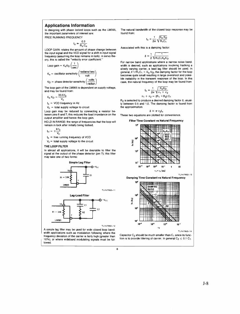
Applications InformationIn designing with phase locked loops such as the LM565,the important parameters of interest are:
FREE RUNNING FREQUENCY
0.3
,oBR~C~LOOP GAIN: relates the amount of phase change betweenthe input signal and the VCO signal for a shift in input signalfrequency (assuming the loop remains in lock), in servo theory, this is called the "velocity error coefficient."
Loop gain - KqKq (-)\sec/
Kq —oscillator sensitivity' radians/sec \
volt /
... / volts \Kn - phase detector sensitivity —•—
Vradian/
The loop gain of the LM565 is dependent on supply voltage,and may be found from:
33.6 f0KoKD = -v7-2
vc
f0 = VCO frequency in Hz
Vc — total supply voltage to circuit
Loop gain may be reduced by connecting a resistor between pins 6 and 7; this reduces the load impedance on theoutput amplifier and hence the loop gain.
HOLD IN RANGE: the range of frequencies that the loop willremain in lock after initially being locked.
lH-±^f0 = free running frequency of VCO
Vc — total supply voltage to the circuit
THE LOOP FILTER
In almost all applications, it will be desirable to filter thesignal at the output of the phase detector (pin 7); this filtermay take one of two forms:
Simple Lag Filter
■©♦VC
Rl - 36k'
TL/H/7853-11
O'Vc
TL/H/7B53-12
A simple lag fifter may be used for wide closed loop bandwidth applications such as modulation following where thefrequency deviation of the carrier is fairly high (greater than10%), or where wideband modulating signals must be followed.
The natural bandwidth of the closed loop response may befound from:
, 1 /KoKd,n"2-VRiCi
Associated with this is a damping factor:
-- A—I2\RiC1KiCiKoKD
For narrow band applications where a narrow noise bandwidth is desired, such as applications involving tracking aslowly varying carrier, a lead lag filter should be used. Ingeneral, if I/R-jOj < Kq Kr>the damping factor for the loopbecomes quite small resulting in large overshoot and possible instability in the transient response of the loop. In thiscase, the natural frequency of the loop may be found from
" 2-VTT+T2T-i + T2 ~ (Rl + R2) C-|
R2 is selected to produce a desired damping factor 5, usually between 0.5 and 1.0. The damping factor is found fromthe approximation:
5 ~ - r2fnThese two equations are plotted for convenience.
Filter Time Constant vs Natural Frequency
ID4
to3
103
101
KoKo-f/RADV
Mh•JC* -
I0» !
Jf*140*1
\t* ir3 10-' itr1 1 to
Tl + T, (NO)
TL/H/7853-13
Damping Time Constant vs Natural Frequency
113
10'
10'
to-* iir1 10J 101
TL/H/7853-14
Capacitor C2 should be much smaller than C-, since its function is to provide filtering of carrier. In general C2 ^ 0.1 C-\.
Miiiiii i HimDan-inn TTrnjRATIO t ffjfl
XII Nil Itfffy'2 -4-
FKKr^T^m
11 llli Uil
J-8

Physical Dimensions inches (millimeters)
:T
MM(12.701 (I
MIN •
ITli-1.335 ^_
xTFDff
C.025
.OKI,
17+T
>11.711-OJM)
• 118 .
(I.t21l
POM-IKS
SfT" (0.737 -114»|
Metal Can Package (H)Order Number LM565H
NS Package Number H10C
J-9
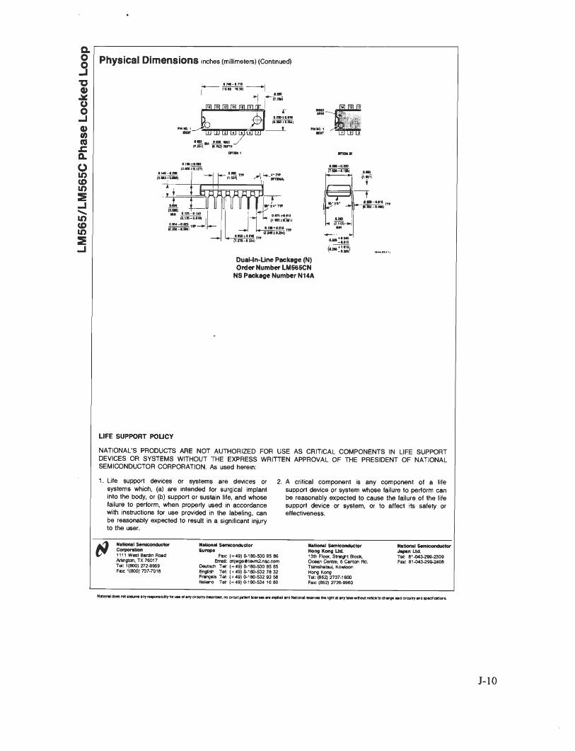
aoo_j
"Oa>__
Oo-I
a>a>(0J_a
oin
in
CO1*0
Physical Dimensions inches (millimeters) (Continued)
H j tl~I—i r~n r~n r~n r~n rtn !
"'Snt-^lIi _iw b man!|f »0 11 Hi)
t
DuaMn-Line Package (N)Order Number LM565CN
NS Package Number N14A
LIFE SUPPORT POLICY
NATIONAL'S PRODUCTS ARE NOT AUTHORIZED FOR USE AS CRITICAL COMPONENTS IN LIFE SUPPORTDEVICES OR SYSTEMS WITHOUT THE EXPRESS WRITTEN APPROVAL OF THE PRESIDENT OF NATIONALSEMICONDUCTOR CORPORATION. As used herein:
1. Life support devices or systems are devices orsystems which, (a) are intended for surgical implantinto the body, or (b) support or sustain life, and whosefailure to perform, when properly used in accordancewith instructions for use provided in the labeling, canbe reasonably expected to result in a significant injuryto the user.
cVNational Semiconductor
Corporation1111 West Baron Road
Arlington, TX 76017Tel: 1(600) 272-9959Fax: 1(800) 737-7018
National SemiconductorEurope
Fax: (+49) 0-160-530 85 98Email- on|wge(ltevn_nsc.com
Deutsch Tel: (+49) 0-160-530 65 65English Tel: (+49) 0-180-532 78 32Francais Tel: (+49) 0-160-532 93 56Itallano Tot- (+49) 0-160-534 16 60
A critical component is any component of a lifesupport device or system whose failure to perform canbe reasonably expected to cause the failure of the lifesupport device or system, or to affect its safety oreffectiveness.
National Semiconductor
Hong Kong Ltd.13fr Floor. Straight Block.Ocean Centre, 5 Canton Hd.TsKTtshatsui, KowloonHong KongTel: (652) 2737-1600Fax: (852) 2736-9960
National SemiconductorJapan Ltd.Tel: 81-043-299-2309Fax: 61-043-299-2408
Nttoi* *>« rxxa_»r» »rv r»^ir«airv for_> rt «~ woiiry flt_i
MO