TAS2764 Digital Input Mono Class-D Audio Amplifier With ...
105
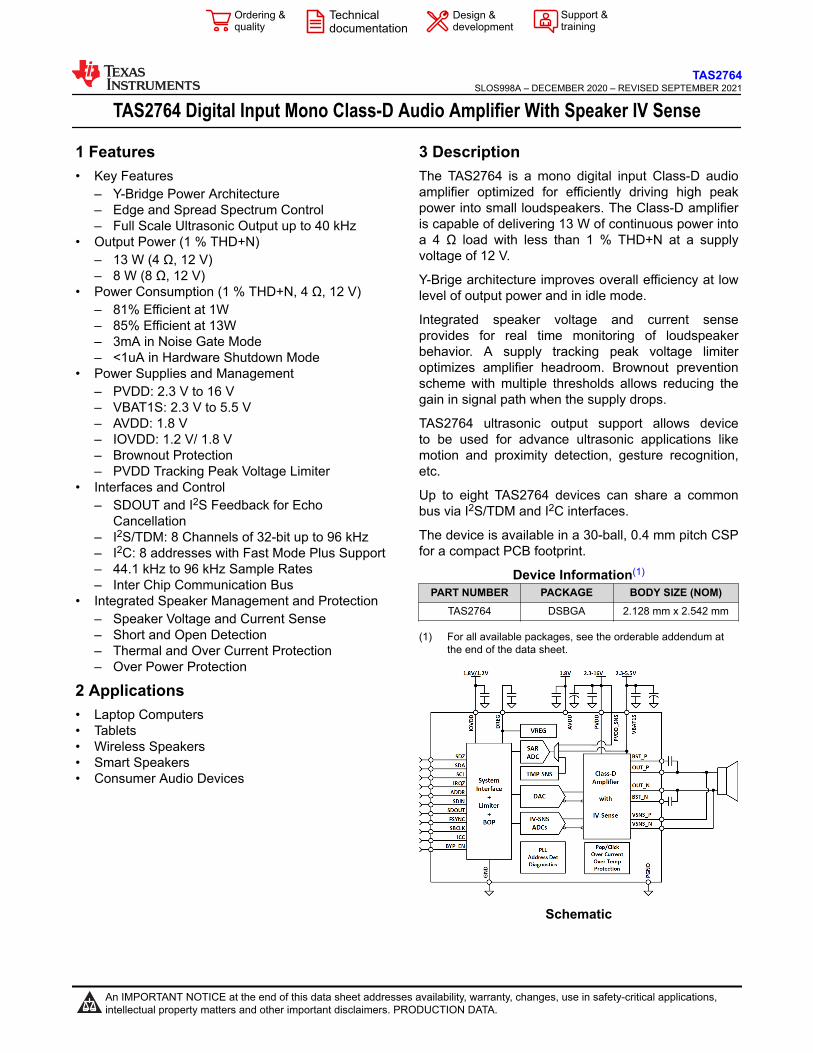
TAS2764 Digital Input Mono Class-D Audio Amplifier With Speaker IV Sense 1 Features • Key Features – Y-Bridge Power Architecture – Edge and Spread Spectrum Control – Full Scale Ultrasonic Output up to 40 kHz • Output Power (1 % THD+N) – 13 W (4 Ω, 12 V) – 8 W (8 Ω, 12 V) • Power Consumption (1 % THD+N, 4 Ω, 12 V) – 81% Efficient at 1W – 85% Efficient at 13W – 3mA in Noise Gate Mode – <1uA in Hardware Shutdown Mode • Power Supplies and Management – PVDD: 2.3 V to 16 V – VBAT1S: 2.3 V to 5.5 V – AVDD: 1.8 V – IOVDD: 1.2 V/ 1.8 V – Brownout Protection – PVDD Tracking Peak Voltage Limiter • Interfaces and Control – SDOUT and I 2 S Feedback for Echo Cancellation – I 2 S/TDM: 8 Channels of 32-bit up to 96 kHz – I 2 C: 8 addresses with Fast Mode Plus Support – 44.1 kHz to 96 kHz Sample Rates – Inter Chip Communication Bus • Integrated Speaker Management and Protection – Speaker Voltage and Current Sense – Short and Open Detection – Thermal and Over Current Protection – Over Power Protection 2 Applications • Laptop Computers • Tablets • Wireless Speakers • Smart Speakers • Consumer Audio Devices 3 Description The TAS2764 is a mono digital input Class-D audio amplifier optimized for efficiently driving high peak power into small loudspeakers. The Class-D amplifier is capable of delivering 13 W of continuous power into a 4 Ω load with less than 1 % THD+N at a supply voltage of 12 V. Y-Brige architecture improves overall efficiency at low level of output power and in idle mode. Integrated speaker voltage and current sense provides for real time monitoring of loudspeaker behavior. A supply tracking peak voltage limiter optimizes amplifier headroom. Brownout prevention scheme with multiple thresholds allows reducing the gain in signal path when the supply drops. TAS2764 ultrasonic output support allows device to be used for advance ultrasonic applications like motion and proximity detection, gesture recognition, etc. Up to eight TAS2764 devices can share a common bus via I 2 S/TDM and I 2 C interfaces. The device is available in a 30-ball, 0.4 mm pitch CSP for a compact PCB footprint. Device Information (1) PART NUMBER PACKAGE BODY SIZE (NOM) TAS2764 DSBGA 2.128 mm x 2.542 mm (1) For all available packages, see the orderable addendum at the end of the data sheet. Schematic TAS2764 SLOS998A – DECEMBER 2020 – REVISED SEPTEMBER 2021 An IMPORTANT NOTICE at the end of this data sheet addresses availability, warranty, changes, use in safety-critical applications, intellectual property matters and other important disclaimers. PRODUCTION DATA.
-
Upload
khangminh22 -
Category
Documents
-
view
1 -
download
0
Transcript of TAS2764 Digital Input Mono Class-D Audio Amplifier With ...
TAS2764 Digital Input Mono Class-D Audio Amplifier With Speaker IV Sense
1 Features• Key Features
– Y-Bridge Power Architecture– Edge and Spread Spectrum Control– Full Scale Ultrasonic Output up to 40 kHz
• Output Power (1 % THD+N)– 13 W (4 Ω, 12 V)– 8 W (8 Ω, 12 V)
• Power Consumption (1 % THD+N, 4 Ω, 12 V)– 81% Efficient at 1W– 85% Efficient at 13W– 3mA in Noise Gate Mode– <1uA in Hardware Shutdown Mode
• Power Supplies and Management– PVDD: 2.3 V to 16 V– VBAT1S: 2.3 V to 5.5 V– AVDD: 1.8 V– IOVDD: 1.2 V/ 1.8 V– Brownout Protection– PVDD Tracking Peak Voltage Limiter
• Interfaces and Control– SDOUT and I2S Feedback for Echo
Cancellation– I2S/TDM: 8 Channels of 32-bit up to 96 kHz– I2C: 8 addresses with Fast Mode Plus Support– 44.1 kHz to 96 kHz Sample Rates– Inter Chip Communication Bus
• Integrated Speaker Management and Protection– Speaker Voltage and Current Sense– Short and Open Detection– Thermal and Over Current Protection– Over Power Protection
2 Applications• Laptop Computers• Tablets• Wireless Speakers• Smart Speakers• Consumer Audio Devices
3 DescriptionThe TAS2764 is a mono digital input Class-D audio amplifier optimized for efficiently driving high peak power into small loudspeakers. The Class-D amplifier is capable of delivering 13 W of continuous power into a 4 Ω load with less than 1 % THD+N at a supply voltage of 12 V.
Y-Brige architecture improves overall efficiency at low level of output power and in idle mode.
Integrated speaker voltage and current sense provides for real time monitoring of loudspeaker behavior. A supply tracking peak voltage limiter optimizes amplifier headroom. Brownout prevention scheme with multiple thresholds allows reducing the gain in signal path when the supply drops.
TAS2764 ultrasonic output support allows device to be used for advance ultrasonic applications like motion and proximity detection, gesture recognition, etc.
Up to eight TAS2764 devices can share a common bus via I2S/TDM and I2C interfaces.
The device is available in a 30-ball, 0.4 mm pitch CSP for a compact PCB footprint.
Device Information(1)
PART NUMBER PACKAGE BODY SIZE (NOM)TAS2764 DSBGA 2.128 mm x 2.542 mm
(1) For all available packages, see the orderable addendum at the end of the data sheet.
Schematic
TAS2764SLOS998A – DECEMBER 2020 – REVISED SEPTEMBER 2021
An IMPORTANT NOTICE at the end of this data sheet addresses availability, warranty, changes, use in safety-critical applications, intellectual property matters and other important disclaimers. PRODUCTION DATA.
Table of Contents1 Features............................................................................12 Applications..................................................................... 13 Description.......................................................................14 Revision History.............................................................. 25 Pin Configuration and Functions...................................36 Specifications.................................................................. 5
6.1 Absolute Maximum Ratings........................................ 56.2 ESD Ratings............................................................... 56.3 Recommended Operating Conditions.........................56.4 Thermal Information....................................................56.5 Electrical Characteristics.............................................66.6 I2C Timing Requirements.......................................... 116.7 TDM Port Timing Requirements................................126.8 Typical Characteristics.............................................. 13
7 Parameter Measurement Information.......................... 238 Detailed Description......................................................24
8.1 Overview................................................................... 248.2 Functional Block Diagram......................................... 248.3 Feature Description...................................................248.4 Device Functional Modes..........................................268.5 Operational Modes....................................................378.6 Faults and Status...................................................... 388.7 Power Sequencing Requirements............................ 418.8 Digital Input Pull Downs............................................ 418.9 Register Map.............................................................418.10 SDOUT Equations.................................................. 86
9 Application and Implementation.................................. 87
9.1 Application Information............................................. 879.2 Typical Application.................................................... 879.3 Design Requirements............................................... 889.4 Detailed Design Procedure....................................... 889.5 Application Curves.................................................... 89
10 Initialization Set Up..................................................... 9010.1 Recommended Configuration at Power Up............ 9010.2 Initial Device Configuration - 4 Channel Power
Up (Default Mode - PWR_MODE1).............................9010.3 Initial Device Configuration - 44.1 kHz....................9110.4 Sample Rate Change - 48 kHz to 44.1kHz............. 9110.5 Idle Channel Hysterisis........................................... 9110.6 DSP Loopback........................................................91
11 Power Supply and I2C Recommendations................ 9211.1 Power Supply Modes.............................................. 92
12 Layout...........................................................................9412.1 Layout Guidelines................................................... 9412.2 Layout Example...................................................... 94
13 Device and Documentation Support..........................9613.1 Receiving Notification of Documentation Updates..9613.2 Support Resources................................................. 9613.3 Trademarks.............................................................9613.4 Electrostatic Discharge Caution..............................9613.5 Glossary..................................................................96
14 Mechanical, Packaging, and Orderable Information.................................................................... 97
4 Revision HistoryNOTE: Page numbers for previous revisions may differ from page numbers in the current version.
Changes from Revision * (December 2020) to Revision A (September 2021) Page• Changed device status to Production Data from Advanced Information............................................................ 1
TAS2764SLOS998A – DECEMBER 2020 – REVISED SEPTEMBER 2021 www.ti.com
2 Submit Document Feedback Copyright © 2021 Texas Instruments Incorporated
Product Folder Links: TAS2764
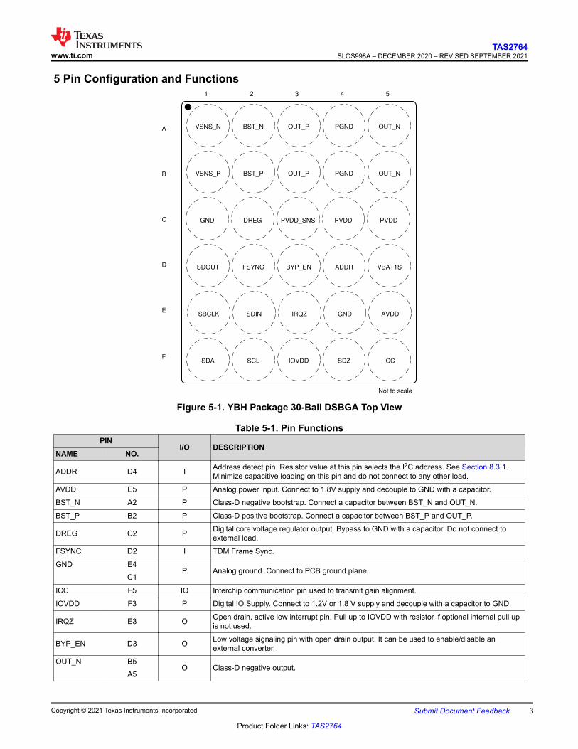
5 Pin Configuration and Functions1 2 3 4 5
A
B
C
D
E
Not to scale
F
VSNS_N BST_N OUT_P PGND OUT_N
VSNS_P BST_P OUT_P PGND OUT_N
GND DREG PVDD_SNS PVDD PVDD
SBCLK SDIN IRQZ GND AVDD
SDA SCL IOVDD SDZ ICC
SDOUT FSYNC BYP_EN ADDR VBAT1S
Figure 5-1. YBH Package 30-Ball DSBGA Top View
Table 5-1. Pin FunctionsPIN
I/O DESCRIPTIONNAME NO.
ADDR D4 I Address detect pin. Resistor value at this pin selects the I2C address. See Section 8.3.1. Minimize capacitive loading on this pin and do not connect to any other load.
AVDD E5 P Analog power input. Connect to 1.8V supply and decouple to GND with a capacitor.
BST_N A2 P Class-D negative bootstrap. Connect a capacitor between BST_N and OUT_N.
BST_P B2 P Class-D positive bootstrap. Connect a capacitor between BST_P and OUT_P.
DREG C2 P Digital core voltage regulator output. Bypass to GND with a capacitor. Do not connect to external load.
FSYNC D2 I TDM Frame Sync.
GND E4P Analog ground. Connect to PCB ground plane.
C1
ICC F5 IO Interchip communication pin used to transmit gain alignment.
IOVDD F3 P Digital IO Supply. Connect to 1.2V or 1.8 V supply and decouple with a capacitor to GND.
IRQZ E3 O Open drain, active low interrupt pin. Pull up to IOVDD with resistor if optional internal pull up is not used.
BYP_EN D3 O Low voltage signaling pin with open drain output. It can be used to enable/disable an external converter.
OUT_N B5O Class-D negative output.
A5
www.ti.comTAS2764
SLOS998A – DECEMBER 2020 – REVISED SEPTEMBER 2021
Copyright © 2021 Texas Instruments Incorporated Submit Document Feedback 3
Product Folder Links: TAS2764
Table 5-1. Pin Functions (continued)PIN
I/O DESCRIPTIONNAME NO.OUT_P B3
O Class-D positive output.A3
PGND B4P Class-D ground. Connect to PCB ground plane.
A4
SBCLK E1 I TDM Serial Bit Clock.
SCL F2 I I2C Clock Pin. Pull up to IOVDD with a resistor.
SDA F1 IO I2C Data Pin. Pull up to IOVDD with a resistor.
SDIN E2 I TDM Serial Data Input.
SDOUT D1 IO TDM Serial Data Output.
SDZ F4 I Active low hardware shutdown.
PVDD C4P Class-D power supply input. Decouple with a capacitor.
C5
PVDD_SNS C3 I PVDD remote sense pin.
VBAT1S D5 P Single-cell battery supply input. Decouple with a capacitor.
VSNS_N A1 I Voltage Sense negative input. Connect to one speaker input.
VSNS_P B1 I Voltage Sense positive input. Connect to the other speaker input.
TAS2764SLOS998A – DECEMBER 2020 – REVISED SEPTEMBER 2021 www.ti.com
4 Submit Document Feedback Copyright © 2021 Texas Instruments Incorporated
Product Folder Links: TAS2764
6 Specifications6.1 Absolute Maximum Ratingsover operating free-air temperature range (unless otherwise noted) (1)
MIN MAX UNIT
Supply Voltage
AVDD –0.3 2 V
IOVDD –0.3 2 V
PVDD –0.3 18.5 V
VBAT1S –0.3 6 V
PVDD-VBAT1S -0.3 18 V
Internal Supply Voltage DREG -0.3 1.5 V
Input voltage(2) Digital IOs referenced to IOVDD supply –0.3 2.3 V
Operating free-air temperature, TA ; Device is functional and reliable, some performance characteristics may be degraded. –40 85 °C
Performance free-air temperature, TP ; All performance characteristics are met. –20 70 °C
Operating junction temperature, TJ –40 125 °C
Storage temperature, Tstg –65 150 °C
(1) Stresses beyond those listed under Section 6.1 can cause permanent damage to the device. These are stress ratings only, which do not imply functional operation of the device at these or any other conditions beyond those indicated under Section 6.3 . Exposure to absolute maximum rated conditions for extended periods can affect device reliability.
(2) All digital inputs and IOs are failsafe.
6.2 ESD RatingsVALUE UNIT
V(ESD) Electrostatic dischargeHuman-body model (HBM), per ANSI/ESDA/JEDEC JS-001(1) ±2000
VCharged-device model (CDM), per JEDEC specification JESD22-C101(2) ±500
(1) JEDEC document JEP155 states that 500-V HBM allows safe manufacturing with a standard ESD control process.(2) JEDEC document JEP157 states that 250-V CDM allows safe manufacturing with a standard ESD control process.
6.3 Recommended Operating Conditionsover operating free-air temperature range (unless otherwise noted)
MIN NOM MAX UNIT
AVDD Supply voltage 1.65 1.8 1.95 V
IOVDD Supply voltage1.1 1.2 1.3
V1.65 1.8 1.95
PVDDSupply voltage (functional)(1) 2.3(2) 16
VSupply voltage (performance) 3.0 16
VBAT1SSupply voltage (functional)(1) 2.3 5.5
VSupply voltage (performance) 3.0 5.5
VIH High-level digital input voltage IOVDD V
VIL Low-level digital input voltage 0 V
RSPK Speaker impedance 3.2 Ω
LSPK Speaker inductance 5 µH
(1) Device will remain functional but performance will degrade.(2) PVDD>VBAT1S-0.7V.
6.4 Thermal Information
THERMAL METRIC(1)
TAS2764
UNITYBH (DSBGA)
30 PINS
RθJA Junction-to-ambient thermal resistance 59.9 °C/W
www.ti.comTAS2764
SLOS998A – DECEMBER 2020 – REVISED SEPTEMBER 2021
Copyright © 2021 Texas Instruments Incorporated Submit Document Feedback 5
Product Folder Links: TAS2764
THERMAL METRIC(1)
TAS2764
UNITYBH (DSBGA)
30 PINS
RθJC(top) Junction-to-case (top) thermal resistance 0.2 °C/W
RθJB Junction-to-board thermal resistance 14.9 °C/W
ψJT Junction-to-top characterization parameter 0.1 °C/W
ψJB Junction-to-board characterization parameter 14.9 °C/W
(1) For more information about traditional and new thermal metrics, see the Semiconductor and IC Package Thermal Metrics application report, SPRA953.
6.5 Electrical CharacteristicsTA = 25 °C, PVDD = 12 V, VBAT1S = 3.8 V, AVDD = 1.8V IOVDD =1.2 V, RL = 4Ω + 16µH, fin = 1 kHz, fs = 48 kHz, Gain = 21 dBV, SDZ = 1, EDGE_RATE[1:0]=00, NG_EN=0, EN_LLSR=1, PWR_MODE1, Measured filter free as in Section 7 (unless otherwise noted).
PARAMETER TEST CONDITIONS MIN TYP MAX UNIT
DIGITAL INPUT and OUTPUT
VIHHigh-level digital input logic voltage threshold All digital pins except SDA and SCL 0.7×IOVDD V
VILLow-level digital input logic voltage threshold All digital pins except SDA and SCL 0.3 ×
IOVDD V
VIH(I2C)High-level digital input logic voltage threshold SDA and SCL 0.7xIOVDD V
VIL(I2C)Low-level digital input logic voltage threshold SDA and SCL 0.3 x
IOVDD V
VOH High-level digital output voltage All digital pins except SDA, SCL and IRQZ; IOH = 100 µA. IOVDD–0.2V V
VOL Low-level digital output voltage All digital pins except SDA, SCL and IRQZ; IOL = –100 µA. 0.2 V
VOL(I2C) Low-level digital output voltage SDA and SCL; IOL(I2C) = -1 mA. - 0.2 x IOVDD V
VOL(IRQZ)Low-level digital output voltage for IRQZ open drain Output IRQZ; IOL(IRQZ) = -1 mA. 0.2 V
IIHInput logic-high leakage for digital inputs All digital pins; Input = IOVDD. –1 1 µA
IILInput logic-low leakage for digital inputs All digital pins; Input = GND. –1 1 µA
ROS OUT to VSNS Resistors Load disconnected 10 kΩ
CIN Input capacitance for digital inputs All digital pins 5 pF
RPDPull down resistance for IO pins when asserted on SDOUT, SDIN, FSYNC, SBCLK 18 kΩ
IO Output Current Strength
Drive Mode 0 - Measured at (IOVDD-0.4V) and 0.4V 8
mADrive Mode 1 - Measured at (IOVDD-0.4V) and 0.4V 6
Drive Mode 2 - Measured at (IOVDD-0.4V) and 0.4V 4
Drive Mode 3 - Measured at (IOVDD-0.4V) and 0.4V 2
AMPLIFIER PERFORMANCE
POUT Maximum Output Power
RL = 4Ω + 16µH, THD+N = 1 % 13
WRL = 8 Ω + 16 µH, THD+N = 1 % 8
RL = 4Ω + 16µH, THD+N = 10 % 15.8
RL = 8 Ω + 16 µH, THD+N = 10 % 9.7
System Efficiency
RL = 4Ω + 16µH, POUT = 1 W 80.5
%
RL = 8 Ω + 16 µH, POUT = 1 W 84
RL = 8 Ω + 5µH, POUT = 1 W PWR_MODE2 76.5
RL = 8 Ω + 16µH, POUT = 1 W PWR_MODE2 82.5
RL = 4Ω + 16µH, POUT = 10 W 85
RL = 8 Ω + 16 µH, POUT = 5 W 90
RL = 8 Ω + 5 µH, POUT = 8 W, PWR_MODE2 90
TAS2764SLOS998A – DECEMBER 2020 – REVISED SEPTEMBER 2021 www.ti.com
6 Submit Document Feedback Copyright © 2021 Texas Instruments Incorporated
Product Folder Links: TAS2764
TA = 25 °C, PVDD = 12 V, VBAT1S = 3.8 V, AVDD = 1.8V IOVDD =1.2 V, RL = 4Ω + 16µH, fin = 1 kHz, fs = 48 kHz, Gain = 21 dBV, SDZ = 1, EDGE_RATE[1:0]=00, NG_EN=0, EN_LLSR=1, PWR_MODE1, Measured filter free as in Section 7 (unless otherwise noted).
PARAMETER TEST CONDITIONS MIN TYP MAX UNIT
THD+N Total Harmonic Distortion and Noise
POUT = 1 W, RL = 4Ω + 16µH, fin = 1 kHz -83
dBPOUT = 1 W, RL = 4Ω + 16µH, fin = 6.67 kHz -83
POUT = 1 W, RL = 8 Ω + 5µH, fin = 20 Hz - 20 kHz, PWR_MODE2 -83
IMD Intermodulation Distortion ITU-R, 19kHz/20kHz, 1:1:6.5W -80 dB
VN Idle Channel Noise
A-Weighted, 20 Hz - 20 kHz, DAC in Mute, PWR_MODE1 27
µVA-Weghted, 20 Hz - 20k Hz, DAC in Mute, PWR_MODE2 27
A-Weighted, 20 Hz - 20 kHz, DAC in Mute, PWR_MODE4 32.7
FPWM Class-D PWM Switching Frequency
Average frequency in Spread Spectrum Mode, CLASSD_SYNC=0 384
kHzFixed Frequency Mode, CLASSD_SYNC=0 365 384 404
Fixed Frequency Mode, CLASSD_SYNC=1, fs = 44.1, 88.2 kHz 352.8
Fixed Frequency Mode, CLASSD_SYNC=1, fs = 48, 96 kHz 384
VOS Output Offset Voltage Idle Mode -1 1 mV
DNR Dynamic RangeA-Weighted, -60 dBFS 109
dBA-Weighted, -60 dBFS, PWR_MODE2 109
SNR Signal to Noise RatioA-Weighted, Referenced to 1 % THD+N Output Level 109
dBA-Weighted, Referenced to 1 % THD+N Output Level PWR_MODE2 109
KCP Click and Pop Performance Into and out of Shutdown, A-weighted 1 2.7 mV
Full Scale Output Voltage fs <= 48kHz 21 dBV
Minimum Programmable Gain fs <= 48kHz 11 dBV
Maximum Programmable Gain fs <= 48kHz 21 dBV
Programmable Output Level Step Size 0.5 dB
Mute attenuation Device in Software Shutdown or Muted in Normal Operation 110 dB
Chip to Chip Group Delay -1 1 µs
EMI Margin to EN55022B 6" cable, Pout = 1W -6 dB
PVDD Power Supply Rejection Ratio
PVDD = 12 V + 200 mVpp, fripple = 217 Hz 100
dBPVDD = 12 V + 200 mVpp, fripple = 1 kHz 112
PVDD = 12 V + 200 mVpp, fripple = 20 kHz 96
VBAT1S Power Supply Rejection Ratio
VBAT1S = 3.8 V + 200 mVpp, fripple = 217 Hz 100
dBVBAT1S = 3.8 V + 200 mVpp, fripple = 1 kHz 112
VBAT1S = 3.8 V + 200 mVpp, fripple = 20 kHz 88
AVDD Power Supply Rejection Ratio
AVDD = 1.8 V + 200 mVpp, fripple = 217 Hz 96
dBAVDD = 1.8 V + 200 mVpp, fripple = 1 kHz 90
AVDD = 1.8 V + 200 mVpp, fripple = 20 kHz 96
Power Supply Intermodulation
PVDD 217 Hz, 100-mVpp, Input f=1kHz @ 400mW -70
dBVBAT1S 217 Hz, 100-mVpp, Input f=1kHz @ 400mW -118
AVDD, 217 Hz, 100-mVpp, Input f=1kHz @ 400mW -82
IOVDD 217 Hz, 100-mVpp, Input f=1kHz @ 400mW -70
Turn ON Time from Release of SW Shutdown
No Volume Ramping 1.2ms
Volume Ramping 5.3
Turn OFF Time From Assertion of SW Shutdown to Amp Hi-Z
No Volume Ramping 0.5ms
Volume Ramping 5.9
Release of SW Shutdown to new assertion of SW Shutdown 1.5 ms
Out of HW Shutdown to first I2C command 1 ms
www.ti.comTAS2764
SLOS998A – DECEMBER 2020 – REVISED SEPTEMBER 2021
Copyright © 2021 Texas Instruments Incorporated Submit Document Feedback 7
Product Folder Links: TAS2764
TA = 25 °C, PVDD = 12 V, VBAT1S = 3.8 V, AVDD = 1.8V IOVDD =1.2 V, RL = 4Ω + 16µH, fin = 1 kHz, fs = 48 kHz, Gain = 21 dBV, SDZ = 1, EDGE_RATE[1:0]=00, NG_EN=0, EN_LLSR=1, PWR_MODE1, Measured filter free as in Section 7 (unless otherwise noted).
PARAMETER TEST CONDITIONS MIN TYP MAX UNIT
Noise Gate recovery to Shutdown latency 100 μs
Power up to BOP_SHDN latency 1.5 ms
DIAGNOSTIC GENERATOR
THD+N Total Harmonic Distortion and Noise Pout=1W, DVC_LVL[7:0]=17h -80 dB
ferr Frequency Error Using internal oscillator 5 %
DIE TEMPERATURESENSOR
Resolution 8 bits
Minimum Die Temperature Measurement -40 °C
Maximum Die Temperature Measurement 150 °C
Die Temperature Resolution 1 °C
Die Temperature Accuracy -5 5 °C
VOLTAGEMONITOR
Resolution 12 bits
Minimum PVDD Measurement 2 V
Maximum PVDD Measurements 16 V
PVDD Resolution 20 mV
PVDD Accuracy -100 100 mV
Minimum VBAT1S Measurement 2 V
Maximum VBAT1S Measurement 6 V
VBAT1S Resolution 20 mV
VBAT1S Accuracy -45 45 mV
TDM SERIAL AUDIO PORT
PCM Sample Rates and FSYNC Input Frequency Typical values 44.1 96 kHz
SBCLK Input Frequency I2S/TDM Operation 0.7056 24.576 MHz
SBCLK Maximum Input Jitter
RMS Jitter below 40 kHz that can be tolerated without performance degradation 0.5
nsRMS Jitter above 40 kHz that can be tolerated without performance degradation 1
SBCLK Cycles per FSYNC in I2S and TDM Modes
Other values: 24, 32, 48, 64, 96, 125, 128, 192, 250, 256, 384, 500 16 512 Cycles
PCM PLAYBACK CHARACTERISTICS fs ≤ 48 kHz
fs Sample Rates 44.1 48 kHz
Passband Frequency Meeting Ripple 0.454 fsPassband Ripple 20Hz to LPF cutoff frequency -0.3 +0.3 dB
Stop Band Attenuation≥ 0.55 fs 60
dB≥ 1 fs 65
Group Delay @ 1kHzNoise Gate Enabled 17.7
1/fsNoise Gate Disabled 9
Group DelayDC to 0.454 fs , Noise Gate enabled, DC blocker disabled 16 19
1/fsDC to 0.454 fs , Noise Gate disabled, DC blocker disabled 7 10
fs > 48 kHz
fs Sample Rates 88.2 96 kHz
Passband Frequency Meeting Ripple fs = 96 kHz 0.375 fsPassband 3db Frequency fs = 96 kHz 0.409 fsPassband Ripple DC to LPF cutoff frequency -0.5 0.5 dB
TAS2764SLOS998A – DECEMBER 2020 – REVISED SEPTEMBER 2021 www.ti.com
8 Submit Document Feedback Copyright © 2021 Texas Instruments Incorporated
Product Folder Links: TAS2764
TA = 25 °C, PVDD = 12 V, VBAT1S = 3.8 V, AVDD = 1.8V IOVDD =1.2 V, RL = 4Ω + 16µH, fin = 1 kHz, fs = 48 kHz, Gain = 21 dBV, SDZ = 1, EDGE_RATE[1:0]=00, NG_EN=0, EN_LLSR=1, PWR_MODE1, Measured filter free as in Section 7 (unless otherwise noted).
PARAMETER TEST CONDITIONS MIN TYP MAX UNIT
Stop Band Attenuation≥ 0.55 fs 60
dB≥ 1 fs 65
Group Delay @ 1kHzNoise Gate Enabled 33.2
1/fsNoise Gate Disabled 17.4
Group Delay
DC to 0.375 fs for 96 kHz, Noise Gate Enabled, DC blocker disabled 33 39
1/fsDC to 0.375 fs for 96 kHz, Noise Gate Disabled, DC blocker disabled 17 23
SPEAKER CURRENT SENSE
Resolution 16 bits
DNR Dynamic Range Un-Weighted, Relative to 0 dBFS 66 dB
THD+N Total Harmonic Distortion and Noise fin = 1 kHz, Pout = 7. 5W -58 dB
Full Scale Input Current -6dBFS Input Signal Level 3.75 A
Differential Mode Gain Pout = 1W, using a 40Hz, -40dBFS pilot tone 0.98 1.02
Differential Mode Gain Variability Pout = 100mW to 0.1% THD+N, using a 40Hz, -40dBFS pilot tone, Calibrated at 100 mW -1.4 1.4 %
Gain Error Over Temperature -200C to 700C, Pout=1W, Calibrated at 250C -1.35 1.35 %
Offset HPF_FREQ_REC[2:0]=0h -2 2 mA
Frequency Response 20Hz-20kHz -0.1 0.1 dB
Group Delay 8 1/fsSPEAKER VOLTAGE SENSE
Resolution 16 bits
DNR Dynamic Range Un-Weighted, Relative 0 dBFS 69 dB
THD+N Total Harmonic Distortion and Noise fin = 1 kHz, Pout = 7.5W -60 dB
Full Scale Input Voltage 14 VPK
Differential Mode Gain Pout = 1W, using a 40Hz - 40dBFS pilot tone 0.99 1.01
Differential Mode Gain Variability Pout = 100mW to 0.1% THD+N, using a 40Hz, -40dBFS pilot tone -0.45 +0.45 %
Gain error over temperature -20C to 70C, Pout=1W -0.75 +0.75 %
Offset HPF_FREQ_REC[2:0]=0h -10 +10 mV
Frequency Response 20Hz - 20kHz -0.1 0.1 dB
Group Delay 8 1/fsSPEAKER VOLTAGE to CURRENT SENSE PHASE
Phase Error between V and I 300 ns
PROTECTION CIRCUITRY
Brownout Prevention Latency to First Attack PWR_MODE2, Measured at BOP_TH0 of 8.25V 15 µs
Thermal Shutdown Temperature -Typical values 135 145 155 °C
Output Over Current Limit on PVDD Output to Output, Output to GND, Output to PVDD 5.9 A
Output Overt Current Limit on VBAT1S Output to Output, Output to GND 2.5 A
VBAT1S Undervoltage Lockout Threshold
UVLO is asserted 2V
UVLO is de-asserted 2.3
AVDD Undervoltage Lockout Threshold
UVLO is asserted 1.4V
UVLO is de-asserted 1.6
IOVDD Undervoltage Lockout Threshold
UVLO is asserted 0.7V
UVLO is de-asserted 1.1
VBAT1S Internal LDO Undervoltage Lockout Threshold UVLO is asserted 4 V
www.ti.comTAS2764
SLOS998A – DECEMBER 2020 – REVISED SEPTEMBER 2021
Copyright © 2021 Texas Instruments Incorporated Submit Document Feedback 9
Product Folder Links: TAS2764
TA = 25 °C, PVDD = 12 V, VBAT1S = 3.8 V, AVDD = 1.8V IOVDD =1.2 V, RL = 4Ω + 16µH, fin = 1 kHz, fs = 48 kHz, Gain = 21 dBV, SDZ = 1, EDGE_RATE[1:0]=00, NG_EN=0, EN_LLSR=1, PWR_MODE1, Measured filter free as in Section 7 (unless otherwise noted).
PARAMETER TEST CONDITIONS MIN TYP MAX UNIT
VBAT1S Internal LDO Overvoltage Lockout Threshold OVLO is asserted 5.5 V
TYPICAL CURRENT CONSUMPTION
Hardware Shutdown
SDZ = 0, PVDD 0.1
µASDZ = 0, VBAT1S 0.1
SDZ = 0, AVDD 1
SDZ = 0, IOVDD 0.1
Software Shutdown
All Clocks Stopped, PVDD 0.1
µAAll Clocks Stopped, VBAT1S 1
All Clocks Stopped, AVDD 10
All Clocks Stopped, IOVDD 1
Noise Gate Mode
fs = 48 kHz, PVDD 0.05
mAfs = 48 kHz, VBAT1S 0.14
fs = 48 kHz, AVDD 3.2
fs = 48 kHz, IOVDD 0.1
Idle Mode - PWR_MODE1, PWR_MODE3
fs = 48 kHz, PVDD 0.02
mAfs = 48 kHz, VBAT1S 3
fs = 48 kHz, AVDD 8.9
fs = 48 kHz, IOVDD 0.1
Idle Mode - PWR_MODE2
fs = 48 kHz, PVDD 3.2
mAfs = 48 kHz, AVDD 9.3
fs = 48 kHz, IOVDD 0.1
Idle Mode - PWR_MODE4
fs = 48 kHz, PVDD 4.1
mAfs = 48 kHz, AVDD 9.3
fs = 48 kHz, IOVDD 0.1
Idle Mode - PWR_MODE1, PWR_MODE3 fs = 48 kHz, AVDD, IV Sense Disabled 6.3
* For definition of power modes see Section 11.1.
TAS2764SLOS998A – DECEMBER 2020 – REVISED SEPTEMBER 2021 www.ti.com
10 Submit Document Feedback Copyright © 2021 Texas Instruments Incorporated
Product Folder Links: TAS2764
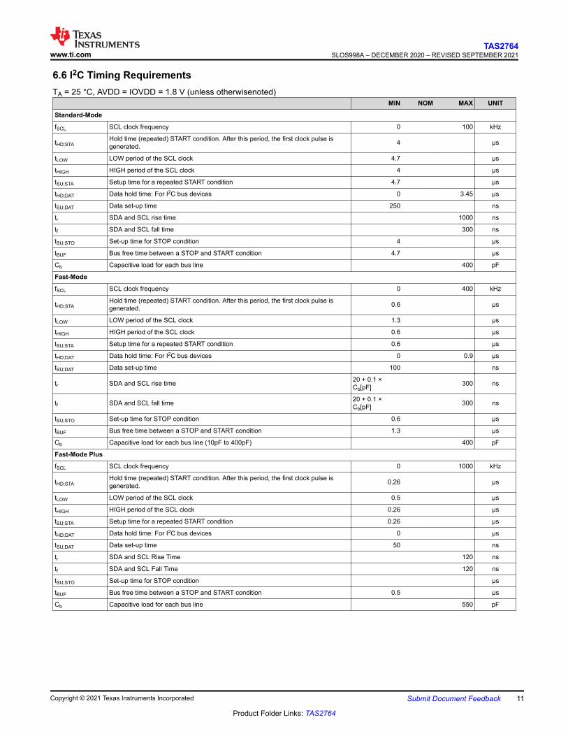
6.6 I2C Timing RequirementsTA = 25 °C, AVDD = IOVDD = 1.8 V (unless otherwisenoted)
MIN NOM MAX UNIT
Standard-Mode
fSCL SCL clock frequency 0 100 kHz
tHD;STAHold time (repeated) START condition. After this period, the first clock pulse is generated. 4 μs
tLOW LOW period of the SCL clock 4.7 μs
tHIGH HIGH period of the SCL clock 4 μs
tSU;STA Setup time for a repeated START condition 4.7 μs
tHD;DAT Data hold time: For I2C bus devices 0 3.45 μs
tSU;DAT Data set-up time 250 ns
tr SDA and SCL rise time 1000 ns
tf SDA and SCL fall time 300 ns
tSU;STO Set-up time for STOP condition 4 μs
tBUF Bus free time between a STOP and START condition 4.7 μs
Cb Capacitive load for each bus line 400 pF
Fast-Mode
fSCL SCL clock frequency 0 400 kHz
tHD;STAHold time (repeated) START condition. After this period, the first clock pulse is generated. 0.6 μs
tLOW LOW period of the SCL clock 1.3 μs
tHIGH HIGH period of the SCL clock 0.6 μs
tSU;STA Setup time for a repeated START condition 0.6 μs
tHD;DAT Data hold time: For I2C bus devices 0 0.9 μs
tSU;DAT Data set-up time 100 ns
tr SDA and SCL rise time 20 + 0.1 × Cb[pF] 300 ns
tf SDA and SCL fall time 20 + 0.1 × Cb[pF] 300 ns
tSU;STO Set-up time for STOP condition 0.6 μs
tBUF Bus free time between a STOP and START condition 1.3 μs
Cb Capacitive load for each bus line (10pF to 400pF) 400 pF
Fast-Mode Plus
fSCL SCL clock frequency 0 1000 kHz
tHD;STAHold time (repeated) START condition. After this period, the first clock pulse is generated. 0.26 μs
tLOW LOW period of the SCL clock 0.5 μs
tHIGH HIGH period of the SCL clock 0.26 μs
tSU;STA Setup time for a repeated START condition 0.26 μs
tHD;DAT Data hold time: For I2C bus devices 0 μs
tSU;DAT Data set-up time 50 ns
tr SDA and SCL Rise Time 120 ns
tf SDA and SCL Fall Time 120 ns
tSU;STO Set-up time for STOP condition μs
tBUF Bus free time between a STOP and START condition 0.5 μs
Cb Capacitive load for each bus line 550 pF
www.ti.comTAS2764
SLOS998A – DECEMBER 2020 – REVISED SEPTEMBER 2021
Copyright © 2021 Texas Instruments Incorporated Submit Document Feedback 11
Product Folder Links: TAS2764
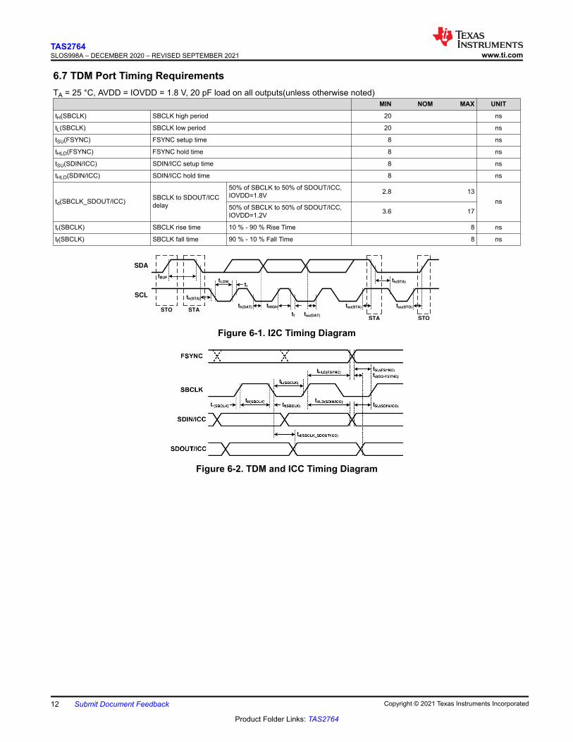
6.7 TDM Port Timing RequirementsTA = 25 °C, AVDD = IOVDD = 1.8 V, 20 pF load on all outputs(unless otherwise noted)
MIN NOM MAX UNIT
tH(SBCLK) SBCLK high period 20 ns
tL(SBCLK) SBCLK low period 20 ns
tSU(FSYNC) FSYNC setup time 8 ns
tHLD(FSYNC) FSYNC hold time 8 ns
tSU(SDIN/ICC) SDIN/ICC setup time 8 ns
tHLD(SDIN/ICC) SDIN/ICC hold time 8 ns
td(SBCLK_SDOUT/ICC) SBCLK to SDOUT/ICC delay
50% of SBCLK to 50% of SDOUT/ICC, IOVDD=1.8V 2.8 13
ns50% of SBCLK to 50% of SDOUT/ICC, IOVDD=1.2V 3.6 17
tr(SBCLK) SBCLK rise time 10 % - 90 % Rise Time 8 ns
tf(SBCLK) SBCLK fall time 90 % - 10 % Fall Time 8 ns
tBUF
STO STA
th(STA)
tLOWtr
th(DAT)
tf
tHIGH
tsu(DAT)
SDA
SCL
tsu(STA)
STA
th(STA)
STO
tsu(STO)
Figure 6-1. I2C Timing Diagram
Figure 6-2. TDM and ICC Timing Diagram
TAS2764SLOS998A – DECEMBER 2020 – REVISED SEPTEMBER 2021 www.ti.com
12 Submit Document Feedback Copyright © 2021 Texas Instruments Incorporated
Product Folder Links: TAS2764
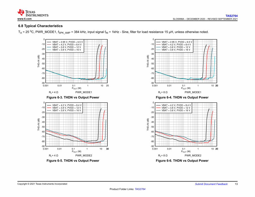
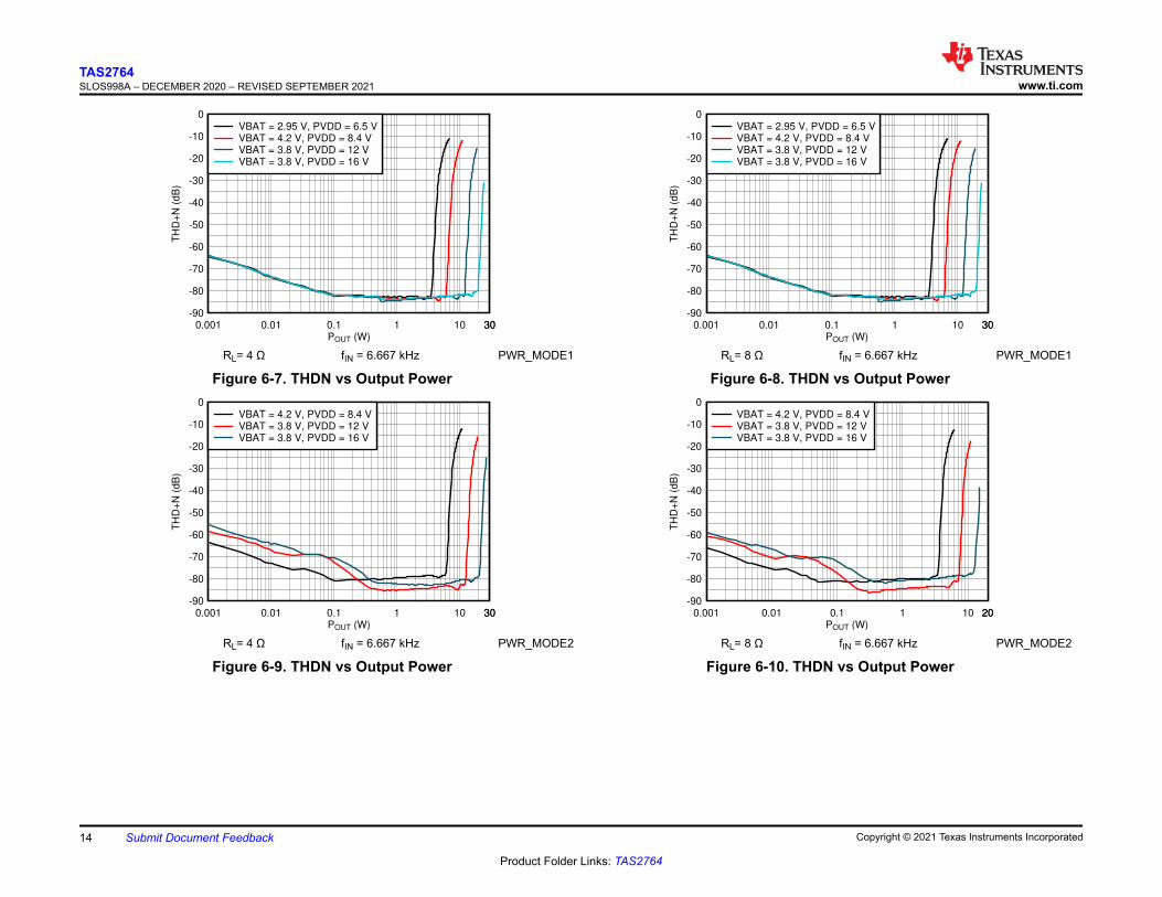
6.8 Typical CharacteristicsTA = 25 0C, PWR_MODE1, fSPK_AMP = 384 kHz, input signal fIN = 1kHz - Sine, filter for load resistance 15 μH, unless otherwise noted.
POUT (W)
TH
D+
N (
dB
)
0.001 0.01 0.1 1 10 25-90
-80
-70
-60
-50
-40
-30
-20
-10
0VBAT = 2.95 V, PVDD = 6.5 VVBAT = 4.2 V, PVDD = 8.4 VVBAT = 3.8 V, PVDD = 12 VVBAT = 3.8 V, PVDD = 16 V
RL= 4 Ω PWR_MODE1
Figure 6-3. THDN vs Output Power
POUT (W)
TH
D+
N (
dB
)
0.001 0.01 0.1 1 10 2020-90
-80
-70
-60
-50
-40
-30
-20
-10
0VBAT = 2.95 V, PVDD = 6.5 VVBAT = 4.2 V, PVDD = 8.4 VVBAT = 3.8 V, PVDD = 12 VVBAT = 3.8 V, PVDD = 16 V
RL= 8 Ω PWR_MODE1
Figure 6-4. THDN vs Output Power
POUT (W)
TH
D+
N (
dB
)
0.001 0.01 0.1 1 10 3030-90
-80
-70
-60
-50
-40
-30
-20
-10
0VBAT = 4.2 V, PVDD = 8.4 VVBAT = 3.8 V, PVDD = 12 VVBAT = 3.8 V, PVDD = 16 V
RL= 4 Ω PWR_MODE2
Figure 6-5. THDN vs Output Power
POUT (W)
TH
D+
N (
dB
)0.001 0.01 0.1 1 10 2020
-90
-80
-70
-60
-50
-40
-30
-20
-10
0VBAT = 4.2 V, PVDD = 8.4 VVBAT = 3.8 V, PVDD = 12 VVBAT = 3.8 V, PVDD = 16 V
RL= 8 Ω PWR_MODE2
Figure 6-6. THDN vs Output Power
www.ti.comTAS2764
SLOS998A – DECEMBER 2020 – REVISED SEPTEMBER 2021
Copyright © 2021 Texas Instruments Incorporated Submit Document Feedback 13
Product Folder Links: TAS2764
POUT (W)
TH
D+
N (
dB
)
0.001 0.01 0.1 1 10 3030-90
-80
-70
-60
-50
-40
-30
-20
-10
0VBAT = 2.95 V, PVDD = 6.5 VVBAT = 4.2 V, PVDD = 8.4 VVBAT = 3.8 V, PVDD = 12 VVBAT = 3.8 V, PVDD = 16 V
RL= 4 Ω fIN = 6.667 kHz PWR_MODE1
Figure 6-7. THDN vs Output Power
POUT (W)
TH
D+
N (
dB
)
0.001 0.01 0.1 1 10 3030-90
-80
-70
-60
-50
-40
-30
-20
-10
0VBAT = 2.95 V, PVDD = 6.5 VVBAT = 4.2 V, PVDD = 8.4 VVBAT = 3.8 V, PVDD = 12 VVBAT = 3.8 V, PVDD = 16 V
RL= 8 Ω fIN = 6.667 kHz PWR_MODE1
Figure 6-8. THDN vs Output Power
POUT (W)
TH
D+
N (
dB
)
0.001 0.01 0.1 1 10 3030-90
-80
-70
-60
-50
-40
-30
-20
-10
0VBAT = 4.2 V, PVDD = 8.4 VVBAT = 3.8 V, PVDD = 12 VVBAT = 3.8 V, PVDD = 16 V
RL= 4 Ω fIN = 6.667 kHz PWR_MODE2
Figure 6-9. THDN vs Output Power
POUT (W)
TH
D+
N (
dB
)
0.001 0.01 0.1 1 10 2020-90
-80
-70
-60
-50
-40
-30
-20
-10
0VBAT = 4.2 V, PVDD = 8.4 VVBAT = 3.8 V, PVDD = 12 VVBAT = 3.8 V, PVDD = 16 V
RL= 8 Ω fIN = 6.667 kHz PWR_MODE2
Figure 6-10. THDN vs Output Power
TAS2764SLOS998A – DECEMBER 2020 – REVISED SEPTEMBER 2021 www.ti.com
14 Submit Document Feedback Copyright © 2021 Texas Instruments Incorporated
Product Folder Links: TAS2764
Frequency (Hz)
TH
D+
N (
dB
)
-85
-84
-83
-82
-81
-80
-79
-78
-77
-76
-75
20 100 1000 10K 20K
VBAT = 2.95 V, PVDD = 6.5 VVBAT = 4.2 V, PVDD = 8.4 VVBAT = 3.8 V, PVDD = 12 VVBAT = 3.8 V, PVDD = 16 V
RL= 4 Ω POUT = 0.1 W
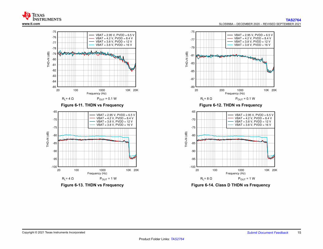
Figure 6-11. THDN vs Frequency
Frequency (Hz)
TH
D+
N (
dB
)
-89
-87
-85
-83
-81
-79
-77
-75
20 200 1000 10K 20K
VBAT = 2.95 V, PVDD = 6.5 VVBAT = 4.2 V, PVDD = 8.4 VVBAT = 3.8 V, PVDD = 12 VVBAT = 3.8 V, PVDD = 16 V
RL= 8 Ω POUT = 0.1 W
Figure 6-12. THDN vs Frequency
Frequency (Hz)
TH
D+
N (
dB
)
-100
-95
-90
-85
-80
-75
-70
-65
20 100 1000 10K 20K
VBAT = 2.95 V, PVDD = 6.5 VVBAT = 4.2 V, PVDD = 8.4 VVBAT = 3.8 V, PVDD = 12 VVBAT = 3.8 V, PVDD = 16 V
RL= 4 Ω POUT = 1 W
Figure 6-13. THDN vs Frequency
Frequency (Hz)
TH
D+
N (
dB
)
-100
-95
-90
-85
-80
-75
-70
-65
20 100 1000 10K 20K
VBAT = 2.95 V, PVDD = 6.5 VVBAT = 4.2 V, PVDD = 8.4 VVBAT = 3.8 V, PVDD = 12 VVBAT = 3.8 V, PVDD = 16 V
RL= 8 Ω POUT = 1 W
Figure 6-14. Class D THDN vs Frequency
www.ti.comTAS2764
SLOS998A – DECEMBER 2020 – REVISED SEPTEMBER 2021
Copyright © 2021 Texas Instruments Incorporated Submit Document Feedback 15
Product Folder Links: TAS2764
VBAT (V)
Idle
Ch
an
ne
l N
ois
e (
A -
we
ighte
d)
(PV
)
2.7 3 3.3 3.6 3.9 4.2 4.5 4.8 5.1 5.4 5.720
22
24
26
28
30
32
34
36
38
40DAC Mute ICN (A - weighted) (PV)DAC Unmute ICN (A - weighted) (PV)
PWR_MODE1
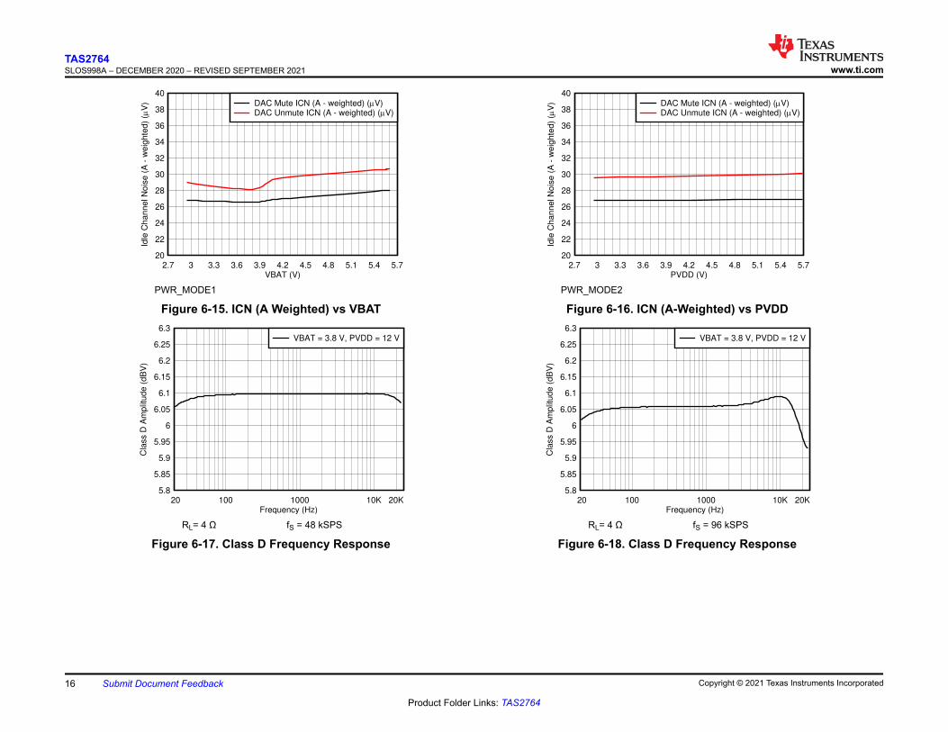
Figure 6-15. ICN (A Weighted) vs VBAT
PVDD (V)
Idle
Ch
an
ne
l N
ois
e (
A -
we
ighte
d)
(PV
)
2.7 3 3.3 3.6 3.9 4.2 4.5 4.8 5.1 5.4 5.720
22
24
26
28
30
32
34
36
38
40DAC Mute ICN (A - weighted) (PV)DAC Unmute ICN (A - weighted) (PV)
PWR_MODE2
Figure 6-16. ICN (A-Weighted) vs PVDD
Frequency (Hz)
Cla
ss D
Am
plit
ud
e (
dB
V)
5.8
5.85
5.9
5.95
6
6.05
6.1
6.15
6.2
6.25
6.3
20 100 1000 10K 20K
VBAT = 3.8 V, PVDD = 12 V
RL= 4 Ω fS = 48 kSPS
Figure 6-17. Class D Frequency Response
Frequency (Hz)
Cla
ss D
Am
plit
ud
e (
dB
V)
5.8
5.85
5.9
5.95
6
6.05
6.1
6.15
6.2
6.25
6.3
20 100 1000 10K 20K
VBAT = 3.8 V, PVDD = 12 V
RL= 4 Ω fS = 96 kSPS
Figure 6-18. Class D Frequency Response
TAS2764SLOS998A – DECEMBER 2020 – REVISED SEPTEMBER 2021 www.ti.com
16 Submit Document Feedback Copyright © 2021 Texas Instruments Incorporated
Product Folder Links: TAS2764
POUT (W)
Eff
icie
ncy (
%)
0.0001 0.001 0.01 0.1 1 10 20200
10
20
30
40
50
60
70
80
90
100VBAT = 2.95 V, PVDD = 6.5 VVBAT = 4.2 V, PVDD = 8.4 VVBAT = 3.8 V, PVDD = 12 VVBAT = 3.8 V, PVDD = 16 V
RL= 4 Ω fIN = 1 kHz
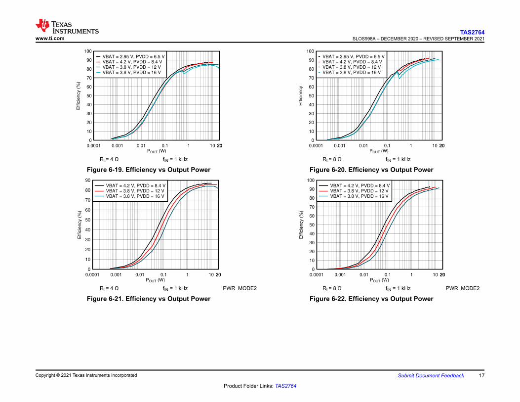
Figure 6-19. Efficiency vs Output Power
POUT (W)
Eff
icie
ncy
0.0001 0.001 0.01 0.1 1 10 20200
10
20
30
40
50
60
70
80
90
100VBAT = 2.95 V, PVDD = 6.5 VVBAT = 4.2 V, PVDD = 8.4 VVBAT = 3.8 V, PVDD = 12 VVBAT = 3.8 V, PVDD = 16 V
RL= 8 Ω fIN = 1 kHz
Figure 6-20. Efficiency vs Output Power
POUT (W)
Eff
icie
ncy (
%)
0.0001 0.001 0.01 0.1 1 10 20200
10
20
30
40
50
60
70
80
90VBAT = 4.2 V, PVDD = 8.4 VVBAT = 3.8 V, PVDD = 12 VVBAT = 3.8 V, PVDD = 16 V
RL= 4 Ω fIN = 1 kHz PWR_MODE2
Figure 6-21. Efficiency vs Output Power
POUT (W)
Eff
icie
ncy (
%)
0.0001 0.001 0.01 0.1 1 10 20200
10
20
30
40
50
60
70
80
90
100VBAT = 4.2 V, PVDD = 8.4 VVBAT = 3.8 V, PVDD = 12 VVBAT = 3.8 V, PVDD = 16 V
RL= 8 Ω fIN = 1 kHz PWR_MODE2
Figure 6-22. Efficiency vs Output Power
www.ti.comTAS2764
SLOS998A – DECEMBER 2020 – REVISED SEPTEMBER 2021
Copyright © 2021 Texas Instruments Incorporated Submit Document Feedback 17
Product Folder Links: TAS2764
Frequency (Hz)
PS
RR
(d
B)
0
20
40
60
80
100
120
140
10 100 1000 10K 20K
AVDD = 1.8 V, PVDD = 12 V
RL= 4 Ω
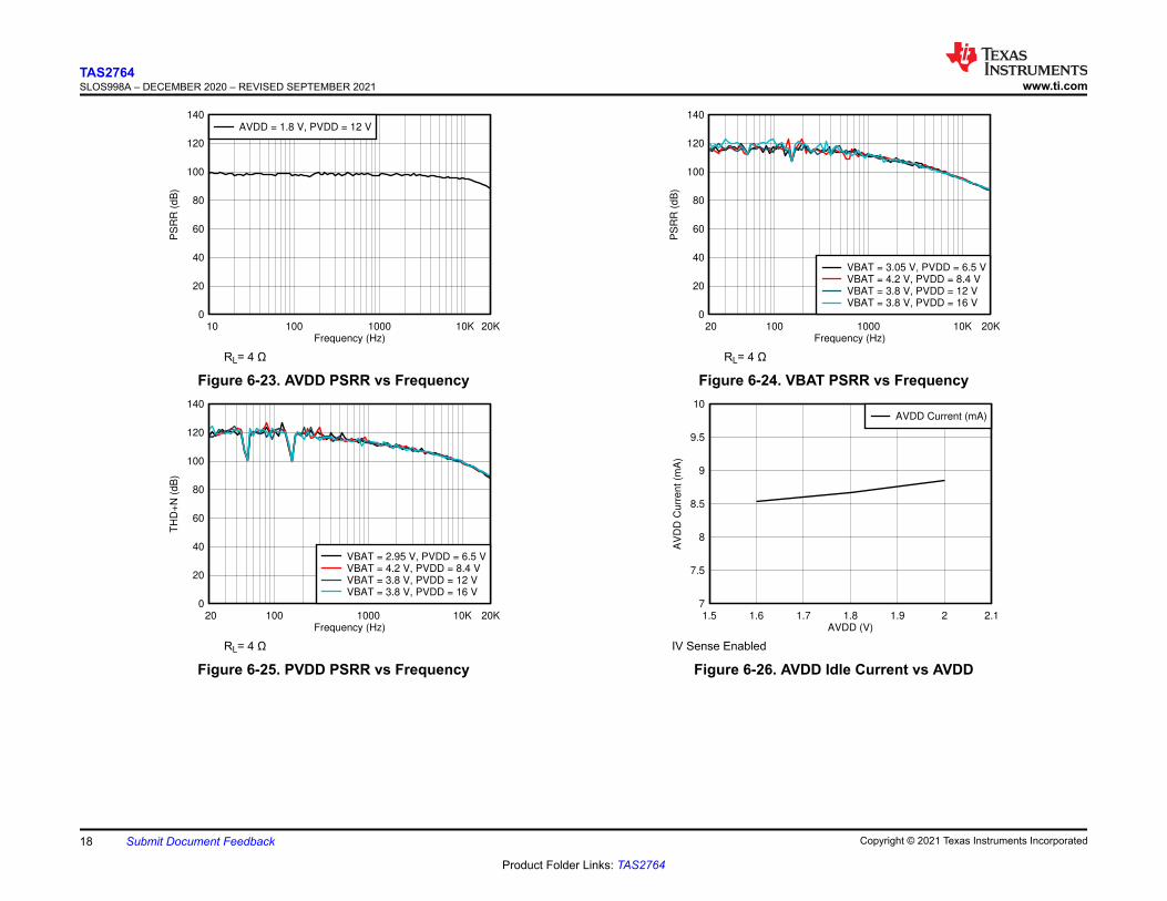
Figure 6-23. AVDD PSRR vs Frequency
Frequency (Hz)
PS
RR
(d
B)
0
20
40
60
80
100
120
140
20 100 1000 10K 20K
VBAT = 3.05 V, PVDD = 6.5 VVBAT = 4.2 V, PVDD = 8.4 VVBAT = 3.8 V, PVDD = 12 VVBAT = 3.8 V, PVDD = 16 V
RL= 4 Ω
Figure 6-24. VBAT PSRR vs Frequency
Frequency (Hz)
TH
D+
N (
dB
)
0
20
40
60
80
100
120
140
20 100 1000 10K 20K
VBAT = 2.95 V, PVDD = 6.5 VVBAT = 4.2 V, PVDD = 8.4 VVBAT = 3.8 V, PVDD = 12 VVBAT = 3.8 V, PVDD = 16 V
RL= 4 Ω
Figure 6-25. PVDD PSRR vs Frequency
AVDD (V)
AV
DD
Cu
rre
nt
(mA
)
1.5 1.6 1.7 1.8 1.9 2 2.17
7.5
8
8.5
9
9.5
10AVDD Current (mA)
IV Sense Enabled
Figure 6-26. AVDD Idle Current vs AVDD
TAS2764SLOS998A – DECEMBER 2020 – REVISED SEPTEMBER 2021 www.ti.com
18 Submit Document Feedback Copyright © 2021 Texas Instruments Incorporated
Product Folder Links: TAS2764
VBAT (V)
VB
AT
Cu
rre
nt
(mA
)
2.5 3 3.5 4 4.5 5 5.5 60
0.5
1
1.5
2
2.5
3
3.5
4
4.5VBAT Current (mA)
IV Sense Enabled
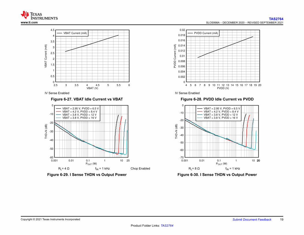
Figure 6-27. VBAT Idle Current vs VBAT
PVDD (V)
PV
DD
Cu
rre
nt
(mA
)
4 5 6 7 8 9 10 11 12 13 14 15 16 17 18 19 200
0.002
0.004
0.006
0.008
0.01
0.012
0.014
0.016
0.018
0.02PVDD Current (mA)
IV Sense Enabled
Figure 6-28. PVDD Idle Current vs PVDD
POUT (W)
TH
D+
N (
dB
)
0.001 0.01 0.1 1 10 25-60
-50
-40
-30
-20
-10
0VBAT = 2.95 V, PVDD = 6.5 VVBAT = 4.2 V, PVDD = 8.4 VVBAT = 3.8 V, PVDD = 12 VVBAT = 3.8 V, PVDD = 16 V
RL= 4 Ω fIN = 1 kHz Chop Enabled
Figure 6-29. I Sense THDN vs Output Power
POUT (W)
TH
D+
N (
dB
)
0.001 0.01 0.1 1 10 2020-70
-60
-50
-40
-30
-20
-10
0VBAT = 2.95 V, PVDD = 6.5 VVBAT = 4.2 V, PVDD = 8.4 VVBAT = 3.8 V, PVDD = 12 VVBAT = 3.8 V, PVDD = 16 V
RL= 8 Ω fIN = 1 kHz
Figure 6-30. I Sense THDN vs Output Power
www.ti.comTAS2764
SLOS998A – DECEMBER 2020 – REVISED SEPTEMBER 2021
Copyright © 2021 Texas Instruments Incorporated Submit Document Feedback 19
Product Folder Links: TAS2764
POUT (W)
TH
D+
N (
dB
)
0.001 0.01 0.1 1 10 25-70
-60
-50
-40
-30
-20
-10
0VBAT = 4.2 V, PVDD = 8.4 VVBAT = 3.8 V, PVDD = 12 VVBAT = 3.8 V, PVDD = 16 V
RL= 4 Ω fIN = 1 kHz PWR_MODE2
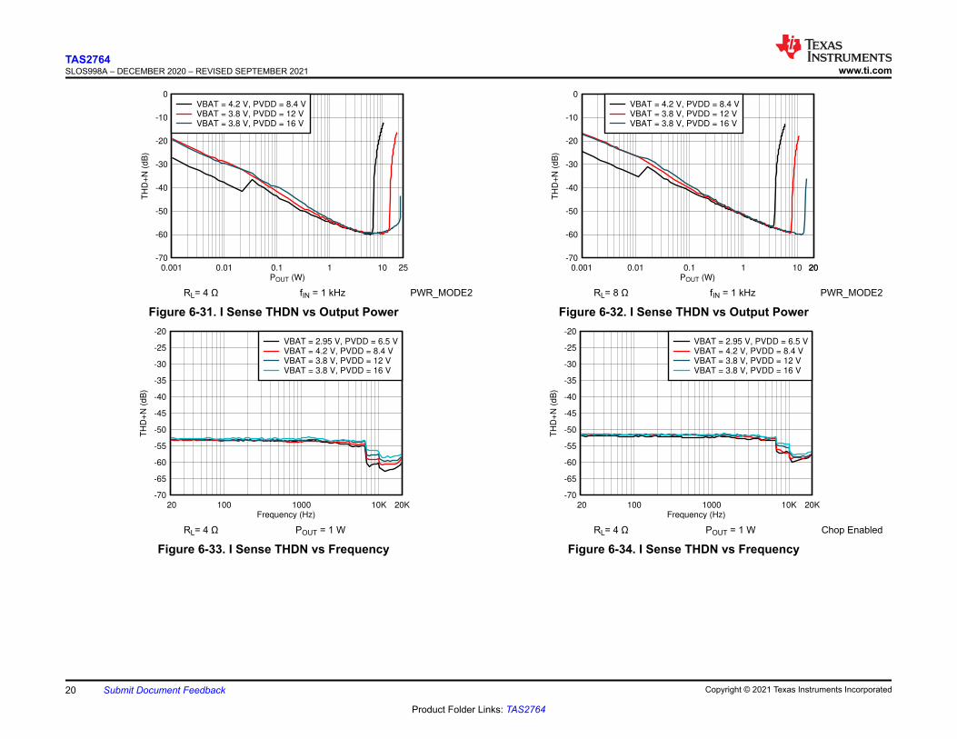
Figure 6-31. I Sense THDN vs Output Power
POUT (W)
TH
D+
N (
dB
)
0.001 0.01 0.1 1 10 2020-70
-60
-50
-40
-30
-20
-10
0VBAT = 4.2 V, PVDD = 8.4 VVBAT = 3.8 V, PVDD = 12 VVBAT = 3.8 V, PVDD = 16 V
RL= 8 Ω fIN = 1 kHz PWR_MODE2
Figure 6-32. I Sense THDN vs Output Power
Frequency (Hz)
TH
D+
N (
dB
)
-70
-65
-60
-55
-50
-45
-40
-35
-30
-25
-20
20 100 1000 10K 20K
VBAT = 2.95 V, PVDD = 6.5 VVBAT = 4.2 V, PVDD = 8.4 VVBAT = 3.8 V, PVDD = 12 VVBAT = 3.8 V, PVDD = 16 V
RL= 4 Ω POUT = 1 W
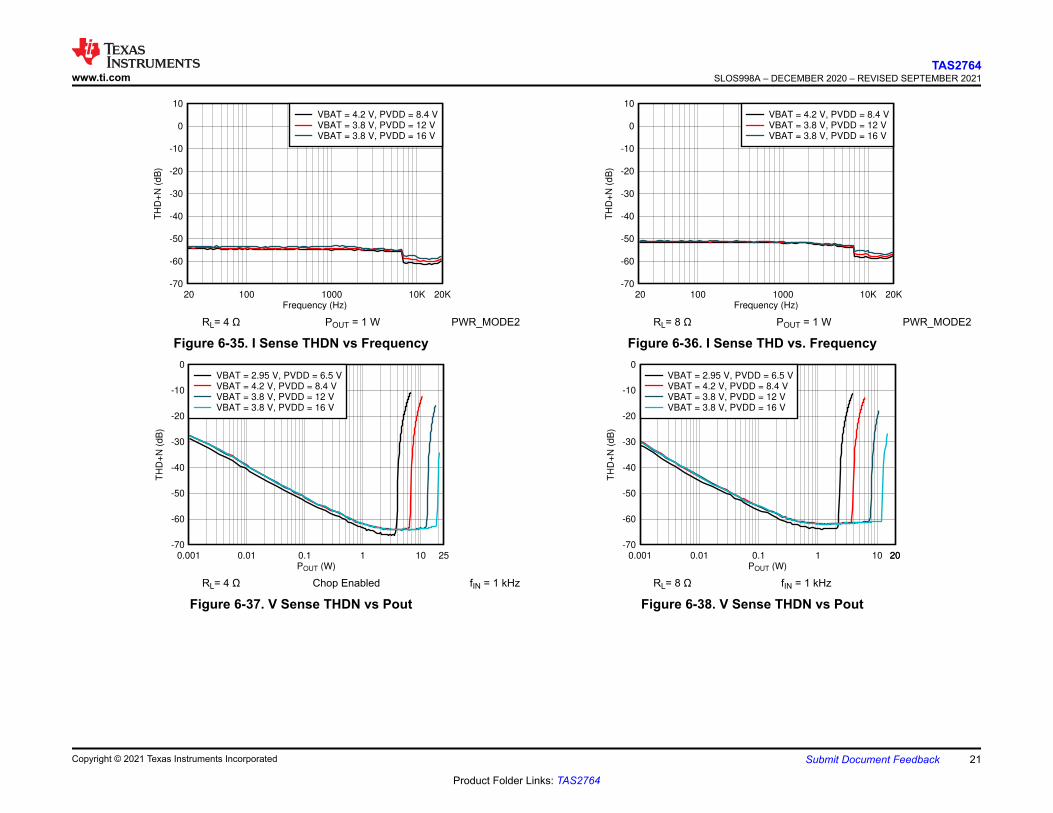
Figure 6-33. I Sense THDN vs Frequency
Frequency (Hz)
TH
D+
N (
dB
)
-70
-65
-60
-55
-50
-45
-40
-35
-30
-25
-20
20 100 1000 10K 20K
VBAT = 2.95 V, PVDD = 6.5 VVBAT = 4.2 V, PVDD = 8.4 VVBAT = 3.8 V, PVDD = 12 VVBAT = 3.8 V, PVDD = 16 V
RL= 4 Ω POUT = 1 W Chop Enabled
Figure 6-34. I Sense THDN vs Frequency
TAS2764SLOS998A – DECEMBER 2020 – REVISED SEPTEMBER 2021 www.ti.com
20 Submit Document Feedback Copyright © 2021 Texas Instruments Incorporated
Product Folder Links: TAS2764
Frequency (Hz)
TH
D+
N (
dB
)
-70
-60
-50
-40
-30
-20
-10
0
10
20 100 1000 10K 20K
VBAT = 4.2 V, PVDD = 8.4 VVBAT = 3.8 V, PVDD = 12 VVBAT = 3.8 V, PVDD = 16 V
RL= 4 Ω POUT = 1 W PWR_MODE2
Figure 6-35. I Sense THDN vs Frequency
Frequency (Hz)
TH
D+
N (
dB
)
-70
-60
-50
-40
-30
-20
-10
0
10
20 100 1000 10K 20K
VBAT = 4.2 V, PVDD = 8.4 VVBAT = 3.8 V, PVDD = 12 VVBAT = 3.8 V, PVDD = 16 V
RL= 8 Ω POUT = 1 W PWR_MODE2
Figure 6-36. I Sense THD vs. Frequency
POUT (W)
TH
D+
N (
dB
)
0.001 0.01 0.1 1 10 25-70
-60
-50
-40
-30
-20
-10
0VBAT = 2.95 V, PVDD = 6.5 VVBAT = 4.2 V, PVDD = 8.4 VVBAT = 3.8 V, PVDD = 12 VVBAT = 3.8 V, PVDD = 16 V
RL= 4 Ω Chop Enabled fIN = 1 kHz
Figure 6-37. V Sense THDN vs Pout
POUT (W)
TH
D+
N (
dB
)
0.001 0.01 0.1 1 10 2020-70
-60
-50
-40
-30
-20
-10
0VBAT = 2.95 V, PVDD = 6.5 VVBAT = 4.2 V, PVDD = 8.4 VVBAT = 3.8 V, PVDD = 12 VVBAT = 3.8 V, PVDD = 16 V
RL= 8 Ω fIN = 1 kHz
Figure 6-38. V Sense THDN vs Pout
www.ti.comTAS2764
SLOS998A – DECEMBER 2020 – REVISED SEPTEMBER 2021
Copyright © 2021 Texas Instruments Incorporated Submit Document Feedback 21
Product Folder Links: TAS2764
Frequency (Hz)
TH
D+
N (
dB
)
-100
-90
-80
-70
-60
-50
-40
-30
-20
-10
0
20 100 1000 10K 20K
VBAT = 2.95 V, PVDD = 6.5 VVBAT = 4.2 V, PVDD = 8.4 VVBAT = 3.8 V, PVDD = 12 VVBAT = 3.8 V, PVDD = 16 V
RL= 4 Ω Chop Enabled POUT = 1 W
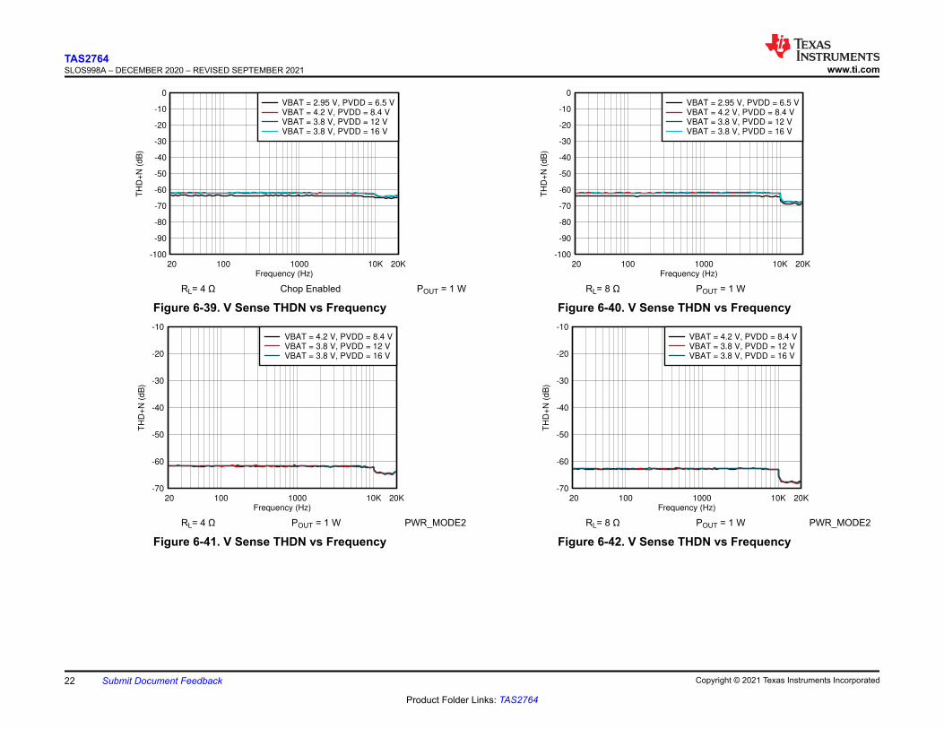
Figure 6-39. V Sense THDN vs Frequency
Frequency (Hz)
TH
D+
N (
dB
)
-100
-90
-80
-70
-60
-50
-40
-30
-20
-10
0
20 100 1000 10K 20K
VBAT = 2.95 V, PVDD = 6.5 VVBAT = 4.2 V, PVDD = 8.4 VVBAT = 3.8 V, PVDD = 12 VVBAT = 3.8 V, PVDD = 16 V
RL= 8 Ω POUT = 1 W
Figure 6-40. V Sense THDN vs Frequency
Frequency (Hz)
TH
D+
N (
dB
)
-70
-60
-50
-40
-30
-20
-10
20 100 1000 10K 20K
VBAT = 4.2 V, PVDD = 8.4 VVBAT = 3.8 V, PVDD = 12 VVBAT = 3.8 V, PVDD = 16 V
RL= 4 Ω POUT = 1 W PWR_MODE2
Figure 6-41. V Sense THDN vs Frequency
Frequency (Hz)
TH
D+
N (
dB
)
-70
-60
-50
-40
-30
-20
-10
20 100 1000 10K 20K
VBAT = 4.2 V, PVDD = 8.4 VVBAT = 3.8 V, PVDD = 12 VVBAT = 3.8 V, PVDD = 16 V
RL= 8 Ω POUT = 1 W PWR_MODE2
Figure 6-42. V Sense THDN vs Frequency
TAS2764SLOS998A – DECEMBER 2020 – REVISED SEPTEMBER 2021 www.ti.com
22 Submit Document Feedback Copyright © 2021 Texas Instruments Incorporated
Product Folder Links: TAS2764
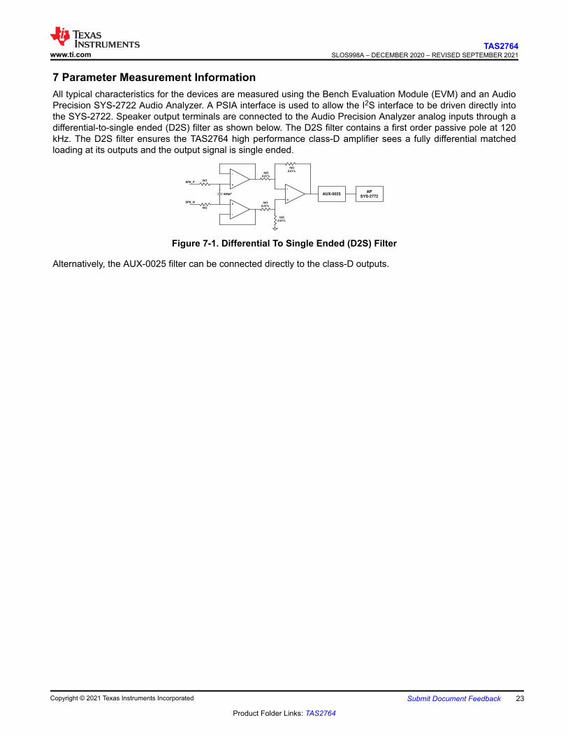
7 Parameter Measurement InformationAll typical characteristics for the devices are measured using the Bench Evaluation Module (EVM) and an Audio Precision SYS-2722 Audio Analyzer. A PSIA interface is used to allow the I2S interface to be driven directly into the SYS-2722. Speaker output terminals are connected to the Audio Precision Analyzer analog inputs through a differential-to-single ended (D2S) filter as shown below. The D2S filter contains a first order passive pole at 120 kHz. The D2S filter ensures the TAS2764 high performance class-D amplifier sees a fully differential matched loading at its outputs and the output signal is single ended.
680pF
1k��
AUX-0025
-
+
1k��
-
+
-
+
1k�
0.01%
1k�
0.01%
1k�
0.01%
1k�
0.01%
SPK_P
SPK_N
AP
SYS-2772
Figure 7-1. Differential To Single Ended (D2S) Filter
Alternatively, the AUX-0025 filter can be connected directly to the class-D outputs.
www.ti.comTAS2764
SLOS998A – DECEMBER 2020 – REVISED SEPTEMBER 2021
Copyright © 2021 Texas Instruments Incorporated Submit Document Feedback 23
Product Folder Links: TAS2764
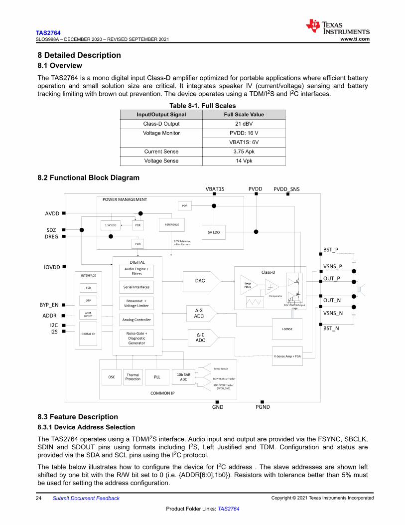
8 Detailed Description8.1 OverviewThe TAS2764 is a mono digital input Class-D amplifier optimized for portable applications where efficient battery operation and small solution size are critical. It integrates speaker IV (current/voltage) sensing and battery tracking limiting with brown out prevention. The device operates using a TDM/I2S and I2C interfaces.
Table 8-1. Full ScalesInput/Output Signal Full Scale Value
Class-D Output 21 dBV
Voltage Monitor PVDD: 16 V
VBAT1S: 6V
Current Sense 3.75 Apk
Voltage Sense 14 Vpk
8.2 Functional Block Diagram
B
Class-D
Loop
Filter
Comparator
16V LDMOS Output
stage
REFERENCE
DAC
10b SAR
ADCPLLOSC
PVDD
AVDD
DREG
IOVDD
SDZ
I2C
I2S
OUT_P
OUT_N
VSNS_N
VSNS_P
Temp Sensor
Thermal
Protection
POR1.5V LDO
Brownout +
Voltage Limiter
BST_P
BST_N
5V LDO
û-��
ADC
I-SENSE
V-Sense Amp + PGA
POWER MANAGEMENT
0.9V Reference
+ Bias Currents
COMMON IP
INTERFACE
ESD
OTP
ADDR
DETECT
DIGITAL IO
Analog Controller
Serial Interfaces
DIGITAL
û-��
ADC
PGND
POR
BOP VBAT1S Tracker
ADDR
POR
VBAT1S PVDD_SNS
BOP PVDD Tracker
(PVDD_SNS)
Noise Gate +
Diagnostic
Generator
Audio Engine +
Filters
GND
BYP_EN
8.3 Feature Description8.3.1 Device Address Selection
The TAS2764 operates using a TDM/I2S interface. Audio input and output are provided via the FSYNC, SBCLK, SDIN and SDOUT pins using formats including I2S, Left Justified and TDM. Configuration and status are provided via the SDA and SCL pins using the I2C protocol.
The table below illustrates how to configure the device for I2C address . The slave addresses are shown left shifted by one bit with the R/W bit set to 0 (i.e. {ADDR[6:0],1b0}). Resistors with tolerance better than 5% must be used for setting the address configuration.
TAS2764SLOS998A – DECEMBER 2020 – REVISED SEPTEMBER 2021 www.ti.com
24 Submit Document Feedback Copyright © 2021 Texas Instruments Incorporated
Product Folder Links: TAS2764
Table 8-2. I2C Address SelectionI2C SLAVE ADDRESS 0x70 0x72 0x74 0x76 0x78 0x7A 0x7C 0x7E
ADDR PIN Short to GND
470 Ω to GND
470 Ω to AVDD
2.2k Ω to GND
2.2k Ω to AVDD
10 kΩ to GND
10 kΩ to AVDD
Short to AVDD
The TAS2764 has a global 7-bit I2C address 0x80. When enabled, the device will additionally respond to I2C commands at this address regardless of the ADDR pin settings. This is used to speed up device configuration when using multiple TAS2764 devices and programming similar settings across all devices. The I2C ACK / NACK cannot be used during the multi-device writes since multiple devices are responding to the I2C command. The I2C CRC function should be used to ensure each device properly received the I2C commands. At the completion of writing multiple devices using the global address, the CRC at I2C_CKSUM register should be checked on each device using the local address for a proper value. The global I2C address can be disabled using I2C_GBL_EN register bit. The I2C address is detected by sampling the ADDR pin when SDZ pin is released. Additionally, the address may be re-detected by setting I2C_AD_DET register bit high after power up and the ADDR pin will be re-sampled.
8.3.2 General I2C Operation
The I2C bus employs two signals, SDA (data) and SCL (clock), to communicate between integrated circuits in a system using serial data transmission. The address and 8 bit data are transferred starting with the most-significant bit (MSB). In addition, each byte transferred on the bus is acknowledged by the receiving device with an acknowledge bit. Each transfer operation begins with the master device driving a start condition on the bus and ends with the master device driving a stop condition on the bus. The bus uses transitions on the data terminal (SDA) while the clock is at logic high to indicate start and stop conditions. A high-to-low transition on SDA indicates a start, and a low-to-high transition indicates a stop. Normal data-bit transitions must occur within the low time of the clock period.
The master generates the 7-bit slave address and the read/write (R/W) bit to open communication with another device and then waits for an acknowledge condition. The device holds SDA low during the acknowledge clock period to indicate acknowledgment. When this occurs, the master transmits the next byte of the sequence. Each device is addressed by a unique 7-bit slave address plus R/W bit (1 byte). All compatible devices share the same signals via a bi-directional bus using a wired-AND connection.
Register (N)8- Bit Data for 8- Bit Data for
Register (N+1)
Figure 8-1. Typical I2C Sequence
There is no limit on the number of bytes that can be transmitted between start and stop conditions. When the last word transfers, the master generates a stop condition to release the bus. Figure 8-1 shows a generic data transfer sequence.
For information about pull-up resistors and single-byte/multiple-byte transfers see .
8.3.3 Register Organization
Device configuration and coefficients are stored using a page and book scheme. Each page contains 128 bytes and each book contains 256 pages. All device configuration registers are stored in book 0, page 0, which is the default setting at power up (and after a software reset). The book and page can be set by the BOOK and PAGE registers respectively.
www.ti.comTAS2764
SLOS998A – DECEMBER 2020 – REVISED SEPTEMBER 2021
Copyright © 2021 Texas Instruments Incorporated Submit Document Feedback 25
Product Folder Links: TAS2764
Note
Programming register bits from Book_0 and Page_4 needs to be done in groups of four registers (32 bit format), each byte corresponding to a register and with less significant byte programmed to 00h. For instance, when programing DC level for diagnostic generator, registers 08 (MSB),09,0A will be programmed to the desired value and register 0B will be programmed to 00h.
8.4 Device Functional Modes8.4.1 TDM Port
The TAS2764 provides a flexible TDM serial audio port. The port can be configured to support a variety of formats including stereo I2S, Left Justified and TDM. Mono audio playback is available via the SDIN pin. The SDOUT pin is used to transmit sample streams including speaker voltage and current sense, PVDD voltage, die temperature and channel gain.
The TDM serial audio port supports up to 16 of 32-bit time slots at 44.1/48 kHz or 8 of 32-bit time slots at a 88.2/96 kHz sample rate. Valid SBCLK to FSYNC ratios are 16, 24, 32, 48, 64, 96, 128, 192, 256, and 512. The device will automatically detect the number of time slots and it does not need to be programmed.
By default, the TAS2764 will automatically detect the PCM playback sample rate. This can be disabled and manually configured by setting the AUTO_RATE register bit high.
The SAMP_RATE[2:0] and SAMP_RATIO[3:0] register bits are used to configure the PCM audio sample rate when AUTO_RATE register bit is high (auto detection of TDM sample rate is disabled). The TAS2764 employs a robust clock fault detection engine that will automatically volume ramp down the playback path if FSYNC does not match the configured sample rate (if AUTO_RATE = 1) or the ratio of SBCLK to FSYNC is not supported (minimizing any audible artifacts). Once the clocks are detected to be valid in both frequency and ratio, the device will automatically volume ramp the playback path back to the configured volume and resume playback.
When using the auto rate detection the sampling rate and SBCLK to FSYNC ration detected on the TDM bus is reported back on the read-only register bits FS_RATE[2:0] and FS_RATIO[3:0] respectively.
The TAS2764 supports a 12 MHz SBCLK operation. The system will detect or should be manually configured for a ratio of 125 or 250. In this specific ratio the last 32-bit slot should not be used to transmit data over the TDM port (Section 8.4.1) or ICC pin ( Section 8.4.2.9.1) as data will be truncated.
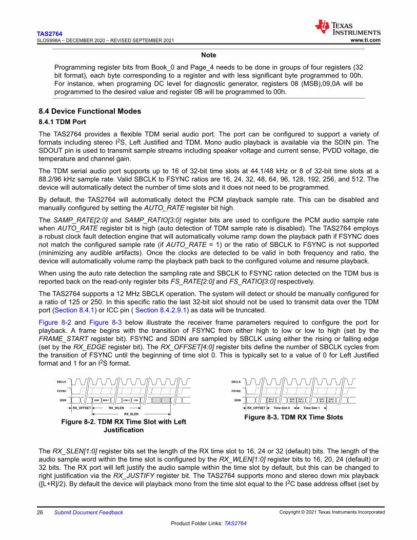
Figure 8-2 and Figure 8-3 below illustrate the receiver frame parameters required to configure the port for playback. A frame begins with the transition of FSYNC from either high to low or low to high (set by the FRAME_START register bit). FSYNC and SDIN are sampled by SBCLK using either the rising or falling edge (set by the RX_EDGE register bit). The RX_OFFSET[4:0] register bits define the number of SBCLK cycles from the transition of FSYNC until the beginning of time slot 0. This is typically set to a value of 0 for Left Justified format and 1 for an I2S format.
MSB MSB-1 LSB+1 LSB
RX_WLEN
RX_SLEN
RX_OFFSET
SBCLK
FSYNC
SDIN
Figure 8-2. TDM RX Time Slot with Left Justification
Slot 0
Bit 31
Slot0
Bit 0
Time Slot 0RX_OFFSET
SBCLK
FSYNC
SDINSlot 1
Bit 31
Slot1
Bit 0
Time Slot 1
Slot2
Bit 31
Figure 8-3. TDM RX Time Slots
The RX_SLEN[1:0] register bits set the length of the RX time slot to 16, 24 or 32 (default) bits. The length of the audio sample word within the time slot is configured by the RX_WLEN[1:0] register bits to 16, 20, 24 (default) or 32 bits. The RX port will left justify the audio sample within the time slot by default, but this can be changed to right justification via the RX_JUSTIFY register bit. The TAS2764 supports mono and stereo down mix playback ([L+R]/2). By default the device will playback mono from the time slot equal to the I2C base address offset (set by
TAS2764SLOS998A – DECEMBER 2020 – REVISED SEPTEMBER 2021 www.ti.com
26 Submit Document Feedback Copyright © 2021 Texas Instruments Incorporated
Product Folder Links: TAS2764
the ADDR pin) for playback. The RX_SCFG[1:0] register bits can be used to override the playback source to the left time slot, right time slot or stereo down mix set by the RX_SLOT_L[3:0] and RX_SLOT_R[3:0] register bits.
If time slot selection places reception either partially or fully beyond the frame boundary, the receiver will return a null sample equivalent to a digitally muted sample.
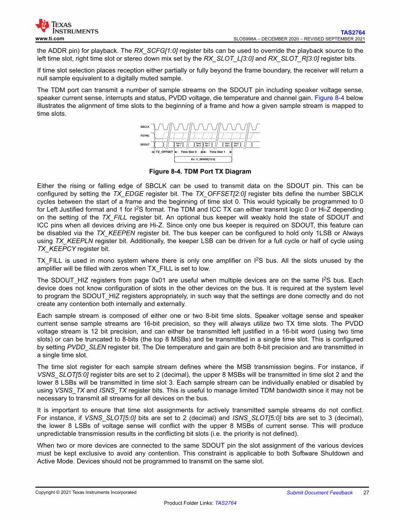
The TDM port can transmit a number of sample streams on the SDOUT pin including speaker voltage sense, speaker current sense, interrupts and status, PVDD voltage, die temperature and channel gain. Figure 8-4 below illustrates the alignment of time slots to the beginning of a frame and how a given sample stream is mapped to time slots.
Slot 0
Bit 7
Slot0
Bit 0
Time Slot 0TX_OFFSET
SBCLK
FSYNC
SDOUTSlot 1
Bit 7
Slot1
Bit 0
Time Slot 1
Slot2
Bit 7
Ex: V_SENSE[15:0]
Figure 8-4. TDM Port TX Diagram
Either the rising or falling edge of SBCLK can be used to transmit data on the SDOUT pin. This can be configured by setting the TX_EDGE register bit. The TX_OFFSET[2:0] register bits define the number SBCLK cycles between the start of a frame and the beginning of time slot 0. This would typically be programmed to 0 for Left Justified format and 1 for I2S format. The TDM and ICC TX can either transmit logic 0 or Hi-Z depending on the setting of the TX_FILL register bit. An optional bus keeper will weakly hold the state of SDOUT and ICC pins when all devices driving are Hi-Z. Since only one bus keeper is required on SDOUT, this feature can be disabled via the TX_KEEPEN register bit. The bus keeper can be configured to hold only 1LSB or Always using TX_KEEPLN register bit. Additionally, the keeper LSB can be driven for a full cycle or half of cycle using TX_KEEPCY register bit.
TX_FILL is used in mono system where there is only one amplifier on I2S bus. All the slots unused by the amplifier will be filled with zeros when TX_FILL is set to low.
The SDOUT_HIZ registers from page 0x01 are useful when multiple devices are on the same I2S bus. Each device does not know configuration of slots in the other devices on the bus. It is required at the system level to program the SDOUT_HIZ registers appropriately, in such way that the settings are done correctly and do not create any contention both internally and externally.
Each sample stream is composed of either one or two 8-bit time slots. Speaker voltage sense and speaker current sense sample streams are 16-bit precision, so they will always utilize two TX time slots. The PVDD voltage stream is 12 bit precision, and can either be transmitted left justified in a 16-bit word (using two time slots) or can be truncated to 8-bits (the top 8 MSBs) and be transmitted in a single time slot. This is configured by setting PVDD_SLEN register bit. The Die temperature and gain are both 8-bit precision and are transmitted in a single time slot.
The time slot register for each sample stream defines where the MSB transmission begins. For instance, if VSNS_SLOT[5:0] register bits are set to 2 (decimal), the upper 8 MSBs will be transmitted in time slot 2 and the lower 8 LSBs will be transmitted in time slot 3. Each sample stream can be individually enabled or disabled by using VSNS_TX and ISNS_TX register bits. This is useful to manage limited TDM bandwidth since it may not be necessary to transmit all streams for all devices on the bus.
It is important to ensure that time slot assignments for actively transmitted sample streams do not conflict. For instance, if VSNS_SLOT[5:0] bits are set to 2 (decimal) and ISNS_SLOT[5:0] bits are set to 3 (decimal), the lower 8 LSBs of voltage sense will conflict with the upper 8 MSBs of current sense. This will produce unpredictable transmission results in the conflicting bit slots (i.e. the priority is not defined).
When two or more devices are connected to the same SDOUT pin the slot assignment of the various devices must be kept exclusive to avoid any contention. This constraint is applicable to both Software Shutdown and Active Mode. Devices should not be programmed to transmit on the same slot.
www.ti.comTAS2764
SLOS998A – DECEMBER 2020 – REVISED SEPTEMBER 2021
Copyright © 2021 Texas Instruments Incorporated Submit Document Feedback 27
Product Folder Links: TAS2764
The current and voltage values are transmitted at the full 16-bit measured values by default. The IVMON_LEN[1:0] register bits can be used to transmit only the 8 MSB bits in one slot or 12 MSB bits values across multiple slots. The special 12-bit mode is used when only 24-bit I2S/TDM data can be processed by the host processor. The device should be configured with the voltage-sense slot and current-sense slot off by 1 slot and will consume 3 consecutive 8-bit slots. In this mode the device will transmit the first 12 MSB bits followed by the second 12 MSB bits specified by the preceding slot.
If time slot selections place transmission beyond the frame boundary, the transmitter will truncate transmission at the frame boundary.
The time slots for VBAT1S, PVDD and TEMP measurements are set using VBAT1S_SLOT[5:0], PVDD_SLOT[5:0] and TEMP_SLOT[5:0] register bits. To enable sample stream register bits VBAT1S_TX, PVDD_TX and TEMP_TX must be set high. The slot length is selected by VBAT1S_SLEN, PVDD_SLEN and TEMP_SLEN register bits.
To set TDM final processed audio slot, enable and length register bits the following register bits need to be programmed: AUDIO_SLOT[5:0], AUDIO_TX and AUDIO_SLEN .
Information about status of slots can be find in STATUS_SLOT[5:0] register bits. STATUS_TX register bit set high enables the status transmit.
The slot configuration for the TX limiter gain reduction can be set between 0 (default) and 63 by setting GAIN_SLOT[5:0] register bits. It is used for the Inter Chip Gain Aligment ( Section 8.4.2.9 ) and can be either over the TDM Bus or ICC pin (Section 8.4.2.9.1). To use this feature, the register bit GAIN_TX needs to be set high (Enable).
8.4.2 Playback Signal Path8.4.2.1 High Pass Filter
Excessive DC and low frequency content in audio playback signal can damage loudspeakers. The TAS2764 employs a high-pass filter (HPF) to prevent this from occurring for the PCM playback path. The HPF_FREQ_PB[2:0] register bits set the corner frequencies of HPF. The filter can be bypassed by setting the register bits to 3'b000.
8.4.2.2 Amplifier Inversion
The device will output a non-inverted signal to the OUT_P and OUT_N pins. The output can be inverted with respect to the digital input value by setting the AMP_INV register bit to high.
8.4.2.3 Digital Volume Control and Amplifier Output Level
The gain from audio input to speaker terminals is controlled by setting the amplifier’s output level and digital volume control (DVC).
Amplifier output level settings are programmed using AMP_LEVEL[4:0] register bits. The levels are presented in the Register Map in dBV (dB relative to 1 Vrms), with a full scale digital audio input (0 dBFS) and the DVC set by default to 0 dB. It should be noted that these levels may not be achievable because of analog clipping in the amplifier, so they should be used to convey gain only.
Equation 1 below calculates amplifier output voltage:
VAMP= INPUT+ADVC+AAMP
(1)
where
• VAMP is the amplifier output voltage in dBV• INPUT is the digital input amplitude as a number of dB with respect to 0 dBFS• ADVC is the digital volume control setting as a number of dB• AAMP is the amplifier output level setting as a number of dBV
TAS2764SLOS998A – DECEMBER 2020 – REVISED SEPTEMBER 2021 www.ti.com
28 Submit Document Feedback Copyright © 2021 Texas Instruments Incorporated
Product Folder Links: TAS2764
The digital volume control (DVC) is configurable from 0 dB to -100 dB in 0.5 dB steps by setting the DVC_LVL[7:0] register bits. Settings greater than C8h are interpreted as mute. When a change in digital volume control occurs, the device ramps the volume to the new setting based on the DVC_RAMP_RATE[1:0] register bits status. If DVC_RAMP_RATE[1:0] bits are set to 2'b11 the volume ramping is disabled. This setting can be used to speed up startup, shutdown and digital volume changes when volume ramping is handled by the system master.
The Class-D amplifier uses a closed-loop architecture, so the gain does not depend on power supply. The approximate threshold for the onset of analog clipping is calculated in Equation 2.
(2)
where
• VPK is the maximum peak un-clipped output voltage in V• VSUP is the power supply of class-D output stage• RL is the speaker load in Ω• RP is the parasitic resistance on PCB (routing, filters) in Ω• RFET is the power stage total resistance (HS FET, LS FET, Sense Resistor, bonding, packaging) in Ω
When VBAT1S supplies class-D output stage typical RFET value is 1 Ω. For PVDD supply RFET typical value is 0.5 Ω.
8.4.2.3.1 Safe Mode
The safe mode is a single bit that will enable 18 dB attenuation in the forward path. It is similar to setting the DVC_LVL[7:0] register bits to a setting of 24h (-18dB). When the SMODE_EN bit is set to high, the DVC_LVL[7:0] register bits will be ignored and volume ramping disabled.
8.4.2.4 VBAT1S Supply
The TAS2764 can operate with or without a VBAT1S supply. When configured without a VBAT1S supply, the PVDD voltage will be used with an internal LDO to generate this supply voltage. A decoupling capacitor should still be populated as recommended in Table 9-1. In this case, VBAT1S_MODE bit should be set to high before transitioning from software shutdown. More details about VBAT1S supply modes of operation can be found in Section 11.1.
8.4.2.5 Low Voltage Signaling (LVS)
The TAS2764 monitors the absolute value of the audio stream.
When the input was initially above the programmed threshold set by LVS_FTH[4:0] register bits the Class D was supplied by PVDD rail. If the signal level drops below this threshold for longer than the hysteresis time defined by LVS_HYS[3:0] bits the Class-D supply will switch to VBAT1S.
The BYP_EN pin will be asserted (open drain released). All values of LVS_HYS[3:0] bit settings will ensure the remaining samples will be output before BYP_EN is asserted. When multiple devices have BYP_EN pin connected together, any device requiring a supply voltage higher than the threshold will pull the open drain output low.
When the signal level crosses above the programmed threshold set by LVS_FTH[4:0] bits the Class-D supply will switch to PVDD.
The open-drain BYP_EN pin will be de-asserted (actively pulling the output low) after a delay programmed by the LVS_DLY[1:0] register bits . The Y Bridge will switch from VBAT1S to PVDD after a delay programmed by the CDS_DLY[1:0] register bits.
LVS threshold is set based on the output signal level and is measured in dBFS.
www.ti.comTAS2764
SLOS998A – DECEMBER 2020 – REVISED SEPTEMBER 2021
Copyright © 2021 Texas Instruments Incorporated Submit Document Feedback 29
Product Folder Links: TAS2764

The LVS threshold can alternately be configured to be a value relative to the VBAT1S voltage. To use the alternate configuration set the LVS_TMODE bit to high and use the LVS_RTH[3:0] register bits for setting the threshold.
Below equations show the maximum level of the input signal in order to keep LVS below threshold (Class D switching on VBAT).
For absolute threshold: Input (dBFS) < LVS_FTH + (21 dBV - ChannelGain [dBV]).
For relative threshold: Input (dBFS) < 20log10 (VBAT1S*CD_EFF - LVS_RTH) + (21 dBV - ChannelGain [dBV]) - 1.5dB.
Where:
* ChannelGain = AMP_LEVEL + DVC_LVL + SAFE_MODE (if enabled, it is -18dB).
* CD_EFF is set by registers 48h-4Bh from page 0x04 and LVH_RTH is set by bits [3:0] of register 6Ah from page 0x00.
* 1.5dB is an inflection factor, already included for absolute threshold.
BOP, Limiter, Thermal Foldback and Thermal Gradient Gain Attenuation should not be taken into account for calculating LV_EN threshold.
Figure 8-5. Low Voltage Signaling (Input=0dB, Gain=0dB)
The group delay numbers are optimized based on whether the Noise Gate feature is enabled or disabled. The delay on CDS_DLY path and LVS_DLY path varies depending on sampling rate and whether Noise Gate mode is enabled or not (see Section 8.9.91).
The LVS fixed thresholds, when CDS_MODE[1:0]=11 (PWR_MODE2 from Section 11.1), can be set using register bits LVS_FTH_LOW[1:0]. When CDS_MODE[1:0]=00 (PWR_MODE1 and PWR_MODE3 from Section 11.1) the thresholds should be set with register bits LVS_FTH[4:0].
8.4.2.6 Y-Bridge
The TAS2764 Class-D output uses a Y-Bridge configuration to improve efficiency during playback. The LVS (Section 8.4.2.5) is internally used to select between the PVDD and VBAT1S supplies. This feature is enabled by setting CDS_MODE[1:0] bits to 2'b00 when both PVDD and VBAT1S are supplied to the device. If not configured to Y-bridge mode the device will use only the selected supply for class-D output even if clipping would otherwise occur. The device can operate using only PVDD to supply class-D output. In this configuration the VBAT1S can be provided from external supply (register bit VBAT1S=0) or generated by an internal LDO (register bit VBAT1S=1). In this case CDS_MODE[1:0] bits should be set to 2'b10. The TAS2764 Y-Bridge with Low Power
TAS2764SLOS998A – DECEMBER 2020 – REVISED SEPTEMBER 2021 www.ti.com
30 Submit Document Feedback Copyright © 2021 Texas Instruments Incorporated
Product Folder Links: TAS2764
on VBAT1S can be used to switch to the VBAT1S rail only at very low power when close to idle. This will reduce the class-D output swing when near idle and limit the current requirements of the VBAT1S supply. Set the CDS_MODE[1:0] register to 2'b11 for this mode.
See Section 11.1 for details on programming the power modes.
The change to the class-D supply determined by the LVS (Section 8.4.2.5) can have a delay programed by CDS_DLY[1:0] register bits.
When in Y-Bridge mode, if the PVDD falls below (VBAT1S+2.5V) level the Y-bridge will stop switching between supplies and will remain on the PVDD supply.
8.4.2.7 Noise Gate
The TAS2764 has a noise-gate feature that monitors the input signal and powers down the class-D when the signal goes below the threshold set by NG_LVL[1:0] bits for longer than the time set by NG_HYST[1:0] register bits. When the signal goes above the threshold the class-D will re-power in 7 samples before the samples applied to the audio input interface reach the class-D bridge. This feature is enabled by setting NG_EN bit to high. Once enabled it is able to power up and down the channel within the device processing delay requiring no additional external control. Volume ramping can be also used during noise gate operations by setting NG_DVR_EN bit to low.
The noise gate can be configured with finer resolution at the expense of additional I2C writes. Use NGFR_EN bit to enable this mode and register bits NGFR_LVL[31:0] to set the fine resolution. The fine resolution hysteresis is set using NGFR_HYST[18:3] register bits.
When noise gate is enabled, once the signal is applied, the TAS2764 will be recovering from noise gate. In this case, a shutdown command, if needed, can be programmed in two ways:
- after muting (zero-ing) the incoming data (recommended);
- 100 us after TAS2764 is exiting noise gate (incoming signal is not zero-ed).
8.4.2.8 Supply Tracking Limiter with Brown Out Prevention
The TAS2764 contains a supply tracking limiter to control distortion and brownout prevention to mitigate brownout events. The gain reduction that occurs due to this block can be aligned across multiple devices using the Inter Chip Gain Alignment feature (Section 8.4.2.9) . The maximum device attenuation set by DEV_MAX_ATTN[6:0] register bits can be used to limit the combination of the limiter and brownout attenuation or the Inter Chip Gain Alignment.
The Supply Tracking Limiter (Section 8.4.2.8.1) and the BOP (Section 8.4.2.8.2) are configured independently. The Inter Chip Gain Alignment, if enabled, keeps multiple device gains in sync if the Supply Tracking Limiter and BOP need to reduce the gain. However, the BOP will take priority in the device. In order to prevent the Supply Tracking Limiter and BOP from both making simultaneous adjustments to the system, the Supply Tracking Limiter and Inter Chip Gain Alignment will be paused once the BOP engages until it is fully released .
By default, the limiter will attack the audio independent of BOP (bit LIM_PDB=0). If it is needed to pause the limiter attenuation when BOP is engaged, the bit LIM_PDB should be set to high.
The attenuation applied to the device can be selected to be either the sum of the limiter attenuation (ICLA) and Brownout attenuation (ICBA) or the maximum of the two of them by setting the ICG_MODE register bit.
8.4.2.8.1 Supply Tracking Limiter
The TAS2764 monitors the PVDD supply voltage and the audio signal to automatically decrease gain when the audio signal peaks exceed a programmable threshold. This helps prevent clipping and extends playback time through end of charge battery conditions. The limiter threshold can be configured to track PVDD below a programmable inflection point with a programmable slope. A minimum threshold sets the limit of threshold reduction from PVDD tracking.
The limiter is enabled by setting the LIM_EN bit register to high.
www.ti.comTAS2764
SLOS998A – DECEMBER 2020 – REVISED SEPTEMBER 2021
Copyright © 2021 Texas Instruments Incorporated Submit Document Feedback 31
Product Folder Links: TAS2764
Configurable attack rate, hold time and release rate are provided to shape the dynamic response of the limiter (LIM_ATK_RT[3:0], LIM_HLD_TM[2:0] and LIM_RLS_RT [3:0] register bits).
A maximum level of attenuation applied by the limiter is configurable via the LIM_MAX_ATTN[3:0] register bits. If the limiter mode is attacking and if it reaches the maximum attenuation, gain will not be reduced any further.
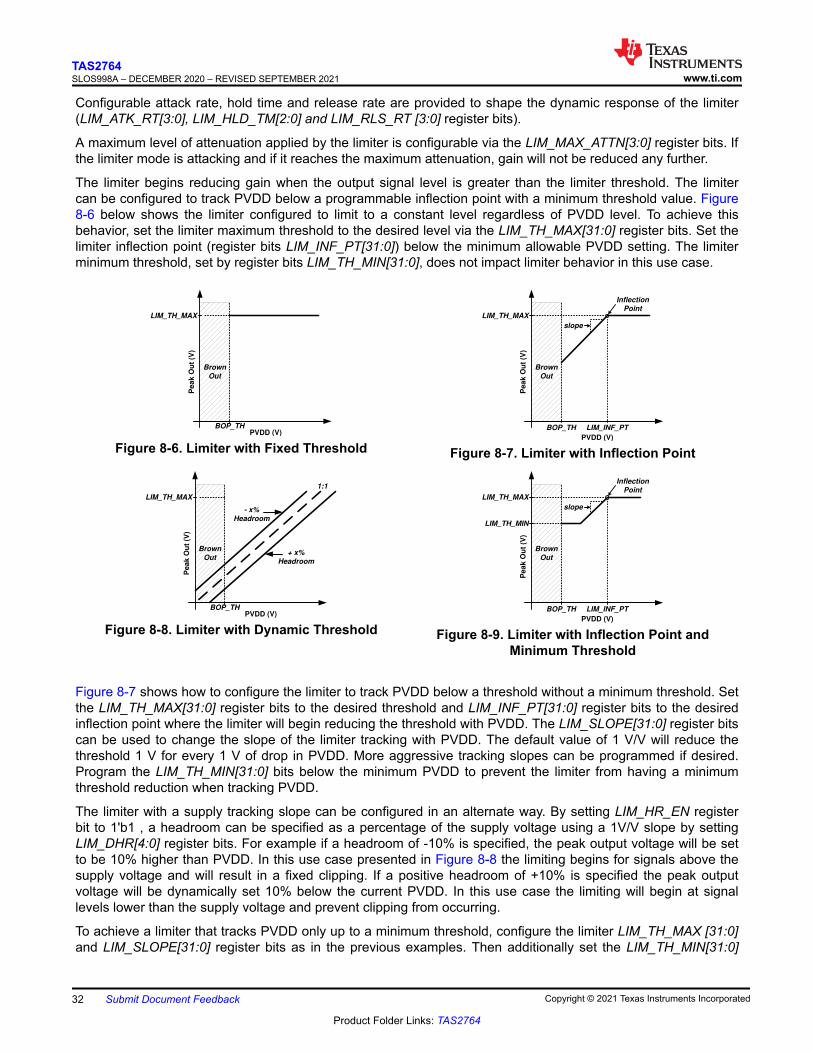
The limiter begins reducing gain when the output signal level is greater than the limiter threshold. The limiter can be configured to track PVDD below a programmable inflection point with a minimum threshold value. Figure 8-6 below shows the limiter configured to limit to a constant level regardless of PVDD level. To achieve this behavior, set the limiter maximum threshold to the desired level via the LIM_TH_MAX[31:0] register bits. Set the limiter inflection point (register bits LIM_INF_PT[31:0]) below the minimum allowable PVDD setting. The limiter minimum threshold, set by register bits LIM_TH_MIN[31:0], does not impact limiter behavior in this use case.
PVDD (V)
Pe
ak
Ou
t (V
)
BOP_TH
Brown
Out
LIM_TH_MAX
Figure 8-6. Limiter with Fixed ThresholdPVDD (V)
Pe
ak
Ou
t (V
)
BOP_TH
Brown
Out
LIM_TH_MAX
slope
LIM_INF_PT
Inflection
Point
Figure 8-7. Limiter with Inflection Point
PVDD (V)
Pe
ak
Ou
t (V
)
BOP_TH
Brown
Out
LIM_TH_MAX
+ x%
Headroom
- x%
Headroom
1:1
Figure 8-8. Limiter with Dynamic ThresholdPVDD (V)
Pe
ak
Ou
t (V
)
BOP_TH
Brown
Out
LIM_TH_MAX
slope
LIM_INF_PT
Inflection
Point
LIM_TH_MIN
Figure 8-9. Limiter with Inflection Point and Minimum Threshold
Figure 8-7 shows how to configure the limiter to track PVDD below a threshold without a minimum threshold. Set the LIM_TH_MAX[31:0] register bits to the desired threshold and LIM_INF_PT[31:0] register bits to the desired inflection point where the limiter will begin reducing the threshold with PVDD. The LIM_SLOPE[31:0] register bits can be used to change the slope of the limiter tracking with PVDD. The default value of 1 V/V will reduce the threshold 1 V for every 1 V of drop in PVDD. More aggressive tracking slopes can be programmed if desired. Program the LIM_TH_MIN[31:0] bits below the minimum PVDD to prevent the limiter from having a minimum threshold reduction when tracking PVDD.
The limiter with a supply tracking slope can be configured in an alternate way. By setting LIM_HR_EN register bit to 1'b1 , a headroom can be specified as a percentage of the supply voltage using a 1V/V slope by setting LIM_DHR[4:0] register bits. For example if a headroom of -10% is specified, the peak output voltage will be set to be 10% higher than PVDD. In this use case presented in Figure 8-8 the limiting begins for signals above the supply voltage and will result in a fixed clipping. If a positive headroom of +10% is specified the peak output voltage will be dynamically set 10% below the current PVDD. In this use case the limiting will begin at signal levels lower than the supply voltage and prevent clipping from occurring.
To achieve a limiter that tracks PVDD only up to a minimum threshold, configure the limiter LIM_TH_MAX [31:0] and LIM_SLOPE[31:0] register bits as in the previous examples. Then additionally set the LIM_TH_MIN[31:0]
TAS2764SLOS998A – DECEMBER 2020 – REVISED SEPTEMBER 2021 www.ti.com
32 Submit Document Feedback Copyright © 2021 Texas Instruments Incorporated
Product Folder Links: TAS2764
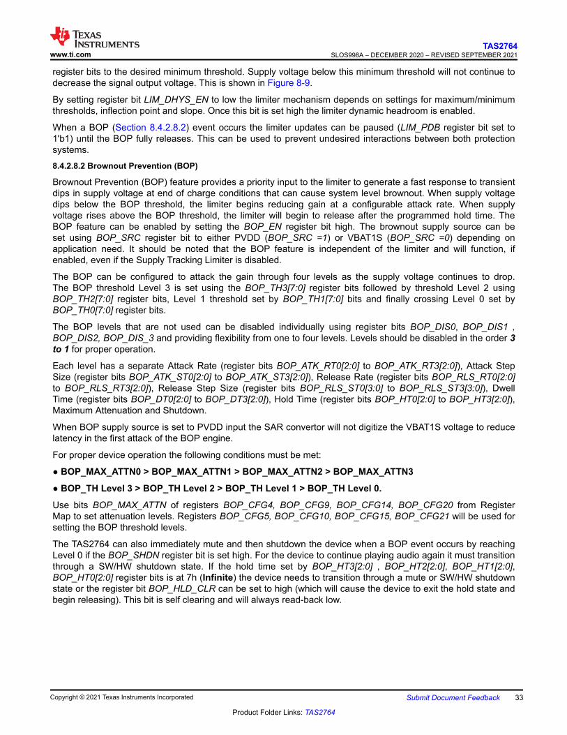
register bits to the desired minimum threshold. Supply voltage below this minimum threshold will not continue to decrease the signal output voltage. This is shown in Figure 8-9.
By setting register bit LIM_DHYS_EN to low the limiter mechanism depends on settings for maximum/minimum thresholds, inflection point and slope. Once this bit is set high the limiter dynamic headroom is enabled.
When a BOP (Section 8.4.2.8.2) event occurs the limiter updates can be paused (LIM_PDB register bit set to 1'b1) until the BOP fully releases. This can be used to prevent undesired interactions between both protection systems.
8.4.2.8.2 Brownout Prevention (BOP)
Brownout Prevention (BOP) feature provides a priority input to the limiter to generate a fast response to transient dips in supply voltage at end of charge conditions that can cause system level brownout. When supply voltage dips below the BOP threshold, the limiter begins reducing gain at a configurable attack rate. When supply voltage rises above the BOP threshold, the limiter will begin to release after the programmed hold time. The BOP feature can be enabled by setting the BOP_EN register bit high. The brownout supply source can be set using BOP_SRC register bit to either PVDD (BOP_SRC =1) or VBAT1S (BOP_SRC =0) depending on application need. It should be noted that the BOP feature is independent of the limiter and will function, if enabled, even if the Supply Tracking Limiter is disabled.
The BOP can be configured to attack the gain through four levels as the supply voltage continues to drop. The BOP threshold Level 3 is set using the BOP_TH3[7:0] register bits followed by threshold Level 2 using BOP_TH2[7:0] register bits, Level 1 threshold set by BOP_TH1[7:0] bits and finally crossing Level 0 set by BOP_TH0[7:0] register bits.
The BOP levels that are not used can be disabled individually using register bits BOP_DIS0, BOP_DIS1 , BOP_DIS2, BOP_DIS_3 and providing flexibility from one to four levels. Levels should be disabled in the order 3 to 1 for proper operation.
Each level has a separate Attack Rate (register bits BOP_ATK_RT0[2:0] to BOP_ATK_RT3[2:0]), Attack Step Size (register bits BOP_ATK_ST0[2:0] to BOP_ATK_ST3[2:0]), Release Rate (register bits BOP_RLS_RT0[2:0] to BOP_RLS_RT3[2:0]), Release Step Size (register bits BOP_RLS_ST0[3:0] to BOP_RLS_ST3[3:0]), Dwell Time (register bits BOP_DT0[2:0] to BOP_DT3[2:0]), Hold Time (register bits BOP_HT0[2:0] to BOP_HT3[2:0]), Maximum Attenuation and Shutdown.
When BOP supply source is set to PVDD input the SAR convertor will not digitize the VBAT1S voltage to reduce latency in the first attack of the BOP engine.
For proper device operation the following conditions must be met:
● BOP_MAX_ATTN0 > BOP_MAX_ATTN1 > BOP_MAX_ATTN2 > BOP_MAX_ATTN3
● BOP_TH Level 3 > BOP_TH Level 2 > BOP_TH Level 1 > BOP_TH Level 0.
Use bits BOP_MAX_ATTN of registers BOP_CFG4, BOP_CFG9, BOP_CFG14, BOP_CFG20 from Register Map to set attenuation levels. Registers BOP_CFG5, BOP_CFG10, BOP_CFG15, BOP_CFG21 will be used for setting the BOP threshold levels.
The TAS2764 can also immediately mute and then shutdown the device when a BOP event occurs by reaching Level 0 if the BOP_SHDN register bit is set high. For the device to continue playing audio again it must transition through a SW/HW shutdown state. If the hold time set by BOP_HT3[2:0] , BOP_HT2[2:0], BOP_HT1[2:0], BOP_HT0[2:0] register bits is at 7h (Infinite) the device needs to transition through a mute or SW/HW shutdown state or the register bit BOP_HLD_CLR can be set to high (which will cause the device to exit the hold state and begin releasing). This bit is self clearing and will always read-back low.
www.ti.comTAS2764
SLOS998A – DECEMBER 2020 – REVISED SEPTEMBER 2021
Copyright © 2021 Texas Instruments Incorporated Submit Document Feedback 33
Product Folder Links: TAS2764
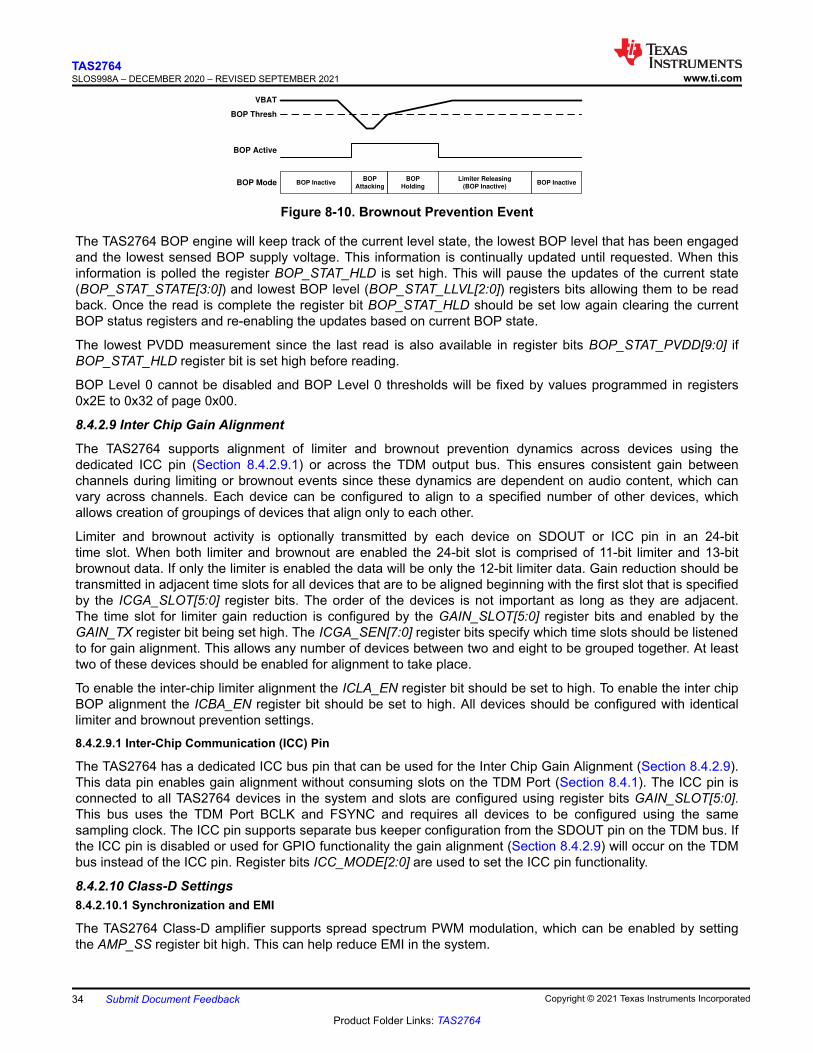
VBAT
BOP Thresh
BOP Active
BOP
Attacking
BOP
Holding
Limiter Releasing
(BOP Inactive)BOP Inactive BOP InactiveBOP Mode
Figure 8-10. Brownout Prevention Event
The TAS2764 BOP engine will keep track of the current level state, the lowest BOP level that has been engaged and the lowest sensed BOP supply voltage. This information is continually updated until requested. When this information is polled the register BOP_STAT_HLD is set high. This will pause the updates of the current state (BOP_STAT_STATE[3:0]) and lowest BOP level (BOP_STAT_LLVL[2:0]) registers bits allowing them to be read back. Once the read is complete the register bit BOP_STAT_HLD should be set low again clearing the current BOP status registers and re-enabling the updates based on current BOP state.
The lowest PVDD measurement since the last read is also available in register bits BOP_STAT_PVDD[9:0] if BOP_STAT_HLD register bit is set high before reading.
BOP Level 0 cannot be disabled and BOP Level 0 thresholds will be fixed by values programmed in registers 0x2E to 0x32 of page 0x00.
8.4.2.9 Inter Chip Gain Alignment
The TAS2764 supports alignment of limiter and brownout prevention dynamics across devices using the dedicated ICC pin (Section 8.4.2.9.1) or across the TDM output bus. This ensures consistent gain between channels during limiting or brownout events since these dynamics are dependent on audio content, which can vary across channels. Each device can be configured to align to a specified number of other devices, which allows creation of groupings of devices that align only to each other.
Limiter and brownout activity is optionally transmitted by each device on SDOUT or ICC pin in an 24-bit time slot. When both limiter and brownout are enabled the 24-bit slot is comprised of 11-bit limiter and 13-bit brownout data. If only the limiter is enabled the data will be only the 12-bit limiter data. Gain reduction should be transmitted in adjacent time slots for all devices that are to be aligned beginning with the first slot that is specified by the ICGA_SLOT[5:0] register bits. The order of the devices is not important as long as they are adjacent. The time slot for limiter gain reduction is configured by the GAIN_SLOT[5:0] register bits and enabled by the GAIN_TX register bit being set high. The ICGA_SEN[7:0] register bits specify which time slots should be listened to for gain alignment. This allows any number of devices between two and eight to be grouped together. At least two of these devices should be enabled for alignment to take place.
To enable the inter-chip limiter alignment the ICLA_EN register bit should be set to high. To enable the inter chip BOP alignment the ICBA_EN register bit should be set to high. All devices should be configured with identical limiter and brownout prevention settings.
8.4.2.9.1 Inter-Chip Communication (ICC) Pin
The TAS2764 has a dedicated ICC bus pin that can be used for the Inter Chip Gain Alignment (Section 8.4.2.9). This data pin enables gain alignment without consuming slots on the TDM Port (Section 8.4.1). The ICC pin is connected to all TAS2764 devices in the system and slots are configured using register bits GAIN_SLOT[5:0]. This bus uses the TDM Port BCLK and FSYNC and requires all devices to be configured using the same sampling clock. The ICC pin supports separate bus keeper configuration from the SDOUT pin on the TDM bus. If the ICC pin is disabled or used for GPIO functionality the gain alignment (Section 8.4.2.9) will occur on the TDM bus instead of the ICC pin. Register bits ICC_MODE[2:0] are used to set the ICC pin functionality.
8.4.2.10 Class-D Settings8.4.2.10.1 Synchronization and EMI
The TAS2764 Class-D amplifier supports spread spectrum PWM modulation, which can be enabled by setting the AMP_SS register bit high. This can help reduce EMI in the system.
TAS2764SLOS998A – DECEMBER 2020 – REVISED SEPTEMBER 2021 www.ti.com
34 Submit Document Feedback Copyright © 2021 Texas Instruments Incorporated
Product Folder Links: TAS2764
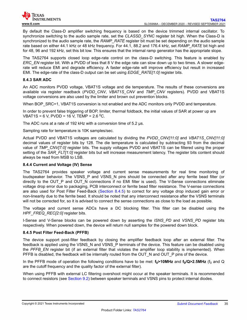
By default the Class-D amplifier switching frequency is based on the device trimmed internal oscillator. To synchronize switching to the audio sample rate, set the CLASSD_SYNC register bit high. When the Class-D is synchronized to the audio sample rate, the RAMP_RATE register bit must be set depending on the audio sample rate based on either 44.1 kHz or 48 kHz frequency. For 44.1, 88.2 and 176.4 kHz, set RAMP_RATE bit high and for 48, 96 and 192 kHz, set this bit low. This ensures that the internal ramp generator has the appropriate slope.
The TAS2764 supports closed loop edge-rate control on the class-D switching. This feature is enabled by ERC_EN register bit. With a PVDD of less that 8 V the edge rate can slow down up to two times. A slower edge-rate will reduce EMI and degrade efficiency. A faster edge-rate will improve efficiency but result in increased EMI. The edge-rate of the class-D output can be set using EDGE_RATE[1:0] register bits.
8.4.3 SAR ADC
An ADC monitors PVDD voltage, VBAT1S voltage and die temperature. The results of these conversions are available via register readback (PVDD_CNV, VBAT1S_CNV and TMP_CNV registers). PVDD and VBAT1S voltage conversions are also used by the limiter and brown out prevention blocks.
When BOP_SRC=1, VBAT1S conversion is not enabled and the ADC monitors only PVDD and temperature.
In order to prevent false triggering of BOP, limiter, thermal foldback, the initial values of SAR at power up are VBAT1S = 6 V, PVDD = 16 V, TEMP = 2.6 0C.
The ADC runs at a rate of 192 kHz with a conversion time of 5.2 μs.
Sampling rate for temperature is 10K samples/sec.
Actual PVDD and VBAT1S voltages are calculated by dividing the PVDD_CNV[11:0] and VBAT1S_CNV[11:0] decimal values of register bits by 128. The die temperature is calculated by subtracting 93 from the decimal value of TMP_CNV[7:0] register bits. The supply voltages PVDD and VBAT1S can be filtered using the proper setting of the SAR_FLT[1:0] register bits but will increase measurement latency. The register bits content should always be read from MSB to LSB.
8.4.4 Current and Voltage (IV) Sense
The TAS2764 provides speaker voltage and current sense measurements for real time monitoring of loudspeaker behavior. The VSNS_P and VSNS_N pins should be connected after any ferrite bead filter (or directly to the OUT_P and OUT_N connections if no EMI filter is used). The V-Sense connections eliminate voltage drop error due to packaging, PCB interconnect or ferrite bead filter resistance. The V-sense connections are also used for Post Filter Feed-Back (Section 8.4.5) to correct for any voltage drop induced gain error or non-linearity due to the ferrite bead. It should be noted that any interconnect resistance after the VSNS terminals will not be corrected for, so it is advised to connect the sense connections as close to the load as possible.
The voltage and current sense ADCs have a DC blocking filter. This filter can be disabled using the HPF_FREQ_REC[2:0] register bits.
I-Sense and V-Sense blocks can be powered down by asserting the ISNS_PD and VSNS_PD register bits respectively. When powered down, the device will return null samples for the powered down block.
8.4.5 Post Filter Feed-Back (PFFB)
The device support post-filter feedback by closing the amplifier feedback loop after an external filter. The feedback is applied using the VSNS_N and VSNS_P terminals of the device. This feature can be disabled using the PFFB_EN register bit (if an external filter that violates the amplifier loop stability is implemented). When PFFB is disabled, the feedback will be internally routed from the OUT_N and OUT_P pins of the device.
In the PFFB mode of operation the following conditions have to be met: f0>10MHz and f0/Q>2.5MHz (f0 and Q are the cutoff frequency and the quality factor of the external filter).
When using PFFB with external LC filtering overshoot might occur at the speaker terminals. It is recommended to connect resistors (see Section 9.2) between speaker terninals and VSNS pins to protect internal diodes.
www.ti.comTAS2764
SLOS998A – DECEMBER 2020 – REVISED SEPTEMBER 2021
Copyright © 2021 Texas Instruments Incorporated Submit Document Feedback 35
Product Folder Links: TAS2764
8.4.6 Load Diagnostics
The TAS2764 can check the speaker terminal for an open or short. This can be used to verify the continuity of the speaker or the traces to the speaker. The entire operation is performed by the TAS2764 and result is reported using the IRQZ pin or by reading over I2C bus on completion. The load diagnostics can be performed using external audio clock (register bit LDG_CLK=0) or the internal oscillator (LDG_CLK=1).
The speaker open (UT) and short (LT) thresholds are configured using the LDG_RES_UT[31:0] and LDG_RES_LT[31:0] register bits. The diagnostic is run by selecting one of the load diagnostic modes set by MODE[2:0] register bits. The load diagnostic can be run before transitioning to active mode or stand-alone returning to software shutdown when complete. When the load diagnostics is run it will play a 22kHz at -35dBFS for 100ms and measure the resistance of the speaker trace. The result is averaged over the time specified by the LDG_AVG[1:0] register bits. The measured speaker impedance can be read from LDS_RES_VAL[31:0] register bits.
8.4.7 Thermal Foldback
The TAS2764 monitors the die temperature and can automatically limit the audio signal when the die temperature reaches a set threshold. It is recommended to use the thermal fold-back registers to configure this protection mechanism as the internal DSP will perform the necessary calculation for each register.
Thermal fold-back can be disabled using TFB_EN register bit. If the die temperature reaches the value set by TF_TEMP_TH[31:0] register bits this feature will begin to attenuate the audio signal to prevent the device from shutting down due to over-temperature. It will attenuate the audio signal by a value set in TF_LIMS[31:0] register bits over a range of temperature set by TF_TEMP_TH[31:0] register bits. The thermal fold-back attack is at a fixed rate of 0.25dB per sample. A maximum attenuation can be specified using register bits TF_MAX_ATTN[31:0]. However, if the device continues to heat up, eventually the device over-temperature will be triggered. The attenuation will be held for a number of samples set by register bits TF_HOLD_CNT[31:0], before the attenuation will begin releasing.
8.4.8 Over Power Protection
The TAS2764 monitors the temperature of the internal power FETs. If the maximum continue power is high and power FETs temperature goes above a threshold, an in-built protection circuit will trigger a thermal foldback and, if temperature still increases, shutdown the device.
The protection mechanism is based on two thresholds TH1 and TH2. The TH1 threshold is set at a temperature 1160C higher than the temperature measured by the internal bandgap but not less than 2500C. The TH1 threshold triggers a thermal foldback.
The TH2 threshold is 400 C above TH1 and triggers thermal shutdown.
The two detection mechanisms can be disabled by setting bits TH_DET_TH2_EN and TH_DET_TH1_EN of register 0x47, page 0x01 to low.
8.4.9 Clocks and PLL
The device clocking is derived from the SBCLK input clock. The tables below show the valid SBCLK clock frequencies for each sample rate and SBCLK to FSYNC ratio (for 44.1 kHz and 48 kHz family frequencies).
If the sample rate is properly configured via the SAMP_RATE[2:0] register bits, no additional configuration is required as long as the SBCLK to FSYNC ratio is valid. The device will detect improper SBCLK frequencies and SBCLK to FSYNC ratios and volume ramp down the playback path to minimize audible artifacts. After the clock error is detected, the device will enter a low power halt mode after a time set by CLK_HALT_TIMER[2:0] register bits if CLK_HALT_EN bit is high. Additionally, the device can automatically power up and down on valid clock signals if CLK_ERR_PWR_EN register bit is set to high. The device sampling rate should not be changed while this feature is enabled. In this mode the CLK_HALT_EN bit register should be set high in order for this feature to work properly.
TAS2764SLOS998A – DECEMBER 2020 – REVISED SEPTEMBER 2021 www.ti.com
36 Submit Document Feedback Copyright © 2021 Texas Instruments Incorporated
Product Folder Links: TAS2764
Table 8-3. Supported SBCLK Frequencies (48 kHz based sample rates)Sample Rate
(kHz)SBCLK to FSYNC Ratio
16 24 32 48 64 96 12548 kHz 768 kHz 1.152 MHz 1.536 MHz 2.304 MHz 3.072 MHz 4.608 MHz 6 MHz
96 kHz 1.536 MHz 2.304 MHz 3.072 MHz 4.608 MHz 6.144 MHz 9.216 MHz 12 MHz
Sample Rate (kHz)
SBCLK to FSYNC Ratio128 192 250 256 384 500 512
48 kHz 6.144 MHz 9.216 MHz 12 MHz 12.288 MHz 18.432 MHz 24 MHz 24.576 MHz
96 kHz 12.288 MHz 18.432 MHz 24 MHz 24.576 MHz - - -
Table 8-4. Supported SBCLK Frequencies (44.1 kHz based sample rates)Sample Rate
(kHz)SBCLK to FSYNC Ratio
16 24 32 48 64 96 12544.1 kHz 705.6 kHz 1.0584 MHz 1.4112 MHz 2.1168 MHz 2.8224 MHz 4.2336 MHz 5.5125 MHz
88.2 kHz 1.4112 MHz 2.1168 MHz 2.8224 MHz 4.2336 MHz 5.6448 MHz 8.4672 MHz 11.025 MHz
Sample Rate (kHz)
SBCLK to FSYNC Ratio128 192 250 256 384 500 512
44.1 kHz 5.6448 MHz 8.4672 MHz 11.025 MHz 11.2896 MHz 16.9344 MHz 22.05 MHz 22.5792 MHz
88.2 kHz 11.2896 MHz 16.9344 MHz 22.05 MHz 22.5792 MHz - - -
8.4.10 Echo Reference
The TAS2764 has a dedicated mode to loop back the DSP output.
This feature allows user to do noise cancellation or echo correction algorithms.
A block diagram is presented in the figure below.
Figure 8-11. Echo Reference Loopback
The echo reference can be enabled by configuring AUDIO_TX bit in TDM_CFG12 register. The slot length and the time slot can be selected using AUDIO_SLEN and AUDIO_SLOT bits in TDM_CFG12 register.
8.5 Operational Modes8.5.1 Hardware Shutdown
The device enters Hardware Shutdown mode if the SDZ pin is asserted low. In Hardware Shutdown mode, the device consumes the minimum quiescent current from AVDD, VBAT1S and PVDD supplies. All registers loose state in this mode and I2C communication is disabled.
In normal shutdown mode if SDZ is asserted low while audio is playing, the device will ramp down volume on the audio, stop the Class-D switching, power down analog and digital blocks and finally put the device into Hardware Shutdown mode. If configured in normal shutdown mode with timeout the device will force a hard shutdown after a timeout set by the configurable shutdown timer (register bits SDZ_TIMEOUT[1:0]). The device can also be
www.ti.comTAS2764
SLOS998A – DECEMBER 2020 – REVISED SEPTEMBER 2021
Copyright © 2021 Texas Instruments Incorporated Submit Document Feedback 37
Product Folder Links: TAS2764
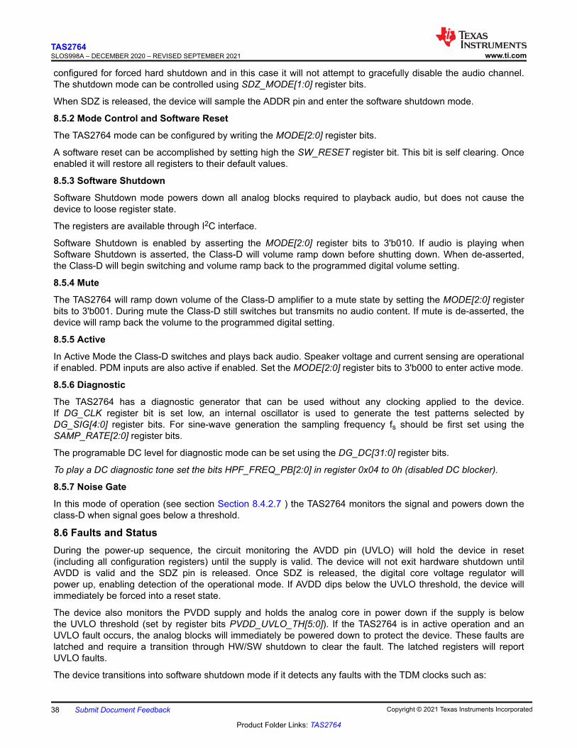
configured for forced hard shutdown and in this case it will not attempt to gracefully disable the audio channel. The shutdown mode can be controlled using SDZ_MODE[1:0] register bits.
When SDZ is released, the device will sample the ADDR pin and enter the software shutdown mode.
8.5.2 Mode Control and Software Reset
The TAS2764 mode can be configured by writing the MODE[2:0] register bits.
A software reset can be accomplished by setting high the SW_RESET register bit. This bit is self clearing. Once enabled it will restore all registers to their default values.
8.5.3 Software Shutdown
Software Shutdown mode powers down all analog blocks required to playback audio, but does not cause the device to loose register state.
The registers are available through I2C interface.
Software Shutdown is enabled by asserting the MODE[2:0] register bits to 3'b010. If audio is playing when Software Shutdown is asserted, the Class-D will volume ramp down before shutting down. When de-asserted, the Class-D will begin switching and volume ramp back to the programmed digital volume setting.
8.5.4 Mute
The TAS2764 will ramp down volume of the Class-D amplifier to a mute state by setting the MODE[2:0] register bits to 3'b001. During mute the Class-D still switches but transmits no audio content. If mute is de-asserted, the device will ramp back the volume to the programmed digital setting.
8.5.5 Active
In Active Mode the Class-D switches and plays back audio. Speaker voltage and current sensing are operational if enabled. PDM inputs are also active if enabled. Set the MODE[2:0] register bits to 3'b000 to enter active mode.
8.5.6 Diagnostic
The TAS2764 has a diagnostic generator that can be used without any clocking applied to the device. If DG_CLK register bit is set low, an internal oscillator is used to generate the test patterns selected by DG_SIG[4:0] register bits. For sine-wave generation the sampling frequency fs should be first set using the SAMP_RATE[2:0] register bits.
The programable DC level for diagnostic mode can be set using the DG_DC[31:0] register bits.
To play a DC diagnostic tone set the bits HPF_FREQ_PB[2:0] in register 0x04 to 0h (disabled DC blocker).
8.5.7 Noise Gate
In this mode of operation (see section Section 8.4.2.7 ) the TAS2764 monitors the signal and powers down the class-D when signal goes below a threshold.
8.6 Faults and StatusDuring the power-up sequence, the circuit monitoring the AVDD pin (UVLO) will hold the device in reset (including all configuration registers) until the supply is valid. The device will not exit hardware shutdown until AVDD is valid and the SDZ pin is released. Once SDZ is released, the digital core voltage regulator will power up, enabling detection of the operational mode. If AVDD dips below the UVLO threshold, the device will immediately be forced into a reset state.
The device also monitors the PVDD supply and holds the analog core in power down if the supply is below the UVLO threshold (set by register bits PVDD_UVLO_TH[5:0]). If the TAS2764 is in active operation and an UVLO fault occurs, the analog blocks will immediately be powered down to protect the device. These faults are latched and require a transition through HW/SW shutdown to clear the fault. The latched registers will report UVLO faults.
The device transitions into software shutdown mode if it detects any faults with the TDM clocks such as:
TAS2764SLOS998A – DECEMBER 2020 – REVISED SEPTEMBER 2021 www.ti.com
38 Submit Document Feedback Copyright © 2021 Texas Instruments Incorporated
Product Folder Links: TAS2764
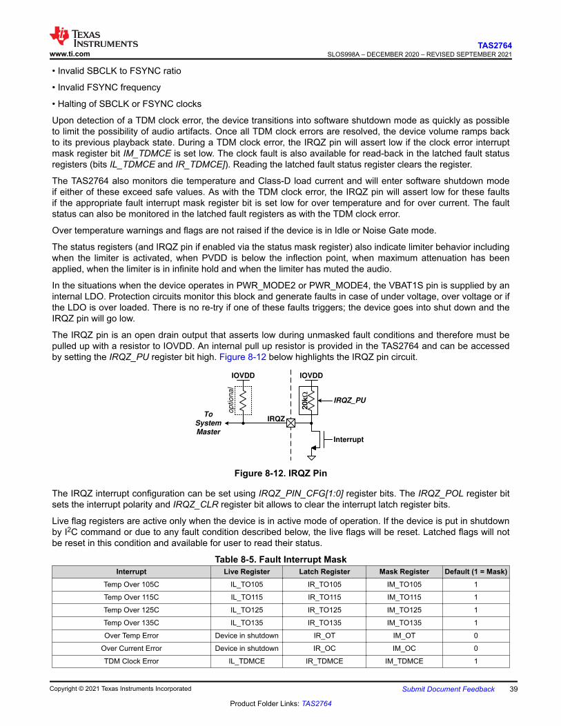
• Invalid SBCLK to FSYNC ratio
• Invalid FSYNC frequency
• Halting of SBCLK or FSYNC clocks
Upon detection of a TDM clock error, the device transitions into software shutdown mode as quickly as possible to limit the possibility of audio artifacts. Once all TDM clock errors are resolved, the device volume ramps back to its previous playback state. During a TDM clock error, the IRQZ pin will assert low if the clock error interrupt mask register bit IM_TDMCE is set low. The clock fault is also available for read-back in the latched fault status registers (bits IL_TDMCE and IR_TDMCE]). Reading the latched fault status register clears the register.
The TAS2764 also monitors die temperature and Class-D load current and will enter software shutdown mode if either of these exceed safe values. As with the TDM clock error, the IRQZ pin will assert low for these faults if the appropriate fault interrupt mask register bit is set low for over temperature and for over current. The fault status can also be monitored in the latched fault registers as with the TDM clock error.
Over temperature warnings and flags are not raised if the device is in Idle or Noise Gate mode.
The status registers (and IRQZ pin if enabled via the status mask register) also indicate limiter behavior including when the limiter is activated, when PVDD is below the inflection point, when maximum attenuation has been applied, when the limiter is in infinite hold and when the limiter has muted the audio.
In the situations when the device operates in PWR_MODE2 or PWR_MODE4, the VBAT1S pin is supplied by an internal LDO. Protection circuits monitor this block and generate faults in case of under voltage, over voltage or if the LDO is over loaded. There is no re-try if one of these faults triggers; the device goes into shut down and the IRQZ pin will go low.
The IRQZ pin is an open drain output that asserts low during unmasked fault conditions and therefore must be pulled up with a resistor to IOVDD. An internal pull up resistor is provided in the TAS2764 and can be accessed by setting the IRQZ_PU register bit high. Figure 8-12 below highlights the IRQZ pin circuit.
20
k:
IOVDD
Interrupt
IRQZ_PU
IOVDD
op
tio
na
l
IRQZTo
System
Master
Figure 8-12. IRQZ Pin
The IRQZ interrupt configuration can be set using IRQZ_PIN_CFG[1:0] register bits. The IRQZ_POL register bit sets the interrupt polarity and IRQZ_CLR register bit allows to clear the interrupt latch register bits.
Live flag registers are active only when the device is in active mode of operation. If the device is put in shutdown by I2C command or due to any fault condition described below, the live flags will be reset. Latched flags will not be reset in this condition and available for user to read their status.
Table 8-5. Fault Interrupt MaskInterrupt Live Register Latch Register Mask Register Default (1 = Mask)
Temp Over 105C IL_TO105 IR_TO105 IM_TO105 1
Temp Over 115C IL_TO115 IR_TO115 IM_TO115 1
Temp Over 125C IL_TO125 IR_TO125 IM_TO125 1
Temp Over 135C IL_TO135 IR_TO135 IM_TO135 1
Over Temp Error Device in shutdown IR_OT IM_OT 0
Over Current Error Device in shutdown IR_OC IM_OC 0
TDM Clock Error IL_TDMCE IR_TDMCE IM_TDMCE 1
www.ti.comTAS2764
SLOS998A – DECEMBER 2020 – REVISED SEPTEMBER 2021
Copyright © 2021 Texas Instruments Incorporated Submit Document Feedback 39
Product Folder Links: TAS2764
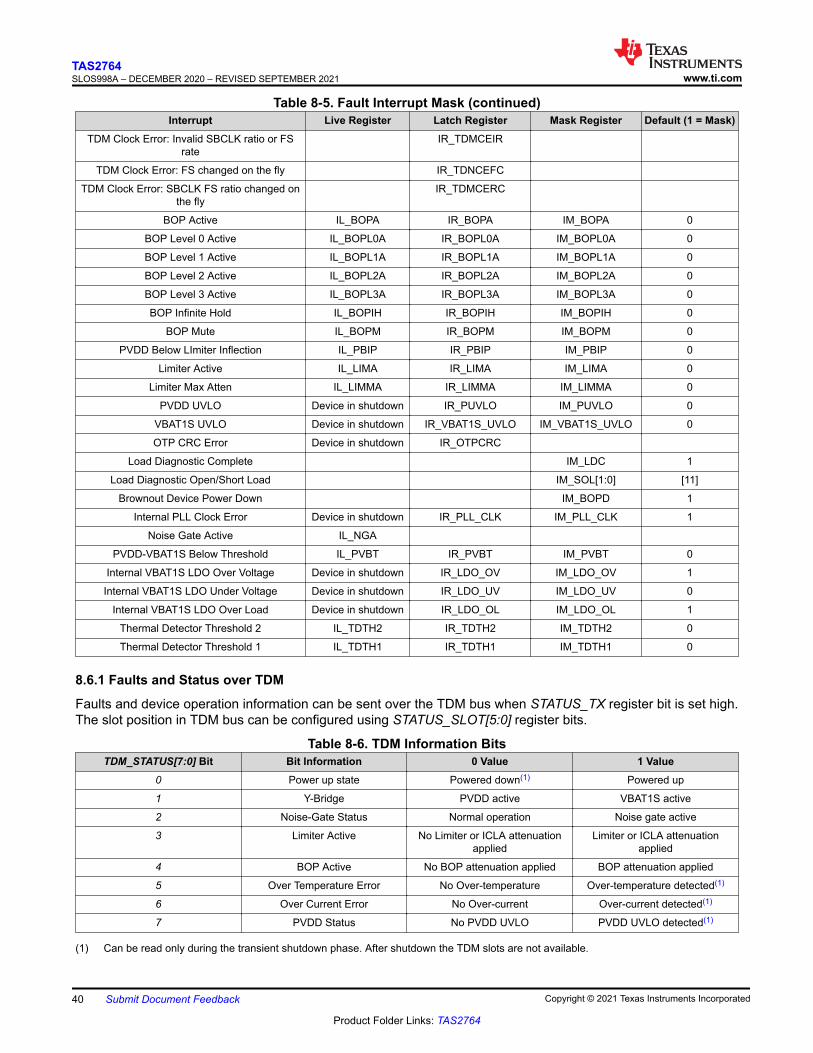
Table 8-5. Fault Interrupt Mask (continued)Interrupt Live Register Latch Register Mask Register Default (1 = Mask)
TDM Clock Error: Invalid SBCLK ratio or FS rate
IR_TDMCEIR
TDM Clock Error: FS changed on the fly IR_TDNCEFC
TDM Clock Error: SBCLK FS ratio changed on the fly
IR_TDMCERC
BOP Active IL_BOPA IR_BOPA IM_BOPA 0
BOP Level 0 Active IL_BOPL0A IR_BOPL0A IM_BOPL0A 0
BOP Level 1 Active IL_BOPL1A IR_BOPL1A IM_BOPL1A 0
BOP Level 2 Active IL_BOPL2A IR_BOPL2A IM_BOPL2A 0
BOP Level 3 Active IL_BOPL3A IR_BOPL3A IM_BOPL3A 0
BOP Infinite Hold IL_BOPIH IR_BOPIH IM_BOPIH 0
BOP Mute IL_BOPM IR_BOPM IM_BOPM 0
PVDD Below LImiter Inflection IL_PBIP IR_PBIP IM_PBIP 0
Limiter Active IL_LIMA IR_LIMA IM_LIMA 0
Limiter Max Atten IL_LIMMA IR_LIMMA IM_LIMMA 0
PVDD UVLO Device in shutdown IR_PUVLO IM_PUVLO 0
VBAT1S UVLO Device in shutdown IR_VBAT1S_UVLO IM_VBAT1S_UVLO 0
OTP CRC Error Device in shutdown IR_OTPCRC
Load Diagnostic Complete IM_LDC 1
Load Diagnostic Open/Short Load IM_SOL[1:0] [11]
Brownout Device Power Down IM_BOPD 1
Internal PLL Clock Error Device in shutdown IR_PLL_CLK IM_PLL_CLK 1
Noise Gate Active IL_NGA
PVDD-VBAT1S Below Threshold IL_PVBT IR_PVBT IM_PVBT 0
Internal VBAT1S LDO Over Voltage Device in shutdown IR_LDO_OV IM_LDO_OV 1
Internal VBAT1S LDO Under Voltage Device in shutdown IR_LDO_UV IM_LDO_UV 0
Internal VBAT1S LDO Over Load Device in shutdown IR_LDO_OL IM_LDO_OL 1
Thermal Detector Threshold 2 IL_TDTH2 IR_TDTH2 IM_TDTH2 0
Thermal Detector Threshold 1 IL_TDTH1 IR_TDTH1 IM_TDTH1 0
8.6.1 Faults and Status over TDM
Faults and device operation information can be sent over the TDM bus when STATUS_TX register bit is set high. The slot position in TDM bus can be configured using STATUS_SLOT[5:0] register bits.
Table 8-6. TDM Information BitsTDM_STATUS[7:0] Bit Bit Information 0 Value 1 Value
0 Power up state Powered down(1) Powered up
1 Y-Bridge PVDD active VBAT1S active
2 Noise-Gate Status Normal operation Noise gate active
3 Limiter Active No Limiter or ICLA attenuation applied
Limiter or ICLA attenuation applied
4 BOP Active No BOP attenuation applied BOP attenuation applied
5 Over Temperature Error No Over-temperature Over-temperature detected(1)
6 Over Current Error No Over-current Over-current detected(1)
7 PVDD Status No PVDD UVLO PVDD UVLO detected(1)
(1) Can be read only during the transient shutdown phase. After shutdown the TDM slots are not available.
TAS2764SLOS998A – DECEMBER 2020 – REVISED SEPTEMBER 2021 www.ti.com
40 Submit Document Feedback Copyright © 2021 Texas Instruments Incorporated
Product Folder Links: TAS2764
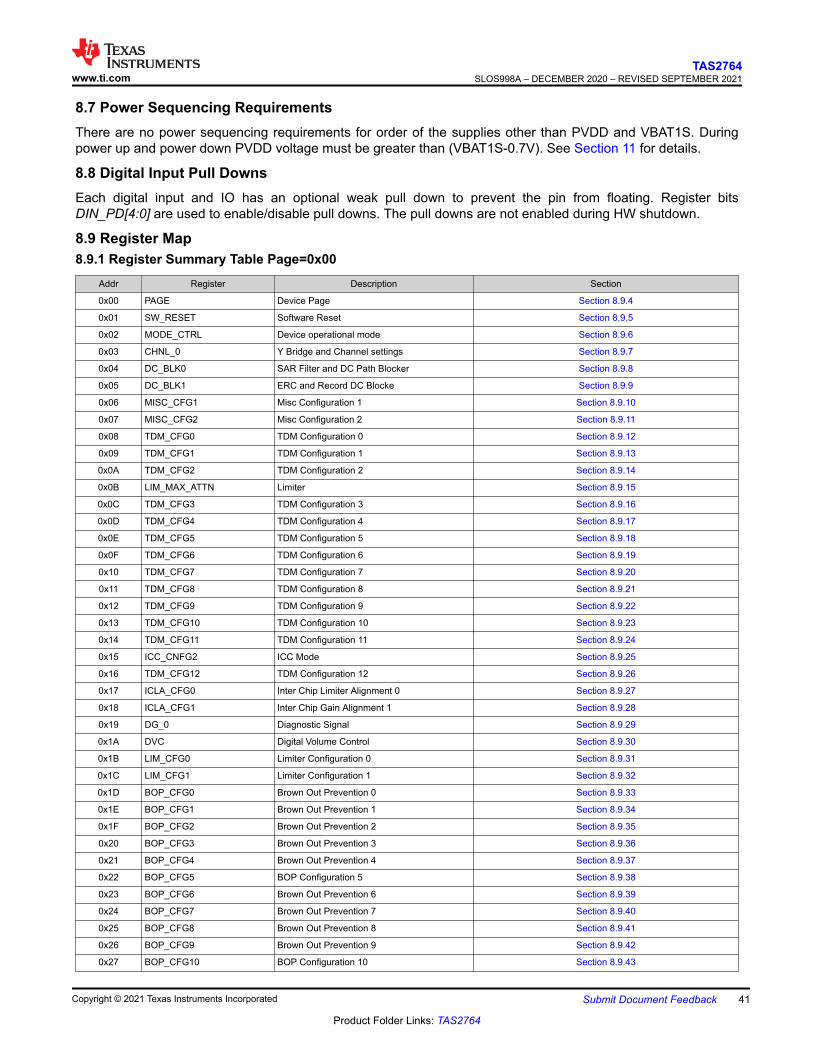
8.7 Power Sequencing RequirementsThere are no power sequencing requirements for order of the supplies other than PVDD and VBAT1S. During power up and power down PVDD voltage must be greater than (VBAT1S-0.7V). See Section 11 for details.
8.8 Digital Input Pull DownsEach digital input and IO has an optional weak pull down to prevent the pin from floating. Register bits DIN_PD[4:0] are used to enable/disable pull downs. The pull downs are not enabled during HW shutdown.
8.9 Register Map8.9.1 Register Summary Table Page=0x00
Addr Register Description Section
0x00 PAGE Device Page Section 8.9.4
0x01 SW_RESET Software Reset Section 8.9.5
0x02 MODE_CTRL Device operational mode Section 8.9.6
0x03 CHNL_0 Y Bridge and Channel settings Section 8.9.7
0x04 DC_BLK0 SAR Filter and DC Path Blocker Section 8.9.8
0x05 DC_BLK1 ERC and Record DC Blocke Section 8.9.9
0x06 MISC_CFG1 Misc Configuration 1 Section 8.9.10
0x07 MISC_CFG2 Misc Configuration 2 Section 8.9.11
0x08 TDM_CFG0 TDM Configuration 0 Section 8.9.12
0x09 TDM_CFG1 TDM Configuration 1 Section 8.9.13
0x0A TDM_CFG2 TDM Configuration 2 Section 8.9.14
0x0B LIM_MAX_ATTN Limiter Section 8.9.15
0x0C TDM_CFG3 TDM Configuration 3 Section 8.9.16
0x0D TDM_CFG4 TDM Configuration 4 Section 8.9.17
0x0E TDM_CFG5 TDM Configuration 5 Section 8.9.18
0x0F TDM_CFG6 TDM Configuration 6 Section 8.9.19
0x10 TDM_CFG7 TDM Configuration 7 Section 8.9.20
0x11 TDM_CFG8 TDM Configuration 8 Section 8.9.21
0x12 TDM_CFG9 TDM Configuration 9 Section 8.9.22
0x13 TDM_CFG10 TDM Configuration 10 Section 8.9.23
0x14 TDM_CFG11 TDM Configuration 11 Section 8.9.24
0x15 ICC_CNFG2 ICC Mode Section 8.9.25
0x16 TDM_CFG12 TDM Configuration 12 Section 8.9.26
0x17 ICLA_CFG0 Inter Chip Limiter Alignment 0 Section 8.9.27
0x18 ICLA_CFG1 Inter Chip Gain Alignment 1 Section 8.9.28
0x19 DG_0 Diagnostic Signal Section 8.9.29
0x1A DVC Digital Volume Control Section 8.9.30
0x1B LIM_CFG0 Limiter Configuration 0 Section 8.9.31
0x1C LIM_CFG1 Limiter Configuration 1 Section 8.9.32
0x1D BOP_CFG0 Brown Out Prevention 0 Section 8.9.33
0x1E BOP_CFG1 Brown Out Prevention 1 Section 8.9.34
0x1F BOP_CFG2 Brown Out Prevention 2 Section 8.9.35
0x20 BOP_CFG3 Brown Out Prevention 3 Section 8.9.36
0x21 BOP_CFG4 Brown Out Prevention 4 Section 8.9.37
0x22 BOP_CFG5 BOP Configuration 5 Section 8.9.38
0x23 BOP_CFG6 Brown Out Prevention 6 Section 8.9.39
0x24 BOP_CFG7 Brown Out Prevention 7 Section 8.9.40
0x25 BOP_CFG8 Brown Out Prevention 8 Section 8.9.41
0x26 BOP_CFG9 Brown Out Prevention 9 Section 8.9.42
0x27 BOP_CFG10 BOP Configuration 10 Section 8.9.43
www.ti.comTAS2764
SLOS998A – DECEMBER 2020 – REVISED SEPTEMBER 2021
Copyright © 2021 Texas Instruments Incorporated Submit Document Feedback 41
Product Folder Links: TAS2764
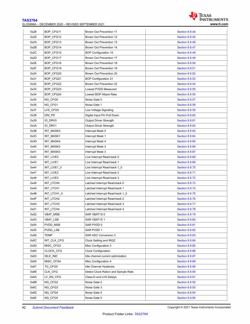
0x28 BOP_CFG11 Brown Out Prevention 11 Section 8.9.44
0x29 BOP_CFG12 Brown Out Prevention 12 Section 8.9.45
0x2A BOP_CFG13 Brown Out Prevention 13 Section 8.9.46
0x2B BOP_CFG14 Brown Out Prevention 14 Section 8.9.47
0x2C BOP_CFG15 BOP Configuration 15 Section 8.9.48
0x2D BOP_CFG17 Brown Out Prevention 17 Section 8.9.49
0x2E BOP_CFG18 Brown Out Prevention 18 Section 8.9.50
0x2F BOP_CFG19 Brown Out Prevention 19 Section 8.9.51
0x30 BOP_CFG20 Brown Out Prevention 20 Section 8.9.52
0x31 BOP_CFG21 BOP Configuration 21 Section 8.9.53
0x32 BOP_CFG22 Brown Out Prevention 22 Section 8.9.54
0x33 BOP_CFG23 Lowest PVDD Measured Section 8.9.55
0x34 BOP_CFG24 Lowest BOP Attack Rate Section 8.9.55
0x35 NG_CFG0 Noise Gate 0 Section 8.9.57
0x36 NG_CFG1 Noise Gate 1 Section 8.9.58
0x37 LVS_CFG0 Low Voltage Signaling Section 8.9.59
0x38 DIN_PD Digital Input Pin Pull Down Section 8.9.60
0x39 IO_DRV0 Output Driver Strength Section 8.9.61
0x3A IO_DRV1 Output Driver Strength Section 8.9.62
0x3B INT_MASK0 Interrupt Mask 0 Section 8.9.63
0x3C INT_MASK1 Interrupt Mask 1 Section 8.9.64
0x3D INT_MASK4 Interrupt Mask 4 Section 8.9.65
0x40 INT_MASK2 Interrupt Mask 2 Section 8.9.66
0x41 INT_MASK3 Interrupt Mask 3 Section 8.9.67
0x42 INT_LIVE0 Live Interrupt Read-back 0 Section 8.9.68
0x43 INT_LIVE1 Live Interrupt Read-back 1 Section 8.9.69
0x44 INT_LIVE1_0 Live Interrupt Read-back 1_0 Section 8.9.70
0x47 INT_LIVE2 Live Interrupt Read-back 2 Section 8.9.71
0x48 INT_LIVE3 Live Interrupt Read-back 3 Section 8.9.72
0x49 INT_LTCH0 Latched Interrupt Read-back 0 Section 8.9.73
0x4A INT_LTCH1 Latched Interrupt Read-back 1 Section 8.9.74
0x4B INT_LTCH1_0 Latched Interrupt Read-back 1_0 Section 8.9.75
0x4F INT_LTCH2 Latched Interrupt Read-back 2 Section 8.9.76
0x50 INT_LTCH3 Latched Interrupt Read-back 3 Section 8.9.77
0x51 INT_LTCH4 Latched Interrupt Read-back 4 Section 8.9.78
0x52 VBAT_MSB SAR VBAT1S 0 Section 8.9.79
0x53 VBAT_LSB SAR VBAT1S 1 Section 8.9.80
0x54 PVDD_MSB SAR PVDD 0 Section 8.9.81
0x55 PVDD_LSB SAR PVDD 1 Section 8.9.82
0x56 TEMP SAR ADC Conversion 2 Section 8.9.83
0x5C INT_CLK_CFG Clock Setting and IRQZ Section 8.9.84
0x5D MISC_CFG3 Misc Configuration 3 Section 8.9.85
0x60 CLOCK_CFG Clock Configuration Section 8.9.86
0x63 IDLE_IND Idle channel current optimization Section 8.9.87
0x65 MISC_CFG4 Misc Configuration 4 Section 8.9.88
0x67 TG_CFG0 Idle Channel Hysterisis Section 8.9.89
0x68 CLK_CFG Detect Clock Ration and Sample Rate Section 8.9.90
0x6A LV_EN_CFG Class-D and LVS Delays Section 8.9.91
0x6B NG_CFG2 Noise Gate 2 Section 8.9.92
0x6C NG_CFG3 Noise Gate 3 Section 8.9.93
0x6D NG_CFG4 Noise Gate 4 Section 8.9.94
0x6E NG_CFG5 Noise Gate 5 Section 8.9.95
TAS2764SLOS998A – DECEMBER 2020 – REVISED SEPTEMBER 2021 www.ti.com
42 Submit Document Feedback Copyright © 2021 Texas Instruments Incorporated
Product Folder Links: TAS2764
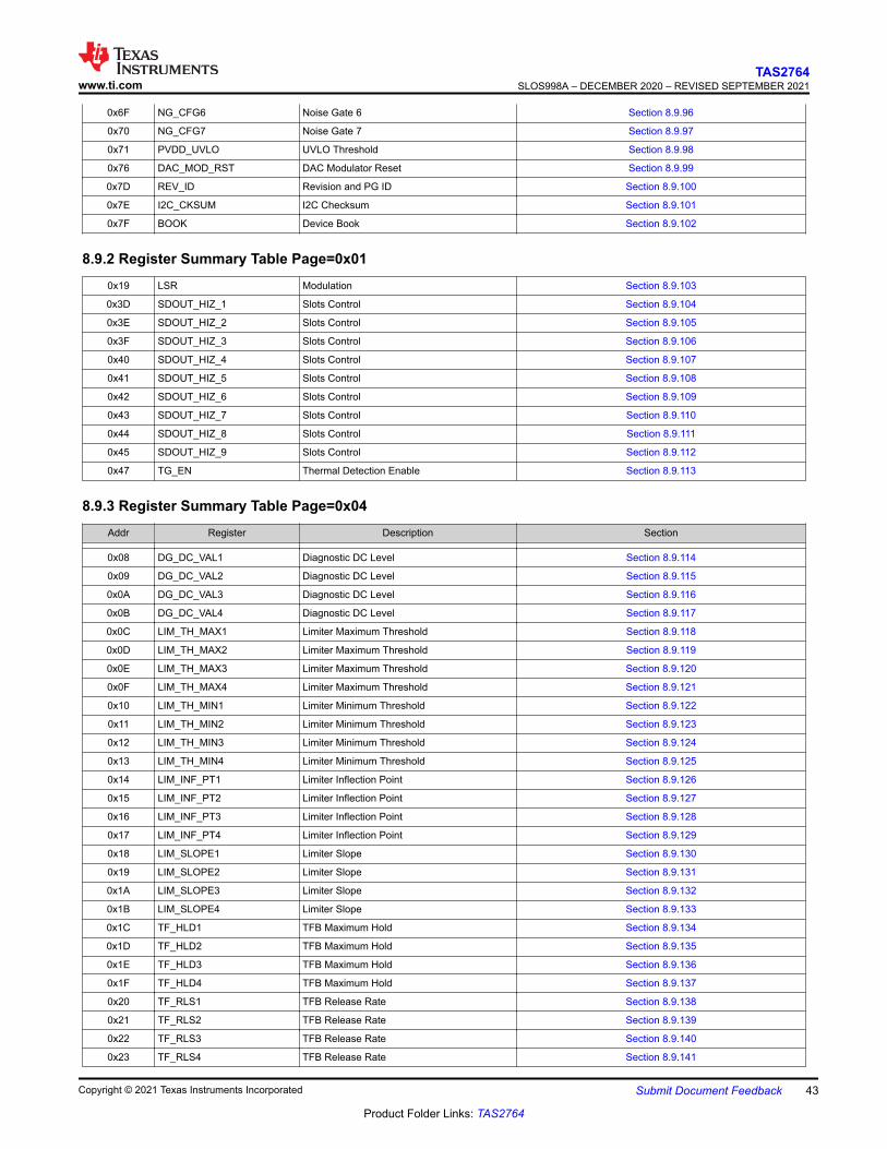
0x6F NG_CFG6 Noise Gate 6 Section 8.9.96
0x70 NG_CFG7 Noise Gate 7 Section 8.9.97
0x71 PVDD_UVLO UVLO Threshold Section 8.9.98
0x76 DAC_MOD_RST DAC Modulator Reset Section 8.9.99
0x7D REV_ID Revision and PG ID Section 8.9.100
0x7E I2C_CKSUM I2C Checksum Section 8.9.101
0x7F BOOK Device Book Section 8.9.102
8.9.2 Register Summary Table Page=0x010x19 LSR Modulation Section 8.9.103
0x3D SDOUT_HIZ_1 Slots Control Section 8.9.104
0x3E SDOUT_HIZ_2 Slots Control Section 8.9.105
0x3F SDOUT_HIZ_3 Slots Control Section 8.9.106
0x40 SDOUT_HIZ_4 Slots Control Section 8.9.107
0x41 SDOUT_HIZ_5 Slots Control Section 8.9.108
0x42 SDOUT_HIZ_6 Slots Control Section 8.9.109
0x43 SDOUT_HIZ_7 Slots Control Section 8.9.110
0x44 SDOUT_HIZ_8 Slots Control Section 8.9.111
0x45 SDOUT_HIZ_9 Slots Control Section 8.9.112
0x47 TG_EN Thermal Detection Enable Section 8.9.113
8.9.3 Register Summary Table Page=0x04Addr Register Description Section
0x08 DG_DC_VAL1 Diagnostic DC Level Section 8.9.114
0x09 DG_DC_VAL2 Diagnostic DC Level Section 8.9.115
0x0A DG_DC_VAL3 Diagnostic DC Level Section 8.9.116
0x0B DG_DC_VAL4 Diagnostic DC Level Section 8.9.117
0x0C LIM_TH_MAX1 Limiter Maximum Threshold Section 8.9.118
0x0D LIM_TH_MAX2 Limiter Maximum Threshold Section 8.9.119
0x0E LIM_TH_MAX3 Limiter Maximum Threshold Section 8.9.120
0x0F LIM_TH_MAX4 Limiter Maximum Threshold Section 8.9.121
0x10 LIM_TH_MIN1 Limiter Minimum Threshold Section 8.9.122
0x11 LIM_TH_MIN2 Limiter Minimum Threshold Section 8.9.123
0x12 LIM_TH_MIN3 Limiter Minimum Threshold Section 8.9.124
0x13 LIM_TH_MIN4 Limiter Minimum Threshold Section 8.9.125
0x14 LIM_INF_PT1 Limiter Inflection Point Section 8.9.126
0x15 LIM_INF_PT2 Limiter Inflection Point Section 8.9.127
0x16 LIM_INF_PT3 Limiter Inflection Point Section 8.9.128
0x17 LIM_INF_PT4 Limiter Inflection Point Section 8.9.129
0x18 LIM_SLOPE1 Limiter Slope Section 8.9.130
0x19 LIM_SLOPE2 Limiter Slope Section 8.9.131
0x1A LIM_SLOPE3 Limiter Slope Section 8.9.132
0x1B LIM_SLOPE4 Limiter Slope Section 8.9.133
0x1C TF_HLD1 TFB Maximum Hold Section 8.9.134
0x1D TF_HLD2 TFB Maximum Hold Section 8.9.135
0x1E TF_HLD3 TFB Maximum Hold Section 8.9.136
0x1F TF_HLD4 TFB Maximum Hold Section 8.9.137
0x20 TF_RLS1 TFB Release Rate Section 8.9.138
0x21 TF_RLS2 TFB Release Rate Section 8.9.139
0x22 TF_RLS3 TFB Release Rate Section 8.9.140
0x23 TF_RLS4 TFB Release Rate Section 8.9.141
www.ti.comTAS2764
SLOS998A – DECEMBER 2020 – REVISED SEPTEMBER 2021
Copyright © 2021 Texas Instruments Incorporated Submit Document Feedback 43
Product Folder Links: TAS2764
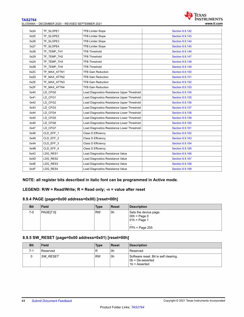
0x24 TF_SLOPE1 TFB Limiter Slope Section 8.9.142
0x25 TF_SLOPE2 TFB Limiter Slope Section 8.9.143
0x26 TF_SLOPE3 TFB Limiter Slope Section 8.9.144
0x27 TF_SLOPE4 TFB Limiter Slope Section 8.9.145
0x28 TF_TEMP_TH1 TFB Threshold Section 8.9.146
0x29 TF_TEMP_TH2 TFB Threshold Section 8.9.147
0x2A TF_TEMP_TH3 TFB Threshold Section 8.9.148
0x2B TF_TEMP_TH4 TFB Threshold Section 8.9.149
0x2C TF_MAX_ATTN1 TFB Gain Reduction Section 8.9.150
0x2D TF_MAX_ATTN2 TFB Gain Reduction Section 8.9.151
0x2E TF_MAX_ATTN3 TFB Gain Reduction Section 8.9.152
0x2F TF_MAX_ATTN4 TFB Gain Reduction Section 8.9.153
0x40 LD_CFG0 Load Diagnostics Resistance Upper Threshold Section 8.9.154
0x41 LD_CFG1 Load Diagnostics Resistance Upper Threshold Section 8.9.155
0x42 LD_CFG2 Load Diagnostics Resistance Upper Threshold Section 8.9.156
0x43 LD_CFG3 Load Diagnostics Resistance Upper Threshold Section 8.9.157
0x44 LD_CFG4 Load Diagnostics Resistance Lower Threshold Section 8.9.158
0x45 LD_CFG5 Load Diagnostics Resistance Lower Threshold Section 8.9.159
0x46 LD_CFG6 Load Diagnostics Resistance Lower Threshold Section 8.9.160
0x47 LD_CFG7 Load Diagnostics Resistance Lower Threshold Section 8.9.161
0x48 CLD_EFF_1 Class D Efficiency Section 8.9.162
0x49 CLD_EFF_2 Class D Efficiency Section 8.9.163
0x4A CLD_EFF_3 Class D Efficiency Section 8.9.164
0x4B CLD_EFF_4 Class D Efficiency Section 8.9.165
0x4C LDG_RES1 Load Diagnostics Resistance Value Section 8.9.166
0x4D LDG_RES2 Load Diagnostics Resistance Value Section 8.9.167
0x4E LDG_RES3 Load Diagnostics Resistance Value Section 8.9.168
0x4F LDG_RES4 Load Diagnostics Resistance Value Section 8.9.169
NOTE: all register bits described in italic font can be programmed in Active mode.
LEGEND: R/W = Read/Write; R = Read only; -n = value after reset
8.9.4 PAGE (page=0x00 address=0x00) [reset=00h]
Bit Field Type Reset Description7-0 PAGE[7:0] RW 0h Sets the device page.
00h = Page 0 01h = Page 1 ... FFh = Page 255
8.9.5 SW_RESET (page=0x00 address=0x01) [reset=00h]
Bit Field Type Reset Description7-1 Reserved R 0h Reserved
0 SW_RESET RW 0h Software reset. Bit is self clearing.0b = De-asserted 1b = Asserted
TAS2764SLOS998A – DECEMBER 2020 – REVISED SEPTEMBER 2021 www.ti.com
44 Submit Document Feedback Copyright © 2021 Texas Instruments Incorporated
Product Folder Links: TAS2764
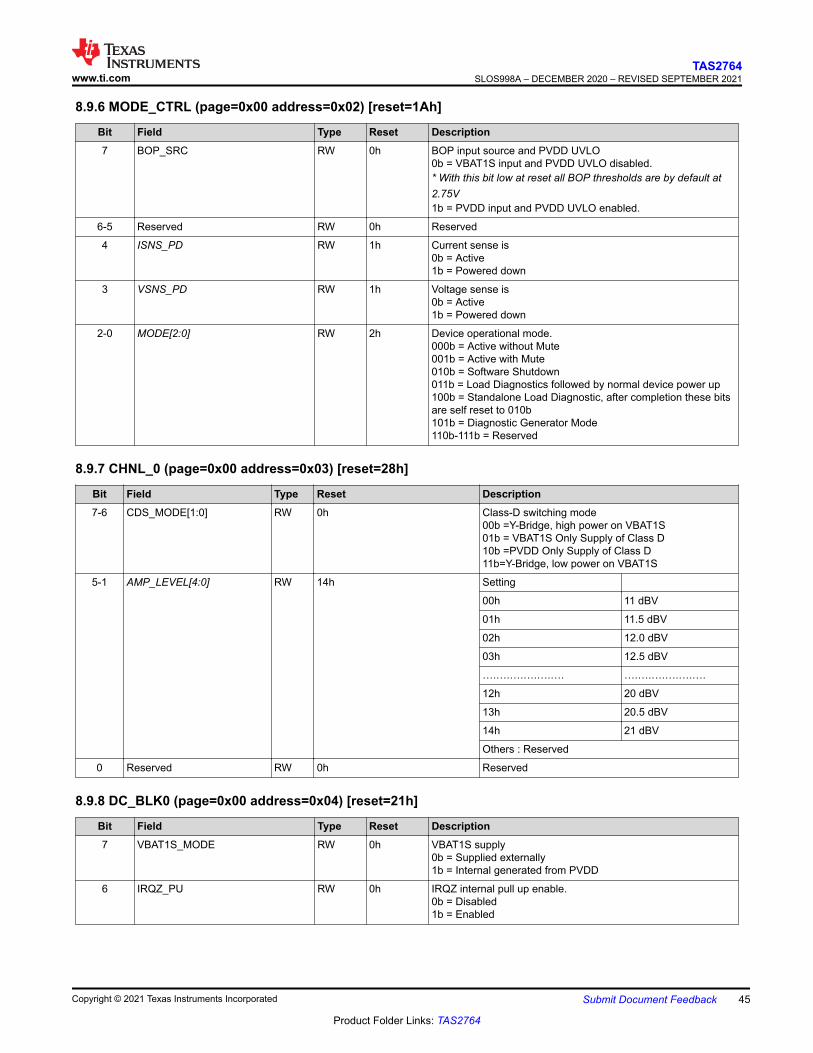
8.9.6 MODE_CTRL (page=0x00 address=0x02) [reset=1Ah]
Bit Field Type Reset Description7 BOP_SRC RW 0h BOP input source and PVDD UVLO
0b = VBAT1S input and PVDD UVLO disabled.* With this bit low at reset all BOP thresholds are by default at 2.75V1b = PVDD input and PVDD UVLO enabled.
6-5 Reserved RW 0h Reserved
4 ISNS_PD RW 1h Current sense is0b = Active 1b = Powered down
3 VSNS_PD RW 1h Voltage sense is0b = Active 1b = Powered down
2-0 MODE[2:0] RW 2h Device operational mode.000b = Active without Mute 001b = Active with Mute 010b = Software Shutdown 011b = Load Diagnostics followed by normal device power up 100b = Standalone Load Diagnostic, after completion these bits are self reset to 010b 101b = Diagnostic Generator Mode 110b-111b = Reserved
8.9.7 CHNL_0 (page=0x00 address=0x03) [reset=28h]
Bit Field Type Reset Description7-6 CDS_MODE[1:0] RW 0h Class-D switching mode
00b =Y-Bridge, high power on VBAT1S 01b = VBAT1S Only Supply of Class D 10b =PVDD Only Supply of Class D 11b=Y-Bridge, low power on VBAT1S
5-1 AMP_LEVEL[4:0] RW 14h Setting
00h 11 dBV
01h 11.5 dBV
02h 12.0 dBV
03h 12.5 dBV
….….….….….…. ….….….….….….
12h 20 dBV
13h 20.5 dBV
14h 21 dBV
Others : Reserved
0 Reserved RW 0h Reserved
8.9.8 DC_BLK0 (page=0x00 address=0x04) [reset=21h]
Bit Field Type Reset Description7 VBAT1S_MODE RW 0h VBAT1S supply
0b = Supplied externally 1b = Internal generated from PVDD
6 IRQZ_PU RW 0h IRQZ internal pull up enable.0b = Disabled 1b = Enabled
www.ti.comTAS2764
SLOS998A – DECEMBER 2020 – REVISED SEPTEMBER 2021
Copyright © 2021 Texas Instruments Incorporated Submit Document Feedback 45
Product Folder Links: TAS2764
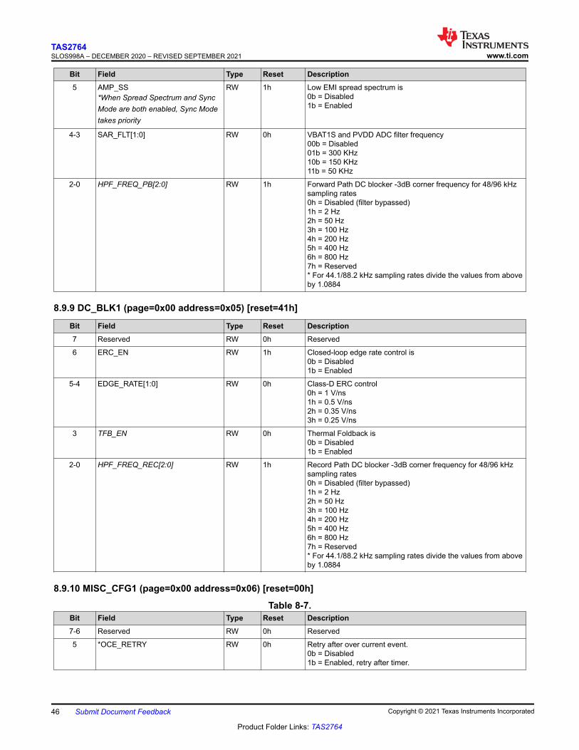
Bit Field Type Reset Description5 AMP_SS
*When Spread Spectrum and Sync Mode are both enabled, Sync Mode takes priority
RW 1h Low EMI spread spectrum is0b = Disabled 1b = Enabled
4-3 SAR_FLT[1:0] RW 0h VBAT1S and PVDD ADC filter frequency00b = Disabled 01b = 300 KHz 10b = 150 KHz 11b = 50 KHz
2-0 HPF_FREQ_PB[2:0] RW 1h Forward Path DC blocker -3dB corner frequency for 48/96 kHz sampling rates0h = Disabled (filter bypassed) 1h = 2 Hz 2h = 50 Hz 3h = 100 Hz 4h = 200 Hz 5h = 400 Hz 6h = 800 Hz 7h = Reserved * For 44.1/88.2 kHz sampling rates divide the values from above by 1.0884
8.9.9 DC_BLK1 (page=0x00 address=0x05) [reset=41h]
Bit Field Type Reset Description7 Reserved RW 0h Reserved
6 ERC_EN RW 1h Closed-loop edge rate control is0b = Disabled 1b = Enabled
5-4 EDGE_RATE[1:0] RW 0h Class-D ERC control0h = 1 V/ns 1h = 0.5 V/ns 2h = 0.35 V/ns 3h = 0.25 V/ns
3 TFB_EN RW 0h Thermal Foldback is0b = Disabled 1b = Enabled
2-0 HPF_FREQ_REC[2:0] RW 1h Record Path DC blocker -3dB corner frequency for 48/96 kHz sampling rates0h = Disabled (filter bypassed) 1h = 2 Hz 2h = 50 Hz 3h = 100 Hz 4h = 200 Hz 5h = 400 Hz 6h = 800 Hz 7h = Reserved * For 44.1/88.2 kHz sampling rates divide the values from above by 1.0884
8.9.10 MISC_CFG1 (page=0x00 address=0x06) [reset=00h]
Table 8-7. Bit Field Type Reset Description7-6 Reserved RW 0h Reserved
5 *OCE_RETRY RW 0h Retry after over current event.0b = Disabled 1b = Enabled, retry after timer.
TAS2764SLOS998A – DECEMBER 2020 – REVISED SEPTEMBER 2021 www.ti.com
46 Submit Document Feedback Copyright © 2021 Texas Instruments Incorporated
Product Folder Links: TAS2764
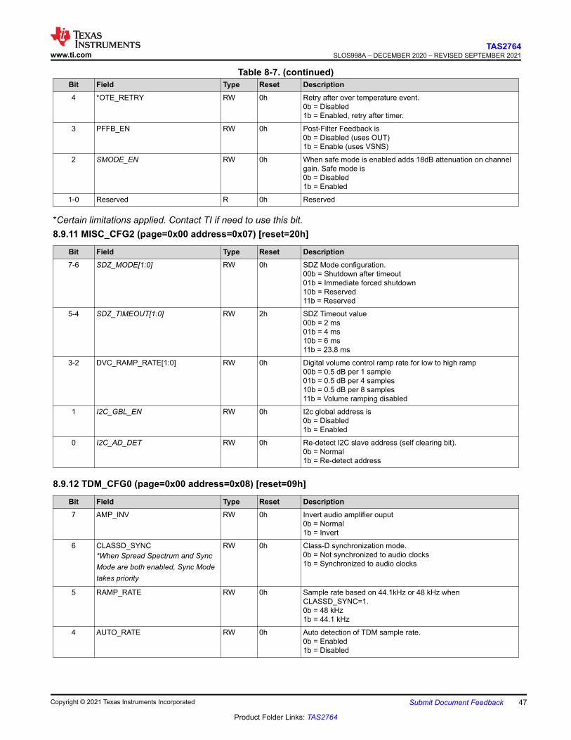
Table 8-7. (continued)Bit Field Type Reset Description4 *OTE_RETRY RW 0h Retry after over temperature event.
0b = Disabled 1b = Enabled, retry after timer.
3 PFFB_EN RW 0h Post-Filter Feedback is0b = Disabled (uses OUT) 1b = Enable (uses VSNS)
2 SMODE_EN RW 0h When safe mode is enabled adds 18dB attenuation on channel gain. Safe mode is 0b = Disabled 1b = Enabled
1-0 Reserved R 0h Reserved
*Certain limitations applied. Contact TI if need to use this bit.8.9.11 MISC_CFG2 (page=0x00 address=0x07) [reset=20h]
Bit Field Type Reset Description7-6 SDZ_MODE[1:0] RW 0h SDZ Mode configuration.
00b = Shutdown after timeout 01b = Immediate forced shutdown10b = Reserved 11b = Reserved
5-4 SDZ_TIMEOUT[1:0] RW 2h SDZ Timeout value00b = 2 ms 01b = 4 ms 10b = 6 ms 11b = 23.8 ms
3-2 DVC_RAMP_RATE[1:0] RW 0h Digital volume control ramp rate for low to high ramp00b = 0.5 dB per 1 sample 01b = 0.5 dB per 4 samples 10b = 0.5 dB per 8 samples 11b = Volume ramping disabled
1 I2C_GBL_EN RW 0h I2c global address is0b = Disabled 1b = Enabled
0 I2C_AD_DET RW 0h Re-detect I2C slave address (self clearing bit).0b = Normal 1b = Re-detect address
8.9.12 TDM_CFG0 (page=0x00 address=0x08) [reset=09h]
Bit Field Type Reset Description7 AMP_INV RW 0h Invert audio amplifier ouput
0b = Normal 1b = Invert
6 CLASSD_SYNC*When Spread Spectrum and Sync Mode are both enabled, Sync Mode takes priority
RW 0h Class-D synchronization mode.0b = Not synchronized to audio clocks 1b = Synchronized to audio clocks
5 RAMP_RATE RW 0h Sample rate based on 44.1kHz or 48 kHz when CLASSD_SYNC=1.0b = 48 kHz 1b = 44.1 kHz
4 AUTO_RATE RW 0h Auto detection of TDM sample rate.0b = Enabled 1b = Disabled
www.ti.comTAS2764
SLOS998A – DECEMBER 2020 – REVISED SEPTEMBER 2021
Copyright © 2021 Texas Instruments Incorporated Submit Document Feedback 47
Product Folder Links: TAS2764
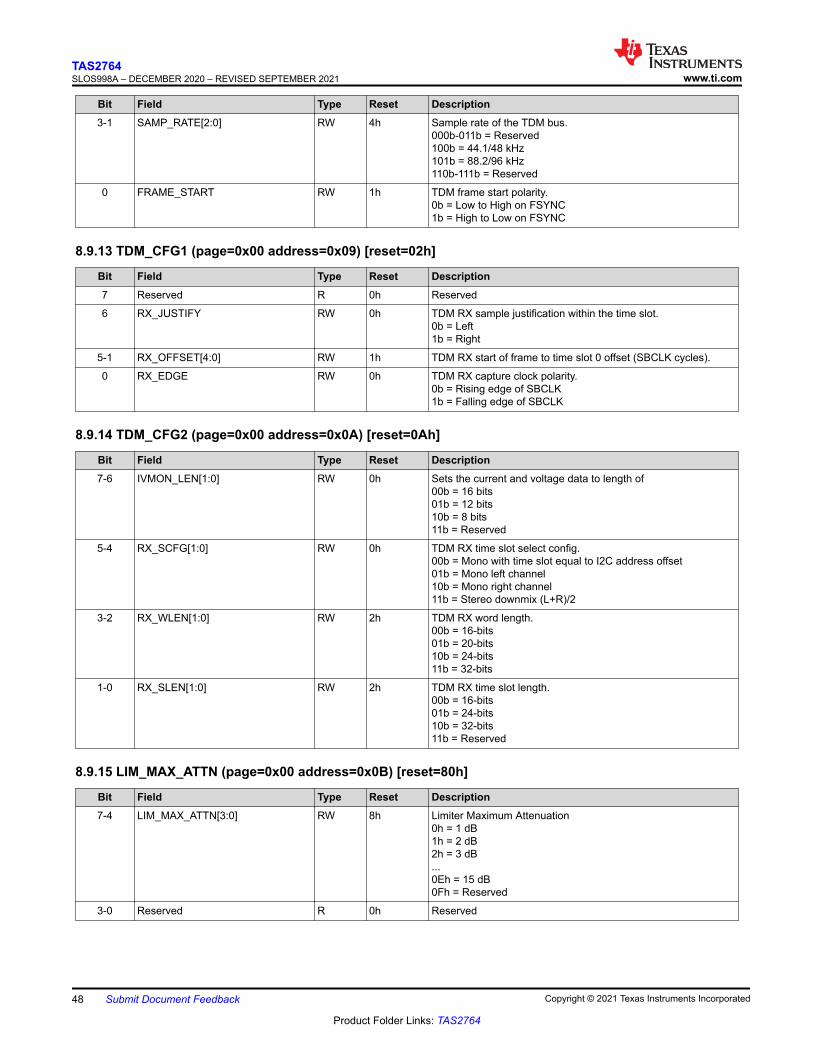
Bit Field Type Reset Description3-1 SAMP_RATE[2:0] RW 4h Sample rate of the TDM bus.
000b-011b = Reserved 100b = 44.1/48 kHz 101b = 88.2/96 kHz 110b-111b = Reserved
0 FRAME_START RW 1h TDM frame start polarity.0b = Low to High on FSYNC 1b = High to Low on FSYNC
8.9.13 TDM_CFG1 (page=0x00 address=0x09) [reset=02h]
Bit Field Type Reset Description7 Reserved R 0h Reserved
6 RX_JUSTIFY RW 0h TDM RX sample justification within the time slot.0b = Left 1b = Right
5-1 RX_OFFSET[4:0] RW 1h TDM RX start of frame to time slot 0 offset (SBCLK cycles).
0 RX_EDGE RW 0h TDM RX capture clock polarity.0b = Rising edge of SBCLK 1b = Falling edge of SBCLK
8.9.14 TDM_CFG2 (page=0x00 address=0x0A) [reset=0Ah]
Bit Field Type Reset Description7-6 IVMON_LEN[1:0] RW 0h Sets the current and voltage data to length of
00b = 16 bits 01b = 12 bits 10b = 8 bits 11b = Reserved
5-4 RX_SCFG[1:0] RW 0h TDM RX time slot select config.00b = Mono with time slot equal to I2C address offset 01b = Mono left channel 10b = Mono right channel 11b = Stereo downmix (L+R)/2
3-2 RX_WLEN[1:0] RW 2h TDM RX word length.00b = 16-bits 01b = 20-bits 10b = 24-bits 11b = 32-bits
1-0 RX_SLEN[1:0] RW 2h TDM RX time slot length.00b = 16-bits 01b = 24-bits 10b = 32-bits 11b = Reserved
8.9.15 LIM_MAX_ATTN (page=0x00 address=0x0B) [reset=80h]
Bit Field Type Reset Description7-4 LIM_MAX_ATTN[3:0] RW 8h Limiter Maximum Attenuation
0h = 1 dB 1h = 2 dB 2h = 3 dB ... 0Eh = 15 dB 0Fh = Reserved
3-0 Reserved R 0h Reserved
TAS2764SLOS998A – DECEMBER 2020 – REVISED SEPTEMBER 2021 www.ti.com
48 Submit Document Feedback Copyright © 2021 Texas Instruments Incorporated
Product Folder Links: TAS2764
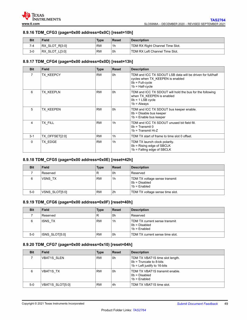
8.9.16 TDM_CFG3 (page=0x00 address=0x0C) [reset=10h]
Bit Field Type Reset Description7-4 RX_SLOT_R[3:0] RW 1h TDM RX Right Channel Time Slot.
3-0 RX_SLOT_L[3:0] RW 0h TDM RX Left Channel Time Slot.
8.9.17 TDM_CFG4 (page=0x00 address=0x0D) [reset=13h]
Bit Field Type Reset Description7 TX_KEEPCY RW 0h TDM and ICC TX SDOUT LSB data will be driven for full/half
cycles when TX_KEEPEN is enabled0b = Full-cycle 1b = Half-cycle
6 TX_KEEPLN RW 0h TDM and ICC TX SDOUT will hold the bus for the following when TX_KEEPEN is enabled0b = 1 LSB cycle 1b = Always
5 TX_KEEPEN RW 0h TDM and ICC TX SDOUT bus keeper enable.0b = Disable bus keeper 1b = Enable bus keeper
4 TX_FILL RW 1h TDM and ICC TX SDOUT unused bit field fill.0b = Transmit 0 1b = Transmit Hi-Z
3-1 TX_OFFSET[2:0] RW 1h TDM TX start of frame to time slot 0 offset.
0 TX_EDGE RW 1h TDM TX launch clock polarity.0b = Rising edge of SBCLK 1b = Falling edge of SBCLK
8.9.18 TDM_CFG5 (page=0x00 address=0x0E) [reset=42h]
Bit Field Type Reset Description7 Reserved R 0h Reserved
6 VSNS_TX RW 1h TDM TX voltage sense transmit 0b = Disabled 1b = Enabled
5-0 VSNS_SLOT[5:0] RW 2h TDM TX voltage sense time slot.
8.9.19 TDM_CFG6 (page=0x00 address=0x0F) [reset=40h]
Bit Field Type Reset Description7 Reserved R 0h Reserved
6 ISNS_TX RW 1h TDM TX current sense transmit 0b = Disabled 1b = Enabled
5-0 ISNS_SLOT[5:0] RW 0h TDM TX current sense time slot.
8.9.20 TDM_CFG7 (page=0x00 address=0x10) [reset=04h]
Bit Field Type Reset Description7 VBAT1S_SLEN RW 0h TDM TX VBAT1S time slot length.
0b = Truncate to 8-bits 1b = Left justify to 16-bits
6 VBAT1S_TX RW 0h TDM TX VBAT1S transmit enable.0b = Disabled 1b = Enabled
5-0 VBAT1S_SLOT[5:0] RW 4h TDM TX VBAT1S time slot.
www.ti.comTAS2764
SLOS998A – DECEMBER 2020 – REVISED SEPTEMBER 2021
Copyright © 2021 Texas Instruments Incorporated Submit Document Feedback 49
Product Folder Links: TAS2764
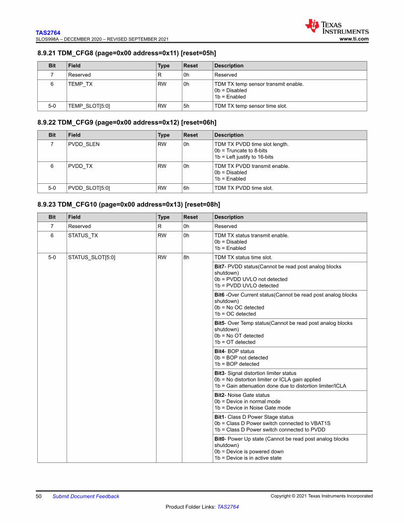
8.9.21 TDM_CFG8 (page=0x00 address=0x11) [reset=05h]
Bit Field Type Reset Description7 Reserved R 0h Reserved
6 TEMP_TX RW 0h TDM TX temp sensor transmit enable.0b = Disabled 1b = Enabled
5-0 TEMP_SLOT[5:0] RW 5h TDM TX temp sensor time slot.
8.9.22 TDM_CFG9 (page=0x00 address=0x12) [reset=06h]
Bit Field Type Reset Description7 PVDD_SLEN RW 0h TDM TX PVDD time slot length.
0b = Truncate to 8-bits 1b = Left justify to 16-bits
6 PVDD_TX RW 0h TDM TX PVDD transmit enable.0b = Disabled 1b = Enabled
5-0 PVDD_SLOT[5:0] RW 6h TDM TX PVDD time slot.
8.9.23 TDM_CFG10 (page=0x00 address=0x13) [reset=08h]
Bit Field Type Reset Description7 Reserved R 0h Reserved
6 STATUS_TX RW 0h TDM TX status transmit enable.0b = Disabled 1b = Enabled
5-0 STATUS_SLOT[5:0] RW 8h TDM TX status time slot.
Bit7- PVDD status(Cannot be read post analog blocks shutdown) 0b = PVDD UVLO not detected 1b = PVDD UVLO detected
Bit6 -Over Current status(Cannot be read post analog blocks shutdown) 0b = No OC detected 1b = OC detected
Bit5- Over Temp status(Cannot be read post analog blocks shutdown) 0b = No OT detected 1b = OT detected
Bit4- BOP status0b = BOP not detected 1b = BOP detected
Bit3- Signal distortion limiter status0b = No distortion limiter or ICLA gain applied 1b = Gain attenuation done due to distortion limiter/ICLA
Bit2- Noise Gate status0b = Device in normal mode 1b = Device in Noise Gate mode
Bit1- Class D Power Stage status0b = Class D Power switch connected to VBAT1S 1b = Class D Power switch connected to PVDD
Bit0- Power Up state (Cannot be read post analog blocks shutdown)0b = Device is powered down 1b = Device is in active state
TAS2764SLOS998A – DECEMBER 2020 – REVISED SEPTEMBER 2021 www.ti.com
50 Submit Document Feedback Copyright © 2021 Texas Instruments Incorporated
Product Folder Links: TAS2764

8.9.24 TDM_CFG11 (page=0x00 address=0x14) [reset=0Ah]
Bit Field Type Reset Description7 Reserved R 0h Reserved
6 GAIN_TX RW 0h TDM /ICC TX limiter gain reduction transmit enable.0b = Disabled 1b = Enabled
5-0 GAIN_SLOT[5:0] RW Ah TDM /ICC TX limiter gain reduction time slot.
00h = 0
01h = 1
........
3Eh = 62
3Fh = 63
8.9.25 ICC_CNFG2 (page=0x00 address=0x15) [reset=00h]
Bit Field Type Reset Description7-5 Reserved R 0h Reserved
4-2 ICC_MODE[2:0] RW 0h Selects ICC pin function0h = Gain alignment on ICC pin 1h = Reserved 2h = ICC pin buffers disabled 3h = ICC pin is a general purpose input 4h = ICC pin is a general purpose output 5h-7h = Reserved
1-0 Reserved R 0h Reserved
8.9.26 TDM_CFG12 (page=0x00 address=0x16) [reset=12h]
Bit Field Type Reset Description7 AUDIO_SLEN RW 0h TDM audio slot length
0b = 16-bits 1b = 24-bits
6 AUDIO_TX RW 0h TDM audio output transmit is0b = Disabled 1b = Enabled
5-0 AUDIO_SLOT[5:0] RW 12h TDM TX status time slot.
8.9.27 ICLA_CFG0 (page=0x00 address=0x17) [reset=0Ch]
Bit Field Type Reset Description7 ICBA_EN RW 0h Inter chip brownout gain alignment is
0b = Disabled 1b = Enabled
6-1 ICGA_SLOT[5:0] RW 6h Inter chip gain alignment starting time slot.
0 ICLA_EN RW 0h Inter chip limiter alignment gain is0b = Disabled 1b = Enabled
8.9.28 ICLA_CFG1 (page=0x00 address=0x18) [reset=00h]
Bit Field Type Reset Description7 ICGA_SEN[7] RW 0h Time slot equals ICGA_SLOT[5:0]+7*3. When enabled, the
limiter will include this time slot in the alignment group.0b = Disabled 1b = Enabled
www.ti.comTAS2764
SLOS998A – DECEMBER 2020 – REVISED SEPTEMBER 2021
Copyright © 2021 Texas Instruments Incorporated Submit Document Feedback 51
Product Folder Links: TAS2764
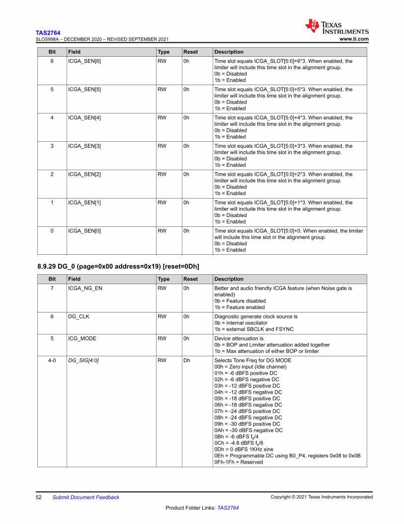
Bit Field Type Reset Description6 ICGA_SEN[6] RW 0h Time slot equals ICGA_SLOT[5:0]+6*3. When enabled, the
limiter will include this time slot in the alignment group.0b = Disabled 1b = Enabled
5 ICGA_SEN[5] RW 0h Time slot equals ICGA_SLOT[5:0]+5*3. When enabled, the limiter will include this time slot in the alignment group.0b = Disabled 1b = Enabled
4 ICGA_SEN[4] RW 0h Time slot equals ICGA_SLOT[5:0]+4*3. When enabled, the limiter will include this time slot in the alignment group.0b = Disabled 1b = Enabled
3 ICGA_SEN[3] RW 0h Time slot equals ICGA_SLOT[5:0]+3*3. When enabled, the limiter will include this time slot in the alignment group.0b = Disabled 1b = Enabled
2 ICGA_SEN[2] RW 0h Time slot equals ICGA_SLOT[5:0]+2*3. When enabled, the limiter will include this time slot in the alignment group.0b = Disabled 1b = Enabled
1 ICGA_SEN[1] RW 0h Time slot equals ICGA_SLOT[5:0]+1*3. When enabled, the limiter will include this time slot in the alignment group.0b = Disabled 1b = Enabled
0 ICGA_SEN[0] RW 0h Time slot equals ICGA_SLOT[5:0]+0. When enabled, the limiter will include this time slot in the alignment group.0b = Disabled 1b = Enabled
8.9.29 DG_0 (page=0x00 address=0x19) [reset=0Dh]
Bit Field Type Reset Description7 ICGA_NG_EN RW 0h Better and audio friendly ICGA feature (when Noise gate is
enabled)0b = Feature disabled 1b = Feature enabled
6 DG_CLK RW 0h Diagnostic generate clock source is0b = internal osscilator 1b = external SBCLK and FSYNC
5 ICG_MODE RW 0h Device attenuation is0b = BOP and Limiter attenuation added together 1b = Max attenuation of either BOP or limiter
4-0 DG_SIG[4:0] RW Dh Selects Tone Freq for DG MODE00h = Zero input (Idle channel) 01h = -6 dBFS positive DC 02h = -6 dBFS negative DC 03h = -12 dBFS positive DC 04h = -12 dBFS negative DC 05h = -18 dBFS positive DC 06h = -18 dBFS negative DC 07h = -24 dBFS positive DC 08h = -24 dBFS negative DC 09h = -30 dBFS positive DC 0Ah = -30 dBFS negative DC 0Bh = -6 dBFS fs/4 0Ch = -4.8 dBFS fs/6 0Dh = 0 dBFS 1KHz sine 0Eh = Programmable DC using B0_P4, registers 0x08 to 0x0B 0Fh-1Fh = Reserved
TAS2764SLOS998A – DECEMBER 2020 – REVISED SEPTEMBER 2021 www.ti.com
52 Submit Document Feedback Copyright © 2021 Texas Instruments Incorporated
Product Folder Links: TAS2764
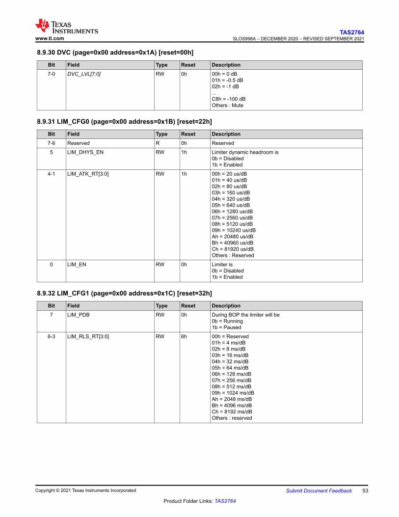
8.9.30 DVC (page=0x00 address=0x1A) [reset=00h]
Bit Field Type Reset Description7-0 DVC_LVL[7:0] RW 0h 00h = 0 dB
01h = -0.5 dB 02h = -1 dB ... C8h = -100 dB Others : Mute
8.9.31 LIM_CFG0 (page=0x00 address=0x1B) [reset=22h]
Bit Field Type Reset Description7-6 Reserved R 0h Reserved
5 LIM_DHYS_EN RW 1h Limiter dynamic headroom is0b = Disabled 1b = Enabled
4-1 LIM_ATK_RT[3:0] RW 1h 00h = 20 us/dB01h = 40 us/dB 02h = 80 us/dB 03h = 160 us/dB 04h = 320 us/dB 05h = 640 us/dB 06h = 1280 us/dB 07h = 2560 us/dB 08h = 5120 us/dB 09h = 10240 us/dB Ah = 20480 us/dB Bh = 40960 us/dB Ch = 81920 us/dB Others : Reserved
0 LIM_EN RW 0h Limiter is0b = Disabled 1b = Enabled
8.9.32 LIM_CFG1 (page=0x00 address=0x1C) [reset=32h]
Bit Field Type Reset Description7 LIM_PDB RW 0h During BOP the limiter will be
0b = Running 1b = Paused
6-3 LIM_RLS_RT[3:0] RW 6h 00h = Reserved01h = 4 ms/dB 02h = 8 ms/dB 03h = 16 ms/dB 04h = 32 ms/dB 05h = 64 ms/dB 06h = 128 ms/dB 07h = 256 ms/dB 08h = 512 ms/dB 09h = 1024 ms/dB Ah = 2048 ms/dB Bh = 4096 ms/dB Ch = 8192 ms/dB Others : reserved
www.ti.comTAS2764
SLOS998A – DECEMBER 2020 – REVISED SEPTEMBER 2021
Copyright © 2021 Texas Instruments Incorporated Submit Document Feedback 53
Product Folder Links: TAS2764
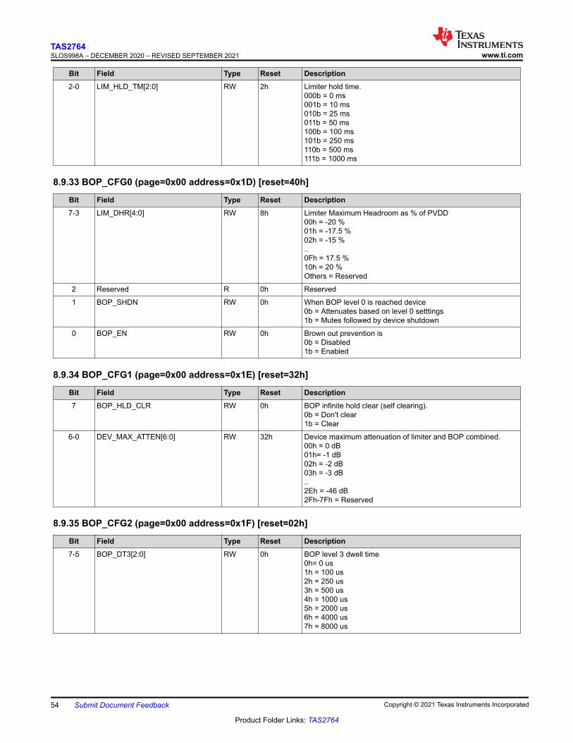
Bit Field Type Reset Description2-0 LIM_HLD_TM[2:0] RW 2h Limiter hold time.
000b = 0 ms 001b = 10 ms 010b = 25 ms 011b = 50 ms 100b = 100 ms 101b = 250 ms 110b = 500 ms 111b = 1000 ms
8.9.33 BOP_CFG0 (page=0x00 address=0x1D) [reset=40h]
Bit Field Type Reset Description7-3 LIM_DHR[4:0] RW 8h Limiter Maximum Headroom as % of PVDD
00h = -20 % 01h = -17.5 % 02h = -15 % .. 0Fh = 17.5 % 10h = 20 % Others = Reserved
2 Reserved R 0h Reserved
1 BOP_SHDN RW 0h When BOP level 0 is reached device0b = Attenuates based on level 0 setttings 1b = Mutes followed by device shutdown
0 BOP_EN RW 0h Brown out prevention is0b = Disabled 1b = Enabled
8.9.34 BOP_CFG1 (page=0x00 address=0x1E) [reset=32h]
Bit Field Type Reset Description7 BOP_HLD_CLR RW 0h BOP infinite hold clear (self clearing).
0b = Don't clear 1b = Clear
6-0 DEV_MAX_ATTEN[6:0] RW 32h Device maximum attenuation of limiter and BOP combined.00h = 0 dB 01h= -1 dB 02h = -2 dB 03h = -3 dB .. 2Eh = -46 dB 2Fh-7Fh = Reserved
8.9.35 BOP_CFG2 (page=0x00 address=0x1F) [reset=02h]
Bit Field Type Reset Description7-5 BOP_DT3[2:0] RW 0h BOP level 3 dwell time
0h= 0 us 1h = 100 us 2h = 250 us 3h = 500 us 4h = 1000 us 5h = 2000 us 6h = 4000 us 7h = 8000 us
TAS2764SLOS998A – DECEMBER 2020 – REVISED SEPTEMBER 2021 www.ti.com
54 Submit Document Feedback Copyright © 2021 Texas Instruments Incorporated
Product Folder Links: TAS2764
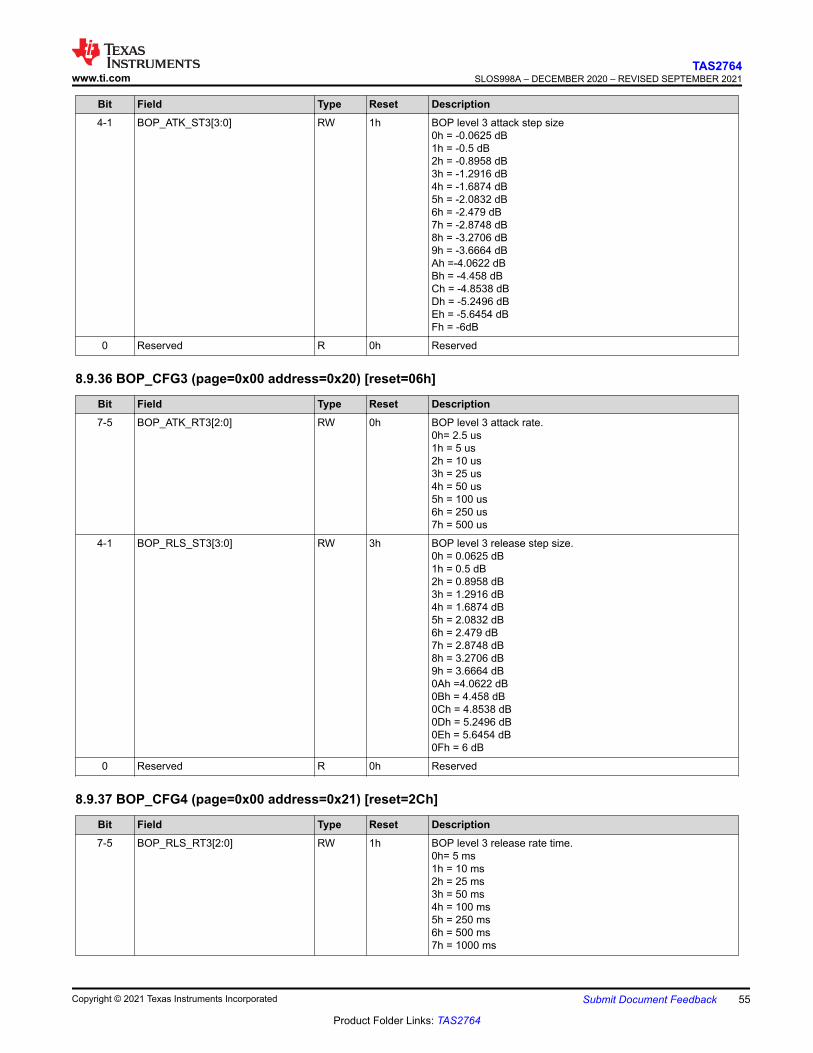
Bit Field Type Reset Description4-1 BOP_ATK_ST3[3:0] RW 1h BOP level 3 attack step size
0h = -0.0625 dB 1h = -0.5 dB 2h = -0.8958 dB 3h = -1.2916 dB 4h = -1.6874 dB 5h = -2.0832 dB 6h = -2.479 dB 7h = -2.8748 dB 8h = -3.2706 dB 9h = -3.6664 dB Ah =-4.0622 dB Bh = -4.458 dB Ch = -4.8538 dB Dh = -5.2496 dB Eh = -5.6454 dB Fh = -6dB
0 Reserved R 0h Reserved
8.9.36 BOP_CFG3 (page=0x00 address=0x20) [reset=06h]
Bit Field Type Reset Description7-5 BOP_ATK_RT3[2:0] RW 0h BOP level 3 attack rate.
0h= 2.5 us 1h = 5 us 2h = 10 us 3h = 25 us 4h = 50 us 5h = 100 us 6h = 250 us 7h = 500 us
4-1 BOP_RLS_ST3[3:0] RW 3h BOP level 3 release step size.0h = 0.0625 dB 1h = 0.5 dB 2h = 0.8958 dB 3h = 1.2916 dB 4h = 1.6874 dB 5h = 2.0832 dB 6h = 2.479 dB 7h = 2.8748 dB 8h = 3.2706 dB 9h = 3.6664 dB 0Ah =4.0622 dB 0Bh = 4.458 dB 0Ch = 4.8538 dB 0Dh = 5.2496 dB 0Eh = 5.6454 dB 0Fh = 6 dB
0 Reserved R 0h Reserved
8.9.37 BOP_CFG4 (page=0x00 address=0x21) [reset=2Ch]
Bit Field Type Reset Description7-5 BOP_RLS_RT3[2:0] RW 1h BOP level 3 release rate time.
0h= 5 ms 1h = 10 ms 2h = 25 ms 3h = 50 ms 4h = 100 ms 5h = 250 ms 6h = 500 ms 7h = 1000 ms
www.ti.comTAS2764
SLOS998A – DECEMBER 2020 – REVISED SEPTEMBER 2021
Copyright © 2021 Texas Instruments Incorporated Submit Document Feedback 55
Product Folder Links: TAS2764

Bit Field Type Reset Description4-0 BOP_MAX_ATTN3[4:0] RW Ch BOP level 3 maximum attenuation.
00h = 0 dB 01h = -1 dB 02h = -2 dB .. 0Ch = -12 dB .. 1Eh = -30 dB 1Fh = -31 dB
8.9.38 BOP_CFG5 (page=0x00 address=0x22) [reset=4Ch]
Bit Field Type Reset Description7-0 BOP_TH3[7:0] RW 4Ch BOP level 3 threshold
Setting BOP Threshold (V) - BOP_SRC=0 (VBAT1S Source)
BOP Threshold (V) - BOP_SRC=1 (PVDD Source)
00h 2.7 5.5
01h 2.75 5.55
02h 2.8 5.6
..... ..... .....
38h 5.5 8.3
39h 0 8.35
..... 0 .....
5Ah 0 10
..... 0 .....
D1h 0 15.95
D2h 0 16
D3h-FFh 0 0
8.9.39 BOP_CFG6 (page=0x00 address=0x23) [reset=20h]
Bit Field Type Reset Description7-5 BOP_HT3[2:0] RW 1h BOP level 3 hold time.
0h = 0 ms 1h = 10 ms 2h = 100 ms 3h = 250 ms 4h = 500ms 5h = 1000 ms 6h = 2000 ms 7h = Infinite (This can be exited using BOP_HLD_CLR bit)
4 BOP_DIS3 RW 0h BOP level 3 is0b = Enabled 1b = Disabled
TAS2764SLOS998A – DECEMBER 2020 – REVISED SEPTEMBER 2021 www.ti.com
56 Submit Document Feedback Copyright © 2021 Texas Instruments Incorporated
Product Folder Links: TAS2764
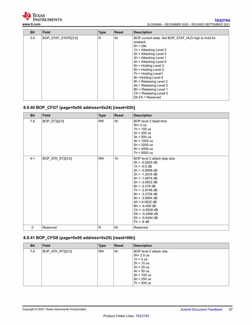
Bit Field Type Reset Description3-0 BOP_STAT_STATE[3:0] R 0h BOP current state. Set BOP_STAT_HLD high to hold for
readack.0h = Idle 1h = Attacking Level 3 2h = Attacking Level 2 3h = Attacking Level 1 4h = Attacking Level 0 5h = Holding Level 3 6h = Holding Level 2 7h = Holding Level1 8h =Holding Level 0 9h = Releasing Level 3 Ah = Releasing Level 2 Bh = Releasing Level 1 Ch = Releasing Level 0 Dh-Fh = Reserved
8.9.40 BOP_CFG7 (page=0x00 address=0x24) [reset=02h]
Bit Field Type Reset Description7-5 BOP_DT2[2:0] RW 0h BOP level 3 dwell time
0h= 0 us 1h = 100 us 2h = 250 us 3h = 500 us 4h = 1000 us 5h = 2000 us 6h = 4000 us 7h = 8000 us
4-1 BOP_ATK_ST2[3:0] RW 1h BOP level 2 attack step size0h = -0.0625 dB 1h = -0.5 dB 2h = -0.8958 dB 3h = -1.2916 dB 4h = -1.6874 dB 5h = -2.0832 dB 6h = -2.479 dB 7h = -2.8748 dB 8h = -3.2706 dB 9h = -3.6664 dB Ah =-4.0622 dB Bh = -4.458 dB Ch = -4.8538 dB Dh = -5.2496 dB Eh = -5.6454 dB Fh = -6 dB
0 Reserved R 0h Reserved
8.9.41 BOP_CFG8 (page=0x00 address=0x25) [reset=06h]
Bit Field Type Reset Description7-5 BOP_ATK_RT2[2:0] RW 0h BOP level 2 attack rate.
0h= 2.5 us 1h = 5 us 2h = 10 us 3h = 25 us 4h = 50 us 5h = 100 us 6h = 250 us 7h = 500 us
www.ti.comTAS2764
SLOS998A – DECEMBER 2020 – REVISED SEPTEMBER 2021
Copyright © 2021 Texas Instruments Incorporated Submit Document Feedback 57
Product Folder Links: TAS2764
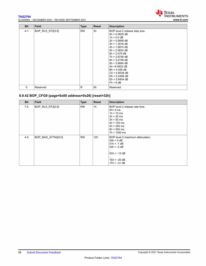
Bit Field Type Reset Description4-1 BOP_RLS_ST2[3:0] RW 3h BOP level 2 release step size.
0h = 0.0625 dB 1h = 0.5 dB 2h = 0.8958 dB 3h = 1.2916 dB 4h = 1.6874 dB 5h = 2.0832 dB 6h = 2.479 dB 7h = 2.8748 dB 8h = 3.2706 dB 9h = 3.6664 dB Ah =4.0622 dB Bh = 4.458 dB Ch = 4.8538 dB Dh = 5.2496 dB Eh = 5.6454 dB Fh = 6 dB
0 Reserved R 0h Reserved
8.9.42 BOP_CFG9 (page=0x00 address=0x26) [reset=32h]
Bit Field Type Reset Description7-5 BOP_RLS_RT2[2:0] RW 1h BOP level 2 release rate time.
0h= 5 ms 1h = 10 ms 2h = 25 ms 3h = 50 ms 4h = 100 ms 5h = 250 ms 6h = 500 ms 7h = 1000 ms
4-0 BOP_MAX_ATTN2[4:0] RW 12h BOP level 2 maximum attenuation.00h = 0 dB 01h = -1 dB 02h = -2 dB .. 0Ch = -12 dB .. 1Eh = -30 dB 1Fh = -31 dB
TAS2764SLOS998A – DECEMBER 2020 – REVISED SEPTEMBER 2021 www.ti.com
58 Submit Document Feedback Copyright © 2021 Texas Instruments Incorporated
Product Folder Links: TAS2764
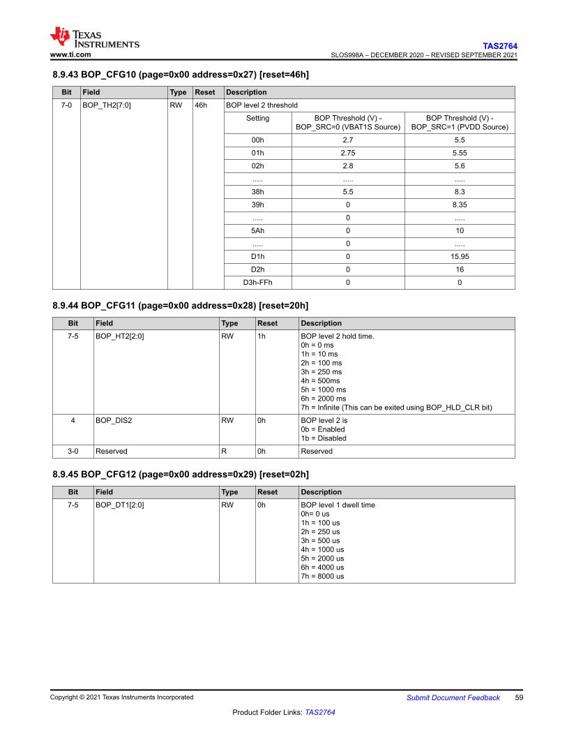
8.9.43 BOP_CFG10 (page=0x00 address=0x27) [reset=46h]
Bit Field Type Reset Description7-0 BOP_TH2[7:0] RW 46h BOP level 2 threshold
Setting BOP Threshold (V) - BOP_SRC=0 (VBAT1S Source)
BOP Threshold (V) - BOP_SRC=1 (PVDD Source)
00h 2.7 5.5
01h 2.75 5.55
02h 2.8 5.6
..... ..... .....
38h 5.5 8.3
39h 0 8.35
..... 0 .....
5Ah 0 10
..... 0 .....
D1h 0 15.95
D2h 0 16
D3h-FFh 0 0
8.9.44 BOP_CFG11 (page=0x00 address=0x28) [reset=20h]
Bit Field Type Reset Description7-5 BOP_HT2[2:0] RW 1h BOP level 2 hold time.
0h = 0 ms 1h = 10 ms 2h = 100 ms 3h = 250 ms 4h = 500ms 5h = 1000 ms 6h = 2000 ms 7h = Infinite (This can be exited using BOP_HLD_CLR bit)
4 BOP_DIS2 RW 0h BOP level 2 is0b = Enabled 1b = Disabled
3-0 Reserved R 0h Reserved
8.9.45 BOP_CFG12 (page=0x00 address=0x29) [reset=02h]
Bit Field Type Reset Description7-5 BOP_DT1[2:0] RW 0h BOP level 1 dwell time
0h= 0 us 1h = 100 us 2h = 250 us 3h = 500 us 4h = 1000 us 5h = 2000 us 6h = 4000 us 7h = 8000 us
www.ti.comTAS2764
SLOS998A – DECEMBER 2020 – REVISED SEPTEMBER 2021
Copyright © 2021 Texas Instruments Incorporated Submit Document Feedback 59
Product Folder Links: TAS2764
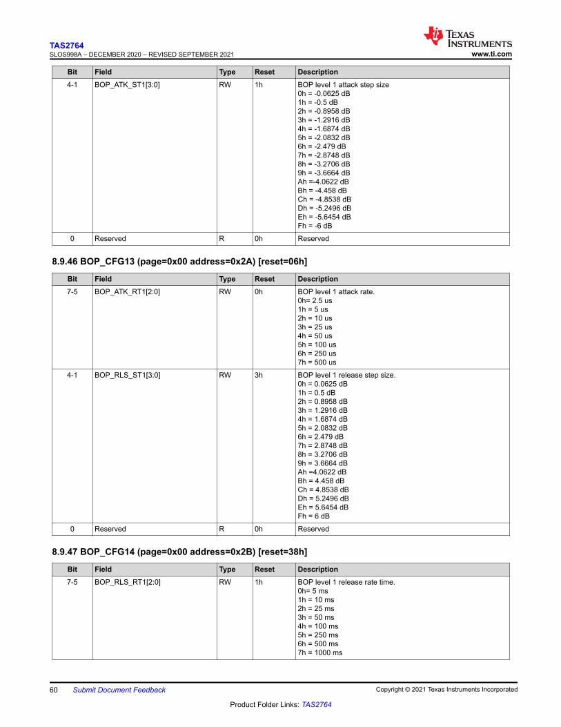
Bit Field Type Reset Description4-1 BOP_ATK_ST1[3:0] RW 1h BOP level 1 attack step size
0h = -0.0625 dB 1h = -0.5 dB 2h = -0.8958 dB 3h = -1.2916 dB 4h = -1.6874 dB 5h = -2.0832 dB 6h = -2.479 dB 7h = -2.8748 dB 8h = -3.2706 dB 9h = -3.6664 dB Ah =-4.0622 dB Bh = -4.458 dB Ch = -4.8538 dB Dh = -5.2496 dB Eh = -5.6454 dB Fh = -6 dB
0 Reserved R 0h Reserved
8.9.46 BOP_CFG13 (page=0x00 address=0x2A) [reset=06h]
Bit Field Type Reset Description7-5 BOP_ATK_RT1[2:0] RW 0h BOP level 1 attack rate.
0h= 2.5 us 1h = 5 us 2h = 10 us 3h = 25 us 4h = 50 us 5h = 100 us 6h = 250 us 7h = 500 us
4-1 BOP_RLS_ST1[3:0] RW 3h BOP level 1 release step size.0h = 0.0625 dB 1h = 0.5 dB 2h = 0.8958 dB 3h = 1.2916 dB 4h = 1.6874 dB 5h = 2.0832 dB 6h = 2.479 dB 7h = 2.8748 dB 8h = 3.2706 dB 9h = 3.6664 dB Ah =4.0622 dB Bh = 4.458 dB Ch = 4.8538 dB Dh = 5.2496 dB Eh = 5.6454 dB Fh = 6 dB
0 Reserved R 0h Reserved
8.9.47 BOP_CFG14 (page=0x00 address=0x2B) [reset=38h]
Bit Field Type Reset Description7-5 BOP_RLS_RT1[2:0] RW 1h BOP level 1 release rate time.
0h= 5 ms 1h = 10 ms 2h = 25 ms 3h = 50 ms 4h = 100 ms 5h = 250 ms 6h = 500 ms 7h = 1000 ms
TAS2764SLOS998A – DECEMBER 2020 – REVISED SEPTEMBER 2021 www.ti.com
60 Submit Document Feedback Copyright © 2021 Texas Instruments Incorporated
Product Folder Links: TAS2764

Bit Field Type Reset Description4-0 BOP_MAX_ATTN1[4:0] RW 18h BOP level 1 maximum attenuation.
0h = 0 dB 1h = -1 dB 2h = -2 dB .. Ch = -12 dB .. 1Eh = -30 dB 1Fh = -31 dB
8.9.48 BOP_CFG15 (page=0x00 address=0x2C) [reset=40h]
Bit Field Type Reset Description7-0 BOP_TH1[7:0] RW 40h BOP level 1 threshold
Setting BOP Threshold (V) - BOP_SRC=0 (VBAT1S Source)
BOP Threshold (V) - BOP_SRC=1 (PVDD Source)
00h 2.7 5.5
01h 2.75 5.55
02h 2.8 5.6
..... ..... .....
38h 5.5 8.3
39h 0 8.35
..... 0 .....
5Ah 0 10
..... 0 .....
D1h 0 15.95
D2h 0 16
D3h-FFh 0 0
8.9.49 BOP_CFG17 (page=0x00 address=0x2D) [reset=20h]
Bit Field Type Reset Description7-5 BOP_HT1[2:0] RW 1h BOP level 1 hold time.
0h = 0 ms 1h = 10 ms 2h = 100 ms 3h = 250 ms 4h = 500ms 5h = 1000 ms 6h = 2000 ms 7h = Infinite (This can be exited using BOP_HLD_CLR bit)
4 BOP_DIS1 RW 0h BOP level 1 is0b = Enabled 1b = Disabled
3-0 Reserved R 0h Reserved
8.9.50 BOP_CFG18 (page=0x00 address=0x2E) [reset=02h]
Bit Field Type Reset Description7-5 BOP_DT0[2:0] RW 0h BOP level 0 dwell time locked
0h= 0 us
www.ti.comTAS2764
SLOS998A – DECEMBER 2020 – REVISED SEPTEMBER 2021
Copyright © 2021 Texas Instruments Incorporated Submit Document Feedback 61
Product Folder Links: TAS2764
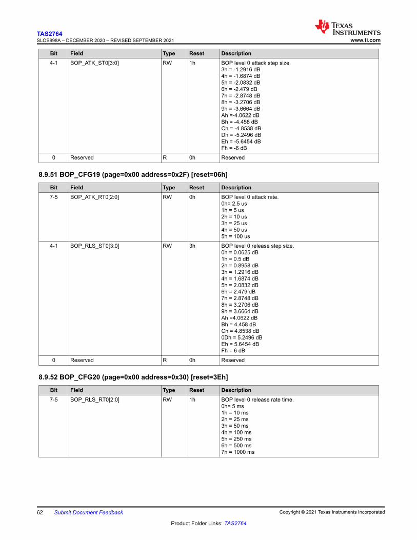
Bit Field Type Reset Description4-1 BOP_ATK_ST0[3:0] RW 1h BOP level 0 attack step size.
3h = -1.2916 dB 4h = -1.6874 dB 5h = -2.0832 dB 6h = -2.479 dB 7h = -2.8748 dB 8h = -3.2706 dB 9h = -3.6664 dB Ah =-4.0622 dB Bh = -4.458 dB Ch = -4.8538 dB Dh = -5.2496 dB Eh = -5.6454 dB Fh = -6 dB
0 Reserved R 0h Reserved
8.9.51 BOP_CFG19 (page=0x00 address=0x2F) [reset=06h]
Bit Field Type Reset Description7-5 BOP_ATK_RT0[2:0] RW 0h BOP level 0 attack rate.
0h= 2.5 us 1h = 5 us 2h = 10 us 3h = 25 us 4h = 50 us 5h = 100 us
4-1 BOP_RLS_ST0[3:0] RW 3h BOP level 0 release step size.0h = 0.0625 dB 1h = 0.5 dB 2h = 0.8958 dB 3h = 1.2916 dB 4h = 1.6874 dB 5h = 2.0832 dB 6h = 2.479 dB 7h = 2.8748 dB 8h = 3.2706 dB 9h = 3.6664 dB Ah =4.0622 dB Bh = 4.458 dB Ch = 4.8538 dB 0Dh = 5.2496 dB Eh = 5.6454 dB Fh = 6 dB
0 Reserved R 0h Reserved
8.9.52 BOP_CFG20 (page=0x00 address=0x30) [reset=3Eh]
Bit Field Type Reset Description7-5 BOP_RLS_RT0[2:0] RW 1h BOP level 0 release rate time.
0h= 5 ms 1h = 10 ms 2h = 25 ms 3h = 50 ms 4h = 100 ms 5h = 250 ms 6h = 500 ms 7h = 1000 ms
TAS2764SLOS998A – DECEMBER 2020 – REVISED SEPTEMBER 2021 www.ti.com
62 Submit Document Feedback Copyright © 2021 Texas Instruments Incorporated
Product Folder Links: TAS2764
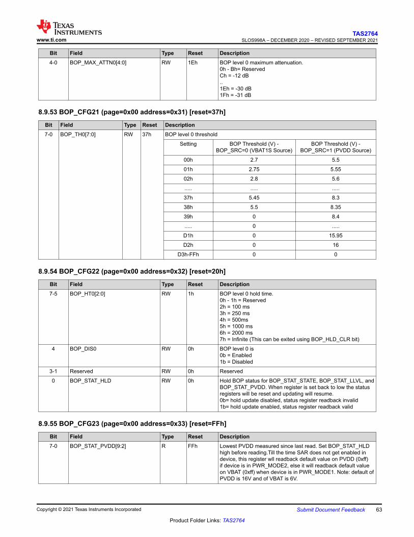
Bit Field Type Reset Description4-0 BOP_MAX_ATTN0[4:0] RW 1Eh BOP level 0 maximum attenuation.
0h - Bh= Reserved Ch = -12 dB .. 1Eh = -30 dB 1Fh = -31 dB
8.9.53 BOP_CFG21 (page=0x00 address=0x31) [reset=37h]
Bit Field Type Reset Description7-0 BOP_TH0[7:0] RW 37h BOP level 0 threshold
Setting BOP Threshold (V) - BOP_SRC=0 (VBAT1S Source)
BOP Threshold (V) - BOP_SRC=1 (PVDD Source)
00h 2.7 5.5
01h 2.75 5.55
02h 2.8 5.6
..... ..... .....
37h 5.45 8.3
38h 5.5 8.35
39h 0 8.4
..... 0 .....
D1h 0 15.95
D2h 0 16
D3h-FFh 0 0
8.9.54 BOP_CFG22 (page=0x00 address=0x32) [reset=20h]
Bit Field Type Reset Description7-5 BOP_HT0[2:0] RW 1h BOP level 0 hold time.
0h - 1h = Reserved 2h = 100 ms 3h = 250 ms 4h = 500ms 5h = 1000 ms 6h = 2000 ms 7h = Infinite (This can be exited using BOP_HLD_CLR bit)
4 BOP_DIS0 RW 0h BOP level 0 is0b = Enabled 1b = Disabled
3-1 Reserved RW 0h Reserved
0 BOP_STAT_HLD RW 0h Hold BOP status for BOP_STAT_STATE, BOP_STAT_LLVL, and BOP_STAT_PVDD. When register is set back to low the status registers will be reset and updating will resume.0b= hold update disabled, status register readback invalid 1b= hold update enabled, status register readback valid
8.9.55 BOP_CFG23 (page=0x00 address=0x33) [reset=FFh]
Bit Field Type Reset Description7-0 BOP_STAT_PVDD[9:2] R FFh Lowest PVDD measured since last read. Set BOP_STAT_HLD
high before reading.Till the time SAR does not get enabled in device, this register wll readback default value on PVDD (0xff) if device is in PWR_MODE2, else it will readback default value on VBAT (0xff) when device is in PWR_MODE1. Note: default of PVDD is 16V and of VBAT is 6V.
www.ti.comTAS2764
SLOS998A – DECEMBER 2020 – REVISED SEPTEMBER 2021
Copyright © 2021 Texas Instruments Incorporated Submit Document Feedback 63
Product Folder Links: TAS2764

8.9.56 BOP_CFG24 (page=0x00 address=0x34) [reset=E6h]
Bit Field Type Reset Description7-6 BOP_STAT_PVDD[1:0] R 3h Lowest PVDD measured since last read. Set BOP_STAT_HLD
high before reading.Till the time SAR does not get enabled in device, this register wll readback default value on PVDD (2'b11) if device is in PWR_MODE2, else it will readback default value on VBAT (2'b11) when device is in PWR_MODE1. Note: default of PVDD is 16V and of VBAT is 6V.
5-3 BOP_STAT_LLVL[2:0] R 4h Lowest BOP level attacked since last read. Set BOP_STAT_HLD high before reading.0h = Attack level 0 was lowest attack level 1h = Attack level 1 was lowest attack level 2h = Attack level 2 was lowest attack level 3h = Attack level 3 was lowest attack level 4h = No BOP attacked since last read
2-1 LVS_FTH_LOW[1:0] RW 3h Threshold for LVS when CDS_MODE=2'b110h = -121.5 dBFS 1h=- -101.5 dBFS (default) 2h= -81.5 dBFS 3h = -71.5 dBFS
0 Reserved R 0h Reserved
8.9.57 NG_CFG0 (page=0x00 address=0x35) [reset=BDh]
Bit Field Type Reset Description7-5 NG_HSYT[2:0] RW 5h Noise Gate Entry hysteris timer
0h = 260us 1h = 500us 2h = 800us 3h = 2 ms 4h = 10 ms 5h = 50 ms 6h = 100 ms 7h = 1000 ms
4-3 NG_LVL[1:0] RW 3h Noise-gate audio threshold level0h = -90 dBFS 1h= -100 dBFS 2h = -110 dBFS 3h = -120 dBFS
2 NG_EN RW 1h Noise gate0b = Disabled 1b = Enabled
1-0 Reserved RW 1h Reserved
8.9.58 NG_CFG1 (page=0x00 address=0x36) [reset=ADh]
Bit Field Type Reset Description7-6 Reserved RW 2h Reserved
5 NG_DVR_EN RW 1h Volume ramping on noise-gate control is0b = Enabled 1b = Disabled
4 Reserved R 0h Reserved
3-0 LVS_HYS[3:0] RW Dh PVDD to VBAT1S hysteresis time0h - 9h= Reserved Ah = 1 ms Bh = 10 ms Ch = 20 ms Dh = 50 ms Eh = 75 ms Fh = 100 ms
TAS2764SLOS998A – DECEMBER 2020 – REVISED SEPTEMBER 2021 www.ti.com
64 Submit Document Feedback Copyright © 2021 Texas Instruments Incorporated
Product Folder Links: TAS2764
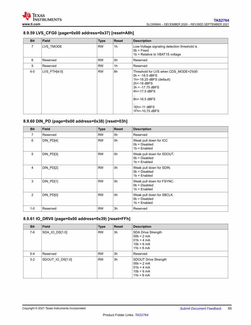
8.9.59 LVS_CFG0 (page=0x00 address=0x37) [reset=A8h]
Bit Field Type Reset Description7 LVS_TMODE RW 1h Low-Voltage signaling detection threshold is
0b = Fixed 1b = Relative to VBAT1S voltage
6 Reserved RW 0h Reserved
5 Reserved RW 1h Reserved
4-0 LVS_FTH[4:0] RW 8h Threshold for LVS when CDS_MODE=2'b000h = -18.5 dBFS 1h=-18.25 dBFS (default) 2h=-18 dBFS 3h = -17.75 dBFS 4h=-17.5 dBFS .. 8h=-16.5 dBFS .. 1Eh=-11 dBFS 1Fh=-10.75 dBFS
8.9.60 DIN_PD (page=0x00 address=0x38) [reset=03h]
Bit Field Type Reset Description7 Reserved RW 0h Reserved
6 DIN_PD[4] RW 0h Weak pull down for ICC0b = Disabled 1b = Enabled
5 DIN_PD[3] RW 0h Weak pull down for SDOUT.0b = Disabled 1b = Enabled
4 DIN_PD[2] RW 0h Weak pull down for SDIN.0b = Disabled 1b = Enabled
3 DIN_PD[1] RW 0h Weak pull down for FSYNC.0b = Disabled 1b = Enabled
2 DIN_PD[0] RW 0h Weak pull down for SBCLK.0b = Disabled 1b = Enabled
1-0 Reserved RW 3h Reserved
8.9.61 IO_DRV0 (page=0x00 address=0x39) [reset=FFh]
Bit Field Type Reset Description7-6 SDA_IO_DS[1:0] RW 3h SDA Drive Strength
00b = 2 mA 01b = 4 mA 10b = 6 mA 11b = 8 mA
5-4 Reserved RW 3h Reserved
3-2 SDOUT_IO_DS[1:0] RW 3h SDOUT Drive Strength00b = 2 mA 01b = 4 mA 10b = 6 mA 11b = 8 mA
www.ti.comTAS2764
SLOS998A – DECEMBER 2020 – REVISED SEPTEMBER 2021
Copyright © 2021 Texas Instruments Incorporated Submit Document Feedback 65
Product Folder Links: TAS2764
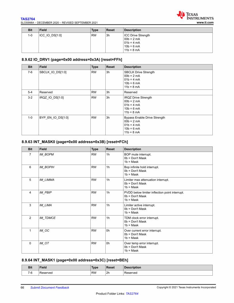
Bit Field Type Reset Description1-0 ICC_IO_DS[1:0] RW 3h ICC Drive Strength
00b = 2 mA 01b = 4 mA 10b = 6 mA 11b = 8 mA
8.9.62 IO_DRV1 (page=0x00 address=0x3A) [reset=FFh]
Bit Field Type Reset Description7-6 SBCLK_IO_DS[1:0] RW 3h SBCLK Drive Strength
00b = 2 mA 01b = 4 mA 10b = 6 mA 11b = 8 mA
5-4 Reserved RW 3h Reserved
3-2 IRQZ_IO_DS[1:0] RW 3h IRQZ Drive Strength00b = 2 mA 01b = 4 mA 10b = 6 mA 11b = 8 mA
1-0 BYP_EN_IO_DS[1:0] RW 3h Bypass Enable Drive Strength00b = 2 mA 01b = 4 mA 10b = 6 mA 11b = 8 mA
8.9.63 INT_MASK0 (page=0x00 address=0x3B) [reset=FCh]
Bit Field Type Reset Description7 IM_BOPM RW 1h BOP mute interrupt.
0b = Don't Mask 1b = Mask
6 IM_BOPIH RW 1h Bop infinite hold interrupt.0b = Don't Mask 1b = Mask
5 IM_LIMMA RW 1h Limiter max attenuation interrupt.0b = Don't Mask 1b = Mask
4 IM_PBIP RW 1h PVDD below limiter inflection point interrupt.0b = Don't Mask 1b = Mask
3 IM_LIMA RW 1h Limiter active interrupt.0b = Don't Mask 1b = Mask
2 IM_TDMCE RW 1h TDM clock error interrupt.0b = Don't Mask 1b = Mask
1 IM_OC RW 0h Over current error interrupt.0b = Don't Mask 1b = Mask
0 IM_OT RW 0h Over temp error interrupt.0b = Don't Mask 1b = Mask
8.9.64 INT_MASK1 (page=0x00 address=0x3C) [reset=BEh]
Bit Field Type Reset Description7-6 Reserved RW 2h Reserved
TAS2764SLOS998A – DECEMBER 2020 – REVISED SEPTEMBER 2021 www.ti.com
66 Submit Document Feedback Copyright © 2021 Texas Instruments Incorporated
Product Folder Links: TAS2764

Bit Field Type Reset Description5 IM_LDC RW 1h Load Diagnostic Completion Mask
0b = Don't Mask 1b = Masked
4 IM_SOL[1:0] RW 3h Load Mask00b = Don't Mask 01b = Mask Open Load Detection 10b = Mask Short Load Detection 01b = Mask Open/Short Load Detection
2 IM_BOPSD*If BOP_SHDN=1 and brownout is detected DSP shuts down if not masked
RW 1h BOP Started Mask0b = Don't Mask 1b = Mask
1-0 Reserved RW 2h Reserved
8.9.65 INT_MASK4 (page=0x00 address=0x3D) [reset=DFh]
Bit Field Type Reset Description7 IM_PLL_CLK RW 1h Internal PLL Derived Clock Error Mask
0b = Don't Mask 1b = Mask
6 Reserved RW 1h Reserved
5 IM_VBAT1S_UVLO RW 0h VBAT1S Under Voltage0b = Don't Mask 1b = Mask
4-0 Reserved RW 1Fh Reserved
8.9.66 INT_MASK2 (page=0x00 address=0x40) [reset=F6h]
Bit Field Type Reset Description7 IM_TO105 RW 1h Temperature over 105C interrupt.
0b = Don't Mask 1b = Mask
6 IM_TO115 RW 1h Temperature over 115C interrupt.0b = Don't Mask 1b = Mask
5 IM_TO125 RW 1h Temperature over 125C interrupt.0b = Don't Mask 1b = Mask
4 IM_TO135 RW 1h Temperature over 135C interrupt.0b = Don't Mask 1b = Mask
3 IM_LDO_UV RW 0h Internal VBAT1S LDO Under Voltage0b = Don't Mask 1b = Mask
2 IM_LDO_OV RW 1h Internal VBAT1S LDO Over Voltage0b = Don't Mask 1b = Mask
1 IM_LDO_OL RW 1h Internal VBAT1S LDO Over Load0b = Don't Mask 1b = Mask
0 IM_PUVLO RW 0h PVDD UVLO interrupt.0b = Don't Mask 1b = Mask
www.ti.comTAS2764
SLOS998A – DECEMBER 2020 – REVISED SEPTEMBER 2021
Copyright © 2021 Texas Instruments Incorporated Submit Document Feedback 67
Product Folder Links: TAS2764
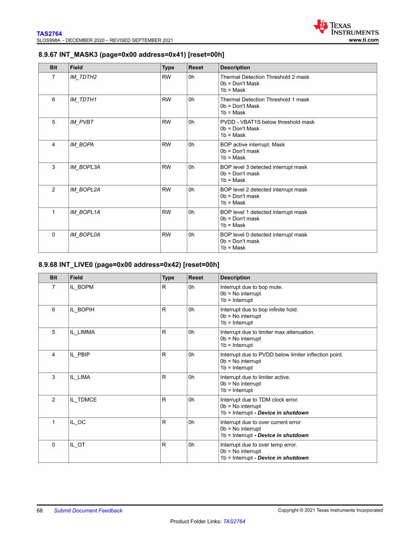
8.9.67 INT_MASK3 (page=0x00 address=0x41) [reset=00h]
Bit Field Type Reset Description7 IM_TDTH2 RW 0h Thermal Detection Threshold 2 mask
0b = Don't Mask 1b = Mask
6 IM_TDTH1 RW 0h Thermal Detection Threshold 1 mask0b = Don't Mask 1b = Mask
5 IM_PVBT RW 0h PVDD - VBAT1S below threshold mask0b = Don't Mask 1b = Mask
4 IM_BOPA RW 0h BOP active interrupt. Mask0b = Don't mask 1b = Mask
3 IM_BOPL3A RW 0h BOP level 3 detected interrupt mask0b = Don't mask 1b = Mask
2 IM_BOPL2A RW 0h BOP level 2 detected interrupt mask0b = Don't mask 1b = Mask
1 IM_BOPL1A RW 0h BOP level 1 detected interrupt mask0b = Don't mask 1b = Mask
0 IM_BOPL0A RW 0h BOP level 0 detected interrupt mask0b = Don't mask 1b = Mask
8.9.68 INT_LIVE0 (page=0x00 address=0x42) [reset=00h]
Bit Field Type Reset Description7 IL_BOPM R 0h Interrupt due to bop mute.
0b = No interrupt 1b = Interrupt
6 IL_BOPIH R 0h Interrupt due to bop infinite hold.0b = No interrupt 1b = Interrupt
5 IL_LIMMA R 0h Interrupt due to limiter max attenuation.0b = No interrupt 1b = Interrupt
4 IL_PBIP R 0h Interrupt due to PVDD below limiter inflection point.0b = No interrupt 1b = Interrupt
3 IL_LIMA R 0h Interrupt due to limiter active.0b = No interrupt 1b = Interrupt
2 IL_TDMCE R 0h Interrupt due to TDM clock error.0b = No interrupt 1b = Interrupt - Device in shutdown
1 IL_OC R 0h Interrupt due to over current error.0b = No interrupt 1b = Interrupt - Device in shutdown
0 IL_OT R 0h Interrupt due to over temp error.0b = No interrupt 1b = Interrupt - Device in shutdown
TAS2764SLOS998A – DECEMBER 2020 – REVISED SEPTEMBER 2021 www.ti.com
68 Submit Document Feedback Copyright © 2021 Texas Instruments Incorporated
Product Folder Links: TAS2764
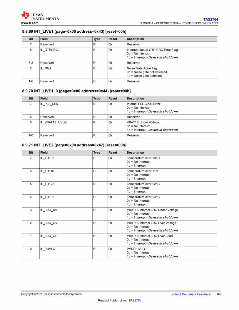
8.9.69 INT_LIVE1 (page=0x00 address=0x43) [reset=00h]
Bit Field Type Reset Description7 Reserved R 0h Reserved
6 IL_OTPCRC R 0h Interrupt due to OTP CRC Error Flag0b = No interrupt 1b = Interrupt - Device in shutdown
5-3 Reserved R 0h Reserved
2 IL_NGA R 0h Noise Gate Acive flag0b = Noise gate not detected 1b = Noise gate detected
1-0 Reserved R 0h Reserved
8.9.70 INT_LIVE1_0 (page=0x00 address=0x44) [reset=00h]
Bit Field Type Reset Description7 IL_PLL_CLK R 0h Internal PLL Clock Error
0b = No interrupt 1b = Interrupt - Device in shutdown
6 Reserved R 0h Reserved
5 IL_VBAT1S_UVLO R 0h VBAT1S Under Voltage0b = No interrupt 1b = Interrupt - Device in shutdown
4-0 Reserved R 0h Reserved
8.9.71 INT_LIVE2 (page=0x00 address=0x47) [reset=00h]
Bit Field Type Reset Description7 IL_TO105 R 0h Temperature over 105C
0b = No Interrupt 1b = Interrupt
6 IL_TO115 R 0h Temperature over 115C0b = No Interrupt 1b = Interrupt
5 IL_TO125 R 0h Temperature over 125C0b = No Interrupt 1b = Interrupt
4 IL_TO135 R 0h Temperature over 135C0b = No Interrupt 1b = Interrupt
3 IL_LDO_UV R 0h VBAT1S Internal LDO Under Voltage0b = No Interrupt 1b = Interrupt - Device in shutdown
2 IL_LDO_OV R 0h VBAT1S Internal LDO Over Voltage0b = No Interrupt 1b = Interrupt - Device in shutdown
1 IL_LDO_OL R 0h VBAT1S Internal LDO Over Load0b = No Interrupt 1b = Interrupt - Device in shutdown
0 IL_PUVLO R 0h PVDD UVLO0b = No Interrupt 1b = Interrupt - Device in shutdown
www.ti.comTAS2764
SLOS998A – DECEMBER 2020 – REVISED SEPTEMBER 2021
Copyright © 2021 Texas Instruments Incorporated Submit Document Feedback 69
Product Folder Links: TAS2764
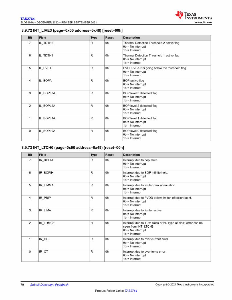
8.9.72 INT_LIVE3 (page=0x00 address=0x48) [reset=00h]
Bit Field Type Reset Description7 IL_TDTH2 R 0h Thermal Detection Threshold 2 active flag
0b = No interrupt 1b = Interrupt
6 IL_TDTH1 R 0h Thermal Detection Threshold 1 active flag0b = No interrupt 1b = Interrupt
5 IL_PVBT R 0h PVDD -VBAT1S going below the threshold flag0b = No interrupt 1b = Interrupt
4 IL_BOPA R 0h BOP active flag0b = No interrupt 1b = Interrupt
3 IL_BOPL3A R 0h BOP level 3 detected flag 0b = No interrupt 1b = Interrupt
2 IL_BOPL2A R 0h BOP level 2 detected flag0b = No interrupt 1b = Interrupt
1 IL_BOPL1A R 0h BOP level 1 detected flag0b = No interrupt 1b = Interrupt
0 IL_BOPL0A R 0h BOP level 0 detected flag0b = No interrupt 1b = Interrupt
8.9.73 INT_LTCH0 (page=0x00 address=0x49) [reset=00h]
Bit Field Type Reset Description7 IR_BOPM R 0h Interrupt due to bop mute.
0b = No interrupt 1b = Interrupt
6 IR_BOPIH R 0h Interrupt due to BOP infinite hold.0b = No interrupt 1b = Interrupt
5 IR_LIMMA R 0h Interrupt due to limiter max attenuation.0b = No interrupt 1b = Interrupt
4 IR_PBIP R 0h Interrupt due to PVDD below limiter inflection point.0b = No interrupt 1b = Interrupt
3 IR_LIMA R 0h Interrupt due to limiter active0b = No interrupt 1b = Interrupt
2 IR_TDMCE R 0h Interrupt due to TDM clock error. Type of clock error can be seen from INT_LTCH80b = No interrupt 1b = Interrupt
1 IR_OC R 0h Interrupt due to over current error0b = No interrupt 1b = Interrupt
0 IR_OT R 0h Interrupt due to over temp error0b = No interrupt 1b = Interrupt
TAS2764SLOS998A – DECEMBER 2020 – REVISED SEPTEMBER 2021 www.ti.com
70 Submit Document Feedback Copyright © 2021 Texas Instruments Incorporated
Product Folder Links: TAS2764
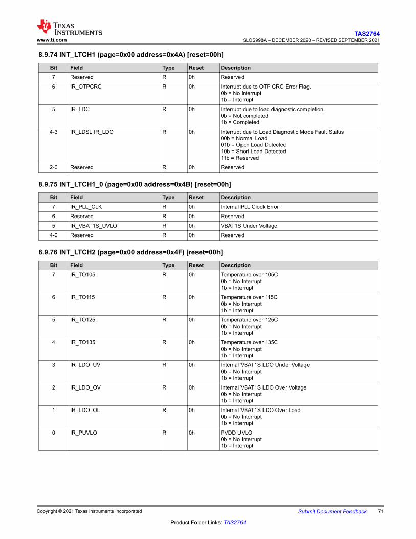
8.9.74 INT_LTCH1 (page=0x00 address=0x4A) [reset=00h]
Bit Field Type Reset Description7 Reserved R 0h Reserved
6 IR_OTPCRC R 0h Interrupt due to OTP CRC Error Flag.0b = No interrupt 1b = Interrupt
5 IR_LDC R 0h Interrupt due to load diagnostic completion.0b = Not completed 1b = Completed
4-3 IR_LDSL IR_LDO R 0h Interrupt due to Load Diagnostic Mode Fault Status00b = Normal Load 01b = Open Load Detected 10b = Short Load Detected 11b = Reserved
2-0 Reserved R 0h Reserved
8.9.75 INT_LTCH1_0 (page=0x00 address=0x4B) [reset=00h]
Bit Field Type Reset Description7 IR_PLL_CLK R 0h Internal PLL Clock Error
6 Reserved R 0h Reserved
5 IR_VBAT1S_UVLO R 0h VBAT1S Under Voltage
4-0 Reserved R 0h Reserved
8.9.76 INT_LTCH2 (page=0x00 address=0x4F) [reset=00h]
Bit Field Type Reset Description7 IR_TO105 R 0h Temperature over 105C
0b = No Interrupt 1b = Interrupt
6 IR_TO115 R 0h Temperature over 115C0b = No Interrupt 1b = Interrupt
5 IR_TO125 R 0h Temperature over 125C0b = No Interrupt 1b = Interrupt
4 IR_TO135 R 0h Temperature over 135C0b = No Interrupt 1b = Interrupt
3 IR_LDO_UV R 0h Internal VBAT1S LDO Under Voltage0b = No Interrupt 1b = Interrupt
2 IR_LDO_OV R 0h Internal VBAT1S LDO Over Voltage0b = No Interrupt 1b = Interrupt
1 IR_LDO_OL R 0h Internal VBAT1S LDO Over Load0b = No Interrupt 1b = Interrupt
0 IR_PUVLO R 0h PVDD UVLO0b = No Interrupt 1b = Interrupt
www.ti.comTAS2764
SLOS998A – DECEMBER 2020 – REVISED SEPTEMBER 2021
Copyright © 2021 Texas Instruments Incorporated Submit Document Feedback 71
Product Folder Links: TAS2764
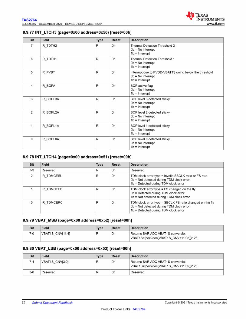
8.9.77 INT_LTCH3 (page=0x00 address=0x50) [reset=00h]
Bit Field Type Reset Description7 IR_TDTH2 R 0h Thermal Detection Threshold 2
0b = No interrupt 1b = Interrupt
6 IR_TDTH1 R 0h Thermal Detection Threshold 10b = No interrupt 1b = Interrupt
5 IR_PVBT R 0h Interrupt due to PVDD-VBAT1S going below the threshold0b = No interrupt 1b = Interrupt
4 IR_BOPA R 0h BOP active flag0b = No interrupt 1b = Interrupt
3 IR_BOPL3A R 0h BOP level 3 detected sticky 0b = No interrupt 1b = Interrupt
2 IR_BOPL2A R 0h BOP level 2 detected sticky 0b = No interrupt 1b = Interrupt
1 IR_BOPL1A R 0h BOP level 1 detected sticky 0b = No interrupt 1b = Interrupt
0 IR_BOPL0A R 0h BOP level 0 detected sticky 0b = No interrupt 1b = Interrupt
8.9.78 INT_LTCH4 (page=0x00 address=0x51) [reset=00h]
Bit Field Type Reset Description7-3 Reserved R 0h Reserved
2 IR_TDMCEIR R 0h TDM clock error type = Invalid SBCLK ratio or FS rate0b = Not detected during TDM clock error 1b = Detected during TDM clock error
1 IR_TDMCEFC R 0h TDM clock error type = FS changed on the fly 0b = Detected during TDM clock error 1b = Not detected during TDM clock error
0 IR_TDMCERC R 0h TDM clock error type = SBCLK FS ratio changed on the fly0b = Not detected during TDM clock error 1b = Detected during TDM clock error
8.9.79 VBAT_MSB (page=0x00 address=0x52) [reset=00h]
Bit Field Type Reset Description7-0 VBAT1S_CNV[11:4] R 0h Returns SAR ADC VBAT1S conversio:
VBAT1S=[hex2dec(VBAT1S_CNV<11:0>)]/128
8.9.80 VBAT_LSB (page=0x00 address=0x53) [reset=00h]
Bit Field Type Reset Description7-4 VBAT1S_CNV[3:0] R 0h Returns SAR ADC VBAT1S conversio:
VBAT1S=[hex2dec(VBAT1S_CNV<11:0>)]/128
3-0 Reserved R 0h Reserved
TAS2764SLOS998A – DECEMBER 2020 – REVISED SEPTEMBER 2021 www.ti.com
72 Submit Document Feedback Copyright © 2021 Texas Instruments Incorporated
Product Folder Links: TAS2764
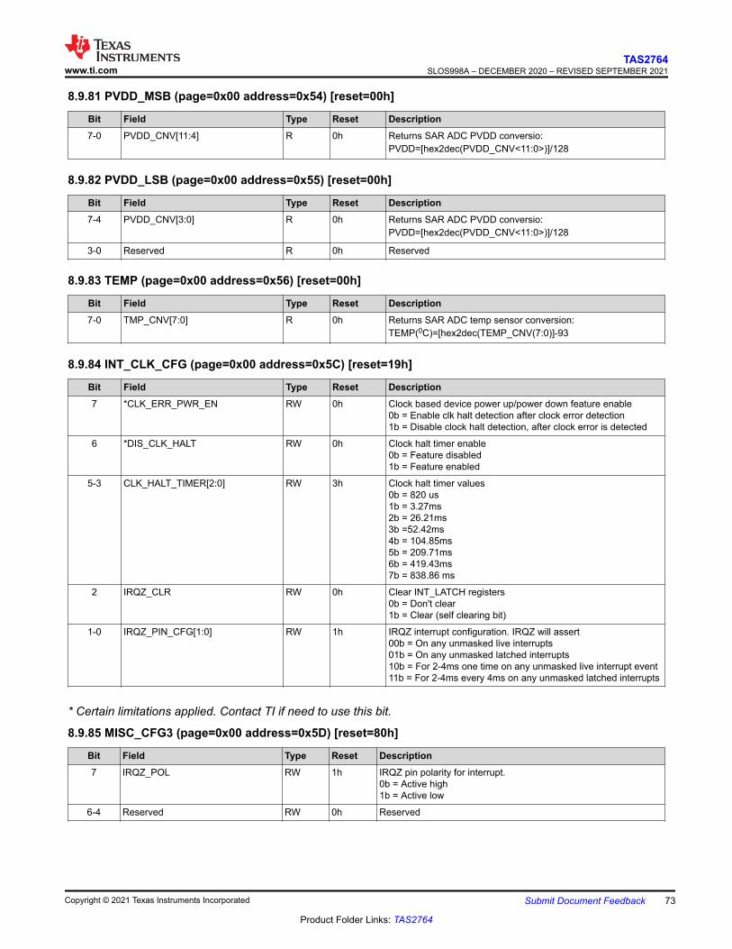
8.9.81 PVDD_MSB (page=0x00 address=0x54) [reset=00h]
Bit Field Type Reset Description7-0 PVDD_CNV[11:4] R 0h Returns SAR ADC PVDD conversio:
PVDD=[hex2dec(PVDD_CNV<11:0>)]/128
8.9.82 PVDD_LSB (page=0x00 address=0x55) [reset=00h]
Bit Field Type Reset Description7-4 PVDD_CNV[3:0] R 0h Returns SAR ADC PVDD conversio:
PVDD=[hex2dec(PVDD_CNV<11:0>)]/128
3-0 Reserved R 0h Reserved
8.9.83 TEMP (page=0x00 address=0x56) [reset=00h]
Bit Field Type Reset Description7-0 TMP_CNV[7:0] R 0h Returns SAR ADC temp sensor conversion:
TEMP(0C)=[hex2dec(TEMP_CNV(7:0)]-93
8.9.84 INT_CLK_CFG (page=0x00 address=0x5C) [reset=19h]
Bit Field Type Reset Description7 *CLK_ERR_PWR_EN RW 0h Clock based device power up/power down feature enable
0b = Enable clk halt detection after clock error detection 1b = Disable clock halt detection, after clock error is detected
6 *DIS_CLK_HALT RW 0h Clock halt timer enable0b = Feature disabled 1b = Feature enabled
5-3 CLK_HALT_TIMER[2:0] RW 3h Clock halt timer values0b = 820 us 1b = 3.27ms 2b = 26.21ms 3b =52.42ms 4b = 104.85ms 5b = 209.71ms 6b = 419.43ms 7b = 838.86 ms
2 IRQZ_CLR RW 0h Clear INT_LATCH registers0b = Don't clear 1b = Clear (self clearing bit)
1-0 IRQZ_PIN_CFG[1:0] RW 1h IRQZ interrupt configuration. IRQZ will assert 00b = On any unmasked live interrupts 01b = On any unmasked latched interrupts 10b = For 2-4ms one time on any unmasked live interrupt event 11b = For 2-4ms every 4ms on any unmasked latched interrupts
* Certain limitations applied. Contact TI if need to use this bit.
8.9.85 MISC_CFG3 (page=0x00 address=0x5D) [reset=80h]
Bit Field Type Reset Description7 IRQZ_POL RW 1h IRQZ pin polarity for interrupt.
0b = Active high 1b = Active low
6-4 Reserved RW 0h Reserved
www.ti.comTAS2764
SLOS998A – DECEMBER 2020 – REVISED SEPTEMBER 2021
Copyright © 2021 Texas Instruments Incorporated Submit Document Feedback 73
Product Folder Links: TAS2764

Bit Field Type Reset Description3-2 YB_BOP_CTRL RW 0h This register selects on which BOP level, Y-bridge and BYP_EN
pad need to shift to PVDD when PVDD_SELECTION = 0.0h = Shift to PVDD when BOP LVL0 is detected 1h = Shift to PVDD when BOP LVL1 or LVL0 is detected 2h = Shift to PVDD when BOP LVL2 or LVL1 or LVL0 is detected 3h = Shift to PVDD when BOP LVL3 or LVL2 or LVL1 or LVL0 is detected
1 Reserved RW 0h Reserved
0 R 0h Reserved
8.9.86 CLOCK_CFG (page=0x00 address=0x60) [reset=0Dh]
Bit Field Type Reset Description7-6 Reserved R 0h Reserved
5-2 SAMP_RATIO[3:0] RW 3h SBCLK to FS ratio when AUTO_RATE=1 (disabled)00h = 16 01h = 24 02h = 32 03h = 48 04h = 64 05h = 96 06h = 128 07h = 192 08h = 256 09h = 384 0Ah = 512 0Bh = 125 0Ch = 250 0Dh = 500 0Eh-0Fh = Reserved
1-0 Reserved RW 1h Reserved
8.9.87 IDLE_IND (page=0x00 address=0x63) [reset=48]
Bit Field Type Reset Description7 IDLE_IND RW 0h Idle channel Class D output current optimization
0b = Used for inductors 15uH and higher 1b = Used for 5uH inductors
6-0 Reserved RW 48h Reserved
8.9.88 MISC_CFG4 (page=0x00 address=0x65) [reset=08]
Bit Field Type Reset Description7-4 Reserved RW 0h Reserved
3 LDG_CLK RW 1h Clock source for load diagnostic0b = External TDM 1b = Internal oscillator
2-1 LDG_IVSNS_AVG 0h Duration on averaging on V/I data0h = 5 ms 1h = 10 ms 2h = 50 ms 3h =100 ms
0 Reserved RW 0h Reserved
8.9.89 TG_CFG0 (page=0x00 address=0x67) [reset=00h]
Bit Field Type Reset Description7-2 Reserved R 0h Reserved
TAS2764SLOS998A – DECEMBER 2020 – REVISED SEPTEMBER 2021 www.ti.com
74 Submit Document Feedback Copyright © 2021 Texas Instruments Incorporated
Product Folder Links: TAS2764
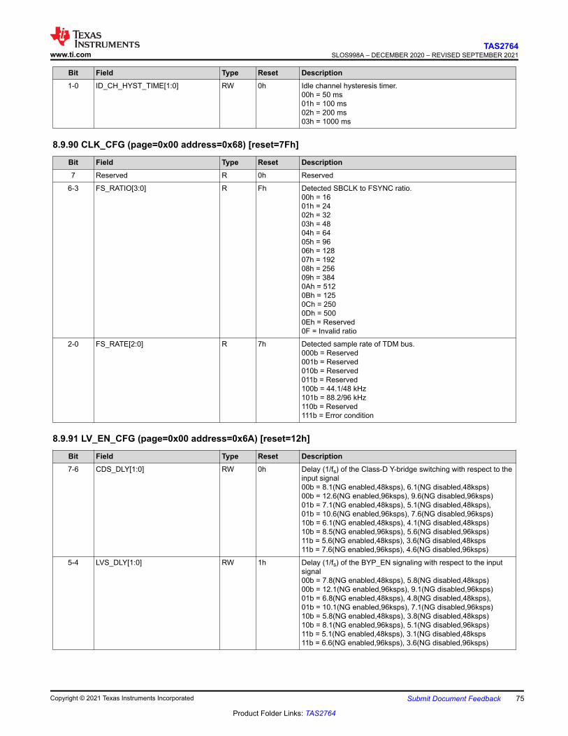
Bit Field Type Reset Description1-0 ID_CH_HYST_TIME[1:0] RW 0h Idle channel hysteresis timer.
00h = 50 ms 01h = 100 ms 02h = 200 ms 03h = 1000 ms
8.9.90 CLK_CFG (page=0x00 address=0x68) [reset=7Fh]
Bit Field Type Reset Description7 Reserved R 0h Reserved
6-3 FS_RATIO[3:0] R Fh Detected SBCLK to FSYNC ratio.00h = 16 01h = 24 02h = 32 03h = 48 04h = 64 05h = 96 06h = 128 07h = 192 08h = 256 09h = 384 0Ah = 512 0Bh = 125 0Ch = 250 0Dh = 500 0Eh = Reserved 0F = Invalid ratio
2-0 FS_RATE[2:0] R 7h Detected sample rate of TDM bus.000b = Reserved 001b = Reserved 010b = Reserved 011b = Reserved 100b = 44.1/48 kHz 101b = 88.2/96 kHz 110b = Reserved 111b = Error condition
8.9.91 LV_EN_CFG (page=0x00 address=0x6A) [reset=12h]
Bit Field Type Reset Description7-6 CDS_DLY[1:0] RW 0h Delay (1/fs) of the Class-D Y-bridge switching with respect to the
input signal 00b = 8.1(NG enabled,48ksps), 6.1(NG disabled,48ksps) 00b = 12.6(NG enabled,96ksps), 9.6(NG disabled,96ksps) 01b = 7.1(NG enabled,48ksps), 5.1(NG disabled,48ksps), 01b = 10.6(NG enabled,96ksps), 7.6(NG disabled,96ksps) 10b = 6.1(NG enabled,48ksps), 4.1(NG disabled,48ksps) 10b = 8.5(NG enabled,96ksps), 5.6(NG disabled,96ksps) 11b = 5.6(NG enabled,48ksps), 3.6(NG disabled,48ksps 11b = 7.6(NG enabled,96ksps), 4.6(NG disabled,96ksps)
5-4 LVS_DLY[1:0] RW 1h Delay (1/fs) of the BYP_EN signaling with respect to the input signal 00b = 7.8(NG enabled,48ksps), 5.8(NG disabled,48ksps) 00b = 12.1(NG enabled,96ksps), 9.1(NG disabled,96ksps) 01b = 6.8(NG enabled,48ksps), 4.8(NG disabled,48ksps), 01b = 10.1(NG enabled,96ksps), 7.1(NG disabled,96ksps) 10b = 5.8(NG enabled,48ksps), 3.8(NG disabled,48ksps) 10b = 8.1(NG enabled,96ksps), 5.1(NG disabled,96ksps) 11b = 5.1(NG enabled,48ksps), 3.1(NG disabled,48ksps 11b = 6.6(NG enabled,96ksps), 3.6(NG disabled,96ksps)
www.ti.comTAS2764
SLOS998A – DECEMBER 2020 – REVISED SEPTEMBER 2021
Copyright © 2021 Texas Instruments Incorporated Submit Document Feedback 75
Product Folder Links: TAS2764
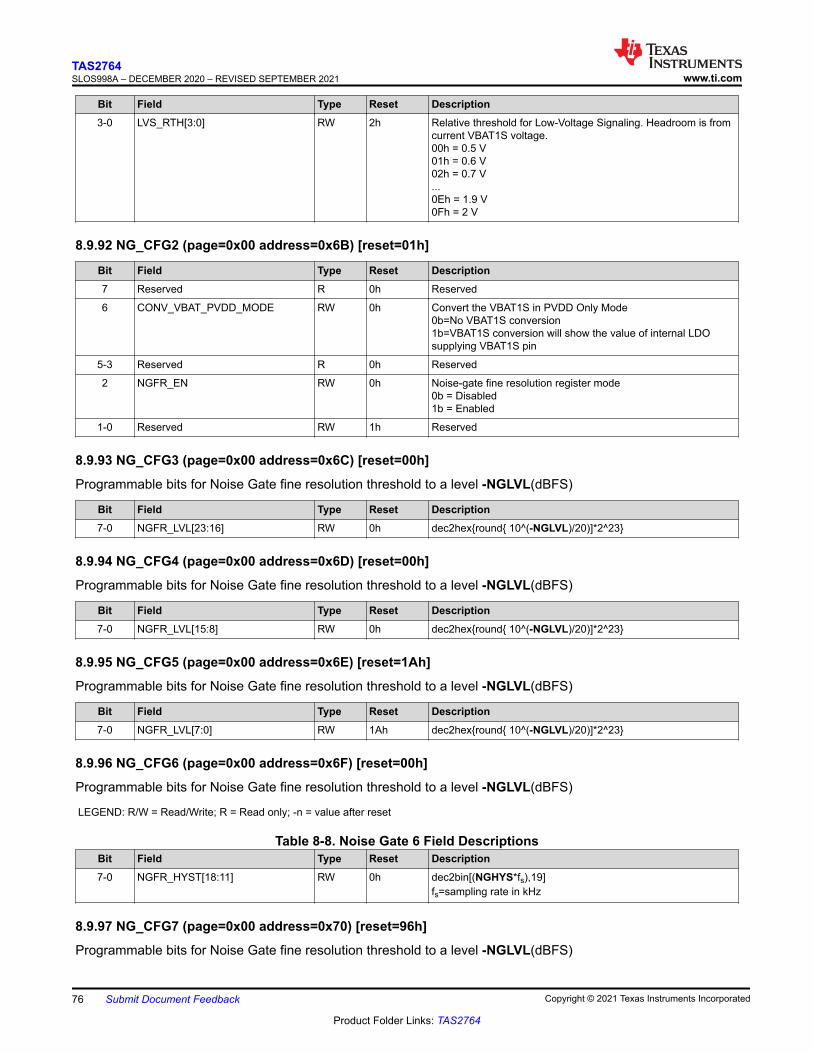
Bit Field Type Reset Description3-0 LVS_RTH[3:0] RW 2h Relative threshold for Low-Voltage Signaling. Headroom is from
current VBAT1S voltage.00h = 0.5 V 01h = 0.6 V 02h = 0.7 V ... 0Eh = 1.9 V 0Fh = 2 V
8.9.92 NG_CFG2 (page=0x00 address=0x6B) [reset=01h]
Bit Field Type Reset Description7 Reserved R 0h Reserved
6 CONV_VBAT_PVDD_MODE RW 0h Convert the VBAT1S in PVDD Only Mode0b=No VBAT1S conversion 1b=VBAT1S conversion will show the value of internal LDO supplying VBAT1S pin
5-3 Reserved R 0h Reserved
2 NGFR_EN RW 0h Noise-gate fine resolution register mode0b = Disabled 1b = Enabled
1-0 Reserved RW 1h Reserved
8.9.93 NG_CFG3 (page=0x00 address=0x6C) [reset=00h]
Programmable bits for Noise Gate fine resolution threshold to a level -NGLVL(dBFS)
Bit Field Type Reset Description7-0 NGFR_LVL[23:16] RW 0h dec2hex{round{ 10^(-NGLVL)/20)]*2^23}
8.9.94 NG_CFG4 (page=0x00 address=0x6D) [reset=00h]
Programmable bits for Noise Gate fine resolution threshold to a level -NGLVL(dBFS)
Bit Field Type Reset Description7-0 NGFR_LVL[15:8] RW 0h dec2hex{round{ 10^(-NGLVL)/20)]*2^23}
8.9.95 NG_CFG5 (page=0x00 address=0x6E) [reset=1Ah]
Programmable bits for Noise Gate fine resolution threshold to a level -NGLVL(dBFS)
Bit Field Type Reset Description7-0 NGFR_LVL[7:0] RW 1Ah dec2hex{round{ 10^(-NGLVL)/20)]*2^23}
8.9.96 NG_CFG6 (page=0x00 address=0x6F) [reset=00h]
Programmable bits for Noise Gate fine resolution threshold to a level -NGLVL(dBFS)
LEGEND: R/W = Read/Write; R = Read only; -n = value after reset
Table 8-8. Noise Gate 6 Field DescriptionsBit Field Type Reset Description7-0 NGFR_HYST[18:11] RW 0h dec2bin[(NGHYS*fs),19]
fs=sampling rate in kHz
8.9.97 NG_CFG7 (page=0x00 address=0x70) [reset=96h]
Programmable bits for Noise Gate fine resolution threshold to a level -NGLVL(dBFS)
TAS2764SLOS998A – DECEMBER 2020 – REVISED SEPTEMBER 2021 www.ti.com
76 Submit Document Feedback Copyright © 2021 Texas Instruments Incorporated
Product Folder Links: TAS2764

LEGEND: R/W = Read/Write; R = Read only; -n = value after reset
Table 8-9. Noise Gate 7 Field DescriptionsBit Field Type Reset Description7-0 NGFR_HYST[10:3] RW 96h dec2bin[(NGHYS*fs),19]
fs=sampling rate in kHz
Example
NGFR_HYST[15:0] is the result of 19 bits processing with last three bits thrown away (000)
For 50 ms and 48ksps formula is: dec2bin[50*48,19]=dec2bin[2400,19]=0000000100101100000
Result: 01h in register 0x6F and 2Ch in register 0x70.
8.9.98 PVDD_UVLO (page=0x00 address=0x71) [reset=00h]
Bit Field Type Reset Description7-6 Reserved RW 00h Reserved
5-0 PVDD_UVLO_TH[5:0] RW 00h PVDD UVLO Thresholds.00h = 2.2 V 01h = 2.419 V 02h = 2.638 V ........... 3Fh= 16 V
8.9.99 DAC_MOD_RST (page=0x00 address=0x76) [reset=02h]
Bit Field Type Reset Description7-2 Reserved RW 0h Reserved
1 DIS_DMOD_RST RW 1h Reset of DAC Modulator when DSP is OFF:0= Enable reset of DAC Modulator when DSP is OFF1= Disable reset of DAC Modulator when DSP is OFF
0 Reserved R 0h ReservedReset value can change when read back .
8.9.100 REV_ID (page=0x00 address=0x7D) [reset=30h]
Bit Field Type Reset Description7-4 REV_ID[3:0] R 3h Returns the revision ID.
3-0 PG_ID[3:0] R 0h Returns the PG ID.
8.9.101 I2C_CKSUM (page=0x00 address=0x7E) [reset=00h]
Bit Field Type Reset Description7-0 I2C_CKSUM[7:0] RW 0h Returns I2C checksum. Writing to this register will reset the
checksum to the written value. This register is updated on writes to other registers on all books and pages.
8.9.102 BOOK (page=0x00 address=0x7F) [reset=00h]
Bit Field Type Reset Description7-0 BOOK[7:0] RW 0h Sets the device book.
00h = Book 0 01h = Book 1 ... FFh = Book 255
www.ti.comTAS2764
SLOS998A – DECEMBER 2020 – REVISED SEPTEMBER 2021
Copyright © 2021 Texas Instruments Incorporated Submit Document Feedback 77
Product Folder Links: TAS2764
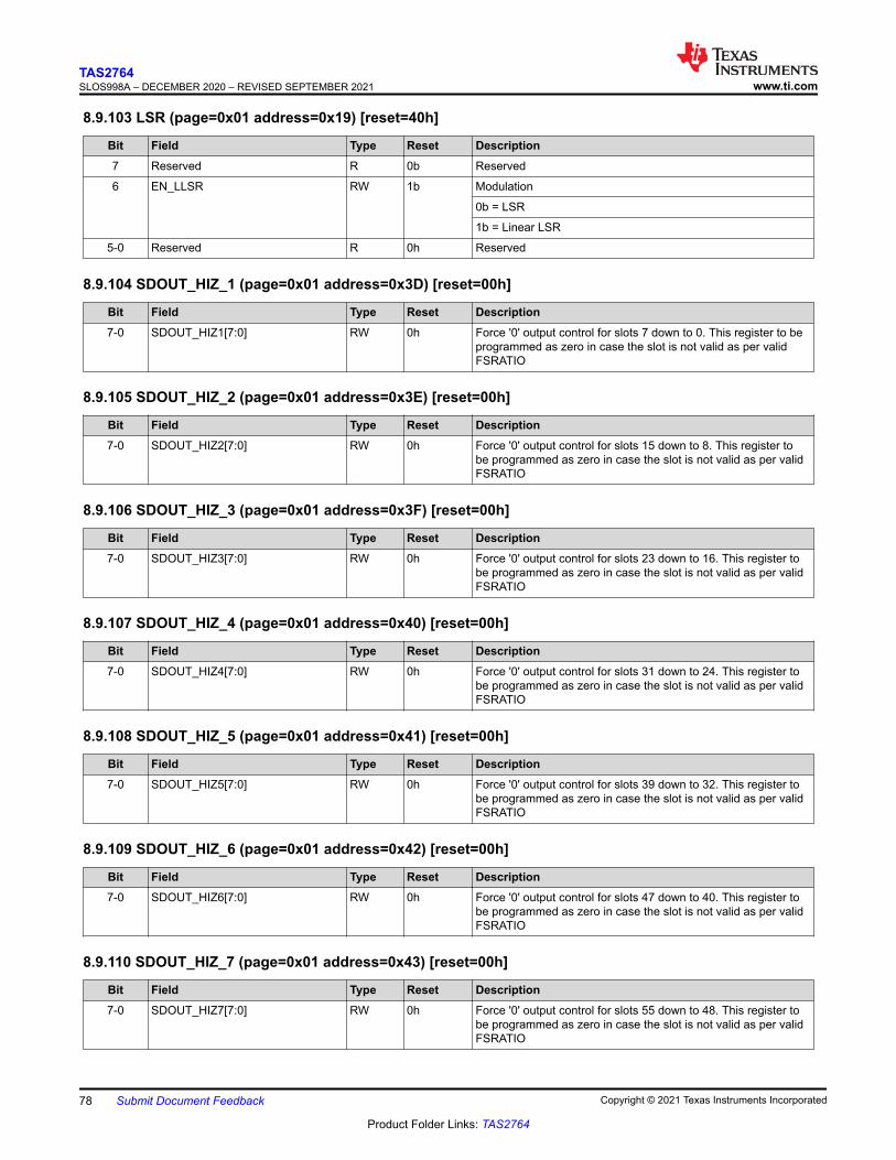
8.9.103 LSR (page=0x01 address=0x19) [reset=40h]
Bit Field Type Reset Description7 Reserved R 0b Reserved
6 EN_LLSR RW 1b Modulation
0b = LSR
1b = Linear LSR
5-0 Reserved R 0h Reserved
8.9.104 SDOUT_HIZ_1 (page=0x01 address=0x3D) [reset=00h]
Bit Field Type Reset Description7-0 SDOUT_HIZ1[7:0] RW 0h Force '0' output control for slots 7 down to 0. This register to be
programmed as zero in case the slot is not valid as per valid FSRATIO
8.9.105 SDOUT_HIZ_2 (page=0x01 address=0x3E) [reset=00h]
Bit Field Type Reset Description7-0 SDOUT_HIZ2[7:0] RW 0h Force '0' output control for slots 15 down to 8. This register to
be programmed as zero in case the slot is not valid as per valid FSRATIO
8.9.106 SDOUT_HIZ_3 (page=0x01 address=0x3F) [reset=00h]
Bit Field Type Reset Description7-0 SDOUT_HIZ3[7:0] RW 0h Force '0' output control for slots 23 down to 16. This register to
be programmed as zero in case the slot is not valid as per valid FSRATIO
8.9.107 SDOUT_HIZ_4 (page=0x01 address=0x40) [reset=00h]
Bit Field Type Reset Description7-0 SDOUT_HIZ4[7:0] RW 0h Force '0' output control for slots 31 down to 24. This register to
be programmed as zero in case the slot is not valid as per valid FSRATIO
8.9.108 SDOUT_HIZ_5 (page=0x01 address=0x41) [reset=00h]
Bit Field Type Reset Description7-0 SDOUT_HIZ5[7:0] RW 0h Force '0' output control for slots 39 down to 32. This register to
be programmed as zero in case the slot is not valid as per valid FSRATIO
8.9.109 SDOUT_HIZ_6 (page=0x01 address=0x42) [reset=00h]
Bit Field Type Reset Description7-0 SDOUT_HIZ6[7:0] RW 0h Force '0' output control for slots 47 down to 40. This register to
be programmed as zero in case the slot is not valid as per valid FSRATIO
8.9.110 SDOUT_HIZ_7 (page=0x01 address=0x43) [reset=00h]
Bit Field Type Reset Description7-0 SDOUT_HIZ7[7:0] RW 0h Force '0' output control for slots 55 down to 48. This register to
be programmed as zero in case the slot is not valid as per valid FSRATIO
TAS2764SLOS998A – DECEMBER 2020 – REVISED SEPTEMBER 2021 www.ti.com
78 Submit Document Feedback Copyright © 2021 Texas Instruments Incorporated
Product Folder Links: TAS2764
8.9.111 SDOUT_HIZ_8 (page=0x01 address=0x44) [reset=00h]
Bit Field Type Reset Description7-0 SDOUT_HIZ8[7:0] RW 0h Force '0' output control for slots 63 down to 56. This register to
be programmed as zero in case the slot is not valid as per valid FSRATIO
8.9.112 SDOUT_HIZ_9 (page=0x01 address=0x45) [reset=00h]
Bit Field Type Reset Description7 SDOUT_FORCE_0_CNT_EN RW 0h Control over sending "0" to un-used slots
0b = All unused slots will have 'Hi-Z' transmitted 1b = Unused slots can transmit '0' base on programming in registers 0x44 to 0x3D
6-0 Reserved RW 0h Reserved
8.9.113 TG_EN (page=0x01 address=0x47) [reset=ABh]
Bit Field Type Reset Description7-2 Reserved R 6'b101010 Reserved
Reset value can change when read back .
1 TG_TH2 RW 1'b1 Thermal threshold 21=Enabled0=Disabled
0 TG_TH1 RW 1'b1 Thermal threshold 11=Enabled0=Disabled
8.9.114 DG_DC_VAL1 (page=0x04 address=0x08) [reset=40h]
Programmable Diagnostic bits for a DC_VAL (dBFS) desired level.
Bit Field Type Reset Description7-0 DG_DC_VAL [31:24] RW 40h dec2hex{256*round[10^(DC_VAL/20)*2^23]}
8.9.115 DG_DC_VAL2 (page=0x04 address=0x09) [reset=26h]
Programmable Diagnostic bits for a DC_VAL (dBFS) desired level.
Bit Field Type Reset Description7-0 DG_DC_VAL [23:16] RW 26h dec2hex{256*round[10^(DC_VAL/20)*2^23]}
8.9.116 DG_DC_VAL3 (page=0x04 address=0x0A) [reset=40h]
Bit Field Type Reset Description7-0 DG_DC_VAL [15:8] RW 40h dec2hex{256*round[10^(DC_VAL/20)*2^23]}
8.9.117 DC_DG_VAL4 (page=0x04 address=0x0B) [reset=00h]
Programmable Diagnostic bits for a DC_VAL (dBFS) desired level.
Bit Field Type Reset Description7-0 DG_DC_VAL [7:0] RW 00h dec2hex{256*round[10^(DC_VAL/20)*2^23]}
8.9.118 LIM_TH_MAX1 (page=0x04 address=0x0C) [reset=68h]
Programmable bits to set limiter maximum threshold to a LIM_TH_MAX (V).
www.ti.comTAS2764
SLOS998A – DECEMBER 2020 – REVISED SEPTEMBER 2021
Copyright © 2021 Texas Instruments Incorporated Submit Document Feedback 79
Product Folder Links: TAS2764
Bit Field Type Reset Description7-0 LIM_TH_MAX[31:24] RW 68h dec2hex{256*round [LIM_TH_MAX*2^19]}
8.9.119 LIM_TH_MAX2 (page=0x04 address=0x0D) [reset=00h]
Programmable bits to set limiter maximum threshold to a LIM_TH_MAX (V).
Bit Field Type Reset Description7-0 LIM_TH_MAX[23:16] RW 00h dec2hex{256*round [LIM_TH_MAX*2^19]}
8.9.120 LIM_TH_MAX3 (page=0x04 address=0x0E) [reset=00h]
Programmable bits to set limiter maximum threshold to a LIM_TH_MAX (V).
Bit Field Type Reset Description7-0 LIM_TH_MAX[15:8] RW 00h dec2hex{256*round [LIM_TH_MAX*2^19]}
8.9.121 LIM_TH_MAX4 (page=0x04 address=0x0F) [reset=00h]
Programmable bits to set limiter maximum threshold to a LIM_TH_MAX (V).
Bit Field Type Reset Description7-0 LIM_TH_MAX[7:0] RW 00h dec2hex{256*round [LIM_TH_MAX*2^19]}
8.9.122 LIM_TH_MIN1 (page=0x04 address=0x10) [reset=28h]
Sets limiter minimum threshold to a LIM_TH_MIN (V) value.
Bit Field Type Reset Description7-0 LIM_TH_MIN[31:24] RW 28h dec2hex{256*round [LIM_TH_MIN*2^19]}
8.9.123 LIM_TH_MIN2 (page=0x04 address=0x11) [reset=00h]
Sets limiter minimum threshold to a LIM_TH_MIN (V) value.
Bit Field Type Reset Description7-0 LIM_TH_MIN[23:16] RW 00h dec2hex{256*round [LIM_TH_MIN*2^19]}
8.9.124 LIM_TH_MIN3 (page=0x04 address=0x12) [reset=00h]
Sets limiter minimum threshold to a LIM_TH_MIN (V) value.
Bit Field Type Reset Description7-0 LIM_TH_MIN[15:8] RW 00h dec2hex{256*round [LIM_TH_MIN*2^19]}
8.9.125 LIM_TH_MIN4 (page=0x04 address=0x13) [reset=00h]
Sets limiter minimum threshold to a LIM_TH_MIN (V) value.
Bit Field Type Reset Description7-0 LIM_TH_MIN[7:0] RW 0h dec2hex{256*round [LIM_TH_MIN*2^19]}
8.9.126 LIM_INF_PT1 (page=0x04 address=0x14) [reset=56h]
Sets limiter inflection point to a value of LIM_INF_PT (V).
Bit Field Type Reset Description7-0 LIM_INF_PT[31:24] RW 56h dec2hex{256*round [LIM_INF_PT*2^19]}
TAS2764SLOS998A – DECEMBER 2020 – REVISED SEPTEMBER 2021 www.ti.com
80 Submit Document Feedback Copyright © 2021 Texas Instruments Incorporated
Product Folder Links: TAS2764
8.9.127 LIM_INF_PT2 (page=0x04 address=0x15) [reset=66h]
Sets limiter inflection point to a value of LIM_INF_PT (V).
Bit Field Type Reset Description7-0 LIM_INF_PT[23:16] RW 66h dec2hex{256*round [LIM_INF_PT*2^19]}
8.9.128 LIM_INF_PT3 (page=0x04 address=0x16) [reset=66h]
Sets limiter inflection point to a value of LIM_INF_PT (V).
Bit Field Type Reset Description7-0 LIM_INF_PT[15:8] RW 66h dec2hex{256*round [LIM_INF_PT*2^19]}
8.9.129 LIM_INF_PT4 (page=0x04 address=0x17) [reset=00h]
Sets limiter inflection point to a value of LIM_INF_PT (V).
Bit Field Type Reset Description7-0 LIM_INF_PT[7:0] RW 0h dec2hex{256*round [LIM_INF_PT*2^19]}
8.9.130 LIM_SLOPE1 (page=0x04 address=0x18) [reset=10h]
Sets limiter slope to a LIM_SLOPE (V) value.
Bit Field Type Reset Description7-0 LIM_SLOPE[31:24] RW 10h dec2hex{256*round [LIM_SLOPE*2^20]}
8.9.131 LIM_SLOPE2 (page=0x04 address=0x19) [reset=00h]
Sets limiter slope to a LIM_SLOPE (V) value.
Bit Field Type Reset Description7-0 LIM_SLOPE[23:16] RW 00h dec2hex{256*round [LIM_SLOPE*2^20]}
8.9.132 LIM_SLOPE3 (page=0x04 address=0x1A) [reset=00h]
Sets limiter slope to a LIM_SLOPE (V) value.
Bit Field Type Reset Description7-0 LIM_SLOPE[15:8] RW 00h dec2hex{256*round [LIM_SLOPE*2^20]}
8.9.133 LIM_SLOPE4 (page=0x04 address=0x1B) [reset=00h]
Sets limiter slope to a LIM_SLOPE (V) value.
Bit Field Type Reset Description7-0 LIM_SLOPE[7:0] RW 00h dec2hex{256*round [LIM_SLOPE*2^20]}
8.9.134 TF_HLD1 (page=0x04 address=0x1C) [reset=00h]
Thermal fold-back hold count set to a TF_HLD (s) value.
Bit Field Type Reset Description7-0 TF_ HOLD_CNT[31:24] RW 00h dec2hex [256*round (TF_HLD*9600)]
8.9.135 TF_HLD2 (page=0x04 address=0x1D) [reset=03h]
Thermal fold-back hold count set to a TF_HLD (s) value.
www.ti.comTAS2764
SLOS998A – DECEMBER 2020 – REVISED SEPTEMBER 2021
Copyright © 2021 Texas Instruments Incorporated Submit Document Feedback 81
Product Folder Links: TAS2764
Bit Field Type Reset Description7-0 TF_HOLD_CNT23:16] RW 03h dec2hex [256*round (TF_HLD*9600)]
8.9.136 TF_HLD3 (page=0x04 address=0x1E) [reset=E8h]
Thermal fold-back hold count set to a TF_HLD (s) value.
Bit Field Type Reset Description7-0 TF_HOLD_CNT[15:8] RW E8h dec2hex [256*round (TF_HLD*9600)]
8.9.137 TF_HLD4 (page=0x04 address=0x1F) [reset=00h]
Thermal fold-back hold count set to a TF_HLD (s) value.
Bit Field Type Reset Description7-0 TF_HOLD_CNT[7:0] RW 00h dec2hex [256*round (TF_HLD*9600)]
8.9.138 TF_RLS1 (page=0x04 address=0x20) [reset=40h]
Thermal fold-back limiter release rate set to a value TF_RLS (dB/100us).
Bit Field Type Reset Description7-0 TF_REL_RATE[31:24] RW 40h dec2hex{256*round[10^(TF_RLS/20)*2^22]}
8.9.139 TF_RLS2 (page=0x04 address=0x21) [reset=12h]
Thermal fold-back limiter release rate set to a value TF_RLS (dB/100us).
Bit Field Type Reset Description7-0 TF_REL_RATE[23:16] RW 12h dec2hex{256*round[10^(TF_RLS/20)*2^22]}
8.9.140 TF_RLS3 (page=0x04 address=0x22) [reset=E0h]
Thermal fold-back limiter release rate set to a value TF_RLS (dB/100us).
Bit Field Type Reset Description7-0 TF_REL_RATE[15:8] RW E0h dec2hex{256*round[10^(TF_RLS/20)*2^22]}
8.9.141 TF_RLS4 (page=0x04 address=0x23) [reset=00h]
Thermal fold-back limiter release rate set to a value TF_RLS (dB/100us).
Bit Field Type Reset Description7-0 TF_REL_RATE[7:0] RW 0h dec2hex{256*round[10^(TF_RLS/20)*2^22]}
8.9.142 TF_SLOPE1 (page=0x04 address=0x24) [reset=04h]
Thermal fold-back limiter attenuation slope set to a value TF_SLOPE (V/0C).
Input level is assumed 0dB and gain is 21dB. Extra 3dB (from 24dB) is due to rms to peak conversion.
Bit Field Type Reset Description7-0 TF_LIMS[31:24] RW 04h dec2hex {256*round[TF_SLOPE/10^(24/20)]*2^23}
8.9.143 TF_SLOPE2 (page=0x04 address=0x25) [reset=08h]
Thermal fold-back limiter attenuation slope set to a value TF_SLOPE (V/0C).
Input level is assumed 0dB and gain is 21dB. Extra 3dB (from 24dB) is due to rms to peak conversion.
TAS2764SLOS998A – DECEMBER 2020 – REVISED SEPTEMBER 2021 www.ti.com
82 Submit Document Feedback Copyright © 2021 Texas Instruments Incorporated
Product Folder Links: TAS2764

Bit Field Type Reset Description7-0 TF_LIMS[23:16] RW 08h dec2hex {256*round[TF_SLOPE/10^(24/20)]*2^23}
8.9.144 TF_SLOPE3 (page=0x04 address=0x26) [reset=89h]
Thermal fold-back limiter attenuation slope set to a value TF_SLOPE (V/0C).
Input level is assumed 0dB and gain is 21dB. Extra 3dB (from 24dB) is due to rms to peak conversion.
Bit Field Type Reset Description7-0 TF_LIMS[15:8] RW 89h dec2hex {256*round[TF_SLOPE/10^(24/20)]*2^23}
8.9.145 TF_SLOPE4 (page=0x04 address=0x27) [reset=00h]
Thermal fold-back limiter attenuation slope set to a value TF_SLOPE (V/0C).
Input level is assumed 0dB and gain is 21dB. Extra 3dB (from 24dB) is due to rms to peak conversion.
Bit Field Type Reset Description7-0 TF_LIMS[7:0] RW 0h dec2hex {256*round[TF_SLOPE/10^(24/20)]*2^23}
8.9.146 TF_TEMP_TH1 (page=0x04 address=0x28) [reset=39h]
Thermal fold-back temperature threshold set to TF_TEMP (0C) value.
Bit Field Type Reset Description7-0 TF_TEMP_TH[31:24] RW 39h dec2hex{256*round[TF_TEMP*(2^15)]}
8.9.147 TF_TEMP_TH2 (page=0x04 address=0x29) [reset=80h]
Thermal fold-back temperature threshold set to TF_TEMP (0C) value.
Bit Field Type Reset Description7-0 TF_TEMP_TH[23:16] RW 80h dec2hex{256*round[TF_TEMP*(2^15)]}
8.9.148 TF_TEMP_TH3 (page=0x04 address=0x2A) [reset=00h]
Thermal fold-back temperature threshold set to TF_TEMP (0C) value.
Bit Field Type Reset Description7-0 TF_TEMP_TH[15:8] RW 00h dec2hex{256*round[TF_TEMP*(2^15)]}
8.9.149 TF_TEMP_TH4 (page=0x04 address=0x2B) [reset=00h]
Thermal fold-back temperature threshold set to TF_TEMP (0C) value.
Bit Field Type Reset Description7-0 TF_TEMP_TH[7:0] RW 00h dec2hex{256*round[TF_TEMP*(2^15)]}
8.9.150 TF_MAX_ATTN1 (page=0x04 address=0x2C) [reset=2Dh]
Thermal fold-back maximum gain reduction set to TF_ATTN (dB) value.
Bit Field Type Reset Description7-0 TF_MAX_ATTN[31:24] RW 2Dh dec2hex{256*round[10^(-TF_ATTN/20)*2^ 23]}
8.9.151 TF_MAX_ATTN2 (page=0x04 address=0x2D) [reset=6Ah]
Thermal fold-back maximum gain reduction set to TF_ATTN (dB) value.
www.ti.comTAS2764
SLOS998A – DECEMBER 2020 – REVISED SEPTEMBER 2021
Copyright © 2021 Texas Instruments Incorporated Submit Document Feedback 83
Product Folder Links: TAS2764
Bit Field Type Reset Description7-0 TF_MAX_ATTN(23:16] RW 6Ah dec2hex{256*round[10^(-TF_ATTN/20)*2^ 23]}
8.9.152 TF_MAX_ATTN3 (page=0x04 address=0x2E) [reset=86h]
Thermal fold-back maximum gain reduction set to TF_ATTN (dB) value.
Bit Field Type Reset Description7-0 TF_MAX_ATTN[15:8] RW 86h dec2hex{256*round[10^(-TF_ATTN/20)*2^ 23]}
8.9.153 TF_MAX_ATTN4 (page=0x04 address=0x2F) [reset=00h]
Thermal fold-back maximum gain reduction set to TF_ATTN (dB) value.
Bit Field Type Reset Description7-0 TF_MAX_ATTN[7:0] RW 0h dec2hex{256*round[10^(-TF_ATTN/20)*2^ 23]}
8.9.154 LD_CFG0 (page=0x04 address=0x40) [reset=02h]
Load diagnostic resistance upper threshold value set to LDG_RES_UT (Ω).
Bit Field Type Reset Description7-0 LDG_RES_UT[31:24] RW 02h dec2hex {256*round[LDG_RES_UT*(3.75/14)*2^14]}
8.9.155 LD_CFG1 (page=0x04 address=0x41) [reset=ADh]
Load diagnostic resistance upper threshold value set to LDG_RES_UT (Ω).
Bit Field Type Reset Description7-0 LDG_RES_UT[23:16] RW ADh dec2hex {256*round[LDG_RES_UT*(3.75/14)*2^14]}
8.9.156 LD_CFG2 (page=0x04 address=0x42) [reset=B7h]
Load diagnostic resistance upper threshold value set to LDG_RES_UT (Ω).
Bit Field Type Reset Description7-0 LDG_RES_UT[15:8] RW B7h dec2hex {256*round[LDG_RES_UT*(3.75/14)*2^14]}
8.9.157 LD_CFG3 (page=0x04 address=0x43) [reset=00h]
Load diagnostic resistance upper threshold value set to LDG_RES_UT (Ω).
Bit Field Type Reset Description7-0 LDG_RES_UT[7:0] RW 0h dec2hex {256*round[LDG_RES_UT*(3.75/14)*2^14]}
8.9.158 LD_CFG4 (page=0x04 address=0x44) [reset=00h]
Load diagnostics resistance lower threshold value set to LDG_RES_LT (Ω).
Bit Field Type Reset Description7-0 LDG_RES_LT[31:24] RW 0h dec2hex {256*round[LDG_RES_LT*(3.75/14)*2^14]}
8.9.159 LD_CFG5 (page=0x04 address=0x45) [reset=1Bh]
Load diagnostics resistance lower threshold value set to LDG_RES_LT (Ω).
Bit Field Type Reset Description7-0 LDG_RES_LT[23:16] RW 1Bh dec2hex {256*round[LDG_RES_LT*(3.75/14)*2^14]}
TAS2764SLOS998A – DECEMBER 2020 – REVISED SEPTEMBER 2021 www.ti.com
84 Submit Document Feedback Copyright © 2021 Texas Instruments Incorporated
Product Folder Links: TAS2764
8.9.160 LD_CFG6 (page=0x04 address=0x46) [reset=6Eh]
Load diagnostics resistance lower threshold value set to LDG_RES_LT (Ω).
Bit Field Type Reset Description7-0 LDG_RES_LT[15:8] RW 6Eh dec2hex {256*round[LDG_RES_LT*(3.75/14)*2^14]}
8.9.161 LD_CFG7 (page=0x04 address=0x47) [reset=00h]
Load diagnostics resistance lower threshold value set to LDG_RES_LT (Ω).
Bit Field Type Reset Description7-0 LDG_RES_LT[7:0] RW 0h dec2hex {256*round[LDG_RES_LT*(3.75/14)*2^14]}
8.9.162 CLD_EFF_1 (page=0x04 address=0x48) [reset=6Ch]
Class D efficiency for LVS relative threshold expressed as a fraction (EFF). Default is 0.85.
Bit Field Type Reset Description7-0 ClassD Efficiency [31:24] RW 6Ch dec2hex[256*round(EFF*2^23)]
8.9.163 CLD_EFF_2 (page=0x04 address=0x49) [reset=CCh]
Class D efficiency for LVS relative threshold expressed as a fraction (EFF). Default is 0.85.
Bit Field Type Reset Description7-0 ClassD Efficiency [23:16] RW CCh dec2hex[256*round(EFF*2^23)]
8.9.164 CLD_EFF_3 (page=0x04 address=0x4A) [reset=CDh]
Class D efficiency for LVS relative threshold expressed as a fraction (EFF). Default is 0.85.
Bit Field Type Reset Description7-0 ClassD Efficiency [15:8] RW CDh dec2hex[256*round(EFF*2^23)]
8.9.165 CLD_EFF_4 (page=0x04 address=0x4B) [reset=00h]
Class D efficiency for LVS relative threshold expressed as a fraction (EFF). Default is 0.85.
Bit Field Type Reset Description7-0 ClassD Efficiency [7:0] RW 00h dec2hex[256*round(EFF*2^23)]
8.9.166 LDG_RES1 (page=0x04 address=0x4C) [reset=00h]
Diagnostic Mode load resistance measured value in Ω. Read value is 0xUUVVXXYY and the last byte to be dropped.
Bit Field Type Reset Description7-0 LDG_RES_VAL[32:24] R 0h (14/3.75)*{[hex2dec(0xUUVVXX)]/2^14)
8.9.167 LDG_RES2 (page=0x04 address=0x4D) [reset=00h]
Diagnostic Mode load resistance measured value in Ω. Read value is 0xUUVVXXYY and the last byte to be dropped.
Bit Field Type Reset Description7-0 LDG_RES_VAL[23:16] R 0h (14/3.75)*{[hex2dec(0xUUVVXX)]/2^14)
www.ti.comTAS2764
SLOS998A – DECEMBER 2020 – REVISED SEPTEMBER 2021
Copyright © 2021 Texas Instruments Incorporated Submit Document Feedback 85
Product Folder Links: TAS2764
8.9.168 LDG_RES3 (page=0x04 address=0x4E) [reset=00h]
Diagnostic Mode load resistance measured value in Ω. Read value is 0xUUVVXXYY and the last byte to be dropped.
Bit Field Type Reset Description7-0 LDG_RES_VAL[15:8] R 0h (14/3.75)*{[hex2dec(0xUUVVXX)]/2^14)
8.9.169 LDG_RES4 (page=0x04 address=0x4F) [reset=00h]
Bit Field Type Reset Description7-0 LDG_RES_VAL[7:0] R 0h Drop this byte.
8.10 SDOUT EquationsThe following equations will alow to convert data read on SDOUT.
PVDD (V)= 16* [Hex2Dec(SDOUTdata)]/2^PVDDSlotLength
By default, PVDDSlotLength=8.
VBAT (V)= 8* [Hex2Dec(SDOUTdata)]/2^VBATSlotLength
By default,VBATSlotLength=8.
TEMP (0C)= [Hex2Dec(SDOUTdata)] -93
TAS2764SLOS998A – DECEMBER 2020 – REVISED SEPTEMBER 2021 www.ti.com
86 Submit Document Feedback Copyright © 2021 Texas Instruments Incorporated
Product Folder Links: TAS2764
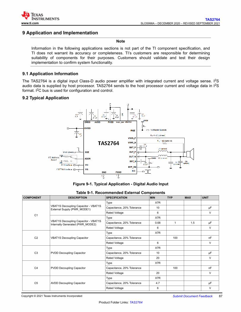
9 Application and ImplementationNote
Information in the following applications sections is not part of the TI component specification, and TI does not warrant its accuracy or completeness. TI’s customers are responsible for determining suitability of components for their purposes. Customers should validate and test their design implementation to confirm system functionality.
9.1 Application InformationThe TAS2764 is a digital input Class-D audio power amplifier with integrated current and voltage sense. I2S audio data is supplied by host processor. TAS2764 sends to the host processor current and voltage data in I2S format. I2C bus is used for configuration and control.
9.2 Typical Application
Figure 9-1. Typical Application - Digital Audio Input
Table 9-1. Recommended External ComponentsCOMPONENT DESCRIPTION SPECIFICATION MIN TYP MAX UNIT
C1
VBAT1S Decoupling Capacitor - VBAT1S External Supply (PWR_MODE1)
Type X7R
Capacitance, 20% Tolerance 10 µF
Rated Voltage 6 V
VBAT1S Decoupling Capacitor - VBAT1S Internally Generated (PWR_MODE2)
Type X7R
Capacitance, 20% Tolerance 0.68 1 1.5 µF
Rated Voltage 6 V
C2 VBAT1S Decoupling Capacitor
Type X7R
Capacitance, 20% Tolerance 100 nF
Rated Voltage 6 V
C3 PVDD Decoupling Capacitor
Type X7R
Capacitance, 20% Tolerance 10 µF
Rated Voltage 20 V
C4 PVDD Decoupling Capacitor
Type X7R
Capacitance, 20% Tolerance 100 nF
Rated Voltage 20 V
C5 AVDD Decoupling Capacitor
Type X7R
Capacitance, 20% Tolerance 4.7 µF
Rated Voltage 6 V
www.ti.comTAS2764
SLOS998A – DECEMBER 2020 – REVISED SEPTEMBER 2021
Copyright © 2021 Texas Instruments Incorporated Submit Document Feedback 87
Product Folder Links: TAS2764
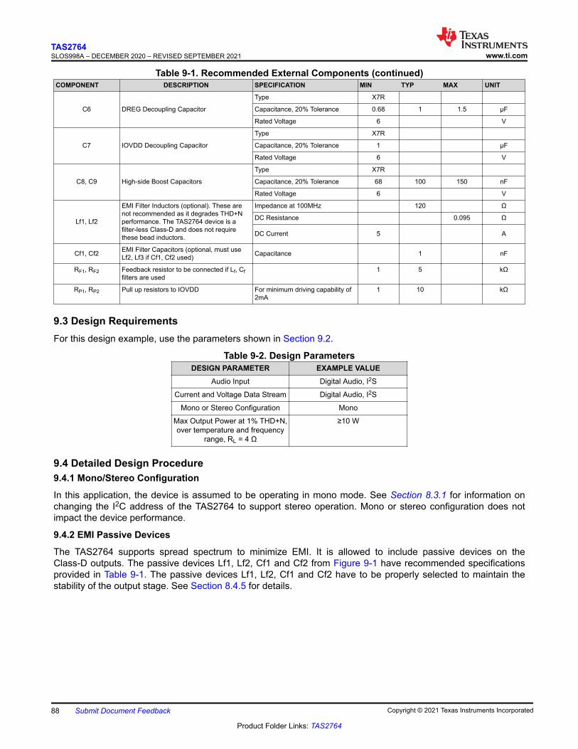
Table 9-1. Recommended External Components (continued)COMPONENT DESCRIPTION SPECIFICATION MIN TYP MAX UNIT
C6 DREG Decoupling Capacitor
Type X7R
Capacitance, 20% Tolerance 0.68 1 1.5 µF
Rated Voltage 6 V
C7 IOVDD Decoupling Capacitor
Type X7R
Capacitance, 20% Tolerance 1 µF
Rated Voltage 6 V
C8, C9 High-side Boost Capacitors
Type X7R
Capacitance, 20% Tolerance 68 100 150 nF
Rated Voltage 6 V
Lf1, Lf2
EMI Filter Inductors (optional). These are not recommended as it degrades THD+N performance. The TAS2764 device is a filter-less Class-D and does not require these bead inductors.
Impedance at 100MHz 120 Ω
DC Resistance 0.095 Ω
DC Current 5 A
Cf1, Cf2 EMI Filter Capacitors (optional, must use Lf2, Lf3 if Cf1, Cf2 used) Capacitance 1 nF
RF1, RF2 Feedback resistor to be connected if Lf, Cf filters are used
1 5 kΩ
RP1, RP2 Pull up resistors to IOVDD For minimum driving capability of 2mA
1 10 kΩ
9.3 Design RequirementsFor this design example, use the parameters shown in Section 9.2.
Table 9-2. Design ParametersDESIGN PARAMETER EXAMPLE VALUE
Audio Input Digital Audio, I2S
Current and Voltage Data Stream Digital Audio, I2S
Mono or Stereo Configuration Mono
Max Output Power at 1% THD+N, over temperature and frequency
range, RL = 4 Ω
≥10 W
9.4 Detailed Design Procedure9.4.1 Mono/Stereo Configuration
In this application, the device is assumed to be operating in mono mode. See Section 8.3.1 for information on changing the I2C address of the TAS2764 to support stereo operation. Mono or stereo configuration does not impact the device performance.
9.4.2 EMI Passive Devices
The TAS2764 supports spread spectrum to minimize EMI. It is allowed to include passive devices on the Class-D outputs. The passive devices Lf1, Lf2, Cf1 and Cf2 from Figure 9-1 have recommended specifications provided in Table 9-1. The passive devices Lf1, Lf2, Cf1 and Cf2 have to be properly selected to maintain the stability of the output stage. See Section 8.4.5 for details.
TAS2764SLOS998A – DECEMBER 2020 – REVISED SEPTEMBER 2021 www.ti.com
88 Submit Document Feedback Copyright © 2021 Texas Instruments Incorporated
Product Folder Links: TAS2764
9.5 Application Curves
POUT (W)
TH
D+
N (
dB
)
0.001 0.01 0.1 1 10 25-90
-80
-70
-60
-50
-40
-30
-20
-10
0VBAT = 2.95 V, PVDD = 6.5 VVBAT = 4.2 V, PVDD = 8.4 VVBAT = 3.8 V, PVDD = 12 VVBAT = 3.8 V, PVDD = 16 V
PWR_MODE2 RL=4Ω
f=1kHz
Figure 9-2. THDN vs Pout
Frequency (Hz)
TH
D+
N (
dB
)
-100
-95
-90
-85
-80
-75
-70
-65
20 100 1000 10K 20K
VBAT = 2.95 V, PVDD = 6.5 VVBAT = 4.2 V, PVDD = 8.4 VVBAT = 3.8 V, PVDD = 12 VVBAT = 3.8 V, PVDD = 16 V
PWR_MODE2 RL=4Ω
f=1kHz
Figure 9-3. THDN vs Frequency
www.ti.comTAS2764
SLOS998A – DECEMBER 2020 – REVISED SEPTEMBER 2021
Copyright © 2021 Texas Instruments Incorporated Submit Document Feedback 89
Product Folder Links: TAS2764
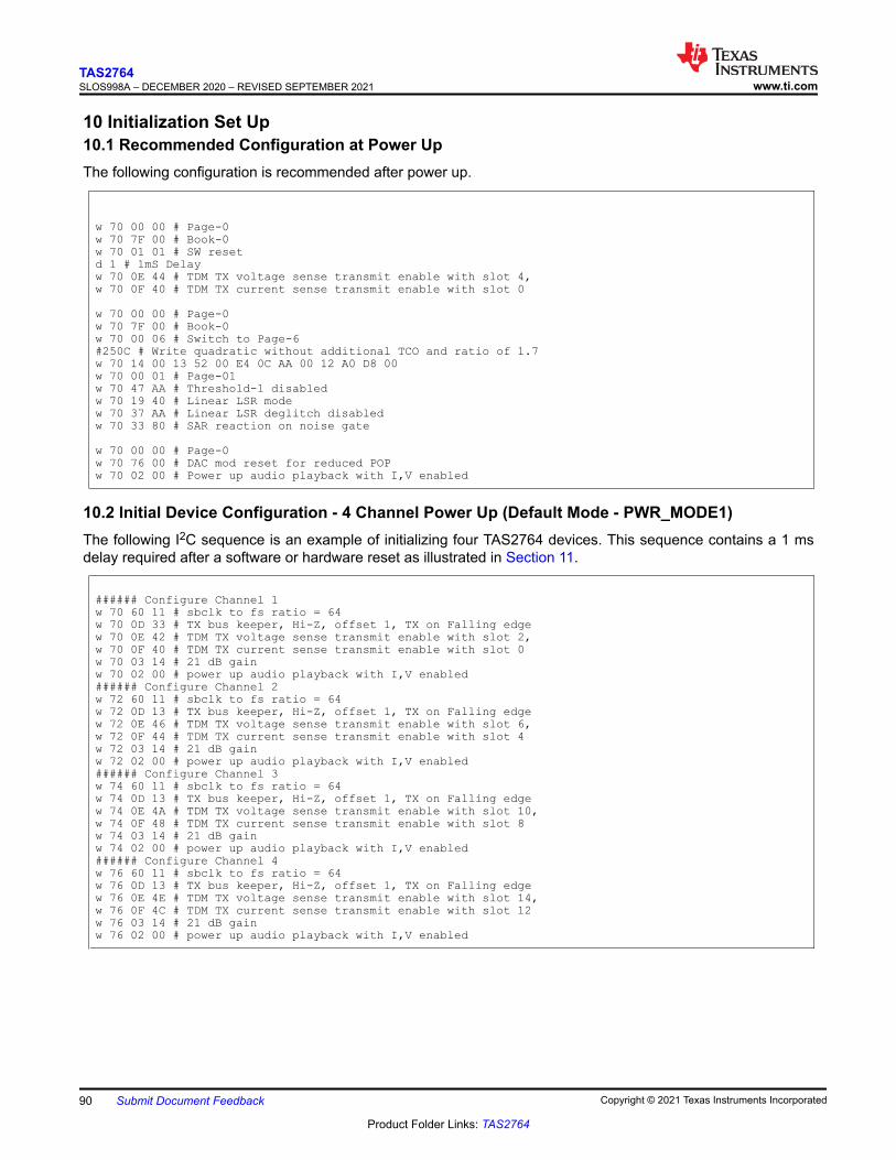
10 Initialization Set Up10.1 Recommended Configuration at Power UpThe following configuration is recommended after power up.
w 70 00 00 # Page-0w 70 7F 00 # Book-0w 70 01 01 # SW resetd 1 # 1mS Delayw 70 0E 44 # TDM TX voltage sense transmit enable with slot 4,w 70 0F 40 # TDM TX current sense transmit enable with slot 0
w 70 00 00 # Page-0w 70 7F 00 # Book-0w 70 00 06 # Switch to Page-6#250C # Write quadratic without additional TCO and ratio of 1.7w 70 14 00 13 52 00 E4 0C AA 00 12 A0 D8 00 w 70 00 01 # Page-01w 70 47 AA # Threshold-1 disabledw 70 19 40 # Linear LSR modew 70 37 AA # Linear LSR deglitch disabledw 70 33 80 # SAR reaction on noise gate
w 70 00 00 # Page-0w 70 76 00 # DAC mod reset for reduced POP w 70 02 00 # Power up audio playback with I,V enabled
10.2 Initial Device Configuration - 4 Channel Power Up (Default Mode - PWR_MODE1)The following I2C sequence is an example of initializing four TAS2764 devices. This sequence contains a 1 ms delay required after a software or hardware reset as illustrated in Section 11.
###### Configure Channel 1w 70 60 11 # sbclk to fs ratio = 64w 70 0D 33 # TX bus keeper, Hi-Z, offset 1, TX on Falling edgew 70 0E 42 # TDM TX voltage sense transmit enable with slot 2,w 70 0F 40 # TDM TX current sense transmit enable with slot 0w 70 03 14 # 21 dB gainw 70 02 00 # power up audio playback with I,V enabled###### Configure Channel 2w 72 60 11 # sbclk to fs ratio = 64w 72 0D 13 # TX bus keeper, Hi-Z, offset 1, TX on Falling edgew 72 0E 46 # TDM TX voltage sense transmit enable with slot 6,w 72 0F 44 # TDM TX current sense transmit enable with slot 4w 72 03 14 # 21 dB gainw 72 02 00 # power up audio playback with I,V enabled###### Configure Channel 3w 74 60 11 # sbclk to fs ratio = 64w 74 0D 13 # TX bus keeper, Hi-Z, offset 1, TX on Falling edgew 74 0E 4A # TDM TX voltage sense transmit enable with slot 10,w 74 0F 48 # TDM TX current sense transmit enable with slot 8w 74 03 14 # 21 dB gainw 74 02 00 # power up audio playback with I,V enabled###### Configure Channel 4w 76 60 11 # sbclk to fs ratio = 64w 76 0D 13 # TX bus keeper, Hi-Z, offset 1, TX on Falling edgew 76 0E 4E # TDM TX voltage sense transmit enable with slot 14,w 76 0F 4C # TDM TX current sense transmit enable with slot 12w 76 03 14 # 21 dB gainw 76 02 00 # power up audio playback with I,V enabled
TAS2764SLOS998A – DECEMBER 2020 – REVISED SEPTEMBER 2021 www.ti.com
90 Submit Document Feedback Copyright © 2021 Texas Instruments Incorporated
Product Folder Links: TAS2764
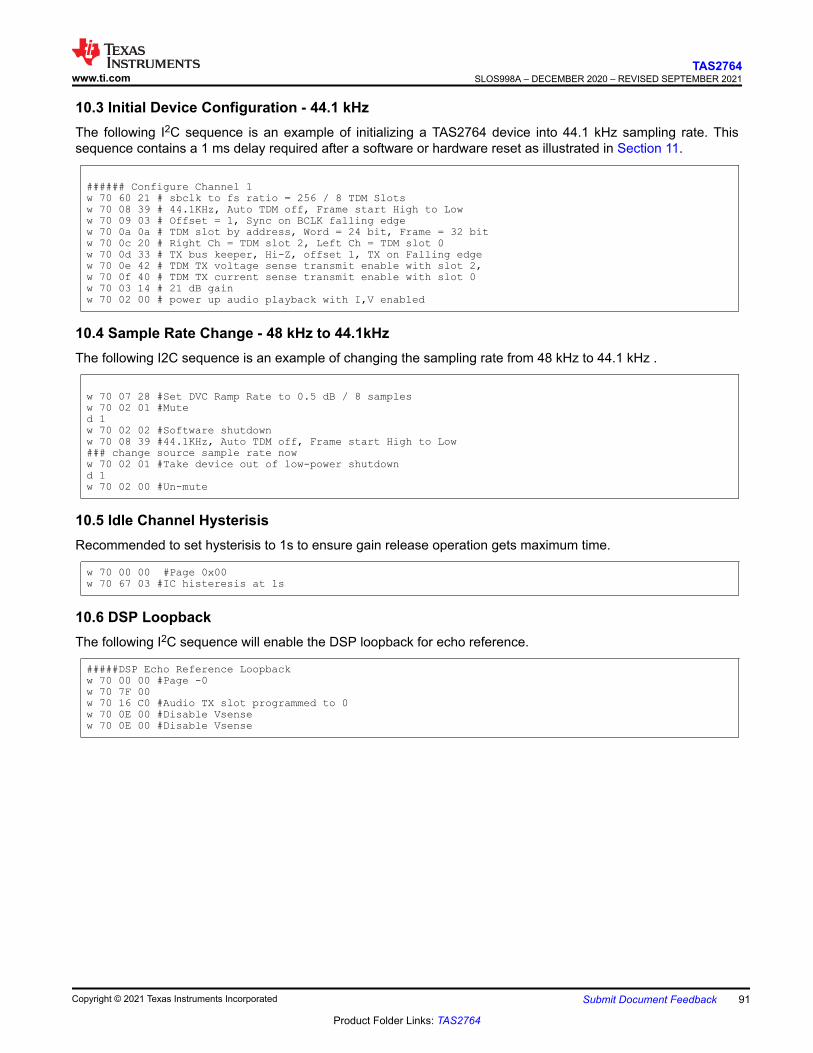
10.3 Initial Device Configuration - 44.1 kHzThe following I2C sequence is an example of initializing a TAS2764 device into 44.1 kHz sampling rate. This sequence contains a 1 ms delay required after a software or hardware reset as illustrated in Section 11.
###### Configure Channel 1w 70 60 21 # sbclk to fs ratio = 256 / 8 TDM Slotsw 70 08 39 # 44.1KHz, Auto TDM off, Frame start High to Loww 70 09 03 # Offset = 1, Sync on BCLK falling edgew 70 0a 0a # TDM slot by address, Word = 24 bit, Frame = 32 bitw 70 0c 20 # Right Ch = TDM slot 2, Left Ch = TDM slot 0w 70 0d 33 # TX bus keeper, Hi-Z, offset 1, TX on Falling edgew 70 0e 42 # TDM TX voltage sense transmit enable with slot 2,w 70 0f 40 # TDM TX current sense transmit enable with slot 0w 70 03 14 # 21 dB gainw 70 02 00 # power up audio playback with I,V enabled
10.4 Sample Rate Change - 48 kHz to 44.1kHzThe following I2C sequence is an example of changing the sampling rate from 48 kHz to 44.1 kHz .
w 70 07 28 #Set DVC Ramp Rate to 0.5 dB / 8 samplesw 70 02 01 #Muted 1w 70 02 02 #Software shutdownw 70 08 39 #44.1KHz, Auto TDM off, Frame start High to Low### change source sample rate noww 70 02 01 #Take device out of low-power shutdownd 1w 70 02 00 #Un-mute
10.5 Idle Channel HysterisisRecommended to set hysterisis to 1s to ensure gain release operation gets maximum time.
w 70 00 00 #Page 0x00w 70 67 03 #IC histeresis at 1s
10.6 DSP LoopbackThe following I2C sequence will enable the DSP loopback for echo reference.
#####DSP Echo Reference Loopbackw 70 00 00 #Page -0w 70 7F 00 w 70 16 C0 #Audio TX slot programmed to 0w 70 0E 00 #Disable Vsensew 70 0E 00 #Disable Vsense
www.ti.comTAS2764
SLOS998A – DECEMBER 2020 – REVISED SEPTEMBER 2021
Copyright © 2021 Texas Instruments Incorporated Submit Document Feedback 91
Product Folder Links: TAS2764
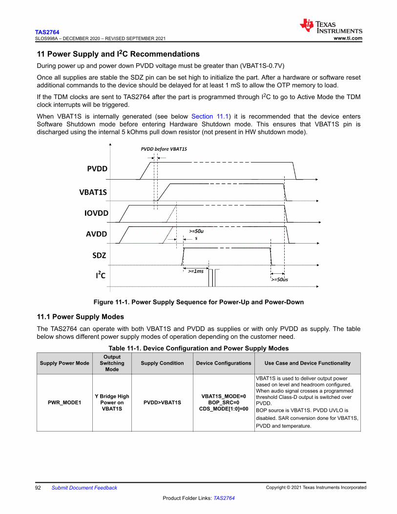
11 Power Supply and I2C RecommendationsDuring power up and power down PVDD voltage must be greater than (VBAT1S-0.7V)
Once all supplies are stable the SDZ pin can be set high to initialize the part. After a hardware or software reset additional commands to the device should be delayed for at least 1 mS to allow the OTP memory to load.
If the TDM clocks are sent to TAS2764 after the part is programmed through I2C to go to Active Mode the TDM clock interrupts will be triggered.
When VBAT1S is internally generated (see below Section 11.1) it is recommended that the device enters Software Shutdown mode before entering Hardware Shutdown mode. This ensures that VBAT1S pin is discharged using the internal 5 kOhms pull down resistor (not present in HW shutdown mode).
Figure 11-1. Power Supply Sequence for Power-Up and Power-Down
11.1 Power Supply ModesThe TAS2764 can operate with both VBAT1S and PVDD as supplies or with only PVDD as supply. The table below shows different power supply modes of operation depending on the customer need.
Table 11-1. Device Configuration and Power Supply Modes
Supply Power ModeOutput
Switching Mode
Supply Condition Device Configurations Use Case and Device Functionality
PWR_MODE1Y Bridge High
Power on VBAT1S
PVDD>VBAT1SVBAT1S_MODE=0
BOP_SRC=0 CDS_MODE[1:0]=00
VBAT1S is used to deliver output power based on level and headroom configured. When audio signal crosses a programmed threshold Class-D output is switched over PVDD.BOP source is VBAT1S. PVDD UVLO is disabled. SAR conversion done for VBAT1S, PVDD and temperature.
TAS2764SLOS998A – DECEMBER 2020 – REVISED SEPTEMBER 2021 www.ti.com
92 Submit Document Feedback Copyright © 2021 Texas Instruments Incorporated
Product Folder Links: TAS2764
Table 11-1. Device Configuration and Power Supply Modes (continued)
Supply Power ModeOutput
Switching Mode
Supply Condition Device Configurations Use Case and Device Functionality
PWR_MODE2Y Bridge Low
Power on VBAT1S
PVDD>VBAT1S+2.5VVBAT1S_MODE=1
BOP_SRC=1 CDS_MODE[1:0]=11
PVDD is the only supply. VBAT1S is delivered by an internal LDO and used to supply at signals close to idle channel levels. When audio signal levels crosses -100dBFS (default), Class_D output switches to PVDD.BOP source is PVDD. PVDD UVLO is enabled. SAR conversion done for PVDD and temperature.
PWR_MODE3Y Bridge High
Power on VBAT1S
PVDD>VBAT1SVBAT1S_MODE=0
BOP_SRC=1 CDS_MODE[1:0]=00
VBAT1S is used to deliver output power based on level and headroom configured. When audio signal crosses a programmed threshold Class-D output is switched over PVDD.BOP source is PVDD. PVDD UVLO is enabled. SAR conversion done for PVDD and temperature.
PWR_MODE4 PVDD PVDD>VBAT1S+2.5VVBAT1S_MODE=1
BOP_SRC=1 CDS_MODE[1:0]=10
Class-D power supplied by PVDD branch of Y bridge. VBAT1S is delivered by an internal LDO.BOP source is PVDD. PVDD UVLO is enabled. SAR conversion done for PVDD and temperature.
For PWR_MODE2 and PWR_MODE4, by default, the internal ADC samples only the PVDD pin in order to meet the stringent requirement on brownout latency. If the monitoring of VBAT1S pin is needed the register bit CONV_VBAT_PVDD_MODE should be set to high. The additional monitoring of VBAT1S will come at the cost of losing brownout latency.
If VBAT1S is generated by internal LDO, customer needs to ensure that PVDD supply level is at least 2.5V above the VBAT1S voltage generated internally. To enable voltage protection the UVLO of PVDD supply should be set above 7.3V by using register bits PVDD_UVLO[5:0]. This will ensure that, with an internally generated VBAT1S of 4.8V, PVDD supply is at least 2.5V higher than VBAT1S.
www.ti.comTAS2764
SLOS998A – DECEMBER 2020 – REVISED SEPTEMBER 2021
Copyright © 2021 Texas Instruments Incorporated Submit Document Feedback 93
Product Folder Links: TAS2764
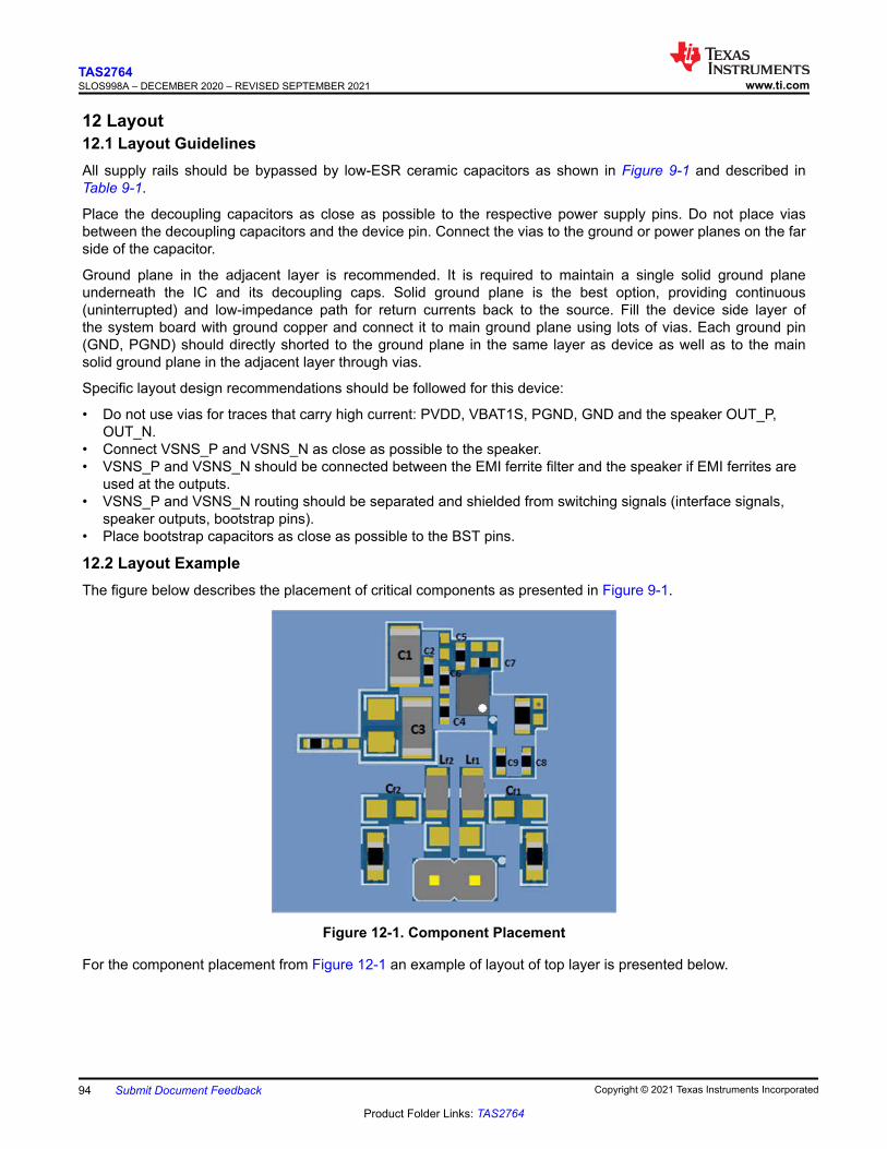
12 Layout12.1 Layout GuidelinesAll supply rails should be bypassed by low-ESR ceramic capacitors as shown in Figure 9-1 and described in Table 9-1.
Place the decoupling capacitors as close as possible to the respective power supply pins. Do not place vias between the decoupling capacitors and the device pin. Connect the vias to the ground or power planes on the far side of the capacitor.
Ground plane in the adjacent layer is recommended. It is required to maintain a single solid ground plane underneath the IC and its decoupling caps. Solid ground plane is the best option, providing continuous (uninterrupted) and low-impedance path for return currents back to the source. Fill the device side layer of the system board with ground copper and connect it to main ground plane using lots of vias. Each ground pin (GND, PGND) should directly shorted to the ground plane in the same layer as device as well as to the main solid ground plane in the adjacent layer through vias.
Specific layout design recommendations should be followed for this device:
• Do not use vias for traces that carry high current: PVDD, VBAT1S, PGND, GND and the speaker OUT_P, OUT_N.
• Connect VSNS_P and VSNS_N as close as possible to the speaker.• VSNS_P and VSNS_N should be connected between the EMI ferrite filter and the speaker if EMI ferrites are
used at the outputs.• VSNS_P and VSNS_N routing should be separated and shielded from switching signals (interface signals,
speaker outputs, bootstrap pins).• Place bootstrap capacitors as close as possible to the BST pins.
12.2 Layout ExampleThe figure below describes the placement of critical components as presented in Figure 9-1.
Figure 12-1. Component Placement
For the component placement from Figure 12-1 an example of layout of top layer is presented below.
TAS2764SLOS998A – DECEMBER 2020 – REVISED SEPTEMBER 2021 www.ti.com
94 Submit Document Feedback Copyright © 2021 Texas Instruments Incorporated
Product Folder Links: TAS2764
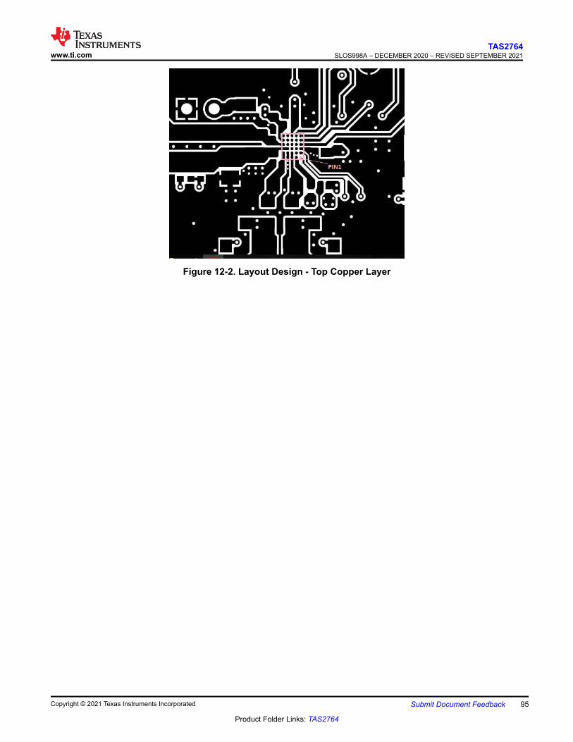
Figure 12-2. Layout Design - Top Copper Layer
www.ti.comTAS2764
SLOS998A – DECEMBER 2020 – REVISED SEPTEMBER 2021
Copyright © 2021 Texas Instruments Incorporated Submit Document Feedback 95
Product Folder Links: TAS2764
13 Device and Documentation Support13.1 Receiving Notification of Documentation UpdatesTo receive notification of documentation updates, navigate to the device product folder on ti.com. Click on Subscribe to updates to register and receive a weekly digest of any product information that has changed. For change details, review the revision history included in any revised document.
13.2 Support ResourcesTI E2E™ support forums are an engineer's go-to source for fast, verified answers and design help — straight from the experts. Search existing answers or ask your own question to get the quick design help you need.
Linked content is provided "AS IS" by the respective contributors. They do not constitute TI specifications and do not necessarily reflect TI's views; see TI's Terms of Use.
13.3 TrademarksTI E2E™ is a trademark of Texas Instruments.All trademarks are the property of their respective owners.13.4 Electrostatic Discharge Caution
This integrated circuit can be damaged by ESD. Texas Instruments recommends that all integrated circuits be handled with appropriate precautions. Failure to observe proper handling and installation procedures can cause damage.ESD damage can range from subtle performance degradation to complete device failure. Precision integrated circuits may be more susceptible to damage because very small parametric changes could cause the device not to meet its published specifications.
13.5 GlossaryTI Glossary This glossary lists and explains terms, acronyms, and definitions.
TAS2764SLOS998A – DECEMBER 2020 – REVISED SEPTEMBER 2021 www.ti.com
96 Submit Document Feedback Copyright © 2021 Texas Instruments Incorporated
Product Folder Links: TAS2764
14 Mechanical, Packaging, and Orderable InformationThe following pages include mechanical, packaging, and orderable information. This information is the most current data available for the designated devices. This data is subject to change without notice and revision of this document. For browser-based versions of this data sheet, refer to the left-hand navigation.
www.ti.comTAS2764
SLOS998A – DECEMBER 2020 – REVISED SEPTEMBER 2021
Copyright © 2021 Texas Instruments Incorporated Submit Document Feedback 97
Product Folder Links: TAS2764
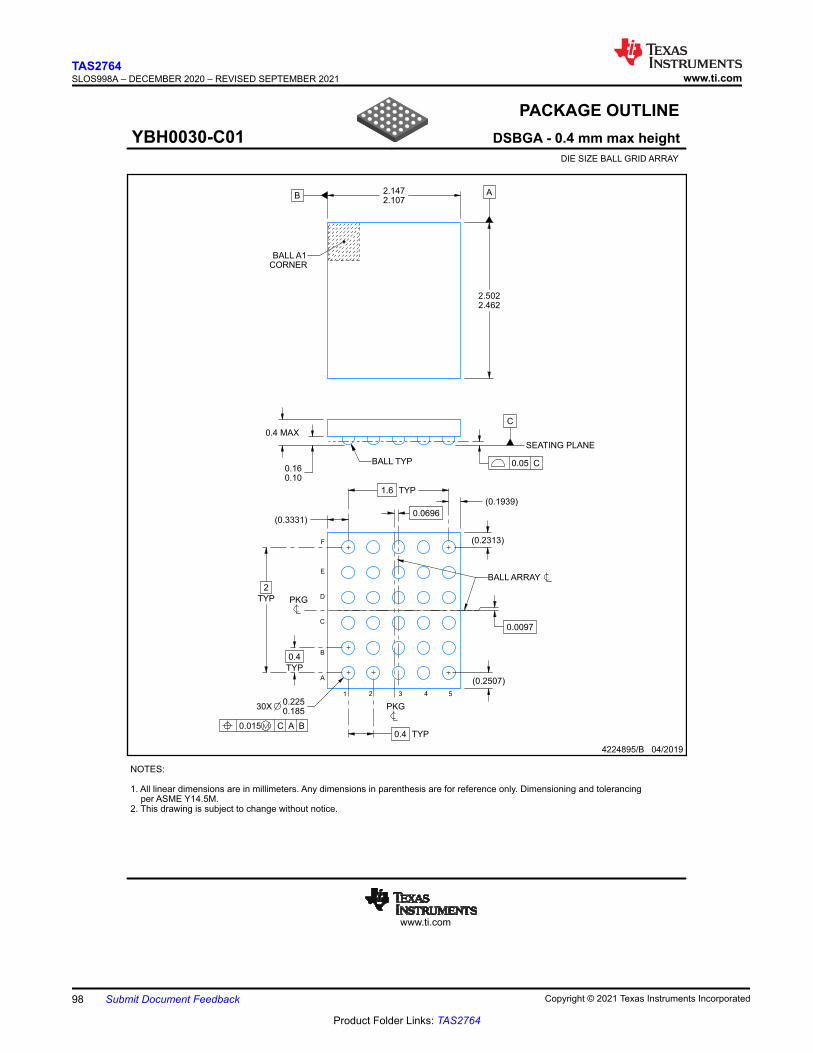
www.ti.com
PACKAGE OUTLINE
C
0.4 MAX
0.160.10
2
TYP
1.6 TYP
0.4
TYP
0.4 TYP
30X0.2250.185
0.0097
0.0696
B2.1472.107
A
2.5022.462
(0.3331)
(0.1939)
(0.2313)
(0.2507)
4224895/B 04/2019
DSBGA - 0.4 mm max heightYBH0030-C01DIE SIZE BALL GRID ARRAY
BALL ARRAY
NOTES:
1. All linear dimensions are in millimeters. Any dimensions in parenthesis are for reference only. Dimensioning and tolerancingper ASME Y14.5M.
2. This drawing is subject to change without notice.
BALL A1CORNER
SEATING PLANE
BALL TYP 0.05 C
A
1 2 3
0.015 C A B
4 5
PKG
PKG
B
C
D
E
F
SCALE 7.000
TAS2764SLOS998A – DECEMBER 2020 – REVISED SEPTEMBER 2021 www.ti.com
98 Submit Document Feedback Copyright © 2021 Texas Instruments Incorporated
Product Folder Links: TAS2764
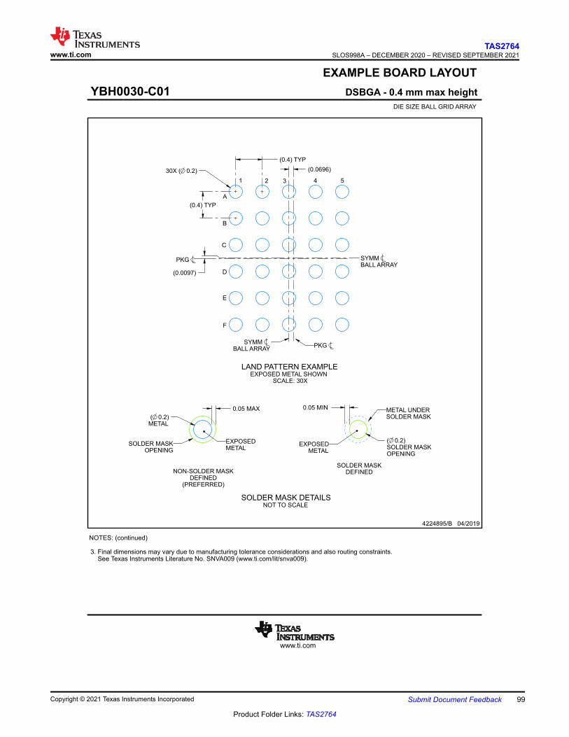
www.ti.com
EXAMPLE BOARD LAYOUT
0.05 MIN0.05 MAX
30X ( 0.2)
(0.4) TYP
(0.4) TYP
( 0.2)SOLDER MASKOPENING
( 0.2)METAL
(0.0097)
(0.0696)
4224895/B 04/2019
DSBGA - 0.4 mm max heightYBH0030-C01DIE SIZE BALL GRID ARRAY
NOTES: (continued)
3. Final dimensions may vary due to manufacturing tolerance considerations and also routing constraints.See Texas Instruments Literature No. SNVA009 (www.ti.com/lit/snva009).
BALL ARRAYSYMM
NOT TO SCALESOLDER MASK DETAILS
SYMMBALL ARRAY
PKG
PKG
C
1 2 3 4 5
A
B
D
E
F
EXPOSED METAL SHOWNLAND PATTERN EXAMPLE
SCALE: 30X
NON-SOLDER MASKDEFINED
(PREFERRED)
EXPOSEDMETAL
SOLDER MASKOPENING
SOLDER MASKDEFINED
METAL UNDERSOLDER MASK
EXPOSEDMETAL
www.ti.comTAS2764
SLOS998A – DECEMBER 2020 – REVISED SEPTEMBER 2021
Copyright © 2021 Texas Instruments Incorporated Submit Document Feedback 99
Product Folder Links: TAS2764
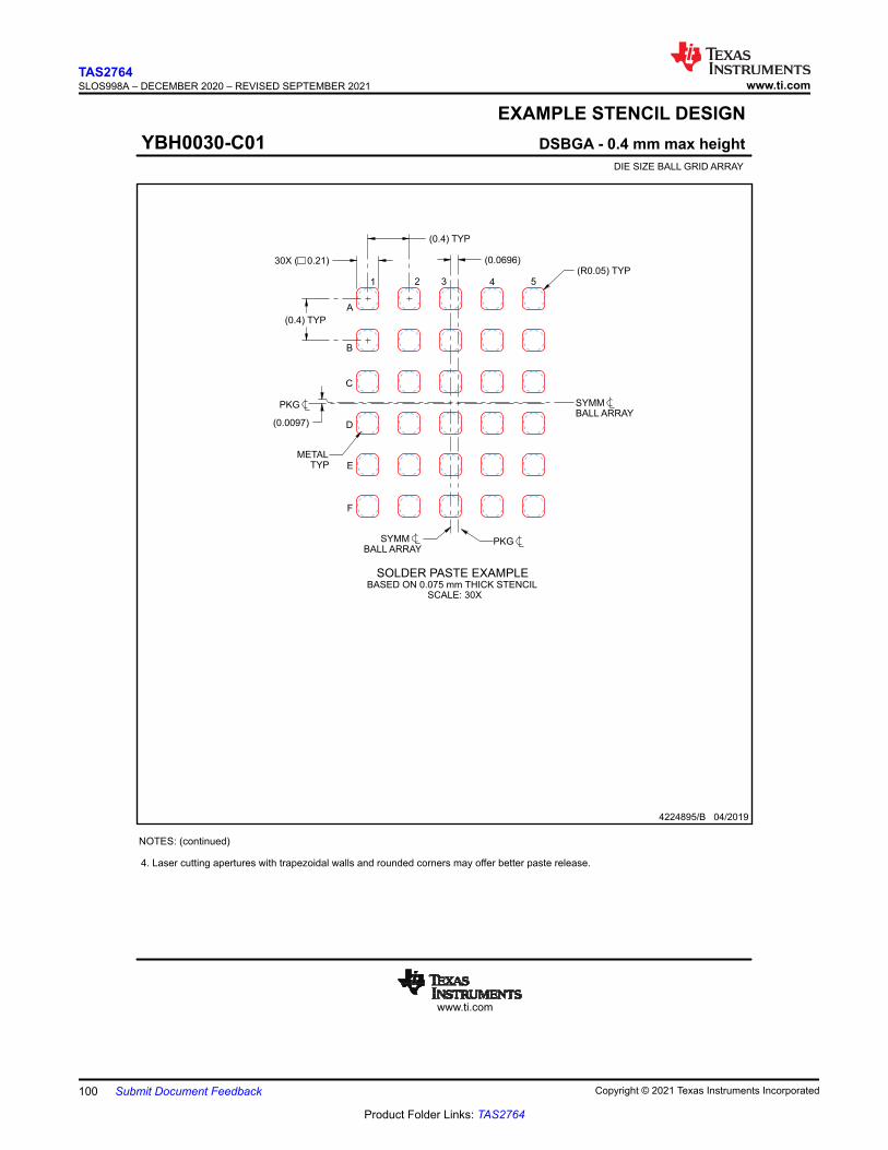
www.ti.com
EXAMPLE STENCIL DESIGN
(0.4) TYP
(0.4) TYP
30X ( 0.21)(R0.05) TYP
(0.0097)
(0.0696)
4224895/B 04/2019
DSBGA - 0.4 mm max heightYBH0030-C01DIE SIZE BALL GRID ARRAY
NOTES: (continued)
4. Laser cutting apertures with trapezoidal walls and rounded corners may offer better paste release.
BALL ARRAYSYMM PKG
PKG SYMMBALL ARRAY
BASED ON 0.075 mm THICK STENCILSOLDER PASTE EXAMPLE
SCALE: 30X
METALTYP
C
1 2 3 4 5
A
B
D
E
F
TAS2764SLOS998A – DECEMBER 2020 – REVISED SEPTEMBER 2021 www.ti.com
100 Submit Document Feedback Copyright © 2021 Texas Instruments Incorporated
Product Folder Links: TAS2764
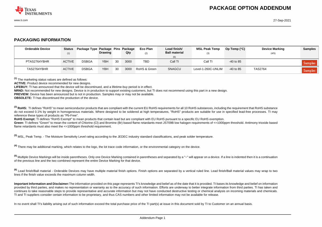
PACKAGE OPTION ADDENDUM
www.ti.com 27-Sep-2021
Addendum-Page 1
PACKAGING INFORMATION
Orderable Device Status(1)
Package Type PackageDrawing
Pins PackageQty
Eco Plan(2)
Lead finish/Ball material
(6)
MSL Peak Temp(3)
Op Temp (°C) Device Marking(4/5)
Samples
PTAS2764YBHR ACTIVE DSBGA YBH 30 3000 TBD Call TI Call TI -40 to 85
TAS2764YBHR ACTIVE DSBGA YBH 30 3000 RoHS & Green SNAGCU Level-1-260C-UNLIM -40 to 85 TAS2764
(1) The marketing status values are defined as follows:ACTIVE: Product device recommended for new designs.LIFEBUY: TI has announced that the device will be discontinued, and a lifetime-buy period is in effect.NRND: Not recommended for new designs. Device is in production to support existing customers, but TI does not recommend using this part in a new design.PREVIEW: Device has been announced but is not in production. Samples may or may not be available.OBSOLETE: TI has discontinued the production of the device.
(2) RoHS: TI defines "RoHS" to mean semiconductor products that are compliant with the current EU RoHS requirements for all 10 RoHS substances, including the requirement that RoHS substancedo not exceed 0.1% by weight in homogeneous materials. Where designed to be soldered at high temperatures, "RoHS" products are suitable for use in specified lead-free processes. TI mayreference these types of products as "Pb-Free".RoHS Exempt: TI defines "RoHS Exempt" to mean products that contain lead but are compliant with EU RoHS pursuant to a specific EU RoHS exemption.Green: TI defines "Green" to mean the content of Chlorine (Cl) and Bromine (Br) based flame retardants meet JS709B low halogen requirements of <=1000ppm threshold. Antimony trioxide basedflame retardants must also meet the <=1000ppm threshold requirement.
(3) MSL, Peak Temp. - The Moisture Sensitivity Level rating according to the JEDEC industry standard classifications, and peak solder temperature.
(4) There may be additional marking, which relates to the logo, the lot trace code information, or the environmental category on the device.
(5) Multiple Device Markings will be inside parentheses. Only one Device Marking contained in parentheses and separated by a "~" will appear on a device. If a line is indented then it is a continuationof the previous line and the two combined represent the entire Device Marking for that device.
(6) Lead finish/Ball material - Orderable Devices may have multiple material finish options. Finish options are separated by a vertical ruled line. Lead finish/Ball material values may wrap to twolines if the finish value exceeds the maximum column width.
Important Information and Disclaimer:The information provided on this page represents TI's knowledge and belief as of the date that it is provided. TI bases its knowledge and belief on informationprovided by third parties, and makes no representation or warranty as to the accuracy of such information. Efforts are underway to better integrate information from third parties. TI has taken andcontinues to take reasonable steps to provide representative and accurate information but may not have conducted destructive testing or chemical analysis on incoming materials and chemicals.TI and TI suppliers consider certain information to be proprietary, and thus CAS numbers and other limited information may not be available for release.
In no event shall TI's liability arising out of such information exceed the total purchase price of the TI part(s) at issue in this document sold by TI to Customer on an annual basis.
PACKAGE OPTION ADDENDUM
www.ti.com 27-Sep-2021
Addendum-Page 2
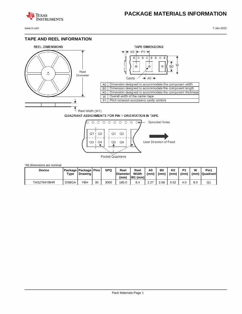
TAPE AND REEL INFORMATION
*All dimensions are nominal
Device PackageType
PackageDrawing
Pins SPQ ReelDiameter
(mm)
ReelWidth
W1 (mm)
A0(mm)
B0(mm)
K0(mm)
P1(mm)
W(mm)
Pin1Quadrant
TAS2764YBHR DSBGA YBH 30 3000 180.0 8.4 2.27 2.68 0.52 4.0 8.0 Q1
PACKAGE MATERIALS INFORMATION
www.ti.com 7-Jan-2022
Pack Materials-Page 1
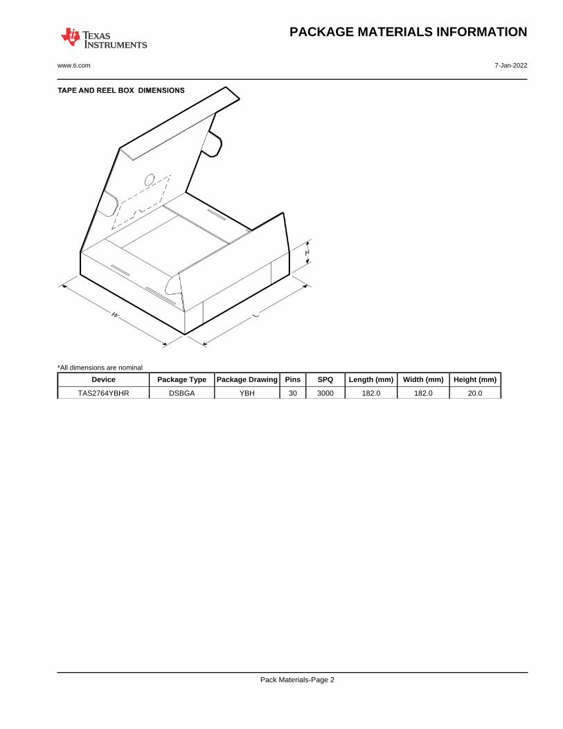
*All dimensions are nominal
Device Package Type Package Drawing Pins SPQ Length (mm) Width (mm) Height (mm)
TAS2764YBHR DSBGA YBH 30 3000 182.0 182.0 20.0
PACKAGE MATERIALS INFORMATION
www.ti.com 7-Jan-2022
Pack Materials-Page 2
IMPORTANT NOTICE AND DISCLAIMERTI PROVIDES TECHNICAL AND RELIABILITY DATA (INCLUDING DATA SHEETS), DESIGN RESOURCES (INCLUDING REFERENCE DESIGNS), APPLICATION OR OTHER DESIGN ADVICE, WEB TOOLS, SAFETY INFORMATION, AND OTHER RESOURCES “AS IS” AND WITH ALL FAULTS, AND DISCLAIMS ALL WARRANTIES, EXPRESS AND IMPLIED, INCLUDING WITHOUT LIMITATION ANY IMPLIED WARRANTIES OF MERCHANTABILITY, FITNESS FOR A PARTICULAR PURPOSE OR NON-INFRINGEMENT OF THIRD PARTY INTELLECTUAL PROPERTY RIGHTS.These resources are intended for skilled developers designing with TI products. You are solely responsible for (1) selecting the appropriate TI products for your application, (2) designing, validating and testing your application, and (3) ensuring your application meets applicable standards, and any other safety, security, regulatory or other requirements.These resources are subject to change without notice. TI grants you permission to use these resources only for development of an application that uses the TI products described in the resource. Other reproduction and display of these resources is prohibited. No license is granted to any other TI intellectual property right or to any third party intellectual property right. TI disclaims responsibility for, and you will fully indemnify TI and its representatives against, any claims, damages, costs, losses, and liabilities arising out of your use of these resources.TI’s products are provided subject to TI’s Terms of Sale or other applicable terms available either on ti.com or provided in conjunction with such TI products. TI’s provision of these resources does not expand or otherwise alter TI’s applicable warranties or warranty disclaimers for TI products.TI objects to and rejects any additional or different terms you may have proposed. IMPORTANT NOTICE
Mailing Address: Texas Instruments, Post Office Box 655303, Dallas, Texas 75265Copyright © 2022, Texas Instruments Incorporated