Synthetic Testing of High Voltage Direct Current Circuit Breakers
323
Synthetic Testing of High Voltage Direct Current Circuit Breakers A thesis submitted to The University of Manchester for the degree of Doctor of Philosophy In the Faculty of Engineering and Physical Sciences 2016 Oliver Nicholas Cwikowski School of Electrical Engineering
-
Upload
khangminh22 -
Category
Documents
-
view
2 -
download
0
Transcript of Synthetic Testing of High Voltage Direct Current Circuit Breakers

Synthetic Testing of High Voltage Direct Current
Circuit Breakers
A thesis submitted to The University of Manchester for the degree of
Doctor of Philosophy
In the Faculty of Engineering and Physical Sciences
2016
Oliver Nicholas Cwikowski
School of Electrical Engineering

2
Table of Contents
Table of Contents ......................................................................................................................... 2
List of Figures .............................................................................................................................. 7
List of Tables .............................................................................................................................. 14
List of Acronyms ........................................................................................................................ 15
List of Main Symbols ................................................................................................................. 16
Acknowledgements ................................................................................................................... 21
Declaration .................................................................................................................................. 20
Copyright Statement .................................................................................................................. 21
Abstract ....................................................................................................................................... 20
Chapter 1: Introduction ........................................................................................................ 24
1.1 Preface ........................................................................................................................ 24
1.2 Electricity Demand and Renewable Energy Sources ................................................... 25
1.3 HVDC Transmission ..................................................................................................... 32
1.3.1 Demand and Market ........................................................................................... 32
1.3.2 Current Source Converters ................................................................................. 34
1.3.3 Voltage Source Converters ................................................................................. 35
1.4 VSC HVDC Protection .................................................................................................. 38
1.4.1 Diversion and AC Side Isolation Protection......................................................... 39
1.4.2 Fault Tolerant Converters ................................................................................... 41
1.4.3 DC Side Isolation ................................................................................................. 42
1.4.4 Mixed Protection Systems .................................................................................. 44
1.5 HVDC Grids with DCCBs .............................................................................................. 45
1.6 Synthetics Testing ....................................................................................................... 52
1.7 DC Grid Modelling ....................................................................................................... 53
1.7.1 Two Level Converters .......................................................................................... 53
1.7.2 Modular Multi-level Converters .......................................................................... 53
1.7.3 DC Cable .............................................................................................................. 54
1.8 Superconductors ......................................................................................................... 54
1.9 Aims and Objectives .................................................................................................... 54
1.10 Main Thesis Contributions .......................................................................................... 55
1.11 Publications ................................................................................................................. 56
1.12 Thesis Structure .......................................................................................................... 58
Chapter 2: Literature Review ............................................................................................... 60
2.1 Introduction ................................................................................................................ 60
2.2 DC Circuit Breakers – Existing ..................................................................................... 60
2.2.1 Passive Resonance DC Circuit Breaker ................................................................ 62

3
2.2.2 IGBT Resonant Circuit Breaker ............................................................................ 63
2.2.3 Active Resonant Circuit Breaker ......................................................................... 64
2.2.4 Pulse Generating Circuit Breaker ........................................................................ 65
2.2.5 Solid State Circuit Breakers ................................................................................. 66
2.2.6 Z‒Source DC Circuit Breaker – Type 1 ................................................................. 67
2.2.7 Z–Source Circuit Breaker – Type 2 ...................................................................... 68
2.2.8 Hybrid DC Circuit Breaker ................................................................................... 69
2.2.9 Hybrid Circuit Breaker with turn off Snubber ..................................................... 70
2.2.10 Hybrid Circuit Breaker with Forced Commutation ............................................. 71
2.2.11 Proactive Hybrid DC Circuit Breaker ................................................................... 72
2.2.12 Capacitive Hybrid Circuit breaker ....................................................................... 73
2.2.13 Hybrid Circuit Breaker with Inductive Commutation Booster ............................ 74
2.2.14 Superconducting Circuit Breaker ........................................................................ 75
2.2.15 C-EPRI Circuit Breaker ......................................................................................... 76
2.3 DC Circuit Breakers – Novel ........................................................................................ 77
2.3.1 Double Hybrid Circuit Breaker (DHCB) ................................................................ 77
2.3.2 Super-Hybrid Circuit Breaker (SHCB) .................................................................. 78
2.3.3 Super-Hybrid Circuit Breaker with Snubber (SHCB-S) ......................................... 79
2.4 Summary of Advantages and Disadvantages .............................................................. 81
2.5 Suitability for Various Applications ............................................................................. 83
2.6 Relevant Standards ..................................................................................................... 85
2.6.1 IEC: 61992-2 ........................................................................................................ 85
2.6.2 IEC: 62271 ........................................................................................................... 85
2.6.3 IEC: 62501 ........................................................................................................... 85
2.6.4 IEC: 60700 ........................................................................................................... 86
2.7 Circuit Breaker Definitions .......................................................................................... 86
2.7.1 Protection Operation .......................................................................................... 87
2.7.2 Protection Operation Philosophy........................................................................ 89
2.7.3 Breaking Time definitions ................................................................................ 90
2.8 Summary ..................................................................................................................... 92
Chapter 3: Converter Fault Analysis and Fault Current Envelopes ................................ 93
3.1 Introduction ................................................................................................................ 93
3.2 Fault Current Envelopes .............................................................................................. 95
3.1.1 Current Rating of DC Circuit breakers ................................................................. 95
3.1.2 The Concept of Fault Current Envelopes ............................................................ 97
3.3 Two-Level Converter Fault Analysis ............................................................................ 99
3.1.3 Pole-to-Pole faults ............................................................................................... 99

4
3.1.4 Pole-to-Ground Faults ....................................................................................... 103
3.1.5 Non-Terminal Faults .......................................................................................... 103
3.4 Fault Current Envelopes for Two Level Converters .................................................. 106
3.5 Envelope Example and Verification .......................................................................... 109
3.1.6 Example System ................................................................................................ 109
3.1.7 Terminal Fault Current Estimation .................................................................... 109
3.1.8 Fault Current Envelope Example ....................................................................... 110
3.6 MMC Fault Current Prediction .................................................................................. 112
3.7 Modular Multi-level Converter Fault Analysis .......................................................... 113
3.1.9 Pole-to-pole Fault.............................................................................................. 113
3.8 Fault Current Envelopes for Modular Multi-Level Converters ................................. 118
3.1.10 Example System and MMC Modeling ............................................................... 119
3.1.11 Results ............................................................................................................... 120
3.9 Protection Time Estimates ........................................................................................ 124
3.10 Fault Current Envelopes in Grids .............................................................................. 124
3.11 Conclusions ............................................................................................................... 124
Chapter 4: Circuit Breaker Analysis .................................................................................. 127
4.1 Introduction .............................................................................................................. 127
4.2 Operation of the Proactive Hybrid Circuit Breaker (PHCB) ....................................... 128
4.3 Analysis of the PHCB ................................................................................................. 130
4.3.1 Description of Key Components ....................................................................... 130
4.3.2 LCS Design ......................................................................................................... 135
4.3.3 RCD LCS ............................................................................................................. 136
4.3.4 Varistor LCS ....................................................................................................... 139
4.4 Analysis and Simulation Comparison ........................................................................ 145
4.4.1 Converter Modelling ......................................................................................... 145
4.4.2 DC Circuit Breaker ............................................................................................. 146
4.4.3 Simulation Results – RCD-LCS ........................................................................... 148
4.4.4 Simulation Results – Varistor-LCS ..................................................................... 150
4.5 Operation of the Super Hybrid Circuit Breaker (SHCB) ............................................. 155
4.6 Analysis of the Super Hybrid Circuit Breaker (SHCB) ................................................ 157
4.6.1 State Space Analysis .......................................................................................... 157
4.6.2 Analysis Verification .......................................................................................... 160
4.7 Travelling Wave Impacts and Grid Inductance ......................................................... 161
4.7.1 PHCB .................................................................................................................. 161
4.7.2 SHCB .................................................................................................................. 165
4.8 Recommendations for Future Fault Studies ............................................................. 165

5
4.9 Conclusions ............................................................................................................... 166
Chapter 5: Circuit Breaker Prototyping ............................................................................ 168
5.1 Introduction .............................................................................................................. 168
5.2 Test Circuit ................................................................................................................ 169
5.2.1 Power Electronic Switches ................................................................................ 170
5.2.2 Mechanical Switch ............................................................................................ 171
5.2.3 Cryostat and Superconducting Coil ................................................................... 172
5.3 Proactive Hybrid Circuit Breaker (PHCB) ................................................................... 174
5.3.1 Discussion .......................................................................................................... 176
5.4 Super Hybrid Circuit Breaker (SHCB) ......................................................................... 177
5.4.1 Comparison to Analysis ..................................................................................... 179
5.4.2 Discussion .......................................................................................................... 181
5.5 Conclusions ............................................................................................................... 182
Chapter 6: Test Circuit Design & Construction ............................................................... 184
6.1 Introduction .............................................................................................................. 184
6.2 Example system ........................................................................................................ 185
6.3 Test Circuit ................................................................................................................ 186
6.3.1 Topology ............................................................................................................ 186
6.4 Test Circuit Parameter Design .................................................................................. 188
6.5 IGBT Stack Design ...................................................................................................... 191
6.5.1 Specification ...................................................................................................... 191
6.5.2 IGBT Module Design .......................................................................................... 192
6.5.3 IGBT Stack ......................................................................................................... 193
6.5.4 Gate Drive Design .............................................................................................. 194
6.5.5 Controller to Module Prototyping .................................................................... 196
6.6 Test Circuit Construction ........................................................................................... 199
6.6.1 Test Circuit Inductance ..................................................................................... 199
6.6.2 Test-Bed ............................................................................................................ 200
6.7 Full System ................................................................................................................ 203
6.8 Conclusion ................................................................................................................. 203
Chapter 7: High Voltage Testing ....................................................................................... 204
7.1 Introduction .............................................................................................................. 204
7.2 Initial High Voltage Testing ....................................................................................... 205
7.3 Full System Test Setup .............................................................................................. 209
7.4 Test Results ............................................................................................................... 210
7.4.1 Transformer Testing .......................................................................................... 210
7.4.2 High Current Impulse Testing............................................................................ 212

6
7.4.3 Current Breaking Testing .................................................................................. 215
7.5 Key Learning Outcomes ............................................................................................ 218
7.5.1 Isolation Switch ................................................................................................. 218
7.5.2 Voltage Supply .................................................................................................. 219
7.5.3 Contact Resistance ............................................................................................ 220
7.5.4 Test Circuit Current/Energy Rating ................................................................... 220
7.5.5 Inductor Design ................................................................................................. 221
7.5.6 Powering Auxiliary Equipment from Test Circuit .............................................. 224
7.5.7 Test Circuit Design ............................................................................................. 225
7.6 Modified Test Circuit Design ..................................................................................... 227
7.6.1 Test Circuit Equations ....................................................................................... 228
7.6.2 Test Circuit Comparison .................................................................................... 229
7.7 Conclusions ............................................................................................................... 231
Chapter 8: Conclusions and Further Work ....................................................................... 233
8.1 Conclusions ............................................................................................................... 233
8.1.1 HVDC Circuit Breakers and Standards (Chapter 2) ........................................... 234
8.1.2 Converter Fault Analysis and Fault Current Envelopes (Chapter 3) .................. 234
8.1.3 Circuit Breaker Analysis (Chapter 4) ................................................................. 235
8.1.4 Low Voltage Prototyping (Chapter 5) ............................................................... 235
8.1.5 Test Circuit Design ............................................................................................. 236
8.1.6 Test Results ....................................................................................................... 236
8.2 Future Work .............................................................................................................. 236
8.2.1 Standards and Test Methods ............................................................................ 236
8.2.2 Converter Fault Analysis and Fault Current Envelopes ..................................... 238
8.2.3 Circuit Breaker Analysis and Thermal Modelling .............................................. 238
References ............................................................................................................................ 240
Appendix 1: Circuit Breaker Analysis Derivations ......................................................... 245
1.A PHCB - RCD LCS - Peak LCS Voltage Derivation ......................................................... 245
1.B PHCB - RCD LCS – Commutation Time Derivation .................................................... 247
1.C PHCB - Varistor LCS – Commutation Time Derivation .............................................. 249
1.D PHCB - Varistor LCS – Circuit Breaker Voltage Derivation ........................................ 251
1.E SHCB – Commutation Current .................................................................................. 253
Appendix 2: Low Power Testing Parameters .................................................................. 255
Appendix 3: Test Circuit Design Costing ........................................................................ 257
3.A Test Circuit Inductor Design ...................................................................................... 262
3.B Isolated Power Supply Magnetics Design ................................................................. 263
3.C Test Circuit Simulations ............................................................................................. 265

7
3.C.1 IGBT Stack Turn off ............................................................................................ 265
3.C.2 Power Losses ..................................................................................................... 267
3.C.3 Thermal Modelling ............................................................................................ 270
Appendix 4: Modified Test Circuit Derivations ............................................................... 275
4.A First Test Circuit Capacitance Derivation .................................................................. 275
4.B Second Test Circuit Capacitance Derivation ............................................................. 275
Appendix 5: Publications .................................................................................................. 276
Word Count: 55,226 (60,6236 including front sections).
List of Figures
Figure 1 – Sea bed leased zones in the UK for offshore [5]. ...................................................... 26
Figure 2 – Radial interconnections under the accelerated growth scenario [9]. ......................... 27
Figure 3 ‒ Integrated connection required for UK's accelerated growth offshore wind farm
scenario [9]. ................................................................................................................................. 28
Figure 4 ‒ Comparison of HVAC and HVDC transmission [7]. Series and Shunt Compensation
(SSC) is required periodically along HVAC lines, this causes a step increase in the cost of a
HVAC transmission line. ............................................................................................................. 31
Figure 5 ‒ Single phase layout of a three phase CSC. ............................................................... 32
Figure 6 ‒ Two level converter arrangement [18]. Single phase of converter is shown for
convenience. ............................................................................................................................... 34
Figure 7 ‒ Layout of a single phase MMC. ................................................................................. 35
Figure 8 ‒ MMC protected through a philosophy of diversion and AC side isolation. ................ 37
Figure 9 ‒ MMC protected through the fault suppressing architecture. ...................................... 39
Figure 10 ‒ MMC converter protected with DCCBs. ................................................................... 41
Figure 11 ‒ MMC protected using several different technologies............................................... 42
Figure 12 ‒ Two separately connected wind farms. ................................................................... 44
Figure 13 – Converters connected into a grid. ............................................................................ 44
Figure 14 ‒ DC grid using DC circuit breakers. .......................................................................... 45
Figure 15 ‒ HVDC grid protected with a combination of DC and AC circuit breakers. ............... 46
Figure 16 ‒ Offshore tie-line configuration. ................................................................................. 47
Figure 17 ‒ Onshore tie line configuration. ................................................................................. 47

8
Figure 18 ‒ Overview of MMC Control structure......................................................................... 50
Figure 19 ‒ DC circuit breaker categories. ................................................................................. 58
Figure 20 – General structure of hybrid circuit breakers. ............................................................ 58
Figure 21 ‒ Passive resonant DC circuit breaker [43]. ............................................................... 59
Figure 22 ‒ The IGBT resonant circuit breaker........................................................................... 60
Figure 23 – Active resonant circuit breaker [44]. ........................................................................ 61
Figure 24 – Layout of bi-directional pulse generating circuit breaker [24]. ................................. 62
Figure 25 – Solid-state circuit breaker [46]. ................................................................................ 63
Figure 26 ‒ The Z-source circuit breaker – Type 1 [47]. ............................................................. 64
Figure 27 ‒ Current flow path during a DC side fault [47]. .......................................................... 64
Figure 28 ‒ Z‒Source circuit breaker topology – Type 2 [48]. .................................................... 65
Figure 29 ‒ The hybrid circuit breaker [46]. ................................................................................ 66
Figure 30 ‒ Hybrid circuit breaker with an RCD snubber. .......................................................... 67
Figure 31 ‒ Hybrid circuit breaker with forced commutation [46]................................................ 68
Figure 32 ‒ Proactive hybrid circuit breaker, proprietary of ABB [50]. ........................................ 69
Figure 33 ‒ Alstom's capacitive hybrid circuit breaker, modified from [51, 52]. .......................... 70
Figure 34 ‒ Hybrid circuit breaker with inductive commutation booster [53]. ............................. 71
Figure 35 – Superconducting DC circuit breaker [54]. ................................................................ 72
Figure 36 ‒ 200 kV DC circuit breaker developed by C-EPRI [32]. ............................................ 73
Figure 37 ‒ Layout of C-EPRI breaker. ....................................................................................... 73
Figure 38 – The double hybrid circuit breaker. ........................................................................... 74
Figure 39 – Superconducting hybrid circuit breaker.[P1] ............................................................ 75
Figure 40 – Superconducting hybrid circuit breaker with voltage control. .................................. 76
Figure 41 – Modified SHCB-S where the secondary branch can be broken into three modules
(M=3)[P1]. ................................................................................................................................... 77
Figure 42 – Circuit breaker voltages and superconductor voltages during stepped turn off. ..... 77
Figure 43 ‒ Layout of hybrid HVDC circuit breaker within DC transmission line. ....................... 84
Figure 44 ‒ State flow diagram for a hybrid circuit breaker. ....................................................... 85
Figure 45 ‒ Series protection philosophy. ................................................................................... 86
Figure 46 ‒ Comparison of series and parallel protection philosophies. .................................... 87

9
Figure 47 ‒ Time ratings for DC circuit breakers. ....................................................................... 88
Figure 47 ‒ Example fault current and potential ratings. ............................................................ 93
Figure 48 ‒ Concept of how a fault current envelope may be used. .......................................... 94
Figure 49 ‒ Application of test area, when comparing to test circuit's current............................ 95
Figure 50 ‒ Simplified TLC structure. ......................................................................................... 98
Figure 51 ‒ Simplified equivalent circuit for TLC. Terminal faults occur at location FT. Non-
terminal fault location shown as FNT............................................................................................ 99
Figure 52 ‒ Bewley lattice diagram also known as bounce diagram. Fault occurs at time t0 at
distance D from the converter. .................................................................................................. 101
Figure 53 ‒ Type 1 and Type 2 envelope structures. ............................................................... 104
Figure 54 ‒ Comparison of simplified model, PSCAD TDM model and Equation (3.1). .......... 106
Figure 55 – Type 1 and Type 2 envelopes compared to simulated fault currents for a range of
pole-to-pole faults. ..................................................................................................................... 108
Figure 56 ‒ Type 1 and Type 2 envelopes compared to simulated fault currents for a range of
pole-to-ground faults. ................................................................................................................ 108
Figure 57 ‒ Simplified diagram of a single phase leg of an MMC. ........................................... 111
Figure 58 ‒ Reduced equivalent circuit for the MMC. ............................................................... 113
Figure 59 ‒ Type 1 and three possible Type 2 envelopes for the MMC. .................................. 115
Figure 60 ‒ Overview of converter controls. ............................................................................. 116
Figure 61 ‒ Fault current envelope for example system and three different approximations of the
fault currents. ............................................................................................................................ 117
Figure 62 ‒ Converter energy discharge proportion against time delay relative to the AC grid.
Discharge proportion (𝑲𝒏) is obtained through simulation and are indicative for the example
system only and not for all converters. ..................................................................................... 118
Figure 63 ‒ Comparison of MMC pole-to-pole fault currents and fault current envelopes. ...... 120
Figure 64 ‒ Fault currents and fault current envelopes when blocking function is included. ... 120
Figure 65 ‒ Current flow in PHCB during initial rise of fault current. ........................................ 125
Figure 66 ‒ Commutation process in PHCB and opening of mechanical switch. ..................... 126

10
Figure 67 ‒ Opening of main breaker, followed by zero crossing in second mechanical switch,
and voltage and current waveforms. ......................................................................................... 126
Figure 68 – Structure of the PHCB. .......................................................................................... 127
Figure 69 – Varistor IV characteristic against device maximum voltage rating. ....................... 129
Figure 70 ‒ LCS configurations. (a) RCD snubber (b) RCD snubber and varistor. .................. 132
Figure 71 ‒ Commutation equivalent circuit for the proactive hybrid circuit breaker. ............... 133
Figure 72 ‒ Qualitative comparison of varistor and RCD LCS voltages. .................................. 137
Figure 73 ‒ Equivalent commutation circuit when a varistor is used in the LCS. ..................... 138
Figure 74 ‒ Equivalent circuit once the entire fault current is flowing in secondary branch.
Primary branch inductance can be ignored as the current in the primary branch is zero. ....... 140
Figure 75 ‒ Simulated point-to-point TLC system. ................................................................... 142
Figure 76 ‒ Layout of circuit breaker model. Two LCS topologies are shown. ........................ 144
Figure 77 – Comparison of LCS voltage simulations and equations for a commutation current of
1 kA. LCS voltage equations refers to Equation (4.32). ............................................................ 145
Figure 78 ‒ Comparison of calculation and simulation results. ................................................ 146
Figure 79 ‒ Comparison of the calculated commutation time and the PSCAD simulation results.
.................................................................................................................................................. 147
Figure 80 ‒ Comparison of simulated and calculated primary branch currents. ...................... 148
Figure 81 – Re-conduction in the primary branch. .................................................................... 149
Figure 82 ‒ Primary branch currents when traveling wave impacts are not compensated for. 151
Figure 83 ‒ Primary branch currents when traveling wave impacts are compensated for. ...... 151
Figure 84 ‒ Normal conduction path in SHCB. ......................................................................... 152
Figure 85 ‒ Commutation effect in SHCB. ................................................................................ 153
Figure 86 – Secondary branch turn off procedure. Capacitance CM1 can be added to the design
to use the superconductor as a part of a RLC snubber circuit. Left hand side circuit, right hand
side waveforms. ........................................................................................................................ 154
Figure 87 ‒ Equivalent commutation circuit for the SHCB. ....................................................... 155
Figure 88 ‒ Simulated and calculated primary branch currents for a range of superconductor
quench resistances. .................................................................................................................. 158

11
Figure 89 ‒ Peak LCS voltage plot against DC side inductance for a range of secondary branch
inductances. Commutation current = 3 kA. ............................................................................... 159
Figure 90 – Number of series devices against Series DC inductance (𝑳𝑫𝑪) for a commutation
current of 3 kA. .......................................................................................................................... 160
Figure 91 ‒ Commutation time against series inductance over a range of commutating currents.
Traveling wave impact included in calculation (dashed lines). Cable voltage assumed to be zero
(solid lines). ............................................................................................................................... 161
Figure 92 ‒ Layout of test circuit. Different commutation elements are placed in the circuit to
validate the different topologies. ............................................................................................... 166
Figure 93 ‒ Test circuit used for topology validation testing. .................................................... 167
Figure 94 – Prototype IGBT module used for low power testing. ............................................. 168
Figure 95 ‒ Vacuum switch and actuator. ................................................................................. 169
Figure 96 ‒ Superconducting coil used for HVDC circuit breaker testing. ................................ 170
Figure 97 ‒ Resistivity of sheath material. ................................................................................ 171
Figure 98 ‒ PHCB interruption test results. .............................................................................. 172
Figure 99 ‒ Experimental results validating operation of SHCB. .............................................. 175
Figure 100 ‒ Comparison of linear approximations to experimental results. Linear
approximations used to obtain estimations of system parameters. .......................................... 177
Figure 101 ‒ Comparison of experimental and calculated primary branch currents, with
percentage error plotted on right hand side. ............................................................................. 178
Figure 102 ‒ Specification envelope for example system and scaled two scaled versions at 1:3
and 1:5. ..................................................................................................................................... 183
Figure 103 ‒ Test circuit and test object. .................................................................................. 184
Figure 104 ‒ Comparison of specification envelope and design test circuit current for 1:3 scale
specification. ............................................................................................................................. 187
Figure 105 ‒ Comparison of specification envelope and design test circuit current for 1:5 scale
specification. ............................................................................................................................. 187
Figure 106 – IGBT module arrangement. ................................................................................. 189
Figure 107 – Prototype IGBT module. ...................................................................................... 189

12
Figure 108 – IGBT stack schematic diagram, showing electrical and control layout................ 190
Figure 109 – Gate drive circuit design used. ............................................................................ 191
Figure 110 ‒ Test results from 10 kHz testing of gate drive with IGBT switch load. ................ 192
Figure 111 ‒ Prototyping test layout of IGBT control and test circuit communication. ............. 193
Figure 112 – Dummy system. A miniature test circuit that allowed the controller software to be
validated prior to high voltage testing. ...................................................................................... 194
Figure 113 – Dummy system testing. Dangerous electronics are placed within the plastic
enclosure. .................................................................................................................................. 195
Figure 114 – Inductor layout. .................................................................................................... 195
Figure 115 ‒ Google sketch up design for test bed. ................................................................. 196
Figure 116 ‒ Low voltage/ High voltage separation shelves. A conduit allows for safe crossover
of high voltage and low voltage cables and protects the fiber optic cables. ............................. 197
Figure 117 – Diode stack with sharing elements on PCB. ........................................................ 197
Figure 118 ‒ Test bed under construction. ............................................................................... 198
Figure 119 – Partially constructed test-bed prior to transport. .................................................. 198
Figure 118 ‒ Schematic layout of the initial testing of the test circuit and IGBT module. ......... 202
Figure 119 ‒ Layout of current and voltage measurements. .................................................... 202
Figure 120 ‒ High voltage prototyping test circuit setup. .......................................................... 202
Figure 121 ‒ Detailed power electronic component layout - test circuit diodes (left), capacitance
(bottom), spark gap (top middle) and test object (right). ........................................................... 203
Figure 122 – Full initial test system. .......................................................................................... 203
Figure 123 ‒ Current performance result from the initial HV testing. Breaking ≈ 750 A. .......... 204
Figure 124 ‒ Schematic layout of the initial testing of the test circuit and IGBT module. ......... 205
Figure 125 ‒ Constructed test system – physical layout in HV laboratory. .............................. 206
Figure 126 ‒ Transformer test circuit layout. ............................................................................ 207
Figure 127 ‒ Transformer test results. Voltage withstand traces for each transformer numbered
0 to 7. ........................................................................................................................................ 207
Figure 128 ‒ Test circuit specification envelopes. Current scale of 1:3 and a lower scale of 1:5.
.................................................................................................................................................. 208

13
Figure 129 ‒ High current impulse testing results compared with simulation, hand calculation,
and fault current testing envelope (5:1). ................................................................................... 210
Figure 130 ‒ Breaking test result 1. First test where significant current was broken. Voltage
reaches 4.5 kV before break down occurs. ............................................................................... 212
Figure 131 ‒ Breaking test result 2. Due to damage caused to the inductor subsequent tests
could not maintain the same voltage levels as in the first test. ................................................. 213
Figure 132 ‒ Damage to electrode after one test circuit triggering. .......................................... 214
Figure 133 ‒ Fault current envelopes including maximum envelopes to prevent additional
energy dissipation in the test object. ......................................................................................... 217
Figure 134 ‒ Decay traces to be included in test result evaluation. Results show that breakdown
has occurred and circuit breaker has failed the test. ................................................................ 219
Figure 135 ‒ Envelope with initial pulse requirement added along with an example initial pulse
of current. .................................................................................................................................. 221
Figure 136 ‒ Test envelopes and test currents for a full power system. .................................. 223
Figure 137 ‒ Improved test circuit design. ................................................................................ 224
Figure 138 ‒ Comparison of original test circuit traces and modified test circuit traces. .......... 226
Figure 139 ‒ Commutation equivalent circuit for the proactive hybrid circuit breaker. ............. 240
Figure 140 ‒ Equivalent circuit diagram for commutation in a varistor based LCS. ................. 244
Figure 141 ‒ Equivalent circuit for PHCB when current is flowing in the secondary branch only.
.................................................................................................................................................. 246
Figure 142 – SHCB equivalent circuit for commutation. ........................................................... 248
Figure 143 ‒ Quench resistance calculation. Taken at point when current is not varying to obtain
resistive voltage drop. ............................................................................................................... 252
Figure 144 – Transformer winding cross section. ..................................................................... 259
Figure 145 ‒ Simulation of test circuit. ...................................................................................... 261
Figure 146 ‒ Turn off process of entire IGBT stack. ................................................................ 261
Figure 147 ‒ Shows the IGBT Voltage for a 1kA pulse. ........................................................... 262
Figure 148 ‒ Comparison of PSCAD turn off voltages and current and estimated turn off
voltages and currents. ............................................................................................................... 263
Figure 149 ‒ Comparison of simulated and estimated snubber currents. ................................ 263

14
Figure 150 ‒ Turn off voltage estimation in PSCAD. ................................................................ 263
Figure 151 ‒ Turn off current estimation produced during the simulation in PSCAD. .............. 264
Figure 152 ‒ Presented power losses and the compensated power losses. ........................... 265
Figure 153 ‒ Cauer (Top) and Foster (Bottom) thermal models used. ..................................... 266
Figure 154 ‒ Junction to case temperatures when using the Foster and Cauer models, when the
IGBT breakers a 1 kA pulse of Current (0.33 kA per IGBT). .................................................... 267
Figure 155 ‒ Thermal response when IGBT fails to turn off (1 kA peak per IGBT) 3 kA total. . 267
Figure 156 ‒ Thermal Response to 1 kA peak current (breaking). ........................................... 268
List of Tables
Table 1 – Summary of DC circuit breaker advantages and disadvantages. ............................... 78
Table 2 - Breaker application suitability summary. ..................................................................... 81
Table 3 ‒ Circuit breaker model parameters. ............................................................................ 144
Table 4 ‒ Peak LCS voltage for various commutation currents over three different fault
distances. Percentage overshoot relative to the 0 km condition is also shown. ....................... 146
Table 5 ‒ Parameters used in primary branch calculation. ....................................................... 177
Table 6 – Test circuit parameters (1:5). .................................................................................... 186
Table 7 ‒ Test circuit parameters (1:3). .................................................................................... 186
Table 8 – Test circuit parameters for initial testing. Initial testing was performed using fewer test
circuit capacitors and was not attempting to match either the 1:3 or 1:5 scaled envelope. ..... 201
Table 9 – Test circuit parameters. ............................................................................................ 205
Table 10 – Comparison of required capacitance and voltage ratings of such capacitance. .... 226
Table 11 – Table of candidate diodes. ...................................................................................... 253
Table 12 ‒ Diode comparison table assuming 50% rating factor of current. ............................ 254
Table 13 ‒ Test circuit component list and costing. .................................................................. 255
Table 14 ‒ IGBT module comparison table. ............................................................................. 256
Table 15 – Inductor design table ............................................................................................... 257
Table 16 – Magnetic material Data: N87 MnZn. ....................................................................... 258
Table 17 – Winding and core area calculations. ....................................................................... 259

15
Table 18 – Magnetics circuit and rectifier components. ............................................................ 259
Table 19 ‒ Foster and Cauer Model Thermal resistances and Capacitances. ......................... 266
List of Acronyms
Acronym Meaning
AAC Alternate Arm Converter
AC Alternating Current
ACCB Alternating Current Circuit Breaker
CB Circuit Breaker
CSC Current Source Converter
DC Direct Current
DCCB Direct Current Circuit Breaker
DEM Detailed Equivalent Model
DHCB Double Hybrid Circuit Breaker
DQ Direct Quadrature
DVTC Double Voltage Test Circuit
EMI Electro-Magnetic Interference
EPSRC Engineering and Physical Sciences Research Council
FACTS Flexible Alternating Current Transmission Systems
FB Full Bridge
FCE Fault Current Envelope
FDPM Frequency Dependant Phase Model
HVAC High Voltage Alternating Current
HVDC High Voltage Direct Current
IC Integrated Circuit
IGBT Insulated Gate Bi-polar Transistor
LCS Line Commutation Switch
LV Low Voltage

16
MMC Modular Multi-Level Converter
MOSFET Metal Oxide Field Effect Transistor
MTC Modified Test Circuit
MV Medium Voltage
NLC Nearest Level Control
OTC Original Test Circuit
PCB Printed Circuit Board
PCC Point of Common Coupling
PG Pulse Generator
PHCB Proactive Hybrid Circuit Breaker
PSCAD Power System Computer Aided Design
RCB Residual Current Breaker
RCD Resistor Capacitor Diode
RMS Root Mean Square
SHCB Superconducting Hybrid Circuit Breaker
TDM Traditional Detailed Model
TLC Two Level Converter
TRV Transient Recovery Voltage
TRL Technology Readiness Level
VSC Voltage Source Converter
XLPE Cross Linked Poly Ethylene
List of Main Symbols
Symbol Definition S.I Unit
𝑪𝟏 Snubber circuit capacitance F
𝑪𝑫𝑪 Capacitance between the DC terminals of a HVDC link F
𝑪𝑴𝟏 Capacitance across mechanical switch in a CB F
𝑪𝒔𝒎 Capacitance of a submodule within a converter F
𝑪𝑻𝟏 Test circuit capacitance F

17
𝑫 The distance between a fault and a converter m
𝑬𝑵𝑳𝒂𝒓𝒎 Exact number of levels in a single arm in a converter -
𝑬𝑽 Energy rating of a varistor J
𝑰𝟎 Initial current value flowing through an inductor A
𝑰𝑨𝑪 The fault current contribution from the AC network to a DC fault A
𝐼𝐴𝑣𝑔 Average fault current derivative for a terminal fault A/s
𝐈𝐛𝐢𝐚𝐬𝐞𝐝 Biased linear approximation of terminal fault current A
𝑰𝑪𝑨𝑷 Current that flows from the DC side capacitance of a converter A
𝐈𝐋𝐢𝐧 Linear approximation of terminal fault current A
𝑰𝑴𝑨𝑿 Maximum fault current A
𝑰𝑴𝟏 Current in primary branch mechanical switch A
𝐈𝐩𝐞𝐚𝐤 Peak of a given current waveform A
𝐈𝐑𝐌𝐒 Root mean square of current A
𝐈𝐬𝐚𝐭 Saturation current of an IGBT A
𝑰𝒔−𝒎𝒂𝒙 Maximum breaking capability of semiconductor switch A
𝐈𝐬𝐬 Steady state current A
𝑲𝒏 The ratio of energy converter arm energy to its normal energy content -
𝒌𝑻𝑾 Travelling wave constant bounded between 1 and 2 -
𝑳𝟐 Primary branch inductance H
𝑳𝟑 Secondary branch inductance H
𝑳𝑫𝑪 Inductance between the DC terminals of a HVDC Link and the cable H
𝑳𝑻 Equivalent inductance in commutation circuit H
𝑳𝑻𝟏 Test circuit inductance in series with circuit breaker H
𝑴𝟐 Second mechanical switch used to provide full isolation -
𝑵 Number of modules in a converter’s arm -
𝒏𝒔𝒆𝒓 Number of series devices in the secondary branch of a hybrid DC CB -
𝐑𝟐 Primary branch resistance Ω
𝑹𝟑 Secondary branch resistance Ω

18
𝑹𝒒 Quench resistance of a superconducting coil Ω
𝑹𝒗𝒂𝒓 Ratio of peak voltage to steady state voltage across switch -
𝑹𝑿 Receiver -
𝑺 The speed at which voltage and current waves propagate down a
cable
m/s
𝑺𝒇𝒗 Safety factor for voltage rating. -
𝑺𝑳 Lower IGBT module in an MMC’s submodule -
𝑺𝒖 Upper IGBT module in an MMC’s submodule -
Time at which maximum difference current occurs s
𝒕𝟎 Time at which fault occurs s
𝑻𝟏 First time segment in FCE s
𝑻𝑨 The time between the arrival of reverse travelling waves during a fault s
𝒕𝒄𝒍𝒓 Clearing time – defined in Chapter 2 s
𝒕𝒄𝒐𝒎 Commutation time – defined in Chapter 2 s
𝒕𝒇 The time at which the fault is seen by the converter s
𝒕𝒊𝒏𝒕 Interruption time of the circuit breaker – defined in Chapter 2 s
𝒕𝒍𝒊𝒎 Current limit operation time – defined in Chapter 2 s
𝐭𝐦𝐢𝐧 Time at which primary branch current reaches a minimum s
𝑻𝒑 Parallel thyristor in an MMC submodule -
𝑻𝒗𝒑 Varistor pulse time s
𝑻𝑿 Transmitter -
𝐕𝟎 Initial voltage across a capacitor V
𝑽𝟏− The first voltage waveform propagating in the negative direction V
𝑽𝟏+ The first forward travelling wave propagating in the positive direction V
𝑽𝒂 Converter’s AC terminal voltage V
𝑽𝒂𝒍 MMC lower arm voltage V
𝑽𝒂𝒓 Arrestor voltage V
𝑽𝒂𝒖 MMC upper arm voltage V

19
𝐕𝐂 Voltage across the DC link cables V
𝑽𝑪𝑩 Voltage cross the branches within a circuit breaker. V
𝑽𝑫𝑪 Voltage between the DC terminals of a HVDC converter V
𝑽𝒅𝒊𝒇𝒇 Difference voltage within converter V
𝑰𝑮𝑩𝑻 Peak voltage rating of a single semiconductor device V
𝑽𝒌 Knee voltage of the varistor V
𝑽𝑶𝑵 Onstate voltage of semiconductor device V
𝑽𝑹𝑪𝑫_𝑯𝑪 Voltage across an LCS with an RCD snubber with a high capacitance
value
V
𝑽𝑹𝑪𝑫_𝑳𝑪 Voltage across an LCS with an RCD snubber with a low capacitance
value
V
𝑽𝒓𝒆𝒇𝒂𝒓𝒎 Reference voltage for a converter arm V
𝑽𝒔𝒎 Voltage across a single submodule within an MMC V
𝑽𝑻 Difference between converter pole-to-pole voltage and cable voltage V
𝑽𝑻𝒓𝒂𝒏𝒔 Peak transient voltage across the circuit breaker V
𝐙𝟎 Characteristic impedance of the DC cable Ω
𝐙𝐜 Impedance of the converter Ω
𝚪𝐂 Converter reflection coefficient -
∆𝑽𝑰𝑮𝑩𝑻 Change in voltage during a circuit breakers operation V
∆𝑰 FCE bias term A
𝜟𝒕𝒄𝒐𝒎𝒔 Time available for communication systems s
𝜟𝒕𝑫𝒆𝒕𝒆𝒄𝒕 Time it takes to detect the presence of a fault s
𝜟𝒕𝑻𝒐𝒕𝒂𝒍 Total time available for DC protection s
𝜟𝒕𝒐𝒑𝒆𝒓𝒂𝒕𝒊𝒐𝒏 Operation time of a DCCB s
𝛕𝐕 Circuit breaker voltage rise time constant s
∅ Phase offset in sinusoidal approximation of fault current rad
𝛚 The natural frequency of a given electrical circuit rad/s
𝝎𝒄𝒐𝒎 Commutation frequency rad/s

20
Abstract
Name of University: The University of Manchester
Candidate’s name: Oliver Nicholas Cwikowski
Degree Title: Doctor of Philosophy
Thesis Title: Synthetic Testing of High Voltage Direct Current Circuit Breakers
Date: July 2016
The UK is facing two major challenges in the development of its electricity network. First, two thirds of the existing power stations are expected to close by 2030. Second, is the requirement to reduce its CO2 emissions by 80% by 2050. Both of these challenges are significant in their own right. The fact that they are occurring at the same time, generates a significant amount of threats to the existing power system, but also provides many new opportunities.
In order to meet both these challenges, significant amounts of offshore wind generation has been installed in the UK. For the wind generation with the longest connections to land, Voltage Source Converter (VSC) based High Voltage Direct Current (HVDC) transmission has to be used.
Due to the high power rating of the offshore wind farms, compared to the limited transmission capacity of the links, a large number of point-to-point connections are required. This has lead to the concept of HVDC grids being proposed, in order to reduce the amount of installed assets required.
HVDC grids are a new transmission environment and the fundamental question of how they will protect themselves must be answered. Several new technologies are under consideration to provide this protection, one of which is the HVDC circuit breaker.
As HVDC circuit breakers are a new technology, they must be tested in a laboratory environment to prove their operation and improve their Technology Readiness Level (TRL). This thesis is concerned with how such HVDC circuit breakers are operated, rated, and tested in a laboratory environment.
A review of the existing circuit breaker technologies is given, along with descriptions of several novel circuit breakers developed in this thesis. A standardized method of rating DC circuit breaker and their associated test circuit is developed.
Mathematical analysis of several circuit breakers is derived from first principles and low power prototypes are developed to validate these design concepts. A high power test circuit is then constructed and a semiconductor circuit breaker is tested. The key learning outcomes from this testing are provided.
Declaration
No portion of the work referred to in the thesis has been submitted in support of an application
for another degree or qualification of this or any other university, or other institute of learning.

21
Copyright Statement
The author of this thesis (including any appendices and/or schedules to this thesis) owns certain
copyright or related rights in it (the “Copyright”) and s/he has given The University of
Manchester certain rights to use such Copyright, including for administrative purposes.
Copies of this thesis, either in full or in extracts and whether in hard or electronic copy, may be
made only in accordance with the Copyright, Designs and Patents Act 1988 (as amended) and
regulations issued under it or, where appropriate, in accordance with licensing agreements
which the University has from time to time. This page must form part of any such copies made.
The ownership of certain Copyright, patents, designs, trade marks and other intellectual
property (the “Intellectual Property”) and any reproductions of copyright works in the thesis, for
example graphs and tables (“Reproductions”), which may be described in this thesis, may not
be owned by the author and may be owned by third parties. Such Intellectual Property and
Reproductions cannot and must not be made available for use without the prior written
permission of the owner(s) of the relevant Intellectual Property and/or Reproductions.
Further information on the conditions under which disclosure, publication and commercialisation
of this thesis, the Copyright and any Intellectual Property and/or Reproductions described in it
may take place is available in the University IP Policy
(seehttp://documents.manchester.ac.uk/DocuInfo.aspx?DocID=487), in any relevant Thesis
restriction declarations deposited in the University Library, The University Library’s regulations
(see http://www.manchester.ac.uk/library/aboutus/regulations) and in The University’s policy on
Presentation of Theses.
Acknowledgements
I am fortunate enough in this life to be blessed with a large and interesting family. Most notable
are my four parents. Each of them has always tried to do the right thing, in many different ways.
This has always given me the support I needed and plenty of experience to draw from. For this,
and many other things, I thank you all.

22
I also owe a great debt of gratitude to my supervisors, Prof Mike Barnes and Dr Roger
Shuttleworth, one I suspect I will never fully repay. Your support and willingness to challenge
me has given me more than I think most people would ever hope to get out of a PhD. I thank
you both.
To all those I have loved and lost, I am thankful for the time that we had together. Uncle Peter, I
find it hard to keep to your advice, I cannot always stop the tears when I think of you, but I smile
with the memories that remain.
To National Grid and EPSRC, Thank you for sponsoring this work and for giving me many
liberties in its development, with special thanks to Dr Paul Coventry. I hope that my work has
been useful, and that it may serve as a starting point for the next generation of research.
To all my friends, family, and colleagues who have been there to support me through the PhD,
especially to Bin and Vaheeshan, I say thank you.
Last, I would like to thank the University of Manchester in general. Deciding to study there was
the best decision of my life, and the 8 years I have spent here have made me, not only an
engineer, but a better person. Thank you all.
The past four years has changed who I am, and how I see the world for the better. One may
see the quote that marks the start of this work as dark, or negative, and I think I would have
taken it that way four years ago. Only when one realizes that in attempting the original, failure is
necessary, does the quote take on a different tone. Failure surrounds those who are expanding
their own capabilities, and the boundaries of the world. No words of my own can better
encapsulate the journey that has lead me to the PhD and through it, to the end.

23
“Failure marks the beginning of every attempt to create the original.”
Overheard in a coffee shop, shared with friends, modified, and finalized.

Chapter 1 Introduction
24
Chapter 1: Introduction
1.1 Preface
Designing the protection systems for High Voltage Direct Current (HVDC) grids will require a
broad and deep understanding of many areas of electrical engineering. Power system analysis,
power electronic design, device physics, communications, travelling wave theory, control,
thermal modelling, protection design, and high voltage engineering are some of the key areas
that will be required to fully develop a HVDC grid protection system.
A search for “HVDC VSC Protection” in IEEExplore shows that only six journal papers were
published before the end of 2012, with the first appearing in 1999. Between 2012 and 2016 this
number increased to twenty three. One of these journal papers have arisen from work carried
out during this PhD. The number of publications demonstrates how the academic and industrial
focus has changed over the course of the last four years and the amount of surrounding
knowledge in this area.
It will be up to the HVDC community to bring together the expertise from all these areas to fully
develop the knowledge, standards, and products, to produce an adequate protection system. It
is hoped this thesis will make a tangible contribution to this area and that the next generation of
researchers may find the work described here helpful, as they continue down this less travelled
road.

Chapter 1 Introduction
25
1.2 Electricity Demand and Renewable Energy Sources
According to the United Nations, the world’s population has now reached 7.3 billion, implying an
increase of 1 billion people since 2003 [1]. Estimates state that around 85% of the world’s
population has some form of regular access to electricity, and this percentage is increasing at
an annual rate of 0.7% [2].
As the world’s population expands, and the percentage of people who need regular access to
electricity increases, there will be an associated increase in the amount of electrical energy
generation and an increase in the size and spread of electrical power systems.
Additional to this fundamental increase in electrical generation, is a push for low-carbon
renewable energy due to the concerns surrounding the impact fossil fuels have on our
environment, which is changing the technologies used to provide electrical energy. Renewable
energy sources are becoming a significant part of our electrical grids. Renewable energy is
estimated to have supplied 19% of global final energy consumption in 2012, and has continued
to grow since then, even in the face of declining policy support around the world [3].
In the UK two thirds of fossil fuel power stations are expected to close by the end of 2030, due
to the equipment reaching the end of its intended life [4]. Coupled with this is a legal
requirement for the UK to reduce its CO2 emissions by 80% relative to 1990 levels by 2050,
presenting opportunities to replace decommissioned power stations with renewable energy
technologies [4].
Based on assessments of how the UK will meet this CO2 reduction and still maintain power
generation levels, wind farms are seen as the UK’s largest potential contributor [4, 5]. As of
June 2015, the UK has 4 GW of offshore wind generation installed, another 1.7 GW under
construction, and is on track to have 10 GWs installed by 2020 [6].
These wind farms, see Figure 1, are planned in three rounds of installation, with each round
moving further away from the shores of Great Britain [5]. As these transmission distances
increase, a decision must be made whether to use High Voltage Alternating Current (HVAC) or
High Voltage Direct Current (HVDC) transmission technologies, as the technological feasibility
and economics of traditional HVAC technology become less favourable [7, 8].

Chapter 1 Introduction
26
Figure 1 – Sea bed leased zones in the UK for offshore [5].
HVDC transmission has been a growing power system technology since the 1940s, with
standard HVDC technology being based around thyristors, and has seen significant
development in the past 20 years, allowing this technology to be applied in new parts of the
power system [7].

Chapter 1 Introduction
27
Figure 2 – Radial interconnections under the accelerated growth scenario [9].

Chapter 1 Introduction
28
Figure 3 ‒ Integrated connection required for UK's accelerated growth offshore wind farm scenario [9].
A recent technology development in HVDC transmission is the Voltage Source Converter
(VSC). VSCs offer a number of technical and economic advantages especially for offshore
applications, as will be discussed in more detail in Section 1.3. The connection lines in Figure 2
show the proposed number of VSC connections that would be required, if each wind farm was

Chapter 1 Introduction
29
connected using a point-to-point (also referred to as radial) connection to the onshore grid. To
date, nearly all VSC transmission systems are of this structure.
As will be explained in Section 1.5, such connections have a limited capacity due to grid
regulations, resulting in multiple connections being required for large single site wind farms.
Such a scenario would present a significant duplication of connections between offshore wind
farms and onshore grid.
In an attempt to reduce the amount of duplication, an integrated connection scenario has been
proposed, shown in Figure 3. This integrated scenario is made possible by the VSC technology,
which allows for a common DC voltage and the DC terminals of several converters to be
connected together, via a DC bus.
This integrated solution was proposed to reduce the amount of assets installed in the offshore
environment, and offers a significant capital cost and maintenance cost reduction [9].
The proposed integrated offshore connections represent the beginnings of an offshore HVDC
grid. With the inception of this new transmission environment, there is a need to revisit the
fundamental question of how such a transmission network would be protected against electrical
faults on the HVDC grid. Several options have been proposed; AC side protection, fault tolerant
converters, and HVDC circuit breakers.
This thesis is concerned with how such HVDC grids may be protected, with a specific focus on
the use, and the testing of HVDC circuit breakers.
First in this chapter, the HVDC transmission market and technology options are discussed. This
gives the reader an introduction to motivations for the migration from HVAC to HVDC, and a
summary view of the available technology options.
Second, the question of HVDC protection is raised in the context of VSC HVDC grids. This
gives a brief introduction to the available options along with their qualitative features and
benefits.
Next, an overview is given of how HVDC grids may be protected using circuit breakers, along
with several future first generation grid scenarios.

Chapter 1 Introduction
30
The concept of Synthetics testing is introduced, what it means, and why it is needed for the
progression of power system equipments’ Technologies Readiness Levels, giving the reader a
specific reason for the funding of this PhD work.
Aims, objectives, and deliverables of this thesis are then summarized. The main contributions
from the thesis are laid out in bullet point form. Lists of all publications that have been
developed during the time of this PhD are also given, followed by a summary of the layout of the
entire thesis.
1.3 HVDC Transmission
1.3.1 Demand and Market
HVDC transmission is typically only used when it is a more economical solution than HVAC
transmission, such as for high power long distance transmission, or to connect two AC grids
operating at different frequencies (known as back-to-back HVDC). As shown in Figure 4, HVAC
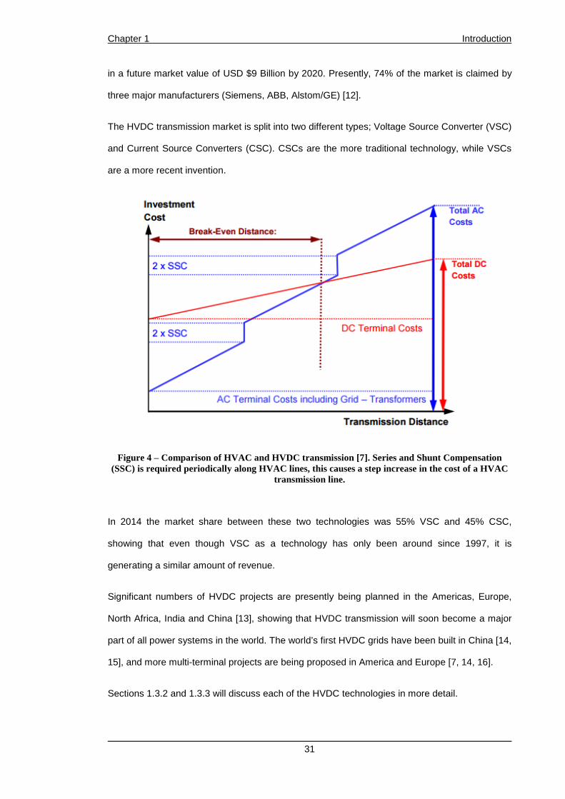
transmission has higher costs per unit length, but has a lower terminal cost when compared to
HVDC transmission [7]. However, HVAC may also require periodic reactive compensation in
order for it to function well over long distances. This causes step increases in the cost of HVAC
lines per unit length. HVDC transmission has a higher initial cost, but a fixed cost per unit length
and requires no compensation along the lines.
The distance at which HVDC becomes cheaper than HVAC, depends on the type of
transmission line medium, where the line is installed, and the technology used for the DC
transmission. The “breakeven” distance is subject to a lot of discussion. But estimates put the
distance at between 50 km and 100 km for cabled systems, and between 500 km and 800 km
for overhead lines [8, 10, 11].
Medium Voltage (MV) DC transmission may have significant cost benefits at shorter distances,
using the same technology as HVDC transmission, except at lower voltages [11].
The market revenue from HVDC and Flexible Alternating Current Transmissions Systems
(FACTS) was USD $6.18 Billion in 2014, with HVDC transmission making up 69% the revenue
[12]. The compound growth rate between 2014 and 2020 is estimated at around 6.6%, resulting
Chapter 1 Introduction
31
in a future market value of USD $9 Billion by 2020. Presently, 74% of the market is claimed by
three major manufacturers (Siemens, ABB, Alstom/GE) [12].
The HVDC transmission market is split into two different types; Voltage Source Converter (VSC)
and Current Source Converters (CSC). CSCs are the more traditional technology, while VSCs
are a more recent invention.
Figure 4 ‒ Comparison of HVAC and HVDC transmission [7]. Series and Shunt Compensation (SSC) is required periodically along HVAC lines, this causes a step increase in the cost of a HVAC
transmission line.
In 2014 the market share between these two technologies was 55% VSC and 45% CSC,
showing that even though VSC as a technology has only been around since 1997, it is
generating a similar amount of revenue.
Significant numbers of HVDC projects are presently being planned in the Americas, Europe,
North Africa, India and China [13], showing that HVDC transmission will soon become a major
part of all power systems in the world. The world’s first HVDC grids have been built in China [14,
15], and more multi-terminal projects are being proposed in America and Europe [7, 14, 16].
Sections 1.3.2 and 1.3.3 will discuss each of the HVDC technologies in more detail.

Chapter 1 Introduction
32
1.3.2 Current Source Converters
CSCs are the more traditional HVDC technology, the first commercial CSC project being
installed in 1941 [17]. CSCs are based around Thyristor technology and have been used
throughout the world for high power long distance transmission. CSCs operate with a fixed
current direction on the DC side and control the DC voltage by varying the turn on angle () of
the thyristor switches ( and ), see Figure 5. Power flow reversal is achieved by inverting the
DC side voltage, for details of its operation see [18].
Figure 5 ‒ Single phase layout of a three phase CSC.
Due to the electrical ratings of the individual Thyristors making up the converter, the power
levels that can be achieved with a CSC are significantly higher larger than anything a VSC can
presently match [18].
One disadvantage a CSC has is in the amount of harmonic filtering required to meet grid
requirements. While CSC converter stations (power electronic valve halls) are smaller than
those in a VSC, when AC side filtering is accounted for, the total foot print requirements become

Chapter 1 Introduction
33
significantly larger [18]. For offshore applications, it is the cost of the civil engineering that
dominates the project’s costs. This is heavily related to the required foot-print of the offshore
platform, which costs around £1 million per square metre [10]. Thus a CSC’s large foot print
makes it unsuitable for offshore applications.
1.3.3 Voltage Source Converters
VSC technology uses Insulated Gate Bi-polar Transistors (IGBTs). VSCs provide a fixed DC link
voltage polarity, rather than a fixed current direction [18]. This allows power flow reversal to be
achieved by changing current direction, rather than inverting voltage [18].
Keeping the voltage polarity fixed has significant benefits for any cables for the transmission
lines, and (as will be discussed in Section 1.5) makes the concept of meshed DC grids more
viable. So much so, that both a 3-terminal and 5-terminal system have been built in China [14,
15].
VSCs also provide the opportunity for HVDC links to support the AC network as they do not
require the AC grid to supply reactive power to the converters. This allows VSC systems to be
connected to weaker parts of the AC network [18]. The VSC also has a number of new ways to
support the AC grid [19-21]. [22]
VSCs have been rapidly developed since their first commercial trial in 1997. The preferred
converter topologies have changed several times since the first two-level VSC, and now seem
to be settling around Modular Multi-level Converters (MMCs).
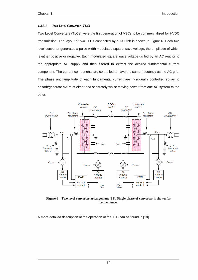
Chapter 1 Introduction
34
1.3.3.1 Two Level Converter (TLC)
Two Level Converters (TLCs) were the first generation of VSCs to be commercialized for HVDC
transmission. The layout of two TLCs connected by a DC link is shown in Figure 6. Each two
level converter generates a pulse width modulated square wave voltage, the amplitude of which
is either positive or negative. Each modulated square wave voltage us fed by an AC reactor to
the appropriate AC supply and then filtered to extract the desired fundamental current
component. The current components are controlled to have the same frequency as the AC grid.
The phase and amplitude of each fundamental current are individually controlled so as to
absorb/generate VARs at either end separately whilst moving power from one AC system to the
other.
Figure 6 ‒ Two level converter arrangement [18]. Single phase of converter is shown for convenience.
A more detailed description of the operation of the TLC can be found in [18].

Chapter 1 Introduction
35
1.3.3.2 Modular Multi-level Converters
Converters with a low number of steps in their output voltage, e.g. the TLC, require significant
filtering in order to meet grid harmonic standards [18]. The Modular-Multi-level Converter (MMC)
output voltage does not require filtering because the output voltage is synthesized through
many small steps, rather than few large steps. The layout of a single phase MMC is shown in
Figure 7.
Figure 7 ‒ Layout of a single phase MMC.
Each phase leg in the MMC consists of two stacks of series connected submodules, and each
stack of submodules is referred to as an arm. Each submodule is effectively a two level
converter, with the ability to provide a positive voltage or zero volts. The sum of the upper arm
voltage () and the lower arm voltage () is controlled to generate a fixed DC voltage (). The difference between the two arm voltages is controlled to generate a sinusoidal output
voltage (). The MMC was developed by Prof. Rainer Marquart in 2003 and was a major
technological leap in the field of HVDC transmission [23]. Since its inception the MMC topology
has been quickly established as the preferred technology for VSC HVDC transmission.

Chapter 1 Introduction
36
1.3.3.3 Advanced MMC
With the inception of the traditional MMC came a number of variations of the fundamental
concept. Full bridge variations have been proposed where improved fault tolerance is required,
and have been used in traction applications1.
Hybrid MMC solutions (which have a mixture of sub-module architectures in the converters e.g.
half bridge and full bridge submodules) have also been proposed, along with a wide range of
eclectic topologies [24-27]. The most notable of the alternative MMC topologies is the Alternate
Arm Converter (AAC), which is presently being developed by Alstom/GE [28].
As will be discussed in Section 1.5 connecting VSC HVDC systems into AC grids offers a wide
range of opportunities for future power systems. Fault tolerant converters such as the Full
Bridge MMC, hybrid MMC, and AAC topologies may have a place within such grids due to their
resilience to DC faults, their ability to control arm currents, and provide additional options for
future HVDC protection scenarios [28].
1.4 VSC HVDC Protection
In order for any HVDC grid to be safely operated, a robust protection philosophy must be
established and reliably implemented. Presently, point-to-point VSC HVDC transmission lines
are protected through a philosophy of current diversion and AC grid isolation. This involves
diverting the current away from sensitive power electronic components within the converter and
opening the circuit breakers at the converter’s AC interface. This technique will be discussed in
more detail in Section 1.4.1.The same technique is thought to be used for existing VSC grids
[29].
This protection philosophy was adopted over the more traditional philosophy of isolation used in
AC grids, since DC isolation is difficult, mainly due to the lack of a current zero crossing. But
there are also other intrinsic issues such as required speed, high current levels, and number of
operations that a single DC breaker would be able to perform.
HVDC protection is also a significantly under developed area, not only in terms of knowledge
but also in terms of existing industrial activity. At the time the first HVDC links were built there
1 Based on discussions with a technical employee at a major manufacturer.
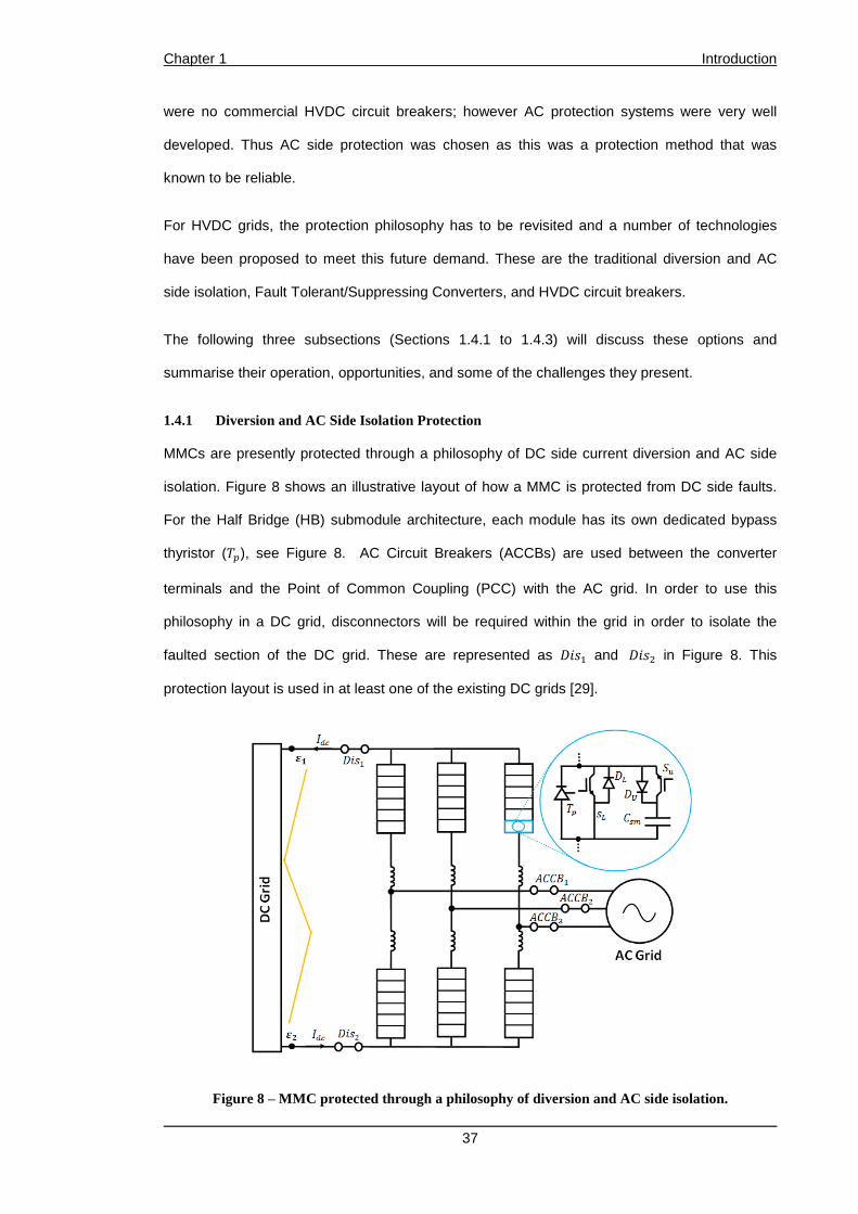
Chapter 1 Introduction
37
were no commercial HVDC circuit breakers; however AC protection systems were very well
developed. Thus AC side protection was chosen as this was a protection method that was
known to be reliable.
For HVDC grids, the protection philosophy has to be revisited and a number of technologies
have been proposed to meet this future demand. These are the traditional diversion and AC
side isolation, Fault Tolerant/Suppressing Converters, and HVDC circuit breakers.
The following three subsections (Sections 1.4.1 to 1.4.3) will discuss these options and
summarise their operation, opportunities, and some of the challenges they present.
1.4.1 Diversion and AC Side Isolation Protection
MMCs are presently protected through a philosophy of DC side current diversion and AC side
isolation. Figure 8 shows an illustrative layout of how a MMC is protected from DC side faults.
For the Half Bridge (HB) submodule architecture, each module has its own dedicated bypass
thyristor (), see Figure 8. AC Circuit Breakers (ACCBs) are used between the converter
terminals and the Point of Common Coupling (PCC) with the AC grid. In order to use this
philosophy in a DC grid, disconnectors will be required within the grid in order to isolate the
faulted section of the DC grid. These are represented as and in Figure 8. This
protection layout is used in at least one of the existing DC grids [29].
Figure 8 ‒ MMC protected through a philosophy of diversion and AC side isolation.

Chapter 1 Introduction
38
When a fault occurs, the DC current () rises rapidly. Eventually the converter will need to
block (turn off all the IGBTs in all the submodules) in order to prevent damage to the devices.
Current is then diverted into the lower diode (). Because the fault currents are very high and
exist for a long period of time, the diodes are not capable of conducting the fault current alone.
To protect the diodes () the parallel thyristors () are turned on, providing an alternate path
for the current to flow, and limiting the current that the diode is exposed to. The converter is
isolated from the AC grid through the use of the ACCBs. Once the DC line current as fallen to
zero, the disconnectors can be opened, isolating the faulted section of the grid. The healthy
parts of the grid can then be reenergised.
The major disadvantages of this technique are the long operation times and the loss of all
power flow between the AC and DC grid. The AC circuit breakers will take several tens of
milliseconds to operate and the faulted part of the DC grid may not be isolated until a
significantly longer period of time has passed.
Another disadvantage is that every single submodule requires its own Thyristors for protection.
Hence there is effectively a stack of thyristors rated at the DC link voltage in each arm, making
the MMC system larger, and more expensive.
The slow speed of the AC protection would result in the power rating of any DC grid being
constrained by the maximum in feed loss limitations of the AC grid that it is connected to. Such
a protection scheme is thus unlikely to be used for high power HVDC grids.
1.4.2 Fault Tolerant Converters
In order to prevent loss of power from the AC grid and to allow the converters to continue to
support the AC network during a DC fault, Fault Tolerant Converters (FTCs) have been
proposed as a potential protection technology for future HVDC grids.
An illustrative example of such a MMC is shown in Figure 9. This is a Full Bridge (FB) MMC,
whose submodules have a different architecture from that of the half bridge, allowing each of
the submodules to provide three voltage levels; positive, zero, and negative. This allows the
converter to suppress the DC side fault current and prevent the AC grid from injecting additional
energy into the DC fault [30]. Thus a DC side fault current can be reduced significantly,
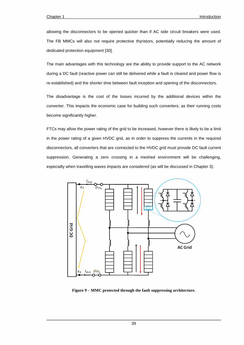
Chapter 1 Introduction
39
allowing the disconnectors to be opened quicker than if AC side circuit breakers were used.
The FB MMCs will also not require protective thyristors, potentially reducing the amount of
dedicated protection equipment [30].
The main advantages with this technology are the ability to provide support to the AC network
during a DC fault (reactive power can still be delivered while a fault is cleared and power flow is
re-established) and the shorter time between fault inception and opening of the disconnectors.
The disadvantage is the cost of the losses incurred by the additional devices within the
converter. This impacts the economic case for building such converters, as their running costs
become significantly higher.
FTCs may allow the power rating of the grid to be increased, however there is likely to be a limit
in the power rating of a given HVDC grid, as in order to suppress the currents in the required
disconnectors, all converters that are connected to the HVDC grid must provide DC fault current
suppression. Generating a zero crossing in a meshed environment will be challenging,
especially when travelling waves impacts are considered (as will be discussed in Chapter 3).
Figure 9 ‒ MMC protected through the fault suppressing architecture.

Chapter 1 Introduction
40
Furthermore, a protection philosophy based around FTCs alone, would also exclude any
existing VSC installation from becoming part of a future HVDC grid. FTCs may be useful for
converters which are connected to the grid via a single cable, or for other specific protection
cases, or when used in conjunction with DC circuit breakers to provide a balance of alternatives
(as will be discussed in Section 1.4.4).
Many other FTCs have been proposed using different architectures, which attempt to reduce
the losses of the converter while maintaining the advantages of increased control flexibility [24-
28]. FTC technology has yet to be used in the transmission network, but some manufacturers
have already installed FB MMCs into traction networks, which operate at lower voltages.
1.4.3 DC Side Isolation
A philosophy based around DC side isolation has also been proposed, which uses circuit
breakers on the DC side of the converters. Faulted sections of the grid would be quickly isolated
by the DC circuit breaker in a similar manner to breakers used in the AC grid.
DC Circuit Breakers (DCCBs) are connected in series with each pole of the converter, as shown
in Figure 10. These circuit breakers are shown simplistically here as an ideal switch, with a
parallel capacitance and a voltage limiting varistor. However, as will be discussed in Chapter 2
of this thesis, many of the proposed designs are more complex than this. It is likely that series
inductance will be required to both decrease the peak fault current and limit its rate-of-rise.
The time frames proposed for DC protection are significantly shorter than those typically seen in
AC systems. DC protection times are often quoted at around 2 to 5 ms [19], but as will be
discussed in Chapter 2, this requires some standardisation of terms. These time frames are
typically chosen to protect the power electronics within the converters and the DCCBs
themselves, and not based upon a stability limit. However removing and recovering from a fault
rapidly, is almost always an improvement as there will be less of a disturbance to the DC and
AC networks.
With DC isolation no special architecture for the converters is required, however new control
techniques will need to be developed for the converters, as the requirements for their design will
have changed.

Chapter 1 Introduction
41
Figure 10 ‒ MMC converter protected with DCCBs.
The main advantage of this protection system is the short time it takes to remove a faulted part
of the network from the healthy part of the network, mainly due to the rapid isolation provided by
the DCCB. The converter will also be able to provide reactive power support to the AC grid after
the fault has been cleared, as it will not have been isolated from it during a protective action.
Thus reactive power support can be initiated after several milliseconds.
DCCBs could also allow existing HVDC links to be integrated into a future DC grid. This would
allow for “interconnecting” projects to be proposed that would link together existing transmission
assets. None of the other protection options would allow this to be done as easily.
The major disadvantage with this philosophy choice is the amount of novel technology, lack of
surrounding knowledge in the community, and the lack of existing standards. However all other
proposed protection methods suffer from this problem as well.
1.4.4 Mixed Protection Systems
A mixture of protection equipment is also likely for future HVDC grids, especially for future
feasibility projects while the equipments’ capabilities are being proven. An example mixed

Chapter 1 Introduction
42
protection scenario is shown in Figure 11. Mixing the protection solutions allows the benefits of
each to be combined together.
ACCBs can still be used to provide backup protection, and would likely still be required to
protect against AC terminals faults. This would add reliability to the protection system, as in the
event the new technologies fail, the proven technology will protect the AC grid.
Fault Tolerant Converters (FTCs) could provide another layer of protection, allowing the fault
current to be reduced in the event the DC circuit breaker fails. This could also mean that
reactive power support can be given in the event of a DCCB failure. The FTCs may also allow
the rating of the DCCBs to be dropped if the fault current can be reliably controlled to a lower
level without impacting the DCCBs operation. FTCs working with DCCBs will also allow power
flow to be re-established much sooner as arm currents within the converter can be returned to
normal operation sooner than if a HB-MMC was used.
Importantly, combining FTCs with DCCBs could allow for a drastic reduction in the amount of
energy that varistors within the DCCBs would have to absorb. At present varistor technology
may not be capable of withstanding the high pulses of energy, without degradation and
subsequent reduction of reliability.
Figure 11 ‒ MMC protected using several different technologies.
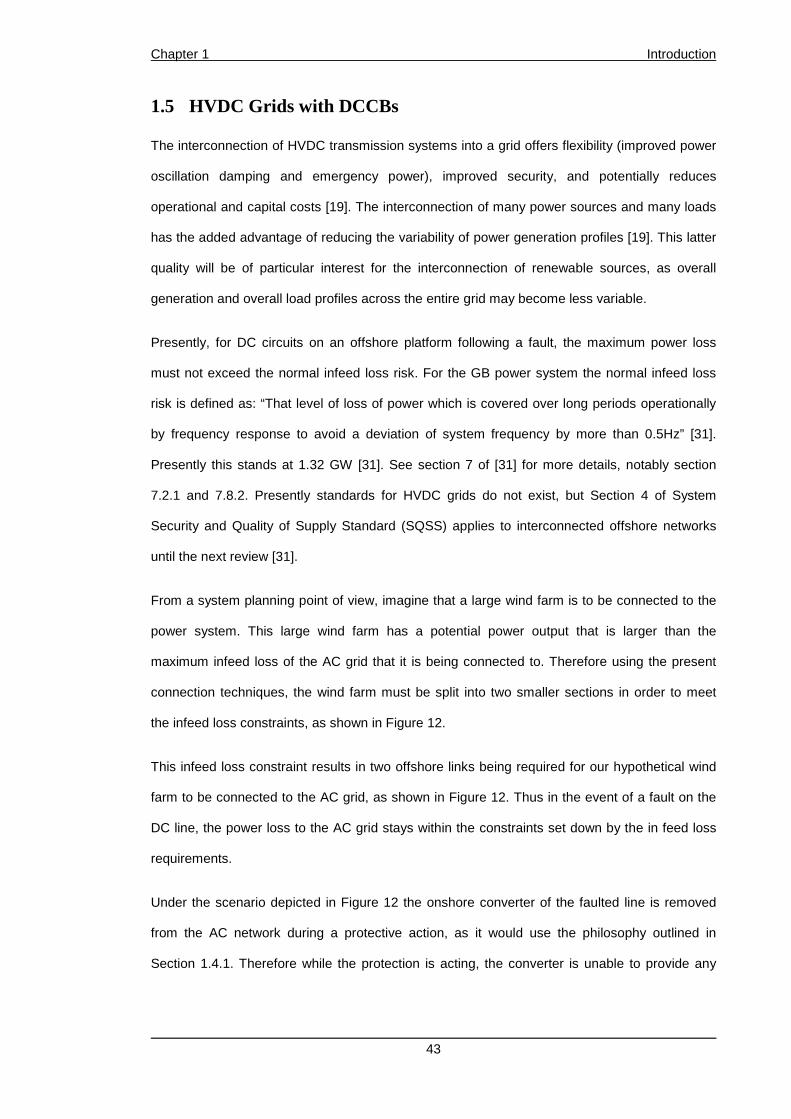
Chapter 1 Introduction
43
1.5 HVDC Grids with DCCBs
The interconnection of HVDC transmission systems into a grid offers flexibility (improved power
oscillation damping and emergency power), improved security, and potentially reduces
operational and capital costs [19]. The interconnection of many power sources and many loads
has the added advantage of reducing the variability of power generation profiles [19]. This latter
quality will be of particular interest for the interconnection of renewable sources, as overall
generation and overall load profiles across the entire grid may become less variable.
Presently, for DC circuits on an offshore platform following a fault, the maximum power loss
must not exceed the normal infeed loss risk. For the GB power system the normal infeed loss
risk is defined as: “That level of loss of power which is covered over long periods operationally
by frequency response to avoid a deviation of system frequency by more than 0.5Hz” [31].
Presently this stands at 1.32 GW [31]. See section 7 of [31] for more details, notably section
7.2.1 and 7.8.2. Presently standards for HVDC grids do not exist, but Section 4 of System
Security and Quality of Supply Standard (SQSS) applies to interconnected offshore networks
until the next review [31].
From a system planning point of view, imagine that a large wind farm is to be connected to the
power system. This large wind farm has a potential power output that is larger than the
maximum infeed loss of the AC grid that it is being connected to. Therefore using the present
connection techniques, the wind farm must be split into two smaller sections in order to meet
the infeed loss constraints, as shown in Figure 12.
This infeed loss constraint results in two offshore links being required for our hypothetical wind
farm to be connected to the AC grid, as shown in Figure 12. Thus in the event of a fault on the
DC line, the power loss to the AC grid stays within the constraints set down by the in feed loss
requirements.
Under the scenario depicted in Figure 12 the onshore converter of the faulted line is removed
from the AC network during a protective action, as it would use the philosophy outlined in
Section 1.4.1. Therefore while the protection is acting, the converter is unable to provide any

Chapter 1 Introduction
44
form of support to the AC grid. However, once the cable has been isolated there is potential for
the converter to be reconnected, to allow it to provide reactive power support.
Figure 12 ‒ Two separately connected wind farms.
Another problem with this connection philosophy is that the offshore wind farm connected to the
faulted HVDC link, can no longer sell its generated electrical energy to the onshore grid. For DC
systems using over head lines, this may not be a huge problem, but for cabled systems, repairs
can take several months. Hence several months of lost revenue must be compensated for in the
financing of such projects.
Figure 13 – Converters connected into a grid.
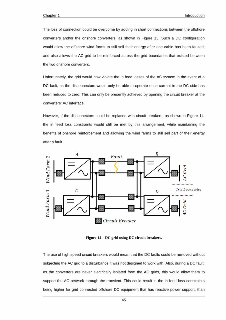
Chapter 1 Introduction
45
The loss of connection could be overcome by adding in short connections between the offshore
converters and/or the onshore converters, as shown in Figure 13. Such a DC configuration
would allow the offshore wind farms to still sell their energy after one cable has been faulted,
and also allows the AC grid to be reinforced across the grid boundaries that existed between
the two onshore converters.
Unfortunately, the grid would now violate the in feed losses of the AC system in the event of a
DC fault, as the disconnectors would only be able to operate once current in the DC side has
been reduced to zero. This can only be presently achieved by opening the circuit breaker at the
converters’ AC interface.
However, if the disconnectors could be replaced with circuit breakers, as shown in Figure 14,
the in feed loss constraints would still be met by this arrangement, while maintaining the
benefits of onshore reinforcement and allowing the wind farms to still sell part of their energy
after a fault.
Figure 14 ‒ DC grid using DC circuit breakers.
The use of high speed circuit breakers would mean that the DC faults could be removed without
subjecting the AC grid to a disturbance it was not designed to work with. Also, during a DC fault,
as the converters are never electrically isolated from the AC grids, this would allow them to
support the AC network through the transient. This could result in the in feed loss constraints
being higher for grid connected offshore DC equipment that has reactive power support, than

Chapter 1 Introduction
46
those that presently exist for point-to-point connected offshore DC equipment. Please note that
additional DC circuit breakers would be required on the interconnecting lines. These are not
shown here to keep the diagram and explanation simple.
Figure 15 ‒ HVDC grid protected with a combination of DC and AC circuit breakers.
However, a HVDC grid that is protected fully by DC circuit breakers is not seen as the next step
in developing HVDC grids. Due to the cost of equipment that is involved, the protection scenario
shown in Figure 15 is more likely.
Figure 15 shows a scenario where both DC and AC circuit breakers protect the DC grid. Under
this scenario the faulted half of the DC grid would be isolated very rapidly from the healthy half,
using DC circuit breakers. The converters that are connected to the faulted half are then
protected using their AC circuit breakers. On shore reinforcement and partial power from Wind
Farm 2 can then be re-established once the faulted line has been isolated and the DCCBs
reclosed. Under this scenario the number of DC circuit breakers is vastly reduced, and only two
offshore DC circuit breakers would be required, reducing the costs significantly and still
providing many of the benefits that a grid connection can offer.
There are two other scenarios which are more likely to be trialled before a heavily meshed grid
is constructed. These are known as “DC Tie Lines” and two potential configurations are shown
in Figure 16 and Figure 17.
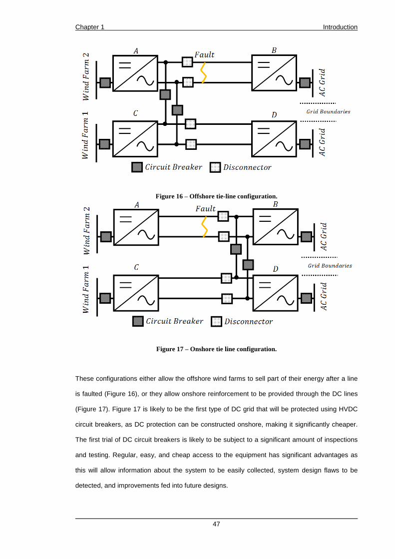
Chapter 1 Introduction
47
Figure 16 ‒ Offshore tie-line configuration.
Figure 17 ‒ Onshore tie line configuration.
These configurations either allow the offshore wind farms to sell part of their energy after a line
is faulted (Figure 16), or they allow onshore reinforcement to be provided through the DC lines
(Figure 17). Figure 17 is likely to be the first type of DC grid that will be protected using HVDC
circuit breakers, as DC protection can be constructed onshore, making it significantly cheaper.
The first trial of DC circuit breakers is likely to be subject to a significant amount of inspections
and testing. Regular, easy, and cheap access to the equipment has significant advantages as
this will allow information about the system to be easily collected, system design flaws to be
detected, and improvements fed into future designs.

Chapter 1 Introduction
48
Presently China is the only country that is building a HVDC circuit breaker (200 kV) and actually
planning to install it into the power system [32], though the details of this are not well publicised.
In Europe there is discussion around developing a medium voltage test environment, before
moving to HVDC equipment [11].
It is also worth noting that there are several other applications for HVDC circuit breakers2. Point-
to-point systems are presently protected using AC circuit breakers along with thyristors to
protect every single module within an MMC. Hence, for every submodule in a MMC there is a
protective semiconductor. In terms of voltage rating, each arm within the converter is rated to at
least the DC voltage (1 pu for this example). This means that there are thyristors rated for at
least 6 pu voltage within the converter for protection purposes alone. A circuit breaker would
require semiconductors rated between 2 - 4 pu voltage. Swapping to a philosophy of DC
isolation could reduce the weight and cost of the converters, while also allowing the converter to
support the AC grid during a fault.
Sub-cycle AC protection is another application which is presently being discussed. If the DC
circuit breaker is not reliant on working in a DC environment, and many are not, there is
potential for them to be used in the AC grid.
HVDC circuit breakers will act within a few milliseconds, rather than several tens of
milliseconds, resulting in fault being removed sooner. This speed could allow for the ratings of
electrical equipment to be drastically reduced, as they would not have to be subjected to an
over current for an extended period of time. Generators would benefit from a reduction in both
mechanical and electrical stress, potentially improving life times.
MVDC networks have been discussed under the context of offshore wind farm connections, and
there are also opportunities for their application in naval and aero space applications [11, 33,
34].
2 Based on discussion with technical experts at a major manufacturer

Chapter 1 Introduction
49
1.6 Synthetics Testing
All the proposed protection options will require significant amounts of development in both
technology and standards in order for them to be used in a large scale HVDC grid. In order for
power system equipment to be installed in a power system, its Technology Readiness Level
(TRL) must be sufficient to allow commissioning of the equipment. According to the US
Department of Energy (DoE) definitions of TRLs, standard power system equipment that has
proven its operation at TRL 9 [35].
In order for a piece of equipment to advance up the TRL ladder, it must meet certain criteria to
progress to the next level. Looking at the transition from TRL 4 to TRL 5 (reproduced below) it
can be seen that there is a significant change in the type of laboratory testing environment [35].
TRL 4: “Component and/or system validation in laboratory environment”
TRL 5: “Laboratory scale, similar system validation in relevant environment”
In order for the technology to progress, there needs to be a definition of “relevant environment”.
Such a definition would normally be given by an appropriate standard. Laboratory testing in this
relevant environment is commonly referred to as synthetics testing.
Synthetics testing attempts to replicate the power system environment in the laboratory. This
allows the capability of new technologies, or new variations of existing equipment, to be proven
before they are installed into the power system.
For HVDC circuit breakers, no such standard presently exists. There are also very few HVDC
grids in the world, and none which presently contain HVDC circuit breakers. Hence there is no
practical experience to base such a standard upon.
Therefore the first revision of a standard must be based on theoretical analysis, laboratory
testing, and an understanding of the limitations of the power system. This thesis aims to aid in
the development of such a first revision standard by undertaking underpinning research.

Chapter 1 Introduction
50
1.7 DC Grid Modelling
In this thesis, simulation results will be presented of grid systems that contain Two Level
Converters (TLC) or Modular Multi-level Converters (MMC). The MMC model and cable models
were not developed as part of this PhD, but only modified to include HVDC circuit breakers. The
TLC models were developed with the co-operation of the author, however full credit cannot be
claimed.
Two converter models were used to verify the fault analysis and the operation of the circuit
breakers in the DC power system. The two models were a Traditional Detailed Model (TDM) of
the TLC and a Detailed Equivalent Model (DEM) of the MMC. Sections 1.7.1 and 1.7.2 will give
a brief introduction to these models.
1.7.1 Two Level Converters
The TLC transmission system was modelled as a 1 GW, 600 kV (+/- 300 kV) symmetrical
monopole system. The converter was modelled using a Traditional Detailed Model (TDM). For
details of the control used in the converter stations and the layout of the transmission system
see [C2].
1.7.2 Modular Multi-level Converters
The MMC was modelled at the same power rating as the TLC (1 GW) and the same voltage
level (+/-300 kV). The submodule architecture chosen was the half bridge MMC and was
modelled in PSCAD. Each arm of the converter contains 30 submodules. Details of the model,
how it works, and its parameters can be found in [36].
Figure 18 ‒ Overview of MMC Control structure.

Chapter 1 Introduction
51
1.7.3 DC Cable
Within each DC transmission model, the cables were modelled using a Frequency Dependent
Phase Model (FDPM) and parameterized based on a 300 kV XLPE cable [36, 37]. This model
was chosen as it is known to be the most accurate model and has the added benefit of being
fast in simulation.
1.8 Superconductors
Superconductors are discussed in this thesis and practical results from the use of such
technology are also shown. Their operation is complex and still subject to some discussion in
the physics community. For the purpose of this Thesis a superconductor is considered as a
material which exhibits zero resistance under normal operating conditions. The zero resistance
characteristic is maintained while the current, temperature, and magnetic flux are all below
critical levels.
When any of these critical levels are exceeded the superconducting wire is said to “quench”, at
which point it starts to exhibit resistive properties. For this Thesis, this simplistic “switch” view of
the technology is sufficient and is the main property that is exploited. For a more detailed view
start with [38].
1.9 Aims and Objectives
Based on the motivations given in this chapter, this PhD was funded by National Grid to
investigate how to test HVDC circuit breakers, with the long term vision of contributing to a
future HVDC circuit breaker standard.
The aim of this PhD was to:
1. Develop knowledge surrounding the testing of high voltage direct current circuit
breakers.
Based on these aims several objectives were outlined:
1. Establish criteria for the testing of a prototype HVDC circuit breaker
2. Design a test circuit to meet this criteria
3. Build prototype circuit breakers and associated testing equipment
Chapter 1 Introduction
52
4. Perform testing
5. Re-evaluate all testing knowledge based on outcomes of the testing
The thesis will attempt to show that this aim has been met, all the objectives were attempted,
and that there has been a sufficient advancement to the area of HVDC circuit breaker synthetics
testing.
1.10 Main Thesis Contributions
The work undertaken as part of this PhD has contributed to several different areas; which will be
explained in bullet point form in this section. The abbreviations ‘R’,’J’,’P’,’PP’,’PS; and ’C’, refer
to Industrial Reports, Journal Publications, Patents, Pending Publication, Pending Submission,
and Conference papers respectively. A list of all such publications is given in Section 1.11 and
all first author publications have been provided in Appendix 5. Each of the main contributions
will end with a series of letters which refers to where that contribution has made an impact.
1. The concept of fault current envelopes was developed for the testing of HVDC circuit
breakers. These provide a standard procedure for specifying the test circuit needed to
properly test a HVDC circuit breaker. Methods for developing a fault current envelope
have been outlined for two commonly used converter topologies. [R3,J2,C1,PS1].
2. The application of fault current envelopes as a test circuit specification tool has been
demonstrated in the development of a high power test circuit. This test circuit has been
built, tested, and validated against this specification. [R4].
3. The influence of travelling waves on hybrid circuit breaker designs has been
highlighted, and mathematically described. The Author was one of the first people to
present on this phenomenon in the HVDC community, and has investigated its impact
to a greater detail than most. This has lead to a new definition of the worse case fault
for HVDC circuit breakers. [R3,J2,C4,C5,PS1,PS2].
4. A novel superconducting hybrid circuit breaker was invented, designed, prototyped, and
attempted to be developed into a licensed product. This design was patented and used
as the basis for a £600,000 EPSRC post doctoral research project at the University of
Manchester.[P1,PP1].

Chapter 1 Introduction
53
1.11 Publications
Industrial Reports [R]:
1. National Grid Interim Report 1.1 – Titled “HVDC Circuit Breakers”
2. National Grid Final Report 1.2 – Titled “HVDC Circuit Breakers” – 106 pages
3. National Grid Report 2.1 - Titled “HVDC Circuit Breaker Synthetics Testing” – 98 Pages
4. National Grid Report 2.2 – Titled “Low Power Synthetic Testing & Travelling Wave
Theory Validation” – 20 pages
5. National Grid Report 2.2.2 – Titled “High Power Synthetic Test Circuit Design: System
Specification, Design and Prototyping” - 54 pages
6. National Grid Report (Additional) – Titled “HVDC Circuit breaker Standards Report” – 32
pages
Journal Publications [J]:
1. Wang, W., M. Barnes, et al., "Impact of DC Breaker Systems on Multi-Terminal VSC-
HVDC Stability," Transactions on Power Delivery, 2015 – [J1]
2. Cwikowski, O., B. Chang, et al., "Fault Current Testing Envelopes for VSC HVDC
Circuit Breakers," IET Generation, Transmission & Distribution. – [J2]
Patents [P]:
1. Cwikowski, M Barnes, et al., "Apparatus and Method for Controlling a DC Current,"
WO2014177874 (A2), 2014 – [P1]
Conference Publications [C]:
1. Cwikowski, O., B. Chang, et al., "Fault Current Testing Envelopes for VSC HVDC
Circuit Breakers," in AC and DC Power Transmission, 11th IET International
Conference on, 2015, pp. 1-8.10.1049/cp.2015.0011 – [C1]
2. Chang, B., O. Cwikowski, et al., "Point-to-point Two-level Converter System Faults
Analysis," presented at IET PEMD Manchester, 2014 - [C2]

Chapter 1 Introduction
54
3. Chang, B., O. Cwikowski, et al., "Multi-terminal VSC-HVDC Pole-to-pole Fault Analysis
and Fault Recovery Study," in AC and DC Power Transmission, 11th IET International
Conference on, 2015, pp. 1-8.10.1049/cp.2015.0093 – [C3]
4. Cwikowski, O., B. Chang, et al., "Analysis and Simulation of the Proactive Hybrid
Circuit Breaker," presented at PEDS, 11th IEEE International Conference on, Sydney,
2015 – [C4]
5. Cwikowski, O., B. Chang, et al., "Impact of Traveling Waves on HVDC Protection,"
presented at Power Electronics and Drive Systems,11th IEEE International Conference
on, Sydney, 2015 – [C5]
Pending Publication [PP]:
1. X. Pei, O. Cwikowski, D. S. Vilchis-Rodriguez, M. Barnes, A. C. Smith, and R.
Shuttleworth. “A Review of technologies for MVDC circuit breakers” accepted for
publication at IECON 2016. - [PP1]
Pending Submission [PS]:
1. O. Cwikowski, A Wood, A. Miller, M. Barnes, R. Shuttleworth. “Operating DC circuit
Breakers with MMC” submitted to IEEE Transactions on Power Delivery. – [PS1]
2. O. Cwikowski ,J. Sau, B. Chang , M. Barnes, O. Gomis, R. Shuttleworth. “Integrating
CFCs into Hybrid HVDC Circuit breakers” Pending submission to IET Generation,
Transmission & Distribution.- [PS2]
3. O. Cwikowski, H.R. Wickramasinghem, G. Konstantinou, J. Pou, M. Barnes, R.
Shuttleworth. “RTDS Power Flow Recovery in MMCs” Pending submission to IEEE
Transactions on Power Delivery – [PS3]
Monthly Newsletter [N]:
• A Monthly VSC Newsletter was started by the author during this PhD. This newsletter
has now been running successfully for 4 Volumes, with Prof Mike Barnes performing
the majority of the work, and the Author, along with others, taking a supporting role. –
[N1]

Chapter 1 Introduction
55
These documents will be referred to throughout this thesis, using the two or three letter indicator
given in square brackets, e.g. [J1] or [PS1].
1.12 Thesis Structure
This section gives a brief overview of the content of each of the following technical chapters.
Chapter 2 – Literature Review
A review of DC circuit breaker topologies is given in Chapter two, which looks at all potential
HVDC circuit breaker topologies. A brief review of which existing standards are relevant to
developing a future HVDC circuit breaker standard is also given. Standard definitions for how
DC protection is operated and circuit breaker times are also given.
Chapter 3 – Converter Fault Analysis and Fault Curr ent Envelopes
The concept of fault current envelopes is introduced in Chapter 3. The fault response of two
different converters is analysed. The analysis takes a broader view of the fault current, looking
at its limitations, rather than trying to develop an exact prediction of fault current. These
limitations are used to develop envelopes, which form the basis of how the test circuit discussed
in Chapter 6 is designed. These limitations show that there is a fundamental change in the
definition of worse case fault for fast acting HVDC circuit breakers.
Chapter 4 – Circuit Breaker Analysis
Two different circuit breaker topologies are analysed in depth in this Chapter. These topologies
were chosen based on the architecture of a high power industrial prototype and a novel circuit
breaker design invented and patented as part of this PhD. The influence of travelling waves is
investigated, and shows they cause significant problems for HVDC circuit breakers, and must
be accounted for in their design.
Chapter 5 – Prototype Circuit Breakers
The two circuit breaker topologies developed in Chapter 4 were then built and tested in the
laboratory. This allowed their design to be validated and allowed some of the analysis to be

Chapter 1 Introduction
56
validated against the practical results. The results for the superconducting hybrid circuit breaker
presented in this chapter, are the first validation of this novel circuit breaker ever performed.
Chapter 6 – Test Circuit Design
The design and construction of a test circuit is detailed in this chapter, using the fault current
envelopes developed in Chapter 3. A semiconductor circuit breaker was then designed to
operate within this test circuit, with a current rating scaled to one fifth of the required current
rating for a circuit breaker connected to a 1 GW converter.
Chapter 7 – Test Results
The tests performed on the semiconductor circuit breaker are presented in Chapter 7. The test
circuit’s design is validated against the specification criteria. The test results from a high current
impulse test and an interruption test are given. Key findings from these tests are also presented,
along with a list of recommendations for future iterations of HVDC circuit breaker testing.
Chapter 8 – Conclusions
The work that was performed during this PhD is summarized, key contributions highlighted, and
future work areas highlighted.
Chapter 2 Literature Review
57
Chapter 2: Literature Review
2.1 Introduction
This chapter describes a range of relevant existing DC circuit breaker topologies and novel DC
circuit breaker designs invented during the PhD work. A summary of the relevant existing
standards is provided, and a discussion of standard terms for HVDC protection is also given at
the end.
2.2 DC Circuit Breakers – Existing
DC circuit breakers can be categorized into three main types, as shown in Figure 19;
Mechanical, Solid-state and Hybrid. Mechanical DC circuit breakers use a mechanical switch as
the main breaking element. Due to the lack of a natural zero current crossing, a mechanical
circuit breakers’ operation must be supported with additional hardware to induce a current zero
in the arc. Mechanical DC circuit breaker designs typically have a low power loss when
conducting and long opening time (>10 ms) depending on the voltage rating of the system.
However, some recent circuit breaker prototypes can operate in less than 10 ms [39].
Solid-state circuit breakers use power electronics switches, in conjunction with voltage limiting
circuitry, to break the flow of current. Solid-state circuit breakers are typically very fast (<1 ms),
however this comes at the expense of high conduction losses (100s of kWs). For HVDC
applications, such losses are unacceptable.
Hybrid circuit breakers attempt to combine the low loss features of mechanical switches with the
fast operating times offered by solid-state breakers. When in the closed position, the current
flows through a low loss mechanical switch. When the current is to be interrupted, it is first
diverted into a semiconductor switch which carries out the actual breaking process. Hybrid
circuit breaker topologies are receiving significant attention from both industry and academia.
The most promising designs are being prototyped at representative voltage and current levels,
with operation times of less than 5 ms.

Chapter 2 Literature Review
58
Figure 19 ‒ DC circuit breaker categories.
Figure 20 – General structure of hybrid circuit breakers.
Hybrid circuit breakers are usually constructed of three parallel branches, Primary, Secondary
and, Energy Absorption, as shown in Figure 20. Current is commutated between these
branches during the circuit breaker’s operation.
The primary branch conducts current during normal conducting operation. The secondary
branch is a temporary conduction path, which carries current for a short period of time during
the circuit breaker’s operation. The energy absorption branch is usually constructed of varistors,
and absorbs the energy stored in any series inductance. It is the energy absorption branch
which ultimately reduces the current to zero.
The remainder of this section summarizes the operation of existing mechanical and hybrid
circuit breaker topologies. Semiconductor circuit breakers are discussed briefly, but due to their
significantly higher conduction losses, some designs [40-42] are not discussed in detail. The
notation used in each section is only relevant to that circuit breaker.
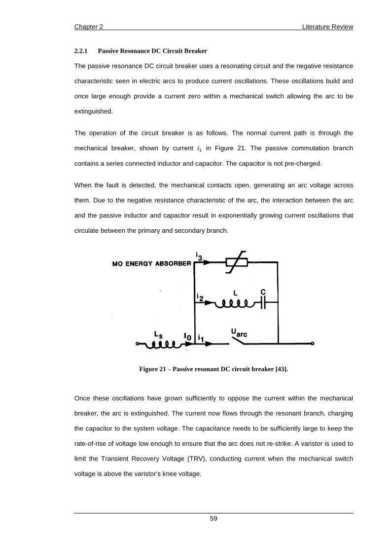
Chapter 2 Literature Review
59
2.2.1 Passive Resonance DC Circuit Breaker
The passive resonance DC circuit breaker uses a resonating circuit and the negative resistance
characteristic seen in electric arcs to produce current oscillations. These oscillations build and
once large enough provide a current zero within a mechanical switch allowing the arc to be
extinguished.
The operation of the circuit breaker is as follows. The normal current path is through the
mechanical breaker, shown by current in Figure 21. The passive commutation branch
contains a series connected inductor and capacitor. The capacitor is not pre-charged.
When the fault is detected, the mechanical contacts open, generating an arc voltage across
them. Due to the negative resistance characteristic of the arc, the interaction between the arc
and the passive inductor and capacitor result in exponentially growing current oscillations that
circulate between the primary and secondary branch.
Figure 21 ‒ Passive resonant DC circuit breaker [43].
Once these oscillations have grown sufficiently to oppose the current within the mechanical
breaker, the arc is extinguished. The current now flows through the resonant branch, charging
the capacitor to the system voltage. The capacitance needs to be sufficiently large to keep the
rate-of-rise of voltage low enough to ensure that the arc does not re-strike. A varistor is used to
limit the Transient Recovery Voltage (TRV), conducting current when the mechanical switch
voltage is above the varistor’s knee voltage.

Chapter 2 Literature Review
60
2.2.2 IGBT Resonant Circuit Breaker
The IGBT resonant circuit breaker is shown in Figure 22. During normal operation current flows
from A to B via, and. When a fault is detected, and are opened, generating
two arc voltages and. As in the previous breaker a resonant system is setup with, and the negative resistances of the two arc voltages and .The voltageis now used as
a power supply to drive the triggering electronics for , so that is switched at the
resonant frequency of the parallel circuit and. A resonating circuit is now formed between
, , and/. The oscillations in this resonant circuit begin to grow and form an
alternating current which is superimposed onto the direct current. Once these oscillations are
large enough to exceed the fault current, a zero crossing is generated and the arcs in both and are extinguished. Current is then commutated into and the voltage gradually
builds to the supply voltage. The resonant circuit capacitance () ensures that the rate-of-rise is
not faster than the rate of dielectric recovery of the mechanical switches. The varistor then
dissipates the energy stored in the series inductance (). The main advantage of this design
over the breaker discussed in Section 2.2.1 is that the induced current oscillations grow faster.
Figure 22 ‒ The IGBT resonant circuit breaker.

Chapter 2 Literature Review
61
2.2.3 Active Resonant Circuit Breaker
The active resonant circuit breaker is shown in Figure 23. This consists of a mechanical switch,
in parallel with an energy absorption branch, and an active resonant circuit.
During normal operation, current flows through the mechanical switch. The resonant circuit
capacitor () is pre-charged by an isolated power supply. The thyristor switches are turned off
to prevent the capacitor discharging.
Once a fault is detected, the mechanical switch is opened and the active resonant circuit is
triggered by turning on one of the thyristor switches. The capacitor discharges through the
resonant inductance () and produces an impulse of current in the opposing direction to the
fault current through the mechanical contacts. Providing the current generated by the resonant
circuit is high enough, a current zero can be generated in the mechanical switch, extinguishing
the arc.
A similar design has also been proposed by ABB in [39] and shows similar operating times to
[44], with both prototypes operating in less than 10 ms.
Figure 23 – Active resonant circuit breaker [44].

Chapter 2 Literature Review
62
2.2.4 Pulse Generating Circuit Breaker
The pulse generating circuit breaker is shown in Figure 24. The circuit breaker is shown in its bi-
directional form for a mono-pole system, however the breaker can also be applied to bi-pole
systems [24]. The circuit breaker has three main elements, the Hybrid Breaking (HB) units,
Damping Branches (DB) and the Pulse Generator (PG). The HBs contain fast acting
mechanical switches and diodes. The DBs are used to limit reverse voltages and absorb energy
after the faulted line has been isolated. The PG uses thyristors, which are well suited to high
current, to produce a current pulse in the HBs, generating a current zero. The PG capacitance
() is charged by the DC line so there is no need for an additional power supply.
When a fault is detected the mechanical switches in the HBs are opened, generating arcs
between the contacts. Once the contacts are sufficiently open the PG is triggered and a current
zero is generated in the mechanical switches. The remaining energy stored in the two series
inductances ( and!) is then dissipated in the two DBs.
The design is fully modular and can be scaled up or down in both current and voltage. The
circuit breaker can also be fired a second time very quickly as the PG capacitor is generally of a
low value.
Figure 24 – Layout of bi-directional pulse generating circuit breaker [24].

Chapter 2 Literature Review
63
2.2.5 Solid State Circuit Breakers
A solid-state breaker using GTO thyristors (and) is shown in Figure 25. The nominal
current path is through one semi-conductive device(or), in this case, each of which has
to withstand the fault current and the peak voltage across the switch [45]. The semiconductor
devices must have turn off capability in order to work in this arrangement.
When a fault occurs on the system, the line current starts to rise. A series inductor (not shown)
limits the rate-of-rise of fault current and the peak fault current. The peak fault current must be
limited to ensure that the semiconductors are not damaged. The current rises until the fault is
detected, at which time the devices are turned off, blocking the current. A parallel surge
arrestor, shown as, limits over voltages across the breaker and removes the energy stored in
any series inductance.
Figure 25 – Solid-state circuit breaker [46].
The losses incurred by a solid-state circuit breaker are likely to be significant (100s kW3), and
prohibit their application in a HVDC environment. Designs have been proposed which use
thyristor technology, however the losses are still very high and require many additional circuits
to allow them to turn off [40-42].
Any solid-state or hybrid circuit breaker will require a series inductance. For thyristor based
designs this is to reduce their I2T energy dissipation and prevent high rates of change of current.
In IGBT based designs the inductance is required to prevent the devices desaturating due to
over current, which results in significant additional losses in the devices.
3 For a 1 kA DC current, with 100 devices in series each with onstate voltage of 1 V the power losses = 1x100x1000 = 100 kW. The onstate voltage will likely be larger than 1 V and more devices will be required in series.

Chapter 2 Literature Review
64
2.2.6 Z‒Source DC Circuit Breaker – Type 1
Figure 26 shows the proposed circuit topology with the Z‒Source circuit breaker enclosed within
the dotted square. The breaker consists of two capacitances and two inductances with parallel
freewheeling diode-resistor circuits.
When the system is in steady state and no DC fault is present, the capacitors are both charged
to the supply voltage (), as the inductors will have no voltage across them in steady state and
the SCR voltage drop will be small. Effectively in steady state the capacitors are in parallel.
When a fault occurs, the load is shorted out. Due to the arrangement of the Z-source breaker,
the capacitors transiently change orientation, and become series connected. This creates a
transient two per unit voltage at the anode of the SCR with respect to ground, resulting in a
reverse current flow through the SCR in opposition to the normal load current. The reverse flow
of current can produce a zero current crossing in the SCR, providing correct electrical
impedances are chosen.
Figure 26 ‒ The Z-source circuit breaker – Type 1 [47].
Figure 27 ‒ Current flow path during a DC side fault [47].

Chapter 2 Literature Review
65
2.2.7 Z–Source Circuit Breaker – Type 2
A second version of the Z‒Source circuit breaker is shown in Figure 28. During normal
operation the load current flows through the inductors and the SCR, and the two capacitors are
essentially uncharged.
When a fault occurs on the system, the load is shorted out and the supply voltage appears
across the Z‒Source as a step in voltage. The capacitors initially provide a low impedance path
for current to flow through, while the inductors initially present a high impedance blocking any
additional current flow.
The fault current will flow through the path shown in Figure 28. Due to the arrangement of the Z-
Source, the fault current flows in opposition to the load current within the SCR. Providing that
the correct impedances are chosen, a current zero can be achieved in the SCR, which allows it
to be turned off.
Figure 28 ‒ Z‒Source circuit breaker topology – Type 2 [48].

Chapter 2 Literature Review
66
2.2.8 Hybrid DC Circuit Breaker
The hybrid circuit breaker topology is shown in Figure 29 [46, 49]. During normal operation
current flows through the mechanical breaker (#), resulting in no additional losses being
incurred compared to a mechanical solution. The semiconductor switches (or) can either be
turned on or off, but do not carry any significant current during normal operation.
When a fault is detected, the mechanical switch is opened and the semiconductor switch is
turned on (if it is not already turned on). Opening the mechanical switch when current is flowing
through it results in an arc being generated. The arc produces a voltage across the mechanical
switch, which causes current to move from the primary branch into the secondary branch. For
this to happen the arc voltage needs to be higher than the on-state voltage of the solid-state
devices and the additional voltage imposed due to the secondary branch inductance (). Under
this circumstance, the primary branch current will eventually fall to zero and the arc will be
extinguished.
The use of an arc to commutate the primary branch current causes the dielectric strength of the
gas within the mechanical switch to degrade significantly. Before the fault current can be broken
by turning off the semiconductors, the mechanical switch must be fully open and a short delay
must be added to allow the gas to dielectrically recover [46].
After this delay the mechanical breaker is able to hold off the entire system voltage, and the
semiconductor switch can be turned off. The energy in the inductance of the circuit is
dissipated in the varistor ().
Figure 29 ‒ The hybrid circuit breaker [46].

Chapter 2 Literature Review
67
2.2.9 Hybrid Circuit Breaker with turn off Snubber
A snubber circuit can be added to the traditional hybrid circuit breaker design discussed in
Section 2.2.8. One such possibility is shown in Figure 30. The circuit breaker operates in the
same manner as the traditional hybrid circuit breaker. Current is commutated into the secondary
branch using the arc generated by opening the contacts of the mechanical switch.
Once the arc has been extinguished in the mechanical switch, the semiconductors in the
secondary branch may be turned off. Current now flows into the snubber circuit capacitor (), which limits the rate-of-rise of voltage across the circuit breaker. Providing the snubber circuit
capacitor is large enough, no additional waiting time is required for the mechanical switch to
dielectrically recover. The impact the mechanical switch opening time has on the circuit
breaker’s total operation time can be reduced in this circuit, as the circuit breaker voltage can be
controlled. A varistor is needed to prevent high overvoltages appearing across the circuit
breaker, not shown in Figure 30. A similar design is discussed in [46].
This circuit breaker design offers some interesting benefits for HVDC applications and provides
the opportunity to reduce the dependency on fast actuators. However, in the circuit breaker’s
present form the capacitance values needed are too large for HVDC applications. For high
current applications the parasitic inductances in the snubber capacitors also become
problematic as these will induce high voltage impulses across the mechanical switch when the
semiconductor switch is turned off. However, recent improvements to this type of design have
been developed and are discussed in Section 2.2.12.
Figure 30 ‒ Hybrid circuit breaker with an RCD snubber.

Chapter 2 Literature Review
68
2.2.10 Hybrid Circuit Breaker with Forced Commutation
One of the problems with the hybrid circuit breaker topologies discussed in sections 2.2.8 and
2.2.9 is the use of an arc to commutate current between the primary and secondary branches.
The arc temporarily damages the dielectric withstand capability of the mechanical switch and
causes contact erosion. Other methods have been developed to commutate current between
the circuit breaker’s branches to prevent this.
One such topology is shown in Figure 31, where an impulse circuit is used to generate a current
zero in the primary branch. During normal operation the current flows through the primary
branch, which is a series combination of $ and the mechanical switch (#).
When a fault is detected, the appropriate thyristor is fired in the impulse circuit, forcing current in
the opposite direction through the inductance. At the same time the required secondary
branch(or) is turned on. When the inductor current reverses, the voltage across$ rises
and fault current starts to commutate into the semiconductor switch(or) via. Once the
primary branch current is low enough, the mechanical switch (#) can start to open [46]. When
the mechanical switch (#) is fully open, the semiconductor switch can be opened and the energy
in is dissipated by the energy absorption branch ().
Figure 31 ‒ Hybrid circuit breaker with forced commutation [46 ].

Chapter 2 Literature Review
69
2.2.11 Proactive Hybrid DC Circuit Breaker
The Proactive Hybrid Circuit Breaker (PHCB) is shown in Figure 32. This consists of two
paralleled branches. The normal current path consists of a mechanical switch and a low voltage
series stack of semi-conductive switches, known as the Load Commutation Switch (LCS). In
parallel with these is the main current breaking element, a stack of semi-conductive switches,
known as the main breaker. The energy absorption branch is combined with the secondary
branch in this case to add functionality to the circuit breaker. In such an arrangement, sections
of the secondary branch can be switched independently from the others. This allows the circuit
breaker to act as a fault current limiter in certain situations [50].
During normal operation the disconnector is closed, the LCS is turned on and the main breaker
is turned off. When a fault is detected, the LCS is turned off and the main breaker is turned on.
The LCS provides sufficient voltage to commutate current from the primary branch into the
secondary branch. The LCS may be triggered before the fault is confirmed. This would allow
the detection algorithm to be processed in parallel with the circuit breaker’s operation, as will be
explained in Section 2.7.
Once all the current is flowing through the main breaker, the high speed mechanical
disconnector is opened. When the mechanical switch is fully open, the main circuit breaker is
turned off, the main breaker current is interrupted, and the line energy is dissipated in the
varistors. The relatively slow series residual current disconnecting circuit breaker is used to
break the leakage current through the main breaker and associated devices, which may be
significant depending on how the energy absorption branch is designed. This switch also
provides full isolation.
Figure 32 ‒ Proactive hybrid circuit breaker, proprietary of A BB [50].

Chapter 2 Literature Review
70
2.2.12 Capacitive Hybrid Circuit breaker
The capacitive hybrid circuit breaker consists of a primary branch containing a LCS, shown as
the LV IGBT in Figure 33, in series with a mechanical switch. The secondary branch consists of
several sub-branches. These sub-branches are split into two types, Time Delay Branches (TDB)
and Arming Branches (AB). The energy absorption branch is the surge arrestor [51, 52].
During normal operation current flows through the primary branch. Once a fault is detected, the
first timing branch () and the thyristor stack are both turned on and the LCS is turned off,
thus commutating the current out of the primary branch. The first timing branch capacitance
(%) has a high capacitance. Providing the LCS voltage is sufficient, the current will fall to zero
in the mechanical switch allowing it to be opened without an arc.
The second timing branch () is triggered once the mechanical switch is partially opened. This
short circuits the first capacitor (%), generating a reverse current in the first timing branch (), allowing to be turned off. The secondary branch capacitor will have a lower capacitance than
%, resulting in a higher rate-of-rise of voltage across the mechanical switch. The same
process can be repeated again to commutate current from the second timing branch () into
the third (&). The arming branch (') is used to commutate the current out of the final timing
branch and allow the voltage to return to normal operating level. The timing branches thus allow
the voltage across the mechanical switch to be controlled.
Figure 33 ‒ Alstom's capacitive hybrid circuit breaker, modified from [51, 52].

Chapter 2 Literature Review
71
2.2.13 Hybrid Circuit Breaker with Inductive Commutation B ooster
This hybrid circuit breaker uses coupled inductors to aid the commutation of primary branch
current. The layout for the circuit breaker is shown in Figure 34. This is a modification of the
traditional hybrid circuit breaker, where a coupled inductor is added between the primary and
secondary branches, to aid commutation of current from the mechanical switch to the
secondary branch [53].
When a fault occurs the line current starts to increase rapidly. Once this is detected the
semiconductor switch in the secondary branch is turned on and the mechanical switch can be
opened. Due to balancing Ampere turns the current rapidly transfers from the mechanical
switch to the IGBT, generating a current zero providing the coupled inductor is designed
appropriately [53]. The dot notation of the inductive commutation booster must be correctly
oriented in order to produce a current zero in the mechanical switch. The current zero
extinguishes the arc and the MOV dissipates the energy stored in the line and series
inductance. The disadvantage of the inductive commutation booster is that it has to work with
DC, and requires a gapped core.
Figure 34 ‒ Hybrid circuit breaker with inductive commutation booster [53].

Chapter 2 Literature Review
72
2.2.14 Superconducting Circuit Breaker
Superconducting fault current limiters may be used in conjunction with existing DC circuit
breaker topologies to help reduce peak fault current. One such arrangement is shown in Figure
35.
The circuit breaker is split into two parts, the current limiter and the interrupter part. In steady
state, the current flows through the superconductor, and the Gas Circuit Breaker (CB). When a
fault occurs the line current increases rapidly. Once the current has increased sufficiently to
exceed the quench current of#, the superconducting material’s resistance dramatically
increases. The current then moves from # into the parallel resistance ((), which is typically the
resistance of the metallic sheath surrounding the superconducting material. This operation
limits the current to a level dependent on the amount of resistance the current limiter can
produce.
Interruption can then be performed by the series circuit breaker, in this case a passive resonant
circuit breaker is used to provide full isolation. However other types of circuit breaker could be
used. The peak voltage across # and the circuit breaker needs to be limited by a varistor;
special care must be taken to ensure that the cryogenic systems for the superconductor are
able to withstand any high voltage impulses they will be exposed to.
Figure 35 – Superconducting DC circuit breaker [54].

Chapter 2 Literature Review
73
2.2.15 C-EPRI Circuit Breaker
C-EPRI have developed a 200 kV, 15 kA HVDC circuit breaker which is shown in Figure 36.
The layout is shown in Figure 37, shows the breaker exploits a cascaded H bridge topology in
the secondary branch [32, 55]. The breaker’s operation is similar to the PHCB with a modified
secondary branch, which allows the circuit breaker’s voltage to be controlled during turn off,
resulting in a reduced operation time. This information is included here for completeness and to
show that industrial prototypes are being developed at full power ratings.
Figure 36 ‒ 200 kV DC circuit breaker developed by C-EPRI [32].
Figure 37 ‒ Layout of C-EPRI breaker.

Chapter 2 Literature Review
74
2.3 DC Circuit Breakers – Novel
This section of the chapter covers new topologies that were invented as part of the PhD.
2.3.1 Double Hybrid Circuit Breaker (DHCB)
The DHCB consists of a primary branch containing two mechanical switches (and), where one of the mechanical switches is in parallel with two stacks of diodes (and ) as
shown in Figure 38.
During normal operation current flows from point A to Point B, or vice versa, through the two
mechanical switches and the series DC inductance ()$). When commutation is desired, the
secondary branch is turned on and the first mechanical switch () is opened. The arc formed
by this mechanical switch commutates the current from the primary branch into the secondary
branch. The arc voltage is limited by the diode string to a level that cannot be sustained as the
contact gaps open. When the arc is extinguished the diodes provide the necessary
commutation voltage via their onstate voltages.
Once the primary branch current has fallen to zero, the second mechanical switch () can be
opened without generating an arc. As the second mechanical switch has not been damaged by
the arc, there is no need to wait for the dielectric strength of to recover, thus resulting in a
shorter operation time than the traditional hybrid circuit breaker. Once is fully open, the
secondary branch can be turned off. The circuit breaker voltage rises, and current is
commutated into the varistor, which dissipates the energy stored in the series inductance ()$).
Figure 38 – The double hybrid circuit breaker.

Chapter 2 Literature Review
75
2.3.2 Super-Hybrid Circuit Breaker (SHCB)
The Super Hybrid Circuit Breaker (SHCB) uses a superconducting fault current limiter to provide
the commutation and a reduction of the primary branch current, see Figure 39. The primary
branch consists of a fault current limiter ((*$) in series with a mechanical switch (). During
normal operation no additional losses are incurred due to the superconductor’s zero resistance
characteristic for DC. Some losses will be present under transient conditions.
When a fault occurs, the primary branch current rises rapidly. Once the current has reached the
critical current density of the superconductor, the superconductor’s resistance increases rapidly.
Following quenching of the superconductor, the secondary branch can be turned on and the
fault current will divide between the primary and secondary branches, based on their relative
impedances. Commutation in this case is based on an impedance difference rather than a
voltage source driving the current change.
The mechanical switch () can then be opened under a low current condition, resulting in little
or no arcing. Once the mechanical switch is fully open, the secondary branch can be turned off.
The varistor then dissipates the energy stored in the series inductance ()$). This circuit
breaker is analysed and prototyped in chapters 4 and 5 respectively.
Figure 39 – Superconducting hybrid circuit breaker.[P1]

Chapter 2 Literature Review
76
2.3.3 Super-Hybrid Circuit Breaker with Snubber (SHCB-S)
The SHCB can be extended to include a snubber circuit which allows for a significant
improvement in operation times. The modified arrangement is shown in Figure 40 and contains
two additional components in the primary branch ( &*$). The additional inductance, *$, can
be incorporated into the structure of the superconducting wire. The normal operation is similar
to the circuit breaker described in 2.3.2 and the process for reducing the primary branch current
is similar.
Once the primary branch current has reduced sufficiently, the primary branch mechanical switch
can be opened with little or no arcing. While the mechanical switch is still opening the
secondary branch can be turned off, causing the voltage to rise rapidly across the circuit
breaker and current to commutate into the varistor.
Due to the presence of *$ and (*$ in the primary branch the majority of the circuit breaker
voltage will appear across the superconductor rather than the mechanical switch. The snubber
circuit formed by,*$, and (*$ limits the rate-of-rise of voltage across the mechanical switch
dramatically, allowing the fault current to be suppressed before the mechanical switch is fully
open.
This design is a significant improvement on the design discussed in Section 2.2.9 as a lower
capacitance is required and the capacitor’s parasitic inductance is less problematic.
Figure 40 – Superconducting hybrid circuit breaker with voltage control.

Chapter 2 Literature Review
77
The design can be further improved through the use of a controller. While most hybrid designs
simply use the secondary branch as a switch - that can either be on or off - the design is
capable of exploiting the turn-off capability of the IGBTs in an improved manner.
If the secondary branch is grouped with the varistors into modules, as shown in Figure 41,
sections of the branch can be turned off independently, resulting in the circuit breaker voltage
being directly controllable and the peak voltage across the superconductor being reduced, see
Figure 42.
Figure 41 – Modified SHCB-S where the secondary branch can be broken into three modules (M=3)[P1].
Figure 42 – Circuit breaker voltages and superconductor voltages during stepped turn off.
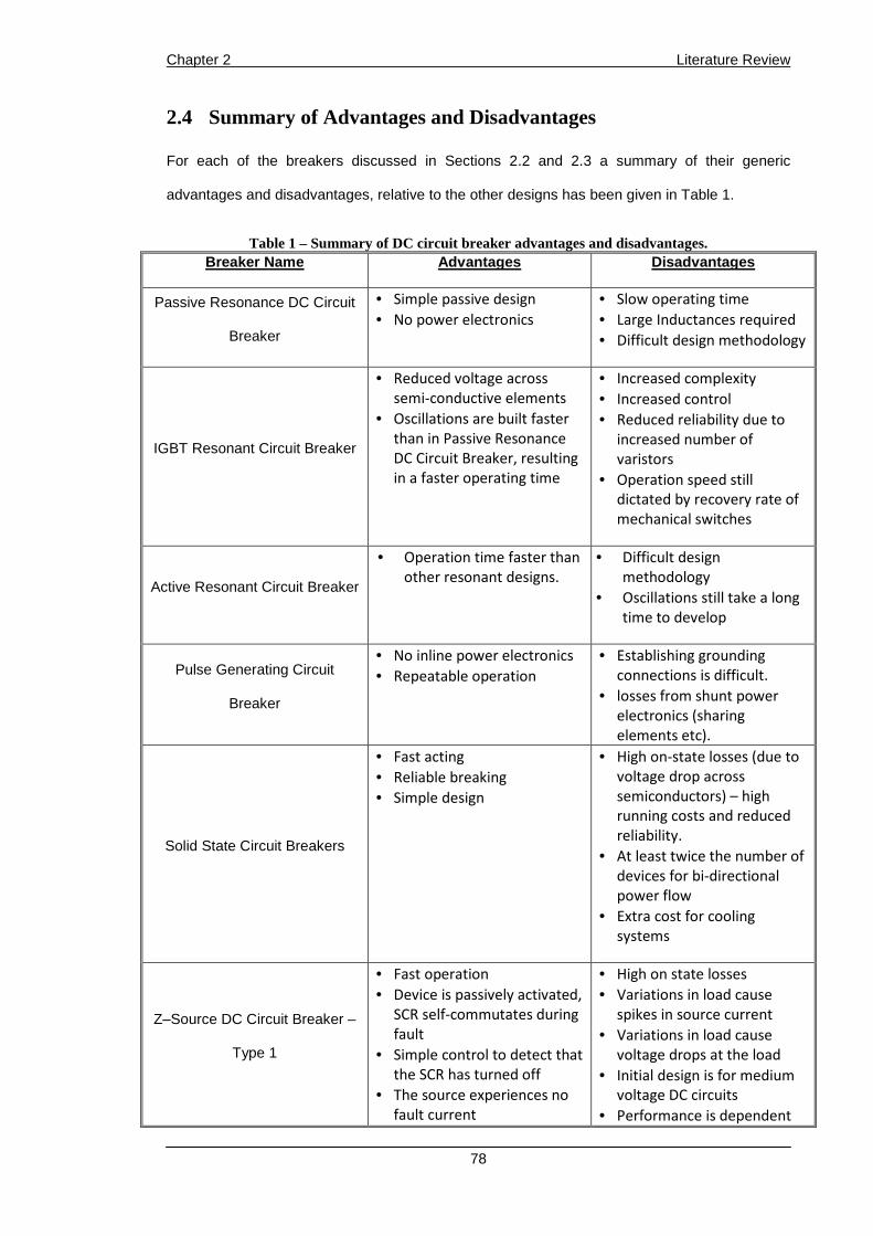
Chapter 2 Literature Review
78
2.4 Summary of Advantages and Disadvantages
For each of the breakers discussed in Sections 2.2 and 2.3 a summary of their generic
advantages and disadvantages, relative to the other designs has been given in Table 1.
Table 1 – Summary of DC circuit breaker advantages and disadvantages. Breaker Name Advantages Disadvantages
Passive Resonance DC Circuit
Breaker
• Simple passive design
• No power electronics
• Slow operating time
• Large Inductances required
• Difficult design methodology
IGBT Resonant Circuit Breaker
• Reduced voltage across
semi-conductive elements
• Oscillations are built faster
than in Passive Resonance
DC Circuit Breaker, resulting
in a faster operating time
• Increased complexity
• Increased control
• Reduced reliability due to
increased number of
varistors
• Operation speed still
dictated by recovery rate of
mechanical switches
Active Resonant Circuit Breaker
• Operation time faster than
other resonant designs.
• Difficult design
methodology
• Oscillations still take a long
time to develop
Pulse Generating Circuit
Breaker
• No inline power electronics
• Repeatable operation
• Establishing grounding
connections is difficult.
• losses from shunt power
electronics (sharing
elements etc).
Solid State Circuit Breakers
• Fast acting
• Reliable breaking
• Simple design
• High on-state losses (due to
voltage drop across
semiconductors) – high
running costs and reduced
reliability.
• At least twice the number of
devices for bi-directional
power flow
• Extra cost for cooling
systems
Z‒Source DC Circuit Breaker –
Type 1
• Fast operation
• Device is passively activated,
SCR self-commutates during
fault
• Simple control to detect that
the SCR has turned off
• The source experiences no
fault current
• High on state losses
• Variations in load cause
spikes in source current
• Variations in load cause
voltage drops at the load
• Initial design is for medium
voltage DC circuits
• Performance is dependent
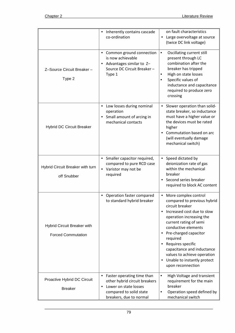
Chapter 2 Literature Review
79
• Inherently contains cascade
co-ordination
on fault characteristics
• Large overvoltage at source
(twice DC link voltage)
Z–Source Circuit Breaker –
Type 2
• Common ground connection
is now achievable
• Advantages similar to Z‒
Source DC Circuit Breaker –
Type 1
• Oscillating current still
present through LC
combination after the
breaker has tripped
• High on state losses
• Specific values of
inductance and capacitance
required to produce zero
crossing
Hybrid DC Circuit Breaker
• Low losses during nominal
operation
• Small amount of arcing in
mechanical contacts
• Slower operation than solid-
state breaker, so inductance
must have a higher value or
the devices must be rated
higher
• Commutation based on arc
(will eventually damage
mechanical switch)
Hybrid Circuit Breaker with turn
off Snubber
• Smaller capacitor required,
compared to pure RCD case
• Varistor may not be
required
• Speed dictated by
deionization rate of gas
within the mechanical
breaker
• Second series breaker
required to block AC content
Hybrid Circuit Breaker with
Forced Commutation
• Operation faster compared
to standard hybrid breaker
• More complex control
compared to previous hybrid
circuit breaker
• Increased cost due to slow
operation increasing the
current rating of semi
conductive elements
• Pre-charged capacitor
required
• Requires specific
capacitance and inductance
values to achieve operation
• Unable to instantly protect
upon reconnection
Proactive Hybrid DC Circuit
Breaker
• Faster operating time than
other hybrid circuit breakers
• Lower on state losses
compared to solid state
breakers, due to normal
• High Voltage and transient
requirement for the main
breaker
• Operation speed defined by
mechanical switch

Chapter 2 Literature Review
80
current flow via LCS and
ultra-fast disconnector
• Highly controllable
Capacitive Hybrid Circuit
breaker
• Thyristor based design
rather than IGBT.
Therefore higher current
ratings.
• Voltage contouring
achievable
• Lower series inductance.
• Pre-emptive operation not
achievable
Hybrid Circuit Breaker with
Inductive Commutation Booster
• No inline power
electronics.
• Slower than other hybrid
designs.
• Difficult to establish design
methodology.
Superconducting Circuit
Breaker
• No conduction losses
• Limits fault current in
worst case
• Cryogenic equipment
expensive
• Uncontrollable
C-EPRI Circuit Breaker
• No isolated power supply
required
• Can operate as current
flow controller as well
• Highly controllable
• Breaking capability limited
by IGBTs
Double Hybrid Circuit Breaker
(DHCB)
• Low loss
• Uses established
technology
• Twp mechanical switch
required
• Commutation based on
arcing
Super-Hybrid Circuit Breaker
(SHCB)
• No conduction losses
• Passive commutation
• Cryogenic equipment
expensive
• Uncontrolled commutation
Super-Hybrid Circuit Breaker
with Snubber (SHCB-S)
• No conduction losses
• Passive commutation
• Can decouple operation
time and mechanical
switch.
• Cryogenic equipment
expensive
• Uncontrolled commutation
2.5 Suitability for Various Applications
Table 2 summarizes the suitability for three potential applications for the circuit breakers
discussed in the previous section. Such categorization is based on the experience of the
Author, and therefore only indicates which circuit breaker topologies merit further investigation
into their application in such areas.
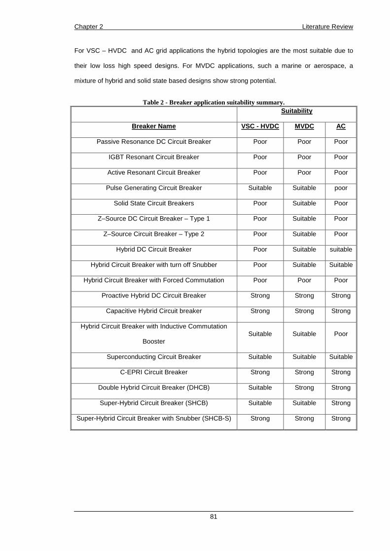
Chapter 2 Literature Review
81
For VSC – HVDC and AC grid applications the hybrid topologies are the most suitable due to
their low loss high speed designs. For MVDC applications, such a marine or aerospace, a
mixture of hybrid and solid state based designs show strong potential.
Table 2 - Breaker application suitability summary. Suitability
Breaker Name VSC - HVDC MVDC AC
Passive Resonance DC Circuit Breaker Poor Poor Poor
IGBT Resonant Circuit Breaker Poor Poor Poor
Active Resonant Circuit Breaker Poor Poor Poor
Pulse Generating Circuit Breaker Suitable Suitable poor
Solid State Circuit Breakers Poor Suitable Poor
Z‒Source DC Circuit Breaker – Type 1 Poor Suitable Poor
Z–Source Circuit Breaker – Type 2 Poor Suitable Poor
Hybrid DC Circuit Breaker Poor Suitable suitable
Hybrid Circuit Breaker with turn off Snubber Poor Suitable Suitable
Hybrid Circuit Breaker with Forced Commutation Poor Poor Poor
Proactive Hybrid DC Circuit Breaker Strong Strong Strong
Capacitive Hybrid Circuit breaker Strong Strong Strong
Hybrid Circuit Breaker with Inductive Commutation
Booster Suitable Suitable Poor
Superconducting Circuit Breaker Suitable Suitable Suitable
C-EPRI Circuit Breaker Strong Strong Strong
Double Hybrid Circuit Breaker (DHCB) Suitable Strong Strong
Super-Hybrid Circuit Breaker (SHCB) Suitable Suitable Strong
Super-Hybrid Circuit Breaker with Snubber (SHCB-S) Strong Strong Strong

Chapter 2 Literature Review
82
2.6 Relevant Standards
This section of the chapter reviews some of the existing DC breaker test standards and their
relevance to the development of a HVDC circuit breaker standard. While the majority of test
standards for HVDC circuit breakers will probably be new material developed specifically for the
application, some of the existing DC breaker standards may be relevant and provide an initial
method for testing. The HVDC breaker tests themselves may be of a different nature, but the
type of test i.e. what one is testing for, will likely be similar to existing methods.
2.6.1 IEC: 61992-2
For mechanical circuit breakers (current breaking switches), tests could be adapted from IEC
61992-2 [56]. IEC 61992-2 covers DC traction circuit breakers and this standard provides
guidance for mechanical and semiconductor circuit breakers [56]. Voltage ratings and
associated test techniques may be directly translated from IEC 62991-2 into a new standard.
The most applicable sections are those which cover very high speed current limiting circuit-
breakers, known as type V. The operation speed of “very high speed breakers” is defined as
less than 2 ms and limits the peak fault current experienced by the system.
2.6.2 IEC: 62271
IEC 62271 covers high voltage switch gear, and part 100 covers AC circuit breakers [57]. In
Section 6 of part 1 in IEC 62271, the tests for any high voltage switch are discussed. This
covers dielectric tests, radio interference, main path resistance tests, temperature rise tests,
short time current withstand, making and breaking tests, tightness tests, mechanical tests, and
environmental and dielectric tests on auxiliary equipment [58]. Most importantly, most of these
tests are likely to provide a good starting point for a DC equivalent standard, as the tests appear
to be non-specific to AC circuit breakers.
2.6.3 IEC: 62501
IEC 62501 is a standard which is used to test VSC valves for converters. These tests cover the
testing of the support structure of individual and multiple valves, dielectric tests, IGBT over
current tests, insensitivity to electromagnetic disturbance tests and short-circuit current tests
[59].
Chapter 2 Literature Review
83
A semiconductor HVDC circuit breaker or a HVDC circuit breaker which uses a string of
semiconductors (typically IGBTs) to break the current will be of a similar structure to a VSC
valve. Such designs are discussed in sections 2.2.2 to 2.2.5 and 2.2.8 to 2.2.15, making this
standard highly relevant.
2.6.4 IEC: 60700
IEC 60700 covers valves for current source HVDC valves, which are commonly made from
thyristors. Thyristor stacks are exploited in the designs given in sections 2.2.3, 2.2.4, 2.2.6,
2.2.7 and 2.2.12. Thyristor stacks are likely to be manufactured in the same way as valves for
current source converters, making tests that would normally cover such valves relevant.
2.7 Circuit Breaker Definitions
The standard definitions for AC circuit breakers do not directly translate across to HVDC
protection. The time frames and dynamics involved do not suit such descriptions. The
topologies for DC protection are also fundamentally different and cannot be fully encompassed
by the terms traditionally used in AC protection.
AC circuit breakers have a relatively long time to act compared to DC circuit breakers. Typically,
the fault currents that an AC circuit breaker is interrupting will have nearly reached steady state
by the time the protection acts, but this is not always the case.
HVDC circuit breakers will be required to act before the DC fault current has reached a steady
state value, due to the limitations of the electronics within the circuit breakers and the
converters themselves. DC circuit breakers will therefore be classified in the same manner as
Type-V circuit breakers in IEC 61992, so called “Current Limiting” breakers, as they open before
the high steady state current level is reached [56].
As discussed in this chapter, the structure of the circuit breakers is also very different. Their
nature will likely be modular for HVDC applications, and they will have multiple stages of
operation, rather than acting as a simple switch which is either open or closed.

Chapter 2 Literature Review
84
Based on the development of several industrial prototypes, hybrid topologies are seen as the
preferred topology of choice. The following section first describes the multi-stage operation of
hybrid circuit breakers in generic terms.
Second, standard definitions for the time ratings of a HVDC circuit breaker are given. These
have been provided to allow consistent notation throughout the thesis, and to provide a basis for
future researchers to work from.
2.7.1 Protection Operation
2.7.1.1 Circuit Breaker Description and States
Hybrid circuit breakers contain several branches within their designs. Each branch has a
specific function. The branches are typically arranged as shown in Figure 43, and are described
by the terms Primary Branch, Secondary Branch, and Energy Absorption.
Figure 43 ‒ Layout of hybrid HVDC circuit breaker within DC tr ansmission line.
For this thesis, the following definitions have been applied to these names:
• Primary Branch: The Branch of the circuit breaker that conducts the current during
normal operation.
• Secondary Branch: A Branch, or Branches, that conduct the fault current for a short
period of time.
• Energy Absorption Branch: The branch which limits the voltage across the circuit
breaker and absorbs any additional energy from the DC grid.

Chapter 2 Literature Review
85
Typically the current is commutated from the primary branch to the secondary branch during the
circuit breaker’s operation. This is commonly referred to as “commutation time”. For this thesis
the following definitions have been adopted:
• Commutation Time: The time taken for the current in the primary branch to decay to
zero, or so close to zero that the next stage in the circuit breaker’s operation can take
place.
• Commutation: The movement of current between branches in a circuit breaker.
As there are multiple stages in any HVDC circuit breaker’s operation, the circuit breaker has to
be described by more than the two simple states of “Open” and Closed”. The circuit breaker
moves from Closed to Open, and from Open to Closed via other states. Figure 44 shows a flow
diagram for a generic hybrid circuit breaker.
Figure 44 ‒ State flow diagram for a hybrid circuit breaker.
When the circuit breaker is to transition from Closed to Open, it must first go into a commutating
state, where current is transferred from primary branch to secondary branch. This takes a
specific amount of time, and the circuit breaker can then only transition into “Possible to Open”
state, once the mechanical switch has opened in the primary branch.
There is then a delay in transitioning from “Possible to Open” into the “Open” state. This delay is
equal to at least the time it takes to turn off the secondary branches that are conducting.
Additional delay time may be added here, while the protection locates the fault.

Chapter 2 Literature Review
86
The circuit breaker must also be able to reset from any of the states that exist between “Closed”
and “Open”. The state “Full Reset” would be akin to a normal re-closure operation. The state
“Half Reset” is required if the circuit breaker has progressed through to the “Possible to Open”
state, but does not interrupt the flow of current.
The commutating state can be said to encompass movement of current from the primary branch
to the secondary branch, and vice versa.
2.7.2 Protection Operation Philosophy
Usually when protection is discussed, operations are thought of as serial, meaning that each
stage in the protection only starts after the previous stage has finished. If the time is taken for
the entire protective action to occur (+,%!) is broken down into three separate stages, Fault
Detection (+,)--), Location (+,!-), and Operation (+,!-.! ), then we can consider the
protection system to operate as shown in Figure 45.
Figure 45 ‒ Series protection philosophy.
The following definitions have been adopted for this thesis:
• Fault Inception ( /0): The moment the electrical conditions of the network at the point
the protection exists change, resulting in an over current condition.
• Detection Time: The time it takes from the fault inception to the moment the protection
is aware that there is a fault.
• Location Time: The time taken for the protection to decide which circuit breakers to
open from the moment a fault is detected.
• Operation Time: The length of time taken for the circuit breaker to transition from the
“Closed” state to the “Open State”.

Chapter 2 Literature Review
87
For HVDC applications, there are significant time constraints on the protection. The total time
available for a protection operation is estimated between 2 and 5 ms, however this is still open
to debate [19]. This has lead to the concept of parallel protection systems, which is depicted in
Figure 46.
Figure 46 ‒ Comparison of series and parallel protection philosophies.
Figure 46 shows that initiating the circuit breakers operation at the moment the fault is detected
allows for a reduction in the overall protection time. The parallel nature of this protection system
also allows some time for communication between circuit breakers, shown as (+,!1). Protection systems are likely to be parallel in nature, and two manufacturers have proposed
their own specific implementations of the generic concept discussed here. Alstom/GE have
proposed “Open Grid” and ABB have proposed “pre-emptive” control [60, 61].
2.7.3 Breaking Time definitions
Standard definitions of the key dynamics seen in HVDC circuit breakers are required. Figure 47
shows a typical fault current, with the labelled time and current ratings. This image is only meant
to be illustrative. The dynamics have been exaggerated to allow the definitions to be drawn
easily.

Chapter 2 Literature Review
88
Figure 47 ‒ Time ratings for DC circuit breakers.
Interruption time ( /23/): The time between fault inception and the circuit breaker building
sufficient voltage to substantially oppose the fault current. This will usually occur with the turn off
of the secondary branch, and a negative fault current derivative. Interruption time is key, as this
is the time that defines the peak current the converter and the circuit breaker are exposed to.
Typically when circuit breaker operation times are quoted at 2 – 5 ms, it is the interruption time
that is being referred to.
Commutation Time( /456): The time taken for the current in the primary branch to decay to
zero, or so close to zero that the next stage in the circuit breaker’s operation can take place. As
will be shown in Chapter 4, the commutation time is not a fixed parameter. Therefore this
quantity will need to be specified over a range, stating the shortest and longest possible times
over a range of system conditions.
Clearing Time ( /478):The time taken from fault inception, to the moment that the DC line current
reaches zero, or the knee current of the varistors (9 --) is reached. This is different to the total
protection time (+,%!) as the total protection time must account for secondary layers of
protection. As will be discussed in Chapter 4, some circuit breakers may be designed to sink
several hundred Amps at the DC link voltage.
Chapter 2 Literature Review
89
Current Limit Operation Time ( /726): The time at which the circuit breaker starts to operate as
a fault current limiter. Some hybrid circuit breaker designs are capable of operating as fault
current limiters, so as to provide addtional time for operation of fault location systems.
2.8 Summary
This chapter has outlined a number of existing topologies for DC circuit breakers. Their
operation has been described and some discussion given to their suitability for VSC HVDC grid
application. Several novel topologies have been proposed showing some of the new
technologies that may be used in future HVDC circuit breakers. A brief review of relevant
existing standards has been given. Such standards may provide a foundation for future testing
regimes.
The operation of HVDC protection systems has also been briefly discussed, and the concept of
parallel operation introduced. Standard terms used to describe the protection used in this thesis
have been defined. Time ratings for the circuit breaker have also been defined in order to
provide consistent notation throughout this thesis.

Chapter 3 Converter Fault Analysis and FCEs
90
Chapter 3: Converter Fault
Analysis and Fault Current
Envelopes
3.1 Introduction
An understanding of the types and levels of fault currents that a DC circuit breaker may be
subjected to during its lifetime is an essential area of knowledge for the development of such
technology. Without this understanding, it is not possible to define a relevant test environment
for the equipment that specifically replicates the VSC-HVDC environment. The transient
behaviour of all equipment that is capable of contributing to fault currents must be understood in
order to determine the effect on the DC fault current.
As shown in Chapter 2 of this thesis, many of the proposed circuit breaker topologies include
new techniques and technologies that are not typically seen in AC protection equipment. Most
notable is the presence of high power electronic switches, sometimes performing several
different functions within the circuit breaker. Any method of rating HVDC protection equipment
must be able to compensate for the various technologies that may exist within the circuit
breakers.
The component with the highest influence over the fault current is probably the converter
located at the interface of the AC and DC grids. With the advent of the MMC, and other
topological variations, the converters’ measurement and control systems will also play a
significant role in defining the DC fault current.

Chapter 3 Converter Fault Analysis and FCEs
91
One of the main benefits of the VSC is its controllability. The VSC is able to rapidly respond to
changes in its environment and provide beneficial action. The beneficial action can even provide
fault current limitation for certain converter topologies [28, 62].
However, for protection system design, this flexibility can present additional challenges. Control
structures which provide benefits under certain operating conditions may cause problems during
or immediately after DC faults. There are many control loops associated with a VSC, and
considering the number of available control strategies for each loop and the number of
measurements used for control, it is clear that predicting the exact level of a fault current is a
significant challenge.
Previous work on the characterisation of currents that DC circuit breakers are required to handle
has often neglected the presence of series inductance, which all hybrid circuit breakers require
[63, 64]. Other analyses have only looked at the steady state fault currents that flow in the
HVDC system [65, 66]. Steady state analysis is unsuitable for HVDC circuit breakers as they
are likely to be classified in the same way as “V Type” circuit breakers in railway applications. V
Type breakers are described as “current limiting” as they interrupt the current before it reaches
a steady final value [56]. Every paper in the prior art investigating fault currents in a MMC
system only focuses on a single converter arrangement, and hence these analyses do not
encompass the variability that will intrinsically exist due to the variation in converter designs.
Understanding how each converter will respond under all operating conditions and control
system configurations is unachievable in the short term, as the detailed knowledge required to
make accurate predictions will not be supplied by the manufacturers for commercial reasons.
However, the limitations of the system can be understood. Through the use of system limits,
criteria can be established which allow specifications for HVDC circuit breakers to be
developed.
This chapter presents fault analyses for two different converter topologies, investigates the
limitations of the faulted circuits, and introduces the concept of Fault Current Envelopes (FCEs).
FCEs provide a method of encapsulating the transient behaviour of the converters and are used
to provide criteria for the design of circuit breakers and their synthetic test circuits. FCEs can be

Chapter 3 Converter Fault Analysis and FCEs
92
developed for any converter topology with only limited knowledge of the converter’s control
system.
The concept of FCEs can be applied to other future converter topologies and to different grid
structures. They provide a standard method to assess the form of fault currents produced by a
given converter topology, and can be used to quantitatively compare the DC fault performance
of complete protection systems. They may also be used to predict the required operating times
of the protection system.
3.2 Fault Current Envelopes
3.1.1 Current Rating of DC Circuit breakers
In order for a test circuit to be designed properly, there must be a specification for its operation
to be compared against. Without such criteria, any tests performed on a circuit breaker cannot
prove whether it is capable of operating in the desired environment, or not.
The specification must be general enough to allow any manufacturer to design a DC circuit
breaker with a topology of their choice, while being specific enough to exclude any circuit
breaker which does not meet the required standard.
AC Circuit breakers are rated based on a wide range of parameters, such as voltage, insulation
level, frequency, normal current, short-time withstand, rated short-circuit breaking current,
transient recovery voltage, short-circuit making current and many others [57]. DC circuit
breakers will be rated in a similar manner, with some additional factors that are specific to the
DC environment.
In terms of current rating, it is too simplistic to rate a DC circuit breaker with a simple current
level. As was shown in Chapter 2, many circuit breakers will contain a multitude of power
electronic components, some of which contain several varieties of semiconductor switch [52].
Other circuit breakers may contain superconductors, as well as other technologies not
traditionally seen in short circuit protection equipment [P1].
For thyristors, conduction power losses in the devices are very important in determining their
short time current carrying capability. This is usually done via their I2T rating, which is a

Chapter 3 Converter Fault Analysis and FCEs
93
measure of the amount of energy that can be dissipated in the device. Ensuring that this limit is
not exceeded is key to keeping the device’s temperature within its rated limits [67].
For IGBTs, the energy dissipation is also important, but is also dependent on the snubber circuit
design, as this will dictate the voltage rise across the device during switching events (which may
also contain other semiconductor switches) [68, 69]. The peak device current is also important
as the devices may de-saturate, if this is exceeded, resulting in an increase in the devices’ on
state voltage, and producing additional power losses in the device, as well as secondary effects
in the circuit breakers operation (as will be discussed in Chapter 4).
Figure 47 ‒ Example fault current and potential ratings.
Figure 47 shows an example fault current that a circuit breaker could be subjected to. It can be
seen that any CB current rating based on the steady state current(I;;), would ignore the initial
transient, that would contribute to the temperature rise seen in the semiconductor device.
Hence, the work described in [70] cannot rate a circuit breaker.
A circuit breaker rating based on the RMS current alone (I<=>), is also unsuitable since the
power losses in the IGBTs will depend on the instantaneous current they are carrying. Thus a
RMS current rating would result in an insufficient representation of the energy dissipated in the
device.

Chapter 3 Converter Fault Analysis and FCEs
94
A current rating based on peak current alone(I?@AB), is also insufficient as semiconductor power
losses and junction temperature rise are also influenced by current values before and after the
peak. Therefore the work described in [71], while also not appropriately considering DC circuit
breaker technologies, cannot be directly used in a standard either.
Therefore, in order to ensure that all the power electronics are tested properly, so that the
breaker is capable of operating in this transient condition, a detailed understanding of the range
of fault currents the circuit breaker will be subjected to is of paramount importance in defining
the current specification for a circuit breaker.
3.1.2 The Concept of Fault Current Envelopes
As discussed in Section 3.1.1 it is necessary to understand the profile (shape of the fault
currents) and range (different types of profile) of fault currents that a circuit breaker may be
subjected to. In order to meet this need the concept of Fault Current Envelopes (FCEs) was
developed.
A FCE is a line which defines the border between what currents are possible and which currents
are not possible. This line is drawn based on the known physical limitations of the HVDC
network. The concept of a fault current envelope is shown in Figure 48.
Figure 48 ‒ Concept of how a fault current envelope may be used.

Chapter 3 Converter Fault Analysis and FCEs
95
The FCE should totally encapsulate, or provide a very strong guideline for all possible fault
currents. This ensures that any peaks in the fault current are encapsulated by the specification
and that the energy dissipation within the circuit breaker will be appropriate.
The FCE is used in conduction with a maximum protection operation time (∆,%! or ∆, ) to
define a test area, as shown in Figure 49. This test area can then be compared to the fault
current generated by a given test circuit. Providing the current of the test circuit exceeds or
closely matches the fault current envelope over the time period of interest, the test current is
valid. This allows the suitability of any existing test circuit to be established, as well as providing
a specification for the development of a new test circuit.
FCEs provide a generalized method to assess the suitability of any test circuit’s current pulse,
without defining the structure of the physical test circuit. The feature allows the manufacturer or
independent testing facility to construct the test circuit in the manner of their choosing.
Figure 49 ‒ Application of test area, when comparing to test circuit's current.
This section has described the concept of fault current envelopes and how they would be used
in a laboratory and as a tool to develop a specification for a given test circuit. In order to draw
these envelopes for a real case, the limitation of the fault current needs to be understood. i.e.
how the boundary is drawn between possible and not possible. Thus there is a need to
Chapter 3 Converter Fault Analysis and FCEs
96
understand how the converters, cables, and AC grid may influence the fault currents for a
proposed protection system.
The type of converter topology will have a major impact on the fault currents, as will the control
strategy for MMCs. If FCEs become a standard method of developing a specification for test
circuits, then FCEs must be developed for the key converter topologies. Further amendments
will be needed as required to compensate for different protection strategies, grid topology, and
converter control techniques.
The following sections will present fault analyses of two types of converter (TLC and HB-MMC).
The analyses describe the fault current where necessary and use the limitations of each
converter topology to develop envelopes based on this understanding.
3.3 Two-Level Converter Fault Analysis
This section of the chapter details the response of a Two-Level Converter (TLC) to a DC fault.
The analysis derives the basic equations to describe the fault currents, and provides a simplified
electrical model that allows the limitations of the fault circuit to be understood.
3.1.3 Pole-to-Pole faults
3.1.3.1 Description
A simplified structure of a TLC is shown in Figure 50. When a terminal fault occurs at locationD%
the cable is short circuited close to the converter, without bypassing the DC side reactors ()$).
As the converters contain power electronic switches, which will change their state during a fault,
a single equation cannot be developed to describe the fault current. The converter’s response to
a fault must be described by a sequence of stages, with each stage having a separate
equivalent electrical circuit, from which a governing equation can be developed.
Stage A – Capacitor Discharge:
As shown in Figure 50 the DC capacitance comprises two capacitors of value 2)$ centre
tapped to earth. When a fault occurs, the effective DC side capacitance ()$) discharges,
building a high current in the circuit breaker’s inductance ()$). An additional current flows from
the AC grid via the converter’s switches.

Chapter 3 Converter Fault Analysis and FCEs
97
For pole-to-pole faults, once the DC voltage across )$ has decreased to zero, the capacitance
voltage will start to reverse. After the capacitance voltage has reached a certain level (typically
<1 kV), the voltage will forward bias the converter’s diodes, causing the capacitor current to
commutate into the converter’s diodes [C2][72]. The switching of the converter’s diodes
represents a significant change in the equivalent electrical circuit, thus a new stage in the
converter’s fault response begins.
Stage B – Free Wheeling:
At the moment all six diode stacks in the TLC become forward biased, they simultaneously
short circuit the AC terminals of the converter. Due to the low impedance of the diode stacks in
their forward biased condition, the AC and DC sides of the converter become decoupled. Thus
the AC grid cannot contribute any additional energy to the DC fault current seen by the circuit
breaker while the diodes remain forward biased. However, high currents will still flow within the
converter, and the AC grid will be subjected to a low impedance.
The peak DC fault current will decay from the moment the diodes short circuit the terminals of
the converter, and only after the instantaneous DC fault current in each arm becomes less than
the AC fault current will zero crossings be generated in the diode stacks, resulting in switching
events. These switching events will alter the electrical parameters of the circuit, resulting in the
start of the next stage.
Stage C – Rectifier and Pseudo-rectifier Operation:
As the current in each diode stack will be different, being comprised of both DC and AC current,
the number of diode stacks that are forward biased will change between 2 and 6 transiently (at
least 2 being in the same leg). While the converter is in this stage, the converter will behave as
a pseudo-rectifier, meaning it will rectify but not with the normal number of conducting diode
stacks. Only once the DC fault current has decayed sufficiently to allow only 2 diode stacks to
be forward biased at any moment will the converter start to behave as a rectifier.

Chapter 3 Converter Fault Analysis and FCEs
98
Figure 50 ‒ Simplified TLC structure.
It may take a significant amount of time for the converter to revert to rectifier operation. The time
taken will be significantly longer than would normally be seen in a point-to-point HVDC system
due to the high series inductance that the circuit breaker requires (typically 100 mH per pole),
which extends the decay time of the DC current.
Based on the parameters used in the verification simulations performed as part of this work, it is
unlikely that the converter will be able to reach stage C. It was observed that in simulations it
takes around 250 ms for the converter to start to behave as a rectifier. This time is heavily
dependent on the amount of stored energy in the DC side of the converter, parasitic
resistances, and series DC side inductance.
For the purposes of this Chapter, it is assumed that the TLC only operates in stages A and B.
Appendix 5 provides a paper published by the Author [PS1], where the pseudo-rectifier
operation is discussed in detail.
3.1.3.2 Simplified Terminal Fault Current Analysis
For a TLC system, the equivalent circuit used to develop descriptive equations of the converter
under a fault is shown in Figure 51 and consists of a capacitor in parallel with a current source
and a diode. These are connected in series with an inductance and in the case where non-
terminal faults are considered, a transmission line. The equivalent circuit assumes a grounded
midpoint.

Chapter 3 Converter Fault Analysis and FCEs
99
The current in the circuit breaker comprises two components, the AC side injection ('$) and the
capacitive discharge component ($'). '$ is the current that flows from the converter’s
switches into the capacitance. The current source is assumed to feed the same value of current
as the initial DC side current, however for longer periods of time this assumption is no longer
valid.
F(,) = HI)$)$ J(K,) + H (3.1)
MNO, ≤ Q2K, K = 1S)$)$
For terminal faults, the current in the circuit breaker can be described by Equation (3.1), from
the moment the cable fault occurs, until the converter’s diodes become forward biased. The
maximum fault current (T'U) at the moment the diodes become forward biased is given by
Equation (3.2). The current rises fastest when the cable voltage first collapses at time zero, and
the maximum fault current derivative is given by Equation (3.3).
TV = HI)$)$ + H (3.2)
W W,XYZ = H)$ (3.3)
Figure 51 ‒ Simplified equivalent circuit for TLC. Terminal fa ults occur at location FT. Non-terminal fault location shown as FNT.

Chapter 3 Converter Fault Analysis and FCEs
100
3.1.4 Pole-to-Ground Faults
Pole-to-ground faults have a different fault sequence than pole-to-pole faults. However these
differences are usually seen in the voltages that appear across the converter. The currents that
the circuit breaker sees are similar enough that the analysis for pole-to-pole faults is sufficient
for the development of a fault current envelope, as will be shown in the verification simulations
of Section 3.5.
3.1.5 Non-Terminal Faults
3.1.5.1 Description
When a fault occurs at a distance from the VSC, additional phenomena must be taken into
account. The cable voltage for terminal faults is clamped close to zero, whereas for non-
terminal faults the cable voltage varies rapidly due to travelling waves propagating between the
converter and fault.
This phenomenon has been observed in AC protection systems, but does not have such a
significant impact on fault currents due to the longer time protection frames and shorter
distances in AC systems. However, due to the long distances and short time frames involved in
HVDC protection systems, such phenomena play a more considerable role.
The travelling waves can be described with a Bewley lattice diagram, and for a single cable
system, the relevant diagram is shown in Figure 52. Distance is shown in the [ direction, and
time in the \ direction. The travelling waves travel along the cable at speed #.
A fault occurs at time ,H, at distance D along the cable. At the point along the cable where the
fault occurs,, the voltage collapses from )$ to zero due to the fault’s low impedance. The
collapse in voltage propagates from the fault towards the converter at speed #. The collapse in
voltage is in effect a negative voltage wave that propagates down the cable, in the reverse
direction (−^), and is shown in Figure 52 as V
The wave is attenuated as it propagates down the cable towards the converter. Once the first
reverse travelling wave (V ) arrives at the converter at time (,a), a reflection occurs due the
converter presenting a discontinuity to the travelling wave. The cable voltage at that location
then becomes the sum of the initial voltage prior to the arrival of V , the first reverse travelling

Chapter 3 Converter Fault Analysis and FCEs
101
(V ) wave and the first forward travelling wave(Vb). The moment the first reverse travelling
wave arrives at the converter (,a) is the moment that the circuit breaker first “sees” the fault.
Unless information is fed via a shorter path, or the travelling waves travel significantly slower
than the speed of light, it is physically impossible for the circuit breakers to be aware of the
presence of the fault before this time.
The first forward travelling wave (Vb) travels back down the cable towards the fault, and when it
arrives back at the fault a second reverse travelling wave is generated (V ) . This process
repeats causing the cable voltage at the converter to change upon the arrival of each reverse
travelling wave. Each reverse travelling wave will arrive at the converter after a time delay
defined by the speed of the travelling waves (#) and the distance to the fault (), shown as (')
in Figure 52. The same process is true for the current wave. However, each subsequent change
will be smaller due to losses in the cable attenuating the voltage and current waves.
Figure 52 ‒ Bewley lattice diagram also known as bounce diagram. Fault occurs at time t0 at distance D from the converter.

Chapter 3 Converter Fault Analysis and FCEs
102
3.1.5.2 Analysis
Obtaining an exact prediction for non-terminal faults, i.e. faults that occur some distance along
the cable, has been attempted in the prior art [73]. However, this is not strictly necessary for the
development of a fault current envelope, which is concerned with the limitations of the system.
When faults occur at a distance from the converter, there is additional resistance in the fault
circuit which inherently limits the steady state fault currents to below those one would expect to
see in a terminal fault. However, for a short time fault currents will exceed those seen from a
terminal fault.
The cable voltage at the moment the reverse travelling wave arrives (,a) at the converter is
given by Equation 3.4. The cable voltage is the sum of the initial voltage, plus the sum of the
first reverse travelling wave and the first forward travelling wave.
$ = )$ + + b (3.4)
The first forward travelling wave (Vb) is the product of the reflection coefficient (c$) at the
converter and the reverse travelling wave (V ). If one assumes that the cable voltage does not
attenuate the magnitude of the voltage wave, and that the voltage wave is an ideal step, the
cable voltage is given by Equation (3.5). This equation shows that for a reflection coefficient
above zero, the cable voltage will become negative, since Γe can only have a magnitude
between 0 and 1.
$ = )$ + (1 + c$) = )$f1 − (1 + c$)g (3.5)
The reflection coefficient for fast voltage transients can be calculated using Equation (3.6),
wherehH is the characteristic impedance of the cable, and h is the impedance of the converter.
Equation (3.6) shows that the circuit breakers inductance dominates the impedance network for
fast changes resulting in a reflection coefficient close to unity [74].
i jk→mfc$g = i jk→m nh − hHh + hHo = i jk→m pqK)$ −
q K)$r − hHqK)$ − q K)$r + hHs = 1
(3.6)
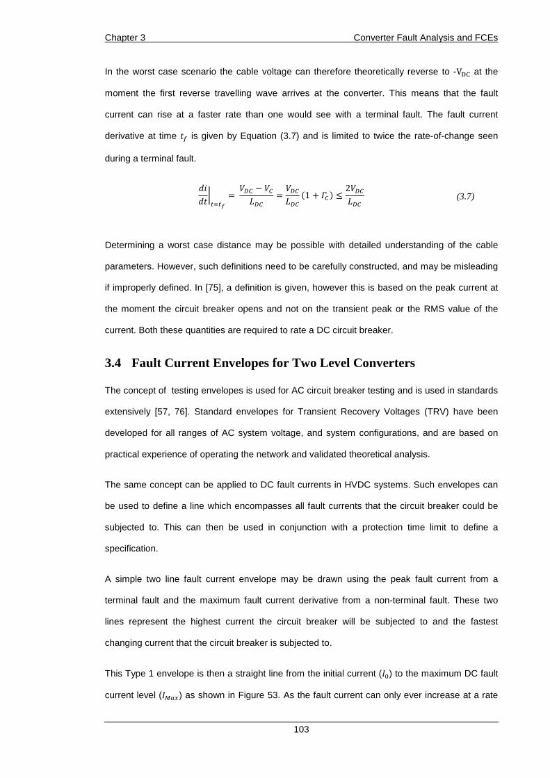
Chapter 3 Converter Fault Analysis and FCEs
103
In the worst case scenario the cable voltage can therefore theoretically reverse to -Vte at the
moment the first reverse travelling wave arrives at the converter. This means that the fault
current can rise at a faster rate than one would see with a terminal fault. The fault current
derivative at time ,a is given by Equation (3.7) and is limited to twice the rate-of-change seen
during a terminal fault.
W W,XYu =)$ − $)$ = )$)$ (1 + c$) ≤ 2)$)$ (3.7)
Determining a worst case distance may be possible with detailed understanding of the cable
parameters. However, such definitions need to be carefully constructed, and may be misleading
if improperly defined. In [75], a definition is given, however this is based on the peak current at
the moment the circuit breaker opens and not on the transient peak or the RMS value of the
current. Both these quantities are required to rate a DC circuit breaker.
3.4 Fault Current Envelopes for Two Level Converters
The concept of testing envelopes is used for AC circuit breaker testing and is used in standards
extensively [57, 76]. Standard envelopes for Transient Recovery Voltages (TRV) have been
developed for all ranges of AC system voltage, and system configurations, and are based on
practical experience of operating the network and validated theoretical analysis.
The same concept can be applied to DC fault currents in HVDC systems. Such envelopes can
be used to define a line which encompasses all fault currents that the circuit breaker could be
subjected to. This can then be used in conjunction with a protection time limit to define a
specification.
A simple two line fault current envelope may be drawn using the peak fault current from a
terminal fault and the maximum fault current derivative from a non-terminal fault. These two
lines represent the highest current the circuit breaker will be subjected to and the fastest
changing current that the circuit breaker is subjected to.
This Type 1 envelope is then a straight line from the initial current (H) to the maximum DC fault
current level (TV) as shown in Figure 53. As the fault current can only ever increase at a rate

Chapter 3 Converter Fault Analysis and FCEs
104
of vwxywx for short periods of time, while the cable voltage is negative, all fault currents will always
match or be below this line. The horizontal line which caps the envelope is the maximum fault
current that a terminal fault could present. The peak current is higher than anything non-terminal
faults could present, due to the additional impedance of the line. Hence all fault currents will
always be encapsulated within the envelope.
Figure 53 ‒ Type 1 and Type 2 envelope structures.
Type 1 envelopes would totally encapsulate all fault currents, however, such an envelope would
produce over-estimates of the fault current in many circumstances, creating a very severe test
specification, potentially inhibiting the application of certain circuit breaker topologies.
In order to reduce the severity of the test specification, a second envelope type was developed.
Type 2 envelopes provide a less severe test specification while still providing a strong
estimation of the fault currents in a DC system.
A Type 2 envelope is drawn using three intersecting lines, as shown in Figure 53. The first line
and the maximum line are the same as the Type 1 envelope. The second line in the envelope is
defined by Equation (3.8) and is a function of the average terminal fault current derivative ('z| )
and a bias term (∆).

Chapter 3 Converter Fault Analysis and FCEs
105
The bias term (∆) is defined by the maximum difference between the terminal fault
approximation given in Equation (3.1) and a linear approximation of the terminal fault current
given in Equation (3.9). The average terminal fault current derivative is given by (3.10), the bias
term (∆) is given by (3.11) using (3.12).
I~A;@(t) = 'z| t + H + ∆
(3.8)
Iy~(t) = 'z| , + H (3.9)
'z| = 2K(T'U − H)Q (3.10)
∆ = (T'U − H) J(K,) − 'z| , ℎOK = 1S)$)$
(3.11)
, = 1K N` 'z|(T'U − H)K
(3.12)
= ∆2H )$r − |'z
(3.13)
T = T'U − H − ∆'z| (3.14)
This bias term (∆) is used to ensure that the biased linear approximation of the terminal fault
current (Equation (3.8)) is always above the terminal fault current, thus entirely encapsulating it.
This ensures that the second line in the fault current envelope provides a strong prediction of
the fault currents. The time at which the Type 2 envelope starts to be defined by Equation (3.8)
is given by Equation (3.13). The envelope is defined by the maximum fault current (I=) at time
T=, given by (3.14).

Chapter 3 Converter Fault Analysis and FCEs
106
3.5 Envelope Example and Verification
3.1.6 Example System
A TLC was simulated in PSCAD to verify the FCE designs. A point-to-point 1 GW, 600 kV (+/-
300 kV) symmetrical monopole TLC was chosen as a representative example case. The
converter was modelled using a Traditional Detailed Model (TDM). The cable length was
chosen to be 250 km and a Frequency Dependent Phase Model (FDPM) was used to represent
the cable [37].
The initial DC current was chosen to be 600 A and the DC side capacitance was 100 µF per
pole. Recent HVDC circuit breaker prototypes can only break around 9 kA [50]. For a breaking
time of 3 ms, the rate-of-change of current needs to be limited to lower than 3 kA/ms (Assuming
an initial current of zero). This rate-of-change of current limit results in 100 mH of inductance
being required per pole [J1][50].
3.1.7 Terminal Fault Current Estimation
A comparison between the analysis developed from the circuit in Figure 51, a computer
simulation of the equivalent circuit, and a TDM PSCAD simulation of a TLC under a pole-to-pole
fault are shown in Figure 54.
Figure 54 ‒ Comparison of simplified model, PSCAD TDM model and Equation (3.1).

Chapter 3 Converter Fault Analysis and FCEs
107
The simulated contributions from the detailed PSCAD model for the AC injection and the
capacitive discharge are shown in the dashed lines of Figure 54. The results show that a plot of
Equation (3.1), a simulation of the equivalent circuit and the TDM model are in strong
agreement. The equivalent circuit can only be used to predict the current in the circuit breaker
and not the constituent components. Equation (3.1) is also only valid until 4.6 ms after the fault,
at which point the converter’s diodes become forward biased.
3.1.8 Fault Current Envelope Example
Simulations were performed using the TDM model changing the distance to the fault for both
pole-to-ground and pole-to-pole faults. The fault resistance was 1 mΩ for each case. The time
delay due the travelling wave propagating from the fault location to the converter have been
removed to allow for an appropriate comparison of terminal and non-terminal fault currents.
Type 1 and Type 2 envelopes were developed for the example system and are plotted
alongside the simulation results from the TDM in Figure 55 and Figure 56. The results show that
Type 1 envelopes always encompass the fault currents, for both pole-to-ground and pole-to-
pole faults. However, the Type 1 envelope over-estimates the fault currents.
Type 2 envelopes provide a very strong estimation of the fault currents that occur in the system.
However, transient over currents occur for the 90 km and 100 km cases. These over currents
will only occur for very short periods however.
In order to mitigate these transient over currents a safety factor can be added to the envelope,
or the bias term (∆) could be increased.

Chapter 3 Converter Fault Analysis and FCEs
108
Figure 55 – Type 1 and Type 2 envelopes compared to simulated fault currents for a range of pole-to-pole faults.
Figure 56 ‒ Type 1 and Type 2 envelopes compared to simulated fault currents for a range of pole-to-ground faults.

Chapter 3 Converter Fault Analysis and FCEs
109
3.6 MMC Fault Current Prediction
To derive a single equation to describe an MMC’s fault current, as many prior art publications
attempt, may be possible if details of the converter’s controls and internal parameters are
known. However, several equations are likely to be required due to the switching events that
occur in the converter’s response to a DC fault.
It is expected that each manufacturer will have their own implementations of the MMC, with
different control systems, measurement systems, electrical components, and physical
structures. Each of these system elements will impact on how much energy the MMC will inject
into the fault and how quickly this energy is injected. As such, exact predictions of the discharge
fault currents are likely to be extremely difficult to derive, as the information required to enter
into such equations will not be widely available.
Since the control structure of a MMC may also change during its operation, in order to provide
additional support to the AC and DC systems, all such predictions would have to be proven for
every possible permutation of control system, as the protection system must always operate,
and be suitable for any eventuality.
However, from the view point of designing a standard, exact predictions are not strictly
necessary. Through the use of fault current envelopes, only the limitations of the system need
to be understood.
This section of the thesis will show how the same envelopes developed in Section 3.4 can be
drawn for the MMC. It must be clearly stated here that the analysis in this section of the thesis
does not attempt to develop an equation to exactly predict the fault current one would see from
an MMC, but is looking at the limitations of the MMC’s operation under some basic operating
assumptions.
Detailed analysis of the converter once it has reached a pseudo-rectifier operation can be found
in Appendix 5, and assumes that the converter blocks quickly, removing the problem of
predicting the discharge current.

Chapter 3 Converter Fault Analysis and FCEs
110
3.7 Modular Multi-level Converter Fault Analysis
3.1.9 Pole-to-pole Fault
3.1.9.1 Description
Figure 57 shows a simplified diagram of a single phase of an MMC converter. The converter
arms are represented as two switches and a capacitance. The upper IGBT-diode pair in each
submodule is represented by a single switch # and #, for the upper and lower arms
respectively. The lower IGBT-diode pair of each submodule is represented by a single switch
# and # for the upper and lower arms respectively. The arm capacitance is shown as$
and the arm inductor is shown as.1. During the converter’s operation, the DC side capacitance varies depending on the number of
submodules inserted. The converter decides how many modules are required in each arm using
a Nearest Level Controller (NLC). As with the TLC, there are switching events in the converter’s
response to a DC fault. However, the MMC’s response includes controlled switching events,
making it a more interesting case. The following sections will describe the MMC’s fault
response, discussing each of the major stages.
Stage A – Discharge:
When a fault occurs, the inserted submodule capacitors discharge into the fault, resulting in a
rapid increase in current. As the fault prevails, submodules are switched in and out of operation.
Once the converter blocks or the submodule capacitors fully discharge, the stored charge in the
parasitic capacitance of the system will discharge very quickly and, in the same manner as the
TLC, the fault current will commutate into the converter’s diodes. For each submodule of the
MMC, the fault current now flows in the lower IGBT submodule diode (# and#). Stage B – Free Wheeling:
The converter’s AC terminals will be subject to a low impedance condition at this moment.
Providing the system impedances are balanced, the AC grid cannot influence the DC fault
current during this stage as the AC current is too low. The DC fault current decays, with a time
constant determined by the system resistance and equivalent DC side inductance (including the

Chapter 3 Converter Fault Analysis and FCEs
111
converter’s arm inductance). When the DC current level falls below that of the AC grid current,
zero crossings are generated in the converter’s diodes, the electrical circuit changes and a new
stage begins.
Stage C – Rectifier and Pseudo Rectifier operation:
When fewer than six converter arms are conducting, the AC grid is capable of influencing the
DC fault current. The amount of influence depends on which arms are conducting and the
electrical parameters.
An analysis has been developed to describe each of these stages in Appendix 5 [PS1].
However, from simulations, when the blocking function of the converter is not modified, the
converter will only provide rectifier operation around 250 ms after fault inception. Thus the
protection systems will most likely operate in stages A and B, making them the relevant stages
for investigation.
Figure 57 ‒ Simplified diagram of a single phase leg of an MMC.
3.1.9.2 Fault Circuit Analysis
To simplify analysis of the converter the following assumptions are made:

Chapter 3 Converter Fault Analysis and FCEs
112
• The converter control structure does not change once a DC fault is detected. This
assumption allows the natural response of the converter to be analysed.
• The converter does not block in the event of a DC side fault. This assumes that the AC
grid is capable of withstanding the disturbance that a DC side fault presents.
The second assumption is not valid over long periods, but allows the natural response of the
MMC to be investigated. As will be shown in Section 3.1.11 the blocking function of the MMC
can be integrated into the envelope’s design once the natural discharge response of the
converter is understood.
In order to predict how the converter will discharge, it is necessary to understand how the
converter calculates the required number of inserted submodules. Typically an NLC uses
Equation (3.15) to calculate the Exact Number of Levels (.1) needed in each arm at any
moment during its operation [36, 77, 78]. Equation (3.15) is then rounded to the nearest
positive integer number. For negative results, the NLC returns a value of zero. The converter’s
instantaneous AC voltage () is added in the numerator for the lower arm, and subtracted for
the upper arm reference voltage. aa is the difference voltage and is the voltage that appears
across one converter arm due to the difference current. The difference current comes from the
instantaneous leg voltages within the converter not beging equal. is the number of available
modules in a single arm [36]. This calculation is performed in conjunction with the capacitor
balancing algorithm, which typically changes the submodule configuration at a frequency of
several kHz.
.1 = .-a.11 = .-a.1)$ = )$2 ± − aa)$
(3.15)
When a DC side fault occurs, the voltage across the submodule capacitors will begin to fall. As
the DC side voltage collapses, Equation (3.16) converges either to the maximum number of
modules in an arm () or to zero. Providing the phase legs’ AC side voltage is higher than the
difference voltage, one arm in each phase leg will eventually insert all its submodules, while the
other will remove all its submodules. In the unusual case when the AC voltage is less than the
difference voltage, both arms in each phase leg will reach either or zero.

Chapter 3 Converter Fault Analysis and FCEs
113
i j→Hf.1g = i j→H p)$2 + )$ s = +∞ → MNO > 0−∞ → 0MNO < 0 (3.16)
In order to get an estimate of the fault current, which is required to develop the envelope, a
reduced equivalent circuit was chosen and is shown in Figure 58. Assuming that the converter
capacitance is fixed will then allow for a simple expression to be derived that roughly predicts
the fault current, given in Equation (3.17).
The problem with this analysis is that the capacitance must vary during the fault. However, the
capacitance will stay within a range, as the number of capacitors and their arrangement is
confined.
IA(t) = T'U sin(ωt + ∅) fort ≤ ∅ − π2ω , ∅ = sin` © IHT'Uª , ω = 1SLteCte
(3.17)
Figure 58 ‒ Reduced equivalent circuit for the MMC.
The lowest possible equivalent capacitance the converter can achieve is when all the
converter’s submodules are inserted (i.e. both arms per phase and this would only occur is
abnormal conditions). This lowest value of capacitance is &$ .
The highest possible capacitance occurs when the sorting algorithm performs very quickly
resulting in the converter switching between two groups of 3N capacitors very rapidly, assuming
that is also the lowest number of submodules that will be inserted in any phase leg. This

Chapter 3 Converter Fault Analysis and FCEs
114
capacitance is $ . Therefore the capacitance the MMC presents to the DC grid ()$) must
always be between &$ and$ , as shown by the equality given Equation (3.18).
312 ≤ ≤ 61
(3.18)
The fault circuit inductance will be dominated by the circuit breaker’s inductance (Lte) and the
converter arm’s inductances (LA°±), Equation (3.19).
L@² = 2Lte + 2LA°±3
(3.19)
3.1.9.3 Peak Fault Current Estimation
The peak fault current that the circuit breaker will experience will be predominately from the
discharge of the converter’s energy into the circuit breaker’s inductance. This analysis assumes
that the converter stays in stages A and B during protective action. The AC grid will contribute
an additional amount to this, but for very fast circuit breakers this amount will also be very
limited as the AC grid will not react to such a fast transient. If the DC fault current at the end of
Stage A is small relative to the AC fault current, the converter will not stay in Stage B for very
long. Hence additional estimates of the peak current will be required if the converter moves into
Stage C.
Equation (3.20) can be used to predict the maximum current obtained if the entire converter’s
capacitive energy is transferred to the circuit breaker’s inductance. However, not all the phase
arms will discharge. From the analysis given in Section 3.1.9.2, only three of the converter’s
arms will fully discharge, while the remaining three will be partially discharged.
T'U = IH + 61V11-³ (3.20)
1 is the submodule voltage,1 is the submodule capacitance,IH is the current at the fault’s
inception,-³is the converter’s equivalent DC side inductance, and1V is number of
submodules within the converter.

Chapter 3 Converter Fault Analysis and FCEs
115
Equation (3.21) sums the proportion that each of converter arm discharges and allows for a
more refined estimation of the peak current due to the converter’s energy. is the ratio of
remaining energy to peak energy in the converter’s arms.
T'U = µH + 11-³ ¶·
Y ¸ (3.21)
3.8 Fault Current Envelopes for Modular Multi-Level Con verters
The structure of the envelope is similar to that developed for the TLC. A difficulty in applying the
envelope is determining an accurate estimation of the terminal fault current, which for the MMC
can only be an approximation.
This uncertainty can be overcome by plotting several envelopes based on the maximum and
minimum capacitance values that the converter can present to the DC side and using Equation
(3.17) to estimate the fault current. As the capacitance will vary within the limits defined by
Equation (3.18), the envelope provides a strong guide for test circuit specification. The modified
and developed envelope is shown in Figure 59.
Figure 59 ‒ Type 1 and three possible Type 2 envelopes for the MMC.

Chapter 3 Converter Fault Analysis and FCEs
116
3.1.10 Example System and MMC Modeling
A 1 GW +/- 300 kV half bridge MMC was modelled using a Detailed Equivalent Model (DEM) in
PSCAD. A FDPM cable model was used and 100 mH inductors were added in series with each
pole to limit the rate-of-rise of fault current. The arm inductances were 45 mH per arm and the
submodule capacitance was chosen to be 1.15 mF. Each arm contains 30 submodules [36].
An overview of the converter controller is given in Figure 60. Active power, frequency and the
DC link voltage are controlled by varying the phase angle of the MMC output voltages, with
respect to the AC system voltage. The reactive power is controlled through the magnitude of the
MMC’s output voltage. A dq current controller is used to provide a faster response than a direct
control system. The dq current controller provides a control reference for the MMC based on the
set points of the outer control loops. Through the NLC and other inner MMC control loops the
voltage reference is translated into control signals for the MMC to provide the required phase
and magnitude of AC voltage [36]. The inner MMC control includes a circulating current
controller and a capacitor voltage balancing controller.
Figure 60 ‒ Overview of converter controls.

Chapter 3 Converter Fault Analysis and FCEs
117
3.1.11 Results
Three capacitance values used based on the limits of the system, which were &$ , &$
and$ . These represent the lowest and highest capacitances, and the capacitance when
three arms have all their submodules connected. The third capacitance value (&$ ) was added
as this is the capacitance that the converter will have when the NLCs have saturated.
The three capacitance values were used in Equation (3.17), to produce three estimates of the
terminal fault current, and hence three Type 2 envelopes. These are plotted in Figure 61 along
with the terminal fault current estimations.
Figure 61 ‒ Fault current envelope for example system and three different approximations of the
fault currents.

Chapter 3 Converter Fault Analysis and FCEs
118
Figure 62 ‒ Converter energy discharge proportion against time delay relative to the AC grid. Discharge proportion (¹3) is obtained through simulation and are indicative for the example
system only and not for all converters.
In order to obtain a suitable prediction for the peak fault currents expected, an estimation of the
amount of energy released by the converter is required. Simulations were performed to estimate
the amount of energy the converter discharges into a terminal fault, which is called the
discharge proportion ( ). A prediction could have been made using all the stored energy within
the converter; however this would produce a high overestimate of the fault current.
Simulations of a point-to-point MMC system under a pole-to-pole fault were run with the
simulated MMC operating in rectifier mode at unity power factor. The converter was operating at
maximum power, delivering 1 GW to the AC system.
The time at which the fault occurs, relative to the AC system point on wave, affects the amount
of energy injected into the fault. This is due to the time at which the Exact Number of Levels
(ENL) calculation saturates (Equation (3.16)). As the saturation time changes, a different
number of submodules will be selected.
The results given in Figure 62 show that for rectifier operation, peak discharge occurs in the 4
ms case and repeats every 10 ms. For inverter operation the peak occurs at 12 ms case but
repeats every 20 ms.

Chapter 3 Converter Fault Analysis and FCEs
119
The FCE verification simulations were performed for the rectifying end of the point-to-point link
and with 4 ms delay time. The rectifying converter’s envelope was drawn based on the
summation of for each arm.
The results shown in Figure 63, indicate that the envelopes that use the minimum (&$ ) and
moderate (&$ ) capacitance values fully encompass the fault currents under all cases. The
envelope that uses the maximum value of capacitance only encapsulates the current for the first
few milliseconds. The overshoot occurs due to the converter’s capacitance changing as the
NLC changes the number of modules that have been inserted, resulting in a faster rate-of-rise
of current.
The envelope no longer encapsulated the fault current after 8.2 milliseconds as there is
additional energy that can flow from the AC grid during the discharge of the arm submodules.
However, once all six arms are conducting and behaving as diode stacks the AC grid can no
longer increase the fault current. Predicting the transient influence of the AC grid during
discharge is complex, and may not be necessary as it is likely that the converter will block within
the first few milliseconds. In such cases, the analysis give in [PS1] can be used to predict the
fault currents.
The fault currents from non-terminal faults can be seen to be higher than the terminal fault up to
2.4 ms. This increase in current is due to the negative cable voltage caused by the travelling
wave phenomenon discussed in Section 3.1.5.
Further simulations were added to show how converter blocking will impact the fault current
response and the envelope’s design. Figure 64 shows the MMC’s fault currents when the
converter blocks at 10 kA and the envelope with the maximum current set to 10 kA. The
envelope can be seen to encapsulate all fault currents and there are only minor overshoots in
the non-terminal fault cases after the converter has blocked.

Chapter 3 Converter Fault Analysis and FCEs
120
Figure 63 ‒ Comparison of MMC pole-to-pole fault currents and fault current envelopes.
Figure 64 ‒ Fault currents and fault current envelopes when blocking function is included.

Chapter 3 Converter Fault Analysis and FCEs
121
3.9 Protection Time Estimates
Estimates for the required operating times can be made using the FCE, if the operation time of
the protection system is determined by a peak current value, rather than a stability criterion. An
estimate can be made by drawing the FCE for a given system, and then marking the maximum
current value on the envelope. The maximum current will have a corresponding time on the
envelope, which gives an estimate for the required protection operation time.
3.10 Fault Current Envelopes in Grids
In order to compensate for the additional currents that would flow in multi-terminal HVDC
systems, superposition of FCEs could be performed. The contribution of fault current from each
converter can be calculated and an envelope drawn. The envelopes can then be superimposed,
providing a new envelope to test the circuit breaker against. Some modification would be
required to compensate for time delays involved with travelling waves on the system.
3.11 Conclusions
This Chapter has described the pole-to-pole fault behaviour for two different converter
topologies. A converter’s fault response needs to be described by multiple stages, each with
accompanying mathematically analysis of the fault currents. The discharge stage (Stage A) and
freewheeling stage (Stage B) have been discussed in this chapter, as these are suitable for the
example systems under consideration.
For other systems, it is probable that the pseudo rectifier behaviour of the converters will need
to be understood. Such analysis can be found in Appendix 5 in the paper titled “Operating DC
circuit breakers with MMC” [PS1]. The analysis can be integrated into the design of envelopes
for systems where the converters reach Stage C of their fault sequence.
Fault Current Envelopes (FCEs) provide a standardized method of developing a specification
for a circuit breaker and its synthetic test circuit. Two envelope types have been developed and
shown to work for two different converter topologies. The concept of fault current envelopes can
be applied to any converter type and provides a method of establishing a circuit breaker
specification when little is known about the converter’s controls and electrical parameters.

Chapter 3 Converter Fault Analysis and FCEs
122
Type 1 envelopes will always encompass the fault currents seen by a circuit breaker. However,
such envelopes will only be suitable for very fast DC circuit breakers and would provide a high
over estimation of the fault current for slower designs.
Type 2 envelopes provide strong estimations of the fault currents for both TLC and MMC
topologies. Transient current overshoots will occur but will only ever be minor overshoots due to
the intrinsic structure of the envelopes ensuring that peak fault current is reached before actual
fault currents do. These overshoots can also be compensated with additional safety factors.
Envelopes can be designed to include the blocking function that some VSC designs have
through a modification of the peak current value.
Non-terminal faults, i.e. faults which occur at distances >0 km from the converter, always initially
present higher fault currents than a terminal fault. Travelling wave effects that are absent in the
terminal fault case result in transiently higher rates of change of current, which result in the fault
currents rising faster. The travelling wave effects can be seen in both the TLC and MMC
systems and others have commented on this effect [75, 79].
Predicting the discharge current (Stage A fault current) from an MMC is complicated since the
converter has direct control over how many submodules are inserted. In systems where the
converter can be blocked quickly enough to allow a linear approximation of the fault current to
be suitable, this problem is removed.
Where the converter cannot be blocked, or the DC side impedance is high enough to prevent
blocking, one must proceed with caution when attempting to estimate the resulting fault current.
In such cases, the converter’s control structure defines how the converter will respond. In order
to fully understand the duties the converter places on the circuit breaker during a fault, it is
necessary to have detailed knowledge of the converter’s controls, and be sure that the
converter does not violate the assumed limitations of the system that define the FCE.
For an MMC, one must take into account the variation in DC side fault current when the time the
fault occurs relative to the AC system voltages and current is varied. This will change how the
converter responds, and the duties that a circuit breaker could be expected to handle. Fault
studies should be performed with a distance, impedance, and time sweep.

Chapter 3 Converter Fault Analysis and FCEs
123
FCEs may be used in reverse, i.e. providing a specification to the converters, to ensure that the
circuit breakers are always subjected to known currents. FCEs can also provide estimates for
the protection system operation time and may be applicable for HVDC grids by superimposing
envelopes.
Chapter 4 Circuit Breaker Analysis
124
Chapter 4:
Circuit Breaker Analysis
4.1 Introduction
The literature review given in Chapter 2 of this thesis covers a wide range of circuit breaker
topologies. While there have been significant attempts to build prototype HVDC circuit breakers,
along with publications that qualitatively describe their operation and performance, very little
mathematical analysis and quantitative understanding is given, even in the more recent prior art
[52, 61, 68, 80, 81]. This is probably due to the commercial sensitivity of such knowledge. The
lack of specific knowledge surrounding HVDC circuit breakers causes problems for the
development of a standard and relevant testing environments, as their operation must be
understood in detail in order to ensure that testing is appropriate.
This chapter covers the analysis of two circuit breaker topologies; the Proactive Hybrid Circuit
Breaker (PHCB) and the Super Hybrid Circuit Breaker (SHCB).
The PHCB was chosen for study, being the first industrial prototype and because any analysis
performed on this circuit breaker may form a foundation for the analysis of other circuit breaker
topologies containing Line Commutation Switches (LCSs), such as [51, 55, 82, 83].
The SHCB is also studied in this chapter as it represents a novel method of primary branch
commutation invented as part of this PhD [P1].
The discussion in this chapter will also describe some of the specific problems faced by circuit
breakers in the VSC-HVDC environment, including the impact of travelling waves and potential
problems with low inductance grids. Fault isolation simulations were performed to verify the
analysis.

Chapter 4 Circuit Breaker Analysis
125
4.2 Operation of the Proactive Hybrid Circuit Breaker (PHCB)
This section will describe the operation of the PHCB in more detail than previously. The
description is qualitative in this section. A more quantitative analysis is given in the following
sections.
Figure 65 shows the layout of the PHCB, the normal current flow path is indicated by an arrow.
When a fault occurs, all the current is already flowing through the primary branch (comprising
the LCS,andº). Thus when there is an increase in the total current due to the fault, the
primary branch also sees an increase in current.
Figure 65 ‒ Current flow in PHCB during initial rise of fault current.
Eventually, the protection system will recognize the fault and the first stage in the circuit
breaker’s operation will be initiated, which is to turn off the LCS and turn on the secondary
branch (comprising & and the main breaker). This begins the commutation process whereby
the primary branch current is transferred, into the secondary branch.
Turning on the secondary branch provides a parallel path for the fault current to flow in.
However, the current in the primary branch must be forced to zero in order for the mechanical
switchº to be opened without an arc. The commutation of the primary branch current is
achieved by the LCS. When the LCS turns off, the primary branch current flows into the LCS’s
snubber circuit and/or voltage limiting circuit. This creates a voltage source in the primary
branch that reduces the primary branch current, and commutates the fault current into the
secondary branch. Once a zero crossing is detected, the mechanical switchº, can be

Chapter 4 Circuit Breaker Analysis
126
triggered to start opening by sending signal T. As the mechanical switch is opened at a
current zero, there is no arcing as the contacts separate.
The secondary branch must continue to conduct while the mechanical switch is opening. The
opening of º will take several milliseconds and the fault current will continue to rise during this
time.
Figure 66 ‒ Commutation process in PHCB and opening of mechanical switch.
Figure 67 ‒ Opening of main breaker, followed by zero crossing in second mechanical switch, and voltage and current waveforms.

Chapter 4 Circuit Breaker Analysis
127
Once the mechanical switch is fully opened, the secondary branch can be turned off. At that
moment the circuit breaker attempts to interrupt the flow of current. The fault current diverts
from the main breaker into the energy absorption branch (Varistor), and the voltage across the
circuit breaker rises rapidly to oppose the flow of current. Current and voltage waveforms for the
complete opening process are shown on the right hand side of Figure 67.
The varistor conducts the fault current while the fault current decays towards zero. During this
time the varistor absorbs significant amounts of energy. Once the varistor current has fallen
sufficiently (this may not necessarily be required to fall to zero), a second switch is opened to
provide full isolation. The second mechanical switch (º) may be required to break tens to
perhaps hundreds of Amps depending on how the varistor is designed, as will be discussed in
Section 4.3.1.2.
4.3 Analysis of the PHCB
4.3.1 Description of Key Components
The description of the PHCB given in Section 4.2 is only a qualitative description of the circuit
breaker’s operation, and only gives the reader a feel for how the circuit breaker works. The
prior-art for this circuit breaker also lacks detailed analysis of the circuit breaker’s operation [61].
Some literature has been published which discusses the topology of the LCS [68], but very little
mathematical analysis has been published in the public domain [84].
Figure 68 – Structure of the PHCB.

Chapter 4 Circuit Breaker Analysis
128
Figure 68 shows the constituent components of the PHCB. The following sections of this
Chapter discuss each major component within the circuit breaker, their design and function.
Analysis of the commutation process is given in sections 4.3.3 and 4.3.4 for two different LCS
structures.
4.3.1.1 Series Inductance - LDC
Any hybrid circuit breaker in a VSC-HVDC environment will require series inductance. The
series inductance provides several functions:
• Current derivative limiting
o Semiconductor devices have a peak current breaking capability. As each circuit
breaker has a finite operation time, the series inductance must be high enough
to keep the fault current below this maximum value while the circuit breaker
operates.
• Peak fault current limitation
o During a DC side fault, the electrostatic energy stored in the converter’s
capacitance is exchanged into electromagnetic energy. By increasing the series
inductance the peak fault current induced by the electrostatic energy will be
reduced.
• Preventing high over voltages across the LCS
o As will be shown later in this chapter, the series inductance plays a role in
limiting the peak LCS voltage.
Generally, the first of these criteria is discussed most often in the literature. Based on this
requirement the amount of series inductance needed can be calculated with Equation (4.22).
Here )$ is the required series inductance as shown in Figure 68.)$is the peak DC link
voltage under normal operating conditions, `1V is the peak current that can be broken by the
secondary branch, ∆,» is the time taken for the mechanical switch to fully open from fault
inception (excluding travelling wave times for non-terminal faults). %¼ is a constant and
compensates for travelling wave effects that will impact the peak current seen for fast DC circuit
breakers. The value of inductance will, however, be limited due to DC power system stability
issues and the dissipation rating of the energy absorption branch [J1].

Chapter 4 Circuit Breaker Analysis
129
)$ = %¼)$∆,½ ;`±A¾ ℎO:1 ≤ %¼ ≤ 2
(4.22)
4.3.1.2 Main Breaker
The minimum number of series devices required in the main breaker will depend on the peak
voltage across the circuit breaker. The peak voltage across the main breaker is defined by the
varistor characteristic, as this limits the voltage across the circuit breaker when the IGBTs are
turned off. Figure 69 shows a typical IV characteristic for a varistor.
J-. = )$(z.(1 − #az)À½Á%
(4.23)
(z. = (1 − #az)À½Á%Â1 − #azÃÀ½Á% − ∆½Á% = %. 9 = %. )$
(4.24)
Figure 69 – Varistor IV characteristic against device maximum voltage rating.
Equation (4.23) can be used to estimate the number of required devices, where J-. is the
minimum number of series devices, #az is a voltage safety factor allowing for some redundancy
in the design, À½Á% is the peak voltage rating of a single IGBT device in the stack and (z. is

Chapter 4 Circuit Breaker Analysis
130
the ratio of peak voltage to knee voltage defined by the varistor characteristic. ∆½Á% is the
amount the voltage deviates during the circuit breaker’s operation.
Should the main breaker’s voltage at turnoff be high then a high number of series devices is
needed. In order to reduce the number of series IGBTs, the varistor stack may be designed to
have a low clamp voltage, in which case the varistor stack passes a certain amount of current at
the DC link voltage. Allowing the varistor to pass current at the DC link voltage reduces∆½Á%,
resulting in fewer series devices. However, the residual current breaker (º) will be required to
break this varistor current to prevent over-heating of the varistors.
4.3.1.3 Secondary Branch Open Circuit Protection
The secondary branch of the PHCB will consist of a high number of series and parallel devices.
These devices will either be IGBTs or Bi-mode IGBTs [61, 85]. It is essential that the secondary
branch provides a low impedance path for the current to flow in order for commutation to be
achieved.
As IGBTs or Bi-mode IGBTs are to be used in the secondary branch, additional protection
circuits will be required to prevent open circuit failures in the secondary branch. Such failures
could arise from the gate drive electronics failing to turn on the device. Failure to remove open
circuit faults quickly could result in the circuit breaker failing to generate a zero crossing in the
mechanical switch, and in turn result in a total failure of the circuit breaker.
Commutation times for HVDC applications will probably be in the tens to hundreds of
microseconds range, the open circuit failure protection will probably be provided by a thyristor in
parallel with each IGBT module or block of IGBT modules, as a mechanical switch will be too
slow.
4.3.1.4 Secondary Branch Inductance
Secondary branch inductance must be kept to a minimum to allow fast commutation and a low
voltage requirement for the LCS. This will be discussed in detail in sections 4.3.3 and 4.3.4.
However, if the design is to use thyristors in the secondary branch, a maximum current
derivative limitation will exist, which in turn will require some branch inductance to be placed in
the secondary branch.

Chapter 4 Circuit Breaker Analysis
131
4.3.1.5 Energy Absorption Branch
The energy absorption branch is a key element within the circuit breaker, and this must be
appropriately rated to absorb the energy stored in the series inductance and dissipate it safely.
Varistors are also limiting factors in any HVDC circuit breaker, since they will limit the number of
operations the circuit breaker will be able to perform and the amount of current and energy the
circuit breaker is capable of dealing with.
The varistor must be able to dissipate the energy stored in the series inductance plus any
additional energy that comes from the DC grid. The energy rating of the varistors must be
greater than that shown Equation (4.25) and must be able carry the peak current for the period
of time given in Equation (4.26) [86].
≳ 12 )$T'U (4.25)
z = TV)$%. − )$
(4.26)
Due to paralleling limitations of varistor technology there may be a need to switch between two
separate banks of IGBT varistor combinations so as to spread the dissipation [87]. This
technique may allow for an increase in the peak energy rating and allowable current decay time
(,. − , ) of the circuit breaker. However this technique would increase the cost and
complexity of the circuit breaker design, and possibly introduce EMI problems.
4.3.1.6 Residual Current Breaker – M2
The semiconductor stack, snubber circuit arrangement, and varistors will all pass a leakage
current. The Residual Current Breaker (RCB - º) shown in Figure 68 is required to break the
leakage current and provide full isolation of the line.
As discussed in Section 4.3.1.5 the varistor stack may be designed to conduct current at the DC
link voltage level, in order to reduce the number of devices in the main breaker. Thus, after the
circuit breaker has operated, the current will not have fallen to zero, and potentially a current
flow of tens to hundreds of Amps may be flowing after the main breaker is turned off. The RCB

Chapter 4 Circuit Breaker Analysis
132
must be rated to break this current, and any additional current flow from the semiconductors
and parallel capacitance across the circuit breaker.
4.3.2 LCS Design
The LCS is a key element for the circuit breaker’s operation. The LCS can be designed in many
different ways and there has yet to be a consensus on which topology is preferred. Each design
variation impacts the commutation process in different ways.
Figure 70 shows two different LCS variations, each capable of commutating the primary branch
current. Neither configuration is better than the other; each simply offers a different method of
commutation both having advantages and disadvantages.
Variations of snubber circuit arrangement and number of devices used in the LCS stack are
discussed in [68]. However no standard or preferred design has come to the forefront and
publications from the manufacturers provide limited information on LCS details.
Sections 4.3.3 and 4.3.4 discuss the novel analysis developed as part of this PhD for both the
topologies shown in Figure 70.
Figure 70 ‒ LCS configurations. (a) RCD snubber (b) RCD snubber and varistor.

Chapter 4 Circuit Breaker Analysis
133
4.3.3 RCD LCS
4.3.3.1 State Space Analysis
The equivalent circuit for the PHCB during commutation is given in Figure 71. This is a 4th order
equivalent circuit with three voltage sources. The equivalent circuit is only valid until a current
zero occurs in the primary branch, at which point the diode in the LCS snubber circuit will stop
conducting, resulting in a change of the equivalent circuit. However this is the time frame of
interest. In Figure 71, represents the stray inductance of the primary branch, Crepresents
the snubber capacitance shown in Figure 70, & represents stray inductance in the main branch,
and Å represents the on voltages of the Main Breaker’s IGBTs.
The system can be described in the standard state space format, shown in Equation (4.27). The
chosen state variables and initial conditions are given in Equation (4.28). The state space
analysis allows any internal state variable to be directly solved for.
The input coefficient matrix (Æ) and state transition matrix (sÇ − È)`are reproduced in
equations (4.29) and (4.30) respectively. Equation (4.31) gives a substitution to reduce
equations (4.29) and (4.30) into a more manageable format.
Figure 71 ‒ Commutation equivalent circuit for the proactive hybrid circuit breaker.
Solving for key state variables allows for design criteria such as peak voltage and commutation
time to be represented in a mathematical format. In this analysis it is assumed that any
resistance is small enough to be ignored. The assumption is verified when the analysis is
compared to a parameterized model of the PHCB in Section 4.4.

Chapter 4 Circuit Breaker Analysis
134
The dependency these key design features have on the electrical parameters of the circuit
breaker and surrounding system can now be understood. The following sections use the state
space analysis presented in this section to obtain key design equations for the commutation
time and peak voltage requirement.
É| (,) = ÊÉ(,) + ÆË(,) (4.27)
Ì(Í) = Î()()&()()Ï , ÌÐ = Î
HH0HÏ , Ñ = ¶te$'Ò¸
(4.28)
Æ = 1% Î
+ & −( + &) −& −& )$ − −()$ + )0 0 0 Ï
(4.29)
(Ó − Ê)` = 1% ÔÕ)$ + &% Ö + × ØÙÙ
ÙÙÙÚÛV ©−& ª 0 ©−&% ª0 (%) 0 f)$ + &g0 ©)$ ª ÛV (%)0 (%) 0 (%) ÜÝÝ
ÝÝÝÞ
(4.30)
ßℎO ∶ % = )$ + )$& + & ÛV = )$ + & + %
(4.31)
4.3.3.2 Peak LCS Voltage
Using the state space analysis discussed in Section 4.3.3.1, an s-domain expression for the
voltage across the LCS can be obtained, which can then be converted into the time domain to
obtain Equation (4.32). Equation (4.33) gives the commutation frequency of the equivalent
circuit. A full derivation can be found in Appendix 1A.
As will be shown in 4.3.3.3 the commutation time is bounded between two values. Substituting
one of the limiting values into Equation (4.32) allows the peak LCS voltage to be estimated.
Being able to predict the peak and hence the steady state voltage expected across the LCS is
important, not just for the design of the circuit breaker, but also for estimating losses that will be

Chapter 4 Circuit Breaker Analysis
135
incurred during steady state, which is useful for future grid planning. Providing commutation is
the period where the voltage across the LCS is at its largest.
The expression for peak LCS voltage in Equation (4.32) has two distinct terms. The second
term is based on the commutation current (H) and the first is based on the system voltages (%
andÒ). The current term has been discussed in literature, but no mention has been made of
the voltage term [68, 84]. This may be due to some manufacturers being able to provide a very
low inductance design, however a standard should be aware of this additional term to ensure all
designs are appropriately tested.
The peak LCS voltage may be higher than this if the commutation time becomes longer and the
assumption that the commutation time is close to its minimal value is no longer true. It is also
important to note that the cable voltage influences the peak voltage across the LCS. Under
conditions when the cable voltage becomes negative, the peak LCS voltage becomes higher.
This will be discussed in more detail in Section 4.7.
(,) = &% + )$Ò()$ + &) f1 − cos(K!1,)g + HK!1 sin(K!1,)
(4.32)
K!1 = I)$ + &% (4.33)
% =)$ − $' (4.34)
À ≈ &Vã + )$Ò)$ + & + HIf + &g
(4.35)
4.3.3.3 Commutation Time
Commutation time is the time taken to divert the flow of current from the primary branch into the
secondary branch from the moment the LCS is turned off. The commutation time can be found
by solving for the time at which maximum LCS voltage occurs. Differentiating Equation (4.32)
and evaluating the function for time it is equal to zero, yields Equation (4.36). The commutation
time can then be found, and is shown in Equation (4.37). A full derivation is given in Appendix
1B.

Chapter 4 Circuit Breaker Analysis
136
From Equation (4.37) it can be seen that the commutation time is bounded between two values.
The argument of the inverse tan function will only ever be positive, hence the inverse tan
function will only return a value between 0 and ä, resulting in the commutation time being
bounded between the values given in Equation (4.38).
As discussed in Section 4.3.3.2, the minimum value of commutation time can be substituted into
Equation (4.32) to provide an estimate for the peak voltage across the LCS.
&% + )$Ò + & K!1sin(K!1,!1) + H cos(K!1,!1) = 0
(4.36)
,!1 = 1K!1 pQ − ,åJ` æ H&% I%()$ + &) çs
(4.37)
Q2K ≤ ,!1 ≤ QK
(4.38)
4.3.4 Varistor LCS
The commutation of primary branch current in a PHCB having a varistor across its LCS Figure
70(b), rather than an RCD snubber Figure 70(a), has a different operation and set of
requirements. The varistor limits the voltages appearing across the LCS, potentially reducing
the circuit breaker losses. The layout of such an LCS is shown in Figure 70 sub-figure(è). Qualitatively speaking, the varistor allows the voltage to rise very rapidly to a fixed level, rather
than having a gradual increase that would be seen when using a RCD snubber, as depicted in
Figure 72.
When an RCD snubber is used alone, the peak voltage can only be limited if the primary branch
has a low parasitic inductance and a High Capacitance (HC). The problem is that a high
capacitance may be required in order to prevent a high over voltage during commutation, but a
high capacitance would lengthen the commutation time, which may be undesirable, as indicated
by the trace marked é$)_ë$ in Figure 72. Using a Low Capacitance (LC) allows the

Chapter 4 Circuit Breaker Analysis
137
commutation time to be reduced, but results in a higher peak voltage, as shown by the trace
é$)_$ in Figure 72.
Figure 72 ‒ Qualitative comparison of varistor and RCD LCS voltages.
With a varistor the voltage can rise rapidly, and then stop rising at the design value, and so this
problem can be overcome, potentially offering an improved design, depending on the
requirements of the breaker.
However, the varistor knee voltage and energy rating must be appropriate. The knee voltage
should be high enough to ensure that primary branch current can be reduced under all system
conditions. The primary branch current must also fall to zero within a specific time. Ensuring a
robust design is more difficult with this non-linear component, as a zero crossing is not
guaranteed.
The next section provides an analysis of the circuit breaker’s operation with a simplified
representation of the varistor as a constant voltage source, and gives estimations for the
minimum voltage requirements for the varistor and an estimate of the commutation time.

Chapter 4 Circuit Breaker Analysis
138
4.3.4.1 State Space Analysis
The equivalent electrical commutation circuit when a varistor is used can be approximated to
that shown in Figure 73, where . is the voltage across the varistor,(& is the resistance of the
secondary branch when turned on, and ! is the on voltages of the Main Breaker’s IGBTs .A
state space analysis can be performed on this third order system to extract equations to
describe the state variables. The choice of state variables, input coefficient matrix and the state
transition matrix are given in equations (4.39) to (4.41).
The analysis assumes that the voltage across the LCS is fixed at . from the instant the LCS is
turned off. The cable voltages and DC link voltages are also assumed to be constant for the
analysis.
Figure 73 ‒ Equivalent commutation circuit when a varistor is used in the LCS.
Ì(Í) = p()()&()s , ÌÐ = 
HH0¸ , Ñ = ¶te − eìíA° ¸
(4.39)
Æ = 1% p + & − −&& )$ −(te + &) −()$ + ) )$ s (4.40)

Chapter 4 Circuit Breaker Analysis
139
(Ó − Ê)` =ØÙÙÙÙÙÚ1/s 0 − (&(&f)$ + g +%0 1/s te(&(&f)$ + g + %0 0 %(&()$ + ) +% ÜÝÝ
ÝÝÝÞ
(4.41)
4.3.4.2 Commutation Time
If the varistor only conducts for a short time and hence only limits a small portion of the natural
LCS voltage (the voltage across the LCS without a varistor), then the analysis in Section 4.3.3.3
will have an acceptably small error. However, if the peak LCS voltage is heavily clipped by the
varistor, the analysis will not provide a reasonable estimate.
The primary branch current during commutation is given by Equation (4.42), where the
coefficients are given in equations (4.43) to (4.47). A solution for the commutation time can be
found using the Lambert function (î(^)) or product log function and is given for completeness
in Equation (4.48). The Lambert function is not commonly used. A more useable estimation of
the commutation time is given by the roots of Equation (4.49). This is achieved by
approximating the exponential term in Equation (4.42) with a second order Taylor series
expansion. The derivation of these equations is given in Appendix 1C.
(,) = ï + , + % `ð (4.42)
ï = %H − % (4.43)
= (f)$ − .g%ñ (4.44)
= ñ%H − ñò + (f)$ − .gñ (4.45)
ñ = ()$ + )(% (4.46)
β = &)$ − . f +&g +Ò + (Hô + õ (4.47)
,1 = Áð Ôî Õ− ð$-ö÷Á Ö − ïñ×
(4.48)
H + n − % ño ,1 + % ñ,1 = 0 (4.49)

Chapter 4 Circuit Breaker Analysis
140
ßℎO ∶ % = )$ + )$& + & (4.50)
4.3.4.3 Minimum Knee Voltage Requirements
As stated in Section 4.3.4 the LCS varistor’s knee voltage needs to be chosen so as to prevent
the following:
• Increased commutation time.
• No zero crossing in primary branch.
• LCS varistor conduction after fault current has been transferred to the main breaker.
These effects can be caused by the varistor’s knee voltage being too low. A sufficiently high
LCS varistor voltage is key to the circuit breaker’s design and must be robust to all system
conditions.
Figure 74 shows the equivalent circuit diagram for the circuit breaker during the period when the
secondary branch is conducting fault current. This shows that the circuit breaker voltage ($Á) is
defined by the secondary branch impedances, and that this voltage is imposed across the
LCS’s varistor.
Figure 74 ‒ Equivalent circuit once the entire fault current is flowing in secondary branch. Primary branch inductance can be ignored as the current in the primary branch is zero.

Chapter 4 Circuit Breaker Analysis
141
Considering the ideal case where the main breaker resistance ((&) is zero, the circuit breaker
voltage once all the current is flowing in the secondary branch, is given by Equation (4.51). For
this ideal case the knee voltage (VB) must be higher than this voltage to prevent current flowing
in the primary branch.
The secondary branch will have a higher resistance than the rest of the transmission system
fault circuit. This will result in additional exponential terms in the equation describing how the
circuit breaker voltage rises while the secondary branch is conducting the fault current, as
shown in Equation (4.52).
$Á(,) = &% + )$Ò)$ + & < 9 (4.51)
$Á(,) = % − )$(% − Ò))$ + & ` øù + H )$(&)$ + & n1 − (&)$ + & ` øùo
(4.52)
ú = )$ + &(&
(4.53)
If Veû(t) exceeds the knee voltage of the varistor at any point during the commutation process
or before the mechanical switch is opened, then current flow in the primary branch will be re-
established. This may result in the mechanical switch chopping current when its contacts start
to open, resulting in a failure of the whole circuit breaker.
If the growth of the exponential component (defined by the time constantú) is slow compared
to the opening time of the mechanical switch, then the exponential term can be ignored,
otherwise it cannot.
Particular care must be taken if the DC series inductance of the circuit breakers is reduced,
following reductions in mechanical switch opening time and/or increases in the breaking
capability of the semiconductors. Reducing )$ will shorten the time constantú, resulting in a
higher voltage across the LCS possibly preventing commutation.

Chapter 4 Circuit Breaker Analysis
142
4.4 Analysis and Simulation Comparison
This section of the thesis discusses the simulations and results obtained for the various PHCB
structures discussed in Chapter 4. The DC system modelling is first discussed, followed by
results for the RCD LCS design and varistor LCS design.
4.4.1 Converter Modelling
In order to verify the analysis in sections 4.3.3 and 4.3.4 simulations of a VSC under DC fault
conditions were performed. A point-to-point VSC transmission system simulation, using a TLC
was used to determine PHCB responses under fault conditions. A 600kV (+/- 300 kV), 1 GW
symmetrical monopole system was chosen as a representative example. The converters were
modelled using a Traditional Detailed Model (TDM). Figure 75 shows the layout of the simulated
system.
Figure 75 ‒ Simulated point-to-point TLC system.
Converter station A controls the DC link voltage to a constant value, while Converter B controls
the DC link power flow. The cable length was chosen to be 250 km to represent the distances
involved in development of round 3 wind farms in the UK [9]. The cable model was a Frequency
Dependent Phase Model (FDPM) [37]. The DC side capacitance was 100 µF per pole and a
100 mH inductor was added in series with each circuit breaker. Simulations were run with a time
step of 0.2 µs.
A point-to-point link was chosen to verify the simulation results as this represents the simplest
DC system, and allows the influence of a single converter to be understood before the
additional influences of a multi-terminal system are analysed.

Chapter 4 Circuit Breaker Analysis
143
4.4.2 DC Circuit Breaker
4.4.2.1 Single Module Modelling
In a real system, each breaker will likely consist of multiple series modules. To reduce
complexity, the circuit breakers were modelled as single units. Individual switches were used for
each of the electrical or mechanical switches within the PHCB.
4.4.2.2 IGBT Branches
As discussed in Chapter 2 of this thesis, many of the proposed HVDC circuit breaker designs
contain semiconductor usually comprised of IGBTs.
In this simulation the IGBT branches were modelled as a single pair of anti-series IGBT with
parameters scaled to the appropriate voltage rating (onstate voltage, onstate resistance). The
IGBT data was taken from an industrial IGBT module [88]. The maximum current that an IGBT
branch can break is assumed to be 10 kA, based on industrial prototypes [61].
4.4.2.3 Mechanical Switches
Mechanical switches were modelled as ideal switches with a low onstate resistance and a high
resistance when in the open state. Is it assumed the all mechanical switches take 2 ms to fully
open their contacts. This is again based on industrial prototypes [52, 61].
4.4.2.4 Arrestors
Arrestors are a key part of any HVDC circuit breaker as these devices return the current to a
normal value. The arrestors’ base I-V characteristic is taken from the data sheet of a single
arrestor, which would protect a single IGBT in the stack forming the secondary branch [89]. The
voltage rating of this arrestor was scaled by the estimated number of series devices needed
within the circuit breaker to provide the total I-V characteristic for each circuit breaker (149 in
this case).
4.4.2.5 Circuit Breaker Model Parameters
A detailed model of the PHCB was developed in PSCAD. The layout of the model is shown in
Figure 76. The IGBT module chosen for the parameterizing was the 5SNA 2000K450300 IGBT
StakPak [88], which is a 4.5 kV/ 2 kA IGBT module. The secondary branch was parameterized
for 298 IGBTs connected in anti-series (149 per direction), based on the equations given in

Chapter 4 Circuit Breaker Analysis
144
Section 4.3.1. The IV characteristic for the varistors, was taken from the B80K1100 [89]. Based
on [61] the LCS is made from two 3x3 matrixes of IGBTs in anti-series. The snubber capacitors
each IGBT in the LCS and main breaker were set to 30 µF, based on [61]. The stray inductance
in each branch was 30 µH [90]. A summary of the model parameters used is given in Table 3.
Each IGBT in the secondary branch was assumed to have its own RCD snubber, steady state
voltage sharing resistor, transient voltage sharing capacitor and varistor. The secondary branch
was then reduced to a single module per direction based on the series combination of the
individual module’s parameters.
Table 3 ‒ Circuit breaker model parameters. )$ 0.1 H (Ò 0.186 Ω
& / 30 µH Ò 932 V
Number of series
devices (per direction) 149 11 µF
Figure 76 ‒ Layout of circuit breaker model. Two LCS topologies are shown.
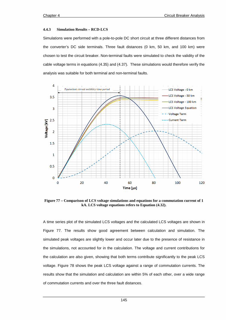
Chapter 4 Circuit Breaker Analysis
145
4.4.3 Simulation Results – RCD-LCS
Simulations were performed with a pole-to-pole DC short circuit at three different distances from
the converter’s DC side terminals. Three fault distances (0 km, 50 km, and 100 km) were
chosen to test the circuit breaker. Non-terminal faults were simulated to check the validity of the
cable voltage terms in equations (4.35) and (4.37). These simulations would therefore verify the
analysis was suitable for both terminal and non-terminal faults.
Figure 77 – Comparison of LCS voltage simulations and equations for a commutation current of 1 kA. LCS voltage equations refers to Equation (4.32).
A time series plot of the simulated LCS voltages and the calculated LCS voltages are shown in
Figure 77. The results show good agreement between calculation and simulation. The
simulated peak voltages are slightly lower and occur later due to the presence of resistance in
the simulations, not accounted for in the calculation. The voltage and current contributions for
the calculation are also given, showing that both terms contribute significantly to the peak LCS
voltage. Figure 78 shows the peak LCS voltage against a range of commutation currents. The
results show that the simulation and calculation are within 5% of each other, over a wide range
of commutation currents and over the three fault distances.

Chapter 4 Circuit Breaker Analysis
146
Figure 78 ‒ Comparison of calculation and simulation results.
Commutation Current [kA] 1 1.5 2 2.5 3
Peak LCS Voltage [V]
0 km 3391 - 4509 - 5656 - 6812 - 7946 -
50 km 3488 2.84% 4606 2.16% 5735 1.40% 6879 0.98% 8015 0.86%
100 km 3446 1.62% 4570 1.36% 5708 0.93% 6854 0.61% 8001 0.70%
Table 4 ‒ Peak LCS voltage for various commutation currents over three different fault distances. Percentage overshoot relative to the 0 km condition is also shown.
The results also show that non-terminal faults produce a slightly higher LCS voltage than the
terminal fault case. The percentage overshoot is summarized in Table 4. The impact that the
cable voltage has diminishes as the commutation current is increased, as the majority of the
LCS voltage is imposed by the current term rather than the voltage term of Equation (4.32), due
to the initial current being significantly higher.
The commutation time results are shown in Figure 79 and show that the calculations are within
10% of the simulation results for the range of distances and commutation currents. All the
simulation results show slightly longer commutation times due to the presence of resistance in

Chapter 4 Circuit Breaker Analysis
147
the commutation circuit. This resistance will reduce the commutation current frequency,
resulting in additional time being required to force the current change.
Figure 79 ‒ Comparison of the calculated commutation time and the PSCAD simulation results.
The impact of traveling waves can also be seen in the commutation time, as it takes slightly
longer under all conditions for faults that occur further away from the converter to commutate
current between the two branches. This is due to the transiently higher rate-of-change of current
induced by a negative cable voltage, which comes from the presence of an inductive
termination of the cables, as discussed in Chapter 3.
4.4.4 Simulation Results – Varistor-LCS
4.4.4.1 Commutation Current
Predicting currents accurately is difficult with the Varistor-LCS topology, as the circuit is
inherently non-linear. Additionally the cable traveling waves will result in current perturbations
within the primary branch current, and will further impact on the voltage generated across the
varistor.

Chapter 4 Circuit Breaker Analysis
148
In order to first verify the analysis, the circuit breaker’s LCS was modeled as an ideal switch in
parallel with a constant voltage source. This allows for a direct comparison of the analysis to the
simplified equivalent circuit. The analysis is compared to simulations that include a more
realistic representation of the LCS in Section 4.4.4.3.
The simulated commutation current and the calculated primary branch current, using Equation
(4.42), are shown Figure 80 for a range of LCS voltages (1 kV to 4.5 kV). The results show
good agreement between simulation and analysis of the simplified system.
Figure 80 ‒ Comparison of simulated and calculated primary branch currents.
4.4.4.2 Minimum Varistor Knee Voltage Estimate
As discussed in Section 4.3.4 the varistor stack must be designed to have an appropriate knee
voltage or adverse effects may occur while the circuit breaker’s mechanical switch is opening. A
simulation of one of these phenomena is shown in Figure 81. The current is first driven to zero
in the mechanical switch by the LCS voltage. The circuit breaker voltage gradually increases
due to the presence of resistance in the secondary branch and changes in the fault current

Chapter 4 Circuit Breaker Analysis
149
derivative. When the voltage has risen high enough, current starts to flow in the primary branch
again. As the circuit breaker voltage increases further, the current increases.
There are three main conclusions from the previous discussion. First, the varistor’s knee voltage
must be high enough to ensure a current zero in the mechanical switch, under all operating
conditions. Second, the varistor must ensure that current flow is not re-established after the first
current zero, while the secondary branch continues to conduct the fault current. Third, the
minimum required knee voltage must be higher when traveling waves are considered. This is
due to the increased fault current derivative imposing a higher voltage across the secondary
branch inductance, which must not be greater than the varistor voltage.
Figure 81 – Re-conduction in the primary branch.
4.4.4.3 Knee Voltage Design Example
To illustrate the importance of the varistor design, a case study was performed with two different
design philosophies. The first set of simulations assumes a terminal fault is the worst case; the
second set takes into account the impact of traveling waves.

Chapter 4 Circuit Breaker Analysis
150
To highlight the importance of the design philosophy, a reduced series inductance was used. A
pole inductance (üý) of 50 mH was chosen, as this is at the lower end of the typical series
inductance seen in breakers [85]. A DC fault study was then performed with faults from 0 km to
200 km, in 50 km steps. The circuit breakers were opened at specific times after the fault
inception and the primary branch currents inspected.
For the traditional design philosophy, the knee voltage was calculated to be 1.65 kV. For the
modified design case, the required minimum knee voltage was calculated to be 1.85 kV. Both
these values were calculated using Equation (4.51) and the additional parameters for the circuit
breaker are given in Section 4.4.2.5.
Figure 82 shows the primary branch currents for the traditional design case. It can be seen that
commutation is not achieved for all fault distances, due to the transiently higher fault current
derivative imposed by the negative cable voltage.
Figure 83 shows that when compensation is made for travelling waves, commutation occurs for
all fault distances. Along with the simulation traces are two plots of Equation (4.42). The first
trace does not compensate for travelling waves, the second trace (identified as Calculation T2 –
TW) does.
Both sets of results highlight that a longer commutation time occurs for non-terminal faults. For
the second design case, the commutation time can be significantly longer (36% longer in the
case of the 50 km fault) than the terminal case. This highlights the need to specify a circuit
breaker’s commutation time under specific conditions. This also shows again that there is a
need for test circuits to replicate the conditions travelling waves create and for the fault current
derivative to be suitable over the entire testing period. How this can be achieved is discussed in
Chapter 7.
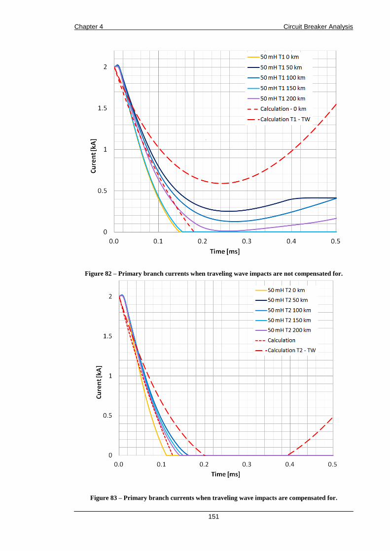
Chapter 4 Circuit Breaker Analysis
151
Figure 82 ‒ Primary branch currents when traveling wave impacts are not compensated for.
Figure 83 ‒ Primary branch currents when traveling wave impacts are compensated for.

Chapter 4 Circuit Breaker Analysis
152
4.5 Operation of the Super Hybrid Circuit Breaker (SHCB)
This section describes the operation of the SHCB in a qualitative manner, before moving onto a
mathematical analysis of the circuit breaker. Under normal conduction, current in the circuit
breaker flows through the primary branch, as indicated by the arrow in Figure 84 (however,
current may flow in either direction). The superconductor and mechanical switch are exposed to
the normal line current. The main breaker is normally off, so no current flows through the
secondary path. The superconductor resistance will be effectively zero although it will have
some inductance due to the coil being formed from many turns of superconducting wire. The
only resistance that exists will be due to contact resistance at the interface of the cryogenic
equipment.
Figure 84 ‒ Normal conduction path in SHCB.
When a fault occurs, the current rises rapidly in the primary branch until the quench current
level of the superconductor is reached. At this stage the resistance of the superconductor
increases rapidly and the superconductor presents a high resistance ((³) in the primary path.
After the superconductor has quenched, the main breaker is turned on and current diverts into
the secondary branch, as shown in Figure 85. The current in the primary branch decays due to
the increased primary branch impedance, relative to the secondary branch. Once the primary
current has decayed sufficiently, the mechanical switch can start to open (triggered by T). The secondary branch must continue to conduct the fault current while the mechanical switch
fully opens.

Chapter 4 Circuit Breaker Analysis
153
Figure 85 ‒ Commutation effect in SHCB.
Once the mechanical switch (º) is fully open, the main breaker can be turned off, as shown in
Figure 86, resulting in the voltage across the circuit breaker rising rapidly to oppose the flow of
current. It is at this moment that the circuit breaker starts to interrupt the flow of current (, ). Once the voltage has risen sufficiently, the varistor will start to conduct and dissipate the energy
stored in the series inductance. As the energy dissipates so the current in the varistor
decreases, and once it has fallen sufficiently, the second mechanical switch (º) can be opened
to provide full isolation.
Additional capacitance (T) can be added in parallel with the primary mechanical switch (º) to
allow the circuit breaker voltage ($Á) and the voltage across mechanical switch (º) to be
decoupled. As explained in Chapter 2, this allows the superconductor to form part of a snubber
circuit. Consequently the circuit breaker voltage rises much faster than the voltage across the
mechanical switch (º), if such a snubber is used. This may have advantages in allowing the
peak current in the secondary branch to be reduced. The feature is not analyzed in this thesis,
but is mentioned here for completeness.

Chapter 4 Circuit Breaker Analysis
154
Figure 86 – Secondary branch turn off procedure. Capacitance CM1 can be added to the design to use the superconductor as a part of a RLC snubber circuit. Left hand side circuit, right hand side
waveforms.
4.6 Analysis of the Super Hybrid Circuit Breaker (SHCB)
The Superconducting Hybrid Circuit Breaker (SHCB) is a novel topology invented during this
PhD project. The circuit breaker uses a novel method of current commutation and offers a
number of interesting opportunities for future designs which are discussed in Chapter 2. This
section of the thesis is concerned with mathematically describing the commutation process for
the SHCB. The analysis allows a comparison of commutation techniques. The breaker design
was built and tested at low power, details of which are given in Chapter 7.
4.6.1 State Space Analysis
When a fault occurs, the circuit breaker rapidly increases the resistance of the circuit breaker’s
primary branch since the superconducting coil in that branch quenches. The increase in primary
branch resistance causes a majority of the fault current to flow into the secondary branch of the
circuit breaker once it is turned on. Providing the change in resistance is high enough, the
mechanical switch will be able to break the remaining primary branch current with a small arc.
The commutation process for the SHCB can be modelled using the equivalent electrical circuit
given in Figure 87. This is a third order equivalent circuit that contains two resistances and three

Chapter 4 Circuit Breaker Analysis
155
circuit inductances. The superconductor’s quench resistance,(, is assumed constant. (& represents the secondary branch resistance.
Superconductors are generally formed from coils of wire, which will have an intrinsic inductance
depending on the specific geometry of the coil. The inductance can either be beneficial or
harmful to the circuit breaker’s operation. For the purposes of mathematical analysis the
superconductor’s inductance is lumped into the primary branch inductance. A state space analysis can be performed on the commutation circuit of Figure 87, using the
state variables defined by the matrixes in Equation (4.54). The input coefficient matrix, and the
state transmission matrix are reproduced below, in equations (4.55) and (4.56) respectively.
Figure 87 ‒ Equivalent commutation circuit for the SHCB.
Ì() = ¶&¸ , [H = ¶HH0¸ , = n %Òo
(4.54)
Æ = 1% ¶ + & −& )$ −()$ + )¸
(4.55)
(Ó − Ê)` = 1 ØÙÙÚ/ −(((& + &) −(&(( + )0 % + f)$ + g(& )$(&0 )$( % + f)$ + &g(ÜÝ
ÝÞ
(4.56)
= ((& + þf)$ + &g( + f)$ + g(& +% (4.57)

Chapter 4 Circuit Breaker Analysis
156
ßℎO ∶ % = )$ + )$& + & (4.58)
If the superconductor’s resistance arises predominantly from the quenching process, then this
analysis is valid from the moment the superconductor quenches. If additional resistance is
required by heating the superconductor, then this analysis applies from the moment the
secondary branch is turned on after the coil has quenched.
4.6.1.1 Commutation Process
As primary current does not reach zero, the definition of commutation time for the PHCB does
not hold for this circuit breaker. Instead, commutation time is the time at which primary branch
current has reached its lowest value, or when the current crosses a sufficiently low enough
value for the mechanical switch M to break the current.
Using the equations of Section 4.6.1 an s-domain expression, Equation (4.59), can be obtained
for the primary branch current at the moment the superconductor quenches. Equation (4.60)
allows (4.59) to put into a more manageable format, where δ andγ are the roots of the second
order polynomial in the denominator of Equation (4.59). Equation (4.59) can then be
transformed into a time-domain expression to describe the decay in primary branch current, as
shown in Equation (4.61). The coefficients for this equation are given in equations (4.62) to
(4.64). A derivation of Equation (4.61) is given in Appendix 1E.
() = H% +(&% + )$Ò + H(&f)$ + g) + (&%% ©((&% + nf)$ + &g( + f)$ + g(&% o + ª
(4.59)
( + )( + ) = ((&% + f)$ +&g( + f)$ + g(&% +
(4.60)
(,) = 1% þï + ` + `
(4.61)
ï = (&%
(4.62)
= − H% −(&% + )$Ò + H(&f)$ + g) + (&%( − )
(4.63)
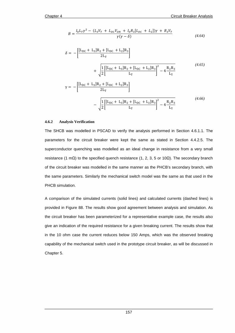
Chapter 4 Circuit Breaker Analysis
157
= H% −(&% + )$Ò + H(&f)$ + g) + (&%( − )
(4.64)
= − fLte +L&gR + fLte + LgR&2Lã +I12 fLte +L&gR + fLte + LgR&Lã − 4RR&Lã
(4.65)
γ = − fLte +L&gR + fLte + LgR&2Lã −I12 fLte +L&gR + fLte + LgR&Lã − 4RR&Lã
(4.66)
4.6.2 Analysis Verification
The SHCB was modelled in PSCAD to verify the analysis performed in Section 4.6.1.1. The
parameters for the circuit breaker were kept the same as stated in Section 4.4.2.5. The
superconductor quenching was modelled as an ideal change in resistance from a very small
resistance (1 mΩ) to the specified quench resistance (1, 2, 3, 5 or 10Ω). The secondary branch
of the circuit breaker was modelled in the same manner as the PHCB’s secondary branch, with
the same parameters. Similarly the mechanical switch model was the same as that used in the
PHCB simulation.
A comparison of the simulated currents (solid lines) and calculated currents (dashed lines) is
provided in Figure 88. The results show good agreement between analysis and simulation. As
the circuit breaker has been parameterized for a representative example case, the results also
give an indication of the required resistance for a given breaking current. The results show that
in the 10 ohm case the current reduces below 150 Amps, which was the observed breaking
capability of the mechanical switch used in the prototype circuit breaker, as will be discussed in
Chapter 5.

Chapter 4 Circuit Breaker Analysis
158
Figure 88 ‒ Simulated and calculated primary branch currents for a range of superconductor quench resistances.
4.7 Travelling Wave Impacts and Grid Inductance
4.7.1 PHCB
Presently, the value of required series DC inductance per pole is estimated to be between 50
mH and 100 mH for a 300 kV VSC system [52, 61, 85]. Some designs have been quoted with
an inductance of 300 mH [44]. However, such values of series DC side inductance may cause
problems for DC grid stability and converter controls [J1]. There may be a requirement to
reduce this inductance in order for a HVDC grid to be controlled appropriately. There are also
significant financial benefits to be made in reducing the physical size and weight of any offshore
equipment. However, reductions in DC inductance may have a deleterious effect on the voltage
rating of the LCS.
Figure 89 shows a plot of the peak LCS voltage for a range of secondary branch inductances
() against the series DC inductance (üý) using Equation (4.32). The plot shows that as the
series DC inductance is reduced there is an increase in the peak LCS voltage. This is due to the

Chapter 4 Circuit Breaker Analysis
159
voltage term in Equation (4.32) containing an inverse proportionality toüý. The impact that
traveling waves have on the peak LCS voltage also becomes more pronounced for lower
inductance grids, due to the voltage term in Equation (4.35) becoming more dominant.
The number of devices required in the LCS can be calculated using Equation (4.67) assuming
each parallel set of IGBTs in the LCS has its own snubber circuit. The Binomial theorem can
then be used to solve for the square-root of the number of series devices(S$*). The result
can be squared and then rounded up to the nearest integer to determine the number of required
devices in series. The results are plotted in Figure 90.
À½Á%$* − HIf + &g$* − &% + )$Ò)$ + & = 0 (4.67)
Figure 89 ‒ Peak LCS voltage plot against DC side inductance for a range of secondary branch inductances. Commutation current = 3 kA.
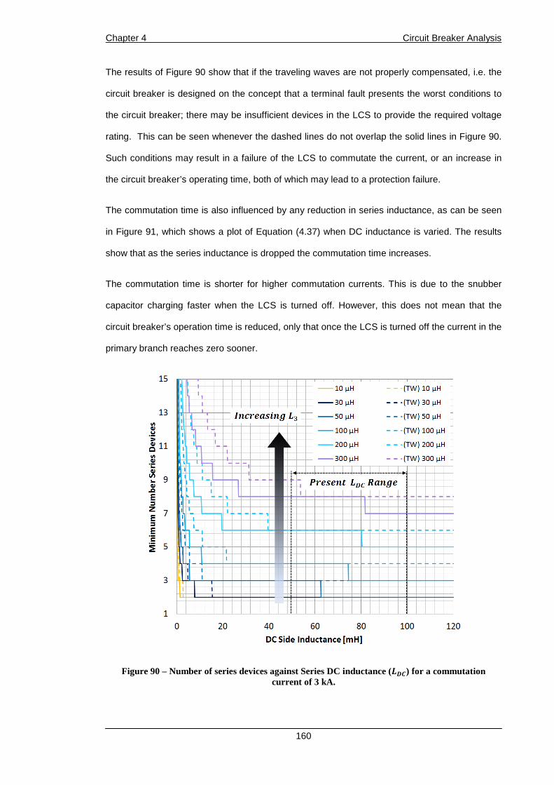
Chapter 4 Circuit Breaker Analysis
160
The results of Figure 90 show that if the traveling waves are not properly compensated, i.e. the
circuit breaker is designed on the concept that a terminal fault presents the worst conditions to
the circuit breaker; there may be insufficient devices in the LCS to provide the required voltage
rating. This can be seen whenever the dashed lines do not overlap the solid lines in Figure 90.
Such conditions may result in a failure of the LCS to commutate the current, or an increase in
the circuit breaker’s operating time, both of which may lead to a protection failure.
The commutation time is also influenced by any reduction in series inductance, as can be seen
in Figure 91, which shows a plot of Equation (4.37) when DC inductance is varied. The results
show that as the series inductance is dropped the commutation time increases.
The commutation time is shorter for higher commutation currents. This is due to the snubber
capacitor charging faster when the LCS is turned off. However, this does not mean that the
circuit breaker’s operation time is reduced, only that once the LCS is turned off the current in the
primary branch reaches zero sooner.
Figure 90 – Number of series devices against Series DC inductance ( üý) for a commutation current of 3 kA.

Chapter 4 Circuit Breaker Analysis
161
Figure 91 ‒ Commutation time against series inductance over a range of commutating currents. Traveling wave impact included in calculation (dashed lines). Cable voltage assumed to be zero
(solid lines). The impact of traveling waves can be seen again in the results. The commutation time is
increased by the negative cable voltage, above the commutation time seen when the cable
voltage is assumed to be zero.
While the impact of the cable voltage may seem minimal and somewhat redundant at this point,
it is important to remember two things. First, the results have been calculated for one case only.
If the electrical parameters are changed then the impact the travelling waves will have on the
LCS operation may become more pronounced. Such parameter changes could be, say, a
reduction in series DC inductance (üý) or an increase in the parasitic inductance ().
With an increased current breaking capability of the semiconductors, such as [85], or an
increase in the speed of the mechanical switch, üý could be reduced significantly. Future
designs will probably attempt to reduce the amount of series inductance as this will have
significant financial benefits.
Other designs may also start to incorporate thyristor technology in the secondary branch, which
will require the addition of series inductance in the secondary branch [52]. The additional

Chapter 4 Circuit Breaker Analysis
162
inductance is required to ensure even current distribution within the thyristor during turn on. As
the circuit breaker’s peak current rating is increased and the required series inductance is
reduced, the secondary branch inductance will also have to be increased, all other things being
equal.
Importantly, this presents a fundamental change in design philosophy for protection equipment.
One would normally design a system based on the worst case scenario, which for protection
equipment is traditionally seen as the terminal fault. From the analysis it is shown that this is
simply not the case for fast acting DC circuit breakers. It is important to now take into account
the influence of travelling waves when designing high speed HVDC circuit breakers.
4.7.2 SHCB
The travelling wave effects that result in a more challenging environment for the PHCB may in
fact be beneficial for other topologies, such as the SHCB. The SHCB uses a superconducting
coil to divert the current away from the primary branch. How effectively and quickly this
diversion is performed, depends on how quickly the fault currents rises within the
superconductor. A faster increase in fault current will quench the superconductor sooner and
result in higher power losses in the coil, resulting in a higher change of resistance.
As the steady state losses of the circuit breaker are also not linked to the voltage rating of the
commutation element, the additional voltage rise that would be seen across the superconductor
would not impact the circuit breaker’s normal operation losses, only the differential voltage
rating of the cryogenic system’s electrical terminals.
4.8 Recommendations for Future Fault Studies
While the circuit breakers in this thesis have been modelled as a single large circuit breaker, it is
more likely that a modular architecture will be adopted for HVDC circuit breakers. This means
that a practical breaker will be made from the series combination of several smaller circuit
breakers.
The series combination allows internal failures within the circuit breakers to occur, without these
failures detrimentally impacting on the circuit breakers’ ability to open, providing that a single

Chapter 4 Circuit Breaker Analysis
163
module failure does not result in a total circuit breaker failure. Additional modules will have to be
added to account for such a failure.
As such, the “module failure” condition needs to be considered for HVDC protection studies. It
needs to be established what will happen when a module within a circuit breaker fails, how this
failure will impact the fault detection systems, and what secondary layers of protection are
enacted when such an event occurs. How the other modules within the circuit breaker respond
to this condition, and how this partial failure impacts the rating of the protection equipment, must
also be specified.
Circuit breaker models such as [80, 91, 92] do not include this modularity, and one must be
careful when using them for fault detection studies. Therefore, for future protection studies it is
essential that circuit breakers be modelled in a modular format, which is able to reflect the
nature of internal faults.
4.9 Conclusions
A detailed study of the PHCB has been performed. The PHCB’s operation has been discussed
in detail, each major component has been assessed, and supporting equations have been
given. State space analysis has been performed on the circuit breaker’s commutation process
and simplified equations have been provided to estimate some of the circuit breaker’s key
performance parameters.
Equations that describe the PHCB’s commutation process have been given for two different
LCS designs. Both topologies have their own merits and issues and require different design
strategies. The analysis in this section has also highlighted additional phenomena that have
been neglected from prior art.
Simulations using TDM models have been performed and verify the analysis and show a strong
agreement for the RCD-LCS design and provide good guide lines for the non-linear Varistor-
LCS design.

Chapter 4 Circuit Breaker Analysis
164
The analysis shows that the impact of travelling waves must be taken into account when
designing high speed HVDC protection equipment. Travelling waves can increase both the
commutation time and the peak voltage seen across the circuit breaker LCS. The standard that
will one day cover HVDC switch-gear must take travelling waves into account, and the design
philosophy for HVDC circuit breakers must not consider terminals faults alone.
The analysis also shows that the impact of travelling waves becomes more pronounced in low
inductance grids. The peak voltage and commutation times for the PHCB both increase as the
inductance in series with the circuit breaker decreases.
An analysis of the novel circuit breaker, the SHCB, has also been developed in this chapter. An
analysis sufficient to describe the current diversion technique has been derived from first
principles. The SHCB may offer an alternative design for future circuit breakers.

Chapter 5 Circuit Breaker Prototyping
165
Chapter 5:
Circuit Breaker Prototyping
5.1 Introduction
As discussed in Chapter 2, there have been many topologies proposed for future HVDC circuit
breakers. Most of the proposed topologies are conceptual, only a few have (limited) supporting
analysis in the public literature, and even fewer have practical test results demonstrating their
capability at any power level. Those which have been built at representative module power
ratings and tested, only present a few, limited results. Key learning outcomes, and specific
design features are not public [44, 52, 61].
To overcome some of these issues, hardware testing was undertaken for reduced power,
representative DC circuit breakers. This chapter presents the practical test results and
discusses key learning outcomes from the prototyping of two different circuit breaker topologies.
The two types of circuit breakers chosen to be prototyped were the:
• Proactive Hybrid Circuit Breaker (PHCB)
• Super Hybrid Circuit Breaker (SHCB)
These designs were chosen as they represented distinct methods of primary branch current
commutation, each method having different advantages and potential for HVDC grid
applications.
The work aimed to validate the basic design of the equipment in a low voltage environment,
validate supporting analysis, and provide an insight into some of the technical limitations of
each topology. Furthermore, this work allowed the controllers, support electronics, and isolated
power supplies to be tested before the high voltage testing was attempted. The SHCB is a novel
design developed by the author (a patent has been filed [P1]) and has never been constructed
prior to this work.

Chapter 5 Circuit Breaker Prototyping
166
This chapter first introduces the equipment used for testing, followed by separate sections
dedicated to each circuit breaker topology.
5.2 Test Circuit
The test circuit is shown in Figure 92. A programmable DC power supply is connected in series
with a diode (%), a series inductance (%), the circuit breaker under test and a load resistor to
provide an initial load current. An IGBT module is placed in parallel with the load resistor to
provide a change in load impedance, and replicate a short circuit fault across the load.
Each circuit breaker uses the same mechanical switch and semiconductor based secondary
branch. The mechanical and semiconductor switches are controlled by switching signals from a
micro-controller; these switches are discussed in more detail in sections 5.2.1 and 5.2.2. The
primary branch current was measured using a current probe, the total fault current was
measured via a low ohm resistor ((T-.@ = 0.2 Ω), and the circuit breaker voltage was
measured with an isolated differential voltage probe.
Figure 92 ‒ Layout of test circuit. Different commutation elements are placed in the circuit to validate the different topologies.
The various commutating elements were placed in the primary branch during testing, to
evaluate each different topology. The commutating elements used were a power electronic
switch, superconducting coil, and a coupled inductor.

Chapter 5 Circuit Breaker Prototyping
167
The commutating tests were not performed to validate the test circuit design, nor to test whether
the circuit breaker topology was suitable for a HVDC-VSC environment, but were performed to
provide proof of concept data and hardware design validation.
A photo graph of the test circuit is shown in Figure 93. A protective transparent casing was
placed around the mechanical switch and power electronics for health and safety purposes.
Figure 93 ‒ Test circuit used for topology validation testing.
5.2.1 Power Electronic Switches
Power electronic switches form a key part of each design. Insulated Gate Bi-polar Transistors
(IGBTs) were chosen for this project as they commonly feature in the most prominent industrial
prototypes. IGBTs are used in the PHCB in two different locations and are also used to form the
secondary branches of hybrid breaker topologies.

Chapter 5 Circuit Breaker Prototyping
168
The design of the IGBT module is discussed in detail in Chapter 6, and was based on an
assessment of multiple options which would allow high voltage testing, to be performed at the
highest power rating based on the budget limitations of this project, as discussed in chapters 6
and 7.
The IGBTs are rated at 2.5 kA 1.7 kV in normal operation. Each IGBT is protected by an
arrestor, has a RCD snubber circuit, optically controlled gate drive circuit, and isolated gate
power supply. A prototype assembly of the IGBT module is shown in Figure 94. The gate drive
is able to prevent the IGBT turning on when there is insufficient available gate drive energy and
communicate this back to the controller.
Figure 94 – Prototype IGBT module used for low power testing.
5.2.2 Mechanical Switch
The mechanical switch (ºin Figure 92 ) uses a moving coil actuator to move a vacuum switch,
the arrangement is shown in Figure 95. This actuator was developed in [93] as part of another
PhD project, but is of an appropriate size and operating speed for the prototyping of these
circuit breakers.

Chapter 5 Circuit Breaker Prototyping
169
The vacuum switch is rated at 3.2 kA peak, and a maximum operating voltage of 1.5 kV. The
actuator is able to fully open the contacts in approximately 3.5 ms. However the majority of this
time is the delay required to accelerate the moving coil actuator plunger and moving contact to
speed. Once the contacts start to open, they become fully open in approximately 1 ms. The
opening data was gathered through testing of the mechanical switch prior to the full power
system tests.
Figure 95 ‒ Vacuum switch and actuator.
5.2.3 Cryostat and Superconducting Coil
The cryostat used was a Cryomech AL230. This cryogenic chamber is rated for 1 kV following
an upgrade to the original design. The cryostat consumes 5.1 kW in steady state for cooling,
and can provide 25 W of cooling at 20 K. Liquid nitrogen is used to cool down each of the coils.

Chapter 5 Circuit Breaker Prototyping
170
Once the cryostat has reached its operating temperature (28 K for the tests performed
described here) the nitrogen will be frozen solid.
The superconducting coil comprises Magnesium Diboride (MgB2) covered in a stainless steel
sheath with a fill factor of 25 %. The coil has nine strands in parallel, each with a diameter of
0.36 mm. The length of the coil was 6.5 m and this was wrapped onto a coil former prior to
being tested. The coil is shown in Figure 96.
The room temperature resistance of the coil is 4.5 Ω. However the resistivity of the sheath
material drops dramatically with temperature and the superconducting material will still be
conductive even when quenched, making the quench resistance significantly smaller. Figure 97
shows how the sheath material resistivity varies with temperature. During quenching tests the
highest resistance value observed was 140 mΩ. While this may seem small, based on some
preliminary simulations of the circuit breaker the resistance would be sufficient to commutate the
primary branch current.
Figure 96 ‒ Superconducting coil used for HVDC circuit breaker testing.

Chapter 5 Circuit Breaker Prototyping
171
Figure 97 ‒ Resistivity of sheath material.
5.3 Proactive Hybrid Circuit Breaker (PHCB)
The PHCB uses a semiconductor device as the commutating element. The semiconductor
device is placed in series with the mechanical switch in the position of the commutating element
in Figure 92. A description of the operation of the PHCB can be found in Chapter 2 and detailed
analysis of its operation can be found in Chapter 4.
Interruption tests where then performed using the test circuit described in Section 5.2. Tests
were performed by incrementing the DC power supply voltage to increase the initial current and
peak current.
The initial fault current was set by the programmable DC power supply. The load current was
instigated for 30 ms before a short circuit, across the load, was replicated by turning on the
IGBT in parallel with the load resistor.
An interruption test result is shown in Figure 98. The fault was applied at time 2 ms, as can be
seen from the rapid increase of total fault current. As this circuit breaker does not perform
commutation passively, a control signal is required to turn on the secondary branch and turn off
the LCS. This trigger signal is shown in Figure 98, and rises around 860 µs after the fault is

Chapter 5 Circuit Breaker Prototyping
172
applied. This delay time was chosen as is it indicative of delay times that are expected for
advanced fault detection systems [94].
The mechanical switch was also triggered at the same time as the LCS and secondary branch
were switched. These actions can be undertaken at the same instance since there is a delay
between when the trigger signal is sent to the mechanical switch and when the vacuum switch
contacts start moving (approximately 2.5 ms), as discussed in Section 5.2.2.
The primary branch current falls very rapidly, and the total fault current flows in the secondary
branch. The secondary branch is turned off when the mechanical switch contacts are known to
be fully open, at approximately 6.45 ms. At this time the circuit breaker voltage rises and the
fault current is reduced to zero by the varistor.
The oscillations in the total fault current are due to an interaction between the DC power supply
and the test circuit inductance.
Figure 98 ‒ PHCB interruption test results.
Chapter 5 Circuit Breaker Prototyping
173
5.3.1 Discussion
The PHCB offers a fast method of commutating the primary branch current at the expense of
the losses incurred by the small stack of devices permanently exposed to the DC line current.
The LCS needs to be triggered by a signal in order for the circuit breaker to operate. Where this
signal comes from and how it is timed with the mechanical switch trigger signal are two
important issues.
The LCS may be triggered by:
• An over current in the primary branch.
• A fault detection system.
• Neighbouring circuit breakers that detect a fault.
The mechanical switch may be triggered in conjunction with the LCS if it is known that the
primary branch current will fall before the contacts within the mechanical switch start to open.
While fast commutation times are shown in these results and in published industrial prototypes,
as discussed in Chapter 4, there is an inherent exchange between commutation time and peak
LCS voltages. In order to reduce the power losses, a longer commutation time may be used.
There may also be open circuit failures in the secondary branch, i.e. a single IGBT within the
stack of IGBTs that does not turn on due to a gate drive failure. This would result in an
extension of the commutation time, and could potentially result in there being current within the
primary branch when the contacts are opened, leading to a failure of the protection device.
Careful consideration of how the triggering of the LCS, secondary branch, and mechanical
switch is performed is key to the robust design of a circuit breaker. Understanding how the
secondary branch modules fail is also very important for this circuit breaker’s design.
How the secondary branch is powered during normal operation is a question that has yet to be
explicitly answered by industry. While this is certainly achievable, the preferred manner has yet
to be established. It may be that the LCS is used to circulate current into the secondary branch
during normal operation in order to charge the gate drive power electronics. Dedicated power
supplies, such as those used in this testing are very unlikely to be used as this would incur
significant additional costs and the physical size of the circuit breaker would increase

Chapter 5 Circuit Breaker Prototyping
174
dramatically. Power may also be sourced from the converters themselves, or from other DC
power system equipment, such as current flow controllers.
Understanding how the circuit breaker is initially powered, how it remains powered during
normal operation, and how well it is able to reject the disturbances that a DC fault would
present, are all important questions for the design of any hybrid circuit breaker.
5.4 Super Hybrid Circuit Breaker (SHCB)
The SHCB uses a superconducting coil to commutate the fault current. The principle of
operation is based around the difference in branch resistances, rather than providing a voltage
to drive the current movement.
The superconducting coil discussed in Section 5.2.3 was added in series with the mechanical
switch in the position of the commutating element in Figure 92. As the quench current of this coil
was around 200 Amps the series test circuit inductance was reduced to increase the rate-of-
change of current and to increase the peak fault current seen in the tests.
Tests were performed by subjecting the circuit breaker to a 30 ms pulse of nominal load current
before applying the fault. Repeated testing was undertaken, incrementing the DC power supply
voltage, steadily increasing the peak fault currents seen by the circuit breaker.
The highest fault current results obtained are shown in Figure 99. The fault was applied at time
1 ms and the total fault current rises rapidly from that instant. The secondary branch remains in
the off state at this time in order to increase the current in the superconductor, allowing
quenching to happen sooner and any resistance change due to heating to be maximized.
Once the current reaches 200 Amps the superconductor starts to quench altering the rate-of-
change of current in the primary branch. At this time, only some sections of the coil have
changed into the quenched state. Thus the coil has yet to reach its total quench resistance.
The fault current continues to increase until the current reaches 300 Amps at which point the
majority of the quench resistance has been achieved. This high resistance then starts to limit
the total fault current (at around 2 ms).

Chapter 5 Circuit Breaker Prototyping
175
Figure 99 ‒ Experimental results validating operation of SHCB.
The mechanical switch is triggered 860 µs after the fault is applied. The triggering is done pre-
emptively as it takes several milliseconds for the contacts to start to open. While the actuator
plunger is accelerating, the secondary branch remains in the off position to allow the
superconductor coil to heat as much as possible, thus generating a higher resistance.
At time 3.6 ms the secondary branch is turned on and the majority of the fault current is
commutated into the secondary branch. In these tests, we also see a high increase in total fault
current. This is due to the low test series inductance used, resulting in the fault current transient
quickly responding to the change in circuit breaker impedance. In a full scale HVDC circuit
breaker, this rapid increase in current would not be seen.
The current in the primary branch is reduced to its steady state value of 30 A in around 400 µs.
The current is then finally forced to zero, with the mechanical switch contacts breaking the

Chapter 5 Circuit Breaker Prototyping
176
remaining current. At 5.5 ms the mechanical switch contacts are fully open, the secondary
branch is turned off and the arrestor decreases the current to zero.
Observed commutation times in these tests are longer than those seen in the PHCB, but not
dramatically longer, especially considering that only 80 mΩ of resistance was used in these
tests. A higher resistance could potentially provide a significantly faster commutation time.
The superconductor coil is observed to start quenching within 600 µs and obtain a full quench in
around 1 ms. This appears to be mainly dependent on how quickly the current is able to rise
and quench each part of the coil. Each part of the superconducting coil will have a slightly
different quench current, due to inherent discrepancies in material properties during
manufacturing. Thus faster quenching will be achieved with faster changing currents, making
superconductors a technology of interest for HVDC applications.
5.4.1 Comparison to Analysis
Using the experimental results gathered it is possible to derive some of the circuit breaker
parameters using linear approximations of fault currents, allowing for some of the analysis
developed in Chapter 4 to be validated. The parameters are derived in Appendix 2A.
The source inductance plus the superconductor inductance ()$ +) can be determined by
observing at the average rate-of-change of current between the moment the fault is applied and
the first peak in the current. Using the source voltage an estimate of the series inductance was
made, and found to be 94.6 µH.
The source inductance ()$) can be found using another linear approximation of the fault
current, once the secondary branch is turned on, as the secondary branch inductance will be
very small. The inductance value gained from this second linear approximation will be
dominated by the source inductance, which was found to be 84.5 µH. The superconductor
inductance is then the difference between the two derived inductance values (10.2 µH).
The superconductor resistance can be found by taking the ratio of the measured voltage and
current. The resistance at the moment the secondary branch is turned on can then be estimated
at a time when the current through the superconductor is constant. At time 3 ms, in the results
shown in Figure 100, the superconductor’s current is constant, hence the impedance at this

Chapter 5 Circuit Breaker Prototyping
177
time will be mainly dominated by the resistance. The quench resistance was found to be 80.4
mΩ.
The parameters used in the calculations are summarized in Table 5. The secondary branch
parameters were taken from the IGBT module datasheet. The parameters were entered into
Equation 4.37 developed in Chapter 4 and compared with the experimental results, shown in
Figure 101, indicating a strong agreement between the results and calculation.
Table 5 ‒ Parameters used in primary branch calculation. Parameter Value Unit
LDC 84.5 µH
L2 10.2 µH
L3 1 nH
RQ 80.4 mΩ
Figure 100 ‒ Comparison of linear approximations to experimental results. Linear approximations used to obtain estimations of system parameters.

Chapter 5 Circuit Breaker Prototyping
178
Figure 101 ‒ Comparison of experimental and calculated primary branch currents, with percentage error plotted on right hand side.
5.4.2 Discussion
The SHCB used a superconductor in a novel manner to commutate the primary branch current
into the secondary branch. This method has the distinct advantage of zero conduction losses
during normal state, resulting in the voltage rating of the commutating element being
independent of the circuit breaker losses. This may allow for some very quick breaking times in
future circuit breaker designs, if the “superconducting snubber circuit” arrangement can be
applied.
The major disadvantage of this circuit breaker is the cryogenic system that is required to cool
the superconducting coil. Cryogenic systems have inherent losses and could result in several
kilowatts of cooling being required. Providing an isolated power supply at the DC line voltage is
also non-trivial, and would incur additional power supply requirements.
The quench resistance of the superconducting coil and the voltage rating of the cryogenic
equipment are the key design features for this circuit breaker. A high quench resistance results

Chapter 5 Circuit Breaker Prototyping
179
in faster commutation times and may provide some fault current limitation during the circuit
breaker’s operation.
The design may have more promise in MV applications or in applications where cryogenic
systems already exist in electrical systems, such as future aerospace applications [34].
The coil used in the tests was not designed for a very high quench resistance and was not
designed specifically for this application. Most superconductors are designed not to quench as
this feature is undesirable in many applications, whereas for HVDC circuit breakers the coil
needs to quench quickly and provide a very high resistance. Further investigations into how to
specially design a coil for this application are presently under way at the University of
Manchester with a view to assessing this technology’s benefits for future grid applications,
under project EP/L021552/1.
The derived equation for the primary branch current has also been validated against hardware
results, showing a strong agreement between Equation 4.37 and the experimental results.
5.5 Conclusions
Two different circuit breaker topologies have been validated in this chapter. Each topology has
been prototyped at 200 V. The current rating of the PHCB has been tested at 200 A and the
SHCB has been tested with a peak current of 550 A.
The PHCB offers a fast commutation method and potentially a power source for the secondary
branch electronics. The design can be controlled easily, but timing of signals the LCS,
secondary branch, and mechanical switch will be key to a robust design, especially when one
starts to consider open circuit failures in the secondary branches.
The SHCB is a novel circuit breaker topology developed and patented as part of this PhD
project. The circuit breaker uses a change in resistance rather than a voltage to commutate
current out of the primary branch. The design concept has been validated in this chapter and
the analysis developed in Chapter 4 of this thesis has been validated against these results. The
results and calculations show a good agreement. While this circuit breaker has plenty of

Chapter 5 Circuit Breaker Prototyping
180
potential if the resistance of the coils can be designed properly, the supporting components
require a technology which is expensive and may inhibit its application.
The powering of hybrid circuit breaker technologies is a question that is often over-looked in the
literature. Dedicated power supplies are unlikely to be used, and it is more likely that the DC
circuit breakers will have to draw their power from the DC lines. How this is done, how often the
circuit breakers can be operated (opened, closed, pre-emptively triggered etc) and how robust
these power supplies are to transients on the DC line are key design criteria for HVDC circuit
breakers.

Chapter 6 Test Circuit Design & Construction
181
Chapter 6: Test Circuit Design &
Construction
6.1 Introduction
A method for defining the fault current specification generated by a test circuit was developed in
Chapter 3. The test circuit must be able to generate a high pulse of current in a shape that
meets the specification set down by the fault current envelope and maximum protection
operation time.
This chapter covers the development of a test circuit to meet the required specification for an
example HVDC system, using the method developed in Chapter 3. The test object used was a
modular semiconductor circuit breaker rated at 2.5 kA and 8.4 kV, with potential to increase
these ratings further if testing proceeded well. The test circuit specification was based on a
reduced scale FCE, as generating currents equivalent to a full scale system would be beyond
the scope of this project.
This chapter first discusses the example HVDC system that was chosen to generate a suitable
full scale FCE. The envelope was scaled down in the ratios 1:3 and 1:5 to provide two
specifications (a comfortably achievable and a more challenging target, given equipment
ratings) to design the test circuit. The scaling was a sensible trade-off between what could be
achieved technically and financially in the project, while still providing a reasonably challenging
and representative problem case. It was important to aim for a high current and voltage rating in
order for technical limitations of the existing equipment to be understood, such knowledge being
fundamental to developing a standard. The chapter then discusses the test circuit topology
chosen for the testing. Its operation is explained qualitatively and a mathematical analysis of its
operation is also provided. The analysis is then used, along with the specification, to define the
parameters for the test circuit.

Chapter 6 Test Circuit Design & Construction
182
Construction details of the physical test circuit and test object are discussed. Details of the
prototyping procedure and auxiliary systems testing are also provided. The test-bed developed
to house the test circuit and test object, to allow ease of testing in the University’s high voltage
lab, is also discussed.
6.2 Example system
In order to define a specification for the test circuit, an example system must be chosen for
which to design an envelope. As the TLC envelope specifications were developed first in this
PhD, this was chosen as the example converter design. However, the converter topology is not
of great relevance, as the envelope shape for MMC and TLC are the same, they only differ in
how they relate to the specific power rating of a converter topology.
The voltage rating selected was +/- 320 kV as this is representative of a full scale system. The
DC pole inductance for the converter was assumed to be 100 mH, based on industrial
prototypes [61]. The pole capacitance of the converter was chosen to be 100 µF. The peak
current for such a system would be 10 kA, assuming fast DC circuit breakers are used to isolate
faults [95]. The total energy in the DC inductance at the moment of peak current is 5 MJ.
This example case was used to develop a specific envelope for the converter, which was then
scaled to a more reasonable value to provide a specification for the equipment built as part of
the PhD. The example envelope is shown in Figure 102 with two current scales that were
deemed appropriate to attempt during this project, based on the financial limitations4. The test
circuit aimed to replicate a scaled version of the currents that the circuit breaker will be
subjected to during a fault. Further tests will be required to ensure that the energy rating of the
circuit breaker is sufficient and that the circuit breaker can withstand all voltage profile
requirements.
4 Full details of costing are given in National grid report 2.2.2 with a summary in Appendix 3C of this
thesis.

Chapter 6 Test Circuit Design & Construction
183
Figure 102 ‒ Specification envelope for example system and scaled two scaled versions at 1:3 and 1:5.
6.3 Test Circuit
6.3.1 Topology
The test circuit topology developed to produce the test current is shown in Figure 103. The test
circuit consists of two diode stacks (% and %), an isolation switch, an inductor (%), and a
capacitor (%). The test object is placed in-between points A and B, shown in Figure 103. (%
represents the circuit resistance.
The operation of the circuit is as follows. The capacitor (%) is initially charged to a voltage (H) and the test object is placed in its “closed” state, to allow current flow between points A and B.
The isolation switch is triggered and the capacitor discharges through the inductance %, diode
%, the test object, and the circuit resistance (%. The generated current,, will have a
sinusoidal shape and can be estimated using Equation (6.68), until such time as the capacitor
starts to reverse charge.
Once the capacitor (%) voltage has reversed, diode % will become forward biased, and the
current will commutate from % into%. The value of the current at the moment it

Chapter 6 Test Circuit Design & Construction
184
commutates into % is denoted as!1, which occurs at time,!1. Should the test object
remain a short circuit the current will then decay exponentially based upon the ratio of the
inductance to the residual circuit resistance (%/(%), (ignoring diode voltage drops) and is
described by (3.14). At this moment the capacitor bank (%) is no longer subjected to current.
Thus % only needs to be rated for the current discharge and not the full current pulse. This
feature means that a cost saving can be made in the construction of the test circuit.
If the test object attempts to break the current, the voltage across the test object will rise
causing current to decay. The voltage rise will be dictated by the internal stray capacitance of
the test object (%Ò) and any voltage limiting circuits within the test object.
In essence, the test circuit works by placing energy into the test circuit capacitance% , then
transferring this into the test circuit’s inductance% and then into the test object capacitance
and its voltage limiting circuit when it attempts to interrupt the flow of current.
Figure 103 ‒ Test circuit and test object.
(,) = Hñ% `k sin(ñ,) MNO, < Q2ñ
(6.68)
ñ = KS − 1
(6.69)
(, − ,!1) = !1`é (6.70)

Chapter 6 Test Circuit Design & Construction
185
This test circuit was chosen for its simplicity and its ability to protect capacitor bank % from
high currents for long periods of time and high reverse voltages. The diode stack %, prevents
the high voltage that appear across the circuit breaker after the current has been reduced to
zero, being seen by the capacitor %. As capacitor bank % needs to have a high capacitance,
reducing the voltage and RMS current requirements of these capacitors is beneficial in terms of
cost. The circuit design also results in the capacitor bank only being reverse charged by a few
volts, which is again beneficial when high values of capacitance are required.
The isolation switch is used to initiate the current impulse. Several choices are available for this
switch. The first design used a trigatron spark gap, which is effectively a spark gap switch
controlled through the generation of a small breakdown between a trigger and a main electrode.
A controlled spark gap was initially chosen over a mechanical switch or semiconductor
equivalent, due to the increased isolation and controllability, which prevents the test object
capacitance being charged prior to operation and hence distorting the test results. However,
repeatability with such a switch design was seen as an issue with the spark gap, so a
semiconductor switch was used later.
6.4 Test Circuit Parameter Design
The required test circuit parameters, for the two specification envelopes, are summarized in
Table 6 and Table 7. Two design specifications were chosen in order to attempt to meet two
different current scales (1:3 and 1:5). The test circuit needed to generate currents at a sufficient
scale in order for the same technical problems to be encountered if this were a full scale
system. However, as with every engineering project, there are financial limitations. Based on an
assessment of project costs, these two current scaling factors were deemed sufficient to enable
key learning outcomes to be found, while also staying within the budget limitations.
In order to use the envelopes, a maximum protection operation time must be specified along
with the envelope. This protection time is then used to establish when it is appropriate for the
test circuit current to fall below the envelope. A protection time of 6 ms was chosen for the 1:5
scale envelopes and a shorter time period of 3 ms was chosen for the 1:3 scale envelopes. This
would allow tests to be performed at the two extremes of the estimations made for protection
operation times [19, 61] and also within the limitations of the available test system. The test time

Chapter 6 Test Circuit Design & Construction
186
is shorter for the higher current tests as the capacitance is reduced within the test circuit, by
stacking the test circuit capacitors in series, in order to achieve a higher energy and shorter
current pulse. There is a trade off between peak current and pulse width within the test circuit
design.
Table 6 provides the parameters chosen to meet the 1:5 scaled envelope over a time period
longer than 6 ms. Table 7 provides the parameters to meet the 1:3 scale envelope over a time
period of at least 3 ms.
The scaled envelopes (1:3 and 1:5) are shown in Figure 104 and Figure 105, with the estimated
test circuit currents using equations (6.68) and (3.14). The results show that with the specified
parameters, the currents are able to meet the specification envelopes over the time period of
interest. These specifications were set out in an industrial report prior to the construction of the
physical test circuit5.
Table 6 – Test circuit parameters (1:5). Parameter Value
Inductance (LT1) 0.6 mH
Capacitance (CT1) 18 mF
Voltage Rating of Capacitor (V0) 750 V
Resistance (RT) 100 mΩ
Table 7 ‒ Test circuit parameters (1:3). Parameter Value
Inductance (LT1) 0.6 mH
Capacitance (CT1) 4.5 mF
Voltage Rating of Capacitor (V0) 1500 V
Resistance (RT) 100 mΩ
5 National Grid Internal Report: High Power Synthetic Test Circuit Design: system Specification,
Design, and Prototyping. Interim Report 2.2.2.

Chapter 6 Test Circuit Design & Construction
187
Figure 104 ‒ Comparison of specification envelope and design test circuit current for 1:3 scale specification.
Figure 105 ‒ Comparison of specification envelope and design test circuit current for 1:5 scale specification.

Chapter 6 Test Circuit Design & Construction
188
6.5 IGBT Stack Design
Based on industrial prototypes, many of the circuit breaker designs discussed contain series
connected power electronic elements [52, 61]. As a starting point, a semiconductor circuit
breaker was chosen as the test object. The stack of IGBT modules would be initially tested and
later used as the main breaking element for additional hybrid circuit breaker designs, such as
the proactive hybrid circuit breaker.
6.5.1 Specification
The IGBT stack will form part of many circuit breaker topologies and must be rated to similar
values of voltage and current as the test circuit.
The initial specifications for the IGBT stack were:
• Peak current breaking capability ≈ 2.5 kA.
• Peak current carrying capability ≈ 3.5 kA.
• Reverse voltage rating of ≈ 10 kV.
• It should be thermally rated to carry the whole pulse of current generated by the test
circuit.
As these specifications cannot be met by a single device, the test object must be constructed
from a series combination of IGBT modules.
The cost of building an IGBT stack to the project’s specification was calculated for fourteen
different high power IGBTs. Estimates were made for the cost of gate drives and isolated power
supplies, based on initial prototyping costs. Snubber circuit costs were estimated over a range
of capacitors. This allowed a reasonable estimate of what the project budget would be capable
of building, and allowed a specification for the voltage rating of the test circuit to be established.
The cost analysis resulted in four different IGBT switches being found as suitable for the project.
The INFINEON - FZ2400R17HP4_B9 device was chosen as there was a plentiful number in
stock with the suppler, and it had a reasonable lead time (17 weeks), thus allowing for a stack to
be constructed within the budgetary constraints.
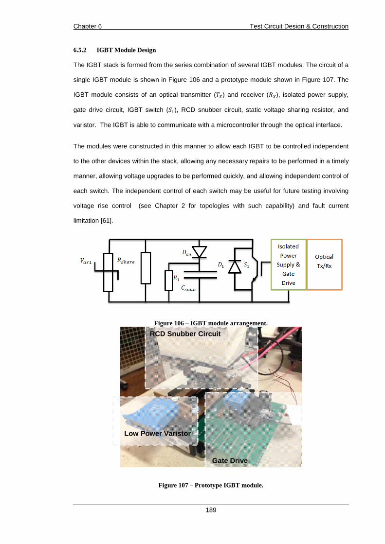
Chapter 6 Test Circuit Design & Construction
189
6.5.2 IGBT Module Design
The IGBT stack is formed from the series combination of several IGBT modules. The circuit of a
single IGBT module is shown in Figure 106 and a prototype module shown in Figure 107. The
IGBT module consists of an optical transmitter (U) and receiver ((U), isolated power supply,
gate drive circuit, IGBT switch (#), RCD snubber circuit, static voltage sharing resistor, and
varistor. The IGBT is able to communicate with a microcontroller through the optical interface.
The modules were constructed in this manner to allow each IGBT to be controlled independent
to the other devices within the stack, allowing any necessary repairs to be performed in a timely
manner, allowing voltage upgrades to be performed quickly, and allowing independent control of
each switch. The independent control of each switch may be useful for future testing involving
voltage rise control (see Chapter 2 for topologies with such capability) and fault current
limitation [61].
Figure 106 – IGBT module arrangement.
Figure 107 – Prototype IGBT module.
RCD Snubber Circuit
Low Power Varistor
Gate Drive

Chapter 6 Test Circuit Design & Construction
190
6.5.3 IGBT Stack
A schematic of the stack layout is given in Figure 108. The IGBT modules were first tested on
their own, before being tested in a series connection.
Figure 108 – IGBT stack schematic diagram, showing electrical and control layout.
6.5.4 Gate Drive Design
A search was performed to find an off the shelf gate drive circuit which could provide a suitable
gate current to the IGBT switch (32 A). However, such drivers that were available could not
deliver the required peak gate current, thus several gate drive ICs would be required in parallel.
Such gate drives were expensive (>£200 per gate drive device, with at least two being required
per IGBT module) and their control functions were not seen as suitable for HVDC applications.
Thus a custom gate drive design was required. The chosen design circuit is shown in Figure
109.

Chapter 6 Test Circuit Design & Construction
191
This topology uses two MOSFET devices in a two level arrangement to provide the required
gate voltage to the IGBT switch. The MOSFETs are controlled through low power IC gate drive
packages, switched by a gate control signal, which is provided through a fibre optic link.
The two MOSFETs are driven from IC drivers and can deliver up to 79 A, which is above the
required gate current. Blanking time between the two MOSFETs is achieved with the inbuilt
“anti-cross” feature of the gate drive IC. The anti-cross feature adds a 350 ns delay to the turn
on of the MOSFET. As the NAND gate will only produce a maximum delay of 40 ns, this still
leaves a 310 ns gap between the signal to the MOSFET turning off, and the MOSFET turning
on, thus the anti-cross feature is conserved. The advantage of the topology is that it can provide
very high gate currents.
Figure 109 – Gate drive circuit design used.
The disadvantage of the design is that it requires several internal floating power supplies for
each of gate drive - however with some modifications to the design these can be reduced. The
switching frequency of the gate drive is also likely to be limited, but for HVDC circuit breaker
applications high switching frequencies may not be a requirement.
The gate drive was prototyped on breadboard to validate the design layout. This was then
extended into a PCB design that included additional features such as over voltage protection,
internal fault detection, and an optical link between gate drive and controller. The optical signal
will allow the controller to take protective action in the event of a gate drive failure. Detailed of
the power supply design can be found in Appendix 3B.

Chapter 6 Test Circuit Design & Construction
192
The gate drive was tested at 10 kHz, first using a capacitive load, then using the IGBT module.
The gate emitter voltage when IGBT module switches are connected to the gate drive is shown
in Figure 110.
The gate drive was also loaded with a representative capacitive load (2 µF, the IGBT switch
gate capacitance was 1.66 µF [96]), and enclosed in the metal case used to reduce EMI. The
gate drive was then tested for 1 hour of continuous switching at 5 kHz to ensure that it would
function over long periods of time.
Figure 110 ‒ Test results from 10 kHz testing of gate drive with IGBT switch load.
6.5.5 Controller to Module Prototyping
Each individual part of the system (isolated power supply, gate drive, discharge switches,
optical interface boards) was prototyped, tested, and then integrated to ensure all equipment
worked together. The prototyping test layout of the microcontroller, discharge circuits, power
supply, and gate drive can be seen in Figure 111.

Chapter 6 Test Circuit Design & Construction
193
Figure 111 ‒ Prototyping test layout of IGBT control and test circuit communication.
As the high voltage test-bed construction was estimated to take several months to design, await
deliveries, and construct, the controller software could not be validated directly using the final
equipment. There was therefore a need for a “dummy” system which would allow the controller
software to be validated without the presence of the high voltage equipment.
A dummy system was designed to interface with the controller in the same manner as high
voltage test-bed equipment. This included charge and discharge circuits, allowing the testing
procedure to be tested and defined. The dummy system included a small replica of the test
circuit that produced currents and voltages over a similar time range, but at a much smaller
amplitude. This allowed the controller to be tested in parallel with the construction of the high
voltage equipment. An image of the dummy system testing can be seen in Figure 112 and the
prototyping setup is shown in Figure 113.
Controller and Optical TX/RX
IGBT
Module
Isolated
Power supply Discharge Circuits

Chapter 6 Test Circuit Design & Construction
194
Figure 112 – Dummy system. A miniature test circuit that allowed the controller software to be validated prior to high voltage testing.
Additional elements were included in the dummy system design, with a view to investigate the
turn off voltage control of a circuit breaker. This feature exists for several designs discussed in
Chapter 2. However, due to time limitations the work could not be attempted. Additional HV
measurement equipment was also designed and prototyped, but again due to time limitations in
the laboratory this work could also not be attempted. The dummy system was successfully used
to aid in the development of this measurement equipment.
Test Object
Measurement
Miniature Test
Circuit

Chapter 6 Test Circuit Design & Construction
195
Figure 113 – Dummy system testing. Dangerous electronics are placed within the plastic enclosure.
6.6 Test Circuit Construction
6.6.1 Test Circuit Inductance
The test circuit inductance was formed from square turns of copper pipe, in the layout shown in
Figure 114. Each side of the inductor was 1 meter in length, giving a cross sectional area of 1
m2. This was chosen as the copper pipe can be bought in 2 m lengths, making the construction
simpler. The diameter of the conductor is 15 mm, with a 3 mm air gap between each turn,
which was thought to be suitable to hold off the required 420 volts per turn [97, 98]. Details of
the design can be found in Appendix 3A.
Figure 114 – Inductor layout.

Chapter 6 Test Circuit Design & Construction
196
6.6.2 Test-Bed
The test circuit and test object were designed to be housed within a moveable test-bed, to allow
the complete system to be assembled outside the high voltage laboratory, and then wheeled
into the HV lab for testing. This ensured that all the time available for testing was used for
testing and not for assembly.
The test bed was designed using Google sketch up, the drawing is shown in Figure 115, and
then constructed in the School’s mechanical workshop. The test bed has two sets of shelves
which house the test object and the auxiliary power supplies. The low voltage and high voltage
equipment are separated by insulating shelves. This separation is shown for the lower shelf pair
in Figure 116.
Figure 115 ‒ Google sketch up design for test bed.
The test circuit’s diodes were built into stacks, as shown in Figure 117, and placed into slots
which hold them upright, at the back of the test-bed. Each diode has its own voltage sharing
elements mounted on a PCB board in parallel with it. Connections are made through copper
JW,NO(%)
( ,åJ((%) åå ,NO(%)
NW(% &% )

Chapter 6 Test Circuit Design & Construction
197
bus bars and the heat sinks have threaded holes, to allow the diodes to be mounted directly
onto the head sink. Insulating frames are used support each stack of diodes.
The test circuit capacitors were located on the bottom of the test bed with a shelf above to
isolate the capacitors from the rest of the test object, as shown in Figure 116. The test circuit
inductor was constructed from copper pipe and housed in a plastic frame, to ensure that the
inductor could be moved away from the sensitive control circuits if required. The entire test-bed
was built on a metal base with wheels to allow the test-bed to be moved around the laboratory
with ease, as shown in Figure 118.
Figure 116 ‒ Low voltage/ High voltage separation shelves. A conduit allows for safe crossover of high voltage and low voltage cables and protects the fiber optic cables.
Figure 117 – Diode stack with sharing elements on PCB.
High Voltage Capacitors
Conduit for
Optic/LV
Cables
High Voltage Electronics
Low Voltage Electronics
Heat sink Voltage sharing (R&C)
Diode

Chapter 6 Test Circuit Design & Construction
198
Figure 118 ‒ Test bed under construction.
Figure 119 – Partially constructed test-bed prior to transport.

Chapter 6 Test Circuit Design & Construction
199
6.7 Full System
The majority of the equipment was first assembled onto the test bed (test object, discharge
circuits, diodes, major electrical connections etc) prior to transport. The equipment’s low voltage
control signals were then tested ensuring no damage to the equipment has occurred, and the
earthing arrangement was correctly connected, before it was loaded and sent to the high
voltage testing facility. An image of the test-bed during assembly is shown in Figure 119.
6.8 Conclusion
This chapter has outlined the specification for the test circuit designed as part of this PhD
project. The test circuit topology and its operation have also been explained. Based on the
specification given, the parameters for the test circuit have been chosen using the analysis
performed on the test circuit topology.
The test object specification and physical design have also been discussed showing the major
components of the semiconductor circuit breaker. The development of the gate drive circuits
and the testing they were subjected to was also discussed briefly.
The procedure used to validate the microcontroller programming was also discussed. This was
done using a dummy system that allowed direct hardware validation of the control software to
be performed before any high voltage tests were performed.
The test-bed designed and built to house the test circuit and test object, was developed to allow
the test circuit to be assembled and transported with ease. As time in the high voltage lab was
limited, as much work that could be carried out prior to entering the HV lab was performed.

Chapter 7 High Voltage Testing
200
Chapter 7: High Voltage Testing
7.1 Introduction
The specification for synthetic test circuits has been developed in Chapter 3 of this thesis. From
this specification a test circuit was proposed in Chapter 6. The test circuit and an appropriate
test object were designed to perform testing.
This chapter covers the high voltage testing performed in order to validate the design of the test
circuit and test object (semiconductor breaker rated at 2.5 kA and 8.4 kV). These tests were
also performed to gain additional insights into the testing procedures and how the specifications
for the circuit breaker are defined.
Initial high voltage testing is discussed in Section 7.2. These tests used a single IGBT module.
Section 7.3 describes the full system test setup, where multiple series-connected IGBT modules
were used. Section 7.4 discusses the high voltage testing that was performed. Isolation
transformer testing, current impulse testing, and current breaking testing are all discussed
individually. The current pulse and current breaking tests are compared to simulations and
calculations of the test circuit where appropriate.
The key learning outcomes from the tests are discussed in Section 7.5 and highlight a number
of additional factors that must be included in the specification for HVDC circuit breaker test
circuits.
Section 7.6 discusses a modified test circuit, which is thought to be more appropriate for higher
power tests. The main conclusions from this chapter are summarised in Section 7.7.
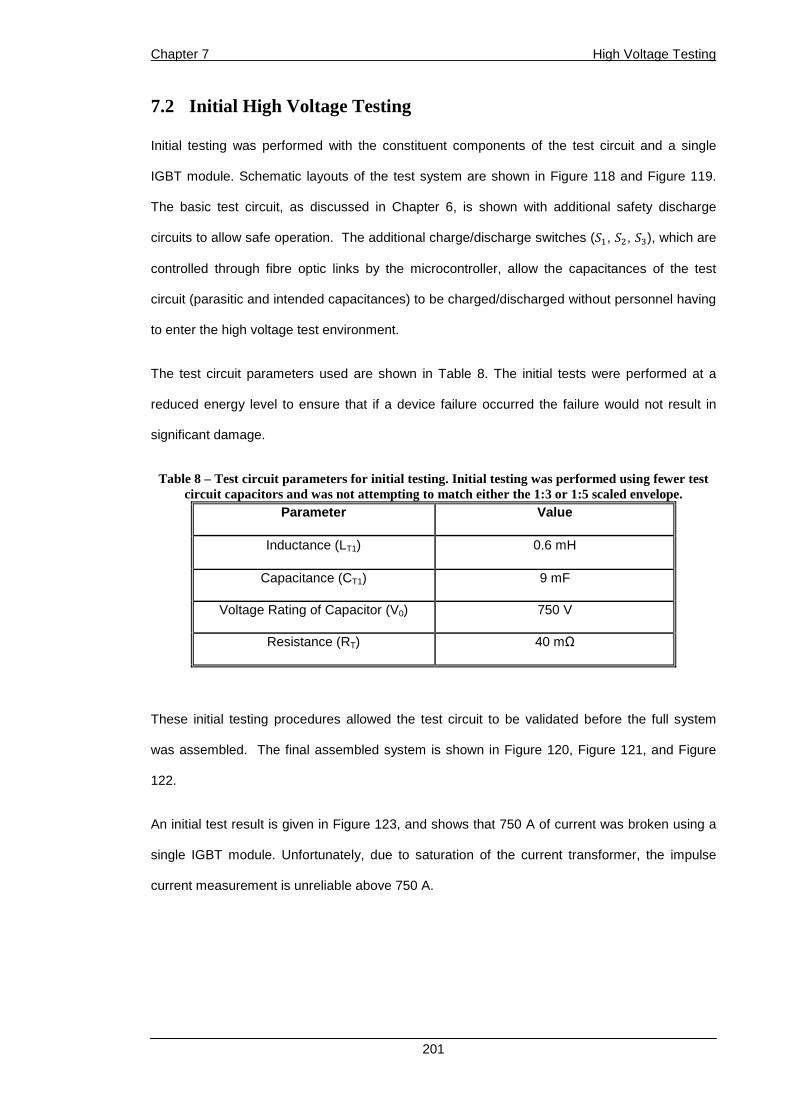
Chapter 7 High Voltage Testing
201
7.2 Initial High Voltage Testing
Initial testing was performed with the constituent components of the test circuit and a single
IGBT module. Schematic layouts of the test system are shown in Figure 118 and Figure 119.
The basic test circuit, as discussed in Chapter 6, is shown with additional safety discharge
circuits to allow safe operation. The additional charge/discharge switches (#, #, #&), which are
controlled through fibre optic links by the microcontroller, allow the capacitances of the test
circuit (parasitic and intended capacitances) to be charged/discharged without personnel having
to enter the high voltage test environment.
The test circuit parameters used are shown in Table 8. The initial tests were performed at a
reduced energy level to ensure that if a device failure occurred the failure would not result in
significant damage.
Table 8 – Test circuit parameters for initial testing. Initial testing was performed using fewer test circuit capacitors and was not attempting to match either the 1:3 or 1:5 scaled envelope.
Parameter Value
Inductance (LT1) 0.6 mH
Capacitance (CT1) 9 mF
Voltage Rating of Capacitor (V0) 750 V
Resistance (RT) 40 mΩ
These initial testing procedures allowed the test circuit to be validated before the full system
was assembled. The final assembled system is shown in Figure 120, Figure 121, and Figure
122.
An initial test result is given in Figure 123, and shows that 750 A of current was broken using a
single IGBT module. Unfortunately, due to saturation of the current transformer, the impulse
current measurement is unreliable above 750 A.

Chapter 7 High Voltage Testing
202
Figure 118 ‒ Schematic layout of the initial testing of the test circuit and IGBT module.
Figure 119 ‒ Layout of current and voltage measurements.
Figure 120 ‒ High voltage prototyping test circuit setup.

Chapter 7 High Voltage Testing
203
Figure 121 ‒ Detailed power electronic component layout - test circuit diodes (left), capacitance (bottom), spark gap (top middle) and test object (right).
Figure 122 – Full initial test system.
Diode Stack
Test Circuit Capacitors
Spark Gap
Test Object

Chapter 7 High Voltage Testing
204
Figure 123 ‒ Current performance result from the initial HV testing. Breaking ≈ 750 A.
The main results of these initial tests were the validation of the equipment interfaces, test circuit
operation, and proof of operation of the test circuit in the HV environment. The equipment, test
method, and health and safety features were also inspected by HV testing experts within the
University’s HV lab. This allowed for additional feedback to be obtained.
The current result, Figure 123, shows that the equipment was capable of operating at 750 A
which gave the author more confidence in moving forward with the design of the final test
system. The testing highlighted the need for an alternative measurement system and the
addition controlled discharge switches.

Chapter 7 High Voltage Testing
205
7.3 Full System Test Setup
The full test system circuit diagram is shown in Figure 124. The test circuit parameters were
increased to the design parameters developed for the full test system, as shown in Table .
The voltage rating of the test object was increased by increasing the number of IGBT modules
in series. The test object for the full system test consisted of 6 IGBT modules in series. This
results in the test object having a peak voltage rating of 8.4 kV and a peak nominal current
breaking capability of 2.5 kA. The semiconductor devices however can conduct a higher current
than this for a shorter period of time as they are rated for 2.5 kA continuous current. An image
of the fully constructed test system is shown in Figure 125. The test circuit was assembled onto
the test bed and all high current electrical connections were made using copper bus bars.
Figure 124 ‒ Schematic layout of the initial testing of the test circuit and IGBT module.
Table 9 – Test circuit parameters.
Parameter Value
Inductance (LT1) 0.6 mH
Capacitance (CT1) 18 mF
Voltage Rating of Capacitor (V0) 750 V
Resistance (RT) 100 mΩ

Chapter 7 High Voltage Testing
206
Figure 125 ‒ Constructed test system – physical layout in HV laboratory.
7.4 Test Results
7.4.1 Transformer Testing
The isolation transformers provide power to the IGBT gate drive circuit. Every custom built
isolation transformer was tested before the test circuit was operated as a whole. Each
transformer was subjected to at least 10 seconds of 12 kV DC between primary and secondary
windings, in the test circuit of Figure 126. Breakdown between the turns was monitored using an
oscilloscope and a voltage divider. The results from the testing of each isolation transformer
are shown in Figure 127.
The test results show that the transformers were capable of withstanding 12 kV for at least 10
seconds, without any indication of breakdown. This is beyond the required for the applied 8.4 kV
as during the test the voltage across between transformer windings will only last for a few
milliseconds.
Test bed, capacitors, and
semiconductors
Inductor
Control Room

Chapter 7 High Voltage Testing
207
Figure 126 ‒ Transformer test circuit layout.
Figure 127 ‒ Transformer test results. Voltage withstand traces for each transformer numbered 0 to 7.
10 kV
10 s

Chapter 7 High Voltage Testing
208
7.4.2 High Current Impulse Testing
The full voltage aimed to establish that the test circuit was capable of matching the envelope it
was designed against, over the required time frame, and that the test object was capable of
carrying the full current pulse produced by the test circuit. The test circuit was designed based
on the two specification envelopes shown in Figure 128. (See Chapter 6 for full specifications).
Figure 128 ‒ Test circuit specification envelopes. Current scale of 1:3 and a lower scale of 1:5.
Figure 129 shows the results that were obtained from the laboratory experiments. When the test
circuit operates at 68% of its peak initial charge, the test circuit is capable of generating the
required current to meet the 1:5 scale envelope. The peak current achieved was 1.94 kA, and
exceeded the 1:5 scale envelope over the time frame of approximately 6 ms (the desired time
frame).
The testing fell short of the expected peak current of 3.58 kA specified by the 1:3 scale
envelope. This is due to the reduced energy that the test circuit was operated at (46% of
maximum) and the additional resistance incurred from copper contacts in the circuit
construction. The time at which the peak current occurs is also less than expected due to the
Chapter 7 High Voltage Testing
209
additional resistance in the inductor’s winding and copper contacts. This was also due to
additional leakage current that was not expected in the circuit.
The result highlights the importance of these parts of the circuit in any test system specification.
Future designs should take care in the design of contacts throughout the circuit, as these will
play an important role in defining the peak current generated by the test circuit. The tests also
highlighted that the required power rating of the HV supply equipment will be heavily influenced
by the leakage current in the test circuit. A higher leakage current will result in a high power DC
supply being required.
Thus the test circuit’s operation has only been proven at the lower end of the system design
specification (1:5 scale). The 1:3 tests could not be attempted due to additional leakage current
in the test circuit, which prevented the test circuit’s capacitors being fully charged by the HV
power supply. In future tests a higher power DC supply will be used, which will allow the test
circuit to be operated at full power.
The laboratory results have also been compared with the PSCAD simulations of test system
and Equation (6.68). The parameters used in the PSCAD simulations came from component
datasheets where possible (IGBT, Capacitors, diodes and resistors), and from the experimental
data (inductor and parasitic resistance). Details of the test circuit simulations can be found in
Appendix 3C.
In Figure 129, the calculation traces use the two limiting values of capacitance for the test circuit
capacitors, based on the intrinsic tolerances specified in their datasheet. These are shown as
the dashed traces which exist either side of the original hand calculation that used 18 mF
(Labelled as Max and Min Cap).
The experimental result shows a good agreement during the rise of the fault current; however it
starts to deviate after about 4.5 milliseconds. Even when the known tolerance in capacitance is
factored into the calculation there is some discrepancy. This is due to the lack of parasitic
effects included in the hand calculation and due to variations in the circuit parameters during the
testing, making predictions of the circuit’s exact electrical parameters difficult. The simulation

Chapter 7 High Voltage Testing
210
results (which include some parasitic components) also show good agreement with the other
results.
The experimental results show some additional oscillations on the current waveform which are
believed to result from variations in the inductor’s impedance due to mechanical movement of
the inductor’s turns and inter-winding capacitance, as will be discussed in Section 7.5.
Figure 129 ‒ High current impulse testing results compared with simulation, hand calculation, and fault current testing envelope (5:1).

Chapter 7 High Voltage Testing
211
7.4.3 Current Breaking Testing
The next set of tests attempted to break the current close to its peak. The tests aimed to show
that the voltage rating of the test circuit was appropriately designed and the test object could
break the current.
Two different results are shown in Figure 130 and Figure 131. These results show the test
circuit generating peak currents of 0.9 kA and 1.6 kA respectively, and then the test object
attempting to interrupt the flow of these currents. The circuit breaker in these tests was open
approximately 5 ms after the start of the current impulse.
At the moment the circuit breaker is turned off, the voltage rises rapidly towards the expected
peak voltage of 5.5 kV. The voltage does not attempt to reach the peak rating of 8.4 kV, as the
current level is below the maximum breaking capability of the test object. This voltage is defined
by the varistor’s characteristic.
However, soon after the voltage rise, break down occurred across the test circuit’s inductor, and
this limited the peak voltage across the test object. As a result of the lower voltage across the
test object, the time it takes to reduce the current to zero is extended, even with the reduced
inductance.
The break down was caused by movement of the turns within the inductor, shorting the air gap
between each turn. When the small spacing (3 mm) between each turn is reduced by the
movement of the turns, an arc can form between two turns. Once two turns have broken down,
there is a cascading voltage break down effect on neighbouring turns, as they see a rapidly
increasing voltage.
Once the voltage has dropped sufficiently, the arc extinguishes and the remaining turn-to-turn
air gap can hold off the remaining 1.68 kV. The 1.68 kV is then sufficient to drive the current to
zero. While the test object is capable of breaking the current, this represents a failure of the test
circuit to withstand the required voltages.
Subsequent testing showed breakdown in the same area, and eventually several turns on the
inductor welded together.

Chapter 7 High Voltage Testing
212
Figure 130 ‒ Breaking test result 1. First test where significant current was broken. Voltage reaches 4.5 kV before break down occurs.

Chapter 7 High Voltage Testing
213
Figure 131 ‒ Breaking test result 2. Due to damage caused to the inductor subsequent tests could not maintain the same voltage levels as in the first test.

Chapter 7 High Voltage Testing
214
7.5 Key Learning Outcomes
7.5.1 Isolation Switch
Two different isolation switches were used during the testing; a spark gap and a semiconductor
isolation switch. The isolation switch is required to isolate the test object from the test circuit
capacitance. Ensuring that the test object is not charged by the voltage supply and reducing the
HV supply current requirements. The switch can be made in several ways, two of which were
attempted during the testing. The following two subsections describe the experience with a
spark gap isolation switch and a semiconductor isolation switch.
7.5.1.1 Spark Gap Experience
Spark gap triggering was initially chosen due to its ability to provide isolation between the test
circuit’s capacitance and the test object, thus preventing the test object being charged during
initial charging of the test circuit and reducing leakage current.
While the spark gap provides benefits in terms of isolation and may be able to provide reliable
triggering in other applications, it was not suitable for these HVDC test circuit applications
because the required current levels are too high. The damage to the electrodes incurred during
testing, shown in Figure 132, was significant.
Figure 132 ‒ Damage to electrode after one test circuit triggering.

Chapter 7 High Voltage Testing
215
7.5.1.2 Semiconductor Isolation switch
Reliable triggering of the test circuit while using a semiconductor isolation switch was achieved,
allowing reliable and repeatable operation of the test circuit. The semiconductor switch also did
not require reconfiguration after each current impulse, which helped speed up the testing
process.
However, semiconductor isolation switches for full power applications may not be suitable. The
semiconductor isolation switch does not provide full isolation between the test circuit’s
capacitance and the test object, resulting in some additional leakage current flowing through the
test object. This puts an additional burden on the HV power supply and prevented the
capacitors being charged to their maximum voltage. This was one of the main contributing
factors limiting the peak energy of the test circuit.
A single IGBT switch was used for these experiments; however several series-connected
devices will be required for higher power applications which may present additional problems,
as leakage current will increase due to voltage sharing resistors and snubber elements.
7.5.2 Voltage Supply
Bench top high voltage supplies are limited in the amount of current they provide. The high
voltage source must be able to supply enough current to ensure that charging can be achieved
in a reasonable time, while also being able to supply the leakage current of the test circuit. The
isolation switch must ensure that any leakage current to the test object is low, to minimize the
loading of the HV supply.
For full scale circuit breaker tests the test circuit capacitor charging supplies will have a DC
voltage rating similar to that of a VSC, but will only have to supply a few Amps to charge the test
circuit capacitance. Thus the required power supplies will be in the tens to hundreds of
kilowatts. The voltage supplies will therefore comprise a significant amount of the test circuit’s
cost. Ensuring that the power rating of the required power supplies is kept to a minimum will be
key for full scale testing systems.

Chapter 7 High Voltage Testing
216
7.5.3 Contact Resistance
The test circuit was designed to have 100 mΩ of resistance. However test results show that this
resistance had increased to 190 mΩ in the implementation. The additional resistance was
mainly caused by copper-to-copper contacts in the electrical connections of the test circuit.
These were present in the inductor and the series connections of the IGBTs. Reducing the
contact resistance in any test circuit design will be key to ensuring operation at maximum
current levels. A variable test circuit resistance would be preferable to control of circuit
resistance in a full scale test system.
7.5.4 Test Circuit Current/Energy Rating
The energy rating of the test circuit must be high enough to ensure the current is sufficient and
the varistors are tested appropriately. However, the test circuit energy should not be too large
either, since a test circuit that produces an overshoot in current could damage the test object.
The risk of current overshoot may limit the type/range of circuit breakers that can be tested at a
given facility or by a specific test circuit.
The envelopes used to specify the minimum current shape generated by the test circuit should
be specified along with a second envelope that dictates the maximum allowed current to ensure
no damage to the test object. Current overshoot produce over heating of the semiconductors,
ultimately resulting in circuit breaker failure. To prevent this effect the original envelope could be
scaled proportionally by a certain amount, or a bias term added to the original envelope to
provide this second maximum envelope. These two examples of how to define a maximum
envelope are shown for the 1:5 scaled envelope in Figure 133.
Specifying a maximum current envelope also ensures that the test circuit current derivative is
appropriate over the duration of the test. As the current must stay within the envelope limits, the
current derivative must also stay reasonably close to the specification envelope’s derivative. As
discussed in Chapter 4, an increased fault current derivative can impact on the voltage ratings
of key elements within the circuit breaker. Ensuring that the fault current derivative is
appropriate during the tests is of great importance to ensure these effects are encompassed in
the testing.

Chapter 7 High Voltage Testing
217
Figure 133 ‒ Fault current envelopes including maximum envelopes to prevent additional energy dissipation in the test object.
The proportional maximum envelope in Figure 133 is scaled by the factor 1.1 at every point, to
provide a very tight specification initially and a more lenient specification as the test continues.
The additive maximum envelope adds 10% of peak fault current (0.175 kA for this example) to
every point in the envelopes. Thus the test specification is easier to achieve, and results in the
test current’s derivative not tracking the envelope derivative as closely.
Which of these envelope augmentation methods is most suitable is a matter for future study.
The maximum envelope will likely use different limitations over different test time frames, some
of them additive maximums, some of them proportional.
7.5.5 Inductor Design
The mechanical forces placed upon the air-cored inductor are very high and can cause the
inductor’s geometry to change during operation. Following any change in geometry, the voltage
1.75 kA

Chapter 7 High Voltage Testing
218
distribution between the turns may not be even, thus turn-to-turn insulation breakdowns may
occur during testing.
If there are many turn-to-turn break downs, this is obvious from a post-test inspection and from
the test results. However if there are only a few turn-to-turn insulation breakdowns it may not be
obvious that this has occurred.
In such a case the test object may still be able to reduce the current towards zero. However,
even if the current is interrupted, this does not mean that the test has been successful. The
standard used to assess the results gathered in the laboratory must be able to exclude tests
where significant breakdown of the inductor’s turns has occurred, or any other form of
breakdown for that matter.
Should an inductor be used which may possibly break down internally then the envelopes used
to specify the test circuit’s design should be extended to include a post-interruption trace which
allows turn-to-turn insulation breakdowns to be observed in the testing specification. Some turn-
to-turn break down may be allowable as this may not result in a complete failure of the circuit
breaker. The test should also compensate for slower voltage rises seen in some circuit breaker
designs, such as [52, 99], which arises from using high capacitance in the secondary branches.
When the test object voltage increases to that of the varistors, so as to oppose the flow of
current, the current will decay at a known rate. The time when this event occurs can be found by
monitoring the control signals to the secondary branch. The current must decay quickly enough,
to ensure that the pulse width limitations of the energy absorbing branch are not exceeded. A
DC circuit breaker standard should provide a test envelope which can be used to assess if the
current is decaying properly from the moment it attempts to interrupt the fault current. An
example case is shown using the test results gathered, in Figure 134. The current should fall
between the limits given in Equation (7.71).
Figure 134 shows that initially the current decay stays within the limits. However, once
breakdown occurs across the inductor’s turns, the current decay reduces and the test current
falls outside the boundaries initially specified. The limitations given in Equation (7.71) are only a

Chapter 7 High Voltage Testing
219
rough guide. Further investigation is needed into what levels of inductor breakdown are seen as
acceptable and how quickly should the current decay once the current begins to be interrupted.
XW W,X1 < W W, < XW W,X1V = -9 − H% ≤ W W, ≤ -9%
(7.71)
Figure 134 ‒ Decay traces to be included in test result evaluation. Results show that breakdown has occurred and circuit breaker has failed the test.
Looking at the results from the current breaking tests in Section 7.4.3, the results show that the
testing procedure needs to define whether the required DC side inductance is part of the circuit
breaker or a separate entity. The procedure needs to define if the circuit breaker is to be tested
with a known inductance, or the inductance is provided as part of the test object.
How inductor turn-to-turn failures impact the test needs to be understood. Not only their specific
impact, but how many of these are tolerable during the test, and how many can be tolerated

Chapter 7 High Voltage Testing
220
during a circuit breaker’s lifetime. For such figures to be known, the duties for the circuit breaker
over its life time need to be established. How many operations can be performed etc.
Furthermore, the protection system must have an established method of dealing with the failure
of a series inductance. How this failure mode is detected, which secondary layers of protection
should be enacted, and how the primary layer of protection (the faulted breaker) survives.
7.5.6 Powering Auxiliary Equipment from Test Circuit
The test circuit has been designed to generate a high pulse of current that replicates the fault
current seen in circuit breakers. The test object is a stack of IGBTs. The IGBTs break the
current flow and are controlled by a microprocessor in an optical link. Their gate drives are
powered by individual isolated power supplies that get their power from the AC grid via a DC
power supply and an H bridge.
While the isolated gate drive power supply arrangement may be one solution that
manufacturers may use, it is more likely that the circuit breakers will extract the energy they
require to power the electronics from the DC grid itself [100]. This is the more likely option
because the cost of building an isolated power supply that draws its energy from a source at
ground potential is significantly higher due to the increased insulation requirements. Extracting
energy from the DC line is likely to be cheaper and more efficient. Thus the test object will have
to extract its auxiliary energy from the test circuit (as it is replicating the DC grid) before it can
operate.
The energy requirements for the gate drives and other auxiliary equipment will vary between
manufacturers depending on how the circuit breaker is designed. The standard must provide
some form of specification for the initial pulse of current (representing normal conduction
operation) that is delivered to the circuit breaker ensuring all manufacturers have a common
specification to work with.
A future test circuit will need to provide an initial flow of current that represents the conditions
under which the circuit breaker will initiate/power up its electronics prior to the fault current
impulse. This would not form part of a thermal stress test or a normal current carrying test, but
would simply be an extension of the high current test enabling the circuit breaker to power itself.

Chapter 7 High Voltage Testing
221
This feature of the testing has not been discussed in prior art, however the feature can be seen
in some published testing results [52]. This is not seen in other test results [39, 61, 99]
An example of how the envelopes could be modified to include the feature is given in Figure
135. The envelopes can extended to include an initial square pulse of current specification. This
is estimated to be several tens of milliseconds long based on [52]. The test circuit must
generate a short pulse of current that falls within the boundaries defined by the envelope. How
long this pulse should be and how high the current should be is a matter for further
investigation.
Figure 135 ‒ Envelope with initial pulse requirement added along with an example initial pulse of current.
7.5.7 Test Circuit Design
The test circuit described in this thesis was designed to generate a pulse of current that would
replicate the currents seen in a real system, at reduced magnitude. The test circuit is also suited
Initial power up pulse
Fault current pulse

Chapter 7 High Voltage Testing
222
for testing sections of a circuit breaker. While the test circuit design has generated the
appropriate current shape at a scale of 1:5 it will be more difficult and expensive to build this
test circuit for higher voltage applications.
When the test circuit is charged to )$ (300 kV) the current generated cannot meet the
requirements set down by the envelope, as the initial rate-of-rise of current would be too low.
For a full scale test circuit, in order to meet the required initial rate-of-rise of current specified by
the test envelopes, the test circuit capacitance has to be charged to twice nominal DC link
voltage. This is required, as discussed in Chapter 4, to replicate the additional voltage seen
across the series inductance imposed by travelling waves. The voltage must be increased as
the series inductance has to remain at the required minimum value.
If the capacitance is kept at the same value when the voltage is doubled, this significantly
increases the test circuit energy, resulting in a significantly increased peak current generated by
the test circuit. This would result in the test current overshooting the maximum envelope by a
significant margin.
To highlight this problem, the test circuit was re parameterized for a full scale envelope. Figure
136 shows the test circuit current for a full power system (+/- 300 kV, 1 GW TLC), with the
specification envelope and maximum envelope for the full scale test current.
The peak current can be reduced by reducing the test circuit capacitance to maintain the same
energy levels, and maintain the same peak current, as shown Figure 136. However this will still
produce an overshoot initially and may result in the test circuit violating the maximum current
limits defined by the maximum envelope specification, even with a generous 20% margin. This
feature would make the testing of circuit breakers that operate between 2 and 4 ms difficult, as
they would need to be over rated to deal with the additional current produced by the test circuit,
resulting in additional costs in building the circuit breakers.
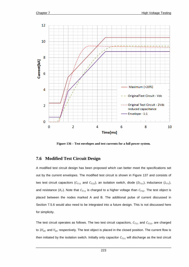
Chapter 7 High Voltage Testing
223
Figure 136 ‒ Test envelopes and test currents for a full power system.
7.6 Modified Test Circuit Design
A modified test circuit design has been proposed which can better meet the specifications set
out by the current envelopes. The modified test circuit is shown in Figure 137 and consists of
two test circuit capacitors (% and %), an isolation switch, diode (%), inductance (%), and resistance ((%). Note that % is charged to a higher voltage than %. The test object is
placed between the nodes marked A and B. The additional pulse of current discussed in
Section 7.5.6 would also need to be integrated into a future design. This is not discussed here
for simplicity.
The test circuit operates as follows. The two test circuit capacitors, % and %, are charged
to 2)$ and )$ respectively. The test object is placed in the closed position. The current flow is
then initiated by the isolation switch. Initially only capacitor % will discharge as the test circuit

Chapter 7 High Voltage Testing
224
diode (%) remains reversed biased. The capacitance value of % is tuned to replicate the
initial rate-of-rise of current caused by travelling wave effects. Once this capacitance has
discharged to )$, capacitance % will start to discharge along with %. The value of % is
chosen to provide a much lower rate-of-change of current and which mimics the terminal fault
current condition.
The test circuit allows the fault current envelope to be traced more easily than the previous test
circuit design, resulting in less current overshoot and allowing the circuit breaker to be tested at
suitable energy levels over a wider range of times. If the test circuit current needs to be
contoured further, due to a more tightly constrained maximum current envelope, additional
capacitor and diode strings can be added in parallel to achieve this.
Figure 137 ‒ Improved test circuit design.
7.6.1 Test Circuit Equations
In order to maintain appropriate energy levels the modified test circuit’s capacitances need to be
designed using equations (7.72) and (7.73). These are derived by equating circuit energies at
two different points during the testing. A derivation of these equations can be found in Appendix
4.
Here % is the original test circuit’s capacitance, and is the time at which the first
discontinuity in the test circuit envelope occurs (See Chapter 3).

Chapter 7 High Voltage Testing
225
% = 43%
(7.72)
% = % − 4%
(7.73)
7.6.2 Test Circuit Comparison
A comparison has been made between three test circuits that could be used to test a circuit
breaker for a +/- 300 kV 1 GW VSC system. This has been done to illustrate the differences that
would appear as the test circuits’ current rating was increased. The three test circuits compared
are the:
• Original Test Circuit (OTC) – shown in Figure 124 where the test circuit capacitors are
charged to )$.
• Double Voltage Test Circuit (DVTC) – same architecture as the OTC and same test
circuit energy but with twice the initial charge on the test circuit capacitors and a
reduced capacitance.
• Modified Test Circuit (MTC) – shown in Figure 137.
The MTC’s current is compared to the original test circuit designs in Figure 138, as if such a
topology was used for a full scale (1:1) HVDC test system. The MTC current can be seen to
exceed the envelope over the specified time frame and also remain within the maximum
envelope constraint (+20%). Thus a circuit breaker that operates within maximum operation
time can be safely tested with this test circuit structure, over the entire current pulse produced
by the test circuit.
The OTC and DVTC traces fail to meet both specifications set out by the two envelope traces.
The OTC cannot produce a high enough initial rate-of-rise of current and the DVTC produces an
overshoot in current violating the maximum.
The MTC also requires less capacitance than the OTC and less extra high voltage capacitance
compared to the DVTC, while also improving the test circuit’s response. A comparison of the
required capacitances and their peak voltage ratings is given in Table 10.

Chapter 7 High Voltage Testing
226
The test circuit will also be able to replicate the impact of travelling waves on the circuit
breaker’s internal power electronic equipment. This is due to the inductor’s voltage exceeding
the DC link voltage level during the test, over time period . Thus the conditions that a negative
cable voltage would impose on the circuit breaker’s operation are replicated.
The maximum envelope also ensures that the current rises at a high enough rate for the entire
test period. Without such a feature, the test circuit would be unable to compensate for the
additional commutation time and additional voltages seen across LCSs that form part of recent
industrial prototypes [52, 61, 83]. The testing procedures for these HVDC circuit breakers at
present appear not to directly compensate for the impact of travelling waves.
Table 10 – Comparison of required capacitance and voltage ratings of such capacitance.
Figure 138 ‒ Comparison of original test circuit traces and modified test circuit traces.
Capacitance [µF] Initial Voltage [kV]
OTC 100 300
DVTC 25 600
MTC 4.79 80.8 600 300

Chapter 7 High Voltage Testing
227
7.7 Conclusions
This chapter has described the testing that was performed using the proposed test circuit and
test object that were described in Chapter 6.
Initial testing was performed to check that the equipment could be integrated together and that
there were no problems with the test circuit architecture. Full system tests where then
performed with all the equipment. The full system tests performed included transformer testing,
current pulse testing, and current breaking testing.
The current pulse testing showed that the test circuit has successfully reproduced a test current
capable of mimicking a 1:5 scaled HVDC system for over 4 ms.
The tests failed to successfully break the current due to an internal breakdown across the
equipment. However, the results identified the need for a current decay requirement allowing
such breakdowns to be identified within the test results.
The testing has also highlighted the need to identify how the circuit breakers are going to power
themselves from the test circuit, as individual power supplies may not be an economic solution.
A modified test circuit has been proposed which will allow for the specifications to be met by the
test circuit more easily. This test circuit also allows the amount of required extra high voltage
test circuit capacitance to be reduced.
Other issues with isolation switches, power supply current limitations, inductor design, contact
resistance, and maximum specifications have also been identified within this chapter.

Chapter 8 Conclusions and Further Work
228
Chapter 8:
Conclusions and Further Work
8.1 Conclusions
The aim of this PhD project was to develop knowledge surrounding the testing of high voltage
direct current circuit breakers.
The objectives for this PhD were, as out outlined in Chapter 1:
6. Establish criteria for the testing of a prototype HVDC circuit breaker (Chapters 2 and 3)
7. Design a test circuit to meet this criteria (Chapter 6)
8. Build prototype circuit breakers and associated test equipment (Chapters 5 and 6)
9. Perform testing (Chapter 7)
10. Revaluate all test knowledge based on outcomes of the testing process (Chapter 7)
This work has gone beyond the required aims in some areas, developing knowledge that was
not part of the original objectives (Chapter 4). Additional publications have also been made in
the area of HVDC protection, looking into other areas the author believed would be relevant and
useful to developing a HVDC circuit breaker standard. Some of these publications have been
provided in Chapter 1. Based on the information given in the chapters of this thesis, this aim
and objectives have been met.
Sections 8.1.1 to 8.1.6 will summarise the main conclusions from each technical chapter in this
thesis. Section 8.2 discusses areas of future work in HVDC protection and synthetic testing.

Chapter 8 Conclusions and Further Work
229
8.1.1 HVDC Circuit Breakers and Standards (Chapter 2)
8.1.1.1 HVDC Circuit Breakers
The review of DC circuit breakers given in this thesis has shown that there is a wide range of
potential topologies for breaking DC fault currents. However, there is a clear trend from industry
to favour a hybrid circuit breaker structure. ABB and Alstom/GE have developed industrial
prototypes of circuit breaker modules, both of which are of a hybrid structure [52, 61]. C-EPRI
have built the only full scale HVDC hybrid circuit breaker, but details on this circuit breaker are
sparse [32]. Siemens has yet to publish a prototyped circuit breaker of any description, however
they are patenting hybrid circuit breaker topologies [83].
Based on the industry prototypes being developed and the benefits provided, the hybrid circuit
breakers appears to be the preferred topology for future HVDC circuit breakers.
8.1.1.2 Standards
Existing standards cannot be used to provide a full HVDC circuit breaker standard. However,
many existing standards may provide a useful starting point. As it appears that hybrid circuit
breakers are the preferred technology, existing standards concerned with the testing of HVDC
valves provide a good starting point. DC traction standards are also of particular use. IEC
60700, 62501, 62271, 61992 may all provide useful information.
There is still significant work required in defining specific tests that will be required for HVDC
circuit breakers. Key areas for future work with respect to testing are discussed in Section 8.2.1.
8.1.2 Converter Fault Analysis and Fault Current Envelopes (Chapter 3)
This thesis describes a generalized method for developing a fault current test criteria. The
concept of FCEs can be applied to any converter type. Two specific converter topologies have
had specific envelope designs developed and it is shown that they provide a very strong guide
in predicting all the fault currents that a circuit breaker is likely to be exposed to. Because FCEs
are shown to be implementable when designing physical test circuits it is possible that they can
be translated into a first generation standard.
FCEs, coupled with the additions to their design given in Chapter 7, also allow impacts from
travelling waves to be compensated in the testing of circuit breakers. As the FCEs are based on

Chapter 8 Conclusions and Further Work
230
the limitations of the system, the test conditions will always be more severe than anything that
the power system can reproduce. Care must be taken with the MMC topologies, as these
converters could be controlled to violate the envelopes if they are not designed appropriately.
FCEs may also provide a method of specifying the fault response of a given converter. MMCs
are highly controllable, and provide a number of options for fault performance. FCEs would
allow the response of the converters to be defined by a standard, and their use could become
part of the commissioning process. The envelopes would provide a reasonable target for the
fault current based on the known limitations of the system. This would go a long way to
guaranteeing the acceptability of the currents that a HVDC circuit breaker would be subjected
to.
8.1.3 Circuit Breaker Analysis (Chapter 4)
Detailed analysis of two hybrid circuit breakers has been presented in this thesis. The PHCB’s
operation has been analysed in detail and equations that describe the commutation process
have been developed for the first time. These equations show that travelling waves will impact
the commutation process in a negative manner, and that in the design of a PHCB, the non-
terminal fault condition needs to be carefully considered.
The novel SHCB, invented and developed as part of this PhD, has also been analysed in detail.
Its operation has been described, and verified against simulations of the circuit breaker in the
DC power system. Travelling waves should not have the same negative impact on the
commutation process, as they would in the PHCB, as they help to increase the resistance of the
superconductor, resulting in faster commutation.
8.1.4 Low Voltage Prototyping (Chapter 5)
Two circuit breaker topologies have been prototyped at low power during this thesis. The PHCB
prototype was developed in order to test the custom built equipment built during this PhD. The
novel SHCB was prototyped for the first time and validated the concept of using a
superconductor as a commutating element in HVDC circuit breakers. This testing also allowed
the analyses developed surrounding the SHCB to be validated.

Chapter 8 Conclusions and Further Work
231
8.1.5 Test Circuit Design
A test circuit capable of generating current between one fifth and one third of a full scale system
was designed. This test circuit was designed using the specification envelopes developed as
part of this PhD work, as no other specification method existed at the time. A semiconductor
circuit breaker was also built to form the object under test.
8.1.6 Test Results
The high power test results showed that the test circuit design procedure was validated for the
one fifth scale envelope. These tests were limited in their peak current rating, however, due to
additional leakage current in the test circuit.
The test results allowed several amendments to the test circuit specification to be developed.
These include the addition of maxima in the test envelope specifications, tail current limitations,
and the requirement for a charging pulse of current to be generated prior to the creation of the
fault current.
8.2 Future Work
8.2.1 Standards and Test Methods
Significant work is still required in developing a full scale HVDC circuit breaker standard. Only
C-EPRI has developed a “full scale” HVDC circuit breaker with plans to install it in a HVDC grid.
Other manufacturers have developed modules of their own topologies. Work needs to begin in
drafting a HVDC circuit breaker standard, using what can be transferred from existing
standards.
Key areas that need investigation are:
Circuit Breaker Energy Testing: The tests developed in this thesis have focused on the current
specification for testing HVDC circuit breakers. The test circuit used will not properly test the
varistors due to the increased inductor voltage that is seen during an interruption test.
Criteria and appropriate test circuits that are better suited to meet such requirements need to be
developed. It is likely that a separate test will be required to test the energy absorption rating of
the circuit breaker.

Chapter 8 Conclusions and Further Work
232
Module Failure Testing: The HVDC community is still viewing HVDC circuit breakers as a single
device, as they are in AC systems. This can be clearly seen in the most recent journal
publications on HVDC circuit breakers [80, 91]. Even in this thesis the modular nature of the
circuit breakers is not always represented. However, the manufacturers have largely stated that
HVDC circuit breakers will be modular in nature [61].
Understanding how the circuit breaker as a whole responds to failure of a single module, or
multiple modules, needs to be understood. Supplementary to this is the requirement for an
understanding of how neighbouring or secondary protection layers will act based on the
detection of this partial failure mode. This will be of particular importance when validating fault
detection algorithms and back up protection methods. How the “DC Relay” is able to provide
selection under such an event will be of great interest.
Power Disturbance Performance: As HVDC circuit breakers will be powered from the HVDC
grid, the limitations of the breaker’s auxiliary power supplies need to be fully understood. If the
power in the DC grid drops due to fault transient, an important question is how long the circuit
breakers can still maintain full controllability before they are unable to re-close or open.
Another important consideration is whether the performance of the circuit breaker is impacted
by a change in the DC grid’s voltage and current. The impact such transients have on the ability
of the power supplies to maintain the required gate drive voltages in order to switch the power
electronics, is fundamental to their operation. The power system conditions that the auxiliary
power supplies should be expected to work under must be defined, in order to produce a
reliable specification for HVDC circuit breakers.
Number of Operations and Repeatability: How many times the circuit breaker can perform a set
pattern of operations before its performance starts to deteriorate, also needs to be established.
Circuit breakers are likely to have a certain amount of energy stored in their auxiliary power
supplies, which will be topped up by a device that extracts energy from the power system.
Understanding how long it takes to full recharge the stored energy is important. Understanding
how many operations, and what type of operations can be performed with the amount of stored
energy is also key for a future standard.

Chapter 8 Conclusions and Further Work
233
8.2.2 Converter Fault Analysis and Fault Current Envelopes
FCEs are a useful tool for designing synthetic test circuits. The FCEs developed in this thesis
should be thought of as the first generation of such envelopes, providing generalized and
definite predictions of fault current. Other converter topologies and control strategies may result
in a significant reduction in fault currents seen compared to the envelopes described in this
thesis. The design of the envelopes should then be reconsidered to take into account any
reductions in current.
The superposition of FCEs is an area of great interest for future applications as this would allow
of specification for real systems to be quickly and simply developed. FCEs would be calculated
for each energy source at each breaker location within the DC grid. The FCE from each source
would then be superimposed to give the final specification. Work will be needed to take into
account different energy sources (batteries, other converters etc.) as well as any travelling wave
effects that may exist in the DC system.
Further work will be needed to define FCEs for the advanced MMC submodule architectures
presently being developed (such as full-bridge sub-modules or the Alternate Arm Converter -
AAC). Such work would allow the requirements for HVDC circuit breakers connected to different
converter topologies to be directly compared, and the benefits that such converters have for the
HVDC protection equipment to be quantified, rather than being qualitative.
Further work is needed to look into how the converters may support the circuit breaker from the
moment the current is interrupted by the circuit breaker. The converters, especially the AAC and
other advanced MMCs, have the ability to influence the recovery process due to their ability to
produce negative arm voltages. How much the advanced MMC topologies can help, and how to
specify this during testing is an interesting question for future research, and what potential
negative impacts exist between the control and the breakers.
8.2.3 Circuit Breaker Analysis and Thermal Modelling
Analysis of two hybrid circuit breakers has been developed as part of this PhD project. This
analysis has taken into account the electrical parameters of the semiconductors in the
secondary branches. The parameters were based on data taken from datasheets and simplified
models of the semiconductors, and assume fixed parameters.

Chapter 8 Conclusions and Further Work
234
During this PhD a few months were devoted to investigating into the thermal and electrical
modelling of semiconductor devices. The work has not been published in this thesis as it never
came to a suitable conclusion. This was mainly due to the amount of time that would have had
to be devoted to the area to obtain a useful outcome, and because the thermal models that
presently exist for the semiconductor devices are unsuitable for the inductive environments that
the circuit breakers operate in.
The existing thermal models are of a voltage dependent current source structure [101-104]. This
is not suitable for inductive environments, as high voltages would be generated elsewhere
within the circuit breaker model. The models need to be of a current dependent voltage source
structure.
The parameters that are given in the IGBT datasheets were gathered using the test techniques
outlined in [105]. As these were performed under DC or low frequency conditions, they may not
be suitable for the transient behaviour in a HVDC circuit breaker, since the devices will be
operating at their limits for short periods of time. Understanding the limitations of the
semiconductors and how to model them is very important.
Developing suitable models would allow the deviation in the electrical parameters of the
semiconductors to be established. This variation could then either be known to be insignificant,
or appropriately compensated for in the circuit breaker designs.

Chapter 8 Conclusions and Further Work
235
References
[1] "World population prospects. The 2015 revision. Key findings and advance tables," United Nations Department of Economic and Social Affairs. 2015.
[2] "Progress toward sustainable energy," Sustainable Energy For All 2015. [3] "Ren21. 2014. Renewables 2014 global status report," United Nations - Energy. 2014. [4] R. D. Garzon, High voltage circuit breakers - designs and application (75-106).
Columbus, 2005. [5] "Electricity ten year statement," National Grid. 2014. [6] "Uk offshore wind: Opportunities for trade and investment," UK Trade & Investment.
2015. [7] "Roadmap to the supergrid technologies," Friends of the Supergrid. 2014. [8] K. Meah and S. Ula, "Comparative evaluation of hvdc and hvac transmission systems,"
in Proc. Power Engineering Society General Meeting, 2007. IEEE, 2007, pp. 1-5. [9] "National grid - offshore development information statement," ed: National Grid, 2010. [10] N. MacLeod, D. Abbott, and A. Burns, "Comparison of hvac and hvdc transmission
options for round 3," in Proc. Global Offshore Wind 2014, Glasgow. [11] Stephanie Hay, Catherine Cleary, Gordon McFadzean, Jason McGray, and N. Kell,
"Tnei - mvdc technology study –market opportunities and economic impact," 2015. [12] R. Chinnasamy, "Analysis of the global hvdc and facts market," Frost and Sullivan
2015. [13] A. Canelhas, High voltage direct current (hvdc) technology, 2012. [14] L. Chuanyue, H. Xiaobo, G. Jingli, and L. Jun, "The dc grid reliability and cost
evaluation with zhoushan five-terminal hvdc case study," in Proc. Power Engineering Conference (UPEC), 2015 50th International Universities, 2015, pp. 1-6.
[15] J. Hu, C. Zhao, X. Zhang, and X. Yang, "Simulation study of the zhoushan project as a three-terminal dc transmission system," in Proc. Power and Energy Society General Meeting, 2012 IEEE, 2012, pp. 1-6.
[16] "Atlantic wind connection:Grid resiliency, its economic and security impacts, and the implications of awc," The Chertoff Group. 2012.
[17] "High voltage direct current transmission," Siemens AG, Erlangen. 2011. [18] B. Williams, Power electronics - chapter 19: Barry W Williams, 2006. [19] D. v. Hertem, K. Linden, J.-P. Taisne, W. Grieshaber, and D. Jovcic, Feasibility of dc
transmission networks. Aberdeen, 2011. [20] M. Bahram, M. Baker, J. Bowles, R. Bunch, J. Lemay, W. Long, J. McConnach, R.
Menzies, J. Reeve, and M. Szechtman, "Intergration of small taps into (existing) hvdc links," vol. 10, pp. 1699-1706, 1995.
[21] S. Wang, G. Li, M. Zhou, and Z. Zhang, "Research on interconnecting offshore wind farms based on multi-terminal vsc-hvsc," in Proc. Power System Technology (POWERCON), 2010 International Conference on, 2012, pp. 1-7.
[22] 2011. Why hvdc? Available: http://www.abb.com/industries/us/9AAF400103.aspx, (Accessed:14th Nov 2011.)
[23] A. Lesnicar and R. Marquardt, "An innovative modular multilevel converter topology suitable for a wide power range," in Proc. Power Tech Conference Proceedings, 2003 IEEE Bologna, 2003, p. 6 pp. Vol.3.
[24] Y. Wang. and R. Marquardt., "Future hvdc-grids employing modular multilevel converters and hybrid dc-breakers," IEEE, vol. EPE'13 ECCE Europe, 2013.
[25] G. P. Adam, K. H. Ahmed, S. J. Finney, K. Bell, and B. W. Williams, "New breed of network fault-tolerant voltage-source-converter hvdc transmission system," Power Systems, IEEE Transactions on, vol. 28, pp. 335-346, 2013.
[26] R. Li, G. P. Adam, D. Holliday, J. E. Fletcher, and B. W. Williams, "Hybrid cascaded modular multilevel converter with dc fault ride-through capability for the hvdc transmission system," IEEE Transactions on Power Delivery, vol. 30, pp. 1853-1862, 2015.
[27] R. Zeng, L. Xu, L. Yao, and B. W. Williams, "Design and operation of a hybrid modular multilevel converter," IEEE Transactions on Power Electronics, vol. 30, pp. 1137-1146, 2015.
[28] M. M. C. Merlin, T. C. Green, P. D. Mitcheson, D. R. Trainer, R. Critchley, W. Crookes, and F. Hassan, "The alternate arm converter: A new hybrid multilevel converter with dc-
Chapter 8 Conclusions and Further Work
236
fault blocking capability," Power Delivery, IEEE Transactions on, vol. 29, pp. 310-317, 2014.
[29] H. Rao, "Architecture of nan'ao multi-terminal vsc-hvdc system and its multi-functional control," Power and Energy Systems, CSEE Journal of, vol. 1, pp. 9-18, 2015.
[30] E. Spahic, F. Schettler, D. Varma, and J. Dorn, "Impact of the dc technology on transmission grids," in Proc. AC and DC Power Transmission, 11th IET International Conference on, 2015, pp. 1-7.
[31] N. Grid, National electricity transmission system security and quality of supply standard vol. Version 2.3, 2012.
[32] C-EPRI. 2015. Sgri launches world’s first 200kv dc circuit breaker. Available: http://www.cepri.com.cn/release/details_66_721.html (Accessed:Nov 2015.)
[33] N. Doerry, "Next generation intergration power system: Ngips technology development roadmap," US Naval Sea Systems Command. 2007.
[34] Paul Gemin, Tom Kupiszewski, Arthur Radun, R. L. Yan Pan, R. W. Di Zhang, Y. J. Xinhui Wu, Steve Galioto, Kiruba Haran, William Premerlani, Jim Bray, and Antonio Caiafa, "Architecture, voltage and components for a turboelectric distributed propulsion electric grid (avc-tedp)," 2015.
[35] "Standard review plan (srp) - technology readiness assessment report," U.S Department of Energy2010.
[36] A. Beddard, "Factors affecting the reliability of vsc-hvdc for the connection of offshore windfarms," Doctor of Philosophy, The University of Manchester, 2015.
[37] A. Beddard and M. Barnes, "Hvdc cable modelling for vsc-hvdc systems," Washington DC, IEEE PES GM Conference, 2014.
[38] E. M. Richard, "Superconducting transmission lines," in Transmission lines and communication networks:An introduction to transmission lines, high-frequency and high-speed pulse characteristics and applications, ed: Wiley-IEEE Press, 1995, pp. 211-267.
[39] T. Eriksson, M. Backman, S. Halén, and A. C. Research, "A low loss mechanical hvdc breaker for hvdc grid applications," presented at Cigré Paris, 2014.
[40] J. Zybroski, J. Czucha, and M. Sajnacki, "Thyristor circuit breaker for overcurrent protection of industrial dc power installations," Electrical Engineers, Proceedings of the Institution of, vol. 123, pp. 685-688, 1976.
[41] J. Mu, L. Wang, and J. Hu, "Analysis and design of topological structure for dc solid-state circuit breaker," in Proc. World Non-Grid-Connected Wind Power and Energy Conference, 2009. WNWEC 2009, 2009, pp. 1-5.
[42] S. B. Tennakoon and P. M. McEwan, "A two stage dc thyristor circuit breaker," Power Electronics, IEEE Transactions on, vol. 12, pp. 597-607, 1997.
[43] B. Bachmann, G. Mauthe, E. Ruoss, H. P. Lips, J. Porter, and J. Vithayathil, "Development of a 500kv airblast hvdc circuit breaker," vol. PAS-104, pp. 2460-2466, 1985.
[44] K. Tahata, S. El Oukaili, K. Kamei, D. Yoshida, Y. Kono, R. Yamamoto, and H. Ito, "Hvdc circuit breakers for hvdc grid applications," in Proc. AC and DC Power Transmission, 11th IET International Conference on, 2015, pp. 1-9.
[45] D. Jovcic and B. Wu, "Fast fault current interruption on high-power dc networks," in Proc. Power and Energy Society General Meeting, 2010 IEEE, 2010, pp. 1-6.
[46] C. Meyer, M. Kowal, and R. W. De Doncker, "Circuit breakers concepts for future high-power dc-applications," in Proc. Industry Applications Conference, 2005. Fourtieth IAS Annual Meeting. Conference Record of the 2005, Aachen, 2005, pp. 860-866 Vol. 2.
[47] R. W. Ashton and K. A. Corzine, "A new z-source dc circuit breaker," Power Electronics, IEEE Transactions on, vol. 27, pp. 2796-2804, 2012.
[48] R. W. Ashton and K. A. Corzine, "Structure and analysis of the z-source mvdc breaker," in Proc. Electric Ship Technologies Symposium (ESTS), 2011 IEEE, Thronton , PA, USA, 2011, pp. 334-338.
[49] J.-M. Meyer and A. Rufer, "A dc hybrid cicuit breaker with ultra-fast contact opening and integrated gate-commutated thyistors (igcts)," Power Delivery, IEEE Transactions on, vol. 21, pp. 646-651, 2006.
[50] M. Callavik, A. Blomberg, J. Hafner, and B. Jacobson, "The hybrid hvdc breaker.," 2012.
[51] C. C. Davidson, R. S. Whitehouse, C. D. Barker, J. P. Dupraz, and W. Grieshaber, "A new ultra-fast hvdc circuit breaker for meshed dc networks," in Proc. AC and DC Power Transmission, 11th IET International Conference on, 2015, pp. 1-7.

Chapter 8 Conclusions and Further Work
237
[52] J. P. Dupraz and D. L. Penache, "Development of a 120 kv direct current circuit breaker," presented at Cigre Paris, 2014.
[53] J. Manusson, R. Saers, and L. Liljestrand, "The commutation booster, a new concept to aid commutation inhybrid dc-breakers " presented at Cigre Paris, 2015.
[54] B. Xiang, Z. Liu, Y. Geng, and S. Yanabu, "Dc circuit breaker using superconductor for current limiting," IEEE Transactions on Applied Superconductivity, vol. 25.2, pp. 1-7, 2015.
[55] W. Zhou, X. Wei, S. Zhang, G. Tang, Z. He, J. Zheng, Y. Dan, and C. Gao, "Development and test of a 200kv full-bridge based hybrid hvdc breaker," in Proc. Power Electronics and Applications (EPE'15 ECCE-Europe), 2015 17th European Conference on, 2015, pp. 1-7.
[56] Iec 61992-2 - railway applications – fixed installations – dc switchgear – part 2: Dc circuit-breakers,IEC-2006.
[57] Iec 62271-100 high-voltage switchgear and controlgear – part 100: Alternating current circuit breakers,IEC-2008
[58] Iec 62271-1 high-voltage switchgear and controlgear – part 1: Common specifications,IEC-2011.
[59] Iec 62501 - voltage sourced converter (vsc) valves for high-voltage direct current (hvdc) power transmission – electrical testing,IEC-2009.
[60] C. D. Barker and R. S. Whitehouse, "An alternative approach to hvdc grid protection," in Proc. AC and DC Power Transmission (ACDC 2012), 10th IET International Conference on, 2012, pp. 1-6.
[61] M. Callavik and A. Blomberg, The hybrid hvdc breaker: ABB Grid Systems, 2012. [62] G. P. Adam and I. E. Davidson, "Robust and generic control of full-bridge modular
multilevel converter high-voltage dc transmission systems," IEEE Transactions on Power Delivery, vol. 30, pp. 2468-2476, 2015.
[63] M. K. Bucher and C. M. Franck, "Analytic approximation of fault current contributions from capacitive components in hvdc cable networks," Power Delivery, IEEE Transactions on, vol. PP, pp. 1-1, 2014.
[64] M. K. Bucher and C. M. Franck, "Comparison of fault currents in multiterminal hvdc grids with different grounding schemes," in Proc. PES General Meeting | Conference & Exposition, 2014 IEEE, 2014, pp. 1-5.
[65] A. Wasserrab, B. Just, and G. Balzer, "Contribution of hvdc converters to the dc short circuit current," in Proc. Power Engineering Conference (UPEC), 2013 48th International Universities', 2013, pp. 1-6.
[66] A. Wasserrab and G. Balzer, "Determination of dc short-circuit currents of mmc-hvdc converters for dc circuit breaker dimensioning," in Proc. AC and DC Power Transmission, 11th IET International Conference on, 2015, pp. 1-7.
[67] B. Williams, Power electronics - chapter 5, 2006. [68] A. Hassanpoor, J. Hafner, and B. Jacobson, "Technical assessment of load
commutation switch in hybrid hvdc breaker," in Proc. Power Electronics Conference (IPEC-Hiroshima - ECCE-ASIA), 2014 International, 2014, pp. 3667-3673.
[69] B. Williams, Power electronics - chapter 3, 2006. [70] A. Wasserrab and G. Balzer, "Evaluation of short circuit currents in multi-terminal hvdc
systems," in Proc. Electrical and Power Engineering (EPE), 2012 International Conference and Exposition on, 2012, pp. 213-218.
[71] M. K. Bucher and C. M. Franck, "Contribution of fault current sources in multiterminal hvdc cable networks," Power Delivery, IEEE Transactions on, vol. 28, pp. 1796-1803, 2013.
[72] Y. Jin, J. E. Fletcher, and J. O'Reilly, "Short-circuit and ground fault analyses and location in vsc-based dc network cables," Industrial Electronics, IEEE Transactions on, vol. 59, pp. 3827-3837, 2012.
[73] A. Wasserrab and G. Balzer, "Frequency-dependent cables for the calculation of line short-circuit currents in hvdc networks," in Proc. Power Engineering Conference (UPEC), 2014 49th International Universities, 2014, pp. 1-6.
[74] M. Riddle, S. Ardalan, and J. Suh, "Derivation of voltage and current transfer functions for multiconductor transmission lines," in Proc. Circuits and Systems, 1989., IEEE International Symposium on, 1989, pp. 2219-2222 vol.3.

Chapter 8 Conclusions and Further Work
238
[75] J. Sneath and A. Rajapakse, "Fault detection and interruption in an earthed hvdc grid using rocov and hybrid dc breakers," in Proc. Power & Energy Society General Meeting, 2015 IEEE, 2015, pp. 1-1.
[76] I. C37.011, "Ieee guide for the application of transient recovery voltage for ac high-voltage circuit breakers," p. 9, 2011.
[77] P. M. Meshram and V. B. Borghate, "A simplified nearest level control (nlc) voltage balancing method for modular multilevel converter (mmc)," Power Electronics, IEEE Transactions on, vol. 30, pp. 450-462, 2015.
[78] G. Konstantinou, J. Pou, R. Darus, S. Ceballos, and V. G. Agelidis, "Defining the exact number of sub-module transitions in fundamental frequency modulated modular multilevel converters," in Proc. Industrial Technology (ICIT), 2015 IEEE International Conference on, 2015, pp. 3052-3057.
[79] J. Sneath and A. D. Rajapakse, "Dc fault protection of a nine-terminal mmc hvdc grid," in Proc. AC and DC Power Transmission, 11th IET International Conference on, 2015, pp. 1-8.
[80] M. Bucher and C. Franck, "Fault current interruption in multiterminal hvdc networks," Power Delivery, IEEE Transactions on, vol. PP, pp. 1-1, 2015.
[81] T. Eriksson, M. Backman, and S. Halén, "A low loss mechanical hvdc breaker for hvdc grid applications," presented at Cigré Paris, 2014.
[82] M. Barnes and A. Beddard, "Uk patent application gb2493911 - circuit breaker conduction path," 2011.
[83] Mojtaba Mohaddes, "Hybrid dc cirucit breaking device," WO 2013/093066 A1, 2013. [84] P. Chang, A. Q. Huang, and S. Xiaoqing, "Current commutation in a medium voltage
hybrid dc circuit breaker using 15 kv vacuum switch and sic devices," in Proc. Applied Power Electronics Conference and Exposition (APEC), 2015 IEEE, 2015, pp. 2244-2250.
[85] M. Rahimo, L. Storasta, F. Dugal, E. Tsyplakov, and U. Schlapbach, "The bimode insulated gate transistor (bigt), an ideal power semiconductor for power electronics based dc breaker applications," presented at Cigre Paris, 2014.
[86] D. Döring, D. Ergin, K. Würflinger, J. Dorn, F. Schettler, and E. Spahic, "System integration aspects of dc circuit breakers," IET Power Electronics, vol. 9, pp. 219-227, 2016.
[87] B. Williams, "Power electronics - chapter 10," pp. 405-408. [88] ABB. 2013. 5sna 2000k450300 igbt datasheet. Available:
http://www05.abb.com/global/scot/scot256.nsf/veritydisplay/6e6983faa83cded383257b4a00515559/$file/5SNA%202000K450300%205SYA%201431-00%2003-2013.pdf, (Accessed:July 2013.)
[89] EPCOS, " Datasheet: Siov metal oxide varistors - block varistors, highe series," ed, April 2011, pp. 13,18.
[90] D. Andersson and A. Henriksson, "Passive and active dc breakers in the three gorges-changzhou hvdc project," ed, 2003.
[91] W. Lin, D. Jovcic, S. Nguefeu, and H. Saad, "Modelling of high-power hybrid dc circuit breaker for grid-level studies," IET Power Electronics, vol. 9, pp. 237-246, Feb. 2016.
[92] N. Ahmed, L. Ängquist, S. Mahmood, A. Antonopoulos, L. Harnefors, S. Norrga, and H. P. Nee, "Efficient modeling of an mmc-based multiterminal dc system employing hybrid hvdc breakers," IEEE Transactions on Power Delivery, vol. 30, pp. 1792-1801, 2015.
[93] X. Pei, "Superconducting current limiter with intergrated vacuum interrupter," Doctor of Philosophy, Faculty of Engineering and Physical Sciences, The Unviersity of Manchester, 2012.
[94] K. D. Kerf, K. Srivastava, M. Reza, D. Bekaert, S. Cole, D. V. Hertem, and R. Belmans, "Wavelet-based protection strategy for dc faults in multi-terminal vsc hvdc systems," IET Generation, Transmission & Distribution, vol. 5, pp. 496-503, 2011.
[95] D. Jovcic, D. Van Hertem, K. Linden, J. P. Taisne, and W. Grieshaber, "Feasibility of dc transmission networks," in Proc. Innovative Smart Grid Technologies (ISGT Europe), 2011 2nd IEEE PES International Conference and Exhibition on, 2011, pp. 1-8.
[96] INFINEON, "Technical information - fz2400r17hp4_b9 " 2013. [97] T. Hosokawa, T. Kaneda, T. Takahashi, T. Yamamoto, T. Morita, and Y. Sekiya, "Dc
breakdown characteristics in the gap with thin dielectric sheet in air," IEEE Transactions on Dielectrics and Electrical Insulation, vol. 18, pp. 822-832, 2011.

Chapter 8 Conclusions and Further Work
239
[98] Y. Liao, R. Li, C. Gao, G. Wang, and Z. Liu, "Flashover tests on air gap of a 800kv dc transmission line under composite dc and switching impulse voltage," IEEE Transactions on Dielectrics and Electrical Insulation, vol. 21, pp. 2095-2101, 2014.
[99] K. Tahata, S. Ka, S. Tokoyoda, K. Kamei, and K. Kikuchi, "Hvdc circuit breakers for hvdc grid applications " presented at AORC Technical Meeting, 2014.
[100] F. B. Effah, A. J. Watson, C. Ji, E. Amankwah, C. M. Johnson, C. Davidson, and J. Clare, "Hybrid hvdc circuit breaker with self-powered gate drives," IET Power Electronics, vol. 9, pp. 228-236, 2016.
[101] A. Ammous, K. Ammous, H. Morel, B. Allard, D. Bergogne, F. Sellami, and J. P. Chante, "Electrothermal modeling of igbts: Application to short-circuit conditions," IEEE Transactions on Power Electronics, vol. 15, pp. 778-790, 2000.
[102] T. H. Duong, A. R. Hefner, and K. D. Hobart, "Electro-thermal simulation and design of a 60 a, 4.5 kv half-bridge si igbt/sic jbs hybrid power module," in Proc. Energy Conversion Congress and Exposition (ECCE), 2012 IEEE, 2012, pp. 4274-4280.
[103] O. S. Senturk, S. Munk-Nielsen, R. Teodorescu, L. Helle, and P. Rodriguez, "Power density investigations for the large wind turbines' grid-side press-pack igbt 3l-npc-vscs," in Proc. Energy Conversion Congress and Exposition (ECCE), 2012 IEEE, 2012, pp. 731-738.
[104] Krzysztof Grecki and Pawel Grecki, "Modelling the influence of self-heating on characteristics of igbts," in Proc. Mixed Design of Integrated Circuits & Systems (MIXDES), 2014 Proceedings of the 21st International Conference, 2014, pp. 298-302.
[105] International standard - semiconductor devices - discrete devices - part 9: Insulated-gate bipolar transistors (igbts) - iec 60747-9,IEC-2007-09.
[106] B. Williams, Power electronics - chapter 26 - appendix 26.13, 2006.
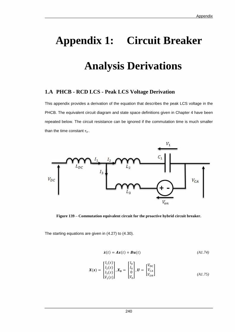
Appendix
240
Appendix 1: Circuit Breaker
Analysis Derivations
1.A PHCB - RCD LCS - Peak LCS Voltage Derivation
This appendix provides a derivation of the equation that describes the peak LCS voltage in the
PHCB. The equivalent circuit diagram and state space definitions given in Chapter 4 have been
repeated below. The circuit resistance can be ignored if the commutation time is much smaller
than the time constantú.
Figure 139 ‒ Commutation equivalent circuit for the proactive hybrid circuit breaker.
The starting equations are given in (4.27) to (4.30).
É| (,) = ÊÉ(,) + ÆË(,) (A1.74)
Ì(Í) = Î()()&()()Ï , ÌÐ = Î
HH0HÏ , Ñ = ¶te$'Ò¸
(A1.75)

Appendix
241
Î 1 −1 −1 00 − & 0)$ 0 & 00 0 0 Ï É| (,) = Î0 0 0 00 0 0 10 0 0 00 1 0 0Ï É(,) + Î
0 0 0 00 0 0 10 0 0 00 1 0 0ÏË(,) (A1.76)
Æ = 1% Î
+ & −( + &) −& −& )$ − −()$ + )0 0 0 Ï
(A1.77)
(Ó − Ê)` = 1% ÔÕ)$ + &% Ö + × ØÙÙ
ÙÙÙÚÛV ©−& ª 0 ©−&% ª0 (%) 0 f)$ + &g0 ©)$ ª ÛV (%)0 (%) 0 (%) ÜÝÝ
ÝÝÝÞ
(A1.78)
ßℎO ∶ % = )$ + )$& + & (A1.79)
ßℎO: ÛV = )$ + & + % (A1.80)
Defining the output function of the state space analysis by Equation (A1.81) allows the LCS
voltage () to be selected. This yields the s-domain expression for the LCS voltage, given in
(A1.82).
() = f0 0 0 1gÌ() = () (A1.81)
(s) = 1Ô)$ + &% × + n&ã + )$Ò% + H + Ho
(A1.82)
Assuming that the initial voltage across (H) the LCS is zero, as the device is turned on during
normal operation, and substituting (A1.83) reduces Equation (A1.82) to (A1.84)
K!1 = In)$ + &% o
(A1.83)
() = &% + )$Ò% 1fK!1 + g + HK!1 K!1fK!1 + g (A1.84)

Appendix
242
Equation (A1.84) can now be transferred into the time domain yielding Equation (A1.87).
() = &% + )$Ò%K!1 f1 − N(K!1,)g + HK!1 J(K!1,) (A1.85)
The maximum of the function occurs whenωű, = ä, which is within the range of possible
commutation times, as will be shown in Appendix 4B. Evaluating at this moment gives the
maximum LCS voltage, which is given in Equation (A1.86).
TV = &% + )$Ò% Ô)$ + &% × + HÔ)$ + &% × (A1.86)
This can be re arranged to give Equation (A1.87). Realising that based on typical parameters
for HVDC circuit breakers the following assumptions can be made: LL& ≈ 0 andLte + L& ≈Lte. This allows for simplified estimate for the peak LCS voltage, given in Equation (A1.88). This
is the same form given in Chapter 4.
TV = &% + )$Ò)$ + & + H Ô )$ + &)$ + )$& + &×
(A1.87)
TV ≃ &% + )$Ò)$ + & + HIn + & o (A1.88)
1.B PHCB - RCD LCS – Commutation Time Derivation
The commutation time can be found by differentiating Equation (A1.85) and setting the result to
zero, and then solving for the time at which this occurs. Taking the time derivative of (A1.85) is
given by Equation (A1.89).
|() = &% + )$Ò)$ + & fK!1 J(K!1,!1)g + H N(K!1,!1) = 0 (A1.89)

Appendix
243
Defining an angle by the ratio of the two magnitudes in Equation (A1.89), gives (A1.90) allows a
reduction from (A1.89) to (A1.93) using the product to sum trigonometric identity.
,åJ(Ѳ) = H&% + )$Ò)$ + & = J(Ѳ)N(Ѳ)
(A1.90)
= I©&% + )$Ò)$ + & K!1ª + © Hª
(A1.91)
fN(Ѳ) J(K!1,!1) + J(Ѳ) N(K!1,!1)g = 0
(A1.92)
f J(K!1,!1 + Ѳ)g = 0 (A1.93)
Equation (A1.93) will only be zero when the argument is zero or an integer multiple of Pi. The
commutation time can then be found be rearranging (A1.94) into (A1.95) by substituting (A1.90).
This can be put into the final form which includes the periodicity which is shown in (A1.96).
Typically n will be unity as commutation occurs on the first oscillation.
K!1,!1 + Ѳ = 0 (A1.94)
,!1 = − 1K!1 Î,åJ` Ô H×ÔK!1 &% + )$Ò)$ + & ×Ï (A1.95)
,!1 = 1K!1 ÎJQ − ,åJ` Ô H×ÔK!1 &% + )$Ò)$ + & ×Ï (A1.96)

Appendix
244
1.C PHCB - Varistor LCS – Commutation Time Derivation
The commutation circuit when a varistor based LCS is used is shown in Figure 140. The state
space equations have been reproduced in equations (A1.97) to (4.41).
Figure 140 ‒ Equivalent circuit diagram for commutation in a varistor based LCS.
¶)$ 0)$ 0 &1 −1 −1¸ É| (,) = ¶0 0 00 0 00 0 0¸ É(,) + ¶1 0 −11 −1 00 0 0 ¸Ë(,) (A1.97)
Ì(Í) = p()()&()s , ÌÐ = 
HH0¸ , Ñ = ¶te − eìíA° ¸
(A1.98)
Æ = 1% p + & − −&& )$ −(te + &) −()$ + ) )$ s (A1.99)
(Ó − Ê)` =ØÙÙÙÙÙÚ1/s 0 − (&(&f)$ + g +%0 1/s te(&(&f)$ + g + %0 0 %(&()$ + ) +% ÜÝÝ
ÝÝÝÞ
(A1.100)
For the LCS varistor design choice, the peak voltage is not our primary concern, as the
varistor’s electrical properties define the profile that is seen across the LCS. We are concerned
with the primary branch current, specifically if it reaches zero. Using Equation (A1.101) the
primary branch current can be selected and Equation (A1.102) can be found.

Appendix
245
() = f0 1 0gÌ() = () (A1.101)
() = %H + ò + (f)$ − $*g%( + ñ) (A1.102)
ñ = ( + )(%
(A1.103)
ò = (&)$ − $*f +&g +Ò + (Hô + õ) (A1.104)
Equation (A1.102) described the primary branch current in the s-domain. This must be
transferred into the time domain, In order to perform the time domain transfer; the equation
must first be put into a standard form. This has been done using partial fractions in Equation
(A1.105).
() = %H + ò + (f)$ − $*g%( + ñ) = nï + + + ño
(A1.105)
The coefficient can be solved for by multiplying through by the denominator and the solving the
three subsequent equations than can be obtained through the normal partial fractions method.
%H + ò + (f)$ − $*g = [ + \( + ñ) + h( + ñ) (A1.106)
3Í = Ð ∶ = (f)$ − $*gñ% (A1.107)
ý5002423/50Í: ï = ò − = 1% ò − (f)$ − $*gñ (A1.108)
ý5002423/50Í : = %H − ï = 1% %H − ò + (f)$ − $*gñ (A1.109)

Appendix
246
Substituting (A1.103) and (A1.104) into (A1.107) to (A1.109) allows for the solutions given in
Chapter 4 of this thesis.
(,1 ) = ï + ,1 + % `ð!" = 0 (A1.110)
The minim time can be found by starting with Equation (A1.110) and then substituting a second
order approximation of the exponential term, yielding
ï + ,1 + % − % ñ,1 + % ñ,1 = 0
(A1.111)
ï + % + n − % ño ,1 + % ñ,1 = 0 (A1.112)
Noting that based on Equation (A1.109) this can be reduced to (A1.113). This can then be used
to solve to find the minimum commutation time.
H + n − % ño ,1 + % ñ,1 = 0 (A1.113)
1.D PHCB - Varistor LCS – Circuit Breaker Voltage Derivation
The derivation of the circuit breaker voltage while current is only flowing in the secondary
branch is given. The equivalent circuit used in Chapter 4 is reproduced in Figure 141.
Figure 141 ‒ Equivalent circuit for PHCB when current is flowing in the secondary branch only.
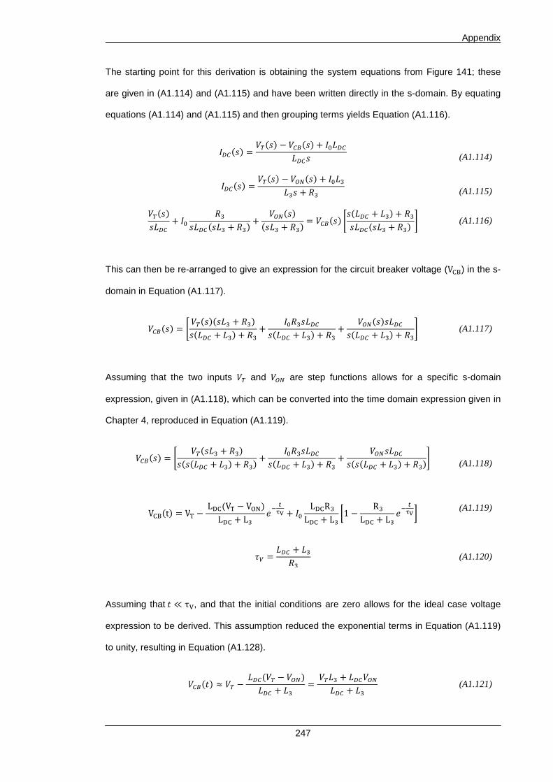
Appendix
247
The starting point for this derivation is obtaining the system equations from Figure 141; these
are given in (A1.114) and (A1.115) and have been written directly in the s-domain. By equating
equations (A1.114) and (A1.115) and then grouping terms yields Equation (A1.116).
)$() = %() − $Á() + H)$)$
(A1.114)
)$() = %() − Ò() + H&& + (&
(A1.115)
%())$ + H (&)$(& + (&) + Ò()(& + (&) = $Á() ()$ + &) + (&)$(& + (&) (A1.116)
This can then be re-arranged to give an expression for the circuit breaker voltage (Veû) in the s-
domain in Equation (A1.117).
$Á() = %()(& + (&)()$ + &) + (& + H(&)$()$ + &) + (& + Ò())$()$ + &) + (& (A1.117)
Assuming that the two inputs % and Ò are step functions allows for a specific s-domain
expression, given in (A1.118), which can be converted into the time domain expression given in
Chapter 4, reproduced in Equation (A1.119).
$Á() = %(& + (&)(()$ + &) + (&) + H(&)$()$ + &) + (& + Ò)$(()$ + &) + (&)
(A1.118)
Veû(t) = Vã − Lte(Vã − Vìí)Lte + L& ` #$ + H LteR&Lte + L& n1 − R&Lte + L& ` #$o
(A1.119)
ú = )$ + &(& (A1.120)
Assuming that, ≪ τv, and that the initial conditions are zero allows for the ideal case voltage
expression to be derived. This assumption reduced the exponential terms in Equation (A1.119)
to unity, resulting in Equation (A1.128).
$Á(,) ≈ % − )$(% − Ò))$ + & = %& + )$Ò)$ + & (A1.121)

Appendix
248
This assumption shows the importance of the system time constant (τv). If the time constant for
the system is long relative to the time is takes to open the mechanical switch, then the voltage
can be kept low and will stay constant. This should reduce the losses in the system from the
LCS.
If this time constant is significant relative to the opening time of the mechanical switch, then the
voltage will start to tend towardsVã, which has a maximum value of twice the DC link voltage.
This will impact when the peak voltage across the LCS.
1.E SHCB – Commutation Current
The equivalent circuit for the SHCB during commutation and the state space arrangement has
been reproduced below in Figure 142 and equations (A1.107) to (A1.125). This derivation is
concerned with finding an expression for the primary branch current during the commutation
period.
Figure 142 – SHCB equivalent circuit for commutation.
Ì() = ¶&¸ , ÌH = ¶HH0¸ , Ñ = n %Òo
(A1.122)
Æ = 1% ¶ + & −& )$ −()$ + )¸
(A1.123)

Appendix
249
(Ó − Ê)` = 1 ØÙÙÚ/ −(((& + &) −(&(( + )0 % + f)$ + g(& )$(&0 )$( % + f)$ + &g(ÜÝ
ÝÞ
(A1.124)
= ((& + þf)$ + &g( + f)$ + g(& +% (A1.125)
Using equations (A1.107) to (A1.125) an s-domain function that describes the primary branch
current (()) can be found using (A1.126), yielding (A1.127).
() = f0 1 0gÌ() (A1.126)
() = H% +(&% + )$Ò + H(&f)$ + g) + (&%% ©((&% + nf)$ + &g( + f)$ + g(&% o + ª
(A1.127)
Representing the second order polynomial in the denominator by its two roots, the equation can
be reduced into Equation (A1.128). This can then be split into separate terms using partial
fractions, as in Equation (A1.129), terms are chosen to allow for a simple inverse Laplace
transform.
() = H% +(&% + )$Ò + H(&f)$ + g) + (&%%( + )( + )
(A1.128)
() = 1% nï + + + + o (A1.129)
= − f)$ +&g( + f)$ + g(&2% −I12 f)$ +&g( + f)$ + g(&% − 4((&%
(A1.130)
= − f)$ +&g( + f)$ + g(&2% +I12 f)$ +&g( + f)$ + g(&% − 4((&%
(A1.131)

Appendix
250
Equation (A1.129) can be directly transferred into the time-domain using standard inverse
Laplace transform substitutions, yielding a time domain expression for the primary branch
current, Equation (A1.132)
(,) = 1% þï + `' + `(
(A1.132)
The coefficients can be solved for by equating (A1.128) and (A1.129), and then multiplying both
by the denominator of Equation (A1.127) . This yields (A1.133).
H% +(&% + Ò + H(&f + g) + (&%= ï( + )( + ) + ( + ) + ( + )
(A1.133)
By comparing the coefficients of the s-terms in (A1.133) the coefficients can be solved for, as
shown below in equations (A1.134) to (A1.136). There are three unknown coefficients, and
three equations given below. These can then be used to find the expressions for the coefficients
given in Chapter 4.
î3Í = Ð: (&% = ï
(A1.134)
ý5002423/50Í: (&% + Ò + H(&f + g) = ï( + ) + +
(A1.135)
ý5002423/50Í : H% =ï + +
(A1.136)
Appendix 2: Low Power Testing
Parameters
The derivation of the inductive parameters from the low voltage testing is given in equations
(A2.137) to (A2.139) . Equation (A2.138) is (A2.137) applied to the moment when the fault is
applied. Equation (A2.139) is (A2.137) applied to the moment the secondary branch is turned

Appendix
251
on. The secondary branch inductance is taken from the data sheet, and is assumed to be 1 nH.
This allows (A2.139) to approximate the circuit breaker’s series inductance. The primary branch
inductance can then be found from the difference of these two equations. The quench
resistance at the moment the secondary branch turns on is given in Equation (A2.141). The
point at which the quench resistance is calculated is given in Figure 143.
≈ ∆∆, (A2.137)
)$ + = ∆,∆ = 30^0.001371 − 53.8 = 94.6μ
(A2.138)
)$ + & + & ≈ )$ = ∆,∆ = 30^(0.0046111 − 0.003562)540 − 166.9 = 84.4μ
(A2.139)
= 94.6 − 84.4 = 10.2μ (A2.140)
(³ ≈ 16.8200 = 80.4jΩ (A2.141)
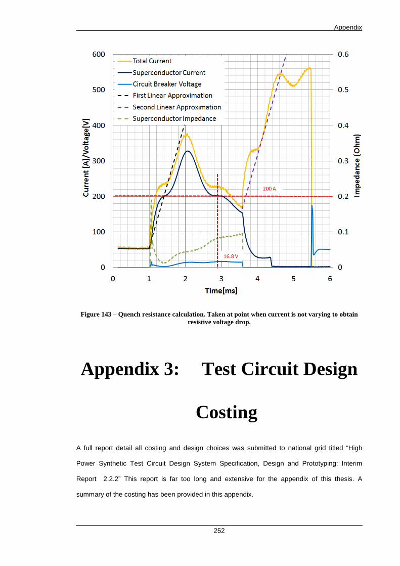
Appendix
252
Figure 143 ‒ Quench resistance calculation. Taken at point when current is not varying to obtain resistive voltage drop.
Appendix 3: Test Circuit Design
Costing
A full report detail all costing and design choices was submitted to national grid titled “High
Power Synthetic Test Circuit Design System Specification, Design and Prototyping: Interim
Report 2.2.2” This report is far too long and extensive for the appendix of this thesis. A
summary of the costing has been provided in this appendix.

Appendix
253
For each major component, several design options were chosen and the total cost, including
additional support components (sharing resistors, gate drives etc) was calculated.
Table 11 – Table of candidate diodes. Name Cost Voltage
Rating
Peak per
Device
Required
Number in
series/parallel
Total
Number
Cost
A IXYS
SEMICONDUCTOR -
DSEI2X121-02A -
DIODE, FAST,
2X123A
£15.46 1200 1200 13/3 39
£602.94
B SEMIKRON -
SKR130/12 - DIODE,
STANDARD, 165A,
1200V, STUD
£32.13 1200 1244.99 13/3 39
£1,253.07
C SOLID STATE -
85HF160 -
STANDARD DIODE,
85A, 1.6KV, DO-5
£8.28 1600 707.10678 10/4 40
£331.20
D SOLID STATE -
1N4056R -
STANDARD DIODE,
275A, 1KV, DO-9
£46.69 1000 2281.7208 15/2 30
£1,400.70
E VISHAY
SEMICONDUCTOR -
VS-400UR120D -
STANDARD DIODE,
400A, 1.2KV, DO-9
£83.45 1200 3471.311 13/1 13
£1,084.85
F GENESIC
SEMICONDUCTOR -
£26.08 1600 3425 10/1 10 £260.80

Appendix
254
S300YR - DIODE,
RECTIFIER, 1600V,
300A, DO9
Table 12 ‒ Diode comparison table assuming 50% rating factor of current. Name Order
Code
Voltag e
Rating
Peak
Current
per
Device
Required
Number
series/parallel
Total
Cost
[£]
A IXYS SEMICONDUCTOR -
DSEI2X121-02A - DIODE,
FAST, 2X123A
9359419 1200 1200 3/3 £139.14
B SEMIKRON - SKR130/12 -
DIODE, STANDARD, 165A,
1200V, STUD
9564543 1200 1245 3/3 £289.17
C SOLID STATE - 85HF160 -
STANDARD DIODE, 85A,
1.6KV, DO-5
1713141 1600 707 2/4 £66.24
D SOLID STATE - 1N4056R -
STANDARD DIODE, 275A,
1KV, DO-9
1713224 1000 2282 4/2 £373.52
E VISHAY SEMICONDUCTOR
- VS-400UR120D -
STANDARD DIODE, 400A,
1.2KV, DO-9
6540843 1200 3471 3/1 £250.35
F GENESIC
SEMICONDUCTOR -
S300YR - DIODE,
RECTIFIER, 1600V, 300A,
DO9
1862791 1600 3425 2/1 £52.16

Appendix
255
Table 13 ‒ Test circuit component list and costing. Description Name Order
Code
Cost Number
per
Device
Minimum
required
Number
Order
Number
(+30%)
Total
Cost
Test Circuit
Test circuit
diodes
GENESIC
SEMICONDUCTOR -
S300YR - DIODE,
RECTIFIER, 1600V, 300A,
DO9
1862791 £26.03 1 12 16 £416.48
33 k Ohm
Sharing
Resistor for D1
VISHAY DALE -
CPF233K000FKE14 -
RESISTOR METAL FILM,
33KOHM, 2W, 1%
1155010 £0.36 49 490 637 £227.41
47.5 k Ohm
sharing
resistor for D2
VISHAY DALE -
CCF6047K5FKE36 -
RESISTOR, METAL FILM,
47.5KOHM, 1W, 1%
1560540 £0.04 85 170 221 £7.74
Sharing
capacitor for
D1 and D2
VISHAY ROEDERSTEIN
- MKP1848 510 094K2 -
CAP, FILM, PP, 1UF, 900V,
RAD
1791629 £1.22 4 48 63 £76.86
copper pipe to
build inductor
Copper Pipe 22mm (2m) 698-786 £14.22 1 40 50 £711.00
connectors for
coppers
Copper Corner Pieces 797-811 £0.40 1 80 90 £36.27
Test Circu it
Capacitor
PPM Capacitor N/A £344 12 12 12 £4128
pipe clips to
hold inductor
50x 22mm Pipe Clip 456-7737 £5.57 1 80 2 £11.14
Copper for
Test circuit
connections
Copper Bar, 1m x 20mm
Diameter x 20mm x 3mm
X4
684-311 £33.90 0.15 1.2 2 £67.80
Diode Hea t
sink
ABL HEATSINKS -
350AB1500B - HEAT SINK,
0.5°C/W
150019 £21.90 1 12 12 £262.80
Sub
total
£5,946

Appendix
256
Table 14 ‒ IGBT module comparison table. Name Cost[£] Power[W] Voltage
[V]
Current
[A]
Number of
Devices in
series
FUJI ELECTRIC - 1MBI3600U4D-
120 - IGBT, MODULE, SINGLE,
3600A/1200V
8840 4275465 6000 4275 7
INFINEON - FZ1000R33HE3 -
IGBT, HI PO, 1 S/W, 3300V,
1000A
7606 1894360 7000 1082 3
FUJI ELECTRIC - 1MBI2400U4D-
120 - IGBT, MODULE, SINGLE,
2400A/1200V
9634 5585411 9000 3723 10
FUJI ELECTRIC - 1MBI1200U4C-
170 - IGBT, MODULE, SINGLE,
1200A/1700V
9568 6289068 19000 1324 14
FUJI ELECTRIC - 1MBI3600U4D-
170 - IGBT, MODULE,
SINGLE,3600A/1700V
9722 4923772 9000 3282 7
INFINEON - FZ2400R17HP4_B9 -
IGBT, ONE SWITCH, 1700V,
2400A
9070 4397925 9000 2931 7
FUJI ELECTRIC - 1MBI1600U4C-
170 - IGBT, MODULE, SINGLE,
1600A/1700V
9332 6569760 17000 1545 13
FUJI ELECTRIC - 1MBI1200UE-
330 - IGBT, MODULE, SINGLE,
9989 6818592 18000 1515 7

Appendix
257
1200A/3300V
FUJI ELECTRIC - 1MBI2400U4D-
170 - IGBT, MODULE, SINGLE,
2400A/1700V
8910 4934544 10000 2960 8
FUJI ELECTRIC - 1MBI1600U4C-
120 - IGBT, MODULE, SINGLE,
1600A/1200V
9646 6593691 13000 2028 14
FUJI ELECTRIC - 1MBI800UG-330
- IGBT, MODULE, SINGLE,
800A/3300V
9094 13121269 18000 2915 7
POWEREX - CM600HA-24A -
IGBT MODULE, 1200V, 600A,
IGBTMOD
7031 8513494 30000 567 32
FUJI ELECTRIC - 2MBI900VXA-
120E-50 - IGBT, MODULE, DUAL,
900A/1200V
9660 5269188 16000 658 17
3.A Test Circuit Inductor Design
The inductor was chosen to be air cored for simplicity and because space requirements were
not an issue for the project design. Using (A3.142) the required number of turns and hence the
amount of required copper was calculated. K is the width of the pipe plus the spacing between
each turn.
= 0!ï[ = 0!ï´ (A3.142)
Table 15 – Inductor design table Inductor Design
Inductance [mH] 1

Appendix
258
µo 1.26E-06
Pipe Width [mm] 15
Area [m2] 1
Spacing [mm] 3
K [mm] 18
Resistance [mΩ] 43
Required Turns 20
Copper Pipe Required [m] 80
Required Corner Pieces 80
3.B Isolated Power Supply Magnetics Design
The peak flux density must be maintained below 80% of the maximum flux density for the given
magnetic material. The flux generated by the primary is a function of the number of turns, or the
volts per turn, as shown by (A3.143) and (A3.144).
= W∅W,
(A3.143)
∅1 = 12 ÀäH sin(K,) W, = 2ÀK = 2√2.1K = ©.1 ª2√2K
(A3.144)
ºå4J, NOïOå = ï = ∅1À = ∅1À0.8 = ∅10.8 × 0.41 = ∅10.312 (A3.145)
The copper wire diameter was chosen to be 0.5 mm2, which fuses at 27.5 A [106] and hence
should carry 1.6 A sufficiently. The required area within the magnetic core for the winding and
insulations is then calculated from the number of turns on the primary and secondary, using
(3.14). This area is then scaled by a packing factor of 0.3 to compensate for the presence of
additional insulation. The layout of the transformer windings and insulation is shown in Figure
144. Table 17 and Table 18 summarise the attributes of the isolating transformers.
Table 16 – Magnetic material Data: N87 MnZn. Magnetic Material Data

Appendix
259
Peak Flux Density 0.39
Safety Factor 0.8
Material Name MnZn
Table 17 – Winding and core area calculations. Primary Turns Area
[mm2]
82.5
Secondary Turns
Area [mm2]
9.5
Total Area [mm2] 92
Packing Factor 0.3
Required Area[mm2] 307
Figure 144 – Transformer winding cross section.
Table 18 – Magnetics circuit and rectifier components. Description Name Order
Code
Cost
Per
Order
Number
Total
Cost
Rectifier AC/DC MULTICOMP - VSIB440 -
BRIDGE RECTIFIER, 4A,
400V, GSIB-5S
1861533 £0.19 11 £2.07
27 V Zener Diode ON SEMICONDUCTOR -
1N5361BG - DIODE,
ZENER, 27V, 5W
9558195 £0.35 21 £7.35
Appendix
260
Secondary winding
short circuit protection,
10 A
LITTELFUSE - 0154010.DR
- FUSE, SMD, OMNI
BLOCK, F 10A
1817192 £1.37 20 £27.40
DC ripple capacitor
High frequency
EPCOS - B32654A684 CAP,
FILM, PP,680NF, 1KV, RAD
1200814 £1.47 10 £14.70
DC ripple capacitor low
frequency
MULTICOMP -
MCGLR50V108M16X32 -
CAP, ALU ELEC, 1000UF,
50V, RAD
1903004 £0.47 10 £4.70
Transformer U&I Core,
840 mm2
EPCOS B67345B0001X027
FERRITE
2355111 £28.88 8 £231.04
Transformer wire
125m, 0.5 mm2
PRO POWER - ECW0.80 -
WIRE, 0.8MM, COPPER,
ENAMELLED, 0.5KG
1230984 £14.60 2 £29.20
Isolating tape, 39 kV
per mm
3M - 23 19MMX9M SELF
FUSING TP - TAPE,SCOTCH
23 PREMIUM TAPE,19MM
X 9.15M
143079 £7.65 11 £84.15
Total £400.61
3.C Test Circuit Simulations
The test circuit was simulated in order to rate individual components within the test circuits
design. Most of the detail can be found in National Grid report 2.2.2, but this is very specific to
the design of this test circuit and component choice. The complete test circuit and IGBT stack
was entered into PSCAD shown in Figure 145. Individual IGBTS, Diode, dynamic and static
voltage sharing, thermal models of the IGBTs and control circuits were simulated. The
parameters used came from the individual data sheers for each component.
3.C.1 IGBT Stack Turn off
The IGBT stack turn off currents are shown in Figure 146, for the IGBT, snubber circuit, varistor
and the sharing resistor. At the moment of turn off, the snubber current rises to peak value of
current in the test circuit inductor. The current is remains equal to the total current while the
capacitor charges. As the voltage increases, the varistor starts to conduct more current. Once
the voltage across the switch is high enough, the varistor starts to conduct the majority of the
total current. The current then decays towards zero. The snubber capacitors then form a ringing
circuit with the voltage sharing capacitors across the test circuit diodes and cause some small
oscillations. The voltage across a single IGBT is shown in Figure 147 and verifies that the
voltage does not exceed 80% of the IGBTS maximum rated voltage (1400 V).

Appendix
261
Figure 145 ‒ Simulation of test circuit.
Figure 146 ‒ Turn off process of entire IGBT stack.

Appendix
262
Figure 147 ‒ Shows the IGBT Voltage for a 1kA pulse.
3.C.2 Power Losses
The previous simulations in section 3.C.1 show the process, but do not include the finite amount
of time it takes for an IGBT to turn off. This results in the power losses that the simulations
produce being incorrect, firstly because the current does not fall to zero instantly and secondly
because the current in the snubber circuit does not rise to the inductor current instantly. Figure
148 shows the PSCAD turn off voltages and current in solid lines and estimations of the actual
turn off voltages and currents in dashed lines. Figure 149 compares the snubber currents for the
simulated and estimated cases.

Appendix
263
Figure 148 ‒ Comparison of PSCAD turn off voltages and current and estimated turn off voltages and currents.
Figure 149 ‒ Comparison of simulated and estimated snubber currents.
Figure 150 ‒ Turn off voltage estimation in PSCAD.

Appendix
264
Figure 151 ‒ Turn off current estimation produced during the simulation in PSCAD.
The turn off current and voltages are estimated in PSCAD by using the blocks shown in Figure
151 and Figure 150.
The turn off voltage is determined the integral of the snubber circuit current divided by the
capacitance. In the case when the IGBT turns off instantly, the current in the snubber rises to
the inductor current instantly, and results in the IGBT voltage rising faster. This is shown by the
solid line in Figure 149.
As twice the charge flows into the snubber capacitor during the turn off time, the voltage
generated by the PSCAD is double what it should be, resulting in the power losses being also
double. The compensated power loss and the simulated power losses are shown in Figure 152.
The calculated maximum breaking current was 977 A (Table 14) for each individual IGBT in the
module, for a power dissipation of 15.5 kW. The simulated IGBT was then turned off at 977 A
and the power losses recorded. Figure 152 shows that when the IGBT breaks current of 997 A,
the peak power dissipation is 15.61 kW, which is well within 1% of the initial calculation.

Appendix
265
Figure 152 ‒ Presented power losses and the compensated power losses.
3.C.3 Thermal Modelling
The IGBT module data sheet gives information for a 4th order Foster thermal impedance model,
between the junction and the case. The Foster model is suitable if the case temperature
remains fixed during the operation and no additional resistance is added to the end of the
network. If additional resistance is added to the end to represent a heat sink, then the model
allows for instantaneous heat travel from junction to case. This fast heat transfer results in the
model producing a junction to ambient temperature which is not reflective of reality, as there is a
large overshoot in the temperature.
Converting the model into a Cauer model provides equivalent thermal impedance and allows
the impact of the heat sink to be assessed as the heat cannot flow instantaneously from junction
to case. The equations used to perform the transformation are given at the end of this section.
The thermal models are shown in Figure 153 and the parameters given in Table 19.
Figure 154 shows the change in junction to case temperature for using the two models. It can
be seen that there is only a small change in temperature when the IGBT is subject to a 0.3 kA

Appendix
266
pulse of current. Figure 156 shows when each IGBT breaks a 1 kA pulse, there is again only a
small change in the junction temperature.
The IGBT must also be rated to deal with the current profile in the event that the IGBT fails to
turn off. Figure 155 shows the change in junction temperature when the IGBT fails to break a 1
kA pulse.
Table 19 ‒ Foster and Cauer Model Thermal resistances and Capacitances. Foster Model
Node Number 1 (case) 2 3 4 (Junction)
Ri [K/kW] 1.6 1.8 0.358 0.328
Ci [J/K] 363 33 17 3
Ti [s] 0.581 0.059 0.006 0.001
Cauer Model
Ri [K/kW] 1.6 2.1 0.578 0.424
Ci [J/K] 363 31 11 2
Ti [s] 0.581 0.0657 0.0063 0.001
Figure 153 ‒ Cauer (Top) and Foster (Bottom) thermal models used.
Heat Sink
Junction Case

Appendix
267
Figure 154 ‒ Junction to case temperatures when using the Foster and Cauer models, when the IGBT breakers a 1 kA pulse of Current (0.33 kA per IGBT).
Figure 155 ‒ Thermal response when IGBT fails to turn off (1 kA peak per IGBT) 3 kA total.

Appendix
268
Figure 156 ‒ Thermal Response to 1 kA peak current (breaking).
Unfortunately these thermal models are not believed to be of particular use due to the impulse
of current being only in existence for a very short period of time/ the thermal dynamics that the
models are based on, are an analytical approximation of the dominant thermal characteristics of
the IGBT while it is cooling. It is very likely that these models do not encompass the correct
thermal dynamics for this type of transient.
The electrical models are also likely to be unsuitable; due to the datasheet information provided
being based on an IGBT that is in thermal equilibrium and not in a transient state. These models
also do not include de-saturation of the IGBT devices themselves, or the temperature
dependant characteristics of the electrical impedances within the devices. The thermal
modelling of semiconductor devices is a very in specialist area and is probably an area that
needs significant further investigation for VSC HVDC protection. As the electrical characteristics
of the semiconductors define key elements of a circuit breaker’s operation and design,
understanding how these can vary and how to model them appropriately would be important.
3.C.3.1 Foster to Cauer model Transformation - Approximation
Subscript denotes the position of the RC pair in both the foster and the Cauer networks. 1 is
connected to the case, 4 is directly connected to the junction.

Appendix
269
($ = (F (A7.146)
$ = F (A7.147)
$ = FFF + F (A7.148)
($ = ($$ (F + (FF(F − 1
(A7.149)
$& = F&FFFF + F&fF + Fg (A7.150)
($& = ($ + ($Û$&$$($($ − 1
(A7.151)
ℎOÛ = (F + (F + (F&(F(F(F&F&FF (A7.152)
$6 = F6F&FFF&FF + F6fFF + F&fF + Fgg
(A7.153)
($6 = ($ + ($ + ($&Û$6$&$$($&($($ − 1
(A7.154)
ℎOÛ = (F + (F + (F& + (F6(F(F(F&(F6F6F&FF
(A7.155)

Appendix
270
Appendix 4: Modified Test
Circuit Derivations
4.A First Test Circuit Capacitance Derivation
For the MTD the capacitance (Cã) needs to discharge from 2Vte to Vte from time zero to time
T. The current at time T needs to be equal to the value of current envelope at this time, this
value of current is given by Equation (3.14). Thus the exchange of electrostatic to
electromagnetic energy over time T is given by Equation (A4.157).
() = W W,X- z-!- = 2)$%
(A4.156)
12%f(2)$) − 2)$g = 12 % n2)$% o
(A4.157)
3)$% = 4)$%
(A4.158)
% = 43% (A4.159)
4.B Second Test Circuit Capacitance Derivation
In order to conserve the total energy in the circuit at the appropriate level the circuit must be
designed to meet Equation (3.14). As Cã and Cã are known this equation can be re arranged
to voltage forCã as shown in Equation (3.14).
12%(2)$) + 12%)$ = 12%)$
(A4.160)
% = % − 4%
(A4.161)

Appendix
271
Appendix 5: Publications
This appendix contains additional publications from the Author.


Fault current testing envelopes for VSC HVDCcircuit breakers
ISSN 1751-8687Received on 14th July 2015Revised on 10th January 2016Accepted on 24th February 2016doi: 10.1049/iet-gtd.2015.0863www.ietdl.org
Oliver Cwikowski1 , Bin Chang1, Mike Barnes1, Roger Shuttleworth1, Antony Beddard2
1Department of Electrical and Electronic Engineering, The University of Manchester, Manchester, UK2Department of Electrical Engineering, Imperial College London, London, UK
E-mail: [email protected]
Abstract: Circuit breakers for high voltage direct current (HVDC) applications are seen as a required technological step inthe development of HVDC grids. The development of several new HVDC circuit breaker prototypes indicate that this stepmay be achieved in the years to come. In order to facilitate the installation of HVDC circuit breakers, appropriate standardsand tests need to be developed. These tests and standards must ensure that the technology is capable of functioning asrequired. In cases where direct testing cannot be carried out, a synthetic test circuit is used to recreate the conditions of thepower system. Testing envelopes which encapsulate the fault currents for two types of voltage source converter underfault conditions are analytically derived in this study and compared with simulations. Testing envelopes allowspecifications for HVDC breaker test circuits to be defined. Discussion is also given to the worst type of fault andprotection operation time estimates.
1 Introduction
High voltage direct current (HVDC) transmission based on voltagesource converters (VSCs) is a rapidly growing market. The firstVSC installation was commissioned in Hällsjön Sweden by ABBin 1997. Between the first installation and 2014 around 20 projectshave been commissioned. In this short period of time, the powerrating of the converters has increased from 3 to 1000 MW. Thereare approximately another 20 projects in the pipe-line to becommissioned between 2014 and 2020, with the power rating,transmission distances and operating DC voltages of eachinstallation typically seeing an increase. Multiple manufacturershave entered the market including Siemens, Alstom and RXPE.The topologies of VSC range from two level converter (TLC) tomodular multi-level converters (MMCs), with MMC being themain choice for future installation.
To date, all but two VSC transmission systems are in apoint-to-point transmission system configuration. Onemulti-terminal system exists on Nan’ao Island in China and wascommissioned in 2013. Another was built in Zhoushan in 2014 [1].
However, all installations presently appear to be protected fromline faults on the direct current (DC) side of the converter bytripping the protection on the alternating current (AC) side of theconverter. Using AC side protection results in the power that wasbeing drawn from the DC side into the AC grid being lost,limiting the power rating of these installations to below theallowable infeed loss of the AC grid.
Connecting VSCs into a multi-terminal grid system has a numberof advantages such as supply security and reducing installation cost.Just as in AC grids, if the faulted part of the grid can be isolated, itallows power flow to be rerouted and maintained.
Before HVDC grids can be realised, protective devices capable ofworking in the VSC transmission environment must be developed.Recently, several prototype HVDC circuit breakers have beendeveloped [2–7]. These circuit breakers would be placed in serieswith each pole on the DC side and be used to isolate the faultedsections of the grid. Other methods have been proposed forprotecting HVDC grids which exploit fault tolerant converters andcircuit breakers in novel manners [3, 8–11].
Before any device can be placed into service, a method must bedeveloped to rate the device. The device must then be tested
against this standard to ensure it can perform as expected. Asdirect testing is not presently achievable, a synthetic environmentwill typically be used to test the breaker in an environment whichis more severe than any event it might experience in the powersystem.
Previous work on the characterisation of fault currents that DCcircuit breakers are expected to handle have often neglected thepresence of the series inductance, which all hybrid circuit breakerswill require [12, 13]. Other analysis has looked at the steady-statefault currents that flow in the HVDC system [14, 15]. Steady-stateanalysis is unsuitable for the rating of very fast DC circuitbreakers as these are likely to isolate the fault before steady stateis reached. HVDC circuit breakers are likely to be classified in asimilar manner to V type circuit breakers in railway applications,such breakers are described as ‘current limiting’ as they operatebefore the system is allowed to reach steady state [16]. Each priorart publication also focuses on a single converter arrangement anddoes not provide generalised analysis sufficient to encompass thevariability that will inherently exist in the converter designs.
This paper is an invited extension of an original conference paperthat was the first effort to develop a standardised method forassessing the suitability of the current generated by a test circuit,the fault current envelope (FCE) [17]. In this paper FCEs arederived for the TLC and MMC with example cases. Discussion isthen given to the definition of the worst case scenario, howenvelopes may be used, and how the requirements for protectionoperation time may be estimated from the FCE.
2 Fault current envelopes
In order for any given test circuit to be designed properly, there mustbe a specification or criteria for its operation to be compared against.Without any such criteria any test is meaningless and in no wayindicates whether a piece of equipment is capable of operating inthe desired manner.
FCEs provide a generalised method to assess the suitability of anytest circuit’s current pulse.
FCEs are lines which encompass all possible fault currents that acircuit breaker should be designed to deal with, and define the linebetween what currents are possible and which are not, based on
IET Generation, Transmission & Distribution
Research Article
IET Gener. Transm. Distrib., pp. 1–81& The Institution of Engineering and Technology 2016

the physical limitations of the system. A test circuit’s current is thensuperimposed over the top of this envelope. Providing the test circuitcurrent exceeds the envelope at all points within the time frame of thetest, the test is deemed suitable.
This paper presents the first method for drawing FCEs for TLCand MMC VSC topologies. These techniques may also be appliedto other converter topologies and adapted for future changes to thegrid structure. First, the methodology for developing an envelopefor the TLC is shown. The same envelope is then adapted to suitan MMC.
3 TLC fault current calculations
Faults can be grouped into four types:Terminal fault: pole-to-pole.Terminal fault: pole-to-ground.Non-terminal fault: pole-to-pole.Non-terminal fault: pole-to-ground.Terminal faults are short circuits which are close to the converterwithout bypassing the DC pole reactor, shown as location FT inFig. 1. Non-terminal faults are faults which occur at some distancealong the cable (>0 km), shown as location FNT in Fig. 1. Thefault current calculations shown in this section assume that DCprotection acts in several milliseconds, which is within whatmanufacturers are quoting as achievable times and close to otherestimations [2, 5, 18].
3.1 TLC pole-to-pole terminal faults
For a TLC system, the equivalent circuit used to develop descriptiveequations of the converter under a fault is shown in Fig. 1 andconsists of an LC circuit, a current source and a diode. The currentsource is assumed to feed the same value of current as the initialDC side current. The current in the circuit breaker is made fromtwo components the AC side injection (IAC) and the capacitivedischarge component (ICap).
When a terminal fault occurs the cable is short circuited close tothe converter, without bypassing the DC side reactor (L1) shownby the location of fault FT in Fig. 1. The DC side capacitance (C1)discharges, resulting in a large injection of current through thecircuit breaker’s inductance (L1). The converter injects anadditional current, which is assumed in this case to be constant.For pole-to-pole faults, once the DC side voltage has reversedsufficiently to forward bias the converter’s diodes, the current inthe capacitor will commutate into the diode (D1) [19, 20].
At the moment the diodes (represented by D1) in the TLC becomeforward biased, they short circuit the AC terminals of the converter,decoupling the DC and AC sides of the converter. At this point theAC grid cannot contribute to the DC fault current seen by the circuitbreaker. It may take up to 80 ms for the short circuit on the converterterminals to be removed. This time is significantly longer than onewould normally see in a point-to-point HVDC system due to thelarge series inductance that the circuit breaker requires. However,if the typical DC side inductance is reduced, the converter wouldsoon start to operate as a rectifier , coupling the AC and DCsystems together again. The peak current will decay from themoment the diodes short circuit the terminals of the converter, andonly after the DC fault current has decreased sufficiently will theconverter start to act as a rectifier.
For terminal faults, the current in the circuit breaker can bedescribed by (1); from the moment the fault occurs, until the peakfault current is reached. A grounded converter DC line midpoint isassumed for this analysis.
The maximum fault current (IMAX) is given by (2) and the largestrate of rise of current occurs at time zero and is given by (3)
IFault(t) = V0
C1
L1
√sin (vt)+ I0
for t ≤ p
2v, v = 1
L1C1
√(1)
IMax = V0
C1
L1
√+ I0 (2)
di
dt
∣∣∣∣t=0
= V0
L1(3)
A comparison between the equivalent circuit and the TDM PSCADsimulations of a TLC under a pole-to-pole fault are shown in Fig. 2.The simulated contributions from the detailed PSCAD model for theAC injection and the capacitive discharge are shown in the dashedlines in Fig. 2. The simplified equivalent circuit is within 7% ofthe simulated fault current. The peak current is slightlyunder-estimated due to the AC injection increasing as the DC sidevoltage collapses, which is evident from the increase in the ACinjection current. As the DC side voltage collapses, the voltagethat drives the AC injection increases, resulting in an increase inthe contribution from the AC system. However, when the AC sideimpedance is large, any current change will be slow relative to thecontribution from the discharge of the DC side capacitance.Equation (1) is also plotted in Fig. 2 and shows a strong agreement.
3.2 TLC non-terminal faults
When a non-terminal fault occurs, additional phenomena come intoconsideration. The simplified equivalent circuit for a non-terminalfault is shown in Fig. 1. The cable or transmission line is includedin the equivalent fault circuit, shown by the location of fault FNT
in Fig. 1.The voltage waves that propagate down the cable, dictate the cable
voltage near the converter, shown as VC in Fig. 1. This differs fromthe terminal fault case where voltage (VC) is clamped at zero by theshort circuit.
Fig. 1 Simplified equivalent circuit for the TLC
Fig. 2 Comparison of terminal fault equivalent model and simulated faultcurrents. Shows simplified circuit provides good tracking for the lowfrequency dynamics
IET Gener. Transm. Distrib., pp. 1–82 & The Institution of Engineering and Technology 2016

When a fault occurs, the voltage at the point on the cable wherethe fault occurs collapses from VDC to zero. This collapse involtage generates a reverse travelling voltage wave (V−
1 ), ofmagnitude –VDC, which propagates down the cable, from the faulttowards the converter. The converter presents a discontinuity tothe wave and hence a reflection occurs. The cable voltage (VC) atthe converter is determined by the initial voltage, plus the sum ofthe waves that arrive at the converter. The bounce diagram for theline is shown in Fig. 3. The cable voltage at the moment the firstreverse travelling wave arrives at the converter can be estimatedusing (4). The cable will degrade the magnitude of the voltagewave as it travels; this is represented by the exponential term(e−kD) in (4). Assuming that the cable does not degrade thevoltage wave magnitude (e−kD = 1), and that the voltage is an idealstep, will provide the limit for the largest possible change in voltage.
The reflection coefficient magnitude will be close to unity for fastchanges in voltage due to the large inductive element present inbetween the circuit breaker and the converter [2]. Equation (4)shows that at the moment the reverse travelling wave arrives at theconverter, the cable voltage becomes negative, if the reflectioncoefficient is greater than zero. The reflection coefficient iscalculated from (5) and tends towards one for fast changes involtages. The initial rate of rise of fault current can be calculatedusing (6). Equation (6) shows that for a reflection coefficientabove zero, the rate of rise of fault current will be above that of aterminal fault (3). The theoretical maximum of (6) is (2VDC/L1),which shows that the maximum fault current rate of change offault current could be up to twice that seen in a terminal fault.This effect has also been discussed in [21–23]
VC = VDC + V−1 (tf , 0)(1+ GC) = VDC[1− e−kD(1+ GC)] (4)
limv1GC = lim
v1Zc − Z0Zc + Z0
[ ]= lim
v1jvL− j/vC
( )− Z0jvL− j/vC
( )+ Z0
[ ]= 1
(5)
di
dt
∣∣∣∣t=0
= VDC − VC
L1= VDC
L1(1+ GC) ≤
2VDC
L1(6)
4 PSCAD simulations
The TLC transmission system was simulated in PSCAD to verify theFCE designs. A 1 GW, 600 kV (+/−300 kV) symmetrical monopoleTLC was chosen for the first case. For details of the control used inthe converter stations and the layout of the transmission system see[19]. The converter is modelled using a traditional detailed model(TDM).
The cable length was chosen to be 250 km and the model usedwas a frequency dependent phase model (FDPM) [24]. The initialDC current is 600 A. The DC side capacitance used was 100 µFper pole.
Present HVDC circuit breaker prototypes can only break around9 kA [2]. For a breaking time of 3 ms, the rate of change ofcurrent needs to be limited to <3 kA/ms (assuming an initialcurrent of zero). The limit imposed by the breaking capability forthe breakers results in the required DC side inductance being atleast 100 mH per pole [2, 25]. All fault currents shown for theTLC are simulated using the TDM of the converter.
5 TLC fault current envelope
The concept of a testing envelope already exists in AC circuit breakertesting and is used in standards extensively [26, 27]. Standardenvelopes for the transient recovery voltages have been developedfor all ranges of AC system voltage, based on experimental resultsand fundamental analysis of the AC system.
The same concept can be applied to DC fault currents in DCsystems. For HVDC circuit breakers, envelopes can be used to
define a line which encapsulates all possible fault currents thatcould occur within the DC circuit breakers. This can then be usedin conjunction with a protection time requirement to define thespecification for the test circuit.
A simple two line FCE may be drawn using the peak fault currentand the maximum fault current derivative. Such an envelope wouldthen simply be a straight line from the initial current (I0) to themaximum DC fault current level (2), with a gradient equal to themaximum fault current derivative (6). This is shown as Envelope 1in Fig. 4a. While this envelope would encapsulate all faultcurrents, it produces large over-estimates of the fault current,creating a very severe test specification, potentially inhibiting theuse of high speed circuit breakers. Envelope 2 provides a lesssevere test specification but still encapsulates the fault currents in aDC system.
Envelope 2 is drawn using three intersecting lines as shown inFig. 4b. The first line increases from the initial current (I0) at arate of (2VDC/L1). The envelope is defined by the fastest rate ofrise of current, until this intersects a biased linear approximationof the terminal (0 km) fault current.
The linear approximation of the terminal fault is made using theaverage fault current derivative of a terminal fault (I∗Avg), given by(7). The linear approximation is then biased by the largestdifference between the calculated terminal fault current using (1),and the linear approximation. The bias value (ΔI ) is given by (8)and the time at which it occurs at it is given by (9). The envelopeis then defined by the biased linear approximation until this lineintersects the peak fault current (IMax) given by (2)
I∗Avg =2v(IMax − I0)
p(7)
DI = (IMax − I0)sin(vt)− I∗Avg t (8)
t = 1
vcos−1 I∗Avg
(IMax − I0)v
( )(9)
T1 =DI
2V0/L1 − iAvg(10)
6 TLC envelope example
Simulations were performed changing the distance to the fault forboth pole-to-pole and pole-to-ground faults. The comparison of thesimulated fault currents generated by the TDM model, and the
Fig. 3 Shows the Bewley lattice diagram for a single faulted DC line.Converter station on left hand side, fault on right-hand side of figure.Waves propagate at speed (S), distance (D) of the cable in this horizontalposition and time shown in the vertical position
IET Gener. Transm. Distrib., pp. 1–83& The Institution of Engineering and Technology 2016

testing envelopes, are shown in Figs. 4c and d. The results showthat the envelope encompasses the fault currents over the majorityof the time period of interest, without excessive over-estimation ofthe fault currents, for both pole-to-pole and pole-to-ground faults.The 100 km fault case and 90 km fault cases marginally exceedthe envelope transiently and so the envelops provide very goodguidance. This could however be compensated for by a safetyfactor added to compensate for tolerances in system parameters.
7 MMC fault current prediction
Sections 7–11 of this paper are concerned with developing a generalFCE for MMC and understanding how a standard may have to bedeveloped in the face of the MMC’s complexity. The response ofthe MMC under DC side faults is an interesting and complexproblem. Attempting to derive a single equation which canaccurately predict the fault currents from an MMC has beenattempted, and may be possible if details of the converter’scontrols are well known.
However, each manufacturer will likely have their ownimplementations of the MMC, with differing control systems,measurement systems and physical structures. As such, gainingexact predictions of the fault currents seen from an MMC is likelyto be impossible as the information required to enter into suchequations will not be freely available. When one considers that thecontrol structure of the MMC will also change during itsoperation, in order to provide additional support to the AC andDC systems, all such predictions would have to be proven forevery possible perturbation of control system structure. This wouldbe required as the protection system must be rated to deal withknown fault currents.
However, from the view point of a standard production suchpredictions are not strictly necessary if the physical limitations ofthe converter’s fault currents are understood. These limitations canthen be used to develop an envelope. Such envelopes can bedrawn with minimal knowledge of the converter’s control systems,measurement systems and electrical parameters. The followingsections provide a simplified analysis of the converter’s faultresponse in order to allow an envelope for the MMC to bedeveloped.
8 MMC under DC side pole-to-pole fault
To use the same envelope design as discussed for the TLC, anestimation of the terminal fault current is required. This section isconcerned with developing an approximation of the MMC’s faultcurrent, which can be used to develop the envelope only and notto exactly predict the MMC’s terminal fault current. To simplifythe analysis of the converter, the following assumptions are made.First, the converter control structure does not change once a DCfault is detected. This assumption allows the natural response ofthe converter to be analysed. Second, the converter does not blockin the event of a DC side fault. This assumes that the AC grid iscapable of withstanding the disturbance that a DC side faultpresents. While the converter will need to block once currentexceeds the designed peak current rating of the internalinsulated-gate bipolar transistors , the envelope’s maximum currentvalue can be modified to include the impact of blocking, as willbe shown in Section 11.
Fig. 5a shows a simplified diagram of a single phase of an MMCconverter. During the converter’s operation, the DC side capacitancevaries depending on the number of sub-modules inserted. Theconverter decides how many modules are required in each armusing a nearest level controller (NLC).
Typically an NLC uses (11) to calculate the number of modules toinsert in each arm [28–30]. This number is then rounded to thenearest positive integer number. If (11) yields a negative result,the exact number of levels (ENLs) calculation returns a zero. Theconverter’s AC voltage (Va) is added in the numerator for thelower arm, and subtracted for the upper arm reference voltage.
Fig. 4 TLC fault current envelope’sa FCE s and simulated pole-to-pole fault current, indicating Envelope 2 provides a lesssevere test design than Envelope 1b Constituent components of Envelope 2c Fault current for pole-to-pole fault currentsd Fault currents for pole-to-ground fault currents
IET Gener. Transm. Distrib., pp. 1–84 & The Institution of Engineering and Technology 2016

Vdiff is the difference voltage and is the voltage that appears acrossone converter arm due to the difference current. N is the numberof available modules in a single arm [30]. This calculation isperformed in conjunction with the capacitor balancing algorithm,which typically changes the sub-module configuration at afrequency of several kilohertz.
When a DC side fault occurs, the voltage across the convertertends towards zero. As the DC side voltage collapses the ENLcalculation converges either to the maximum number of modulesin an arm (N ) or to zero, as shown in (12). Providing thedifference voltage is always smaller than the phase legs’ AC sidevoltage, one arm’s ENL calculation will tend to zero modules andthe other will tend towards the maximum available. In the unusualcase when the AC voltage is less than the difference voltage, botharms in the converter phase leg will tend towards either N or zero.The converter may sort the sub-modules several times during therise of the fault current. This potentially exposes all sub-modulesin the converter discharge
ENLarm = Vref arm
Vsm= N
Vref arm
VDC= N
VDC/2( )
+ Va − Vdiff
VDC(11)
limVDC0
NVDC/2( )+ k
VDC
⌈ ⌉= +1 N for k . 0
−1 0 for k , 0
(12)
A reduced equivalent circuit is shown in Fig. 5b. Assuming that theconverter capacitance is fixed allows for a direct derivation of thefault current approximation (13). The problem with this equationis that the capacitance does vary during the fault. However, whatcan be said is that the capacitance will stay within a range of
capacitance based on the limitations of the converter’s design andoperation.
The lowest possible capacitance the converter can achieve is whenall sub-modules in the converter are inserted. The highest possiblecapacitance is the case when the sorting algorithm is performedvery quickly resulting in the converter switching between twogroups of N capacitors very rapidly. This means that the value forC1 must always be between (3Csm/2N) and (6Csm/N), as shown in (14).
The equivalent circuit inductance will be dominated by the DCside inductance and the arm inductances, and can be estimated byusing (15)
IFault(t) = Imaxsin(vt + f)
for t ≤ f− p/2( )v
, f = sin−1 I0Imax
( ), v = 1
L1C1
√ (13)
3Csm
2N, C1 ,
6Csm
N(14)
L1 = 2LDC + 2Larm3
(15)
9 MMC fault current envelope
9.1 Initial rise of fault current
The maximum rate of rise of fault current for the MMC is still limitedby (6). This limit will only be violated if the converter produces avoltage over which it is designed to produce on the DC side. Suchan occurrence is very unlikely. Hence, the envelope for the MMCmay start using the same line as in the TLC example case. Thisstarts from the initial current (I0) and increases at a constantgradient equal to (2VDC/L1).
9.2 Peak fault current estimation
The peak current can be estimated by considering the energy storedin the converter. From the analysis in Section 8, we know that in eachleg, one arm will eventually insert all of its sub-modules, while theopposing arm will reduce the number of inserted sub-modules tozero. This results in one arm per leg becoming fully discharged,while the other arm is partially discharged. This means that thenatural response of the converter is to tend towards discharging atleast half of its stored energy. Of course, if the converter isblocked before the sub-modules are fully discharged, this willlimit the peak current.
Assume all of the energy that the converter discharges transfer intothe DC side inductance allows (16) to be derived. Vsm is thesub-module voltage and Csm is the sub-module capacitance. Kn isthe ratio of remaining energy to peak energy in the converter’s arms
Imax =I20 + NV 2
smCsm
L1
∑6n=1
Kn
[ ]√√√√ (16)
9.3 Linear approximation terminal fault current
To apply the same envelope used in the TLC example, a reasonableapproximation of the terminal fault current is required. Using thesimplified equivalent circuit, Fig. 6b, the terminal fault current can
Fig. 5 Overview of MMC control structure
a Simplified equivalent circuit of single phase of an MMC under fault conditions.The NLC for each arm controls the number of sub-modules which are switched inand out of operationb Reduced equivalent circuit for MMC under a DC side fault
Fig. 6 Linear approximation terminal fault current’s
IET Gener. Transm. Distrib., pp. 1–85& The Institution of Engineering and Technology 2016

be approximated by using the limits of the converter’s capacitance.The three capacitance values used were (3Csm/2N), (3Csm/N) and(6Csm/N ). These represent the lowest and highest capacitance, aswell as the capacitance when only three arms are inserting all oftheir sub-modules. This third capacitance value was chosen as thisis the capacitance that the converter will have once the NLCs havesaturated.
These three capacitance values are then substituted into (13) toproduce three approximations of the terminal fault current. Theaverage fault current derivative for each approximation is providedby (17). Equation (18) is used along with (8) to calculate therequired bias current for each approximation.
This process will produce three separate lines for the envelope,which can then be plotted with the peak fault current (Section 9.2)and initial rate of rise of fault current (Section 9.1) to form theFCE. An example case of how the envelope is drawn is given inSection 11
I∗Avg =v(IMax − I0)
p/2( )− f( ) (17)
t =cos−1 I∗Avg/IMaxv
( )( )− f
v(18)
10 MMC modelling
A 1 GW +/−300 kV half bridge MMC was modelled in PSCADusing a detailed equivalent model (DEM). An FDPM cable modelwas used and 100 mH inductors are added in series with eachpole. The arm inductances are 45 mH per arm and the sub-modulecapacitance was chosen to be 1.15 mF. Each arm contains 30sub-modules. An overview of the MMC’s control structure isgiven in Fig. 7. Active power, frequency and the DC link voltagecan all be controlled by varying the phase angle of the MMCoutput voltages, with respect to the AC system voltage. Thereactive power and AC voltage are controlled through themagnitude of the MMC’s output voltage. For this paper dq currentcontrol is employed due to its ability to provide a faster responsethan direct control. The current controller provides the controlreference for the MMC based on the set points of the outer controlloops. Through the use of an NLC and other inner MMC controlstructures the voltage reference is translated into control signals forthe MMC to provide the required phase and magnitude. The innerMMC control includes a circulating current controller and acapacitor voltage balancing control. All fault current traces shownin this paper are from simulations using the DEM.
11 MMC FCE example
Simulations of a point-to-point MMC system under pole-to-polefaults were run while the simulated MMC was operating inrectifier mode and unity power factor. The converter was operatingat maximum power, delivering 1 GW to an AC system.
Three envelopes were drawn using (16), (17), (11) and (8). Eachenvelope used a different value of capacitance namely (3Csm/2N ),(3Csm/N ) and (6Csm/N ). The three approximations of the terminalfault current and the lines used to form the envelopes are allshown in Fig. 7a.
Simulations were performed to estimate the amount of energyeach arm discharges during a terminal fault. Fig. 5b showsproportion of the converter energy discharged during terminalfaults. The time at which the fault occurs relative to the ACsystem point on wave affects the amount the converter isdischarged, due to the time at which the ENL saturates changing.For the rectifier operation the peak discharge occurs in the 4 mscase and repeats every 10 ms. For inverter operation the peakoccurs at the 12 ms case. The fault simulations were run at the 4ms delay time, the rectifying converter’s envelope was drawnbased on the respective value of Kn for each arm. The fault
Fig. 7 Overview of the MMC’s control structurea Show the construction of the three envelopes based on the three differentapproximations of the terminal fault currentb Summation of converter arm discharge proportion for a range of point of wave. Peakdischarge occurs at 12 ms for inverter and twice per cycle for rectifier occurring at 4 and14 msc MMC FCE with an estimate for the peak current based on converter dischargesimulationsd Effect of MMC blocking when its current reaches 10 kA
IET Gener. Transm. Distrib., pp. 1–86 & The Institution of Engineering and Technology 2016

currents over a range of distances and the envelope are shownFig. 5c.
The results show that the envelopes that use the capacitance valuesof (3Csm/2N) and (3Csm/N) totally encompass the fault currents underall cases. The envelope that uses (6Csm/N) only encapsulates thecurrent for the first few milliseconds. This over shoot occurs due tothe converter’s capacitance changing as the fault persists.
The impact travelling waves have on the fault current can also beseen in the results. The fault currents from non-terminal faults can beseen to be higher for up to 2.4 ms. This increase in current is due tothe negative cable voltage caused by the inductive termination of thecables.
Further simulations were added to show how the blocking of theconverter will impact the fault current response and the envelopedesign. Fig. 7d shows the MMC’s fault currents when theconverter blocks at 10 kA and the modified envelope. Theenvelope uses the current that the converter blocks at, as itsmaximum. The envelope can be seen to encapsulate all the faultcurrents and there is only a minor overshoot after the converterhas blocked. It is likely that the protection will have to act beforethe converter blocks in order to maintain control of the converters.
12 Protection operation time estimates
Estimates for the required operating times can be made using theFCE if the operation time is determined by a peak current value.An estimate is performed by drawing the FCE and then markingon the maximum current value on the envelope. The maximumcurrent will have a corresponding time on the envelope, whichgives an estimate for the required protection operation time. Anexample is shown in Fig. 5c for a peak current of 10 kA.
13 Fault current envelopes in DC grids
To compensate for the additional currents that would flow in amulti-terminal HVDC system, super-position of FCEs could beperformed. The contribution of fault current seen by the breakerfrom each converter can be calculated and an envelope drawn.Each envelope could then be added together, providing a newenvelope to test the circuit breaker against that included theinfluence of multiple sources.
14 Worst case fault scenario
Traditionally the worst case fault is seen as a fault closest to thevoltage source, or a ‘terminal fault’. The thinking being a terminalfault is the case where the impedance in the circuit is at its lowest,resulting in the largest current production from a fixed voltage. Forslower protection systems, operating over short distances, thisassumption has worked well in previous applications.
However, the operating time of DC protection devices is likely tobe significantly faster than traditional protection devices. Estimationshave been made [18] and present prototype technology operatesbetween 2 and 5 ms, depending on the definition of breaking time.
Referring to Figs. 4b and c, it can be seen that, for the TLC system,non-terminal faults result in higher fault currents than a terminalfault, for the first 2.1 ms. After 2.1 ms, the terminal fault producesa higher current. Similar times can be seen in Fig. 5c for the MMC.
If it is accepted that the case which produces the highest current isthe worst case, then an important conclusion can be drawn: Terminalfaults may not present the highest currents for fast DC protection.Certainly, if a protection system was designed with semiconductorbreakers, which could act within 0.2 ms [18], non-terminal faultswould be a more severe event for the breaker. Hence developing atest schedule based on the currents that flow from a terminal faultwould be insufficient and give no indication of the circuitbreaker’s ability to work in the VSC transmission environment.Understanding when the most severe event transitions from anon-terminal into a terminal fault is an important area for future study.
15 Conclusions
FCEs provide a generalised method for assessing the suitability of atest circuit’s current for a given application. Envelopes can be drawnfor any kind of converter using this same methodology produced inthis paper. The work in this paper provides a generalised method forhalf bridge MMC and TLC converters.
Type 1 envelopes will always encapsulate fault current but may beexcessive from a testing viewpoint. Type 2 envelopes provide astrong guideline without the need for complex fault currentcalculations.
The MMC can influence how much energy is discharged into thefault. The analysis in this paper assumed the converter does not reactin any way to the presence of a DC side fault. However, the MMCconverter may be controlled to change its fault response.
This paper has also indicated that terminal faults may not alwaysbe the worst case fault. Travelling wave effects can result in highcurrents in the circuit breaker, providing the termination of thecable is inductive. This effect has also been discussed in [21, 22].Cable terminations are likely to be inductive for applications thatuse hybrid HVDC circuit breakers, as these are required for thecircuit breakers operation.
Depending on a number of system design factors, a fault whichoccurs at several tens of kilometres from the converter willproduce higher currents, higher losses and higher changes injunction temperature in a semiconductor-based circuit breaker, forthe first few milliseconds of a fault.
Testing based on the concept that a terminal fault is the mostsevere event for a HVDC circuit breaker, may not always be thecase. Careful study of all the different types of technologies withina circuit breaker must be undertaken when developing a standard.
Care must also be taken when defining the worst case fault forMMC converters as the peak current will heavily depend on thetime at which the fault occurs, the converter’s control system, andhow the converter responds the presence of a fault. The FCE maybe applied in future work to multi-terminal applications throughsuper-position of the envelopes. Further work may be required tocompensate properly for time delay effects.
Estimates for the protection systems’ required operating time canbe made if the operating time is defined, not by a stability criteria, butby the peak currents that the circuit breaker or converter can handle.
Envelopes may provide a method of providing a specification forthe converter’s response to a DC side fault, rather than just aspecification for the DC circuit breaker.
If the series inductance required by HVDC circuit breaker isdramatically reduced, then the derivation of the envelopes wouldneed to be modified to take into account the additional impact ofthe AC system. Further iterations of enveloped design will berequired for different grounding arrangements, converter designs,grid structures and protection equipment.
16 Acknowledgments
The authors thank National Grid for their assistance in developingthis work under project TAO/22360, with special thanks to Dr.Paul Coventry. The authors thank Willem Leterme and Dr DirkVanHertem for their constructive feedback on this work.
17 References
1 Rao, H.: ‘Architecture of Nan’ao multi-terminal VSC-HVDC system and itsmulti-functional control’, CSEE J. Power Energy Syst., 2015, 1, pp. 9–18,10.17775/CSEEJPES.2015.00002
2 Callavik, M., Blomberg, A.: ‘The hybrid HVDC breaker’ (ABB Grid Systems,2012)
3 Wang, Y., Marquardt, R.: ‘Future HVDC-grids employing modular multilevelconverters and hybrid DC-breakers’. IEEE, EPE’13 ECCE Europe, 2013, ISBN:978-90-75815-17-7, 978-1-4799-0114-2
4 Derakhanfar, R., Jonsson, T.U., Häfner, J., et al.: ‘Hybrid HVDC circuit breaker – asolution for future HVDC system’. Cigre Paris, 2014
5 Dupraz, J.P., Penache, D.L.: ‘Development of a 120 kV direct current circuitbreaker’. Cigre Paris, 2014
IET Gener. Transm. Distrib., pp. 1–87& The Institution of Engineering and Technology 2016

6 Tahata, K., Ka, S., El Oukaili, S., et al.: ‘HVDC circuit breakers for HVDC gridapplications’. AORC Technical Meeting, 2014
7 Eriksson, T., Backman, M., Halén, S., et al.: ‘A low loss mechanical HVDCbreaker for HVDC grid applications’. Cigré Paris, 2014
8 Merlin, M.M.C., Green, T.C., Mitcheson, P.D., et al.: ‘The alternate arm converter:anew hybrid multilevel converter with DC-fault blocking capability’, IEEE Trans.Power Deliv., 2014, 29, pp. 310–317, DOI: 10.1109/tpwrd.2013.2282171
9 Xiaoqian, L., Wenhua, L., Song, Q., et al.: ‘An enhanced MMC topology with DCfault ride-through capability’. Industrial Electronics Society, IECON 2013–39thAnnual Conf. of the IEEE, 2013, pp. 6182–6188, DOI: 10.1109/iecon.2013.6700152
10 Hajian, M., Lu, Z., Jovcic, D., et al.: ‘DC transmission grid with low-speedprotection using mechanical DC circuit breakers’, IEEE Trans. Power Deliv.,2015, 30, pp. 1383–1391, DOI: 10.1109/tpwrd.2014.2371618
11 Barker, C.D., Whitehouse, R.S.: ‘An alternative approach to HVDC gridprotection’. Tenth IET Int. Conf. on AC and DC Power Transmission (ACDC2012), 2012, pp. 1–6, DOI: 10.1049/cp.2012.1962
12 Bucher, M.K., Franck, C.M.: ‘Analytic approximation of fault currentcontributions from capacitive components in HVDC cable networks’, IEEETrans. Power Deliv., 2014, p. 1, DOI: 10.1109/tpwrd.2014.2327132
13 Bucher, M.K., Franck, C.M.: ‘Comparison of fault currents in multiterminalHVDC grids with different grounding schemes’. 2014 IEEE PES GeneralMeeting | Conf. & Exposition, 2014, pp. 1–5, DOI: 10.1109/PESGM.2014.6938990
14 Wasserrab, A., Just, B., Balzer, G., et al.: ‘Contribution of HVDC converters to theDC short circuit current’. 2013 48th Int. Universities Power Engineering Conf.(UPEC), 2013, pp. 1–6, DOI: 10.1109/UPEC.2013.6715029
15 Wasserrab, A., Balzer, G.: ‘Determination of DC short-circuit currents ofMMC-HVDC converters for DC circuit breaker Dimensioning’. Eleventh IET Int.Conf. on AC andDC Power Transmission, 2015, pp. 1–7, DOI: 10.1049/cp.2015.0013
16 IEC: ‘IEC 61992-2 – railway applications – fixed installations – DC switchgear –part 2: DC circuit-breakers’, 2006, 2, ed, ISBN 2-8318-8457-8
17 Cwikowski, O., Chang, B., Barnes, M., et al.: ‘Fault current testing envelopes forVSC HVDC circuit breakers’. Eleventh IET Int. Conf. on AC and DC PowerTransmission, 2015, pp. 1–8, DOI: 10.1049/cp.2015.0011
18 Hertem, D.v., Linden, K., Taisne, J-P., et al.: ‘Feasibility of DC transmissionnetworks’ (Aberdeen, 2011)
19 Chang, B., Cwikowski, O., Barnes, M., et al.: ‘Point-to-point two-level convertersystem faults analysis’, Power Electronics, Machines and Drives (PEMD 2014),7th IET International Conference on, Manchester, 8–10 April 2014, pp. 1–6
20 Jin, Y., Fletcher, J.E., O’Reilly, J., et al.: ‘Short-circuit and ground fault analysesand location in VSC-based DC network cables’, IEEE Trans. Ind. Electron., 2012,59, pp. 3827–3837, DOI: 10.1109/TIE.2011.2162712
21 Sneath, J., Rajapakse, A.D.: ‘DC fault protection of a nine-terminal MMC HVDCGrid’. Eleventh IET Int. Conf. on AC and DC Power Transmission, 2015, pp. 1–8,DOI: 10.1049/cp.2015.0082
22 Sneath, J., Rajapakse, A.: ‘Fault detection and Interruption in an earthed HVDCgrid using ROCOV and hybrid DC breakers’. 2015 IEEE Power & EnergySociety General Meeting, 2015, pp. 1–1, DOI: 10.1109/PESGM.2015.7285879
23 Cwikowski, O., Chang, B., Barnes, M., et al.: ‘Impact of traveling waves on HVDCprotection’. Eleventh IEEE Int. Conf. on Power Electronics and Drive Systems,Syndey, 2015
24 Beddard, A., Barnes, M.: ‘HVDC cable modelling for VSC-HVDC systems’. IEEEPES GM Conf., Washington DC, 2014
25 Wang, W., Barnes, M., Marjanovic, O., et al.: ‘Impact of DC breaker systems onmulti-terminal VSC-HVDC stability’, Trans. Power Deliv., 2015, 31, (2), pp.769–779
26 IEC: ‘IEC 62271-100 high-voltage switchgear and control gear – part 100:alternating current circuit breakers’. in Edition 2, 2008- 04, ed, 2008, ISBN2-8318-9714-9
27 C37.011, I.: ‘IEEE guide for the application of transient recovery voltage for AChigh-voltage circuit breakers’, 2011, p. 9, ISBN 978-0-7381-7141-8
28 Meshram, P.M., Borghate, V.B.: ‘A simplified nearest level control (NLC) voltagebalancing method for modular multilevel converter (MMC)’, IEEE Trans. PowerElectron., 2015, 30, pp. 450–462, DOI: 10.1109/tpel.2014.2317705
29 Konstantinou, G., Pou, J., Darus, R., et al.: ‘Defining the exact number ofsub-module transitions in fundamental frequency modulated modular multilevelconverters’. 2015 IEEE Int. Conf. on Industrial Technology (ICIT), 2015,pp. 3052–3057, DOI: 10.1109/icit.2015.7125549
30 Beddard, A.: ‘Factors affecting the reliability of VSC-HVDC for theconnection of offshore windfarms’, Doctor of philosophy, The University ofManchester, 2015
IET Gener. Transm. Distrib., pp. 1–88 & The Institution of Engineering and Technology 2016

IEEE TRANSACTIONS ON POWER DELIVERY, VOL. 31, NO. 2, APRIL 2016 769
Impact of DC Breaker Systems onMultiterminal VSC-HVDC StabilityWenyuan Wang, Student Member, IEEE, Mike Barnes, Senior Member, IEEE,
Ognjen Marjanovic, Member, IEEE, and Oliver Cwikowski
Abstract—The use of VSC-HVDC grids for offshore wind farmintegration will require the use of dc breaker systems and presentlythey require dc reactors to limit the rate of rise of fault current.The introduction of large dc reactors throughout a VSC-HVDCsystem can have a significant impact on its stable operation andwillrequire additional control. This paper analyzes this problem andproposes a PSS-like control (DCPSS) to aid dc grid stability andcope with this effect. A generalized analytical model for studies ondc voltage control is presented. Key stability and transient perfor-mance issues caused by the use of the dc reactors in amultiterminalsystem are investigated by analyzing poles, zeros, and frequencyresponses of open-loop and closed-loop models. Design and loca-tion identification methods for the DCPSS are provided. An ex-cellent damping enhancement is achieved by this controller. Theanalytical studies and time-domain simulations in this paper areperformed based on two VSC-HVDC models.Index Terms—DC breaker, droop control, multiterminal, sta-
bility, VSC-HVDC.
I. INTRODUCTION
T HEUSE of VSC-HVDC for offshore wind-farm intercon-nection typically becomes cost-effective after 60 to 100
km. Presently, point-to-point connections are used—one windfarm connection to shore via one dedicated link, with power rat-ings in the range of 500 to 1000 MW. As the number of suchlinks grows and wind-farm sites reach multi-GW power ratings,the use of multiterminal VSC-HVDC (MTDC), or even HVDCgrids, becomes attractive to improve reliability and security, andpotentially to reduce capital cost.Presently, fault clearance for point-to-point systems is under-
taken by ac-side breakers. For large dc grids, this will be im-practical since the entire dc grid would need to be de-energized.The disruption caused by such an event would most likely beprohibitive. HVDC circuit breakers (DCCBs) to isolate faultedlines individually would be needed, such as the design shownin Fig. 1. Thus, substantial research has been undertaken bymajor manufacturers in developing dc breakers, and very good
Manuscript received August 27, 2014; revised January 03, 2015; acceptedFebruary 15, 2015. Date of publication March 24, 2015; date of current versionMarch 22, 2016. This work was supported in part by the School of Electricaland Electronics Engineering, in part by the University of Manchester, and inpart by National Grid plc, U.K. Paper no. TPWRD-01050-2014.The authors are with the School of Electrical and Electronic Engineering,
The University of Manchester, Manchester M13 9PL, U.K. (e-mail: [email protected]; [email protected]).Color versions of one or more of the figures in this paper are available online
at http://ieeexplore.ieee.org.Digital Object Identifier 10.1109/TPWRD.2015.2409132
Fig. 1. ABB proactive HVDC circuit breaker [1].
progress is being made in developing full-scale commercial de-vices [1], [2].All of these devices to date, however, rely on a relatively large
dc reactor to help limit the rate of rise of faulted current and therate of reduction of dc voltages. This reactor is also likely to berequired for fault detection algorithms [3]. The minimum size ofthe dc reactor depends on the breaking time of the DCCB, andits maximum current breaking rating, which is directly linkedwith the cost of the breaker. On the other hand, the dc reactorsize is also limited by its cost and, possibly, the extra conductionloss and stability requirement of the dc grid. Values on the orderof 100 mH per pole for 320-kV systems are typically used inprevious published works [1], [4].However, large dc reactors will extend the electrical distance
between converter stations, have a detrimental effect on the dcvoltage control, and even affect the stability of HVDC grids.A number of excellent papers exist that analyze the dynamicsof multiterminal grids [5]–[9], but none yet examine the impactof this new component. The stability in the level of the dc gridcan be interpreted as dc voltage stability. The main target of dcvoltage control is to cope with the transient power imbalance inthe dc grid and maintain the voltages of all terminals within anacceptable level range. Droop control, which enables distributedcontrol and has relatively high reliability, has been suggested asthe most feasible dc voltage-control strategy for MTDC [6]–[8],[10]. As such, droop control will be used as the benchmark con-trol in this paper for the study of the impact on the dc reactor onMTDC dynamics.The purpose of this paper is to address the limitations
imposed by the dc reactor on the stability and dynamic per-formance of MTDC systems, and show how control can beimproved to cope with such issues. This paper approachesthese problems from the perspective of pole-zero analysisand frequency-response analysis, to provide a comprehen-sive review of the issues. A generalized analytical modelfor dc voltage stability studies is described in Section II. In
0885-8977 © 2015 IEEE. Personal use is permitted, but republication/redistribution requires IEEE permission.See http://www.ieee.org/publications_standards/publications/rights/index.html for more information.

770 IEEE TRANSACTIONS ON POWER DELIVERY, VOL. 31, NO. 2, APRIL 2016
Fig. 2. Representation of the VSC-HVDC plant and active power controller.
Section III, the stability limitations imposed by the dc breakingsystem are demonstrated and analyzed in a simple and genericfour-terminal MTDC system. In Section IV, the new dc voltagedamping control is proposed to enhance the transient behaviorof systems with large dc reactors. The selection of the controllerlocation and the performance of this damping control are gener-alized and demonstrated using a more complex seven-terminalMTDC system.
II. GENERALIZED ANALYTICAL MODELING
A generalized mathematical model is derived here in orderto perform detailed analytical studies regarding the dc voltagestability of a VSC-HVDC grid.
A. Modeling of Onshore Converter Dynamics
An average-value VSC model shown in Fig. 2, where theswitching dynamics are not explicitly represented, is employedhere, since such high-frequency dynamics are of little concernin terms of dc grid stability. On the ac side, the VSC is modelledas a controlled voltage source. The dc-side VSC model is rep-resented as a controlled current source, based upon the powerbalance principle and the equivalent circuit typically used formodular multilevel converter (MMC) systems [11].The converter ac current is typically controlled in a -syn-
chronous system. A phase-locked loop (PLL) is controlled toenable the alignment of the -axis and the voltage vector at thepoint of common coupling (PCC), in order to minimize the cou-pling between active and reactive power control. For a relativelystrong ac system, the -axis current and reactive power controlare likely to have a very limited impact on the active powertransfer, since the -axis PCC voltage is normally maintainedto be zero by the PLL [10], [12], [13]. Therefore, the -axis-re-lated controllers are not included here in the analytical modelfor the dc voltage stability study, since the focus of this paper ison dc system dynamics, not a very weak ac system connection.The dc voltage droop, with its steady-state characteristic and
controller implementation shown in Fig. 3, will be employedfor the onshore converter stations (OSC) under investigation toform a closed-loop model. The droop with deadband control,which enables the converter power to remain unperturbed whenthe local dc voltage is within the defined range, can be modelledas a droop controller or an active power controller, dependingon the operating condition. For the commonly proposed voltage-
Fig. 3. (a) Typical steady-state characteristics of the V-P droop and the droopwith a power deadband. (b) Droop controller implementation.
power (V-P) droop control [7], [10], [12], [14], the active powerreference is manipulated by the droop dc voltage controllerand, therefore, the active power control system acts as part ofthe plant model of the droop control. This section focuses onderiving a state-space model to represent this plant model, basedon the system and the notations shown in Fig. 2.The system dynamics related to the -axis current can be rep-
resented by the following differential equations:
(1)
(2)
where “ ” refers to the deviation from the linearized point,is the aggregated impedance of the transformer and arm
reactor, and is the equivalent grid impedance [10].The system dynamics associated with the -axis filter bus
voltage can be derived as
(3)
Assuming the converter is not connected to a very weak acsystem, the drift of the -axis PCC voltage is likely to be wellcontrolled by the PLL. Therefore, the small-signal form of theinverting power of the VSC can be approximated as
(4)
Please note that inverting power orientation ( , inverter)and per-unit values are used throughout this paper.The equivalent converter capacitor is derived based on
the total energy stored in the submodules [15]. The equivalentarm inductance is also modelled in the dc side with its valuegiven by , as suggested in [11]for average-valueMMCmodels. Assuming the ac power at the PCC is equalto the dc-side power, the dynamics of the dc-link capacitor canbe linearized as
(5)
where the subscript “o” refers to the operating point (OP). Thevoltage across and is the dc voltage to be controlled.A very small capacitance is modelled to enable to be astate variable to facilitate the generalized modelling
(6)

WANG et al.: IMPACT OF DC BREAKER SYSTEMS ON MULTITERMINAL VSC-HVDC STABILITY 771
The dynamics of the integrators in the two PI controllers forthe current and active power control can be described by
(7)where the and are the two state variables of the twointegrators. Based upon the active power controller structureand (4), the reference can be represented as
(8)
To enable the state-space formulation, and in (7)need to be substituted with (4) and (8), respectively.A first-order transfer function (TF) with a time constant
is used to represent the VSC modulation control. This enablesthe VSC ac voltage to become a state variable and, therefore,facilitates mathematical modelling. The dynamics related to thisstate variable can then be described as
(9)
where the voltage reference is calculated based on the cur-rent controller structure. Note that in (9) needs to be sub-stituted by (8) for the final state-space formulation.Based on the nine differential equations that have been
shown, a ninth-order state-space model is then readily con-structed for the th onshore converter terminal (OSC) in anMTDC system, in the form of (10), where is the powerreference of the th converter, is the dc current injectedinto the th converter from the dc grid, denotes the distur-bance vector ( in this case). The correspondingnine state variables are listed as shown in (11). The matricesassociated with and are extracted in order tofacilitate the integration of the VSC model and the dc networkmodel
(10)
(11)
This paper focuses on the dynamic relations between the dcvoltages and converter powers. The effect of the variableswill not be discussed. More input/disturbances and output ofinterest can, however, be added in this model for other analyses.Any offshore VSC station is controlled as the local slack
ac bus to absorb the power generated by the wind farm andnormally does not participate in dc voltage control. From theviewpoint of dc system control, a wind-farm-side converter(WFC) has similar behavior as an OSC in active power controlmode, provided that no significant wind power oscillationoccurs. An identical dc-link model to the OSC is applied tothe WFC, while for simplicity, the ac side is modelled as a
Fig. 4. Circuit of a multi- cable model with dc inductances at two ends.
controlled power source with a time constant representing thesimplified dynamics of wind turbine converters. The overallWFC dynamics are also represented in the form of (10).
B. Modeling of the DC Network
The dc reactors will be located at the ends of each line in thedc switchyard of the converter station. For a dc line modelledby sections, as illustrated in Fig. 4, the dynamics of the dcreactors and the sections can be represented by the following
differential equations:
(12)
(13)
where and represent the inductance and the re-sistance of the dc reactor, respectively. Subsequently, the
th-order state-space model of the th line and theassociated dc breaking reactors can be written as
(14)
where the dc voltages at the two ends are used as input and thedc currents out of the line are produced as output
(15)
For a dc grid with converter terminals and dc lines,based on the modelling structure illustrated in Fig. 5, the dc linemodels in the form of (14) can then be interconnected to formthe state-space model of the overall dc network
......

772 IEEE TRANSACTIONS ON POWER DELIVERY, VOL. 31, NO. 2, APRIL 2016
Fig. 5. DC network model integrating multiple line models.
...
......
...(16)
where is used to transform the vector of the VSC terminaldc voltages to the voltage vector suitable for the input of linemodels, and is used to obtain the vector of the converter dccurrent from the outputs of the line models, as shown
(17)
C. Integration of the Converter and Network ModelsA schematic diagram of the multi-input-multioutput (MIMO)
plant model used for MTDC voltage stability analysis is shownin Fig. 6. This model can be employed for studies on an MIMOcontroller; however, in this paper, open-loop and closed-loopsystems with the more realistic distributed control will be ana-lyzed. For the droop control, the power references of the OSCsin dc voltage-control mode are employed as the manipulatedinput. The power variations of the WFCs and the OSC in activepower control mode act as disturbances to the dc voltage con-trol. The power “reference” for the WFC is mechanical powercaptured by the turbine system
(18)
By combining the analytical models of all converter terminalsshown in the form of (10) and the dc network model shownin (18) [equivalent to (16)], the overall open-loop state-space
Fig. 6. Formulation of the plant model for dc voltage control.
model for dc voltage stability studies can be derived as shown in(19), where is the state variables of the th converter model,
is the th column of , and is the th row of ,is the total number of converter terminals, and is the numberof state variables of .In the following studies, the relevant open-loop transfer func-
tions are extracted from this multivariable model. The closed-loop MTDC model will be formed by connecting droop con-trollers to this MIMO model
.... . .
...
... ...
... (19)
III. ANALYSIS OF STABILITY AND PERFORMANCE ISSUESA four-terminal VSC-HVDC system, with its topology and
the nominal power flow shown in Fig. 7, is employed as thecandidate system to demonstrate the stability and performanceissues revealed in this section. Each converter station is rated at1000 MW, 320 kV, and a symmetrical monopole topology isused. The nominal dc reactor of 100 mH per pole is selected forthe dc breaker system.
A. Stability and Controllability IssuesDroop control is essentially a proportional dc voltage con-
troller. Root locus analysis based on the plant model is veryeffective to analyze controllability and to determine the appro-priate V-P droop gain. For a particular VSC terminal, the plantof its droop controller is the transfer function (TF) between its

WANG et al.: IMPACT OF DC BREAKER SYSTEMS ON MULTITERMINAL VSC-HVDC STABILITY 773
Fig. 7. Four-terminal VSC-HVDC test model.
Fig. 8. Root loci of the transfer function of in low frequencies.(a) Without the dc reactor. (b) With the dc reactor of 100 mH.
power reference and the local dc voltage , whichcan be directly extracted from theMIMOmodel. Controllabilityanalysis is performed based upon the open-loop plant models ofdc voltage control, in order to present the general stability issuesimposed by the dc reactor, despite controller parameterization.The limitations imposed by the dc reactor on the dc voltage con-trollability and stability are investigated by analyzing the loci ofpoles and zeros.With respect to control using OSC1, the root loci of the
plant model is shown in Fig. 8(a) and (b), forthe four-terminal model without and with consideration of thedc reactors in the system, respectively. Only the low-frequencydominant poles and zeros out of the hundreds in the system areshown here for clarity. Including the 100-mH dc reactors sig-nificantly worsens the controllability of the system, since thereare right-half-plane (RHP) poles and zeros located close to eachother, as shown in Fig. 8(b).It is acknowledged in [16]that large peaks of sensitivity in a
transfer function are unavoidable when RHP poles are close toRHP zeros and, therefore, such systems will be very difficult tostabilize. The root loci in Fig. 8(b) suggest that when there isno other converter in control mode, the dc voltage is uncon-trollable by OSC1 using droop control, despite the droop gainsetting. In fact, the dc reactor imposes a severe constraint forall types of dc voltage control using OSC1, including dc slackbus control and voltage margin control. An increased numberof converters need to be configured in dc voltage-control modein order to stabilize the dc system installed with dc reactors. Itis possible that dc slack bus control using only one converter isnot feasible for such dc systems.
Fig. 9. Trajectories of the dominant poles and zeroes of the open-loop TFas OSC3's inverting power varies from 0.85 to 0.45 p.u.
For an MTDC system with dc breaker systems, its dynamicsare likely to be quite sensitive to the variations of the power-flowcondition of the network. This is demonstrated by Fig. 9, wherethe trajectories of the dominant poles and zeros of the plantmodel of dc voltage control using OSC3 areshown for a range of power-flow scenarios, where the powersof OSC3 and OSC1 vary while the powers of OSC2 and WFC1are kept constant.The dominant poles and zeros migrate toward the RHP as the
rectifying power of OSC3 increases. The low-frequency zerosare especially highly sensitive to the power flow of the localterminal as well as the dc network. This effect is mainly causedby the underlying nonlinearity in (5). This nonlinearization isinevitable as essentially the dc-side control of the VSC relieson the ac side -axis current control, which directly correlateswith active power rather than dc current. The RHP poles imposea lower bound of the dc voltage-control bandwidth. The RHPzeros, however, imply high-gain instability and an upper boundof the bandwidth [16].This robustness issue with respect to the converter power flow
exists, even without including large dc reactors in the model.However, the increase of the inductances in the dc system sig-nificantly worsens this issue by amplifying the sensitivity ofthe poles/zeros to the power flow. It is preferable to implementvoltage droop control for the converters which usually operateas inverters. For better robustness, droop control is also sug-gested to be applied to the converters which are likely to expe-rience power reversals. The converter may need to change itscontrol mode in case of extreme power-flow changes. More ad-vanced robust controller designs may be required to ensure thestability of a dc grid where the power flow could vary signifi-cantly and frequently.For three settings of the dc reactor size, root loci of the plant
model regarding the dc voltage control usingOSC3 are shown in Fig. 10. This analysis demonstrates that thelarger size of dc inductance implies tighter constraints on theboundaries of droop control gain. This low-gain instability fea-ture has been briefly explained in [10]. As the unstable polesmove toward the RHP as the inductance increases, a high-gaincontroller may have to be employed to obtain a stable system.Furthermore, for the 200- and 300-mH scenarios, it is very dif-ficult to achieve satisfactory dynamic performance since thedamping of the dominant closed-loop poles would be exces-sively low due to the location of the zeros. This clearly showsthat the control requirement imposes a bound on the maximum

774 IEEE TRANSACTIONS ON POWER DELIVERY, VOL. 31, NO. 2, APRIL 2016
Fig. 10. Root loci of the plant model for three dc inductorsizes.
Fig. 11. Frequency response of the open-loop TF , for threescenarios of models (Case A: single model for all three cables; Case B: 70km per section; Case C: 35 km per section).
dc reactor size, which is also dependent on the specific networktopologies and power-flow condition.It should be noted that for an HVDC grid, which has larger
equivalent capacitances and resistances, the dc system will bemore stable and better damped and, therefore, may allow dcreactors with higher ratings to be utilized.Generally, to improve the stability of dc grids with large dc
reactors, voltage droop control systems with carefully designedbandwidth/gains and selected location, should be adopted bymore converters, particularly for inverters.
B. Dynamic Performance Issues
Frequency-response analysis is employed here to intuitivelyaddress the dynamic performance issues caused by large dcreactors. This analytic tool is very useful in interpreting thedamping, the robust performance, and the key oscillatingfrequencies of a complex dynamic system.With three types of -model configuration of the cables, the
frequency responses of the open-loop model areshown in Fig. 11. Given the frequency range of interest, cablemodels of appropriate fidelities for the dc grid stability studycan be determined based on such analysis. The single- cablemodels are sufficiently accurate up to 100 Hz. Case C is used fordynamic studies of the four-terminal model. Similar results canbe obtained by performing the frequency-response analysis forother transfer functions extracted from the MIMO plant model.Since this paper focuses on the slow transients below 50 Hz, themultiple- model is selected for simplicity, as the more detailedfrequency-dependent model does not provide more insightfulinformation of the low-frequency transients.The low-frequency peak at 21.1 Hz in Fig. 11 implies that
the dc voltage at OSC1 could be highly sensitive to the power
Fig. 12. Frequency responses of the closed-loop TFs between the dc voltagesof the four terminals and , with the droop controller at OSC315).
reference change of OSC1 at such a frequency. This low-fre-quency resonance of the open-loop model will be reflected inthe closed-loop model.The frequency responses of the transfer functions between
the four terminal voltages and the power deviation of OSC1 ofa closed-loop model are shown in Fig. 12. In this closed-loopsystem, OSC3 uses a droop control with a gain of 15, OSC2employs droop control with a power deadband (deadbandrange: 0.92–1.06 p.u.), and OSC1 is in power control mode.Since the analytical model is based on the nominal OP, OSC2 ismodelled the same way as it is in power control mode.In an MTDC system with dc reactors, the dynamic behav-
iors of dc voltages at different terminals may differ significantly.This is mainly due to the increase of dc inductances effectivelyslowing down the propagation of dynamic changes of dc cur-rents from one terminal to another. As shown in Fig. 12, thefrequency peaks of the transfer functions associated with OSC1and OSC2 are much higher than those with OSC3 and OSC4.The frequency-domain peak is a very effective performancemeasure of the closed-loop system behavior, in this case, theresponses of dc voltages to a power disturbance. Larger fre-quency-domain peaks normally indicate poorer transient perfor-mance and robustness [16]. This indicates a serious performanceissue, that the dc voltages of the terminals in active power con-trol mode could lack damping. Global dc voltage control, whichis implemented based on several local measurements, maynot be able to ensure satisfactory performance of all dc terminalvoltages when the resonance peaks resulting from the mesheddc circuit exist.Time-domain simulation was performed to verify the fre-
quency-response analysis, with the dc voltage responses to afault at the PCC bus of OSC1 shown in Fig. 13. The fault, whichresults in a 50% sag of the ac voltage at PCC1, occurred at 0.1s and is cleared after 150 ms. All of the electromagnetic sim-ulations are performed on an average-value VSC model usingDIgSILENT PowerFactory. In case of the sudden power varia-tion of OSC1, the dc voltages of OSC1 and OSC2 experiencedsevere oscillations, especially when OSC2 was in the powerdeadband mode. In contrast, the dc voltages of the OSC3 andWFC1 are damped much better. This confirms the frequencyresponses shown in Fig. 12. Furthermore, the key oscillationfrequency in Fig. 13 agrees very well with frequency-domainresults. Please note that for a more complete analysis of thedisturbance rejection performances of the dc voltage control as

WANG et al.: IMPACT OF DC BREAKER SYSTEMS ON MULTITERMINAL VSC-HVDC STABILITY 775
Fig. 13. Responses of the dc voltages to a 50% voltage sag caused by a faultat PCC1 (droop controller at OSC3, 15).
Fig. 14. Frequency response of the closed-loop TF for threesizes of dc reactors, with droop controller at OSC3 15).
Fig. 15. Response of the dc voltage of OSC1 to a 0.2-p.u. step change of thepower reference , with the droop controller at OSC3 15).
would be required for an actual implementation, the frequencyresponses with respect to the transfer functions between the dcvoltages and the power variations of all the converters need tobe evaluated.When OSC3 operates in droop control mode while other
OSCs are in power control mode, the impact of the dc reactorsize on the frequency response of the TF between andthe power deviation of OSC1 is shown in Fig. 14. For systemswith larger dc reactors, the frequency-response peak tends to belarger and located at a lower frequency, and this implies that theoscillations of the corresponding dc voltages in case of powerimbalance in the dc system are more severe. Similar behaviorscan be observed from the TFs between dc voltages and powervariations of other terminals. The frequency-response analysisis verified by the simulation provided in Fig. 15, which showsthe dc voltage responses to the change of power reference ofOSC1. Increasing the dc reactor could significantly deterioratethe dynamic dc voltage performance of the converters whichdo not participate in dc voltage control. The issue could be alle-viated by engaging the underdamped converters with transientdc voltage control.The next section will provide a new transient dc voltage con-
troller to tackle the dynamic performance issue.
Fig. 16. Generalized closed-loop model for dc voltage control in MTDC sys-tems with damping controllers.
Fig. 17. DC voltage damping controller structure.
IV. DC VOLTAGE DAMPING CONTROLLER
A dc damping controller similar to a power system stabilizer(PSS), called a DCPSS, is developed in this paper to providetransient damping for the dc voltage and improve the stabilityof the dc network by modifying converter power control using asupplementary stabilizing signal. A typical closed-loop MTDCmodel with such damping controllers is illustrated in Fig. 16.During transients, the voltages of the dc grid are regulated bythe droop control, together with the DCPSS, to reject the powerdisturbances coming from other terminals. In steady states, anOSC equipped with the DCPSS behaves like a typical converterin the active power control mode. Since the speed deviation isnormally used by the PSS in generator systems, the locally mea-sured dc voltage, which is the indicator of power balance in dcsystems, acts as the input for the DCPSS.As shown in Fig. 17, the DCPSS controller is comprised of
a bandpass filter (BPF), a phase compensator, and stabilizergain. The bandpass filter not only allows the oscillations topass as the washout in the PSS, but also prevents the dampingcontroller from reacting to fast dynamics above a certain fre-quency threshold. The phase compensation is designed to com-pensate the phase difference between the PSS output and con-verter power output, in order to produce a component of dc cur-rent roughly in phase with the variations.To demonstrate the generalization of the modelling method
and the analysis approach presented in Sections II and III, amore complex seven-terminal MTDCmodel, with its schematicdiagram shown in Fig. 18, is employed for the studies on theDCPSS. DC reactors of 100 mH are utilized in the model. Thesystem is also built in the PowerFactory to perform time-domainsimulations.

776 IEEE TRANSACTIONS ON POWER DELIVERY, VOL. 31, NO. 2, APRIL 2016
Fig. 18. Network diagram of the seven-terminal HVDC test model.
Fig. 19. Singular value plots of the closed-loop models with all of the dcterminal voltages as output and the power of the selected terminal as input(OSC1: 7; OSC2: 15).
Singular value analysis has been used to select the DCPSSlocation, cross-verified with participation factor analysis. Themethods can also be directly applied to identify the appropriatelocation for dc voltage droop control.The singular value method, which is the equivalent frequency
response for multivariable systems and provides insightful in-formation on the gains between multiple output and input [16],is employed here to assess the gain between the dc voltages ofall terminals and the power reference of a particular VSC ter-minal. A singular value plot shows the gains between the Eu-clidean norm of the output vector and that of the input vector inthe frequency domain [16]. An OSC with large singular valuesin the frequency range of interest implies that the dc voltages ofthe overall system are likely to be sensitive to the power varia-tion of this OSC and, therefore, it can be a desirable site for theDCPSS.When OSC1 and OSC2 operate in droop control mode with
droop gains of 7 and 15, respectively, and OSC3-5 operates inpower control mode, the singular values between the vectorand the power setpoints of the selected terminals are shown inFig. 19 for this closed-loop model.The singular value between all of the terminal voltages and
the power of OSC3 has the highest peak. This shows that theOSC3 is suitable for the installation of the DCPSS, because thepower of OSC3 generally has a larger impact on the dc voltagearound the resonant frequency (18.3 Hz). In addition, WFCshave a relatively lower impact on the dc voltages at low fre-quencies, which indicates relatively good disturbance rejectioncapability of the system regarding wind power changes.
TABLE ISELECTED PARTICIPATION FACTORS FOR THE SEVEN-TERMINAL SYSTEM
Participation factor analysis has been adopted for the identi-fication of PSS in a multimachine system [17], [18]. The partic-ipation factors corresponding to the th mode eigenvalue can beinterpreted as [19]
(20)
where and are the left and right eigenvectors, respectively.The element reflects the relative participation of the th statein the th eigenvalue (mode) [19].In the participation factor method, first, the dominant
oscillating modes need to be identified by computing the eigen-values. It is observed that the dc terminal voltages are the statevariables which generally have large participation factors in thepoorly damped eigenvalues, in analogy to the frequency in theac system [18]. Therefore, the participation factors associatedwith the dc voltages of each converter terminal are calculatedfor the modes of interest.For the seven-terminal system, with respect to the of the
OSCs, the participation factors corresponding to the low-fre-quency poorly damply modes are calculated as shown in Table I.OSC3 is selected as the desired converter station for the in-stallation of DCPSS, due to its significant participation in themost poorly damped mode. The frequency of this mode is iden-tified as the same as the frequency of the singular value peakin Fig. 19. This participation-factor method yields an identicalDCPSS location as the singular-value approach.It should be noted that the candidate terminal, which is iden-
tified as the suitable site for the DCPSS using the methods frombefore, requires further controllability analysis using root locusor the frequency response based on the plant model. The nextprocedure is the parameterization for the DCPSS. The frequencyrange of interest can be identified by observing the frequen-cies where the singular value peaks occur, such as the 15–25Hz range shown in Fig. 19. A wider frequency range is sug-gested for the bandpass filter as the frequency-domain peaksmay vary with the operating condition of the system. Althoughthe DCPSS is used to enhance damping of the selected modes ofoscillations, phase compensation is designed for a range of fre-quencies rather than a single frequency. To compensate for thelag of the power control loop, the phase lead can be designed bydisregarding the control of other terminals. With the BPF andthe compensator ready to use, the gain of the DCPSS is selectedby performing root locus analysis, to identify the point wheresufficient damping is achieved [19].
V. TESTING DAMPING CONTROLLERSThe performance of the proposed damping controllers is eval-
uated using transient simulations of the seven-terminal model.The configured control modes and droop gains for the OSCs in

WANG et al.: IMPACT OF DC BREAKER SYSTEMS ON MULTITERMINAL VSC-HVDC STABILITY 777
TABLE IICONTROL MODES AND DROOP GAINS OF OSCS FOR CASES 1 AND 2
TABLE IIIDCPSS PARAMETERS FOR TWO CASE STUDIES
Fig. 20. Responses of the dc voltage and power of OSC3 and OSC4 to a lossof 250-MW generation in wind farm 2, with three types of control applied toOSC3 (Case 1: OSC1 and OSC2 in droop mode).
the two case studies are shown in Table II. In Case 1, OSC1 andOSC2 are selected to operate in droop control mode. In Case 2,another droop controller is added for OSC4 to strengthen the dcvoltage stability. OSC3 is selected as the site for DCPSS. Theparameters of the damping controller, shown in Table III, aredesigned based on the methodology discussed in Section IV.For a sudden loss of 250-MW wind generation at WF2 in
Case 1, the selected responses of dc voltages and powers arecompared in Fig. 20, with OSC3 operating in three controlmodes: power control, droop control, and DCPSS control.The power imbalance in the dc network caused by the windfarm is shared by the terminals in droop control.The transient simulations show the feasibility of the location
and design of the DCPSS. The damping of the dc voltage ofOSC3 is significantly improved by replacing the conventionalactive power control with the DCPSS. The performance of theDCPSS is slightly better than droop control, as shown bythe dc voltages of OSC3 and OSC4 as well as the power varia-tion of OSC3, in that the power of OSC3 is utilized more effi-ciently by the DSPSS to damp the poorly damped modes thanthe droop control. Furthermore, unlike the droop control, the
Fig. 21. Responses of the dc voltage and power of OSC3 and OSC4 to a faultoccurring at PCC5, with three types of control applied to OSC3 (Case 2: OSC1,OSC2, and OSC4 in droop control).
steady-state power of OSC3 remains as the pretransient levelwhen the DCPSS is adopted.The damping improvement is, however, limited for the dc
voltage of OSC4, as the oscillations in OSC4 cannot be directlysensed by the damping controller located at OSC3 due to thelarge electrical distance between the converters. The responsesof OSC3 and OSC4 to a fault at the PCC bus of OSC5 are shownin Fig. 21, with three types of control applied to OSC3. The faultat PCC5, which resulted in a 70% voltage drop, occurred at 0.1 sand was cleared after 200 ms.When OSC3 was in power controlmode and the MTDC stability was maintained by three OSCsout of five, the transient voltage of OSC4 was controlled withinan acceptable range; however, the dc voltage of OSC3 experi-enced severe oscillations. The comparison of the controllers forOSC3 clearly demonstrates the damping enhancement providedby the DCPSS, as the amplitude and duration of the dc voltageoscillations are significantly reduced.Generally, the damping of the system can also be improved
by utilizing more widespread distributed dc voltage control, asshown in Figs. 20 and 21. However, it is worth noting that purelyincreasing the number of controllers does not necessarilyimprove the damping performance as the location and design ofthe controller also matter.The use of the DCPSS has several advantages over incorpo-
rating more terminals in droop control. First, the power transferfor the converter with DCPSS control is only perturbed duringfast dc transients. Therefore, this feature facilitates power-flowcontrol and allows the DCPSS to be used for converters con-nected with relatively weak ac grids, unlike the droop control,which is normally attached to the terminals supported bystrong ac systems. Furthermore, with appropriate location andthe phase compensation, the poorly damped poles are moreeffectively targeted by the DCPSS than droop control and,therefore, better damping performance can be achieved. The
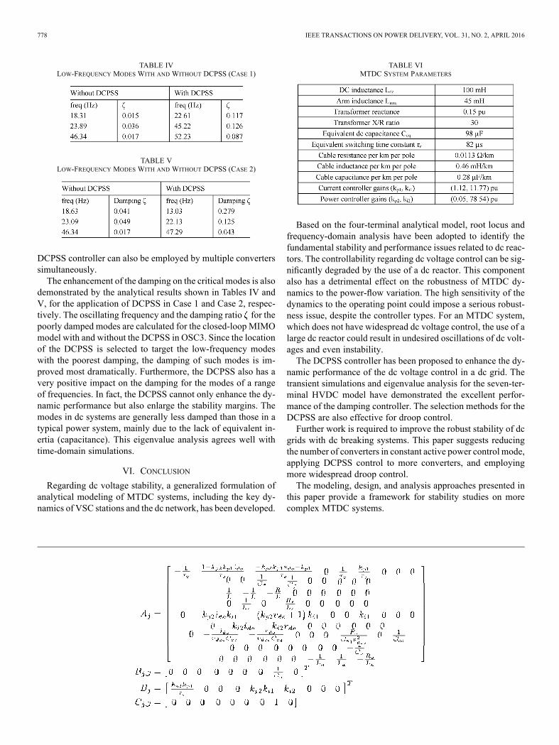
778 IEEE TRANSACTIONS ON POWER DELIVERY, VOL. 31, NO. 2, APRIL 2016
TABLE IVLOW-FREQUENCY MODES WITH AND WITHOUT DCPSS (CASE 1)
TABLE VLOW-FREQUENCY MODES WITH AND WITHOUT DCPSS (CASE 2)
DCPSS controller can also be employed by multiple converterssimultaneously.The enhancement of the damping on the critical modes is also
demonstrated by the analytical results shown in Tables IV andV, for the application of DCPSS in Case 1 and Case 2, respec-tively. The oscillating frequency and the damping ratio for thepoorly damped modes are calculated for the closed-loop MIMOmodel with and without the DCPSS in OSC3. Since the locationof the DCPSS is selected to target the low-frequency modeswith the poorest damping, the damping of such modes is im-proved most dramatically. Furthermore, the DCPSS also has avery positive impact on the damping for the modes of a rangeof frequencies. In fact, the DCPSS cannot only enhance the dy-namic performance but also enlarge the stability margins. Themodes in dc systems are generally less damped than those in atypical power system, mainly due to the lack of equivalent in-ertia (capacitance). This eigenvalue analysis agrees well withtime-domain simulations.
VI. CONCLUSIONRegarding dc voltage stability, a generalized formulation of
analytical modeling of MTDC systems, including the key dy-namics of VSC stations and the dc network, has been developed.
TABLE VIMTDC SYSTEM PARAMETERS
Based on the four-terminal analytical model, root locus andfrequency-domain analysis have been adopted to identify thefundamental stability and performance issues related to dc reac-tors. The controllability regarding dc voltage control can be sig-nificantly degraded by the use of a dc reactor. This componentalso has a detrimental effect on the robustness of MTDC dy-namics to the power-flow variation. The high sensitivity of thedynamics to the operating point could impose a serious robust-ness issue, despite the controller types. For an MTDC system,which does not have widespread dc voltage control, the use of alarge dc reactor could result in undesired oscillations of dc volt-ages and even instability.The DCPSS controller has been proposed to enhance the dy-
namic performance of the dc voltage control in a dc grid. Thetransient simulations and eigenvalue analysis for the seven-ter-minal HVDC model have demonstrated the excellent perfor-mance of the damping controller. The selection methods for theDCPSS are also effective for droop control.Further work is required to improve the robust stability of dc
grids with dc breaking systems. This paper suggests reducingthe number of converters in constant active power control mode,applying DCPSS control to more converters, and employingmore widespread droop control.The modeling, design, and analysis approaches presented in
this paper provide a framework for stability studies on morecomplex MTDC systems.
WANG et al.: IMPACT OF DC BREAKER SYSTEMS ON MULTITERMINAL VSC-HVDC STABILITY 779
APPENDIX
For the th converter model, the parametric representationsof the matrices in (10) are shown in the equation at the bottomof the previous page.
REFERENCES[1] J. Häfner and B. Jacobson, “Proactive hybrid HVDC breakers—A key
innovation for reliable HVDC grids, integrating supergrids and micro-grids,” in Proc. CIGRE Symp., Bologna, Italy, 2011, pp. B4–B110.
[2] W. Grieshaber, J. P. Dupraz, D. L. Penache, and L. Violleau, “Devel-opment and test of a 120 kV direct current circuit breaker,” in Proc.CIGRE, Paris, France, 2014.
[3] J. Descloux, B. Raison, and J. B. Curis, “Protection algorithm based ondifferential voltage measurement for MTDC grids,” in Proc. Develop.Power Syst. Protect. IET, 2014, pp. 1–5.
[4] J. Sneath and A. D. Rajapakse, “Fault detection and interruption in anearthed HVDC grid using ROCOV and hybrid DC breakers,” IEEETrans. Power Del., to be published.
[5] K. De Kerf et al., “Wavelet-based protection strategy for DC faults inmulti-terminal VSC HVDC systems,” IET Gen. Transm. Distrib., vol.5, pp. 496–503, 2011.
[6] L. Xu and L. Yao, “DC voltage control and power dispatch of a multi-terminal HVDC system for integrating large offshore wind farms,” IETRenew. Power Gen., vol. 5, pp. 223–233, 2011.
[7] J. Beerten, S. Cole, and R. Belmans, “Modeling of multi-terminal VSCHVDC systems with distributed DC voltage control,” IEEE Trans.Power Syst., vol. 29, no. 1, pp. 34–42, Jan. 2014.
[8] L. Jun, J. Tianjun, O. Gomis-Bellmunt, J. Ekanayake, and N. Jenkins,“Operation and control of multiterminal HVDC transmission foroffshore wind farms,” IEEE Trans. Power Del., vol. 26, no. 4, pp.2596–2604, Oct. 2011.
[9] G. O. Kalcon, G. P. Adam, O. Anaya-Lara, S. Lo, and K. Uhlen,“Small-signal stability analysis of multi-terminal VSC-based DCtransmission systems,” IEEE Trans. Power Syst., vol. 27, no. 4, pp.1818–1830, Oct. 2012.
[10] W. Wang, A. Beddard, M. Barnes, and O. Marjanovic, “Analysis ofactive power control for VSC-HVDC,” IEEE Trans. Power Del., vol.29, no. 4, pp. 1978–1988, Oct. 2014.
[11] H. Saad, S. Dennetiere, J. Mahseredjian, P. Delarue, X. Guillaud, J.Peralta, and S. Nguefeu, “Modular multilevel converter models forelectromagnetic transients,” IEEE Trans. Power Del., vol. 29, no. 3,pp. 1481–1489, Jul. 2013.
[12] T. M. Haileselassie, “Control, dynamics and operation of multi-ter-minal VSC-HVDC transmission systems,” Ph.D. dissertation, Norwe-gian Univ. Sci. Technol., Trondheim, Norway, 2012.
[13] J. Z. Zhou, D. Hui, F. Shengtao, Z. Yi, and A. M. Gole, “Impactof short-circuit ratio and phase-locked-loop parameters on thesmall-signal behavior of a VSC-HVDC converter,” IEEE Trans.Power Del., vol. 29, no. 5, pp. 2287–2296, Oct. 2014.
[14] C. Dierckxsens, K. Srivastava, M. Reza, S. Cole, J. Beerten, and R.Belmans, “A distributed DC voltage control method for VSC MTDCsystems,” Elect. Power Syst. Res., vol. 82, pp. 54–58, 2012.
[15] B. Jacobson, P. Karlsson, G. Asplund, L. Harnefors, and T. Jonsson,“VSC-HVDC transmission with cascaded two-level converters,” inProc. CIGRE Session, 2010, pp. B4–B110.
[16] S. Skogestad and I. Postlethwaite, Multivariable Feedback Control:Analysis and Design, 2nd ed. Hoboken, NJ, USA: Wiley, 2005.
[17] E. Z. Zhou, O. P. Malik, and G. S. Hope, “Theory and method for se-lection of power system stabilizer location,” IEEE Trans. Energy Con-vers., vol. 6, no. 1, pp. 170–176, Mar. 1991.
[18] Y. Y. Hsu and C. L. Chen, “Identification of optimum location for sta-biliser applications using participation factors,” Proc. Inst. Elect. Eng.,Gen. Transm. Distrib., vol. 134, pp. 238–244, 1987.
[19] P. Kundur, N. J. Balu, and M. G. Lauby, Power System Stability andControl. New York, USA: McGraw-Hill, 1994.
Wenyuan Wang (S’15) received the B.Eng. degreein electrical and electronic engineering from TheUniversity of Manchester, Manchester, U.K., in2011, where he is currently pursuing the Ph.D.degree in HVDC systems.His research interests include operation, stability,
and control of multiterminal VSC-HVDC systems.
Mike Barnes (M’96–SM’07) received the B.Eng.and Ph.D. degrees in power electronics and drivesfrom the University of Warwick, Coventry, U.K., in1993 and 1998, respectively.
In 1997, he was a Lecturer with the Universityof Manchester Institute of Science and Technology,Manchester, U.K. (UMIST merged with The Univer-sity of Manchester), where is currently a Professor.His research interests cover the field of power-elec-tronics-enabled power systems.
Ognjen Marjanovic (M’08) received the B.Eng. de-gree in electrical and electronic engineering in 1998and the Ph.D. degree in model predictive controlfrom the School of Engineering, Victoria Universityof Manchester, Manchester, U.K., in 2002.Currently he is a Senior Lecturer in the School of
Electrical and Electronic Engineering at The Univer-sity of Manchester.
Oliver Cwikowski received the M.Eng. degreein electrical and electronic engineering from theUniversity of Manchester, Manchester, U.K. in 2012,where he is currently pursuing the Ph.D. degree inHVDC systems.His main research focus is HVDC circuit breakers
for application in VSC-based grids, which is spon-sored by National Grid. His work looks into thedesign and construction of prototype HVDC circuitbreakers, aiming to aid in the development of astandard for HVDC circuit breakers.

> REPLACE THIS LINE WITH YOUR PAPER IDENTIFICATION NUMBER (DOUBLE-CLICK HERE TO EDIT) <
1
Abstract— High Voltage Direct Current (HVDC) grids may be
protected from dc faults through the application of HVDC circuit
breakers. Recent advances in dc circuit breaker technologies may
allow faults in the dc grid to be cleared without a permanent loss
of power to the connected ac grids. The requirements the
protection has yet to be fully defined; especially where half
bridge modular multi-level converter controls are concerned.
This paper investigates how an MMC converter may be designed
to recover from a pole-to-pole fault. The fault response of the
converter to a fault is analyzed in depth. This analysis highlights
key stages in the converter response to a dc fault, allowing the
MMC fault currents to be predicted. This analysis is then verified
in PSCAD simulations and the power flow recovery is shown.
The converter controls are investigated, improvements made to
the power flow recovery, and the need for arm current
controllers highlighted.
Index Terms— HVDC, Grid, Protection, dc, Circuit breaker
VSC, MMC, Control.
I. INTRODUCTION
IGH Voltage Direct Current (HVDC) circuit breakers
are being considered as a potential method of providing
short circuit protection in future HVDC grids [1]. Presently,
only two VSC HVDC grids exist in the world [2, 3]. The
power rating of these grids is low enough, relative to the
maximum infeed loss limitations, to allow dc faults to be
cleared through a philosophy of current diversion and ac side
isolation, which is the traditional choice for VSC HVDC
transmission.
In future grids, if the infeed loss requirements of the ac
grids cannot be met with the traditional protection, new
technologies will be needed. Two new technologies being
considered are: Fault Blocking Converters (FBCs) and HVDC
circuit breakers.
Recent advances in HVDC circuit breakers show short
This paper was submitted for review on the 29/06/2016. This work was
supported in part by the Engineering and Physical Sciences Research Council
and National Grid under projects EP/L021552/1 and TAO/22360. Special thanks to Dr Paul Coventry, Dr Antony Beddard, and Prof Jan Evans-freeman
for their support in this project.
O. Cwikowski, is a research associate at the University of Manchester, Manchester, M139PL UK (e-mail:
M. Barnes is a professor the University of Manchester, Manchester, M139PL UK (e-mail: [email protected]).
R. Shuttleworth is a senior lecturer at the University of Manchester,
Manchester, M139PL UK (e-mail: [email protected]). A. Wood is a senior lecturer at the University of Canterbury, Christchurch,
8041, New Zealand, (e-mail: [email protected]).
A. Miller is the Green Grid director at the University of Canterbury, Christchurch, 8041, New Zealand, (e-mail: [email protected]).
interruption times (<10 ms) can be achieved with novel
topologies [4-7]. Many topologies have been proposed and
industrial prototypes have been developed.
Several FBC architectures have been proposed, along with
associated novel control schemes [8-11]. These converters
may be used in conjunction with HVDC circuit breakers to
reduce equipment requirements and minimize the disturbance
that is caused to the ac grid by a dc fault [12, 13].
However, HVDC breaker interaction with the control of
Half Bridge (HB) Modular Multi-level Converters (MMCs),
the presently preferred topology, has received little attention.
The impact fault clearing will have on the HB-MMC’s
operation and the disturbance seen by the ac grid, are
important areas of study in order to assess the suitability of
future HVDC connections and to specify protection
requirements.
The impact that dc protection systems have on the operation
of the ac and dc grids has been investigated previously [14].
However, this analysis looks at the impact of the HVDC
circuit breakers on voltage stability, and not when faults occur.
System integration aspects are discussed in [15], but they do
not look at the converter fault response or recovery in depth.
Fault currents have been investigated in [16], but assume
that the dc fault current is significantly larger than the ac side
fault currents and that the converter takes no preventative
action against dc faults.
Controls have been investigated for the HB MMC when the
converter is not blocked during a dc fault, implying a high dc
side impedance [17]. Such control is excellent for the
converters in a grid which are not exposed to a significant over
current.
This paper investigates how the HB MMC responds and
recovers from a pole-to-pole fault. PSCAD simulation results
are used to verify the fault analysis and it is shown that
additional converter controls can be used to prevent
unnecessary blocking of the converter, improving the power
flow recovery with respect to the ac grid.
The paper’s main contribution is detailed analysis of a
terminal pole-to-pole fault. The fault analysis can be used to
predict fault currents that the circuit breakers and converters
are expected to handle under a dc fault transient, and how the
fault current recovery is impacted by the converter. The
understanding this analysis imparts allows improvements to be
made to the existing control structure used in this paper,
removing unnecessary tripping of the converter. This work
will also allow the initial conditions relevant to controller
designs to be predicted. The paper indicates that the power
flow recovery is influences by how well the converter controls
Operating DC Circuit Breakers with MMC
Oliver Cwikowski, Alan Wood, Member, IEEE, Allan Miller, Senior Member, IEEE, Mike Barnes,
Senior Member, Roger Shuttleworth
H

> REPLACE THIS LINE WITH YOUR PAPER IDENTIFICATION NUMBER (DOUBLE-CLICK HERE TO EDIT) <
2
its arm currents.
II. OPEN GRID PROTECTION
Open grid dc protection was first proposed by GE/Alstom
in [18]. This protection philosophy was developed to reduce
the number of dc circuit breakers, component ratings, and
reduce operating time of the dc protection system.
When operating with an Open Grid philosophy, when any
circuit breaker detects a fault on the system, it first opens,
even before it has been confirmed that the fault is within its
protective zone. As all circuit breakers in the dc system have
been opened the fault is definitely cleared. Each circuit
breakers then establishes if it should reclose, or not, depending
on a fault location system.
This protection philosophy has been used in this paper as it
allows the protection sequence for a single converter to be
analyzed irrespective of grid topology.
The system under investigation in this paper is shown in
Fig. 1. First, a pole-to-pole fault is applied to the MMC
converter. The converter is then subjected to a dc side over
current due to this low impedance condition, resulting in the
converter blocking. The fault is cleared by a HVDC circuit
breaker, reducing the over current condition. The converter is
then able to unblock and attempt to reestablish power flow to
the ac grid. This paper describes and improves this process.
III. HVDC CIRCUIT BREAKERS
HVDC circuit breakers are required to generate their own
zero crossings. This has lead to a number of topologies being
developed that contain large power electronic elements. Out of
these designs has come a standard type known as “Hybrid
breakers”. Hybrid breakers attempt to combine the benefits of
mechanical circuit breakers and power electronic switches, to
form high speed, low loss dc circuit breakers. Several
manufacturers have developed industrial prototypes that are of
the hybrid form [5, 19]. Plans exist for a full scale HVDC
circuit breaker to be installed [7].
For the purposes of this paper the circuit breaker has been
modeled as an ideal mechanical switch with an interruption
delay, in parallel with a semiconductor circuit breaker, as
shown in Fig. 2 [15]. The semiconductors are protected from
overvoltage by a varistor stack. The parameters used in the
circuit breaker model are given in Table I.
IV. HB MMC POLE-TO-POLE FAULT ANALYSIS
The layout of an MMC is shown in Fig. 3. The MMC is
made from six arms which consist of stacks of Sub Modules
(SMs). Simplistically from a protection point of view, the
converter can be in one of two states; unblocked, or blocked.
When the converter is unblocked, the control is capable of
influencing the state variables, through the manipulation of the
SMs. When the converter is blocked, the control is unable to
influence the state variables. During the period the converter is
blocked, the state variables are driven by the power system’s
forcing functions.
Due to the converter’s switching trajectory, the circuit
cannot be described by a single equivalent circuit across the
entire protection time. As such, the converter’s fault response
Fig. 1. System under investigation.
TABLE I CIRCUIT BREAKER PARAMETERS.
0.1 H Snubber Cap 0.234 µF
904 V Interruption Time 4 ms
0.1 Ω Detection Time 1 ms
Number of series devices
149 Knee Voltage 320 kV
2
Fig. 2. Layout of circuit breaker model.
must be broken down into a sequence of stages. Between each
stage within the sequence, the electrical circuit changes, due to
a controlled or uncontrolled switching of devices within the
converter. The following sections describe key stages in the
MMC’s fault sequence. These stages can occur very rapidly,
resulting in the converter’s equivalent circuit changing many
times before the circuit breaker is opened.
A. Stage A – Discharge
The converter’s first stage in the fault sequence is the
discharge stage. This stage starts at the moment the fault is
seen by the converter until the converter is blocked.
During this time the MMC’s SMs will discharge through
the dc side inductance, at a rate defined by the voltage that is
presented across the dc side inductor.
It is possible that before the converter is blocked the SM
sorting algorithm within the converter will change which SMs
are inserted. This potentially exposes all SMs within the
converter to some amount of discharge.
Assuming that significant discharge of the SMs is
prohibited in order to maintain the ability to switch the IGBTs
within each SM, and the converter will attempt to maintain the
dc link voltage during this discharge, the fault current during
this time can be estimated using (1).

> REPLACE THIS LINE WITH YOUR PAPER IDENTIFICATION NUMBER (DOUBLE-CLICK HERE TO EDIT) <
3
Fig. 3. HB Modular Multi-level Converter (MMC) and two dc circuit breakers connected to a dc grid.
Fig. 4. Stage A equivalent circuit diagram.
(1)
(2)
is the dc link voltage at the moment the fault
occurs. is a constant to compensate for the increased
voltage across the equivalent dc inductance caused by the
cable voltage, this value is bounded between 0 and 1, and it
proportionally relates the cable voltage to the dc link voltage
[16]. is the Thevenin equivalent circuit inductance,
given by (2).
An important note here is that when the arm current is
positive at the moment the converter is blocked, the inserted
capacitors will continue to discharge until the arm current has
reached zero. This can result in a slight delay between the
converter block signal being sent and the beginning of the
second stage.
B. Stage B – Free Wheeling
The second stage is the Free Wheeling stage. This stage
starts after the converter is blocked and continues, as is
explained in this section, until the moment a zero crossing(s)
occurs in a converter arm. The moment a zero crossing occurs
in any of the converter’s arms, the equivalent circuit changes
and another set of equations must be developed.
The moment the converter blocks the SM voltage that was
driving the fault current being removed. Current is
commutated out of the IGBTs in the SMs and starts to flow in
the diodes of the lower switches ( ).
At this moment all six arms act like diode stacks, and each
leg of the converter carries a third of the dc line current. The
converter layout is now represented by Fig. 5.
As all six diodes are forward biased, this exposes all three
phases of the ac grid to a reduction in load impedance. Thus
the ac grid will be exposed to an increase in current. However
this will not be a short circuit to the ac system as the arm
inductors provide some impedance. The ac grid is not capable
of contributing to the dc fault current level at this stage, and
this is explained as follows.
Consider the voltage that would appear across and
(Voltage nodes marked on Fig. 4 due to the influence of a
single phase of the ac system. Providing the arm impedances
match, the ac system voltages, and impedances are balanced,
then each phase’s contribution will have the same magnitude.
When the phase angle of these contributions is considered,
these contributions will sum to zero. Thus, the ac grid cannot
contribute to the dc fault while all six diodes are conducting.
The ac grid voltages will influence the arm currents during
this time.
However, the cable voltage is capable of forcing a change in
the dc line current during this time. The cable voltage can
become negative due to the inductive termination of the dc
lines, which can increase the fault current.
The fault current can be described using (3), which is made
up of two components; an exponentially decaying initial
current ( ), and travelling wave component .
(3)
(4)
(5)
While the freewheeling condition is maintained on the dc
side of the converter, the ac grid will be subjected to an
increase in current, which will flow through the converter’s
arms, but not into the dc circuit breaker.
The ac grid current will circulate in all possible paths
within the converter. However, the majority of the phase
currents will flow in the loops shown in Fig. 5. It can be seen
that each phase-to-phase voltage increases the current in two
arms, and decreases the current in two other arms. Each phase
superimposes its own contribution to each arm current on top
of the dc component. Fig. 6 shows a phasor diagram for the
arm currents during this freewheeling stage. Each arm current
is the sum of a dc component (
), and an ac component ( ),
as described in (12), where denotes upper or lower arm
positions and n denotes the phase leg. The ac component of
each arm current ( ) is the difference of two separate phase
current contributions. The ac component of each arm current
is growing, while the dc component is decaying. This will
eventually lead to a zero crossing in the arm, resulting in the
converter moving to the next stage.
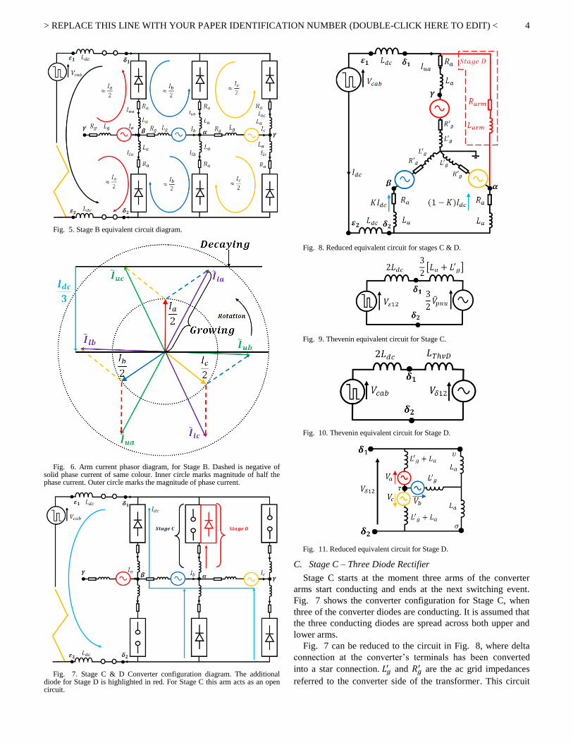
> REPLACE THIS LINE WITH YOUR PAPER IDENTIFICATION NUMBER (DOUBLE-CLICK HERE TO EDIT) <
4
Fig. 5. Stage B equivalent circuit diagram.
Fig. 6. Arm current phasor diagram, for Stage B. Dashed is negative of solid phase current of same colour. Inner circle marks magnitude of half the phase current. Outer circle marks the magnitude of phase current.
Fig. 7. Stage C & D Converter configuration diagram. The additional diode for Stage D is highlighted in red. For Stage C this arm acts as an open circuit.
Fig. 8. Reduced equivalent circuit for stages C & D.
Fig. 9. Thevenin equivalent circuit for Stage C.
Fig. 10. Thevenin equivalent circuit for Stage D.
Fig. 11. Reduced equivalent circuit for Stage D.
C. Stage C – Three Diode Rectifier
Stage C starts at the moment three arms of the converter
arms start conducting and ends at the next switching event.
Fig. 7 shows the converter configuration for Stage C, when
three of the converter diodes are conducting. It is assumed that
the three conducting diodes are spread across both upper and
lower arms.
Fig. 7 can be reduced to the circuit in Fig. 8, where delta
connection at the converter’s terminals has been converted
into a star connection. and
are the ac grid impedances
referred to the converter side of the transformer. This circuit

> REPLACE THIS LINE WITH YOUR PAPER IDENTIFICATION NUMBER (DOUBLE-CLICK HERE TO EDIT) <
5
can then be reduced into a Thevenin equivalent circuit shown
in Fig. 9, when the circuit resistance is assumed to yield much
lower impedance than the inductors. is the cable’s voltage
at the point where is connects to the converter.
Using the Laplace transform given in (6), the dc fault
current can be described by (7). is the phase-to-neutral
voltage that connects to the conducting upper arm during this
period. For the opposing diode configuration (two upper arms,
one lower arm conducting) this voltage would be the phase to
neutral voltage connected to the conducting lower arm. The
cable voltage has been ignored in (7) to provide a simplified
result.
(6)
(7)
(8)
D. Stage D – Four Diode Rectifier
Another possible pseudo-rectifier operation is when four of
the diode stacks in the converter are conducting. It is assumed
that the four diodes are spread evenly across the upper and
lower arms.
The converter configuration is given in Fig. 7, with the
additional upper arm diode marked in red. The equivalent
circuit diagram is given in Fig. 8 with the additional arm path
highlighted.
Assuming low circuit resistance, and considering the
voltages and impedances to the right of nodes and then a
reduced equivalent circuit can be found for this configuration,
shown in Fig. 11.
Fig. 11 shows that only two of the phases are capable of
providing a net contribution. Phase B in this case, cannot as
the two contributions to voltage across the two
impedances sum to zero, as they act in opposing
directions and the same magnitude. This will hold true
providing that the converter arm and ac system impedances
are balanced.
Fig. 11 can then be reduced to the Thevenin equivalent
circuit, whose inductance is given by (9) and Thevenin voltage
in (10). This reduction has been performed using a star-delta
transform on the nodes marked ( ) in Fig. 11, then by
subsuming impedance into one of the delta
impedances, the circuit can be transformed back into a new
star connection with reduced complexity.
Using the Laplace transform given in (6) and assuming the
cable voltage influence is small, (14) describes the fault
current during Stage D.
(9)
(10)
(11)
E. Stage E – Fault Current Decay
The final stage occurs at the moment the circuit breaker
starts to generate the opposing voltage which starts to interrupt
the fault current. The circuit breaker could open during any
one of the stages described in the fault analysis sections of this
paper. Hence is it important to understand the conditions that
the circuit breaker may open under as the voltage will be
different depend on the converter’s configuration. (12) shows
three possible values of voltage .
However, for the case study results show in Section VI, the
circuit breaker opens when the converter is in Stage C.
Based on the analysis presented in Section IV‒C, a reduced
equivalent circuit can be derived for the moment at which the
circuit breaker first attempts to interrupt the current,
generating a voltage source ( ) to oppose the flow of
current, as shown in Fig. 12.
(12)
(13)
(14)
The current from the start of this stage can be estimated by
(13), assuming that the ac system voltages, cable voltage, and
varistor voltages are constant. is the allowed overvoltage
ratio. is the initial current at the start of Stage E. is the
time between fault inception and the circuit breaker attempting
to interrupt the fault current.
From this analysis it can be seen that when a circuit breaker
opens in Stage C, in order for the varistor to force a negative
current change in the fault current, the varistor voltage must be
able to overcome 1.5 times the ac phase to neutral voltage plus
any additional voltage imposed by the cable. This represents a
lower limit for the peak voltages expected across the circuit
breakers.
V. CONVERTER CONTROLS
As the converter is used in a new transmission environment,
there will be a change to the converter’s requirements. These
requirements will need to be met, at least in part, by different
converter controls. An overview diagram of the converter
controls in this paper given in Fig. 13.
This section of the paper gives a brief discussion of
response of the original controls used in the converter
simulations and additions that have been introduced to
improve the power flow recovery. The converter’s power flow
recovery, shown in Fig. 14, was gradually improved from the
Original Response (OR) through the following steps. Details
of the system modeling are given in Section VI.

> REPLACE THIS LINE WITH YOUR PAPER IDENTIFICATION NUMBER (DOUBLE-CLICK HERE TO EDIT) <
6
Fig. 12. Stage E: Reduced equivalent circuit.
Fig. 13. Control system layout for power and current loops.
Fig. 14. PCC power flow recovery and blocking signals for a range of control strategies when subjected to a 0 km fault.
Fig. 15. DQ circulating current controller with two degrees of freedom.
A. Original Response (OR)
The converter’s original power flow response to a dc
protective action is shown in Fig. 14, along with the
converter’s blocking signal. When a dc fault occurs resulting
in a large dc fault current relative to the maximum current
limit of the converter’s arms, 3 kA for this case, as the dc
current is large it is likely that the converter will be required to
block. The only cases where this would not happen, is when
the protection is fast enough or the dc side impedance is large
enough to prevent a significant arm current.
The converter remains blocked until the circuit breaker
recloses and the arm currents have decayed to a reasonable
value to allow the converter to continue operating, for this
paper this is assumed to be 2.5 kA. It can be seen in the
original response additional blocking occurs after the
protection has reclosed. This is unwanted and causes
unnecessary disturbance to the ac system.
B. Arm Current Control (CCSC)
In order to totally remove the unnecessary tripping of the
converter, a Circulating Current Suppression Controller
(CCSC) was added in the PSCAD simulations, the structure of
which is shown in Fig. 15. This allows the converter to have
control over the arm currents. The controller was designed
based around [20, 21]. The PI controller was modified to
remove a zero from the controller’s closed loop transfer
function, which resulted in an improved transient response.
The improvement can be seen in traces marked as “CCSC” in
Fig. 14.
C. Final Control
In order to reduce the peak fault currents seen by the circuit
breaker, and decrease the amount the SMs discharge, it was
decided that upon the detection of a fault the converter should
block. Providing fault detection occurs before the arm currents
rise beyond their limits, this blocking scheme reduces the
amount of sub module discharge. It was observed that this
lessened the time the converter was blocked for in many cases,
as shown in Fig. 14.
In order to improve the converter’s power flow recovery
further the following additions were made to converter’s
control loops and re-close criteria: Anti-integral Windup,
Resettable Controller Integral Terms, Converter unblocks at
low arm currents (<0.1 kA).
Anti-integral wind up was added to mitigate the impacts of
controller saturation that were observed in the simulations.
Blocking decouples the system’s manipulated variables and
state variables. The manipulated variables are the converter
arm voltages. The state variables are driven by the power
system (ac grid or SM voltages etc). This means that while the
converter is blocked the integral terms drift away from their
desired values. The anti-integral windup and resettable
integral terms were added to mitigate this problem. This
reduces the amount of time the converter spent in the blocked
condition, as can be seen in the traces marked as “Final” in
Fig. 14.
VI. CASE STUDY
The MMC converter was modeled using a Detailed
Equivalent Model (DEM). The converter parameters are given
in Table II. The converter arrangement is shown in Fig. 1.
The power traces are measured on the ac grid side of the
transformer at the PCC.
In each simulation the converter is subjected to a dc fault at
200 ms, the fault is detected 1 millisecond after the fault
inception and the circuit breaker imposes a counter voltage 5
millisecond after fault inception. Then the circuit breaker
recloses once the dc fault current reaches zero. The converter
unblocks once all arm currents are less than 100 A, at which
point the converter attempts to reestablish power flow. It is
assumed that the faulted section of the grid is isolated by other

> REPLACE THIS LINE WITH YOUR PAPER IDENTIFICATION NUMBER (DOUBLE-CLICK HERE TO EDIT) <
7
circuit breakers in the dc grid, through the open grid
philosophy.
Two sets of results are presented. The first set of
simulations was performed to verify the pole-to-pole fault
analysis performed in Section IV. The second set of results
shows that controller used in this paper prevents unnecessary
blocking of the converter when it is subjected to a range of
pole-to-pole fault conditions. In each simulation the converter
is delivering or absorbing 1 GW from the ac grid it is
connected to and power is monitored at the Point of Common
Coupling (PCC) in the ac network.
Fig. 16 and Fig. 17 shows a plot of the fault current from a
0 km fault and a plot of the number of diodes conducting
within the converter, when the converter is acting as an
inverter and rectifier respectively. The number of diodes
indicates which stage the converter is in during its fault
sequence. PSCAD simulation and analytical results are both
shown.
The results show a strong agreement between the simulation
and the analysis. The analysis for the case when five diodes
are conducting has not been included in this paper. However,
the amount the current changes during this stage is minimal
for the parameters in these simulations.
Fig. 18 show that the predictions provide a strong guide -
line for estimating the fault currents which occur at a distance
from the converter. The influence of traveling waves on the
fault current can be seen in the simulation results and can
increase the fault currents above those in a 0 km fault.
The associated power flow recovery profile for each of the
fault current simulations is given in Fig. 19. The results show
that the converter power flow is recovers within 40 ms of the
fault inception. There is also no additional blocking of the
converter once the converter unblocks.
Fig. 20 shows that even though circuit breaker reduces the
dc line current to zero, and forces a change in current in some
arms, other arm currents remain significant. The arm currents
must be returned to within normal operating magnitudes and
orientation with respect to the other arms currents in order to
regain the initial power flow condition.
As part of the recovery process energy must also flow from
the ac grid back into the dc system to recharge the cables. This
current inrush causes problems and is difficult to control with
the HB converter topology, and may result in converter
tripping if not appropriately mitigated against.
Once major advantage of advanced MMC topologies (full
bridge or Alternate arm converter) will be their ability to limit
post fault inrush currents, or improve the recovery profile of
the power at the PCC [8, 22], although this feature is not
widely discussed.
Other methods may attempt to use the dc switch gear to
limit these inrush currents [19].
TABLE II CASE STUDY CONVERTER PARAMETERS.
600 kV 45 mH
217 kV
46.8 mH
Fig. 16. Uninterrupted fault current for converter working in rectifier mode. Calculations are compared to fault current at each switching event.
Fig. 17. Uninterrupted fault current from a terminal fault and a plot of the number of diodes conducting. Fault current is compared to equations developed for each stage.
Fig. 18. Fault currents for rectifying operation compared to the analysis developed in Section IV.
Fig. 19. PCC power flow recovery and blocking signals over a range of different faults.

> REPLACE THIS LINE WITH YOUR PAPER IDENTIFICATION NUMBER (DOUBLE-CLICK HERE TO EDIT) <
8
Fig. 20. Arm and dc line currents during protective action and fault recovery.
VII. CONCLUSIONS
The HB MMC fault response needs to be described by a
sequence of fault responses, rather than a single fault response
due to the controlled and uncontrolled switching of the
converter’s power electronics. This paper has provided
generalized analysis to predict the dc fault current and how the
fault current is distributed among the converter arms.
Once the time frames that the converter spends within each
stage of its fault sequence have been established, an analysis
of the fault recovery process can also be performed. This
paper presents an analysis for recovery in one of these stages,
and provides an equation dictating the minimum arrestor knee
voltage for the dc circuit breaker.
During the recovery stage the dc fault current is reduced to
zero. However, this does not mean that the converter’s arm
currents have decayed to zero as well. The arm currents must
recover to reasonable values before power flow can be re-
established.
The converter control system needs to be designed to
encompass the additional requirements imposed by the dc
fault recovery process. This paper has presented a first
generation control method to remove unnecessary blocking of
the converter; however improvements to power flow recovery
need to be investigated further.
Faults on the dc cables are likely to impact the ac system for
a time period much longer than the time it takes to clear the
fault. Based on the results shown in this paper, the disturbance
exists for at least two cycles.
Traveling waves in the dc cables significantly influence the
fault currents seen by the circuit breaker and can result in
higher currents in many instances.
REFERENCES
[1] H. Dirk Van, G.-B. Oriol, and L. Jun, "DC fault phenomena and
DC grid protection," in HVDC Grids:For Offshore and Supergrid of the Future, ed: Wiley-IEEE Press, 2016, pp. 345-370.
[2] L. Chuanyue, H. Xiaobo, G. Jingli, and L. Jun, "The DC grid
reliability and cost evaluation with Zhoushan five-terminal HVDC case study," in Power Engineering Conference (UPEC), 2015 50th
International Universities, 2015, pp. 1-6.
[3] H. Rao, "Architecture of Nan'ao multi-terminal VSC-HVDC system and its multi-functional control," Power and Energy
Systems, CSEE Journal of, vol. 1, pp. 9-18, 2015.
[4] A. Hassanpoor, J. Hafner, and B. Jacobson, "Technical Assessment of Load Commutation Switch in Hybrid HVDC Breaker," Power
Electronics, IEEE Transactions on, vol. 30, pp. 5393-5400, 2015.
[5] J. P. Dupraz and D. L. Penache, "Development of a 120 kV direct
current circuit breaker," presented at the Cigre Paris, 2014.
[6] T. Eriksson, M. Backman, S. Halén, and A. C. Research, "A low
loss mechanical HVDC breaker for HVDC grid applications,"
presented at the Cigré Paris, 2014. [7] W. Zhou, X. Wei, S. Zhang, G. Tang, Z. He, J. Zheng, et al.,
"Development and test of a 200kV full-bridge based hybrid HVDC
breaker," in Power Electronics and Applications (EPE'15 ECCE-Europe), 2015 17th European Conference on, 2015, pp. 1-7.
[8] M. M. C. Merlin, T. C. Green, P. D. Mitcheson, D. R. Trainer, R.
Critchley, W. Crookes, et al., "The Alternate Arm Converter: A New Hybrid Multilevel Converter With DC-Fault Blocking
Capability," Power Delivery, IEEE Transactions on, vol. 29, pp.
310-317, 2014. [9] R. Li, G. P. Adam, D. Holliday, J. E. Fletcher, and B. W. Williams,
"Hybrid Cascaded Modular Multilevel Converter With DC Fault
Ride-Through Capability for the HVDC Transmission System," IEEE Transactions on Power Delivery, vol. 30, pp. 1853-1862,
2015.
[10] R. Zeng, L. Xu, L. Yao, and B. W. Williams, "Design and Operation of a Hybrid Modular Multilevel Converter," IEEE
Transactions on Power Electronics, vol. 30, pp. 1137-1146, 2015.
[11] G. P. Adam, K. H. Ahmed, S. J. Finney, K. Bell, and B. W. Williams, "New Breed of Network Fault-Tolerant Voltage-Source-
Converter HVDC Transmission System," Power Systems, IEEE
Transactions on, vol. 28, pp. 335-346, 2013. [12] G. Chaffey and T. C. Green, "Reduced DC circuit breaker
requirement on mixed converter HVDC networks," in PowerTech, 2015 IEEE Eindhoven, 2015, pp. 1-6.
[13] C. D. Barker, R. S. Whitehouse, A. G. Adamczyk, and M. Boden,
"Designing fault tolerant HVDC networks with a limited need for HVDC circuit breaker operation," presented at the Cigre, Paris,
2014.
[14] W. Wang, M. Barnes, O. Marjanovic, and O. Cwikowski, "Impact of DC Breaker Systems on Multi-Terminal VSC-HVDC Stability,"
Transactions on Power Delivery, 2015.
[15] D. Döring, D. Ergin, K. Würflinger, J. Dorn, F. Schettler, and E. Spahic, "System integration aspects of DC circuit breakers," IET
Power Electronics, vol. 9, pp. 219-227, 2016.
[16] O. Cwikowski, B. Chang, M. Barnes, R. Shuttleworth, and A. Beddard, "Fault current testing envelopes for VSC HVDC circuit
breakers," IET Generation, Transmission & Distribution, vol. 10,
pp. 1393-1400, 2016. [17] R. Li, L. Xu, D. Holliday, F. Page, S. J. Finney, and B. W.
Williams, "Continuous Operation of Radial Multiterminal HVDC
Systems Under DC Fault," IEEE Transactions on Power Delivery, vol. 31, pp. 351-361, 2016.
[18] C. D. Barker and R. S. Whitehouse, "An alternative approach to
HVDC grid protection," in AC and DC Power Transmission (ACDC 2012), 10th IET International Conference on, 2012, pp. 1-
6.
[19] M. Callavik and A. Blomberg, The Hybrid HVDC Breaker: ABB Grid Systems, 2012.
[20] A. Beddard, "Factors Affecting the Reliability of VSC-HVDC for
the Connection of Offshore Windfarms," Doctor of Philosophy, The University of Manchester, 2015.
[21] Q. Tu, Z. Xu, and J. Zhang, "Circulating current suppressing
controller in modular multilevel converter," in IECON 2010 - 36th Annual Conference on IEEE Industrial Electronics Society, 2010,
pp. 3198-3202.
[22] G. P. Adam and I. E. Davidson, "Robust and Generic Control of Full-Bridge Modular Multilevel Converter High-Voltage DC
Transmission Systems," IEEE Transactions on Power Delivery,
vol. 30, pp. 2468-2476, 2015.

> REPLACE THIS LINE WITH YOUR PAPER IDENTIFICATION NUMBER (DOUBLE-CLICK HERE TO EDIT) <
1
Abstract—This paper shows how post fault power recovery of
a Half Bridge Modular Multi-level Converter (HB MMC) can be
improved. It is shown that the HB-MMC can reduce the dc side
fault current, providing benefits to dc switch gear. This paper
shows that the standard DQ CCSC for HB-MMC should not be
used in HVDC fault studies that use dc Circuit Breakers (CBs),
and highlights the need to model appropriate arm current
controllers. A HB-MMC point-to-point system that is protected
with dc CBs, is simulated on an RTDS using detailed switch
models of the converters and switch gear. A dc CB controller has
been implemented in a software-in-the-loop fashion. The
controller is provided free for download. A comparison of
circulating current controllers shows that the standard DQ
controller is unsuitable for fault studies. A modified blocking
structure discussed for the HB-MMC is proposed, which allows
the dc switch gear requirements to be reduced. Bench mark final
case studies are provided to show the benefits that can be
obtained from different dc protection systems.
Index Terms— HVDC, Grid, Protection, dc, Circuit breaker
VSC, MMC, Control.
I. INTRODUCTION
IGH Voltage Direct Current (HVDC) grids are seen as a
future transmission technology [1]. For this new
transmission environment, the question of grid protection has
to be revisited; in cases where the dc grid power level exceeds
the infeed loss limitations of the ac power network. HVDC
Circuit Breakers (CBs) have been proposed as a suitable
technology to isolated faulted parts of the dc grid [2]. Several
industrial prototyped have been developed and a full scale 200
kV CB is being installed into an existing HVDC grid [3, 4].
Other technologies, such as Fault Tolerant Converters
(FTCs) have been proposed to either support the dc switch
gear or provide an alternative [5, 6]. However, such converter
topologies have yet to be implemented in the power system
This paper was submitted for review on the 29/06/2016. This work was
supported in part by the Engineering and Physical Sciences Research Council
and National Grid under projects EP/L021552/1 and TAO/22360. Special
thanks to Dr Paul Coventry for his support. O. Cwikowski, is a research associate at the University of Manchester,
Manchester, M139PL UK (e-mail:
[email protected]). H.R. Wickramasinghem is a PhD student at the University of New South
Wales, Sydney, NSW 2052, Australia, (e-mail: [email protected]).
M. Barnes is a professor the University of Manchester, Manchester, M139PL UK (e-mail: [email protected]).
R. Shuttleworth is a senior lecturer at the University of Manchester,
Manchester, M139PL UK (e-mail: [email protected]). G. Konstantinou is a lecturer at the University of New South Wales,
Sydney, NSW 2052, Australia, (e-mail: [email protected]).
J. Pou is a professor at the University of New South Wales, Sydney, NSW 2052, Australia, (e-mail: [email protected]).
due to the increased losses that are incurred. While such
converter technologies will be suitable in the future, there is a
need to understand how dc CBs will work with the existing
converter topologies. Presently, the preferred technology is the
Half Bridge (HB) Modular Multi-level Converter (MMC).
It is important for power system planning to understand
how quickly a HB-MMC can recovery from dc faults is
important, as this allows the impact on the ac grid to be
understood. How soon after a fault normal power flow is re-
established is determined by how quickly the converter’s
internal voltages and currents are returned to normal operating
levels. This requires detailed models of the internal dynamics
of the converter in order for the grid level limitations to be
understood.
The control of the HB-MMC has been investigated for high
impedance dc fault conditions where the converter does not
block [7]. However, there may be limitations of the amount of
dc side inductance which can be placed in series with the
converters [8].
Detailed models of the breakers are required for this study,
as fault dynamics must be kept within the limitations of the dc
switchgear. A grid level CB model and an appropriate
controller has been developed in [9] based on the first
industrial prototype developed by ABB [4]. This model
assumes that the commutation process is guaranteed, which is
appropriate for grid level studies.
However, to reduce the requirements for dc protection
equipment, converters may be controlled to manipulate the dc
fault current [6]. Based on the analysis presented in [10], the
profile of the dc fault current influences the commutation
process (movement of current between the CB’s primary and
secondary branches) in a negative manner. The profile of the
fault current dictates the peak voltage seen across the CB’s
Line Commutation Switch (LCS) and the time it takes to
reduce the primary branch current to zero. LCSs, or similar,
appear in at least three industrial prototypes [3, 4, 11].
Therefore, potential for unwanted interactions between a
converter’s controls and a CB’s operation exist. For fault
studies, a model that encapsulates the commutation process is
required.
Furthermore, the post fault recovery process has yet to be
studied with dc CBs, but similar work can be found in the area
of startup procedures [12]. Under scenarios where an Open
Grid dc protection philosophy, or similar, some CBs will
reclose soon after opening [13]. The converter and dc
protection must ensure that power flow is re-established
quickly and the system’s protections does not trip during
recovery.
In this paper a point-to-point HB-MMC system that is
RTDS Power Flow Recovery in MMCs
O. Cwikowski, H. R. Wickramasinghem, G. Konstantinou, J. Pou, M. Barnes, R. Shuttleworth
H

> REPLACE THIS LINE WITH YOUR PAPER IDENTIFICATION NUMBER (DOUBLE-CLICK HERE TO EDIT) <
2
protected by using hybrid CBs is modeled in a Real Time
Digital Simulator (RTDS). A comparison of dc protection
options for the converter and CB are compared; circulating
current controllers, blocking scheme and CB Fault Current
Limitation (FCL). A combination of these options are
benchmarked against the traditional methods to highlight the
potential benefits that can be gained from changing the way
the converter and dc protection are operated.
This paper shows that in certain cases, the HB-MMC can
limit the dc fault current and be controlled to reduce the
energy dissipated in the CBs. It is also shown that the standard
DQ CCSC, while functional, may not be suitable for fault
studies and it is recommended that a different CCSC technique
be established for future fault studies.
Fig. 1. RTDS system.
Fig. 2. Layout of RTDS simulations.
II. RTDS SYSTEM SETUP
The RTDS system used in this paper is shown in Fig. 1.
Three RTDS racks are used. Racks 1 and 2 are used to run the
MMC switch models, cable models, CB model, and ac power
system. Rack 3 is used to run the dc CB controllers separately.
A 400 MW point-to-point HB-MMC transmission line is
simulated in the first two racks. This switched model of the
MMC based on the CIGRE average model from Test System 1
from Working Group B4.57 [14].
Racks 1 and 2 passes Analogue signals to Rack 3 via the
AIO connections. Digital signals are passed between the racks
using the Front Panel Interface (FPI).
Rack 3 reads in the analogue signals from the simulated
HVDC transmission system. When the CB self protection
functions are not enabled, only the total fault current ( ) and
primary branch ( ) currents are required. The controller
code then makes a decision on which state the CB should be
in, based on the analogue inputs, CB control signals (FC &
RC), and the present state of the CB. The control signals are
then output to the Front Panel Interface (FPI) and fed into
racks 1 & 2.
III. DC CIRCUIT BREAKER CONTROLLER
In order to ensure control actions taken by the converter
have no negative influence over the dc CB’s operation, a
detailed switch model of a hybrid dc CB has been used in this
paper. The hybrid CB chosen for this paper is the proactive
hybrid CB, developed by ABB [4]. The layout of the model is
shown in Fig. 3.
Power electronic stacks are represented by single switches
parameterized for to have the same electric characteristics as
the required stack of devices. Mechanical switches are
modeled as switches, which have a maximum current
chopping capability and minimum opening time. The
mechanical switches present a low impedance until the end of
the delay time, at which point they become high impedance.
All hybrid CBs will require a series dc side reactor ( ), in
order to limit the peak fault current they are exposed to.
Parasitic inductance ( ) has been added to the secondary
branch in order to obtain realistic commutation time, based on
the hardware results this time is approximately 250 µs [4]. The
LCS’ snubber circuit capacitance ( ) has been modeled to
ensure reasonable LCS voltages are maintained during a
protection action [10]. The voltage across the CB is limited by
the varistor ( ). Each component has been modeled using
the small time step components within RSCAD.
The state of the CB is controlled through a specifically
designed RTDS software controller shown in Fig. 2. The user
provides settings for the controller and can enable the
functions which are desirable for the simulation case. The
state diagram for the CB is based on the operation detailed in
[4] and reclose procedure in [9]. Each time step the controller
makes a decision to either change state or continue to wait for
one of the mechanical switches to open. This decision is based
on the present state of the CB, the analogue inputs from the
HVDC transmission system, and the CB control signals Fault

> REPLACE THIS LINE WITH YOUR PAPER IDENTIFICATION NUMBER (DOUBLE-CLICK HERE TO EDIT) <
3
Confirm (FC) and Re-Close (RC). The CB controller also has
an Open Grid (OG) function, which allows the CB’s operation
to be triggered before signal FC becomes true.
Fig. 3. RTDS proactive hybrid CB model layout.
Fig. 4. Layout of DCCB controller code.
Fig. 5. RTDS results of breaking operation. CB parameters exaggerated to show commutation time and switching events.
Fig. 6. CB opens to isolate section of grid, then recloses onto a fault and behaves as an FCL limiting the current to a maximum of 1 kA.
This function pushes the current into the secondary branch
and opens mechanical switch , when the total fault current
exceeds a pre-defined level. The CB does not fully open until
the FC signal becomes true. An example of the CB opening
procedure is shown in Fig. 5.
The CB controller also has an output signal (PF) which
signals to the user that, due to the power system conditions,
the breaker’s operation has failed, and what type of failure has
occurred. Details of the PF function are given in the
controller’s instruction manual.
The failure modes which can be detected are: LCS over
voltage, peak current violation, commutation time violation,
tail time violation, and CB overvoltage.
A commutation time violation occurs when it takes too long
to reduce the primary branch current to zero once the LCS has
been turned off. A tail time violation occurs when the varistor
is subjected to a pulse of current that is longer than it is
designed to handle.
Any failure causes the mechanical switches and LCS to turn
on, and to turn off. This results in an inability of the
protection to isolate the fault, while protecting the secondary
branch power electronics.
The controller can also have a FCL operation enabled. This
feature allows the CB to limit the dc fault current by
modulating the secondary branch when mechanical switch
is fully open [4]. An example of the feature is shown in Fig.
6, where the CB recloses while the fault is still prevailing. The
CB turns off the secondary branch to decrease the fault current
and recloses the secondary branch once the current is below a
preset value.
As will be shown in Section VI, this feature can mitigate
inrush currents when a CB recloses. The RTDS CB model,
controller, and an instruction manual have been made freely
available for download at: <insert download LINK>.
IV. BLOCKING STRATEGY
Typically, once any arm current has exceeded a maximum
threshold, all converter’s IGBTs will be turned off. This
“blocking” and prevents damage to the IGBTs. The blocking
results in each converter arm behaving as a diode stack. The
number of arms which are defines the ability of the ac grid to
influence the dc fault current.
An alternative blocking strategy is proposed in this paper,
which provides additional benefits to the dc side equipment.
Rather than blocking all IGBTs once the arm current
threshold has been violated, the arm voltage references are set
0 0.03333 0.06667 0.1 0.13333 0.16667 0.2
-0.5
0
0.5
1
1.5
2
kA
IM2

> REPLACE THIS LINE WITH YOUR PAPER IDENTIFICATION NUMBER (DOUBLE-CLICK HERE TO EDIT) <
4
to zero. This turns off all the upper IGBTs ( ) and turns on
all the lower IGBTs ( ) in each sub-module, shown in Fig. 8.
This can be done providing the current limit for the lower
IGBT is not violated. This modified blocking structure
effectively prevents the converter acting as a pseudo-rectifier
during a dc fault, preventing the ac grid from imposing a
significant voltage across the converter’s dc terminals.
Fig. 7 shows the dc fault current and converter arm currents
for a terminal fault for a normal blocking scheme. Each arm
current is made up of a dc component and an ac component. It
can be clearly seen that in the normal blocking case the lower
IGBT threshold cannot be violated as current cannot flow in
this direction within the arms, once the converter is blocked.
For the modified case, because the arm currents become
positive (due to the lower IGBT being turned on), the
converter no longer acts as a rectifier. The dc fault current can
be described by (1) and decays based on the system’s parasitic
resistance (3) and equivalent dc side inductance (2).
Fig. 7. Normal blocking converter equivalent circuit resembles rectifier. Modified blocking circuit shown with IGBT paths in each arm. The majority of each phase current will flow in two arm loops, indicated by dashed lines for phase B.
Fig. 8. Sub-module architecture.
Fig. 9. Equivalent circuit for dc fault current recovery.
This has the effect of reducing the fault current seen by the
dc breaker, while increasing the RMS of the arm currents.
The modified strategy results, Fig. 11, show the arm current
is biased down by the dc fault current, the peak positive arm
current is lower in magnitude than the negative peak arm
current. Providing the ac grid impedance and arm inductances
are sufficient to keep the arm currents below the positive arm
current threshold, there is no to need to turn off the lower
IGBT. If violated, then the bypass thyristor ( ) used in some
HB-MMC modules can be used to support the IGBT in
conducting the current, shown in Fig. 8.
The benefits for the dc CB current can be clearly seen, as
the peak fault current has been reduced. This comes at the
expense of increasing the arm currents.
(1)
(2)
(3)
(4)
(5)
Providing this modified blocking state can be maintained
over the protection period, then the peak fault current
experienced by the CB will be determined by how quickly the
converter can block, plus any additional impact imposed by
traveling waves [15]. For a terminal fault (4) can be used to
describe the fault current. is the time is takes to block the
converter from the inception of the terminal fault. is a
multiplying factor that can be sued to compensate for the
additional current imposed by the cable voltage [15].
As converter’s DC terminal voltage is kept low during a dc
fault, this has the added benefit of reducing the pulse
requirements for the dc CB’s varistor. Fig. 9 shows the
equivalent circuit at the moment the dc CB attempts to
interrupt the flow of current by turning off . Pulse width of
the varistor is given by (5). When the converter is blocked in
the normal method, the converter has a substantial Thevenin
equivalent voltage source ( ). For the modified blocking
case this thevenin equivalent voltage is zero, for a balanced
system. This also reduces the converter’s equivalent
impedance ( ) as there are more parallel paths available
for current flow within the converter, both reduce the current
pulse width.
V. ARM CURRENT CONTROLLERS
This section of the paper provides a comparison between
two different arm current controllers. Two controllers were
chosen for this study. One is the commonly used DQ
Circulating Current Suppressing Controller (CCSC), based on
the work presented in [16]. The other controller used is a
Forced Circulating Current Controller (FC3) [17]. This
controller provides a direct set point for each of the arm
currents. This gives the arm current controller some control
over the individual arm currents.

> REPLACE THIS LINE WITH YOUR PAPER IDENTIFICATION NUMBER (DOUBLE-CLICK HERE TO EDIT) <
5
Fig. 10. Fault current and arm currents for normal blocking.
Fig. 11. Fault current and arm currents for modified blocking.
Fig. 12. Converter arm currents with DQ CCSC at rectifier.
Fig. 13. Converter arm currents with FC3 at rectifier.
Fig. 14. Real power flow during protective action.
The arm current controller method was changed at the
rectifying end of the point-to-point system to highlight the
improvements that could be made. For these results, a dc pole-
to-pole fault was applied which is then isolated by the CBs.
Once the dc line current has fallen to zero and the fault has
been removed, CB starts the re-closure procedure and the
converter attempts to re-establish the pre-fault power flow.
The rectifying converter is each case is absorbing 400 MW at
unity power factor.
Fig. 14 compares the power flow recovery power at the
Point of Common Coupling (PCC), between the two control
techniques. It can be seen that that when FC3 control is used
the power flow recovery process is far less oscillatory. The
power flow also recovers sooner, with a lower overshoot.
The additional oscillations seen in the DQ CCSC power
flow recovery are due to the sustained oscillations in the
converter’s arm currents, shown Fig. 12. For DQ control, the
disturbance to the converter exists for a significantly longer
period of time, with normal operation not being reached until
time 0.5 s.
For the FC3 control option the arm currents are still
significantly disturbed, but they recovery much sooner, with
normal operation re-established at 0.35 s. It is likely that
implementing the FC3 in the inverter would show additional
improvements. The dc fault transient is a sub-cycle
disturbance; however its impact is seen in the converter for a
significantly longer period of time. The dc fault is able to
influence the converters operation over this extended of time
for two reasons. First, the isolation of a dc fault does not imply
zero magnitude arm currents; hence the converter needs to
return these arm currents to their desired value. Second, there
are no established tuning methods for the HB-MMC that
include the influence of the series dc side inductor ( ), or
attempt to mitigate the impact of the dc fault. There is clearly
a need to develop tuning methods and requirements for the
tuning of MMC controls that are protected by dc CBs.
VI. BENCH MARK CASE STUDY
Several topics have been discussed to reduce the impact of
dc fault transient on the HB-MMC; arm current controller,
blocking method, and CB FCL. Each of the options proposed
for these areas has advantages and disadvantages.
In order to highlight these, a bench mark comparison of

> REPLACE THIS LINE WITH YOUR PAPER IDENTIFICATION NUMBER (DOUBLE-CLICK HERE TO EDIT) <
6
three different dc protection systems was performed. The three
cases chosen are detailed in Table I. The limitations of the dc
protection system are given in Table II. The parameters used
in Table II were used to obtain a suitable dc side inductor
value to ensure the peak fault current of the dc equipment was
not violated. It was also decided to add the Fault Confirm (FC)
signal to the blocking logic within the converters. This means
that once the fault is detected, the converter blocks, rather than
waiting for the arm current limitations to be reached.
For Case 1, the equivalent dc side inductance can be
estimated from (6) assuming a linear increase in current and
ignoring any influence traveling waves will have on the fault
current. This assumes that the CB attempts to interrupt the
flow of current at time . is the time after fault
inception that the secondary branch is turned off..
For cases 2 and 3, fault current stops increasing after the
converter is blocked at time ( ). is the time after
fault inception that the converter is blocked, which for these
cases is 2 ms.
Fault studies were performed using the RTDS setup
described in Section II. The protection action sequence for
each case is as follows. A pole-to-pole dc fault is applied,
resulting in an increase in the dc fault current. The converter is
then blocked in either the normal or modified manner, based
on either an over current limit being reached or the FC signal
becoming true. In parallel to this, the CB will begin its
operation once the Open Grid Trigger Current is reached, or
once the Fault Confirm (FC) signal is generated by the fault
detection system. The CB will then isolate the converter from
the dc cable and force the dc current to zero. Once the dc fault
current has reached zero and the fault confirm signal has fallen
to zero (20 ms after fault inception), the CB recloses. Upon
reclosing, the CB presents low impedance to the dc network,
the converter attempts to re-establish the pre-fault power flow.
Simulation results are shown in Fig. 15 to Fig. 17. A
comparison of the protection systems as a whole is given in
Table III.
Looking at Fig. 15, large differences can be seen in the
requirements for the dc switch gear for each case. Case 1
presents the highest dc fault current and longest current pulse
width in the varistor. Comparing the exact numbers in Table
III, the fault current has been reduced by 2.1 kA and
requirements for the varistor in cases 2 and 3 are one tenth of
those seen in Case 1. This is due to the blocking strategy
preventing the converter from negatively influencing the
decay of the fault current and the reduced dc side inductance
used in cases 2 and 3.
The interruption time has also been dramatically reduced,
predominantly due to the reduction in the varistor current
pulse width time. This would allow the CB to reclose sooner if
the fault duration was shorter.
(6)
TABLE I DC PROTECTION SYSTEMS.
Case Arm Current
Controller
(Inv/Rec)
Blocking
Strategy
DC CB
FCL
Open
Grid
1 DQ CCSC / DQ
CCSC Normal
No
Yes
2 DQ CCSC / FC3 Modified No
Yes
3 DQ CCSC /FC3 Modified Yes
No
TABLE II
DC PROTECTION PARAMETERS.
Attribute Value
Peak DC Fault Current 10 kA
Mechanical Switch Opening Time 2.5 ms
Secondary Branch Inductance 40 µH
Converter Blocking DC Current 6 kA
Fault Detection Time 2 ms
Open Grid Trigger Current 3 kA
Fault Duration 20 ms
Overvoltage Ratio 1.5 pu
The inrush current seen when the CB is reclosed is higher
for the cases which use the modified blocking strategy. This is
due to the lower impedance condition that the ac network is
subjected to with this blocking strategy. As the arm currents
are larger, when the converter unblocks and the CB recloses,
there is an associated larger inrush of current. While the peak
inrush current has not been limited with the use of the DC
FCL function, the re-close current oscillations are significantly
reduced and a more damped response is observed.
The real power at the PCC is plotted for each protection
case in Fig. 15. The power flow is re-established sooner when
FC3 control is used (cases 2 and 3) and the response does not
contain large oscillations, as in Case 1. The power flow
reaches steady state approximately 219 ms sooner than when
the FC3 controller is used and the power flow reaches 90% of
the post fault power flow level 28 ms sooner. The dramatic
swing in PCC power can be reduced if the dc CB operates as a
FCL, which may have implications for ac grid angle stability.
Fig. 17 shows that in each case there us a large swing in the
reactive power at the PCC. The DQ control here provides a
superior response, as the peak reactive power is lower,
potentially resulting in a reduction in ac grid voltage spikes.
VII. DISCUSSION
The three protection cases investigated in Section VI show
case various design options for equipment that will form parts
of a dc protection system. Case 1 has been developed using
“traditional” converter design options. While this may be true
for existing HVDC links, once dc CBs are included in the
transmission link, there is a fundamental change in the way the
converter responds to a fault, and a change in the design

> REPLACE THIS LINE WITH YOUR PAPER IDENTIFICATION NUMBER (DOUBLE-CLICK HERE TO EDIT) <
7
specifications. Once switch gear is introduced into the dc side,
one must consider the impact the converter has on the rating of
the dc side equipment. This additional consideration changes
the design philosophy one may adopt in many areas.
Case 2 shows that moving away from the DQ CCSC
reduces the disturbance caused by a dc fault. Further
developments in this area are highly likely and specific
controllers to mitigate dc faults will likely be required. This
highlights for grid studies where dc CBs are included, not
assume that the DQ CCSC is suitable.
Fig. 15. Comparison of dc fault currents.
Fig. 16. Power flow recovery at rectifier’s PPC. CB CTL signal on right hand axis, shows when CB is in the fully open position.
Fig. 17. Reactive power flow recovery at rectifier’s PCC.
TABLE III
BENCH MARK COMPARISON OF PROTECTION CASES
Bench Mark Normal
Case 1
Modified
Case 2 Case 3
Peak Arm Current (-ve/+ve) [kA]
9.2/3.6 10.2/9.3 9.9/9.3
90% Power Recovery
Time [ms] 92.5 64.5 64.5
Power Steady State Time [ms]
454 235 235
Peak DC Current [kA] 9.85 7.72 7.71
Peak Recovery Current
[kA] 1.39 4.04 4.06
Varistor Energy [MJ] 25.6 2.256 2.44
Varistor Break Pulse
Width [ms] 20.9 2.38 2.66
Pole Inductor [mH] 57 35 35
Isolation Time [ms] 26.95 8.58 8.48
Max Q [GVAR] 0.59 1.73 1.74
Max P [GW] 0.48 0.79 0.38
There is a need to define a arm current controller for dc
fault studies and how this influences the dynamic performance
of the converters at other modeling levels.
The case studies have shown that there is an alternative
blocking method which can significantly reduce the
requirements for the dc switch gear. Providing the arm
currents can be kept to a reasonable value.
The converter could be put into this configuration just
before the CB interrupts the fault current. This would allow
for the benefits seen for the varistors to be obtained, while still
mitigating some of the converter arm currents. There would be
no reduction to the peak dc fault current or in series
inductance in such a case.
None of the cases are definitively the best options as this is
highly dependent on the specific HVDC transmission
environment under question. The modified blocking strategy
clearly has benefits to the dc switch gear, especially the
varistors which are a major limiting technology for HVDC
CBs. Advanced MMC may provide further benefits to the dc
protection equipment [6].
The case studies also show the dc protection system will
have a dramatic influence on the power flow recovery, both
active and reactive. The interactions between the dc protection
and key ac grid dynamics must be investigated in further
detail. Dc protection equipment may cause or prevent
problems.
The impact that the dc protection equipment has on the ac
protection must also be investigated. Selectivity must be
coherent between the ac and dc protection system, and the ac
system must only respond to transients caused by the dc
protective action when they are required to. Communication
techniques between these protections must be established.
VIII. CONCLUSIONS
A point-to-point HB-MMC HVDC system has been
implemented in an RTDS, along with detailed switching
models of dc CBs used to provide protection dc short circuit
protection.

> REPLACE THIS LINE WITH YOUR PAPER IDENTIFICATION NUMBER (DOUBLE-CLICK HERE TO EDIT) <
8
A dc CB controller has been developed in the RTDS
environment which allows hybrid dc CBs to be controlled.
Any hybrid CB that contains a LCS, or equivalent, in the
primary branch may be controlled by this controller, which
has been made freely available for download, along with an
instruction manual.
The standard dc CCSC is likely unsuitable for HVDC grids
that contain dc CB. Fault studies should be performed with a
more suitable arm current control method. The impact this has
on other HVDC investigation studies is an area for future
study.
This paper has shown that the HB-MMC is capable of
limiting the dc fault current level and capable of supporting
the dc CB during opening.
A comparison of different dc protection systems has been
made, showing that significant benefits can be made through
different technology choices.
REFERENCES
[1] H. Dirk Van, G.-B. Oriol, and L. Jun, "Drivers for the development
of HVDC grids," in HVDC Grids:For Offshore and Supergrid of
the Future, ed: Wiley-IEEE Press, 2016, p. 528. [2] H. Dirk Van, G.-B. Oriol, and L. Jun, "DC fault phenomena and
DC grid protection," in HVDC Grids:For Offshore and Supergrid
of the Future, ed: Wiley-IEEE Press, 2016, p. 528. [3] W. Zhou, X. Wei, S. Zhang, G. Tang, Z. He, J. Zheng, et al.,
"Development and test of a 200kV full-bridge based hybrid HVDC
breaker," in Power Electronics and Applications (EPE'15 ECCE-Europe), 2015 17th European Conference on, 2015, pp. 1-7.
[4] M. Callavik and A. Blomberg, The Hybrid HVDC Breaker: ABB
Grid Systems, 2012. [5] M. M. C. Merlin, T. C. Green, P. D. Mitcheson, D. R. Trainer, R.
Critchley, W. Crookes, et al., "The Alternate Arm Converter: A
New Hybrid Multilevel Converter With DC-Fault Blocking Capability," Power Delivery, IEEE Transactions on, vol. 29, pp.
310-317, 2014.
[6] G. Chaffey and T. C. Green, "Reduced DC circuit breaker requirement on mixed converter HVDC networks," in PowerTech,
2015 IEEE Eindhoven, 2015, pp. 1-6.
[7] R. Li, L. Xu, D. Holliday, F. Page, S. J. Finney, and B. W. Williams, "Continuous Operation of Radial Multiterminal HVDC
Systems Under DC Fault," IEEE Transactions on Power Delivery,
vol. 31, pp. 351-361, 2016.
[8] W. Wang, M. Barnes, O. Marjanovic, and O. Cwikowski, "Impact
of DC Breaker Systems on Multi-Terminal VSC-HVDC Stability,"
Transactions on Power Delivery, 2015. [9] W. Lin, D. Jovcic, S. Nguefeu, and H. Saad, "Modelling of high-
power hybrid DC circuit breaker for grid-level studies," IET Power
Electronics, vol. 9, pp. 237-246, 2016. [10] O. Cwikowski, M. Barnes, R. Shuttleworth, and B. Chang,
"Analysis and Simualtion of the Proactive Hybrid Circuit
Breaker," presented at the Power Electronics and Drive Systems,11th IEEE International Conference on, Sydney, 2015.
[11] J. P. Dupraz and D. L. Penache, "Development of a 120 kV direct
current circuit breaker," presented at the Cigre Paris, 2014. [12] P. Wang, X. P. Zhang, P. F. Coventry, and R. Zhang, "Start-Up
Control of an Offshore Integrated MMC Multi-Terminal HVDC
System With Reduced DC Voltage," IEEE Transactions on Power Systems, vol. 31, pp. 2740-2751, 2016.
[13] C. D. Barker and R. S. Whitehouse, "An alternative approach to
HVDC grid protection," in AC and DC Power Transmission (ACDC 2012), 10th IET International Conference on, 2012, pp. 1-
6.
[14] C. W. G. B4.57, "Guide for the Development of Models for HVDC Converters in a HVDC Grid.," ed, 2010, pp. 148-156.
[15] O. Cwikowski, B. Chang, M. Barnes, R. Shuttleworth, and A. Beddard, "Fault current testing envelopes for VSC HVDC circuit
breakers," IET Generation, Transmission & Distribution, vol. 10,
pp. 1393-1400, 2016.
[16] Q. Tu, Z. Xu, and J. Zhang, "Circulating current suppressing
controller in modular multilevel converter," in IECON 2010 - 36th
Annual Conference on IEEE Industrial Electronics Society, 2010, pp. 3198-3202.
[17] J. Pou, S. Ceballos, G. Konstantinou, V. G. Agelidis, R. Picas, and
J. Zaragoza, "Circulating Current Injection Methods Based on Instantaneous Information for the Modular Multilevel Converter,"
IEEE Transactions on Industrial Electronics, vol. 62, pp. 777-788,
2015.

Analysis and Simulation of the Proactive Hybrid Circuit Breaker
Oliver Cwikowski, Mike Barnes, Roger Shuttleworth and Bin Chang
The University of Manchester [email protected]
Abstract – High Voltage Direct Current (HVDC) short circuit protection is a fundamental requirement for any HVDC transmission system. Presently, all point-to-point links are protected using circuit breakers on the AC side of the converters. In order to enable HVDC grids, a more advanced protection system must be developed. HVDC circuit breakers are one solution for the protection of future HVDC grids. Several designs have been proposed for DC circuit breakers but few are suitable for Voltage Source Converter (VSC) applications. To date, only a few industrial prototypes have been developed, which are seen to be suitable for the VSC HVDC applications. This paper presents analysis and simulations on one of these prototypes, the Proactive Hybrid Circuit Breaker (PHCB). Equations are derived from a state-space analysis of the circuit breaker. A model of the circuit breaker is suitably parameterized for a +/- 300 kV VSC system in PSCAD. Fault simulations are then performed and compared to the equations developed in a state space analysis. Discussion is then given to the design and testing of the Load Commutation Switch (LCS).
I. INTRODUCTION
Short circuit protection is a fundamental requirement for any transmission system. Low impedance faults on transmission lines result in large current flows, which, if not suitably protected against, will cause significant damage to power system equipment.
The protection of High Voltage Direct Current (HVDC) grids against short circuit faults is an area where further development is required to increase the maximum power rating of such grids. Whether the short circuit protection should come from the AC side of the converters, within the converters, the DC side protection devices or a mixture of all three possibilities, is a subject that is still presently under debate. It is likely that several techniques will be developed, based on the specific layout and power rating of a given HVDC grid.
Circuit breakers are one option for DC side short circuit protection. They may be used in a similar fashion to AC circuit breakers, where they are placed at each end of all the cables in the grid. Hence, in the event of a fault, the faulted cable is isolated from the rest of the grid.
However, in order to reduce costs, DC circuit breakers may be used more sparingly instead. In such a situation, the HVDC circuit breakers would be placed at strategic locations in the grid to separate large sections of the grid in the event of a fault, rather than a single cable. The fault would then be located within the faulted subsection and disconnectors used to isolate the faulted cable. After the faulted cable is isolated, the remaining healthy grid can be re-energized and the DC circuit breaker reclosed. Backup protection would then be
provided by the AC side circuit breakers if the DC protection fails [1].
Presently advanced industrial prototypes have been developed, no commercial breaker is in operation [2-5]. However many circuit breaker designs have been proposed and further developments are expected in this area [6-9]. Understanding how these breakers operate in detail, and which conditions to test them under is a necessary step on the road to a HVDC circuit breaker standard.
This paper is concerned with the analysis of one of these designs, the Proactive Hybrid Circuits Breaker (PHCB). Prior art in this area has been qualitative in terms of the circuit breaker operation. No design equations have been given or any comparison of theory with simulation and experiment. The design of the PHCB is specifically discussed in [10, 11]; however these papers give only a qualitative description.
This paper firstly gives a general description of hybrid circuit breakers and the language used to describe them. A description of the PHCB is then given followed by analysis of key design elements and a state space analysis of the circuit breaker during commutation. This state space analysis yields design equations which can be used to aid in the understanding of how the breaker works and aid in the design of a breaker.
The simulation setup is discussed and the choice of the parameters for the circuit breaker model is presented. Test simulation results are then shown in a simplified system to allow a comparison of theory and simulation. Further simulation results are shown from a PSCAD model of a point-to-point system for DC side faults at a range of distances along the cable. The detailed simulations verify the fidelity of the analysis. The circuit breaker operation and design are then discussed with reference to the analysis and results gathered as part of this work, followed by the conclusions.
II. HYBRID CIRCUIT BREAKERS
Hybrid circuit breakers are combinations of mechanical switches and semiconductor switches. Traditional mechanical switches are too slow for HVDC applications and entirely semiconductor solutions introduce very high losses to the system, increasing the operational costs of the HVDC system [12]. Hybrid circuit breakers attempt to combine the high speed nature of semiconductors and the low losses of mechanical switches.
The generic structure of hybrid breakers is shown in Fig. 1 and shows that hybrid breakers consist of three branches: a primary branch, a secondary branch and an energy absorption branch.
IEEE PEDS 2015, Sydney, Australia 9 – 12 June 2015
978-1-4799-4402-6/15/$31.00 ©2015 IEEE
4

Fig. 1. Generic structure and placement of hybrid circuit breaker.
Fig. 2. Proactive Hybrid Circuit Breaker, from [2].
The primary branch generally consists of at least a mechanical switch, but may also contain additional inductors, semiconductor switches and snubber circuits [2, 6, 13, 14].
The secondary branch may consist of solely semiconductor switches with turn off capability, or a semiconductor switch in series with a capacitor. In the second case, turn off capability is not required as the current in the secondary branch will eventually decrease to zero [13].
The energy absorption branch consists of a large bank of varistors (or similar devices) which are used to limit the Transient Recovery Voltage (TRV) and dissipate the energy stored in the DC side inductance. An inductor (LDC) must presently be placed in series with any hybrid HVDC circuit breaker to limit the rate of rise of fault current and the peak fault current.
Hybrid circuit breaker designs can be operated serially or pre-emptively. Pre-emptive operation differs from serial operation as all the circuit breakers in the grid would initiate once they detect a fault.
Operating all the circuit breakers in a HVDC grid pre-emptively allows for a reduction in the overall operation time of the protection system as fault location algorithms can be run in parallel with the operation of the circuit breaker. Pre-emptive operation also allows backup protection to occur much sooner than a serially operated system, since the current will already be in the secondary branches of the circuit breaker, which provides backup protection.
III. PROACTIVE HYBRID CIRCUIT BREAKER
A. Operation The Proactive Hybrid Circuit Breaker (PHCB) is shown in
Fig. 2. The primary branch consists of a mechanical switch and a small group of semi-conductive switches, known as the Load Commutation Switch (LCS). The secondary branch consists of a large stack of semiconductor switches. The energy absorption branch in this design has been tied in with the secondary branch, which allows current limiting operation once the mechanical switch is fully open [2].
During normal operation the disconnector is closed, the LCS is turned on and the main breaker is turned on. Due to the higher impedance in the main semi-conductive breaker, the majority of the load current will be flowing through the disconnector and the LCS, but some of the current will flow through the main breaker.
When a fault occurs, the current within both branches will start to increase. When a fault is detected, the load commutation switch is turned off. Turning off the LCS causes the voltage across it to rise, as current flows into the parallel snubber capacitance (not shown in Fig. 2.), resulting in a current to flow between the primary and secondary path. A varistor may be used to limit the voltage across the LCS, however this work does not include a varistor based on the topologies discussed in [15] . The voltage rating of the LCS is sufficient to ensure that the current produced can in effect force a current zero in the primary branch, at which point the mechanical switch can be opened.
Once the mechanical switch is fully open and the main breaker is switched off, a transient recovery voltage appears across the circuit breaker, which is limited by the varistors in the energy absorption branch. The series Residual Current Disconnecting Circuit Breaker (RCDCB) is used to break the leakage current through the main breaker and associated devices. This leakage current comes from the semiconductor devices, snubber circuits and the varistors. The varistors may be designed to sink 10’s to 100’s of amps at the DC link voltage to reduce the number of series devices required in the circuit breaker.
B. Descriptive Equations An inductor is required in series with the PHCB for several
reasons. Primarily the inductor is required to limit the rate of rise of current and the peak fault current the semiconductors are exposed to, which in turn limits the power losses in the semiconductor branch. However, as it will be shown in Section VI, this inductor has other functions.
The equation to size the inductor based on the peak breaking capability of the semiconductor branch is given in (1). = ∆
(1)
Imax is the maximum breaking capability of the main breaker, ∆tTotal is the maximum time the current is maintained in the secondary branch, kTW is a constant to compensate for traveling wave effects and VDC is the total DC link voltage. kTW compensates for over voltages experienced across the DC side inductance during fault transients and can usually be assumed to be 1. If the speed of the circuit breaker is increased, could be increased to 2. The inductance value is however limited due to power system stability issues and physical size of the inductor [16-18].
The secondary branch in the hybrid circuit breaker must be rated to deal with the peak transient voltage imposed across the circuit breaker during its operation. The peak over voltage occurs after the semiconductors in the secondary path have been turned off and is limited by the varistor branch. The
5

number of series devices required can be calculated using (2) and (3).
Where nis the number of series devices, VDC is the total DC link voltage, is the peak voltage rating of any individual device in the secondary branch, Sf is the safety margin used in the design, ∆V is the change in voltage during a fault transient across a device and Rvar is the ratio of peak transient overvoltage to the DC link voltage.
The equivalent circuit used to describe the PHCB at the moment the LCS has been turned off is shown in Fig. 3. The parallel capacitance around the LCS is C1, L2 is the inductance of the primary path, L3is the inductance of the secondary path, Von is the on state voltage of the secondary path and VCA is the cable voltage.
Performing a state space analysis on the equivalent circuit, using the matrixes shown in (4) , yields the state transition matrix shown in (6). The equivalent circuit is only valid from the time the devices are turned off to the time the maximum voltage appears across the LCS.
The maximum voltage across the LCS can be estimated using (7). Knowing the maximum voltage is important to estimate the losses during normal operation.
The peak voltage across the LCS is dependent on the current being broken and the voltage rating of the system, indicated by the two separate parts of (7).
The current term comes from the need to change the energy in the branch inductances. For the primary branch, the current needs to be changed from I0 to zero. For the secondary branch, the current needs to be increased from zero to I0. Both of these current changes require an amount of energy that must be present within the snubber circuit capacitance in order to facilitate the change in current.
The voltage term comes from the voltage sources in the equivalent circuit. The voltage at the converter terminals (VDC) and the cable voltage (VCA) are both divided across the DC side and parasitic inductances, shown in Fig. 4.
The capacitance C1 will block pure DC, resulting in a proportion of (VDC - VCA) appearing across the LCS. A similar circuit can be drawn for the “on state” voltage source of the secondary branch and is shown in Fig. 5.
Fig. 3. PHCB equivalent circuit for commutation.
= (1 − )
(2)
= (1 − )!1 − " − ∆ = #$
(3)
% = &'())* , %0 = &--0-
* , . = /0123
(4)
4 = 1 (( + ) + ())6
&( + ) −(( + )) −() −) ( −( −( + ()0 0 0 *
(5)
(7 − 8)9' = 1 :; + )<1(( + ) + ())= + 7(>?
@AAAAAAB1/7 ; −)7<'(( + ) + ())= 0 ; −)(( + ) + ())=0 7 0 D −( + ))(( + 3 + ()F0 ; 7<'(( + ) + ())= 1/7 ; ( + ) + ()=0 1/<' 0 7 GH
HHHHHI
(6)
' ≈ )( − 0) + 12 + ) + -KL( + )M<'
(7)
N ≈ 1O PQ − R9' DO-(( + ) + ()))( − 0) + 12 FS (8)
O = K + )<'(( + ) + ())
(9)
Fig. 4. Voltage divider circuit for converter terminal voltage and cable
voltage.
Fig. 5. Voltage divider circuit for the on state voltage of the secondary
branch.
6

As the LCS may operate within a few hundred microseconds from the moment the fault is detected, the cable voltage may in fact be negative, due to traveling wave effects [17]. As the cable voltage can become negative this will increase the voltage across the LCS further, resulting in the peak operational voltage across the LCS occurring during a non-terminal fault transient.
The analysis also yields an estimate for the time it takes to commutate from the primary branch into the secondary branch, shown in (8), this is here defined as the “commutation time” of the circuit breaker and will be described as such throughout the paper.
IV. SIMULATIONS
A. Example Case This paper uses a +/- 300 kV example system to provide
comparative values for circuit breaker attributes. It will be assumed that the mechanical switches operate in 2 ms [2]. As the breaking capability of any large semiconductor switch will be limited, this paper assumes this limit to be 10 kA for IGBTs based on [2]. The peak transient over voltage on the system is assumed to be 2 p.u.
B. Parameterizing of PHCB for simulations Using the example case described in Section A, the
following design features were calculated using the equations developed in Section B. The device chosen for the secondary branch and LCS varistor was the 5SNA 2000K450300 [19]. Based on the Voltage rating and a Voltage safety factor of 10%, the required number of series devices in the secondary branch was calculated to be 298 (149 per direction).
Although not done here, the number of series devices can be reduced by lowering the knee voltage of the varistors to a value less than the DC link voltage. As such, the varistors will conduct a significant current at the rated DC voltage. In such a case, a residual current breaker would be required to chop the remaining current.
The size of the DC side inductor was set to 100 mH per pole, based on the information given in [2]. The inductor sizing is based on a peak breaking current of 10 kA and a maximum breaking time of 3 ms. The breaking time is the time required to detect the fault, commutate the current into the secondary path and to open the mechanical switch. Backup protection must then be considered. In the event a circuit breaker fails, other circuit breakers must detect this failure and make a decision to open or to continue to conduct the fault current. Additional time must be added into the design to compensate for the backup protection: this time is assumed to be 1 ms.
Based on [2] the LCS is made from a 3x3 matrix of IGBTs per direction. The snubber capacitors used for each IGBT in the LCS and main breaker were set to 30 µF. For the main breaker the snubber limits the rate of rise of voltage across each IGBT to 300 V/µs when breaking 10 kA.
The stray inductance in each branch was set to 30 µH [20]. Resistors and capacitors were used for static and dynamic voltage sharing across each device [21]. For the IGBTs in the LCS the sharing resistor was calculated to be 55.6 kΩ, based on a resistor tolerance of 1%.
Fig. 6. The structure of the PHCB model.
Fig. 7. Simplified environment system diagram.
The sharing capacitor used was 5.46 µF based on a 5% tolerance. For the IGBTs in the secondary branch a 3.25 kΩ resistor and 7.7 µF capacitor were used across each device with the same tolerance estimations. The layout of the PHCB is shown in Fig. 6.
V. SIMULATION SETUP
A. Simplified Environment Simulations The circuit breaker was first simulated in a simplified
environment to allow a direct comparison of theory and simulation. The HVDC converter is represented as a fixed 300 kV voltage source, with an initial DC current of 0.5 kA. A resistive load is used to set the initial current, which is then shorted to simulate a fault event, creating a fault current with a rate of rise of 3 kA /ms [12] . Once the current reaches 1 kA, the LCS is triggered and the current commutated out of the primary branch into the main breaker. Once the current in the primary branch has reached zero, the mechanical switch is opened. If the breaker is acting in a position where it is providing backup protection, the main breaker within that circuit breaker will conduct current for 3 ms before turning off. The main breaker will need to carry current for 3 ms in the event that the circuit breaker is operated pre-emptively and it acts after the primary layer of protection has failed. The simplified system diagram is shown in Fig. 7. The results from the test simulations are shown in Fig. 8, Fig. 9, and Fig. 10.
The simulation results show that the voltage across each IGBT remains the designed maximum of 4.05 kV. The fault current is cleared from the line 8.4 ms after the fault inception, shown by the varistor current reaching zero in Fig. 8. The time it takes for the varistor current to reach zero is
7

dependent on the varistor design, peak current and the DC side inductance. If the peak overvoltage is reduced, this time will increase. In the test systems VDC remains constant during the protection operation; however if a VSC converter provided the DC voltage instead of an ideal voltage source, the DC side voltage would decay, resulting in a shorter clearing time. If a residual current breaker is used to chop the varistor leak current this time could be reduced.
The fault current starts to decrease after 3.186 ms, which is the effective breaking time of the circuit breaker, as it is at this moment that the main breaker is turned off (see Fig. 10). The DC grid voltage will rise to the designed maximum over voltage when the fault current is broken in the semiconductors, but will not reach its nominal value until the varistor current is close to zero.
B. HVDC System simulation details A simulated point-to-point VSC transmission system was
used to perform simulations of a Two Level Converter (TLC) under fault conditions. A 1 GW, 600 kV (+/- 300 kV) symmetrical monopole system was chosen as a representative example. For details of the control used in the converter stations and the layout of the transmission system see [18].The cable length was chosen to be 250 km to represent the distances involved in development of round 3 wind farms in the UK [22]. The model used was a Frequency Dependent Phase Model (FDPM) [23]. The initial DC current is 500 A in each case. The DC side capacitance used was 100 µF per pole. The simulations were run with a time step of 0.2 µs.
C. Detailed Fault Simulations The circuit breaker developed in the test case was then
translated into a detailed simulation of a point-to-point TLC HVDC system. Details of the PSCAD simulations can be found in [18]. Fault simulations were run for faults at 0 km, 50 km and 100 km. Traditionally, terminal faults are taken to be the most severe type of fault, however for DC systems this may not always be the case [17]. Equations (7) and (8) show the cable voltages influences commutation time and voltage.
The cable voltage will be fixed at zero for low impedance terminal faults. However, for non-terminal faults, the cable voltage will change based on the arrival of voltage reflections at the converter. The large inductors required to limit fault currents in HVDC systems result in the DC cable voltage at the point of connection to the converter reversing polarity when a fault occurs on the DC side cable. This reversal of voltage could introduce a higher LCS peak voltage or result in a longer commutation time depending on the circuit breaker parameters.
The simulations were performed where the LCS is triggered at different current levels. The current level or “commutation current” was varied from 1 kA to 3 kA in 0.5 kA steps. Fault simulations were performed for each commutation current, at 0 km, 50 km and 100 km, to assess the influence of the cable voltage on the circuit breaker operation.
Fig. 8. Voltages and Currents during operation of the PHCB.
Fig. 9. LCS currents and voltage rise during turn off.
Fig. 10. Circuit breaker currents and voltages at the moment the
secondary branch is turned off.
8

Fig. 11. LCS peak voltage at different commutating currents. Detailed
simulations strongly match calculation.
Fig. 12. LCS Commutation times from test simulations, detailed point-
to-point simulations and calculations.
A comparison of the simulation results and the theoretical calculations are shown in Fig. 11 and Fig.12. Fig.11, shows that the simulations are within 3% of the peak LCS voltage calculations, indicating a strong fidelity between simulation and calculation. As there is an increase in commutation current, there is an approximately linear increase in LCS voltage. For non-terminal faults, the peak LCS voltage is also slightly higher, but this difference is below 100 V for this example case.
However, if the parasitic inductance in the secondary branch is increased or DC side reactor is decreased, the influence of the cable voltage on the peak LCS voltage will increase.
Fig. 12 shows that the simulations results are within 10% of the commutation time calculations. This difference is likely caused by the assumption that the DC link voltage and the cable voltage are static during the commutation, and that the resistance in the commutation circuit is zero. While the resistance in the commutation circuit will be low (<1 Ω), it will not be zero. The resistance will slightly damp out the
system and result in a longer commutation time, which ties in with the results.
The results also show that there is a slight increase in the time it takes to commutate for non-terminal faults. The parasitic inductance ()) and the DC voltage level will dictate the influence of the cable voltage on the commutation time.
Inspecting (8) , it can be seen that the commutation time for the circuit is bounded between TU and T(U, which for this example case is between 80 µs and 40 µs.
Increasing the current at which the LCS is triggered, reduces the commutation time. However, an increase in the overall operating time of the circuit breaker will be incurred, as there is a longer time between the fault inception and the LCS being triggered. The current for which the LCS is designed to trip, will depend on the initial DC line current and the ability of the control DC current controller to reject non-short circuit disturbances.
VI. DESIGN CONSIDERATIONS FOR THE LCS
The size DC side reactor is an undesirable attribute of any hybrid circuit breaker. The additional cost from materials and from space requirements for offshore applications can be very high. The DC side inductance can be reduced if the current breaking capability of the semiconductors is improved and open time of the mechanical switch is reduced [2].
However, there is a limit to how much the DC side inductance can be reduced, depending on the parasitic inductance of the secondary branch.
Plotting peak LCS voltage against DC side inductance by varying LDC in (7), it can be seen in Fig. 13 that the LCS voltage increases with a decrease in DC side inductance. This is due to a larger proportion of the converter voltage being applied across the LCS.
A larger peak voltage must be compensated for in the number of series devices within the LCS. Increasing the number of series devices required results in increased power losses while the circuit breaker carries the nominal DC current.
Assuming that the snubber capacitance (Csn) is much larger than the sharing capacitor (Csh), a polynomial expression ((10) assuming the cable voltage is zero) can be developed for the number of series devices required in any given LCS. The minimum number of series devices in the LCS is plotted for a range of parasitic inductance values in Fig. 14.
N − -KL( + )MW<XY − ) + 12 + ) = 0
(10)
The number of devices required in the LCS is based upon the voltage rating of the devices, the snubber capacitance and the amount of redundancy required in the LCS. The results in Fig. 14 show that the parasitic inductance must be kept minimal to allow a reduction in LDC. If the parasitic inductance is too large, the number of required devices increases very quickly.
9

Fig. 13. Plots of the peak LCS voltage against DC side inductance, for a
range of parasitic inductances, using Equation (7). Y axis Log scale.
Fig. 14. Minimum Number of Series IGBTs in the LCS. Plots have been
rounded up to yield only integer solutions for the number of series devices, using (10) and rounding up. Y axis Log Scale.
Fig. 15. Commutation Time against LCS parallel Capacitance (C1).
The snubber capacitance for the IGBTs in the LCS may be increased in order to compensate for the additional voltage that arises from reducing LDC. However, this will increase the commutation time for the circuit breaker, as the natural frequency of the commutation circuit is decreased. Consideration must be given in the design of the PHCB as to how the capacitance C1 changes during the life time of the circuit breaker.
Redundant IGBTs will be required to ensure that the breaker can continue to operate if a single IGBT fails. These IGBTs will need to fail short circuit to allow high currents to flow through them.
As the devices are short circuited in the event of a device failure, Capacitance C1 will be increased. This increase comes from the number of capacitors in series being reduced by the number of IGBTs that have failed.
This increase in C1 will reduce the peak voltage across during commutation. However, this will also increase the commutation time to be more than it was prior the IGBTs in the LCS failing. The commutation time is plotted against capacitance C1 in Fig. 15. This results in the circuit breaker’s commutation time changing (∆Z) depending on the amount of redundancy integrated into the design, and how much of it has failed previously.
Therefore, any circuit breaker which uses semiconductor stacks to commutate the current in the primary branch, must be tested at full redundancy (W[) in the LCS and minimum redundancy (W[\#), to ensure that in each case the LCS is properly designed to handle the commutation voltage and that the additional operation time is compensated for in the circuit breaker operation. Or show that their design compensates for this phenomenon, through control or additional hardware.
Fig. 15 shows that based on the stated commutation time in [2] of 250 µs, C1 would be 100 µF if the parasitic inductances are the same. The range of capacitances for C1 would be from 100 µF to 300 µF for an LCS with three series IGBTs. These capacitance values correspond to a commutation time variation of 250 µs to 425 µs.
A more preferable arrangement may be to have a single large snubber for all the IGBTs in the LCS. This would mean that when a signal IGBT fails short circuit, there is a minimal change in the commutation time. However, the snubber would provide a single point of failure within the LCS.
VII. CONCLUSIONS
The PHCB combines semiconductor breaking technology and mechanical switches into a fast, low loss circuit breaker design. This design, along with some more recent innovations, shows that some semiconductor components may be permanently in series with the DC line.
Equations have been developed for key design features of the PHCB and compared to PSCAD simulations. Simulations indicate a strong fidelity to the equations. A second set of simulations was performed using a detailed PSCAD simulation of a VSC HVDC system, and again shows a strong fidelity between simulation and theory.
The peak LCS voltage is determined by the DC voltage level, the commutating current, snubber capacitance, DC side
10

inductance and the parasitic inductances of the circuit breaker. If there are large parasitic inductances in the circuit breaker, the commutation voltage will increase, resulting in additional losses during normal operation of the breaker, due to the increases number of semiconductor devices required in the LCS.
The commutation time is also determined by the same factors as the peak LCS voltage. The commutation time has been found to be limited between half and a quarter of the natural period of the commutation circuit.
The mathematical analysis also showed that the cable voltage influences the peak LCS voltage and the commutation time. The analysis showed that theoretically a non-terminal fault would produce a higher LCS voltage and take longer for the commutation of the current in the primary branch to occur. This means that testing should consider the additional influence of the cable voltage.
The influence of the cable voltage on the operation of the circuit breaker is directly linked to the parasitic inductances in the circuit breaker and to the DC voltage level. For the example case used in this paper, the difference is minimal. However this effect should not be ignored as it may become more influential in other cases.
The analysis has also yielded that there is a minimum required DC side inductance to ensure that the voltage across the LCS during operation is kept to a reasonable value. If the number of devices required is too large the operational costs of having such a hybrid circuit breaker in the DC power system may be too excessive.
The amount of redundancy put into the LCS must be carefully designed along with the snubber capacitance used within the LCS. As the commutation circuit capacitance changes in the event a redundant module is shorted, this will influence the peak voltage across the LCS and the operation time of the circuit breaker.
Testing should be performed for the case when there is maximum and minimum redundancy available within the LCS. These tests should ensure that the LCS is properly rated and that the additional commutation time - from an increase C1 - does not have an impact on the rest of the circuit breaker.
ACKNOWLEDGEMENTS
The Authors would like to thank National Grid for their assistance in developing this work under project TAO/22360, with special thanks to Paul Coventry.
REFERENCES
[1] C. D. Barker, R. S. Whitehouse, A. G. Adamczyk, and M. Boden, "Designing fault tolerant HVDC networks with a limited need for HVDC circuit breaker operation," presented at Cigre, Paris, 2014.
[2] M. Callavik and A. Blomberg, The Hybrid HVDC Breaker: ABB Grid Systems, 2012.
[3] J. P. Dupraz and D. L. Penache, "Development of a 120 kV direct current circuit breaker," presented at Cigre Paris, 2014.
[4] C-EPRI. (2015). SGRI launches world’s first 200kV DC Circuit Breaker. Available: http://www.cepri.com.cn/release/details_66_721.html
[5] T. Eriksson, M. Backman, S. Halén, and A. C. Research, "A low loss mechanical HVDC breaker for HVDC grid applications," presented at Cigré Paris, 2014.
[6] C. Meyer, M. Kowal, and R. W. De Doncker, "Circuit breaker concepts for future high-power DC-applications," in Industry Applications Conference. Fourtieth IAS Annual Meeting., 2005, pp. 860-866 Vol. 2.
[7] B. Xiang, Z. Liu, Y. Geng, and S. Yanabu, "DC Circuit Breaker Using Superconductor for Current Limiting," IEEE Transactions on Applied Superconductivity, vol. 25.2, pp. 1-7, 2015.
[8] A. Burnett, C. Oates, and C. Davidson, "WO 2013/127463 - High Voltage DC Circuit Breaker Apparatus," 2013.
[9] P. Skarby, "WO 2011/141055 A1 - A High Voltage DC Breaker Apparatus," 2011.
[10] A. Hassanpoor, J. Hafner, and B. Jacobson, "Technical assessment of load commutation switch in hybrid HVDC breaker," in Power Electronics Conference (IPEC-Hiroshima - ECCE-ASIA), 2014 International, 2014, pp. 3667-3673.
[11] R. Derakhanfar, T. U. Jonsson, U. Steiger, and M. Habert, "Hybrid HVDC Circuit Breaker - A solution for future HVDC system," presented at Cigre Paris, 2014.
[12] D. v. Hertem, K. Linden, J.-P. Taisne, W. Grieshaber, and D. Jovcic, Feasibility of DC transmission Networks. Aberdeen, 2011.
[13] M. Barnes and A. Beddard, "UK Patent Application GB2493911 - Circuit breaker conduction path," 2011.
[14] J. M. Meyer and A. Rufer, "A DC hybrid circuit breaker with ultra-fast contact opening and integrated gate-commutated thyristors (IGCTs)," IEEE Transactions on Power Delivery, vol. 21, pp. 646-651, 2006.
[15] J. Hafner, A. Hassanpoor, and K. Ahrengart, "HVDC Hybrid Circuit Breaker with Snubber Circuit," PCT/EP2011/070484,WO/2013/071980 2011.
[16] W. Wang, M. Barnes, O. Marjanovic, and O. Cwikowski, "Impact of DC Breaker Systems on Multi-Terminal VSC-HVDC Stability," Transactions on Power Delivery, 2015.
[17] O. Cwikowski, M. Barnes, R. Shuttleworth, and B. Chang, "Fault Current Testing Envelopes for VSC HVDC Circuit Breakers," presented at IET ACDC 2015, Brmingham, 2015.
[18] B. Chang, O. Cwikowski, R. Shuttleworth, and M. Barnes, "Point-to-point Two-level Converter System Faults Analysis," presented at IET PEMD Manchester, 2014.
[19] ABB. (2013). 5SNA 2000K450300 IGBT Datasheet. Available: http://www05.abb.com/global/scot/scot256.nsf/veritydisplay/6e6983faa83cded383257b4a00515559/$file/5SNA%202000K450300%205SYA%201431-00%2003-2013.pdf
[20] D. A. A. Henriksson, "Passive and Active DC Breakers in the Three Gorges-Changzhou HVDC Project," ed, 2003.
[21] B. Williams, "Power Electronics - Chapter 10," pp. 405-408.
[22] "National Grid - Offshore Development Information Statement," ed: National Grid, 2010.
[23] A. Beddard and M. Barnes, "HVDC Cable Modelling for VSC-HVDC Systems," Washington DC, IEEE PES GM Conference, 2014.
11

The Impact of Traveling Waves on HVDC Protection
Oliver Cwikowski, Mike Barnes, Roger Shuttleworth
The University of Manchester [email protected]
Abstract - The development of High Voltage Direct Current (HVDC) protection technology is a necessary step in the development of high power Voltage Source Converter (VSC) transmission grids. Presently, only a few industry prototypes have been developed for VSC HVDC grid applications[1-3]. However, before any piece of equipment can be installed, it must be subject to testing to prove it is capable of working. These tests are based upon operational experience and/or theoretical analysis of the system it is to be placed in. To date, no VSC HVDC circuit breaker is in commercial operation. Developing knowledge around the testing of the circuit breaker is an important step on the road to HVDC grids. This paper discusses the impact of traveling wave phenomena on the testing of HVDC circuit breakers for VSC applications, derives theoretical calculations to describe the phenomena and compares this to PSCAD simulations of a VSC under DC side pole-to-pole faults.
I. INTRODUCTION
The development of appropriate methods for HVDC circuit breakers is a fundamental step on the road to high power Voltage Source Converter (VSC) High Voltage Direct Current (HVDC) grids. Testing must cover all transient events that the circuit breakers are subjected to during their life-time. Presently, there is no VSC HVDC circuit breaker in commercial operation anywhere in the world and there are only two Multi-terminal HVDC systems in the world, which are protected from the AC side of the converters.
The required operating time of any DC protection system will depend on the type of protection and the structure of the VSC system is it operating in. The protection layers may be formed from DC circuit breakers, circuit breakers on the converters’ AC side, the converters’ fault blocking capability or disconnectors within the DC grid which can open once the grid has been powered down.
Presently, AC circuit breakers can be used alone if the whole DC grid power rating is less than the infrequent maximum infeed loss of the grid, which for the UK presently stands at 1800 MW [4].
DC circuit breakers provide the opportunity to increase the power rating of a given HVDC grid beyond this level, providing that the AC circuit breakers are not required to back up the DC side protection. In this scenario the maximum infeed loss would no longer apply to the design of the protection system, as the power transfer to the AC grid would be quickly reestablished, most likely within a single AC cycle (<20 ms).
HVDC circuit breakers may be used frequently throughout the grid at the end of each cable, allowing any faulted cable to be individually isolated, without powering down the rest of the grid.
However, due to the size and cost of HVDC circuit breakers, they may be used less frequently within DC transmission grids. In this scenario larger protection zones would be formed and these would be separated by DC breakers, resulting in large sections of the grid being powered down during a protective event [5].
The DC protection scenario will ultimately define the requirements for the opening times of HVDC circuit breakers. However, estimations of the required breaking time of HVDC circuit breakers presently stand around the 2 to 5 ms mark and prototyping shows that these speeds may be achievable [1-3, 6].
Prior to a circuit breaker installation, the circuit breaker will first be tested in a laboratory. A number of tests will be performed on the circuit breaker, or key elements within that circuit breaker, in a synthetic environment. The test circuits used to perform the “synthetic testing” are designed to replicate the extremes of the transmission system.
Due to the lack of operational experience, the first generation of testing methods must be developed from simulation, theoretical analysis and laboratory prototyping of the transmission system.
However, understanding which conditions represent the extreme cases for such a complicated system is difficult, especially when the wide range of circuit breaker designs are considered. HVDC circuit breaker designs may include energy absorption branches, voltage rise limitation circuits, resonating circuits, current impulse circuits, superconducting elements, small semiconductors for commutation, large semiconductor switches for current breaking and mechanical switches [7-13].
The wide range of designs all indicate that a HVDC breaker will likely consist of more than a mechanical switch. Each component within the circuit breaker will have different conditions which represents the worst case.
HVDC protection is also undergoing a significant amount of research and development by industry and academia, meaning that further developments in performance are to be expected. The lack of standard approach or a real system to base estimates off leaves a large amount of ambiguity around estimations for the total operation time of a HVDC circuit breaker. In terms of standards for HVDC circuit breakers, this requires them to be future proofed to developments, and potential users need to be aware of any problems which may occur with such advances.
An assessment of the impact of traveling waves on a pure semiconductor (IGBT) HVDC circuit breaker is given in this paper. A semiconductor breaker was chosen as many hybrid
IEEE PEDS 2015, Sydney, Australia 9 – 12 June 2015
978-1-4799-4402-6/15/$31.00 ©2015 IEEE
890

breakers use large IGBT switches to perform the breaking of the current and other designs contain semiconductors in series with the DC line during normal operation [1, 2, 7]. In essence, at the moment the current is broken using hybrid breaker, with a semiconductor based secondary branch, one essentially has a semiconductor circuit breaker, as the other branches must be capable of withstanding the Transient Recovery Voltage (TRV) before the semiconductor path can be turned off.
As the total operating time of the protection system is still an undefined quantity, using a semiconductor breaker allows the protection operating time to be varied in these simulations independent of any mechanical switch limitations.
The losses that are incurred from using a pure semiconductor breaker would prohibit their application, however the analysis performed in this paper is relevant to many hybrid designs. This paper highlights the impact of traveling waves on the rating of key components within HVDC circuit breakers, for a range of DC protection operating times. Results indicate that traveling waves can result in faults which occur at a long distance from the converters being a more severe event than a fault that occurs at the terminals of the converter, in some cases.
II. TERMINAL FAULTS
Terminal faults are short circuits which occur as close to the converter as possible, without bypassing the DC side inductor. The equation which describes a terminal fault for a TLC is shown in (1). Providing that the protection system acts quickly, the peak current can be estimated as (2) [14].
When a fault occurs, the DC side capacitance discharges through the DC side reactor. Essentially an exchange of electrostatic energy and electromagnetic energy occurs, which is why the inductance is able to limit the fault currents’ peak as well as its rate of change. The rate of change of current is at its highest at time zero, as the voltage cross the inductor is at its largest at this moment, and is shown in (3). As current flow increases through the inductor, the DC side capacitor will discharge, reducing the rate of change of current.
How quickly the AC grid starts to contribute to the fault currents on the DC side depends on the DC side impedance and the transformer impedance. As the transformers are likely to have a very large impedance, such injection of current will be slow relative to the fast operating time of the DC protection system.
Terminal faults have traditionally been seen as the worst case scenario. This thinking is based around the concept that the faulted circuits have the lowest impedance, hence the largest current, compared to a fault that occurs along the cable.
Indeed if DC protection is only required in 10’s of milliseconds terminal faults do present the highest fault currents. However, these arguments see the cable as a impedance whose impedance is divided into sections based on the fault location, rather than viewing the cable as a transmission line, where the voltages and currents are determined by the arrival of waves at a point in that cable.
Fig. 1. Shows the equivalent circuit for a terminal fault.
=
+ ∅ − ! + # (1)
$%& ≤ ∅ − (2! , ∅ = ( − +,-./0
1 ,! = 13
For Pole-to-Ground faults =452 , = 245 , = 452 For Pole-to-Pole Faults =45 , = 45 , = 45 67 =
+
+
(2)
889: = (3) 5 = + ,;<,=1 + >5 = [1 − @,A41 + >5]
(4)
Fig. 2. Simplified equivalent circuit for non-terminal faults. 889: = 2
(5)
>5 ≈DE − DDE + D =! −1 !F − D! − 1 !F + D = ,G= −,G
(6)
891

88 = − 51 = 1 1 + >5
(7)
, + G = @,A4H1 − >5 ≈ 0
(8)
III. NON-TERMINAL FAULTS
A non-terminal fault is a short circuit which occurs on the cable at some distance from the converter. When a non-terminal fault happens, traveling wave phenomena can change the initial rate of change of fault current above that of a fault at the terminals of the converter. While this higher rate of change is sustained, the fault current becomes larger relative to that system’s terminal fault response.
A simplified equivalent circuit for a non-terminal fault is shown in Fig. 2. The cable or transmission line is included in the equivalent fault circuit, as the cable voltage directly influences the current in the circuit breaker.
The voltage waves that propagate down the cable, dictate the cable voltage at the converter, shown as VC in Fig. 2.
The cable voltage at the converter is determined by the initial voltage, plus the sum of the voltage waves that arrive at the converter. When a fault occurs, the voltage at the point of the fault collapses from VDC to zero. This collapse in voltage generates a reverse traveling voltage wave (,), of amplitude negative VDC, which propagates from the fault, along the cable towards the converter. The converter presents a discontinuity to the wave and hence a reflection occurs. The cable voltage at the converter is then given by (4). The cable will attenuate the voltage wave as it travels; this is represented by the exponential term (e-kD) in (4). Assuming that the cable does not degrade the voltage wave magnitude, will provide the most severe change in voltage.
It is important to remember that the fault is only seen by the converter once the first traveling wave has arrived at the converter ration. Prior to this time the converter cannot detect the presence of the fault. Hence the time origin must be shifted to compensate for this delay. The time origin is shown as time J in Fig. 3.
Equation (4) shows that at the moment the reverse traveling wave arrives at the converter, the cable voltage becomes negative if the reflection coefficient (>5 is assumed to be unity and the cable does not degrade the voltage wave (e-kD = 1). The reflection coefficient magnitude will be close to unity for fast changes in voltage due to the large inductive element at the converter, see (6) which ignores the impedance of the converter.
For point-to-point transmission, the inductors may be small, but for multi-terminal systems with HVDC circuit breakers, these inductors will be much larger. Depending on the type of circuit breaker used and the voltage rating of the system, these could be in the region of 10 mH to 100 mH, possibly larger [9], depending on the DC link voltage. These inductors provide several functions, but are mainly required to limit the rate of rise of current and peak fault current.
Fig. 3. Shows the wave propagation diagram for a faulted DC line.
Converter station on left hand side, fault on right hand side. Converter and fault are separated by distance D. Waves propagate at speed S, Distance (D) along the cable is in the horizontal axis, time is shown in the vertical axis.
Equation (7) shows that for a reflection coefficient above zero, the rate of rise of fault current will be above that of a terminal fault (3). The theoretical maximum is given by (5), which shows that the maximum fault current rate of change is limited to twice that of a terminal fault.
For the purposes of HVDC circuit breaker design, understanding the impact that the cable voltage reversal will have on elements which operate within and around time K is important (see Fig. 3).
Time,K, is dependent on the distance from the converter to the fault. For long transmission distances (10’s – 100’s km), this time could be in the region of a few milliseconds. When one considers that DC transmission is favorable for long distance transmission and that DC protection will act within a few milliseconds, the circuit breaker will be operating in the presence of this cable voltage reversal and all subsequent reflection arrivals.
While the circuit breakers are unlikely to break the fault current during time K, other switching events, essential to many hybrid breakers, are very likely to occur within time K.
Items such as the Line Commutation Switches (LCSs) will operate within several hundred microseconds of the arrival of the first reverse traveling wave [9].The LCS will also conduct the fault current during this time, resulting in a non-terminal fault being a more severe event for the LCS, in terms of highest current.
Further reflections will also be present, and will impact the circuit breaker during its operation, especially if the circuit breaker used is of a hybrid structure.
IV. PSCAD SIMULATIONS
A 1 GW, +/- 300 kV, point-to-point transmission system was chosen as the example case, using the Two Level Converter (TLC) topology. The transmission distance chosen was 250 km, as this is representative of distances involved in round three of the UK’s offshore wind plan [15]. For details on the control and modeling used in the simulation see [14].
892

The cable model used was a Frequency Dependent Phase Model (FDPM), parameterized for a 300 kV DC XLPE system [16].The DC side capacitance was 100 µF per pole and the DC side inductance was chosen to be 100 mH, to limit the peak DC fault current to within 10 kA based on [9]. The response of the converter to a fault is to block once the voltage across the DC side capacitance has dropped below 80% of its nominal value.
A. Semiconductor Circuit Breaker Design The IGBTs chosen for the semiconductor breaker, were the
5SNA 2000K450300 [17]. A series stack of 149 (per direction) of these was considered to be an appropriate, with a 10% safety margin. The peak fault current for the HVDC system was designed to be 10 kA, based on [9].
A snubber circuit was used to limit the power losses in each device. The snubber capacitance used was 33 µF to ensure the dV/dt was below 300V/µs when breaking 10 kA [9].
Varistors are used across each individual IGBT to limit the Transient Recovery Voltage (TRV) that occurs after the fault current is broken. The EPCOS B80K1100 was chosen to be suitable to be placed across each IGBT, and the IV characteristic was entered into the PSCAD simulations. Several of these varistors would be required in parallel to increase the energy rating, depending on the speed of the protection system.
B. Non Fault Clearing Simulation Results Simulations were performed using the example system
described in Section IV. The fault distance was varied from 50 km to 250 km. No attempt is made to clear the fault in these simulations.
The per unit voltage across the DC side inductor, which directly defines the rate of change of current in the circuit breaker, for each of the faults, is shown in Fig. 4.
The nominal DC side voltage is taken as 1 per unit in this case. The inductor voltage is the difference between the voltage across the converter and the cable voltage and can only go above 1 per unit if the cable voltage is negative. As the cable voltage becomes negative during a fault transient, this means that the reflection coefficient for the converter and inductor is above zero.
Fig. 5 shows that non-terminals fault produce initially higher currents for faults for all non-terminal faults simulated, except the 200 km and 250 km cases. In these last two cases, the fault current remains below that of a terminal fault due to the slower rise of voltage across the current limiting inductor, resulting in a slower rate of change of current. The voltage across the DC side inductor rises slower due to the rate of change of change of cable voltage being slower for faults that are further away. For the cases below 200 km, even with the cable attenuation, because the traveling voltage wave case is almost doubled when reflected, the voltage across the inductor exceeds 1 per unit.
Fig. 6 shows that the power losses in the semiconductors are also initially higher for the non-terminal faults. The current overshoot caused by the cable voltage, results in
higher conduction losses and average power losses within the semiconductors.
Inspecting the 50 km case, it can be seen in Fig. 4 that the over voltage only exists across the inductor for around 600 µs. However, the current and power losses remain above those for terminal fault (0 km) for 1.2 ms. The fact that the over current exists beyond the presence of the over voltage across the inductor, indicates that even after the over voltage has gone, its influence exists on the system for longer.
The influence of this over voltage can be seen to exist for longer periods of time for faults up to the 200 km case. The instantaneous power losses are maintained above those of a terminal fault for up to 2.2 ms for the 150 km case.
It is important to remember that some hybrid circuit breaker designs include smaller stacks of semiconductors which are permanently in series with the DC lines during normal operation [1, 2].
Fig. 4. Voltage across series DC side inductor, shown as L1 in Fig. 1.
Fig. 5. Pole-to-pole fault currents within circuit breaker.
893

Fig. 6. Power losses within a single IGBT of the circuit breaker.
Fig. 7. Peak losses at turn off for a range of protection times.
Fig. 8. Junction to ambient temperature rise for a single IGBT during
pole to pole faults.
These semiconductor elements, known as Line Commutation Switches (LCSs), are used to reduce the proportion of the fault current flowing in the mechanical switch. These semiconductors will be subjected to the fault current and certainly be subjected to the over current that is seen during a non-terminal fault. Even with a simple semiconductor breaker, and before the breaking of the fault current is considered, the results show that a terminal fault cannot be instantly assumed to be the worst case scenario.
Whether this initial overshoot causes a problem is dependent on the size of the overshoot and the capability of the circuit breaker in series with the line.
This over shoot effect could drive some semiconductor devices into de-saturation, resulting in a dramatic increase in the power losses within the device, potentially resulting in a failure of the device.
V. FAULT CURRENT BREAKING SIMULATION RESULTS
The previous simulations the circuit breakers did not attempt to protect the system, and were presented to show the impact of fault location on the fault current response and power losses within any semiconductor elements in series with the DC line. However, components essential to the successful operation of any breaker are not active until the current is broken. Snubber circuits and varistors only conduct current when the circuit breaker attempts to force the current to zero.
Estimations for the breaking time have been given in [9, 18] and these agree that the breaking time required for circuit breakers is likely to be a few milliseconds. However a definite time will depend on the specific system that the breakers are deployed in and how the backup protection is provided.
Due to the ambiguity presently surrounding the required/achievable operating times of the circuit breakers, simulations were performed for breaking times of 500 µs to 5 ms, in 500 µs steps. This was done to highlight the time frame over which the traveling waves impact the example system, such that they are a more severe event than terminal faults.
The simulations present the peak power losses and temperature rises in the semiconductors. The peak current, pulse width and energy dissipation in the varistors is also shown, as these are key elements in the successful breaking of the fault current.
Three fault distances will be shown for comparison purposes. A terminal fault (0 km) and two non-terminal faults (50 km and 100 km). The time at which the circuit breaker opens was then varied for each of these cases. For the non-terminal faults, a delay was added to compensate for the time it takes for the traveling waves to reach the converters.
A. Semiconductor Power Losses and Temperature Rise The on state power losses were calculated using (9). The
turn off power losses were estimated using a linear current approximation (10) and multiplied by the voltage across the snubber capacitor, given in (11).MNOA is the current at the moment the semiconductors are turned off, PHH is the turn off time of the device andQN is the snubber circuit capacitance.
894
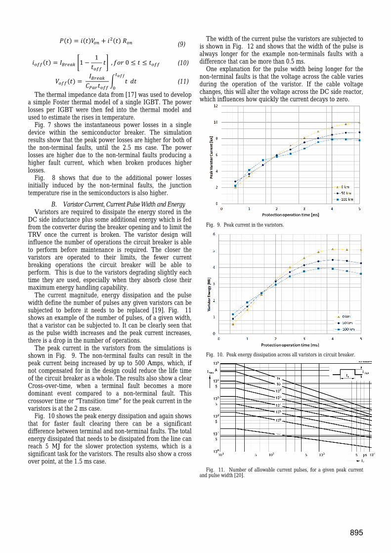
R = PS + TPS (9)
PHH = MNOA U1 − 1PHH V , $%&0 ≤ ≤ PHH
(10)
PHH = MNOAQNPHHW X<< 8
(11)
The thermal impedance data from [17] was used to develop a simple Foster thermal model of a single IGBT. The power losses per IGBT were then fed into the thermal model and used to estimate the rises in temperature.
Fig. 7 shows the instantaneous power losses in a single device within the semiconductor breaker. The simulation results show that the peak power losses are higher for both of the non-terminal faults, until the 2.5 ms case. The power losses are higher due to the non-terminal faults producing a higher fault current, which when broken produces higher losses.
Fig. 8 shows that due to the additional power losses initially induced by the non-terminal faults, the junction temperature rise in the semiconductors is also higher.
B. Varistor Current, Current Pulse Width and Energy Varistors are required to dissipate the energy stored in the
DC side inductance plus some additional energy which is fed from the converter during the breaker opening and to limit the TRV once the current is broken. The varistor design will influence the number of operations the circuit breaker is able to perform before maintenance is required. The closer the varistors are operated to their limits, the fewer current breaking operations the circuit breaker will be able to perform. This is due to the varistors degrading slightly each time they are used, especially when they absorb close their maximum energy handling capability.
The current magnitude, energy dissipation and the pulse width define the number of pulses any given varistors can be subjected to before it needs to be replaced [19]. Fig. 11 shows an example of the number of pulses, of a given width, that a varistor can be subjected to. It can be clearly seen that as the pulse width increases and the peak current increases, there is a drop in the number of operations.
The peak current in the varistors from the simulations is shown in Fig. 9. The non-terminal faults can result in the peak current being increased by up to 500 Amps, which, if not compensated for in the design could reduce the life time of the circuit breaker as a whole. The results also show a clear Cross-over-time, when a terminal fault becomes a more dominant event compared to a non-terminal fault. This crossover time or “Transition time” for the peak current in the varistors is at the 2 ms case.
Fig. 10 shows the peak energy dissipation and again shows that for faster fault clearing there can be a significant difference between terminal and non-terminal faults. The total energy dissipated that needs to be dissipated from the line can reach 5 MJ for the slower protection systems, which is a significant task for the varistors. The results also show a cross over point, at the 1.5 ms case.
The width of the current pulse the varistors are subjected to is shown in Fig. 12 and shows that the width of the pulse is always longer for the example non-terminals faults with a difference that can be more than 0.5 ms.
One explanation for the pulse width being longer for the non-terminal faults is that the voltage across the cable varies during the operation of the varistor. If the cable voltage changes, this will alter the voltage across the DC side reactor, which influences how quickly the current decays to zero.
Fig. 9. Peak current in the varistors.
Fig. 10. Peak energy dissipation across all varistors in circuit breaker.
Fig. 11. Number of allowable current pulses, for a given peak current
and pulse width [20].
895

Fig. 12. Current pulse width against DC protection operating time.
Fig. 13. Product of peak varistor current and pulse width, against the
protection operating time.
Fig. 14. Pole-to-pole cable voltages for a 0 km and 50 km fault.
Fig. 14 shows that the cable voltage transiently becomes negative due to the reflected waves. However as the waves are slowly attenuated, the cable voltages reaches a steady state value above zero.
In terms of longest current pulse, there is no “crossover” point seen in the results, it appears that over the 5 ms range, non-terminals faults always produce a longer current pulse width.
However taking the product of the peak current and the pulse width will allow estimation as to which is the most severe case for the varistor, in terms of how many impulses the varistor can take, and provides a cross over point.
Fig. 13 shows the product of the peak current and pulse time for each case. For this parameter, the cross over point can be seen to be at the 2 ms case again.
From each of these results, there is a clear transition time where the non-terminals present a more severe event than a terminal fault. After this time, it appears that terminal faults become the more severe event. This “transition time” varies depending on the attribute that is being investigated, making it difficult to have a single transition time for any system. More work needs to be done to understand at which distance these effects become most severe and under what conditions they will result in failure of a DC breaker.
VI. DISCUSSION
The results from the simulations show that non-terminal faults are the most serve DC fault event in some cases. Whether a terminal fault or a non-terminal fault is the most severe event, depends on the operating speed of the DC protection system and the design of the transmission system.
While the impact of the traveling wave effect may seem small in some cases, it is important to remember two things. Firstly, this analysis is only for one example system. Changing some of the component choices, design method or the example case may result in a much larger impact. As an example, reducing the DC side inductance would increase the peak currents, which would influence the semiconductor losses, device temperature and energy dissipation greatly.
For fast DC protection it is likely that the DC side inductors will be reduced, resulting in much higher currents. Consideration must be given to the influence of the cable voltage on the design of key elements within a fast HVDC circuit breaker.
Secondly, present thinking would hitherto develop a testing schedule based around the concept of a terminal fault being the worst case. Hence all standards and testing would be geared towards testing for such an event. The impact of the cable voltage reversal must be compared relative to the terminal fault for each case, as this the “bench mark” of traditional thinking. If it can be shown that there is no significant difference in all cases, then then testing can move forward based on the worst case being a terminal fault.
The results also show some of the benefits that can be gained by having fast HVDC protection. A reduction in magnitude of the peak current, power losses or varistor energy rating will be translated into a cost saving, as few devices or lower rated devices can be used in the construction of the breaker.
Faster DC protection also reduces the difference between peak transient currents and nominal currents. This will allow
896

a reduction in equipment rating elsewhere in the DC grid, giving further savings.
VII. CONCLUSIONS
Traditionally, the worst case fault has always been considered that which is closest to the source of energy. For HVDC applications this translates to a fault at the terminals of the converter, or “terminal fault”. However, due to the very fast operating times of HVDC protection, this may not be the case.
This paper has shown that for semiconductors in series with the DC line, non-terminal faults can induce:
• Higher fault currents. • Higher power losses. • Larger changes in device temperatures. • Higher energy requirements for varistors. • Longer current pulse width in varistors.
The simplified analysis shows that non-terminal faults, i.e
faults that occur at some distance from the converter, produce fault currents with the highest initial rate of rise of fault current. The rate of change of fault current is theoretically limited to be twice the maximum rate of change for a terminal fault current.
Whether or not the traveling waves have an impact on the testing philosophy is dependent on the operating time of the protection system and the design of the VSC transmission system.
The time at which the non-terminal fault presents a more severe event than a terminal event, is dependent on the:
• Variable in question. • DC protection operation speed. • Design of the VSC transmission system. • Technology capability.
As HVDC circuit breakers are likely to be more complex
than just a fast mechanical switch, understanding the technology within each of the breakers is important. For each device within the breaker, understanding the power system conditions that present the worst case scenario for any specific device within the circuit breaker is of fundamental importance.
ACKNOWLEDGEMENTS
The Authors would like to thank National Grid for their assistance in developing this work under project TAO/22360, with special thanks to Paul Coventry.
REFERENCES
[1] R. Derakhanfar, T. U. Jonsson, U. Steiger, and M. Habert, "Hybrid HVDC Circuit Breaker - A solution for future HVDC system," presented at Cigre Paris, 2014.
[2] J. P. Dupraz and D. L. Penache, "Development of a 120 kV direct current circuit breaker," presented at Cigre Paris, 2014.
[3] T. Eriksson, M. Backman, S. Halén, and A. C. Research, "A low loss mechanical HVDC breaker for HVDC grid applications," presented at Cigré Paris, 2014.
[4] N. Grid, "National Electricity Transmission System and Security and Quaility of Supply Standard - Version 2.2," ed, 2012.
[5] C. D. Barker, R. S. Whitehouse, A. G. Adamczyk, and M. Boden, "Designing fault tolerant HVDC networks with a limited need for HVDC circuit breaker operation," presented at Cigre, Paris, 2014.
[6] C-EPRI. (2015). SGRI launches world’s first 200kV DC Circuit Breaker. Available: http://www.cepri.com.cn/release/details_66_721.html
[7] C. Meyer, M. Kowal, and R. W. De Doncker, "Circuit breaker concepts for future high-power DC-applications," in Industry Applications Conference. Fourtieth IAS Annual Meeting., 2005, pp. 860-866 Vol. 2.
[8] J. M. Meyer and A. Rufer, "A DC hybrid circuit breaker with ultra-fast contact opening and integrated gate-commutated thyristors (IGCTs)," IEEE Transactions on Power Delivery, vol. 21, pp. 646-651, 2006.
[9] M. Callavik and A. Blomberg, The Hybrid HVDC Breaker: ABB Grid Systems, 2012.
[10] B. Bachmann, G. Mauthe, E. Ruoss, H. P. Lips, J. Porter, and J. Vithayathil, "Development of a 500 kV Airblast HVDC Circuit Breaker," IEEE Transactions on Power Apparatus and Systems, vol. PAS-104, pp. 2460-2466, 1985.
[11] K. A. Corzine and R. W. Ashton, "Structure and analysis of the Z-source MVDC breaker," in Electric Ship Technologies Symposium (ESTS), IEEE, 2011, pp. 334-338.
[12] Y. W. R. Marquardt., "Future HVDC-Grids employing Modular Multilevel Converters and Hybrid DC-Breakers," IEEE, vol. EPE'13 ECCE Europe, 2013.
[13] B. Xiang, Z. Liu, Y. Geng, and S. Yanabu, "DC Circuit Breaker Using Superconductor for Current Limiting," IEEE Transactions on Applied Superconductivity, vol. 25.2, pp. 1-7, 2015.
[14] B. Chang, O. Cwikowski, R. Shuttleworth, and M. Barnes, "Point-to-point Two-level Converter System Faults Analysis," presented at IET PEMD Manchester, 2014.
[15] "National Grid - Offshore Development Information Statement," ed: National Grid, 2010.
[16] A. Beddard and M. Barnes, "HVDC Cable Modelling for VSC-HVDC Systems," Washington DC, IEEE PES GM Conference, 2014.
[17] ABB. (2013). 5SNA 2000K450300 IGBT Datasheet. Available: http://www05.abb.com/global/scot/scot256.nsf/veritydisplay/6e6983faa83cded383257b4a00515559/$file/5SNA%202000K450300%205SYA%201431-00%2003-2013.pdf
[18] D. v. Hertem, K. Linden, J.-P. Taisne, W. Grieshaber, and D. Jovcic, Feasibility of DC transmission Networks. Aberdeen, 2011.
[19] B. Williams, "Power Electronics - Chapter 10," pp. 405-408.
[20] EPCOS, "DateSheet: EPCOS SIOV Metal Oxide Varistors," ed, 2011, p. 18.
897