Synthesis, Structural, Electrical, Magnetic and Dielectric Spectroscopic Characterization of...
15
Synthesis, structural, electrical, magnetic and dielectric spectroscopic characterization of C-Er 2 Si 2 O 7 Shahid Ameer, Ahmad Faraz*, Asghari Maqsood, Nasir M. Ahmad Thermal Transport Laboratory, School of Chemical and Materials Engineering (SCME), National University of Sciences and Technology (NUST), H-12, Islamabad, Pakistan. Cell: +92-333-9319316, Email: [email protected] Keywords: electronic materials, X-ray diffraction, dielectric properties, electrical properties, magnetic parameters, saturation magnetization (Ms), remanance (Mr) Abstract The polymorphic Er 2 Si 2 O 7 is synthesized by solid state double sintering method. Structural and morphological characterizations have been performed using X-ray diffraction (XRD) and scanning electron microscopy (SEM). The electrical characterization has been performed by two probe method as a function of temperature. The dielectric spectroscopic measurements of polymorphic Er 2 Si 2 O 7 are performed in the temperature range 300-555 K and frequency range 3 kHz to 1 MHz. The dc electrical transport data are analyzed according to Mott’s variable-range hopping. The ac conductivity σ ac (ω) is obtained through the dielectric spectroscopic measurements. The ac conductivity obeys power law which can be expressed as σ ac (ω) = B ω s , where s is slope and it determines the ac electrical transport phenomenon. The ac electrical transport data and its variation with temperature in this rare earth formulation are well discussed. The magnetic behavior of synthesized material is analyzed and confirmed that material have non-magnetic behavior with coercivity (Hc) 842 Oe. While the values of magnetic saturation (MS) and remanace (Mr) were found in range 3.90emu/g and 1.07emu/g. 1. Introduction The compound containing rare earth materials specially their silicates are promising materials for future microelectronics because of their high dielectric constant and low losses as a replacement for traditional SiON/poly-Si electrodes. Modern solid state technology has recently made use of rare earth compounds in microwave devices, semiconductors, ferromagnetic, ferroelectric, laser and phosphors. Dielectric phenomenon in rare earth containing materials has been recently extensively studied [1]. Currently the dielectric spectroscopic measurements have been performed and charge transport mechanisms are analyzed by many authors [2, 3] for various rare earth formulations. Journal of Nano Research Vol. 17 (2012) pp 85-98 Online available since 2012/Feb/03 at www.scientific.net © (2012) Trans Tech Publications, Switzerland doi:10.4028/www.scientific.net/JNanoR.17.85 All rights reserved. No part of contents of this paper may be reproduced or transmitted in any form or by any means without the written permission of TTP, www.ttp.net. (ID: 119.154.40.173-09/03/12,15:01:42)
Transcript of Synthesis, Structural, Electrical, Magnetic and Dielectric Spectroscopic Characterization of...

Synthesis, structural, electrical, magnetic and dielectric spectroscopic
characterization of C-Er2Si2O7
Shahid Ameer, Ahmad Faraz*, Asghari Maqsood, Nasir M. Ahmad
Thermal Transport Laboratory, School of Chemical and Materials Engineering (SCME), National
University of Sciences and Technology (NUST), H-12, Islamabad, Pakistan.
Cell: +92-333-9319316, Email: [email protected]
Keywords: electronic materials, X-ray diffraction, dielectric properties, electrical properties, magnetic parameters, saturation magnetization (Ms), remanance (Mr)
Abstract
The polymorphic Er2Si2O7 is synthesized by solid state double sintering method. Structural
and morphological characterizations have been performed using X-ray diffraction (XRD) and
scanning electron microscopy (SEM). The electrical characterization has been performed by two
probe method as a function of temperature. The dielectric spectroscopic measurements of
polymorphic Er2Si2O7 are performed in the temperature range 300-555 K and frequency range 3
kHz to 1 MHz. The dc electrical transport data are analyzed according to Mott’s variable-range
hopping. The ac conductivity σac(ω) is obtained through the dielectric spectroscopic measurements.
The ac conductivity obeys power law which can be expressed as σac (ω) = B ωs, where s is slope
and it determines the ac electrical transport phenomenon. The ac electrical transport data and its
variation with temperature in this rare earth formulation are well discussed. The magnetic behavior
of synthesized material is analyzed and confirmed that material have non-magnetic behavior with
coercivity (Hc) 842 Oe. While the values of magnetic saturation (MS) and remanace (Mr) were
found in range 3.90emu/g and 1.07emu/g.
1. Introduction
The compound containing rare earth materials specially their silicates are promising
materials for future microelectronics because of their high dielectric constant and low losses as a
replacement for traditional SiON/poly-Si electrodes. Modern solid state technology has recently
made use of rare earth compounds in microwave devices, semiconductors, ferromagnetic,
ferroelectric, laser and phosphors. Dielectric phenomenon in rare earth containing materials has
been recently extensively studied [1]. Currently the dielectric spectroscopic measurements have
been performed and charge transport mechanisms are analyzed by many authors [2, 3] for various
rare earth formulations.
Journal of Nano Research Vol. 17 (2012) pp 85-98Online available since 2012/Feb/03 at www.scientific.net© (2012) Trans Tech Publications, Switzerlanddoi:10.4028/www.scientific.net/JNanoR.17.85
All rights reserved. No part of contents of this paper may be reproduced or transmitted in any form or by any means without the written permission of TTP,www.ttp.net. (ID: 119.154.40.173-09/03/12,15:01:42)

Worldwide, the researchers are analyzing various rare earth formulations specially their oxides and
silicates for transistor scaling as being high dielectric materials for 22nm node and beyond [4]. The
unique properties of this group of compounds, which also include rare-earth silicates/disilicates, are
due to their special 4fn electronic states and the general shielding of these orbitals by higher orbitals
in the rare earth ions [5].
The compound Er2Si2O7 exists in three polymorphs, the low temperature polymorph (type B),
monoclinic (type C) and the high temperature monoclinic modification (type D). The preparation of
this material in the form of both poly- and single crystals has been reported by Maqsood et al [6].
The material was characterized by X-ray diffraction. The lattice constants and possible space groups
were determined by the same authors [7-9]. This paper describes the synthesis, electrical, magnetic
and dielectric characterization of C-Er2Si2O7. The ac electrical parameters are also calculated from
the data of dielectric parameters as a function of both frequency and temperature. The dc electrical
conductivity in the temperature range 410-540 K and ac electrical conductivity as a function of
frequency and temperature in the range 300-555 K and magnetic parameters (Hc, Mr, Ms) are
reported.
2. Experimental procedure
The material was prepared by solid state reaction method. Precursors taken were 99.9 %
Er2O3, BDH silica gel of 60-120 mesh. The SiO2, containing 12 wt % of H2O was calcined at 1000º
C and then kept in a desiccators. The composition calculated from the formula was well mixed and
heated at 1450º C for 24 hours and then kept at this temperature for 24 hours. After that the furnace
was switched off. On cooling, the material was remixed thoroughly and the same process was
repeated. Structural and morphological investigations are achieved by X-ray powder diffraction
(XRD) and Scanning electron microscopy (SEM).
For resistivity measurement, the powder was compacted into pellets of approximately 13
mm in diameter and of thickness of 4.5 mm. Because of very high resistivity of C-Er2Si2O7 at room
temperature, a two probe method was used to measure the dc electrical resistivity. For dielectric
measurements, Wayne Kerr 6500B Impedance analyzer was used to check the response of C-
Er2Si2O7 in the frequency domain. All the measurements were done in a temperature controlled
furnace, and the temperature accuracy is within 2K. The ac electrical conductivity (σac) was
calculated from the dielectric parameters as a function of frequency at different temperatures.
Magnetic parameters Hc, Ms and Mr are analyzed using VSM (BHV-50, Riken Denshi Co. Ltd.
Japan).
86 Journal of Nano Research Vol. 17
3. Results and discussion
3.1 Structural investigation
The x-ray diffraction for C-Er2Si2O7 in powder identifies that the bulk sample be the
polycrystalline nature. Results are analyzed with card No. ASTM 82-0733 and it proves that the
resulted structure is the C-phase of Er2Si2O7 with lattice constants in agreement with previous
reports [6] as shown in Fig. 1. The high temperature polymorph forms a monoclinic structure with
lattice constants, a = 6.849 Å, b= 8.939 Å and c = 4.722 Å, β = 101.8. Scanning electron
microscopy shows the morphology of particle as shown in Fig. 2 (a) .Fig. 2 (b) shows the EDX
compositional analysis which confirms that the resulting Er : Si ratio was 7 : 1 in agreement with
the composition.
20 40 60 800
1000
2000
3000
4000
5000
Intensity (a.u.)
2 θ θ θ θ values
(021)
(201)
(130)(220)(131)
(221)
(222)(132)(200)
(111)
(331)(133) (530)
Fig. 1: X-ray diffraction pattern of C-Er2Si2O7.
Journal of Nano Research Vol. 17 87

Fig. 2(a): SEM Micrograph of C-Er2Si2O7.
Fig. 2(b): EDX analysis of C-Er2Si2O7.
3.2 DC electrical properties
The dc electrical conductivity of C-Er2Si2O7 is measured as a function of temperature in the
range 410-540 K. The dc electrical conductivity of C-Er2Si2O7 follows a semiconductor like
behavior, expressed by the relation [10]:
88 Journal of Nano Research Vol. 17

σdc=σ0exp (-∆E/kBT). (1)
Where σ0 is the pre-exponential factor, kB is the Boltzmann constant and ∆E is the activation energy
for the conduction process. In order to calculate the activation energy, ln σdc vs 1/kBT was plotted
and corresponding slope provided the activation energy as shown in Fig. 3. The electrical
conductivity measured at room temperature is 1.7 × 10⁻⁵ S/m and also the activation energy for
conduction process comes out to be 0.367 ± 0.02 eV.
The parameter σ0 as indicated in Eq. 1 is an indication of conduction path that whether the
conduction is caused by the extended states or localized states [11]. For extended state path of
conduction, σ0 should be within the range 103-104 S/cm [12] and σ0 should have a smaller value for
conduction through localized states. In case of C-Er2Si2O7, the value of pre-exponential factor σ0 is
10-3 S/cm, which is fairly small. This small value of σ0 is a confirmation of fact that the hopping of
charge carriers between localized states is responsible for conduction. Another confirmation
towards the hopping of charge carrier can be obtained by the small value of activation energy [13],
which in this case is 0.367 eV for C-Er2Si2O7.
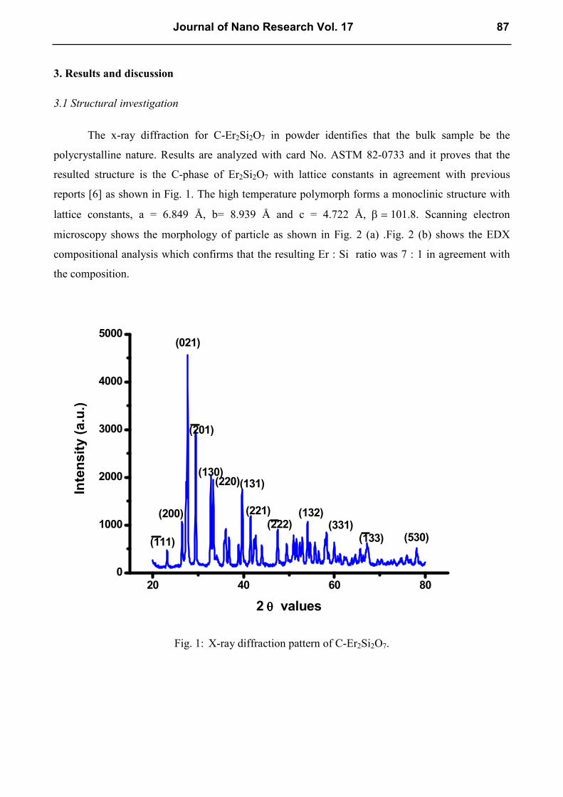
It is further assumed that Mott’s Variable Range Hopping (VRH) mechanism is the criteria for the
conduction, which can be expressed as [14, 15]:
σ = σoexp{- (To/T) 1/4} (2)
where To being the degree of disorder, given by To= λα3/ {kBN(EF)}, N(EF) is the density of states
at fermi level, λ is a dimensionless constant of about 16 [15,16] and α has a value of 107cm-1. Fig. 4
is the graphical form of Mott VRH plot as expressed by Eq. 2. The hopping distance (R) and
average hopping energy (Wdc) are calculated using the relations below as a function of temperature
[15], and are shown in Table 1.
R={9/(8παkBTN(EF)}0.25. (3)
Wdc=3/(4πR3N(EF)). (4)
There are two necessary conditions for applying Mott’s VRH mechanism, which can be
expressed as [14]
(i) average hopping energy must be greater than thermal energy (i.e. Wdc > kBT ) and
(ii) αR > 1
Here both the conditions are satisfied. Values of R and Wdc are shown in Table 1.
Journal of Nano Research Vol. 17 89

Table 1: Parameters of Mott’s VRH mechanism at 410-540 K. To = 8.2×10⁸ K and
N (EF) = 2.2x10¹⁷ eV-1cm-3.
Temperature (K) R dc(nm) W dc(meV)
413 14.5 344
433 14.3 357
453 14.1 369
473 14.0 381
493 13.8 393
513 13.7 405
533 13.6 417
Fig. 3: Arrhenius plot for C-Er2Si2O7.
90 Journal of Nano Research Vol. 17
Fig. 4: Mott’s VRH plot.
3.3 Dielectric properties
Fig. 5 shows the variation of dielectric constant (ε′) with the frequency in the temperature
range 300-555 K. The range of frequency used was 3 kHz – 1 MHz. This decreasing trend of
dielectric constant with the frequency is because of the fact that the dielectric constant is explained
by a contribution to polarzibility from various factors like deformational (electronic and ionic) as
well as relaxation (orientation and interfacial modes) polarization. Upon increasing frequency,
orientation mode of polarization decreases as it requires more time than ionic and electronic mode
of polarization. This causes the dielectric constant to decreases with increasing frequency and
reaching a almost constant value at higher frequency because of only interfacial polarization. The
value of dielectric constant increases with increase in temperature showing that the relaxation
frequency of the dispersion increases with rising temperature. Also orientation mode of polarization
is associated with the motion of molecules initiated by thermal energy, so the diploes are unable to
orient themselves at sufficiently low temperature [17]. When the temperature increases, it provides
enough thermal energy for facilitation of orientation polarization and consequently dielectric
constant increases.
Journal of Nano Research Vol. 17 91

Variation of dielectric loss with frequency follows a power law expressed by relation below:
ε′′ = Aωm (5)
where A being a constant. Inset in Fig. 5 shows the graphical representation of power law
expressed by Eq. 5. This plot provides us the value of frequency coefficient of dielectric loss ‘ m’
by the slope of plot. The m values variation with temperature are also shown as inset in Fig. 7. The
m values can also be expressed by famous Guintini relation [18] as:
m=4kBT/wM (6)
where wM being the maximum barrier height and other variables have their usual meanings. The
maximum barrier height height wM calculated for C-Er2Si2O7 comes out to be 0.068 eV.
The increase of dielectric loss with temperature has been explained by Stevels [19] who categorized
the relaxation into three types, conduction losses, dipole losses and viberational losses. At lower
temperature, conduction losses are minimum because they are proportional to {σac(ω) /ω)}. As the
temperature increases, the ac conductivity {σac(ω)} increases and so the conduction losses also
increases, which is the reason of increasing dielectric loss with increasing temperature.
The ac electrical conductivity dependence on frequency can be expressed as:
σtotal(ω)=σdc+σac(ω). (7)
Where σ total(ω) represents the total electrical conductivity at any particular angular frequency (ω)
and at any certain temperature, σdc is the dc conductivity. The dependence of ac electrical
conductivity upon frequency of applied signal can be expressed by a power law expressed below:
σac(ω)=Bωs. (8)
where B is as pre exponential factor and s is the frequency exponent [15, 20-22] which is generally
less than or equal to unity and it defines the degree of interaction between mobile ions and its
surrounding lattices .The pre-factor B is the measure of strength of polarization [23]. It is also
important to mention that the magnitude of ac conductivity (BωS) is slightly greater than the dc
conductivity. Fig. 6 shows the frequency dependence of ac electrical conductivity in the
temperature range 300-555 K. It is evident from Fig. 6 that ac electrical conductivity, σac (ω), almost
increases linearly with the increase in temperature. The increase of σac (ω) with increasing
frequency suggests that hopping of charge carriers is responsible for conduction and that the
increasing of the frequency of applied field enhances the jumping of charge carriers between the
different localized states and reduces the activation energy of doing so.
92 Journal of Nano Research Vol. 17

It is also a well known fact that, the relation σ = σ0 exp (-∆E/ kB T) is indicative of the fact that the
mobile charge carriers are thermally activated by ∆E. The activation energies of conduction,
calculated at various frequencies are listed in Table 2. The values of ac activation energies are much
less than that of the dc activation energies in the entire temperature range. The difference is due to
fact that the charge carriers in dc conduction always chooses the easiest path available which may
sometime include some large jumps, while this is not much important in ac conduction process [24].
It is clear from the Table 2 that ∆E decreases with increasing frequency as found for other materials
[25]. It is because the increase of frequency facilitates the electronic jumping between different
localized states, consequently activation energy decreases with increasing frequency.
Table 2: The ac electronic parameters of C-Er2Si2O7 at different frequencies.
Parameters
∆E (eV)
100 kHz
0.213
200 kHz
0.183
400 kHz
0.154
600 kHz
0.009
800 kHz
0.006
σ 300 (10-7
S/m) 1.38 2.14 38 4.8 63
Table 3: Different parameters of CBH model at 50 KHz; calculated value of U is 0.17eV along with W Loss
Temperature (K) R min (nm) N (eV-1
- cm-3
) W Loss (mwatt)
300 1.42 1.04 x 10¹⁹ 1.49
450 1.30 2.91 x 10¹⁹ 7.38
480 1.28 3.62 x10¹⁹ 1.05
530 1.21 5.16 x10¹⁹ 1.62
555 1.12 7.85 x 10¹⁹ 2.55
The temperature dependence of s is shown in Fig. 7. The values of s decreases with the
increase in temperature. It is well known that the power law (BωS) is generally obeyed with the
values s ≈ 0.7 at room temperature, and the classically accepted range of s lies between 0.6 < s < 1
is likely to be associated with the presence of hopping conduction [26, 27]. In nutshell, firstly the
discrepancy between the values of ac and dc activation energies secondly the smaller values of
activation energy lastly the increase of ac conductivity {σac (ω)} with increase of frequency
confirms the presence of hopping conduction be the responsible for conduction.
In order to explain the temperature and frequency variation of ac electrical conductivity,
there are models for conduction, whose identification is achieved by the frequency coefficient s and
its temperature dependence [28-30]. There are two main types of models named the quantum
mechanical tunneling model [31, 32] and classical hopping model [33, 34]. The classical hopping
over a barrier (HOB) model [32] suggests the values of s equal to unity which does not agree with
Journal of Nano Research Vol. 17 93
our experimental results (s ≈ 0.75). So we propose the correlated barrier hopping (CBH) model to
explain experimental observed conductivity behavior. In this model, conduction occurs by means of
hopping of electrons over a coulomb barrier separating two equilibrium states. A coulomb
correlation can be made between these states, which results in correlation between relaxation
variable, U, of coulomb barrier and distance between states, R. This model, first developed by Pike
[35] for single electron hopping, has been modified by Elliot [27] for simultaneous two electron
hopping. According to CBH model, value of s should be from 0.7 to 1 at room temperature and
should decrease with increasing temperature. This agrees well with our results (s ≈ 0.75) and
thermal variation as shown in Table 3.
In the CBH model, electrons in charged defect centers jump over coulomb barrier of height
U expressed by:
U = wM- (8e2/ε′R). (9)
where wM is the maximum barrier height and others have usual meaning. From Eq. 9, U comes out
to be equal to wM as other factors are negligibly small. The ac conductivity is expressed as [31]:
σac(ω) = π�
�� N2ε′εo R
6 (10)
where N is density of a pair of sites and R is expressed as:
R = e2/ [π ε′εo{wM-kBTln (1/ωτ0 )}] (11)
The lower bound (cut off) to R is given by:
Rmin = e2/ π ε′εowM (12)
The temperature dependence of frequency exponent in this model is evaluated to be:
s = (1-6kBT) / [wM-kBTln (1/ωτ0)] (13)
A first approximation to Eq. 13 gives:
s = (1-6kBT) / wM (14)
In ac fields the energy loss per unit volume per unit time may be expressed as :
WLoss = (ωεoE2
ε′′) / (8 π) (15)
Where ω is the angular frequency and E is the ac field [36]. The values of energy loss calculated at
different temperatures are tabulated in Table 3.
94 Journal of Nano Research Vol. 17
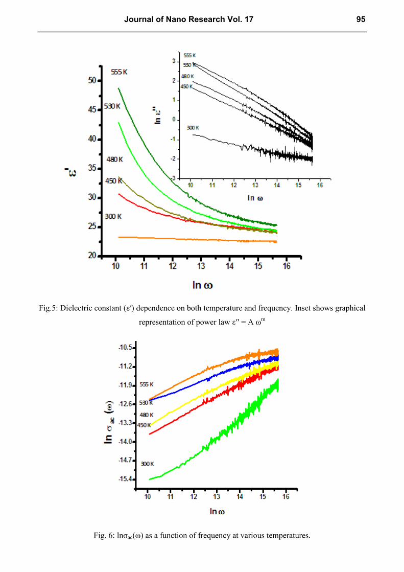
Fig.5: Dielectric constant (ε′) dependence on both temperature and frequency. Inset shows graphical
representation of power law ε′′ = A ωm
Fig. 6: lnσac(ω) as a function of frequency at various temperatures.
Journal of Nano Research Vol. 17 95

Fig. 7: Variation of parameters‘s’ and ‘m’ with temperature.
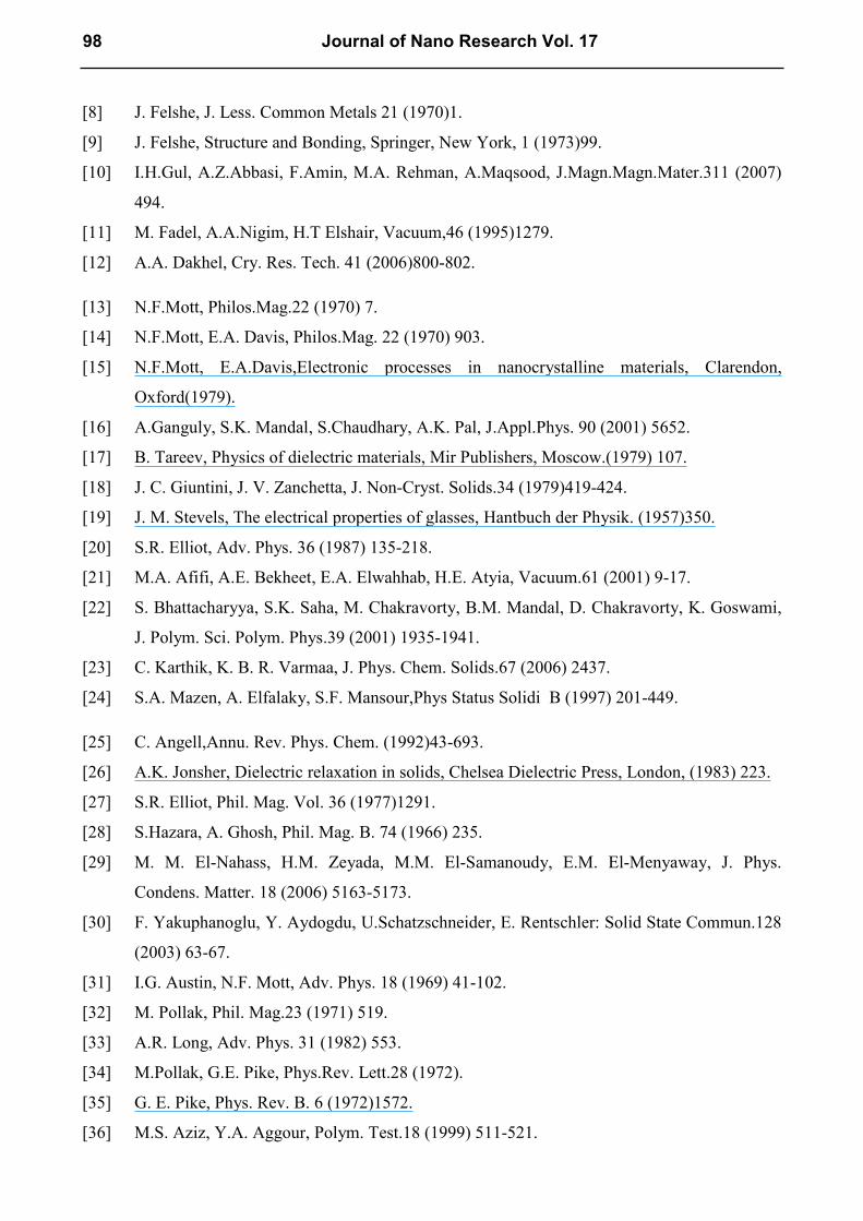
3.3. Magnetic Studies
The magnetic studies are performed using vibrating samples magnetometer (VSM).The magnetic
nature of synthesized sample is revealed from magnetic hysteresis loop. Fig 7 represents hysteresis
loops of synthesized material confirmed non-magnetic nature of synthesized material. Magnetic
saturation (MS) and remanance (Mr) are calculated from hysteresis loop with values found in range
3.90emu/g and 1.07emu/g.The higher coercive force value 842 Oe further confirmed the non-
magnetic behavior of fabricated material. The value of squerence ratio (Mr/Ms) is found in range
0.27.
96 Journal of Nano Research Vol. 17
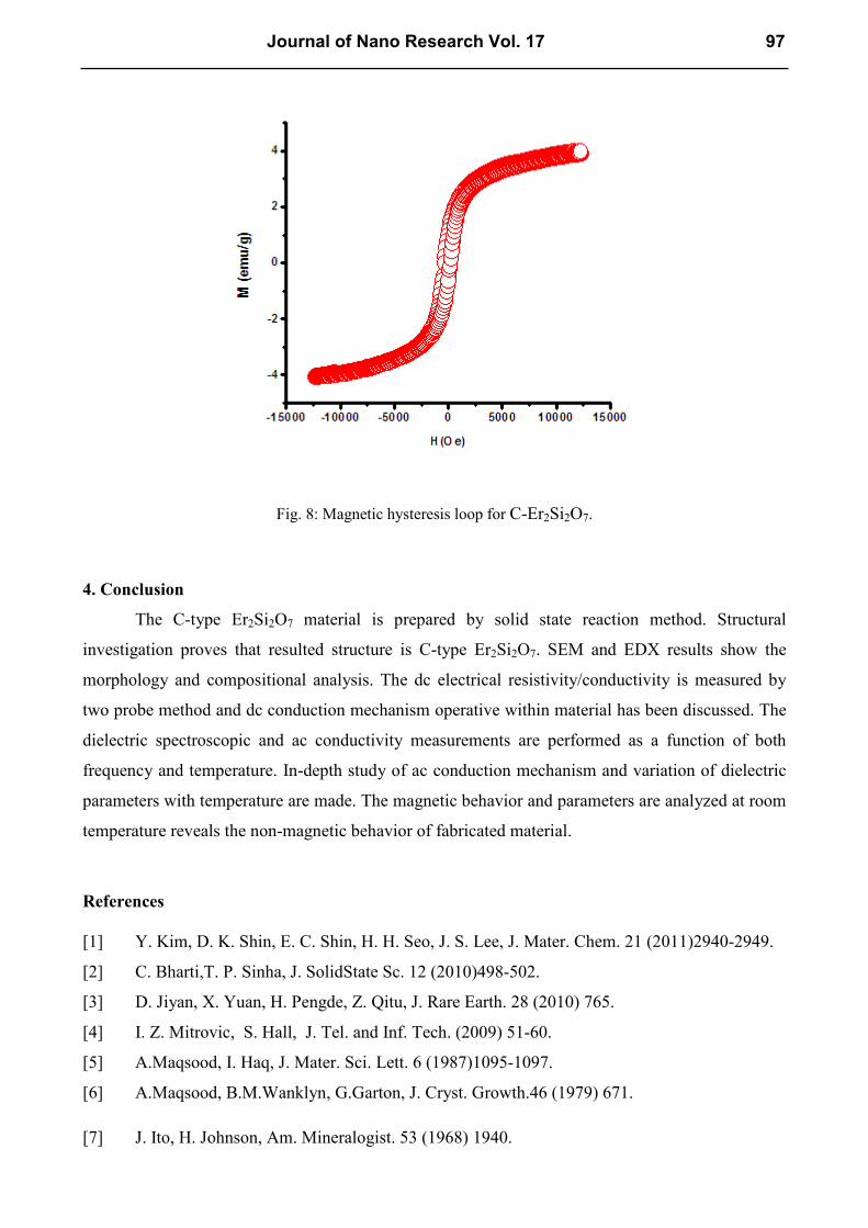
Fig. 8: Magnetic hysteresis loop for C-Er2Si2O7.
4. Conclusion
The C-type Er2Si2O7 material is prepared by solid state reaction method. Structural
investigation proves that resulted structure is C-type Er2Si2O7. SEM and EDX results show the
morphology and compositional analysis. The dc electrical resistivity/conductivity is measured by
two probe method and dc conduction mechanism operative within material has been discussed. The
dielectric spectroscopic and ac conductivity measurements are performed as a function of both
frequency and temperature. In-depth study of ac conduction mechanism and variation of dielectric
parameters with temperature are made. The magnetic behavior and parameters are analyzed at room
temperature reveals the non-magnetic behavior of fabricated material.
References
[1] Y. Kim, D. K. Shin, E. C. Shin, H. H. Seo, J. S. Lee, J. Mater. Chem. 21 (2011)2940-2949.
[2] C. Bharti,T. P. Sinha, J. SolidState Sc. 12 (2010)498-502.
[3] D. Jiyan, X. Yuan, H. Pengde, Z. Qitu, J. Rare Earth. 28 (2010) 765.
[4] I. Z. Mitrovic, S. Hall, J. Tel. and Inf. Tech. (2009) 51-60.
[5] A.Maqsood, I. Haq, J. Mater. Sci. Lett. 6 (1987)1095-1097.
[6] A.Maqsood, B.M.Wanklyn, G.Garton, J. Cryst. Growth.46 (1979) 671.
[7] J. Ito, H. Johnson, Am. Mineralogist. 53 (1968) 1940.
Journal of Nano Research Vol. 17 97
[8] J. Felshe, J. Less. Common Metals 21 (1970)1.
[9] J. Felshe, Structure and Bonding, Springer, New York, 1 (1973)99.
[10] I.H.Gul, A.Z.Abbasi, F.Amin, M.A. Rehman, A.Maqsood, J.Magn.Magn.Mater.311 (2007)
494.
[11] M. Fadel, A.A.Nigim, H.T Elshair, Vacuum,46 (1995)1279.
[12] A.A. Dakhel, Cry. Res. Tech. 41 (2006)800-802.
[13] N.F.Mott, Philos.Mag.22 (1970) 7.
[14] N.F.Mott, E.A. Davis, Philos.Mag. 22 (1970) 903.
[15] N.F.Mott, E.A.Davis,Electronic processes in nanocrystalline materials, Clarendon,
Oxford(1979).
[16] A.Ganguly, S.K. Mandal, S.Chaudhary, A.K. Pal, J.Appl.Phys. 90 (2001) 5652.
[17] B. Tareev, Physics of dielectric materials, Mir Publishers, Moscow.(1979) 107.
[18] J. C. Giuntini, J. V. Zanchetta, J. Non-Cryst. Solids.34 (1979)419-424.
[19] J. M. Stevels, The electrical properties of glasses, Hantbuch der Physik. (1957)350.
[20] S.R. Elliot, Adv. Phys. 36 (1987) 135-218.
[21] M.A. Afifi, A.E. Bekheet, E.A. Elwahhab, H.E. Atyia, Vacuum.61 (2001) 9-17.
[22] S. Bhattacharyya, S.K. Saha, M. Chakravorty, B.M. Mandal, D. Chakravorty, K. Goswami,
J. Polym. Sci. Polym. Phys.39 (2001) 1935-1941.
[23] C. Karthik, K. B. R. Varmaa, J. Phys. Chem. Solids.67 (2006) 2437.
[24] S.A. Mazen, A. Elfalaky, S.F. Mansour,Phys Status Solidi B (1997) 201-449.
[25] C. Angell,Annu. Rev. Phys. Chem. (1992)43-693.
[26] A.K. Jonsher, Dielectric relaxation in solids, Chelsea Dielectric Press, London, (1983) 223.
[27] S.R. Elliot, Phil. Mag. Vol. 36 (1977)1291.
[28] S.Hazara, A. Ghosh, Phil. Mag. B. 74 (1966) 235.
[29] M. M. El-Nahass, H.M. Zeyada, M.M. El-Samanoudy, E.M. El-Menyaway, J. Phys.
Condens. Matter. 18 (2006) 5163-5173.
[30] F. Yakuphanoglu, Y. Aydogdu, U.Schatzschneider, E. Rentschler: Solid State Commun.128
(2003) 63-67.
[31] I.G. Austin, N.F. Mott, Adv. Phys. 18 (1969) 41-102.
[32] M. Pollak, Phil. Mag.23 (1971) 519.
[33] A.R. Long, Adv. Phys. 31 (1982) 553.
[34] M.Pollak, G.E. Pike, Phys.Rev. Lett.28 (1972).
[35] G. E. Pike, Phys. Rev. B. 6 (1972)1572.
[36] M.S. Aziz, Y.A. Aggour, Polym. Test.18 (1999) 511-521.
98 Journal of Nano Research Vol. 17

Journal of Nano Research Vol. 17 10.4028/www.scientific.net/JNanoR.17
Synthesis, Structural, Electrical, Magnetic and Dielectric SpectroscopicCharacterization of C-Er<sub>2</sub>Si<sub>2</sub>O<sub>7</sub>
10.4028/www.scientific.net/JNanoR.17.85
![Structural, dielectric, and ferroelectric properties of compositionally graded (Pb,La)TiO[sub 3] thin films with conductive LaNiO[sub 3] bottom electrodes](https://static.fdokumen.com/doc/165x107/633e60cf311de04f4d03b0af/structural-dielectric-and-ferroelectric-properties-of-compositionally-graded-pblatiosub.jpg)


![Small anisotropy, weak thermal fluctuations, and high field superconductivity in Co-doped iron pnictide Ba(Fe[sub 1−x]Co[sub x])[sub 2]As[sub 2]](https://static.fdokumen.com/doc/165x107/633cc1de7000aa173d0630af/small-anisotropy-weak-thermal-fluctuations-and-high-field-superconductivity-in.jpg)

![Structure and strain relaxation mechanisms of ultrathin epitaxial Pr[sub 2]O[sub 3] films on Si(111)](https://static.fdokumen.com/doc/165x107/633f80a8f43ed5a83d02c492/structure-and-strain-relaxation-mechanisms-of-ultrathin-epitaxial-prsub-2osub.jpg)
![Investigation of InP etching mechanisms in a Cl[sub 2]/H[sub 2] inductively coupled plasma by optical emission spectroscopy](https://static.fdokumen.com/doc/165x107/6341a38bfb2d3e0a380c77e8/investigation-of-inp-etching-mechanisms-in-a-clsub-2hsub-2-inductively-coupled.jpg)
![Magnetically frustrated behavior in multiferroics RMn[sub 2]O[sub 5] (R=Bi, Eu, and Dy): A Raman scattering study](https://static.fdokumen.com/doc/165x107/6337955c7dc7407a2703d6e6/magnetically-frustrated-behavior-in-multiferroics-rmnsub-2osub-5-rbi-eu.jpg)


![Field dependent alternating current susceptibility of metalorganically deposited YBa[sub 2]Cu[sub 3]O[sub 7−δ] films](https://static.fdokumen.com/doc/165x107/6336a344b5f91cb18a0beaa7/field-dependent-alternating-current-susceptibility-of-metalorganically-deposited.jpg)
![Optical spectroscopic analyses of OH incorporation into SiO[sub 2] films deposited from O[sub 2]/tetraethoxysilane plasmas](https://static.fdokumen.com/doc/165x107/6345705d38eecfb33a068f14/optical-spectroscopic-analyses-of-oh-incorporation-into-siosub-2-films-deposited.jpg)
![Probing molecular symmetry effects in the ionization of N[sub 2] and O[sub 2] by intense laser fields](https://static.fdokumen.com/doc/165x107/6337c3fed102fae1b6078809/probing-molecular-symmetry-effects-in-the-ionization-of-nsub-2-and-osub-2-by.jpg)

