Synthesis and Characterization of Pristine and Doped (Ti and ...
147
Synthesis and Characterization of Pristine and Doped (Ti and Cr) AlN Thin Films By Padmalochan Panda (Enrolment No. PHYS 02 2013 04 006 ) Indira Gandhi Centre for Atomic Research, Kalpakkam, India. A thesis submitted to the Board of Studies in Physical Sciences in partial fulfillment of requirements for the Degree of DOCTOR OF PHILOSOPHY of HOMI BHABHA NATIONAL INSTITUTE July, 2019
-
Upload
khangminh22 -
Category
Documents
-
view
8 -
download
0
Transcript of Synthesis and Characterization of Pristine and Doped (Ti and ...

Synthesis and Characterization of Pristine andDoped (Ti and Cr) AlN Thin Films
By
Padmalochan Panda
(Enrolment No. PHYS 02 2013 04 006 )
Indira Gandhi Centre for Atomic Research, Kalpakkam, India.
A thesis submitted to the
Board of Studies in Physical Sciences
in partial fulfillment of requirements
for the Degree of
DOCTOR OF PHILOSOPHY
of
HOMI BHABHA NATIONAL INSTITUTE
July, 2019

ii


List of Publications
(a) Journals:
1. Padmalochan Panda, R. Ramaseshan, N. Ravi, G. Mangamma, Feby Jose, S.
Dash, K. Suzuki and H. Suematsu,“Reduction of residual stress in AlN films synthe-
sized by magnetron sputtering technique”, Materials Chemistry and Physics
200 (2017) 78-84 .
2. Padmalochan Panda, R. Ramaseshan, S. Tripura Sundari and H. Suematsu,
“Anisotropic optical properties of a-axis AlN films : a spectroscopic ellipsometry
study”, OSA Continuum 1 (2018) 1241-1250 .
3. Padmalochan Panda, Nanda Gopala Krishna, Parasmani Rajput and R. Ramase-
shan, “Local crystal structure and mechanical properties of sputtered Ti-doped AlN
thin films”, Phys. Chem. Chem. Phys. 20 (2018) 29817-29825 .
4. Padmalochan Panda, R. Ramaseshan, Madhusmita Sahoo, Nanda Gopal Kr-
ishna, A. K. Yadav, S. N. Jha and D. Bhattacharyya, “Local crystal structure in
the vicinity of Cr in doped AlN thin films studied by X-ray absorption spectroscopy”,
Phys. Chem. Chem. Phys. 20 (2018) 13084-13091 .
5. Padmalochan Panda and R. Ramaseshan, “Effects of Cr doping on the mechan-
ical properties of AlN films grown by the co-sputtering technique”, Ceramics In-
ternational 45 (2019) 1755-1760 .
(b) Conference proceedings:
1. Padmalochan Panda, Bulusu Sravani, R. Ramaseshan, N. Ravi, Feby Jose, S.
Dash and A.K. Tyagi, “Growth and characterization of highly oriented aluminum
nitride films by DC reactive sputtering”, AIP Conference Proceedings, 1665
(2015) 080064 .
2. Padmalochan Panda, R. Ramaseshan, Nanda Gopala Krishna and S. Dash,
“Growth and characterization of a-axis oriented Cr-doped AlN films by DC mag-
netron sputtering”, AIP Conference Proceedings, 1731 (2016) 080038 .
iv

3. Padmalochan Panda, R. Ramaseshan, S. Tripura Sundari, R. Rajaraman, H.
Suematsu and S. Dash, “Structural and Optical Properties of Sputtered AlN Thin
Films”, AIP Conference Proceedings, 1832 (2017) 080061 .
(c) Oral/Poster presentation:
1. R. Ramaseshan, Padmalochan Panda, S. Dash and A.K. Tyagi, “Synthesis and
characterization of transition element based nitride thin films”, Nano 15 - 2015
(K.S.Rangasamy College of Technology, Tiruchengode, Tamil nadu,
India).
2. Padmalochan Panda, Madhusmita Sahoo, R. Ramaseshan, S. Tripura Sundari,
H. Suematsu and S. Dash, “Local crystal structure and physical properties of sput-
tered Cr-doped AlN thin films”, 8th International Conference on Electroce-
ramics - 2017 (Nagoya, Japan).
3. Padmalochan Panda, R. Ramaseshan, S. Tripura Sundari, N. Ravi and H. Sue-
matsu, “Synthesis and characterization of oriented AlN thin films by transmission
electron microscopy”, International Conference on Microscopy and 39th
Annual Meeting of EMSI-2017 (Mahabalipuram, India).
4. Padmalochan Panda, R. Ramaseshan,“Tuning of indentation hardness of AlN
films by the Cr and Ti co-doping”, Research Scholars Meet on Materials
Science and Engineering of Nuclear Materials-HBNI, 2018 (IGCAR,
Kalpakkam, India).
(c) Other publications (Not Included in the Thesis)
1. K.G. Raghavendra, A. Dasgupta, P. Bhaskar, K. Jayasankar, C.N. Athreya, Pad-
malochan Panda, S.Saroja, V. SubramanyaSarma, R. Ramaseshan, “Synthesis
and characterization of Fe-15 wt.% ZrO2 nanocomposite powders by mechanical
milling”, Powder Technology 287 (2016) 190-200 .
2. Ch. Thirmal, Padmalochan Panda, R. Ramaseshan and P. Murugavel, “Non-
Isothermal Crystallization kinetics and nanomechanical properties of Poly (vinyli-
denefluride) -La0.7Sr0.3MnO3 Nanocomposite Films”, Adv. Sci. Eng. Med. 8
(2016) 1-7 .
v


'
&
$
%
Dedicated
To
Nature and My Family
“Look deep into nature, and then you will understandeverything better.” - Albert Einstein
vii

Acknowledgments
First and foremost, it is a pleasure to express my deepest gratitude to my supervisor,
Dr. R. Ramaseshan for his guidance and encouragement throughout the course of present
dissertation.
I would like to extend my sincere thanks to the doctoral committee members Dr. M.
Kamruddin, Dr. Tom Mathews, Dr. Arup Dasgupta and Dr. Sharat Chandra for their
comments and suggestions.
I would like to express my gratitude to Dr. A. K. Bhaduri and Dr. S.A.V. Satya Murty,
present and past Director, IGCAR for permitting me to pursue Ph.D. at IGCAR. I am
highly thankful to Dr. G. Amarendra, Dr. M. P. Janawadkar and Dr. C. S. Sundar,
present and past Group Director, MSG for providing the conductive atmosphere for my
smooth research. I would like to thank Dr. R. Rajaraman, Dr. N. V. Chandra Shekar
and Dr. B. V. R. Tata, present and past Dean, Physical Sciences for their support. I
would also like to thank Dr. Lakshmi Narasimman and Dr. M. Saibaba for the wonderful
hospitality during my stay at JRF Enclave. I would like to acknowledge the Department
of Atomic Energy for the research fellowship.
It is my pleasure to express my deepest gratitude to Dr. S. Tripura Sundari for fruitful
discussions and help in carrying out ellipsometry experiments as well as manuscript and
thesis corrections. I would like to extend my sincere thanks to Dr. S. K. Dhara for fruitful
suggestions and manuscript corrections. I would also like to thank Dr. G. Rajendra Joshi
for valuable suggestions and thesis corrections.
I would like to extend my sincere thanks to Prof. H. Suematsu, Nagaoka University
of Technology, Japan, for TEM experiments, Dr. S. Ilango, Mrs. Sunitha and Mr.
Magudapathy, for GIXRD experiments, Dr. G. Mangamma, for AFM experiments, Mr.
viii

Nanda Gopal Krishna, for XPS experiments, Dr. Madhusmita Sahoo, Dr. A. K. Yadav,
BARC, Dr. Parsmani Rajput, BARC, Dr. S. N. Jha, BARC. and Dr. D. Bhattacharya,
BARC, for XAS experiments and analysis.
I would like to thank my seniors, friends and juniors Dr. Subrata Ghosh, Dr. Avinash
Patsha, Dr. Bonu Venkatramana, Dr. T. R. Devidas, Dr. K. Srinivasan, Dr. K. G.
Raghavendra, Dr. D. Karthickeyan, Ashok Bahuguna, Nilakantha, Lakshmanan, Irshad,
Radhikesh, Vairavel, Zaibudeen, Manoj, Madhushmita, Shivang, Nidhin, Vikash, San-
thosh, Santanu, Anil, Gopinath, Binaya, Dilip, Alok, Bijaya, Pradosh, Sekhar, Jeevraj
for their suggestions, encouragement, friendship and help during these years.
Thanks to all my well wishers, all the members of the Materials Science Group and friends
in the JRF enclave.
Finally, special thanks to Namrata (Sonu) for all her adoration and support for me for
everything. I am thankful to God, my beloved parents and my whole family for their
encouragement, unconditional love and blessings to overcome many barriers to reach the
milestone of Doctor of Philosophy.
Thank you all for your love, patience and support to make it possible.
ix

Abstract
Aluminum nitride (AlN) is a wide band gap (∼ 6.2 eV) semiconducting material with high
thermal conductivity (up to 320 W/mK) and low thermal coefficient of expansion with
high piezoelectric response. For these characteristics, thin film of AlN finds an important
role in semiconductor industry, for example in high-temperature opto-electronic devices,
surface acoustic wave devices and short-wavelength light source/detector applications. It
is seen that plane orientation of AlN films also plays a vital role in device performance.
For example, the extracted light intensity from a-plane or m-plane oriented AlN LEDs is
25 times higher than the conventional c-plane LEDs with shortest emission wavelength
of 210 nm. Also, the surface acoustic velocity of a-axis oriented AlN film is higher than
c-axis oriented AlN film. In addition, AlN films doped with transition metals such as
Cr and Ti are also potential candidates for the spin-dependent photonic and electronic
device applications.
Since, a-axis orientation AlN films have higher demand in many practical applications;
it is therefore imperative and pertinent to optimize the growth condition to achieve the
a-axis oriented AlN film and examine the nature of anisotropic optical properties for
its better use in the area of optoelectronics. Similarly, several unique parameters such
as doping concentration, position (substitution/interstitial) and the local environment of
doping element play an essential role in the physical properties of doped-AlN films which
is mainly controlled by the growth parameters. Therefore, the effect of dopant in the local
crystal structure of AlN film needs close inspection to understand the mechanism of phys-
ical properties. Moreover, the physical contact loading during processing or packaging
for the device applications generates plastic deformation which significantly deteriorates
x
the performance of the devices. Due to this AlN films as well as doped-AlN films require
a vital comprehension in nano-mechanical properties.
AlN thin films have been grown at various growth temperatures (Ts, 35 to 600 C) us-
ing reactive magnetron sputtering technique. The crystal structure, orientation, degree of
columnar growth and residual stress of these films have been characterized using GIXRD,
Rocking curve of XRD, TEM and sin2ψ technique, respectively. A preferential a-axis ori-
ented AlN film with columnar structure has been grown at Ts of 400 C. The residual
stress measurement reveals the transition of stress from tensile to compressive between
the Ts of 200 to 400 C. The mechanical properties of the AlN films have been investigated
by the nano-indentation technique. This study reveals that the variation of hardness (H )
was between 13.0 to 18.5 GPa, with the elastic modulus (238 GPa) relatively high for
the a-axis oriented AlN film. Evolution of uniaxial anisotropic optical properties with
Ts has been investigated by Phase Modulated Spectroscopic Ellipsometry (SE) technique
with the photon energy ranging from 0.6 to 6.5 eV. It is observed that a-axis oriented
AlN film exhibits nearly isotropic behavior with the birefringence (∆n) as -0.01 at 210 nm
compared to the c-axis counterpart with ∆n value as -0.05 reported so far in the literature.
Ti and Cr doped AlN films have been grown at different doping concentrations using re-
active co-sputtering technique. The doped films are crystallized with hexagonal wurtzite
structure without the presence of any secondary phases belongs to doping elements. Sur-
face chemical analysis is carried out using X-ray Photoelectron Spectroscopy. The in-
fluence of Ti and Cr atoms on the local crystal environment of the films have been
systematically explored by X-ray Absorption Spectroscopy (XAS) measurement in BL-9
of Indus-II, RRCAT, India. It is observed that the insertion of transition metal replaces
the Al atom in the AlN lattice and led to the localized distorted tetrahedron nitride
xi

structure without any cluster formation. The bond length of doping element with N and
Al in first and second co-ordination sphere have been extracted from the Extended X-ray
Absorption Fine Structure (EXAFS) fitting. These bond lengths are found to decrease
with doping concentrations. However, the rate of decrease in Cr doped films is relatively
higher than Ti doped AlN films due to the strong of p-d hybridization exist between the
Cr - host atoms compared to the Ti - host atoms. The local crystal structure environment
consequently governs the hardness of the doped films. It is observed that the hardness of
Cr and Ti doped AlN films is increased from 17.5 GPa of pristine AlN to around 23 GPa
and 27.6 GPa, respectively.
xii

Contents
Page
Abstract x
1 Introduction 1
1.1 Aluminum nitride (AlN) . . . . . . . . . . . . . . . . . . . . . . . . . . . 1
1.1.1 Crystal structure of AlN . . . . . . . . . . . . . . . . . . . . . . . 1
1.1.2 Phase diagram of AlN . . . . . . . . . . . . . . . . . . . . . . . . 3
1.1.3 Properties and application of AlN films . . . . . . . . . . . . . . . 3
1.1.4 Growth of AlN films . . . . . . . . . . . . . . . . . . . . . . . . . 7
1.2 Transition metal doped AlN . . . . . . . . . . . . . . . . . . . . . . . . . 10
1.2.1 Properties and applications of Al1−xTixN films . . . . . . . . . . . 11
1.2.2 Properties and applications of Al1−xCrxN films . . . . . . . . . . . 13
1.3 Motivation . . . . . . . . . . . . . . . . . . . . . . . . . . . . . . . . . . . 14
1.4 Objective and overview of the thesis . . . . . . . . . . . . . . . . . . . . . 16
2 Experimental techniques 19
2.1 Introduction . . . . . . . . . . . . . . . . . . . . . . . . . . . . . . . . . . 19
2.2 Magnetron sputtering unit . . . . . . . . . . . . . . . . . . . . . . . . . . 19
2.3 Growth of thin films . . . . . . . . . . . . . . . . . . . . . . . . . . . . . 21
2.3.1 Aluminum nitride (AlN) . . . . . . . . . . . . . . . . . . . . . . . 21
2.3.2 Ti doped AlN (Al1−xTixN) . . . . . . . . . . . . . . . . . . . . . . 22
2.3.3 Cr doped AlN (Al1−xCrxN) . . . . . . . . . . . . . . . . . . . . . 23
2.4 Characterization techniques . . . . . . . . . . . . . . . . . . . . . . . . . 23
2.4.1 X-ray Diffraction (XRD) . . . . . . . . . . . . . . . . . . . . . . . 23
2.4.2 Transmission Electron Microscopy (TEM) . . . . . . . . . . . . . 27
2.4.3 Atomic Force Microscopy (AFM) . . . . . . . . . . . . . . . . . . 28
2.4.4 X-ray Photoelectron Spectroscopy (XPS) . . . . . . . . . . . . . . 28
2.5 X-Ray Absorption Spectroscopy(XAS) . . . . . . . . . . . . . . . . . . . 30
2.5.1 Experimental details of XAS . . . . . . . . . . . . . . . . . . . . . 31
2.5.2 Theoretical background . . . . . . . . . . . . . . . . . . . . . . . . 33
2.6 Nanoindentation . . . . . . . . . . . . . . . . . . . . . . . . . . . . . . . 35
2.7 Spectroscopic Ellipsometry (SE) . . . . . . . . . . . . . . . . . . . . . . . 38
xiii

3 Effect of growth temperature on crystallographic orientation, mechan-ical and optical properties of AlN films 42
3.1 Introduction . . . . . . . . . . . . . . . . . . . . . . . . . . . . . . . . . . 42
3.2 Growth and crystallographic studies of AlN films . . . . . . . . . . . . . 43
3.2.1 GIXRD . . . . . . . . . . . . . . . . . . . . . . . . . . . . . . . . 44
3.2.2 Cross sectional TEM and SAED . . . . . . . . . . . . . . . . . . . 47
3.2.3 Morphology and surface roughness by AFM . . . . . . . . . . . . 49
3.3 Residual stress . . . . . . . . . . . . . . . . . . . . . . . . . . . . . . . . 50
3.4 Mechanical properties . . . . . . . . . . . . . . . . . . . . . . . . . . . . . 54
3.5 Anisotropic optical properties of AlN films . . . . . . . . . . . . . . . . . 56
3.5.1 Modeling and fitting for the analysis of optical constant . . . . . . 57
3.5.2 Behavior of anisotropic optical constant with growth temperatures 63
3.6 Conclusion . . . . . . . . . . . . . . . . . . . . . . . . . . . . . . . . . . . 68
4 Significance of Ti on local crystal structure and mechanical propertiesof Al1−xTixN thin films 71
4.1 Introduction . . . . . . . . . . . . . . . . . . . . . . . . . . . . . . . . . . 71
4.2 Growth and crystallographic studies of Al1−xTixN thin films . . . . . . . 72
4.3 Surface chemical analysis . . . . . . . . . . . . . . . . . . . . . . . . . . . 75
4.4 Morphology and surface roughness by AFM . . . . . . . . . . . . . . . . 77
4.5 Local crystal structure at vicinity of Ti in AlN: XAS . . . . . . . . . . . 78
4.5.1 XANES analysis . . . . . . . . . . . . . . . . . . . . . . . . . . . 78
4.5.2 EXAFS analysis . . . . . . . . . . . . . . . . . . . . . . . . . . . . 81
4.6 Mechanical properties . . . . . . . . . . . . . . . . . . . . . . . . . . . . . 84
4.7 Conclusion . . . . . . . . . . . . . . . . . . . . . . . . . . . . . . . . . . . 88
5 Significance of Cr on local crystal structure and mechanical propertiesof Al1−xCrxN thin films 90
5.1 Introduction . . . . . . . . . . . . . . . . . . . . . . . . . . . . . . . . . . 90
5.2 Growth and crystallographic studies of Al1−xCrxN thin films . . . . . . . 91
5.3 Surface chemical analysis . . . . . . . . . . . . . . . . . . . . . . . . . . . 94
5.4 Morphology and surface roughness by AFM . . . . . . . . . . . . . . . . 96
5.5 Local crystal structure at vicinity of Cr in AlN: XAS . . . . . . . . . . . 97
5.5.1 XANES analysis . . . . . . . . . . . . . . . . . . . . . . . . . . . 97
5.5.2 EXAFS analysis . . . . . . . . . . . . . . . . . . . . . . . . . . . . 100
5.6 Mechanical properties . . . . . . . . . . . . . . . . . . . . . . . . . . . . . 103
5.7 Conclusion . . . . . . . . . . . . . . . . . . . . . . . . . . . . . . . . . . . 108
6 Summary and future directions 110
6.1 Summary . . . . . . . . . . . . . . . . . . . . . . . . . . . . . . . . . . . 110
6.2 Future directions . . . . . . . . . . . . . . . . . . . . . . . . . . . . . . . 112
xiv

List of Figures
1.1 Crystal structure of wurtzite AlN. . . . . . . . . . . . . . . . . . . . . . . 2
1.2 Phase diagram of AlN with temperature [14]. . . . . . . . . . . . . . . . 3
1.3 Band structure and labelling of respective transitions for wurzite AlN. . . 6
1.4 Emission properties of GaN and AlN [27]. . . . . . . . . . . . . . . . . . 7
1.5 Orientation diagram of AlN films under various sputtering pressures andTSD [12]. . . . . . . . . . . . . . . . . . . . . . . . . . . . . . . . . . . . 9
1.6 Band diagram for group III-nitride and AlTiN with respect to the vacuumlevel [76]. . . . . . . . . . . . . . . . . . . . . . . . . . . . . . . . . . . . 12
2.1 Photograph of the sputtering unit (MECA 2000-France) and the arrange-ment of guns covered by targets. . . . . . . . . . . . . . . . . . . . . . . . 20
2.2 The schematic configuration of a common GIXRD. . . . . . . . . . . . . 25
2.3 Schematic of different angles of conventional rotation w.r.t diffractometerplane. . . . . . . . . . . . . . . . . . . . . . . . . . . . . . . . . . . . . . 26
2.4 A typical normalized X-ray absorption spectrum. . . . . . . . . . . . . . 31
2.5 Schematic of photoelectric effect, in which an x-ray is absorbed and a corelevel electron is ejected from the atom. . . . . . . . . . . . . . . . . . . . 32
2.6 A schematic layout of XAS measurement unit. . . . . . . . . . . . . . . . 33
2.7 Schematic illustration of indentation load-displacement curve with impor-tant measured parameters ([105]). . . . . . . . . . . . . . . . . . . . . . . 36
2.8 Schematic illustration of the unloading process showing contact geometryparameters ([105]). . . . . . . . . . . . . . . . . . . . . . . . . . . . . . . 37
2.9 Geometry of an ellipsometric measurement. . . . . . . . . . . . . . . . . . 38
2.10 Schematic of the sample analysis procedure. . . . . . . . . . . . . . . . . 39
2.11 Schematic diagram of a phase modulated SE experiment setup. . . . . . 40
3.1 GIXRD profiles of AlN thin films with different Ts. . . . . . . . . . . . . 45
3.2 Rocking curve for (100) plane of AlN grown at 400 C. . . . . . . . . . . 46
3.3 The variation of crystallite size of AlN thin films with different growthtemperature (Ts). . . . . . . . . . . . . . . . . . . . . . . . . . . . . . . . 47
3.4 Dark-field cross-sectional TEM micrographs (a-d), corresponding SAEDpatterns (e-h) of AlN films grown at 35, 200, 400 and 600 C, respectivelyand indexed SAED pattern of AlN film grown at 400 C (i). . . . . . . . 48
xv

3.5 AFM images of AlN films on Si grown at (a) 35 C, (b) 200 C, (c) 400 Cand (d) 600 C. . . . . . . . . . . . . . . . . . . . . . . . . . . . . . . . . 50
3.6 Residual stress of AlN thin films as a function of Ts. . . . . . . . . . . . . 51
3.7 Hardness and modulus of AlN thin films as a function of Ts. . . . . . . . 55
3.8 Behavior of hardness as a function of crystallite size. . . . . . . . . . . . 56
3.9 A schematic diagram of the ellipsometry experiment with the differentazimuthal angles. . . . . . . . . . . . . . . . . . . . . . . . . . . . . . . . 57
3.10 The extracted (a) n and (b) k at a different azimuthal angles for AlN filmgrown at 400 C. . . . . . . . . . . . . . . . . . . . . . . . . . . . . . . . 58
3.11 The measured (a) Is and (b) Ic at a different incident angle for AlN filmgrown at 35 C. . . . . . . . . . . . . . . . . . . . . . . . . . . . . . . . . 59
3.12 The measured (a) Is and (b) Ic at a different incident angle for AlN filmgrown at 400 C. . . . . . . . . . . . . . . . . . . . . . . . . . . . . . . . 59
3.13 The measured (a) εr and (b) εi at a different incident angle for AlN filmgrown at 35 C. . . . . . . . . . . . . . . . . . . . . . . . . . . . . . . . . 60
3.14 The measured (a) εr and (b) εi at a different incident angle for AlN filmgrown at 400 C. . . . . . . . . . . . . . . . . . . . . . . . . . . . . . . . 60
3.15 Experimental and corresponding fit of (a) Is, (b) Ic for AlN film grown at400 C. . . . . . . . . . . . . . . . . . . . . . . . . . . . . . . . . . . . . . 61
3.16 Film thickness measured by SE and TEM. . . . . . . . . . . . . . . . . . 63
3.17 A plot of refractive index (a) n⊥, (b) n‖ and extinction coefficient (c) k⊥,(d) k‖ against to photon energy. . . . . . . . . . . . . . . . . . . . . . . . 64
3.18 The variation of n and k value at 210 nm of AlN films with Ts. . . . . . . 66
3.19 Optical band gaps of AlN films with Ts for k⊥ and k‖. . . . . . . . . . . . 67
3.20 The dispersion of (a) birefringence (∆n) (b) and dichroism (∆k) with en-ergy at different Ts. . . . . . . . . . . . . . . . . . . . . . . . . . . . . . . 68
3.21 Dispersion parameters derived from the fitting with Ts. . . . . . . . . . . 69
4.1 GIXRD profiles of Al1−xTixN thin films with x = 0, 1.5, 3 and 4 at%. . . 73
4.2 W-H plots of Al1−xTixN films with x = 0 and 4 at%. . . . . . . . . . . . 74
4.3 High resolution XPS spectra of (a) Al 2p, (b) N 1s and (c) Ti 2p forAl1−xTixN film with x = 4 at%. . . . . . . . . . . . . . . . . . . . . . . . 76
4.4 AFM images of Al1−xTixN films at (a) x = 0, (b) x = 1.5, (c) x = 3, and(b) x = 4 at%. . . . . . . . . . . . . . . . . . . . . . . . . . . . . . . . . 78
4.5 Ti K-edge absorption spectra of Al1−xTixN films. . . . . . . . . . . . . . 79
4.6 Extended region fitting using ARTEMIS in R-space of Al1−xTixN thin films. 81
4.7 (Ti-N)ax and (Ti-N)bs bond lengths are shown with Ti concentration ofAl1−xTixN films. . . . . . . . . . . . . . . . . . . . . . . . . . . . . . . . 84
4.8 Indentation hardness as a function of depth of Si (100) substrate andAl1−xTixN films with x = 0 to 4 at%. . . . . . . . . . . . . . . . . . . . . 85
4.9 Indentation modulus as a function of depth of Si (100) substrate andAl1−xTixN films with x = 0 to 4 at%. . . . . . . . . . . . . . . . . . . . . 86
xvi
4.10 Indentation hardness and modulus of Al1−xTixN films as a function of Ticoncentrations. . . . . . . . . . . . . . . . . . . . . . . . . . . . . . . . . 87
4.11 AFM images of the indentation impressions at 2 mN load of Al1−xTixNfilms with x = 0 and 4 at%. . . . . . . . . . . . . . . . . . . . . . . . . . 88
5.1 GIXRD profiles of Al1−xCrxN thin films with x = 0, 2, 4 and 6 at% . . . 92
5.2 W-H plots of Al1−xCrxN films with x = 0 and 6 at%. . . . . . . . . . . . 93
5.3 Core level XPS of (a) Al 2p, (b) N 1s and (c) Cr 2p for Al1−xCrxN filmwith x = 6 at%. . . . . . . . . . . . . . . . . . . . . . . . . . . . . . . . . 95
5.4 AFM images of Al1−xCrxN films at Cr concentration of (a)x = 0, (b)x =2, (c)x = 4, and (d)x = 6 at%. . . . . . . . . . . . . . . . . . . . . . . . 96
5.5 Cr K-edge absorption spectra of Al1−xCrxN films. . . . . . . . . . . . . . 98
5.6 Extended region fitting using ARTEMIS in R-space of Al1−xCrxN thin films.100
5.7 (Cr-N)ax and (Cr-N)bs bond length are plotted as the function of Cr con-centration. . . . . . . . . . . . . . . . . . . . . . . . . . . . . . . . . . . . 103
5.8 Indentation hardness as a function of depth of Si (100) substrate andAl1−xCrxN films with x = 0 to 6 at%. . . . . . . . . . . . . . . . . . . . . 104
5.9 Indentation modulus as a function of depth of Si (100) substrate andAl1−xCrxN films with x = 0 to 6 at%. . . . . . . . . . . . . . . . . . . . . 104
5.10 Indentation hardness and modulus of Al1−xCrxN films with Cr concentration.105
5.11 AFM images of the indentation impressions at a peak load of 2 mN ofAl1−xCrxN films with x = 0 and 6 at%. . . . . . . . . . . . . . . . . . . . 107
xvii
List of Tables
1.1 Comparison of physical properties of AlN and other semiconductor mate-rials [1–5, 15, 16]. . . . . . . . . . . . . . . . . . . . . . . . . . . . . . . . 4
1.2 Comparison of piezoelectric properties of AlN and other piezoelectric ma-terials. . . . . . . . . . . . . . . . . . . . . . . . . . . . . . . . . . . . . . 5
2.1 Deposition parameters of AlN thin films by DC sputtering. . . . . . . . . 22
2.2 Growth parameters of Al1−xTixN thin films. . . . . . . . . . . . . . . . . 22
2.3 Growth parameters of Cr doped AlN films by reactive magnetron co-sputtering. . . . . . . . . . . . . . . . . . . . . . . . . . . . . . . . . . . . 23
3.1 RMS roughness (Rrms) and average grain size of these AlN films. . . . . 49
3.2 Residual stress of AlN films at different Ts. . . . . . . . . . . . . . . . . . 52
3.3 Thermal stress of a-axis and c-axis AlN films at different Ts. . . . . . . . 53
4.1 Crystallite size (D) and strain (ε) of Al1−xTixN thin films with x = 0, 1.5,3 and 4 at%. . . . . . . . . . . . . . . . . . . . . . . . . . . . . . . . . . 74
4.2 Binding energy of Al1−xTixN thin films with references. . . . . . . . . . . 75
4.3 Pre-edge position of Al1−xTixN films in Ti K-edge absorption spectra. . . 80
4.4 The fitting path parameters of Al1−xTixN thin films . . . . . . . . . . . . 83
5.1 Crystallite size (D) and strain (ε) of Al1−xCrxN thin films with x = 0, 2,4 and 6 at%. . . . . . . . . . . . . . . . . . . . . . . . . . . . . . . . . . . 93
5.2 Binding energy of different photoelectron peaks extracted from the Al1−xCrxNthin films with references. . . . . . . . . . . . . . . . . . . . . . . . . . . 94
5.3 Rrms and average grain size of Al1−xCrxN films with different Cr concen-tration. . . . . . . . . . . . . . . . . . . . . . . . . . . . . . . . . . . . . . 97
5.4 Pre-edge peak of Al1−xCrxN films in Cr K-edge absorption spectra. . . . 99
5.5 Fitted path parameters for the Al1−xCrxN thin films . . . . . . . . . . . 102
xviii

Chapter 1
Introduction
1.1 Aluminum nitride (AlN)
In the last two decades, aluminum nitride (AlN) has been attracted in the semiconductor
industry due to their unique outstanding physical and optical properties with great tech-
nological advantages. AlN is a wide band gap (∼ 6.2 eV) semiconducting material with
high thermal conductivity (up to 320 W/mK), high melting temperature (∼3000 C),
low thermal coefficient of expansion and high piezoelectric response [1–5]. For these
characteristics, it has gained much interest in the semiconductor industry, for example;
high-temperature opto-electronic devices, heat sink, surface acoustic wave devices and
short-wavelength light source/detector applications.
1.1.1 Crystal structure of AlN
AlN usually crystallizes in the hexagonal wurtzite structure (w-AlN) with P63mc (186)
space group in ambient condition [1, 3, 6]. However, AlN has also metastable cubic zinc-
blende (c-AlN) and cubic rock-salt crystal structures, which are stable at certain pressure
conditions and at very small dimensions (nm) for example, in thin films on a suitable
lattice matched substrates having coherent strain. This has been reported theoretically
as well as experimentally with lattice parameter, a = 4.37 A (c-AlN) [6–10].
1

Aluminum nitride (AlN) Chapter 1
Figure 1.1 – Crystal structure of wurtzite AlN.
Hexagonal w-AlN is a direct band gap semiconductor in the group III-nitrides with close
packed (h c p) structure having ABABAB stacking type sequence along c-axis [001],
which is shown in Fig. 1.1. The lattice constants of w-AlN are a = 3.110 A and c =
4.980 A. In w-AlN, one Al atom is associated with four N atoms and forms a distorted
tetrahedron structure. Among them, three Al-N(i) (i = 1, 2, 3) bonds are named as B1
at the base (bs-basal) with bond length 1.885 A, whereas one Al-N0 bond in the c-axis
direction is named as B2 at the apex (ax-axial) with bond length 1.997 A. The bond B1
is covalent in nature due to sp3-hybridization between semi-full orbits of Al and N atoms,
whereas bond B2 is ionic character due to the coupling of Al empty orbit and N full
orbit [11–13]. The (100) plane is composed of B1 bonds which is stronger than (bonding
energy) the B2 bonds. The planes along [100], [010] and [110] direction are made up
of B1 type of bonds, whereas the planes along [001], [011] and [111] direction are made
up of both B1 and B2 type of bonds. Thus, [001] direction possess more ionic character
with lower bond energy than the other directions. The c/a ratio of w-AlN deviates from
the theoretical ratio (c/a = 1.633) of hexagonal crystal structure. Therefore, the dipole
moments do not cancel each other along the c-axis due to the lack of centre of inversion
symmetry and consequently give rise to the spontaneous polarization. Hence, AlN crystal
2
Chapter 1: Introduction Chapter 1
has polar face along [001] direction and non-polar along [100] direction [11–13].
1.1.2 Phase diagram of AlN
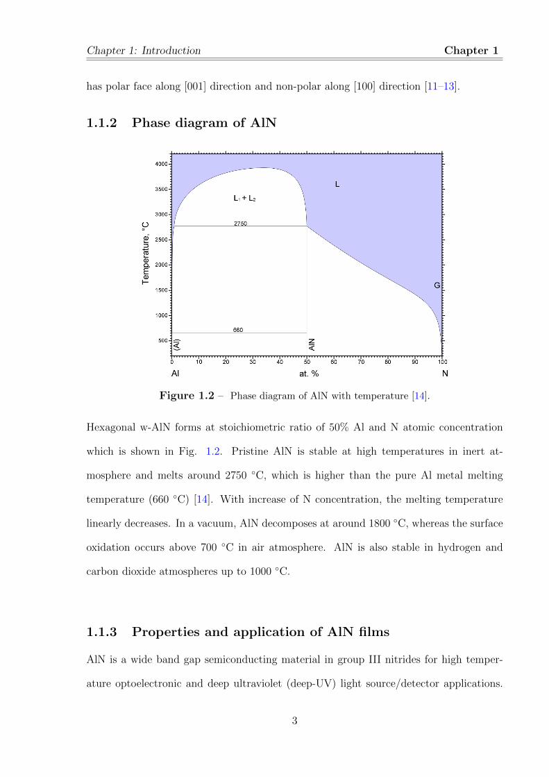
Figure 1.2 – Phase diagram of AlN with temperature [14].
Hexagonal w-AlN forms at stoichiometric ratio of 50% Al and N atomic concentration
which is shown in Fig. 1.2. Pristine AlN is stable at high temperatures in inert at-
mosphere and melts around 2750 C, which is higher than the pure Al metal melting
temperature (660 C) [14]. With increase of N concentration, the melting temperature
linearly decreases. In a vacuum, AlN decomposes at around 1800 C, whereas the surface
oxidation occurs above 700 C in air atmosphere. AlN is also stable in hydrogen and
carbon dioxide atmospheres up to 1000 C.
1.1.3 Properties and application of AlN films
AlN is a wide band gap semiconducting material in group III nitrides for high temper-
ature optoelectronic and deep ultraviolet (deep-UV) light source/detector applications.
3

Aluminum nitride (AlN) Chapter 1
The properties of AlN compared with other semiconductor materials, are shown in Table
1.1 [1–5, 15, 16]. A reasonable thermal match to Si, InP and InAs, make AlN (with
high thermal conductivity) an attractive material for electronic packaging and heat-sink
applications. Due to the similarity in crystal structure and lattice constant between AlN
and GaN, the AlN film is also used as beneficial buffer layer for the growth of GaN films
for optoelectronic devices [17]. AlN has good chemical stability, high hardness and high
electrical resistivity (≥ 1010 Ωcm), hence it is used as a thermal dissipation, protection
against environment and electrical insulation layers in opto-electronic devices.
Semi- Band gap Transition Thermal conductivity Coefficient ofconductors (eV) type (W/mK) expansion (10−6/C)
AlN ∼6.2 Direct 230-320 4.5GaN ∼3.4 Direct 130-220 5.6ZnO ∼3.3 Direct 43-54 2.9
Si ∼1.1 Indirect 140-160 4.1InP ∼1.3 Direct 68 4.5InAs ∼0.4 Direct 30-50 5.2GaAs ∼1.4 Direct 45-54 6.5
Table 1.1 – Comparison of physical properties of AlN and other semiconductor materials[1–5, 15, 16].
Moreover, highly oriented AlN thin film deposited on silicon, has received considerable
attention recently as a piezoelectric material (piezo-coefficient, d33 = 5.6 pm/V) for sur-
face acoustic wave (SAW) devices on the account of their high surface acoustic velocity,
temperature stability, chemical stability characteristics compared to ZnO, LiNbO3 and
PZT, etc [18–22]. The piezoelectric properties of AlN are compared to other materials,
are shown in Table 1.2 [18, 21, 23–25]. In w-AlN films, a-axis oriented AlN exhibits a
higher acoustic velocity and electro-mechanical coupling coefficient than c-axis oriented
AlN. Therefore, it is expected that a-axis oriented AlN film can perform better for SAW
devices [26].
4

Chapter 1: Introduction Chapter 1
Piezoelectric Accustic d33 Compatibility withmaterials velocity (m/s) (pm/V) Si technology
AlN 5600 5.6 GoodZnO 2558 12.4 Fair
LiNbO3 3795 31.5 PoorPZT 3104 200 Poor
Table 1.2 – Comparison of piezoelectric properties of AlN and other piezoelectric mate-rials.
Generally, the Ultraviolet (UV) light with wavelength shorter than 400 nm is divided in to
near-UV (300-400 nm), deep-UV (200-300 nm) and vacuum-UV (< 200 nm) light. Since
vacuum-UV light is absorbed by air, deep-UV light is the shortest wavelength that is avail-
able in the living environment. Deep-UV light has high energy to kill bacteria, viruses and
decompose harmful stable substances (such as, dioxin, polychlorinated biphenyls-PCBs,
etc). Therefore, these sources are used in water purification, sterilization and environ-
mental protection devices. Also, it is used in high density optical data recording and
nano-fabrication technologies, since they have low focal point of light due to lower wave-
length [27]. Particularly, the wide direct band gap of AlN, GaN and ZnO semiconductors
are favorable for short-wavelength light emitting and high-power devices. Deep-UV LEDs
with high efficiency are expected to be a future candidate for the health care and indus-
trial applications where AlN films find an important role with emission wavelength of 210
nm (shortest wavelength ever observed from any semiconductor) [28, 29]. According to
DFT calculation (Ceperley-Alder exchange correlation potential) as well as experimen-
tal results (CL and deep UV laser PL), the degenerated p-type valence band maximum
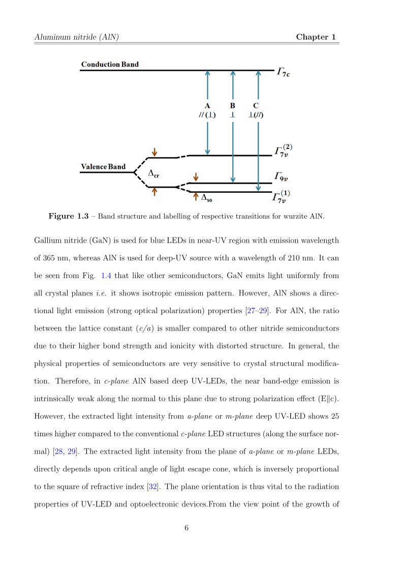
creates excitonic states due to the hexagonal crystal-field (Mcr = -217 meV) and spin-
orbit splitting (Mso = 20 meV), as shown in Fig. 1.3 [30, 31]. Therefore, there are two
configurations of excitonic transitions i.e. σ (E⊥c; c− axis of wurzite structure) and π
(E‖c) configurations. Hexagonal w-AlN crystal has polar face along [001] direction, so
the polarization of light strongly affects along the c-axis of the crystal.
5
Aluminum nitride (AlN) Chapter 1
Figure 1.3 – Band structure and labelling of respective transitions for wurzite AlN.
Gallium nitride (GaN) is used for blue LEDs in near-UV region with emission wavelength
of 365 nm, whereas AlN is used for deep-UV source with a wavelength of 210 nm. It can
be seen from Fig. 1.4 that like other semiconductors, GaN emits light uniformly from
all crystal planes i.e. it shows isotropic emission pattern. However, AlN shows a direc-
tional light emission (strong optical polarization) properties [27–29]. For AlN, the ratio
between the lattice constant (c/a) is smaller compared to other nitride semiconductors
due to their higher bond strength and ionicity with distorted structure. In general, the
physical properties of semiconductors are very sensitive to crystal structural modifica-
tion. Therefore, in c-plane AlN based deep UV-LEDs, the near band-edge emission is
intrinsically weak along the normal to this plane due to strong polarization effect (E‖c).
However, the extracted light intensity from a-plane or m-plane deep UV-LED shows 25
times higher compared to the conventional c-plane LED structures (along the surface nor-
mal) [28, 29]. The extracted light intensity from the plane of a-plane or m-plane LEDs,
directly depends upon critical angle of light escape cone, which is inversely proportional
to the square of refractive index [32]. The plane orientation is thus vital to the radiation
properties of UV-LED and optoelectronic devices.From the view point of the growth of
6

Chapter 1: Introduction Chapter 1
thin films, AlN prefers to grow along c-plane predominantly rather than a-plane. Since,
a-plane LED structures are desirable to enhance the light extraction and improve the
emission efficiency, it is important to grow high quality a-plane oriented AlN films.
Figure 1.4 – Emission properties of GaN and AlN [27].
1.1.4 Growth of AlN films
In the past decades, an extensive research work has been carried out on the optimization
of deposition by various coating techniques and deposition parameters in order to obtain
the required reproducible quality thin films. Epitaxial growth of c-axis AlN has already
been demonstrated such as, chemical vapor deposition on oriented AlN, molecular beam
epitaxy on oriented GaN, Si and pulsed laser deposition on oriented molybdenum sub-
strates [33–36]. In most techniques, the deposition temperatures are quite high, hence a
smooth surface morphology and stress free epitaxial film could not be obtained due to
the degradation of the substrates [37]. For surface acoustic wave (SAW) device applica-
tions, highly oriented films and homogeneous composition with low surface roughness is
expected, since large surface roughness led to increase in propagation loss especially in
7

Aluminum nitride (AlN) Chapter 1
high frequency [38]. Reactive sputtering technique is promising under such circumstances
when, low substrate temperature deposition (wide variety of substrate materials, com-
patible with current semiconductor device processes) and good surface finish as well as
adhesion are required [39].
Whenever w-AlN is grown as a thin film using PVD or CVD, [002] oriented or polycrys-
talline AlN is most favoured. Thermodynamically grown AlN film also follows the same
phenomena. The surface energy of (002) plane (∼5.6 jm−2) is higher then the surface
energy of (100) plane (∼2.4 jm−2) in w-AlN [10]. Therefore, high energetic adatoms
are favorable for the formation of (002) oriented plane, whereas low energetic adatoms
are favorable for the formation of (100) oriented plane [13, 40]. Feby et. al. reported
a-axis orientated AlN film growth for a target to substrate distance (TSD) of 18 cm
and a growth temperature of 300 C. The rocking curve of (100) plane shows a FWHM
of 0.0145, which confirms a highly oriented a-axis AlN film on Si(100) substrates [19].
Ishihara et. al. reported that AlN thin films grown with (100) orientation on Al and
diamond substrates for a TSD of 12 to 15 cm and sputtering pressure of 3 × 10⁻³ mbar,
whereas the (002) orientation is observed for a TSD of 6 to 10 cm with the same pressure
as above [41]. The FWHM of the rocking curve for the AlN (002) peak shows ∼0.2, that
suggests that the AlN film highly oriented along the c-axis [42]. Xu et. al. have grown
a-axis oriented AlN film on Si(111) substrate with increasing the pressure from 3 to 12 ×
10−3 mbar at TSD of 4 cm. Also, they have grown a-axis oriented AlN film by increasing
TSD from 3 to 12 cm at pressure of 3 × 10⁻³ mbar [12]. Similarly, Chen et. al. have also
grown a-axis oriented AlN films on Si(100) substrates at a pressure of 10−2 mbar with
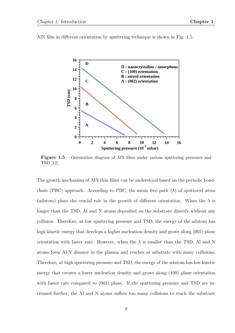
TSD as 6 cm [43]. In general, it is observed from literature that AlN films deposited at
low TSD and low sputtering pressure exhibited (002) preferred orientation whereas those
synthesized at high TSD and high pressure exhibited (100) orientation. The growth of
8
Chapter 1: Introduction Chapter 1
AlN film in different orientation by sputtering technique is shown in Fig. 1.5.
16
14
12
10
8
6
4
2
0
TSD
(cm
)
1614121086420Sputtering pressure (10
-3 mbar)
A
B
C
DD : nanocrystaline / amorphousC : (100) orientationB : mixed orientationA : (002) orientation
Figure 1.5 – Orientation diagram of AlN films under various sputtering pressures andTSD [12].
The growth mechanism of AlN thin films can be understood based on the periodic bond-
chain (PBC) approach. According to PBC, the mean free path (λ) of sputtered atom
(adatom) plays the crucial role in the growth of different orientation. When the λ is
longer than the TSD, Al and N atoms deposited on the substrate directly without any
collision. Therefore, at low sputtering pressure and TSD, the energy of the adatom has
high kinetic energy that develops a higher nucleation density and grows along (002) plane
orientation with faster rate. However, when the λ is smaller than the TSD, Al and N
atoms form Al-N dimmer in the plasma and reaches at substrate with many collisions.
Therefore, at high sputtering pressure and TSD, the energy of the adatom has low kinetic
energy that creates a lower nucleation density and grows along (100) plane orientation
with faster rate compared to (002) plane. If the sputtering pressure and TSD are in-
creased further, the Al and N atoms suffers too many collisions to reach the substrate
9

Chapter 1
and have no enough energy to arrange in a crystalline hexagonal w-AlN structure. Thus,
AlN films are found to be amorphous. This mechanism is called as ‘dimmer model’ or
‘nucleation density model’ [12, 41, 43].
Generally, the AlN film can be grown epitaxially on Si(111) substrates along c-axis. How-
ever, the growth of (100) AlN is favoured by the Si (100) substrates due to the following
reasons. The lattice arrangements of Si(100) surface are known to be square and the
atomic arrangement of (100) surface of AlN are rectangular. Therefore, a-axis oriented
is relatively favorable compared to the c-axis oriented AlN films on Si(100) substrates
[44, 45]. It is also reported that Al interlayer (few nm) is required to increase the adhesion
strength between the film and Si substrate, which also favours the growth of AlN film
along a-axis due to the reduction in lattice mismatch [46]. Similarly, high quality a-plane
AlN epitaxial films are successfully deposited on r -plane sapphire using a thin ZnO buffer
layer for surface acoustic wave (SAW) applications by magnetron sputtering [26, 47].
1.2 Transition metal doped AlN
In semiconductors, the charge of electrons play a crucial role in the information process-
ing and communications, opto-electronic and high-frequency devices; whereas magnetic
materials are used for the information recording using the spin of electron. To make use
of both charge and spin of electrons in semiconductors for the device applications, tran-
sition metals (TM) are normally doped in nonmagnetic semiconductors to make dilute
magnetic semiconductor (DMS) and they are attracted potentially in spintronic applica-
tions [48, 49]. The mechanism of the ferromagnetism is induced due to the indirect and
double exchange interaction between the magnetic moments of partially filled d orbital
10

Chapter 1: TM doped AlN Chapter 1
of TM with the host orbital which is caused by the virtual magnetic acceptor level and
valence band transitions [49–53].
However, only few DMS materials are available with Curie temperature above the room
temperature, which are essential from the view point of both fundamental research and
practical applications. Following theoretical predictions and experimental results, TM
doped wide band gap semiconductors (ZnO, SnO2, TiO2, GaN and AlN) were attracted
considerable attention in spin-dependent photonic and electronic devices due to their
intrinsic ferromagnetism above room temperature [49, 54–56]. Among them, AlN is a
wide band gap semiconductor with a high thermal conductivity and melting temperature
which are compatible with the modern day microelectronics. AlN is chemically stable
at high temperatures and demonstrates a high solubility for transition metals. First row
transition metals (Sc, Ti, V, Cr, Mn, Fe, Co and Ni) are used to dope AlN lattice to
change its physical properties for the application in lasers, deep UV to UV LEDs, sensor,
UV polarizer, high-temperature optoelectronic displays and spin-tunneling devices in the
wavelength span of 200 to 375 nm by band-gap-engineering [28, 51–54, 57–65].
1.2.1 Properties and applications of Al1−xTixN films
Ti doped AlN films have revealed as n-type ferromagnetic material for dilute magnetic
semiconductor applications at room temperature, reported by first principle calculation
as well as experimental methods [66–69]. Addition of transition elements to AlN such
as Ti, Cr and Zr have yielded ternary nitrides with higher hardness, superior oxidation
resistance, good wear and corrosion resistance [70–73]. This improvement in performance
manifested as a decrease in flank wear and corresponding increase in life time of the
tool during drilling, cutting tests of aerospace components and long-life surface modified
11

Transition metal doped AlN Chapter 1
membranes. Al1−xTixN can be grown using sputtering technique at low temperature on
various substrates including metals. Al0.9Ti0.1N film deposited on optical fiber is used
as infrared whispering gallery modes microlaser in the range of 775 to 800 nm for the
biomedical applications [74, 75].
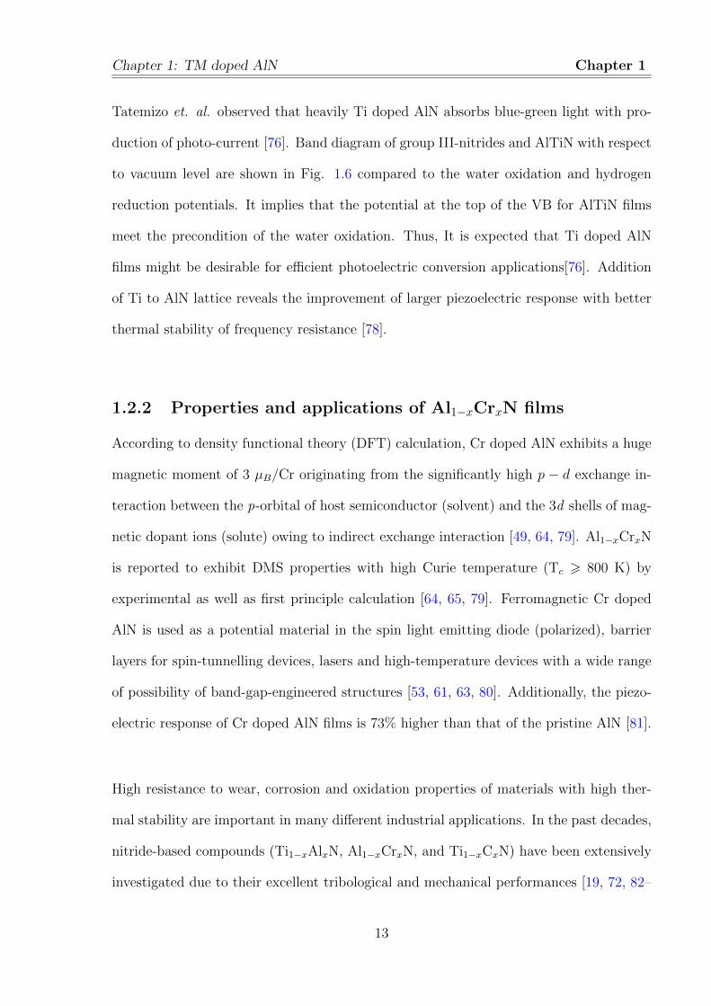
Figure 1.6 – Band diagram for group III-nitride and AlTiN with respect to the vacuumlevel [76].
An extensive research is going on for highly efficient hydrogen gas production by tuning
the band gap energy of wide band gap semiconductors via photo-electrochemical water
splitting. For example, TiO2 is used potentially for the hydrogen generation via photo-
electrochemical water splitting [76, 77]. However, the band gap of TiO2 is too wide to
absorb a significant portion of the solar spectrum and the valence band potential is too
low for effective oxidation of water. While exploring the possibility of heavy transition
metal doping to group III nitride materials for photoelectric conversion under visible light,
12
Chapter 1: TM doped AlN Chapter 1
Tatemizo et. al. observed that heavily Ti doped AlN absorbs blue-green light with pro-
duction of photo-current [76]. Band diagram of group III-nitrides and AlTiN with respect
to vacuum level are shown in Fig. 1.6 compared to the water oxidation and hydrogen
reduction potentials. It implies that the potential at the top of the VB for AlTiN films
meet the precondition of the water oxidation. Thus, It is expected that Ti doped AlN
films might be desirable for efficient photoelectric conversion applications[76]. Addition
of Ti to AlN lattice reveals the improvement of larger piezoelectric response with better
thermal stability of frequency resistance [78].
1.2.2 Properties and applications of Al1−xCrxN films
According to density functional theory (DFT) calculation, Cr doped AlN exhibits a huge
magnetic moment of 3 µB/Cr originating from the significantly high p − d exchange in-
teraction between the p-orbital of host semiconductor (solvent) and the 3d shells of mag-
netic dopant ions (solute) owing to indirect exchange interaction [49, 64, 79]. Al1−xCrxN
is reported to exhibit DMS properties with high Curie temperature (Tc > 800 K) by
experimental as well as first principle calculation [64, 65, 79]. Ferromagnetic Cr doped
AlN is used as a potential material in the spin light emitting diode (polarized), barrier
layers for spin-tunnelling devices, lasers and high-temperature devices with a wide range
of possibility of band-gap-engineered structures [53, 61, 63, 80]. Additionally, the piezo-
electric response of Cr doped AlN films is 73% higher than that of the pristine AlN [81].
High resistance to wear, corrosion and oxidation properties of materials with high ther-
mal stability are important in many different industrial applications. In the past decades,
nitride-based compounds (Ti1−xAlxN, Al1−xCrxN, and Ti1−xCxN) have been extensively
investigated due to their excellent tribological and mechanical performances [19, 72, 82–
13

Chapter 1
87]. It is reported that Al1−xCrxN compound synthesized by various physical vapor depo-
sition techniques with x = 17 to 79 at% having hardness between 20 to 41 GPa [72, 84–87].
1.3 Motivation
AlN has high technological demand in deep-UV LED, since it has the shortest emission
wavelength 210 nm. It is seen that the plane orientation of AlN films also play a vital
role in device performance. For example, the extracted light intensity from a-plane or
m-plane oriented AlN LEDs is 25 times higher than the conventional c-plane LEDs. Also,
the surface acoustic velocity of a-axis oriented AlN film is higher than c-axis oriented,
that is expected to show a better performance in SAW devices. Thus, it is important to
optimize the growth conditions and to develop high quality a-axis oriented AlN films. It
is also important to examine the nature of anisotropic optical properties of these films
for its better use in the area of opto-electronics. Although there are few reports available
on the anisotropic optical properties of AlN thin films, which are confined to c-axis ori-
ented films only [88–92]. Therefore, it is imperative and pertinent to examine the nature
of refractive index of a-axis oriented AlN thin films over a broad range of wavelengths
starting from deep UV to NIR.
Transition metal doped AlN films are the potential source of magnetic semiconductors
for spin-dependent photonic and electronic device applications. For example, Cr doped
AlN films are the well known dilute magnetic semiconductor (DMS) with high Curie
temperature, Tc > 800 K. According to density functional theory (DFT) calculation,
Cr doped AlN exhibits a huge magnetic moment (3 µB/Cr) compared to other transi-
tion metal dopants. However, the experimentally observed magnetic moment was less
14
Chapter 1: Motivation Chapter 1
than 1 µB/Cr, due to possible role of Cr clusters, nitrogen vacancies, defects and im-
purities for the different Cr concentration in AlN lattice [52, 54, 64]. Though Cr ionic
radii is larger than the Al atom, still it can settle in the interstitial sites of AlN lattice.
Formation of Cr clusters at interstitial sites reduce the total magnetic moment, which
increases the antiferromagnetic states [79, 80]. Cui et. al. have reported using DFT
calculation that the Cr clusters larger than 2 atoms exhibit antiferromagnetic coupling
[79]. Hence, the growth of cluster less doped AlN thin films is the first step to achieve
the DMS property in these systems. Also, piezoelectric response of Cr doped AlN films
is 73% higher than that of the pristine AlN. Similarly, Ti doped AlN films also exhibit
room temperature DMS property and are desirable for the efficient photoelectric conver-
sion devices as well. However, several unique parameters such as doping concentration,
position (substitution/interstitial) and the local environment of doping element play an
essential role in the physical properties of doped AlN films which is mainly controlled by
the growth parameters. Therefore, the effect of dopant in the local crystal structure of
AlN film needs a fundamental investigation using X-Ray Absorption Spectroscopy (XAS).
Addition of transition metals to AlN such as Ti, Cr and Zr have yielded ternary nitride
compounds with higher hardness, superior oxidation resistance, good wear resistance and
corrosion resistance. On the other hand, AlN shows a high solubility for transition metals
with high chemical stability upto high temperatures. Doping of transition metals (< 15
at% ) in wurtzite hexagonal AlN (at the Al site) has considerable demands in the areas
of opto-electronics and more specifically in dilute magnetic semiconductor (DMS) device
applications. Moreover, the physical contact loading during processing or packaging for
the opto-electronic device applications generates plastic deformation which significantly
deteriorates the performance of the devices. In this regard, a systematic study of me-
chanical properties of transition metals (Ti and Cr) doped AlN thin films has not been
15

Chapter 1
explored. Due to this, AlN films as well as doped AlN films require a vital comprehension
in nano-mechanical properties.
1.4 Objective and overview of the thesis
The prime aim of the present thesis is to grow a-axis oriented AlN film and understand
the effects of growth temperature on residual stress and mechanical properties. Addition-
ally, It emphasizes the anisotropic optical properties of a-axis oriented AlN films over a
broad range of wavelengths starting from deep UV to NIR. This thesis also highlights
the growth of Ti and Cr-doped AlN films, the local crystal structure and the mechanical
properties with respect to doping concentration. The thesis is organized in to six chapters
and the contents of each chapter are summarized as follows.
Chapter 1 briefly introduces the crystal structure, general properties and applications
of pristine AlN as well as doped AlN films. A progress and present status of growth of
a-axis oriented AlN thin films and their applications are briefly introduced.
Chapter 2 provides a description of the magnetron sputtering system used for the growth
of pristine and doped (Ti and Cr) AlN thin films. The growth parameters used for the
synthesis of these films are described in detail. These films are characterized by X-Ray
Diffraction (XRD), Transmission Electron Microscopy (TEM), Atomic Force Microscopy
(AFM), and X-Ray Photoelectron Spectroscopy (XPS) to investigate the crystallographic,
structural, morphological and chemical properties. Local crystal structure at the vicin-
ity of doping elements are characterized by X-Ray Absorption Spectroscopy (XAS) and
the working principle is briefly presented in this section. Also a brief introduction to
16

Chapter 1: Objective Chapter 1
the characterization techniques used for the mechanical and optical properties of these
thin films (using nano-indentation technique and Spectroscopic Ellipsometry (SE), re-
spectively) and their basic principle are also presented.
Chapter 3 presents the growth of AlN thin films with different growth temperatures (Ts,
35 to 600 C), deposited by reactive sputtering technique. This chapter primarily con-
cerned with the growth of a-axis oriented AlN thin films and it is obtained at a growth
temperature of 400 C. Also, this chapter reports the residual stress in AlN films for
different growth temperatures which is measured by the sin2ψ technique and exhibits a
transition from tensile to compressive between 200 to 400 C. Nano-indentation hardness
(H) of these films with respect to the growth temperature showed a variation between 12.8
to 19.0 GPa. However, a-axis oriented AlN film exhibits relatively a high elastic modulus,
such as E = 237.6 GPa. Optical characterization of these thin films are discussed with
the help of SE technique in the broad range of energy, which is a non-invasive non-contact
technique with a high degree of accuracy. This chapter also presents an elaborate study
on the anisotropic optical properties of AlN films with respect to growth temperatures,
in the photon energy range of 0.6 to 6.5 eV. It is observed that the birefringence (∆n =
-0.01) of a-axis oriented AlN film is relatively lower compared to the c-axis oriented AlN
film (∆n = -0.05 at 210 nm) reported in the literature so far.
Chapter 4 presents the growth of Ti doped AlN (Al1−xTixN) films by reactive co-
sputtering technique with different Ti concentrations (x = 0, 1.5, 3 and 4 at% ). The
surface chemical analysis and morphology of these films are studied by XPS and AFM
technique. This chapter fundamentally explores the local crystal structure around the
Ti dopant in AlN lattice, which is investigated by X-ray absorption spectroscopy. It
is observed that Ti forms localized TiN species with distorted tetrahedron structure by
17

Objective and overview of the thesis Chapter 1
replacing Al atom in AlN lattice leading to increase in tensile strain. The coordination
number of Ti with N atom in first coordination sphere shows a stoichiometry nature i.e
around four, similar to pristine AlN. The bond lengths (Ti-N)ax, (Ti-N)bs are found to
be moderately decreased with Ti concentration, whereas Ti-Al bond length in second
coordination sphere is independent of Ti. Finally, this chapter describes the effect of Ti
doping on the mechanical properties of AlN thin films, where the hardness of Al1−xTixN
films are increased from 17.5 to 27.6 GPa with increase in doping concentration.
Chapter 5 presents the growth of Cr doped AlN (Al1−xCrxN) films by reactive co-
sputtering technique with different Cr concentrations (x = 0, 2, 4 and 6 at% ). The
surface chemical analysis and morphology of these films are also studied by XPS and
AFM techniques. From X-ray absorption spectroscopy study, it is observed that Cr also
replaces the Al atom in AlN lattice and forms localized distorted tetrahedron CrN species
as similar to Ti doped AlN films. These films have both N and Al vacancies in the first
and second coordination sphere, respectively. The bond lengths (Cr-N)ax and (Cr-N)bs
are found to be decreasing rapidly with Cr concentration and shows a strong p − d hy-
bridization compared to Ti doped AlN films. Therefore, the modulus enhanced from 231
to 313 GPa with the increase in Cr concentration. The hardness of Al1−xCrxN films is
varying between 17.5 to 23.0 GPa and show a lower hardness compared to Ti doped AlN
due to more Al and N vacancies and large crystallite size.
Chapter 6 summarizes the research contribution and the major findings of this thesis.
In addition, few issues that will be tackled in the near future are also indicated.
18

Chapter 2
Experimental techniques
2.1 Introduction
This chapter provides a brief description of the magnetron sputtering system used for
the growth of thin films and the characterization techniques such as X-ray Diffraction
(XRD), Transmission Electron Microscopy (TEM), Atomic Force Microscopy (AFM),
and X-ray Photoelectron Spectroscopy (XPS) to investigate the crystallographic, struc-
tural, morphological, chemical and elemental analysis. The growth parameters used for
the synthesis of thin films (AlN, Cr doped AlN and Ti doped AlN) in this research work
are explained in detail. Local crystal structure at the vicinity of doping elements (Cr and
Ti) in AlN thin films are characterized by X-ray Absorption Spectroscopy (XAS), which
is briefly presented in this section. A brief introduction of the characterization techniques
used for the mechanical and optical properties of these thin films using nano-indentation
technique and Spectroscopic Ellipsometry (SE), respectively are given.
2.2 Magnetron sputtering unit
In this research work, thin films are grown using reactive magnetron sputtering technique
(M/s. MECA 2000, France). The main parts of the system are the high vacuum chamber
19

Magnetron sputtering unit Chapter 2
(diameter: 630 mm and height: 500 mm) housing three magnetron guns (two RF and one
DC source), six substrate holders of 4 inch diameter and thickness monitor. This system
is pumped by a turbo molecular pump (Leybold-Germany, pumping speed 1100 lit/min)
backed by a rotary pump (Leybold-Germany). This system is also equipped with mass
flow controllers for gas and suitable vacuum measuring gauges. During sputter deposition,
a thousand position gate valve (VAT, Switzerland) with a stepper motor controlled by a
VAT PM-5 (Switzerland) controller is maintained the working pressure in the chamber
according to the feed back signal obtained from the capacitance manometer (Baratron,
MKS). This VAT PM-5 controller is capable of operating in two modes namely (i) con-
stant pressure mode and (ii) constant position mode. Fig.2.1 depicts the photograph of
this sputtering unit.
Figure 2.1 – Photograph of the sputtering unit (MECA 2000-France) and the arrangementof guns covered by targets.
This sputtering unit has three magnetron guns with 50 mm diameter and 5 mm thickness
targets with pneumatic shutters. Among these, two are RF powered with LCR match
boxes and third one is with DC powered, baked by water cooled system to reduce the
heat during the deposition. Two RF sources are powered by Hutttinger 600 RF and the
DC source is powered by Huttinger 1500 DC. These three guns are placed by focusing
towards the substrate at an angle 30 from the normal for co-sputtering of three tar-
gets simultaneously. A non-magnetic shield is used to separate the targets for avoiding
20

Chapter 2: Growth of thin films Chapter 2
cross contamination at the time of co-sputtering (Fig. 2.1). A quartz crystal monitor
MAXTEK, INC (USA) is used to monitor the thickness of the coating on the fly. It also
contains a stationary substrate heater to grow thin films at different temperatures upto
800 C. The important deposition parameters to grow thin films with desired properties
are sputtering power, sputtering pressure, gas flow, target to substrate distance (TSD)
and substrate temperature.
2.3 Growth of thin films
2.3.1 Aluminum nitride (AlN)
AlN thin films were grown on silicon (100) substrates by DC reactive magnetron sputter-
ing technique from pure aluminum target (4N) of 50 mm diameter in a high purity argon
(5N) and nitrogen (5N) gas mixture. Si (100) substrates were cleaned by a standard
two-step RCA process i.e. at first soaked in a solution of H2O : NH4OH : H2O2 (5:1:1)
at 70 C and then etched in a 2% HF-H2O solution for 2 minutes to remove the native
oxide layers on the surface. Before deposition, the sputtering chamber was evacuated
to 1 × 10⁻⁶ mbar. At first, a mono layer of Al in Ar atmosphere was deposited on the
substrate for few seconds to improve the adhesion between the substrate and deposited
AlN thin films. These films were grown at different growth temperatures (substrate tem-
perature, Ts) by keeping constant Ar/N2 gas ratio, target to substrate distance (TSD)
and deposition pressure. The deposition parameters in this study are listed in Table 2.1.
Surface profilometer Dektak 6M (M/s.Veeco, USA) was used to measure the thickness of
these films, and it was found to be around 1 µm.
21

Growth of thin films Chapter 2
Sputtering parameters Values
Target Al (4N pure)Substrate Si (100)Deposition pressure (mbar) 5× 10⁻³
TSD (cm) 14Ar : N2 (sccm) 4 : 1DC power (W) 200Growth temperature (Ts) (C) 35 to 600
Table 2.1 – Deposition parameters of AlN thin films by DC sputtering.
2.3.2 Ti doped AlN (Al1−xTixN)
Al1−xTixN thin films were grown on Si(100) substrate by reactive magnetron co-sputtering
technique from 50 mm diameter Al and Ti targets (4N pure) in pure argon and nitrogen
gas (5N pure) atmosphere. These Si (100) substrates were also cleaned by the standard
two-step RCA process as described earlier. Before deposition, the base pressure of sput-
tering chamber was maintained below the pressure of 6× 10⁻⁶ mbar by turbo-molecular
pump. Al1−xTixN films were grown at constant flow of argon to nitrogen ratio, TSD and
growth temperature with changing the Ti sputtering power, which are listed in Table 2.2.
Surface profiler was used to determine the thickness of Al1−xTixN films and it was found
to be around 400 nm.
Sputtering parameters Values
Target (4N) Al and TiTSD (cm) 7
Ar : N2 (sccm) 4 : 1Growth temperature (C) 400
Power (Al:Ti)(W) 200:0 200:30 200:50 200:70Sputtering pressure (10−3 mbar) 5 7 7.6 8
Ti at% 0 1.5 3 4
Table 2.2 – Growth parameters of Al1−xTixN thin films.
22
Chapter 2: Characterization techniques Chapter 2
2.3.3 Cr doped AlN (Al1−xCrxN)
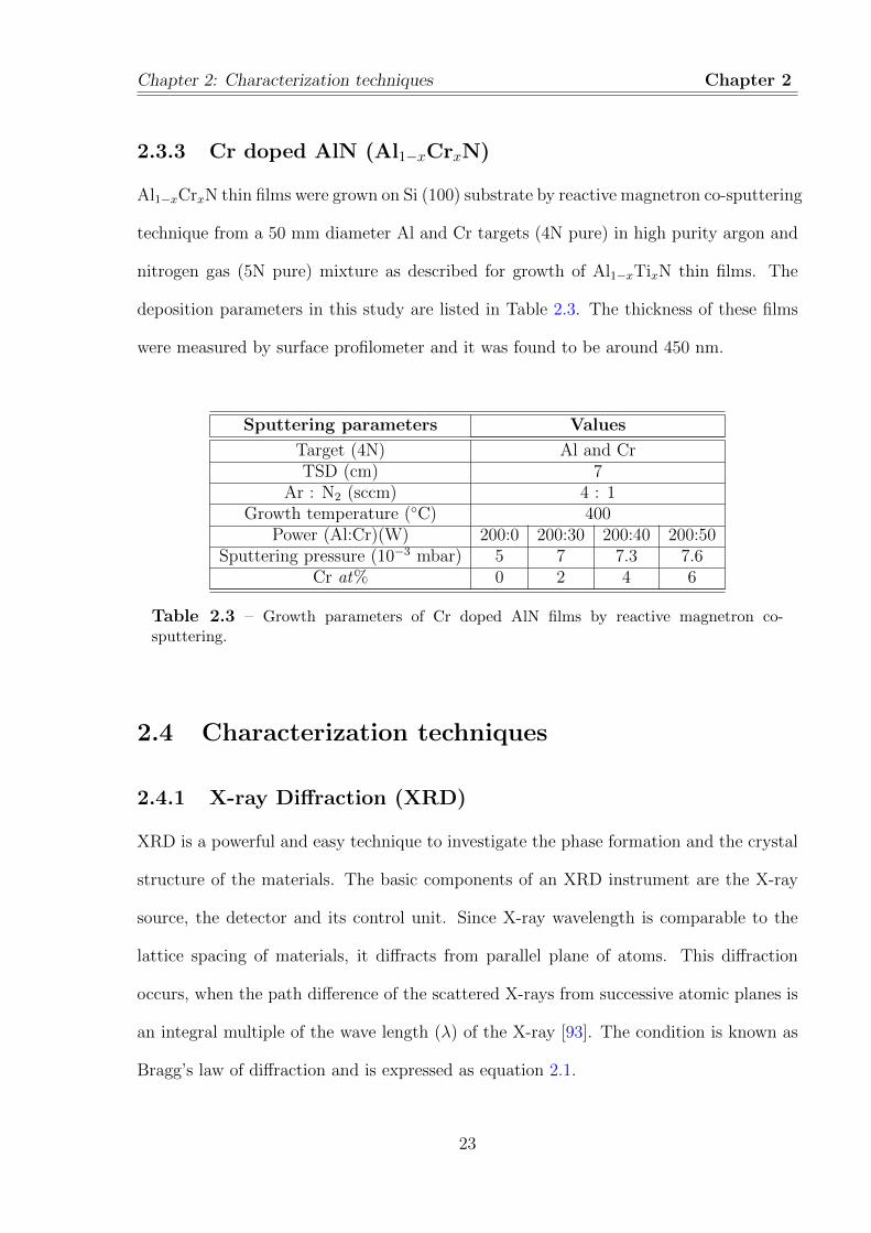
Al1−xCrxN thin films were grown on Si (100) substrate by reactive magnetron co-sputtering
technique from a 50 mm diameter Al and Cr targets (4N pure) in high purity argon and
nitrogen gas (5N pure) mixture as described for growth of Al1−xTixN thin films. The
deposition parameters in this study are listed in Table 2.3. The thickness of these films
were measured by surface profilometer and it was found to be around 450 nm.
Sputtering parameters Values
Target (4N) Al and CrTSD (cm) 7
Ar : N2 (sccm) 4 : 1Growth temperature (C) 400
Power (Al:Cr)(W) 200:0 200:30 200:40 200:50Sputtering pressure (10−3 mbar) 5 7 7.3 7.6
Cr at% 0 2 4 6
Table 2.3 – Growth parameters of Cr doped AlN films by reactive magnetron co-sputtering.
2.4 Characterization techniques
2.4.1 X-ray Diffraction (XRD)
XRD is a powerful and easy technique to investigate the phase formation and the crystal
structure of the materials. The basic components of an XRD instrument are the X-ray
source, the detector and its control unit. Since X-ray wavelength is comparable to the
lattice spacing of materials, it diffracts from parallel plane of atoms. This diffraction
occurs, when the path difference of the scattered X-rays from successive atomic planes is
an integral multiple of the wave length (λ) of the X-ray [93]. The condition is known as
Bragg’s law of diffraction and is expressed as equation 2.1.
23

Characterization techniques Chapter 2
nλ = 2dsinθ (2.1)
where λ is the wavelength of X-ray used (normally Cu Kα, λ= 1.54056 A), θ is the
diffraction angle and d is the inter planar spacing. In a diffraction pattern, the recorded
intensity is plotted against the diffraction angle 2θ. Each diffracted peak correlates to a
plane in the crystal structure.
The penetration depth of X-ray beams in Bragg-Brentano mode XRD, ranges from a few
micrometers to a few hundred micrometers, depending on the density of the material. As
a result of this, the Bragg Brentano configuration generally produces intense signal from
the substrate and weak signals from the film itself. By using a very small grazing angle
for the incident rays, the penetration depth of X-rays can be limited to a few nanometers
i.e. X-rays interaction volume confine to a few tens to hundreds of nanometers from the
surface of thin film [94]. Thus, grazing incidance X- ray diffraction (GIXRD) is com-
monly used to investigate the significant surface and interface structure of thin films to
avoid the substrate information. Fig. 2.2 depicts the schematic diagram of the GIXRD
arrangement. In the present study, the identification of crystalline phases of thin films
were carried out by Bragg-Brantano (Cu - Kα) geometry and Grazing Incidence X-ray
Diffraction (GIXRD) technique (M/s. Bruker D8, Germany) with a grazing angle of 0.5.
However, in thin films, the peak width of XRD profile consists of both crystallite size
and strain component. Hence, to delineate the effect of microstrain and crystallite size
on the peak broadening, Williamson-Hall (W-H) method is used. Mean crystallite size
and strain of the film are calculated from XRD profiles using the following equation.
24

Chapter 2: Characterization techniques Chapter 2
Figure 2.2 – The schematic configuration of a common GIXRD.
βcosθ =Kλ
D+ 4εsinθ (2.2)
where K is the Scherrer constant (0.9), D is the crystallite size, β is the Full Width at
Half Maximum (FWHM) and ε is the induced strain in the film [95].
2.4.1.1 Rocking curve (ω-Scan)
In XRD, there are three conventional angle of rotation (ω, φ and ψ) in different direction
with respect to diffractometer plane, which is shown in Fig. 2.3. Whereas, ω is the angle
between incident X-rays and film surface, φ is the in-plane rotation of the film and ψ is
the azimuthal tilt.
The degree of preferred orientation of a crystallographic plane of film and it’s crystal
quality can be determined by rocking curve measurement of XRD. In this measurement,
the X-ray source and the detector angle (2θ) are fixed for a particular Bragg peak. The
25

Characterization techniques Chapter 2
Figure 2.3 – Schematic of different angles of conventional rotation w.r.t diffractometerplane.
diffraction intensity is measured by the rocking (ω-rotation) of film surface around the
Bragg peak [93, 94]. The degree (or distribution) of preferred orientation is estimated
from the FWHM of the rocking curve profile which is discussed in section 3.2.1.
2.4.1.2 Residual stress
A well-documented sin2ψ technique is used to measure the residual stress of thin films,
where the crystallographic planes titled from the surface normal at different ψ angles.
Usually, the lattice spacing varies with the strain of elastically strained crystalline mate-
rial. There is a correlation exists between the stress components in the film and variation
in the inter-planer spacings (d) for the tilt angles (ψ) along the diffraction vector is shown
below
σφ =E
(1 + ν) sin2ψ
(di − d0
d0
)(2.3)
where E - Young’s modulus, ν - Poisson’s ratio,(di−d0d0
)- micro-strain, σφ is the stress
26
Chapter 2: Characterization techniques Chapter 2
in the film.[93, 96]. In this sin2ψ technique, various tilt angles (ψ) are used to measure
the residual stress of these films. Also, in-plane rotation φ = 0, 45 and 90 of the samples
are used to obtain a three dimensional stress distribution in the system.
2.4.2 Transmission Electron Microscopy (TEM)
TEM is an unique material characterization technique that enables investigation of high
resolution microstructural features with magnified images of the order of 103 to 106 as
well as acquisition of crystallographic information. In principle, TEM uses near rela-
tivistic electron beam normally accelerated by hundreds of kV supply voltage. Normally,
e-beam interacts with target specimen in three ways i.e. unscattered electrons (trans-
mitted/direct beam), elastically scattered electrons (diffracted beam) and inelastically
scattered electrons [97]. The transmission of e-beam without any interaction with the
specimen is inversely proportional to the specimen thickness. Depending on the mode
of operation, a sophisticated system of electromagnetic lenses focuses the scattered elec-
trons into an image or a diffraction pattern. The directions of coherent elastic scattered
electrons are determined by the crystallographic orientation between the atomic planes
of the specimen and the incident beam. By selecting the diffracted beam from a selected
area on the specimen, selected area electron diffraction (SAED) pattern can be obtained.
The SAED pattern is equivalent to an X-ray diffraction pattern. A single crystal leads
to a well arranged spot pattern on the screen; a poly-crystal constitutes a ring pattern.
Whereas, an amorphous material produces a series of diffuse halos. General analysis of
the samples can be carried out by different modes of the TEM, such as the bright field
and dark field images, SEAD patterns, high resolution TEM (HRTEM) and fast Fourier
transform (FFT) images. Images formed from the transmitted electrons are known as
bright field images and images formed using specific diffracted (hkl) beams are known
27

Characterization techniques Chapter 2
as dark field images. They yield information about both atomic structure and defects
present in the material. Thus TEM is definitely a useful and effective tool to characterize
the thin films to investigate the crystal structure, phase and orientation.
In this study, the cross section samples for transmission electron microscopy have been
prepared using a focused ion beam system (JIB-4500, JEOL, Japan). Cross sectional
microstructural studies were performed using a transmission electron microscopy (M/s
JEM-2100F, JEOL, Japan ) operating at 200 kV.
2.4.3 Atomic Force Microscopy (AFM)
The AFM is widely used for the study of surface morphology with an order of atomic
scale spatial resolution. The AFM probes consists of sharp tip of the order of 10 nm,
which is used for probing interactions between the tip and surface of the sample. The
common force associated with AFM interaction is the inter atomic force called as van der
Waals force and it depends on the separation between the tip and the sample. The small
forces between the tip and specimen during the scan will cause a deflection on the can-
tilever. A laser beam is focused on the back of a cantilever and this will be detected by a
position sensitive photo diode. By raster-scanning of the tip across the surface and record-
ing the change in force as a function of position to map the morphology of the surface.
In this study, the surface morphology of these films was characterized by an AFM (M/s.
Anton Paar, Switzerland) with a contact cantilever single-crystal silicon tip of size 10 nm.
2.4.4 X-ray Photoelectron Spectroscopy (XPS)
The XPS, also known as electron spectroscopy for chemical analysis (ESCA) is a widely
used surface sensitive technique to investigate the compositional elements and its chem-
28

Chapter 2: XAS Chapter 2
ical state. In this technique, a surface of specimen is irradiated with X-rays of known
energy (commonly Al Kα or Mg Kα) in ultra high vacuum. In this technique, the ir-
radiated photons interact with the core-level electrons of the atom. When the incident
energy (hν) is greater than the binding energy (Eb) of the electron in a particular shell, a
photo-electron is ejected with a kinetic energy (Ek), which is represented in the following
equation.
Ek = hν − Eb − φ (2.4)
where φ is the work function of the material. These ejected photo-electrons are collected
by an electron analyzer that measures their kinetic energy. An electron energy analyzer
produces an energy spectrum i.e. intensity agnaist binding energy (number of photo-
electrons with time) [98].
For the present study, a monochromatic Al Kα radiation with 1486.71 eV, at an operating
power 300 W was used. The emitted photoelectrons were analyzed by a hemispherical
analyzer with 150 mm mean radius. The spectrometer was calibrated using a standard
silver sample. The data obtained were processed by the Specslab2 software. The binding
energy of C-1s spectrum from contaminated carbon at 284.7 eV was used as a reference to
account for any charging of the sample. The peak positions were compared with standard
values for identification of different elements. The pass energy, incident and detection an-
gles in XPS with respect to the sample surface normal are 50 eV, 55 and 0, respectively.
Ar+ ion beam with 1 keV and current 0.5 mA were employed to sputter few nm layers of
the film surface to clean the specimen.
29

X-Ray Absorption Spectroscopy(XAS) Chapter 2
2.5 X-Ray Absorption Spectroscopy(XAS)
X-ray absorption spectroscopy (XAS) generally deals with measurement of absorption
coefficient as a function of x-ray photon energy around an absorption edge of an element
in a material. X-ray absorption spectrum is broadly classified into two important parts
i.e. X-ray absorption near-edge structure (XANES) and extended x-ray absorption fine
structure (EXAFS) after the edge, which is shown in Fig. 2.4. XANES is sensitive to
three-dimensional geometrical arrangements (symmetry e.g. octahedral, tetrahedral co-
ordination) of atoms around x-ray absorbing atom in the host material [99]. It is also
helpful in determining the chemical oxidation state of the absorbing atom. On the other
hand, EXAFS is generally characterized by the presence of fine structure oscillations and
gives precise information about local structure around the particular atomic species in
the short range order. This determination is confined to a distance given by the mean free
path of the photo-electron within 5-7 A radius from the element. On the basis of above
characteristic, the EXAFS is a powerful structural local probe to determine the bond
length, coordination number, disorderness in the co-ordination sphere of the absorbing
atom.
Normally, the energy of x-rays are ranging from ∼ 500 eV to 500 keV (wavelengths from
∼ 25 to 0.25 A). At this energy range, an electron absorbs photon in a tightly bound
quantum core level of an atom. The incident x-ray energy must be greater than the bind-
ing energy of a particular core level of an absorbing atom, so that the electron will be
removed from its quantum level. In this case, excess energy is given to a photo-electron
that is ejected from the atom as seen in Fig. 2.5.
With the advent of modern synchrotron radiation sources, XAS technique has emerged
30

Chapter 2: XAS Chapter 2
Figure 2.4 – A typical normalized X-ray absorption spectrum.
to be the most powerful local structure determination technique, which can be applied
to any type of material i.e. amorphous, polycrystalline, polymers, surfaces and liquids in
ambient condition. XAS can be measured either in transmission or fluorescence geome-
tries. In transmission mode, the absorption coefficient (µ) is measured as a function of
log(I0/I), where I0 is the intensity of incident x-rays and I is the intensity of transmit-
ted beam through specimen. Usually, fluorescence geometry is preferable in thin films
deposited on thick substrate. In this mode, µ is measured as a function of (If/I0), where
If is the intensity of fluorescence x-rays.
2.5.1 Experimental details of XAS
XAS measurement with synchrotron radiation is generally carried out in two different
modes viz., scanning and dispersive. In this study, doped (Cr and Ti) AlN films were
studied by the standard 45 geometry fluorescence mode at BL-09, which is a scanning
XAS beamline, of the Indus-2 Synchrotron source (2.5 GeV, 200 mA) at Raja Ramanna
Centre for Advanced Technology (RRCAT), Indore, India. The beam-line consisted of
31
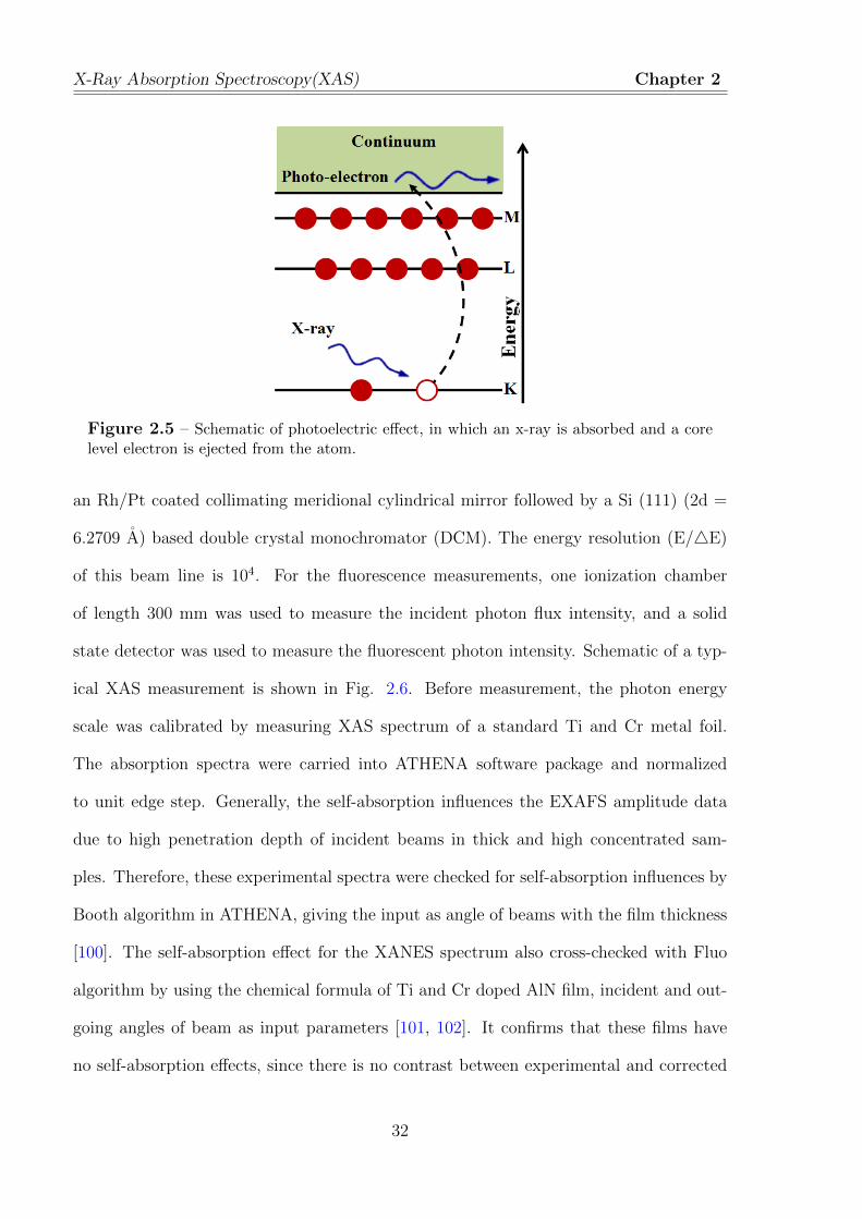
X-Ray Absorption Spectroscopy(XAS) Chapter 2
Figure 2.5 – Schematic of photoelectric effect, in which an x-ray is absorbed and a corelevel electron is ejected from the atom.
an Rh/Pt coated collimating meridional cylindrical mirror followed by a Si (111) (2d =
6.2709 A) based double crystal monochromator (DCM). The energy resolution (E/4E)
of this beam line is 104. For the fluorescence measurements, one ionization chamber
of length 300 mm was used to measure the incident photon flux intensity, and a solid
state detector was used to measure the fluorescent photon intensity. Schematic of a typ-
ical XAS measurement is shown in Fig. 2.6. Before measurement, the photon energy
scale was calibrated by measuring XAS spectrum of a standard Ti and Cr metal foil.
The absorption spectra were carried into ATHENA software package and normalized
to unit edge step. Generally, the self-absorption influences the EXAFS amplitude data
due to high penetration depth of incident beams in thick and high concentrated sam-
ples. Therefore, these experimental spectra were checked for self-absorption influences by
Booth algorithm in ATHENA, giving the input as angle of beams with the film thickness
[100]. The self-absorption effect for the XANES spectrum also cross-checked with Fluo
algorithm by using the chemical formula of Ti and Cr doped AlN film, incident and out-
going angles of beam as input parameters [101, 102]. It confirms that these films have
no self-absorption effects, since there is no contrast between experimental and corrected
32

Chapter 2: XAS Chapter 2
self-absorption spectrum.
Figure 2.6 – A schematic layout of XAS measurement unit.
2.5.2 Theoretical background
Core-electron absorbs the incident x-ray (E) and jumps to continuum state with a ki-
netic energy of E−E0, where E0 is the binding energy of core-electron. The core state is
eventually filled by ejecting a fluorescent x-ray or an Auger electron. The photo-electron
propagates in continuum state and get backscattered from the surrounded several neigh-
boring atoms. Photo-electrons and the final state of the photo-electron can be described,
by the superposition of the original and scattered waves. This leads to an interference
phenomenon that modifies the interaction probability between core electrons and incident
photons. Constructive interference increases while destructive interference decreases the
absorption coefficient of the atom. This interference phenomenon depends on the distance
between emitting and scattering atoms, their atomic mass and coordination numbers.
Since the oscillations in the absorption spectra are important in EXAFS, the oscillation
part of the measured absorption co-efficient (µ(E)) was converted to the fine structure
function χ(E) using the following equation.
χ(E) =µ(E)− µ0(E)
∆µ0(E0)(2.5)
33

X-Ray Absorption Spectroscopy(XAS) Chapter 2
where E0 is the threshold energy, µ0(E) is the the smooth background function as the
absorption of an isolated atom and ∆µ0(E) is the edge step in the absorption. Analysis
of EXAFS is done in k -space by converting the absorption co-efficient χ(E) to k-space
(χ(k)) using the following relation.
k =
√2m(E − E0)
~2(2.6)
where m belongs to mass of the electron, χ(k) is weighted by k3 for amplification of
oscillations to compensate the damping of the amplitude of XAFS oscillation at high k.
Under the dipole approximation, an analytical expression of the EXAFS signal can be
derived as the relationship shown below [103].
χ(k) =∑ Njfj(k)e−2k2σ2
j e−2Rjλ
kR2j
Sin[2kRj + δj(k)] (2.7)
where, Nj is the number of jth neighbors of the absorbing atom at a distance of Rj, having
a scattering amplitude of fj and phase of δj. The term σj represents the fluctuation at
the atomic positions (having both structural as well as thermal effect) and λ is the mean
free path of the scattering photo-electron.
Crystal structure parameters from the EXAFS signal are determined by fitting the ex-
perimental EXAFS spectra with the above theoretical expression. χ(R) versus radial
distances (R) plots are used to extract the co-ordination number, radial distances and
neighbouring atoms of the dopant in different co-ordination spheres. Different codes
for EXAFS data analysis programme are available among which, IFEFFIT package is
mostly used [104]. The goodness of the fit has been measured by minimizing a statistical
parameter; known as R-factor, which is defined by the equation shown below.
34

Chapter 2: Nanoindentation Chapter 2
R =
∑maxi=min[Re(χd(ri)− χt(ri))2 + Im(χd(ri)− χt(ri))2]∑max
i=min[Re(χd(ri))2 + Im(χd(ri))2](2.8)
The theoretical scattering path of a absorbing element in specimen is generated with
FEFF modelling using ARTEMIS for the fitting the experimental data, which has IFEF-
FIT integrated with it [104].
2.6 Nanoindentation
Nano-indentation is a novel and versatile technique developed over the past three decades
to investigate the local mechanical properties of extremely small volume of bulk materi-
als and thin films. In a traditional indentation experiment, an indenter is pressed into
a specimen with a known load and is subsequently removed. Generally, It measures the
hardness, modulus, and stiffens of a material and also allows the depth resolved inden-
tation from a surface to sub-surface. The hardness of the material is defined as the load
divided by residual indentation area and the indentation impression is only a few nanome-
ters in depth. Its attractiveness stems largely from the fact that mechanical properties
can be determined directly from indentation load and displacement measurements with-
out the need to image the hardness impression.
The nano-indentation system consists of a precision loading arrangement and accurate
measurement of displacement having high thermal stability. The precision loading could
be accomplished by electromagnetic deflection of a spring and the displacement could be
measured by a capacitance gauge or Linear Variable Differential Transformer (LVDT). In
nano-indentation, the most commonly used tip is the Berkovich tetrahedral diamond with
sharp three sided point like tip. The hardness (H) and elastic modulus (E) are calculated
35

Nanoindentation Chapter 2
Figure 2.7 – Schematic illustration of indentation load-displacement curve with importantmeasured parameters ([105]).
from the load displacement profile of indentation test using Oliver and Pharr formalism
[105]. A schematic representation of a typical load displacement curve obtained with a
Berkovich indenter is presented in Fig. 2.7, where the P and h belongs to the load and
displacement of the indenter. Deformation during loading is assumed to be both elastic
and plastic in nature as the permanent hardness impression forms. During unloading,
it is assumed that only the elastic displacements are recovered. From the P − h curve,
the maximum load (Pmax) and the maximum displacement (hmax) must be measured.
The slope of the upper portion of the unloading curve during the initial stages of elastic
unloading is called stiffness, which is defined by S = dP/dh. The parameter hf is the
final depth of penetration after the indenter is fully unloaded.
The indentation contact area is measured on the unloading process to find the H and
E of a material, which is shown schematically in Fig. 2.8. During the indentation, the
specimen surface displaces at the contact perimeter from the initial surface is defined by
hs = εPmaxS
, where ε is a constant that depends on the geometry of the indenter. The
36

Chapter 2: Nanoindentation Chapter 2
Figure 2.8 – Schematic illustration of the unloading process showing contact geometryparameters ([105]).
vertical displacement of the contact periphery i.e. the depth along which contact is made
between the indenter and the specimen is denoted by hc (hc = hmax − hs) and it is;
hc = hmax − εPmaxS
(2.9)
Assuming F (d) be an area-function that describes the cross sectional area of the indenter
at a distance d back from its top of the tip, the contact area (A) is defined as A = F (hc).
From the contact area, the hardness is estimated from the relationship shown below,
H =PmaxA
(2.10)
The measured stiffness is related to the contact area as S =
√4π
AEeff , where Eeff is the
effective elastic modulus defined by the below equation.
1
Eeff=
1− ν2
E+
1− ν2i
Ei(2.11)
The indentation modulus E can be extracted by giving the elastic constants of indenter
(Ei), Poisson’s ratio of the specimen (ν) and indenter (νi) as input in above relation.
37

Chapter 2
In this study, the nano-mechanical properties of pristine and doped AlN thin films were
carried out by a compact platform Ultra Nano-indentation Tester (M/s. Anton Paar,
Switzerland) equipped with a three sided pyramidal diamond (Berkovich) tip with an
end radius of 30 nm. Indentation was performed as a function of depth (10 nm to 650
nm) at different linear load with the standard process i.e. the loading and unloading
rates are maintained at twice of the peak load.
2.7 Spectroscopic Ellipsometry (SE)
Figure 2.9 – Geometry of an ellipsometric measurement.
Spectroscopic Ellipsometry (SE) measurement is a powerful unique optical characteriza-
tion technique to determine the optical properties of materials in the broad energy range,
which is a non invasive, non-contact and sensitive technique with a high degree of accu-
racy [106]. SE is commonly used to measure optical properties of solids such as refractive
index, extinction co-efficient, and dielectric constant. SE measures the change in polar-
ization state of a linear polarization light as it reflects from the sample of the interest.
38

Chapter 2: Spectroscopic Ellipsometry Chapter 2
The polarization change between the parallel (p) and perpendicular (s) components of
the reflected light with respect to the plane of incidence is represented as the change in
amplitude (Ψ) and the phase difference (∆), which are considered as ellipsometric pa-
rameters, are shown in Fig. 2.9. The ellipsometric parameters Ψ and ∆ are related to
the ratio of reflection coefficients is shown below
ρ =rprs
= ei∆tanΨ (2.12)
where rp and rs are the parallel and perpendicular reflection coefficients, respectively.
In this experiment, Is and Ic are the experimentally measured parameters from which the
pseudo dielectric constants are computed. These are related to Ψ and ∆ in the following
equation below.
Is = sin(2Ψ)sin(∆) and Ic = sin(2Ψ)cos(∆) (2.13)
Figure 2.10 – Schematic of the sample analysis procedure.
The optical characteristics of materials are extracted through suitable optical modeling
to experimental measured Is and Ic values, which is shown in Fig. 2.10. In the first
39

Spectroscopic Ellipsometry (SE) Chapter 2
step, it is necessary to create a theoretical model of the material of interest for data
analysis. This model needs to include the order of the layers, their optical constants and
thickness (unknown physical parameters). These values are not known, hence an initial
guess should be provided with the basic knowledge in SE. The model should also contain
some known parameters, such as wavelength, polarization state, and the angle of incident
light. The next step in data analysis is to vary the unknown physical parameters and
generated data from the model by successive iterations until one finds the set of variable
parameters which yield a calculated data that closely match the measured optical data.
This has to evaluate the best-fit model in order to decide whether the predicted model is
physically reasonable and whether all the parameters are unique and not correlated. It
is then understood that these set of parameters represents the true physical description
of the sample under study.
PolarizerAnalyser
70°
PMT
Sample
SourcePhotoelastic
modulator
Figure 2.11 – Schematic diagram of a phase modulated SE experiment setup.
A classical non-linear minimization regression analysis was performed by the Levenberg
Marquardt algorithm to carry out the fitting of experimental data using the model to
describe the sample. A high resolution goodness of fitting by the root-mean-square error
(χ2) is defined as;
40

Chapter 2: Spectroscopic Ellipsometry Chapter 2
χ2 =1
2N − P − 1
N∑i=1
[(Is,mi − Is,ci
10−2
)2
+
(Ic,mi − Ic,ci
10−2
)2]
(2.14)
where N is the number of data points, P is the number of parameters to be fitted and
indices mi and ci are the measured and computed quantity of the ith energy of ellipsom-
etry parameters [107].
In this study, the SE parameters are measured in ambient conditions by a phase mod-
ulated Spectroscopic Ellipsometer (M/s. Horiba Jobin-Yvon, UVISEL2, France) at an
incident angle of 65, 70 and 75 in the photon energy range of 0.6 to 6.5 eV with 0.01
eV increment as shown in Fig. 2.11. The data analysis and fittings are performed using
DeltaPsi2 software.
41

Chapter 3
Effect of growth temperature oncrystallographic orientation,mechanical and optical properties ofAlN films
3.1 Introduction
Aluminum nitride (AlN) films have been attracted in the semiconductor industry due to
their unique outstanding physical and optical properties with great technological advan-
tages. Deep ultra-violet light-emitting diode (UV-LED) with high efficiency is an expected
future candidate for health care and industrial applications where AlN thin films find an
important role with emission wavelength of 210 nm (shortest wavelength ever observed
from any semiconductor) using a p-i-n homojunction of AlN. The extracted light inten-
sity along the surface normal from a-plane or m-plane deep UV-LED is 25 times higher
compared to the conventional c-plane structure [28, 29]. So, plane orientation heavily
affects the radiation properties of UV-LED, polarizer, electro-luminescent diodes like op-
toelectronic devices. Generally, properties of these films depend on the crystal structure,
crystal orientation and micro-structure that in turn depend on the deposition conditions.
Thus, it is important to optimize the growth conditions and to develop high quality a-axis
oriented AlN films. Due to simplicity and reproducibility, reactive magnetron sputter-
42
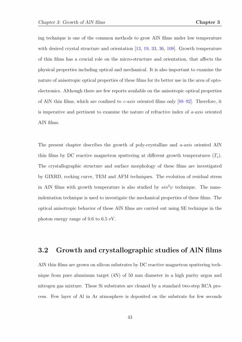
Chapter 3: Growth of AlN films Chapter 3
ing technique is one of the common methods to grow AlN films under low temperature
with desired crystal structure and orientation [13, 19, 33, 36, 108]. Growth temperature
of thin films has a crucial role on the micro-structure and orientation, that affects the
physical properties including optical and mechanical. It is also important to examine the
nature of anisotropic optical properties of these films for its better use in the area of opto-
electronics. Although there are few reports available on the anisotropic optical properties
of AlN thin films, which are confined to c-axis oriented films only [88–92]. Therefore, it
is imperative and pertinent to examine the nature of refractive index of a-axis oriented
AlN films.
The present chapter describes the growth of poly-crystalline and a-axis oriented AlN
thin films by DC reactive magnetron sputtering at different growth temperatures (Ts).
The crystallographic structure and surface morphology of these films are investigated
by GIXRD, rocking curve, TEM and AFM techniques. The evolution of residual stress
in AlN films with growth temperature is also studied by sin2ψ technique. The nano-
indentation technique is used to investigate the mechanical properties of these films. The
optical anisotropic behavior of these AlN films are carried out using SE technique in the
photon energy range of 0.6 to 6.5 eV.
3.2 Growth and crystallographic studies of AlN films
AlN thin films are grown on silicon substrates by DC reactive magnetron sputtering tech-
nique from pure aluminum target (4N) of 50 mm diameter in a high purity argon and
nitrogen gas mixture. These Si substrates are cleaned by a standard two-step RCA pro-
cess. Few layer of Al in Ar atmosphere is deposited on the substrate for few seconds
43

Growth and crystallographic studies of AlN films Chapter 3
to improve the adhesion between the substrate and the deposited film. Thereafter, AlN
films are deposited in 5×10⁻³ mbar sputtering pressure at different growth temperatures
(Ts : 35, 200, 400 and 600 C) by keeping all other sputtering parameters constant. The
details of the growth parameters are given at section 2.3.1.
3.2.1 GIXRD
The GIXRD profiles of AlN thin films deposited over Si (100) with different Ts varying
from 35 to 600 C by DC magnetron sputtering are shown in Fig. 3.1. The GIXRD
patterns of these films show poly-crystalline hexagonal wurtzite structure and agree with
the JCPDS data 25-1133. At 35 C, a poly-crystalline nature is observed, however with
the increase in temperature up to 400 C, the crystallinity has increased along with ori-
entation either (101) or (100). At 400 C, the film exhibits a strong texture towards
(100) plane i.e. a preferential orientation towards a-axis. Thereafter, the crystallinity is
decreased at 600 C and shows a profile similar to AlN film grown at 35 C.
When x-ray beam is irradiated in asymmetrical diffraction configuration (GIXRD) with
a particular angle (Bragg angle) on the planes of oriented crystals, a high intensity peak
is seen corresponding to that plane and it is called texture. Generally, the texture is used
when maximum number of crystals inside the film are orientated in a single direction
[109]. However, epitaxial growth is used when all the crystals belonging to the film grown
in a single direction perpendicular to the substrate. Hence, it is concluded that there is
a preferential orientation along a-axis of AlN film grown at 400 C. To verify the crystal
quality and preferential orientation along a-axis of this AlN film, a rocking curve of (100)
plane has carried out and is shown in Fig. 3.2. It exhibits a FWHM of 0.0391±0.0005
at the angle 33.2 (2θ). This signifies that the (100) planes are oriented parallel to the
44

Chapter 3: Growth of AlN films Chapter 3
Nor
mal
ized
inte
nsity
(a.
u.)
706560555045403530Angle (2q, deg.)
35 ºC
200 °C
400 ºC
600 ºC(1
00)
(002
)(1
01)
(102
)
(110
)
(103
)
ICDD-025-1133
Figure 3.1 – GIXRD profiles of AlN thin films with different Ts.
substrate. However this is slightly larger than the reported a-axis oriented AlN where the
target to substrate distance is varied by maintaining substrate temperature constant[19].
To understand the growth of AlN thin films with temperature, it is important to know
the bonding nature and strength with its orientation. The crystal structure of wurtzite
AlN is discussed and shown in Fig. 1.1 of section 1.1.1. One Al atom is associated with
four N atoms and forms a distorted tetrahedron structure. Among them, three Al-N(i)
(i = 1, 2, 3) bonds are named as B1, whereas one Al - N0 bond in the c-axis direction
is named as B2. The bond B1 is more covalent in nature, whereas B2 is more ionic in
nature [12, 13]. The (100) plane is composed of the B1 bonds which is much stronger
compared to B2 bonds. So at low pressures and increasing temperatures, B2 bond can be
45

Growth and crystallographic studies of AlN films Chapter 3
Inte
nsity
(a.
u.)
16.916.816.716.616.5Angle (q, deg)
orignal - - fitted line
w = 0.03913 ± 0.00052
Figure 3.2 – Rocking curve for (100) plane of AlN grown at 400 C.
easily dissociated that led to the increase in the vertical growth rate of (100) planes. At
400 C growth temperature, the film is highly oriented along a-axis due to (100) crystal-
lite overgrowth compared to other orientations. But above 400 C, other orientations are
also present, since higher temperature is favorable for the dissociation and regrowth of
both the bonds. Therefore, it can be understood that the optimum growth temperature
for depositing highly a-axis oriented AlN films is 400 C.
Crystallite size was calculated from GIXRD profile using Williamson-Hall method and
plotted against growth temperature (Ts) as shown in Fig. 3.3. The crystallite size in-
creases with the increase of Ts until 400 C and thereafter, it decreases. This is due to
the enhanced atom mobility at high temperatures, this increases the ad-atoms surface
diffusion length leading to a higher probability of ad-atoms migration from the landing
site to nucleation site. So that a better crystallinity and higher degree of orientation is
seen up to 400 C. However, further increase in the growth temperature the crystallite
46

Chapter 3: Growth of AlN films Chapter 3
100
80
60
40
20
0
Cry
stal
lite
size
(nm
)
7006005004003002001000Growth temperature (°C)
Figure 3.3 – The variation of crystallite size of AlN thin films with different growthtemperature (Ts).
size decreases drastically. At higher temperatures over 400 C, excessive surface mobility
of ad-atoms make thin film texture difficult due to stronger re-evaporation effect which
results in reducing the crystallite size and intensity of the peaks [108, 110].
3.2.2 Cross sectional TEM and SAED
Figs. 3.4(a-d) show dark-field TEM cross sectional micrographs of AlN films grown at
different Ts. The structure comprises of parallelly spaced columnar structure with an
angle tilted by a few degrees to the substrate normal. In sputtering system there are
three guns placed focusing towards the substrate at an angle. So the sputtered atom flux
arrives obliquely at an angle α and causes inclination to the crystallite columns by β,
where α and β are related by the empirical tangent-rule : tan β = 1/2 tanα [111]. A thin
interface layer of Al deposited to improve the bonding between AlN and Si substrate is
visible at the bottom of the columnar films.
47

Growth and crystallographic studies of AlN films Chapter 3
Figure 3.4 – Dark-field cross-sectional TEM micrographs (a-d), corresponding SAEDpatterns (e-h) of AlN films grown at 35, 200, 400 and 600 C, respectively and indexedSAED pattern of AlN film grown at 400 C (i).
Figs. 3.4(e-i) shows the corresponding SAED patterns of those films deposited at different
Ts. The diffraction rings are indexed using the space group P63mc, lattice constants a =
0.311 nm and c = 0.497 nm (JCPDS file 25-1133). The one deposited at 35 C exhibited
a polycrystalline micro-structure with mixed planes of (100), (101), (102), (110), (103)
and (112). A representative SAED pattern of AlN film grown at 400 C is indexed and
is shown in Fig. 3.4(i). Generally, SAED patterns of single crystal, polycrystalline and
amorphous material exhibit spot, sharp ring and diffused like ring patterns, respectively
48

Chapter 3: Growth of AlN films Chapter 3
[97]. Since, all these films are polycrystalline in nature, the SAED shows a perfect circular
ring patterns. However, the one deposited at 400 C exhibits a systematic dot pattern of
(100) plane. This pattern represents a well crystallized film with a preferential orientation
towards a-axis compared to other films and analogous to the GIXRD profile shown in
Fig. 3.1.
3.2.3 Morphology and surface roughness by AFM
Fig. 3.5 consists of AFM images taken over 1.5 ×1.5 µm2 area showing the morphology
of AlN films deposited on Si at various Ts. In Fig. 3.5 (a), AlN films deposited at 35 C
exhibit irregular grains with less surface density. However, the increase in growth tem-
perature from 200 C to 600 C resulted a similar morphology with a pebble-like grain
structure and dense surface.
Ts (C) Rrms (nm) Grain size (nm)35 3.0 10.5200 5.2 48.0400 9.0 64.0600 7.8 37.0
Table 3.1 – RMS roughness (Rrms) and average grain size of these AlN films.
Table 3.1, displays the root mean square roughness (Rrms) and the mean diameter of the
grains against the growth temperatures (Ts). Rrms and average grain size are significantly
affected by the increase in growth temperatures. Since the thermal energy is delivered to
the surface, the energy and mobility of surface ad-atoms are enhanced the atomic diffu-
sion. This resulted in the formation of fewer large grains by agglomeration of adjoining
atoms or crystals and make surface coarser with the growth temperatures. This can be
seen in the cross-sectional TEM image (Fig. 3.4), the waviness is pronounced more in
400 C. However, at 600 C roughness decreases due to the decrease in grain size and
crystallite size which is similar to Fig. 3.3.
49

Chapter 3
Figure 3.5 – AFM images of AlN films on Si grown at (a) 35 C, (b) 200 C, (c) 400 Cand (d) 600 C.
3.3 Residual stress
Residual stress plays an important role on thin films since it alters the physical properties
like energy-band structure, external quantum efficiency of LED, piezoelectric constant and
mechanical properties. This may cause micro-cracks or peeling from the substrate, which
reduces the coated component lifetime and performance [112]. Therefore, it is important
to control the residual stress by controlling the deposition parameters to synthesize a
mechanically stable films. A well-documented sin2ψ technique has been used to measure
the residual stress of these AlN films, which is discussed in section 2.4.1. The observed
50
Chapter 3: Chapter 3
residual stress of all these films are shown in Fig. 3.6 as a function of Ts. A tendency
from tensile to compression is observed with the increase in Ts. The mean value of the
residual stress has decreased from 0.42 GPa to 0.28 GPa, when the Ts increased from 35
C to 200 C. However, after this temperature a transition has occurred in the residual
stress i.e tensile to compressive mode. At 600 C, the residual stress has increased in the
compression mode up to 0.15 GPa.
-0.6
-0.4
-0.2
0.0
0.2
0.4
0.6
Res
idua
l str
ess
(GP
a)
7006005004003002001000
Growth temperature (ºC)
Compressive Stress
Tensile Stress
Figure 3.6 – Residual stress of AlN thin films as a function of Ts.
To understand the nature of residual stress with the Ts, the literature results are sum-
marized in Table 3.2. Especially, only the transition from tensile to compressive stress
regions and vice versa are picked up for the discussion. Among all, only Wang et al.
reported a similar transition (the bias voltage was kept at -40 V), whereas in this study
the bias voltage was 0 V [113].
51

Residual stress Chapter 3
RT to high temperatureresidual stress variation
Range of shift(Ts )
Deposition technique Ref.
Tensile to compressive 150 to 300 C DC reactive sputtering [113]Compressive to tensile RT to 400 C RF reactive sputtering [13]Tensile to compressive 200 to 400 C DC reactive sputtering this work
Table 3.2 – Residual stress of AlN films at different Ts.
At low Ts/Tm (Ts = growth temperature and Tm = melting temperature of coating
material), the intrinsic stress dominate over the thermal stress. It is important to know
whether the thermal stress also plays a role in the residual stress of the system. In
general, the origin of residual stress can be attributed to the epitaxial stress (lattice
mismatch between substrate and the film), thermal stress (difference in co-efficient of
thermal expansion between substrate and the film), microstructure and the mode of
growth (intrinsic stress). The thermal expansion coefficient of AlN film is larger than
that of the Si substrate. Due to this, AlN films possess a thermal stress as the film is
cooled down to room temperature from high temperature after deposition. This thermal
stress can be calculated using the relation[114]
σT =Ef
(1− νf )(αs − αf )(Ts − Tr) (3.1)
where σT is thermal stress, αs and αf are thermal coefficient of expansion of substrate
(Si, 3.6× 10⁻⁶ C−1) and the AlN film (5.3, 4.2 × 10 −6 C−1 along a-axis and c-axis,
respectively) Tr and Ts are room and growth temperature, Ef and νf are Young’s modu-
lus (AlN, 350 GPa) and Poisson’s ratio (AlN, 0.21) [115]. The calculated thermal stress
is shown in Table 3.3. It is seen that AlN exhibits a strong compressive thermal stress
along a-axis compared to c-axis with increase in Ts.
Intrinsic or growth stress is a structure and micro-structure sensitive property which is
52

Chapter 3: Chapter 3
Ts(C) σT (a-axis)
(GPa)σT (c-axis)(GPa)
35 -0.007 -0.002200 -0.131 -0.046400 -0.282 -0.099600 -0.433 -0.152
Table 3.3 – Thermal stress of a-axis and c-axis AlN films at different Ts.
observed in films during deposition and growth under non-equilibrium conditions. In the
early stages of the film growth, the film consists of smaller crystallites/grains, separated
by an atomic-scale distance. When these crystallites/grains coalesce, a tensile stress is
generated at the point where neighboring islands impinge on each other [116]. As well as,
the parameter Ts/Tm is very important in stress-related behavior for different materials.
At low growth temperature i.e low Ts/Tm, the intrinsic stress can dominate over thermal
stress [117, 118]. Because, when these AlN films deposited at room temperature, there
is a little surface diffusion and one would expect the Al or N vacancy concentration to
be much larger than at equilibrium. When these excess vacancies are subsequently anni-
hilated at vertical boundary, the associated volume change results in an in-plane change
of film dimensions [119]. So at lower growth temperatures, stress relaxation by diffusion
does not occur where intrinsic stress dominates over the thermal stress and a tensile
stress develops. Also, according to atomic peening model, at high deposition pressure
and high TSD (14 cm), the mean free path of the sputtered particle reduces, and there
is a particle energy loss due to increase in collision probability between plasma particles
which increases the oblique angle particle bombardment. So, atomic self-shadowing effect
causes a tensile stress in the film[117, 118].
However, the increase in Ts, the diffusion of defects and vacancies in AlN lattice mi-
crostructure causes the decrease in residual stress due to film densification by decreasing
53
Chapter 3
the void regions through enhanced atomic rearrangement. At 400 C, the film shows pref-
erential orientation along a-axis that possess high thermal stress compared to c-axis. So
the residual stress changes from tensile to compressive stress due to dominant of thermal
stress over intrinsic stress. There after, thermal stress dominates over the intrinsic stress
at high Ts (600 C) and the compressive residual stress increases. It can be reasoned in
Fig. 3.6 that Ts plays a major role on residual stress of sputtered AlN films.
3.4 Mechanical properties
The indentation test have been performed to the know the penetration resistance of ma-
terials i.e mechanical properties of materials by a known geometry indenter under a fixed
load. Recently, It has been seen that there is a significant improvement in indentation
equipment for the measurement of mechanical properties on small scales (few nm) of
materials. It is now feasible to monitor a very precise and accurate load and depth of an
indenter during experiment.
Thin film of AlN is a potential wide band gap semiconducting material for optoelec-
tronic device applications. Moreover, the physical contact loading during processing or
packaging of devices, generates plastic deformation which significantly deteriorates the
performance of the devices. In this regard, it is vital to study of mechanical properties of
AlN films with different growth temperatures. Nanoindentation studies are performed on
these films at a peak load of 4 mN. The absence of creep and thermal drift was verified by
holding the indenter at maximum load for 2 sec (no change in penetration depth). The
indentation hardness (H) and modulus (E) are extracted from the loading and unloading
of the indentation curve as described in section 2.6, are shown in Fig. 3.7. At 35 C, AlN
film shows a hardness increases to 18.5 GPa for AlN film grown at 200 C. There after,
54

Chapter 3: Mechanical properties Chapter 3
further increase in Ts, hardness shows a gradual drop i.e. down to 13.0 GPa for 600 C.
30
25
20
15
10
5
0
Inde
ntat
ion
hard
ness
(H, G
Pa)
6005004003002001000
Growth temperature (°C)
300
250
200
150
100
50
0
Inde
ntat
ion
mod
ulus
(E, G
Pa)
Modulus Hardness
Figure 3.7 – Hardness and modulus of AlN thin films as a function of Ts.
Normally, crystallite size of material, plane orientation, planar density, bond strength
and residual stress collectively contributes to the change in mechanical properties of the
thin film. In this study, AlN film grown at 35 C shows a H as 15.0 GPa due to the
presence of defect and porosity at low growth temperature, however AlN film grown at
200 C shows high H value compared to other films. It can be seen from GIXRD profile
of AlN films in Fig. 3.1 that AlN grown at 200 C exhibits a strong texture along (101)
planes, which is belongs to c-plane family having higher planner density. Therefore, it
shows a relatively high hardness compared to other films. It is understood from GIXRD
and AFM, the average crystallite size and grain size increases with Ts. Aditionally, the
stress relaxation occurred in these films can be seen from residual stress measurement
in Fig. 3.6. According to Hall-Petch relation, the hardness decreases with increase in
crystallite size. Hence, the H is decreased with growth temperatures. Also, a transition
55

Chapter 3
25
20
15
10
5
0
Har
dnes
s (H
, GP
a)
806040200
Crystallite size (nm)
Figure 3.8 – Behavior of hardness as a function of crystallite size.
from Hall-Petch to inverse Hall-Petch occurs when crystallite size is around 15-18 nm
[120, 121]. Fig. 3.8 shows the behavior of hardness as a function of crystallite size.
In this study, it also shows a critical transition of crystallite size around 15-20 nm i.e.
lower the critical size, the hardness decreased and above the critical size the hardness
also decreased with increase in crystallite size, which is satisfying the Hall-Petch relation.
Moreover, indentation modulus (E) of these AlN films is also varied from 192 to 238 GPa
with different Ts. Generally, modulus depends on the nature of the inter-atomic bonds
in the crystal. At 400 C, AlN film is highly a-axis oriented which contains B1 type of
bonds (covalent). So this film has exhibited high elastic nature with higher modulus of
238 GPa.
3.5 Anisotropic optical properties of AlN films
SE is used to measure anisotropic optical properties of AlN films as a function of Ts to
investigate the refractive index (n), extinction co-efficient (k) and band gap. The SE
parameters are measured in ambient conditions by a phase modulated ellipsometer at
56
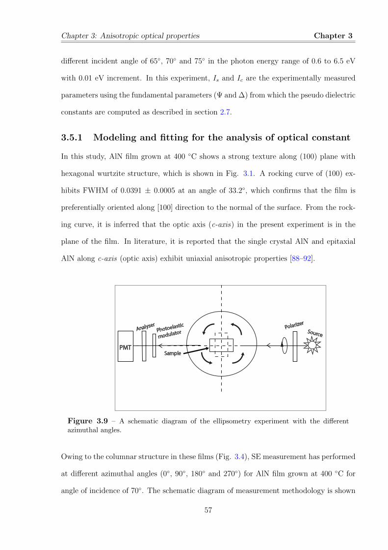
Chapter 3: Anisotropic optical properties Chapter 3
different incident angle of 65, 70 and 75 in the photon energy range of 0.6 to 6.5 eV
with 0.01 eV increment. In this experiment, Is and Ic are the experimentally measured
parameters using the fundamental parameters (Ψ and ∆) from which the pseudo dielectric
constants are computed as described in section 2.7.
3.5.1 Modeling and fitting for the analysis of optical constant
In this study, AlN film grown at 400 C shows a strong texture along (100) plane with
hexagonal wurtzite structure, which is shown in Fig. 3.1. A rocking curve of (100) ex-
hibits FWHM of 0.0391 ± 0.0005 at an angle of 33.2, which confirms that the film is
preferentially oriented along [100] direction to the normal of the surface. From the rock-
ing curve, it is inferred that the optic axis (c-axis) in the present experiment is in the
plane of the film. In literature, it is reported that the single crystal AlN and epitaxial
AlN along c-axis (optic axis) exhibit uniaxial anisotropic properties [88–92].
Sample
SourceAnal
yser
PMT
Photoelastic
modulator
Polarizer
Figure 3.9 – A schematic diagram of the ellipsometry experiment with the differentazimuthal angles.
Owing to the columnar structure in these films (Fig. 3.4), SE measurement has performed
at different azimuthal angles (0, 90, 180 and 270) for AlN film grown at 400 C for
angle of incidence of 70. The schematic diagram of measurement methodology is shown
57

Anisotropic optical properties of AlN films Chapter 3
in Fig. 3.9. The extracted n and k values with azimuthal angles are shown in Fig. 3.10,
which show a difference near to band edge of this film.
2.8
2.6
2.4
2.2
2.0
n
654321Energy (eV)
0 º90º180º270º
(a)0.8
0.6
0.4
0.2
0.0
k
654321
Energy (eV)
(b)
0 º90º180º270º
Figure 3.10 – The extracted (a) n and (b) k at a different azimuthal angles for AlN filmgrown at 400 C.
In this study, the SE data of these films are collected for three different angles of in-
cidence, viz 65, 70 and 75. A representative experimentally measured ellipsometric
parameters (Is and Ic) for 65, 70 and 75 angles of incidence for the film grown at 35
and 400 C are shown in Fig. 3.11 and 3.12, respectively. The corresponding pseudo
dielectric functions (εr and εi) are also shown in Fig. 3.13 and 3.14, respectively. It is
found that the pseudo-dielectric function deduced from Is and Ic for the three angles
showed a difference for 400 C film as compared to the 35 C film. The small difference
for 400 C film could be due to the orientation of the film along a-axis i.e. it exhibits an
anisotropic behavior.
58

Chapter 3: Anisotropic optical properties Chapter 3
654321Energy (eV)
-1.0
-0.5
0.0
0.5
1.0
I c
(b)
65° 70° 75°
-1.0
-0.5
0.0
0.5
1.0I s
654321Energy (eV)
(a)
65° 70° 75°
Figure 3.11 – The measured (a) Is and (b) Ic at a different incident angle for AlN filmgrown at 35 C.
-1.0
-0.5
0.0
0.5
1.0
I c
654321Energy (eV)
(b)
65° 70° 75°
-1.0
-0.5
0.0
0.5
1.0
I s
654321Energy (eV)
(a)
65° 70° 75°
Figure 3.12 – The measured (a) Is and (b) Ic at a different incident angle for AlN filmgrown at 400 C.
59

Anisotropic optical properties of AlN films Chapter 3
-30
-20
-10
0
10
20
30
ei
654321Energy (eV)
(b) 65° 70° 75°
50
40
30
20
10
0
er
654321Energy (eV)
(a) 65° 70° 75°
Figure 3.13 – The measured (a) εr and (b) εi at a different incident angle for AlN filmgrown at 35 C.
30
20
10
0
-10
-20
ei
654321Energy (eV)
(b) 65° 70° 75°
40
30
20
10
0
er
654321Energy (eV)
(a) 65° 70° 75°
Figure 3.14 – The measured (a) εr and (b) εi at a different incident angle for AlN filmgrown at 400 C.
The refractive index (n) and extinction coefficient (k) of these films are computed by
fitting Is and Ic with the modified Forouhi-Bloomer dipersion relation. This relation
fits smoothly for broader wavelength range i.e. from normal to anomalous dispersion
region [122]. This is also consistent with Kramers-Kronig relation with five independent
parameters as described below.
60

Chapter 3: Anisotropic optical properties Chapter 3
n = n∞ +N∑j=1
Bj(ω − ωj) + Cj(ω − ωj)2 + Γ2
j
(3.2)
k =
∑N
j=1
fj(ω − ωg)2
(ω − ωj)2 + Γ2j
: ω > ωg
0 : ω ≤ ωg
(3.3)
where
Bj =
fjΓj
[Γ2j − (ωj − ωg)2
]Cj = 2fjΓj(ωj − ωg)
where, the term fj (in eV) is the oscillator strength, Γj (in eV) is the broadening factor of
absorption peak, ωj (in eV) is the energy at which the extinction coefficient is maximum
and ωg (in eV) is the minimum energy from which absorption starts.
654321Energy (eV)
Ic Exp Ic Fit
(b)
I s
654321Energy (eV)
Is Exp Is Fit
(a)I c
Figure 3.15 – Experimental and corresponding fit of (a) Is, (b) Ic for AlN film grown at400 C.
The anisotropic optical properties of single crystals or epitaxial thin films are conven-
61

Anisotropic optical properties of AlN films Chapter 3
tionally studied by generalized ellipsometry [123, 124]. However, in the present case, the
AlN thin films are predominantly polycrystalline and the film grown at 400 C is tex-
tured and highly oriented along a-axis. The anisotropic optical properties are extracted
by suitable models using DeltaPsi2 software based on the approaches mentioned in lit-
erature [90–92, 125, 126]. A systematic approach of inclusion and omission of layers has
been followed in which, a five layer model (Air/roughness (AlN + void)/ AlN/ interface
(Al+AlN)/ Si) with uniaxial anisotropic conditions is employed for the analysis of op-
tical properties of AlN films. The treatment of roughness and interface layer is based
on Bruggeman Effective Medium Approximation (BEMA). The fitting is performed by
classical non-linear minimization Levenberg-Marquardt algorithm, which is expressed in
terms of χ2 value that defines the goodness of fit and is described in section 2.7. The
χ2 value for all the fittings are 20 to 30 in the energy range of 0.6 to 6.5 eV. Measured
experimental parameters (Is and Ic) for AlN film grown at a typical Ts of 400 C over a
spectral range 0.6 to 6.5 eV and corresponding fit are shown in Fig. 3.15 (a,b). It is seen
that the fitting of Is and Ic across the whole spectral range is in good agreement with
the experimental Is and Ic.
The roughness as deduced from SE of these films is found to lie between 7 and 20 nm.
These values are higher than the root mean square roughness values (3 to 9 nm) as
obtained from atomic force microscopy (AFM). The surface roughness obtained by AFM
technique is acquired over an area of 1.5×1.5 µm2 and thus basically represents the local
roughness values of these films. In SE technique, the data are acquired over a large
elliptical area of 2×0.7 mm2. Thus, the difference in the magnitude of roughness is due
to the fact that the data for ellipsometry is obtained from a larger area with mixture of
materials and voids compared to AFM [127–129]. Nevertheless, the roughness computed
from SE and AFM, both follows a similar trend with Ts. The thickness of the interface
62

Chapter 3: Anisotropic optical properties Chapter 3
1600
1400
1200
1000
800
600
400
200
0
SE
thic
knes
s (n
m)
6005004003002001000
Growth temperature (°C)
1600
1400
1200
1000
800
600
400
200
0
TE
M th
ickn
ess
(nm
)
SETEM
Figure 3.16 – Film thickness measured by SE and TEM.
layer (Al+AlN) between AlN film and Si substrate is extracted from the fitting that
decreases from 16 to 5 nm as a function of Ts.
3.5.2 Behavior of anisotropic optical constant with growth tem-
peratures
The real (n) and imaginary (k) parts of the refractive index of AlN films for different
Ts obtained from the five layer model are shown in Fig. 3.17 (a, b, c, d). The n and
k exhibit strong uniaxial anisotropic dispersion and increase monotonically with increas-
ing photon energy in normal dispersion region, while it decreases in anomalous region.
All these films show transparent nature up to a photon energy 3.5 eV (354 nm) from NIR.
Since, AlN is predominantly used in deep-UV region (210 nm), it is worthwhile to explore
the behavior of both n and k of these films as a function of Ts in Fig. 3.18. With the
increase in Ts, both n⊥ and n‖ increase up to 400 C and then thereafter it falls, while
63

Anisotropic optical properties of AlN films Chapter 3
2.8
2.6
2.4
2.2
2.0
1.8
n ^
35 ºC200 ºC400 ºC600 ºC
(a)2.8
2.6
2.4
2.2
2.0
1.8
n //
(b) 35 ºC 200 ºC 400 ºC 600 ºC
1.2
0.8
0.4
0.0
k ^
654321Energy (eV)
35 ºC 200 ºC 400 ºC 600 ºC
(c) 1.2
0.8
0.4
0.0
k //
654321Energy (eV)
(d)
35 ºC 200 ºC 400 ºC 600 ºC
Figure 3.17 – A plot of refractive index (a) n⊥, (b) n‖ and extinction coefficient (c) k⊥,(d) k‖ against to photon energy.
both k⊥ and k‖ decreased with respect to Ts. As it is well known that the optical param-
eter n and k are basically dependent on the crystal structure, disorders like voids, lattice
defects and chemical composition of the film [130]. In the present study, the crystallite
size of these films is shown in Fig. 3.3 and it follows the behavior of refractive index. The
parameter Ts/Tm (Tm = melting temperature of growing material) is important for the
columnar high dense growth of film that defines the film orientation and structure [131].
Since, the Tm of AlN is very high, the parameter Ts/Tm is very low at room temperature.
Thus, there is a little surface diffusion of adatoms to grow high dense columnar struc-
ture and one would expect voids, nitrogen vacancies and defect concentration to be much
higher. But, with increase in Ts, the adatom mobility increases and causes the increase in
crystalite size and columnar structure. The higher mobility of adatoms causes the forma-
64

Chapter 3: Anisotropic optical properties Chapter 3
tion of dense AlN films and reduces the residual stress, porosity and defects. Increase in
growth or annealing temperature reduces the concentration of defect states like nitrogen,
impurity and coordination defects, where refractive index of the film is improved and is
proportional to packing density [130, 132]. Hence, n value is increasing linearly with Ts
upto 400 C, then a fall at 600 C due to decrease in crystallite size. So, highly a-axis
oriented AlN film grown at 400 C, exhibits high n (n⊥ = 2.56, n‖ = 2.55), which is lower
than the reported c-axis oriented AlN (∼ 2.7) [91, 92, 133]. Jiang et al and Shokhovets et
al have described the optical anisotropic properties of c-axis oriented AlN films using the
variable angle spectroscopic ellipsometry (VASE) technique [91, 92]. The refractive index
values are around 2.30 (n‖) and 2.20 (n⊥) at 4 eV of photon energy. In the present study,
the refractive index values are 2.17 (n‖) and 2.14 (n⊥) at 4 eV for the a-axis oriented
AlN films [134]. At 35 C, the value k is higher due to more vacancies in the film and
Al concentration in the interface layer, that additionally contribute to the absorption by
creating localized states. But, with increase in Ts, ad-atoms have high surface mobility
that reduces the defects and Al concentration in the interface layer. That resulted in the
reduction of k value. Thus, the optical parameters n and k strongly depend on Ts and
correlates to crystallite size of these films.
To obtain the optical bandgap of these AlN films, the absorption coefficient (α) (defined
as α = 4πk/λ, where λ is the wavelength of the incident light) is calculated over extended
energy range (0.6 to 6.5 eV) using the formalism followed by Looper et al [122]. The op-
tical band gaps for the k⊥ and k‖ are obtained using a linear extrapolation of tangential
line to the energy axis of (Eα)2, which is shown in Fig. 3.19. These results agree well
with Kar et al, where they have reported the bandgap energy of AlN films annealed as
a function of temperature [135]. The band gap increases with Ts up to 400 C then it
decreases at 600 C. So, optical band gap also strongly depends on the crystallite size.
65
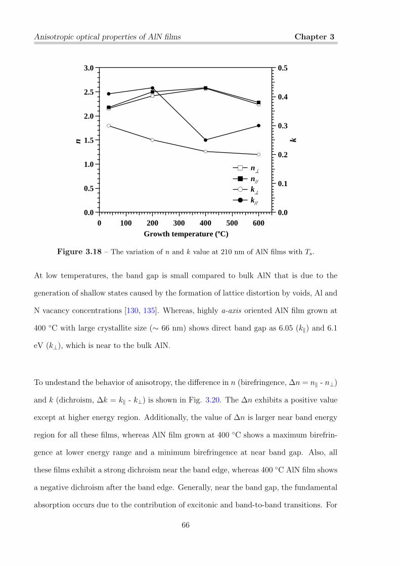
Anisotropic optical properties of AlN films Chapter 3
3.0
2.5
2.0
1.5
1.0
0.5
0.0
n
6005004003002001000Growth temperature (ºC)
0.5
0.4
0.3
0.2
0.1
0.0
k
n^
n//
k^
k//
Figure 3.18 – The variation of n and k value at 210 nm of AlN films with Ts.
At low temperatures, the band gap is small compared to bulk AlN that is due to the
generation of shallow states caused by the formation of lattice distortion by voids, Al and
N vacancy concentrations [130, 135]. Whereas, highly a-axis oriented AlN film grown at
400 C with large crystallite size (∼ 66 nm) shows direct band gap as 6.05 (k‖) and 6.1
eV (k⊥), which is near to the bulk AlN.
To undestand the behavior of anisotropy, the difference in n (birefringence, ∆n = n‖ - n⊥)
and k (dichroism, ∆k = k‖ - k⊥) is shown in Fig. 3.20. The ∆n exhibits a positive value
except at higher energy region. Additionally, the value of ∆n is larger near band energy
region for all these films, whereas AlN film grown at 400 C shows a maximum birefrin-
gence at lower energy range and a minimum birefringence at near band gap. Also, all
these films exhibit a strong dichroism near the band edge, whereas 400 C AlN film shows
a negative dichroism after the band edge. Generally, near the band gap, the fundamental
absorption occurs due to the contribution of excitonic and band-to-band transitions. For
66
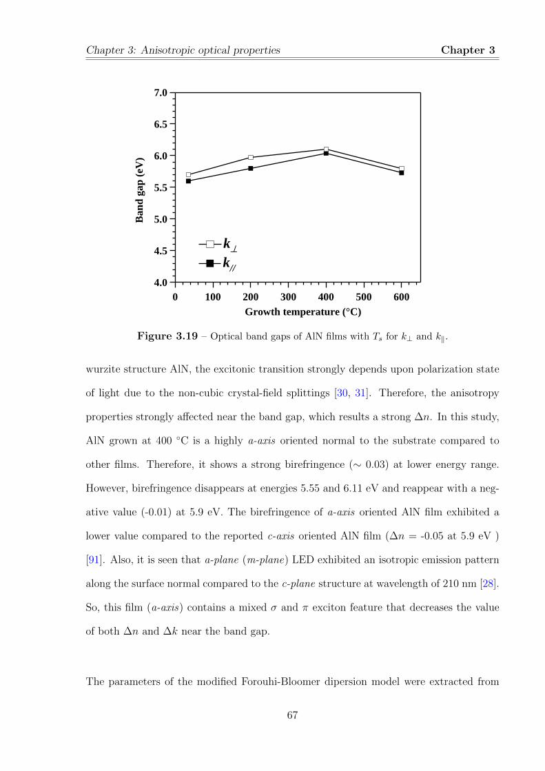
Chapter 3: Anisotropic optical properties Chapter 3
7.0
6.5
6.0
5.5
5.0
4.5
4.0
Ban
d ga
p (e
V)
6005004003002001000Growth temperature (°C)
k^k//
Figure 3.19 – Optical band gaps of AlN films with Ts for k⊥ and k‖.
wurzite structure AlN, the excitonic transition strongly depends upon polarization state
of light due to the non-cubic crystal-field splittings [30, 31]. Therefore, the anisotropy
properties strongly affected near the band gap, which results a strong ∆n. In this study,
AlN grown at 400 C is a highly a-axis oriented normal to the substrate compared to
other films. Therefore, it shows a strong birefringence (∼ 0.03) at lower energy range.
However, birefringence disappears at energies 5.55 and 6.11 eV and reappear with a neg-
ative value (-0.01) at 5.9 eV. The birefringence of a-axis oriented AlN film exhibited a
lower value compared to the reported c-axis oriented AlN film (∆n = -0.05 at 5.9 eV )
[91]. Also, it is seen that a-plane (m-plane) LED exhibited an isotropic emission pattern
along the surface normal compared to the c-plane structure at wavelength of 210 nm [28].
So, this film (a-axis) contains a mixed σ and π exciton feature that decreases the value
of both ∆n and ∆k near the band gap.
The parameters of the modified Forouhi-Bloomer dipersion model were extracted from
67

Chapter 3
0.15
0.10
0.05
0.00
-0.05
-0.10
Bire
frin
genc
e (D
n)
654321Energy (eV)
35°C 200°C 400°C 600°C
(a)0.8
0.6
0.4
0.2
0.0
Dic
hroi
sm (D
k)
654321Energy (eV)
35 ºC 200 ºC 400 ºC 600 ºC
(b)
Figure 3.20 – The dispersion of (a) birefringence (∆n) (b) and dichroism (∆k) withenergy at different Ts.
the fitting and shown in Fig. 3.21. The Γj and fj, both decrease with Ts upto 400 C. The
broadening parameter Γj (= ~/τj, where τj is the phonon relaxation time), is the inverse
of relaxation time, depends on the phonon contribution and microstructural parameters,
such as static impurities, defect density, strain, grain boundary, grain sizes, etc [106].
A decrease in Γj is observed with the increase in Ts and implies an increase in phonon
relaxation time due to the increase in crystallite size as well as decrease in residual stress.
ωj defines the energy at which the extinction coefficient is maximum for a material and it
increases with Ts due to increase in band gap, whereas energy from which the absorption
starts (ωg) is almost constant. So, at 400 C, AlN film shows high n as well as low k with
higher value of ωj among all due to higher purity, larger crystallite size and also highly
oriented.
3.6 Conclusion
AlN thin films have grown using reactive magnetron sputtering at different growth tem-
peratures (Ts, 35 to 600 C). All these films are crystallized with wurtzite structure and
68

Chapter 3: Conclusion Chapter 3
6
5
4
3
2
1
0
wg (
eV)
6005004003002001000
Growth temperature (°C)
8
6
4
2
0
wj (
eV)
wg//wg^
wj//wj^
2.0
1.5
1.0
0.5
0.0
Gj (
eV)
0.5
0.4
0.3
0.2
0.1
0.0
Gj// Gj^
f j (eV
)
fj//fj^
Figure 3.21 – Dispersion parameters derived from the fitting with Ts.
the Ts influences the orientation of these films. The crystallinity is increased with Ts and a
preferential a-axis orientation is observed at 400 C. The cross section and SAED pattern
of AlN films showed a high degree of alignment (columnar structure) as well as the orien-
tation. The surface morphology, RMS roughness and average grain size are also strongly
influenced by the Ts. However, the residual stress measurement by sin2ψ technique ex-
hibits a transition from tensile to compressive between 200 to 400 C growth temperature.
Nano-indentation hardness studies on these films revealed that the indentation hardness
(H) varied between 13.0 to 18.5 GPa, where as at 400 C AlN film exhibited a relatively
high elastic modulus (E = 238 GPa) due to the B1 type of bonding which is more cova-
lent in nature. Uniaxial anisotropic optical properties of these films with different Ts are
69

Conclusion Chapter 3
investigated by SE technique, which are strongly depend on Ts. Highly a-axis oriented
AlN film grown at 400 C, exhibited high n (n⊥ = 2.55, n‖ = 2.57) and low k (k⊥ = 0.21,
k‖ = 0.25) at 210 nm (deep-UV region) with low value of ∆n (-0.01) and ∆k (0.03). With
increase in Ts, the band gap also increased upto 400 C, which is close to the bulk AlN.
So, the anisotropy optical properties of a-axis AlN can be effectively used in UV-LED
and electro-luminescent diode based polarization-sensitive optoelectronic applications.
70

Chapter 4
Significance of Ti on local crystalstructure and mechanical propertiesof Al1−xTixN thin films
4.1 Introduction
Addition of transition elements to AlN such as Ti, Cr and Zr have yielded ternary nitrides
with higher hardness, superior oxidation resistance, good wear and corrosion resistance
[70–73]. Amongst, Ti doped AlN films have revealed as a n-type ferromagnetic material
for dilute magnetic semiconductor (DMS) applications at room temperature, reported
both by first principle calculation as well as experimental methods [66, 67, 69, 136].
Al99Ti1N film deposited on optical fiber is used in infrared whispering gallery modes
microlaser in the range of 775 to 800 nm for biomedical applications [74, 75]. Explor-
ing the possibility of heavy transition metal doping to group III nitride materials for
photoelectric conversion under visible light, this Ti doped AlN is expected as a poten-
tial candidate for efficient solar energy conversion [76]. In addition, doping of Ti to AlN
lattice reveals the improvement of piezoelectric response as compared to pristine AlN [78].
The present chapter describes about the growth of Al1−xTixN thin films by reactive
magnetron co-sputtering at different Ti concentrations and the crystallographic structure,
71
Chapter 4
surface chemical analysis and morphology of these films are investigated by GIXRD, XPS
and AFM. Doping concentration, position of dopant and their local crystal structure are
very important factors that affect the physical and mechanical properties of these films.
Therefore, the local crystal structure around Ti dopant in these thin films are analyzed
by X-ray absorption spectroscopy (XAS) technique i.e. both X-ray absorption near-
edge structure (XANES) and extended X-ray absorption fine structure (EXAFS). Since,
Ti doped AlN films are used predominantly in optoelectronic devices, so it is crucial
to investigate the mechanical properties, because of contact loading/unloading during
processing and fabrication that degrade the efficiency of the devices. Hence, the nano-
indentation technique is used to investigate the mechanical properties of these films.
4.2 Growth and crystallographic studies of Al1−xTixN
thin films
Al1−xTixN films (x =0, 1.5, 3 and 4 at%) were grown on Si(100) substrate by reactive
magnetron co-sputtering technique from a 4N pure, 50 mm diameter Al and Ti targets in
Ar and N2 gas environment. Before deposition, the Si wafers are cleaned by the standard
RCA procedure. Al1−xTixN films were grown at constant flow of argon to nitrogen ratio,
target to substrate distance (TSD) and growth temperature by changing the Ti sputter-
ing power, that are listed in section 2.3.2.
GIXRD profiles of Al1−xTixN thin films with different Ti concentrations (x =0, 1.5, 3 and
4 at%) are shown in Fig. 4.1. All these films exhibit poly-crystalline wurtzite hexagonal
structure of AlN and concur with the ICDD data 25-1133. It is ascertained that these Ti
atoms are dissolved well in the host AlN lattice, in the absence of any other secondary
peaks corresponding to Ti metal/compound.
72
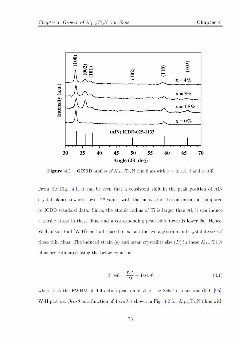
Chapter 4: Growth of Al1−xTixN thin films Chapter 4
Inte
nsi
ty (
a.u
.)
706560555045403530
Angle (2q, deg)
x = 0%
x = 1.5%
x = 3%
x = 4%(1
00
)
(00
2)
(10
1)
(11
0)
(10
3)
(10
2)
(AlN) ICDD-025-1133
Figure 4.1 – GIXRD profiles of Al1−xTixN thin films with x = 0, 1.5, 3 and 4 at%.
From the Fig. 4.1, it can be seen that a consistent shift in the peak position of AlN
crystal planes towards lower 2θ values with the increase in Ti concentration compared
to ICDD standard data. Since, the atomic radius of Ti is larger than Al, it can induce
a tensile stress in these films and a corresponding peak shift towards lower 2θ. Hence,
Williamson-Hall (W-H) method is used to extract the average strain and crystallite size of
these thin films. The induced strain (ε) and mean crystallite size (D) in these Al1−xTixN
films are estimated using the below equation
βcosθ =Kλ
D+ 4εsinθ (4.1)
where β is the FWHM of diffraction peaks and K is the Scherrer constant (0.9) [95].
W-H plot i.e. βcosθ as a function of 4 sinθ is shown in Fig. 4.2 for Al1−xTixN films with
73

Growth and crystallographic studies of Al1−xTixN thin films Chapter 4
x = 0 and 4 at%, only. The strain and crystallite size are calculated from the slope and
y-intercept of the linear fit to the data, respectively.
2.01.81.61.41.21.0
4 Sinq
y = 0.0059x + 0.0056
Ti (x, 4 at%)
20x10-3
15
10
5
0
b C
osq
2.01.81.61.41.21.0
4 Sinq
y = 0.0051x + 0.0049
Ti (x, 0 at%)
Figure 4.2 – W-H plots of Al1−xTixN films with x = 0 and 4 at%.
x (at%) D (nm) ε (10−3)0 29 5.1
1.5 27 5.23 26 5.54 24 5.9
Table 4.1 – Crystallite size (D) and strain (ε) of Al1−xTixN thin films with x = 0, 1.5, 3and 4 at%.
The average crystallite size and strain of Al1−xTixN films with different concentration
are shown in Table 4.1. The crystallite size shows a consistent decline with respect
to Ti concentration. Pristine AlN (x = 0 at% ) grown at a sputtering pressure of 5
×10−3 mbar, has a crystallite size of around 29 nm. Ti atoms are doped in AlN by the
reactive co-sputtering technique that increases the sputtering pressure due to increase
in Ti sputtering power as listed in Table 4.1. Thus, sputtered atoms from the target
encounter many collisions before it reaches the substrate due to decrease in mean free
path and hence reduces the ad-atom energy. So, the crystallite size gradually decreases
74

Chapter 4: XPS Chapter 4
along with Ti concentration. Also, the atomic radius of Ti atom (1.46 A) is larger than
that of Al (1.43 A), the substitute doping of Ti atom in AlN lattice expands the lattice
parameter compared to pristine AlN [66, 67, 76]. Therefore, Al1−xTixN films exhibit
tensile strain that increase with the Ti concentration, which is shown in Table 4.1.
4.3 Surface chemical analysis
For surface chemical analysis, XPS is used to explore the core electron binding energies of
Al1−xTixN thin films and quantify the Ti concentration. The convolution of a Gaussian
and a Lorentzian function is used to fit the high-resolution core level XPS spectra for
Al 2p, N 1s and Ti 2p and the resultant binding energy is extracted, which is shown
in Table 4.2. For discussion, a representative fitted core level spectrum corresponding to
Al1−xTixN film with x = 4 at% after Shirley background subtraction is shown in Fig. 4.3.
x (%) Al 2p (eV) N 1s (eV) Ti 2p3/2 (eV)Al-N Al-O Al-N N-C Ti-N
0 74.1 75.1 397.2 399.01.5 74.1 75.0 397.2 399.0 455.03 74.3 75.1 397.2 398.9 455.24 74.2 75.0 397.1 399.0 455.3
Ref. [137] 74.4 75.0 397.5 398.7Ref. [138] 74.1 397.2 454.9Ref. [139] 73.6 -
74.674.7 -75.6
396.8 -397.9
Ref. [70, 140, 141] 74.1 396.5 454.8 - 455.1
Table 4.2 – Binding energy of Al1−xTixN thin films with references.
Fig. 4.3(a), the convolution of a Gaussian and a Lorentzian function is used to fit the
high-resolution core level Al 2p spectra. For simplification, the spin-orbit components of
Al 2p spectra have been neglected in the curve fitting. In Al 2p profile, the strong intensity
peak having area 85% of the original peak is found at 74.2 eV. This binding energy is
75
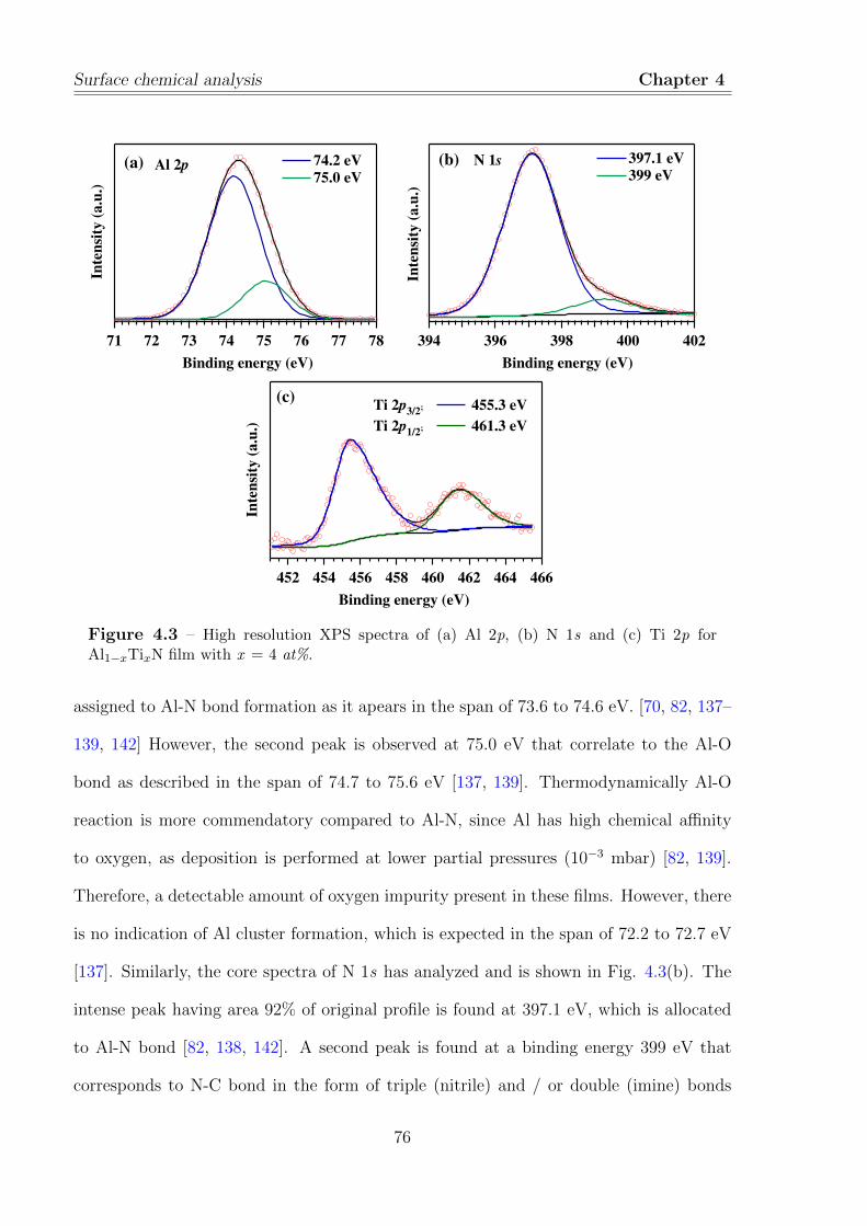
Surface chemical analysis Chapter 4In
ten
sity
(a
.u.)
7877767574737271
Binding energy (eV)
74.2 eV
75.0 eV(a) Al 2p
Inte
nsi
ty (
a.u
.)
402400398396394
Binding energy (eV)
397.1 eV
399 eV(b) N 1s
Inte
nsi
ty (
a.u
.)
466464462460458456454452
Binding energy (eV)
Ti 2p3/2; 455.3 eV
Ti 2p1/2; 461.3 eV
(c)
Figure 4.3 – High resolution XPS spectra of (a) Al 2p, (b) N 1s and (c) Ti 2p forAl1−xTixN film with x = 4 at%.
assigned to Al-N bond formation as it apears in the span of 73.6 to 74.6 eV. [70, 82, 137–
139, 142] However, the second peak is observed at 75.0 eV that correlate to the Al-O
bond as described in the span of 74.7 to 75.6 eV [137, 139]. Thermodynamically Al-O
reaction is more commendatory compared to Al-N, since Al has high chemical affinity
to oxygen, as deposition is performed at lower partial pressures (10−3 mbar) [82, 139].
Therefore, a detectable amount of oxygen impurity present in these films. However, there
is no indication of Al cluster formation, which is expected in the span of 72.2 to 72.7 eV
[137]. Similarly, the core spectra of N 1s has analyzed and is shown in Fig. 4.3(b). The
intense peak having area 92% of original profile is found at 397.1 eV, which is allocated
to Al-N bond [82, 138, 142]. A second peak is found at a binding energy 399 eV that
corresponds to N-C bond in the form of triple (nitrile) and / or double (imine) bonds
76

Chapter 4: XAS Chapter 4
[137, 143]. The core spectra of Ti shown in fig. 4.3(c) was analyzed with the help of
asymmetric Doniach-Sunjic parameter towards higher binding energies. Also, the peaks
having binding energy as 455.3 and 461.3 eV correspond to the Ti-N bond of 2p3/2 and
2p1/2, respectively. Sufficient number of recent reports discussing the binding energy for
Ti-N bond formation is also similar to this range and clearly different from the binding
energy for the formation of Ti clusters (453.8 eV) [69, 70, 140, 141].
4.4 Morphology and surface roughness by AFM
AlN thin film is a potential candidate in surface and bulk acoustic wave devices due to
high acoustic velocity. Surface acoustic waves could travel through the surface of the
material which possess very small surface roughness has less propagation loss [37]. In this
study, surface micro-structure and roughness of Al1−xTixN films are carried out by AFM
technique. AFM images over 1 × 1 µm2 surface area of Al1−xTixN films with x = 0 and
4 at% are shown in Fig. 4.4.
Al1−xTixN films exhibit smooth morphology with pebble-like grain structure. The average
(Ra) and root mean square roughness (Rrms) of these films is extracted from AFM. For
pristine AlN film, the Ra and Rrms is around 2.0 and 2.6 nm, respectively. Whereas, the
roughness (Ra, Rrms) is decreased as (1.6, 1.8), (1.4, 1.6) and (1.2, 1.5) nm with addition
of Ti as 1.5, 3 and 4 at%, respectively. The roughness shows a similar behaviour with
crystallite size as described in Table 4.1 i.e. surface roughness decreases with the decrease
in grain growth.
77

Local crystal structure at vicinity of Ti in AlN: XAS Chapter 4
Figure 4.4 – AFM images of Al1−xTixN films at (a) x = 0, (b) x = 1.5, (c) x = 3, and(b) x = 4 at%.
4.5 Local crystal structure at vicinity of Ti in AlN:
XAS
XAS is broadly classified into two important parts i.e. XANES and EXAFS after the
edge. Ti K-edge absorption spectra of Al1−xTixN films are shown in Fig. 4.5 to investi-
gate the local structure of the Ti dopant in the AlN lattice.
4.5.1 XANES analysis
XANES is very sensitive to the geometrical arrangements of X-ray absorbing atom (sym-
metry e.g. octahedral, tetrahedral coordination) in the host material. It can be seen from
Fig. 4.5 that K-edge absorption spectra of Ti in Al1−xTixN films show a pre-edge peak
78

Chapter 4: XAS Chapter 4
Nor
mal
ized
abs
orpt
ion
co-e
ffic
ient
[m
(E),
(a.
u.)]
5060504050205000498049604940Energy (eV)
Pre-edge
x = 1.5%
x = 3%
x = 4%
Figure 4.5 – Ti K-edge absorption spectra of Al1−xTixN films.
around 4967 eV. Tatemizo et al and Tuilier et al have reported a pre-edge peak for K-edge
absorption spectra of Ti in doped AlN films is around 4966 eV and in Al-rich Ti1−xAlxN
composite films is arround 4969 eV, respectively [76, 144]. They have concluded that Ti
atoms occupy the cation (Al) site of hexagonal AlN structure and forms localized TiN
species. Usually, the pre-edge peak for Ti K-edge appears at 4964 eV for Ti metal and
low intense peak around 4969-4971 eV for octahedral coordination of cubic TiN lattice
[76, 144]. In this study, the pre-edge peak position at 4967 eV is in consistent with
tetrahedrally coordinated TiN species in wurtzite hexagonal AlN lattice [145]. Normally,
this pre-edge peak is a signature of 1s to 3d electronic transitions of transition metals
[146, 147]. However, for symmetric groups having center of inversion, this transition is
forbidden by Laporte selection rule (∆l = ±1) [148]. AlN has a distorted tetrahedron
structure, where one Al atom forms covalent bond with three N atoms at the base (bs
- basal) having bond length 0.1885 nm and an ionic Al-N bond at the apex (ax - axial)
79

Local crystal structure at vicinity of Ti in AlN: XAS Chapter 4
having bond length 0.1997 nm [12]. Hence, AlN has no centre of symmetry due to the
C3v point group and Ti doped AlN partially allows the 1s to 3d electronic transition
[76, 136, 147]. Additionally, it is also reported that transition metal atom replaces Al
atom in AlN lattice and forms the p−d hybridization between it’s neighbouring N atoms
[81, 136, 146, 147]. Therefore, Ti K-edge absorption spectra of Al1−xTixN films show a
strong pre-edge peak at 4967 eV due to the p−d mixing [76, 144, 146]. In this study, the
XANES analysis is conforming that Ti replaces the Al atom tetrahedrally in AlN matrix
and leads to form TiN species with p− d mixing.
x (at%) Energy (eV) Intensity1.5 4967.0 ± 0.2 0.253 4967.0 ± 0.2 0.274 4967.0 ± 0.2 0.31
Table 4.3 – Pre-edge position of Al1−xTixN films in Ti K-edge absorption spectra.
The pre-edge peak positions and intensity of Al1−xTixN films are shown in Table 4.3. It
is exhibited that the intensity of the pre-edge peaks increase with the Ti concentration,
however the pre-edge energy is not changed. It is also confirmed from XANES that Ti
forms distorted tetrahedron structure with surrounding nitrogen atom and form p − d
hybridization. Since, the ionic radius of Ti (0.68 A) is larger than that of Al (0.51 A),
the doping Ti atom in AlN lattice deforms the tetrahedron surroundings compared to
pristine AlN and it increases with Ti concentration. Addition to this, the induced strain
in these films increases with the Ti concentration, extracted using W-H method. Hence,
1s - 3d transition strength increases with higher Ti concentration.
80

Chapter 4: XAS Chapter 4
4.5.2 EXAFS analysis
For the EXAFS, oscillation part of the measured absorption co-efficient (µ(E)) is con-
verted to the fine structure function χ(E) as described in section 2.5. Finally, χ(R) versus
radial distances (R) plots are used to extract the co-ordination number, radial distances
and neighbouring atoms of the dopant in different co-ordination spheres. Wurtzite hexag-
onal AlN phase has been used as crystallographic inputs for the fitting of these spectra.
43210
Measured
Fitted
x = 4%
x = 3%
x = 1.5%
|c(R
)| (
Å-3
)
Radial distance (Å)
Figure 4.6 – Extended region fitting using ARTEMIS in R-space of Al1−xTixN thin films.
Three single scattering paths are considered for EXAFS analysis as one path for basal
nitrogen [(Ti-N)bs], second path for the axial nitrogen [(Ti-N)ax] from the first coordina-
tion sphere and third path as Ti-Al from the second coordination sphere. Since the ranks
of multiple scattering paths are very low, only the single scattering paths are included in
the analysis. The overall value of R-factor is then minimized to establish the goodness
of fit. The fitted EXAFS oscillation χ(k) curves in R-space are shown in Fig. 4.6. The
81

Local crystal structure at vicinity of Ti in AlN: XAS Chapter 4
bond lengths of Ti-N and Ti-Al paths as well as the corresponding co-ordination numbers
(C.N) of each path (NS02, N =degeneracy of path), Deby-waller factor (σ2) and R-factor,
are observed from the EXAFS and are shown in Table 4.4.
4.5.2.1 Discussion on coordination number and bond length
The total coordination number (axial and basal) of Ti with N atom in the first coordina-
tion sphere of these Al1−xTixN thin films are 3.70, 3.75 and 3.93 for x = 1.5, 3 and 4 at%,
respectively. For AlN, the stoichiometric coordination number of Al atom with N is 4 in
the first coordination sphere. So Ti dopant in these films show a nearly stoichiometric
coordination with N atom. similar to Al atom in AlN lattice. However, it is observed
that the coordination number of Ti in the second sphere with Al atom are 8.35, 8.46 and
8.40 for x = 1.5, 3 and 4 at%, that is lower than the Al-Al in second coordination sphere
(∼ 12, AlN lattice) i.e.. This signifies that it possess Al vacancies in second coordination
sphere. Thus, all these films exhibit a constant coordination number in both first and
second sphere, which is independent of Ti concentration.
The (Ti-N)ax and (Ti-N)bs bond length variation as a function of Ti concentration of
first coordination sphere in Al1−xTixN films are shown in Fig. 4.7. Since, ionic radius
of Ti3+ (0.68 A) is larger than the Al (0.51 A), so the Ti-N bond along both axial and
basal has increased compared to the pristine AlN. However, the bond length for (Ti-N)ax
reduces with the Ti concentration, whereas (Ti-N)bs bond length decreases moderately
with Ti. This result is very similar with lower magnitude order as Cr doped AlN films
grown by co-sputtering technique, which is discuused in chapter-5. Abdul et al and
Fan et al have reported that Ti doped AlN exhibits ferromagnetic properties due to
strong p − d hybridization mechanism between the doping element and the host atoms
by the first principles calculations [66, 136]. It is also reported by Bannikov et al that
82

Chapter 4: Indentation Chapter 4
Sample Paths Bond length C.N. σ2 (A)2 R
(Error)(A) (Error) (Error)x = 1.5% (Ti-N)ax 2.082 0.90 0.0031 0.04
(0.007) (0.07) (0.0006)(Ti-N)bs 1.938 2.80 0.0033
(0.004) (0.06) (0.0005)Ti-Al 3.094 8.35 0.0210
(0.008) (0.13) (0.0004)x = 3% (Ti-N)ax 2.070 1.00 0.0037 0.02
(0.005) (0.06) (0.0004)(Ti-N)bs 1.932 2.75 0.0032
(0.005) (0.04) (0.0005)Ti-Al 3.081 8.46 0.0262
(0.006) (0.06) (0.0003)x = 4% (Ti-N)ax 2.064 1.00 0.0030 0.01
(0.004) (0.02) (0.0006)(Ti-N)bs 1.930 2.93 0.0033
(0.004) (0.05) (0.0001)Ti-Al 3.087 8.40 0.0251
(0.006) (0.04) (0.0004)
Table 4.4 – The fitting path parameters of Al1−xTixN thin films
covalent bond strength increases by the addition of Ti in cubic AlN with the help of
charge density distribution theory [67]. Therefore, the bond length in first coordination
sphere in Al1−xTixN films decreases gradually with the Ti concentration and indicates a
strong p − d hybridization which is also seen from XANES analysis. From Table 4.4, it
can be seen that the bond length of Ti with Al in second coordination sphere is around
3.08 A which is similar to that of Al-Al (3.14 A) in bulk AlN as calculated by Cui et
al using density functional theory [79]. In this study, EXAFS confirms that Ti atom
forms distorted tetrahedral structure by replacing Al atom in AlN lattice, which is also
corroborated with the observation of XRD, XPS and XANES studies without any other
Ti clustering in Al1−xTixN thin films.
83

Mechanical properties Chapter 4
2.10
2.05
2.00
1.95
1.90
(Ti-
N) a
x b
on
d l
eng
th (
Å)
54321
Ti (x, %)
2.00
1.95
1.90
1.85
1.80
(Ti-
N) b
s b
on
d l
eng
th (
Å)
Axial
Basal
Figure 4.7 – (Ti-N)ax and (Ti-N)bs bond lengths are shown with Ti concentration ofAl1−xTixN films.
4.6 Mechanical properties
Nanomechanical characterization is performed by nano-indentation technique as a func-
tion of depth (20 nm to 650 nm) to understand the deformation behavior of Al1−xTixN
thin films. Fig. 4.8 and Fig. 4.9 show the indentation hardness (H) and modulus (E)
of Si (100) substrate and Al1−xTixN films with x = 0 to 4 at%, respectively. It is well
known that the average surface roughness (Ra) causes an uncertainty in indentation con-
tact area due to asperity contact at very shallow depths (less that 20 × Ra) [149]. In
this study, the average surface roughness of these films are around maximum of 2 nm.
Therefore, the H and E are studied from the 20 nm depth of the films. The H and
E of Si is independent of depth as an average value of 11.5 and 175 GPa, respectively.
Pristine AlN film shows a constant hardness value around 17.5 GPa from 20 to 60 nm
and afterwards it decreases slightly with depth. According to indentation thumb rule,
the indentation should be performed lower depth than the one-tenth (1/10th) of the total
84

Chapter 4: Indentation Chapter 4
30
25
20
15
10
5
0
Inde
ntat
ion
hard
ness
(H
, GP
a)
7006005004003002001000
Indentation depth (nm)
x = 4% x = 3% x = 1.5% x = 0% Si (100)
Figure 4.8 – Indentation hardness as a function of depth of Si (100) substrate andAl1−xTixN films with x = 0 to 4 at%.
film thickness to ascertain the film hardness by avoiding the substrate effect [150]. In this
study, thickness of these Al1−xTixN films are around 400 nm. So, the hardness decreases
gradually at higher depth due to the substrate effect. Ti doped AlN films also exhibit a
similar behavior as pristine AlN film. The modulus (E) of these films decreased rapidly
with depth and reached the substrate modulus value at higher depths, which is shown in
Fig. 4.9. The H and E of Al1−xTixN films are extracted at a depth of 35 nm which is
shown in Fig. 4.10, according to less than the 1/10th depth rule.
In Fig. 4.10, it is seen that both H and E of Al1−xTixN films are gradually increased
with x = 0 to 4 at%. Mechanical properties of thin film generally depends on it’s micro-
structure i.e crystallite size of material, plane orientation, planar density, bond strength
and induced stress during the growth. In this study, we have observed crystallite size
reduction with Ti concentration as 29 nm to 24 nm and shown in Table 4.1. According
85

Mechanical properties Chapter 4
400
300
200
100
0
Inde
ntat
ion
mod
ulus
(E
, GP
a)
7006005004003002001000
Indentation depth (nm)
x = 4% x = 3% x = 1.5% x = 0% Si (100)
Figure 4.9 – Indentation modulus as a function of depth of Si (100) substrate andAl1−xTixN films with x = 0 to 4 at%.
to Hall-Petch relation, the hardness increases with the decrease in crystallite size above
critical value of crystallite size (15-18 nm). Therefore, the H of these films is increased.
Addition to this, the induced strain in these films also increased with Ti that is cal-
culated by Williamson-Hall method and is shown in Table 4.1. Also, from XAS study
of Al1−xTixN films, it is confirmed that Ti forms localized TiN species with distorted
tetrahedron structure by replacing the Al atom in AlN lattice having a stoichiometry
coordination number with N atoms in first coordination sphere. So, the indentation
hardness is increased from 17.5 to 27.6 GPa with Ti concentration as 0 to 4 at%. Cai et
al have reported that the indentation hardness is varied between 28 to 38 GPa for AlTiN
films deposited by arc ion plating method using Al (67 at% ) and Ti (38 at% ) composite
targets [71]. Similarly, Jose et al have discussed that TiAlN film with 36 at% of Ti shows
indentation hardness as 35 GPa due the high density cubic AlN phase formation [73].
However, modulus of films depend on the nature of inter-atomic bond strength in the
86

Chapter 4: Indentation Chapter 4
30
25
20
15
10
5
0
Ind
enta
tio
n h
ard
nes
s (H
, G
Pa)
543210
Ti (x, %)
400
300
200
100
0
Ind
enta
tion
mod
ulu
s (E
, G
Pa)
Hardness
Modulus
Figure 4.10 – Indentation hardness and modulus of Al1−xTixN films as a function of Ticoncentrations.
crystal. From EXAFS analysis, it is observed that Ti-N bond length decreased with Ti
concentration and a distorted tetrahedral structure formed. Covalent band gap (Eh) is
related to inter-atomic distance by a relation Eh = Kd−2.5, i.e the covalent bond strength
increases with a decrease in bond length [71]. So, the indentation modulus also increases
from 231 to 293 GPa with Ti concentration as 0 to 4 at%.
Usually, the indentation impression on films are collected by AFM technique to study the
pile-up or sink-in behavior due to plastic deformation [151]. Hence, AFM image of the
indentation of Al1−xTixN thin films with x = 0 and 4 at% over a 2 × 2 µm2 surface area
is shown in Fig. 4.11 for a 2 mN indentation load. All these films show a well-defined
sink-in indentation behaviour. It is observed that Al1−xTixN film at x = 4 at% shows
large sink-in behaviour compared to pristine AlN films without any radial cracks and
exhibits a high elastic recovery behaviour i.e. high resistance to plastic deformation with
87

Chapter 4
Figure 4.11 – AFM images of the indentation impressions at 2 mN load of Al1−xTixNfilms with x = 0 and 4 at%.
the addition of Ti to AlN lattice.
4.7 Conclusion
Al1−xTixN films are grown by co-sputtering technique with various Ti concentration (x =
0, 1.5, 3 and 4 at% ). All these films are found to be poly-crystalline wurtzite hexagonal
of AlN without any other secondary phases belongs to Ti compound. Ti concentration,
chemical analysis and surface morphology of these films are studied by the XPS and AFM.
XAS is performed to study the local crystal structure at the environment of Ti dopant that
is investigated by both XANES and EXAFS of Al1−xTixN thin films. It is observed that Ti
forms localized TiN species with distorted tetrahedron structure by replacing the Al atom
in AlN lattice resulting to a tensile strain. The coordination number of Ti in first sphere
shows stoichiometry with N atom, whereas Al vacancies are found in second coordination
88

Chapter 4: Chapter 4
sphere. The bond lengths (Ti-N)ax, (Ti-N)bs are found to be moderately decreased with
Ti concentration, whereas Ti-Al bond length in second coordination sphere is independent
of Ti. Thus, XAS measurement confirms the enhancement of p−d hybridization between
Ti and N atoms in Al1−xTixN thin films. The H and E of Al1−xTixN films are increased
from 17.5 to 27.6 GPa and 231 to 293 GPa, respectively with x = 0 to 4 at% having
well-defined sink-in indentation impression behaviour without any radial cracks.
89

Chapter 5
Significance of Cr on local crystalstructure and mechanical propertiesof Al1−xCrxN thin films
5.1 Introduction
Cr doped AlN is reported to exhibit DMS properties with Curie temperature higher than
room temperature (Tc > 800 K) by both experimental as well as first principle calculation
[64, 65, 79]. According to density functional theory (DFT) calculation, Cr doped AlN
exhibits a huge magnetic moment (3 µB/Cr) compared to other transition metal dopants.
However, the experimentally observed magnetic moment was less than 1 µB/Cr, due to
possible role of Cr clusters, nitrogen vacancies, defects and impurities for the different
Cr concentration in AlN lattice [52, 54, 64]. Though Cr ionic radii is larger than the Al
atom, still it can settle in the interstitial sites of AlN lattice. Formation of Cr clusters
at interstitial sites reduce the total magnetic moment, which increases the antiferromag-
netic states [79, 80]. Cui et. al. have reported using DFT calculation that the Cr clusters
larger than 2 atoms exhibit antiferromagnetic coupling [79]. Hence, the growth of cluster
less doped AlN thin films is the first step to achieve the DMS property in these sys-
tems. Also, piezoelectric response of Cr doped AlN films is 73% higher than that of
the pristine AlN [81]. However, several unique parameters such as doping concentration,
90

Chapter 5: Growth of Al1−xCrxN thin films Chapter 5
position (substitution/interstitial) and the local environment of doping element play an
essential role in the physical properties of doped AlN films, which is mainly controlled by
the growth parameters. Therefore, the effect of dopant in the local crystal structure of
AlN film needs a fundamental investigation using X-Ray Absorption Spectroscopy (XAS).
The present chapter describes about the growth of Al1−xCrxN thin films by reactive
magnetron co-sputtering with different Cr concentrations. The crystallographic structure,
surface chemical analysis and morphology of these films are investigated by GIXRD, XPS
and AFM technique. The local crystal structure around Cr dopant in these thin films
are analyzed by XAS i.e. both XANES and EXAFS techniques. The nano-indentation
technique is used to investigate the mechanical properties of these films.
5.2 Growth and crystallographic studies of Al1−xCrxN
thin films
Al1−xCrxN thin films are grown on silicon (100) substrates by reactive magnetron co-
sputtering technique at different Cr concentration (x = 0, 2, 4 and 6 at%) from high
pure Al and Cr target (4N) in a Ar:N2 gas mixture. These Si substrates are cleaned by
a standard two-step RCA process. Al1−xCrxN films are deposited at different Cr power
to vary the concentration by keeping all other sputtering parameters as constant. The
details of the growth parameters are given at section 2.3.3.
The GIXRD profiles of reactive magnetron sputtered Al1−xCrxN thin films with different
Cr concentrations (x = 0, 2, 4 and 6 at%) are shown in Fig. 5.1. The GIXRD patterns
of these films exhibited poly-crystalline hexagonal wurtzite structure and agree with the
JCPDS data 25-1133. Doped Cr atoms are well dissolved in the AlN and can be ascer-
91
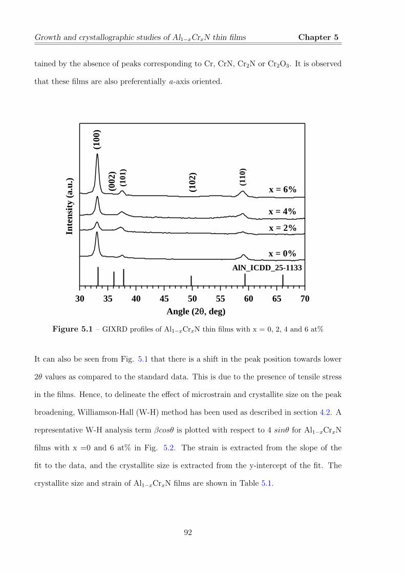
Growth and crystallographic studies of Al1−xCrxN thin films Chapter 5
tained by the absence of peaks corresponding to Cr, CrN, Cr2N or Cr2O3. It is observed
that these films are also preferentially a-axis oriented.
Inte
nsit
y (a
.u.)
706560555045403530Angle (2q, deg)
(100
)
(101
)
(110
)
x = 0%
x = 2%
x = 4%
x = 6%
AlN_ICDD_25-1133
(002
)
(102
)
Figure 5.1 – GIXRD profiles of Al1−xCrxN thin films with x = 0, 2, 4 and 6 at%
It can also be seen from Fig. 5.1 that there is a shift in the peak position towards lower
2θ values as compared to the standard data. This is due to the presence of tensile stress
in the films. Hence, to delineate the effect of microstrain and crystallite size on the peak
broadening, Williamson-Hall (W-H) method has been used as described in section 4.2. A
representative W-H analysis term βcosθ is plotted with respect to 4 sinθ for Al1−xCrxN
films with x =0 and 6 at% in Fig. 5.2. The strain is extracted from the slope of the
fit to the data, and the crystallite size is extracted from the y-intercept of the fit. The
crystallite size and strain of Al1−xCrxN films are shown in Table 5.1.
92

Chapter 5: Growth of Al1−xCrxN thin films Chapter 5
2.01.81.61.41.21.0
4 Sinq
y = 0.0040x + 0.0038
Cr = 6 at%
20x10-3
15
10
5
0
b C
osq
2.01.81.61.41.21.0
4 Sinq
y = 0.0051x + 0.0049
Cr = 0 at%
Figure 5.2 – W-H plots of Al1−xCrxN films with x = 0 and 6 at%.
x (at%) D (nm) ε (10−3)0 29 5.12 19 5.44 24 5.26 37 4.0
Table 5.1 – Crystallite size (D) and strain (ε) of Al1−xCrxN thin films with x = 0, 2, 4and 6 at%.
Pristine AlN (x = 0 at% ) grown at sputtering pressure 5 ×10⁻³ mbar has crystallite
size around 29 nm with a tensile strain. Thereafter, Cr atoms are doped in AlN by the
reactive co-sputtering technique that increases the sputtering pressure from 5 to 7 ×10⁻³
mbar as listed in section 2.3.3. Thus, sputtered atoms from the target undergoes many
collisions to reach the substrate due to the decrease in the mean free path and reduces
the ad-atom energy. So, the crystallite size is decreased with higher strain at x = 2 at%
compared to pristine AlN. Thereafter, the strain gradually decreases with addition of Cr
to AlN lattice with increase in crystallite size. Luo et al has reported a similar trend
in the stress of AlN films with the addition of Cr [81]. In this present study, all these
films were grown with a-axis preferential orientation on Si (100) substrate, where there
is a lattice mismatch always exits between AlN and the Si substrate. So, Cr doping in
93
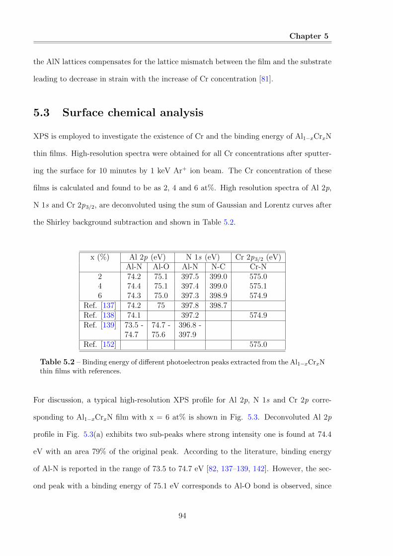
Chapter 5
the AlN lattices compensates for the lattice mismatch between the film and the substrate
leading to decrease in strain with the increase of Cr concentration [81].
5.3 Surface chemical analysis
XPS is employed to investigate the existence of Cr and the binding energy of Al1−xCrxN
thin films. High-resolution spectra were obtained for all Cr concentrations after sputter-
ing the surface for 10 minutes by 1 keV Ar+ ion beam. The Cr concentration of these
films is calculated and found to be as 2, 4 and 6 at%. High resolution spectra of Al 2p,
N 1s and Cr 2p3/2, are deconvoluted using the sum of Gaussian and Lorentz curves after
the Shirley background subtraction and shown in Table 5.2.
x (%) Al 2p (eV) N 1s (eV) Cr 2p3/2 (eV)Al-N Al-O Al-N N-C Cr-N
2 74.2 75.1 397.5 399.0 575.04 74.4 75.1 397.4 399.0 575.16 74.3 75.0 397.3 398.9 574.9
Ref. [137] 74.2 75 397.8 398.7Ref. [138] 74.1 397.2 574.9Ref. [139] 73.5 -
74.774.7 -75.6
396.8 -397.9
Ref. [152] 575.0
Table 5.2 – Binding energy of different photoelectron peaks extracted from the Al1−xCrxNthin films with references.
For discussion, a typical high-resolution XPS profile for Al 2p, N 1s and Cr 2p corre-
sponding to Al1−xCrxN film with x = 6 at% is shown in Fig. 5.3. Deconvoluted Al 2p
profile in Fig. 5.3(a) exhibits two sub-peaks where strong intensity one is found at 74.4
eV with an area 79% of the original peak. According to the literature, binding energy
of Al-N is reported in the range of 73.5 to 74.7 eV [82, 137–139, 142]. However, the sec-
ond peak with a binding energy of 75.1 eV corresponds to Al-O bond is observed, since
94

Chapter 5: XPS Chapter 5
Inte
nsit
y (a
.u.)
7877767574737271Binding energy (eV)
74.3 eV75.0 eV
(a) Al 2p
Inte
nsit
y (a
.u.)
402400398396394Binding energy (eV)
397.3 eV398.9 eV
(b) N 1s
Inte
nsit
y (a
.u.)
590585580575570Binding energy (eV)
Cr 2p3/2; 574.9 eVCr 2p1/2; 584.5 eV
(c)
Figure 5.3 – Core level XPS of (a) Al 2p, (b) N 1s and (c) Cr 2p for Al1−xCrxN filmwith x = 6 at%.
Al has a significant chemical affinity to O. Thermodynamically Al-O interaction is more
favourable compared to Al-N, as sputtering experiments are carried out at lower partial
pressures (sum of Ar and N2). There is no evidence for Al-Al bonding or Al cluster for-
mation, for which usually a peak is expected in the range between 72.2 to 72.8 eV [137].
Similarly, the N 1s profile has been deconvoluted and is shown in Fig. 5.3(b) with an
intense peak corresponding to the binding energy 397.4 eV with 93% of an area which is
assigned to Al-N. Recent reports on the binding energy of N 1s also confirms the same
[82, 138, 142]. A second peak corresponding to a binding energy 399 eV is assigned to
N-C bond in the form of triple (nitrile) and / or double (imine) bonds [137, 143]. Also,
Cr XPS profile has fitted with the asymmetric Doniach-Sunjic parameter and is shown in
95

Chapter 5
Fig. 5.3(c). The peaks corresponding to 575.1 and 584.6 eV are assigned to Cr-N bond
of 2p3/2 and 2p1/2 core level of Cr. This binding energy is also well within the reported
values [81, 138, 152]. This binding energy is clearly different from the Cr-Cr formation
energy of 574 eV.
5.4 Morphology and surface roughness by AFM
Fig.5.4 consists of AFM images over 1 × 1 µm2 surface area of Al1−xCrxN films deposited
on Si (100) substrate having Cr concentration as x = 0 and 6 at%.
Figure 5.4 – AFM images of Al1−xCrxN films at Cr concentration of (a)x = 0, (b)x = 2,(c)x = 4, and (d)x = 6 at%.
All these films exhibit a similar morphology with smooth pebble-like grain structure.
The root mean square roughness (Rrms) and the mean diameter of grains with the Cr
concentration is extracted from AFM is shown in Table 5.3. For pristine AlN film, the
96

Chapter 5: XAS Chapter 5
x (at% ) Rrms (nm) Grain size (nm)0 2.6 352 1.3 224 3.3 336 4.0 46
Table 5.3 – Rrms and average grain size of Al1−xCrxN films with different Cr concentra-tion.
surface consists of uniform smooth grains having roughness and grain size as 2.6 nm
and 35 nm, respectively. However, both the roughness and grain size decreased with the
addition of Cr atom (2%) and then significantly increased up to 6% of Cr atom. This can
be compared from Table 5.1 that the roughness and grain size shows a similar behavior
with crystallite size as observed from XRD. The surface of the film becomes coarser due
to crystal growth that increases surface roughness. Since, the surface roughness of these
Al1−xCrxN films is very low, these films can be used for surface acoustic wave device
applications.
5.5 Local crystal structure at vicinity of Cr in AlN:
XAS
5.5.1 XANES analysis
Cr K-edge absorption spectra of Al1−xCrxN films are shown in Fig. 5.5 to investigate the
local structure of the Cr dopant in the AlN lattice. From Fig. 5.5, a pre-edge peak is
observed at around 5989 eV in all the Cr K-edge absorption spectra. Similar pre-edge
peak in the XANES of Cr doped AlN films is reported as 5988.7 eV and 5989 eV by Fan
et al in Cr doped AlN and Hashimoto et al in Cr doped GaN, respectively [68, 147]. They
have shown that when Cr is introduced to the host matrix of AlN and GaN, Cr replaces
the cation and forms localized CrN species. This is in concurrence with the observed
97

Local crystal structure at vicinity of Cr in AlN: XAS Chapter 5
pre-edge peak in this study also [153]. Hence, it is concluded that when Cr is doped
in AlN using the experimental methods described in this study led to the formation of
localized CrN species in AlN. However, XAS is a localized technique, used to identify the
ambiguity arising out of other local species of Cr with Oxygen. Usually, the pre-edge peak
corresponding to CrO2 and CrO3 appears at 5979.6 eV and 5981.4 eV, respectively [154].
Also, the absorption spectrum of Cr2O3 is similar to the CrO2. These pre-edge peaks are
distinctly different from the pre-edge peak observed in our study, which is around 5989
eV. Hence, it is concluded that there are no secondary oxide phases corresponding to Cr
in these thin films.
Abs
orpt
ion
(a.u
.)
61006080606060406020600059805960Energy (eV)
x = 6% x = 4% x = 2%
Pre-edge
Figure 5.5 – Cr K-edge absorption spectra of Al1−xCrxN films.
Normally, the pre-edge peaks of transition metal elements in XAS spetcrum are the sig-
nature of 1s to 3d electronic transitions [146, 147]. It is discussed in section 4.5.1 that
1s to 3d electronic transitions is generally forbidden for centro-symmetric compounds
and can be possible to some extent in non-centro symmetric distorted tetrahedron com-
98

Chapter 5: XAS Chapter 5
pounds [81, 136, 146, 147]. Since, AlN has a distorted tetrahedron structure, it is to note
that this pre-edge peak at 5989 eV is solely from the localized distorted tetrahedron TiN
species in AlN films. In addition to that this transition is also due to the presence of p-d
hybridization between Cr and it’s neighbouring N atoms that led to the breakdown of the
selection rule and p-d orbital mixing becomes feasible [81, 147]. Since, we have already
confirmed that Cr replaces Al in AlN matrix, then Cr also has p− d mixing.
x (at%) Energy (eV) Intensity1.5 5989.0 ± 0.2 0.233 5989.0 ± 0.2 0.194 5989.5 ± 0.2 0.17
Table 5.4 – Pre-edge peak of Al1−xCrxN films in Cr K-edge absorption spectra.
The pre-edge peak positions and intensity of Al1−xCrxN films are shown in Table 5.4. It
is observed that the position of pre-edge peak is moving towards higher energy at high
Cr concentration. Also, the intensity of the pre-edge peaks decreases with the increase
of Cr in these films. At lower Cr concentrations, strain in these films is highly deforming
the tetrahedron surroundings of Cr as well as the symmetry of the structure [68, 81]. It
is observed that the strain decreases with the increase of Cr concentration that has been
extracted using W-H method is shown in Table 5.1. In other words, the pre-edge peak
intensity will be maximum for the films with lower Cr concentration, which is the case in
the present study. Hence it can be concluded that 1s - 3d transition strength is higher
when Cr concentration is low. Since, the Cr3+ ionic radius (0.63 A) is smaller than that
of Ti3+ (0.68 A), the distorted tetrahedron structure of AlN is deformed less compared
to Ti when it is doped with Cr. So, the magnitude of intensities of Cr K-edge are lower
compared to pre-edge peak intensities of Ti K-edge as shown in section 4.5.1.
99

Local crystal structure at vicinity of Cr in AlN: XAS Chapter 5
5.5.2 EXAFS analysis
For the EXAFS, oscillation part of the measured absorption co-efficient (µ(E)) is con-
verted to the fine structure function χ(E) as described in section 2.5. Finally, χ(R) versus
radial distances (R) plots are used to extract the co-ordination number, radial distances
and neighbouring atoms of the dopant in different co-ordination spheres. Wurtzite hexag-
onal AlN phase has been used as crystallographic inputs for the fitting of these spectra.
|c(R
)| (
Å-3
)
43210Radial distance (Å)
Measured Fitted
x = 6%
x = 4%
x = 2%
Figure 5.6 – Extended region fitting using ARTEMIS in R-space of Al1−xCrxN thin films.
Three paths corresponding to three basal nitrogen [(Cr-N)bs] and one path corresponding
to the axial nitrogen [(Cr-N)ax] from the first co-ordination sphere and one path from
the second co-ordination sphere (Cr-Al) are considered for the fitting of Al1−xCrxN film
spectra. Since the ranks of multiple scattering paths are very low, only the single scat-
tering paths are included in the analysis. The overall value of R-factor is then minimized
to establish the goodness of fit. The fitted EXAFS oscillation χ(k) curves in R-space are
shown in Fig. 5.6. The bond lengths of Cr-N and Cr-Al paths as well as the corresponding
100
Chapter 5: XAS Chapter 5
co-ordination numbers (C.N) of each path (NS02, N =degeneracy of path), Deby-waller
factor (σ2) and R-factor, are observed from the EXAFS and are shown in Table 5.5.
5.5.2.1 Discussion on coordination number and bond length
The total coordination number (axial and basal) of Cr with N atom in the first coordina-
tion sphere of these Al1−xCrxN films is around 2.91 (constant). For AlN, the stoichiomet-
ric coordination number of Al atom with N is 4 in the first coordination sphere. So Cr
dopant in these films show non-stoichiometric coordination with N atom. Similarly, it is
observed that the coordination number of Cr in second sphere with Al atom is 8.03, 8.25
and 8.44 for x = 2, 4 and 6 at%, which is also lower than the Al-Al in second coordination
sphere (∼ 12) in AlN lattice. Hence, the coordination number of Cr in AlN film shows a
lower stoichiometry compared to Ti doped AlN thin films with more N and Al vacancies
in first and second coordination sphere.
The (Cr-N)ax and (Cr-N)bs bond lengths variation as a function of Cr concentrations for
the first coordination sphere in Al1−xTixN films are shown in Fig. 5.7. It is observed that
both the bond lengths decrease gradually with the Cr concentration. However, it is known
that Cr3+ ionic radius (0.63 A) is larger than the ionic radius of Al (0.51 A), it is expected
that Cr-N bond length should increase with the Cr concentration [79]. However, due to
the strong atomic attraction as well as magnetic coupling of Cr and N, it is expected that
the lattice constant of the Cr doped AlN decreases with the increase of Cr concentration
[79, 81]. According to charge density distribution theory, it is understood that in pristine
AlN there is a small overlap between Al and N charge densities, which leads to ionic
bonding. When Al is replaced by Cr atom, there is a large scale overlap compared to
pristine AlN i.e. there is a strong p-d hybridization between dopant and the host atoms,
101

Local crystal structure at vicinity of Cr in AlN: XAS Chapter 5
Sample Paths Bond length C.N σ2 (A)2 R
(Error)(A) (Error) (Error)x = 2% (Cr-N)ax 2.041 0.70 0.0011 0.02
(0.005) (0.06) (0.0001)(Cr-N)bs 1.872 2.20 0.0202
(0.005) (0.05) (0.0003)Cr-Al 3.135 8.03 0.0250
(0.006) (0.08) (0.0003)x = 4% (Cr-N)ax 1.994 0.70 0.0011 0.03
(0.005) (0.09) (0.0005)(Cr-N)bs 1.845 2.21 0.0182
(0.005) (0.08) (0.0007)Cr-Al 3.163 8.25 0.0220
(0.009) (0.11) (0.0002)x = 6% (Cr-N)ax 1.982 0.72 0.0010 0.01
(0.003) (0.06) (0.0001)(Cr-N)bs 1.813 2.22 0.0172
(0.003) (0.03) (0.0004)Cr-Al 3.151 8.44 0.0220
(0.005) (0.08) (0.0003)
Table 5.5 – Fitted path parameters for the Al1−xCrxN thin films
which causes the reduction in bond length [155]. Saeed et al [156] have also reported
that the bond lengths of Cr-N and Cr-Al decreases with increase in Cr concentration,
explained by Murnaghan’s equation of state. Also, it is seen from XRD that the strain
(tensile) decreases with increasing Cr concentration, this in turn reduces the bond length.
5.5.2.2 Discussion on Cr cluster formation
As we know, EXAFS is highly sensitive to the local co-ordination and bond length of
neighbouring atoms. It provides information about the dopant position and the bond
lengths of the dopant (absorber) with its nearest neighbors. In addition to this, EXAFS
study also helps in identifying the nature of Cr bonding in AlN matrix. In particular, in
the present study, it helps to remove the ambiguity regarding the Cr cluster formation.
From Table 5.5, it can be observed that Cr-Al bond length is around 3.15 A, which is
similar to Al-Al bond length, in AlN system. Emura et al [157] reported a bond length
102

Chapter 5: Indentation Chapter 5
2.10
2.05
2.00
1.95
1.90
(C
r-N
) ax bo
nd le
ngth
(Å
)
7654321Cr (x, %)
1.90
1.85
1.80
1.75
1.70
(C
r-N
) bs bo
nd le
ngth
(Å
)
Basal Axial
Figure 5.7 – (Cr-N)ax and (Cr-N)bs bond length are plotted as the function of Cr con-centration.
of 3.11 A for Cr-Al in substitutionally Cr doped AlN films by plasma-assisted molecular
beam epitaxy method on Al2O3 (0001) substrate. Cui et al [79] reported the nearest
neighbour Cr-Cr bond length of 2.49 A in bulk bcc Cr. Whereas they calculated the
bond length of Al-N and Al-Al as 1.90 and 3.14 A, respectively in bulk AlN using DFT.
So, in this study EXAFS confirms that there is no Cr clustering in these films. However,
Cr substitutes the cation (Al) of few AlN tetrahedrons in these AlN matrices. This result
corroborates with the observation of XANES studies described above, wherein we have
elucidated that when Cr forms localised CrN species rather than Cr clusters.
5.6 Mechanical properties
Nanomechanical characterization is performed by nano-indentation technique to under-
stand the deformation behavior of AlN film with the addition of Cr for the design of
opto-electronic devices. Nano-indentation is performed on Al1−xCrxN films as a function
of depth (20 nm to 650 nm) at different linear load. The indentation hardness (H) and
103

Mechanical properties Chapter 5
25
20
15
10
5
0
Inde
ntat
ion
hard
ness
(H
, GP
a)
7006005004003002001000
Indentation depth (nm)
x = 6% x = 4% x = 2% x = 0% Si (100)
Figure 5.8 – Indentation hardness as a function of depth of Si (100) substrate andAl1−xCrxN films with x = 0 to 6 at%.
350
300
250
200
150
100
50
0
Inde
ntat
ion
mod
ulus
(E
, GP
a)
7006005004003002001000
Indentation depth (nm)
x = 6% x = 4% x = 2% x = 0% Si (100)
Figure 5.9 – Indentation modulus as a function of depth of Si (100) substrate andAl1−xCrxN films with x = 0 to 6 at%.
104

Chapter 5: Indentation Chapter 5
modulus (E) of Si (100) substrate and Al1−xCrxN films with x = 0 to 6 at% are shown
in Fig. 5.8 and Fig. 5.9, respectively. It is observed that H and E of Si are almost
constant throughout the depth at around 11.5 and 175 GPa, respectively. However, the
H of Al1−xCrxN films show a steady value up to 50 nm and thereafter decreases with
the indentation depth due to the substrate effect. It is well known that the indentation
should be performed within the one-tenth (1/10th) thickness of the film to determine the
film hardness to avoid the substrate effect [150]. In this study, the film thickness is around
450 nm and the hardness at or below 50 nm are constant and then decreases to reach the
composite hardness, which follows the 1/10th rule. Similarly, the indentation modulus
value also decreases with depth as similar an exponential function and reach the value of
substrate at 650 nm depth. The mechanical parameters have extracted at a depth of 35
nm from the indentation experiment and are plotted in Fig. 5.10.
25
20
15
10
5
0
Inde
ntat
ion
hard
ness
(H
, GP
a)
6420Cr (x, %)
400
300
200
100
0
Inde
ntat
ion
mod
ulus
(E
, GP
a)
Hardness Modulus
Figure 5.10 – Indentation hardness and modulus of Al1−xCrxN films with Cr concentra-tion.
105

Mechanical properties Chapter 5
In Fig. 5.10, it is seen that the hardness value is 17.5 GPa for pristine AlN film. Whereas
with the addition of 2% Cr atom to AlN film, the hardness value shows as 23 GPa. There
after with increase in Cr, hardness exhibits a constant drop to 21.3 GPa for x = 6 at%.
Normally, improvement in mechanical properties occurs due to the collective contribu-
tion of the film micro-structure i.e. crystallite size of material, plane orientation, planar
density, bond strength and induced stress during the growth of films. It can be seen from
Table 5.1 that the Al1−xCrxN film at x = 2% contains high intrinsic strain among all
these films. Apart from this, the ionic radius of Cr is larger than the Al. In the doping
process, Cr substitutes Al atom and forms local CrN species that increases the density
of AlN lattice structure. It is also reported that the hardness of CrN film is around 25
GPa [150]. Therefore, this film shows higher hardness compared to pristine AlN films.
However, the lattice strain decreases with Cr concentration as well as the crystallite size
increases (Hall-Petch relation), which can be seen in XRD (Fig. 5.1) and AFM (Table
5.3). So, the hardness decreases due to the stress relaxation and grain growth.
Cr doped AlN films exhibited lower hardness compared to Ti doped AlN films. From
XAS study, it can be understood that Cr forms localized CrN species with distorted
tetrahedron structure and this deformation (distorted) is smaller than the Ti doped AlN.
Also, the coordination number of Cr in Al1−xCrxN films shows a lower stoichiometric
compared to the coordination number of Ti in Al1−xTixN films having more N and Al
vacancies in first and second coordination sphere. Additionally, Ti doped AlN films are
found to be polycrystalline whereas, Cr doped AlN films are found to be crystallizing
with a preferential a-axis direction. The hardness of highly a-axis oriented AlN film is
found to be 16.4 GPa as shown in Fig. 3.7. Because of these reasons, Cr doped AlN films
exhibit low hardness compared to Ti doped AlN films.
106

Chapter 5: Indentation Chapter 5
Moreover, nanoindentation modulus (E) of Al1−xCrxN films is gradually increased with
Cr concentration i.e. from 231 to 313 GPa for x = 0 to 6%, respectively in Fig. 5.10.
Predominantly, modulus of a material depends on the nature of the inter-atomic bond
strength. It is also perceived that Cr replaces substitutionally with Al atom in AlN crys-
tal and the bond lengths belong to first and second co-ordination sphere decreases rapidly
with Cr concentration due to the augmentation of strong p-d hybridization between the
Cr and N atom. Therefore, covalent bond strength increases in AlN lattice that enhances
the modulus of the films. Thus, addition of Cr to AlN lattice exhibits high elastic in
nature compared to Ti doped AlN films [158].
Figure 5.11 – AFM images of the indentation impressions at a peak load of 2 mN ofAl1−xCrxN films with x = 0 and 6 at%.
107

Chapter 5
The plastic deformation of these films during indentation can be explored from the topog-
raphy images of the indentation impression by observing the pile-up or sink-in behavior
[151]. The typical AFM images of the indentation impressions at a peak load of 2 mN
over 2 × 2 µm2 surface area of Al1−xCrxN films with x = 0 and 6 at% are shown in Fig.
5.11. Indentation impression of all these films exhibits a well-defined sink-in behavior
which is caused by the Berkovich indenter. It is evident that Al1−xCrxN films have high
elastic recovery i.e. high resistance to plastic deformation after the indentation without
any radial cracks.
5.7 Conclusion
Cr doped AlN thin films are grown using reactive magnetron co-sputtering with different
Cr concentrations (0, 2, 4 and 6 at% ). Surface chemical analysis and Cr concentration
of these films are studied by the XPS. All these films are found to be crystallizing along
a-axis direction with wurtzite structure of AlN without any secondary phases belongs to
Cr compound. The crystallite size of these films increases with Cr concentration. The
surface morphology, roughness and average grain size are also affected by the Cr dopant
in AlN films. The local crystal structure around the Cr dopant in Al1−xCrxN films are
analyzed by both XANES and EXAFS. It is observed that Cr replaces the Al atom in
AlN lattice and forms localized distorted tetrahedron CrN species. The total coordination
number (axial and basal) of Cr with N atom in the first coordination sphere is around
2.91 (constant), whereas for second sphere with Al atom is 8.03, 8.25 and 8.44 for x = 2, 4
and 6 at%. So, Cr dopant in these films shows non-stoichiometric coordination compared
to pristine AlN lattice with both N and Al vacancies in the first and second coordination
sphere, respectively. The bond lengths (Cr-N)ax, (Cr-N)bs and Cr-Al, extracted from the
EXAFS fitting are found to be decreasing rapidly with Cr concentration and shows a
strong p − d hybridization between dopant and host atoms compared to Ti doped AlN
108

Chapter 5: Conclusion Chapter 5
films. Therefore, the modulus enhanced from 231 to 313 GPa with the increase in Cr
concentration. The hardness of Al1−xCrxN films is varying between 17.5 to 23 GPa with
the increase of Cr. These Cr doped AlN films show a lower hardness compared to Ti doped
AlN due to more Al and N vacancies and large crystallite size. Indentation impression of
these films exhibits a well-defined sink-in behavior and gives an evidence of high elastic
recovery without any radial cracks.
109

Chapter 6
Summary and future directions
6.1 Summary
The main focus of this thesis is to grow a-axis oriented AlN films to study the crystal
structure, mechanical and optical properties. Additionally, this thesis also focuses on
the growth of transition metal (Ti and Cr) doped AlN films and study of local crystal
structure as well as mechanical behavior with different doping concentrations. The re-
sults obtained in this thesis are expected to have relevance in realizing for fundamental
applications and device fabrications in deep-UV opto-electronics.
The growth of AlN thin films using reactive magnetron sputtering at different growth
temperatures (Ts, 35 to 600 C) have discussed. All these films are crystallized with
wurtzite structure and the Ts influences the orientation of these films. The crystallinity
is increased with Ts and a preferential a-axis orientation is observed at 400 C with high
degree of columnar structure. The surface morphology, RMS roughness and average grain
size are also strongly influenced by the Ts. However, the residual stress measurement by
sin2ψ technique exhibits a transition from tensile to compressive between 200 to 400 C
growth temperature. Nano-indentation hardness studies on these films revealed that the
indentation hardness (H) varied between 13.0 to 18.5 GPa, whereas at 400 C AlN film
110

Chapter 6: Summary Chapter 6
exhibited a relatively high elastic modulus (E = 238 GPa) due to the B1 type of bonding
which is more covalent in nature. Uniaxial anisotropic optical properties of these films
with different Ts are investigated by SE technique, which is strongly depend on Ts. Highly
a-axis oriented AlN film grown at 400 C, exhibited high n (n⊥ = 2.55, n‖ = 2.57) and
low k (k⊥ = 0.21, k‖ = 0.25) at 210 nm (deep-UV region) with low value of ∆n (-0.01)
and ∆k (0.03). It is observed that the birefringence (∆n = -0.01) of a-axis oriented AlN
film is relatively lower compared to the c-axis oriented AlN film (∆n = -0.05 at 210 nm)
reported in the literature so far. With the increase in Ts the band gap increased upto
400 C, which is close to the bulk AlN. So, the anisotropy optical properties of a-axis
AlN can be effectively used in UV-LED and electro-luminescent diode based polarization
sensitive optoelectronic applications.
Similarly, the Ti and Cr doped AlN (Al1−xTixN and Al1−xCrxN) films are grown by re-
active magnetron co-sputtering technique with different Ti (x = 0, 1.5, 3 and 4 at% )
and Cr concentrations (x = 0, 2, 4 and 6 at% ). All these films are found to be poly-
crystalline wurtzite hexagonal of AlN without any other secondary phases belonging to
Ti and Cr compounds. However, Cr doped AlN films are found to be crystallizing along
a-axis direction as compared to Ti doped AlN films. The surface chemical analysis, dop-
ing concentration and surface morphology of these films are studied by XPS and AFM
technique. All these films have exhibited an intrinsic tensile residual strain. The ten-
sile strain increases with the Ti concentration in Al1−xTixN films, whereas it decreases
with Cr concentration in Al1−xCrxN films. The local crystal structure around Ti and Cr
dopant in Al1−xTixN and Al1−xCrxN films, respectively are analyzed by both XANES
and EXAFS. Both the cases, it is observed that Ti and Cr forms localized nitride species
with distorted tetrahedron structure by replacing the Al atom in AlN lattice. The co-
ordination number of Ti in first sphere shows stoichiometric with N atom, whereas Al
111

Chapter 6
vacancies are found in second coordination sphere. The bond lengths (Ti-N)ax, (Ti-N)bs
are found to be moderately decreased with Ti concentration, whereas Ti-Al bond length
in second coordination sphere is independent of Ti. Thus, XAS measurement confirms
the enhancement of p−d hybridization between Ti and N atoms in Al1−xTixN thin films.
Similarly, the bond lengths (Cr-N)ax, (Cr-N)bs and Cr-Al, extracted from the EXAFS
fitting are found to be decreased rapidly compared to Al1−xTixN films with Cr due to the
strong atomic attraction as well as magnetic coupling between dopant and host atoms
that shows a strong p − d hybridization between Cr and N. The indentation hardness
(H) and modulus (E) of Al1−xTixN films are increased from 17.5 to 27.6 GPa and 231 to
293 GPa, respectively with x = 0 to 4 at%. The H of Al1−xCrxN films is varied between
17.5 to 23 GPa. Whereas, E is enhanced with Cr concentration from 231 to 313 GPa for
x = 0 to 6% due to strong p-d hybridization between the Cr and N atom. Indentation
impression of these films exhibits a well-defined sink-in behavior and gives an evidence of
high elastic recovery without any radial cracks.
6.2 Future directions
Though AlN is embedded with many versatile properties, a growth of doped a-axis ori-
ented epitaxial AlN films is a most challenging task. To make use of its practical ap-
plications, understanding and exploring the proper growth condition is therefore very
necessary. In addition to the exotic optical and mechanical properties, AlN also has
a high thermal conductivity. It is therefore important to study the thermal conduc-
tivity properties of doped epitaxial AlN films for IC packaging in optoelectronics and
thermal/environmental barrier coating applications. Transition metal doped group III
nitrides have attracted considerable attention in spin-dependent photonic and electronic
devices due to their intrinsic ferromagnetic with semiconducting properties. Therefore,
doped AlN film requires a investigation in both local and bulk magnetization proper-
112

Chapter 6: Future directions Chapter 6
ties. Apart from this, heavily doped wide band gap materials are expected to be used in
photovoltaic conversion applications, intermediate band solar cell and photo-electrodes
semiconductor for artificial photosynthesis. Thus doping and tailoring of AlN films par-
ticularly with transition elements such as p-type (Mg, Be, C etc) and n-type (Si, Cr, Ti,
V, Co etc) will provide wide opportunity in the area of future cutting edge science and
industry.
So, it is important to develop various concentrations of p-type (Mg, Be, C etc) and n-type
(Si, Cr, Ti, V, Co etc) doped epitaxial AlN films using various deposition techniques for
the tailoring of structural, optical, thermal and electrical properties as elaborated below;
1. Optimization of p-type and n-type AlN growth in order to obtain high quality epitaxial
film as well as smooth surface morphologies.
2. Investigation of the crystal orientation and epitaxial nature of these films and opti-
mization of the growth process for improved physical properties.
3. Investigation of the optical and electrical properties of these epitaxial layers in order
to find the best efficient p and n-type doping elements.
4. Investigation on improvement of thermal conductivity and nano-mechanical properties
with different doping elements to AlN to find out the future hard materials for optoelec-
tronic applications.
113
References
[1] H. Morkoc, Handbook of Nitride Semiconductors and Devices.Vol.1: Materials
Properties, Physics and Growth, WILEY-VCH, Weinheim, 2008.
[2] T. S. Pan, Y. Zhang, J. Huang, B. Zeng, D. H. Hong, S. L. Wang, H. Z. Zeng,
M. Gao, W. Huang and Y. Lin, Journal of Applied Physics, 2012, 112, 044905.
[3] T. Hanada, Basic properties of ZnO, GaN, and related materials, Springer, 2009,
pp. 1–19.
[4] W. Martienssen and H. Warlimont, Springer handbook of condensed matter and
materials data, Springer Science & Business Media, 2006.
[5] P. Y. Yu and M. Cardona, Fundamentals of semiconductors: physics and materials
properties, Springer, 1996.
[6] F. Litimein, B. Bouhafs, Z. Dridi and P. Ruterana, New Journal of Physics, 2002,
4, 64.
[7] W.-T. Lin, L.-C. Meng, G.-J. Chen and H.-S. Liu, Applied physics letters, 1995, 66,
2066–2068.
[8] T. Schupp, K. Lischka and D. As, Journal of Crystal Growth, 2010, 312, 1500–1504.
[9] M. Bartosik, M. Todt, D. Holec, J. Todt, L. Zhou, H. Riedl, H. Bohm, F. Rammer-
storfer and P. Mayrhofer, Applied Physics Letters, 2015, 107, 071602.
114
[10] D. Holec and P. H. Mayrhofer, Scripta materialia, 2012, 67, 760–762.
[11] R. Rodriguez-Clemente, B. Aspar, N. Azema, B. Armas, C. Combescure, J. Durand
and A. Figueras, Journal of crystal growth, 1993, 133, 59–70.
[12] X.-H. Xu, H.-S. Wu, C.-J. Zhang and Z.-H. Jin, Thin Solid Films, 2001, 388, 62 –
67.
[13] F. Medjani, R. Sanjines, G. Allidi and A. Karimi, Thin Solid Films, 2006, 515, 260
– 265.
[14] H. M. and J. S., Metall. Trans. A, 1992, 23, 3141–3149.
[15] H. A. Barkad, A. Soltani, M. Mattalah, J.-C. Gerbedoen, M. Rousseau, J.-C. D.
Jaeger, A. BenMoussa, V. Mortet, K. Haenen, B. Benbakhti, M. Moreau, R. Dupuis
and A. Ougazzaden, Journal of Physics D: Applied Physics, 2010, 43, 465104.
[16] Y. Xu, M. Goto, R. Kato, Y. Tanaka and Y. Kagawa, Journal of Applied Physics,
2012, 111, 084320.
[17] M. D. Brubaker, I. Levin, A. V. Davydov, D. M. Rourke, N. A. Sanford, V. M.
Bright and K. A. Bertness, Journal of Applied Physics, 2011, 110, 053506.
[18] T. Kamohara, M. Akiyama and N. Kuwano, Applied Physics Letters, 2008, 92,
093506.
[19] F. Jose, R. Ramaseshan, S. Tripura Sundari, S. Dash, A. K. Tyagi, M. S. R. N.
Kiran and U. Ramamurty, Applied Physics Letters, 2012, 101, 254102.
[20] M. Clement, L. Vergara, J. Sangrador, E. Iborra and A. Sanz-Hervas, Ultrasonics,
2004, 42, 403–407.
115
[21] T. Aubert, J. Bardong, O. Legrani, O. Elmazria, M. Badreddine Assouar, G. Bruck-
ner and A. Talbi, Journal of Applied Physics, 2013, 114, 014505.
[22] S. Wu, R. Ro, Z.-X. Lin and M.-S. Lee, Journal of Applied Physics, 2008, 104,
064919.
[23] J. Rodrıguez-Madrid, G. Iriarte, O. A. Williams and F. Calle, Sensors and Actuators
A: Physical, 2013, 189, 364–369.
[24] L. Qian, C. Li, M. Li, F. Wang and B. Yang, Applied Physics Letters, 2014, 105,
183501.
[25] Y.-J. Hsiao, T.-H. Fang, Y.-H. Chang, Y.-S. Chang and S. Wu, Materials Letters,
2006, 60, 1140–1143.
[26] S. Fu, Q. Li, M. Wang, C. Song, F. Zeng and F. Pan, Journal of Materials Science:
Materials in Electronics, 2018, 29, 3912–3919.
[27] Y. Taniyasu and M. Kasu, NTT Tech. Rev, 2010, 8, 1–5.
[28] Y. Taniyasu and M. Kasu, Applied Physics Letters, 2010, 96, 221110.
[29] Y. Taniyasu, M. Kasu and T. Makimoto, Nature, 2006, 441, 325.
[30] L. Chen, B. J. Skromme, R. F. Dalmau, R. Schlesser, Z. Sitar, C. Chen, W. Sun,
J. Yang, M. A. Khan, M. L. Nakarmi, J. Y. Lin and H.-X. Jiang, Applied Physics
Letters, 2004, 85, 4334–4336.
[31] E. Silveira, J. A. Freitas, O. J. Glembocki, G. A. Slack and L. J. Schowalter, Phys.
Rev. B, 2005, 71, 041201.
[32] E. F. Schubert, Light Emitting Diodes, Cambridge University Press, 2nd edn., 2006.
116

[33] I. Bryan, A. Rice, L. Hussey, Z. Bryan, M. Bobea, S. Mita, J. Xie, R. Kirste,
R. Collazo and Z. Sitar, Applied Physics Letters, 2013, 102, 061602.
[34] A. Kakanakova-Georgieva, G. K. Gueorguiev, R. Yakimova and E. JanzA©n, Jour-
nal of Applied Physics, 2004, 96, 5293–5297.
[35] K. T., S. M., U. Y., K. J. F., S. R., O. T., N. S. and C. S. F., physica status solidi
(a), 2006, 203, 1603–1606.
[36] K. Okamoto, S. Inoue, T. Nakano, T.-W. Kim, M. Oshima and H. Fujioka, Thin
Solid Films, 2008, 516, 4809 – 4812.
[37] H. Liu, G. Tang, F. Zeng and F. Pan, Journal of Crystal Growth, 2013, 363, 80 –
85.
[38] X.-P. Kuang, H.-Y. Zhang, G.-G. Wang, L. Cui, C. Zhu, L. Jin, R. Sun and J.-C.
Han, Superlattices and Microstructures, 2012, 52, 931 – 940.
[39] C. Mirpuri, S. Xu, J. D. Long and K. Ostrikov, Journal of Applied Physics, 2007,
101, 024312.
[40] H. Cheng, Y. Sun, J. Zhang, Y. Zhang, S. Yuan and P. Hing, Journal of crystal
growth, 2003, 254, 46–54.
[41] M. Ishihara, S. Li, H. Yumoto, K. Akashi and Y. Ide, Thin Solid Films, 1998, 316,
152–157.
[42] M. Ishihara, T. Nakamura, F. Kokai and Y. Koga, Diamond and related materials,
2002, 11, 408–412.
[43] Y. Chen, R. Wang, B. Wang, T. Xing, X. Song, M. Zhu and H. Yan, Journal of
crystal growth, 2005, 283, 315–319.
117

[44] T. Liu, J. Zhang, X. Su, J. Huang, J. Wang and K. Xu, Scientific reports, 2016, 6,
1–8.
[45] W. Wang, W. Yang, Z. Liu, H. Wang, L. Wen and G. Li, Scientific reports, 2015,
5, 11480.
[46] A. Kale, R. Brusa and A. Miotello, Applied Surface Science, 2012, 258, 3450–3454.
[47] H.-G. Chen, S.-R. Jian, H.-L. Kao, M.-R. Chen and G.-Z. Huang, Thin Solid Films,
2011, 519, 5090–5094.
[48] H. Ohno, Science, 1998, 281, 951–956.
[49] V. I. Litvinov and V. K. Dugaev, Phys. Rev. Lett., 2001, 86, 5593–5596.
[50] S. W. Fan, X. N. Huang and K. L. Yao, Journal of Applied Physics, 2017, 121,
073905.
[51] C. Zhou, A. Ghods, V. G. Saravade, P. V. Patel, K. L. Yunghans, C. Ferguson,
Y. Feng, B. Kucukgok, N. Lu and I. T. Ferguson, ECS Journal of Solid State
Science and Technology, 2017, 6, Q149–Q156.
[52] D. Kumar, J. Antifakos, M. G. Blamire and Z. H. Barber, Applied Physics Letters,
2004, 84, 5004–5006.
[53] S. G. Yang, A. B. Pakhomov, S. T. Hung and C. Y. Wong, Applied Physics Letters,
2002, 81, 2418–2420.
[54] K. Ueda, H. Tabata and T. Kawai, Applied Physics Letters, 2001, 79, 988–990.
[55] S. Ogale, R. Choudhary, J. Buban, S. Lofland, S. Shinde, S. Kale, V. Kulkarni,
J. Higgins, C. Lanci, J. Simpson et al., Physical Review Letters, 2003, 91, 077205.
118

[56] Y. Matsumoto, M. Murakami, T. Shono, T. Hasegawa, T. Fukumura, M. Kawasaki,
P. Ahmet, T. Chikyow, S.-y. Koshihara and H. Koinuma, Science, 2001, 291, 854–
856.
[57] Y. Muramoto, M. Kimura and S. Nouda, Semiconductor Science and Technology,
2014, 29, 084004.
[58] V. Chivukula, D. Ciplys, A. Sereika, M. Shur, J. Yang and R. Gaska, Applied
Physics Letters, 2010, 96, 163504.
[59] T. Aoki, N. Fukuhara, T. Osada, H. Sazawa, M. Hata and T. Inoue, Applied Physics
Express, 2014, 7, 106502.
[60] M. Alevli, C. Ozgit, I. Donmez and N. Biyikli, Journal of Vacuum Science & Tech-
nology A, 2012, 30, 021506.
[61] H. Y. Yang, S. F. Yu, J. I. Wong, Z. H. Cen, H. K. Liang and T. Chen, ACS Appl.
Mater. Interfaces, 2011, 3, 1726–1730.
[62] J. Song, J. Zhou, W. Wang, Y. Liu, X. Li, X. Xu, X. An and E. Xie, J. Phys. Chem.
C, 2010, 114, 10761–10767.
[63] T.-C. Liu, H. Kominami, H. F. Greer, W. Zhou, Y. Nakanishi and R.-S. Liu, Chem.
Mater., 2012, 24, 3486–3492.
[64] L.-J. Shi, L.-F. Zhu, Y.-H. Zhao and B.-G. Liu, Phys. Rev. B, 2008, 78, 195206.
[65] J. Zhang, X. Z. Li, B. Xu and D. J. Sellmyer, Applied Physics Letters, 2005, 86,
212504.
[66] A. Majid, M. Azmat, N. Ahmad, F. Hussain and G. Nabi, Journal of Magnetism
and Magnetic Materials, 2017, 432, 351 – 355.
119

[67] V. V. Bannikov, A. R. Beketov, M. V. Baranov, A. A. Elagin, V. S. Kudyakova
and R. A. Shishkin, Physics of the Solid State, 2016, 58, 924–932.
[68] B. Fan, F. Zeng, C. Chen, Y. C. Yang, P. Y. Yang and F. Pan, Journal of Applied
Physics, 2009, 106, 073907.
[69] Y. Ren, D. Pan, J. Jian, X. Jiang, J. Li, Y. Sun and R. Wu, Integrated Ferroelectrics,
2013, 146, 154–160.
[70] F. Cai, M. Chen, M. Li and S. Zhang, Ceramics International, 2017, 43, 3774 –
3783.
[71] F. Cai, S. Zhang, J. Li, Z. Chen, M. Li and L. Wang, Applied Surface Science, 2011,
258, 1819 – 1825.
[72] E. L. Bourhis, P. Goudeau, M. Staia, E. Carrasquero and E. Puchi-Cabrera, Surface
and Coatings Technology, 2009, 203, 2961 – 2968.
[73] F. Jose, R. Ramaseshan, S. Dash, A. Dasgupta, S. Saroja and A. K. Tyagi, Journal
of Nanoscience and Nanotechnology, 2009, 9, 5451–5454.
[74] M. Maqbool, K. Main and M. Kordesch, Opt. Lett., 2010, 35, 3637–3639.
[75] M. Maqbool, K. Main and I. Ahmad, Journal of Low Temperature Physics, 2015,
179, 365–374.
[76] N. Tatemizo, Y. Miura, K. Nishio, S. Hirata, F. Sawa, K. Fukui, T. Isshiki and
S. Imada, J. Mater. Chem. A, 2017, 5, 20824–20832.
[77] Y. Gai, J. Li, S.-S. Li, J.-B. Xia and S.-H. Wei, Physical review letters, 2009, 102,
036402.
120

[78] E. Iborra, J. Capilla, J. Olivares, M. Clement and V. Felmetsger, IEEE International
Ultrasonics Symposium, 2012, pp. 2734–2737.
[79] X. Y. Cui, D. Fernandez-Hevia, B. Delley, A. J. Freeman and C. Stampfl, Journal
of Applied Physics, 2007, 101, 103917.
[80] B. Amin, S. Arif, I. Ahmad, M. Maqbool, R. Ahmad, S. Goumri-Said and K. Pris-
brey, Journal of Electronic Materials, 2011, 40, 1428–1436.
[81] J. T. Luo, B. Fan, F. Zeng and F. Pan, Journal of Physics D: Applied Physics,
2009, 42, 235406.
[82] F. Jose, R. Ramaseshan, S. Dash, S. Bera, A. K. Tyagi and B. Raj, Journal of
Physics D: Applied Physics, 2010, 43, 075304.
[83] Q. Wang, F. Zhou and J. Yan, Surface and Coatings Technology, 2016, 285, 203–
213.
[84] J. Rujisomnapa, S. Surinphong and P. Wongpanya, Current Trends in the Devel-
opment of Industry, 2013, pp. 858–863.
[85] C. Nouveau, C. Labidi, J.-P. F. Martin, R. Collet and A. Djouadi, Wear, 2007,
263, 1291 – 1299.
[86] H. C. Barshilia, N. Selvakumar, B. Deepthi and K. Rajam, Surface and Coatings
Technology, 2006, 201, 2193–2201.
[87] A. Reiter, V. Derflinger, B. Hanselmann, T. Bachmann and B. Sartory, Surface and
Coatings Technology, 2005, 200, 2114 – 2122.
[88] H. Yamashita, K. Fukui, S. Misawa and S. Yoshida, Journal of Applied Physics,
1979, 50, 896–898.
121

[89] L. Benedict, T. Wethkamp, K. Wilmers, C. Cobet, N. Esser, E. L. Shirley,
W. Richter and M. Cardona, Solid state communications, 1999, 112, 129–133.
[90] L.-P. Wang, D. S. Shim, Q. Ma, V. R. Rao, E. Ginsburg and A. Talalyevsky, Journal
of Vacuum Science & Technology A, 2005, 23, 1284–1289.
[91] W. Jiang, W. Lin, S. Li, J. Chen and J. Kang, Optical Materials, 2010, 32, 891 –
895.
[92] S. Shokhovets, R. Goldhahn, G. Gobsch, S. Piekh, R. Lantier, A. Rizzi, V. Lebedev
and W. Richter, Journal of Applied Physics, 2003, 94, 307–312.
[93] B. D. Cullity, Elements of X-Ray Diffraction, Addison-Wesley, USA, Second Edition
edn., 1978.
[94] M. Birkholz, Thin Film Analysis by X-Ray Scattering, Wiley-VCH, Weinheim, 2006.
[95] A. K. Zak, W. A. Majid, M. Abrishami and R. Yousefi, Solid State Sciences, 2011,
13, 251 – 256.
[96] B. B. He, Two-Dimensional X-Ray Diffraction, John Wiley & Sons, New Jersey,
2009.
[97] R. Egerton, Physical Principles of Electron Microscopy: An Introduction to TEM,
SEM, and AEM, Springer, US, 2011.
[98] J. Watts and J. Wolstenholme, An Introduction to Surface Analysis by XPS and
AES, John Wiley & Sons, 2003.
[99] M. Newville, Reviews in Mineralogy and Geochemistry, 2014, 78, 33–74.
[100] C. H. Booth and F. Bridges, Physica Scripta, 2005, 2005, 202.
122
[101] C. Adelhelm, M. Balden and M. Sikora, Materials Science and Engineering: C,
2007, 27, 1423–1427.
[102] K. Hamamoto, T. Suzuki, B. Liang, T. Yamaguchi, H. Sumi, Y. Fujishiro, B. In-
gram, A. J. Kropf and J. D. Carter, Journal of Power Sources, 2013, 222, 15–20.
[103] D. Konigsberger and R. Prince, X-Ray Absorption: Principles, Applications, Tech-
niques of EXAFS, SEXAFS and XANES, Wiley, New York, 1988.
[104] M. Newville, B. Ravel, D. Haskel, J. Rehr, E. Stern and Y. Yacoby, Physica B:
Condensed Matter, 1995, 208-209, 154 – 156.
[105] W. Oliver and G. Pharr, Journal of Materials Research, 2004, 19, 3–20.
[106] S. Tripura Sundari, R. Ramaseshan, F. Jose, S. Dash and A. K. Tyagi, Journal of
Applied Physics, 2014, 115, 033516.
[107] M. Modreanu, J. Sancho-Parramon, O. Durand, B. Servet, M. Stchakovsky,
C. Eypert, C. Naudin, A. Knowles, F. Bridou and M.-F. Ravet, Applied Surface
Science, 2006, 253, 328 – 334.
[108] K.-H. Chiu, J.-H. Chen, H.-R. Chen and R.-S. Huang, Thin Solid Films, 2007, 515,
4819 – 4825.
[109] R. Guinebretiere, X-ray Diffraction by Polycrystalline Materials, ISTE Ltd, 2007.
[110] M.-S. Lee, S. Wu, S.-B. Jhong, K.-T. Liu, R. Ro, C.-C. Shih, Z.-X. Lin, K.-I. Chen
and S.-C. Cheng, Microelectronics Reliability, 2010, 50, 1984–1987.
[111] S. Mahieu, P. Ghekiere, D. Depla and R. D. Gryse, Thin Solid Films, 2006, 515,
1229 – 1249.
123
[112] P. Panda, R. Ramaseshan, N. Ravi, G. Mangamma, F. Jose, S. Dash, K. Suzuki
and H. Suematsu, Materials Chemistry and Physics, 2017, 200, 78 – 84.
[113] J. Wang, Q. Zhang, G. F. Yang, C. J. Yao, Y. J. Li, R. Sun, J. L. Zhao and S. M.
Gao, Journal of Materials Science: Materials in Electronics, 2016, 27, 3026–3032.
[114] C. L. Tien, T. W. Lin, K. C. Yu, T. Y. Tsai and H. F. Shih, IEEE Transactions
on Magnetics, 2014, 50, 1–4.
[115] W. M. Yim and R. J. Paff, Journal of Applied Physics, 1974, 45, 1456–1457.
[116] B. W. Sheldon, K. H. A. Lau and A. Rajamani, Journal of Applied Physics, 2001,
90, 5097–5103.
[117] J. A. Thornton and D. Hoffman, Thin Solid Films, 1989, 171, 5 – 31.
[118] H. Windischmann, Critical Reviews in Solid State and Materials Sciences, 1992,
17, 547–596.
[119] J. Song and J. Yu, Thin Solid Films, 2002, 415, 167 – 172.
[120] G. Guisbiers and L. Buchaillot, Journal of Physics D: Applied Physics, 2008, 41,
172001.
[121] R. Jayaganthan, K. Mohankumar and A. Tay, International Journal of
Nanoscience, 2005, 4, 197–205.
[122] P. Loper, M. Stuckelberger, B. Niesen, J. Werner, M. Filipic, S.-J. Moon, J.-H.
Yum, M. Topic, S. De Wolf and C. Ballif, J. Phys. Chem. Lett., 2015, 6, 66–71.
[123] G. E. Jellison Jr, M. A. McGuire, L. A. Boatner, J. D. Budai, E. D. Specht and
D. J. Singh, Physical Review B, 2011, 84, 195439.
124

[124] G. Jellison Jr, L. Boatner, J. Budai, B.-S. Jeong and D. Norton, Journal of Applied
Physics, 2003, 93, 9537–9541.
[125] M.-I. Kang, S. W. Kim, Y.-G. Kim and J.-W. Ryu, Journal of the Korean Physical
Society, 2010, 57, 389–394.
[126] M. Gaillet, L. Yan and E. Teboul, Thin solid films, 2007, 516, 170–174.
[127] T. Easwarakhanthan, M. B. Assouar, P. Pigeat and P. Alnot, Journal of Applied
Physics, 2005, 98, 073531.
[128] P. Janicek, K. M. Niang, J. Mistrik, K. Palka and A. J. Flewitt, Applied Surface
Science, 2017, 421, 557–564.
[129] S. T. Sundari, N. Raut, T. Mathews, P. Ajikumar, S. Dash, A. Tyagi and B. Raj,
Applied Surface Science, 2011, 257, 7399 – 7404.
[130] Z. Zhao, B. Tay, L. Huang, S. Lau and J. Gao, Optical Materials, 2004, 27, 465 –
469.
[131] J. A. Thornton, Journal of Vacuum Science and Technology, 1974, 11, 666–670.
[132] G. Balakrishnan, S. T. Sundari, R. Ramaseshan, R. Thirumurugesan, E. Mohandas,
D. Sastikumar, P. Kuppusami, T. Kim and J. Song, Ceramics International, 2013,
39, 9017 – 9023.
[133] L. Jiang, W. Shen, H. Ogawa and Q. Guo, Journal of applied physics, 2003, 94,
5704–5709.
[134] P. Panda, R. Ramaseshan, S. T. Sundari and H. Suematsu, OSA Continuum, 2018,
1, 1241–1250.
[135] J. Kar, G. Bose and S. Tuli, Surface and Coatings Technology, 2005, 198, 64 – 67.
125

[136] S. Fan, K. Yao, Z. Huang, J. Zhang, G. Gao and G. Du, Chemical Physics Letters,
2009, 482, 62 – 65.
[137] D. Chen, D. Xu, J. Wang and Y. Zhang, Journal of Physics D: Applied Physics,
2008, 41, 235303.
[138] G. Greczynski, D. Primetzhofer, J. Lu and L. Hultman, Applied Surface Science,
2017, 396, 347 – 358.
[139] P. Motamedi and K. Cadien, Applied Surface Science, 2014, 315, 104 – 109.
[140] G. Greczynski and L. Hultman, Applied Surface Science, 2016, 387, 294 – 300.
[141] D. Jaeger and J. Patscheider, Journal of Electron Spectroscopy and Related Phe-
nomena, 2012, 185, 523 – 534.
[142] X. H. Ji, S. P. Lau, G. Q. Yu, W. H. Zhong and B. K. Tay, Journal of Physics D:
Applied Physics, 2004, 37, 1472.
[143] A. Mahmood, R. Machorro, S. Muhl, J. Heiras, F. Castillon, M. Farias and E. An-
drade, Diamond and Related Materials, 2003, 12, 1315 – 1321.
[144] M.-H. Tuilier, M.-J. Pac, G. Covarel, C. Rousselot and L. Khouchaf, Surface and
Coatings Technology, 2007, 201, 4536 – 4541.
[145] P. Panda, N. G. Krishna, P. Rajput and R. Ramaseshan, Phys. Chem. Chem. Phys.,
2018, 20, 29817–29825.
[146] T. Yamamoto, X-Ray Spectrometry: An International Journal, 2008, 37, 572–584.
[147] M. Hashimoto, S. Emura, H. Tanaka, T. Honma, N. Umesaki, S. Hasegawa and
H. Asahi, Journal of Applied Physics, 2006, 100, 103907.
126
[148] P. Durant and B. Durrant, Introduction to Advanced Inorganic Chemistry, Longman
Group, London, 1970.
[149] ISO 14577-1 : Metallic materials - Instrumented indentation test for hardness and
materials parameters - Part 1: Test method, 2015.
[150] H. Ichimura and I. Ando, Surface and Coatings Technology, 2001, 145, 88 – 93.
[151] A. Fischer-Cripps, Nanoindentation, Springer-Verlag, New York, 2002.
[152] A. Conde, A. Cristobal, G. Fuentes, T. Tate and J. de Damborenea, Surface and
Coatings Technology, 2006, 201, 3588 – 3595.
[153] P. Panda, R. Ramaseshan, M. Sahoo, N. G. Krishna, A. K. Yadav, S. N. Jha and
D. Bhattacharyya, Phys. Chem. Chem. Phys., 2018, 20, 13084–13091.
[154] A. Pantelouris, H. Modrow, M. Pantelouris, J. Hormes and D. Reinen, Chemical
Physics, 2004, 300, 13 – 22.
[155] Q. Wang, A. K. Kandalam, Q. Sun and P. Jena, Phys. Rev. B, 2006, 73, 115411.
[156] Y. Saeed, A. Shaukat, S. Nazir, N. Ikram and A. H. Reshak, Journal of Solid State
Chemistry, 2010, 183, 242 – 249.
[157] E. Shuichi, K. Shigeya, T. Katsuhiko, T. Hiroyuki, H. Shigehiko and A. Hajime,
physica status solidi c, 2011, 8, 473–475.
[158] P. Panda and R. Ramaseshan, Ceramics International, 2019, 45, 1755–1760.
127