synthCube 291 VCF
18
copyright 2012 synthcube.com Page 1 synthCube 291 VCF (buchla / verbos circuit realized by dustin stroh) module documents v2.0 06/20/2014 PCB rev 2.0 Errata:
-
Upload
khangminh22 -
Category
Documents
-
view
0 -
download
0
Transcript of synthCube 291 VCF
copyright 2012 synthcube.com Page 1
synthCube
291 VCF
(buchla / verbos circuit realized by dustin stroh)
module documents v2.0
06/20/2014
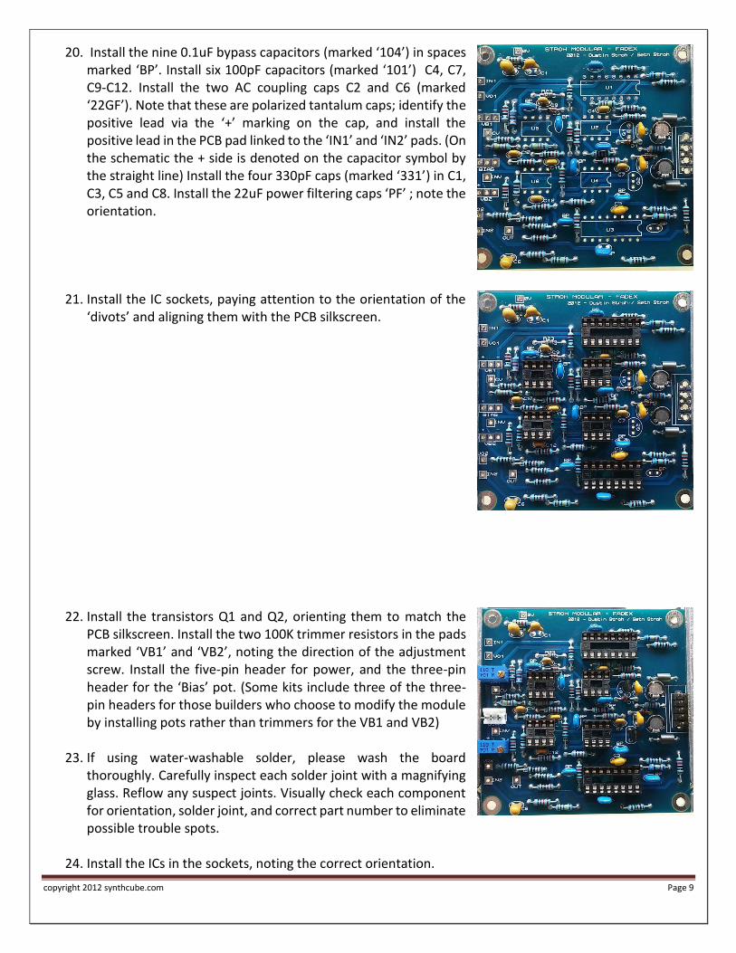
PCB rev 2.0
Errata:
copyright 2012 synthcube.com Page 2
Circuit Description A discussion thread about the circuit layout is here: http://www.muffwiggler.com/forum/viewtopic.php?t=43540&highlight=291
Links to schematics are here:
XFADER: http://home.comcast.net/~r3cogniz3r/FadeX.pdf
291: http://home.comcast.net/~r3cogniz3r/291j.pdf General Assembly Preparation
1) Check that the kit contains all of the parts noted in the BOM; notify us of any discrepancy using [email protected]
2) Gather additional materials and tools necessary for your build: a. Tools (soldering iron, pliers, wire cutters/stripper, etc) b. Solder of your choice c. Digital camera to document your progress
3) Prepare the pots for assembly: a. Break off the metal tab b. Slide the metal tab into the slot in the shaft- this adds some strength to the shaft for mounting
knobs
copyright 2012 synthcube.com Page 3
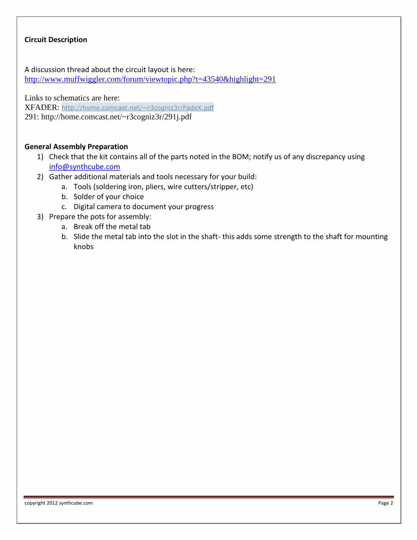
PCB Assembly Instructions 1. The single version of the module requires assembly of one of the 291 PCBs. The dual version requires
assembly of two of the 291 PCBs and one of the ‘Fadex’ PCBs. All PCBS should be included in your kit. You may choose to assemble both of the 291 PCBs at the same time, or assemble them individually.
2. Match each PCB with its component kit bag. Begin by assembling either one or both 291 PCBs.
3. Identify all the resistors. Its good practice to check resistors using an ohmmeter to verify their values. It’s also good practice to install resistors so the color bands align the same direction -- that makes troubleshooting easier. Note: kits use a mix of metal film (blue body) and carbon film (tan body) resistors. The resistors in your kit may not match the pictures so please verify resistor values before installing them.
4. Install the 100K resistor R35. Some kits were
packed with six resistors, but the PCB requires only one. The rest are surplus for your bench. Install the five 1K resistors R27, R33, R34, R48, R49.
5. Next install the four 1.5K resistors R20, R21, R28, R29. Install the four 6.8K resistors R3, R8, R12, R31. Install the four 10K resistors R5, R15, R25, R32.
copyright 2012 synthcube.com Page 4
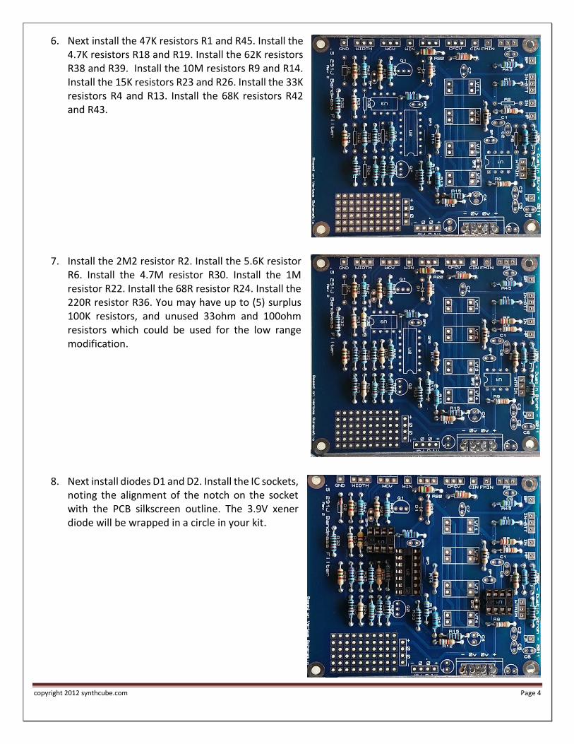
6. Next install the 47K resistors R1 and R45. Install the 4.7K resistors R18 and R19. Install the 62K resistors R38 and R39. Install the 10M resistors R9 and R14. Install the 15K resistors R23 and R26. Install the 33K resistors R4 and R13. Install the 68K resistors R42 and R43.
7. Install the 2M2 resistor R2. Install the 5.6K resistor
R6. Install the 4.7M resistor R30. Install the 1M resistor R22. Install the 68R resistor R24. Install the 220R resistor R36. You may have up to (5) surplus 100K resistors, and unused 33ohm and 100ohm resistors which could be used for the low range modification.
8. Next install diodes D1 and D2. Install the IC sockets,
noting the alignment of the notch on the socket with the PCB silkscreen outline. The 3.9V xener diode will be wrapped in a circle in your kit.
copyright 2012 synthcube.com Page 5
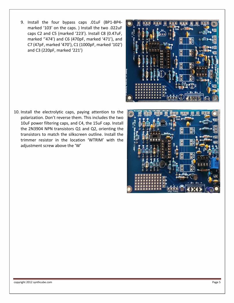
9. Install the four bypass caps .01uF (BP1-BP4-
marked ‘103’ on the caps. ) Install the two .022uF caps C2 and C5 (marked ‘223’). Install C8 (0.47uF, marked ‘’474’) and C6 (470pF, marked ‘471’), and C7 (47pF, marked ‘470’), C1 (1000pF, marked ‘102’) and C3 (220pF, marked ‘221’)
10. Install the electrolytic caps, paying attention to the
polarization. Don’t reverse them. This includes the two 10uF power filtering caps, and C4, the 15uF cap. Install the 2N3904 NPN transistors Q1 and Q2, orienting the transistors to match the silkscreen outline. Install the trimmer resistor in the location ‘WTRIM’ with the adjustment screw above the ‘W’
copyright 2012 synthcube.com Page 6
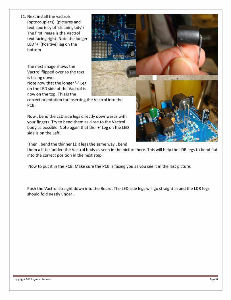
11. Next install the vactrols (optocouplers). (pictures and text courtesy of ‘cleaninglady’) The first image is the Vactrol text facing right. Note the longer LED '+' (Positive) leg on the bottom The next image shows the Vactrol flipped over so the text is facing down. Note now that the longer '+' Leg on the LED side of the Vactrol is now on the top. This is the correct orientation for inserting the Vactrol into the PCB. Now , bend the LED side legs directly downwards with your fingers. Try to bend them as close to the Vactrol body as possible. Note again that the '+' Leg on the LED side is on the Left. Then , bend the thinner LDR legs the same way , bend them a little 'under' the Vactrol body as seen in the picture here. This will help the LDR legs to bend flat into the correct position in the next step. Now to put it in the PCB. Make sure the PCB is facing you as you see it in the last picture. Push the Vactrol straight down into the Board. The LED side legs will go straight in and the LDR legs should fold neatly under .
copyright 2012 synthcube.com Page 7
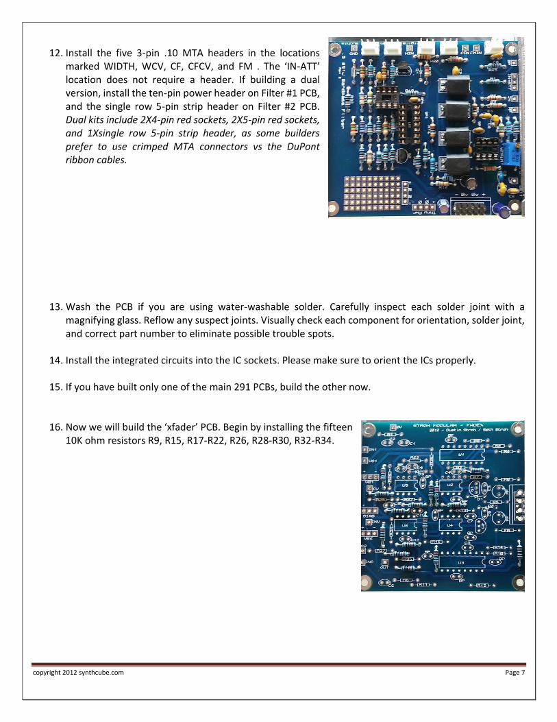
12. Install the five 3-pin .10 MTA headers in the locations
marked WIDTH, WCV, CF, CFCV, and FM . The ‘IN-ATT’ location does not require a header. If building a dual version, install the ten-pin power header on Filter #1 PCB, and the single row 5-pin strip header on Filter #2 PCB. Dual kits include 2X4-pin red sockets, 2X5-pin red sockets, and 1Xsingle row 5-pin strip header, as some builders prefer to use crimped MTA connectors vs the DuPont ribbon cables.
13. Wash the PCB if you are using water-washable solder. Carefully inspect each solder joint with a magnifying glass. Reflow any suspect joints. Visually check each component for orientation, solder joint, and correct part number to eliminate possible trouble spots.
14. Install the integrated circuits into the IC sockets. Please make sure to orient the ICs properly.
15. If you have built only one of the main 291 PCBs, build the other now.
16. Now we will build the ‘xfader’ PCB. Begin by installing the fifteen 10K ohm resistors R9, R15, R17-R22, R26, R28-R30, R32-R34.

copyright 2012 synthcube.com Page 8
17. Install the eight 100R (100 ohm) resistors R4, R8, R12, R14, R31, R35-R37.
18. Install the resistors appropriate for your power scheme. For 12V
systems, install R23 (11k), R25 and R27 (24K3) and R24 (12K1). For 15V schemes, install R23 (14K), R25 and R27 (30K1) and R24 (11K5). Kits contain resistors for both schemes. Install the remaining resistors R2 and R10 (60K4), R3 and R11 (1M) and R1, R5, R6, R7, R13 and R16 (30K1).
19. Install the diodes D1-D3 and the ferrite beads ‘FB’. Pay attention
to the orientation of the diodes. Ferrite beads have no orientation.
copyright 2012 synthcube.com Page 9
20. Install the nine 0.1uF bypass capacitors (marked ‘104’) in spaces marked ‘BP’. Install six 100pF capacitors (marked ‘101’) C4, C7, C9-C12. Install the two AC coupling caps C2 and C6 (marked ‘22GF’). Note that these are polarized tantalum caps; identify the positive lead via the ‘+’ marking on the cap, and install the positive lead in the PCB pad linked to the ‘IN1’ and ‘IN2’ pads. (On the schematic the + side is denoted on the capacitor symbol by the straight line) Install the four 330pF caps (marked ‘331’) in C1, C3, C5 and C8. Install the 22uF power filtering caps ‘PF’ ; note the orientation.
21. Install the IC sockets, paying attention to the orientation of the
‘divots’ and aligning them with the PCB silkscreen.
22. Install the transistors Q1 and Q2, orienting them to match the
PCB silkscreen. Install the two 100K trimmer resistors in the pads marked ‘VB1’ and ‘VB2’, noting the direction of the adjustment screw. Install the five-pin header for power, and the three-pin header for the ‘Bias’ pot. (Some kits include three of the three-pin headers for those builders who choose to modify the module by installing pots rather than trimmers for the VB1 and VB2)
23. If using water-washable solder, please wash the board
thoroughly. Carefully inspect each solder joint with a magnifying glass. Reflow any suspect joints. Visually check each component for orientation, solder joint, and correct part number to eliminate possible trouble spots.
24. Install the ICs in the sockets, noting the correct orientation.

copyright 2012 synthcube.com Page 10
25. Now you should have three completed PCBs- 2X291 PCB and 1XFADEX PCB. Now we will begin assembly
of the panel and related components.
26. Assemble the panel, beginning with the jacks. Note the orientation of the jacks to allow easier soldering of the ground (sleeve) connections. Solder the ground (sleeve) connections as illustrated; it will be easier to solder these before the pot are installed. There are three jacks that require soldering of a long lead wire (black insulation in pics) that will be connected to the PCBs. For the ground connections you can use scrap leads, scrap wire, solid or stranded wire. Two options are shown for connecting the grounds next to the standoffs—one using insulated stranded wire, the other using a piece of scrap resistor lead. Leave room to install the standoffs.
27. Install the pots, noting the correct locations for the 50K pots, and orienting them to match the illustration. Install four of the 1” 4X40 hex aluminum standoffs using #4-40X3/8 pan screws or #4-40 X3/8 socket head cap screws. Install #4 washers on the back of the panel between the standoff and the cap screw.
28. Now we will create crimped socket connectors and solder the wires to pots. The general process for creating the crimped wire/socket assembly is as follows:
a. Cut wires in the approximate length required b. Crimp the wires into the red socket in the order shown on the illustration. You can use a manual
crimping tool, a small screwdriver, or a ‘pistol’ grip tool like this one: c. Strip the ends of the wires and tin them. d. Note: The wire colors noted on the illustration are examples only. You can use any color scheme
that you choose for the wiring. e. Some builders elect not to use the sockets, and prefer to solder wires directly to the PCB. In this
case, do not solder the three-pin headers to the PCB. f. Pay particular attention to the pin numbers and pot lug numbers on the illustration. Some pots
are wired ‘in reverse’ to others and it’s important to make the proper header-pin to pot-lug connection.
copyright 2012 synthcube.com Page 11
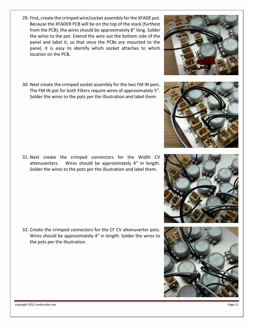
29. First, create the crimped wire/socket assembly for the XFADE pot. Because the XFADER PCB will be on the top of the stack (furthest from the PCB), the wires should be approximately 8” long. Solder the wires to the pot. Extend the wire out the bottom side of the panel and label it, so that once the PCBs are mounted to the panel, it is easy to identify which socket attaches to which location on the PCB.
30. Next create the crimped socket assembly for the two FM IN pots. The FM IN pot for both Filters require wires of approximately 5”. Solder the wires to the pots per the illustration and label them.
31. Next create the crimped connectors for the Width CV attenuverters. Wires should be approximately 4” in length. Solder the wires to the pots per the illustration and label them.
32. Create the crimped connectors for the CF CV attenuverter pots. Wires should be approximately 4” in length. Solder the wires to the pots per the illustration.
copyright 2012 synthcube.com Page 12
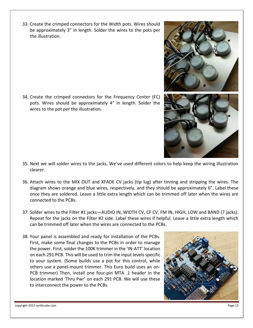
33. Create the crimped connectors for the Width pots. Wires should
be approximately 3” in length. Solder the wires to the pots per the illustration.
34. Create the crimped connectors for the Frequency Center (FC) pots. Wires should be approximately 4” in length. Solder the wires to the pot per the illustration.
35. Next we will solder wires to the jacks. We’ve used different colors to help keep the wiring illustration clearer.
36. Attach wires to the MIX OUT and XFADE CV jacks (tip lug) after tinning and stripping the wires. The diagram shows orange and blue wires, respectively, and they should be approximately 6”. Label these once they are soldered. Leave a little extra length which can be trimmed off later when the wires are connected to the PCBs.
37. Solder wires to the Filter #1 jacks—AUDIO IN, WIDTH CV, CF CV, FM IN, HIGH, LOW and BAND (7 jacks).
Repeat for the jacks on the Filter #2 side. Label these wires if helpful. Leave a little extra length which can be trimmed off later when the wires are connected to the PCBs.
38. Your panel is assembled and ready for installation of the PCBs.
First, make some final changes to the PCBs in order to manage the power. First, solder the 100K trimmer in the ‘IN-ATT’ location on each 291 PCB. This will be used to trim the input levels specific to your system. (Some builds use a pot for this control, while others use a panel-mount trimmer. This Euro build uses an on-PCB trimmer) Then, install one four-pin MTA .1 header in the location marked ‘Thru Pwr’ on each 291 PCB. We will use these to interconnect the power to the PCBs.
copyright 2012 synthcube.com Page 13
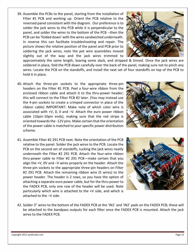
39. Assemble the PCBs to the panel, starting from the installation of Filter #1 PCB and working up. Orient the PCB relative to the reversed panel consistent with the diagram. Our preference is to solder the jack wires to the PCB while it is perpendicular to the panel, and solder the wires to the bottom of the PCB --then the PCB can be ‘folded down’ with the wires sandwiched underneath. In reverse this can facilitate troubleshooting and repair. The picture shows the relative position of the panel and PCB prior to soldering the jack wires; note the pot wire assemblies moved slightly out of the way and the jack wires trimmed to approximately the same length, leaving some slack, and stripped & tinned. Once the jack wires are soldered in place, fold the PCB down carefully over the back of the panel, making sure not to pinch any wires. Locate the PCB on the standoffs, and install the next set of four standoffs on top of the PCB to hold it in place.
40. Attach the three-pin sockets to the appropriate three-pin headers on the Filter #1 PCB. Peel a four-wire ribbon from the enclosed ribbon cable and attach it to the thru-power header; this will connect to the Filter PCB #2 later. (You may instead use the 4-pin sockets to create a crimped connector in place of the ribbon cable) IMPORTANT: Make note of which color wire is associated with +V, 0, 0 and –V. Attach the euro power ribbon cable (16pin-10pin ends), making sure that the red stripe is oriented towards the -12V pins. Make certain that the orientation of the power cable is matched to your specific power distribution scheme.
41. Assemble Filter #2 291 PCB next. Note the orientation of the PCB relative to the panel. Solder the jack wires to the PCB. Locate the PCB on the second set of standoffs, tucking the jack wires neatly underneath the Filter #2 291 PCB. Attach the four-wire ribbon thru-power cable to Filter #2 291 PCB—make certain that you align the +V, 0V and –V wires properly on the header. Attach the three-pin sockets to the appropriate three-pin headers on Filter #2 291 PCB. Attach the remaining ribbon wire (5 wires) to the power header. The header is 2 rows, so you have the option of attaching a separate euro power cable, but for the thru-power to the FADEX PCB, only one row of the header will be used. Note particularly which wire is attached to the +V side, and which is attached to the –V side.
42. Solder 3” wires to the bottom of the FADEX PCB at the ‘IN1’ and ‘IN2’ pads on the FADEX PCB; these will
be attached to the bandpass outputs for each filter once the FADEX PCB is mounted. Attach the jack wires to the FADEX PCB.
copyright 2012 synthcube.com Page 14
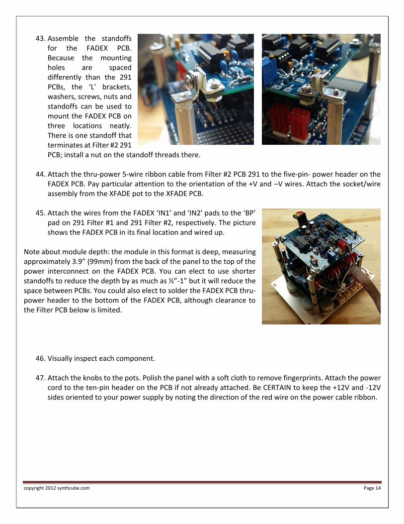
43. Assemble the standoffs
for the FADEX PCB. Because the mounting holes are spaced differently than the 291 PCBs, the ‘L’ brackets, washers, screws, nuts and standoffs can be used to mount the FADEX PCB on three locations neatly. There is one standoff that terminates at Filter #2 291 PCB; install a nut on the standoff threads there.
44. Attach the thru-power 5-wire ribbon cable from Filter #2 PCB 291 to the five-pin- power header on the FADEX PCB. Pay particular attention to the orientation of the +V and –V wires. Attach the socket/wire assembly from the XFADE pot to the XFADE PCB.
45. Attach the wires from the FADEX ‘IN1’ and ‘IN2’ pads to the ‘BP’ pad on 291 Filter #1 and 291 Filter #2, respectively. The picture shows the FADEX PCB in its final location and wired up.
Note about module depth: the module in this format is deep, measuring approximately 3.9” (99mm) from the back of the panel to the top of the power interconnect on the FADEX PCB. You can elect to use shorter standoffs to reduce the depth by as much as ½”-1” but it will reduce the space between PCBs. You could also elect to solder the FADEX PCB thru-power header to the bottom of the FADEX PCB, although clearance to the Filter PCB below is limited.
46. Visually inspect each component.
47. Attach the knobs to the pots. Polish the panel with a soft cloth to remove fingerprints. Attach the power
cord to the ten-pin header on the PCB if not already attached. Be CERTAIN to keep the +12V and -12V sides oriented to your power supply by noting the direction of the red wire on the power cable ribbon.
copyright 2012 synthcube.com Page 15
291PCB (The Dual Kit Requires 2 of these BOMs)Type Short Description Mouser PN Value Unit Quant Part Notes Ref Designator
SEMI 1N4148 Signal Diode 512-1N4148T26A 1 stra ight leads D2
SEMI 3.9V Zener Diode 2% 771-BZX79-B3V9133 3.9 V 1 looped leads D1
CAP Electrolytic Cap 15uF 667-EEA-GA1E150B 15 uF 1 C4
CAP Electrolytic Cap 10uF 667-EEA-GA1E100B 10 uF 2 power caps PF
CAP Multi layer Ceramic Cap 220pF 810-FK18C0G2E221J 220 pF 1 C3
CAP Multi layer Ceramic Cap 1000pf 594-K102J15C0GF5TH5 1000 pf 1 C1
CAP Multi layer Ceramic Cap .022uF 810-FK14X7R2A223K 0.022 uF 2 C2, C5
CAP Multi layer Ceramic Cap 470pF 594-K471J15C0GF5TL2 470 pF 1 C6
CAP Multi layer Ceramic Cap 47pF 810-FK28C0G1H470J 47 pF 1 C7
CAP Multi layer Ceramic Cap .47uF 80-C315C474K5R-TR 0.47 uF 1 C8
CAP Multi layer Ceramic Cap .01uF 594-K103K15X7RF5TL2 0.01 uF 4 bypass BP
SEMI 2N3904 NPN Trans is tor 512-2N3904TF 2 Q1, Q2
IC 14 Pin IC Socket n/a 1
IC 8 Pin IC Socket n/a 2
RES Metal Fi lm Res is tor 47Kohm 1% 271-47K/REEL-RC 47 kOhm 2 R1, R45
RES Metal Fi lm Res is tor 2.2Mohm 1% 271-2.2M/REEL-RC 2.2 mOhm 1 R2
RES Metal Fi lm Res is tor 5.6Kohm 1% 271-5.6K/REEL-RC 5.6 kOhm 1 R6
RES Metal Fi lm Res is tor 10Mohm 1% 271-10M/REEL-RC 10 mOhm 2 R9, R14
RES Metal Fi lm Res is tor 4.7Kohm 1% 271-4.7K/REEL-RC 4.7 kOhm 2 R18, R19
RES Metal Fi lm Res is tor 1.5Kohm 1% 271-1.5K/REEL-RC 1.5 kOhm 4 R20, R21, R28, R29
RES Metal Fi lm Res is tor 1.0Mohm 1% 271-1.0M/REEL-RC 1 mOhm 1 R22
RES Metal Fi lm Res is tor 68ohm 1% 271-68/REEL-RC 68 Ohm 1 R24
RES Metal Fi lm Res is tor 1Kohm 1% 271-1K/REEL-RC 1 kOhm 5 R27, R33, R34, R48, R49
RES Metal Fi lm Res is tor 4.7Mohm 1% 271-4.7M/REEL-RC 4.7 mOhm 1 R30
RES Metal Fi lm Res is tor 220ohm 1% 271-220/REEL-RC 220 Ohm 1 R36
RES Metal Fi lm Res is tor 62Kohm 1% 271-62K/REEL-RC 62 kOhm 2 R38, R39
RES Metal Fi lm Res is tor 68Kohm 1% 271-68K/REEL-RC 68 kOhm 2 R42, R43
RES Metal Fi lm Res is tor 33Kohm 1% 271-33K/REEL-RC 33 kOhm 2 R4, R13
RES Metal Fi lm Res is tor 100Kohm 1% 271-100K/REEL-RC 100 kOhm 1 R35
RES Metal Fi lm Res is tor 6.8Kohm 1% 271-6.8K/REEL-RC 6.8 kOhm 4 R3, R8, R12, R31
RES Metal Fi lm Res is tor 10Kohm 1% 271-10K/REEL-RC 10 kOhm 4 R5, R15, R25, R32
RES Metal Fi lm Res is tor 15Kohm 1% 271-15K/REEL-RC 15 kOhm 2 R23, R26
RES Metal Fi lm Res is tor 33ohm 1% 271-33/REEL-RC 33 Ohm 1 R24 (mod for ext low range)
RES Metal Fi lm Res is tor 100ohm 1% 271-100/REEL-RC 100 Ohm 1 R27 (mod for ext low range)
IC TL071 Op Amp 595-TL071CN 1 U1
IC TL072 Dual OpAmp 511-TL072CN 1 U3
IC TL074 Quad OpAmp 595-TL074CN 1 U2
SEMI VTL5C3 Vactrol n/a 4
TRM Trimmer Vert Adj 5K 652-3296Y-1-502LF 5 kOhm 1 Width Trim
TRM 100K Vertica l 20 Turn 652-3296W-1-104LF 100 kOhm 1 Input Attenuation
HDR Headers & Wire Hous ings 10P DR VERT HDR 649-67997-210HLF 1 euro power
HDR .156 Friction lock 4 pin header, sq post 571-640445-4 1 15v power
HDR 0.1 Header 3P Friction Lock 571-6404563 5
HDR 0.1 Header Socket 3P Red 571-3-640440-3 5
PCB n/a 1
copyright 2012 synthcube.com Page 16
j3RK XFADR BOM
Type Short Description Mouser PN Value Unit Quant Part Notes Ref Designator
CAP Multi layer Ceramic Cap 330pF 810-FK18C0G2A331J 330 pF 4 C1, C3, C5, C8
CAP Tantalum Cap 22uF 22 uF 2AC coupling; jumper for DC
C2, C6
CAP Multi layer Ceramic Cap 100pF 594-K101J15C0GF5TL2 100 pF 6 C4, C7, C9-C12
CAP Multi layer Ceramic Cap .1uF 594-K104K15X7RF5TH5 0.1 uF 9 BP caps
CAP Electrolytic Cap 22uF 667-EEA-GA1V220B 22 uF 2 PF caps
SEMI 2N3906 PNP Trans is tor 512-2N3906TF 2 Q1, Q2
SEMI 1N4148 Signal Diode 512-1N4148T26A 3 D1-D3
SEMI Ferri te Beads 81-BL01RN1A1F1J 2 FB
RES Metal Fi lm Res is tor 11Kohm 1% 271-11K/REEL-RC 11 kOhm 1 for 12V operation R23
RES Metal Fi lm Res is tor 24.3Kohm 1% 271-24.3K/REEL-RC 24.3 kOhm 2 for 12V operation R25, R27
RES Metal Fi lm Res is tor 12.1Kohm 1% 271-12.1K/REEL-RC 12.1 kOhm 1 for 12V operation r24
RES Metal Fi lm Res is tor 1.0Mohm 1% 271-1.0M/REEL-RC 1 mOhm 2 R3, R11
RES Metal Fi lm Res is tor 10Kohm 1% 271-10K/REEL-RC 10 kOhm 15R9, R15, R17-R22, R26, R28-R30, R32-R34
RES Metal Fi lm Res is tor 30.1Kohm 1% 271-30.1K/REEL-RC 30.1 kOhm 6 R1, R5-R7, R13, R16
RES Metal Fi lm Res is tor 30.1Kohm 1% 271-30.1K/REEL-RC 30.1 kOhm 2 for 15V operation R25, R27
RES Metal Fi lm Res is tor 60.4Kohm 1% 271-60.4K/REEL-RC 60.4 kOhm 2 R2, R10
RES Metal Fi lm Res is tor 100ohm 1% 271-100/REEL-RC 100 Ohm 8 R4, R8, R12, R14, R31, R35-R37
RES Metal Fi lm Res is tor 14Kohm 1% 271-14K/REEL-RC 14 kOhm 1 for 15V operation R23
RES Metal Fi lm Res is tor 11.5Kohm 1% 271-11.5K/REEL-RC 11.5 kOhm 1 for 15V operation R24
TRM 100K Vertica l 20 Turn 652-3296W-1-104LF 100 kOhm 2 VB1, VB2
IC LM13700 TransCond Amp 926-LM13700N/NOPB 2 U1, U3
IC TL072 Dual OpAmp 511-TL072CN 3 U2, U4, U6
IC LT1013CPDual Prec. OpAmp 595-LT1013CP 1
IC 16 Pin IC Socketn/a
2
IC 8 Pin IC Socketn/a
4
HDR .156 Friction lock 4 pin header, sq post 571-640445-4 1 Power 12V
HDR Headers & Wire Hous ings 10P DR VERT HDR 649-67997-210HLF 1 Power 15V
HDR 0.1 Header 3P Friction Lock 571-6404563 1 Bias Pot
HDR 0.1 Header Socket 3P Red 571-3-640440-3 1
PCB n/a 1
copyright 2012 synthcube.com Page 17
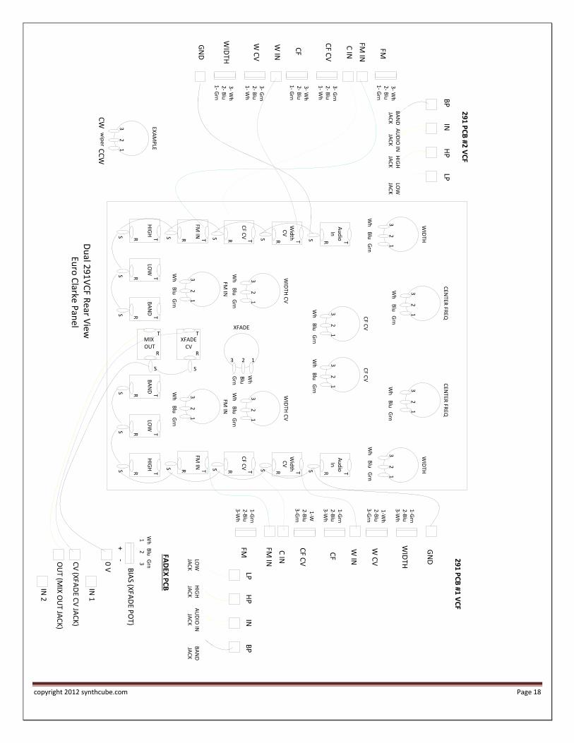
291 Filter Dual Clarke68 Euro Panel
Description Type Quant Part Notes Ref Designator
16mm pots 50K linear solder lug, solid shaft POT 3 FM, XFADE
16mm pots 10K linear solder lug, solid shaft POT 8 CF, CF CV, Width, Width CV
3.5mm jack JACK 16
Knob- small 13mm KNOB 7
Knob- medium KNOB 4
Panel- clarke68 PAN 1
Panel Screws M3X.5X6mm Pan HDWR 4
0.1 Header 4P Friction Lock HDR 2 power interconnect 291-291
1" aluminum standoffs 11
#4-40 nuts 4
#4-40X1/4" Pan screws 4
#4 Nylon washers 12 4-Panel; 8- PCB Mounting
#4-40X3/8 socket head screws 4 standoffs to panel
#4 'L' brackets 4
Dupont ribbon cable HDR 1 4 wide power interconnect
Dupont ribbon cable HDR 1 5 wide power interconnect
Strip pin headers (5 wide) HDR 2 power interconnect 291-Xfader
10-16 power cable, euro PWR 1
copyright 2012 synthcube.com Page 18
Du
al 29
1V
CF R
ear View
Eu
ro C
larke Pan
el
S
HIG
H
R T
S
LOW
R T
S
BA
ND
R T
S
MIXOUT
R
T
S
BA
ND
R T
S
LOW
R T
S
HIG
H
R T
S
FM IN
R T S
CF C
V
R T S
Wid
thC
VR T S
Au
dio
InR T
S
FM IN
R T S
CF C
V
R T S
Wid
thC
VR T S
Au
dio
InR T
S
XFADECV
R
T
FM IN
32
1
WID
TH C
V
32
1
FM IN
32
1
WID
TH C
V
32
1
WID
TH
32
1
CEN
TER FR
EQ
32
1
CF C
V
32
1
CF C
V
32
1
WID
TH
32
1
CEN
TER FR
EQ
32
1
29
1 P
CB
#1 V
CF
29
1 P
CB
#2 V
CF
BIA
S (XFA
DE P
OT)
FAD
EX P
CB
CV
(XFA
DE C
V JA
CK
)
OU
T (MIX
OU
T JAC
K)
0 V
XFADE
3 2 1
+-
Wh1
Blu2
Grn3
Wh
Blu
Grn
3-
Wh
2-
Blu
1-
Grn
FM IN
C IN
CF C
V
CF
WIN
WC
V
WID
TH
GN
D
Wh
Blu
Grn
Wh
Blu
Grn
1-G
rn2
-Blu
3-W
hFM FM
IN
C IN
CF C
V
CF
WIN
WC
V
WID
TH
GN
D
FM
EXA
MP
LE
32
1
CW
C
CW
w
iper
3-
Grn
2-
Blu
1-
Wh
1-W
2-B
lu3
-Grn
Wh
Blu
Grn
Wh
Blu
Grn
3-
Grn
2-B
lu1
-W
h
1-W
h2
-Blu
3-G
rn
3-
Wh
2-
Blu
1-
Grn
Wh
Blu
Grn
1-G
rn2
-Blu
3-W
h
Wh
Blu
Grn
Wh
Blu
Grn
Wh
Blu
Grn
Wh
Blu
Grn
Wh
Blu
Grn
1-G
rn2
-Blu
3-W
h
3-
Wh
2-
Blu
1-
Grn B
PIN
HP
LP
LPH
PIN
BP
IN 2
IN 1
BA
ND
JAC
KH
IGH
JAC
KLO
WJA
CK
AU
DIO
INJA
CK
BA
ND
JAC
KH
IGH
JAC
KLO
WJA
CK
AU
DIO
INJA
CK