The nature of small molecules adsorbed on defective carbon ...
Upload
independentCategory
view
0download
0
S-EDITCreating an Inverter Using S-Edit
To launch S-Edit in one of the LAB PCs, go to Start > Electrical > Tanner EDA > Tanner Tools v15.2 > S-Edit v15.2 64-bit.
Now we will create an inverter schematic and symbol. Start with creating a new design by going to File > New > New Design.
Specify the folder you want to create your design in and the name of your design. Suppose you name it “ENGN1600_tutorial”. It will show up in the Libraries navigator on the left.
On public machines, the Libraries might not immediately be loaded. To add library to your design, download the Tanner Libraries folder here (use the password given in class). Now, click on “Add…” button on the Libraries window in S-EDIT, or go to File > Open > Add Library and browse the download folderto point to Libraries\All\All.tanner file. After loading the library, several sub-libraries will show up in the Libraries window, such as IO_Pads and Devices.
Once the library is loaded you will see the following libraries loaded in the Libraries window:
Creating the schematic

To load a schematic cell, go to Cell > New View… You will see the following screen:
Write the name of the cell you want to create the schematic of and then click OK. A new cell view will open up.
A CMOS inverter needs an NMOS, a PMOS, Vdd, Gnd and In/Out ports. On the left in the Libraries window, click on the Devices library, its symbol objects will be listed in the window below. Find the NMOS from the list. Choose your device, and click on Instance, or simply drag and drop it to the designarea. Do the same for PMOS, Vdd and Gnd symbols. Before you drop the instance, a window may show up like the one on the left below.

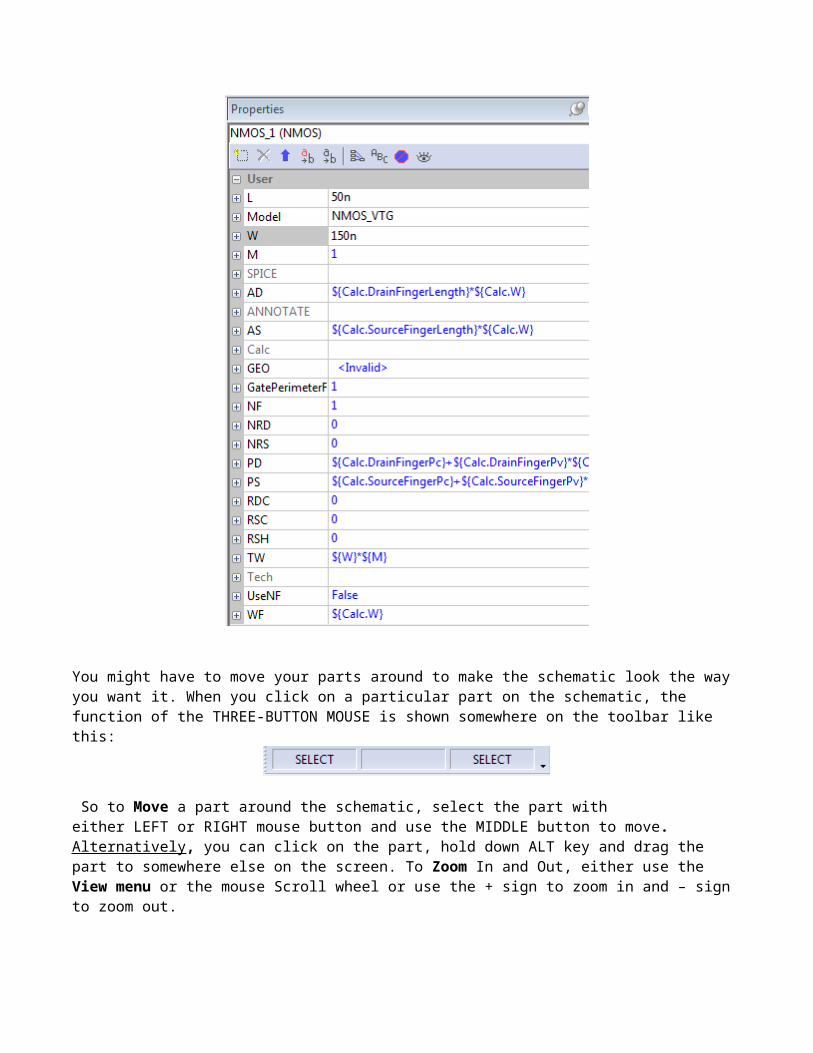
After you drop the instance, a second window (like the one on the right) will show up on the right side of the screen. Here you could initiate the properties of the instance, such as its Length and Width. Or after placing the instance, you can always single-click on it and edit its properties in the Properties navigator on the right. Let’s say we set the length and width of NMOS devices to be 50n and 150n, and the length and width of PMOS devicesto be 50n and 300n, respectively.
NOTE: in order to run SPICE simulations with our libraries, the model has tobe changed from NMOS to NMOS_VTG.
You might have to move your parts around to make the schematic look the way you want it. When you click on a particular part on the schematic, the function of the THREE-BUTTON MOUSE is shown somewhere on the toolbar like this:
So to Move a part around the schematic, select the part with either LEFT or RIGHT mouse button and use the MIDDLE button to move. Alternatively, you can click on the part, hold down ALT key and drag the part to somewhere else on the screen. To Zoom In and Out, either use the View menu or the mouse Scroll wheel or use the + sign to zoom in and – sign to zoom out.

Once we have the main parts in place, it is time to add I/O ports and wire the parts together. Select and place an Input port and an Output port on theschematic and give the ports a unique name.
Now using the wiring tool make appropriate connections. After clicking on the wiring tool, a SINGLE MOUSE CLICK starts the wiring. If you want to end wiring at a particular location, DOUBLE CLICK.
Your completed inverter schematic should look like this. is the input port and is the output port.

So we have made the connections. Now it is time to go change the length and width of the MOS devices as per the specifications.
Inverter Symbol
To create a symbol, first create a View — create a new cell with a new symbol view, or create a new symbol view of an existing cell using Cell > New View. Give the symbol a View name, and select the interface it is to be associated with. Then, using the polygon and drawing tools
, draw the usual symbol for an inverter. Add the inputand output ports. Make sure to give the ports the same name that you used inthe schematic i.e. in and out. Now using lines (not wires) connect the portsto the inverter symbol. You should have something that looks like:
The creation of the symbol might be helpful when you do hierarchical design. CREATING SPICE NETLIST FROM THE SCHEMATIC
Go to File > Export > Export Spice. Specify the Ouput filename. Check Exclude .end in Options (Without the .end, the generated SPICE file can be included in other SPICE files.) Say Export.The SPICE file is saved in the same directory as the schematic. The file contains the following information:
MNMOS_1 Out In Gnd Gnd NMOS_VTG W=150n L=50n AS=135f PS=2.1u AD=135f PD=2.1uMPMOS_1 Out In Vdd Vdd PMOS_VTG W=300n L=50n AS=270f PS=2.4u AD=270f PD=2.4u

This generated SPICE file is NOT complete. This is just a description of thecircuit structure that you drew in the schematic. In order to simulate the inverter, we still need to add some MOS models, simulation type (DC, transient, AC, MonteCarlo etc.) and give an Input Stimulus. A more detailed description of the SPICE file and what else you need to add is provided below.
Last Updated: Marco Donato
1/31/2013
Simulating your Inverter with SmartSpiceNow that you have a L-Edit/S-Edit generated Spice File, it is time to look at how to make it complete for simulation.
Download and copy to your folder the 45nm model that you will be using for the MOS models. Again, use the password given in class to access the folder.
The SPICE Netlist generated from S-Edit contains the following information and is saved as inverter.sp
* SPICE export by: S-Edit 15.22* Export time: Wed Jan 30 16:39:09 2013* Design: ENGN1600_tutorial* Cell: inverter* Interface: view0* View: view0* View type: connectivity* Export as: top-level cell* Export mode: flat* Exclude empty cells: no* Exclude .model: yes* Exclude .end: yes* Exclude simulator commands: yes* Expand paths: yes* Wrap lines: no* Root path: C:\Users\Marco\Desktop\EN1600_test\ENGN1600_tutorial

* Exclude global pins: no* Exclude instance locations: yes* Control property name: SPICE
MNMOS_1 Out In Gnd Gnd NMOS_VTG W=150n L=50n AS=135f PS=2.1u AD=135f PD=2.1uMPMOS_1 Out In Vdd Vdd PMOS_VTG W=300n L=50n AS=270f PS=2.4u AD=270f PD=2.4u
This generated SPICE file contains the basic description of the circuit structure. Now we will add the section that specifies the model library, thepower supply, other simulation specific parameters, the type of analysis andthe input stimulus.
Let’s look at our spice_deck.sp file that contains everything that we need to do an analysis of our inverter.
*Main inverter file .param Supply=1.1.include '../models/hspice_nom.include' .options post
* Define power supply .global Vdd Gnd Vdd Vdd Gnd 'Supply'
*Set Transient Analysis .tran 100ps 500ns
*** CIRCUIT NETLIST *** * .include <name_of_extracted_spice_file> .include 'inverter.sp'
*** INPUT STIMULS *** * add any input vector here
vin1 In Gnd pulse(0 Supply 10n 1n 1n 50n 100n) * if you want to see the VTC for the inverter add a DC analysis .DC vin1 0 Supply 0.1 .END
The lines shown in BLUE do not need to be edited as you move from one designto the other. The first red line containing the transient analysis definition might change. You might change the timestep, the total time of simulation or you might have to do a completely different analysis (eg. DC analysis instead of TRANSIENT). The second red line containing the .include 'inverter.sp' will change based on what your Tanner generated spice file is called. In this example the description of the inverter was extracted to inverter.sp. Hence the name of the include file. The third line containing the Input Stimulus might change based on what your input port is labeled. The green line shows how to use a DC analysis to generate a VTC forthe inverter. Comment out the Green line if you are not running any DC analysis.
This should get you started with SPICE. A more detailed description of a SPICE DECK is given starting on page 9 of this document.
Important: Remember to have the models directory in the same directory whereyour design is saved, and copy the spice_deck.sp file in the design directory. If you have them in a different folder, make sure to specify the full-path of the files in your .include statement.
Now that you have prepared your complete Spice file, start SMARTSPICE.
Start a project with sourcing the input files. Click on the source button
, or simply drag a deck from the Explorer Window and drops it over the SMARTSPICE Window. To reload your source after a modification press the quick button that says Reload the current input deck. SmartSpice will open and parse your input file. You shouldn't see any errors.
Go to the Analysis -> Run menu option. An information box will appear while the simulation is running. The file can also be run by pressing Ctrl-R.
If you want to see what the output plots look like. Click the vectors button
. A dialog will appear listing different plots and vectors that are available. Click on the tran1 plot. Scroll down the vector list until you see the input and output voltages. Highlight them and click Plot. You can highlight multiple items by holding down the Ctrl key and clicking on your selection.
If you change your Spice input file after you run a simulation, then reload and run it again, you'll see many different vectors available, named tran1, tran2, tran3, etc... Be sure to unselect your old plots before clicking the

plot button, unless you want to see the old plots and your new one on the same graph.
Example : Generating all possible input combinations for a two input gate.
If you are simulating a two-input gate, you want to make sure that the gate works for all four possible input combinations (00, 01, 10 and 11). Let’s say that your two inputs are labeled A and B. Using: vin1 A Gnd pulse(0 Supply 10n 1n 1n 50n 100n) vin2 B Gnd pulse(0 Supply 10n 1n 1n 100n 200n) as the two input pulse should simulate all four combinations in one single run.
See the tutorial below if you want to find out what exactly the pulse statement does
Last Updated: Marco Donato01/31/2013

How to add a little SPICE to your circuit design
For this class we will use SILVACO's SmartSpice, an industry standard circuit simulator. This tutorial will give you a basic idea on how to write spice files from scratch or how to edit spice netlists generated by Tanner.
Before we get started make sure you download 45nm Technology file from here (same password).
Here is an example spice deck for the following circuit.
* Spice Netlist for an Inverter* This spice deck creates a simple inverter with an output load* cap, runs a transient analysis and measures the propagation delay************************************************************************ Set supply and library***********************************************************************.temp 27 * Set operating temp.param Supply=1.1.include '../models/hspice_nom.include' * the 45nm MOS model library.options post * this will allow you to view the result************************************************************************ Define power supply***********************************************************************
.global Vdd GndVdd Vdd Gnd 'Supply'
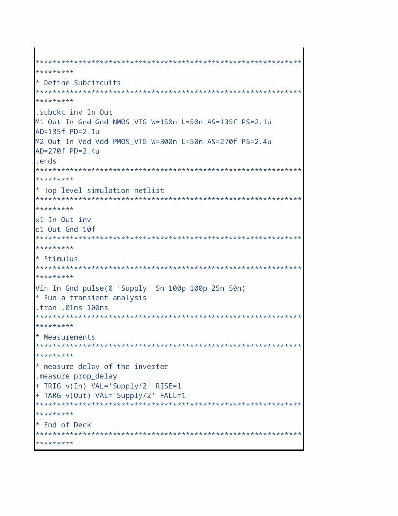
************************************************************************ Define Subcircuits***********************************************************************.subckt inv In OutM1 Out In Gnd Gnd NMOS_VTG W=150n L=50n AS=135f PS=2.1u AD=135f PD=2.1uM2 Out In Vdd Vdd PMOS_VTG W=300n L=50n AS=270f PS=2.4u AD=270f PD=2.4u.ends************************************************************************ Top level simulation netlist***********************************************************************x1 In Out invc1 Out Gnd 10f************************************************************************ Stimulus***********************************************************************Vin In Gnd pulse(0 'Supply' 5n 100p 100p 25n 50n)* Run a transient analysis.tran .01ns 100ns************************************************************************ Measurements************************************************************************ measure delay of the inverter.measure prop_delay+ TRIG v(In) VAL='Supply/2' RISE=1+ TARG v(Out) VAL='Supply/2' FALL=1************************************************************************ End of Deck***********************************************************************
.end
Looks scary? Don’t panic...
Here are some common things you see in the above spice deck
The FIRST LINE of the deck is always interpreted as the 'Title'. It is generally helpful to put the name of the circuit as the title for quick reference.
Any line that begins with a * is a COMMENT and will be ignored by the SPICE tool. In SMARTSPICE if you want to block comment use #COM and #ENDCOM. eg.:
#COM This is a comment line1 THis is a comment line2 #ENDCOM
.temp statement specifies the simulation temperature in Celsius. If youremove this line, SPICE will use a default room temperature of 27C.
.param statement specifies a constant definition. Once you define a parameter, you can use the name you specified instead of the actual value. See how 'Supply' is used in the above SPICE deck.
.include statement allows you to "include" other files in your deck. Here the .include statement is adding the NMOS and PMOS model definitionsfor the 45nm technology.
The next thing you see in the deck is the definition of 'Vdd' and 'Gnd' values.
All the items that I have discussed so far can be directly copied to any SPICE deck that you wish to write. The .temp value might need a change depending on the temperature you wish to simulate.
The SUBCIRCUIT definition was not really necessary for this 'simple' design. However, once you get into more complicated designs, you mightfind this helpful. Basically, a .subckt definition just defines a module that you will be using later on for the real netlist. The general format is:.subckt <name_of_module> <Input_1> <Input_2> ...<Input_n> <Output> Remember to end the sub-cricut defintion with a .ends statement

Now comes the main part: Top Level Simulation Netlist. This is the part where you describe the actual physical connection for the circuitshown above. The simulation netlist that you will use for this class will generally have one of the following circuit elements: X - sub-circuit elements, C-capacitance, R-Resistance, M-mosfets. The general format is: X<number> <Input1> <Input2> ... <Inputn> <Output> C<number> <Node1> <Node2> <Capacitance_value> R<number> <Noe1> <Node2> <Resistance_value> M<number> <Drain> <Gate> <Source> <Bulk> <Width> <Length> [optional AD, PD, AS, PS]
The next section is where you would describe the input pattern for simulation. For digital simulations, you will either use the pulse or the pwl (piecewise linear).I recommend pulse statement over pwl. The format of the pulse statement is: voltname node1 node2 Pulse(start_volt end_volt initial_delay rise_time fall_time pulse_width period So the pulse statement in the deck above: Vin In Gnd pulse(0 'Supply' 5n 100p 100p 25n 50n) specifies a pulse at node In, starting at 0v, stayingat 0v for 5ns, then rising to 1.1v with a rise time of 100ps, staying high for 25ns and falling to 0v with a fall time of 100p and repeating every 50ns.
So far, we have described the circuit netlist and setup all the input voltages. Next step is to specify what kind of simulation we will be doing. For this course, you will either do a DC analysis or a Transient analysis. For a DC analysis the format is: .DC src1 vstart vstop vincrease (src2 start2 stop2 increase2)For the transient analysis, the format is: .tran timestep timestop
You could add a .END statement here and end the deck. Sometimes you might want to make some measurements without having to go through a tedious method of deducing certain values from a plot. In the above example, I show a way to measure the propagation delay from Input to Output for the inverter. Similarly, you can measure numerous parameters, eg. Power, Voltage at certain times etc. In the above example, the propagation delay is measured when the input voltage rises to 50% of Vdd and the output node falls to 50% of Vdd. Notice the + sign in the measure statement above. Here the + sign does not indicate "addition", it simply means that the .measure statement was supposd to be one single line but due to some reason (space constraint in the line) had to be written on multiple lines. If you start a stament with a +, SPICE will consider it as a continuation of the previous line. Just as an example this is how you would measure the average

power of the inverter: .measure average_power AVG power FROM=10n TO 50n
Now that you have successfully understood and created a spice netlist, open SmartSpice, load the netlist, hit RUN and enjoy.
This is all you have to do to add a little SPICE to your circuits.
Last Updated: Marco Donato
01/31/2013
Creating an I-V characteristic curve of a PMOS
Copy the following SPICE deck to your folder. Make sure you have downloaded the 45nm library file into the same folder.

*I-V curve PMOS
.param Supply=1.1
.include '../models/hspice_nom.include'
.options post* Define power supply.global Vdd GndVdd Vdd Gnd 'Supply'
*** CIRCUIT NETLIST ****** mpmos1 drain gate source bulk L= length W= widthM1 ds gs Vdd Vdd PMOS_VTG W=500n L=160n
*** DEFINE VOLTAGE CONNECTIONS ************************************** you need to change some connections around for NMOS
* VoltageName Node+ Node- VoltageValuevds Vdd ds 'Supply'vgs Vdd gs 'Supply'****************************************
*** INPUT STIMULS ****increase Vds from 0 to 1.1v with step of 0.01 increase vgs from 0 to 1.1v with step of 0.2
.DC vds 0 1.1 0.01 SWEEP vgs 0 1.1 0.2
.END
Open Smart Spice and load the spice deck. Run the spice deck.
Plot i(vds) vs vds by clicking and choosing i(vds) from the list.

This will invoke SmartView and produce the following plot for the PMOS:

This should give you an idea of what to do for an NMOS.
Last Updated: Marco Donato
02/07/2013

SmartSpice Plots
After the analysis is complete, click on from the toolbar to launch thevectors window.

Click on the voltage name that you want to print. Click Plot.
When it’s plotted in SmartView, click on the left, which will start a new plot space.
In SmartSpice again, click on the second voltage name. Click Plot.
Repeat this, until you have all the inputs and outputs plotted.
This will result in all the inputs and output voltages on the same plot as subplots.
Easy for you to visualize and simulate. Easy for me to grade
If you have plotted two signals in one plot and want to split them up, rightclick on the plot and select Split All/Selected. It will then give you a stacked view.


By default your background will be black. You can change this to a white background by going to Edit > Preferences > Colors and selecting a white background with black axes.
Last Updated: Kumud Nepal
02/06/2011
Copyright © 2022 FDOKUMEN