Suitability of Paper-Based Substrates for Printed Electronics
18
Citation: Jansson, E.; Lyytikäinen, J.; Tanninen, P.; Eiroma, K.; Leminen, V.; Immonen, K.; Hakola, L. Suitability of Paper-Based Substrates for Printed Electronics. Materials 2022, 15, 957. https://doi.org/10.3390/ma15030957 Academic Editors: Luis Pereira and Aaron Mazzeo Received: 21 December 2021 Accepted: 24 January 2022 Published: 26 January 2022 Publisher’s Note: MDPI stays neutral with regard to jurisdictional claims in published maps and institutional affil- iations. Copyright: © 2022 by the authors. Licensee MDPI, Basel, Switzerland. This article is an open access article distributed under the terms and conditions of the Creative Commons Attribution (CC BY) license (https:// creativecommons.org/licenses/by/ 4.0/). materials Article Suitability of Paper-Based Substrates for Printed Electronics Elina Jansson 1, * , Johanna Lyytikäinen 2 , Panu Tanninen 2 , Kim Eiroma 3 , Ville Leminen 2 , Kirsi Immonen 4 and Liisa Hakola 3 1 VTT Technical Research Centre of Finland Ltd., Sensing Solutions, Kaitovayla 1, FI-90590 Oulu, Finland 2 Laboratory of Production Engineering, Department of Mechanical Engineering, School of Energy Systems, LUT University, Yliopistonkatu 34, FI-53850 Lappeenranta, Finland; Johanna.Lyytikainen@lut.fi (J.L.); panu.tanninen@lut.fi (P.T.); Ville.Leminen@lut.fi (V.L.) 3 VTT Technical Research Centre of Finland Ltd., Sensing Solutions, Tietotie 3, FI-02150 Espoo, Finland; kim.eiroma@vtt.fi (K.E.); liisa.hakola@vtt.fi (L.H.) 4 VTT Technical Research Centre of Finland Ltd., Biomaterial Processing and Products, Visiokatu 4, FI-33720 Tampere, Finland; kirsi.immonen@vtt.fi * Correspondence: Elina.Jansson@vtt.fi Abstract: Flexible plastic substrates are widely used in printed electronics; however, they cause major climate impacts and pose sustainability challenges. In recent years, paper-based electronics has been studied to increase the recyclability and sustainability of printed electronics. The aim of this paper is to analyze the printability and performance of metal conductor layers on different paper-based substrates using both flexography and screen printing and to compare the achieved performance with that of plastic foils. In addition, the re-pulpability potential of the used paper-based substrates is evaluated. As compared to the common polyethylene terephthalate (PET) substrate, the layer conductivity on paper-based substrates was found to be improved with both the printing methods without having a large influence on the detail rendering. This means that a certain surface roughness and porosity is needed for the improved ink transfer and optimum ink behavior on the surface of the substrate. In the case of uncoated paper-based substrates, the conductivity and print quality decreased by preventing the formation of the proper and intimate ink-substrate contact during the ink transfer. Finally, the re-pulpability trials together with layer quality analysis detected very good, coated substrate candidates for paper-based printed electronics competing with or even outperforming the print quality on the reference PET foil. Keywords: paper-based electronics; printed electronics; re-pulpability 1. Introduction The demand for a variety of flexible electronics, such as wearable electronics, opto- electronics, flexible printed circuits, hybrid circuits, energy devices, and sensors, has been increasing rapidly in recent years. At the same time, roll-to-roll (R2R) and high-throughput manufacturing is becoming increasingly popular in the electronics industry, driving the search for novel flexible substrate materials suitable for printing processes [1]. However, currently, the situation in printed electronics is challenging from an environmental perspec- tive due to commonly used plastic substrates, such as polyethylene terephthalate (PET) or polyethylene naphthalate (PEN), and metal inks, such as silver and copper. Indeed, the main sources of climate impacts and sustainability challenges in the printed electronics stem from fossil-based substrate materials and metals used [2,3]. Bio-based flexible substrates, such as papers and paperboards, with smaller environmental footprint and originating from renewable resources are clear opportunities to improve the situation. Many of these materials are often recyclable and biodegradable. Paper-based substrates are of low cost, flexible, biodegradable, recyclable, and de- formable as well as often more thermally stable than commonly used flexible plastic Materials 2022, 15, 957. https://doi.org/10.3390/ma15030957 https://www.mdpi.com/journal/materials
-
Upload
khangminh22 -
Category
Documents
-
view
2 -
download
0
Transcript of Suitability of Paper-Based Substrates for Printed Electronics
Citation: Jansson, E.; Lyytikäinen, J.;
Tanninen, P.; Eiroma, K.; Leminen, V.;
Immonen, K.; Hakola, L. Suitability
of Paper-Based Substrates for Printed
Electronics. Materials 2022, 15, 957.
https://doi.org/10.3390/ma15030957
Academic Editors: Luis Pereira and
Aaron Mazzeo
Received: 21 December 2021
Accepted: 24 January 2022
Published: 26 January 2022
Publisher’s Note: MDPI stays neutral
with regard to jurisdictional claims in
published maps and institutional affil-
iations.
Copyright: © 2022 by the authors.
Licensee MDPI, Basel, Switzerland.
This article is an open access article
distributed under the terms and
conditions of the Creative Commons
Attribution (CC BY) license (https://
creativecommons.org/licenses/by/
4.0/).
materials
Article
Suitability of Paper-Based Substrates for Printed ElectronicsElina Jansson 1,* , Johanna Lyytikäinen 2, Panu Tanninen 2, Kim Eiroma 3, Ville Leminen 2, Kirsi Immonen 4
and Liisa Hakola 3
1 VTT Technical Research Centre of Finland Ltd., Sensing Solutions, Kaitovayla 1, FI-90590 Oulu, Finland2 Laboratory of Production Engineering, Department of Mechanical Engineering, School of Energy Systems,
LUT University, Yliopistonkatu 34, FI-53850 Lappeenranta, Finland; [email protected] (J.L.);[email protected] (P.T.); [email protected] (V.L.)
3 VTT Technical Research Centre of Finland Ltd., Sensing Solutions, Tietotie 3, FI-02150 Espoo, Finland;[email protected] (K.E.); [email protected] (L.H.)
4 VTT Technical Research Centre of Finland Ltd., Biomaterial Processing and Products, Visiokatu 4,FI-33720 Tampere, Finland; [email protected]
* Correspondence: [email protected]
Abstract: Flexible plastic substrates are widely used in printed electronics; however, they causemajor climate impacts and pose sustainability challenges. In recent years, paper-based electronicshas been studied to increase the recyclability and sustainability of printed electronics. The aim ofthis paper is to analyze the printability and performance of metal conductor layers on differentpaper-based substrates using both flexography and screen printing and to compare the achievedperformance with that of plastic foils. In addition, the re-pulpability potential of the used paper-basedsubstrates is evaluated. As compared to the common polyethylene terephthalate (PET) substrate,the layer conductivity on paper-based substrates was found to be improved with both the printingmethods without having a large influence on the detail rendering. This means that a certain surfaceroughness and porosity is needed for the improved ink transfer and optimum ink behavior on thesurface of the substrate. In the case of uncoated paper-based substrates, the conductivity and printquality decreased by preventing the formation of the proper and intimate ink-substrate contactduring the ink transfer. Finally, the re-pulpability trials together with layer quality analysis detectedvery good, coated substrate candidates for paper-based printed electronics competing with or evenoutperforming the print quality on the reference PET foil.
Keywords: paper-based electronics; printed electronics; re-pulpability
1. Introduction
The demand for a variety of flexible electronics, such as wearable electronics, opto-electronics, flexible printed circuits, hybrid circuits, energy devices, and sensors, has beenincreasing rapidly in recent years. At the same time, roll-to-roll (R2R) and high-throughputmanufacturing is becoming increasingly popular in the electronics industry, driving thesearch for novel flexible substrate materials suitable for printing processes [1]. However,currently, the situation in printed electronics is challenging from an environmental perspec-tive due to commonly used plastic substrates, such as polyethylene terephthalate (PET) orpolyethylene naphthalate (PEN), and metal inks, such as silver and copper. Indeed, themain sources of climate impacts and sustainability challenges in the printed electronics stemfrom fossil-based substrate materials and metals used [2,3]. Bio-based flexible substrates,such as papers and paperboards, with smaller environmental footprint and originatingfrom renewable resources are clear opportunities to improve the situation. Many of thesematerials are often recyclable and biodegradable.
Paper-based substrates are of low cost, flexible, biodegradable, recyclable, and de-formable as well as often more thermally stable than commonly used flexible plastic
Materials 2022, 15, 957. https://doi.org/10.3390/ma15030957 https://www.mdpi.com/journal/materials
Materials 2022, 15, 957 2 of 18
foils [4–7]. However, their high roughness, absorbency, poor barrier properties, opaque-ness, and sensitivity to moisture are considered to create challenges in printed electronicswhere ultra-smooth, dimensionally stable, and non-absorbing substrates are required forhighly functional devices [5–9]. Fortunately, the roughness, porosity, and surface energy ofpaper-based substrates can be easily adjusted and controlled by means of coating, calender-ing, and adding fillers and additives [6,7]. Paper coatings, for example, increase surfacesmoothness and reduce the size of the pores. This way ink and moisture absorption andpenetration into paper can be decreased through decreased fiber swelling and improvedpaper strength. At the same time, layer conductivity can be increased and printability aswell as barrier properties improved [4,6–8]. On the other hand, too smooth and closedpaper surface increase lateral ink spreading, significantly resulting in lower print resolution.This also decreases ink transfer, resulting in thinner ink layers and thus poorer conduc-tivity and ink adhesion [8,10,11]. Despite the possibilities to easily affect and improvepaper properties, higher electrical resistance is typically expected on papers than plasticfoils [12]. Other flexible bio-based materials, such as biopolymer polylactic acid (PLA),silk fibroin, nanocellulose (NCF), and nanochitin, have also been developed for printedelectronics applications where transparency and high smoothness of the flexible substrateare required [8,13–16].
Paper-based electronics is a widely studied area. Paper has been evaluated as a sub-strate for thermochromic and electrochromic displays, resistive memory devices, transistors,capacitors, disposable radio frequency identification (RFID) tags, batteries, photovoltaiccells, and sensors and actuators [4–6,12,17–19]. In recent years, the use of paper-basedsubstrates in diagnostics, pharmaceutical, energy harvesting, and wearable applications hasgrown due to paper’s high breathability consequently from porosity, flexibility, and sustain-ability [6,20]. Examples of these devices include wearable pressure and humidity sensors,thermoelectric generators, as well as smart bandages [20]. Paper-based electronics have alsobeen demonstrated with high-volume mass-manufacturing techniques. Hakola et al. [5]manufactured fully-printed electrochromic display elements onto paper substrate usingR2R rotary screen printing with high yield and good performance.
Printed conductive tracks are important building blocks for any electronic device,thus highlighting the good printability properties on paper substrates combined with goodelectronic performance. The most widely used printing methods with paper-based electron-ics include screen printing, gravure, flexography, and inkjet printing [7,8,10,20]. To avoidabsorption or penetration of functional materials into the paper structure and to achievehigh conductivity, particle-based conductive metal inks or pastes are typically used withpaper-based substrates [6]. Although metal particulate inks are not considered sustainablematerials as such, the development of deinking and recycling or reusing strategies shoulddecrease their environmental footprint in the future [7]. Other opportunities arise fromreplacing harmful and critical metals with abundant metals, and by aiming at minimal useof metals in general.
Micro particle conductive inks contain micrometer-sized metal flakes mixed withbinders, solvents, and additives [7,21,22]. After printing, the solvent is removed from theprinted layer via evaporation at elevated temperatures of typically 100–150 C. This waythe conductive particles are packed closer together and the number of conductive pathswithin the printed layer increase. Micro particle inks give reasonable conductivity evenafter drying at room temperature, are less prone to penetrate into the paper pores, and arecheaper than nanoparticle inks [4,7]. Sheet resistance values of 40–50 mΩ/square havebeen reached with printed antennas on paper. However, due to the large flake size, lowsheet resistance is achieved only with thick layers, which in turn increases the roughnessand volume resistivity of the printed layers, and decreases the detail rendering [7,21,22].
Nanoparticle conductive inks, for their part, contain spherical metal nanoparticlesthat are encapsulated with a thin protective shell dispersed in solvent. [23–25]. Afterprinting, a sintering step is added to remove the encapsulation layer and cause adjacentnanoparticles to coalescence. Typically, the sintering of the printed layers on flexible

Materials 2022, 15, 957 3 of 18
substrates is done with heat at elevated temperatures of 120–150 C. By decreasing theamount of encapsulant material and increasing the particle size to 150–160 nm or usingalternative encapsulation materials, the sintering temperature can be lowered, and highconductivity of 4.6 µΩ·cm can be achieved [25,26]. Other sintering methods have also beendeveloped to enable the particle coalescence even at room temperature and to broaden theflexible substrate selection further. The most promising techniques are chemical sintering,where nanoparticles are destabilized with chemicals, and electrical sintering where anapplied voltage causes current flow through the structure leading to local heating bydissipation [23,24,27]. On paper-based substrates, the reached volume resistivity values are6.8 µΩ·cm and 2.7 µΩ·cm for chemical and electrical sintering, respectively.
Intelligent packaging is often mentioned as one of the most promising areas for paper-based electronics [9]. The goal of intelligent packaging technologies is to provide means forcontrolling packed product quality or informing about it, to provide more convenience toconsumers, to market and brand the products, and to control counterfeiting and theft [28].Printed electronics is often said to enable ‘electronics everywhere’ [29,30]. This causesa challenge to be able to collect and manage these devices from different waste streams,for example, among packaging waste that is a sector strongly relying on paper basedmaterials. According to Furuta et al. [31] and Erdmann et al. [32], electronic componentscan influence the composition of solid and liquid residues in paper recycling process, andthereby affect disposal costs. The increasing amount of adhesives in the pulp comingfrom component assembly and electronic label attachment may result in an increase ofagglomerated adhesives and fibers. Aliaga et al. evaluated how electronic componentsaffect paper recycling [33]. Their observation was that the presence of printed electroniccomponents did not increase the fiber rejects during paper recycling, and properties ofthe recycled paper were not significantly affected. Therefore, the recyclability of printedpaper-based electronics seems to be mostly affected by the substrate itself.
In this paper, the printability of the silver conductor tracks on different paper-basedsubstrates was analyzed using two commonly used printing methods in the printed elec-tronics field, i.e., flexography and screen printing. Furthermore, the achieved print qualityand conductor layer performance was compared to the printed layer properties achievedwith the PET foil substrate that is commonly used as a flexible substrate in printed elec-tronics. The re-pulpability of the selected paper-based substrates was also analyzed todetermine the reusability potential of the substrates.
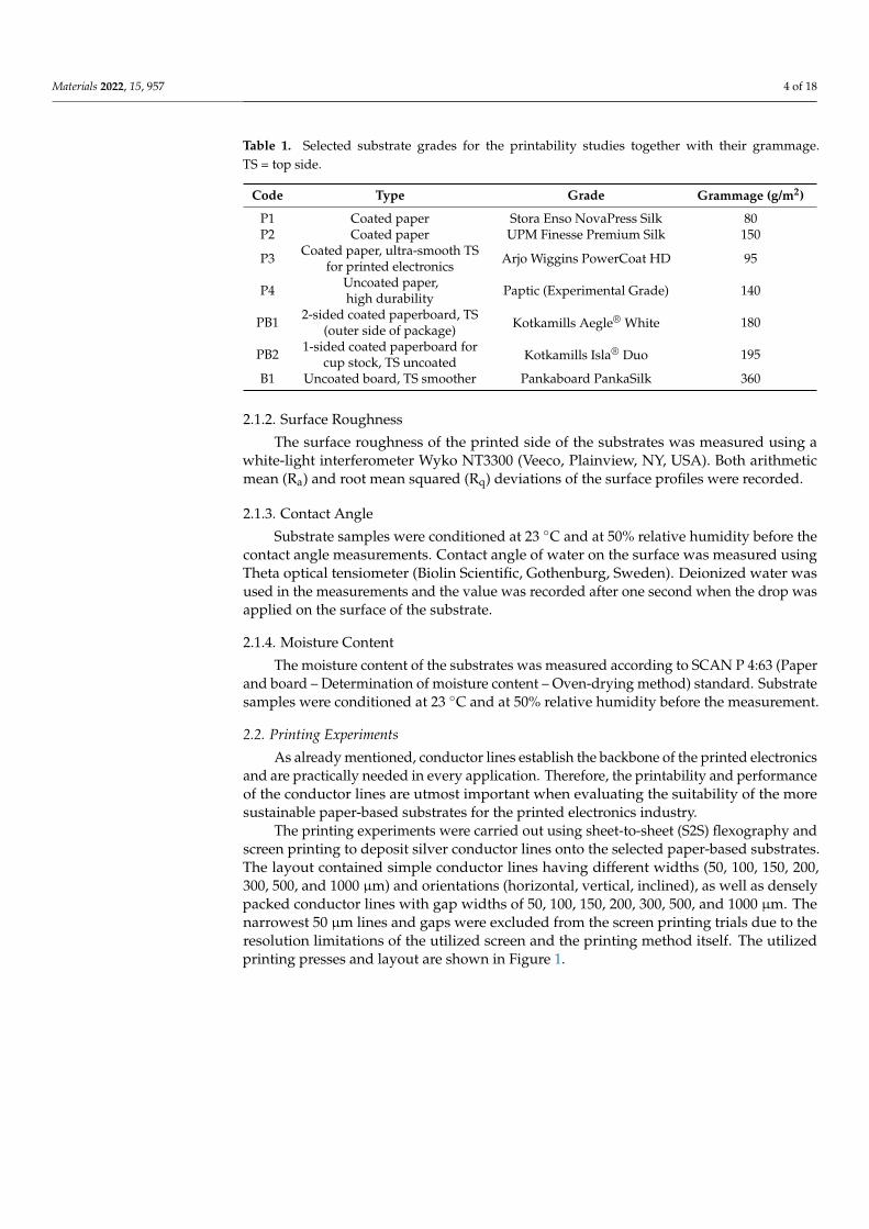
2. Materials and Methods2.1. Substrate Selection and Analytics
Seven different commercially available paper-based substrates were selected for theprintability trials: four printing papers (P1–P4), two coated paperboards (PB1, PB2), andone uncoated board (B1), as presented in Table 1. In order to evaluate the printability ofthe substrates in real life applications, their top side (TS) was printed meaning that theultra-smooth side of P3, the smoother (outer) side of PB1, the uncoated (outer) side of cupstock PB2, and the smoother side of B1 were printed.
2.1.1. Re-Pulping Experiments
The re-pulpability of the paper-based substrates was tested based on the Fibre BoxAssociation’s (FBA) method [34] with small modifications. In total, 60 g of substrate wasused in the experiments. After screening, the substrate material that did not pass throughthe sieve was collected as reject. The percentage of reject was calculated from the initial massand the reject mass. The re-pulpability test is passed, and the material can be consideredre-pulpable when the amount of reject is below 15%.
Materials 2022, 15, 957 4 of 18
Table 1. Selected substrate grades for the printability studies together with their grammage.TS = top side.
Code Type Grade Grammage (g/m2)
P1 Coated paper Stora Enso NovaPress Silk 80P2 Coated paper UPM Finesse Premium Silk 150
P3 Coated paper, ultra-smooth TSfor printed electronics Arjo Wiggins PowerCoat HD 95
P4 Uncoated paper,high durability Paptic (Experimental Grade) 140
PB1 2-sided coated paperboard, TS(outer side of package) Kotkamills Aegle® White 180
PB2 1-sided coated paperboard forcup stock, TS uncoated Kotkamills Isla® Duo 195
B1 Uncoated board, TS smoother Pankaboard PankaSilk 360
2.1.2. Surface Roughness
The surface roughness of the printed side of the substrates was measured using awhite-light interferometer Wyko NT3300 (Veeco, Plainview, NY, USA). Both arithmeticmean (Ra) and root mean squared (Rq) deviations of the surface profiles were recorded.
2.1.3. Contact Angle
Substrate samples were conditioned at 23 C and at 50% relative humidity before thecontact angle measurements. Contact angle of water on the surface was measured usingTheta optical tensiometer (Biolin Scientific, Gothenburg, Sweden). Deionized water wasused in the measurements and the value was recorded after one second when the drop wasapplied on the surface of the substrate.
2.1.4. Moisture Content
The moisture content of the substrates was measured according to SCAN P 4:63 (Paperand board – Determination of moisture content – Oven-drying method) standard. Substratesamples were conditioned at 23 C and at 50% relative humidity before the measurement.
2.2. Printing Experiments
As already mentioned, conductor lines establish the backbone of the printed electronicsand are practically needed in every application. Therefore, the printability and performanceof the conductor lines are utmost important when evaluating the suitability of the moresustainable paper-based substrates for the printed electronics industry.
The printing experiments were carried out using sheet-to-sheet (S2S) flexography andscreen printing to deposit silver conductor lines onto the selected paper-based substrates.The layout contained simple conductor lines having different widths (50, 100, 150, 200,300, 500, and 1000 µm) and orientations (horizontal, vertical, inclined), as well as denselypacked conductor lines with gap widths of 50, 100, 150, 200, 300, 500, and 1000 µm. Thenarrowest 50 µm lines and gaps were excluded from the screen printing trials due to theresolution limitations of the utilized screen and the printing method itself. The utilizedprinting presses and layout are shown in Figure 1.

Materials 2022, 15, 957 5 of 18
Figure 1. (a) Flexiproof 100 printer used for the flexographic printing trials and the principle of theflexography; (b) EKRA E2 screen printer and its operating principle, and (c) the printing layout.
2.2.1. Flexographic Printing Trials
The principle of the flexographic printing is shown in Figure 1a. The ink is initiallyapplied onto a ceramic or chrome-plated anilox roller. The anilox roller has tiny cells with acertain volume engraved or etched evenly onto its surface. As the ink covers the surface ofthe anilox roller completely, a steel doctor blade removes excess ink so that the ink remainsonly inside the cells of the anilox roller. After this, the ink is transferred in a nip onto aflexible photopolymer printing plate that has the printed patterns as raised elements on itssurface. Finally, the ink is transferred onto the substrate in a printing nip and dried. Thecell volume of the anilox roller determine the amount of ink available during the process.The nip pressures and printing speed determine the final ink transfer volume onto thesubstrate and also the ink spreading, i.e., detail rendering.
Flexographic printings were done with Flexiproof 100 (RK PrintCoat Instruments,Litlington, UK) tabletop printer using PFI-722 water-based silver nanoparticle ink (Nova-centrix, Austin, TX, USA). The viscosity of the ink is 300–600 mPa·s and silver content is60 wt-%. The printing plate was Cyrel® DPR 67 (DuPont, Wilmington, DE, USA) with athickness of 1.7 mm and hardness of 69 ShA. The printing speed was 50 m/min and theprinted layers were dried with hot air in a box oven at 130 C for 30 min. Two different ce-ramic anilox rollers with the ink transfer volumes of 5 mL/m2 (200 cells/cm) and 7 mL/m2
(120 cells/cm) were used. The B1 board could not be printed with flexography due toits high stiffness and thickness that prevented its proper mounting around the substratecylinder and its smooth passage through the printing process. In addition, a 125 µm thickPET plastic foil Melinex ST506 (DuPont Teijin Films, Chester, VA, USA) was printed as areference substrate to compare the achieved printability results on paper-based substrateswith the quality achieved on a substrate used commonly in printed electronics.
2.2.2. Screen Printing Trials
In S2S screen printing (Figure 1b), the ink is applied in front of the rubber squeegee thatsqueezes ink through the screen openings onto the substrate. The screen is manufacturedfrom metal or polymeric threads that form a mesh pattern with openings between thethreads. The mesh count of the screen, thread parameters, and squeegee pressure determinethe ink transfer amount and resolution. The non-image areas of the screen are coveredwith a stencil, thus leaving only image areas open and ready for the ink transfer. As thesqueegee pushes the screen into contact with the substrate and moves along the screen,the ink gets transferred onto the substrate. After the printing, the printed layer is dried.The substrate is typically conveyed to the printing unit underneath the screen on a movingsubstrate table onto which the substrate is held in place by means of suction.

Materials 2022, 15, 957 6 of 18
Screen printing trials were done with an E2 sheet-based screen printer (EKRA, Aachen,Germany) using LS-411AW micro particle silver paste (Asahi Chemical Laboratory Co.Ltd.,Tokyo, Japan). The viscosity of the paste is 22 Pa·s, silver content approximately 70 wt-%,and solids content approximately 85 wt.%. A stainless steel screen (Koenen, Ottobrunn-Riemerling, Germany) with a mesh count of 325 lines/inch and a wire diameter of 24 µmwas used to print the conductor layers at the speed of 40 mm/s. The utilized rubbersqueegee had a hardness of 65 ShA and angle of 45. The printed samples were dried withhot air in a box oven at 150 C for 20 min.
2.2.3. Rotary Screen Printing Trials
Figure 2a presents the operation principle of the roll-to-roll (R2R) rotary screen printing.The cylindrical metal screen having printed patterns as openings on its surface rotates toenable a continuous operation. Stationary rubber squeegee is located inside the rotatingscreen and the ink is also applied inside the screen. The ink gets transferred from the insideof the screen onto the substrate as the squeegee is pressed against the rotating screen andmoving substrate. The metal backing cylinder acts as support for the substrate during theink transfer. After the ink transfer, the substrate web with printed layers is conveyed to thedrying section of the R2R printing line.
Figure 2. Roll-to-roll (R2R) rotary screen printing process with P1 paper using VTT’s R2R printingline and the operating principle of the rotary screen printing (a) and the layout for the R2R printingtrials (b).
Rotary screen printing trials in R2R environment were performed with VTT’s pilotproduction line (Figure 2a) onto P1 (100 g/m2) and P3 papers as well as onto PET plasticfoil Melinex ST506 (DuPont Teijin Films, Chester, VA, USA). Microparticle silver pasteLS-411AW (Asahi, Japan) was printed using cylindrical stainless steel screens (SPGPrints,Boxmeer, The Netherlands) with a mesh count of 305 lines/inch and theoretical wet inklayer thickness of 11 µm. The layout, shown in Figure 2b, consisted of printed lines andgaps with widths of 50, 80, 100, 200, 500, and 1000 µm as well as antenna patterns havingline and gap widths of 100, 200, 500, and 1000 µm. The printing speed was 2 m/min andtemperature of the hot-air ovens of ROKO was set to 140 C. The total dwell time in thedrying section was approximately 3 min. The print run length was approximately 30 m persubstrate and the quality analysis was done for 5–10 m of samples.

Materials 2022, 15, 957 7 of 18
2.3. Printability Analysis
The printability of the conductor lines on the paper-based substrates was evaluatedconsidering their use in the printed electronics applications. Important printability parame-ters included the layer conductivity, i.e., the sheet resistance (SR) and volume resistivity(VR) of the printed conductor layers, minimum conductive conductor line width, minimumreproducible gap width, and ink spreading.
2.3.1. Minimum Conductive Line Width
The minimum conductive line width was determined by measuring the resistance ofthe printed conductors having different widths and orientations with a common digitalmultimeter FLUKE 289 (Fluke, Everett, WA, USA). The narrowest line width that gave ameasurable resistance value was evaluated to be the minimum reproducible line width thatcan be utilized in the printed electronics applications. The measurements were taken forevery line orientation separately from which an average value of the minimum conductiveline width in a test point was calculated.
2.3.2. Detail Rendering
The minimum reproducible gap width and ink spreading was analyzed by means ofthe SmartScope ZIP 250 microscope (OGP, Rochester, NY, USA). The minimum gap widthwas determined by detecting the completely open gaps without any ink splashes in everypattern orientation separately and calculating the average minimum gap in a test point.The ink spread was determined by measuring the widths of 500 µm and 1000 µm wide linesin every orientation and calculating the difference between the measured and designed linewidths. The measurements were taken in every line orientation separately and an averageink spreading in a test point was then calculated. In addition, the visual quality of theprinted conductor layers was analyzed by means of NeoScopeTM JCM-5000 (JEOL, Tokyo,Japan) scanning electron microscope (SEM).
2.3.3. Conductivity
The resistance of the printed 1000 µm wide lines with different orientations wasmeasured with the common digital multimeter FLUKE 289 (Fluke, Everett, WA, USA). Thelayer thickness was measured with Dektak 150 surface profilometer (Veeco, Plainview, NY,USA) from samples where the ink did not penetrate into the surface irregularities of thesubstrate. Thus, the layer thickness was measured on PET and on P1 paper in the case offlexography and screen printing, respectively. In R2R screen printing, the layer thicknesswas measured from all the test points. The sheet resistance and volume resistivity werethen calculated by means of the measured resistance (R), line width (w), line length (l), andlayer thickness (h):
SR (Ω/sq.) = Rwl−1 (1)
VR (Ω·cm) = SR h (2)
3. Results3.1. Paper-Based Substrate Quality
Table 2 presents the measured properties of the substrates. Roughness and contactangles were measured from the printed side of the substrates. The surface roughnessof the substrate was found to influence the ink transfer so that rougher surfaces acceptmore ink but as the surface roughness increases too much, the ink–substrate contact areadecreases, and the ink transfer gets reduced [35]. All the paper-based substrates used in thisstudy have significantly higher roughness than the reference substrate PET, thus predictingdifferences in the ink transfer, printability, and performance of the conductor lines betweenthe selected substrate types. The smoothest paper-based substrates are P3 and PB1 whereasthe roughest substrates are P4 and B1.

Materials 2022, 15, 957 8 of 18
Table 2. Roughness, percentage of rejects, moisture content, and contact angle of water. Roughnessand contact angle were measured from the printed side of the substrates.
CodeRoughness (µm) Percentage of
Rejects (%)Moisture
Content (%)Contact
Angle ()Ra Rq
P1 0.97 ± 0.15 1.25 ± 0.25 0.0 6.6 65P2 1.14 ± 0.18 1.49 ± 0.26 0.1 4.6 83P3 0.20 ± 0.04 0.28 ± 0.06 27.3 5.5 98P4 5.19 ± 0.91 6.77 ± 1.16 33.7 6.8 112
PB1 0.72 ± 0.07 0.93 ± 0.09 0.2 7.9 68PB2 3.87 ± 0.46 5.10 ± 0.56 13.9 7.8 114B1 5.34 ± 1.23 6.82 ± 1.60 0.6 7.0 119
PET (REF) 0.007 ± 0.002 0.013 ± 0.005 - - -
The surface is considered hydrophobic, and ink wetting is lower when the contactangle of water is over 90, as is for P3, P4, PB2, and B1. However, with paper-basedsubstrates, the wetting is affected by porosity, localized hydrophobicity (internal sizing),and roughness of the substrate. In addition, the dynamic phenomena of the contact an-gle on paper-based substrates might depict the ink wetting phenomena more accuratelythan the static contact angle measured done here [36]. It should be noted that ink wet-ting and spreading are also affected by the forces present during the ink transfer in theprinting nip [37].
The amount of reject is under <1% for P1, P2, PB1, PB2, and B1 substrates, thusindicating their excellent re-pulpability. However, the amount of reject is calculated from thematerial left on the sieve and this may be increased due to the coating, filler, and additivestype, or if the tested material has, for example, larger particles or very long fibers and notentirely because of the presence of un-recyclable materials. For example, re-pulping of P3,P4, and PB2 substrates results in large amounts of rejects, thus indicating only the presenceof larger particles/fibers or unsuitable materials for the utilized re-pulping method.
The moisture content of the paper-based substrate is the lowest for P2 and P3 papersand the highest for PB1 and PB2 paperboards. The lower the moisture content of the paper,the better its dimensional stability, thus improving the registration accuracy in multilayerprinting. Typically, appropriate moisture content level of printing papers is 5–7%. Toohigh moisture content can create difficulties in paper runnability in the printing processand layer unevenness or poorer printability due to uneven ink absorption and ink transfer.In addition, too low moisture content, for its part, creates runnability issues by causingthe paper to tear more easily during processing. According to the results, printability anddimensional stability issues might be present with PB1 and PB2 substrates that has highermoisture content than 7%. However, these materials are coated with a barrier layer thatreduces the effect of the moisture content of the base paper to print quality, dimensionalstability, and runnability.
3.2. Printability in Flexography
All the selected paper-based substrates are properly printable with flexography andgive good layer coverage with sharp printed edges and reproducible gap details, as shownin Figure 3. The layer quality on paper-based substrates is rather similar to the qualityon the reference PET foil. On paper-based substrates, the edge raggedness or waviness isexpectedly higher due to their more irregular surface. However, the layer coverage and linedefinition on coated paper-based substrates have equal quality as compared to the qualityon the reference PET foil. Therefore, the higher layer roughness of the coated paper-basedsubstrates does not adversely affect the print quality. However, the surface texture of theeven rougher uncoated P4 and PB2 substrates shines through the printed layers, thus givinga more mottled appearance and seemingly decreasing the layer coverage. This results fromthe ink absorption into the pores, ink flow, or spreading along the surface irregularities,as well as uneven ink transfer, i.e., formation of poorer and inhomogeneous ink-substrate

Materials 2022, 15, 957 9 of 18
contact. The visual print quality remains unchanged as the ink transfer volume increasesfrom 5 mL/m2 to 7 mL/m2.
Materials 2022, 15, 957 9 of 18
definition on coated paper-based substrates have equal quality as compared to the quality on the reference PET foil. Therefore, the higher layer roughness of the coated paper-based substrates does not adversely affect the print quality. However, the surface texture of the even rougher uncoated P4 and PB2 substrates shines through the printed layers, thus giv-ing a more mottled appearance and seemingly decreasing the layer coverage. This results from the ink absorption into the pores, ink flow, or spreading along the surface irregular-ities, as well as uneven ink transfer, i.e., formation of poorer and inhomogeneous ink-substrate contact. The visual print quality remains unchanged as the ink transfer volume increases from 5 mL/m2 to 7 mL/m2.
(a) (b) (c) (d)
Figure 3. Photographs of the flexo-printed conductor layers on paper-based substrates using the nanoparticle silver ink and the ink transfer volume of 5 mL/m2. In addition, microscope images of the printed 1000 µm wide vertical lines with a scale bar of 1 mm are shown. The substrates are papers P1–P4 (a,b), paperboards PB1 and PB2 (c), and reference polyethylene terephthalate (PET) plastic foil (d).
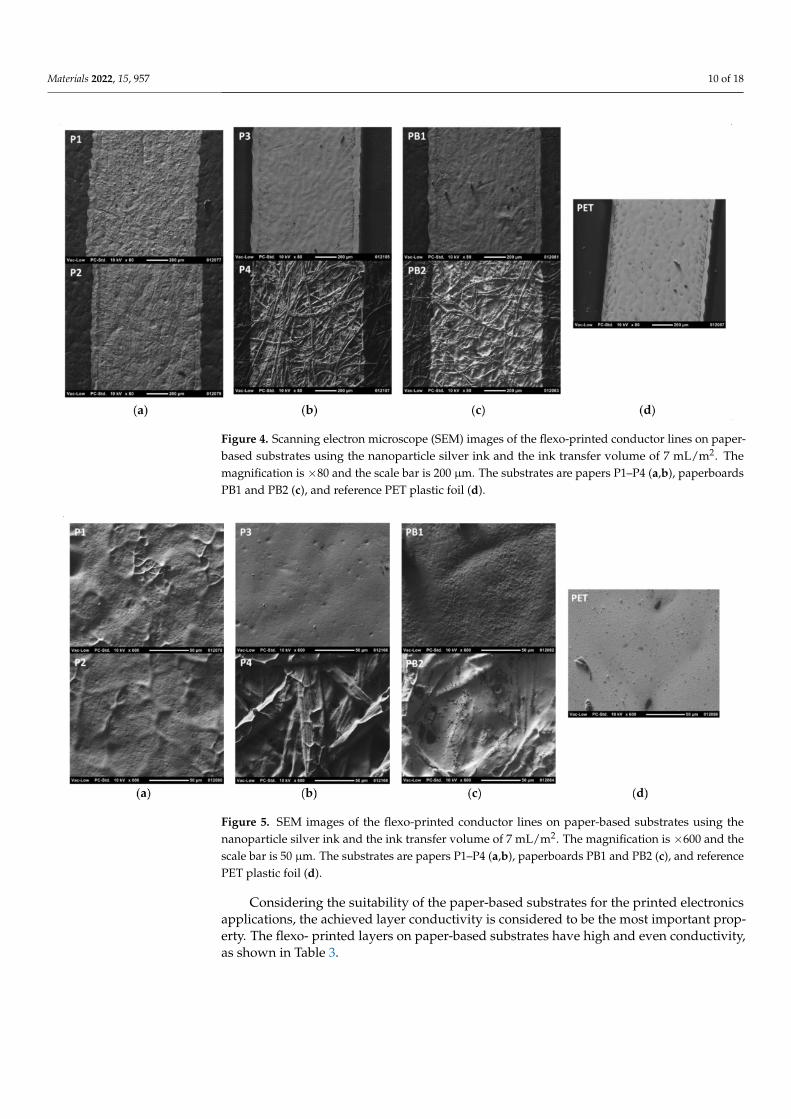
Figures 4 and 5 show that the printed layers are properly transferred onto the sub-strate and remain on the surface of the substrates rather than penetrate into the pores of the paper-based substrates. Even with uncoated paper-based substrates, the nanoparticle ink does not penetrate inside the paper structure along the pores but tends to follow the irregularities of the substrate surface. Therefore, the printed layers are expected to have good conductivity. However, the surface texture of the paper-based substrates is clearly visible through the thin nanoparticle ink layer. The measured layer thicknesses on PET were 302 nm and 632 nm for the ink transfer volumes of 5 mL/m2 and 7 mL/m2, respec-tively. When the layer thickness is smaller than the roughness of the substrate, as with P1, P2, P4, and PB2 substrates, the ink layer follows the surface irregularities of the substrate. With the uncoated rougher substrates P4 and PB2, the ink transfer into the deep valleys
Figure 3. Photographs of the flexo-printed conductor layers on paper-based substrates using thenanoparticle silver ink and the ink transfer volume of 5 mL/m2. In addition, microscope images ofthe printed 1000 µm wide vertical lines with a scale bar of 1 mm are shown. The substrates are papersP1–P4 (a,b), paperboards PB1 and PB2 (c), and reference polyethylene terephthalate (PET) plasticfoil (d).
Figures 4 and 5 show that the printed layers are properly transferred onto the substrateand remain on the surface of the substrates rather than penetrate into the pores of the paper-based substrates. Even with uncoated paper-based substrates, the nanoparticle ink does notpenetrate inside the paper structure along the pores but tends to follow the irregularities ofthe substrate surface. Therefore, the printed layers are expected to have good conductivity.However, the surface texture of the paper-based substrates is clearly visible through thethin nanoparticle ink layer. The measured layer thicknesses on PET were 302 nm and632 nm for the ink transfer volumes of 5 mL/m2 and 7 mL/m2, respectively. When thelayer thickness is smaller than the roughness of the substrate, as with P1, P2, P4, andPB2 substrates, the ink layer follows the surface irregularities of the substrate. With theuncoated rougher substrates P4 and PB2, the ink transfer into the deep valleys of thesurface profile seems to be partial and ink-free areas are seen in the bottom of the surfaceirregularities. However, with smoother P3 and PB1 substrates, the ink layer fills the smallersurface irregularities completely, which in turn leads to smoother conductor layers withmore even surface quality. On the ultra-smooth and un-porous PET foil, for its part, somelayer unevenness and pinholes appear, thus indicating that the optimum ink transfer andlevelling in flexography seems to require some substrate surface roughness and differentsurface energy with the utilized water-based ink.
Materials 2022, 15, 957 10 of 18
Figure 4. Scanning electron microscope (SEM) images of the flexo-printed conductor lines on paper-based substrates using the nanoparticle silver ink and the ink transfer volume of 7 mL/m2. Themagnification is ×80 and the scale bar is 200 µm. The substrates are papers P1–P4 (a,b), paperboardsPB1 and PB2 (c), and reference PET plastic foil (d).
Figure 5. SEM images of the flexo-printed conductor lines on paper-based substrates using thenanoparticle silver ink and the ink transfer volume of 7 mL/m2. The magnification is ×600 and thescale bar is 50 µm. The substrates are papers P1–P4 (a,b), paperboards PB1 and PB2 (c), and referencePET plastic foil (d).
Considering the suitability of the paper-based substrates for the printed electronicsapplications, the achieved layer conductivity is considered to be the most important prop-erty. The flexo- printed layers on paper-based substrates have high and even conductivity,as shown in Table 3.

Materials 2022, 15, 957 11 of 18
Table 3. Calculated average and standard deviation values for sheet resistance (SR) and volumeresistivity (VR) of flexo-printed conductor layers on different substrates. The layer thickness used inthe VR measurement was considered to be equal on every substrate since the high surface roughnessof the paper-based substrates prevented reliable measurement of layer thickness.
CodeSheet Resistance (mΩ/square) Volume Resistivity (Ω·cm)
5 mL/m2 7 mL/m2 5 mL/m2 7 mL/m2
P1 326 ± 35 177 ± 19 9.8 × 10⁻⁶ 2.2 × 10⁻⁶
P2 202 ± 22 138 ± 7 6.1 × 10⁻⁶ 1.4 × 10⁻⁶
P3 253 ± 26 169 ± 16 7.6 × 10⁻⁶ 1.6 × 10⁻⁶
P4 644 ± 111 318 ± 38 1.9 × 10⁻⁵ 7.0 × 10⁻⁶
PB1 198 ± 27 177 ± 17 6.0 × 10⁻⁶ 1.7 × 10⁻⁶
PB2 1524 ± 345 1199 ± 325 4.6 × 10⁻⁵ 2.2 × 10⁻⁵
PET (REF) 356 ± 33 260 ± 23 1.1 × 10⁻⁵ 2.1 × 10⁻⁶
Even better conductivity is achieved on the coated P1, P2, P3, and PB1 substratesthan on the reference PET substrate. Thus, coated paper-based substrates seem to acceptmore ink and have better layer uniformity with more particle-to-particle contacts despitetheir higher surface roughness and porosity, and a wide range of contact angle values, ascompared to the reference PET substrate. On uncoated P4 and PB2 substrates, for theirpart, the sheet resistance value and its deviation are higher because of the poorer inktransfer into the roughness profile of the substrates and the ink flow or spreading intothe deep surface irregularities of the substrate during the layer levelling, thus decreasingthe number of conductive particle-to-particle contacts within the printed layers. As theamount of particle-to-particle contacts decrease, less particles are available for merging andcoalescence into each other, thus decreasing the layer conductivity further.
The sheet resistance values in flexography are rather high (>100 mΩ/square) resultingfrom the low layer thickness of 302–632 nm. However, the nanoparticle ink leads to alow volume resistivity value of 1.4–46 µΩ·cm, i.e., high conductivity. The values achievedon coated paper-based substrates and on PET are comparable to the volume resistivitiesachieved with previous studies presented in the Introduction chapter. The volume resis-tivity values on coated P1, P2, P3, and PB1 substrates are equal or even lower than onPET, thus indicating a high ink transfer and good particle-to-particle contact formationalso on rougher paper-based substrates. On uncoated P4 and PB2 substrates, the volumeresistivities are higher because of the ink sinking into the large surface irregularities, thusreducing the number of particle-to-particle contacts and particle coalescence possibilities.In addition, the increase in the ink transfer volume decreases both the sheet resistanceand the volume resistivity values due to the thicker layers with more densely packednanoparticles. Therefore, it can be concluded that coated paper-based is a good alternativeto plastic foils without sacrificing layer conductivity and performance.
The reproducibility and detail rendering of the printed conductor layers play a majorrole in designing printed electronic circuits. Figure 6 shows the printed gap quality in thevertical direction using the two ink transfer volumes. As the ink transfer volume increases,the ink tends to spread more, thus increasing the minimum reproducible gap and decreasingthe edge quality of the gaps. On uncoated paper-based substrates, the gap quality is equalto the other substrate since the surface irregularities prevent lateral ink from spreading.The gap quality seems to be poorer on coated P2 and PB1 substrates. As compared to thePET substrate, the minimum reproducible gap width on paper-based substrates is slightlyincreased, which indicates higher ink spreading on paper-based substrates. This higherspreading is most likely from the differences in surface energy between the paper-basedsubstrates and PET as well as on higher ink transfer onto the paper-based substrates.

Materials 2022, 15, 957 12 of 18
Figure 6. Microscope images of the flexo-printed gaps on paper-based substrates using the nanopar-ticle silver ink and two different ink transfer volumes. The scale bar is 500 µm and four narrowestvertical gaps, i.e., 50, 100, 150, and 200 µm, are presented. The substrates are papers P1–P4 (a,b),paperboards PB1 and PB2 (c), and reference PET plastic foil (d).
Table 4 presents the measured and calculated results for the different substrates andink transfer volumes in flexography. The higher ink transfer volume of 7 mL/m2 increasesthe ink spread due to the increased amount of ink on the substrate. This also leads to theincreased minimum gap width and decreased minimum conductive line. The ink spreadand minimum gap widths are higher on paper-based substrates than on PET. However,the layer quality on P1 paper is not far from the quality on PET foil and the differencesbetween the substrates are not that significant. There is no large difference in minimumconductive line between the paper-based substrates and the PET foil. However, coated P1and uncoated PB2 substrates do not perform that well when printing these small details.
Table 4. Measured ink spreading, minimum reproducible designed gap width, and minimumconductive designed line width of the flexo-printed conductor layers on different substrates.
CodeSpreading (µm) Minimum Gap Width (µm) Minimum Conductive
Line Width (µm)5 mL/m2 7 mL/m2 5 mL/m2 7 mL/m2 5 mL/m2 7 mL/m2
P1 4 51 75 100 103 106P2 27 70 100 108 83 79P3 13 41 100 108 83 79P4 27 84 100 133 142 92
PB1 60 84 100 100 79 50PB2 15 70 100 150 79 50PET
(REF) 13 34 67 100 78 67
In conclusion, the selected paper-based substrates are excellent substrate candidatesfor printed electronics. Despite their higher roughness, the printed layer conductivityand coverage are improved, as compared to the printed layers on PET plastic foil. Inaddition, the detail rendering on paper-based substrates is at the same level as with PETfoil. Therefore, some substrate roughness seems to be beneficial for proper ink transferand formation of more partcile-to-partcile contacts within the printed layers. Uncoatedpaper-based substrates, for their part, suffer from ink penetration into surface irregularities,

Materials 2022, 15, 957 13 of 18
poorer ink transfer into deep surface irregularities, and ink flow along the surface irregu-larities, thus decreasing layer conductivity and visual quality. However, the deep surfaceirregularities prevent lateral ink spread, thus giving good detail rendering.
3.3. Printability in Screen Printing
As in the case of flexography with nanoparticle ink, micro particle silver paste isproperly printable with screen printing onto different paper-based substrates (Figure 7).The higher solid content and viscosity of the conductor ink in screen printing increasethe layer thickness to 12.6 µm, as compared to 302–632 nm in flexography. With coatedsubstrates P1, P2, P3, and PB1, the surface irregularities of the substrate are completelyfilled with ink and the layer coverage is good, but the mesh pattern of the screen is copiedonto the surface of the printed layers. The printed line edges become more ragged andwavier, and some surface texture and fibers of the substrate are seen through the printedlayer with uncoated substrates P4, PB2, and B1. This results from the ink flow along thesurface irregularities and fibers of the substrates as well as from the poorer ink transfer, i.e.,the poorer contact formation between the ink/screen and the substrate.
Figure 7. SEM images of the screen-printed conductor lines on paper-based substrates using themicro-particle silver paste. The magnification is ×80 and the scale bar is 200 µm. The substrates arepapers P1–P4 (a,b), paperboards PB1 and PB2 (c), and board B1 (d).
The difference between the nanoparticle ink used in flexography and the microparticleink used in screen printing is clearly visible in Figure 8. Tiny nanoparticles have mergedand sintered together during the oven drying, thus forming a uniform layer and withoutseeing separate silver particles anymore. On the other hand, with the microparticle ink,separate silver flakes are clearly seen since no sintering takes place during the layer drying.Therefore, the printed layer has a more irregular and uneven surface, and its volumeresistivity is expected to be higher.
Table 5 presents the properties of the screen-printed conductor layers on differentpaper-based substrates. The screen-printed layers have very low sheet resistance values(<40 mΩ/square) due to high layer thickness of 12.6 µm. However, as expected, the volumeresistivity values are higher than with flexography resulting from the larger particle size inthe ink and the un-sintered layer structure, thus forming less contacts between conductiveparticles within the printed layers. The substrate has no large effect on conductivity due tothe thick layer covering and filling the surface irregularities and forming a continuous inklayer. On uncoated PB1 and B1 substrates, the ink spread and minimum gap widths arelarger because of the ink flow along the surface irregularities. However, on uncoated P4,

Materials 2022, 15, 957 14 of 18
the ink spread is very low, despite the larger minimum gap value. This indicates that theprinting of the densely spaced lines is more difficult and more prone to ink splashes andunevenness as well as excessive flow on the surface of the substrate than the printing ofindividual lines far apart from each other. The minimum conductive line is not affectedby the substrate to a great extent. Only with B1, the minimum conductive line is 200 µmwhereas with other substrates, the minimum line width is less than 150 µm.
Figure 8. SEM images of the printed conductor layers on P1 substrate. The magnification is ×600and the scale bar is 50 µm. The flexo-printed layer with nanoparticle ink (a) and screen-printed layerwith microparticle ink (b) are shown.
Table 5. Calculated sheet resistance and volume resistivity as well as measured ink spreading,minimum reproducible designed gap width, and minimum conductive designed line width of thescreen-printed conductor layers on different substrates.
Substrate SheetResistance (mΩ/square)
VolumeResistivity (Ω·cm)
Spreading(µm)
Minimum GapWidth (µm)
MinimumConductive Line (µm)
P1 30.8 ± 1.7 3.9 × 10⁻⁵ 32 150 106P2 35.4 ± 1.6 4.5 × 10⁻⁵ 24 161 122P3 33.1 ± 2.0 4.2 × 10⁻⁵ 33 144 128P4 31.0 ± 1.0 3.9 × 10⁻⁵ 49 211 133
PB1 36.4 ± 1.0 4.6 × 10⁻⁵ 57 128 106PB2 38.8 ± 2.0 4.9 × 10⁻⁵ 102 300 100B1 32.7 ± 3.3 4.1 × 10⁻⁵ 124 611 200
Screen printing can reproduce thick conductor layers with good coverage and lowsheet resistance onto different paper-based substrates. The thick printed layers can easilyfill the surface irregularities of the substrate, thus giving low sheet resistance, despitethe substrate roughness. However, on uncoated substrates, the ink tends to spread morealong the surface irregularities of the substrate, thus making the detail rendering poorerand creating more ragged and wavier printed edges. The large particle size of the microparticle ink and the un-sintered layer structure after drying increases the achievable volumeresistivity by decreasing the amount of conductive paths within the printed layer.

Materials 2022, 15, 957 15 of 18
3.4. R2R Printability in Screen Printing
Figure 9 shows good printability and detail rendering in R2R rotary screen printingon P1, P3, and PET substrates. The mesh pattern of the screen is visible on the surface, aswith the S2S screen printing, resulting from the high ink viscosity that slows down the inklayer levelling. The layer conductivity is higher on paper-based substrates than on PET,although there are no large differences in layer thickness, as shown in Table 6. Therefore,the ink particles can align themselves into better contact with each other on rougher andmore porous surfaces than on the extremely smooth and non-absorbent PET. The substratehas no effect on the detail rendering in the R2R printing since no uncoated substrates wereused. Thus, the detail rendering is very good, and the ink layers do not spread on thesubstrates after the ink transfer in the R2R process.
Figure 9. SEM images of the R2R screen-printed conductor lines on the selected substrates usingmicro-particle silver paste. The magnification is ×80 and the scale bar is 200 µm. The substrates areP1 (a), P3 (b), and PET reference foil (c).
Table 6. Calculated sheet resistance and volume resistivity as well as measured layer thickness, inkspreading, minimum reproducible designed gap width, and minimum conductive designed linewidth of the rotary screen-printed conductor layers on different substrates.
SubstrateSheet
Resistance(mΩ/square)
VolumeResistivity
(Ω·cm)
Thickness(µm)
Spreading(µm)
Minimum GapWidth (µm)
MinimumConductiveLine (µm)
P1 45.3 ± 1.3 4.1 × 10⁻⁵ 9.1 ± 0.8 −27 50 87P3 39.4 ± 0.6 3.4 × 10⁻⁵ 8.5 ± 0.9 −26 50 87
PET 52.3 ± 2.5 4.7 × 10⁻⁵ 8.9 ± 0.3 −19 50 98
As compared to the S2S screen-printed layer quality, the sheet resistance values inrotary screen printing are slightly higher because of the thinner ink layer, lower dryingtemperature, and shorter drying time. However, no difference in volume resistivity is seen,meaning that the screen-printed layers have similar conductivity but the differences in thescreen properties and printing mechanisms create changes in the ink transfer amount. The

Materials 2022, 15, 957 16 of 18
detail rendering in rotary screen printing is better than in S2S screen printing. This can beexplained by the smaller ink transfer and thinner layers in the rotary screen printing.
4. Discussion
The tested commercial paper-based substrates found to be suitable substrate can-didates for printed electronics applications using both flexography and screen printing.Despite their higher roughness and porosity, as compared to PET foil and a wide range ofmeasured contact angle levels, print quality and layer performance was equal or even betterthan on the reference PET substrate. Therefore, some layer roughness and porosity wasfound to be beneficial for ink transfer and formation of highly conductive layers. Previousstudies stated that printed layer conductivities on papers have not reached the conductivitylevels on plastic foils. However, in this paper, the quality and performance of the printedconductor layers on coated paper-based substrates was better or at the same level than onthe PET foil, resulting from better ink transfer onto the rougher but rather even surface. Inaddition, the utilized commercial papers have modern coatings optimized for the printingof small details without ink penetration, and some grades are said to be even tailored forprinted electronics by manufacturers, such as P3.
In flexography, the layer conductivity and coverage were higher on coated paper-based substrates than on the PET foil. This means that some layer roughness was neededto increase the ink transfer rate. The detail rendering properties were slightly poorer on thepaper-based substrates than on the PET foil but the differences were rather small. The deepsurface irregularities of uncoated substrates prevented lateral ink spread, thus improvingthe detail rendering properties—similar between the coated paper-based substrates andthe PET foil. However, with rougher uncoated papers, the ink transfer got poorer, and theink layer sunk into the irregularities of the paper surface, thus decreasing the conductivity.The contact angle of water on the paper-based substrates had no effect on the layer qualitydue to the high nip pressure forcing the ink to transfer and spread on the surface ofthe substrates.
The ink transfer volume in flexography had a large effect on the printed conductorlayers. As the ink transfer volume increased, more ink was transferred onto the substrates,resulting in better conductivity but higher ink spreading and poorer detail rendering.
In screen printing, the effect of the substrate on the layer quality was small. The thickmicro particle ink layers filled the surface irregularities, thus forming highly conductivelayers, despite the substrate properties. However, the detail rendering was poorer withuncoated paper-based substrates due to the ink flow or spreading along the surface fibersand irregularities of the substrate. R2R printing trials also confirmed that better conductivitywas achieved on coated paper-based substrates having higher roughness than on the ultra-smooth PET foil. Furthermore, no effect on the detail rendering could be detected.
The nanoparticle ink used in flexography formed uniform layers where individualparticles had merged/sintered together, thus resulting in low volume resistivity. However,the resulting thin layer increased the sheet resistance. With microparticle ink used in screenprinting trials, the individual silver flakes/particles remained separated, thus increasingvolume resistivity. The high layer thickness, for its part, ensured the formation of lowsheet resistance.
According to the re-pulpability and printability trials, the most promising recyclablesubstrates to be used in printed electronics applications were P1, P2, and PB1. These paper-based substrates were coated with an average surface roughness, Ra, between 0.72 µmand 1.14 µm. The lower moisture content with P1 and P2 papers indicate their betterdimensional stability during processing as well as more even print quality, as compared tothe PB1 paperboard. Further considering the performance and quality of the printed layers,the most promising paper-based substrate is P1 when searching for an easily re-pulpableor recyclable alternative to PET plastic foil.
The results shown in this paper give encouraging data for the possibility to replaceplastic foil substrates in printed electronics applications with coated, rough, porous, and
Materials 2022, 15, 957 17 of 18
recyclable paper-based substrates without sacrificing layer performance. The achievedresults can be exploited when replacing plastic foils in applications where highly conductiveor thick layers are needed, such as printed antennas, sensors, and displays. The flexiblenature of paper-based substrates together with their good breathability (porosity) also openpossibilities in wearable electronic applications.
Author Contributions: Conceptualization, E.J., L.H. and K.I.; methodology, E.J., K.E., V.L., J.L. andP.T.; validation, E.J., L.H., K.E., V.L., J.L., P.T. and K.I.; formal analysis, E.J., K.E., V.L., J.L. and P.T.;investigation, E.J., K.E., V.L., J.L. and P.T.; data curation, E.J.; writing—original draft preparation,E.J.,L.H.,K.E.,V.L.,J.L. and P.T.; writing—review and editing, E.J.; visualization, E.J.; supervision, L.H.,V.L. and K.I.; project administration, L.H.,V.L. and K.I.; funding acquisition, L.H. and V.L. All authorshave read and agreed to the published version of the manuscript.
Funding: Research work was carried out in ECOtronics project (www.ecotronics.fi (accessed on 22December 2021)) co-funded by Business Finland, VTT Technical Research Centre of Finland, TampereUniversity, LUT University and LAB University of Applied Sciences (grant no.1423/31/2019). Partof the facilities used were provided by the Academy of Finland Research Infrastructure “PrintedIntelligence Infrastructure (PII-FIRI, grant no. 32020)”.
Institutional Review Board Statement: Not applicable.
Informed Consent Statement: Not applicable.
Data Availability Statement: The authors confirm that the data supporting the findings of this studyare available within the article. The raw data that support the findings of this study are availablefrom the corresponding author, E.J., upon reasonable request.
Acknowledgments: The authors would like to acknowledge Asta Pesonen, Anne Peltoniemi, MinnaKehusmaa, Ulla Sarajärvi, and Hannu Sääskilahti for their assistance during the implementation ofthe printing trials and sample analysis.
Conflicts of Interest: The authors declare no conflict of interest.
References1. Gagliardi, M. Global Markets for Roll-to-Roll Technologies for Flexible Devices. 2016. Available online: www.bccresearch.com
(accessed on 3 November 2021).2. Liu, J.; Yang, C.; Wu, H.; Lin, Z.; Zhang, Z.; Wang, R.; Wong, C.P. Future paper based printed circuit boards for green electronics:
Fabrication and life cycle assessment. Energy Environ. Sci. 2014, 7, 3674–3682. [CrossRef]3. Espinosa, N.; García-Valverde, R.; Urbina, A.; Lenzmann, F.; Manceau, M.; Angmo, D.; Krebs, F.C. Life cycle assessment of
ITO-free flexible polymer solar cells prepared by roll-to-roll coating and printing. Sol. Energy Mater. Sol. Cells 2012, 97, 3–13.[CrossRef]
4. Bollström, R.; Toivakka, M. Paper substrate for printed functionality. In Proceedings of the 15th Fundamental ResearchSymposium, Cambridge, UK, 8–13 September 2013; pp. 945–966.
5. Hakola, L.; Jansson, E.; Futsch, R.; Happonen, T.; Thenot, V.; Depres, G.; Rougier, A.; Smolander, M. Sustainable roll-to-rollmanufactured multi-layer smart label. Int. J. Adv. Manuf. Technol. 2021, 117, 2921–2934. [CrossRef]
6. Ihalainen, P.; Määttänen, A.; Järnström, J.; Tobjörk, D.; Österbacka, R.; Peltonen, J. Influence of Surface Properties of CoatedPapers- on Printed Electronics. Ind. Eng. Chem. Res. 2012, 51, 6025–6036. [CrossRef]
7. Tobjörk, D.; Österbacka, R. Paper Electronics. Adv. Mater. 2011, 23, 1935–1961. [CrossRef]8. Torvinen, K.; Sievänen, J.; Hjelt, T.; Hellen, E. Smooth and flexible filler-nanocellulose composite structure for printed electronics
applications. Cellulose 2012, 19, 821–829. [CrossRef]9. Sullivan, M. Printed Electronics: Global Markets to 2022; BCC Research LLC: Wellesley, MA, USA, 2018.10. Valdec, D.; Hajdek, K.; Majnaric, I.; Cerepinko, D. Influence of Printing Substrate on Quality of Line and Text Reproduction in
Flexography. Appl. Sci. 2021, 11, 7827. [CrossRef]11. Kattumenu, R.; Rebros, M.; Joyce, M.; Fleming, P.D.; Neelgund, G. Effect of substrate properties on conductive traces printed with
silver-based flexographic ink. Nord. Pulp Pap. Res. J. 2009, 24, 101–106. [CrossRef]12. Gigac, J.; Fiserova, M.; Kovac, M.; Stankovska, M. Paper substrates for inkjet printing of UHF RFID antennas. Wood Res. 2020, 65,
25–36. [CrossRef]13. Sun, Q.; Qian, B.; Uto, K.; Chen, J.; Liu, X.; Minari, T. Electronic Biomaterials towards Flexible Sensors: A Review. Biosens.
Bioelectron. 2018, 2018, 18.14. Luoma, E.; Välimäki, M.; Rokkonen, T.; Sääskilahti, H.; Ollila, J.; Rekilä, J.; Immonen, K. Oriented and annealed poly(lactic acid)
films and their performance in flexible printed and hybrid electronics. J. Plast. Film. Sheeting 2021, 37, 34. [CrossRef]

Materials 2022, 15, 957 18 of 18
15. Välimäki, M.K.; Sokka, L.I.; Peltola, H.B.; Ihme, S.S.; Rokkonen, T.M.J.; Kurkela, T.J.; Ollila, J.T.; Korhonen, A.T.; Hast, J.T. Printedand hybrid integrated electronics using bio-based and recycled materials—Increasing sustainability with greener materials andtechnologies. Int. J. Adv. Manuf. Technol. 2020, 111, 325–339. [CrossRef]
16. Jin, J.; Lee, D.; Im, H.-G.; Han, Y.C.; Jeong, E.G.; Rolandi, M.; Choi, K.C.; Bae, B.-S. Chitin Nanofiber Transparent Paper for FlexibleGreen Electronics. Adv. Mater. 2016, 28, 5169–5175. [CrossRef]
17. Barras, R.; Cunha, I.; Gaspar, D.; Fortunato, E.; Martins, R.; Pereira, L. Printable cellulose-based electroconductive composites forsensing elements in paper electronics. Flex. Print. Electron. 2017, 2, 12. [CrossRef]
18. Sappati, K.K.; Bhadra, S. Piezoelectric Polymer and Paper Substrates: A Review. Sensors 2018, 18, 3605. [CrossRef] [PubMed]19. Gaspar, C.; Olkkonen, J.; Passoja, S.; Smolander, M. Paper as Active Layer in Inkjet-Printed Capacitive Humidity Sensors. Sensors
2017, 17, 1464. [CrossRef]20. Xu, Y.; Fei, Q.; Page, M.; Zhao, G.; Ling, Y.; Stoll, S.B.; Yan, Z. Paper-based wearable electronics. iScience 2021, 24, 14. [CrossRef]
[PubMed]21. Merilampi, S.; Laine-Ma, T.; Ruuskanen, P. The characterization of electrically conductive silver ink patterns on flexible substrates.
Microelectron. Reliab. 2009, 49, 782–790. [CrossRef]22. Gordon, S.E.; Dorfman, J.R.; Kirk, D.; Adams, K. Advances in Conductive Inks across Multiple Applications and Deposition
Platforms. In Proceedings of the IPC APEX EXPO 2012, San Diego, CA, USA, 28 February–1 March 2012; p. 7.23. Allen, M.L.; Aronniemi, M.; Mattila, T.; Alastalo, A.; Ojanperä, K.; Suhonen, M.; Seppä, H. Electrical sintering of nanoparticle
structures. Nanotechnology 2008, 19, 4. [CrossRef]24. Grouchco, M.; Kamyshny, A.; Mihailescu, C.F.; Anghel, D.F.; Magdassi, S. Conductive Inks with a “Built-In” Mechanism That
Enables Sintering at Room Temperature. ACS Nano 2011, 5, 3354–3359. [CrossRef]25. Huang, Q.; Shen, W.; Xu, Q.; Tan, R.; Song, W. Properties of polyacrylic acid-coated silver nanoparticle ink for inkjet printing
conductive tracks on paper with high conductivity. Mater. Chem. Phys. 2014, 147, 550–556. [CrossRef]26. Mo, L.; Guo, Z.; Wang, Z.; Yang, L.; Fang, Y.; Xin, Z.; Li, X.; Chen, Y.; Cao, M.; Zhang, Q.; et al. Nano-Silver Ink of High
Conductivity and Low Sintering Temperature for Paper Electronics. Nanoscale Res. Lett. 2019, 14, 11. [CrossRef]27. Magdassi, S.; Grouchco, M.; Berezin, O.; Kamyshny, A. Triggering the Sintering of Silver Nanoparticles at Room Temperature.
ACS Nano 2010, 4, 1943–1948. [CrossRef]28. Sohail, M.; Sun, D.-W.; Zhu, Z. Recent developments in intelligent packaging for enhancing food quality and safety. Crit. Rev.
Food Sci. Nutr. 2018, 58, 2650–2662. [CrossRef] [PubMed]29. Kirchmeyer, S. The OE-A roadmap for organic and printed electronics: Creating a guidepost to complex interlinked technologies,
applications and markets. Transl. Mater. Res. 2016, 3, 11. [CrossRef]30. Leminen, V.; Kainusalmi, M.; Tanninen, P.; Lindell, H.; Varis, J.; Ovaska, S.-S.; Backfolk, K.; Pitkänen, M.; Sipiläinen-Malm, T.;
Hartman, J.; et al. Aspects on Packaging Safety and Biomaterials. In Proceedings of the 26th IAPRI Symposium on Packaging,Espoo, Finland, 10–13 June 2013.
31. Furuta, T.; Tonooka, H.; Kobayashi, M. Research on Recycling Cardboard with RF Tags/Labels. In Proceedings of the EighthInternational Conference on EcoBalance, Tokyo, Japan, 10–12 December 2008; Rengo Co., Ltd.: Tokyo, Japan, 2008.
32. Erdmann, L.; Hilty, L.; Althaus, H.-J. Einfluss Von RFID-Tags Auf Die Abfallentsorgung: Prognose Möglicher Auswirkungen EinesMassenhaften Einsatzes von RFIDTags im Konsumgüterbereich Auf Die Umwelt Und Die Abfallentsorgung; Umweltbundesamt: Dessau-Roßlau, Germany, 2009; 185p.
33. Aliaga, C.; Zhang, H.; Dobon, A.; Hortal, M.; Beneventi, D. Recyclability assessment of printed electronics on paper substrate: Acase study for smart envelopes in courier and postal services. Waste Manag. 2015, 38, 41–48. [CrossRef]
34. Anon. Voluntary Standard for Repulping and Recycling Corrugated Fiberboard Treated to Improve Its Performance in the Presence of Waterand Water Vapor; Fibre Box Association: Itasca, IL, USA, 2013; 23p.
35. Olsson, R. Some Aspects on Flexographic Ink-Paper and Paperboard Coating Interaction. Ph.D. Thesis, Karlstad University,Faculty of Technology and Science, Chemical Engineering, Karlstad, Sweden, 2007.
36. Samyn, P. Wetting and hydrophobic modification of cellulose surfaces for paper applications. J. Mater. Sci. 2013, 48, 6455–6498.[CrossRef]
37. Olsson, R.; Yang, L.; van Stam, J.; Lestelius, M. Effects on ink setting in flexographic printing: Coating polarity and dot gain. Nord.Pulp Pap. Res. J. 2006, 21, 569–574. [CrossRef]