Structural Integration of Silicon Solar Cells and Lithium-ion ...
120
UCLA UCLA Electronic Theses and Dissertations Title Structural Integration of Silicon Solar Cells and Lithium-ion Batteries Using Printed Electronics Permalink https://escholarship.org/uc/item/6kp7k07f Author Kang, Jin Sung Publication Date 2012 Peer reviewed|Thesis/dissertation eScholarship.org Powered by the California Digital Library University of California
-
Upload
khangminh22 -
Category
Documents
-
view
3 -
download
0
Transcript of Structural Integration of Silicon Solar Cells and Lithium-ion ...

UCLAUCLA Electronic Theses and Dissertations
TitleStructural Integration of Silicon Solar Cells and Lithium-ion Batteries Using Printed Electronics
Permalinkhttps://escholarship.org/uc/item/6kp7k07f
AuthorKang, Jin Sung
Publication Date2012 Peer reviewed|Thesis/dissertation
eScholarship.org Powered by the California Digital LibraryUniversity of California

UNIVERSITY OF CALIFORNIA
Los Angeles
Structural Integration of Silicon Solar Cells and Lithium-ion Batteries
Using Printed Electronics
A dissertation submitted in partial satisfaction of the
requirements for the degree Doctor of Philosophy
in Mechanical Engineering
by
Jin Sung Kang
2012

ii
ABSTRACT OF THE DISSERTATION
Structural Integration of Silicon Solar Cells and Lithium-ion Batteries
Using Printed Electronics
by
Jin Sung Kang
Doctor of Philosophy in Mechanical Engineering
University of California, Los Angeles, 2012
Professor H. Thomas Hahn, Chair
Inkjet printing of electrode using copper nanoparticle ink is presented. Electrode was
printed on a flexible glass epoxy composite substrate using drop on demand piezoelectric
dispenser and was sintered at 200°C in N2 gas condition. The printed electrodes were made with
various widths and thicknesses. Surface morphology of electrode was analyzed using scanning
electron microscope (SEM) and atomic force microscope (AFM). Reliable dimensions for
printed electronics were found from this study.
Single-crystalline silicon solar cells were tested under four-point bending to find the
feasibility of directly integrating them onto a carbon fiber/epoxy composite laminate. These solar
cells were not able to withstand 0.2% strain. On the other hand, thin-film amorphous silicon solar
cells were subjected to flexural fatigue loadings. The current density-voltage curves were
analyzed at different cycles, and there was no noticeable degradation on its performance up to
100 cycles.
iii
A multifunctional composite laminate which can harvest and store solar energy was
fabricated using printed electrodes. The integrated printed circuit board (PCB) was co-cured with
a carbon/epoxy composite laminate by the vacuum bag molding process in an autoclave; an
amorphous silicon solar cell and a thin-film solid state lithium-ion (Li-ion) battery were
adhesively joined and electrically connected to a thin flexible PCB; and then the passive
components such as resistors and diodes were electrically connected to the printed circuit board
by silver pasting.
Since a thin-film solid state Li-ion battery was not able to withstand tensile strain above
0.4%, thin Li-ion polymer batteries were tested under various mechanical loadings and
environmental conditions to find the feasibility of using the polymer batteries for our
multifunctional purpose. It was found that the Li-ion polymer batteries were stable under
pressure and tensile loading without any noticeable degradation on its charge and discharge
performances. Also, the active materials did not decompose at 80°C, and the battery was
performing well under low temperature of -27°C. Lastly, the batteries were embedded inside a
carbon fiber/epoxy composite laminate to characterize their performance under fatigue loading.
Finally, an intense pulsed light (IPL) was used to sinter printed silver nanoink patterns.
X-ray diffraction (XRD) was used to find grain size of printed silver nanoink patterns. From
these analyses it was confirmed that IPL is able to adequately sinter silver nanoink patterns for
printed electronics without degradation of the substrates in less than 30 ms.
iv
The dissertation of Jin Sung Kang is approved.
Gregory P Carman
Pei-Yu Chiou
Qibing Pei
H Thomas Hahn, Committee Chair
University of California, Los Angeles
2012

v
To God almighty, the creator of the Heavens and the Earth, and the Savior -
who leads me, and gives me strength.
To my parents, my family, my friends and you -
who make my life meaningful.
vi
TABLE OF CONTENTS
ABSTRACT OF THE DISSERTATION ....................................................................................... ii
LIST OF FIGURES ....................................................................................................................... ix
LIST OF TABLES .........................................................................................................................xv
ACKNOWLEGEMENT .............................................................................................................. xvi
VITA ........................................................................................................................................... xvii
1. Introduction ................................................................................................................................1
1.1. Background .......................................................................................................................1
1.2. Statement of Purpose ........................................................................................................3
1.3. References .........................................................................................................................4
2. Inkjet Printed Electronics Using Copper Nanoparticle Ink ......................................................6
2.1. Introduction .......................................................................................................................6
2.2. Experimental Details ........................................................................................................7
2.2.1. Specimen Preparation ..............................................................................................7
2.2.2. Characterization .......................................................................................................8
2.3. Results and Discussion ...................................................................................................10
2.4. Conclusions .....................................................................................................................14
2.5. References .......................................................................................................................14
vii
3. Analysis on Performances of Silicon Solar Cells ...................................................................24
3.1. Introduction .....................................................................................................................24
3.2. Experimental Details ......................................................................................................25
3.2.1. Specimen Preparation ............................................................................................25
3.2.2. Experimental Setup and Procedure ........................................................................25
3.3. Results and Discussion ...................................................................................................27
3.3.1. Single Crystalline Silicon Solar Cell .....................................................................27
3.3.2. Amorphous Silicon Solar Cell ...............................................................................27
3.4. Conclusions .....................................................................................................................28
3.5. References .......................................................................................................................29
4. Inkjet Printed Electronics For Multifunctional Composite Structure .....................................35
4.1. Introduction .....................................................................................................................35
4.2. Mechanical Reliability of Inkjet Printed Electrodes .......................................................37
4.3. Integrated Power Laminate .............................................................................................38
4.4. Conclusions .....................................................................................................................41
4.5. References .......................................................................................................................41
5. Analysis on Performances of Lithium-Ion Polymer Battery ..................................................53
5.1. Introduction .....................................................................................................................53
5.2. Experimental Details ......................................................................................................54
5.2.1. Specimen Specifications ........................................................................................54
5.2.2. Experimental Setup and Procedure ........................................................................55

viii
5.3. Results and Discussion ...................................................................................................57
5.4. Conclusions .....................................................................................................................61
5.5. References .......................................................................................................................62
6. Sintering of Inkjet Printed Silver Nanoparticles at Room Temperature Using Intense Pulsed
Light.... .....................................................................................................................................75
6.1. Introduction .....................................................................................................................75
6.2. Experimental Details ......................................................................................................76
6.2.1. Specimen Specifications ........................................................................................76
6.2.2. IPL System Setup and Sintering Conditions ..........................................................77
6.2.3. Characterization .....................................................................................................78
6.3. Results and Discussion ...................................................................................................80
6.4. Conclusions .....................................................................................................................86
6.5. References .......................................................................................................................86
7. Concluding Remarks ..............................................................................................................98
7.1. Current Research Accomplishments ...............................................................................98
7.2. Recommendations for Further Work ............................................................................100
7.2.1. Free Standing Integration .....................................................................................100
7.2.2. Synthesis of Carbon Nanotube using IPL ............................................................100
7.3. References .....................................................................................................................101
ix
LIST OF FIGURES
Figure 2.1 Drop-on demand piezoelectric ink-jet nozzle: (a) schematic diagram; (b) SEM
photograph of the micro ink-jet nozzle; (c) ink-jet printer ....................................17
Figure 2.2 The computer-controlled three axis gantry system in Samsung electro-mechanic
Inc. for ink-jet printing of Cu nanoink ...................................................................17
Figure 2.3 Printed electrode ....................................................................................................17
Figure 2.4 Optical microscope images of fully sintered printed electrodes: (a) 5 times printed,
(b) 10 times printed, and (c) 20 times printed ........................................................18
Figure 2.5 Sintering of the copper nanoparticles ink as function of sintering time ................18
Figure 2.6 SEM images of inkjet printed electrode (a) before, and (b) after thermal
sintering..................................................................................................................19
Figure 2.7 Surface profiles of printed electrode using profilometer: (a) 5 times printed, (b) 10
times printed, and (c) 20 times printed ..................................................................19
Figure 2.8 Resistivity of printed electrodes depended on their widths and number of printing
compared to resistivity of bulk copper...................................................................20
Figure 2.9 SEM images of printed electrodes at 1000 times magnification: (a) 5 times printed
(b) 10 times printed, and (c) 20 times printed ........................................................20
Figure 2.10 Schematic drawing of producing preexisting cracks .............................................21
Figure 2.11 AFM images of printed electrodes with green lines passing through preexisting
cracks on their top surfaces: (a) 5 times printed, (b) 10 times printed, and (c) 20
times printed...........................................................................................................21
x
Figure 2.12 Schematic drawing of (a) producing preexisting cracks in 5 times printed
electrode, (b) covering preexisting cracks in 10 times printed electrode, and (c)
crack propagation in 20 times printed electrode ....................................................22
Figure 2.13 SEM images of printed electrodes at 50000 times magnification: (a) 5 times
printed, (b) 10 times printed, and (c) 20 times printed ..........................................23
Figure 2.14 Surface profiles of printed electrode using X-ray tomography: (a) 5 times printed,
(b) 10 times printed, and (c) 20 times printed ........................................................23
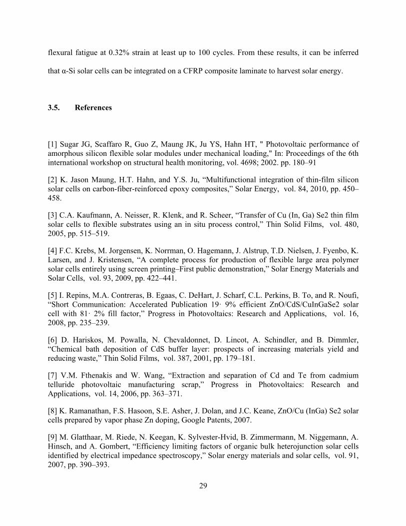
Figure 3.1 (a) c-Si solar cell from BP Solar and (b) α-Si solar cell from PowerFilm. ............31
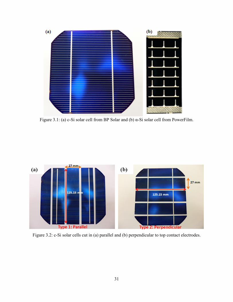
Figure 3.2 c-Si solar cells cut in (a) parallel and (b) perpendicular to top contact electrodes 31
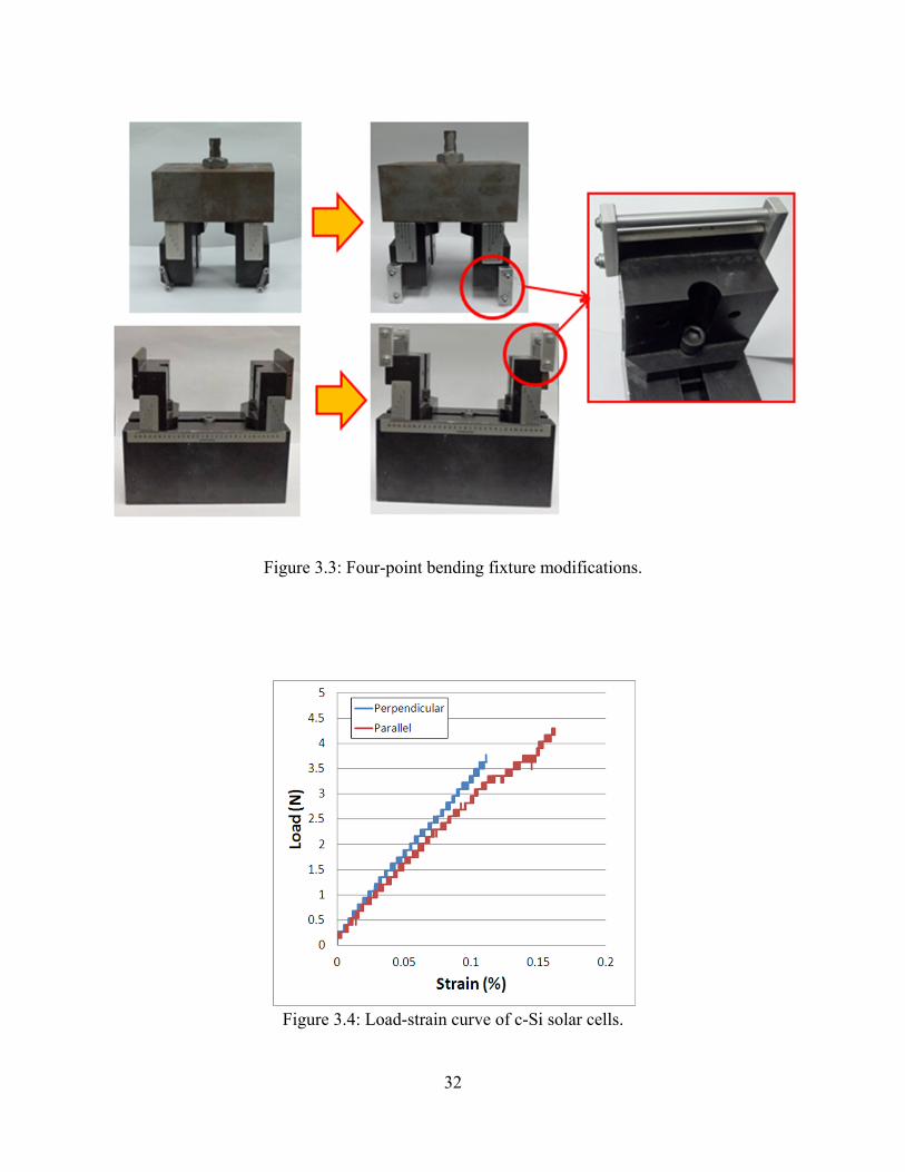
Figure 3.3 Four-point bending fixture modifications ..............................................................32
Figure 3.4 Load-strain curve of c-Si solar cells ......................................................................32
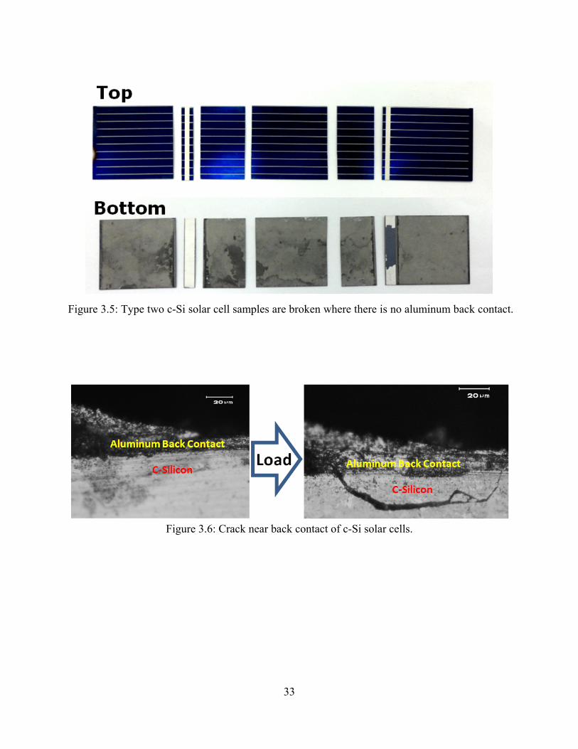
Figure 3.5 Type two c-Si solar cell samples were broken where there is no aluminum back
contact ....................................................................................................................33
Figure 3.6 Crack near back contact of c-Si solar cells ............................................................33
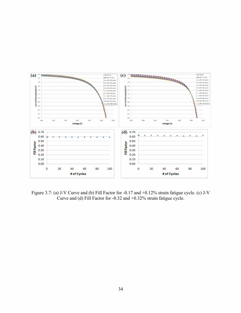
Figure 3.7 (a) J-V Curve and (b) Fill Factor for -0.17 and +0.12% strain flexural fatigue
cycle. (c) J-V Curve and (d) Fill Factor for -0.32 and +0.32% strain flexural
fatigue cycle ...........................................................................................................34
Figure 4.1 The printed copper electrode scratched experiment result ....................................44
Figure 4.2 Recommended cure cycle for composite in autoclave ...........................................44
Figure 4.3 Reliability test of the printed electronic laminate co-cured on the graphite/epoxy
composite: (a) photograph of the co-cured specimen; (b) the electrode reliability
specimen; (c) the electrical connection specimen; (d) a four-point probes
resistance measurement .........................................................................................45
xi
Figure 4.4 Change in Resistance of the printed electrode with respect to the electrode
thicknesses (a) under static loading and (b) under 0.5 % strain of fatigue ............45
Figure 4.5 Electrical connections: (a) soldering connection; (b) silver pasting connection. (c)
Resistance change of the electrical connections under static loading ....................46
Figure 4.6 The printed electrode for integration: (a) drawing and (b) printed electronic circuit
for integration.........................................................................................................47
Figure 4.7 Fabrication procedure of the power laminate: (a) printed electrode pattern
attached with thin-film solar cell and battery by adhesive; (b) co-cured BT core on
the carbon/epoxy composite with electrical connection with diode using the silver
paste .......................................................................................................................47
Figure 4.8 Cross section view of the power laminate co-cured composite laminate ..............48
Figure 4.9 Experimental setup of the integrated power laminate: (a) schematic diagram; (b)
sectional view of the power laminate .....................................................................49
Figure 4.10 Performance of the solar cell in the power laminate under mechanical loading: (a)
I-V curve of the solar cell with respect to static strain; (b) fill factor of solar
cell ..........................................................................................................................50
Figure 4.11 The battery characteristics under mechanical static loading: charge/discharge
capacity with respect to strain ................................................................................50
Figure 4.12 Charging characteristics of the battery from the solar cell in the power laminate at
no strain and 0.4 % of static strain .........................................................................51
Figure 4.13 The crack propagation through the active materials of the thin-film solid state
battery ....................................................................................................................52
Figure 5.1 The Li-ion polymer battery from Dow-Kokam .....................................................64
xii
Figure 5.2 The experimental setup for the Li-ion polymer battery under uni-axial pressure:
(a) below and (b) above 3 MPa ..............................................................................64
Figure 5.3 (a) CFRP composite laminate with embedded Li-ion polymer battery. (b) The
insulated Li-ion polymer battery on CFRP composite laminate ............................65
Figure 5.4 (a) Charging and (b) discharging curves of the Li-ion polymer battery at 0.05 C-
rate..........................................................................................................................66
Figure 5.5 (a) Charging and (b) discharging curves of the Li-ion polymer battery at 2.5 C-
rate..........................................................................................................................66
Figure 5.6 The experimental setup for the Li-ion polymer battery under tensile loading ......67
Figure 5.7 Change in tensile strain during charge and discharge ............................................68
Figure 5.8 The performance of the Li-ion battery under tensile loading ................................69
Figure 5.9 The performance of the Li-ion battery under uni-axial pressure ...........................70
Figure 5.10 The Li-ion polymer battery after uni-axial pressure test .......................................70
Figure 5.11 The performance of the Li-ion battery at high temperatures of 50, 60, 70 and
80 °C ......................................................................................................................71
Figure 5.12 The performance of the Li-ion battery at low temperatures of -3 and -27 °C .......71
Figure 5.13 (a) The experimental setup for the multi-functional composite laminate under
fatigue loading. Loads and strains for (b) tension-compression and (c) tension-
tension fatigue testing ............................................................................................72
Figure 5.14 Discharging of the Li-ion polymer battery under fatigue loading: (a) tension-
compression and (b) tension-tension .....................................................................73
Figure 5.15 Changes in distances between each active layers during fatigue cycles ................73
xiii
Figure 5.16 The changes in discharging voltages of Li-ion polymer batteries under fatigue
loading: (a) tension-compression and (b) tension-tension .....................................74
Figure 5.17 The performance of the Li-ion battery under fatigue loadings ..............................74
Figure 6.1 The geometry profile of the silver conductive pattern ...........................................89
Figure 6.2 The silver nanoink pattern used for sheet resistance measurement: (a) before and
(b) after dried at 85 °C ...........................................................................................89
Figure 6.3 Schematic diagram of IPL system .........................................................................90
Figure 6.4 The spectral distribution of a xenon flash lamp between 380 nm and 1000 nm for
50 J/cm2 ..................................................................................................................90
Figure 6.5 Schematic of consecutive IPL pulse types: (a) single, (b) two, and (c) three
consecutive pulse modes ........................................................................................91
Figure 6.6 SEM images of the surfaces of the silver nanoink patterns: (a) before IPL was
applied, and after IPL was applied with one pulse at (b) 20 J/cm2, (c) 30 J/cm2, (d)
40 J/cm2, and (e) 50 J/cm2 ......................................................................................92
Figure 6.7 SEM images of the surfaces of the silver nanoink patterns: (a) two consecutive
pulses and (b) three consecutive pulses at 50 J/cm2, and (c) thermally sintered at
200 °C ....................................................................................................................93
Figure 6.8 Resistivity of sintered patterns ...............................................................................93
Figure 6.9 XRD of the silver nanoink pattern .........................................................................94
Figure 6.10 Adhesive tape test of the silver nanoink patterns after following types of IPL were
applied: (a) one pulse, (b) two consecutive pulses, and (c) three consecutive
pulses.
To each pair, left ones are the peeled off scotch tape ............................................95

xiv
Figure 6.11 Absorbance and reflectance of silver nanoink pattern ...........................................96
Figure 6.12 The differential scanning calorimetry result of the silver nanoink at 10 °C/min...96
Figure 6.13 (a) original BT-core, (b) BT-core after thermal sintering at 200 °C and (c) BT-
core after IPL sintering ..........................................................................................97

xv
LIST OF TABLES
Table 2.1 Physical constants of copper ..................................................................................16
Table 2.2 Dimensions and Electrical Resistance of Printed Electrodes ................................16
Table 4.2 Specification of the amorphous silicon thin-film solar cell ...................................43
Table 4.3 Specification of the thin-film battery .....................................................................43
Table 6.1 Resistivity of printed patterns ................................................................................88
Table 6.2 Grain sizes of printed patterns ...............................................................................88
Table 6.3 Material properties .................................................................................................88

xvi
ACKNOWLEGEMENTS
First of all, I would like to thank God for providing me with wonderful opportunities and
leading me through my studies. I would like to thank Professor H. Thomas Hahn for his guidance,
support and advice. This thesis would not have been possible without the contribution and effort
of him. I also appreciate Professor Gregory P. Carman, Professor Pei-Yu Chiou, and Professor
Qibing Pei for serving as my committee members and for their professional suggestion to my
study. I will never forget the valuable discussion and help from my mentor and partner, Professor
Hak Sung Kim and Dr. Jong Eun Ryu. I also want to thank Professor Kosuke Takahashi, Mr.
Stephan Prince, Mr. Joseph Riendeau, Dr. Dong-Myung Yoon, Mr. Eli Novin, Ms. Nataly Qian
Chen and all of group members and friends. Most of all, I am also forever grateful to my family
and my friends for their support.
The present study is based on work supported by the Air Force Office of Scientific
Research through a MURI grant FA9550-06-1-0326 to the University of Washington.
Appreciation is extended to Dr. B. Les Lee for encouragement in this work. This research was
supported partly by the WCU (World Class University) program through the National Research
Foundation funded by the Ministry of Education, Science and Technology of Korea (R31-2008-
10083-0).
xvii
VITA
October 28, 1986 Born, Seoul, Korea 2008 B. S., Mechanical Engineering Department of Mechanical and Aerospace Engineering University of California, Los Angeles (UCLA) 2010 M. S., Mechanical Engineering Department of Mechanical and Aerospace Engineering University of California, Los Angeles (UCLA) 2010 Visiting Student Researcher Optoelectronic Materials Center Korea Institute of Science And Technology (KIST) Seoul, Korea 2008-2012 Teaching Assistant, Teaching Associate, Graduate Student Researcher Department of Mechanical and Aerospace Engineering University of California, Los Angeles (UCLA)
PUBLICATIONS AND PRESENTAIONS
Jin S Kang, Hak S Kim, Jongeun Ryu, H Thomas Hahn, “Sintering of Inkjet Printed Silver Nanoparticles at Room Temperature Using Intense Pulsed Light, ” J. Electronic Materials, vol. 40, number 11, 2011, 2268-2277. Jin S Kang, Hak S Kim, Jong Ryu, H Thomas Hahn, Seonhee Jang, and Jae W. Joung, “Inkjet Printed Electronics using Copper Nanoparticle Ink,” J. Materials Science: Materials in Electronics, vol. 21, number 11, 2010, 1213-1220. Hak Sung Kim, Yong-Min Lee, Sanjay R. Dhage, Jin S Kang, H. Thomas Hahn, “Nano composite for power laminate,” 17th International Conference on Composite Materials, Edinburgh, United of Kingdom, July, 2009. Hak S Kim, Jin S Kang, J S Park, and H Thomas Hahn, Hyun C. Jung and Jae W. Joung, “Inkjet printed electronic technique for multifunctional composite structure,” Composites Science and Technology, vol. 69, 2009, 1256-1264.
1
CHAPTER ONE
Introduction
1.1. Background
Multifunctional composite structure is the structure which can not only endure
mechanical stresses but perform various functions such as energy harvest, energy storage,
sensing, and actuating[1]. The greatest advantage in having multifunctional composite structure
is reducing weight by combining various functions. General types of multifunctional structures
are structural power materials, autonomous sensing and actuating materials, electromagnetic
multifunctional materials and survivable, damage-tolerant materials[2]. Multifunctional
composite structure can be applied onto building windows to harvest solar energy during the day,
and cars to harvest thermal energy from engine. One of the most promising areas of using
multifunctional composite structure is Unmanned Aerial Vehicles (UAVs), and the structural
power materials system is the most interesting type because many UAVs are used for
surveillance and disaster relief, which require long flight endurance time[3,4].
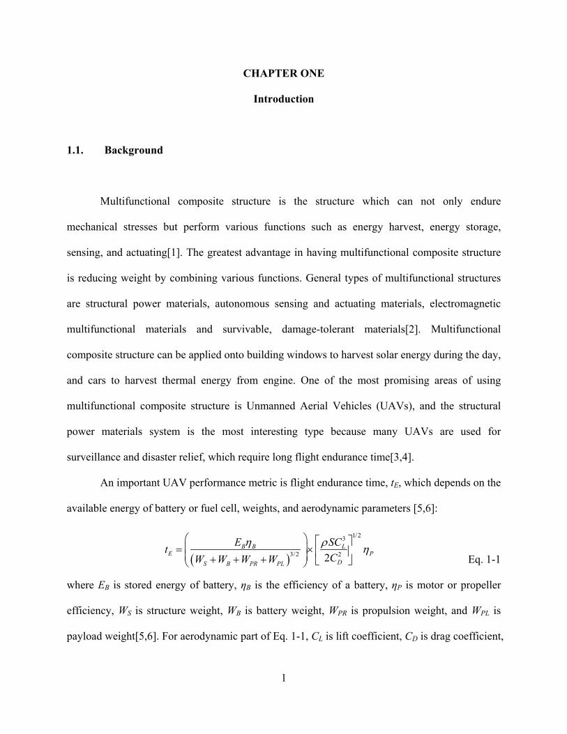
An important UAV performance metric is flight endurance time, tE, which depends on the
available energy of battery or fuel cell, weights, and aerodynamic parameters [5,6]:
Eq. 1-1
where EB is stored energy of battery, ηB is the efficiency of a battery, ηP is motor or propeller
efficiency, WS is structure weight, WB is battery weight, WPR is propulsion weight, and WPL is
payload weight[5,6]. For aerodynamic part of Eq. 1-1, CL is lift coefficient, CD is drag coefficient,
( )
1/23
3/2 22B B L
E PDS B PR PL
E SCtCW W W W
η ρ η
= × + + +
2
S is wing platform area, and ρ is air density. This equation shows that one can prolong the flight
endurance time by improving the battery to have more energy or by decreasing weight of
different parts of UAVs. The resulting change in the flight endurance time is given by:
Eq.1-2
According to Eq. 1-2 [5,6], reducing weight of subsystems of UAVs is 50% more effective than
improving battery efficiency and useable energy of battery. The fuel or battery system and
structure of UAVs each takes about 20 to 40% of the total weight[6]. Therefore, there is much
room for improving flight endurance time by combining structural components with energy
harvest and/or storage capabilities. One good example use of a multifunctional material system is
Wasp. Using multidisciplinary design optimization and analysis[7], the endurance time of a
multifunctional Wasp can be made 25.9% greater than that of an unifunctional Wasp.
Not only the energy storage but also the energy harvest is essential in prolonging the
flight endurance time. There are many different types of energies that can be harvested while a
UAV is in flight, such as heat[8-10], vibration[11-15], and solar energies[16,17]. Government
agencies such as NASA and DARPA are funding UAV projects that are aiming at very high
flight altitude of 60000 to 90000 feet and flight time of over one month. Current UAVs that are
available as initial prototypes are SoLong by AC Propulsion, Helios by AeroVironment, and
Zephyr by Qinetiq; they have flown 48, 24, and 54 hours, respectively[18-20].
In order to effectively integrate solar cells and batteries with structural components, the
development of methods of making thin and cost effective conductive paths is very important. In
recent years, printed electronics technology has attracted lots of attentions in its applications such
as flexible radio frequency identification (RFID) tags[21], wearable electronics[22], organic light
( ) ( )32
B B S BE
E B B total
E W Wtt E W
ηη
∆ ∆ + ∆∆= −
3
emitting diodes, and organic solar cells. Conventionally, mask-based photolithography method is
used to make a desired conductive pattern. However, the subsequent processes of
photolithography require etching and metal deposition such as solvent lift-off and electroplating
process that generate large amount of toxic chemical waste. Therefore, many researchers started
to pay more attention on the direct inkjet printing method because it does not require the
additional etching and metal deposition processes; it has only one-step printing procedure of
making a desired conductive pattern on various substrates. In addition to the simple process, and
cost and material reduction, the flexibility of changing patterns and the capability of printing on a
large area are the most distinguishable advantages of printing method over the photolithography.
1.2. Statement of Purpose
The main objective of the research is to develop multifunctional composite which can
harvest and store energy while being used as a structural component of an UAV. There are many
sources of energy such as heat, vibration, and solar energy. For this study, solar cells will be used
to harvest energy for the system and lithium-ion batteries will be used to store the harvested
energy. Following topics were studied to manufacture and characterize multifunctional structures
with energy harvest and storage capability:
(1) Develop printed electronics techniques to integrate thin-film solar cells and batteries
(2) Characterize solar cells and batteries for multifunctional performance
(3) Develop structural integration methods for thin-film solar cells and batteries
(4) Develop methods to sinter printed electronics without damaging substrates
4
1.3. References
[1] H.S. Kim, J.S. Kang, J.S. Park, H.T. Hahn, H.C. Jung, and J.W. Joung, “Inkjet printed electronics for multifunctional composite structure,” Composites Science and Technology, vol. 69, 2009, pp. 1256–1264.
[2] Christodoulou L, Venables J. Multifunctional material systems: The first generation. J Miner Met Mater Soc 2003;55; 39-45.
[3] Rodriguez P, Geckle W, Barton J, Samsundar J, Gao T, Brown M, Martin S. An emergency response UAV surveillance system. AMIA Annu Sym Proc 2006; 1078.
[4] Loyall J, Ye J, Neema S, Mahadevan N. Model-based design of end-to-end quality of service in a multi-UAV surveillance and target tracking application. 2nd RTAS Workshop on Model-Driven Embedded Syst 2004.
[5] J.P. Thomas and M.A. Qidwai, “The design and application of multifunctional structure-battery materials systems,” JOM Journal of the Minerals, Metals and Materials Society, vol. 57, 2005, pp. 18–24.
[6] J.P. Thomas, M.A. Qidwai, P. Matic, R.K. Everett, A.S. Gozdz, M.T. Keennon, and J. Grasmeyer, “Multifunctional structure-plus-power concepts,” AIAA Paper, vol. 1239, 2002.
[7] J.P. Thomas, M.T. Keennon, A. DuPasquier, M.A. Qidwai, P. Matic, and N.R.L.W.D.M.M. BRANCH, “Multifunctional structure-battery materials for enhanced performance in small unmanned air vehicles,” 2003.
[8] M. Taya, Design of active composites, DTIC Document, 2009.
[9] O. Namli and M. Taya, “Design of Piezo-SMA Composite for Thermal Energy Harvester Under Fluctuating Temperature,” Journal of Applied Mechanics, vol. 1, 2010, p. 74.
[10] O.C. Namli, J.K. Lee, and M. Taya, “Modeling of piezo-SMA composites for thermal energy harvester,” Proceedings of SPIE, 2007, p. 65261L.
[11] Anton S R and Sodano H A 2007 A review of power harvesting using piezoelectric materials (2003-2006) Smart Mater. Struct. 16 R1-21.
[12] Cook-Chennault K A, Thambi N and Sastry A M 2008 Powering MEMS portable devices-a review of non-regenerative and regenerative power supply systems with special emphasis on piezoelectric energy harvesting systems Smart Mater. Struct. 17 043001
[13] Erturk A and Inman D J 2008 A distributed parameter electromechanical model for cantilevered piezoelectric energy harvesters J. Vib. Acoust. 130 041002
5
[14] Elvin N G and Elvin A A 2009 A general equivalent circuit model for piezoelectric generators J. Intell. Mater. Syst. Struct. 20 3-9.
[15] Kong N, Ha D S, Erturk A and Inman D J 2009 Resistive impedance matching circuit for piezoelectric energy harvesting J. Intell. Mater. Syst. Struct.
[16] Maung J K, Hahn H T and Ju Y S 2010 Multifunctional integration of thin-film silicon solar cells on carbon-fiber-reinforced epoxy composites Sol. Energy 84 450-8
[17] Sugar JG, Scaffaro R, Guo Z, Maung JK, Ju YS, Hahn HT. Photovoltaic Performance of Amorphous Silicon Flexible Solar Modules under Mechanical Loading. Proc 6th International Workshop on Structural Health Monitoring 2007.
[18] A. Rapinett, “Zephyr: A High Altitude Long Endurance Unmanned Air Vehicle,” University of Surrey, 2009.
[19] L.P. Dube, W.A. McElroy, and D.W. Pepper, “Use of COMSOL In Aerodynamic Optimization of the UNLV Solar-Powered Unmanned Aerial Vehicle.”
[20] E. Bennett, “NASA's Helios prototype-soaring to a new record.,” SAMPE journal, vol. 38, 2002, pp. 41–47.
[21] S.K. Volkman, Y. Pei, D. Redinger, S. Yin, and V. Subramanian, “Ink-jetted silver/copper conductors for printed RFID applications,” Materials Research Society Symposium Proceedings, 2004, pp. 151–156.
[22] S.M. Bidoki, D. McGorman, D.M. Lewis, M. Clark, G. Horler, and R.E. Miles, “Inkjet printing of conductive patterns on textile fabrics,” AATCC review, vol. 5, 2005, p. 11.
6
CHAPTER TWO
Inkjet Printed Electronics Using Copper Nanoparticle Ink
2.1. Introduction
To take advantage of inkjet printing, the development of a conductive nanoink has
become the most important issue. There are two general approaches in making a conductive
ink[1]. The first method is to use solutions of metallic organic precursors, which can be reduced
at a low temperature. The second method, which is widely used in inkjet printing technology, is
to use suspended metallic nanoparticles because they have low melting point than their bulk
forms do[2].
Initially, suspension of gold and silver nanoparticles drew attention for a conductive inks
because of their high conductivity and thermal stability. Bieri et al. developed a conductive ink
by suspending gold nanoparticles in toluene, but it had a high electrical resistivity of 140 nΩ∙m,
six times that of bulk gold, and it had the problem of volatile organic compounds emission in
industrial applications[3]. In the work of Lee et al., a conductive ink using silver nanoparticles
was developed by dissociating silver nitrate in hydrocarbon using butylamine[4]. However, both
gold and silver are significantly more expensive than copper. Therefore, a conductive ink using
copper nanoparticles drew more attention in recent years.
Several methods to fabricate a conductive ink using copper nanoparticles were
developed such as thermal decomposition, nonionic micro emulsions, ultraviolet irradiation, and
reduction of copper salts[5,6]. Yet, these processes were not economically efficient because of
low throughput of less than 6.35 g of copper per 1 L of solution (0.1 M). To resolve this problem,
7
Lee et al.[7] introduced a chemically controlled process for copper nanoparticles; this novel
process has a high throughput of 0.2 M. In this study, we used the chemically controlled process
to prepare the copper nanoink.
In addition to the high throughput processing, the characterization of reliability and
property of the printed pattern is an essential step to the successful application of copper nanoink.
As the nanoparticles in the ink are mixed with polymer binders and solvents, there are inevitable
free spaces between the nanoparticles after the nanoink is dried. Moreover, the sintering process
can induce cracks in the printed pattern because of the volume decrease by necking and fusion[6].
Therefore, it is essential to minimize those adverse effects in order to improve the reliability and
quality of the printed electronics.
In this study, we investigated the sintering phenomena of the copper nanoparticles and
the effect of printed electrode’s thickness on the quality and reliability of the conductive patterns
printed on a glass fiber/epoxy laminate. The surfaces of the electrodes were analyzed with SEM,
profilometer, and AFM. X-ray tomography was used to investigate the cracks inside of the
printed patterns.
2.2. Experimental Details
2.2.1. Specimen Preparation
The conductive copper nanoink for this study was prepared by Inkjet Business Group in
Samsung Electro-Mechanics. To prepare the nanoink, copper nanoparticles of average diameter
of 5 nm were coated with an organic capping molecule, poly(N-vinylpyrrolidone) (PVP), and
8
then dispersed in ethylene glycol at 40 % by weight. The organic capping molecules were used
to help disperse and prevent aggregation of the copper nanoparticles at room temperature.
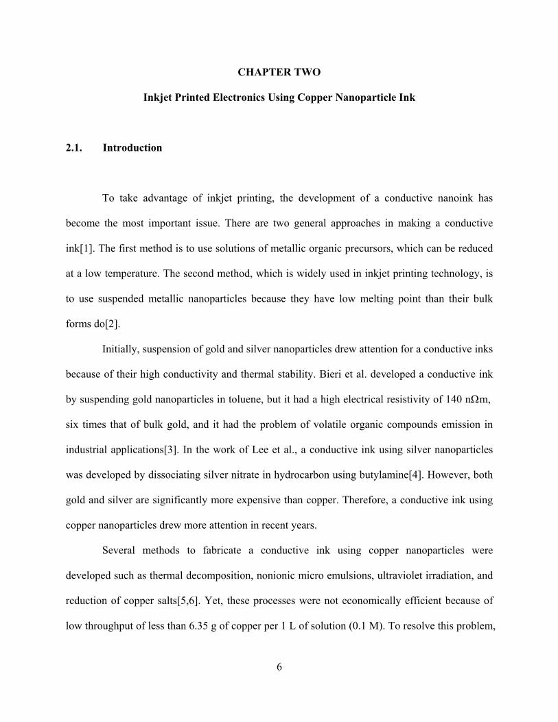
The principle of a drop-on-demand (DOD) piezoelectric inkjet nozzle is shown in Fig.
2.1a. In the nozzle, a voltage-controlled piezoelectric actuator presses the orifice membrane and
controls the droplet volume to 40 pL. Figure 2.1b shows an SEM image of an inkjet nozzle. The
inkjet printer head (Fig. 2.1c) consisting of 512 nozzles was manufactured by Samsung Electro-
Mechanics. The inkjet printer head is mounted on a computer–controlled three-axis gantry
system with the movement accuracy of ±1 um, Fig. 2.2.
Copper nanoink was printed by the gantry system at a resolution of 800 dpi (dots per
inch) on a woven glass fabric/BT (bismaleimide triazine) composite laminate, BT core, 100 μm
thick. A designed circuit pattern was printed 5, 10, and 20 times to vary the thickness of the
electrode. Figure 2.3 shows the printed electrode pattern where the two circular pads at the ends
are used for measurement. BT core was kept at 85 to help solvent in the ink to be dried more
quickly during the printing process.
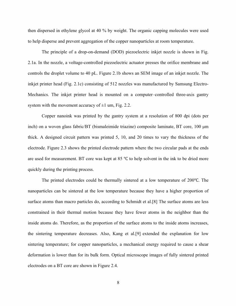
The printed electrodes could be thermally sintered at a low temperature of 200. The
nanoparticles can be sintered at the low temperature because they have a higher proportion of
surface atoms than macro particles do, according to Schmidt et al.[8] The surface atoms are less
constrained in their thermal motion because they have fewer atoms in the neighbor than the
inside atoms do. Therefore, as the proportion of the surface atoms to the inside atoms increases,
the sintering temperature decreases. Also, Kang et al.[9] extended the explanation for low
sintering temperature; for copper nanoparticles, a mechanical energy required to cause a shear
deformation is lower than for its bulk form. Optical microscope images of fully sintered printed
electrodes on a BT core are shown in Figure 2.4.

9
2.2.2. Characterization
An optical microscope (Olympus BX 41, Olympus, Japan) was used to analyze the
sintered printed electrodes. The surface profile of each electrode was measured using a
profilometer (Dektak 8 Surface Profiler, Veeco, USA). An AFM (Dimension 3100, Veeco, USA)
was used for the nanoscale surface characterization. A SEM (JSM-6700F, JEOL, Japan) was
used to analyze surface cracks and the surface morphology of sintered copper nanoparticles. An
X-ray micro-tomography system (SkyScan 1172, SkyScan, Belgium) was used for three-
dimensional microscale internal characterization. A four-point probes method was used to
measure the resistance of each printed electrode using a digital multimeter (Keithley 2100,
Keithley Instruments, USA). In this mehod, a first pair of test leads sends test current, and a
second pair of test leads measures the voltage drop across a printed electrode. This method
minimizes the effects of lead resistance because the high input impedance nature of voltmeter
eliminates the current though the second pair of test leads. The resulting electrical resistivity, ρ,
was calculated using the following equation:
RwtL
ρ = Eq. 2-1
where R is the electrical resistance, w is the width, t is the thickness, and L is the length of an
printed electrode.
10
2.3. Results and Discussion
The melting temperature of metallic nanoparticles can be predicted by the following
equation[10] :
2/3
021 s
m s ls l
dT Td Lr d
γ γ = × − −
Eq. 2-2
where d is the density, γ is the surface tension, T0 is the melting temperature of bulk metal, L is
the latent heat of fusion, and r is the radius of the nanoparticle. The subscripts s and l denote
solid and liquid, respectively. The material constants of copper are shown in Table 2.1; the liquid
state properties are taken from copper at the temperature of 1500 K. Eq. 2-2 predicts that the
melting temperature of copper is significantly depressed much lower than 600°C when the
particle radius is smaller than 10 nm. Also, because sintering temperature is defined as the
temperature at which the grains of solid form from particles connected at their surfaces, it is
20 % lower than the melting temperature for the bulk, according to Mackenzie and
Shuttleworth[11]. In this study, copper nanoparticles were fully sintered at 200°C in an inert
atmosphere of nitrogen gas to prevent the oxidation.
Figure 2.5 shows the sintering result of the copper nanoparticle ink as a function of
sintering time for the 5-times printed electrode. It was found that the copper nanoparticles could
be sintered fully in 20 minutes. Figure 2.6 shows high-resolution SEM images of an inkjet
printed electrode before and after 20-minute thermal sintering; dispersed copper nanoparticles
are agglomerated and sintered after thermal sintering.
11
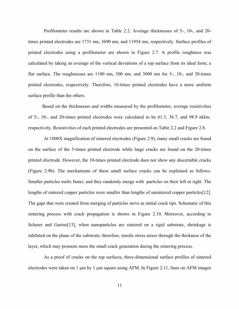
Profilometer results are shown in Table 2.2. Average thicknesses of 5-, 10-, and 20-
times printed electrodes are 1731 nm, 3690 nm, and 11954 nm, respectively. Surface profiles of
printed electrodes using a profilometer are shown in Figure 2.7. A profile roughness was
calculated by taking an average of the vertical deviations of a top surface from its ideal form, a
flat surface. The roughnesses are 1100 nm, 500 nm, and 3000 nm for 5-, 10-, and 20-times
printed electrodes, respectively. Therefore, 10-times printed electrodes have a more uniform
surface profile than the others.
Based on the thicknesses and widths measured by the profilometer, average resistivities
of 5-, 10-, and 20-times printed electrodes were calculated to be 61.3, 36.7, and 98.9 nΩ∙m,
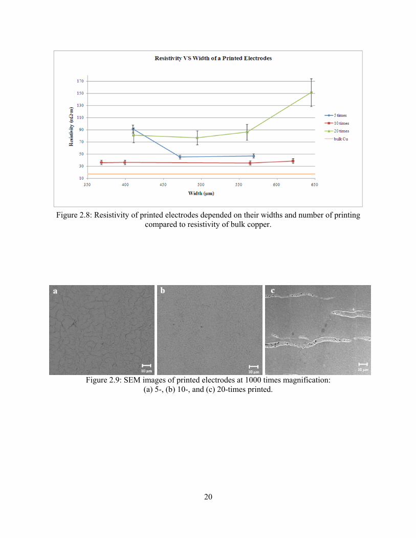
respectively. Resistivities of each printed electrodes are presented on Table 2.2 and Figure 2.8.
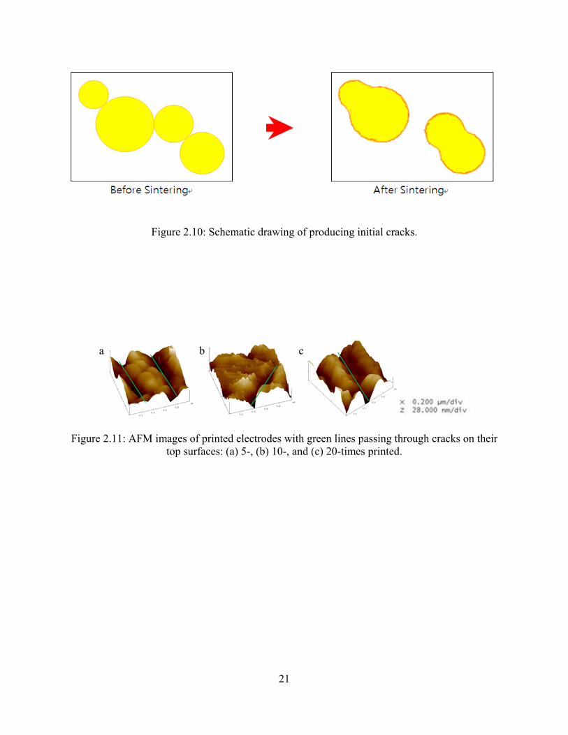
At 1000X magnification of sintered electrodes (Figure 2.9), many small cracks are found
on the surface of the 5-times printed electrode while large cracks are found on the 20-times
printed electrode. However, the 10-times printed electrode does not show any discernible cracks
(Figure 2.9b). The mechanisms of these small surface cracks can be explained as follows.
Smaller particles melts faster, and they randomly merge with particles on their left or right. The
lengths of sintered copper particles were smaller than lengths of unsintered copper particles[12].
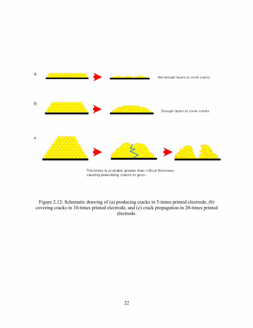
The gaps that were created from merging of particles serve as initial crack tips. Schematic of this
sintering process with crack propagation is shown in Figure 2.10. Moreover, according to
Scherer and Garino[13], when nanoparticles are sintered on a rigid substrate, shrinkage is
inhibited on the plane of the substrate; therefore, tensile stress arises through the thickness of the
layer, which may promote more the small crack generation during the sintering process.
As a proof of cracks on the top surfaces, three-dimensional surface profiles of sintered
electrodes were taken on 1 μm by 1 μm square using AFM. In Figure 2.11, lines on AFM images
12
of printed electrodes indicate the cracks on their top surfaces. All 5-, 10-, and 20-times printed
electrodes have these cracks. As Figure 2.9b shows, 10-times printed electrode’s cracks were not
observable because 10-times printed electrode had enough number of printed layers to cover the
cracks being generated during sintering process (Figure 2.12b). Unlike 10-times printed
electrode, 5-times printed electrode does not have enough layers to cover cracks; therefore,
cracks are shown at 1000X magnification (Figure 2.9).
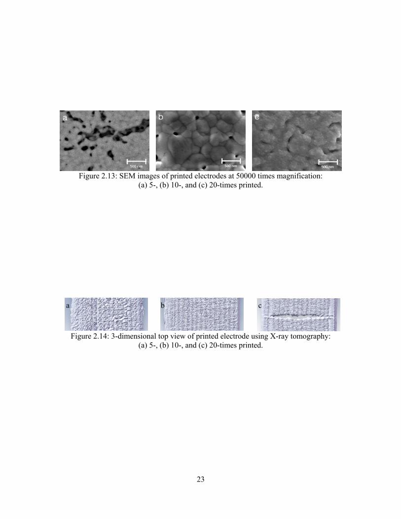
Using 50000X magnification, agglomerations of copper nanoparticles are observed for
5-, 10-, and 20-times printed electrodes, shown in Figure 2.13a, 2.13b, and 2.13c, respectively.
Voids in 5-times printed electrodes are bigger than 10-times printed electrodes. Similarly, voids
in 10-times printed electrodes were bigger than voids in 20-times printed electrode, showing that
copper nanoparticles were most densely sintered for 20-times printed electrodes.
Although the 20-times printed electrode is most densely agglomerated, and has more
number of layers than the 10-times printed one, severe microscopic cracks are observed at low
SEM magnification (Figure 2.9) and X-ray tomography (Figure 2.14). Small cracks on the 5-
times printed electrode are not observed on the X-ray tomography because of its low resolution.
Figure 2.9c shows that small cracks in the 20-times printed electrode have grown into larger
cracks. The existence of these large cracks can be explained by the following two reasons. First,
according to Scherer and Garino[13], less porous film experience more stress from a rigid
substrate. Since the 20-times printed electrode is the least porous, it experienced highest tensile
biaxial stress from its rigid substrate, which causes crack propagation.
13
Secondly, according to Bordia and Jagota[14], a crack grows when the thickness of the
film is greater than the critical thickness. The governing equation for crack growth in a sintered
thin-film can be expressed as follows:
Eq. 2-3
where k is a friction parameter, a is a half of crack length, and v is Poisson’s ratio, 0.355 for Cu.
As shown in Figure 2.9a, the lengths of cracks on top surfaces are at least 3 µm. Using these
parameters, the right side of Eq. 2-3 is calculated to be 5.4 µm. This means if 1k is larger than
5.4 µm, a crack will grow. In other words, the friction parameter, k, should not be smaller than
0.185 µm-1.
The friction parameter is depended on the film thickness. According to Jagota and
Hui[15], the friction parameter can be expressed as below,
Eq. 2-4
where t is the film thickness. Using the friction parameter value obtained above, it can be
determined that if the thickness of the film is greater than 5.3 µm, the friction parameter will be
less than 0.185 µm-1, and the crack will grow. Since the 20-times printed electrode has the film
thickness greater than 5.3 µm, the cracks on the 20-times printed electrode propagated.
Lastly, the 10-times printed electrode has the best quality, the low resistivity of 36.7
nΩ∙m. This resistivity is higher than that of bulk copper, 17.2 nΩ∙m due to the porous structure
of a sintered copper electrode. However, this resistivity of the printed electrode is suitable to be
2
11
ak v
π > −
1 3(1 )2
vkt
−=
14
used as a conductive path for a solar cell and battery because the resistivity of our printed
electrodes is lower than 87 nΩ∙m, wh ich is th e a dequate resistivity value for a conductive
circuit[16].
2.4. Conclusions
Inkjet printed electrodes with various dimensions were characterized. Specific results are
(1) To reduce the amount of cracks, range of particle size should be reduced as much as
possible because the cracks are initially formed by having different particle sizes.
(2) To have good quality of printed electrode, the number of printings should not be too large
so that the final thickness is kept below the critical thickness.
(3) The resistivity of the optimal printed electrode using the copper nanoparticles was 36.7
nΩ∙m, which is suitable for industrial applications such as RFID.
2.5. References
[1] D. Kim and J. Moon, “Highly Conductive Ink Jet Printed Films of Nanosilver Particles for Printable Electronics,” Electrochemical and Solid-State Letters, vol. 8, Nov. 2005, pp. J30-J33.
[2] G.L. Allen, R.A. Bayles, W.W. Gile, and W.A. Jesser, “Small particle melting of pure metals,” Thin solid films, vol. 144, 1986, pp. 297–308.
[3] N.R. Bieri, J. Chung, S.E. Haferl, D. Poulikakos, and C.P. Grigoropoulos, “Microstructuring by printing and laser curing of nanoparticle solutions,” Applied Physics Letters, vol. 82, 2003, p. 3529.
[4] K.J. Lee, B.H. Jun, T.H. Kim, and J. Joung, “Direct synthesis and inkjetting of silver nanocrystals toward printed electronics,” Nanotechnology, vol. 17, 2006, pp. 2424-2428.
[5] M. Aslam, G. Gopakumar, T.L. Shoba, I.S. Mulla, K. Vijayamohanan, S.K. Kulkarni, J. Urban, and W. Vogel, “Formation of Cu and Cu2O nanoparticles by variation of the surface

15
ligand: Preparation, structure, and insulating-to-metallic transition,” Journal of colloid and interface science, vol. 255, 2002, pp. 79–90.
[6] L. Qi, J. Ma, and J. Shen, “Synthesis of copper nanoparticles in nonionic water-in-oil microemulsions,” Journal of colloid and interface science, vol. 186, 1997, pp. 498–500.
[7] Y. Lee, J. Choi, K.J. Lee, N.E. Stott, and D. Kim, “Large-scale synthesis of copper nanoparticles by chemically controlled reduction for applications of inkjet-printed electronics,” Nanotechnology, vol. 19, 2008, p. 415604.
[8] M. Schmidt, R. Kusche, B. Von Issendorff, and H. Haberland, “Irregular variations in the melting point of size-selected atomic clusters,” Nature, vol. 393, 1998, pp. 238–240.
[9] J.W. Kang and H.J. Hwang, “Molecular dynamics simulations of ultra-thin Cu nanowires,” Computational materials science, vol. 27, 2003, pp. 305–312.
[10] P. Buffat and J. Borel, “Size effect on the melting temperature of gold particles,” Physical Review A, vol. 13, Jun. 1976, pp. 2287-2298.
[11] J.K. Mackenzie and R. Shuttleworth, “A Phenomenological Theory of Sintering,” Proceedings of the Physical Society. Section B, vol. 62, 1949, pp. 833-852.
[12] H. Zhu, “Sintering processes of two nanoparticles: A study by molecular dynamics simulations,” Philosophical Magazine Letters, vol. 73, 1996, pp. 27-33.
[13] G.W. Scherer and T. Garino, “Viscous Sintering on a Rigid Substrate,” Journal of the American Ceramic Society, vol. 68, 1985, pp. 216-220.
[14] R.K. Bordia and A. Jagota, “Crack Growth and Damage in Constrained Sintering Films,” Journal of the American Ceramic Society, vol. 76, 1993, pp. 2475-2485.
[15] A. Jagota and C.Y. Hui, “Mechanics of sintering thin films–I. Formulation and analytical results,” Mechanics of Materials, vol. 9, 1990, pp. 107–119.
[16] V. Subramanian, P. Chang, D. Huang, J. Lee, S. Molesa, D. Redinger, S. Volkman, VLSI Design held jointly with 5th International Conference on Embedded Systems and Design., 19th International Conference on, 6 (2006)
16
Table 2.1: Physical constants of copper Solid Liquid
Density, ρ (kg∙m-3) 8960 7998
Surface tension, γ (J∙m-2) 1.8 1.1 Latent heat of fusion, L (J∙kg-1) 2.05×10⁵ -
Table 2.2: Dimensions and Electrical Resistances of Printed Electrodes.
Number of Printing
Resistance (Ω)
Width (μm)
Average Thickness
(nm)
Length (cm)
Resistivity (nΩ∙m)
5 11.2882 409.68 1979 10 91.497 6.4898 471.73 1480 10 45.306 4.7632 569.04 1736 10 47.051
10
2.6414 368.01 3736 10 36.316 2.4143 398.93 3773 10 36.339 1.9327 564.38 3255 10 35.505 1.5616 621.08 3996 10 38.757
20
1.4849 410.27 13295 10 80.993 1.4231 494.33 10926 10 76.861 1.3917 560.37 11053 10 86.199 1.8719 645.10 12543 10 151.467
17
Figure 2.1: Drop-on demand piezoelectric ink-jet nozzle: (a) schematic diagram; (b) SEM
photograph of the micro ink-jet nozzle; (c) ink-jet printer head
Figure 2.2: The computer-controlled three axis gantry system in Samsung electro-mechanic Inc.
for ink-jet printing of Cu nanoink
Figure 2.3: Printed electrode
Controller
Printing table
3-axis gantry system
Inkjet print head
(a) (b) (c)
18
Figure 2.4: Optical microscope images of fully sintered printed electrodes:
(a) 5-, (b) 10-, and (c) 20-times printed.
Figure 2.5: Sintering of the copper nanoparticles ink as function of sintering time.
b a c
19
Figure 2.6: SEM images of inkjet printed electrode
(a) before, and (b) after thermal sintering.
Figure 2.7: Surface profiles of printed electrode using profilometer:
(a) 5-, (b) 10-, and (c) 20-times printed.
a b c
20
Figure 2.8: Resistivity of printed electrodes depended on their widths and number of printing
compared to resistivity of bulk copper.
Figure 2.9: SEM images of printed electrodes at 1000 times magnification:
(a) 5-, (b) 10-, and (c) 20-times printed.
21
Figure 2.10: Schematic drawing of producing initial cracks.
Figure 2.11: AFM images of printed electrodes with green lines passing through cracks on their
top surfaces: (a) 5-, (b) 10-, and (c) 20-times printed.
c a b
22
Figure 2.12: Schematic drawing of (a) producing cracks in 5-times printed electrode, (b)
covering cracks in 10-times printed electrode, and (c) crack propagation in 20-times printed electrode.
b
a
c
23
Figure 2.13: SEM images of printed electrodes at 50000 times magnification:
(a) 5-, (b) 10-, and (c) 20-times printed.
Figure 2.14: 3-dimensional top view of printed electrode using X-ray tomography:
(a) 5-, (b) 10-, and (c) 20-times printed.
a b c
24
CHAPTER THREE
Multifunctional Performance of Silicon Solar Cells
3.1. Introduction
Since the appropriate thickness of printed electrodes was found in the previous chapter,
it is important to test different solar cells to find the one that can be integrated directly on a
structural component using an inkjet printed circuit. According to Sugar et al.[1], the
performance of amorphous silicon solar cells is stable up to a tensile strain of 1%, and these solar
cells were still functional up to 2.4% tensile strain. Maung et al.[2] integrated a thin-film
amorphous silicon solar cell onto a carbon/epoxy composite laminate by co-curing inside an
autoclave, and studied its performance under fatigue loadings. There was no significant
performance degradation when the solar cell was cycled between 0 and 0.3% strain.
The efficiency of amorphous silicon solar cell is about 12%. Different types of thin
flexible solar cells such as Copper Indium Gallium Selenide (CIGS)[3] and organic polymer[4]
solar cells are being developed to achieve higher efficiency with better mechanical durability.
CIGS solar cell has about 20% efficiency[5]. However, CIGS solar cells degrade with humidity
and generate toxic wastes during manufacturing[6-8]. Organic polymer solar cells are much
more prone of large strains than amorphous silicon solar cells, but they are unstable and very
sensitive to environmental conditions[9,10].
In the present research, single-crystalline silicon (c-Si) solar cells were studied under
mechanical loading because they are known to have a high efficiency of 23%, which is higher
than that of amorphous silicon solar cells. Also, the flexural fatigue of amorphous silicon (α-Si)

25
solar cells was studied. The resulting information is critically needed in order to check the
reliability of a solar cell when it is integrated on the wings of an unmanned aerial vehicles.
3.2. Experimental Details
3.2.1. Specimen Preparation
c-Si solar cells for this study were obtained from BP Solar (London, United Kingdom).
Dimensions of these solar cells are 125.15×125.15×0.275± 0.005 mm. The average thickness of
crystalline silicon is 0.200± 0.003 mm, and a blue anti-reflecting coating of silicon nitride is
applied on the front. The average thickness of aluminum back contact is 0.075 mm, and 3 mm
wide silver soldering pads are on the back of these solar cells. (Figure 3.1a)
The thin-film amorphous silicon (α-Si) solar cells were purchased from Jameco
Electronics (California, United States), manufactured by PowerFilm Solar (Iowa, United States).
Dimensions of these solar cells are 84×37×0.330± 0.005 mm. The manufacturer specification
claims the thickness of amorphous silicon to be 400 nm. (Figure 3.1b)
3.2.2. Experimental Setup and Procedure
Wings of aircraft are typically subjected to about 0.2% of fatigue strain during flight.
Therefore, before utilizing a solar cell as an energy harvesting source it is important to find a
mechanical endurance limit. To mechanically test the c-Si solar cell, it was cut by a dicing saw
(DAD-321, Disco, Japan) into 27 mm by 125.15 mm pieces. There were two types of c-Si solar
cell samples. Type one samples were cut parallel to top contact electrodes, and type two samples
26
were cut perpendicular to top contact electrodes. (Figure 3.2) Each sample was subjected to four-
point bending following ASTM D7264 standards using a tabletop mechanical tester (Instron
4411, Instron, USA)[11]. The optical microscope (Olympus BX 41, Olympus, Japan) was used
to analyze c-Si solar cells. For c-Si solar cells, load and displacement were recorded using a
control board on a tabletop mechanical tester, then displacement data were converted into strain
values using the following equation:
Eq. 3-1
where ε is strain, δ is displacement of a loading crosshead in mm, t is thickness of c-Si solar cell
in mm, and L is support span in mm[11].
α-Si solar cells were subjected to flexural fatigue cycles instead of static bending. To
make a sample for this testing, four layers of carbon fiber reinforced polymer (CFRP) prepregs
(CYCOM 977-3, Cytec Industries, USA) were cured inside an autoclave (Thermal Equipment
Corporation, United States) with a lay-up sequence of [0, 90]s. A precision strain gage (EA-6-
062AP-120, Micro-Measurements Division, United States) was attached on the middle of the
bottom of the CFRP composite laminate, and the α-Si solar cell was attached using a two-part
epoxy adhesive (Scotch-Weld DP-420, 3M, USA) on the top of the CFRP composite laminate.
The four-point bending fixture was modified so that flexural loading can be applied in
full reversal: compressive load on the way down and tensile load on the way up of the crosshead.
(Figure 3.3) A strain gage amplifier (Omega 941, Omega, USA), and a load cell amplifier
(Omega 916, Omega, USA) were used to obtain strain and load data, respectively. Photovoltaic
performances of α-Si solar cells were analyzed using a source meter (Keithley 2400, Keithley,
2
4.36 tLδε =
27
USA). An overhead projector (Kodak Carousel 750, Kodak, USA) with a DEK 500W
incandescent light bulb was used as a light source.
3.3. Results and Discussion
3.3.1. Single Crystalline Silicon Solar Cell
Following ASTM D7264 for a four-point bending test of the c-Si solar cells, the space
between the outer supports was kept at 90 mm. For the type one samples, the average tensile
strain was 0.15 ± 0.01%. For the type two samples, the average tensile strain at failure was
0.10± 0.01%. (Figure 3.4) The decrease in tensile strain is due to support from the aluminum
back contact. For the type one samples, the aluminum back contact is covering the whole c-Si,
providing an uniform support. However, for the type two samples, there is no aluminum back
contact where there is 3 mm wide silver soldering pads. The absence of an aluminum back
contact creates stress concentrations around the silver soldering pads. Figure 3.5 shows that the
type two samples are broken where there is no aluminum back contact, and Figure 3.6 shows
crack under near the bottom contact. Moreover, the tensile strain of 0.15% is not high enough to
be used for the wing of an aircraft. These solar cells will thus not be able to endure the
mechanical loads imposed on them.
3.3.2. Amorphous Silicon Solar Cell
For α-Si solar cells, their performances were characterized after two different flexural
fatigue cycles. First set of five α-Si solar cells was subjected to a tensile strain of 0.12% and a
28
compressive strain of -0.17%. Second set of five α-Si solar cells was subjected to a tensile strain
of 0.32% and a compressive strain of -0.32%. The current-voltage (I-V) curves were obtained
before testing, and after 1, 10, 30, 40, 50, 60, 70, 80, 90 and 100 cycles, respectively, using a
source meter, and the current values were divided by the aperture area of 0.002108 m2 to convert
them into the current density. For both sets of solar cells, there was no noticeable change in their
performance. The average short circuit current density was 2.15± 0.05 A/m2, and the average
open circuit voltage was 5.54± 0.08 V. Fill factors were calculated using the following equation:
Eq. 3-2
where Jmax is the current density in A/m2 and Vmax is the voltage in V at the maximum power
point. The maximum power point is where the product of current density, voltage, and aperture
area is the maximum on the J-V curves. Jsc is the short circuit current in A/m2, where J-V curve
crosses the y-axis, and Voc is the open circuit voltage in V, where J-V curve crosses the x-axis.
(Figure 3.7) Fill factors do not decrease after flexural fatigue up to 100 cycles. Fill factor
compares performance of solar cells to an ideal diode. Note that the average fill factor is
0.60± 0.02. Although longer fatigue testing is needed for better reliability, α-Si solar cells appear
to be a good candidate to be used on an aircraft to harvest solar energy.
3.4. Conclusions
c-Si solar cells are too brittle to be directly integrated onto a CFRP composite laminate
because failure occurs below 0.2% tensile strain. α-Si solar cells can endure fully reversed
max max
sc oc
J VFFJ V
=
29
flexural fatigue at 0.32% strain at least up to 100 cycles. From these results, it can be inferred
that α-Si solar cells can be integrated on a CFRP composite laminate to harvest solar energy.
3.5. References
[1] Sugar JG, Scaffaro R, Guo Z, Maung JK, Ju YS, Hahn HT, " Photovoltaic performance of amorphous silicon flexible solar modules under mechanical loading," In: Proceedings of the 6th international workshop on structural health monitoring, vol. 4698; 2002. pp. 180–91
[2] K. Jason Maung, H.T. Hahn, and Y.S. Ju, “Multifunctional integration of thin-film silicon solar cells on carbon-fiber-reinforced epoxy composites,” Solar Energy, vol. 84, 2010, pp. 450–458.
[3] C.A. Kaufmann, A. Neisser, R. Klenk, and R. Scheer, “Transfer of Cu (In, Ga) Se2 thin film solar cells to flexible substrates using an in situ process control,” Thin Solid Films, vol. 480, 2005, pp. 515–519.
[4] F.C. Krebs, M. Jorgensen, K. Norrman, O. Hagemann, J. Alstrup, T.D. Nielsen, J. Fyenbo, K. Larsen, and J. Kristensen, “A complete process for production of flexible large area polymer solar cells entirely using screen printing–First public demonstration,” Solar Energy Materials and Solar Cells, vol. 93, 2009, pp. 422–441.
[5] I. Repins, M.A. Contreras, B. Egaas, C. DeHart, J. Scharf, C.L. Perkins, B. To, and R. Noufi, “Short Communication: Accelerated Publication 19· 9% efficient ZnO/CdS/CuInGaSe2 solar cell with 81· 2% fill factor,” Progress in Photovoltaics: Research and Applications, vol. 16, 2008, pp. 235–239.
[6] D. Hariskos, M. Powalla, N. Chevaldonnet, D. Lincot, A. Schindler, and B. Dimmler, “Chemical bath deposition of CdS buffer layer: prospects of increasing materials yield and reducing waste,” Thin Solid Films, vol. 387, 2001, pp. 179–181.
[7] V.M. Fthenakis and W. Wang, “Extraction and separation of Cd and Te from cadmium telluride photovoltaic manufacturing scrap,” Progress in Photovoltaics: Research and Applications, vol. 14, 2006, pp. 363–371.
[8] K. Ramanathan, F.S. Hasoon, S.E. Asher, J. Dolan, and J.C. Keane, ZnO/Cu (InGa) Se2 solar cells prepared by vapor phase Zn doping, Google Patents, 2007.
[9] M. Glatthaar, M. Riede, N. Keegan, K. Sylvester-Hvid, B. Zimmermann, M. Niggemann, A. Hinsch, and A. Gombert, “Efficiency limiting factors of organic bulk heterojunction solar cells identified by electrical impedance spectroscopy,” Solar energy materials and solar cells, vol. 91, 2007, pp. 390–393.

30
[10] J. Nakamura, C. Yokoe, K. Murata, and K. Takahashi, “Efficient organic solar cells by penetration of conjugated polymers into perylene pigments,” Journal of applied physics, vol. 96, 2004, p. 6878.
[11] Standard test method for flexural properties of polymer matrix composite materials. ASTM 2007, D 7246M-2007
31
Figure 3.1: (a) c-Si solar cell from BP Solar and (b) α-Si solar cell from PowerFilm.
Figure 3.2: c-Si solar cells cut in (a) parallel and (b) perpendicular to top contact electrodes.
32
Figure 3.3: Four-point bending fixture modifications.
Figure 3.4: Load-strain curve of c-Si solar cells.
33
Figure 3.5: Type two c-Si solar cell samples are broken where there is no aluminum back contact.
Figure 3.6: Crack near back contact of c-Si solar cells.
34
Figure 3.7: (a) J-V Curve and (b) Fill Factor for -0.17 and +0.12% strain fatigue cycle. (c) J-V
Curve and (d) Fill Factor for -0.32 and +0.32% strain fatigue cycle.
35
CHAPTER FOUR
Multifunctional Composite Structure via Inkjet Printing
4.1. Introduction
Multifunctional composite structure is defined as the structure which can not only bear
load but also perform other functions such as energy harvest and storage, sensing and actuating,
and more. In order to perform multifunctional functions, a conducting circuit should be
embedded within the load bearing structure. As for the patterning of conductive circuits, the
conventional photolithographic method used for printed circuit boards (PCBs) is time consuming,
expensive, and environmentally undesirable. As an alternative, Kim et al. and Park et al. used an
ink containing nano-sized Ag or Cu particles in an inkjet printer to print conductive path on a
polymer substrate[1,2]. Although the melting temperature of bulk copper is 1084°C, the authors
have shown that when the particle size is in the few-nanometer range, the inkjet printed circuit
sintered at a lower sintering temperature can have a high conductivity as a conventionally
produced one.
Different from typical functional devices, multifunctional structures include load bearing
function as well as other non-structural function. Because there is no information available, to
the author's knowledge, on the structural integrity of the inkjet printed electrodes, this topic was
studied in the present work.
Most energy harvest and storage systems are parasitic to load bearing structures,
increasing the total weight and volume while decreasing the fuel efficiency as they require heavy
transmission cables from a centralized power source. Therefore, hybrid composite structures
36
have been developed by embedding thin-film batteries[3-5], thin-film solar cells[6,7], and
thermoelectric devices[8,9] into composite laminates to have multifunctional capabilities.
In Chapter 3, a thin-film amorphous silicon solar cell was attached on a composite
laminate and investigated the effect of a flexural fatigue loading on its performance. It was found
that the solar cell maintains its virgin efficiency under flexural fatigue loadings. Pereira et al.
investigated the performance of embedded thin-film batteries under mechanical loading[5].
Specifically, they characterized the charge and discharge characteristics under increasing levels
of applied stress. Since there has been no attempt to integrate solar cells and batteries together
into a load bearing structure, an energy harvest and storage composite was fabricated using an
inkjet printed circuit.
In this study, the conducting circuits are placed on the laminate using an inkjet printing
technique. The mechanical reliability of inkjet printed electrodes was tested under static and
fatigue loadings to find if it was applicable to a multifunctional composite for an unmanned
aerial vehicle. In order to show the feasibility of the inkjet printed electrode for multifunctional
composite structure, an energy harvest and storage composite laminate was made using inkjet
printed electrodes as interconnection between a thin-film solar cell and a thin-film battery. The
thin-film solar cell, the thin-film battery and the additional passive components were co-cured
with the composite laminate to form a power laminate. The performance of the power laminate is
also studied under mechanical loading.
37
4.2. Mechanical Reliability of Inkjet Printed Electrodes
Using the printed system and copper nanoink described in the Chapter 2, the desired
copper pattern was printed on a flexible BT core substrate. Because the cracks on the top surface
grows when the thickness of a printed electrode is greater than 5.3 μm, the printing was repeated
to make the desired electrode thickness of 1, 2, and 4 μm. The adhesion between the printed
electrode and BT core was good, as shown in a simple scratch test using a diamond-tip pen, Fig.
4.1.
The BT core with the printed copper pattern was co-cured on a graphite/epoxy laminate
(T700SC/RS-30G) with a lay-up sequence of [0/90]s in an autoclave following the
manufacturer’s recommended cure cycle, Fig. 4.2. Figure 4.3a shows the composite specimen
co-cured with the copper patterned BT core. The total thickness of the specimen is 0.67 mm
which includes the 0.57-mm-thick graphite/epoxy composite.
Figures 4.3b and 4.3c show the specimen mounted on a universal tensile tester to study
the effect of mechanical loading on the electrode resistance. The resistance was measured under
various levels of load using a four-point probes method, Fig. 4.3d, described in Chapter 2. Figure
4.4a shows the effect of electrode thickness on the resistance under a static loading. The
electrode with 4 μm thickness does not show any noticeable change up to the maximum strain
applied while the two thinner electrodes (1 and 2 μm) show increased resistances. This is likely
to be the results of stronger particle junctions in the electrode with 4 μm thickness. Figure 4.4b
shows the resistance changes under cycling between 0 and 0.5% strain. At each cycle, a
resistance measured at both 0 and 0.5% strain. Again, the electrode with 4 μm thickness does not
show any change in resistance up to the maximum cycles studied. However, such is not the case

38
with the other two thinner electrodes (1 and 2 μm); their resistances oscillate and increase as the
electrodes were being loaded and unloaded. Therefore, the thickness of the electrode used in the
power laminate was selected as 4 μm.
For the electrical connection test, 100 Ω resistor was connected between two short
electrodes by soldering or silver pasting. Soldering (Sn97Cu3) was done at 260°C whereas the
silver paste (Ted Pella) was cured at 60°C for 2 h, Figures 4.5a and 4.5b. Similarly to the
electrode test, the resistance between two short electrodes, which were connected by a resistor,
was measured under at various levels of load using the same four-point probes method, Figs.
4.3c and 4.3d. Figure 4.5c shows the resulting resistance changes of the resistors. One of the
solder connections failed at 0.7% strain while the silver paste connections did not until 1.1%
strain. Since the silver paste was found to be reliable under mechanical static loading, it was used
for electrical connections in the power laminate.
4.3. Integrated Power Laminate
Figure 4.6a shows the circuit pattern for the integration of a solar cell and a battery on a
BT core. The circuit patterns were made using the inkjet printing method on the BT core. The
electrodes on the top and bottom surfaces were connected to each other through via holes, where
the nanoink was smeared into and sintered. In order to insulate the electrodes from graphite
fibers in the composite, polyimide ink was printed with a thickness of 25 μm and cured over the
whole area of the laminate except where the solar cell and battery are to be located as shown in
Fig. 4.6b. Table 4.1 shows the specifications of the amorphous silicon thin-film solar cell TX3-
25 (Powerfilm Inc.). The solar cell is very thin (0.2 mm), so that it can be integrated into
39
composite structures in various shapes without significantly increasing the total thickness. Table
4.2 shows the specification of the solid state thin-film lithium battery S8-ES (Front Edge
Technology) which is remarkably thin and flexible. The top and bottom 50-μm thick mica
substrates are held and sealed together around the edges with a 40-μm thick heat resistant epoxy
layer, so that it can sustain the composite cure temperature of 120°C.
Figure 4.7 shows the fabrication process of the power laminate. The battery and the solar
cell are attached to the BT core using an epoxy adhesive DP460 (3M) and their electrodes are
connected to the printed electrodes using the sliver paste as shown in Fig. 4.7a. Each silver paste
connection is sealed using the same adhesive DP460 (3M) for insulation from the conductive
graphite fibers in the composite laminate. The final assembly consisting of the BT core and the
composite laminate is cured in an autoclave. After the cure cycle, a diode is connected using the
silver paste to prevent reverse currents flowing from the battery to the solar cell as shown in Fig.
4.7b.
Figure 4.8 shows the cross-sectional view of the power laminate. By integrating a solar
cell and battery on a laminate, the total laminate thickness was increased by 0.42 mm. The
multifunctional power laminate should have load bearing function as well as autonomic energy
harvest/store function. Since the power laminate was fabricated on a host composite laminate,
the developed multifunctional power laminate has almost the same strength and modulus with
the bare composite laminate. Figure 4.9 shows the experimental set-up of the integrated power
laminate to test the performance under mechanical loading. The light was shone on the solar cell
using the overhead projector described in Chapter 3. The current-voltage (I-V) curve of solar cell
was measured using a source meter, Keithley 2400, with a voltage sweep from 0 to 5 V at
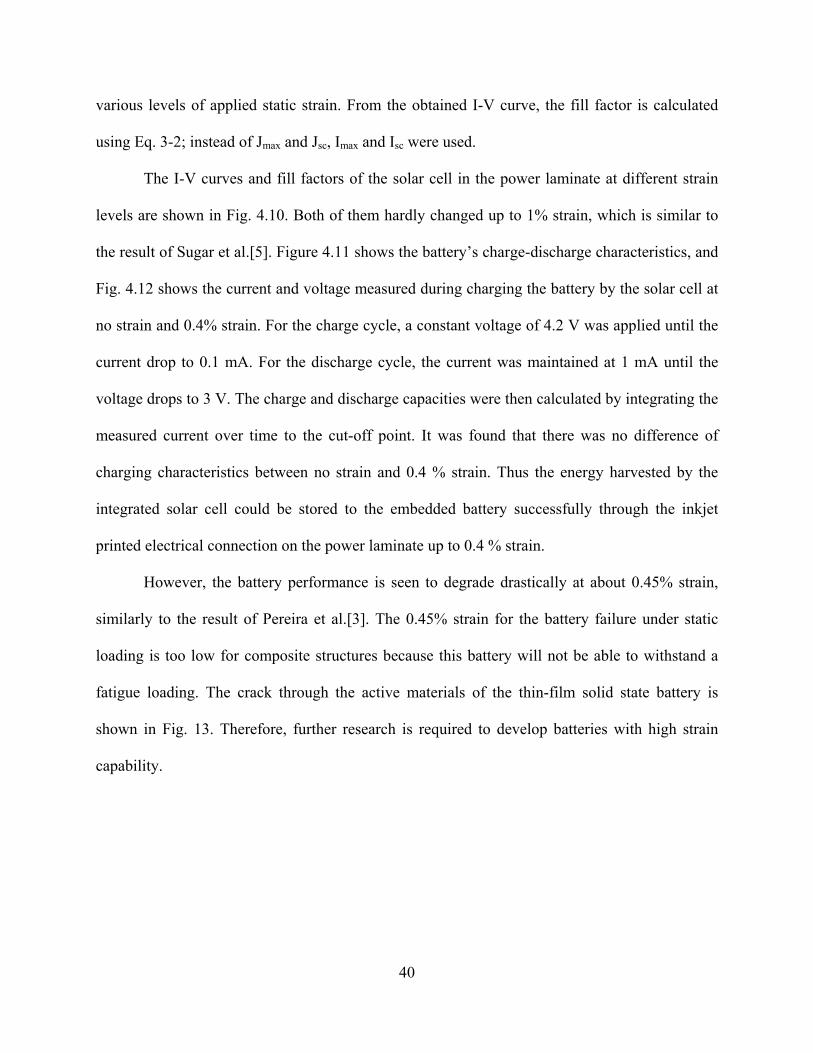
40
various levels of applied static strain. From the obtained I-V curve, the fill factor is calculated
using Eq. 3-2; instead of Jmax and Jsc, Imax and Isc were used.
The I-V curves and fill factors of the solar cell in the power laminate at different strain
levels are shown in Fig. 4.10. Both of them hardly changed up to 1% strain, which is similar to
the result of Sugar et al.[5]. Figure 4.11 shows the battery’s charge-discharge characteristics, and
Fig. 4.12 shows the current and voltage measured during charging the battery by the solar cell at
no strain and 0.4% strain. For the charge cycle, a constant voltage of 4.2 V was applied until the
current drop to 0.1 mA. For the discharge cycle, the current was maintained at 1 mA until the
voltage drops to 3 V. The charge and discharge capacities were then calculated by integrating the
measured current over time to the cut-off point. It was found that there was no difference of
charging characteristics between no strain and 0.4 % strain. Thus the energy harvested by the
integrated solar cell could be stored to the embedded battery successfully through the inkjet
printed electrical connection on the power laminate up to 0.4 % strain.
However, the battery performance is seen to degrade drastically at about 0.45% strain,
similarly to the result of Pereira et al.[3]. The 0.45% strain for the battery failure under static
loading is too low for composite structures because this battery will not be able to withstand a
fatigue loading. The crack through the active materials of the thin-film solid state battery is
shown in Fig. 13. Therefore, further research is required to develop batteries with high strain
capability.
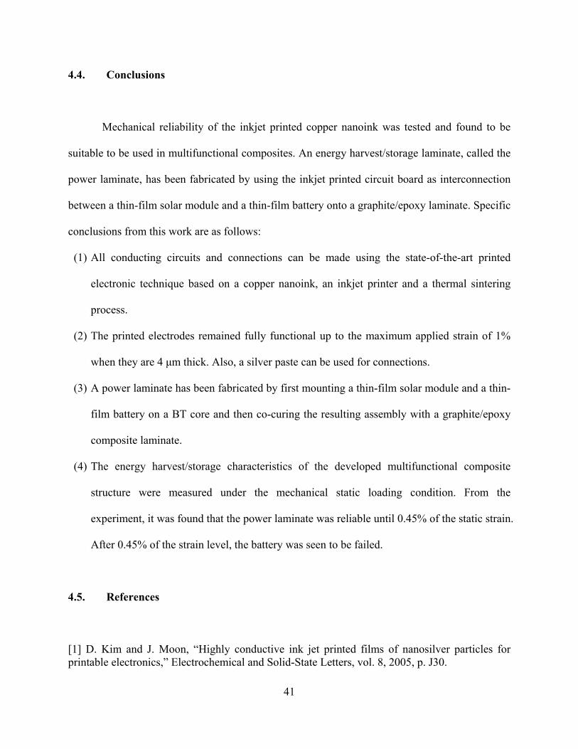
41
4.4. Conclusions
Mechanical reliability of the inkjet printed copper nanoink was tested and found to be
suitable to be used in multifunctional composites. An energy harvest/storage laminate, called the
power laminate, has been fabricated by using the inkjet printed circuit board as interconnection
between a thin-film solar module and a thin-film battery onto a graphite/epoxy laminate. Specific
conclusions from this work are as follows:
(1) All conducting circuits and connections can be made using the state-of-the-art printed
electronic technique based on a copper nanoink, an inkjet printer and a thermal sintering
process.
(2) The printed electrodes remained fully functional up to the maximum applied strain of 1%
when they are 4 μm thick. Also, a silver paste can be used for connections.
(3) A power laminate has been fabricated by first mounting a thin-film solar module and a thin-
film battery on a BT core and then co-curing the resulting assembly with a graphite/epoxy
composite laminate.
(4) The energy harvest/storage characteristics of the developed multifunctional composite
structure were measured under the mechanical static loading condition. From the
experiment, it was found that the power laminate was reliable until 0.45% of the static strain.
After 0.45% of the strain level, the battery was seen to be failed.
4.5. References
[1] D. Kim and J. Moon, “Highly conductive ink jet printed films of nanosilver particles for printable electronics,” Electrochemical and Solid-State Letters, vol. 8, 2005, p. J30.
42
[2] B.K. Park, D. Kim, S. Jeong, J. Moon, and J.S. Kim, “Direct writing of copper conductive patterns by ink-jet printing,” Thin Solid Films, vol. 515, 2007, pp. 7706–7711.
[3] Thomas J. P., Qidwai M. A., Matic P., Everett R. K., Gozdz A. S., Keenon M. T., and Grasmeyer J. M., “Multifunctional structure-plus-power concepts,” Proceedings of 43rd AIAA/ASME/ASCE/AHS/ASC structures, structural dynamics, and materials conference, 2002, AIAA2002-1239.
[4] J.P. Thomas and M.A. Qidwai, “Mechanical design and performance of composite multifunctional materials,” Acta materialia, vol. 52, 2004, pp. 2155–2164.
[5] T. Pereira, Z. Guo, S. Nieh, J. Arias, and H.T. Hahn, “Embedding thin-film lithium energy cells in structural composites,” Composites Science and Technology, vol. 68, 2008, pp. 1935–1941.
[6] O. Morton, “Solar energy: A new day dawning?: Silicon Valley sunrise,” Nature, vol. 443, 2006, pp. 19–22.
[7] Sugar, J. G., Scaffaro , R. Guo, Z. Maung, J. K., Ju, Y. S., and Hahn, H. T., "Photovoltaic Performance of Amorphous Silicon Flexible Solar Modules under Mechanical Loading," 2002, Proceedings of the 6th International Workshop on Structural Health Monitoring, 4698: 180-191,
[8] J. Weber, K. Potje-Kamloth, F. Haase, P. Detemple, F. Volklein, and T. Doll, “Coin-size coiled-up polymer foil thermoelectric power generator for wearable electronics,” Sensors and Actuators A: Physical, vol. 132, 2006, pp. 325–330.
[9] W. Qu, M. Plötner, and W.J. Fischer, “Microfabrication of thermoelectric generators on flexible foil substrates as a power source for autonomous microsystems,” Journal of Micromechanics and Microengineering, vol. 11, 2001, p. 146.
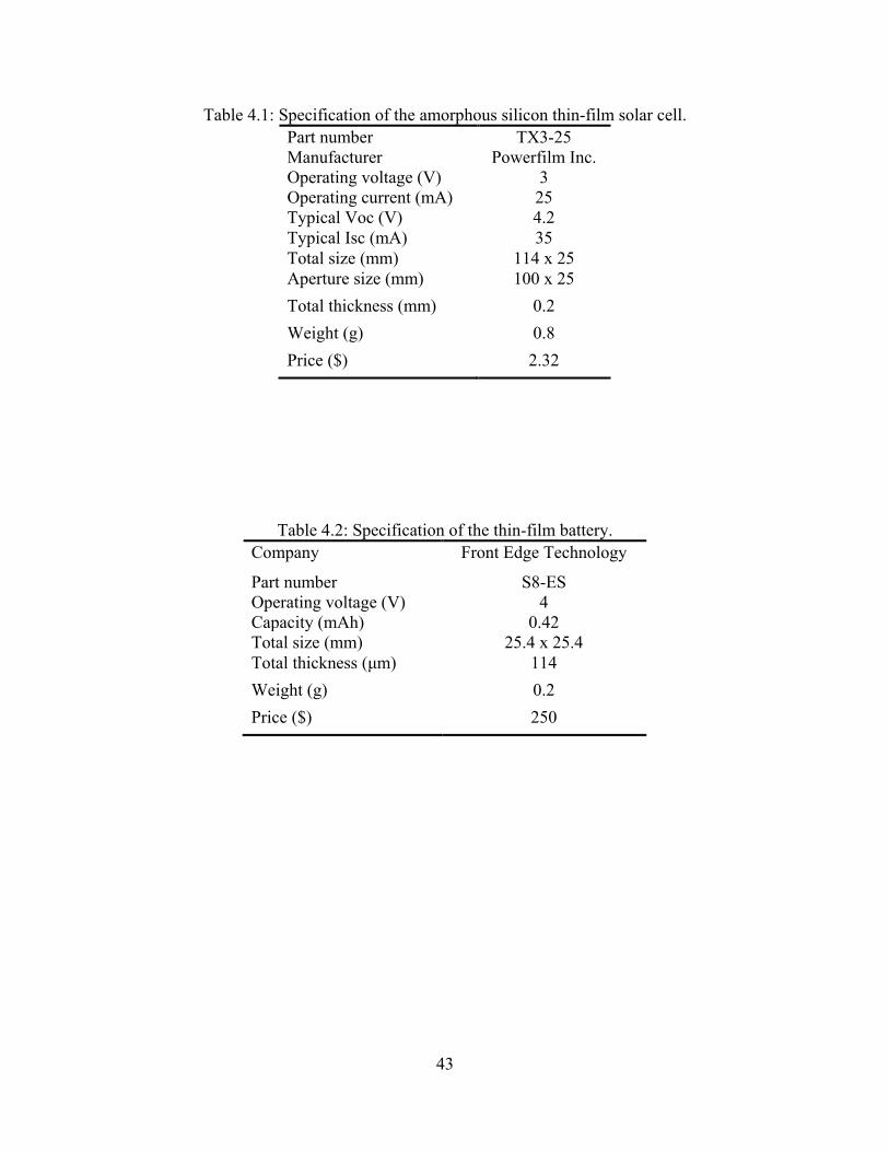
43
Table 4.1: Specification of the amorphous silicon thin-film solar cell. Part number TX3-25 Manufacturer Powerfilm Inc. Operating voltage (V) 3 Operating current (mA) 25 Typical Voc (V) 4.2 Typical Isc (mA) 35 Total size (mm) 114 x 25 Aperture size (mm) 100 x 25 Total thickness (mm) 0.2 Weight (g) 0.8 Price ($) 2.32
Table 4.2: Specification of the thin-film battery. Company Front Edge Technology
Part number S8-ES Operating voltage (V) 4 Capacity (mAh) 0.42 Total size (mm) 25.4 x 25.4 Total thickness (μm) 114 Weight (g) 0.2 Price ($) 250
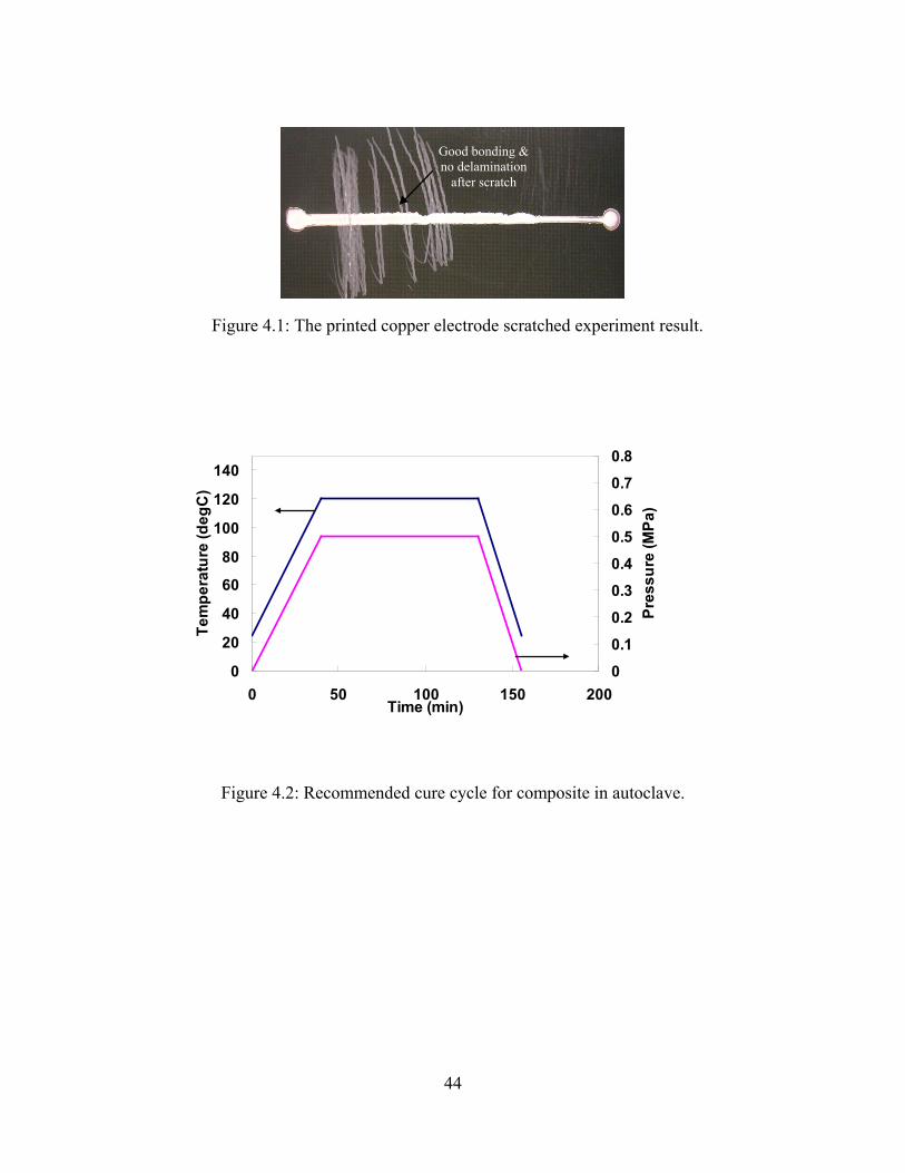
44
Figure 4.1: The printed copper electrode scratched experiment result.
Figure 4.2: Recommended cure cycle for composite in autoclave.
0
20
40
60
80
100
120
140
0 50 100 150 200Time (min)
Tem
pera
ture
(deg
C)
0
0.1
0.2
0.3
0.4
0.5
0.6
0.7
0.8
Pres
sure
(MPa
)
Good bonding & no delamination
after scratch
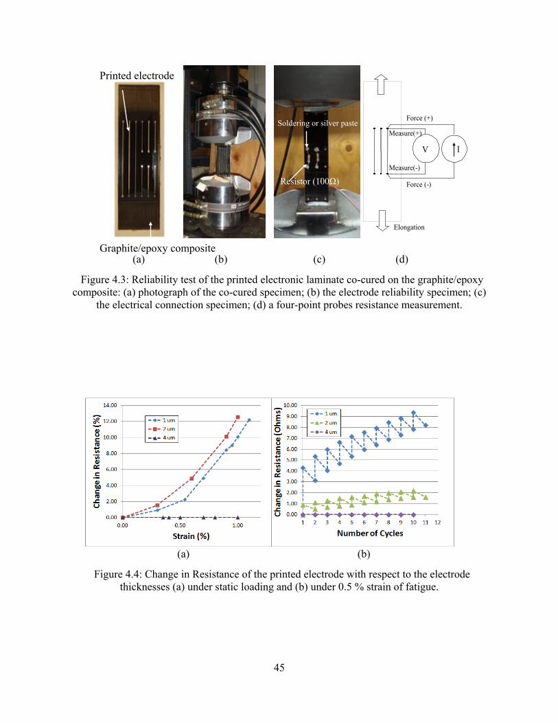
45
Figure 4.3: Reliability test of the printed electronic laminate co-cured on the graphite/epoxy
composite: (a) photograph of the co-cured specimen; (b) the electrode reliability specimen; (c) the electrical connection specimen; (d) a four-point probes resistance measurement.
Figure 4.4: Change in Resistance of the printed electrode with respect to the electrode thicknesses (a) under static loading and (b) under 0.5 % strain of fatigue.
(a) (b)
Printed electrode
(c) Graphite/epoxy composite
Elongation
V
Measure(+)
I
Force (+)
Force (-)
Measure(-)
(d)
Resistor (100Ω)
Soldering or silver paste
(a) (b)
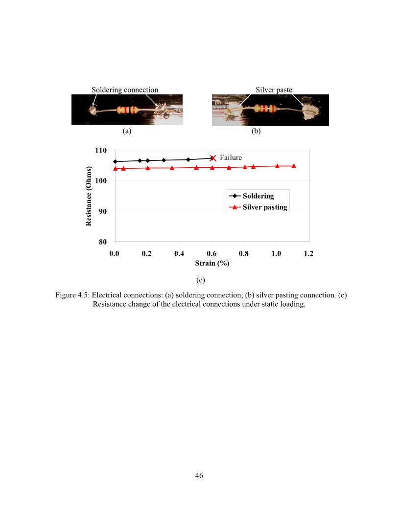
46
Figure 4.5: Electrical connections: (a) soldering connection; (b) silver pasting connection. (c)
Resistance change of the electrical connections under static loading.
(a) (b)
Soldering connection Silver paste
80
90
100
110
0.0 0.2 0.4 0.6 0.8 1.0 1.2Strain (%)
Res
istan
ce (O
hms)
Soldering Silver pasting
Failure
(c)
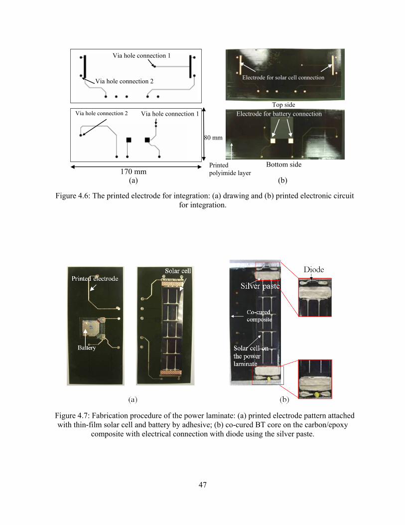
47
Figure 4.6: The printed electrode for integration: (a) drawing and (b) printed electronic circuit
for integration.
Figure 4.7: Fabrication procedure of the power laminate: (a) printed electrode pattern attached with thin-film solar cell and battery by adhesive; (b) co-cured BT core on the carbon/epoxy
composite with electrical connection with diode using the silver paste.
(a) (b)
Top side
Bottom side
Via hole connection 1
Via hole connection 2
Via hole connection 1 Via hole connection 2
Electrode for solar cell connection
Electrode for battery connection
Printed polyimide layer 170 mm
80 mm

48
Figure 4.8: Cross section view of the power laminate co-cured composite laminate.
Ethylene Tefrafluoroethylene (~35 um) Ethylene Vinyl Acetate (~30um)
Solar device + substrate (~66 um)
Ethylene Vinyl Acetate (~30 um) Ethylene Tefrafluoroethylene (~25um)
Epoxy adhesive DP460 (~105 um)
BT core (~100 um)
Li-ion solid state thin-film battery (~114 um)
T700SC/RS-30G (Total thickness: 530 um)
Epoxy adhesive DP460 (~30 um)
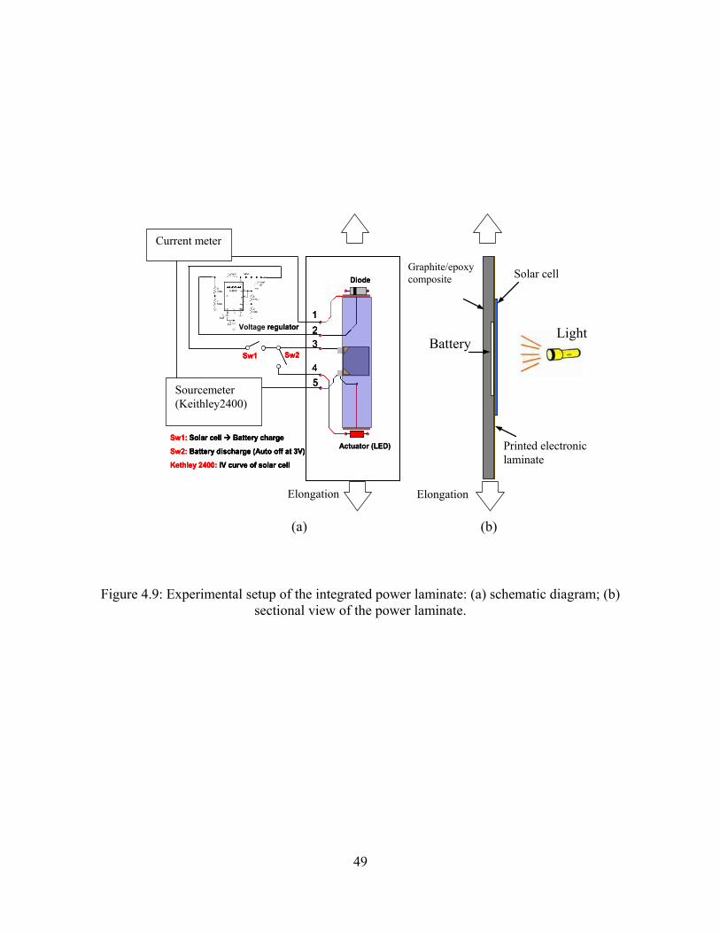
49
Figure 4.9: Experimental setup of the integrated power laminate: (a) schematic diagram; (b)
sectional view of the power laminate.
DiodeDiode
Actuator (LED)Actuator (LED)
123
45
Sw1: Solar cell Battery charge
Sw2: Battery discharge (Auto off at 3V)
Kethley 2400: IV curve of solar cell
Sw1 Sw2
Kethley 2400
Voltage regulator123
45
Sw1: Solar cell Battery charge
Sw2: Battery discharge (Auto off at 3V)
Kethley 2400: IV curve of solar cell
Sw1 Sw2
Kethley 2400
123
45
Sw1: Solar cell Battery charge
Sw2: Battery discharge (Auto off at 3V)
Kethley 2400: IV curve of solar cell
Sw1 Sw2
Kethley 2400
Voltage regulator
Elongation
(a) (b)
Light
Solar cell
Printed electronic laminate
Graphite/epoxy composite
Battery
Sourcemeter (Keithley2400)
Current meter
Elongation
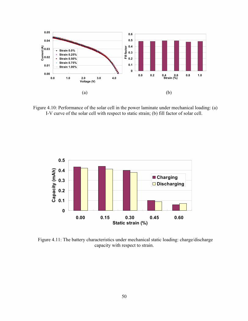
50
Figure 4.10: Performance of the solar cell in the power laminate under mechanical loading: (a)
I-V curve of the solar cell with respect to static strain; (b) fill factor of solar cell.
Figure 4.11: The battery characteristics under mechanical static loading: charge/discharge
capacity with respect to strain.
0
0.1
0.2
0.3
0.4
0.5
0.00 0.15 0.30 0.45 0.60Static strain (%)
Cap
acity
(mA
h)
ChargingDischarging
0.00
0.01
0.02
0.03
0.04
0.05
0.0 1.0 2.0 3.0 4.0Voltage (V)
Cur
rent
(A)
Strain 0.0%Strain 0.25%Strain 0.50%Strain 0.75%Strain 1.00%
0
0.1
0.2
0.3
0.4
0.5
0.6
0.0 0.2 0.4 0.6 0.8 1.0Strain (%)
Fill
fact
or
(b) (a)
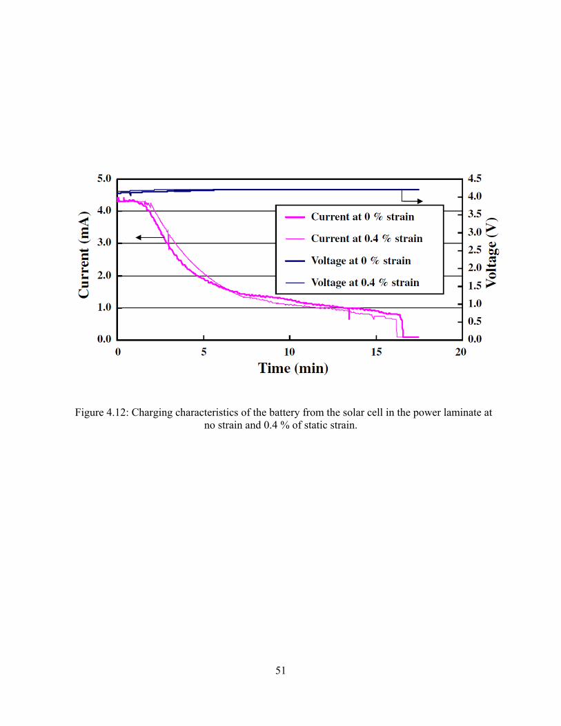
51
Figure 4.12: Charging characteristics of the battery from the solar cell in the power laminate at
no strain and 0.4 % of static strain.
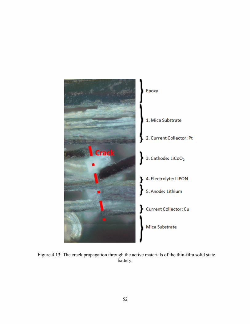
52
Figure 4.13: The crack propagation through the active materials of the thin-film solid state battery.

53
CHAPTER FIVE
Performance of Lithium-Ion Polymer Battery
5.1. Introduction
As stated in Chapter 1, reducing the weight by utilizing multifunctional structure is 50%
more effective than improving the specific energy of the battery in increasing the flight time
endurance of UAVs[1,2]. To help mitigate the potential weight added by such energy devices,
multifunctional hybrid composite structures have been developed with load-bearing thin-film
batteries[3-5], thin-film solar cells[6,7], and thermoelectric devices[8,9] integrated in the
composite laminate structure.
Pereira et al.[3,4] have used thin-film solid-state batteries. These batteries are very thin,
0.14 mm, but the specific energy is only about 7.2 Wh/kg, including the packaging mass. Since
most of battery constituents are made of ceramics, they are very brittle. Under bending these
batteries start to degrade at 0.06% strain. This solid-state battery works at 0.37% strain but the
charge and discharge capacity is less than half of the original capacity. Similarly, the thin-film
solid-state battery failure occurred when a tensile stain is above 0.4% in Chapter 4. Under
bending the solid-state battery performances were degrading because of packaging failure, which
leads to oxidation of battery constituents. Under tensile loading the battery constituents were
damaged as shown in Figure 4.13.
Unlike the thin-film solid-state batteries, the lithium-sulfur (LiS) batteries have much
higher initial specific energy, reaching 250 to 350 Wh/kg[10]. However, the charge efficiency is
85% and the capacity decreases due to side reactions during charge/discharge cycle between

54
sulfur and liquid electrolyte. Also, these batteries may self-combust and catch fire due to the
growth of the lithium electrode into a branchlike structures that increases the impedance and
temperature of the battery[11]. A promising alternative to solid-state and LiS batteries is the
lithium-ion (Li-ion) polymer battery, which has a higher charging efficiency, 95 to 99%, than
LiS batteries. Also, the Li-ion polymer battery is very stable and widely used[12].
In this research, we have studied the performance of Li-ion polymer batteries from Dow
Kokam under structural and environmental loadings including compression, tensile and fatigue
loadings, and temperature. The Li-ion polymer batteries were integrated into the carbon fiber
reinforced polymer (CFRP) composite laminate using an out-of-autoclave co-curing method
inside a thermal chamber to test the performance of the battery under fatigue loading.
Mechanical loadings were applied using an Instron machine, and the temperature was varied
using a furnace and a refrigerator. These batteries were charged and discharged with a source
meter, and data were obtained using the same source meter as well.
5.2. Experimental Details
5.2.1. Specimen Specifications
All the batteries for this study were purchased from Dow Kokam (Midland, Miami).
These were thin-film Li-ion polymer batteries. Dimensions of these batteries are 3.1± 0.1, 47± 1,
and 30± 1 mm for thickness, length, and width, respectively. The average mass of these batteries
were 9.38± 0.3 g. The operating voltage of these batteries was 3.7 V, and the end of discharge
voltage cutoff was 2.8 V. The manufacturer specification claims the energy density of 143
mAh/g for these cells.
55
The battery is basically multilayer composite both functionally and structurally. For
casing, cast polypropylene/ aluminum/ nylon composite 0.155 ± 0.002 mm thick is used. For
energy storage, the battery has 12 cathodes and 11 anodes arranged in alternation. The cathode
consists of a 0.026± 0.002 mm thick layer of lithium cobalt oxide (LiCoO2) and lithium cobalt
manganese nickel oxide (LiMnNiCoO2) blend coated on a 0.031± 0.002 mm thick aluminum
current collector. The anode, on the other hand, has a 0.029± 0.002 mm thick layer of graphite
coated on a 0.062± 0.002 mm thick copper current collector. A polyvinylidene fluoride (PVDF)
separator of 0.014± 0.002 mm thickness is used for this battery. The packaged battery is shown
in Fig. 5.1.
5.2.2. Experimental Setup and Procedure
In order to establish a reference capacity, five batteries were subjected to three
consecutive charge/discharge cycles between 2.8 and 4.2 V at 0.05C (17.5 mA) and five more at
2.5C (875 mA) using a source meter (Keithley 2400, Keithley, USA). The resulting current and
voltage were recorded at every second, and the charge/discharge capacity was calculated by:
Eq. 5-1
The battery was loaded on a tabletop mechanical tester (Instron 4411, Instron, USA) up
to 1.7% strain because typically, the maximum tensile strain of CFRP composite laminates is
1.5% strain. Strain and load were recorded using a strain gage amplifier (Omega 941, Omega,
USA), and a load cell amplifier (Omega 916, Omega, USA), respectively. A precision strain
0
C i dtτ
= ⋅∫
56
gage (EA-6-062AP-120, Micro-Measurements Division, USA) was attached on the middle of the
battery, and aluminum tabs were attached on both ends of the battery using a two-part epoxy
adhesive (Scotch-Weld DP-420, 3M, USA). The battery was then subjected to charge and
discharge cycles at different strain levels.
Also, the battery was tested in compression in the thickness direction using the custom-
made fixture shown in Fig. 5.2. A table-top mechanical tester was used for a pressure up to 3
MPa, and a servo-hydraulic mechanical tester (Instron 8516, Instron, USA) was used for pressure
higher than 3 MPa.
Effect of temperature on the performance of the battery was studied using a furnace
(Type 1400 Furnace, Barnstead Thermolyne, USA) for temperatures higher than 25°C (50, 60,
70 and 80°C), a mini- refrigerator (Chefmate, USA), for -3°C, and a chest freezer (GE, USA),
for -27°C. The temperature of the battery was monitored using a thermocouple (HH 501, Omega,
USA). At high temperatures, the batteries were charged and discharged at 2.5 C-rate. At low
temperatures, the batteries were discharged at 1/12 C-rates, respectively. Between each cycle,
soaking time was two hours.
The battery was co-cured inside a carbon/epoxy composite laminate using an out of
autoclave co-curing method at 80°C inside a thermal chamber (Gravity Oven, Linberg/BlueM,
USA). (Figure 5.3a) Six layers of carbon fiber reinforced polymer prepregs (CYCOM 754, Cytec
Industries, USA) were used with a lay-up sequence of [0]6; the battery was located in the middle
of the lay-up. Before co-curing the Li-ion polymer battery and the pre-pregs together, a flat
flexible cable coated with polyester (Shielded FFC Cable, Nicomatic, USA), 240 µm thick and 5
mm wide, was connected to positive and negative steel connectors by wrapping with a carbon
tapes (Carbon conductive tabs, Ted Pella, USA). (A flat flexible cable was used instead of an
57
inkjet printed circuit because an alligator clip has to be attached to monitor a current and voltage
of the Li-ion polymer battery.) Then, a silver paint (Colloidal Silver, Ted Pella, USA) was used
to ensure conductive paths. These connections were dried inside a thermal chamber at 60°C for
four hours. After the extended connections were completely attached, an epoxy adhesive (5
Minute Epoxy, Devcon, USA) was used to insulate connectors from carbon fibers. (Figure 5.3b)
These laminates were tested under tension-compression and tension-tension fatigue loadings
using a servo-hydraulic mechanical tester while the embedded batteries underwent charge and
discharge cycles at 2.5 C rate.
5.3. Results and Discussion
To obtain the baseline performance, the Li-ion polymer batteries were charged and
discharged at 0.05 and 2.5 C-rates. As Figs. 5.4a and 5.4b shows, average charge and discharge
capacities are 349.8± 0.3 and 348.5± 0.2 mAh, respectively at 0.05 C-rate. The batteries were
fully charged and discharged meeting their specifications given by Dow Kokam. However, as the
C-rate was increased to 2.5, the charge and discharge capacities decreased to 290.7± 0.6 and
289.9± 0.5 mAh, respectively, which is only 82.9% of their full capacity due to larger transition
resistance of Li-ions between the electrodes and the electrolyte. (Figure 5.5) The capacity of Li-
ion polymer batteries is known to decrease as the C-rate increases[12,13].
The specimen and the experimental setup to characterize the Li-ion polymer battery
under various mechanical and environmental conditions are shown in Fig. 5.6. This test was
performed to ensure that the battery is elastic enough to endure tensile loadings while it is
embedded inside CFRP composite laminates. Due to lithiation during charging and de-lithiation
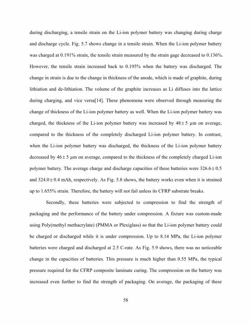
58
during discharging, a tensile strain on the Li-ion polymer battery was changing during charge
and discharge cycle. Fig. 5.7 shows change in a tensile strain. When the Li-ion polymer battery
was charged at 0.191% strain, the tensile strain measured by the strain gage decreased to 0.136%.
However, the tensile strain increased back to 0.195% when the battery was discharged. The
change in strain is due to the change in thickness of the anode, which is made of graphite, during
lithiation and de-lithiation. The volume of the graphite increases as Li diffuses into the lattice
during charging, and vice versa[14]. These phenomena were observed through measuring the
change of thickness of the Li-ion polymer battery as well. When the Li-ion polymer battery was
charged, the thickness of the Li-ion polymer battery was increased by 48± 5 µm on average,
compared to the thickness of the completely discharged Li-ion polymer battery. In contrast,
when the Li-ion polymer battery was discharged, the thickness of the Li-ion polymer battery
decreased by 46± 5 µm on average, compared to the thickness of the completely charged Li-ion
polymer battery. The average charge and discharge capacities of these batteries were 326.6± 0.5
and 324.0± 0.4 mAh, respectively. As Fig. 5.8 shows, the battery works even when it is strained
up to 1.655% strain. Therefore, the battery will not fail unless its CFRP substrate breaks.
Secondly, these batteries were subjected to compression to find the strength of
packaging and the performance of the battery under compression. A fixture was custom-made
using Poly(methyl methacrylate) (PMMA or Plexiglass) so that the Li-ion polymer battery could
be charged or discharged while it is under compression. Up to 8.14 MPa, the Li-ion polymer
batteries were charged and discharged at 2.5 C-rate. As Fig. 5.9 shows, there was no noticeable
change in the capacities of batteries. This pressure is much higher than 0.55 MPa, the typical
pressure required for the CFRP composite laminate curing. The compression on the battery was
increased even further to find the strength of packaging. On average, the packaging of these
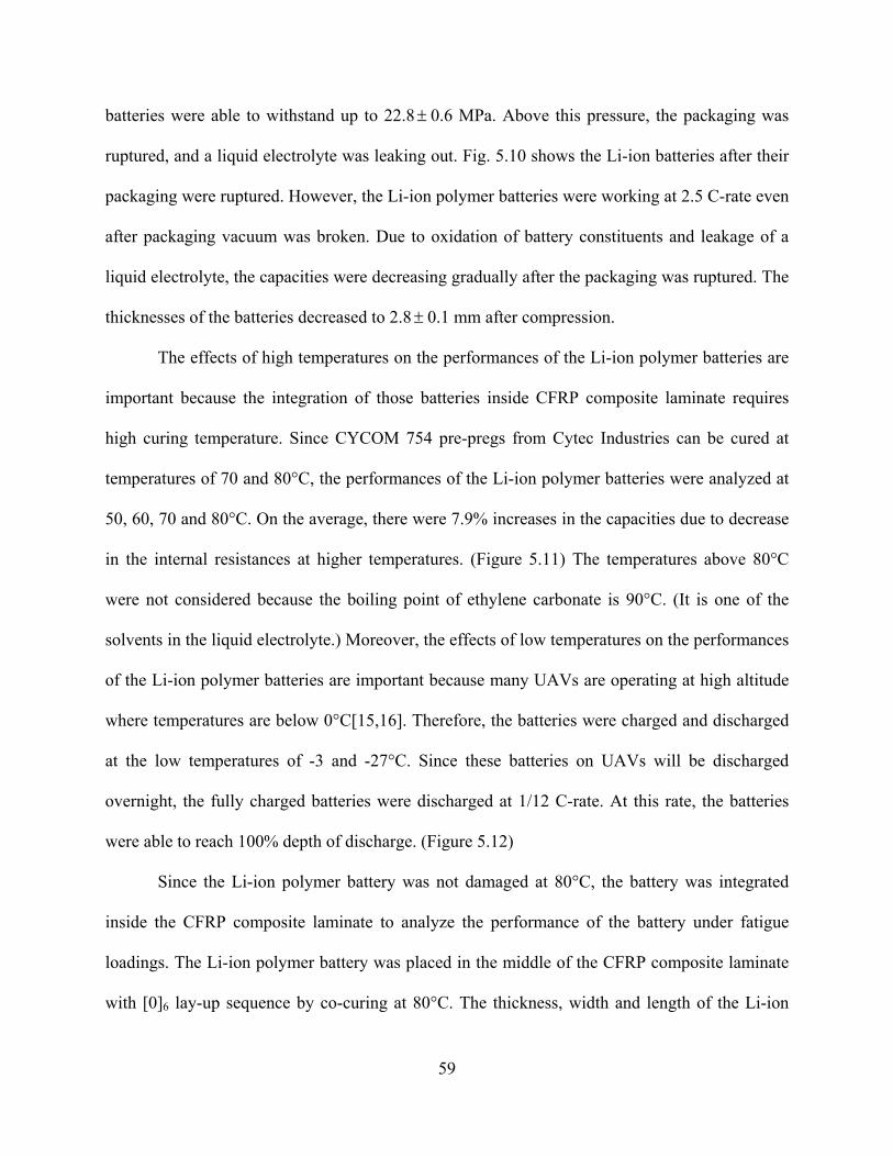
59
batteries were able to withstand up to 22.8± 0.6 MPa. Above this pressure, the packaging was
ruptured, and a liquid electrolyte was leaking out. Fig. 5.10 shows the Li-ion batteries after their
packaging were ruptured. However, the Li-ion polymer batteries were working at 2.5 C-rate even
after packaging vacuum was broken. Due to oxidation of battery constituents and leakage of a
liquid electrolyte, the capacities were decreasing gradually after the packaging was ruptured. The
thicknesses of the batteries decreased to 2.8± 0.1 mm after compression.
The effects of high temperatures on the performances of the Li-ion polymer batteries are
important because the integration of those batteries inside CFRP composite laminate requires
high curing temperature. Since CYCOM 754 pre-pregs from Cytec Industries can be cured at
temperatures of 70 and 80°C, the performances of the Li-ion polymer batteries were analyzed at
50, 60, 70 and 80°C. On the average, there were 7.9% increases in the capacities due to decrease
in the internal resistances at higher temperatures. (Figure 5.11) The temperatures above 80°C
were not considered because the boiling point of ethylene carbonate is 90°C. (It is one of the
solvents in the liquid electrolyte.) Moreover, the effects of low temperatures on the performances
of the Li-ion polymer batteries are important because many UAVs are operating at high altitude
where temperatures are below 0°C[15,16]. Therefore, the batteries were charged and discharged
at the low temperatures of -3 and -27°C. Since these batteries on UAVs will be discharged
overnight, the fully charged batteries were discharged at 1/12 C-rate. At this rate, the batteries
were able to reach 100% depth of discharge. (Figure 5.12)
Since the Li-ion polymer battery was not damaged at 80°C, the battery was integrated
inside the CFRP composite laminate to analyze the performance of the battery under fatigue
loadings. The Li-ion polymer battery was placed in the middle of the CFRP composite laminate
with [0]6 lay-up sequence by co-curing at 80°C. The thickness, width and length of the Li-ion

60
polymer battery and CFRP composite laminate were 4.6 ± 0.1, 56 ± 1 and 221 ± 3 mm,
respectively. The performance of the Li-ion polymer battery was characterized under two
different fatigue cycles: tension-compression and tension-tension. Fig. 5.13a shows the
experimental setup for the composite laminate with the battery under tensile and fatigue loading.
For the tension-compression cycles, the tensile strain was 0.11% and compressive strain was -
0.17%. However, since the span length of the composite laminate was very long compared to its
thickness, the composite laminate was buckling under compressive loading. For the tension-
tension cycle, the minimum tensile strain was 0.035%, and the maximum tensile strain was
0.38%. For the both cycles, the frequency of each cycle was kept at 0.2 Hz, and the charge and
discharge were done at 2.5 C-rate. Fig. 5.13b and 5.13c shows loads and strains for each cycles.
Also, the strain range for both types of fatigue loadings were about 0.3% strain because for the
most aircrafts, the fatigue strains are well kept below 0.3% strain[17].
As shown in Fig. 5.14, the discharging voltage value oscillates as fatigue loading was
applied. The sudden drops in voltage are due to the separation of active layers of the Li-ion
polymer battery. During each cycle, the maximum tensile loading compresses the battery,
resulting in decreasing of distances between each layers and increasing of contact areas. (Figure
5.15) When the composite laminate was under compression, it underwent buckling because the
composite laminate was long compared to its thickness. Since the Li-ion polymer battery was in
the tensile side, the Li-ion polymer battery was compressed, experiencing the same effect as if
the Li-ion polymer battery was under the maximum tensile loading. Fig. 5.16a,b shows changes
in discharging voltages of the Li-ion polymer batteries during fatigue cycles. As a result, the
capacities of the Li-ion polymer batteries dropped by 18.8% for the tensile-compression cycle
and 32.9% for the tensile-tensile cycle. (Figure 5.17) The capacities of the Li-ion polymer
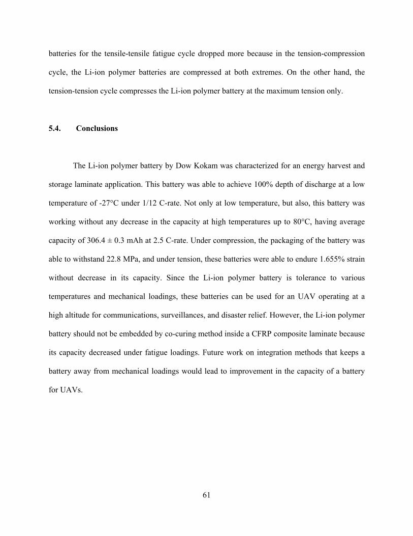
61
batteries for the tensile-tensile fatigue cycle dropped more because in the tension-compression
cycle, the Li-ion polymer batteries are compressed at both extremes. On the other hand, the
tension-tension cycle compresses the Li-ion polymer battery at the maximum tension only.
5.4. Conclusions
The Li-ion polymer battery by Dow Kokam was characterized for an energy harvest and
storage laminate application. This battery was able to achieve 100% depth of discharge at a low
temperature of -27°C under 1/12 C-rate. Not only at low temperature, but also, this battery was
working without any decrease in the capacity at high temperatures up to 80°C, having average
capacity of 306.4 ± 0.3 mAh at 2.5 C-rate. Under compression, the packaging of the battery was
able to withstand 22.8 MPa, and under tension, these batteries were able to endure 1.655% strain
without decrease in its capacity. Since the Li-ion polymer battery is tolerance to various
temperatures and mechanical loadings, these batteries can be used for an UAV operating at a
high altitude for communications, surveillances, and disaster relief. However, the Li-ion polymer
battery should not be embedded by co-curing method inside a CFRP composite laminate because
its capacity decreased under fatigue loadings. Future work on integration methods that keeps a
battery away from mechanical loadings would lead to improvement in the capacity of a battery
for UAVs.

62
5.5. References
[1] Thomas J. P., Qidwai M. A., Matic P., Everett R. K., Gozdz A. S., Keenon M. T., and Grasmeyer J. M., “Multifunctional structure-plus-power concepts,” Proceedings of 43rd AIAA/ASME/ASCE/AHS/ASC structures, structural dynamics, and materials conference, 2002, AIAA2002-1239.
[2] Thomas., J. P., Qidwai., M. A., “Mechanical design and performance of composite multifunctional materials,” Acta materialia, 2004, 52:2155-2164
[3] T. Pereira, R. Scaffaro, S. Nieh, J. Arias, Z. Guo, and H.T. Hahn, “The performance of thin-film Li-ion batteries under flexural deflection,” Journal of Micromechanics and Microengineering, vol. 16, 2006, p. 2714.
[4] T. Pereira, R. Scaffaro, Z. Guo, S. Nieh, J. Arias, and H.T. Hahn, “Performance of thin-film lithium energy cells under uniaxial pressure,” Advanced Engineering Materials, vol. 10, 2008, pp. 393–399.
[5] H.S. Kim, J.S. Kang, J.S. Park, H.T. Hahn, H.C. Jung, and J.W. Joung, “Inkjet printed electronics for multifunctional composite structure,” Composites Science and Technology, vol. 69, 2009, pp. 1256–1264.
[6] Sugar, J. G., Scaffaro , R. Guo, Z. Maung, J. K., Ju, Y. S., and Hahn, H. T., "Photovoltaic Performance of Amorphous Silicon Flexible Solar Modules under Mechanical Loading," Proceedings of the 6th International Workshop on Structural Health Monitoring, Stanford, CA, September 11-13, 2007.
[7] K. Jason Maung, H.T. Hahn, and Y.S. Ju, “Multifunctional integration of thin-film silicon solar cells on carbon-fiber-reinforced epoxy composites,” Solar Energy, vol. 84, 2010, pp. 450–458.
[8] J.W. Stevens, “Heat transfer and thermoelectric design considerations for a ground-source thermo generator,” Thermoelectrics, 1999. Eighteenth International Conference on, 1999, pp. 68–71.
[9] E.E. Lawrence and G.J. Snyder, “A study of heat sink performance in air and soil for use in a thermoelectric energy harvesting device,” Thermoelectrics, 2002. Proceedings ICT'02. Twenty-First International Conference on, 2002, pp. 446–449.
[10] J.R. Akridge and Y. Mikhaylik, "Lithium-Sulfur Secondary Battery: Chemistry and Practical System Performance," 2005 International Conference on Polymer Batteries and Fuel Cells, Las Vegas, Nevada, June 12-17, 2005.
[11] A. Rapinett, “Zephyr: A High Altitude Long Endurance Unmanned Air Vehicle,” University of Surrey, 2009.

63
[12] H.H. Sumathipala, J. Hassoun, S. Panero, and B. Scrosati, “Li-LiFePO 4 rechargeable polymer battery using dual composite polymer electrolytes,” Journal of Applied Electrochemistry, vol. 38, 2008, pp. 39–42.
[13] N. Li and C.R. Martin, “A high-rate, high-capacity, nanostructured Sn-based anode prepared using sol-gel template synthesis,” Journal of the Electrochemical Society, vol. 148, 2001, p. A164.
[14] Y. Qi and S.J. Harris, “In Situ Observation of Strains during Lithiation of a Graphite Electrode,” Journal of The Electrochemical Society, vol. 157, 2010, p. A741.
[15] R. J. Havens, R. T. Koll, and H. E. LaGow, “The pressure, density, and temperature of the earth's atmosphere to 160 kilometers,” Journal of Geophysical Research, vol. 57, no. 1, pp. 59–72, 1952.
[16] H. Eisenbeiss, “A mini unmanned aerial vehicle (UAV): system overview and image acquisition,” International Archives of Photogrammetry. Remote Sensing and Spatial Information Sciences, vol. 36, no. 5, 2004.
[17] R.J. Diefendorf and E. Tokarsky, “High-performance carbon fibers,” Polymer Engineering & Science, vol. 15, 1975, pp. 150–159.

64
Figure 5.1: The Li-ion polymer battery from Dow-Kokam.
Figure 5.2: The experimental setup for the Li-ion polymer battery under uni-axial pressure: (a)
below and (b) above 3 MPa.
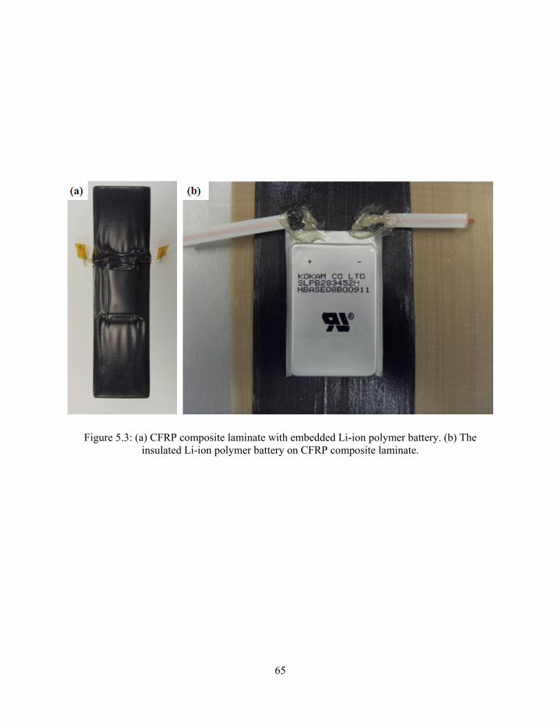
65
Figure 5.3: (a) CFRP composite laminate with embedded Li-ion polymer battery. (b) The
insulated Li-ion polymer battery on CFRP composite laminate.
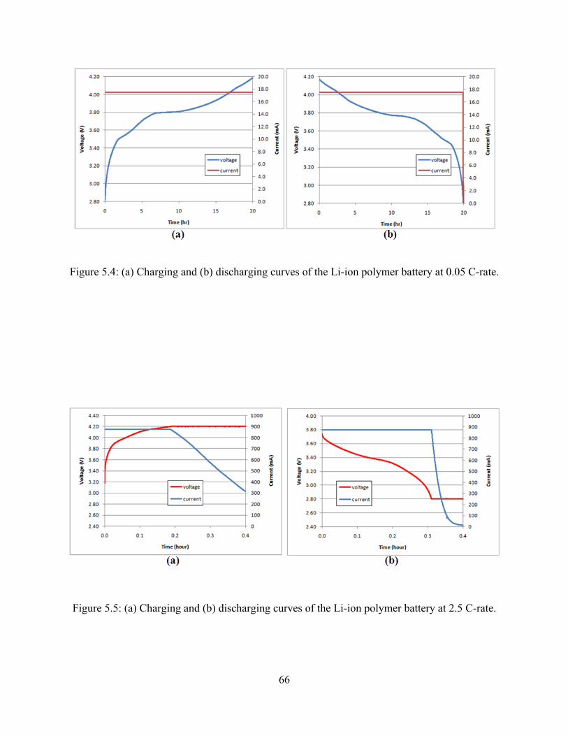
66
Figure 5.4: (a) Charging and (b) discharging curves of the Li-ion polymer battery at 0.05 C-rate.
Figure 5.5: (a) Charging and (b) discharging curves of the Li-ion polymer battery at 2.5 C-rate.
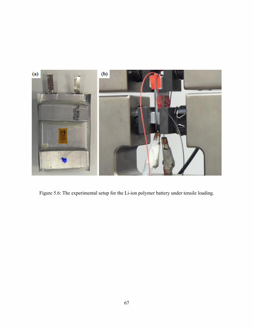
67
Figure 5.6: The experimental setup for the Li-ion polymer battery under tensile loading.
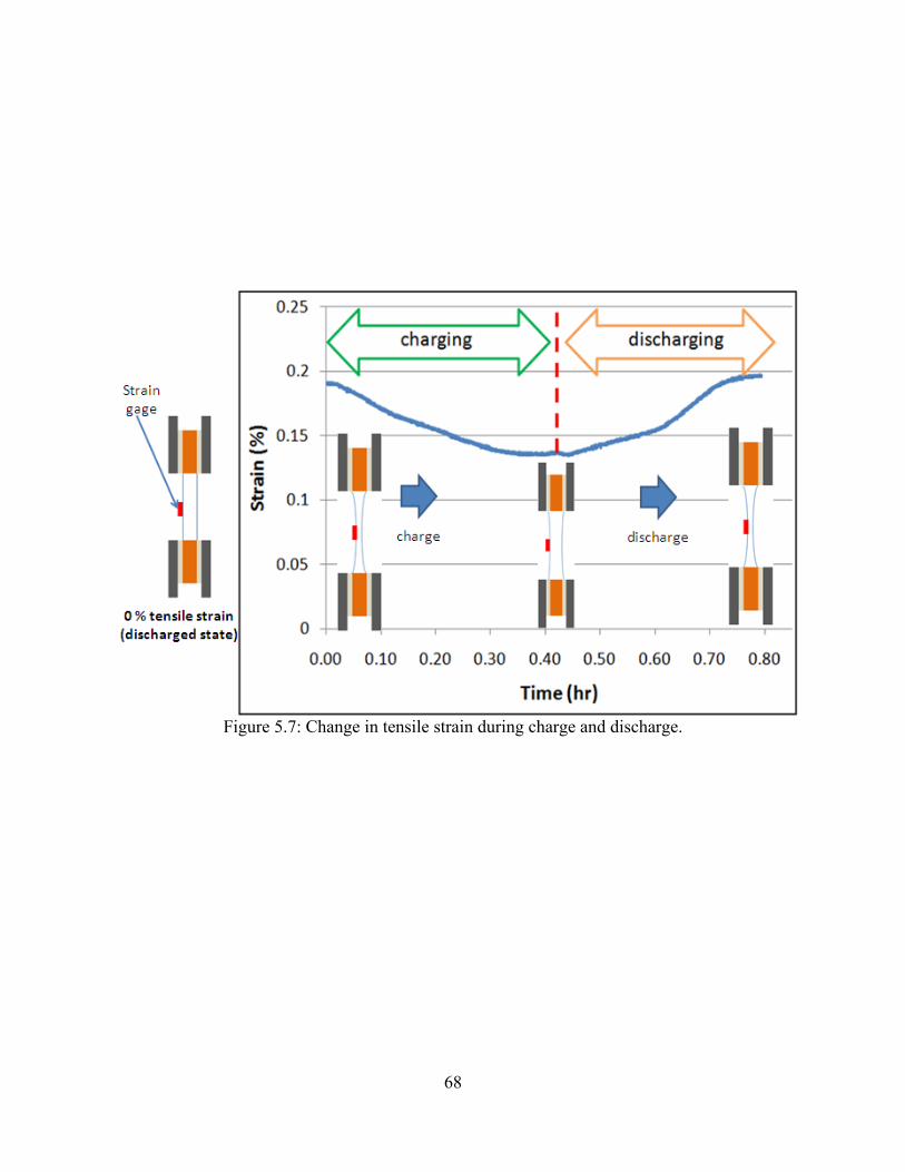
68
Figure 5.7: Change in tensile strain during charge and discharge.
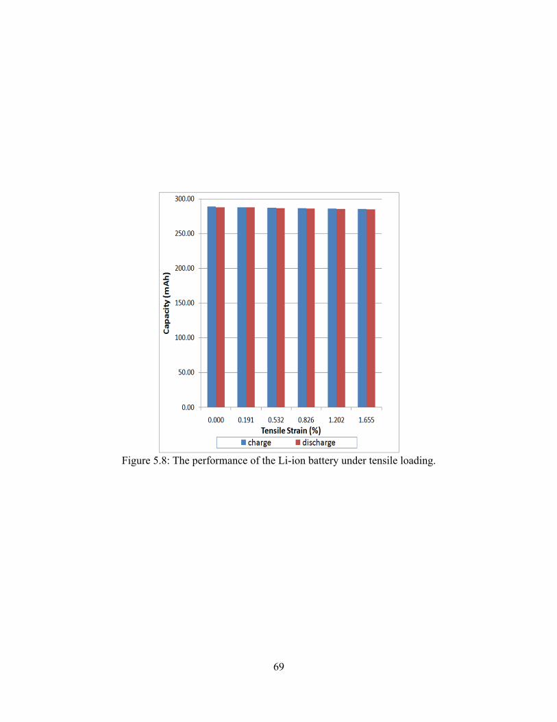
69
Figure 5.8: The performance of the Li-ion battery under tensile loading.
70
Figure 5.9: The performance of the Li-ion battery under uni-axial pressure.
Figure 5.10: The Li-ion polymer battery after uni-axial pressure test.
71
Figure 5.11: The performance of the Li-ion battery at high temperatures of 50, 60, 70 and 80 °C.
Figure 5.12: The performance of the Li-ion battery at low temperatures of -3 and -27 °C.
72
Figure 5.13: (a) The experimental setup for the multi-functional composite laminate under
fatigue loading. Loads and strains for (b) tension-compression and (c) tension-tension fatigue testing.

73
Figure 5.14: Discharging of the Li-ion polymer battery under fatigue loading: (a) tension-
compression and (b) tension-tension.
Figure 5.15: Changes in distances between each active layers during fatigue cycles.
74
Figure 5.16: The changes in discharging voltages of Li-ion polymer batteries under fatigue
loading: (a) tension-compression and (b) tension-tension.
Figure 5.17: The performance of the Li-ion battery under fatigue loadings.
75
CHAPTER SIX
Sintering of Inkjet Printed Silver Nanoparticles at Room Temperature
Using Intense Pulsed Light
6.1. Introduction
In Chapter 2, it was shown that an inkjet printed electrodes can be thermally sintered at
200°C for 30 min. However, this method required long cycle times and a vacuum thermal
chamber. To reduce sintering time, Ko et al.[1] demonstrated use of a 520 nm laser to sinter
conductive patterns. However, the laser system requires a complicated three-dimensional (3D)
gantry system, and can be applied only onto a small area at a time. A promising alternative to
laser sintering is a flash lamp annealing, which was developed to sinter thin gate oxides on a
large portion of a silicon wafer within milliseconds[2]. This method uses a xenon lamp to apply
broad-wavelength light at a high energy density.
In addition, a low-temperature sintering of conductive patterns is necessary to prevent
degradation of a polymeric substrate such as the glass-fiber-reinforced polymer composite
(GFRPC) substrate[3]. A well-dispersed silver nanoparticles were fabricated using common,
generic chemicals by Samsung Electro-Mechanics[4]. The diameter of these silver nanoparticles
is less than 50 nm, which is adequate for IPL sintering because they can be sintered at
temperatures lower than 200°C[5].
In this research, we have studied the sintering of silver nanoink patterns using IPL
technology at various energy densities and pulse numbers without damaging a GFRPC laminate.
The silver nanoink patterns were printed onto two different substrates, a GFRPC laminate and
76
polyimide film, using a 3D inkjet printing system. They were chosen as substrates because they
are the most popular materials used in printed circuit boards[6]. Thermal analysis for the silver
nanoink was performed using differential scanning calorimetry (DSC). The resistivities of
sintered patterns were calculated from a resistance measured with a source meter and a thickness
measured with a profilometer. The resistivity of IPL sintered patterns was compared with that of
thermally sintered patterns. The grain sizes and surface morphologies were characterized using
X-ray diffraction (XRD) and scanning electron microscopy (SEM), respectively. Furthermore,
absorbance of the silver nanoink was obtained using ultraviolet-visible spectroscopy. Finally, the
IPL sintering mechanism for silver nanoink was analyzed using a lumped capacitance thermal
analysis.
6.2. Experimental Details
6.2.1. Specimen Specifications
The conductive silver nanoink for this study was prepared by the Imaging Electronics
Team in Samsung Electro-Mechanics. Silver nitrate (AgNO3) was used as a silver precursor, n-
butylamine was used as a solvent, and sodium borohydride (NaBH4) was used as a reducing
agent. For the dispersion medium of the silver nanoink, diethylene glycol (DEG) and water were
used. Silver nanoparticles of 20 to 40 nm in diameter were dispersed in solvents at 50 wt%. A
drop-on-demand piezoelectric inkjet printer (SemJet, Samsung Electro-Mechanics, Korea) with
128 nozzles was used to print the pattern shown in Fig. 6.1. The droplet size of this printer was
30 pL. The silver nanoink patterns used to calculate resistivity consisted of two square pads with
2.2 mm sides, and a line 0.4 mm wide and 8.8 mm long. The patterns were printed on a 100 μm
77
thick GFRPC laminate; bismaleimide triazine (BT) was used as the polymer matrix. During
inkjet printing, the substrate was kept at 85°C to facilitate drying of the solvent in the nanoink.
To look at the surface morphology and study the lattice structure, 5 μL of silver nanoink
was dropped using a microdispenser (Research Pro, Eppendorf, Germany), and spread uniformly
over a 10 mm by 10 mm square on a polyimide film (Kapton, Dupont, USA). The silver nanoink
was heated in an oven (Gravity oven, Lindberg/Blue M, USA) at 85°C for 5 min to dry the
solvent. Figure 6.2 depicts the silver pattern before and after it had been dried. The masking tape
was removed after the silver pattern had been dried. In addition, 5 μL of silver nanoink was
dropped using a microdispenser onto GFRPC laminate to study the effect of thermal sintering on
the substrate.
6.2.2. IPL System Setup and Sintering Conditions
The IPL sintering system has the following components: a xenon flash lamp (QXA,
PerkinElmer, UK), an aluminum reflector, an ultraviolet (UV) filter, a power supply, four
supercapacitors, and a simmer triggering pulse controller. The schematic of this system is shown
in Fig. 6.3. The intense pulsed light is produced by arc plasma between the electrodes after the
gas is ionized by a voltage bias of 16 kV[7]. When the lamp is triggered using a pulse controller,
approximately 1000 A of electrical current is delivered within milliseconds from the
supercapacitor (40,000 μF). The optical spectrum of light from our xenon lamp covers a range of
wavelengths from 160 nm to 2.5 um[7]. The UV light degrades polymer substrates; therefore, a
UV filter was used to eliminate wavelengths under 380 nm[8]. The spectral distribution of the
xenon flash lamp from 380 and 1000 nm for 50 J/cm2 irradiation is shown in Fig. 6.4.
78
Using the simmer triggering pulse controller, the energy density of the IPL can be set
between 20 and 50 J/cm2 by varying the capacitor charge. The energy density range was
measured and verified by the manufacturer of the xenon lamp when the specimen was 14 mm
away from the lamp[9]. The number of consecutive pulses can be varied between one and three.
For this experiment, IPL energy was applied at 20, 30, 40, and 50 J/cm2. For a single pulse, the
on-time of each pulse was fixed at 4 ms. For the two consecutive pulses, on-times were fixed at 4
ms and 6 ms, consecutively, and for the three consecutive pulse types, on-times were fixed at 4,
6, and 6 ms, consecutively. The time gap between pulses was kept at 5 ms. As the on-time
decreased, the power of the IPL light increased. For instance, at 50 J/cm2, the single-pulse mode
irradiated at 12,500 W/cm2 for 4 ms, whereas the three consecutive pulse mode irradiated at
3125 W/cm2 for 14 ms. The schematics of each pulse type are shown in Fig. 6.5. For comparison,
the printed pattern was thermally sintered for 30 min at 200°C inside a furnace (Type 1400
Furnace, Barnstead Thermolyne, USA).
6.2.3. Characterization
The light absorption spectrum of silver nanoink was obtained using ultraviolet-visible
spectroscopy (UV-3101 PC, Shimadzu, Japan) from 380 nm to 1000 nm. The specimen was
prepared by uniformly coating a soda-lime glass slide with the silver nanoink. The surface
morphologies of the IPL sintered silver electrodes were analyzed using SEM (JSM-6700F,

79
JEOL, Japan). The crystal phase was analyzed by XRD (X’Pert Pro, PANalytical, USA). Also,
grain sizes of printed patterns were calculated using the Scherrer equation shown below[10]:
Eq. 6-1
where λ is wavelength, 0.1541 nm, δ is the full-width at half-maximum (FWHM) in radians, and
θ is the diffraction angle. In the grain size calculation, 0.010° was subtracted from a full-width at
half-maximum due to the instrumental broadening. The melting temperature of the silver
nanoink was determined using DSC (Pyris Diamond DSC, Perkin Elmer, USA) in dynamic
scanning mode at a rate of 10°C/min from 50 to 400°C.
The four-point probes method, described in Chapter 2, was used to measure the
resistance of each pattern using a source meter (Keithley 2400, Keithley, USA) on a probe
station (MP-0900, Wentworth Laboratories, USA) with probe needles (SE-T, Signatone, USA).
The probe needles were made of tungsten, and the diameter of the tip of the needle was 5.0 µm.
The distance between the midpoints of two pairs of current and voltage probe needles was 10.0
mm. (For each pair of needles, the current probe and voltage probe needles were placed 0.30 mm
apart.) The thickness and width of each pattern was measured using a profilometer (Tencor P-10
Surface Profilometer, KLA-Tencor, USA). This profilometer has resolution of 10 nm. The
electrical resistivity, ρ, was calculated using the Eq. 2-1. The width, thickness, and length of the
silver pattern are shown in Fig. 6.1.
0.9cos
D λδ θ
=
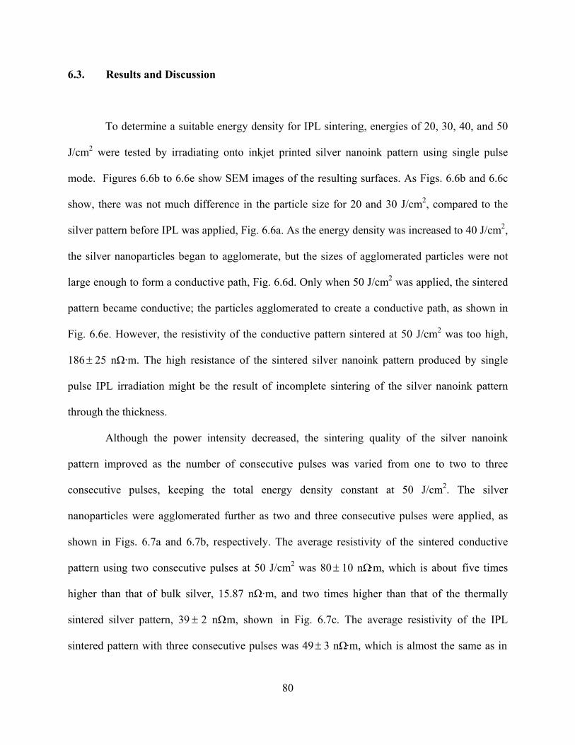
80
6.3. Results and Discussion
To determine a suitable energy density for IPL sintering, energies of 20, 30, 40, and 50
J/cm2 were tested by irradiating onto inkjet printed silver nanoink pattern using single pulse
mode. Figures 6.6b to 6.6e show SEM images of the resulting surfaces. As Figs. 6.6b and 6.6c
show, there was not much difference in the particle size for 20 and 30 J/cm2, compared to the
silver pattern before IPL was applied, Fig. 6.6a. As the energy density was increased to 40 J/cm2,
the silver nanoparticles began to agglomerate, but the sizes of agglomerated particles were not
large enough to form a conductive path, Fig. 6.6d. Only when 50 J/cm2 was applied, the sintered
pattern became conductive; the particles agglomerated to create a conductive path, as shown in
Fig. 6.6e. However, the resistivity of the conductive pattern sintered at 50 J/cm2 was too high,
186± 25 nΩ∙m. The high resistance of the sintered silver nanoink pattern produced by single
pulse IPL irradiation might be the result of incomplete sintering of the silver nanoink pattern
through the thickness.
Although the power intensity decreased, the sintering quality of the silver nanoink
pattern improved as the number of consecutive pulses was varied from one to two to three
consecutive pulses, keeping the total energy density constant at 50 J/cm2. The silver
nanoparticles were agglomerated further as two and three consecutive pulses were applied, as
shown in Figs. 6.7a and 6.7b, respectively. The average resistivity of the sintered conductive
pattern using two consecutive pulses at 50 J/cm2 was 80± 10 nΩ∙m, which is about five times
higher than that of bulk silver, 15.87 nΩ∙m, and two times higher than that of the thermally
sintered silver pattern, 39 ± 2 nΩ∙m, shown in Fig. 6.7c. The average resistivity of the IPL
sintered pattern with three consecutive pulses was 49± 3 nΩ∙m, which is almost the same as in

81
previous work by Kim et al.[9] on printed copper pattern, 50 nΩ∙m. The thermally sintered
pattern had better resistivity because the grain boundaries of silver nanoparticles grew and the
pattern became denser. The average thickness of the sintered patterns was 9.83 ± 2.00 μm).
Representative values of resistances, widths, lengths, thicknesses and resistivities of sintered
patterns are presented in Table 6.1, and resistivities are summarized in Fig. 6.8. Based on these
results, it was concluded that the silver nanoink patterns on polyimide films were fully sintered
with three consecutive pulses at 50 J/cm2; applying high energy for longer period of time was
more effective in sintering silver nanoink.
Moreover, XRD was used to show increasing grain size, as in Fig. 6.9. Three samples
were used for the comparison: before IPL sintering, after IPL sintering with three consecutive
pulses at 50 J/cm2 and thermally sintered samples. Before IPL was applied, XRD showed broad
and low-intensity peaks, which means that the silver nanoink pattern is in an amorphous phase.
However, after IPL was applied, XRD showed very sharp and high-intensity peaks. These sharp
peaks show that the silver nanoink pattern was sintered completely, becoming a crystalline
solid[11]. Figure 6.9 shows five characteristic peaks at 38.3°¸ 44.5°, 64.6°, 77.7°, and 81.6° for
the planar reflections of (111), (200), (220), (310), and (222), respectively. These characteristic
peaks confirmed that face-centered cubic silver had been obtained using IPL [12] Using Eq. 6-1,
the grain size of the printed silver nanoparticles was calculated to be 28.0± 8.1 nm, which is
within the range of silver nanoparticle size, 20 to 40 nm in diameter. After the three consecutive
IPL pulses, the grain size increased to 86.3± 7.2 nm. This increase in grain size shows that the
silver nanoparticles were melted during the application of IPL, and they were solidified after the
application of IPL. Also, the thermally sintered pattern had a larger grain size of 102.8± 5.2 nm,

82
as expected from the SEM images. FWHM and diffraction angles for these calculations are
presented in Table 6.2.
Adhesion between the electrode pattern and the substrate is important in printed
electronics. Therefore, peel testing using adhesive tape (Tape 810, 3M, US) was performed on
the silver patterns. The adhesive tape was firmly pressed onto the IPL sintered conductive
patterns, and was slowly peeled off from the patterns by hand at 150° to 160°. The silver patterns
that were applied with IPL for single and two consecutive pulses were easily peeled off with the
adhesive tape, as shown in Figs. 6.10a and 6.10b, respectively. However, the silver pattern on
which the three consecutive IPL pulses were applied was not peeled off, shown in Fig. 6.10c.
Therefore, it was concluded that the IPL sintered electrode pattern with three consecutive pulses
had a reliable bond to the substrate.
The sintering mechanism can be analyzed using a lumped capacitance model. The Biot
number for IPL sintering of silver nanoparticles can be calculated from the following equation:
Eq. 6-3
where h is the convective heat transfer coefficient of air, 15 W/m2∙K, r is the radius of the silver
nanoparticle, 30 nm, and k is the thermal conductivity of silver, 429 W/m∙K. As the Biot number
is much less than 0.1, the temperature increase in the silver nanoink pattern during the
application of IPL can be estimated using a lumped capacitance method as follows:
Eq. 6-4
total
m p m p
ETd C At d C t
ε∆ = =
3hrBik
=
83
where εtotal is the total net absorbed energy density, dm is the density of the nanoink, Cp is the
heat capacity of the nanoink, and t is the conductive pattern thickness. To calculate the absorbed
energy density, the applied energy density of IPL, 50 J/cm2, was broken down to specific energy
densities at different wavelengths, according to the graph shown in Fig. 6.4. Since the absorption
of silver is dependent on wavelength, ultraviolet-visible spectroscopy was used to determine the
absorbance of light at different wavelengths. In addition to the absorbance, the reflectance of the
silver nanoparticles is also an important factor to calculate the net absorbed energy. The
absorption peak of silver nanoink around 558 ± 4 nm is shown in Fig. 6.11. From 558 to 1000
nm, the absorbance decreased to 0.611 from 0.962. Also, Fig. 6.11 shows that the reflectance
increased from 0.80 to 0.95 as the wavelength increased from 380 to 1000 nm [13] Based on the
absorbance and reflectance, the absorbed energy density at each wavelength, λE , was calculated
using the following equation[14]:
Eq. 6-5
where λR is the reflectance, λI is the energy density, and λα is the absorbance of the silver
pattern at different wavelengths, λ.
The light energy density of wavelengths greater than 1000 nm is very small compared
with that of wavelengths less than 1000 nm. Therefore, the absorbed energy densities at different
wavelengths were summed over 380 to 1000 nm to obtain the total absorbed energy density, totalε ,
84
by applying IPL at 50 J/cm2 using the following equation:
Eq. 6-6
From the calculation above, the total energy absorbed by the silver nanoparticle layer was
calculated to be 2.267 J/cm2. In the calculation, all of the gradients in the dried silver nanoink
such as 30% diethylene glycol (DEG) and 70% silver nanoparticles by weight were considered.
Material properties used for this calculation are presented in Table 6.3. The heat capacity of the
silver nanoink layer was calculated to be 0.591 J/gK using the mixture rule[15]:
Eq.6-7
where C is the heat capacity and w is the weight percent. The subscripts D and Ag denote DEG
and silver nanoink, respectively.
Based on the calculated total absorbed energy and total heat capacity, the increase in
temperature of the silver nanoink pattern at 10 μm thickness was calculated to be 500°C during
the irradiation by IPL. This temperature increase was high enough to cause coalescence and
sintering of silver nanoparticles because as the size of a metallic particle decreases the melting
temperature decreases. As shown in Eq.2-2, the melting temperature can be decreased
dramatically by decreasing the size of the particles in the nano range. Through the differential
scanning calorimetry (DSC) shown in Fig. 6.12, the melting temperature of the silver nanoink
was found to be 194.1 ± 4.5°C which is defined as the onset temperature of the endothermic
peak[16]. This temperature is much lower than the temperature of printed pattern reached by IPL
irradiation, 525°C, obtained by summing the room temperature of 25°C and the increase in
p D D Ag AgC w C w C= +
85
temperature (500°C) by IPL irradiation at 50 J/cm2, calculated using Eq. 6-6. In addition,
according to Mackenzie and Shuttleworth,[17] the sintering temperature of a metal particle is
about 20% lower than its melting temperature at which the small particles agglomerate together
due to surface diffusion. Also, the average latent heat of fusion of the silver nanoparticles was
obtained as 12.8 ± 2.1 kJ/kg from three samples of silver nanoink. According to Zhao et al., [18]
the latent heat of fusion of silver nanoparticles can be as low as 10.29 kJ/kg, which is one-ninth
of the latent heat of fusion of the bulk silver, 88.0 kJ/kg. Therefore, silver nanoparticles were
adequately sintered by IPL irradiation to make a low-resistance conductive path, showing clearly
adhered junctions among the particles and grainy structure. (Figure 6.7b)
Moreover, according to Hong and Yeh [19] bismaleimide triazine resins are thermally
degraded by heating above 190°C. This temperature is lower than the melting temperature of our
silver nanoparticles. As expected, when the silver pattern on the GFRPC laminate was sintered at
200°C for 30 min, thermal degradation of GFRPC laminate was observed based on the color of
the GFRPC laminate, Fig. 6.13b. Compared with the original GFRPC laminate, Fig. 6.13a, the
GFRPC laminate with the silver nanoink pattern that was sintered at 200°C was blackened due to
thermal degradation. However, as Fig. 6.13c shows, the GFRPC laminate with the silver nanoink
pattern that was sintered by IPL at room temperature was degraded less than that of the thermal
sintered case, which is one of the strengths of IPL sintering. According to Kim et al., [9] the
GFRPC substrate was saved because it has much higher thermal capacity and mass than that of
the metal particle layer, and the IPL irradiation duration is less than 30 ms. Therefore, it could be
concluded that the IPL sintering technique can protect the substrate better than the conventional
thermal sintering process.
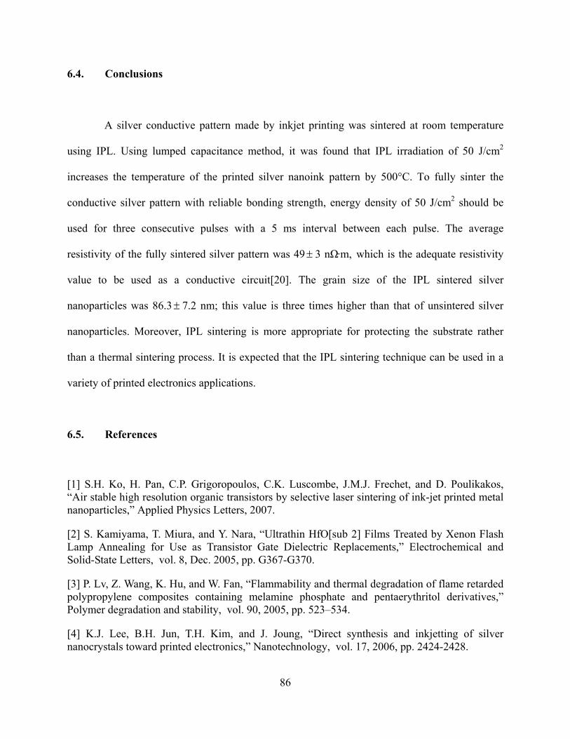
86
6.4. Conclusions
A silver conductive pattern made by inkjet printing was sintered at room temperature
using IPL. Using lumped capacitance method, it was found that IPL irradiation of 50 J/cm2
increases the temperature of the printed silver nanoink pattern by 500°C. To fully sinter the
conductive silver pattern with reliable bonding strength, energy density of 50 J/cm2 should be
used for three consecutive pulses with a 5 ms interval between each pulse. The average
resistivity of the fully sintered silver pattern was 49± 3 nΩ∙m, which is the adequate resistivity
value to be used as a conductive circuit[20]. The grain size of the IPL sintered silver
nanoparticles was 86.3± 7.2 nm; this value is three times higher than that of unsintered silver
nanoparticles. Moreover, IPL sintering is more appropriate for protecting the substrate rather
than a thermal sintering process. It is expected that the IPL sintering technique can be used in a
variety of printed electronics applications.
6.5. References
[1] S.H. Ko, H. Pan, C.P. Grigoropoulos, C.K. Luscombe, J.M.J. Frechet, and D. Poulikakos, “Air stable high resolution organic transistors by selective laser sintering of ink-jet printed metal nanoparticles,” Applied Physics Letters, 2007.
[2] S. Kamiyama, T. Miura, and Y. Nara, “Ultrathin HfO[sub 2] Films Treated by Xenon Flash Lamp Annealing for Use as Transistor Gate Dielectric Replacements,” Electrochemical and Solid-State Letters, vol. 8, Dec. 2005, pp. G367-G370.
[3] P. Lv, Z. Wang, K. Hu, and W. Fan, “Flammability and thermal degradation of flame retarded polypropylene composites containing melamine phosphate and pentaerythritol derivatives,” Polymer degradation and stability, vol. 90, 2005, pp. 523–534.
[4] K.J. Lee, B.H. Jun, T.H. Kim, and J. Joung, “Direct synthesis and inkjetting of silver nanocrystals toward printed electronics,” Nanotechnology, vol. 17, 2006, pp. 2424-2428.

87
[5] P. Buffat and J. Borel, “Size effect on the melting temperature of gold particles,” Physical Review A, vol. 13, Jun. 1976, pp. 2287-2298.
[6] M.K. Ghosh and K.L. Mittal, Polyimides: fundamentals and applications, CRC, 1996.
[7] PerkinElmer Optoelectronics 2009 High Performance Flash and Arc Lamps (Waltham, MA: Perkinelmer)
[8] D.J.T. Hill, F.A. Rasoul, J.S. Forsythe, J.H. O'Donnell, P.J. Pomery, G.A. George, P.R. Young, and J.W. Connell, “Effect of simulated low earth orbit radiation on polyimides (UV degradation study),” Journal of Applied Polymer Science, vol. 58, 1995, pp. 1847-1856.
[9] H. Kim, S.R. Dhage, D. Shim, and H.T. Hahn, “Intense pulsed light sintering of copper nanoink for printed electronics,” Applied Physics A, vol. 97, 2009, pp. 791-798.
[10] H.G. Jiang, M. Rühle, and E.J. Lavernia, “On the Applicability of the X-Ray Diffraction Line Profile Analysis in Extracting Grain Size and Microstrain in Nanocrystalline Materials,” Journal of Materials Research, vol. 14, 1999, pp. 549-559.
[11] B.E. Warren, X-ray Diffraction, Dover Pubns, 1990.
[12] E.A. Owen and G.I. Williams, “A low-temperature X-ray camera,” Journal of Scientific Instruments, vol. 31, 1954, pp. 49-54.
[13] M. Bass, Handbook of optics, McGraw-Hill, 2001.
[14] M.A. Al-Nimr and V.S. Arpaci, “Picosecond thermal pulses in thin metal films,” Journal of Applied Physics, vol. 85, 1999, p. 2517.
[15] W. Dimoplon, “Estimating specific-heat of liquid mixtures,” Chem. Eng, vol. 79, 1972, pp. 64–66.
[16] B.B. Sauer, W.G. Kampert, E. Neal Blanchard, S.A. Threefoot, and B.S. Hsiao, “Temperature modulated DSC studies of melting and recrystallization in polymers exhibiting multiple endotherms,” Polymer, vol. 41, 2000, pp. 1099–1108.
[17] J.K. Mackenzie and R. Shuttleworth, “A Phenomenological Theory of Sintering,” Proceedings of the Physical Society. Section B, vol. 62, 1949, pp. 833-852.
[18] S.J. Zhao, S.Q. Wang, D.Y. Cheng, and H.Q. Ye, “Three Distinctive Melting Mechanisms in Isolated Nanoparticles,” J. Phys. Chem. B, vol. 105, Dec. 2011, pp. 12857-12860.
[19] S.G. Hong and C.S. Yeh, “The effects of copper oxides on the thermal degradation of bismaleimide triazine prepreg,” Polymer degradation and stability, vol. 83, 2004, pp. 529–537.
[20] V. Subramanian, P. Chang, D. Huang, J. Lee, S. Molesa, D. Redinger, S. Volkman, VLSI Design held jointly with 5th International Conference on Embedded Systems and Design., 19th International Conference on, 6 (2006)
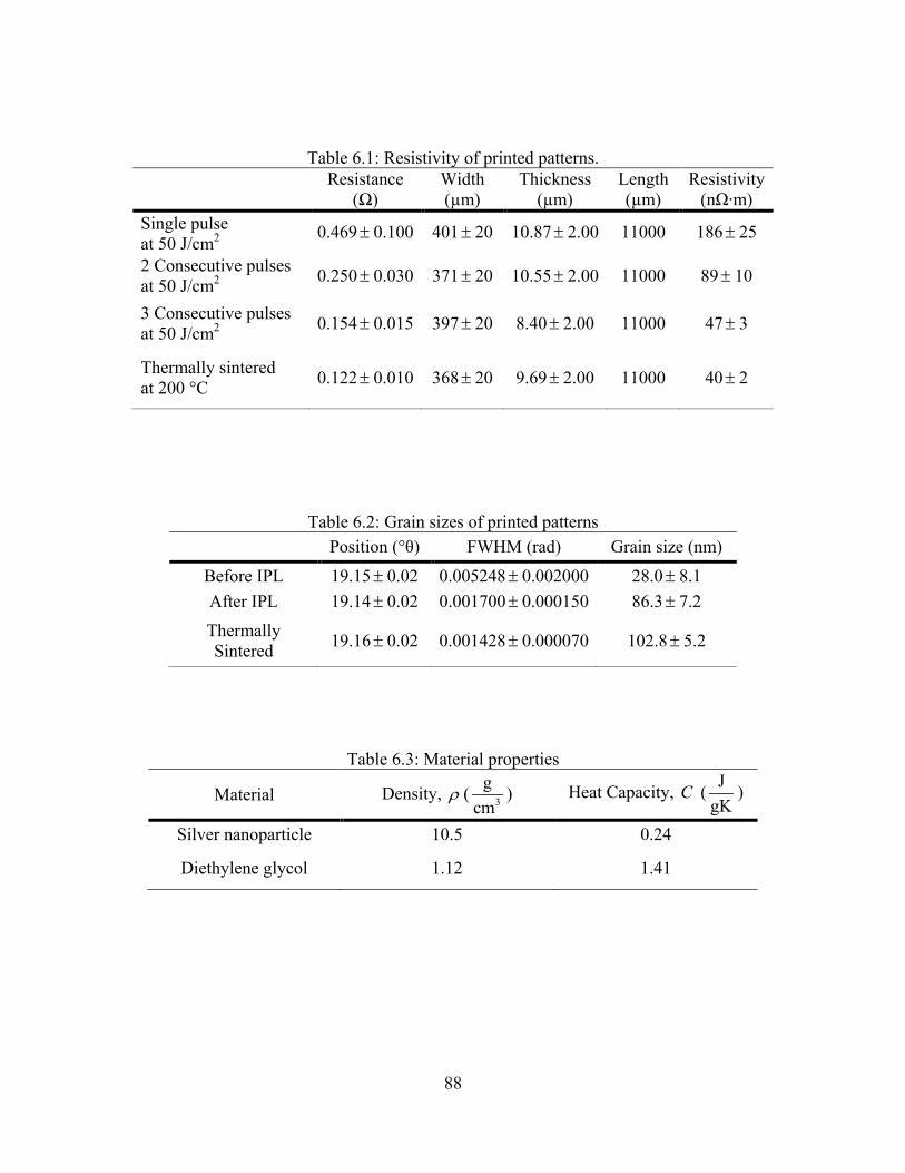
88
Table 6.1: Resistivity of printed patterns.
Resistance (Ω)
Width (µm)
Thickness (µm)
Length (µm)
Resistivity (nΩ∙m)
Single pulse at 50 J/cm2 0.469± 0.100 401± 20 10.87± 2.00 11000 186± 25
2 Consecutive pulses at 50 J/cm2 0.250± 0.030 371± 20 10.55± 2.00 11000 89± 10
3 Consecutive pulses at 50 J/cm2 0.154± 0.015 397± 20 8.40± 2.00 11000 47± 3
Thermally sintered at 200 °C 0.122± 0.010 368± 20 9.69± 2.00 11000 40± 2
Table 6.2: Grain sizes of printed patterns Position (°θ) FWHM (rad) Grain size (nm)
Before IPL 19.15± 0.02 0.005248± 0.002000 28.0± 8.1 After IPL 19.14± 0.02 0.001700± 0.000150 86.3± 7.2 Thermally Sintered 19.16± 0.02 0.001428± 0.000070 102.8± 5.2
Table 6.3: Material properties
Material Density, ρ ( 3
gcm
) Heat Capacity, C ( JgK
)
Silver nanoparticle 10.5 0.24
Diethylene glycol 1.12 1.41
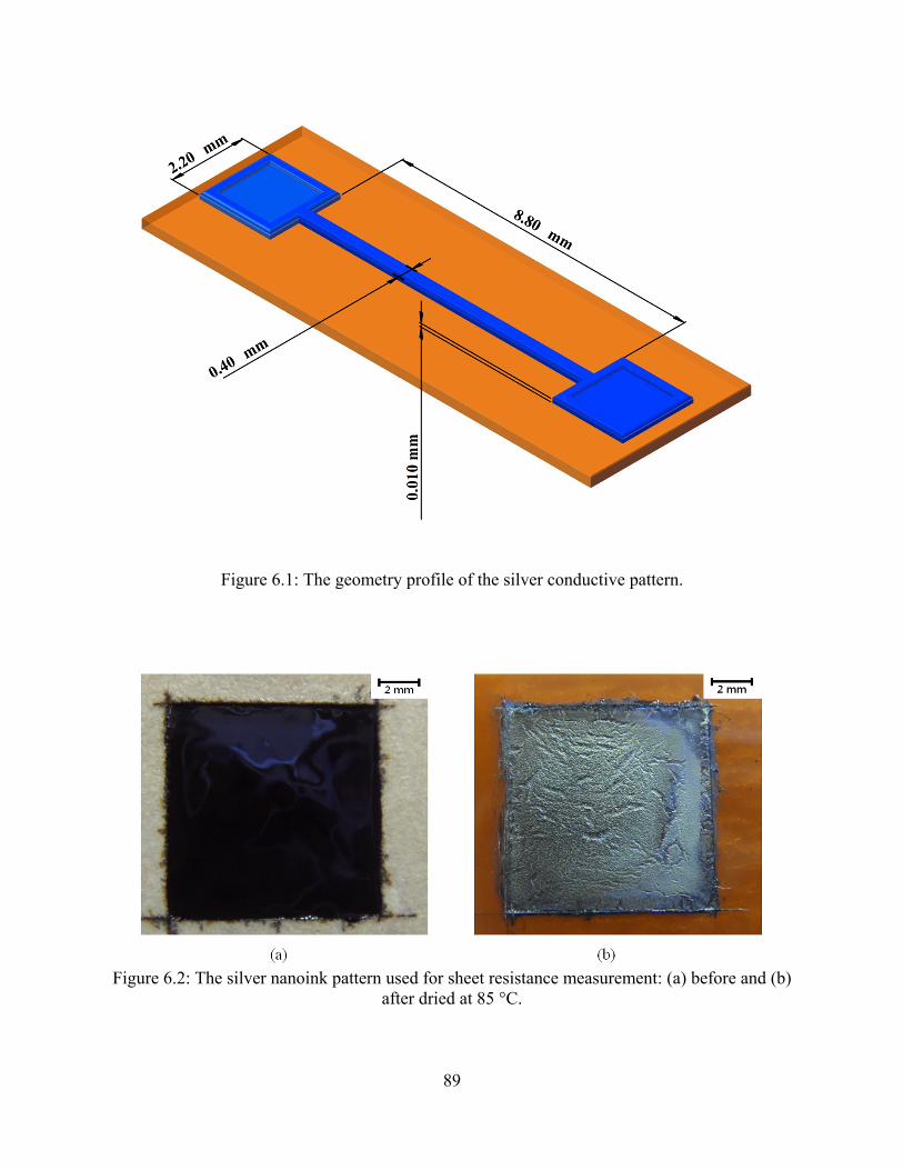
89
Figure 6.1: The geometry profile of the silver conductive pattern.
Figure 6.2: The silver nanoink pattern used for sheet resistance measurement: (a) before and (b)
after dried at 85 °C.
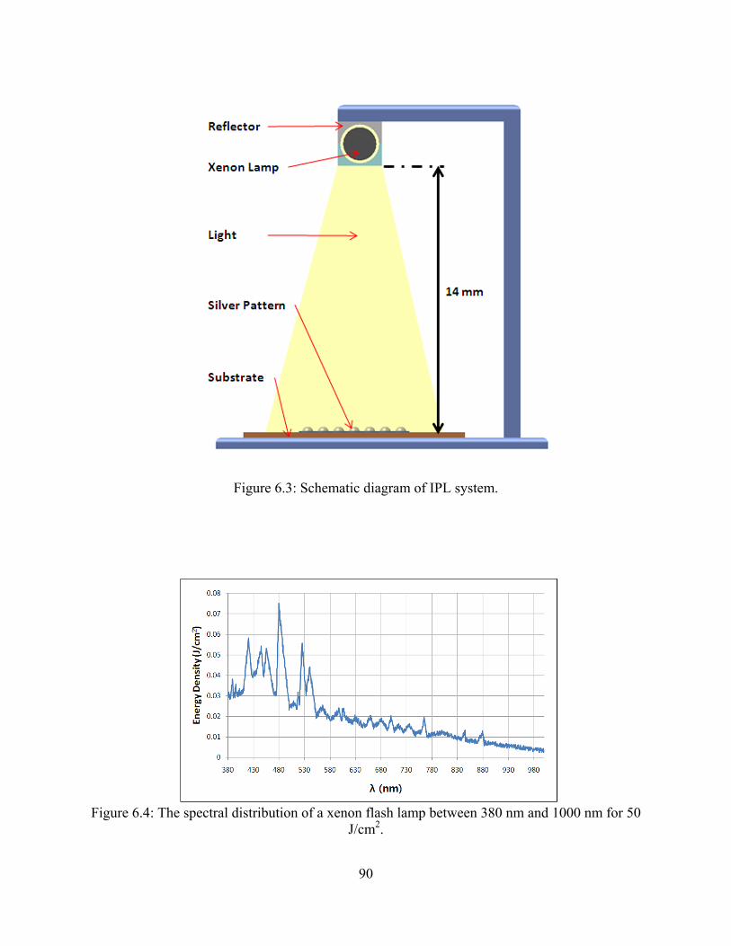
90
Figure 6.3: Schematic diagram of IPL system.
Figure 6.4: The spectral distribution of a xenon flash lamp between 380 nm and 1000 nm for 50
J/cm2.
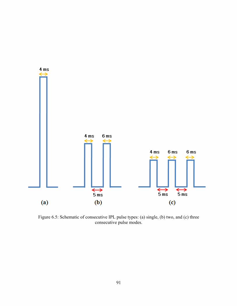
91
Figure 6.5: Schematic of consecutive IPL pulse types: (a) single, (b) two, and (c) three consecutive pulse modes.
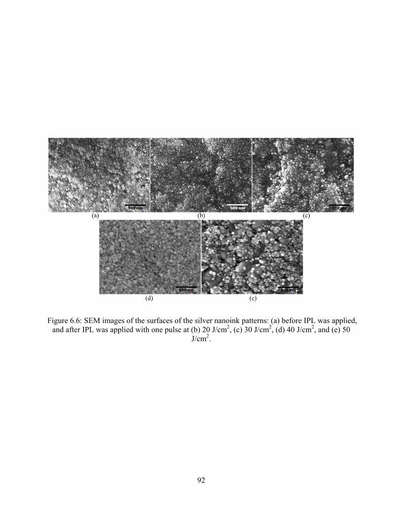
92
Figure 6.6: SEM images of the surfaces of the silver nanoink patterns: (a) before IPL was applied,
and after IPL was applied with one pulse at (b) 20 J/cm2, (c) 30 J/cm2, (d) 40 J/cm2, and (e) 50 J/cm2.
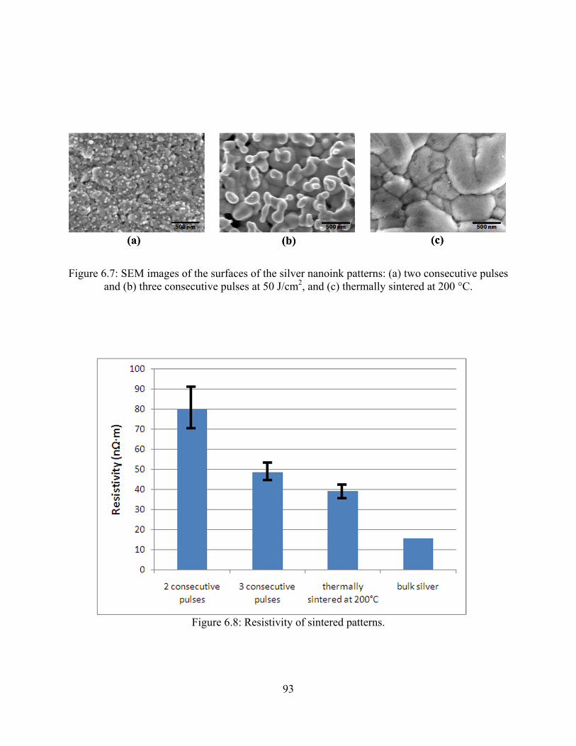
93
Figure 6.7: SEM images of the surfaces of the silver nanoink patterns: (a) two consecutive pulses
and (b) three consecutive pulses at 50 J/cm2, and (c) thermally sintered at 200 °C.
Figure 6.8: Resistivity of sintered patterns.
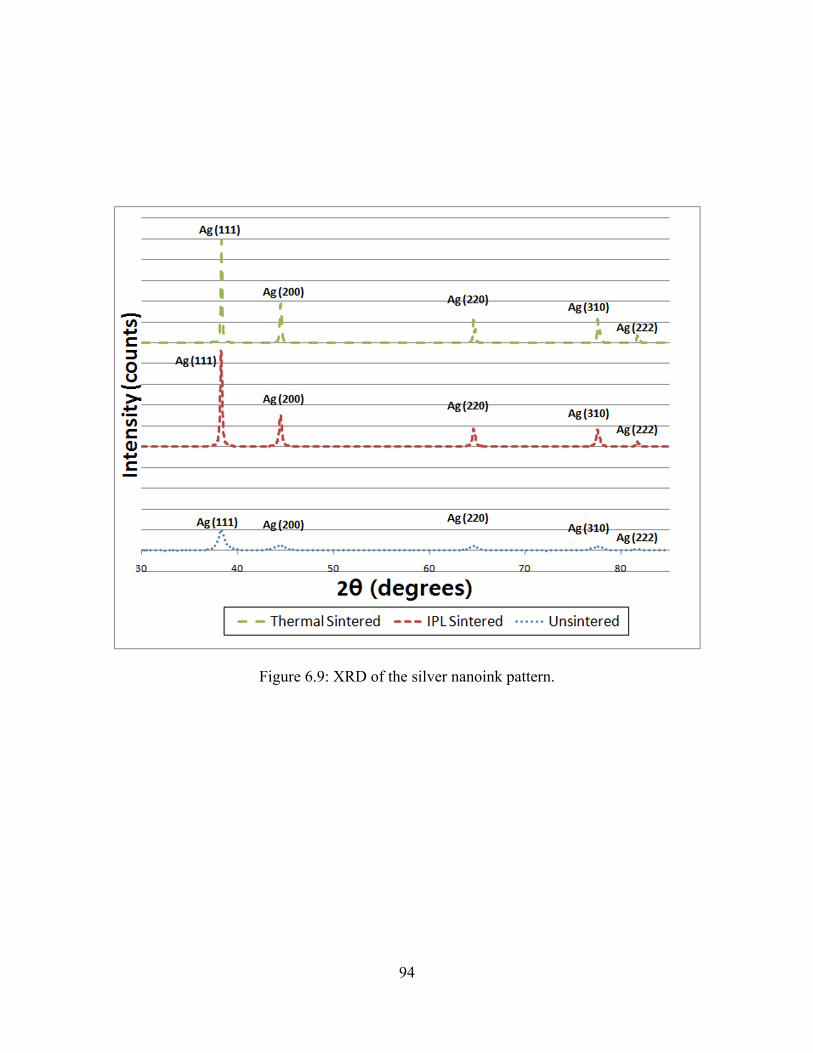
94
Figure 6.9: XRD of the silver nanoink pattern.
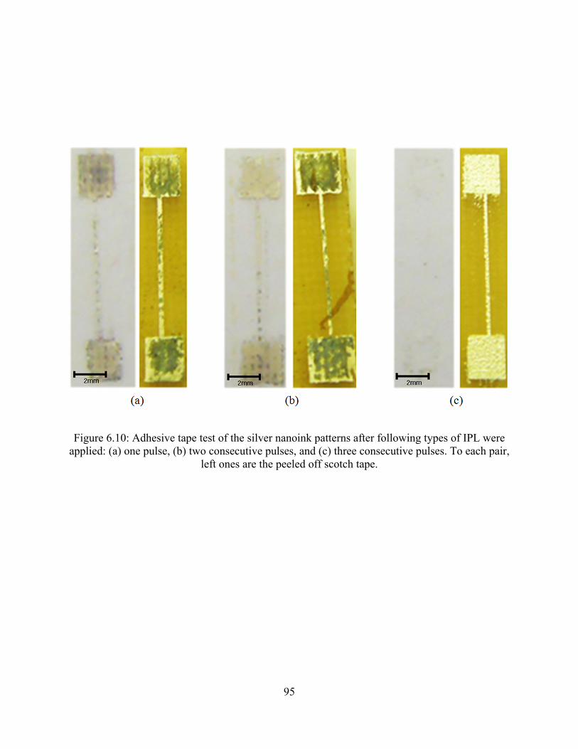
95
Figure 6.10: Adhesive tape test of the silver nanoink patterns after following types of IPL were
applied: (a) one pulse, (b) two consecutive pulses, and (c) three consecutive pulses. To each pair, left ones are the peeled off scotch tape.
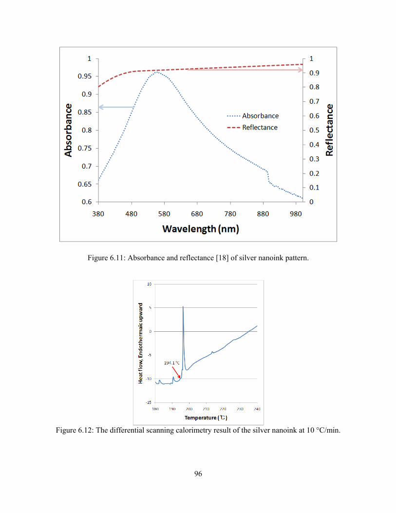
96
Figure 6.11: Absorbance and reflectance [18] of silver nanoink pattern.
Figure 6.12: The differential scanning calorimetry result of the silver nanoink at 10 °C/min.
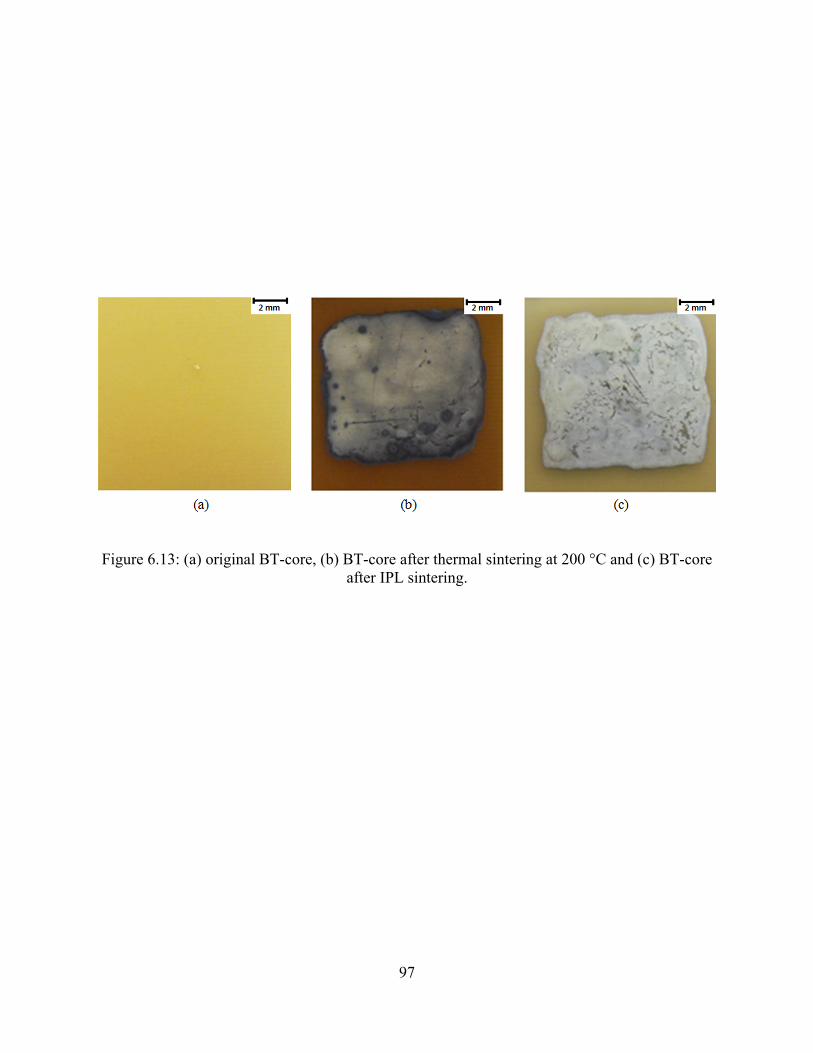
97
Figure 6.13: (a) original BT-core, (b) BT-core after thermal sintering at 200 °C and (c) BT-core
after IPL sintering.
98
CHAPTER SEVEN
Concluding Remarks
7.1. Current Research Accomplishments
A multifunctional composite laminate which can harvest and store a solar energy was
developed and investigated in this study. The integration of active components onto a carbon
fiber reinforced polymer composite laminate was done by using printed electrodes. First, the
optimal thickness for making reliable printed electrodes were studied. Then, different kinds of
solar cells and batteries were studied under various mechanical and environmental conditions.
Lastly, novel sintering process was developed and analyzed to facilitate a manufacturing process
and to save a polymeric substrate. The specific findings, results and accomplishments are
summarized as follows:
(1) Copper electrodes were printed on composite laminates by inkjet printing and thermal
sintering. To reduce the amount of cracks, the range of particle size should be reduced as
much as possible because the cracks on surface are mainly caused by having different sizes
of particles.
(2) To have good quality of printed electrode, number of printing should not be large because
when the thickness of a printed copper electrode become larger than 5.3 µm, cracks of
printed electrodes grow. Low resistivity of 36.7 nΩ∙m has been reached by printing 5-times.
99
(3) α-Si solar cells can endure various mechanical loadings including but not limit to the fully
reversed flexural fatigue at 0.32% strain at least up to 100 cycles without degradation on their
performance.
(4) c-Si solar cells are too brittle to be directly integrated onto a CFRP composite laminate using
printed electronics because a tensile failure occurs below 0.2% tensile strain.
(5) The printed electrodes remained fully functional up to the maximum applied strain of 1%
when they were 4 μm thick.
(6) A power laminate has been fabricated by first mounting a thin-film solar module and a thin-
film battery on a BT core and then co-curing the resulting assembly with a graphite/epoxy
composite laminate. A conducting circuit to connect the solar cell and the battery printed on a
BT core.
(7) The Li-ion polymer battery was able to achieve 100% depth of discharge at a low
temperature of -27 °C under 1/12 C-rate. Under tensile loadings, these batteries were able to
endure tensile strain up to 1.7% without a degradation on its performance.
(8) A silver conductive pattern made by an inkjet printing was sintered at a room temperature
using IPL in an ambient condition. Using the lumped capacitance method, it was found that
IPL irradiation of 50 J/cm2 in a three consecutive pulse mode increases the temperature of the
printed silver nanoink pattern by 500°C.
(9) IPL sintering is more appropriate for protecting the polymeric substrate rather than a
conventional thermal sintering process because polymer matrix degrades during thermal
sintering. Average resistivity of the fully sintered silver pattern by IPL was 49± 3 nΩ∙m.

100
7.2. Recommendations for Further Work
7.2.1. Free Standing Integration
The final goal in this research is to integrate energy harvest/storage components with
load bearing structures. However, a battery can show better performance it is disassociated from
a mechanical loading. Therefore, a new device packaging concept should be developed, which
reduces stress distribution on a battery or solar cell by not attaching it to a composite itself, hence
the name “free-standing”. A thin, transparent, flexible polymer film or adhesive is overlaid onto a
battery or solar cell and attached to a composite substrate.
7.2.2. Synthesis of Carbon Nanotube using IPL
IPL can be used to apply an intense heat in any environment. There many different
methods of making carbon nanotubes (CNTs), but using IPL will reduce a manufacturing time.
Proposed methods are as follows: The environment should be an inert environment by flowing
Argon at a fixed flow rate of 0.00000167 m3/s. The source of a carbon is an activated carbon
fiber (ACF) because it has very large surface area with many pores and has high adsorptivity.
Before irradiating ACF surface with IPL, ACF should go through impregnation process of an
iron or nickel, which acts as an catalyst. The impregnation can be done by immersing ACF in an
aqueous solution of iron(III)chloride hexahydrate (FeCl3·6H2O), then hydroxylamine
hydrochloride (NH2OH ·HCl) should be added to reduce iron. The impregnated ACF should be
dried in an oven, and IPL can be applied after it is dried. In this process, a carbon nanotube could
be produced by CO disproportionation (the Boudouard reaction)[1,2]. The successful growth of a

101
carbon nanotube on ACF will lead to development of a fuel cell electrode material because an
ACF with carbon nanotubes should be light, highly conductive, porous, and stable.
7.3. References
[1] Nikolaev, M.J. Bronikowski, R.K. Bradley, F. Rohmund, D.T. Colbert, K.A. Smith, and R.E. Smalley, “Gas-phase catalytic growth of single-walled carbon nanotubes from carbon monoxide,” Chemical Physics Letters, vol. 313, 1999, pp. 91–97
[2] C.A. Fyfe, M.S. McKinnon, A. Rudin, and W.J. Tchir, “Investigation of the mechanism of the thermal decomposition of cured phenolic resins by high-resolution carbon-13 CP/MAS solid-state NMR spectroscopy,” Macromolecules, vol. 16, 1983, pp. 1216–1219