Improved Sufur/Lithium Suflide Nano-composite Electrodes for Next-Generation Lithium Cells
Upload
independentCategory
view
1download
0
(This is a sample cover image for this issue. The actual cover is not yet available at this time.)
This article appeared in a journal published by Elsevier. The attachedcopy is furnished to the author for internal non-commercial researchand education use, including for instruction at the authors institution
and sharing with colleagues.
Other uses, including reproduction and distribution, or selling orlicensing copies, or posting to personal, institutional or third party
websites are prohibited.
In most cases authors are permitted to post their version of thearticle (e.g. in Word or Tex form) to their personal website orinstitutional repository. Authors requiring further information
regarding Elsevier’s archiving and manuscript policies areencouraged to visit:
http://www.elsevier.com/copyright

Author's personal copy
Non-aqueous electrodeposition of porous tin-based film as an anodefor lithium-ion battery
C.D. Gu*, Y.J. Mai, J.P. Zhou, Y.H. You, J.P. TuState Key Laboratory of Silicon Materials and Department of Materials Science and Engineering, Zhejiang University, Hangzhou 310027, China
h i g h l i g h t s g r a p h i c a l a b s t r a c t
< Porous tin-based film with double-layer structure, i.e. SnO2/SneCu.
< Tin-based film electrodepositedfrom Ethaline based electrolyte.
< Self-assembly distribution con-structing an open and bicontinuousporous Sn network.
< Double-layer tin-based film deliv-ering a satisfactory Li ion storagecapacity.
a r t i c l e i n f o
Article history:Received 9 December 2011Received in revised form23 February 2012Accepted 26 April 2012Available online 6 May 2012
Keywords:Ionic liquidElectrodepositionTinLithium-ion batteries
a b s t r a c t
Porous tin-based films are electrodeposited on copper foils from a choline chloride/ethylene glycol basedelectrolyte containing SnCl2$2H2O without any complexing agent or additive. Increasing the depositiontime and voltage produces thicker films. The initially deposited Sn grains are relatively uniform with anaverage size of 200e300 nm and a kind of self-assembly distribution constructing an open and bicon-tinuous porous network. The architecture of these films possesses a double-layer structure, i.e. SnO2
(superficial layer)/SneCu alloy (bottom layer), which is revealed by X-ray diffractometer and X-rayphotoelectron spectroscopy. The electrochemical performance of the porous tin-based films as anode forlithium-ion batteries is measured. Although the capacity fades gradually with repeated cycling,a reversible capacity of 300-350 mAh g�1 is maintained for more than 50 cycles, which suggests that thein situ formed Sn–Cu alloy could provide an interlocking interface between active materials and currentcollector. Therefore, the tin’s shedding from the current collector can be restrained. Moreover, theinactive materials, such as the oxide in the superficial layer and the Cu in the bottom layer, could also actas buffers to relieve the induced volume expansion of Sn during the repeated lithiathion/delithiationprocess, thus giving the good cycle performances.
� 2012 Elsevier B.V. All rights reserved.
1. Introduction
As for the current commercial rechargeable lithium-ionbatteries, carbonaceous materials are the most commonly usedanode materials due to their low cost and low electrochemicalpotentials with respect to lithiummetal [1e3]. However, since their
theoretical capacity is only 372 mAh g�1, there are demands todevelop new anode materials with higher capacity to enhance theenergy density of lithium-ion batteries as a power supply forportable electric devices and electric vehicles. Tin-based materialshave been focused on because their capacity (994 mAh g�1, thetheoretical limit of Li4.4Sn) largely exceeds that of graphite [4e6].However, severe volume expansion in the pure tin anode wouldoccur due to lithiation/delithiation process during charge-discharge cycles, which causes poor cycle performance andinhibits its application in lithium-ion batteries [7,8]. Therefore, tin
* Corresponding author. Tel./fax: þ86 571 87952573.E-mail addresses: [email protected], [email protected] (C.D. Gu).
Contents lists available at SciVerse ScienceDirect
Journal of Power Sources
journal homepage: www.elsevier .com/locate/ jpowsour
0378-7753/$ e see front matter � 2012 Elsevier B.V. All rights reserved.doi:10.1016/j.jpowsour.2012.04.085
Journal of Power Sources 214 (2012) 200e207
Author's personal copy
oxides [9e14] or tin-based alloys (for example, SneZn [15], SneSb[16,17], SneCo [18], and SneCu [5,19e21]) have been attractedmuch more attentions due to their better cyclability than pure tinbecause of the inactive elements in the oxides or alloy buffervolume changes during charge/discharge cycling.
In order to enhance the cyclability of tin-based active materials,a good electronic conductivity among the active materials and atthe interface between them and the current collector is desirable[5]. Electrodeposition is a versatile bottom-up processing methodthat can be used to deposit metals, ceramics, polymers, and semi-conductors in a wide range of microstructures and nanostructures.The method is inexpensive and relatively simple, and especially itcan support a good interface strength and electronic conductivitybetween the coatingmetals and the substrate. The electrodepositedCu6Sn5 film is one of the most promising anode materials becauseof its low price, high conductivity, and good retention of capacity[5,19,20]. However, the usual procedure of Sn or Sn-based alloyselectrodeposition is mostly based on aqueous solutions of whichthere are limitations including the poisonous plating baths, thenecessity for complexing agents and additives, and the difficulthandling of hydrogen evolution processes [5,19,20]. Room-temperature ionic liquids aremore advantageous green solvents forthe electrodeposition of metals due to their wide electrochemicalwindows, extremely low vapour pressures, and numerous, onlypartly understood, cation/anion effects [22e24]. Sn or Sn-basedalloys have been successfully electrodeposited from ionic liquids[25e29]. Moreover, the macroporous Sn was direct electro-deposited from a water- and air-stable room-temperature ionicliquid, namely, 1-ethyl-3-methylimidazolium-dicyanamide [26].The porous Sn or Sn-based alloy would be a good anode candidatefor the lithium-ion batteries because the porous structure couldrelieve the anode of the severe volume expansion in the lithiation/delithiation process.
Recently, we have demonstrated that nanoporous Ag films oncopper alloy substrates could be fabricated by the galvanicreplacement reaction from the mixture (1:2 mol ratio) of choline
chloride/ethylene glycol (Ethaline) containing AgCl [30]. It wassuggested that the viscous Ethaline might be the soft template forthe formation of nanoporous Ag deposits [30]. Ethaline, one oftypical deep eutectic solvents with non-aggressive nature inventedby Abbott and co-workers [31] is a promising solvent used for thedeposition of a range of metal films, for example, Zn, Sn, and Cu, athigh current efficiency [28,32,33]. However, the electrodepositionof porous Sn-based films from the non-aggressive ethaline have notbeen explored. Based on this thought, this paper investigates thefacile electrodeposition of porous Sn films from the Ethaline basedelectrolyte and their microstructure and lithium storage perfor-mance. Importantly, it is found that the composition of the as-deposited Sn films is SnO2/SneCu alloy double-layer structureexhibiting a good electrochemical performance during the cycledlithiation/delithiation process.
2. Experimental
2.1. Electrodeposition and characterization of the porous tin-basedanode
Choline chloride (AR, Aladdin) and ethylene glycol (AR, Aladdin)were used as received. The homogeneous colorless Ethaline wasformed by stirring the mixture of the two components in a molratio of 1 choline chloride : 2 ethylene glycol at 80 �C for about30 min. The electrolyte is the Ethaline solution containing 0.1 MSnCl2$2H2O. The substrate was the copper foil with a thickness ofabout 0.03 mm, which was served as the current collector for theanode in lithium-ion batteries. A surface cleaning treatment of thesubstrate was conducted to remove the industrial oil by electrolyticdegreasing and deionized water rinsing. Before the electroplatingprocess, the substrate was dried with flowing air. The porous tin-based film was direct-current electroplated from the above elec-trolyte bath at variable applied voltages and ambient temperature(25 � 3 �C) without the deaeration process. During the electrode-position process, the anode consisted in a tin plate. The final
Fig. 1. Surface morphologies of as-deposited Sn-based films at 0.5 V for different deposition time. (a) 2 min; (b) 5 min; (c) 10 min; (d) 15 min. Insets are the correspondingmagnified SEM pictures.
C.D. Gu et al. / Journal of Power Sources 214 (2012) 200e207 201

Author's personal copy
deposits were sequentially rinsed with methanol and deionizedwater.
A field emission scanning electron microscope (FE-SEM, HitachiS-4800) was employed for the observations of the film surface andan energy dispersive X-ray spectrometer (EDS) attached was usedfor qualitative elemental chemical analysis. Crystalline structure ofthe deposits was studied by X-ray diffractometer (XRD, Rigaku D/max 2550PC, Japan) with a Cu target (l ¼ 1.54056 Å) and a mono-chronmator at 40 kV and 250 mA with the scanning rate and stepbeing 4� min�1 and 0.02�, respectively. X-ray photoelectron spec-troscopy (XPS, AXIS UTLTRADLD) was used to characterize thecomposition and chemical state of the product using Al (mono-chromatic) Ka radiation with E ¼ 1486.6 eV. All core-level spectrawere referenced to the C 1 s peak at 284.8 eV assumed to originatefrom the surface hydrocarbon contamination. The compositiondepth profile of the film was analyzed by combining a sequence ofion gun etch cycles (etching ratew5e6 nmmin�1) interleaved withXPS measurements.
2.2. Electrochemical measurements of the porous tin-based anode
Electrochemical performances of the electrodeposited tin-basedanodes were investigated with two-electrode coin-type cells (CR2025) assembled in an argon-filled glove box with the metalliclithium foil as both the reference and counter electrodes, 1 M LiPF6in ethylene carbonate (EC)-dimethyl carbonate (DME) (1:1 involume) as the electrolyte, and a polypropylene (PP) micro-porousfilm (Cellgard 2300) as the separator. Charge-discharge tests wereconducted on LAND battery program-control test system between0.05 and 3.0 V at a rate of 100 mA g�1. Cyclic voltammetry (CV) wasperformed on CHI660C electrochemical workstation in the poten-tial ranges of 0.02e3.0 V at a scan rate of 0.1 mV s�1.
3. Results and discussion
3.1. Surface morphology
Fig. 1 gives the deposition time-dependent surface morphol-ogies of the electrodeposited Sn films from the Ethaline basedelectrolyte at 0.5 V. After 2 min deposition, the substrate wascovered by the netlike Sn deposits as shown in Fig. 1a. It is foundthat the initially deposited Sn grains are relatively uniformwith anaverage size of 200e300 nm and a kind of self-assembly distribu-tion. The connected Sn grains construct an open and bicontinuousporous network between them with the pore size in the range of30e40 nm. It is also found that a few larger Sn grains with the sizeof about 1 mm are randomly distributed in the Sn network, whichmay be due to the preferential growth of deposits in the currentconvergence area of the substrate. When prolonging the depositiontime to 5 min, the size of netlike Sn grains increase to about500e700 nm, as shown in Fig. 1b. However, the pores betweengrains still exist and retain the size of about 20e30 nm. At thedeposition times of 10 and 15 min, grains are ready to connect eachother at the expense of pores as shown in Fig. 1c and d. It can beseen that at 0.5 V with increasing the deposition time, the filmdensity is accordingly increased. However, pores still exist in thefilm obtained from the Ethaline based electrolyte, which is largelydifferent from the Sn-based film electrodeposited from the aqueouselectrolyte with a dense microstructure [19,20]. Fig. 2 gives thesurface morphologies of the electrodeposited Sn films from theEthaline based electrolyte at 0.7 V for 5 (a) and 15 min (b),respectively. After 5 min deposition, the Sn film obtained at 0.7 Vhas a similar surface morphology with those obtained at 0.5 V (seeFig. 1). However, with prolonging the deposition time to 15 min,a rougher surface is obtained at 0.7 V, where plenty of cone-like Sn
grains with the size of about 1 mm randomly grow on the surfaceleaving much more pores in the films.
Fig. 3a and d give typical cross-section morphologies of theelectrodeposited Sn films at 0.7 V for 5 min and for 15 min,respectively, fromwhich it can be seen that the Sn films are tightlyadhered to the brass substrate. With the EDS mapping analysis ofelements Sn (such as Fig. 3b and e) and Cu (such as Fig. 3c and f), thethickness values of the electrodeposited films can be roughlydetermined and are summarized in Table 1. It is indicated thatincreasing the deposition time and voltage would produce thickerfilms. However, the film thickness seems not to be uniform, whichshould be related to the porous structure of the films.
3.2. Crystal structure and composition
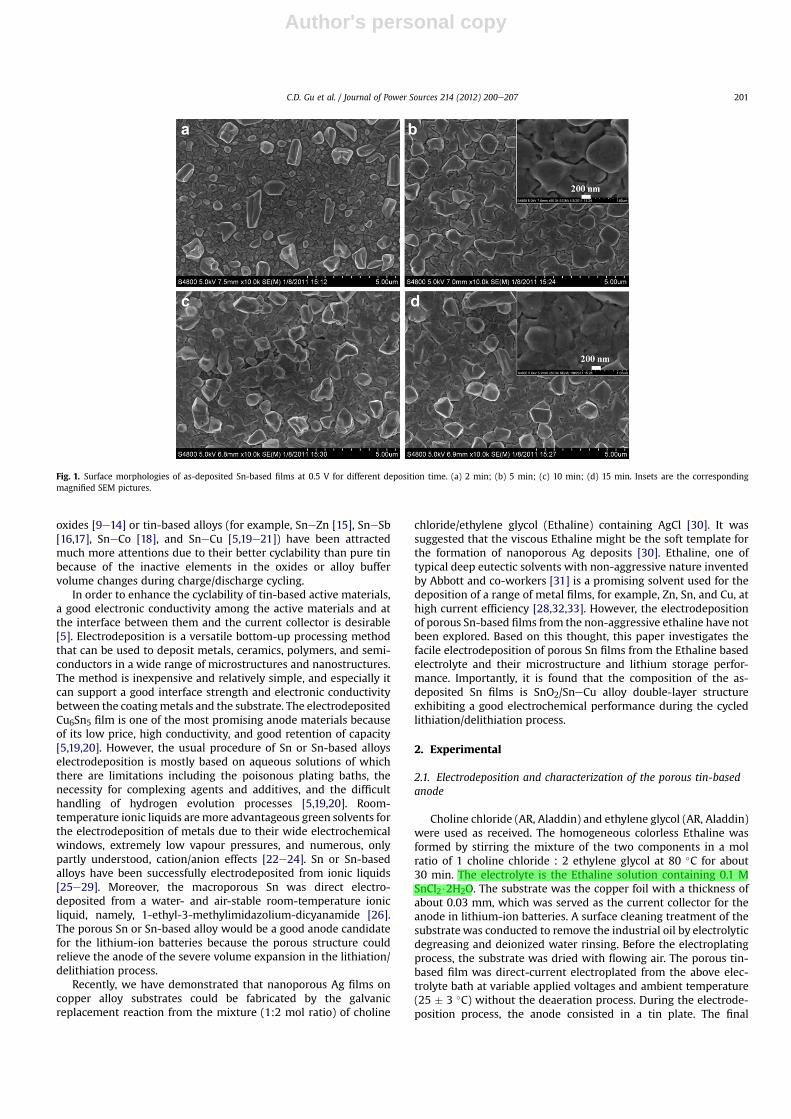
Fig. 4 gives the typical XRD patterns of the electrodeposited Snfilms on the copper substrate at 0.5 V and 0.7 V, respectively. InFig. 4, the peaks at 43.3�, 50.4�, and 74.1� are assigned to the face-centered cubic (fcc) Cu substrate planes of (111), (200), and (220),respectively. The other peaks should be attributed to the Sn films,which indicates the presence of two basic phases in both Sn filmsshown in Fig. 4: the b-Sn (JCPDS 04-0673) and Cu6Sn5 (JCPDS 02-0713). The weak peak at 30.2� is assigned to (101) plane of Cu6Sn5phase. The in situ formation of Cu6Sn5 layer can be attributed to themutual diffusion of the Sn and Cu atoms. Du et al. also found that
Fig. 2. Surface morphologies of as-deposited Sn-based films at 0.7 V for (a) 5 min and(b) 15 min, respectively. Insets are the corresponding magnified SEM pictures.
C.D. Gu et al. / Journal of Power Sources 214 (2012) 200e207202

Author's personal copy
the Cu6Sn5 layer was formed in the electroless plating Sn on thecopper foam [20]. The study of Tamura et al. indicated the elec-trodeposition process of tin on copper without heat treatmentscould form a slight Cu6Sn5 intermetallic compound layer at theinterface between tin and copper [5]. As for the lithium batteries,the formation of Cu6Sn5 layer could enhance the bonding forcebetween active materials and current collector, which restrainstin’s shedding from the current collector and leads to good cyclingperformance [5,20].
The XPS analysis is carried out to investigate the surface struc-ture of the Sn film as shown in Fig. 2, and the corresponding resultsare shown in Fig. 5. The binding energies in the XPS spectra arecalibrated by using that of C 1 s (284.8 eV). All peaks in the XPS fullspectrum shown in Fig. 5a can be ascribed to Sn, C, and O elements.The presence of C comes mainly from pump oil in the vacuumsystem of the XPS equipment. The presence of O implies that tinoxide layer should be formed on the film’s surface. The high-reso-lution spectra for Sn is shown in Fig. 5b, where the two main peakscentered at 486.2 and 494.7 eV can be assigned to Sn 2d5/2 and Sn3d3/2 for SnO2, respectively. There are two small satellite peaks canbe found at 484 and 492.5 eV, respectively, which might beassigned to the pure Sn. The XPS result of Fig. 5b indicates thatsmall amount of SnO2 forms the top surface layer of the
electrodeposited Sn films. The architectures of the electrodepositedSn films are further illustrated by the XPS composition depth profileas shown in Fig. 5c and d. The atomic concentrations of Cu, O, Snand C as themain elements in the films show variations throughoutthe film thickness. As shown in Fig. 5c for the film obtained at 0.7 Vfor 5 min, the atomic concentration ratio of O/Sn is nearly 2 at thefirst 60 s of sputter time, which should be responsible for the thinSnO2 layer on the film surface. However, the concentration of Orapidly decreases to about 0 after about 180 s of etching. Accord-ingly, the Sn concentration increases to the maximum value at thesputter time of 120 s. Then, the concentration of Sn decreasesgradually accompanied with the gradually increasing of the atomicconcentration of Cu, which should correspond to the Cu6Sn5 tran-sition layer at the interface of the film and the substrate. Based onthe result of XRD (Fig. 4) and XPS (Fig. 5c) measurements, it can beseen that the electrodeposited porous film possesses double-layerarchitecture, i.e. SnO2/SneCu alloy from the top layer to thebottom layer. For comparison, the XPS composition depth profile ofthe film obtained at 0.7 V for 15 min is presented in Fig. 5d, fromwhich the double-layer structure of the porous Sn-based film isfurther proved. Moreover, after the same etching duration, theatomic concentration of Sn in the film still holds around 30%, whichindicates that the double-layer film obtained at 0.7 V for 15 min is
Fig. 3. Typical cross-section morphology and EDS mapping analysis of the electrodeposited Sn-based films at 0.7 V for 5 min (a, b, and c) and at 0.7 V for 15 min (d, e, and f).
C.D. Gu et al. / Journal of Power Sources 214 (2012) 200e207 203
Author's personal copy
much thicker than that obtained at 0.7 V for 5 min. Furthermore, inthe double-layer film the thickness of bottom layer (SneCu alloy) ismuch higher than that of the top layer (SnO2). The SneCu layerconstructs the interlocking interface between the film and thesubstrate, which is believed to support good interface strength.
3.3. Electrochemical performance
The porous Sn-based films with double-layer architecture ofSnO2/SneCu alloy are expected to deliver good electrochemicalperformances as potential anodes in lithium batteries due to theircomposite characteristic and porous structures. The typical lithiuminsertion/extraction profiles of the electrodeposited Sn-based filmobtained at 0.7 V for 15 min at a current density of 100 mA g�1 aredemonstrated in Fig. 6, in which the voltage window is fixed from0.05 to 3.0 V. In the first discharging process, the potential dropsrapidly to a small plateau of about 0.6 V, and then decreasesgradually to a large plateau of about 0.4 V. Lastly, the potentialfurther gradually decreases to the stop potential of w0.05 V. Theplateau around 0.6 V should correspond to the irreversible reactionof top SnO2 layer with lithium to form Li2O and Sn [11,34] and the
formation of the solid electrolyte interface (SEI) layers [9,35], whichalmost disappears in the following cycles as shown in Fig. 6. Theinactive Li2O disperses in the top layer of the Sn-based film, whichcould relieve the volume changes during the following charge/discharge cycling. The plateau around 0.4 V should be attributed tothe Li intercalation process of Sn and Cu6Sn5 compositions [5,36],which corresponds to the formation of Li2CuSn phase and the endproduce of the full lithiation of the Cu6Sn5 and Sn should be Li4.4Sn
0 .7 V 15 m in
(b )
(a )
0.5 V 15 m in
C u6S n
5 P D F 02-0713
C u P D F 04-0836
25 30 35 40 45 50 55 60 65 70 75 80 85
S n P D F 04-0673
Inte
nsity
(a.
u.)
2θ (degree)
Fig. 4. XRD patterns of the electrodeposited Sn-based films on the copper substrate.(a) at 0.5 V for 15 min; (b) at 0.7 V for 15 min.
Table 1Thickness of electrodeposited Sn-based films determined by theEDS mapping analysis.
Deposition condition Thickness/mm
At 0.5 V for 5 min 0.35 � 0.1At 0.5 V for 15 min 0.75 � 0.2At 0.7 V for 5 min 0.48 � 0.1At 0.7 V for 15 min 0.92 � 0.2
1000 800 600 400 200 00
1x10 5
2x10 5
3x10 5
4x10 5 a
Sn
MN
Na
O K
LL
S n 3p
O 1
s
Sn
3d
C 1
s
Sn
4s
Sn
4p S
n 4
dInte
nsity
(C
PS
)
B ind ing E nergy (eV )500 498 496 494 492 490 488 486 484 482 480
0.0
5 .0x10 3
1 .0x10 4
1 .5x10 4
2 .0x10 4
2 .5x10 4
3 .0x10 4
484 eV
486 .2 eV
S n 3d3/2
for S n
S n 3d3 /2
fo r S nO2
b
8.5 eV
8.5 eV
S n 3d5 /2
for S nO2
S n 3d5 /2
fo r S n
Inte
nsity
(C
PS
)
B ind ing E nergy (eV )
0 500 1000 1500 2000 2500 3000 35000
20
40
60
80
100c
Ato
mic
co
ncen
tra
tion
(%
)
S pu tte r tim e (s)
C u 2p O 1s S n 3d
0 500 1000 1500 2000 2500 3000 3500
0
10
20
30
40
50
60
70d
Sputte r tim e (s)
Ato
mic
con
cent
ratio
n (%
)
C u 2p O 1s S n 3d
Fig. 5. (a) XPS full spectrum of the Sn-based film electrodeposited at 0.7 V for 5 min. (b) High-resolution spectra for Sn species. (ced) XPS composition depth profiles from the Sn-based films (c: 0.7 V for 5 min; d: 0.7 V for 15 min).
C.D. Gu et al. / Journal of Power Sources 214 (2012) 200e207204

Author's personal copy
and Cu [36]. In the first charging process, the anode potentialchanges to about 0.4 V versus Li/Liþ immediately after starting thetest, stabilized, and then gradually changed toward the negativeagain. It is considered that the plateau results from the reformationof the SneLi intermetallic in a multistep reaction [36]. The furthergradual increase of anode potential results from a coexistence withseveral SneLi alloy phases in the active material [5,36]. The 0.8 Vplateau during the charge process of the Sn-based electrode shouldbe associated with the coexistence of Li2�xCuSn and Cu6Sn5 [36].The bottom layer of the porous Sn-based film, mainly the in situformed Cu6Sn5 in this study, could enhance the bonding forcebetween active materials and current collector and restrain tin’sshedding from the current collector [5,20]. Moreover, the inactiveCu in the bottom layer would also act as buffers to relieve theinduced volume expansion of Sn in the lithiation/delithiationprocess.
It is worth noting that the first charging process of the batteryshown in Fig. 6 exhibits an abnormal plateau behavior when theanode potential changed to about 2.9 V versus Li/Liþ, which makesthe coulombic efficiency of the first cycle above 100%. Thisphenomenon is observed for all the batteries of this study. Theabnormal potential plateau around 2.9 V versus Li/Liþ disappears inthe following cycles as shown in Fig. 6. The 2.9 V plateau corre-sponds to the highest irreversible anode peak shown in the firstcycle of CV curves (Fig. 7), whichmight be related to the presence ofoxygen in the system or other unknown oxidation reactions. Thedisappearance of the 2.9 V potential plateau in the following cyclesindicates that the remnants O might be exhausted or the formationof undecomposable oxides. In the following cycles, charge-discharge curves shown in Fig. 6 have the similar profile withgood cyclability and efficiency.
The CV curves for the electrodeposited Sn-based film at 0.7 V for15 min are given in Fig. 7. The irreversible reduction peak centeredatw0.6 V during the first cycle should be related to the formation ofSEI layers and the irreversible reaction of top SnO2 layer withlithium to form Li2O and Sn as described above. The electrodeshows reversible behavior from the second to the following cycles.The reduction waves ranging from 0.01 to 0.4 V correspond to thefully Li intercalation processes to form the Li4.4Sn and Cu [36]. Theoxidation peaks from w0.4 to w0.8 V should be corresponding tothe reformation of Cu6Sn5.
Fig. 8 displays the cycleability and coulombic efficiency curves ofthe electrodeposited Sn-based samples. Except for the abnormalfirst
cycle, the sample of 0.7 V 15 min holds the highest coulombic effi-ciency of more than 96%. The coulombic efficiency of other sampleskeeps steadilymore than 93%. As for samples electrodeposited at thevoltage of 0.7 V, although the capacity fades gradually with repeatedcycling, a reversible capacity of 310e340 mA h g�1 is maintained formore than 50 cycles, which suggests that the electrodepositionprocess could provide improved electronic conductivity among theactive materials and at the interface between them and the currentcollector. The porous structure in the Sn-based films shown in Figs.1and 2 could also provide more rooms to relieve the drastic volumechanges during the repeated lithiathion/delithiation process, thusimproving the cycleability. Moreover, it is found that the filmselectrodeposited at 0.7 V show the better cycle performance thanthose obtained at 0.5 V. Stabilized at a certain deposition voltage,films obtained with short deposition time would also producea better cycle performance, as shown in Fig. 8. The voltage- anddeposition time-dependent cycle performances might be related tothe film thickness. As indicated in Table 1, higher voltage or depo-sition time produces a little thicker porous Sn-based film. Theremight be an optimizedfilm thickness for the electrodes to deliver thebetter cycle performance. In this study, the optimized value of thefilm thickness might be around 500 nm deduced from the Table 1
0 200 400 600 800 1000 1200
0.0
0.5
1.0
1.5
2.0
2.5
3.0
charging
discharging
Elec
trode
pot
entia
l ( V
vs.
Li/L
i+ )
Specific capacity ( mAh g -1 )
C yc le num ber: 50 ,40 ,30 ,20 ,10 ,3 ,2 ,1
Cycle number: 50,40,30,20,10,3,2,1
Fig. 6. Charge-discharge curves of the Sn-based anode electrodeposited at 0.7 V for15 min. Electrode potential range: 0.05e3.0 V vs. Li/Liþ, charge-discharge currentdensity: 100 mA g�1.
Fig. 7. CV curves for the electrodeposited Sn-based film obtained at 0.7 V for 15 min.
0 10 20 30 40 50
200
400
600
800
1000
1200
1400
Spac
ity C
apac
ity (m
Ah g
-1)
Cycle Number
C harge C apacity (0 .5 V 5 m in ) D ischarge C apacity (0 .5 V 5 m in) C harge C apacity (0 .7 V 5 m in ) D ischarge C apacity (0 .7 V 5 m in) C harge C apacity (0 .5 V 15 m in) D ischarge C apacity (0 .5 V 15 m in) C harge C apacity (0 .7 V 15 m in) D ischarge C apacity (0 .7 V 15 m in)
0
20
40
60
80
100120
Cou
lom
bic
Effic
ienc
y (%
)
C ou lom b ic E ffic iency (0 .5 V 5 m in) C ou lom b ic E ffic iency (0 .7 V 5 m in) C ou lom b ic E ffic iency (0 .5 V 15 m in ) C ou lom b ic E ffic iency (0 .7 V 15 m in )
Fig. 8. Cyclic performance of the as-deposited Sn-based films at a charge-dischargerate of 100 mA g�1.
C.D. Gu et al. / Journal of Power Sources 214 (2012) 200e207 205
Author's personal copy
and Fig. 8. The film thickness is associated with its composition asindicated in Fig. 5. Therefore, furtherwork should be done to explorethe optimized thickness ratio of SnO2/Cu6Sn5 layers. In Fig. 8, it isfound that the capacity of the sample obtained at 0.5 V 15 min fadesrapidly after about 30 cycles, which implies a bad connectionbetween the active materials and the current collector occurred.
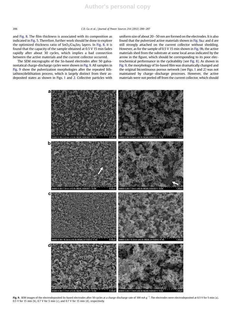
The SEM micrographs of the Sn-based electrodes after 50 galva-nostatical charge-discharge cycles were shown in Fig. 9. All samples inFig. 9 show the pulverization morphologies after the repeated lith-iathion/delithiation process, which is largely distinct from their as-deposited states as shown in Figs. 1 and 2. Collective particles with
uniform size of about 20e50nmare formedon the electrodes. It is alsofound that the pulverized activematerials shown in Fig. 9a,c and d arestill strongly attached on the current collector without shedding.However, as for the sample of 0.5 V 15min shown in Fig. 9b, the activematerials shed from the substrate at some local areas indicated by thearrow in the figure, which should be corresponding to its poor elec-trochemical performance in the cycleability (see Fig. 8). As shown inFig. 9, themorphology of Sn-based filmwas dramatically changed andthe original bicontinuous porous network (see Figs. 1 and 2) was notmaintained by chargeedischarge processes. However, the activematerials were not peeled off from the current collector, which should
Fig. 9. SEM images of the electrodeposited Sn-based electrodes after 50 cycles at a charge-discharge rate of 100 mA g�1. The electrodes were electrodeposited at 0.5 V for 5 min (a),0.5 V for 15 min (b), 0.7 V for 5 min (c), and 0.7 V for 15 min (d), respectively.
C.D. Gu et al. / Journal of Power Sources 214 (2012) 200e207206
Author's personal copy
be attributed to the porous film structure and the in situ formedinterlocking interfacebetweenSnandCuas shown inFig. 5c andd. Theporous structure in the Sn-based films providesmore rooms to relievethe drastic volume changes at the initial lithiathion/delithiationprocess. At the charge-discharge state, the inactive Cu network in thebottom layer of the electrode could interlock the active Sn and preventthe active material from peeling off the substrate.
4. Conclusion
This work provides a facile and environmental-friendly electrode-position process to fabricate porous tin-based films from the Ethalinebased electrolyte containing SnCl2$2H2O without any complexingagent or additive. Moreover, microstructure, composition, and elec-trochemical performance of the novel films were thoroughly investi-gated. SEMobservations indicated that the initially deposited Sngrainswere relatively uniform with a kind of self-assembly distributionconstructing an open and bicontinuous porous network. XRD and XPSanalysis revealed that thesefilmshad adouble-layer structure of SnO2/SneCu alloy from the top layer to the bottom layer of the films. Theporous tin-based composite films exhibited good cycle performancesas anode during the repeated lithiathion/delithiation process.
Acknowledgments
The work was supported by the National Natural ScienceFoundation of China (51001089), the Specialized Research Fund forthe Doctoral Program of Higher Education of China(20100101120026), the Research Foundation of Education Bureau ofZhejiang Province (Y200906938), the Key Science and TechnologyInnovation Team of Zhejiang Province under grant number2010R50013, and the 2010 Natural Science Basic Research OpenFoundation of the Key Lab of Automobile Materials, Ministry ofEducation, Jilin University (Grant No. 11-450060445349).
References
[1] M. Winter, J.O. Besenhard, M.E. Spahr, P. Novak, Adv. Mater. 10 (1998)725e763.
[2] J.R. Dahn, T. Zheng, Y.H. Liu, J.S. Xue, Science 270 (1995) 590e593.
[3] Y.S. Hu, P. Adelhelm, B.M. Smarsly, S. Hore, M. Antonietti, J. Maier, Adv. Funct.Mater. 17 (2007) 1873e1878.
[4] M. Winter, J.O. Besenhard, Electrochim. Acta 45 (1999) 31e50.[5] N. Tamura, R. Ohshita, M. Fujimoto, S. Fujitani, M. Kamino, I. Yonezu, J. Power
Sources 107 (2002) 48e55.[6] R.A. Huggins, J. Power Sources 81-82 (1999) 13e19.[7] S.F. Yang, P.Y. Zavalij, M.S. Whittingham, Electrochem. Commun. 5 (2003)
587e590.[8] W. Choi, J.Y. Lee, B.H. Jung, H.S. Lim, J. Power Sources 136 (2004) 154e159.[9] C. Kim, M. Noh, M. Choi, J. Cho, B. Park, Chem. Mater. 17 (2005) 3297e3301.
[10] S.M. Paek, E. Yoo, I. Honma, Nano Lett. 9 (2009) 72e75.[11] N.C. Li, C.R. Martin, J. Electrochem. Soc. 148 (2001) A164eA170.[12] X.W. Lou, Y. Wang, C.L. Yuan, J.Y. Lee, L.A. Archer, Adv. Mater. 18 (2006) 2325.[13] I.A. Courtney, J.R. Dahn, J. Electrochem. Soc. 144 (1997) 2045e2052.[14] C.D. Gu, Y.J. Mai, J.P. Zhou, J.P. Tu, Funct. Mater. Lett. 4 (2011) 377e381.[15] L.B. Wang, S. Kitamura, T. Sonoda, K. Obata, S. Tanase, T. Sakai, J. Electrochem.
Soc. 150 (2003) A1346eA1350.[16] L.H. Shi, H. Li, Z.X. Wang, X.J. Huang, L.Q. Chen, J. Mater. Chem. 11 (2001)
1502e1505.[17] H. Li, L.H. Shi, W. Lu, X.J. Huang, L.Q. Chen, J. Electrochem. Soc. 148 (2001)
A915eA922.[18] N. Tamura, Y. Kato, A. Mikami, M. Kamino, S. Matsuta, S. Fujitani,
J. Electrochem. Soc. 153 (2006) A1626eA1632.[19] X.Y. Fan, Q.C. Zhuang, G.Z. Wei, L. Huang, Q.F. Dong, S.G. Sun, J. Appl. Elec-
trochem. 39 (2009) 1323e1330.[20] Z.J. Du, S.C. Zhang, T. Jiang, Z.M. Bai, Electrochim. Acta 55 (2010)
3537e3541.[21] S.H. Ju, H.C. Jang, Y.C. Kang, J. Power Sources 189 (2009) 163e168.[22] M. Armand, F. Endres, D.R. MacFarlane, H. Ohno, B. Scrosati, Nat. Mater. 8
(2009) 621e629.[23] F. Endres, Chemphyschem 3 (2002) 144e154.[24] S.Z. El Abedin, M. Polleth, S.A. Meiss, J. Janek, F. Endres, Green Chem. 9 (2007)
549e553.[25] Y.S. Fung, D.R. Zhu, J. Electrochem. Soc. 149 (2002) A319eA324.[26] M.-J. Deng, T.-I. Leong, I.W. Sun, P.-Y. Chen, J.-K. Chang, W.-T. Tsai, Electro-
chem. Solid-State Lett. 11 (2008) D85eD88.[27] J.F. Huang, I.W. Sun, J. Electrochem. Soc. 150 (2003) E299eE306.[28] A.P. Abbott, G. Capper, K.J. McKenzie, K.S. Ryder, J. Electroanal. Chem. 599
(2007) 288e294.[29] X.H. Xu, C.L. Hussey, J. Electrochem. Soc. 140 (1993) 618e626.[30] C.D. Gu, X.J. Xu, J.P. Tu, J. Phys. Chem. C 114 (2010) 13614e13619.[31] A.P. Abbott, D. Boothby, G. Capper, D.L. Davies, R.K. Rasheed, J. Am. Chem. Soc.
126 (2004) 9142e9147.[32] A.H. Whitehead, M. Polzler, B. Gollas, J. Electrochem. Soc. 157 (2010)
D328eD334.[33] A.P. Abbott, K.J. McKenzie, Phys. Chem. Chem. Phys. 8 (2006) 4265e4279.[34] M. Mohamedi, S.J. Lee, D. Takahashi, M. Nishizawa, T. Itoh, I. Uchida, Elec-
trochim. Acta 46 (2001) 1161e1168.[35] X. Sun, J. Liu, Y. Li, Chem. Mater. 18 (2006) 3486e3494.[36] D. Larcher, L.Y. Beaulieu, D.D. MacNeil, J.R. Dahn, J. Electrochem. Soc. 147
(2000) 1658e1662.
C.D. Gu et al. / Journal of Power Sources 214 (2012) 200e207 207
Copyright © 2022 FDOKUMEN