Stress Memorization Technique—Fundamental Understanding and Low-Cost Integration for Advanced CMOS...
8
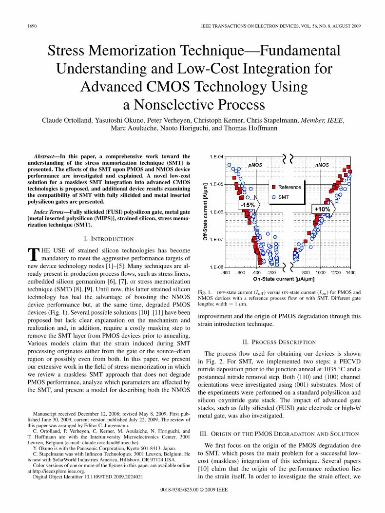
1690 IEEE TRANSACTIONS ON ELECTRON DEVICES, VOL. 56, NO. 8, AUGUST 2009 Stress Memorization Technique—Fundamental Understanding and Low-Cost Integration for Advanced CMOS Technology Using a Nonselective Process Claude Ortolland, Yasutoshi Okuno, Peter Verheyen, Christoph Kerner, Chris Stapelmann, Member, IEEE, Marc Aoulaiche, Naoto Horiguchi, and Thomas Hoffmann Abstract—In this paper, a comprehensive work toward the understanding of the stress memorization technique (SMT) is presented. The effects of the SMT upon PMOS and NMOS device performance are investigated and explained. A novel low-cost solution for a maskless SMT integration into advanced CMOS technologies is proposed, and additional device results examining the compatibility of SMT with fully silicided and metal inserted polysilicon gates are presented. Index Terms—Fully silicided (FUSI) polysilicon gate, metal gate [metal inserted polysilicon (MIPS)], strained silicon, stress memo- rization technique (SMT). I. INTRODUCTION T HE USE of strained silicon technologies has become mandatory to meet the aggressive performance targets of new device technology nodes [1]–[5]. Many techniques are al- ready present in production process flows, such as stress liners, embedded silicon germanium [6], [7], or stress memorization technique (SMT) [8], [9]. Until now, this latter strained silicon technology has had the advantage of boosting the NMOS device performance but, at the same time, degraded PMOS devices (Fig. 1). Several possible solutions [10]–[11] have been proposed but lack clear explanation on the mechanism and realization and, in addition, require a costly masking step to remove the SMT layer from PMOS devices prior to annealing. Various models claim that the strain induced during SMT processing originates either from the gate or the source–drain region or possibly even from both. In this paper, we present our extensive work in the field of stress memorization in which we review a maskless SMT approach that does not degrade PMOS performance, analyze which parameters are affected by the SMT, and present a model for describing both the NMOS Manuscript received December 12, 2008; revised May 8, 2009. First pub- lished June 30, 2009; current version published July 22, 2009. The review of this paper was arranged by Editor C. Jungemann. C. Ortolland, P. Verheyen, C. Kerner, M. Aoulaiche, N. Horiguchi, and T. Hoffmann are with the Interuniversity Microelectronics Center, 3001 Leuven, Belgium (e-mail: [email protected]). Y. Okuno is with the Panasonic Corporation, Kyoto 601-8413, Japan. C. Stapelmann was with Infineon Technologies, 3001 Leuven, Belgium. He is now with SolarWorld Industries America, Hillsboro, OR 97124 USA. Color versions of one or more of the figures in this paper are available online at http://ieeexplore.ieee.org. Digital Object Identifier 10.1109/TED.2009.2024021 Fig. 1. OFF-state current (I off ) versus ON-state current (Ion) for PMOS and NMOS devices with a reference process flow or with SMT. Different gate lengths; width = 1 μm. improvement and the origin of PMOS degradation through this strain introduction technique. II. PROCESS DESCRIPTION The process flow used for obtaining our devices is shown in Fig. 2. For SMT, we implemented two steps: a PECVD nitride deposition prior to the junction anneal at 1035 ◦ C and a postanneal nitride removal step. Both 110 and 100 channel orientations were investigated using (001) substrates. Most of the experiments were performed on a standard polysilicon and silicon oxynitride gate stack. The impact of advanced gate stacks, such as fully silicided (FUSI) gate electrode or high-k/ metal gate, was also investigated. III. ORIGIN OF THE PMOS DEGRADATION AND SOLUTION We first focus on the origin of the PMOS degradation due to SMT, which poses the main problem for a successful low- cost (maskless) integration of this technique. Several papers [10] claim that the origin of the performance reduction lies in the strain itself. In order to investigate the strain effect, we 0018-9383/$25.00 © 2009 IEEE
-
Upload
independent -
Category
Documents
-
view
1 -
download
0
Transcript of Stress Memorization Technique—Fundamental Understanding and Low-Cost Integration for Advanced CMOS...
1690 IEEE TRANSACTIONS ON ELECTRON DEVICES, VOL. 56, NO. 8, AUGUST 2009
Stress Memorization Technique—FundamentalUnderstanding and Low-Cost Integration for
Advanced CMOS Technology Usinga Nonselective Process
Claude Ortolland, Yasutoshi Okuno, Peter Verheyen, Christoph Kerner, Chris Stapelmann, Member, IEEE,Marc Aoulaiche, Naoto Horiguchi, and Thomas Hoffmann
Abstract—In this paper, a comprehensive work toward theunderstanding of the stress memorization technique (SMT) ispresented. The effects of the SMT upon PMOS and NMOS deviceperformance are investigated and explained. A novel low-costsolution for a maskless SMT integration into advanced CMOStechnologies is proposed, and additional device results examiningthe compatibility of SMT with fully silicided and metal insertedpolysilicon gates are presented.
Index Terms—Fully silicided (FUSI) polysilicon gate, metal gate[metal inserted polysilicon (MIPS)], strained silicon, stress memo-rization technique (SMT).
I. INTRODUCTION
THE USE of strained silicon technologies has becomemandatory to meet the aggressive performance targets of
new device technology nodes [1]–[5]. Many techniques are al-ready present in production process flows, such as stress liners,embedded silicon germanium [6], [7], or stress memorizationtechnique (SMT) [8], [9]. Until now, this latter strained silicontechnology has had the advantage of boosting the NMOSdevice performance but, at the same time, degraded PMOSdevices (Fig. 1). Several possible solutions [10]–[11] have beenproposed but lack clear explanation on the mechanism andrealization and, in addition, require a costly masking step toremove the SMT layer from PMOS devices prior to annealing.Various models claim that the strain induced during SMTprocessing originates either from the gate or the source–drainregion or possibly even from both. In this paper, we presentour extensive work in the field of stress memorization in whichwe review a maskless SMT approach that does not degradePMOS performance, analyze which parameters are affected bythe SMT, and present a model for describing both the NMOS
Manuscript received December 12, 2008; revised May 8, 2009. First pub-lished June 30, 2009; current version published July 22, 2009. The review ofthis paper was arranged by Editor C. Jungemann.
C. Ortolland, P. Verheyen, C. Kerner, M. Aoulaiche, N. Horiguchi, andT. Hoffmann are with the Interuniversity Microelectronics Center, 3001Leuven, Belgium (e-mail: [email protected]).
Y. Okuno is with the Panasonic Corporation, Kyoto 601-8413, Japan.C. Stapelmann was with Infineon Technologies, 3001 Leuven, Belgium. He
is now with SolarWorld Industries America, Hillsboro, OR 97124 USA.Color versions of one or more of the figures in this paper are available online
at http://ieeexplore.ieee.org.Digital Object Identifier 10.1109/TED.2009.2024021
Fig. 1. OFF-state current (Ioff ) versus ON-state current (Ion) for PMOS andNMOS devices with a reference process flow or with SMT. Different gatelengths; width = 1 μm.
improvement and the origin of PMOS degradation through thisstrain introduction technique.
II. PROCESS DESCRIPTION
The process flow used for obtaining our devices is shownin Fig. 2. For SMT, we implemented two steps: a PECVDnitride deposition prior to the junction anneal at 1035 ◦C and apostanneal nitride removal step. Both 〈110〉 and 〈100〉 channelorientations were investigated using (001) substrates. Most ofthe experiments were performed on a standard polysilicon andsilicon oxynitride gate stack. The impact of advanced gatestacks, such as fully silicided (FUSI) gate electrode or high-k/metal gate, was also investigated.
III. ORIGIN OF THE PMOS DEGRADATION AND SOLUTION
We first focus on the origin of the PMOS degradation dueto SMT, which poses the main problem for a successful low-cost (maskless) integration of this technique. Several papers[10] claim that the origin of the performance reduction liesin the strain itself. In order to investigate the strain effect, we
0018-9383/$25.00 © 2009 IEEE
ORTOLLAND et al.: STRESS MEMORIZATION TECHNIQUE—FUNDAMENTAL UNDERSTANDING AND INTEGRATION 1691
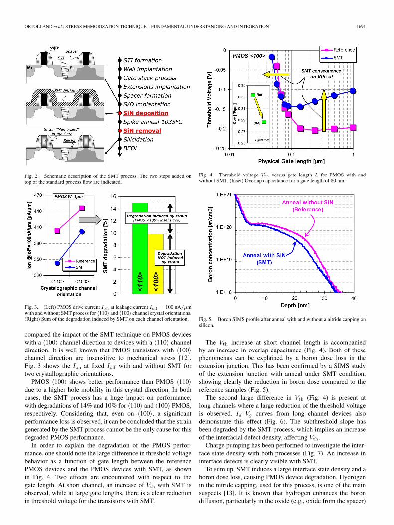
Fig. 2. Schematic description of the SMT process. The two steps added ontop of the standard process flow are indicated.
Fig. 3. (Left) PMOS drive current Ion at leakage current Ioff = 100 nA/μmwith and without SMT process for 〈110〉 and 〈100〉 channel crystal orientations.(Right) Sum of the degradation induced by SMT on each channel orientation.
compared the impact of the SMT technique on PMOS deviceswith a 〈100〉 channel direction to devices with a 〈110〉 channeldirection. It is well known that PMOS transistors with 〈100〉channel direction are insensitive to mechanical stress [12].Fig. 3 shows the Ion at fixed Ioff with and without SMT fortwo crystallographic orientations.
PMOS 〈100〉 shows better performance than PMOS 〈110〉due to a higher hole mobility in this crystal direction. In bothcases, the SMT process has a huge impact on performance,with degradations of 14% and 10% for 〈110〉 and 〈100〉 PMOS,respectively. Considering that, even on 〈100〉, a significantperformance loss is observed, it can be concluded that the straingenerated by the SMT process cannot be the only cause for thisdegraded PMOS performance.
In order to explain the degradation of the PMOS perfor-mance, one should note the large difference in threshold voltagebehavior as a function of gate length between the referencePMOS devices and the PMOS devices with SMT, as shownin Fig. 4. Two effects are encountered with respect to thegate length. At short channel, an increase of Vth with SMT isobserved, while at large gate lengths, there is a clear reductionin threshold voltage for the transistors with SMT.
Fig. 4. Threshold voltage Vth versus gate length L for PMOS with andwithout SMT. (Inset) Overlap capacitance for a gate length of 80 nm.
Fig. 5. Boron SIMS profile after anneal with and without a nitride capping onsilicon.
The Vth increase at short channel length is accompaniedby an increase in overlap capacitance (Fig. 4). Both of thesephenomenas can be explained by a boron dose loss in theextension junction. This has been confirmed by a SIMS studyof the extension junction with anneal under SMT condition,showing clearly the reduction in boron dose compared to thereference samples (Fig. 5).
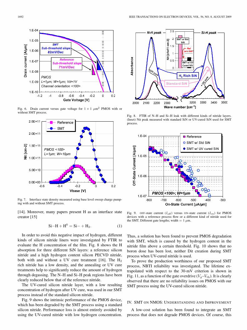
The second large difference in Vth (Fig. 4) is present atlong channels where a large reduction of the threshold voltageis observed. Id–Vg curves from long channel devices alsodemonstrate this effect (Fig. 6). The subthreshold slope hasbeen degraded by the SMT process, which implies an increaseof the interfacial defect density, affecting Vth.
Charge pumping has been performed to investigate the inter-face state density with both processes (Fig. 7). An increase ininterface defects is clearly visible with SMT.
To sum up, SMT induces a large interface state density and aboron dose loss, causing PMOS device degradation. Hydrogenin the nitride capping, used for this process, is one of the mainsuspects [13]. It is known that hydrogen enhances the borondiffusion, particularly in the oxide (e.g., oxide from the spacer)
1692 IEEE TRANSACTIONS ON ELECTRON DEVICES, VOL. 56, NO. 8, AUGUST 2009
Fig. 6. Drain current versus gate voltage for 1 × 1 μm2 PMOS with orwithout SMT process.
Fig. 7. Interface state density measured using base level sweep charge pump-ing with and without SMT process.
[14]. Moreover, many papers present H as an interface statecreator [15]
Si−H + H0 = Si− + H2. (1)
In order to avoid this negative impact of hydrogen, differentkinds of silicon nitride liners were investigated by FTIR toevaluate the H concentration of the film. Fig. 8 shows the Habsorption for three different SiN layers: a reference siliconnitride and a high hydrogen content silicon PECVD nitride,both with and without a UV cure treatment [16]. The H2
rich nitride has a low density, and the annealing or UV curetreatments help to significantly reduce the amount of hydrogenthrough degassing. The N–H and Si–H peak regions have beenclearly reduced below that of the reference nitride.
The UV-cured silicon nitride layer, with a low resultingconcentration of hydrogen after UV cure, was used in our SMTprocess instead of the standard silicon nitride.
Fig. 9 shows the intrinsic performance of the PMOS device,which has been degraded by the SMT process using a standardsilicon nitride. Performance loss is almost entirely avoided byusing the UV-cured nitride with low hydrogen concentration.
Fig. 8. FTIR of N–H and Si–H leak with different kinds of nitride layers.(Inset) Nit peak measured with standard SiN or UV-cured SiN used for SMTprocess.
Fig. 9. OFF-state current (Ioff ) versus ON-state current (Ion) for PMOSdevices with a reference process flow or a different kind of nitride used forthe SMT. Different gate lengths; width = 1 μm.
Thus, a solution has been found to prevent PMOS degradationwith SMT, which is caused by the hydrogen content in thenitride film above a certain threshold. Fig. 10 shows that noboron dose has been lost, neither Dit creation during SMTprocess when UV-cured nitride is used.
To prove the production worthiness of our proposed SMTprocess, NBTI reliability was investigated. The lifetime ex-trapolated with respect to the 30-mV criterion is shown inFig. 11, as a function of the gate overdrive (Vg–Vth). It is clearlyobserved that there are no reliability issues on PMOS with ourSMT process using the UV-cured silicon nitride.
IV. SMT ON NMOS: UNDERSTANDING AND IMPROVEMENT
A low-cost solution has been found to integrate an SMTprocess that does not degrade PMOS devices. Of course, this
ORTOLLAND et al.: STRESS MEMORIZATION TECHNIQUE—FUNDAMENTAL UNDERSTANDING AND INTEGRATION 1693
Fig. 10. (Left) Boron SIMS profile after anneal with and without a UV-curednitride capping on silicon. (Right) Interface state density measured using baselevel sweep charge pumping with and without UV-cured SiN SMT process.
Fig. 11. NBTI lifetime versus overdrive for the reference and SMT processes.The measurements were carried out on 10 × 1 μm2 PMOS devices at T =125 ◦C, using measure-sense and measure technique [17].
Fig. 12. OFF-state current (Ioff ) versus ON-state current (Ion) for NMOSdevices with a reference process flow or a different kind of nitride used forthe SMT. Different gate lengths; width = 1 μm.
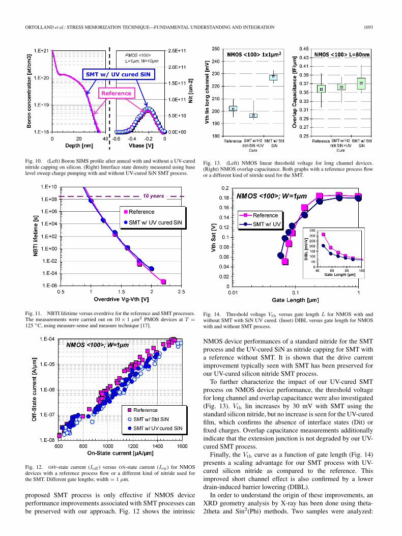
proposed SMT process is only effective if NMOS deviceperformance improvements associated with SMT processes canbe preserved with our approach. Fig. 12 shows the intrinsic
Fig. 13. (Left) NMOS linear threshold voltage for long channel devices.(Right) NMOS overlap capacitance. Both graphs with a reference process flowor a different kind of nitride used for the SMT.
Fig. 14. Threshold voltage Vth versus gate length L for NMOS with andwithout SMT with SiN UV cured. (Inset) DIBL versus gate length for NMOSwith and without SMT process.
NMOS device performances of a standard nitride for the SMTprocess and the UV-cured SiN as nitride capping for SMT witha reference without SMT. It is shown that the drive currentimprovement typically seen with SMT has been preserved forour UV-cured silicon nitride SMT process.
To further characterize the impact of our UV-cured SMTprocess on NMOS device performance, the threshold voltagefor long channel and overlap capacitance were also investigated(Fig. 13). Vth lin increases by 30 mV with SMT using thestandard silicon nitride, but no increase is seen for the UV-curedfilm, which confirms the absence of interface states (Dit) orfixed charges. Overlap capacitance measurements additionallyindicate that the extension junction is not degraded by our UV-cured SMT process.
Finally, the Vth curve as a function of gate length (Fig. 14)presents a scaling advantage for our SMT process with UV-cured silicon nitride as compared to the reference. Thisimproved short channel effect is also confirmed by a lowerdrain-induced barrier lowering (DIBL).
In order to understand the origin of these improvements, anXRD geometry analysis by X-ray has been done using theta-2theta and Sin2(Phi) methods. Two samples were analyzed:
1694 IEEE TRANSACTIONS ON ELECTRON DEVICES, VOL. 56, NO. 8, AUGUST 2009
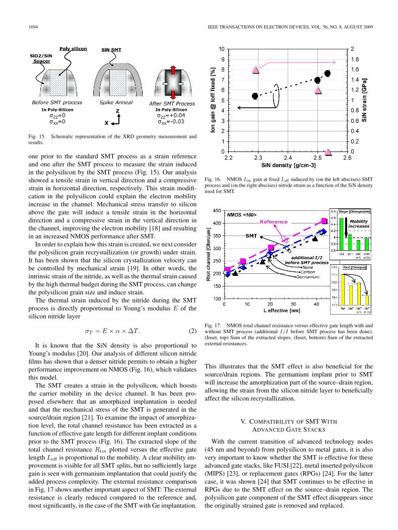
Fig. 15. Schematic representation of the XRD geometry measurement andresults.
one prior to the standard SMT process as a strain referenceand one after the SMT process to measure the strain inducedin the polysilicon by the SMT process (Fig. 15). Our analysisshowed a tensile strain in vertical direction and a compressivestrain in horizontal direction, respectively. This strain modifi-cation in the polysilicon could explain the electron mobilityincrease in the channel: Mechanical stress transfer to siliconabove the gate will induce a tensile strain in the horizontaldirection and a compressive strain in the vertical direction inthe channel, improving the electron mobility [18] and resultingin an increased NMOS performance after SMT.
In order to explain how this strain is created, we next considerthe polysilicon grain recrystallization (or growth) under strain.It has been shown that the silicon crystallization velocity canbe controlled by mechanical strain [19]. In other words, theintrinsic strain of the nitride, as well as the thermal strain causedby the high thermal budget during the SMT process, can changethe polysilicon grain size and induce strain.
The thermal strain induced by the nitride during the SMTprocess is directly proportional to Young’s modulus E of thesilicon nitride layer
σT = E × α × ΔT. (2)
It is known that the SiN density is also proportional toYoung’s modulus [20]. Our analysis of different silicon nitridefilms has shown that a denser nitride permits to obtain a higherperformance improvement on NMOS (Fig. 16), which validatesthis model.
The SMT creates a strain in the polysilicon, which booststhe carrier mobility in the device channel. It has been pro-posed elsewhere that an amorphized implantation is neededand that the mechanical stress of the SMT is generated in thesource/drain region [21]. To examine the impact of amorphiza-tion level, the total channel resistance has been extracted as afunction of effective gate length for different implant conditionsprior to the SMT process (Fig. 16). The extracted slope of thetotal channel resistance Rtot plotted versus the effective gatelength Leff is proportional to the mobility. A clear mobility im-provement is visible for all SMT splits, but no sufficiently largegain is seen with germanium implantation that could justify theadded process complexity. The external resistance comparisonin Fig. 17 shows another important aspect of SMT: The externalresistance is clearly reduced compared to the reference and,most significantly, in the case of the SMT with Ge implantation.
Fig. 16. NMOS Ion gain at fixed Ioff induced by (on the left abscises) SMTprocess and (on the right abscises) nitride strain as a function of the SiN densityused for SMT.
Fig. 17. NMOS total channel resistance versus effective gate length with andwithout SMT process (additional I/I before SMT process has been done).(Inset, top) Sum of the extracted slopes. (Inset, bottom) Sum of the extractedexternal resistances.
This illustrates that the SMT effect is also beneficial for thesource/drain regions. The germanium implant prior to SMTwill increase the amorphization part of the source–drain region,allowing the strain from the silicon nitride layer to beneficiallyaffect the silicon recrystallization.
V. COMPATIBILITY OF SMT WITH
ADVANCED GATE STACKS
With the current transition of advanced technology nodes(45 nm and beyond) from polysilicon to metal gates, it is alsovery important to know whether the SMT is effective for theseadvanced gate stacks, like FUSI [22], metal inserted polysilicon(MIPS) [23], or replacement gates (RPGs) [24]. For the lattercase, it was shown [24] that SMT continues to be effective inRPGs due to the SMT effect on the source–drain region. Thepolysilicon gate component of the SMT effect disappears sincethe originally strained gate is removed and replaced.
ORTOLLAND et al.: STRESS MEMORIZATION TECHNIQUE—FUNDAMENTAL UNDERSTANDING AND INTEGRATION 1695
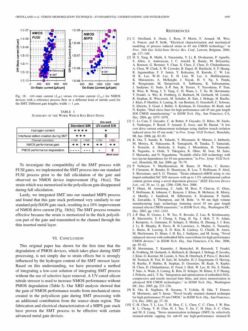
Fig. 18. OFF-state current (Ioff ) versus ON-state current (Ion) for NMOSdevices with a reference process flow or a different kind of nitride used forthe SMT. Different gate lengths; width = 1 μm.
TABLE ISUMMARY OF THE WORK WHICH HAS BEEN DONE
To investigate the compatibility of the SMT process withFUSI gates, we implemented the SMT process into our standardFUSI process prior to the full silicidation of the gate andobserved no NMOS device improvement [Fig. 18(a)]. Thestrain which was memorized in the polysilicon gate disappearedduring full silicidation.
Lastly, we integrated SMT into our standard MIPS processand found that this gate stack performed very similarly to ourstandard poly/SiON gate stack, resulting in a 10% improvementof NMOS drive current [Fig. 18(b)]. The SMT process remainseffective because the strain is memorized in the thick polysili-con part of the gate and transmitted to the channel through thethin inserted metal layer.
VI. CONCLUSION
This original paper has shown for the first time that thedegradation of PMOS devices, which takes place during SMTprocessing, is not simply due to strain effects but is stronglyinfluenced by the hydrogen content of the SMT stressor layer.Based on this understanding, we have presented a methodof integrating a low-cost solution of integrating SMT processwithout the use of selective layer removal. A UV-cured siliconnitride stressor is used to increase NMOS performance withoutPMOS degradation (Table I). Our XRD analysis showed thatthe gain of NMOS performance results from mechanical stresscreated in the polysilicon gate during SMT processing withan additional contribution from the source–drain region. Thefabrication and electrical characterization of a MIPS gate stackhave proven the SMT process to be effective with certainadvanced metal gate devices.
REFERENCES
[1] C. Ortolland, S. Orain, J. Rosa, P. Morin, F. Arnaud, M. Woo,A. Poncet, and P. Stolk, “Electrical characterization and mechanicalmodeling of process induced strain in 65 nm CMOS technology,” inProc. 34th Eur. Solid-State Device Res. Conf., Leuven, Belgium, 2004,pp. 137–140.
[2] H. S. Yang, R. Malik, S. Narasimha, Y. Li, R. Divakaruni, P. Agnello,S. Allen, A. Antreasyan, J. C. Arnold, K. Bandy, M. Belyansky,A. Bonnoit, G. Bronner, V. Chan, X. Chen, Z. Chen, D. Chidambarrao,A. Chou, W. Clark, S. W. Crowder, B. Engel, H. Harifuchi, S. F. Huang,R. Jagannathan, F. F. Jamin, Y. Kohyama, H. Kuroda, C. W. Lai,H. K. Lee, W.-H. Lee, E. H. Lim, W. Lai, A. Mallikarjunan,K. Matsumoto, A. McKnight, J. Nayak, H. Y. Ng, S. Panda,R. Rengarajan, M. Steigerwalt, S. Subbanna, K. Subramanian,J. Sudijono, G. Sudo, S.-P. Sun, B. Tessier, Y. Toyoshima, P. Tran,R. Wise, R. Wong, I. Y. Yang, C. H. Wann, L. T. Su, M. Horstmann,T. Feudel, A. Wei, K. Frohberg, G. Burbach, M. Gerhardt, M. Lenski,R. Stephan, K. Wieczorek, M. Schaller, H. Salz, J. Hohage, H. Ruelke,J. Klais, P. Huebler, S. Luning, R. van Bentum, G. Grasshoff, C. Schwan,E. Ehrichs, S. Goad, J. Buller, S. Krishnan, D. Greenlaw, M. Raab, andN. Kepler, “Dual stress liner for high performance sub-45 nm gate lengthSOI CMOS manufacturing,” in IEDM Tech. Dig., San Francisco, CA,Dec. 2004, pp. 1075–1078.
[3] C. Le Cam, F. Guyader, C. de Buttet, P. Guyader, G. Ribes, M. Sardo,S. Vanbergue, F. Boeuf, F. Arnaud, E. Josse, and M. Haond, “A lowcost drive current enhancement technique using shallow trench isolationinduced stress for 45 nm node,” in Proc. Symp. VLSI Technol., Honolulu,HI, Jun. 2006, pp. 82–83.
[4] K. Ota, T. Sanuki, K. Yahashi, Y. Miyanami, K. Matsuo, J. Idebuchi,M. Moriya, K. Nakayama, R. Yamaguchi, H. Tanaka, T. Yamazaki,S. Terauchi, A. Horiuchi, S. Fujita, I. Mizushima, H. Yamasaki,K. Nagaoka, A. Oishi, Y. Takegawa, K. Ohno, M. Iwai, M. Saito,F. Matsuoka, and N. Nagashima, “Scalable eSiGe S/D technology withless layout dependence for 45-nm generation,” in Proc. Symp. VLSI Tech-nol., Honolulu, HI, Jun. 2006, pp. 78–79.
[5] P. Verheyen, V. Machkaoutsan, M. Bauer, D. Weeks, C. Kerner,F. Clemente, H. Bender, D. Shamiryan, R. Loo, T. Hoffmann, P. Absil,S. Biesemans, and S. G. Thomas, “Strain enhanced nMOS using in situdoped embedded SiC S/D stressors with up to 1.5% substitutional carboncontent grown using a novel deposition process,” IEEE Electron DeviceLett., vol. 29, no. 11, pp. 1206–1208, Nov. 2008.
[6] T. Ghani, M. Armstrong, C. Auth, M. Bost, P. Charvat, G. Glass,T. Hoffmann, K. Johnson, C. Kenyon, J. Klaus, B. McIntyre, K. Mistry,A. Murthy, J. Sandford, M. Silberstein, S. Sivakumar, P. Smith,K. Zawadzki, S. Thompson, and M. Bohr, “A 90 nm high volumemanufacturing logic technology featuring novel 45 nm gate lengthstrained silicon CMOS transistors,” in IEDM Tech. Dig., Washington DC,Dec. 2003, pp. 1161–1163.
[7] J.-P. Han, H. Utomo, L. W. Teo, N. Rovedo, Z. Luo, R. Krishnasamy,R. Stierstorfer, Y. F. Chong, S. Fang, H. Ng, J. Holt, T. N. Adam,J. Kempisty, A. Gutmann, D. Schepis, S. Mishra, H. Zhuang, J. J. Kim,J. Li, R. Murphy, R. Davis, B. St Lawrence, A. Madan, A. Turansky,L. Burns, R. Loesing, S. D. Kim, R. Lindsay, G. Chiulli, R. Amos,M. Hierlemann, D. Shum, J. H. Ku, J. Sudijono, and M. Ieong, “Novelenhanced stressor with embedded SiGe source/drain for high performanceCMOS devices,” in IEDM Tech. Dig., San Francisco, CA, Dec. 2006,pp. 59–62.
[8] M. Horstmann, T. Kammler, J. Hontschel, H. Bierstedt, T. Feudel,K. Frohberg, M. Gerhardt, A. Hellmich, K. Hempel, J. Hohage, P. Javorka,J. Klais, G. Koerner, M. Lenski, A. Neu, R. Otterbach, P. Press, C. Reichel,M. Trentsch, B. Trui, H. Salz, M. Schaller, H.-J. Engelmann, O. Herzog,H. Ruelke, P. Hubler, R. Stephan, D. Greenlaw, M. Raab, N. Kepler,H. Chen, D. Chidambarrao, D. Fried, J. Holt, W. Lee, H. Nii, S. Panda,T. Sato, A. Waite, S. Liming, K. Rim, D. Schepis, M. Khare, S. F. Huang,J. Pellerin, and L. T. Su, “Integration and optimization of embedded-SiGe,compressive and tensile stressed liner films, and stress memorization inadvanced SOI CMOS technologies,” in IEDM Tech. Dig., WashingtonDC, Dec. 2005, pp. 233–236.
[9] K. Ota, K. Sugihara, H. Sayama, T. Uchida, H. Oda, T. Eimori,H. Morimoto, and Y. Inoue, “Novel locally strained channel techniquefor high performance 55 nm CMOS,” in IEDM Tech. Dig., San Francisco,CA, Dec. 2002, pp. 27–30.
[10] C.-H. Chen, T. L. Lee, T. H. Hou, C. L. Chen, C. C. Chen, J. W. Hsu,K. L. Cheng, Y. H. Chiu, H. J. Tao, Y. Jin, C. H. Diaz, S. C. Chen,and M.-S. Liang, “Stress memorization technique (SMT) by selectivelystrained-nitride capping for sub-65 nm high-performance strained-Si
1696 IEEE TRANSACTIONS ON ELECTRON DEVICES, VOL. 56, NO. 8, AUGUST 2009
device application,” in Proc. Symp. VLSI Technol., Honolulu, HI,Jun. 2004, pp. 56–57.
[11] F. Boeuf, F. Arnaud, M. T. Basso, D. Sotta, F. Wacquant, J. Rosa,N. Bicais-Lepinay, H. Bernard, J. Bustos, S. Manakli, M. Gaillardin,J. Grant, T. Skotnicki, B. Tavel, B. Duriez, M. Bidaud, P. Gouraud,C. Chaton, P. Morin, J. Todeschini, M. Jurdit, L. Pain, V. De-Jonghe,R. El-Farhane, and S. Jullian, “A conventional 45 nm CMOS node low-cost platform for general purpose and low power applications,” in IEDMTech. Dig., San Francisco, CA, Dec. 2004, pp. 425–428.
[12] C. Ortolland, P. Morin, F. Arnaud, S. Orain, C. Reddy, C. Chaton, andP. Stolk, “Mobility enhancement by strained nitride liners for 65 nmCMOS logic design features,” in Proc. Mater. Res. Soc. Symp.,San Francisco, CA, 2006, vol. 913, pp. 53–58.
[13] C. Ortolland, P. Morin, C. Chaton, E. Mastromatteo, C. Populaire,S. Orain, F. Leverd, P. Stolk, F. Boeuf, and F. Arnaud, “Stress memo-rization technique (SMT) optimization for 45 nm CMOS,” in Proc. Symp.VLSI Technol., Honolulu, HI, Jun. 2006, pp. 78–79.
[14] S. Chakravarthi, P. Kohli, P. R. Chidambaram, H. Bu, A. Jain,B. Hornung, and C. F. Machala, “Modeling the effect of source/drainsidewall spacer process on boron ultra shallow junctions,” in Proc. Int.Conf. Simulation Semicond. Process. Devices, Boston, MA, Sep. 2003,pp. 159–162.
[15] J. H. Stathis and E. Cartier, “Atomic hydrogen reactions with Pb centersat the (100) Si/SiO2 interface,” Phys. Rev. Lett., vol. 72, no. 17, pp. 2745–2748, Apr. 1994.
[16] V. Zubkov, M. Balseanu, L.-Q. Xia, and H. M’Saad, “Post depositionultraviolet treatment of silicon nitride dielectric: Modeling and experi-ment,” in Proc. Mater. Res. Soc. Symp., San Francisco, CA, 2006, vol. 910,pp. 53–58.
[17] T. Grasser, B. Kaczer, P. Hehenberger, W. Gos, R. O’Connor,H. Reisinger, W. Gustin, and C. Schunder, “Simultaneous extrac-tion of recoverable and permanent components contributing to bias-temperature instability,” in IEDM Tech. Dig., Washington DC, Dec. 2007,pp. 801–804.
[18] S. E. Thompson, G. Sun, Y. S. Choi, and T. Nishida, “Uniaxial-process-induced strained-Si: Extending the CMOS roadmap,” IEEE Trans. Elec-tron Devices, vol. 53, no. 5, pp. 1010–1020, May 2006.
[19] N. G. Rudawski, K. S. Jones, and R. Gwilliam, “Kinetics and morpholog-ical instabilities of stressed solid–solid phase transformations,” Phys. Rev.Lett., vol. 100, no. 16, p. 165 501, Apr. 2008.
[20] G. Raymond, P. Morin, A. Devos, D. A. Hess, M. Braccini, and F. Volpi,“Characterisation of silicon nitride thin film used as a stressor liners onCMOS FETs,” in Proc. Ultimate Integration Silicon, Udine, Italy, 2008,pp. 199–202.
[21] A. Wei, M. Wiatr, A. Mowry, A. Gehring, R. Boschke, C. Scott,J. Hoentschel, S. Duenkel, M. Gerhardt, T. Feudel, M. Lenski,F. Wirbeleit, R. Otterbach, R. Callahan, G. Koerner, N. Krumm,D. Greenlaw, M. Raab, and M. Horstmann, “Multiple stress memorizationin advanced SOI CMOS technologies,” in Proc. Symp. VLSI Technol.,Kyoto, Japan, Jun. 2007, pp. 216–217.
[22] T. Hoffmann, A. Veloso, A. Lauwers, H. Yu, H. Tigelaar, M. VanDal,T. Chiarella, C. Kerner, T. Kauerauf, A. Shickova, R. Mitsuhashi,I. Satoru, M. Niwa, A. Rothschild, B. Froment, J. Ramos, A. Nackaerts,M. Rosmeulen, S. Brus, C. Vrancken, P. P. Absil, M. Jurczak,S. Biesemans, and J. A. Kittl, “Ni-based FUSI gates: CMOS integrationfor 45 nm node and beyond,” in IEDM Tech. Dig., San Francisco, CA,Dec. 2006, pp. 269–272.
[23] S. Kibicek, T. Schram, V. Paraschiv, R. Vos, M. Demand, C. Adelmann,T. Witters, L. Nyns, L.-A. Ragnarsson, H. Yu, A. Veloso, R. Singanamalla,T. Kauerauf, E. Rohr, S. Brus, C. Vrancken, V. S. Chang, R. Mitsuhashi,A. Akheyar, H.-J. Cho, J. C. Hooker, B. J. O’Sullivan, T. Chiarella,C. Kerner, A. Delabie, S. Van Elshocht, K. De Meyer, S. De Gendt,P. Absil, T. Hoffmann, and S. Biesemans, “Low Vt CMOS using dopedHf-based oxides, TaC-based metals and laser-only anneal,” in IEDM Tech.Dig., Washington DC, Dec. 2007, pp. 49–52.
[24] K. Mistry, C. Allen, C. Auth, B. Beattie, D. Bergstrom, M. Bost,M. Brazier, M. Buehler, A. Cappellani, R. Chau, C.-H. Choi, G. Ding,K. Fischer, T. Ghani, R. Grover, W. Han, D. Hanken, M. Hattendorf,J. He, J. Hicks, R. Huessner, D. Ingerly, P. Jain, R. James, L. Jong,S. Joshi, C. Kenyon, K. Kuhn, K. Lee, H. Liu, J. Maiz, B. Mclntyre,P. Moon, J. Neirynck, S. Pae, C. Parker, D. Parsons, C. Prasad, L. Pipes,M. Prince, P. Ranade, T. Reynolds, J. Sandford, L. Shifren, J. Sebastian,J. Seiple, D. Simon, S. Sivakumar, P. Smith, C. Thomas, T. Troeger,P. Vandervoorn, S. Williams, and K. Zawadzki, “A 45 nm logic technologywith high-k + metal gate transistors, strained silicon, 9 Cu interconnectlayers, 193 nm dry patterning, and 100% Pb-free packaging,” in IEDMTech. Dig., Washington DC, Dec. 2007, pp. 247–250.
Claude Ortolland was born in Chambéry, France, in1980. He received the Engineer degree in materialsfrom the Institut National des Sciences Appliqués,Lyon, France, and the M.S. degree in microelec-tronics and the Ph.D. degree from the Institut Na-tional des Sciences Appliqués in 2003 and 2006,respectively.
He was with NXP Semiconductors (formerlyPhilips Semiconductors), Crolles, France, from 2003to 2007. He has been working on reliability for90-nm CMOS, then working on the integration, un-
derstanding, and modeling of process-induced stress in 65-nm CMOS technol-ogy, and, finally, on yield enhancement for 45-nm CMOS Technology. In 2007,he is with the Interuniversity Microelectronics Center, Leuven, Belgium, as aDevice Engineer for advanced sub-32-nm CMOS technology.
Yasutoshi Okuno received the Ph.D. degree in en-gineering from Osaka University, Osaka, Japan, in1993.
He then joined the R&D Group, Texas Instru-ments, Inc., Tsukuba, Japan, and moved to MemoryR&D Group, Kilby Center, Texas Instruments, Inc.,Dallas, TX, as an FEOL Process Engineer. In late1998, he is with the ULSI Process DevelopmentGroup, Panasonic Corporation, Kyoto, Japan, wherehe is currently leading the FEOL module integrationfor advance CMOS process.
Peter Verheyen received the B.S. degree in elec-trical engineering and the Ph.D. degree from theKatholieke Universiteit Leuven, Leuven, Belgium,in 1996 and 2003, respectively. His Ph.D. topic was“Advanced device architectures based on strainedSiGe layers: Physics and technology.”
He is with the Interuniversity MicroelectronicsCenter, Leuven, where he was a Doctoral Researcherand is currently a Member of the Process Quality andIntegration Group, working on MEMS and opticalapplications on Si substrates.
Christoph Kerner was born in Munich, Germany, in1977. He received the M.S. degree in physics, withcomputational physics as an additional minor, fromthe University of Sussex, Brighton, U.K., in 1999 andthe Ph.D. degree in physics from the InteruniversityMicroelectronics Center (IMEC), Leuven, Belgium,and the University of Leuven, Leuven, in 2004.
Since 2004, he has been with IMEC, working inthe CMOS Department as a Characterization Engi-neer. His current work focuses on advanced CMOStechnologies and related characterization and under-
standing. He is part of IMEC’s core partner program performing R&D forleading semiconductor companies. His other research interests include morethan Moore, quantum information processing, and emerging nanodevices.
ORTOLLAND et al.: STRESS MEMORIZATION TECHNIQUE—FUNDAMENTAL UNDERSTANDING AND INTEGRATION 1697
Chris Stapelmann (M’07) received the M.S.(Dipl.Ing.) degree in mechanical engineering fromthe RWTH Technical University of Aachen, Aachen,Germany.
From 2001 to 2008, he held various engineeringand leadership positions at Infineon Technologies,including the roles of On-Site Manager at IMEC andLead Engineer for FEOL Technology Developmentfor sub-45-nm CMOS technologies. He representedInfineon Technologies at the International Technol-ogy Roadmap for Semiconductors Front End Process
working group from 2006 to 2008. In April 2008, he is with SolarWorldIndustries America, Hillsboro, OR, as a Process Engineer for Solar Wafer andCell Testing. His current work is dedicated to the improvement of solar cellefficiencies.
Marc Aoulaiche received the M.S. degree inphysics and microelectronics from the Universityof Provence (Aix-Marseille I), Aix-en-Provence,France, in 2004 and the Ph.D. degree in micro-electronics on bias-temperature-instability effects inMOSFETs with high-k dielectrics and metal gates,characterization, and modeling from the Interuni-versity Microelectronics Center (IMEC), Leuven,Belgium, and the Department of Electrical Engineer-ing, Katholieke Universiteit Leuven, Leuven.
Since January 2009, he has been with the LogicDevice Design Group, IMEC. His main research topics are reliability, electricalcharacterization, and compact modeling.
Naoto Horiguchi received the B.S. degree in ap-plied physics from Tokyo University, Tokyo, Japan,in 1992.
In 1992, he was with Fujitsu Laboratories Ltd.,where he was engaged in the research and devel-opment of devices using semiconductor nanostruc-tures. In 1997–1998, he was with the University ofCalifornia, Santa Barbara, as a Visiting Researcher.In 1999, he returned to Fujitsu Laboratories Ltd.,where he was engaged in advanced CMOSFETprocess integrations and advanced embedded mem-
ory development. In 2006, he joined the Interuniversity Microelectronics Cen-ter, Leuven, Belgium, where he is currently working on advanced CMOSFETprocess integrations.
Thomas Hoffmann received the Ph.D. degree fromLille University, Lille, France, in 2000.
He then joined the R&D Group, Intel Corpora-tion, Hillsboro, OR, as a TCAD Engineer for sub-90-nm technologies. In 2004, he moved to Intel’sTechnology Development Group as a Device Engi-neer for 45-nm process development. In 2005, heis with the Interuniversity Microelectronics Center,Leuven, Belgium, leading the electrical characteriza-tion group for advanced silicon technologies. He hasauthored or coauthored approximately 50 technical
papers for publication in journals and presentations at conferences.