
Sri Chandrasekharendra Saraswathi Viswa Mahavidyalaya
200
SRI CHANDRASEKHARENDRA SARASWATHI VISWA MAHAVIDYALAYA (University established under section 3of UGC Act 1956) (Accredited with ‘A’ Grade by NAAC) Enathur, Kanchipuram – 631 561 DEPARTMENT OF ELECTRONICS AND COMMUNICATION ENGINEERING Prepared by: Dr. V.Jayapradha, Assistant Professor Course Material VLSI Design FULL TIME B.E III YEAR, VI th SEMESTER
-
Upload
khangminh22 -
Category
Documents
-
view
2 -
download
0
Transcript of Sri Chandrasekharendra Saraswathi Viswa Mahavidyalaya

SRI CHANDRASEKHARENDRA SARASWATHI VISWA MAHAVIDYALAYA (University established under section 3of UGC Act 1956)
(Accredited with ‘A’ Grade by NAAC) Enathur, Kanchipuram – 631 561
DEPARTMENT OF ELECTRONICS AND COMMUNICATION ENGINEERING
Prepared by:
Dr. V.Jayapradha, Assistant Professor
Course Material
VLSI Design
FULL TIME B.E III YEAR, VIth SEMESTER

Sri Chandrasekharendra Saraswathi Viswa Mahavidyalaya
Department of Electronics and Communication Engineering Syllabus for Full Time BE, Regulations 2018
(Applicable for students admitted from 2018-19 onwards
VLSI DESIGN VI SEMESTER PRE-REQUISITE:
Basic knowledge of Electronic Circuits and Digital System Design
OBJECTIVES:
To understand the principles of CMOS-VLSI technology and the design issues involved at circuit, logic, layout, system level and to learn programmable logics.
UNIT I INTRODUCTION TO VLSI AND MOS TRANSISTOR THEORY (10 Hrs)
Evolution of IC Technologies: SS1, MSI, LSI, VLSI, ULSI, and GLSI. The Moore’s Law, MOS THEORY: The MOS as switch - nMOS and pMOS. CMOS logic and its features, The nMOS Enhancement Transistor - Working and Characteristics. Threshold voltage and Body effect of MOS. MOS device design equations (First order effects).MOS INVERTERS: The CMOS inverter Transfer characteristics, Noise margin. The nMOS and pseudo-nMOS inverter, Tile BiCMOS Inverter, Tile CMOS Transmission gate
UNIT II CMOS PROCESSING TECHNOLOGY AND LAYOUTS (9 Hrs)
Silicon Semiconductor fabrication technology, Fabrication forms and CMOS (Basic n-WELL process) LAYOUTS AND DESIGN RULES: Layout based rules, Simple CMOS Stick Layout diagrams - Inverter, NAND, NOR gates and Multiplexer. Scaling: Constant Field, and Constant voltage
UNIT III MOS CIRCUIT PERFORMANCE AND CMOS LOGIC CIRCUITS (9 Hrs)
Sheet Resistance definition, MOS device capacitances – model, Distributed RC effects, switching characteristics - Rise time, fall time and Delay time. Stage ratio, Simple examples of Combinational and Sequential circuits using CMOS: NANDI NOR gates, and Compound gates, Latches, and Registers.
UNIT IV SUB SYSTEM DESIGN AND TESTING (9 Hrs)
General System Design-Design of ALU subsystems, Adder and Multipliers Memories - Static RAM, Control Logic Implementation using PLA’s. Testing of VLSI circuits - Need for Testing, Fault models, and ATPG. Design for Testability (DFT) - Scan Based and Self-test approaches.
UNIT V PROGRAMMABLE LOGICS (8 Hrs)
Basic ROM structures, PLAs, PALs, PLDs, Implementation of Traffic Light controller using PLD, FPGAs and CPLDs: XILINX and ALTERA series.
OUTCOMES: Total: 45 Hrs
At the end of the course, the student should be able to:
Learn the evolution of IC Technologies
Learn and analyze front end and back end of CMOS Circuits
Analyze circuit performance and logic circuits of CMOS
Understand design and testability for VLSI circuits
TEXTBOOKS:
1. Neil Weste and Kamran Eshraghian, “Principles of CMOS VLSI Design"-Addison Wesley,1998.
2. Charles H Roth,Jr."Digital Systems Design using VHDL"-Thomson Learning, 2001.
REFERENCES:
1. VLSI Design Principles- John P. Uyemura, John Wiley,2002
2. E. Fabricious, Introduction to VLSI design, McGraw-Hill1990
3. Wayne Wolf, Modern VLSI Design, Pearson Education, 2003
PEC2 MULTIMEDIA COMPRESSION TECHNIQUES VI SEMESTER
L T P C
3 0 0 3
VLSI Design
Prerequisite: Basic knowledge of Electronic Circuits and Digital System Design Objectives:
To learn basic CMOS Circuits.
To understand the principles of CMOS-VLSI technology. UNIT-I Introduction to VLSI and MOS Transistor Theory: Evolution of IC Technologies: SS1, MSI, LSI, VLSI, ULSI, and GLSI. The Moore’s Law. MOS THEORY: The MOS as switch - nMOS and pMOS. CMOS logic and its features. The nMOS Enhancement Transistor - Working and Characteristics. Threshold voltage and Body effect of MOS. MOS device design equations (First order effects).MOS INVERTERS: The CMOS inverter Transfer characteristics, Noise margin. The nMOS and pseudo-nMOS inverter. Tile BiCMOS Inverter. Tile CMOS Transmission gate. Outcome: On completion of the course, student will be able to
Learn the evolution of IC Technologies
Identify the various IC fabrication methods.

UNIT-I Pre Test- MCQ
1. VLSI technology uses ________ to form integrated circuit.
a) transistors
b) switches
c) diodes
d) buffers
2. Medium scale integration has ____________
a) ten logic gates
b) fifty logic gates
c) hundred logic gates
d) thousands logic gates
3. nMOS is ____________
a) donor doped
b) acceptor doped
c) all of the mentioned
d) none of the mentioned
4. MOS transistors consist of which of the following?
a) semiconductor layer
b) metal layer
c) layer of silicon-di-oxide
d) all of the mentioned
5. In basic inverter circuit, which is connected to ground
a) source
b) gates
c) drain
d) resistance

Unit -1 IC Technologies, MOS & Bi CMOS Circuits
INTRODUCTION TO IC TECHNOLOGY
The development of electronics endless with invention of vaccum tubes and associated
electronic circuits. This activity termed as vaccum tube electronics, afterward the evolution of solid
state devices and consequent development of integrated circuits are responsible for the present status
of communication, computing and instrumentation.
• The first vaccum tube diode was invented by john ambrase Fleming in 1904.
• The vaccum triode was invented by lee de forest in 1906.
Early developments of the Integrated Circuit (IC) go back to 1949. German engineer
Werner Jacobi filed a patent for an IC like semiconductor amplifying device showing five
transistors on a common substrate in a 2-stage amplifier arrangement. Jacobi disclosed small
cheap of hearing aids.
Integrated circuits were made possible by experimental discoveries which showed that
semiconductor devices could perform the functions of vacuum tubes and by mid-20th-century
technology advancements in semiconductor device fabrication.
The integration of large numbers of tiny transistors into a small chip was an enormous
improvement over the manual assembly of circuits using electronic components.
The integrated circuits mass production capability, reliability, and building-block approach to
circuit design ensured the rapid adoption of standardized ICs in place of designs using discrete
transistors.
An integrated circuit (IC) is a small semiconductor-based electronic device consisting of
fabricated transistors, resistors and capacitors. Integrated circuits are the building blocks of
most electronic devices and equipment. An integrated circuit is also known as a chip or
microchip.
There are two main advantages of ICs over discrete circuits: cost and performance. Cost is
low because the chips, with all their components, are printed as a unit by photolithography rather
than being constructed one transistor at a time. Furthermore, much less material is used to construct a
packaged IC die than a discrete circuit. Performance is high since the components switch quickly and
consume little power (compared to their discrete counterparts) because the components are small and
positioned close together. As of 2006, chip areas range from a few square millimeters to around 350
mm2, with up to 1 million transistors per mm

Unit -1 IC Technologies, MOS & Bi CMOS Circuits
IC Invention:
Inventor Year Circuit Remark
Fleming 1904
1906
Vacuum tube diode
Vacuum triode
large expensive, power- hungry, unreliable
William Shockley (Bell labs)
1945 Semiconductor replacing vacuum tube
--
Bardeen and Brattain and
Shockley (Bell labs)
1947 Point Contact transfer
resistance device “BJT”
Driving factor of growth of the VLSI technology
Werner Jacobi (Siemens AG)
1949 1st IC containing amplifying Device 2stage amplifier
No commercial use reported
Shockley 1951 Junction Transistor “Practical form of
transistor” Jack Kilby
(Texas
Instruments)
July 1958 Integrated Circuits F/F With 2-T Germanium slice
and gold wires
Father of IC design
Noyce Fairchild Semiconductor
Dec. 1958 Integrated Circuits Silicon “The Mayor of Silicon
Valley”
Kahng Bell Lab 1960 First MOSFET Start of new era for semiconductor industry
Fairchild Semiconductor
And Texas
1061 First Commercial
IC
Frank Wanlass
(Fairchild Semiconductor)
1963 CMOS
Federico Faggin
(Fairchild Semiconductor)
1968 Silicon gate IC technology Later Joined Intel to lead first CPU Intel 4004 in 1970
2
2300 T on 9mm
Zarlink Semiconductors
Recently M2A capsule for endoscopy
take photographs of digestive tract 2/sec.

Unit -1 IC Technologies, MOS & Bi CMOS Circuits
Moore’s Law:
Gordon E. Moore - Chairman Emeritus of Intel Corporation
1965 - observed trends in industry - of transistors on ICs vs release dates
Noticed number of transistors doubling with release of each new IC generation
Release dates (separate generations) were all 18-24 months apart
The level of integration of silicon technology as measured in terms of number of devices per IC
Semiconductor industry has followed this prediction with surprising accuracy.
IC Technology:
• Speed / Power performance of available technologies
• The microelectronics evolution
• SIA Roadmap
• Semiconductor Manufacturers 2001 Ranking
Category BJT CMOS
Power Dissipation
Moderate to High
less
Speed Faster Fast
Gm 4ms 0.4ms
Switch implementation
poor Good
Techn ology improvement
slower Faster
“The number of transistors on an integrated circuit will double every 18 months”
Circuit Technology
IC Technology
GaAs SiGe BiCMOS CMOS Bipolar SOI
Lower Power
Dissipation
Appr. Equal rise and fall
time Why
CMOS ?
High packing density
Fully restored
logic levels
Scale down more easily

Unit -1 IC Technologies, MOS & Bi CMOS Circuits
Scale of Integration:
Small scale integration(SSI) --1960
The technology was developed by integrating the number of transistors of 1-100
on a single chip. Ex: Gates, flip-flops, op-amps.
Medium scale integration(MSI) --1967
The technology was developed by integrating the number of transistors of 100-
1000 on a single chip. Ex: Counters, MUX, adders, 4-bit microprocessors.
Large scale integration(LSI) --1972
The technology was developed by integrating the number of transistors of 1000-
10000 on a single chip. Ex:8-bit microprocessors,ROM,RAM.
Very large scale integration(VLSI) -1978
The technology was developed by integrating the number of transistors of 10000-
1Million on a single chip. Ex:16-32 bit microprocessors, peripherals,
complimentary high MOS.
Ultra large scale integration(ULSI)
The technology was developed by integrating the number of transistors of 1Million-
10 Millions on a single chip. Ex: special purpose processors.
Giant scale integration(GSI)
The technology was developed by integrating the number of transistors of above 10
Millions on a single chip. Ex: Embedded system, system on chip.
Fabrication technology has advanced to the point that we can put a complete system on a
single chip.
Single chip computer can include a CPU, bus, I/O devices and memory.
This reduces the manufacturing cost than the equivalent board level system with higher
performance and lower power.

Unit -1 IC Technologies, MOS & Bi CMOS Circuits
MOS TECHNOLOGY:
MOS technology is considered as one of the very important and promising technologies in
the VLSI design process. The circuit designs are realized based on pMOS, nMOS, CMOS and
BiCMOS devices.
The pMOS devices are based on the p-channel MOS transistors. Specifically, the pMOS
channel is part of a n-type substrate lying between two heavily doped p+ wells beneath the
source and drain electrodes. Generally speaking, a pMOS transistor is only constructed in
consort with an NMOS transistor.
The nMOS technology and design processes provide an excellent background for other
technologies. In particular, some familiarity with nMOS allows a relatively easy transition to
CMOS technology and design.
The techniques employed in nMOS technology for logic design are similar to GaAs technology..
Therefore, understanding the basics of nMOS design will help in the layout of GaAs circuits
In addition to VLSI technology, the VLSI design processes also provides a new degree of
freedom for designers which helps for the significant developments. With the rapid advances in
technology the the size of the ICs is shrinking and the integration density is increasing.
The minimum line width of commercial products over the years is shown in the graph below.
The graph shows a significant decrease in the size of the chip in recent years which implicitly
indicates the advancements in the VLSI technology.

Unit -1 IC Technologies, MOS & Bi CMOS Circuits
MOS Transistor Symbol:
ENHANCEMENT AND DEPLETION MODE MOS TRANSISTORS
MOS Transistors are built on a silicon substrate. Silicon which is a group IV material is the
eighth most common element in the universe by mass, but very rarely occurs as the pure free element
in nature. It is most widely distributed in dusts, sands, planetoids, and planets as various forms of
silicon dioxide (silica) or silicates. It forms crystal lattice with bonds to four neighbours. Silicon is a
semiconductor. Pure silicon has no free carriers and conducts poorly. But adding dopants to silicon
increases its conductivity. If a group V material i.e. an extra electron is added, it forms an n-type
semiconductor. If a group III material i.e. missing electron pattern is formed (hole), the resulting
semiconductor is called a p-type semiconductor.
A junction between p-type and n-type semiconductor forms a conduction path. Source and
Drain of the Metal Oxide Semiconductor (MOS) Transistor is formed by the “doped” regions on the

gure 1.5: (a) Enhancement N-type MOSFET (b) Depletion N-type MOSFET
Unit -1 IC Technologies, MOS & Bi CMOS Circuits
surface of chip. Oxide layer is formed by means of deposition of the silicon dioxide (SiO2) layer
which forms as an insulator and is a very thin pattern. Gate of the MOS transistor is the thin layer of
“polysilicon (poly)”; used to apply electric field to the surface of silicon between Drain and Source,
to form a “channel” of electrons or holes. Control by the Gate voltage is achieved by modulating the
conductivity of the semiconductor region just below the gate. This region is known as the channel.
The Metal–Oxide–Semiconductor Field Effect Transistor (MOSFET) is a transistor which is a
voltage-controlled current device, in which current at two electrodes, drain and source is controlled
by the action of an electric field at another electrode gate having in-between semiconductor and a
very thin metal oxide layer. It is used for amplifying or switching electronic signals.
The Enhancement and Depletion mode MOS transistors are further classified as N-type named
NMOS (or N-channel MOS) and P-type named PMOS (or P-channel MOS) devices. Figure 1.5
shows the MOSFETs along with their enhancement and depletion modes.
Figure 1.5: (c) Enhancement P-type MOSFET (d) Depletion P-type MOSFET
The depletion mode devices are doped so that a channel exists even with zero voltage from gate to
source during manufacturing of the device. Hence the channel always appears in the device. To
control the channel, a negative voltage is applied to the gate (for an N-channel device), depleting the
Fi

Unit -1 IC Technologies, MOS & Bi CMOS Circuits
channel, which reduces the current flow through the device. In essence, the depletion-mode device is
equivalent to a closed (ON) switch, while the enhancement-mode device does not have the built in
channel and is equivalent to an open (OFF) switch. Due to the difficulty of turning off the depletion
mode devices, they are rarely used
Working of Enhancement Mode Transistor
The enhancement mode devices do not have the in-built channel. By applying the required potentials,
the channel can be formed. Also for the MOS devices, there is a threshold voltage (Vt), below which
not enough charges will be attracted for the channel to be formed. This threshold voltage for a MOS
transistor is a function of doping levels and thickness of the oxide layer.
Case 1: Vgs = 0V and Vgs < Vt
The device is non-conducting, when no gate voltage is applied (Vgs = 0V) or (Vgs < Vt) and also drain
to source potential Vds = 0. With an insufficient voltage on the gate to establish the channel region as
N-type, there will be no conduction between the source and drain. Since there is no conducting
channel, there is no current drawn, i.e. Ids = 0, and the device is said to be in the cut-off region. This
is shown in the Figure 1.7 (a).
Figure 1.7: (a) Cut-off Region
Case 2: Vgs > Vt
When a minixmum voltage greater than the threshold voltage Vt (i.e. Vgs > Vt) is applied, a high
concentration of negative charge carriers forms an inversion layer located by a thin layer next to the
interface between the semiconductor and the oxide insulator. This forms a channel between the
source and drain of the transistor. This is shown in the Figure 1.7 (b).
Figure 1.7: (b) Formation of a Channel

Unit -1 IC Technologies, MOS & Bi CMOS Circuits
A positive Vds reverse biases the drain substrate junction, hence the depletion region around the
drain widens, and since the drain is adjacent to the gate edge, the depletion region widens in the
channel. This is shown in Figure 1.7 (c). This results in flow of electron from source to drain
resulting in current Ids.. The device is said to operate in linear region during this phase. Further
increase in Vds, increases the reverse bias on the drain substrate junction in contact with the inversion
layer which causes inversion layer density to decrease. This is shown in Figure 1.7 (d). The point at
which the inversion layer density becomes very small (nearly zero) at the drain end is termed pinch-
off. The value of Vds at pinch-off is denoted as Vds,sat. This is termed as saturation region for the
MOS device. Diffusion current completes the path from source to drain in this case, causing the
channel to exhibit a high resistance and behaves as a constant current source.
Vgs > Vt Vgs > Vt
VSB = 0 VDS > 0 VSB = 0 VDS > 0
Body Body Figure 1.7: (c) Linear Region. (d) Saturation Region
The MOSFET ID versus VDS characteristics (V-I Characteristics) is shown in the Figure 1.8. For VGS
< Vt, ID = 0 and device is in cut-off region. As VDS increases at a fixed VGS, ID increases in the linear
region due to the increased lateral field, but at a decreasing rate since the inversion layer density is
decreasing. Once pinch-off is reached, further increase in VDS results in increase in ID; due to the
formation of the high field region which is very small. The device starts in linear region, and moves
into saturation region at higher VDS.
ID > 0 n + n +
P Substrate
ID > 0 n + n +
P Substrate

Unit -1 IC Technologies, MOS & Bi CMOS Circuits
Basic Electrical Properties of MOS and Bi CMOS circuits
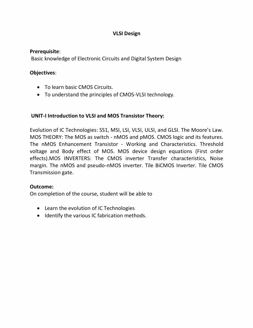
ID-VDS Characteristics of MOS Transistor :
The graph below shows the ID Vs VDS characteristics of an n- MOS transistor for several values of
VGS .It is clear that there are two conduction states when the device is ON. The saturated state and
the non-saturated state. The saturated curve is the flat portion and defines the saturation region. For
Vgs < VDS + Vth, the nMOS device is conducting and ID is independent of VDS. For Vgs > VDS +
Vth, the transistor is in the non-saturation region and the curve is a half parabola. When the transistor
is OFF (Vgs < Vth), then ID is zero for any VDS value.
The boundary of the saturation/non-saturation bias states is a point seen for each curve in the graph as
the intersection of the straight line of the saturated region with the quadratic curve of the non-
saturated region. This intersection point occurs at the channel pinch off voltage called VDSAT. The
diamond symbol marks the pinch-off voltage VDSAT for each value of VGS. VDSAT is defined as
the minimum drain-source voltage that is required to keep the transistor in saturation for a given VGS
.In the non-saturated state, the drain current initially increases almost linearly from the origin before
bending in a parabolic response. Thus the name ohmic or linear for the non- saturated region.
The drain current in saturation is virtually independent of VDS and the transistor acts as a current
Unit -1 IC Technologies, MOS & Bi CMOS Circuits
source. This is because there is no carrier inversion at the drain region of the channel. Carriers are
pulled into the high electric field of the drain/substrate pn junction and ejected out of the drain
terminal.
Drain-to-Source Current IDS Versus Voltage VDS Relationships :
The working of a MOS transistor is based on the principle that the use of a voltage on the gate induce
a charge in the channel between source and drain, which may then be caused to move from source to
drain under the influence of an electric field created by voltage Vds applied between drain and
source. Since the charge induced is dependent on the gate to source voltage Vgs then Ids is dependent
on both Vgs and Vds.
Let us consider the diagram below in which electrons will flow source to drain .So,the drain current
is given by
Charge induced in channel (Qc) Ids =-Isd = Electron transit time(τ) Length of the channel Where the
transit time is given by τsd = ------------------------------
Velocity (v)

Unit -1 IC Technologies, MOS & Bi CMOS Circuits
But velocity v= µEds
Where µ =electron or hole mobility and Eds = Electric field also , Eds = Vds/L
so,v = µ.Vds/L and τds = L2 / µ.Vds
The typical values of µ at room temperature are given below.
Non-saturated Region :
Let us consider the Id vs Vd relationships in the non-saturated region .The charge induced in the
channel due to due to the voltage difference between the gate and the channel, Vgs (assuming
substrate connected to source). The voltage along the channel varies linearly with distance X from the
source due to the IR drop in the channel .In the non-saturated state the average value is Vds/2. Also
the effective gate voltage Vg = Vgs – Vt where Vt, is the threshold voltage needed to invert the
charge under the gate and establish the channel.
Hence the induced charge is Qc = Eg εins εoW. L
Where
Eg = average electric field gate to channel
εins = relative permittivity of insulation between gate and channel εo=permittivity

Unit -1 IC Technologies, MOS & Bi CMOS Circuits
Here D is the thickness of the oxide layer. Thus
So, by combining the above two equations ,we get
or the above equation can be written as
In the non-saturated or resistive region where Vds < Vgs – Vt and
Generally ,a constant β is defined as
So that ,the expression for drain –source current will become
The gate /channel capacitance is

Unit -1 IC Technologies, MOS & Bi CMOS Circuits
Hence we can write another alternative form for the drain current as
Some time it is also convenient to use gate –capacitance per unit area ,Cg So,the drain current is
This is the relation between drain current and drain-source voltage in non-saturated region.
Saturated Region
Saturation begins when Vds = Vgs - V, since at this point the IR drop in the channel equals the
effective gate to channel voltage at the drain and we may assume that the current remains fairly
constant as Vds increases further. Thus
or we can also write that
or it can also be written as
or
The expressions derived above for Ids hold for both enhancement and depletion mode devices. Here
the threshold voltage for the nMOS depletion mode device (denoted as Vtd) is negative.

Unit -1 IC Technologies, MOS & Bi CMOS Circuits
MOS Transistor Threshold Voltage Vt :
The gate structure of a MOS transistor consists, of charges stored in the dielectric layers and in the
surface to surface interfaces as well as in the substrate itself. Switching an enhancement mode MOS
transistor from the off to the on state consists in applying sufficient gate voltage to neutralize these
charges and enable the underlying silicon to undergo an inversion due to the electric field from the
gate. Switching a depletion mode nMOS transistor from the on to the off state consists in applying
enough voltage to the gate to add to the stored charge and invert the 'n' implant region to 'p'.
The threshold voltage Vt may be expressed as:
where QD = the charge per unit area in the depletion layer below the oxide Qss = charge density at
Si: SiO2 interface
Co =Capacitance per unit area.
Φns = work function difference between gate and Si
ΦfN = Fermi level potential between inverted surface and bulk Si
For polynomial gate and silicon substrate, the value of Φns is negative but negligible and the
magnitude and sign of Vt are thus determined by balancing the other terms in the equation. To
evaluate the Vt the other terms are determined as below.
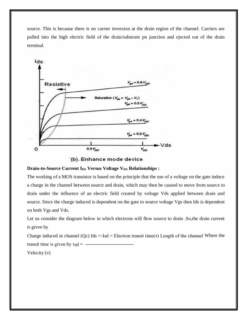
Body Effect :
Generally while studying the MOS transistors it is treated as a three terminal device. But, the body of
the transistor is also an implicit terminal which helps to understand the characteristics of the
transistor. Considering the body of the MOS transistor as a terminal is known as the body effect. The
potential difference between the source and the body (Vsb) affects the threshold
Unit -1 IC Technologies, MOS & Bi CMOS Circuits
voltage of the transistor. In many situations, this Body Effect is relatively insignificant, so we can
(unless otherwise stated) ignore the Body Effect. But it is not always insignificant, in some cases it
can have a tremendous impact on MOSFET circuit performance.
Body effect - nMOS device
Increasing Vsb causes the channel to be depleted of charge carriers and thus the threshold voltage is
raised. Change in Vt is given by ΔVt = γ.(Vsb)1/2 where γ is a constant which depends on substrate
doping so that the more lightly doped the substrate, the smaller will be the body effect
The threshold voltage can be written as
Where Vt(0) is the threshold voltage for Vsd = 0
For n-MOS depletion mode transistors ,the body voltage values at different VDD voltages are given
below.
VSB = 0 V ; Vsd = -0.7VDD (= - 3.5 V for VDD =+5V ) VSB = 5 V ; Vsd = -0.6VDD (= - 3.0 V for
VDD =+5V )
nMOS INVERTER :
An inverter circuit is a very important circuit for producing a complete range of logic circuits. This is
needed for restoring logic levels, for Nand and Nor gates, and for sequential and memory circuits of
various forms .

Unit -1 IC Technologies, MOS & Bi CMOS Circuits
A simple inverter circuit can be constructed using a transistor with source connected to ground and a
load resistor of connected from the drain to the positive supply rail VDD· The output is taken from
the drain and the input applied between gate and ground .
But, during the fabrication resistors are not conveniently produced on the silicon substrate and even
small values of resistors occupy excessively large areas .Hence some other form of load resistance is
used. A more convenient way to solve this problem is to use a depletion mode transistor as the load,
as shown in Fig. below.
The salient features of the n-MOS inverter are
For the depletion mode transistor, the gate is connected to the source so it is always on .
In this configuration the depletion mode device is called the pull-up (P.U) and the enhancement mode
device the pull-down (P.D) transistor.
With no current drawn from the output, the currents Ids for both transistors must be equal.
nMOS Inverter transfer characteristic.
The transfer characteristic is drawn by taking Vds on x-axis and Ids on Y-axis for both enhancement
and depletion mode transistors. So,to obtain the inverter transfer characteristic for

Unit -1 IC Technologies, MOS & Bi CMOS Circuits
Vgs = 0 depletion mode characteristic curve is superimposed on the family of curves for the
enhancement mode device and from the graph it can be seen that , maximum voltage across the
enhancement mode device corresponds to minimum voltage across the depletion mode transistor.
From the graph it is clear that as Vin(=Vgs p.d. transistor) exceeds the Pulldown threshold voltage
current begins to flow. The output voltage Vout thus decreases and the subsequent increases in Vin
will cause the Pull down transistor to come out of saturation and become resistive.
CMOS Inverter:
The inverter is the very important part of all digital designs. Once its operation and properties are
clearly understood, Complex structures like NAND gates, adders, multipliers, and microprocessors
can also be easily done. The electrical behavior of these complex circuits can be almost completely
derived by extrapolating the results obtained for inverters. As shown in the diagram below the CMOS
transistor is designed using p-MOS and n-MOS transistors.

Unit -1 IC Technologies, MOS & Bi CMOS Circuits
In the inverter circuit ,if the input is high .the lower n-MOS device closes to discharge the capacitive
load .Similarly ,if the input is low,the top p-MOS device is turned on to charge the capacitive load
.At no time both the devices are on ,which prevents the DC current flowing from positive power
supply to ground. Qualitatively this circuit acts like the switching circuit, since the p-channel
transistor has exactly the opposite characteristics of the n-channel transistor. In the transition region
both transistors are saturated and the circuit operates with a large voltage gain. The C-MOS transfer
characteristic is shown in the below graph.
Considering the static conditions first, it may be Seen that in region 1 for which Vi,. = logic 0, we
have the p-transistor fully turned on while the n-transistor is fully turned off. Thus no current flows
through the inverter and the output is directly connected to VDD through the p-transistor.
Hence the output voltage is logic 1 . In region 5 , Vin = logic 1 and the n-transistor is fully on while
the p-transistor is fully off. So, no current flows and logic 0 appears at the output.

D.C and transfer characteristics of a CMOS inverter A CMOS inverter contains a PMOS and a NMOS transistor connected at the drain and gate terminals, a supply voltage VDD at the PMOS source terminal, and a ground connected at the NMOS source terminal. The operation of the CMOS inverter can be divided into five regions CMOS inverter diagram
Regions : Region A: P device is OFF and n device is ON. Vout=VDD. Region B: PMOS is linear region and NMOS is saturation region.
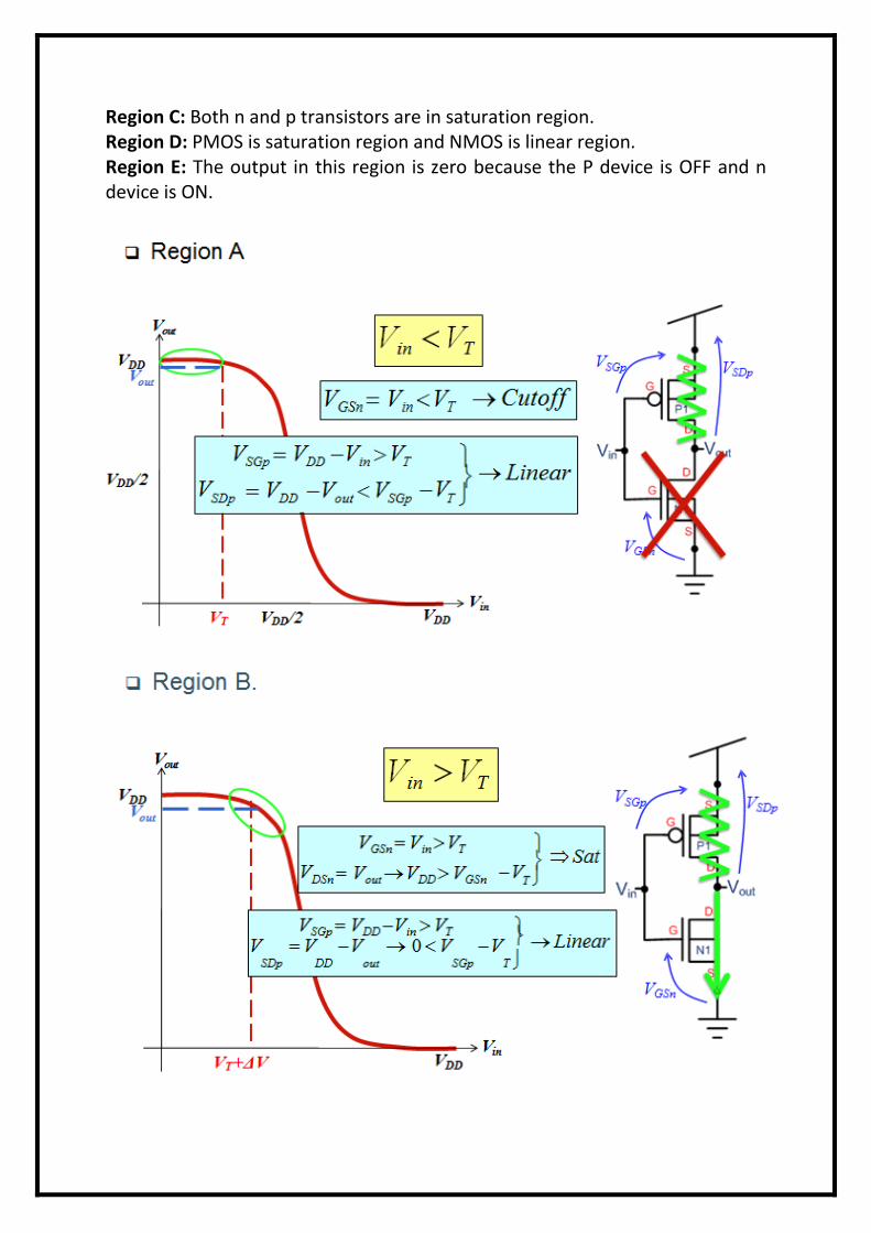
Region C: Both n and p transistors are in saturation region. Region D: PMOS is saturation region and NMOS is linear region. Region E: The output in this region is zero because the P device is OFF and n device is ON.


Noise Margin: Practical inverter circuits experience external disturbances leading to extra voltage on the signal lines. Such unwanted additional voltage is termed as noise. If the noise in a digital circuit exceeds certain margins, known as noise margins. VIL – Maximum low input voltage VIH – Minimum high input voltage VOL – Maximum low output voltage VOH – Minimum high output voltage

Unit -1 IC Technologies, MOS & Bi CMOS Circuits
In region 2 the input voltage has increased to a level which just exceeds the threshold voltage of the
n-transistor. The n-transistor conducts and has a large voltage between source and drain; so it is in
saturation. The p-transistor is also conducting but with only a small voltage across it, it operates in
the unsaturated resistive region. A small current now flows through the inverter from VDD to VSS. If
we wish to analyze the behavior in this region, we equate the p-device resistive region current with
the n-device saturation current and thus obtain the voltage and current relationships.
Region 4 is similar to region 2 but with the roles of the p- and n-transistors reversed.However, the
current magnitudes in regions 2 and 4 are small and most of the energy consumed in switching from
one state to the other is due to the larger current which flows in region 3.
Region 3 is the region in which the inverter exhibits gain and in which both transistors are in
saturation.
The currents in each device must be the same ,since the transistors are in series. So,we can write that
Since both transistors are in saturation, they act as current sources so that the equivalent circuit in this
region is two current sources in series between VDD and Vss with the output voltage coming from
their common point. The region is inherently unstable in consequence and the changeover from one
logic level to the other is rapid.
Determination of Pull-up to Pull –Down Ratio (Zp.u}Zp.d.)for an nMOS Inverter driven by
another nMOS Inverter :
Let us consider the arrangement shown in Fig.(a). in which an inverter is driven from the output of
another similar inverter. Consider the depletion mode transistor for which Vgs = 0 under all
conditions, and also assume that in order to cascade inverters without degradation the condition
BiCMOS INVERTER:
A BiCMOS inverter, consists of a PMOS and NMOS transistor ( M2 and M1), two NPN bipolar junction
transistors,( Q2 and Q1), and two impedances which act as loads( Z2 and Z1) as shown in the circuit below.

Unit -1 IC Technologies, MOS & Bi CMOS Circuits
When input, Vin, is high (VDD), the NMOS transistor ( M1), turns on, causing Q1 to conduct,while
M2 and Q2 are off, as shown in figure (b) . Hence , a low (GND) voltage is translated to the output
Vout. On the other hand, when the input is low, the M2 and Q2 turns on, while M1and Q1 turns off,
resulting to a high output level at the output as shown in Fig.(b).
In steady-state operation, Q1 and Q2 never turns on or off simultaneously, resulting to a lower power
consumption. This leads to a push-pull bipolar output stage. Transistors M1and M2, on the other
hand, works as a phase-splitter, which results to a higher input impedance.
The impedances Z2 and Z1 are used to bias the base-emitter junction of the bipolar transistor and to
ensure that base charge is removed when the transistors turn off. For example when the input voltage
makes a high-to-low transition, M1 turns off first. To turn off Q1, the base charge must be removed,
which can be achieved by Z1.With this effect, transition time reduces. However,

Unit -1 IC Technologies, MOS & Bi CMOS Circuits
41
there exists a short time when both Q1 and Q2 are on, making a direct path from the supply
(VDD) to the ground. This results to a current spike that is large and has a detrimental effect on
both the noise and power consumption, which makes the turning off of the bipolar transistor
fast .
Comparison of BiCMOS and C-MOS technologies
The BiCMOS gates perform in the same manner as the CMOS inverter in terms of power
consumption, because both gates display almost no static power consumption.
When comparing BiCMOS and CMOS in driving small capacitive loads, their performance are
comparable, however, making BiCMOS consume more power than CMOS. On the other hand,
driving larger capacitive loads makes BiCMOS in the advantage of consuming less power than
CMOS, because the construction of CMOS inverter chains are needed to drive large capacitance
loads, which is not needed in BiCMOS.
The BiCMOS inverter exhibits a substantial speed advantage over CMOS inverters, especially
when driving large capacitive loads. This is due to the bipolar transistor’s capability of
effectively multiplying its current.
For very low capacitive loads, the CMOS gate is faster than its BiCMOS counterpart due to
small values of Cint. This makes BiCMOS ineffective when it comes to the implementation of
internal gates for logic structures such as ALUs, where associated load capacitances are small.
BiCMOS devices have speed degradation in the low supply voltage region and also BiCMOS is
having greater manufacturing complexity than CMOS.

Module 4 : Propagation Delays in MOS Lecture 17 : Pseudo NMOS Inverter Objectives In this lecture you will learn the following
• Introduction • Different Configurations with NMOS Inverter • Worries about Pseudo NMOS Inverter • Calculation of Capacitive Load
17.1 Introduction The inverter that uses a p-device pull-up or load that has its gate permanently ground. An n-device pull-down or driver is driven with the input signal. This roughly equivalent to use of a depletion load is Nmos technology and is thus called ‘Pseudo-NMOS’. The circuit is used in a variety of CMOS logic circuits. In this, PMOS for most of the time will be linear region. So resistance is low and hence RC time constant is low. When the driver is turned on a constant DC current flows in the circuit.
Fig 17.1: CMOS Inverter Circuit
17.2 Different Configurations with NMOS Inverter
• When the input voltage is less than VTn.
• The output is ‘high’ and no current is drawn from the supply.
• As we raise the input just above VTn, the output starts falling.
• In this region the nMOS is saturated, while the pMOS is linear.

17.3 CMOS Summary Logic consumes no static power in CMOS design style. However, signals have to be routed to the n pull down network as well as to the p pull up network. So the load presented to every driver is high. This is exacerbated by the fact that n and p channel transistors cannot be placed close together as these are in different wells which have to be kept well separated in order to avoid latchup.
17.4 Pseudo nMOS Design Style The CMOS pull up network is replaced by a single pMOS transistor with its gate grounded. Since the pMOS is not driven by signals, it is always ‘on'. The effective gate voltage seen by the pMOS transistor is Vdd. Thus the overvoltage on the p channel gate is always Vdd -VTp. When the nMOS is turned ‘on', a direct path between supply and ground exists and static power will be drawn. However, the dynamic power is reduced due to lower capacitive loading. 17.5 Static Characteristics As we sweep the input voltage from ground to, we encounter the following regimes of operation:
• nMOS ‘off’ • nMOS saturated, pMOS linear • nMOS linear, pMOS linear • nMOS linear, pMOS saturated

UNIT-I Post Test- MCQ
1. What is the condition for linear region?
a) Vgs lesser than Vt
b) Vgs greater than Vt
c) Vds lesser than Vgs
d) Vds greater than Vgs
2. In depletion mode, source and drain are connected by
a) insulating channel
b) conducing channel
c) Vdd
d) Vss
3. Inversion layer in enhancement mode consists of excess of
a) positive carriers
b) negative carriers
c) both in equal quantity
d) neutral carriers
4. As source drain voltage increases, channel depth
a) increases
b) decreases
c) logarithmically increases
d) exponentially increases
5. In the region where inverter exhibits gain, the two transistors are in which region
a) linear
b) cut-off
c) non saturation
d) saturation

VLSI Design
Prerequisite: Basic knowledge of Electronic Circuits and Digital System Design Objectives:
To learn CMOS process technology.
To learn layout UNIT-II CMOS PROCESSING TECHNOLOGY AND LAYOUTS: Silicon Semiconductor fabrication technology, Fabrication forms and CMOS (Basic n-WELL process). LAYOUTS AND DESIGN RULES: Layout based rules, Simple CMOS Stick Layout diagrams - Inverter, NAND, NOR gates and Multiplexer. Scaling: Constant Field, and Constant voltage. Outcome: On completion of the course, student will be able to
Express the Layout of simple MOS circuit using Lambda based design rules.
Able to learn Layout, Stick diagrams, Fabrication steps.

UNIT-II Pre Test- MCQ
1. CMOS technology is used in developing
a) microprocessors
b) microcontrollers
c) digital logic circuits
d) all of the mentioned
2. N-well is created on
a) p substrate
b) n substrate
c) p & n substrate
d) none of the mentioned
3. CMOS is
a) unidirectional
b) bidirectional
c) directional
d) none of the mentioned
4. Which has high input resistance?
a) nMOS
b) CMOS
c) pMOS
d) BiCMOS
5. Stick diagrams are those which convey layer information through
a) thickness
b) color
c) shapes
d) layers
2
Unit-2 VLSI Circuit Design Processes
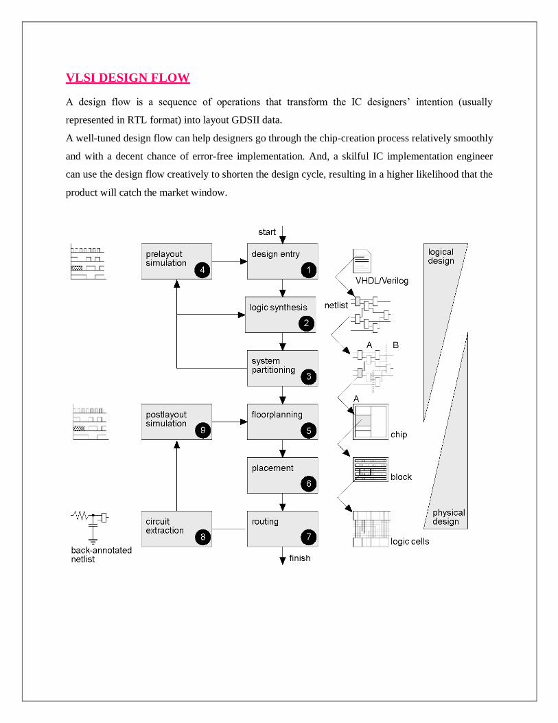
VLSI DESIGN FLOW
A design flow is a sequence of operations that transform the IC designers’ intention (usually
represented in RTL format) into layout GDSII data.
A well-tuned design flow can help designers go through the chip-creation process relatively smoothly
and with a decent chance of error-free implementation. And, a skilful IC implementation engineer
can use the design flow creatively to shorten the design cycle, resulting in a higher likelihood that the
product will catch the market window.

3
Unit-2 VLSI Circuit Design Processes
Front-end design (Logical design):
1. Design entry – Enter the design in to an ASIC design system using a hardware description
language (HDL) or schematic entry
2. Logic synthesis – Generation of net list (logic cells and their connections) from HDL code.
Logic synthesis consists of following steps: (i) Technology independent Logic optimization (ii)
Translation: Converting Behavioral description to structural domain (iii) Technology mapping or
Library binding
3. System partitioning - Divide a large system into ASIC-sized pieces
4. Pre-layout simulation - Check to see if the design functions correctly. Gate level
functionality and timing details can be verified.
Back-end design (Physical design):
5. Floor planning - Arrange the blocks of the netlist on the chip
6. Placement - Decide the locations of cells in a block
7. Routing - Make the connections between cells and blocks
8. Circuit Extraction - Determine the resistance and capacitance of the interconnect
9. Post-layout simulation - Check to see the design still works with the added loads of the
interconnect
Partitioning

Unit -1 IC Technologies, MOS & Bi CMOS Circuits
NMOS FABRICATION
The following description explains the basic steps used in the process of fabrication.
(a) The fabrication process starts with the oxidation of the silicon substrate.
It is shown in the Figure 1.9 (a).
(b) A relatively thick silicon dioxide layer, also called field oxide, is created on the surface of the
substrate. This is shown in the Figure 1.9 (b).
(c) Then, the field oxide is selectively etched to expose the silicon surface on which the MOS
transistor will be created. This is indicated in the Figure 1.9 (c).
(d) This is followed by covering the surface of substrate with a thin, high-quality oxide layer, which
will eventually form the gate oxide of the
MOS transistor as illustrated in Figure 1.9 (d).
(e) On top of the thin oxide, a layer of polysilicon (polycrystalline silicon) is deposited as is shown in
the Figure 1.9 (e). Polysilicon is used both as gate electrode material for MOS transistors and also as
an interconnect medium in silicon integrated circuits. Undoped polysilicon has relatively high
resistivity. The resistivity of polysilicon can be reduced, however, by doping it with impurity atoms.
(f) After deposition, the polysilicon layer is patterned and etched to form the interconnects and the
MOS transistor gates. This is shown in Figure 1.9 (f).
(g) The thin gate oxide not covered by polysilicon is also etched along, which exposes the bare
silicon surface on which the source and drain junctions are to be formed (Figure 1.9 (g)).
(h) The entire silicon surface is then doped with high concentration of impurities, either through
diffusion or ion implantation (in this case with donor atoms to produce n-type doping). Diffusion is
achieved by heating the wafer to a high temperature and passing the gas containing desired impurities
over the surface. Figure 1.9 (h) shows that the doping penetrates the exposed areas on the silicon
surface, ultimately creating two n-type regions (source and drain junctions) in the p-type substrate.
The impurity doping also penetrates the polysilicon on the surface, reducing its resistivity.
(i) Once the source and drain regions are completed, the entire surface is again covered with an
insulating layer of silicon dioxide, as shown in
Figure 1.9 (i).(j) The insulating oxide layer is then patterned in order to provide contact windows for
the drain and source junctions, as illustrated in Figure 1.9 (j).

Unit -1 IC Technologies, MOS & Bi CMOS Circuits
CMOS FABRICATION:
CMOS fabrication can be accomplished using either of the three technologies:
• N-well technologies/P-well technologies
• Twin well technology
• Silicon On Insulator (SOI)
The fabrication of CMOS can be done by following the below shown twenty steps, by which CMOS
can be obtained by integrating both the NMOS and PMOS transistors on the same chip substrate. For
integrating these NMOS and PMOS devices on the same chip, special regions called as wells or tubs
are required in which semiconductor type and substrate type are opposite to each other.

Unit -1 IC Technologies, MOS & Bi CMOS Circuits
Step5: Photoresist removal
A P-well has to be created on a N-substrate or N-well has to be created on a P-substrate. In this
article, the fabrication of CMOS is described using the P-substrate, in which the NMOS transistor is
fabricated on a P-type substrate and the PMOS transistor is fabricated in N-well.
The fabrication process involves twenty steps, which are as follows:
N-Well Process
Step1: Substrate
Primarily, start the process with a P-substrate.
Step2: Oxidation
The oxidation process is done by using high-purity oxygen and hydrogen, which are exposed in an oxidation furnace approximately at 1000 degree centigrade.
Step3: Photoresist
A light-sensitive polymer that softens whenever exposed to light is called as Photoresist layer.
It is formed.
Step4: Masking
The photoresist is exposed to UV rays through the N-well mask

Step10: Deposition of polysilicon
Unit -1 IC Technologies, MOS & Bi CMOS Circuits
A part of the photoresist layer is removed by treating the wafer with the basic or acidic solutio n.
Step6: Removal of SiO2 using acid etching
The SiO2 oxidation layer is removed through the open area made by the removal of photoresist using hydrofluoric acid.
Step7: Removal of photoresist
The entire photoresist layer is stripped off, as shown in the below figure.
Step8: Formation of the N-well
By using ion implantation or diffusion process N-well is formed.
Step9: Removal of SiO2
Using the hydrofluoric acid, the remaining SiO2 is removed.
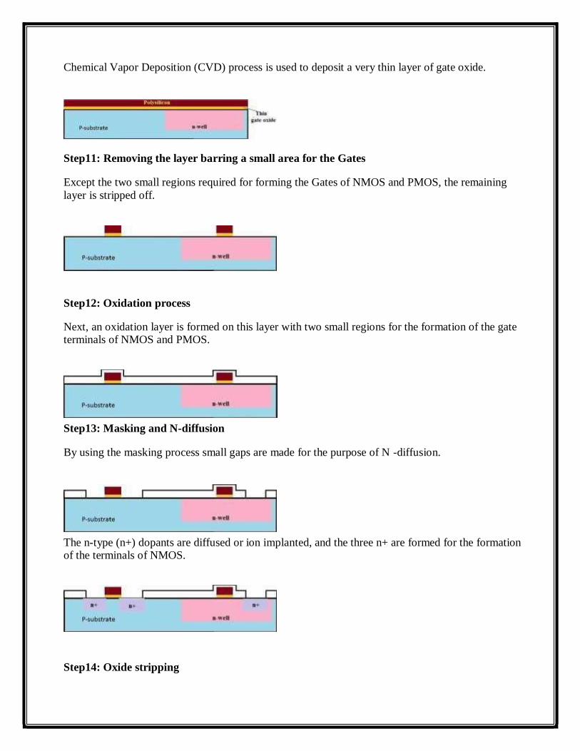
Step14: Oxide stripping
Unit -1 IC Technologies, MOS & Bi CMOS Circuits
Chemical Vapor Deposition (CVD) process is used to deposit a very thin layer of gate oxide.
Step11: Removing the layer barring a small area for the Gates
Except the two small regions required for forming the Gates of NMOS and PMOS, the remaining layer is stripped off.
Step12: Oxidation process
Next, an oxidation layer is formed on this layer with two small regions for the formation of the gate terminals of NMOS and PMOS.
Step13: Masking and N-diffusion
By using the masking process small gaps are made for the purpose of N -diffusion.
The n-type (n+) dopants are diffused or ion implanted, and the three n+ are formed for the formation of the terminals of NMOS.

Unit -1 IC Technologies, MOS & Bi CMOS Circuits
The remaining oxidation layer is stripped off.
Step15: P-diffusion
Similar to the above N-diffusion process, the P-diffusion regions are diffused to form the terminals of the PMOS.
Step16: Thick field oxide
A thick-field oxide is formed in all regions except the terminals of the PMOS and NMOS.
Step18: Removal of excess metal
The excess metal is removed from the wafer layer.
Step19: Terminals
The terminals of the PMOS and NMOS are made from respective gaps.
Step20: Assigning the names of the terminals of the NMOS and PMOS
Step17: Metallization Aluminum is sputtered on the whole wafer.

Unit -1 IC Technologies, MOS & Bi CMOS Circuits
Fabrication of CMOS using P-well process
Among all the fabrication processes of the CMOS, N-well process is mostly used for the fabrication
of the CMOS. P-well process is almost similar to the N-well. But the only difference in p-well
process is that it consists of a main N-substrate and, thus, P-wells itself acts as substrate for the N-
devices.
Twin tub-CMOS Fabrication Process
In this process, separate optimization of the n-type and p-type transistors will be provided. The
independent optimization of Vt, body effect and gain of the P-devices, N-devices can be made
possible with this process.
Different steps of the fabrication of the CMOS using the twintub process are as follows:
Lightly doped n+ or p+ substrate is taken and, to protect the latch up, epitaxial layer is used.
The high-purity controlled thickness of the layers of silicon are grown with exact dopant
concentrations.
The dopant and its concentration in Silicon are used to determine electrical properties.
Formation of the tub
Thin oxide construction

Unit -1 IC Technologies, MOS & Bi CMOS Circuits
Implantation of the source and drain
Cuts for making contacts
Metallization
By using the above steps we can fabricate CMOS using twin tub process method.
Silicon-on-Insulator (SOI) CMOS Process
Rather than using silicon as the substrate material, technologists have sought to use an insulating
substrate to improve process characteristics such as speed and latch-up susceptibility. The SOI
CMOS technology allows the creation of independent, completely isolated nMOS and pMOS
transistors virtually side-by-side on an insulating substrate. The main advantages of this technology
are the higher integration density (because of the absence of well regions), complete avoidance of the
latch-up problem, and lower parasitic capacitances compared to the conventional p & n-well or twin-
tub CMOS processes. A cross-section of nMOS and pMOS devicesusing SOI processis
shown below.
The SOI CMOS process is considerably more costly than the standard p & n-well CMOS process.
Yet the improvements of device performance and the absence of latch-up problems can justify its
use, especially for deep-sub-micron devices.

4
Unit-2 VLSI Circuit Design Processes
MOS LAYERS
MOS design is aimed at turning a specification into masks for processing silicon to meet the
specification. We have seen that MOS circuits are formed on four basic layers
N-diffusion
P-diffusion
Poly Si
Metal
which are isolated from one another by thick or thin (thinox) silicon silicon dioxide insulating
layers. The thin oxide (thinox) mask region includes n-diffusion, p-diffusion, and transistor
channels. Polysilicon and thinox regions interact so that a transistor is formed where they cross
one another.
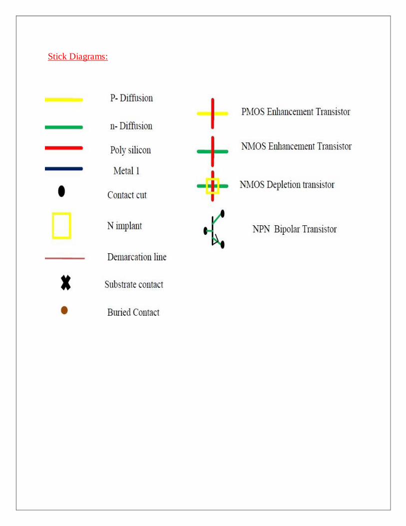
STICK DIAGRAMS
A stick diagram is a diagrammatic representation of a chip layout that helps to abstract a model
for design of full layout from traditional transistor schematic. Stick diagrams are used to convey
the layer information with the help of a color code.
“A stick diagram is a cartoon of a layout.”
The designer draws a freehand sketch of a layout, using colored lines to represent the various
process layers such as diffusion, metal and polysilicon. Where polysilicon crosses diffusion,
transistors are created and where metal wires join diffusion or polysilicon, contacts are formed.
For example, in the case of nMOS design,
Green color is used for n-diffusion
Red for polysilicon
Blue for metal
Yellow for implant, and black for contact areas.
Monochrome encoding is also used in stick diagrams to represent the layer information.
5
Unit-2 VLSI Circuit Design Processes
Stick Diagrams –NMOS Encoding
NMOS ENCODING

6
Unit-2 VLSI Circuit Design Processes
CMOS ENCODING

7
Unit-2 VLSI Circuit Design Processes
Stick Diagrams – Some Rules
Rule 1:
When two or more ‘sticks’ of the same type cross or touch each other that represents
electrical contact.
Rule 2:
When two or more “sticks” of different type cross or touch each other there is no electrical
contact. (If electrical contact is needed we have to show the connection explicitly)

8
Unit-2 VLSI Circuit Design Processes
Rule 3:
When a poly crosses diffusion it represents a transistor.
Note: If a contact is shown then it is not a transistor.
Rule 4:
In CMOS a demarcation line is drawn to avoid touching of p-diff with n-diff. All PMOS must lie
on one side of the line and all NMOS will have to be on the other side.

9
Unit-2 VLSI Circuit Design Processes
nMOS Design Style :
To understand the design rules for nMOS design style , let us consider a single metal, single
polysilicon nMOS technology.
The layout of nMOS is based on the following important features.
n-diffusion [n-diff.] and other thin oxide regions [thinox] (green) ;
polysilicon 1 [poly.]-since there is only one polysilicon layer here (red);
metal 1 [metal]-since we use only one metal layer here (blue);
implant (yellow);
contacts (black or brown [buried]).
A transistor is formed wherever poly. crosses n-diff. (red over green) and all diffusion wires
(interconnections) are n-type (green).When starting a layout, the first step normally taken is to
draw the metal (blue) VDD and GND rails in parallel allowing enough space between them for the
other circuit elements which will be required. Next, thinox (green) paths may be drawn between
the rails for inverters and inverter based logic as shown in Fig. below. Inverters and inverter-
based logic comprise a pull-up structure, usually a depletion mode transistor, connected from the
output point to VDD and a pull down structure of enhancement mode transistors suitably
interconnected between the output point and GND. This is illustrated in the Fig.(b). remembering
that poly. (red) crosses thinox (green)wherever transistors are required. One should consider the
implants (yellow) for depletion mode transistors and also consider the length to width (L:W)
ratio for each transistor. These ratios are important particularly in nMOS and nMOS- like
circuits.

10
Unit-2 VLSI Circuit Design Processes

11
Unit-2 VLSI Circuit Design Processes
CMOS Design Style:
The CMOS design rules are almost similar and extensions of n-MOS design rules except the
Implant (yellow) and the buried contact (brown). In CMOS design Yellow is used to identify p
transistors and wires, as depletion mode devices are not utilized. The two types of transistors 'n'
and 'p', are separated by the demarcation line (representing the p-well boundary) above which all
p-type devices are placed (transistors and wires (yellow). The n-devices (green) are consequently
placed below the demarcation line and are thus located in the p-well as shown in the diagram
below.
Diffusion paths must not cross the demarcation line and n-diffusion and p-diffusion wires must
not join. The 'n' and 'p' features are normally joined by metal where a connection is needed. Their
geometry will appear when the stick diagram is translated to a mask layout. However, one must not forget
to place crosses on VDD and Vss rails to represent the substrate and p-well connection respectively. The
design style is explained by taking the example the design of a single bit shift register. The design begins
with the drawing of the VDD and Vss rails in parallel and in metal and the creation of an (imaginary)
demarcation line in-between, as shown in Fig.below. The n-transistors are then placed below this line and
thus close to Vss, while p-transistors are placed above the line and below VDD In both cases, the
transistors are conveniently placed with their diffusion paths parallel to the rails (horizontal in the
diagram) as shown in Fig.(b). A similar approach can be taken with transistors in symbolic form.

12
Unit-2 VLSI Circuit Design Processes
Fig. CMOS stick layout design style (a,b,c,d)
The n- along with the p-transistors are interconnected to the rails using the metal and
connect as Shown in Fig.(d). It must be remembered that only metal and poly-silicon can cross
the demarcation line but with that restriction, wires can run-in diffusion also. Finally, the
remaining interconnections are made as appropriate and the control signals and data inputs are
added as shown in the Fig.(d).
13
Unit-2 VLSI Circuit Design Processes
Stick Diagrams:

14
Unit-2 VLSI Circuit Design Processes
Examples of Stick Diagrams
CMOS Inverter

15
Unit-2 VLSI Circuit Design Processes
Contd….
Fig. CMOS NAND gate

16
Unit-2 VLSI Circuit Design Processes
Design Rules and Layout
In VLSI design, as processes become more and more complex, need for the designer to
understand the intricacies of the fabrication process and interpret the relations between the
different photo masks is really troublesome. Therefore, a set of layout rules, also called design
rules, has been defined. They act as an interface or communication link between the circuit
designer and the process engineer during the manufacturing phase. The objective associated with
layout rules is to obtain a circuit with optimum yield (functional circuits versus non-functional
circuits) in as small as area possible without compromising reliability of the circuit. In addition,
Design rules can be conservative or aggressive, depending on whether yield or performance is
desired. Generally, they are a compromise between the two. Manufacturing processes have their
inherent limitations in accuracy. So the need of design rules arises due to manufacturing
problems like –
• Photo resist shrinkage, tearing.
• Variations in material deposition, temperature and oxide thickness.
• Impurities.
• Variations across a wafer.
These lead to various problems like :
• Transistor problems:
Variations in threshold voltage: This may occur due to variations in oxide thickness, ion-
implantation and poly layer. Changes in source/drain diffusion overlap. Variations in
substrate.
• Wiring problems:
Diffusion: There is variation in doping which results in variations in resistance,
capacitance. Poly, metal: Variations in height, width resulting in variations in resistance,
capacitance. Shorts and opens.
• Oxide problems:
Variations in height.
Lack of planarity.
• Via problems:
Via may not be cut all the way through.

17
Unit-2 VLSI Circuit Design Processes
Undersize via has too much resistance.
Via may be too large and create short.
To reduce these problems, the design rules specify to the designer certain geometric constraints
on the layout artwork so that the patterns on the processed wafers will preserve the topology and
geometry of the designs. This consists of minimum-width and minimum-spacing constraints and
requirements between objects on the same or different layers. Apart from following a definite set
of rules, design rules also come by experience.
Why we use design rules?
• Interface between designer and process engineer
• Historically, the process technology referred to the length of the silicon channel
between the source and drain terminals in field effect transistors.
• The sizes of other features are generally derived as a ratio of the channel length,
where some may be larger than the channel size and some smaller.
For example, in a 90 nm process, the length of the channel may be 90 nm, but the width of the
gate terminal may be only 50 nm.

18
Unit-2 VLSI Circuit Design Processes
Design rules define ranges for features
Examples:
• min. wire widths to avoid breaks
• min. spacing to avoid shorts
• minimum overlaps to ensure complete overlaps
– Measured in microns
– Required for resolution/tolerances of masks
Fabrication processes defined by minimum channel width
– Also minimum width of poly traces
– Defines “how fast” a fabrication process is
Types of Design Rules
The design rules primary address two issues:
1. The geometrical reproduction of features that can be reproduced by the maskmaking and
lithographical process, and
2. The interaction between different layers.
There are primarily two approaches in describing the design rules.
1. Linear scaling is possible only over a limited range of dimensions.
2. Scalable design rules are conservative .This results in over dimensioned and less dense
design.
3. This rule is not used in real life.
1. Scalable Design Rules (e.g. SCMOS, λ-based design rules):
In this approach, all rules are defined in terms of a single parameter λ. The rules are so chosen
that a design can be easily ported over a cross section of industrial process ,making the layout
portable .Scaling can be easily done by simply changing the value of.
The key disadvantages of this approach are:
2. Absolute Design Rules (e.g. μ-based design rules ) :
In this approach, the design rules are expressed in absolute dimensions (e.g. 0.75μm) and
therefore can exploit the features of a given process to a maximum degree. Here, scaling and
porting is more demanding, and has to be performed either manually or using CAD tools .Also,
these rules tend to be more complex especially for deep submicron.

19
Unit-2 VLSI Circuit Design Processes
The fundamental unity in the definition of a set of design rules is the minimum line width .It
stands for the minimum mask dimension that can be safely transferred to the semiconductor
material .Even for the same minimum dimension, design rules tend to differ from company to
company, and from process to process. Now, CAD tools allow designs to migrate between
compatible processes.
• Lambda-based (scalable CMOS) design rules define scalable rules based on λ
(which is half of the minimum channel length)
– classes of MOSIS SCMOS rules: SUBMICRON, DEEPSUBMICRON
• Stick diagram is a draft of real layout, it serves as an abstract view between the
schematic and layout.
• Circuit designer in general want tighter, smaller layouts for improved performance
and decreased silicon area.
• On the other hand, the process engineer wants design rules that result in a
controllable and reproducible process.
• Generally we find there has to be a compromise for a competitive circuit to be
produced at a reasonable cost.
• All widths, spacing, and distances are written in the form
• λ = 0.5 X minimum drawn transistor length
• Design rules based on single parameter, λ
• Simple for the designer
• Wide acceptance
• Provide feature size independent way of setting out mask
• If design rules are obeyed, masks will produce working circuits
• Minimum feature size is defined as 2 λ
• Used to preserve topological features on a chip
• Prevents shorting, opens, contacts from slipping out of area to be contacted

20
Unit-2 VLSI Circuit Design Processes
TRANSISTOR DESIGN RULES (nMOS, pMOS and CMOS)
DESIGN RULES FOR WIRES (nMOS and CMOS)

21
Unit-2 VLSI Circuit Design Processes
22
Unit-2 VLSI Circuit Design Processes

23
Unit-2 VLSI Circuit Design Processes
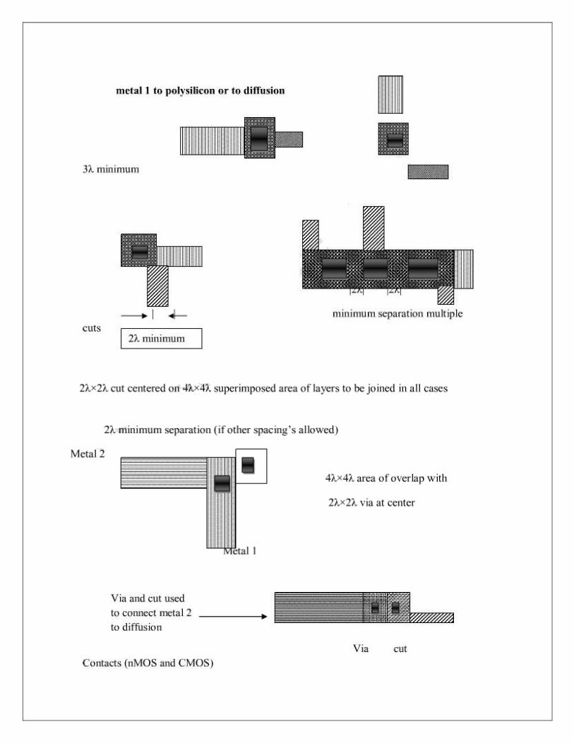
CONTACT CUTS
When making contacts between poly-silicon and diffusion in nMOS circuits it should be
remembered that there are three possible approaches--poly. to metal then metal to diff., or
aburied contact poly. to diff. , or a butting contact (poly. to diff. using metal). Among the three
the latter two, the buried contact is the most widely used, because of advantage in space and a
reliable contact. At one time butting contacts were widely used , but now a days they are
superseded by buried contacts.
In CMOS designs, poly. to diff. contacts are always made via metal. A simple process is
followed for making connections between metal and either of the other two layers (as in Fig.a),
The 2λ. x 2λ. contact cut indicates an area in which the oxide is to be removed down to the
underlying polysilicon or diffusion surface. When deposition of the metal layer takes place the
metal is deposited through the contact cut areas onto the underlying area so that contact is made
between the layers.
The process is more complex for connecting diffusion to poly-silicon using the butting
contact approach (Fig.b), In effect, a 2λ. x 2λ contact cut is made down to each of the layers to
be joined. The layers are butted together in such a way that these two contact cuts become
contiguous. Since the poly-silicon and diffusion outlines overlap and thin oxide under poly
silicon acts as a mask in the diffusion process, the poly-silicon and diffusion layers are also
butted together. The contact between the two butting layers is then made by a metal overlay as
shown in the Fig.

24
Unit-2 VLSI Circuit Design Processes
Fig.(a) . n-MOS & C-MOS Contacts
Fig.(b). Contacts poly-silicon to diffusion
25
Unit-2 VLSI Circuit Design Processes
In buried contact basically, layers are joined over a 2λ. x 2λ. area with the buried
contact cut extending by 1λ, in all directions around the contact area except that the contact cut
extension is increased to 2λ. in diffusion paths leaving the contact area. This helps to avoid the
formation of unwanted transistors. So this buried contact approach is simpler when compared to
others. The, poly-silicon is deposited directly on the underlying crystalline wafer. When
diffusion takes place, impurities will diffuse into the poly-silicon as well as into the diffusion
region within the contact area. Thus a satisfactory connection between poly-silicon and diffusion
is ensured. Buried contacts can be smaller in area than their butting contact counterparts and,
since they use no metal layer, they are subject to fewer design rule restrictions in a layout.
Other design rules
Double Metal MOS process Rules
CMOS fabrication is much more complex than nMOS fabrication
2 um Double metal, Double poly. CMOS/BiCMOS Rules
1.2um Double Metal single poly.CMOS rules
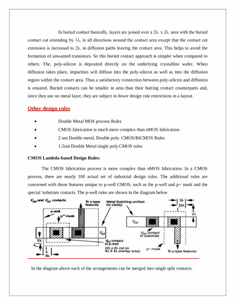
CMOS Lambda-based Design Rules:
The CMOS fabrication process is more complex than nMOS fabrication. In a CMOS
process, there are nearly 100 actual set of industrial design rules. The additional rules are
concerned with those features unique to p-well CMOS, such as the p-well and p+ mask and the
special 'substrate contacts. The p-well rules are shown in the diagram below
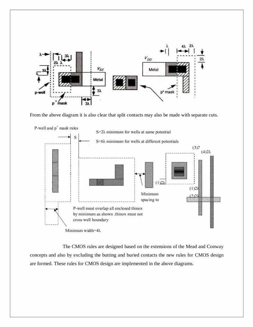
In the diagram above each of the arrangements can be merged into single split contacts.
26
Unit-2 VLSI Circuit Design Processes
From the above diagram it is also clear that split contacts may also be made with separate cuts.
The CMOS rules are designed based on the extensions of the Mead and Conway
concepts and also by excluding the butting and buried contacts the new rules for CMOS design
are formed. These rules for CMOS design are implemented in the above diagrams.

27
Unit-2 VLSI Circuit Design Processes
µM CMOS Design rules

28
Unit-2 VLSI Circuit Design Processes

29
Unit-2 VLSI Circuit Design Processes

30
Unit-2 VLSI Circuit Design Processes
Layout Diagrams for NMOS and CMOS Inverters and Gates
Basic Gate Design

31
Unit-2 VLSI Circuit Design Processes

32
Unit-2 VLSI Circuit Design Processes
Layout & Stick Diagram of CMOS Inverter
2 input NAND gate
33
Unit-2 VLSI Circuit Design Processes
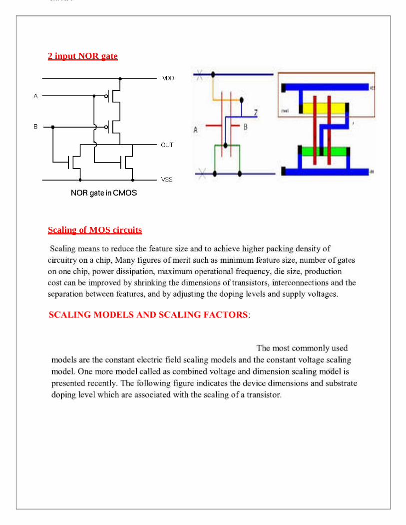
2 input NOR gate
Scaling of MOS circuits

34
Unit-2 VLSI Circuit Design Processes

35
Unit-2 VLSI Circuit Design Processes

36
Unit-2 VLSI Circuit Design Processes
CURRENT DENSITY J:

37
Unit-2 VLSI Circuit Design Processes
Limitations of Scaling:

38
Unit-2 VLSI Circuit Design Processes

39
Unit-2 VLSI Circuit Design Processes

40
Unit-2 VLSI Circuit Design Processes

Types of Scaling Two types of scaling are common:
1) constant field scaling and 2) constant voltage scaling.
Constant field scaling yields the largest reduction in the power-delay product of a single transistor. However, it requires a reduction in the power supply voltage as one decreases the minimum feature size. Constant voltage scaling does not have this problem and is therefore the preferred scaling method since it provides voltage compatibility with older circuit technologies. The disadvantage of constant voltage scaling is that the electric field increases as the minimum feature length is reduced. This leads to velocity saturation, mobility degradation, increased leakage currents and lower breakdown voltages. After scaling, the different MOSFET parameters will be converted as given by table below: Before Scaling After Constant Field Scaling After Constant Voltage Scaling
Where s = scaling parameter of MOS

UNIT-II Post Test- MCQ
1. Lithography is:
a) Process used to transfer a pattern to a layer on the chip
b) Process used to develop an oxidation layer on the chip
c) Process used to develop a metal layer on the chip
d) Process used to produce the chip
2. n and p transistors are separated by using
a) differentiation line
b) separation line
c) demarcation line
d) black line
3. Which color is used for polysilicon?
a) brown
b) red
c) white
d) orange
4. The width of n-diffusion and p-diffusion layer should be
a) 3λ
b) 2λ
c) λ
d) 4λ
5. In nMOS fabrication, etching is done using
a) plasma
b) hydrochloric acid
c) sulphuric acid
d) sodium chloride

VLSI Design
Prerequisite: Basic knowledge of Electronic Circuits and Digital System Design Objectives:
To understand MOS transistor as a switch and its capacitance.
Student will be able to design digital systems using MOS circuits (Static and Switching characteristics of inverters)
UNIT-III MOS CIRCUIT PERFORMANCE AND CMOS LOGIC CIRCUITS: Sheet Resistance definition, MOS device capacitances - model. Distributed RC effects. Switching characteristics - Rise time, fall time and Delay time. Stage ratio. Simple examples of Combinational and Sequential circuits using CMOS: NANDI NOR gates, and Compound gates, Latches, and Registers. Outcome: On completion of the course, student will be able to
Analyze circuit performance and logic circuits of CMOS

UNIT-III Pre Test- MCQ
1. Which layer has high capacitance value?
a) metal
b) diffusion
c) silicide
d) polysilicon
2. Gate area can be given as
a) L/W
b) L * W
c) 2L/W
d) L/2W
3. Gate area is scaled by
a) α
b) 1/α
c) 1/α2
d) α2
4. __________ can pass a logic 1 perfectly, but cannot pass a logic 0 perfectly. (a) nMOS transistor (b) pMOS transistor (c) CMOS transistor
(d) none of these
5. AND terms are realized by __________ connections of nMOS in PDN. (a) Series (b) parallel (c) cascade
(d) anti-parallel

14
Unit-3 Gate level design & Basic circuit concepts
Basic Circuit Concepts:
Sheet Resistance Rs and its concepts to MOS
The sheet resistance is a measure of resistance of thin films that have a uniform thickness.
It is commonly used to characterize materials made by semiconductor doping, metal deposition,
resistive paste printing, and glass coating.
Example of these processes are: doped semiconductor regions (eg: silicon or polysilicon)
and resistors.
Model:

UNIT-1: MOS TRANSISTOR PRINCIPLE DSEC/ECE/QB
EC6601 – VLSI DESIGN Page 4
c) Vgs > Vt Vds > Vgs - Vt This region is called Saturation Region where the drain current
remains almost constant. Even if the Vds is increased more and more, the increased voltage gets
dropped in the depletion region leading to a constant current. The typical threshold voltage for an
enhancement mode transistor is given by Vt = 0.2 * Vdd.
Derivation: (6 Marks)
Draw the VI characteristics (2 Marks)
2. Explain in detail of C-V characteristics of MOSFET. (Nov/Dec-15)
Simple MOS capacitance model (4 Marks)
Approximate channel as connected to source
Cgs = eoxWL/tox = CoxWL = CpermicronW
Cpermicron is typically about 2 fF/mm
Detailed MOS capacitance model (4 Marks)
0 1 2 3 4 50
0.5
1
1.5
2
2.5
Vds
I ds (m
A)
Vgs = 5
Vgs = 4
Vgs = 3
Vgs = 2
Vgs = 1
CV Characteristics of MOSFET

UNIT-1: MOS TRANSISTOR PRINCIPLE DSEC/ECE/QB
EC6601 – VLSI DESIGN Page 5
MOS device capacitance (4 Marks)
Diffusion capacitance (4 Marks)
Csb, Cdb
Undesirable, called parasitic capacitance
Capacitance depends on area and perimeter
Use small diffusion nodes
Comparable to Cg for contacted diff
½ Cg for un contacted
Varies with process
3. Discuss the mathematical equations that can be used to model the drain current and diffusion
capacitances of MOS transistor. (Nov/Dec-16)
Drain current derivation: (8 Marks)
Diffusion capacitances of MOS transistor: (8 Marks)Csb, Cdb
Undesirable, called parasitic capacitance
Capacitance depends on area and perimeter

UNIT-1: MOS TRANSISTOR PRINCIPLE DSEC/ECE/QB
EC6601 – VLSI DESIGN Page 6
Use small diffusion nodes
Comparable to Cg for contacted diff
½ Cg for un contacted
Varies with process
4. Explain the electrical properties of MOS transistor in detail. (Nov/Dec-17, Nov/Dec-13)
Ideal IV characteristics (4 Marks)Three regions of operation
Cutoff (1 Mark) Linear (1 Mark) Saturation (1 Mark) Equation (1 Mark)
Non ideal characteristics (4 Marks)o High Field Effects (1 Mark)
Mobility Degradation Velocity Saturation
o Channel Length Modulation(1 Mark)o Threshold Voltage Effects(1 Mark)
Body Effect Drain-Induced Barrier Lowering Short Channel Effect
o Leakage(1 Mark) Subthreshold Leakage Gate Leakage Junction Leakage
C-V characteristics (4 Marks)
Simple MOS capacitance model (1 Mark)
Detailed MOS capacitance model (4 Mark)
MOS device capacitance (4 Mark)
Diffusion capacitance (4 Mark)

21
EXTRINSIC CAPACITANCES
Extrinsic capacitances are modeled by using lumped capacitances, each of which is associated with a region
of the transistor’s geometry.One capacitor is used between each pair of transistor terminals, plus an
additional capacitor between the well and the bulk if the transistor is fabricated in a well.
Extrinsic Capacitance Types
Overlap capacitances that are mostly dependent on geometry.
Junction capacitances that are dependent on geometry and on bias.

22

23
Diode Capacitance
When a reverse voltage is applied to a PN junction , the holes in the p-region are attracted to the anode
terminal and electrons in the n-region are attracted to the cathode terminal. The resulting region contains
almost no carriers, and is called the depletion region. The depletion region acts similarly to the dielectric of a
capacitor.The depletion region increases in width as the reverse voltage across it increases. If we imagine
that the diode capacitance can be likened to a parallel plate capacitor, then as the plate spacing (i.e. the
depletion region width) increases, the capacitance should decrease. Increasing the reverse bias voltage across
the PN junction therefore decreases the diode capacitance. Source/Drain-Bulk Junction Capacitances At the
source region there is a source-to bulk junction capacitance, CjBS,e, and at the drain region there is a drain-
to-bulk junction capacitance, CjBD,e. Source/Drain-Bulk Junction Capacitances The junction capacitances
can be calculated by splitting the drain and source regions into a “side-wall” portion and a “bottom-wall”
portion. n The capacitance associated with the side wall portion is found by multiplying the length of the
side-wall perimeter (excluding the side contacting the channel) by the effective sidewall capacitance per unit
length. The capacitance for the bottom-wall portion is found by multiplying the area of the bottomwall by the
bottom-wall capacitance per unit area. Well-Bulk Junction Capacitance If the MOSFET is in a well, a well-
to-bulk junction capacitance, CjBW,e, must be added. The well-bulk junction capacitance is calculated
similarly to the source and drain junction capacitances, by dividing the total well-bulk junction capacitance
into side-wall and bottom-wall components. If more than one transistor is placed in a well, the well-bulk
junction capacitance should only be included once in the total model.

Switching charateristics of CMOS inverter. Transient Analysis of CMOS Inverter
Vin(t), input voltage, function of time
Vout(t), output voltage, function of time
VDD and Ground, DC (not function of time)
find Vout(t) = f(Vin(t))
Fall time tf: Definition:
Waveform to rise from 90% to 10% of its steady state value.
Time for output to rise from ‘1’to ‘0’

Derivation: (4 Marks)
Initial condition, Vout(0) = 0V
( ) ( )
( ) ( )
Take ln on both sides
( ) ( )
( ) ( ) ( )
(
)
(
)
(
)
(
)
(
)
(
)
(
) (
)
(
) (
)

(
)
Rise time, tr: Definition:
Waveform to rise from 10% to 90% of its steady state value.
Time for output to rise from ‘0’to ‘1’

Derivation: Initial condition, Vout(0) = 0V
( ) ( )
From the output wave form , wkt, V1= 0.9 VDD and V0 = 0.1 VDD . Rise time is defined between V0 and V1.
( ) ( )
Proceed as in previous (Fall time)
Maximum signal frequency: It is defined as largest frequency applied to the gate and allows to settle to a definable state.
Propagation Delay, tp:
Measures speed of output reaction to input change
Time difference between input transition (50%) and 50% output level.

Fall propagation delay, tpf
time for output to fall by 50%
reference to input change by 50% Rise propagation delay, tpr
time for output to rise by 50%
reference to input change by 50% Ideal expression (if input is step change)
( ) ( )
Total Propagation Delay– ( )
RC Delay Models: The delay of the logic gates can be estimated as the RC product of the effective drive resistance and the load capacitance. Effective Resistance and Capacitance: Use equivalent circuits for MOS transistors
Ideal switch + capacitance and ON resistance
Unit nMOS has resistance R, capacitance C
Unit pMOS has resistance 2R, capacitance C If transistors are in series, then their resistance is the sum of individual
resistance. If transistors are in parallel then the effective resistance is equal to the
resistance of single resistor.
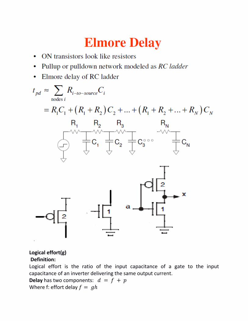
Logical effort(g) Definition: Logical effort is the ratio of the input capacitance of a gate to the input capacitance of an inverter delivering the same output current. Delay has two components: Where f: effort delay

g: logical effort h: electrical effort = Cout / Cin p: parasitic delay Logical effort of common gates
Examples:
Delay in Multi-stage Logic Network Path logical effort: It is product of logical efforts of all logic gates along the path.
Path electrical effort: It is ratio of output capacitance to input capacitance.
( )
( )
Path effort: The path effort is expressed in terms of the path logical effort G (the product of the individual logical efforts of the gates), and the path electrical effort H (the ratio of the load of the path to its input capacitance).

Path branching effort: Due to fan-out in a logic network, some drive current is directed along the path.

2
Unit-3 Gate level design & Basic circuit concepts
CMOS Logic gates and other complex gates
CMOS logic gate concept:

3
Unit-3 Gate level design & Basic circuit concepts
CMOS Static logic
Design Procedure:

4
Unit-3 Gate level design & Basic circuit concepts
Examples:

5
Unit-3 Gate level design & Basic circuit concepts
1.

6
Unit-3 Gate level design & Basic circuit concepts
2.

7
Unit-3 Gate level design & Basic circuit concepts
Complex Gates:
Transmission gate logic:

8
Unit-3 Gate level design & Basic circuit concepts
A transmission gate is a essentially a switch that connects two points. In order to pass 0’s
and 1’s equally well, a pair of transistors (one N-Channel and one P-Channel) is used as shown below:
When s = 1 the two transistors conduct and connect x and y
The top transistor passes x when it is 1 and the bottom transistor passes x when it is 0
When s = 0 the two transistor are cut off disconnecting x and y
N-Channel MOS Transistors pass a 0 better than a 1
P-Channel MOS Transistors pass a 1 better than a 0

9/10/2020 VLSI Design - Sequential MOS Logic Circuits - Tutorialspoint
https://www.tutorialspoint.com/vlsi_design/vlsi_design_sequential_mos_logic_circuits.htm 1/8
VLSI Design - Sequential MOS Logic CircuitsVLSI Design - Sequential MOS Logic Circuits
Logic circuits are divided into two categories − (a) Combinational Circuits, and (b) SequentialLogic circuits are divided into two categories − (a) Combinational Circuits, and (b) SequentialCircuits.Circuits.
In Combinational circuits, the output depends only on the condition of the latest inputs.In Combinational circuits, the output depends only on the condition of the latest inputs.
In Sequential circuits, the output depends not only on the latest inputs, but also on the condition ofIn Sequential circuits, the output depends not only on the latest inputs, but also on the condition ofearlier inputs. Sequential circuits contain memory elements.earlier inputs. Sequential circuits contain memory elements.
Sequential circuits are of three types −Sequential circuits are of three types −
BistableBistable − Bistable circuits have two stable operating points and will be in either of the states. − Bistable circuits have two stable operating points and will be in either of the states.Example − Memory cells, latches, flip-flops and registers.Example − Memory cells, latches, flip-flops and registers.
MonostableMonostable − Monostable circuits have only one stable operating point and even if they are − Monostable circuits have only one stable operating point and even if they aretemporarily perturbed to the opposite state, they will return in time to their stable operating point.temporarily perturbed to the opposite state, they will return in time to their stable operating point.Example: Timers, pulse generators.Example: Timers, pulse generators.
AstableAstable − circuits have no stable operating point and oscillate between several states. Example − − circuits have no stable operating point and oscillate between several states. Example −Ring oscillator.Ring oscillator.
CMOS Logic CircuitsCMOS Logic Circuits
SR Latch based on NOR GateSR Latch based on NOR Gate

9/10/2020 VLSI Design - Sequential MOS Logic Circuits - Tutorialspoint
https://www.tutorialspoint.com/vlsi_design/vlsi_design_sequential_mos_logic_circuits.htm 2/8
If the set input (S) is equal to logic If the set input (S) is equal to logic "1""1" and the reset input is equal to logic and the reset input is equal to logic "0.""0." then the output Q then the output Qwill be forced to logic will be forced to logic "1""1". While $\overline{Q}$ is forced to logic . While $\overline{Q}$ is forced to logic "0""0". This means the SR latch will. This means the SR latch willbe set, irrespective of its previous state.be set, irrespective of its previous state.
Similarly, if S is equal to "0" and R is equal to Similarly, if S is equal to "0" and R is equal to "1""1" then the output Q will be forced to then the output Q will be forced to "0""0" while while$\overline{Q}$ is forced to $\overline{Q}$ is forced to "1""1". This means the latch is reset, regardless of its previously held state.. This means the latch is reset, regardless of its previously held state.Finally, if both of the inputs S and R are equal to logic Finally, if both of the inputs S and R are equal to logic "1""1" then both output will be forced to logic then both output will be forced to logic"0""0" which conflicts with the complementarity of Q and $\overline{Q}$. which conflicts with the complementarity of Q and $\overline{Q}$.
Therefore, this input combination is not allowed during normal operation. Truth table of NOR basedTherefore, this input combination is not allowed during normal operation. Truth table of NOR basedSR Latch is given in table.SR Latch is given in table.
SS RR QQ $\overline{Q}$$\overline{Q}$ OperationOperation
00 00 QQ $\overline{Q}$$\overline{Q}$ HoldHold
11 00 11 00 SetSet
00 11 00 11 ResetReset
11 11 00 00 Not allowedNot allowed
CMOS SR latch based on NOR gate is shown in the figure given below.CMOS SR latch based on NOR gate is shown in the figure given below.

9/10/2020 VLSI Design - Sequential MOS Logic Circuits - Tutorialspoint
https://www.tutorialspoint.com/vlsi_design/vlsi_design_sequential_mos_logic_circuits.htm 3/8
If the S is equal to VIf the S is equal to V and the R is equal to V and the R is equal to V , both of the parallel-connected transistors M1 and, both of the parallel-connected transistors M1 andM2 will be ON. The voltage on node $\overline{Q}$ will assume a logic-low level of VM2 will be ON. The voltage on node $\overline{Q}$ will assume a logic-low level of V = 0. = 0.
At the same time, both M3 and M4 are turned off, which results in a logic-high voltage VAt the same time, both M3 and M4 are turned off, which results in a logic-high voltage V at node at nodeQ. If the R is equal to VQ. If the R is equal to V and the S is equal to V and the S is equal to V , M1 and M2 turned off and M3 and M4 turned, M1 and M2 turned off and M3 and M4 turnedon.on.
SR Latch based on NAND GateSR Latch based on NAND Gate
Block diagram and gate level schematic of NAND based SR latch is shown in the figure. The smallBlock diagram and gate level schematic of NAND based SR latch is shown in the figure. The smallcircles at the S and R input terminals represents that the circuit responds to active low inputcircles at the S and R input terminals represents that the circuit responds to active low inputsignals. The truth table of NAND based SR latch is given in tablesignals. The truth table of NAND based SR latch is given in table
OHOH OLOL
OLOL
OHOH
OHOH OLOL

9/10/2020 VLSI Design - Sequential MOS Logic Circuits - Tutorialspoint
https://www.tutorialspoint.com/vlsi_design/vlsi_design_sequential_mos_logic_circuits.htm 4/8
SS RR QQ Q′Q′
00 00 NCNC NCNC No change. Latch remained in present state.No change. Latch remained in present state.
11 00 11 00 Latch SET.Latch SET.
00 11 00 11 Latch RESET.Latch RESET.
11 11 00 00 Invalid condition.Invalid condition.
If S goes to 0 (while R = 1), Q goes high, pulling $\overline{Q}$ low and the latch enters Set stateIf S goes to 0 (while R = 1), Q goes high, pulling $\overline{Q}$ low and the latch enters Set state
S = S = 00 then Q = then Q = 11 (if R = (if R = 11))
If R goes to 0 (while S = 1), Q goes high, pulling $\overline{Q}$ low and the latch is ResetIf R goes to 0 (while S = 1), Q goes high, pulling $\overline{Q}$ low and the latch is Reset
R = R = 00 then Q = then Q = 11 (if S = (if S = 11))
Hold state requires both S and R to be high. If S = R = 0 then output is not allowed, as it wouldHold state requires both S and R to be high. If S = R = 0 then output is not allowed, as it wouldresult in an indeterminate state. CMOS SR Latch based on NAND Gate is shown in figure.result in an indeterminate state. CMOS SR Latch based on NAND Gate is shown in figure.
Depletion-load nMOS SR Latch based on NAND Gate is shown in figure. The operation is similar toDepletion-load nMOS SR Latch based on NAND Gate is shown in figure. The operation is similar tothat of CMOS NAND SR latch. The CMOS circuit implementation has low static power dissipationthat of CMOS NAND SR latch. The CMOS circuit implementation has low static power dissipationand high noise margin.and high noise margin.
CMOS Logic CircuitsCMOS Logic Circuits
Clocked SR LatchClocked SR Latch
The figure shows a NOR-based SR latch with a clock added. The latch is responsive to inputs SThe figure shows a NOR-based SR latch with a clock added. The latch is responsive to inputs Sand R only when CLK is high.and R only when CLK is high.

9/10/2020 VLSI Design - Sequential MOS Logic Circuits - Tutorialspoint
https://www.tutorialspoint.com/vlsi_design/vlsi_design_sequential_mos_logic_circuits.htm 5/8
When CLK is low, the latch retains its current state. Observe that Q changes state −When CLK is low, the latch retains its current state. Observe that Q changes state −
When S goes high during positive CLK.When S goes high during positive CLK.
On leading CLK edge after changes in S & R during CLK low time.On leading CLK edge after changes in S & R during CLK low time.
A positive glitch in S while CLK is highA positive glitch in S while CLK is high
When R goes high during positive CLK.When R goes high during positive CLK.
CMOS AOI implementation of clocked NOR based SR latch is shown in the figure. Note that onlyCMOS AOI implementation of clocked NOR based SR latch is shown in the figure. Note that only12 transistors required.12 transistors required.
When CLK is low, two series terminals in N tree N are open and two parallel transistors inWhen CLK is low, two series terminals in N tree N are open and two parallel transistors intree P are ON, thus retaining state in the memory cell.tree P are ON, thus retaining state in the memory cell.
When clock is high, the circuit becomes simply a NOR based CMOS latch which willWhen clock is high, the circuit becomes simply a NOR based CMOS latch which willrespond to input S and R.respond to input S and R.
Clocked SR Latch based on NAND GateClocked SR Latch based on NAND Gate

9/10/2020 VLSI Design - Sequential MOS Logic Circuits - Tutorialspoint
https://www.tutorialspoint.com/vlsi_design/vlsi_design_sequential_mos_logic_circuits.htm 6/8
Circuit is implemented with four NAND gates. If this circuit is implemented with CMOS then itCircuit is implemented with four NAND gates. If this circuit is implemented with CMOS then itrequires 16 transistors.requires 16 transistors.
The latch is responsive to S or R only if CLK is high.The latch is responsive to S or R only if CLK is high.
If both input signals and the CLK signals are active high: i.e., the latch output Q will be setIf both input signals and the CLK signals are active high: i.e., the latch output Q will be setwhen CLK = "1" S = "1" and R = "0"when CLK = "1" S = "1" and R = "0"
Similarly, the latch will be reset when CLK = "1," S = "0," andSimilarly, the latch will be reset when CLK = "1," S = "0," and
When CLK is low, the latch retains its present state.When CLK is low, the latch retains its present state.
Clocked JK LatchClocked JK Latch
The figure above shows a clocked JK latch, based on NAND gates. The disadvantage of an SRThe figure above shows a clocked JK latch, based on NAND gates. The disadvantage of an SRlatch is that when both S and R are high, its output state becomes indeterminant. The JK latchlatch is that when both S and R are high, its output state becomes indeterminant. The JK latcheliminates this problem by using feedback from output to input, such that all input states of the trutheliminates this problem by using feedback from output to input, such that all input states of the truthtable are allowable. If J = K = 0, the latch will hold its present state.table are allowable. If J = K = 0, the latch will hold its present state.
If J = 1 and K = 0, the latch will set on the next positive-going clock edge, i.e. Q = 1, $\overline{Q}$If J = 1 and K = 0, the latch will set on the next positive-going clock edge, i.e. Q = 1, $\overline{Q}$= 0= 0
If J = 0 and K = 1, the latch will reset on the next positive-going clock edge, i.e. Q = 1 andIf J = 0 and K = 1, the latch will reset on the next positive-going clock edge, i.e. Q = 1 and$\overline{Q}$ = 0.$\overline{Q}$ = 0.
If J = K = 1, the latch will toggle on the next positive-going clock edgeIf J = K = 1, the latch will toggle on the next positive-going clock edge
The operation of the clocked JK latch is summarized in the truth table given in table.The operation of the clocked JK latch is summarized in the truth table given in table.

9/10/2020 VLSI Design - Sequential MOS Logic Circuits - Tutorialspoint
https://www.tutorialspoint.com/vlsi_design/vlsi_design_sequential_mos_logic_circuits.htm 7/8
JJ KK QQ $\overline{Q}$$\overline{Q}$ SS RR QQ $\overline{Q}$$\overline{Q}$ OperationOperation
00 0000 11 11 11 00 11
HoldHold11 00 11 11 11 00
00 1100 11 11 11 00 11
ResetReset11 00 11 00 00 11
11 0000 11 00 11 11 00
SetSet11 00 11 11 11 00
11 1100 11 00 11 11 00
toggletoggle11 00 11 00 00 11
CMOS D Latch ImplementationCMOS D Latch Implementation

9/10/2020 VLSI Design - Sequential MOS Logic Circuits - Tutorialspoint
https://www.tutorialspoint.com/vlsi_design/vlsi_design_sequential_mos_logic_circuits.htm 8/8
The D latch is normally, implemented with transmission gate (TG) switches as shown in the figure.The D latch is normally, implemented with transmission gate (TG) switches as shown in the figure.The input TG is activated with CLK while the latch feedback loop TG is activated with CLK. Input DThe input TG is activated with CLK while the latch feedback loop TG is activated with CLK. Input Dis accepted when CLK is high. When CLK goes low, the input is opencircuited and the latch is setis accepted when CLK is high. When CLK goes low, the input is opencircuited and the latch is setwith the prior data D.with the prior data D.

UNIT-III Post Test- MCQ
1. Minimum number of transistors required to design a XOR gate is (a) six (b) eight (c) twelve
(d) ten
2. Rise time and fall time is to Vdd
a) directly proportional
b) inversely proportonal
c) exponentially equal
d) not related 3. Estimate the frequency of an N-stage ring oscillator with g = 1, h = 1, p = 1
and d = 2
a. 1/2N
b. 1/4N
c. 1/6N
d. 1/8N
4. The time difference between the input signal crossing a 0.5VDD and the
output signal crossing its 0.5 VDD when the output signal is changing from
low to high is:
a. Propagation Delay low-to-high (Rise Propagation)
b. Fall Transition Time
c. Rise Transition Time
d. Propagation delay low-to-high (Fall Propagation)
5. For the following figure, what is the Elmore delay equation:
a. ∑(i=1,N)Ci(∑(j=1,i)Rj)
b. b. ∑(i=1,N)Ci(∑(j=1,i)Rj+1)
c. c. ∑(i=1,N)Ci(∑(j=1,i)Rj - 1)
d. d. ∑(i=1,N)Ci(∑(j=1,i)Rj/1)

VLSI Design
Prerequisite: Basic knowledge of Electronic Circuits and Digital System Design Objectives:
To learn the concepts of designing VLSI Subsystems.
UNIT- IV SUB SYSTEM DESIGN AND TESTING: General System Design-Design of ALU subsystems, Adder and Multipliers Memories - Static RAM, Control Logic Implementation using PLA’s. Testing of VLSI circuits - Need for Testing, Fault models, and ATPG. Design for Testability (DFT) - Scan Based and Self-test approaches. Outcome: On completion of the course, student will be able to
Apply the design rules for subsystem design
Understand design and testability for VLSI circuits

UNIT-IV Pre Test- MCQ
1. One byte is equal to __________ bits. (a)4
(b) 6
(c) 8
(d) 16
2. A ROM can have __________.
a. Storage capacity b. Retrieving capacity c. Store once and read many times capacity d. Store many times and read once capacity
3. Memory write operation means __________. a. Storing data into the memory b. Retrieving data from the memory c. Erasing data into the memory
d. Copying data into the memory
4. Size of the memory means a. Area of the memory b. Power of the memory c. Speed of the memory
d. Storage capacity of the memory
5. In a memory, each location can have a. Only one address b. Multiple addresses c. Both a and b
d. Two addresses
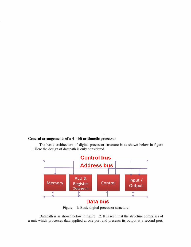
Prof. Roopa Kulkarni, GIT, Belgaum. 2
2. It is possible to divide any complex function into less complex subfunctions that
is up to leaf cells
3. Process is known as top-down design
4. As a systems complexity increases, its organization changes as different factors
become relevant to its creation
5. Coupling can be used as a measure of how much submodels interact
6. It is crucial that components interacting with high frequency be physically
proximate, since one may pay severe penalties for long, high-bandwidth
interconnects
7. Concurrency should be exploited – it is desirable that all gates on the chip do
useful work most of the time
8. Because technology changes so fast, the adaptation to a new process must occur
in a short time.
Hence representing a design several approaches are possible. They are:
• Conventional circuit symbols
• Logic symbols
• Stick diagram
• Any mixture of logic symbols and stick diagram that is convenient at a stage
• Mask layouts
• Architectural block diagrams and floor plans
General arrangements of a 4 – bit arithmetic processor
The basic architecture of digital processor structure is as shown below in figure
6.1. Here the design of datapath is only considered.
Figure 6.1: Basic digital processor structure
Datapath is as shown below in figure 6.2. It is seen that the structure comprises of
a unit which processes data applied at one port and presents its output at a second port.
www.bookspar.com | VTU NOTES | QUESTION PAPERS | NEWS | RESULTS | FORUMS
www.bookspar.com | VTU NOTES | QUESTION PAPERS | NEWS | RESULTS | FORUMS
www.bookspar.com | VTU NOTES | QUESTION PAPERS | NEWS | RESULTS | FORUMS
www.bookspar.com | VTU NOTES | QUESTION PAPERS | NEWS | RESULTS | FORUMS
My
Text Box
Subsystem Design Processes Illustration
My
Text Box
General Considerations Lower unit cost Higher reliability Lower power dissipation, lower weight and lower volume Better performance Enhanced repeatability Possibility of reduced design/development periods

Prof. Roopa Kulkarni, GIT, Belgaum. 3
Alternatively, the two data ports may be combined as a single bidirectional port if storage
facilities exist in the datapath. Control over the functions to be performed is effected by
control signals as shown.
Figure 6.2: Communication strategy for the datapath
Datapath can be decomposed into blocks showing the main subunits as in
figure 3. In doing so it is useful to anticipate a possible floor plan to show the planned
relative decomposition of the subunits on the chip and hence on the mask layouts.
Figure 6.3: Subunits and basic interconnection for datapath
Nature of the bus architecture linking the subunits is discussed below. Some of
the possibilities are:
One bus architecture:
Figure 6.4: One bus architecture
Sequence:
1. 1st operand from registers to ALU. Operand is stored there.
2. 2nd
operand from register to ALU and added.
3. Result is passed through shifter and stored in the register
www.bookspar.com | VTU NOTES | QUESTION PAPERS | NEWS | RESULTS | FORUMS
www.bookspar.com | VTU NOTES | QUESTION PAPERS | NEWS | RESULTS | FORUMS
www.bookspar.com | VTU NOTES | QUESTION PAPERS | NEWS | RESULTS | FORUMS
www.bookspar.com | VTU NOTES | QUESTION PAPERS | NEWS | RESULTS | FORUMS

Prof. Roopa Kulkarni, GIT, Belgaum. 4
Two bus architecture:
Figure 6.5: Two bus architecture
Sequence:
1. Two operands (A & B) are sent from register(s) to ALU & are operated upon,
result S in ALU.
2. Result is passed through the shifter & stored in registers.
Three bus architecture:
Figure 6.6: Three bus architecture
Sequence:
Two operands (A & B) are sent from registers, operated upon, and shifted result
(S) returned to another register, all in same clock period.
In pursuing this design exercise, it was decided to implement the structure with a
2 – bus architecture. A tentative floor plan of the proposed design which includes some
form of interface to the parent system data bus is shown in figure 6.7.
Figure 6.7: Tentative floor plan for 4 – bit datapath
www.bookspar.com | VTU NOTES | QUESTION PAPERS | NEWS | RESULTS | FORUMS
www.bookspar.com | VTU NOTES | QUESTION PAPERS | NEWS | RESULTS | FORUMS
www.bookspar.com | VTU NOTES | QUESTION PAPERS | NEWS | RESULTS | FORUMS
www.bookspar.com | VTU NOTES | QUESTION PAPERS | NEWS | RESULTS | FORUMS

Prof. Roopa Kulkarni, GIT, Belgaum. 5
The proposed processor will be seen to comprise a register array in which 4-bit
numbers can be stored, either from an I/O port or from the output of the ALU via a
shifter. Numbers from the register array can be fed in pairs to the ALU to be added (or
subtracted) and the result can be shifted or not. The data connections between the I/O
port, ALU, and shifter must be in the form of 4-bit buses. Also, each of the blocks must
be suitably connected to control lines so that its function may be defined for any of a
range of possible operations.
During the design process, and in particular when defining the interconnection
strategy and designing the stick diagrams, care must be taken in allocating the layers to
the various data or control paths. Points to be noted:
� Metal can cross poly or diffusion
� Poly crossing diffusion form a transistor
� Whenever lines touch on the same level an interconnection is formed
� Simple contacts can be used to join diffusion or poly to metal.
� Buried contacts or a butting contacts can be used to join diffusion and poly
� Some processes use 2nd
metal
� 1st and 2
nd metal layers may be joined using a via
� Each layer has particular electrical properties which must be taken into account
� For CMOS layouts, p-and n-diffusion wires must not directly join each other
� Nor may they cross either a p-well or an n-well boundary
Design of a 4-bit shifter
Any general purpose n-bit shifter should be able to shift incoming data by up to
n – 1 place in a right-shift or left-shift direction. Further specifying that all shifts should
be on an end-around basis, so that any bit shifted out at one end of a data word will be
shifted in at the other end of the word, then the problem of right shift or left shift is
greatly eased. It can be analyzed that for a 4-bit word, that a 1-bit shift right is equivalent
to a 3-bit shift left and a 2-bit shift right is equivalent to a 2-bit left etc. Hence, the design
of either shift right or left can be done. Here the design is of shift right by 0, 1, 2, or 3
places. The shifter must have:
• input from a four line parallel data bus
• four output lines for the shifted data
• means of transferring input data to output lines with any shift from 0 to 3 bits
Consider a direct MOS switch implementation of a 4 X 4 crossbar switches shown in
figure 6.8. The arrangement is general and may be expanded to accommodate n-bit
inputs/outputs. In this arrangement any input can be connected to any or all the outputs.
Furthermore, 16 control signals (sw00 – sw15), one for each transistor switch, must be
provided to drive the crossbar switch, and such complexity is highly undesirable.
www.bookspar.com | VTU NOTES | QUESTION PAPERS | NEWS | RESULTS | FORUMS
www.bookspar.com | VTU NOTES | QUESTION PAPERS | NEWS | RESULTS | FORUMS
www.bookspar.com | VTU NOTES | QUESTION PAPERS | NEWS | RESULTS | FORUMS
www.bookspar.com | VTU NOTES | QUESTION PAPERS | NEWS | RESULTS | FORUMS

Prof. Roopa Kulkarni, GIT, Belgaum. 6
Figure 6.8: 4 X 4 crossbar switch
An adaptation of this arrangement recognizes the fact that we couple the switch
gates together in groups of four and also form four separate groups corresponding to
shifts of zero, one, two and three bits. The resulting arrangement is known as a barrel
shifter and a 4 X 4 barrel shifter circuit diagram is as shown in the figure 6.9.
Figure 6.9: 4 X 4 barrel shifter
The interbus switches have their gate inputs connected in a staircase fashion in
groups of four and there are now four shift control inputs which must be mutually
exclusive in the active state. CMOS transmission gates may be used in place of the
simple pass transistor switches if appropriate. Barrel shifter connects the input lines
representing a word to a group of output lines with the required shift determined by its
control inputs (sh0, sh1, sh2, sh3). Control inputs also determine the direction of the shift.
If input word has n – bits and shifts from 0 to n-1 bit positions are to be implemented.
To summaries the design steps
Set out the specifications
Partition the architecture into subsystems
Set a tentative floor plan
Determine the interconnects
Choose layers for the bus & control lines
Conceive a regular architecture
Develop stick diagram
www.bookspar.com | VTU NOTES | QUESTION PAPERS | NEWS | RESULTS | FORUMS
www.bookspar.com | VTU NOTES | QUESTION PAPERS | NEWS | RESULTS | FORUMS
www.bookspar.com | VTU NOTES | QUESTION PAPERS | NEWS | RESULTS | FORUMS
www.bookspar.com | VTU NOTES | QUESTION PAPERS | NEWS | RESULTS | FORUMS

Prof. Roopa Kulkarni, GIT, Belgaum. 7
Produce mask layouts for standard cell
Cascade & replicate standard cells as required to complete the design
Design of an ALU subsystem Having designed the shifter, we shall design another subsystem of the 4-bit data
path. An appropriate choice is ALU as shown in the figure 6.10 below.
Figure 6.10: 4-bit data path for processor
The heart of the ALU is a 4-bit adder circuit. A 4-bit adder must take sum of two
4-bit numbers, and there is an assumption that all 4-bit quantities are presented in parallel
form and that the shifter circuit is designed to accept and shift a 4-bit parallel sum from
the ALU. The sum is to be stored in parallel at the output of the adder from where it is
fed through the shifter and back to the register array. Therefore, a single 4-bit data bus is
needed from the adder to the shifter and another 4-bit bus is required from the shifted
output back to the register array. Hence, for an adder two 4-bit parallel numbers are fed
on two 4-bit buses. The clock signal is also required to the adder, during which the inputs
are given and sum is generated. The shifter is unclocked but must be connected to four
shift control lines.
Design of a 4-bit adder: The truth table of binary adder is as shown in table 6.1
Inputs Outputs
Ak Bk Ck-1 Sk Ck
0 0 0 0 0
0 1 0 1 0
1 0 0 1 0
1 1 0 0 1
0 0 1 1 0
0 1 1 0 1
1 0 1 0 1
1 1 1 1 1
www.bookspar.com | VTU NOTES | QUESTION PAPERS | NEWS | RESULTS | FORUMS
www.bookspar.com | VTU NOTES | QUESTION PAPERS | NEWS | RESULTS | FORUMS
www.bookspar.com | VTU NOTES | QUESTION PAPERS | NEWS | RESULTS | FORUMS
www.bookspar.com | VTU NOTES | QUESTION PAPERS | NEWS | RESULTS | FORUMS

Prof. Roopa Kulkarni, GIT, Belgaum. 8
As seen from the table any column k there will be three inputs namely Ak , Bk as
present input number and Ck-1 as the previous carry. It can also be seen that there are two
outputs sum Sk and carry Ck.
From the table one form of the equation is:
Sum Sk = HkCk-l’ + Hk’Ck-1
New carry Ck = AkBk + Hkck-1
Where
Half sum Hk = Ak’Bk + Ak Bk’
Adder element requirements Table 6.1 reveals that the adder requirement may be stated as:
If Ak = Bk then Sk = Ck-1
Else Sk = Ck-l’
And for the carry Ck
If Ak = Bk then Ck = Ak = Bk
Else Ck = Ck-l
Thus the standard adder element for 1-bit is as shown in the figure 6.11.
Figure 6.11: Adder element
Implementing ALU functions with an adder:
An ALU must be able to add and subtract two binary numbers, perform logical
operations such as And, Or and Equality (Ex-or) functions. Subtraction can be performed
by taking 2’s complement of the negative number and perform the further addition. It is
desirable to keep the architecture as simple as possible, and also see that the adder
performs the logical operations also. Hence let us examine the possibility.
The adder equations are:
Sum Sk = HkCk-l’ + Hk’Ck-1
New carry Ck = AkBk + Hk Ck-1
Where
Half sum Hk = Ak’Bk + Ak Bk’
Let us consider the sum output, if the previous carry is at logical 0, then
Sk = Hk. 1 + Hk’. 0
Sk = Hk = Ak’Bk + Ak Bk’ – An Ex-or operation
Now, if Ck-1 is logically 1, then
Sk = Hk. 0 + Hk’. 1
www.bookspar.com | VTU NOTES | QUESTION PAPERS | NEWS | RESULTS | FORUMS
www.bookspar.com | VTU NOTES | QUESTION PAPERS | NEWS | RESULTS | FORUMS
www.bookspar.com | VTU NOTES | QUESTION PAPERS | NEWS | RESULTS | FORUMS
www.bookspar.com | VTU NOTES | QUESTION PAPERS | NEWS | RESULTS | FORUMS

Prof. Roopa Kulkarni, GIT, Belgaum. 9
Sk = Hk’ – An Ex-Nor operation
Next, consider the carry output of each element, first Ck-1 is held at logical 0, then
Ck = AkBk + Hk . 0
Ck = AkBk - An And operation
Now if Ck-1 is at logical 1, then
Ck = AkBk + Hk . 1
On solving Ck = Ak + Bk - An Or operation
The adder element implementing both the arithmetic and logical functions can be
implemented as shown in the figure 6.12.
Figure 6.12: 1-bit adder element
The above can be cascaded to form 4-bit ALU.
A further consideration of adders
Generation:
This principle of generation allows the system to take advantage of the
occurrences “ak=bk”. In both cases (ak=1 or ak=0) the carry bit will be known.
Propagation:
If we are able to localize a chain of bits ak ak+1...ak+p and bk bk+1...bk+p for which ak
not equal to bk for k in [k,k+p], then the output carry bit of this chain will be equal to the
input carry bit of the chain.
These remarks constitute the principle of generation and propagation used to
speed the addition of two numbers.
All adders which use this principle calculate in a first stage.
pk = ak XOR bk
gk = ak bk
www.bookspar.com | VTU NOTES | QUESTION PAPERS | NEWS | RESULTS | FORUMS
www.bookspar.com | VTU NOTES | QUESTION PAPERS | NEWS | RESULTS | FORUMS
www.bookspar.com | VTU NOTES | QUESTION PAPERS | NEWS | RESULTS | FORUMS
www.bookspar.com | VTU NOTES | QUESTION PAPERS | NEWS | RESULTS | FORUMS

Prof. Roopa Kulkarni, GIT, Belgaum. 10
Manchester carry – chain
This implementation can be very performant (20 transistors) depending on the
way the XOR function is built. The carry propagation of the carry is controlled by the
output of the XOR gate. The generation of the carry is directly made by the function at
the bottom. When both input signals are 1, then the inverse output carry is 0.
Figure-6.12: An adder with propagation signal controlling the pass-gate
In the schematic of Figure 6.12, the carry passes through a complete transmission
gate. If the carry path is precharged to VDD, the transmission gate is then reduced to a
simple NMOS transistor. In the same way the PMOS transistors of the carry generation is
removed. One gets a Manchester cell.
www.bookspar.com | VTU NOTES | QUESTION PAPERS | NEWS | RESULTS | FORUMS
www.bookspar.com | VTU NOTES | QUESTION PAPERS | NEWS | RESULTS | FORUMS
www.bookspar.com | VTU NOTES | QUESTION PAPERS | NEWS | RESULTS | FORUMS
www.bookspar.com | VTU NOTES | QUESTION PAPERS | NEWS | RESULTS | FORUMS

Prof. Roopa Kulkarni, GIT, Belgaum. 11
Figure-6.13: The Manchester cell
The Manchester cell is very fast, but a large set of such cascaded cells would be
slow. This is due to the distributed RC effect and the body effect making the propagation
time grow with the square of the number of cells. Practically, an inverter is added every
four cells, like in Figure 6.14.
Figure-6.14: The Manchester carry cell
Adder Enhancement techniques
The operands of addition are the addend and the augend. The addend is added to
the augend to form the sum. In most computers, the augmented operand (the augend) is
replaced by the sum, whereas the addend is unchanged. High speed adders are not only
for addition but also for subtraction, multiplication and division. The speed of a digital
processor depends heavily on the speed of adders. The adders add vectors of bits and the
principal problem is to speed- up the carry signal. A traditional and non optimized four
bit adder can be made by the use of the generic one-bit adder cell connected one to the
other. It is the ripple carry adder. In this case, the sum resulting at each stage need to wait
for the incoming carry signal to perform the sum operation. The carry propagation can be
speed-up in two ways. The first –and most obvious– way is to use a faster logic circuit
technology. The second way is to generate carries by means of forecasting logic that does
not rely on the carry signal being rippled from stage to stage of the adder.
www.bookspar.com | VTU NOTES | QUESTION PAPERS | NEWS | RESULTS | FORUMS
www.bookspar.com | VTU NOTES | QUESTION PAPERS | NEWS | RESULTS | FORUMS
www.bookspar.com | VTU NOTES | QUESTION PAPERS | NEWS | RESULTS | FORUMS
www.bookspar.com | VTU NOTES | QUESTION PAPERS | NEWS | RESULTS | FORUMS

Prof. Roopa Kulkarni, GIT, Belgaum. 12
The Carry-Skip Adder
Depending on the position at which a carry signal has been generated, the
propagation time can be variable. In the best case, when there is no carry generation, the
addition time will only take into account the time to propagate the carry signal. Figure
6.15 is an example illustrating a carry signal generated twice, with the input carry being
equal to 0. In this case three simultaneous carry propagations occur. The longest is the
second, which takes 7 cell delays (it starts at the 4th position and ends at the 11th
position). So the addition time of these two numbers with this 16-bits Ripple Carry Adder
is 7.k + k’, where k is the delay cell and k’ is the time needed to compute the 11th sum bit
using the 11th carry-in.
With a Ripple Carry Adder, if the input bits Ai and Bi are different for all position
i, then the carry signal is propagated at all positions (thus never generated), and the
addition is completed when the carry signal has propagated through the whole adder. In
this case, the Ripple Carry Adder is as slow as it is large. Actually, Ripple Carry Adders
are fast only for some configurations of the input words, where carry signals are
generated at some positions.
Carry Skip Adders take advantage both of the generation or the propagation of the
carry signal. They are divided into blocks, where a special circuit detects quickly if all the
bits to be added are different (Pi = 1 in all the block). The signal produced by this circuit
will be called block propagation signal. If the carry is propagated at all positions in the
block, then the carry signal entering into the block can directly bypass it and so be
transmitted through a multiplexer to the next block. As soon as the carry signal is
transmitted to a block, it starts to propagate through the block, as if it had been generated
at the beginning of the block. Figure 6.16 shows the structure of a 24-bits Carry Skip
Adder, divided into 4 blocks.
Figure 6.15: Example of Carry skip adder
www.bookspar.com | VTU NOTES | QUESTION PAPERS | NEWS | RESULTS | FORUMS
www.bookspar.com | VTU NOTES | QUESTION PAPERS | NEWS | RESULTS | FORUMS
www.bookspar.com | VTU NOTES | QUESTION PAPERS | NEWS | RESULTS | FORUMS
www.bookspar.com | VTU NOTES | QUESTION PAPERS | NEWS | RESULTS | FORUMS

Prof. Roopa Kulkarni, GIT, Belgaum. 13
Figure-6.16: Block diagram of a carry skip adder
Optimization of the carry skip adder
It becomes now obvious that there exist a trade-off between the speed and the size
of the blocks. In this part we analyze the division of the adder into blocks of equal size.
Let us denote k1 the time needed by the carry signal to propagate through an adder cell,
and k2 the time it needs to skip over one block. Suppose the N-bit Carry Skip Adder is
divided into M blocks, and each block contains P adder cells. The actual addition time of
a Ripple Carry Adder depends on the configuration of the input words. The completion
time may be small but it also may reach the worst case, when all adder cells propagate the
carry signal. In the same way, we must evaluate the worst carry propagation time for the
Carry Skip Adder. The worst case of carry propagation is depicted in Figure 6.17.
Figure-6.17: Worst case carry propagation for Carry Skip adder
The configuration of the input words is such that a carry signal is generated at the
beginning of the first block. Then this carry signal is propagated by all the succeeding
adder cells but the last which generates another carry signal. In the first and the last block
the block propagation signal is equal to 0, so the entering carry signal is not transmitted
to the next block. Consequently, in the first block, the last adder cells must wait for the
carry signal, which comes from the first cell of the first block. When going out of the first
www.bookspar.com | VTU NOTES | QUESTION PAPERS | NEWS | RESULTS | FORUMS
www.bookspar.com | VTU NOTES | QUESTION PAPERS | NEWS | RESULTS | FORUMS
www.bookspar.com | VTU NOTES | QUESTION PAPERS | NEWS | RESULTS | FORUMS
www.bookspar.com | VTU NOTES | QUESTION PAPERS | NEWS | RESULTS | FORUMS

Prof. Roopa Kulkarni, GIT, Belgaum. 14
block, the carry signal is distributed to the 2nd
, 3rd
and last block, where it propagates. In
these blocks, the carry signals propagate almost simultaneously (we must account for the
multiplexer delays). Any other situation leads to a better case. Suppose for instance that
the 2nd
block does not propagate the carry signal (its block propagation signal is equal to
zero), then it means that a carry signal is generated inside. This carry signal starts to
propagate as soon as the input bits are settled. In other words, at the beginning of the
addition, there exist two sources for the carry signals. The paths of these carry signals are
shorter than the carry path of the worst case. Let us formalize that the total adder is made
of N adder cells. It contains M blocks of P adder cells. The total of adder cells is then
N=M.P
The time T needed by the carry signal to propagate through P adder cells is
T=k1.P
The time T' needed by the carry signal to skip through M adder blocks is
T'=k2.M
The problem to solve is to minimize the worst case delay which is:
The Carry-Select Adder
This type of adder is not as fast as the Carry Look Ahead (CLA) presented in a
next section. However, despite its bigger amount of hardware needed, it has an interesting
design concept. The Carry Select principle requires two identical parallel adders that are
partitioned into four-bit groups. Each group consists of the same design as that shown on
Figure 6.18. The group generates a group carry. In the carry select adder, two sums are
generated simultaneously. One sum assumes that the carry in is equal to one as the other
assumes that the carry in is equal to zero. So that the predicted group carry is used to
select one of the two sums.
It can be seen that the group carries logic increases rapidly when more high- order
groups are added to the total adder length. This complexity can be decreased, with a
subsequent increase in the delay, by partitioning a long adder into sections, with four
groups per section, similar to the CLA adder.
www.bookspar.com | VTU NOTES | QUESTION PAPERS | NEWS | RESULTS | FORUMS
www.bookspar.com | VTU NOTES | QUESTION PAPERS | NEWS | RESULTS | FORUMS
www.bookspar.com | VTU NOTES | QUESTION PAPERS | NEWS | RESULTS | FORUMS
www.bookspar.com | VTU NOTES | QUESTION PAPERS | NEWS | RESULTS | FORUMS

Prof. Roopa Kulkarni, GIT, Belgaum. 15
Figure-6.18: The Carry Select adder
Optimization of the carry select adder
• Computational time
T = K1n
• Dividing the adder into blocks with 2 parallel paths
T = K1n/2 + K2
• For a n-bit adder of M-blocks and each block contains P adder cells in series
T = PK1 + (M – 1) K2 ; n = M.P minimum value for T is when M=√(K1n / K1 )
The Carry Look-Ahead Adder
The limitation in the sequential method of forming carries, especially in the
Ripple Carry adder arises from specifying ci as a specific function of ci-1. It is possible to
express a carry as a function of all the preceding low order carry by using the recursivity
of the carry function. With the following expression a considerable increase in speed can
be realized.
Usually the size and complexity for a big adder using this equation is not
affordable. That is why the equation is used in a modular way by making groups of carry
(usually four bits). Such a unit generates then a group carry which give the right predicted
information to the next block giving time to the sum units to perform their calculation.
Figure-6.19: The Carry Generation unit performing the Carry group computation
www.bookspar.com | VTU NOTES | QUESTION PAPERS | NEWS | RESULTS | FORUMS
www.bookspar.com | VTU NOTES | QUESTION PAPERS | NEWS | RESULTS | FORUMS
www.bookspar.com | VTU NOTES | QUESTION PAPERS | NEWS | RESULTS | FORUMS
www.bookspar.com | VTU NOTES | QUESTION PAPERS | NEWS | RESULTS | FORUMS

Prof. Roopa Kulkarni, GIT, Belgaum. 16
Such unit can be implemented in various ways, according to the allowed level of
abstraction. In a CMOS process, 17 transistors are able to guarantee the static function
(Figure 6.20). However this design requires a careful sizing of the transistors put in
series.
The same design is available with less transistors in a dynamic logic design. The
sizing is still an important issue, but the number of transistors is reduced (Figure 6.21).
Figure-6.20: Static implementation of the 4-bit carry lookahead chain
Figure-6.21: Dynamic implementation of the 4-bit carry lookahead chain
Figure 6.22 shows the implementation of 16-bit CLA adder.
www.bookspar.com | VTU NOTES | QUESTION PAPERS | NEWS | RESULTS | FORUMS
www.bookspar.com | VTU NOTES | QUESTION PAPERS | NEWS | RESULTS | FORUMS
www.bookspar.com | VTU NOTES | QUESTION PAPERS | NEWS | RESULTS | FORUMS
www.bookspar.com | VTU NOTES | QUESTION PAPERS | NEWS | RESULTS | FORUMS

Prof. Roopa Kulkarni, GIT, Belgaum. 17
Figure-6.22: Implementation of a 16-bit CLA adder
Multipliers
Introduction
Multiplication can be considered as a series of repeated additions. The number to
be added is the multiplicand, the number of times that it is added is the multiplier, and the
result is the product. Each step of the addition generates a partial product. In most
computers, the operands usually contain the same number of bits. When the operands are
interpreted as integers, the product is generally twice the length of the operands in order
to preserve the information content. This repeated addition method that is suggested by
the arithmetic definition is slow that it is almost always replaced by an algorithm that
makes use of positional number representation.
It is possible to decompose multipliers in two parts. The first part is dedicated to
the generation of partial products, and the second one collects and adds them. As for
adders, it is possible to enhance the intrinsic performances of multipliers. Acting in the
generation part, the Booth (or modified Booth) algorithm is often used because it reduces
the number of partial products. The collection of the partial products can then be made
using a regular array, a Wallace tree or a binary tree
Serial-Parallel Multiplier
This multiplier is the simplest one, the multiplication is considered as a
succession of additions.
if A = (an an-1……a0) and B = (bn bn-1……b0)
The product A.B is expressed as :
A.B = A.2n.bn + A.2
n-1.bn-1 +…+ A.20.b
0
The structure of Figure 6.23 is suited only for positive operands. If the operands are
negative and coded in 2’s complement:
1. The most significant bit of B has a negative weight, so a subtraction has to be
performed at the last step.
www.bookspar.com | VTU NOTES | QUESTION PAPERS | NEWS | RESULTS | FORUMS
www.bookspar.com | VTU NOTES | QUESTION PAPERS | NEWS | RESULTS | FORUMS
www.bookspar.com | VTU NOTES | QUESTION PAPERS | NEWS | RESULTS | FORUMS
www.bookspar.com | VTU NOTES | QUESTION PAPERS | NEWS | RESULTS | FORUMS

Prof. Roopa Kulkarni, GIT, Belgaum. 18
2. Operand A.2k must be written on 2N bits, so the most significant bit of A must be
duplicated. It may be easier to shift the content of the accumulator to the right
instead of shifting A to the left.
Figure-6.23: Serial-Parallel multiplier
Braun Parallel Multiplier
The simplest parallel multiplier is the Braun array. All the partial products A.bk
are computed in parallel, and then collected through a cascade of Carry Save Adders. At
the bottom of the array, the output of the array is noted in Carry Save, so an additional
adder converts it (by the mean of carry propagation) into the classical notation (Figure
6.24). The completion time is limited by the depth of the carry save array, and by the
carry propagation in the adder. Note that this multiplier is only suited for positive
operands. Negative operands may be multiplied using a Baugh-Wooley multiplier.
Figure 6.24: A 4-bit Braun Array
www.bookspar.com | VTU NOTES | QUESTION PAPERS | NEWS | RESULTS | FORUMS
www.bookspar.com | VTU NOTES | QUESTION PAPERS | NEWS | RESULTS | FORUMS
www.bookspar.com | VTU NOTES | QUESTION PAPERS | NEWS | RESULTS | FORUMS
www.bookspar.com | VTU NOTES | QUESTION PAPERS | NEWS | RESULTS | FORUMS

Prof. Roopa Kulkarni, GIT, Belgaum. 24
Unit 7: Memory
Objectives: At the end of this unit we will be able to understand
• System timing consideration
• Storage / Memory Elements
� dynamic shift register
� 1T and 3T dynamic memory
� 4T dynamic and 6T static CMOS memory
• Array of memory cells
System timing considerations: • Two phase non-overlapping clock
• φ1 leads φ2
• Bits to be stored are written to register and subsystems on φ1
• Bits or data written are assumed to be settled before φ2
• φ2 signal used to refresh data
• Delays assumed to be less than the intervals between the leading edge of φ1 & φ2
• Bits or data may be read on the next φ1
• There must be atleast one clocked storage element in series with every closed
loop signal path
Storage / Memory Elements:
The elements that we will be studying are:
• Dynamic shift register
• 3T dynamic RAM cell
• 1T dynamic memory cell
• Pseudo static RAM / register cell
• 4T dynamic & 6T static memory cell
• JK FF circuit
• D FF circuit
Dynamic shift register:
Circuit diagram: Refer to unit 4(ch 6.5.4)
Power dissipation • static dissipation is very small
• dynamic power is significant
• dissipation can be reduced by alternate geometry
Volatility • data storage time is limited to 1msec or less
www.bookspar.com | VTU NOTES | QUESTION PAPERS | NEWS | RESULTS | FORUMS
www.bookspar.com | VTU NOTES | QUESTION PAPERS | NEWS | RESULTS | FORUMS
www.bookspar.com | VTU NOTES | QUESTION PAPERS | NEWS | RESULTS | FORUMS
www.bookspar.com | VTU NOTES | QUESTION PAPERS | NEWS | RESULTS | FORUMS

Prof. Roopa Kulkarni, GIT, Belgaum. 25
3T dynamic RAM cell:
Circuit diagram
Figure 7.1: 3T Dynamic RAM Cell
Working • RD = low, bit read from bus through T1, WR = high, logic level on bus
sent to Cg of T2, WR = low again
• Bit level is stored in Cg of T2, RD=WR=low
• Stored bit is read by RD = high, bus will be pulled to ground if a 1 was
stored else 0 if T2 non-conducting, bus will remain high.
Dissipation • Static dissipation is nil
• Depends on bus pull-up & on duration of RD signal & switching
frequency
Volatility • Cell is dynamic, data will be there as long as charge remains on Cg of T2
1T dynamic memory cell:
Circuit diagram
Figure 7.2: 1T Dynamic RAM Cell
T1
Bus
GND
WR RD
T3
T2
VDD
www.bookspar.com | VTU NOTES | QUESTION PAPERS | NEWS | RESULTS | FORUMS
www.bookspar.com | VTU NOTES | QUESTION PAPERS | NEWS | RESULTS | FORUMS
www.bookspar.com | VTU NOTES | QUESTION PAPERS | NEWS | RESULTS | FORUMS
www.bookspar.com | VTU NOTES | QUESTION PAPERS | NEWS | RESULTS | FORUMS

Prof. Roopa Kulkarni, GIT, Belgaum. 26
Working • Row select (RS) = high, during write from R/W line Cm is charged
• data is read from Cm by detecting the charge on Cm with RS = high
• cell arrangement is bit complex.
• solution: extend the diffusion area comprising source of pass transistor,
but Cd<<< Cgchannel
• another solution : create significant capacitor using poly plate over
diffusion area.
• Cm is formed as a 3-plate structure
• with all this careful design is necessary to achieve consistent readability
Dissipation • no static power, but there must be an allowance for switching energy
during read/write
Pseudo static RAM / register cell:
Circuit diagram
Figure 7.3: nMOS pseudo-static memory Cell
Figure 7.4: CMOS pseudo-static memory Cell
WR,φ1 RD,φ1
φ2
O/P
φ2 WR,φ1 RD,φ1
φ2
O/P
WR, φ1 RD, φ1
www.bookspar.com | VTU NOTES | QUESTION PAPERS | NEWS | RESULTS | FORUMS
www.bookspar.com | VTU NOTES | QUESTION PAPERS | NEWS | RESULTS | FORUMS
www.bookspar.com | VTU NOTES | QUESTION PAPERS | NEWS | RESULTS | FORUMS
www.bookspar.com | VTU NOTES | QUESTION PAPERS | NEWS | RESULTS | FORUMS

Prof. Roopa Kulkarni, GIT, Belgaum. 27
Working • dynamic RAM need to be refreshed periodically and hence not
convenient
• static RAM needs to be designed to hold data indefinitely
• One way is connect 2 inverter stages with a feedback.
• say φ2 to refresh the data every clock cycle
• bit is written on activating the WR line which occurs with φ1 of the clock
• bit on Cg of inverter 1 will produce complemented output at inverter 1 and
true at output of inverter 2
• at every φ2 , stored bit is refreshed through the gated feedback path
• stored bit is held till φ2 of clock occurs at time less than the decay time of
stored bit
• to read RD along with φ1 is activated
Note:
• WR and RD must be mutually exclusive
• φ2 is used for refreshing, hence no data to be read, if so charge sharing
effect, leading to destruction of stored bit
• cells must be stackable, both side-by-side & top to bottom
• allow for other bus lines to run through the cell
4T dynamic & 6T static memory cell:
Circuit diagram
Figure 7.4: Dynamic and static memory cells
bit bit_b
word
www.bookspar.com | VTU NOTES | QUESTION PAPERS | NEWS | RESULTS | FORUMS
www.bookspar.com | VTU NOTES | QUESTION PAPERS | NEWS | RESULTS | FORUMS
www.bookspar.com | VTU NOTES | QUESTION PAPERS | NEWS | RESULTS | FORUMS
www.bookspar.com | VTU NOTES | QUESTION PAPERS | NEWS | RESULTS | FORUMS

Prof. Roopa Kulkarni, GIT, Belgaum. 28
Working • uses 2 buses per bit to store bit and bit’
• both buses are precharged to logic 1 before read or write operation.
• write operation
• read operation
Write operation
• both bit & bit’ buses are precharged to VDD with clock φ1 via transistor
T5 & T6
• column select line is activated along with φ2
• either bit or bit’ line is discharged along the I/O line when carrying a
logic 0
• row & column select signals are activated at the same time => bit line
states are written in via T3 & T4, stored by T1 & T2 as charge
Read operation
• bit and bit’ lines are again precharged to VDD via T5 & T6 during φ1
• if 1 has been stored, T2 ON & T1 OFF
• bit’ line will be discharged to VSS via T2
• each cell of RAM array be of minimum size & hence will be the
transistors
• implies incapable of sinking large charges quickly
• RAM arrays usually employ some form of sense amplifier
• T1, T2, T3 & T4 form as flip-flop circuit
• if sense line to be inactive, state of the bit line reflects the charge present
on gate capacitance of T1 & T3
• current flowing from VDD through an on transistor helps to maintain the
state of bit lines
www.bookspar.com | VTU NOTES | QUESTION PAPERS | NEWS | RESULTS | FORUMS
www.bookspar.com | VTU NOTES | QUESTION PAPERS | NEWS | RESULTS | FORUMS
www.bookspar.com | VTU NOTES | QUESTION PAPERS | NEWS | RESULTS | FORUMS
www.bookspar.com | VTU NOTES | QUESTION PAPERS | NEWS | RESULTS | FORUMS

Prof. Roopa Kulkarni, GIT, Belgaum. 29
Unit 8: Testability
Objective: At the end of this unit we will be able to understand
• Design for testability (DFT)
• DFT methods for digital circuits:
� Ad-hoc methods
� Structured methods:
• Scan
• Level Sensitive Scan Design
• Boundary scan
• Other Scan Techniques
Definition:
Design for testability (DFT) refers to those design techniques that make test generation
and test application cost-effective.
Some terminologies:
Input / output (I/O) pads
• Protection of circuitry on chip from damage
• Care to be taken in handling all MOS circuits
• Provide necessary buffering between the environments On & OFF chip
• Provide for the connections of power supply
• Pads must be always placed around the peripheral
Minimum set of pads include:
• VDD connection pad
• GND(VSS) connection pad
• Input pad
• Output pad
• Bidirectional I/O pad
Designer must be aware of:
• nature of circuitry
• ratio/size of inverters/buffers on which output lines are connected
• how input lines pass through the pad circuit (pass transistor/transmission gate)
System delays
Buses:
• convenient concept in distributing data & control through a system
• bidirectional buses are convenient
• in design of datapath
• problems: capacitive load present
www.bookspar.com | VTU NOTES | QUESTION PAPERS | NEWS | RESULTS | FORUMS
www.bookspar.com | VTU NOTES | QUESTION PAPERS | NEWS | RESULTS | FORUMS
www.bookspar.com | VTU NOTES | QUESTION PAPERS | NEWS | RESULTS | FORUMS
www.bookspar.com | VTU NOTES | QUESTION PAPERS | NEWS | RESULTS | FORUMS

Prof. Roopa Kulkarni, GIT, Belgaum. 30
• largest capacitance
• sufficient time must be allowed to charge the total bus
• clock φ1 & φ2
Control paths, selectors & decoders
1. select registers and open pass transistors to connect cells to bus
2. Data propagation delay bus
3. Carry chain delay
Faults and Fault Modeling
A fault model is a model of how a physical or parametric fault manifests itself in the
circuit Operation. Fault tests are derived based on these models
Physical Faults are caused due to the following reasons:
� Defect in silicon substrate
� Photolithographic defects
� Mask contamination and scratches
� Process variations and abnormalities
� Oxide defects
Physical faults cause Electrical and Logical faults
Logical Faults are:
� Single/multiple stuck-at (most used)
� CMOS stuck-open
� CMOS stuck-on
� AND / OR Bridging faults
Electrical faults are due to short, opens, transistor stuck on, stuck open, excessive steady
state currents, resistive shorts and open.
Design for Testability
Two key concepts
• Observability
• Controllability
DFT often is associated with design modifications that provide improved access
to internal circuit elements such that the local internal state can be controlled
(controllability) and/or observed (observability) more easily. The design modifications
can be strictly physical in nature (e.g., adding a physical probe point to a net) and/or add
active circuit elements to facilitate controllability/observability (e.g., inserting a
multiplexer into a net). While controllability and observability improvements for internal
circuit elements definitely are important for test, they are not the only type of DFT
www.bookspar.com | VTU NOTES | QUESTION PAPERS | NEWS | RESULTS | FORUMS
www.bookspar.com | VTU NOTES | QUESTION PAPERS | NEWS | RESULTS | FORUMS
www.bookspar.com | VTU NOTES | QUESTION PAPERS | NEWS | RESULTS | FORUMS
www.bookspar.com | VTU NOTES | QUESTION PAPERS | NEWS | RESULTS | FORUMS

Prof. Roopa Kulkarni, GIT, Belgaum. 31
Testing combinational logic
The solution to the problem of testing a purely combinational logic block is a
good set of patterns detecting "all" the possible faults.
The first idea to test an N input circuit would be to apply an N-bit counter to the
inputs (controllability), then generate all the 2N combinations, and observe the outputs
for checking (observability). This is called "exhaustive testing", and it is very efficient...
but only for few- input circuits. When the input number increase, this technique becomes
very time consuming.
Sensitized Path Testing
Most of the time, in exhaustive testing, many patterns do not occur during the
application of the circuit. So instead of spending a huge amount of time searching for
faults everywhere, the possible faults are first enumerated and a set of appropriate vectors
are then generated. This is called "single-path sensitization" and it is based on "fault
oriented testing".
www.bookspar.com | VTU NOTES | QUESTION PAPERS | NEWS | RESULTS | FORUMS
www.bookspar.com | VTU NOTES | QUESTION PAPERS | NEWS | RESULTS | FORUMS
www.bookspar.com | VTU NOTES | QUESTION PAPERS | NEWS | RESULTS | FORUMS
www.bookspar.com | VTU NOTES | QUESTION PAPERS | NEWS | RESULTS | FORUMS

Prof. Roopa Kulkarni, GIT, Belgaum. 32
The basic idea is to select a path from the site of a fault, through a sequence of gates
leading to an output of the combinational logic under test. The process is composed of
three steps :
• Manifestation : gate inputs, at the site of the fault, are specified as to generate the
opposite value of the faulty value (0 for SA1, 1 for SA0).
• Propagation : inputs of the other gates are determined so as to propagate the fault
signal along the specified path to the primary output of the circuit. This is done by
setting these inputs to "1" for AND/NAND gates and "0" for OR/NOR gates.
• Consistency : or justification. This final step helps finding the primary input
pattern that will realize all the necessary input values. This is done by tracing
backward from the gate inputs to the primary inputs of the logic in order to
receive the test patterns.
Example1 - SA1 of line1 (L1) : the aim is to find the vector(s) able to detect this fault.
• Manifestation: L1 = 0 , then input A = 0. In a fault-free situation, the output F
changes with A if B,C and D are fixed : for B,C and D fixed, L1 is SA1 gives
F = 0, for instance, even if A = 0 (F = 1 for fault-free).
• Propagation: Through the AND-gate : L5 = L8 = 1, this condition is necessary
for the propagation of the " L1 = 0 ". This leads to L10 = 0. Through the
NOR-gate, and since L10 = 0, then L11 = 0, so the propagated manifestation can
reach the primary output F. F is then read and compared with the fault-free value:
F = 1.
www.bookspar.com | VTU NOTES | QUESTION PAPERS | NEWS | RESULTS | FORUMS
www.bookspar.com | VTU NOTES | QUESTION PAPERS | NEWS | RESULTS | FORUMS
www.bookspar.com | VTU NOTES | QUESTION PAPERS | NEWS | RESULTS | FORUMS
www.bookspar.com | VTU NOTES | QUESTION PAPERS | NEWS | RESULTS | FORUMS

Prof. Roopa Kulkarni, GIT, Belgaum. 33
• Consistency: From the AND-gate : L5=1, and then L2=B=1. Also L8=1, and
then L7=1. Until now we found the values of A and B. When C and D are found,
then the test vectors are generated, in the same manner, and ready to be applied to
detect L1= SA1. From the NOT-gate, L11=0, so L9=L7=1 (coherency with
L8=L7). From the OR-gate L7=1, and since L6=L2=B=1, so B+C+D=L7=1, then
C and D can have either 1 or 0.
These three steps have led to four possible vectors detecting L1=SA1.
Example 2 - SA1 of line8 (L8) : The same combinational logic having one internal line
SA1
• Manifestation : L8 = 0
• Propagation: Through the AND-gate: L5 = L1 = 1, then L10 = 0 Through the
NOR-gate: we want to have L11 = 0, not to mask L10 = 0.
• Consistency: From the AND-gate L8 = 0 leads to L7 = 0. From the NOT-gate
L11 = 0 means L9 = L7 = 1, L7 could not be set to 1 and 0 at the same time. This
incompatibility could not be resolved in this case, and the fault "L8 SA1" remains
undetectable.
D – Algorithm:
Given a circuit comprising combinational logic, the algorithm aims to find an
assignment of input values that will allow detection of a particular internal fault by
examining the output conditions. Using this algorithm the system can either be said as
good or faulty. The existence of a fault in the faulty machine will cause a discrepancy
between its behavior and that of the good machine for some particular values of inputs.
The D-algorithm provides a systematic means of assigning input values for that particular
design so that the discrepancy is driven to an output where it may be observed and thus
detected. The algorithm is time-intensive and computing intensive for large circuits.
www.bookspar.com | VTU NOTES | QUESTION PAPERS | NEWS | RESULTS | FORUMS
www.bookspar.com | VTU NOTES | QUESTION PAPERS | NEWS | RESULTS | FORUMS
www.bookspar.com | VTU NOTES | QUESTION PAPERS | NEWS | RESULTS | FORUMS
www.bookspar.com | VTU NOTES | QUESTION PAPERS | NEWS | RESULTS | FORUMS

Prof. Roopa Kulkarni, GIT, Belgaum. 34
Practical design for test guidelines
Practical guidelines for testability should aim to facilitate test processes in three
main ways:
• facilitate test generation
• facilitate test application
• avoid timing problems
These matters are discussed as below:
Improve Controllability and Observability
All "design for test" methods ensure that a design has enough observability and
controllability to provide for a complete and efficient testing. When a node has difficult
access from primary inputs or outputs (pads of the circuit), a very efficient method is to
add internal pads acceding to this kind of node in order, for instance, to control block B2
and observe block B1 with a probe.
Figure 8.1 Improve Controllability and Observability
It is easy to observe block B1 by adding a pad just on its output, without breaking
the link between the two blocks. The control of the block B2 means to set a 0 or a 1 to its
input, and also to be transparent to the link B1-B2. The logic functions of this purpose are
a NOR- gate, transparent to a zero, and a NAND-gate, transparent to a one. By this way
the control of B2 is possible across these two gates.
Another implementation of this cell is based on pass-gates multiplexers
performing the same function, but with less transistors than with the NAND and NOR
gates (8 instead of 12).
The simple optimization of observation and control is not enough to guarantee a
full testability of the blocks B1 and B2. This technique has to be completed with some
other techniques of testing depending on the internal structures of blocks B1 and B2.
www.bookspar.com | VTU NOTES | QUESTION PAPERS | NEWS | RESULTS | FORUMS
www.bookspar.com | VTU NOTES | QUESTION PAPERS | NEWS | RESULTS | FORUMS
www.bookspar.com | VTU NOTES | QUESTION PAPERS | NEWS | RESULTS | FORUMS
www.bookspar.com | VTU NOTES | QUESTION PAPERS | NEWS | RESULTS | FORUMS
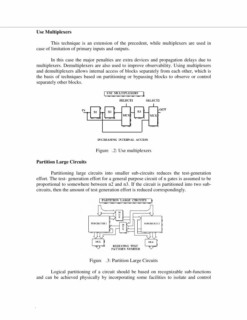
Prof. Roopa Kulkarni, GIT, Belgaum. 35
Use Multiplexers
This technique is an extension of the precedent, while multiplexers are used in
case of limitation of primary inputs and outputs.
In this case the major penalties are extra devices and propagation delays due to
multiplexers. Demultiplexers are also used to improve observability. Using multiplexers
and demultiplexers allows internal access of blocks separately from each other, which is
the basis of techniques based on partitioning or bypassing blocks to observe or control
separately other blocks.
Figure 8.2: Use multiplexers
Partition Large Circuits
Partitioning large circuits into smaller sub-circuits reduces the test-generation
effort. The test- generation effort for a general purpose circuit of n gates is assumed to be
proportional to somewhere between n2 and n3. If the circuit is partitioned into two sub-
circuits, then the amount of test generation effort is reduced correspondingly.
Figure 8.3: Partition Large Circuits
Logical partitioning of a circuit should be based on recognizable sub-functions
and can be achieved physically by incorporating some facilities to isolate and control
www.bookspar.com | VTU NOTES | QUESTION PAPERS | NEWS | RESULTS | FORUMS
www.bookspar.com | VTU NOTES | QUESTION PAPERS | NEWS | RESULTS | FORUMS
www.bookspar.com | VTU NOTES | QUESTION PAPERS | NEWS | RESULTS | FORUMS
www.bookspar.com | VTU NOTES | QUESTION PAPERS | NEWS | RESULTS | FORUMS
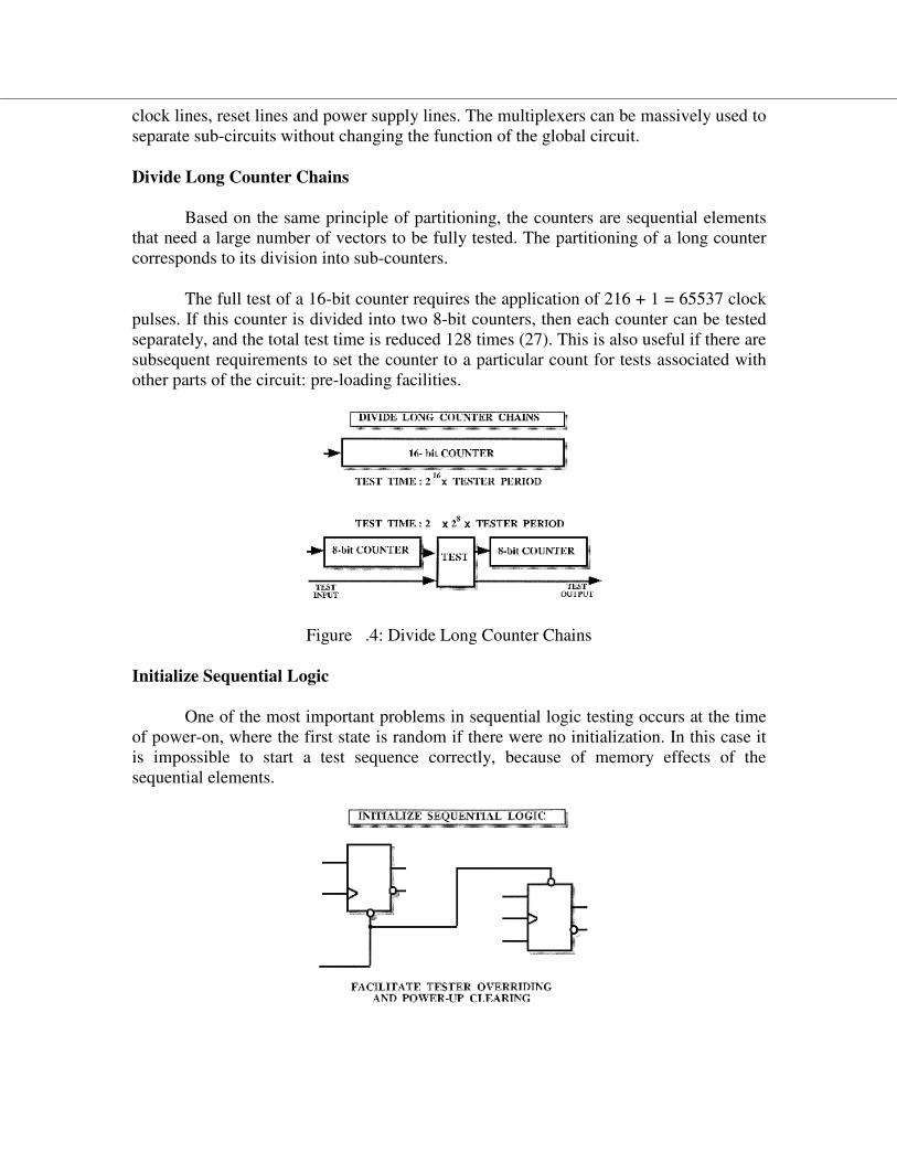
Prof. Roopa Kulkarni, GIT, Belgaum. 36
clock lines, reset lines and power supply lines. The multiplexers can be massively used to
separate sub-circuits without changing the function of the global circuit.
Divide Long Counter Chains
Based on the same principle of partitioning, the counters are sequential elements
that need a large number of vectors to be fully tested. The partitioning of a long counter
corresponds to its division into sub-counters.
The full test of a 16-bit counter requires the application of 216 + 1 = 65537 clock
pulses. If this counter is divided into two 8-bit counters, then each counter can be tested
separately, and the total test time is reduced 128 times (27). This is also useful if there are
subsequent requirements to set the counter to a particular count for tests associated with
other parts of the circuit: pre-loading facilities.
Figure 8.4: Divide Long Counter Chains
Initialize Sequential Logic
One of the most important problems in sequential logic testing occurs at the time
of power-on, where the first state is random if there were no initialization. In this case it
is impossible to start a test sequence correctly, because of memory effects of the
sequential elements.
www.bookspar.com | VTU NOTES | QUESTION PAPERS | NEWS | RESULTS | FORUMS
www.bookspar.com | VTU NOTES | QUESTION PAPERS | NEWS | RESULTS | FORUMS
www.bookspar.com | VTU NOTES | QUESTION PAPERS | NEWS | RESULTS | FORUMS
www.bookspar.com | VTU NOTES | QUESTION PAPERS | NEWS | RESULTS | FORUMS

Prof. Roopa Kulkarni, GIT, Belgaum. 37
Figure 8.5: Initialize Sequential Logic
The solution is to provide flip-flops or latches with a set or reset input, and then to
use them so that the test sequence would start with a known state.
Ideally, all memory elements should be able to be set to a known state, but
practically this could be very surface consuming, also it is not always necessary to
initialize all the sequential logic. For example, a serial-in serial-out counter could have its
first flip-flop provided with an initialization, then after a few clock pulses the counter is
in a known state.
Overriding of the tester is necessary some times, and requires the addition of gates
before a Set or a Reset so the tester can override the initialization state of the logic.
Avoid Asynchronous Logic
Asynchronous logic uses memory elements in which state-transitions are
controlled by the sequence of changes on the primary inputs. There is thus no way to
determine easily when the next state will be established. This is again a problem of
timing and memory effects.
Asynchronous logic is faster than synchronous logic, since the speed in
asynchronous logic is only limited by gate propagation delays and interconnects. The
design of asynchronous logic is then more difficult than synchronous (clocked) logic and
must be carried out with due regards to the possibility of critical races (circuit behavior
depending on two inputs changing simultaneously) and hazards (occurrence of a
momentary value opposite to the expected value).
Non-deterministic behavior in asynchronous logic can cause problems during
fault simulation. Time dependency of operation can make testing very difficult, since it is
sensitive to tester signal skew.
Avoid Logical Redundancy
Logical redundancy exists either to mask a static-hazard condition, or
unintentionally (design bug). In both cases, with a logically redundant node it is not
possible to make a primary output value dependent on the value of the redundant node.
This means that certain fault conditions on the node cannot be detected, such as a node
SA1 of the function F.
www.bookspar.com | VTU NOTES | QUESTION PAPERS | NEWS | RESULTS | FORUMS
www.bookspar.com | VTU NOTES | QUESTION PAPERS | NEWS | RESULTS | FORUMS
www.bookspar.com | VTU NOTES | QUESTION PAPERS | NEWS | RESULTS | FORUMS
www.bookspar.com | VTU NOTES | QUESTION PAPERS | NEWS | RESULTS | FORUMS

Prof. Roopa Kulkarni, GIT, Belgaum. 38
Figure 8.6: Avoid Logical Redundancy
Another inconvenience of logical redundancy is the possibility for a non-
detectable fault on a redundant node to mask the detection of a fault normally-detectable,
such a SA0 of input C in the second example, masked by a SA1 of a redundant node.
Avoid Delay Dependent Logic
Automatic test pattern generators work in logic domains, they view delay
dependent logic as redundant combinational logic. In this case the ATPG will see an
AND of a signal with its complement, and will therefore always compute a 0 on the
output of the AND-gate (instead of a pulse). Adding an OR-gate after the AND-gate
output permits to the ATPG to substitute a clock signal directly.
Figure 8.7: Avoid Delay Dependent Logic
Avoid Clock Gating
When a clock signal is gated with any data signal, for example a load signal
coming from a tester, a skew or any other hazard on that signal can cause an error on the
output of logic.
www.bookspar.com | VTU NOTES | QUESTION PAPERS | NEWS | RESULTS | FORUMS
www.bookspar.com | VTU NOTES | QUESTION PAPERS | NEWS | RESULTS | FORUMS
www.bookspar.com | VTU NOTES | QUESTION PAPERS | NEWS | RESULTS | FORUMS
www.bookspar.com | VTU NOTES | QUESTION PAPERS | NEWS | RESULTS | FORUMS

Prof. Roopa Kulkarni, GIT, Belgaum. 39
Figure 8.8: Avoid Clock Gating
This is also due to asynchronous type of logic. Clock signals should be distributed
in the circuit with respect to synchronous logic structure.
Distinguish Between Signal and Clock
This is another timing situation to avoid, in which the tester could not be
synchronized if one clock or more are dependent on asynchronous delays (across D-input
of flip-flops, for example).
Figure 8.9: Distinguish Between Signal and Clock
Avoid Self Resetting Logic
The self resetting logic is more related to asynchronous logic, since a reset input
is independent of clock signal.
Before the delayed reset, the tester reads the set value and continues the normal
operation. If a reset has occurred before tester observation, then the read value is
erroneous. The solution to this problem is to allow the tester to override by adding an
OR-gate, for example, with an inhibition input coming from the tester. By this way the
right response is given to the tester at the right time.
www.bookspar.com | VTU NOTES | QUESTION PAPERS | NEWS | RESULTS | FORUMS
www.bookspar.com | VTU NOTES | QUESTION PAPERS | NEWS | RESULTS | FORUMS
www.bookspar.com | VTU NOTES | QUESTION PAPERS | NEWS | RESULTS | FORUMS
www.bookspar.com | VTU NOTES | QUESTION PAPERS | NEWS | RESULTS | FORUMS

Prof. Roopa Kulkarni, GIT, Belgaum. 40
Figure 8.10: Avoid Self Resetting Logic
Use Bused Structure
This approach is related, by structure, to partitioning technique. It is very useful
for microprocessor-like circuits. Using this structure allows the external tester the access
of three buses, which go to many different modules.
Figure 8.11: Use Bused Structure
The tester can then disconnect any module from the buses by putting its output
into a high- impedance state. Test patterns can then be applied to each module separately.
Separate Analog and Digital Circuits
Testing analog circuit requires a completely different strategy than for digital
circuit. Also the sharp edges of digital signals can cause cross-talk problem to the analog
lines, if they are close to each other.
www.bookspar.com | VTU NOTES | QUESTION PAPERS | NEWS | RESULTS | FORUMS
www.bookspar.com | VTU NOTES | QUESTION PAPERS | NEWS | RESULTS | FORUMS
www.bookspar.com | VTU NOTES | QUESTION PAPERS | NEWS | RESULTS | FORUMS
www.bookspar.com | VTU NOTES | QUESTION PAPERS | NEWS | RESULTS | FORUMS

Prof. Roopa Kulkarni, GIT, Belgaum. 41
Figure 8.12: Separate Analog and Digital Circuits
If it is necessary to route digital signals near analog lines, then the digital lines
should be properly balanced and shielded. Also, in the cases of circuits like Analog-
Digital converters, it is better to bring out analog signals for observation before
conversion. For Digital-Analog converters, digital signals are to be brought out also for
observation before conversion.
Ad-Hoc DFT Method
Good design practices learnt through experience are used as guidelines:
• Avoid asynchronous (unclocked) feedback.
• Make flip-flops initializable.
• Avoid redundant gates. Avoid large fan-in gates.
• Provide test control for difficult-to-control signals.
• Avoid gated clocks.
• Avoid delay dependant logic.
• Avoid parallel drivers.
• Avoid monostable and self-resetting logic.
Design Reviews
� Manual analysis
• Conducted by experts
� Programmed analysis
• Using design auditing tools
� Programmed enforcement
• Must use certain design practices and cell types.
Objective: Adherence to design guidelines and testability improvement techniques with
little impact on performance and area.
www.bookspar.com | VTU NOTES | QUESTION PAPERS | NEWS | RESULTS | FORUMS
www.bookspar.com | VTU NOTES | QUESTION PAPERS | NEWS | RESULTS | FORUMS
www.bookspar.com | VTU NOTES | QUESTION PAPERS | NEWS | RESULTS | FORUMS
www.bookspar.com | VTU NOTES | QUESTION PAPERS | NEWS | RESULTS | FORUMS

Prof. Roopa Kulkarni, GIT, Belgaum. 42
Disadvantages of ad-hoc DFT methods:
• Experts and tools not always available.
• Test generation is often manual with no guarantee of high fault coverage.
• Design iterations may be necessary.
Scan Design Techniques
The set of design for testability guidelines presented above is a set of ad hoc
methods to design random logic in respect with testability requirements. The scan design
techniques are a set of structured approaches to design (for testability) the sequential
circuits.
The major difficulty in testing sequential circuits is determining the internal state
of the circuit. Scan design techniques are directed at improving the controllability and
observability of the internal states of a sequential circuit. By this the problem of testing a
sequential circuit is reduced to that of testing a combinational circuit, since the internal
states of the circuit are under control.
Scan Path
The goal of the scan path technique is to reconfigure a sequential circuit, for the
purpose of testing, into a combinational circuit. Since a sequential circuit is based on a
combinational circuit and some storage elements, the technique of scan path consists in
connecting together all the storage elements to form a long serial shift register. Thus the
internal state of the circuit can be observed and controlled by shifting (scanning) out the
contents of the storage elements. The shift register is then called a scan path.
Figure 8.13: Scan Path
The storage elements can either be D, J-K, or R-S types of flip-flops, but simple
latches cannot be used in scan path. However, the structure of storage elements is slightly
different than classical ones. Generally the selection of the input source is achieved using
a multiplexer on the data input controlled by an external mode signal. This multiplexer is
integrated into the D-flip-flop, in our case; the D-flip-flop is then called MD-flip-flop
(multiplexed-flip-flop).
www.bookspar.com | VTU NOTES | QUESTION PAPERS | NEWS | RESULTS | FORUMS
www.bookspar.com | VTU NOTES | QUESTION PAPERS | NEWS | RESULTS | FORUMS
www.bookspar.com | VTU NOTES | QUESTION PAPERS | NEWS | RESULTS | FORUMS
www.bookspar.com | VTU NOTES | QUESTION PAPERS | NEWS | RESULTS | FORUMS

Prof. Roopa Kulkarni, GIT, Belgaum. 43
The sequential circuit containing a scan path has two modes of operation: a
normal mode and a test mode which configure the storage elements in the scan path.
As analyzed from figure 8.13, in the normal mode, the storage elements are
connected to the combinational circuit, in the loops of the global sequential circuit, which
is considered then as a finite state machine.
In the test mode, the loops are broken and the storage elements are connected
together as a serial shift register (scan path), receiving the same clock signal. The input of
the scan path is called scan-in and the output scan-out. Several scan paths can be
implemented in one same complex circuit if it is necessary, though having several scan-in
inputs and scan-out outputs.
A large sequential circuit can be partitioned into sub-circuits, containing
combinational sub-circuits, associated with one scan path each. Efficiency of the test
pattern generation for a combinational sub-circuit is greatly improved by partitioning,
since its depth is reduced.
Before applying test patterns, the shift register itself has to be verified by shifting
in all ones i.e. 111...11, or zeros i.e. 000...00, and comparing.
The method of testing a circuit with the scan path is as follows:
1. Set test mode signal, flip-flops accept data from input scan-in
2. Verify the scan path by shifting in and out test data
3. Set the shift register to an initial state
4. Apply a test pattern to the primary inputs of the circuit
5. Set normal mode, the circuit settles and can monitor the primary outputs of the
circuit
6. Activate the circuit clock for one cycle
7. Return to test mode
8. Scan out the contents of the registers, simultaneously scan in the next pattern
www.bookspar.com | VTU NOTES | QUESTION PAPERS | NEWS | RESULTS | FORUMS
www.bookspar.com | VTU NOTES | QUESTION PAPERS | NEWS | RESULTS | FORUMS
www.bookspar.com | VTU NOTES | QUESTION PAPERS | NEWS | RESULTS | FORUMS
www.bookspar.com | VTU NOTES | QUESTION PAPERS | NEWS | RESULTS | FORUMS

Prof. Roopa Kulkarni, GIT, Belgaum. 44
Level sensitivity scan design (LSSD)
`
Figure 8.14: Level sensitivity scan design
The level-sensitive aspect means that the sequential network is designed so that
when an input change occurs, the response is independent of the component and wiring
delays within the network (Figure 8.14).
The scan path aspect is due to the use of shift register latches (SRL) employed as
storage elements. In the test mode they are connected as a long serial shidt register. Each
SRL has a specific design similar to a master-slave FF. it is driven by two non-
overlapping clocks which can be controlled readily from the primary inputs to the circuit.
Input D1 is the normal data input to the SRL; clocks CK1 and CK2 control the normal
operation of the SRL while clocks CK3 and CK2 control scan path movements through
the SRL. The SRL output is derived at L2 in both modes of operation, the mode
depending on which clocks are activated.
Advantages:
• Circuit operation is independent of dynamic characteristics of the logic elements
• ATP generation is simplified
• Eliminate hazards and races
• Simplifies test generation and fault simulation
Boundary Scan Test (BST)
Boundary Scan Test (BST) is a technique involving scan path and self-testing
techniques to resolve the problem of testing boards carrying VLSI integrated circuits
and/or surface mounted devices (SMD).
Printed circuit boards (PCB) are becoming very dense and complex, especially
with SMD circuits, that most test equipment cannot guarantee good fault coverage.
BST (figure 8.15) consists in placing a scan path (shift register) adjacent to each
component pin and to interconnect the cells in order to form a chain around the border of
the circuit. The BST circuits contained on one board are then connected together to form
a single path through the board.
The boundary scan path is provided with serial input and output pads and appropriate
clock pads which make it possible to:
www.bookspar.com | VTU NOTES | QUESTION PAPERS | NEWS | RESULTS | FORUMS
www.bookspar.com | VTU NOTES | QUESTION PAPERS | NEWS | RESULTS | FORUMS
www.bookspar.com | VTU NOTES | QUESTION PAPERS | NEWS | RESULTS | FORUMS
www.bookspar.com | VTU NOTES | QUESTION PAPERS | NEWS | RESULTS | FORUMS
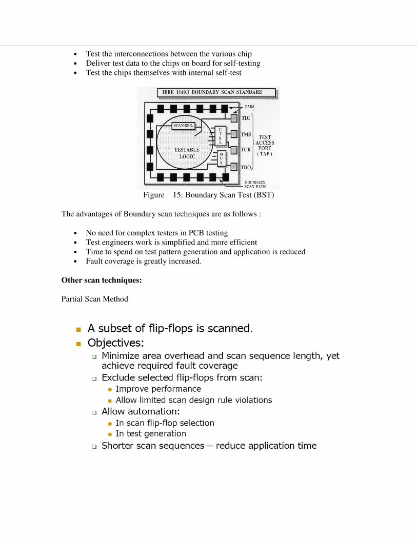
Prof. Roopa Kulkarni, GIT, Belgaum. 45
• Test the interconnections between the various chip
• Deliver test data to the chips on board for self-testing
• Test the chips themselves with internal self-test
Figure 8.15: Boundary Scan Test (BST)
The advantages of Boundary scan techniques are as follows :
• No need for complex testers in PCB testing
• Test engineers work is simplified and more efficient
• Time to spend on test pattern generation and application is reduced
• Fault coverage is greatly increased.
Other scan techniques:
Partial Scan Method
www.bookspar.com | VTU NOTES | QUESTION PAPERS | NEWS | RESULTS | FORUMS
www.bookspar.com | VTU NOTES | QUESTION PAPERS | NEWS | RESULTS | FORUMS
www.bookspar.com | VTU NOTES | QUESTION PAPERS | NEWS | RESULTS | FORUMS
www.bookspar.com | VTU NOTES | QUESTION PAPERS | NEWS | RESULTS | FORUMS

Prof. Roopa Kulkarni, GIT, Belgaum. 46
Random Access Scan Method
Procedure:
� Set test inputs to all test points
� Apply the master reset signal to initialize all memory elements
� Set scan-in address & data, then apply the scan clock
� Repeat the above step until all internal test inputs are scanned
� Clock once for normal operation
� Check states of the output points
� Read the scan-out states of all memory elements by applying the address
Built-in-self test
Objectives:
1. To reduce test pattern generation cost
2. To reduce volume of test data
3. To reduce test time
Built-in Self Test, or BIST, is the technique of designing additional hardware and
software features into integrated circuits to allow them to perform self-testing, i.e., testing
of their own operation (functionally, parametrically, or both) using their own circuits,
thereby reducing dependence on an external automated test equipment (ATE).
BIST is a Design-for-Testability (DFT) technique, because it makes the electrical
testing of a chip easier, faster, more efficient, and less costly. The concept of BIST is
applicable to just about any kind of circuit, so its implementation can vary as widely as
the product diversity that it caters to. As an example, a common BIST approach for
www.bookspar.com | VTU NOTES | QUESTION PAPERS | NEWS | RESULTS | FORUMS
www.bookspar.com | VTU NOTES | QUESTION PAPERS | NEWS | RESULTS | FORUMS
www.bookspar.com | VTU NOTES | QUESTION PAPERS | NEWS | RESULTS | FORUMS
www.bookspar.com | VTU NOTES | QUESTION PAPERS | NEWS | RESULTS | FORUMS

Prof. Roopa Kulkarni, GIT, Belgaum. 47
DRAM's includes the incorporation onto the chip of additional circuits for pattern
generation, timing, mode selection, and go-/no-go diagnostic tests.
Advantages of implementing BIST include:
1) Lower cost of test, since the need for external electrical testing using an ATE
will be reduced, if not eliminated
2) Better fault coverage, since special test structures can be incorporated onto the
chips
3) Shorter test times if the BIST can be designed to test more structures in
parallel
4) Easier customer support and
5) Capability to perform tests outside the production electrical testing
environment. The last advantage mentioned can actually allow the consumers
themselves to test the chips prior to mounting or even after these are in the
application boards.
Disadvantages of implementing BIST include:
1) Additional silicon area and fab processing requirements for the BIST circuits
2) Reduced access times
3) Additional pin (and possibly bigger package size) requirements, since the
BIST circuitry need a way to interface with the outside world to be effective and
4) Possible issues with the correctness of BIST results, since the on-chip testing
hardware itself can fail.
Techniques are:
• compact test: signature analysis
• linear feedback shift register
• BILBO
• self checking technique
Compact Test: Signature analysis
Signature analysis performs polynomial division that is, division of the data out of
the device under test (DUT). This data is represented as a polynomial P(x) which is
divided by a characteristic polynomial C(x) to give the signature R(x), so that
R(x) = P(x)/C(x)
This is summarized as in figure 8.16.
TGP
(Digital
Tester)
DUT
Compaction
Signature
Analysis
www.bookspar.com | VTU NOTES | QUESTION PAPERS | NEWS | RESULTS | FORUMS
www.bookspar.com | VTU NOTES | QUESTION PAPERS | NEWS | RESULTS | FORUMS
www.bookspar.com | VTU NOTES | QUESTION PAPERS | NEWS | RESULTS | FORUMS
www.bookspar.com | VTU NOTES | QUESTION PAPERS | NEWS | RESULTS | FORUMS

Prof. Roopa Kulkarni, GIT, Belgaum. 48
Figure 8.16: BIST – signature analysis
Linear feedback shift register (LFSR):
An LFSR is a shift register that, when clocked, advances the signal through the
register from one bit to the next most-significant bit. Some of the outputs are combined in
exclusive-OR configuration to form a feedback mechanism. A linear feedback shift
register can be formed by performing exclusive-OR (Figure 8.16) on the outputs of two
or more of the flip-flops together and feeding those outputs back into the input of one of
the flip-flops.
LFSR technique can be applied in a number of ways, including random number
generation, polynomial division for signature analysis, and n-bit counting. LFSR can be
series or parallel, the differences being in the operating speed and in the area of silicon
occupied; Parallel LFSR being faster but larger than serial LFSR.
Figure 8.16: Linear feedback shift register
Built-in logic block observer (BILBO):
BILBO is a built-in test generation scheme which uses signature analysis in
conjunction with a scan path. The major component of a BILBO is an LFSR with a few
gates (Figure 8.17).
A BILBO register (built-in logic block observer) combines normal flipflops
with a few additional gates to provide four different functions. The example circuit
shown in the applet realizes a four-bit register. However, the generalization to larger bit-
widths should be obvious, with the XOR gates in the LFSR feedback path chosen to
implement a good polynomial for the given bit-width.
D0
Clock
Q0 Q1 Q2
i0 i1 i2
www.bookspar.com | VTU NOTES | QUESTION PAPERS | NEWS | RESULTS | FORUMS
www.bookspar.com | VTU NOTES | QUESTION PAPERS | NEWS | RESULTS | FORUMS
www.bookspar.com | VTU NOTES | QUESTION PAPERS | NEWS | RESULTS | FORUMS
www.bookspar.com | VTU NOTES | QUESTION PAPERS | NEWS | RESULTS | FORUMS

Prof. Roopa Kulkarni, GIT, Belgaum. 49
When the A and B control inputs are both 1, the circuit functions as a normal
parallel D-type register.
When both A and B inputs are 0, the D-inputs are ignored (due to the AND gate
connected to A), but the flipflops are connected as a shift-register via the NOR and XOR
gates. The input to the first flipflop is then selected via the multiplexer controlled by the
S input. If the S input is 1, the multiplexer transmits the value of the external SIN shift-in
input to the first flipflop, so that the BILBO register works as a normal shift-register. This
allows to initialize the register contents using a single signal wire, e.g. from an external
test controller.
If all of the A, B, and S inputs are 0, the flipflops are configured as a shift-
register, again, but the input bit to the first flipflop is computed by the XOR gates in the
LFSR feedback path. This means that the register works as a standard LFSR
pseudorandom pattern generator, useful to drive the logic connected to the Q outputs.
Note that the start value of the LFSR sequence can be set by shifting it in via the SIN
input.
Finally, if B and S are 0 but A is 1, the flipflops are configured as a shift-register,
but the input value of each flipflop is the XOR of the D-input and the Q-output of the
previous flipflop. This is exactly the configuration of a standard LFSR signature analysis
register.
Because a BILBO register can be used as a pattern generator for the block it
drives, as well provide signature-analysis for the block it is driven by, a whole circuit can
be made self-testable with very low overhead and with only minimal performance
degradation (two extra gates before the D inputs of the flipflops).
www.bookspar.com | VTU NOTES | QUESTION PAPERS | NEWS | RESULTS | FORUMS
www.bookspar.com | VTU NOTES | QUESTION PAPERS | NEWS | RESULTS | FORUMS
www.bookspar.com | VTU NOTES | QUESTION PAPERS | NEWS | RESULTS | FORUMS
www.bookspar.com | VTU NOTES | QUESTION PAPERS | NEWS | RESULTS | FORUMS
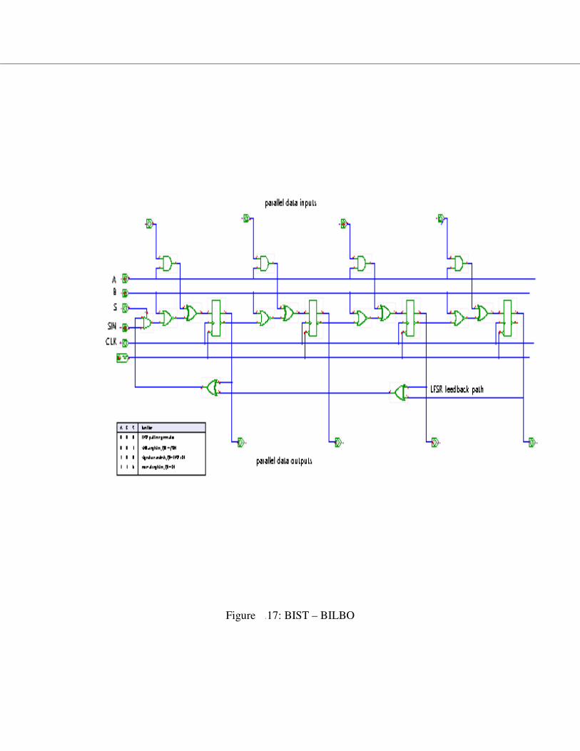
Prof. Roopa Kulkarni, GIT, Belgaum. 50
Figure 8.17: BIST – BILBO
www.bookspar.com | VTU NOTES | QUESTION PAPERS | NEWS | RESULTS | FORUMS
www.bookspar.com | VTU NOTES | QUESTION PAPERS | NEWS | RESULTS | FORUMS
www.bookspar.com | VTU NOTES | QUESTION PAPERS | NEWS | RESULTS | FORUMS
www.bookspar.com | VTU NOTES | QUESTION PAPERS | NEWS | RESULTS | FORUMS

Prof. Roopa Kulkarni, GIT, Belgaum. 51
Self-checking techniques:
It consists of logic block and checkers should then obey a set of rules in which the
logic block is ‘strongly fault secure’ and the checker ‘strongly code disjoint’. The code
use in data encoding depends on the type of errors that may occur at the logic block
output. In general three types are possible:
• Simple error: one bit only affected at a time.
• Unidirectional error: multiple bits at 1 instead of 0 (or 0 instead of 1)
• Multiple errors: multiple bits affected in any order.
Self-checking techniques are applied to circuits in which security is important so
that fault tolerance is of major interest. Such technique will occupy more area in silicon
than classical techniques such as functional testing but provide very high test coverage.
www.bookspar.com | VTU NOTES | QUESTION PAPERS | NEWS | RESULTS | FORUMS
www.bookspar.com | VTU NOTES | QUESTION PAPERS | NEWS | RESULTS | FORUMS
www.bookspar.com | VTU NOTES | QUESTION PAPERS | NEWS | RESULTS | FORUMS
www.bookspar.com | VTU NOTES | QUESTION PAPERS | NEWS | RESULTS | FORUMS

UNIT-IV Post Test- MCQ
1. Stuck open (off) fault occur/s due to _________ a. An incomplete contact (open) of source to drain node b. Large separation of drain or source diffusion from the gate c. Both a and b d. None of the above
2. For a circuit with k lines, single stuck-at fault is possible
a) k b) 2k c) k/2 d) k2
3. The sum is generated in CLA using
(a) Carry generate and propagate signals (b) Carry generate signal (c) Carry input, carry generate, and propagate signals (d) Carry input and carry generate signals
4. Pseudo static RAM cell is built using
a) one inverter b) two inverters c) three inverters d) four inverters
5. The boundary scan path is provided with
a) serial input pads b) parallel input pads c) parallel output pads d) buffer pads

VLSI Design
Prerequisite: Basic knowledge of Electronic Circuits and Digital System Design Objectives:
To learn techniques of chip design using programmable devices. UNIT-V PROGRAMMABLE LOGICS: Basic ROM structures, PLAs, PALs, PLDs, Implementation of Traffic Light controller using PLD. FPGAs and CPLDs: XILINX and ALTERA series. Outcome: On completion of the course, student will be able to
Differentiate various FPGA architectures

UNIT-V Pre Test- MCQ
1. In testability, which terminology is used to represent or indicate the formal evidences of correctness?
a. Validation b. Verification c. Simulation d. Integration
2. Which programming technologies are predominantly associated with SPLDs and CPLDs?
a. EPROM b. EEPROM c. FLASH d. All of the above
3. Programmable logic array (PLA) has __________ .
a. fixed OR plane followed by a programmable AND plane b. programmable AND plane followed by a fixed OR plane c. fixed AND plane followed by a programmable OR plane d. programmable AND plane followed by a programmable OR plane
4. Sequential circuits are represented as a) finite state machine b) infinite state machine c) finite synchronous circuit d) infinite asynchronous circuit
5. The contents of the EPROM are erased by ________
a) Overcharging the chip
b) Exposing the chip to UV rays
c) Exposing the chip to IR rays
d) Discharging the Chip

Dr. Y.Narasimha Murthy Ph.D [email protected]
UNIT-1 CPLD & FPGA ARCHITECTURE & APPLICATIONS
Introduction : The need of programmable devices was realized in early 70s itself with the
design of PLD by Ron Cline from Signetics . The digital ICs like TTL or CMOS have fixed
functionality and the user has no option to change or modify their functionality .i.e they work
according to the design given by the manufacturer. So,to change this people started thinking of a
methodology by which the functionality of an IC can be modified or changed. Then the concept
of using Fuses in ICs entered and gained momentum. This method of changing or modifying
the functionality of an IC using the Fuses was appreciated and this method of blowing a Fuse
between two contacts or keeping the Fuse intact was done by using a software and hence these
devices were called Programmable Logic Devices(PLDs).
Many digital chips were considered under the category of PLDs .But the most fundamental and
primitive was the Memories like ROM or PROM etc.
The realization of Digital circuits by PLDs can be classified as shown in the diagram below.
PLAs were introduced in the early 1970s, by Philips, but their main drawbacks were that they
were expensive to manufacture and offered somewhat poor speed-performance. Both
disadvantages were due to the two levels of configurable logic, because programmable logic
planes were difficult to manufacture and introduced significant propagation delays. To overcome
these problems , Programmable Array Logic (PAL) devices were developed.
Memory : Memory is used to store, provide access to, and allow modification of data and
program code for use within a processor-based electronic circuit or system. The two basic types
of memory are ROM (read-only memory) and RAM (random access memory).

Dr. Y.Narasimha Murthy Ph.D [email protected]
ROM is used for holding program code that must be retained when the memory power is
removed. It is considered to provide nonvolatile storage. The code can either be fixed when the
memory is fabricated (mask programmable ROM) or electrically programmed once (PROM,
Programmable ROM) or multiple times. Multiple programming capacity requires the ability to
erase prior programming, which is available with EPROM (electrically programmable ROM,
erased using ultraviolet [UV] light), EEPROM or EEPROM (electrically erasable PROM), or
flash (also electrically erased). PROM is sometimes considered to be in the same category of
circuit as programmable logic, although in this text, PROM is considered in the memory
category only.
RAM is used for holding data and program code that require fast access and the ability to modify
the contents during normal operation. RAM differs from read-only memory (ROM) in that it can
be both read from and written to in the normal circuit application. However, flash memory can
also be referred to as nonvolatile RAM (NVRAM). RAM is considered to provide a volatile
storage, because unlike ROM, the contents of RAM will be lost when the power is removed.
There are two main types of RAM: static RAM (SRAM) and dynamic RAM (DRAM).
ROM- READ ONLY MEMORY : A ROM is essentially a memory device for storage purpose
in which a fixed set of binary information is stored. The user must first specify the binary
information to be stored and then it is embedded in the unit to form the required interconnection
pattern. ROM contains special internal links that can be fused or broken. Certain links are to be
broken or blown out to realize the desired interconnections for a particular application and to
form the required circuit path. Once a pattern is established for a ROM, it remained fixed even if
the power supply to the circuit is switched off and then switched on again.
The block diagram of ROM is shown below. It consists of n input lines and m-output lines.
Each bit combination of input variables is called an address and each bit combination that is
formed at output lines is called a word. Thus, an address is essentially binary number that
denotes one of the min-terms of n variables and the number of bits per word is equal to the
number of output lines m. It is possible to generate p = 2n number of distinct addresses from n
number of input variables. Since there are 2n distinct addresses in a ROM, there are 2n distinct
words which are said to be stored in the device and an output word can be selected by a unique
address. The address value applied to the input lines specifies the word at output lines at any

Dr. Y.Narasimha Murthy Ph.D [email protected]
given time. A ROM is characterized by the number of words 2n and number of bits per word m
and denoted as 2n × m ROM.
For example a 32 × 8 ROM contains 32 words of 8 bits each. This means there are eight output
lines and there are 32 numbers of distinct words stored in that unit, each of which is applied to
the output lines. The particular word selected from the presently available output lines is
determined by five input variables, as there are five input lines for a 32 × 8 ROM, because 25 =
32. Five input variables can specify 32 addresses or min-terms and for each address input there is
a unique selected word. Thus, if the input address is 0000, word number 0 is selected. For
address 0001, word number 1 is selected and so on.
A ROM is sometimes specified by the total number of bits it contains, which is 2n × m. For
example, a 4,096-bit ROM may be organized as 512 words of 8 bits each. That means the device
has 9 input lines (29 × m = 512) and 8 output lines.
In Figure below, the block consisting of an AND array with buffers or inverters is equivalent to a
decoder. The decoder basically is a combinational circuit that generates 2n numbers of minterms
from n number of input lines. 2n or p numbers of minterms are realized from n number of input
variables with the help of n numbers of buffers, n numbers of inverters, and 2n numbers of AND
gates.

Dr. Y.Narasimha Murthy Ph.D [email protected]
Each of the minterms is applied to the inputs of m number of OR gates through fusible links.
Thus, m numbers of output functions can be produced after blowing of some selected fuses. The
equivalent logic diagram of a 2n×m ROM is shown below
ROM has many important applications in the design of digital computer systems. Realization of
complex combinational circuits, code conversions, generating bit patterns, performing arithmetic
functions like multipliers, forming look-up tables for arithmetic functions, and bit patterns for
characters are some of its applications. They are particularly useful for the realization of multiple
output combinational circuits with the same set of inputs. As such, they are used to store fixed bit
patterns that represent the sequence of control variables needed to enable the various operations
in the system. They are also used in association with microprocessors and microcontrollers.

Dr. Y.Narasimha Murthy Ph.D [email protected]
PROGRAMMABLE LOGIC DEVICE-(PLD): The logic devices other than TTL ,CMOS
families whose logical operation is specified by the user through a process called programming
are called Programmable Logic Devices. So, the programmable logic device is the IC that
contain digital logic cells and programmable interconnect . The idea of PLD was first conceived
by Ron Cline from Signetics in 1975 with programmable AND and OR planes. The basic idea
with these devices is to enable the designer to configure the logic cells and interconnect to form a
digital electronic circuit within a single IC package. Here, the hardware resources will be
configured to implement a required functionality. By changing the hardware configuration, the
PLD will operate a different function. The functioning and basic working principle of PLD is
explained below through the diagrams.

Dr. Y.Narasimha Murthy Ph.D [email protected]
There are three types of PLD available. The simple programmable logic device (SPLD), the
Complex programmable logic device(CPLD), and the Field programmable gate array (FPGA).
Device Type AND Array OR Array
ROM Fixed Programmable
PLA Programmable Programmable
PAL Programmable Fixed
Simple Programmable Logic Device (SPLD)
The PLD with simple architectural features can be called as SPLD or Simple programmable
Logic Device. The SPLD was introduced prior to the CPLD and FPGA. Based on the
architecture the SPLDs are classified into three types. Programmable logic array (PLA),
Programmable array of logic (PAL), and Generic Array of Logic (GAL).
PLA-Programmable Logic Array PLA, Programmable Logic Array is a type of LSI device and conceptually similar to a ROM.
However, a PLA does not contain all AND gates to form the decoder or does not generate all the

Dr. Y.Narasimha Murthy Ph.D [email protected]
minterms like ROM. In the PLA, the decoder is replaced by a group of AND gates with
buffers/inverters, each of which can be programmed to generate some product terms of input
variable combinations that are essential to realize the output functions. The AND and OR gates
inside the PLA are initially fabricated with the fusible links among them. The required Boolean
functions are implemented in sum of the products form by opening the appropriate links and
retaining the desired connections.
So, the PLA consists of two programmable planes AND and OR planes . The AND plane
consists of programmable interconnect along with AND gates. The OR plane consists of
programmable interconnect along with OR gates. In this view, there are four inputs to the PLA
and four outputs from the PLA. Each of the inputs can be connected to an AND gate with any of
the other inputs by connecting the crossover point of the vertical and horizontal interconnect
lines in the AND gate programmable interconnect. Initially, the crossover points are not
electrically connected, but configuring the PLA will connect particular cross over points
together. In this view, the AND gate is seen with a single line to the input. This view is by
convention, but this also means that any of the inputs (vertical lines) can be connected. Hence,
for four PLA inputs, the AND gate also has four inputs. The single output from each of the AND
gates is applied to an OR gate programmable inter connect.

Dr. Y.Narasimha Murthy Ph.D [email protected]
Again, the crossover points are initially not electrically connected, but configuring the PLA will
connect particular crossover points together. In this view, the OR gate is seen with a single line
to the input. This view is by convention, but this also means that any of AND gate outputs can be
connected to the OR gate inputs. Hence, for four AND gates, the OR gate also has four inputs
Therefore, the function is implemented in either AND-OR form when the output link across
INVERTER is in place, or in AND-OR-INVERT form when the link is blown off. The general
structure of a PLA with internal connections is shown in figure below.

Dr. Y.Narasimha Murthy Ph.D [email protected]
The size of a PLA is specified by the number of inputs, the number of product terms,and the
number of outputs. The number of sum terms is equal to the number of outputs. The PLA
described in figure above is specified as n × p × m PLA. The number of programmable links is
2n × p + p × m + m, whereas that of ROM is 2n × m. A typical PLA of 16 × 48 × 8 has 16 input
variables, 48 product terms, and 8 output lines.
To implement the same combinational circuit, a 216 × 8 ROM is needed, which consists of 216 =
65536 minterms or product terms. So there is a drastic reduction in number of AND gates within
the PAL chip, thus reducing the fabrication time and cost.
PROGRAMMABLE ARRAY LOGIC (PAL) :
The first programmable device was the programmable array logic (PAL) developed by
Monolithic Memories Inc(MMI). The Programmable Array Logic or PAL is similar to PLA,
but in a PAL device only AND gates are programmable. The OR array is fixed by the
manufacturer. This makes PAL devices easier to program and less expensive than PLA. On the
other hand, since the OR array is fixed, it is less flexible than a PLA device.

Dr. Y.Narasimha Murthy Ph.D [email protected]
The PAL device. has n input lines which are fed to buffers/inverters. Buffers/inverters are
connected to inputs of AND gates through programmable links. Outputs of AND gates are then
fed to the OR array with fixed connections. It should be noted that, all the outputs of an AND
array are not connected to an OR array. In contrast to that, only some of the AND outputs are
connected to an OR array which is at the manufacturer's discretion. This can be clarified by
above, which illustrates the internal connection of a four-input, eight AND-gates and three-
output PAL device before programming. Note that while every buffer/inverter is connected to
AND gates through links, F1-related OR gates are connected to only three AND outputs, F2 with
three AND gates, and F3 with two AND gates. So this particular device can generate only eight
product terms, out of which two of the three OR gates may have three product terms each and the
rest of the OR gates will have only two product terms. Therefore, while designing with PAL,
particular attention is to be given to the fixed OR array.
GAL-Generic Array Logic PAL and PLA devices are one-time programmable (OTP) based on PROM, so the PAL or PLA
configuration cannot be changed after it has been configured. This limitation means that the
configured device would have to be discarded and a new device configured. The GAL, although
similar to the PAL architecture, uses EEPROM and can be reconfigured.
The Generic Array Logic (GAL) device was invented by Lattice Semiconductor. The GAL was
an improvement on the PAL because one device was able to take the place of many PAL devices
or could even have functionality not covered by the original range. Its primary benefit, however,
was that it was erasable and re-programmable making prototyping and design changes easier for
engineers. The GAL is very useful in the prototyping stage of a design, when any bugs in the
logic can be corrected by reprogramming.

PLDs
• Programmable Logic Devices (PLDs)
• PROM: Programmable Read Only Memories (1960s)
• PLA: Programmable Logic Arrays [Signetics] (1975)
• PALÔ: Programmable Array Logic [MMI] (1976)
• GALÔ: Generic Array Logic
• CPLDs (Complex PLDs)
• FPGA: Field Programmable Gate Arrays
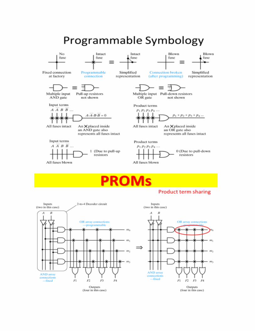

Example
Implement:
an inverter (NOT)
an OR gate
a NAND gate
an XOR gate
With:
a PROM
a PLA
a PAL
A B F1 F2 F3 F4
0 0 1 0 1 0
0 1 1 1 1 1
1 0 0 1 1 1
1 1 0 1 0 0
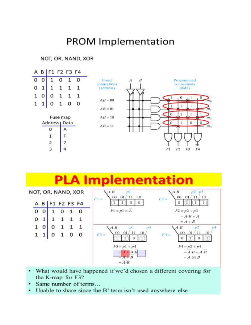


Dr. Y.Narasimha Murthy Ph.D [email protected]
Complex Programmable Logic Device (CPLD):
CPLDs were pioneered by Altera, first in their family of chips called Classic EPLDs, and then
in three additional series, called MAX 5000, MAX 7000 and MAX 9000. The CPLD is the
complex programmable Logic Device which is more complex than the SPLD. This is build on
SPLD architecture and creates a much larger design. Consequently, the SPLD can be used to
integrate the functions of a number of discrete digital ICs into a single device and the CPLD can
be used to integrate the functions of a number of SPLDs into a single device.
So, the CPLD architecture is based on a small number of logic blocks and a global
programmable interconnect. Instead of relying on a programming unit to configure chip , it is
advantageous to be able to perform the programming while the chip is still attached to its circuit
board. This method of programming is known is called In-System programming (ISP). It is not
usually provided for PLAs (or) PALs , but it is available for the more sophisticated chips known
as Complex programmable logic device.
The CPLD consists of a number of logic blocks or functional blocks, each of which contains a
macrocell and either a PLA or PAL circuit arrangement. In this view, eight logic blocks are
shown. The building block of the CPLD is the macro-cell, which contains logic implementing
disjunctive normal form expressions and more specialized logic operations. The macro cell
provides additional circuitry to accommodate registered or nonregistered outputs, along with
signal polarity control. Polarity control provides an output that is a true signal or a complement

Dr. Y.Narasimha Murthy Ph.D [email protected]
of the true signal. The actual number of logic blocks within a CPLD varies; the more logic
blocks available, the larger the design that can be configured.
In the center of the design is a global programmable interconnect. This interconnect allows
connections to the logic block macrocells and the I/O cell arrays (the digital I/O cells of the
CPLD connecting to the pins of the CPLD package).The programmable interconnect is usually
based on either array-based interconnect or multiplexer-based interconnect:• Array-based
interconnect allows any signal within the programmable interconnect to connect to any logic
block within the CPLD.

Dr. Y.Narasimha Murthy Ph.D [email protected]
This is achieved by allowing horizontal and vertical routing within the programmable
interconnect and allowing the crossover points to be connected or unconnected (the same idea as
with the PLA and PAL), depending on the CPLD configuration.
• Multiplexer-based interconnect uses digital multiplexers connected to each of the macrocell
inputs within the logic blocks. Specific signals within the programmable interconnect are
connected to specific inputs of the multiplexers. It would not be practical to connect all internal
signals within the programmable interconnect to the inputs of all multiplexers due to size
and speed of operation considerations.
FPGAs – FIELD PROGRAMMABLE GATE ARRAYS
The FPGA concept emerged in 1985 with the XC2064TM FPGA family from Xilinx . The
“FPGA is an integrated circuit that contains many (64 to over 10,000) identical logic cells that
can be viewed as standard components.” The individual cells are interconnected by a matrix of
wires and programmable switches. A user's design is implemented by specifying the simple
logic function for each cell and selectively closing the switches in the interconnect matrix. The
array of logic cells and interconnect form a fabric of basic building blocks for logic circuits.
Complex designs are created by combining these basic blocks to create the desired circuit.
Unlike CPLDs (Complex Programmable Logic Devices) FPGAs contain neither AND nor OR
planes.The FPGA architecture consists of configurable logic blocks, configurable I/O blocks,
and programmable interconnect. Also, there will be clock circuitry for driving the clock signals
to each logic block, and additional logic resources such as ALUs, memory, and decoders may be
available. The two basic types of programmable elements for an FPGA are Static RAM and anti-
fuses.
Each logic block in an FPGA has a small number of inputs and one output. A look
up table (LUT) is the most commonly used type of logic block used within FPGAs.
There are two types of FPGAs.(i) SRAM based FPGAs and (ii) Antifuse technology based(OTP)
Every FPGA consists of the following elements
Configurable logic blocks(CLBs)
Configurable input output blocks(IOBs)
Two layer metal network of vertical and horizontal lines for interconnecting the CLBS

Dr. Y.Narasimha Murthy Ph.D [email protected]
Configurable logic blocks(CLBs):
The configurable logic block is the basic logic cell and it is either RAM based or PLD based .
It consists of registers (memory), Muxes and combinatorial functional unit. An array of CLBS
are embedded within a set of vertical and horizontal channels that contain routing which can be
personalized to interconnect CLBs.
Configurable Input / Output logic locks (IOBs):
CLBs and routing channels are surrounded by a set of programmable I/Os which is
an arrangement of transistors for configurable I/O drivers.
Programmable interconnects:
These are un programmed interconnection resources on the chip which have
channeled routing with fuse links. Four types of interconnect architectures are available. They
are
Row-Column Architecture
Island Style Architecture
Sea-of-Gates Architecture

Dr. Y.Narasimha Murthy Ph.D [email protected]
Advantages of FPGAs:
Design cycle is significantly reduced. A user can program an FPGA design in a few
minutes or seconds rather than weeks or months required for mask programmed parts.
High gate density i.e, it offers large gate counts.
No custom masks tooling is required (Low cost).
Low risk and highly flexible.
Reprogram ability for some FPGAs (design can be altered easily).
Suitable for prototyping.
Parallelism
Allows for system-level extraction of parallelism to match input data at design time
Huge computational capability Fast development and Dynamic reconfiguration
Updating new pattern matching rules (or simply rules)
Device should not stop when updating new rules
Update time for new rules
To provide fast response to new attacks, the compilation and updating
time for new rules needs to be short
In case of a hardwired FPGA architecture, the update time is mostly dependent
on place & route time
Memory-based units can provide near instantaneous updates
Limitations:
Speed is comparatively less.
The circuit delay depends on the performance of the design implementation tools.
The mapping of the logic design into FPGA architecture requires sophisticated design
implementation (CAD) tools than PLDs.
FPGA Programming Technologies:
(a) Antifuse Technology:
An antifuse is a two terminal device that when un-programmed has a very high resistance
between the two terminals and when programmed, or “blown”, creates a very low resistance or

Dr. Y.Narasimha Murthy Ph.D [email protected]
permanent connection. The application of a high voltage from 11 V to 21 V will create the low
resistive permanent connection. Antifuse technologies come in two types. The first is oxide-
nitride-oxide (ONO) dielectric based and the other is amorphous silicon or metal-to-metal
antifuse structures.
Dielectric based antifuses consist of a dielectric material between N+ diffusion and polysilicon
which breaks down when a high voltage is applied. Early dielectrics were a single-layered oxide
dielectric until Actel came out with the programmable low impedance circuit element (PLICE),
which is a multi-layer oxide-nitride-oxide (ONO) dielectric fuse. A high voltage across the
PLICE melts the dielectric and creates polycrystalline silicon between the terminals. When the
PLICE is blown, it adds three layers rather than the double metal CMOS process. The layers are
a thin layer of oxide an top off the N+ surface, Low-pressure Chemical Vapor Deposition
(LPCVD) nitride and the reoxidized top oxide. The programming current has an important effect
because the higher the current during programming, the lower the link resistance, resulting in
smaller thickness for the antifuse material. Programming circuits for antifuses need to supply
high currents (15 ma for Actel) to insure high reliability and performance.
Amorphous silicon antifuse technology is the alternative to dielectric antifuse. It consists of
amorphous silicon between two layers of metal that changes phases when current is applied.
When the antifuse is not programmed the amorphous silicon has a resistance of 1 Giga ohm.
When a high current (about 20 mA) is applied to the anitfuse the amorphous silicon changes into
a conductive polysilicon link. Quick Logic pASIC FPGA is a perfect example of an amorphous
silicon antifuse technology.
(b). SRAM-based Technology:
SRAM FPGA architecture consists of static RAM cells to control pass gates or multiplexers.
The FPGA speed is determined by the delay introduced by the logic cells and the routing
channels. Multiplexers, look-up tables and output drivers affect the speed of signals through the
logic cells. An FPGA with more PIPs is easier to route but introducing more routing delay. The
size of the look-up table plays an important role depending on the design. Smaller LUTs provide
higher density but larger ones are preferred for high-speed applications.
Distinguish between SRAM and Antifuse Technologies: The following points explains the
differences between the two technologies.

Dr. Y.Narasimha Murthy Ph.D [email protected]
1. Antifuse programming technology is faster than SRAM programming technology due to the
RC delays introduced by the interconnect structure.
2. Antifuse technology has more silicon area per gate and is easier to route than SRAM
technology.
3. A disadvantage of antifuse FPGA is that they require more process layers and mask steps and
also contain high voltage programming transistors.
4. SRAM-based technology contains higher capacity than antifuse technologies.
5. SRAM based technology is very flexible with in-system programmability and the ability to
reconfigure the design during the debugging stage while antifuse technology is one-time
programmable (OTP). This ability reduces design and development, which reduces overall
cost of the design. Another advantage to this is that SRAM technology can be programmed at
the factory through complete verification test where the antifuse are tested as “blanks” and
require programming by the user to verify design requirements and operation.
6. A disadvantage of SRAM technology is that it is volatile meaning it has to be reprogrammed
every time power is turned off and on again. The SRAM usually require an extra memory
element to program the chip which occupies board space .
Altera’s FLEX 10K Series CPLDs
Altera‟s FLEX 10K devices are the industry‟s first embedded PLDs. Based on reconfigurable
CMOS SRAM elements, the Flexible Logic Element MatriX (FLEX) architecture incorporates
all features necessary to implement common gate array mega functions. With 10,000 to 250,000
typical gates ,the FLEX 10K family provides the density, speed, and features to integrate entire
systems, including multiple 32-bit buses, into a single device.
FLEX 10K devices are reconfigurable .So, the designer is not required to generate test vectors
for fault coverage purposes. Additionally, the designer need not manage inventories of different
ASIC designs; FLEX 10K devices can be configured on the board for the specific functionality
required.
Each FLEX 10K device contains an Embedded Array (EA) and a Logic Array (LA).
The Embedded Array is used to implement a variety of memory functions or complex logic
functions, such as digital signal processing (DSP) ,microcontroller, wide-data-path manipulation,
and data-transformation functions.

Dr. Y.Narasimha Murthy Ph.D [email protected]
The Logic Array performs the same function as the sea-of-gates in the gate array: it is used to
implement general logic, such as counters, adders, state machines, and multiplexers.
The combination of embedded and logic arrays provides the high performance and high density
of embedded gate arrays, enabling designers to implement an entire system on a single device.
FLEX 10K devices are configured at system power-up with data stored in an Altera serial
configuration device or provided by a system controller.
Logic Element is , the smallest unit of logic in the FLEX 10K architecture, has a compact size
that provides efficient logic utilization. Each LE contains a four-input LUT, which is a function
generator that can quickly compute any function of four variables. In addition, each LE contains
a programmable flip flop with a synchronous enable, a carry chain, and a cascade chain. Each LE
drives both the local and the Fast Track. The programmable flip flop in the LE can be configured
for D, T, JK, or SR operation. The clock, clear, and preset control signals on the flip flop can be
driven by global signals, general-purpose I/O pins, or any internal logic. For combinatorial
functions, the flip flop is bypassed and the output of the LUT drives the output of the LE.

Dr. Y.Narasimha Murthy Ph.D [email protected]
The carry chain provides a very fast (as low as 0.2 ns) carry-forward function between Les. The
carry-in signal from a lower-order bit drives forward into the higher-order bit via the carry chain,
and feeds into both the LUT and the next portion of the carry chain. This feature allows the
FLEX 10K architecture to implement high-speed counters, adders, and comparators of arbitrary
width efficiently.
Cascade Chain in the FLEX 10K architecture can implement functions that have a very wide
fan-in. Adjacent LUTs can be used to compute portions of the function in parallel; the cascade
chain serially connects the intermediate values. The cascade chain can use a logical AND
or logical OR (via De Morgan‟s inversion) to connect the outputs of adjacent Les. Each
additional LE provides four more inputs to the effective width of a function, with a delay as low
as 0.7 ns per LE. Cascade chain logic can be created automatically by the Compiler during
design processing, or manually by the designer during design entry.
Altera offers the EPC1, EPC2, EPC16, and EPC1441 configuration devices, which configure
FLEX 10K devices via a serial data stream. Configuration data can also be downloaded from
system RAM or from Altera‟s Bit Blaster serial download cable or Byte Blaster MV parallel port
download cable.
Even after configuring a FLEX 10K device , it can be reconfigured in-circuit by resetting the
device and loading new data .Because reconfiguration requires less than 320 ms, real-time
changes can be made during system operation. FLEX 10K devices contain an optimized interface
that permits microprocessors to configure FLEX 10K devices serially or in parallel, and
synchronously or asynchronously. The interface also enables microprocessors to treat a FLEX
10K device as memory and configure the device by writing to a virtual memory location, making
it very easy for the designer to reconfigure the device.
SPEED PERFORMANCE :
The speed performance of PLDs is affected by their architectural features like I/O blocks, Logic
Elements and the Interconnects. The routing of these elements also paly an important role.For example
if a finite state machine is to be implemented in an FPGA, then the amount of logic feeding each
state machine flip-flop must be minimized. This follows because in FPGAs flip-flops are directly
fed by logic blocks that have relatively few inputs (typically 4 - 8). If the state machine flip-flops
are fed by more logic than will fit into a single logic block, then multiple levels of logic blocks

Dr. Y.Narasimha Murthy Ph.D [email protected]
will be needed, and speed-performance will decrease. Even in a CPLD architecture, speed-
performance of a state machine can be significantly affected by state bit encoding,for example, in
the Altera MAX 7000 CPLDs, flip-flops that are fed by five or fewer product terms will operate faster
than those that require more than five terms.
CPLDS are ideal for high-speed applications requiring critical timing and FPGAs are more
flexible with the finer-grained architecture. Lattice semiconductor CPLD series architecture
offered predictable timing, high densities, in-system programmability, flexible architecture for
mixed combinatorial and register intensive designs and system partitioning. Some applications
can not use CPLDs. Planetary Spacecraft and earth orbiting satellites and science instruments
require Radiation Hardened PLDs. Between CPLD and FPGAs ,the CPLDs are fast and ,
predictable but the FPGAs are application dependent.
The CPLD implementation of the sequential circuit is much faster than the FPGA version.
However, the most interesting aspect is the difference between the 5 -bit and13-bit versions of
the circuit. If both versions are operated at 100 MHz for CPLD implementation, while the 13-
bit version is much slower than its smaller counterpart for the FPGA. This is a good example of
how FPGAs are not suitable for implementing circuits that require “wide” logic gates (the 14-
inputAND-gates for this example), whereas CPLDs can easily implement such applications.
It is widely accepted by designers who use PLDs that FPGAs are the best choice for data-path
circuits, because wide logic gates are not required and the number of flip-flops needed is large.
But it is true that the FPGAs cannot provide required performance in an FPGA, and the CPLDs
were successful . The reason that the CPLDs provided better performance is to do with their
simple structure that provides for very high-speed paths from input pins, through AND-OR logic
and flip-flops, to output pins.
It is also found experimentally that the CPLD-based counters achieve the maximum possible
speed of tpd plus the setup time of the flip-flop. This is because each counter bit needs up to 34-
input AND functions that feed 4-input OR-gates .In the FLEX devices, high-speed carry chain is
employed to implement the required wide AND. It is the speed of this carry chain that limits the
speed-performance of the FLEX-based counter. Roughly, a counter of double the size has twice
the carry chain length and thus half the speed performance. So , the conclusion is Altera CPLDs

Dr. Y.Narasimha Murthy Ph.D [email protected]
can implement very fast counters, however, it is difficult to construct many large counters in one device.
The FLEX FPGAs are better suited for this purpose, but performance and routability are compromised
when the carry chain hardware is used. Both performance and routability can be improved by enhancing
the counter design with a very a small cost in area. However, these gains cannot be realized without
intimate knowledge of the FPGA architecture.
References : 1. „Architecture of Field-Programmable Gate Arrays‟ Jonathan Rose, Abbas EL
Gamal, and Alberto Sangiovanni-Vincentelli
2. Architecture of FPGAs and CPLDs: A Tutorial, Stephen Brown and Jonathan Rose
3.‟Designing for High Speed-Performance in CPLDs and FPGAs‟, Zeljko Zilic, Guy Lemieux
4.‟Digital Principles and Logic Design‟ A. SAHA N. MANNA

TRAFFIC LIGHT CONTROLLER
Function
• Three lights only (RED, GREEN, YELLOW)
• The lights glow cyclically at a fixed time.
• The circuit will be driven by a clock of appropriate frequency
TLC-One way
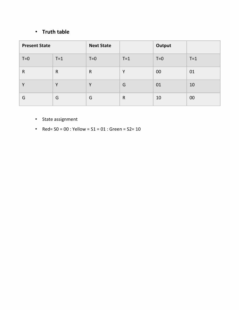
• Truth table
• State assignment
• Red= S0 = 00 : Yellow = S1 = 01 : Green = S2= 10
Present State Next State
Output
T=0 T=1 T=0 T=1 T=0 T=1
R R R Y 00 01
Y Y Y G 01 10
G G G R 10 00

Verilog CODE
COUNTER module counter (clk, clr, q);
input clk, clr;
output [3:0] q;
reg [3:0] tmp;
always @(posedge clk or posedge clr)
Begin
if (clr)
tmp <= 4’b0000;
else
tmp <= tmp + 1+b1;
end
assign q = tmp;
endmodule
State machines (Traffic Light Controller)
module traffic_light (clk, light); input clk;
output [0:2] light; reg [0:2] light;
parameter S0=0, S1=1, S2=2;
parameter RED=3’b000, GREEN=3’b010, YELLOW=3’b001;
reg [0:1] state;
always @ (posedge clk)
case (state)
S0: begin // S0 means RED
light <= YELLOW;
state <= S1;
end
S1: begin // S1 means YELLOW
light <= GREEN;
state <= S2;
end
S2: begin // S2 means GREEN
light <= RED;
state <= S0;
end
default: begin
light <= RED;
state <= S0;
End endcase endmodule

Timing Conditions
• Green light will be ON for 30 seconds • Yellow light will be ON for 4 Seconds • Both Red-Red condition will be for 1 seconds (HOLD) • Total time for the traffic control is 70 seconds


UNIT-V Post Test- MCQ
1. How much locations an 8-bit address code can select in memory? a. 8 locations b. 256 locations c. 65,536 locations d. 131,072 locations
2. In spartan-3 family architecture, which programmable functional element accepts two 18 bit binary numbers as inputs and computes the product?
a. Configurable Logic Blocks b. Input Output Blocks c. Block RAM d. Multiplier Blocks
3. The reason for the implementation of the cache memory is ________ i. To increase the internal memory of the system ii. The difference in speeds of operation of the processor and memory
iii. To reduce the memory access and cycle time iv. All of the mentioned
4. What is a fusing process? i. It is a process by which data is passed to the memory ii. It is a process by which data is read through the memory iii. It is a process by which programs are burnout to the
diode/transistors iv. It is a process by which data is fetched through the memory
5. What is the function of F3 in the given PLA Implementation.
a. F3 = 𝐴
b. F3 = 𝐴 + 𝐵 c. F3 = A ⊕ B d. F3 = A+ B