
SRI CHANDRASEKHARENDRA SARASWATHI VISWA ...
207
SRI CHANDRASEKHARENDRA SARASWATHI VISWA MAHAVIDYALAYA (University established under section 3of UGC Act 1956) (Accredited with ‘A’ Grade by NAAC) Enathur, Kanchipuram – 631 561 DEPARTMENT OF ELECTRONICS AND COMMUNICATION ENGINEERING LABORATORY MANUAL FOR MICROPROCESSOR AND MICROCONTROLLER LABORATORY FULL TIME B.E., II YEAR / IV SEMESTER PREPARED BY: DR.P.VENKATESAN, ECE SHRI. R.PALANI, LAB. INSTRUCTOR/ECE APPROVED BY: PROF.V.SWAMINATHAN, HOD/ECE
-
Upload
khangminh22 -
Category
Documents
-
view
4 -
download
0
Transcript of SRI CHANDRASEKHARENDRA SARASWATHI VISWA ...

SRI CHANDRASEKHARENDRA SARASWATHI VISWA MAHAVIDYALAYA
(University established under section 3of UGC Act 1956) (Accredited with ‘A’ Grade by NAAC)
Enathur, Kanchipuram – 631 561
DEPARTMENT OF ELECTRONICS AND COMMUNICATION ENGINEERING
LABORATORY MANUAL FOR
MICROPROCESSOR AND MICROCONTROLLER LABORATORY
FULL TIME B.E., II YEAR / IV SEMESTER
PREPARED BY: DR.P.VENKATESAN, ECE
SHRI. R.PALANI, LAB. INSTRUCTOR/ECE
APPROVED BY: PROF.V.SWAMINATHAN, HOD/ECE

SRI CHANDRASEKHARENDRA SARASWATHI VISWA MAHAVIDYALAYA
(University established under section 3of UGC Act 1956) (Accredited with ‘A’ Grade by NAAC)
Enathur, Kanchipuram – 631 561
DEPARTMENT OF ELECTRONICS AND COMMUNICATION ENGINEERING
MICROPROCESSOR AND MICROCONTROLLER LABORATORY
NAME OF THE STUDENT :
REGISTER NUMBER :
YEAR/SEM :
SRI CHANDRASEKHARENDRA SARASWATHI VISWA MAHAVIDYALAYA
ENATHUR, KANCHIPURAM – 631 561

EX. NO DATE NAME OF THE EXPERIMENT STAFF SIGN
REMARKS
1 BASIC ARITHMETIC AND LOGICAL OPERATIONS USING 8086 MICROPROCESSOR 16 BIT ADDITION
2 BASIC ARITHMETIC AND LOGICAL OPERATIONS USING 8086 MICROPROCESSOR 16 BIT SUBTRACTION
3 BASIC ARITHMETIC AND LOGICAL OPERATIONS USING 8086 MICROPROCESSOR 16 BIT MULTIPLICATION
4 BASIC ARITHMETIC AND LOGICAL OPERATIONS USING 8086 MICROPROCESSOR 16 BIT DIVISION:
5 MOVE A DATA BLOCK WITHOUT OVERLAP
6 CODE CONVERSION, DECIMAL ARITHMETIC AND MATRIX OPERATIONS.CODE CONVERSIONS – DECIMAL TO HEXADECIMAL
7 CODE CONVERSION –HEXADECIMAL TO DECIMAL
8 FLOATING POINT OPERATIONS- STRING MANIPULATIONS, SORTING AND SEARCHING,COPYING A STRING
9 ASCENDING & DESCENDING
10 LARGEST& SMALLEST
11 TRAFFIC LIGHT CONTROL
12 STEPPER MOTOR INTERFACING
13 DIGITAL CLOCK
14 INTERFACING PRGRAMMABLE KEYBOARD ANDDISPLAY CONTROLLER- 8279
15 A/D AND D/A INTERFACE AND WAVEFORM GENERATION-ADC
16 INTERFACING DIGITAL – TO – ANALOG CONVERTE

EX. NO DATE NAME OF THE EXPERIMENT STAFF SIGN
REMARKS
1 INTRODUCTION OF MICROCONTROLLER KIT
2 ARITHMETIC OPERATION A) ADDITION OF 2 - 8 BIT NUMBERS B) SUBTRACTION OF 2 - 8 BIT NUMBERS C) MULTIPLICATION OF 2 - 8 NUMBERS D) DIVISION OF 2 - 8 BIT NUMBERS
3 FINDING MAXIMUM VALUE IN AN ARRAY
4 SORTING OF DATA A) ASCENDING ORDER B) DESCENDING ORDER
5 CODE CONVERSION A) HEX-TO-ASCII B) ASCII-TO-BINARY CONVERSION
6 SQUARE ROOT OF A GIVEN DATA
7 TRANSFER DATA SERIALLY BETWEEN TWO KITS (STUDY OF 8253/8251
8 SEVEN SEGMENT DISPLAY
9 8 BIT ADC
10 8 BIT DAC
11 INTERNAL INTERRUPT PROGRAM
12 STEPPER MOTOR CONTROL USING 8051
MICROCONTROLLER
13 TRAFFIC LIGHT CONTROLLER
14
15
16
EX. NO: 01
DATE :
BASIC ARITHMETIC AND LOGICAL OPERATIONS USING 8086
MICROPROCESSOR -16 BIT ADDITION
AIM:
To write an assembly language program to perform addition two 16 bit numbers
by an 8 bit number using 8086.
APPARATUS REQUIRED:
S.NO ITEM SPECIFICATION QUANTITY
1. MICROPROCESSOR KIR 8086 KIT 1
2. POWER SUPPLY + 5 V DC 1
3. KEY BOARD - 1
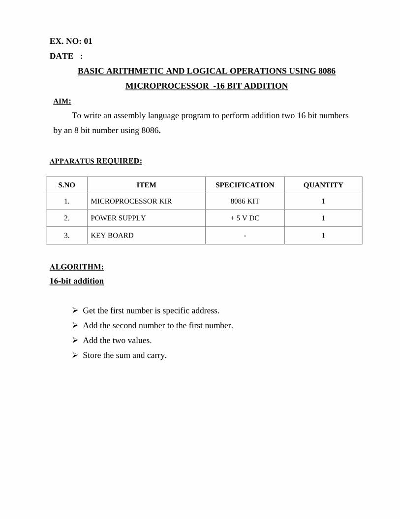
ALGORITHM:
16-bit addition
Get the first number is specific address.
Add the second number to the first number.
Add the two values.
Store the sum and carry.

FLOECHART:
ADDITION:

PROGRAM FOR ADDITION;
ADDRESS OPCODE LABEL MNEMONICS COMMENT
1000 MOV CX,0000H Initialize counter CX
1003 MOV AX,[1200] Get the first data in AXregister.
1006 MOV BX, [1202]Get the second data in BXregister.
100A ADD AX,BX Add the contents of boththe register AX & BX
100C JNC L1 Check for carry
100E INC CX If carry exists, incrementthe CX
100F LI L1 : MOV[1206],CX Store the carry
1013 MOV [1204], AX Store the sum
1016 INT-3 HLT Stop the program
OUTPUT FOR ADDITION:
INPUT
ADDRESS DATA
1200120112021203
OUTPUT 12041205
RESULT:
Thus assembly language programs to perform addition two 16 bit numbers by an 8bit number using 8086 Performed and the result is stored.

EX. NO: 02
DATE :
BASIC ARITHMETIC AND LOGICAL OPERATIONS USING
8086 MICROPROCESSOR - 16 BIT SUBTRACTION
AIM:
To write an assembly language program to perform subtraction two 16 bitnumbers by an 8 bit number using 8086.
APPARATUS REQUIRED:
S.NO ITEM SPECIFICATION QUANTITY
1. MICROPROCESSOR KIR 8086 KIT 1
2. POWER SUPPLY + 5 V DC 1
3. KEY BOARD - 1
ALGORITHM:
16-bit SUBTRACTION:
Initialize the MSBs of difference to 0
Get the first number
Subtract the second number from the first number.
If there is any borrow, increment MSBs of difference by 1.
Store LSBs of difference.
Store MSBs of difference.
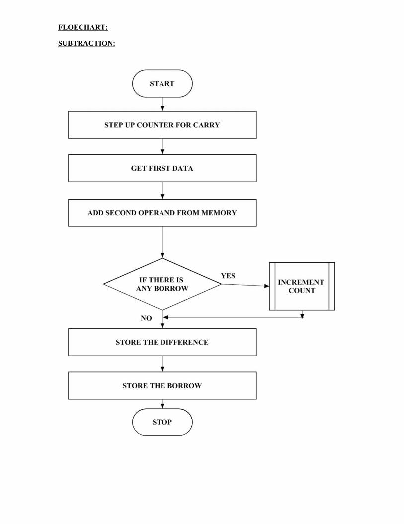
FLOECHART:
SUBTRACTION:

PROGRAM FOR SUBTRACTION:
ADDRESS OPCODE LABEL MNEMONICS COMMENT
1000 MOV CX,0000H Initialize counter CX
1003 MOV AX,[1300] Get the first data in AXregister
1006 MOV BX, [1302] Get the second data in BXregister.
100A SUB AX,BX Subtract the contents of boththe register AX & BX
100C JNC A Check the Borrow.
100E INC CX If carry exists, increment theCX
100F LI MOV [1306],CX Store the Borrow.
1013 MOV [1304], AX Store the difference.
1016 INT-3 HLT Stop the program
OUTPUT FOR ADDITION:
INPUT
ADDRESS DATA
1300130113021303
OUTPUT 13041305
RESULT:
Thus assembly language programs to perform subtraction two 16 bit
numbers by an 8 bit number using 8086 Performed and the result is stored.

EX. NO: 03
DATE :
BASIC ARITHMETIC AND LOGICAL OPERATIONS USING
8086 MICROPROCESSOR - 16 BIT MULTIPLICATION
AIM:
To write an assembly language program to perform Multiplication two 16 bit
numbers by an 8 bit number using 8086.
APPARATUS REQUIRED:
S.NO ITEM SPECIFICATION QUANTITY
1. MICROPROCESSOR KIR 8086 KIT 1
2. POWER SUPPLY + 5 V DC 1
3. KEY BOARD - 1
ALGORITHM:
16-bit MULTIPLICATION
Multiplication of 16-bit numbers:
Get the multiplier.
Get the multiplicand
Initialize the product to 0.
Product = product + multiplicand
Decrement the multiplier by 1.
If multiplicand is not equal to 0, repeat from step (d) otherwise store the
product.
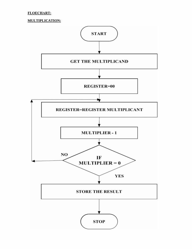
FLOECHART:
MULTIPLICATION:

PROGRAM FOR MULTIPLICATION:
ADDRESS OPCODE LABEL MNEMONICS COMMENT
1000 MOV AX,1234H Get the first data in AXregister.
1003 MOV BX,[1300]Get the second data in BXregister.
1006 MUL BX Multiply AX & BX data
1008 INT 3 Break point.
MULTIPLICATION OUTPUT:
INPUT
OUTPUT
RESULT:
Thus assembly language programs to perform multiplication two 16 bit
numbers by an 8 bit number using 8086 Performed and the result is stored.

EX. NO: 04
DATE :
BASIC ARITHMETIC AND LOGICAL OPERATIONS USING
8086 MICROPROCESSOR - 16 BIT DIVISION:
AIM:
To write an assembly language program to perform division two 16 bit
numbers by an 8 bit number using 8086.
APPARATUS REQUIRED:
S.NO ITEM SPECIFICATION QUANTITY
1. MICROPROCESSOR KIT 8086 KIT 1
2. POWER SUPPLY + 5 V DC 1
3. KEY BOARD - 1
ALGORITHM:
16-bit division
Division of 16-bit numbers:
Get the dividend and divisor.
Initialize the quotient to 0.
Dividend = dividend–divisor
If the divisor is greater, store the quotient
Go to step 3
If dividend is greater, quotient = quotient+ repeat from step 4.

FLOECHART:
DIVISION:

PROGRAM FOR DIVISION:
ADDRESS OPCODE LABEL MNEMONICS COMMENT
1000 MOV AX,[1200]Get the first data in AXregister,
1003 MOV DX,[1202] Get the second data in DXregister.
1007 MOV BX,[1204] Move the higher order data.
100D MOV [1206],AX Move ax register into address
100B DIV DX Divide the dividend bydivisor
1010 MOV AX,BX Copy the lower order data
1012 MOV [1208],AX Store the higher order data.
1015 INT 3 Stop the program.
OUTPUT FOR DIVISION:
INPUT AX= DX=
OUTPUT AX= DX=
RESULT:
Thus assembly language programs to perform division two 16 bit numbers by
an 8 bit number using 8086 Performed and the result is stored.

EX. NO: 05
DATE :
MOVE A DATA BLOCK WITHOUT OVERLAP
AIM:
To move a data block without overlap
APPARATUS REQUIRED:
S.NO ITEM SPECIFICATION QUANTITY
1. MICROPROCESSOR KIR 8086 KIT 1
2. POWER SUPPLY + 5 V DC 1
3. KEY BOARD - 1
ALGORITHM:
Initialize the memory location to the data pointer.
Increment B register.
Increment accumulator by 1 and adjust it to decimal every time.
Compare the given decimal number with accumulator value.
When both match, the equivalent hexadecimal value is in B register.
Store the resultant in memory location.

PROGRAM:
ADDRESS OPCODES PROGRAM COMMENTS
1000 MOV CL, 05 Get the Data range
1002 MOV SI, 1400 Get the first data.
1005 MOV DI, 1450 Get the second data.
1008 LD DSB Store the lower orderproduct
1009 MOV [DI], AL Store the result
100B INC DI Increment the pointer.
100C DEC 1008 Counter 0
1010 INT 3 Break point
OUTPUT:
INPUT OUTPUT
1400 1450
1401 1451
1402 1452
1403 1453
1404 1454
RESULT:
Thus the output for the Move a data block without overlap was executedsuccessfully.

EX. NO: 06
DATE :
CODE CONVERSION, DECIMAL ARITHMETIC
AND MATRIX OPERATIONS.
Code Conversions –Decimal to Hexadecimal:
AIM:
To convert a given decimal number to hexadecimal.
ALGORITHM:
Initialize the memory location to the data pointer.
Increment B register.
Increment accumulator by 1 and adjust it to decimal every time.
Compare the given decimal number with accumulator value.
When both match, the equivalent hexadecimal value is in B register.
Store the resultant in memory location.
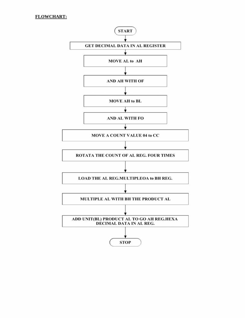
FLOWCHART:
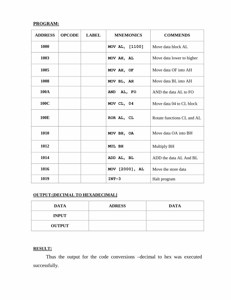
PROGRAM:
ADDRESS OPCODE LABEL MNEMONICS COMMENDS
1000 MOV AL, [1100] Move data block AL
1003 MOV AH, AL Move data lower to higher
1005 MOV AH, OF Move data OF into AH
1008 MOV BL, AH Move data BL into AH
100A AND AL, FO AND the data AL to FO
100C MOV CL, 04 Move data 04 to CL block
100E ROR AL, CL Rotate functions CL and AL
1010 MOV BH, OA Move data OA into BH
1012 MUL BH Multiply BH
1014 ADD AL, BL ADD the data AL And BL
1016 MOV [2000], AL Move the store data
1019 INT-3 Halt program
OUTPUT:[DECIMAL TO HEXADECIMAL]
DATA ADRESS DATA
INPUT
OUTPUT
RESULT:
Thus the output for the code conversions –decimal to hex was executed
successfully.

EX. NO: 07
DATE :
CODE CONVERSION –HEXADECIMAL TO DECIMAL
AIM:
To convert a given hexadecimal number to decimal.
ALGORITHM:
Initialize the memory location to the data pointer.
Increment B register.
Increment accumulator by 1 and adjust it to decimal every time.
Compare the given hexadecimal number with B register value.
When both match, the equivalent decimal value is in A register.
Store the resultant in memory location.

PROGRAM;
ADDRESS OPCODE LABEL MNEMONICS COMMENTS
1000 MOV AL, [1100] Move date to AL REG
1003 MOV DX, AL Move data AL TO DX
1008 JC TEN Jump carry
100A SUB AL, 64 Subtract data
100C INC DL Increment DL
100E JUP HUND JUMP label data
1010 TEN CMP AL, OA Compare register
1012 JC UNIT Jump carry
1014 SUB AL,OA Subtract data
1016 INC DH Increment DH
1018 JC TEN JUMP carry
101A UNIT MOV [200],DL Move data to DL
101E MOV [200],DH Move data to DH
1022 MOV [200],AL Move data to AL
1025 MOV [200],AH Move data to AH
1027 HLT Stop the program
1006 HUND MOV AL, 64 Move data to AX REG

OUTPUT:[ HEXADECIMAL NUMBER TO DECIMAL]:
RESULT:
Thus the output for the addition code conversions –decimal to hex was
executed successfully.
INPUT OUTPUT
MEMORY
DATA

EX. NO: 08
DATE :
FLOATING POINT OPERATIONS- STRING MANIPULATIONS,
SORTING AND SEARCHING
Copying a String:
AIM:
To move a string of length FF from source to destination.
ALGORITHM:
Initialize the data segment .(DS)
Initialize the extra data segment .(ES)
Initialize the start of string in the DS. (SI)
Initialize the start of string in the ES. (DI)
Move the length of the string (FF) in CX register.
Move the byte from DS TO ES, till CX=0.

FLOECHART:

PROGRAM:
ADDRESS OPCODES PROGRAM COMMENTS
1000 MOV SI,1200H Initialize destination address
1003 MOV DI,1300H Initialize starting address.
1006 MOV CX,0006H Initialize array size
1008 CLD Clear direction flag
100A REP MOVSB Copy the contents of source intodestination until count reaches zero
100C HLT Stop
OUTPUT : [ COPYING A STRING]:
INPUT OUTPUT
1400 1450
1401 1451
1402 1452
1403 1453
1404 1454
RESULT:
Thus a string of a particular length is moved from source segment to
destination segment.
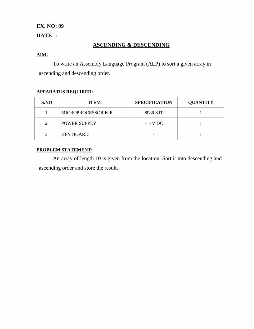
EX. NO: 09
DATE :
ASCENDING & DESCENDING
AIM:
To write an Assembly Language Program (ALP) to sort a given array in
ascending and descending order.
APPARATUS REQUIRED:
S.NO ITEM SPECIFICATION QUANTITY
1. MICROPROCESSOR KIR 8086 KIT 1
2. POWER SUPPLY + 5 V DC 1
3. KEY BOARD - 1
PROBLEM STATEMENT:
An array of length 10 is given from the location. Sort it into descending and
ascending order and store the result.

ALGORITHM:
Sorting in ascending order:
Load the array count in two registers C1 and C2.
Get the first two numbers.
Compare the numbers and exchange if necessary so that the two numbers are in
ascending order.
Decrement C2.
Get the third number from the array and repeat the process until C2 is 0.
Decrement C1 and repeat the process until C1 is 0.
Sorting in descending order:
Load the array count in two registers C1 and C2.
Get the first two numbers.
Compare the numbers and exchange if necessary so that the two numbers are in
descending order.
Decrement C2.
Get the third number from the array and repeat the process until C2 is 0.
Decrement C1 and repeat the process until C1 is 0.

FLOECHART:[ASCENDING]:
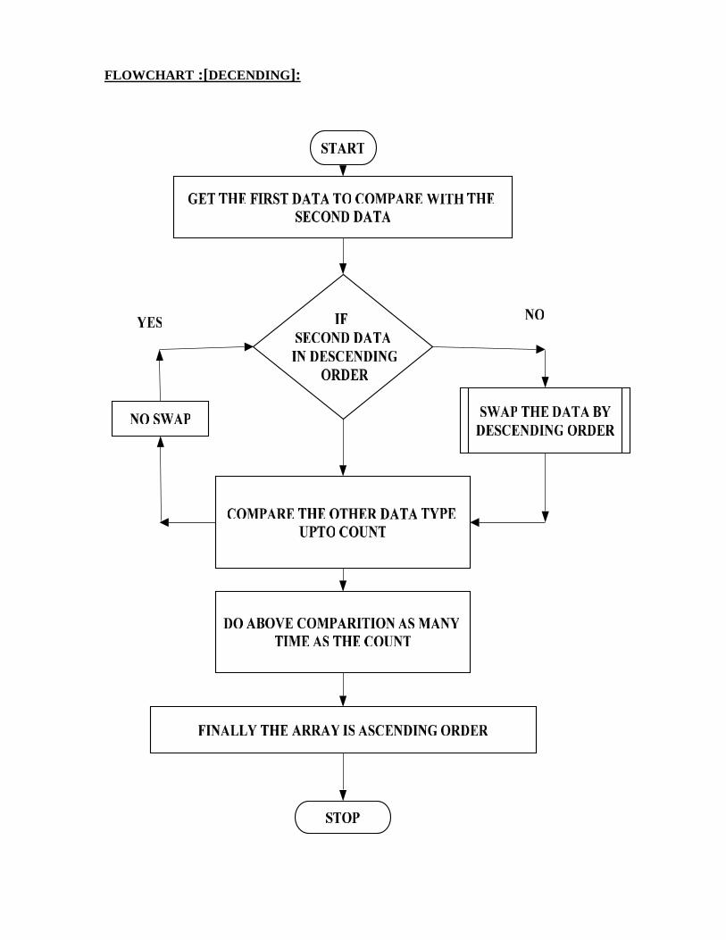
FLOWCHART :[DECENDING]:

PROGRAM FOR ASCENDING ORDER:
ADDRESS OPCODES PROGRAM COMMENTS
1000 MOV SI,1200HInitialize memory location forarray size
1002 MOV CL,[SI] Number of comparisons in CL
1004 L4 : MOVSI,1200H Initialize memory location forarray size
1006 MOV DL,[SI] Get the count in DL
1007 INC SI Go to next memory location
1009 MOV AL,[SI] Get the first data in AL
100B L3 : INC SI Go to next memory location
100E MOV BL,[SI] Get the second data in BL
1010 CMP AL,BL Compare two data’s
1012 JNB L1 If AL < BL go to L1
1014 DEC SIElse, Decrement the memorylocation
1016 MOV [SI],AL Store the smallest data
1018 MOV AL,BL Get the next data AL
1019 JMP L2 Jump to L2
101A L1 : DEC SI Decrement the memory location
101C MOV [SI],BL Store the greatest data in memorylocation
101E L2 : INC SI Go to next memory location
1020 DEC DL Decrement the count
1022 JNZ L3Jump to L3, if the count is notreached
1024 MOV [SI],AL Store data in memory location
1026 DEC CL Decrement the count
1028 JNZ L4 Jump to L4, if the count is notreached zero
1029 HLT Stop

PROGRAM FOR DESCENDING ORDER:
ADDRESS OPCODES PROGRAM COMMENTS
1000 MOV SI,1200H Initialize memory locationfor array size
1002 MOV CL,[SI]Number of comparisons inCL
1004L4 :MOVSI,1200H
Initialize memory locationfor array size
1006 MOV DL,[SI] Get the count in DL
1007 INC SIGo to next memorylocation
1009 MOV AL,[SI] Get the first data in AL
100B L3 : INC SIGo to next memorylocation

OUTPUT FOR ASCENDING:
OUTPUT FOR DESCENDING ORDER:
RESULT:
Thus given array of numbers are sorted in ascending & descending order.
DATA
INPUT
OUTPUT
DATA
INPUT
OUTPUT

EX. NO: 10
DATE :
LARGEST& SMALLEST
AIM:
To write an Assembly Language Program(ALP) to find the largest and
smallest number in a given array.
APPARATUS REQUIRED:
S.NO ITEM SPECIFICATION QUANTITY
1. MICROPROCESSOR KIR 8086 KIT 1
2. POWER SUPPLY + 5 V DC 1
3. KEY BOARD - 1
PROBLEM STATEMENT:
An array of length 5 is given from the location. Find the largest and smallest
number and store the result.

ALGORITHM:
(i) Finding largest number:
Load the array count in a register C1.
Get the first two numbers.
Compare the numbers and exchange if the number is small.
Get the third number from the array and repeat the process until C1 is 0.
(ii) Finding smallest number:
Load the array count in a register C1.
Get the first two numbers.
Compare the numbers and exchange if the number is large.
Get the third number from the array and repeat the process until C1 is 0.

FLOECHART:[LARGEST]

FLOECHART:[SMALLEST]

PROGRAM FOR FINDING LARGEST NUMBER:
ADDRESS OPCODES PROGRAM COMMENDS
1000 MOV SI,1200H Initialize array size
1002 MOV CL,[SI] Initialize the count
1004 INC SI Go to next memory location
1006 MOV AL,[SI] Move the first data in AL
1007 DEC CL Reduce the count
1009 L2 : INC SI Move the SI pointer to next data
100B CMP AL,[SI] Compare two data’s
100E JNB L1 If AL > [SI] then go to L1 ( no swap)
1010 MOV AL,[SI] Else move the large number to AL
1012 L1 : DEC CL Decrement the count
1014 JNZ L2 If count is not zero go to L2
1016 MOV DI,1300H Initialize DI with 1300H
1018 MOV [DI],AL Else store the biggest number in 1300location
1010 HLT Stop

PROGRAM FOR FINDING SMALLEST NUMBER:
ADDRESS OPCODES PROGRAM COMMENDS
1000 MOV SI,1200H Initialize array size
1002 MOV CL,[SI] Initialize the count
1004 INC SI Go to next memory location
1006 MOV AL,[SI] Move the first data in AL
1007 DEC CL Reduce the count
1009 L2 : INC SI Move the SI pointer to next data
100B CMP AL,[SI] Compare two data’s
100E JB L1 If AL < [SI] then go to L1 ( no swap)
1010 MOV AL,[SI] Else move the large number to AL
1012 L1 : DEC CL Decrement the count
1014 JNZ L2 If count is not zero go to L2
1016 MOV DI,1300H Initialize DI with 1300H
1018 MOV [DI],AL Else store the biggest number in 1300 location
1010 HLT Stop

OUTPUT FOR LARGESTNUMBER:
OUTPUT FOR SMALLEST NUMBER:
RESULT:
Thus largest and smallest number is found in a given array.
DATA
INPUT
OUTPUT
DATA
INPUT
OUTPUT

DATE :
TRAFFIC LIGHT CONTROL
AIM:
To write an assembly language program in 8086 to Traffic light control
APPARATUS REQUIRED:
SL .No ITEM SPECIFICATION QUANTITY
1. Microprocessor kit 8086 kit 1
2. Power Supply +5 V dc 1
PROGRAM;
Log into System.
Select control type.
If Automatic mode select then go to step 4th else go to step 8.
If Automatic control activated.
Assign time period for green, yellow signal.
If emergency vehicle is over then go to step 4.
If rally come then go to step 8.
Manual control activated.
Assign time period for green, yellow signal according to that particular road.
If emergency over then go to step 4.
EXP.NO: 11
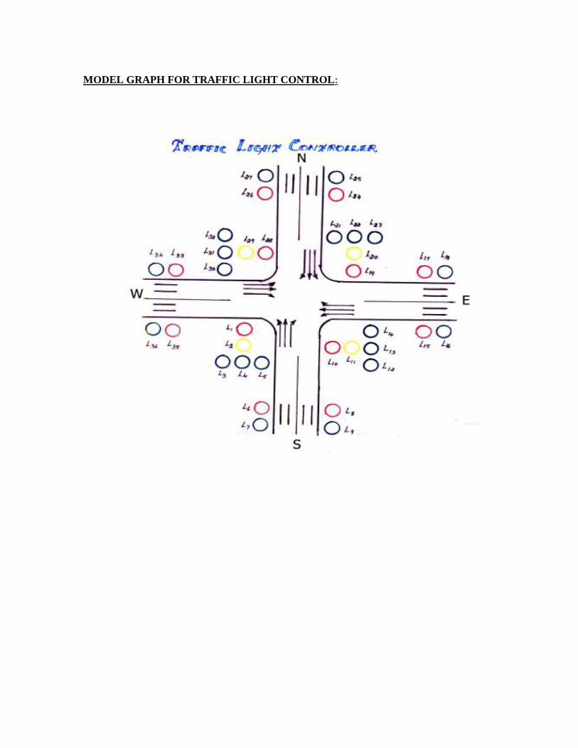
MODEL GRAPH FOR TRAFFIC LIGHT CONTROL:

ASSEMBLY LANGUAGE PROGRAM FOR TRAFFIC LIGHT CONTROL:
ADDRESS OPCODE LABEL MNEMONICS
1000 MVI A,80
1002 OUT CWR
1004 REPEAT MVI E, 03
1006 LXI H, C100
1007 NEXTSTAT MOV A, M
1009 OUT PORRTA
100B INX H
100E MOV A, M
1010 OUT PORTB
1012 INX H
1014 MOV A,M
1016 OUT PORT C
1018 CALL DELAY
1019 INX H
101A DCR E
101C JNZ NEXTSTAT
101E JMP REPEAT
1022 DELAY LXI D, 3000
1024 L2 MVI C,FF
1026 L1 DCR C
1028 JNZ L1
1029 DCR D
1000 MOV A, D
1002 ORA E
1004 JNZ L2
1006 RET

RESULT:
Thus the assembly language program for traffic light control is verified

DATE :
STEPPER MOTOR INTERFACING
AIM:
To write an assembly language program in 8086 to rotate the motor atdifferent speeds.
APPARATUS REQUIRED:
SL.NO ITEM SPECIFICATION QUANTITY
1. Microprocessor kit 8086 1
2. Power Supply +5 V, dc,+12 V dc 1
3. Stepper Motor Interface board - 1
4. Stepper Motor - 1
PROBLEM STATEMENT:
Write a code for achieving a specific angle of rotation in a given time and
particular number of rotations in a specific time.
THEORY:
A motor in which the rotor is able to assume only discrete stationary
angular position is a stepper motor. The rotary motion occurs in a stepwise manner
from one equilibrium position to the next. Two-phase scheme: Any two adjacent
stator windings are energized. There are two magnetic fields active in quadrature
and none of the rotor pole faces can be in direct alignment with the stator poles. A
partial but symmetric alignment of the rotor poles is of course possible.
EX. NO: 12

ALGORITHM:
For running stepper motor clockwise and anticlockwise directions
Get the first data from the lookup table.
Initialize the counter and move data into accumulator.
Drive the stepper motor circuitry and introduce delay
Decrement the counter is not zero repeat from step(iii)
Repeat the above procedure both for backward and forward directions.
SWITCHING SEQUENCE OF STEPPER MOTOR:
MEMORYLOCATION A1 A2 B1 B2 HEX CODE
4500 1 0 0 0 09 H
4501 0 1 0 1 05 H
4502 0 1 1 0 06 H
4503 1 0 1 0 0A H

FLOWCHART:

PROGRAM FOR STEPPER MOTOR CONTOL;
ADDRESS OPCODE PROGRAM COMMENTS
1000START : MOVDI, 1200H
Initialize memory location to store the arrayof number
1002 MOV CX, 0004H Initialize array size
1004LOOP 1 : MOVAL,[DI] Copy the first data in AL
1006 OUT 0C0,AL Send it through port address
1007 MOV DX, 1010H Introduce delay
1009 L1 : DEC DX Declare DX
100B JNZ L1 JUNP no zero
100E INC DI Increment DI
1010 LOOP LOOP1 Go to next memory location
1012 JMP START Loop until all the data’s have been sent Go tostart location for continuous rotation
10141200 :09,05,06,0A Array of data’s
RESULT:
Thus the assembly language program for rotating stepper motor in both
clockwise and anticlockwise directions is written and verified.

DATE :
DIGITAL CLOCK
AIM:
To display the digital clock specifically by displaying the hours, minutes and
seconds using 8086 kits
APPARATUS REQUIRED:
PRELIMINARY SETTINGS:
Store time value in memory location 1500- Seconds
1501- Minutes
1502- Hours
S.NO ITEM SPECIFICATION
1 Microprocessor kit 8086
2 Power Supply 5V
EX. NO: 13

DIGITAL CLOCK PROGRAM:
MEMORY OPCODE LABEL MNEMONICS
1000 START
1000 CALL CONVERT
1003 CALL DISPLAY
1006 DELAY MOV AL, 0B0H
1009 OUT 16H, AL
100B MOV CL, 07H
100E S2 MOV AL, 88H
1011 OUT 14H, AL
1013 MOV AL, 80H
1016 OUT 14H, AL
1018 S1 MOV AL, 80H
101BOUT 16H, AL
101D NOP
101E NOP
101F NOP
1020 NOP
1021 IN AL, 14H
1023 MOV DL, AL
1025 IN AL, 14H
1027 OR AL,DL
1029 JNZ S1
102B DEC CL

102D JNZ S2
102F MOV SI, 1500H
1033 MOV AL.[SI]
1035 INC AL
1037 MOV [SI],AL
1039 CMP AL, 3CH
103C JNZ START
103E MOV AL, 00H
1041 MOV[SI], AL
1043 INC AL
1044 MOV [SI],AL
1046 CMP AL,3CH
1048 JNZ START
1041 MOV AL, 0
104D MOV AL, [SI]
104F MOV AL, O
1052 MOV [SI],AL
1054 INC SI
1055 MOV AL, [SI]
1057 CMP AL, 18H
1059 JNZ START
105B MOV AL, 0
105E MOV SI,AL
1060 MOV AL,0
1063 MOV [SI],AL

1065 JMP START
1068 DISPLAY MOV AH, 06H
106B MOV DX, 1600H
106F MOV CH, 01
1072 MOV CL , 01
1075 INT 5
1077 RET
1078 CONVERT MOV SI, 1500H
107C MOV BX, 1608H
1080 MOV AL, 24
1080 MOV [BX,] AL
SECONDS
1085 MOV AL, SI
1087 MOV AH, 0
108A MOV DH, 0AH
108D DIV DH
108F ADD AH, 30H
1092 DEC BX
1093 MOV [BX], AH
1095 DEC BX
1096ADD AL, 30H
1098 HLT

RESULT;
Thus the digital clock program has been written and executed using 8086
microprocessor kit and the output of digital clock was displayed as [hours: minutes:
seconds] successfully.

DATE :
INTERFACING PRGRAMMABLE KEYBOARD AND
DISPLAY CONTROLLER- 8279
AIM :To display the rolling message “HELP US “ in the display.
APPARATUS REQUIRED:
8086 Microprocessor kit, Power supply, interfacing board.
ALGORITHM :
Display of rolling message “HELP US “
Initialize the counter
Set 8279 for 8 digit character display, right entry
Set 8279 for clearing the display
Write the command to display
Load the character into accumulator and display it
Introduce the delay
Repeat from step 1.
EX. NO: 14

PROGRAM:
MEMORYLOCATION OPCODES PROGRAM COMMENDS
1000START : MOVSI,1200H Initialize array
1000 MOV CX,000FH Initialize array size
1003 MOV AL,10 Store the control word fordisplay mode
1006 OUT C2,AL Send through output port
1009 MOV AL,CCStore the control word toclear display
100B OUT C2,AL Send through output port
100E MOV AL,90 Store the control word towrite display
1011 OUT C2,AL Send through output port
1013 L1 : MOV AL,[SI] Get the first data
1016 OUT C0,AL Send through output port
1018 CALL DELAY Give delay
101B INC SI Go & get next data
101D LOOP L1 Loop until all the data’shave been taken
101E JMP START Go to starting location
101FDELAY : MOVDX,0A0FFH Store 16bit count value
1020 LOOP1 : DEC DX Decrement count value
1021 JNZ LOOP1Loop until count valuesbecomes zero
1023 RET Return to main program

VVIT DEPARTMENT OF ELECTRONICS AND COMMUNICATION ENGINEERING
1. Display Mode Setup: Control word-10 H
0 0 0 1 0 0 0 0
0 0 0 D D K K K
DD-00- 8Bit character display left entry
01- 16Bit character display left entry
10- 8Bit character display right entry
11- 16Bit character display right entry
KKK- Key Board Mode
000-2Key lockout.
2.Clear Display: Control word-DC H
1 1 0 1 1 1 0 0
1 1 0 CD CD CD CF CA
11 A0-3; B0-3 =F
1-Enables Clear display0-Contents of RAM will be displayed
1-FIFO Status is cleared1-Clear all bits(Combined effect of CD)

3. Write Display: Control word-90H
1 0 0 1 0 0 0 0
1 0 0AI A A A A
Selects one of the 16 rows of display.
Auto increment = 1, the row address selected will be incremented aftereach of read and write operation of the display RAM.

FLOWCHART:

SEGMENT DEFINITION:
DATA BUS D7 D6 D5 D4 D3 D2 D1 D0
SEGMENTS d c b a d g f e
RESULT:
Thus the rolling message “HELP US” is displayed using 8279 interface kit.

DATE :
A/D AND D/A INTERFACE AND WAVEFORM GENERATION.
ADC
AIM:
To write an assembly language program to convert an analog signal into a
digital signal using an ADC interfacing.
APPARATUS REQUIRED:
SL.NO ITEM SPECIFICATION QUANTITY
1. Microprocessor kit 8086 1
2. Power Supply +5 V dc,+12 V dc 1
3. ADC Interface board - 1
THEORY:
An ADC usually has two additional control lines: the SOC input to tell the
ADC when to start the conversion and the EOC output to announce when the
conversion is complete.
ALGORITHM:
Select the channel and latch the address.
Send the start conversion pulse.
Read EOC signal.
If EOC = 1 continue else go to step (iii)
Read the digital output.
Store it in a memory location.
EX. NO: 15

PROGRAM:
MEMORYLOCATION
OPCODES PROGRAM COMMENTS
1000 MOV AL,00Load accumulatorwith value for ALEhigh
1000 OUT 0C8H,ALSend through outputport
1003 MOV AL,08Load accumulatorwith value for ALElow
1006 OUT 0C8H,AL Send through outputport
1009 MOV AL,01Store the value tomake SOC high inthe accumulator
100B OUT 0D0H,AL Send through outputport
100E MOV AL,00
Introduce delay
1011 MOV AL,00
1013 MOV AL,00
1016 MOV AL,00
1018 OUT 0D0H,ALStore the value tomake SOC low theaccumulator
101B L1 : IN AL, 0D8H Send through outputport
101D AND AL,01
Read the EOC signalfrom port & checkfor end of conversion
101E CMP AL,01
101F JNZ L1

1020 IN AL,0C0H from port again
1021 MOV BX,1100 Read data from port
1023 MOV [BX],AL Initialize the memorylocation to store data
1025 HLT Store the data andhalt program
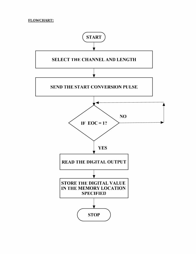
FLOWCHART:

OUTPUT:
ANALOG VOLTAGE DIGITAL DATA ON LEDDISPLAY
HEX CODE IN MEMORYLOCATION
RESULT:
Thus the ADC was interfaced with 8086 and the given analog inputs were
converted into its digital equivalent.

DATE :INTERFACING DIGITAL – TO – ANALOG CONVERTER
AIM:
1. To write an assembly language program for digital to analog conversion2. To convert digital inputs into analog outputs & To generate different
waveforms
APPARATUS REQUIRED:
SL.NO ITEM SPECIFICATION QUANTITY
1. Microprocessor kit 8086 Vi Microsystems 1
2. Power Supply +5 V, dc,+12 V dc 1
3. DAC Interface board - 1
PROBLEM STATEMENT:
The program is executed for various digital values and equivalent analogvoltages are measured and also the waveforms are measured at the output portsusing CRO.
THEORY:
Since DAC 0800 is an 8 bit DAC and the output voltage variation isbetween –5v and +5v. The output voltage varies in steps of 10/256 = 0.04(approximately). The digital data input and the corresponding output voltages arepresented in the table. The basic idea behind the generation of waveforms is thecontinuous generation of analog output of DAC. With 00 (Hex) as input to DAC2the analog output is –5v. Similarly with FF H as input, the output is +5v.Outputting digital data 00 and FF at regular intervals, to DAC2, results in a squarewave of amplitude 5v.Output digital data from 00 to FF in constant steps of 01 toDAC2. Repeat this sequence again and again. As a result a saw-tooth wave will begenerated at DAC2 output. Output digital data from 00 to FF in constant steps of01 to DAC2. Output digital data from FF to 00 in constant steps of 01 to DAC2.
EX. NO: 16

FLOECHART:
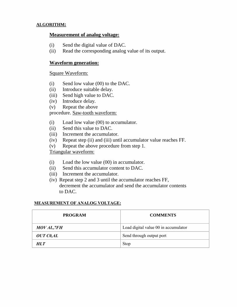
ALGORITHM:
Measurement of analog voltage:
(i) Send the digital value of DAC.(ii) Read the corresponding analog value of its output.
Waveform generation:
Square Waveform:
(i) Send low value (00) to the DAC.(ii) Introduce suitable delay.(iii) Send high value to DAC.(iv) Introduce delay.(v) Repeat the aboveprocedure. Saw-tooth waveform:
(i) Load low value (00) to accumulator.(ii) Send this value to DAC.(iii) Increment the accumulator.(iv) Repeat step (ii) and (iii) until accumulator value reaches FF.(v) Repeat the above procedure from step 1.Triangular waveform:
(i) Load the low value (00) in accumulator.(ii) Send this accumulator content to DAC.(iii) Increment the accumulator.(iv) Repeat step 2 and 3 until the accumulator reaches FF,
decrement the accumulator and send the accumulator contentsto DAC.
MEASUREMENT OF ANALOG VOLTAGE:
PROGRAM COMMENTS
MOV AL,7FH Load digital value 00 in accumulator
OUT C0,AL Send through output port
HLT Stop

DIGITAL DATA ANALOG VOLTAGE
PROGRAM TABLE: saw tooth wave
PROGRAM COMMENTS
L2: MOV AL,00H Load 00 in accumulator
OUT C0,AL Send through output port
CALL L1 Give a delay
MOV AL,FFH Load FF in accumulator
OUT C0,AL Send through output port
CALL L1 Give a delay
JMP L2 Go to starting location
L3: MOV CX,05FFH Load count value in CX register
L1: LOOP L3 Decrement until it reaches zero
RET Return to main program

PROGRAM TABLE: Square Wave
PROGRAM COMMENTS
L2; OUT C0,AL Load 00 in accumulator
CALL L1 Send through output port
MOV AL,FFH Give a delay
OUT C0,AL Load FF in accumulator
CALL L1 Send through output port
JMP L2 Give a delay
L1 Load 00 in accumulator
L3 Send through output port
RET return
PROGRAM TABLE: Triangular Wave
PROGRAM COMMENTS
L3 Load 00 in accumulator
L1 Send through output port
INC AL Increment contents of accumulator
JNZ L1 Send through output port until it reaches FF
MOV AL,0FFH Load FF in accumulator
L2 Send through output port
DEC AL Decrement contents of accumulator
JNZ L2 Send through output port until it reaches 00
JMP L3 Go to starting location
L3 Load 00 in accumulator

WAVEFORM GENERATION:
WAVEFORMS AMPLITUDE TIMEPERIOD
Square Waveform
Saw-tooth waveform
Triangular waveform
RESULT
Thus the DAC was interfaced with 8085 and different waveforms have been
generated.

1. STUDY OF 8051 MICROCONTROLLER
Aim
To study the microcontroller 8051
Architecture of 8051 Microcontroller
Architecture of 8051 microcontroller has following features
4 Kb of ROM is not much at all.
128Kb of RAM (including SFRs) satisfies the user's basic needs.
4 ports having in total of 32 input/output lines are in most cases sufficient to make all
necessary connections to peripheral environment.
The whole configuration is obviously thought of as to satisfy the needs of most
programmers working on development of automation devices. One of its advantages is that
nothing is missing and nothing is too much. In other words, it is created exactly in accordance
to the average user‘s taste and needs. Other advantages are RAM organization, the operation
of Central Processor Unit (CPU) and ports which completely use all recourses and enable
further upgrade.

Pin out Description
Pins 1-8: Port 1 each of these pins can be configured as an input or an output.
Pin 9: RS A logic one on this pin disables the microcontroller and clears the contents of most
registers. In other words, the positive voltage on this pin resets the microcontroller. By
applying logic zero to this pin, the program starts execution from the beginning.
Pins10-17: Port 3 Similar to port 1, each of these pins can serve as general input or output.
Besides, all of them have alternative functions:
Pin 10: RXD Serial asynchronous communication input or Serial synchronous
communication output.
Pin 11: TXD Serial asynchronous communication output or Serial synchronous
communication clock output.
Pin 12: INT0 Interrupt 0 inputs.
Pin 13: INT1 Interrupt 1 input.
Pin 14: T0 Counter 0 clock input.
Pin 15: T1 Counter 1 clock input.
Pin 16: WR Write to external (additional) RAM.
Pin 17: RD Read from external RAM.

Pin 18, 19: X2, X1 Internal oscillator input and output. A quartz crystal which specifies
operating frequency is usually connected to these pins. Instead of it, miniature ceramics
resonators can also be used for frequency stability. Later versions of microcontrollers operate
at a frequency of 0 Hz up to over 50 Hz.
Pin 20: GND Ground.
Pin 21-28: Port 2 If there is no intention to use external memory then these port pins are
configured as general inputs/outputs. In case external memory is used, the higher address
byte, i.e. addresses A8-A15 will appear on this port. Even though memory with capacity of
64Kb is not used, which means that not all eight port bits are used for its addressing, the rest
of them are not available as inputs/outputs.
Pin 29: PSEN If external ROM is used for storing program then a logic zero (0) appears on it
every time the microcontroller reads a byte from memory.
Pin 30: ALE Prior to reading from external memory, the microcontroller puts the lower
address byte (A0-A7) on P0 and activates the ALE output. After receiving signal from the
ALE pin, the external register (usually 74HCT373 or 74HCT375 add-on chip) memorizes the
state of P0 and uses it as a memory chip address. Immediately after that, the ALU pin is
returned its previous logic state and P0 is now used as a Data Bus. As seen, port data
multiplexing is performed by means of only one additional (and cheap) integrated circuit. In
other words, this port is used for both data and address transmission.
Pin 31: EA By applying logic zero to this pin, P2 and P3 are used for data and address
transmission with no regard to whether there is internal memory or not. It means that even
there is a program written to the microcontroller, it will not be executed. Instead, the program
written to external ROM will be executed. By applying logic one to the EA pin, the
microcontroller will use both memories, first internal then external (if exists).
Pin 32-39: Port 0 Similar to P2, if external memory is not used, these pins can be used as
general inputs/outputs. Otherwise, P0 is configured as address output (A0-A7) when the ALE
pin is driven high (1) or as data output (Data Bus) when the ALE pin is driven low (0).
Pin 40: VCC +5V power supply.
Input/Output Ports (I/O Ports)
All 8051 microcontrollers have 4 I/O ports each comprising 8 bits which can be configured as
inputs or outputs. Accordingly, in total of 32 input/output pins enabling the microcontroller to
be connected to peripheral devices are available for use.
Pin configuration, i.e. whether it is to be configured as an input (1) or an output (0), depends
on its logic state. In order to configure a microcontroller pin as an input, it is necessary to
apply a logic zero (0) to appropriate I/O port bit. In this case, voltage level on appropriate pin
will be 0.
Similarly, in order to configure a microcontroller pin as an input, it is necessary to apply a
logic one (1) to appropriate port. In this case, voltage level on appropriate pin will be 5V (as
is the case with any TTL input). This may seem confusing but don't loose your patience. It all
becomes clear after studying simple electronic circuits connected to an I/O pin.
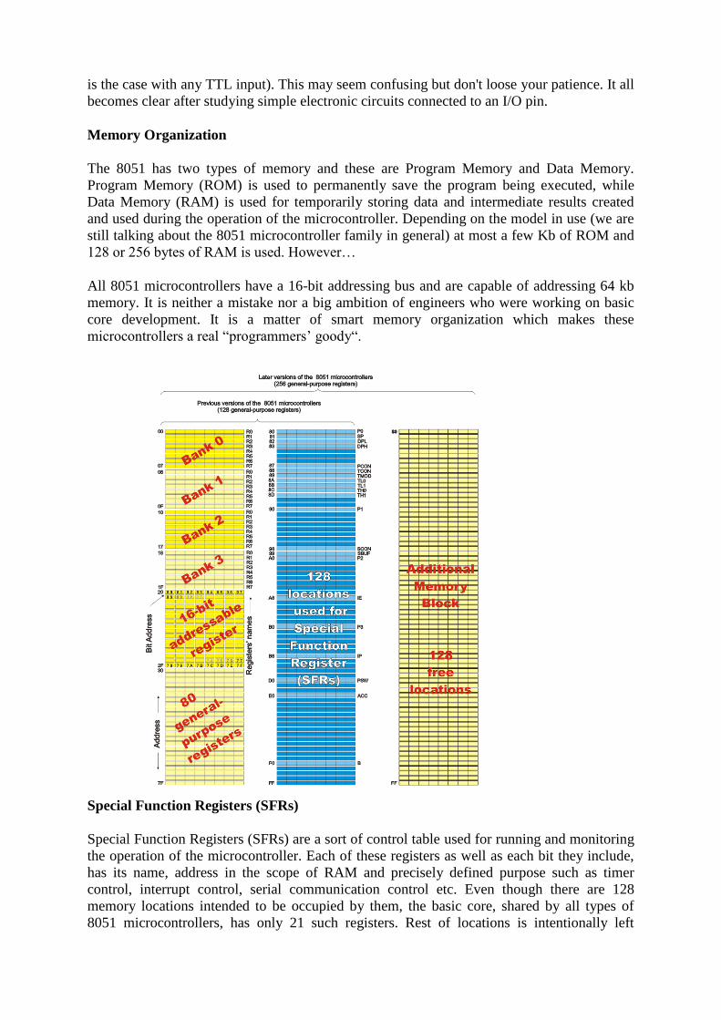
Memory Organization
The 8051 has two types of memory and these are Program Memory and Data Memory.
Program Memory (ROM) is used to permanently save the program being executed, while
Data Memory (RAM) is used for temporarily storing data and intermediate results created
and used during the operation of the microcontroller. Depending on the model in use (we are
still talking about the 8051 microcontroller family in general) at most a few Kb of ROM and
128 or 256 bytes of RAM is used. However…
All 8051 microcontrollers have a 16-bit addressing bus and are capable of addressing 64 kb
memory. It is neither a mistake nor a big ambition of engineers who were working on basic
core development. It is a matter of smart memory organization which makes these
microcontrollers a real “programmers’ goody“.
Special Function Registers (SFRs)
Special Function Registers (SFRs) are a sort of control table used for running and monitoring
the operation of the microcontroller. Each of these registers as well as each bit they include,
has its name, address in the scope of RAM and precisely defined purpose such as timer
control, interrupt control, serial communication control etc. Even though there are 128
memory locations intended to be occupied by them, the basic core, shared by all types of
8051 microcontrollers, has only 21 such registers. Rest of locations is intentionally left

unoccupied in order to enable the manufacturers to further develop microcontrollers keeping
them compatible with the previous versions. It also enables programs written a long time ago
for microcontrollers which are out of production now to be used today.
Program Status Word (PSW) Register
PSW register is one of the most important SFRs. It contains several status bits that reflect the
current state of the CPU. Besides, this register contains Carry bit, Auxiliary Carry, two
register bank select bits, Overflow flag, parity bit and user-definable status flag.
P - Parity bit. If a number stored in the accumulator is even then this bit will be
automatically set (1), otherwise it will be cleared (0). It is mainly used during data transmit
and receive via serial communication.
- Bit 1. This bit is intended to be used in the future versions of microcontrollers.
OV Overflow occurs when the result of an arithmetical operation is larger than 255 and
cannot be stored in one register. Overflow condition causes the OV bit to be set (1).
Otherwise, it will be cleared (0).
RS0, RS1 - Register bank select bits. These two bits are used to select one of four register
banks of RAM. By setting and clearing these bits, registers R0-R7 are stored in one of four
banks of RAM.

RS1 RS2 Space in RAM
0 0 Bank0 00h-07h
0 1 Bank1 08h-0Fh
1 0 Bank2 10h-17h
1 1 Bank3 18h-1Fh
F0 - Flag 0. This is a general-purpose bit available for use.
AC - Auxiliary Carry Flag is used for BCD operations only.
CY - Carry Flag is the (ninth) auxiliary bit used for all arithmetical operations and shift
instructions.
Data Pointer Register (DPTR)
DPTR register is not a true one because it doesn't physically exist. It consists of two separate
registers: DPH (Data Pointer High) and (Data Pointer Low). For this reason it may be treated
as a 16-bit register or as two independent 8-bit registers. Their 16 bits are primarly used for
external memory addressing. Besides, the DPTR Register is usually used for storing data and
intermediate results.

Stack Pointer (SP) Register
A value stored in the Stack Pointer points to the first free stack address and permits stack
availability. Stack pushes increment the value in the Stack Pointer by 1. Likewise, stack pops
decrement its value by 1. Upon any reset and power-on, the value 7 is stored in the Stack
Pointer, which means that the space of RAM reserved for the stack starts at this location. If
another value is written to this register, the entire Stack is moved to the new memory
location.
P0, P1, P2, P3 - Input/Output Registers
If neither external memory nor serial communication system are used then 4 ports with in
total of 32 input/output pins are available for connection to peripheral environment. Each bit
within these ports affects the state and performance of appropriate pin of the microcontroller.
Thus, bit logic state is reflected on appropriate pin as a voltage (0 or 5 V) and vice versa,
voltage on a pin reflects the state of appropriate port bit.
As mentioned, port bit state affects performance of port pins, i.e. whether they will be
configured as inputs or outputs. If a bit is cleared (0), the appropriate pin will be configured
as an output, while if it is set (1), the appropriate pin will be configured as an input. Upon
reset and power-on, all port bits are set (1), which means that all appropriate pins will be
configured as inputs.
Counters and Timers
As you already know, the microcontroller oscillator uses quartz crystal for its operation. As
the frequency of this oscillator is precisely defined and very stable, pulses it generates are
always of the same width, which makes them ideal for time measurement. Such crystals are
also used in quartz watches. In order to measure time between two events it is sufficient to
count up pulses coming from this oscillator. That is exactly what the timer does. If the timer
is properly programmed, the value stored in its register will be incremented (or decremented)
with each coming pulse, i.e. once per each machine cycle. A single machine-cycle instruction
lasts for 12 quartz oscillator periods, which means that by embedding quartz with oscillator
frequency of 12MHz, a number stored in the timer register will be changed million times per
second, i.e. each microsecond.
The 8051 microcontroller has 2 timers/counters called T0 and T1. As their names suggest,
their main purpose is to measure time and count external events. Besides, they can be used
for generating clock pulses to be used in serial communication, so called Baud Rate.

Timer T0
As seen in figure below, the timer T0 consists of two registers – TH0 and TL0 representing a
low and a high byte of one 16-digit binary number.
Accordingly, if the content of the timer T0 is equal to 0 (T0=0) then both registers it consists
of will contain 0. If the timer contains for example number 1000 (decimal), then the TH0
register (high byte) will contain the number 3, while the TL0 register (low byte) will contain
decimal number 232.
Formula used to calculate values in these two registers is very simple:
TH0 × 256 + TL0 = T
Matching the previous example it would be as follows:
3 × 256 + 232 = 1000
Since the timer T0 is virtually 16-bit register, the largest value it can store is 65 535. In case
of exceeding this value, the timer will be automatically cleared and counting starts from 0.
This condition is called an overflow. Two registers TMOD and TCON are closely connected
to this timer and control its operation.

TMOD Register (Timer Mode)
The TMOD register selects the operational mode of the timers T0 and T1. As seen in figure
below, the low 4 bits (bit0 - bit3) refer to the timer 0, while the high 4 bits (bit4 - bit7) refer
to the timer 1. There are 4 operational modes and each of them is described herein.
Bits of this register have the following function:
GATE1 enables and disables Timer 1 by means of a signal brought to the INT1 pin
(P3.3):
o 1 - Timer 1 operates only if the INT1 bit is set.
o 0 - Timer 1 operates regardless of the logic state of the INT1 bit.
C/T1 selects pulses to be counted up by the timer/counter 1:
o 1 - Timer counts pulses brought to the T1 pin (P3.5).
o 0 - Timer counts pulses from internal oscillator.
T1M1,T1M0 These two bits select the operational mode of the Timer 1.
T1M1 T1M0 Mode Description
0 0 0 13-bit timer
0 1 1 16-bit timer
1 0 2 8-bit auto-
reload
1 1 3 Split mode
GATE0 enables and disables Timer 1 using a signal brought to the INT0 pin (P3.2):
o 1 - Timer 0 operates only if the INT0 bit is set.
o 0 - Timer 0 operates regardless of the logic state of the INT0 bit.
C/T0 selects pulses to be counted up by the timer/counter 0:
o 1 - Timer counts pulses brought to the T0 pin (P3.4).
o 0 - Timer counts pulses from internal oscillator.
T0M1,T0M0 These two bits select the oprtaional mode of the Timer 0.
T0M1 T0M0 Mode Description
0 0 0 13-bit timer
0 1 1 16-bit timer
1 0 2 8-bit auto-reload
1 1 3 Split mode
Timer Control (TCON) Register
TCON register is also one of the registers whose bits are directly in control of timer
operation.
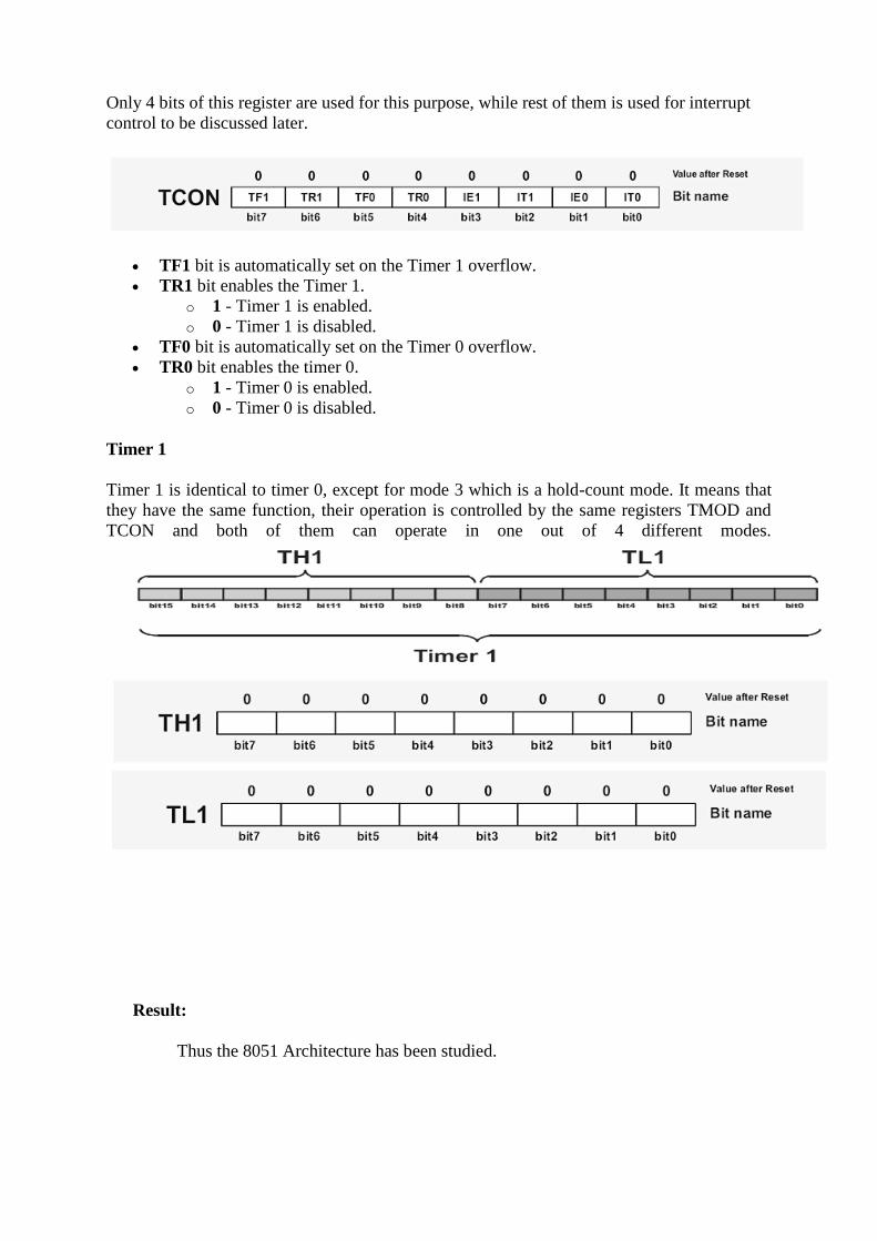
Only 4 bits of this register are used for this purpose, while rest of them is used for interrupt
control to be discussed later.
TF1 bit is automatically set on the Timer 1 overflow.
TR1 bit enables the Timer 1.
o 1 - Timer 1 is enabled.
o 0 - Timer 1 is disabled.
TF0 bit is automatically set on the Timer 0 overflow.
TR0 bit enables the timer 0.
o 1 - Timer 0 is enabled.
o 0 - Timer 0 is disabled.
Timer 1
Timer 1 is identical to timer 0, except for mode 3 which is a hold-count mode. It means that
they have the same function, their operation is controlled by the same registers TMOD and
TCON and both of them can operate in one out of 4 different modes.
Result:
Thus the 8051 Architecture has been studied.

2. ARTHMETIC OPERATIONS USING 8051
Aim:
To do the arithmetic operations using 8051 microprocessor
Apparatus required:
8085 microprocessor kit
DAC interface kit
Keyboard
Algorithm:
Addition / Subtraction
Step 1 : Move 1H data to memory
Step 2 : Add or subtract 1H data with 2nd data
Step 3 : Initialize data pointer.
Step 4 : Move result to memory pointed by DPTR.
Multiplication / Division
Step 1 : Get 1H data and 2nd data to memory
Step 2 : Multiply or divide 1H data with 2nd data
Step 3 : Initialize data pointer.
Step 4 : Move result to memory pointed by DPTR (first port)
Step 5 : Increment DPTR
Step 6 : Move 2nd part of result to register A
Step 7 : Move result to 2nd memory location pointer by DPTR
START
Out 1H data in memory
Add or subtract 1H and 1st data
Initialize DPTR
Stop
Move result to memory preset by DPTR
Program: 8-bit Addition:
Memory
Location
Label Opcode Mnemonics Comments
4100 Start C3 CLR C Clear the carry flat
4101 74DA MOV A, #01 Moves data 1 to
register A
4103 24DA ADD A, #02 Add content of A and
data 2 and store in A
4105 464500 MOV DPTR,#4500 Moves data 4500 to
DPTR
4108 F0 MOVX @DPTR,A Moves control of A to
location pointed DTPR
4109 80 FE SJMP 4109 Short jump to 4109
Execution:
Addition:
ML Input
4103
4109
ML Output
4500
START
Get data into the register
Complement the data
Move the data to pointer by DPTR
Stop
Increment data
Increment DPTR
Move data into paste location
Short jump to preset location

Program: 8-bit Subtraction:
Memory
Location
Label Opcode Mnemonics Comments
4100 Start C3 CLR C Clear the carry flat
4101 74DA MOV A,#05 Moves data 1 to
register A
4103 24DA SUBB A,#02 Subtract data 2 from
content of A and store
result in A
4105 464500 MOV DPTR,#4500 Moves 4500 to DPTR
4108 F0 MOVX @DPTR,A Moves result by
location by DTPR
4109 80 FE SJMP 4109 Short jump to 4109
Execution:
Subtraction:
ML Input
4101
4103
Program: 8-bit Multiplication:
Memory
Location
Label Opcode Mnemonics Comments
4100 Start 7403 MOV A,#03 Move immediate data
to accumulator
4101 75F003 MOV B,#02 Move 2nd data to B
register
4105 A4 MUL AB Get the product in A &
B
4106 904500 MOV DPTR, # 4500 Load data in 4500
location
4109
410A
F0 MOVX @DPTR,A
INC DPTR
Move A t ext RAM
410B E5F0 MOV A,B Move 2nd data in A
410D F0 MOVX @DPTR,A Same the ext RAM
410E 80FE SJMP 410E Remain idle in infinite
loop
Execution:
Multiplication:
ML Input
4101
4103
ML Output
4500
Output Address Value
4500

Program: 8-bit Division:
Memory
Location
Label Opcode Mnemonics Comments
4100 Start 7408 MOV A,#04 Move immediate data
to accumulator
4102 75F002 MOV B,#02 Move immediate to B
reg.
4105 84 DIV AB Divide content of A &
B
4106 904500 MOV DPTR, # 4500 Load data pointer with
4500 location
4109 F0 MOVX @DPTR,A Move A to ext RAM
410A A3 INC DPTR Increment data pointer
410B ESF0 MOV A,B Move remainder to A
410D F0 MOVX @DPTR,A Move A to ext RAM
410E 80FE SJMP 410E Remain idle in infinite
loop
Execution:
Division:
ML Input
4101
4103
Result:
Thus 8-bit addition, subtraction, multiplication and division is performed using 8051.
Output Address Value
4500
3 LARGEST ELEMENTS IN AN ARRAY
Aim:
Write an assembly language program to find the biggest number in an array of 8-bit
unsigned numbers of predetermined length.
Apparatus required:
8051 microcontroller kit
(0-5V) DC battery
Algorithm:
1. Initialize pointer and counter.
2. Load internal memory location 40H as zero.
3. Move the first element of an array to r5 register.
4. Compare the data stored in memory location 40H is equal to or less than the
value of first element of an array.
5. If it is lesser, then move the data of first element to 40H memory location
ELSE increment pointer and decrement counter.
6. Check the counter. If counter is not equal to zero, repeat from the 2nd
step else Move the R5 register to 40H memory location.
7. Stop the program.
Program:
Memory
Location
Label Opcode Mnemonics Comments
4100 90 42 00 MOV DPTR,#4200H
4103 75 40 00
MOV 40H,#00H
4106 7D 0A MOV R5,#0AH
4108 LOOP2: E0 MOVX A,@DPTR
4109 B5 40 08 CJNE A,40H,LOOP1
410C LOOP 3 A3 INC DPTR
410D DD F9 DJNZ R5,LOOP2
410F E5 40 MOV A,40H
4111 F0 MOVX @DPTR,A
4112 HLT 80 FE SJMP HLT
4114 LOOP1 40 F6 JC LOOP3
4116 F5 40 MOV 40H,A
4118 80 F2 SJMP LOOP3
SAMPLE INPUT AND OUTPUT:
INPUT:
Memory address Data
4200
OUTPUT:
Memory address Data
RESULT:
Thus the assembly language program was written to find the largest element in an
array and executed using 8051 microcontroller.

4. SORTING OF DATA-ASCENDING ORDER-DESCEDING
AIM:
To arrange an array of 8-bit unsigned numbers of known length in an ascending order.
Apparatus required:
8051 microcontroller kit
(0-5V) DC battery
Algorithm:
1. Initialize the register and data pointer.
2. Get first two elements in registers A &B.
3. Compare the two elements of data. If value of B register is high then exchange A
& B data else increment pointer and decrement register R3.
4. Check R3 is zero, and then move the register R5 & R6.
5. Again increment pointer and decrement R4,
6. Check R4 is zero. If no repeat the process from step 2.
7. Otherwise stop the program.
Program:
Memory
Location
Label Opcode Mnemonics Comments
4100 7B 04 MOV R3,#4
4102 7C 04 MOV R4,#4
4104 90 45 00 MOV DPTR,#4500
4107 REPT 1: AD 82 MOV R5,DPL
4109 AE 83 MOV R6, DPH
410B E0 MOVX A,@DPTR
410C F5 FO MOV B,A
410E REPT A3 INC DPTR
410F E0 MOVX A,@DPTR
4110 F8 MOV R0,A
4111 C3 CLR C
4112 95 F0 SUBB A,B
4114 50 13 JNC CHKNXT
4116 EXCH C0 82 PUSH DPL

4118 C0 83 PUSH DPH
411A 8D 83 MOV DPL,R5
411C 8E 83 MOV DPH,R6
411E E8 MOV A,R0
411F F0 MOVX @DPTR,A
4120 D0 83 POP DPH
4122 D0 82 POP DPL
4124 E5 F0 MOV A,B
4126 F0 MOVX @DPTR,A
4127 88 F0 MOV B,R0
4129 CHKNXT: DBE3 DJNZ R3,REPT
412B 1C DEC R4
412C EC MOV A,R4
412D FB MOV R3,A
412E OC INC R 4
412F 8D 82 MOV DPL,R5
4131 8E 83 MOV DPH,R6
4133 A3 INC DPTR
4134 DC D1 DJNZ R4,REPT1
4136 80 FE SJMP HLT
Algorithm:
1. Initialize the register and data pointer.
2. Get first two elements in registers A &B.
3. Compare the two elements of data. If value of B register is low then exchange A &
B data else increment pointer and decrement register R3.
4. Check R3 is zero, and then move the register R5 & R6.
5. Again increment pointer and decrement R4,
6. Check R4 is zero. If no repeat the process from step 2.
7. Otherwise stop the program.

Program for Descending:
Memory
Location
Label Opcode Mnemonics Comments
4100 7B 04 MOV R3,#4
4102 7C 04 MOV R4,#4
4104 90 45 00 MOV DPTR,#4500
4107 REPT 1: AD 82 MOV R5,DPL
4109 AE 83 MOV R6, DPH
410B E0 MOVX A,@DPTR
410C F5 FO MOV B,A
410E REPT A3 INC DPTR
410F E0 MOVX A,@DPTR
4110 F8 MOV R0,A
4111 C3 CLR C
4112 95 F0 SUBB A,B
4114 50 13 JC CHKNXT
4116 EXCH C0 82 PUSH DPL
4118 C0 83 PUSH DPH
411A 8D 83 MOV DPL,R5
411C 8E 83 MOV DPH,R6
411E E8 MOV A,R0
411F F0 MOVX @DPTR,A
4120 D0 83 POP DPH
4122 D0 82 POP DPL
4124 E5 F0 MOV A,B

4126 F0 MOVX @DPTR,A
4127 88 F0 MOV B,R0
4129 CHKNXT: DBE3 DJNZ R3,REPT
412B 1C DEC R4
412C EC MOV A,R4
412D FB MOV R3,A
412E OC INC R 4
412F 8D 82 MOV DPL,R5
4131 8E 83 MOV DPH,R6
4133 A3 INC DPTR
4134 DC D1 DJNZ R4,REPT1
4136 80 FE SJMP HLT
SAMPLE INPUT AND OUTPUT ASCENDING
INPUT:
Memory address Data
OUTPUT:
Memory address Data
SAMPLE INPUT AND OUTPUT DESCENDING
INPUT:
Memory address Data

OUTPUT:
Memory address Data
RESULT:
Thus the assembly language program was written to sort the data in an ascending order and
executed using 8051 microcontroller.

5A. Hex TO ASCII CONVERSION
Aim:
Write an assembly language program to convert a binary number to its equivalent
ASCII code and display the result in the address field.
Apparatus required:
8051 microcontroller kit
(0-5V) DC battery
Algorithm:
1. Get the decimal number in the range 00 to 99 as input
2. Separate the higher and lower nibble of the two digit number
3. Add 30h to the lower nibble and store the result
4. Bring the higher nibble to the ones position, add 30h to it and display the result.
Program:
Memory
Location
Label Opcode Mnemonics Comments
4100 90 42 00 MOV DPTR,#4200H Input a Hex Value
4103 E0 MOVX A, @DPTR
4104 F8 MOV R0,A
4105 94 0A SUBB A, #0AH Compare Value 0-9
4107 50 05 JNC LOOP1 Values A-F go to Loop 1
4109 E8 MOV A,R0
410A 24 30 ADD A,#30H 0-9 Add 30H
410C 80 03 SJMP LOOP
410E LOOP 1 E8 MOV A, RO
410F 24 37 ADD A, #37H A-F Add 37H
4111 LOOP 90 45 00 MOV DPTR, #4500H
4114 F0 MOVX @DPTR, A ASCII Value Output
4115 80 FE SJMP 4115

SAMPLE INPUT AND OUTPUT:
INPUT:
Memory address Data
4200 Hex Data=
OUTPUT:
Memory address Data
4500 ASCII Data=
Result:
Thus the assembly language program was written to converter Hexadecimal number to
equivalent ASCII Code and executed using 8051 microcontroller.

5B. ASCII TO BINARY CONVERSION
Aim:
Write an ALP to convert a Ascii to its equivalent BINARY number and display the
result in the data field.
Apparatus required:
8051 microcontroller kit
(0-5V) power supply
Algorithm:
Step1: Get the Ascii code.
Step2: Clear carry bit
Step3: Subtract with borrow 30h from the input
Step4: Subtract Accumulator with 0AH
Step5: Display Hexadecimal Value at 4300H
Step6: Display Binary Value at 4500H
Program:
Memory
Location
Label Opcode Mnemonics Comments
4100 90 42 00 MOV DPTR#4200H Get an Input
4103 E0 MOVX A,@DPTR
4104 C3 CLR C
4105 94 30 SUBB A,#30H Convert ASCII
4107 C3 CLR C
4108 94 0A SUBB A, #0AH
410A 40 04 JC LOOP
410C 74 FF MOV A, #FFH
410E 80 02 SJMP L1
4110 LOOP 24 0A ADD A,#0AH
4112 L1 90 43 00 MOV DPTR, #4300H
4115 F0 MOVX @DPTR,A
4116 F5 F0 MOV B,A

4118 79 08 MOV R1,#08H
411A 90 45 00 MOV DPTR,#4500H BINARY OUTPUT
411D LOP 13 RRC A
411E F5 F0 MOV B,A
4120 40 05 JC LOOP1
4122 74 00 MOV A,#00H
4124 F0 MOVX @DPTR,A
4125 80 03 SJMP RESULT
4127 LOOP1 74 01 MOV A, #01H
4129 F0 MOVX @DPTR, A
412A RESULT 05 82 INC DPL
412C E5 F0 MOV A,B
412E D9 ED DJNZ R1, LOP
4130 80 FE SJMP 4130
Address Sample1 Sample2
Input (ASCII) 4200
Hexa Decimal Value 4300
Output (BINARY)in
the data field
4500
4501
Result:
Thus the assembly language program was written to converter ASCII number to equivalent
Binary Value and executed using 8051 microcontroller.

6 FIND THE SQUARE ROOT OF A GIVEN DATA
Aim:
To write an assembly language program to find the square root of a given data
Apparatus required:
8051 microcontroller kit
(0-5V) DC battery
Algorithm:
1. Enter a program.
2. Enter the input hex value to location 4200h.
3. Execute the program.
4. The output square root value stored in a location 4500h.
PROGRAM:
Memory
Location
Label Opcode Mnemonics Comments
4100 Origin: 90 42 00 MOV DPTR,#4200h Get a input data
4103 e0 MOVX A,@DPTR
4104 f9 MOV R1,a
4105 7a 01 MOV R2, #01h Initialize counter
4107 LOOPI: e9 MOV A,R1
4108 8a f0 MOV B,R2
410a 84 DIV AB divide the given value
and counter
410b fb MOV R3,A
410c ac f0 MOV R4,B
410e 9a SUBB A ,R2 compare
410f 60 03 JZ RESULT Dividend and counter
4111 0a INC R2
4112 80 f3 SJMP L1
SAMPLE INPUT AND OUTPUT:
Result: Thus an assembly language program is written to find the square root of a given data and
executed successfully
ML Input
4200 40(hex
value)=64(decimal)
ML Output
4500 8

7. Transfer data serially between two kits
Aim:
To write an assembly language program Transmitting and Receiving the data between two
kits.
Apparatus required:
8051 microcontroller kit
(0-5V) DC battery
Algorithm:
1. Initialize TMOD with 20H
2. Set the values for TCON and SCON
3. Set the input address to DPTR
4. Based on the bit value on SCON store the data in SBUF
5. Increment DPTR and check for the loop end value
PROGRAM FOR RECEIVER.
Memory
Location
Label Opcode Mnemonics Comments
4100 75 89 20 MOV TMOD, #20H
4103 75 8D A0 MOV TH1, #0A0H
4106 75 8B 00 MOV TL1, #00H
4109 75 88 40 MOV TCON, #40H
410C 75 98 58 MOV SCON, #58H
410F 90 45 00 MOV DPTR, #4500H
4112 RELOAD 7D 05 MOV R5, #05H
4114 CHECK 30 98 FD JNB SCON.0, CHECK
4117 C2 98 CLR SCON.0
4119 E5 99 MOV A, SBUF
411B F0 MOVX @DPTR, A
411C A3 INC DPTR
411D B4 3F F2 CJNE A, #3FH,
RELOAD
4120 DD F2 DJNZ R5, CHECK
4122 E4 CLAR A
4123 12 00 20 LCALL 0020H
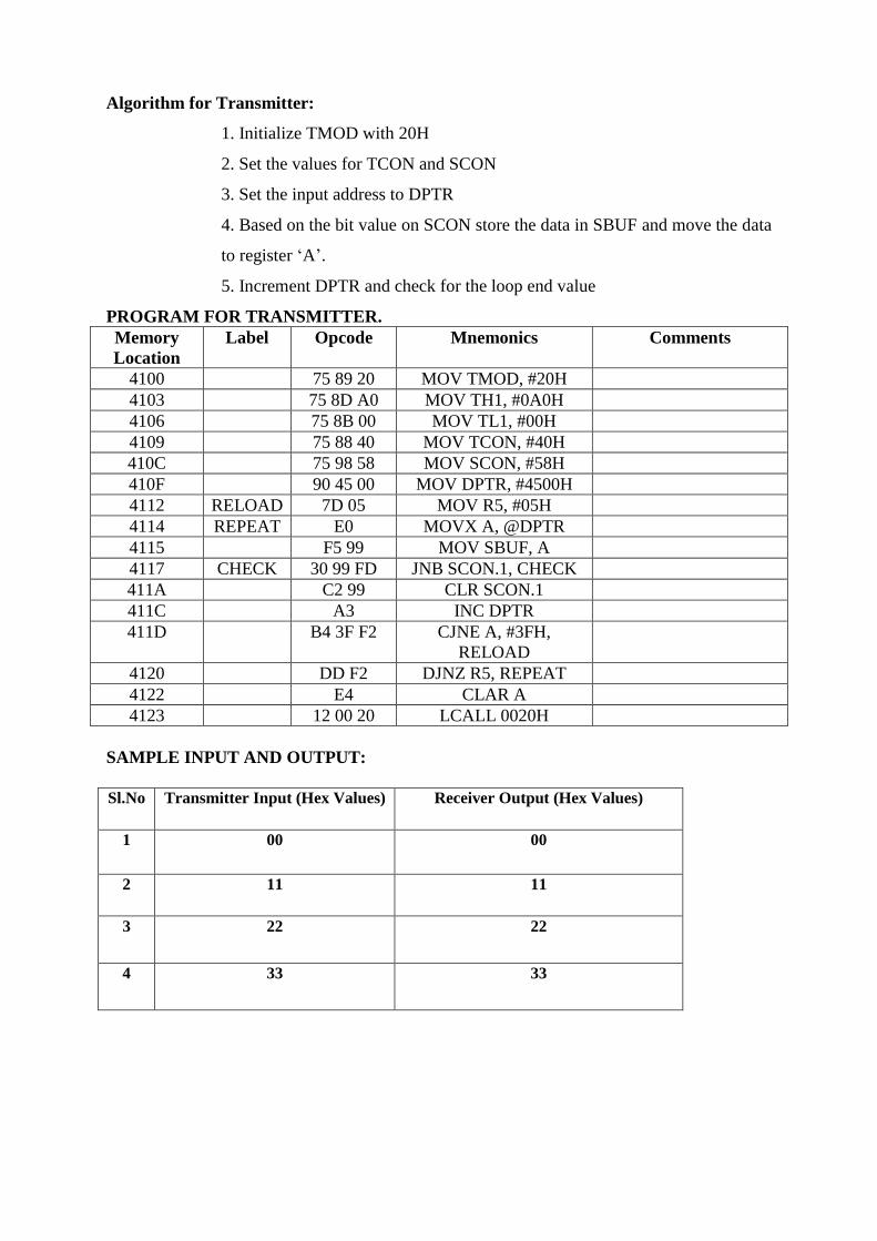
Algorithm for Transmitter:
1. Initialize TMOD with 20H
2. Set the values for TCON and SCON
3. Set the input address to DPTR
4. Based on the bit value on SCON store the data in SBUF and move the data
to register ‘A’.
5. Increment DPTR and check for the loop end value
PROGRAM FOR TRANSMITTER.
Memory
Location
Label Opcode Mnemonics Comments
4100 75 89 20 MOV TMOD, #20H
4103 75 8D A0 MOV TH1, #0A0H
4106 75 8B 00 MOV TL1, #00H
4109 75 88 40 MOV TCON, #40H
410C 75 98 58 MOV SCON, #58H
410F 90 45 00 MOV DPTR, #4500H
4112 RELOAD 7D 05 MOV R5, #05H
4114 REPEAT E0 MOVX A, @DPTR
4115 F5 99 MOV SBUF, A
4117 CHECK 30 99 FD JNB SCON.1, CHECK
411A C2 99 CLR SCON.1
411C A3 INC DPTR
411D B4 3F F2 CJNE A, #3FH,
RELOAD
4120 DD F2 DJNZ R5, REPEAT
4122 E4 CLAR A
4123 12 00 20 LCALL 0020H
SAMPLE INPUT AND OUTPUT:
Sl.No Transmitter Input (Hex Values) Receiver Output (Hex Values)
1 00 00
2 11 11
3 22 22
4 33 33

Result: Thus an assembly language program displaying characters on seven segment display has been
executed.
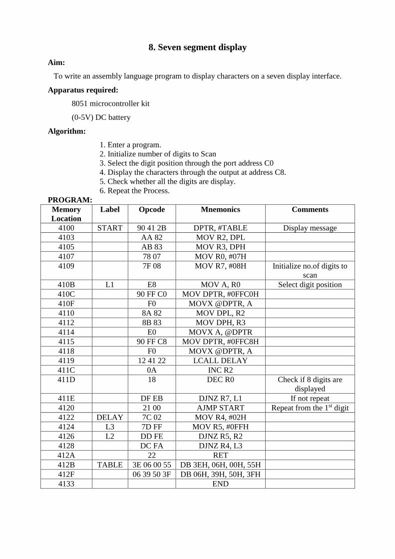
8. Seven segment display
Aim:
To write an assembly language program to display characters on a seven display interface.
Apparatus required:
8051 microcontroller kit
(0-5V) DC battery
Algorithm:
1. Enter a program.
2. Initialize number of digits to Scan
3. Select the digit position through the port address C0
4. Display the characters through the output at address C8.
5. Check whether all the digits are display.
6. Repeat the Process.
PROGRAM:
Memory
Location
Label Opcode Mnemonics Comments
4100 START 90 41 2B DPTR, #TABLE Display message
4103 AA 82 MOV R2, DPL
4105 AB 83 MOV R3, DPH
4107 78 07 MOV R0, #07H
4109 7F 08 MOV R7, #08H Initialize no.of digits to
scan
410B L1 E8 MOV A, R0 Select digit position
410C 90 FF C0 MOV DPTR, #0FFC0H
410F F0 MOVX @DPTR, A
4110 8A 82 MOV DPL, R2
4112 8B 83 MOV DPH, R3
4114 E0 MOVX A, @DPTR
4115 90 FF C8 MOV DPTR, #0FFC8H
4118 F0 MOVX @DPTR, A
4119 12 41 22 LCALL DELAY
411C 0A INC R2
411D 18 DEC R0 Check if 8 digits are
displayed
411E DF EB DJNZ R7, L1 If not repeat
4120 21 00 AJMP START Repeat from the 1st digit
4122 DELAY 7C 02 MOV R4, #02H
4124 L3 7D FF MOV R5, #0FFH
4126 L2 DD FE DJNZ R5, R2
4128 DC FA DJNZ R4, L3
412A 22 RET
412B TABLE 3E 06 00 55 DB 3EH, 06H, 00H, 55H
412F 06 39 50 3F DB 06H, 39H, 50H, 3FH
4133 END

SAMPLE INPUT AND OUTPUT:
Sl.No Input (hex Values) Output (Characters)
Result:
Thus an assembly language program displaying characters on seven segment display has been
executed.

9. Eight-Bit Digital to Analog Converter
Aim:
To write an assembly language program to display Characters on a seven display interface.
Apparatus required:
8051 microcontroller kit
(0-5V) DC battery
Algorithm:
1. Move the Port Address of DAC 2 FFC8 to the DPTR.
2. Move the Value of Register A to DPTR and then Call the delay.
3. Move the Value of Register A (FFh) to DPTR and the call the dalay.
4. Repeat the steps 2 and 3.
PROGRAM TO GENERATE SQUARE WAVEFORM
Memory
Location
Label Opcode Mnemonics Comments
4100 90 FF C8 MOV DPTR, #0FFC8H
4103 START: 74 00 MOV A, #00H
4105 F0 MOVX @DPTR, A
4106 12 41 12 LCALL DELAY
4109 74 FF MOV A, #0FFH
410B F0 MOVX @DPTR, A
410C 12 41 12 LCALL DELAY
410F 02 41 03 LJMP STTART
4112 79 05 MOV R1, #05H
4114 7A FF MOV R2, #0FFH
4116 DA FE DJNZ R2, HERE
4118 D9 FA DJNZ R1, LOOP
411A 22 RET
411B 80 E6 SJMP START
PROGRAM TO GENERATE SAW-TOOTH WAVEFORM
Memory
Location
Label Opcode Mnemonics Comments
4100 90 FF C0 MOV DPTR, #0FFC0H
4103 74 00 MOV A, #00H
4105 F0 MOVX @DPTR, A
4106 04 INC A
4107 80 FC SJMP LOOP
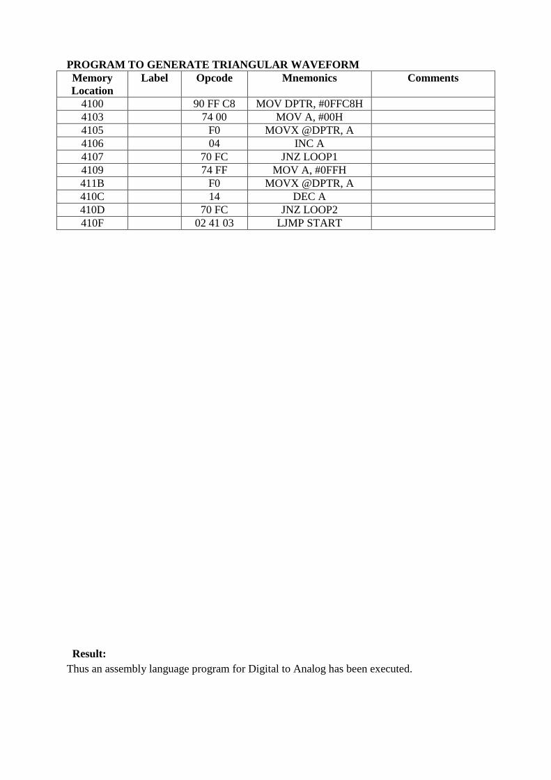
PROGRAM TO GENERATE TRIANGULAR WAVEFORM
Memory
Location
Label Opcode Mnemonics Comments
4100 90 FF C8 MOV DPTR, #0FFC8H
4103 74 00 MOV A, #00H
4105 F0 MOVX @DPTR, A
4106 04 INC A
4107 70 FC JNZ LOOP1
4109 74 FF MOV A, #0FFH
411B F0 MOVX @DPTR, A
410C 14 DEC A
410D 70 FC JNZ LOOP2
410F 02 41 03 LJMP START
Result: Thus an assembly language program for Digital to Analog has been executed.
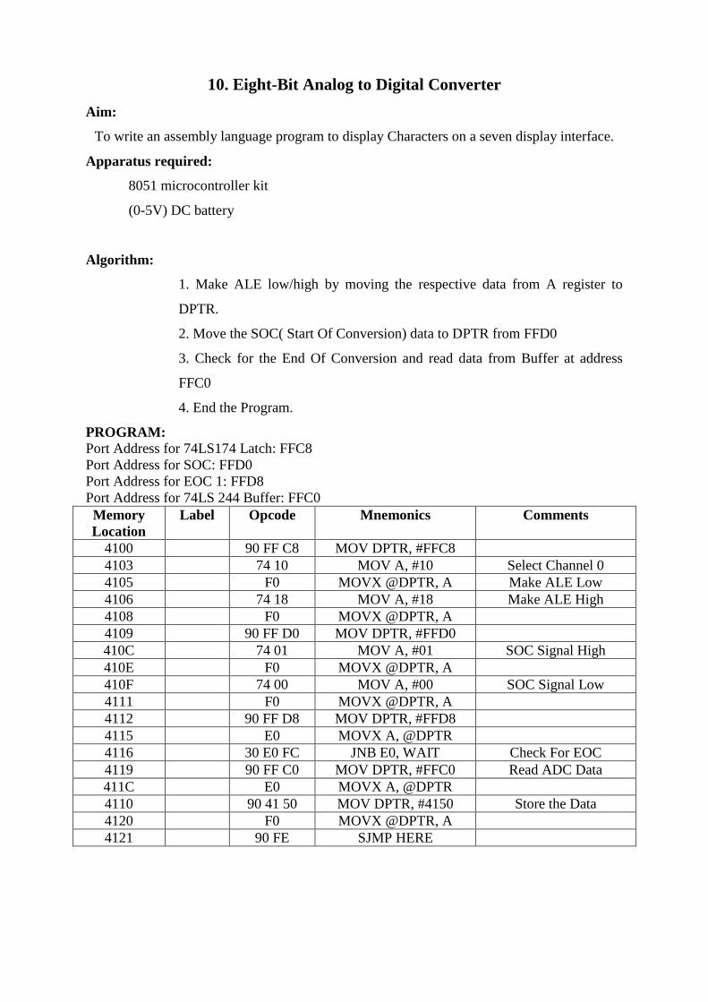
10. Eight-Bit Analog to Digital Converter
Aim:
To write an assembly language program to display Characters on a seven display interface.
Apparatus required:
8051 microcontroller kit
(0-5V) DC battery
Algorithm:
1. Make ALE low/high by moving the respective data from A register to
DPTR.
2. Move the SOC( Start Of Conversion) data to DPTR from FFD0
3. Check for the End Of Conversion and read data from Buffer at address
FFC0
4. End the Program.
PROGRAM:
Port Address for 74LS174 Latch: FFC8
Port Address for SOC: FFD0
Port Address for EOC 1: FFD8
Port Address for 74LS 244 Buffer: FFC0
Memory
Location
Label Opcode Mnemonics Comments
4100 90 FF C8 MOV DPTR, #FFC8
4103 74 10 MOV A, #10 Select Channel 0
4105 F0 MOVX @DPTR, A Make ALE Low
4106 74 18 MOV A, #18 Make ALE High
4108 F0 MOVX @DPTR, A
4109 90 FF D0 MOV DPTR, #FFD0
410C 74 01 MOV A, #01 SOC Signal High
410E F0 MOVX @DPTR, A
410F 74 00 MOV A, #00 SOC Signal Low
4111 F0 MOVX @DPTR, A
4112 90 FF D8 MOV DPTR, #FFD8
4115 E0 MOVX A, @DPTR
4116 30 E0 FC JNB E0, WAIT Check For EOC
4119 90 FF C0 MOV DPTR, #FFC0 Read ADC Data
411C E0 MOVX A, @DPTR
4110 90 41 50 MOV DPTR, #4150 Store the Data
4120 F0 MOVX @DPTR, A
4121 90 FE SJMP HERE

Result: Thus an assembly language program is executed for analog to digital conversion.
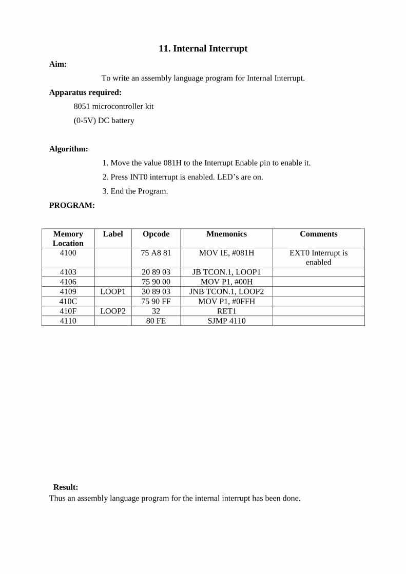
11. Internal Interrupt
Aim:
To write an assembly language program for Internal Interrupt.
Apparatus required:
8051 microcontroller kit
(0-5V) DC battery
Algorithm:
1. Move the value 081H to the Interrupt Enable pin to enable it.
2. Press INT0 interrupt is enabled. LED’s are on.
3. End the Program.
PROGRAM:
Memory
Location
Label Opcode Mnemonics Comments
4100 75 A8 81 MOV IE, #081H EXT0 Interrupt is
enabled
4103 20 89 03 JB TCON.1, LOOP1
4106 75 90 00 MOV P1, #00H
4109 LOOP1 30 89 03 JNB TCON.1, LOOP2
410C 75 90 FF MOV P1, #0FFH
410F LOOP2 32 RET1
4110 80 FE SJMP 4110
Result: Thus an assembly language program for the internal interrupt has been done.

12. SPEED CONTROL OF STEPPER MOTOR
Aim:
To write an assembly program to make the stepper motor run in forward and reverse
direction.
Apparatus required:
Stepper motor
8051 microprocessor kit
(0-5V) power supply
Algorithm:
1. Fix the DPTR with the Latch Chip address FFC0
2. Move the values of register A one by one with some delay based on the 2-
Phase switching Scheme and repeat the loop.
3. For Anti Clockwise direction repeat the step 3 by reversing the value
sequence.
4. End the Program
Memory
Location
Label Opcode Mnemonics Comments
4100 90 FF C0 MOV DPTR, #FFC0
4103 74 09 MOV A, #09
4105 E0 MOVX @DPTR, A
4106 12 41 3B LCALL DELAY
4109 74 05 MOV A, #05
410B E0 MOVX @DPTR, A
410C 12 41 3B LCALL DELAY
410F 74 06 MOV A, #06
411B E0 MOVX @DPTR, A
411C 12 41 3B LCALL DELAY
411F 74 0A MOV A, #0A
412B E0 MOVX @DPTR, A
412C 12 41 3B LCALL DELAY
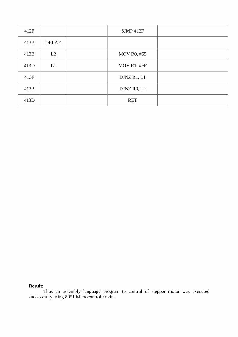
412F SJMP 412F
413B DELAY
413B L2 MOV R0, #55
413D L1 MOV R1, #FF
413F DJNZ R1, L1
413B DJNZ R0, L2
413D RET
Result:
Thus an assembly language program to control of stepper motor was executed
successfully using 8051 Microcontroller kit.

13. TRAFFIC LIGHT CONTROLLER
Aim:
To write an assembly language program to display Characters on a seven display interface.
Apparatus required:
8051 microcontroller kit
(0-5V) DC battery
Algorithm:
1. Fix the control the control and move the control word to control register.
2. Move the Traffic Light LED Position values to Port A, Port B and Port C
respectively based on the logic.
3. Fix the delay based on the requirement.
3. Execute the program.
PROGRAM: 4100 ORG 4100
CONTRL EQU 0FF0FH
PORT A EQU 0FF0CH
PORT B EQU 0FF0DH
PORT C EQU 0FF0EH
Memory
Location
Label Opcode Mnemonics Comments
4100 74 80 MOV A, #80H
4102 90 FF 0F MOV DPTR, #CONTRL
4105 F0 MOVX @DPTR, A
4106 START 7C 04 MOV R4, #04H
4108 90 41 9B MOV DPTR, #LOOK1
410B AA 83 MOV R2, DPH
410D AB 82 MOV R3, DPL
410F 90 41 8F MOV DPTR, #LOOK
4112 A8 83 MOV R0, DPH
4114 A9 82 MOV R1, DPL
4116 GO E0 MOVX A, @DPTR
4117 A8 83 MOV R0, DPH
4119 A9 82 MOV R1, DPL
411B 90 FF 0C MOV DPTR, #PORT A
411E F0 MOVX @DPTR, A
411F 09 INC R1
4120 88 83 MOV DPH, R0
4122 89 82 MOV DPL, R1
4124 E0 MOVX A, @DPTR
4125 A8 83 MOV R0, DPH
4127 A9 82 MOV R1, DPL

4129 90 FF 0D MOV DPTR, #PORT B
412C F0 MOVX @DPTR, A
412D 09 INC R1
412E 88 83 MOV DPH, R0
4130 89 82 MOV DPL, R1
4132 E0 MOVX A, @DPTR
4133 A8 83 MOV R0, DPH
4135 A9 82 MOV R1, DPL
4137 90 FF 0E MOV DPTR, #PORT C
413A F0 MOVX @DPTR, A
413B 09 INC R1
413C 12 41 75 LCALL DELAY
413F 8A 83 MOV DPH, R2
4141 8B 82 MOV DPL, R3
4143 E0 MOVX A, @DPTR
4144 AA 83 MOV R2, DPH
4146 AB 82 MOV R3, DPL
4148 90 FF 0C MOV DPTR, #PORT A
414B F0 MOVX @DPTR, A
414C 0B INC R3
414D 8A 83 MOV DPH, R2
414F 8B 82 MOV DPL, R3
4151 E0 MOVX A, @DPTR
4152 AA 83 MOV R2, DPH
4154 AB 82 MOV R3, DPL
4156 90 FF 0D MOV DPTR, #PORT B
4159 F0 MOVX @DPTR, A
415A 0B INC R3
415B 8A 83 MOV DPH, R2
415D 8B 82 MOV DPL, R3
415F E0 MOVX A, @DPTR
4160 AA 83 MOV R2, DPH
4162 AB 82 MOV R3, DPL
4164 90 FF 0E MOV DPTR, #PORT C
4167 F0 MOVX @DPTR, A
4168 0B INC R3
4169 12 41 82 LCALL DELAY1
416C 88 83 MOV DPH, R0
416E 89 82 MOV DPL, R1
4170 DC A4 DJNZ R4, GO
4172 12 41 06 LCALL START
4175 DELAY 7D 12 MOV R5, #12H
4177 L3 7E FF MOV R6, #0FFH
4179 L2 7F FF MOV R7, #0FFH
417B L1 DF FE DJNZ R7, L1
417D DE FA DJNZ R6, L2
417F DD F6 DJNZ R5, L3
4181 22 RET
4182 DELAY1 7D 12 MOV R5, #12H

4184 L6 7E FF MOV R6, #0FFH
4186 L5 7F FF MOV R7, #0FFH
4188 L4 DF FE DJNZ R7, L4
418A DE FA DJNZ R6, L5
418C DD F6 DJNZ R5, L6
418E 22 RET
418F LOOK 44 27 12 DB 44H, 27H, 12H
4192 92 2B 10 DB 92H, 2BH, 10H
4195 84 9D 10 DB 84H, 9DH, 10H
4198 84 2E 48 DB 84H, 2EH, 48H
419B LOOK1 48 27 12 DB 48H, 27H, 12H
419E 92 4B 10 DB 92H, 4BH, 10H
41A1 84 9D 20 DB 84H, 9DH, 20H
41A4 04 2E 49 DB 04H, 2EH, 49H
Result: Thus an assembly language program for the Traffic Light Control has been executed.

Complete 8086 instruction set
Quick reference:
Operand types: REG: AX, BX, CX, DX, AH, AL, BL, BH, CH, CL, DH, DL, DI, SI, BP, SP. SREG: DS, ES, SS, and only as second operand: CS. memory: [BX], [BX+SI+7], variable, etc...(see Memory Access). immediate: 5, -24, 3Fh, 10001101b, etc...
Notes:
When two operands are required for an instruction they are separated by comma. For example: REG, memory When there are two operands, both operands must have the same size (except shift and rotate instructions). For example: AL, DL DX, AX m1 DB ? AL, m1 m2 DW ? AX, m2 Some instructions allow several operand combinations. For example: memory, immediate
AAA AAD AAM AAS ADC ADD AND CALL CBW CLC CLD CLI CMC CMP
CMPSB CMPSW CWD DAA DAS DEC DIV HLT IDIV IMUL IN INC INT INTO IRET JA
JAE JB JBE JC JCXZ JE JG JGE JL JLE JMP JNA JNAE JNB
JNBE JNC JNE JNG JNGE JNL JNLE JNO JNP JNS JNZ JO JP JPE
JPO JS JZ LAHF LDS LEA LES LODSB LODSW LOOP LOOPE LOOPNE LOOPNZ LOOPZ
MOV MOVSB MOVSW MUL NEG NOP NOT OR OUT POP POPA POPF PUSH PUSHA PUSHF RCL
RCR REP REPE REPNE REPNZ REPZ RET RETF ROL ROR SAHF SAL SAR SBB
SCASB SCASW SHL SHR STC STD STI STOSB STOSW SUB TEST XCHG XLATB XOR
Page 1 of 538086 instructions
REG, immediate memory, REG REG, SREG Some examples contain macros, so it is advisable to use Shift + F8 hot key to Step Over (to make macro code execute at maximum speed set step delay to zero), otherwise emulator will step through each instruction of a macro. Here is an example that uses PRINTN macro:
include 'emu8086.inc' ORG 100h MOV AL, 1 MOV BL, 2 PRINTN 'Hello World!' ; macro. MOV CL, 3 PRINTN 'Welcome!' ; macro. RET
These marks are used to show the state of the flags: 1 - instruction sets this flag to 1. 0 - instruction sets this flag to 0. r - flag value depends on result of the instruction. ? - flag value is undefined (maybe 1 or 0).
Some instructions generate exactly the same machine code, so disassembler may have a problem decoding to your original code. This is especially important for Conditional Jump instructions (see "Program Flow Control" in Tutorials for more information).
Instructions in alphabetical order:
Instruction Operands Description
ASCII Adjust after Addition. Corrects result in AH and AL after addition when working with BCD values. It works according to the following Algorithm: if low nibble of AL > 9 or AF = 1 then:
Page 2 of 538086 instructions

AAA No operands
AL = AL + 6 AH = AH + 1 AF = 1 CF = 1
else
AF = 0 CF = 0
in both cases: clear the high nibble of AL. Example:
MOV AX, 15 ; AH = 00, AL = 0Fh AAA ; AH = 01, AL = 05 RET
C Z S O P A
r ? ? ? ? r
AAD No operands
ASCII Adjust before Division. Prepares two BCD values for division. Algorithm:
AL = (AH * 10) + AL AH = 0
Example:
MOV AX, 0105h ; AH = 01, AL = 05 AAD ; AH = 00, AL = 0Fh (15) RET
C Z S O P A
? r r ? r ?
ASCII Adjust after Multiplication. Corrects the result of multiplication of two BCD values. Algorithm:
AH = AL / 10 AL = remainder
Page 3 of 538086 instructions
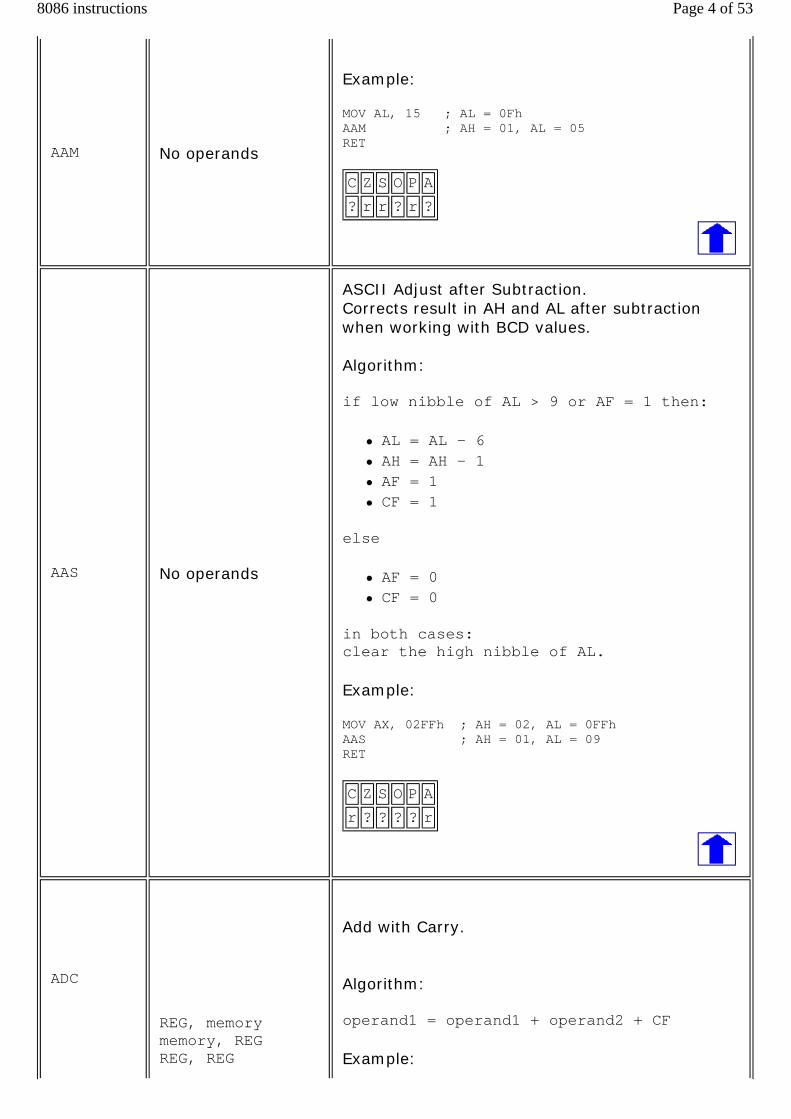
AAM No operands
Example:
MOV AL, 15 ; AL = 0Fh AAM ; AH = 01, AL = 05 RET
C Z S O P A
? r r ? r ?
AAS No operands
ASCII Adjust after Subtraction. Corrects result in AH and AL after subtraction when working with BCD values. Algorithm: if low nibble of AL > 9 or AF = 1 then:
AL = AL - 6 AH = AH - 1 AF = 1 CF = 1
else
AF = 0 CF = 0
in both cases: clear the high nibble of AL. Example:
MOV AX, 02FFh ; AH = 02, AL = 0FFh AAS ; AH = 01, AL = 09 RET
C Z S O P A
r ? ? ? ? r
ADC
REG, memory memory, REG REG, REG
Add with Carry. Algorithm: operand1 = operand1 + operand2 + CF Example:
Page 4 of 538086 instructions

memory, immediate REG, immediate
STC ; set CF = 1 MOV AL, 5 ; AL = 5 ADC AL, 1 ; AL = 7 RET
C Z S O P A
r r r r r r
ADD
REG, memory memory, REG REG, REG memory, immediate REG, immediate
Add. Algorithm: operand1 = operand1 + operand2 Example:
MOV AL, 5 ; AL = 5 ADD AL, -3 ; AL = 2 RET
C Z S O P A
r r r r r r
AND
REG, memory memory, REG REG, REG memory, immediate REG, immediate
Logical AND between all bits of two operands. Result is stored in operand1. These rules apply: 1 AND 1 = 1 1 AND 0 = 0 0 AND 1 = 0 0 AND 0 = 0 Example:
MOV AL, 'a' ; AL = 01100001b AND AL, 11011111b ; AL = 01000001b ('A') RET
C Z S O P
0 r r 0 r
Transfers control to procedure, return address is (IP) is pushed to stack. 4-byte address may be entered in this form: 1234h:5678h, first value is a
Page 5 of 538086 instructions

CALL procedure name label 4-byte address
segment second value is an offset (this is a far call, so CS is also pushed to stack). Example:
ORG 100h ; for COM file. CALL p1 ADD AX, 1 RET ; return to OS. p1 PROC ; procedure declaration. MOV AX, 1234h RET ; return to caller. p1 ENDP
C Z S O P A
unchanged
CBW No operands
Convert byte into word. Algorithm: if high bit of AL = 1 then:
AH = 255 (0FFh)
else
AH = 0
Example:
MOV AX, 0 ; AH = 0, AL = 0 MOV AL, -5 ; AX = 000FBh (251) CBW ; AX = 0FFFBh (-5) RET
C Z S O P A
unchanged
Clear Carry flag. Algorithm: CF = 0
Page 6 of 538086 instructions

CLC No operands
C
0
CLD No operands
Clear Direction flag. SI and DI will be incremented by chain instructions: CMPSB, CMPSW, LODSB, LODSW, MOVSB, MOVSW, STOSB, STOSW. Algorithm: DF = 0
D
0
CLI No operands
Clear Interrupt enable flag. This disables hardware interrupts. Algorithm: IF = 0
I
0
CMC No operands
Complement Carry flag. Inverts value of CF. Algorithm: if CF = 1 then CF = 0 if CF = 0 then CF = 1
C
r
Compare. Algorithm: operand1 - operand2
Page 7 of 538086 instructions

CMP
REG, memory memory, REG REG, REG memory, immediate REG, immediate
result is not stored anywhere, flags are set (OF, SF, ZF, AF, PF, CF) according to result. Example:
MOV AL, 5 MOV BL, 5 CMP AL, BL ; AL = 5, ZF = 1 (so equal!) RET
C Z S O P A
r r r r r r
CMPSB No operands
Compare bytes: ES:[DI] from DS:[SI]. Algorithm:
DS:[SI] - ES:[DI] set flags according to result: OF, SF, ZF, AF, PF, CF if DF = 0 then
SI = SI + 1 DI = DI + 1
else SI = SI - 1 DI = DI - 1
Example: open cmpsb.asm from c:\emu8086\examples
C Z S O P A
r r r r r r
CMPSW No operands
Compare words: ES:[DI] from DS:[SI]. Algorithm:
DS:[SI] - ES:[DI] set flags according to result: OF, SF, ZF, AF, PF, CF if DF = 0 then
SI = SI + 2 DI = DI + 2
else SI = SI - 2 DI = DI - 2
Page 8 of 538086 instructions

example: open cmpsw.asm from c:\emu8086\examples
C Z S O P A
r r r r r r
CWD No operands
Convert Word to Double word. Algorithm: if high bit of AX = 1 then:
DX = 65535 (0FFFFh)
else
DX = 0
Example:
MOV DX, 0 ; DX = 0 MOV AX, 0 ; AX = 0 MOV AX, -5 ; DX AX = 00000h:0FFFBh CWD ; DX AX = 0FFFFh:0FFFBh RET
C Z S O P A
unchanged
DAA No operands
Decimal adjust After Addition. Corrects the result of addition of two packed BCD values. Algorithm: if low nibble of AL > 9 or AF = 1 then:
AL = AL + 6 AF = 1
if AL > 9Fh or CF = 1 then:
AL = AL + 60h CF = 1
Example:
Page 9 of 538086 instructions

MOV AL, 0Fh ; AL = 0Fh (15) DAA ; AL = 15h RET
C Z S O P A
r r r r r r
DAS No operands
Decimal adjust After Subtraction. Corrects the result of subtraction of two packed BCD values. Algorithm: if low nibble of AL > 9 or AF = 1 then:
AL = AL - 6 AF = 1
if AL > 9Fh or CF = 1 then:
AL = AL - 60h CF = 1
Example:
MOV AL, 0FFh ; AL = 0FFh (-1) DAS ; AL = 99h, CF = 1 RET
C Z S O P A
r r r r r r
DEC REG memory
Decrement. Algorithm: operand = operand - 1 Example:
MOV AL, 255 ; AL = 0FFh (255 or -1) DEC AL ; AL = 0FEh (254 or -2) RET
CF - unchanged!
Z S O P A
r r r r r
Page 10 of 538086 instructions

DIV REG memory
Unsigned divide. Algorithm:
when operand is a byte: AL = AX / operand AH = remainder (modulus)
when operand is a word: AX = (DX AX) / operand DX = remainder (modulus)
Example:
MOV AX, 203 ; AX = 00CBh MOV BL, 4 DIV BL ; AL = 50 (32h), AH = 3 RET
C Z S O P A
? ? ? ? ? ?
HLT No operands
Halt the System. Example:
MOV AX, 5 HLT
C Z S O P A
unchanged
IDIV REG memory
Signed divide. Algorithm:
when operand is a byte: AL = AX / operand AH = remainder (modulus)
when operand is a word: AX = (DX AX) / operand DX = remainder (modulus)
Example:
MOV AX, -203 ; AX = 0FF35h MOV BL, 4 IDIV BL ; AL = -50 (0CEh), AH = -3 (0FDh) RET
Page 11 of 538086 instructions
C Z S O P A
? ? ? ? ? ?
IMUL REG memory
Signed multiply. Algorithm:
when operand is a byte: AX = AL * operand.
when operand is a word: (DX AX) = AX * operand.
Example:
MOV AL, -2 MOV BL, -4 IMUL BL ; AX = 8 RET
CF=OF=0 when result fits into operand of IMUL.
C Z S O P A
r ? ? r ? ?
IN
AL, im.byte AL, DX AX, im.byte AX, DX
Input from port into AL or AX. Second operand is a port number. If required to access port number over 255 - DX register should be used. Example:
IN AX, 4 ; get status of traffic lights. IN AL, 7 ; get status of stepper-motor.
C Z S O P A
unchanged
INC REG memory
Increment. Algorithm: operand = operand + 1 Example:
MOV AL, 4 INC AL ; AL = 5
Page 12 of 538086 instructions
RET
CF - unchanged!
Z S O P A
r r r r r
INT immediate byte
Interrupt numbered by immediate byte (0..255). Algorithm:
Push to stack: flags register CS IP
IF = 0 Transfer control to interrupt procedure
Example:
MOV AH, 0Eh ; teletype. MOV AL, 'A' INT 10h ; BIOS interrupt. RET
C Z S O P A I
unchanged 0
INTO No operands
Interrupt 4 if Overflow flag is 1. Algorithm: if OF = 1 then INT 4 Example:
; -5 - 127 = -132 (not in -128..127) ; the result of SUB is wrong (124), ; so OF = 1 is set: MOV AL, -5 SUB AL, 127 ; AL = 7Ch (124) INTO ; process error. RET
Interrupt Return.
Page 13 of 538086 instructions
IRET No operands
Algorithm:
Pop from stack: IP CS flags register
C Z S O P A
popped
JA label
Short Jump if first operand is Above second operand (as set by CMP instruction). Unsigned. Algorithm:
if (CF = 0) and (ZF = 0) then jump
Example:
include 'emu8086.inc' ORG 100h MOV AL, 250 CMP AL, 5 JA label1 PRINT 'AL is not above 5' JMP exit label1: PRINT 'AL is above 5' exit: RET
C Z S O P A
unchanged
JAE label
Short Jump if first operand is Above or Equal to second operand (as set by CMP instruction). Unsigned. Algorithm:
if CF = 0 then jump
Example:
include 'emu8086.inc' ORG 100h MOV AL, 5 CMP AL, 5 JAE label1 PRINT 'AL is not above or equal to 5' JMP exit label1:
Page 14 of 538086 instructions

PRINT 'AL is above or equal to 5' exit: RET
C Z S O P A
unchanged
JB label
Short Jump if first operand is Below second operand (as set by CMP instruction). Unsigned. Algorithm:
if CF = 1 then jump
Example:
include 'emu8086.inc' ORG 100h MOV AL, 1 CMP AL, 5 JB label1 PRINT 'AL is not below 5' JMP exit label1: PRINT 'AL is below 5' exit: RET
C Z S O P A
unchanged
JBE label
Short Jump if first operand is Below or Equal to second operand (as set by CMP instruction). Unsigned. Algorithm:
if CF = 1 or ZF = 1 then jump
Example:
include 'emu8086.inc' ORG 100h MOV AL, 5 CMP AL, 5 JBE label1 PRINT 'AL is not below or equal to 5' JMP exit label1: PRINT 'AL is below or equal to 5' exit: RET
Page 15 of 538086 instructions

C Z S O P A
unchanged
JC label
Short Jump if Carry flag is set to 1. Algorithm:
if CF = 1 then jump
Example:
include 'emu8086.inc' ORG 100h MOV AL, 255 ADD AL, 1 JC label1 PRINT 'no carry.' JMP exit label1: PRINT 'has carry.' exit: RET
C Z S O P A
unchanged
JCXZ label
Short Jump if CX register is 0. Algorithm:
if CX = 0 then jump
Example:
include 'emu8086.inc' ORG 100h MOV CX, 0 JCXZ label1 PRINT 'CX is not zero.' JMP exit label1: PRINT 'CX is zero.' exit: RET
C Z S O P A
unchanged
Short Jump if first operand is Equal to second operand (as set by CMP instruction).
Page 16 of 538086 instructions

JE label
Signed/Unsigned. Algorithm:
if ZF = 1 then jump
Example:
include 'emu8086.inc' ORG 100h MOV AL, 5 CMP AL, 5 JE label1 PRINT 'AL is not equal to 5.' JMP exit label1: PRINT 'AL is equal to 5.' exit: RET
C Z S O P A
unchanged
JG label
Short Jump if first operand is Greater then second operand (as set by CMP instruction). Signed. Algorithm:
if (ZF = 0) and (SF = OF) then jump
Example:
include 'emu8086.inc' ORG 100h MOV AL, 5 CMP AL, -5 JG label1 PRINT 'AL is not greater -5.' JMP exit label1: PRINT 'AL is greater -5.' exit: RET
C Z S O P A
unchanged
Short Jump if first operand is Greater or Equal to second operand (as set by CMP instruction). Signed. Algorithm:
Page 17 of 538086 instructions

JGE label
if SF = OF then jump
Example:
include 'emu8086.inc' ORG 100h MOV AL, 2 CMP AL, -5 JGE label1 PRINT 'AL < -5' JMP exit label1: PRINT 'AL >= -5' exit: RET
C Z S O P A
unchanged
JL label
Short Jump if first operand is Less then second operand (as set by CMP instruction). Signed. Algorithm:
if SF <> OF then jump
Example:
include 'emu8086.inc' ORG 100h MOV AL, -2 CMP AL, 5 JL label1 PRINT 'AL >= 5.' JMP exit label1: PRINT 'AL < 5.' exit: RET
C Z S O P A
unchanged
Short Jump if first operand is Less or Equal to second operand (as set by CMP instruction). Signed. Algorithm:
if SF <> OF or ZF = 1 then jump
Example:
Page 18 of 538086 instructions

JLE label
include 'emu8086.inc' ORG 100h MOV AL, -2 CMP AL, 5 JLE label1 PRINT 'AL > 5.' JMP exit label1: PRINT 'AL <= 5.' exit: RET
C Z S O P A
unchanged
JMP label 4-byte address
Unconditional Jump. Transfers control to another part of the program. 4-byte address may be entered in this form: 1234h:5678h, first value is a segment second value is an offset. Algorithm:
always jump
Example:
include 'emu8086.inc' ORG 100h MOV AL, 5 JMP label1 ; jump over 2 lines! PRINT 'Not Jumped!' MOV AL, 0 label1: PRINT 'Got Here!' RET
C Z S O P A
unchanged
JNA label
Short Jump if first operand is Not Above second operand (as set by CMP instruction). Unsigned. Algorithm:
if CF = 1 or ZF = 1 then jump
Example:
include 'emu8086.inc' ORG 100h MOV AL, 2
Page 19 of 538086 instructions

CMP AL, 5 JNA label1 PRINT 'AL is above 5.' JMP exit label1: PRINT 'AL is not above 5.' exit: RET
C Z S O P A
unchanged
JNAE label
Short Jump if first operand is Not Above and Not Equal to second operand (as set by CMP instruction). Unsigned. Algorithm:
if CF = 1 then jump
Example:
include 'emu8086.inc' ORG 100h MOV AL, 2 CMP AL, 5 JNAE label1 PRINT 'AL >= 5.' JMP exit label1: PRINT 'AL < 5.' exit: RET
C Z S O P A
unchanged
JNB label
Short Jump if first operand is Not Below second operand (as set by CMP instruction). Unsigned. Algorithm:
if CF = 0 then jump
Example:
include 'emu8086.inc' ORG 100h MOV AL, 7 CMP AL, 5 JNB label1 PRINT 'AL < 5.'
Page 20 of 538086 instructions

JMP exit label1: PRINT 'AL >= 5.' exit: RET
C Z S O P A
unchanged
JNBE label
Short Jump if first operand is Not Below and Not Equal to second operand (as set by CMP instruction). Unsigned. Algorithm:
if (CF = 0) and (ZF = 0) then jump
Example:
include 'emu8086.inc' ORG 100h MOV AL, 7 CMP AL, 5 JNBE label1 PRINT 'AL <= 5.' JMP exit label1: PRINT 'AL > 5.' exit: RET
C Z S O P A
unchanged
JNC label
Short Jump if Carry flag is set to 0. Algorithm:
if CF = 0 then jump
Example:
include 'emu8086.inc' ORG 100h MOV AL, 2 ADD AL, 3 JNC label1 PRINT 'has carry.' JMP exit label1: PRINT 'no carry.' exit:
Page 21 of 538086 instructions

RET
C Z S O P A
unchanged
JNE label
Short Jump if first operand is Not Equal to second operand (as set by CMP instruction). Signed/Unsigned. Algorithm:
if ZF = 0 then jump
Example:
include 'emu8086.inc' ORG 100h MOV AL, 2 CMP AL, 3 JNE label1 PRINT 'AL = 3.' JMP exit label1: PRINT 'Al <> 3.' exit: RET
C Z S O P A
unchanged
JNG label
Short Jump if first operand is Not Greater then second operand (as set by CMP instruction). Signed. Algorithm:
if (ZF = 1) and (SF <> OF) then jump
Example:
include 'emu8086.inc' ORG 100h MOV AL, 2 CMP AL, 3 JNG label1 PRINT 'AL > 3.' JMP exit label1: PRINT 'Al <= 3.' exit: RET
Page 22 of 538086 instructions

C Z S O P A
unchanged
JNGE label
Short Jump if first operand is Not Greater and Not Equal to second operand (as set by CMP instruction). Signed. Algorithm:
if SF <> OF then jump
Example:
include 'emu8086.inc' ORG 100h MOV AL, 2 CMP AL, 3 JNGE label1 PRINT 'AL >= 3.' JMP exit label1: PRINT 'Al < 3.' exit: RET
C Z S O P A
unchanged
JNL label
Short Jump if first operand is Not Less then second operand (as set by CMP instruction). Signed. Algorithm:
if SF = OF then jump
Example:
include 'emu8086.inc' ORG 100h MOV AL, 2 CMP AL, -3 JNL label1 PRINT 'AL < -3.' JMP exit label1: PRINT 'Al >= -3.' exit: RET
C Z S O P A
Page 23 of 538086 instructions

unchanged
JNLE label
Short Jump if first operand is Not Less and Not Equal to second operand (as set by CMP instruction). Signed. Algorithm:
if (SF = OF) and (ZF = 0) then jump
Example:
include 'emu8086.inc' ORG 100h MOV AL, 2 CMP AL, -3 JNLE label1 PRINT 'AL <= -3.' JMP exit label1: PRINT 'Al > -3.' exit: RET
C Z S O P A
unchanged
JNO label
Short Jump if Not Overflow. Algorithm:
if OF = 0 then jump
Example:
; -5 - 2 = -7 (inside -128..127) ; the result of SUB is correct, ; so OF = 0: include 'emu8086.inc' ORG 100h MOV AL, -5 SUB AL, 2 ; AL = 0F9h (-7) JNO label1 PRINT 'overflow!' JMP exit label1: PRINT 'no overflow.' exit: RET
C Z S O P A
Page 24 of 538086 instructions

unchanged
JNP label
Short Jump if No Parity (odd). Only 8 low bits of result are checked. Set by CMP, SUB, ADD, TEST, AND, OR, XOR instructions. Algorithm:
if PF = 0 then jump
Example:
include 'emu8086.inc' ORG 100h MOV AL, 00000111b ; AL = 7 OR AL, 0 ; just set flags. JNP label1 PRINT 'parity even.' JMP exit label1: PRINT 'parity odd.' exit: RET
C Z S O P A
unchanged
JNS label
Short Jump if Not Signed (if positive). Set by CMP, SUB, ADD, TEST, AND, OR, XOR instructions. Algorithm:
if SF = 0 then jump
Example:
include 'emu8086.inc' ORG 100h MOV AL, 00000111b ; AL = 7 OR AL, 0 ; just set flags. JNS label1 PRINT 'signed.' JMP exit label1: PRINT 'not signed.' exit: RET
C Z S O P A
unchanged
Page 25 of 538086 instructions

JNZ label
Short Jump if Not Zero (not equal). Set by CMP, SUB, ADD, TEST, AND, OR, XOR instructions. Algorithm:
if ZF = 0 then jump
Example:
include 'emu8086.inc' ORG 100h MOV AL, 00000111b ; AL = 7 OR AL, 0 ; just set flags. JNZ label1 PRINT 'zero.' JMP exit label1: PRINT 'not zero.' exit: RET
C Z S O P A
unchanged
JO label
Short Jump if Overflow. Algorithm:
if OF = 1 then jump
Example:
; -5 - 127 = -132 (not in -128..127) ; the result of SUB is wrong (124), ; so OF = 1 is set: include 'emu8086.inc' org 100h MOV AL, -5 SUB AL, 127 ; AL = 7Ch (124) JO label1 PRINT 'no overflow.' JMP exit label1: PRINT 'overflow!' exit: RET
C Z S O P A
unchanged
Page 26 of 538086 instructions

JP label
Short Jump if Parity (even). Only 8 low bits of result are checked. Set by CMP, SUB, ADD, TEST, AND, OR, XOR instructions. Algorithm:
if PF = 1 then jump
Example:
include 'emu8086.inc' ORG 100h MOV AL, 00000101b ; AL = 5 OR AL, 0 ; just set flags. JP label1 PRINT 'parity odd.' JMP exit label1: PRINT 'parity even.' exit: RET
C Z S O P A
unchanged
JPE label
Short Jump if Parity Even. Only 8 low bits of result are checked. Set by CMP, SUB, ADD, TEST, AND, OR, XOR instructions. Algorithm:
if PF = 1 then jump
Example:
include 'emu8086.inc' ORG 100h MOV AL, 00000101b ; AL = 5 OR AL, 0 ; just set flags. JPE label1 PRINT 'parity odd.' JMP exit label1: PRINT 'parity even.' exit: RET
C Z S O P A
unchanged
Short Jump if Parity Odd. Only 8 low bits of result
Page 27 of 538086 instructions

JPO label
are checked. Set by CMP, SUB, ADD, TEST, AND, OR, XOR instructions. Algorithm:
if PF = 0 then jump
Example:
include 'emu8086.inc' ORG 100h MOV AL, 00000111b ; AL = 7 OR AL, 0 ; just set flags. JPO label1 PRINT 'parity even.' JMP exit label1: PRINT 'parity odd.' exit: RET
C Z S O P A
unchanged
JS label
Short Jump if Signed (if negative). Set by CMP, SUB, ADD, TEST, AND, OR, XOR instructions. Algorithm:
if SF = 1 then jump
Example:
include 'emu8086.inc' ORG 100h MOV AL, 10000000b ; AL = -128 OR AL, 0 ; just set flags. JS label1 PRINT 'not signed.' JMP exit label1: PRINT 'signed.' exit: RET
C Z S O P A
unchanged
Short Jump if Zero (equal). Set by CMP, SUB, ADD, TEST, AND, OR, XOR instructions.
Page 28 of 538086 instructions

JZ label
Algorithm:
if ZF = 1 then jump
Example:
include 'emu8086.inc' ORG 100h MOV AL, 5 CMP AL, 5 JZ label1 PRINT 'AL is not equal to 5.' JMP exit label1: PRINT 'AL is equal to 5.' exit: RET
C Z S O P A
unchanged
LAHF No operands
Load AH from 8 low bits of Flags register. Algorithm:
AH = flags register
AH bit: 7 6 5 4 3 2 1 0 [SF] [ZF] [0] [AF] [0] [PF] [1] [CF]
bits 1, 3, 5 are reserved.
C Z S O P A
unchanged
Load memory double word into word register and DS. Algorithm:
REG = first word DS = second word
Example:
ORG 100h
Page 29 of 538086 instructions

LDS REG, memory
LDS AX, m RET m DW 1234h DW 5678h END
AX is set to 1234h, DS is set to 5678h.
C Z S O P A
unchanged
LEA REG, memory
Load Effective Address. Algorithm:
REG = address of memory (offset)
Example:
MOV BX, 35h MOV DI, 12h LEA SI, [BX+DI] ; SI = 35h + 12h = 47h
Note: The integrated 8086 assembler automatically replaces LEA with a more efficient MOV where possible. For example:
org 100h LEA AX, m ; AX = offset of m RET m dw 1234h END
C Z S O P A
unchanged
Load memory double word into word register and ES. Algorithm:
Page 30 of 538086 instructions

LES REG, memory
REG = first word ES = second word
Example:
ORG 100h LES AX, m RET m DW 1234h DW 5678h END
AX is set to 1234h, ES is set to 5678h.
C Z S O P A
unchanged
LODSB No operands
Load byte at DS:[SI] into AL. Update SI. Algorithm:
AL = DS:[SI] if DF = 0 then
SI = SI + 1 else
SI = SI - 1
Example:
ORG 100h LEA SI, a1 MOV CX, 5 MOV AH, 0Eh m: LODSB INT 10h LOOP m RET a1 DB 'H', 'e', 'l', 'l', 'o'
C Z S O P A
unchanged
Page 31 of 538086 instructions

LODSW No operands
Load word at DS:[SI] into AX. Update SI. Algorithm:
AX = DS:[SI] if DF = 0 then
SI = SI + 2 else
SI = SI - 2
Example:
ORG 100h LEA SI, a1 MOV CX, 5 REP LODSW ; finally there will be 555h in AX. RET a1 dw 111h, 222h, 333h, 444h, 555h
C Z S O P A
unchanged
LOOP label
Decrease CX, jump to label if CX not zero. Algorithm:
CX = CX - 1 if CX <> 0 then
jump else
no jump, continue
Example:
include 'emu8086.inc' ORG 100h MOV CX, 5 label1: PRINTN 'loop!' LOOP label1 RET
C Z S O P A
unchanged
Page 32 of 538086 instructions
LOOPE label
Decrease CX, jump to label if CX not zero and Equal (ZF = 1). Algorithm:
CX = CX - 1 if (CX <> 0) and (ZF = 1) then
jump else
no jump, continue
Example:
; Loop until result fits into AL alone, ; or 5 times. The result will be over 255 ; on third loop (100+100+100), ; so loop will exit. include 'emu8086.inc' ORG 100h MOV AX, 0 MOV CX, 5 label1: PUTC '*' ADD AX, 100 CMP AH, 0 LOOPE label1 RET
C Z S O P A
unchanged
LOOPNE label
Decrease CX, jump to label if CX not zero and Not Equal (ZF = 0). Algorithm:
CX = CX - 1 if (CX <> 0) and (ZF = 0) then
jump else
no jump, continue
Example:
; Loop until '7' is found, ; or 5 times. include 'emu8086.inc' ORG 100h
Page 33 of 538086 instructions
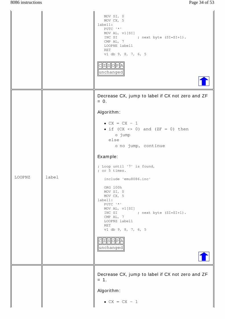
MOV SI, 0 MOV CX, 5 label1: PUTC '*' MOV AL, v1[SI] INC SI ; next byte (SI=SI+1). CMP AL, 7 LOOPNE label1 RET v1 db 9, 8, 7, 6, 5
C Z S O P A
unchanged
LOOPNZ label
Decrease CX, jump to label if CX not zero and ZF = 0. Algorithm:
CX = CX - 1 if (CX <> 0) and (ZF = 0) then
jump else
no jump, continue
Example:
; Loop until '7' is found, ; or 5 times. include 'emu8086.inc' ORG 100h MOV SI, 0 MOV CX, 5 label1: PUTC '*' MOV AL, v1[SI] INC SI ; next byte (SI=SI+1). CMP AL, 7 LOOPNZ label1 RET v1 db 9, 8, 7, 6, 5
C Z S O P A
unchanged
Decrease CX, jump to label if CX not zero and ZF = 1. Algorithm:
CX = CX - 1
Page 34 of 538086 instructions

LOOPZ label
if (CX <> 0) and (ZF = 1) then jump
else no jump, continue
Example:
; Loop until result fits into AL alone, ; or 5 times. The result will be over 255 ; on third loop (100+100+100), ; so loop will exit. include 'emu8086.inc' ORG 100h MOV AX, 0 MOV CX, 5 label1: PUTC '*' ADD AX, 100 CMP AH, 0 LOOPZ label1 RET
C Z S O P A
unchanged
MOV
REG, memory memory, REG REG, REG memory, immediate REG, immediate SREG, memory memory, SREG REG, SREG SREG, REG
Copy operand2 to operand1. The MOV instruction cannot:
set the value of the CS and IP registers. copy value of one segment register to another segment register (should copy to general register first). copy immediate value to segment register (should copy to general register first).
Algorithm:
operand1 = operand2
Example:
ORG 100h MOV AX, 0B800h ; set AX = B800h (VGA memory). MOV DS, AX ; copy value of AX to DS. MOV CL, 'A' ; CL = 41h (ASCII code). MOV CH, 01011111b ; CL = color attribute. MOV BX, 15Eh ; BX = position on screen. MOV [BX], CX ; w.[0B800h:015Eh] = CX. RET ; returns to operating system.
Page 35 of 538086 instructions

C Z S O P A
unchanged
MOVSB No operands
Copy byte at DS:[SI] to ES:[DI]. Update SI and DI. Algorithm:
ES:[DI] = DS:[SI] if DF = 0 then
SI = SI + 1 DI = DI + 1
else SI = SI - 1 DI = DI - 1
Example:
ORG 100h CLD LEA SI, a1 LEA DI, a2 MOV CX, 5 REP MOVSB RET a1 DB 1,2,3,4,5 a2 DB 5 DUP(0)
C Z S O P A
unchanged
Copy word at DS:[SI] to ES:[DI]. Update SI and DI. Algorithm:
ES:[DI] = DS:[SI] if DF = 0 then
SI = SI + 2 DI = DI + 2
else SI = SI - 2 DI = DI - 2
Example:
Page 36 of 538086 instructions

MOVSW No operands
ORG 100h CLD LEA SI, a1 LEA DI, a2 MOV CX, 5 REP MOVSW RET a1 DW 1,2,3,4,5 a2 DW 5 DUP(0)
C Z S O P A
unchanged
MUL REG memory
Unsigned multiply. Algorithm:
when operand is a byte: AX = AL * operand.
when operand is a word: (DX AX) = AX * operand.
Example:
MOV AL, 200 ; AL = 0C8h MOV BL, 4 MUL BL ; AX = 0320h (800) RET
CF=OF=0 when high section of the result is zero.
C Z S O P A
r ? ? r ? ?
NEG REG memory
Negate. Makes operand negative (two's complement). Algorithm:
Invert all bits of the operand Add 1 to inverted operand
Example:
MOV AL, 5 ; AL = 05h NEG AL ; AL = 0FBh (-5) NEG AL ; AL = 05h (5)
Page 37 of 538086 instructions

RET
C Z S O P A
r r r r r r
NOP No operands
No Operation. Algorithm:
Do nothing
Example:
; do nothing, 3 times: NOP NOP NOP RET
C Z S O P A
unchanged
NOT REG memory
Invert each bit of the operand. Algorithm:
if bit is 1 turn it to 0. if bit is 0 turn it to 1.
Example:
MOV AL, 00011011b NOT AL ; AL = 11100100b RET
C Z S O P A
unchanged
REG, memory
Logical OR between all bits of two operands. Result is stored in first operand. These rules apply: 1 OR 1 = 1 1 OR 0 = 1 0 OR 1 = 1 0 OR 0 = 0
Page 38 of 538086 instructions

OR
memory, REG REG, REG memory, immediate REG, immediate
Example:
MOV AL, 'A' ; AL = 01000001b OR AL, 00100000b ; AL = 01100001b ('a') RET
C Z S O P A
0 r r 0 r ?
OUT
im.byte, AL im.byte, AX DX, AL DX, AX
Output from AL or AX to port. First operand is a port number. If required to access port number over 255 - DX register should be used. Example:
MOV AX, 0FFFh ; Turn on all OUT 4, AX ; traffic lights. MOV AL, 100b ; Turn on the third OUT 7, AL ; magnet of the stepper-motor.
C Z S O P A
unchanged
POP REG SREG memory
Get 16 bit value from the stack. Algorithm:
operand = SS:[SP] (top of the stack) SP = SP + 2
Example:
MOV AX, 1234h PUSH AX POP DX ; DX = 1234h RET
C Z S O P A
unchanged
Pop all general purpose registers DI, SI, BP, SP, BX, DX, CX, AX from the stack.
Page 39 of 538086 instructions

POPA No operands
SP value is ignored, it is Popped but not set to SP register). Note: this instruction works only on 80186 CPU and later! Algorithm:
POP DI POP SI POP BP POP xx (SP value ignored) POP BX POP DX POP CX POP AX
C Z S O P A
unchanged
POPF No operands
Get flags register from the stack. Algorithm:
flags = SS:[SP] (top of the stack) SP = SP + 2
C Z S O P A
popped
PUSH
REG SREG memory immediate
Store 16 bit value in the stack. Note: PUSH immediate works only on 80186 CPU and later! Algorithm:
SP = SP - 2 SS:[SP] (top of the stack) = operand
Example:
MOV AX, 1234h PUSH AX POP DX ; DX = 1234h RET
Page 40 of 538086 instructions

C Z S O P A
unchanged
PUSHA No operands
Push all general purpose registers AX, CX, DX, BX, SP, BP, SI, DI in the stack. Original value of SP register (before PUSHA) is used. Note: this instruction works only on 80186 CPU and later! Algorithm:
PUSH AX PUSH CX PUSH DX PUSH BX PUSH SP PUSH BP PUSH SI PUSH DI
C Z S O P A
unchanged
PUSHF No operands
Store flags register in the stack. Algorithm:
SP = SP - 2 SS:[SP] (top of the stack) = flags
C Z S O P A
unchanged
Rotate operand1 left through Carry Flag. The number of rotates is set by operand2. When immediate is greater then 1, assembler generates several RCL xx, 1 instructions because 8086 has machine code only for this instruction (the same principle works for all other shift/rotate instructions). Algorithm:
Page 41 of 538086 instructions

RCL
memory, immediate REG, immediate memory, CL REG, CL
shift all bits left, the bit that goes off is set to CF and previous value of CF is inserted to the right-most position.
Example:
STC ; set carry (CF=1). MOV AL, 1Ch ; AL = 00011100b RCL AL, 1 ; AL = 00111001b, CF=0. RET
OF=0 if first operand keeps original sign.
C O
r r
RCR
memory, immediate REG, immediate memory, CL REG, CL
Rotate operand1 right through Carry Flag. The number of rotates is set by operand2. Algorithm:
shift all bits right, the bit that goes off is set to CF and previous value of CF is inserted to the left-most position.
Example:
STC ; set carry (CF=1). MOV AL, 1Ch ; AL = 00011100b RCR AL, 1 ; AL = 10001110b, CF=0. RET
OF=0 if first operand keeps original sign.
C O
r r
Repeat following MOVSB, MOVSW, LODSB, LODSW, STOSB, STOSW instructions CX times. Algorithm: check_cx: if CX <> 0 then
do following chain instruction
Page 42 of 538086 instructions

REP chain instruction
CX = CX - 1 go back to check_cx
else
exit from REP cycle
Z
r
REPE chain instruction
Repeat following CMPSB, CMPSW, SCASB, SCASW instructions while ZF = 1 (result is Equal), maximum CX times. Algorithm: check_cx: if CX <> 0 then
do following chain instruction CX = CX - 1 if ZF = 1 then:
go back to check_cx else
exit from REPE cycle
else
exit from REPE cycle
example: open cmpsb.asm from c:\emu8086\examples
Z
r
Repeat following CMPSB, CMPSW, SCASB, SCASW instructions while ZF = 0 (result is Not Equal), maximum CX times. Algorithm: check_cx: if CX <> 0 then
do following chain instruction
Page 43 of 538086 instructions

REPNE chain instruction
CX = CX - 1 if ZF = 0 then:
go back to check_cx else
exit from REPNE cycle
else
exit from REPNE cycle
Z
r
REPNZ chain instruction
Repeat following CMPSB, CMPSW, SCASB, SCASW instructions while ZF = 0 (result is Not Zero), maximum CX times. Algorithm: check_cx: if CX <> 0 then
do following chain instruction CX = CX - 1 if ZF = 0 then:
go back to check_cx else
exit from REPNZ cycle
else
exit from REPNZ cycle
Z
r
Repeat following CMPSB, CMPSW, SCASB, SCASW instructions while ZF = 1 (result is Zero), maximum CX times. Algorithm: check_cx: if CX <> 0 then
Page 44 of 538086 instructions

REPZ chain instruction
do following chain instruction CX = CX - 1 if ZF = 1 then:
go back to check_cx else
exit from REPZ cycle
else
exit from REPZ cycle
Z
r
RET No operands or even immediate
Return from near procedure. Algorithm:
Pop from stack: IP
if immediate operand is present: SP = SP + operand
Example:
ORG 100h ; for COM file. CALL p1 ADD AX, 1 RET ; return to OS. p1 PROC ; procedure declaration. MOV AX, 1234h RET ; return to caller. p1 ENDP
C Z S O P A
unchanged
RETF No operands or even immediate
Return from Far procedure. Algorithm:
Pop from stack: IP CS
if immediate operand is present:
Page 45 of 538086 instructions

SP = SP + operand
C Z S O P A
unchanged
ROL
memory, immediate REG, immediate memory, CL REG, CL
Rotate operand1 left. The number of rotates is set by operand2. Algorithm:
shift all bits left, the bit that goes off is set to CF and the same bit is inserted to the right-most position.
Example:
MOV AL, 1Ch ; AL = 00011100b ROL AL, 1 ; AL = 00111000b, CF=0. RET
OF=0 if first operand keeps original sign.
C O
r r
ROR
memory, immediate REG, immediate memory, CL REG, CL
Rotate operand1 right. The number of rotates is set by operand2. Algorithm:
shift all bits right, the bit that goes off is set to CF and the same bit is inserted to the left-most position.
Example:
MOV AL, 1Ch ; AL = 00011100b ROR AL, 1 ; AL = 00001110b, CF=0. RET
OF=0 if first operand keeps original sign.
C O
r r
Store AH register into low 8 bits of Flags register. Algorithm:
Page 46 of 538086 instructions

SAHF No operands
flags register = AH
AH bit: 7 6 5 4 3 2 1 0 [SF] [ZF] [0] [AF] [0] [PF] [1] [CF]
bits 1, 3, 5 are reserved.
C Z S O P A
r r r r r r
SAL
memory, immediate REG, immediate memory, CL REG, CL
Shift Arithmetic operand1 Left. The number of shifts is set by operand2. Algorithm:
Shift all bits left, the bit that goes off is set to CF. Zero bit is inserted to the right-most position.
Example:
MOV AL, 0E0h ; AL = 11100000b SAL AL, 1 ; AL = 11000000b, CF=1. RET
OF=0 if first operand keeps original sign.
C O
r r
SAR
memory, immediate REG, immediate memory, CL REG, CL
Shift Arithmetic operand1 Right. The number of shifts is set by operand2. Algorithm:
Shift all bits right, the bit that goes off is set to CF. The sign bit that is inserted to the left-most position has the same value as before shift.
Example:
MOV AL, 0E0h ; AL = 11100000b SAR AL, 1 ; AL = 11110000b, CF=0. MOV BL, 4Ch ; BL = 01001100b SAR BL, 1 ; BL = 00100110b, CF=0. RET
Page 47 of 538086 instructions

OF=0 if first operand keeps original sign.
C O
r r
SBB
REG, memory memory, REG REG, REG memory, immediate REG, immediate
Subtract with Borrow. Algorithm: operand1 = operand1 - operand2 - CF Example:
STC MOV AL, 5 SBB AL, 3 ; AL = 5 - 3 - 1 = 1 RET
C Z S O P A
r r r r r r
SCASB No operands
Compare bytes: AL from ES:[DI]. Algorithm:
AL - ES:[DI] set flags according to result: OF, SF, ZF, AF, PF, CF if DF = 0 then
DI = DI + 1 else
DI = DI - 1
C Z S O P A
r r r r r r
SCASW No operands
Compare words: AX from ES:[DI]. Algorithm:
AX - ES:[DI] set flags according to result: OF, SF, ZF, AF, PF, CF if DF = 0 then
DI = DI + 2
Page 48 of 538086 instructions

else DI = DI - 2
C Z S O P A
r r r r r r
SHL
memory, immediate REG, immediate memory, CL REG, CL
Shift operand1 Left. The number of shifts is set by operand2. Algorithm:
Shift all bits left, the bit that goes off is set to CF. Zero bit is inserted to the right-most position.
Example:
MOV AL, 11100000b SHL AL, 1 ; AL = 11000000b, CF=1. RET
OF=0 if first operand keeps original sign.
C O
r r
SHR
memory, immediate REG, immediate memory, CL REG, CL
Shift operand1 Right. The number of shifts is set by operand2. Algorithm:
Shift all bits right, the bit that goes off is set to CF. Zero bit is inserted to the left-most position.
Example:
MOV AL, 00000111b SHR AL, 1 ; AL = 00000011b, CF=1. RET
OF=0 if first operand keeps original sign.
C O
r r
Page 49 of 538086 instructions

STC No operands
Set Carry flag. Algorithm: CF = 1
C
1
STD No operands
Set Direction flag. SI and DI will be decremented by chain instructions: CMPSB, CMPSW, LODSB, LODSW, MOVSB, MOVSW, STOSB, STOSW. Algorithm: DF = 1
D
1
STI No operands
Set Interrupt enable flag. This enables hardware interrupts. Algorithm: IF = 1
I
1
STOSB No operands
Store byte in AL into ES:[DI]. Update DI. Algorithm:
ES:[DI] = AL if DF = 0 then
DI = DI + 1 else
DI = DI - 1
Example:
ORG 100h LEA DI, a1
Page 50 of 538086 instructions

MOV AL, 12h MOV CX, 5 REP STOSB RET a1 DB 5 dup(0)
C Z S O P A
unchanged
STOSW No operands
Store word in AX into ES:[DI]. Update DI. Algorithm:
ES:[DI] = AX if DF = 0 then
DI = DI + 2 else
DI = DI - 2
Example:
ORG 100h LEA DI, a1 MOV AX, 1234h MOV CX, 5 REP STOSW RET a1 DW 5 dup(0)
C Z S O P A
unchanged
SUB
REG, memory memory, REG REG, REG memory, immediate REG, immediate
Subtract. Algorithm: operand1 = operand1 - operand2 Example:
MOV AL, 5 SUB AL, 1 ; AL = 4 RET
Page 51 of 538086 instructions

C Z S O P A
r r r r r r
TEST
REG, memory memory, REG REG, REG memory, immediate REG, immediate
Logical AND between all bits of two operands for flags only. These flags are effected: ZF, SF, PF. Result is not stored anywhere. These rules apply: 1 AND 1 = 1 1 AND 0 = 0 0 AND 1 = 0 0 AND 0 = 0 Example:
MOV AL, 00000101b TEST AL, 1 ; ZF = 0. TEST AL, 10b ; ZF = 1. RET
C Z S O P
0 r r 0 r
XCHG REG, memory memory, REG REG, REG
Exchange values of two operands. Algorithm: operand1 < - > operand2 Example:
MOV AL, 5 MOV AH, 2 XCHG AL, AH ; AL = 2, AH = 5 XCHG AL, AH ; AL = 5, AH = 2 RET
C Z S O P A
unchanged
Translate byte from table. Copy value of memory byte at DS:[BX + unsigned AL] to AL register. Algorithm:
Page 52 of 538086 instructions

copyright © 2005 emu8086.com all rights reserved.
XLATB No operands
AL = DS:[BX + unsigned AL] Example:
ORG 100h LEA BX, dat MOV AL, 2 XLATB ; AL = 33h RET dat DB 11h, 22h, 33h, 44h, 55h
C Z S O P A
unchanged
XOR
REG, memory memory, REG REG, REG memory, immediate REG, immediate
Logical XOR (Exclusive OR) between all bits of two operands. Result is stored in first operand. These rules apply: 1 XOR 1 = 0 1 XOR 0 = 1 0 XOR 1 = 1 0 XOR 0 = 0 Example:
MOV AL, 00000111b XOR AL, 00000010b ; AL = 00000101b RET
C Z S O P A
0 r r 0 r ?
Page 53 of 538086 instructions

2
TABLE OF CONTENTS
ALL COMMANDS IN ALPHABETIC ORDER: ............................................................................................................... 6
THE STANDARD 8051/52 CPU REGISTERS. .................................................................................................................. 6
ARITHMETIC OPERATORS ............................................................................................................................................. 7
LOGICAL OPERATIONS .................................................................................................................................................... 7
DATA TRANSFER ................................................................................................................................................................ 8
BOOLEAN MANIPULATION ............................................................................................................................................. 8
ACALL ADDR11 ................................................................................................................................................................. 10
ADD A,<SRC-BYTE> .......................................................................................................................................................... 10
ADD A,RN ......................................................................................................................................................................... 10
ADD A,DIRECT ................................................................................................................................................................... 10
ADD A,@RI ....................................................................................................................................................................... 11
ADD A,#DATA .................................................................................................................................................................... 11
ADDC A,<SRC-BYTE> ....................................................................................................................................................... 11
ADDC A,RN ....................................................................................................................................................................... 11
ADDC A,DIRECT ................................................................................................................................................................ 11
ADDC A,@RI .................................................................................................................................................................... 12
ADDC A,#DATA ................................................................................................................................................................. 12
AJMP ADDRESS11 ............................................................................................................................................................. 12
ANL <DEST-BYTE>,<SRC-BYTE> .................................................................................................................................. 12
ANL A,RN .......................................................................................................................................................................... 13
ANL A,DIRECT ................................................................................................................................................................... 13
ANL A,@RI ....................................................................................................................................................................... 13
ANL A,#DATA .................................................................................................................................................................... 13
ANL DIRECT,A ................................................................................................................................................................... 13
ANL DIRECT,#DATA ........................................................................................................................................................... 13
ANL C,<SRC-BIT> .............................................................................................................................................................. 13
ANL C,BIT .......................................................................................................................................................................... 14
ANL C,/BIT ......................................................................................................................................................................... 14
CJNE <DEST-BYTE>,<SRC-BYTE>,REL8..................................................................................................................... 14
CJNE A,DIRECT,REL8 ......................................................................................................................................................... 14
CJNE A,#DATA,REL8 .......................................................................................................................................................... 15
CJNE RN,#DATA,REL8 ........................................................................................................................................................ 15
CJNE @RI,#DATA,REL8 ..................................................................................................................................................... 15
CLR A ................................................................................................................................................................................... 16
CLR BIT ............................................................................................................................................................................... 16
CLR C................................................................................................................................................................................. 16
CLR BIT .............................................................................................................................................................................. 16
CPL A .................................................................................................................................................................................... 16
CPL BIT ................................................................................................................................................................................ 17
CPL C ................................................................................................................................................................................. 17
CPL BIT .............................................................................................................................................................................. 17
DA A ...................................................................................................................................................................................... 17

3
DEC BYTE ............................................................................................................................................................................ 18
DEC A ................................................................................................................................................................................ 18
DEC RN .............................................................................................................................................................................. 18
DIV AB .................................................................................................................................................................................. 19
DJNZ <BYTE>,REL8 .......................................................................................................................................................... 19
DJNZ RN,REL8 .................................................................................................................................................................... 20
DJNZ DIRECT,REL8 ............................................................................................................................................................. 20
INC BYTE ............................................................................................................................................................................. 20
INC A .................................................................................................................................................................................. 20
INC RN................................................................................................................................................................................ 21
INC DIRECT ......................................................................................................................................................................... 21
INC @RI ............................................................................................................................................................................. 21
INC DPTR ............................................................................................................................................................................. 21
JB BIT,REL8 ........................................................................................................................................................................ 21
JBC BIT,REL8 ...................................................................................................................................................................... 22
JC BIT,REL8 ........................................................................................................................................................................ 22
JMP @A+DPTR ................................................................................................................................................................... 23
JNB BIT,REL8 ...................................................................................................................................................................... 23
JNC REL8 ............................................................................................................................................................................. 23
JNZ REL8 ............................................................................................................................................................................. 24
JZ REL8 ................................................................................................................................................................................ 24
LCALL ADDR16 .................................................................................................................................................................. 25
LJMP ADDR16 ..................................................................................................................................................................... 25
MOV <DEST>,<SOURCE> ................................................................................................................................................ 25
MOV A,RN ......................................................................................................................................................................... 26
MOV A,DIRECT ................................................................................................................................................................... 26
MOV A,@RI ....................................................................................................................................................................... 26
MOV A,#DATA ................................................................................................................................................................... 26
MOV RN,A ......................................................................................................................................................................... 26
MOV RN,DIRECT ................................................................................................................................................................. 26
MOV RN,#DATA ................................................................................................................................................................. 27
MOV DIRECT,A ................................................................................................................................................................... 27
MOV DIRECT,RN ................................................................................................................................................................. 27
MOV DIRECT,DIRECT .......................................................................................................................................................... 27
MOV DIRECT,@RI .............................................................................................................................................................. 27
MOV DIRECT,#DATA ........................................................................................................................................................... 27
MOV @RI,A ....................................................................................................................................................................... 28
MOV @RI,DIRECT .............................................................................................................................................................. 28
MOV @RI,#DATA ............................................................................................................................................................... 28
MOV <DEST-BIT>,<SOURCE-BIT> ................................................................................................................................ 28
MOV C,BIT ......................................................................................................................................................................... 28
MOV A,DIRECT ................................................................................................................................................................... 28
MOV DPTR,#DATA16 ........................................................................................................................................................ 29
MOVC A,@A+<BASE-REG> ............................................................................................................................................. 29

4
MOVC A,@A+DPTR ........................................................................................................................................................ 29
MOVC A,@A+PC ............................................................................................................................................................. 29
MOVX A,@A+<BASE-REG> ............................................................................................................................................. 30
MOVX A,@RI.................................................................................................................................................................... 30
MOVX A,@DPTR ............................................................................................................................................................. 30
MOVX @RI,A.................................................................................................................................................................... 31
MOVX @DPTR,A ............................................................................................................................................................. 31
MUL AB ................................................................................................................................................................................ 31
NOP ....................................................................................................................................................................................... 31
ORL <DEST-BYTE>,<SRC-BYTE> ................................................................................................................................. 32
ORL A,RN .......................................................................................................................................................................... 32
ORL A,DIRECT .................................................................................................................................................................... 32
ORL A,@RI ........................................................................................................................................................................ 32
ORL A,#DATA .................................................................................................................................................................... 32
ORL DIRECT,A .................................................................................................................................................................... 33
ORL DIRECT,#DATA ............................................................................................................................................................ 33
ORL C,<SRC-BIT>.............................................................................................................................................................. 33
ORL C,BIT .......................................................................................................................................................................... 33
ORL C,/BIT ......................................................................................................................................................................... 33
POP DIRECT ....................................................................................................................................................................... 33
PUSH DIRECT ..................................................................................................................................................................... 34
RET ....................................................................................................................................................................................... 34
RETI ...................................................................................................................................................................................... 35
RL A ...................................................................................................................................................................................... 35
RLC A ................................................................................................................................................................................... 35
RR A ...................................................................................................................................................................................... 36
RRC A ................................................................................................................................................................................... 36
SETB <BIT> ......................................................................................................................................................................... 36
SETB C............................................................................................................................................................................... 36
SETB <BIT> ........................................................................................................................................................................ 37
SJMP REL8 .......................................................................................................................................................................... 37
SUBB A,<SRC-BYTE> ........................................................................................................................................................ 37
SUBB A,RN ........................................................................................................................................................................ 38
SUBB A,DIRECT ................................................................................................................................................................. 38
SUBB A,@RI ..................................................................................................................................................................... 38
SUBB A,#DATA .................................................................................................................................................................. 38
SWAP A ................................................................................................................................................................................ 38
XCH A,<BYTE> ................................................................................................................................................................... 38
XCH A,RN .......................................................................................................................................................................... 39
XCH A,DIRECT ................................................................................................................................................................... 39
XCH A,@RI ....................................................................................................................................................................... 39
XCHD A,@RI ....................................................................................................................................................................... 39
XRL <DEST-BYTE>,<SRC-BYTE> .................................................................................................................................. 40

5
XRL A,RN ........................................................................................................................................................................... 40
XRL A,DIRECT .................................................................................................................................................................... 40
XRL A,@RI ........................................................................................................................................................................ 40
XRL A,#DATA ..................................................................................................................................................................... 40
XRL DIRECT,A .................................................................................................................................................................... 41
ANL DIRECT,#DATA ............................................................................................................................................................ 41
TABLE OF CONTENTS ....................................................................................................................................................... 2

6
THE 8051 INSTRUCTION SET
All commands in alphabetic order:
ACALL addr11 DIV AB LJMP addr16 RETI
ADD A,<src DJNZ <byte,<rel8 MOV <dest,<src RL A
ADDC A,<src INC <byte MOV DPTR,#data16 RLC A
AJMP addr11 INC DPTR MOV bit,bit RR A
ANL <dest,<src JB bit,rel8 MOVC A,@A+<base RRC A
ANL <bit JBC bit,rel8 MOVX <dest,<src SETB bit
CJNE <dest,<src,rel8 JC rel8 MUL AB SJMP rel8
CLR A JMP @A+DPTR NOP SUBB A,<src
CLR bit JNB bit,rel8 ORL <dest,<src SWAP A
CPL A JNC rel8 ORL C,bit XCH A,<byte
CPL bit JNZ rel8 POP direct XCHD A,@Ri
DA A JZ rel8 PUSH direct XRL <dest,<src
DEC <byte LCALL addr16 RET
The standard 8051/52 CPU Registers.
Symbol Name Address Reset-value
ACC * Accumulator E0 0000 0000 (00)
B * B Register F0 0000 0000 (00)
PSW * Program Status Word D0 0000 0000 (00)
SP Stack Pointer 81 0000 0111 (07)
DPL Low Byte Dptr 82 0000 0000 (00)
DPH High Byte Dptr 83 0000 0000 (00)
P0 * Port 0 80 1111 1111 (FF)
P1 * Port 1 90 1111 1111 (FF)
P2 * Port 2 A0 1111 1111 (FF)
P3 * Port 3 B0 1111 1111 (FF)
IP * Interrupt Priority Control B8 xxx0 0000 (?0)
IE * Interrupt Enable Control A8 0xx0 0000 (?0)
TMOD Timer/Counter Mode Control 89 0000 0000 (00)
TCON * Timer/Counter Control 88 0000 0000 (00)
T2CON * ^ Timer/Counter 2 Control C8 0000 0000 (00)
TH0 Timer/Counter 0 High Byte 8C 0000 0000 (00)
TL0 Timer/Counter 0 Low Byte 8A 0000 0000 (00)
TH1 Timer/Counter 1 High Byte 8D 0000 0000 (00)
TL1 Timer/Counter 1 Low Byte 8B 0000 0000 (00)
TH2 ^ Timer/Counter 1 High Byte CD 0000 0000 (00)
TL2 ^ Timer/Counter 2 Low Byte CC 0000 0000 (00)
RCAP2H ^ T/C 2 Capture Reg. High Byte CB 0000 0000 (00)
RCAP2L ^ T/C 2 Capture Reg. Low Byte CA 0000 0000 (00)
SCON * Serial Control 98 0000 0000 (00)
SBUF Serial Data Buffer 99 xxxx xxxx (??)
PCON Power Control 87 0xxx 0000 (?0)
Description: ^ = 80C52 * = Bit addressable x = Unknown state.

7
ARITHMETIC OPERATORS
Instruction Description Bytes Periods C OV AC
ADD A, Rn Add register to ACC 1 12 x x x
ADD A, direct Add direct byte to ACC 2 12 x x x
ADD A, @Ri Add indirect RAM to ACC 1 12 x x x
ADD A, #data Add immediate data to ACC 2 12 x x x
ADDC A, Rn Add register to ACC with Carry 1 12 x x x
ADDC A, direct Add direct byte to ACC with Carry 2 12 x x x
ADDC A, @Ri Add indirect RAM to ACC with Carry 1 12 x x x
ADDC A, #data Add immediate data to ACC with Carry 2 12 x x x
SUBB A, Rn Subtract Register from ACC with borrow 1 12 x x x
SUBB A, direct Subtract indirect RAM from ACC with borrow 2 12 x x x
SUBB A, @Ri Subtract indirect RAM from ACC with borrow 1 12 x x x
SUBB A, #data Subtract immediate data from ACC with borrow 2 12 x x x
INC A Increment ACC 1 12
INC Rn Increment register 1 12
INC direct Increment direct byte 2 12
INC @Ri Increment direct RAM 1 12
DEC A Decrement ACC 1 12
DEC Rn Decrement Register 1 12
DEC direct Decrement direct byte 2 12
DEC @Ri Decrement indirect RAM 1 12
INC DPTR Increment Data Pointer 1 24
MUL AB Multiply A & B 1 48 0 x
DIV AB Divide A by B 1 48 0 x
DA A Decimal Adjust ACC 1 12 x
LOGICAL OPERATIONS
Instruction Description Bytes Periods C OV AC
ANL A,Rn AND register to ACC 1 12
ANL A,direct AND direct byte to ACC 2 12
ANL A,@Ri AND indirect RAM to ACC 1 12
ANL A,#data AND immediate data to ACC 2 12
ANL direct,A AND ACC to direct byte 2 12
ANL direct,#data AND immediate data to direct byte 3 24
ORL A,Rn OR register to ACC 1 12
ORL A,direct OR direct byte to ACC 2 12
ORL A,@Ri OR indirect RAM to ACC 1 12
ORL A,#data OR immediate data to ACC 2 12
ORL direct,A OR ACC to direct byte 2 12
ORL direct,#data OR immediate data to direct byte 3 24
XRL A,Rn XOR register to ACC 1 12
XRL A,direct XOR direct byte to ACC 2 12
XRL A,@Ri XOR indirect RAM to ACC 1 12
XRL A,#data XOR immediate data to ACC 2 12
XRL direct,A XOR ACC to direct byte 2 12
XRL direct,#data XOR immediate data to direct byte 3 24
CLR A Clear the ACC 1 12
CPL A Complement the ACC 1 12
RL A Rotate the ACC left 1 12

8
RLC A Rotate the ACC left through Carry 1 12 x
RR A Rotate the ACC right 1 12
RRC A Rotate the ACC right through Carry 1 12 x
SWAP A Swap nibbles in the ACC 1 12
DATA TRANSFER
Instruction Description Bytes Periods C OV AC
MOV A,Rn Move Register to ACC 1 12
MOV A,direct Move Direct byte to ACC 2 12
MOV A,@Ri Move Indirect byte to ACC 1 12
MOV A,#data Move Immediate data to ACC 2 12
MOV Rn,A Mov ACC to Register 1 12
MOV Rn,direct Move Direct byte to Register 2 24
MOV Rn,#data Move Immediate data to Register 2 12
MOV direct,A Move ACC to Direct byte 2 12
MOV direct,Rn Move Register to Direct byte 2 24
MOV direct,direct Move Direct byte to Direct byte 3 24
MOV direct,@Ri Mov Indirect RAM to Direct byte 3 24
MOV direct,#data Move Immediate data to Direct byte 3 24
MOV @Ri,A Move ACC to Indirect RAM 1 12
MOV @Ri,direct Move direct byte to indirect RAM. 2 24
MOV @Ri,#data Move Immediate data to Indirect RAM 2 12
MOV DPTR,#data16 Load datapointer with 16 bit constant 3 24
MOVC A,@A+DPTR Move code byte at ACC+DPTR to ACC 1 24
MOVC A,@A+PC Move code byte at ACC+PC to ACC 1 24
MOVX A,@Ri Move external RAM to ACC 1 24
MOVX @Ri,A Move ACC to external RAM 1 24
MOVX A,@DPTR Move external RAM to ACC 1 24
MOVX @DPTR,A Move ACC to external RAM 1 24
PUSH direct Push direct byte to stack 2 24
POP direct Pop direct byte from stack 2 24
XCH A,Rn Exchange register with ACC 1 12
XCH A,direct Exchange direct byte with ACC 2 12
XCH A,@Ri Exchange indirect RAM with ACC 1 12
XCHD A,@Ri Exchange low order digit indirect RAM with ACC 1 12
BOOLEAN MANIPULATION
Instruction Description Bytes Periods C OV AC
CLR C Clear carry flag 1 12 0
CLR bit Clear direct bit 2 12
SETB C Set carry flag 1 12 1
SETB bit Set direct bit 2 12
CPL C Complement carry flag 1 12 x
CPL bit Complement direct bit 2 12
ANL C,bit AND direct bit to carry 2 24 x
ANL C,/bit AND complement of direct bit to carry 2 24 x
ORL C,bit OR direct bit to carry 2 24 x
ORL C,/bit OR complement of direct bit to carry 2 24 x
MOV C,bit Move direct bit to carry 2 12 x
MOV bit,C Move carry to direct bit 2 24
JC rel Jump if carry is set 2 24

9
JNC rel Jump if carry is NOT set 2 24
JB bit,rel Jump if direct bit is set 3 24
JNB bit,rel Jump if direct bit is NOT set 3 24
JBC bit,rel Jump if direct bit is set and clear that bit 3 24

10
ACALL addr11
Function: Absolute Call within 2K block
Description: ACALL unconditionally calls a subroutine located at the indicated address. The instruction increments
the PC twice to obtain the address of the following instruction, then pushes the 16-bit result onto the
stack (low-order byte first) and increments the Stack Pointer twice.
The destination address is obtained by successively concatenating the five high-order bits of the
incremented PC, opcode bits 7-5, and the second byte of the instruction. The subroutine called must
therefore start within the same 2 K block of the program memory as the first byte of the instruction
following ACALL.
No flags are affected.
Example: Initially SP equals 07H. The labs “ SUBRTN “ is at program memory location 0345 H. After
executing the instruction,
ACALL SUBRTN
at location 0123H, SP will contain 09H, internal RAM locations 08H and 09H will contain 25H and
01H, respectively, and the PC will contain 0345H.
Bytes: 2
Clocks: 24
Encoding: a10 a9 a8 1:0 0 0 1 a7 a6 a5 a4:a3 a2 a1 a0
Operation: (PC) « (PC) + 2
(SP) « (SP) + 1
[(SP)] « (PC7-0)
(SP) « (SP) + 1
[(SP)] « (PC15-8)
(PC10-0) « page address
Flags: None
ADD A,<src-byte>
Function: Add
Description: ADD adds the byte variable indicated to the Accumulator, leaving the result in the Accumulator.
The carry and auxiliary-carry flags are set, respectively, if there is a carry-out from bit 7 or bit 3, and
cleared otherwise.
When adding unsigned integers, the carry flag indicates an overflow occured.
OV is set there is a carry-out of bit 6 but not out of bit 7, or a carry-out of bit 7 but not bit 6;
otherwise OV is cleared.
When adding signed integers, OV indicates a negative number produced as the sum of two positive
operands, or a positive sum from two negative operands.
Four source operand addressing modes are allowed : register, direct, register-
indirect, or immediate.
Example: The Accumulator holds 0C3H (11000011B) and register 0 holds 0AAH (10101010B).
The instruction,
ADD A, R0 will leave 6DH (01101101B) in the Accumulator with the AC flag cleared and both the carry flag and
OV set to 1.
ADD A,Rn
Function: Add register byte to ACC
Bytes: 1
Clocks: 12
Encoding: 0 0 1 0:1 r r r
Operation: (A) « (A) +(Rn)
Flags: C AC OV
ADD A,direct
Function: Add direct byte to ACC
Bytes: 2
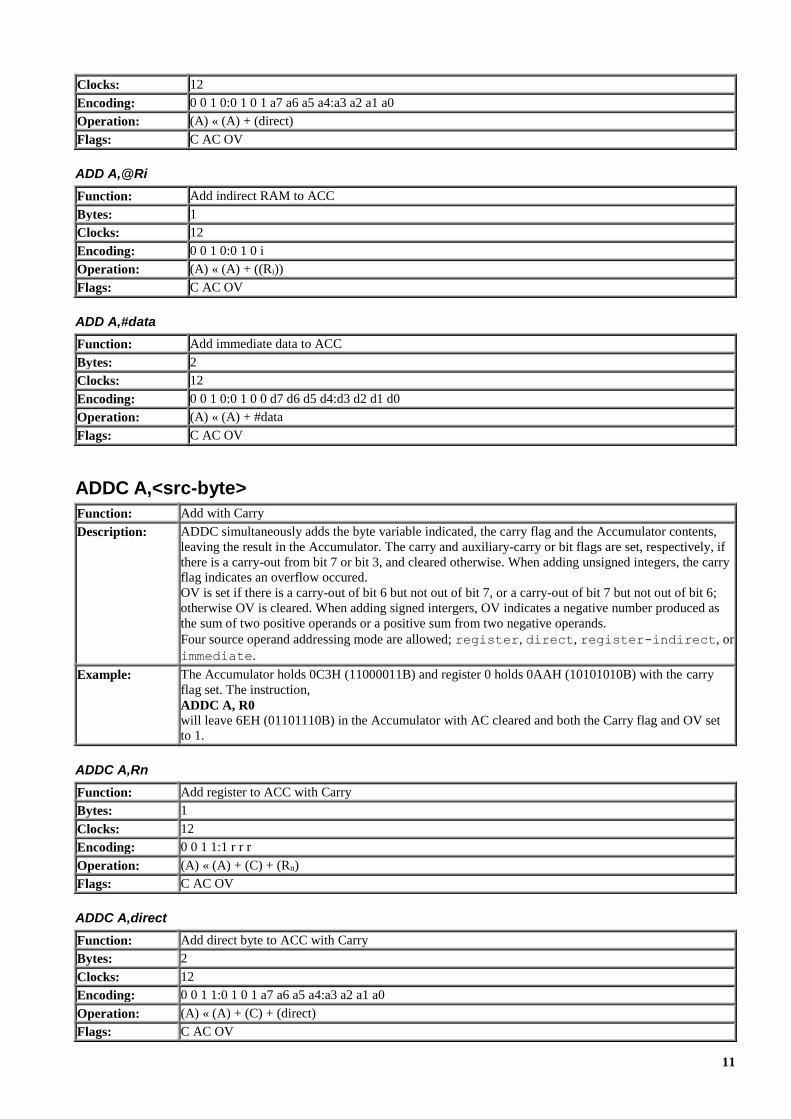
11
Clocks: 12
Encoding: 0 0 1 0:0 1 0 1 a7 a6 a5 a4:a3 a2 a1 a0
Operation: (A) « (A) + (direct)
Flags: C AC OV
ADD A,@Ri
Function: Add indirect RAM to ACC
Bytes: 1
Clocks: 12
Encoding: 0 0 1 0:0 1 0 i
Operation: (A) « (A) + ((Ri))
Flags: C AC OV
ADD A,#data
Function: Add immediate data to ACC
Bytes: 2
Clocks: 12
Encoding: 0 0 1 0:0 1 0 0 d7 d6 d5 d4:d3 d2 d1 d0
Operation: (A) « (A) + #data
Flags: C AC OV
ADDC A,<src-byte>
Function: Add with Carry
Description: ADDC simultaneously adds the byte variable indicated, the carry flag and the Accumulator contents,
leaving the result in the Accumulator. The carry and auxiliary-carry or bit flags are set, respectively, if
there is a carry-out from bit 7 or bit 3, and cleared otherwise. When adding unsigned integers, the carry
flag indicates an overflow occured.
OV is set if there is a carry-out of bit 6 but not out of bit 7, or a carry-out of bit 7 but not out of bit 6;
otherwise OV is cleared. When adding signed intergers, OV indicates a negative number produced as
the sum of two positive operands or a positive sum from two negative operands.
Four source operand addressing mode are allowed; register, direct, register-indirect, or
immediate.
Example: The Accumulator holds 0C3H (11000011B) and register 0 holds 0AAH (10101010B) with the carry
flag set. The instruction,
ADDC A, R0 will leave 6EH (01101110B) in the Accumulator with AC cleared and both the Carry flag and OV set
to 1.
ADDC A,Rn
Function: Add register to ACC with Carry
Bytes: 1
Clocks: 12
Encoding: 0 0 1 1:1 r r r
Operation: (A) « (A) + (C) + (Rn)
Flags: C AC OV
ADDC A,direct
Function: Add direct byte to ACC with Carry
Bytes: 2
Clocks: 12
Encoding: 0 0 1 1:0 1 0 1 a7 a6 a5 a4:a3 a2 a1 a0
Operation: (A) « (A) + (C) + (direct)
Flags: C AC OV

12
ADDC A,@Ri
Function: Add indirect RAM to ACC with Carry
Bytes: 1
Clocks: 12
Encoding: 0 0 1 1:0 1 1 i
Operation: (A) « (A) + (C) + ((Ri))
Flags: C AC OV
ADDC A,#data
Function: Add immediate data to ACC with Carry
Bytes: 2
Clocks: 12
Encoding: 0 0 1 0:0 1 0 0 d7 d6 d5 d4:d3 d2 d1 d0
Operation: (A) « (A) + (C) + #data
Flags: C AC OV
AJMP address11
Function: Absolute jump to address
Description: AJMP transfers program execution to the indicated address, which is formed at run-time by
concatenating the high-order five bits of the PC (after incrementing the PC twice), opcode bits 7-5, and
the second byte of the instruction. The destination must therefore be within the same 2 K block of
program memory as the first byte of the instruction following AJMP.
Example: The label "JMPADR" is at program memory location 0123H.
The instruction,
AJMP JMPADR is a location 0345H and will load the PC with 0123H.
Bytes: 2
Clocks: 24
Encoding: a10 a9 a8 0:0 0 0 1 a7 a6 a5 a4:a3 a2 a1 a0
Operation: (PC) « (PC) + 2
(PC10-0) « page address
Flags: None
ANL <dest-byte>,<src-byte>
Function: Logical-AND for byte variables
Description: ANL performs the bitwise logical-AND operation between the variables indicated and stores the results
in the destination variable. No flags are affected. The two operands allow six addressing mode
combinations.
When the destination is the Accumulator, the source can use register, direct, register-
indirect, or immediate addressing; when the destination is a direct address, the source can be the
Accumulator or immediate data.
Note: When this instruction is used to modify an output port, the value used as the original port data
will be read from the output data latch, not the input pins.
Example: If the Accumulator holds 0C3H (11000011B) and register 0 holds 55H (01010101B) then the
instruction,
ANL A, R0 will leave 41H (01000001B) in the Accumulator.
When the destination is a directly addressed byte, this instruction will clear combinations of bits in any
RAM location or hardware register. The mask byte determining the pattern of bits to be cleared would
either be a constant contained in the instruction or a value computed in the Accumulator at run-time.
The instruction,
ANL P1, #01110011B will clear bits 7, 3, and 2 of output port 1.

13
ANL A,Rn
Function: Logical AND register byte to ACC
Bytes: 1
Clocks: 12
Encoding: 0 1 0 1:1 r r r
Operation: (A) « (A) ^ (Rn)
Flags:
ANL A,direct
Function: Logical AND direct byte to ACC
Bytes: 2
Clocks: 12
Encoding: 0 1 0 1:0 1 0 1 a7 a6 a5 a4:a3 a2 a1 a0
Operation: (A) « (A) ^ (direct)
Flags:
ANL A,@Ri
Function: Logical AND indirect RAM to ACC
Bytes: 1
Clocks: 12
Encoding: 0 1 0 1:0 1 1 i
Operation: (A) « (A) ^ ((Ri))
Flags:
ANL A,#data
Function: Logical AND immediate data to ACC
Bytes: 2
Clocks: 12
Encoding: 0 1 0 1:0 1 0 0 d7 d6 d5 d4:d3 d2 d1 d0
Operation: (A) « (A) ^ #data
Flags:
ANL direct,A
Function: Logical AND ACC to direct data
Bytes: 2
Clocks: 12
Encoding: 0 1 0 1:0 0 1 0 d7 d6 d5 d4:d3 d2 d1 d0
Operation: (direct) « (direct) ^ ACC
Flags:
ANL direct,#data
Function: Logical AND immediate data to direct data
Bytes: 3
Clocks: 24
Encoding: 0 1 0 1:0 0 1 1 a7 a6 a5 a4:a3 a2 a1 a0 d7 d6 d5 d4:d3 d2 d1 d0
Operation: (direct) « (direct) ^ #data
Flags:
ANL C,<src-bit>
Function: Logical-AND for bit variables
Description: If the Boolean value of the source bit is logical 0 then clear the carry flag; otherwise leave the carry
flag in its current state. A slash ("/") preceding the operand in the assembly language indicates that the

14
logical complement of the addressed bit is used as the source value, but the source bit itself is not
affected. No other flags are affected.
Only direct addressing is allowed for the source operand.
Example: Set the carry flag if, P1.0 = 1, ACC.7 = 1, and OV = 0
MOV C, P1.0 ; LOAD CARRY WITH INPUT PIN STATE
ANL C, ACC.7 ; AND CARRY WITH ACC BIT 7
ANL C,/OV ; AND WITH INVERSE OF OVERFLOW FLAG
ANL C,bit
Function: Logical AND bit variable to carry
Bytes: 2
Clocks: 24
Encoding: 1 0 0 0:0 0 1 0 b7 b6 b5 b4:b3 b2 b1 b0
Operation: (C) « (C) ^ (bit)
Flags: C
ANL C,/bit
Function: Logical AND bit variable to carry
Bytes: 2
Clocks: 24
Encoding: 1 0 1 1:0 0 0 0 b7 b6 b5 b4:b3 b2 b1 b0
Operation: (C) « (C) ^ (bit)
Flags: C
CJNE <dest-byte>,<src-byte>,rel8
Function: Compare and Jump if Not Equal
Description: CJNE compares the magnitudes of the first two operands, and branches if their values are not equal.
The branch destination is computed by adding the signed relative- displacement in the last instruction
byte to the PC, after incrementing the PC to the start of the next instruction. The carry flag is set if
the unsigned integer value of <dest-byte> is less than the unsigned integer value of <src-byte>;
otherwise, the carry is cleared. Neither operand is affected.
The first two operands allow four addressing mode combinations: the Accumulator may be compared
with any directly addressed byte or immediate data, and any indirect RAM location or working register
can be compared with an immediate constant.
Example: The Accumulator contains 34H, register 7 contains 56H. The first instruction in the sequence,
CJNE R7, #60H, NOT_EQ
; ... ... ; R7 = 60H
NOT_EQ: JC REQ_LOW ; IF R7 < 60H
; ... ... ; R7 > 60H sets the carry flag and branches to the instruction at label NOT_EQ. By testing the carry flag, this
instruction determines whether R7 is greater or less than 60H.
If the data being presented to Port 1 is also 34H, then the instruction,
WAIT : CJNE A, P1, WAIT clears the carry flag and continues with the next instruction in sequence, since the Accumulator does
equal the data read from P1. (If some other value was being input on P1, the program will loop at this
point until the P1 data changes to 34H).
CJNE A,direct,rel8
Function: Compare direct byte to ACC, Jump if Not Equal
Bytes: 3
Clocks: 24
Encoding: 1 0 1 1:0 1 0 1 a7 a6 a5 a4:a3 a2 a1 a0 r7 r6 r5 r4:r3 r2 r1 r0
Operation: (PC) « (PC) + 3
IF (A) <> (direct)
THEN
(PC) « (PC) + relative offset

15
IF (A) < (direct)
THEN
(C) « 1
ELSE
(C) « 0
Flags: C
CJNE A,#data,rel8
Function: Compare immediate data to ACC, Jump if Not Equal
Bytes: 3
Clocks: 24
Encoding: 1 0 1 1:0 1 0 0 a7 a6 a5 a4:a3 a2 a1 a0 r7 r6 r5 r4:r3 r2 r1 r0
Operation: (PC) « (PC) + 3
IF (A) <> data
THEN
(PC) « (PC) + relative offset
IF (A) < data
THEN
(C) « 1
ELSE
(C) « 0
Flags: C
CJNE Rn,#data,rel8
Function: Compare immediate data to register, Jump if Not Equal
Bytes: 3
Clocks: 24
Encoding: 1 0 1 1:1 r r r a7 a6 a5 a4:a3 a2 a1 a0 r7 r6 r5 r4:r3 r2 r1 r0
Operation: (PC) « (PC) + 3
IF (Rn) <> data
THEN
(PC) « (PC) + relative offset
IF (Rn) < data
THEN
(C) « 1
ELSE
(C) « 0
Flags: C
CJNE @Ri,#data,rel8
Function: Compare immediate data to register, Jump if Not Equal
Bytes: 3
Clocks: 24
Encoding: 1 0 1 1:0 1 1 i a7 a6 a5 a4:a3 a2 a1 a0 r7 r6 r5 r4:r3 r2 r1 r0
Operation: (PC) « (PC) + 3
IF ((Ri)) <> data
THEN
(PC) « (PC) + relative offset
IF ((Ri)) < data
THEN
(C) « 1
ELSE
(C) « 0
Flags: C

16
CLR A
Function: Clears the ACC
Description: The Accumulator is cleared (all bits set on zero). No flags are affected.
Example: The Accumulator contains 5CH (01011100B).
The instruction,
CLR A Will leave the Accumulator set to 00H (00000000B).
Bytes: 1
Clocks: 12
Encoding: 1 1 1 1:0 1 0 0
Operation: (A) « 0
Flags: None
CLR bit
Function: Clear bit
Description: The indicated bit is cleared (reset to zero).
No other flags are affected.
CLR can operate on the carry flag or any directly addressable bit.
Example: Port 1 has previously been written with 5DH (01011101B).
The instruction,
CLR P1.2 will leave the port set to 59H (01011001B).
CLR C
Function: Clears the carry
Bytes: 1
Clocks: 12
Encoding: 1 1 0 0:0 0 1 1
Operation: (C) « 0
Flags: C
CLR bit
Function: Clears bit
Bytes: 2
Clocks: 12
Encoding: 1 1 0 0:0 0 1 0 b7 b6 b5 b4:b3 b2 b1 b0
Operation: (bit) « 0
Flags:
CPL A
Function: Complement Accumulator
Description: Each bit of the Accumulator is logically complemented (one’s complement).
Bits which previously contained a one are changed to a zero and vice-versa. No flags are affected.
Example: The accumulator contains 5CH (01011100B). The instruction,
CPL A will leave the Accumulator set to 0A3H (10100011B).
Bytes: 1
Clocks: 12
Encoding: 1 1 1 1:0 1 0 0
Operation: (A) « (A)
Flags: None
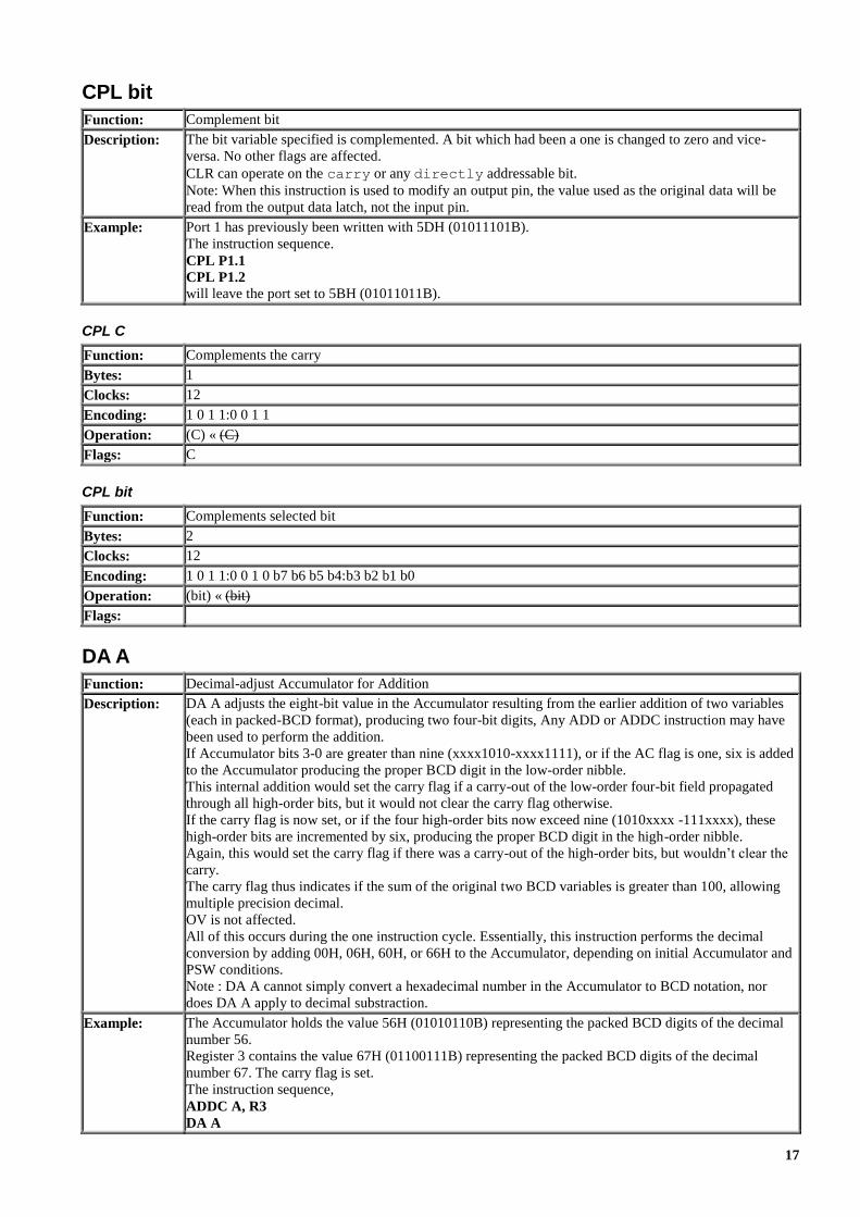
17
CPL bit
Function: Complement bit
Description: The bit variable specified is complemented. A bit which had been a one is changed to zero and vice-
versa. No other flags are affected.
CLR can operate on the carry or any directly addressable bit.
Note: When this instruction is used to modify an output pin, the value used as the original data will be
read from the output data latch, not the input pin.
Example: Port 1 has previously been written with 5DH (01011101B).
The instruction sequence.
CPL P1.1
CPL P1.2 will leave the port set to 5BH (01011011B).
CPL C
Function: Complements the carry
Bytes: 1
Clocks: 12
Encoding: 1 0 1 1:0 0 1 1
Operation: (C) « (C)
Flags: C
CPL bit
Function: Complements selected bit
Bytes: 2
Clocks: 12
Encoding: 1 0 1 1:0 0 1 0 b7 b6 b5 b4:b3 b2 b1 b0
Operation: (bit) « (bit)
Flags:
DA A
Function: Decimal-adjust Accumulator for Addition
Description: DA A adjusts the eight-bit value in the Accumulator resulting from the earlier addition of two variables
(each in packed-BCD format), producing two four-bit digits, Any ADD or ADDC instruction may have
been used to perform the addition.
If Accumulator bits 3-0 are greater than nine (xxxx1010-xxxx1111), or if the AC flag is one, six is added
to the Accumulator producing the proper BCD digit in the low-order nibble.
This internal addition would set the carry flag if a carry-out of the low-order four-bit field propagated
through all high-order bits, but it would not clear the carry flag otherwise.
If the carry flag is now set, or if the four high-order bits now exceed nine (1010xxxx -111xxxx), these
high-order bits are incremented by six, producing the proper BCD digit in the high-order nibble.
Again, this would set the carry flag if there was a carry-out of the high-order bits, but wouldn’t clear the
carry.
The carry flag thus indicates if the sum of the original two BCD variables is greater than 100, allowing
multiple precision decimal.
OV is not affected.
All of this occurs during the one instruction cycle. Essentially, this instruction performs the decimal
conversion by adding 00H, 06H, 60H, or 66H to the Accumulator, depending on initial Accumulator and
PSW conditions.
Note : DA A cannot simply convert a hexadecimal number in the Accumulator to BCD notation, nor
does DA A apply to decimal substraction.
Example: The Accumulator holds the value 56H (01010110B) representing the packed BCD digits of the decimal
number 56.
Register 3 contains the value 67H (01100111B) representing the packed BCD digits of the decimal
number 67. The carry flag is set.
The instruction sequence,
ADDC A, R3
DA A

18
will first perform a standard twos-complement binary addition, resulting in the value 0BEH (10111110),
in the Accumulator.
The carry and auxillary carry flags will be cleared.
The decimal Adjust instruction will then after the Accumulator to the value 24H (00100100B) indicating
the packed BCD digits of the decimal number 24, the low-order two digits of the decimal sum of 56,67,
and the carry-in.
The carry flag will set by the Decimal Adjust instruction, indicating that a decimal overflow occured.
The true sum 56,67, and 1 is 124. BCD variables can be incremented or decremented by adding 01H or
99H.
If the Accumulator initially holds 30H (representing the digits of 30 decimal), then the instruction
sequence,
ADD A, #99H
DA A will leave the carry set and 29H in the Accumulator, since 30 + 99 = 129.
The low-order byte of the sum can be interpreted to mean 30 -1 = 29.
Bytes: 1
Clocks: 12
Encoding: 1 1 0 1:0 1 0 0
Operation: IF [[(A3 – 0 ) > 9] V [(AC) = 1]]
THEN (A3 – 0 ) « (A3 – 0 ) + 6
AND
IF [[(A7 – 4 ) > 9] V [(C) = 1]]
THEN (A7 – 4 ) « (A7 – 4 ) + 6
Flags: C
DEC byte
Function: Decrement
Description: The variable indicated is decremented by one.
An original value of 00H will underflow to 0FFH.
No flags are affected.
Four operand addressing modes are allowed: accumulator, register, direct, or register-
indirect.
Note: When this instruction is used to modify an output port, the value used as the original port data will
be read from the output data latch, not the input pins.
Example: Register 0 contains 7FH (01111111B). Internal RAM locations 7EH and 7FH contain 00H and 40H,
respectively.
The instruction sequence.
DEC @R0
DEC R0
DEC @R0 will leave register 0 set to 7EH internal RAM locations 7EH and 7FH to 0FFH and 3FH.
DEC A
Function: Decrement ACC by one
Bytes: 1
Clocks: 12
Encoding: 0 0 0 1:0 1 0 0
Operation: (A) « (A) - 1
Flags:
DEC Rn
Function: Decrement register by one
Bytes: 1
Clocks: 12
Encoding: 0 0 0 1:1 r r r
Operation: (Rn) « (Rn) - 1
Flags:
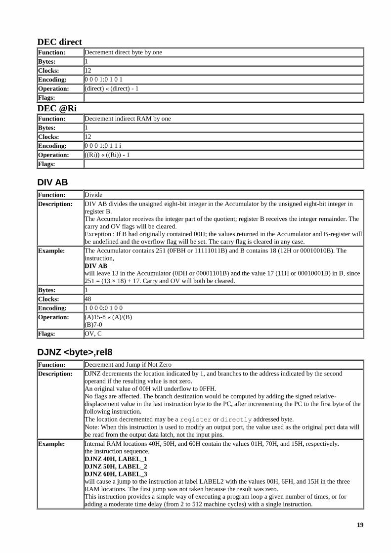
19
DEC direct
Function: Decrement direct byte by one
Bytes: 1
Clocks: 12
Encoding: 0 0 0 1:0 1 0 1
Operation: (direct) « (direct) - 1
Flags:
DEC @Ri Function: Decrement indirect RAM by one
Bytes: 1
Clocks: 12
Encoding: 0 0 0 1:0 1 1 i
Operation: ((Ri)) « ((Ri)) - 1
Flags:
DIV AB
Function: Divide
Description: DIV AB divides the unsigned eight-bit integer in the Accumulator by the unsigned eight-bit integer in
register B.
The Accumulator receives the integer part of the quotient; register B receives the integer remainder. The
carry and OV flags will be cleared.
Exception : If B had originally contained 00H; the values returned in the Accumulator and B-register will
be undefined and the overflow flag will be set. The carry flag is cleared in any case.
Example: The Accumulator contains 251 (0FBH or 11111011B) and B contains 18 (12H or 00010010B). The
instruction,
DIV AB will leave 13 in the Accumulator (0DH or 00001101B) and the value 17 (11H or 00010001B) in B, since
251 = (13 × 18) + 17. Carry and OV will both be cleared.
Bytes: 1
Clocks: 48
Encoding: 1 0 0 0:0 1 0 0
Operation: (A)15-8 « (A)/(B)
(B)7-0
Flags: OV, C
DJNZ <byte>,rel8
Function: Decrement and Jump if Not Zero
Description: DJNZ decrements the location indicated by 1, and branches to the address indicated by the second
operand if the resulting value is not zero.
An original value of 00H will underflow to 0FFH.
No flags are affected. The branch destination would be computed by adding the signed relative-
displacement value in the last instruction byte to the PC, after incrementing the PC to the first byte of the
following instruction.
The location decremented may be a register or directly addressed byte.
Note: When this instruction is used to modify an output port, the value used as the original port data will
be read from the output data latch, not the input pins.
Example: Internal RAM locations 40H, 50H, and 60H contain the values 01H, 70H, and 15H, respectively.
the instruction sequence,
DJNZ 40H, LABEL_1
DJNZ 50H, LABEL_2
DJNZ 60H, LABEL_3 will cause a jump to the instruction at label LABEL2 with the values 00H, 6FH, and 15H in the three
RAM locations. The first jump was not taken because the result was zero.
This instruction provides a simple way of executing a program loop a given number of times, or for
adding a moderate time delay (from 2 to 512 machine cycles) with a single instruction.

20
The instruction sequence,
MOV R2, #8
TOGGLE:
CPL P1.7
DJNZ R2, TOGGLE will toggle P1.7 eight times, causing four output pulses to appear at bit 7 of output Port 1.
Each pulse will last three machine cycles; two for DJNZ and one to alter the pin.
DJNZ Rn,rel8
Function: Decrement register, Jump if Not Zero
Bytes: 2
Clocks: 24
Encoding: 1 1 0 1:1 r r r r7 r6 r5 r4:r3 r2 r1 r0
Operation: (PC) « (PC) + 2
(Rn) « (Rn) - 1
IF (RN) > 0 or (Rn) < 0
THEN
(PC) « (PC) + rel8
Flags:
DJNZ direct,rel8
Function: Decrement direct byte, Jump if Not Zero
Bytes: 3
Clocks: 24
Encoding: 1 1 0 1:0 1 0 1 a7 a6 a5 a4:a3 a2 a1 a0 r7 r6 r5 r4:r3 r2 r1 r0
Operation: (PC) « (PC) + 2
(direct) « (direct) - 1
IF (direct) > 0 or (direct) < 0
THEN
(PC) « (PC) + rel8
Flags:
INC byte
Function: Decrement
Description: INC increments the indicated variable by 1.
An original value of 0FFH will overflow to 00H. No flags are affected.
Four addressing modes are allowed: accumulator, register, direct, or register-
indirect.
Note: When this instruction is used to modify an output port, the value used as the original port data
will be read from the output data latch, not the input pins.
Example: Register 0 contains 7EH (011111110B). Internal locations 7EH and 7FH contain 0FFH and 40H,
respectively.
The instruction sequence,
INC @R0
INC R0
INC @R0 will leave register 0 set to 7FH and internal RAM locations 7EH and 7FH holding (respectively) 00H
and 41H.
INC A
Function: Increment ACC by one
Bytes: 1
Clocks: 12
Encoding: 0 0 0 0:0 1 0 0
Operation: (A) « (A) + 1
Flags:
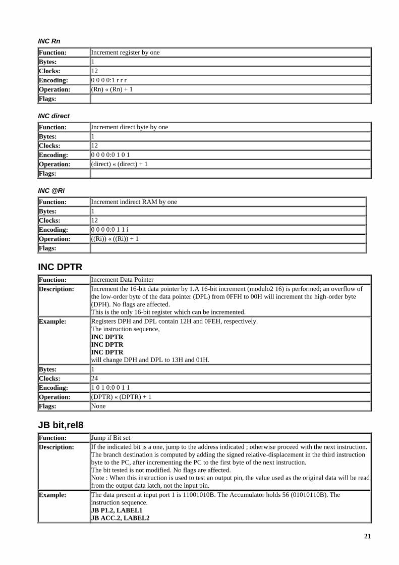
21
INC Rn
Function: Increment register by one
Bytes: 1
Clocks: 12
Encoding: 0 0 0 0:1 r r r
Operation: (Rn) « (Rn) + 1
Flags:
INC direct
Function: Increment direct byte by one
Bytes: 1
Clocks: 12
Encoding: 0 0 0 0:0 1 0 1
Operation: (direct) « (direct) + 1
Flags:
INC @Ri
Function: Increment indirect RAM by one
Bytes: 1
Clocks: 12
Encoding: 0 0 0 0:0 1 1 i
Operation: ((Ri)) « ((Ri)) + 1
Flags:
INC DPTR
Function: Increment Data Pointer
Description: Increment the 16-bit data pointer by 1.A 16-bit increment (modulo2 16) is performed; an overflow of
the low-order byte of the data pointer (DPL) from 0FFH to 00H will increment the high-order byte
(DPH). No flags are affected.
This is the only 16-bit register which can be incremented.
Example: Registers DPH and DPL contain 12H and 0FEH, respectively.
The instruction sequence,
INC DPTR
INC DPTR
INC DPTR will change DPH and DPL to 13H and 01H.
Bytes: 1
Clocks: 24
Encoding: 1 0 1 0:0 0 1 1
Operation: (DPTR) « (DPTR) + 1
Flags: None
JB bit,rel8
Function: Jump if Bit set
Description: If the indicated bit is a one, jump to the address indicated ; otherwise proceed with the next instruction.
The branch destination is computed by adding the signed relative-displacement in the third instruction
byte to the PC, after incrementing the PC to the first byte of the next instruction.
The bit tested is not modified. No flags are affected.
Note : When this instruction is used to test an output pin, the value used as the original data will be read
from the output data latch, not the input pin.
Example: The data present at input port 1 is 11001010B. The Accumulator holds 56 (01010110B). The
instruction sequence.
JB P1.2, LABEL1
JB ACC.2, LABEL2

22
will cause program execution to branch to the instruction at label LABEL 2.
Bytes: 3
Clocks: 24
Encoding: 0 0 1 0:0 0 0 0 b7 b6 b5 b4:b3 b2 b1 b0 r7 r6 r5 r4:r3 r2 r1 r0
Operation: (PC) « (PC) + 3
IF (bit) = 1
THEN
(PC) « (PC) + rel8
Flags: None
JBC bit,rel8
Function: Jump if Bit set and clear bit
Description: If the indicated bit is a one, branch to the address indicated; otherwise proceed with the next
instruction.
The bit will not be cleared if it is already a zero.
The branch destination is computed by adding the signed relative-displacement in the third instruction
byte to the PC, after incrementing the PC to the first byte of the next instruction. No flags are affected.
Note: When this instruction is used to test an output pin, the value used as the original data will be read
from the output data latch, not the input pin.
Example: The Accumulator holds 56H (01010110B).
The instruction sequence,
JBC ACC.3, LABEL 1
JBC ACC.2, LABEL 2 will cause program execution to continue at the instruction identified by the label LABEL2, with the
Accumulator modified to 52H (01010010B).
Bytes: 3
Clocks: 24
Encoding: 0 0 0 1:0 0 0 0 b7 b6 b5 b4:b3 b2 b1 b0 r7 r6 r5 r4:r3 r2 r1 r0
Operation: (PC) « (PC) + 3
IF (bit) = 1
THEN
(bit) « 0
(PC) « (PC) + rel8
Flags: None
JC bit,rel8
Function: Jump if Carry is set
Description: If the carry flag is set, branch to the address indicated ; otherwise proceed with the next instruction.
The branch destination is computed by adding the signed relative-displacement in the second
instruction byte to the PC, after incrementing the PC twice. No flags are affected.
Example: The carry flag is cleared.
The instruction sequence,
JC LABEL1
CPL C
JC LABEL2 will set the carry and cause program execution to continue at the instruction identified by the label
LABEL2.
Bytes: 2
Clocks: 24
Encoding: 0 1 0 0:0 0 0 0 r7 r6 r5 r4:r3 r2 r1 r0
Operation: (PC) « (PC) + 2
IF (C) = 1
THEN
(PC) « (PC) + rel8
Flags: None
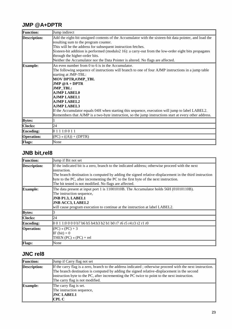
23
JMP @A+DPTR
Function: Jump indirect
Description: Add the eight-bit unsigned contents of the Accumulator with the sixteen-bit data pointer, and load the
resulting sum to the program counter.
This will be the address for subsequent instruction fetches.
Sixteen-bit addition is performed (modulo2 16): a carry-out from the low-order eight bits propagates
through the higher-order bits.
Neither the Accumulator nor the Data Pointer is altered. No flags are affected.
Example: An even number from 0 to 6 is in the Accumulator.
The following sequence of instructions will branch to one of four AJMP instructions in a jump table
starting at JMP-TBL:
MOV DPTR,#JMP_TBL
JMP @A + DPTR
JMP_TBL:
AJMP LABEL0
AJMP LABEL1
AJMP LABEL2
AJMP LABEL3 If the Accumulator equals 04H when starting this sequence, execution will jump to label LABEL2.
Remembers that AJMP is a two-byte instruction, so the jump instructions start at every other address.
Bytes: 1
Clocks: 24
Encoding: 0 1 1 1:0 0 1 1
Operation: (PC) « ((A)) + (DPTR)
Flags: None
JNB bit,rel8
Function: Jump if Bit not set
Description: If the indicated bit is a zero, branch to the indicated address; otherwise proceed with the next
instruction.
The branch destination is computed by adding the signed relative-displacement in the third instruction
byte to the PC, after incrementing the PC to the first byte of the next instruction.
The bit tested is not modified. No flags are affected.
Example: The data present at input port 1 is 11001010B. The Accumulator holds 56H (01010110B).
The instruction sequence,
JNB P1.3, LABEL1
JNB ACC3, LABEL2 will cause program execution to continue at the instruction at label LABEL2.
Bytes: 3
Clocks: 24
Encoding: 0 0 1 1:0 0 0 0 b7 b6 b5 b4:b3 b2 b1 b0 r7 r6 r5 r4:r3 r2 r1 r0
Operation: (PC) « (PC) + 3
IF (bit) = 0
THEN (PC) « (PC) + rel
Flags: None
JNC rel8
Function: Jump if Carry flag not set
Description: If the carry flag is a zero, branch to the address indicated ; otherwise proceed with the next instruction.
The branch destination is computed by adding the signed relative-displacement in the second
instruction byte to the PC, after incrementing the PC twice to point to the next instruction.
The carry flag is not modified.
Example: The carry flag is set.
The instruction sequence,
JNC LABEL1
CPL C

24
JNC LABEL2 will clear the carry and cause program execution to continue at the instruction identified by the label
LABEL2.
Bytes: 2
Clocks: 24
Encoding: 0 1 0 1:0 0 0 0 r7 r6 r5 r4:r3 r2 r1 r0
Operation: (PC) « (PC) + 2
IF (C) = 0
THEN (PC) « (PC) + rel
Flags: None
JNZ rel8
Function: Jump if Accumulator Not Zero
Description: If any bit of the Accumulator is a one, branch to the indicated address; otherwise proceed with the next
instruction.
The branch destination is computed by adding the signed relative-displacement in the second
instruction byte to the PC, after incrementing the PC twice.
The Accumulator is not modified. No flags are affected.
Example: The Accumulator originally holds 00H.
The instruction sequence,
JNZ LABEL1
INC A
JNZ LABEL2 will set the Accumulator to 01H and continue at label LABEL2.
Bytes: 2
Clocks: 24
Encoding: 0 1 1 1:0 0 0 0 r7 r6 r5 r4:r3 r2 r1 r0
Operation: (PC) « (PC) + 2
IF (A) <> 0
THEN (PC) « (PC) + rel
Flags: None
JZ rel8
Function: Jump if Accumulator is Zero
Description: If all bits of the Accumulator are zero, branch to the address indicated; otherwise proceed with the next
instruction.
The branch destination is computed by adding the signed relative-displacement in the second
instruction byte to the PC, after incrementing the PC twice.
The Accumulator is not modified. No flags are affected.
Example: The Accumulator originally contains 01H.
The instruction sequence,
JZ LABEL1
DEC A
JZ LABEL2 will change the Accumulator to 00H and cause program execution at the instruction identified by the
label LABEL2.
Bytes: 2
Clocks: 24
Encoding: 0 1 1 1:0 0 0 0 r7 r6 r5 r4:r3 r2 r1 r0
Operation: (PC) « (PC) + 2
IF (A) = 0
THEN (PC) « (PC) + rel
Flags: None

25
LCALL addr16
Function: Long call
Description: LCALL calls a subroutine located at the indicated address.
The instruction adds three to the program counter to generate the address of the next instruction and
then pushes the 16-bit result onto the stack (low byte first), incrementing the Stack Pointer by two.
The high-order and low-order bytes of the PC are then loaded, respectively, with the second and third
bytes of the LCALL instruction.
Program execution continues with the instruction at this address. The subroutine may therefore begin
anywhere in the full 64K-byte program memory address space. No flags are affected.
Example: Initially the Stack Pointer equals 07H.
The label "SUBRTN" is assigned to program memory location 1234H.
After executing the instruction,
LCALL SUBRTN at location 0123H, the Stack Pointer will contain 09H, internal RAM locations 08H and 09H will
contain 26H and 01H, and the PC will contain 1235H.
Bytes: 3
Clocks: 24
Encoding: 0 0 0 1:0 0 1 0 a15 a14 a13 a12:a11 a10 a9 a8 a7 a6 a5 a4:a3 a2 a1 a0
Operation: (PC) « (PC) + 3
(SP) « (SP) + 1
((SP)) « (PC7-0)
(SP) « (SP) + 1
((SP)) « (PC15-8)
(PC) « addr15-0
Flags: None
LJMP addr16
Function: Long jump
Description: LJMP causes an unconditional branch to the indicated address, by loading the high-order and low-order
bytes of the PC (respectively) with the second and third instruction bytes.
The destination may therefore be anywhere in the full 64K program memory address space. No flags
are affected.
Example: The label "JMPADR" is assigned to the instruction at program memory location 1234H.
The instruction,
LJMP JMPADR at location 0123H will load the program counter with 1234H.
Bytes: 3
Clocks: 24
Encoding: 0 0 0 0:0 0 1 0 a15 a14 a13 a12:a11 a10 a9 a8 a7 a6 a5 a4:a3 a2 a1 a0
Operation: (PC) « addr15-0
Flags: None
MOV <dest>,<source>
Function: Move byte variable
Description: The byte variable indicated the second operand is copied into the location specified by the first
operand.
The source byte is not affected. No other register or flag is affected.
This is by far the most flexible operation.
Fifteen combinations of source and destination addressing modes are allowed: MOV A,Rn MOV A,direct MOV A,@Ri MOV A,#data
MOV Rn,A MOV Rn,direct MOV Rn,#data MOV direct,A MOV direct,Rn MOV direct,direct MOV direct,@Ri MOV direct,#data
MOV @Ri,A MOV @Ri,direct MOV @Ri,#data
Note: Mov A,ACC is not a valid instruction.
Example: Internal RAM location 30H holds 40H. The value of RAM location 40H is 10H.
The data present at input port 1 is 11001010B (0CAH).

26
MOV R0, #30H ; R0 <= 30h
MOV A, @R0 ; A <= 40H
MOV R1, A ; R1 <= 40h
MOV R, @R1 ; B <= 10h
MOV @R1, P1 ; RAM (40H) <= OCAH
MOV P2, P1 ; P2 # 0CAH leaves the value 30H in register 0,40H in both the Accumulator and register 1,10H in register B, and
0CAH (11001010B) both in RAM location 40H and output on port 2.
MOV A,Rn
Function: Move register to ACC
Bytes: 1
Clocks: 12
Encoding: 1 1 1 0:1 r r r
Operation: (A) « (Rn)
Flags:
MOV A,direct
Function: Move direct byte to ACC
Bytes: 2
Clocks: 12
Encoding: 1 1 1 0:0 1 0 1 a7 a6 a5 a4:a3 a2 a1 a0
Operation: (A) « (direct)
Flags:
MOV A,@Ri
Function: Move indirect ram to ACC
Bytes: 1
Clocks: 12
Encoding: 1 1 1 0:0 1 1 i
Operation: (A) « ((Ri))
Flags:
MOV A,#data
Function: Move immediate data to ACC
Bytes: 2
Clocks: 12
Encoding: 0 1 1 1:0 1 0 0 d7 d6 d5 d4:d3 d2 d1 d0
Operation: (A) « #data
Flags:
MOV Rn,A
Function: Move ACC to register
Bytes: 1
Clocks: 12
Encoding: 1 1 1 1:1 r r r
Operation: (Rn) « (A)
Flags:
MOV Rn,direct
Function: Move direct byte to register
Bytes: 2
Clocks: 24

27
Encoding: 1 0 1 0:1 r r r a7 a6 a5 a4:a3 a2 a1 a0
Operation: (Rn) « (direct)
Flags:
MOV Rn,#data
Function: Move immediate data to register
Bytes: 2
Clocks: 12
Encoding: 0 1 1 1:1 r r r d7 d6 d5 d4:d3 d2 d1 d0
Operation: (Rn) « #data
Flags:
MOV direct,A
Function: Move ACC to direct byte
Bytes: 2
Clocks: 12
Encoding: 1 1 1 1:0 1 0 1 a7 a6 a5 a4:a3 a2 a1 a0
Operation: (direct) « (A)
Flags:
MOV direct,Rn
Function: Move register to direct byte
Bytes: 2
Clocks: 24
Encoding: 1 0 0 0:1 r r r a7 a6 a5 a4:a3 a2 a1 a0
Operation: (direct) « (Rn)
Flags:
MOV direct,direct
Function: Move direct byte to direct byte
Bytes: 3
Clocks: 24
Encoding: 1 0 0 0:0 1 0 1 a7 a6 a5 a4:a3 a2 a1 a0(src) a7 a6 a5 a4:a3 a2 a1 a0(dest)
Operation: (direct) « (direct)
Flags:
MOV direct,@Ri
Function: Move indirect ram to direct byte
Bytes: 2
Clocks: 24
Encoding: 1 0 0 0:0 1 1 i a7 a6 a5 a4:a3 a2 a1 a0
Operation: (direct) « ((Ri))
Flags:
MOV direct,#data
Function: Move immediate data to direct byte
Bytes: 3
Clocks: 24
Encoding: 1 0 0 0:0 1 0 1 a7 a6 a5 a4:a3 a2 a1 a0 d7 d6 d5 d4:d3 d2 d1 d0
Operation: (direct) « #data
Flags:

28
MOV @Ri,A
Function: Move ACC to indirect ram
Bytes: 1
Clocks: 12
Encoding: 1 1 1 1:0 1 1 i
Operation: ((Ri)) « (A)
Flags:
MOV @Ri,direct
Function: Move direct byte to indirect ram
Bytes: 2
Clocks: 24
Encoding: 1 0 1 0:0 1 1 i a7 a6 a5 a4:a3 a2 a1 a0
Operation: ((Ri)) « (direct)
Flags:
MOV @Ri,#data
Function: Move immediate data to indirect ram
Bytes: 2
Clocks: 12
Encoding: 0 1 1 1:0 1 1 i d7 d6 d5 d4:d3 d2 d1 d0
Operation: ((Ri)) « #data
Flags:
MOV <dest-bit>,<source-bit>
Function: Move bit data
Description: The Boolean variable indicated by the second operand is copied into the location specified by the first
operand. One of the operands must be the carry flag; the other may be any directly addressable bit.
No other register or flag is affected.
Example: The carry flag is originally set.
The data present at input Port 3 is 11000101B.
The data previously written to output Port 1 is 35H (00110101B).
MOV P1.3, C
MOV C, P3.3
MOV P1.2, C will leave the carry cleared and change Port 1 to 39H (00111001B).
MOV C,bit
Function: Move bit data to Carry
Bytes: 2
Clocks: 12
Encoding: 1 0 1 0:0 0 1 0 b7 b6 b5 b4:b3 b2 b1 b0
Operation: (C) « (bit)
Flags:
MOV A,direct
Function: Move Carry to bit data
Bytes: 2
Clocks: 24
Encoding: 1 0 0 1:0 0 1 0 b7 b6 b5 b4:b3 b2 b1 b0
Operation: (bit) « (C)
Flags:

29
MOV DPTR,#data16
Function: Load data pointer with a 16 bit constant
Description: The Data Pointer is loaded with the 16-bit constant indicated.
the 16-bit constant is loaded into the second and third bytes of the instruction.
The second byte (DPH) is the high-order byte, while the third byte (DPL) holds the low-order byte. No
flags are affected.
This is the only instruction which moves 16-bits of data at once.
Example: The instruction,
MOV DPTR, 1234H will load the value 1234H into the Data Pointer: DPH will hold 12H and DPL will hold 34H.
Bytes: 3
Clocks: 24
Encoding: 1 0 0 1:0 0 0 0 d15 d14 d13 d12:d11 d10 d9 d8 d7 d6 d5 d4:d3 d2 d1 d0
Operation: (DPH) « #data15-8
(DPL) « #data7-0
Flags: None
MOVC A,@A+<base-reg>
Function: Move Code byte
Description: The MOVC instructions load the Accumulator with a code byte, or constant from program memory.
The address of the byte fetched is the sum of the original unsigned eight-bit.
Accumulator contents and the contents of a sixteen-bit base register, which may be either the Data
Pointer or the PC.
In the latter case, PC is incremented to the address of the following instruction before being added with
the
Accumulator; otherwise the base register is not altered. Sixteen-bit addition is performed so a carry-out
from the low-order eight bits may propagate through higher-order bits.
No flags are affected.
Example: A value between 0 and 3 is in the Accumulator.
The following instructions will translate the value in the Accumulator to one of four values defined by
the DB (define byte) directive.
REL_PC: INC A
MOVC A, @A + PC
RET
DB 66H
DB 77H
DB 88H
DB 99H If the subroutine is called with the Accumulator equal to 01H, it will return with 77H in the
Accumulator.
The INC A before the MOVC instruction is needed to "get around" the RET instruction above the table.
If several bytes of code separated the MOVC from the table, the corresponding number would be added
to the Accumulator instead.
Flags:
MOVC A,@A+DPTR
Function: Move Code byte at ACC + DPTR to ACC
Bytes: 1
Clocks: 24
Encoding: 1 0 0 1:0 0 1 1
Operation: (A) « ((A) + (DPTR))
Flags: None
MOVC A,@A+PC
Function: Move Code byte at ACC + PC to ACC
Bytes: 1
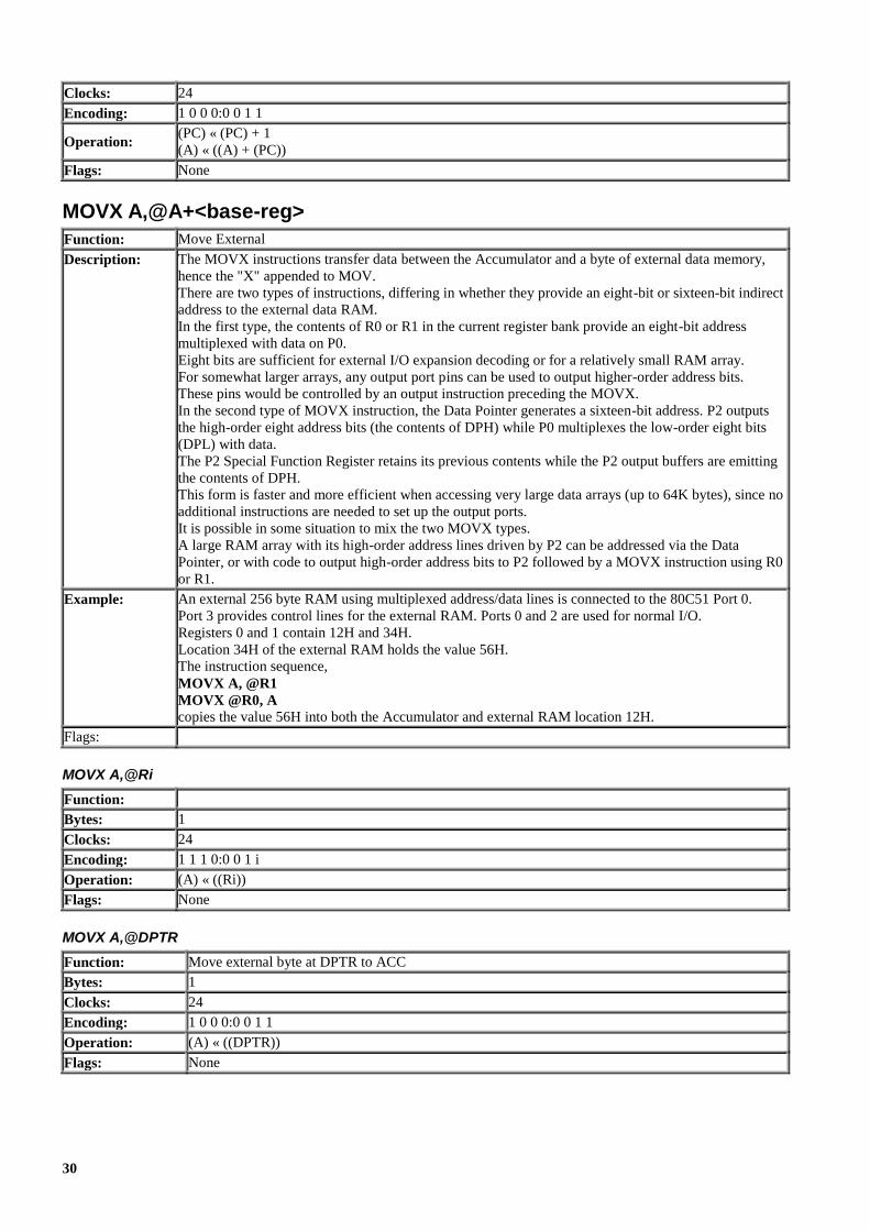
30
Clocks: 24
Encoding: 1 0 0 0:0 0 1 1
Operation: (PC) « (PC) + 1
(A) « ((A) + (PC))
Flags: None
MOVX A,@A+<base-reg>
Function: Move External
Description: The MOVX instructions transfer data between the Accumulator and a byte of external data memory,
hence the "X" appended to MOV.
There are two types of instructions, differing in whether they provide an eight-bit or sixteen-bit indirect
address to the external data RAM.
In the first type, the contents of R0 or R1 in the current register bank provide an eight-bit address
multiplexed with data on P0.
Eight bits are sufficient for external I/O expansion decoding or for a relatively small RAM array.
For somewhat larger arrays, any output port pins can be used to output higher-order address bits.
These pins would be controlled by an output instruction preceding the MOVX.
In the second type of MOVX instruction, the Data Pointer generates a sixteen-bit address. P2 outputs
the high-order eight address bits (the contents of DPH) while P0 multiplexes the low-order eight bits
(DPL) with data.
The P2 Special Function Register retains its previous contents while the P2 output buffers are emitting
the contents of DPH.
This form is faster and more efficient when accessing very large data arrays (up to 64K bytes), since no
additional instructions are needed to set up the output ports.
It is possible in some situation to mix the two MOVX types.
A large RAM array with its high-order address lines driven by P2 can be addressed via the Data
Pointer, or with code to output high-order address bits to P2 followed by a MOVX instruction using R0
or R1.
Example: An external 256 byte RAM using multiplexed address/data lines is connected to the 80C51 Port 0.
Port 3 provides control lines for the external RAM. Ports 0 and 2 are used for normal I/O.
Registers 0 and 1 contain 12H and 34H.
Location 34H of the external RAM holds the value 56H.
The instruction sequence,
MOVX A, @R1
MOVX @R0, A copies the value 56H into both the Accumulator and external RAM location 12H.
Flags:
MOVX A,@Ri
Function:
Bytes: 1
Clocks: 24
Encoding: 1 1 1 0:0 0 1 i
Operation: (A) « ((Ri))
Flags: None
MOVX A,@DPTR
Function: Move external byte at DPTR to ACC
Bytes: 1
Clocks: 24
Encoding: 1 0 0 0:0 0 1 1
Operation: (A) « ((DPTR))
Flags: None

31
MOVX @Ri,A
Function:
Bytes: 1
Clocks: 24
Encoding: 1 1 1 1:0 0 1 i
Operation: ((Ri)) « (A)
Flags: None
MOVX @DPTR,A
Function: Move ACC to external byte at DPTR
Bytes: 1
Clocks: 24
Encoding: 1 1 1 1:0 0 0 0
Operation: ((DPTR)) « (A)
Flags: None
MUL AB
Function: Multiply
Description: MUL AB multiplies the unsigned eight-bit integers in the Accumulator and register B.
The low-order byte of the sixteen-bit product is left in the Accumulator, and the high-order byte in B.
If the product is greater than 255 (OFFH) the overflow flag is set; otherwise it is cleared.
The carry flag is always cleared.
Example: Originally the Accumulator holds the value 80 (50H).
Register B holds the value 160 (OAOH).
The instruction,
MUL AB will give the product 12,800 (3200H), so B is changed to 32H (00110010B) and the Accumulator is
cleared.
The overflow flag is set, carry is cleared.
Bytes: 1
Clocks: 48
Encoding: 1 0 1 0:0 1 0 0
Operation: (PC) « (PC) + 1
Flags: OV C
NOP
Function: No Operation
Description: Execution continue at the following instruction.
Other than the PC, no registers or flags are effected.
Example: It is desired to produce a low-going output pulse on bit 7 of Port 2 lasting exactly 5 cycles.
A simple SETB/CLR sequence would generate a one-cycle pulse, so four additional cycles must be
inserted.
This may be done (assuming no interrupts are enable) with the instruction sequence.
CLR P2.7
NOP
NOP
NOP
NOP
SETB P2.7
Bytes: 1
Clocks: 12
Encoding: 0 0 0 0:0 0 0 0
Operation: (PC) « (PC) + 1
Flags: None

32
ORL <dest-byte>,<src-byte>
Function: Logical-OR for byte variables
Description: ORL performs the bitwise logical-OR operation between the indicated variables, storing the results in
the destination byte.
The two operands allow six addressing mode combinations.
When the destination is the Accumulator, the source can use register, direct, register-
indirect, or immediate addressing; when the destination is a direct address, the source can be the
Accumulator or immediate data.
Note: When this instruction is used to modify an output port, the value used as the original port data
will be read from the output data latch, not the input pins.
No flags are affected.
Example: If the Accumulator holds 0C3H (11000011B) and R0 holds 55H (01010101B) then the instruction,
ORL A, R0 will leave the Accumulator holding the value 0D7H (11010111B).
When the destination is a directly addressed byte, the instruction can set combinations of bits in any
RAM location or hardware register.
The pattern of bits to be set is determined by a mask byte, which may be either a constant data value in
the instruction or a variable computed in the Accumulator at run-time.
The instruction.,
ORL P1, #00110010b will set bits 5, 4, and 1 of output Port 1.
ORL A,Rn
Function: Logical OR register byte to ACC
Bytes: 1
Clocks: 12
Encoding: 0 1 0 0:1 r r r
Operation: (A) « (A) v (Rn)
Flags:
ORL A,direct
Function: Logical OR direct byte to ACC
Bytes: 2
Clocks: 12
Encoding: 0 1 0 0:0 1 0 1 a7 a6 a5 a4:a3 a2 a1 a0
Operation: (A) « (A) v (direct)
Flags:
ORL A,@Ri
Function: Logical OR indirect RAM to ACC
Bytes: 1
Clocks: 12
Encoding: 0 1 0 0:0 1 1 i
Operation: (A) « (A) v ((Ri))
Flags:
ORL A,#data
Function: Logical OR immediate data to ACC
Bytes: 2
Clocks: 12
Encoding: 0 1 0 0:0 1 0 0 d7 d6 d5 d4:d3 d2 d1 d0
Operation: (A) « (A) v #data
Flags:

33
ORL direct,A
Function: Logical OR ACC to direct data
Bytes: 2
Clocks: 12
Encoding: 0 1 0 0:0 0 1 0 d7 d6 d5 d4:d3 d2 d1 d0
Operation: (direct) « (direct) v ACC
Flags:
ORL direct,#data
Function: Logical OR immediate data to direct data
Bytes: 3
Clocks: 24
Encoding: 0 1 0 0:0 0 1 1 a7 a6 a5 a4:a3 a2 a1 a0 d7 d6 d5 d4:d3 d2 d1 d0
Operation: (direct) « (direct) v #data
Flags:
ORL C,<src-bit>
Function: Logical OR for bit variables
Description: Set the carry flag if the Boolean value is a logical 1; leave the carry in its current state otherwise.
A slash ("/") preceding the operand in the assembly language indicates that the logical complement of
the addressed bit is used as the source value, but the source bit it self is not affected.
No other flags are affected.
Example: Set the carry flag if and only if P1.0 = 1, ACC.7 = 1, or OV = 0.
MOV C, P1.0 ; LOAD CARRY WITH INPUT PIN P1.0
ORL C, ACC.7 ; OR CARRY WITH THE ACC BIT 7
ORL C,/OV ; OR CARRY WITH THE INVERSE OF OV
ORL C,bit
Function: Logical OR bit variable to carry
Bytes: 2
Clocks: 24
Encoding: 0 1 1 1:0 0 1 0 b7 b6 b5 b4:b3 b2 b1 b0
Operation: (C) « (C) v (bit)
Flags: C
ORL C,/bit
Function: Logical OR complement of bit variable to carry
Bytes: 2
Clocks: 24
Encoding: 1 0 1 0:0 0 0 0 b7 b6 b5 b4:b3 b2 b1 b0
Operation: (C) « (C) v (bit)
Flags: C
POP direct
Function: Pop from the stack
Description: The contents of internal RAM location addressed by the Stack Pointer is read, and the Stack Pointer is
decremented by one.
The value read is then transferred to the directly addressed byte indicated.
No flags are affected.
Example: The Stack Pointer originally contains the value 32H, and internal RAM locations 30H through 32H
contain the values 20H, 23H, and 01H, respectively.
The instruction sequence,
POP DPH

34
POP DPL will leave the Stack Pointer equal to the value 30H and the Data Pointer set to 0123H.
At this point the instruction,
POP SP will leave the Stack Pointer set to 20H.
Note that in this special case the Stack Pointer was decremented to 2FH before being loaded with the
value popped (20H).
Bytes: 2
Clocks: 24
Encoding: 1 1 0 1:0 0 0 0 a7 a6 a5 a4:a3 a2 a1 a0
Operation: (direct) « ((SP))
(SP) « (SP) -1
Flags: None
PUSH direct
Function: Push onto the stack
Description: The Stack Pointer is incremented by one.
The contents for the indicated variable is then copied into the internal RAM location addressed by the
Stack Pointer.
Otherwise no flags are affected.
Example: On entering interrupt routine the Stack Pointer contains 09H.
The Data Pointer holds the value 0123H.
The instruction sequence,
PUSH DPL
PUSH DPH will leave the Stack Pointer set to 0BH and store 23H and 01H in internal RAM location 0AH and 0BH,
respectively.
Bytes: 2
Clocks: 24
Encoding: 1 1 0 0:0 0 0 0 a7 a6 a5 a4:a3 a2 a1 a0
Operation: (SP) « (SP) + 1
((SP)) « (direct)
Flags: None
RET
Function: Return from subroutine
Description: RET pops the high-and low-order bytes of the PC successively from the stack, decrementing the Stack
Pointer by two.
Program execution continues at the resulting address, generally the instruction immediately following en
ACALL or LCALL.
No flags are affected.
Example: The Stack Pointer originally contains the value 0BH.
Internal RAM locations 0AH and 0BH contain the values 23H, and 01H, respectively.
The instruction,
RET will leave the Stack Pointer equal to the value 09H. Program execution will continue at location 0123H.
Bytes: 1
Clocks: 24
Encoding: 0 0 1 0:0 0 1 0
Operation: (PC15-8) « ((SP))
(SP) « (SP) - 1
(PC7-0) « ((SP))
(SP) « (SP) - 1
Flags: None

35
RETI
Function: Return from interrupt
Description: RETI pops the high-and low-order bytes of the PC successively from the stack, and restores the interrupt
logic to accept additional interrupts at the same priority level as the one just processed.
The Stack Pointer is left decremented by two. No other registers are affected; the PSW is not
automatically restored to its pre-interrupt status.
Program execution continues at the resulting address, which is generally the instruction immediately after
the point at which the interrupt request was detected.
If a lower-or-same-level interrupt had been pending when the RETI instruction is executed, that one
instruction will be executed before the pending interrupt is processed.
Example: The Stack Pointer originally contains the value 0BH.
An interrupt was detected during the instruction ending at location 0122H.
Internal RAM locations 0AH and 0BH contain the values 23H and 01H, respectively.
The instruction,
RETI will leave the Stack Pointer equal to 09H and return program execution to location 0123H.
Bytes: 1
Clocks: 24
Encoding: 0 0 1 1:0 0 1 0
Operation: (PC15-8) « ((SP))
(SP) « (SP) - 1
(PC7-0) « ((SP))
(SP) « (SP) - 1
Flags: None
RL A
Function: Rotate Accumulator Left
Description: The eight bits in the Accumulator are rotated one bit to the left.
Bit 7 rotated into the bit 0 position.
No flags are affected.
Example: The Accumulator holds the value 0C5H (11000101B).
The instruction,
RL A leaves the Accumulator holding the value 8BH (10001011B) with the carry unaffected.
Bytes: 1
Clocks: 12
Encoding: 0 0 1 0:0 0 1 1
Operation: (An + 1) « (An) n = 0-6
(A0) « (A7)
Flags: None
RLC A
Function: Rotate Accumulator Left through the Carry flag
Description: The eight bits in the Accumulator and the carry flag are together rotated one bit to the left.
Bit 7 moves into the carry flag; the original state of the carry flag moves into the bit 0 position.
No other flags are affected.
Example: The Accumulator holds the value 0C5H (11000101B), and the carry is zero.
The instruction,
RCL A leaves the Accumulator holding the value 8BH (10001010B) with the carry set.
Bytes: 1
Clocks: 12
Encoding: 0 0 1 1:0 0 1 1
Operation: (An + 1) « (An) n = 0-6
(A0) « (C)
(C) « (A7)

36
Flags: C
RR A
Function: Rotate Accumulator Right
Description: The eight bits in the Accumulator are rotated one bit to the right.
Bit 0 is rotated into the bit 7 position.
No flags are affected.
Example: The Accumulator holds the value 0C5H (11000101B).
The instruction,
RR A leaves the Accumulator holding the value 0E2H (11100010B) with the carry unaffected.
Bytes: 1
Clocks: 12
Encoding: 0 0 0 0:0 0 1 1
Operation: (An) « (An + 1) n = 0-6
(A7) « (A0)
Flags: none
RRC A
Function: Rotate Accumulator Right through Carry flag
Description: The eight bits in the Accumulator and the carry flag are together rotated one bit to the right.
Bit 0 moves into the carry flag; the original value of the carry flag moves into the bit 7 position.
No other flags are affected.
Example: The Accumulator holds the value 0C5H (11000101B), and the carry is zero.
The instruction,
RRC A leaves the Accumulator holding the value 62 (01100010B) with the carry set.
Bytes: 1
Clocks: 12
Encoding: 0 0 0 1:0 0 1 1
Operation: (An) « (An + 1) n = 0-6
(A7) « (C)
(C) « (A0)
Flags: C
SETB <bit>
Function: Setb bit
Description: SETB sets the indicated bit to one. SETB can operate on the carry flag or any direct addressable bit.
No other flags are affected.
Example: The carry flag is cleared.
Output Port 1 has been written with the value 34H (00110100B).
The instructions,
SETB C
SETB P1.0 will leave the carry flag set to 1 and change the data output on Port 1 to 35H (00110101B).
SETB C
Function: Set the Carry
Bytes: 1
Clocks: 12
Encoding: 1 1 0 1:0 0 1 1
Operation: (C) « 1
Flags: C
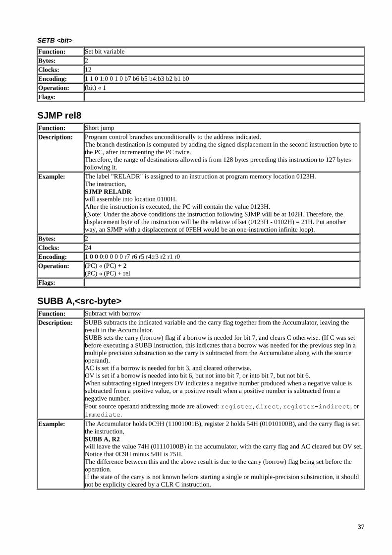
37
SETB <bit>
Function: Set bit variable
Bytes: 2
Clocks: 12
Encoding: 1 1 0 1:0 0 1 0 b7 b6 b5 b4:b3 b2 b1 b0
Operation: (bit) « 1
Flags:
SJMP rel8
Function: Short jump
Description: Program control branches unconditionally to the address indicated.
The branch destination is computed by adding the signed displacement in the second instruction byte to
the PC, after incrementing the PC twice.
Therefore, the range of destinations allowed is from 128 bytes preceding this instruction to 127 bytes
following it.
Example: The label "RELADR" is assigned to an instruction at program memory location 0123H.
The instruction,
SJMP RELADR will assemble into location 0100H.
After the instruction is executed, the PC will contain the value 0123H.
(Note: Under the above conditions the instruction following SJMP will be at 102H. Therefore, the
displacement byte of the instruction will be the relative offset (0123H - 0102H) = 21H. Put another
way, an SJMP with a displacement of 0FEH would be an one-instruction infinite loop).
Bytes: 2
Clocks: 24
Encoding: 1 0 0 0:0 0 0 0 r7 r6 r5 r4:r3 r2 r1 r0
Operation: (PC) « (PC) + 2
(PC) « (PC) + rel
Flags:
SUBB A,<src-byte>
Function: Subtract with borrow
Description: SUBB subtracts the indicated variable and the carry flag together from the Accumulator, leaving the
result in the Accumulator.
SUBB sets the carry (borrow) flag if a borrow is needed for bit 7, and clears C otherwise. (If C was set
before executing a SUBB instruction, this indicates that a borrow was needed for the previous step in a
multiple precision substraction so the carry is subtracted from the Accumulator along with the source
operand).
AC is set if a borrow is needed for bit 3, and cleared otherwise.
OV is set if a borrow is needed into bit 6, but not into bit 7, or into bit 7, but not bit 6.
When subtracting signed integers OV indicates a negative number produced when a negative value is
subtracted from a positive value, or a positive result when a positive number is subtracted from a
negative number.
Four source operand addressing mode are allowed: register, direct, register-indirect, or
immediate.
Example: The Accumulator holds 0C9H (11001001B), register 2 holds 54H (01010100B), and the carry flag is set.
the instruction,
SUBB A, R2 will leave the value 74H (01110100B) in the accumulator, with the carry flag and AC cleared but OV set.
Notice that 0C9H minus 54H is 75H.
The difference between this and the above result is due to the carry (borrow) flag being set before the
operation.
If the state of the carry is not known before starting a single or multiple-precision substraction, it should
not be explicity cleared by a CLR C instruction.

38
SUBB A,Rn
Function: Subtract register to ACC with borrow
Bytes: 1
Clocks: 12
Encoding: 1 0 0 1:1 r r r
Operation: (A) « (A) - (C) - (Rn)
Flags: C AC OV
SUBB A,direct
Function: Subtract direct byte to ACC with borrow
Bytes: 2
Clocks: 12
Encoding: 1 0 0 1:0 1 0 1 a7 a6 a5 a4:a3 a2 a1 a0
Operation: (A) « (A) - (C) - (direct)
Flags: C AC OV
SUBB A,@Ri
Function: Subtract indirect RAM to ACC with borrow
Bytes: 1
Clocks: 12
Encoding: 1 0 0 1:0 1 1 i
Operation: (A) « (A) - (C) - ((Ri))
Flags: C AC OV
SUBB A,#data
Function: Subtract immediate data to ACC with borrow
Bytes: 2
Clocks: 12
Encoding: 1 0 0 1:0 1 0 0 d7 d6 d5 d4:d3 d2 d1 d0
Operation: (A) « (A) - (C) - #data
Flags: C AC OV
SWAP A
Function: Swap nibbles within the Accumulator
Description: SWAP A interchanges the low-and high-order nibbles (four-bit fields) of the Accumulator (bits 3-0 and
bits 7-4).
The operation can also be thought of a four-bit rotate instruction.
No flags are affected.
Example: The Accumulator holds the value 0C5H (11000101B).
The instruction,
SWAP A leave the Accumulator holding the value 5CH (01011100B).
Bytes: 1
Clocks: 12
Encoding: 1 1 0 0:0 1 0 0
Operation: (A3-0) «» (A7-4)
Flags: None
XCH A,<byte>
Function: Exchange Accumulator with byte variable
Description: XCH loads the Accumulator with the contents of the indicated variable, at the same time writing the
original Accumulator contents to the indicated variable.

39
The source/destination operand can use register, direct or register-indirect addressing.
Example: R0 contains the addres 20H.
The Accumulator holds the value 3FH (00111111B).
Internal RAM location 20H holds the value 75H (01110101B).
The instruction,
XCH A, @R0 will leave RAM location 20H holding the values 3FH (00111111B) and 75H (01110101B) in the
Accumulator.
XCH A,Rn
Function: Exchange ACC with register
Bytes: 1
Clocks: 12
Encoding: 1 1 0 0:1 r r r
Operation: (A) «» (Rn)
Flags:
XCH A,direct
Function: Exchange ACC with direct byte
Bytes: 2
Clocks: 12
Encoding: 1 1 0 0:0 1 0 1 a7 a6 a5 a4:a3 a2 a1 a0
Operation: (A) «» (direct)
Flags:
XCH A,@Ri
Function: Exchange ACC with indirect RAM
Bytes: 1
Clocks: 12
Encoding: 1 1 0 0:0 1 1 i
Operation: (A) «» ((Ri))
Flags:
XCHD A,@Ri
Function: Exchange digit
Description: XCHD exchanges the low order nibble of the ACC (Bits 3-0), generally representing a hexadecimal or
BCD digit, with that of the internal RAM location indirectly addressed by the specified register.
The high order nibbles (bits 7-4) of each register are not affected.
No flags are affected.
Example: R0 contains the address 20H.
The ACC holds the value 36H (00110110b).
Internal RAM location 20H holds the value 75H (01110101b).
The instruction,
XHCD A,@R0 will leave RAM location 20H holding the value 76H (01110110b) and 35H (00110101B) in the ACC.
Bytes: 1
Clocks: 12
Encoding: 1 1 0 1:0 1 1 i
Operation: (A3-0) «» ((Ri3-0))
Flags:

40
XRL <dest-byte>,<src-byte>
Function: Logical Exclusive OR for byte variables
Description: XRL performs the bitwise logical Exclusive OR operation between the variables indicated and stores the
results in the destination variable. No flags are affected. The two operands allow six addressing mode
combinations.
When the destination is the Accumulator, the source can use register, direct, register-
indirect, or immediate addressing; when the destination is a direct address, the source can be the
Accumulator or immediate data.
Note: When this instruction is used to modify an output port, the value used as the original port data will
be read from the output data latch, not the input pins.
Example: If the Accumulator holds 0C3H (11000011B) and register 0 holds AAH (10101010B) then the
instruction,
XRL A, R0 will leave 69H (01101001B) in the Accumulator.
When the destination is a directly addressed byte, this instruction can complement combinations of bits
in any RAM location or hardware register.
The mask byte determining the pattern of bits to be cleared would either be a constant contained in the
instruction or a value computed in the Accumulator at run-time.
The instruction,
XRL P1, #00110001B will complement bits 5, 4, and 0 of output port 1.
XRL A,Rn
Function: Logical Exclusive OR register byte to ACC
Bytes: 1
Clocks: 12
Encoding: 0 1 1 0:1 r r r
Operation: (A) « (A) XOR (Rn)
Flags:
XRL A,direct
Function: Logical Exclusive OR direct byte to ACC
Bytes: 2
Clocks: 12
Encoding: 0 1 1 0:0 1 0 1 a7 a6 a5 a4:a3 a2 a1 a0
Operation: (A) « (A) XOR (direct)
Flags:
XRL A,@Ri
Function: Logical Exclusive OR indirect RAM to ACC
Bytes: 1
Clocks: 12
Encoding: 0 1 1 0:0 1 1 i
Operation: (A) « (A) XOR ((Ri))
Flags:
XRL A,#data
Function: Logical Exclusive OR immediate data to ACC
Bytes: 2
Clocks: 12
Encoding: 0 1 1 0:0 1 0 0 d7 d6 d5 d4:d3 d2 d1 d0
Operation: (A) « (A) XOR #data
Flags:

41
XRL direct,A
Function: Logical Exclusive OR ACC to direct data
Bytes: 2
Clocks: 12
Encoding: 0 1 1 0:0 0 1 0 d7 d6 d5 d4:d3 d2 d1 d0
Operation: (direct) « (direct) XOR ACC
Flags:
ANL direct,#data
Function: Logical Exclusive OR immediate data to direct data
Bytes: 3
Clocks: 24
Encoding: 0 1 1 0:0 0 1 1 a7 a6 a5 a4:a3 a2 a1 a0 d7 d6 d5 d4:d3 d2 d1 d0
Operation: (direct) « (direct) XOR #data
Flags: